Embed Size (px)
Citation preview
0
50
100
150
200
250
300
350
400
450
500
-40 -25 -10 5 20 35 50 65 80 95 110 125
TA – Temperature – °C
(VIN
–V
OU
T)
–D
rop
ou
tV
olt
ag
e–
mV
RL = 100 µA
RL = 100 mA
IL
I
Product
Folder
Sample &Buy
Technical
Documents
Tools &
Software
Support &Community
LP2950, LP2951SLVS582I –APRIL 2006–REVISED NOVEMBER 2014
LP295x Adjustable Micropower Voltage Regulators with Shutdown1 Features 2 Applications1• Wide Input Range: Up to 30 V • Applications with High-Voltage Input• Rated Output Current of 100 mA • Power Supplies• Low Dropout: 380 mV (Typ) at 100 mA
3 Description• Low Quiescent Current: 75 μA (Typ)The LP2950 and LP2951 devices are bipolar, low-• Tight Line Regulation: 0.03% (Typ) dropout voltage regulators that can accommodate a
• Tight Load Regulation: 0.04% (Typ) wide input supply-voltage range of up to 30 V. Theeasy-to-use, 3-pin LP2950 is available in fixed-output• High VO Accuracyvoltages of 5 V, 3.3 V, and 3 V. However, the 8-pin– 1.4% at 25°CLP2951 is able to output either a fixed or adjustable
– 2% Over Temperature output from the same device. By tying the OUTPUT• Can Be Used as a Regulator or Reference and SENSE pins together, and the FEEDBACK and
VTAP pins together, the LP2951 outputs a fixed 5 V,• Stable With Low ESR (>12 mΩ) Capacitors3.3 V, or 3 V (depending on the version).• Current- and Thermal-Limiting Features Alternatively, by leaving the SENSE and VTAP pins
• LP2950 Only (3-Pin Package) open and connecting FEEDBACK to an externalresistor divider, the output can be set to any value– Fixed-Output Voltages of 5 V, 3.3 V, and 3 Vbetween 1.235 V to 30 V.• LP2951 Only (8-Pin Package)
– Fixed- or Adjustable-Output Voltages: Device Information(1)
5 V/ADJ, 3.3 V/ADJ, and 3 V/ADJ PART NUMBER PACKAGE BODY SIZE (NOM)– Low-Voltage Error Signal on Falling Output LP2950 TO-92 (3) 4.83 mm x 4.83 mm– Shutdown Capability SOIC (8) 4.90 mm x 3.90 mm
LP2951– Remote Sense Capability for Optimal Output SON (8) 3.00 mm x 3.00 mmRegulation and Accuracy (1) For all available packages, see the orderable addendum at
the end of the data sheet.
Dropout Voltage vs Temperature
1
An IMPORTANT NOTICE at the end of this data sheet addresses availability, warranty, changes, use in safety-critical applications,intellectual property matters and other important disclaimers. PRODUCTION DATA.
LP2950, LP2951SLVS582I –APRIL 2006–REVISED NOVEMBER 2014 www.ti.com
Table of Contents7.3 LP2951 Functional Block Diagram.......................... 131 Features .................................................................. 17.4 Feature Description................................................. 142 Applications ........................................................... 17.5 Device Functional Modes........................................ 153 Description ............................................................. 1
8 Application and Implementation ........................ 164 Revision History..................................................... 28.1 Application Information............................................ 165 Pin Configuration and Functions ......................... 38.2 Typical Application ................................................. 166 Specifications......................................................... 4
9 Power Supply Recommendations ...................... 196.1 Absolute Maximum Ratings ...................................... 410 Layout................................................................... 196.2 Handling Ratings ...................................................... 4
10.1 Layout Guidelines ................................................. 196.3 Recommended Operating Conditions....................... 410.2 Layout Example .................................................... 196.4 Thermal Information .................................................. 4
11 Device and Documentation Support ................. 196.5 Electrical Characteristics........................................... 511.1 Trademarks ........................................................... 196.6 Typical Characteristics .............................................. 711.2 Electrostatic Discharge Caution............................ 197 Detailed Description ............................................ 1211.3 Glossary ................................................................ 197.1 Overview ................................................................. 12
12 Mechanical, Packaging, and Orderable7.2 LP2950 Functional Block Diagram.......................... 12Information ........................................................... 19
4 Revision History
Changes from Revision H (March 2012) to Revision I Page
• Added Applications, Device Information table, Handling Ratings table, Feature Description section, DeviceFunctional Modes, Application and Implementation section, Power Supply Recommendations section, Layoutsection, Device and Documentation Support section, and Mechanical, Packaging, and Orderable Information section. ..... 1
• Removed Ordering Information table. .................................................................................................................................... 1
2 Submit Documentation Feedback Copyright © 2006–2014, Texas Instruments Incorporated
Product Folder Links: LP2950 LP2951
1
2
3
4
8
7
6
5
INPUT
FEEDBACK
VTAP
ERROR
OUTPUT
SENSE
SHUTDOWN
GND
LP2951
D OR P PACKAGE
(TOP VIEW)
OUTPUT
GND
INPUT
LP2950
LP PACKAGE
(BOTTOM VIEW)
LP2951
DRG PACKAGE
(TOP VIEW)
1
2
3
4
8
7
6
5
INPUT
FEEDBACK
VTAP
ERROR
OUTPUT
SENSE
SHUTDOWN
GND
Thermal
Pad
LP2950, LP2951www.ti.com SLVS582I –APRIL 2006–REVISED NOVEMBER 2014
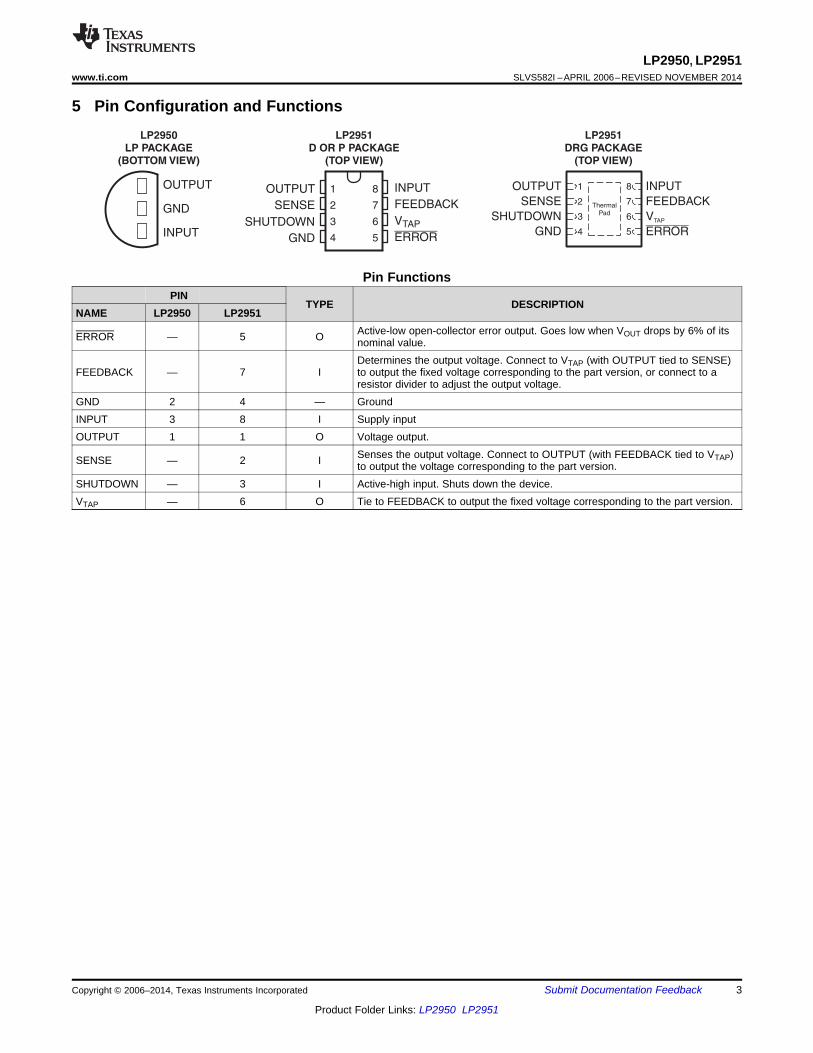
5 Pin Configuration and Functions
Pin FunctionsPIN
TYPE DESCRIPTIONNAME LP2950 LP2951
Active-low open-collector error output. Goes low when VOUT drops by 6% of itsERROR — 5 O nominal value.Determines the output voltage. Connect to VTAP (with OUTPUT tied to SENSE)
FEEDBACK — 7 I to output the fixed voltage corresponding to the part version, or connect to aresistor divider to adjust the output voltage.
GND 2 4 — GroundINPUT 3 8 I Supply inputOUTPUT 1 1 O Voltage output.
Senses the output voltage. Connect to OUTPUT (with FEEDBACK tied to VTAP)SENSE — 2 I to output the voltage corresponding to the part version.SHUTDOWN — 3 I Active-high input. Shuts down the device.VTAP — 6 O Tie to FEEDBACK to output the fixed voltage corresponding to the part version.
Copyright © 2006–2014, Texas Instruments Incorporated Submit Documentation Feedback 3
Product Folder Links: LP2950 LP2951
LP2950, LP2951SLVS582I –APRIL 2006–REVISED NOVEMBER 2014 www.ti.com
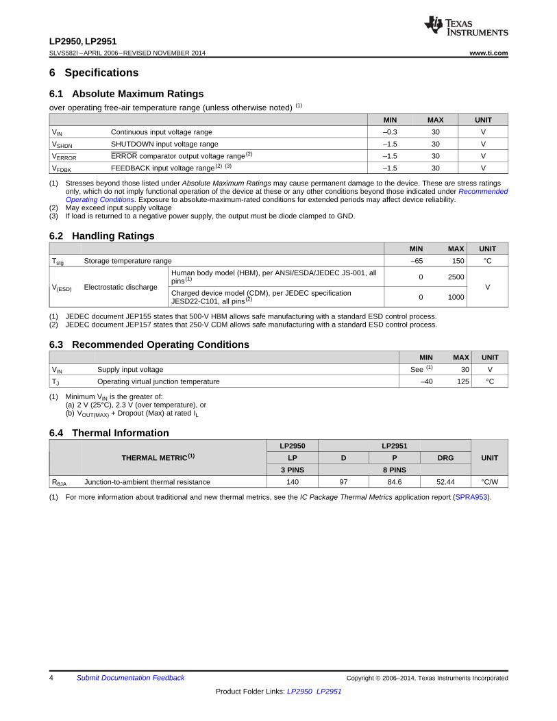
6 Specifications
6.1 Absolute Maximum Ratingsover operating free-air temperature range (unless otherwise noted) (1)
MIN MAX UNITVIN Continuous input voltage range –0.3 30 VVSHDN SHUTDOWN input voltage range –1.5 30 VVERROR ERROR comparator output voltage range (2) –1.5 30 VVFDBK FEEDBACK input voltage range (2) (3) –1.5 30 V
(1) Stresses beyond those listed under Absolute Maximum Ratings may cause permanent damage to the device. These are stress ratingsonly, which do not imply functional operation of the device at these or any other conditions beyond those indicated under RecommendedOperating Conditions. Exposure to absolute-maximum-rated conditions for extended periods may affect device reliability.
(2) May exceed input supply voltage(3) If load is returned to a negative power supply, the output must be diode clamped to GND.
6.2 Handling RatingsMIN MAX UNIT
Tstg Storage temperature range –65 150 °CHuman body model (HBM), per ANSI/ESDA/JEDEC JS-001, all 0 2500pins (1)
V(ESD) Electrostatic discharge VCharged device model (CDM), per JEDEC specification 0 1000JESD22-C101, all pins (2)
(1) JEDEC document JEP155 states that 500-V HBM allows safe manufacturing with a standard ESD control process.(2) JEDEC document JEP157 states that 250-V CDM allows safe manufacturing with a standard ESD control process.
6.3 Recommended Operating ConditionsMIN MAX UNIT
VIN Supply input voltage See (1) 30 VTJ Operating virtual junction temperature –40 125 °C
(1) Minimum VIN is the greater of:(a) 2 V (25°C), 2.3 V (over temperature), or(b) VOUT(MAX) + Dropout (Max) at rated IL
6.4 Thermal InformationLP2950 LP2951
THERMAL METRIC (1) LP D P DRG UNIT3 PINS 8 PINS
RθJA Junction-to-ambient thermal resistance 140 97 84.6 52.44 °C/W
(1) For more information about traditional and new thermal metrics, see the IC Package Thermal Metrics application report (SPRA953).
4 Submit Documentation Feedback Copyright © 2006–2014, Texas Instruments Incorporated
Product Folder Links: LP2950 LP2951
LP2950, LP2951www.ti.com SLVS582I –APRIL 2006–REVISED NOVEMBER 2014
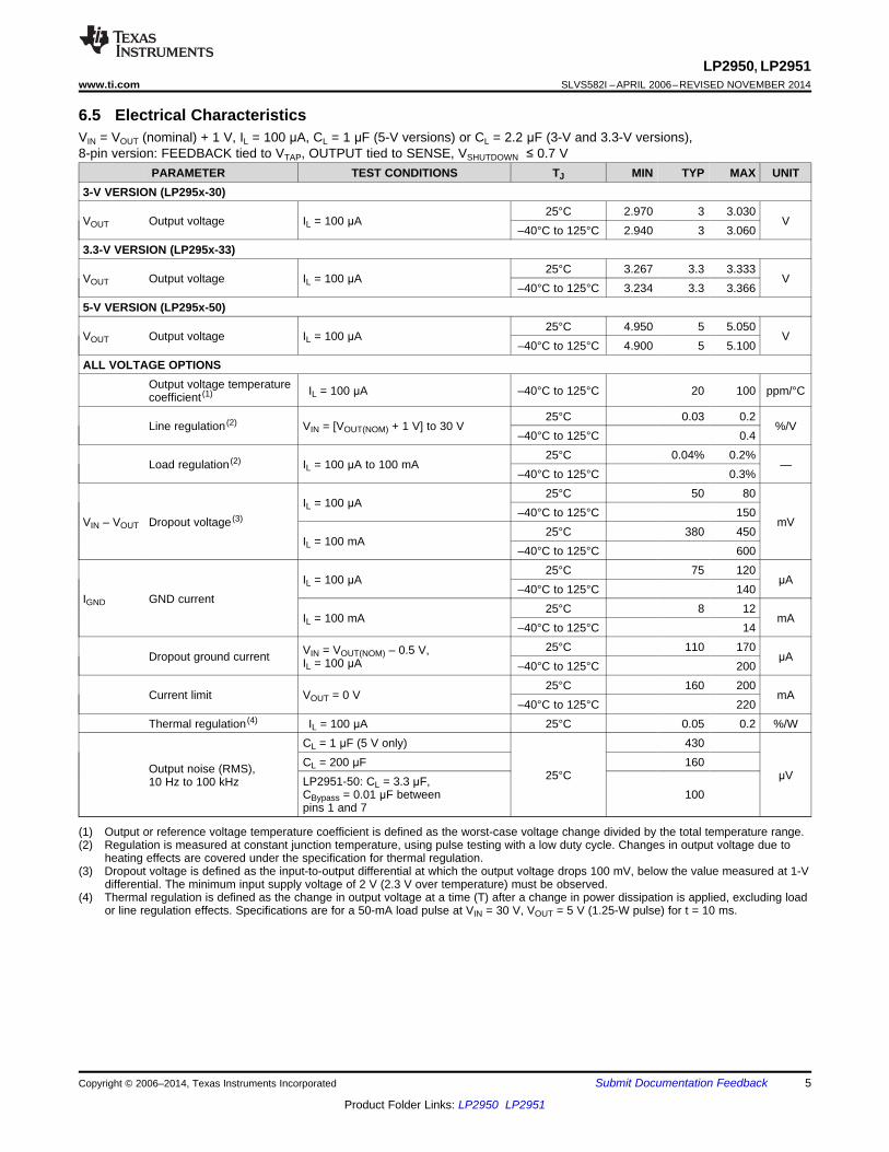
6.5 Electrical CharacteristicsVIN = VOUT (nominal) + 1 V, IL = 100 μA, CL = 1 μF (5-V versions) or CL = 2.2 μF (3-V and 3.3-V versions),8-pin version: FEEDBACK tied to VTAP, OUTPUT tied to SENSE, VSHUTDOWN ≤ 0.7 V
PARAMETER TEST CONDITIONS TJ MIN TYP MAX UNIT3-V VERSION (LP295x-30)
25°C 2.970 3 3.030VOUT Output voltage IL = 100 μA V
–40°C to 125°C 2.940 3 3.0603.3-V VERSION (LP295x-33)
25°C 3.267 3.3 3.333VOUT Output voltage IL = 100 μA V
–40°C to 125°C 3.234 3.3 3.3665-V VERSION (LP295x-50)
25°C 4.950 5 5.050VOUT Output voltage IL = 100 μA V
–40°C to 125°C 4.900 5 5.100ALL VOLTAGE OPTIONS
Output voltage temperature IL = 100 μA –40°C to 125°C 20 100 ppm/°Ccoefficient (1)
25°C 0.03 0.2Line regulation (2) VIN = [VOUT(NOM) + 1 V] to 30 V %/V
–40°C to 125°C 0.425°C 0.04% 0.2%
Load regulation (2) IL = 100 μA to 100 mA —–40°C to 125°C 0.3%
25°C 50 80IL = 100 μA
–40°C to 125°C 150VIN – VOUT Dropout voltage (3) mV
25°C 380 450IL = 100 mA
–40°C to 125°C 60025°C 75 120
IL = 100 μA μA–40°C to 125°C 140
IGND GND current25°C 8 12
IL = 100 mA mA–40°C to 125°C 14
25°C 110 170VIN = VOUT(NOM) – 0.5 V,Dropout ground current μAIL = 100 μA –40°C to 125°C 20025°C 160 200
Current limit VOUT = 0 V mA–40°C to 125°C 220
Thermal regulation (4) IL = 100 μA 25°C 0.05 0.2 %/WCL = 1 μF (5 V only) 430CL = 200 μF 160Output noise (RMS), 25°C μVLP2951-50: CL = 3.3 μF,10 Hz to 100 kHzCBypass = 0.01 μF between 100pins 1 and 7
(1) Output or reference voltage temperature coefficient is defined as the worst-case voltage change divided by the total temperature range.(2) Regulation is measured at constant junction temperature, using pulse testing with a low duty cycle. Changes in output voltage due to
heating effects are covered under the specification for thermal regulation.(3) Dropout voltage is defined as the input-to-output differential at which the output voltage drops 100 mV, below the value measured at 1-V
differential. The minimum input supply voltage of 2 V (2.3 V over temperature) must be observed.(4) Thermal regulation is defined as the change in output voltage at a time (T) after a change in power dissipation is applied, excluding load
or line regulation effects. Specifications are for a 50-mA load pulse at VIN = 30 V, VOUT = 5 V (1.25-W pulse) for t = 10 ms.
Copyright © 2006–2014, Texas Instruments Incorporated Submit Documentation Feedback 5
Product Folder Links: LP2950 LP2951
LP2950, LP2951SLVS582I –APRIL 2006–REVISED NOVEMBER 2014 www.ti.com
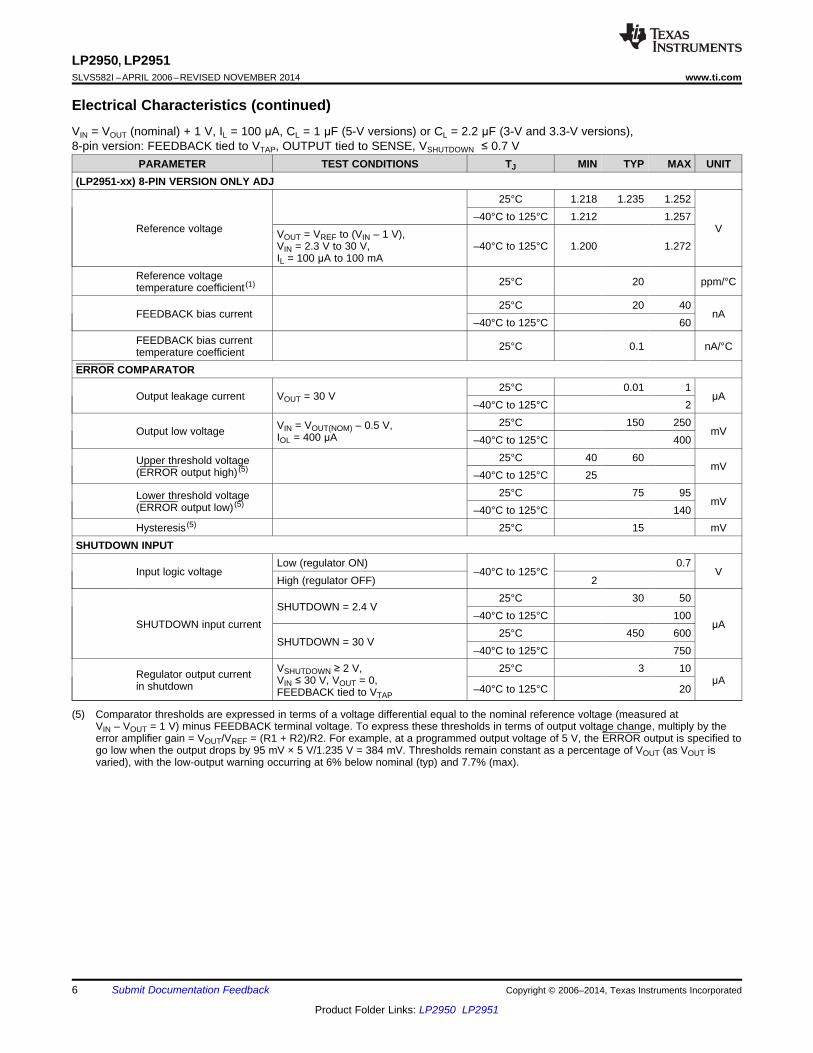
Electrical Characteristics (continued)VIN = VOUT (nominal) + 1 V, IL = 100 μA, CL = 1 μF (5-V versions) or CL = 2.2 μF (3-V and 3.3-V versions),8-pin version: FEEDBACK tied to VTAP, OUTPUT tied to SENSE, VSHUTDOWN ≤ 0.7 V
PARAMETER TEST CONDITIONS TJ MIN TYP MAX UNIT(LP2951-xx) 8-PIN VERSION ONLY ADJ
25°C 1.218 1.235 1.252–40°C to 125°C 1.212 1.257
Reference voltage VVOUT = VREF to (VIN – 1 V),VIN = 2.3 V to 30 V, –40°C to 125°C 1.200 1.272IL = 100 μA to 100 mA
Reference voltage 25°C 20 ppm/°Ctemperature coefficient (1)
25°C 20 40FEEDBACK bias current nA
–40°C to 125°C 60FEEDBACK bias current 25°C 0.1 nA/°Ctemperature coefficient
ERROR COMPARATOR25°C 0.01 1
Output leakage current VOUT = 30 V μA–40°C to 125°C 2
25°C 150 250VIN = VOUT(NOM) – 0.5 V,Output low voltage mVIOL = 400 μA –40°C to 125°C 40025°C 40 60Upper threshold voltage mV(ERROR output high) (5) –40°C to 125°C 2525°C 75 95Lower threshold voltage mV(ERROR output low) (5) –40°C to 125°C 140
Hysteresis (5) 25°C 15 mVSHUTDOWN INPUT
Low (regulator ON) 0.7Input logic voltage –40°C to 125°C V
High (regulator OFF) 225°C 30 50
SHUTDOWN = 2.4 V–40°C to 125°C 100
SHUTDOWN input current μA25°C 450 600
SHUTDOWN = 30 V–40°C to 125°C 750
VSHUTDOWN ≥ 2 V, 25°C 3 10Regulator output current VIN ≤ 30 V, VOUT = 0, μAin shutdown –40°C to 125°C 20FEEDBACK tied to VTAP
(5) Comparator thresholds are expressed in terms of a voltage differential equal to the nominal reference voltage (measured atVIN – VOUT = 1 V) minus FEEDBACK terminal voltage. To express these thresholds in terms of output voltage change, multiply by theerror amplifier gain = VOUT/VREF = (R1 + R2)/R2. For example, at a programmed output voltage of 5 V, the ERROR output is specified togo low when the output drops by 95 mV × 5 V/1.235 V = 384 mV. Thresholds remain constant as a percentage of VOUT (as VOUT isvaried), with the low-output warning occurring at 6% below nominal (typ) and 7.7% (max).
6 Submit Documentation Feedback Copyright © 2006–2014, Texas Instruments Incorporated
Product Folder Links: LP2950 LP2951
4.900
4.925
4.950
4.975
5.000
5.025
5.050
5.075
5.100
-40 -25 -10 5 20 35 50 65 80 95 110 125
TA – Temperature – °C
VO
UT
–O
utpu
tVol
tage
–V
IL = 100 µA
IL = 100 mA
0
10
20
30
40
50
60
70
80
90
100
110
120
0 1 2 3 4 5 6 7 8
VIN – Input Voltage – V
Qui
esce
ntC
urre
nt–
µA
IL = 0
0
20
40
60
80
100
120
140
160
180
200
0 1 2 3 4 5 6 7 8 9 10
VIN – Input Voltage – V
Inpu
tCur
rent
–µ
A
R = 50 kL Ω
0
10
20
30
40
50
60
70
80
90
100
110
120
0 1 2 3 4 5 6 7 8 9 10
VIN – Input Voltage – V
Inpu
tCur
rent
–m
A
R = 50L Ω
0
10
20
30
40
50
60
70
80
90
100
0 1 2 3 4 5 6 7 8 9 10
VIN – Input Voltage – V
Inpu
tCur
rent
–µ
A
R =L ∞
0.01
0.1
1
10
0.0001 0.001 0.01 0.1
IL – Load Current – A
Qu
iescen
tC
urr
en
t–
mA
LP2950, LP2951www.ti.com SLVS582I –APRIL 2006–REVISED NOVEMBER 2014
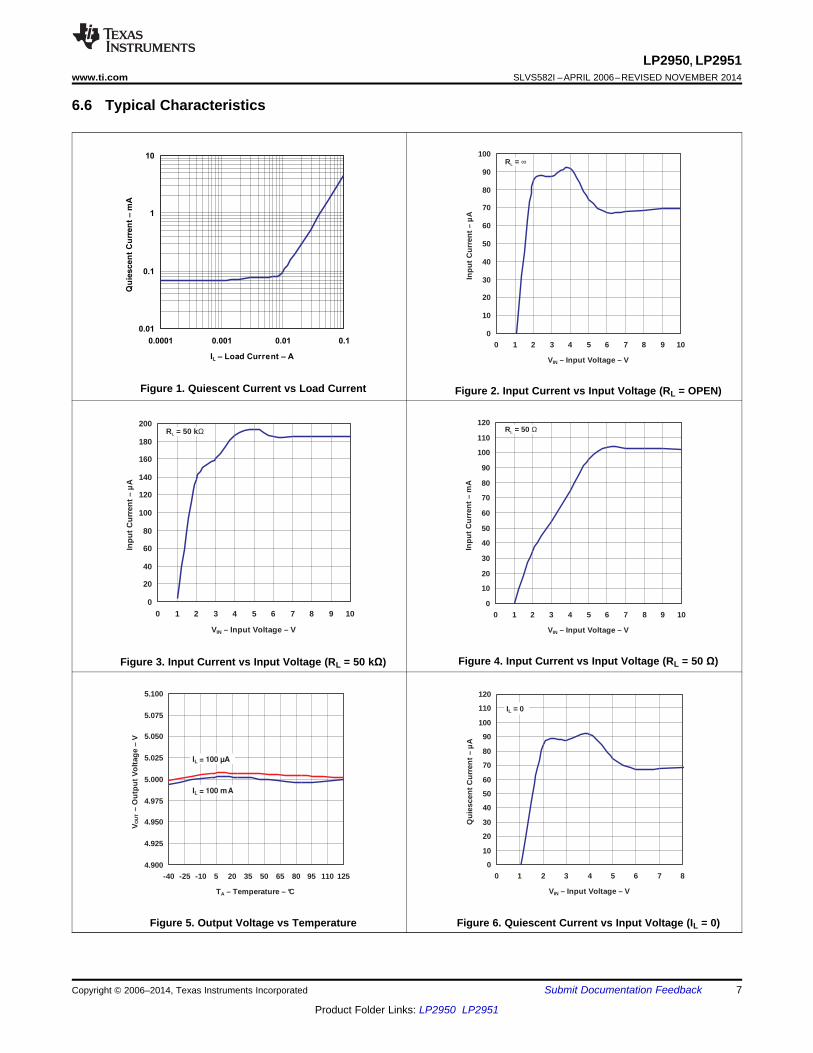
6.6 Typical Characteristics
Figure 1. Quiescent Current vs Load Current Figure 2. Input Current vs Input Voltage (RL = OPEN)
Figure 4. Input Current vs Input Voltage (RL = 50 Ω)Figure 3. Input Current vs Input Voltage (RL = 50 kΩ)
Figure 5. Output Voltage vs Temperature Figure 6. Quiescent Current vs Input Voltage (IL = 0)
Copyright © 2006–2014, Texas Instruments Incorporated Submit Documentation Feedback 7
Product Folder Links: LP2950 LP2951
50
75
100
125
150
175
200
225
250
-40 -25 -10 5 20 35 50 65 80 95 110 125
TA – Temperature – °C
Sh
ort
-Cir
cu
itC
urr
en
t–
mA
0
50
100
150
200
250
300
350
400
450
500
-40 -25 -10 5 20 35 50 65 80 95 110 125
TA – Temperature – °C
(VIN
–V
OU
T)
–D
rop
ou
tV
olt
ag
e–
mV
RL = 100 µA
RL = 100 mA
IL
I
5
5.5
6
6.5
7
7.5
8
8.5
9
9.5
10
-40 -25 -10 5 20 35 50 65 80 95 110 125
TA – Temperature – °C
Qui
esce
ntC
urre
nt–
mA
IL = 100 mA
V IN = 6 V
50
55
60
65
70
75
80
85
90
95
100
-40 -25 -10 5 20 35 50 65 80 95 110 125
TA – Temperature – °C
Qui
esce
ntC
urre
nt–
µA
IL = 100 µA
V IN = 6 V
0
10
20
30
40
50
60
70
80
90
100
110
120
0 1 2 3 4 5 6 7 8
VIN – Input Voltage – V
Qui
esce
ntC
urre
nt–
µA
IL = 1 mA
0
1
2
3
4
5
6
7
8
0 1 2 3 4 5 6 7 8
VIN – Input Voltage – V
Qu
iescen
tC
urr
en
t–
mA
IL = 100 mA
LP2950, LP2951SLVS582I –APRIL 2006–REVISED NOVEMBER 2014 www.ti.com
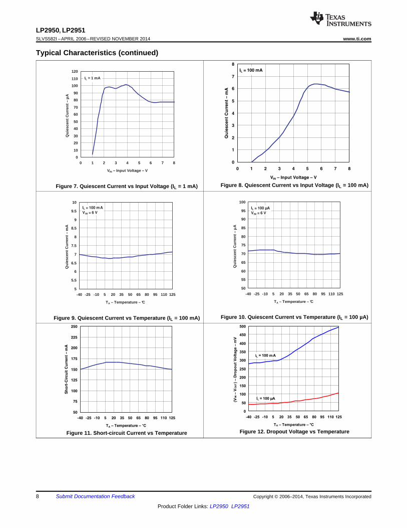
Typical Characteristics (continued)
Figure 8. Quiescent Current vs Input Voltage (IL = 100 mA)Figure 7. Quiescent Current vs Input Voltage (IL = 1 mA)
Figure 10. Quiescent Current vs Temperature (IL = 100 µA)Figure 9. Quiescent Current vs Temperature (IL = 100 mA)
Figure 12. Dropout Voltage vs TemperatureFigure 11. Short-circuit Current vs Temperature
8 Submit Documentation Feedback Copyright © 2006–2014, Texas Instruments Incorporated
Product Folder Links: LP2950 LP2951
0
0.25
0.5
0.75
1
1.25
1.5
1.75
2
0 0.1 0.2 0.3 0.4 0.5 0.6 0.7 0.8 0.9
VOL – Output Low Voltage – V
I SIN
K–
Sin
kC
urr
en
t–
mA
T = 125A
T = 25A
T = –40A
Input Voltage2 V/div
Output Voltage80 mV/div
-20
-15
-10
-5
0
5
10
15
20
25
30
-55 -30 -5 20 45 70 95 120 145
TA – Temperature – °C
FE
ED
BA
CK
Bia
sC
urre
nt–
nA
0
1
2
3
4
5
6
7
8
0 1 2 3 4 5 6 7 8
V IN – Input Voltage – V
ER
RO
RO
utp
ut
–V
50-k resistor to
external 5-V supply
W
50-k resistor
to V
W
OUT
1.6
1.65
1.7
1.75
1.8
1.85
1.9
1.95
2
-40 -25 -10 5 20 35 50 65 80 95 110 125
TA – Temperature – °C
Min
imum
Ope
ratin
gV
olta
ge–
V
0
50
100
150
200
250
300
350
400
0.0001 0.001 0.01 0.1
IO – Output Current – A
(VIN
–V
OU
T)
–D
rop
ou
tV
olt
ag
e–
mV
LP2950, LP2951www.ti.com SLVS582I –APRIL 2006–REVISED NOVEMBER 2014
Typical Characteristics (continued)
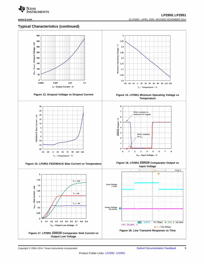
Figure 13. Dropout Voltage vs Dropout Current Figure 14. LP2951 Minimum Operating Voltage vsTemperature
Figure 16. LP2951 ERROR Comparator Output vsFigure 15. LP2951 FEEDBACK Bias Current vs TemperatureInput Voltage
Figure 18. Line Transient Response vs TimeFigure 17. LP2951 ERROR Comparator Sink Current vs
Output Low Voltage
Copyright © 2006–2014, Texas Instruments Incorporated Submit Documentation Feedback 9
Product Folder Links: LP2950 LP2951
20
30
40
50
60
70
80
90
1.E+01 1.E+02 1.E+03 1.E+04 1.E+05 1.E+06
f – Frequency – Hz
Pow
er-S
uppl
yR
ippl
eR
ejec
tion
–dB
IL = 100 µA
IL = 0
V IN = 6 V
CL = 1 µF
10 100 1k 10k 100k 1M10
20
30
40
50
60
70
80
90
100
1.E+01 1.E+02 1.E+03 1.E+04 1.E+05 1.E+06
f – Frequency – Hz
Pow
er-S
uppl
yR
ippl
eR
ejec
tion
–dB
IL = 10 mA
IL = 1 mA
VIN = 6 V
CL = 1 µF
10 100 1k 10k 100k 1M
0.01
0.1
1
10
100
1.E+01 1.E+02 1.E+03 1.E+04 1.E+05 1.E+06
f – Frequency – Hz
Out
putI
mpe
danc
e–
Ohm
IL = 1 mA
IL = 100 mA
IL = 100 µA
10 100 1k 10k 100k 1M
Ω
Output Load100 mA/div
Output Voltage100 mV/div
LP2950, LP2951SLVS582I –APRIL 2006–REVISED NOVEMBER 2014 www.ti.com
Typical Characteristics (continued)
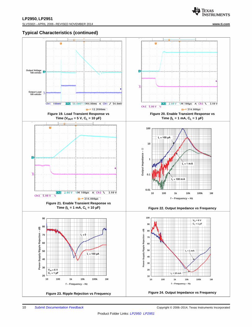
Figure 19. Load Transient Response vs Figure 20. Enable Transient Response vsTime (VOUT = 5 V, CL = 10 µF) Time (IL = 1 mA, CL = 1 µF)
Figure 21. Enable Transient Response vsTime (IL = 1 mA, CL = 10 µF) Figure 22. Output Impedance vs Frequency
Figure 24. Output Impedance vs FrequencyFigure 23. Ripple Rejection vs Frequency
10 Submit Documentation Feedback Copyright © 2006–2014, Texas Instruments Incorporated
Product Folder Links: LP2950 LP2951
0.8
0.9
1
1.1
1.2
1.3
1.4
1.5
1.6
1.7
-40 -25 -10 5 20 35 50 65 80 95 110 125
TA – Temperature – °C
Inpu
tLog
icV
olta
ge(O
Nto
OF
F)
–V
-2
-1
0
1
2
3
4
5
6
0 5 10 15 20 25 30
VIN – Input Voltage – V
Out
putV
olta
geC
hang
e–
mV
0
50
100
150
200
250
300
350
400
-40 -25 -10 5 20 35 50 65 80 95 110 125
TA – Temperature – °C
RP
2P
4–
Pin
2to
Pin
4R
esis
tan
ce
–kk
W
0.8
0.9
1
1.1
1.2
1.3
1.4
1.5
1.6
1.7
-40 -25 -10 5 20 35 50 65 80 95 110 125
TA – Temperature – °C
Inp
ut
Lo
gic
Vo
ltag
e(O
FF
toO
N)
–V
10
20
30
40
50
60
70
80
90
100
1.E+01 1.E+02 1.E+03 1.E+04 1.E+05 1.E+06
f – Frequency – Hz
Pow
er-S
uppl
yR
ippl
eR
ejec
tion
–dB
IL = 100 mA
IL = 50 mA
VIN = 6 V
CL = 1 µF
10 100 1k 10k 100k 1M
0
1
2
3
4
5
6
1.E+01 1.E+02 1.E+03 1.E+04 1.E+05
f – Frequency – Hz
Out
putN
oise
–µ
V
CL = 1 µF
CL = 3.3 µF
CL = 200 µF
10 100 1k 10k 100k
LP2950, LP2951www.ti.com SLVS582I –APRIL 2006–REVISED NOVEMBER 2014
Typical Characteristics (continued)
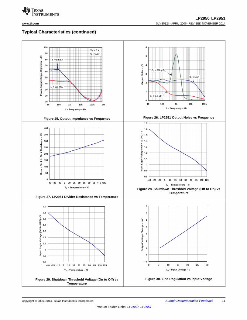
Figure 26. LP2951 Output Noise vs FrequencyFigure 25. Output Impedance vs Frequency
Figure 28. Shutdown Threshold Voltage (Off to On) vsTemperature
Figure 27. LP2951 Divider Resistance vs Temperature
Figure 30. Line Regulation vs Input VoltageFigure 29. Shutdown Threshold Voltage (On to Off) vsTemperature
Copyright © 2006–2014, Texas Instruments Incorporated Submit Documentation Feedback 11
Product Folder Links: LP2950 LP2951
+
1.23-V Reference
Error Amplifier
GND
OUTPUT
INPUT
LP2950, LP2951SLVS582I –APRIL 2006–REVISED NOVEMBER 2014 www.ti.com
7 Detailed Description
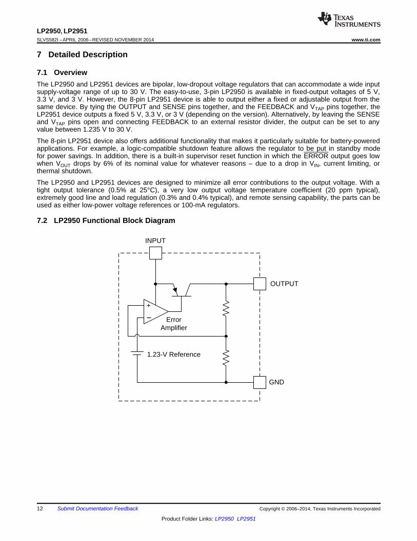
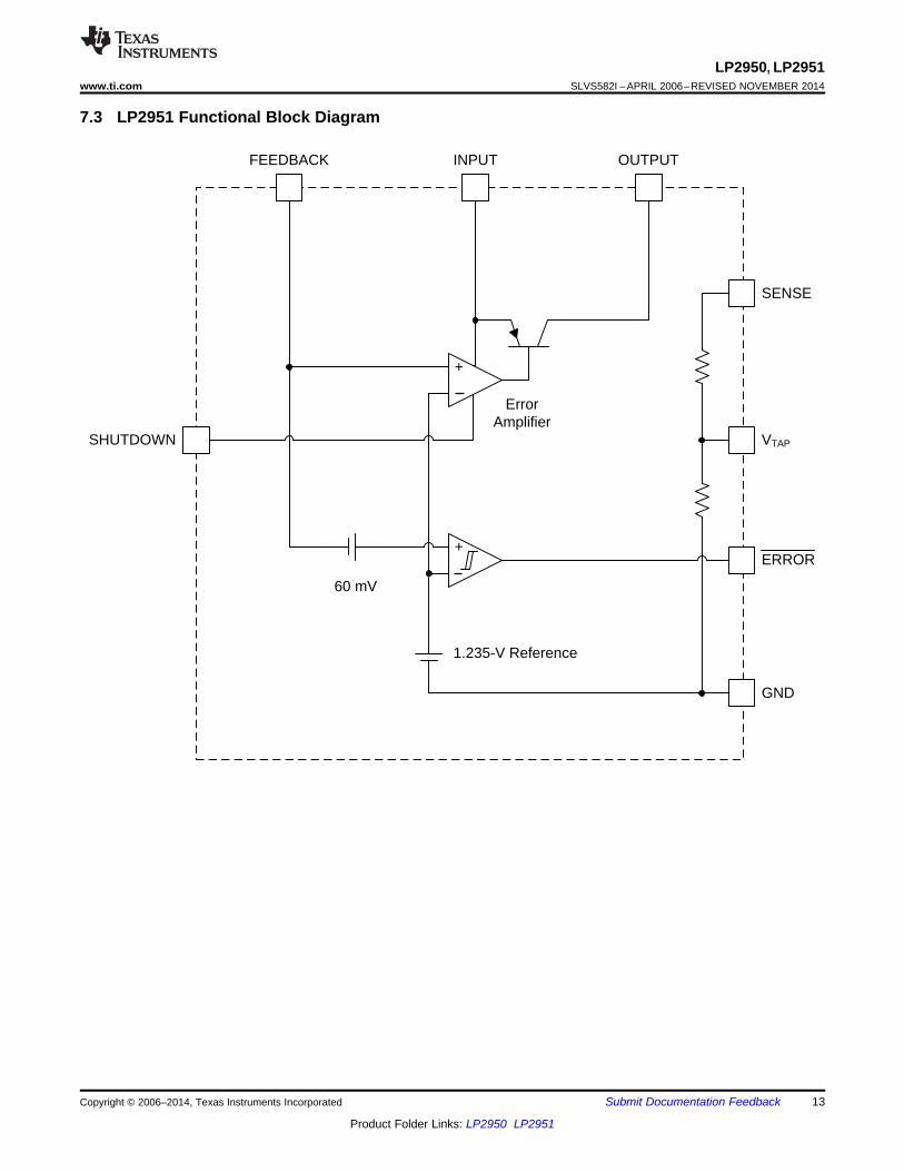
7.1 OverviewThe LP2950 and LP2951 devices are bipolar, low-dropout voltage regulators that can accommodate a wide inputsupply-voltage range of up to 30 V. The easy-to-use, 3-pin LP2950 is available in fixed-output voltages of 5 V,3.3 V, and 3 V. However, the 8-pin LP2951 device is able to output either a fixed or adjustable output from thesame device. By tying the OUTPUT and SENSE pins together, and the FEEDBACK and VTAP pins together, theLP2951 device outputs a fixed 5 V, 3.3 V, or 3 V (depending on the version). Alternatively, by leaving the SENSEand VTAP pins open and connecting FEEDBACK to an external resistor divider, the output can be set to anyvalue between 1.235 V to 30 V.
The 8-pin LP2951 device also offers additional functionality that makes it particularly suitable for battery-poweredapplications. For example, a logic-compatible shutdown feature allows the regulator to be put in standby modefor power savings. In addition, there is a built-in supervisor reset function in which the ERROR output goes lowwhen VOUT drops by 6% of its nominal value for whatever reasons – due to a drop in VIN, current limiting, orthermal shutdown.
The LP2950 and LP2951 devices are designed to minimize all error contributions to the output voltage. With atight output tolerance (0.5% at 25°C), a very low output voltage temperature coefficient (20 ppm typical),extremely good line and load regulation (0.3% and 0.4% typical), and remote sensing capability, the parts can beused as either low-power voltage references or 100-mA regulators.
7.2 LP2950 Functional Block Diagram
12 Submit Documentation Feedback Copyright © 2006–2014, Texas Instruments Incorporated
Product Folder Links: LP2950 LP2951
+
+
60 mV
1.235-V Reference
Error Amplifier
SENSE
VTAP
ERROR
GND
OUTPUTINPUTFEEDBACK
SHUTDOWN
LP2950, LP2951www.ti.com SLVS582I –APRIL 2006–REVISED NOVEMBER 2014
7.3 LP2951 Functional Block Diagram
Copyright © 2006–2014, Texas Instruments Incorporated Submit Documentation Feedback 13
Product Folder Links: LP2950 LP2951
5 V
1.3 V
InputVoltage
OutputVoltage
ERROR
4.75 V
LP2950, LP2951SLVS582I –APRIL 2006–REVISED NOVEMBER 2014 www.ti.com
7.4 Feature Description
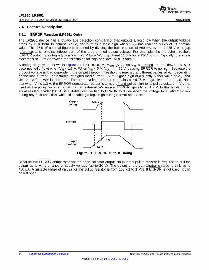
7.4.1 ERROR Function (LP2951 Only)The LP2951 device has a low-voltage detection comparator that outputs a logic low when the output voltagedrops by ≈6% from its nominal value, and outputs a logic high when VOUT has reached ≈95% of its nominalvalue. This 95% of nominal figure is obtained by dividing the built-in offset of ≈60 mV by the 1.235-V bandgapreference, and remains independent of the programmed output voltage. For example, the trip-point threshold(ERROR output goes high) typically is 4.75 V for a 5-V output and 11.4 V for a 12-V output. Typically, there is ahysteresis of 15 mV between the thresholds for high and low ERROR output.
A timing diagram is shown in Figure 31 for ERROR vs VOUT (5 V), as VIN is ramped up and down. ERRORbecomes valid (low) when VIN ≈ 1.3 V. When VIN ≈ 5 V, VOUT = 4.75 V, causing ERROR to go high. Because thedropout voltage is load dependent, the output trip-point threshold is reached at different values of VIN, dependingon the load current. For instance, at higher load current, ERROR goes high at a slightly higher value of VIN, andvice versa for lower load current. The output-voltage trip point remains at ~4.75 V, regardless of the load. Notethat when VIN ≤ 1.3 V, the ERROR comparator output is turned off and pulled high to its pullup voltage. If VOUT isused as the pullup voltage, rather than an external 5-V source, ERROR typically is ~1.2 V. In this condition, anequal resistor divider (10 kΩ is suitable) can be tied to ERROR to divide down the voltage to a valid logic lowduring any fault condition, while still enabling a logic high during normal operation.
Figure 31. ERROR Output Timing
Because the ERROR comparator has an open-collector output, an external pullup resistor is required to pull theoutput up to VOUT or another supply voltage (up to 30 V). The output of the comparator is rated to sink up to400 μA. A suitable range of values for the pullup resistor is from 100 kΩ to 1 MΩ. If ERROR is not used, it canbe left open.
14 Submit Documentation Feedback Copyright © 2006–2014, Texas Instruments Incorporated
Product Folder Links: LP2950 LP2951
R1
R2
FEEDBACK
VOUT
æ ö= ´ + -ç ÷
è øOUT REF FB 1
R1V V 1 I R
R2
LP2950, LP2951www.ti.com SLVS582I –APRIL 2006–REVISED NOVEMBER 2014
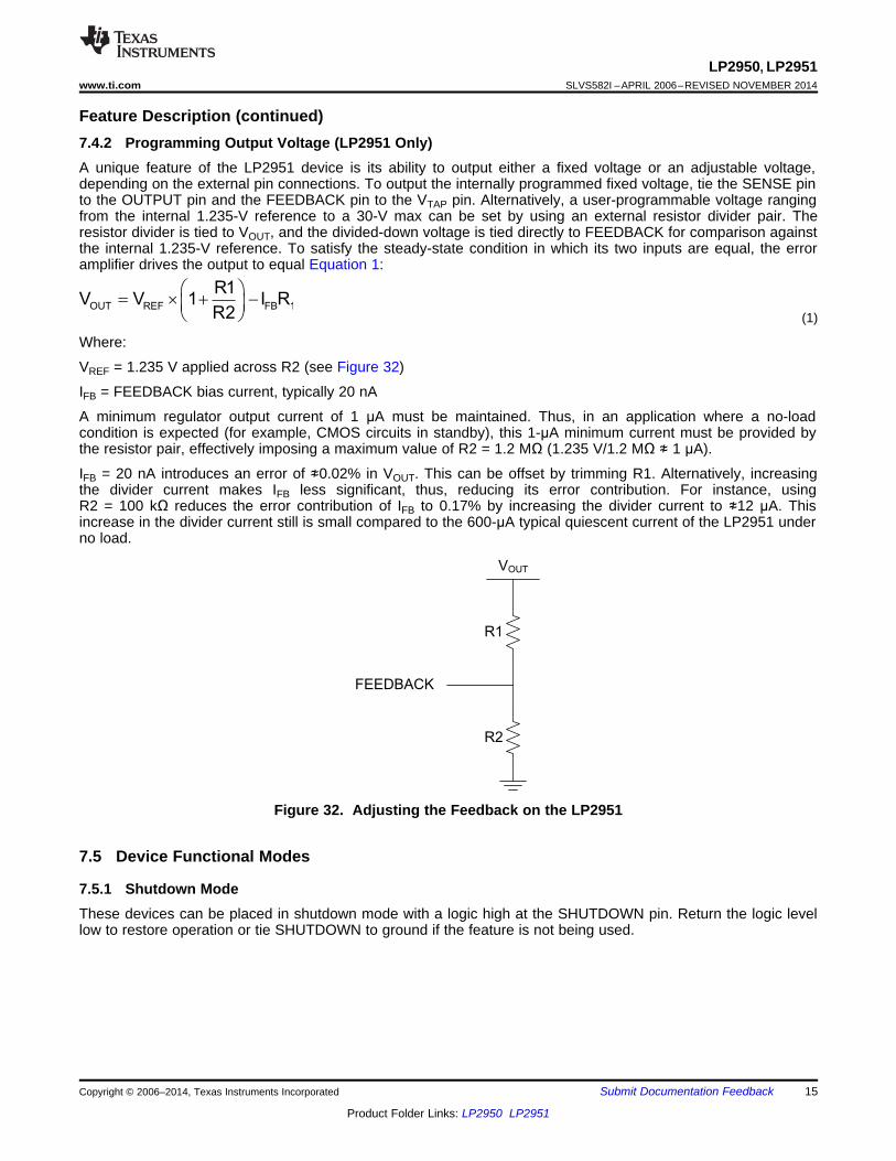
Feature Description (continued)7.4.2 Programming Output Voltage (LP2951 Only)A unique feature of the LP2951 device is its ability to output either a fixed voltage or an adjustable voltage,depending on the external pin connections. To output the internally programmed fixed voltage, tie the SENSE pinto the OUTPUT pin and the FEEDBACK pin to the VTAP pin. Alternatively, a user-programmable voltage rangingfrom the internal 1.235-V reference to a 30-V max can be set by using an external resistor divider pair. Theresistor divider is tied to VOUT, and the divided-down voltage is tied directly to FEEDBACK for comparison againstthe internal 1.235-V reference. To satisfy the steady-state condition in which its two inputs are equal, the erroramplifier drives the output to equal Equation 1:
(1)
Where:
VREF = 1.235 V applied across R2 (see Figure 32)
IFB = FEEDBACK bias current, typically 20 nA
A minimum regulator output current of 1 μA must be maintained. Thus, in an application where a no-loadcondition is expected (for example, CMOS circuits in standby), this 1-μA minimum current must be provided bythe resistor pair, effectively imposing a maximum value of R2 = 1.2 MΩ (1.235 V/1.2 MΩ ≉ 1 μA).
IFB = 20 nA introduces an error of ≉0.02% in VOUT. This can be offset by trimming R1. Alternatively, increasingthe divider current makes IFB less significant, thus, reducing its error contribution. For instance, usingR2 = 100 kΩ reduces the error contribution of IFB to 0.17% by increasing the divider current to ≉12 μA. Thisincrease in the divider current still is small compared to the 600-μA typical quiescent current of the LP2951 underno load.
Figure 32. Adjusting the Feedback on the LP2951
7.5 Device Functional Modes
7.5.1 Shutdown ModeThese devices can be placed in shutdown mode with a logic high at the SHUTDOWN pin. Return the logic levellow to restore operation or tie SHUTDOWN to ground if the feature is not being used.
Copyright © 2006–2014, Texas Instruments Incorporated Submit Documentation Feedback 15
Product Folder Links: LP2950 LP2951
LP2951-50
1
2
3
4
8
7
6
5
VOUT
SENSE
SHUTDOWN
GND
FEEDBACK
VTAP
1 PF
VOUT = 5 V
330 kȍ
ERROR
VIN
1 PF
VIN = 12 V
LP2950, LP2951SLVS582I –APRIL 2006–REVISED NOVEMBER 2014 www.ti.com
8 Application and Implementation
NOTEInformation in the following applications sections is not part of the TI componentspecification, and TI does not warrant its accuracy or completeness. TI’s customers areresponsible for determining suitability of components for their purposes. Customers shouldvalidate and test their design implementation to confirm system functionality.
8.1 Application InformationThe LP295x devices are used as low-dropout regulators with a wide range of input voltages.
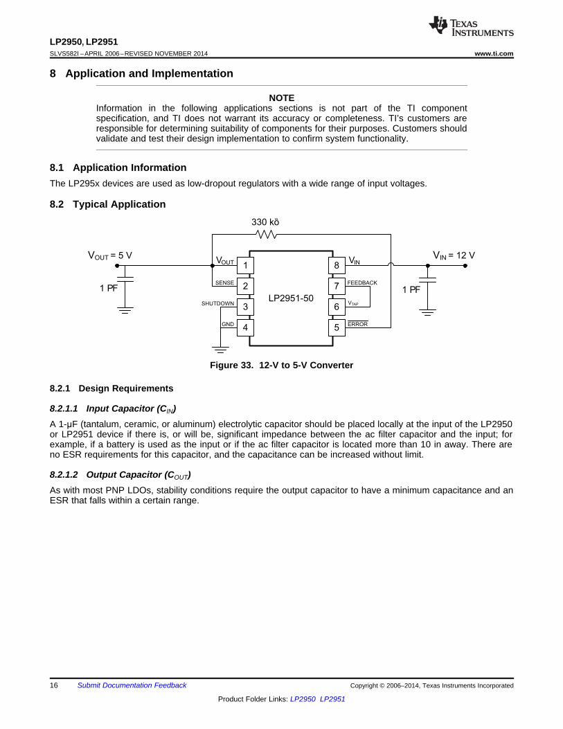
8.2 Typical Application
Figure 33. 12-V to 5-V Converter
8.2.1 Design Requirements
8.2.1.1 Input Capacitor (CIN)A 1-μF (tantalum, ceramic, or aluminum) electrolytic capacitor should be placed locally at the input of the LP2950or LP2951 device if there is, or will be, significant impedance between the ac filter capacitor and the input; forexample, if a battery is used as the input or if the ac filter capacitor is located more than 10 in away. There areno ESR requirements for this capacitor, and the capacitance can be increased without limit.
8.2.1.2 Output Capacitor (COUT)As with most PNP LDOs, stability conditions require the output capacitor to have a minimum capacitance and anESR that falls within a certain range.
16 Submit Documentation Feedback Copyright © 2006–2014, Texas Instruments Incorporated
Product Folder Links: LP2950 LP2951
® =
p ´ ´
;(CBYPASS) (BYPASS)
1f 200 Hz C
2 R1 200 Hz
LP2950, LP2951www.ti.com SLVS582I –APRIL 2006–REVISED NOVEMBER 2014
Typical Application (continued)8.2.2 Detailed Design Procedure
8.2.2.1 Capacitance ValueFor VOUT ≥ 5 V, a minimum of 1 μF is required. For lower VOUT, the regulator’s loop gain is running closer to unitygain and, thus, has lower phase margins. Consequently, a larger capacitance is needed for stability.For VOUT = 3 V or 3.3 V, a minimum of 2.2 μF is recommended. For worst case, VOUT = 1.23 V (using the ADJversion), a minimum of 3.3 μF is recommended. COUT can be increased without limit and only improves theregulator stability and transient response. Regardless of its value, the output capacitor should have a resonantfrequency greater than 500 kHz.
The minimum capacitance values given above are for maximum load current of 100 mA. If the maximumexpected load current is less than 100 mA, then lower values of COUT can be used. For instance, if IOUT < 10 mA,then only 0.33 μF is required for COUT. For IOUT < 1 mA, 0.1 μF is sufficient for stability requirements. Thus, for aworst-case condition of 100-mA load and VOUT = VREF = 1.235 V (representing the highest load current andlowest loop gain), a minimum COUT of 3.3 μF is recommended.
For the LP2950/51, no load stability is inherent in the design — a desirable feature in CMOS circuits that are putin standby (such as RAM keep-alive applications). If the LP2951 is used with external resistors to set the outputvoltage, a minimum load current of 1 μA is recommended through the resistor divider.
8.2.2.2 Capacitor TypesMost tantalum or aluminum electrolytics are suitable for use at the input. Film-type capacitors also work but athigher cost. When operating at low temperature, care should be taken with aluminum electrolytics, as theirelectrolytes often freeze at –30°C. For this reason, solid tantalum capacitors should be used at temperaturesbelow –25°C.
Ceramic capacitors can be used, but due to their low ESR (as low as 5 mΩ to 10 mΩ), they may not meet theminimum ESR requirement previously discussed. If a ceramic capacitor is used, a series resistor between0.1 Ω to 2 Ω must be added to meet the minimum ESR requirement. In addition, ceramic capacitors have oneglaring disadvantage that must be taken into account — a poor temperature coefficient, where the capacitancecan vary significantly with temperature. For instance, a large-value ceramic capacitor (≥ 2.2 μF) can lose morethan half of its capacitance as temperature rises from 25°C to 85°C. Thus, a 2.2-μF capacitor at 25°C drops wellbelow the minimum COUT required for stability as ambient temperature rises. For this reason, select an outputcapacitor that maintains the minimum 2.2 μF required for stability for the entire operating temperature range.
8.2.2.3 CBYPASS: Noise and Stability ImprovementIn the LP2951 device, an external FEEDBACK pin directly connected to the error amplifier noninverting input canallow stray capacitance to cause instability by shunting the error amplifier feedback to GND, especially at highfrequencies. This is worsened if high-value external resistors are used to set the output voltage, because a highresistance allows the stray capacitance to play a more significant role; i.e., a larger RC time delay is introducedbetween the output of the error amplifier and its FEEDBACK input, leading to more phase shift and lower phasemargin. A solution is to add a 100-pF bypass capacitor (CBYPASS) between OUTPUT and FEEDBACK; becauseCBYPASS is in parallel with R1, it lowers the impedance seen at FEEDBACK at high frequencies, in effectoffsetting the effect of the parasitic capacitance by providing more feedback at higher frequencies. Morefeedback forces the error amplifier to work at a lower loop gain, so COUT should be increased to a minimum of3.3 μF to improve the regulator’s phase margin.
CBYPASS can be also used to reduce output noise in the LP2951 device. This bypass capacitor reduces theclosed loop gain of the error amplifier at the high frequency, so noise no longer scales with the output voltage.This improvement is more noticeable with higher output voltages, where loop gain reduction is greatest. Asuitable CBYPASS is calculated as shown in Equation 2:
(2)
On the 3-pin LP2950 device, noise reduction can be achieved by increasing the output capacitor, which causesthe regulator bandwidth to be reduced, thus eliminating high-frequency noise. However, this method is relativelyinefficient, as increasing COUT from 1 μF to 220 μF only reduces the regulator’s output noise from430 μV to 160 μV (over a 100-kHz bandwidth).
Copyright © 2006–2014, Texas Instruments Incorporated Submit Documentation Feedback 17
Product Folder Links: LP2950 LP2951
Output Load100 mA/div
Output Voltage100 mV/div
LP2950, LP2951SLVS582I –APRIL 2006–REVISED NOVEMBER 2014 www.ti.com
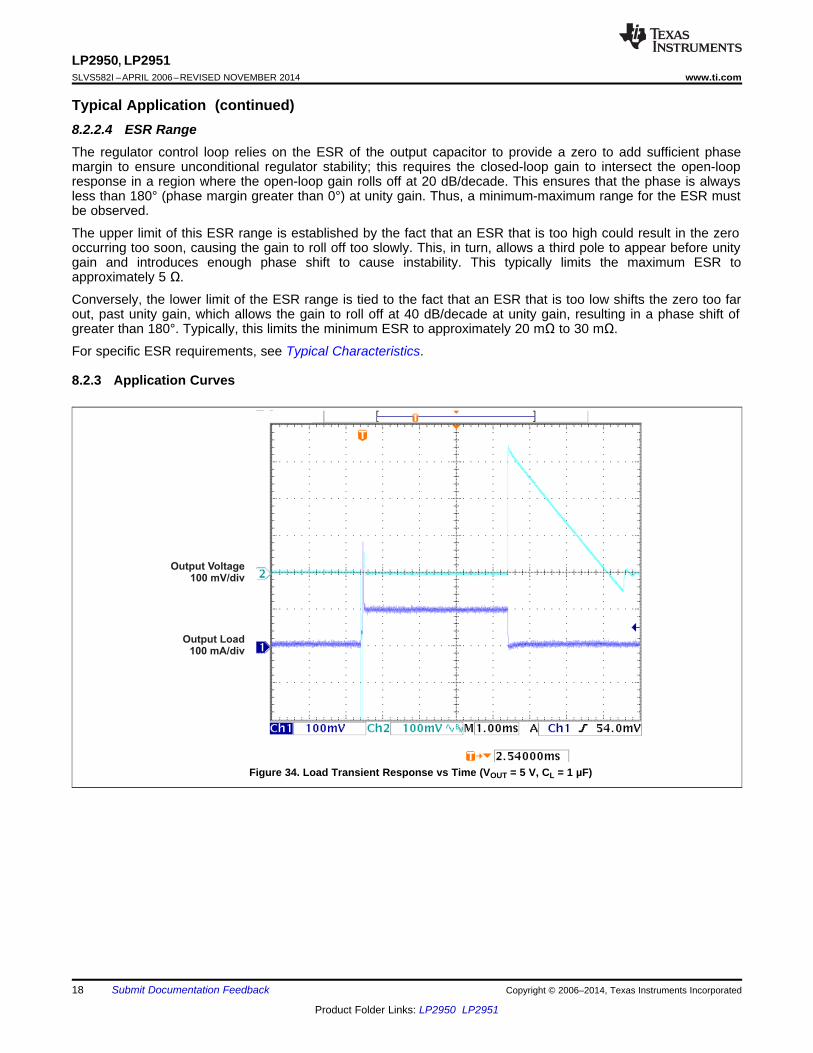
Typical Application (continued)8.2.2.4 ESR RangeThe regulator control loop relies on the ESR of the output capacitor to provide a zero to add sufficient phasemargin to ensure unconditional regulator stability; this requires the closed-loop gain to intersect the open-loopresponse in a region where the open-loop gain rolls off at 20 dB/decade. This ensures that the phase is alwaysless than 180° (phase margin greater than 0°) at unity gain. Thus, a minimum-maximum range for the ESR mustbe observed.
The upper limit of this ESR range is established by the fact that an ESR that is too high could result in the zerooccurring too soon, causing the gain to roll off too slowly. This, in turn, allows a third pole to appear before unitygain and introduces enough phase shift to cause instability. This typically limits the maximum ESR toapproximately 5 Ω.
Conversely, the lower limit of the ESR range is tied to the fact that an ESR that is too low shifts the zero too farout, past unity gain, which allows the gain to roll off at 40 dB/decade at unity gain, resulting in a phase shift ofgreater than 180°. Typically, this limits the minimum ESR to approximately 20 mΩ to 30 mΩ.
For specific ESR requirements, see Typical Characteristics.
8.2.3 Application Curves
Figure 34. Load Transient Response vs Time (VOUT = 5 V, CL = 1 µF)
18 Submit Documentation Feedback Copyright © 2006–2014, Texas Instruments Incorporated
Product Folder Links: LP2950 LP2951
LP2951-50
1
2
3
4
8
7
6
5
1 PF 1 PF
ERROR can be left floating if not used
LP2950, LP2951www.ti.com SLVS582I –APRIL 2006–REVISED NOVEMBER 2014
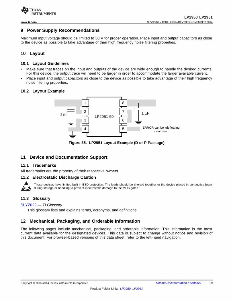
9 Power Supply RecommendationsMaximum input voltage should be limited to 30 V for proper operation. Place input and output capacitors as closeto the device as possible to take advantage of their high frequency noise filtering properties.
10 Layout
10.1 Layout Guidelines• Make sure that traces on the input and outputs of the device are wide enough to handle the desired currents.
For this device, the output trace will need to be larger in order to accommodate the larger available current.• Place input and output capacitors as close to the device as possible to take advantage of their high frequency
noise filtering properties.
10.2 Layout Example
Figure 35. LP2951 Layout Example (D or P Package)
11 Device and Documentation Support
11.1 TrademarksAll trademarks are the property of their respective owners.
11.2 Electrostatic Discharge CautionThese devices have limited built-in ESD protection. The leads should be shorted together or the device placed in conductive foamduring storage or handling to prevent electrostatic damage to the MOS gates.
11.3 GlossarySLYZ022 — TI Glossary.
This glossary lists and explains terms, acronyms, and definitions.
12 Mechanical, Packaging, and Orderable InformationThe following pages include mechanical, packaging, and orderable information. This information is the mostcurrent data available for the designated devices. This data is subject to change without notice and revision ofthis document. For browser-based versions of this data sheet, refer to the left-hand navigation.
Copyright © 2006–2014, Texas Instruments Incorporated Submit Documentation Feedback 19
Product Folder Links: LP2950 LP2951
PACKAGE OPTION ADDENDUM
www.ti.com 25-Sep-2021
Addendum-Page 1
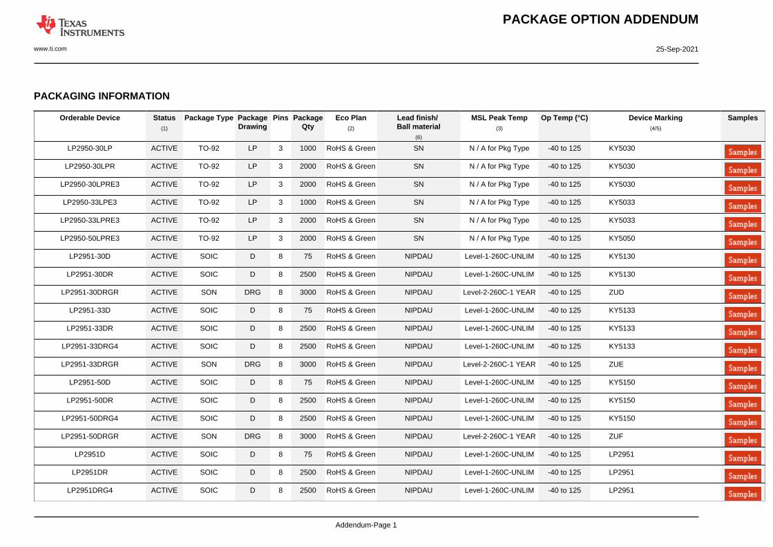
PACKAGING INFORMATION
Orderable Device Status(1)
Package Type PackageDrawing
Pins PackageQty
Eco Plan(2)
Lead finish/Ball material
(6)
MSL Peak Temp(3)
Op Temp (°C) Device Marking(4/5)
Samples
LP2950-30LP ACTIVE TO-92 LP 3 1000 RoHS & Green SN N / A for Pkg Type -40 to 125 KY5030
LP2950-30LPR ACTIVE TO-92 LP 3 2000 RoHS & Green SN N / A for Pkg Type -40 to 125 KY5030
LP2950-30LPRE3 ACTIVE TO-92 LP 3 2000 RoHS & Green SN N / A for Pkg Type -40 to 125 KY5030
LP2950-33LPE3 ACTIVE TO-92 LP 3 1000 RoHS & Green SN N / A for Pkg Type -40 to 125 KY5033
LP2950-33LPRE3 ACTIVE TO-92 LP 3 2000 RoHS & Green SN N / A for Pkg Type -40 to 125 KY5033
LP2950-50LPRE3 ACTIVE TO-92 LP 3 2000 RoHS & Green SN N / A for Pkg Type -40 to 125 KY5050
LP2951-30D ACTIVE SOIC D 8 75 RoHS & Green NIPDAU Level-1-260C-UNLIM -40 to 125 KY5130
LP2951-30DR ACTIVE SOIC D 8 2500 RoHS & Green NIPDAU Level-1-260C-UNLIM -40 to 125 KY5130
LP2951-30DRGR ACTIVE SON DRG 8 3000 RoHS & Green NIPDAU Level-2-260C-1 YEAR -40 to 125 ZUD
LP2951-33D ACTIVE SOIC D 8 75 RoHS & Green NIPDAU Level-1-260C-UNLIM -40 to 125 KY5133
LP2951-33DR ACTIVE SOIC D 8 2500 RoHS & Green NIPDAU Level-1-260C-UNLIM -40 to 125 KY5133
LP2951-33DRG4 ACTIVE SOIC D 8 2500 RoHS & Green NIPDAU Level-1-260C-UNLIM -40 to 125 KY5133
LP2951-33DRGR ACTIVE SON DRG 8 3000 RoHS & Green NIPDAU Level-2-260C-1 YEAR -40 to 125 ZUE
LP2951-50D ACTIVE SOIC D 8 75 RoHS & Green NIPDAU Level-1-260C-UNLIM -40 to 125 KY5150
LP2951-50DR ACTIVE SOIC D 8 2500 RoHS & Green NIPDAU Level-1-260C-UNLIM -40 to 125 KY5150
LP2951-50DRG4 ACTIVE SOIC D 8 2500 RoHS & Green NIPDAU Level-1-260C-UNLIM -40 to 125 KY5150
LP2951-50DRGR ACTIVE SON DRG 8 3000 RoHS & Green NIPDAU Level-2-260C-1 YEAR -40 to 125 ZUF
LP2951D ACTIVE SOIC D 8 75 RoHS & Green NIPDAU Level-1-260C-UNLIM -40 to 125 LP2951
LP2951DR ACTIVE SOIC D 8 2500 RoHS & Green NIPDAU Level-1-260C-UNLIM -40 to 125 LP2951
LP2951DRG4 ACTIVE SOIC D 8 2500 RoHS & Green NIPDAU Level-1-260C-UNLIM -40 to 125 LP2951
PACKAGE OPTION ADDENDUM
www.ti.com 25-Sep-2021
Addendum-Page 2
(1) The marketing status values are defined as follows:ACTIVE: Product device recommended for new designs.LIFEBUY: TI has announced that the device will be discontinued, and a lifetime-buy period is in effect.NRND: Not recommended for new designs. Device is in production to support existing customers, but TI does not recommend using this part in a new design.PREVIEW: Device has been announced but is not in production. Samples may or may not be available.OBSOLETE: TI has discontinued the production of the device.
(2) RoHS: TI defines "RoHS" to mean semiconductor products that are compliant with the current EU RoHS requirements for all 10 RoHS substances, including the requirement that RoHS substancedo not exceed 0.1% by weight in homogeneous materials. Where designed to be soldered at high temperatures, "RoHS" products are suitable for use in specified lead-free processes. TI mayreference these types of products as "Pb-Free".RoHS Exempt: TI defines "RoHS Exempt" to mean products that contain lead but are compliant with EU RoHS pursuant to a specific EU RoHS exemption.Green: TI defines "Green" to mean the content of Chlorine (Cl) and Bromine (Br) based flame retardants meet JS709B low halogen requirements of <=1000ppm threshold. Antimony trioxide basedflame retardants must also meet the <=1000ppm threshold requirement.
(3) MSL, Peak Temp. - The Moisture Sensitivity Level rating according to the JEDEC industry standard classifications, and peak solder temperature.
(4) There may be additional marking, which relates to the logo, the lot trace code information, or the environmental category on the device.
(5) Multiple Device Markings will be inside parentheses. Only one Device Marking contained in parentheses and separated by a "~" will appear on a device. If a line is indented then it is a continuationof the previous line and the two combined represent the entire Device Marking for that device.
(6) Lead finish/Ball material - Orderable Devices may have multiple material finish options. Finish options are separated by a vertical ruled line. Lead finish/Ball material values may wrap to twolines if the finish value exceeds the maximum column width.
Important Information and Disclaimer:The information provided on this page represents TI's knowledge and belief as of the date that it is provided. TI bases its knowledge and belief on informationprovided by third parties, and makes no representation or warranty as to the accuracy of such information. Efforts are underway to better integrate information from third parties. TI has taken andcontinues to take reasonable steps to provide representative and accurate information but may not have conducted destructive testing or chemical analysis on incoming materials and chemicals.TI and TI suppliers consider certain information to be proprietary, and thus CAS numbers and other limited information may not be available for release.
In no event shall TI's liability arising out of such information exceed the total purchase price of the TI part(s) at issue in this document sold by TI to Customer on an annual basis.
OTHER QUALIFIED VERSIONS OF LP2951 :
• Automotive : LP2951-Q1
NOTE: Qualified Version Definitions:
• Automotive - Q100 devices qualified for high-reliability automotive applications targeting zero defects
TAPE AND REEL INFORMATION
*All dimensions are nominal
Device PackageType
PackageDrawing
Pins SPQ ReelDiameter
(mm)
ReelWidth
W1 (mm)
A0(mm)
B0(mm)
K0(mm)
P1(mm)
W(mm)
Pin1Quadrant
LP2951-30DR SOIC D 8 2500 330.0 12.4 6.4 5.2 2.1 8.0 12.0 Q1
LP2951-30DRGR SON DRG 8 3000 330.0 12.4 3.3 3.3 1.1 8.0 12.0 Q2
LP2951-33DR SOIC D 8 2500 330.0 12.4 6.4 5.2 2.1 8.0 12.0 Q1
LP2951-33DRGR SON DRG 8 3000 330.0 12.4 3.3 3.3 1.1 8.0 12.0 Q2
LP2951-50DR SOIC D 8 2500 330.0 12.4 6.4 5.2 2.1 8.0 12.0 Q1
LP2951-50DRGR SON DRG 8 3000 330.0 12.4 3.3 3.3 1.1 8.0 12.0 Q2
LP2951DR SOIC D 8 2500 330.0 12.4 6.4 5.2 2.1 8.0 12.0 Q1
PACKAGE MATERIALS INFORMATION
www.ti.com 5-Jan-2022
Pack Materials-Page 1
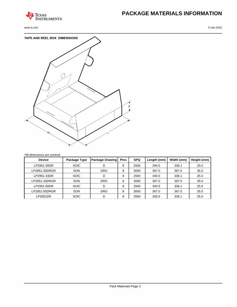
*All dimensions are nominal
Device Package Type Package Drawing Pins SPQ Length (mm) Width (mm) Height (mm)
LP2951-30DR SOIC D 8 2500 340.5 336.1 25.0
LP2951-30DRGR SON DRG 8 3000 367.0 367.0 35.0
LP2951-33DR SOIC D 8 2500 340.5 336.1 25.0
LP2951-33DRGR SON DRG 8 3000 367.0 367.0 35.0
LP2951-50DR SOIC D 8 2500 340.5 336.1 25.0
LP2951-50DRGR SON DRG 8 3000 367.0 367.0 35.0
LP2951DR SOIC D 8 2500 340.5 336.1 25.0
PACKAGE MATERIALS INFORMATION
www.ti.com 5-Jan-2022
Pack Materials-Page 2
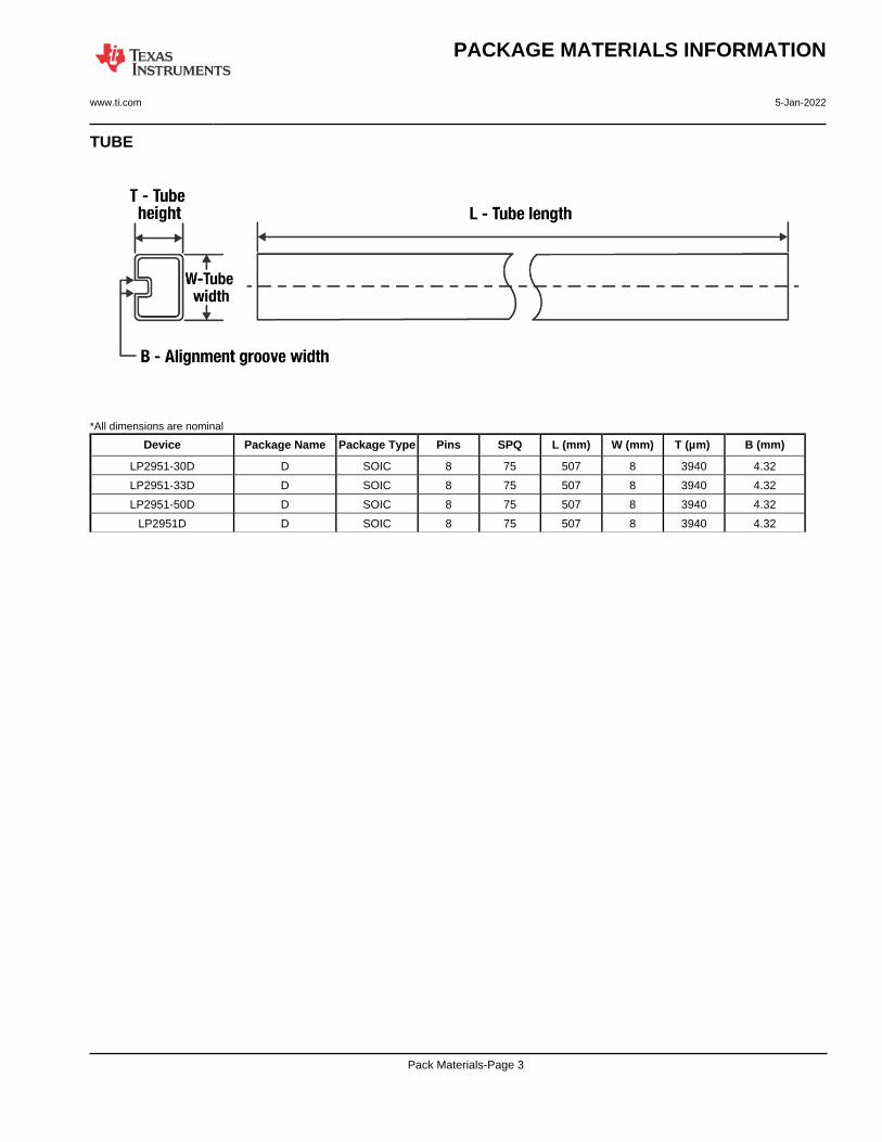
TUBE
*All dimensions are nominal
Device Package Name Package Type Pins SPQ L (mm) W (mm) T (µm) B (mm)
LP2951-30D D SOIC 8 75 507 8 3940 4.32
LP2951-33D D SOIC 8 75 507 8 3940 4.32
LP2951-50D D SOIC 8 75 507 8 3940 4.32
LP2951D D SOIC 8 75 507 8 3940 4.32
PACKAGE MATERIALS INFORMATION
www.ti.com 5-Jan-2022
Pack Materials-Page 3
www.ti.com
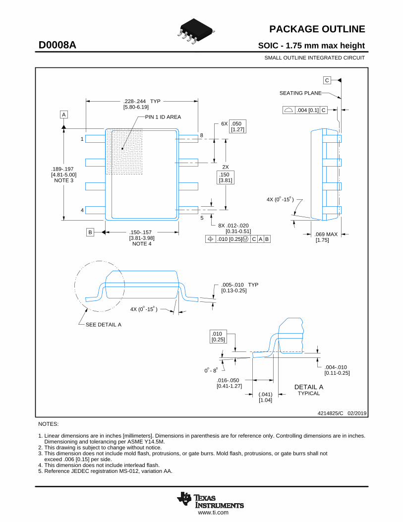
PACKAGE OUTLINE
C
.228-.244 TYP[5.80-6.19]
.069 MAX[1.75]
6X .050[1.27]
8X .012-.020 [0.31-0.51]
2X.150[3.81]
.005-.010 TYP[0.13-0.25]
0 - 8 .004-.010[0.11-0.25]
.010[0.25]
.016-.050[0.41-1.27]
4X (0 -15 )
A
.189-.197[4.81-5.00]
NOTE 3
B .150-.157[3.81-3.98]
NOTE 4
4X (0 -15 )
(.041)[1.04]
SOIC - 1.75 mm max heightD0008ASMALL OUTLINE INTEGRATED CIRCUIT
4214825/C 02/2019
NOTES: 1. Linear dimensions are in inches [millimeters]. Dimensions in parenthesis are for reference only. Controlling dimensions are in inches. Dimensioning and tolerancing per ASME Y14.5M. 2. This drawing is subject to change without notice. 3. This dimension does not include mold flash, protrusions, or gate burrs. Mold flash, protrusions, or gate burrs shall not exceed .006 [0.15] per side. 4. This dimension does not include interlead flash.5. Reference JEDEC registration MS-012, variation AA.
18
.010 [0.25] C A B
54
PIN 1 ID AREA
SEATING PLANE
.004 [0.1] C
SEE DETAIL A
DETAIL ATYPICAL
SCALE 2.800
www.ti.com
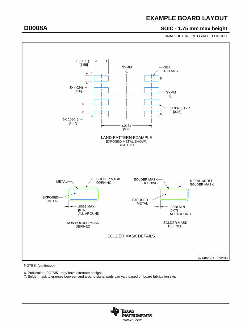
EXAMPLE BOARD LAYOUT
.0028 MAX[0.07]ALL AROUND
.0028 MIN[0.07]ALL AROUND
(.213)[5.4]
6X (.050 )[1.27]
8X (.061 )[1.55]
8X (.024)[0.6]
(R.002 ) TYP[0.05]
SOIC - 1.75 mm max heightD0008ASMALL OUTLINE INTEGRATED CIRCUIT
4214825/C 02/2019
NOTES: (continued) 6. Publication IPC-7351 may have alternate designs. 7. Solder mask tolerances between and around signal pads can vary based on board fabrication site.
METALSOLDER MASKOPENING
NON SOLDER MASKDEFINED
SOLDER MASK DETAILS
EXPOSEDMETAL
OPENINGSOLDER MASK METAL UNDER
SOLDER MASK
SOLDER MASKDEFINED
EXPOSEDMETAL
LAND PATTERN EXAMPLEEXPOSED METAL SHOWN
SCALE:8X
SYMM
1
45
8
SEEDETAILS
SYMM
www.ti.com
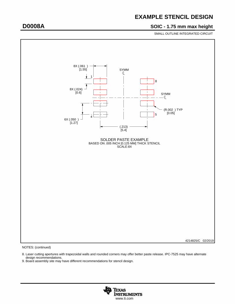
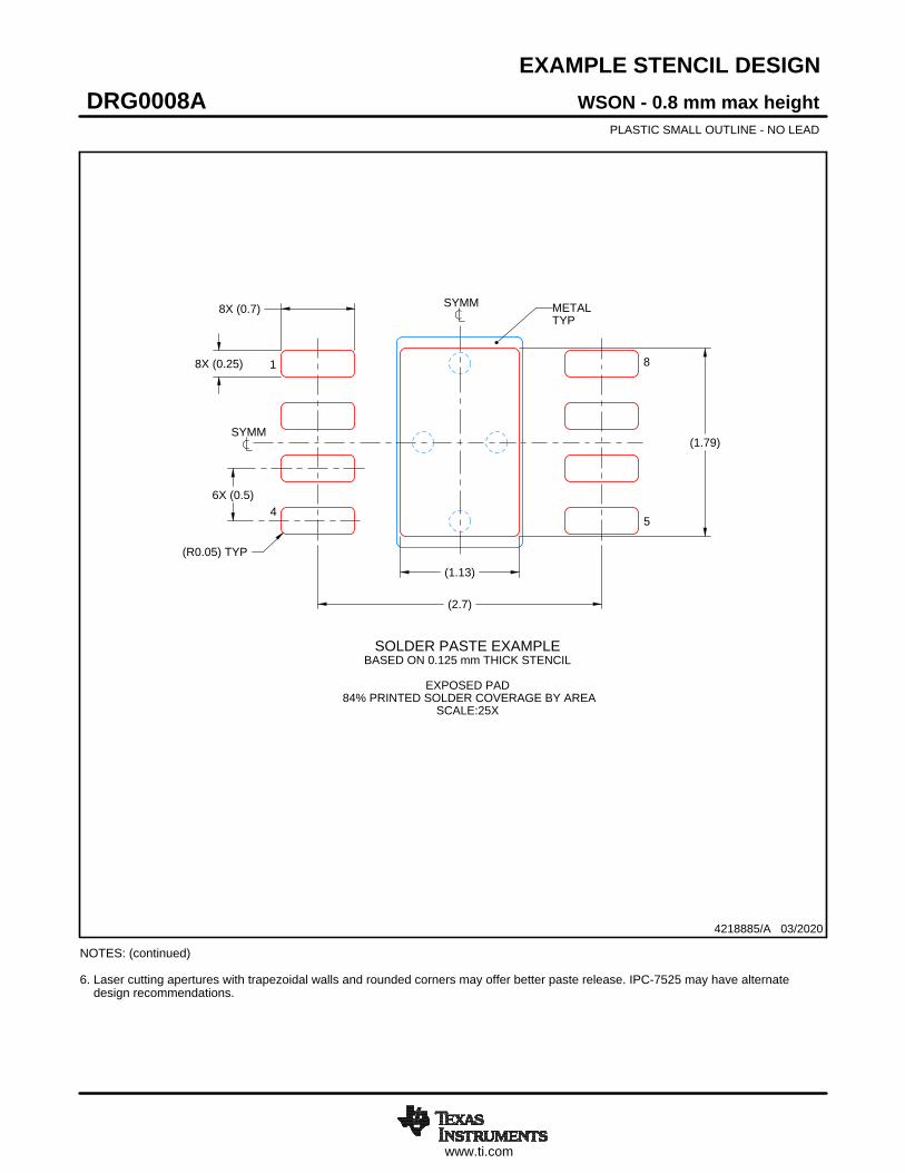
EXAMPLE STENCIL DESIGN
8X (.061 )[1.55]
8X (.024)[0.6]
6X (.050 )[1.27]
(.213)[5.4]
(R.002 ) TYP[0.05]
SOIC - 1.75 mm max heightD0008ASMALL OUTLINE INTEGRATED CIRCUIT
4214825/C 02/2019
NOTES: (continued) 8. Laser cutting apertures with trapezoidal walls and rounded corners may offer better paste release. IPC-7525 may have alternate design recommendations. 9. Board assembly site may have different recommendations for stencil design.
SOLDER PASTE EXAMPLEBASED ON .005 INCH [0.125 MM] THICK STENCIL
SCALE:8X
SYMM
SYMM
1
45
8
www.ti.com
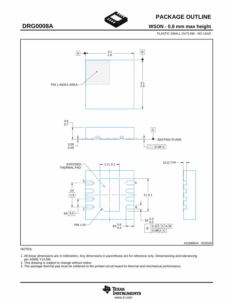
PACKAGE OUTLINE
C
8X 0.30.2
2 0.12X1.5
1.2 0.1
6X 0.5
0.80.7
8X 0.60.4
0.050.00
A 3.12.9
B
3.12.9
(0.2) TYP
WSON - 0.8 mm max heightDRG0008APLASTIC SMALL OUTLINE - NO LEAD
4218885/A 03/2020
PIN 1 INDEX AREA
SEATING PLANE
0.08 C
1
4 5
8
PIN 1 ID 0.1 C A B0.08 C
THERMAL PADEXPOSED
NOTES: 1. All linear dimensions are in millimeters. Any dimensions in parenthesis are for reference only. Dimensioning and tolerancing per ASME Y14.5M. 2. This drawing is subject to change without notice. 3. The package thermal pad must be soldered to the printed circuit board for thermal and mechanical performance.
SCALE 5.000
www.ti.com
EXAMPLE BOARD LAYOUT
0.07 MINALL AROUND
0.07 MAXALL AROUND
8X (0.25)
(2)
(2.7)
6X (0.5)
(1.2)
( 0.2) VIATYP
(0.75)
8X (0.7)
(R0.05) TYP(0.35)
WSON - 0.8 mm max heightDRG0008APLASTIC SMALL OUTLINE - NO LEAD
4218885/A 03/2020
SYMM
1
4 5
8
LAND PATTERN EXAMPLEEXPOSED METAL SHOWN
SCALE:20X
NOTES: (continued) 4. This package is designed to be soldered to a thermal pad on the board. For more information, see Texas Instruments literature number SLUA271 (www.ti.com/lit/slua271).5. Vias are optional depending on application, refer to device data sheet. If any vias are implemented, refer to their locations shown on this view. It is recommended that vias under paste be filled, plugged or tented.
SYMM
SOLDER MASKOPENINGSOLDER MASK
METAL UNDER
SOLDER MASKDEFINED
EXPOSEDMETAL
METALSOLDER MASKOPENING
SOLDER MASK DETAILS
NON SOLDER MASKDEFINED
(PREFERRED)
EXPOSEDMETAL
www.ti.com
EXAMPLE STENCIL DESIGN
(R0.05) TYP
8X (0.25)
8X (0.7)
(1.13)
(1.79)
(2.7)
6X (0.5)
WSON - 0.8 mm max heightDRG0008APLASTIC SMALL OUTLINE - NO LEAD
4218885/A 03/2020
NOTES: (continued) 6. Laser cutting apertures with trapezoidal walls and rounded corners may offer better paste release. IPC-7525 may have alternate design recommendations.
SOLDER PASTE EXAMPLEBASED ON 0.125 mm THICK STENCIL
EXPOSED PAD
84% PRINTED SOLDER COVERAGE BY AREASCALE:25X
SYMM
1
45
8
METALTYP
SYMM
www.ti.com
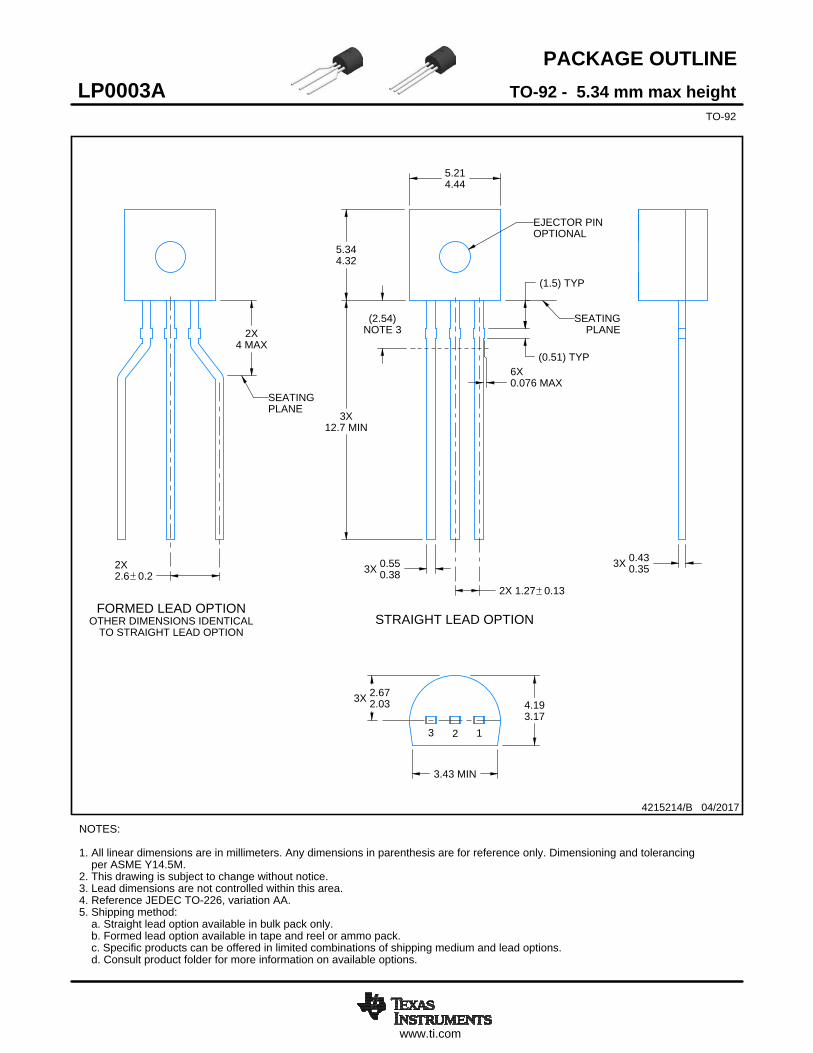
PACKAGE OUTLINE
3X 2.672.03
5.214.44
5.344.32
3X12.7 MIN
2X 1.27 0.13
3X 0.550.38
4.193.17
3.43 MIN
3X 0.430.35
(2.54)NOTE 3
2X2.6 0.2
2X4 MAX
SEATINGPLANE
6X0.076 MAX
(0.51) TYP
(1.5) TYP
TO-92 - 5.34 mm max heightLP0003ATO-92
4215214/B 04/2017
NOTES: 1. All linear dimensions are in millimeters. Any dimensions in parenthesis are for reference only. Dimensioning and tolerancing per ASME Y14.5M.2. This drawing is subject to change without notice.3. Lead dimensions are not controlled within this area.4. Reference JEDEC TO-226, variation AA.5. Shipping method: a. Straight lead option available in bulk pack only. b. Formed lead option available in tape and reel or ammo pack. c. Specific products can be offered in limited combinations of shipping medium and lead options. d. Consult product folder for more information on available options.
EJECTOR PINOPTIONAL
PLANESEATING
STRAIGHT LEAD OPTION
3 2 1
SCALE 1.200
FORMED LEAD OPTIONOTHER DIMENSIONS IDENTICAL
TO STRAIGHT LEAD OPTION
SCALE 1.200
www.ti.com
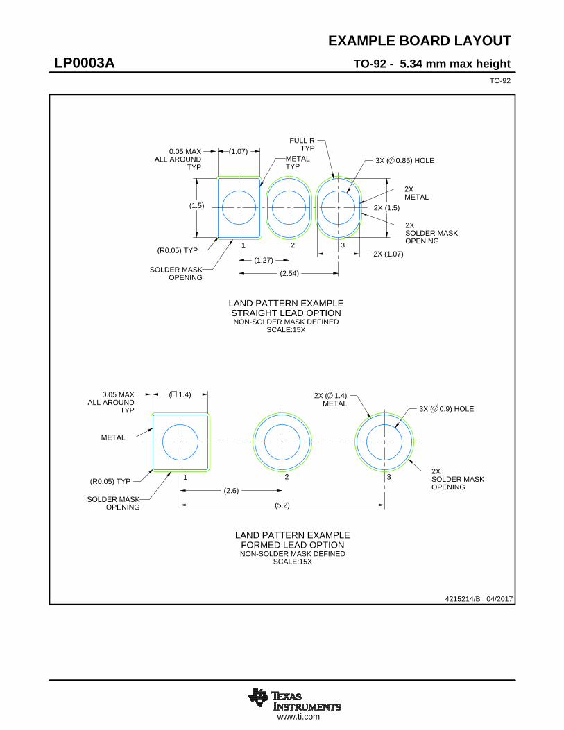
EXAMPLE BOARD LAYOUT
0.05 MAXALL AROUND
TYP
(1.07)
(1.5) 2X (1.5)
2X (1.07)(1.27)
(2.54)
FULL RTYP
( 1.4)0.05 MAXALL AROUND
TYP
(2.6)
(5.2)
(R0.05) TYP
3X ( 0.9) HOLE
2X ( 1.4)METAL
3X ( 0.85) HOLE
(R0.05) TYP
4215214/B 04/2017
TO-92 - 5.34 mm max heightLP0003ATO-92
LAND PATTERN EXAMPLEFORMED LEAD OPTIONNON-SOLDER MASK DEFINED
SCALE:15X
SOLDER MASKOPENING
METAL
2XSOLDER MASKOPENING
1 2 3
LAND PATTERN EXAMPLESTRAIGHT LEAD OPTIONNON-SOLDER MASK DEFINED
SCALE:15X
METALTYP
SOLDER MASKOPENING
2XSOLDER MASKOPENING
2XMETAL
1 2 3
www.ti.com
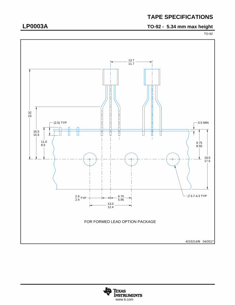
TAPE SPECIFICATIONS
19.017.5
13.711.7
11.08.5
0.5 MIN
TYP-4.33.7
9.758.50
TYP2.92.4
6.755.95
13.012.4
(2.5) TYP
16.515.5
3223
4215214/B 04/2017
TO-92 - 5.34 mm max heightLP0003ATO-92
FOR FORMED LEAD OPTION PACKAGE
IMPORTANT NOTICE AND DISCLAIMERTI PROVIDES TECHNICAL AND RELIABILITY DATA (INCLUDING DATA SHEETS), DESIGN RESOURCES (INCLUDING REFERENCE DESIGNS), APPLICATION OR OTHER DESIGN ADVICE, WEB TOOLS, SAFETY INFORMATION, AND OTHER RESOURCES “AS IS” AND WITH ALL FAULTS, AND DISCLAIMS ALL WARRANTIES, EXPRESS AND IMPLIED, INCLUDING WITHOUT LIMITATION ANY IMPLIED WARRANTIES OF MERCHANTABILITY, FITNESS FOR A PARTICULAR PURPOSE OR NON-INFRINGEMENT OF THIRD PARTY INTELLECTUAL PROPERTY RIGHTS.These resources are intended for skilled developers designing with TI products. You are solely responsible for (1) selecting the appropriate TI products for your application, (2) designing, validating and testing your application, and (3) ensuring your application meets applicable standards, and any other safety, security, regulatory or other requirements.These resources are subject to change without notice. TI grants you permission to use these resources only for development of an application that uses the TI products described in the resource. Other reproduction and display of these resources is prohibited. No license is granted to any other TI intellectual property right or to any third party intellectual property right. TI disclaims responsibility for, and you will fully indemnify TI and its representatives against, any claims, damages, costs, losses, and liabilities arising out of your use of these resources.TI’s products are provided subject to TI’s Terms of Sale or other applicable terms available either on ti.com or provided in conjunction with such TI products. TI’s provision of these resources does not expand or otherwise alter TI’s applicable warranties or warranty disclaimers for TI products.TI objects to and rejects any additional or different terms you may have proposed. IMPORTANT NOTICE
Mailing Address: Texas Instruments, Post Office Box 655303, Dallas, Texas 75265Copyright © 2022, Texas Instruments Incorporated