Embed Size (px)
Citation preview

Micro-Research Finland Oy
Timing System Modules
Jukka Pietarinen
EPICS Collaboration Meeting,Argonne, June 2006

Micro-Research Finland Oy
[email protected] Collaboration Meeting, ANL, Argonne14.6.2006
Timing System
• Functionality based on the APS timing system
• Redesigned for SLS → Series 100
• Improved performance for Diamond → Series 200
• Timing signals needed for synchronisation of subsystems are applied to Event Generator (EVG) or generated by EVG
• Timing information is converted to 8-bit event codes and disbtributed to Event Receivers (EVR) as optical signals
• Event clock rate determines timing resolution:– Minimum clock rate 50 MHz, 20 ns resolution– Maximum clock rate 125 MHz, 8 ns resolution
• 8-bit distributed bus running in parallel and independent of timing events allows distribution of eight signals updated with the event clock rate

Micro-Research Finland Oy
[email protected] Collaboration Meeting, ANL, Argonne14.6.2006
Event Generator (EVG-200)
RF input• Event clock divided from RF• EVG-200: /4, /5, /6, /8, /10 or /12• VME-EVG-230: /1, /2, ... , /32
Line syncronisation inpute.g. 50 Hz / 60 Hz TTL level
SFP transceiver• Optical signal to EVRs (fan-outs)
Distributed bus inputs
External trigger inputs

Micro-Research Finland Oy
[email protected] Collaboration Meeting, ANL, Argonne14.6.2006
EVG Event Sources
• Eight Trigger Events send out programmable event code on– External input (transition board)– Multiplexed counter output– Line synchronisation input trigger
• Two Event Sequencers
• Software Event (IOC access)
• External Timestamping seconds counter events
• Upstream EVG events
• Super Cycle Sequencer (currently in development)
Micro-Research Finland Oy
[email protected] Collaboration Meeting, ANL, Argonne14.6.2006
EVG Multiplexed Counters
• 32-bit counters generate programmable frequencies– Maximum frequency 62.5 MHz (event clock 125 MHz)– Maximum period > 34 s (event clock 125 MHz)
• Counter outputs may:– Generate trigger events– Drive distributed bus signals– Counter output 7 can be used for line sychronisation
• MXC use at Diamond– MXC0 booster revolution clock RF/264 i.e. Event clock/66, 1.893 MHz– MXC1 storage ring revolution clock RF/936 i.e. Event clock/234, 534 kHz– MXC7 booster and storage ring coincidence clock event clock/(39*66), 48.5 kHz

Micro-Research Finland Oy
[email protected] Collaboration Meeting, ANL, Argonne14.6.2006
EVG Event Sequencers
Ram address 32 bit 8 bit
0 event timestamp event code 1. Event
1 event timestamp event code 2. Event
2 event timestamp event code 3. Event
|
|
|
|
2047 event timestamp event code 2048. Event
Special event codes
0x00 Null event code – no event transmitted0x7F End sequence – stop or recycle sequence
Micro-Research Finland Oy
[email protected] Collaboration Meeting, ANL, Argonne14.6.2006
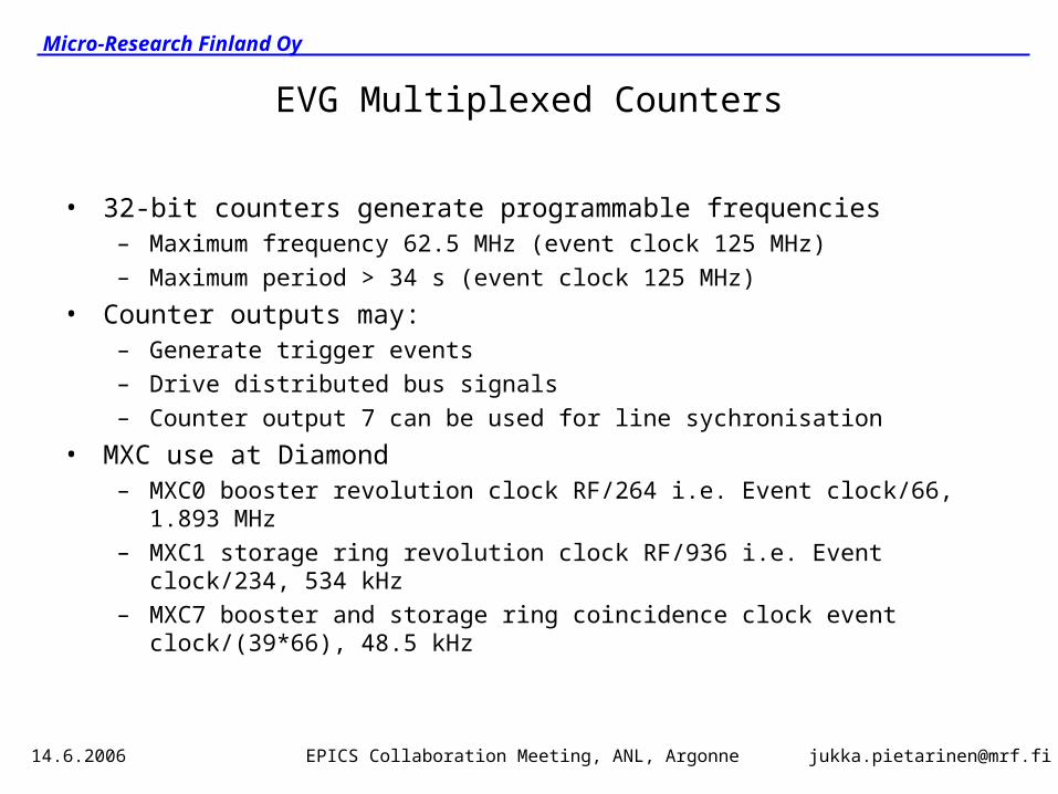
EVG Event Sequencer Triggering
• SW trigger
• External input
• Multiplexed counter output
• Line synchronisation triggering
LineSync.input
ProgrammableDivider
/1 to /256
Phase shifter0 to 25.5 ms
in 0.1 ms steps
MXC7
Event clock
TriggerD
Q

Micro-Research Finland Oy
[email protected] Collaboration Meeting, ANL, Argonne14.6.2006
Sequencer and Event Analyser Example
address timestamp event
0 0 0x20 1. Event
1 85168 0x2a 2. Event
2 94537 0x24 3. Event
3 94538 0x25 4. Event
4 94821 0x2c 5. Event
5 282002 0x30 6. Event
6 283895 0x3c 7. Event
7 284000 0x7f End sequence
Analyser time (s) Offset (us) code
0,190072274 -1,07 11
0,190073347 0,00 20
0,235073191 44999,84 2a
0,240023448 49950,10 24
0,240023977 49950,63 25
0,240173504 50100,16 2c
0,339073511 149000,16 30
0,340073707 150000,36 3c
0,390076629 -1,07 11
0,390077702 0,00 20
0,435077546 44999,84 2a
0,440027803 49950,10 24
0,440028332 49950,63 25
0,440177859 50100,16 2c
0,539077866 149000,16 30
0,540078062 150000,36 3c
• Sequence RAM prescaler set to 264/4, 528 us cycles• Line sync. divider 10• 50 Hz applied to line sync. Input• Trigger event enabled to send 0x11 on seq. trigger
Event Analyser with 64-bit time counter

Micro-Research Finland Oy
[email protected] Collaboration Meeting, ANL, Argonne14.6.2006
Event Receiver (EVR-200-RF)
HTB OTB TTB NTB
SFP transceiver• Optical signal from EVG (or fan-out)
Recovered RF output (optional)
Programmable outputs• 5 TTL level• 2 LVPECL levelExternal trigger input

Micro-Research Finland Oy
[email protected] Collaboration Meeting, ANL, Argonne14.6.2006
EVR Event Mapping
Two Event Mapping RAMs• One RAM enabled at a time• 256 x 16 bit RAM• Each received 8-bit event code
is mapped to a 16-bit word• Mapped bit determines which
functions and HW outputs get triggered
• MAP13 delayed IRQ• MAP14 latch timestamp• MAP15 FIFO event/IRQ
Map bit OTP PDP LVL
0 0 0 0 reset
1 1 1 0 set
2 2 2 1 reset
3 3 3 1 set
4 4 2 reset
5 5 2 set
6 6 3 reset
7 7 3 set
8 8 4 reset
9 9 4 set
10 10 5 reset
11 11 5 set
12 12 6 reset
13 13 6 set

Micro-Research Finland Oy
[email protected] Collaboration Meeting, ANL, Argonne14.6.2006
EVR hardware outputs
14 OTP outputs
• Programmable delay, width and polarity– 32 bit delay counter, max. 34 s delay @ 125 MHz event clock– 16 bit width counter, 8 ns to 524 us pulses @ 125 MHz event clock
• TB OTP0-7 may be programmed to output DBUS signals
4 PDP outputs
• Programmable delay, width, polarity and prescaler– 32 bit delay and width counters– 16 bit prescaler– Maximum delay and width up to 625 h @ 125 MHz event clock
7 LVL outputs
• Output level changed by event codes

Micro-Research Finland Oy
[email protected] Collaboration Meeting, ANL, Argonne14.6.2006
Timestamping at Diamond (EVG)
10 MHzreference
clock 1 MHz
1 HzRS232 ASCII time
MCU
EVG
’0’
’1’
DBUS4
Code 0x7D (EVCRS)
Code 0x70 (SEC0)
Code 0x71 (SEC1)
MCU generates 32+1 events at 1 Hz to send binary ”Diamond” time in seconds serially to all EVRs
1 Hz
Micro-Research Finland Oy
[email protected] Collaboration Meeting, ANL, Argonne14.6.2006
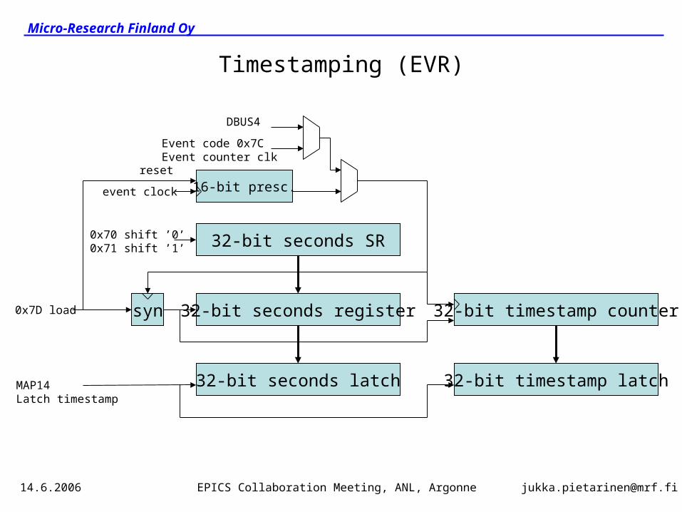
Timestamping (EVR)
32-bit seconds SR0x70 shift ’0’0x71 shift ’1’
32-bit seconds register0x7D load
32-bit seconds latchMAP14Latch timestamp
32-bit timestamp counter
32-bit timestamp latch
syn
16-bit presc.event clock
reset
DBUS4
Event code 0x7CEvent counter clk

Micro-Research Finland Oy
[email protected] Collaboration Meeting, ANL, Argonne14.6.2006
Event FIFO
32-bit seconds register 32-bit timestamp counter
32-bit Seconds 32-bit timestamp 8-bit event
32-bit Seconds 32-bit timestamp 8-bit event
| | |32-bit Seconds 32-bit timestamp 8-bit eventMAP15
Event FIFOwrite
Event code
• FIFO can hold up to 511 events• Timestamping of a local hardware signal with EVR external event input

Micro-Research Finland Oy
[email protected] Collaboration Meeting, ANL, Argonne14.6.2006
Data Transmission
2 kByteDual-ported
memory
EVG EVR
VME
• Configurable buffer size 4 to 2048 bytes
• Utilises distributed bus (DBUS bandwidth is halved when data transfers are enabled)
• Automatic checksumming
• Maximum transfer rate 62.5 Mbytes/s with 125 MHz event clock
2 kByteDual-ported
memory
VME
• Buffer size included in transmission
• Automatic checksum verification
• flag set on error
• Interrupt on receive complete

Micro-Research Finland Oy
[email protected] Collaboration Meeting, ANL, Argonne14.6.2006
Super Cycle Sequencer (in development)
PowerPC8 kbytes ISOCM
128 MbytesSDRAM
16384 pagesof 1024 events
8 kbytesDPRAM/DSOCMControl registersWindow for one1024 event page
VME2+8 kbytes
DPRAM/DSOCMTwo pages of1024 events
SequencerDCR controllerVME
IRQ
Control & IRQ
DCR
Eventinterface
Page consist of 1024 events• 32-bit timestamp• 8-bit event codeMachine cycle consists of one or several consecutive pages• end of machine cycle determined by end-cycle code 0x7f
PLB

Micro-Research Finland Oy
[email protected] Collaboration Meeting, ANL, Argonne14.6.2006
Future PlansVME versions• Support standard VME with 5V supply• VME-EVG: programmable RF divider /1, /2, ..., /32• VME-EVR: two versions
1. With RF recovery and two LVPECL outputs2. w/o RF recovery, reduced jitter performance, typ. 20-30 ps rms
CompactPCI versions• Maximum bit rate 2.0 Gbps, 100 MHz event clock• PCI-EVG w/o super cycle sequencer• PCI-EVR:
– jitter performance similar to PMC-EVR / VME-EVR w/o RF– I/O signals on P2/J2 PXI star trigger, trigger bus, local bus pins allows using
module in 32-bit rear I/O systems, 64-bit systems and PXI systems
EVR for embedded systems• Form factor: PCI-104, MiniPCI, other?

Micro-Research Finland Oy
[email protected] Collaboration Meeting, ANL, Argonne14.6.2006
Acknowledgements
• Developers of the APS timing system• Timo Korhonen, Paul Scherrer-Instute/SLS for initiating the
redesign and inventing valuable features• Yuri Chernousko and Angelos Gonias from Diamond for
many ideas improving the functionality• Users and evaluators of the timing system for feedback and
helping to understand the requirements of various timing systems


![[2010] - Pietarinen - Essential Analytic Philosophy](https://img.pdfslide.us/doc/110x75/577cd2b81a28ab9e7895d3c1/2010-pietarinen-essential-analytic-philosophy.jpg)