Embed Size (px)
Citation preview
Micro-Nano Thermal-Fluid: Physics, Sensors, Measurements
Cantilever Sensors: An Example of what you will learn in ME 381R
Prof. Li Shi
Micro-Nano Thermal-Fluid Laboratory
Department of Mechanical Engineering
The University of Texas at Austin
2
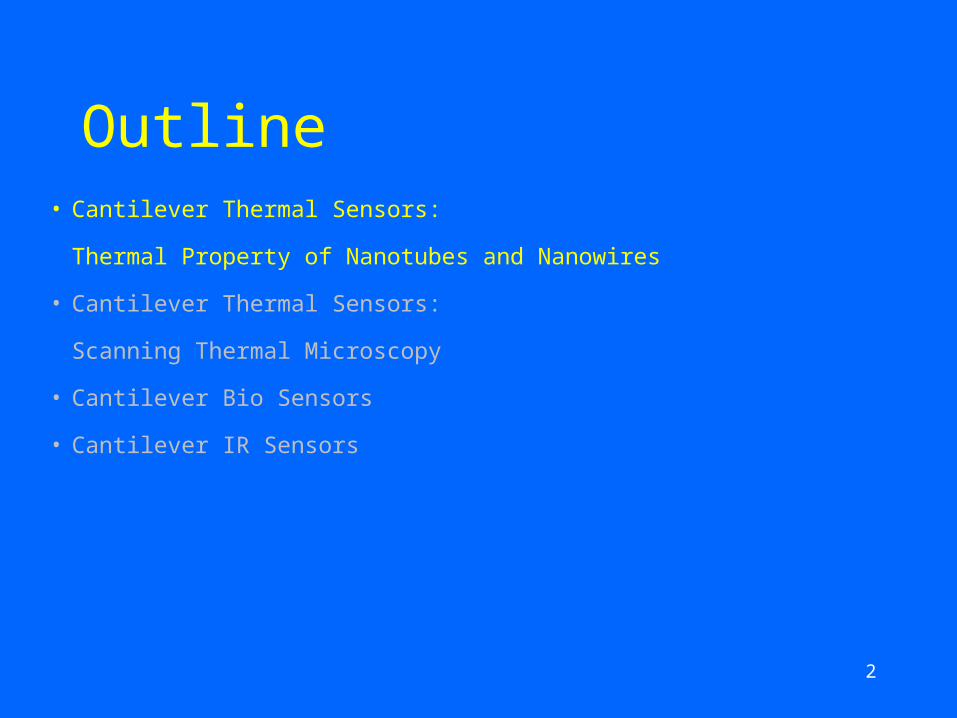
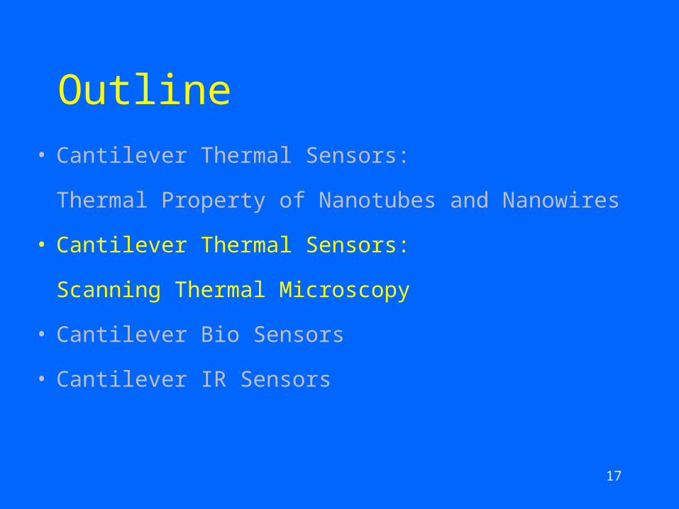
Outline• Cantilever Thermal Sensors:
Thermal Property of Nanotubes and Nanowires
• Cantilever Thermal Sensors:
Scanning Thermal Microscopy
• Cantilever Bio Sensors
• Cantilever IR Sensors
3
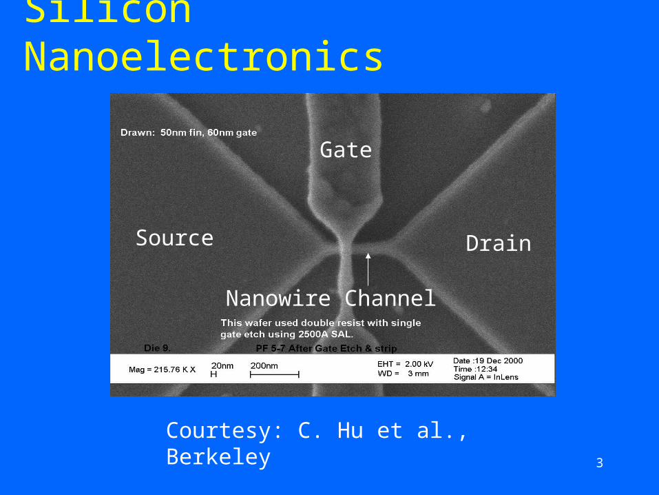
Source Drain
Gate
Nanowire Channel
Silicon Nanoelectronics
Courtesy: C. Hu et al., Berkeley
4
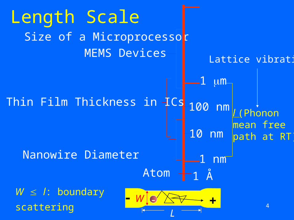
Length Scale
1 m
1 nm
MEMS Devices
Size of a Microprocessor
Nanowire Diameter
100 nml (Phonon mean freepath at RT)
1 ÅAtom
L
W l: boundary scattering - +-W
Thin Film Thickness in ICs
10 nm
Lattice vibration
5
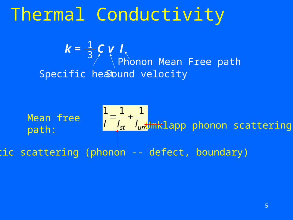
Thermal Conductivity
k = C v l13
Specific heat Sound velocityPhonon Mean Free path
umst lll111 Mean free path:
Static scattering (phonon -- defect, boundary)
Umklapp phonon scattering
6
0
10
20
30
40
50
60
0 40 80 120 160 200 240 280 320 360
0
10
20
30
40
50
60
0 40 80 120 160 200 240 280 320 360
Temperature (K)
The
rmal
Con
duct
ivity
(W
/m-K
)
30nm
56nm
115nm
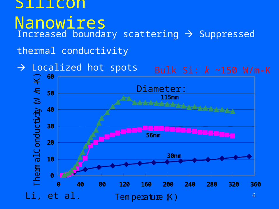
Silicon NanowiresIncreased boundary scattering Suppressed thermal conductivity
Localized hot spots
Li, et al.
Bulk Si: k ~150 W/m-K
Diameter:
7
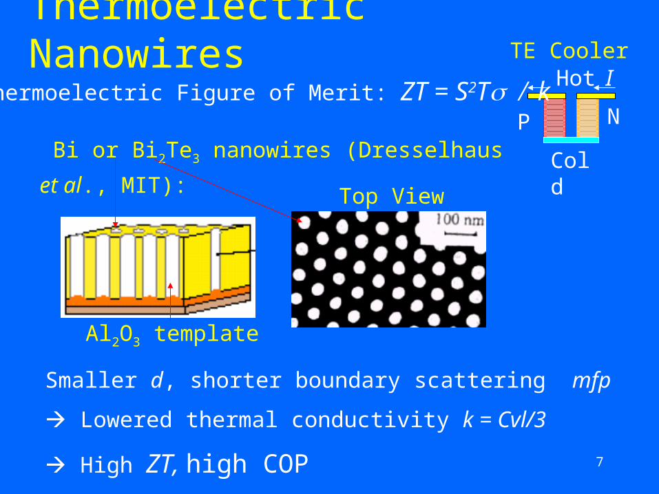
Thermoelectric Nanowires
Bi or Bi2Te3 nanowires (Dresselhaus et al., MIT):
Top View
Al2O3 template
Smaller d, shorter boundary scattering mfp
Lowered thermal conductivity k = Cvl/3
High ZT, high COP
I
Cold
Hot
P N
TE Cooler
Thermoelectric Figure of Merit: ZT = S2Tk
8
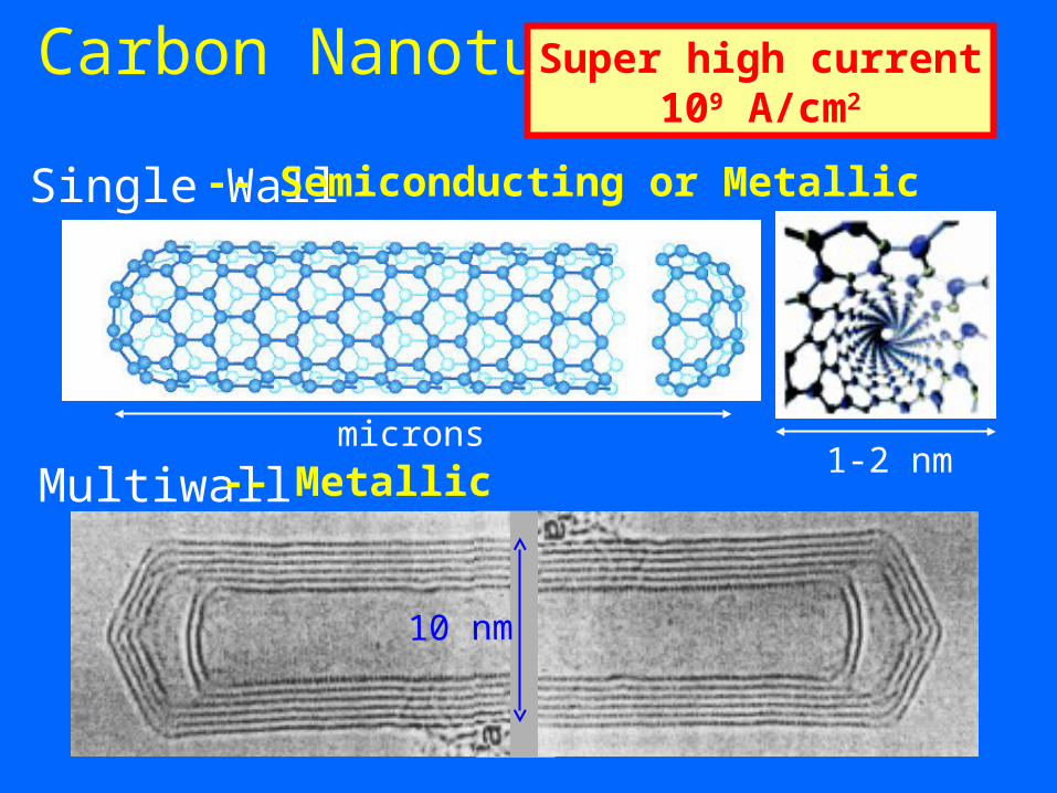
Carbon Nanotubes
Single Wall -- Semiconducting or Metallic
Super high current109 A/cm2
1-2 nmmicrons
Multiwall -- Metallic
10 nm
9
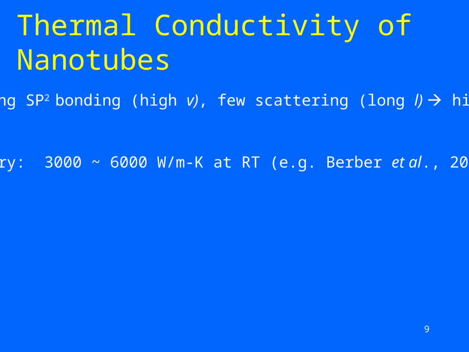
Thermal Conductivity of Nanotubes
• Strong SP2 bonding (high v), few scattering (long l) high k
• Theory: 3000 ~ 6000 W/m-K at RT (e.g. Berber et al., 2000)
10
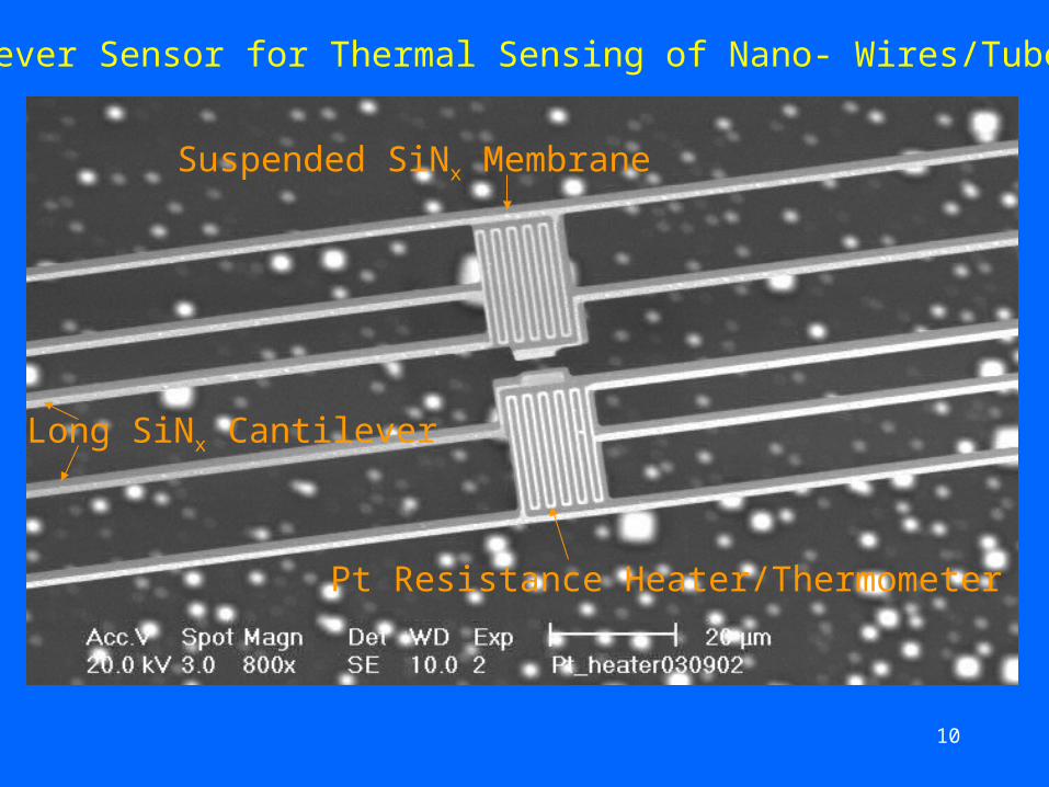
Pt Resistance Heater/Thermometer
Suspended SiNx Membrane
Long SiNx Cantilever
A Cantilever Sensor for Thermal Sensing of Nano- Wires/Tubes
11
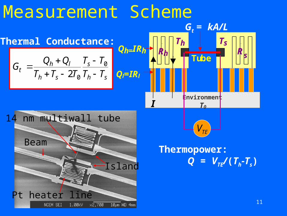
Measurement Scheme
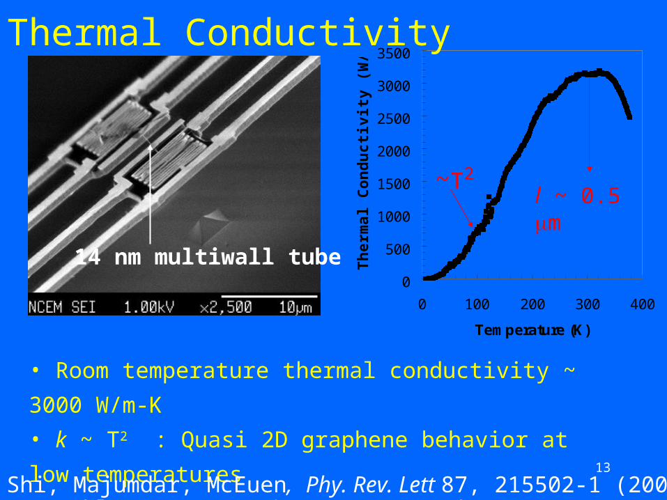
14 nm multiwall tube
Island
Beam
Pt heater line
Th Ts
t Ts
R s
Rh Qh=IRh
Tube
Ql=IRl
Environment
T0 I
Gt = kA/L
sh
s
sh
lht TT
TT
TTT
QQG
0
02
Thermal Conductance:
VTE
Thermopower:Q = VTE/(Th-Ts)
12
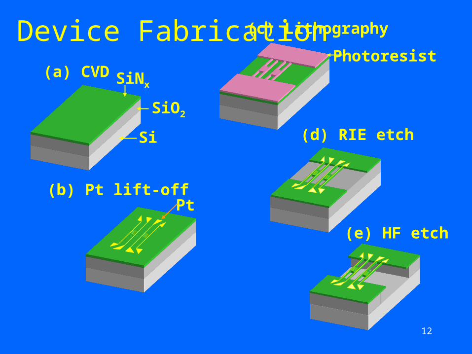
Device Fabrication
Si
SiO2
SiNx
Pt
Photoresist(a) CVD
(b) Pt lift-off
(c) Lithography
(d) RIE etch
(e) HF etch
13
0
500
1000
1500
2000
2500
3000
3500
0 100 200 300 400
Temperature (K)
Th
erm
al
Co
nd
uc
tiv
ity
(W
/m-K
)
Thermal Conductivity
• Room temperature thermal conductivity ~ 3000 W/m-K
• k ~ T2 : Quasi 2D graphene behavior at low temperatures
• Umklapp scattering ~ 320 K , l ~ 0.5 m
l ~ 0.5 m~T2
Kim, Shi, Majumdar, McEuen, Phy. Rev. Lett 87, 215502-1 (2001)
14 nm multiwall tube
14
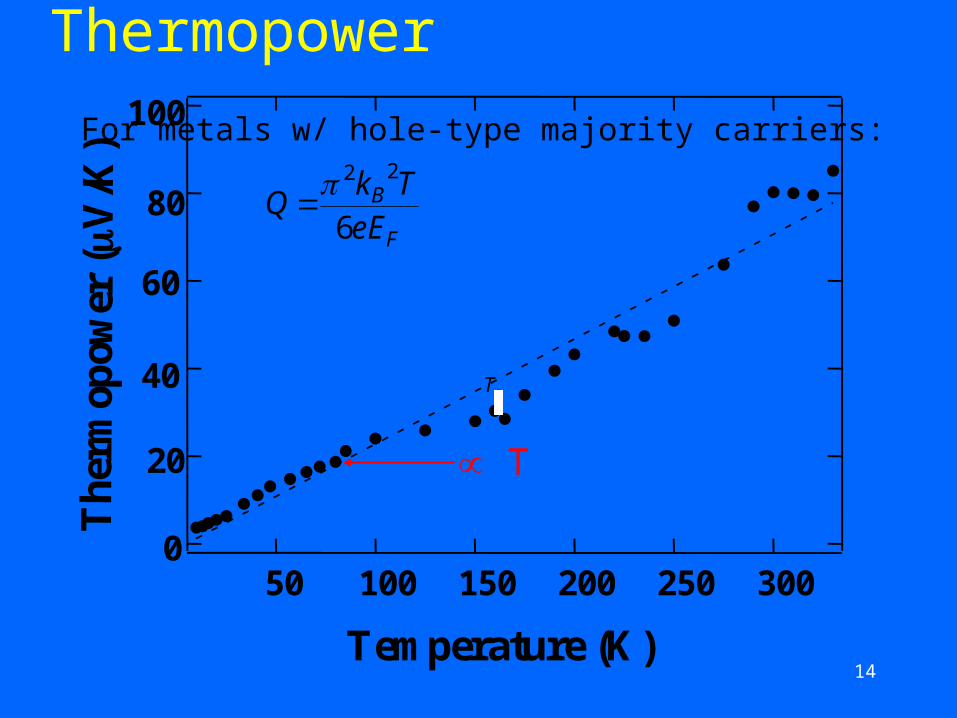
Thermopower100
80
60
40
20
030025020015010050
Ts
Th
erm
opow
er (V
/K)
Temperature (K)
F
B
eETk
Q6
22
For metals w/ hole-type majority carriers:
T
15
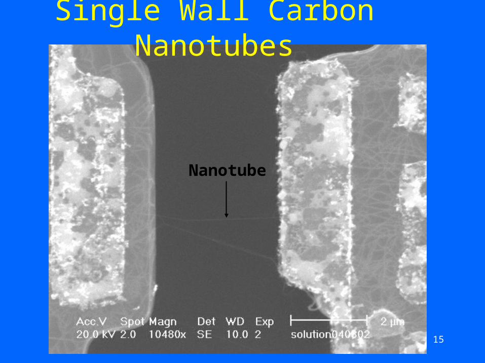
Single Wall Carbon Nanotubes
Nanotube
16
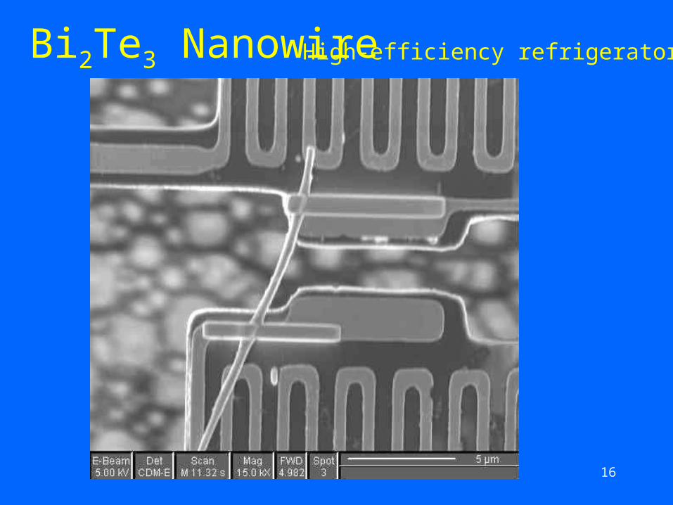
Bi2Te3 Nanowire High-efficiency refrigerators!
17
Outline
• Cantilever Thermal Sensors:
Thermal Property of Nanotubes and Nanowires
• Cantilever Thermal Sensors:
Scanning Thermal Microscopy
• Cantilever Bio Sensors
• Cantilever IR Sensors
18
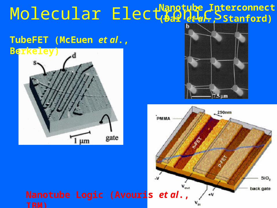
Molecular Electronics
TubeFET (McEuen et al., Berkeley)
Nanotube Logic (Avouris et al., IBM)
Nanotube Interconnect(Dai et al., Stanford)
19
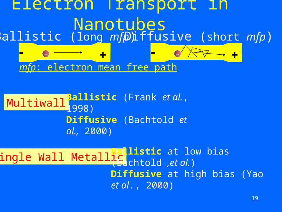
Electron Transport in Nanotubes
- +- - +-
Ballistic (long mfp) Diffusive (short mfp)
mfp: electron mean free path
MultiwallBallistic (Frank et al., 1998)Diffusive (Bachtold et al., 2000)
Single Wall MetallicBallistic at low bias (Bachtold ,et al.)Diffusive at high bias (Yao et al., 2000)
20
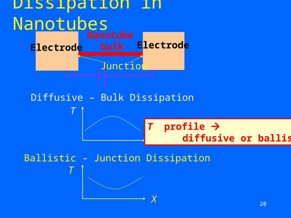
Dissipation in Nanotubes
Nanotube bulk Electrode
Electrode
Diffusive – Bulk Dissipation
Ballistic – Junction Dissipation
Junction
X
X
T
T
T profile diffusive or ballistic
21
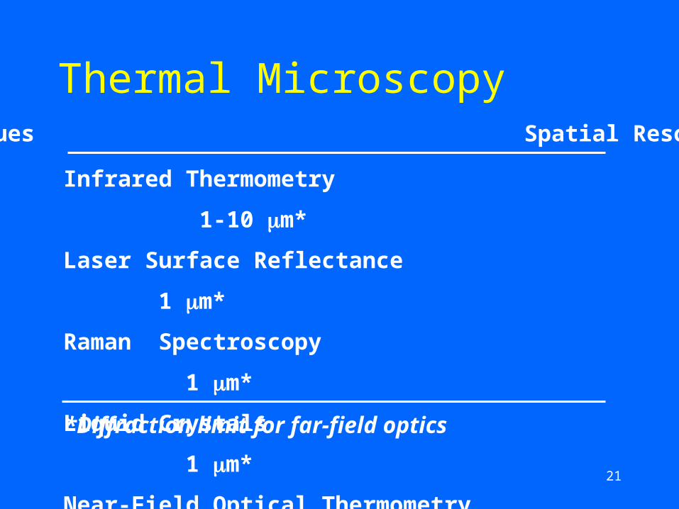
Thermal Microscopy
Infrared Thermometry 1-10 m*
Laser Surface Reflectance 1 m*
Raman Spectroscopy 1 m*
Liquid Crystals 1 m*
Near-Field Optical Thermometry < 1m
Scanning Thermal Microscopy (SThM) < 100 nm
Techniques Spatial Resolution
*Diffraction limit for far-field optics
22
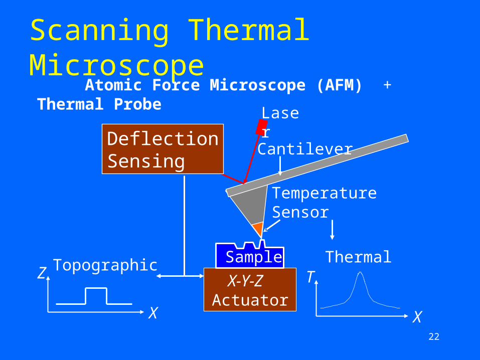
X-Y-Z Actuator
Scanning Thermal Microscope
Sample
Temperature Sensor
Laser
Atomic Force Microscope (AFM) + Thermal Probe
CantileverDeflectionSensing
Thermal
X
TTopographic
X
Z
23
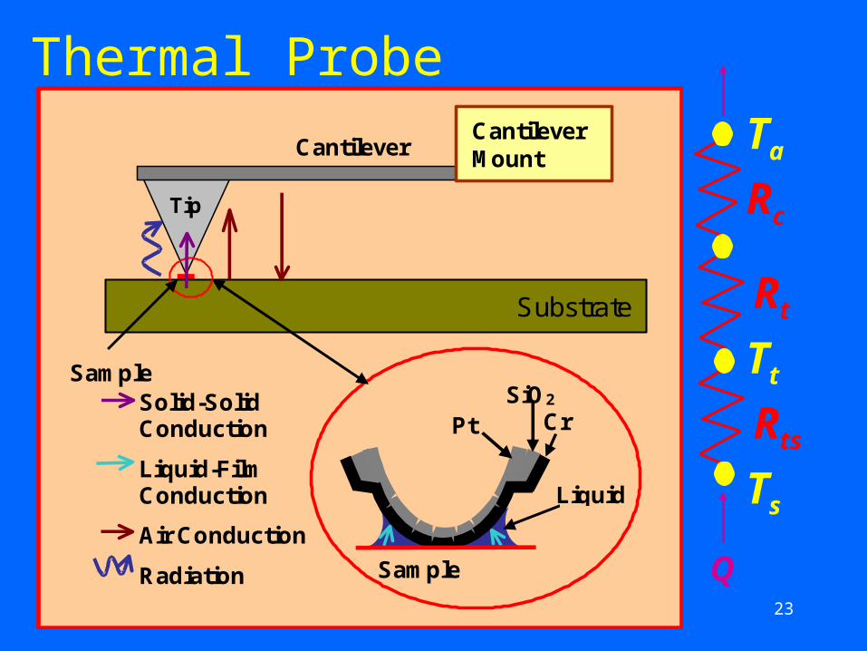
Thermal Probe
Tip
Solid-Solid Conduction
Liquid-Film Conduction
Air Conduction
Radiation
Cantilever Cantilever Mount
Liquid
Cr Pt SiO2
Sample
Substrate
Sample
Rts
Rt
Ts
Ta
Tt
Rc
Q
24
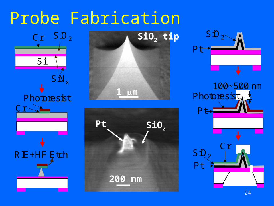
Probe Fabrication
1 m
SiO2 tip
Si
SiO2
SiNx
Photoresist Cr
Cr
RIE+HF Etch
200 nm
Pt SiO2
SiO2
Pt
Pt
CrSiO2
Photoresist
Pt
100~500 nm
25
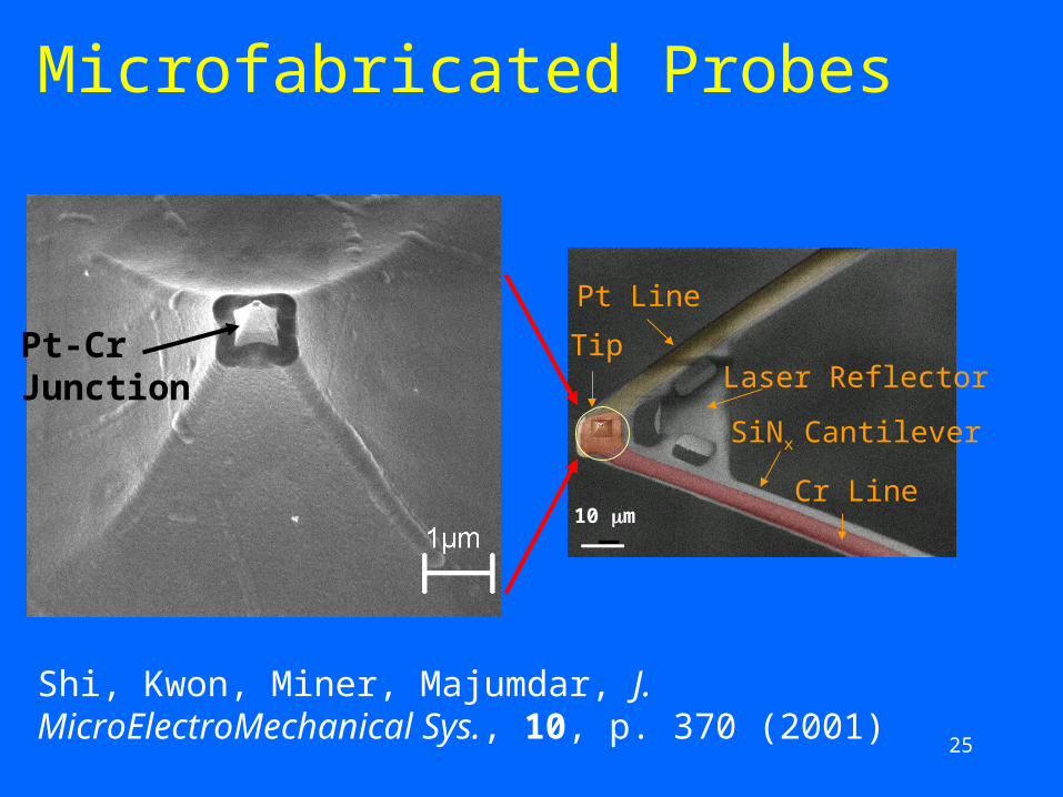
Microfabricated Probes
Pt-Cr Junction
Shi, Kwon, Miner, Majumdar, J. MicroElectroMechanical Sys., 10, p. 370 (2001)
10 m
Pt Line
Cr Line
TipLaser Reflector
SiNx Cantilever
26
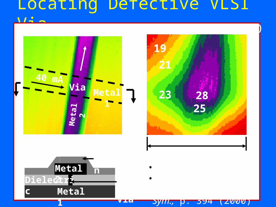
Locating Defective VLSI Via
• Collaboration: TI• Shi et al., Int. Reli. Phys. Sym., p. 394 (2000)Metal 1
DielectricMetal 2
Passivation
0.4 m Via
Cross Section
Topography Tip Temperature Rise (K)
20 m
2823
21
19
25
Met
al 2
ViaMetal 1
40 mA
27
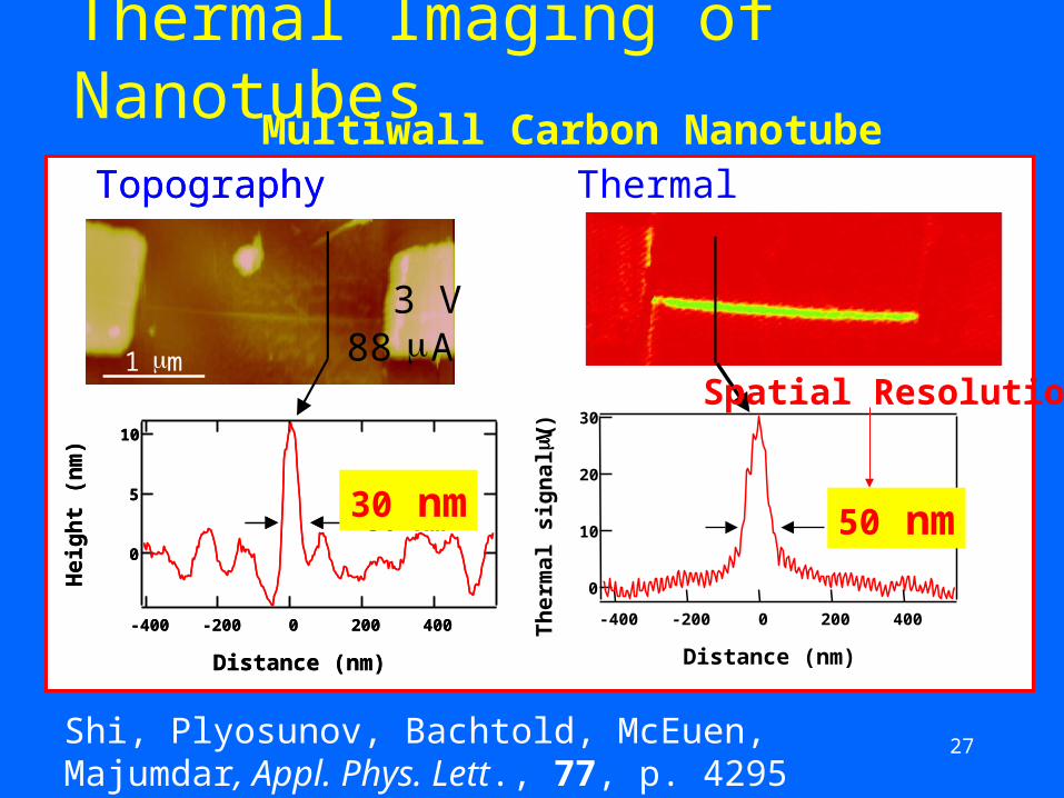
Thermal Imaging of Nanotubes Multiwall Carbon Nanotube
1 m
Topography
1 m
Topography
3 V88 A
Distance (nm)
Th
erm
al s
ign
al ( V
) 30
20
10
0
4002000-200-400
50 nm
Distance (nm)
Hei
ght
(nm
)
30 nm
10
5
0
4002000-200-400
Distance (nm)
Hei
ght
(nm
)
30 nm
10
5
0
4002000-200-400
Thermal
30 nm 50 nm
Shi, Plyosunov, Bachtold, McEuen, Majumdar, Appl. Phys. Lett., 77, p. 4295 (2000)
Spatial Resolution
28
20
10
0
210
Distance (m)
Tti
p(K
)
-40
-20
0
20
40
10000-1000
Bias voltage (mV)
Cur
rent
(A
)
1 m
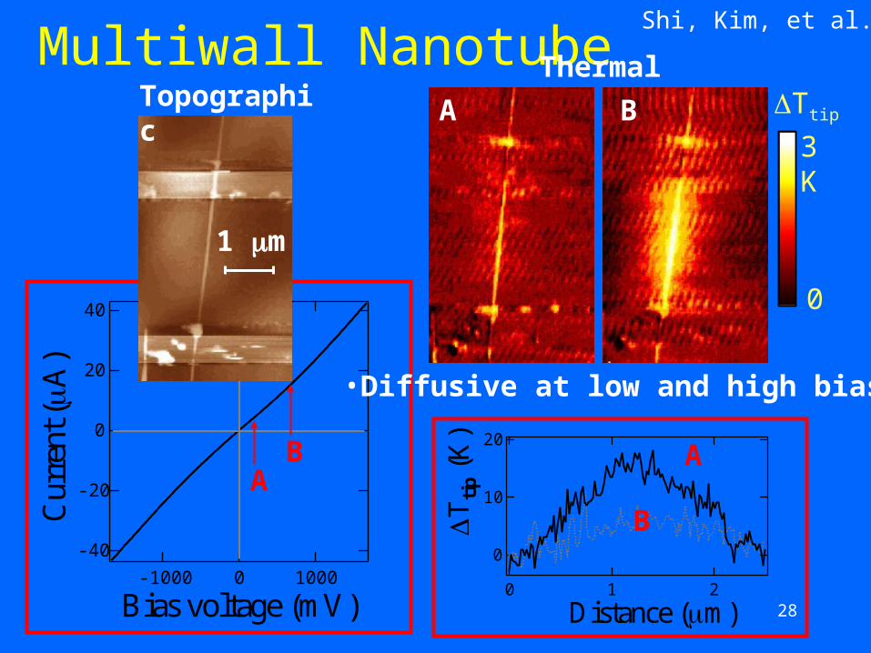
Multiwall NanotubeTopographic
Thermal
A B Ttip
3 K
0
•Diffusive at low and high biases
AB A
B
Shi, Kim, et al.
29
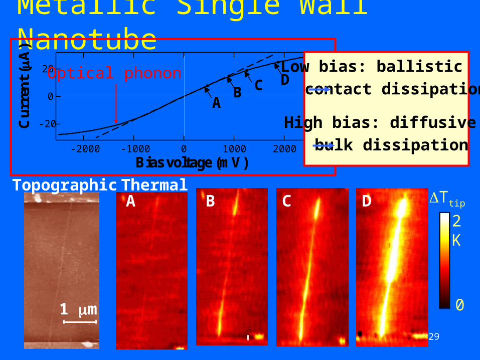
Metallic Single Wall Nanotube
-20
0
20
200010000-1000-2000
Bias voltage (mV)
Cu
rren
t (
A)
AB C D
Bias voltage (mV)
Cu
rren
t (
A)
AB C D
Topographic Thermal
1 m
A B C D
Optical phonon Low bias: ballistic
contact dissipation
High bias: diffusive
bulk dissipation
Ttip
2 K
0
30
Outline
• Cantilever Thermal Sensors:
Thermal Property of Nanotubes and Nanowires
• Cantilever Thermal Sensors:
Scanning Thermal Microscopy
• Cantilever Bio Sensors
• Cantilever IR Sensors
31
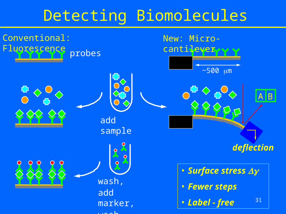
Detecting BiomoleculesConventional: Fluorescence
add sample
probes
wash, add marker,wash
• Surface stress
• Fewer steps
• Label - free
deflection
A B
New: Micro-cantilever
~500 m
32
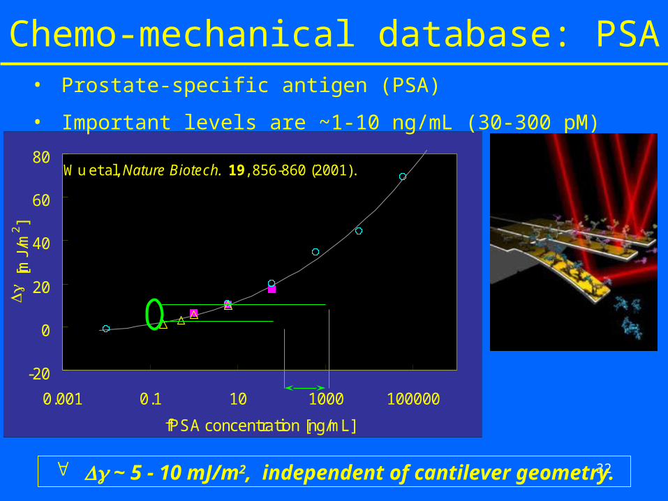
Chemo-mechanical database: PSA
-20
0
20
40
60
80
0.001 0.1 10 1000 100000
fPSA concentration [ng/mL]
[
mJ/
m2]
Wu et al, Nature Biotech. 19, 856-860 (2001).
~ 5 - 10 mJ/m2, independent of cantilever geometry.
• Prostate-specific antigen (PSA)
• Important levels are ~1-10 ng/mL (30-300 pM)
33
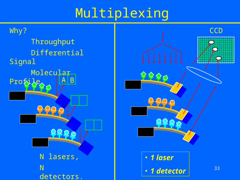
MultiplexingWhy?
Throughput
Differential Signal
Molecular Profile
A B
N lasers,
N detectors.
• 1 laser
• 1 detector
CCD
34
Outline
• Cantilever Thermal Sensors:
Thermal Property of Nanotubes and Nanowires
• Cantilever Thermal Sensors:
Scanning Thermal Microscopy
• Cantilever Bio Sensors
• Cantilever IR Sensors (See PowerPoint File 2)