Embed Size (px)
Citation preview
1
1Introduction micro electronics - CAS - NvdM 2009
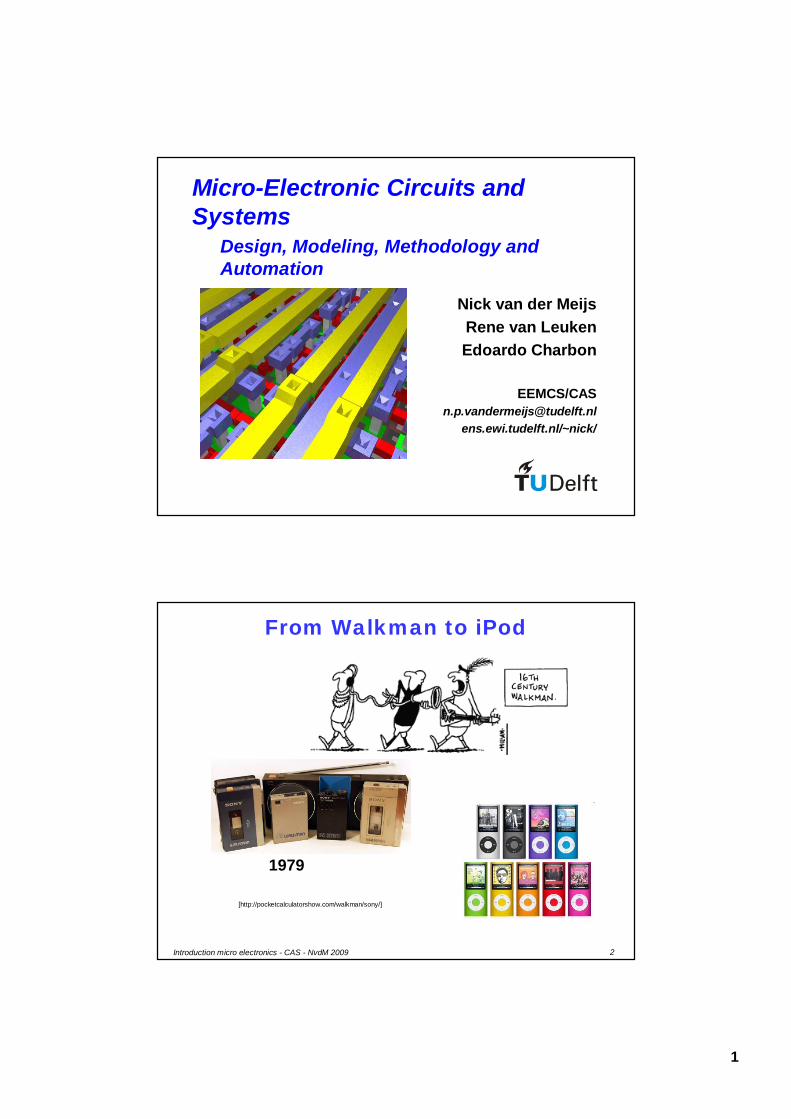
Micro-Electronic Circuits and Systems
Design, Modeling, Methodology and Automation
Nick van der MeijsRene van LeukenEdoardo Charbon
EEMCS/[email protected]
ens.ewi.tudelft.nl/~nick/
2Introduction micro electronics - CAS - NvdM 2009
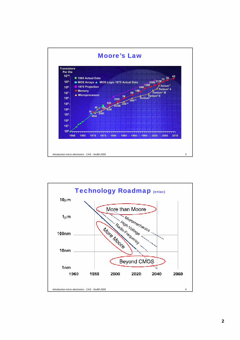
From Walkman to iPod
[http://pocketcalculatorshow.com/walkman/sony/]
1979
2
3Introduction micro electronics - CAS - NvdM 2009
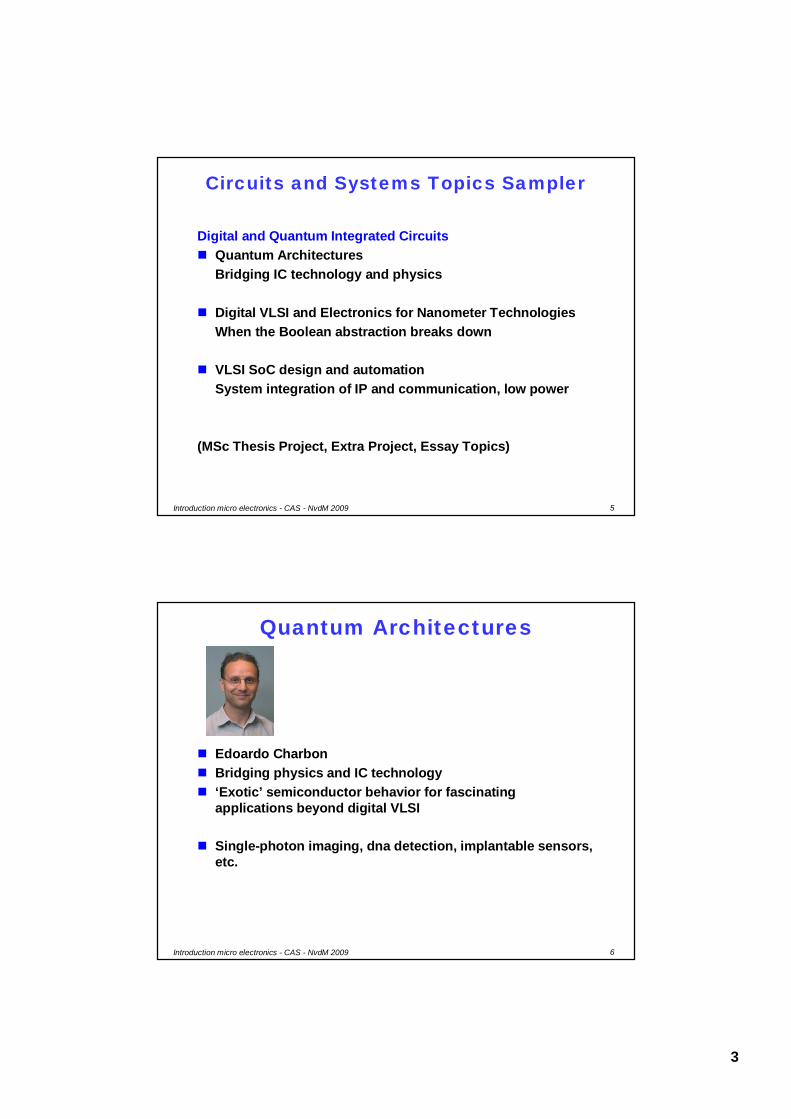
Moore’s Law
4Introduction micro electronics - CAS - NvdM 2009
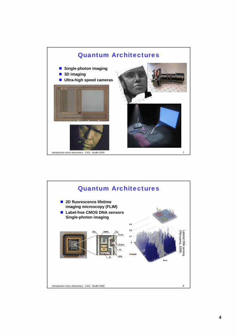
Technology Roadmap (eniac)
3
5Introduction micro electronics - CAS - NvdM 2009
Circuits and Systems Topics Sampler
Digital and Quantum Integrated CircuitsQuantum ArchitecturesBridging IC technology and physics
Digital VLSI and Electronics for Nanometer TechnologiesWhen the Boolean abstraction breaks down
VLSI SoC design and automationSystem integration of IP and communication, low power
(MSc Thesis Project, Extra Project, Essay Topics)
6Introduction micro electronics - CAS - NvdM 2009
Quantum Architectures
Edoardo CharbonBridging physics and IC technology‘Exotic’ semiconductor behavior for fascinating applications beyond digital VLSI
Single-photon imaging, dna detection, implantable sensors, etc.
4
7Introduction micro electronics - CAS - NvdM 2009
Quantum Architectures
Single-photon imaging3D imaging Ultra-high speed cameras
8Introduction micro electronics - CAS - NvdM 2009
Quantum Architectures
Labeled DN
A sensing (M
aruyama, 2008)
2D fluorescence lifetime imaging microscopy (FLIM)Label-free CMOS DNA sensors Single-photon imaging
5
9Introduction micro electronics - CAS - NvdM 2009
Quantum Architectures
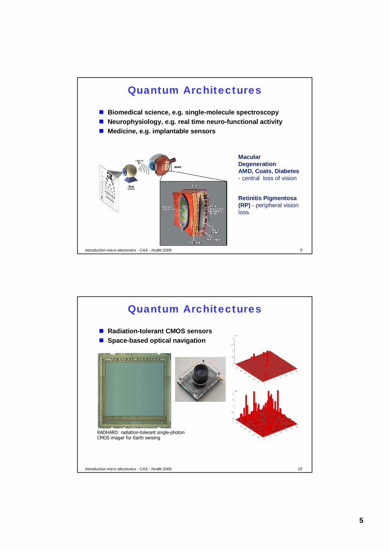
Biomedical science, e.g. single-molecule spectroscopyNeurophysiology, e.g. real time neuro-functional activity Medicine, e.g. implantable sensors
Retinitis Pigmentosa(RP) - peripheral vision loss
Macular Degeneration AMD, Coats, Diabetes - central loss of vision
10Introduction micro electronics - CAS - NvdM 2009
Quantum Architectures
Radiation-tolerant CMOS sensorsSpace-based optical navigation
RADHARD: radiation-tolerant single-photon CMOS imager for Earth sensing
6
11Introduction micro electronics - CAS - NvdM 2009
Quantum Architectures
Integration of plasmonic elements onto siliconPlasmonic ICs
12Introduction micro electronics - CAS - NvdM 2009
MSc Projects
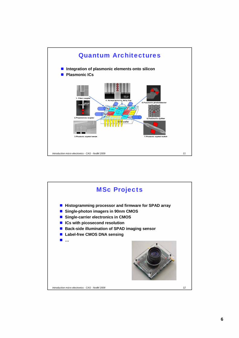
Histogramming processor and firmware for SPAD arraySingle-photon imagers in 90nm CMOSSingle-carrier electronics in CMOSICs with picosecond resolutionBack-side illumination of SPAD imaging sensorLabel-free CMOS DNA sensing…
7
13Introduction micro electronics - CAS - NvdM 2009
CMOS Image Sensor Demos
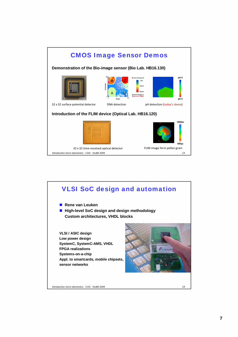
Demonstration of the Bio-image sensor (Bio Lab. HB16.130)
DNA detection pH detection (today’s demo)
pH 4
pH 9
Introduction of the FLIM device (Optical Lab. HB16.120)
FLIM image form pollen grain32 x 32 time‐resolved optical detector
32 x 32 surface potential detector
1800ps
900ps
14Introduction micro electronics - CAS - NvdM 2009
VLSI SoC design and automation
Rene van LeukenHigh-level SoC design and design methodologyCustom architectures, VHDL blocks
VLSI / ASIC designLow power designSystemC, SystemC-AMS, VHDLFPGA realizationsSystems-on-a-chipAppl. to smartcards, mobile chipsets,sensor networks
8
15Introduction micro electronics - CAS - NvdM 2009
Research Area’s
1. Algorithms to Architectures (SystemC / VHDL)2. Architectures to RTL implementation ( VHDL / FPGA)3. RTL implementation to ASIC ( VLSI physical design)4. Software / DA tools
16Introduction micro electronics - CAS - NvdM 2009
VLSI Design: 90nm Communication Processor
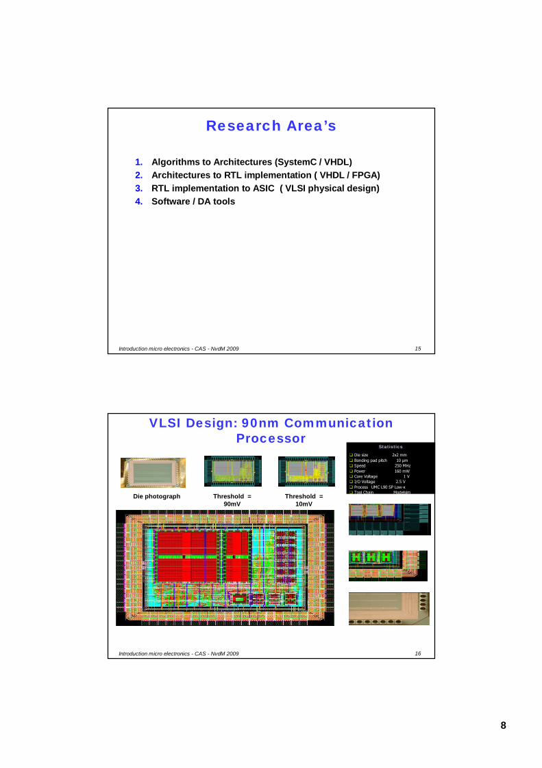
Statistics
Die size 2x2 mmBonding pad pitch 10 µmSpeed 250 MHzPower 160 mWCore Voltage 1 VI/O Voltage 2.5 VProcess UMC L90 SP Low-κTool Chain Modelsim
Design CompilerSOC Encounter
VirtuosoCalibre
Threshold = 90mV
Threshold = 10mV
Die photograph
9
17Introduction micro electronics - CAS - NvdM 2009
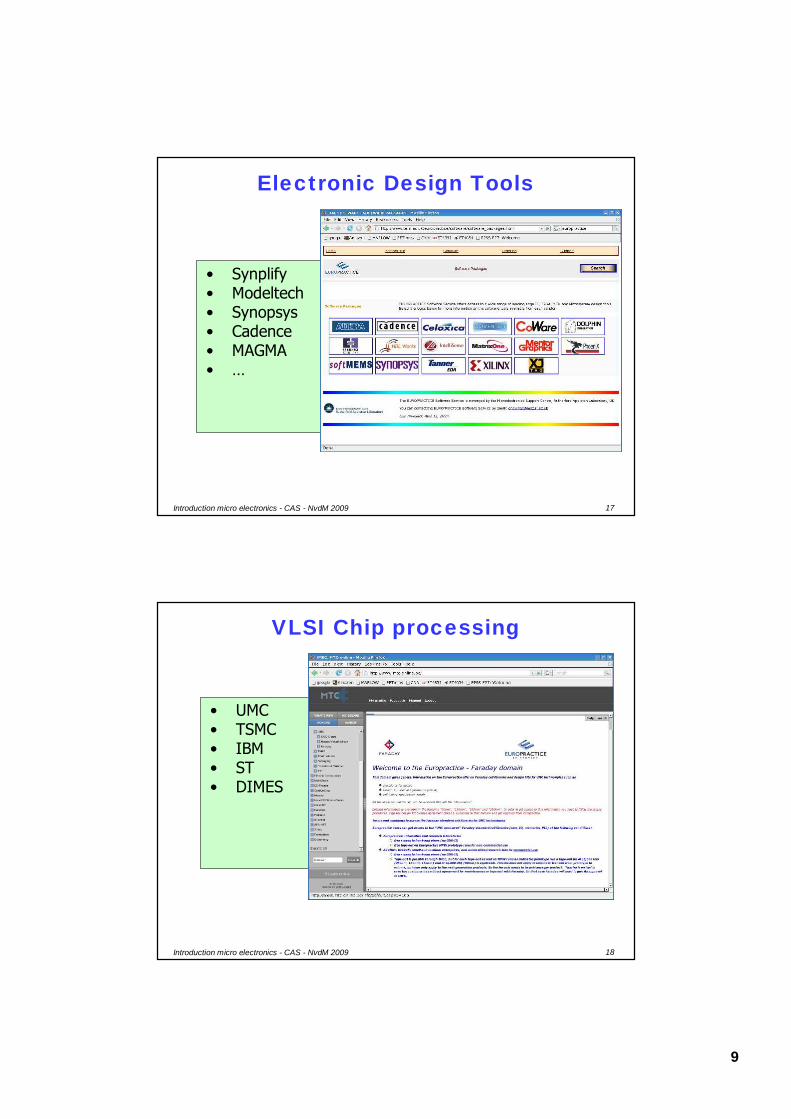
• Synplify• Modeltech• Synopsys• Cadence• MAGMA• …
Electronic Design Tools
18Introduction micro electronics - CAS - NvdM 2009
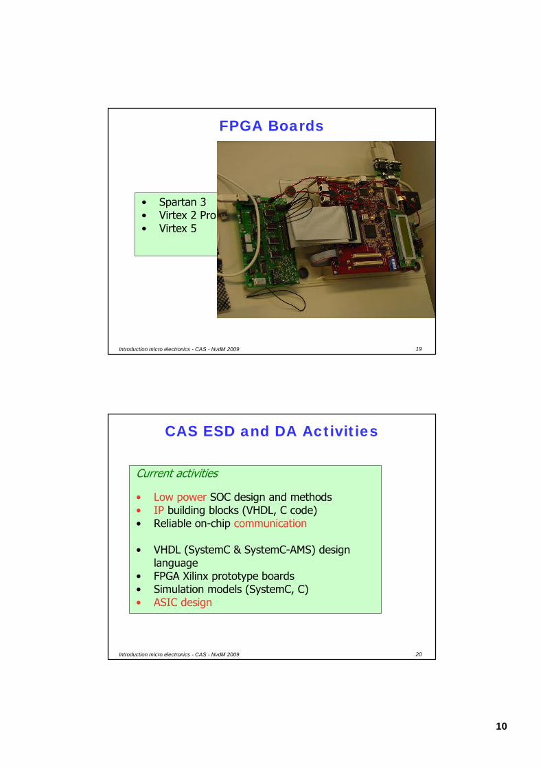
• UMC• TSMC• IBM• ST• DIMES
VLSI Chip processing
10
19Introduction micro electronics - CAS - NvdM 2009
• Spartan 3• Virtex 2 Pro• Virtex 5
FPGA Boards
20Introduction micro electronics - CAS - NvdM 2009
Current activities
• Low power SOC design and methods• IP building blocks (VHDL, C code)• Reliable on-chip communication
• VHDL (SystemC & SystemC-AMS) design language
• FPGA Xilinx prototype boards• Simulation models (SystemC, C)• ASIC design
CAS ESD and DA Activities
11
21Introduction micro electronics - CAS - NvdM 2009
MSc ProjectsPast:
Fingerprint engineLT codes for error correction of NoCVHDL to SystemC translatorDMA controller for Automotive (NXP)Micro Blaze 32 bit processorASIC design: 8 bit processorASIC design: R-Vex 32 bit VLWI processorVideo Motion detection SoC
Current:SystemC AMS synthesis toolAsync, dataflow synthesis toolAsync SoC design/ASICMicroBlaze VLSI realizationVideo motion detection ASIC realizationSystemC SoC models …
Also: FPGA prototyping
22Introduction micro electronics - CAS - NvdM 2009
Digital VLSI and Electronics for Nanometer Technologies
Nick van der MeijsWhen digital becomes analog
VLSI DesignModeling, Methodology and Automation
12
23Introduction micro electronics - CAS - NvdM 2009
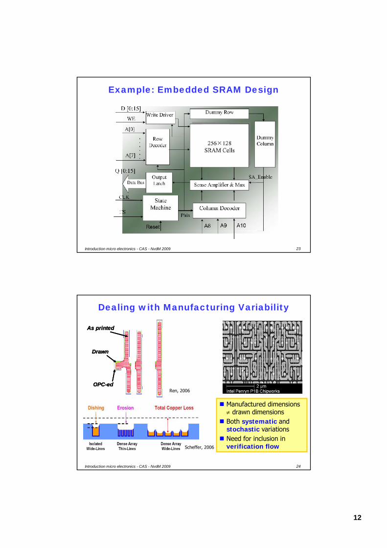
Example: Embedded SRAM Design
24Introduction micro electronics - CAS - NvdM 2009
Dealing with Manufacturing Variability
Scheffer, 2006
As printed
Drawn
OPC-ed
As printedAs printed
DrawnDrawn
OPC-edOPC-edRen, 2006
Manufactured dimensions ≠ drawn dimensionsBoth systematic and stochastic variationsNeed for inclusion in verification flow
13
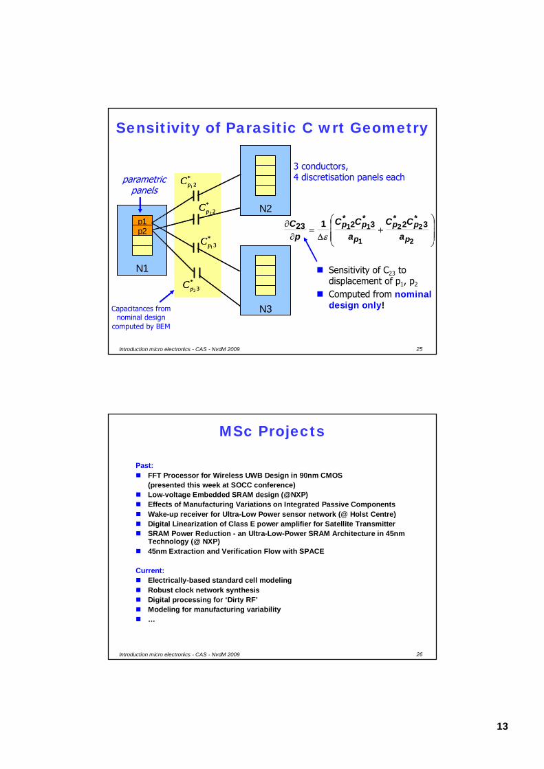
25Introduction micro electronics - CAS - NvdM 2009
Sensitivity of Parasitic C wrt Geometry
N1
p1p2
N2
N3
*21pC
*32pC
*22pC
*31pC
N1
p1p2
N1
p1p2p1p2
N2N2
N3N3
*21pC
*32pC
*22pC
*31pC ⎟⎟
⎟
⎠
⎞
⎜⎜⎜
⎝
⎛+
∆=
∂∂
2
22
1
11*
3*
2*
3*
223 1p
pp
p
ppa
CCa
CCp
Cε
3 conductors, 4 discretisation panels eachparametric
panels
Sensitivity of C23 to displacement of p1, p2
Computed from nominal design only!Capacitances from
nominal designcomputed by BEM
26Introduction micro electronics - CAS - NvdM 2009
MSc Projects
Past:FFT Processor for Wireless UWB Design in 90nm CMOS(presented this week at SOCC conference)Low-voltage Embedded SRAM design (@NXP)Effects of Manufacturing Variations on Integrated Passive ComponentsWake-up receiver for Ultra-Low Power sensor network (@ Holst Centre)Digital Linearization of Class E power amplifier for Satellite TransmitterSRAM Power Reduction - an Ultra-Low-Power SRAM Architecture in 45nm Technology (@ NXP)45nm Extraction and Verification Flow with SPACE
Current:Electrically-based standard cell modelingRobust clock network synthesisDigital processing for ‘Dirty RF’Modeling for manufacturing variability…
14
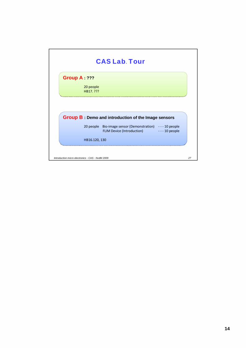
27Introduction micro electronics - CAS - NvdM 2009
CAS Lab. Tour
Group B : Demo and introduction of the Image sensors
20 people Bio‐image sensor (Demonstration) ‐ ‐ ‐ 10 people FLIM Device (Introduction) ‐ ‐ ‐ 10 people
HB16.120, 130
Group A : ???
20 peopleHB17. ???