Embed Size (px)
Citation preview
MiCOM P139 Feeder Management
and Bay Control Version: -304/306/307 -
405/406/407/408/409/410/411/412/413 -605/611/612
Technical Manual Volume 2 of 2
P139/EN M/A88
Contains:V605 P139/EN M/B33 (AFSV.12.09450.D) V611 P139/EN AD/A77 (AFSV.12.09690.D)V612 P139/EN AD/A88 (AFSV.12.09950 D)

MiCOM P139 Feeder Management
and Bay Control
Version 304 405/406/407 -605
Technical Manual Volume 2 of 2
P139/EN M/B33 (AFSV.12.09450 D)

!
Warning When electrical equipment is in operation, dangerous voltage will be present in certain parts of the equipment. Failure to observe warning notices, incorrect use, or improper use may endanger personnel and equipment and cause personal injury or physical damage.
Before working in the terminal strip area, the device must be isolated. Where stranded conductors are used, wire end ferrules must be employed.
Proper and safe operation of this device depends on appropriate shipping and handling, proper storage, installation and commissioning, and on careful operation, maintenance and servicing.
For this reason only qualified personnel may work on or operate this device.
Any modifications to this device must be in accordance with the manual. If any other modification is made without the express permission of AREVA T&D, it will invalidate the warranty, and may render the product unsafe.
Qualified Personnel are individuals who
! are familiar with the installation, commissioning, and operation of the device and of the system to which it is being connected;
! are able to perform switching operations in accordance with safety engineering standards and are authorized to energize and de-energize equipment and to isolate, ground, and label it;
! are trained in the care and use of safety apparatus in accordance with safety engineering standards;
! are trained in emergency procedures (first aid).
Note The operating manual for this device gives instructions for its installation, commissioning, and operation. However, the manual cannot cover all conceivable circumstances or include detailed information on all topics. In the event of questions or specific problems, do not take any action without proper authorization. Contact the appropriate AREVA technical sales office and request the necessary information.
Any agreements, commitments, and legal relationships and any obligations on the part of AREVA, including settlement of warranties, result solely from the applicable purchase contract, which is not affected by the contents of the operating manual.

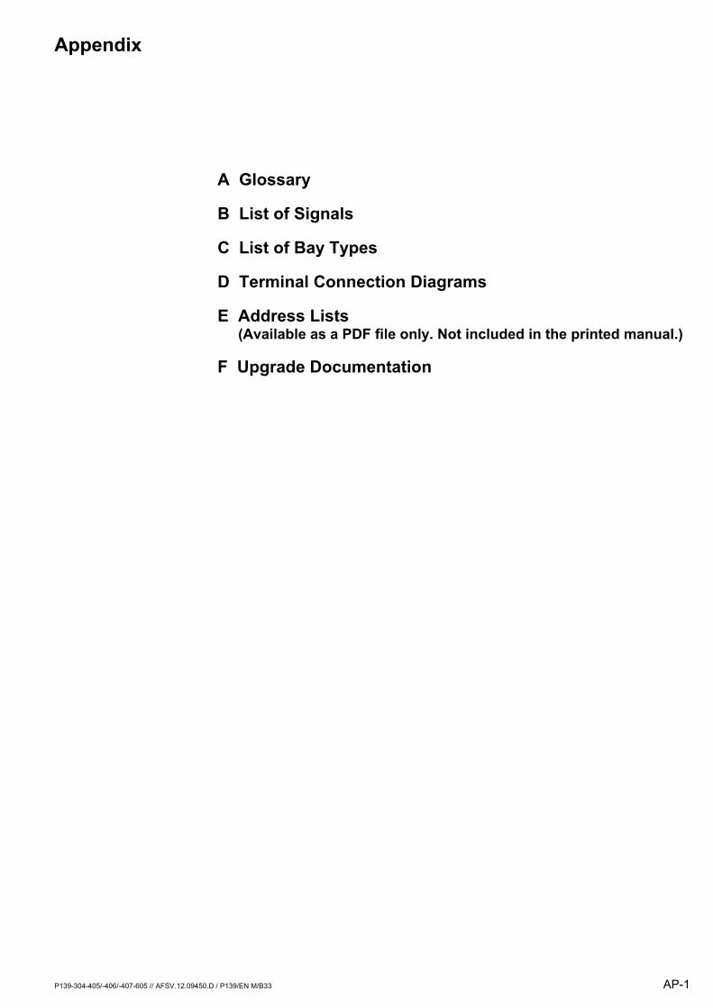
Appendix
P139-304-405/-406/-407-605 // AFSV.12.09450.D / P139/EN M/B33 AP-1
A Glossary
B List of Signals
C List of Bay Types
D Terminal Connection Diagrams
E Address Lists (Available as a PDF file only. Not included in the printed manual.)
F Upgrade Documentation
Appendix (continued)
AP-2 P139-304-405/-406/-407-605 // AFSV.12.09450.D / P139/EN M/B33
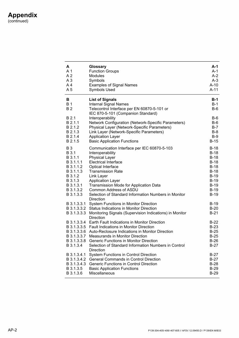
A Glossary A-1A 1 Function Groups A-1A 2 Modules A-2A 3 Symbols A-3A 4 Examples of Signal Names A-10A 5 Symbols Used A-11
B List of Signals B-1B 1 Internal Signal Names B-1B 2 Telecontrol Interface per EN 60870-5-101 or
IEC 870-5-101 (Companion Standard) B-6
B 2.1 Interoperability B-6B 2.1.1 Network Configuration (Network-Specific Parameters) B-6B 2.1.2 Physical Layer (Network-Specific Parameters) B-7B 2.1.3 Link Layer (Network-Specific Parameters) B-8B 2.1.4 Application Layer B-9B 2.1.5 Basic Application Functions B-15
B 3 Communication Interface per IEC 60870-5-103 B-18B 3.1 Interoperability B-18B 3.1.1 Physical Layer B-18B 3.1.1.1 Electrical Interface B-18B 3.1.1.2 Optical Interface B-18B 3.1.1.3 Transmission Rate B-18B 3.1.2 Link Layer B-19B 3.1.3 Application Layer B-19B 3.1.3.1 Transmission Mode for Application Data B-19B 3.1.3.2 Common Address of ASDU B-19B 3.1.3.3 Selection of Standard Information Numbers in Monitor
Direction B-19
B 3.1.3.3.1 System Functions in Monitor Direction B-19B 3.1.3.3.2 Status Indications in Monitor Direction B-20B 3.1.3.3.3 Monitoring Signals (Supervision Indications) in Monitor
Direction B-21
B 3.1.3.3.4 Earth Fault Indications in Monitor Direction B-22B 3.1.3.3.5 Fault Indications in Monitor Direction B-23B 3.1.3.3.6 Auto-Reclosure Indications in Monitor Direction B-25B 3.1.3.3.7 Measurands in Monitor Direction B-25B 3.1.3.3.8 Generic Functions in Monitor Direction B-26B 3.1.3.4 Selection of Standard Information Numbers in Control
Direction B-27
B 3.1.3.4.1 System Functions in Control Direction B-27B 3.1.3.4.2 General Commands in Control Direction B-27B 3.1.3.4.3 Generic Functions in Control Direction B-28B 3.1.3.5 Basic Application Functions B-29B 3.1.3.6 Miscellaneous B-29
Appendix (continued)
P139-304-405/-406/-407-605 // AFSV.12.09450.D / P139/EN M/B33 AP-3
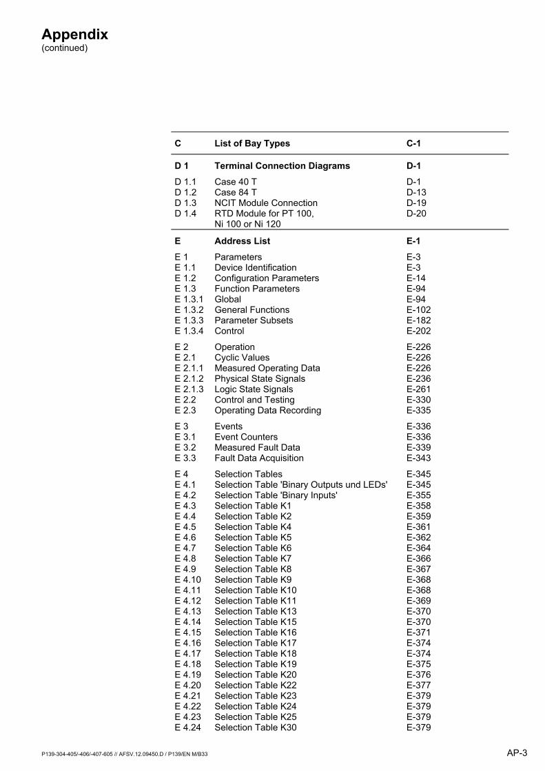
C List of Bay Types C-1
D 1 Terminal Connection Diagrams D-1 D 1.1 D 1.2 D 1.3 D 1.4
Case 40 T Case 84 T NCIT Module Connection RTD Module for PT 100, Ni 100 or Ni 120
D-1 D-13 D-19 D-20
E Address List E-1
E 1 Parameters E-3 E 1.1 Device Identification E-3 E 1.2 Configuration Parameters E-14 E 1.3 Function Parameters E-94 E 1.3.1 Global E-94 E 1.3.2 General Functions E-102 E 1.3.3 Parameter Subsets E-182 E 1.3.4 Control E-202
E 2 Operation E-226 E 2.1 Cyclic Values E-226 E 2.1.1 Measured Operating Data E-226 E 2.1.2 Physical State Signals E-236 E 2.1.3 Logic State Signals E-261 E 2.2 Control and Testing E-330 E 2.3 Operating Data Recording E-335
E 3 Events E-336 E 3.1 Event Counters E-336 E 3.2 Measured Fault Data E-339 E 3.3 Fault Data Acquisition E-343
E 4 Selection Tables E-345 E 4.1 Selection Table 'Binary Outputs und LEDs' E-345 E 4.2 Selection Table 'Binary Inputs' E-355 E 4.3 Selection Table K1 E-358 E 4.4 Selection Table K2 E-359 E 4.5 Selection Table K4 E-361 E 4.6 Selection Table K5 E-362 E 4.7 Selection Table K6 E-364 E 4.8 Selection Table K7 E-366 E 4.9 Selection Table K8 E-367 E 4.10 Selection Table K9 E-368 E 4.11 Selection Table K10 E-368 E 4.12 Selection Table K11 E-369 E 4.13 Selection Table K13 E-370 E 4.14 Selection Table K15 E-370 E 4.15 Selection Table K16 E-371 E 4.16 Selection Table K17 E-374 E 4.17 Selection Table K18 E-374 E 4.18 Selection Table K19 E-375 E 4.19 Selection Table K20 E-376 E 4.20 Selection Table K22 E-377 E 4.21 Selection Table K23 E-379 E 4.22 Selection Table K24 E-379 E 4.23 Selection Table K25 E-379 E 4.24 Selection Table K30 E-379
Appendix (continued)
AP-4 P139-304-405/-406/-407-605 // AFSV.12.09450.D / P139/EN M/B33
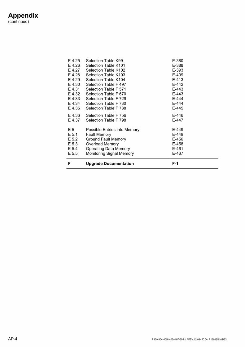
E 4.25 Selection Table K99 E-380 E 4.26 Selection Table K101 E-388 E 4.27 Selection Table K102 E-393 E 4.28 Selection Table K103 E-409 E 4.29 Selection Table K104 E-413 E 4.30 Selection Table F 497 E-442 E 4.31 Selection Table F 571 E-443 E 4.32 Selection Table F 670 E-443 E 4.33 Selection Table F 729 E-444 E 4.34 Selection Table F 730 E-444 E 4.35 Selection Table F 738 E-445
E 4.36 Selection Table F 756 E-446 E 4.37 Selection Table F 798 E-447
E 5 Possible Entries into Memory E-449 E 5.1 Fault Memory E-449 E 5.2 Ground Fault Memory E-456 E 5.3 Overload Memory E-458 E 5.4 Operating Data Memory E-461 E 5.5 Monitoring Signal Memory E-467
F Upgrade Documentation F-1
Appendix A - Glossary
P139-304-405/-406/-407-605 // AFSV.12.09450.D / P139/EN M/B33 A-1
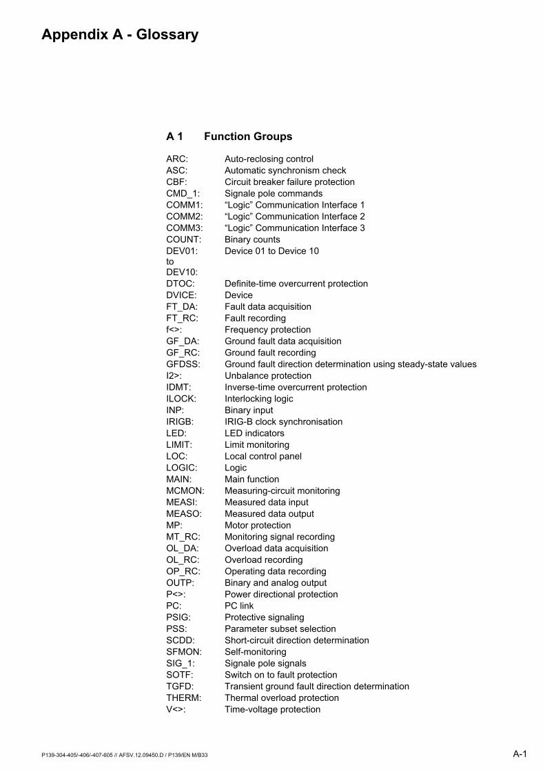
A 1 Function Groups
ARC: Auto-reclosing control ASC: Automatic synchronism check CBF: Circuit breaker failure protection CMD_1: Signale pole commands COMM1: Logic Communication Interface 1 COMM2: Logic Communication Interface 2 COMM3: Logic Communication Interface 3 COUNT: Binary counts DEV01: to DEV10:
Device 01 to Device 10
DTOC: Definite-time overcurrent protection DVICE: Device FT_DA: Fault data acquisition FT_RC: Fault recording f<>: Frequency protection GF_DA: Ground fault data acquisition GF_RC: Ground fault recording GFDSS: Ground fault direction determination using steady-state values I2>: Unbalance protection IDMT: Inverse-time overcurrent protection ILOCK: Interlocking logic INP: Binary input IRIGB: IRIG-B clock synchronisation LED: LED indicators LIMIT: Limit monitoring LOC: Local control panel LOGIC: Logic MAIN: Main function MCMON: Measuring-circuit monitoring MEASI: Measured data input MEASO: Measured data output MP: Motor protection MT_RC: Monitoring signal recording OL_DA: Overload data acquisition OL_RC: Overload recording OP_RC: Operating data recording OUTP: Binary and analog output P<>: Power directional protection PC: PC link PSIG: Protective signaling PSS: Parameter subset selection SCDD: Short-circuit direction determination SFMON: Self-monitoring SIG_1: Signale pole signals SOTF: Switch on to fault protection TGFD: Transient ground fault direction determination THERM: Thermal overload protection V<>: Time-voltage protection
Appendix A - Glossary (continued)
A-2 P139-304-405/-406/-407-605 // AFSV.12.09450.D / P139/EN M/B33
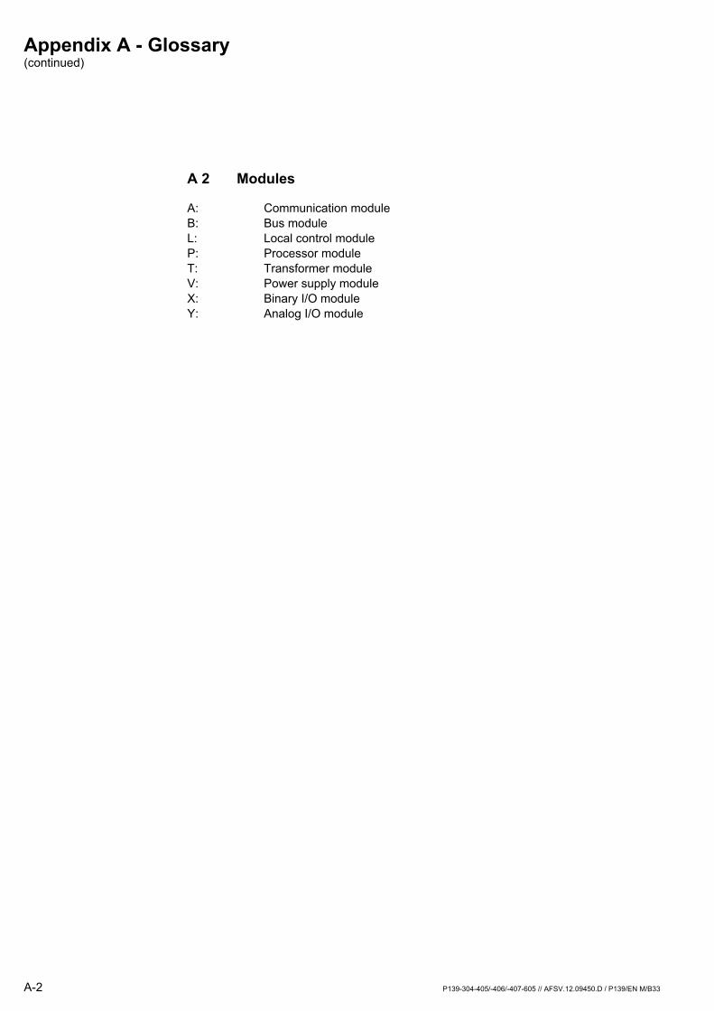
A 2 Modules A: Communication module B: Bus module L: Local control module P: Processor module T: Transformer module V: Power supply module X: Binary I/O module Y: Analog I/O module
Appendix A - Glossary (continued)
P139-304-405/-406/-407-605 // AFSV.12.09450.D / P139/EN M/B33 A-3
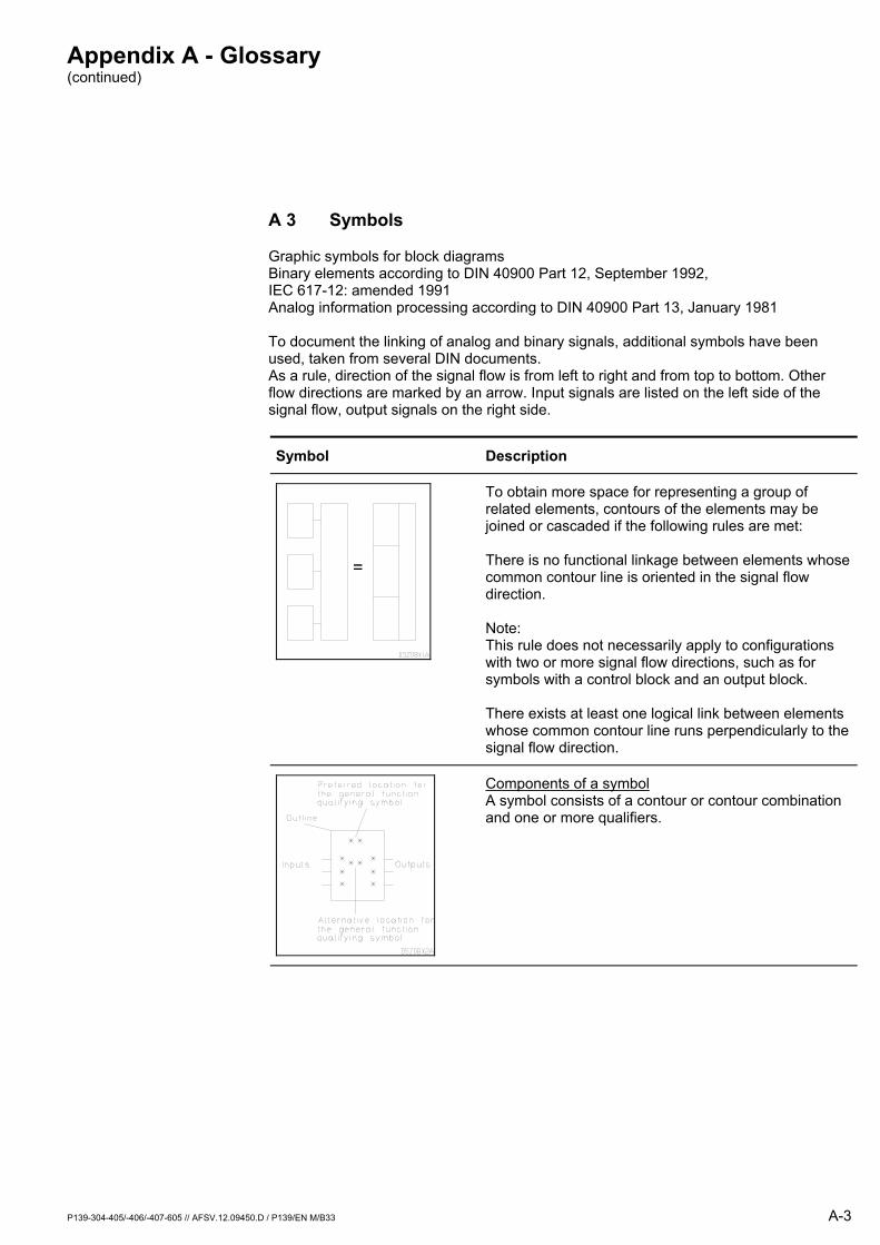
A 3 Symbols
Graphic symbols for block diagrams Binary elements according to DIN 40900 Part 12, September 1992, IEC 617-12: amended 1991 Analog information processing according to DIN 40900 Part 13, January 1981 To document the linking of analog and binary signals, additional symbols have been used, taken from several DIN documents. As a rule, direction of the signal flow is from left to right and from top to bottom. Other flow directions are marked by an arrow. Input signals are listed on the left side of the signal flow, output signals on the right side.
Symbol Description
=
To obtain more space for representing a group of related elements, contours of the elements may be joined or cascaded if the following rules are met: There is no functional linkage between elements whose common contour line is oriented in the signal flow direction. Note: This rule does not necessarily apply to configurations with two or more signal flow directions, such as for symbols with a control block and an output block. There exists at least one logical link between elements whose common contour line runs perpendicularly to the signal flow direction.
Components of a symbol A symbol consists of a contour or contour combination and one or more qualifiers.
Appendix A - Glossary (continued)
A-4 P139-304-405/-406/-407-605 // AFSV.12.09450.D / P139/EN M/B33
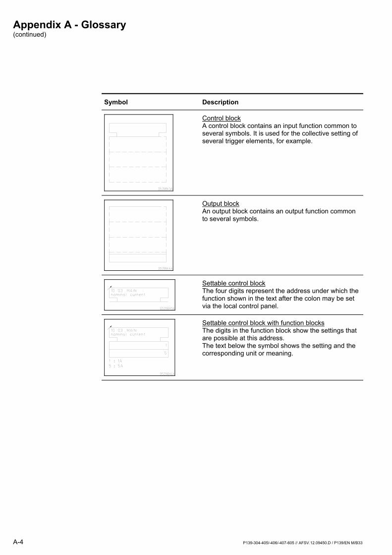
Symbol Description
Control block A control block contains an input function common to several symbols. It is used for the collective setting of several trigger elements, for example.
Output block An output block contains an output function common to several symbols.
Settable control block The four digits represent the address under which the function shown in the text after the colon may be set via the local control panel.
Settable control block with function blocks The digits in the function block show the settings that are possible at this address. The text below the symbol shows the setting and the corresponding unit or meaning.
Appendix A - Glossary (continued)
P139-304-405/-406/-407-605 // AFSV.12.09450.D / P139/EN M/B33 A-5
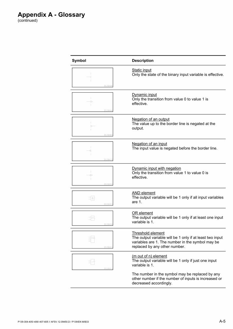
Symbol Description
Static input Only the state of the binary input variable is effective.
Dynamic input Only the transition from value 0 to value 1 is effective.
Negation of an output The value up to the border line is negated at the output.
Negation of an input The input value is negated before the border line.
Dynamic input with negation Only the transition from value 1 to value 0 is effective.
AND element The output variable will be 1 only if all input variables are 1.
OR element The output variable will be 1 only if at least one input variable is 1.
Threshold element The output variable will be 1 only if at least two input variables are 1. The number in the symbol may be replaced by any other number.
(m out of n) element The output variable will be 1 only if just one input variable is 1. The number in the symbol may be replaced by any other number if the number of inputs is increased or decreased accordingly.
Appendix A - Glossary (continued)
A-6 P139-304-405/-406/-407-605 // AFSV.12.09450.D / P139/EN M/B33
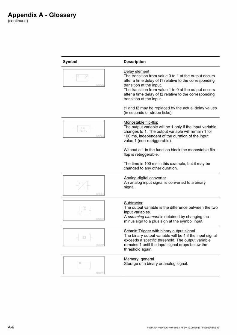
Symbol Description
Delay element The transition from value 0 to 1 at the output occurs after a time delay of t1 relative to the corresponding transition at the input. The transition from value 1 to 0 at the output occurs after a time delay of t2 relative to the corresponding transition at the input. t1 and t2 may be replaced by the actual delay values (in seconds or strobe ticks).
Monostable flip-flop The output variable will be 1 only if the input variable changes to 1. The output variable will remain 1 for 100 ms, independent of the duration of the input value 1 (non-retriggerable). Without a 1 in the function block the monostable flip-flop is retriggerable. The time is 100 ms in this example, but it may be changed to any other duration.
Analog-digital converter An analog input signal is converted to a binary signal.
Subtractor The output variable is the difference between the two input variables. A summing element is obtained by changing the minus sign to a plus sign at the symbol input.
Schmitt Trigger with binary output signal The binary output variable will be 1 if the input signal exceeds a specific threshold. The output variable remains 1 until the input signal drops below the threshold again.
Memory, general Storage of a binary or analog signal.
Appendix A - Glossary (continued)
P139-304-405/-406/-407-605 // AFSV.12.09450.D / P139/EN M/B33 A-7
Symbol Description
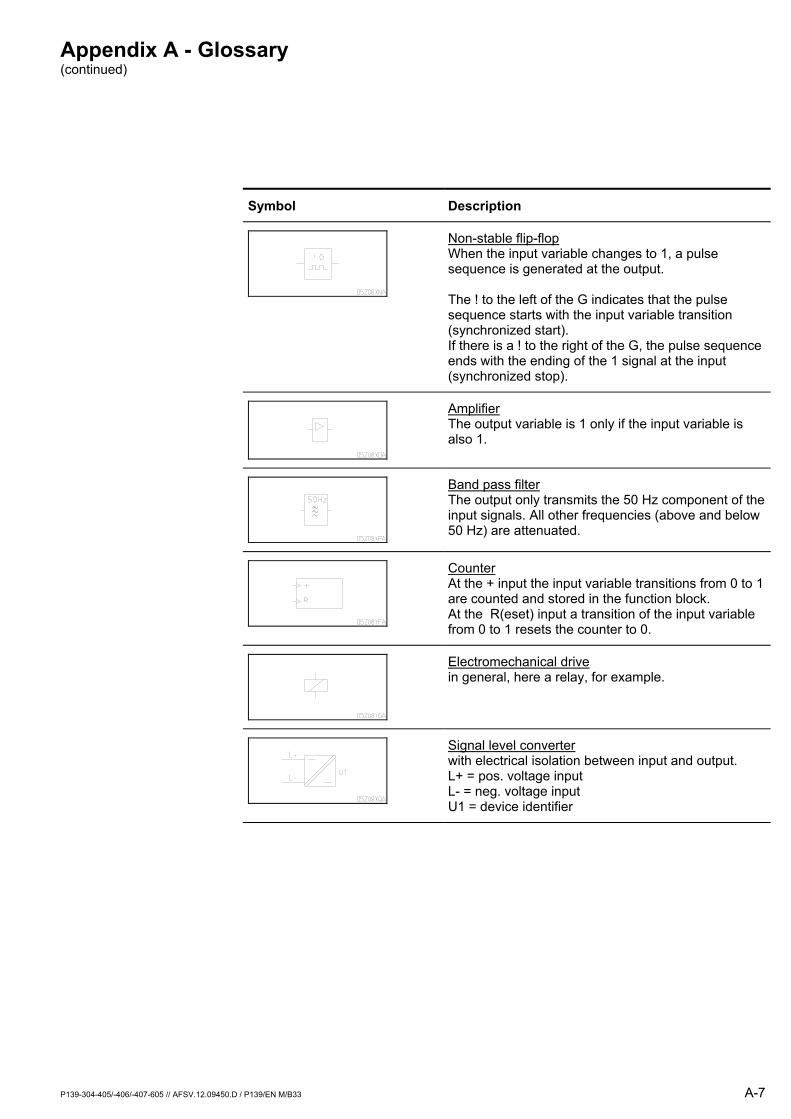
Non-stable flip-flop When the input variable changes to 1, a pulse sequence is generated at the output. The ! to the left of the G indicates that the pulse sequence starts with the input variable transition (synchronized start). If there is a ! to the right of the G, the pulse sequence ends with the ending of the 1 signal at the input (synchronized stop).
Amplifier The output variable is 1 only if the input variable is also 1.
Band pass filter The output only transmits the 50 Hz component of the input signals. All other frequencies (above and below 50 Hz) are attenuated.
Counter At the + input the input variable transitions from 0 to 1 are counted and stored in the function block. At the R(eset) input a transition of the input variable from 0 to 1 resets the counter to 0.
Electromechanical drive in general, here a relay, for example.
Signal level converter with electrical isolation between input and output. L+ = pos. voltage input L- = neg. voltage input U1 = device identifier
Appendix A - Glossary (continued)
A-8 P139-304-405/-406/-407-605 // AFSV.12.09450.D / P139/EN M/B33
Symbol Description
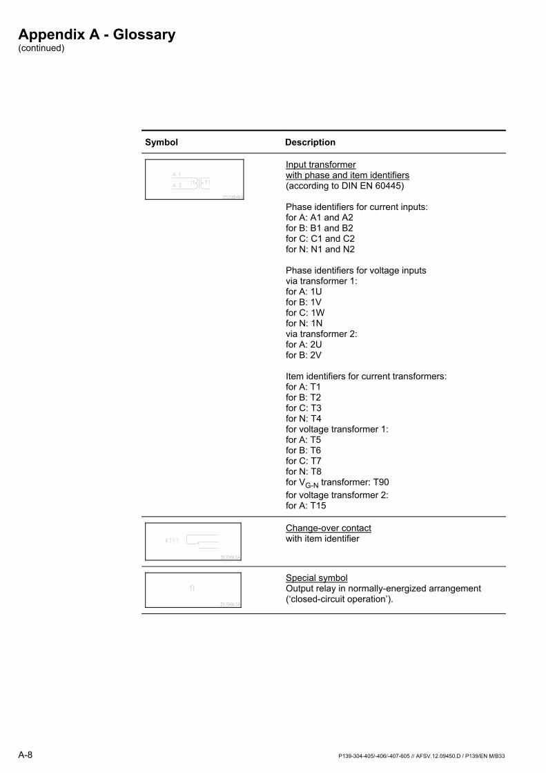
Input transformer with phase and item identifiers (according to DIN EN 60445) Phase identifiers for current inputs: for A: A1 and A2 for B: B1 and B2 for C: C1 and C2 for N: N1 and N2 Phase identifiers for voltage inputs via transformer 1: for A: 1U for B: 1V for C: 1W for N: 1N via transformer 2: for A: 2U for B: 2V Item identifiers for current transformers: for A: T1 for B: T2 for C: T3 for N: T4 for voltage transformer 1: for A: T5 for B: T6 for C: T7 for N: T8 for VG-N transformer: T90 for voltage transformer 2: for A: T15
Change-over contact with item identifier
Special symbol Output relay in normally-energized arrangement (closed-circuit operation).
Appendix A - Glossary (continued)
P139-304-405/-406/-407-605 // AFSV.12.09450.D / P139/EN M/B33 A-9
Symbol Description
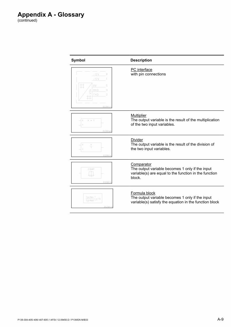
PC interface with pin connections
Multiplier The output variable is the result of the multiplication of the two input variables.
Divider The output variable is the result of the division of the two input variables.
Comparator The output variable becomes 1 only if the input variable(s) are equal to the function in the function block.
Formula block The output variable becomes 1 only if the input variable(s) satisfy the equation in the function block
Appendix A - Glossary (continued)
A-10 P139-304-405/-406/-407-605 // AFSV.12.09450.D / P139/EN M/B33
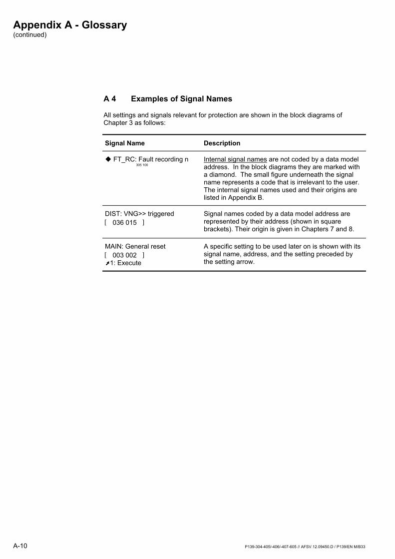
A 4 Examples of Signal Names
All settings and signals relevant for protection are shown in the block diagrams of Chapter 3 as follows:
Signal Name Description
! FT_RC: Fault recording n 305 100
Internal signal names are not coded by a data model address. In the block diagrams they are marked with a diamond. The small figure underneath the signal name represents a code that is irrelevant to the user. The internal signal names used and their origins are listed in Appendix B.
DIST: VNG>> triggered [ 036 015 ]
Signal names coded by a data model address are represented by their address (shown in square brackets). Their origin is given in Chapters 7 and 8.
MAIN: General reset [ 003 002 ] !1: Execute
A specific setting to be used later on is shown with its signal name, address, and the setting preceded by the setting arrow.
Appendix A - Glossary (continued)
P139-304-405/-406/-407-605 // AFSV.12.09450.D / P139/EN M/B33 A-11
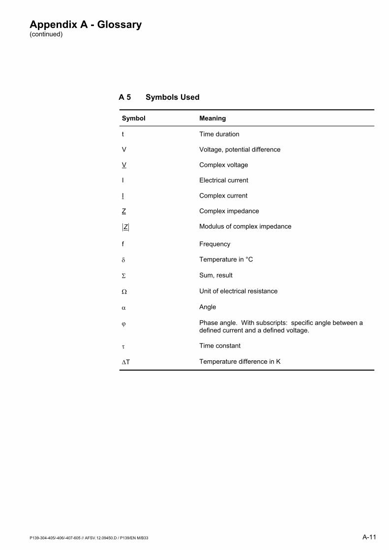
A 5 Symbols Used
Symbol Meaning
t Time duration
V Voltage, potential difference
V Complex voltage
I Electrical current
I Complex current
Z Complex impedance
Z Modulus of complex impedance
f Frequency
δ Temperature in °C
Σ Sum, result
Ω Unit of electrical resistance
α Angle
ϕ Phase angle. With subscripts: specific angle between a defined current and a defined voltage.
τ Time constant
∆T Temperature difference in K

A-12 P139-304-405/-406/-407-605 // AFSV.12.09450.D / P139/EN M/B33
Appendix B - List of Signals
P139-304-405/-406/-407-605 // AFSV.12.09450.D / P139/EN M/B33 B-1
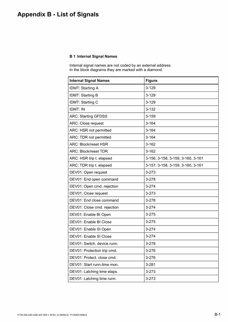
B 1 Internal Signal Names
Internal signal names are not coded by an external address. In the block diagrams they are marked with a diamond.
Internal Signal Names Figure
IDMT: Starting A 3-129
IDMT: Starting B 3-129
IDMT: Starting C 3-129
IDMT: IN 3-132
ARC: Starting GFDSS 3-159
ARC: Close request 3-164
ARC: HSR not permitted 3-164
ARC: TDR not permitted 3-164
ARC: Block/reset HSR 3-162
ARC: Block/reset TDR 3-162
ARC: HSR trip t. elapsed 3-156, 3-158, 3-159, 3-160, 3-161
ARC: TDR trip t. elapsed 3-157, 3-158, 3-159, 3-160, 3-161
DEV01: Open request 3-273
DEV01: End open command 3-278
DEV01: Open cmd. rejection 3-274
DEV01: Close request 3-273
DEV01: End close command 3-278
DEV01: Close cmd. rejection 3-274
DEV01: Enable BI Open 3-275
DEV01: Enable BI Close 3-275
DEV01: Enable SI Open 3-274
DEV01: Enable SI Close 3-274
DEV01: Switch. device runn. 3-278
DEV01: Protection trip cmd. 3-276
DEV01: Protect. close cmd. 3-276
DEV01: Start runn.time mon. 3-281
DEV01: Latching time elaps. 3-273
DEV01: Latching time runn. 3-273
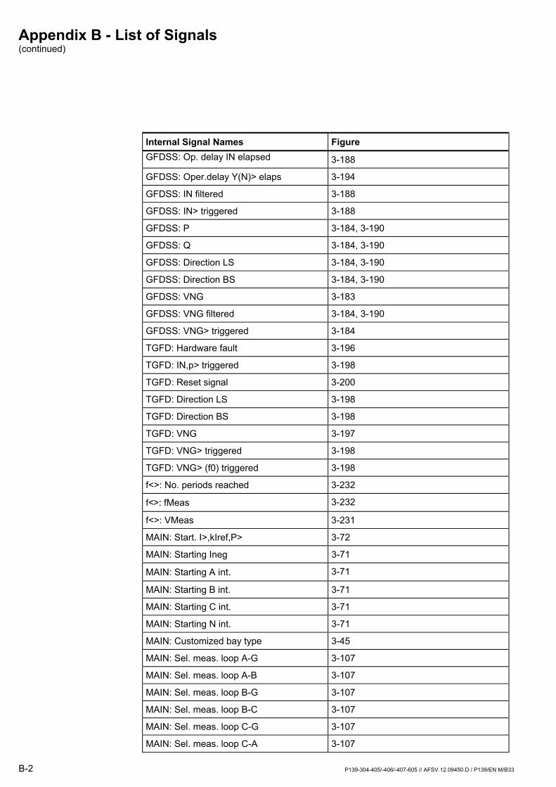
Appendix B - List of Signals (continued)
B-2 P139-304-405/-406/-407-605 // AFSV.12.09450.D / P139/EN M/B33
Internal Signal Names Figure GFDSS: Op. delay IN elapsed 3-188
GFDSS: Oper.delay Y(N)> elaps 3-194
GFDSS: IN filtered 3-188
GFDSS: IN> triggered 3-188
GFDSS: P 3-184, 3-190
GFDSS: Q 3-184, 3-190
GFDSS: Direction LS 3-184, 3-190
GFDSS: Direction BS 3-184, 3-190
GFDSS: VNG 3-183
GFDSS: VNG filtered 3-184, 3-190
GFDSS: VNG> triggered 3-184
TGFD: Hardware fault 3-196
TGFD: IN,p> triggered 3-198
TGFD: Reset signal 3-200
TGFD: Direction LS 3-198
TGFD: Direction BS 3-198
TGFD: VNG 3-197
TGFD: VNG> triggered 3-198
TGFD: VNG> (f0) triggered 3-198
f<>: No. periods reached 3-232
f<>: fMeas 3-232
f<>: VMeas 3-231
MAIN: Start. I>,kIref,P> 3-72
MAIN: Starting Ineg 3-71
MAIN: Starting A int. 3-71
MAIN: Starting B int. 3-71
MAIN: Starting C int. 3-71
MAIN: Starting N int. 3-71
MAIN: Customized bay type 3-45
MAIN: Sel. meas. loop A-G 3-107
MAIN: Sel. meas. loop A-B 3-107
MAIN: Sel. meas. loop B-G 3-107
MAIN: Sel. meas. loop B-C 3-107
MAIN: Sel. meas. loop C-G 3-107
MAIN: Sel. meas. loop C-A 3-107
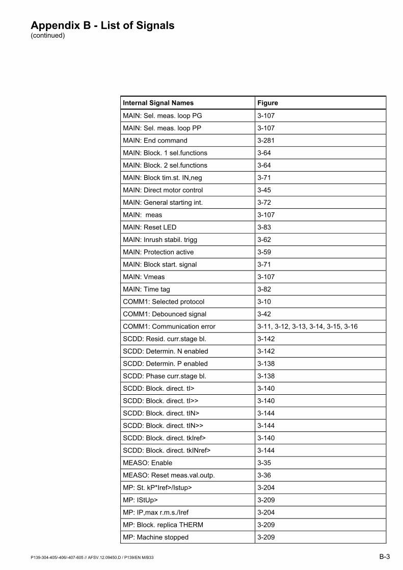
Appendix B - List of Signals (continued)
P139-304-405/-406/-407-605 // AFSV.12.09450.D / P139/EN M/B33 B-3
Internal Signal Names Figure
MAIN: Sel. meas. loop PG 3-107
MAIN: Sel. meas. loop PP 3-107
MAIN: End command 3-281
MAIN: Block. 1 sel.functions 3-64
MAIN: Block. 2 sel.functions 3-64
MAIN: Block tim.st. IN,neg 3-71
MAIN: Direct motor control 3-45
MAIN: General starting int. 3-72
MAIN: meas 3-107
MAIN: Reset LED 3-83
MAIN: Inrush stabil. trigg 3-62
MAIN: Protection active 3-59
MAIN: Block start. signal 3-71
MAIN: Vmeas 3-107
MAIN: Time tag 3-82
COMM1: Selected protocol 3-10
COMM1: Debounced signal 3-42
COMM1: Communication error 3-11, 3-12, 3-13, 3-14, 3-15, 3-16
SCDD: Resid. curr.stage bl. 3-142
SCDD: Determin. N enabled 3-142
SCDD: Determin. P enabled 3-138
SCDD: Phase curr.stage bl. 3-138
SCDD: Block. direct. tI> 3-140
SCDD: Block. direct. tI>> 3-140
SCDD: Block. direct. tIN> 3-144
SCDD: Block. direct. tIN>> 3-144
SCDD: Block. direct. tkIref> 3-140
SCDD: Block. direct. tkINref> 3-144
MEASO: Enable 3-35
MEASO: Reset meas.val.outp. 3-36
MP: St. kP*Iref>/Istup> 3-204
MP: IStUp> 3-209
MP: IP,max r.m.s./Iref 3-204
MP: Block. replica THERM 3-209
MP: Machine stopped 3-209
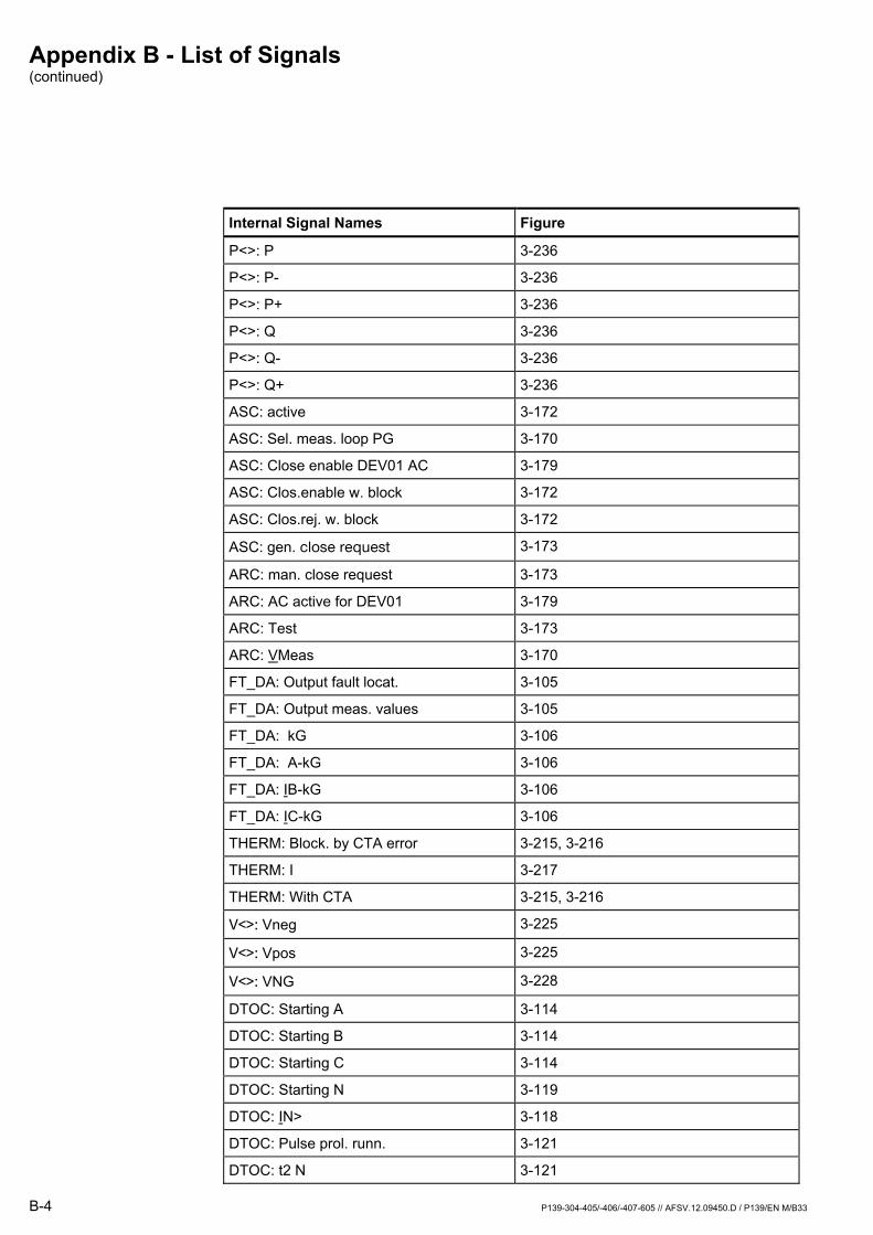
Appendix B - List of Signals (continued)
B-4 P139-304-405/-406/-407-605 // AFSV.12.09450.D / P139/EN M/B33
Internal Signal Names Figure
P<>: P 3-236
P<>: P- 3-236
P<>: P+ 3-236
P<>: Q 3-236
P<>: Q- 3-236
P<>: Q+ 3-236
ASC: active 3-172
ASC: Sel. meas. loop PG 3-170
ASC: Close enable DEV01 AC 3-179
ASC: Clos.enable w. block 3-172
ASC: Clos.rej. w. block 3-172
ASC: gen. close request 3-173
ARC: man. close request 3-173
ARC: AC active for DEV01 3-179
ARC: Test 3-173
ARC: VMeas 3-170
FT_DA: Output fault locat. 3-105
FT_DA: Output meas. values 3-105
FT_DA: kG 3-106
FT_DA: A-kG 3-106
FT_DA: IB-kG 3-106
FT_DA: IC-kG 3-106
THERM: Block. by CTA error 3-215, 3-216
THERM: I 3-217
THERM: With CTA 3-215, 3-216
V<>: Vneg 3-225
V<>: Vpos 3-225
V<>: VNG 3-228
DTOC: Starting A 3-114
DTOC: Starting B 3-114
DTOC: Starting C 3-114
DTOC: Starting N 3-119
DTOC: IN> 3-118
DTOC: Pulse prol. runn. 3-121
DTOC: t2 N 3-121
Appendix B - List of Signals (continued)
P139-304-405/-406/-407-605 // AFSV.12.09450.D / P139/EN M/B33 B-5
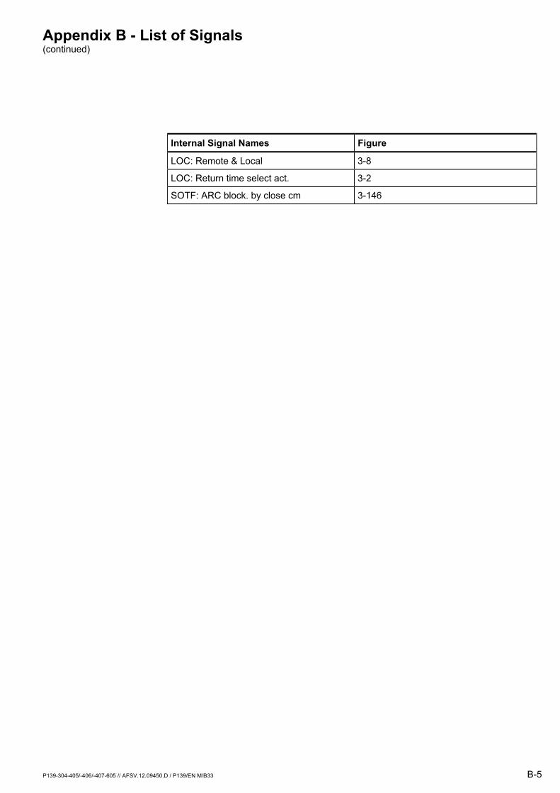
Internal Signal Names Figure
LOC: Remote & Local 3-8
LOC: Return time select act. 3-2
SOTF: ARC block. by close cm 3-146
Appendix B - List of Signals (continued)
B-6 P139-304-405/-406/-407-605 // AFSV.12.09450.D / P139/EN M/B33
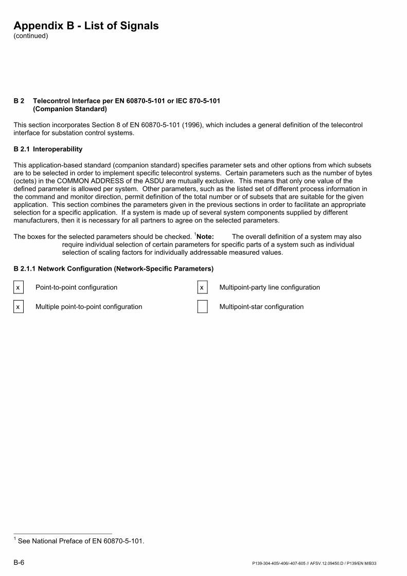
B 2 Telecontrol Interface per EN 60870-5-101 or IEC 870-5-101 (Companion Standard)
This section incorporates Section 8 of EN 60870-5-101 (1996), which includes a general definition of the telecontrol interface for substation control systems.
B 2.1 Interoperability
This application-based standard (companion standard) specifies parameter sets and other options from which subsets are to be selected in order to implement specific telecontrol systems. Certain parameters such as the number of bytes (octets) in the COMMON ADDRESS of the ASDU are mutually exclusive. This means that only one value of the defined parameter is allowed per system. Other parameters, such as the listed set of different process information in the command and monitor direction, permit definition of the total number or of subsets that are suitable for the given application. This section combines the parameters given in the previous sections in order to facilitate an appropriate selection for a specific application. If a system is made up of several system components supplied by different manufacturers, then it is necessary for all partners to agree on the selected parameters.
The boxes for the selected parameters should be checked. 1Note: The overall definition of a system may also require individual selection of certain parameters for specific parts of a system such as individual selection of scaling factors for individually addressable measured values.
B 2.1.1 Network Configuration (Network-Specific Parameters)
x Point-to-point configuration x Multipoint-party line configuration
x Multiple point-to-point configuration Multipoint-star configuration
1 See National Preface of EN 60870-5-101.
Appendix B - List of Signals (continued)
P139-304-405/-406/-407-605 // AFSV.12.09450.D / P139/EN M/B33 B-7
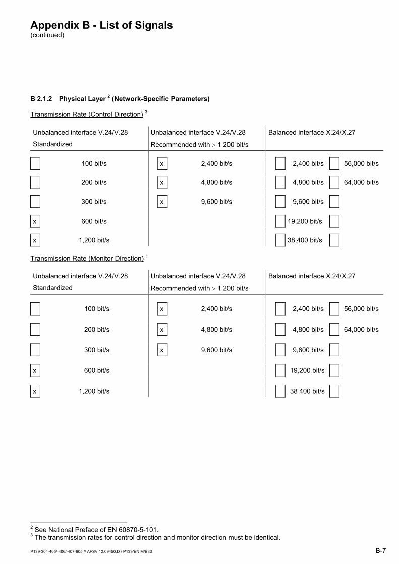
B 2.1.2 Physical Layer 2 (Network-Specific Parameters)
Transmission Rate (Control Direction) 3
Unbalanced interface V.24/V.28
Standardized
Unbalanced interface V.24/V.28
Recommended with > 1 200 bit/s
Balanced interface X.24/X.27
100 bit/s x 2,400 bit/s 2,400 bit/s 56,000 bit/s
200 bit/s x 4,800 bit/s 4,800 bit/s 64,000 bit/s
300 bit/s x 9,600 bit/s 9,600 bit/s x 600 bit/s 19,200 bit/s
x 1,200 bit/s 38,400 bit/s
Transmission Rate (Monitor Direction) 2
Unbalanced interface V.24/V.28
Standardized
Unbalanced interface V.24/V.28
Recommended with > 1 200 bit/s
Balanced interface X.24/X.27
100 bit/s x 2,400 bit/s 2,400 bit/s 56,000 bit/s 200 bit/s x 4,800 bit/s 4,800 bit/s 64,000 bit/s 300 bit/s x 9,600 bit/s 9,600 bit/s x 600 bit/s 19,200 bit/s x 1,200 bit/s 38 400 bit/s
2 See National Preface of EN 60870-5-101. 3 The transmission rates for control direction and monitor direction must be identical.
Appendix B - List of Signals (continued)
B-8 P139-304-405/-406/-407-605 // AFSV.12.09450.D / P139/EN M/B33
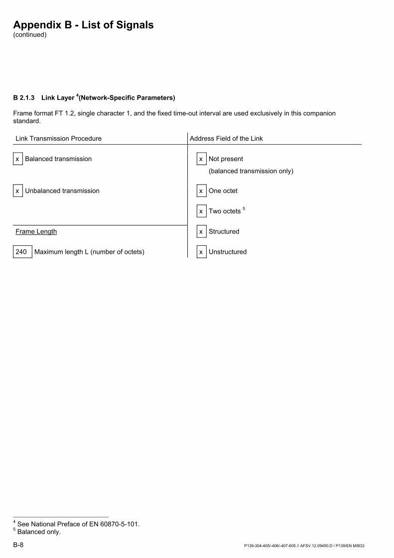
B 2.1.3 Link Layer 4(Network-Specific Parameters)
Frame format FT 1.2, single character 1, and the fixed time-out interval are used exclusively in this companion standard.
Link Transmission Procedure Address Field of the Link x Balanced transmission x Not present
(balanced transmission only) x Unbalanced transmission x One octet x Two octets 5 Frame Length x Structured 240 Maximum length L (number of octets) x Unstructured
4 See National Preface of EN 60870-5-101. 5 Balanced only.
Appendix B - List of Signals (continued)
P139-304-405/-406/-407-605 // AFSV.12.09450.D / P139/EN M/B33 B-9
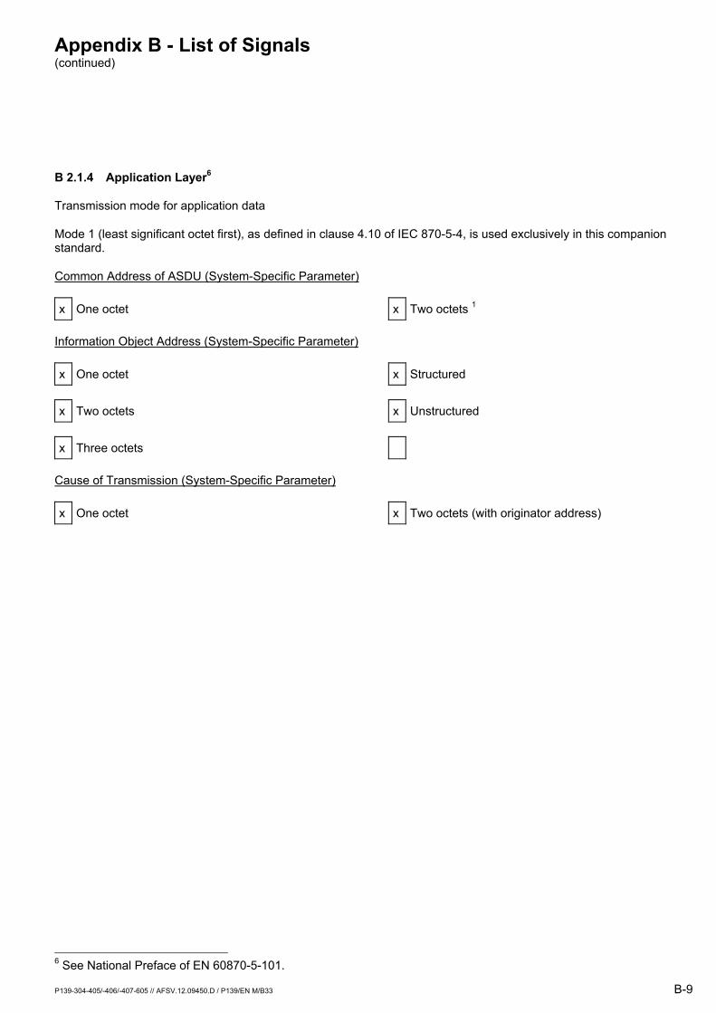
B 2.1.4 Application Layer6
Transmission mode for application data
Mode 1 (least significant octet first), as defined in clause 4.10 of IEC 870-5-4, is used exclusively in this companion standard.
Common Address of ASDU (System-Specific Parameter)
x One octet x Two octets 1
Information Object Address (System-Specific Parameter)
x One octet x Structured x Two octets x Unstructured x Three octets
Cause of Transmission (System-Specific Parameter)
x One octet x Two octets (with originator address)
6 See National Preface of EN 60870-5-101.
Appendix B - List of Signals (continued)
B-10 P139-304-405/-406/-407-605 // AFSV.12.09450.D / P139/EN M/B33
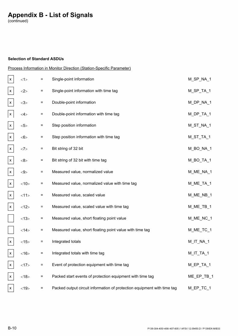
Selection of Standard ASDUs
Process Information in Monitor Direction (Station-Specific Parameter)
x <1> = Single-point information M_SP_NA_1
x <2> = Single-point information with time tag M_SP_TA_1
x <3> = Double-point information M_DP_NA_1
x <4> = Double-point information with time tag M_DP_TA_1
x <5> = Step position information M_ST_NA_1
x <6> = Step position information with time tag M_ST_TA_1
x <7> = Bit string of 32 bit M_BO_NA_1
x <8> = Bit string of 32 bit with time tag M_BO_TA_1
x <9> = Measured value, normalized value M_ME_NA_1
x <10> = Measured value, normalized value with time tag M_ME_TA_1
x <11> = Measured value, scaled value M_ME_NB_1
x <12> = Measured value, scaled value with time tag M_ME_TB_1
<13> = Measured value, short floating point value M_ME_NC_1
<14> = Measured value, short floating point value with time tag M_ME_TC_1
x <15> = Integrated totals M_IT_NA_1
x <16> = Integrated totals with time tag M_IT_TA_1
x <17> = Event of protection equipment with time tag M_EP_TA_1
x <18> = Packed start events of protection equipment with time tag ME_EP_TB_1
x <19> = Packed output circuit information of protection equipment with time tag M_EP_TC_1
Appendix B - List of Signals (continued)
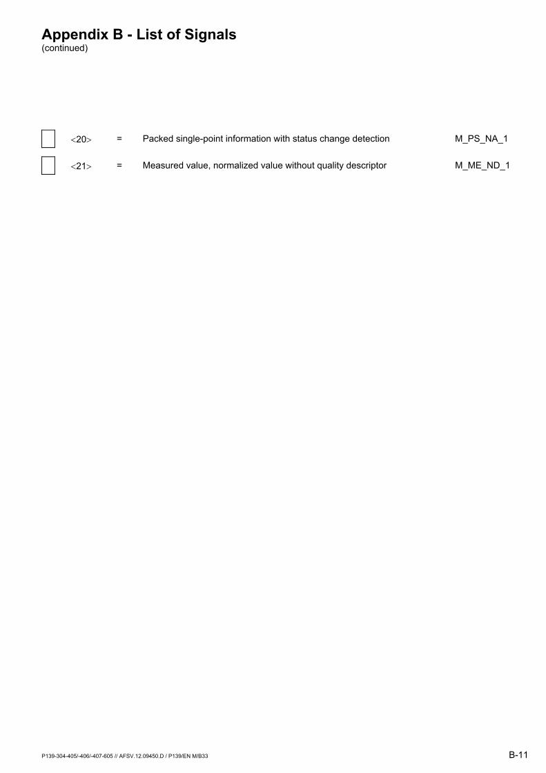
P139-304-405/-406/-407-605 // AFSV.12.09450.D / P139/EN M/B33 B-11
<20> = Packed single-point information with status change detection M_PS_NA_1
<21> = Measured value, normalized value without quality descriptor M_ME_ND_1
Appendix B - List of Signals (continued)
B-12 P139-304-405/-406/-407-605 // AFSV.12.09450.D / P139/EN M/B33
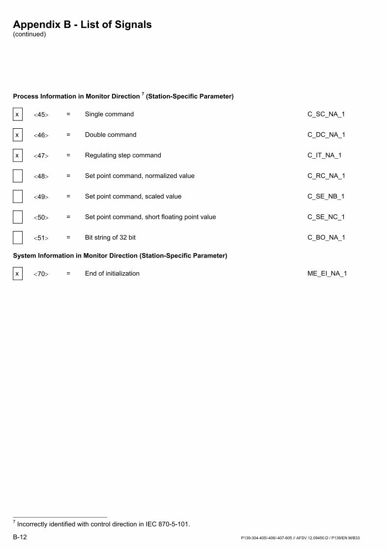
Process Information in Monitor Direction 7 (Station-Specific Parameter)
x <45> = Single command C_SC_NA_1 x <46> = Double command C_DC_NA_1 x <47> = Regulating step command C_IT_NA_1 <48> = Set point command, normalized value C_RC_NA_1 <49> = Set point command, scaled value C_SE_NB_1 <50> = Set point command, short floating point value C_SE_NC_1 <51> = Bit string of 32 bit C_BO_NA_1
System Information in Monitor Direction (Station-Specific Parameter)
x <70> = End of initialization ME_EI_NA_1
7 Incorrectly identified with control direction in IEC 870-5-101.
Appendix B - List of Signals (continued)
P139-304-405/-406/-407-605 // AFSV.12.09450.D / P139/EN M/B33 B-13
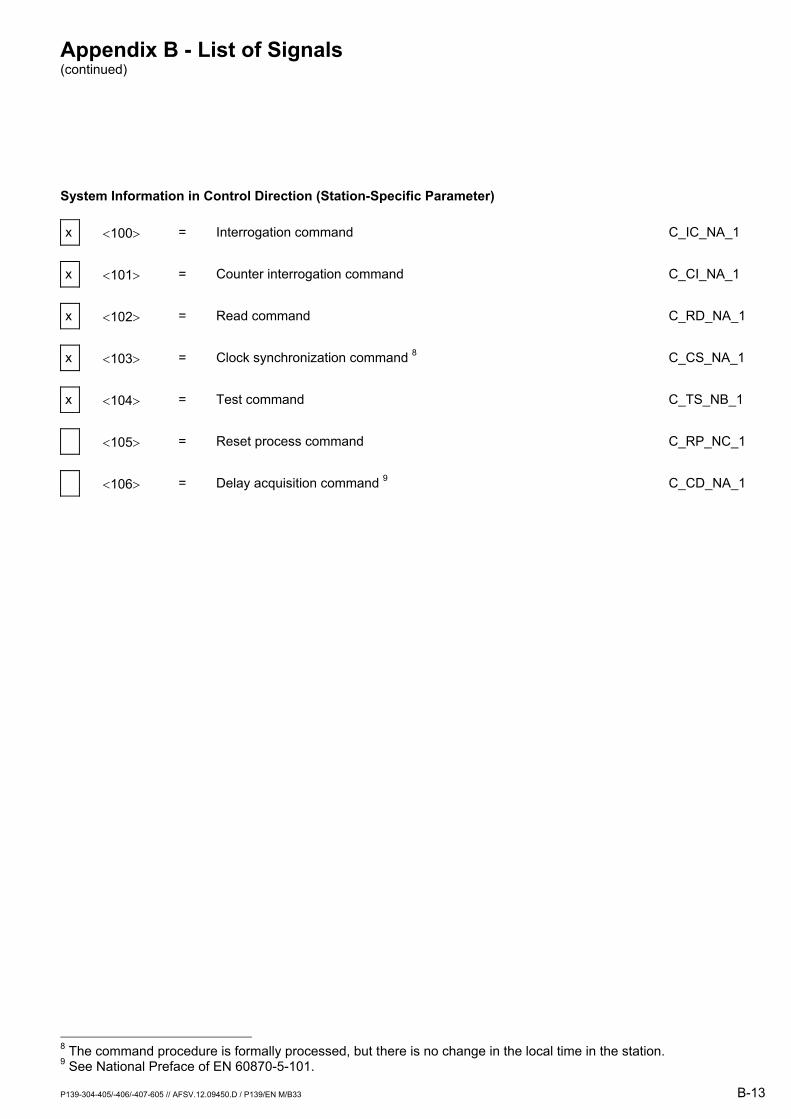
System Information in Control Direction (Station-Specific Parameter)
x <100> = Interrogation command C_IC_NA_1 x <101> = Counter interrogation command C_CI_NA_1 x <102> = Read command C_RD_NA_1 x <103> = Clock synchronization command 8 C_CS_NA_1 x <104> = Test command C_TS_NB_1 <105> = Reset process command C_RP_NC_1 <106> = Delay acquisition command 9 C_CD_NA_1
8 The command procedure is formally processed, but there is no change in the local time in the station. 9 See National Preface of EN 60870-5-101.
Appendix B - List of Signals (continued)
B-14 P139-304-405/-406/-407-605 // AFSV.12.09450.D / P139/EN M/B33
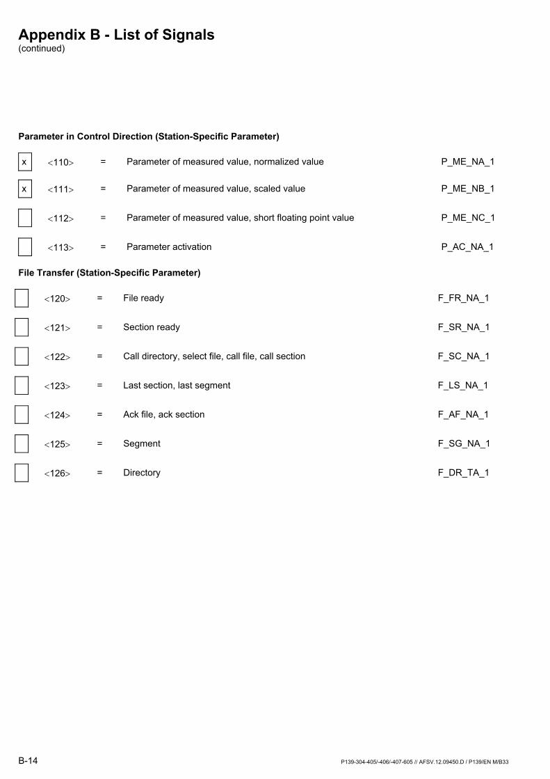
Parameter in Control Direction (Station-Specific Parameter)
x <110> = Parameter of measured value, normalized value P_ME_NA_1
x <111> = Parameter of measured value, scaled value P_ME_NB_1 <112> = Parameter of measured value, short floating point value P_ME_NC_1 <113> = Parameter activation P_AC_NA_1
File Transfer (Station-Specific Parameter)
<120> = File ready F_FR_NA_1 <121> = Section ready F_SR_NA_1 <122> = Call directory, select file, call file, call section F_SC_NA_1 <123> = Last section, last segment F_LS_NA_1 <124> = Ack file, ack section F_AF_NA_1 <125> = Segment F_SG_NA_1 <126> = Directory F_DR_TA_1
Appendix B - List of Signals (continued)
P139-304-405/-406/-407-605 // AFSV.12.09450.D / P139/EN M/B33 B-15
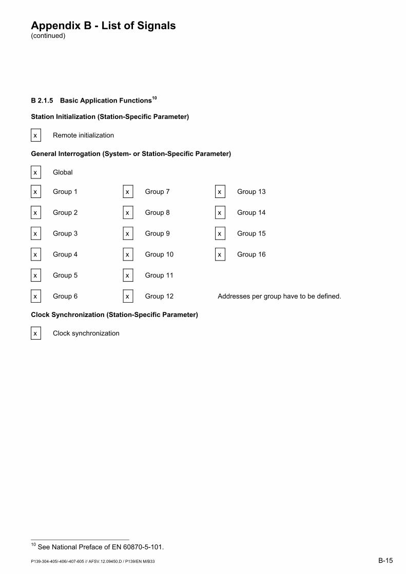
B 2.1.5 Basic Application Functions10
Station Initialization (Station-Specific Parameter)
x Remote initialization
General Interrogation (System- or Station-Specific Parameter)
x Global
x Group 1 x Group 7 x Group 13 x Group 2 x Group 8 x Group 14 x Group 3 x Group 9 x Group 15 x Group 4 x Group 10 x Group 16 x Group 5 x Group 11 x Group 6 x Group 12 Addresses per group have to be defined.
Clock Synchronization (Station-Specific Parameter)
x Clock synchronization
10 See National Preface of EN 60870-5-101.
Appendix B - List of Signals (continued)
B-16 P139-304-405/-406/-407-605 // AFSV.12.09450.D / P139/EN M/B33
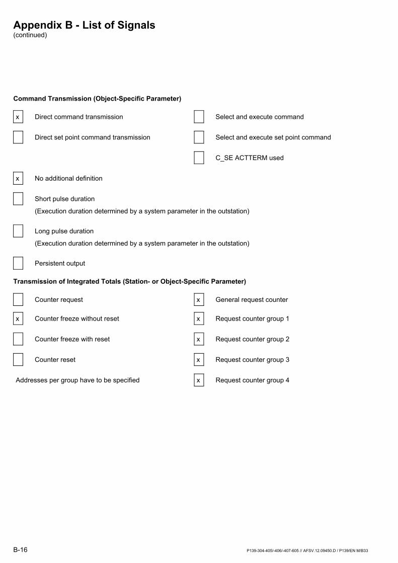
Command Transmission (Object-Specific Parameter)
x Direct command transmission Select and execute command Direct set point command transmission Select and execute set point command C_SE ACTTERM used x No additional definition
Short pulse duration
(Execution duration determined by a system parameter in the outstation) Long pulse duration
(Execution duration determined by a system parameter in the outstation) Persistent output
Transmission of Integrated Totals (Station- or Object-Specific Parameter)
Counter request x General request counter
x Counter freeze without reset x Request counter group 1 Counter freeze with reset x Request counter group 2 Counter reset x Request counter group 3 Addresses per group have to be specified x Request counter group 4
Appendix B - List of Signals (continued)
P139-304-405/-406/-407-605 // AFSV.12.09450.D / P139/EN M/B33 B-17
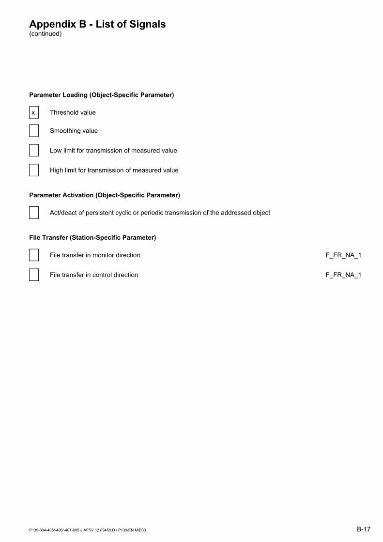
Parameter Loading (Object-Specific Parameter)
x Threshold value
Smoothing value Low limit for transmission of measured value High limit for transmission of measured value
Parameter Activation (Object-Specific Parameter)
Act/deact of persistent cyclic or periodic transmission of the addressed object
File Transfer (Station-Specific Parameter)
File transfer in monitor direction F_FR_NA_1 File transfer in control direction F_FR_NA_1
Appendix B - List of Signals (continued)
B-18 P139-304-405/-406/-407-605 // AFSV.12.09450.D / P139/EN M/B33
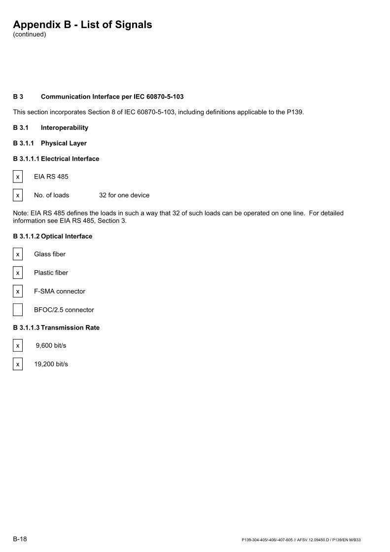
B 3 Communication Interface per IEC 60870-5-103
This section incorporates Section 8 of IEC 60870-5-103, including definitions applicable to the P139.
B 3.1 Interoperability
B 3.1.1 Physical Layer
B 3.1.1.1 Electrical Interface
x EIA RS 485
x No. of loads 32 for one device
Note: EIA RS 485 defines the loads in such a way that 32 of such loads can be operated on one line. For detailed information see EIA RS 485, Section 3.
B 3.1.1.2 Optical Interface
x Glass fiber
x Plastic fiber
x F-SMA connector
BFOC/2.5 connector
B 3.1.1.3 Transmission Rate
x 9,600 bit/s
x 19,200 bit/s
Appendix B - List of Signals (continued)
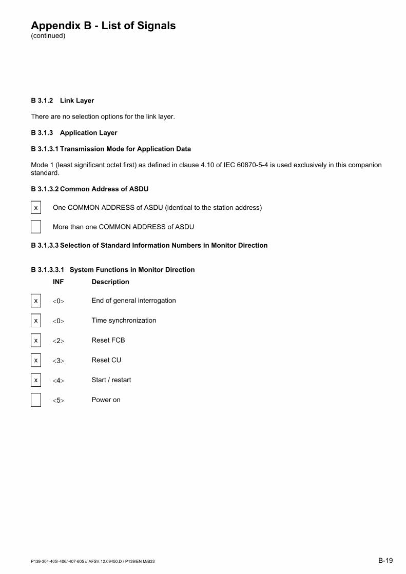
P139-304-405/-406/-407-605 // AFSV.12.09450.D / P139/EN M/B33 B-19
B 3.1.2 Link Layer
There are no selection options for the link layer.
B 3.1.3 Application Layer
B 3.1.3.1 Transmission Mode for Application Data
Mode 1 (least significant octet first) as defined in clause 4.10 of IEC 60870-5-4 is used exclusively in this companion standard.
B 3.1.3.2 Common Address of ASDU
x One COMMON ADDRESS of ASDU (identical to the station address)
More than one COMMON ADDRESS of ASDU
B 3.1.3.3 Selection of Standard Information Numbers in Monitor Direction
B 3.1.3.3.1 System Functions in Monitor Direction INF Description
x <0> End of general interrogation
x <0> Time synchronization
x <2> Reset FCB
x <3> Reset CU
x <4> Start / restart
<5> Power on
Appendix B - List of Signals (continued)
B-20 P139-304-405/-406/-407-605 // AFSV.12.09450.D / P139/EN M/B33
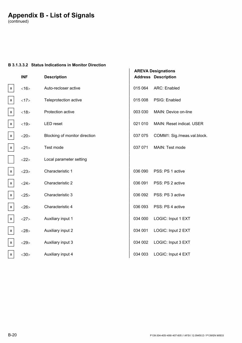
B 3.1.3.3.2 Status Indications in Monitor Direction AREVA Designations INF Description Address Description
x <16> Auto-recloser active 015 064 ARC: Enabled
x <17> Teleprotection active 015 008 PSIG: Enabled
x <18> Protection active 003 030 MAIN: Device on-line
x <19> LED reset 021 010 MAIN: Reset indicat. USER
x <20> Blocking of monitor direction 037 075 COMM1: Sig./meas.val.block.
x <21> Test mode 037 071 MAIN: Test mode
<22> Local parameter setting
x <23> Characteristic 1 036 090 PSS: PS 1 active
x <24> Characteristic 2 036 091 PSS: PS 2 active
x <25> Characteristic 3 036 092 PSS: PS 3 active
x <26> Characteristic 4 036 093 PSS: PS 4 active
x <27> Auxiliary input 1 034 000 LOGIC: Input 1 EXT
x <28> Auxiliary input 2 034 001 LOGIC: Input 2 EXT
x <29> Auxiliary input 3 034 002 LOGIC: Input 3 EXT
x <30> Auxiliary input 4 034 003 LOGIC: Input 4 EXT
Appendix B - List of Signals (continued)
P139-304-405/-406/-407-605 // AFSV.12.09450.D / P139/EN M/B33 B-21
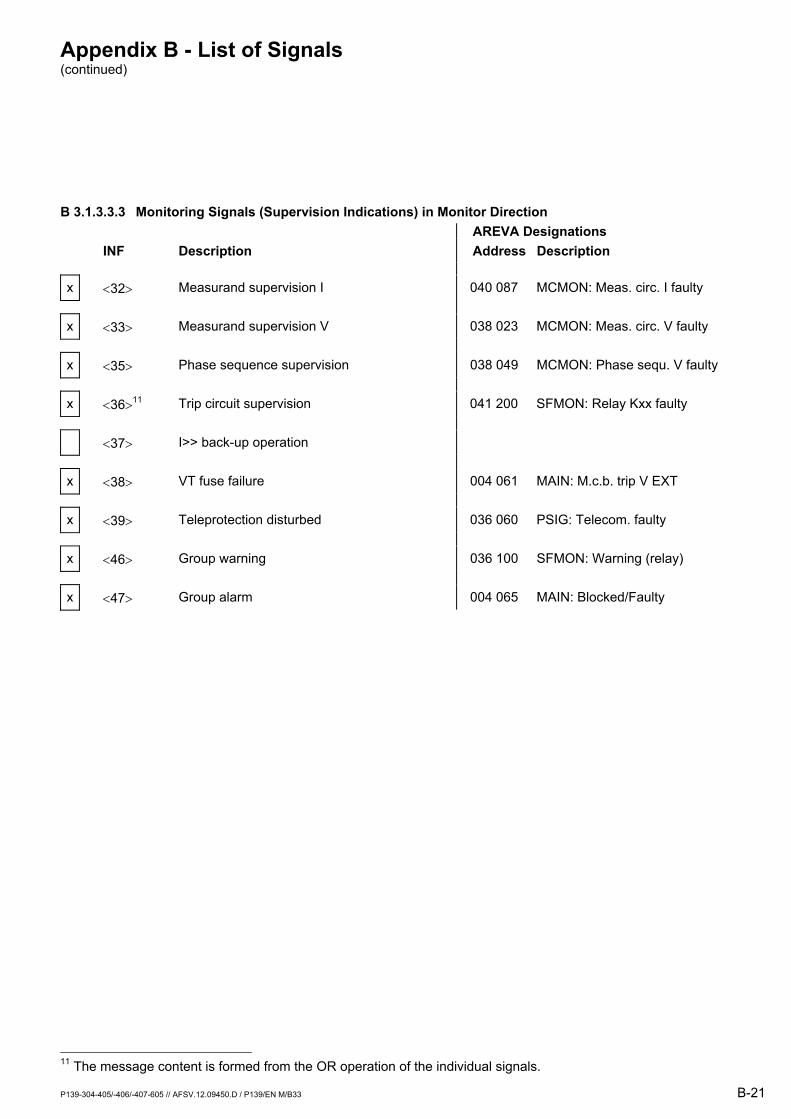
B 3.1.3.3.3 Monitoring Signals (Supervision Indications) in Monitor Direction AREVA Designations INF Description Address Description
x <32> Measurand supervision I 040 087 MCMON: Meas. circ. I faulty
x <33> Measurand supervision V 038 023 MCMON: Meas. circ. V faulty
x <35> Phase sequence supervision 038 049 MCMON: Phase sequ. V faulty
x <36>11 Trip circuit supervision 041 200 SFMON: Relay Kxx faulty
<37> I>> back-up operation
x <38> VT fuse failure 004 061 MAIN: M.c.b. trip V EXT
x <39> Teleprotection disturbed 036 060 PSIG: Telecom. faulty
x <46> Group warning 036 100 SFMON: Warning (relay)
x <47> Group alarm 004 065 MAIN: Blocked/Faulty
11 The message content is formed from the OR operation of the individual signals.
Appendix B - List of Signals (continued)
B-22 P139-304-405/-406/-407-605 // AFSV.12.09450.D / P139/EN M/B33
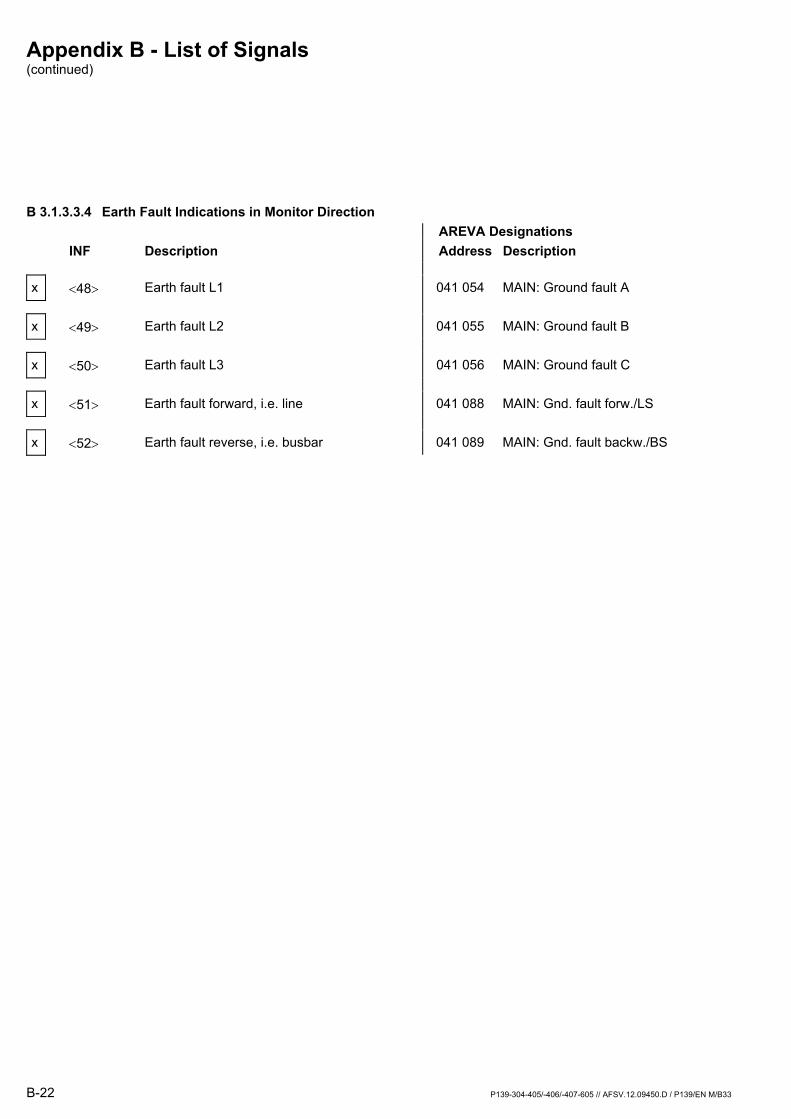
B 3.1.3.3.4 Earth Fault Indications in Monitor Direction AREVA Designations INF Description Address Description
x <48> Earth fault L1 041 054 MAIN: Ground fault A
x <49> Earth fault L2 041 055 MAIN: Ground fault B
x <50> Earth fault L3 041 056 MAIN: Ground fault C
x <51> Earth fault forward, i.e. line 041 088 MAIN: Gnd. fault forw./LS
x <52> Earth fault reverse, i.e. busbar 041 089 MAIN: Gnd. fault backw./BS
Appendix B - List of Signals (continued)
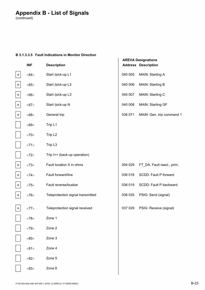
P139-304-405/-406/-407-605 // AFSV.12.09450.D / P139/EN M/B33 B-23
B 3.1.3.3.5 Fault Indications in Monitor Direction AREVA Designations INF Description Address Description
x <64> Start /pick-up L1 040 005 MAIN: Starting A
x <65> Start /pick-up L3 040 006 MAIN: Starting B
x <66> Start /pick-up L3 040 007 MAIN: Starting C
x <67> Start /pick-up N 040 008 MAIN: Starting GF
x <68> General trip 036 071 MAIN: Gen. trip command 1
<69> Trip L1
<70> Trip L2
<71> Trip L3
<72> Trip I>> (back-up operation)
x <73> Fault location X in ohms 004 029 FT_DA: Fault react., prim.
x <74> Fault forward/line 036 018 SCDD: Fault P forward
x <75> Fault reverse/busbar 036 019 SCDD: Fault P backward
x <76> Teleprotection signal transmitted 036 035 PSIG: Send (signal)
x <77> Teleprotection signal received 037 029 PSIG: Receive (signal)
<78> Zone 1
<79> Zone 2
<80> Zone 3
<81> Zone 4
<82> Zone 5
<83> Zone 6
Appendix B - List of Signals (continued)
B-24 P139-304-405/-406/-407-605 // AFSV.12.09450.D / P139/EN M/B33
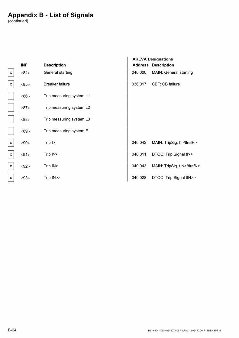
AREVA Designations INF Description Address Description
x <84> General starting 040 000 MAIN: General starting
x <85> Breaker failure 036 017 CBF: CB failure
<86> Trip measuring system L1
<87> Trip measuring system L2
<88> Trip measuring system L3
<89> Trip measuring system E
x <90> Trip I> 040 042 MAIN: TripSig. tI>/tIrefP>
x <91> Trip I>> 040 011 DTOC: Trip Signal tI>>
x <92> Trip IN> 040 043 MAIN: TripSig. tIN>/tIrefN>
x <93> Trip IN>> 040 028 DTOC: Trip Signal tIN>>
Appendix B - List of Signals (continued)
P139-304-405/-406/-407-605 // AFSV.12.09450.D / P139/EN M/B33 B-25
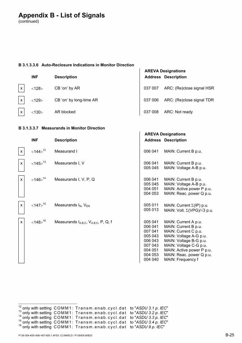
B 3.1.3.3.6 Auto-Reclosure Indications in Monitor Direction AREVA Designations INF Description Address Description
x <128> CB on by AR 037 007 ARC: (Re)close signal HSR
x <129> CB on by long-time AR 037 006 ARC: (Re)close signal TDR
x <130> AR blocked 037 008 ARC: Not ready
B 3.1.3.3.7 Measurands in Monitor Direction AREVA Designations INF Description Address Description
x <144>12 Measurand I 006 041 MAIN: Current B p.u.
x <145>13 Measurands I, V 006 041 005 045
MAIN: Current B p.u. MAIN: Voltage A-B p.u.
x <146>14 Measurands I, V, P, Q 006 041 005 045 004 051 004 053
MAIN: Current B p.u. MAIN: Voltage A-B p.u. MAIN: Active power P p.u. MAIN: Reac. power Q p.u.
x <147>15 Measurands IN, VEN 005 011 005 013
MAIN: Current Σ(IP) p.u. MAIN: Volt. Σ(VPG)/√3 p.u.
x <148>16 Measurands IA,B,C, VA,B,C, P, Q, f 005 041 006 041 007 041 005 043 006 043 007 043 004 051 004 053 004 040
MAIN: Current A p.u. MAIN: Current B p.u. MAIN: Current C p.u. MAIN: Voltage A-G p.u. MAIN: Voltage B-G p.u. MAIN: Voltage C-G p.u. MAIN: Active power P p.u. MAIN: Reac. power Q p.u. MAIN: Frequency f
12 only with setting C O M M 1 : T r a n s m . e n a b . c y c l . d a t to "ASDU 3.1 p. IEC" 13 only with setting C O M M 1 : T r a n s m . e n a b . c y c l . d a t to "ASDU 3.2 p. IEC" 14 only with setting C O M M 1 : T r a n s m . e n a b . c y c l . d a t to "ASDU 3.3 p. IEC" 15 only with setting C O M M 1 : T r a n s m . e n a b . c y c l . d a t to "ASDU 3.4 p. IEC" 16 only with setting C O M M 1 : T r a n s m . e n a b . c y c l . d a t to "ASDU 9 p. IEC"
Appendix B - List of Signals (continued)
B-26 P139-304-405/-406/-407-605 // AFSV.12.09450.D / P139/EN M/B33
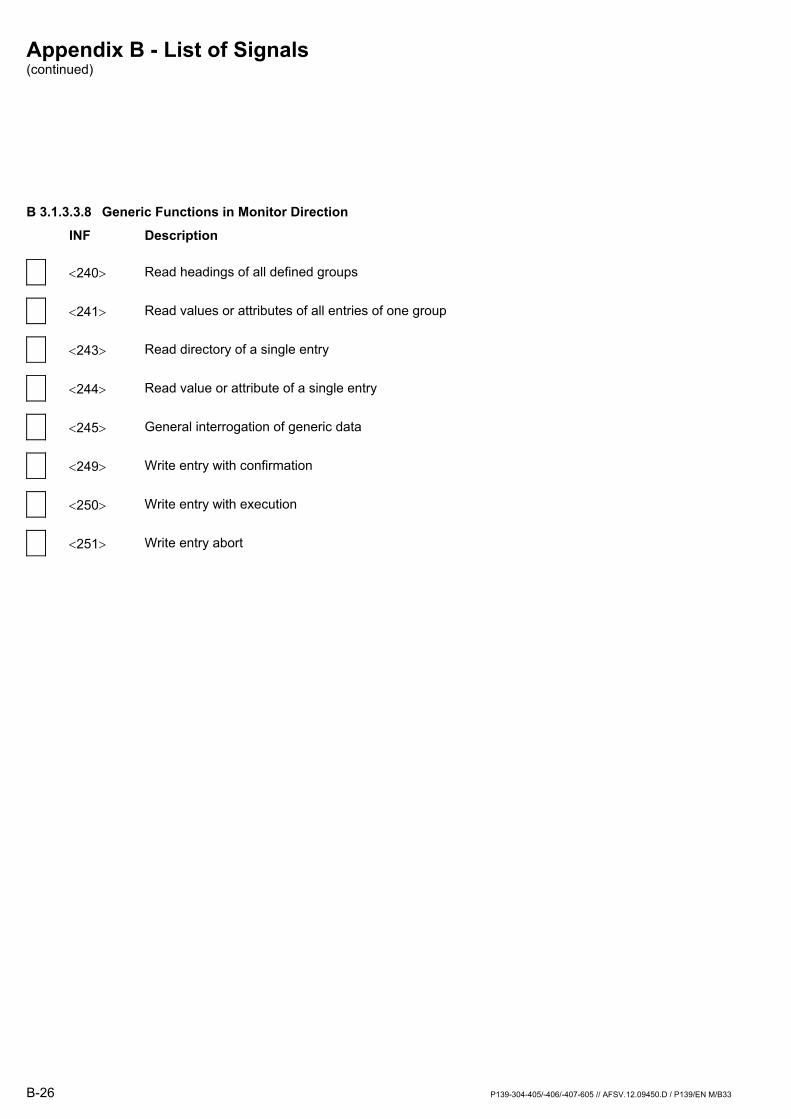
B 3.1.3.3.8 Generic Functions in Monitor Direction INF Description
<240> Read headings of all defined groups
<241> Read values or attributes of all entries of one group
<243> Read directory of a single entry
<244> Read value or attribute of a single entry
<245> General interrogation of generic data
<249> Write entry with confirmation
<250> Write entry with execution
<251> Write entry abort
Appendix B - List of Signals (continued)
P139-304-405/-406/-407-605 // AFSV.12.09450.D / P139/EN M/B33 B-27
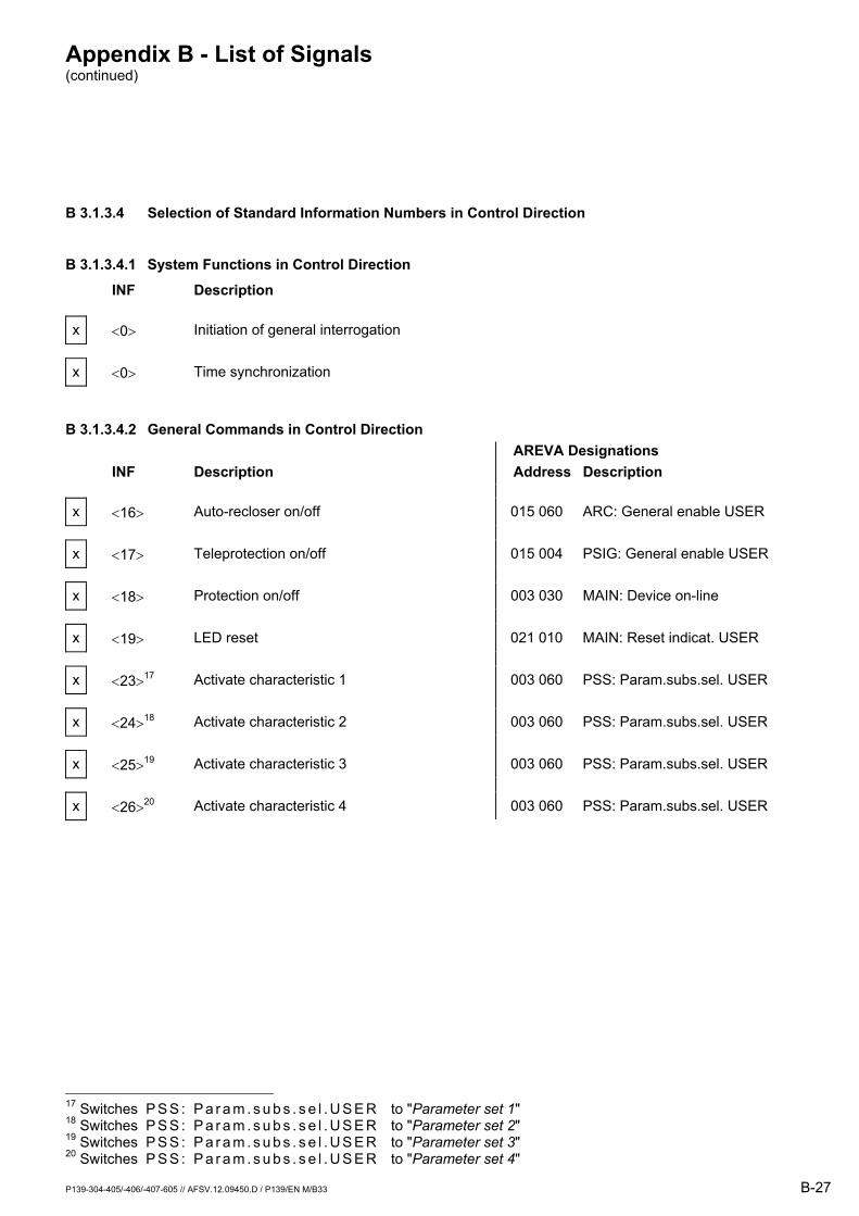
B 3.1.3.4 Selection of Standard Information Numbers in Control Direction
B 3.1.3.4.1 System Functions in Control Direction INF Description
x <0> Initiation of general interrogation
x <0> Time synchronization
B 3.1.3.4.2 General Commands in Control Direction AREVA Designations INF Description Address Description
x <16> Auto-recloser on/off 015 060 ARC: General enable USER
x <17> Teleprotection on/off 015 004 PSIG: General enable USER
x <18> Protection on/off 003 030 MAIN: Device on-line
x <19> LED reset 021 010 MAIN: Reset indicat. USER
x <23>17 Activate characteristic 1 003 060 PSS: Param.subs.sel. USER
x <24>18 Activate characteristic 2 003 060 PSS: Param.subs.sel. USER
x <25>19 Activate characteristic 3 003 060 PSS: Param.subs.sel. USER
x <26>20 Activate characteristic 4 003 060 PSS: Param.subs.sel. USER
17 Switches P S S : P a r a m . s u b s . s e l . U S E R to "Parameter set 1" 18 Switches P S S : P a r a m . s u b s . s e l . U S E R to "Parameter set 2" 19 Switches P S S : P a r a m . s u b s . s e l . U S E R to "Parameter set 3" 20 Switches P S S : P a r a m . s u b s . s e l . U S E R to "Parameter set 4"
Appendix B - List of Signals (continued)
B-28 P139-304-405/-406/-407-605 // AFSV.12.09450.D / P139/EN M/B33
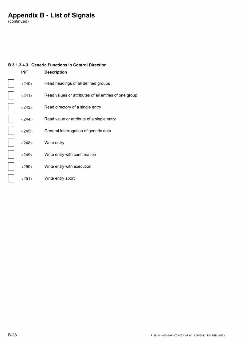
B 3.1.3.4.3 Generic Functions in Control Direction INF Description
<240> Read headings of all defined groups
<241> Read values or attributes of all entries of one group
<243> Read directory of a single entry
<244> Read value or attribute of a single entry
<245> General interrogation of generic data
<248> Write entry
<249> Write entry with confirmation
<250> Write entry with execution
<251> Write entry abort
Appendix B - List of Signals (continued)
P139-304-405/-406/-407-605 // AFSV.12.09450.D / P139/EN M/B33 B-29
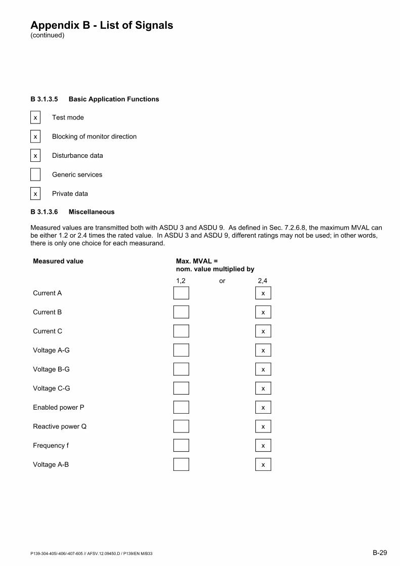
B 3.1.3.5 Basic Application Functions
x Test mode
x Blocking of monitor direction
x Disturbance data
Generic services
x Private data
B 3.1.3.6 Miscellaneous
Measured values are transmitted both with ASDU 3 and ASDU 9. As defined in Sec. 7.2.6.8, the maximum MVAL can be either 1.2 or 2.4 times the rated value. In ASDU 3 and ASDU 9, different ratings may not be used; in other words, there is only one choice for each measurand.
Measured value Max. MVAL = nom. value multiplied by
1,2 or 2,4
Current A x
Current B x
Current C x
Voltage A-G x
Voltage B-G x
Voltage C-G x
Enabled power P x
Reactive power Q x
Frequency f x
Voltage A-B x

B-30 P139-304-405/-406/-407-605 // AFSV.12.09450.D / P139/EN M/B33
Appendix C - List of Bay Types
P139-304-405/-406/-407-605 // AFSV.12.09450.D / P139/EN M/B33 C-1
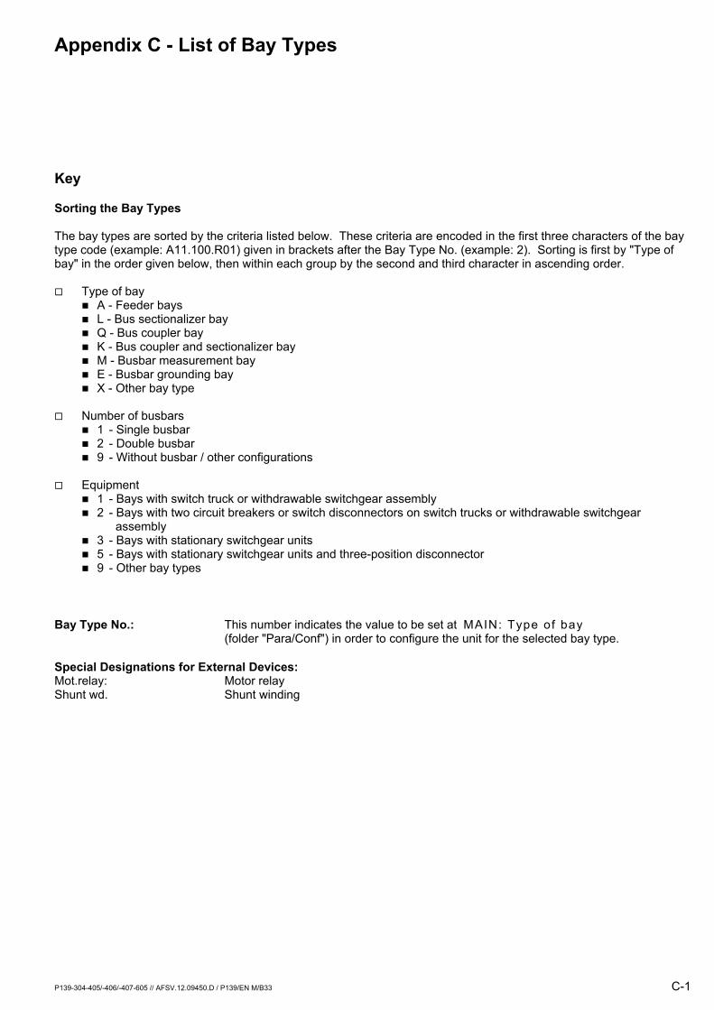
Key
Sorting the Bay Types The bay types are sorted by the criteria listed below. These criteria are encoded in the first three characters of the bay type code (example: A11.100.R01) given in brackets after the Bay Type No. (example: 2). Sorting is first by "Type of bay" in the order given below, then within each group by the second and third character in ascending order. ! Type of bay " A - Feeder bays " L - Bus sectionalizer bay " Q - Bus coupler bay " K - Bus coupler and sectionalizer bay " M - Busbar measurement bay " E - Busbar grounding bay " X - Other bay type ! Number of busbars " 1 - Single busbar " 2 - Double busbar " 9 - Without busbar / other configurations ! Equipment " 1 - Bays with switch truck or withdrawable switchgear assembly " 2 - Bays with two circuit breakers or switch disconnectors on switch trucks or withdrawable switchgear assembly " 3 - Bays with stationary switchgear units " 5 - Bays with stationary switchgear units and three-position disconnector " 9 - Other bay types
Bay Type No.: This number indicates the value to be set at MAIN: Type of bay (folder "Para/Conf") in order to configure the unit for the selected bay type.
Special Designations for External Devices: Mot.relay: Motor relay Shunt wd. Shunt winding
Appendix C - List of Bay Types (continued)
C-2 P139-304-405/-406/-407-605 // AFSV.12.09450.D / P139/EN M/B33
Table "Assignment of Binary Inputs and Output Relays"
Column "Switchgear unit" This column begins with the designation for the external device (switchgear unit). The function group follows in brackets. The function group encompasses all setting options for monitoring the switchgear unit and its signals. "Open" and "Close(d)" indicate the signal message or control direction of the switchgear unit.
Column "Binary Input": The "Open" or "Closed" signal should be connected to the binary input U xxxx. The connection points of the binary input U xxxx are shown in the terminal connection diagrams.
Column "Output relay" The "Open" or "Close" control of the switchgear unit is effected via output relay K xxxx. The connection points of the output relay K xxxx are shown in the terminal connection diagrams.
Table "Bay Interlock Equations for Operation without Station Interlocking"
Note! The interlock equations are stored at substation control level, not at unit level.
Symbols used in the Boolean interlock equations: /: Negation 0: Switchgear unit "Open" I: Switchgear unit "Closed" X: Switchgear unit in intermediate position
FctBl1: Function block 1, configuration at MAIN: Fct .asg. fc t .b lock.1 (Folder "Para/Func/Ctrl")
FctBl2: Function block 2, configuration at MAIN: Fct .asg. fc t .b lock.2 (Folder "Para/Func/Ctrl")

Appendix C - List of Bay Types (continued)
P139-304-405/-406/-407-605 // AFSV.12.09450.D / P139/EN M/B33 C-3
Bay Type No. 2 (A11.100.R01) Feeder bay with circuit breaker, single busbar
Assignment of Binary Inputs and Output Relays
Switchgear unit Binary input Output relay
Q0 (DEV01) X0 (DEV02)
Open Close(d) Open Close(d)
U A01 U A02 U A03 U A04
K A01 K A02/ /
Bay Interlock Equations for Operation without Station Interlocking
Switchgear unit Control O/C Interlock equation
Q0 Close(d) /(X0=X) & /(FctBl1=I) & /(FctBl2=I)
Bay Interlock Equations for Operation with Station Interlocking
Switchgear unit Control O/C Interlock equation
Q0 Close(d) /(X0=X) & /(FctBl1=I) & /(FctBl2=I)
Appendix C - List of Bay Types (continued)
C-4 P139-304-405/-406/-407-605 // AFSV.12.09450.D / P139/EN M/B33
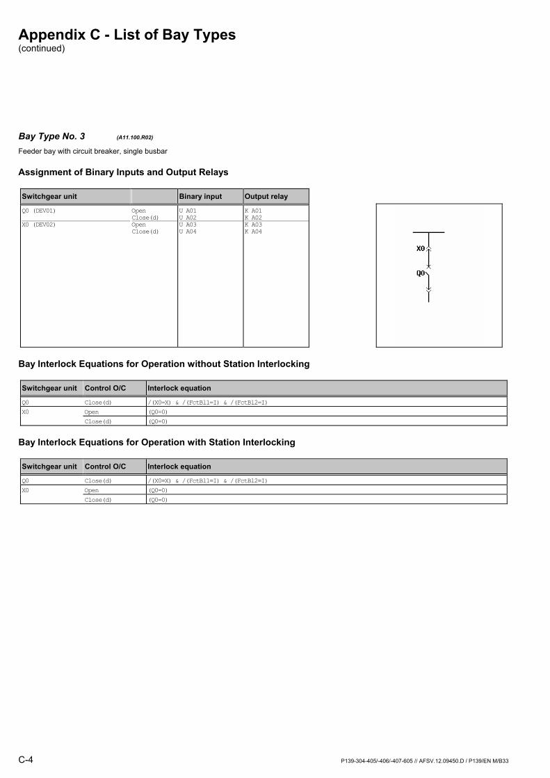
Bay Type No. 3 (A11.100.R02) Feeder bay with circuit breaker, single busbar
Assignment of Binary Inputs and Output Relays
Switchgear unit Binary input Output relay
Q0 (DEV01) X0 (DEV02)
Open Close(d) Open Close(d)
U A01 U A02 U A03 U A04
K A01 K A02K A03 K A04
Bay Interlock Equations for Operation without Station Interlocking
Switchgear unit Control O/C Interlock equation
Q0 Close(d) /(X0=X) & /(FctBl1=I) & /(FctBl2=I) X0 Open (Q0=0) Close(d) (Q0=0)
Bay Interlock Equations for Operation with Station Interlocking
Switchgear unit Control O/C Interlock equation
Q0 Close(d) /(X0=X) & /(FctBl1=I) & /(FctBl2=I) X0 Open (Q0=0) Close(d) (Q0=0)
Appendix C - List of Bay Types (continued)
P139-304-405/-406/-407-605 // AFSV.12.09450.D / P139/EN M/B33 C-5
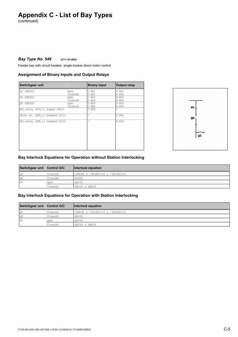
Bay Type No. 546 (A11.101.M03) Feeder bay with circuit breaker, single busbar,direct motor control
Assignment of Binary Inputs and Output Relays
Switchgear unit Binary input Output relay
Q0 (DEV01) X0 (DEV02) Q8 (DEV03) Mot.relay (SIG_1: Signal S012) Shunt wd. (CMD_1: Command C011) Mot.relay (CMD_1: Command C012)
Open Close(d) Open Close(d) Open Close(d)
U A01 U A02 U A03 U A04 U A05 U A06 U B06 / /
K A01 K A02K A03 K A04K A05 K A06/
K B05
K B06
Bay Interlock Equations for Operation without Station Interlocking
Switchgear unit Control O/C Interlock equation
Q0 Close(d) /(X0=X) & /(FctBl1=I) & /(FctBl2=I) Q8 Close(d) (X0=0) X0 Open (Q0=0) Close(d) (Q0=0) & (Q8=0)
Bay Interlock Equations for Operation with Station Interlocking
Switchgear unit Control O/C Interlock equation
Q0 Close(d) /(X0=X) & /(FctBl1=I) & /(FctBl2=I) Q8 Close(d) (X0=0) X0 Open (Q0=0) Close(d) (Q0=0) & (Q8=0)
Appendix C - List of Bay Types (continued)
C-6 P139-304-405/-406/-407-605 // AFSV.12.09450.D / P139/EN M/B33
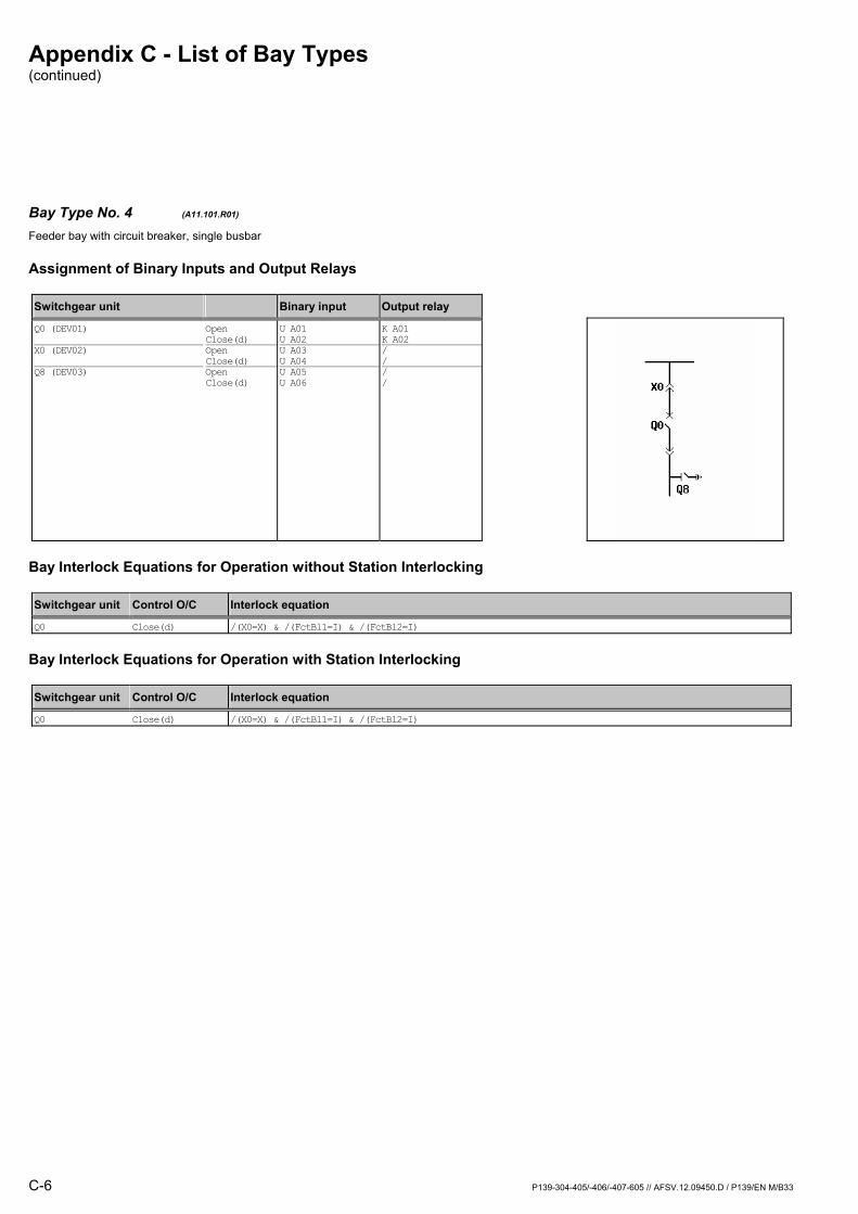
Bay Type No. 4 (A11.101.R01) Feeder bay with circuit breaker, single busbar
Assignment of Binary Inputs and Output Relays
Switchgear unit Binary input Output relay
Q0 (DEV01) X0 (DEV02) Q8 (DEV03)
Open Close(d) Open Close(d) Open Close(d)
U A01 U A02 U A03 U A04 U A05 U A06
K A01 K A02/ // /
Bay Interlock Equations for Operation without Station Interlocking
Switchgear unit Control O/C Interlock equation
Q0 Close(d) /(X0=X) & /(FctBl1=I) & /(FctBl2=I)
Bay Interlock Equations for Operation with Station Interlocking
Switchgear unit Control O/C Interlock equation
Q0 Close(d) /(X0=X) & /(FctBl1=I) & /(FctBl2=I)
Appendix C - List of Bay Types (continued)
P139-304-405/-406/-407-605 // AFSV.12.09450.D / P139/EN M/B33 C-7
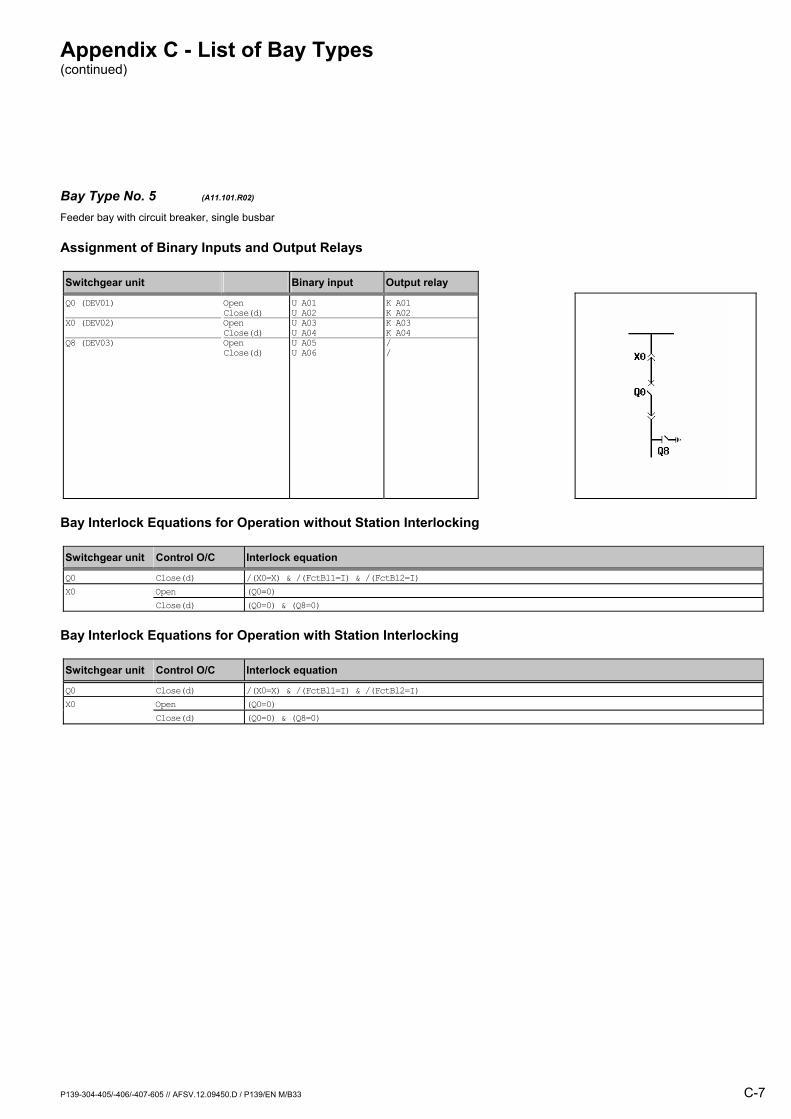
Bay Type No. 5 (A11.101.R02) Feeder bay with circuit breaker, single busbar
Assignment of Binary Inputs and Output Relays
Switchgear unit Binary input Output relay
Q0 (DEV01) X0 (DEV02) Q8 (DEV03)
Open Close(d) Open Close(d) Open Close(d)
U A01 U A02 U A03 U A04 U A05 U A06
K A01 K A02K A03 K A04/ /
Bay Interlock Equations for Operation without Station Interlocking
Switchgear unit Control O/C Interlock equation
Q0 Close(d) /(X0=X) & /(FctBl1=I) & /(FctBl2=I) X0 Open (Q0=0) Close(d) (Q0=0) & (Q8=0)
Bay Interlock Equations for Operation with Station Interlocking
Switchgear unit Control O/C Interlock equation
Q0 Close(d) /(X0=X) & /(FctBl1=I) & /(FctBl2=I) X0 Open (Q0=0) Close(d) (Q0=0) & (Q8=0)
Appendix C - List of Bay Types (continued)
C-8 P139-304-405/-406/-407-605 // AFSV.12.09450.D / P139/EN M/B33
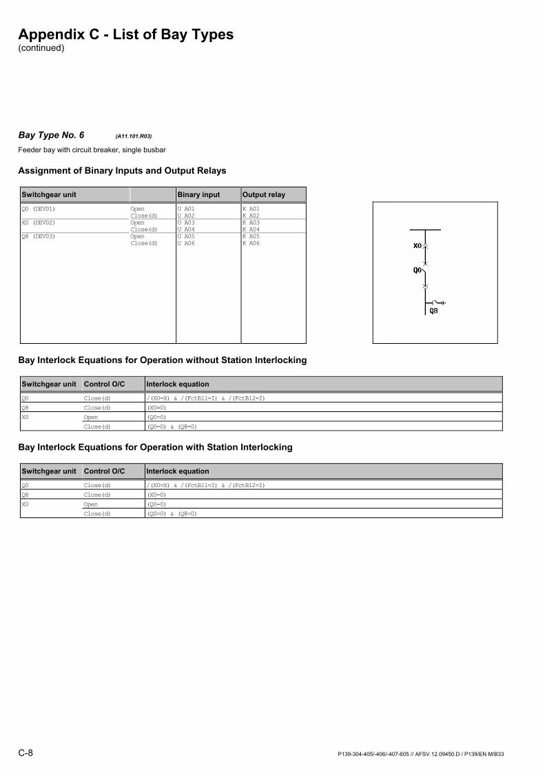
Bay Type No. 6 (A11.101.R03) Feeder bay with circuit breaker, single busbar
Assignment of Binary Inputs and Output Relays
Switchgear unit Binary input Output relay
Q0 (DEV01) X0 (DEV02) Q8 (DEV03)
Open Close(d) Open Close(d) Open Close(d)
U A01 U A02 U A03 U A04 U A05 U A06
K A01 K A02K A03 K A04K A05 K A06
Bay Interlock Equations for Operation without Station Interlocking
Switchgear unit Control O/C Interlock equation
Q0 Close(d) /(X0=X) & /(FctBl1=I) & /(FctBl2=I) Q8 Close(d) (X0=0) X0 Open (Q0=0) Close(d) (Q0=0) & (Q8=0)
Bay Interlock Equations for Operation with Station Interlocking
Switchgear unit Control O/C Interlock equation
Q0 Close(d) /(X0=X) & /(FctBl1=I) & /(FctBl2=I) Q8 Close(d) (X0=0) X0 Open (Q0=0) Close(d) (Q0=0) & (Q8=0)

Appendix C - List of Bay Types (continued)
P139-304-405/-406/-407-605 // AFSV.12.09450.D / P139/EN M/B33 C-9
Bay Type No. 523 (A11.108.R01) Feeder bay with circuit breaker, single busbar
Assignment of Binary Inputs and Output Relays
Switchgear unit Binary input Output relay
Q0 (DEV01) X0 (DEV02) Q15 (DEV03)
Open Close(d) Open Close(d) Open Close(d)
U A01 U A02 U A03 U A04 U A05 U A06
K A01 K A02/ // /
Bay Interlock Equations for Operation without Station Interlocking
Switchgear unit Control O/C Interlock equation
Q0 Close(d) /(X0=X) & (Q15=0) & /(FctBl1=I) & /(FctBl2=I)
Bay Interlock Equations for Operation with Station Interlocking
Switchgear unit Control O/C Interlock equation
Q0 Close(d) /(X0=X) & (Q15=0) & /(FctBl1=I) & /(FctBl2=I)

Appendix C - List of Bay Types (continued)
C-10 P139-304-405/-406/-407-605 // AFSV.12.09450.D / P139/EN M/B33
Bay Type No. 549 (A11.109.M03) Feeder bay with circuit breaker, single busbar,direct motor control
Assignment of Binary Inputs and Output Relays
Switchgear unit Binary input Output relay
Q0 (DEV01) Q8 (DEV02) X0 (DEV03) Q15 (DEV04) Mot.relay (SIG_1: Signal S012) Shunt wd. (CMD_1: Command C011) Mot.relay (CMD_1: Command C012)
Open Close(d) Open Close(d) Open Close(d) Open Close(d)
U A01 U A02 U A03 U A04 U A05 U A06 U B01 U B02 U B06 / /
K A01 K A02K A03 K A04K A05 K A06/ //
K B05
K B06
Bay Interlock Equations for Operation without Station Interlocking
Switchgear unit Control O/C Interlock equation
Q0 Close(d) /(X0=X) & (Q15=0) & /(FctBl1=I) & /(FctBl2=I) Q8 Close(d) (X0=0) X0 Open (Q0=0) Close(d) (Q0=0) & (Q8=0) & (Q15=0)
Bay Interlock Equations for Operation with Station Interlocking
Switchgear unit Control O/C Interlock equation
Q0 Close(d) /(X0=X) & (Q15=0) & /(FctBl1=I) & /(FctBl2=I) Q8 Close(d) (X0=0) X0 Open (Q0=0) Close(d) (Q0=0) & (Q8=0) & (Q15=0)

Appendix C - List of Bay Types (continued)
P139-304-405/-406/-407-605 // AFSV.12.09450.D / P139/EN M/B33 C-11
Bay Type No. 244 (A11.109.R01) Feeder bay with circuit breaker, single busbar
Assignment of Binary Inputs and Output Relays
Switchgear unit Binary input Output relay
Q0 (DEV01) X0 (DEV02) Q8 (DEV03) Q15 (DEV07)
Open Close(d) Open Close(d) Open Close(d) Open Close(d)
U A01 U A02 U A03 U A04 U A05 U A06 U C01 U C02
K A01 K A02/ // // /
Bay Interlock Equations for Operation without Station Interlocking
Switchgear unit Control O/C Interlock equation
Q0 Close(d) /(X0=X) & /(FctBl1=I) & /(FctBl2=I)
Bay Interlock Equations for Operation with Station Interlocking
Switchgear unit Control O/C Interlock equation
Q0 Close(d) /(X0=X) & /(FctBl1=I) & /(FctBl2=I)
Appendix C - List of Bay Types (continued)
C-12 P139-304-405/-406/-407-605 // AFSV.12.09450.D / P139/EN M/B33
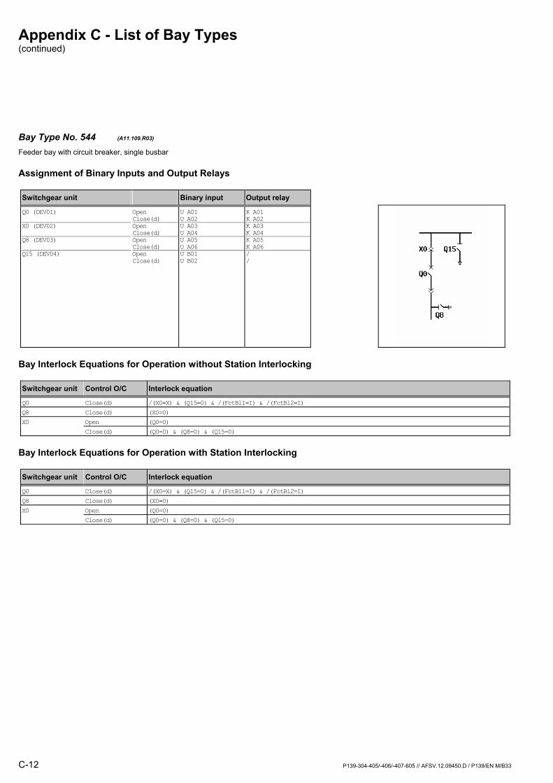
Bay Type No. 544 (A11.109.R03) Feeder bay with circuit breaker, single busbar
Assignment of Binary Inputs and Output Relays
Switchgear unit Binary input Output relay
Q0 (DEV01) X0 (DEV02) Q8 (DEV03) Q15 (DEV04)
Open Close(d) Open Close(d) Open Close(d) Open Close(d)
U A01 U A02 U A03 U A04 U A05 U A06 U B01 U B02
K A01 K A02K A03 K A04K A05 K A06/ /
Bay Interlock Equations for Operation without Station Interlocking
Switchgear unit Control O/C Interlock equation
Q0 Close(d) /(X0=X) & (Q15=0) & /(FctBl1=I) & /(FctBl2=I) Q8 Close(d) (X0=0) X0 Open (Q0=0) Close(d) (Q0=0) & (Q8=0) & (Q15=0)
Bay Interlock Equations for Operation with Station Interlocking
Switchgear unit Control O/C Interlock equation
Q0 Close(d) /(X0=X) & (Q15=0) & /(FctBl1=I) & /(FctBl2=I) Q8 Close(d) (X0=0) X0 Open (Q0=0) Close(d) (Q0=0) & (Q8=0) & (Q15=0)

Appendix C - List of Bay Types (continued)
P139-304-405/-406/-407-605 // AFSV.12.09450.D / P139/EN M/B33 C-13
Bay Type No. 567 (A11.132.R01) Feeder bay with circuit breaker, single busbar
Assignment of Binary Inputs and Output Relays
Switchgear unit Binary input Output relay
Q0 (DEV01) X0 (DEV02) Q8 (DEV03) Q52 (DEV05)
Open Close(d) Open Close(d) Open Close(d) Open Close(d)
U A01 U A02 U A03 U A04 U A05 U A06 U B03 U B04
K A01 K A02/ // // /
Bay Interlock Equations for Operation without Station Interlocking
Switchgear unit Control O/C Interlock equation
Q0 Close(d) /(X0=X) & /(FctBl1=I) & /(FctBl2=I)
Bay Interlock Equations for Operation with Station Interlocking
Switchgear unit Control O/C Interlock equation
Q0 Close(d) /(X0=X) & /(FctBl1=I) & /(FctBl2=I)

Appendix C - List of Bay Types (continued)
C-14 P139-304-405/-406/-407-605 // AFSV.12.09450.D / P139/EN M/B33
Bay Type No. 521 (A11.134.R02.1) Feeder bay with circuit breaker, single busbar
Assignment of Binary Inputs and Output Relays
Switchgear unit Binary input Output relay
Q0 (DEV01) X0 (DEV02) Q1 (DEV03) Q81 (DEV04) Q82 (DEV05)
Open Close(d) Open Close(d) Open Close(d) Open Close(d) Open Close(d)
U A01 U A02 U A03 U A04 U A05 U A06 U B01 U B02 U B03 U B04
K A01 K A02/ /K A05 K A06/ // /
Bay Interlock Equations for Operation without Station Interlocking
Switchgear unit Control O/C Interlock equation
Q0 Close(d) /(X0=X) & /(Q1=X) & (Q82=0) & /(FctBl1=I) & /(FctBl2=I) Q1 Open (Q0=0) Close(d) (Q0=0) & (Q81=0) & (Q82=0)
Bay Interlock Equations for Operation with Station Interlocking
Switchgear unit Control O/C Interlock equation
Q0 Close(d) /(X0=X) & /(Q1=X) & (Q82=0) & /(FctBl1=I) & /(FctBl2=I) Q1 Open (Q0=0) Close(d) (Q0=0) & (Q81=0) & (Q82=0)
Appendix C - List of Bay Types (continued)
P139-304-405/-406/-407-605 // AFSV.12.09450.D / P139/EN M/B33 C-15
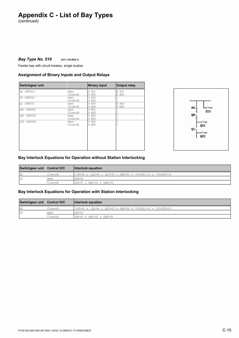
Bay Type No. 519 (A11.135.R02.1) Feeder bay with circuit breaker, single busbar
Assignment of Binary Inputs and Output Relays
Switchgear unit Binary input Output relay
Q0 (DEV01) X0 (DEV02) Q1 (DEV03) Q81 (DEV04) Q82 (DEV05) Q15 (DEV06)
Open Close(d) Open Close(d) Open Close(d) Open Close(d) Open Close(d) Open Close(d)
U A01 U A02 U A03 U A04 U A05 U A06 U B01 U B02 U B03 U B04 U B05 U B06
K A01 K A02/ /K A05 K A06/ // // /
Bay Interlock Equations for Operation without Station Interlocking
Switchgear unit Control O/C Interlock equation
Q0 Close(d) /(X0=X) & /(Q1=X) & (Q15=0) & (Q82=0) & /(FctBl1=I) & /(FctBl2=I) Q1 Open (Q0=0) Close(d) (Q0=0) & (Q81=0) & (Q82=0)
Bay Interlock Equations for Operation with Station Interlocking
Switchgear unit Control O/C Interlock equation
Q0 Close(d) /(X0=X) & /(Q1=X) & (Q15=0) & (Q82=0) & /(FctBl1=I) & /(FctBl2=I) Q1 Open (Q0=0) Close(d) (Q0=0) & (Q81=0) & (Q82=0)

Appendix C - List of Bay Types (continued)
C-16 P139-304-405/-406/-407-605 // AFSV.12.09450.D / P139/EN M/B33
Bay Type No. 7 (A11.200.R01) Feeder bay with switch disconnector, single busbar
Assignment of Binary Inputs and Output Relays
Switchgear unit Binary input Output relay
Q0 (DEV01) X0 (DEV02)
Open Close(d) Open Close(d)
U A01 U A02 U A03 U A04
K A01 K A02/ /
Bay Interlock Equations for Operation without Station Interlocking
Switchgear unit Control O/C Interlock equation
Q0 Close(d) /(X0=X) & /(FctBl1=I) & /(FctBl2=I)
Bay Interlock Equations for Operation with Station Interlocking
Switchgear unit Control O/C Interlock equation
Q0 Close(d) /(X0=X) & /(FctBl1=I) & /(FctBl2=I)
Appendix C - List of Bay Types (continued)
P139-304-405/-406/-407-605 // AFSV.12.09450.D / P139/EN M/B33 C-17
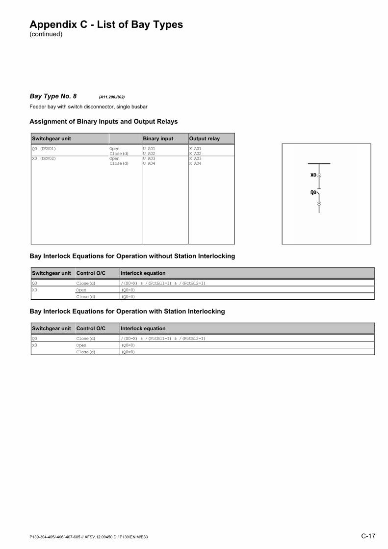
Bay Type No. 8 (A11.200.R02) Feeder bay with switch disconnector, single busbar
Assignment of Binary Inputs and Output Relays
Switchgear unit Binary input Output relay
Q0 (DEV01) X0 (DEV02)
Open Close(d) Open Close(d)
U A01 U A02 U A03 U A04
K A01 K A02K A03 K A04
Bay Interlock Equations for Operation without Station Interlocking
Switchgear unit Control O/C Interlock equation
Q0 Close(d) /(X0=X) & /(FctBl1=I) & /(FctBl2=I) X0 Open (Q0=0) Close(d) (Q0=0)
Bay Interlock Equations for Operation with Station Interlocking
Switchgear unit Control O/C Interlock equation
Q0 Close(d) /(X0=X) & /(FctBl1=I) & /(FctBl2=I) X0 Open (Q0=0) Close(d) (Q0=0)

Appendix C - List of Bay Types (continued)
C-18 P139-304-405/-406/-407-605 // AFSV.12.09450.D / P139/EN M/B33
Bay Type No. 9 (A11.201.R01) Feeder bay with switch disconnector, single busbar
Assignment of Binary Inputs and Output Relays
Switchgear unit Binary input Output relay
Q0 (DEV01) X0 (DEV02) Q8 (DEV03)
Open Close(d) Open Close(d) Open Close(d)
U A01 U A02 U A03 U A04 U A05 U A06
K A01 K A02/ // /
Bay Interlock Equations for Operation without Station Interlocking
Switchgear unit Control O/C Interlock equation
Q0 Close(d) /(X0=X) & /(FctBl1=I) & /(FctBl2=I)
Bay Interlock Equations for Operation with Station Interlocking
Switchgear unit Control O/C Interlock equation
Q0 Close(d) /(X0=X) & /(FctBl1=I) & /(FctBl2=I)

Appendix C - List of Bay Types (continued)
P139-304-405/-406/-407-605 // AFSV.12.09450.D / P139/EN M/B33 C-19
Bay Type No. 10 (A11.201.R02) Feeder bay with switch disconnector, single busbar
Assignment of Binary Inputs and Output Relays
Switchgear unit Binary input Output relay
Q0 (DEV01) X0 (DEV02) Q8 (DEV03)
Open Close(d) Open Close(d) Open Close(d)
U A01 U A02 U A03 U A04 U A05 U A06
K A01 K A02K A03 K A04/ /
Bay Interlock Equations for Operation without Station Interlocking
Switchgear unit Control O/C Interlock equation
Q0 Close(d) /(X0=X) & /(FctBl1=I) & /(FctBl2=I) X0 Open (Q0=0) Close(d) (Q0=0) & (Q8=0)
Bay Interlock Equations for Operation with Station Interlocking
Switchgear unit Control O/C Interlock equation
Q0 Close(d) /(X0=X) & /(FctBl1=I) & /(FctBl2=I) X0 Open (Q0=0) Close(d) (Q0=0) & (Q8=0)

Appendix C - List of Bay Types (continued)
C-20 P139-304-405/-406/-407-605 // AFSV.12.09450.D / P139/EN M/B33
Bay Type No. 11 (A11.201.R03) Feeder bay with switch disconnector, single busbar
Assignment of Binary Inputs and Output Relays
Switchgear unit Binary input Output relay
Q0 (DEV01) X0 (DEV02) Q8 (DEV03)
Open Close(d) Open Close(d) Open Close(d)
U A01 U A02 U A03 U A04 U A05 U A06
K A01 K A02K A03 K A04K A05 K A06
Bay Interlock Equations for Operation without Station Interlocking
Switchgear unit Control O/C Interlock equation
Q0 Close(d) /(X0=X) & /(FctBl1=I) & /(FctBl2=I) Q8 Close(d) (X0=0) X0 Open (Q0=0) Close(d) (Q0=0) & (Q8=0)
Bay Interlock Equations for Operation with Station Interlocking
Switchgear unit Control O/C Interlock equation
Q0 Close(d) /(X0=X) & /(FctBl1=I) & /(FctBl2=I) Q8 Close(d) (X0=0) X0 Open (Q0=0) Close(d) (Q0=0) & (Q8=0)

Appendix C - List of Bay Types (continued)
P139-304-405/-406/-407-605 // AFSV.12.09450.D / P139/EN M/B33 C-21
Bay Type No. 12 (A11.400.R01) Feeder bay with switch disconnector / fuse unit, single busbar
Assignment of Binary Inputs and Output Relays
Switchgear unit Binary input Output relay
Q0 (DEV01) X0 (DEV02) F (SIG_1: Signal S011)
Open Close(d) Open Close(d)
U A01 U A02 U A03 U A04 U B05
K A01 K A02/ //
Bay Interlock Equations for Operation without Station Interlocking
Switchgear unit Control O/C Interlock equation
Q0 Close(d) /(X0=X) & /(FctBl1=I) & /(FctBl2=I)
Bay Interlock Equations for Operation with Station Interlocking
Switchgear unit Control O/C Interlock equation
Q0 Close(d) /(X0=X) & /(FctBl1=I) & /(FctBl2=I)

Appendix C - List of Bay Types (continued)
C-22 P139-304-405/-406/-407-605 // AFSV.12.09450.D / P139/EN M/B33
Bay Type No. 13 (A11.400.R02) Feeder bay with switch disconnector / fuse unit, single busbar
Assignment of Binary Inputs and Output Relays
Switchgear unit Binary input Output relay
Q0 (DEV01) X0 (DEV02) F (SIG_1: Signal S011)
Open Close(d) Open Close(d)
U A01 U A02 U A03 U A04 U B05
K A01 K A02K A03 K A04/
Bay Interlock Equations for Operation without Station Interlocking
Switchgear unit Control O/C Interlock equation
Q0 Close(d) /(X0=X) & /(FctBl1=I) & /(FctBl2=I) X0 Open (Q0=0) Close(d) (Q0=0)
Bay Interlock Equations for Operation with Station Interlocking
Switchgear unit Control O/C Interlock equation
Q0 Close(d) /(X0=X) & /(FctBl1=I) & /(FctBl2=I) X0 Open (Q0=0) Close(d) (Q0=0)

Appendix C - List of Bay Types (continued)
P139-304-405/-406/-407-605 // AFSV.12.09450.D / P139/EN M/B33 C-23
Bay Type No. 14 (A11.401.R01) Feeder bay with switch disconnector / fuse unit, single busbar
Assignment of Binary Inputs and Output Relays
Switchgear unit Binary input Output relay
Q0 (DEV01) X0 (DEV02) Q8 (DEV03) F (SIG_1: Signal S011)
Open Close(d) Open Close(d) Open Close(d)
U A01 U A02 U A03 U A04 U A05 U A06 U B05
K A01 K A02/ // //
Bay Interlock Equations for Operation without Station Interlocking
Switchgear unit Control O/C Interlock equation
Q0 Close(d) /(X0=X) & /(FctBl1=I) & /(FctBl2=I)
Bay Interlock Equations for Operation with Station Interlocking
Switchgear unit Control O/C Interlock equation
Q0 Close(d) /(X0=X) & /(FctBl1=I) & /(FctBl2=I)
Appendix C - List of Bay Types (continued)
C-24 P139-304-405/-406/-407-605 // AFSV.12.09450.D / P139/EN M/B33
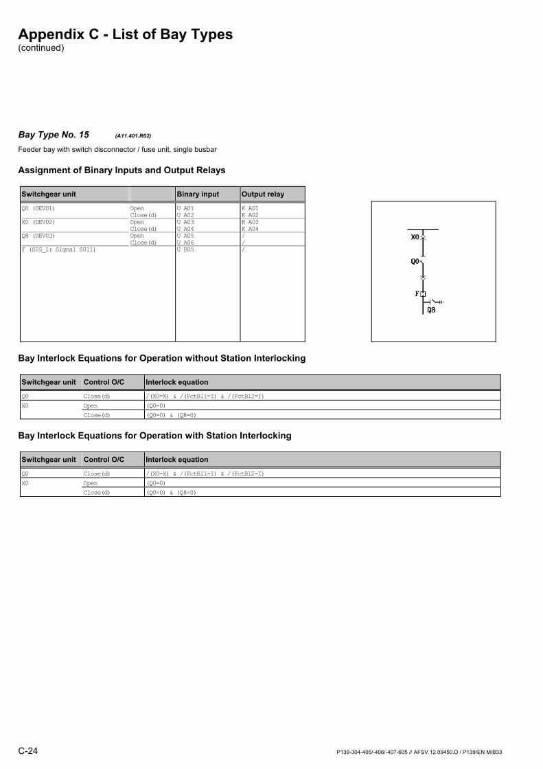
Bay Type No. 15 (A11.401.R02) Feeder bay with switch disconnector / fuse unit, single busbar
Assignment of Binary Inputs and Output Relays
Switchgear unit Binary input Output relay
Q0 (DEV01) X0 (DEV02) Q8 (DEV03) F (SIG_1: Signal S011)
Open Close(d) Open Close(d) Open Close(d)
U A01 U A02 U A03 U A04 U A05 U A06 U B05
K A01 K A02K A03 K A04/ //
Bay Interlock Equations for Operation without Station Interlocking
Switchgear unit Control O/C Interlock equation
Q0 Close(d) /(X0=X) & /(FctBl1=I) & /(FctBl2=I) X0 Open (Q0=0) Close(d) (Q0=0) & (Q8=0)
Bay Interlock Equations for Operation with Station Interlocking
Switchgear unit Control O/C Interlock equation
Q0 Close(d) /(X0=X) & /(FctBl1=I) & /(FctBl2=I) X0 Open (Q0=0) Close(d) (Q0=0) & (Q8=0)
Appendix C - List of Bay Types (continued)
P139-304-405/-406/-407-605 // AFSV.12.09450.D / P139/EN M/B33 C-25
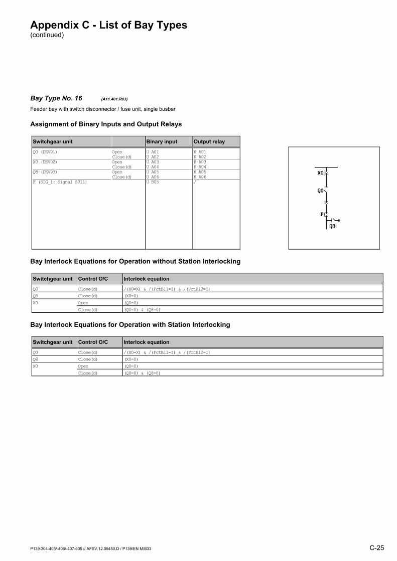
Bay Type No. 16 (A11.401.R03) Feeder bay with switch disconnector / fuse unit, single busbar
Assignment of Binary Inputs and Output Relays
Switchgear unit Binary input Output relay
Q0 (DEV01) X0 (DEV02) Q8 (DEV03) F (SIG_1: Signal S011)
Open Close(d) Open Close(d) Open Close(d)
U A01 U A02 U A03 U A04 U A05 U A06 U B05
K A01 K A02K A03 K A04K A05 K A06/
Bay Interlock Equations for Operation without Station Interlocking
Switchgear unit Control O/C Interlock equation
Q0 Close(d) /(X0=X) & /(FctBl1=I) & /(FctBl2=I) Q8 Close(d) (X0=0) X0 Open (Q0=0) Close(d) (Q0=0) & (Q8=0)
Bay Interlock Equations for Operation with Station Interlocking
Switchgear unit Control O/C Interlock equation
Q0 Close(d) /(X0=X) & /(FctBl1=I) & /(FctBl2=I) Q8 Close(d) (X0=0) X0 Open (Q0=0) Close(d) (Q0=0) & (Q8=0)
Appendix C - List of Bay Types (continued)
C-26 P139-304-405/-406/-407-605 // AFSV.12.09450.D / P139/EN M/B33
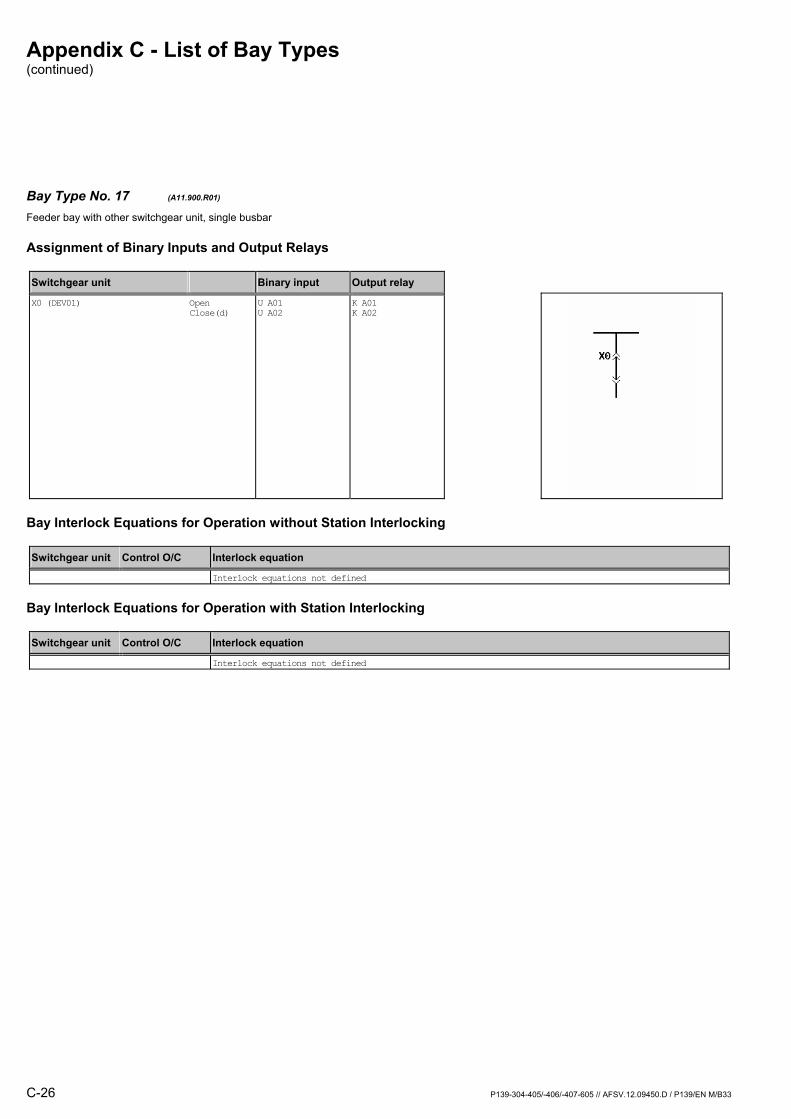
Bay Type No. 17 (A11.900.R01) Feeder bay with other switchgear unit, single busbar
Assignment of Binary Inputs and Output Relays
Switchgear unit Binary input Output relay
X0 (DEV01)
Open Close(d)
U A01 U A02
K A01 K A02
Bay Interlock Equations for Operation without Station Interlocking
Switchgear unit Control O/C Interlock equation
Interlock equations not defined
Bay Interlock Equations for Operation with Station Interlocking
Switchgear unit Control O/C Interlock equation
Interlock equations not defined

Appendix C - List of Bay Types (continued)
P139-304-405/-406/-407-605 // AFSV.12.09450.D / P139/EN M/B33 C-27
Bay Type No. 504 (A11.901.R00) Feeder bay with other switchgear unit, single busbar
Assignment of Binary Inputs and Output Relays
Switchgear unit Binary input Output relay
X0 (DEV02) Q8 (DEV03)
Open Close(d) Open Close(d)
U A03 U A04 U A05 U A06
/ // /
Bay Interlock Equations for Operation without Station Interlocking
Switchgear unit Control O/C Interlock equation
Interlock equations not defined
Bay Interlock Equations for Operation with Station Interlocking
Switchgear unit Control O/C Interlock equation
Interlock equations not defined

Appendix C - List of Bay Types (continued)
C-28 P139-304-405/-406/-407-605 // AFSV.12.09450.D / P139/EN M/B33
Bay Type No. 541 (A13.104.R01) Feeder bay with circuit breaker, single busbar
Assignment of Binary Inputs and Output Relays
Switchgear unit Binary input Output relay
Q0 (DEV01) Q1 (DEV02)
Open Close(d) Open Close(d)
U A01 U A02 U A03 U A04
K A01 K A02/ /
Bay Interlock Equations for Operation without Station Interlocking
Switchgear unit Control O/C Interlock equation
Q0 Close(d) /(FctBl1=I) & /(FctBl2=I)
Bay Interlock Equations for Operation with Station Interlocking
Switchgear unit Control O/C Interlock equation
Q0 Close(d) /(FctBl1=I) & /(FctBl2=I)

Appendix C - List of Bay Types (continued)
P139-304-405/-406/-407-605 // AFSV.12.09450.D / P139/EN M/B33 C-29
Bay Type No. 18 (A13.105.M03) Feeder bay with circuit breaker, single busbar,direct motor control
Assignment of Binary Inputs and Output Relays
Switchgear unit Binary input Output relay
Q0 (DEV01) Q1 (DEV02) Q8 (DEV03) Mot.relay (SIG_1: Signal S012) Shunt wd. (CMD_1: Command C011) Mot.relay (CMD_1: Command C012)
Open Close(d) Open Close(d) Open Close(d)
U A01 U A02 U A03 U A04 U A05 U A06 U B06 / /
K A01 K A02K A03 K A04K A05 K A06/
K B05
K B06
Bay Interlock Equations for Operation without Station Interlocking
Switchgear unit Control O/C Interlock equation
Q0 Close(d) /(Q1=X) & (Q8=0) & /(FctBl1=I) & /(FctBl2=I) Q1 Open (Q0=0) Close(d) (Q0=0) & (Q8=0) Q8 Close(d) (Q0=0) & (Q1=0)
Bay Interlock Equations for Operation with Station Interlocking
Switchgear unit Control O/C Interlock equation
Q0 Close(d) /(Q1=X) & (Q8=0) & /(FctBl1=I) & /(FctBl2=I) Q1 Open (Q0=0) Close(d) (Q0=0) & (Q8=0) Q8 Close(d) (Q0=0) & (Q1=0)

Appendix C - List of Bay Types (continued)
C-30 P139-304-405/-406/-407-605 // AFSV.12.09450.D / P139/EN M/B33
Bay Type No. 19 (A13.105.R01) Feeder bay with circuit breaker, single busbar
Assignment of Binary Inputs and Output Relays
Switchgear unit Binary input Output relay
Q0 (DEV01) Q1 (DEV02) Q8 (DEV03)
Open Close(d) Open Close(d) Open Close(d)
U A01 U A02 U A03 U A04 U A05 U A06
K A01 K A02/ // /
Bay Interlock Equations for Operation without Station Interlocking
Switchgear unit Control O/C Interlock equation
Q0 Close(d) /(Q1=X) & (Q8=0) & /(FctBl1=I) & /(FctBl2=I)
Bay Interlock Equations for Operation with Station Interlocking
Switchgear unit Control O/C Interlock equation
Q0 Close(d) /(Q1=X) & (Q8=0) & /(FctBl1=I) & /(FctBl2=I)
Appendix C - List of Bay Types (continued)
P139-304-405/-406/-407-605 // AFSV.12.09450.D / P139/EN M/B33 C-31
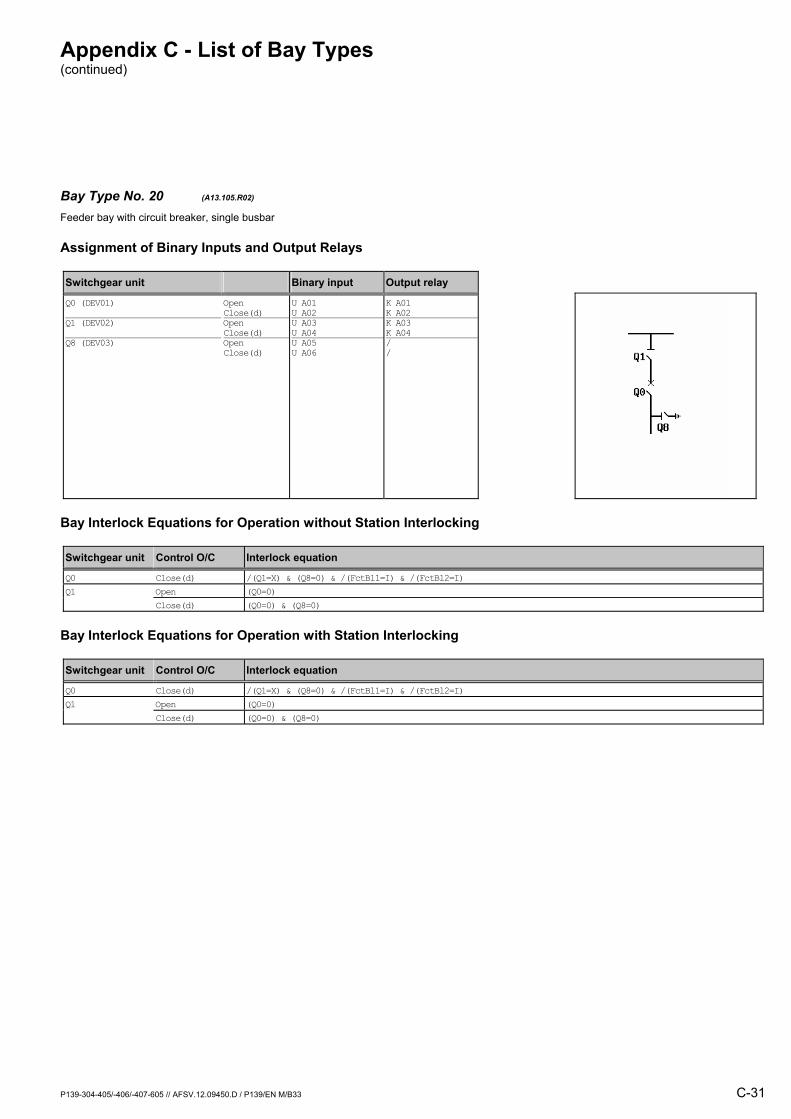
Bay Type No. 20 (A13.105.R02) Feeder bay with circuit breaker, single busbar
Assignment of Binary Inputs and Output Relays
Switchgear unit Binary input Output relay
Q0 (DEV01) Q1 (DEV02) Q8 (DEV03)
Open Close(d) Open Close(d) Open Close(d)
U A01 U A02 U A03 U A04 U A05 U A06
K A01 K A02K A03 K A04/ /
Bay Interlock Equations for Operation without Station Interlocking
Switchgear unit Control O/C Interlock equation
Q0 Close(d) /(Q1=X) & (Q8=0) & /(FctBl1=I) & /(FctBl2=I) Q1 Open (Q0=0) Close(d) (Q0=0) & (Q8=0)
Bay Interlock Equations for Operation with Station Interlocking
Switchgear unit Control O/C Interlock equation
Q0 Close(d) /(Q1=X) & (Q8=0) & /(FctBl1=I) & /(FctBl2=I) Q1 Open (Q0=0) Close(d) (Q0=0) & (Q8=0)

Appendix C - List of Bay Types (continued)
C-32 P139-304-405/-406/-407-605 // AFSV.12.09450.D / P139/EN M/B33
Bay Type No. 21 (A13.105.R03) Feeder bay with circuit breaker, single busbar
Assignment of Binary Inputs and Output Relays
Switchgear unit Binary input Output relay
Q0 (DEV01) Q1 (DEV02) Q8 (DEV03)
Open Close(d) Open Close(d) Open Close(d)
U A01 U A02 U A03 U A04 U A05 U A06
K A01 K A02K A03 K A04K A05 K A06
Bay Interlock Equations for Operation without Station Interlocking
Switchgear unit Control O/C Interlock equation
Q0 Close(d) /(Q1=X) & (Q8=0) & /(FctBl1=I) & /(FctBl2=I) Q1 Open (Q0=0) Close(d) (Q0=0) & (Q8=0) Q8 Close(d) (Q0=0) & (Q1=0)
Bay Interlock Equations for Operation with Station Interlocking
Switchgear unit Control O/C Interlock equation
Q0 Close(d) /(Q1=X) & (Q8=0) & /(FctBl1=I) & /(FctBl2=I) Q1 Open (Q0=0) Close(d) (Q0=0) & (Q8=0) Q8 Close(d) (Q0=0) & (Q1=0)

Appendix C - List of Bay Types (continued)
P139-304-405/-406/-407-605 // AFSV.12.09450.D / P139/EN M/B33 C-33
Bay Type No. 557 (A13.106.R03) Feeder bay with circuit breaker, single busbar
Assignment of Binary Inputs and Output Relays
Switchgear unit Binary input Output relay
Q0 (DEV01) Q1 (DEV02) Q9 (DEV03)
Open Close(d) Open Close(d) Open Close(d)
U A01 U A02 U A03 U A04 U A05 U A06
K A01 K A02K A03 K A04K A05 K A06
Bay Interlock Equations for Operation without Station Interlocking
Switchgear unit Control O/C Interlock equation
Q0 Close(d) /(Q1=X) & /(Q9=X) & /(FctBl1=I) & /(FctBl2=I) Q1 Open (Q0=0) Close(d) (Q0=0) Q9 Open (Q0=0) Close(d) (Q0=0)
Bay Interlock Equations for Operation with Station Interlocking
Switchgear unit Control O/C Interlock equation
Q0 Close(d) /(Q1=X) & /(Q9=X) & /(FctBl1=I) & /(FctBl2=I) Q1 Open (Q0=0) Close(d) (Q0=0) Q9 Open (Q0=0) Close(d) (Q0=0)
Appendix C - List of Bay Types (continued)
C-34 P139-304-405/-406/-407-605 // AFSV.12.09450.D / P139/EN M/B33
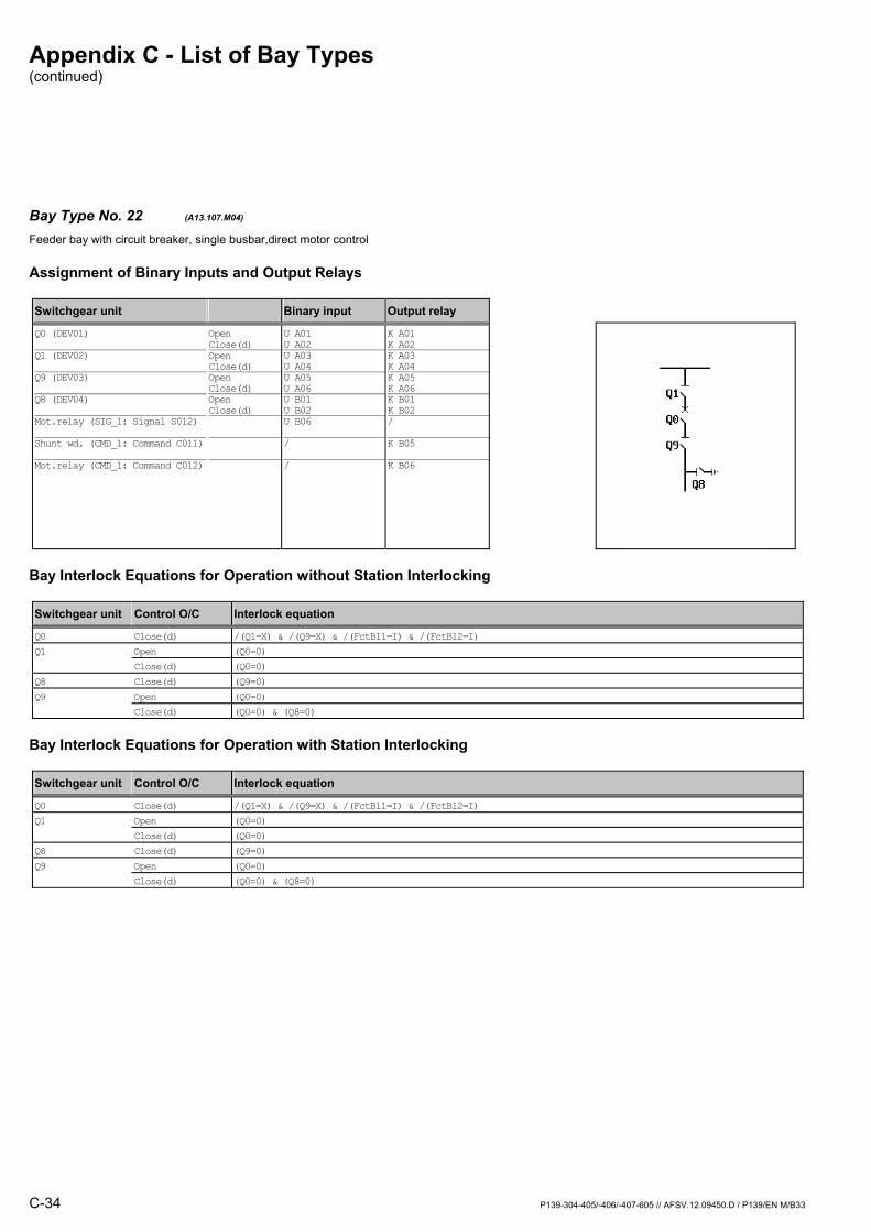
Bay Type No. 22 (A13.107.M04) Feeder bay with circuit breaker, single busbar,direct motor control
Assignment of Binary Inputs and Output Relays
Switchgear unit Binary input Output relay
Q0 (DEV01) Q1 (DEV02) Q9 (DEV03) Q8 (DEV04) Mot.relay (SIG_1: Signal S012) Shunt wd. (CMD_1: Command C011) Mot.relay (CMD_1: Command C012)
Open Close(d) Open Close(d) Open Close(d) Open Close(d)
U A01 U A02 U A03 U A04 U A05 U A06 U B01 U B02 U B06 / /
K A01 K A02K A03 K A04K A05 K A06K B01 K B02/
K B05
K B06
Bay Interlock Equations for Operation without Station Interlocking
Switchgear unit Control O/C Interlock equation
Q0 Close(d) /(Q1=X) & /(Q9=X) & /(FctBl1=I) & /(FctBl2=I) Q1 Open (Q0=0) Close(d) (Q0=0) Q8 Close(d) (Q9=0) Q9 Open (Q0=0) Close(d) (Q0=0) & (Q8=0)
Bay Interlock Equations for Operation with Station Interlocking
Switchgear unit Control O/C Interlock equation
Q0 Close(d) /(Q1=X) & /(Q9=X) & /(FctBl1=I) & /(FctBl2=I) Q1 Open (Q0=0) Close(d) (Q0=0) Q8 Close(d) (Q9=0) Q9 Open (Q0=0) Close(d) (Q0=0) & (Q8=0)

Appendix C - List of Bay Types (continued)
P139-304-405/-406/-407-605 // AFSV.12.09450.D / P139/EN M/B33 C-35
Bay Type No. 23 (A13.107.R01) Feeder bay with circuit breaker, single busbar
Assignment of Binary Inputs and Output Relays
Switchgear unit Binary input Output relay
Q0 (DEV01) Q1 (DEV02) Q9 (DEV03) Q8 (DEV04)
Open Close(d) Open Close(d) Open Close(d) Open Close(d)
U A01 U A02 U A03 U A04 U A05 U A06 U B01 U B02
K A01 K A02/ // // /
Bay Interlock Equations for Operation without Station Interlocking
Switchgear unit Control O/C Interlock equation
Q0 Close(d) /(Q1=X) & /(Q9=X) & /(FctBl1=I) & /(FctBl2=I)
Bay Interlock Equations for Operation with Station Interlocking
Switchgear unit Control O/C Interlock equation
Q0 Close(d) /(Q1=X) & /(Q9=X) & /(FctBl1=I) & /(FctBl2=I)
Appendix C - List of Bay Types (continued)
C-36 P139-304-405/-406/-407-605 // AFSV.12.09450.D / P139/EN M/B33
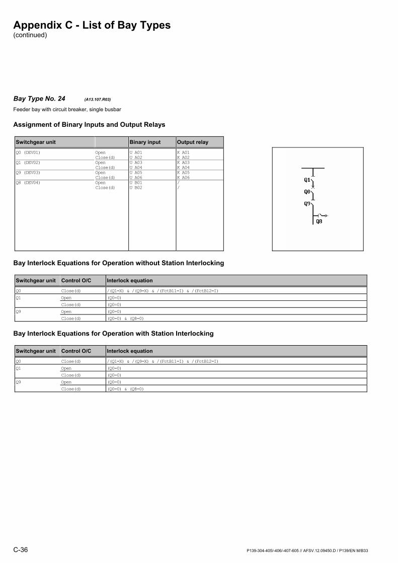
Bay Type No. 24 (A13.107.R03) Feeder bay with circuit breaker, single busbar
Assignment of Binary Inputs and Output Relays
Switchgear unit Binary input Output relay
Q0 (DEV01) Q1 (DEV02) Q9 (DEV03) Q8 (DEV04)
Open Close(d) Open Close(d) Open Close(d) Open Close(d)
U A01 U A02 U A03 U A04 U A05 U A06 U B01 U B02
K A01 K A02K A03 K A04K A05 K A06/ /
Bay Interlock Equations for Operation without Station Interlocking
Switchgear unit Control O/C Interlock equation
Q0 Close(d) /(Q1=X) & /(Q9=X) & /(FctBl1=I) & /(FctBl2=I) Q1 Open (Q0=0) Close(d) (Q0=0) Q9 Open (Q0=0) Close(d) (Q0=0) & (Q8=0)
Bay Interlock Equations for Operation with Station Interlocking
Switchgear unit Control O/C Interlock equation
Q0 Close(d) /(Q1=X) & /(Q9=X) & /(FctBl1=I) & /(FctBl2=I) Q1 Open (Q0=0) Close(d) (Q0=0) Q9 Open (Q0=0) Close(d) (Q0=0) & (Q8=0)
Appendix C - List of Bay Types (continued)
P139-304-405/-406/-407-605 // AFSV.12.09450.D / P139/EN M/B33 C-37
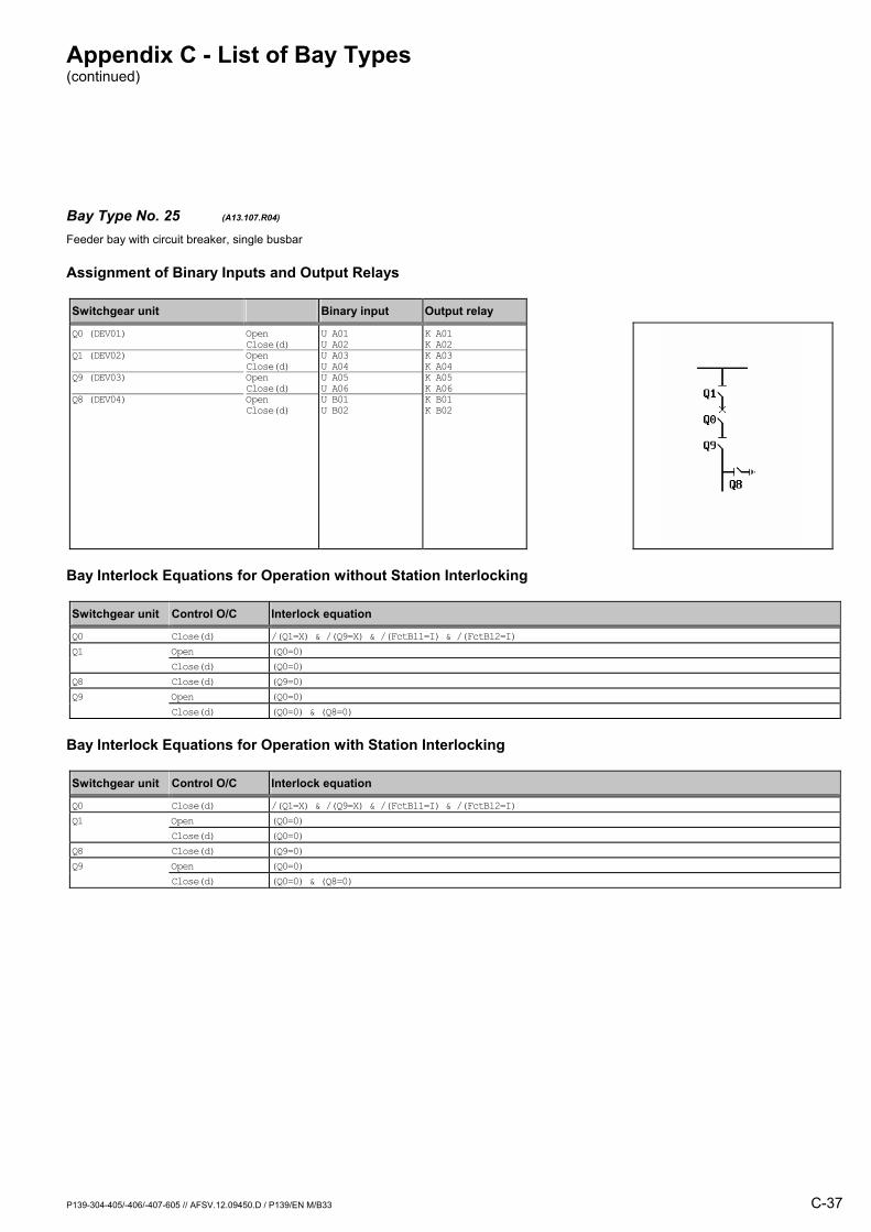
Bay Type No. 25 (A13.107.R04) Feeder bay with circuit breaker, single busbar
Assignment of Binary Inputs and Output Relays
Switchgear unit Binary input Output relay
Q0 (DEV01) Q1 (DEV02) Q9 (DEV03) Q8 (DEV04)
Open Close(d) Open Close(d) Open Close(d) Open Close(d)
U A01 U A02 U A03 U A04 U A05 U A06 U B01 U B02
K A01 K A02K A03 K A04K A05 K A06K B01 K B02
Bay Interlock Equations for Operation without Station Interlocking
Switchgear unit Control O/C Interlock equation
Q0 Close(d) /(Q1=X) & /(Q9=X) & /(FctBl1=I) & /(FctBl2=I) Q1 Open (Q0=0) Close(d) (Q0=0) Q8 Close(d) (Q9=0) Q9 Open (Q0=0) Close(d) (Q0=0) & (Q8=0)
Bay Interlock Equations for Operation with Station Interlocking
Switchgear unit Control O/C Interlock equation
Q0 Close(d) /(Q1=X) & /(Q9=X) & /(FctBl1=I) & /(FctBl2=I) Q1 Open (Q0=0) Close(d) (Q0=0) Q8 Close(d) (Q9=0) Q9 Open (Q0=0) Close(d) (Q0=0) & (Q8=0)

Appendix C - List of Bay Types (continued)
C-38 P139-304-405/-406/-407-605 // AFSV.12.09450.D / P139/EN M/B33
Bay Type No. 508 (A13.111.R03) Feeder bay with circuit breaker, single busbar
Assignment of Binary Inputs and Output Relays
Switchgear unit Binary input Output relay
Q0 (DEV01) Q1 (DEV02) Q8 (DEV03) Q15 (DEV04)
Open Close(d) Open Close(d) Open Close(d) Open Close(d)
U A01 U A02 U A03 U A04 U A05 U A06 U B01 U B02
K A01 K A02K A03 K A04K A05 K A06/ /
Bay Interlock Equations for Operation without Station Interlocking
Switchgear unit Control O/C Interlock equation
Q0 Close(d) /(Q1=X) & (Q8=0) & (Q15=0) & /(FctBl1=I) & /(FctBl2=I) Q1 Open (Q0=0) Close(d) (Q0=0) & (Q8=0) & (Q15=0) Q8 Close(d) (Q0=0) & (Q1=0)
Bay Interlock Equations for Operation with Station Interlocking
Switchgear unit Control O/C Interlock equation
Q0 Close(d) /(Q1=X) & (Q8=0) & (Q15=0) & /(FctBl1=I) & /(FctBl2=I) Q1 Open (Q0=0) Close(d) (Q0=0) & (Q8=0) & (Q15=0) Q8 Close(d) (Q0=0) & (Q1=0)

Appendix C - List of Bay Types (continued)
P139-304-405/-406/-407-605 // AFSV.12.09450.D / P139/EN M/B33 C-39
Bay Type No. 26 (A13.200.R01) Feeder bay with switch disconnector, single busbar
Assignment of Binary Inputs and Output Relays
Switchgear unit Binary input Output relay
Q0 (DEV01)
Open Close(d)
U A01 U A02
K A01 K A02
Bay Interlock Equations for Operation without Station Interlocking
Switchgear unit Control O/C Interlock equation
Interlock equations not defined
Bay Interlock Equations for Operation with Station Interlocking
Switchgear unit Control O/C Interlock equation
Interlock equations not defined
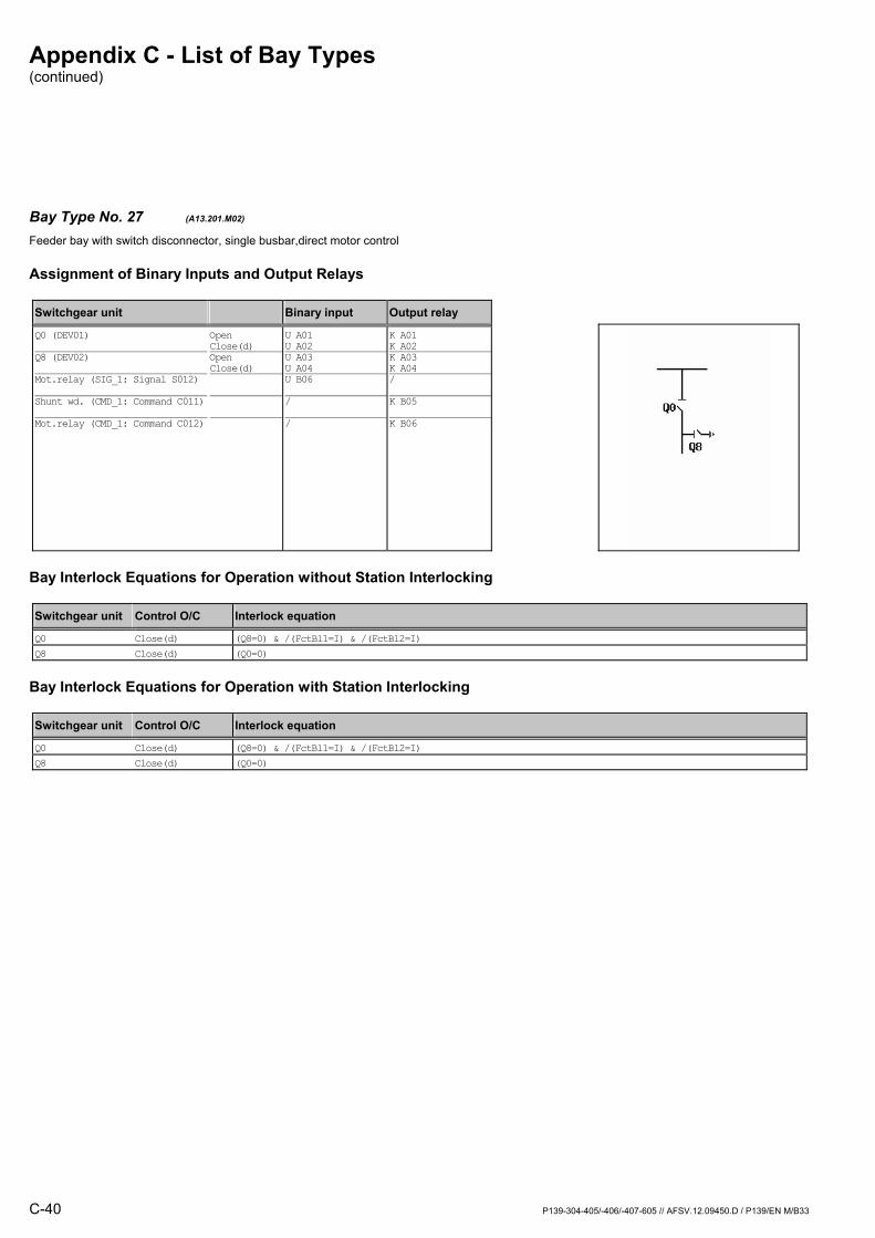
Appendix C - List of Bay Types (continued)
C-40 P139-304-405/-406/-407-605 // AFSV.12.09450.D / P139/EN M/B33
Bay Type No. 27 (A13.201.M02) Feeder bay with switch disconnector, single busbar,direct motor control
Assignment of Binary Inputs and Output Relays
Switchgear unit Binary input Output relay
Q0 (DEV01) Q8 (DEV02) Mot.relay (SIG_1: Signal S012) Shunt wd. (CMD_1: Command C011) Mot.relay (CMD_1: Command C012)
Open Close(d) Open Close(d)
U A01 U A02 U A03 U A04 U B06 / /
K A01 K A02K A03 K A04/
K B05
K B06
Bay Interlock Equations for Operation without Station Interlocking
Switchgear unit Control O/C Interlock equation
Q0 Close(d) (Q8=0) & /(FctBl1=I) & /(FctBl2=I) Q8 Close(d) (Q0=0)
Bay Interlock Equations for Operation with Station Interlocking
Switchgear unit Control O/C Interlock equation
Q0 Close(d) (Q8=0) & /(FctBl1=I) & /(FctBl2=I) Q8 Close(d) (Q0=0)
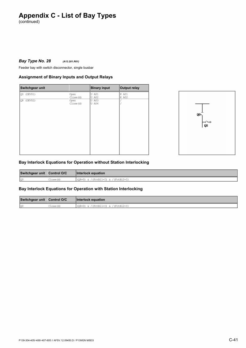
Appendix C - List of Bay Types (continued)
P139-304-405/-406/-407-605 // AFSV.12.09450.D / P139/EN M/B33 C-41
Bay Type No. 28 (A13.201.R01) Feeder bay with switch disconnector, single busbar
Assignment of Binary Inputs and Output Relays
Switchgear unit Binary input Output relay
Q0 (DEV01) Q8 (DEV02)
Open Close(d) Open Close(d)
U A01 U A02 U A03 U A04
K A01 K A02/ /
Bay Interlock Equations for Operation without Station Interlocking
Switchgear unit Control O/C Interlock equation
Q0 Close(d) (Q8=0) & /(FctBl1=I) & /(FctBl2=I)
Bay Interlock Equations for Operation with Station Interlocking
Switchgear unit Control O/C Interlock equation
Q0 Close(d) (Q8=0) & /(FctBl1=I) & /(FctBl2=I)

Appendix C - List of Bay Types (continued)
C-42 P139-304-405/-406/-407-605 // AFSV.12.09450.D / P139/EN M/B33
Bay Type No. 29 (A13.201.R02) Feeder bay with switch disconnector, single busbar
Assignment of Binary Inputs and Output Relays
Switchgear unit Binary input Output relay
Q0 (DEV01) Q8 (DEV02)
Open Close(d) Open Close(d)
U A01 U A02 U A03 U A04
K A01 K A02K A03 K A04
Bay Interlock Equations for Operation without Station Interlocking
Switchgear unit Control O/C Interlock equation
Q0 Close(d) (Q8=0) & /(FctBl1=I) & /(FctBl2=I) Q8 Close(d) (Q0=0)
Bay Interlock Equations for Operation with Station Interlocking
Switchgear unit Control O/C Interlock equation
Q0 Close(d) (Q8=0) & /(FctBl1=I) & /(FctBl2=I) Q8 Close(d) (Q0=0)

Appendix C - List of Bay Types (continued)
P139-304-405/-406/-407-605 // AFSV.12.09450.D / P139/EN M/B33 C-43
Bay Type No. 30 (A13.205.M03) Feeder bay with switch disconnector, single busbar,direct motor control
Assignment of Binary Inputs and Output Relays
Switchgear unit Binary input Output relay
Q0 (DEV01) Q1 (DEV02) Q8 (DEV03) Mot.relay (SIG_1: Signal S012) Shunt wd. (CMD_1: Command C011) Mot.relay (CMD_1: Command C012)
Open Close(d) Open Close(d) Open Close(d)
U A01 U A02 U A03 U A04 U A05 U A06 U B06 / /
K A01 K A02K A03 K A04K A05 K A06/
K B05
K B06
Bay Interlock Equations for Operation without Station Interlocking
Switchgear unit Control O/C Interlock equation
Q0 Close(d) /(Q1=X) & (Q8=0) & /(FctBl1=I) & /(FctBl2=I) Q1 Open (Q0=0) Close(d) (Q0=0) & (Q8=0) Q8 Close(d) (Q0=0) & (Q1=0)
Bay Interlock Equations for Operation with Station Interlocking
Switchgear unit Control O/C Interlock equation
Q0 Close(d) /(Q1=X) & (Q8=0) & /(FctBl1=I) & /(FctBl2=I) Q1 Open (Q0=0) Close(d) (Q0=0) & (Q8=0) Q8 Close(d) (Q0=0) & (Q1=0)
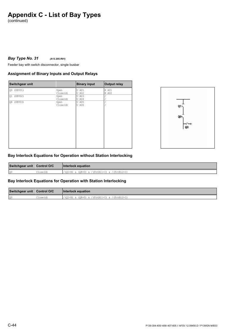
Appendix C - List of Bay Types (continued)
C-44 P139-304-405/-406/-407-605 // AFSV.12.09450.D / P139/EN M/B33
Bay Type No. 31 (A13.205.R01) Feeder bay with switch disconnector, single busbar
Assignment of Binary Inputs and Output Relays
Switchgear unit Binary input Output relay
Q0 (DEV01) Q1 (DEV02) Q8 (DEV03)
Open Close(d) Open Close(d) Open Close(d)
U A01 U A02 U A03 U A04 U A05 U A06
K A01 K A02/ // /
Bay Interlock Equations for Operation without Station Interlocking
Switchgear unit Control O/C Interlock equation
Q0 Close(d) /(Q1=X) & (Q8=0) & /(FctBl1=I) & /(FctBl2=I)
Bay Interlock Equations for Operation with Station Interlocking
Switchgear unit Control O/C Interlock equation
Q0 Close(d) /(Q1=X) & (Q8=0) & /(FctBl1=I) & /(FctBl2=I)
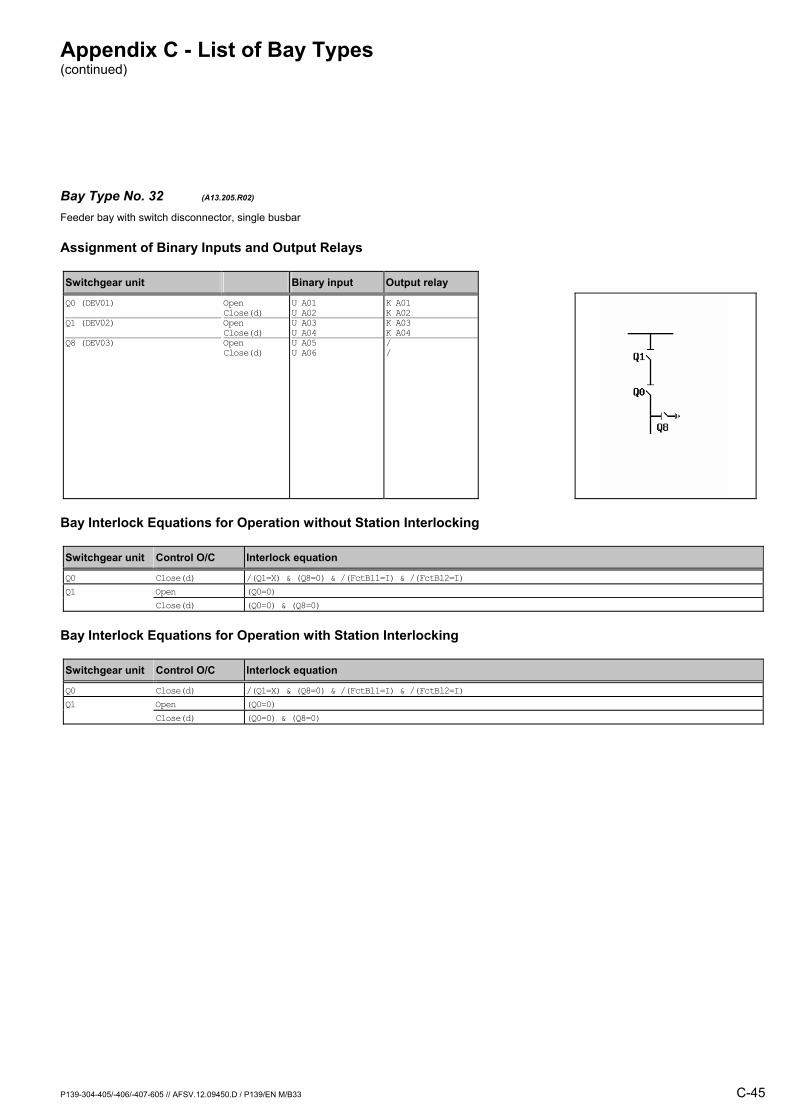
Appendix C - List of Bay Types (continued)
P139-304-405/-406/-407-605 // AFSV.12.09450.D / P139/EN M/B33 C-45
Bay Type No. 32 (A13.205.R02) Feeder bay with switch disconnector, single busbar
Assignment of Binary Inputs and Output Relays
Switchgear unit Binary input Output relay
Q0 (DEV01) Q1 (DEV02) Q8 (DEV03)
Open Close(d) Open Close(d) Open Close(d)
U A01 U A02 U A03 U A04 U A05 U A06
K A01 K A02K A03 K A04/ /
Bay Interlock Equations for Operation without Station Interlocking
Switchgear unit Control O/C Interlock equation
Q0 Close(d) /(Q1=X) & (Q8=0) & /(FctBl1=I) & /(FctBl2=I) Q1 Open (Q0=0) Close(d) (Q0=0) & (Q8=0)
Bay Interlock Equations for Operation with Station Interlocking
Switchgear unit Control O/C Interlock equation
Q0 Close(d) /(Q1=X) & (Q8=0) & /(FctBl1=I) & /(FctBl2=I) Q1 Open (Q0=0) Close(d) (Q0=0) & (Q8=0)

Appendix C - List of Bay Types (continued)
C-46 P139-304-405/-406/-407-605 // AFSV.12.09450.D / P139/EN M/B33
Bay Type No. 33 (A13.205.R03) Feeder bay with switch disconnector, single busbar
Assignment of Binary Inputs and Output Relays
Switchgear unit Binary input Output relay
Q0 (DEV01) Q1 (DEV02) Q8 (DEV03)
Open Close(d) Open Close(d) Open Close(d)
U A01 U A02 U A03 U A04 U A05 U A06
K A01 K A02K A03 K A04K A05 K A06
Bay Interlock Equations for Operation without Station Interlocking
Switchgear unit Control O/C Interlock equation
Q0 Close(d) /(Q1=X) & (Q8=0) & /(FctBl1=I) & /(FctBl2=I) Q1 Open (Q0=0) Close(d) (Q0=0) & (Q8=0) Q8 Close(d) (Q0=0) & (Q1=0)
Bay Interlock Equations for Operation with Station Interlocking
Switchgear unit Control O/C Interlock equation
Q0 Close(d) /(Q1=X) & (Q8=0) & /(FctBl1=I) & /(FctBl2=I) Q1 Open (Q0=0) Close(d) (Q0=0) & (Q8=0) Q8 Close(d) (Q0=0) & (Q1=0)

Appendix C - List of Bay Types (continued)
P139-304-405/-406/-407-605 // AFSV.12.09450.D / P139/EN M/B33 C-47
Bay Type No. 34 (A13.400.R01) Feeder bay with switch disconnector / fuse unit, single busbar
Assignment of Binary Inputs and Output Relays
Switchgear unit Binary input Output relay
Q0 (DEV01) F (SIG_1: Signal S011)
Open Close(d)
U A01 U A02 U B05
K A01 K A02/
Bay Interlock Equations for Operation without Station Interlocking
Switchgear unit Control O/C Interlock equation
Interlock equations not defined
Bay Interlock Equations for Operation with Station Interlocking
Switchgear unit Control O/C Interlock equation
Interlock equations not defined
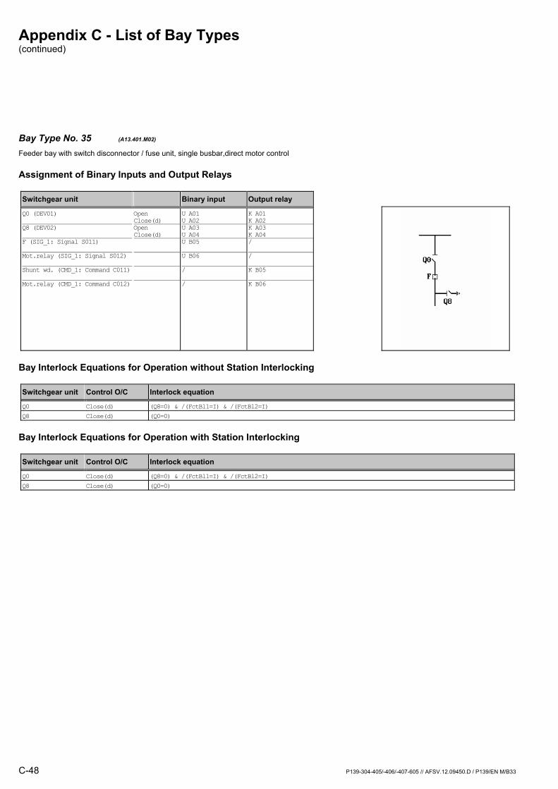
Appendix C - List of Bay Types (continued)
C-48 P139-304-405/-406/-407-605 // AFSV.12.09450.D / P139/EN M/B33
Bay Type No. 35 (A13.401.M02) Feeder bay with switch disconnector / fuse unit, single busbar,direct motor control
Assignment of Binary Inputs and Output Relays
Switchgear unit Binary input Output relay
Q0 (DEV01) Q8 (DEV02) F (SIG_1: Signal S011) Mot.relay (SIG_1: Signal S012) Shunt wd. (CMD_1: Command C011) Mot.relay (CMD_1: Command C012)
Open Close(d) Open Close(d)
U A01 U A02 U A03 U A04 U B05 U B06 / /
K A01 K A02K A03 K A04/
/
K B05
K B06
Bay Interlock Equations for Operation without Station Interlocking
Switchgear unit Control O/C Interlock equation
Q0 Close(d) (Q8=0) & /(FctBl1=I) & /(FctBl2=I) Q8 Close(d) (Q0=0)
Bay Interlock Equations for Operation with Station Interlocking
Switchgear unit Control O/C Interlock equation
Q0 Close(d) (Q8=0) & /(FctBl1=I) & /(FctBl2=I) Q8 Close(d) (Q0=0)

Appendix C - List of Bay Types (continued)
P139-304-405/-406/-407-605 // AFSV.12.09450.D / P139/EN M/B33 C-49
Bay Type No. 36 (A13.401.R01) Feeder bay with switch disconnector / fuse unit, single busbar
Assignment of Binary Inputs and Output Relays
Switchgear unit Binary input Output relay
Q0 (DEV01) Q8 (DEV02) F (SIG_1: Signal S011)
Open Close(d) Open Close(d)
U A01 U A02 U A03 U A04 U B05
K A01 K A02/ //
Bay Interlock Equations for Operation without Station Interlocking
Switchgear unit Control O/C Interlock equation
Q0 Close(d) (Q8=0) & /(FctBl1=I) & /(FctBl2=I)
Bay Interlock Equations for Operation with Station Interlocking
Switchgear unit Control O/C Interlock equation
Q0 Close(d) (Q8=0) & /(FctBl1=I) & /(FctBl2=I)
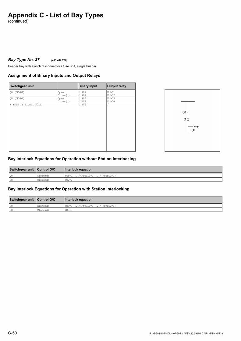
Appendix C - List of Bay Types (continued)
C-50 P139-304-405/-406/-407-605 // AFSV.12.09450.D / P139/EN M/B33
Bay Type No. 37 (A13.401.R02) Feeder bay with switch disconnector / fuse unit, single busbar
Assignment of Binary Inputs and Output Relays
Switchgear unit Binary input Output relay
Q0 (DEV01) Q8 (DEV02) F (SIG_1: Signal S011)
Open Close(d) Open Close(d)
U A01 U A02 U A03 U A04 U B05
K A01 K A02K A03 K A04/
Bay Interlock Equations for Operation without Station Interlocking
Switchgear unit Control O/C Interlock equation
Q0 Close(d) (Q8=0) & /(FctBl1=I) & /(FctBl2=I) Q8 Close(d) (Q0=0)
Bay Interlock Equations for Operation with Station Interlocking
Switchgear unit Control O/C Interlock equation
Q0 Close(d) (Q8=0) & /(FctBl1=I) & /(FctBl2=I) Q8 Close(d) (Q0=0)
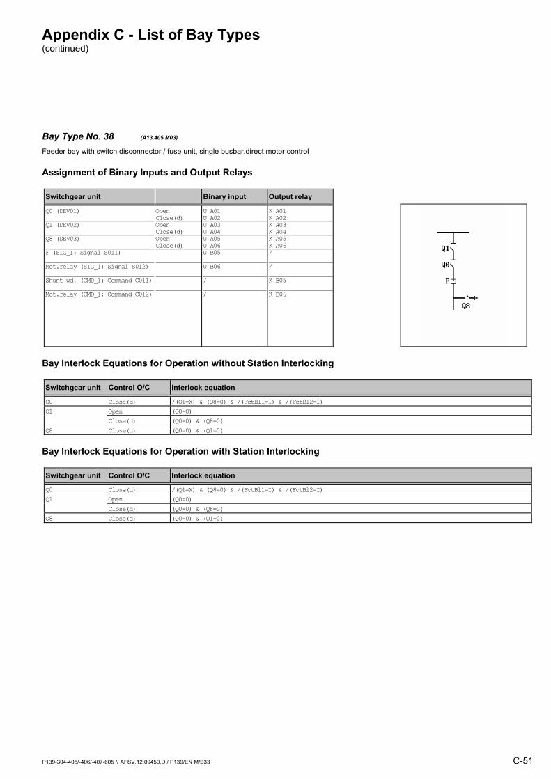
Appendix C - List of Bay Types (continued)
P139-304-405/-406/-407-605 // AFSV.12.09450.D / P139/EN M/B33 C-51
Bay Type No. 38 (A13.405.M03) Feeder bay with switch disconnector / fuse unit, single busbar,direct motor control
Assignment of Binary Inputs and Output Relays
Switchgear unit Binary input Output relay
Q0 (DEV01) Q1 (DEV02) Q8 (DEV03) F (SIG_1: Signal S011) Mot.relay (SIG_1: Signal S012) Shunt wd. (CMD_1: Command C011) Mot.relay (CMD_1: Command C012)
Open Close(d) Open Close(d) Open Close(d)
U A01 U A02 U A03 U A04 U A05 U A06 U B05 U B06 / /
K A01 K A02K A03 K A04K A05 K A06/
/
K B05
K B06
Bay Interlock Equations for Operation without Station Interlocking
Switchgear unit Control O/C Interlock equation
Q0 Close(d) /(Q1=X) & (Q8=0) & /(FctBl1=I) & /(FctBl2=I) Q1 Open (Q0=0) Close(d) (Q0=0) & (Q8=0) Q8 Close(d) (Q0=0) & (Q1=0)
Bay Interlock Equations for Operation with Station Interlocking
Switchgear unit Control O/C Interlock equation
Q0 Close(d) /(Q1=X) & (Q8=0) & /(FctBl1=I) & /(FctBl2=I) Q1 Open (Q0=0) Close(d) (Q0=0) & (Q8=0) Q8 Close(d) (Q0=0) & (Q1=0)
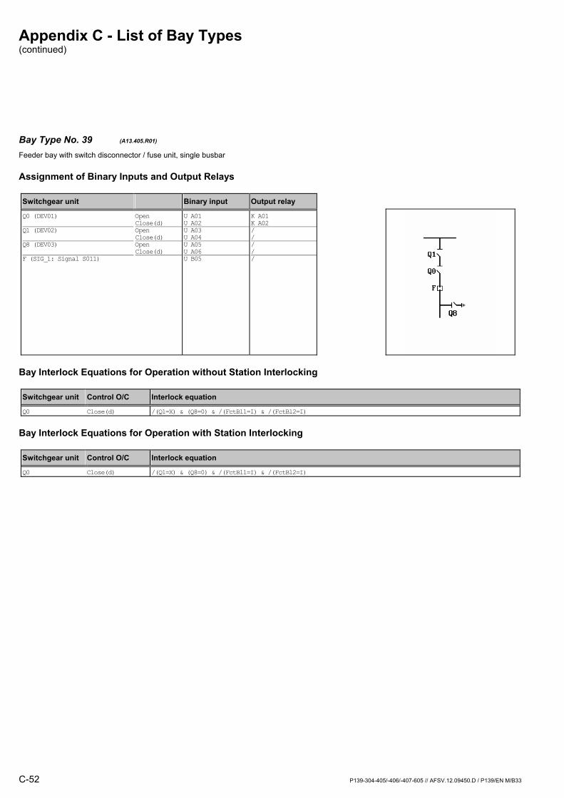
Appendix C - List of Bay Types (continued)
C-52 P139-304-405/-406/-407-605 // AFSV.12.09450.D / P139/EN M/B33
Bay Type No. 39 (A13.405.R01) Feeder bay with switch disconnector / fuse unit, single busbar
Assignment of Binary Inputs and Output Relays
Switchgear unit Binary input Output relay
Q0 (DEV01) Q1 (DEV02) Q8 (DEV03) F (SIG_1: Signal S011)
Open Close(d) Open Close(d) Open Close(d)
U A01 U A02 U A03 U A04 U A05 U A06 U B05
K A01 K A02/ // //
Bay Interlock Equations for Operation without Station Interlocking
Switchgear unit Control O/C Interlock equation
Q0 Close(d) /(Q1=X) & (Q8=0) & /(FctBl1=I) & /(FctBl2=I)
Bay Interlock Equations for Operation with Station Interlocking
Switchgear unit Control O/C Interlock equation
Q0 Close(d) /(Q1=X) & (Q8=0) & /(FctBl1=I) & /(FctBl2=I)

Appendix C - List of Bay Types (continued)
P139-304-405/-406/-407-605 // AFSV.12.09450.D / P139/EN M/B33 C-53
Bay Type No. 40 (A13.405.R02) Feeder bay with switch disconnector / fuse unit, single busbar
Assignment of Binary Inputs and Output Relays
Switchgear unit Binary input Output relay
Q0 (DEV01) Q1 (DEV02) Q8 (DEV03) F (SIG_1: Signal S011)
Open Close(d) Open Close(d) Open Close(d)
U A01 U A02 U A03 U A04 U A05 U A06 U B05
K A01 K A02K A03 K A04/ //
Bay Interlock Equations for Operation without Station Interlocking
Switchgear unit Control O/C Interlock equation
Q0 Close(d) /(Q1=X) & (Q8=0) & /(FctBl1=I) & /(FctBl2=I) Q1 Open (Q0=0) Close(d) (Q0=0) & (Q8=0)
Bay Interlock Equations for Operation with Station Interlocking
Switchgear unit Control O/C Interlock equation
Q0 Close(d) /(Q1=X) & (Q8=0) & /(FctBl1=I) & /(FctBl2=I) Q1 Open (Q0=0) Close(d) (Q0=0) & (Q8=0)
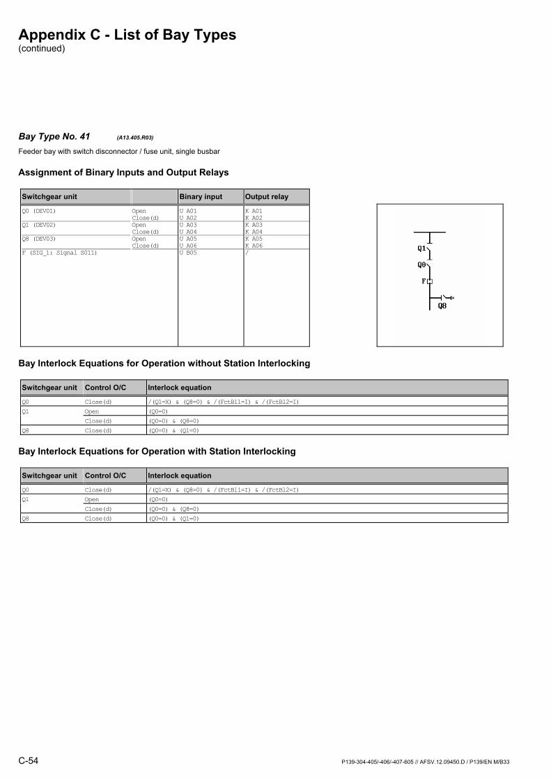
Appendix C - List of Bay Types (continued)
C-54 P139-304-405/-406/-407-605 // AFSV.12.09450.D / P139/EN M/B33
Bay Type No. 41 (A13.405.R03) Feeder bay with switch disconnector / fuse unit, single busbar
Assignment of Binary Inputs and Output Relays
Switchgear unit Binary input Output relay
Q0 (DEV01) Q1 (DEV02) Q8 (DEV03) F (SIG_1: Signal S011)
Open Close(d) Open Close(d) Open Close(d)
U A01 U A02 U A03 U A04 U A05 U A06 U B05
K A01 K A02K A03 K A04K A05 K A06/
Bay Interlock Equations for Operation without Station Interlocking
Switchgear unit Control O/C Interlock equation
Q0 Close(d) /(Q1=X) & (Q8=0) & /(FctBl1=I) & /(FctBl2=I) Q1 Open (Q0=0) Close(d) (Q0=0) & (Q8=0) Q8 Close(d) (Q0=0) & (Q1=0)
Bay Interlock Equations for Operation with Station Interlocking
Switchgear unit Control O/C Interlock equation
Q0 Close(d) /(Q1=X) & (Q8=0) & /(FctBl1=I) & /(FctBl2=I) Q1 Open (Q0=0) Close(d) (Q0=0) & (Q8=0) Q8 Close(d) (Q0=0) & (Q1=0)

Appendix C - List of Bay Types (continued)
P139-304-405/-406/-407-605 // AFSV.12.09450.D / P139/EN M/B33 C-55
Bay Type No. 503 (A13.432.R02) Feeder bay with switch disconnector / fuse unit, single busbar
Assignment of Binary Inputs and Output Relays
Switchgear unit Binary input Output relay
Q0 (DEV01) Q8 (DEV02) F (SIG_1: Signal S011)
Open Close(d) Open Close(d)
U A01 U A02 U A03 U A04 U B05
K A01 K A02K A03 K A04/
Bay Interlock Equations for Operation without Station Interlocking
Switchgear unit Control O/C Interlock equation
Q0 Close(d) (Q8=0) & /(FctBl1=I) & /(FctBl2=I) Q8 Close(d) (Q0=0)
Bay Interlock Equations for Operation with Station Interlocking
Switchgear unit Control O/C Interlock equation
Q0 Close(d) (Q8=0) & /(FctBl1=I) & /(FctBl2=I) Q8 Close(d) (Q0=0)

Appendix C - List of Bay Types (continued)
C-56 P139-304-405/-406/-407-605 // AFSV.12.09450.D / P139/EN M/B33
Bay Type No. 507 (A13.433.R02) Feeder bay with switch disconnector / fuse unit, single busbar
Assignment of Binary Inputs and Output Relays
Switchgear unit Binary input Output relay
Q0 (DEV01) Q8 (DEV02) Q15 (DEV03) F (SIG_1: Signal S011)
Open Close(d) Open Close(d) Open Close(d)
U A01 U A02 U A03 U A04 U A05 U A06 U B05
K A01 K A02K A03 K A04/ //
Bay Interlock Equations for Operation without Station Interlocking
Switchgear unit Control O/C Interlock equation
Q0 Close(d) (Q8=0) & (Q15=0) & /(FctBl1=I) & /(FctBl2=I) Q8 Close(d) (Q0=0)
Bay Interlock Equations for Operation with Station Interlocking
Switchgear unit Control O/C Interlock equation
Q0 Close(d) (Q8=0) & (Q15=0) & /(FctBl1=I) & /(FctBl2=I) Q8 Close(d) (Q0=0)
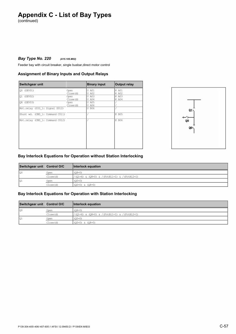
Appendix C - List of Bay Types (continued)
P139-304-405/-406/-407-605 // AFSV.12.09450.D / P139/EN M/B33 C-57
Bay Type No. 220 (A15.105.M02) Feeder bay with circuit breaker, single busbar,direct motor control
Assignment of Binary Inputs and Output Relays
Switchgear unit Binary input Output relay
Q0 (DEV01) Q1 (DEV02) Q8 (DEV03) Mot.relay (SIG_1: Signal S012) Shunt wd. (CMD_1: Command C011) Mot.relay (CMD_1: Command C012)
Open Close(d) Open Close(d) Open Close(d)
U A01 U A02 U A03 U A04 U A05 U A06 U B06 / /
K A01 K A02K A03 K A04/ //
K B05
K B06
Bay Interlock Equations for Operation without Station Interlocking
Switchgear unit Control O/C Interlock equation
Q0 Open (Q8=0) Close(d) /(Q1=X) & (Q8=0) & /(FctBl1=I) & /(FctBl2=I) Q1 Open (Q0=0) Close(d) (Q0=0) & (Q8=0)
Bay Interlock Equations for Operation with Station Interlocking
Switchgear unit Control O/C Interlock equation
Q0 Open (Q8=0) Close(d) /(Q1=X) & (Q8=0) & /(FctBl1=I) & /(FctBl2=I) Q1 Open (Q0=0) Close(d) (Q0=0) & (Q8=0)
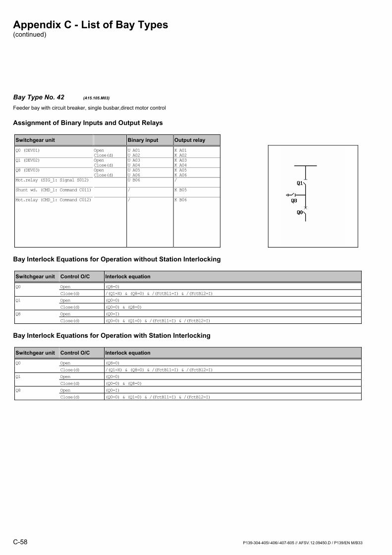
Appendix C - List of Bay Types (continued)
C-58 P139-304-405/-406/-407-605 // AFSV.12.09450.D / P139/EN M/B33
Bay Type No. 42 (A15.105.M03) Feeder bay with circuit breaker, single busbar,direct motor control
Assignment of Binary Inputs and Output Relays
Switchgear unit Binary input Output relay
Q0 (DEV01) Q1 (DEV02) Q8 (DEV03) Mot.relay (SIG_1: Signal S012) Shunt wd. (CMD_1: Command C011) Mot.relay (CMD_1: Command C012)
Open Close(d) Open Close(d) Open Close(d)
U A01 U A02 U A03 U A04 U A05 U A06 U B06 / /
K A01 K A02K A03 K A04K A05 K A06/
K B05
K B06
Bay Interlock Equations for Operation without Station Interlocking
Switchgear unit Control O/C Interlock equation
Q0 Open (Q8=0) Close(d) /(Q1=X) & (Q8=0) & /(FctBl1=I) & /(FctBl2=I) Q1 Open (Q0=0) Close(d) (Q0=0) & (Q8=0) Q8 Open (Q0=I) Close(d) (Q0=0) & (Q1=0) & /(FctBl1=I) & /(FctBl2=I)
Bay Interlock Equations for Operation with Station Interlocking
Switchgear unit Control O/C Interlock equation
Q0 Open (Q8=0) Close(d) /(Q1=X) & (Q8=0) & /(FctBl1=I) & /(FctBl2=I) Q1 Open (Q0=0) Close(d) (Q0=0) & (Q8=0) Q8 Open (Q0=I) Close(d) (Q0=0) & (Q1=0) & /(FctBl1=I) & /(FctBl2=I)

Appendix C - List of Bay Types (continued)
P139-304-405/-406/-407-605 // AFSV.12.09450.D / P139/EN M/B33 C-59
Bay Type No. 43 (A15.105.R01) Feeder bay with circuit breaker, single busbar
Assignment of Binary Inputs and Output Relays
Switchgear unit Binary input Output relay
Q0 (DEV01) Q1 (DEV02) Q8 (DEV03)
Open Close(d) Open Close(d) Open Close(d)
U A01 U A02 U A03 U A04 U A05 U A06
K A01 K A02/ // /
Bay Interlock Equations for Operation without Station Interlocking
Switchgear unit Control O/C Interlock equation
Q0 Open (Q8=0) Close(d) /(Q1=X) & (Q8=0) & /(FctBl1=I) & /(FctBl2=I)
Bay Interlock Equations for Operation with Station Interlocking
Switchgear unit Control O/C Interlock equation
Q0 Open (Q8=0) Close(d) /(Q1=X) & (Q8=0) & /(FctBl1=I) & /(FctBl2=I)
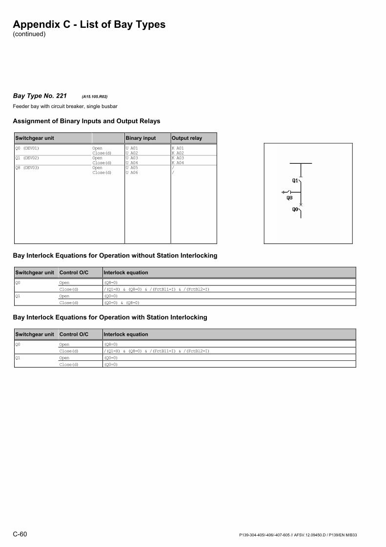
Appendix C - List of Bay Types (continued)
C-60 P139-304-405/-406/-407-605 // AFSV.12.09450.D / P139/EN M/B33
Bay Type No. 221 (A15.105.R02) Feeder bay with circuit breaker, single busbar
Assignment of Binary Inputs and Output Relays
Switchgear unit Binary input Output relay
Q0 (DEV01) Q1 (DEV02) Q8 (DEV03)
Open Close(d) Open Close(d) Open Close(d)
U A01 U A02 U A03 U A04 U A05 U A06
K A01 K A02K A03 K A04/ /
Bay Interlock Equations for Operation without Station Interlocking
Switchgear unit Control O/C Interlock equation
Q0 Open (Q8=0) Close(d) /(Q1=X) & (Q8=0) & /(FctBl1=I) & /(FctBl2=I) Q1 Open (Q0=0) Close(d) (Q0=0) & (Q8=0)
Bay Interlock Equations for Operation with Station Interlocking
Switchgear unit Control O/C Interlock equation
Q0 Open (Q8=0) Close(d) /(Q1=X) & (Q8=0) & /(FctBl1=I) & /(FctBl2=I) Q1 Open (Q0=0) Close(d) (Q0=0)
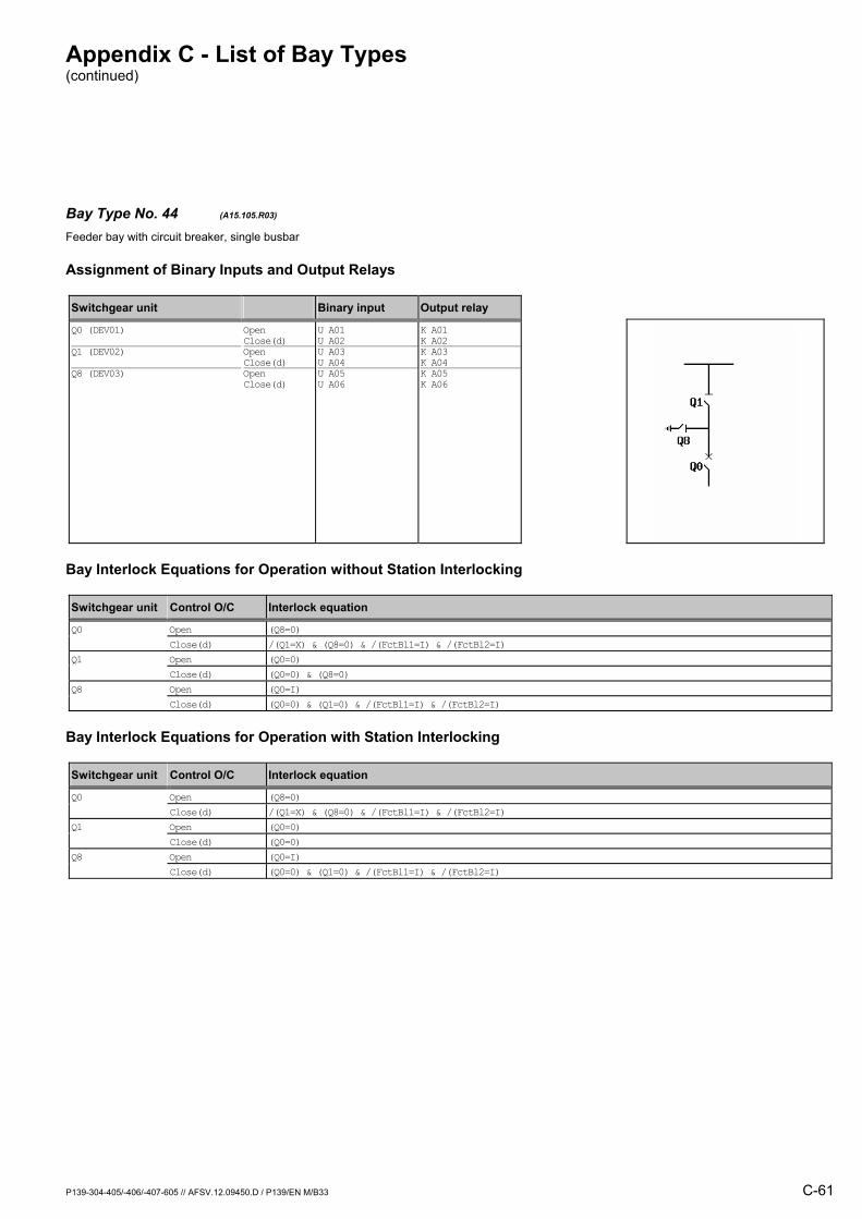
Appendix C - List of Bay Types (continued)
P139-304-405/-406/-407-605 // AFSV.12.09450.D / P139/EN M/B33 C-61
Bay Type No. 44 (A15.105.R03) Feeder bay with circuit breaker, single busbar
Assignment of Binary Inputs and Output Relays
Switchgear unit Binary input Output relay
Q0 (DEV01) Q1 (DEV02) Q8 (DEV03)
Open Close(d) Open Close(d) Open Close(d)
U A01 U A02 U A03 U A04 U A05 U A06
K A01 K A02K A03 K A04K A05 K A06
Bay Interlock Equations for Operation without Station Interlocking
Switchgear unit Control O/C Interlock equation
Q0 Open (Q8=0) Close(d) /(Q1=X) & (Q8=0) & /(FctBl1=I) & /(FctBl2=I) Q1 Open (Q0=0) Close(d) (Q0=0) & (Q8=0) Q8 Open (Q0=I) Close(d) (Q0=0) & (Q1=0) & /(FctBl1=I) & /(FctBl2=I)
Bay Interlock Equations for Operation with Station Interlocking
Switchgear unit Control O/C Interlock equation
Q0 Open (Q8=0) Close(d) /(Q1=X) & (Q8=0) & /(FctBl1=I) & /(FctBl2=I) Q1 Open (Q0=0) Close(d) (Q0=0) Q8 Open (Q0=I) Close(d) (Q0=0) & (Q1=0) & /(FctBl1=I) & /(FctBl2=I)

Appendix C - List of Bay Types (continued)
C-62 P139-304-405/-406/-407-605 // AFSV.12.09450.D / P139/EN M/B33
Bay Type No. 45 (A21.104.M04) Feeder bay with circuit breaker, double busbar,direct motor control
Assignment of Binary Inputs and Output Relays
Switchgear unit Binary input Output relay
Q0 (DEV01) Q1 (DEV02) Q2 (DEV03) X0 (DEV04) Mot.relay (SIG_1: Signal S012) Shunt wd. (CMD_1: Command C011) Mot.relay (CMD_1: Command C012)
Open Close(d) Open Close(d) Open Close(d) Open Close(d)
U A01 U A02 U A03 U A04 U A05 U A06 U B01 U B02 U B06 / /
K A01 K A02K A03 K A04K A05 K A06K B01 K B02/
K B05
K B06
Bay Interlock Equations for Operation without Station Interlocking
Switchgear unit Control O/C Interlock equation
Q0 Close(d) /(Q1=X) & /(Q2=X) & /(X0=X) & /(FctBl1=I) & /(FctBl2=I) Q1 Open (Q0=0) & (Q2=0) Close(d) (Q0=0) & (Q2=0) Q2 Open (Q0=0) & (Q1=0) Close(d) (Q0=0) & (Q1=0) X0 Open (Q0=0) & (Q1=0) & (Q2=0) Close(d) (Q0=0) & (Q1=0) & (Q2=0)
Bay Interlock Equations for Operation with Station Interlocking
Switchgear unit Control O/C Interlock equation
Q0 Close(d) /(Q1=X) & /(Q2=X) & /(X0=X) & /(FctBl1=I) & /(FctBl2=I) X0 Open (Q0=0) & (Q1=0) & (Q2=0) Close(d) (Q0=0) & (Q1=0) & (Q2=0)

Appendix C - List of Bay Types (continued)
P139-304-405/-406/-407-605 // AFSV.12.09450.D / P139/EN M/B33 C-63
Bay Type No. 46 (A21.104.R01) Feeder bay with circuit breaker, double busbar
Assignment of Binary Inputs and Output Relays
Switchgear unit Binary input Output relay
Q0 (DEV01) Q1 (DEV02) Q2 (DEV03) X0 (DEV04)
Open Close(d) Open Close(d) Open Close(d) Open Close(d)
U A01 U A02 U A03 U A04 U A05 U A06 U B01 U B02
K A01 K A02/ // // /
Bay Interlock Equations for Operation without Station Interlocking
Switchgear unit Control O/C Interlock equation
Q0 Close(d) /(Q1=X) & /(Q2=X) & /(X0=X) & /(FctBl1=I) & /(FctBl2=I)
Bay Interlock Equations for Operation with Station Interlocking
Switchgear unit Control O/C Interlock equation
Q0 Close(d) /(Q1=X) & /(Q2=X) & /(X0=X) & /(FctBl1=I) & /(FctBl2=I)
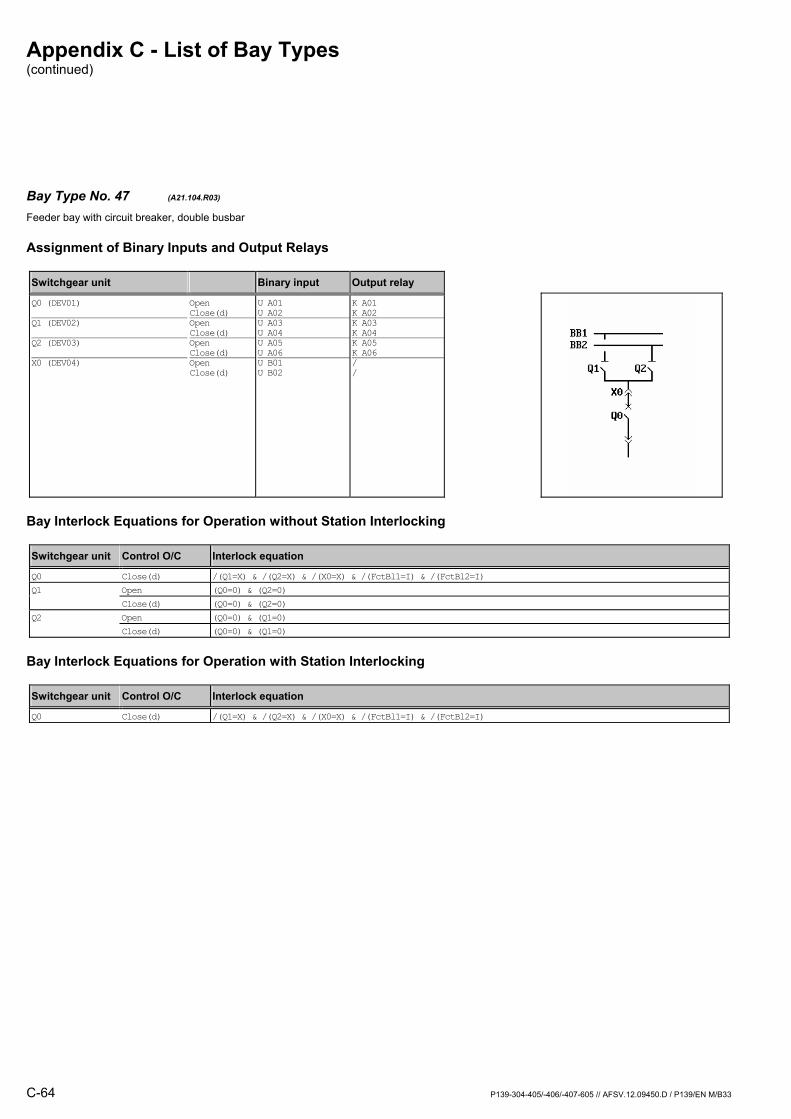
Appendix C - List of Bay Types (continued)
C-64 P139-304-405/-406/-407-605 // AFSV.12.09450.D / P139/EN M/B33
Bay Type No. 47 (A21.104.R03) Feeder bay with circuit breaker, double busbar
Assignment of Binary Inputs and Output Relays
Switchgear unit Binary input Output relay
Q0 (DEV01) Q1 (DEV02) Q2 (DEV03) X0 (DEV04)
Open Close(d) Open Close(d) Open Close(d) Open Close(d)
U A01 U A02 U A03 U A04 U A05 U A06 U B01 U B02
K A01 K A02K A03 K A04K A05 K A06/ /
Bay Interlock Equations for Operation without Station Interlocking
Switchgear unit Control O/C Interlock equation
Q0 Close(d) /(Q1=X) & /(Q2=X) & /(X0=X) & /(FctBl1=I) & /(FctBl2=I) Q1 Open (Q0=0) & (Q2=0) Close(d) (Q0=0) & (Q2=0) Q2 Open (Q0=0) & (Q1=0) Close(d) (Q0=0) & (Q1=0)
Bay Interlock Equations for Operation with Station Interlocking
Switchgear unit Control O/C Interlock equation
Q0 Close(d) /(Q1=X) & /(Q2=X) & /(X0=X) & /(FctBl1=I) & /(FctBl2=I)

Appendix C - List of Bay Types (continued)
P139-304-405/-406/-407-605 // AFSV.12.09450.D / P139/EN M/B33 C-65
Bay Type No. 48 (A21.104.R04) Feeder bay with circuit breaker, double busbar
Assignment of Binary Inputs and Output Relays
Switchgear unit Binary input Output relay
Q0 (DEV01) Q1 (DEV02) Q2 (DEV03) X0 (DEV04)
Open Close(d) Open Close(d) Open Close(d) Open Close(d)
U A01 U A02 U A03 U A04 U A05 U A06 U B01 U B02
K A01 K A02K A03 K A04K A05 K A06K B01 K B02
Bay Interlock Equations for Operation without Station Interlocking
Switchgear unit Control O/C Interlock equation
Q0 Close(d) /(Q1=X) & /(Q2=X) & /(X0=X) & /(FctBl1=I) & /(FctBl2=I) Q1 Open (Q0=0) & (Q2=0) Close(d) (Q0=0) & (Q2=0) Q2 Open (Q0=0) & (Q1=0) Close(d) (Q0=0) & (Q1=0) X0 Open (Q0=0) & (Q1=0) & (Q2=0) Close(d) (Q0=0) & (Q1=0) & (Q2=0)
Bay Interlock Equations for Operation with Station Interlocking
Switchgear unit Control O/C Interlock equation
Q0 Close(d) /(Q1=X) & /(Q2=X) & /(X0=X) & /(FctBl1=I) & /(FctBl2=I) X0 Open (Q0=0) & (Q1=0) & (Q2=0) Close(d) (Q0=0) & (Q1=0) & (Q2=0)

Appendix C - List of Bay Types (continued)
C-66 P139-304-405/-406/-407-605 // AFSV.12.09450.D / P139/EN M/B33
Bay Type No. 49 (A21.105.M05) Feeder bay with circuit breaker, double busbar,direct motor control
Assignment of Binary Inputs and Output Relays
Switchgear unit Binary input Output relay
Q0 (DEV01) Q1 (DEV02) Q2 (DEV03) X0 (DEV04) Q8 (DEV05) Mot.relay (SIG_1: Signal S012) Shunt wd. (CMD_1: Command C011) Mot.relay (CMD_1: Command C012)
Open Close(d) Open Close(d) Open Close(d) Open Close(d) Open Close(d)
U A01 U A02 U A03 U A04 U A05 U A06 U B01 U B02 U B03 U B04 U B06 / /
K A01 K A02K A03 K A04K A05 K A06K B01 K B02K B03 K B04/
K B05
K B06
Bay Interlock Equations for Operation without Station Interlocking
Switchgear unit Control O/C Interlock equation
Q0 Close(d) /(Q1=X) & /(Q2=X) & /(X0=X) & /(FctBl1=I) & /(FctBl2=I) Q1 Open (Q0=0) & (Q2=0) Close(d) (Q0=0) & (Q2=0) Q2 Open (Q0=0) & (Q1=0) Close(d) (Q0=0) & (Q1=0) Q8 Close(d) (X0=0) X0 Open (Q0=0) & (Q1=0) & (Q2=0) Close(d) (Q0=0) & (Q1=0) & (Q2=0) & (Q8=0)
Bay Interlock Equations for Operation with Station Interlocking
Switchgear unit Control O/C Interlock equation
Q0 Close(d) /(Q1=X) & /(Q2=X) & /(X0=X) & /(FctBl1=I) & /(FctBl2=I) Q8 Close(d) (X0=0) X0 Open (Q0=0) & (Q1=0) & (Q2=0) Close(d) (Q0=0) & (Q1=0) & (Q2=0) & (Q8=0)
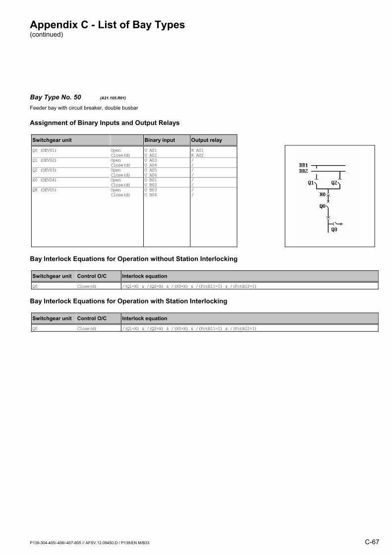
Appendix C - List of Bay Types (continued)
P139-304-405/-406/-407-605 // AFSV.12.09450.D / P139/EN M/B33 C-67
Bay Type No. 50 (A21.105.R01) Feeder bay with circuit breaker, double busbar
Assignment of Binary Inputs and Output Relays
Switchgear unit Binary input Output relay
Q0 (DEV01) Q1 (DEV02) Q2 (DEV03) X0 (DEV04) Q8 (DEV05)
Open Close(d) Open Close(d) Open Close(d) Open Close(d) Open Close(d)
U A01 U A02 U A03 U A04 U A05 U A06 U B01 U B02 U B03 U B04
K A01 K A02/ // // // /
Bay Interlock Equations for Operation without Station Interlocking
Switchgear unit Control O/C Interlock equation
Q0 Close(d) /(Q1=X) & /(Q2=X) & /(X0=X) & /(FctBl1=I) & /(FctBl2=I)
Bay Interlock Equations for Operation with Station Interlocking
Switchgear unit Control O/C Interlock equation
Q0 Close(d) /(Q1=X) & /(Q2=X) & /(X0=X) & /(FctBl1=I) & /(FctBl2=I)

Appendix C - List of Bay Types (continued)
C-68 P139-304-405/-406/-407-605 // AFSV.12.09450.D / P139/EN M/B33
Bay Type No. 51 (A21.105.R03) Feeder bay with circuit breaker, double busbar
Assignment of Binary Inputs and Output Relays
Switchgear unit Binary input Output relay
Q0 (DEV01) Q1 (DEV02) Q2 (DEV03) X0 (DEV04) Q8 (DEV05)
Open Close(d) Open Close(d) Open Close(d) Open Close(d) Open Close(d)
U A01 U A02 U A03 U A04 U A05 U A06 U B01 U B02 U B03 U B04
K A01 K A02K A03 K A04K A05 K A06/ // /
Bay Interlock Equations for Operation without Station Interlocking
Switchgear unit Control O/C Interlock equation
Q0 Close(d) /(Q1=X) & /(Q2=X) & /(X0=X) & /(FctBl1=I) & /(FctBl2=I) Q1 Open (Q0=0) & (Q2=0) Close(d) (Q0=0) & (Q2=0) Q2 Open (Q0=0) & (Q1=0) Close(d) (Q0=0) & (Q1=0)
Bay Interlock Equations for Operation with Station Interlocking
Switchgear unit Control O/C Interlock equation
Q0 Close(d) /(Q1=X) & /(Q2=X) & /(X0=X) & /(FctBl1=I) & /(FctBl2=I)

Appendix C - List of Bay Types (continued)
P139-304-405/-406/-407-605 // AFSV.12.09450.D / P139/EN M/B33 C-69
Bay Type No. 52 (A21.105.R04) Feeder bay with circuit breaker, double busbar
Assignment of Binary Inputs and Output Relays
Switchgear unit Binary input Output relay
Q0 (DEV01) Q1 (DEV02) Q2 (DEV03) X0 (DEV04) Q8 (DEV05)
Open Close(d) Open Close(d) Open Close(d) Open Close(d) Open Close(d)
U A01 U A02 U A03 U A04 U A05 U A06 U B01 U B02 U B03 U B04
K A01 K A02K A03 K A04K A05 K A06K B01 K B02/ /
Bay Interlock Equations for Operation without Station Interlocking
Switchgear unit Control O/C Interlock equation
Q0 Close(d) /(Q1=X) & /(Q2=X) & /(X0=X) & /(FctBl1=I) & /(FctBl2=I) Q1 Open (Q0=0) & (Q2=0) Close(d) (Q0=0) & (Q2=0) Q2 Open (Q0=0) & (Q1=0) Close(d) (Q0=0) & (Q1=0) X0 Open (Q0=0) & (Q1=0) & (Q2=0) Close(d) (Q0=0) & (Q1=0) & (Q2=0) & (Q8=0)
Bay Interlock Equations for Operation with Station Interlocking
Switchgear unit Control O/C Interlock equation
Q0 Close(d) /(Q1=X) & /(Q2=X) & /(X0=X) & /(FctBl1=I) & /(FctBl2=I) X0 Open (Q0=0) & (Q1=0) & (Q2=0) Close(d) (Q0=0) & (Q1=0) & (Q2=0) & (Q8=0)

Appendix C - List of Bay Types (continued)
C-70 P139-304-405/-406/-407-605 // AFSV.12.09450.D / P139/EN M/B33
Bay Type No. 53 (A21.105.R05) Feeder bay with circuit breaker, double busbar
Assignment of Binary Inputs and Output Relays
Switchgear unit Binary input Output relay
Q0 (DEV01) Q1 (DEV02) Q2 (DEV03) X0 (DEV04) Q8 (DEV05)
Open Close(d) Open Close(d) Open Close(d) Open Close(d) Open Close(d)
U A01 U A02 U A03 U A04 U A05 U A06 U B01 U B02 U B03 U B04
K A01 K A02K A03 K A04K A05 K A06K B01 K B02K B03 K B04
Bay Interlock Equations for Operation without Station Interlocking
Switchgear unit Control O/C Interlock equation
Q0 Close(d) /(Q1=X) & /(Q2=X) & /(X0=X) & /(FctBl1=I) & /(FctBl2=I) Q1 Open (Q0=0) & (Q2=0) Close(d) (Q0=0) & (Q2=0) Q2 Open (Q0=0) & (Q1=0) Close(d) (Q0=0) & (Q1=0) Q8 Close(d) (X0=0) X0 Open (Q0=0) & (Q1=0) & (Q2=0) Close(d) (Q0=0) & (Q1=0) & (Q2=0) & (Q8=0)
Bay Interlock Equations for Operation with Station Interlocking
Switchgear unit Control O/C Interlock equation
Q0 Close(d) /(Q1=X) & /(Q2=X) & /(X0=X) & /(FctBl1=I) & /(FctBl2=I) Q8 Close(d) (X0=0) X0 Open (Q0=0) & (Q1=0) & (Q2=0) Close(d) (Q0=0) & (Q1=0) & (Q2=0) & (Q8=0)
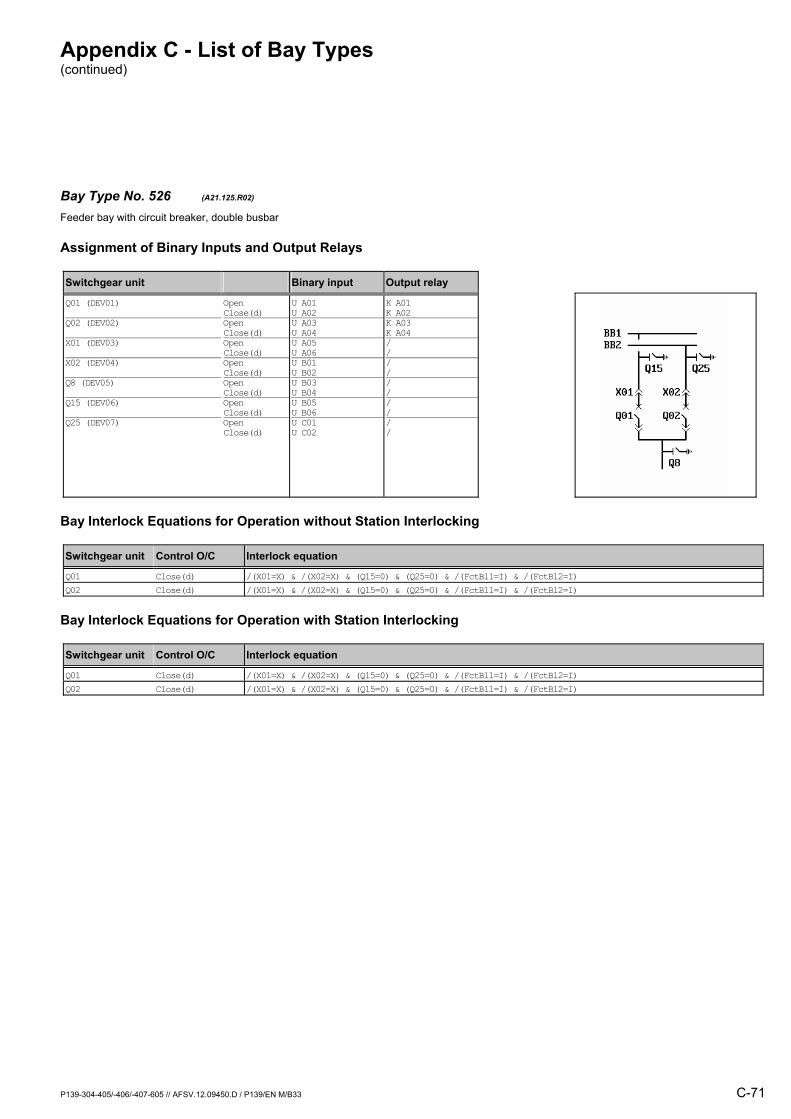
Appendix C - List of Bay Types (continued)
P139-304-405/-406/-407-605 // AFSV.12.09450.D / P139/EN M/B33 C-71
Bay Type No. 526 (A21.125.R02) Feeder bay with circuit breaker, double busbar
Assignment of Binary Inputs and Output Relays
Switchgear unit Binary input Output relay
Q01 (DEV01) Q02 (DEV02) X01 (DEV03) X02 (DEV04) Q8 (DEV05) Q15 (DEV06) Q25 (DEV07)
Open Close(d) Open Close(d) Open Close(d) Open Close(d) Open Close(d) Open Close(d) Open Close(d)
U A01 U A02 U A03 U A04 U A05 U A06 U B01 U B02 U B03 U B04 U B05 U B06 U C01 U C02
K A01 K A02K A03 K A04/ // // // // /
Bay Interlock Equations for Operation without Station Interlocking
Switchgear unit Control O/C Interlock equation
Q01 Close(d) /(X01=X) & /(X02=X) & (Q15=0) & (Q25=0) & /(FctBl1=I) & /(FctBl2=I) Q02 Close(d) /(X01=X) & /(X02=X) & (Q15=0) & (Q25=0) & /(FctBl1=I) & /(FctBl2=I)
Bay Interlock Equations for Operation with Station Interlocking
Switchgear unit Control O/C Interlock equation
Q01 Close(d) /(X01=X) & /(X02=X) & (Q15=0) & (Q25=0) & /(FctBl1=I) & /(FctBl2=I) Q02 Close(d) /(X01=X) & /(X02=X) & (Q15=0) & (Q25=0) & /(FctBl1=I) & /(FctBl2=I)
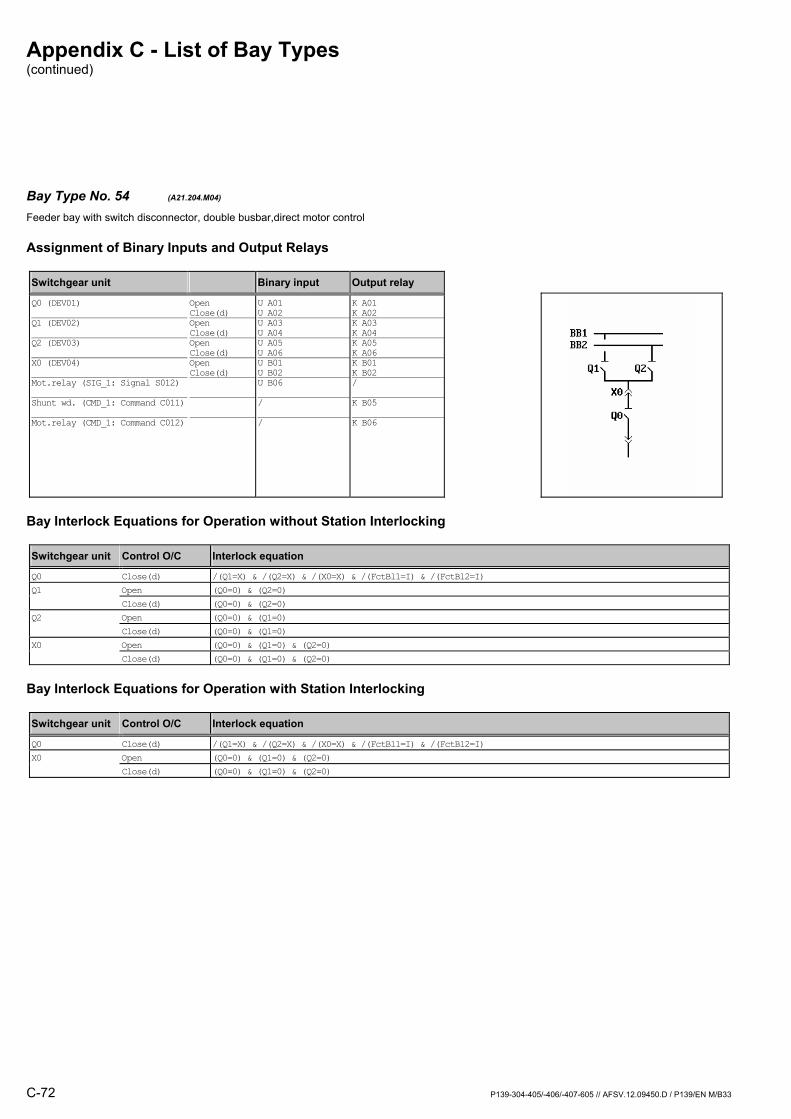
Appendix C - List of Bay Types (continued)
C-72 P139-304-405/-406/-407-605 // AFSV.12.09450.D / P139/EN M/B33
Bay Type No. 54 (A21.204.M04) Feeder bay with switch disconnector, double busbar,direct motor control
Assignment of Binary Inputs and Output Relays
Switchgear unit Binary input Output relay
Q0 (DEV01) Q1 (DEV02) Q2 (DEV03) X0 (DEV04) Mot.relay (SIG_1: Signal S012) Shunt wd. (CMD_1: Command C011) Mot.relay (CMD_1: Command C012)
Open Close(d) Open Close(d) Open Close(d) Open Close(d)
U A01 U A02 U A03 U A04 U A05 U A06 U B01 U B02 U B06 / /
K A01 K A02K A03 K A04K A05 K A06K B01 K B02/
K B05
K B06
Bay Interlock Equations for Operation without Station Interlocking
Switchgear unit Control O/C Interlock equation
Q0 Close(d) /(Q1=X) & /(Q2=X) & /(X0=X) & /(FctBl1=I) & /(FctBl2=I) Q1 Open (Q0=0) & (Q2=0) Close(d) (Q0=0) & (Q2=0) Q2 Open (Q0=0) & (Q1=0) Close(d) (Q0=0) & (Q1=0) X0 Open (Q0=0) & (Q1=0) & (Q2=0) Close(d) (Q0=0) & (Q1=0) & (Q2=0)
Bay Interlock Equations for Operation with Station Interlocking
Switchgear unit Control O/C Interlock equation
Q0 Close(d) /(Q1=X) & /(Q2=X) & /(X0=X) & /(FctBl1=I) & /(FctBl2=I) X0 Open (Q0=0) & (Q1=0) & (Q2=0) Close(d) (Q0=0) & (Q1=0) & (Q2=0)

Appendix C - List of Bay Types (continued)
P139-304-405/-406/-407-605 // AFSV.12.09450.D / P139/EN M/B33 C-73
Bay Type No. 55 (A21.204.R01) Feeder bay with switch disconnector, double busbar
Assignment of Binary Inputs and Output Relays
Switchgear unit Binary input Output relay
Q0 (DEV01) Q1 (DEV02) Q2 (DEV03) X0 (DEV04)
Open Close(d) Open Close(d) Open Close(d) Open Close(d)
U A01 U A02 U A03 U A04 U A05 U A06 U B01 U B02
K A01 K A02/ // // /
Bay Interlock Equations for Operation without Station Interlocking
Switchgear unit Control O/C Interlock equation
Q0 Close(d) /(Q1=X) & /(Q2=X) & /(X0=X) & /(FctBl1=I) & /(FctBl2=I)
Bay Interlock Equations for Operation with Station Interlocking
Switchgear unit Control O/C Interlock equation
Q0 Close(d) /(Q1=X) & /(Q2=X) & /(X0=X) & /(FctBl1=I) & /(FctBl2=I)

Appendix C - List of Bay Types (continued)
C-74 P139-304-405/-406/-407-605 // AFSV.12.09450.D / P139/EN M/B33
Bay Type No. 56 (A21.204.R03) Feeder bay with switch disconnector, double busbar
Assignment of Binary Inputs and Output Relays
Switchgear unit Binary input Output relay
Q0 (DEV01) Q1 (DEV02) Q2 (DEV03) X0 (DEV04)
Open Close(d) Open Close(d) Open Close(d) Open Close(d)
U A01 U A02 U A03 U A04 U A05 U A06 U B01 U B02
K A01 K A02K A03 K A04K A05 K A06/ /
Bay Interlock Equations for Operation without Station Interlocking
Switchgear unit Control O/C Interlock equation
Q0 Close(d) /(Q1=X) & /(Q2=X) & /(X0=X) & /(FctBl1=I) & /(FctBl2=I) Q1 Open (Q0=0) & (Q2=0) Close(d) (Q0=0) & (Q2=0) Q2 Open (Q0=0) & (Q1=0) Close(d) (Q0=0) & (Q1=0)
Bay Interlock Equations for Operation with Station Interlocking
Switchgear unit Control O/C Interlock equation
Q0 Close(d) /(Q1=X) & /(Q2=X) & /(X0=X) & /(FctBl1=I) & /(FctBl2=I)
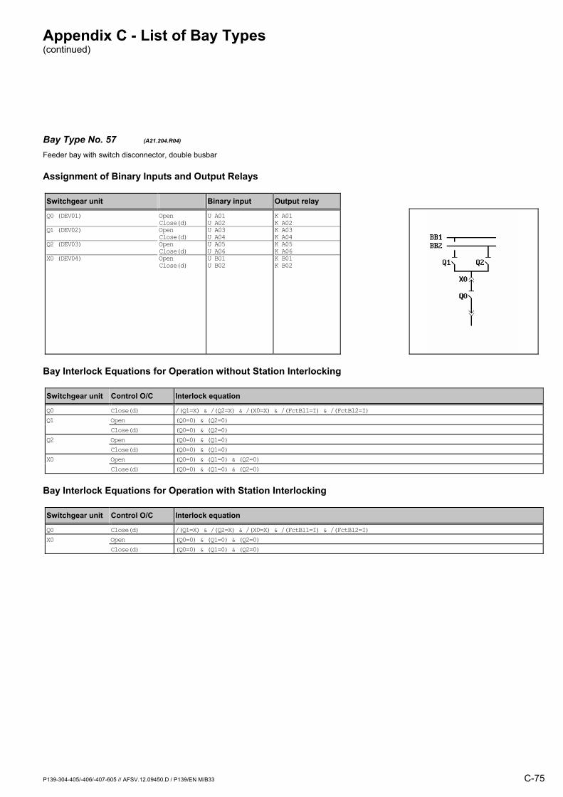
Appendix C - List of Bay Types (continued)
P139-304-405/-406/-407-605 // AFSV.12.09450.D / P139/EN M/B33 C-75
Bay Type No. 57 (A21.204.R04) Feeder bay with switch disconnector, double busbar
Assignment of Binary Inputs and Output Relays
Switchgear unit Binary input Output relay
Q0 (DEV01) Q1 (DEV02) Q2 (DEV03) X0 (DEV04)
Open Close(d) Open Close(d) Open Close(d) Open Close(d)
U A01 U A02 U A03 U A04 U A05 U A06 U B01 U B02
K A01 K A02K A03 K A04K A05 K A06K B01 K B02
Bay Interlock Equations for Operation without Station Interlocking
Switchgear unit Control O/C Interlock equation
Q0 Close(d) /(Q1=X) & /(Q2=X) & /(X0=X) & /(FctBl1=I) & /(FctBl2=I) Q1 Open (Q0=0) & (Q2=0) Close(d) (Q0=0) & (Q2=0) Q2 Open (Q0=0) & (Q1=0) Close(d) (Q0=0) & (Q1=0) X0 Open (Q0=0) & (Q1=0) & (Q2=0) Close(d) (Q0=0) & (Q1=0) & (Q2=0)
Bay Interlock Equations for Operation with Station Interlocking
Switchgear unit Control O/C Interlock equation
Q0 Close(d) /(Q1=X) & /(Q2=X) & /(X0=X) & /(FctBl1=I) & /(FctBl2=I) X0 Open (Q0=0) & (Q1=0) & (Q2=0) Close(d) (Q0=0) & (Q1=0) & (Q2=0)
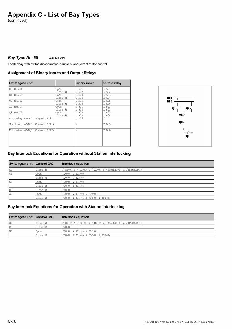
Appendix C - List of Bay Types (continued)
C-76 P139-304-405/-406/-407-605 // AFSV.12.09450.D / P139/EN M/B33
Bay Type No. 58 (A21.205.M05) Feeder bay with switch disconnector, double busbar,direct motor control
Assignment of Binary Inputs and Output Relays
Switchgear unit Binary input Output relay
Q0 (DEV01) Q1 (DEV02) Q2 (DEV03) X0 (DEV04) Q8 (DEV05) Mot.relay (SIG_1: Signal S012) Shunt wd. (CMD_1: Command C011) Mot.relay (CMD_1: Command C012)
Open Close(d) Open Close(d) Open Close(d) Open Close(d) Open Close(d)
U A01 U A02 U A03 U A04 U A05 U A06 U B01 U B02 U B03 U B04 U B06 / /
K A01 K A02K A03 K A04K A05 K A06K B01 K B02K B03 K B04/
K B05
K B06
Bay Interlock Equations for Operation without Station Interlocking
Switchgear unit Control O/C Interlock equation
Q0 Close(d) /(Q1=X) & /(Q2=X) & /(X0=X) & /(FctBl1=I) & /(FctBl2=I) Q1 Open (Q0=0) & (Q2=0) Close(d) (Q0=0) & (Q2=0) Q2 Open (Q0=0) & (Q1=0) Close(d) (Q0=0) & (Q1=0) Q8 Close(d) (X0=0) X0 Open (Q0=0) & (Q1=0) & (Q2=0) Close(d) (Q0=0) & (Q1=0) & (Q2=0) & (Q8=0)
Bay Interlock Equations for Operation with Station Interlocking
Switchgear unit Control O/C Interlock equation
Q0 Close(d) /(Q1=X) & /(Q2=X) & /(X0=X) & /(FctBl1=I) & /(FctBl2=I) Q8 Close(d) (X0=0) X0 Open (Q0=0) & (Q1=0) & (Q2=0) Close(d) (Q0=0) & (Q1=0) & (Q2=0) & (Q8=0)

Appendix C - List of Bay Types (continued)
P139-304-405/-406/-407-605 // AFSV.12.09450.D / P139/EN M/B33 C-77
Bay Type No. 59 (A21.205.R01) Feeder bay with switch disconnector, double busbar
Assignment of Binary Inputs and Output Relays
Switchgear unit Binary input Output relay
Q0 (DEV01) Q1 (DEV02) Q2 (DEV03) X0 (DEV04) Q8 (DEV05)
Open Close(d) Open Close(d) Open Close(d) Open Close(d) Open Close(d)
U A01 U A02 U A03 U A04 U A05 U A06 U B01 U B02 U B03 U B04
K A01 K A02/ // // // /
Bay Interlock Equations for Operation without Station Interlocking
Switchgear unit Control O/C Interlock equation
Q0 Close(d) /(Q1=X) & /(Q2=X) & /(X0=X) & /(FctBl1=I) & /(FctBl2=I)
Bay Interlock Equations for Operation with Station Interlocking
Switchgear unit Control O/C Interlock equation
Q0 Close(d) /(Q1=X) & /(Q2=X) & /(X0=X) & /(FctBl1=I) & /(FctBl2=I)
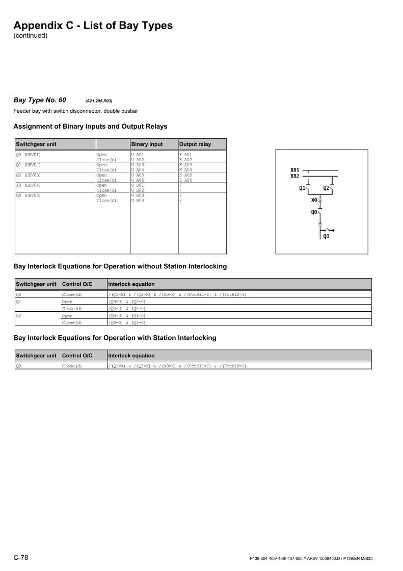
Appendix C - List of Bay Types (continued)
C-78 P139-304-405/-406/-407-605 // AFSV.12.09450.D / P139/EN M/B33
Bay Type No. 60 (A21.205.R03) Feeder bay with switch disconnector, double busbar
Assignment of Binary Inputs and Output Relays
Switchgear unit Binary input Output relay
Q0 (DEV01) Q1 (DEV02) Q2 (DEV03) X0 (DEV04) Q8 (DEV05)
Open Close(d) Open Close(d) Open Close(d) Open Close(d) Open Close(d)
U A01 U A02 U A03 U A04 U A05 U A06 U B01 U B02 U B03 U B04
K A01 K A02K A03 K A04K A05 K A06/ // /
Bay Interlock Equations for Operation without Station Interlocking
Switchgear unit Control O/C Interlock equation
Q0 Close(d) /(Q1=X) & /(Q2=X) & /(X0=X) & /(FctBl1=I) & /(FctBl2=I) Q1 Open (Q0=0) & (Q2=0) Close(d) (Q0=0) & (Q2=0) Q2 Open (Q0=0) & (Q1=0) Close(d) (Q0=0) & (Q1=0)
Bay Interlock Equations for Operation with Station Interlocking
Switchgear unit Control O/C Interlock equation
Q0 Close(d) /(Q1=X) & /(Q2=X) & /(X0=X) & /(FctBl1=I) & /(FctBl2=I)
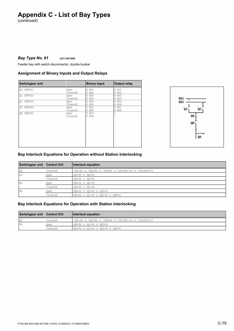
Appendix C - List of Bay Types (continued)
P139-304-405/-406/-407-605 // AFSV.12.09450.D / P139/EN M/B33 C-79
Bay Type No. 61 (A21.205.R04) Feeder bay with switch disconnector, double busbar
Assignment of Binary Inputs and Output Relays
Switchgear unit Binary input Output relay
Q0 (DEV01) Q1 (DEV02) Q2 (DEV03) X0 (DEV04) Q8 (DEV05)
Open Close(d) Open Close(d) Open Close(d) Open Close(d) Open Close(d)
U A01 U A02 U A03 U A04 U A05 U A06 U B01 U B02 U B03 U B04
K A01 K A02K A03 K A04K A05 K A06K B01 K B02/ /
Bay Interlock Equations for Operation without Station Interlocking
Switchgear unit Control O/C Interlock equation
Q0 Close(d) /(Q1=X) & /(Q2=X) & /(X0=X) & /(FctBl1=I) & /(FctBl2=I) Q1 Open (Q0=0) & (Q2=0) Close(d) (Q0=0) & (Q2=0) Q2 Open (Q0=0) & (Q1=0) Close(d) (Q0=0) & (Q1=0) X0 Open (Q0=0) & (Q1=0) & (Q2=0) Close(d) (Q0=0) & (Q1=0) & (Q2=0) & (Q8=0)
Bay Interlock Equations for Operation with Station Interlocking
Switchgear unit Control O/C Interlock equation
Q0 Close(d) /(Q1=X) & /(Q2=X) & /(X0=X) & /(FctBl1=I) & /(FctBl2=I) X0 Open (Q0=0) & (Q1=0) & (Q2=0) Close(d) (Q0=0) & (Q1=0) & (Q2=0) & (Q8=0)
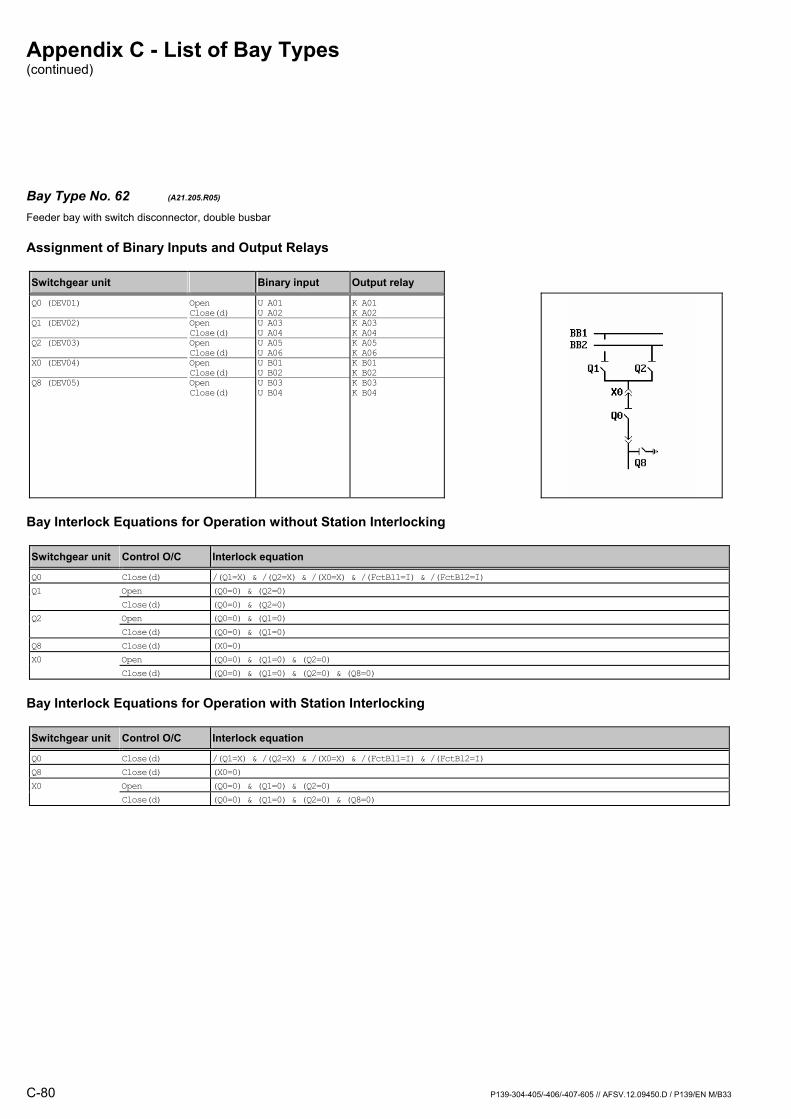
Appendix C - List of Bay Types (continued)
C-80 P139-304-405/-406/-407-605 // AFSV.12.09450.D / P139/EN M/B33
Bay Type No. 62 (A21.205.R05) Feeder bay with switch disconnector, double busbar
Assignment of Binary Inputs and Output Relays
Switchgear unit Binary input Output relay
Q0 (DEV01) Q1 (DEV02) Q2 (DEV03) X0 (DEV04) Q8 (DEV05)
Open Close(d) Open Close(d) Open Close(d) Open Close(d) Open Close(d)
U A01 U A02 U A03 U A04 U A05 U A06 U B01 U B02 U B03 U B04
K A01 K A02K A03 K A04K A05 K A06K B01 K B02K B03 K B04
Bay Interlock Equations for Operation without Station Interlocking
Switchgear unit Control O/C Interlock equation
Q0 Close(d) /(Q1=X) & /(Q2=X) & /(X0=X) & /(FctBl1=I) & /(FctBl2=I) Q1 Open (Q0=0) & (Q2=0) Close(d) (Q0=0) & (Q2=0) Q2 Open (Q0=0) & (Q1=0) Close(d) (Q0=0) & (Q1=0) Q8 Close(d) (X0=0) X0 Open (Q0=0) & (Q1=0) & (Q2=0) Close(d) (Q0=0) & (Q1=0) & (Q2=0) & (Q8=0)
Bay Interlock Equations for Operation with Station Interlocking
Switchgear unit Control O/C Interlock equation
Q0 Close(d) /(Q1=X) & /(Q2=X) & /(X0=X) & /(FctBl1=I) & /(FctBl2=I) Q8 Close(d) (X0=0) X0 Open (Q0=0) & (Q1=0) & (Q2=0) Close(d) (Q0=0) & (Q1=0) & (Q2=0) & (Q8=0)
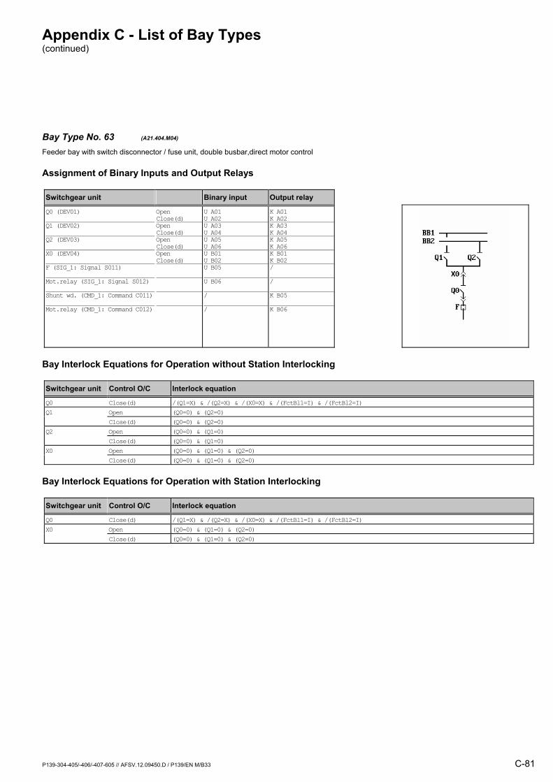
Appendix C - List of Bay Types (continued)
P139-304-405/-406/-407-605 // AFSV.12.09450.D / P139/EN M/B33 C-81
Bay Type No. 63 (A21.404.M04) Feeder bay with switch disconnector / fuse unit, double busbar,direct motor control
Assignment of Binary Inputs and Output Relays
Switchgear unit Binary input Output relay
Q0 (DEV01) Q1 (DEV02) Q2 (DEV03) X0 (DEV04) F (SIG_1: Signal S011) Mot.relay (SIG_1: Signal S012) Shunt wd. (CMD_1: Command C011) Mot.relay (CMD_1: Command C012)
Open Close(d) Open Close(d) Open Close(d) Open Close(d)
U A01 U A02 U A03 U A04 U A05 U A06 U B01 U B02 U B05 U B06 / /
K A01 K A02K A03 K A04K A05 K A06K B01 K B02/
/
K B05
K B06
Bay Interlock Equations for Operation without Station Interlocking
Switchgear unit Control O/C Interlock equation
Q0 Close(d) /(Q1=X) & /(Q2=X) & /(X0=X) & /(FctBl1=I) & /(FctBl2=I) Q1 Open (Q0=0) & (Q2=0) Close(d) (Q0=0) & (Q2=0) Q2 Open (Q0=0) & (Q1=0) Close(d) (Q0=0) & (Q1=0) X0 Open (Q0=0) & (Q1=0) & (Q2=0) Close(d) (Q0=0) & (Q1=0) & (Q2=0)
Bay Interlock Equations for Operation with Station Interlocking
Switchgear unit Control O/C Interlock equation
Q0 Close(d) /(Q1=X) & /(Q2=X) & /(X0=X) & /(FctBl1=I) & /(FctBl2=I) X0 Open (Q0=0) & (Q1=0) & (Q2=0) Close(d) (Q0=0) & (Q1=0) & (Q2=0)
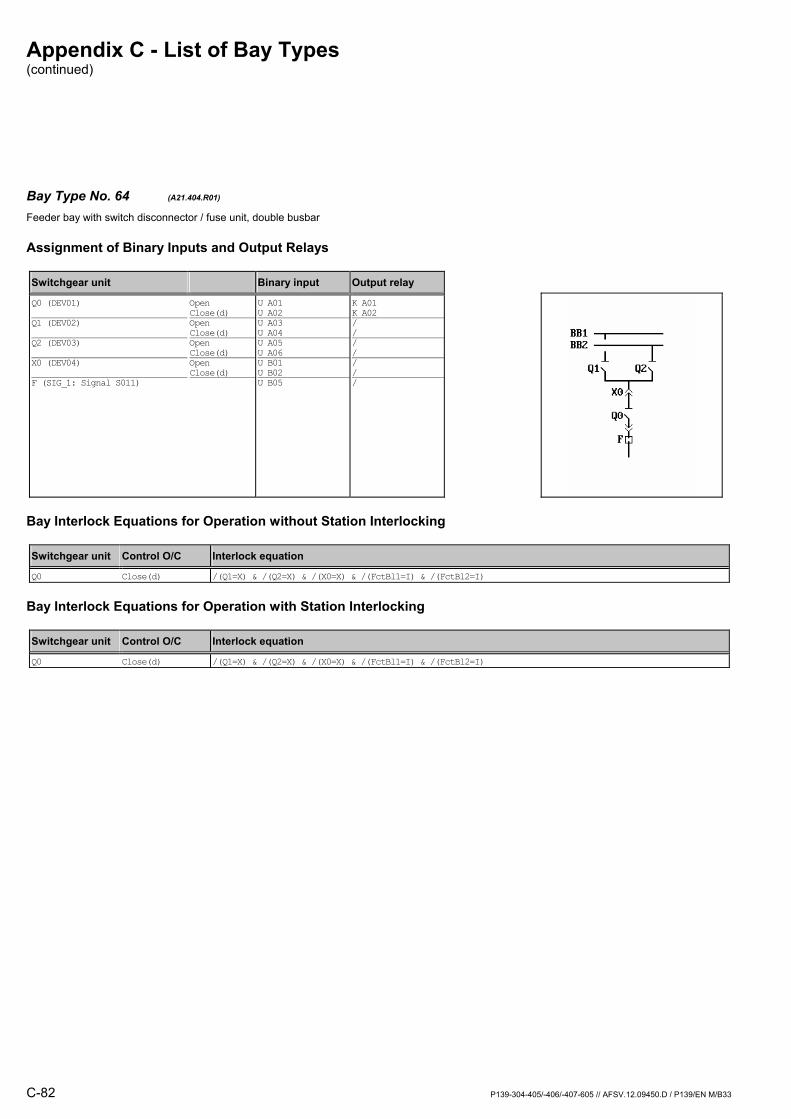
Appendix C - List of Bay Types (continued)
C-82 P139-304-405/-406/-407-605 // AFSV.12.09450.D / P139/EN M/B33
Bay Type No. 64 (A21.404.R01) Feeder bay with switch disconnector / fuse unit, double busbar
Assignment of Binary Inputs and Output Relays
Switchgear unit Binary input Output relay
Q0 (DEV01) Q1 (DEV02) Q2 (DEV03) X0 (DEV04) F (SIG_1: Signal S011)
Open Close(d) Open Close(d) Open Close(d) Open Close(d)
U A01 U A02 U A03 U A04 U A05 U A06 U B01 U B02 U B05
K A01 K A02/ // // //
Bay Interlock Equations for Operation without Station Interlocking
Switchgear unit Control O/C Interlock equation
Q0 Close(d) /(Q1=X) & /(Q2=X) & /(X0=X) & /(FctBl1=I) & /(FctBl2=I)
Bay Interlock Equations for Operation with Station Interlocking
Switchgear unit Control O/C Interlock equation
Q0 Close(d) /(Q1=X) & /(Q2=X) & /(X0=X) & /(FctBl1=I) & /(FctBl2=I)

Appendix C - List of Bay Types (continued)
P139-304-405/-406/-407-605 // AFSV.12.09450.D / P139/EN M/B33 C-83
Bay Type No. 65 (A21.404.R03) Feeder bay with switch disconnector / fuse unit, double busbar
Assignment of Binary Inputs and Output Relays
Switchgear unit Binary input Output relay
Q0 (DEV01) Q1 (DEV02) Q2 (DEV03) X0 (DEV04) F (SIG_1: Signal S011)
Open Close(d) Open Close(d) Open Close(d) Open Close(d)
U A01 U A02 U A03 U A04 U A05 U A06 U B01 U B02 U B05
K A01 K A02K A03 K A04K A05 K A06/ //
Bay Interlock Equations for Operation without Station Interlocking
Switchgear unit Control O/C Interlock equation
Q0 Close(d) /(Q1=X) & /(Q2=X) & /(X0=X) & /(FctBl1=I) & /(FctBl2=I) Q1 Open (Q0=0) & (Q2=0) Close(d) (Q0=0) & (Q2=0) Q2 Open (Q0=0) & (Q1=0) Close(d) (Q0=0) & (Q1=0)
Bay Interlock Equations for Operation with Station Interlocking
Switchgear unit Control O/C Interlock equation
Q0 Close(d) /(Q1=X) & /(Q2=X) & /(X0=X) & /(FctBl1=I) & /(FctBl2=I)
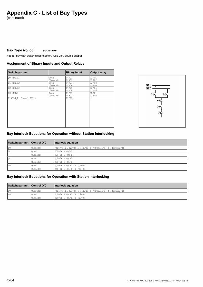
Appendix C - List of Bay Types (continued)
C-84 P139-304-405/-406/-407-605 // AFSV.12.09450.D / P139/EN M/B33
Bay Type No. 66 (A21.404.R04) Feeder bay with switch disconnector / fuse unit, double busbar
Assignment of Binary Inputs and Output Relays
Switchgear unit Binary input Output relay
Q0 (DEV01) Q1 (DEV02) Q2 (DEV03) X0 (DEV04) F (SIG_1: Signal S011)
Open Close(d) Open Close(d) Open Close(d) Open Close(d)
U A01 U A02 U A03 U A04 U A05 U A06 U B01 U B02 U B05
K A01 K A02K A03 K A04K A05 K A06K B01 K B02/
Bay Interlock Equations for Operation without Station Interlocking
Switchgear unit Control O/C Interlock equation
Q0 Close(d) /(Q1=X) & /(Q2=X) & /(X0=X) & /(FctBl1=I) & /(FctBl2=I) Q1 Open (Q0=0) & (Q2=0) Close(d) (Q0=0) & (Q2=0) Q2 Open (Q0=0) & (Q1=0) Close(d) (Q0=0) & (Q1=0) X0 Open (Q0=0) & (Q1=0) & (Q2=0) Close(d) (Q0=0) & (Q1=0) & (Q2=0)
Bay Interlock Equations for Operation with Station Interlocking
Switchgear unit Control O/C Interlock equation
Q0 Close(d) /(Q1=X) & /(Q2=X) & /(X0=X) & /(FctBl1=I) & /(FctBl2=I) X0 Open (Q0=0) & (Q1=0) & (Q2=0) Close(d) (Q0=0) & (Q1=0) & (Q2=0)
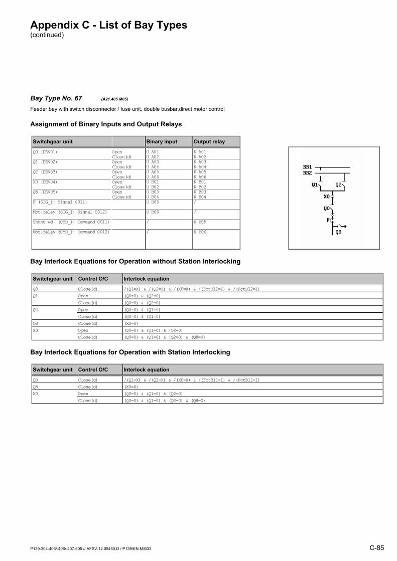
Appendix C - List of Bay Types (continued)
P139-304-405/-406/-407-605 // AFSV.12.09450.D / P139/EN M/B33 C-85
Bay Type No. 67 (A21.405.M05) Feeder bay with switch disconnector / fuse unit, double busbar,direct motor control
Assignment of Binary Inputs and Output Relays
Switchgear unit Binary input Output relay
Q0 (DEV01) Q1 (DEV02) Q2 (DEV03) X0 (DEV04) Q8 (DEV05) F (SIG_1: Signal S011) Mot.relay (SIG_1: Signal S012) Shunt wd. (CMD_1: Command C011) Mot.relay (CMD_1: Command C012)
Open Close(d) Open Close(d) Open Close(d) Open Close(d) Open Close(d)
U A01 U A02 U A03 U A04 U A05 U A06 U B01 U B02 U B03 U B04 U B05 U B06 / /
K A01 K A02K A03 K A04K A05 K A06K B01 K B02K B03 K B04/
/
K B05
K B06
Bay Interlock Equations for Operation without Station Interlocking
Switchgear unit Control O/C Interlock equation
Q0 Close(d) /(Q1=X) & /(Q2=X) & /(X0=X) & /(FctBl1=I) & /(FctBl2=I) Q1 Open (Q0=0) & (Q2=0) Close(d) (Q0=0) & (Q2=0) Q2 Open (Q0=0) & (Q1=0) Close(d) (Q0=0) & (Q1=0) Q8 Close(d) (X0=0) X0 Open (Q0=0) & (Q1=0) & (Q2=0) Close(d) (Q0=0) & (Q1=0) & (Q2=0) & (Q8=0)
Bay Interlock Equations for Operation with Station Interlocking
Switchgear unit Control O/C Interlock equation
Q0 Close(d) /(Q1=X) & /(Q2=X) & /(X0=X) & /(FctBl1=I) & /(FctBl2=I) Q8 Close(d) (X0=0) X0 Open (Q0=0) & (Q1=0) & (Q2=0) Close(d) (Q0=0) & (Q1=0) & (Q2=0) & (Q8=0)
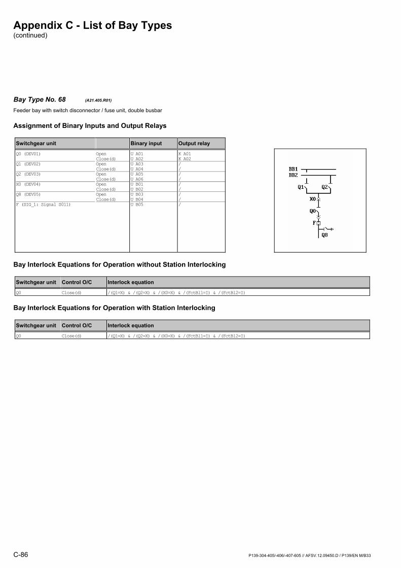
Appendix C - List of Bay Types (continued)
C-86 P139-304-405/-406/-407-605 // AFSV.12.09450.D / P139/EN M/B33
Bay Type No. 68 (A21.405.R01) Feeder bay with switch disconnector / fuse unit, double busbar
Assignment of Binary Inputs and Output Relays
Switchgear unit Binary input Output relay
Q0 (DEV01) Q1 (DEV02) Q2 (DEV03) X0 (DEV04) Q8 (DEV05) F (SIG_1: Signal S011)
Open Close(d) Open Close(d) Open Close(d) Open Close(d) Open Close(d)
U A01 U A02 U A03 U A04 U A05 U A06 U B01 U B02 U B03 U B04 U B05
K A01 K A02/ // // // //
Bay Interlock Equations for Operation without Station Interlocking
Switchgear unit Control O/C Interlock equation
Q0 Close(d) /(Q1=X) & /(Q2=X) & /(X0=X) & /(FctBl1=I) & /(FctBl2=I)
Bay Interlock Equations for Operation with Station Interlocking
Switchgear unit Control O/C Interlock equation
Q0 Close(d) /(Q1=X) & /(Q2=X) & /(X0=X) & /(FctBl1=I) & /(FctBl2=I)
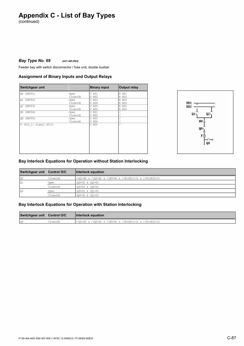
Appendix C - List of Bay Types (continued)
P139-304-405/-406/-407-605 // AFSV.12.09450.D / P139/EN M/B33 C-87
Bay Type No. 69 (A21.405.R03) Feeder bay with switch disconnector / fuse unit, double busbar
Assignment of Binary Inputs and Output Relays
Switchgear unit Binary input Output relay
Q0 (DEV01) Q1 (DEV02) Q2 (DEV03) X0 (DEV04) Q8 (DEV05) F (SIG_1: Signal S011)
Open Close(d) Open Close(d) Open Close(d) Open Close(d) Open Close(d)
U A01 U A02 U A03 U A04 U A05 U A06 U B01 U B02 U B03 U B04 U B05
K A01 K A02K A03 K A04K A05 K A06/ // //
Bay Interlock Equations for Operation without Station Interlocking
Switchgear unit Control O/C Interlock equation
Q0 Close(d) /(Q1=X) & /(Q2=X) & /(X0=X) & /(FctBl1=I) & /(FctBl2=I) Q1 Open (Q0=0) & (Q2=0) Close(d) (Q0=0) & (Q2=0) Q2 Open (Q0=0) & (Q1=0) Close(d) (Q0=0) & (Q1=0)
Bay Interlock Equations for Operation with Station Interlocking
Switchgear unit Control O/C Interlock equation
Q0 Close(d) /(Q1=X) & /(Q2=X) & /(X0=X) & /(FctBl1=I) & /(FctBl2=I)

Appendix C - List of Bay Types (continued)
C-88 P139-304-405/-406/-407-605 // AFSV.12.09450.D / P139/EN M/B33
Bay Type No. 70 (A21.405.R04) Feeder bay with switch disconnector / fuse unit, double busbar
Assignment of Binary Inputs and Output Relays
Switchgear unit Binary input Output relay
Q0 (DEV01) Q1 (DEV02) Q2 (DEV03) X0 (DEV04) Q8 (DEV05) F (SIG_1: Signal S011)
Open Close(d) Open Close(d) Open Close(d) Open Close(d) Open Close(d)
U A01 U A02 U A03 U A04 U A05 U A06 U B01 U B02 U B03 U B04 U B05
K A01 K A02K A03 K A04K A05 K A06K B01 K B02/ //
Bay Interlock Equations for Operation without Station Interlocking
Switchgear unit Control O/C Interlock equation
Q0 Close(d) /(Q1=X) & /(Q2=X) & /(X0=X) & /(FctBl1=I) & /(FctBl2=I) Q1 Open (Q0=0) & (Q2=0) Close(d) (Q0=0) & (Q2=0) Q2 Open (Q0=0) & (Q1=0) Close(d) (Q0=0) & (Q1=0) X0 Open (Q0=0) & (Q1=0) & (Q2=0) Close(d) (Q0=0) & (Q1=0) & (Q2=0) & (Q8=0)
Bay Interlock Equations for Operation with Station Interlocking
Switchgear unit Control O/C Interlock equation
Q0 Close(d) /(Q1=X) & /(Q2=X) & /(X0=X) & /(FctBl1=I) & /(FctBl2=I) X0 Open (Q0=0) & (Q1=0) & (Q2=0) Close(d) (Q0=0) & (Q1=0) & (Q2=0) & (Q8=0)

Appendix C - List of Bay Types (continued)
P139-304-405/-406/-407-605 // AFSV.12.09450.D / P139/EN M/B33 C-89
Bay Type No. 71 (A21.405.R05) Feeder bay with switch disconnector / fuse unit, double busbar
Assignment of Binary Inputs and Output Relays
Switchgear unit Binary input Output relay
Q0 (DEV01) Q1 (DEV02) Q2 (DEV03) X0 (DEV04) Q8 (DEV05) F (SIG_1: Signal S011)
Open Close(d) Open Close(d) Open Close(d) Open Close(d) Open Close(d)
U A01 U A02 U A03 U A04 U A05 U A06 U B01 U B02 U B03 U B04 U B05
K A01 K A02K A03 K A04K A05 K A06K B01 K B02K B03 K B04/
Bay Interlock Equations for Operation without Station Interlocking
Switchgear unit Control O/C Interlock equation
Q0 Close(d) /(Q1=X) & /(Q2=X) & /(X0=X) & /(FctBl1=I) & /(FctBl2=I) Q1 Open (Q0=0) & (Q2=0) Close(d) (Q0=0) & (Q2=0) Q2 Open (Q0=0) & (Q1=0) Close(d) (Q0=0) & (Q1=0) Q8 Close(d) (X0=0) X0 Open (Q0=0) & (Q1=0) & (Q2=0) Close(d) (Q0=0) & (Q1=0) & (Q2=0) & (Q8=0)
Bay Interlock Equations for Operation with Station Interlocking
Switchgear unit Control O/C Interlock equation
Q0 Close(d) /(Q1=X) & /(Q2=X) & /(X0=X) & /(FctBl1=I) & /(FctBl2=I) Q8 Close(d) (X0=0) X0 Open (Q0=0) & (Q1=0) & (Q2=0) Close(d) (Q0=0) & (Q1=0) & (Q2=0) & (Q8=0)
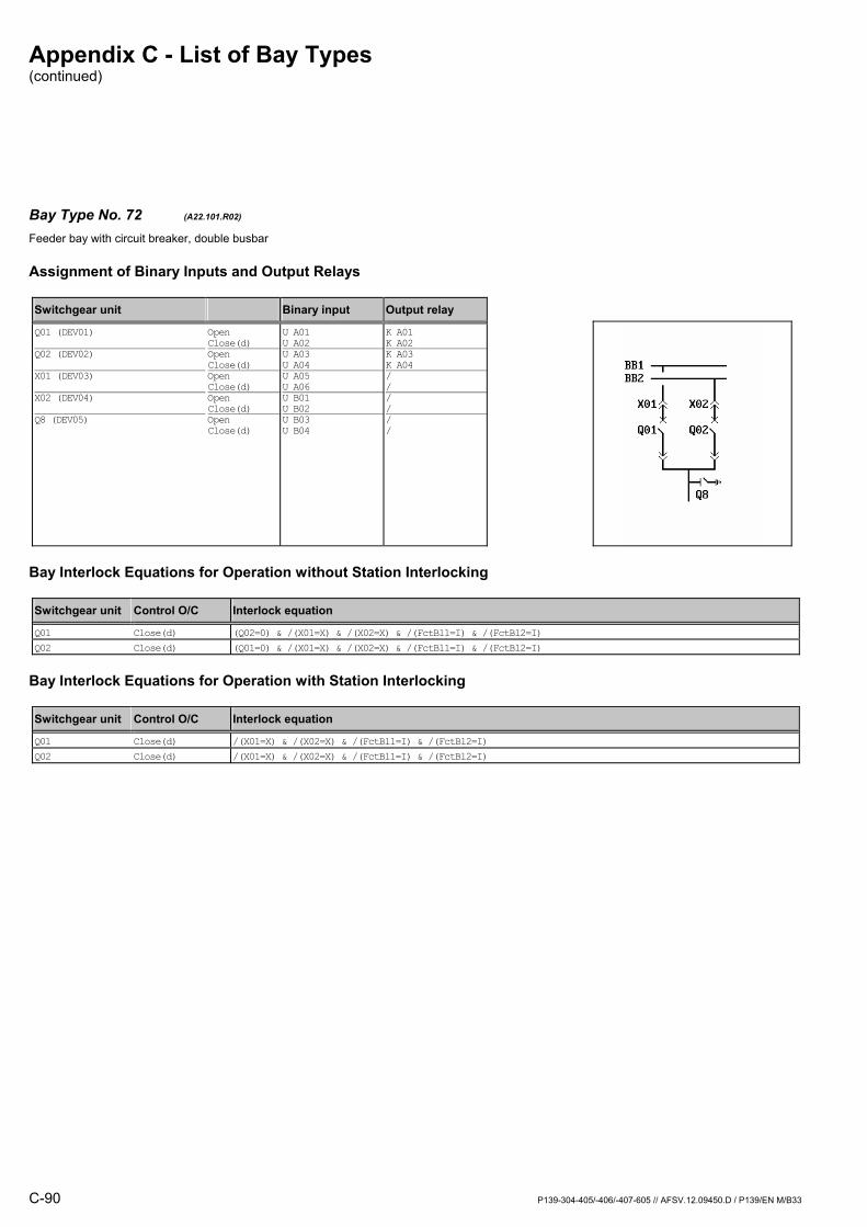
Appendix C - List of Bay Types (continued)
C-90 P139-304-405/-406/-407-605 // AFSV.12.09450.D / P139/EN M/B33
Bay Type No. 72 (A22.101.R02) Feeder bay with circuit breaker, double busbar
Assignment of Binary Inputs and Output Relays
Switchgear unit Binary input Output relay
Q01 (DEV01) Q02 (DEV02) X01 (DEV03) X02 (DEV04) Q8 (DEV05)
Open Close(d) Open Close(d) Open Close(d) Open Close(d) Open Close(d)
U A01 U A02 U A03 U A04 U A05 U A06 U B01 U B02 U B03 U B04
K A01 K A02K A03 K A04/ // // /
Bay Interlock Equations for Operation without Station Interlocking
Switchgear unit Control O/C Interlock equation
Q01 Close(d) (Q02=0) & /(X01=X) & /(X02=X) & /(FctBl1=I) & /(FctBl2=I) Q02 Close(d) (Q01=0) & /(X01=X) & /(X02=X) & /(FctBl1=I) & /(FctBl2=I)
Bay Interlock Equations for Operation with Station Interlocking
Switchgear unit Control O/C Interlock equation
Q01 Close(d) /(X01=X) & /(X02=X) & /(FctBl1=I) & /(FctBl2=I) Q02 Close(d) /(X01=X) & /(X02=X) & /(FctBl1=I) & /(FctBl2=I)

Appendix C - List of Bay Types (continued)
P139-304-405/-406/-407-605 // AFSV.12.09450.D / P139/EN M/B33 C-91
Bay Type No. 73 (A22.101.R04) Feeder bay with circuit breaker, double busbar
Assignment of Binary Inputs and Output Relays
Switchgear unit Binary input Output relay
Q01 (DEV01) Q02 (DEV02) X01 (DEV03) X02 (DEV04) Q8 (DEV05)
Open Close(d) Open Close(d) Open Close(d) Open Close(d) Open Close(d)
U A01 U A02 U A03 U A04 U A05 U A06 U B01 U B02 U B03 U B04
K A01 K A02K A03 K A04K A05 K A06K B01 K B02/ /
Bay Interlock Equations for Operation without Station Interlocking
Switchgear unit Control O/C Interlock equation
Q01 Close(d) (Q02=0) & /(X01=X) & /(X02=X) & /(FctBl1=I) & /(FctBl2=I) Q02 Close(d) (Q01=0) & /(X01=X) & /(X02=X) & /(FctBl1=I) & /(FctBl2=I) X01 Open (Q01=0) Close(d) (Q01=0) & (Q8=0) X02 Open (Q02=0) Close(d) (Q02=0) & (Q8=0)
Bay Interlock Equations for Operation with Station Interlocking
Switchgear unit Control O/C Interlock equation
Q01 Close(d) /(X01=X) & /(X02=X) & /(FctBl1=I) & /(FctBl2=I) Q02 Close(d) /(X01=X) & /(X02=X) & /(FctBl1=I) & /(FctBl2=I) X01 Open (Q01=0) Close(d) (Q01=0) & (Q8=0) X02 Open (Q02=0) Close(d) (Q02=0) & (Q8=0)
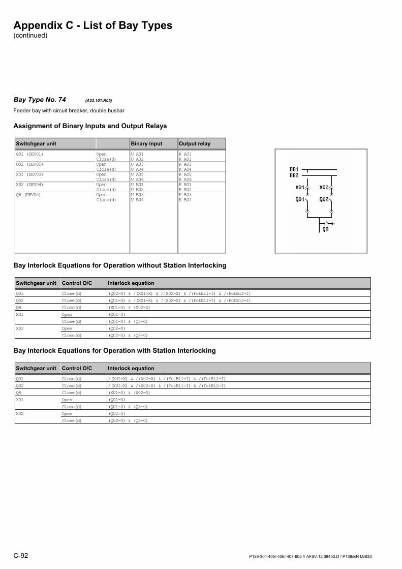
Appendix C - List of Bay Types (continued)
C-92 P139-304-405/-406/-407-605 // AFSV.12.09450.D / P139/EN M/B33
Bay Type No. 74 (A22.101.R05) Feeder bay with circuit breaker, double busbar
Assignment of Binary Inputs and Output Relays
Switchgear unit Binary input Output relay
Q01 (DEV01) Q02 (DEV02) X01 (DEV03) X02 (DEV04) Q8 (DEV05)
Open Close(d) Open Close(d) Open Close(d) Open Close(d) Open Close(d)
U A01 U A02 U A03 U A04 U A05 U A06 U B01 U B02 U B03 U B04
K A01 K A02K A03 K A04K A05 K A06K B01 K B02K B03 K B04
Bay Interlock Equations for Operation without Station Interlocking
Switchgear unit Control O/C Interlock equation
Q01 Close(d) (Q02=0) & /(X01=X) & /(X02=X) & /(FctBl1=I) & /(FctBl2=I) Q02 Close(d) (Q01=0) & /(X01=X) & /(X02=X) & /(FctBl1=I) & /(FctBl2=I) Q8 Close(d) (X01=0) & (X02=0) X01 Open (Q01=0) Close(d) (Q01=0) & (Q8=0) X02 Open (Q02=0) Close(d) (Q02=0) & (Q8=0)
Bay Interlock Equations for Operation with Station Interlocking
Switchgear unit Control O/C Interlock equation
Q01 Close(d) /(X01=X) & /(X02=X) & /(FctBl1=I) & /(FctBl2=I) Q02 Close(d) /(X01=X) & /(X02=X) & /(FctBl1=I) & /(FctBl2=I) Q8 Close(d) (X01=0) & (X02=0) X01 Open (Q01=0) Close(d) (Q01=0) & (Q8=0) X02 Open (Q02=0) Close(d) (Q02=0) & (Q8=0)
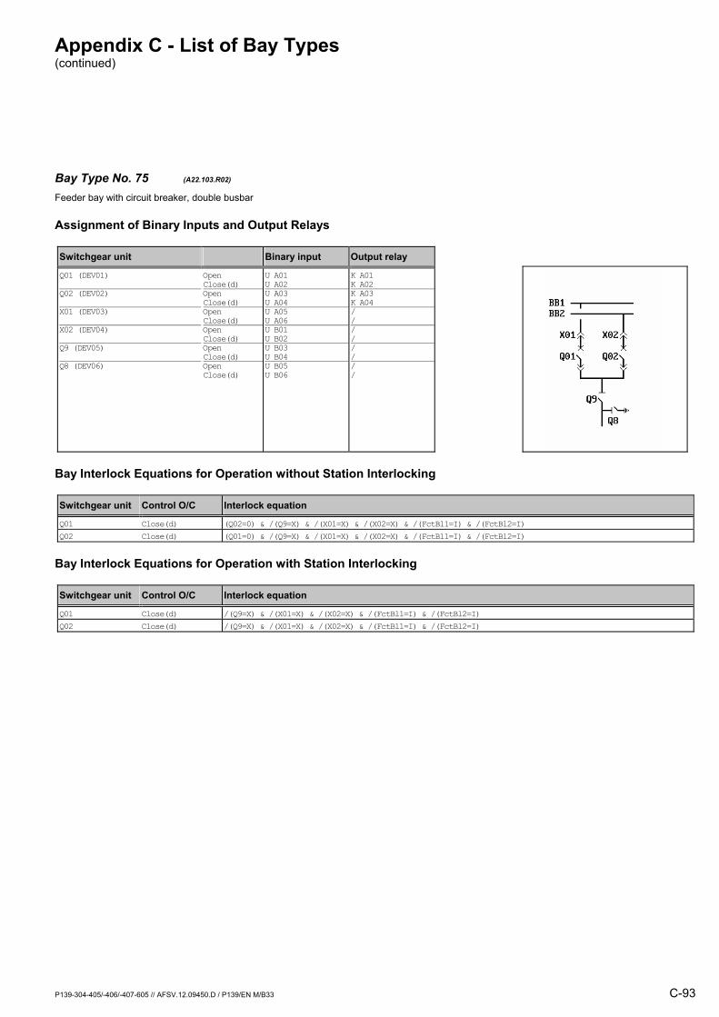
Appendix C - List of Bay Types (continued)
P139-304-405/-406/-407-605 // AFSV.12.09450.D / P139/EN M/B33 C-93
Bay Type No. 75 (A22.103.R02) Feeder bay with circuit breaker, double busbar
Assignment of Binary Inputs and Output Relays
Switchgear unit Binary input Output relay
Q01 (DEV01) Q02 (DEV02) X01 (DEV03) X02 (DEV04) Q9 (DEV05) Q8 (DEV06)
Open Close(d) Open Close(d) Open Close(d) Open Close(d) Open Close(d) Open Close(d)
U A01 U A02 U A03 U A04 U A05 U A06 U B01 U B02 U B03 U B04 U B05 U B06
K A01 K A02K A03 K A04/ // // // /
Bay Interlock Equations for Operation without Station Interlocking
Switchgear unit Control O/C Interlock equation
Q01 Close(d) (Q02=0) & /(Q9=X) & /(X01=X) & /(X02=X) & /(FctBl1=I) & /(FctBl2=I) Q02 Close(d) (Q01=0) & /(Q9=X) & /(X01=X) & /(X02=X) & /(FctBl1=I) & /(FctBl2=I)
Bay Interlock Equations for Operation with Station Interlocking
Switchgear unit Control O/C Interlock equation
Q01 Close(d) /(Q9=X) & /(X01=X) & /(X02=X) & /(FctBl1=I) & /(FctBl2=I) Q02 Close(d) /(Q9=X) & /(X01=X) & /(X02=X) & /(FctBl1=I) & /(FctBl2=I)

Appendix C - List of Bay Types (continued)
C-94 P139-304-405/-406/-407-605 // AFSV.12.09450.D / P139/EN M/B33
Bay Type No. 76 (A22.103.R03) Feeder bay with circuit breaker, double busbar
Assignment of Binary Inputs and Output Relays
Switchgear unit Binary input Output relay
Q01 (DEV01) Q02 (DEV02) X01 (DEV03) X02 (DEV04) Q9 (DEV05) Q8 (DEV06)
Open Close(d) Open Close(d) Open Close(d) Open Close(d) Open Close(d) Open Close(d)
U A01 U A02 U A03 U A04 U A05 U A06 U B01 U B02 U B03 U B04 U B05 U B06
K A01 K A02K A03 K A04/ // /K B03 K B04/ /
Bay Interlock Equations for Operation without Station Interlocking
Switchgear unit Control O/C Interlock equation
Q01 Close(d) (Q02=0) & /(Q9=X) & /(X01=X) & /(X02=X) & /(FctBl1=I) & /(FctBl2=I) Q02 Close(d) (Q01=0) & /(Q9=X) & /(X01=X) & /(X02=X) & /(FctBl1=I) & /(FctBl2=I) Q9 Open (Q01=0) & (Q02=0) Close(d) (Q01=0) & (Q02=0) & (Q8=0)
Bay Interlock Equations for Operation with Station Interlocking
Switchgear unit Control O/C Interlock equation
Q01 Close(d) /(Q9=X) & /(X01=X) & /(X02=X) & /(FctBl1=I) & /(FctBl2=I) Q02 Close(d) /(Q9=X) & /(X01=X) & /(X02=X) & /(FctBl1=I) & /(FctBl2=I) Q9 Open (Q01=0) & (Q02=0) Close(d) (Q01=0) & (Q02=0) & (Q8=0)
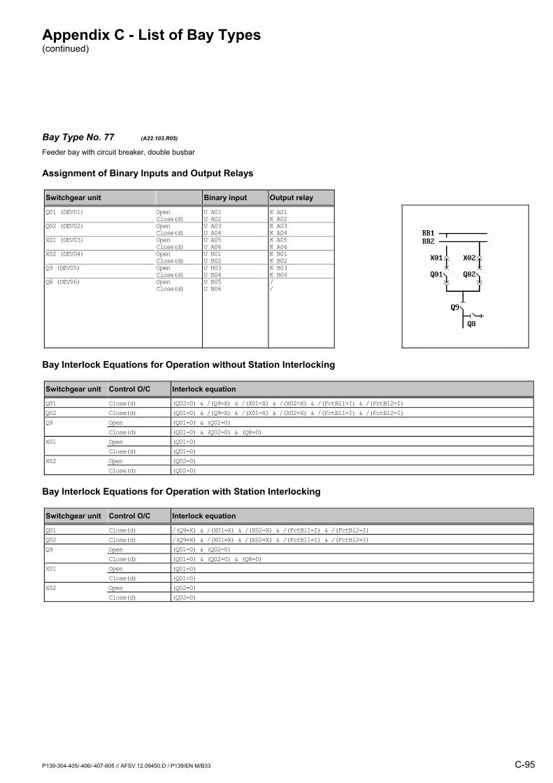
Appendix C - List of Bay Types (continued)
P139-304-405/-406/-407-605 // AFSV.12.09450.D / P139/EN M/B33 C-95
Bay Type No. 77 (A22.103.R05) Feeder bay with circuit breaker, double busbar
Assignment of Binary Inputs and Output Relays
Switchgear unit Binary input Output relay
Q01 (DEV01) Q02 (DEV02) X01 (DEV03) X02 (DEV04) Q9 (DEV05) Q8 (DEV06)
Open Close(d) Open Close(d) Open Close(d) Open Close(d) Open Close(d) Open Close(d)
U A01 U A02 U A03 U A04 U A05 U A06 U B01 U B02 U B03 U B04 U B05 U B06
K A01 K A02K A03 K A04K A05 K A06K B01 K B02K B03 K B04/ /
Bay Interlock Equations for Operation without Station Interlocking
Switchgear unit Control O/C Interlock equation
Q01 Close(d) (Q02=0) & /(Q9=X) & /(X01=X) & /(X02=X) & /(FctBl1=I) & /(FctBl2=I) Q02 Close(d) (Q01=0) & /(Q9=X) & /(X01=X) & /(X02=X) & /(FctBl1=I) & /(FctBl2=I) Q9 Open (Q01=0) & (Q02=0) Close(d) (Q01=0) & (Q02=0) & (Q8=0) X01 Open (Q01=0) Close(d) (Q01=0) X02 Open (Q02=0) Close(d) (Q02=0)
Bay Interlock Equations for Operation with Station Interlocking
Switchgear unit Control O/C Interlock equation
Q01 Close(d) /(Q9=X) & /(X01=X) & /(X02=X) & /(FctBl1=I) & /(FctBl2=I) Q02 Close(d) /(Q9=X) & /(X01=X) & /(X02=X) & /(FctBl1=I) & /(FctBl2=I) Q9 Open (Q01=0) & (Q02=0) Close(d) (Q01=0) & (Q02=0) & (Q8=0) X01 Open (Q01=0) Close(d) (Q01=0) X02 Open (Q02=0) Close(d) (Q02=0)
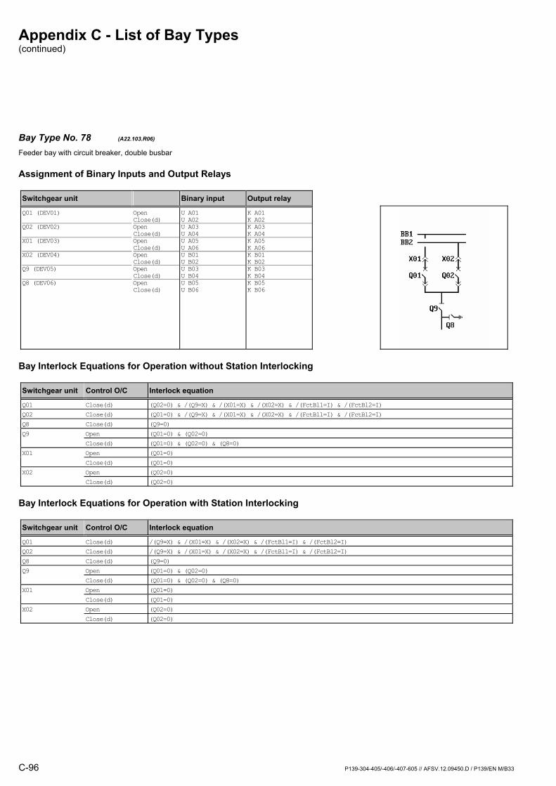
Appendix C - List of Bay Types (continued)
C-96 P139-304-405/-406/-407-605 // AFSV.12.09450.D / P139/EN M/B33
Bay Type No. 78 (A22.103.R06) Feeder bay with circuit breaker, double busbar
Assignment of Binary Inputs and Output Relays
Switchgear unit Binary input Output relay
Q01 (DEV01) Q02 (DEV02) X01 (DEV03) X02 (DEV04) Q9 (DEV05) Q8 (DEV06)
Open Close(d) Open Close(d) Open Close(d) Open Close(d) Open Close(d) Open Close(d)
U A01 U A02 U A03 U A04 U A05 U A06 U B01 U B02 U B03 U B04 U B05 U B06
K A01 K A02K A03 K A04K A05 K A06K B01 K B02K B03 K B04K B05 K B06
Bay Interlock Equations for Operation without Station Interlocking
Switchgear unit Control O/C Interlock equation
Q01 Close(d) (Q02=0) & /(Q9=X) & /(X01=X) & /(X02=X) & /(FctBl1=I) & /(FctBl2=I) Q02 Close(d) (Q01=0) & /(Q9=X) & /(X01=X) & /(X02=X) & /(FctBl1=I) & /(FctBl2=I) Q8 Close(d) (Q9=0) Q9 Open (Q01=0) & (Q02=0) Close(d) (Q01=0) & (Q02=0) & (Q8=0) X01 Open (Q01=0) Close(d) (Q01=0) X02 Open (Q02=0) Close(d) (Q02=0)
Bay Interlock Equations for Operation with Station Interlocking
Switchgear unit Control O/C Interlock equation
Q01 Close(d) /(Q9=X) & /(X01=X) & /(X02=X) & /(FctBl1=I) & /(FctBl2=I) Q02 Close(d) /(Q9=X) & /(X01=X) & /(X02=X) & /(FctBl1=I) & /(FctBl2=I) Q8 Close(d) (Q9=0) Q9 Open (Q01=0) & (Q02=0) Close(d) (Q01=0) & (Q02=0) & (Q8=0) X01 Open (Q01=0) Close(d) (Q01=0) X02 Open (Q02=0) Close(d) (Q02=0)
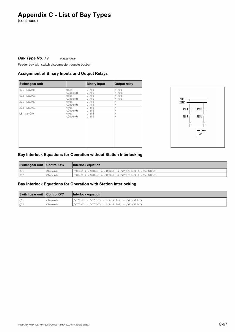
Appendix C - List of Bay Types (continued)
P139-304-405/-406/-407-605 // AFSV.12.09450.D / P139/EN M/B33 C-97
Bay Type No. 79 (A22.201.R02) Feeder bay with switch disconnector, double busbar
Assignment of Binary Inputs and Output Relays
Switchgear unit Binary input Output relay
Q01 (DEV01) Q02 (DEV02) X01 (DEV03) X02 (DEV04) Q8 (DEV05)
Open Close(d) Open Close(d) Open Close(d) Open Close(d) Open Close(d)
U A01 U A02 U A03 U A04 U A05 U A06 U B01 U B02 U B03 U B04
K A01 K A02K A03 K A04/ // // /
Bay Interlock Equations for Operation without Station Interlocking
Switchgear unit Control O/C Interlock equation
Q01 Close(d) (Q02=0) & /(X01=X) & /(X02=X) & /(FctBl1=I) & /(FctBl2=I) Q02 Close(d) (Q01=0) & /(X01=X) & /(X02=X) & /(FctBl1=I) & /(FctBl2=I)
Bay Interlock Equations for Operation with Station Interlocking
Switchgear unit Control O/C Interlock equation
Q01 Close(d) /(X01=X) & /(X02=X) & /(FctBl1=I) & /(FctBl2=I) Q02 Close(d) /(X01=X) & /(X02=X) & /(FctBl1=I) & /(FctBl2=I)

Appendix C - List of Bay Types (continued)
C-98 P139-304-405/-406/-407-605 // AFSV.12.09450.D / P139/EN M/B33
Bay Type No. 80 (A22.201.R04) Feeder bay with switch disconnector, double busbar
Assignment of Binary Inputs and Output Relays
Switchgear unit Binary input Output relay
Q01 (DEV01) Q02 (DEV02) X01 (DEV03) X02 (DEV04) Q8 (DEV05)
Open Close(d) Open Close(d) Open Close(d) Open Close(d) Open Close(d)
U A01 U A02 U A03 U A04 U A05 U A06 U B01 U B02 U B03 U B04
K A01 K A02K A03 K A04K A05 K A06K B01 K B02/ /
Bay Interlock Equations for Operation without Station Interlocking
Switchgear unit Control O/C Interlock equation
Q01 Close(d) (Q02=0) & /(X01=X) & /(X02=X) & /(FctBl1=I) & /(FctBl2=I) Q02 Close(d) (Q01=0) & /(X01=X) & /(X02=X) & /(FctBl1=I) & /(FctBl2=I) X01 Open (Q01=0) Close(d) (Q01=0) & (Q8=0) X02 Open (Q02=0) Close(d) (Q02=0) & (Q8=0)
Bay Interlock Equations for Operation with Station Interlocking
Switchgear unit Control O/C Interlock equation
Q01 Close(d) /(X01=X) & /(X02=X) & /(FctBl1=I) & /(FctBl2=I) Q02 Close(d) /(X01=X) & /(X02=X) & /(FctBl1=I) & /(FctBl2=I) X01 Open (Q01=0) Close(d) (Q01=0) & (Q8=0) X02 Open (Q02=0) Close(d) (Q02=0) & (Q8=0)
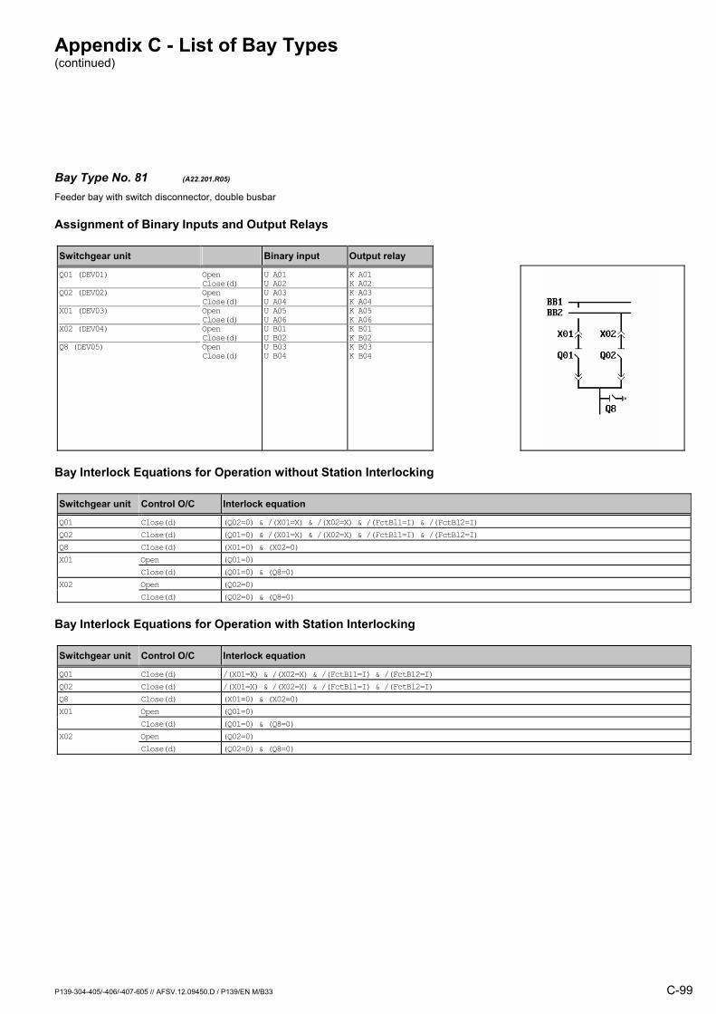
Appendix C - List of Bay Types (continued)
P139-304-405/-406/-407-605 // AFSV.12.09450.D / P139/EN M/B33 C-99
Bay Type No. 81 (A22.201.R05) Feeder bay with switch disconnector, double busbar
Assignment of Binary Inputs and Output Relays
Switchgear unit Binary input Output relay
Q01 (DEV01) Q02 (DEV02) X01 (DEV03) X02 (DEV04) Q8 (DEV05)
Open Close(d) Open Close(d) Open Close(d) Open Close(d) Open Close(d)
U A01 U A02 U A03 U A04 U A05 U A06 U B01 U B02 U B03 U B04
K A01 K A02K A03 K A04K A05 K A06K B01 K B02K B03 K B04
Bay Interlock Equations for Operation without Station Interlocking
Switchgear unit Control O/C Interlock equation
Q01 Close(d) (Q02=0) & /(X01=X) & /(X02=X) & /(FctBl1=I) & /(FctBl2=I) Q02 Close(d) (Q01=0) & /(X01=X) & /(X02=X) & /(FctBl1=I) & /(FctBl2=I) Q8 Close(d) (X01=0) & (X02=0) X01 Open (Q01=0) Close(d) (Q01=0) & (Q8=0) X02 Open (Q02=0) Close(d) (Q02=0) & (Q8=0)
Bay Interlock Equations for Operation with Station Interlocking
Switchgear unit Control O/C Interlock equation
Q01 Close(d) /(X01=X) & /(X02=X) & /(FctBl1=I) & /(FctBl2=I) Q02 Close(d) /(X01=X) & /(X02=X) & /(FctBl1=I) & /(FctBl2=I) Q8 Close(d) (X01=0) & (X02=0) X01 Open (Q01=0) Close(d) (Q01=0) & (Q8=0) X02 Open (Q02=0) Close(d) (Q02=0) & (Q8=0)
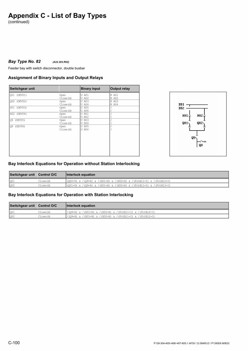
Appendix C - List of Bay Types (continued)
C-100 P139-304-405/-406/-407-605 // AFSV.12.09450.D / P139/EN M/B33
Bay Type No. 82 (A22.203.R02) Feeder bay with switch disconnector, double busbar
Assignment of Binary Inputs and Output Relays
Switchgear unit Binary input Output relay
Q01 (DEV01) Q02 (DEV02) X01 (DEV03) X02 (DEV04) Q9 (DEV05) Q8 (DEV06)
Open Close(d) Open Close(d) Open Close(d) Open Close(d) Open Close(d) Open Close(d)
U A01 U A02 U A03 U A04 U A05 U A06 U B01 U B02 U B03 U B04 U B05 U B06
K A01 K A02K A03 K A04/ // // // /
Bay Interlock Equations for Operation without Station Interlocking
Switchgear unit Control O/C Interlock equation
Q01 Close(d) (Q02=0) & /(Q9=X) & /(X01=X) & /(X02=X) & /(FctBl1=I) & /(FctBl2=I) Q02 Close(d) (Q01=0) & /(Q9=X) & /(X01=X) & /(X02=X) & /(FctBl1=I) & /(FctBl2=I)
Bay Interlock Equations for Operation with Station Interlocking
Switchgear unit Control O/C Interlock equation
Q01 Close(d) /(Q9=X) & /(X01=X) & /(X02=X) & /(FctBl1=I) & /(FctBl2=I) Q02 Close(d) /(Q9=X) & /(X01=X) & /(X02=X) & /(FctBl1=I) & /(FctBl2=I)
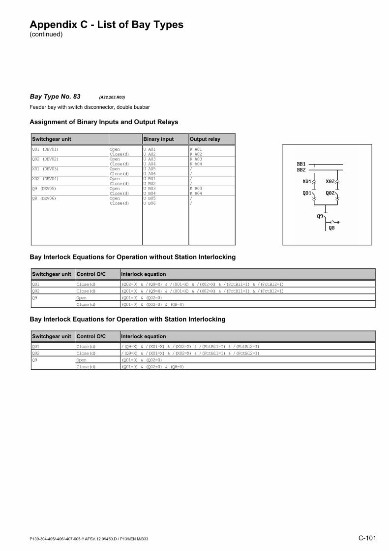
Appendix C - List of Bay Types (continued)
P139-304-405/-406/-407-605 // AFSV.12.09450.D / P139/EN M/B33 C-101
Bay Type No. 83 (A22.203.R03) Feeder bay with switch disconnector, double busbar
Assignment of Binary Inputs and Output Relays
Switchgear unit Binary input Output relay
Q01 (DEV01) Q02 (DEV02) X01 (DEV03) X02 (DEV04) Q9 (DEV05) Q8 (DEV06)
Open Close(d) Open Close(d) Open Close(d) Open Close(d) Open Close(d) Open Close(d)
U A01 U A02 U A03 U A04 U A05 U A06 U B01 U B02 U B03 U B04 U B05 U B06
K A01 K A02K A03 K A04/ // /K B03 K B04/ /
Bay Interlock Equations for Operation without Station Interlocking
Switchgear unit Control O/C Interlock equation
Q01 Close(d) (Q02=0) & /(Q9=X) & /(X01=X) & /(X02=X) & /(FctBl1=I) & /(FctBl2=I) Q02 Close(d) (Q01=0) & /(Q9=X) & /(X01=X) & /(X02=X) & /(FctBl1=I) & /(FctBl2=I) Q9 Open (Q01=0) & (Q02=0) Close(d) (Q01=0) & (Q02=0) & (Q8=0)
Bay Interlock Equations for Operation with Station Interlocking
Switchgear unit Control O/C Interlock equation
Q01 Close(d) /(Q9=X) & /(X01=X) & /(X02=X) & /(FctBl1=I) & /(FctBl2=I) Q02 Close(d) /(Q9=X) & /(X01=X) & /(X02=X) & /(FctBl1=I) & /(FctBl2=I) Q9 Open (Q01=0) & (Q02=0) Close(d) (Q01=0) & (Q02=0) & (Q8=0)
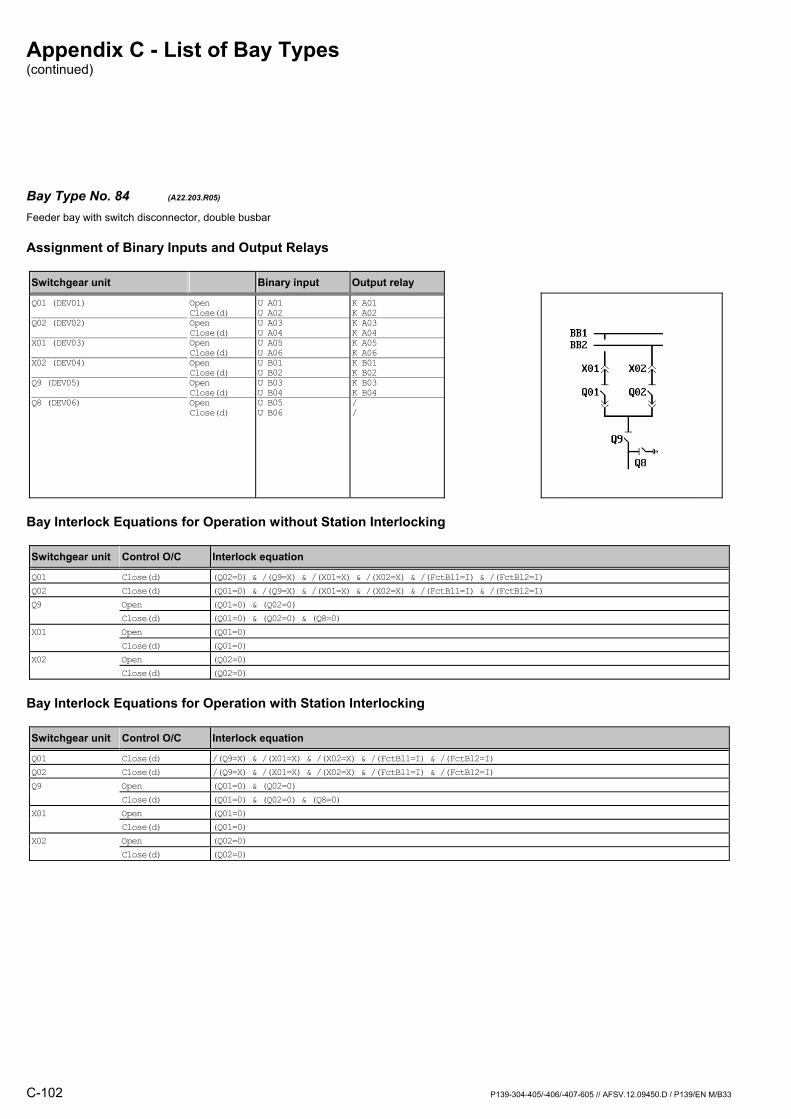
Appendix C - List of Bay Types (continued)
C-102 P139-304-405/-406/-407-605 // AFSV.12.09450.D / P139/EN M/B33
Bay Type No. 84 (A22.203.R05) Feeder bay with switch disconnector, double busbar
Assignment of Binary Inputs and Output Relays
Switchgear unit Binary input Output relay
Q01 (DEV01) Q02 (DEV02) X01 (DEV03) X02 (DEV04) Q9 (DEV05) Q8 (DEV06)
Open Close(d) Open Close(d) Open Close(d) Open Close(d) Open Close(d) Open Close(d)
U A01 U A02 U A03 U A04 U A05 U A06 U B01 U B02 U B03 U B04 U B05 U B06
K A01 K A02K A03 K A04K A05 K A06K B01 K B02K B03 K B04/ /
Bay Interlock Equations for Operation without Station Interlocking
Switchgear unit Control O/C Interlock equation
Q01 Close(d) (Q02=0) & /(Q9=X) & /(X01=X) & /(X02=X) & /(FctBl1=I) & /(FctBl2=I) Q02 Close(d) (Q01=0) & /(Q9=X) & /(X01=X) & /(X02=X) & /(FctBl1=I) & /(FctBl2=I) Q9 Open (Q01=0) & (Q02=0) Close(d) (Q01=0) & (Q02=0) & (Q8=0) X01 Open (Q01=0) Close(d) (Q01=0) X02 Open (Q02=0) Close(d) (Q02=0)
Bay Interlock Equations for Operation with Station Interlocking
Switchgear unit Control O/C Interlock equation
Q01 Close(d) /(Q9=X) & /(X01=X) & /(X02=X) & /(FctBl1=I) & /(FctBl2=I) Q02 Close(d) /(Q9=X) & /(X01=X) & /(X02=X) & /(FctBl1=I) & /(FctBl2=I) Q9 Open (Q01=0) & (Q02=0) Close(d) (Q01=0) & (Q02=0) & (Q8=0) X01 Open (Q01=0) Close(d) (Q01=0) X02 Open (Q02=0) Close(d) (Q02=0)
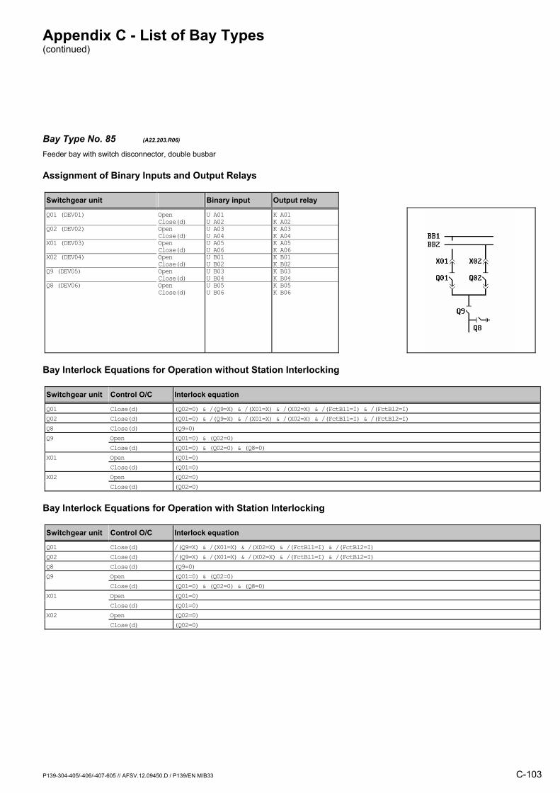
Appendix C - List of Bay Types (continued)
P139-304-405/-406/-407-605 // AFSV.12.09450.D / P139/EN M/B33 C-103
Bay Type No. 85 (A22.203.R06) Feeder bay with switch disconnector, double busbar
Assignment of Binary Inputs and Output Relays
Switchgear unit Binary input Output relay
Q01 (DEV01) Q02 (DEV02) X01 (DEV03) X02 (DEV04) Q9 (DEV05) Q8 (DEV06)
Open Close(d) Open Close(d) Open Close(d) Open Close(d) Open Close(d) Open Close(d)
U A01 U A02 U A03 U A04 U A05 U A06 U B01 U B02 U B03 U B04 U B05 U B06
K A01 K A02K A03 K A04K A05 K A06K B01 K B02K B03 K B04K B05 K B06
Bay Interlock Equations for Operation without Station Interlocking
Switchgear unit Control O/C Interlock equation
Q01 Close(d) (Q02=0) & /(Q9=X) & /(X01=X) & /(X02=X) & /(FctBl1=I) & /(FctBl2=I) Q02 Close(d) (Q01=0) & /(Q9=X) & /(X01=X) & /(X02=X) & /(FctBl1=I) & /(FctBl2=I) Q8 Close(d) (Q9=0) Q9 Open (Q01=0) & (Q02=0) Close(d) (Q01=0) & (Q02=0) & (Q8=0) X01 Open (Q01=0) Close(d) (Q01=0) X02 Open (Q02=0) Close(d) (Q02=0)
Bay Interlock Equations for Operation with Station Interlocking
Switchgear unit Control O/C Interlock equation
Q01 Close(d) /(Q9=X) & /(X01=X) & /(X02=X) & /(FctBl1=I) & /(FctBl2=I) Q02 Close(d) /(Q9=X) & /(X01=X) & /(X02=X) & /(FctBl1=I) & /(FctBl2=I) Q8 Close(d) (Q9=0) Q9 Open (Q01=0) & (Q02=0) Close(d) (Q01=0) & (Q02=0) & (Q8=0) X01 Open (Q01=0) Close(d) (Q01=0) X02 Open (Q02=0) Close(d) (Q02=0)

Appendix C - List of Bay Types (continued)
C-104 P139-304-405/-406/-407-605 // AFSV.12.09450.D / P139/EN M/B33
Bay Type No. 86 (A23.104.M03) Feeder bay with circuit breaker, double busbar,direct motor control
Assignment of Binary Inputs and Output Relays
Switchgear unit Binary input Output relay
Q0 (DEV01) Q1 (DEV02) Q2 (DEV03) Mot.relay (SIG_1: Signal S012) Shunt wd. (CMD_1: Command C011) Mot.relay (CMD_1: Command C012)
Open Close(d) Open Close(d) Open Close(d)
U A01 U A02 U A03 U A04 U A05 U A06 U B06 / /
K A01 K A02K A03 K A04K A05 K A06/
K B05
K B06
Bay Interlock Equations for Operation without Station Interlocking
Switchgear unit Control O/C Interlock equation
Q0 Close(d) /(Q1=X) & /(Q2=X) & /(FctBl1=I) & /(FctBl2=I) Q1 Open (Q0=0) & (Q2=0) Close(d) (Q0=0) & (Q2=0) Q2 Open (Q0=0) & (Q1=0) Close(d) (Q0=0) & (Q1=0)
Bay Interlock Equations for Operation with Station Interlocking
Switchgear unit Control O/C Interlock equation
Q0 Close(d) /(Q1=X) & /(Q2=X) & /(FctBl1=I) & /(FctBl2=I)

Appendix C - List of Bay Types (continued)
P139-304-405/-406/-407-605 // AFSV.12.09450.D / P139/EN M/B33 C-105
Bay Type No. 87 (A23.104.R01) Feeder bay with circuit breaker, double busbar
Assignment of Binary Inputs and Output Relays
Switchgear unit Binary input Output relay
Q0 (DEV01) Q1 (DEV02) Q2 (DEV03)
Open Close(d) Open Close(d) Open Close(d)
U A01 U A02 U A03 U A04 U A05 U A06
K A01 K A02/ // /
Bay Interlock Equations for Operation without Station Interlocking
Switchgear unit Control O/C Interlock equation
Q0 Close(d) /(Q1=X) & /(Q2=X) & /(FctBl1=I) & /(FctBl2=I)
Bay Interlock Equations for Operation with Station Interlocking
Switchgear unit Control O/C Interlock equation
Q0 Close(d) /(Q1=X) & /(Q2=X) & /(FctBl1=I) & /(FctBl2=I)
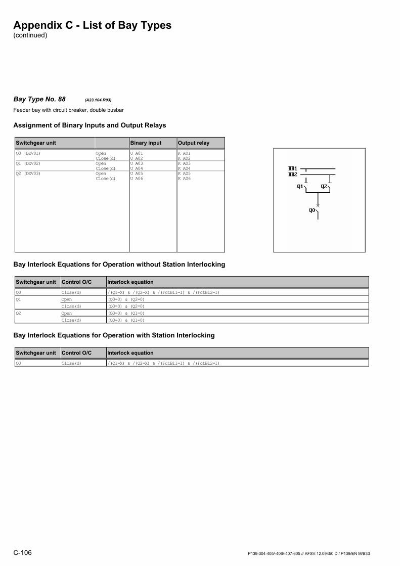
Appendix C - List of Bay Types (continued)
C-106 P139-304-405/-406/-407-605 // AFSV.12.09450.D / P139/EN M/B33
Bay Type No. 88 (A23.104.R03) Feeder bay with circuit breaker, double busbar
Assignment of Binary Inputs and Output Relays
Switchgear unit Binary input Output relay
Q0 (DEV01) Q1 (DEV02) Q2 (DEV03)
Open Close(d) Open Close(d) Open Close(d)
U A01 U A02 U A03 U A04 U A05 U A06
K A01 K A02K A03 K A04K A05 K A06
Bay Interlock Equations for Operation without Station Interlocking
Switchgear unit Control O/C Interlock equation
Q0 Close(d) /(Q1=X) & /(Q2=X) & /(FctBl1=I) & /(FctBl2=I) Q1 Open (Q0=0) & (Q2=0) Close(d) (Q0=0) & (Q2=0) Q2 Open (Q0=0) & (Q1=0) Close(d) (Q0=0) & (Q1=0)
Bay Interlock Equations for Operation with Station Interlocking
Switchgear unit Control O/C Interlock equation
Q0 Close(d) /(Q1=X) & /(Q2=X) & /(FctBl1=I) & /(FctBl2=I)

Appendix C - List of Bay Types (continued)
P139-304-405/-406/-407-605 // AFSV.12.09450.D / P139/EN M/B33 C-107
Bay Type No. 89 (A23.105.M04) Feeder bay with circuit breaker, double busbar,direct motor control
Assignment of Binary Inputs and Output Relays
Switchgear unit Binary input Output relay
Q0 (DEV01) Q1 (DEV02) Q2 (DEV03) Q8 (DEV04) Mot.relay (SIG_1: Signal S012) Shunt wd. (CMD_1: Command C011) Mot.relay (CMD_1: Command C012)
Open Close(d) Open Close(d) Open Close(d) Open Close(d)
U A01 U A02 U A03 U A04 U A05 U A06 U B01 U B02 U B06 / /
K A01 K A02K A03 K A04K A05 K A06K B01 K B02/
K B05
K B06
Bay Interlock Equations for Operation without Station Interlocking
Switchgear unit Control O/C Interlock equation
Q0 Close(d) /(Q1=X) & /(Q2=X) & (Q8=0) & /(FctBl1=I) & /(FctBl2=I) Q1 Open (Q0=0) & (Q2=0) Close(d) (Q0=0) & (Q2=0) & (Q8=0) Q2 Open (Q0=0) & (Q1=0) Close(d) (Q0=0) & (Q1=0) & (Q8=0) Q8 Close(d) (Q0=0) & (Q1=0) & (Q2=0)
Bay Interlock Equations for Operation with Station Interlocking
Switchgear unit Control O/C Interlock equation
Q0 Close(d) /(Q1=X) & /(Q2=X) & (Q8=0) & /(FctBl1=I) & /(FctBl2=I) Q1 Close(d) (Q8=0) Q2 Close(d) (Q8=0) Q8 Close(d) (Q0=0) & (Q1=0) & (Q2=0)

Appendix C - List of Bay Types (continued)
C-108 P139-304-405/-406/-407-605 // AFSV.12.09450.D / P139/EN M/B33
Bay Type No. 90 (A23.105.R01) Feeder bay with circuit breaker, double busbar
Assignment of Binary Inputs and Output Relays
Switchgear unit Binary input Output relay
Q0 (DEV01) Q1 (DEV02) Q2 (DEV03) Q8 (DEV04)
Open Close(d) Open Close(d) Open Close(d) Open Close(d)
U A01 U A02 U A03 U A04 U A05 U A06 U B01 U B02
K A01 K A02/ // // /
Bay Interlock Equations for Operation without Station Interlocking
Switchgear unit Control O/C Interlock equation
Q0 Close(d) /(Q1=X) & /(Q2=X) & (Q8=0) & /(FctBl1=I) & /(FctBl2=I)
Bay Interlock Equations for Operation with Station Interlocking
Switchgear unit Control O/C Interlock equation
Q0 Close(d) /(Q1=X) & /(Q2=X) & (Q8=0) & /(FctBl1=I) & /(FctBl2=I)

Appendix C - List of Bay Types (continued)
P139-304-405/-406/-407-605 // AFSV.12.09450.D / P139/EN M/B33 C-109
Bay Type No. 91 (A23.105.R03) Feeder bay with circuit breaker, double busbar
Assignment of Binary Inputs and Output Relays
Switchgear unit Binary input Output relay
Q0 (DEV01) Q1 (DEV02) Q2 (DEV03) Q8 (DEV04)
Open Close(d) Open Close(d) Open Close(d) Open Close(d)
U A01 U A02 U A03 U A04 U A05 U A06 U B01 U B02
K A01 K A02K A03 K A04K A05 K A06/ /
Bay Interlock Equations for Operation without Station Interlocking
Switchgear unit Control O/C Interlock equation
Q0 Close(d) /(Q1=X) & /(Q2=X) & (Q8=0) & /(FctBl1=I) & /(FctBl2=I) Q1 Open (Q0=0) & (Q2=0) Close(d) (Q0=0) & (Q2=0) & (Q8=0) Q2 Open (Q0=0) & (Q1=0) Close(d) (Q0=0) & (Q1=0) & (Q8=0)
Bay Interlock Equations for Operation with Station Interlocking
Switchgear unit Control O/C Interlock equation
Q0 Close(d) /(Q1=X) & /(Q2=X) & (Q8=0) & /(FctBl1=I) & /(FctBl2=I) Q1 Close(d) (Q8=0) Q2 Close(d) (Q8=0)
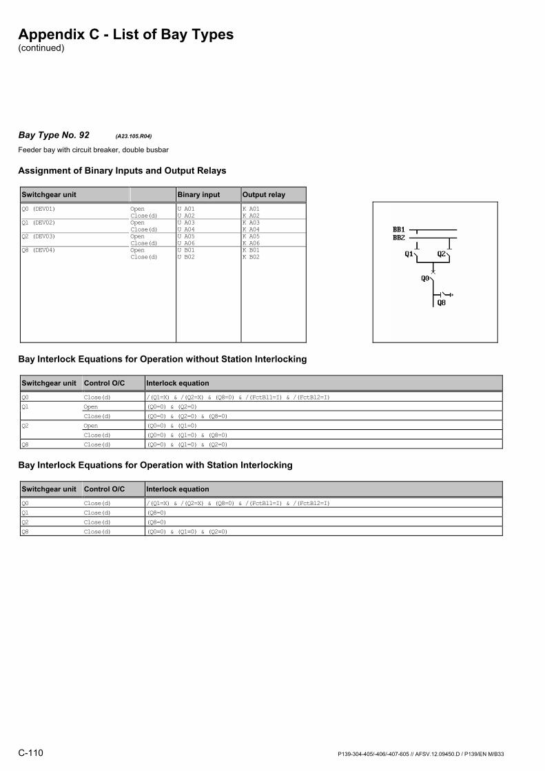
Appendix C - List of Bay Types (continued)
C-110 P139-304-405/-406/-407-605 // AFSV.12.09450.D / P139/EN M/B33
Bay Type No. 92 (A23.105.R04) Feeder bay with circuit breaker, double busbar
Assignment of Binary Inputs and Output Relays
Switchgear unit Binary input Output relay
Q0 (DEV01) Q1 (DEV02) Q2 (DEV03) Q8 (DEV04)
Open Close(d) Open Close(d) Open Close(d) Open Close(d)
U A01 U A02 U A03 U A04 U A05 U A06 U B01 U B02
K A01 K A02K A03 K A04K A05 K A06K B01 K B02
Bay Interlock Equations for Operation without Station Interlocking
Switchgear unit Control O/C Interlock equation
Q0 Close(d) /(Q1=X) & /(Q2=X) & (Q8=0) & /(FctBl1=I) & /(FctBl2=I) Q1 Open (Q0=0) & (Q2=0) Close(d) (Q0=0) & (Q2=0) & (Q8=0) Q2 Open (Q0=0) & (Q1=0) Close(d) (Q0=0) & (Q1=0) & (Q8=0) Q8 Close(d) (Q0=0) & (Q1=0) & (Q2=0)
Bay Interlock Equations for Operation with Station Interlocking
Switchgear unit Control O/C Interlock equation
Q0 Close(d) /(Q1=X) & /(Q2=X) & (Q8=0) & /(FctBl1=I) & /(FctBl2=I) Q1 Close(d) (Q8=0) Q2 Close(d) (Q8=0) Q8 Close(d) (Q0=0) & (Q1=0) & (Q2=0)

Appendix C - List of Bay Types (continued)
P139-304-405/-406/-407-605 // AFSV.12.09450.D / P139/EN M/B33 C-111
Bay Type No. 93 (A23.106.M04) Feeder bay with circuit breaker, double busbar,direct motor control
Assignment of Binary Inputs and Output Relays
Switchgear unit Binary input Output relay
Q0 (DEV01) Q1 (DEV02) Q2 (DEV03) Q9 (DEV04) Mot.relay (SIG_1: Signal S012) Shunt wd. (CMD_1: Command C011) Mot.relay (CMD_1: Command C012)
Open Close(d) Open Close(d) Open Close(d) Open Close(d)
U A01 U A02 U A03 U A04 U A05 U A06 U B01 U B02 U B06 / /
K A01 K A02K A03 K A04K A05 K A06K B01 K B02/
K B05
K B06
Bay Interlock Equations for Operation without Station Interlocking
Switchgear unit Control O/C Interlock equation
Q0 Close(d) /(Q1=X) & /(Q2=X) & /(Q9=X) & /(FctBl1=I) & /(FctBl2=I) Q1 Open (Q0=0) & (Q2=0) Close(d) (Q0=0) & (Q2=0) Q2 Open (Q0=0) & (Q1=0) Close(d) (Q0=0) & (Q1=0) Q9 Open (Q0=0) Close(d) (Q0=0)
Bay Interlock Equations for Operation with Station Interlocking
Switchgear unit Control O/C Interlock equation
Q0 Close(d) /(Q1=X) & /(Q2=X) & /(Q9=X) & /(FctBl1=I) & /(FctBl2=I) Q9 Open (Q0=0) Close(d) (Q0=0)

Appendix C - List of Bay Types (continued)
C-112 P139-304-405/-406/-407-605 // AFSV.12.09450.D / P139/EN M/B33
Bay Type No. 94 (A23.106.R01) Feeder bay with circuit breaker, double busbar
Assignment of Binary Inputs and Output Relays
Switchgear unit Binary input Output relay
Q0 (DEV01) Q1 (DEV02) Q2 (DEV03) Q9 (DEV04)
Open Close(d) Open Close(d) Open Close(d) Open Close(d)
U A01 U A02 U A03 U A04 U A05 U A06 U B01 U B02
K A01 K A02/ // // /
Bay Interlock Equations for Operation without Station Interlocking
Switchgear unit Control O/C Interlock equation
Q0 Close(d) /(Q1=X) & /(Q2=X) & /(Q9=X) & /(FctBl1=I) & /(FctBl2=I)
Bay Interlock Equations for Operation with Station Interlocking
Switchgear unit Control O/C Interlock equation
Q0 Close(d) /(Q1=X) & /(Q2=X) & /(Q9=X) & /(FctBl1=I) & /(FctBl2=I)

Appendix C - List of Bay Types (continued)
P139-304-405/-406/-407-605 // AFSV.12.09450.D / P139/EN M/B33 C-113
Bay Type No. 95 (A23.106.R04) Feeder bay with circuit breaker, double busbar
Assignment of Binary Inputs and Output Relays
Switchgear unit Binary input Output relay
Q0 (DEV01) Q1 (DEV02) Q2 (DEV03) Q9 (DEV04)
Open Close(d) Open Close(d) Open Close(d) Open Close(d)
U A01 U A02 U A03 U A04 U A05 U A06 U B01 U B02
K A01 K A02K A03 K A04K A05 K A06K B01 K B02
Bay Interlock Equations for Operation without Station Interlocking
Switchgear unit Control O/C Interlock equation
Q0 Close(d) /(Q1=X) & /(Q2=X) & /(Q9=X) & /(FctBl1=I) & /(FctBl2=I) Q1 Open (Q0=0) & (Q2=0) Close(d) (Q0=0) & (Q2=0) Q2 Open (Q0=0) & (Q1=0) Close(d) (Q0=0) & (Q1=0) Q9 Open (Q0=0) Close(d) (Q0=0)
Bay Interlock Equations for Operation with Station Interlocking
Switchgear unit Control O/C Interlock equation
Q0 Close(d) /(Q1=X) & /(Q2=X) & /(Q9=X) & /(FctBl1=I) & /(FctBl2=I) Q9 Open (Q0=0) Close(d) (Q0=0)
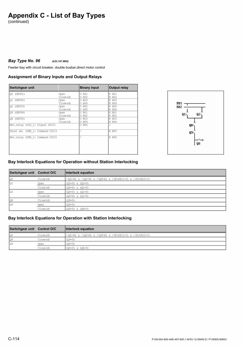
Appendix C - List of Bay Types (continued)
C-114 P139-304-405/-406/-407-605 // AFSV.12.09450.D / P139/EN M/B33
Bay Type No. 96 (A23.107.M05) Feeder bay with circuit breaker, double busbar,direct motor control
Assignment of Binary Inputs and Output Relays
Switchgear unit Binary input Output relay
Q0 (DEV01) Q1 (DEV02) Q2 (DEV03) Q9 (DEV04) Q8 (DEV05) Mot.relay (SIG_1: Signal S012) Shunt wd. (CMD_1: Command C011) Mot.relay (CMD_1: Command C012)
Open Close(d) Open Close(d) Open Close(d) Open Close(d) Open Close(d)
U A01 U A02 U A03 U A04 U A05 U A06 U B01 U B02 U B03 U B04 U B06 / /
K A01 K A02K A03 K A04K A05 K A06K B01 K B02K B03 K B04/
K B05
K B06
Bay Interlock Equations for Operation without Station Interlocking
Switchgear unit Control O/C Interlock equation
Q0 Close(d) /(Q1=X) & /(Q2=X) & /(Q9=X) & /(FctBl1=I) & /(FctBl2=I) Q1 Open (Q0=0) & (Q2=0) Close(d) (Q0=0) & (Q2=0) Q2 Open (Q0=0) & (Q1=0) Close(d) (Q0=0) & (Q1=0) Q8 Close(d) (Q9=0) Q9 Open (Q0=0) Close(d) (Q0=0) & (Q8=0)
Bay Interlock Equations for Operation with Station Interlocking
Switchgear unit Control O/C Interlock equation
Q0 Close(d) /(Q1=X) & /(Q2=X) & /(Q9=X) & /(FctBl1=I) & /(FctBl2=I) Q8 Close(d) (Q9=0) Q9 Open (Q0=0) Close(d) (Q0=0) & (Q8=0)

Appendix C - List of Bay Types (continued)
P139-304-405/-406/-407-605 // AFSV.12.09450.D / P139/EN M/B33 C-115
Bay Type No. 97 (A23.107.R01) Feeder bay with circuit breaker, double busbar
Assignment of Binary Inputs and Output Relays
Switchgear unit Binary input Output relay
Q0 (DEV01) Q1 (DEV02) Q2 (DEV03) Q9 (DEV04) Q8 (DEV05)
Open Close(d) Open Close(d) Open Close(d) Open Close(d) Open Close(d)
U A01 U A02 U A03 U A04 U A05 U A06 U B01 U B02 U B03 U B04
K A01 K A02/ // // // /
Bay Interlock Equations for Operation without Station Interlocking
Switchgear unit Control O/C Interlock equation
Q0 Close(d) /(Q1=X) & /(Q2=X) & /(Q9=X) & /(FctBl1=I) & /(FctBl2=I)
Bay Interlock Equations for Operation with Station Interlocking
Switchgear unit Control O/C Interlock equation
Q0 Close(d) /(Q1=X) & /(Q2=X) & /(Q9=X) & /(FctBl1=I) & /(FctBl2=I)

Appendix C - List of Bay Types (continued)
C-116 P139-304-405/-406/-407-605 // AFSV.12.09450.D / P139/EN M/B33
Bay Type No. 98 (A23.107.R04) Feeder bay with circuit breaker, double busbar
Assignment of Binary Inputs and Output Relays
Switchgear unit Binary input Output relay
Q0 (DEV01) Q1 (DEV02) Q2 (DEV03) Q9 (DEV04) Q8 (DEV05)
Open Close(d) Open Close(d) Open Close(d) Open Close(d) Open Close(d)
U A01 U A02 U A03 U A04 U A05 U A06 U B01 U B02 U B03 U B04
K A01 K A02K A03 K A04K A05 K A06K B01 K B02/ /
Bay Interlock Equations for Operation without Station Interlocking
Switchgear unit Control O/C Interlock equation
Q0 Close(d) /(Q1=X) & /(Q2=X) & /(Q9=X) & /(FctBl1=I) & /(FctBl2=I) Q1 Open (Q0=0) & (Q2=0) Close(d) (Q0=0) & (Q2=0) Q2 Open (Q0=0) & (Q1=0) Close(d) (Q0=0) & (Q1=0) Q9 Open (Q0=0) Close(d) (Q0=0) & (Q8=0)
Bay Interlock Equations for Operation with Station Interlocking
Switchgear unit Control O/C Interlock equation
Q0 Close(d) /(Q1=X) & /(Q2=X) & /(Q9=X) & /(FctBl1=I) & /(FctBl2=I) Q9 Open (Q0=0) Close(d) (Q0=0) & (Q8=0)
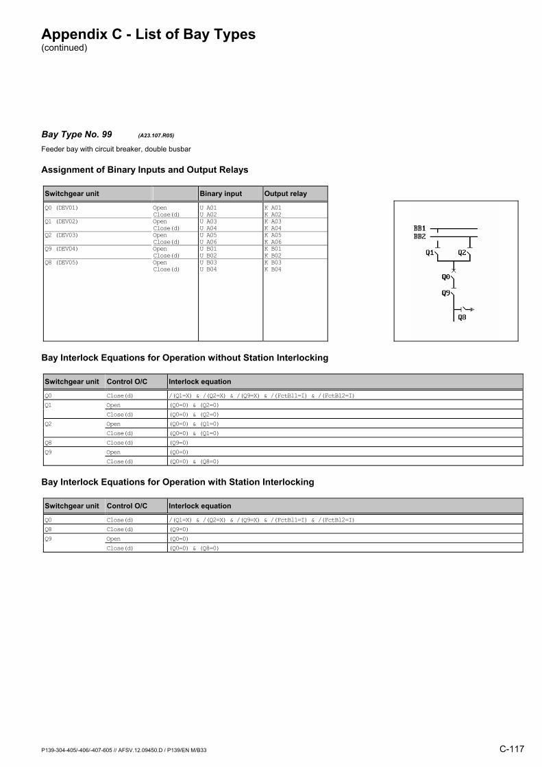
Appendix C - List of Bay Types (continued)
P139-304-405/-406/-407-605 // AFSV.12.09450.D / P139/EN M/B33 C-117
Bay Type No. 99 (A23.107.R05) Feeder bay with circuit breaker, double busbar
Assignment of Binary Inputs and Output Relays
Switchgear unit Binary input Output relay
Q0 (DEV01) Q1 (DEV02) Q2 (DEV03) Q9 (DEV04) Q8 (DEV05)
Open Close(d) Open Close(d) Open Close(d) Open Close(d) Open Close(d)
U A01 U A02 U A03 U A04 U A05 U A06 U B01 U B02 U B03 U B04
K A01 K A02K A03 K A04K A05 K A06K B01 K B02K B03 K B04
Bay Interlock Equations for Operation without Station Interlocking
Switchgear unit Control O/C Interlock equation
Q0 Close(d) /(Q1=X) & /(Q2=X) & /(Q9=X) & /(FctBl1=I) & /(FctBl2=I) Q1 Open (Q0=0) & (Q2=0) Close(d) (Q0=0) & (Q2=0) Q2 Open (Q0=0) & (Q1=0) Close(d) (Q0=0) & (Q1=0) Q8 Close(d) (Q9=0) Q9 Open (Q0=0) Close(d) (Q0=0) & (Q8=0)
Bay Interlock Equations for Operation with Station Interlocking
Switchgear unit Control O/C Interlock equation
Q0 Close(d) /(Q1=X) & /(Q2=X) & /(Q9=X) & /(FctBl1=I) & /(FctBl2=I) Q8 Close(d) (Q9=0) Q9 Open (Q0=0) Close(d) (Q0=0) & (Q8=0)
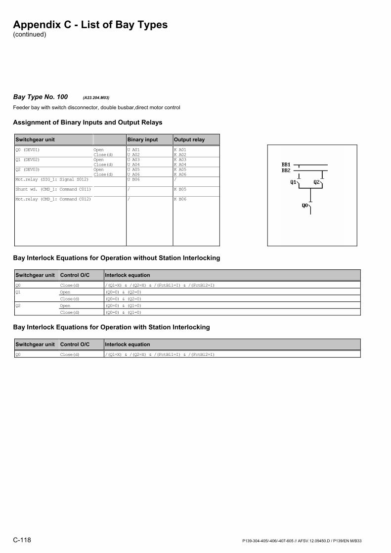
Appendix C - List of Bay Types (continued)
C-118 P139-304-405/-406/-407-605 // AFSV.12.09450.D / P139/EN M/B33
Bay Type No. 100 (A23.204.M03) Feeder bay with switch disconnector, double busbar,direct motor control
Assignment of Binary Inputs and Output Relays
Switchgear unit Binary input Output relay
Q0 (DEV01) Q1 (DEV02) Q2 (DEV03) Mot.relay (SIG_1: Signal S012) Shunt wd. (CMD_1: Command C011) Mot.relay (CMD_1: Command C012)
Open Close(d) Open Close(d) Open Close(d)
U A01 U A02 U A03 U A04 U A05 U A06 U B06 / /
K A01 K A02K A03 K A04K A05 K A06/
K B05
K B06
Bay Interlock Equations for Operation without Station Interlocking
Switchgear unit Control O/C Interlock equation
Q0 Close(d) /(Q1=X) & /(Q2=X) & /(FctBl1=I) & /(FctBl2=I) Q1 Open (Q0=0) & (Q2=0) Close(d) (Q0=0) & (Q2=0) Q2 Open (Q0=0) & (Q1=0) Close(d) (Q0=0) & (Q1=0)
Bay Interlock Equations for Operation with Station Interlocking
Switchgear unit Control O/C Interlock equation
Q0 Close(d) /(Q1=X) & /(Q2=X) & /(FctBl1=I) & /(FctBl2=I)

Appendix C - List of Bay Types (continued)
P139-304-405/-406/-407-605 // AFSV.12.09450.D / P139/EN M/B33 C-119
Bay Type No. 101 (A23.204.R01) Feeder bay with switch disconnector, double busbar
Assignment of Binary Inputs and Output Relays
Switchgear unit Binary input Output relay
Q0 (DEV01) Q1 (DEV02) Q2 (DEV03)
Open Close(d) Open Close(d) Open Close(d)
U A01 U A02 U A03 U A04 U A05 U A06
K A01 K A02/ // /
Bay Interlock Equations for Operation without Station Interlocking
Switchgear unit Control O/C Interlock equation
Q0 Close(d) /(Q1=X) & /(Q2=X) & /(FctBl1=I) & /(FctBl2=I)
Bay Interlock Equations for Operation with Station Interlocking
Switchgear unit Control O/C Interlock equation
Q0 Close(d) /(Q1=X) & /(Q2=X) & /(FctBl1=I) & /(FctBl2=I)
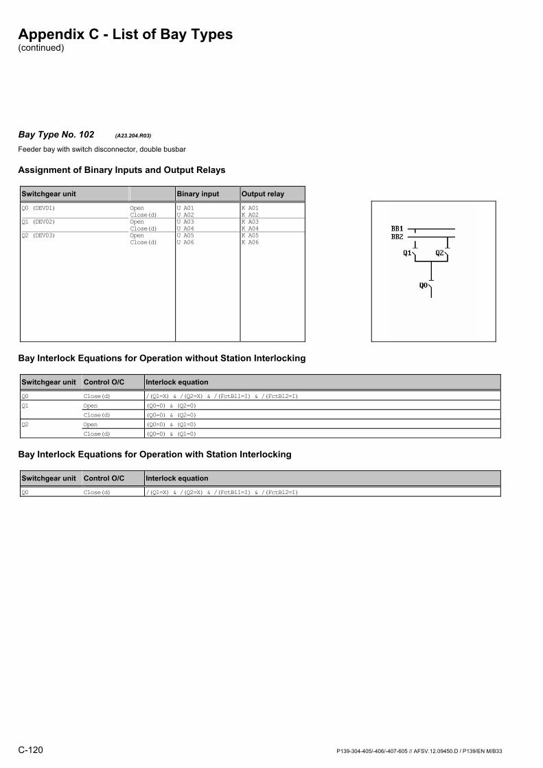
Appendix C - List of Bay Types (continued)
C-120 P139-304-405/-406/-407-605 // AFSV.12.09450.D / P139/EN M/B33
Bay Type No. 102 (A23.204.R03) Feeder bay with switch disconnector, double busbar
Assignment of Binary Inputs and Output Relays
Switchgear unit Binary input Output relay
Q0 (DEV01) Q1 (DEV02) Q2 (DEV03)
Open Close(d) Open Close(d) Open Close(d)
U A01 U A02 U A03 U A04 U A05 U A06
K A01 K A02K A03 K A04K A05 K A06
Bay Interlock Equations for Operation without Station Interlocking
Switchgear unit Control O/C Interlock equation
Q0 Close(d) /(Q1=X) & /(Q2=X) & /(FctBl1=I) & /(FctBl2=I) Q1 Open (Q0=0) & (Q2=0) Close(d) (Q0=0) & (Q2=0) Q2 Open (Q0=0) & (Q1=0) Close(d) (Q0=0) & (Q1=0)
Bay Interlock Equations for Operation with Station Interlocking
Switchgear unit Control O/C Interlock equation
Q0 Close(d) /(Q1=X) & /(Q2=X) & /(FctBl1=I) & /(FctBl2=I)

Appendix C - List of Bay Types (continued)
P139-304-405/-406/-407-605 // AFSV.12.09450.D / P139/EN M/B33 C-121
Bay Type No. 103 (A23.205.M04) Feeder bay with switch disconnector, double busbar,direct motor control
Assignment of Binary Inputs and Output Relays
Switchgear unit Binary input Output relay
Q0 (DEV01) Q1 (DEV02) Q2 (DEV03) Q8 (DEV04) Mot.relay (SIG_1: Signal S012) Shunt wd. (CMD_1: Command C011) Mot.relay (CMD_1: Command C012)
Open Close(d) Open Close(d) Open Close(d) Open Close(d)
U A01 U A02 U A03 U A04 U A05 U A06 U B01 U B02 U B06 / /
K A01 K A02K A03 K A04K A05 K A06K B01 K B02/
K B05
K B06
Bay Interlock Equations for Operation without Station Interlocking
Switchgear unit Control O/C Interlock equation
Q0 Close(d) /(Q1=X) & /(Q2=X) & (Q8=0) & /(FctBl1=I) & /(FctBl2=I) Q1 Open (Q0=0) & (Q2=0) Close(d) (Q0=0) & (Q2=0) & (Q8=0) Q2 Open (Q0=0) & (Q1=0) Close(d) (Q0=0) & (Q1=0) & (Q8=0) Q8 Close(d) (Q0=0) & (Q1=0) & (Q2=0)
Bay Interlock Equations for Operation with Station Interlocking
Switchgear unit Control O/C Interlock equation
Q0 Close(d) /(Q1=X) & /(Q2=X) & (Q8=0) & /(FctBl1=I) & /(FctBl2=I) Q1 Close(d) (Q8=0) Q2 Close(d) (Q8=0) Q8 Close(d) (Q0=0) & (Q1=0) & (Q2=0)
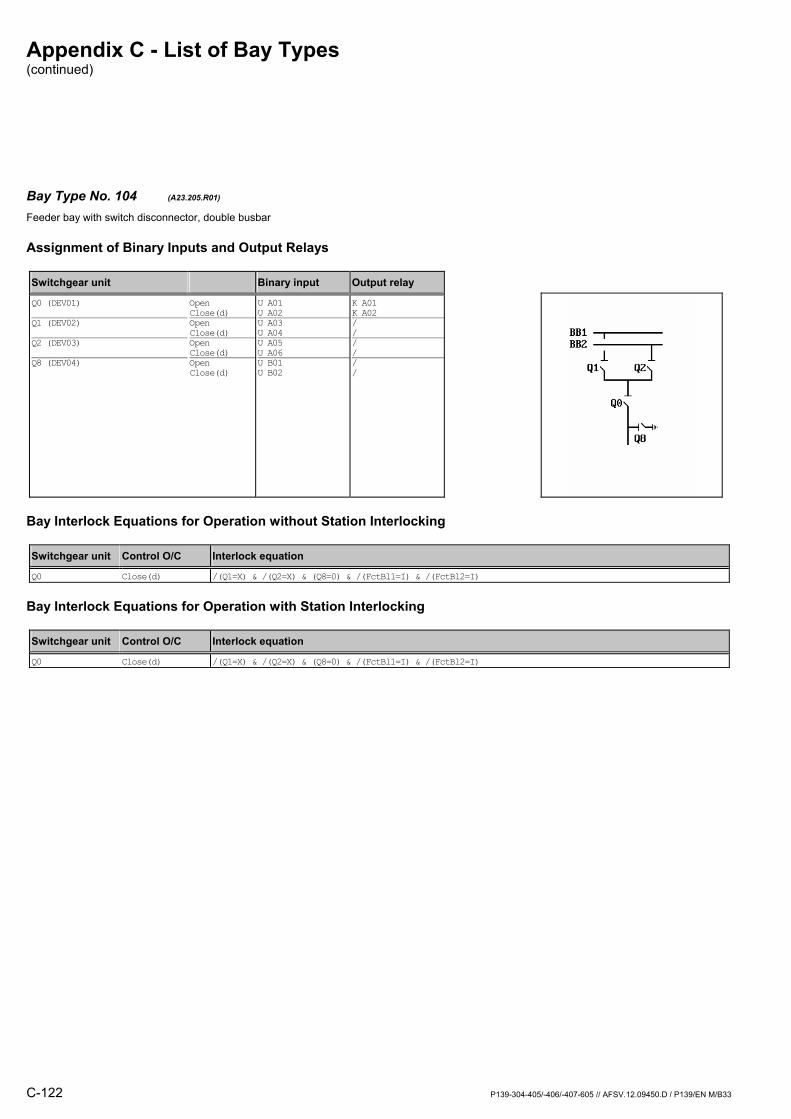
Appendix C - List of Bay Types (continued)
C-122 P139-304-405/-406/-407-605 // AFSV.12.09450.D / P139/EN M/B33
Bay Type No. 104 (A23.205.R01) Feeder bay with switch disconnector, double busbar
Assignment of Binary Inputs and Output Relays
Switchgear unit Binary input Output relay
Q0 (DEV01) Q1 (DEV02) Q2 (DEV03) Q8 (DEV04)
Open Close(d) Open Close(d) Open Close(d) Open Close(d)
U A01 U A02 U A03 U A04 U A05 U A06 U B01 U B02
K A01 K A02/ // // /
Bay Interlock Equations for Operation without Station Interlocking
Switchgear unit Control O/C Interlock equation
Q0 Close(d) /(Q1=X) & /(Q2=X) & (Q8=0) & /(FctBl1=I) & /(FctBl2=I)
Bay Interlock Equations for Operation with Station Interlocking
Switchgear unit Control O/C Interlock equation
Q0 Close(d) /(Q1=X) & /(Q2=X) & (Q8=0) & /(FctBl1=I) & /(FctBl2=I)

Appendix C - List of Bay Types (continued)
P139-304-405/-406/-407-605 // AFSV.12.09450.D / P139/EN M/B33 C-123
Bay Type No. 105 (A23.205.R03) Feeder bay with switch disconnector, double busbar
Assignment of Binary Inputs and Output Relays
Switchgear unit Binary input Output relay
Q0 (DEV01) Q1 (DEV02) Q2 (DEV03) Q8 (DEV04)
Open Close(d) Open Close(d) Open Close(d) Open Close(d)
U A01 U A02 U A03 U A04 U A05 U A06 U B01 U B02
K A01 K A02K A03 K A04K A05 K A06/ /
Bay Interlock Equations for Operation without Station Interlocking
Switchgear unit Control O/C Interlock equation
Q0 Close(d) /(Q1=X) & /(Q2=X) & (Q8=0) & /(FctBl1=I) & /(FctBl2=I) Q1 Open (Q0=0) & (Q2=0) Close(d) (Q0=0) & (Q2=0) & (Q8=0) Q2 Open (Q0=0) & (Q1=0) Close(d) (Q0=0) & (Q1=0) & (Q8=0)
Bay Interlock Equations for Operation with Station Interlocking
Switchgear unit Control O/C Interlock equation
Q0 Close(d) /(Q1=X) & /(Q2=X) & (Q8=0) & /(FctBl1=I) & /(FctBl2=I) Q1 Close(d) (Q8=0) Q2 Close(d) (Q8=0)

Appendix C - List of Bay Types (continued)
C-124 P139-304-405/-406/-407-605 // AFSV.12.09450.D / P139/EN M/B33
Bay Type No. 106 (A23.205.R04) Feeder bay with switch disconnector, double busbar
Assignment of Binary Inputs and Output Relays
Switchgear unit Binary input Output relay
Q0 (DEV01) Q1 (DEV02) Q2 (DEV03) Q8 (DEV04)
Open Close(d) Open Close(d) Open Close(d) Open Close(d)
U A01 U A02 U A03 U A04 U A05 U A06 U B01 U B02
K A01 K A02K A03 K A04K A05 K A06K B01 K B02
Bay Interlock Equations for Operation without Station Interlocking
Switchgear unit Control O/C Interlock equation
Q0 Close(d) /(Q1=X) & /(Q2=X) & (Q8=0) & /(FctBl1=I) & /(FctBl2=I) Q1 Open (Q0=0) & (Q2=0) Close(d) (Q0=0) & (Q2=0) & (Q8=0) Q2 Open (Q0=0) & (Q1=0) Close(d) (Q0=0) & (Q1=0) & (Q8=0) Q8 Close(d) (Q0=0) & (Q1=0) & (Q2=0)
Bay Interlock Equations for Operation with Station Interlocking
Switchgear unit Control O/C Interlock equation
Q0 Close(d) /(Q1=X) & /(Q2=X) & (Q8=0) & /(FctBl1=I) & /(FctBl2=I) Q1 Close(d) (Q8=0) Q2 Close(d) (Q8=0) Q8 Close(d) (Q0=0) & (Q1=0) & (Q2=0)
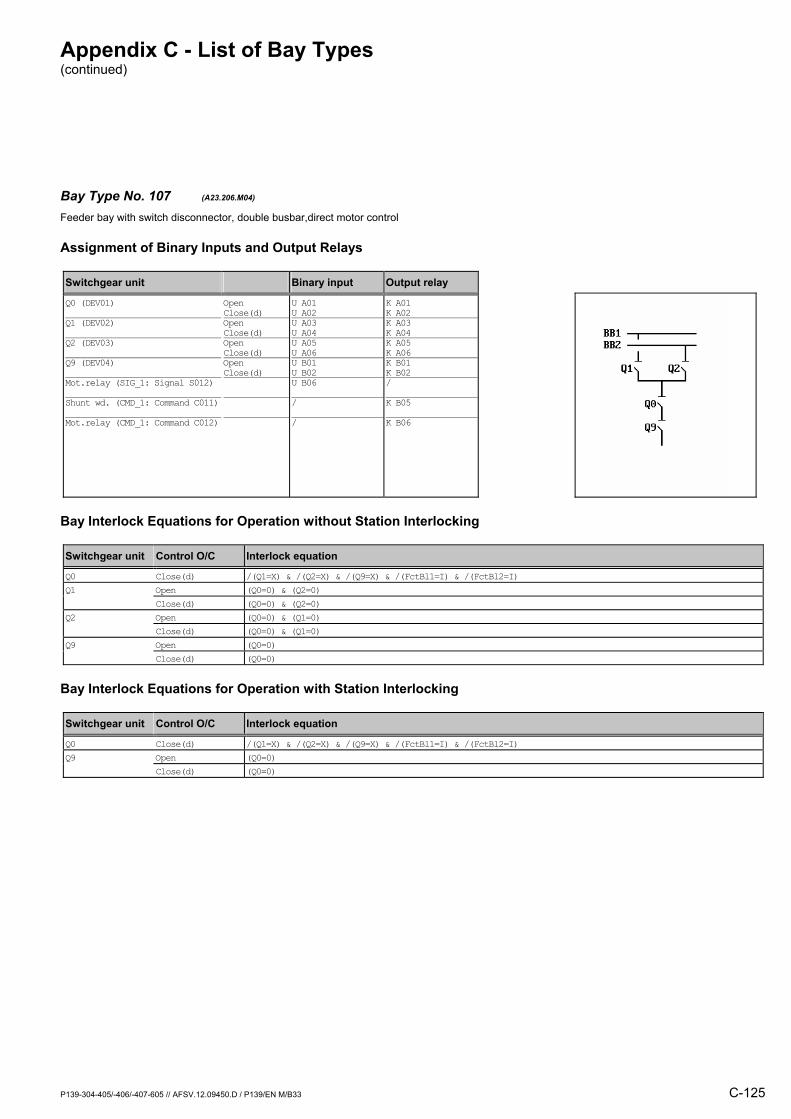
Appendix C - List of Bay Types (continued)
P139-304-405/-406/-407-605 // AFSV.12.09450.D / P139/EN M/B33 C-125
Bay Type No. 107 (A23.206.M04) Feeder bay with switch disconnector, double busbar,direct motor control
Assignment of Binary Inputs and Output Relays
Switchgear unit Binary input Output relay
Q0 (DEV01) Q1 (DEV02) Q2 (DEV03) Q9 (DEV04) Mot.relay (SIG_1: Signal S012) Shunt wd. (CMD_1: Command C011) Mot.relay (CMD_1: Command C012)
Open Close(d) Open Close(d) Open Close(d) Open Close(d)
U A01 U A02 U A03 U A04 U A05 U A06 U B01 U B02 U B06 / /
K A01 K A02K A03 K A04K A05 K A06K B01 K B02/
K B05
K B06
Bay Interlock Equations for Operation without Station Interlocking
Switchgear unit Control O/C Interlock equation
Q0 Close(d) /(Q1=X) & /(Q2=X) & /(Q9=X) & /(FctBl1=I) & /(FctBl2=I) Q1 Open (Q0=0) & (Q2=0) Close(d) (Q0=0) & (Q2=0) Q2 Open (Q0=0) & (Q1=0) Close(d) (Q0=0) & (Q1=0) Q9 Open (Q0=0) Close(d) (Q0=0)
Bay Interlock Equations for Operation with Station Interlocking
Switchgear unit Control O/C Interlock equation
Q0 Close(d) /(Q1=X) & /(Q2=X) & /(Q9=X) & /(FctBl1=I) & /(FctBl2=I) Q9 Open (Q0=0) Close(d) (Q0=0)

Appendix C - List of Bay Types (continued)
C-126 P139-304-405/-406/-407-605 // AFSV.12.09450.D / P139/EN M/B33
Bay Type No. 108 (A23.206.R01) Feeder bay with switch disconnector, double busbar
Assignment of Binary Inputs and Output Relays
Switchgear unit Binary input Output relay
Q0 (DEV01) Q1 (DEV02) Q2 (DEV03) Q9 (DEV04)
Open Close(d) Open Close(d) Open Close(d) Open Close(d)
U A01 U A02 U A03 U A04 U A05 U A06 U B01 U B02
K A01 K A02/ // // /
Bay Interlock Equations for Operation without Station Interlocking
Switchgear unit Control O/C Interlock equation
Q0 Close(d) /(Q1=X) & /(Q2=X) & /(Q9=X) & /(FctBl1=I) & /(FctBl2=I)
Bay Interlock Equations for Operation with Station Interlocking
Switchgear unit Control O/C Interlock equation
Q0 Close(d) /(Q1=X) & /(Q2=X) & /(Q9=X) & /(FctBl1=I) & /(FctBl2=I)
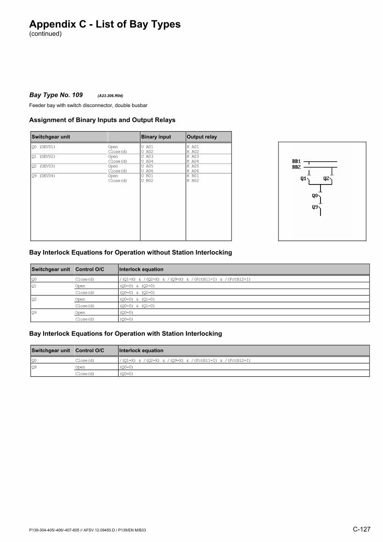
Appendix C - List of Bay Types (continued)
P139-304-405/-406/-407-605 // AFSV.12.09450.D / P139/EN M/B33 C-127
Bay Type No. 109 (A23.206.R04) Feeder bay with switch disconnector, double busbar
Assignment of Binary Inputs and Output Relays
Switchgear unit Binary input Output relay
Q0 (DEV01) Q1 (DEV02) Q2 (DEV03) Q9 (DEV04)
Open Close(d) Open Close(d) Open Close(d) Open Close(d)
U A01 U A02 U A03 U A04 U A05 U A06 U B01 U B02
K A01 K A02K A03 K A04K A05 K A06K B01 K B02
Bay Interlock Equations for Operation without Station Interlocking
Switchgear unit Control O/C Interlock equation
Q0 Close(d) /(Q1=X) & /(Q2=X) & /(Q9=X) & /(FctBl1=I) & /(FctBl2=I) Q1 Open (Q0=0) & (Q2=0) Close(d) (Q0=0) & (Q2=0) Q2 Open (Q0=0) & (Q1=0) Close(d) (Q0=0) & (Q1=0) Q9 Open (Q0=0) Close(d) (Q0=0)
Bay Interlock Equations for Operation with Station Interlocking
Switchgear unit Control O/C Interlock equation
Q0 Close(d) /(Q1=X) & /(Q2=X) & /(Q9=X) & /(FctBl1=I) & /(FctBl2=I) Q9 Open (Q0=0) Close(d) (Q0=0)

Appendix C - List of Bay Types (continued)
C-128 P139-304-405/-406/-407-605 // AFSV.12.09450.D / P139/EN M/B33
Bay Type No. 110 (A23.207.M05) Feeder bay with switch disconnector, double busbar,direct motor control
Assignment of Binary Inputs and Output Relays
Switchgear unit Binary input Output relay
Q0 (DEV01) Q1 (DEV02) Q2 (DEV03) Q9 (DEV04) Q8 (DEV05) Mot.relay (SIG_1: Signal S012) Shunt wd. (CMD_1: Command C011) Mot.relay (CMD_1: Command C012)
Open Close(d) Open Close(d) Open Close(d) Open Close(d) Open Close(d)
U A01 U A02 U A03 U A04 U A05 U A06 U B01 U B02 U B03 U B04 U B06 / /
K A01 K A02K A03 K A04K A05 K A06K B01 K B02K B03 K B04/
K B05
K B06
Bay Interlock Equations for Operation without Station Interlocking
Switchgear unit Control O/C Interlock equation
Q0 Close(d) /(Q1=X) & /(Q2=X) & /(Q9=X) & /(FctBl1=I) & /(FctBl2=I) Q1 Open (Q0=0) & (Q2=0) Close(d) (Q0=0) & (Q2=0) Q2 Open (Q0=0) & (Q1=0) Close(d) (Q0=0) & (Q1=0) Q8 Close(d) (Q9=0) Q9 Open (Q0=0) Close(d) (Q0=0) & (Q8=0)
Bay Interlock Equations for Operation with Station Interlocking
Switchgear unit Control O/C Interlock equation
Q0 Close(d) /(Q1=X) & /(Q2=X) & /(Q9=X) & /(FctBl1=I) & /(FctBl2=I) Q8 Close(d) (Q9=0) Q9 Open (Q0=0) Close(d) (Q0=0) & (Q8=0)

Appendix C - List of Bay Types (continued)
P139-304-405/-406/-407-605 // AFSV.12.09450.D / P139/EN M/B33 C-129
Bay Type No. 111 (A23.207.R01) Feeder bay with switch disconnector, double busbar
Assignment of Binary Inputs and Output Relays
Switchgear unit Binary input Output relay
Q0 (DEV01) Q1 (DEV02) Q2 (DEV03) Q9 (DEV04) Q8 (DEV05)
Open Close(d) Open Close(d) Open Close(d) Open Close(d) Open Close(d)
U A01 U A02 U A03 U A04 U A05 U A06 U B01 U B02 U B03 U B04
K A01 K A02/ // // // /
Bay Interlock Equations for Operation without Station Interlocking
Switchgear unit Control O/C Interlock equation
Q0 Close(d) /(Q1=X) & /(Q2=X) & /(Q9=X) & /(FctBl1=I) & /(FctBl2=I)
Bay Interlock Equations for Operation with Station Interlocking
Switchgear unit Control O/C Interlock equation
Q0 Close(d) /(Q1=X) & /(Q2=X) & /(Q9=X) & /(FctBl1=I) & /(FctBl2=I)

Appendix C - List of Bay Types (continued)
C-130 P139-304-405/-406/-407-605 // AFSV.12.09450.D / P139/EN M/B33
Bay Type No. 112 (A23.207.R04) Feeder bay with switch disconnector, double busbar
Assignment of Binary Inputs and Output Relays
Switchgear unit Binary input Output relay
Q0 (DEV01) Q1 (DEV02) Q2 (DEV03) Q9 (DEV04) Q8 (DEV05)
Open Close(d) Open Close(d) Open Close(d) Open Close(d) Open Close(d)
U A01 U A02 U A03 U A04 U A05 U A06 U B01 U B02 U B03 U B04
K A01 K A02K A03 K A04K A05 K A06K B01 K B02/ /
Bay Interlock Equations for Operation without Station Interlocking
Switchgear unit Control O/C Interlock equation
Q0 Close(d) /(Q1=X) & /(Q2=X) & /(Q9=X) & /(FctBl1=I) & /(FctBl2=I) Q1 Open (Q0=0) & (Q2=0) Close(d) (Q0=0) & (Q2=0) Q2 Open (Q0=0) & (Q1=0) Close(d) (Q0=0) & (Q1=0) Q9 Open (Q0=0) Close(d) (Q0=0) & (Q8=0)
Bay Interlock Equations for Operation with Station Interlocking
Switchgear unit Control O/C Interlock equation
Q0 Close(d) /(Q1=X) & /(Q2=X) & /(Q9=X) & /(FctBl1=I) & /(FctBl2=I) Q9 Open (Q0=0) Close(d) (Q0=0) & (Q8=0)
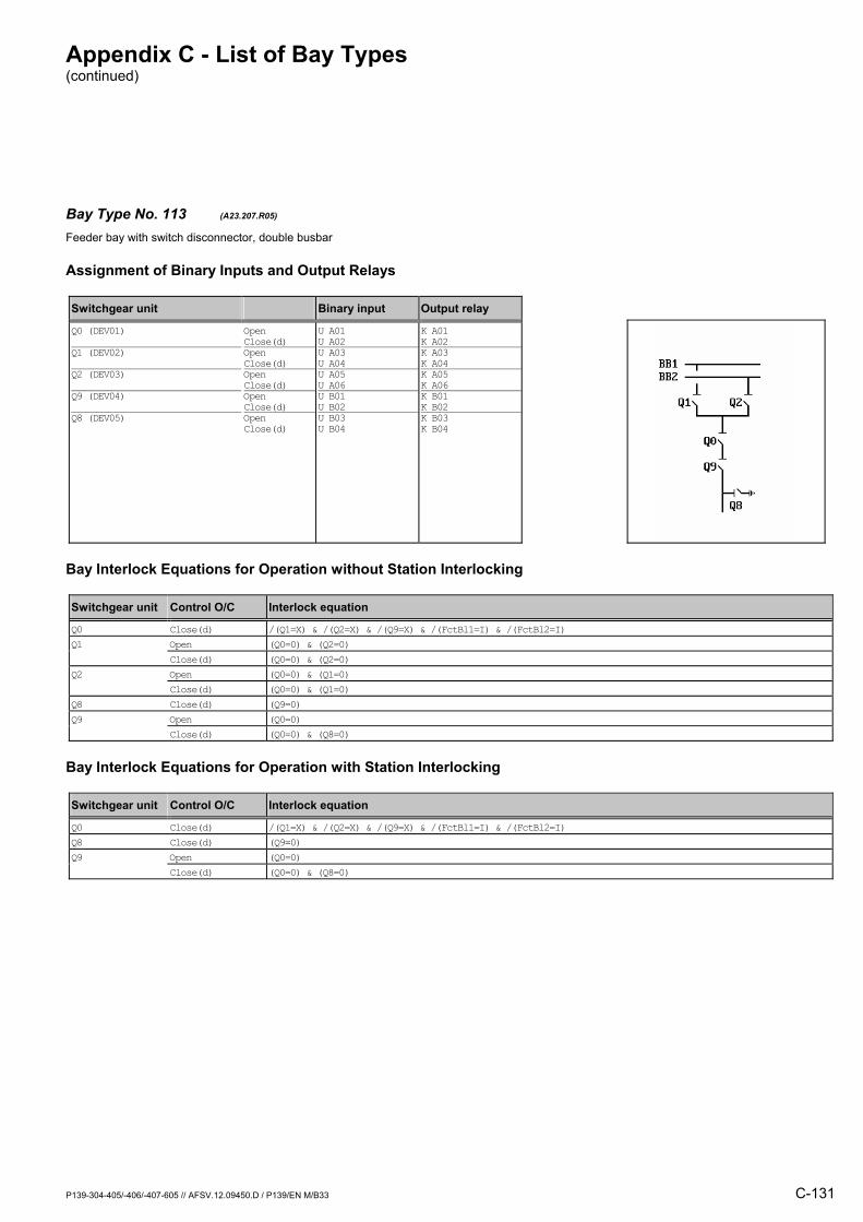
Appendix C - List of Bay Types (continued)
P139-304-405/-406/-407-605 // AFSV.12.09450.D / P139/EN M/B33 C-131
Bay Type No. 113 (A23.207.R05) Feeder bay with switch disconnector, double busbar
Assignment of Binary Inputs and Output Relays
Switchgear unit Binary input Output relay
Q0 (DEV01) Q1 (DEV02) Q2 (DEV03) Q9 (DEV04) Q8 (DEV05)
Open Close(d) Open Close(d) Open Close(d) Open Close(d) Open Close(d)
U A01 U A02 U A03 U A04 U A05 U A06 U B01 U B02 U B03 U B04
K A01 K A02K A03 K A04K A05 K A06K B01 K B02K B03 K B04
Bay Interlock Equations for Operation without Station Interlocking
Switchgear unit Control O/C Interlock equation
Q0 Close(d) /(Q1=X) & /(Q2=X) & /(Q9=X) & /(FctBl1=I) & /(FctBl2=I) Q1 Open (Q0=0) & (Q2=0) Close(d) (Q0=0) & (Q2=0) Q2 Open (Q0=0) & (Q1=0) Close(d) (Q0=0) & (Q1=0) Q8 Close(d) (Q9=0) Q9 Open (Q0=0) Close(d) (Q0=0) & (Q8=0)
Bay Interlock Equations for Operation with Station Interlocking
Switchgear unit Control O/C Interlock equation
Q0 Close(d) /(Q1=X) & /(Q2=X) & /(Q9=X) & /(FctBl1=I) & /(FctBl2=I) Q8 Close(d) (Q9=0) Q9 Open (Q0=0) Close(d) (Q0=0) & (Q8=0)
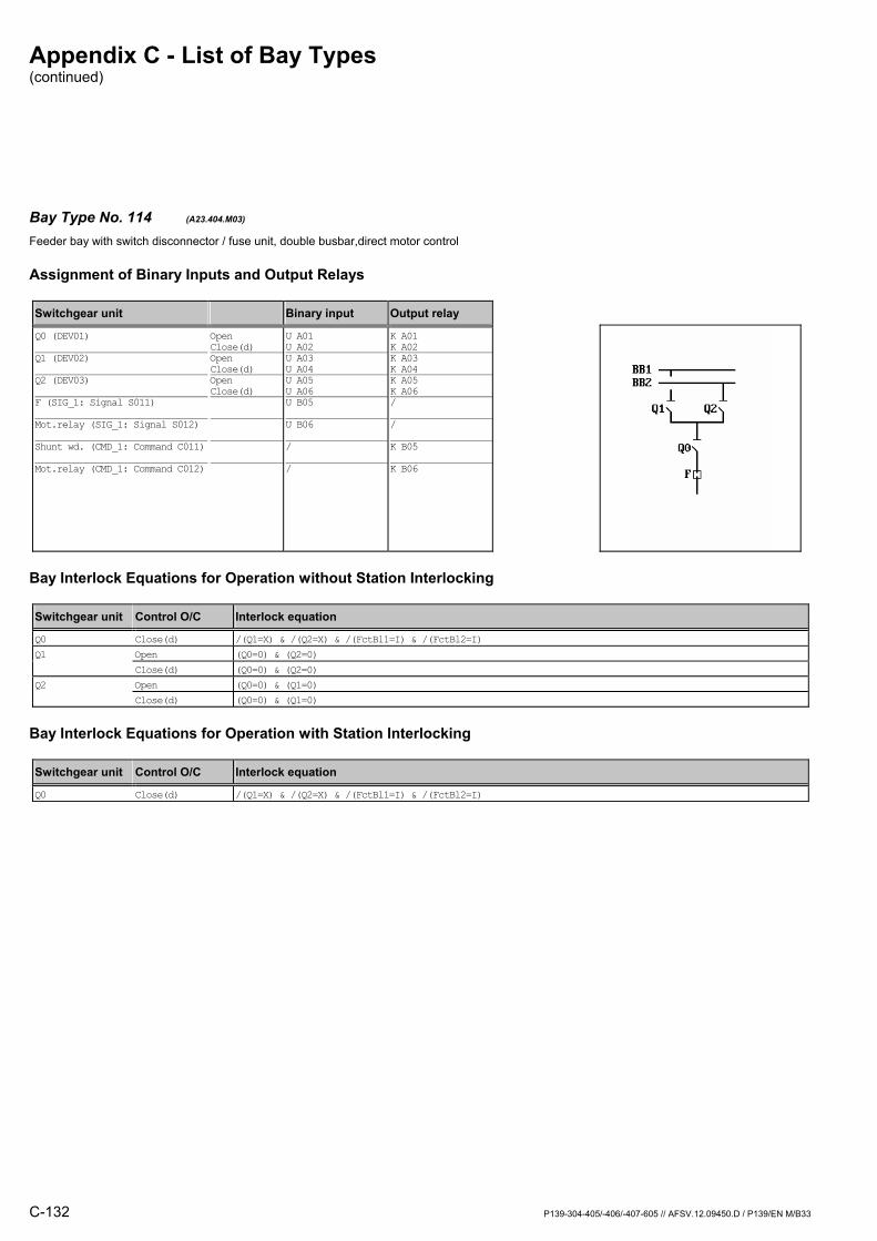
Appendix C - List of Bay Types (continued)
C-132 P139-304-405/-406/-407-605 // AFSV.12.09450.D / P139/EN M/B33
Bay Type No. 114 (A23.404.M03) Feeder bay with switch disconnector / fuse unit, double busbar,direct motor control
Assignment of Binary Inputs and Output Relays
Switchgear unit Binary input Output relay
Q0 (DEV01) Q1 (DEV02) Q2 (DEV03) F (SIG_1: Signal S011) Mot.relay (SIG_1: Signal S012) Shunt wd. (CMD_1: Command C011) Mot.relay (CMD_1: Command C012)
Open Close(d) Open Close(d) Open Close(d)
U A01 U A02 U A03 U A04 U A05 U A06 U B05 U B06 / /
K A01 K A02K A03 K A04K A05 K A06/
/
K B05
K B06
Bay Interlock Equations for Operation without Station Interlocking
Switchgear unit Control O/C Interlock equation
Q0 Close(d) /(Q1=X) & /(Q2=X) & /(FctBl1=I) & /(FctBl2=I) Q1 Open (Q0=0) & (Q2=0) Close(d) (Q0=0) & (Q2=0) Q2 Open (Q0=0) & (Q1=0) Close(d) (Q0=0) & (Q1=0)
Bay Interlock Equations for Operation with Station Interlocking
Switchgear unit Control O/C Interlock equation
Q0 Close(d) /(Q1=X) & /(Q2=X) & /(FctBl1=I) & /(FctBl2=I)

Appendix C - List of Bay Types (continued)
P139-304-405/-406/-407-605 // AFSV.12.09450.D / P139/EN M/B33 C-133
Bay Type No. 115 (A23.404.R01) Feeder bay with switch disconnector / fuse unit, double busbar
Assignment of Binary Inputs and Output Relays
Switchgear unit Binary input Output relay
Q0 (DEV01) Q1 (DEV02) Q2 (DEV03) F (SIG_1: Signal S011)
Open Close(d) Open Close(d) Open Close(d)
U A01 U A02 U A03 U A04 U A05 U A06 U B05
K A01 K A02/ // //
Bay Interlock Equations for Operation without Station Interlocking
Switchgear unit Control O/C Interlock equation
Q0 Close(d) /(Q1=X) & /(Q2=X) & /(FctBl1=I) & /(FctBl2=I)
Bay Interlock Equations for Operation with Station Interlocking
Switchgear unit Control O/C Interlock equation
Q0 Close(d) /(Q1=X) & /(Q2=X) & /(FctBl1=I) & /(FctBl2=I)
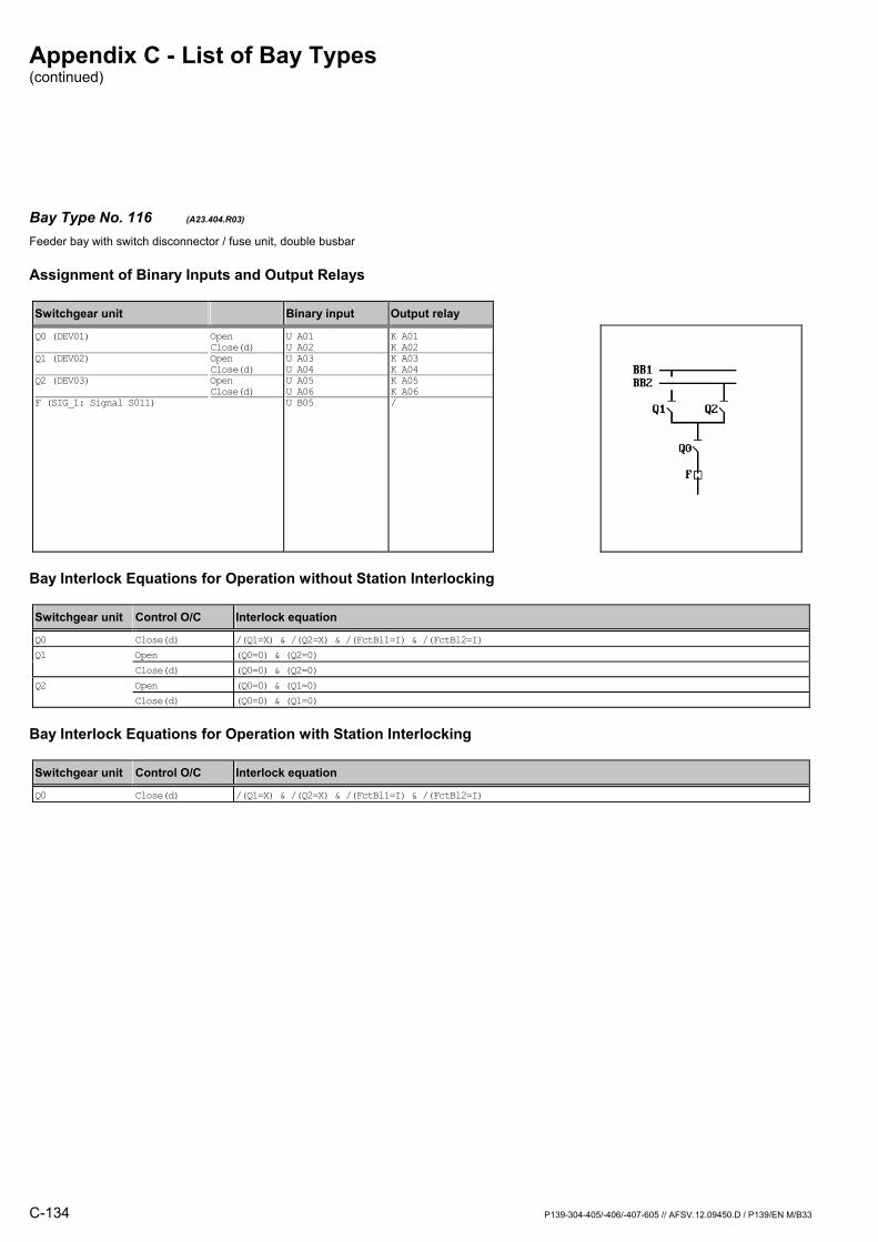
Appendix C - List of Bay Types (continued)
C-134 P139-304-405/-406/-407-605 // AFSV.12.09450.D / P139/EN M/B33
Bay Type No. 116 (A23.404.R03) Feeder bay with switch disconnector / fuse unit, double busbar
Assignment of Binary Inputs and Output Relays
Switchgear unit Binary input Output relay
Q0 (DEV01) Q1 (DEV02) Q2 (DEV03) F (SIG_1: Signal S011)
Open Close(d) Open Close(d) Open Close(d)
U A01 U A02 U A03 U A04 U A05 U A06 U B05
K A01 K A02K A03 K A04K A05 K A06/
Bay Interlock Equations for Operation without Station Interlocking
Switchgear unit Control O/C Interlock equation
Q0 Close(d) /(Q1=X) & /(Q2=X) & /(FctBl1=I) & /(FctBl2=I) Q1 Open (Q0=0) & (Q2=0) Close(d) (Q0=0) & (Q2=0) Q2 Open (Q0=0) & (Q1=0) Close(d) (Q0=0) & (Q1=0)
Bay Interlock Equations for Operation with Station Interlocking
Switchgear unit Control O/C Interlock equation
Q0 Close(d) /(Q1=X) & /(Q2=X) & /(FctBl1=I) & /(FctBl2=I)
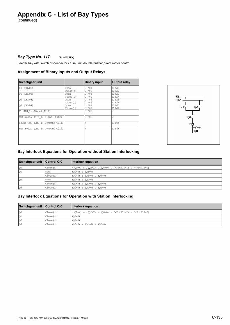
Appendix C - List of Bay Types (continued)
P139-304-405/-406/-407-605 // AFSV.12.09450.D / P139/EN M/B33 C-135
Bay Type No. 117 (A23.405.M04) Feeder bay with switch disconnector / fuse unit, double busbar,direct motor control
Assignment of Binary Inputs and Output Relays
Switchgear unit Binary input Output relay
Q0 (DEV01) Q1 (DEV02) Q2 (DEV03) Q8 (DEV04) F (SIG_1: Signal S011) Mot.relay (SIG_1: Signal S012) Shunt wd. (CMD_1: Command C011) Mot.relay (CMD_1: Command C012)
Open Close(d) Open Close(d) Open Close(d) Open Close(d)
U A01 U A02 U A03 U A04 U A05 U A06 U B01 U B02 U B05 U B06 / /
K A01 K A02K A03 K A04K A05 K A06K B01 K B02/
/
K B05
K B06
Bay Interlock Equations for Operation without Station Interlocking
Switchgear unit Control O/C Interlock equation
Q0 Close(d) /(Q1=X) & /(Q2=X) & (Q8=0) & /(FctBl1=I) & /(FctBl2=I) Q1 Open (Q0=0) & (Q2=0) Close(d) (Q0=0) & (Q2=0) & (Q8=0) Q2 Open (Q0=0) & (Q1=0) Close(d) (Q0=0) & (Q1=0) & (Q8=0) Q8 Close(d) (Q0=0) & (Q1=0) & (Q2=0)
Bay Interlock Equations for Operation with Station Interlocking
Switchgear unit Control O/C Interlock equation
Q0 Close(d) /(Q1=X) & /(Q2=X) & (Q8=0) & /(FctBl1=I) & /(FctBl2=I) Q1 Close(d) (Q8=0) Q2 Close(d) (Q8=0) Q8 Close(d) (Q0=0) & (Q1=0) & (Q2=0)
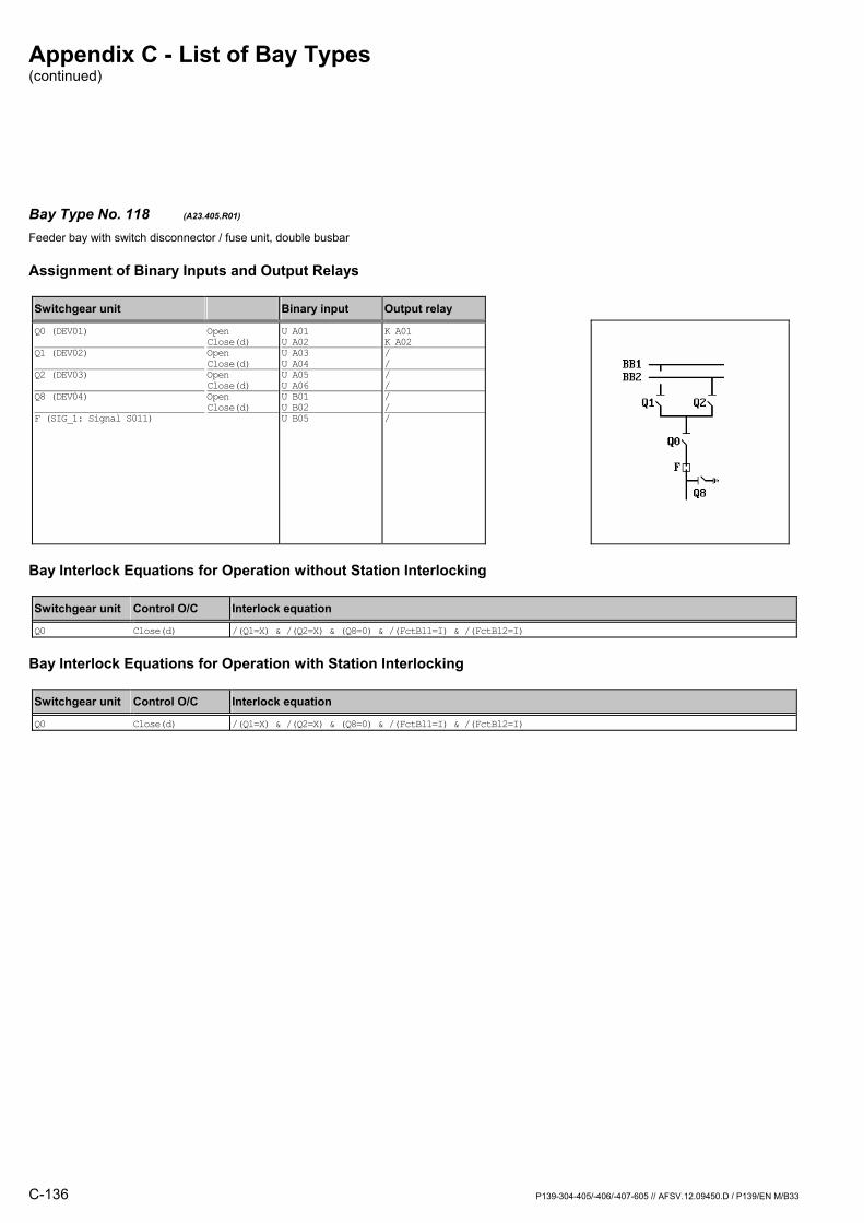
Appendix C - List of Bay Types (continued)
C-136 P139-304-405/-406/-407-605 // AFSV.12.09450.D / P139/EN M/B33
Bay Type No. 118 (A23.405.R01) Feeder bay with switch disconnector / fuse unit, double busbar
Assignment of Binary Inputs and Output Relays
Switchgear unit Binary input Output relay
Q0 (DEV01) Q1 (DEV02) Q2 (DEV03) Q8 (DEV04) F (SIG_1: Signal S011)
Open Close(d) Open Close(d) Open Close(d) Open Close(d)
U A01 U A02 U A03 U A04 U A05 U A06 U B01 U B02 U B05
K A01 K A02/ // // //
Bay Interlock Equations for Operation without Station Interlocking
Switchgear unit Control O/C Interlock equation
Q0 Close(d) /(Q1=X) & /(Q2=X) & (Q8=0) & /(FctBl1=I) & /(FctBl2=I)
Bay Interlock Equations for Operation with Station Interlocking
Switchgear unit Control O/C Interlock equation
Q0 Close(d) /(Q1=X) & /(Q2=X) & (Q8=0) & /(FctBl1=I) & /(FctBl2=I)

Appendix C - List of Bay Types (continued)
P139-304-405/-406/-407-605 // AFSV.12.09450.D / P139/EN M/B33 C-137
Bay Type No. 119 (A23.405.R03) Feeder bay with switch disconnector / fuse unit, double busbar
Assignment of Binary Inputs and Output Relays
Switchgear unit Binary input Output relay
Q0 (DEV01) Q1 (DEV02) Q2 (DEV03) Q8 (DEV04) F (SIG_1: Signal S011)
Open Close(d) Open Close(d) Open Close(d) Open Close(d)
U A01 U A02 U A03 U A04 U A05 U A06 U B01 U B02 U B05
K A01 K A02K A03 K A04K A05 K A06/ //
Bay Interlock Equations for Operation without Station Interlocking
Switchgear unit Control O/C Interlock equation
Q0 Close(d) /(Q1=X) & /(Q2=X) & (Q8=0) & /(FctBl1=I) & /(FctBl2=I) Q1 Open (Q0=0) & (Q2=0) Close(d) (Q0=0) & (Q2=0) & (Q8=0) Q2 Open (Q0=0) & (Q1=0) Close(d) (Q0=0) & (Q1=0) & (Q8=0)
Bay Interlock Equations for Operation with Station Interlocking
Switchgear unit Control O/C Interlock equation
Q0 Close(d) /(Q1=X) & /(Q2=X) & (Q8=0) & /(FctBl1=I) & /(FctBl2=I) Q1 Close(d) (Q8=0) Q2 Close(d) (Q8=0)

Appendix C - List of Bay Types (continued)
C-138 P139-304-405/-406/-407-605 // AFSV.12.09450.D / P139/EN M/B33
Bay Type No. 120 (A23.405.R04) Feeder bay with switch disconnector / fuse unit, double busbar
Assignment of Binary Inputs and Output Relays
Switchgear unit Binary input Output relay
Q0 (DEV01) Q1 (DEV02) Q2 (DEV03) Q8 (DEV04) F (SIG_1: Signal S011)
Open Close(d) Open Close(d) Open Close(d) Open Close(d)
U A01 U A02 U A03 U A04 U A05 U A06 U B01 U B02 U B05
K A01 K A02K A03 K A04K A05 K A06K B01 K B02/
Bay Interlock Equations for Operation without Station Interlocking
Switchgear unit Control O/C Interlock equation
Q0 Close(d) /(Q1=X) & /(Q2=X) & (Q8=0) & /(FctBl1=I) & /(FctBl2=I) Q1 Open (Q0=0) & (Q2=0) Close(d) (Q0=0) & (Q2=0) & (Q8=0) Q2 Open (Q0=0) & (Q1=0) Close(d) (Q0=0) & (Q1=0) & (Q8=0) Q8 Close(d) (Q0=0) & (Q1=0) & (Q2=0)
Bay Interlock Equations for Operation with Station Interlocking
Switchgear unit Control O/C Interlock equation
Q0 Close(d) /(Q1=X) & /(Q2=X) & (Q8=0) & /(FctBl1=I) & /(FctBl2=I) Q1 Close(d) (Q8=0) Q2 Close(d) (Q8=0) Q8 Close(d) (Q0=0) & (Q1=0) & (Q2=0)

Appendix C - List of Bay Types (continued)
P139-304-405/-406/-407-605 // AFSV.12.09450.D / P139/EN M/B33 C-139
Bay Type No. 222 (A25.105.M03.1) Feeder bay with circuit breaker, double busbar,direct motor control
Assignment of Binary Inputs and Output Relays
Switchgear unit Binary input Output relay
Q0 (DEV01) Q1 (DEV02) Q2 (DEV03) Q8 (DEV04) Mot.relay (SIG_1: Signal S012) Shunt wd. (CMD_1: Command C011) Mot.relay (CMD_1: Command C012)
Open Close(d) Open Close(d) Open Close(d) Open Close(d)
U A01 U A02 U A03 U A04 U A05 U A06 U B01 U B02 U B06 / /
K A01 K A02K A03 K A04K A05 K A06/ //
K B05
K B06
Bay Interlock Equations for Operation without Station Interlocking
Switchgear unit Control O/C Interlock equation
Q0 Open (Q8=0) Close(d) /(Q1=X) & /(Q2=X) & (Q8=0) & /(FctBl1=I) & /(FctBl2=I) Q1 Open (Q0=0) & (Q2=0) Close(d) (Q0=0) & (Q2=0) & (Q8=0) Q2 Open (Q0=0) & (Q1=0) Close(d) (Q0=0) & (Q1=0) & (Q8=0)
Bay Interlock Equations for Operation with Station Interlocking
Switchgear unit Control O/C Interlock equation
Q0 Open (Q8=0) Close(d) /(Q1=X) & /(Q2=X) & (Q8=0) & /(FctBl1=I) & /(FctBl2=I) Q1 Close(d) (Q8=0) Q2 Close(d) (Q8=0)
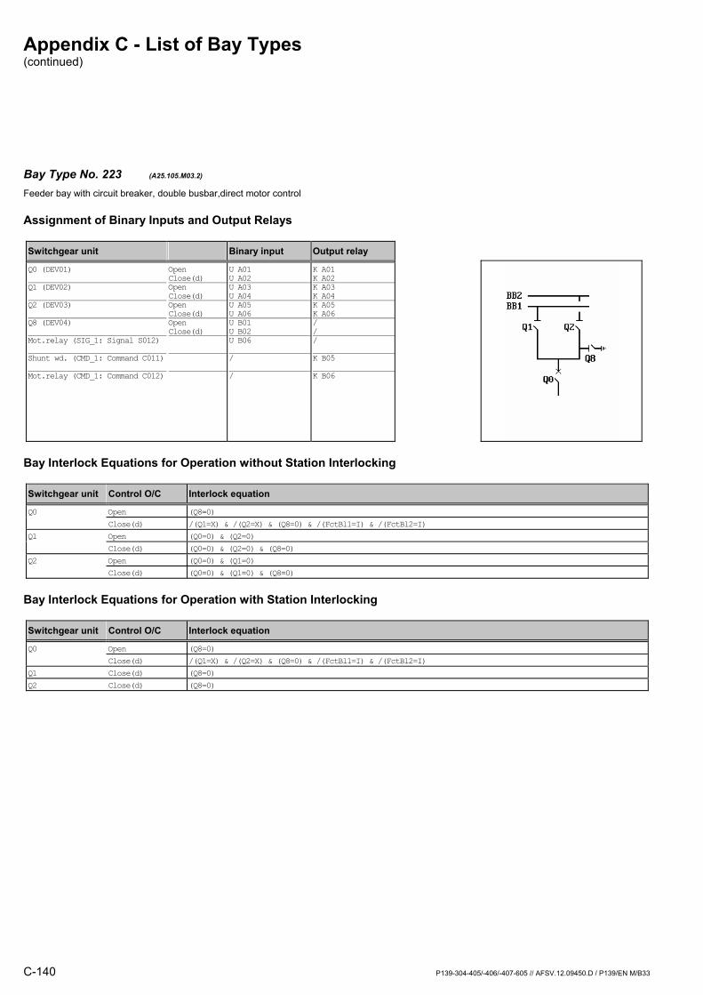
Appendix C - List of Bay Types (continued)
C-140 P139-304-405/-406/-407-605 // AFSV.12.09450.D / P139/EN M/B33
Bay Type No. 223 (A25.105.M03.2) Feeder bay with circuit breaker, double busbar,direct motor control
Assignment of Binary Inputs and Output Relays
Switchgear unit Binary input Output relay
Q0 (DEV01) Q1 (DEV02) Q2 (DEV03) Q8 (DEV04) Mot.relay (SIG_1: Signal S012) Shunt wd. (CMD_1: Command C011) Mot.relay (CMD_1: Command C012)
Open Close(d) Open Close(d) Open Close(d) Open Close(d)
U A01 U A02 U A03 U A04 U A05 U A06 U B01 U B02 U B06 / /
K A01 K A02K A03 K A04K A05 K A06/ //
K B05
K B06
Bay Interlock Equations for Operation without Station Interlocking
Switchgear unit Control O/C Interlock equation
Q0 Open (Q8=0) Close(d) /(Q1=X) & /(Q2=X) & (Q8=0) & /(FctBl1=I) & /(FctBl2=I) Q1 Open (Q0=0) & (Q2=0) Close(d) (Q0=0) & (Q2=0) & (Q8=0) Q2 Open (Q0=0) & (Q1=0) Close(d) (Q0=0) & (Q1=0) & (Q8=0)
Bay Interlock Equations for Operation with Station Interlocking
Switchgear unit Control O/C Interlock equation
Q0 Open (Q8=0) Close(d) /(Q1=X) & /(Q2=X) & (Q8=0) & /(FctBl1=I) & /(FctBl2=I) Q1 Close(d) (Q8=0) Q2 Close(d) (Q8=0)
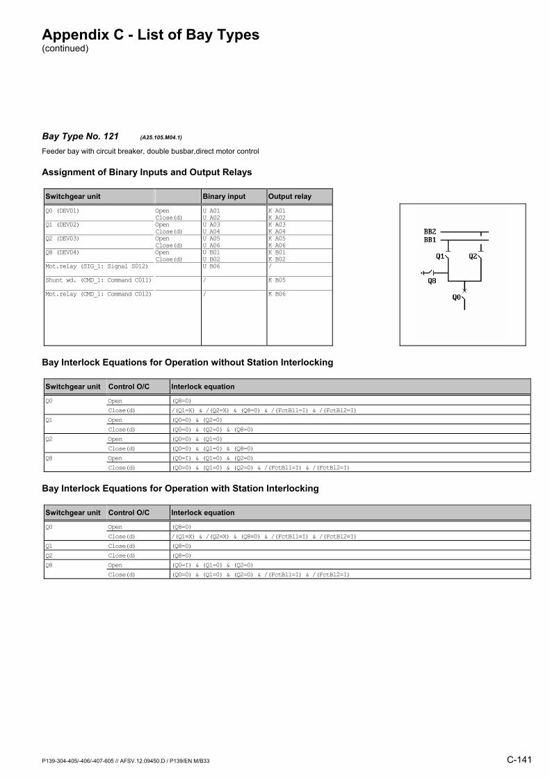
Appendix C - List of Bay Types (continued)
P139-304-405/-406/-407-605 // AFSV.12.09450.D / P139/EN M/B33 C-141
Bay Type No. 121 (A25.105.M04.1) Feeder bay with circuit breaker, double busbar,direct motor control
Assignment of Binary Inputs and Output Relays
Switchgear unit Binary input Output relay
Q0 (DEV01) Q1 (DEV02) Q2 (DEV03) Q8 (DEV04) Mot.relay (SIG_1: Signal S012) Shunt wd. (CMD_1: Command C011) Mot.relay (CMD_1: Command C012)
Open Close(d) Open Close(d) Open Close(d) Open Close(d)
U A01 U A02 U A03 U A04 U A05 U A06 U B01 U B02 U B06 / /
K A01 K A02K A03 K A04K A05 K A06K B01 K B02/
K B05
K B06
Bay Interlock Equations for Operation without Station Interlocking
Switchgear unit Control O/C Interlock equation
Q0 Open (Q8=0) Close(d) /(Q1=X) & /(Q2=X) & (Q8=0) & /(FctBl1=I) & /(FctBl2=I) Q1 Open (Q0=0) & (Q2=0) Close(d) (Q0=0) & (Q2=0) & (Q8=0) Q2 Open (Q0=0) & (Q1=0) Close(d) (Q0=0) & (Q1=0) & (Q8=0) Q8 Open (Q0=I) & (Q1=0) & (Q2=0) Close(d) (Q0=0) & (Q1=0) & (Q2=0) & /(FctBl1=I) & /(FctBl2=I)
Bay Interlock Equations for Operation with Station Interlocking
Switchgear unit Control O/C Interlock equation
Q0 Open (Q8=0) Close(d) /(Q1=X) & /(Q2=X) & (Q8=0) & /(FctBl1=I) & /(FctBl2=I) Q1 Close(d) (Q8=0) Q2 Close(d) (Q8=0) Q8 Open (Q0=I) & (Q1=0) & (Q2=0) Close(d) (Q0=0) & (Q1=0) & (Q2=0) & /(FctBl1=I) & /(FctBl2=I)
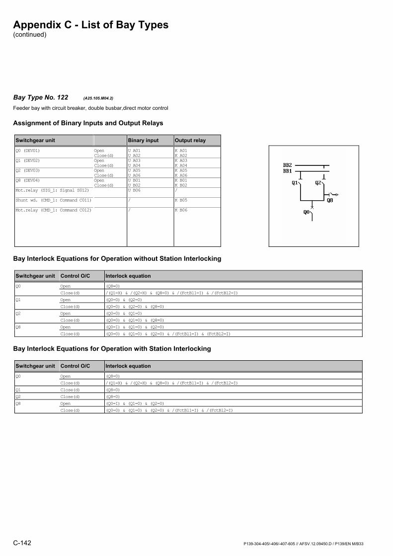
Appendix C - List of Bay Types (continued)
C-142 P139-304-405/-406/-407-605 // AFSV.12.09450.D / P139/EN M/B33
Bay Type No. 122 (A25.105.M04.2) Feeder bay with circuit breaker, double busbar,direct motor control
Assignment of Binary Inputs and Output Relays
Switchgear unit Binary input Output relay
Q0 (DEV01) Q1 (DEV02) Q2 (DEV03) Q8 (DEV04) Mot.relay (SIG_1: Signal S012) Shunt wd. (CMD_1: Command C011) Mot.relay (CMD_1: Command C012)
Open Close(d) Open Close(d) Open Close(d) Open Close(d)
U A01 U A02 U A03 U A04 U A05 U A06 U B01 U B02 U B06 / /
K A01 K A02K A03 K A04K A05 K A06K B01 K B02/
K B05
K B06
Bay Interlock Equations for Operation without Station Interlocking
Switchgear unit Control O/C Interlock equation
Q0 Open (Q8=0) Close(d) /(Q1=X) & /(Q2=X) & (Q8=0) & /(FctBl1=I) & /(FctBl2=I) Q1 Open (Q0=0) & (Q2=0) Close(d) (Q0=0) & (Q2=0) & (Q8=0) Q2 Open (Q0=0) & (Q1=0) Close(d) (Q0=0) & (Q1=0) & (Q8=0) Q8 Open (Q0=I) & (Q1=0) & (Q2=0) Close(d) (Q0=0) & (Q1=0) & (Q2=0) & /(FctBl1=I) & (FctBl2=I)
Bay Interlock Equations for Operation with Station Interlocking
Switchgear unit Control O/C Interlock equation
Q0 Open (Q8=0) Close(d) /(Q1=X) & /(Q2=X) & (Q8=0) & /(FctBl1=I) & /(FctBl2=I) Q1 Close(d) (Q8=0) Q2 Close(d) (Q8=0) Q8 Open (Q0=I) & (Q1=0) & (Q2=0) Close(d) (Q0=0) & (Q1=0) & (Q2=0) & /(FctBl1=I) & /(FctBl2=I)

Appendix C - List of Bay Types (continued)
P139-304-405/-406/-407-605 // AFSV.12.09450.D / P139/EN M/B33 C-143
Bay Type No. 123 (A25.105.R01.1) Feeder bay with circuit breaker, double busbar
Assignment of Binary Inputs and Output Relays
Switchgear unit Binary input Output relay
Q0 (DEV01) Q1 (DEV02) Q2 (DEV03) Q8 (DEV04)
Open Close(d) Open Close(d) Open Close(d) Open Close(d)
U A01 U A02 U A03 U A04 U A05 U A06 U B01 U B02
K A01 K A02/ // // /
Bay Interlock Equations for Operation without Station Interlocking
Switchgear unit Control O/C Interlock equation
Q0 Open (Q8=0) Close(d) /(Q1=X) & /(Q2=X) & (Q8=0) & /(FctBl1=I) & /(FctBl2=I)
Bay Interlock Equations for Operation with Station Interlocking
Switchgear unit Control O/C Interlock equation
Q0 Open (Q8=0) Close(d) /(Q1=X) & /(Q2=X) & (Q8=0) & /(FctBl1=I) & /(FctBl2=I)

Appendix C - List of Bay Types (continued)
C-144 P139-304-405/-406/-407-605 // AFSV.12.09450.D / P139/EN M/B33
Bay Type No. 124 (A25.105.R01.2) Feeder bay with circuit breaker, double busbar
Assignment of Binary Inputs and Output Relays
Switchgear unit Binary input Output relay
Q0 (DEV01) Q1 (DEV02) Q2 (DEV03) Q8 (DEV04)
Open Close(d) Open Close(d) Open Close(d) Open Close(d)
U A01 U A02 U A03 U A04 U A05 U A06 U B01 U B02
K A01 K A02/ // // /
Bay Interlock Equations for Operation without Station Interlocking
Switchgear unit Control O/C Interlock equation
Q0 Open (Q8=0) Close(d) /(Q1=X) & /(Q2=X) & (Q8=0) & /(FctBl1=I) & /(FctBl2=I)
Bay Interlock Equations for Operation with Station Interlocking
Switchgear unit Control O/C Interlock equation
Q0 Open (Q8=0) Close(d) /(Q1=X) & /(Q2=X) & (Q8=0) & /(FctBl1=I) & /(FctBl2=I)
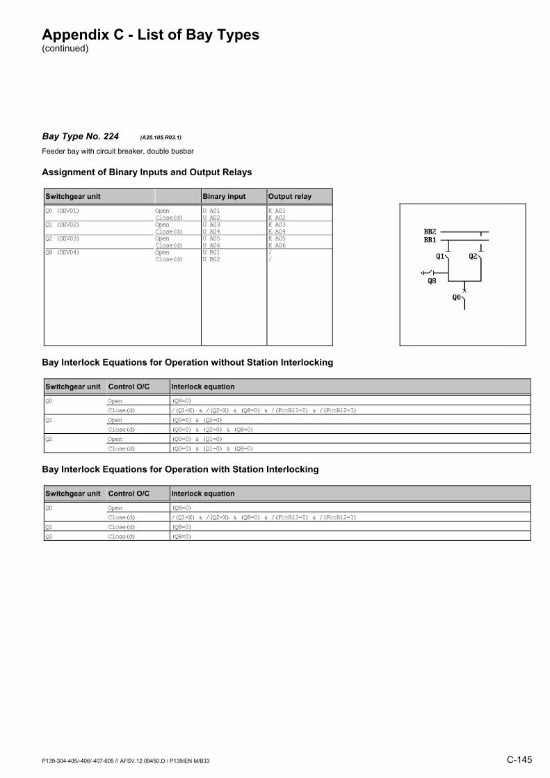
Appendix C - List of Bay Types (continued)
P139-304-405/-406/-407-605 // AFSV.12.09450.D / P139/EN M/B33 C-145
Bay Type No. 224 (A25.105.R03.1) Feeder bay with circuit breaker, double busbar
Assignment of Binary Inputs and Output Relays
Switchgear unit Binary input Output relay
Q0 (DEV01) Q1 (DEV02) Q2 (DEV03) Q8 (DEV04)
Open Close(d) Open Close(d) Open Close(d) Open Close(d)
U A01 U A02 U A03 U A04 U A05 U A06 U B01 U B02
K A01 K A02K A03 K A04K A05 K A06/ /
Bay Interlock Equations for Operation without Station Interlocking
Switchgear unit Control O/C Interlock equation
Q0 Open (Q8=0) Close(d) /(Q1=X) & /(Q2=X) & (Q8=0) & /(FctBl1=I) & /(FctBl2=I) Q1 Open (Q0=0) & (Q2=0) Close(d) (Q0=0) & (Q2=0) & (Q8=0) Q2 Open (Q0=0) & (Q1=0) Close(d) (Q0=0) & (Q1=0) & (Q8=0)
Bay Interlock Equations for Operation with Station Interlocking
Switchgear unit Control O/C Interlock equation
Q0 Open (Q8=0) Close(d) /(Q1=X) & /(Q2=X) & (Q8=0) & /(FctBl1=I) & /(FctBl2=I) Q1 Close(d) (Q8=0) Q2 Close(d) (Q8=0)
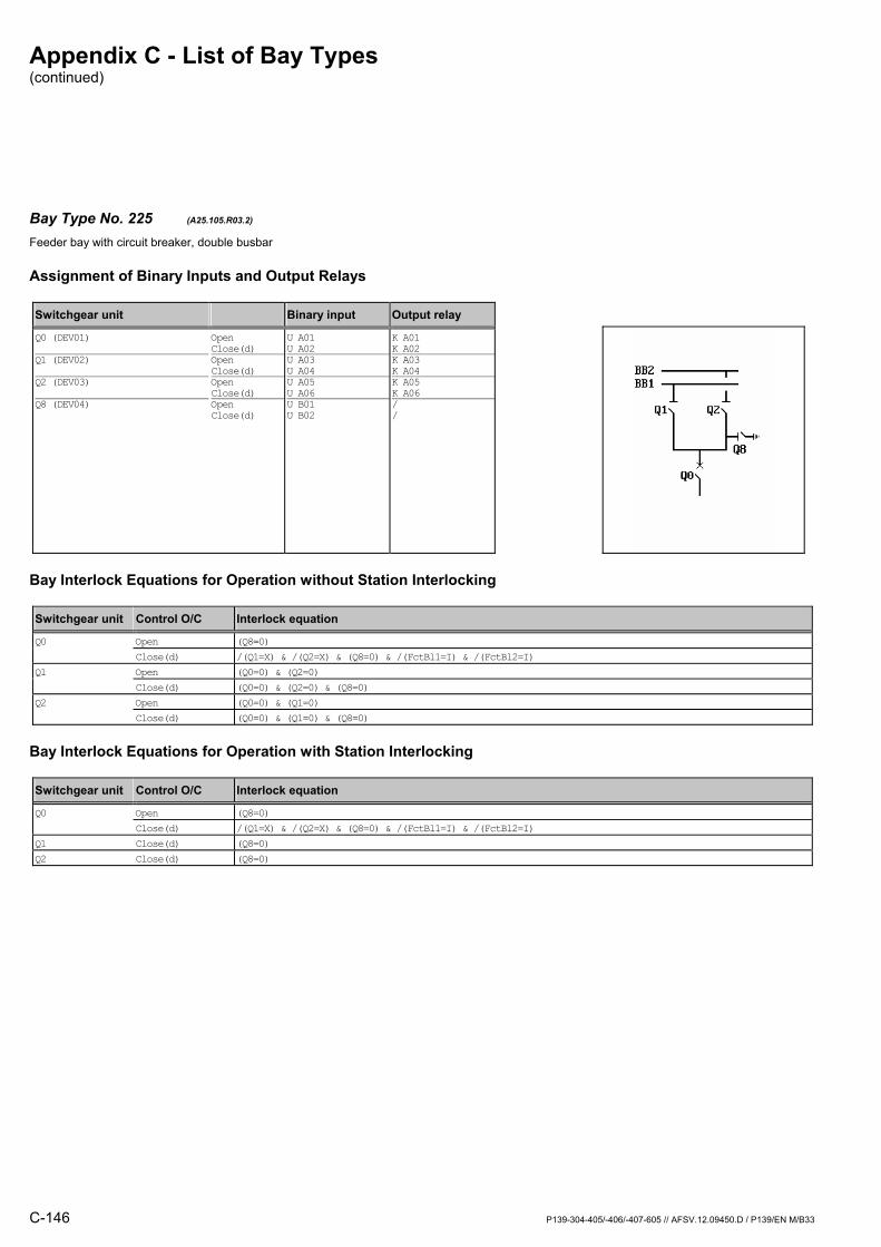
Appendix C - List of Bay Types (continued)
C-146 P139-304-405/-406/-407-605 // AFSV.12.09450.D / P139/EN M/B33
Bay Type No. 225 (A25.105.R03.2) Feeder bay with circuit breaker, double busbar
Assignment of Binary Inputs and Output Relays
Switchgear unit Binary input Output relay
Q0 (DEV01) Q1 (DEV02) Q2 (DEV03) Q8 (DEV04)
Open Close(d) Open Close(d) Open Close(d) Open Close(d)
U A01 U A02 U A03 U A04 U A05 U A06 U B01 U B02
K A01 K A02K A03 K A04K A05 K A06/ /
Bay Interlock Equations for Operation without Station Interlocking
Switchgear unit Control O/C Interlock equation
Q0 Open (Q8=0) Close(d) /(Q1=X) & /(Q2=X) & (Q8=0) & /(FctBl1=I) & /(FctBl2=I) Q1 Open (Q0=0) & (Q2=0) Close(d) (Q0=0) & (Q2=0) & (Q8=0) Q2 Open (Q0=0) & (Q1=0) Close(d) (Q0=0) & (Q1=0) & (Q8=0)
Bay Interlock Equations for Operation with Station Interlocking
Switchgear unit Control O/C Interlock equation
Q0 Open (Q8=0) Close(d) /(Q1=X) & /(Q2=X) & (Q8=0) & /(FctBl1=I) & /(FctBl2=I) Q1 Close(d) (Q8=0) Q2 Close(d) (Q8=0)
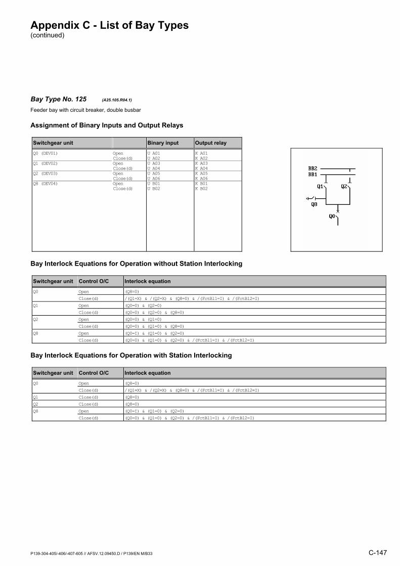
Appendix C - List of Bay Types (continued)
P139-304-405/-406/-407-605 // AFSV.12.09450.D / P139/EN M/B33 C-147
Bay Type No. 125 (A25.105.R04.1) Feeder bay with circuit breaker, double busbar
Assignment of Binary Inputs and Output Relays
Switchgear unit Binary input Output relay
Q0 (DEV01) Q1 (DEV02) Q2 (DEV03) Q8 (DEV04)
Open Close(d) Open Close(d) Open Close(d) Open Close(d)
U A01 U A02 U A03 U A04 U A05 U A06 U B01 U B02
K A01 K A02K A03 K A04K A05 K A06K B01 K B02
Bay Interlock Equations for Operation without Station Interlocking
Switchgear unit Control O/C Interlock equation
Q0 Open (Q8=0) Close(d) /(Q1=X) & /(Q2=X) & (Q8=0) & /(FctBl1=I) & /(FctBl2=I) Q1 Open (Q0=0) & (Q2=0) Close(d) (Q0=0) & (Q2=0) & (Q8=0) Q2 Open (Q0=0) & (Q1=0) Close(d) (Q0=0) & (Q1=0) & (Q8=0) Q8 Open (Q0=I) & (Q1=0) & (Q2=0) Close(d) (Q0=0) & (Q1=0) & (Q2=0) & /(FctBl1=I) & /(FctBl2=I)
Bay Interlock Equations for Operation with Station Interlocking
Switchgear unit Control O/C Interlock equation
Q0 Open (Q8=0) Close(d) /(Q1=X) & /(Q2=X) & (Q8=0) & /(FctBl1=I) & /(FctBl2=I) Q1 Close(d) (Q8=0) Q2 Close(d) (Q8=0) Q8 Open (Q0=I) & (Q1=0) & (Q2=0) Close(d) (Q0=0) & (Q1=0) & (Q2=0) & /(FctBl1=I) & /(FctBl2=I)
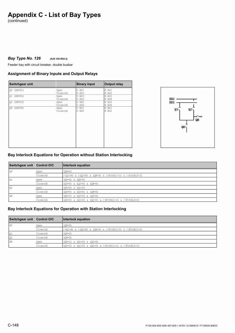
Appendix C - List of Bay Types (continued)
C-148 P139-304-405/-406/-407-605 // AFSV.12.09450.D / P139/EN M/B33
Bay Type No. 126 (A25.105.R04.2) Feeder bay with circuit breaker, double busbar
Assignment of Binary Inputs and Output Relays
Switchgear unit Binary input Output relay
Q0 (DEV01) Q1 (DEV02) Q2 (DEV03) Q8 (DEV04)
Open Close(d) Open Close(d) Open Close(d) Open Close(d)
U A01 U A02 U A03 U A04 U A05 U A06 U B01 U B02
K A01 K A02K A03 K A04K A05 K A06K B01 K B02
Bay Interlock Equations for Operation without Station Interlocking
Switchgear unit Control O/C Interlock equation
Q0 Open (Q8=0) Close(d) /(Q1=X) & /(Q2=X) & (Q8=0) & /(FctBl1=I) & /(FctBl2=I) Q1 Open (Q0=0) & (Q2=0) Close(d) (Q0=0) & (Q2=0) & (Q8=0) Q2 Open (Q0=0) & (Q1=0) Close(d) (Q0=0) & (Q1=0) & (Q8=0) Q8 Open (Q0=I) & (Q1=0) & (Q2=0) Close(d) (Q0=0) & (Q1=0) & (Q2=0) & /(FctBl1=I) & /(FctBl2=I)
Bay Interlock Equations for Operation with Station Interlocking
Switchgear unit Control O/C Interlock equation
Q0 Open (Q8=0) Close(d) /(Q1=X) & /(Q2=X) & (Q8=0) & /(FctBl1=I) & /(FctBl2=I) Q1 Close(d) (Q8=0) Q2 Close(d) (Q8=0) Q8 Open (Q0=I) & (Q1=0) & (Q2=0) Close(d) (Q0=0) & (Q1=0) & (Q2=0) & /(FctBl1=I) & /(FctBl2=I)

Appendix C - List of Bay Types (continued)
P139-304-405/-406/-407-605 // AFSV.12.09450.D / P139/EN M/B33 C-149
Bay Type No. 127 (A25.128.R01) Feeder bay with circuit breaker, double busbar
Assignment of Binary Inputs and Output Relays
Switchgear unit Binary input Output relay
Q0 (DEV01) Q1 (DEV02) Q2 (DEV03) Q81 (DEV04) Q82 (DEV05)
Open Close(d) Open Close(d) Open Close(d) Open Close(d) Open Close(d)
U A01 U A02 U A03 U A04 U A05 U A06 U B01 U B02 U B03 U B04
K A01 K A02/ // // // /
Bay Interlock Equations for Operation without Station Interlocking
Switchgear unit Control O/C Interlock equation
Q0 Open (Q81=0) & (Q82=0) Close(d) /(Q1=X) & /(Q2=X) & (Q81=0) & (Q82=0) & /(FctBl1=I) & /(FctBl2=I)
Bay Interlock Equations for Operation with Station Interlocking
Switchgear unit Control O/C Interlock equation
Q0 Open (Q81=0) & (Q82=0) Close(d) /(Q1=X) & /(Q2=X) & (Q81=0) & (Q82=0) & /(FctBl1=I) & /(FctBl2=I)
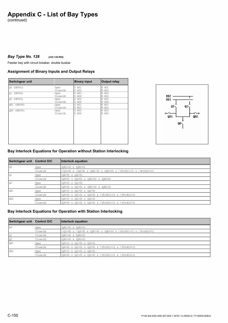
Appendix C - List of Bay Types (continued)
C-150 P139-304-405/-406/-407-605 // AFSV.12.09450.D / P139/EN M/B33
Bay Type No. 128 (A25.128.R05) Feeder bay with circuit breaker, double busbar
Assignment of Binary Inputs and Output Relays
Switchgear unit Binary input Output relay
Q0 (DEV01) Q1 (DEV02) Q2 (DEV03) Q81 (DEV04) Q82 (DEV05)
Open Close(d) Open Close(d) Open Close(d) Open Close(d) Open Close(d)
U A01 U A02 U A03 U A04 U A05 U A06 U B01 U B02 U B03 U B04
K A01 K A02K A03 K A04K A05 K A06K B01 K B02K B03 K B04
Bay Interlock Equations for Operation without Station Interlocking
Switchgear unit Control O/C Interlock equation
Q0 Open (Q81=0) & (Q82=0) Close(d) /(Q1=X) & /(Q2=X) & (Q81=0) & (Q82=0) & /(FctBl1=I) & /(FctBl2=I) Q1 Open (Q0=0) & (Q2=0) Close(d) (Q0=0) & (Q2=0) & (Q81=0) & (Q82=0) Q2 Open (Q0=0) & (Q1=0) Close(d) (Q0=0) & (Q1=0) & (Q81=0) & (Q82=0) Q81 Open (Q0=I) & (Q1=0) & (Q2=0) Close(d) (Q0=0) & (Q1=0) & (Q2=0) & /(FctBl1=I) & /(FctBl2=I) Q82 Open (Q0=I) & (Q1=0) & (Q2=0) Close(d) (Q0=0) & (Q1=0) & (Q2=0) & /(FctBl1=I) & /(FctBl2=I)
Bay Interlock Equations for Operation with Station Interlocking
Switchgear unit Control O/C Interlock equation
Q0 Open (Q81=0) & (Q82=0) Close(d) /(Q1=X) & /(Q2=X) & (Q81=0) & (Q82=0) & /(FctBl1=I) & /(FctBl2=I) Q1 Close(d) (Q81=0) & (Q82=0) Q2 Close(d) (Q81=0) & (Q82=0) Q81 Open (Q0=I) & (Q1=0) & (Q2=0) Close(d) (Q0=0) & (Q1=0) & (Q2=0) & /(FctBl1=I) & /(FctBl2=I) Q82 Open (Q0=I) & (Q1=0) & (Q2=0) Close(d) (Q0=0) & (Q1=0) & (Q2=0) & /(FctBl1=I) & /(FctBl2=I)

Appendix C - List of Bay Types (continued)
P139-304-405/-406/-407-605 // AFSV.12.09450.D / P139/EN M/B33 C-151
Bay Type No. 133 (L11.100.R01) Bus sectionalizer bay with circuit breaker, single busbar
Assignment of Binary Inputs and Output Relays
Switchgear unit Binary input Output relay
Q0 (DEV01) X01 (DEV02)
Open Close(d) Open Close(d)
U A01 U A02 U A03 U A04
K A01 K A02/ /
Bay Interlock Equations for Operation without Station Interlocking
Switchgear unit Control O/C Interlock equation
Q0 Close(d) /(X01=X) & /(FctBl1=I) & /(FctBl2=I)
Bay Interlock Equations for Operation with Station Interlocking
Switchgear unit Control O/C Interlock equation
Q0 Close(d) /(X01=X) & /(FctBl1=I) & /(FctBl2=I)

Appendix C - List of Bay Types (continued)
C-152 P139-304-405/-406/-407-605 // AFSV.12.09450.D / P139/EN M/B33
Bay Type No. 553 (L11.100.R01.2) Bus sectionalizer bay with circuit breaker, single busbar
Assignment of Binary Inputs and Output Relays
Switchgear unit Binary input Output relay
Q0 (DEV01) X01 (DEV02)
Open Close(d) Open Close(d)
U A01 U A02 U A03 U A04
K A01 K A02/ /
Bay Interlock Equations for Operation without Station Interlocking
Switchgear unit Control O/C Interlock equation
Q0 Close(d) /(X01=X) & /(FctBl1=I) & /(FctBl2=I)
Bay Interlock Equations for Operation with Station Interlocking
Switchgear unit Control O/C Interlock equation
Q0 Close(d) /(X01=X) & /(FctBl1=I) & /(FctBl2=I)

Appendix C - List of Bay Types (continued)
P139-304-405/-406/-407-605 // AFSV.12.09450.D / P139/EN M/B33 C-153
Bay Type No. 134 (L11.100.R02) Bus sectionalizer bay with circuit breaker, single busbar
Assignment of Binary Inputs and Output Relays
Switchgear unit Binary input Output relay
Q0 (DEV01) X01 (DEV02)
Open Close(d) Open Close(d)
U A01 U A02 U A03 U A04
K A01 K A02K A03 K A04
Bay Interlock Equations for Operation without Station Interlocking
Switchgear unit Control O/C Interlock equation
Q0 Close(d) /(X01=X) & /(FctBl1=I) & /(FctBl2=I) X01 Open (Q0=0) Close(d) (Q0=0)
Bay Interlock Equations for Operation with Station Interlocking
Switchgear unit Control O/C Interlock equation
Q0 Close(d) /(X01=X) & /(FctBl1=I) & /(FctBl2=I) X01 Open (Q0=0) Close(d) (Q0=0)

Appendix C - List of Bay Types (continued)
C-154 P139-304-405/-406/-407-605 // AFSV.12.09450.D / P139/EN M/B33
Bay Type No. 528 (L11.102.R01) Bus sectionalizer bay with circuit breaker, single busbar
Assignment of Binary Inputs and Output Relays
Switchgear unit Binary input Output relay
Q0 (DEV01) X0 (DEV02) Q15 (DEV03)
Open Close(d) Open Close(d) Open Close(d)
U A01 U A02 U A03 U A04 U A05 U A06
K A01 K A02/ // /
Bay Interlock Equations for Operation without Station Interlocking
Switchgear unit Control O/C Interlock equation
Q0 Close(d) /(X0=X) & (Q15=0) & /(FctBl1=I) & /(FctBl2=I)
Bay Interlock Equations for Operation with Station Interlocking
Switchgear unit Control O/C Interlock equation
Q0 Close(d) /(X0=X) & (Q15=0) & /(FctBl1=I) & /(FctBl2=I)

Appendix C - List of Bay Types (continued)
P139-304-405/-406/-407-605 // AFSV.12.09450.D / P139/EN M/B33 C-155
Bay Type No. 542 (L11.102.R01.2) Bus sectionalizer bay with circuit breaker, single busbar
Assignment of Binary Inputs and Output Relays
Switchgear unit Binary input Output relay
Q0 (DEV01) X0 (DEV02) Q15 (DEV03)
Open Close(d) Open Close(d) Open Close(d)
U A01 U A02 U A03 U A04 U A05 U A06
K A01 K A02/ // /
Bay Interlock Equations for Operation without Station Interlocking
Switchgear unit Control O/C Interlock equation
Q0 Close(d) /(X0=X) & (Q15=0) & /(FctBl1=I) & /(FctBl2=I)
Bay Interlock Equations for Operation with Station Interlocking
Switchgear unit Control O/C Interlock equation
Q0 Close(d) /(X0=X) & (Q15=0) & /(FctBl1=I) & /(FctBl2=I)

Appendix C - List of Bay Types (continued)
C-156 P139-304-405/-406/-407-605 // AFSV.12.09450.D / P139/EN M/B33
Bay Type No. 135 (L11.104.R01) Bus sectionalizer bay with circuit breaker, single busbar
Assignment of Binary Inputs and Output Relays
Switchgear unit Binary input Output relay
Q0 (DEV01) X01 (DEV02) Q8 (DEV03)
Open Close(d) Open Close(d) Open Close(d)
U A01 U A02 U A03 U A04 U A05 U A06
K A01 K A02/ // /
Bay Interlock Equations for Operation without Station Interlocking
Switchgear unit Control O/C Interlock equation
Q0 Close(d) /(X01=X) & /(FctBl1=I) & /(FctBl2=I)
Bay Interlock Equations for Operation with Station Interlocking
Switchgear unit Control O/C Interlock equation
Q0 Close(d) /(X01=X) & /(FctBl1=I) & /(FctBl2=I)

Appendix C - List of Bay Types (continued)
P139-304-405/-406/-407-605 // AFSV.12.09450.D / P139/EN M/B33 C-157
Bay Type No. 136 (L11.104.R02) Bus sectionalizer bay with circuit breaker, single busbar
Assignment of Binary Inputs and Output Relays
Switchgear unit Binary input Output relay
Q0 (DEV01) X01 (DEV02) Q8 (DEV03)
Open Close(d) Open Close(d) Open Close(d)
U A01 U A02 U A03 U A04 U A05 U A06
K A01 K A02K A03 K A04/ /
Bay Interlock Equations for Operation without Station Interlocking
Switchgear unit Control O/C Interlock equation
Q0 Close(d) /(X01=X) & /(FctBl1=I) & /(FctBl2=I) X01 Open (Q0=0) Close(d) (Q0=0) & (Q8=0)
Bay Interlock Equations for Operation with Station Interlocking
Switchgear unit Control O/C Interlock equation
Q0 Close(d) /(X01=X) & /(FctBl1=I) & /(FctBl2=I) X01 Open (Q0=0) Close(d) (Q0=0) & (Q8=0)

Appendix C - List of Bay Types (continued)
C-158 P139-304-405/-406/-407-605 // AFSV.12.09450.D / P139/EN M/B33
Bay Type No. 137 (L11.104.R03) Bus sectionalizer bay with circuit breaker, single busbar
Assignment of Binary Inputs and Output Relays
Switchgear unit Binary input Output relay
Q0 (DEV01) X01 (DEV02) Q8 (DEV03)
Open Close(d) Open Close(d) Open Close(d)
U A01 U A02 U A03 U A04 U A05 U A06
K A01 K A02K A03 K A04K A05 K A06
Bay Interlock Equations for Operation without Station Interlocking
Switchgear unit Control O/C Interlock equation
Q0 Close(d) /(X01=X) & /(FctBl1=I) & /(FctBl2=I) Q8 Close(d) (X01=0) & (Q8=I) X01 Open (Q0=0) Close(d) (Q0=0) & (Q8=0)
Bay Interlock Equations for Operation with Station Interlocking
Switchgear unit Control O/C Interlock equation
Q0 Close(d) /(X01=X) & /(FctBl1=I) & /(FctBl2=I) Q8 Close(d) (X01=0) X01 Open (Q0=0) Close(d) (Q0=0) & (Q8=0)
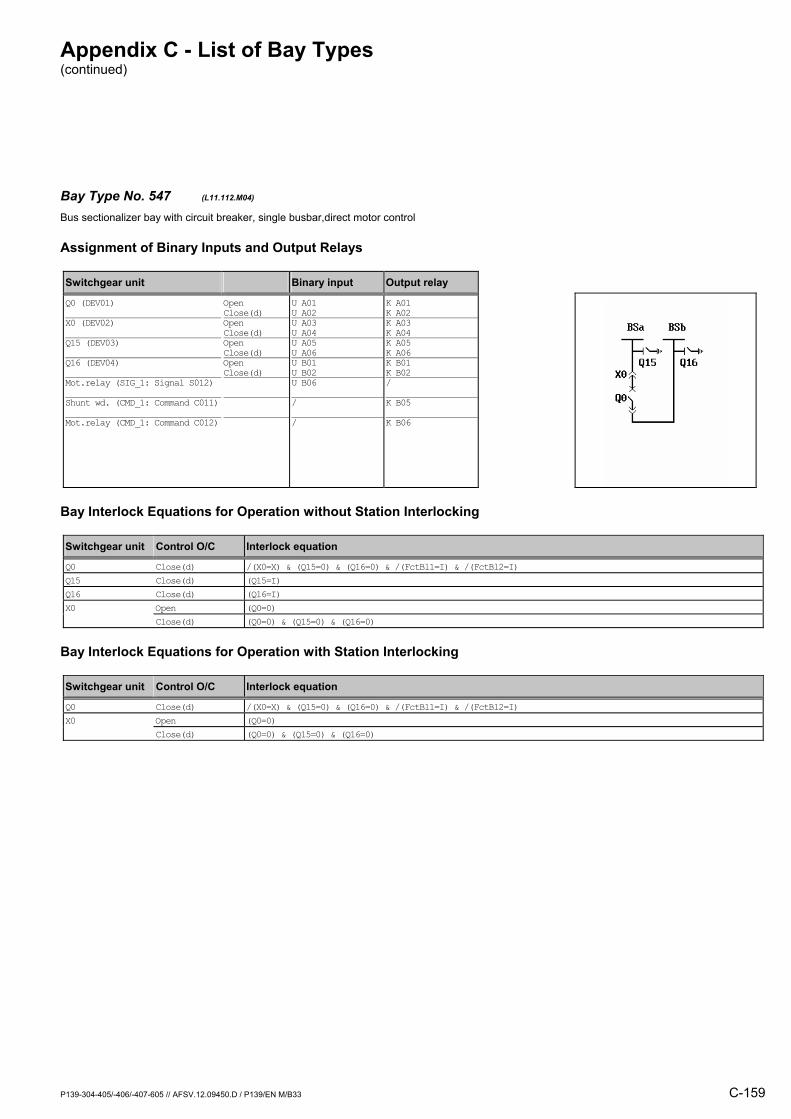
Appendix C - List of Bay Types (continued)
P139-304-405/-406/-407-605 // AFSV.12.09450.D / P139/EN M/B33 C-159
Bay Type No. 547 (L11.112.M04) Bus sectionalizer bay with circuit breaker, single busbar,direct motor control
Assignment of Binary Inputs and Output Relays
Switchgear unit Binary input Output relay
Q0 (DEV01) X0 (DEV02) Q15 (DEV03) Q16 (DEV04) Mot.relay (SIG_1: Signal S012) Shunt wd. (CMD_1: Command C011) Mot.relay (CMD_1: Command C012)
Open Close(d) Open Close(d) Open Close(d) Open Close(d)
U A01 U A02 U A03 U A04 U A05 U A06 U B01 U B02 U B06 / /
K A01 K A02K A03 K A04K A05 K A06K B01 K B02/
K B05
K B06
Bay Interlock Equations for Operation without Station Interlocking
Switchgear unit Control O/C Interlock equation
Q0 Close(d) /(X0=X) & (Q15=0) & (Q16=0) & /(FctBl1=I) & /(FctBl2=I) Q15 Close(d) (Q15=I) Q16 Close(d) (Q16=I) X0 Open (Q0=0) Close(d) (Q0=0) & (Q15=0) & (Q16=0)
Bay Interlock Equations for Operation with Station Interlocking
Switchgear unit Control O/C Interlock equation
Q0 Close(d) /(X0=X) & (Q15=0) & (Q16=0) & /(FctBl1=I) & /(FctBl2=I) X0 Open (Q0=0) Close(d) (Q0=0) & (Q15=0) & (Q16=0)
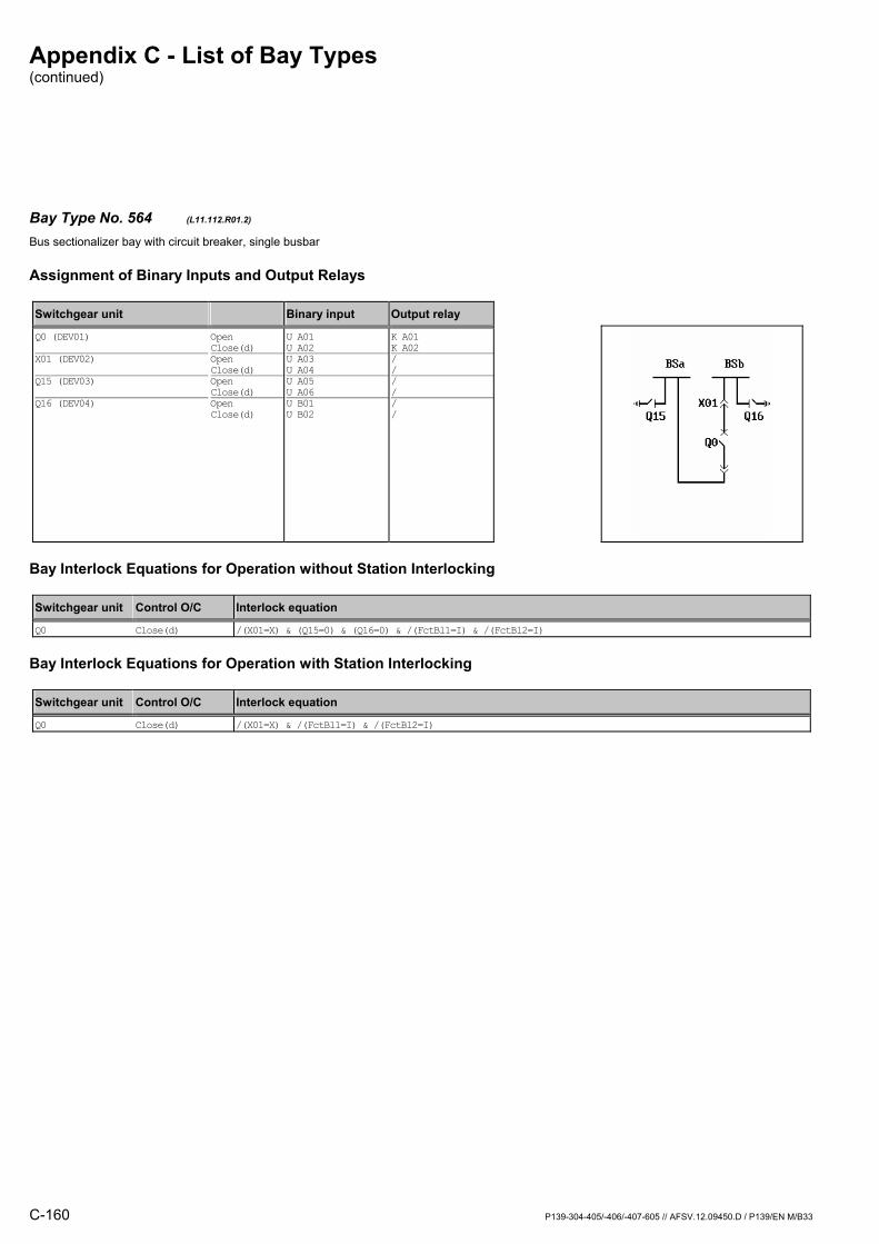
Appendix C - List of Bay Types (continued)
C-160 P139-304-405/-406/-407-605 // AFSV.12.09450.D / P139/EN M/B33
Bay Type No. 564 (L11.112.R01.2) Bus sectionalizer bay with circuit breaker, single busbar
Assignment of Binary Inputs and Output Relays
Switchgear unit Binary input Output relay
Q0 (DEV01) X01 (DEV02) Q15 (DEV03) Q16 (DEV04)
Open Close(d) Open Close(d) Open Close(d) Open Close(d)
U A01 U A02 U A03 U A04 U A05 U A06 U B01 U B02
K A01 K A02/ // // /
Bay Interlock Equations for Operation without Station Interlocking
Switchgear unit Control O/C Interlock equation
Q0 Close(d) /(X01=X) & (Q15=0) & (Q16=0) & /(FctBl1=I) & /(FctBl2=I)
Bay Interlock Equations for Operation with Station Interlocking
Switchgear unit Control O/C Interlock equation
Q0 Close(d) /(X01=X) & /(FctBl1=I) & /(FctBl2=I)

Appendix C - List of Bay Types (continued)
P139-304-405/-406/-407-605 // AFSV.12.09450.D / P139/EN M/B33 C-161
Bay Type No. 138 (L11.116.R01) Bus sectionalizer bay with circuit breaker, single busbar
Assignment of Binary Inputs and Output Relays
Switchgear unit Binary input Output relay
Q0 (DEV01) X01 (DEV02) X02 (DEV03)
Open Close(d) Open Close(d) Open Close(d)
U A01 U A02 U A03 U A04 U A05 U A06
K A01 K A02/ // /
Bay Interlock Equations for Operation without Station Interlocking
Switchgear unit Control O/C Interlock equation
Q0 Close(d) /(X01=X) & /(X02=X) & /(FctBl1=I) & /(FctBl2=I)
Bay Interlock Equations for Operation with Station Interlocking
Switchgear unit Control O/C Interlock equation
Q0 Close(d) /(X01=X) & /(X02=X) & /(FctBl1=I) & /(FctBl2=I)

Appendix C - List of Bay Types (continued)
C-162 P139-304-405/-406/-407-605 // AFSV.12.09450.D / P139/EN M/B33
Bay Type No. 545 (L11.116.R01.2) Bus sectionalizer bay with circuit breaker, single busbar
Assignment of Binary Inputs and Output Relays
Switchgear unit Binary input Output relay
Q0 (DEV01) X01 (DEV02) X02 (DEV03)
Open Close(d) Open Close(d) Open Close(d)
U A01 U A02 U A03 U A04 U A05 U A06
K A01 K A02/ // /
Bay Interlock Equations for Operation without Station Interlocking
Switchgear unit Control O/C Interlock equation
Q0 Close(d) /(X01=X) & /(X02=X) & /(FctBl1=I) & /(FctBl2=I)
Bay Interlock Equations for Operation with Station Interlocking
Switchgear unit Control O/C Interlock equation
Q0 Close(d) /(X01=X) & /(X02=X) & /(FctBl1=I) & /(FctBl2=I)
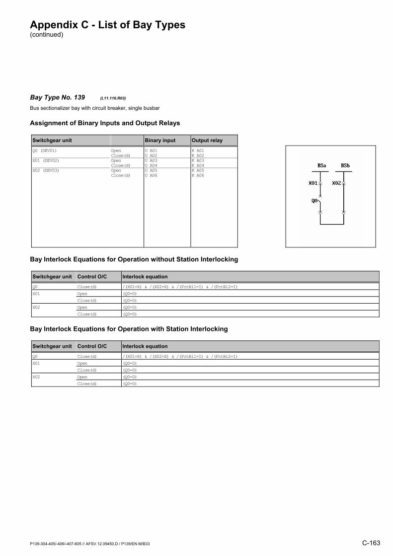
Appendix C - List of Bay Types (continued)
P139-304-405/-406/-407-605 // AFSV.12.09450.D / P139/EN M/B33 C-163
Bay Type No. 139 (L11.116.R03) Bus sectionalizer bay with circuit breaker, single busbar
Assignment of Binary Inputs and Output Relays
Switchgear unit Binary input Output relay
Q0 (DEV01) X01 (DEV02) X02 (DEV03)
Open Close(d) Open Close(d) Open Close(d)
U A01 U A02 U A03 U A04 U A05 U A06
K A01 K A02K A03 K A04K A05 K A06
Bay Interlock Equations for Operation without Station Interlocking
Switchgear unit Control O/C Interlock equation
Q0 Close(d) /(X01=X) & /(X02=X) & /(FctBl1=I) & /(FctBl2=I) X01 Open (Q0=0) Close(d) (Q0=0) X02 Open (Q0=0) Close(d) (Q0=0)
Bay Interlock Equations for Operation with Station Interlocking
Switchgear unit Control O/C Interlock equation
Q0 Close(d) /(X01=X) & /(X02=X) & /(FctBl1=I) & /(FctBl2=I) X01 Open (Q0=0) Close(d) (Q0=0) X02 Open (Q0=0) Close(d) (Q0=0)

Appendix C - List of Bay Types (continued)
C-164 P139-304-405/-406/-407-605 // AFSV.12.09450.D / P139/EN M/B33
Bay Type No. 548 (L11.120.M03) Bus sectionalizer bay with circuit breaker, single busbar,direct motor control
Assignment of Binary Inputs and Output Relays
Switchgear unit Binary input Output relay
Q0 (DEV01) Q8 (DEV02) X01 (DEV03) X02 (DEV04) Mot.relay (SIG_1: Signal S012) Shunt wd. (CMD_1: Command C011) Mot.relay (CMD_1: Command C012)
Open Close(d) Open Close(d) Open Close(d) Open Close(d)
U A01 U A02 U A03 U A04 U A05 U A06 U B01 U B02 U B06 / /
K A01 K A02K A03 K A04K A05 K A06/ //
K B05
K B06
Bay Interlock Equations for Operation without Station Interlocking
Switchgear unit Control O/C Interlock equation
Q0 Close(d) /(X01=X) & /(X02=X) & /(FctBl1=I) & /(FctBl2=I) Q8 Close(d) (X01=0) & (X02=0) X01 Open (Q0=0) Close(d) (Q0=0) & (Q8=0)
Bay Interlock Equations for Operation with Station Interlocking
Switchgear unit Control O/C Interlock equation
Q0 Close(d) /(X01=X) & /(X02=X) & /(FctBl1=I) & /(FctBl2=I) Q8 Close(d) (X01=0) & (X02=0) X01 Open (Q0=0) Close(d) (Q0=0) & (Q8=0)
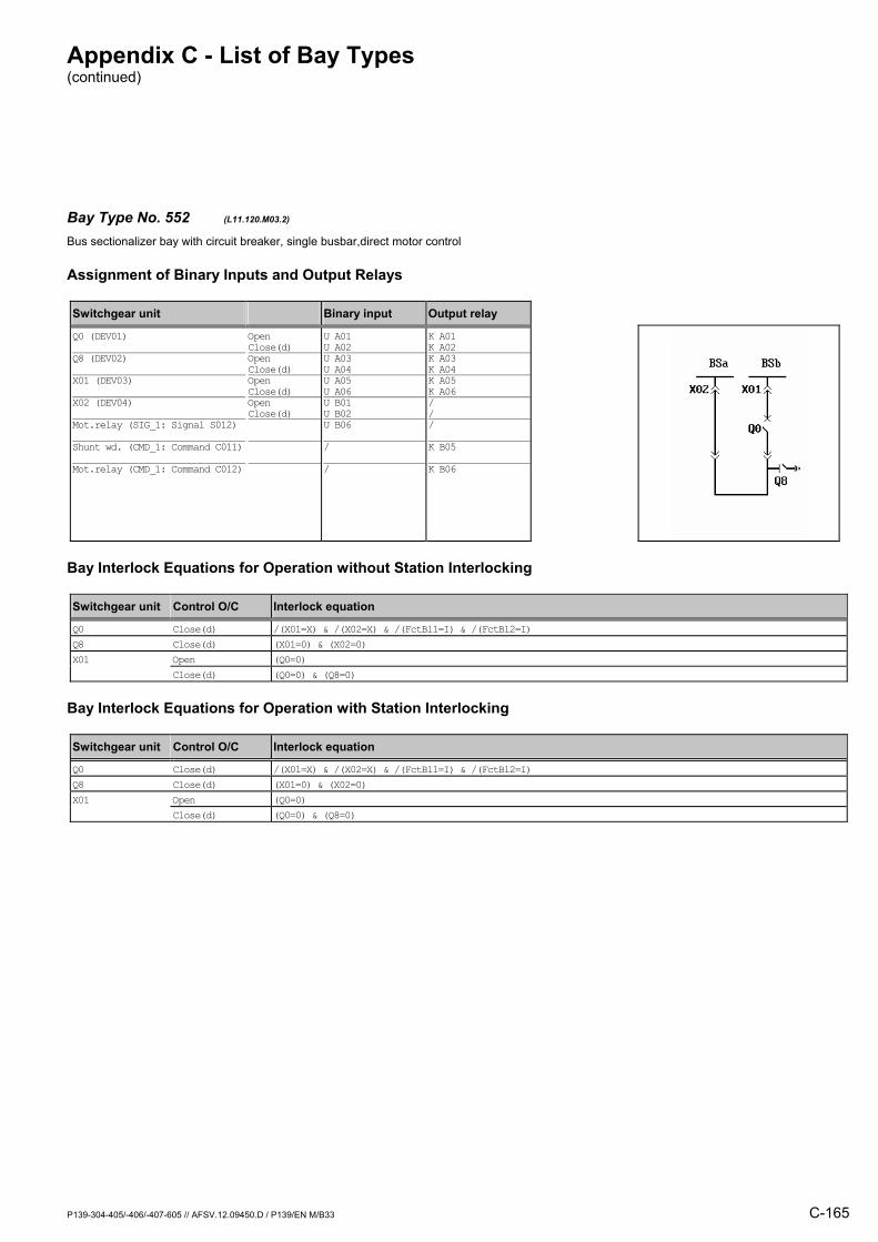
Appendix C - List of Bay Types (continued)
P139-304-405/-406/-407-605 // AFSV.12.09450.D / P139/EN M/B33 C-165
Bay Type No. 552 (L11.120.M03.2) Bus sectionalizer bay with circuit breaker, single busbar,direct motor control
Assignment of Binary Inputs and Output Relays
Switchgear unit Binary input Output relay
Q0 (DEV01) Q8 (DEV02) X01 (DEV03) X02 (DEV04) Mot.relay (SIG_1: Signal S012) Shunt wd. (CMD_1: Command C011) Mot.relay (CMD_1: Command C012)
Open Close(d) Open Close(d) Open Close(d) Open Close(d)
U A01 U A02 U A03 U A04 U A05 U A06 U B01 U B02 U B06 / /
K A01 K A02K A03 K A04K A05 K A06/ //
K B05
K B06
Bay Interlock Equations for Operation without Station Interlocking
Switchgear unit Control O/C Interlock equation
Q0 Close(d) /(X01=X) & /(X02=X) & /(FctBl1=I) & /(FctBl2=I) Q8 Close(d) (X01=0) & (X02=0) X01 Open (Q0=0) Close(d) (Q0=0) & (Q8=0)
Bay Interlock Equations for Operation with Station Interlocking
Switchgear unit Control O/C Interlock equation
Q0 Close(d) /(X01=X) & /(X02=X) & /(FctBl1=I) & /(FctBl2=I) Q8 Close(d) (X01=0) & (X02=0) X01 Open (Q0=0) Close(d) (Q0=0) & (Q8=0)
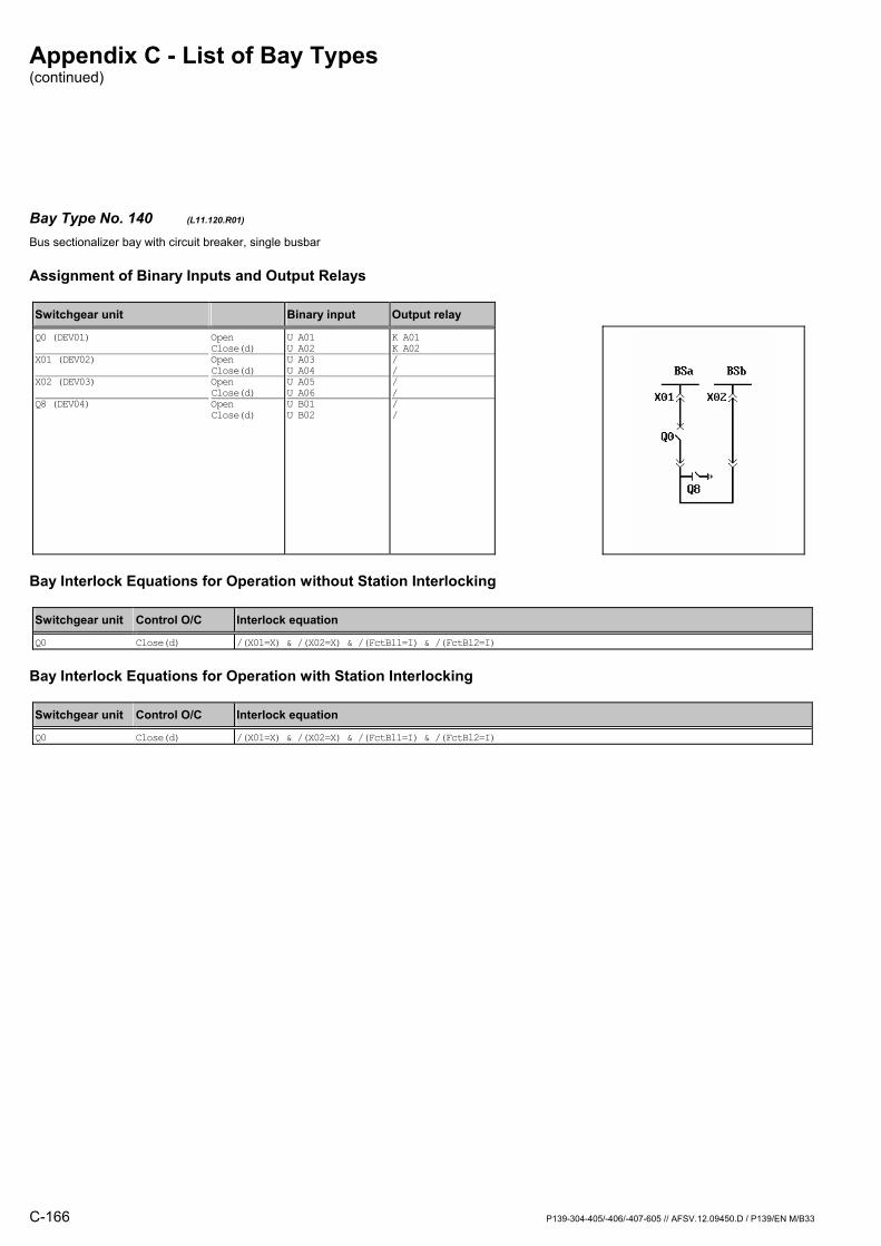
Appendix C - List of Bay Types (continued)
C-166 P139-304-405/-406/-407-605 // AFSV.12.09450.D / P139/EN M/B33
Bay Type No. 140 (L11.120.R01) Bus sectionalizer bay with circuit breaker, single busbar
Assignment of Binary Inputs and Output Relays
Switchgear unit Binary input Output relay
Q0 (DEV01) X01 (DEV02) X02 (DEV03) Q8 (DEV04)
Open Close(d) Open Close(d) Open Close(d) Open Close(d)
U A01 U A02 U A03 U A04 U A05 U A06 U B01 U B02
K A01 K A02/ // // /
Bay Interlock Equations for Operation without Station Interlocking
Switchgear unit Control O/C Interlock equation
Q0 Close(d) /(X01=X) & /(X02=X) & /(FctBl1=I) & /(FctBl2=I)
Bay Interlock Equations for Operation with Station Interlocking
Switchgear unit Control O/C Interlock equation
Q0 Close(d) /(X01=X) & /(X02=X) & /(FctBl1=I) & /(FctBl2=I)

Appendix C - List of Bay Types (continued)
P139-304-405/-406/-407-605 // AFSV.12.09450.D / P139/EN M/B33 C-167
Bay Type No. 141 (L11.120.R03) Bus sectionalizer bay with circuit breaker, single busbar
Assignment of Binary Inputs and Output Relays
Switchgear unit Binary input Output relay
Q0 (DEV01) X01 (DEV02) X02 (DEV03) Q8 (DEV04)
Open Close(d) Open Close(d) Open Close(d) Open Close(d)
U A01 U A02 U A03 U A04 U A05 U A06 U B01 U B02
K A01 K A02K A03 K A04K A05 K A06/ /
Bay Interlock Equations for Operation without Station Interlocking
Switchgear unit Control O/C Interlock equation
Q0 Close(d) /(X01=X) & /(X02=X) & /(FctBl1=I) & /(FctBl2=I) X01 Open (Q0=0) Close(d) (Q0=0) & (Q8=0) X02 Open (Q0=0) Close(d) (Q0=0) & (Q8=0)
Bay Interlock Equations for Operation with Station Interlocking
Switchgear unit Control O/C Interlock equation
Q0 Close(d) /(X01=X) & /(X02=X) & /(FctBl1=I) & /(FctBl2=I) X01 Open (Q0=0) Close(d) (Q0=0) & (Q8=0) X02 Open (Q0=0) Close(d) (Q0=0) & (Q8=0)
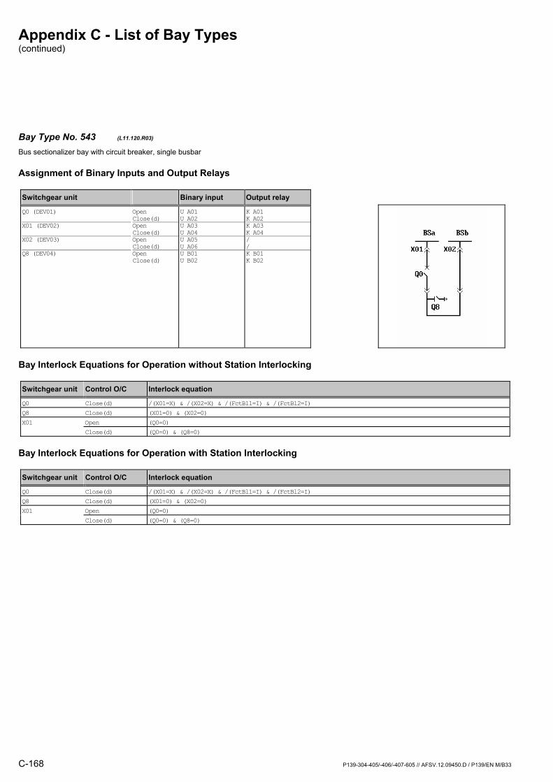
Appendix C - List of Bay Types (continued)
C-168 P139-304-405/-406/-407-605 // AFSV.12.09450.D / P139/EN M/B33
Bay Type No. 543 (L11.120.R03) Bus sectionalizer bay with circuit breaker, single busbar
Assignment of Binary Inputs and Output Relays
Switchgear unit Binary input Output relay
Q0 (DEV01) X01 (DEV02) X02 (DEV03) Q8 (DEV04)
Open Close(d) Open Close(d) Open Close(d) Open Close(d)
U A01 U A02 U A03 U A04 U A05 U A06 U B01 U B02
K A01 K A02K A03 K A04/ /K B01 K B02
Bay Interlock Equations for Operation without Station Interlocking
Switchgear unit Control O/C Interlock equation
Q0 Close(d) /(X01=X) & /(X02=X) & /(FctBl1=I) & /(FctBl2=I) Q8 Close(d) (X01=0) & (X02=0) X01 Open (Q0=0) Close(d) (Q0=0) & (Q8=0)
Bay Interlock Equations for Operation with Station Interlocking
Switchgear unit Control O/C Interlock equation
Q0 Close(d) /(X01=X) & /(X02=X) & /(FctBl1=I) & /(FctBl2=I) Q8 Close(d) (X01=0) & (X02=0) X01 Open (Q0=0) Close(d) (Q0=0) & (Q8=0)
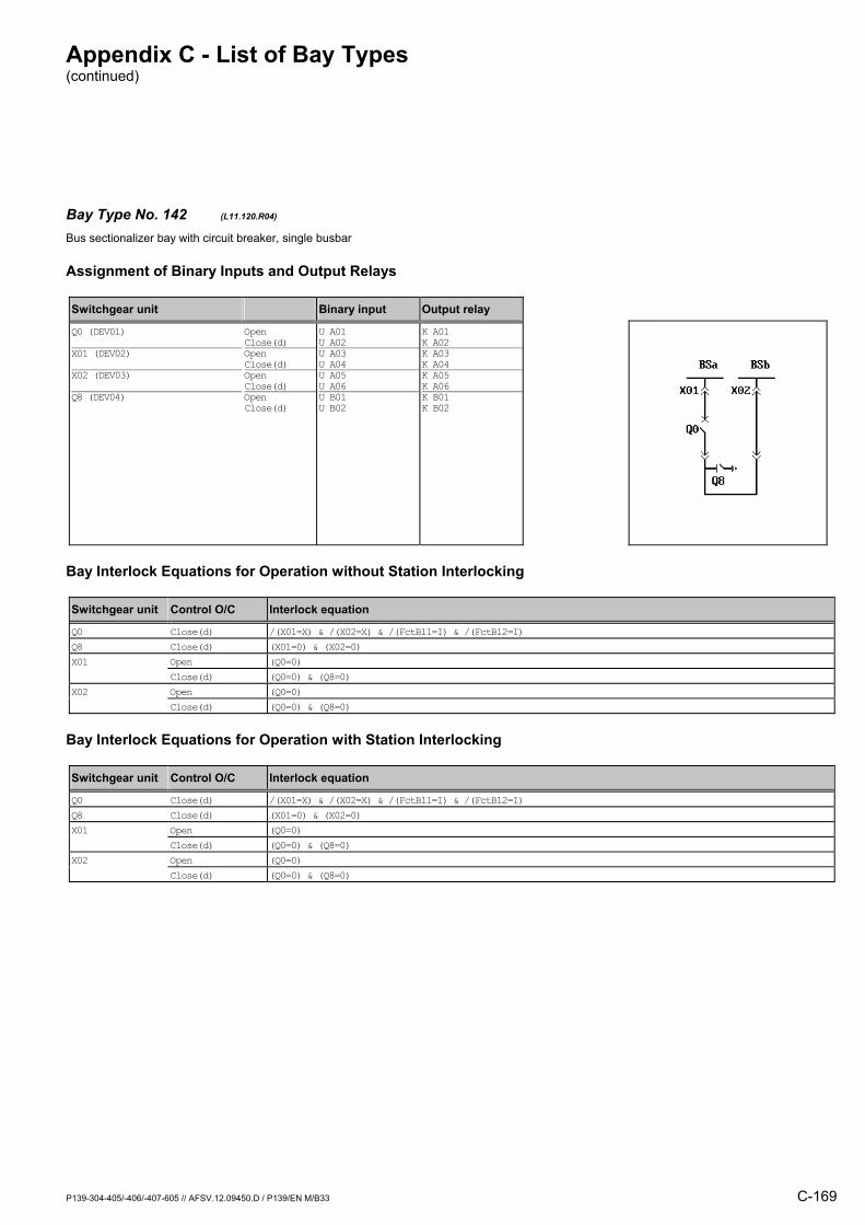
Appendix C - List of Bay Types (continued)
P139-304-405/-406/-407-605 // AFSV.12.09450.D / P139/EN M/B33 C-169
Bay Type No. 142 (L11.120.R04) Bus sectionalizer bay with circuit breaker, single busbar
Assignment of Binary Inputs and Output Relays
Switchgear unit Binary input Output relay
Q0 (DEV01) X01 (DEV02) X02 (DEV03) Q8 (DEV04)
Open Close(d) Open Close(d) Open Close(d) Open Close(d)
U A01 U A02 U A03 U A04 U A05 U A06 U B01 U B02
K A01 K A02K A03 K A04K A05 K A06K B01 K B02
Bay Interlock Equations for Operation without Station Interlocking
Switchgear unit Control O/C Interlock equation
Q0 Close(d) /(X01=X) & /(X02=X) & /(FctBl1=I) & /(FctBl2=I) Q8 Close(d) (X01=0) & (X02=0) X01 Open (Q0=0) Close(d) (Q0=0) & (Q8=0) X02 Open (Q0=0) Close(d) (Q0=0) & (Q8=0)
Bay Interlock Equations for Operation with Station Interlocking
Switchgear unit Control O/C Interlock equation
Q0 Close(d) /(X01=X) & /(X02=X) & /(FctBl1=I) & /(FctBl2=I) Q8 Close(d) (X01=0) & (X02=0) X01 Open (Q0=0) Close(d) (Q0=0) & (Q8=0) X02 Open (Q0=0) Close(d) (Q0=0) & (Q8=0)
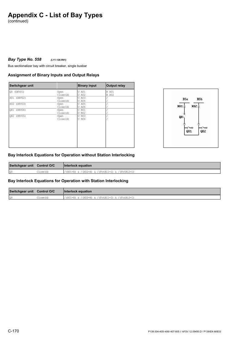
Appendix C - List of Bay Types (continued)
C-170 P139-304-405/-406/-407-605 // AFSV.12.09450.D / P139/EN M/B33
Bay Type No. 558 (L11.128.R01) Bus sectionalizer bay with circuit breaker, single busbar
Assignment of Binary Inputs and Output Relays
Switchgear unit Binary input Output relay
Q0 (DEV01) X01 (DEV02) X02 (DEV03) Q81 (DEV04) Q82 (DEV05)
Open Close(d) Open Close(d) Open Close(d) Open Close(d) Open Close(d)
U A01 U A02 U A03 U A04 U A05 U A06 U B01 U B02 U B03 U B04
K A01 K A02/ // // // /
Bay Interlock Equations for Operation without Station Interlocking
Switchgear unit Control O/C Interlock equation
Q0 Close(d) /(X01=X) & /(X02=X) & /(FctBl1=I) & /(FctBl2=I)
Bay Interlock Equations for Operation with Station Interlocking
Switchgear unit Control O/C Interlock equation
Q0 Close(d) /(X01=X) & /(X02=X) & /(FctBl1=I) & /(FctBl2=I)
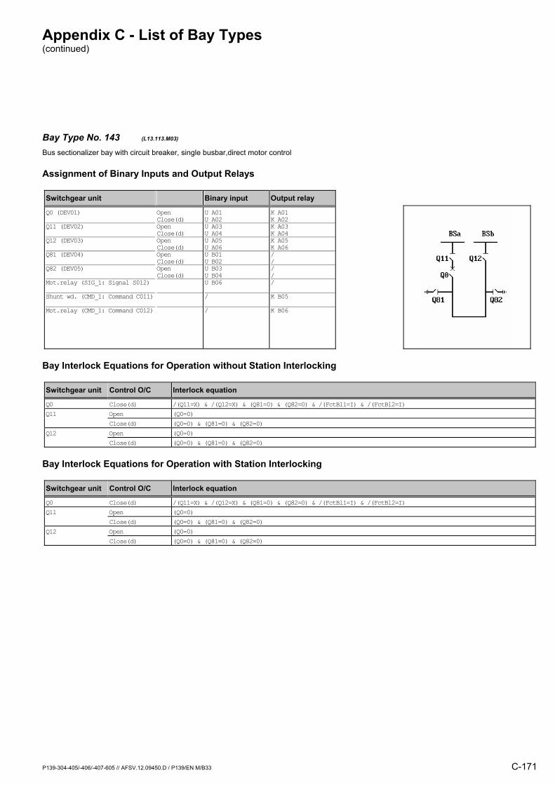
Appendix C - List of Bay Types (continued)
P139-304-405/-406/-407-605 // AFSV.12.09450.D / P139/EN M/B33 C-171
Bay Type No. 143 (L13.113.M03) Bus sectionalizer bay with circuit breaker, single busbar,direct motor control
Assignment of Binary Inputs and Output Relays
Switchgear unit Binary input Output relay
Q0 (DEV01) Q11 (DEV02) Q12 (DEV03) Q81 (DEV04) Q82 (DEV05) Mot.relay (SIG_1: Signal S012) Shunt wd. (CMD_1: Command C011) Mot.relay (CMD_1: Command C012)
Open Close(d) Open Close(d) Open Close(d) Open Close(d) Open Close(d)
U A01 U A02 U A03 U A04 U A05 U A06 U B01 U B02 U B03 U B04 U B06 / /
K A01 K A02K A03 K A04K A05 K A06/ // //
K B05
K B06
Bay Interlock Equations for Operation without Station Interlocking
Switchgear unit Control O/C Interlock equation
Q0 Close(d) /(Q11=X) & /(Q12=X) & (Q81=0) & (Q82=0) & /(FctBl1=I) & /(FctBl2=I) Q11 Open (Q0=0) Close(d) (Q0=0) & (Q81=0) & (Q82=0) Q12 Open (Q0=0) Close(d) (Q0=0) & (Q81=0) & (Q82=0)
Bay Interlock Equations for Operation with Station Interlocking
Switchgear unit Control O/C Interlock equation
Q0 Close(d) /(Q11=X) & /(Q12=X) & (Q81=0) & (Q82=0) & /(FctBl1=I) & /(FctBl2=I) Q11 Open (Q0=0) Close(d) (Q0=0) & (Q81=0) & (Q82=0) Q12 Open (Q0=0) Close(d) (Q0=0) & (Q81=0) & (Q82=0)
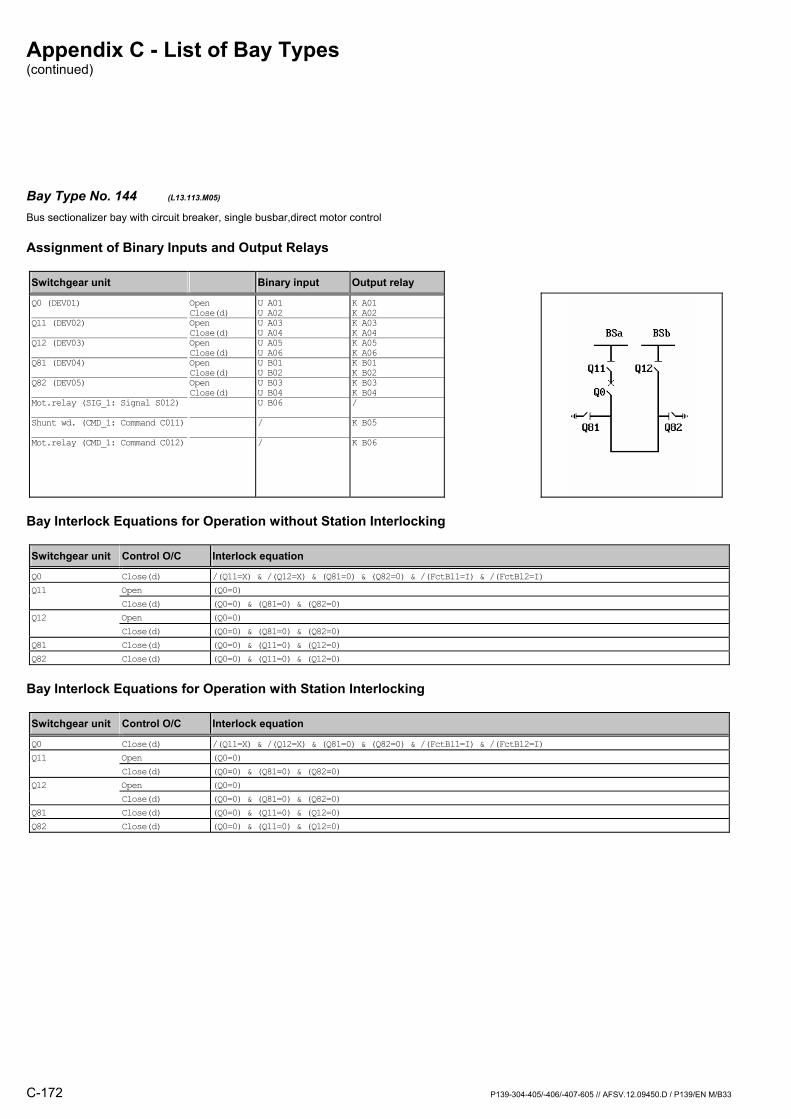
Appendix C - List of Bay Types (continued)
C-172 P139-304-405/-406/-407-605 // AFSV.12.09450.D / P139/EN M/B33
Bay Type No. 144 (L13.113.M05) Bus sectionalizer bay with circuit breaker, single busbar,direct motor control
Assignment of Binary Inputs and Output Relays
Switchgear unit Binary input Output relay
Q0 (DEV01) Q11 (DEV02) Q12 (DEV03) Q81 (DEV04) Q82 (DEV05) Mot.relay (SIG_1: Signal S012) Shunt wd. (CMD_1: Command C011) Mot.relay (CMD_1: Command C012)
Open Close(d) Open Close(d) Open Close(d) Open Close(d) Open Close(d)
U A01 U A02 U A03 U A04 U A05 U A06 U B01 U B02 U B03 U B04 U B06 / /
K A01 K A02K A03 K A04K A05 K A06K B01 K B02K B03 K B04/
K B05
K B06
Bay Interlock Equations for Operation without Station Interlocking
Switchgear unit Control O/C Interlock equation
Q0 Close(d) /(Q11=X) & /(Q12=X) & (Q81=0) & (Q82=0) & /(FctBl1=I) & /(FctBl2=I) Q11 Open (Q0=0) Close(d) (Q0=0) & (Q81=0) & (Q82=0) Q12 Open (Q0=0) Close(d) (Q0=0) & (Q81=0) & (Q82=0) Q81 Close(d) (Q0=0) & (Q11=0) & (Q12=0) Q82 Close(d) (Q0=0) & (Q11=0) & (Q12=0)
Bay Interlock Equations for Operation with Station Interlocking
Switchgear unit Control O/C Interlock equation
Q0 Close(d) /(Q11=X) & /(Q12=X) & (Q81=0) & (Q82=0) & /(FctBl1=I) & /(FctBl2=I) Q11 Open (Q0=0) Close(d) (Q0=0) & (Q81=0) & (Q82=0) Q12 Open (Q0=0) Close(d) (Q0=0) & (Q81=0) & (Q82=0) Q81 Close(d) (Q0=0) & (Q11=0) & (Q12=0) Q82 Close(d) (Q0=0) & (Q11=0) & (Q12=0)

Appendix C - List of Bay Types (continued)
P139-304-405/-406/-407-605 // AFSV.12.09450.D / P139/EN M/B33 C-173
Bay Type No. 145 (L13.113.R01) Bus sectionalizer bay with circuit breaker, single busbar
Assignment of Binary Inputs and Output Relays
Switchgear unit Binary input Output relay
Q0 (DEV01) Q11 (DEV02) Q12 (DEV03) Q81 (DEV04) Q82 (DEV05)
Open Close(d) Open Close(d) Open Close(d) Open Close(d) Open Close(d)
U A01 U A02 U A03 U A04 U A05 U A06 U B01 U B02 U B03 U B04
K A01 K A02/ // // // /
Bay Interlock Equations for Operation without Station Interlocking
Switchgear unit Control O/C Interlock equation
Q0 Close(d) /(Q11=X) & /(Q12=X) & (Q81=0) & (Q82=0) & /(FctBl1=I) & /(FctBl2=I)
Bay Interlock Equations for Operation with Station Interlocking
Switchgear unit Control O/C Interlock equation
Q0 Close(d) /(Q11=X) & /(Q12=X) & (Q81=0) & (Q82=0) & /(FctBl1=I) & /(FctBl2=I)
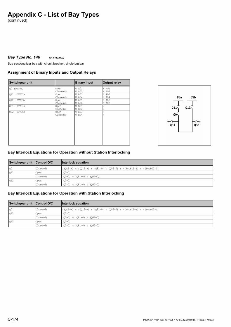
Appendix C - List of Bay Types (continued)
C-174 P139-304-405/-406/-407-605 // AFSV.12.09450.D / P139/EN M/B33
Bay Type No. 146 (L13.113.R03) Bus sectionalizer bay with circuit breaker, single busbar
Assignment of Binary Inputs and Output Relays
Switchgear unit Binary input Output relay
Q0 (DEV01) Q11 (DEV02) Q12 (DEV03) Q81 (DEV04) Q82 (DEV05)
Open Close(d) Open Close(d) Open Close(d) Open Close(d) Open Close(d)
U A01 U A02 U A03 U A04 U A05 U A06 U B01 U B02 U B03 U B04
K A01 K A02K A03 K A04K A05 K A06/ // /
Bay Interlock Equations for Operation without Station Interlocking
Switchgear unit Control O/C Interlock equation
Q0 Close(d) /(Q11=X) & /(Q12=X) & (Q81=0) & (Q82=0) & /(FctBl1=I) & /(FctBl2=I) Q11 Open (Q0=0) Close(d) (Q0=0) & (Q81=0) & (Q82=0) Q12 Open (Q0=0) Close(d) (Q0=0) & (Q81=0) & (Q82=0)
Bay Interlock Equations for Operation with Station Interlocking
Switchgear unit Control O/C Interlock equation
Q0 Close(d) /(Q11=X) & /(Q12=X) & (Q81=0) & (Q82=0) & /(FctBl1=I) & /(FctBl2=I) Q11 Open (Q0=0) Close(d) (Q0=0) & (Q81=0) & (Q82=0) Q12 Open (Q0=0) Close(d) (Q0=0) & (Q81=0) & (Q82=0)
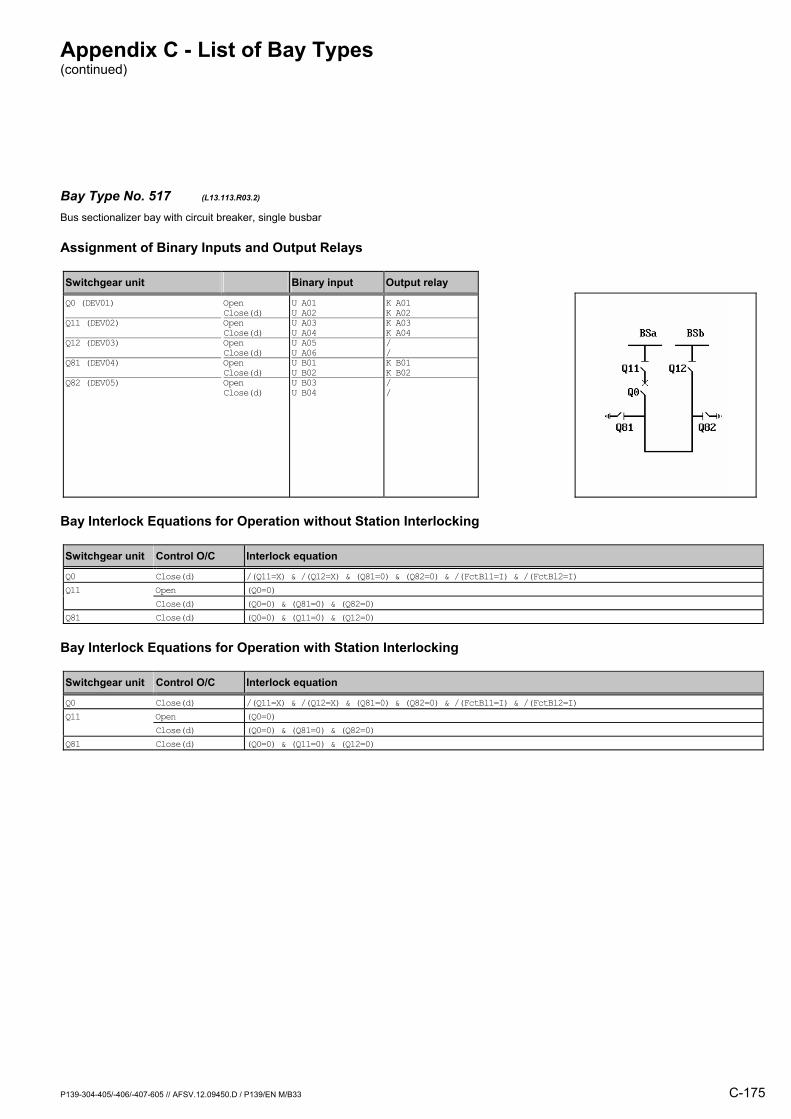
Appendix C - List of Bay Types (continued)
P139-304-405/-406/-407-605 // AFSV.12.09450.D / P139/EN M/B33 C-175
Bay Type No. 517 (L13.113.R03.2) Bus sectionalizer bay with circuit breaker, single busbar
Assignment of Binary Inputs and Output Relays
Switchgear unit Binary input Output relay
Q0 (DEV01) Q11 (DEV02) Q12 (DEV03) Q81 (DEV04) Q82 (DEV05)
Open Close(d) Open Close(d) Open Close(d) Open Close(d) Open Close(d)
U A01 U A02 U A03 U A04 U A05 U A06 U B01 U B02 U B03 U B04
K A01 K A02K A03 K A04/ /K B01 K B02/ /
Bay Interlock Equations for Operation without Station Interlocking
Switchgear unit Control O/C Interlock equation
Q0 Close(d) /(Q11=X) & /(Q12=X) & (Q81=0) & (Q82=0) & /(FctBl1=I) & /(FctBl2=I) Q11 Open (Q0=0) Close(d) (Q0=0) & (Q81=0) & (Q82=0) Q81 Close(d) (Q0=0) & (Q11=0) & (Q12=0)
Bay Interlock Equations for Operation with Station Interlocking
Switchgear unit Control O/C Interlock equation
Q0 Close(d) /(Q11=X) & /(Q12=X) & (Q81=0) & (Q82=0) & /(FctBl1=I) & /(FctBl2=I) Q11 Open (Q0=0) Close(d) (Q0=0) & (Q81=0) & (Q82=0) Q81 Close(d) (Q0=0) & (Q11=0) & (Q12=0)
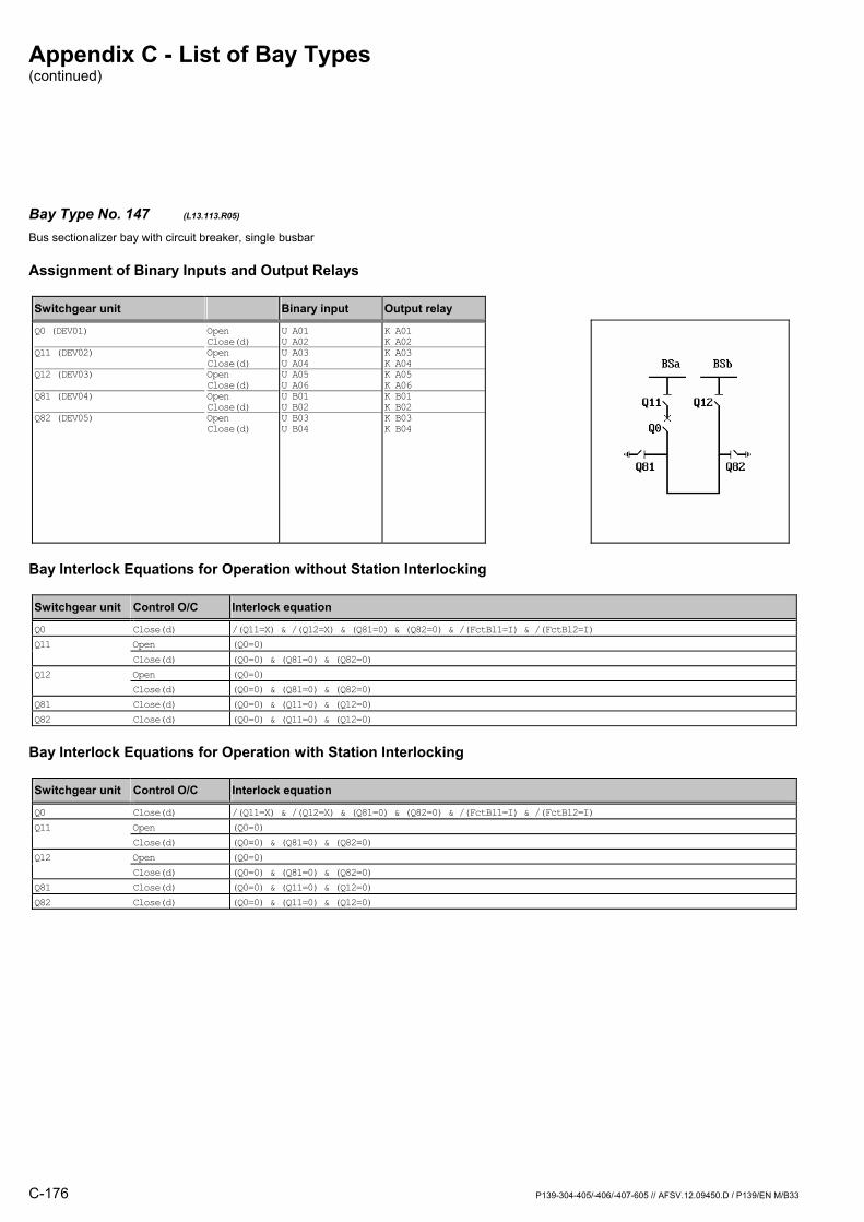
Appendix C - List of Bay Types (continued)
C-176 P139-304-405/-406/-407-605 // AFSV.12.09450.D / P139/EN M/B33
Bay Type No. 147 (L13.113.R05) Bus sectionalizer bay with circuit breaker, single busbar
Assignment of Binary Inputs and Output Relays
Switchgear unit Binary input Output relay
Q0 (DEV01) Q11 (DEV02) Q12 (DEV03) Q81 (DEV04) Q82 (DEV05)
Open Close(d) Open Close(d) Open Close(d) Open Close(d) Open Close(d)
U A01 U A02 U A03 U A04 U A05 U A06 U B01 U B02 U B03 U B04
K A01 K A02K A03 K A04K A05 K A06K B01 K B02K B03 K B04
Bay Interlock Equations for Operation without Station Interlocking
Switchgear unit Control O/C Interlock equation
Q0 Close(d) /(Q11=X) & /(Q12=X) & (Q81=0) & (Q82=0) & /(FctBl1=I) & /(FctBl2=I) Q11 Open (Q0=0) Close(d) (Q0=0) & (Q81=0) & (Q82=0) Q12 Open (Q0=0) Close(d) (Q0=0) & (Q81=0) & (Q82=0) Q81 Close(d) (Q0=0) & (Q11=0) & (Q12=0) Q82 Close(d) (Q0=0) & (Q11=0) & (Q12=0)
Bay Interlock Equations for Operation with Station Interlocking
Switchgear unit Control O/C Interlock equation
Q0 Close(d) /(Q11=X) & /(Q12=X) & (Q81=0) & (Q82=0) & /(FctBl1=I) & /(FctBl2=I) Q11 Open (Q0=0) Close(d) (Q0=0) & (Q81=0) & (Q82=0) Q12 Open (Q0=0) Close(d) (Q0=0) & (Q81=0) & (Q82=0) Q81 Close(d) (Q0=0) & (Q11=0) & (Q12=0) Q82 Close(d) (Q0=0) & (Q11=0) & (Q12=0)
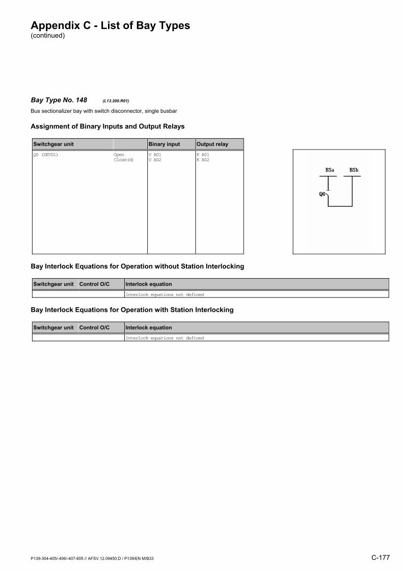
Appendix C - List of Bay Types (continued)
P139-304-405/-406/-407-605 // AFSV.12.09450.D / P139/EN M/B33 C-177
Bay Type No. 148 (L13.200.R01) Bus sectionalizer bay with switch disconnector, single busbar
Assignment of Binary Inputs and Output Relays
Switchgear unit Binary input Output relay
Q0 (DEV01)
Open Close(d)
U A01 U A02
K A01 K A02
Bay Interlock Equations for Operation without Station Interlocking
Switchgear unit Control O/C Interlock equation
Interlock equations not defined
Bay Interlock Equations for Operation with Station Interlocking
Switchgear unit Control O/C Interlock equation
Interlock equations not defined

Appendix C - List of Bay Types (continued)
C-178 P139-304-405/-406/-407-605 // AFSV.12.09450.D / P139/EN M/B33
Bay Type No. 149 (L13.202.R01) Bus sectionalizer bay with switch disconnector, single busbar
Assignment of Binary Inputs and Output Relays
Switchgear unit Binary input Output relay
Q0 (DEV01) Q15 (DEV02) Q16 (DEV03)
Open Close(d) Open Close(d) Open Close(d)
U A01 U A02 U A03 U A04 U A05 U A06
K A01 K A02/ // /
Bay Interlock Equations for Operation without Station Interlocking
Switchgear unit Control O/C Interlock equation
Q0 Close(d) (Q15=0) & (Q16=0) & /(FctBl1=I) & /(FctBl2=I)
Bay Interlock Equations for Operation with Station Interlocking
Switchgear unit Control O/C Interlock equation
Q0 Close(d) (Q15=0) & (Q16=0) & /(FctBl1=I) & /(FctBl2=I)
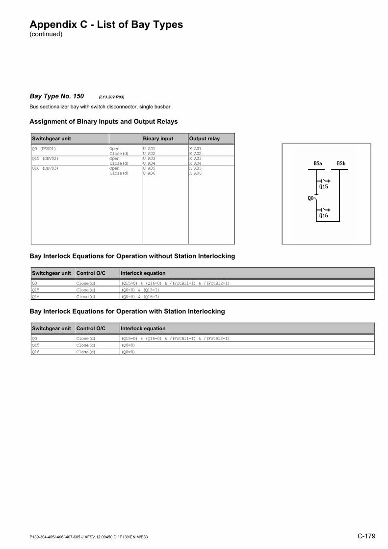
Appendix C - List of Bay Types (continued)
P139-304-405/-406/-407-605 // AFSV.12.09450.D / P139/EN M/B33 C-179
Bay Type No. 150 (L13.202.R03) Bus sectionalizer bay with switch disconnector, single busbar
Assignment of Binary Inputs and Output Relays
Switchgear unit Binary input Output relay
Q0 (DEV01) Q15 (DEV02) Q16 (DEV03)
Open Close(d) Open Close(d) Open Close(d)
U A01 U A02 U A03 U A04 U A05 U A06
K A01 K A02K A03 K A04K A05 K A06
Bay Interlock Equations for Operation without Station Interlocking
Switchgear unit Control O/C Interlock equation
Q0 Close(d) (Q15=0) & (Q16=0) & /(FctBl1=I) & /(FctBl2=I) Q15 Close(d) (Q0=0) & (Q15=I) Q16 Close(d) (Q0=0) & (Q16=I)
Bay Interlock Equations for Operation with Station Interlocking
Switchgear unit Control O/C Interlock equation
Q0 Close(d) (Q15=0) & (Q16=0) & /(FctBl1=I) & /(FctBl2=I) Q15 Close(d) (Q0=0) Q16 Close(d) (Q0=0)
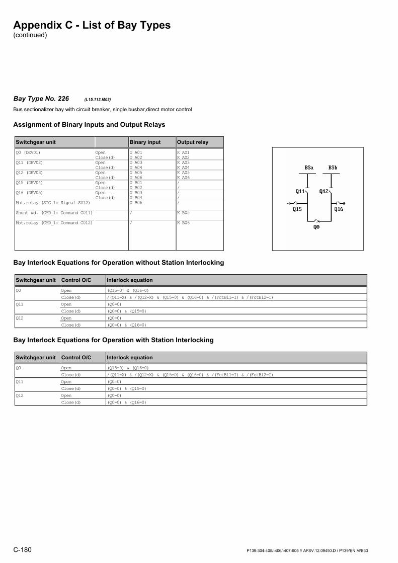
Appendix C - List of Bay Types (continued)
C-180 P139-304-405/-406/-407-605 // AFSV.12.09450.D / P139/EN M/B33
Bay Type No. 226 (L15.113.M03) Bus sectionalizer bay with circuit breaker, single busbar,direct motor control
Assignment of Binary Inputs and Output Relays
Switchgear unit Binary input Output relay
Q0 (DEV01) Q11 (DEV02) Q12 (DEV03) Q15 (DEV04) Q16 (DEV05) Mot.relay (SIG_1: Signal S012) Shunt wd. (CMD_1: Command C011) Mot.relay (CMD_1: Command C012)
Open Close(d) Open Close(d) Open Close(d) Open Close(d) Open Close(d)
U A01 U A02 U A03 U A04 U A05 U A06 U B01 U B02 U B03 U B04 U B06 / /
K A01 K A02K A03 K A04K A05 K A06/ // //
K B05
K B06
Bay Interlock Equations for Operation without Station Interlocking
Switchgear unit Control O/C Interlock equation
Q0 Open (Q15=0) & (Q16=0) Close(d) /(Q11=X) & /(Q12=X) & (Q15=0) & (Q16=0) & /(FctBl1=I) & /(FctBl2=I) Q11 Open (Q0=0) Close(d) (Q0=0) & (Q15=0) Q12 Open (Q0=0) Close(d) (Q0=0) & (Q16=0)
Bay Interlock Equations for Operation with Station Interlocking
Switchgear unit Control O/C Interlock equation
Q0 Open (Q15=0) & (Q16=0) Close(d) /(Q11=X) & /(Q12=X) & (Q15=0) & (Q16=0) & /(FctBl1=I) & /(FctBl2=I) Q11 Open (Q0=0) Close(d) (Q0=0) & (Q15=0) Q12 Open (Q0=0) Close(d) (Q0=0) & (Q16=0)
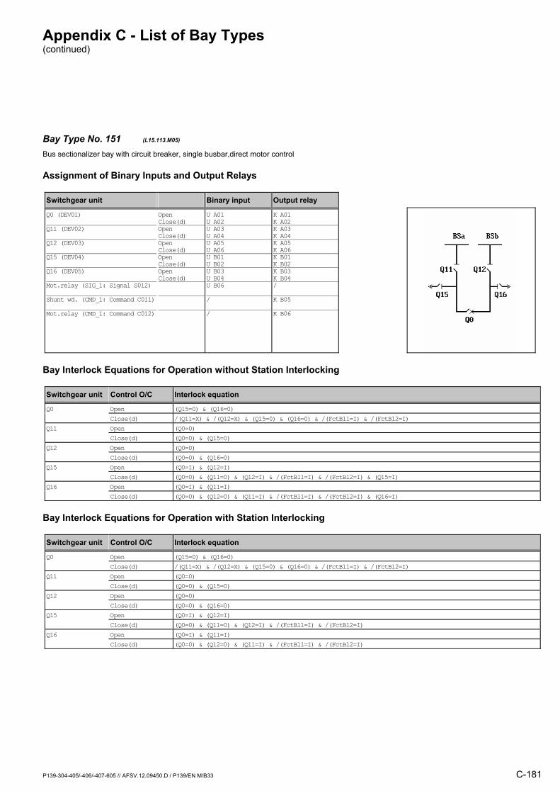
Appendix C - List of Bay Types (continued)
P139-304-405/-406/-407-605 // AFSV.12.09450.D / P139/EN M/B33 C-181
Bay Type No. 151 (L15.113.M05) Bus sectionalizer bay with circuit breaker, single busbar,direct motor control
Assignment of Binary Inputs and Output Relays
Switchgear unit Binary input Output relay
Q0 (DEV01) Q11 (DEV02) Q12 (DEV03) Q15 (DEV04) Q16 (DEV05) Mot.relay (SIG_1: Signal S012) Shunt wd. (CMD_1: Command C011) Mot.relay (CMD_1: Command C012)
Open Close(d) Open Close(d) Open Close(d) Open Close(d) Open Close(d)
U A01 U A02 U A03 U A04 U A05 U A06 U B01 U B02 U B03 U B04 U B06 / /
K A01 K A02K A03 K A04K A05 K A06K B01 K B02K B03 K B04/
K B05
K B06
Bay Interlock Equations for Operation without Station Interlocking
Switchgear unit Control O/C Interlock equation
Q0 Open (Q15=0) & (Q16=0) Close(d) /(Q11=X) & /(Q12=X) & (Q15=0) & (Q16=0) & /(FctBl1=I) & /(FctBl2=I) Q11 Open (Q0=0) Close(d) (Q0=0) & (Q15=0) Q12 Open (Q0=0) Close(d) (Q0=0) & (Q16=0) Q15 Open (Q0=I) & (Q12=I) Close(d) (Q0=0) & (Q11=0) & (Q12=I) & /(FctBl1=I) & /(FctBl2=I) & (Q15=I) Q16 Open (Q0=I) & (Q11=I) Close(d) (Q0=0) & (Q12=0) & (Q11=I) & /(FctBl1=I) & /(FctBl2=I) & (Q16=I)
Bay Interlock Equations for Operation with Station Interlocking
Switchgear unit Control O/C Interlock equation
Q0 Open (Q15=0) & (Q16=0) Close(d) /(Q11=X) & /(Q12=X) & (Q15=0) & (Q16=0) & /(FctBl1=I) & /(FctBl2=I) Q11 Open (Q0=0) Close(d) (Q0=0) & (Q15=0) Q12 Open (Q0=0) Close(d) (Q0=0) & (Q16=0) Q15 Open (Q0=I) & (Q12=I) Close(d) (Q0=0) & (Q11=0) & (Q12=I) & /(FctBl1=I) & /(FctBl2=I) Q16 Open (Q0=I) & (Q11=I) Close(d) (Q0=0) & (Q12=0) & (Q11=I) & /(FctBl1=I) & /(FctBl2=I)

Appendix C - List of Bay Types (continued)
C-182 P139-304-405/-406/-407-605 // AFSV.12.09450.D / P139/EN M/B33
Bay Type No. 152 (L15.113.R01) Bus sectionalizer bay with circuit breaker, single busbar
Assignment of Binary Inputs and Output Relays
Switchgear unit Binary input Output relay
Q0 (DEV01) Q11 (DEV02) Q12 (DEV03) Q15 (DEV04) Q16 (DEV05)
Open Close(d) Open Close(d) Open Close(d) Open Close(d) Open Close(d)
U A01 U A02 U A03 U A04 U A05 U A06 U B01 U B02 U B03 U B04
K A01 K A02/ // // // /
Bay Interlock Equations for Operation without Station Interlocking
Switchgear unit Control O/C Interlock equation
Q0 Open (Q15=0) & (Q16=0) Close(d) /(Q11=X) & /(Q12=X) & (Q15=0) & (Q16=0) & /(FctBl1=I) & /(FctBl2=I)
Bay Interlock Equations for Operation with Station Interlocking
Switchgear unit Control O/C Interlock equation
Q0 Open (Q15=0) & (Q16=0) Close(d) /(Q11=X) & /(Q12=X) & (Q15=0) & (Q16=0) & /(FctBl1=I) & /(FctBl2=I)

Appendix C - List of Bay Types (continued)
P139-304-405/-406/-407-605 // AFSV.12.09450.D / P139/EN M/B33 C-183
Bay Type No. 227 (L15.113.R03) Bus sectionalizer bay with circuit breaker, single busbar
Assignment of Binary Inputs and Output Relays
Switchgear unit Binary input Output relay
Q0 (DEV01) Q11 (DEV02) Q12 (DEV03) Q15 (DEV04) Q16 (DEV05)
Open Close(d) Open Close(d) Open Close(d) Open Close(d) Open Close(d)
U A01 U A02 U A03 U A04 U A05 U A06 U B01 U B02 U B03 U B04
K A01 K A02K A03 K A04K A05 K A06/ // /
Bay Interlock Equations for Operation without Station Interlocking
Switchgear unit Control O/C Interlock equation
Q0 Open (Q15=0) & (Q16=0) Close(d) /(Q11=X) & /(Q12=X) & (Q15=0) & (Q16=0) & /(FctBl1=I) & /(FctBl2=I) Q11 Open (Q0=0) Close(d) (Q0=0) & (Q15=0) Q12 Open (Q0=0) Close(d) (Q0=0) & (Q16=0)
Bay Interlock Equations for Operation with Station Interlocking
Switchgear unit Control O/C Interlock equation
Q0 Open (Q15=0) & (Q16=0) Close(d) /(Q11=X) & /(Q12=X) & (Q15=0) & (Q16=0) & /(FctBl1=I) & /(FctBl2=I) Q11 Open (Q0=0) Close(d) (Q0=0) & (Q15=0) Q12 Open (Q0=0) Close(d) (Q0=0) & (Q16=0)
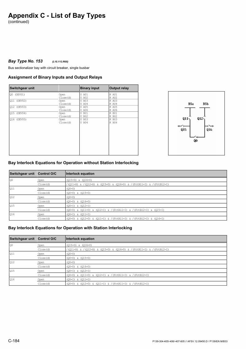
Appendix C - List of Bay Types (continued)
C-184 P139-304-405/-406/-407-605 // AFSV.12.09450.D / P139/EN M/B33
Bay Type No. 153 (L15.113.R05) Bus sectionalizer bay with circuit breaker, single busbar
Assignment of Binary Inputs and Output Relays
Switchgear unit Binary input Output relay
Q0 (DEV01) Q11 (DEV02) Q12 (DEV03) Q15 (DEV04) Q16 (DEV05)
Open Close(d) Open Close(d) Open Close(d) Open Close(d) Open Close(d)
U A01 U A02 U A03 U A04 U A05 U A06 U B01 U B02 U B03 U B04
K A01 K A02K A03 K A04K A05 K A06K B01 K B02K B03 K B04
Bay Interlock Equations for Operation without Station Interlocking
Switchgear unit Control O/C Interlock equation
Q0 Open (Q15=0) & (Q16=0) Close(d) /(Q11=X) & /(Q12=X) & (Q15=0) & (Q16=0) & /(FctBl1=I) & /(FctBl2=I) Q11 Open (Q0=0) Close(d) (Q0=0) & (Q15=0) Q12 Open (Q0=0) Close(d) (Q0=0) & (Q16=0) Q15 Open (Q0=I) & (Q12=I) Close(d) (Q0=0) & (Q11=0) & (Q12=I) & /(FctBl1=I) & /(FctBl2=I) & (Q15=I) Q16 Open (Q0=I) & (Q11=I) Close(d) (Q0=0) & (Q12=0) & (Q11=I) & /(FctBl1=I) & /(FctBl2=I) & (Q16=I)
Bay Interlock Equations for Operation with Station Interlocking
Switchgear unit Control O/C Interlock equation
Q0 Open (Q15=0) & (Q16=0) Close(d) /(Q11=X) & /(Q12=X) & (Q15=0) & (Q16=0) & /(FctBl1=I) & /(FctBl2=I) Q11 Open (Q0=0) Close(d) (Q0=0) & (Q15=0) Q12 Open (Q0=0) Close(d) (Q0=0) & (Q16=0) Q15 Open (Q0=I) & (Q12=I) Close(d) (Q0=0) & (Q11=0) & (Q12=I) & /(FctBl1=I) & /(FctBl2=I) Q16 Open (Q0=I) & (Q11=I) Close(d) (Q0=0) & (Q12=0) & (Q11=I) & /(FctBl1=I) & /(FctBl2=I)
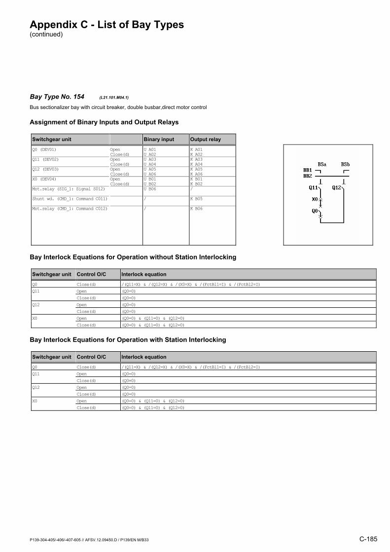
Appendix C - List of Bay Types (continued)
P139-304-405/-406/-407-605 // AFSV.12.09450.D / P139/EN M/B33 C-185
Bay Type No. 154 (L21.101.M04.1) Bus sectionalizer bay with circuit breaker, double busbar,direct motor control
Assignment of Binary Inputs and Output Relays
Switchgear unit Binary input Output relay
Q0 (DEV01) Q11 (DEV02) Q12 (DEV03) X0 (DEV04) Mot.relay (SIG_1: Signal S012) Shunt wd. (CMD_1: Command C011) Mot.relay (CMD_1: Command C012)
Open Close(d) Open Close(d) Open Close(d) Open Close(d)
U A01 U A02 U A03 U A04 U A05 U A06 U B01 U B02 U B06 / /
K A01 K A02K A03 K A04K A05 K A06K B01 K B02/
K B05
K B06
Bay Interlock Equations for Operation without Station Interlocking
Switchgear unit Control O/C Interlock equation
Q0 Close(d) /(Q11=X) & /(Q12=X) & /(X0=X) & /(FctBl1=I) & /(FctBl2=I) Q11 Open (Q0=0) Close(d) (Q0=0) Q12 Open (Q0=0) Close(d) (Q0=0) X0 Open (Q0=0) & (Q11=0) & (Q12=0) Close(d) (Q0=0) & (Q11=0) & (Q12=0)
Bay Interlock Equations for Operation with Station Interlocking
Switchgear unit Control O/C Interlock equation
Q0 Close(d) /(Q11=X) & /(Q12=X) & /(X0=X) & /(FctBl1=I) & /(FctBl2=I) Q11 Open (Q0=0) Close(d) (Q0=0) Q12 Open (Q0=0) Close(d) (Q0=0) X0 Open (Q0=0) & (Q11=0) & (Q12=0) Close(d) (Q0=0) & (Q11=0) & (Q12=0)
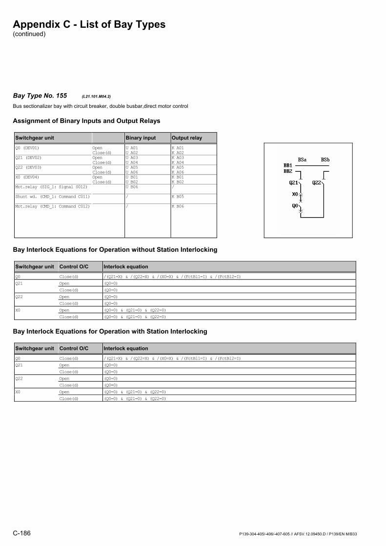
Appendix C - List of Bay Types (continued)
C-186 P139-304-405/-406/-407-605 // AFSV.12.09450.D / P139/EN M/B33
Bay Type No. 155 (L21.101.M04.2) Bus sectionalizer bay with circuit breaker, double busbar,direct motor control
Assignment of Binary Inputs and Output Relays
Switchgear unit Binary input Output relay
Q0 (DEV01) Q21 (DEV02) Q22 (DEV03) X0 (DEV04) Mot.relay (SIG_1: Signal S012) Shunt wd. (CMD_1: Command C011) Mot.relay (CMD_1: Command C012)
Open Close(d) Open Close(d) Open Close(d) Open Close(d)
U A01 U A02 U A03 U A04 U A05 U A06 U B01 U B02 U B06 / /
K A01 K A02K A03 K A04K A05 K A06K B01 K B02/
K B05
K B06
Bay Interlock Equations for Operation without Station Interlocking
Switchgear unit Control O/C Interlock equation
Q0 Close(d) /(Q21=X) & /(Q22=X) & /(X0=X) & /(FctBl1=I) & /(FctBl2=I) Q21 Open (Q0=0) Close(d) (Q0=0) Q22 Open (Q0=0) Close(d) (Q0=0) X0 Open (Q0=0) & (Q21=0) & (Q22=0) Close(d) (Q0=0) & (Q21=0) & (Q22=0)
Bay Interlock Equations for Operation with Station Interlocking
Switchgear unit Control O/C Interlock equation
Q0 Close(d) /(Q21=X) & /(Q22=X) & /(X0=X) & /(FctBl1=I) & /(FctBl2=I) Q21 Open (Q0=0) Close(d) (Q0=0) Q22 Open (Q0=0) Close(d) (Q0=0) X0 Open (Q0=0) & (Q21=0) & (Q22=0) Close(d) (Q0=0) & (Q21=0) & (Q22=0)

Appendix C - List of Bay Types (continued)
P139-304-405/-406/-407-605 // AFSV.12.09450.D / P139/EN M/B33 C-187
Bay Type No. 156 (L21.101.R01.1) Bus sectionalizer bay with circuit breaker, double busbar
Assignment of Binary Inputs and Output Relays
Switchgear unit Binary input Output relay
Q0 (DEV01) Q11 (DEV02) Q12 (DEV03) X0 (DEV04)
Open Close(d) Open Close(d) Open Close(d) Open Close(d)
U A01 U A02 U A03 U A04 U A05 U A06 U B01 U B02
K A01 K A02/ // // /
Bay Interlock Equations for Operation without Station Interlocking
Switchgear unit Control O/C Interlock equation
Q0 Close(d) /(Q11=X) & /(Q12=X) & /(X0=X) & /(FctBl1=I) & /(FctBl2=I)
Bay Interlock Equations for Operation with Station Interlocking
Switchgear unit Control O/C Interlock equation
Q0 Close(d) /(Q11=X) & /(Q12=X) & /(X0=X) & /(FctBl1=I) & /(FctBl2=I)

Appendix C - List of Bay Types (continued)
C-188 P139-304-405/-406/-407-605 // AFSV.12.09450.D / P139/EN M/B33
Bay Type No. 157 (L21.101.R01.2) Bus sectionalizer bay with circuit breaker, double busbar
Assignment of Binary Inputs and Output Relays
Switchgear unit Binary input Output relay
Q0 (DEV01) Q21 (DEV02) Q22 (DEV03) X0 (DEV04)
Open Close(d) Open Close(d) Open Close(d) Open Close(d)
U A01 U A02 U A03 U A04 U A05 U A06 U B01 U B02
K A01 K A02/ // // /
Bay Interlock Equations for Operation without Station Interlocking
Switchgear unit Control O/C Interlock equation
Q0 Close(d) /(Q21=X) & /(Q22=X) & /(X0=X) & /(FctBl1=I) & /(FctBl2=I)
Bay Interlock Equations for Operation with Station Interlocking
Switchgear unit Control O/C Interlock equation
Q0 Close(d) /(Q21=X) & /(Q22=X) & /(X0=X) & /(FctBl1=I) & /(FctBl2=I)

Appendix C - List of Bay Types (continued)
P139-304-405/-406/-407-605 // AFSV.12.09450.D / P139/EN M/B33 C-189
Bay Type No. 158 (L21.101.R03.1) Bus sectionalizer bay with circuit breaker, double busbar
Assignment of Binary Inputs and Output Relays
Switchgear unit Binary input Output relay
Q0 (DEV01) Q11 (DEV02) Q12 (DEV03) X0 (DEV04)
Open Close(d) Open Close(d) Open Close(d) Open Close(d)
U A01 U A02 U A03 U A04 U A05 U A06 U B01 U B02
K A01 K A02K A03 K A04K A05 K A06/ /
Bay Interlock Equations for Operation without Station Interlocking
Switchgear unit Control O/C Interlock equation
Q0 Close(d) /(Q11=X) & /(Q12=X) & /(X0=X) & /(FctBl1=I) & /(FctBl2=I) Q11 Open (Q0=0) Close(d) (Q0=0) Q12 Open (Q0=0) Close(d) (Q0=0)
Bay Interlock Equations for Operation with Station Interlocking
Switchgear unit Control O/C Interlock equation
Q0 Close(d) /(Q11=X) & /(Q12=X) & /(X0=X) & /(FctBl1=I) & /(FctBl2=I) Q11 Open (Q0=0) Close(d) (Q0=0) Q12 Open (Q0=0) Close(d) (Q0=0)
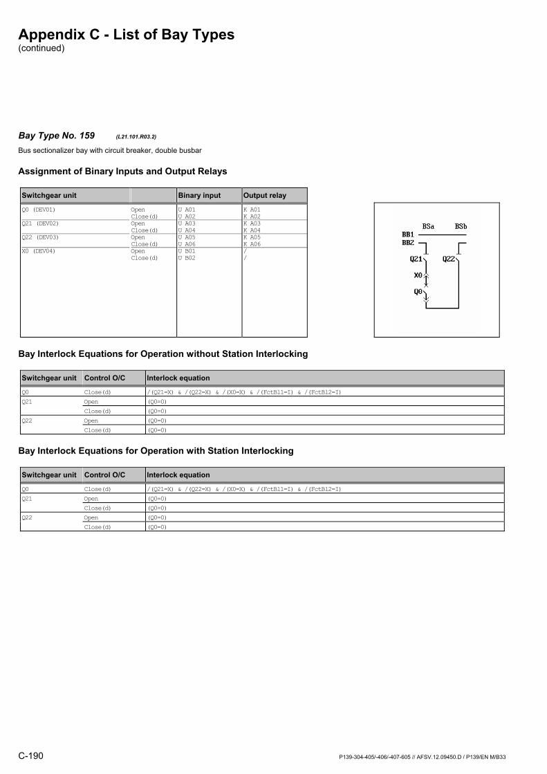
Appendix C - List of Bay Types (continued)
C-190 P139-304-405/-406/-407-605 // AFSV.12.09450.D / P139/EN M/B33
Bay Type No. 159 (L21.101.R03.2) Bus sectionalizer bay with circuit breaker, double busbar
Assignment of Binary Inputs and Output Relays
Switchgear unit Binary input Output relay
Q0 (DEV01) Q21 (DEV02) Q22 (DEV03) X0 (DEV04)
Open Close(d) Open Close(d) Open Close(d) Open Close(d)
U A01 U A02 U A03 U A04 U A05 U A06 U B01 U B02
K A01 K A02K A03 K A04K A05 K A06/ /
Bay Interlock Equations for Operation without Station Interlocking
Switchgear unit Control O/C Interlock equation
Q0 Close(d) /(Q21=X) & /(Q22=X) & /(X0=X) & /(FctBl1=I) & /(FctBl2=I) Q21 Open (Q0=0) Close(d) (Q0=0) Q22 Open (Q0=0) Close(d) (Q0=0)
Bay Interlock Equations for Operation with Station Interlocking
Switchgear unit Control O/C Interlock equation
Q0 Close(d) /(Q21=X) & /(Q22=X) & /(X0=X) & /(FctBl1=I) & /(FctBl2=I) Q21 Open (Q0=0) Close(d) (Q0=0) Q22 Open (Q0=0) Close(d) (Q0=0)

Appendix C - List of Bay Types (continued)
P139-304-405/-406/-407-605 // AFSV.12.09450.D / P139/EN M/B33 C-191
Bay Type No. 160 (L21.101.R04.1) Bus sectionalizer bay with circuit breaker, double busbar
Assignment of Binary Inputs and Output Relays
Switchgear unit Binary input Output relay
Q0 (DEV01) Q11 (DEV02) Q12 (DEV03) X0 (DEV04)
Open Close(d) Open Close(d) Open Close(d) Open Close(d)
U A01 U A02 U A03 U A04 U A05 U A06 U B01 U B02
K A01 K A02K A03 K A04K A05 K A06K B01 K B02
Bay Interlock Equations for Operation without Station Interlocking
Switchgear unit Control O/C Interlock equation
Q0 Close(d) /(Q11=X) & /(Q12=X) & /(X0=X) & /(FctBl1=I) & /(FctBl2=I) Q11 Open (Q0=0) Close(d) (Q0=0) Q12 Open (Q0=0) Close(d) (Q0=0) X0 Open (Q0=0) & (Q11=0) & (Q12=0) Close(d) (Q0=0) & (Q11=0) & (Q12=0)
Bay Interlock Equations for Operation with Station Interlocking
Switchgear unit Control O/C Interlock equation
Q0 Close(d) /(Q11=X) & /(Q12=X) & /(X0=X) & /(FctBl1=I) & /(FctBl2=I) Q11 Open (Q0=0) Close(d) (Q0=0) Q12 Open (Q0=0) Close(d) (Q0=0) X0 Open (Q0=0) & (Q11=0) & (Q12=0) Close(d) (Q0=0) & (Q11=0) & (Q12=0)
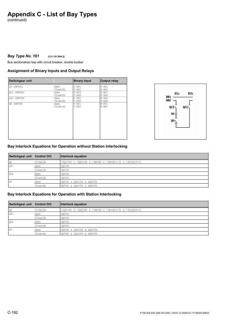
Appendix C - List of Bay Types (continued)
C-192 P139-304-405/-406/-407-605 // AFSV.12.09450.D / P139/EN M/B33
Bay Type No. 161 (L21.101.R04.2) Bus sectionalizer bay with circuit breaker, double busbar
Assignment of Binary Inputs and Output Relays
Switchgear unit Binary input Output relay
Q0 (DEV01) Q21 (DEV02) Q22 (DEV03) X0 (DEV04)
Open Close(d) Open Close(d) Open Close(d) Open Close(d)
U A01 U A02 U A03 U A04 U A05 U A06 U B01 U B02
K A01 K A02K A03 K A04K A05 K A06K B01 K B02
Bay Interlock Equations for Operation without Station Interlocking
Switchgear unit Control O/C Interlock equation
Q0 Close(d) /(Q21=X) & /(Q22=X) & /(X0=X) & /(FctBl1=I) & /(FctBl2=I) Q21 Open (Q0=0) Close(d) (Q0=0) Q22 Open (Q0=0) Close(d) (Q0=0) X0 Open (Q0=0) & (Q21=0) & (Q22=0) Close(d) (Q0=0) & (Q21=0) & (Q22=0)
Bay Interlock Equations for Operation with Station Interlocking
Switchgear unit Control O/C Interlock equation
Q0 Close(d) /(Q21=X) & /(Q22=X) & /(X0=X) & /(FctBl1=I) & /(FctBl2=I) Q21 Open (Q0=0) Close(d) (Q0=0) Q22 Open (Q0=0) Close(d) (Q0=0) X0 Open (Q0=0) & (Q21=0) & (Q22=0) Close(d) (Q0=0) & (Q21=0) & (Q22=0)

Appendix C - List of Bay Types (continued)
P139-304-405/-406/-407-605 // AFSV.12.09450.D / P139/EN M/B33 C-193
Bay Type No. 513 (L21.109.R03.1) Bus sectionalizer bay with circuit breaker, double busbar
Assignment of Binary Inputs and Output Relays
Switchgear unit Binary input Output relay
Q0 (DEV01) Q11 (DEV02) Q12 (DEV03) X0 (DEV04) Q8 (DEV05)
Open Close(d) Open Close(d) Open Close(d) Open Close(d) Open Close(d)
U A01 U A02 U A03 U A04 U A05 U A06 U B01 U B02 U B03 U B04
K A01 K A02K A03 K A04K A05 K A06/ // /
Bay Interlock Equations for Operation without Station Interlocking
Switchgear unit Control O/C Interlock equation
Q0 Close(d) /(Q11=X) & /(Q12=X) & /(X0=X) & (Q8=0) & /(FctBl1=I) & /(FctBl2=I) Q11 Open (Q0=0) Close(d) (Q0=0) & (Q8=0) Q12 Open (Q0=0) Close(d) (Q0=0) & (Q8=0)
Bay Interlock Equations for Operation with Station Interlocking
Switchgear unit Control O/C Interlock equation
Q0 Close(d) /(Q11=X) & /(Q12=X) & /(X0=X) & (Q8=0) & /(FctBl1=I) & /(FctBl2=I) Q11 Open (Q0=0) Close(d) (Q0=0) & (Q8=0) Q12 Open (Q0=0) Close(d) (Q0=0) & (Q8=0)

Appendix C - List of Bay Types (continued)
C-194 P139-304-405/-406/-407-605 // AFSV.12.09450.D / P139/EN M/B33
Bay Type No. 514 (L21.109.R03.2) Bus sectionalizer bay with circuit breaker, double busbar
Assignment of Binary Inputs and Output Relays
Switchgear unit Binary input Output relay
Q0 (DEV01) Q21 (DEV02) Q22 (DEV03) X0 (DEV04) Q8 (DEV05)
Open Close(d) Open Close(d) Open Close(d) Open Close(d) Open Close(d)
U A01 U A02 U A03 U A04 U A05 U A06 U B01 U B02 U B03 U B04
K A01 K A02K A03 K A04K A05 K A06/ // /
Bay Interlock Equations for Operation without Station Interlocking
Switchgear unit Control O/C Interlock equation
Q0 Close(d) /(Q21=X) & /(Q22=X) & /(X0=X) & (Q8=0) & /(FctBl1=I) & /(FctBl2=I) Q21 Open (Q0=0) Close(d) (Q0=0) & (Q8=0) Q22 Open (Q0=0) Close(d) (Q0=0) & (Q8=0)
Bay Interlock Equations for Operation with Station Interlocking
Switchgear unit Control O/C Interlock equation
Q0 Close(d) /(Q21=X) & /(Q22=X) & /(X0=X) & (Q8=0) & /(FctBl1=I) & /(FctBl2=I) Q21 Open (Q0=0) Close(d) (Q0=0) & (Q8=0) Q22 Open (Q0=0) Close(d) (Q0=0) & (Q8=0)
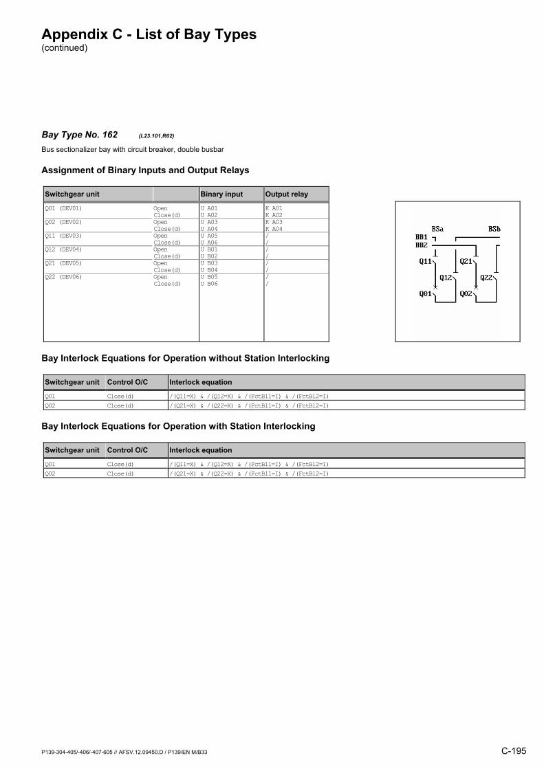
Appendix C - List of Bay Types (continued)
P139-304-405/-406/-407-605 // AFSV.12.09450.D / P139/EN M/B33 C-195
Bay Type No. 162 (L23.101.R02) Bus sectionalizer bay with circuit breaker, double busbar
Assignment of Binary Inputs and Output Relays
Switchgear unit Binary input Output relay
Q01 (DEV01) Q02 (DEV02) Q11 (DEV03) Q12 (DEV04) Q21 (DEV05) Q22 (DEV06)
Open Close(d) Open Close(d) Open Close(d) Open Close(d) Open Close(d) Open Close(d)
U A01 U A02 U A03 U A04 U A05 U A06 U B01 U B02 U B03 U B04 U B05 U B06
K A01 K A02K A03 K A04/ // // // /
Bay Interlock Equations for Operation without Station Interlocking
Switchgear unit Control O/C Interlock equation
Q01 Close(d) /(Q11=X) & /(Q12=X) & /(FctBl1=I) & /(FctBl2=I) Q02 Close(d) /(Q21=X) & /(Q22=X) & /(FctBl1=I) & /(FctBl2=I)
Bay Interlock Equations for Operation with Station Interlocking
Switchgear unit Control O/C Interlock equation
Q01 Close(d) /(Q11=X) & /(Q12=X) & /(FctBl1=I) & /(FctBl2=I) Q02 Close(d) /(Q21=X) & /(Q22=X) & /(FctBl1=I) & /(FctBl2=I)
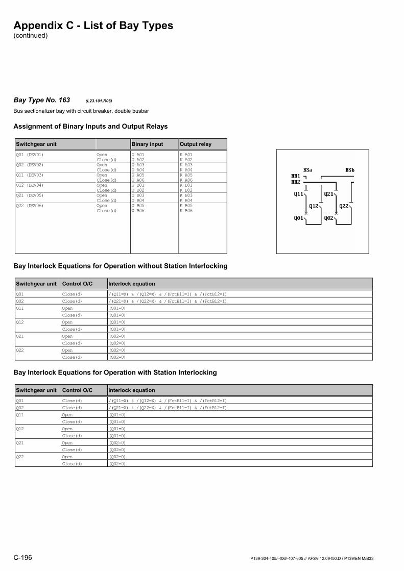
Appendix C - List of Bay Types (continued)
C-196 P139-304-405/-406/-407-605 // AFSV.12.09450.D / P139/EN M/B33
Bay Type No. 163 (L23.101.R06) Bus sectionalizer bay with circuit breaker, double busbar
Assignment of Binary Inputs and Output Relays
Switchgear unit Binary input Output relay
Q01 (DEV01) Q02 (DEV02) Q11 (DEV03) Q12 (DEV04) Q21 (DEV05) Q22 (DEV06)
Open Close(d) Open Close(d) Open Close(d) Open Close(d) Open Close(d) Open Close(d)
U A01 U A02 U A03 U A04 U A05 U A06 U B01 U B02 U B03 U B04 U B05 U B06
K A01 K A02K A03 K A04K A05 K A06K B01 K B02K B03 K B04K B05 K B06
Bay Interlock Equations for Operation without Station Interlocking
Switchgear unit Control O/C Interlock equation
Q01 Close(d) /(Q11=X) & /(Q12=X) & /(FctBl1=I) & /(FctBl2=I) Q02 Close(d) /(Q21=X) & /(Q22=X) & /(FctBl1=I) & /(FctBl2=I) Q11 Open (Q01=0) Close(d) (Q01=0) Q12 Open (Q01=0) Close(d) (Q01=0) Q21 Open (Q02=0) Close(d) (Q02=0) Q22 Open (Q02=0) Close(d) (Q02=0)
Bay Interlock Equations for Operation with Station Interlocking
Switchgear unit Control O/C Interlock equation
Q01 Close(d) /(Q11=X) & /(Q12=X) & /(FctBl1=I) & /(FctBl2=I) Q02 Close(d) /(Q21=X) & /(Q22=X) & /(FctBl1=I) & /(FctBl2=I) Q11 Open (Q01=0) Close(d) (Q01=0) Q12 Open (Q01=0) Close(d) (Q01=0) Q21 Open (Q02=0) Close(d) (Q02=0) Q22 Open (Q02=0) Close(d) (Q02=0)

Appendix C - List of Bay Types (continued)
P139-304-405/-406/-407-605 // AFSV.12.09450.D / P139/EN M/B33 C-197
Bay Type No. 554 (L23.901.M01.1) Bus sectionalizer bay with other switchgear unit, double busbar,direct motor control
Assignment of Binary Inputs and Output Relays
Switchgear unit Binary input Output relay
Q11 (DEV01) Mot.relay (SIG_1: Signal S012) Shunt wd. (CMD_1: Command C011) Mot.relay (CMD_1: Command C012)
Open Close(d)
U A01 U A02 U B06 / /
K A01 K A02/
K B05
K B06
Bay Interlock Equations for Operation without Station Interlocking
Switchgear unit Control O/C Interlock equation
Interlock equations not defined
Bay Interlock Equations for Operation with Station Interlocking
Switchgear unit Control O/C Interlock equation
Interlock equations not defined

Appendix C - List of Bay Types (continued)
C-198 P139-304-405/-406/-407-605 // AFSV.12.09450.D / P139/EN M/B33
Bay Type No. 555 (L23.901.M01.2) Bus sectionalizer bay with other switchgear unit, double busbar,direct motor control
Assignment of Binary Inputs and Output Relays
Switchgear unit Binary input Output relay
Q21 (DEV01) Mot.relay (SIG_1: Signal S012) Shunt wd. (CMD_1: Command C011) Mot.relay (CMD_1: Command C012)
Open Close(d)
U A01 U A02 U B06 / /
K A01 K A02/
K B05
K B06
Bay Interlock Equations for Operation without Station Interlocking
Switchgear unit Control O/C Interlock equation
Interlock equations not defined
Bay Interlock Equations for Operation with Station Interlocking
Switchgear unit Control O/C Interlock equation
Interlock equations not defined
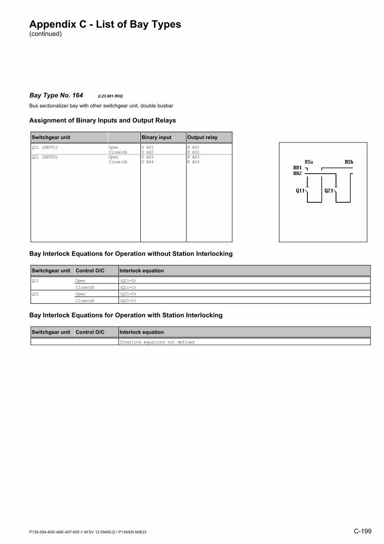
Appendix C - List of Bay Types (continued)
P139-304-405/-406/-407-605 // AFSV.12.09450.D / P139/EN M/B33 C-199
Bay Type No. 164 (L23.901.R02) Bus sectionalizer bay with other switchgear unit, double busbar
Assignment of Binary Inputs and Output Relays
Switchgear unit Binary input Output relay
Q11 (DEV01) Q21 (DEV02)
Open Close(d) Open Close(d)
U A01 U A02 U A03 U A04
K A01 K A02K A03 K A04
Bay Interlock Equations for Operation without Station Interlocking
Switchgear unit Control O/C Interlock equation
Q11 Open (Q11=0) Close(d) (Q11=I) Q21 Open (Q21=0) Close(d) (Q21=I)
Bay Interlock Equations for Operation with Station Interlocking
Switchgear unit Control O/C Interlock equation
Interlock equations not defined

Appendix C - List of Bay Types (continued)
C-200 P139-304-405/-406/-407-605 // AFSV.12.09450.D / P139/EN M/B33
Bay Type No. 242 (L23.903.M01.3) Bus sectionalizer bay with other switchgear unit, double busbar,direct motor control
Assignment of Binary Inputs and Output Relays
Switchgear unit Binary input Output relay
Q12 (DEV01) Q15 (DEV02) Q25 (DEV03) Mot.relay (SIG_1: Signal S012) Shunt wd. (CMD_1: Command C011) Mot.relay (CMD_1: Command C012)
Open Close(d) Open Close(d) Open Close(d)
U A01 U A02 U A03 U A04 U A05 U A06 U B06 / /
K A01 K A02/ // //
K B05
K B06
Bay Interlock Equations for Operation without Station Interlocking
Switchgear unit Control O/C Interlock equation
Q12 Open (Q12=0) Close(d) (Q12=I)
Bay Interlock Equations for Operation with Station Interlocking
Switchgear unit Control O/C Interlock equation
Interlock equations not defined

Appendix C - List of Bay Types (continued)
P139-304-405/-406/-407-605 // AFSV.12.09450.D / P139/EN M/B33 C-201
Bay Type No. 243 (L23.903.M01.4) Bus sectionalizer bay with other switchgear unit, double busbar,direct motor control
Assignment of Binary Inputs and Output Relays
Switchgear unit Binary input Output relay
Q21 (DEV01) Q15 (DEV02) Q25 (DEV03) Mot.relay (SIG_1: Signal S012) Shunt wd. (CMD_1: Command C011) Mot.relay (CMD_1: Command C012)
Open Close(d) Open Close(d) Open Close(d)
U A01 U A02 U A03 U A04 U A05 U A06 U B06 / /
K A01 K A02/ // //
K B05
K B06
Bay Interlock Equations for Operation without Station Interlocking
Switchgear unit Control O/C Interlock equation
Q21 Open (Q21=0) Close(d) (Q21=I)
Bay Interlock Equations for Operation with Station Interlocking
Switchgear unit Control O/C Interlock equation
Interlock equations not defined
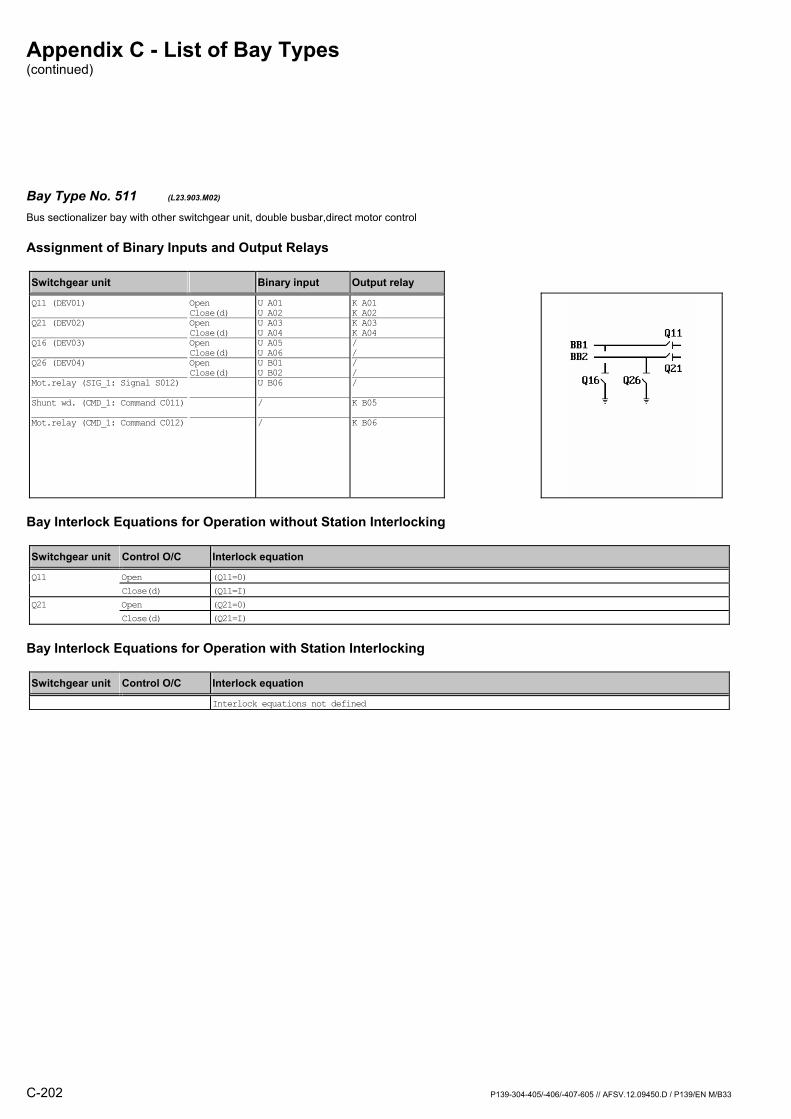
Appendix C - List of Bay Types (continued)
C-202 P139-304-405/-406/-407-605 // AFSV.12.09450.D / P139/EN M/B33
Bay Type No. 511 (L23.903.M02) Bus sectionalizer bay with other switchgear unit, double busbar,direct motor control
Assignment of Binary Inputs and Output Relays
Switchgear unit Binary input Output relay
Q11 (DEV01) Q21 (DEV02) Q16 (DEV03) Q26 (DEV04) Mot.relay (SIG_1: Signal S012) Shunt wd. (CMD_1: Command C011) Mot.relay (CMD_1: Command C012)
Open Close(d) Open Close(d) Open Close(d) Open Close(d)
U A01 U A02 U A03 U A04 U A05 U A06 U B01 U B02 U B06 / /
K A01 K A02K A03 K A04/ // //
K B05
K B06
Bay Interlock Equations for Operation without Station Interlocking
Switchgear unit Control O/C Interlock equation
Q11 Open (Q11=0) Close(d) (Q11=I) Q21 Open (Q21=0) Close(d) (Q21=I)
Bay Interlock Equations for Operation with Station Interlocking
Switchgear unit Control O/C Interlock equation
Interlock equations not defined

Appendix C - List of Bay Types (continued)
P139-304-405/-406/-407-605 // AFSV.12.09450.D / P139/EN M/B33 C-203
Bay Type No. 228 (L25.113.M03.1) Bus sectionalizer bay with circuit breaker, double busbar,direct motor control
Assignment of Binary Inputs and Output Relays
Switchgear unit Binary input Output relay
Q0 (DEV01) Q11 (DEV02) Q12 (DEV03) Q15 (DEV04) Q16 (DEV05) Mot.relay (SIG_1: Signal S012) Shunt wd. (CMD_1: Command C011) Mot.relay (CMD_1: Command C012)
Open Close(d) Open Close(d) Open Close(d) Open Close(d) Open Close(d)
U A01 U A02 U A03 U A04 U A05 U A06 U B01 U B02 U B03 U B04 U B06 / /
K A01 K A02K A03 K A04K A05 K A06/ // //
K B05
K B06
Bay Interlock Equations for Operation without Station Interlocking
Switchgear unit Control O/C Interlock equation
Q0 Open (Q15=0) & (Q16=0) Close(d) /(Q11=X) & /(Q12=X) & (Q15=0) & (Q16=0) & /(FctBl1=I) & /(FctBl2=I) Q11 Open (Q0=0) Close(d) (Q0=0) & (Q15=0) Q12 Open (Q0=0) Close(d) (Q0=0) & (Q16=0)
Bay Interlock Equations for Operation with Station Interlocking
Switchgear unit Control O/C Interlock equation
Q0 Open (Q15=0) & (Q16=0) Close(d) /(Q11=X) & /(Q12=X) & (Q15=0) & (Q16=0) & /(FctBl1=I) & /(FctBl2=I) Q11 Open (Q0=0) Close(d) (Q0=0) & (Q15=0) Q12 Open (Q0=0) Close(d) (Q0=0) & (Q16=0)

Appendix C - List of Bay Types (continued)
C-204 P139-304-405/-406/-407-605 // AFSV.12.09450.D / P139/EN M/B33
Bay Type No. 229 (L25.113.M03.2) Bus sectionalizer bay with circuit breaker, double busbar,direct motor control
Assignment of Binary Inputs and Output Relays
Switchgear unit Binary input Output relay
Q0 (DEV01) Q21 (DEV02) Q22 (DEV03) Q25 (DEV04) Q26 (DEV05) Mot.relay (SIG_1: Signal S012) Shunt wd. (CMD_1: Command C011) Mot.relay (CMD_1: Command C012)
Open Close(d) Open Close(d) Open Close(d) Open Close(d) Open Close(d)
U A01 U A02 U A03 U A04 U A05 U A06 U B01 U B02 U B03 U B04 U B06 / /
K A01 K A02K A03 K A04K A05 K A06/ // //
K B05
K B06
Bay Interlock Equations for Operation without Station Interlocking
Switchgear unit Control O/C Interlock equation
Q0 Open (Q25=0) & (Q26=0) Close(d) /(Q21=X) & /(Q22=X) & (Q25=0) & (Q26=0) & /(FctBl1=I) & /(FctBl2=I) Q21 Open (Q0=0) Close(d) (Q0=0) & (Q25=0) Q22 Open (Q0=0) Close(d) (Q0=0) & (Q26=0)
Bay Interlock Equations for Operation with Station Interlocking
Switchgear unit Control O/C Interlock equation
Q0 Open (Q25=0) & (Q26=0) Close(d) /(Q21=X) & /(Q22=X) & (Q25=0) & (Q26=0) & /(FctBl1=I) & /(FctBl2=I) Q21 Open (Q0=0) Close(d) (Q0=0) & (Q25=0) Q22 Open (Q0=0) Close(d) (Q0=0) & (Q26=0)

Appendix C - List of Bay Types (continued)
P139-304-405/-406/-407-605 // AFSV.12.09450.D / P139/EN M/B33 C-205
Bay Type No. 165 (L25.113.M05.1) Bus sectionalizer bay with circuit breaker, double busbar,direct motor control
Assignment of Binary Inputs and Output Relays
Switchgear unit Binary input Output relay
Q0 (DEV01) Q11 (DEV02) Q12 (DEV03) Q15 (DEV04) Q16 (DEV05) Mot.relay (SIG_1: Signal S012) Shunt wd. (CMD_1: Command C011) Mot.relay (CMD_1: Command C012)
Open Close(d) Open Close(d) Open Close(d) Open Close(d) Open Close(d)
U A01 U A02 U A03 U A04 U A05 U A06 U B01 U B02 U B03 U B04 U B06 / /
K A01 K A02K A03 K A04K A05 K A06K B01 K B02K B03 K B04/
K B05
K B06
Bay Interlock Equations for Operation without Station Interlocking
Switchgear unit Control O/C Interlock equation
Q0 Open (Q15=0) & (Q16=0) Close(d) /(Q11=X) & /(Q12=X) & (Q15=0) & (Q16=0) & /(FctBl1=I) & /(FctBl2=I) Q11 Open (Q0=0) Close(d) (Q0=0) & (Q15=0) Q12 Open (Q0=0) Close(d) (Q0=0) & (Q16=0) Q15 Open (Q0=I) & (Q12=I) Close(d) (Q0=0) & (Q11=0) & (Q12=I) & /(FctBl1=I) & /(FctBl2=I) & (Q15=I) Q16 Open (Q0=I) & (Q11=I) Close(d) (Q0=0) & (Q12=0) & (Q11=I) & /(FctBl1=I) & /(FctBl2=I) & (Q16=I)
Bay Interlock Equations for Operation with Station Interlocking
Switchgear unit Control O/C Interlock equation
Q0 Open (Q15=0) & (Q16=0) Close(d) /(Q11=X) & /(Q12=X) & (Q15=0) & (Q16=0) & /(FctBl1=I) & /(FctBl2=I) Q11 Open (Q0=0) Close(d) (Q0=0) & (Q15=0) Q12 Open (Q0=0) Close(d) (Q0=0) & (Q16=0) Q15 Open (Q0=I) & (Q12=I) Close(d) (Q0=0) & (Q11=0) & (Q12=I) & /(FctBl1=I) & /(FctBl2=I) Q16 Open (Q0=I) & (Q11=I) Close(d) (Q0=0) & (Q12=0) & (Q11=I) & /(FctBl1=I) & /(FctBl2=I)
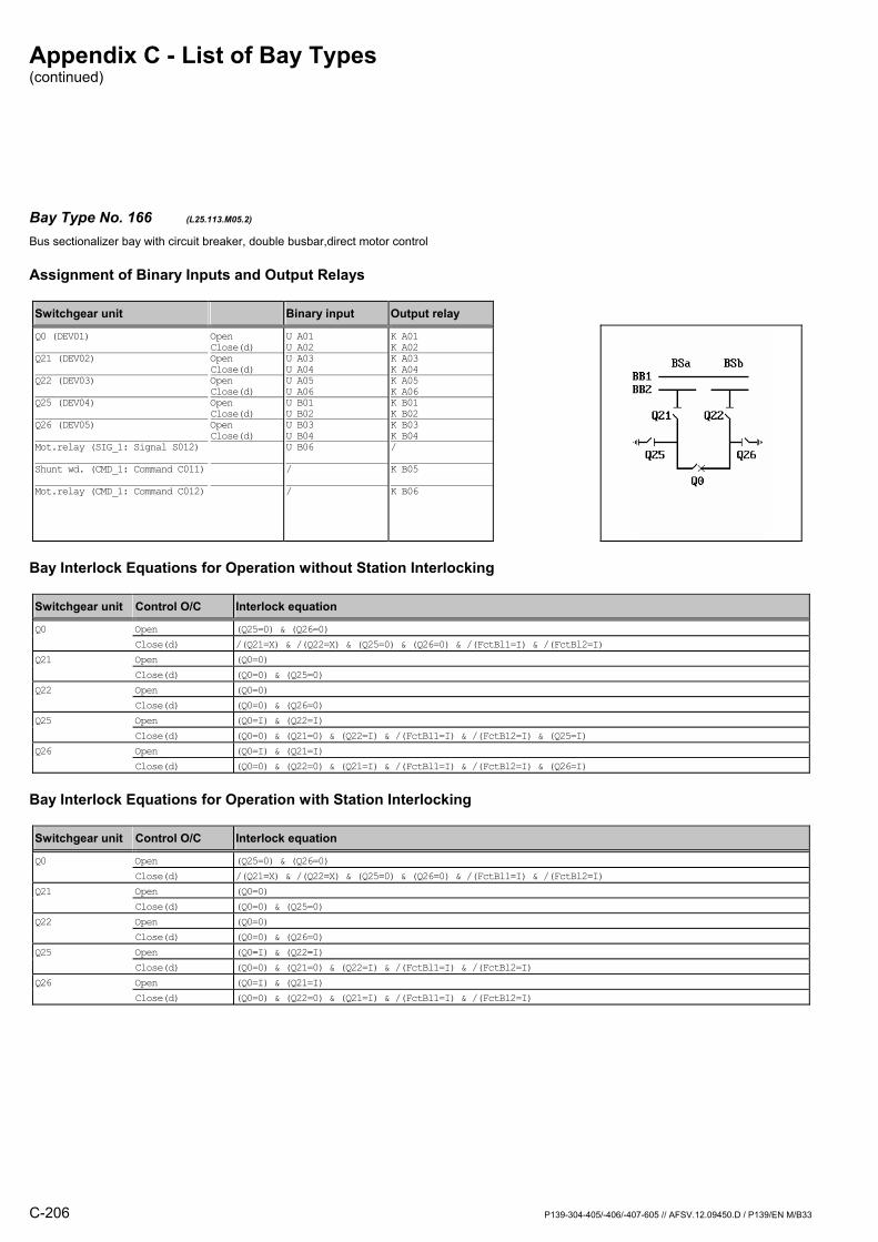
Appendix C - List of Bay Types (continued)
C-206 P139-304-405/-406/-407-605 // AFSV.12.09450.D / P139/EN M/B33
Bay Type No. 166 (L25.113.M05.2) Bus sectionalizer bay with circuit breaker, double busbar,direct motor control
Assignment of Binary Inputs and Output Relays
Switchgear unit Binary input Output relay
Q0 (DEV01) Q21 (DEV02) Q22 (DEV03) Q25 (DEV04) Q26 (DEV05) Mot.relay (SIG_1: Signal S012) Shunt wd. (CMD_1: Command C011) Mot.relay (CMD_1: Command C012)
Open Close(d) Open Close(d) Open Close(d) Open Close(d) Open Close(d)
U A01 U A02 U A03 U A04 U A05 U A06 U B01 U B02 U B03 U B04 U B06 / /
K A01 K A02K A03 K A04K A05 K A06K B01 K B02K B03 K B04/
K B05
K B06
Bay Interlock Equations for Operation without Station Interlocking
Switchgear unit Control O/C Interlock equation
Q0 Open (Q25=0) & (Q26=0) Close(d) /(Q21=X) & /(Q22=X) & (Q25=0) & (Q26=0) & /(FctBl1=I) & /(FctBl2=I) Q21 Open (Q0=0) Close(d) (Q0=0) & (Q25=0) Q22 Open (Q0=0) Close(d) (Q0=0) & (Q26=0) Q25 Open (Q0=I) & (Q22=I) Close(d) (Q0=0) & (Q21=0) & (Q22=I) & /(FctBl1=I) & /(FctBl2=I) & (Q25=I) Q26 Open (Q0=I) & (Q21=I) Close(d) (Q0=0) & (Q22=0) & (Q21=I) & /(FctBl1=I) & /(FctBl2=I) & (Q26=I)
Bay Interlock Equations for Operation with Station Interlocking
Switchgear unit Control O/C Interlock equation
Q0 Open (Q25=0) & (Q26=0) Close(d) /(Q21=X) & /(Q22=X) & (Q25=0) & (Q26=0) & /(FctBl1=I) & /(FctBl2=I) Q21 Open (Q0=0) Close(d) (Q0=0) & (Q25=0) Q22 Open (Q0=0) Close(d) (Q0=0) & (Q26=0) Q25 Open (Q0=I) & (Q22=I) Close(d) (Q0=0) & (Q21=0) & (Q22=I) & /(FctBl1=I) & /(FctBl2=I) Q26 Open (Q0=I) & (Q21=I) Close(d) (Q0=0) & (Q22=0) & (Q21=I) & /(FctBl1=I) & /(FctBl2=I)

Appendix C - List of Bay Types (continued)
P139-304-405/-406/-407-605 // AFSV.12.09450.D / P139/EN M/B33 C-207
Bay Type No. 167 (L25.113.R01.1) Bus sectionalizer bay with circuit breaker, double busbar
Assignment of Binary Inputs and Output Relays
Switchgear unit Binary input Output relay
Q0 (DEV01) Q11 (DEV02) Q12 (DEV03) Q15 (DEV04) Q16 (DEV05)
Open Close(d) Open Close(d) Open Close(d) Open Close(d) Open Close(d)
U A01 U A02 U A03 U A04 U A05 U A06 U B01 U B02 U B03 U B04
K A01 K A02/ // // // /
Bay Interlock Equations for Operation without Station Interlocking
Switchgear unit Control O/C Interlock equation
Q0 Open (Q15=0) & (Q16=0) Close(d) /(Q11=X) & /(Q12=X) & (Q15=0) & (Q16=0) & /(FctBl1=I) & /(FctBl2=I)
Bay Interlock Equations for Operation with Station Interlocking
Switchgear unit Control O/C Interlock equation
Q0 Open (Q15=0) & (Q16=0) Close(d) /(Q11=X) & /(Q12=X) & (Q15=0) & (Q16=0) & /(FctBl1=I) & /(FctBl2=I)
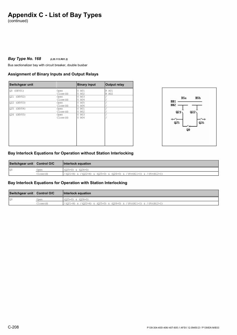
Appendix C - List of Bay Types (continued)
C-208 P139-304-405/-406/-407-605 // AFSV.12.09450.D / P139/EN M/B33
Bay Type No. 168 (L25.113.R01.2) Bus sectionalizer bay with circuit breaker, double busbar
Assignment of Binary Inputs and Output Relays
Switchgear unit Binary input Output relay
Q0 (DEV01) Q21 (DEV02) Q22 (DEV03) Q25 (DEV04) Q26 (DEV05)
Open Close(d) Open Close(d) Open Close(d) Open Close(d) Open Close(d)
U A01 U A02 U A03 U A04 U A05 U A06 U B01 U B02 U B03 U B04
K A01 K A02/ // // // /
Bay Interlock Equations for Operation without Station Interlocking
Switchgear unit Control O/C Interlock equation
Q0 Open (Q25=0) & (Q26=0) Close(d) /(Q21=X) & /(Q22=X) & (Q25=0) & (Q26=0) & /(FctBl1=I) & /(FctBl2=I)
Bay Interlock Equations for Operation with Station Interlocking
Switchgear unit Control O/C Interlock equation
Q0 Open (Q25=0) & (Q26=0) Close(d) /(Q21=X) & /(Q22=X) & (Q25=0) & (Q26=0) & /(FctBl1=I) & /(FctBl2=I)

Appendix C - List of Bay Types (continued)
P139-304-405/-406/-407-605 // AFSV.12.09450.D / P139/EN M/B33 C-209
Bay Type No. 230 (L25.113.R03.1) Bus sectionalizer bay with circuit breaker, double busbar
Assignment of Binary Inputs and Output Relays
Switchgear unit Binary input Output relay
Q0 (DEV01) Q11 (DEV02) Q12 (DEV03) Q15 (DEV04) Q16 (DEV05)
Open Close(d) Open Close(d) Open Close(d) Open Close(d) Open Close(d)
U A01 U A02 U A03 U A04 U A05 U A06 U B01 U B02 U B03 U B04
K A01 K A02K A03 K A04K A05 K A06/ // /
Bay Interlock Equations for Operation without Station Interlocking
Switchgear unit Control O/C Interlock equation
Q0 Open (Q15=0) & (Q16=0) Close(d) /(Q11=X) & /(Q12=X) & (Q15=0) & (Q16=0) & /(FctBl1=I) & /(FctBl2=I) Q11 Open (Q0=0) Close(d) (Q0=0) & (Q15=0) Q12 Open (Q0=0) Close(d) (Q0=0) & (Q16=0)
Bay Interlock Equations for Operation with Station Interlocking
Switchgear unit Control O/C Interlock equation
Q0 Open (Q15=0) & (Q16=0) Close(d) /(Q11=X) & /(Q12=X) & (Q15=0) & (Q16=0) & /(FctBl1=I) & /(FctBl2=I) Q11 Open (Q0=0) Close(d) (Q0=0) & (Q15=0) Q12 Open (Q0=0) Close(d) (Q0=0) & (Q16=0)
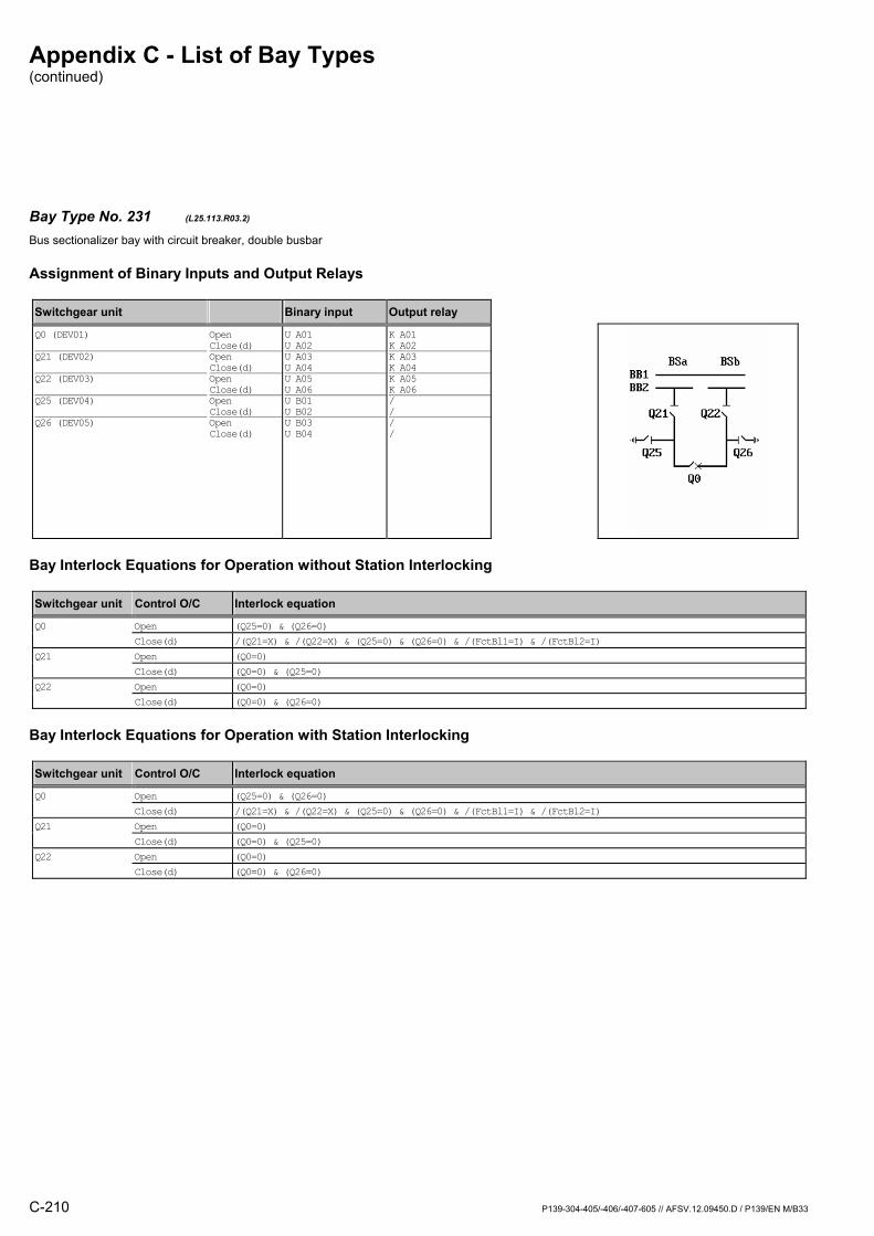
Appendix C - List of Bay Types (continued)
C-210 P139-304-405/-406/-407-605 // AFSV.12.09450.D / P139/EN M/B33
Bay Type No. 231 (L25.113.R03.2) Bus sectionalizer bay with circuit breaker, double busbar
Assignment of Binary Inputs and Output Relays
Switchgear unit Binary input Output relay
Q0 (DEV01) Q21 (DEV02) Q22 (DEV03) Q25 (DEV04) Q26 (DEV05)
Open Close(d) Open Close(d) Open Close(d) Open Close(d) Open Close(d)
U A01 U A02 U A03 U A04 U A05 U A06 U B01 U B02 U B03 U B04
K A01 K A02K A03 K A04K A05 K A06/ // /
Bay Interlock Equations for Operation without Station Interlocking
Switchgear unit Control O/C Interlock equation
Q0 Open (Q25=0) & (Q26=0) Close(d) /(Q21=X) & /(Q22=X) & (Q25=0) & (Q26=0) & /(FctBl1=I) & /(FctBl2=I) Q21 Open (Q0=0) Close(d) (Q0=0) & (Q25=0) Q22 Open (Q0=0) Close(d) (Q0=0) & (Q26=0)
Bay Interlock Equations for Operation with Station Interlocking
Switchgear unit Control O/C Interlock equation
Q0 Open (Q25=0) & (Q26=0) Close(d) /(Q21=X) & /(Q22=X) & (Q25=0) & (Q26=0) & /(FctBl1=I) & /(FctBl2=I) Q21 Open (Q0=0) Close(d) (Q0=0) & (Q25=0) Q22 Open (Q0=0) Close(d) (Q0=0) & (Q26=0)
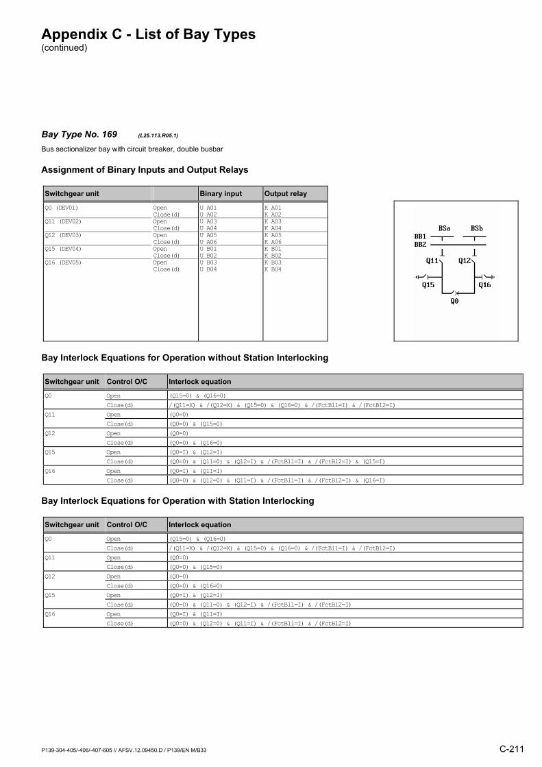
Appendix C - List of Bay Types (continued)
P139-304-405/-406/-407-605 // AFSV.12.09450.D / P139/EN M/B33 C-211
Bay Type No. 169 (L25.113.R05.1) Bus sectionalizer bay with circuit breaker, double busbar
Assignment of Binary Inputs and Output Relays
Switchgear unit Binary input Output relay
Q0 (DEV01) Q11 (DEV02) Q12 (DEV03) Q15 (DEV04) Q16 (DEV05)
Open Close(d) Open Close(d) Open Close(d) Open Close(d) Open Close(d)
U A01 U A02 U A03 U A04 U A05 U A06 U B01 U B02 U B03 U B04
K A01 K A02K A03 K A04K A05 K A06K B01 K B02K B03 K B04
Bay Interlock Equations for Operation without Station Interlocking
Switchgear unit Control O/C Interlock equation
Q0 Open (Q15=0) & (Q16=0) Close(d) /(Q11=X) & /(Q12=X) & (Q15=0) & (Q16=0) & /(FctBl1=I) & /(FctBl2=I) Q11 Open (Q0=0) Close(d) (Q0=0) & (Q15=0) Q12 Open (Q0=0) Close(d) (Q0=0) & (Q16=0) Q15 Open (Q0=I) & (Q12=I) Close(d) (Q0=0) & (Q11=0) & (Q12=I) & /(FctBl1=I) & /(FctBl2=I) & (Q15=I) Q16 Open (Q0=I) & (Q11=I) Close(d) (Q0=0) & (Q12=0) & (Q11=I) & /(FctBl1=I) & /(FctBl2=I) & (Q16=I)
Bay Interlock Equations for Operation with Station Interlocking
Switchgear unit Control O/C Interlock equation
Q0 Open (Q15=0) & (Q16=0) Close(d) /(Q11=X) & /(Q12=X) & (Q15=0) & (Q16=0) & /(FctBl1=I) & /(FctBl2=I) Q11 Open (Q0=0) Close(d) (Q0=0) & (Q15=0) Q12 Open (Q0=0) Close(d) (Q0=0) & (Q16=0) Q15 Open (Q0=I) & (Q12=I) Close(d) (Q0=0) & (Q11=0) & (Q12=I) & /(FctBl1=I) & /(FctBl2=I) Q16 Open (Q0=I) & (Q11=I) Close(d) (Q0=0) & (Q12=0) & (Q11=I) & /(FctBl1=I) & /(FctBl2=I)
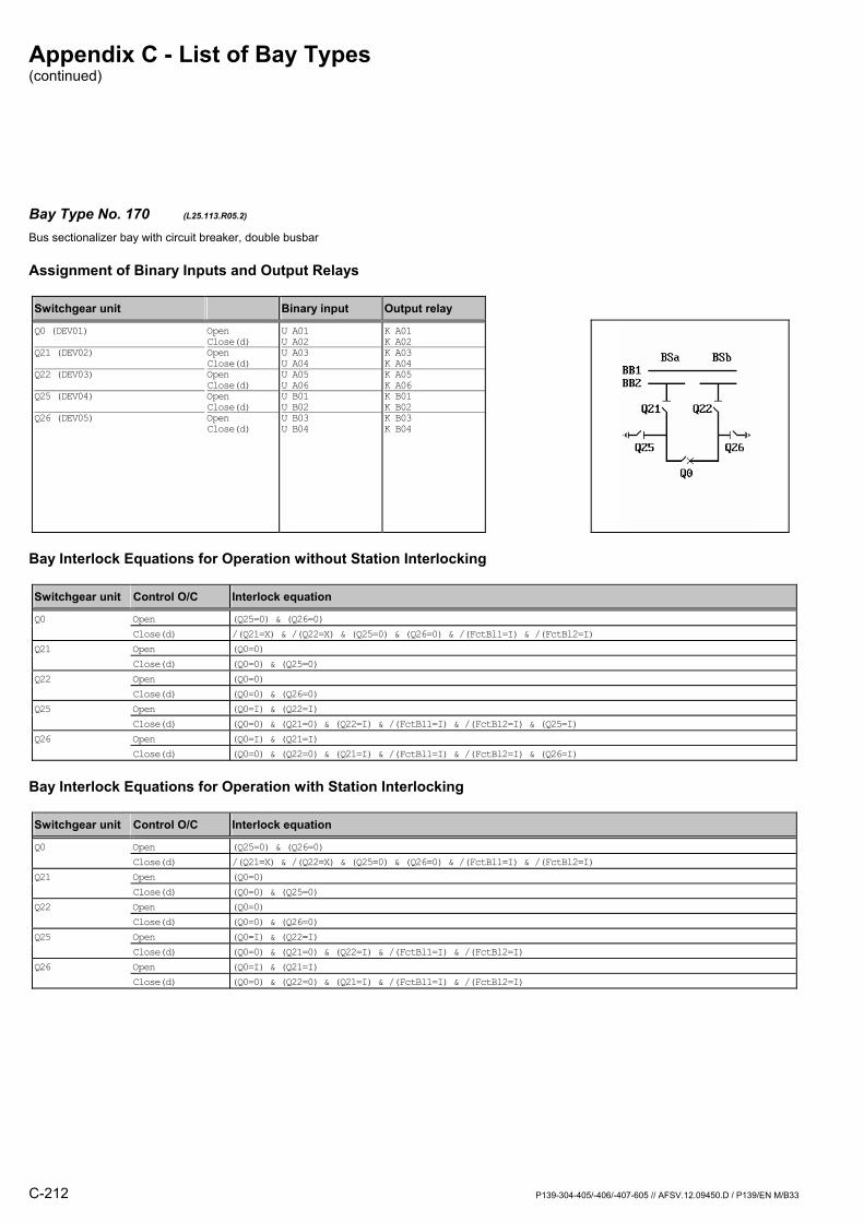
Appendix C - List of Bay Types (continued)
C-212 P139-304-405/-406/-407-605 // AFSV.12.09450.D / P139/EN M/B33
Bay Type No. 170 (L25.113.R05.2) Bus sectionalizer bay with circuit breaker, double busbar
Assignment of Binary Inputs and Output Relays
Switchgear unit Binary input Output relay
Q0 (DEV01) Q21 (DEV02) Q22 (DEV03) Q25 (DEV04) Q26 (DEV05)
Open Close(d) Open Close(d) Open Close(d) Open Close(d) Open Close(d)
U A01 U A02 U A03 U A04 U A05 U A06 U B01 U B02 U B03 U B04
K A01 K A02K A03 K A04K A05 K A06K B01 K B02K B03 K B04
Bay Interlock Equations for Operation without Station Interlocking
Switchgear unit Control O/C Interlock equation
Q0 Open (Q25=0) & (Q26=0) Close(d) /(Q21=X) & /(Q22=X) & (Q25=0) & (Q26=0) & /(FctBl1=I) & /(FctBl2=I) Q21 Open (Q0=0) Close(d) (Q0=0) & (Q25=0) Q22 Open (Q0=0) Close(d) (Q0=0) & (Q26=0) Q25 Open (Q0=I) & (Q22=I) Close(d) (Q0=0) & (Q21=0) & (Q22=I) & /(FctBl1=I) & /(FctBl2=I) & (Q25=I) Q26 Open (Q0=I) & (Q21=I) Close(d) (Q0=0) & (Q22=0) & (Q21=I) & /(FctBl1=I) & /(FctBl2=I) & (Q26=I)
Bay Interlock Equations for Operation with Station Interlocking
Switchgear unit Control O/C Interlock equation
Q0 Open (Q25=0) & (Q26=0) Close(d) /(Q21=X) & /(Q22=X) & (Q25=0) & (Q26=0) & /(FctBl1=I) & /(FctBl2=I) Q21 Open (Q0=0) Close(d) (Q0=0) & (Q25=0) Q22 Open (Q0=0) Close(d) (Q0=0) & (Q26=0) Q25 Open (Q0=I) & (Q22=I) Close(d) (Q0=0) & (Q21=0) & (Q22=I) & /(FctBl1=I) & /(FctBl2=I) Q26 Open (Q0=I) & (Q21=I) Close(d) (Q0=0) & (Q22=0) & (Q21=I) & /(FctBl1=I) & /(FctBl2=I)
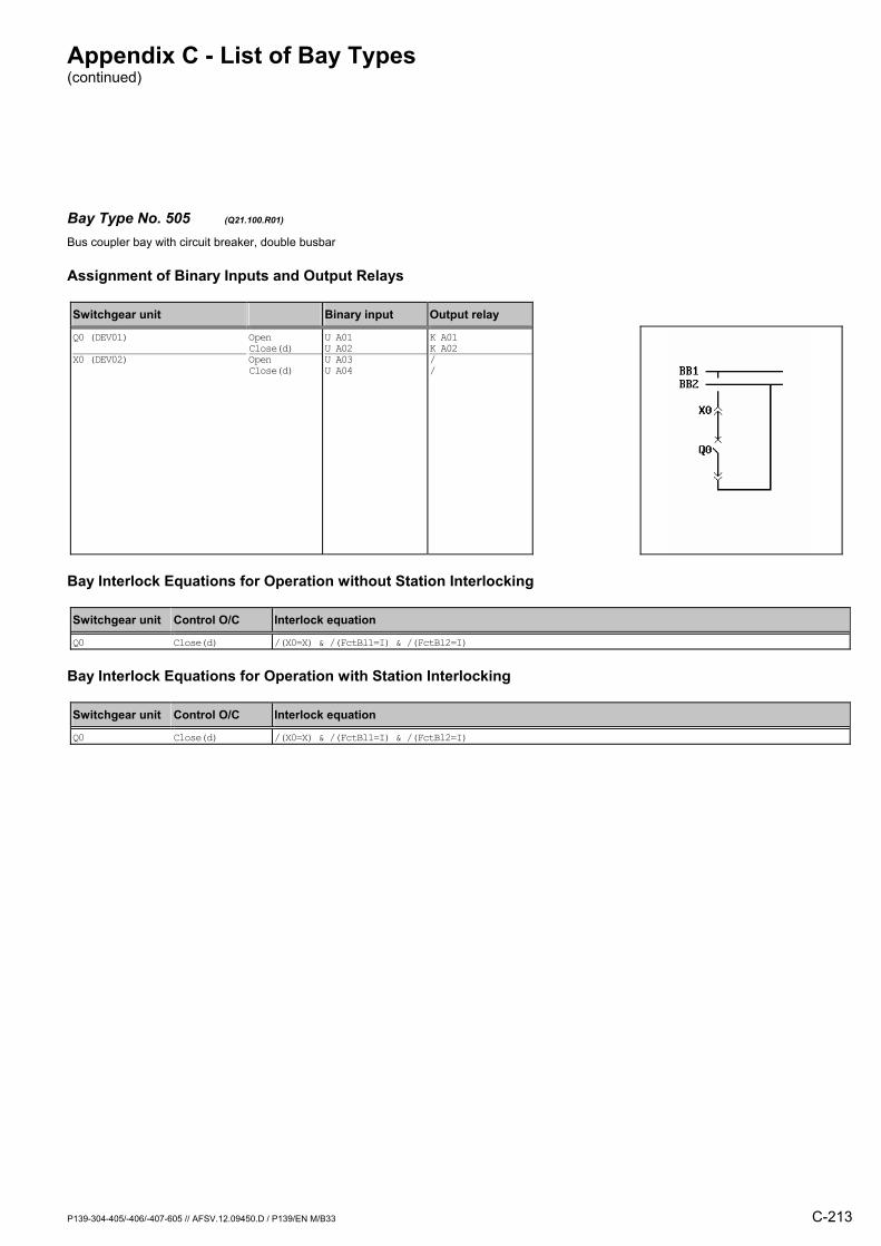
Appendix C - List of Bay Types (continued)
P139-304-405/-406/-407-605 // AFSV.12.09450.D / P139/EN M/B33 C-213
Bay Type No. 505 (Q21.100.R01) Bus coupler bay with circuit breaker, double busbar
Assignment of Binary Inputs and Output Relays
Switchgear unit Binary input Output relay
Q0 (DEV01) X0 (DEV02)
Open Close(d) Open Close(d)
U A01 U A02 U A03 U A04
K A01 K A02/ /
Bay Interlock Equations for Operation without Station Interlocking
Switchgear unit Control O/C Interlock equation
Q0 Close(d) /(X0=X) & /(FctBl1=I) & /(FctBl2=I)
Bay Interlock Equations for Operation with Station Interlocking
Switchgear unit Control O/C Interlock equation
Q0 Close(d) /(X0=X) & /(FctBl1=I) & /(FctBl2=I)
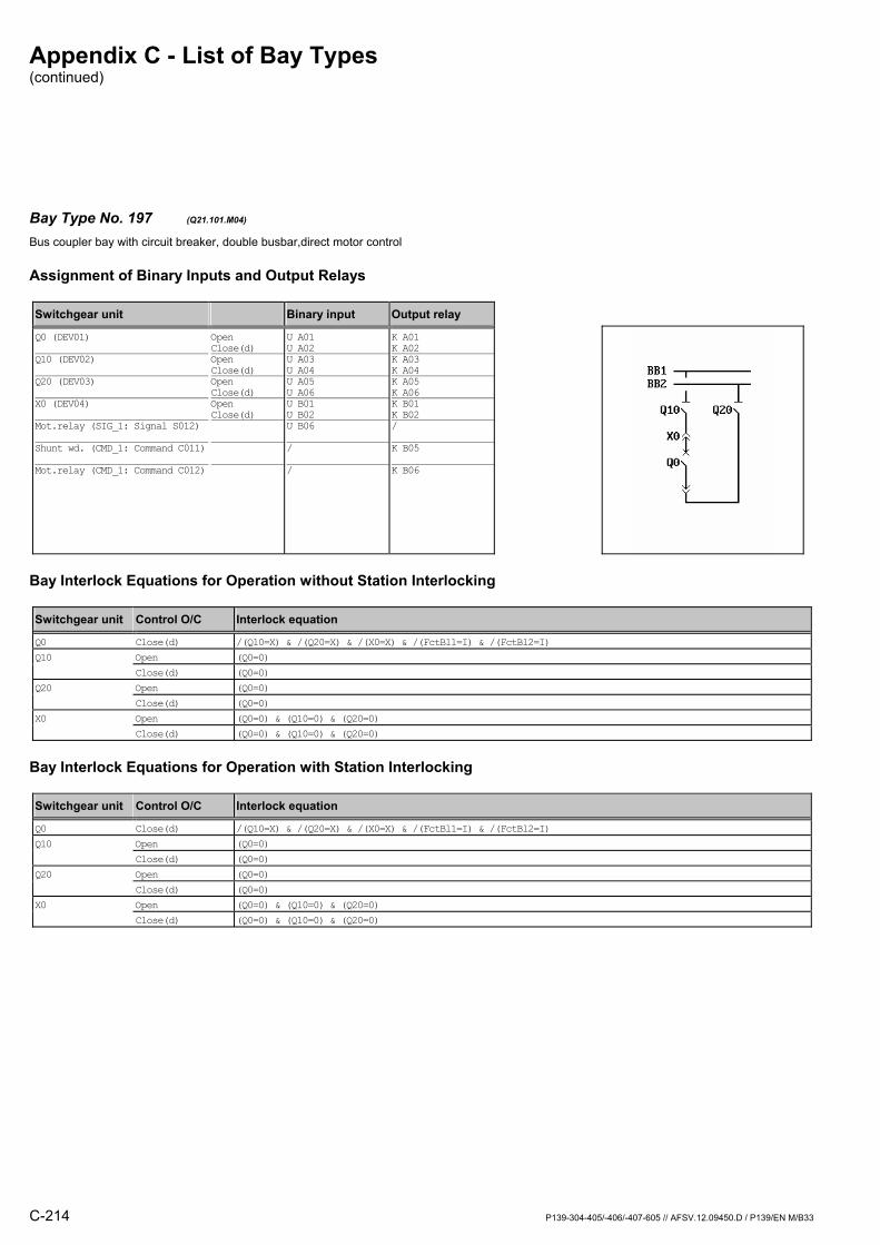
Appendix C - List of Bay Types (continued)
C-214 P139-304-405/-406/-407-605 // AFSV.12.09450.D / P139/EN M/B33
Bay Type No. 197 (Q21.101.M04) Bus coupler bay with circuit breaker, double busbar,direct motor control
Assignment of Binary Inputs and Output Relays
Switchgear unit Binary input Output relay
Q0 (DEV01) Q10 (DEV02) Q20 (DEV03) X0 (DEV04) Mot.relay (SIG_1: Signal S012) Shunt wd. (CMD_1: Command C011) Mot.relay (CMD_1: Command C012)
Open Close(d) Open Close(d) Open Close(d) Open Close(d)
U A01 U A02 U A03 U A04 U A05 U A06 U B01 U B02 U B06 / /
K A01 K A02K A03 K A04K A05 K A06K B01 K B02/
K B05
K B06
Bay Interlock Equations for Operation without Station Interlocking
Switchgear unit Control O/C Interlock equation
Q0 Close(d) /(Q10=X) & /(Q20=X) & /(X0=X) & /(FctBl1=I) & /(FctBl2=I) Q10 Open (Q0=0) Close(d) (Q0=0) Q20 Open (Q0=0) Close(d) (Q0=0) X0 Open (Q0=0) & (Q10=0) & (Q20=0) Close(d) (Q0=0) & (Q10=0) & (Q20=0)
Bay Interlock Equations for Operation with Station Interlocking
Switchgear unit Control O/C Interlock equation
Q0 Close(d) /(Q10=X) & /(Q20=X) & /(X0=X) & /(FctBl1=I) & /(FctBl2=I) Q10 Open (Q0=0) Close(d) (Q0=0) Q20 Open (Q0=0) Close(d) (Q0=0) X0 Open (Q0=0) & (Q10=0) & (Q20=0) Close(d) (Q0=0) & (Q10=0) & (Q20=0)

Appendix C - List of Bay Types (continued)
P139-304-405/-406/-407-605 // AFSV.12.09450.D / P139/EN M/B33 C-215
Bay Type No. 198 (Q21.101.R01) Bus coupler bay with circuit breaker, double busbar
Assignment of Binary Inputs and Output Relays
Switchgear unit Binary input Output relay
Q0 (DEV01) Q10 (DEV02) Q20 (DEV03) X0 (DEV04)
Open Close(d) Open Close(d) Open Close(d) Open Close(d)
U A01 U A02 U A03 U A04 U A05 U A06 U B01 U B02
K A01 K A02/ // // /
Bay Interlock Equations for Operation without Station Interlocking
Switchgear unit Control O/C Interlock equation
Q0 Close(d) /(Q10=X) & /(Q20=X) & /(X0=X) & /(FctBl1=I) & /(FctBl2=I)
Bay Interlock Equations for Operation with Station Interlocking
Switchgear unit Control O/C Interlock equation
Q0 Close(d) /(Q10=X) & /(Q20=X) & /(X0=X) & /(FctBl1=I) & /(FctBl2=I)
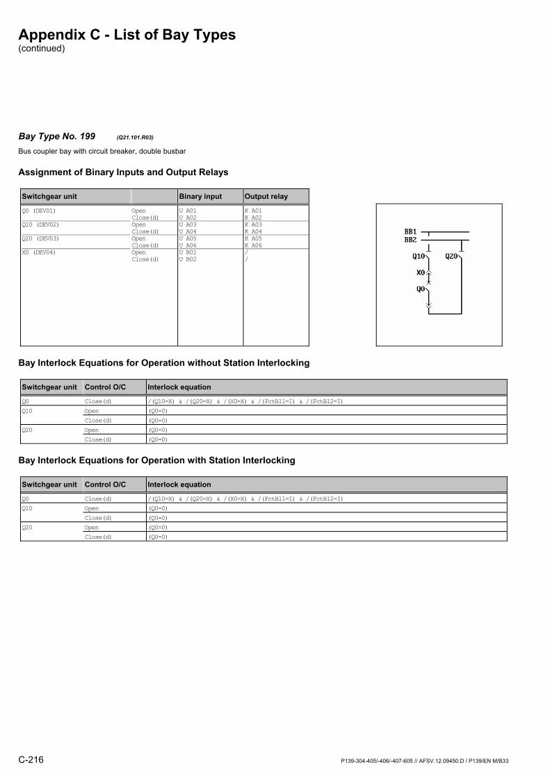
Appendix C - List of Bay Types (continued)
C-216 P139-304-405/-406/-407-605 // AFSV.12.09450.D / P139/EN M/B33
Bay Type No. 199 (Q21.101.R03) Bus coupler bay with circuit breaker, double busbar
Assignment of Binary Inputs and Output Relays
Switchgear unit Binary input Output relay
Q0 (DEV01) Q10 (DEV02) Q20 (DEV03) X0 (DEV04)
Open Close(d) Open Close(d) Open Close(d) Open Close(d)
U A01 U A02 U A03 U A04 U A05 U A06 U B01 U B02
K A01 K A02K A03 K A04K A05 K A06/ /
Bay Interlock Equations for Operation without Station Interlocking
Switchgear unit Control O/C Interlock equation
Q0 Close(d) /(Q10=X) & /(Q20=X) & /(X0=X) & /(FctBl1=I) & /(FctBl2=I) Q10 Open (Q0=0) Close(d) (Q0=0) Q20 Open (Q0=0) Close(d) (Q0=0)
Bay Interlock Equations for Operation with Station Interlocking
Switchgear unit Control O/C Interlock equation
Q0 Close(d) /(Q10=X) & /(Q20=X) & /(X0=X) & /(FctBl1=I) & /(FctBl2=I) Q10 Open (Q0=0) Close(d) (Q0=0) Q20 Open (Q0=0) Close(d) (Q0=0)

Appendix C - List of Bay Types (continued)
P139-304-405/-406/-407-605 // AFSV.12.09450.D / P139/EN M/B33 C-217
Bay Type No. 200 (Q21.101.R04) Bus coupler bay with circuit breaker, double busbar
Assignment of Binary Inputs and Output Relays
Switchgear unit Binary input Output relay
Q0 (DEV01) Q10 (DEV02) Q20 (DEV03) X0 (DEV04)
Open Close(d) Open Close(d) Open Close(d) Open Close(d)
U A01 U A02 U A03 U A04 U A05 U A06 U B01 U B02
K A01 K A02K A03 K A04K A05 K A06K B01 K B02
Bay Interlock Equations for Operation without Station Interlocking
Switchgear unit Control O/C Interlock equation
Q0 Close(d) /(Q10=X) & /(Q20=X) & /(X0=X) & /(FctBl1=I) & /(FctBl2=I) Q10 Open (Q0=0) Close(d) (Q0=0) Q20 Open (Q0=0) Close(d) (Q0=0) X0 Open (Q0=0) & (Q10=0) & (Q20=0) Close(d) (Q0=0) & (Q10=0) & (Q20=0)
Bay Interlock Equations for Operation with Station Interlocking
Switchgear unit Control O/C Interlock equation
Q0 Close(d) /(Q10=X) & /(Q20=X) & /(X0=X) & /(FctBl1=I) & /(FctBl2=I) Q10 Open (Q0=0) Close(d) (Q0=0) Q20 Open (Q0=0) Close(d) (Q0=0) X0 Open (Q0=0) & (Q10=0) & (Q20=0) Close(d) (Q0=0) & (Q10=0) & (Q20=0)
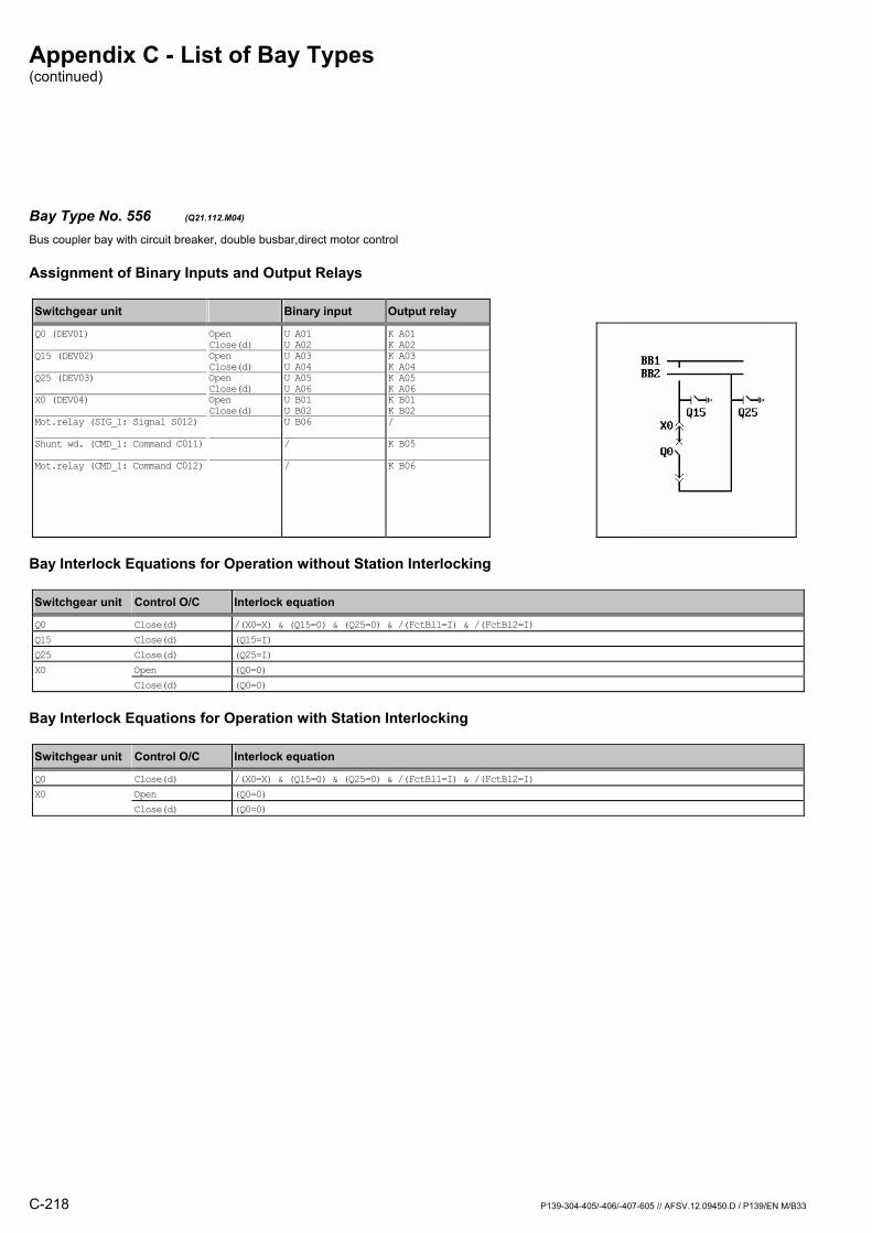
Appendix C - List of Bay Types (continued)
C-218 P139-304-405/-406/-407-605 // AFSV.12.09450.D / P139/EN M/B33
Bay Type No. 556 (Q21.112.M04) Bus coupler bay with circuit breaker, double busbar,direct motor control
Assignment of Binary Inputs and Output Relays
Switchgear unit Binary input Output relay
Q0 (DEV01) Q15 (DEV02) Q25 (DEV03) X0 (DEV04) Mot.relay (SIG_1: Signal S012) Shunt wd. (CMD_1: Command C011) Mot.relay (CMD_1: Command C012)
Open Close(d) Open Close(d) Open Close(d) Open Close(d)
U A01 U A02 U A03 U A04 U A05 U A06 U B01 U B02 U B06 / /
K A01 K A02K A03 K A04K A05 K A06K B01 K B02/
K B05
K B06
Bay Interlock Equations for Operation without Station Interlocking
Switchgear unit Control O/C Interlock equation
Q0 Close(d) /(X0=X) & (Q15=0) & (Q25=0) & /(FctBl1=I) & /(FctBl2=I) Q15 Close(d) (Q15=I) Q25 Close(d) (Q25=I) X0 Open (Q0=0) Close(d) (Q0=0)
Bay Interlock Equations for Operation with Station Interlocking
Switchgear unit Control O/C Interlock equation
Q0 Close(d) /(X0=X) & (Q15=0) & (Q25=0) & /(FctBl1=I) & /(FctBl2=I) X0 Open (Q0=0) Close(d) (Q0=0)

Appendix C - List of Bay Types (continued)
P139-304-405/-406/-407-605 // AFSV.12.09450.D / P139/EN M/B33 C-219
Bay Type No. 565 (Q21.112.M04.2) Bus coupler bay with circuit breaker, double busbar,direct motor control
Assignment of Binary Inputs and Output Relays
Switchgear unit Binary input Output relay
Q0 (DEV01) Q15 (DEV02) Q25 (DEV03) X0 (DEV04) Mot.relay (SIG_1: Signal S012) Shunt wd. (CMD_1: Command C011) Mot.relay (CMD_1: Command C012)
Open Close(d) Open Close(d) Open Close(d) Open Close(d)
U A01 U A02 U A03 U A04 U A05 U A06 U B01 U B02 U B06 / /
K A01 K A02K A03 K A04K A05 K A06K B01 K B02/
K B05
K B06
Bay Interlock Equations for Operation without Station Interlocking
Switchgear unit Control O/C Interlock equation
Q0 Close(d) /(X0=X) & (Q15=0) & (Q25=0) & /(FctBl1=I) & /(FctBl2=I) Q15 Close(d) (Q15=I) Q25 Close(d) (Q25=I) X0 Open (Q0=0) Close(d) (Q0=0)
Bay Interlock Equations for Operation with Station Interlocking
Switchgear unit Control O/C Interlock equation
Q0 Close(d) /(X0=X) & (Q15=0) & (Q25=0) & /(FctBl1=I) & /(FctBl2=I) X0 Open (Q0=0) Close(d) (Q0=0)
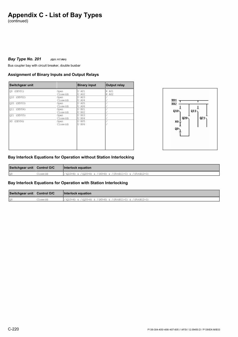
Appendix C - List of Bay Types (continued)
C-220 P139-304-405/-406/-407-605 // AFSV.12.09450.D / P139/EN M/B33
Bay Type No. 201 (Q21.117.R01) Bus coupler bay with circuit breaker, double busbar
Assignment of Binary Inputs and Output Relays
Switchgear unit Binary input Output relay
Q0 (DEV01) Q10 (DEV02) Q20 (DEV03) Q11 (DEV04) Q21 (DEV05) X0 (DEV06)
Open Close(d) Open Close(d) Open Close(d) Open Close(d) Open Close(d) Open Close(d)
U A01 U A02 U A03 U A04 U A05 U A06 U B01 U B02 U B03 U B04 U B05 U B06
K A01 K A02/ // // // // /
Bay Interlock Equations for Operation without Station Interlocking
Switchgear unit Control O/C Interlock equation
Q0 Close(d) /(Q10=X) & /(Q20=X) & /(X0=X) & /(FctBl1=I) & /(FctBl2=I)
Bay Interlock Equations for Operation with Station Interlocking
Switchgear unit Control O/C Interlock equation
Q0 Close(d) /(Q10=X) & /(Q20=X) & /(X0=X) & /(FctBl1=I) & /(FctBl2=I)
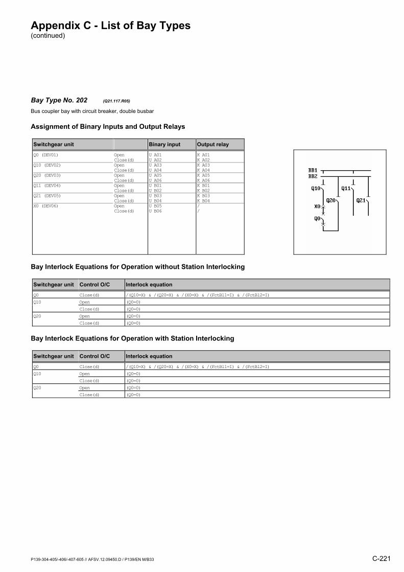
Appendix C - List of Bay Types (continued)
P139-304-405/-406/-407-605 // AFSV.12.09450.D / P139/EN M/B33 C-221
Bay Type No. 202 (Q21.117.R05) Bus coupler bay with circuit breaker, double busbar
Assignment of Binary Inputs and Output Relays
Switchgear unit Binary input Output relay
Q0 (DEV01) Q10 (DEV02) Q20 (DEV03) Q11 (DEV04) Q21 (DEV05) X0 (DEV06)
Open Close(d) Open Close(d) Open Close(d) Open Close(d) Open Close(d) Open Close(d)
U A01 U A02 U A03 U A04 U A05 U A06 U B01 U B02 U B03 U B04 U B05 U B06
K A01 K A02K A03 K A04K A05 K A06K B01 K B02K B03 K B04/ /
Bay Interlock Equations for Operation without Station Interlocking
Switchgear unit Control O/C Interlock equation
Q0 Close(d) /(Q10=X) & /(Q20=X) & /(X0=X) & /(FctBl1=I) & /(FctBl2=I) Q10 Open (Q0=0) Close(d) (Q0=0) Q20 Open (Q0=0) Close(d) (Q0=0)
Bay Interlock Equations for Operation with Station Interlocking
Switchgear unit Control O/C Interlock equation
Q0 Close(d) /(Q10=X) & /(Q20=X) & /(X0=X) & /(FctBl1=I) & /(FctBl2=I) Q10 Open (Q0=0) Close(d) (Q0=0) Q20 Open (Q0=0) Close(d) (Q0=0)
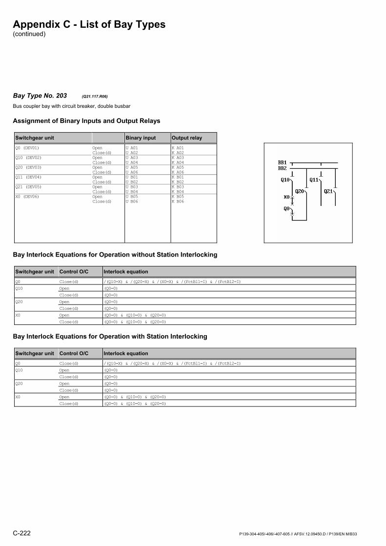
Appendix C - List of Bay Types (continued)
C-222 P139-304-405/-406/-407-605 // AFSV.12.09450.D / P139/EN M/B33
Bay Type No. 203 (Q21.117.R06) Bus coupler bay with circuit breaker, double busbar
Assignment of Binary Inputs and Output Relays
Switchgear unit Binary input Output relay
Q0 (DEV01) Q10 (DEV02) Q20 (DEV03) Q11 (DEV04) Q21 (DEV05) X0 (DEV06)
Open Close(d) Open Close(d) Open Close(d) Open Close(d) Open Close(d) Open Close(d)
U A01 U A02 U A03 U A04 U A05 U A06 U B01 U B02 U B03 U B04 U B05 U B06
K A01 K A02K A03 K A04K A05 K A06K B01 K B02K B03 K B04K B05 K B06
Bay Interlock Equations for Operation without Station Interlocking
Switchgear unit Control O/C Interlock equation
Q0 Close(d) /(Q10=X) & /(Q20=X) & /(X0=X) & /(FctBl1=I) & /(FctBl2=I) Q10 Open (Q0=0) Close(d) (Q0=0) Q20 Open (Q0=0) Close(d) (Q0=0) X0 Open (Q0=0) & (Q10=0) & (Q20=0) Close(d) (Q0=0) & (Q10=0) & (Q20=0)
Bay Interlock Equations for Operation with Station Interlocking
Switchgear unit Control O/C Interlock equation
Q0 Close(d) /(Q10=X) & /(Q20=X) & /(X0=X) & /(FctBl1=I) & /(FctBl2=I) Q10 Open (Q0=0) Close(d) (Q0=0) Q20 Open (Q0=0) Close(d) (Q0=0) X0 Open (Q0=0) & (Q10=0) & (Q20=0) Close(d) (Q0=0) & (Q10=0) & (Q20=0)

Appendix C - List of Bay Types (continued)
P139-304-405/-406/-407-605 // AFSV.12.09450.D / P139/EN M/B33 C-223
Bay Type No. 245 (Q21.132.R01) Bus coupler bay with circuit breaker, double busbar
Assignment of Binary Inputs and Output Relays
Switchgear unit Binary input Output relay
Q0 (DEV01) X0 (DEV02) Q15 (DEV03) Q25 (DEV04)
Open Close(d) Open Close(d) Open Close(d) Open Close(d)
U A01 U A02 U A03 U A04 U A05 U A06 U B01 U B02
K A01 K A02/ // // /
Bay Interlock Equations for Operation without Station Interlocking
Switchgear unit Control O/C Interlock equation
Q0 Close(d) /(X0=X) & /(FctBl1=I) & /(FctBl2=I)
Bay Interlock Equations for Operation with Station Interlocking
Switchgear unit Control O/C Interlock equation
Q0 Close(d) /(X0=X) & /(FctBl1=I) & /(FctBl2=I)

Appendix C - List of Bay Types (continued)
C-224 P139-304-405/-406/-407-605 // AFSV.12.09450.D / P139/EN M/B33
Bay Type No. 563 (Q21.133.R01) Bus coupler bay with circuit breaker, double busbar
Assignment of Binary Inputs and Output Relays
Switchgear unit Binary input Output relay
Q0 (DEV01) X01 (DEV02) X02 (DEV03)
Open Close(d) Open Close(d) Open Close(d)
U A01 U A02 U A03 U A04 U A05 U A06
K A01 K A02/ // /
Bay Interlock Equations for Operation without Station Interlocking
Switchgear unit Control O/C Interlock equation
Q0 Close(d) /(X01=X) & /(X02=X) & /(FctBl1=I) & /(FctBl2=I)
Bay Interlock Equations for Operation with Station Interlocking
Switchgear unit Control O/C Interlock equation
Q0 Close(d) /(X01=X) & /(X02=X) & /(FctBl1=I) & /(FctBl2=I)
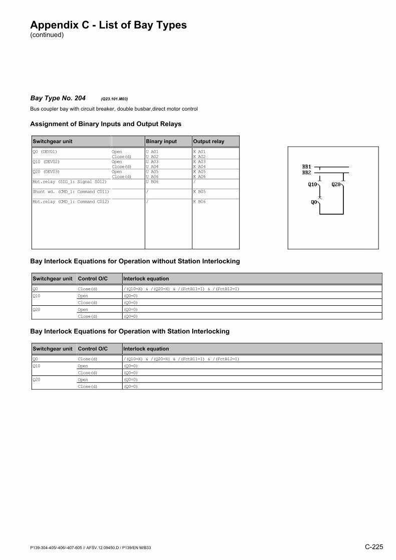
Appendix C - List of Bay Types (continued)
P139-304-405/-406/-407-605 // AFSV.12.09450.D / P139/EN M/B33 C-225
Bay Type No. 204 (Q23.101.M03) Bus coupler bay with circuit breaker, double busbar,direct motor control
Assignment of Binary Inputs and Output Relays
Switchgear unit Binary input Output relay
Q0 (DEV01) Q10 (DEV02) Q20 (DEV03) Mot.relay (SIG_1: Signal S012) Shunt wd. (CMD_1: Command C011) Mot.relay (CMD_1: Command C012)
Open Close(d) Open Close(d) Open Close(d)
U A01 U A02 U A03 U A04 U A05 U A06 U B06 / /
K A01 K A02K A03 K A04K A05 K A06/
K B05
K B06
Bay Interlock Equations for Operation without Station Interlocking
Switchgear unit Control O/C Interlock equation
Q0 Close(d) /(Q10=X) & /(Q20=X) & /(FctBl1=I) & /(FctBl2=I) Q10 Open (Q0=0) Close(d) (Q0=0) Q20 Open (Q0=0) Close(d) (Q0=0)
Bay Interlock Equations for Operation with Station Interlocking
Switchgear unit Control O/C Interlock equation
Q0 Close(d) /(Q10=X) & /(Q20=X) & /(FctBl1=I) & /(FctBl2=I) Q10 Open (Q0=0) Close(d) (Q0=0) Q20 Open (Q0=0) Close(d) (Q0=0)
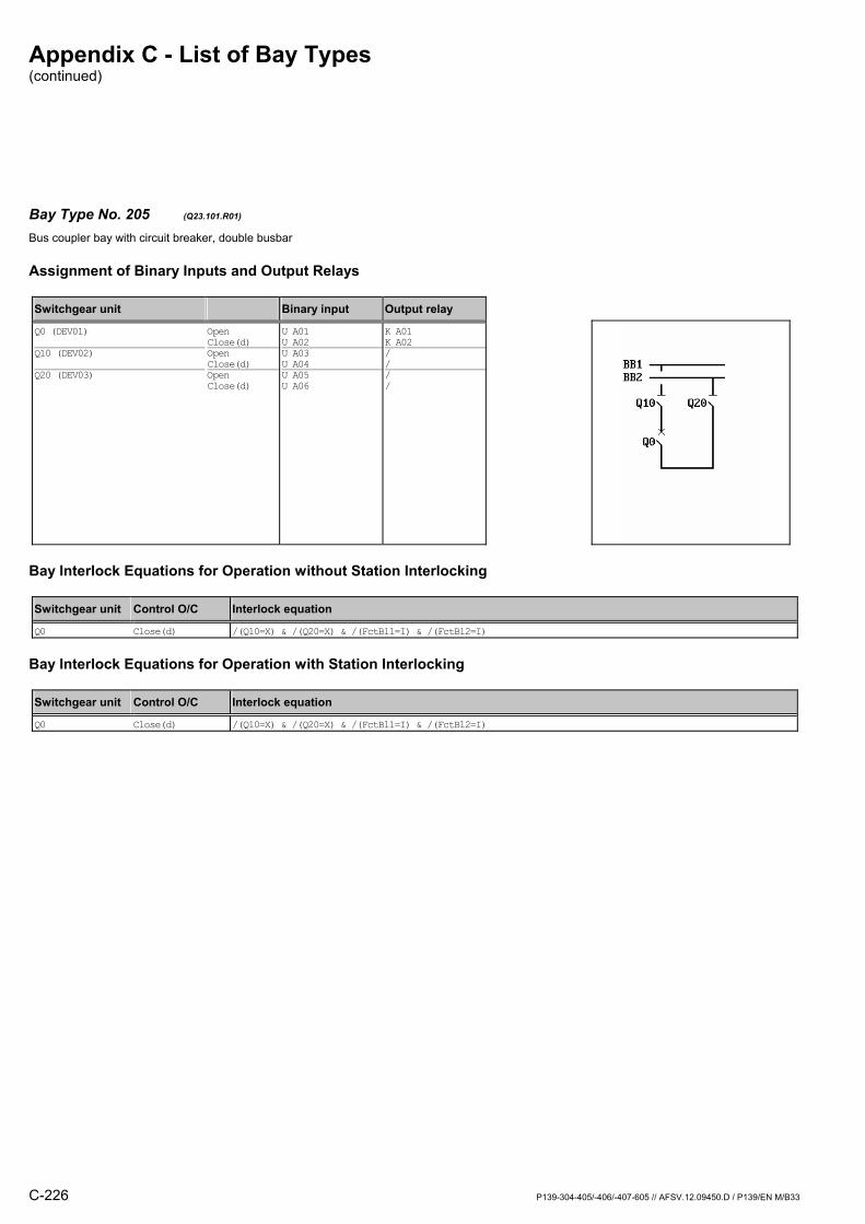
Appendix C - List of Bay Types (continued)
C-226 P139-304-405/-406/-407-605 // AFSV.12.09450.D / P139/EN M/B33
Bay Type No. 205 (Q23.101.R01) Bus coupler bay with circuit breaker, double busbar
Assignment of Binary Inputs and Output Relays
Switchgear unit Binary input Output relay
Q0 (DEV01) Q10 (DEV02) Q20 (DEV03)
Open Close(d) Open Close(d) Open Close(d)
U A01 U A02 U A03 U A04 U A05 U A06
K A01 K A02/ // /
Bay Interlock Equations for Operation without Station Interlocking
Switchgear unit Control O/C Interlock equation
Q0 Close(d) /(Q10=X) & /(Q20=X) & /(FctBl1=I) & /(FctBl2=I)
Bay Interlock Equations for Operation with Station Interlocking
Switchgear unit Control O/C Interlock equation
Q0 Close(d) /(Q10=X) & /(Q20=X) & /(FctBl1=I) & /(FctBl2=I)

Appendix C - List of Bay Types (continued)
P139-304-405/-406/-407-605 // AFSV.12.09450.D / P139/EN M/B33 C-227
Bay Type No. 206 (Q23.101.R03) Bus coupler bay with circuit breaker, double busbar
Assignment of Binary Inputs and Output Relays
Switchgear unit Binary input Output relay
Q0 (DEV01) Q10 (DEV02) Q20 (DEV03)
Open Close(d) Open Close(d) Open Close(d)
U A01 U A02 U A03 U A04 U A05 U A06
K A01 K A02K A03 K A04K A05 K A06
Bay Interlock Equations for Operation without Station Interlocking
Switchgear unit Control O/C Interlock equation
Q0 Close(d) /(Q10=X) & /(Q20=X) & /(FctBl1=I) & /(FctBl2=I) Q10 Open (Q0=0) Close(d) (Q0=0) Q20 Open (Q0=0) Close(d) (Q0=0)
Bay Interlock Equations for Operation with Station Interlocking
Switchgear unit Control O/C Interlock equation
Q0 Close(d) /(Q10=X) & /(Q20=X) & /(FctBl1=I) & /(FctBl2=I) Q10 Open (Q0=0) Close(d) (Q0=0) Q20 Open (Q0=0) Close(d) (Q0=0)
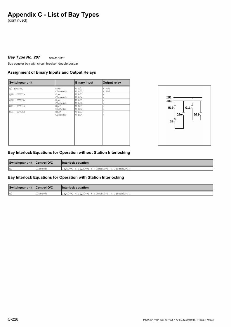
Appendix C - List of Bay Types (continued)
C-228 P139-304-405/-406/-407-605 // AFSV.12.09450.D / P139/EN M/B33
Bay Type No. 207 (Q23.117.R01) Bus coupler bay with circuit breaker, double busbar
Assignment of Binary Inputs and Output Relays
Switchgear unit Binary input Output relay
Q0 (DEV01) Q10 (DEV02) Q20 (DEV03) Q11 (DEV04) Q21 (DEV05)
Open Close(d) Open Close(d) Open Close(d) Open Close(d) Open Close(d)
U A01 U A02 U A03 U A04 U A05 U A06 U B01 U B02 U B03 U B04
K A01 K A02/ // // // /
Bay Interlock Equations for Operation without Station Interlocking
Switchgear unit Control O/C Interlock equation
Q0 Close(d) /(Q10=X) & /(Q20=X) & /(FctBl1=I) & /(FctBl2=I)
Bay Interlock Equations for Operation with Station Interlocking
Switchgear unit Control O/C Interlock equation
Q0 Close(d) /(Q10=X) & /(Q20=X) & /(FctBl1=I) & /(FctBl2=I)

Appendix C - List of Bay Types (continued)
P139-304-405/-406/-407-605 // AFSV.12.09450.D / P139/EN M/B33 C-229
Bay Type No. 208 (Q23.117.R05) Bus coupler bay with circuit breaker, double busbar
Assignment of Binary Inputs and Output Relays
Switchgear unit Binary input Output relay
Q0 (DEV01) Q10 (DEV02) Q20 (DEV03) Q11 (DEV04) Q21 (DEV05)
Open Close(d) Open Close(d) Open Close(d) Open Close(d) Open Close(d)
U A01 U A02 U A03 U A04 U A05 U A06 U B01 U B02 U B03 U B04
K A01 K A02K A03 K A04K A05 K A06K B01 K B02K B03 K B04
Bay Interlock Equations for Operation without Station Interlocking
Switchgear unit Control O/C Interlock equation
Q0 Close(d) /(Q10=X) & /(Q20=X) & /(FctBl1=I) & /(FctBl2=I) Q10 Open (Q0=0) Close(d) (Q0=0) Q20 Open (Q0=0) Close(d) (Q0=0)
Bay Interlock Equations for Operation with Station Interlocking
Switchgear unit Control O/C Interlock equation
Q0 Close(d) /(Q10=X) & /(Q20=X) & /(FctBl1=I) & /(FctBl2=I) Q10 Open (Q0=0) Close(d) (Q0=0) Q20 Open (Q0=0) Close(d) (Q0=0)
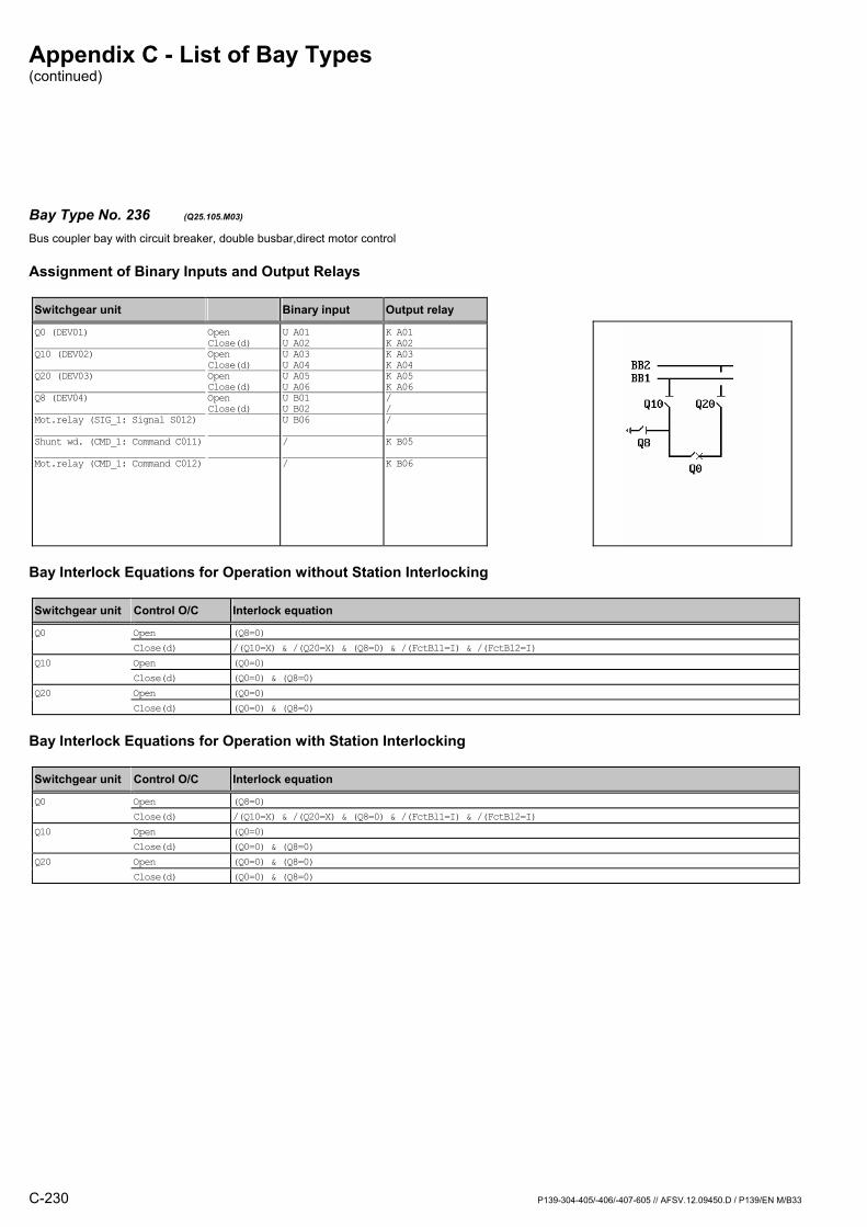
Appendix C - List of Bay Types (continued)
C-230 P139-304-405/-406/-407-605 // AFSV.12.09450.D / P139/EN M/B33
Bay Type No. 236 (Q25.105.M03) Bus coupler bay with circuit breaker, double busbar,direct motor control
Assignment of Binary Inputs and Output Relays
Switchgear unit Binary input Output relay
Q0 (DEV01) Q10 (DEV02) Q20 (DEV03) Q8 (DEV04) Mot.relay (SIG_1: Signal S012) Shunt wd. (CMD_1: Command C011) Mot.relay (CMD_1: Command C012)
Open Close(d) Open Close(d) Open Close(d) Open Close(d)
U A01 U A02 U A03 U A04 U A05 U A06 U B01 U B02 U B06 / /
K A01 K A02K A03 K A04K A05 K A06/ //
K B05
K B06
Bay Interlock Equations for Operation without Station Interlocking
Switchgear unit Control O/C Interlock equation
Q0 Open (Q8=0) Close(d) /(Q10=X) & /(Q20=X) & (Q8=0) & /(FctBl1=I) & /(FctBl2=I) Q10 Open (Q0=0) Close(d) (Q0=0) & (Q8=0) Q20 Open (Q0=0) Close(d) (Q0=0) & (Q8=0)
Bay Interlock Equations for Operation with Station Interlocking
Switchgear unit Control O/C Interlock equation
Q0 Open (Q8=0) Close(d) /(Q10=X) & /(Q20=X) & (Q8=0) & /(FctBl1=I) & /(FctBl2=I) Q10 Open (Q0=0) Close(d) (Q0=0) & (Q8=0) Q20 Open (Q0=0) & (Q8=0) Close(d) (Q0=0) & (Q8=0)
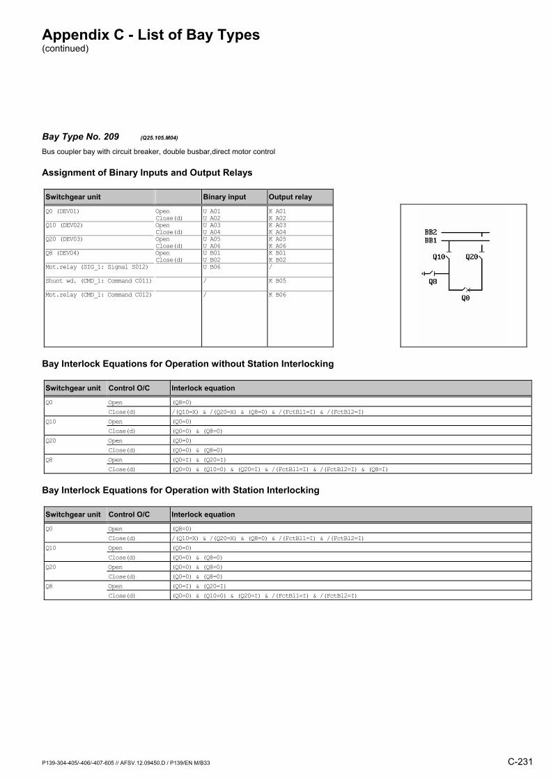
Appendix C - List of Bay Types (continued)
P139-304-405/-406/-407-605 // AFSV.12.09450.D / P139/EN M/B33 C-231
Bay Type No. 209 (Q25.105.M04) Bus coupler bay with circuit breaker, double busbar,direct motor control
Assignment of Binary Inputs and Output Relays
Switchgear unit Binary input Output relay
Q0 (DEV01) Q10 (DEV02) Q20 (DEV03) Q8 (DEV04) Mot.relay (SIG_1: Signal S012) Shunt wd. (CMD_1: Command C011) Mot.relay (CMD_1: Command C012)
Open Close(d) Open Close(d) Open Close(d) Open Close(d)
U A01 U A02 U A03 U A04 U A05 U A06 U B01 U B02 U B06 / /
K A01 K A02K A03 K A04K A05 K A06K B01 K B02/
K B05
K B06
Bay Interlock Equations for Operation without Station Interlocking
Switchgear unit Control O/C Interlock equation
Q0 Open (Q8=0) Close(d) /(Q10=X) & /(Q20=X) & (Q8=0) & /(FctBl1=I) & /(FctBl2=I) Q10 Open (Q0=0) Close(d) (Q0=0) & (Q8=0) Q20 Open (Q0=0) Close(d) (Q0=0) & (Q8=0) Q8 Open (Q0=I) & (Q20=I) Close(d) (Q0=0) & (Q10=0) & (Q20=I) & /(FctBl1=I) & /(FctBl2=I) & (Q8=I)
Bay Interlock Equations for Operation with Station Interlocking
Switchgear unit Control O/C Interlock equation
Q0 Open (Q8=0) Close(d) /(Q10=X) & /(Q20=X) & (Q8=0) & /(FctBl1=I) & /(FctBl2=I) Q10 Open (Q0=0) Close(d) (Q0=0) & (Q8=0) Q20 Open (Q0=0) & (Q8=0) Close(d) (Q0=0) & (Q8=0) Q8 Open (Q0=I) & (Q20=I) Close(d) (Q0=0) & (Q10=0) & (Q20=I) & /(FctBl1=I) & /(FctBl2=I)
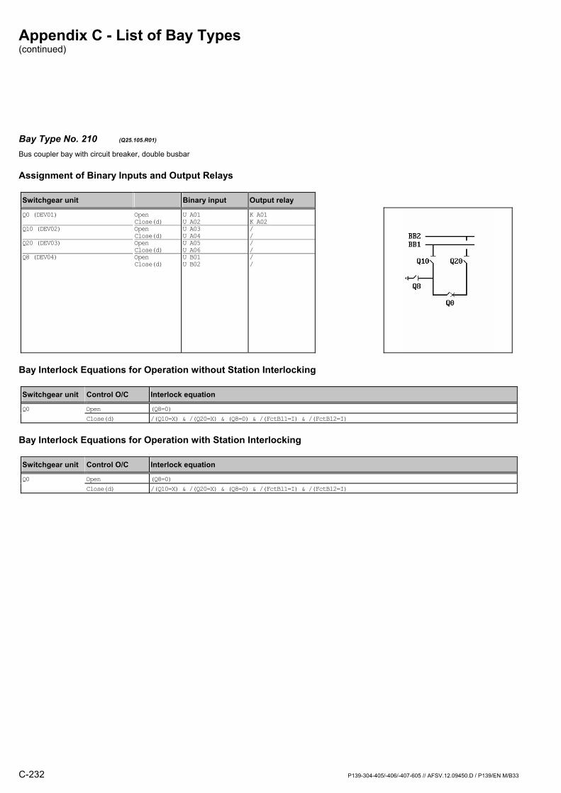
Appendix C - List of Bay Types (continued)
C-232 P139-304-405/-406/-407-605 // AFSV.12.09450.D / P139/EN M/B33
Bay Type No. 210 (Q25.105.R01) Bus coupler bay with circuit breaker, double busbar
Assignment of Binary Inputs and Output Relays
Switchgear unit Binary input Output relay
Q0 (DEV01) Q10 (DEV02) Q20 (DEV03) Q8 (DEV04)
Open Close(d) Open Close(d) Open Close(d) Open Close(d)
U A01 U A02 U A03 U A04 U A05 U A06 U B01 U B02
K A01 K A02/ // // /
Bay Interlock Equations for Operation without Station Interlocking
Switchgear unit Control O/C Interlock equation
Q0 Open (Q8=0) Close(d) /(Q10=X) & /(Q20=X) & (Q8=0) & /(FctBl1=I) & /(FctBl2=I)
Bay Interlock Equations for Operation with Station Interlocking
Switchgear unit Control O/C Interlock equation
Q0 Open (Q8=0) Close(d) /(Q10=X) & /(Q20=X) & (Q8=0) & /(FctBl1=I) & /(FctBl2=I)
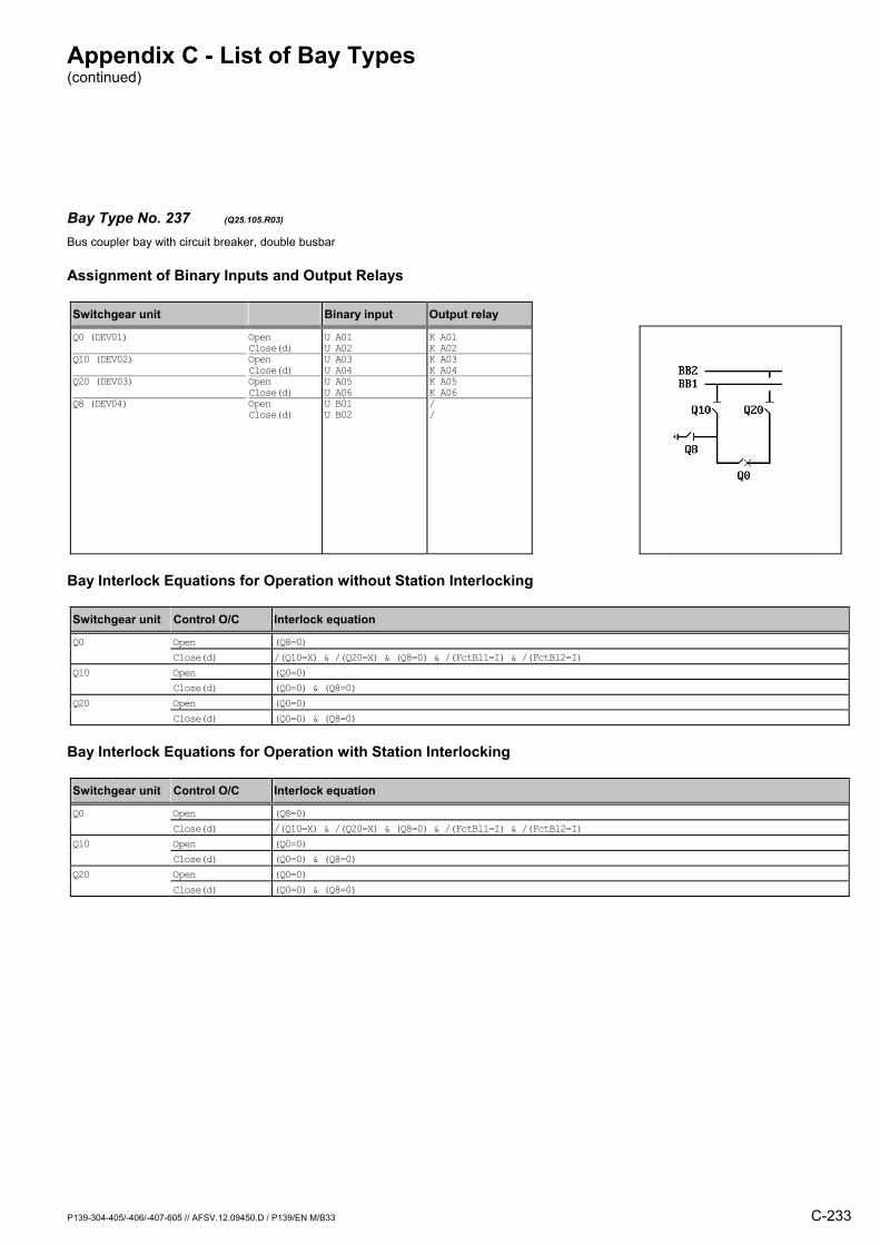
Appendix C - List of Bay Types (continued)
P139-304-405/-406/-407-605 // AFSV.12.09450.D / P139/EN M/B33 C-233
Bay Type No. 237 (Q25.105.R03) Bus coupler bay with circuit breaker, double busbar
Assignment of Binary Inputs and Output Relays
Switchgear unit Binary input Output relay
Q0 (DEV01) Q10 (DEV02) Q20 (DEV03) Q8 (DEV04)
Open Close(d) Open Close(d) Open Close(d) Open Close(d)
U A01 U A02 U A03 U A04 U A05 U A06 U B01 U B02
K A01 K A02K A03 K A04K A05 K A06/ /
Bay Interlock Equations for Operation without Station Interlocking
Switchgear unit Control O/C Interlock equation
Q0 Open (Q8=0) Close(d) /(Q10=X) & /(Q20=X) & (Q8=0) & /(FctBl1=I) & /(FctBl2=I) Q10 Open (Q0=0) Close(d) (Q0=0) & (Q8=0) Q20 Open (Q0=0) Close(d) (Q0=0) & (Q8=0)
Bay Interlock Equations for Operation with Station Interlocking
Switchgear unit Control O/C Interlock equation
Q0 Open (Q8=0) Close(d) /(Q10=X) & /(Q20=X) & (Q8=0) & /(FctBl1=I) & /(FctBl2=I) Q10 Open (Q0=0) Close(d) (Q0=0) & (Q8=0) Q20 Open (Q0=0) Close(d) (Q0=0) & (Q8=0)
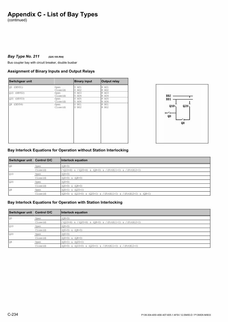
Appendix C - List of Bay Types (continued)
C-234 P139-304-405/-406/-407-605 // AFSV.12.09450.D / P139/EN M/B33
Bay Type No. 211 (Q25.105.R04) Bus coupler bay with circuit breaker, double busbar
Assignment of Binary Inputs and Output Relays
Switchgear unit Binary input Output relay
Q0 (DEV01) Q10 (DEV02) Q20 (DEV03) Q8 (DEV04)
Open Close(d) Open Close(d) Open Close(d) Open Close(d)
U A01 U A02 U A03 U A04 U A05 U A06 U B01 U B02
K A01 K A02K A03 K A04K A05 K A06K B01 K B02
Bay Interlock Equations for Operation without Station Interlocking
Switchgear unit Control O/C Interlock equation
Q0 Open (Q8=0) Close(d) /(Q10=X) & /(Q20=X) & (Q8=0) & /(FctBl1=I) & /(FctBl2=I) Q10 Open (Q0=0) Close(d) (Q0=0) & (Q8=0) Q20 Open (Q0=0) Close(d) (Q0=0) & (Q8=0) Q8 Open (Q0=I) & (Q20=I) Close(d) (Q0=0) & (Q10=0) & (Q20=I) & /(FctBl1=I) & /(FctBl2=I) & (Q8=I)
Bay Interlock Equations for Operation with Station Interlocking
Switchgear unit Control O/C Interlock equation
Q0 Open (Q8=0) Close(d) /(Q10=X) & /(Q20=X) & (Q8=0) & /(FctBl1=I) & /(FctBl2=I) Q10 Open (Q0=0) Close(d) (Q0=0) & (Q8=0) Q20 Open (Q0=0) Close(d) (Q0=0) & (Q8=0) Q8 Open (Q0=I) & (Q20=I) Close(d) (Q0=0) & (Q10=0) & (Q20=I) & /(FctBl1=I) & /(FctBl2=I)

Appendix C - List of Bay Types (continued)
P139-304-405/-406/-407-605 // AFSV.12.09450.D / P139/EN M/B33 C-235
Bay Type No. 238 (Q25.109.M03) Bus coupler bay with circuit breaker, double busbar,direct motor control
Assignment of Binary Inputs and Output Relays
Switchgear unit Binary input Output relay
Q0 (DEV01) Q10 (DEV02) Q20 (DEV03) Q8 (DEV04) Mot.relay (SIG_1: Signal S012) Shunt wd. (CMD_1: Command C011) Mot.relay (CMD_1: Command C012)
Open Close(d) Open Close(d) Open Close(d) Open Close(d)
U A01 U A02 U A03 U A04 U A05 U A06 U B01 U B02 U B06 / /
K A01 K A02K A03 K A04K A05 K A06/ //
K B05
K B06
Bay Interlock Equations for Operation without Station Interlocking
Switchgear unit Control O/C Interlock equation
Q0 Open (Q8=0) Close(d) /(Q10=X) & /(Q20=X) & (Q8=0) & /(FctBl1=I) & /(FctBl2=I) Q10 Open (Q0=0) Close(d) (Q0=0) & (Q8=0) Q20 Open (Q0=0) Close(d) (Q0=0) & (Q8=0)
Bay Interlock Equations for Operation with Station Interlocking
Switchgear unit Control O/C Interlock equation
Q0 Open (Q8=0) Close(d) /(Q10=X) & /(Q20=X) & (Q8=0) & /(FctBl1=I) & /(FctBl2=I) Q10 Open (Q0=0) Close(d) (Q0=0) & (Q8=0) Q20 Open (Q0=0) Close(d) (Q0=0) & (Q8=0)
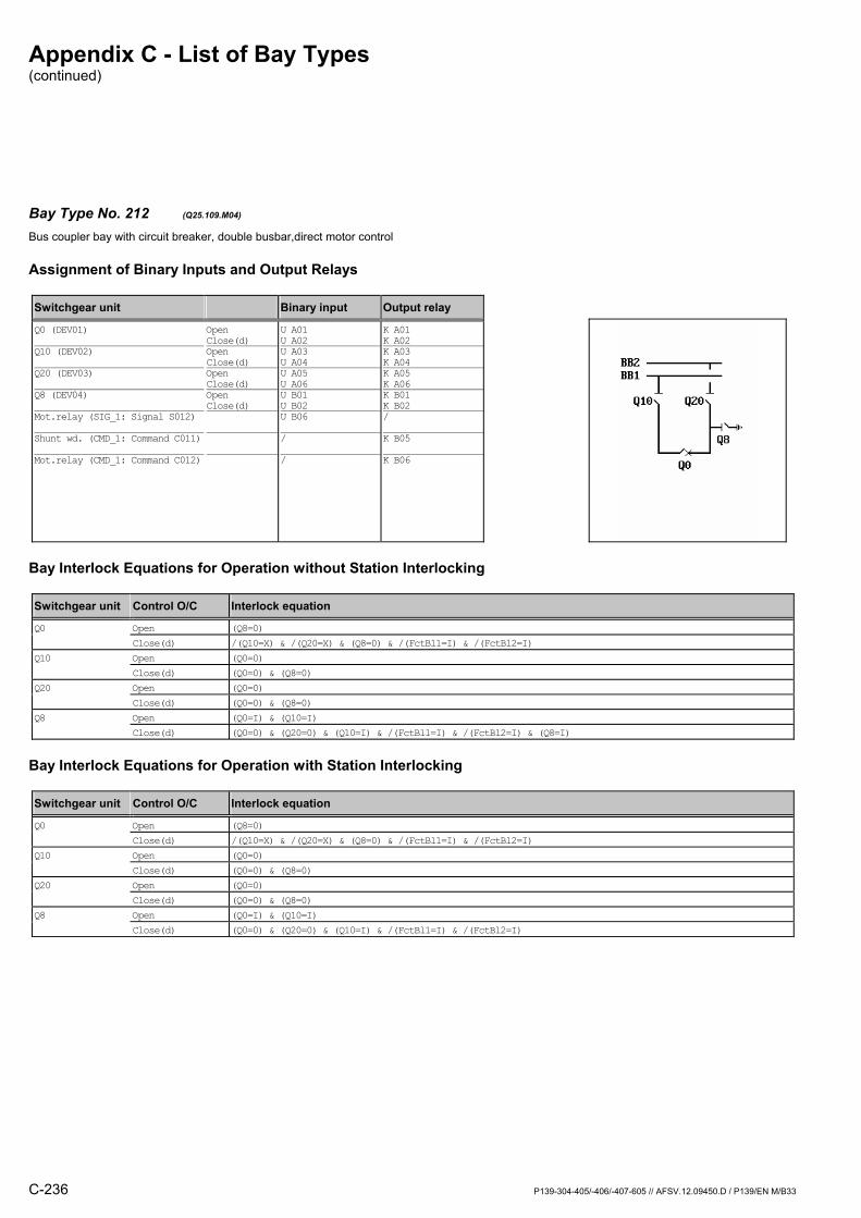
Appendix C - List of Bay Types (continued)
C-236 P139-304-405/-406/-407-605 // AFSV.12.09450.D / P139/EN M/B33
Bay Type No. 212 (Q25.109.M04) Bus coupler bay with circuit breaker, double busbar,direct motor control
Assignment of Binary Inputs and Output Relays
Switchgear unit Binary input Output relay
Q0 (DEV01) Q10 (DEV02) Q20 (DEV03) Q8 (DEV04) Mot.relay (SIG_1: Signal S012) Shunt wd. (CMD_1: Command C011) Mot.relay (CMD_1: Command C012)
Open Close(d) Open Close(d) Open Close(d) Open Close(d)
U A01 U A02 U A03 U A04 U A05 U A06 U B01 U B02 U B06 / /
K A01 K A02K A03 K A04K A05 K A06K B01 K B02/
K B05
K B06
Bay Interlock Equations for Operation without Station Interlocking
Switchgear unit Control O/C Interlock equation
Q0 Open (Q8=0) Close(d) /(Q10=X) & /(Q20=X) & (Q8=0) & /(FctBl1=I) & /(FctBl2=I) Q10 Open (Q0=0) Close(d) (Q0=0) & (Q8=0) Q20 Open (Q0=0) Close(d) (Q0=0) & (Q8=0) Q8 Open (Q0=I) & (Q10=I) Close(d) (Q0=0) & (Q20=0) & (Q10=I) & /(FctBl1=I) & /(FctBl2=I) & (Q8=I)
Bay Interlock Equations for Operation with Station Interlocking
Switchgear unit Control O/C Interlock equation
Q0 Open (Q8=0) Close(d) /(Q10=X) & /(Q20=X) & (Q8=0) & /(FctBl1=I) & /(FctBl2=I) Q10 Open (Q0=0) Close(d) (Q0=0) & (Q8=0) Q20 Open (Q0=0) Close(d) (Q0=0) & (Q8=0) Q8 Open (Q0=I) & (Q10=I) Close(d) (Q0=0) & (Q20=0) & (Q10=I) & /(FctBl1=I) & /(FctBl2=I)

Appendix C - List of Bay Types (continued)
P139-304-405/-406/-407-605 // AFSV.12.09450.D / P139/EN M/B33 C-237
Bay Type No. 213 (Q25.109.R01) Bus coupler bay with circuit breaker, double busbar
Assignment of Binary Inputs and Output Relays
Switchgear unit Binary input Output relay
Q0 (DEV01) Q10 (DEV02) Q20 (DEV03) Q8 (DEV04)
Open Close(d) Open Close(d) Open Close(d) Open Close(d)
U A01 U A02 U A03 U A04 U A05 U A06 U B01 U B02
K A01 K A02/ // // /
Bay Interlock Equations for Operation without Station Interlocking
Switchgear unit Control O/C Interlock equation
Q0 Open (Q8=0) Close(d) /(Q10=X) & /(Q20=X) & (Q8=0) & /(FctBl1=I) & /(FctBl2=I)
Bay Interlock Equations for Operation with Station Interlocking
Switchgear unit Control O/C Interlock equation
Q0 Open (Q8=0) Close(d) /(Q10=X) & /(Q20=X) & (Q8=0) & /(FctBl1=I) & /(FctBl2=I)

Appendix C - List of Bay Types (continued)
C-238 P139-304-405/-406/-407-605 // AFSV.12.09450.D / P139/EN M/B33
Bay Type No. 239 (Q25.109.R03) Bus coupler bay with circuit breaker, double busbar
Assignment of Binary Inputs and Output Relays
Switchgear unit Binary input Output relay
Q0 (DEV01) Q10 (DEV02) Q20 (DEV03) Q8 (DEV04)
Open Close(d) Open Close(d) Open Close(d) Open Close(d)
U A01 U A02 U A03 U A04 U A05 U A06 U B01 U B02
K A01 K A02K A03 K A04K A05 K A06/ /
Bay Interlock Equations for Operation without Station Interlocking
Switchgear unit Control O/C Interlock equation
Q0 Open (Q8=0) Close(d) /(Q10=X) & /(Q20=X) & (Q8=0) & /(FctBl1=I) & /(FctBl2=I) Q10 Open (Q0=0) Close(d) (Q0=0) & (Q8=0) Q20 Open (Q0=0) Close(d) (Q0=0) & (Q8=0)
Bay Interlock Equations for Operation with Station Interlocking
Switchgear unit Control O/C Interlock equation
Q0 Open (Q8=0) Close(d) /(Q10=X) & /(Q20=X) & (Q8=0) & /(FctBl1=I) & /(FctBl2=I) Q10 Open (Q0=0) Close(d) (Q0=0) & (Q8=0) Q20 Open (Q0=0) Close(d) (Q0=0) & (Q8=0)
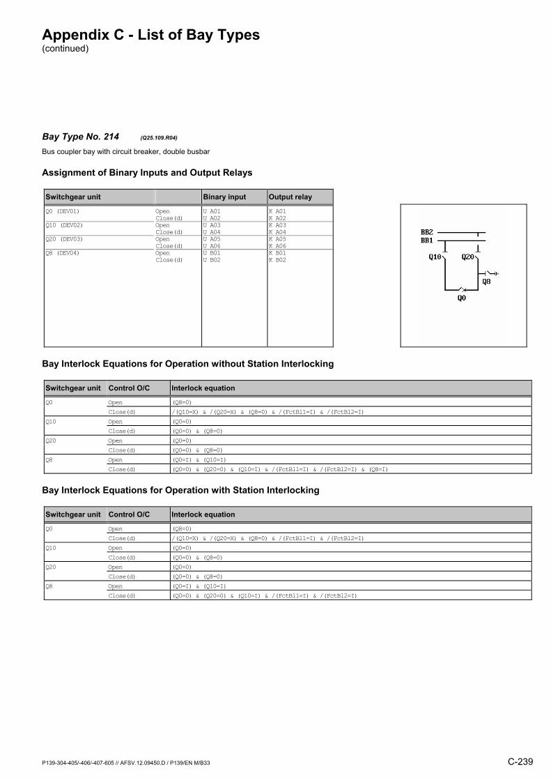
Appendix C - List of Bay Types (continued)
P139-304-405/-406/-407-605 // AFSV.12.09450.D / P139/EN M/B33 C-239
Bay Type No. 214 (Q25.109.R04) Bus coupler bay with circuit breaker, double busbar
Assignment of Binary Inputs and Output Relays
Switchgear unit Binary input Output relay
Q0 (DEV01) Q10 (DEV02) Q20 (DEV03) Q8 (DEV04)
Open Close(d) Open Close(d) Open Close(d) Open Close(d)
U A01 U A02 U A03 U A04 U A05 U A06 U B01 U B02
K A01 K A02K A03 K A04K A05 K A06K B01 K B02
Bay Interlock Equations for Operation without Station Interlocking
Switchgear unit Control O/C Interlock equation
Q0 Open (Q8=0) Close(d) /(Q10=X) & /(Q20=X) & (Q8=0) & /(FctBl1=I) & /(FctBl2=I) Q10 Open (Q0=0) Close(d) (Q0=0) & (Q8=0) Q20 Open (Q0=0) Close(d) (Q0=0) & (Q8=0) Q8 Open (Q0=I) & (Q10=I) Close(d) (Q0=0) & (Q20=0) & (Q10=I) & /(FctBl1=I) & /(FctBl2=I) & (Q8=I)
Bay Interlock Equations for Operation with Station Interlocking
Switchgear unit Control O/C Interlock equation
Q0 Open (Q8=0) Close(d) /(Q10=X) & /(Q20=X) & (Q8=0) & /(FctBl1=I) & /(FctBl2=I) Q10 Open (Q0=0) Close(d) (Q0=0) & (Q8=0) Q20 Open (Q0=0) Close(d) (Q0=0) & (Q8=0) Q8 Open (Q0=I) & (Q10=I) Close(d) (Q0=0) & (Q20=0) & (Q10=I) & /(FctBl1=I) & /(FctBl2=I)

Appendix C - List of Bay Types (continued)
C-240 P139-304-405/-406/-407-605 // AFSV.12.09450.D / P139/EN M/B33
Bay Type No. 240 (Q25.113.M03) Bus coupler bay with circuit breaker, double busbar,direct motor control
Assignment of Binary Inputs and Output Relays
Switchgear unit Binary input Output relay
Q0 (DEV01) Q10 (DEV02) Q20 (DEV03) Q15 (DEV04) Q25 (DEV05) Mot.relay (SIG_1: Signal S012) Shunt wd. (CMD_1: Command C011) Mot.relay (CMD_1: Command C012)
Open Close(d) Open Close(d) Open Close(d) Open Close(d) Open Close(d)
U A01 U A02 U A03 U A04 U A05 U A06 U B01 U B02 U B03 U B04 U B06 / /
K A01 K A02K A03 K A04K A05 K A06/ // //
K B05
K B06
Bay Interlock Equations for Operation without Station Interlocking
Switchgear unit Control O/C Interlock equation
Q0 Open (Q15=0) & (Q25=0) Close(d) /(Q10=X) & /(Q20=X) & (Q15=0) & (Q25=0) & /(FctBl1=I) & /(FctBl2=I) Q10 Open (Q0=0) Close(d) (Q0=0) & (Q15=0) Q20 Open (Q0=0) Close(d) (Q0=0) & (Q25=0)
Bay Interlock Equations for Operation with Station Interlocking
Switchgear unit Control O/C Interlock equation
Q0 Open (Q15=0) & (Q25=0) Close(d) /(Q10=X) & /(Q20=X) & (Q15=0) & (Q25=0) & /(FctBl1=I) & /(FctBl2=I) Q10 Open (Q0=0) Close(d) (Q0=0) & (Q15=0) Q20 Open (Q0=0) Close(d) (Q0=0) & (Q25=0)
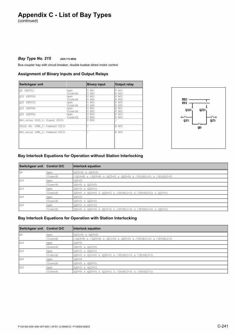
Appendix C - List of Bay Types (continued)
P139-304-405/-406/-407-605 // AFSV.12.09450.D / P139/EN M/B33 C-241
Bay Type No. 215 (Q25.113.M05) Bus coupler bay with circuit breaker, double busbar,direct motor control
Assignment of Binary Inputs and Output Relays
Switchgear unit Binary input Output relay
Q0 (DEV01) Q10 (DEV02) Q20 (DEV03) Q15 (DEV04) Q25 (DEV05) Mot.relay (SIG_1: Signal S012) Shunt wd. (CMD_1: Command C011) Mot.relay (CMD_1: Command C012)
Open Close(d) Open Close(d) Open Close(d) Open Close(d) Open Close(d)
U A01 U A02 U A03 U A04 U A05 U A06 U B01 U B02 U B03 U B04 U B06 / /
K A01 K A02K A03 K A04K A05 K A06K B01 K B02K B03 K B04/
K B05
K B06
Bay Interlock Equations for Operation without Station Interlocking
Switchgear unit Control O/C Interlock equation
Q0 Open (Q15=0) & (Q25=0) Close(d) /(Q10=X) & /(Q20=X) & (Q15=0) & (Q25=0) & /(FctBl1=I) & /(FctBl2=I) Q10 Open (Q0=0) Close(d) (Q0=0) & (Q15=0) Q15 Open (Q0=I) & (Q20=I) Close(d) (Q0=0) & (Q10=0) & (Q20=I) & /(FctBl1=I) & /(FctBl2=I) & (Q15=I) Q20 Open (Q0=0) Close(d) (Q0=0) & (Q25=0) Q25 Open (Q0=I) & (Q10=I) Close(d) (Q0=0) & (Q20=0) & (Q10=I) & /(FctBl1=I) & /(FctBl2=I) & (Q25=I)
Bay Interlock Equations for Operation with Station Interlocking
Switchgear unit Control O/C Interlock equation
Q0 Open (Q15=0) & (Q25=0) Close(d) /(Q10=X) & /(Q20=X) & (Q15=0) & (Q25=0) & /(FctBl1=I) & /(FctBl2=I) Q10 Open (Q0=0) Close(d) (Q0=0) & (Q15=0) Q15 Open (Q0=I) & (Q20=I) Close(d) (Q0=0) & (Q10=0) & (Q20=I) & /(FctBl1=I) & /(FctBl2=I) Q20 Open (Q0=0) Close(d) (Q0=0) & (Q25=0) Q25 Open (Q0=I) & (Q10=I) Close(d) (Q0=0) & (Q20=0) & (Q10=I) & /(FctBl1=I) & /(FctBl2=I)

Appendix C - List of Bay Types (continued)
C-242 P139-304-405/-406/-407-605 // AFSV.12.09450.D / P139/EN M/B33
Bay Type No. 216 (Q25.113.R01) Bus coupler bay with circuit breaker, double busbar
Assignment of Binary Inputs and Output Relays
Switchgear unit Binary input Output relay
Q0 (DEV01) Q10 (DEV02) Q20 (DEV03) Q15 (DEV04) Q25 (DEV05)
Open Close(d) Open Close(d) Open Close(d) Open Close(d) Open Close(d)
U A01 U A02 U A03 U A04 U A05 U A06 U B01 U B02 U B03 U B04
K A01 K A02/ // // // /
Bay Interlock Equations for Operation without Station Interlocking
Switchgear unit Control O/C Interlock equation
Q0 Open (Q15=0) & (Q25=0) Close(d) /(Q10=X) & /(Q20=X) & (Q15=0) & (Q25=0) & /(FctBl1=I) & /(FctBl2=I)
Bay Interlock Equations for Operation with Station Interlocking
Switchgear unit Control O/C Interlock equation
Q0 Open (Q15=0) & (Q25=0) Close(d) /(Q10=X) & /(Q20=X) & (Q15=0) & (Q25=0) & /(FctBl1=I) & /(FctBl2=I)
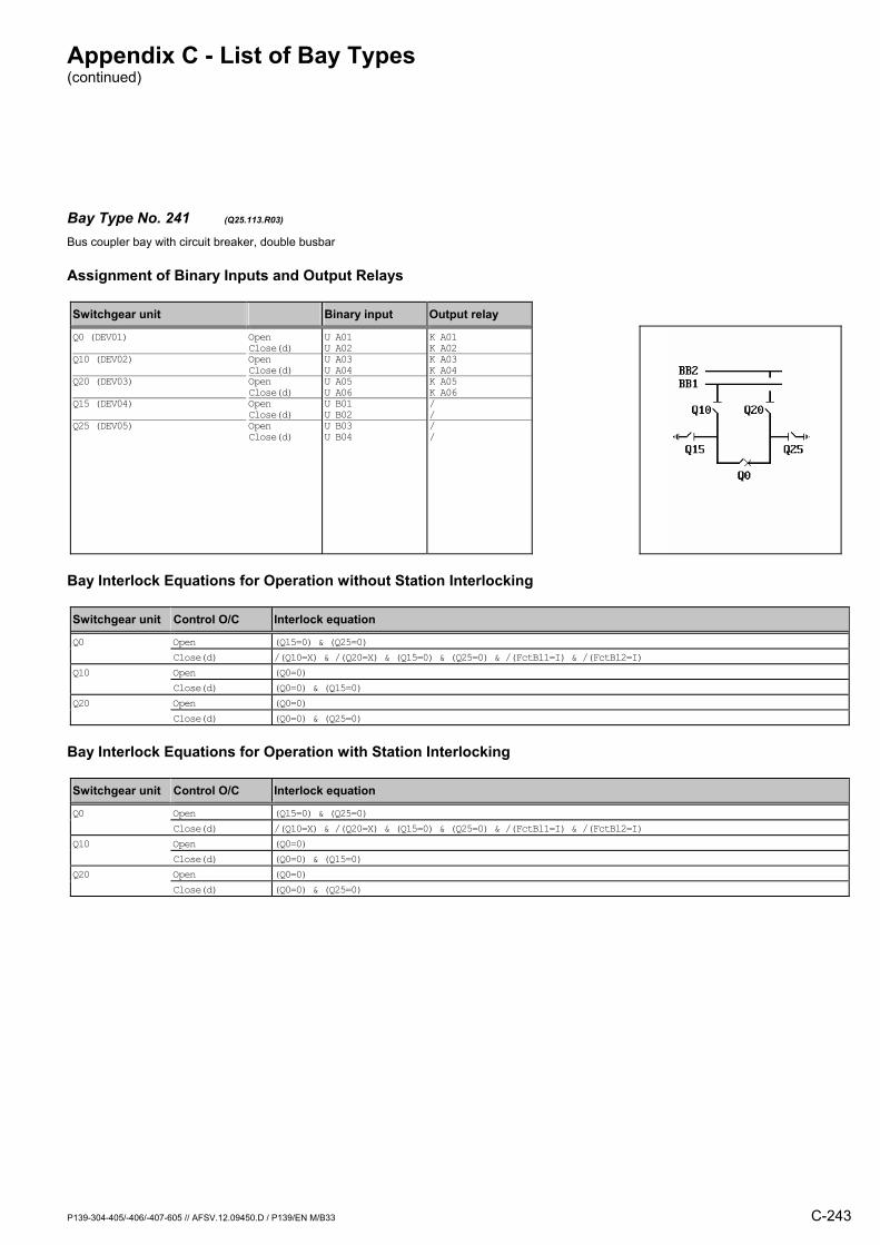
Appendix C - List of Bay Types (continued)
P139-304-405/-406/-407-605 // AFSV.12.09450.D / P139/EN M/B33 C-243
Bay Type No. 241 (Q25.113.R03) Bus coupler bay with circuit breaker, double busbar
Assignment of Binary Inputs and Output Relays
Switchgear unit Binary input Output relay
Q0 (DEV01) Q10 (DEV02) Q20 (DEV03) Q15 (DEV04) Q25 (DEV05)
Open Close(d) Open Close(d) Open Close(d) Open Close(d) Open Close(d)
U A01 U A02 U A03 U A04 U A05 U A06 U B01 U B02 U B03 U B04
K A01 K A02K A03 K A04K A05 K A06/ // /
Bay Interlock Equations for Operation without Station Interlocking
Switchgear unit Control O/C Interlock equation
Q0 Open (Q15=0) & (Q25=0) Close(d) /(Q10=X) & /(Q20=X) & (Q15=0) & (Q25=0) & /(FctBl1=I) & /(FctBl2=I) Q10 Open (Q0=0) Close(d) (Q0=0) & (Q15=0) Q20 Open (Q0=0) Close(d) (Q0=0) & (Q25=0)
Bay Interlock Equations for Operation with Station Interlocking
Switchgear unit Control O/C Interlock equation
Q0 Open (Q15=0) & (Q25=0) Close(d) /(Q10=X) & /(Q20=X) & (Q15=0) & (Q25=0) & /(FctBl1=I) & /(FctBl2=I) Q10 Open (Q0=0) Close(d) (Q0=0) & (Q15=0) Q20 Open (Q0=0) Close(d) (Q0=0) & (Q25=0)
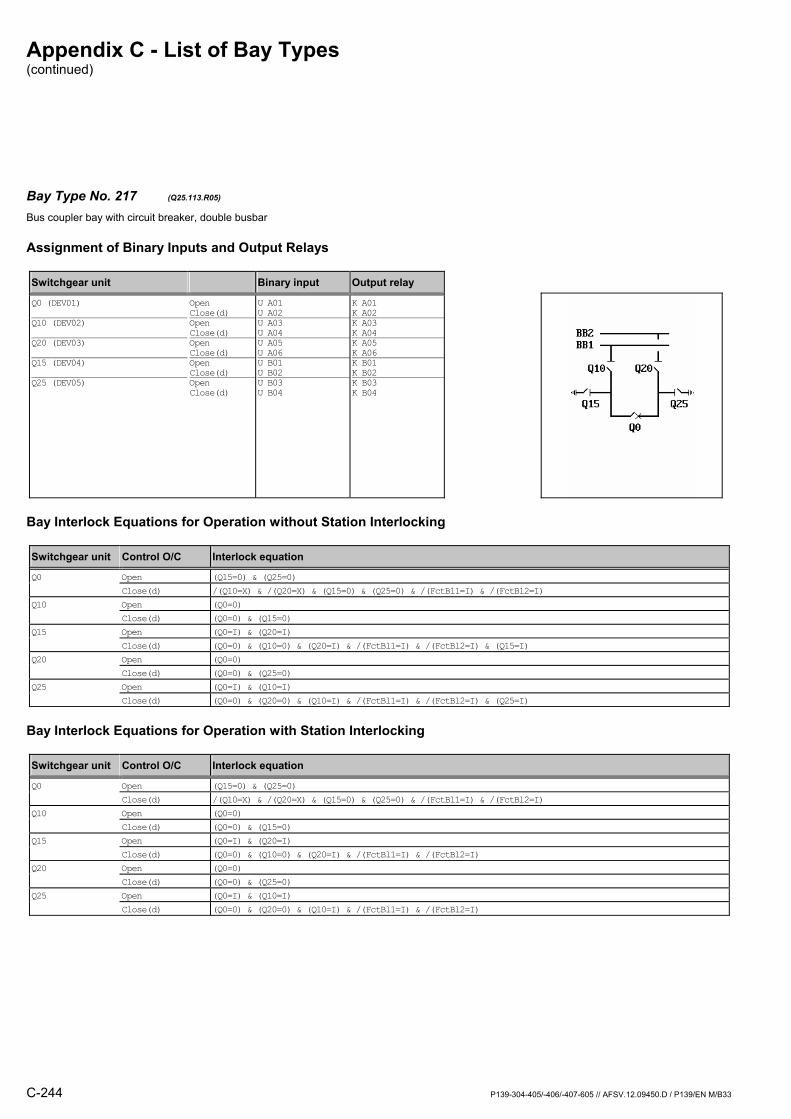
Appendix C - List of Bay Types (continued)
C-244 P139-304-405/-406/-407-605 // AFSV.12.09450.D / P139/EN M/B33
Bay Type No. 217 (Q25.113.R05) Bus coupler bay with circuit breaker, double busbar
Assignment of Binary Inputs and Output Relays
Switchgear unit Binary input Output relay
Q0 (DEV01) Q10 (DEV02) Q20 (DEV03) Q15 (DEV04) Q25 (DEV05)
Open Close(d) Open Close(d) Open Close(d) Open Close(d) Open Close(d)
U A01 U A02 U A03 U A04 U A05 U A06 U B01 U B02 U B03 U B04
K A01 K A02K A03 K A04K A05 K A06K B01 K B02K B03 K B04
Bay Interlock Equations for Operation without Station Interlocking
Switchgear unit Control O/C Interlock equation
Q0 Open (Q15=0) & (Q25=0) Close(d) /(Q10=X) & /(Q20=X) & (Q15=0) & (Q25=0) & /(FctBl1=I) & /(FctBl2=I) Q10 Open (Q0=0) Close(d) (Q0=0) & (Q15=0) Q15 Open (Q0=I) & (Q20=I) Close(d) (Q0=0) & (Q10=0) & (Q20=I) & /(FctBl1=I) & /(FctBl2=I) & (Q15=I) Q20 Open (Q0=0) Close(d) (Q0=0) & (Q25=0) Q25 Open (Q0=I) & (Q10=I) Close(d) (Q0=0) & (Q20=0) & (Q10=I) & /(FctBl1=I) & /(FctBl2=I) & (Q25=I)
Bay Interlock Equations for Operation with Station Interlocking
Switchgear unit Control O/C Interlock equation
Q0 Open (Q15=0) & (Q25=0) Close(d) /(Q10=X) & /(Q20=X) & (Q15=0) & (Q25=0) & /(FctBl1=I) & /(FctBl2=I) Q10 Open (Q0=0) Close(d) (Q0=0) & (Q15=0) Q15 Open (Q0=I) & (Q20=I) Close(d) (Q0=0) & (Q10=0) & (Q20=I) & /(FctBl1=I) & /(FctBl2=I) Q20 Open (Q0=0) Close(d) (Q0=0) & (Q25=0) Q25 Open (Q0=I) & (Q10=I) Close(d) (Q0=0) & (Q20=0) & (Q10=I) & /(FctBl1=I) & /(FctBl2=I)
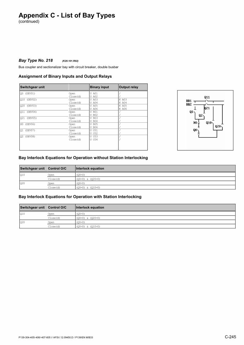
Appendix C - List of Bay Types (continued)
P139-304-405/-406/-407-605 // AFSV.12.09450.D / P139/EN M/B33 C-245
Bay Type No. 218 (K29.101.R02) Bus coupler and sectionalizer bay with circuit breaker, double busbar
Assignment of Binary Inputs and Output Relays
Switchgear unit Binary input Output relay
Q0 (DEV01) Q10 (DEV02) Q20 (DEV03) Q11 (DEV04) Q21 (DEV05) X0 (DEV06) Q1 (DEV07) Q2 (DEV08)
Open Close(d) Open Close(d) Open Close(d) Open Close(d) Open Close(d) Open Close(d) Open Close(d) Open Close(d)
U A01 U A02 U A03 U A04 U A05 U A06 U B01 U B02 U B03 U B04 U B05 U B06 U C01 U C02 U C03 U C04
/ /K A03 K A04K A05 K A06/ // // // // /
Bay Interlock Equations for Operation without Station Interlocking
Switchgear unit Control O/C Interlock equation
Q10 Open (Q0=0) Close(d) (Q0=0) & (Q20=0) Q20 Open (Q0=0) Close(d) (Q0=0) & (Q10=0)
Bay Interlock Equations for Operation with Station Interlocking
Switchgear unit Control O/C Interlock equation
Q10 Open (Q0=0) Close(d) (Q0=0) & (Q20=0) Q20 Open (Q0=0) Close(d) (Q0=0) & (Q10=0)
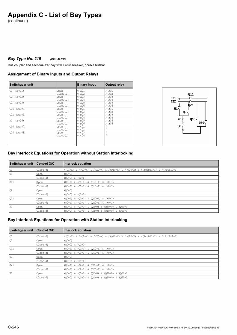
Appendix C - List of Bay Types (continued)
C-246 P139-304-405/-406/-407-605 // AFSV.12.09450.D / P139/EN M/B33
Bay Type No. 219 (K29.101.R06) Bus coupler and sectionalizer bay with circuit breaker, double busbar
Assignment of Binary Inputs and Output Relays
Switchgear unit Binary input Output relay
Q0 (DEV01) Q1 (DEV02) Q2 (DEV03) Q11 (DEV04) Q21 (DEV05) X0 (DEV06) Q10 (DEV07) Q20 (DEV08)
Open Close(d) Open Close(d) Open Close(d) Open Close(d) Open Close(d) Open Close(d) Open Close(d) Open Close(d)
U A01 U A02 U A03 U A04 U A05 U A06 U B01 U B02 U B03 U B04 U B05 U B06 U C01 U C02 U C03 U C04
K A01 K A02K A03 K A04K A05 K A06K B01 K B02K B03 K B04K B05 K B06/ // /
Bay Interlock Equations for Operation without Station Interlocking
Switchgear unit Control O/C Interlock equation
Q0 Close(d) /(Q1=X) & /(Q2=X) & /(X0=X) & /(Q10=X) & /(Q20=X) & /(FctBl1=I) & /(FctBl2=I) Q1 Open (Q0=0) Close(d) (Q0=0) & (Q2=0) Q11 Open (Q0=I) & (Q1=I) & (Q10=I) & (X0=I) Close(d) (Q0=I) & (Q1=I) & (Q10=I) & (X0=I) Q2 Open (Q0=0) Close(d) (Q0=0) & (Q1=0) Q21 Open (Q0=I) & (Q2=I) & (Q20=I) & (X0=I) Close(d) (Q0=I) & (Q2=I) & (Q20=I) & (X0=I) X0 Open (Q0=0) & (Q1=0) & (Q2=0) & (Q10=0) & (Q20=0) Close(d) (Q0=0) & (Q1=0) & (Q2=0) & (Q10=0) & (Q20=0)
Bay Interlock Equations for Operation with Station Interlocking
Switchgear unit Control O/C Interlock equation
Q0 Close(d) /(Q1=X) & /(Q2=X) & /(X0=X) & /(Q10=X) & /(Q20=X) & /(FctBl1=I) & /(FctBl2=I) Q1 Open (Q0=0) Close(d) (Q0=0) & (Q2=0) Q11 Open (Q0=I) & (Q1=I) & (Q10=I) & (X0=I) Close(d) (Q0=I) & (Q1=I) & (Q10=I) & (X0=I) Q2 Open (Q0=0) Close(d) (Q0=0) & (Q1=0) Q21 Open (Q0=I) & (Q2=I) & (Q20=I) & (X0=I) Close(d) (Q0=I) & (Q2=I) & (Q20=I) & (X0=I) X0 Open (Q0=0) & (Q1=0) & (Q2=0) & (Q10=0) & (Q20=0) Close(d) (Q0=0) & (Q1=0) & (Q2=0) & (Q10=0) & (Q20=0)
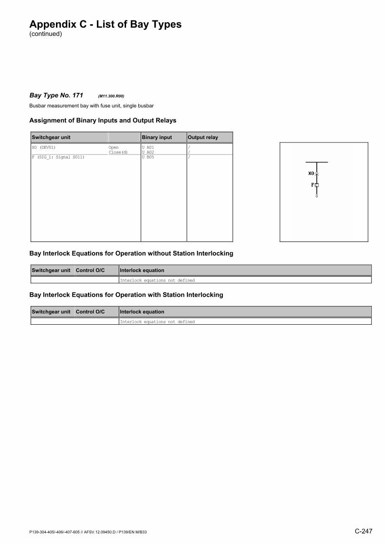
Appendix C - List of Bay Types (continued)
P139-304-405/-406/-407-605 // AFSV.12.09450.D / P139/EN M/B33 C-247
Bay Type No. 171 (M11.300.R00) Busbar measurement bay with fuse unit, single busbar
Assignment of Binary Inputs and Output Relays
Switchgear unit Binary input Output relay
X0 (DEV01) F (SIG_1: Signal S011)
Open Close(d)
U A01 U A02 U B05
/ //
Bay Interlock Equations for Operation without Station Interlocking
Switchgear unit Control O/C Interlock equation
Interlock equations not defined
Bay Interlock Equations for Operation with Station Interlocking
Switchgear unit Control O/C Interlock equation
Interlock equations not defined

Appendix C - List of Bay Types (continued)
C-248 P139-304-405/-406/-407-605 // AFSV.12.09450.D / P139/EN M/B33
Bay Type No. 172 (M11.300.R01) Busbar measurement bay with fuse unit, single busbar
Assignment of Binary Inputs and Output Relays
Switchgear unit Binary input Output relay
X0 (DEV01) F (SIG_1: Signal S011)
Open Close(d)
U A01 U A02 U B05
K A01 K A02/
Bay Interlock Equations for Operation without Station Interlocking
Switchgear unit Control O/C Interlock equation
Interlock equations not defined
Bay Interlock Equations for Operation with Station Interlocking
Switchgear unit Control O/C Interlock equation
Interlock equations not defined
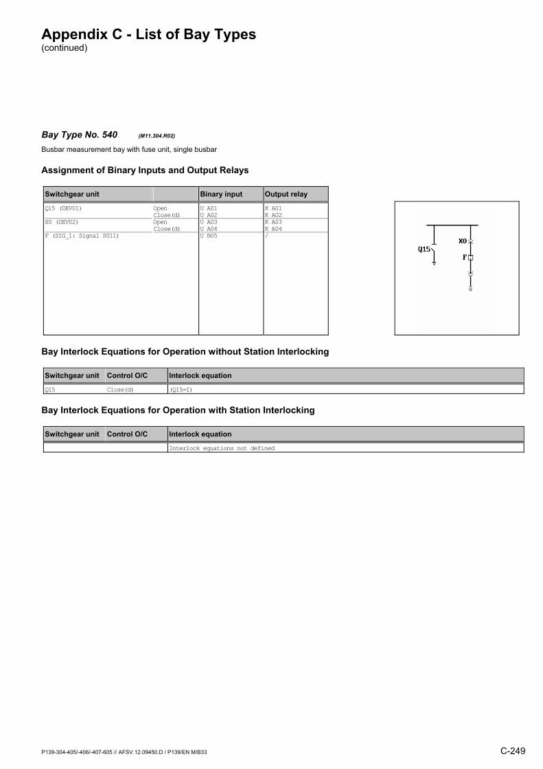
Appendix C - List of Bay Types (continued)
P139-304-405/-406/-407-605 // AFSV.12.09450.D / P139/EN M/B33 C-249
Bay Type No. 540 (M11.304.R02) Busbar measurement bay with fuse unit, single busbar
Assignment of Binary Inputs and Output Relays
Switchgear unit Binary input Output relay
Q15 (DEV01) X0 (DEV02) F (SIG_1: Signal S011)
Open Close(d) Open Close(d)
U A01 U A02 U A03 U A04 U B05
K A01 K A02K A03 K A04/
Bay Interlock Equations for Operation without Station Interlocking
Switchgear unit Control O/C Interlock equation
Q15 Close(d) (Q15=I)
Bay Interlock Equations for Operation with Station Interlocking
Switchgear unit Control O/C Interlock equation
Interlock equations not defined

Appendix C - List of Bay Types (continued)
C-250 P139-304-405/-406/-407-605 // AFSV.12.09450.D / P139/EN M/B33
Bay Type No. 173 (M11.900.R00) Busbar measurement bay with other switchgear unit, single busbar
Assignment of Binary Inputs and Output Relays
Switchgear unit Binary input Output relay
X0 (DEV01)
Open Close(d)
U A01 U A02
/ /
Bay Interlock Equations for Operation without Station Interlocking
Switchgear unit Control O/C Interlock equation
Interlock equations not defined
Bay Interlock Equations for Operation with Station Interlocking
Switchgear unit Control O/C Interlock equation
Interlock equations not defined

Appendix C - List of Bay Types (continued)
P139-304-405/-406/-407-605 // AFSV.12.09450.D / P139/EN M/B33 C-251
Bay Type No. 174 (M11.900.R01) Busbar measurement bay with other switchgear unit, single busbar
Assignment of Binary Inputs and Output Relays
Switchgear unit Binary input Output relay
X0 (DEV01)
Open Close(d)
U A01 U A02
K A01 K A02
Bay Interlock Equations for Operation without Station Interlocking
Switchgear unit Control O/C Interlock equation
Interlock equations not defined
Bay Interlock Equations for Operation with Station Interlocking
Switchgear unit Control O/C Interlock equation
Interlock equations not defined

Appendix C - List of Bay Types (continued)
C-252 P139-304-405/-406/-407-605 // AFSV.12.09450.D / P139/EN M/B33
Bay Type No. 175 (M13.312.M02) Busbar measurement bay with fuse unit, single busbar,direct motor control
Assignment of Binary Inputs and Output Relays
Switchgear unit Binary input Output relay
Q1 (DEV01) Q15 (DEV02) F (SIG_1: Signal S011) Mot.relay (SIG_1: Signal S012) Shunt wd. (CMD_1: Command C011) Mot.relay (CMD_1: Command C012)
Open Close(d) Open Close(d)
U A01 U A02 U A03 U A04 U B05 U B06 / /
K A01 K A02K A03 K A04/
/
K B05
K B06
Bay Interlock Equations for Operation without Station Interlocking
Switchgear unit Control O/C Interlock equation
Q15 Close(d) (Q15=I)
Bay Interlock Equations for Operation with Station Interlocking
Switchgear unit Control O/C Interlock equation
Interlock equations not defined

Appendix C - List of Bay Types (continued)
P139-304-405/-406/-407-605 // AFSV.12.09450.D / P139/EN M/B33 C-253
Bay Type No. 176 (M13.312.R01) Busbar measurement bay with fuse unit, single busbar
Assignment of Binary Inputs and Output Relays
Switchgear unit Binary input Output relay
Q1 (DEV01) Q15 (DEV02) F (SIG_1: Signal S011)
Open Close(d) Open Close(d)
U A01 U A02 U A03 U A04 U B05
K A01 K A02/ //
Bay Interlock Equations for Operation without Station Interlocking
Switchgear unit Control O/C Interlock equation
Interlock equations not defined
Bay Interlock Equations for Operation with Station Interlocking
Switchgear unit Control O/C Interlock equation
Interlock equations not defined

Appendix C - List of Bay Types (continued)
C-254 P139-304-405/-406/-407-605 // AFSV.12.09450.D / P139/EN M/B33
Bay Type No. 177 (M13.312.R02) Busbar measurement bay with fuse unit, single busbar
Assignment of Binary Inputs and Output Relays
Switchgear unit Binary input Output relay
Q1 (DEV01) Q15 (DEV02) F (SIG_1: Signal S011)
Open Close(d) Open Close(d)
U A01 U A02 U A03 U A04 U B05
K A01 K A02K A03 K A04/
Bay Interlock Equations for Operation without Station Interlocking
Switchgear unit Control O/C Interlock equation
Q15 Close(d) (Q15=I)
Bay Interlock Equations for Operation with Station Interlocking
Switchgear unit Control O/C Interlock equation
Interlock equations not defined

Appendix C - List of Bay Types (continued)
P139-304-405/-406/-407-605 // AFSV.12.09450.D / P139/EN M/B33 C-255
Bay Type No. 506 (M13.902.R00) Busbar measurement bay with other switchgear unit, single busbar
Assignment of Binary Inputs and Output Relays
Switchgear unit Binary input Output relay
Q1 (DEV01)
Open Close(d)
U A01 U A02
/ /
Bay Interlock Equations for Operation without Station Interlocking
Switchgear unit Control O/C Interlock equation
Interlock equations not defined
Bay Interlock Equations for Operation with Station Interlocking
Switchgear unit Control O/C Interlock equation
Interlock equations not defined
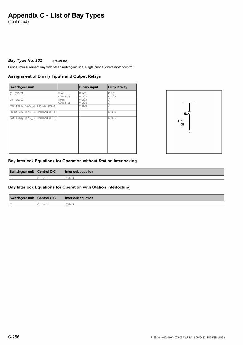
Appendix C - List of Bay Types (continued)
C-256 P139-304-405/-406/-407-605 // AFSV.12.09450.D / P139/EN M/B33
Bay Type No. 232 (M15.903.M01) Busbar measurement bay with other switchgear unit, single busbar,direct motor control
Assignment of Binary Inputs and Output Relays
Switchgear unit Binary input Output relay
Q1 (DEV01) Q8 (DEV02) Mot.relay (SIG_1: Signal S012) Shunt wd. (CMD_1: Command C011) Mot.relay (CMD_1: Command C012)
Open Close(d) Open Close(d)
U A01 U A02 U A03 U A04 U B06 / /
K A01 K A02/ //
K B05
K B06
Bay Interlock Equations for Operation without Station Interlocking
Switchgear unit Control O/C Interlock equation
Q1 Close(d) (Q8=0)
Bay Interlock Equations for Operation with Station Interlocking
Switchgear unit Control O/C Interlock equation
Q1 Close(d) (Q8=0)
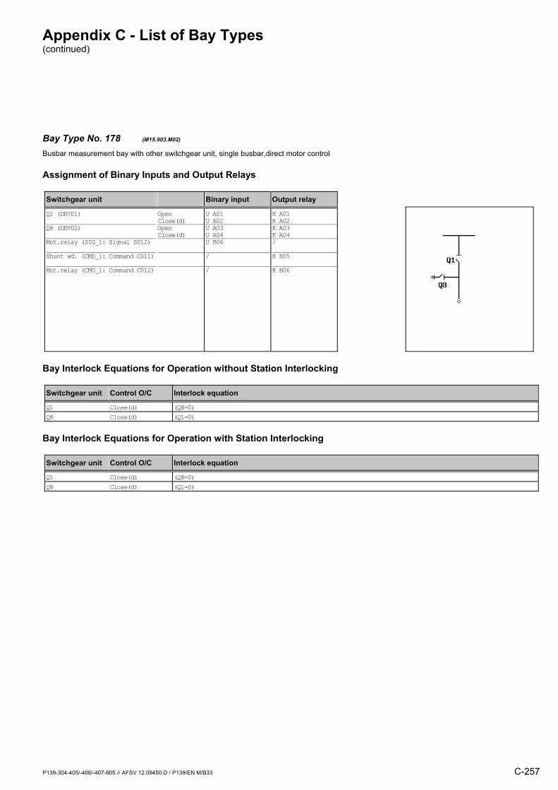
Appendix C - List of Bay Types (continued)
P139-304-405/-406/-407-605 // AFSV.12.09450.D / P139/EN M/B33 C-257
Bay Type No. 178 (M15.903.M02) Busbar measurement bay with other switchgear unit, single busbar,direct motor control
Assignment of Binary Inputs and Output Relays
Switchgear unit Binary input Output relay
Q1 (DEV01) Q8 (DEV02) Mot.relay (SIG_1: Signal S012) Shunt wd. (CMD_1: Command C011) Mot.relay (CMD_1: Command C012)
Open Close(d) Open Close(d)
U A01 U A02 U A03 U A04 U B06 / /
K A01 K A02K A03 K A04/
K B05
K B06
Bay Interlock Equations for Operation without Station Interlocking
Switchgear unit Control O/C Interlock equation
Q1 Close(d) (Q8=0) Q8 Close(d) (Q1=0)
Bay Interlock Equations for Operation with Station Interlocking
Switchgear unit Control O/C Interlock equation
Q1 Close(d) (Q8=0) Q8 Close(d) (Q1=0)
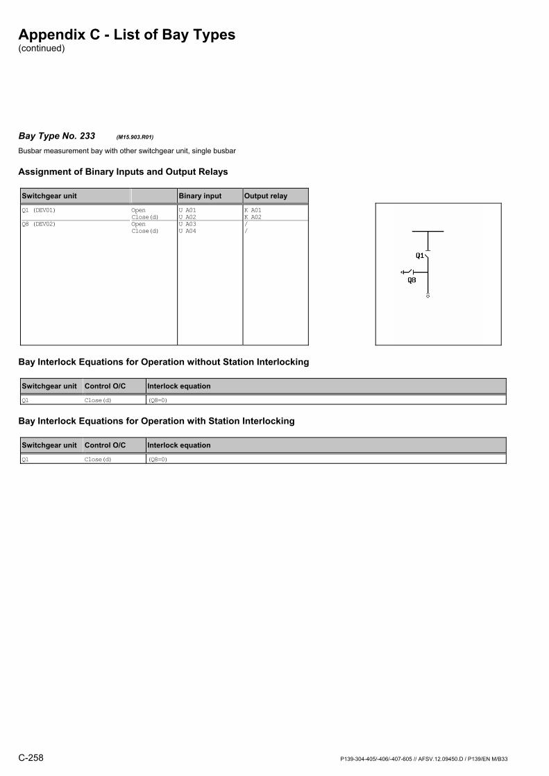
Appendix C - List of Bay Types (continued)
C-258 P139-304-405/-406/-407-605 // AFSV.12.09450.D / P139/EN M/B33
Bay Type No. 233 (M15.903.R01) Busbar measurement bay with other switchgear unit, single busbar
Assignment of Binary Inputs and Output Relays
Switchgear unit Binary input Output relay
Q1 (DEV01) Q8 (DEV02)
Open Close(d) Open Close(d)
U A01 U A02 U A03 U A04
K A01 K A02/ /
Bay Interlock Equations for Operation without Station Interlocking
Switchgear unit Control O/C Interlock equation
Q1 Close(d) (Q8=0)
Bay Interlock Equations for Operation with Station Interlocking
Switchgear unit Control O/C Interlock equation
Q1 Close(d) (Q8=0)
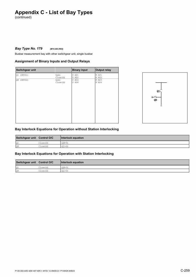
Appendix C - List of Bay Types (continued)
P139-304-405/-406/-407-605 // AFSV.12.09450.D / P139/EN M/B33 C-259
Bay Type No. 179 (M15.903.R02) Busbar measurement bay with other switchgear unit, single busbar
Assignment of Binary Inputs and Output Relays
Switchgear unit Binary input Output relay
Q1 (DEV01) Q8 (DEV02)
Open Close(d) Open Close(d)
U A01 U A02 U A03 U A04
K A01 K A02K A03 K A04
Bay Interlock Equations for Operation without Station Interlocking
Switchgear unit Control O/C Interlock equation
Q1 Close(d) (Q8=0) Q8 Close(d) (Q1=0)
Bay Interlock Equations for Operation with Station Interlocking
Switchgear unit Control O/C Interlock equation
Q1 Close(d) (Q8=0) Q8 Close(d) (Q1=0)
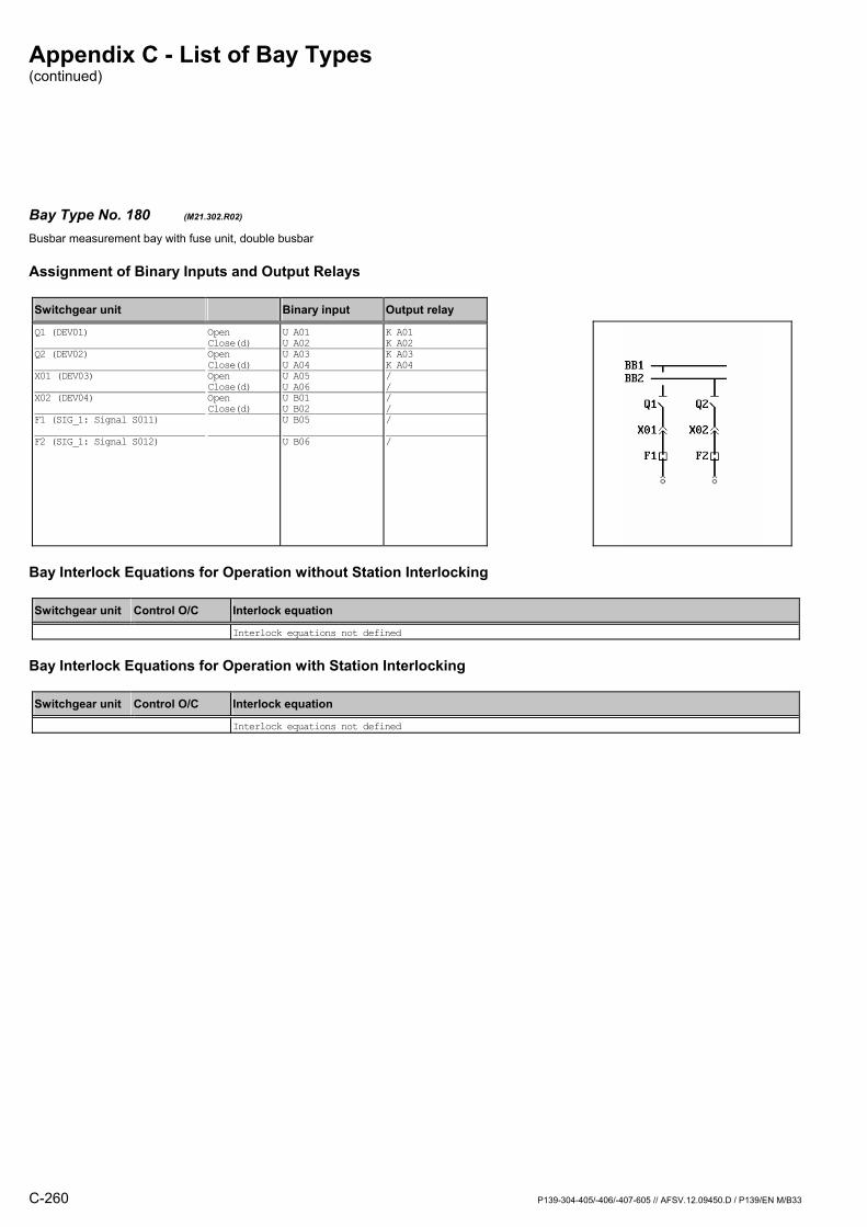
Appendix C - List of Bay Types (continued)
C-260 P139-304-405/-406/-407-605 // AFSV.12.09450.D / P139/EN M/B33
Bay Type No. 180 (M21.302.R02) Busbar measurement bay with fuse unit, double busbar
Assignment of Binary Inputs and Output Relays
Switchgear unit Binary input Output relay
Q1 (DEV01) Q2 (DEV02) X01 (DEV03) X02 (DEV04) F1 (SIG_1: Signal S011) F2 (SIG_1: Signal S012)
Open Close(d) Open Close(d) Open Close(d) Open Close(d)
U A01 U A02 U A03 U A04 U A05 U A06 U B01 U B02 U B05 U B06
K A01 K A02K A03 K A04/ // //
/
Bay Interlock Equations for Operation without Station Interlocking
Switchgear unit Control O/C Interlock equation
Interlock equations not defined
Bay Interlock Equations for Operation with Station Interlocking
Switchgear unit Control O/C Interlock equation
Interlock equations not defined
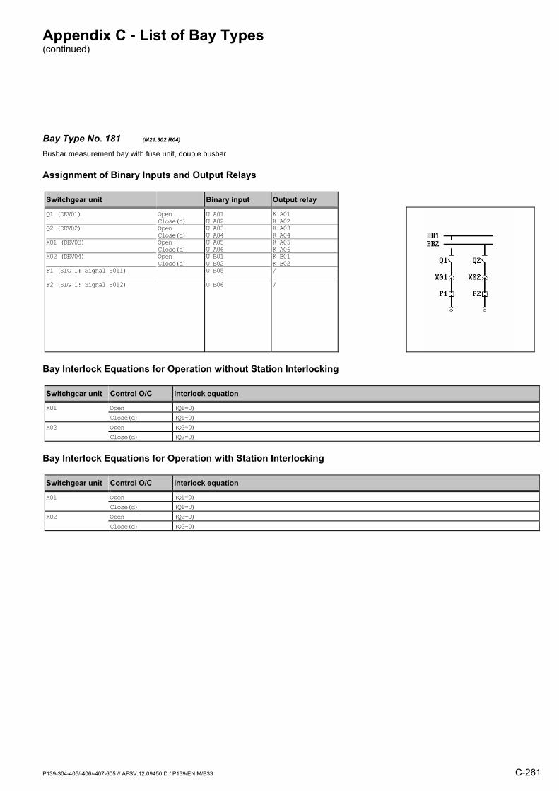
Appendix C - List of Bay Types (continued)
P139-304-405/-406/-407-605 // AFSV.12.09450.D / P139/EN M/B33 C-261
Bay Type No. 181 (M21.302.R04) Busbar measurement bay with fuse unit, double busbar
Assignment of Binary Inputs and Output Relays
Switchgear unit Binary input Output relay
Q1 (DEV01) Q2 (DEV02) X01 (DEV03) X02 (DEV04) F1 (SIG_1: Signal S011) F2 (SIG_1: Signal S012)
Open Close(d) Open Close(d) Open Close(d) Open Close(d)
U A01 U A02 U A03 U A04 U A05 U A06 U B01 U B02 U B05 U B06
K A01 K A02K A03 K A04K A05 K A06K B01 K B02/
/
Bay Interlock Equations for Operation without Station Interlocking
Switchgear unit Control O/C Interlock equation
X01 Open (Q1=0) Close(d) (Q1=0) X02 Open (Q2=0) Close(d) (Q2=0)
Bay Interlock Equations for Operation with Station Interlocking
Switchgear unit Control O/C Interlock equation
X01 Open (Q1=0) Close(d) (Q1=0) X02 Open (Q2=0) Close(d) (Q2=0)
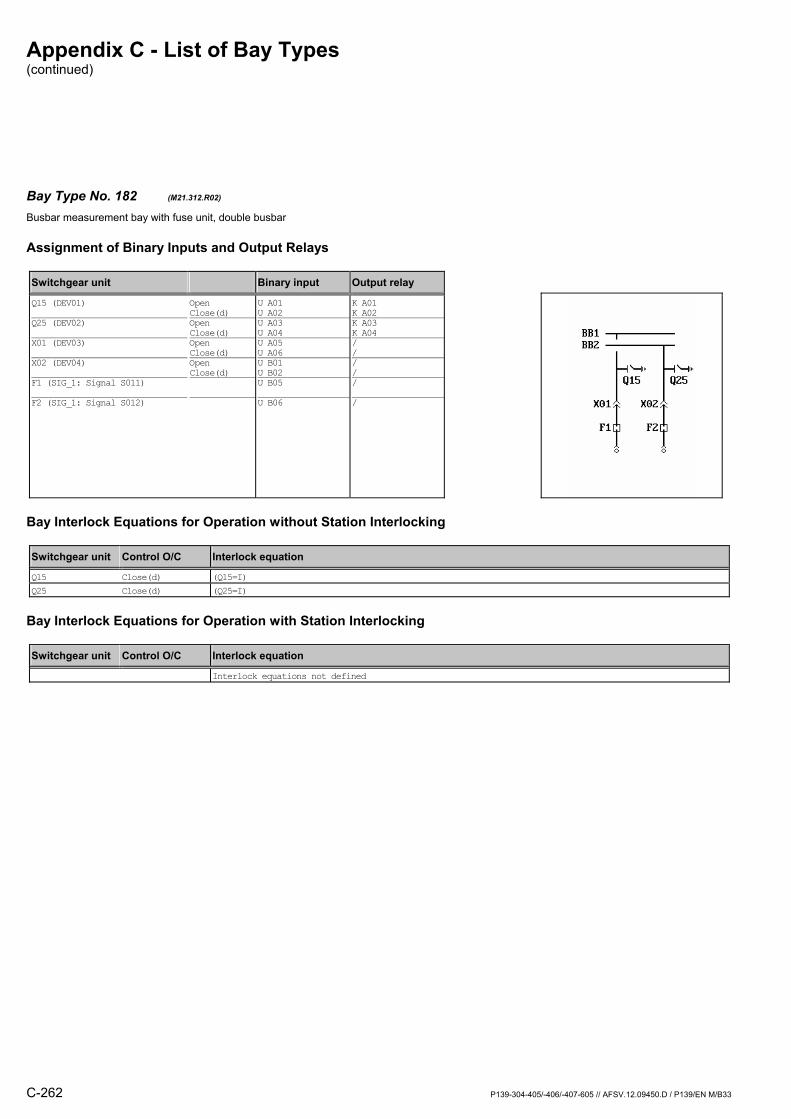
Appendix C - List of Bay Types (continued)
C-262 P139-304-405/-406/-407-605 // AFSV.12.09450.D / P139/EN M/B33
Bay Type No. 182 (M21.312.R02) Busbar measurement bay with fuse unit, double busbar
Assignment of Binary Inputs and Output Relays
Switchgear unit Binary input Output relay
Q15 (DEV01) Q25 (DEV02) X01 (DEV03) X02 (DEV04) F1 (SIG_1: Signal S011) F2 (SIG_1: Signal S012)
Open Close(d) Open Close(d) Open Close(d) Open Close(d)
U A01 U A02 U A03 U A04 U A05 U A06 U B01 U B02 U B05 U B06
K A01 K A02K A03 K A04/ // //
/
Bay Interlock Equations for Operation without Station Interlocking
Switchgear unit Control O/C Interlock equation
Q15 Close(d) (Q15=I) Q25 Close(d) (Q25=I)
Bay Interlock Equations for Operation with Station Interlocking
Switchgear unit Control O/C Interlock equation
Interlock equations not defined
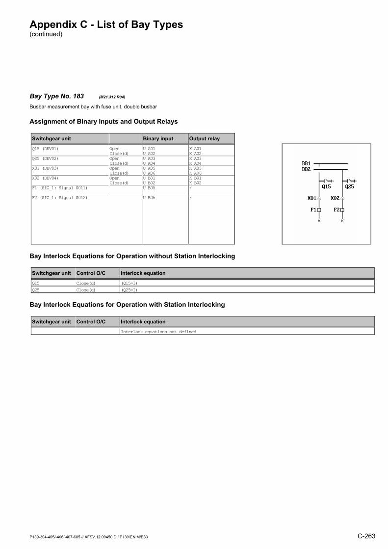
Appendix C - List of Bay Types (continued)
P139-304-405/-406/-407-605 // AFSV.12.09450.D / P139/EN M/B33 C-263
Bay Type No. 183 (M21.312.R04) Busbar measurement bay with fuse unit, double busbar
Assignment of Binary Inputs and Output Relays
Switchgear unit Binary input Output relay
Q15 (DEV01) Q25 (DEV02) X01 (DEV03) X02 (DEV04) F1 (SIG_1: Signal S011) F2 (SIG_1: Signal S012)
Open Close(d) Open Close(d) Open Close(d) Open Close(d)
U A01 U A02 U A03 U A04 U A05 U A06 U B01 U B02 U B05 U B06
K A01 K A02K A03 K A04K A05 K A06K B01 K B02/
/
Bay Interlock Equations for Operation without Station Interlocking
Switchgear unit Control O/C Interlock equation
Q15 Close(d) (Q15=I) Q25 Close(d) (Q25=I)
Bay Interlock Equations for Operation with Station Interlocking
Switchgear unit Control O/C Interlock equation
Interlock equations not defined

Appendix C - List of Bay Types (continued)
C-264 P139-304-405/-406/-407-605 // AFSV.12.09450.D / P139/EN M/B33
Bay Type No. 184 (M21.902.R02) Busbar measurement bay with other switchgear unit, double busbar
Assignment of Binary Inputs and Output Relays
Switchgear unit Binary input Output relay
Q1 (DEV01) Q2 (DEV02) X01 (DEV03) X02 (DEV04)
Open Close(d) Open Close(d) Open Close(d) Open Close(d)
U A01 U A02 U A03 U A04 U A05 U A06 U B01 U B02
K A01 K A02K A03 K A04/ // /
Bay Interlock Equations for Operation without Station Interlocking
Switchgear unit Control O/C Interlock equation
Interlock equations not defined
Bay Interlock Equations for Operation with Station Interlocking
Switchgear unit Control O/C Interlock equation
Interlock equations not defined

Appendix C - List of Bay Types (continued)
P139-304-405/-406/-407-605 // AFSV.12.09450.D / P139/EN M/B33 C-265
Bay Type No. 185 (M21.902.R04) Busbar measurement bay with other switchgear unit, double busbar
Assignment of Binary Inputs and Output Relays
Switchgear unit Binary input Output relay
Q1 (DEV01) Q2 (DEV02) X01 (DEV03) X02 (DEV04)
Open Close(d) Open Close(d) Open Close(d) Open Close(d)
U A01 U A02 U A03 U A04 U A05 U A06 U B01 U B02
K A01 K A02K A03 K A04K A05 K A06K B01 K B02
Bay Interlock Equations for Operation without Station Interlocking
Switchgear unit Control O/C Interlock equation
X01 Open (Q1=0) Close(d) (Q1=0) X02 Open (Q2=0) Close(d) (Q2=0)
Bay Interlock Equations for Operation with Station Interlocking
Switchgear unit Control O/C Interlock equation
X01 Open (Q1=0) Close(d) (Q1=0) X02 Open (Q2=0) Close(d) (Q2=0)

Appendix C - List of Bay Types (continued)
C-266 P139-304-405/-406/-407-605 // AFSV.12.09450.D / P139/EN M/B33
Bay Type No. 186 (M21.912.R02) Busbar measurement bay with other switchgear unit, double busbar
Assignment of Binary Inputs and Output Relays
Switchgear unit Binary input Output relay
Q15 (DEV01) Q25 (DEV02) X01 (DEV03) X02 (DEV04)
Open Close(d) Open Close(d) Open Close(d) Open Close(d)
U A01 U A02 U A03 U A04 U A05 U A06 U B01 U B02
K A01 K A02K A03 K A04/ // /
Bay Interlock Equations for Operation without Station Interlocking
Switchgear unit Control O/C Interlock equation
Q15 Close(d) (Q15=I) Q25 Close(d) (Q25=I)
Bay Interlock Equations for Operation with Station Interlocking
Switchgear unit Control O/C Interlock equation
Interlock equations not defined

Appendix C - List of Bay Types (continued)
P139-304-405/-406/-407-605 // AFSV.12.09450.D / P139/EN M/B33 C-267
Bay Type No. 187 (M21.912.R04) Busbar measurement bay with other switchgear unit, double busbar
Assignment of Binary Inputs and Output Relays
Switchgear unit Binary input Output relay
Q15 (DEV01) Q25 (DEV02) X01 (DEV03) X02 (DEV04)
Open Close(d) Open Close(d) Open Close(d) Open Close(d)
U A01 U A02 U A03 U A04 U A05 U A06 U B01 U B02
K A01 K A02K A03 K A04K A05 K A06K B01 K B02
Bay Interlock Equations for Operation without Station Interlocking
Switchgear unit Control O/C Interlock equation
Q15 Close(d) (Q15=I) Q25 Close(d) (Q25=I)
Bay Interlock Equations for Operation with Station Interlocking
Switchgear unit Control O/C Interlock equation
Interlock equations not defined
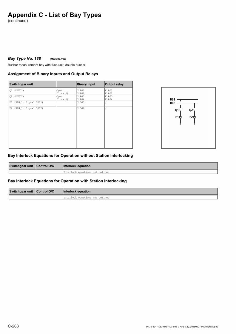
Appendix C - List of Bay Types (continued)
C-268 P139-304-405/-406/-407-605 // AFSV.12.09450.D / P139/EN M/B33
Bay Type No. 188 (M23.302.R02) Busbar measurement bay with fuse unit, double busbar
Assignment of Binary Inputs and Output Relays
Switchgear unit Binary input Output relay
Q1 (DEV01) Q2 (DEV02) F1 (SIG_1: Signal S011) F2 (SIG_1: Signal S012)
Open Close(d) Open Close(d)
U A01 U A02 U A03 U A04 U B05 U B06
K A01 K A02K A03 K A04/
/
Bay Interlock Equations for Operation without Station Interlocking
Switchgear unit Control O/C Interlock equation
Interlock equations not defined
Bay Interlock Equations for Operation with Station Interlocking
Switchgear unit Control O/C Interlock equation
Interlock equations not defined

Appendix C - List of Bay Types (continued)
P139-304-405/-406/-407-605 // AFSV.12.09450.D / P139/EN M/B33 C-269
Bay Type No. 189 (M23.312.R02) Busbar measurement bay with fuse unit, double busbar
Assignment of Binary Inputs and Output Relays
Switchgear unit Binary input Output relay
Q15 (DEV01) Q25 (DEV02) F1 (SIG_1: Signal S011) F2 (SIG_1: Signal S012)
Open Close(d) Open Close(d)
U A01 U A02 U A03 U A04 U B05 U B06
K A01 K A02K A03 K A04/
/
Bay Interlock Equations for Operation without Station Interlocking
Switchgear unit Control O/C Interlock equation
Q15 Close(d) (Q15=I) Q25 Close(d) (Q25=I)
Bay Interlock Equations for Operation with Station Interlocking
Switchgear unit Control O/C Interlock equation
Interlock equations not defined
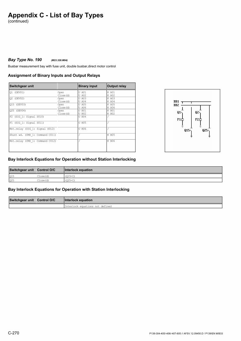
Appendix C - List of Bay Types (continued)
C-270 P139-304-405/-406/-407-605 // AFSV.12.09450.D / P139/EN M/B33
Bay Type No. 190 (M23.328.M04) Busbar measurement bay with fuse unit, double busbar,direct motor control
Assignment of Binary Inputs and Output Relays
Switchgear unit Binary input Output relay
Q1 (DEV01) Q2 (DEV02) Q15 (DEV03) Q25 (DEV04) F2 (SIG_1: Signal S010) F1 (SIG_1: Signal S011) Mot.relay (SIG_1: Signal S012) Shunt wd. (CMD_1: Command C011) Mot.relay (CMD_1: Command C012)
Open Close(d) Open Close(d) Open Close(d) Open Close(d)
U A01 U A02 U A03 U A04 U A05 U A06 U B01 U B02 U B04 U B05 U B06 / /
K A01 K A02K A03 K A04K A05 K A06K B01 K B02/
/
/
K B05
K B06
Bay Interlock Equations for Operation without Station Interlocking
Switchgear unit Control O/C Interlock equation
Q15 Close(d) (Q15=I) Q25 Close(d) (Q25=I)
Bay Interlock Equations for Operation with Station Interlocking
Switchgear unit Control O/C Interlock equation
Interlock equations not defined

Appendix C - List of Bay Types (continued)
P139-304-405/-406/-407-605 // AFSV.12.09450.D / P139/EN M/B33 C-271
Bay Type No. 191 (M23.328.R02) Busbar measurement bay with fuse unit, double busbar
Assignment of Binary Inputs and Output Relays
Switchgear unit Binary input Output relay
Q1 (DEV01) Q2 (DEV02) Q15 (DEV03) Q25 (DEV04) F1 (SIG_1: Signal S011) F2 (SIG_1: Signal S012)
Open Close(d) Open Close(d) Open Close(d) Open Close(d)
U A01 U A02 U A03 U A04 U A05 U A06 U B01 U B02 U B05 U B06
K A01 K A02K A03 K A04/ // //
/
Bay Interlock Equations for Operation without Station Interlocking
Switchgear unit Control O/C Interlock equation
Interlock equations not defined
Bay Interlock Equations for Operation with Station Interlocking
Switchgear unit Control O/C Interlock equation
Interlock equations not defined

Appendix C - List of Bay Types (continued)
C-272 P139-304-405/-406/-407-605 // AFSV.12.09450.D / P139/EN M/B33
Bay Type No. 192 (M23.328.R04) Busbar measurement bay with fuse unit, double busbar
Assignment of Binary Inputs and Output Relays
Switchgear unit Binary input Output relay
Q1 (DEV01) Q2 (DEV02) Q15 (DEV03) Q25 (DEV04) F1 (SIG_1: Signal S011) F2 (SIG_1: Signal S012)
Open Close(d) Open Close(d) Open Close(d) Open Close(d)
U A01 U A02 U A03 U A04 U A05 U A06 U B01 U B02 U B05 U B06
K A01 K A02K A03 K A04K A05 K A06K B01 K B02/
/
Bay Interlock Equations for Operation without Station Interlocking
Switchgear unit Control O/C Interlock equation
Q15 Close(d) (Q15=I) Q25 Close(d) (Q25=I)
Bay Interlock Equations for Operation with Station Interlocking
Switchgear unit Control O/C Interlock equation
Interlock equations not defined
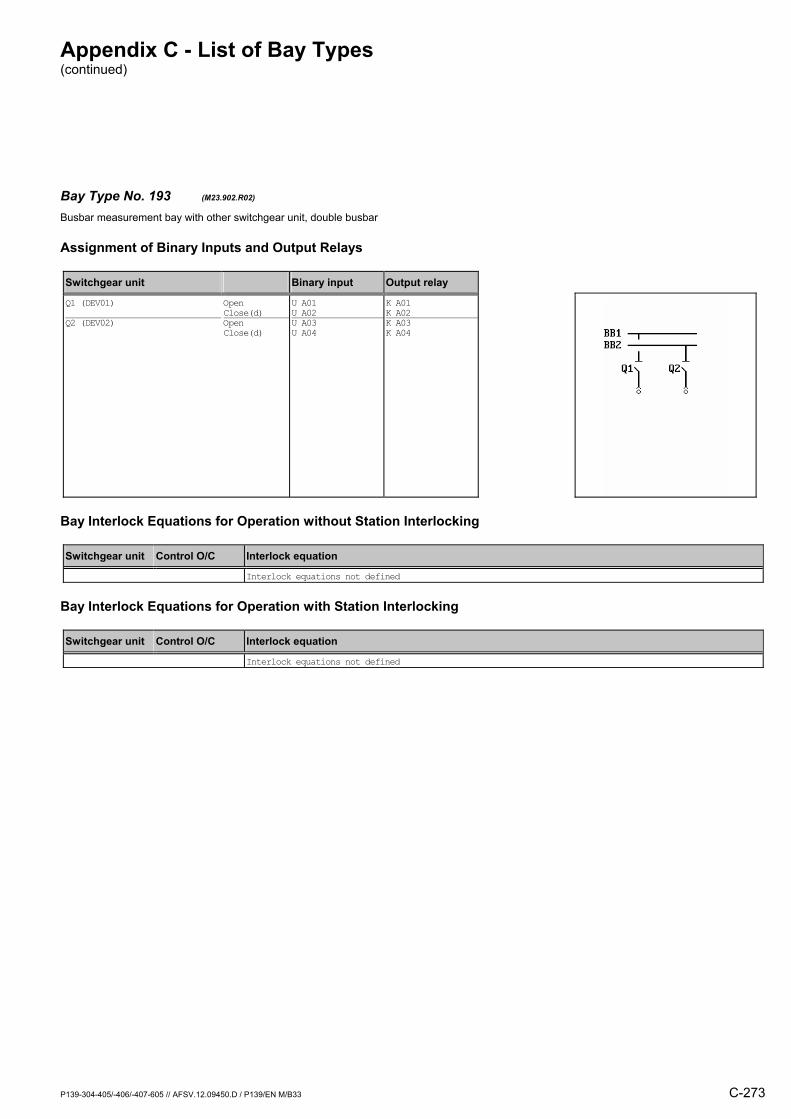
Appendix C - List of Bay Types (continued)
P139-304-405/-406/-407-605 // AFSV.12.09450.D / P139/EN M/B33 C-273
Bay Type No. 193 (M23.902.R02) Busbar measurement bay with other switchgear unit, double busbar
Assignment of Binary Inputs and Output Relays
Switchgear unit Binary input Output relay
Q1 (DEV01) Q2 (DEV02)
Open Close(d) Open Close(d)
U A01 U A02 U A03 U A04
K A01 K A02K A03 K A04
Bay Interlock Equations for Operation without Station Interlocking
Switchgear unit Control O/C Interlock equation
Interlock equations not defined
Bay Interlock Equations for Operation with Station Interlocking
Switchgear unit Control O/C Interlock equation
Interlock equations not defined
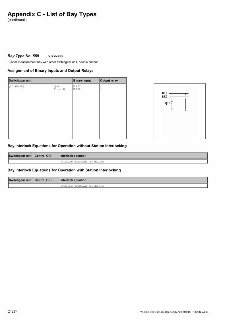
Appendix C - List of Bay Types (continued)
C-274 P139-304-405/-406/-407-605 // AFSV.12.09450.D / P139/EN M/B33
Bay Type No. 559 (M23.904.R00) Busbar measurement bay with other switchgear unit, double busbar
Assignment of Binary Inputs and Output Relays
Switchgear unit Binary input Output relay
Q15 (DEV01)
Open Close(d)
U A01 U A02
/ /
Bay Interlock Equations for Operation without Station Interlocking
Switchgear unit Control O/C Interlock equation
Interlock equations not defined
Bay Interlock Equations for Operation with Station Interlocking
Switchgear unit Control O/C Interlock equation
Interlock equations not defined
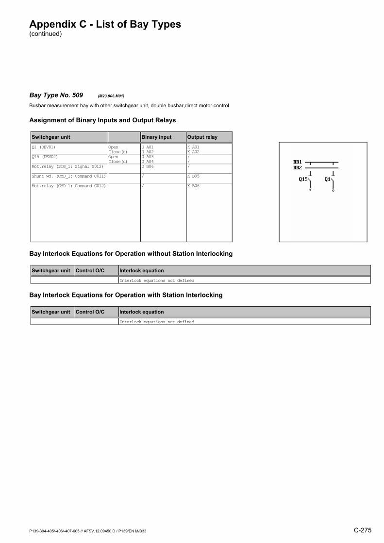
Appendix C - List of Bay Types (continued)
P139-304-405/-406/-407-605 // AFSV.12.09450.D / P139/EN M/B33 C-275
Bay Type No. 509 (M23.906.M01) Busbar measurement bay with other switchgear unit, double busbar,direct motor control
Assignment of Binary Inputs and Output Relays
Switchgear unit Binary input Output relay
Q1 (DEV01) Q15 (DEV02) Mot.relay (SIG_1: Signal S012) Shunt wd. (CMD_1: Command C011) Mot.relay (CMD_1: Command C012)
Open Close(d) Open Close(d)
U A01 U A02 U A03 U A04 U B06 / /
K A01 K A02/ //
K B05
K B06
Bay Interlock Equations for Operation without Station Interlocking
Switchgear unit Control O/C Interlock equation
Interlock equations not defined
Bay Interlock Equations for Operation with Station Interlocking
Switchgear unit Control O/C Interlock equation
Interlock equations not defined
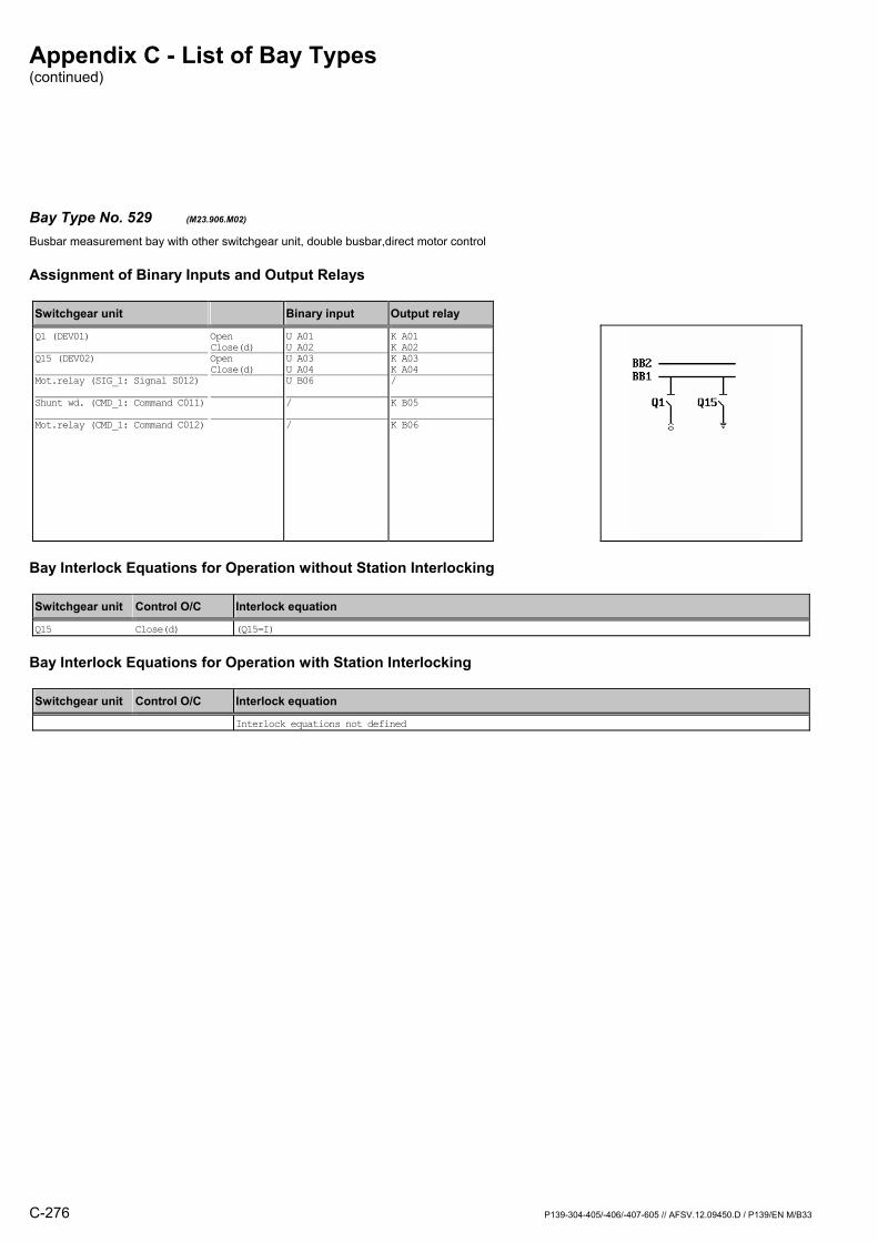
Appendix C - List of Bay Types (continued)
C-276 P139-304-405/-406/-407-605 // AFSV.12.09450.D / P139/EN M/B33
Bay Type No. 529 (M23.906.M02) Busbar measurement bay with other switchgear unit, double busbar,direct motor control
Assignment of Binary Inputs and Output Relays
Switchgear unit Binary input Output relay
Q1 (DEV01) Q15 (DEV02) Mot.relay (SIG_1: Signal S012) Shunt wd. (CMD_1: Command C011) Mot.relay (CMD_1: Command C012)
Open Close(d) Open Close(d)
U A01 U A02 U A03 U A04 U B06 / /
K A01 K A02K A03 K A04/
K B05
K B06
Bay Interlock Equations for Operation without Station Interlocking
Switchgear unit Control O/C Interlock equation
Q15 Close(d) (Q15=I)
Bay Interlock Equations for Operation with Station Interlocking
Switchgear unit Control O/C Interlock equation
Interlock equations not defined

Appendix C - List of Bay Types (continued)
P139-304-405/-406/-407-605 // AFSV.12.09450.D / P139/EN M/B33 C-277
Bay Type No. 560 (M23.908.R00) Busbar measurement bay with other switchgear unit, double busbar
Assignment of Binary Inputs and Output Relays
Switchgear unit Binary input Output relay
Q25 (DEV01)
Open Close(d)
U A01 U A02
/ /
Bay Interlock Equations for Operation without Station Interlocking
Switchgear unit Control O/C Interlock equation
Interlock equations not defined
Bay Interlock Equations for Operation with Station Interlocking
Switchgear unit Control O/C Interlock equation
Interlock equations not defined
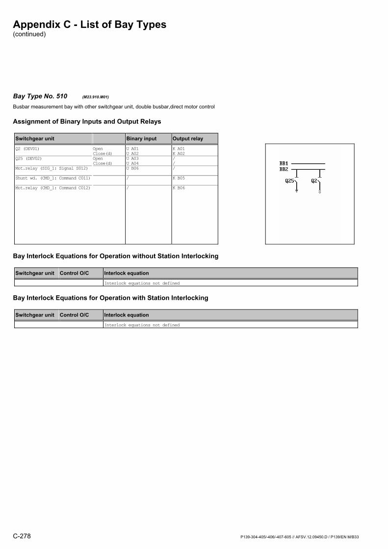
Appendix C - List of Bay Types (continued)
C-278 P139-304-405/-406/-407-605 // AFSV.12.09450.D / P139/EN M/B33
Bay Type No. 510 (M23.910.M01) Busbar measurement bay with other switchgear unit, double busbar,direct motor control
Assignment of Binary Inputs and Output Relays
Switchgear unit Binary input Output relay
Q2 (DEV01) Q25 (DEV02) Mot.relay (SIG_1: Signal S012) Shunt wd. (CMD_1: Command C011) Mot.relay (CMD_1: Command C012)
Open Close(d) Open Close(d)
U A01 U A02 U A03 U A04 U B06 / /
K A01 K A02/ //
K B05
K B06
Bay Interlock Equations for Operation without Station Interlocking
Switchgear unit Control O/C Interlock equation
Interlock equations not defined
Bay Interlock Equations for Operation with Station Interlocking
Switchgear unit Control O/C Interlock equation
Interlock equations not defined
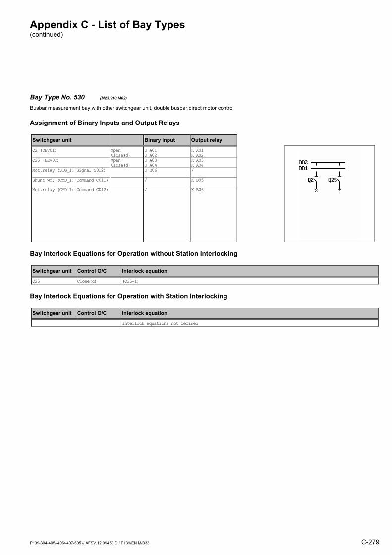
Appendix C - List of Bay Types (continued)
P139-304-405/-406/-407-605 // AFSV.12.09450.D / P139/EN M/B33 C-279
Bay Type No. 530 (M23.910.M02) Busbar measurement bay with other switchgear unit, double busbar,direct motor control
Assignment of Binary Inputs and Output Relays
Switchgear unit Binary input Output relay
Q2 (DEV01) Q25 (DEV02) Mot.relay (SIG_1: Signal S012) Shunt wd. (CMD_1: Command C011) Mot.relay (CMD_1: Command C012)
Open Close(d) Open Close(d)
U A01 U A02 U A03 U A04 U B06 / /
K A01 K A02K A03 K A04/
K B05
K B06
Bay Interlock Equations for Operation without Station Interlocking
Switchgear unit Control O/C Interlock equation
Q25 Close(d) (Q25=I)
Bay Interlock Equations for Operation with Station Interlocking
Switchgear unit Control O/C Interlock equation
Interlock equations not defined
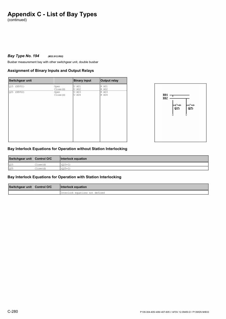
Appendix C - List of Bay Types (continued)
C-280 P139-304-405/-406/-407-605 // AFSV.12.09450.D / P139/EN M/B33
Bay Type No. 194 (M23.912.R02) Busbar measurement bay with other switchgear unit, double busbar
Assignment of Binary Inputs and Output Relays
Switchgear unit Binary input Output relay
Q15 (DEV01) Q25 (DEV02)
Open Close(d) Open Close(d)
U A01 U A02 U A03 U A04
K A01 K A02K A03 K A04
Bay Interlock Equations for Operation without Station Interlocking
Switchgear unit Control O/C Interlock equation
Q15 Close(d) (Q15=I) Q25 Close(d) (Q25=I)
Bay Interlock Equations for Operation with Station Interlocking
Switchgear unit Control O/C Interlock equation
Interlock equations not defined

Appendix C - List of Bay Types (continued)
P139-304-405/-406/-407-605 // AFSV.12.09450.D / P139/EN M/B33 C-281
Bay Type No. 234 (M25.903.M02) Busbar measurement bay with other switchgear unit, double busbar,direct motor control
Assignment of Binary Inputs and Output Relays
Switchgear unit Binary input Output relay
Q1 (DEV01) Q2 (DEV02) Q81 (DEV03) Q82 (DEV04) Mot.relay (SIG_1: Signal S012) Shunt wd. (CMD_1: Command C011) Mot.relay (CMD_1: Command C012)
Open Close(d) Open Close(d) Open Close(d) Open Close(d)
U A01 U A02 U A03 U A04 U A05 U A06 U B01 U B02 U B06 / /
K A01 K A02K A03 K A04/ // //
K B05
K B06
Bay Interlock Equations for Operation without Station Interlocking
Switchgear unit Control O/C Interlock equation
Q1 Close(d) (Q81=0) Q2 Close(d) (Q82=0)
Bay Interlock Equations for Operation with Station Interlocking
Switchgear unit Control O/C Interlock equation
Q1 Close(d) (Q81=0) Q2 Close(d) (Q82=0)
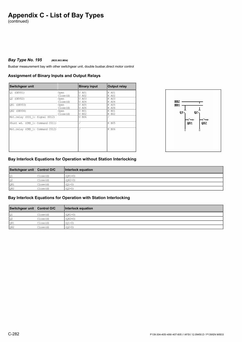
Appendix C - List of Bay Types (continued)
C-282 P139-304-405/-406/-407-605 // AFSV.12.09450.D / P139/EN M/B33
Bay Type No. 195 (M25.903.M04) Busbar measurement bay with other switchgear unit, double busbar,direct motor control
Assignment of Binary Inputs and Output Relays
Switchgear unit Binary input Output relay
Q1 (DEV01) Q2 (DEV02) Q81 (DEV03) Q82 (DEV04) Mot.relay (SIG_1: Signal S012) Shunt wd. (CMD_1: Command C011) Mot.relay (CMD_1: Command C012)
Open Close(d) Open Close(d) Open Close(d) Open Close(d)
U A01 U A02 U A03 U A04 U A05 U A06 U B01 U B02 U B06 / /
K A01 K A02K A03 K A04K A05 K A06K B01 K B02/
K B05
K B06
Bay Interlock Equations for Operation without Station Interlocking
Switchgear unit Control O/C Interlock equation
Q1 Close(d) (Q81=0) Q2 Close(d) (Q82=0) Q81 Close(d) (Q1=0) Q82 Close(d) (Q2=0)
Bay Interlock Equations for Operation with Station Interlocking
Switchgear unit Control O/C Interlock equation
Q1 Close(d) (Q81=0) Q2 Close(d) (Q82=0) Q81 Close(d) (Q1=0) Q82 Close(d) (Q2=0)
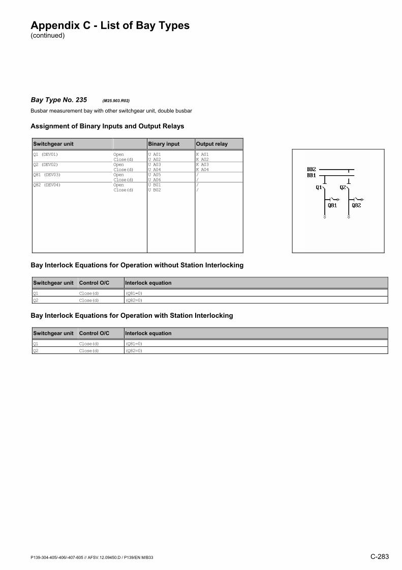
Appendix C - List of Bay Types (continued)
P139-304-405/-406/-407-605 // AFSV.12.09450.D / P139/EN M/B33 C-283
Bay Type No. 235 (M25.903.R02) Busbar measurement bay with other switchgear unit, double busbar
Assignment of Binary Inputs and Output Relays
Switchgear unit Binary input Output relay
Q1 (DEV01) Q2 (DEV02) Q81 (DEV03) Q82 (DEV04)
Open Close(d) Open Close(d) Open Close(d) Open Close(d)
U A01 U A02 U A03 U A04 U A05 U A06 U B01 U B02
K A01 K A02K A03 K A04/ // /
Bay Interlock Equations for Operation without Station Interlocking
Switchgear unit Control O/C Interlock equation
Q1 Close(d) (Q81=0) Q2 Close(d) (Q82=0)
Bay Interlock Equations for Operation with Station Interlocking
Switchgear unit Control O/C Interlock equation
Q1 Close(d) (Q81=0) Q2 Close(d) (Q82=0)
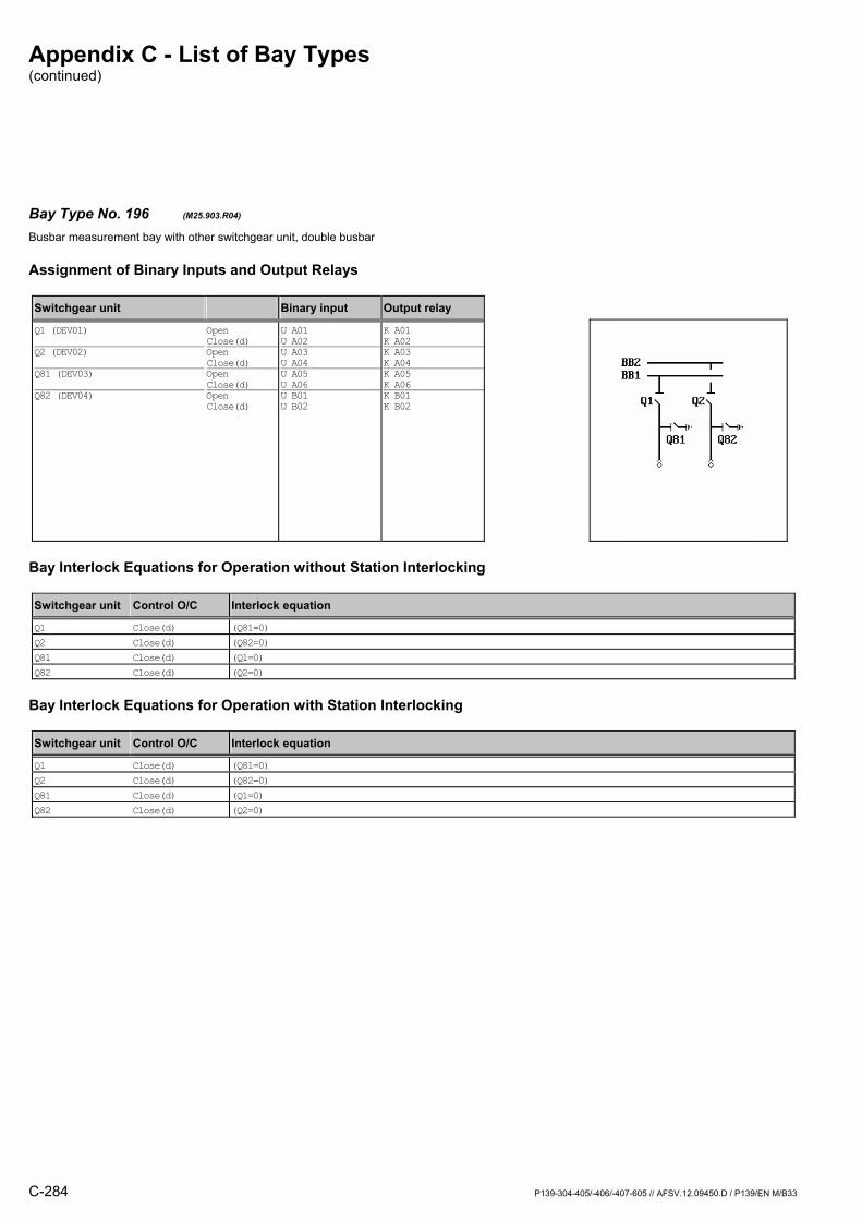
Appendix C - List of Bay Types (continued)
C-284 P139-304-405/-406/-407-605 // AFSV.12.09450.D / P139/EN M/B33
Bay Type No. 196 (M25.903.R04) Busbar measurement bay with other switchgear unit, double busbar
Assignment of Binary Inputs and Output Relays
Switchgear unit Binary input Output relay
Q1 (DEV01) Q2 (DEV02) Q81 (DEV03) Q82 (DEV04)
Open Close(d) Open Close(d) Open Close(d) Open Close(d)
U A01 U A02 U A03 U A04 U A05 U A06 U B01 U B02
K A01 K A02K A03 K A04K A05 K A06K B01 K B02
Bay Interlock Equations for Operation without Station Interlocking
Switchgear unit Control O/C Interlock equation
Q1 Close(d) (Q81=0) Q2 Close(d) (Q82=0) Q81 Close(d) (Q1=0) Q82 Close(d) (Q2=0)
Bay Interlock Equations for Operation with Station Interlocking
Switchgear unit Control O/C Interlock equation
Q1 Close(d) (Q81=0) Q2 Close(d) (Q82=0) Q81 Close(d) (Q1=0) Q82 Close(d) (Q2=0)
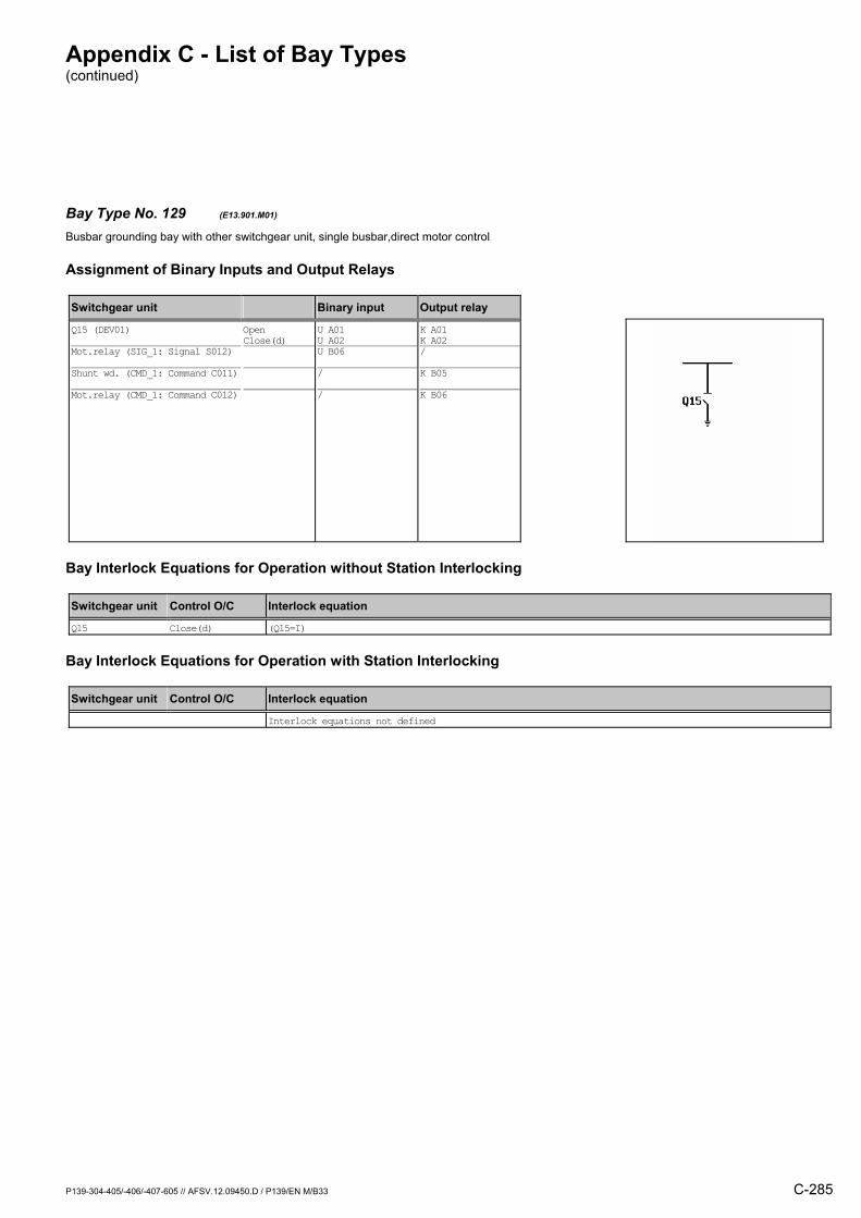
Appendix C - List of Bay Types (continued)
P139-304-405/-406/-407-605 // AFSV.12.09450.D / P139/EN M/B33 C-285
Bay Type No. 129 (E13.901.M01) Busbar grounding bay with other switchgear unit, single busbar,direct motor control
Assignment of Binary Inputs and Output Relays
Switchgear unit Binary input Output relay
Q15 (DEV01) Mot.relay (SIG_1: Signal S012) Shunt wd. (CMD_1: Command C011) Mot.relay (CMD_1: Command C012)
Open Close(d)
U A01 U A02 U B06 / /
K A01 K A02/
K B05
K B06
Bay Interlock Equations for Operation without Station Interlocking
Switchgear unit Control O/C Interlock equation
Q15 Close(d) (Q15=I)
Bay Interlock Equations for Operation with Station Interlocking
Switchgear unit Control O/C Interlock equation
Interlock equations not defined
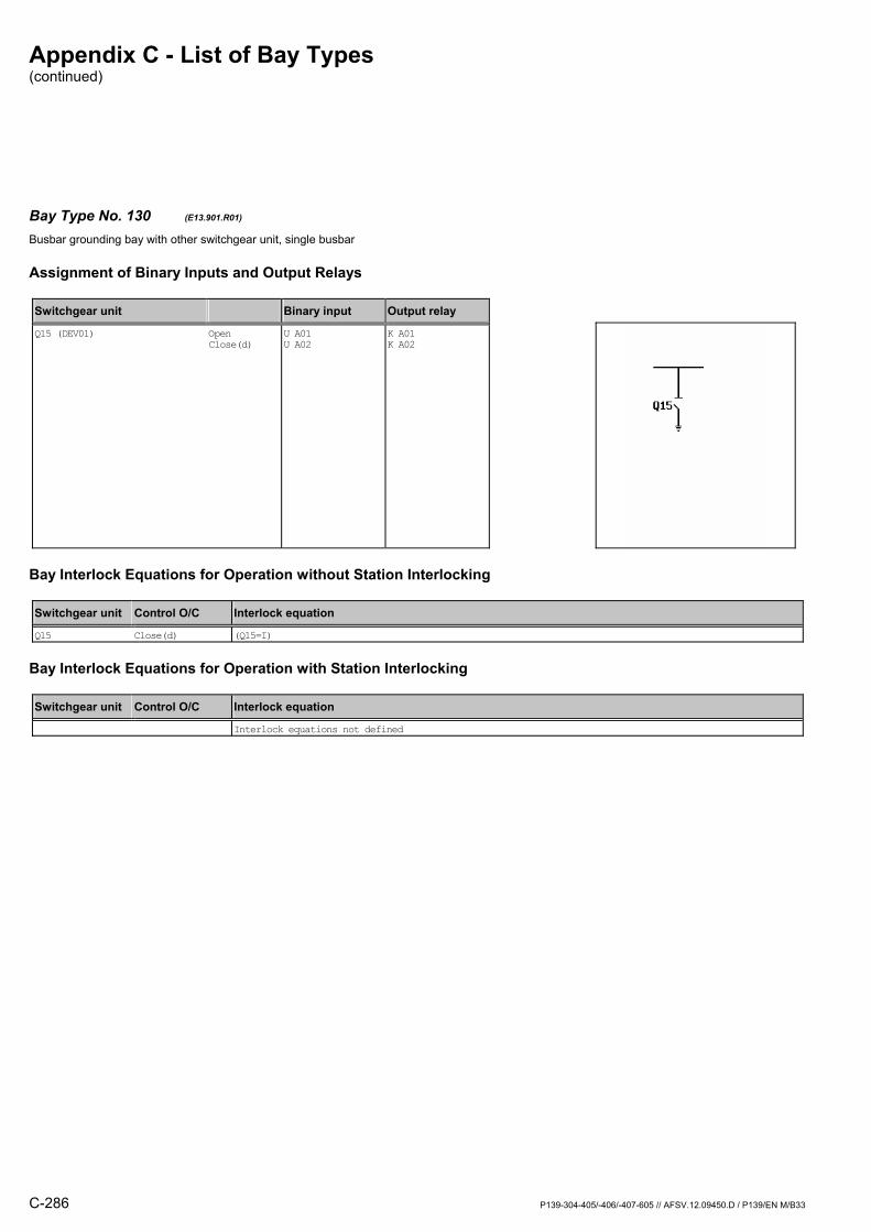
Appendix C - List of Bay Types (continued)
C-286 P139-304-405/-406/-407-605 // AFSV.12.09450.D / P139/EN M/B33
Bay Type No. 130 (E13.901.R01) Busbar grounding bay with other switchgear unit, single busbar
Assignment of Binary Inputs and Output Relays
Switchgear unit Binary input Output relay
Q15 (DEV01)
Open Close(d)
U A01 U A02
K A01 K A02
Bay Interlock Equations for Operation without Station Interlocking
Switchgear unit Control O/C Interlock equation
Q15 Close(d) (Q15=I)
Bay Interlock Equations for Operation with Station Interlocking
Switchgear unit Control O/C Interlock equation
Interlock equations not defined

Appendix C - List of Bay Types (continued)
P139-304-405/-406/-407-605 // AFSV.12.09450.D / P139/EN M/B33 C-287
Bay Type No. 131 (E23.903.M02) Busbar grounding bay with other switchgear unit, double busbar,direct motor control
Assignment of Binary Inputs and Output Relays
Switchgear unit Binary input Output relay
Q15 (DEV01) Q25 (DEV02) Mot.relay (SIG_1: Signal S012) Shunt wd. (CMD_1: Command C011) Mot.relay (CMD_1: Command C012)
Open Close(d) Open Close(d)
U A01 U A02 U A03 U A04 U B06 / /
K A01 K A02K A03 K A04/
K B05
K B06
Bay Interlock Equations for Operation without Station Interlocking
Switchgear unit Control O/C Interlock equation
Q15 Close(d) (Q15=I) Q25 Close(d) (Q25=I)
Bay Interlock Equations for Operation with Station Interlocking
Switchgear unit Control O/C Interlock equation
Interlock equations not defined
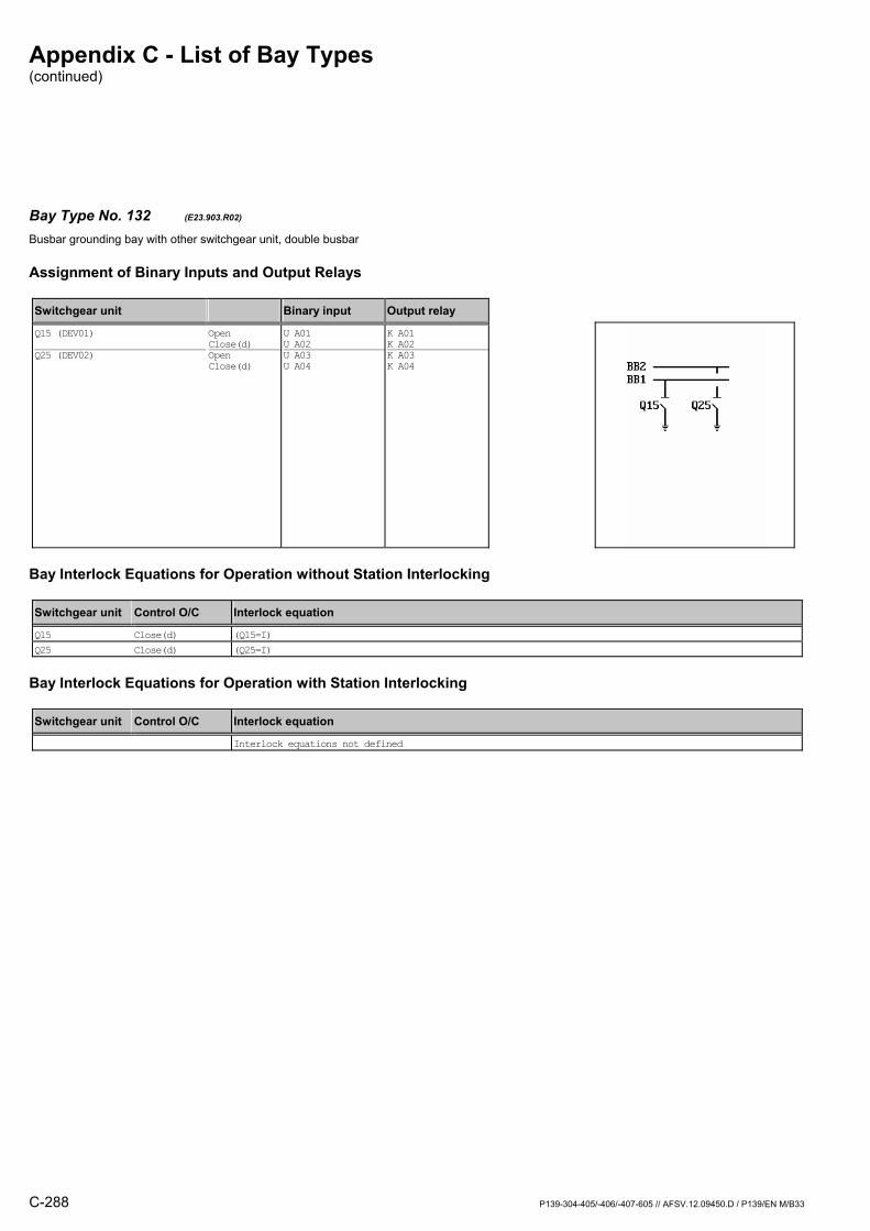
Appendix C - List of Bay Types (continued)
C-288 P139-304-405/-406/-407-605 // AFSV.12.09450.D / P139/EN M/B33
Bay Type No. 132 (E23.903.R02) Busbar grounding bay with other switchgear unit, double busbar
Assignment of Binary Inputs and Output Relays
Switchgear unit Binary input Output relay
Q15 (DEV01) Q25 (DEV02)
Open Close(d) Open Close(d)
U A01 U A02 U A03 U A04
K A01 K A02K A03 K A04
Bay Interlock Equations for Operation without Station Interlocking
Switchgear unit Control O/C Interlock equation
Q15 Close(d) (Q15=I) Q25 Close(d) (Q25=I)
Bay Interlock Equations for Operation with Station Interlocking
Switchgear unit Control O/C Interlock equation
Interlock equations not defined

Appendix C - List of Bay Types (continued)
P139-304-405/-406/-407-605 // AFSV.12.09450.D / P139/EN M/B33 C-289
Bay Type No. 1 (X99.901.R00) Other bay type with other switchgear unit, without busbar
Assignment of Binary Inputs and Output Relays
Switchgear unit Binary input Output relay
Bay Interlock Equations for Operation without Station Interlocking
Switchgear unit Control O/C Interlock equation
Interlock equations not defined
Bay Interlock Equations for Operation with Station Interlocking
Switchgear unit Control O/C Interlock equation
Interlock equations not defined
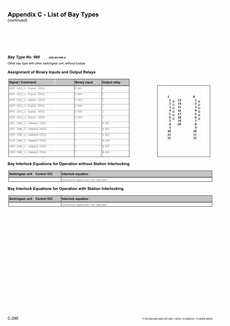
Appendix C - List of Bay Types (continued)
C-290 P139-304-405/-406/-407-605 // AFSV.12.09450.D / P139/EN M/B33
Bay Type No. 980 (X99.902.R06.2) Other bay type with other switchgear unit, without busbar
Assignment of Binary Inputs and Output Relays
Signal / Command Binary input Output relay
S001 (SIG_1: Signal S001) S002 (SIG_1: Signal S002) S003 (SIG_1: Signal S003) S004 (SIG_1: Signal S004) S005 (SIG_1: Signal S005) S006 (SIG_1: Signal S006) C001 (CMD_1: Command C001) C002 (CMD_1: Command C002) C003 (CMD_1: Command C003) C004 (CMD_1: Command C004) C005 (CMD_1: Command C005) C006 (CMD_1: Command C006)
U A01 U A02 U A03 U A04 U A05 U A06 / / / / / /
/
/
/
/
/
/
K A01
K A02
K A03
K A04
K A05
K A06
Bay Interlock Equations for Operation without Station Interlocking
Switchgear unit Control O/C Interlock equation
Interlock equations not defined
Bay Interlock Equations for Operation with Station Interlocking
Switchgear unit Control O/C Interlock equation
Interlock equations not defined
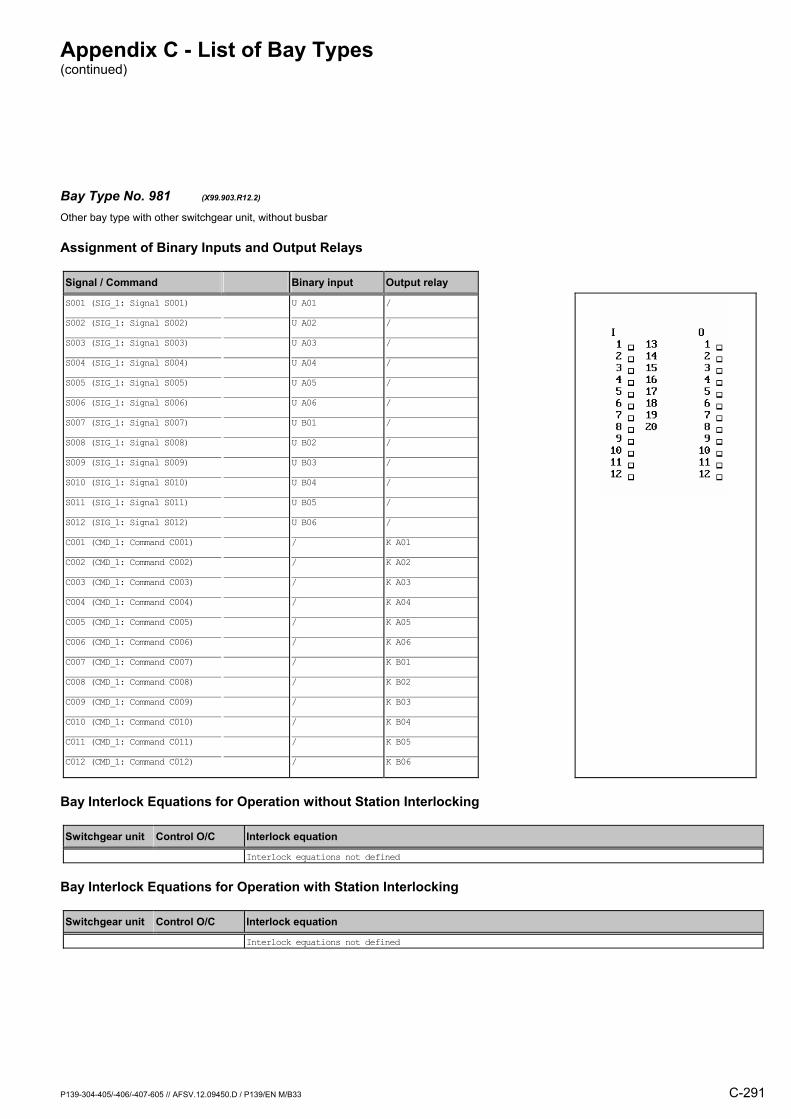
Appendix C - List of Bay Types (continued)
P139-304-405/-406/-407-605 // AFSV.12.09450.D / P139/EN M/B33 C-291
Bay Type No. 981 (X99.903.R12.2) Other bay type with other switchgear unit, without busbar
Assignment of Binary Inputs and Output Relays
Signal / Command Binary input Output relay
S001 (SIG_1: Signal S001) S002 (SIG_1: Signal S002) S003 (SIG_1: Signal S003) S004 (SIG_1: Signal S004) S005 (SIG_1: Signal S005) S006 (SIG_1: Signal S006) S007 (SIG_1: Signal S007) S008 (SIG_1: Signal S008) S009 (SIG_1: Signal S009) S010 (SIG_1: Signal S010) S011 (SIG_1: Signal S011) S012 (SIG_1: Signal S012) C001 (CMD_1: Command C001) C002 (CMD_1: Command C002) C003 (CMD_1: Command C003) C004 (CMD_1: Command C004) C005 (CMD_1: Command C005) C006 (CMD_1: Command C006) C007 (CMD_1: Command C007) C008 (CMD_1: Command C008) C009 (CMD_1: Command C009) C010 (CMD_1: Command C010) C011 (CMD_1: Command C011) C012 (CMD_1: Command C012)
U A01 U A02 U A03 U A04 U A05 U A06 U B01 U B02 U B03 U B04 U B05 U B06 / / / / / / / / / / / /
/
/
/
/
/
/
/
/
/
/
/
/
K A01
K A02
K A03
K A04
K A05
K A06
K B01
K B02
K B03
K B04
K B05
K B06
Bay Interlock Equations for Operation without Station Interlocking
Switchgear unit Control O/C Interlock equation
Interlock equations not defined
Bay Interlock Equations for Operation with Station Interlocking
Switchgear unit Control O/C Interlock equation
Interlock equations not defined
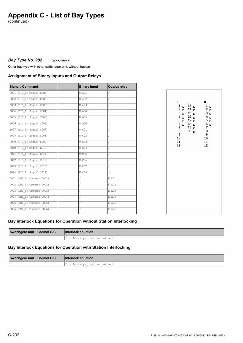
Appendix C - List of Bay Types (continued)
C-292 P139-304-405/-406/-407-605 // AFSV.12.09450.D / P139/EN M/B33
Bay Type No. 982 (X99.904.R06.2) Other bay type with other switchgear unit, without busbar
Assignment of Binary Inputs and Output Relays
Signal / Command Binary input Output relay
S001 (SIG_1: Signal S001) S002 (SIG_1: Signal S002) S003 (SIG_1: Signal S003) S004 (SIG_1: Signal S004) S005 (SIG_1: Signal S005) S006 (SIG_1: Signal S006) S007 (SIG_1: Signal S007) S008 (SIG_1: Signal S008) S009 (SIG_1: Signal S009) S010 (SIG_1: Signal S010) S011 (SIG_1: Signal S011) S012 (SIG_1: Signal S012) S013 (SIG_1: Signal S013) S014 (SIG_1: Signal S014) C001 (CMD_1: Command C001) C002 (CMD_1: Command C002) C003 (CMD_1: Command C003) C004 (CMD_1: Command C004) C005 (CMD_1: Command C005) C006 (CMD_1: Command C006)
U A01 U A02 U A03 U A04 U A05 U A06 U C01 U C02 U C03 U C04 U C05 U C06 U C07 U C08 / / / / / /
/
/
/
/
/
/
/
/
/
/
/
/
/
/
K A01
K A02
K A03
K A04
K A05
K A06
Bay Interlock Equations for Operation without Station Interlocking
Switchgear unit Control O/C Interlock equation
Interlock equations not defined
Bay Interlock Equations for Operation with Station Interlocking
Switchgear unit Control O/C Interlock equation
Interlock equations not defined
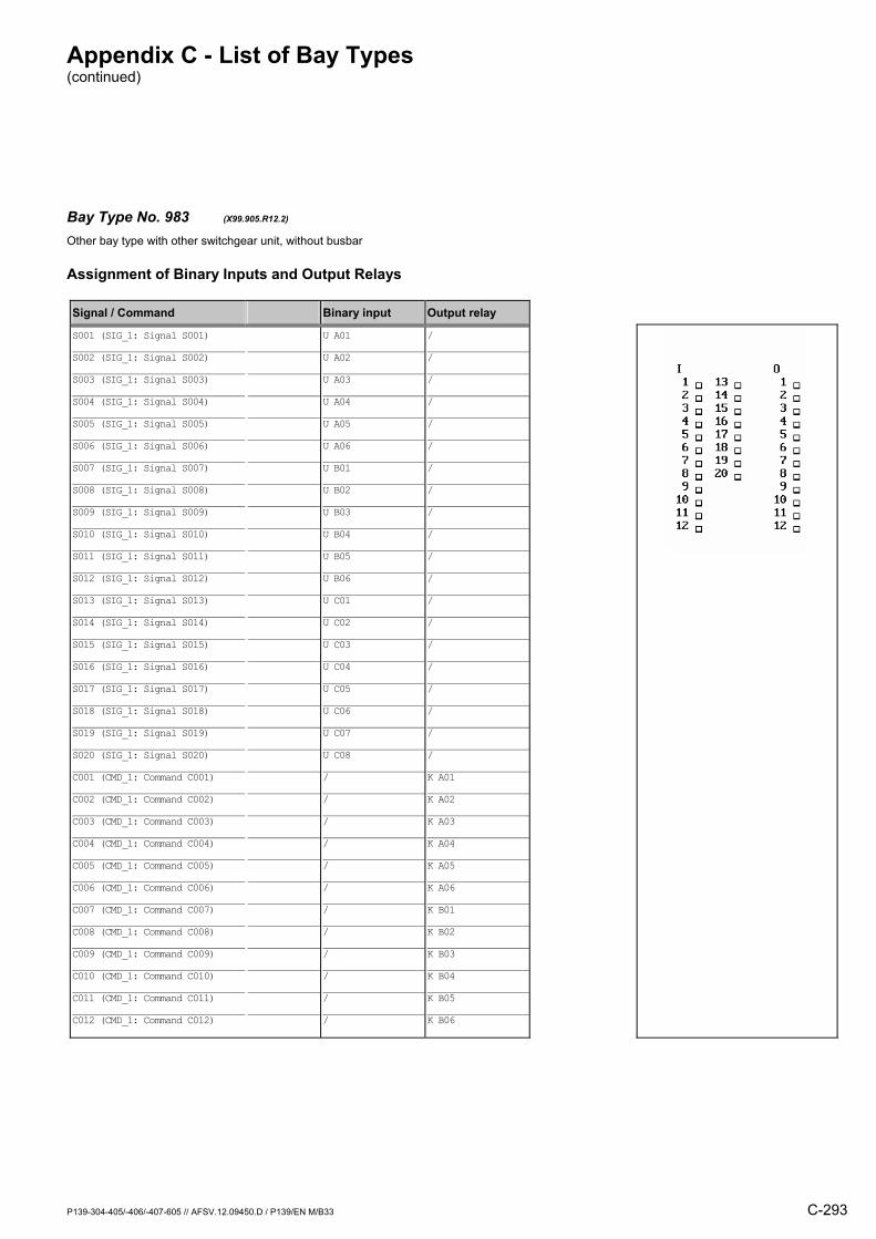
Appendix C - List of Bay Types (continued)
P139-304-405/-406/-407-605 // AFSV.12.09450.D / P139/EN M/B33 C-293
Bay Type No. 983 (X99.905.R12.2) Other bay type with other switchgear unit, without busbar
Assignment of Binary Inputs and Output Relays
Signal / Command Binary input Output relay
S001 (SIG_1: Signal S001) S002 (SIG_1: Signal S002) S003 (SIG_1: Signal S003) S004 (SIG_1: Signal S004) S005 (SIG_1: Signal S005) S006 (SIG_1: Signal S006) S007 (SIG_1: Signal S007) S008 (SIG_1: Signal S008) S009 (SIG_1: Signal S009) S010 (SIG_1: Signal S010) S011 (SIG_1: Signal S011) S012 (SIG_1: Signal S012) S013 (SIG_1: Signal S013) S014 (SIG_1: Signal S014) S015 (SIG_1: Signal S015) S016 (SIG_1: Signal S016) S017 (SIG_1: Signal S017) S018 (SIG_1: Signal S018) S019 (SIG_1: Signal S019) S020 (SIG_1: Signal S020) C001 (CMD_1: Command C001) C002 (CMD_1: Command C002) C003 (CMD_1: Command C003) C004 (CMD_1: Command C004) C005 (CMD_1: Command C005) C006 (CMD_1: Command C006) C007 (CMD_1: Command C007) C008 (CMD_1: Command C008) C009 (CMD_1: Command C009) C010 (CMD_1: Command C010) C011 (CMD_1: Command C011) C012 (CMD_1: Command C012)
U A01 U A02 U A03 U A04 U A05 U A06 U B01 U B02 U B03 U B04 U B05 U B06 U C01 U C02 U C03 U C04 U C05 U C06 U C07 U C08 / / / / / / / / / / / /
/
/
/
/
/
/
/
/
/
/
/
/
/
/
/
/
/
/
/
/
K A01
K A02
K A03
K A04
K A05
K A06
K B01
K B02
K B03
K B04
K B05
K B06
Appendix C - List of Bay Types (continued)
C-294 P139-304-405/-406/-407-605 // AFSV.12.09450.D / P139/EN M/B33
Bay Interlock Equations for Operation without Station Interlocking
Switchgear unit Control O/C Interlock equation
Interlock equations not defined
Bay Interlock Equations for Operation with Station Interlocking
Switchgear unit Control O/C Interlock equation
Interlock equations not defined
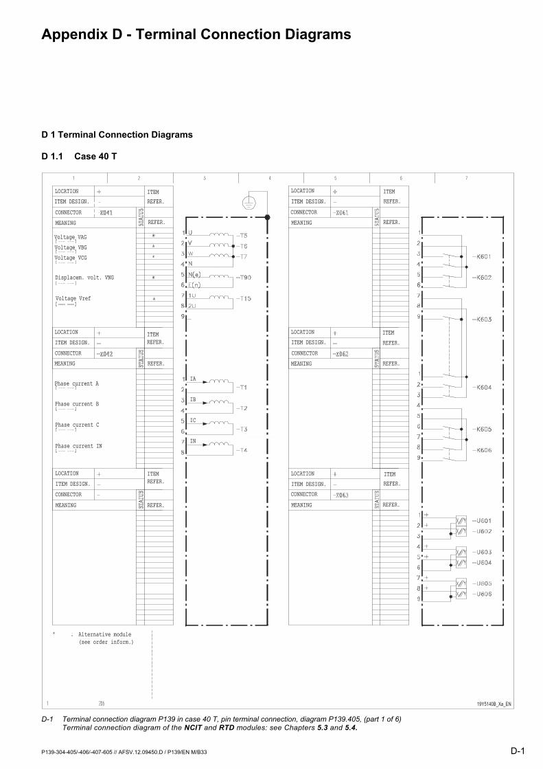
Appendix D - Terminal Connection Diagrams
P139-304-405/-406/-407-605 // AFSV.12.09450.D / P139/EN M/B33 D-1
D 1 Terminal Connection Diagrams
D 1.1 Case 40 T
LOCATION ITEM
REFER.ITEM DESIGN.ITEM DESIGN.
CONNECTOR
MEANING REFER.
Voltage VAGVoltage VAG
Voltage VBGVoltage VBG
Voltage VCGVoltage VCG
Displacem. volt. VNGDisplacem. volt. VNG
Voltage VrefVoltage Vref
Phase current APhase current AIA
IB
IC
IN
Phase current BPhase current B
Phase current CPhase current C
Phase current INPhase current IN
LOCATION
ITEM DESIGN.ITEM DESIGN.
CONNECTOR
MEANING
ITEM
REFER.
REFER.
LOCATION
ITEM DESIGN.ITEM DESIGN.
CONNECTOR
MEANING
ITEM
REFER.
REFER.
Alternative moduleAlternative module
(see order inform.)(see order inform.)
LOCATION
ITEM DESIGN.ITEM DESIGN.
CONNECTOR
MEANING
ITEM
REFER.
REFER.
LOCATION
ITEM DESIGN.ITEM DESIGN.
CONNECTOR
MEANING
ITEM
REFER.
REFER.
LOCATION
ITEM DESIGN.ITEM DESIGN.
CONNECTOR
MEANING
ITEM
REFER.
REFER.
19Y5140B_Xa_EN D-1 Terminal connection diagram P139 in case 40 T, pin terminal connection, diagram P139.405, (part 1 of 6)
Terminal connection diagram of the NCIT and RTD modules: see Chapters 5.3 and 5.4.
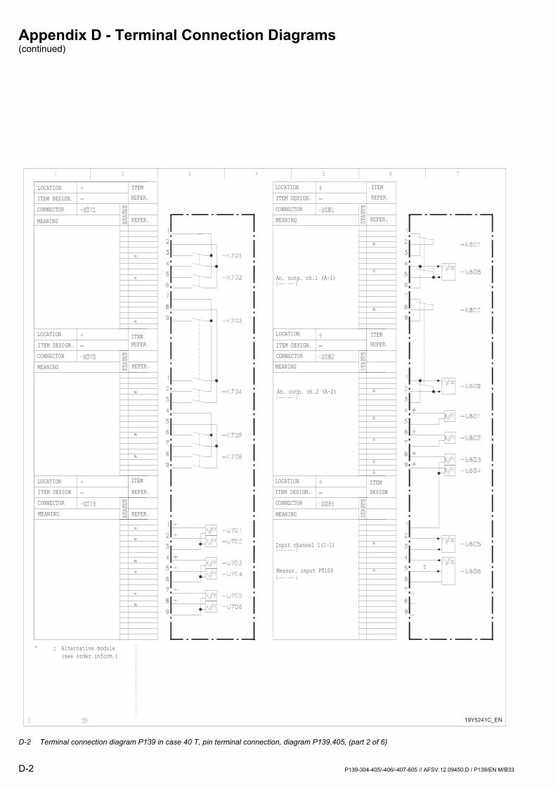
Appendix D - Terminal Connection Diagrams (continued)
D-2 P139-304-405/-406/-407-605 // AFSV.12.09450.D / P139/EN M/B33
19Y5241C_EN
LOCATION
ITEM DESIGN.
CONNECTOR
MEANING
ITEM
REFER.
REFER.
LOCATION
ITEM DESIGN.
CONNECTOR
MEANING
ITEM
REFER.
REFER.
LOCATION
ITEM DESIGN
CONNECTOR
MEANING
ITEM
REFER.
REFER.
Alternative module
(see order inform.)
LOCATION
ITEM DESIGN.
CONNECTOR
MEANING
ITEM
REFER.
REFER.
An. outp. ch.1 (A-1)
An. outp. ch.2 (A-2)
Input channel 1(I-1)
Measur. input PT100
LOCATION
ITEM DESIGN.
CONNECTOR
MEANING
ITEM
DESIGN
LOCATION
ITEM DESIGN.
CONNECTOR
MEANING
ITEM
REFER.
D-2 Terminal connection diagram P139 in case 40 T, pin terminal connection, diagram P139.405, (part 2 of 6)
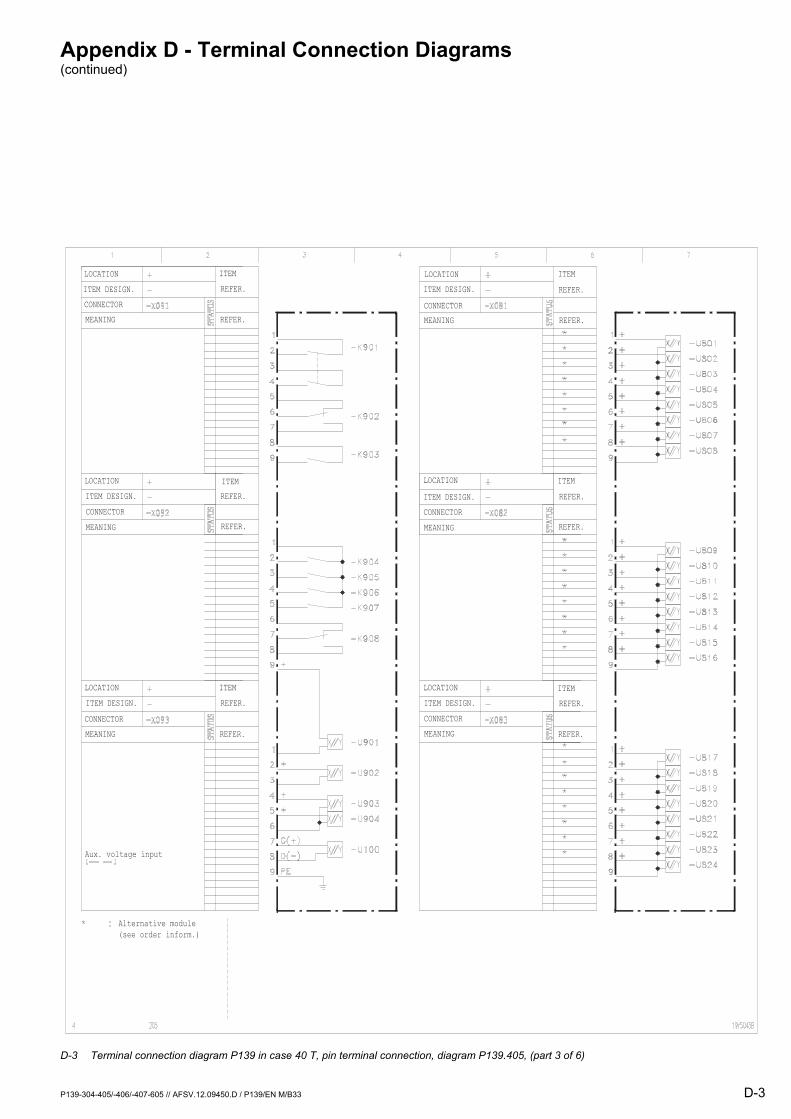
Appendix D - Terminal Connection Diagrams (continued)
P139-304-405/-406/-407-605 // AFSV.12.09450.D / P139/EN M/B33 D-3
LOCATION
ITEM DESIGN.
CONNECTOR
MEANING
ITEM
REFER.
REFER.
LOCATION
ITEM DESIGN.
CONNECTOR
MEANING
ITEM
REFER.
REFER.
LOCATION
ITEM DESIGN.
CONNECTOR
MEANING
ITEM
REFER.
REFER.
Aux. voltage input
Alternative module
(see order inform.)
LOCATION
ITEM DESIGN.
CONNECTOR
MEANING
ITEM
REFER.
REFER.
LOCATION
ITEM DESIGN.
CONNECTOR
MEANING
ITEM
REFER.
REFER.
LOCATION
ITEM DESIGN.
CONNECTOR
MEANING
ITEM
REFER.
REFER.
D-3 Terminal connection diagram P139 in case 40 T, pin terminal connection, diagram P139.405, (part 3 of 6)
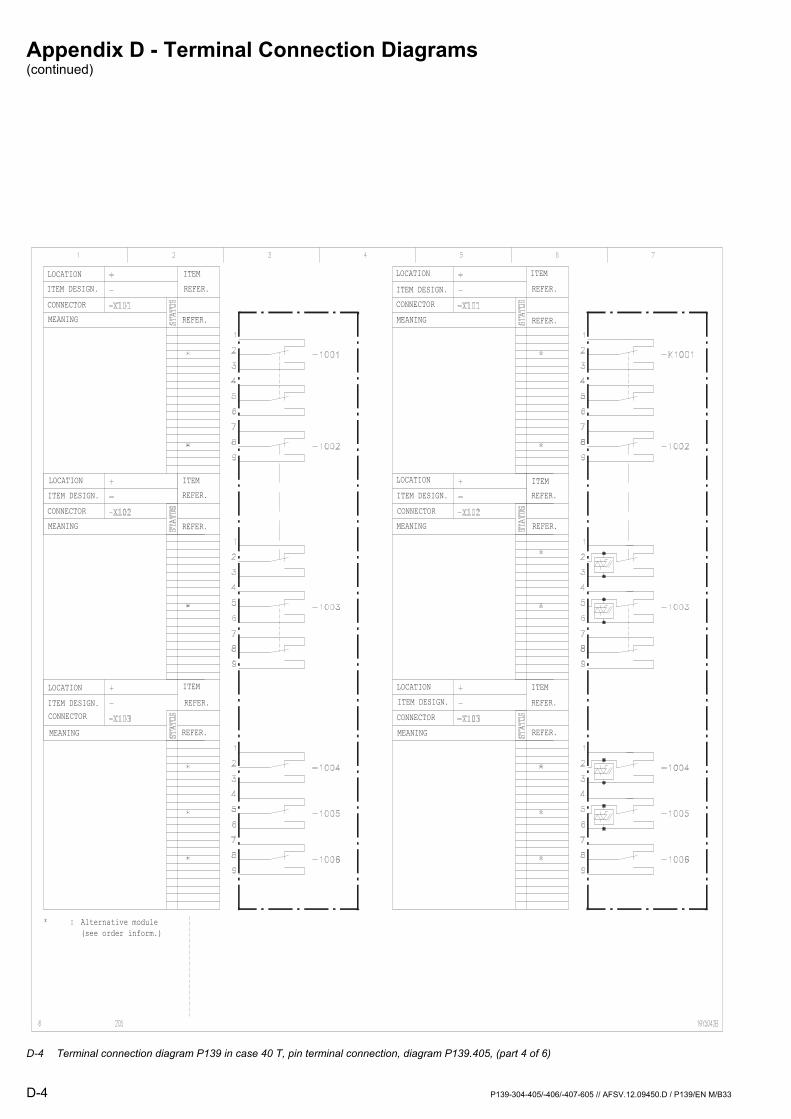
Appendix D - Terminal Connection Diagrams (continued)
D-4 P139-304-405/-406/-407-605 // AFSV.12.09450.D / P139/EN M/B33
LOCATION
ITEM DESIGN.
CONNECTOR
MEANING
ITEM
REFER.
REFER.
LOCATION
ITEM DESIGN.
CONNECTOR
MEANING
ITEM
REFER.
REFER.
LOCATION
ITEM DESIGN.
CONNECTOR
MEANING
ITEM
REFER.
REFER.
Alternative module
(see order inform.)
LOCATION
ITEM DESIGN.
CONNECTOR
MEANING
ITEM
REFER.
REFER.
LOCATION
ITEM DESIGN.
CONNECTOR
MEANING
ITEM
REFER.
REFER.
LOCATION
ITEM DESIGN.
CONNECTOR
MEANING
ITEM
REFER.
REFER.
D-4 Terminal connection diagram P139 in case 40 T, pin terminal connection, diagram P139.405, (part 4 of 6)
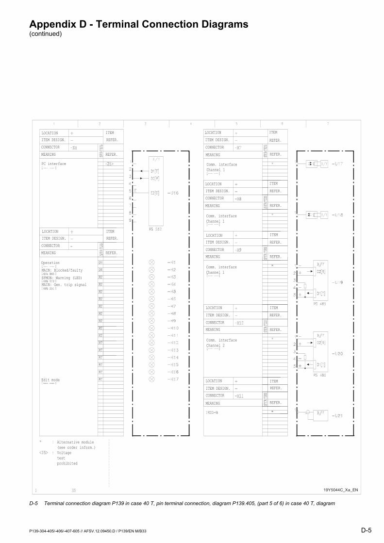
Appendix D - Terminal Connection Diagrams (continued)
P139-304-405/-406/-407-605 // AFSV.12.09450.D / P139/EN M/B33 D-5
19Y5044C_Xa_EN
LOCATION
ITEM DESIGN.
CONNECTOR
MEANING
ITEM
REFER.
REFER.
PC interface
LOCATION
ITEM DESIGN.
CONNECTOR
MEANING
ITEM
REFER.
REFER.
Operation
MAIN: Blocked/faulty
SFMON: Warning (LED)
MAIN: Gen. trip signal
Edit mode
Alternative module
(see order inform.)
Voltage
test
prohibited
LOCATION
ITEM DESIGN.
CONNECTOR
MEANING
ITEM
REFER.
REFER.
Comm. interface
Channel 1
LOCATION
ITEM DESIGN.
CONNECTOR
MEANING
ITEM
REFER.
REFER.
Comm. interface
Channel 1
Comm. interface
Channel 1
Comm. interface
Channel 2
LOCATION
ITEM DESIGN.
CONNECTOR
MEANING
ITEM
REFER.
REFER.
LOCATION
ITEM DESIGN.
CONNECTOR
MEANING
ITEM
REFER.
REFER.
LOCATION
ITEM DESIGN.
CONNECTOR
MEANING
ITEM
REFER.
REFER.
D-5 Terminal connection diagram P139 in case 40 T, pin terminal connection, diagram P139.405, (part 5 of 6) in case 40 T, diagram
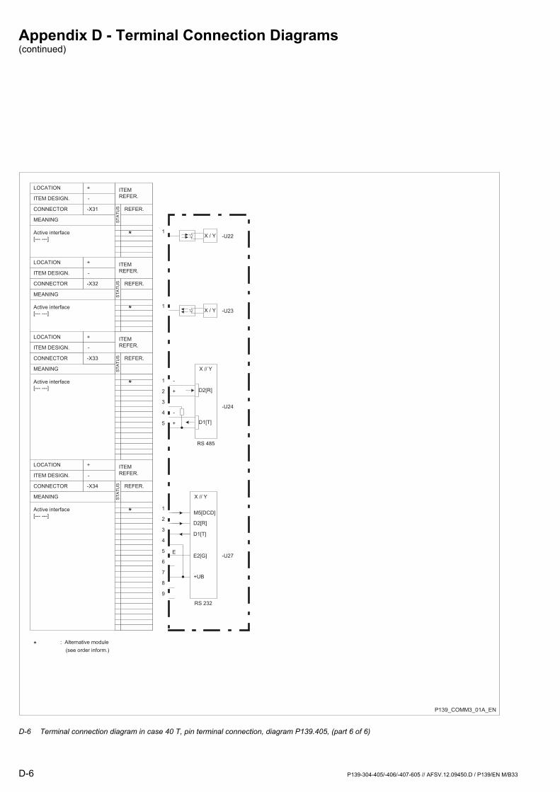
Appendix D - Terminal Connection Diagrams (continued)
D-6 P139-304-405/-406/-407-605 // AFSV.12.09450.D / P139/EN M/B33
-
+
LOCATION
ITEM DESIGN.
CONNECTOR
MEANING
+
-
-X31
P139_COMM3_01A_EN
ITEM
REFER.
*
RS 485
1
2
3
4
5
6
7
8
9
E
X / Y
1
2
3
4
5
1
X / Y1
* : Alternative module
(see order inform.)
ST
AT
US REFER.
LOCATION
ITEM DESIGN.
CONNECTOR
MEANING
-X32
ITEM
REFER.
*
ST
AT
US REFER.
LOCATION
ITEM DESIGN.
CONNECTOR
MEANING
-X33
ITEM
REFER.
*
ST
AT
US REFER.
LOCATION
ITEM DESIGN.
CONNECTOR
MEANING
-X34
ITEM
REFER.
*
ST
AT
US REFER.
+
-
+
-
+
-
-U22
-U24
-U27
-U23
Active interface
[--- ---]
Active interface
[--- ---]
Active interface
[--- ---]
Active interface
[--- ---]
-
+
X // Y
D2[R]
D1[T]
D1[T]
D2[R]
RS 232
E2[G]
X // Y
M5[DCD]
+UB
D-6 Terminal connection diagram in case 40 T, pin terminal connection, diagram P139.405, (part 6 of 6)
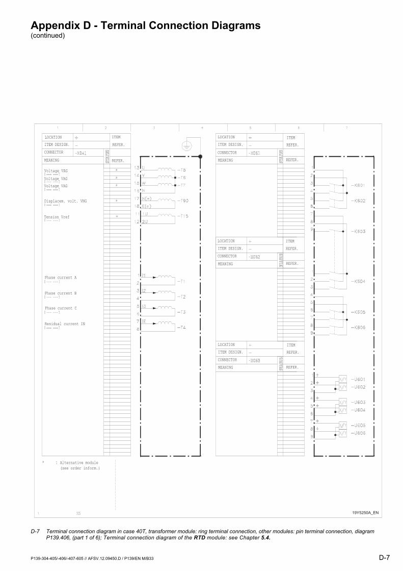
Appendix D - Terminal Connection Diagrams (continued)
P139-304-405/-406/-407-605 // AFSV.12.09450.D / P139/EN M/B33 D-7
19Y5250A_EN
LOCATION
ITEM DESIGN.
CONNECTOR
MEANING
ITEM
REFER.
REFER.
Voltage VAG
Voltage VAG
Voltage VAG
Displacem. volt. VNG
Tension Vref
Phase current A
Phase current B
Phase current C
Residual current IN
Alternative module
(see order inform.)
LOCATION
ITEM DESIGN.
CONNECTOR
MEANING
ITEM
REFER.
REFER.
LOCATION
ITEM DESIGN.
CONNECTOR
MEANING
ITEM
REFER.
REFER.
LOCATION
ITEM DESIGN.
CONNECTOR
MEANING
ITEM
REFER.
REFER.
D-7 Terminal connection diagram in case 40T, transformer module: ring terminal connection, other modules: pin terminal connection, diagram P139.406, (part 1 of 6); Terminal connection diagram of the RTD module: see Chapter 5.4.
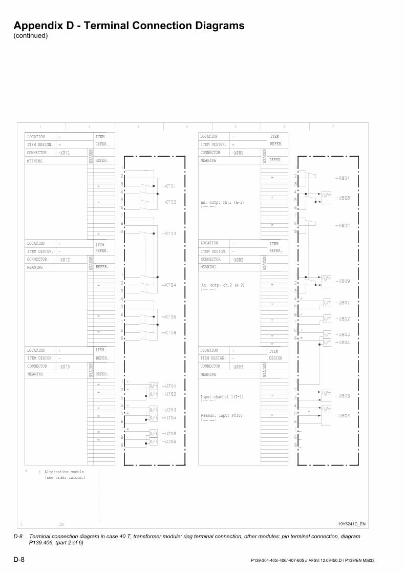
Appendix D - Terminal Connection Diagrams (continued)
D-8 P139-304-405/-406/-407-605 // AFSV.12.09450.D / P139/EN M/B33
19Y5241C_EN
LOCATION
ITEM DESIGN.
CONNECTOR
MEANING
ITEM
REFER.
REFER.
LOCATION
ITEM DESIGN.
CONNECTOR
MEANING
ITEM
REFER.
REFER.
LOCATION
ITEM DESIGN
CONNECTOR
MEANING
ITEM
REFER.
REFER.
Alternative module
(see order inform.)
LOCATION
ITEM DESIGN.
CONNECTOR
MEANING
ITEM
REFER.
REFER.
An. outp. ch.1 (A-1)
An. outp. ch.2 (A-2)
Input channel 1(I-1)
Measur. input PT100
LOCATION
ITEM DESIGN.
CONNECTOR
MEANING
ITEM
DESIGN
LOCATION
ITEM DESIGN.
CONNECTOR
MEANING
ITEM
REFER.
D-8 Terminal connection diagram in case 40 T, transformer module: ring terminal connection, other modules: pin terminal connection, diagram
P139.406, (part 2 of 6)
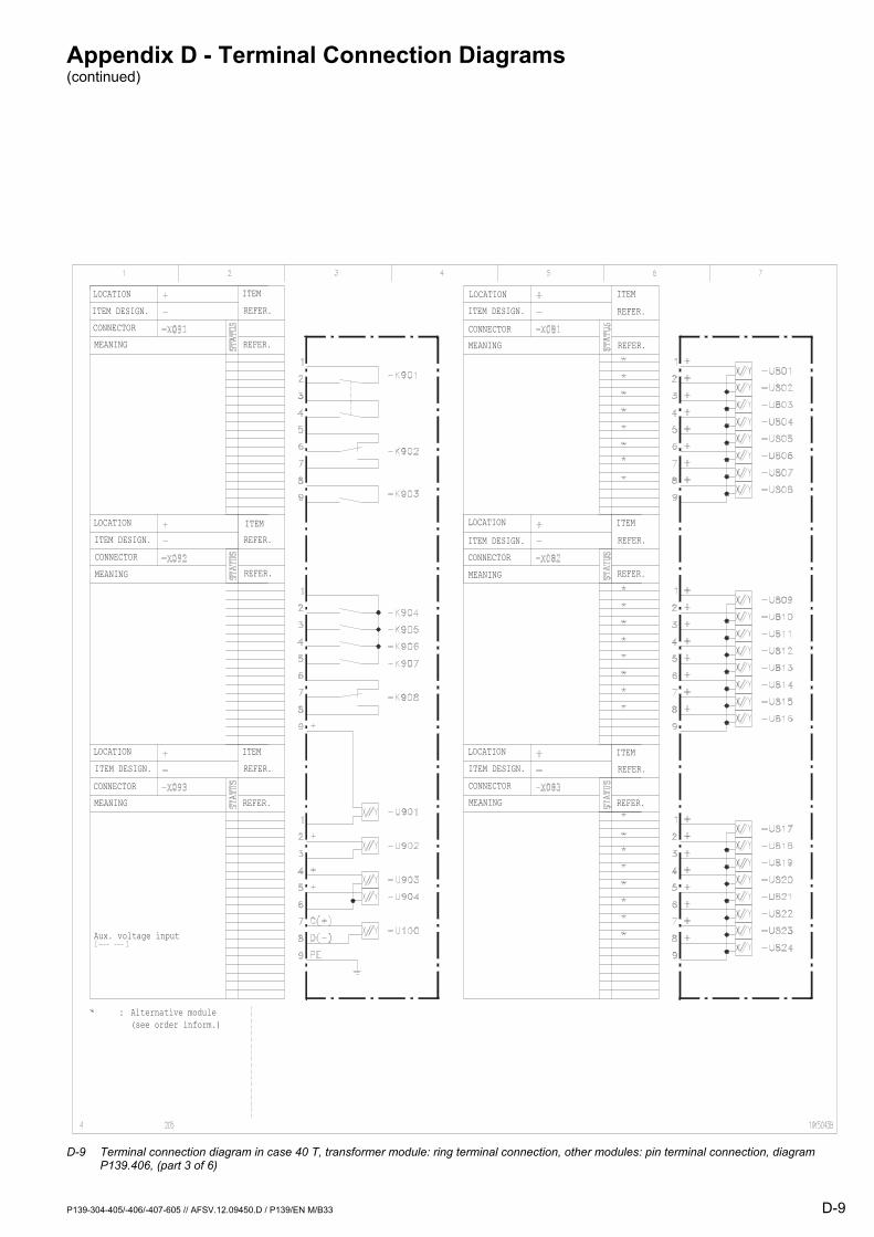
Appendix D - Terminal Connection Diagrams (continued)
P139-304-405/-406/-407-605 // AFSV.12.09450.D / P139/EN M/B33 D-9
LOCATION
ITEM DESIGN.
CONNECTOR
MEANING
ITEM
REFER.
REFER.
LOCATION
ITEM DESIGN.
CONNECTOR
MEANING
ITEM
REFER.
REFER.
LOCATION
ITEM DESIGN.
CONNECTOR
MEANING
ITEM
REFER.
REFER.
Aux. voltage input
Alternative module
(see order inform.)
LOCATION
ITEM DESIGN.
CONNECTOR
MEANING
ITEM
REFER.
REFER.
LOCATION
ITEM DESIGN.
CONNECTOR
MEANING
ITEM
REFER.
REFER.
LOCATION
ITEM DESIGN.
CONNECTOR
MEANING
ITEM
REFER.
REFER.
D-9 Terminal connection diagram in case 40 T, transformer module: ring terminal connection, other modules: pin terminal connection, diagram
P139.406, (part 3 of 6)
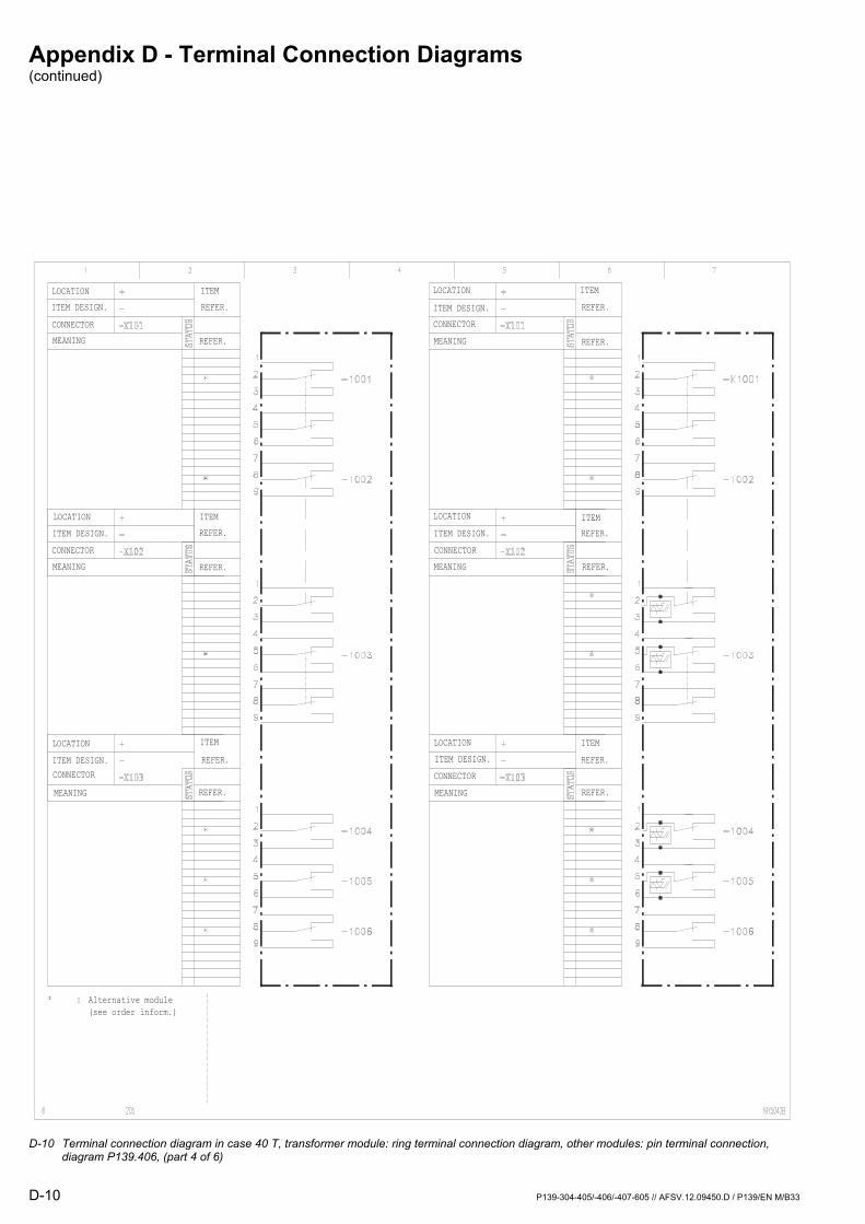
Appendix D - Terminal Connection Diagrams (continued)
D-10 P139-304-405/-406/-407-605 // AFSV.12.09450.D / P139/EN M/B33
LOCATION
ITEM DESIGN.
CONNECTOR
MEANING
ITEM
REFER.
REFER.
LOCATION
ITEM DESIGN.
CONNECTOR
MEANING
ITEM
REFER.
REFER.
LOCATION
ITEM DESIGN.
CONNECTOR
MEANING
ITEM
REFER.
REFER.
Alternative module
(see order inform.)
LOCATION
ITEM DESIGN.
CONNECTOR
MEANING
ITEM
REFER.
REFER.
LOCATION
ITEM DESIGN.
CONNECTOR
MEANING
ITEM
REFER.
REFER.
LOCATION
ITEM DESIGN.
CONNECTOR
MEANING
ITEM
REFER.
REFER.
D-10 Terminal connection diagram in case 40 T, transformer module: ring terminal connection diagram, other modules: pin terminal connection,
diagram P139.406, (part 4 of 6)
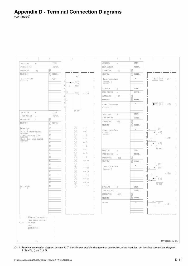
Appendix D - Terminal Connection Diagrams (continued)
P139-304-405/-406/-407-605 // AFSV.12.09450.D / P139/EN M/B33 D-11
19Y5044C_Xa_EN
LOCATION
ITEM DESIGN.
CONNECTOR
MEANING
ITEM
REFER.
REFER.
PC interface
LOCATION
ITEM DESIGN.
CONNECTOR
MEANING
ITEM
REFER.
REFER.
Operation
MAIN: Blocked/faulty
SFMON: Warning (LED)
MAIN: Gen. trip signal
Edit mode
Alternative module
(see order inform.)
Voltage
test
prohibited
LOCATION
ITEM DESIGN.
CONNECTOR
MEANING
ITEM
REFER.
REFER.
Comm. interface
Channel 1
LOCATION
ITEM DESIGN.
CONNECTOR
MEANING
ITEM
REFER.
REFER.
Comm. interface
Channel 1
Comm. interface
Channel 1
Comm. interface
Channel 2
LOCATION
ITEM DESIGN.
CONNECTOR
MEANING
ITEM
REFER.
REFER.
LOCATION
ITEM DESIGN.
CONNECTOR
MEANING
ITEM
REFER.
REFER.
LOCATION
ITEM DESIGN.
CONNECTOR
MEANING
ITEM
REFER.
REFER.
D-11 Terminal connection diagram in case 40 T, transformer module: ring terminal connection, other modules: pin terminal connection, diagram
P139.406, (part 5 of 6)
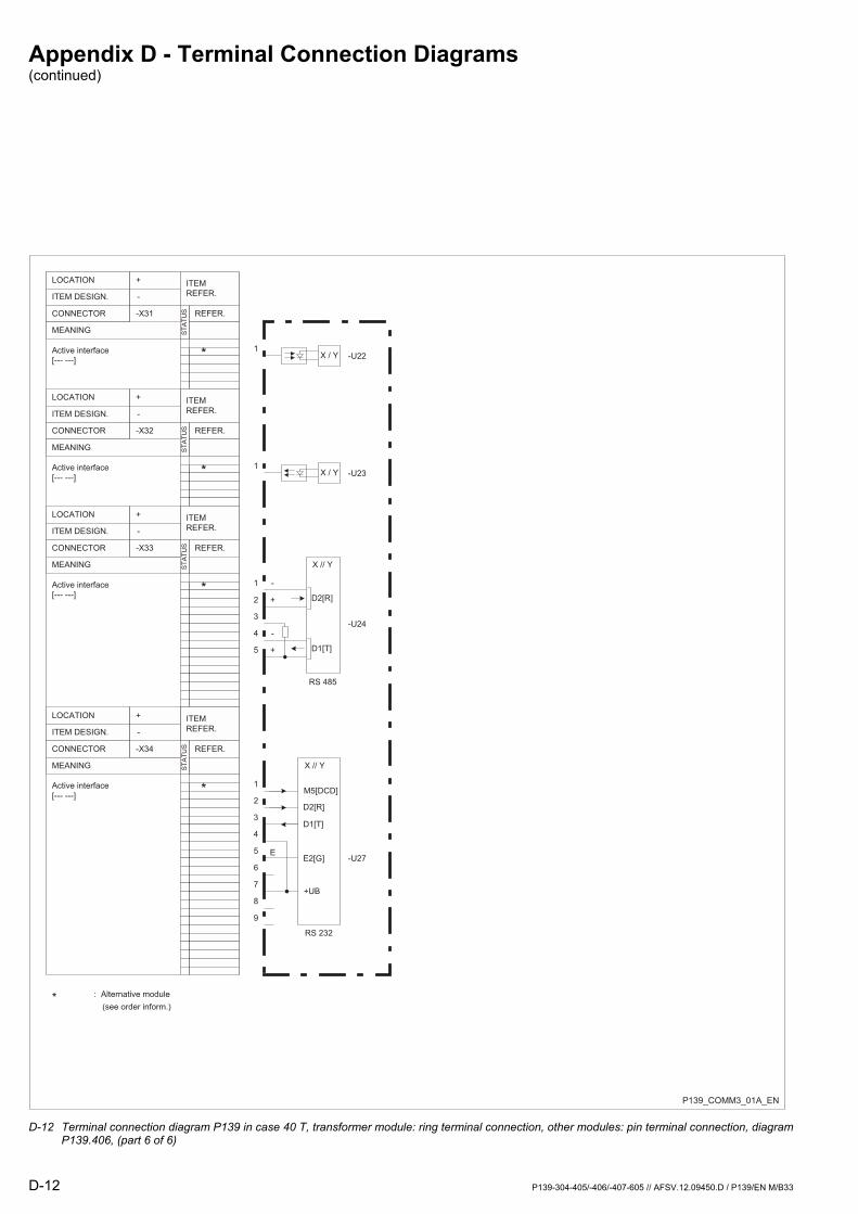
Appendix D - Terminal Connection Diagrams (continued)
D-12 P139-304-405/-406/-407-605 // AFSV.12.09450.D / P139/EN M/B33
-
+
LOCATION
ITEM DESIGN.
CONNECTOR
MEANING
+
-
-X31
P139_COMM3_01A_EN
ITEM
REFER.
*
RS 485
1
2
3
4
5
6
7
8
9
E
X / Y
1
2
3
4
5
1
X / Y1
* : Alternative module
(see order inform.)
ST
AT
US REFER.
LOCATION
ITEM DESIGN.
CONNECTOR
MEANING
-X32
ITEM
REFER.
*
ST
AT
US REFER.
LOCATION
ITEM DESIGN.
CONNECTOR
MEANING
-X33
ITEM
REFER.
*
ST
AT
US REFER.
LOCATION
ITEM DESIGN.
CONNECTOR
MEANING
-X34
ITEM
REFER.
*
ST
AT
US REFER.
+
-
+
-
+
-
-U22
-U24
-U27
-U23
Active interface
[--- ---]
Active interface
[--- ---]
Active interface
[--- ---]
Active interface
[--- ---]
-
+
X // Y
D2[R]
D1[T]
D1[T]
D2[R]
RS 232
E2[G]
X // Y
M5[DCD]
+UB
D-12 Terminal connection diagram P139 in case 40 T, transformer module: ring terminal connection, other modules: pin terminal connection, diagram
P139.406, (part 6 of 6)
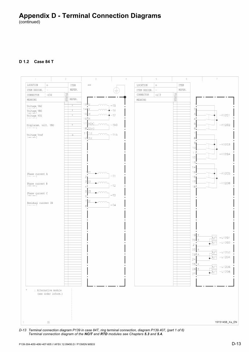
Appendix D - Terminal Connection Diagrams (continued)
P139-304-405/-406/-407-605 // AFSV.12.09450.D / P139/EN M/B33 D-13
D 1.2 Case 84 T
-X121LOCATION
ITEM DESIGN.
CONNECTOR
MEANING
ITEM
REFER.
REFER.
Voltage VAG
Voltage VBG
Voltage VCG
Displacem. volt. VNG
Voltage Vref
Phase current A
Phase current B
Phase current C
Residual current IN
Alternative module
(see order inform.)
19Y5145B_Xa_EN
LOCATION
ITEM DESIGN.
CONNECTOR
MEANING
ITEM
REFER.
D-13 Terminal connection diagram P139 in case 84T, ring terminal connection, diagram P139.407, (part 1 of 6)
Terminal connection diagram of the NCIT and RTD modules see Chapters 5.3 and 5.4.
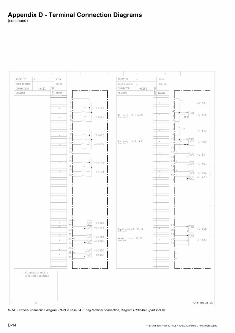
Appendix D - Terminal Connection Diagrams (continued)
D-14 P139-304-405/-406/-407-605 // AFSV.12.09450.D / P139/EN M/B33
-X141 -X161
-
LOCATION
ITEM DESIGN.
CONNECTION
MEANING
ITEM
REFER.
REFER.
Alternative module
(see order inform.)
19Y5146B_Xa_EN
LOCATION
ITEM DESIGN.
CONNECTOR
MEANING
ITEM
DESIGN.
REFER.
An. outp. ch.1 (A-1)
An. outp. ch.2 (A-2)
Input channel 1(I-1)
Measur. input PT100
D-14 Terminal connection diagram P139 in case 84 T, ring terminal connection, diagram P139.407, (part 2 of 6)
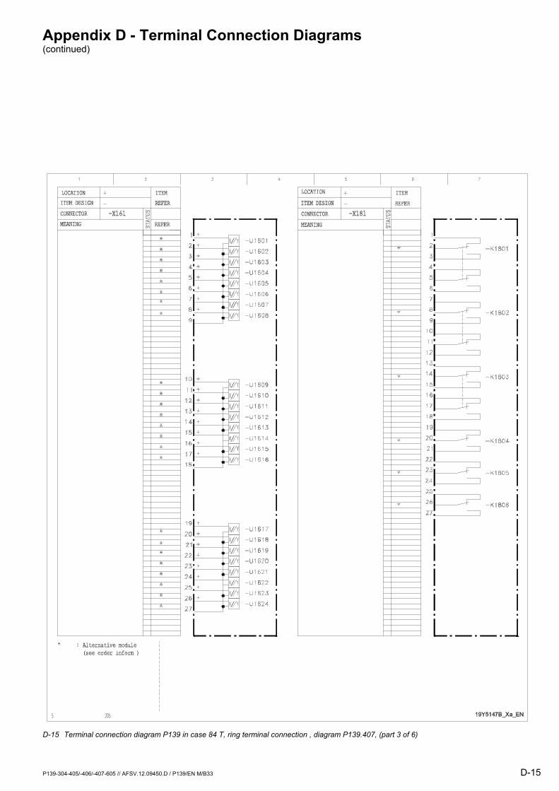
Appendix D - Terminal Connection Diagrams (continued)
P139-304-405/-406/-407-605 // AFSV.12.09450.D / P139/EN M/B33 D-15
D-15 Terminal connection diagram P139 in case 84 T, ring terminal connection , diagram P139.407, (part 3 of 6)
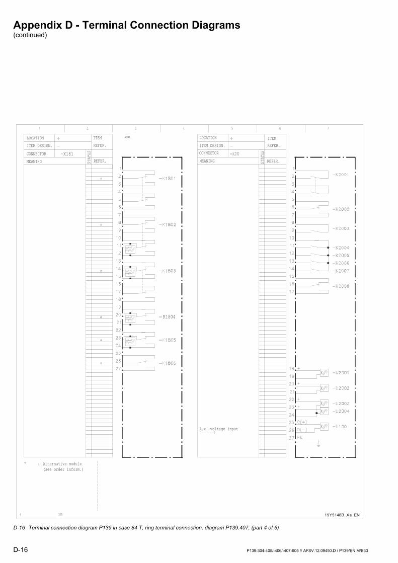
Appendix D - Terminal Connection Diagrams (continued)
D-16 P139-304-405/-406/-407-605 // AFSV.12.09450.D / P139/EN M/B33
-X201
-X181
LOCATION
ITEM DESIGN.
CONNECTOR
MEANING
ITEM
REFER.
REFER.
Alternative module
(see order inform.)
Aux. voltage input
LOCATION
ITEM DESIGN.
CONNECTOR
MEANING
ITEM
REFER.
REFER.
K1804
19Y5148B_Xa_EN D-16 Terminal connection diagram P139 in case 84 T, ring terminal connection, diagram P139.407, (part 4 of 6)
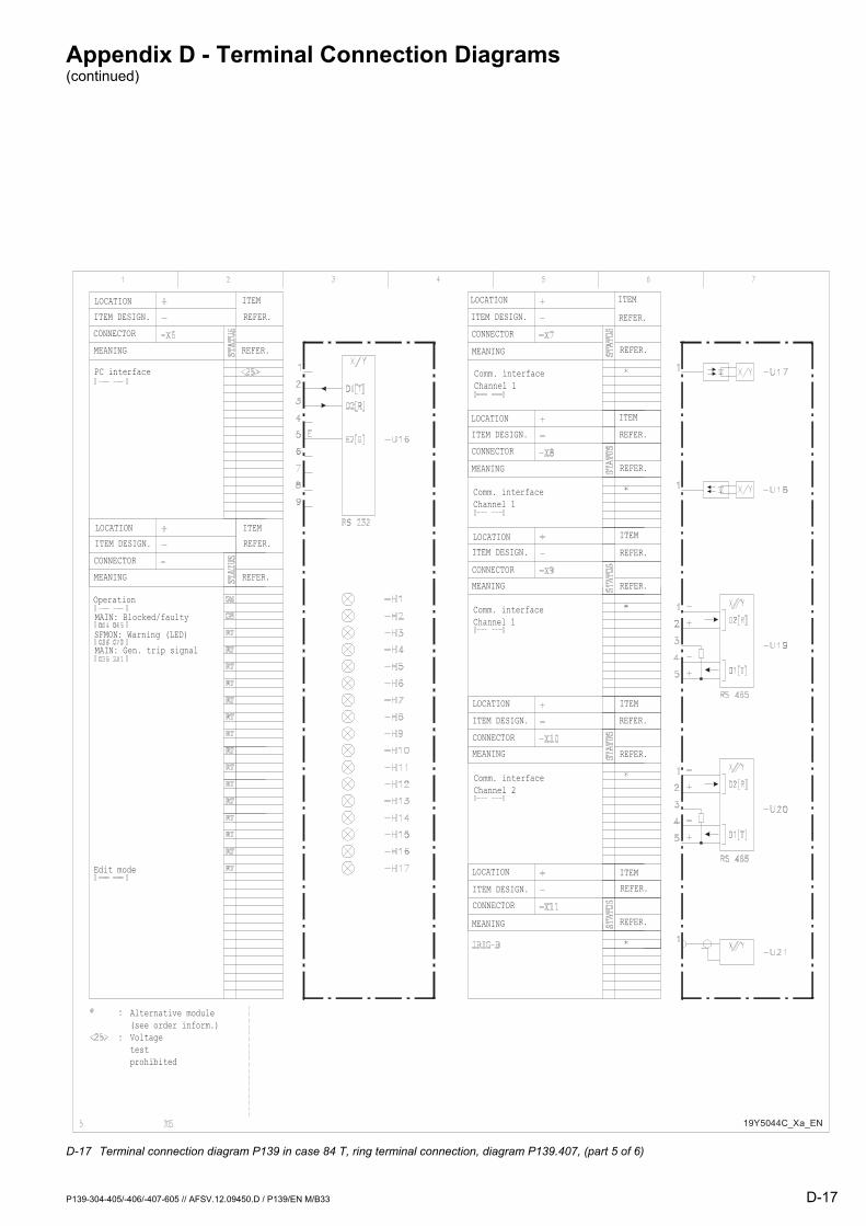
Appendix D - Terminal Connection Diagrams (continued)
P139-304-405/-406/-407-605 // AFSV.12.09450.D / P139/EN M/B33 D-17
19Y5044C_Xa_EN
LOCATION
ITEM DESIGN.
CONNECTOR
MEANING
ITEM
REFER.
REFER.
PC interface
LOCATION
ITEM DESIGN.
CONNECTOR
MEANING
ITEM
REFER.
REFER.
Operation
MAIN: Blocked/faulty
SFMON: Warning (LED)
MAIN: Gen. trip signal
Edit mode
Alternative module
(see order inform.)
Voltage
test
prohibited
LOCATION
ITEM DESIGN.
CONNECTOR
MEANING
ITEM
REFER.
REFER.
Comm. interface
Channel 1
LOCATION
ITEM DESIGN.
CONNECTOR
MEANING
ITEM
REFER.
REFER.
Comm. interface
Channel 1
Comm. interface
Channel 1
Comm. interface
Channel 2
LOCATION
ITEM DESIGN.
CONNECTOR
MEANING
ITEM
REFER.
REFER.
LOCATION
ITEM DESIGN.
CONNECTOR
MEANING
ITEM
REFER.
REFER.
LOCATION
ITEM DESIGN.
CONNECTOR
MEANING
ITEM
REFER.
REFER.
D-17 Terminal connection diagram P139 in case 84 T, ring terminal connection, diagram P139.407, (part 5 of 6)

Appendix D - Terminal Connection Diagrams (continued)
D-18 P139-304-405/-406/-407-605 // AFSV.12.09450.D / P139/EN M/B33
-
+
LOCATION
ITEM DESIGN.
CONNECTOR
MEANING
+
-
-X31
P139_COMM3_01A_EN
ITEM
REFER.
*
RS 485
1
2
3
4
5
6
7
8
9
E
X / Y
1
2
3
4
5
1
X / Y1
* : Alternative module
(see order inform.)
ST
AT
US REFER.
LOCATION
ITEM DESIGN.
CONNECTOR
MEANING
-X32
ITEM
REFER.
*
ST
AT
US REFER.
LOCATION
ITEM DESIGN.
CONNECTOR
MEANING
-X33
ITEM
REFER.
*
ST
AT
US REFER.
LOCATION
ITEM DESIGN.
CONNECTOR
MEANING
-X34
ITEM
REFER.
*
ST
AT
US REFER.
+
-
+
-
+
-
-U22
-U24
-U27
-U23
Active interface
[--- ---]
Active interface
[--- ---]
Active interface
[--- ---]
Active interface
[--- ---]
-
+
X // Y
D2[R]
D1[T]
D1[T]
D2[R]
RS 232
E2[G]
X // Y
M5[DCD]
+UB
D-18 Terminal connection diagram P139 in case 84 T, ring terminal connection, diagram P139.407, (part 6 of 6)
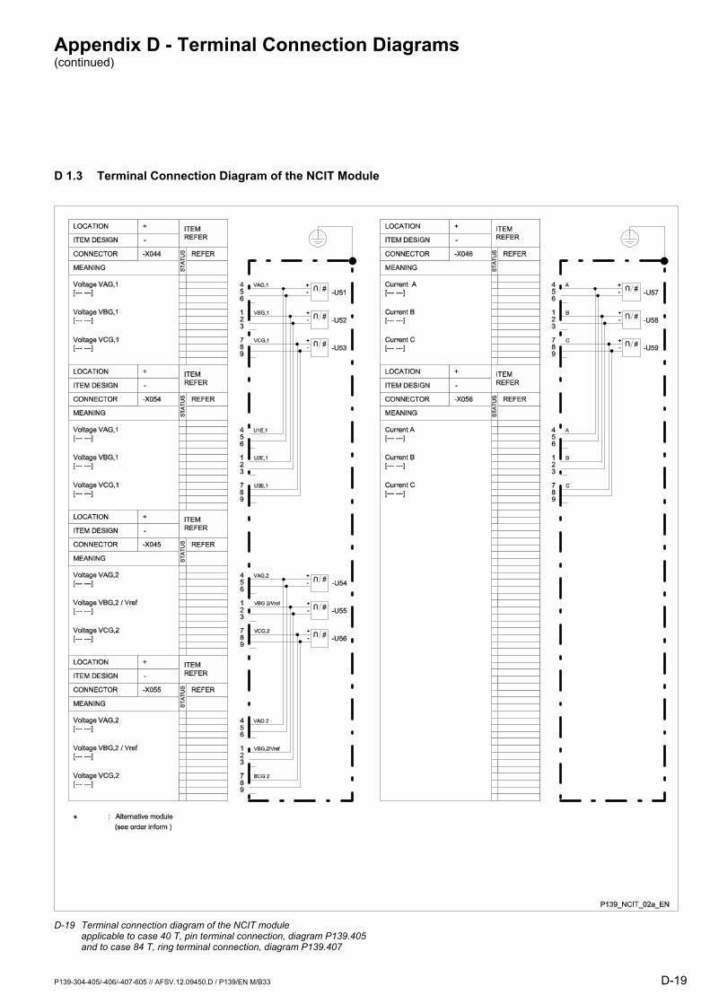
Appendix D - Terminal Connection Diagrams (continued)
P139-304-405/-406/-407-605 // AFSV.12.09450.D / P139/EN M/B33 D-19
D 1.3 Terminal Connection Diagram of the NCIT Module
D-19 Terminal connection diagram of the NCIT module
applicable to case 40 T, pin terminal connection, diagram P139.405 and to case 84 T, ring terminal connection, diagram P139.407
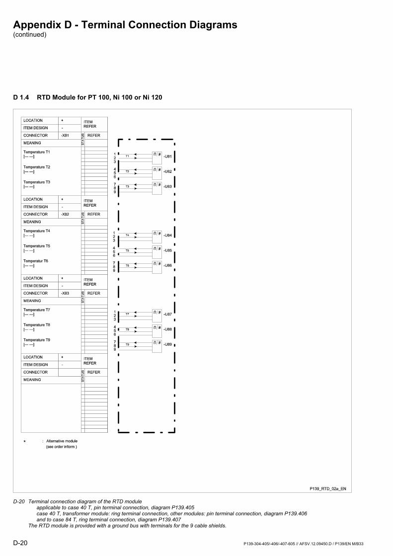
Appendix D - Terminal Connection Diagrams (continued)
D-20 P139-304-405/-406/-407-605 // AFSV.12.09450.D / P139/EN M/B33
D 1.4 RTD Module for PT 100, Ni 100 or Ni 120
D-20 Terminal connection diagram of the RTD module
applicable to case 40 T, pin terminal connection, diagram P139.405 case 40 T, transformer module: ring terminal connection, other modules: pin terminal connection, diagram P139.406 and to case 84 T, ring terminal connection, diagram P139.407 The RTD module is provided with a ground bus with terminals for the 9 cable shields.
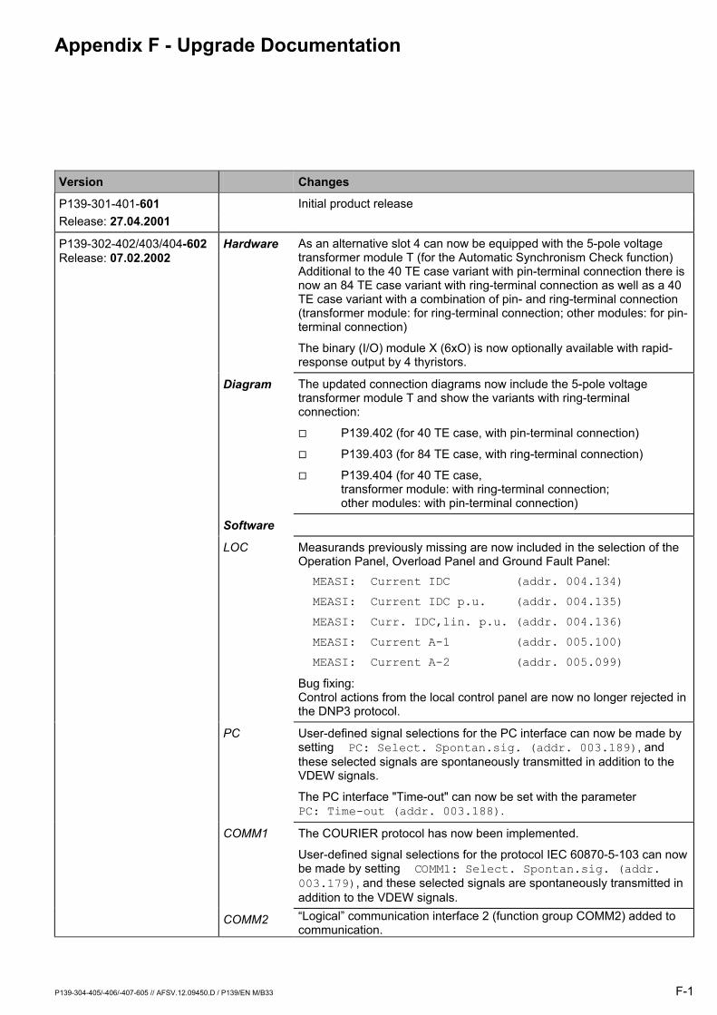
Appendix F - Upgrade Documentation
P139-304-405/-406/-407-605 // AFSV.12.09450.D / P139/EN M/B33 F-1
Version Changes
P139-301-401-601 Initial product release Release: 27.04.2001
P139-302-402/403/404-602 Release: 07.02.2002
Hardware As an alternative slot 4 can now be equipped with the 5-pole voltage transformer module T (for the Automatic Synchronism Check function) Additional to the 40 TE case variant with pin-terminal connection there is now an 84 TE case variant with ring-terminal connection as well as a 40 TE case variant with a combination of pin- and ring-terminal connection (transformer module: for ring-terminal connection; other modules: for pin-terminal connection)
The binary (I/O) module X (6xO) is now optionally available with rapid-response output by 4 thyristors.
Diagram The updated connection diagrams now include the 5-pole voltage transformer module T and show the variants with ring-terminal connection:
! P139.402 (for 40 TE case, with pin-terminal connection)
! P139.403 (for 84 TE case, with ring-terminal connection)
! P139.404 (for 40 TE case, transformer module: with ring-terminal connection; other modules: with pin-terminal connection)
Software
LOC Measurands previously missing are now included in the selection of the Operation Panel, Overload Panel and Ground Fault Panel: MEASI: Current IDC (addr. 004.134) MEASI: Current IDC p.u. (addr. 004.135) MEASI: Curr. IDC,lin. p.u. (addr. 004.136) MEASI: Current A-1 (addr. 005.100) MEASI: Current A-2 (addr. 005.099) Bug fixing: Control actions from the local control panel are now no longer rejected in the DNP3 protocol.
PC User-defined signal selections for the PC interface can now be made by setting PC: Select. Spontan.sig. (addr. 003.189), and these selected signals are spontaneously transmitted in addition to the VDEW signals.
The PC interface "Time-out" can now be set with the parameter PC: Time-out (addr. 003.188).
COMM1 The COURIER protocol has now been implemented.
User-defined signal selections for the protocol IEC 60870-5-103 can now be made by setting COMM1: Select. Spontan.sig. (addr. 003.179), and these selected signals are spontaneously transmitted in addition to the VDEW signals.
COMM2 Logical communication interface 2 (function group COMM2) added to communication.
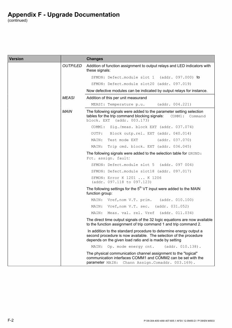
Appendix F - Upgrade Documentation (continued)
F-2 P139-304-405/-406/-407-605 // AFSV.12.09450.D / P139/EN M/B33
Version Changes
OUTP/LED Addition of function assignment to output relays and LED indicators with these signals:
SFMON: Defect.module slot 1 (addr. 097.000) to SFMON: Defect.module slot20 (addr. 097.019) Now defective modules can be indicated by output relays for instance.
MEASI Addition of this per unit measurand MEASI: Temperature p.u. (addr. 004.221)
MAIN The following signals were added to the parameter setting selection tables for the trip command blocking signals: COMM1: Command block. EXT (addr. 003.173) COMM1: Sig./meas. block EXT (addr. 037.074) OUTP: Block outp.rel. EXT (addr. 040.014) MAIN: Test mode EXT (addr. 037.070) MAIN: Trip cmd. block. EXT (addr. 036.045) The following signals were added to the selection table for GRUND: Fct. assign. fault: SFMON: Defect.module slot 5 (addr. 097 004) SFMON: Defect.module slot18 (addr. 097.017) SFMON: Error K 1201 ... K 1206 (addr. 097.118 to 097.123) The following settings for the 5th VT input were added to the MAIN function group: MAIN: Vref,nom V.T. prim. (addr. 010.100) MAIN: Vref,nom V.T. sec. (addr. 031.052) MAIN: Meas. val. rel. Vref (addr. 011.034) The direct time output signals of the 32 logic equations are now available to the function assignment of trip command 1 and trip command 2.
In addition to the standard procedure to determine energy output a second procedure is now available. The selection of the procedure depends on the given load ratio and is made by setting MAIN: Op. mode energy cnt. (addr. 010.138). The physical communication channel assignment to the "logical" communication interfaces COMM1 and COMM2 can be set with the parameter MAIN: Chann Assign.Comaddr. 003.169).
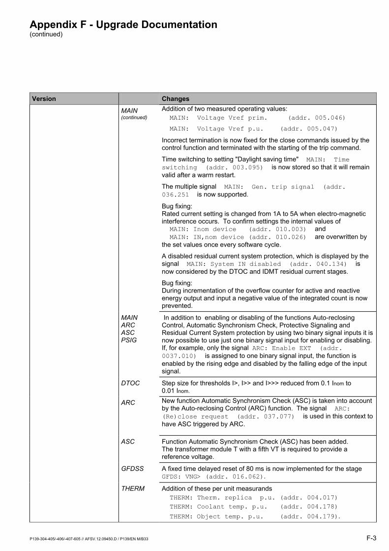
Appendix F - Upgrade Documentation (continued)
P139-304-405/-406/-407-605 // AFSV.12.09450.D / P139/EN M/B33 F-3
Version Changes MAIN
(continued) Addition of two measured operating values: MAIN: Voltage Vref prim. (addr. 005.046) MAIN: Voltage Vref p.u. (addr. 005.047) Incorrect termination is now fixed for the close commands issued by the control function and terminated with the starting of the trip command.
Time switching to setting "Daylight saving time" MAIN: Time switching (addr. 003.095) is now stored so that it will remain valid after a warm restart.
The multiple signal MAIN: Gen. trip signal (addr. 036.251 is now supported.
Bug fixing: Rated current setting is changed from 1A to 5A when electro-magnetic interference occurs. To confirm settings the internal values of MAIN: Inom device (addr. 010.003) and MAIN: IN,nom device (addr. 010.026) are overwritten by the set values once every software cycle.
A disabled residual current system protection, which is displayed by the signal MAIN: System IN disabled (addr. 040.134) is now considered by the DTOC and IDMT residual current stages.
Bug fixing: During incrementation of the overflow counter for active and reactive energy output and input a negative value of the integrated count is now prevented.
MAIN ARC ASC PSIG
In addition to enabling or disabling of the functions Auto-reclosing Control, Automatic Synchronism Check, Protective Signaling and Residual Current System protection by using two binary signal inputs it is now possible to use just one binary signal input for enabling or disabling. If, for example, only the signal ARC: Enable EXT (addr. 0037.010) is assigned to one binary signal input, the function is enabled by the rising edge and disabled by the falling edge of the input signal.
DTOC Step size for thresholds I>, I>> and I>>> reduced from 0.1 Inom to 0.01 Inom.
ARC New function Automatic Synchronism Check (ASC) is taken into account by the Auto-reclosing Control (ARC) function. The signal ARC: (Re)close request (addr. 037.077) is used in this context to have ASC triggered by ARC.
ASC Function Automatic Synchronism Check (ASC) has been added. The transformer module T with a fifth VT is required to provide a reference voltage.
GFDSS A fixed time delayed reset of 80 ms is now implemented for the stage GFDS: VNG> (addr. 016.062).
THERM Addition of these per unit measurands THERM: Therm. replica p.u. (addr. 004.017) THERM: Coolant temp. p.u. (addr. 004.178) THERM: Object temp. p.u. (addr. 004.179).
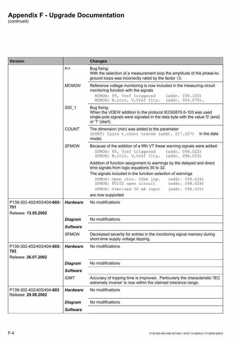
Appendix F - Upgrade Documentation (continued)
F-4 P139-304-405/-406/-407-605 // AFSV.12.09450.D / P139/EN M/B33
Version Changes
f<> Bug fixing: With the selection of a measurement loop the amplitude of the phase-to-ground loops was incorrectly rated by the factor √3.
MCMON Reference voltage monitoring is now included in the measuring-circuit monitoring function with the signals MCMON: FF, Vref triggered (addr. 038.100) MCMON: M.circ. V,Vref flty. (addr. 004.078).
SIG_1 Bug fixing: When the VDEW addition to the protocol IEC60870-5-103 was used single-pole signals were signaled in the data byte with the value '0' (end) or '1' (start).
COUNT The dimension (min) was added to the parameter COUNT: Cycle t.count transm (addr. 217.007) in the data model.
SFMON Because of the addition of a fifth VT these warning signals were added: SFMON: FF, Vref triggered (addr. 098.022) SFMON: M.circ. V,Vref flty. (addr. 098.023) Addition of function assignment to warnings by the delayed and direct time signals from logic equations 30 to 32. The signals included in the function selection of warnings SFMON: Open circ. 20mA inp. (addr. 098.026) SFMON: PT100 open circuit (addr. 098.024) SFMON: Overload 20 mA input (addr. 098.025) are now supported.
P139-302-402/403/404-602-701 Release: 13.05.2002
Hardware No modifications
Diagram No modifications
Software
SFMON Decreased severity for entries in the monitoring signal memory during short-time supply voltage dipping.
P139-302-402/403/404-602-702 Release: 26.07.2002
Hardware No modifications
Diagram No modifications
Software
IDMT Accuracy of tripping time is improved. Particularly the characteristic 'IEC extremely inverse' is now within the claimed tolerance range.
P139-302-402/403/404-603 Release: 29.08.2002
Hardware No modifications
Diagram No modifications
Software
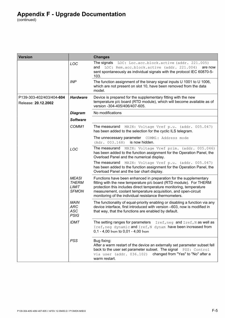
Appendix F - Upgrade Documentation (continued)
P139-304-405/-406/-407-605 // AFSV.12.09450.D / P139/EN M/B33 F-5
Version Changes
LOC The signals LOC: Loc.acc.block.active (addr. 221.005) and LOC: Rem.acc.block.active (addr. 221.004) are now sent spontaneously as individual signals with the protocol IEC 60870-5-103.
INP The function assignment of the binary signal inputs U 1001 to U 1006, which are not present on slot 10, have been removed from the data model.
P139-303-402/403/404-604 Release: 20.12.2002
Hardware Device is prepared for the supplementary fitting with the new temperature p/c board (RTD module), which will become available as of version -304-405/406/407-605.
Diagram No modifications
Software
COMM1 The measurand MAIN: Voltage Vref p.u. (addr. 005.047) has been added to the selection for the cyclic ILS telegram.
The unnecessary parameter COMM1: Address mode (Adr. 003.168) is now hidden.
LOC The measurand MAIN: Voltage Vref prim. (addr. 005.046) has been added to the function assignment for the Operation Panel, the Overload Panel and the numerical display. The measurand MAIN: Voltage Vref p.u. (addr. 005.047) has been added to the function assignment for the Operation Panel, the Overload Panel and the bar chart display.
MEASI THERM LIMIT SFMON
Functions have been enhanced in preparation for the supplementary fitting with the new temperature p/c board (RTD module). For THERM protection this includes direct temperature monitoring, temperature measurement, coolant temperature acquisition, and open-circuit monitoring of the individual resistance thermometers.
MAIN ARC ASC PSIG
The functionality of equal-priority enabling or disabling a function via any device interface, first introduced with version 603, now is modified in that way, that the functions are enabled by default.
IDMT The setting ranges for parameters Iref,neg and Iref,N as well as Iref,neg dynamic and Iref,N dynam have been increased from 0,1 - 4,00 Inom to 0,01 - 4,00 Inom
PSS Bug fixing: After a warm restart of the device an externally set parameter subset fell back to the user set parameter subset. The signal PSS: Control via user (addr. 036.102) changed from "Yes" to "No" after a warm restart.
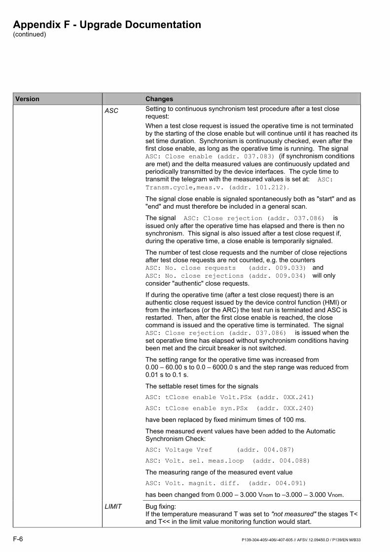
Appendix F - Upgrade Documentation (continued)
F-6 P139-304-405/-406/-407-605 // AFSV.12.09450.D / P139/EN M/B33
Version Changes
ASC Setting to continuous synchronism test procedure after a test close request: When a test close request is issued the operative time is not terminated by the starting of the close enable but will continue until it has reached its set time duration. Synchronism is continuously checked, even after the first close enable, as long as the operative time is running. The signal ASC: Close enable (addr. 037.083) (if synchronism conditions are met) and the delta measured values are continuously updated and periodically transmitted by the device interfaces. The cycle time to transmit the telegram with the measured values is set at: ASC: Transm.cycle,meas.v. (addr. 101.212).
The signal close enable is signaled spontaneously both as "start" and as "end" and must therefore be included in a general scan.
The signal ASC: Close rejection (addr. 037.086) is issued only after the operative time has elapsed and there is then no synchronism. This signal is also issued after a test close request if, during the operative time, a close enable is temporarily signaled.
The number of test close requests and the number of close rejections after test close requests are not counted, e.g. the counters ASC: No. close requests (addr. 009.033) and ASC: No. close rejections (addr. 009.034) will only consider "authentic" close requests.
If during the operative time (after a test close request) there is an authentic close request issued by the device control function (HMI) or from the interfaces (or the ARC) the test run is terminated and ASC is restarted. Then, after the first close enable is reached, the close command is issued and the operative time is terminated. The signal ASC: Close rejection (addr. 037.086) is issued when the set operative time has elapsed without synchronism conditions having been met and the circuit breaker is not switched.
The setting range for the operative time was increased from 0.00 60.00 s to 0.0 6000.0 s and the step range was reduced from 0.01 s to 0.1 s.
The settable reset times for the signals ASC: tClose enable Volt.PSx (addr. 0XX.241) ASC: tClose enable syn.PSx (addr. 0XX.240)
have been replaced by fixed minimum times of 100 ms.
These measured event values have been added to the Automatic Synchronism Check: ASC: Voltage Vref (addr. 004.087) ASC: Volt. sel. meas.loop (addr. 004.088)
The measuring range of the measured event value ASC: Volt. magnit. diff. (addr. 004.091) has been changed from 0.000 3.000 Vnom to 3.000 3.000 Vnom.
LIMIT Bug fixing: If the temperature measurand T was set to "not measured" the stages T< and T<< in the limit value monitoring function would start.
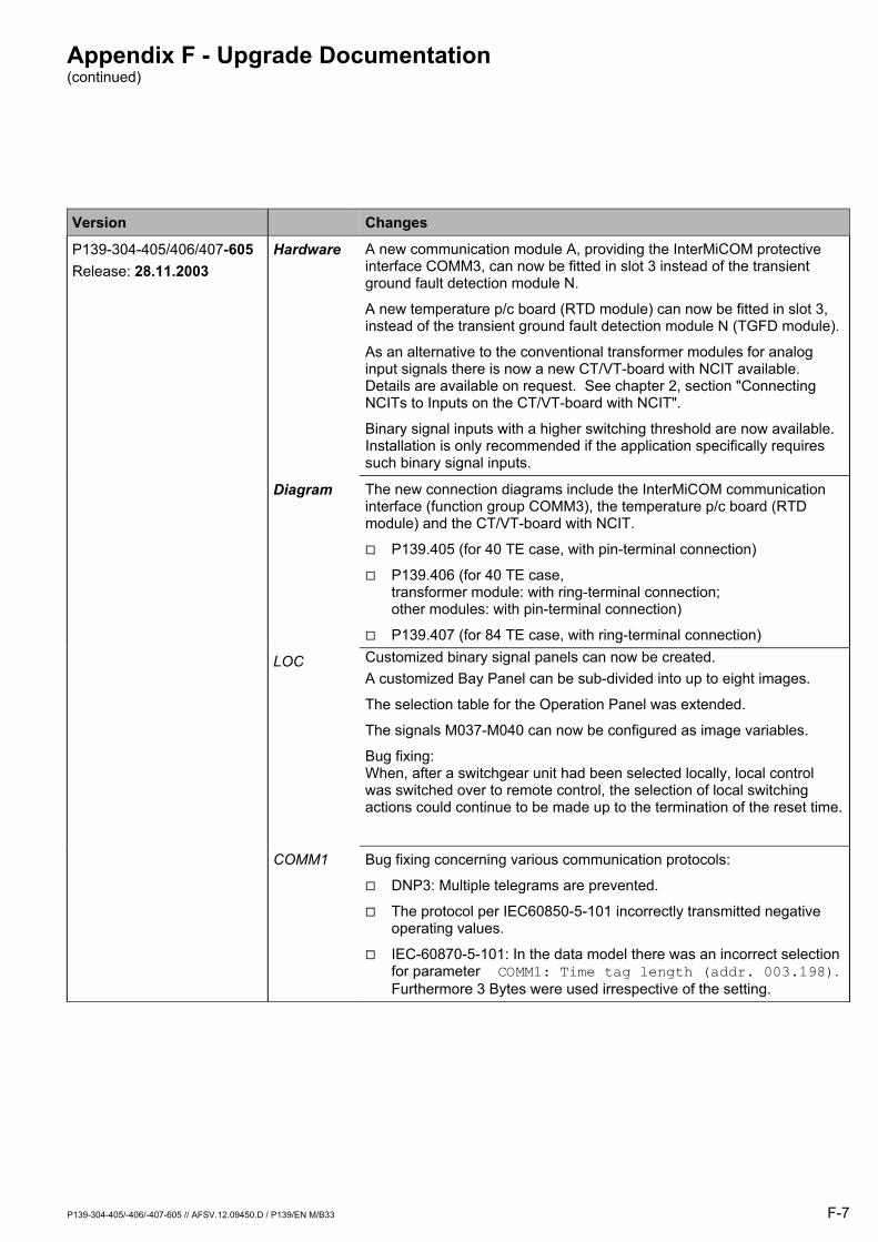
Appendix F - Upgrade Documentation (continued)
P139-304-405/-406/-407-605 // AFSV.12.09450.D / P139/EN M/B33 F-7
Version Changes
P139-304-405/406/407-605 Release: 28.11.2003
Hardware A new communication module A, providing the InterMiCOM protective interface COMM3, can now be fitted in slot 3 instead of the transient ground fault detection module N.
A new temperature p/c board (RTD module) can now be fitted in slot 3, instead of the transient ground fault detection module N (TGFD module).
As an alternative to the conventional transformer modules for analog input signals there is now a new CT/VT-board with NCIT available. Details are available on request. See chapter 2, section "Connecting NCITs to Inputs on the CT/VT-board with NCIT".
Binary signal inputs with a higher switching threshold are now available. Installation is only recommended if the application specifically requires such binary signal inputs.
Diagram The new connection diagrams include the InterMiCOM communication interface (function group COMM3), the temperature p/c board (RTD module) and the CT/VT-board with NCIT.
! P139.405 (for 40 TE case, with pin-terminal connection)
! P139.406 (for 40 TE case, transformer module: with ring-terminal connection; other modules: with pin-terminal connection)
! P139.407 (for 84 TE case, with ring-terminal connection)
LOC Customized binary signal panels can now be created. A customized Bay Panel can be sub-divided into up to eight images.
The selection table for the Operation Panel was extended.
The signals M037-M040 can now be configured as image variables.
Bug fixing: When, after a switchgear unit had been selected locally, local control was switched over to remote control, the selection of local switching actions could continue to be made up to the termination of the reset time.
COMM1 Bug fixing concerning various communication protocols:
! DNP3: Multiple telegrams are prevented.
! The protocol per IEC60850-5-101 incorrectly transmitted negative operating values.
! IEC-60870-5-101: In the data model there was an incorrect selection for parameter COMM1: Time tag length (addr. 003.198). Furthermore 3 Bytes were used irrespective of the setting.
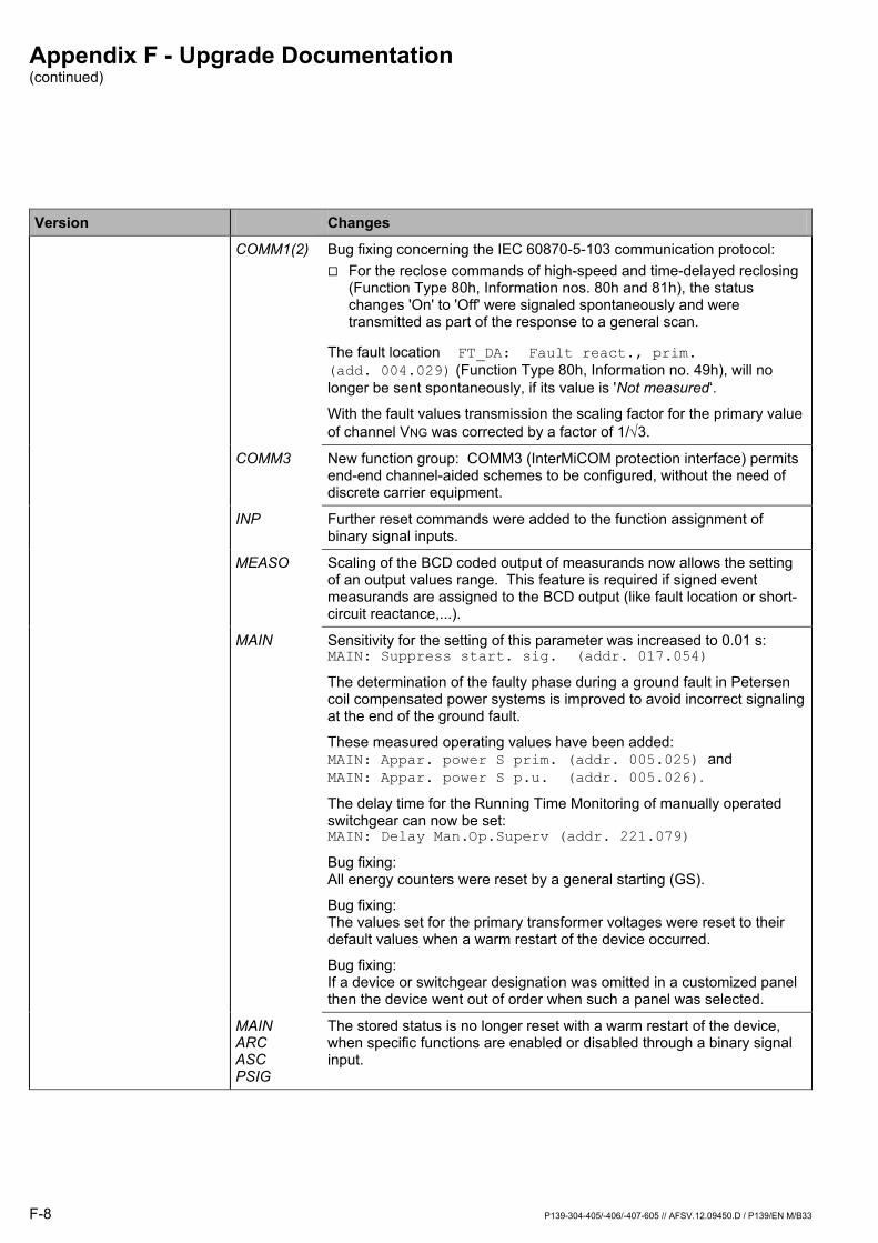
Appendix F - Upgrade Documentation (continued)
F-8 P139-304-405/-406/-407-605 // AFSV.12.09450.D / P139/EN M/B33
Version Changes
COMM1(2) Bug fixing concerning the IEC 60870-5-103 communication protocol: ! For the reclose commands of high-speed and time-delayed reclosing
(Function Type 80h, Information nos. 80h and 81h), the status changes 'On' to 'Off' were signaled spontaneously and were transmitted as part of the response to a general scan.
The fault location FT_DA: Fault react., prim. (add. 004.029) (Function Type 80h, Information no. 49h), will no longer be sent spontaneously, if its value is 'Not measured.
With the fault values transmission the scaling factor for the primary value of channel VNG was corrected by a factor of 1/√3.
COMM3 New function group: COMM3 (InterMiCOM protection interface) permits end-end channel-aided schemes to be configured, without the need of discrete carrier equipment.
INP Further reset commands were added to the function assignment of binary signal inputs.
MEASO Scaling of the BCD coded output of measurands now allows the setting of an output values range. This feature is required if signed event measurands are assigned to the BCD output (like fault location or short-circuit reactance,...).
MAIN Sensitivity for the setting of this parameter was increased to 0.01 s: MAIN: Suppress start. sig. (addr. 017.054)
The determination of the faulty phase during a ground fault in Petersen coil compensated power systems is improved to avoid incorrect signaling at the end of the ground fault.
These measured operating values have been added: MAIN: Appar. power S prim. (addr. 005.025) and MAIN: Appar. power S p.u. (addr. 005.026).
The delay time for the Running Time Monitoring of manually operated switchgear can now be set: MAIN: Delay Man.Op.Superv (addr. 221.079)
Bug fixing: All energy counters were reset by a general starting (GS).
Bug fixing: The values set for the primary transformer voltages were reset to their default values when a warm restart of the device occurred.
Bug fixing: If a device or switchgear designation was omitted in a customized panel then the device went out of order when such a panel was selected.
MAIN ARC ASC PSIG
The stored status is no longer reset with a warm restart of the device, when specific functions are enabled or disabled through a binary signal input.
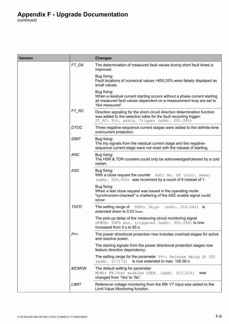
Appendix F - Upgrade Documentation (continued)
P139-304-405/-406/-407-605 // AFSV.12.09450.D / P139/EN M/B33 F-9
Version Changes
FT_DA The determination of measured fault values during short fault times is improved.
Bug fixing: Fault locations of numerical values >655.35% were falsely displayed as small values.
Bug fixing: When a residual current starting occurs without a phase current starting all measured fault values dependent on a measurement loop are set to 'Not measured'.
FT_RC
Direction signaling for the short-circuit direction determination function was added to the selection table for the fault recording trigger: FT_RC: Fct. assig. Trigger (addr. 003.085)
DTOC Three negative-sequence current stages were added to the definite-time overcurrent protection.
IDMT Bug fixing: The trip signals from the residual current stage and the negative-sequence current stage were not reset with the release of starting.
ARC Bug fixing: The HSR & TDR counters could only be acknowledged/cleared by a cold restart.
ASC Bug fixing: With a close request the counter ASC: No. GF (curr. meas) (addr. 009.003) was increment by a count of 8 instead of 1.
Bug fixing: When a test close request was issued in the operating mode "synchronism-checked" a chattering of the ASC enable signal could occur.
TGFD The setting range of TGFD: IN,p> (addr. 016.042) is extended down to 0.03 Inom.
The pick-up delay of the measuring circuit monitoring signal SFMON: TGFD mon. triggered (addr. 093.094) is now increased from 5 s to 65 s.
P<> The power directional protection now includes overload stages for active and reactive power.
The starting signals from the power directional protection stages now feature direction dependency.
The setting range for the parameter P<>: Release delay Q> PS1 (addr. 017172) is now extended to max. 100.00 s.
MCMON The default setting for parameter MCMO: FF,Vref enabled USER. (addr. 013.014) was changed from 'Yes' to 'No'.
LIMIT Reference voltage monitoring from the fifth VT input was added to the Limit Value Monitoring function.
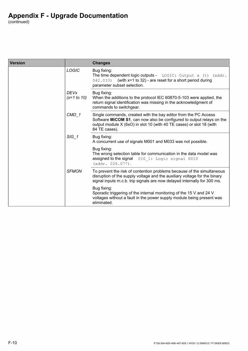
Appendix F - Upgrade Documentation (continued)
F-10 P139-304-405/-406/-407-605 // AFSV.12.09450.D / P139/EN M/B33
Version Changes
LOGIC Bug fixing: The time dependent logic outputs - LOGIC: Output x (t) (addr. 042.033) (with x=1 to 32) - are reset for a short period during parameter subset selection.
DEVx (x=1 to 10)
Bug fixing: When the additions to the protocol IEC 60870-5-103 were applied, the return signal identification was missing in the acknowledgment of commands to switchgear.
CMD_1 Single commands, created with the bay editor from the PC Access Software MiCOM S1, can now also be configured to output relays on the output module X (6xO) in slot 10 (with 40 TE cases) or slot 18 (with 84 TE cases).
SIG_1 Bug fixing: A concurrent use of signals M001 and M033 was not possible.
Bug fixing: The wrong selection table for communication in the data model was assigned to the signal SIG_1: Logic signal S010 (addr. 226.077).
SFMON To prevent the risk of contention problems because of the simultaneous disruption of the supply voltage and the auxiliary voltage for the binary signal inputs m.c.b. trip signals are now delayed internally for 300 ms.
Bug fixing: Sporadic triggering of the internal monitoring of the 15 V and 24 V voltages without a fault in the power supply module being present was eliminated.


AREVA T&D's Automation & Information Systems Business www.areva-td.com T&D Worldwide Contact Centre online 24 hours a day: +44 (0) 1785 25 00 70 http://www.areva-td.com/contactcentre/
Pub
licat
ion:
P13
9/E
N M
/B33
(AFS
V.1
2.09
450
D)
VO
L. 2
/2

MiCOM P139 Feeder Management and Bay
Control Version: P139 -304 -405/406/407 -605 P139 -306 -408/409/410 -611
Upgrade Documentation
P139/EN AD/A77 (AFSV.12.09690.D)

P139, Upgrade Documentation: -605 to -611
P139, Upgrade Documentation: -605 to -611
P139/EN AD/A77 // AFSV.12.09690 D /// P139-306-408/409/410-611 U-3
Contents
1 Overview U-5
2 Functional Details U-12 2.1 Communication interface IEC 61850 (Function Group IEC) U-12
2.2 Generic Object Oriented Substation Event (Function Group GOOSE) U-18
2.3 Generic Substation State Event (Function Group GSSE) U-32
2.4 Self-Monitoring (Function Group SFMON) U-43
2.5 Short-circuit direction determination (Function Group SCDD) U-44
2.6 Thermal overload protection (Function Group THERM) U-46
2.7 Circuit Breaker Failure Protection (Function Group CBF) U-58
2.8 Circuit Breaker Monitoring
(Function Group CBM) U-68
P139, Upgrade Documentation: -605 to -611 (continued)
U-4 P139/EN AD/A77 // AFSV.12.09690 D /// P139-306-408/409/410-611
In the new version of the P139 several enhanced features and changes on existing features have been included. These are described with reference to the Technical Manual listed below.
References Released Version Documentation
28.11.2003 P139-304-405/406/407-605 Technical Manual AFSV.12.09450/1 EN
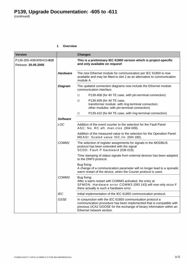
P139, Upgrade Documentation: -605 to -611 (continued)
P139/EN AD/A77 // AFSV.12.09690 D /// P139-306-408/409/410-611 U-5
1 Overview
Version Changes
This is a preliminary IEC 61850 version which is project-specific and only available on request!
P139-305-408/409/410-610 Release: 20.05.2005
Hardware The new Ethernet module for communication per IEC 61850 is now available and may be fitted to slot 2 as an alternative to communication module A.
Diagram The updated connection diagrams now include the Ethernet module communication interface.
P139.408 (for 40 TE case, with pin-terminal connection)
P139.409 (for 40 TE case, transformer module: with ring-terminal connection; other modules: with pin-terminal connection)
P139.410 (for 84 TE case, with ring-terminal connection)
Software
LOC Addition of the event counter to the selection for the Fault Panel ASC: No. RC af t . man.c los (004 009).
Addition of the measured value to the selection for the Operation Panel. MEASI: Scaled value IDC,l in (004 180).
COMM1 The selection of register assignments for signals in the MODBUS protocol has been extended with the signal SCDD: Faul t P backward (036 019).
Time stamping of status signals from external devices has been adapted to the DNP3 protocol.
Bug fixing: A change of a communication parameter will no longer lead to a sporadic warm restart of the device, when the Courier protocol is used.
COMM3 Bug fixing: After a warm restart with COMM3 activated, the entry at SFMON: Hardware error COMM3 (093 143) will now only occur if there actually is such a hardware error.
IEC Initial implementation of the IEC 61850 communication protocol.
GSSE In conjunction with the IEC 61850 communication protocol a communication procedure has been implemented that is compatible with previous UCA2 GOOSE for the exchange of binary information within an Ethernet network section.
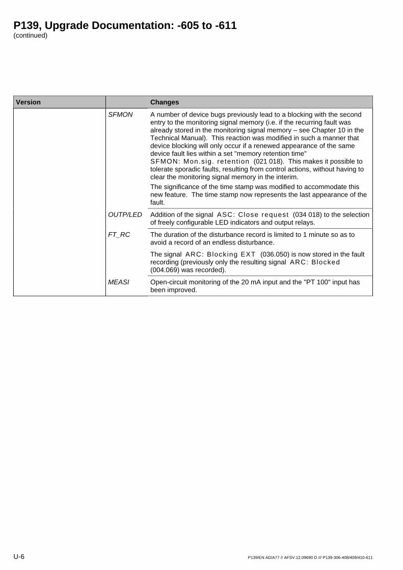
P139, Upgrade Documentation: -605 to -611 (continued)
U-6 P139/EN AD/A77 // AFSV.12.09690 D /// P139-306-408/409/410-611
Version Changes
SFMON A number of device bugs previously lead to a blocking with the second entry to the monitoring signal memory (i.e. if the recurring fault was already stored in the monitoring signal memory – see Chapter 10 in the Technical Manual). This reaction was modified in such a manner that device blocking will only occur if a renewed appearance of the same device fault lies within a set "memory retention time" SFMON: Mon.s ig. retent ion (021 018). This makes it possible to tolerate sporadic faults, resulting from control actions, without having to clear the monitoring signal memory in the interim. The significance of the time stamp was modified to accommodate this new feature. The time stamp now represents the last appearance of the fault.
OUTP/LED Addition of the signal ASC: Close request (034 018) to the selection of freely configurable LED indicators and output relays.
FT_RC The duration of the disturbance record is limited to 1 minute so as to avoid a record of an endless disturbance.
The signal ARC: Blocking EXT (036.050) is now stored in the fault recording (previously only the resulting signal ARC: Blocked (004.069) was recorded).
MEASI Open-circuit monitoring of the 20 mA input and the "PT 100" input has been improved.
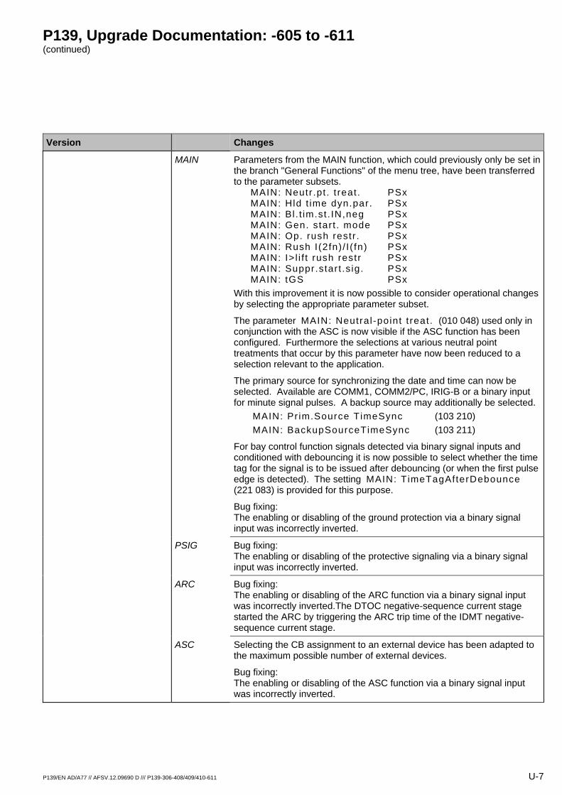
P139, Upgrade Documentation: -605 to -611 (continued)
P139/EN AD/A77 // AFSV.12.09690 D /// P139-306-408/409/410-611 U-7
Version Changes
MAIN Parameters from the MAIN function, which could previously only be set in the branch "General Functions" of the menu tree, have been transferred to the parameter subsets.
MAIN: Neutr .pt . t reat . PSx MAIN: Hld t ime dyn.par. PSx MAIN: Bl . t im.st . IN,neg PSx MAIN: Gen. star t . mode PSx MAIN: Op. rush restr . PSx MAIN: Rush I(2fn) / I ( fn) PSx MAIN: I> l i f t rush restr PSx MAIN: Suppr.star t .s ig. PSx MAIN: tGS PSx
With this improvement it is now possible to consider operational changes by selecting the appropriate parameter subset.
The parameter MAIN: Neutral-point t reat. (010 048) used only in conjunction with the ASC is now visible if the ASC function has been configured. Furthermore the selections at various neutral point treatments that occur by this parameter have now been reduced to a selection relevant to the application.
The primary source for synchronizing the date and time can now be selected. Available are COMM1, COMM2/PC, IRIG-B or a binary input for minute signal pulses. A backup source may additionally be selected.
MAIN: Pr im.Source TimeSync (103 210) MAIN: BackupSourceTimeSync (103 211)
For bay control function signals detected via binary signal inputs and conditioned with debouncing it is now possible to select whether the time tag for the signal is to be issued after debouncing (or when the first pulse edge is detected). The setting MAIN: TimeTagAfterDebounce (221 083) is provided for this purpose.
Bug fixing: The enabling or disabling of the ground protection via a binary signal input was incorrectly inverted.
PSIG Bug fixing: The enabling or disabling of the protective signaling via a binary signal input was incorrectly inverted.
ARC Bug fixing: The enabling or disabling of the ARC function via a binary signal input was incorrectly inverted.The DTOC negative-sequence current stage started the ARC by triggering the ARC trip time of the IDMT negative-sequence current stage.
ASC Selecting the CB assignment to an external device has been adapted to the maximum possible number of external devices.
Bug fixing: The enabling or disabling of the ASC function via a binary signal input was incorrectly inverted.
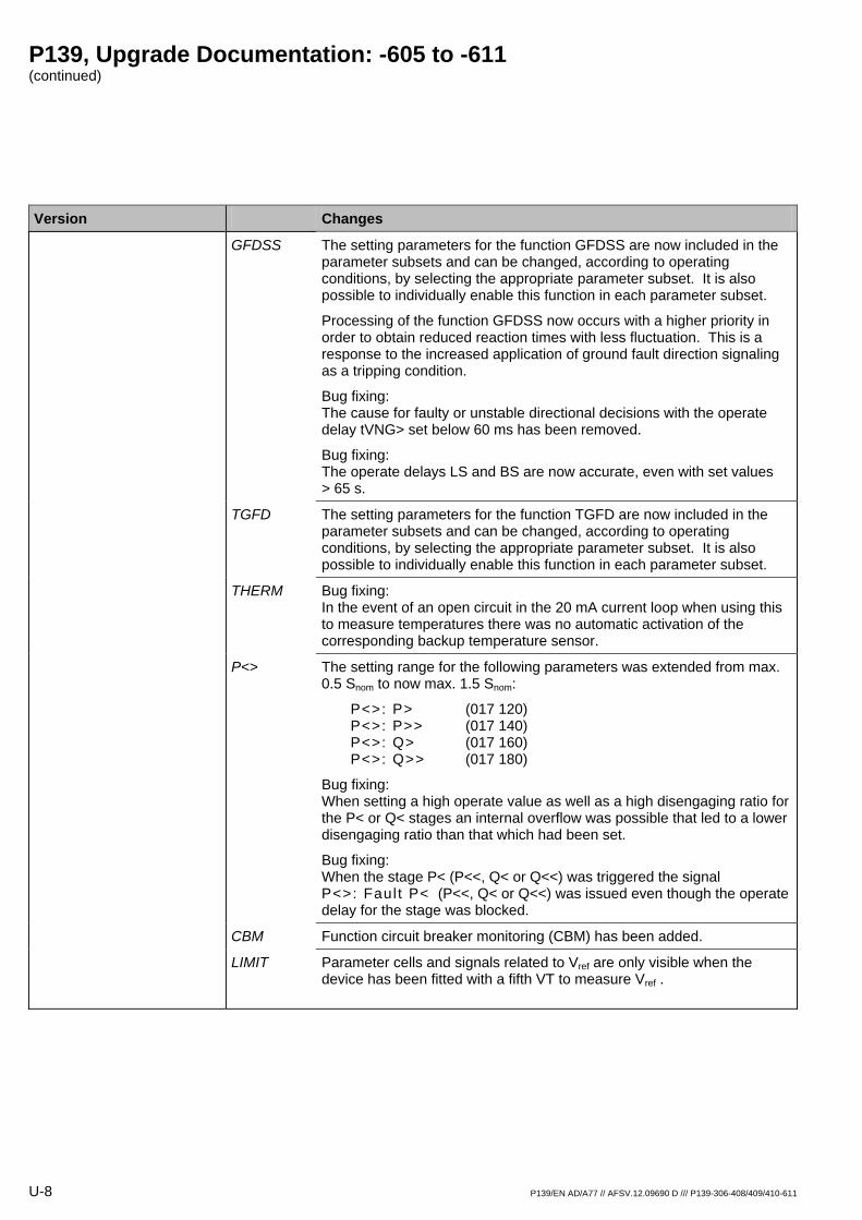
P139, Upgrade Documentation: -605 to -611 (continued)
U-8 P139/EN AD/A77 // AFSV.12.09690 D /// P139-306-408/409/410-611
Version Changes
GFDSS The setting parameters for the function GFDSS are now included in the parameter subsets and can be changed, according to operating conditions, by selecting the appropriate parameter subset. It is also possible to individually enable this function in each parameter subset.
Processing of the function GFDSS now occurs with a higher priority in order to obtain reduced reaction times with less fluctuation. This is a response to the increased application of ground fault direction signaling as a tripping condition.
Bug fixing: The cause for faulty or unstable directional decisions with the operate delay tVNG> set below 60 ms has been removed.
Bug fixing: The operate delays LS and BS are now accurate, even with set values > 65 s.
TGFD The setting parameters for the function TGFD are now included in the parameter subsets and can be changed, according to operating conditions, by selecting the appropriate parameter subset. It is also possible to individually enable this function in each parameter subset.
THERM Bug fixing: In the event of an open circuit in the 20 mA current loop when using this to measure temperatures there was no automatic activation of the corresponding backup temperature sensor.
P<> The setting range for the following parameters was extended from max. 0.5 Snom to now max. 1.5 Snom:
P<>: P> (017 120) P<>: P>> (017 140) P<>: Q> (017 160) P<>: Q>> (017 180)
Bug fixing: When setting a high operate value as well as a high disengaging ratio for the P< or Q< stages an internal overflow was possible that led to a lower disengaging ratio than that which had been set.
Bug fixing: When the stage P< (P<<, Q< or Q<<) was triggered the signal P<>: Faul t P< (P<<, Q< or Q<<) was issued even though the operate delay for the stage was blocked.
CBM Function circuit breaker monitoring (CBM) has been added.
LIMIT Parameter cells and signals related to Vref are only visible when the device has been fitted with a fifth VT to measure Vref .
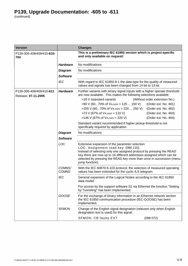
P139, Upgrade Documentation: -605 to -611 (continued)
P139/EN AD/A77 // AFSV.12.09690 D /// P139-306-408/409/410-611 U-9
Version Changes
This is a preliminary IEC 61850 version which is project-specific and only available on request!
P139-305-408/409/410-610-704
Hardware No modifications
Diagram No modifications
Software
IEC With regard to IEC 61850-8-1 the data type for the quality of measured values and signals has been changed from 14 bit to 13 bit.
P139-306-408/409/410-611 Release: 07.11.2005
Hardware Further variants with binary signal inputs with a higher operate threshold are now available. This makes the following selections available:
>18 V (standard variant) (Without order extension No.) >90 V (60...70% of VA,nom = 125 ... 150 V) (Order ext. No. 461) >155 V (60...70% of VA,nom = 220 ... 250 V) (Order ext. No. 462) >73 V (67% of VA,nom = 110 V) (Order ext. No. 463)
>146 V (67% of VA,nom = 220 V) (Order ext. No. 464)
Standard variant recommended if higher pickup threshold is not specifically required by application.
Diagram No modifications
Software
LOC Extensive expansion of the parameter selection LOC: Assignment read key (080 110). Instead of selecting only one assigned protocol by pressing the READ key there are now up to 16 different addresses assigned which can be selected by pressing the READ key more than once in succession (menu jump function).
COMM1/ COMM2
With the IEC 60870-5-103 protocol, the selection of measured operating values has been extended for the cyclic ILS telegram.
IEC General expansion of the Logical Nodes according to the IEC 61850 data model.
For access by the support software S1 via Ethernet the function "Setting by Tunneling" has been implemented.
GOOSE For the exchange of binary information in an Ethernet network section the IEC 61850 communication procedure (IEC-GOOSE) has been implemented.
SFMON Change of the English signal designation (relevant only when English designation text is used) for this signal:
SFMON: CB faul ty EXT (098 072)
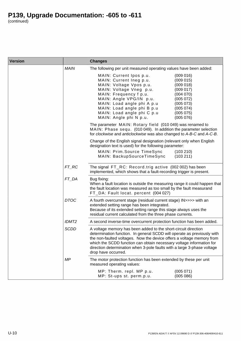
P139, Upgrade Documentation: -605 to -611 (continued)
U-10 P139/EN AD/A77 // AFSV.12.09690 D /// P139-306-408/409/410-611
Version Changes
MAIN The following per unit measured operating values have been added:
MAIN: Current Ipos p.u. (009 016) MAIN: Current Ineg p.u. (009 015) MAIN: Vol tage Vpos p.u. (009 018) MAIN: Vol tage Vneg p.u. (009 017) MAIN: Frequency f p.u. (004 070) MAIN: Angle VPG/IN p.u. (005 072) MAIN: Load angle phi A p.u (005 073) MAIN: Load angle phi B p.u (005 074) MAIN: Load angle phi C p.u (005 075) MAIN: Angle phi N p.u. (005 076)
The parameter MAIN: Rotary f ie ld (010 049) was renamed to MAIN: Phase sequ. (010 049). In addition the parameter selection for clockwise and anticlockwise was also changed to A-B-C and A-C-B.
Change of the English signal designation (relevant only when English designation text is used) for the following parameter:
MAIN: Pr im.Source TimeSync (103 210) MAIN: BackupSourceTimeSync (103 211)
FT_RC The signal FT_RC: Record.tr ig act ive (002 002) has been implemented, which shows that a fault-recording trigger is present.
FT_DA Bug fixing: When a fault location is outside the measuring range it could happen that the fault location was measured as too small by the fault measurand FT_DA: Faul t locat. percent (004 027)
DTOC A fourth overcurrent stage (residual current stage) IN>>>> with an extended setting range has been integrated. Because of its extended setting range this stage always uses the residual current calculated from the three phase currents.
IDMT2 A second inverse-time overcurrent protection function has been added.
SCDD A voltage memory has been added to the short-circuit direction determination function. In general SCDD will operate as previously with the non-faulted voltages. Now the device offers a voltage memory from which the SCDD function can obtain necessary voltage information for direction determination when 3-pole faults with a large 3-phase voltage drop have occurred.
MP The motor protection function has been extended by these per unit measured operating values:
MP: Therm. repl . MP p.u. (005 071) MP: St-ups st . perm.p.u. (005 086)
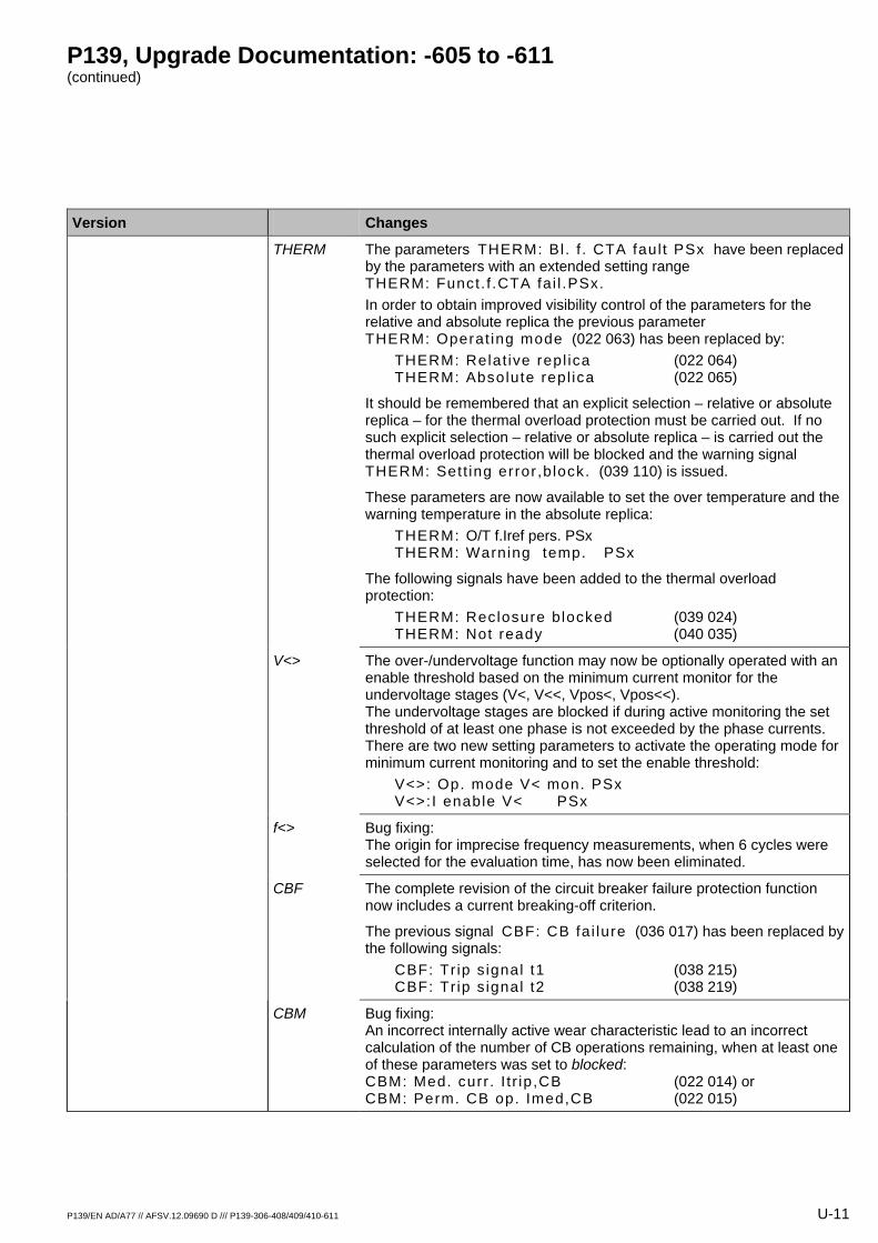
P139, Upgrade Documentation: -605 to -611 (continued)
P139/EN AD/A77 // AFSV.12.09690 D /// P139-306-408/409/410-611 U-11
Version Changes
THERM The parameters THERM: Bl . f . CTA faul t PSx have been replaced by the parameters with an extended setting range THERM: Funct. f .CTA fai l .PSx. In order to obtain improved visibility control of the parameters for the relative and absolute replica the previous parameter THERM: Operat ing mode (022 063) has been replaced by:
THERM: Relat ive repl ica (022 064) THERM: Absolute repl ica (022 065)
It should be remembered that an explicit selection – relative or absolute replica – for the thermal overload protection must be carried out. If no such explicit selection – relative or absolute replica – is carried out the thermal overload protection will be blocked and the warning signal THERM: Sett ing error ,b lock. (039 110) is issued.
These parameters are now available to set the over temperature and the warning temperature in the absolute replica:
THERM: O/T f.Iref pers. PSx THERM: Warning temp. PSx
The following signals have been added to the thermal overload protection:
THERM: Reclosure blocked (039 024) THERM: Not ready (040 035)
V<> The over-/undervoltage function may now be optionally operated with an enable threshold based on the minimum current monitor for the undervoltage stages (V<, V<<, Vpos<, Vpos<<). The undervoltage stages are blocked if during active monitoring the set threshold of at least one phase is not exceeded by the phase currents. There are two new setting parameters to activate the operating mode for minimum current monitoring and to set the enable threshold:
V<>: Op. mode V< mon. PSx V<>:I enable V< PSx
f<> Bug fixing: The origin for imprecise frequency measurements, when 6 cycles were selected for the evaluation time, has now been eliminated.
CBF The complete revision of the circuit breaker failure protection function now includes a current breaking-off criterion.
The previous signal CBF: CB fa i lure (036 017) has been replaced by the following signals:
CBF: Tr ip s ignal t1 (038 215) CBF: Tr ip s ignal t2 (038 219)
CBM Bug fixing: An incorrect internally active wear characteristic lead to an incorrect calculation of the number of CB operations remaining, when at least one of these parameters was set to blocked: CBM: Med. curr . I t r ip,CB (022 014) or CBM: Perm. CB op. Imed,CB (022 015)
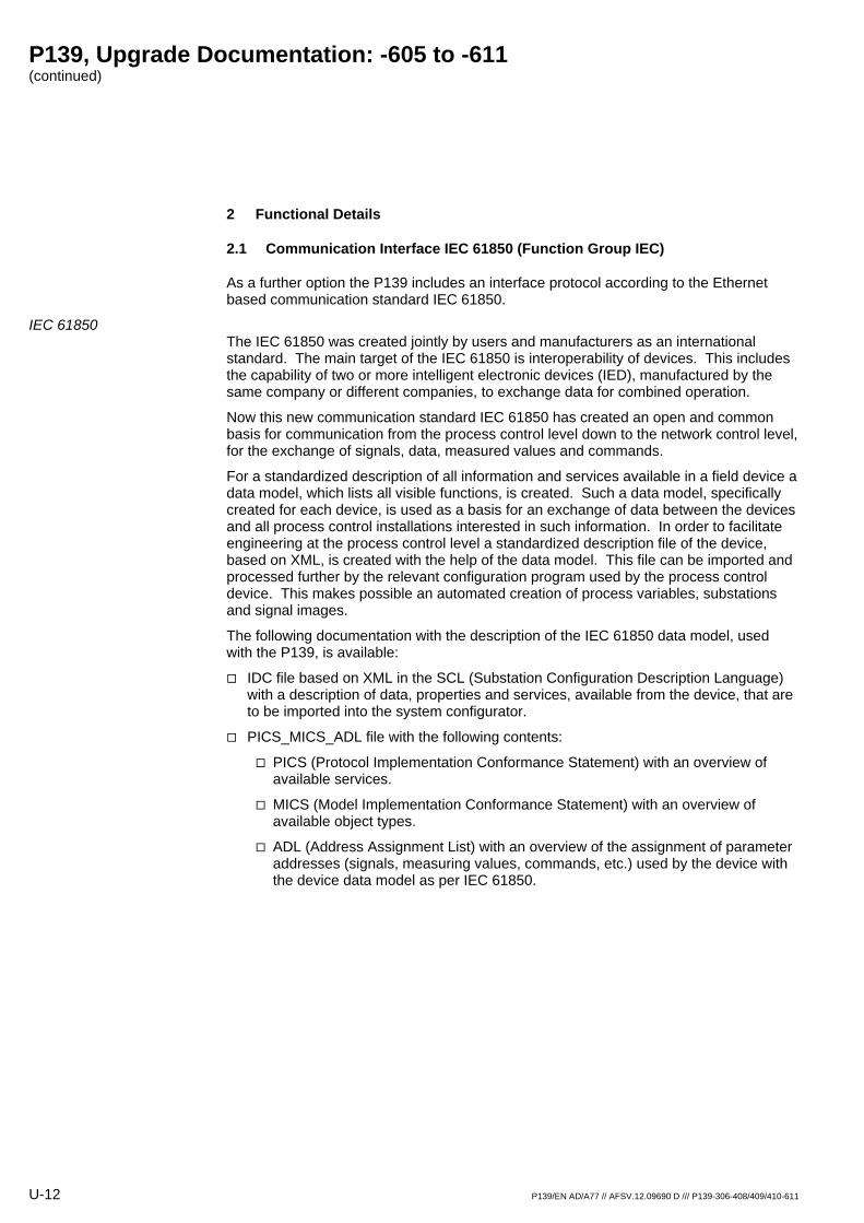
P139, Upgrade Documentation: -605 to -611 (continued)
U-12 P139/EN AD/A77 // AFSV.12.09690 D /// P139-306-408/409/410-611
2 Functional Details
2.1 Communication Interface IEC 61850 (Function Group IEC)
As a further option the P139 includes an interface protocol according to the Ethernet based communication standard IEC 61850.
IEC 61850 The IEC 61850 was created jointly by users and manufacturers as an international standard. The main target of the IEC 61850 is interoperability of devices. This includes the capability of two or more intelligent electronic devices (IED), manufactured by the same company or different companies, to exchange data for combined operation.
Now this new communication standard IEC 61850 has created an open and common basis for communication from the process control level down to the network control level, for the exchange of signals, data, measured values and commands.
For a standardized description of all information and services available in a field device a data model, which lists all visible functions, is created. Such a data model, specifically created for each device, is used as a basis for an exchange of data between the devices and all process control installations interested in such information. In order to facilitate engineering at the process control level a standardized description file of the device, based on XML, is created with the help of the data model. This file can be imported and processed further by the relevant configuration program used by the process control device. This makes possible an automated creation of process variables, substations and signal images.
The following documentation with the description of the IEC 61850 data model, used with the P139, is available:
IDC file based on XML in the SCL (Substation Configuration Description Language) with a description of data, properties and services, available from the device, that are to be imported into the system configurator.
PICS_MICS_ADL file with the following contents:
PICS (Protocol Implementation Conformance Statement) with an overview of available services.
MICS (Model Implementation Conformance Statement) with an overview of available object types.
ADL (Address Assignment List) with an overview of the assignment of parameter addresses (signals, measuring values, commands, etc.) used by the device with the device data model as per IEC 61850.
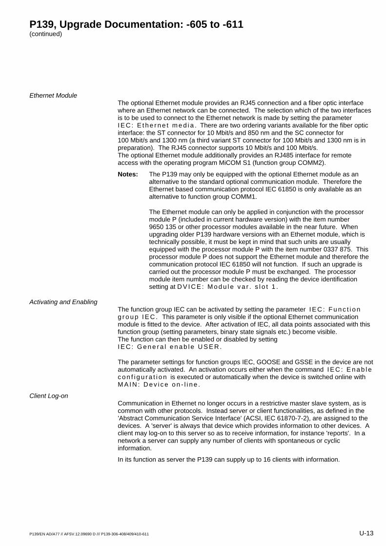
P139, Upgrade Documentation: -605 to -611 (continued)
P139/EN AD/A77 // AFSV.12.09690 D /// P139-306-408/409/410-611 U-13
Ethernet Module The optional Ethernet module provides an RJ45 connection and a fiber optic interface where an Ethernet network can be connected. The selection which of the two interfaces is to be used to connect to the Ethernet network is made by setting the parameter I E C : E t h e r n e t m e d i a . There are two ordering variants available for the fiber optic interface: the ST connector for 10 Mbit/s and 850 nm and the SC connector for 100 Mbit/s and 1300 nm (a third variant ST connector for 100 Mbit/s and 1300 nm is in preparation). The RJ45 connector supports 10 Mbit/s and 100 Mbit/s. The optional Ethernet module additionally provides an RJ485 interface for remote access with the operating program MiCOM S1 (function group COMM2).
Notes: The P139 may only be equipped with the optional Ethernet module as an alternative to the standard optional communication module. Therefore the Ethernet based communication protocol IEC 61850 is only available as an alternative to function group COMM1.
The Ethernet module can only be applied in conjunction with the processor module P (included in current hardware version) with the item number 9650 135 or other processor modules available in the near future. When upgrading older P139 hardware versions with an Ethernet module, which is technically possible, it must be kept in mind that such units are usually equipped with the processor module P with the item number 0337 875. This processor module P does not support the Ethernet module and therefore the communication protocol IEC 61850 will not function. If such an upgrade is carried out the processor module P must be exchanged. The processor module item number can be checked by reading the device identification setting at D V I C E : M o d u l e v a r . s l o t 1 .
Activating and Enabling The function group IEC can be activated by setting the parameter I E C : F u n c t i o n g r o u p I E C . This parameter is only visible if the optional Ethernet communication module is fitted to the device. After activation of IEC, all data points associated with this function group (setting parameters, binary state signals etc.) become visible. The function can then be enabled or disabled by setting I E C : G e n e r a l e n a b l e U S E R .
The parameter settings for function groups IEC, GOOSE and GSSE in the device are not automatically activated. An activation occurs either when the command I E C : E n a b l e c o n f i g u r a t i o n is executed or automatically when the device is switched online with M A I N : D e v i c e o n - l i n e .
Client Log-on Communication in Ethernet no longer occurs in a restrictive master slave system, as is common with other protocols. Instead server or client functionalities, as defined in the 'Abstract Communication Service Interface' (ACSI, IEC 61870-7-2), are assigned to the devices. A 'server' is always that device which provides information to other devices. A client may log-on to this server so as to receive information, for instance 'reports'. In a network a server can supply any number of clients with spontaneous or cyclic information.
In its function as server the P139 can supply up to 16 clients with information.
P139, Upgrade Documentation: -605 to -611 (continued)
U-14 P139/EN AD/A77 // AFSV.12.09690 D /// P139-306-408/409/410-611
Clock Synchronization With IEC 61850 clock synchronization occurs via the SNTP protocol, defined as standard for Ethernet. Here the P139 functions as SNTP client.
For clock synchronization one can select between the operating modes Broadcast from SNTP Server or Request from Server. With the first operating mode synchronization occurs by a broadcast message sent from the SNTP server to all devices in the network, and in the second operating mode the P139 requests the device specific time signal during a settable cycle.
Control and Monitoring of Switchgear Units
Control of switchgear units by the P139 can be carried out from all clients that have previously logged-on to the device. Only one control command is executed at a time, i.e. further control requests issued by other clients during the execution of such a command are rejected. To control external devices the following operating modes can be set at I E C : D E V c o n t r o l m o d e l :
Status only
Direct control with normal security
Direct control with enhanced security
SBO (Select before operate) with enhanced security
When set to the operating mode Select before operate the switchgear unit is selected by the client before the control command is issued. Because of this selection the switchgear unit is reserved for the client. Control requests issued by other clients are rejected. If after a selection no control command is issued by the client the P139 resets this selection after 2 minutes have elapsed.
The switchgear units’ contact positions signaled to the clients are made with the Report Control Blocks of the switchgear units.
Fault Transmission Transmission of fault files is supported per "File Transfer".
Transmission of "Goose Messages"
The so-called "Goose Message" is a particular form of data transmission. Whereas normal server-client-services are transmitted at the MMS and TCP/IP level, the "Goose Message" is transmitted directly at the Ethernet level with a high transmission priority. Furthermore these "Goose Messages" can be received by all participants in the respective sub-network, independent of their server or client function. In IEC 61850 "Goose Messages" are applied for the accelerated transmission of information between two or more devices. Application fields are, for example, a reverse interlocking, a transfer trip or a decentralized substation interlock. In future the "Goose Message" will therefore replace a wired or serial protective interface.
According to IEC 61850 there are two types of "Goose Messages", the GSSE and the IEC-GOOSE. The GSSE is used to transmit binary information with a simple configuration by 'bit pairs', and it is compatible with UCA2. However the IEC-GOOSE enables transmission of all data formats available in the data model, such as binary information, integer values or even analog measured values. But this will require more extensive configuration with the help of the data model from the field unit situated on the opposite side. With the IEC-GOOSE the P139 at this time supports sending and receiving of binary information or two-pole external device states.
P139, Upgrade Documentation: -605 to -611 (continued)
P139/EN AD/A77 // AFSV.12.09690 D /// P139-306-408/409/410-611 U-15
Communication with the Operating Program MiCOM S1 via the Ethernet Interface
Direct access by the operating program MiCOM S1 via the Ethernet interface on the device may occur through the "tunneling principle". Transmission is carried out by an Ethernet Standard Protocol, but this is only supported by the associated operating program MiCOM S1 (specific manufacturer solution). Such transmission is accomplished over the same hardware for the network, which is used for server-client communication and "Goose Messages". Available are all the familiar functions offered by the operating program MiCOM S1 such as reading/writing of setting parameters or retrieving stored data.
The function group IEC presents the following parameters, measured values and signals:
Configuration Parameters
IEC: Function group IEC 056 059
Canceling function group IEC or including it in the configuration. If the function group is cancelled from the configuration, then all associated settings and signals are hidden.
IEC: General enable USER 104 000
Enabling and disabling function group IEC.
IEC: Enable configuration 104 058
This parameter can only be sent individually. In order to maintain consistency of all parameters in the function groups IEC, GSSE and GOOSE, they are only enabled mutually by this parameter. After this command is sent to the device, the actual status of the previously changed parameter setting of the three function groups is enabled in the communication data model of the connected device. This function is carried out automatically with the off-line/on-line switching of the device.
IEC: Inactivity timer 104 050
Additional communication monitor at Ethernet. Should a logged-on client issue no further request message after this time period has elapsed, this client will automatically be logged-off, i.e. no further reports will be issued to him. To re-establish communication the client is required to perform a new log-on procedure with the device (IED).
IEC: Deadband value 104 051
Setting to calculate the filter value for all measured value Report Control Blocks (RCB) except the measured value for energy. Should a change occur in one of the measured values, which is greater than the filter value, the RCB is again sent to all clients. For each measured value the filter value is calculated according to this formula: Step size measured value • Setting I E C : D e a d b a n d v a l u e
IEC: Ethernet media 104 056
Selecting the physical communication channel from either wired (RJ45) or optical fiber (ST/SC connector depending on ordering option)
IEC: Delta t (energy) 104 060
Cycle time to send energy value by Report Control Block (RCB). No RCB transmission with setting to blocked!
P139, Upgrade Documentation: -605 to -611 (continued)
U-16 P139/EN AD/A77 // AFSV.12.09690 D /// P139-306-408/409/410-611
IEC: IP address 104 001
IP address for the device (IED has server function).
IEC: Subnet mask 104 005
The subnet mask defines which part of the IP address is addressed by the sub-network and which part by the device that is logged-on to the network.
IEC: Number of routes 104 010
Number of network routes, that can be contacted outside of the sub-network, between the device (IED) and a client or server, communicating with this device, and situated in an exterior target network.
Such a configuration is required only then when this device must contact an external client/server direct without having its own network router to convert an IP address.
Addressing of the router and the target network however are always necessary.
Up to four such external target networks can be contacted.
IEC: Router address 1 104 011
IP address of network router # 1.
IEC: Target network 1 104 015
IP address of target network # 1.
IEC: Router address 2 104 019
IP address of network router # 2.
IEC: Target network 2 104 023
IP address of target network # 2.
IEC: Router address 3 104 027
IP address of network router # 3.
IEC: Target network 3 104 031
IP address of target network # 3.
IEC: Router address 4 104 035
IP address of network router # 4.
IEC: Target network 4 104 039
IP address of target network # 4.
IEC: SNTP operating mode 104 200 Operating mode for the time synchronization telegram. When set to
Broadcast synchronization occurs cyclically with the clock server transmitting a broadcast signal and, when set to Request from Server each device (IED has client function) individually requests a synchronization signal after its own cycle time.
IEC: SNTP poll cycle time 104 201 Device (IED) poll cycle time for time synchronization when operating mode
is set to Request from Server.
IEC: SNTP server IP addr. 104 202 IP address of the synchronizing clock server.
IEC: Diff. local time 104 206 Time difference between UTC and local time at the devices' substation
(IED).
P139, Upgrade Documentation: -605 to -611 (continued)
P139/EN AD/A77 // AFSV.12.09690 D /// P139-306-408/409/410-611 U-17
IEC: Diff. dayl.sav. time 104 207 Time difference when changing to daylight saving time.
IEC: IED name 104 057 Name of the device (IED has server function). This device name serves as
device identification in the IEC 61850 system, it is included in the Logical Device Name in the IEC data model and must therefore be unambiguous. All devices logged-on to the network should have non-recurring IED names.
IEC: DEV control model 221 081 Setting of which control model is to be used to control all external devices.
Suggested setting when performing switching operations at maximum safety is SBO enh. Security (SBO = Select-Before-Operate).
Function Parameters, General Functions
COUNT: IEC 61850 pulsQty 221 096 Setting the scaling factor to transmit the counter value via IEC 61850.
According to the standard the resulting value is calculated as: Value transmitted = actual value * pulsQty (see IEC 61850: Value = actVal * pulsQty).
Measured Operating Data
IEC: MAC address 104 061 MAC address for the network hardware of the Ethernet module. This
address is introduced during manufacture and can only be read.
Logic State Signals
IEC: Comm. link faulty 105 180 Display when an Ethernet module has not initiated properly, i.e. if the MAC
address is missing or there is a non-plausible parameter setting!
IEC: Control reservation 221 082 Display if a client has made a reservation to control an external device
("select" for control by control mode "select before operate").
P139, Upgrade Documentation: -605 to -611 (continued)
U-18 P139/EN AD/A77 // AFSV.12.09690 D /// P139-306-408/409/410-611
2.2 Generic Object Oriented Substation Event (Function Group GOOSE)
For high-speed exchange of information between individual IEDs (intelligent electronic devices) in a local network, the P139 provides the function group GOOSE as defined in the standard IEC 61850. GOOSE features high-speed and secure transmission for reverse interlocking, decentralized substation interlock, trip commands, blocking, enabling, contact position signals and other signals.
"Goose Messages" are only transmitted by switches but not by routers. "Goose Messages" therefore remain in the local network to which the device is logged-on.
Activating and Enabling The function group GOOSE can be activated by setting the parameter G O O S E : F u n c t i o n g r o u p G O O S E . This parameter is only visible if the optional Ethernet communication module is fitted to the device. After activation of GOOSE, all data points associated to this function group (setting parameters, binary state signals etc.) become visible. The function can then be enabled or disabled by setting G O O S E : G e n e r a l e n a b l e U S E R .
The parameter settings for function groups IEC, GOOSE and GSSE in the device are not automatically activated. An activation occurs either when the command I E C : E n a b l e c o n f i g u r a t i o n is executed or automatically when the device is switched online with M A I N : D e v i c e o n - l i n e . In addition the function group IEC must be configured and enabled.
Sending GOOSE With GOOSE up to 32 logic binary state signals and up to 10 two-pole states from the maximum of 10 possible external devices associated to the P139 can be sent. Selection of binary state signals is made by setting GOOSE: O u t p u t n f c t . a s s i g . (n = 1 to 32). The up to 10 two-pole states of the external devices are a fixed part of GOOSE for which there is no necessity to set parameters. The assignment of data object indexes to logic state signals is made in the range from 1 to 32 according to the assignment to GOOSE outputs. The two-pole state signals from external devices 1 to 10 receive a permanent assignment of data object indexes in ascending order from 33 to 42.
GOOSE is automatically sent with each new state change of a configured binary state signal or an external device. There are numerous send repetitions in fixed ascending time periods (10 ms, 20 ms, 50 ms, 100 ms, 500 ms, 1000 ms, 2000 ms). If after 2 seconds there is no further state change apparent, GOOSE is then sent cyclically at 2-second intervals.
In order to have unambiguous identification of GOOSE sent, characteristics such as the Goose ID number, MAC address, application ID and VLAN identifier must be entered through parameter settings. Further characteristics are the 'Dataset Configuration Revision' with the fixed value "100" as well as the 'Dataset Reference', which is made up of the IED name (setting in function group IEC) and the fixed string "System/LLNO$GooseST".
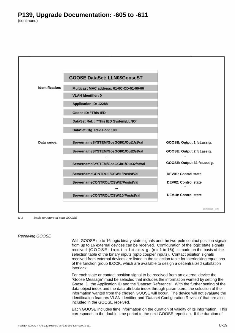
P139, Upgrade Documentation: -605 to -611 (continued)
P139/EN AD/A77 // AFSV.12.09690 D /// P139-306-408/409/410-611 U-19
GOOSE DataSet: LLN0$GooseST
Goose ID: "This IED"
ServernameSYSTEM/GosGGI01/Out1/stVal
Multicast MAC address: 01-0C-CD-01-00-00
VLAN Identifier: 0
GOOSE: Output 1 fct.assig.
ServernameCONTROL/CSWI1/Pos/stVal
…
… …
…GOOSE: Output 2 fct.assig.
GOOSE: Output 32 fct.assig.
DEV01: Control state
DEV02: Control state
DEV10: Control state
19Z6101B _EN
ServernameSYSTEM/GosGGI01/Out2/stVal
ServernameSYSTEM/GosGGI01/Out32/stVal
ServernameCONTROL/CSWI2/Pos/stVal
ServernameCONTROL/CSWI10/Pos/stVal
Identification:
Data range:
Application ID: 12288
DataSet Cfg. Revision: 100
DataSet Ref. : "This IED System/LLNO"
U-1 Basic structure of sent GOOSE
Receiving GOOSE With GOOSE up to 16 logic binary state signals and the two-pole contact position signals from up to 16 external devices can be received. Configuration of the logic state signals received (G O O S E : I n p u t n f c t . a s s i g . (n = 1 to 16)) is made on the basis of the selection table of the binary inputs (opto coupler inputs). Contact position signals received from external devices are listed in the selection table for interlocking equations of the function group ILOCK, which are available to design a decentralized substation interlock.
For each state or contact position signal to be received from an external device the "Goose Message" must be selected that includes the information wanted by setting the Goose ID, the Application ID and the 'Dataset Reference'. With the further setting of the data object index and the data attribute index through parameters, the selection of the information wanted from the chosen GOOSE will occur. The device will not evaluate the identification features VLAN identifier and ‘Dataset Configuration Revision’ that are also included in the GOOSE received.
Each GOOSE includes time information on the duration of validity of its information. This corresponds to the double time period to the next GOOSE repetition. If the duration of
P139, Upgrade Documentation: -605 to -611 (continued)
U-20 P139/EN AD/A77 // AFSV.12.09690 D /// P139-306-408/409/410-611
validity has elapsed without having received this GOOSE again (i.e. because of a fault in communication), the signals received will automatically be set to their respective default value GOOSE: Input n defaul t and GOOSE: Ext .Dev n defaul t (n = 1 to 16).
The function group GOOSE presents the following parameters, measured values and signals:
Configuration Parameters GOOSE: Function group GOOSE 056 068
Canceling function group GOOSE or including it in the configuration. If the function group is cancelled from the configuration, then all associated settings and signals are hidden. The parameters of this function group are only then active if function group IEC has been configured and is activated, and if the parameters of this function group have been activated through the parameter I E C : E n a b l e c o n f i g u r a t i o n or by switching the device off-line/on-line.
GOOSE: General enable USER 106 001
Enabling and disabling function group GOOSE.
GOOSE: Goose ID 106 002
Goose ID being sent by this device (IED). GOOSE includes a Dataset with 32 binary and configurable virtual outputs and 10 two-pole states to the maximum of 10 monitored external devices
GOOSE: Multic. MAC address 106 003
Multicast MAC address to provide identification of GOOSE to the receiving clients (IED). The default MAC address entered is suggested as a standard according to IEC 61850. The multicast MAC address entered in GOOSE may be modified so as to increase transmission security or to reduce the number of "GOOSE Messages" to be read by receiving clients (IED).
GOOSE: Application ID 106 004
Application ID of GOOSE being sent by this device (IED).
GOOSE: VLAN Identifier 106 006
VLAN identifier of GOOSE being sent by this device (IED). The VLAN identifier makes it possible to have switches in the network filter messages, if the switches support such a function. Because so-called multicast MAC addresses are applied, switches are unable to filter messages in the network if they do not include a VLAN identifier.
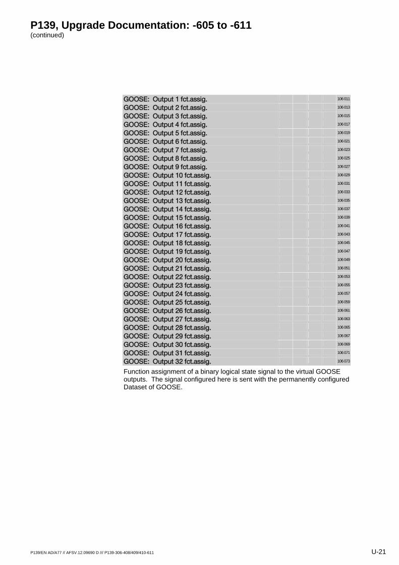
P139, Upgrade Documentation: -605 to -611 (continued)
P139/EN AD/A77 // AFSV.12.09690 D /// P139-306-408/409/410-611 U-21
GOOSE: Output 1 fct.assig. 106 011
GOOSE: Output 2 fct.assig. 106 013
GOOSE: Output 3 fct.assig. 106 015
GOOSE: Output 4 fct.assig. 106 017
GOOSE: Output 5 fct.assig. 106 019
GOOSE: Output 6 fct.assig. 106 021
GOOSE: Output 7 fct.assig. 106 023
GOOSE: Output 8 fct.assig. 106 025
GOOSE: Output 9 fct.assig. 106 027
GOOSE: Output 10 fct.assig. 106 029
GOOSE: Output 11 fct.assig. 106 031
GOOSE: Output 12 fct.assig. 106 033
GOOSE: Output 13 fct.assig. 106 035
GOOSE: Output 14 fct.assig. 106 037
GOOSE: Output 15 fct.assig. 106 039
GOOSE: Output 16 fct.assig. 106 041
GOOSE: Output 17 fct.assig. 106 043
GOOSE: Output 18 fct.assig. 106 045
GOOSE: Output 19 fct.assig. 106 047
GOOSE: Output 20 fct.assig. 106 049
GOOSE: Output 21 fct.assig. 106 051
GOOSE: Output 22 fct.assig. 106 053
GOOSE: Output 23 fct.assig. 106 055
GOOSE: Output 24 fct.assig. 106 057
GOOSE: Output 25 fct.assig. 106 059
GOOSE: Output 26 fct.assig. 106 061
GOOSE: Output 27 fct.assig. 106 063
GOOSE: Output 28 fct.assig. 106 065
GOOSE: Output 29 fct.assig. 106 067
GOOSE: Output 30 fct.assig. 106 069
GOOSE: Output 31 fct.assig. 106 071
GOOSE: Output 32 fct.assig. 106 073
Function assignment of a binary logical state signal to the virtual GOOSE outputs. The signal configured here is sent with the permanently configured Dataset of GOOSE.
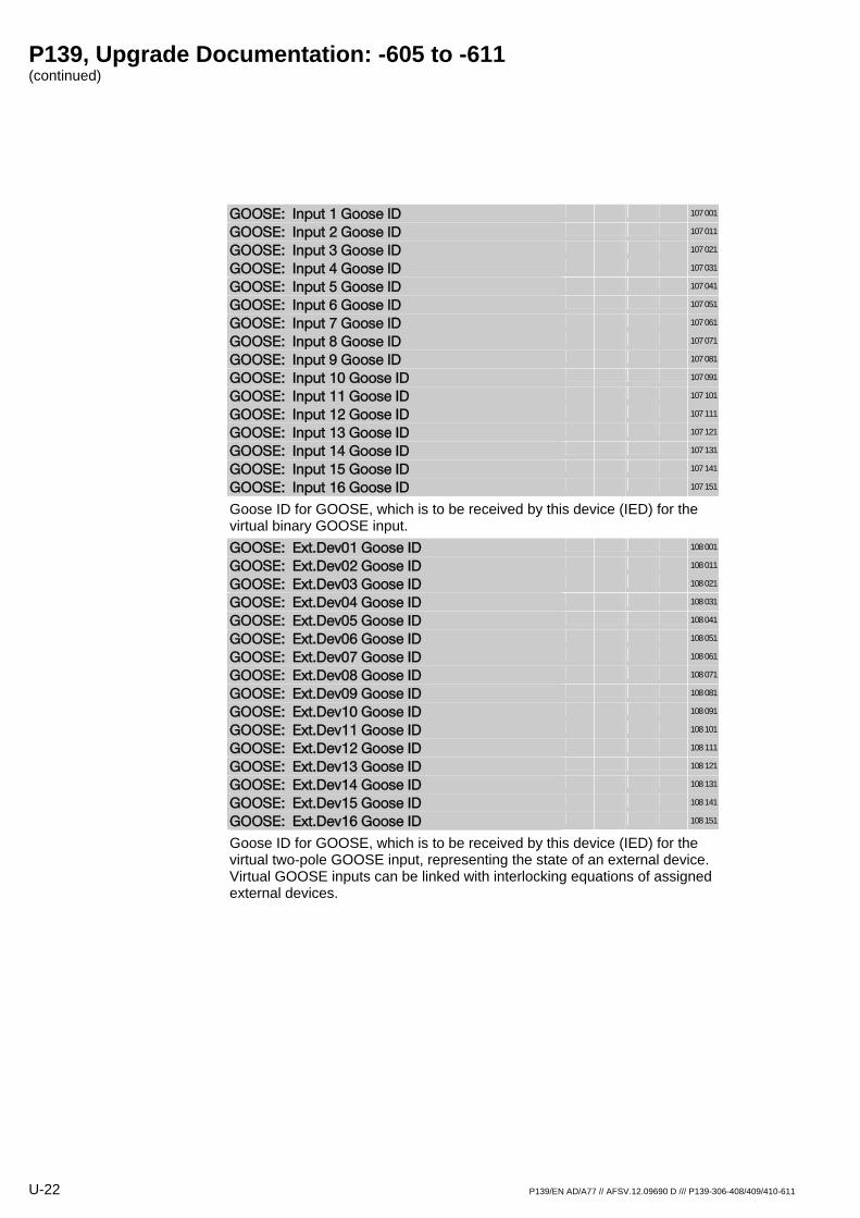
P139, Upgrade Documentation: -605 to -611 (continued)
U-22 P139/EN AD/A77 // AFSV.12.09690 D /// P139-306-408/409/410-611
GOOSE: Input 1 Goose ID 107 001
GOOSE: Input 2 Goose ID 107 011
GOOSE: Input 3 Goose ID 107 021
GOOSE: Input 4 Goose ID 107 031
GOOSE: Input 5 Goose ID 107 041
GOOSE: Input 6 Goose ID 107 051
GOOSE: Input 7 Goose ID 107 061
GOOSE: Input 8 Goose ID 107 071
GOOSE: Input 9 Goose ID 107 081
GOOSE: Input 10 Goose ID 107 091
GOOSE: Input 11 Goose ID 107 101
GOOSE: Input 12 Goose ID 107 111
GOOSE: Input 13 Goose ID 107 121
GOOSE: Input 14 Goose ID 107 131
GOOSE: Input 15 Goose ID 107 141
GOOSE: Input 16 Goose ID 107 151
Goose ID for GOOSE, which is to be received by this device (IED) for the virtual binary GOOSE input.
GOOSE: Ext.Dev01 Goose ID 108 001
GOOSE: Ext.Dev02 Goose ID 108 011
GOOSE: Ext.Dev03 Goose ID 108 021
GOOSE: Ext.Dev04 Goose ID 108 031
GOOSE: Ext.Dev05 Goose ID 108 041
GOOSE: Ext.Dev06 Goose ID 108 051
GOOSE: Ext.Dev07 Goose ID 108 061
GOOSE: Ext.Dev08 Goose ID 108 071
GOOSE: Ext.Dev09 Goose ID 108 081
GOOSE: Ext.Dev10 Goose ID 108 091
GOOSE: Ext.Dev11 Goose ID 108 101
GOOSE: Ext.Dev12 Goose ID 108 111
GOOSE: Ext.Dev13 Goose ID 108 121
GOOSE: Ext.Dev14 Goose ID 108 131
GOOSE: Ext.Dev15 Goose ID 108 141
GOOSE: Ext.Dev16 Goose ID 108 151
Goose ID for GOOSE, which is to be received by this device (IED) for the virtual two-pole GOOSE input, representing the state of an external device. Virtual GOOSE inputs can be linked with interlocking equations of assigned external devices.
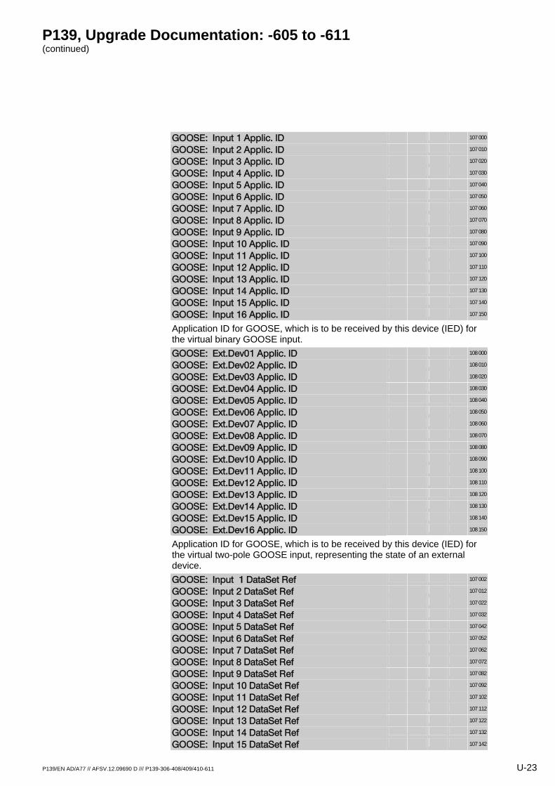
P139, Upgrade Documentation: -605 to -611 (continued)
P139/EN AD/A77 // AFSV.12.09690 D /// P139-306-408/409/410-611 U-23
GOOSE: Input 1 Applic. ID 107 000
GOOSE: Input 2 Applic. ID 107 010
GOOSE: Input 3 Applic. ID 107 020
GOOSE: Input 4 Applic. ID 107 030
GOOSE: Input 5 Applic. ID 107 040
GOOSE: Input 6 Applic. ID 107 050
GOOSE: Input 7 Applic. ID 107 060
GOOSE: Input 8 Applic. ID 107 070
GOOSE: Input 9 Applic. ID 107 080
GOOSE: Input 10 Applic. ID 107 090
GOOSE: Input 11 Applic. ID 107 100
GOOSE: Input 12 Applic. ID 107 110
GOOSE: Input 13 Applic. ID 107 120
GOOSE: Input 14 Applic. ID 107 130
GOOSE: Input 15 Applic. ID 107 140
GOOSE: Input 16 Applic. ID 107 150
Application ID for GOOSE, which is to be received by this device (IED) for the virtual binary GOOSE input.
GOOSE: Ext.Dev01 Applic. ID 108 000
GOOSE: Ext.Dev02 Applic. ID 108 010
GOOSE: Ext.Dev03 Applic. ID 108 020
GOOSE: Ext.Dev04 Applic. ID 108 030
GOOSE: Ext.Dev05 Applic. ID 108 040
GOOSE: Ext.Dev06 Applic. ID 108 050
GOOSE: Ext.Dev07 Applic. ID 108 060
GOOSE: Ext.Dev08 Applic. ID 108 070
GOOSE: Ext.Dev09 Applic. ID 108 080
GOOSE: Ext.Dev10 Applic. ID 108 090
GOOSE: Ext.Dev11 Applic. ID 108 100
GOOSE: Ext.Dev12 Applic. ID 108 110
GOOSE: Ext.Dev13 Applic. ID 108 120
GOOSE: Ext.Dev14 Applic. ID 108 130
GOOSE: Ext.Dev15 Applic. ID 108 140
GOOSE: Ext.Dev16 Applic. ID 108 150
Application ID for GOOSE, which is to be received by this device (IED) for the virtual two-pole GOOSE input, representing the state of an external device.
GOOSE: Input 1 DataSet Ref 107 002
GOOSE: Input 2 DataSet Ref 107 012
GOOSE: Input 3 DataSet Ref 107 022
GOOSE: Input 4 DataSet Ref 107 032
GOOSE: Input 5 DataSet Ref 107 042
GOOSE: Input 6 DataSet Ref 107 052
GOOSE: Input 7 DataSet Ref 107 062
GOOSE: Input 8 DataSet Ref 107 072
GOOSE: Input 9 DataSet Ref 107 082
GOOSE: Input 10 DataSet Ref 107 092
GOOSE: Input 11 DataSet Ref 107 102
GOOSE: Input 12 DataSet Ref 107 112
GOOSE: Input 13 DataSet Ref 107 122
GOOSE: Input 14 DataSet Ref 107 132
GOOSE: Input 15 DataSet Ref 107 142
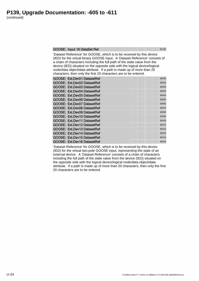
P139, Upgrade Documentation: -605 to -611 (continued)
U-24 P139/EN AD/A77 // AFSV.12.09690 D /// P139-306-408/409/410-611
GOOSE: Input 16 DataSet Ref 107 152
'Dataset Reference' for GOOSE, which is to be received by this device (IED) for the virtual binary GOOSE input. A 'Dataset Reference' consists of a chain of characters including the full path of the state value from the device (IED) situated on the opposite side with the logical device/logical node/data object/data attribute. If a path is made up of more than 20 characters, then only the first 20 characters are to be entered.
GOOSE: Ext.Dev01 DatasetRef 108 002
GOOSE: Ext.Dev02 DatasetRef 108 012
GOOSE: Ext.Dev03 DatasetRef 108 022
GOOSE: Ext.Dev04 DatasetRef 108 032
GOOSE: Ext.Dev05 DatasetRef 108 042
GOOSE: Ext.Dev06 DatasetRef 108 052
GOOSE: Ext.Dev07 DatasetRef 108 062
GOOSE: Ext.Dev08 DatasetRef 108 072
GOOSE: Ext.Dev09 DatasetRef 108 082
GOOSE: Ext.Dev10 DatasetRef 108 092
GOOSE: Ext.Dev11 DatasetRef 108 102
GOOSE: Ext.Dev12 DatasetRef 108 112
GOOSE: Ext.Dev13 DatasetRef 108 122
GOOSE: Ext.Dev14 DatasetRef 108 132
GOOSE: Ext.Dev15 DatasetRef 108 142
GOOSE: Ext.Dev16 DatasetRef 108 152
'Dataset Reference' for GOOSE, which is to be received by this device (IED) for the virtual two-pole GOOSE input, representing the state of an external device. A 'Dataset Reference' consists of a chain of characters including the full path of the state value from the device (IED) situated on the opposite side with the logical device/logical node/data object/data attribute. If a path is made up of more than 20 characters, then only the first 20 characters are to be entered.
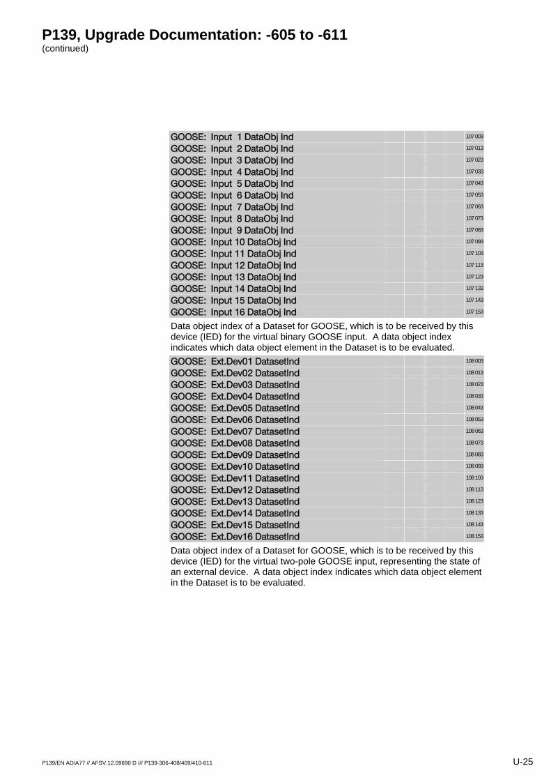
P139, Upgrade Documentation: -605 to -611 (continued)
P139/EN AD/A77 // AFSV.12.09690 D /// P139-306-408/409/410-611 U-25
GOOSE: Input 1 DataObj Ind 107 003
GOOSE: Input 2 DataObj Ind 107 013
GOOSE: Input 3 DataObj Ind 107 023
GOOSE: Input 4 DataObj Ind 107 033
GOOSE: Input 5 DataObj Ind 107 043
GOOSE: Input 6 DataObj Ind 107 053
GOOSE: Input 7 DataObj Ind 107 063
GOOSE: Input 8 DataObj Ind 107 073
GOOSE: Input 9 DataObj Ind 107 083
GOOSE: Input 10 DataObj Ind 107 093
GOOSE: Input 11 DataObj Ind 107 103
GOOSE: Input 12 DataObj Ind 107 113
GOOSE: Input 13 DataObj Ind 107 123
GOOSE: Input 14 DataObj Ind 107 133
GOOSE: Input 15 DataObj Ind 107 143
GOOSE: Input 16 DataObj Ind 107 153
Data object index of a Dataset for GOOSE, which is to be received by this device (IED) for the virtual binary GOOSE input. A data object index indicates which data object element in the Dataset is to be evaluated.
GOOSE: Ext.Dev01 DatasetInd 108 003
GOOSE: Ext.Dev02 DatasetInd 108 013
GOOSE: Ext.Dev03 DatasetInd 108 023
GOOSE: Ext.Dev04 DatasetInd 108 033
GOOSE: Ext.Dev05 DatasetInd 108 043
GOOSE: Ext.Dev06 DatasetInd 108 053
GOOSE: Ext.Dev07 DatasetInd 108 063
GOOSE: Ext.Dev08 DatasetInd 108 073
GOOSE: Ext.Dev09 DatasetInd 108 083
GOOSE: Ext.Dev10 DatasetInd 108 093
GOOSE: Ext.Dev11 DatasetInd 108 103
GOOSE: Ext.Dev12 DatasetInd 108 113
GOOSE: Ext.Dev13 DatasetInd 108 123
GOOSE: Ext.Dev14 DatasetInd 108 133
GOOSE: Ext.Dev15 DatasetInd 108 143
GOOSE: Ext.Dev16 DatasetInd 108 153
Data object index of a Dataset for GOOSE, which is to be received by this device (IED) for the virtual two-pole GOOSE input, representing the state of an external device. A data object index indicates which data object element in the Dataset is to be evaluated.
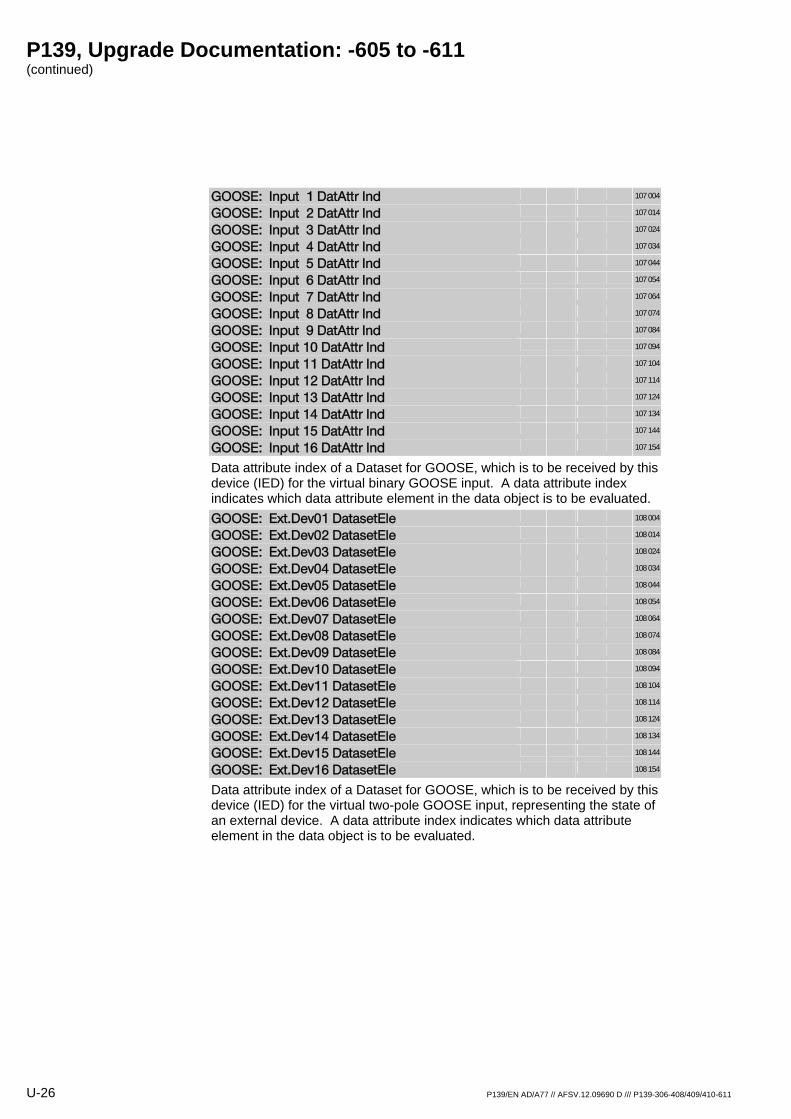
P139, Upgrade Documentation: -605 to -611 (continued)
U-26 P139/EN AD/A77 // AFSV.12.09690 D /// P139-306-408/409/410-611
GOOSE: Input 1 DatAttr Ind 107 004
GOOSE: Input 2 DatAttr Ind 107 014
GOOSE: Input 3 DatAttr Ind 107 024
GOOSE: Input 4 DatAttr Ind 107 034
GOOSE: Input 5 DatAttr Ind 107 044
GOOSE: Input 6 DatAttr Ind 107 054
GOOSE: Input 7 DatAttr Ind 107 064
GOOSE: Input 8 DatAttr Ind 107 074
GOOSE: Input 9 DatAttr Ind 107 084
GOOSE: Input 10 DatAttr Ind 107 094
GOOSE: Input 11 DatAttr Ind 107 104
GOOSE: Input 12 DatAttr Ind 107 114
GOOSE: Input 13 DatAttr Ind 107 124
GOOSE: Input 14 DatAttr Ind 107 134
GOOSE: Input 15 DatAttr Ind 107 144
GOOSE: Input 16 DatAttr Ind 107 154
Data attribute index of a Dataset for GOOSE, which is to be received by this device (IED) for the virtual binary GOOSE input. A data attribute index indicates which data attribute element in the data object is to be evaluated.
GOOSE: Ext.Dev01 DatasetEle 108 004
GOOSE: Ext.Dev02 DatasetEle 108 014
GOOSE: Ext.Dev03 DatasetEle 108 024
GOOSE: Ext.Dev04 DatasetEle 108 034
GOOSE: Ext.Dev05 DatasetEle 108 044
GOOSE: Ext.Dev06 DatasetEle 108 054
GOOSE: Ext.Dev07 DatasetEle 108 064
GOOSE: Ext.Dev08 DatasetEle 108 074
GOOSE: Ext.Dev09 DatasetEle 108 084
GOOSE: Ext.Dev10 DatasetEle 108 094
GOOSE: Ext.Dev11 DatasetEle 108 104
GOOSE: Ext.Dev12 DatasetEle 108 114
GOOSE: Ext.Dev13 DatasetEle 108 124
GOOSE: Ext.Dev14 DatasetEle 108 134
GOOSE: Ext.Dev15 DatasetEle 108 144
GOOSE: Ext.Dev16 DatasetEle 108 154
Data attribute index of a Dataset for GOOSE, which is to be received by this device (IED) for the virtual two-pole GOOSE input, representing the state of an external device. A data attribute index indicates which data attribute element in the data object is to be evaluated.
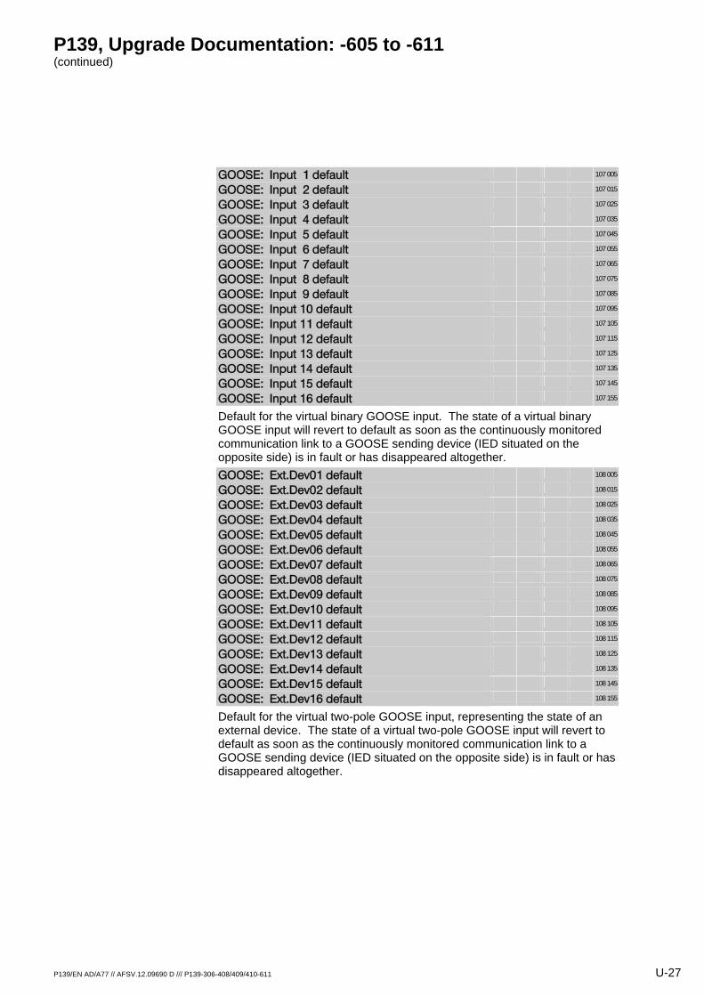
P139, Upgrade Documentation: -605 to -611 (continued)
P139/EN AD/A77 // AFSV.12.09690 D /// P139-306-408/409/410-611 U-27
GOOSE: Input 1 default 107 005
GOOSE: Input 2 default 107 015
GOOSE: Input 3 default 107 025
GOOSE: Input 4 default 107 035
GOOSE: Input 5 default 107 045
GOOSE: Input 6 default 107 055
GOOSE: Input 7 default 107 065
GOOSE: Input 8 default 107 075
GOOSE: Input 9 default 107 085
GOOSE: Input 10 default 107 095
GOOSE: Input 11 default 107 105
GOOSE: Input 12 default 107 115
GOOSE: Input 13 default 107 125
GOOSE: Input 14 default 107 135
GOOSE: Input 15 default 107 145
GOOSE: Input 16 default 107 155
Default for the virtual binary GOOSE input. The state of a virtual binary GOOSE input will revert to default as soon as the continuously monitored communication link to a GOOSE sending device (IED situated on the opposite side) is in fault or has disappeared altogether.
GOOSE: Ext.Dev01 default 108 005
GOOSE: Ext.Dev02 default 108 015
GOOSE: Ext.Dev03 default 108 025
GOOSE: Ext.Dev04 default 108 035
GOOSE: Ext.Dev05 default 108 045
GOOSE: Ext.Dev06 default 108 055
GOOSE: Ext.Dev07 default 108 065
GOOSE: Ext.Dev08 default 108 075
GOOSE: Ext.Dev09 default 108 085
GOOSE: Ext.Dev10 default 108 095
GOOSE: Ext.Dev11 default 108 105
GOOSE: Ext.Dev12 default 108 115
GOOSE: Ext.Dev13 default 108 125
GOOSE: Ext.Dev14 default 108 135
GOOSE: Ext.Dev15 default 108 145
GOOSE: Ext.Dev16 default 108 155
Default for the virtual two-pole GOOSE input, representing the state of an external device. The state of a virtual two-pole GOOSE input will revert to default as soon as the continuously monitored communication link to a GOOSE sending device (IED situated on the opposite side) is in fault or has disappeared altogether.
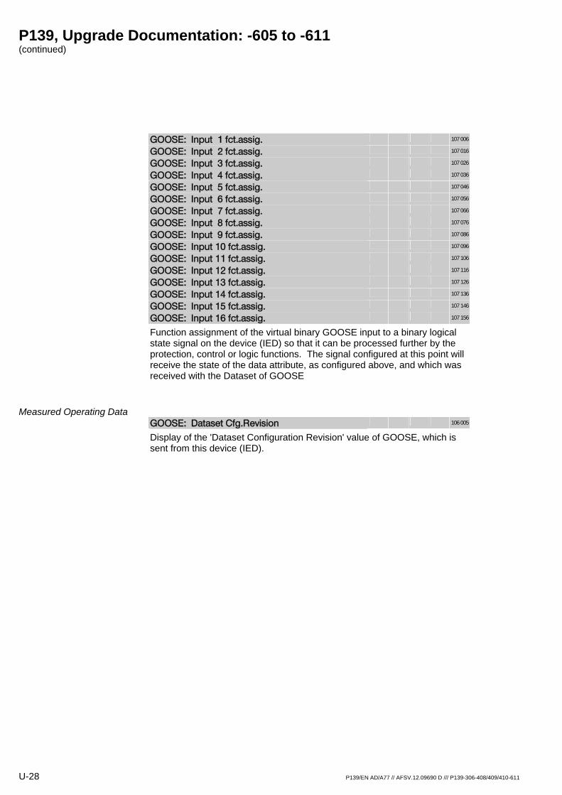
P139, Upgrade Documentation: -605 to -611 (continued)
U-28 P139/EN AD/A77 // AFSV.12.09690 D /// P139-306-408/409/410-611
GOOSE: Input 1 fct.assig. 107 006
GOOSE: Input 2 fct.assig. 107 016
GOOSE: Input 3 fct.assig. 107 026
GOOSE: Input 4 fct.assig. 107 036
GOOSE: Input 5 fct.assig. 107 046
GOOSE: Input 6 fct.assig. 107 056
GOOSE: Input 7 fct.assig. 107 066
GOOSE: Input 8 fct.assig. 107 076
GOOSE: Input 9 fct.assig. 107 086
GOOSE: Input 10 fct.assig. 107 096
GOOSE: Input 11 fct.assig. 107 106
GOOSE: Input 12 fct.assig. 107 116
GOOSE: Input 13 fct.assig. 107 126
GOOSE: Input 14 fct.assig. 107 136
GOOSE: Input 15 fct.assig. 107 146
GOOSE: Input 16 fct.assig. 107 156
Function assignment of the virtual binary GOOSE input to a binary logical state signal on the device (IED) so that it can be processed further by the protection, control or logic functions. The signal configured at this point will receive the state of the data attribute, as configured above, and which was received with the Dataset of GOOSE
Measured Operating Data GOOSE: Dataset Cfg.Revision 106 005
Display of the 'Dataset Configuration Revision' value of GOOSE, which is sent from this device (IED).
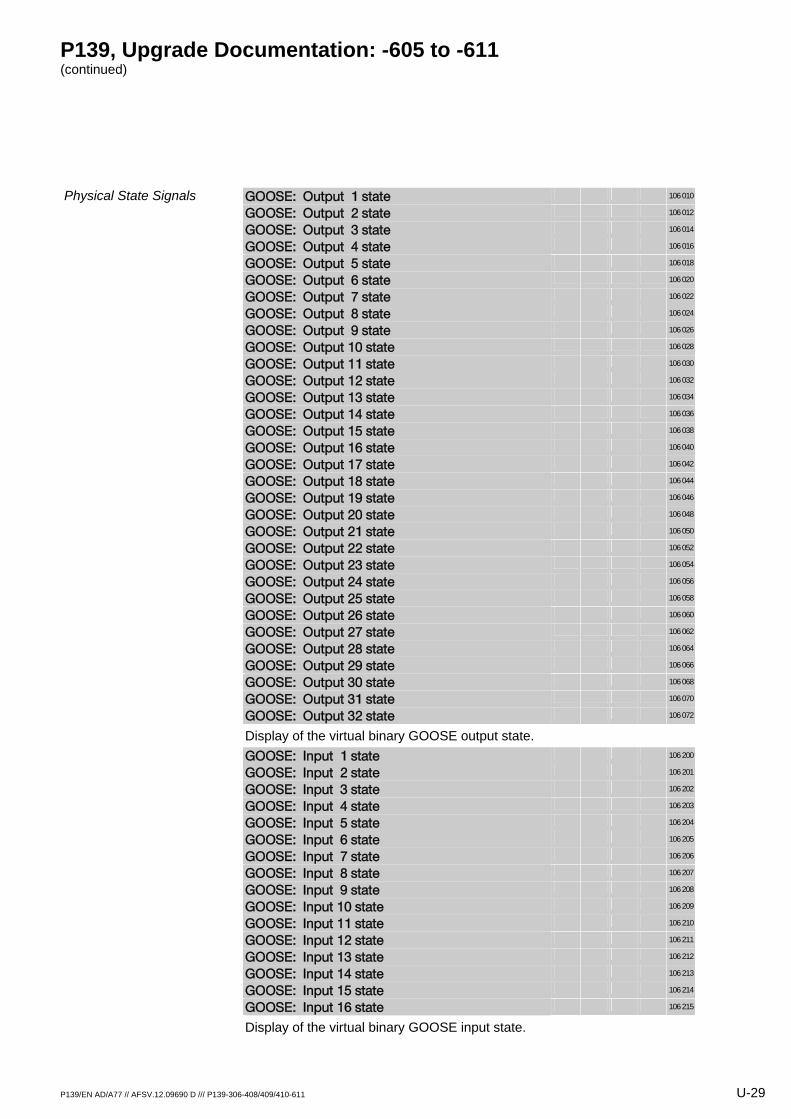
P139, Upgrade Documentation: -605 to -611 (continued)
P139/EN AD/A77 // AFSV.12.09690 D /// P139-306-408/409/410-611 U-29
Physical State Signals GOOSE: Output 1 state 106 010
GOOSE: Output 2 state 106 012
GOOSE: Output 3 state 106 014
GOOSE: Output 4 state 106 016
GOOSE: Output 5 state 106 018
GOOSE: Output 6 state 106 020
GOOSE: Output 7 state 106 022
GOOSE: Output 8 state 106 024
GOOSE: Output 9 state 106 026
GOOSE: Output 10 state 106 028
GOOSE: Output 11 state 106 030
GOOSE: Output 12 state 106 032
GOOSE: Output 13 state 106 034
GOOSE: Output 14 state 106 036
GOOSE: Output 15 state 106 038
GOOSE: Output 16 state 106 040
GOOSE: Output 17 state 106 042
GOOSE: Output 18 state 106 044
GOOSE: Output 19 state 106 046
GOOSE: Output 20 state 106 048
GOOSE: Output 21 state 106 050
GOOSE: Output 22 state 106 052
GOOSE: Output 23 state 106 054
GOOSE: Output 24 state 106 056
GOOSE: Output 25 state 106 058
GOOSE: Output 26 state 106 060
GOOSE: Output 27 state 106 062
GOOSE: Output 28 state 106 064
GOOSE: Output 29 state 106 066
GOOSE: Output 30 state 106 068
GOOSE: Output 31 state 106 070
GOOSE: Output 32 state 106 072 Display of the virtual binary GOOSE output state.
GOOSE: Input 1 state 106 200
GOOSE: Input 2 state 106 201
GOOSE: Input 3 state 106 202
GOOSE: Input 4 state 106 203
GOOSE: Input 5 state 106 204
GOOSE: Input 6 state 106 205
GOOSE: Input 7 state 106 206
GOOSE: Input 8 state 106 207
GOOSE: Input 9 state 106 208
GOOSE: Input 10 state 106 209
GOOSE: Input 11 state 106 210
GOOSE: Input 12 state 106 211
GOOSE: Input 13 state 106 212
GOOSE: Input 14 state 106 213
GOOSE: Input 15 state 106 214
GOOSE: Input 16 state 106 215 Display of the virtual binary GOOSE input state.
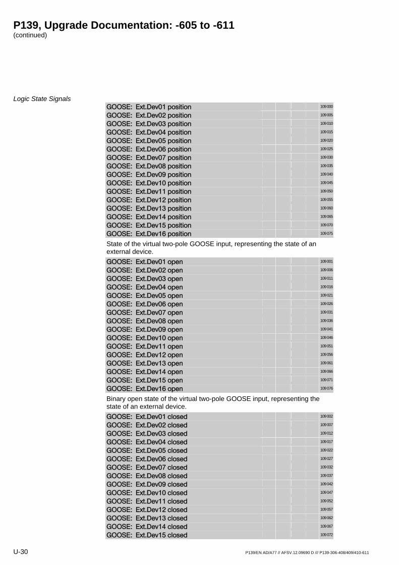
P139, Upgrade Documentation: -605 to -611 (continued)
U-30 P139/EN AD/A77 // AFSV.12.09690 D /// P139-306-408/409/410-611
Logic State Signals GOOSE: Ext.Dev01 position 109 000
GOOSE: Ext.Dev02 position 109 005
GOOSE: Ext.Dev03 position 109 010
GOOSE: Ext.Dev04 position 109 015
GOOSE: Ext.Dev05 position 109 020
GOOSE: Ext.Dev06 position 109 025
GOOSE: Ext.Dev07 position 109 030
GOOSE: Ext.Dev08 position 109 035
GOOSE: Ext.Dev09 position 109 040
GOOSE: Ext.Dev10 position 109 045
GOOSE: Ext.Dev11 position 109 050
GOOSE: Ext.Dev12 position 109 055
GOOSE: Ext.Dev13 position 109 060
GOOSE: Ext.Dev14 position 109 065
GOOSE: Ext.Dev15 position 109 070
GOOSE: Ext.Dev16 position 109 075 State of the virtual two-pole GOOSE input, representing the state of an
external device.
GOOSE: Ext.Dev01 open 109 001
GOOSE: Ext.Dev02 open 109 006
GOOSE: Ext.Dev03 open 109 011
GOOSE: Ext.Dev04 open 109 016
GOOSE: Ext.Dev05 open 109 021
GOOSE: Ext.Dev06 open 109 026
GOOSE: Ext.Dev07 open 109 031
GOOSE: Ext.Dev08 open 109 036
GOOSE: Ext.Dev09 open 109 041
GOOSE: Ext.Dev10 open 109 046
GOOSE: Ext.Dev11 open 109 051
GOOSE: Ext.Dev12 open 109 056
GOOSE: Ext.Dev13 open 109 061
GOOSE: Ext.Dev14 open 109 066
GOOSE: Ext.Dev15 open 109 071
GOOSE: Ext.Dev16 open 109 076 Binary open state of the virtual two-pole GOOSE input, representing the
state of an external device.
GOOSE: Ext.Dev01 closed 109 002
GOOSE: Ext.Dev02 closed 109 007
GOOSE: Ext.Dev03 closed 109 012
GOOSE: Ext.Dev04 closed 109 017
GOOSE: Ext.Dev05 closed 109 022
GOOSE: Ext.Dev06 closed 109 027
GOOSE: Ext.Dev07 closed 109 032
GOOSE: Ext.Dev08 closed 109 037
GOOSE: Ext.Dev09 closed 109 042
GOOSE: Ext.Dev10 closed 109 047
GOOSE: Ext.Dev11 closed 109 052
GOOSE: Ext.Dev12 closed 109 057
GOOSE: Ext.Dev13 closed 109 062
GOOSE: Ext.Dev14 closed 109 067
GOOSE: Ext.Dev15 closed 109 072
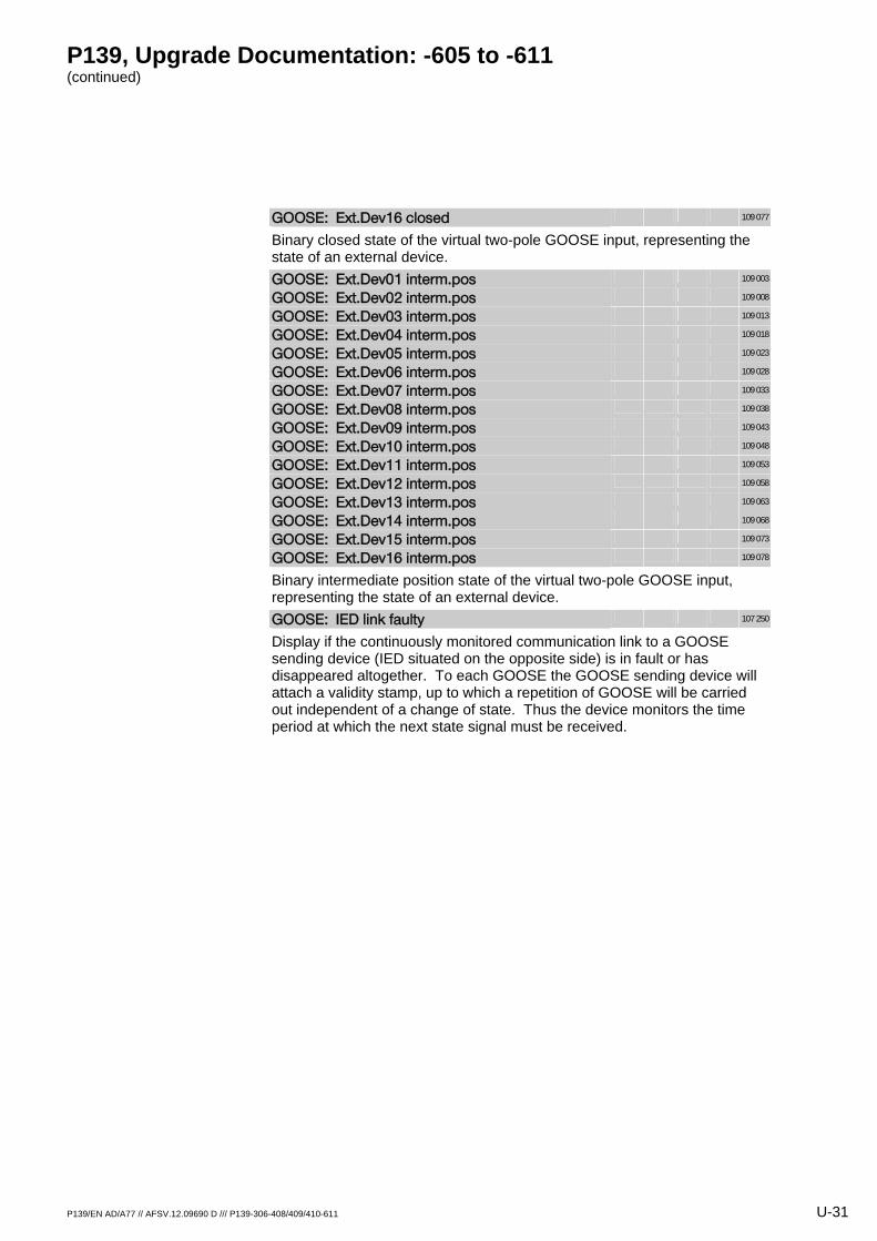
P139, Upgrade Documentation: -605 to -611 (continued)
P139/EN AD/A77 // AFSV.12.09690 D /// P139-306-408/409/410-611 U-31
GOOSE: Ext.Dev16 closed 109 077 Binary closed state of the virtual two-pole GOOSE input, representing the
state of an external device.
GOOSE: Ext.Dev01 interm.pos 109 003
GOOSE: Ext.Dev02 interm.pos 109 008
GOOSE: Ext.Dev03 interm.pos 109 013
GOOSE: Ext.Dev04 interm.pos 109 018
GOOSE: Ext.Dev05 interm.pos 109 023
GOOSE: Ext.Dev06 interm.pos 109 028
GOOSE: Ext.Dev07 interm.pos 109 033
GOOSE: Ext.Dev08 interm.pos 109 038
GOOSE: Ext.Dev09 interm.pos 109 043
GOOSE: Ext.Dev10 interm.pos 109 048
GOOSE: Ext.Dev11 interm.pos 109 053
GOOSE: Ext.Dev12 interm.pos 109 058
GOOSE: Ext.Dev13 interm.pos 109 063
GOOSE: Ext.Dev14 interm.pos 109 068
GOOSE: Ext.Dev15 interm.pos 109 073
GOOSE: Ext.Dev16 interm.pos 109 078 Binary intermediate position state of the virtual two-pole GOOSE input,
representing the state of an external device.
GOOSE: IED link faulty 107 250 Display if the continuously monitored communication link to a GOOSE
sending device (IED situated on the opposite side) is in fault or has disappeared altogether. To each GOOSE the GOOSE sending device will attach a validity stamp, up to which a repetition of GOOSE will be carried out independent of a change of state. Thus the device monitors the time period at which the next state signal must be received.
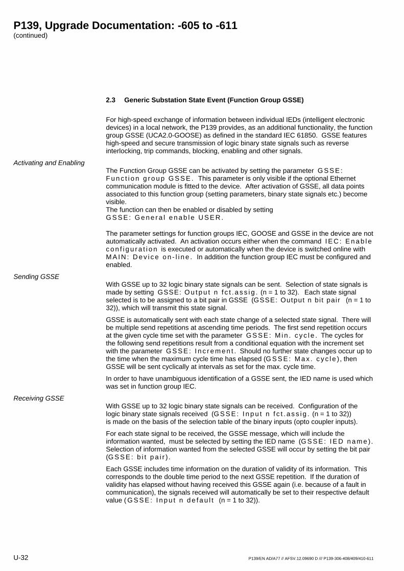
P139, Upgrade Documentation: -605 to -611 (continued)
U-32 P139/EN AD/A77 // AFSV.12.09690 D /// P139-306-408/409/410-611
2.3 Generic Substation State Event (Function Group GSSE)
For high-speed exchange of information between individual IEDs (intelligent electronic devices) in a local network, the P139 provides, as an additional functionality, the function group GSSE (UCA2.0-GOOSE) as defined in the standard IEC 61850. GSSE features high-speed and secure transmission of logic binary state signals such as reverse interlocking, trip commands, blocking, enabling and other signals.
Activating and Enabling The Function Group GSSE can be activated by setting the parameter G S S E : F u n c t i o n g r o u p G S S E . This parameter is only visible if the optional Ethernet communication module is fitted to the device. After activation of GSSE, all data points associated to this function group (setting parameters, binary state signals etc.) become visible. The function can then be enabled or disabled by setting G S S E : G e n e r a l e n a b l e U S E R .
The parameter settings for function groups IEC, GOOSE and GSSE in the device are not automatically activated. An activation occurs either when the command I E C : E n a b l e c o n f i g u r a t i o n is executed or automatically when the device is switched online with M A I N : D e v i c e o n - l i n e . In addition the function group IEC must be configured and enabled.
Sending GSSE With GSSE up to 32 logic binary state signals can be sent. Selection of state signals is made by setting GSSE: O u t p u t n f c t . a s s i g . (n = 1 to 32). Each state signal selected is to be assigned to a bit pair in GSSE (GSSE: Output n bi t pair (n = 1 to 32)), which will transmit this state signal.
GSSE is automatically sent with each state change of a selected state signal. There will be multiple send repetitions at ascending time periods. The first send repetition occurs at the given cycle time set with the parameter G S S E : M i n . c y c l e . The cycles for the following send repetitions result from a conditional equation with the increment set with the parameter G S S E : I n c r e m e n t . Should no further state changes occur up to the time when the maximum cycle time has elapsed (G S S E : M a x . c y c l e ) , then GSSE will be sent cyclically at intervals as set for the max. cycle time.
In order to have unambiguous identification of a GSSE sent, the IED name is used which was set in function group IEC.
Receiving GSSE With GSSE up to 32 logic binary state signals can be received. Configuration of the logic binary state signals received (G S S E : I n p u t n f c t . a s s i g . (n = 1 to 32)) is made on the basis of the selection table of the binary inputs (opto coupler inputs).
For each state signal to be received, the GSSE message, which will include the information wanted, must be selected by setting the IED name (G S S E : I E D n a m e ). Selection of information wanted from the selected GSSE will occur by setting the bit pair (G S S E : b i t p a i r ) .
Each GSSE includes time information on the duration of validity of its information. This corresponds to the double time period to the next GSSE repetition. If the duration of validity has elapsed without having received this GSSE again (i.e. because of a fault in communication), the signals received will automatically be set to their respective default value ( G S S E : I n p u t n d e f a u l t (n = 1 to 32)).
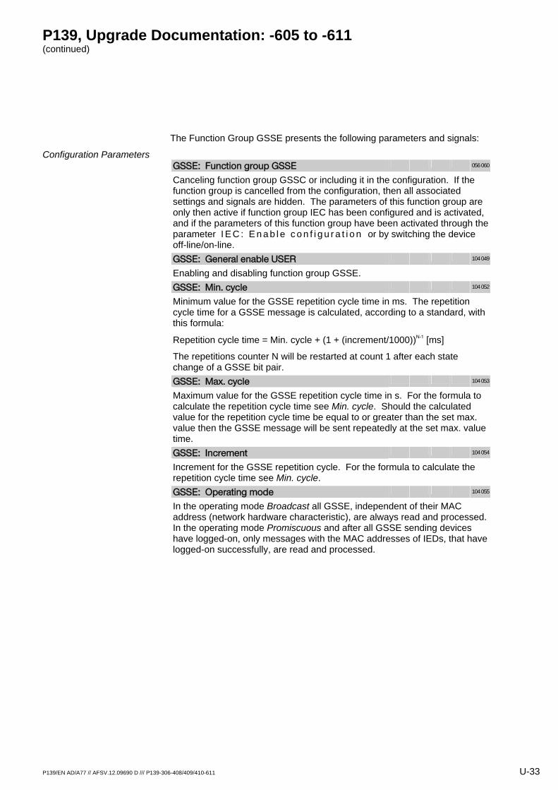
P139, Upgrade Documentation: -605 to -611 (continued)
P139/EN AD/A77 // AFSV.12.09690 D /// P139-306-408/409/410-611 U-33
The Function Group GSSE presents the following parameters and signals:
Configuration Parameters GSSE: Function group GSSE 056 060
Canceling function group GSSC or including it in the configuration. If the function group is cancelled from the configuration, then all associated settings and signals are hidden. The parameters of this function group are only then active if function group IEC has been configured and is activated, and if the parameters of this function group have been activated through the parameter I E C : E n a b l e c o n f i g u r a t i o n or by switching the device off-line/on-line.
GSSE: General enable USER 104 049
Enabling and disabling function group GSSE.
GSSE: Min. cycle 104 052
Minimum value for the GSSE repetition cycle time in ms. The repetition cycle time for a GSSE message is calculated, according to a standard, with this formula:
Repetition cycle time = Min. cycle + (1 + (increment/1000))N-1 [ms]
The repetitions counter N will be restarted at count 1 after each state change of a GSSE bit pair.
GSSE: Max. cycle 104 053
Maximum value for the GSSE repetition cycle time in s. For the formula to calculate the repetition cycle time see Min. cycle. Should the calculated value for the repetition cycle time be equal to or greater than the set max. value then the GSSE message will be sent repeatedly at the set max. value time.
GSSE: Increment 104 054
Increment for the GSSE repetition cycle. For the formula to calculate the repetition cycle time see Min. cycle.
GSSE: Operating mode 104 055
In the operating mode Broadcast all GSSE, independent of their MAC address (network hardware characteristic), are always read and processed. In the operating mode Promiscuous and after all GSSE sending devices have logged-on, only messages with the MAC addresses of IEDs, that have logged-on successfully, are read and processed.

P139, Upgrade Documentation: -605 to -611 (continued)
U-34 P139/EN AD/A77 // AFSV.12.09690 D /// P139-306-408/409/410-611
GSSE: Output 1 bit pair 104 101
GSSE: Output 2 bit pair 104 104
GSSE: Output 3 bit pair 104 107
GSSE: Output 4 bit pair 104 110
GSSE: Output 5 bit pair 104 113
GSSE: Output 6 bit pair 104 116
GSSE: Output 7 bit pair 104 119
GSSE: Output 8 bit pair 104 122
GSSE: Output 9 bit pair 104 125
GSSE: Output 10 bit pair 104 128
GSSE: Output 11 bit pair 104 131
GSSE: Output 12 bit pair 104 134
GSSE: Output 13 bit pair 104 137
GSSE: Output 14 bit pair 104 140
GSSE: Output 15 bit pair 104 143
GSSE: Output 16 bit pair 104 146
GSSE: Output 17 bit pair 104 149
GSSE: Output 18 bit pair 104 152
GSSE: Output 19 bit pair 104 155
GSSE: Output 20 bit pair 104 158
GSSE: Output 21 bit pair 104 161
GSSE: Output 22 bit pair 104 164
GSSE: Output 23 bit pair 104 167
GSSE: Output 24 bit pair 104 170
GSSE: Output 25 bit pair 104 173
GSSE: Output 26 bit pair 104 176
GSSE: Output 27 bit pair 104 179
GSSE: Output 28 bit pair 104 182
GSSE: Output 29 bit pair 104 185
GSSE: Output 30 bit pair 104 188
GSSE: Output 31 bit pair 104 191
GSSE: Output 32 bit pair 104 194
Setting with which GSSE bit pair the configured binary signal of the virtual GSSE outputs is to be transmitted. A GSSE is always transmitted consisting of a fixed number of 96 bit pairs, of which a maximum of 32 are used by this device (IED) during a send operation.
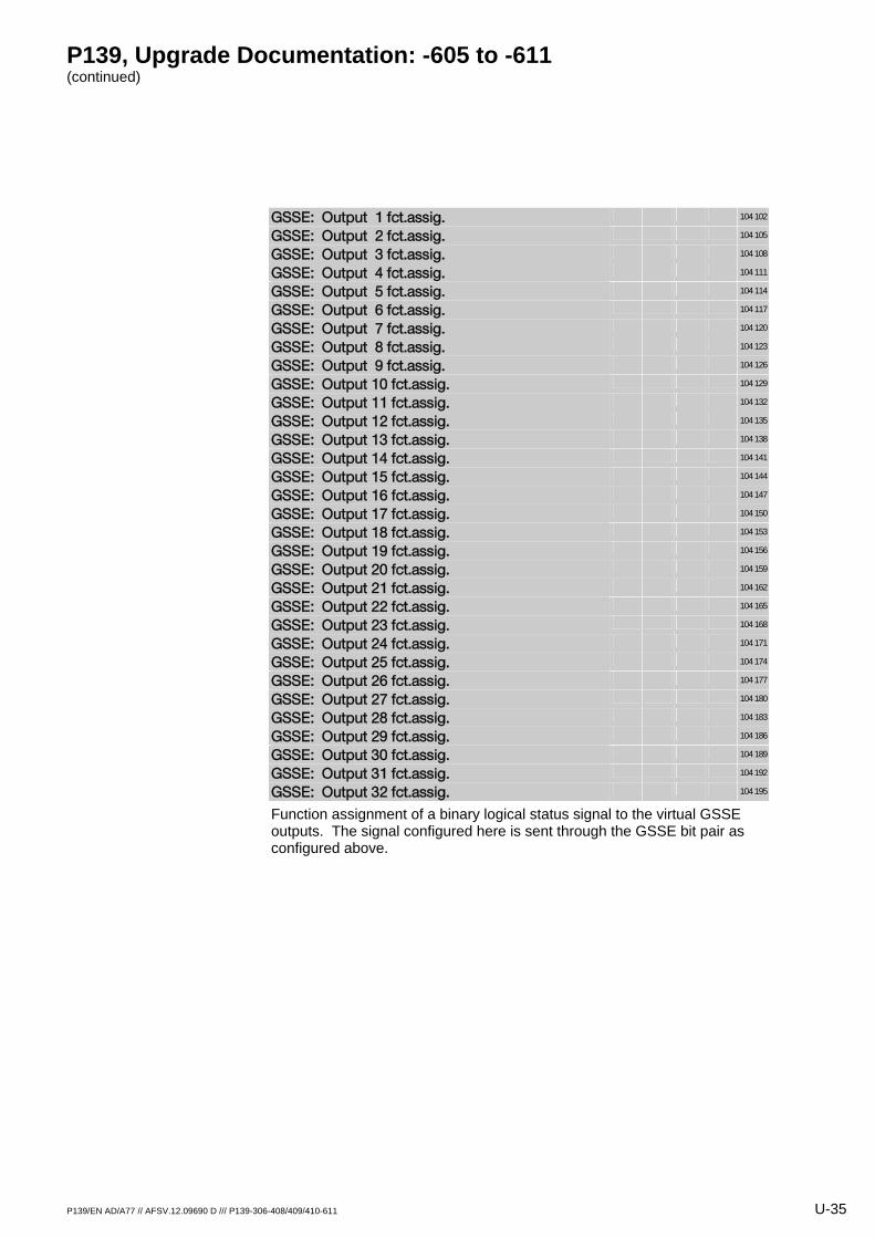
P139, Upgrade Documentation: -605 to -611 (continued)
P139/EN AD/A77 // AFSV.12.09690 D /// P139-306-408/409/410-611 U-35
GSSE: Output 1 fct.assig. 104 102
GSSE: Output 2 fct.assig. 104 105
GSSE: Output 3 fct.assig. 104 108
GSSE: Output 4 fct.assig. 104 111
GSSE: Output 5 fct.assig. 104 114
GSSE: Output 6 fct.assig. 104 117
GSSE: Output 7 fct.assig. 104 120
GSSE: Output 8 fct.assig. 104 123
GSSE: Output 9 fct.assig. 104 126
GSSE: Output 10 fct.assig. 104 129
GSSE: Output 11 fct.assig. 104 132
GSSE: Output 12 fct.assig. 104 135
GSSE: Output 13 fct.assig. 104 138
GSSE: Output 14 fct.assig. 104 141
GSSE: Output 15 fct.assig. 104 144
GSSE: Output 16 fct.assig. 104 147
GSSE: Output 17 fct.assig. 104 150
GSSE: Output 18 fct.assig. 104 153
GSSE: Output 19 fct.assig. 104 156
GSSE: Output 20 fct.assig. 104 159
GSSE: Output 21 fct.assig. 104 162
GSSE: Output 22 fct.assig. 104 165
GSSE: Output 23 fct.assig. 104 168
GSSE: Output 24 fct.assig. 104 171
GSSE: Output 25 fct.assig. 104 174
GSSE: Output 26 fct.assig. 104 177
GSSE: Output 27 fct.assig. 104 180
GSSE: Output 28 fct.assig. 104 183
GSSE: Output 29 fct.assig. 104 186
GSSE: Output 30 fct.assig. 104 189
GSSE: Output 31 fct.assig. 104 192
GSSE: Output 32 fct.assig. 104 195
Function assignment of a binary logical status signal to the virtual GSSE outputs. The signal configured here is sent through the GSSE bit pair as configured above.

P139, Upgrade Documentation: -605 to -611 (continued)
U-36 P139/EN AD/A77 // AFSV.12.09690 D /// P139-306-408/409/410-611
GSSE: Input 1 bit pair 105 001
GSSE: Input 2 bit pair 105 006
GSSE: Input 3 bit pair 105 011
GSSE: Input 4 bit pair 105 016
GSSE: Input 5 bit pair 105 021
GSSE: Input 6 bit pair 105 026
GSSE: Input 7 bit pair 105 031
GSSE: Input 8 bit pair 105 036
GSSE: Input 9 bit pair 105 041
GSSE: Input 10 bit pair 105 046
GSSE: Input 11 bit pair 105 051
GSSE: Input 12 bit pair 105 056
GSSE: Input 13 bit pair 105 061
GSSE: Input 14 bit pair 105 066
GSSE: Input 15 bit pair 105 071
GSSE: Input 16 bit pair 105 076
GSSE: Input 17 bit pair 105 081
GSSE: Input 18 bit pair 105 086
GSSE: Input 19 bit pair 105 091
GSSE: Input 20 bit pair 105 096
GSSE: Input 21 bit pair 105 101
GSSE: Input 22 bit pair 105 106
GSSE: Input 23 bit pair 105 111
GSSE: Input 24 bit pair 105 116
GSSE: Input 25 bit pair 105 121
GSSE: Input 26 bit pair 105 126
GSSE: Input 27 bit pair 105 131
GSSE: Input 28 bit pair 105 136
GSSE: Input 29 bit pair 105 141
GSSE: Input 30 bit pair 105 146
GSSE: Input 31 bit pair 105 151
GSSE: Input 32 bit pair 105 156
Setting which GSSE bit pair is assigned to which virtual GSSE input. A GSSE is always received consisting of a fixed number of 96 bit pairs, of which a maximum of 32 are processed by this device (IED).
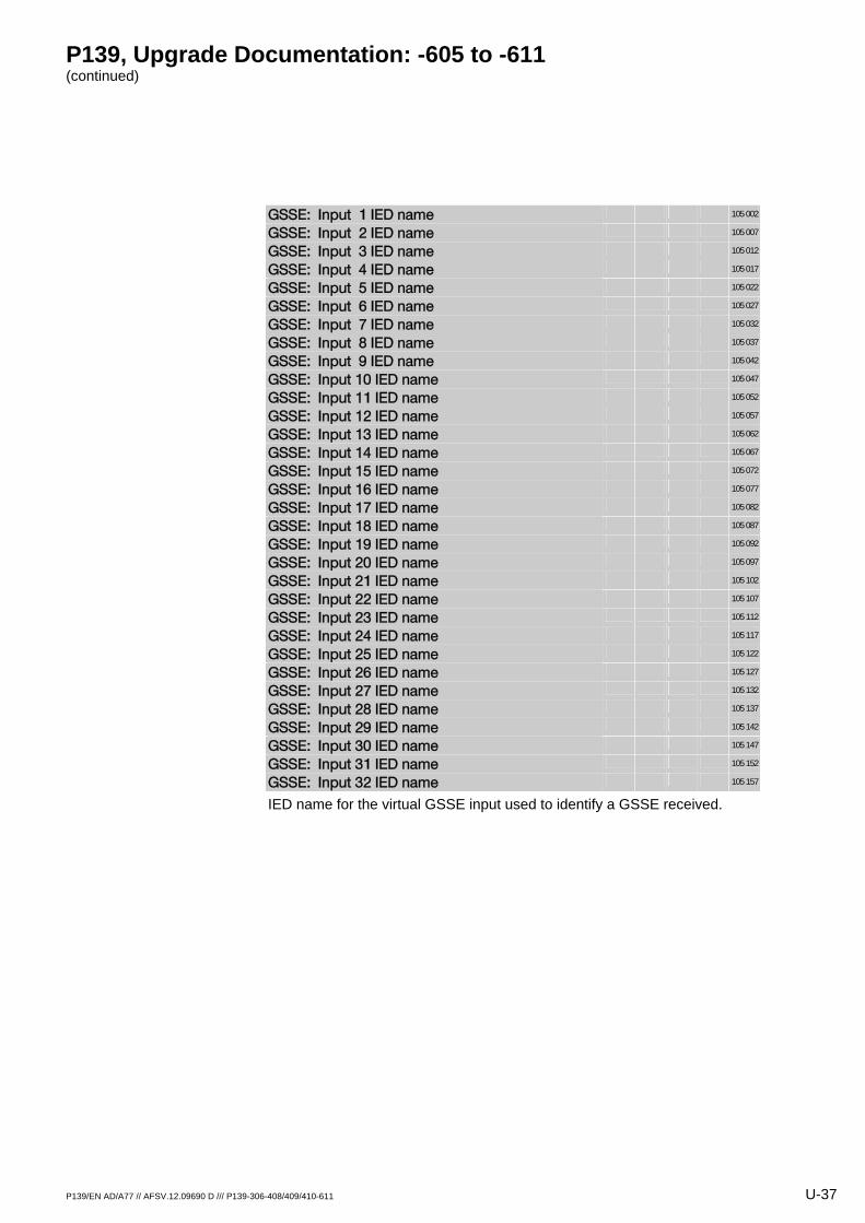
P139, Upgrade Documentation: -605 to -611 (continued)
P139/EN AD/A77 // AFSV.12.09690 D /// P139-306-408/409/410-611 U-37
GSSE: Input 1 IED name 105 002
GSSE: Input 2 IED name 105 007
GSSE: Input 3 IED name 105 012
GSSE: Input 4 IED name 105 017
GSSE: Input 5 IED name 105 022
GSSE: Input 6 IED name 105 027
GSSE: Input 7 IED name 105 032
GSSE: Input 8 IED name 105 037
GSSE: Input 9 IED name 105 042
GSSE: Input 10 IED name 105 047
GSSE: Input 11 IED name 105 052
GSSE: Input 12 IED name 105 057
GSSE: Input 13 IED name 105 062
GSSE: Input 14 IED name 105 067
GSSE: Input 15 IED name 105 072
GSSE: Input 16 IED name 105 077
GSSE: Input 17 IED name 105 082
GSSE: Input 18 IED name 105 087
GSSE: Input 19 IED name 105 092
GSSE: Input 20 IED name 105 097
GSSE: Input 21 IED name 105 102
GSSE: Input 22 IED name 105 107
GSSE: Input 23 IED name 105 112
GSSE: Input 24 IED name 105 117
GSSE: Input 25 IED name 105 122
GSSE: Input 26 IED name 105 127
GSSE: Input 27 IED name 105 132
GSSE: Input 28 IED name 105 137
GSSE: Input 29 IED name 105 142
GSSE: Input 30 IED name 105 147
GSSE: Input 31 IED name 105 152
GSSE: Input 32 IED name 105 157
IED name for the virtual GSSE input used to identify a GSSE received.
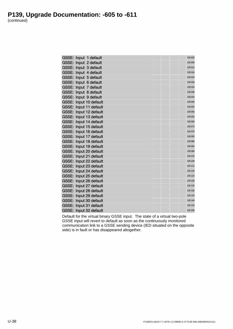
P139, Upgrade Documentation: -605 to -611 (continued)
U-38 P139/EN AD/A77 // AFSV.12.09690 D /// P139-306-408/409/410-611
GSSE: Input 1 default 105 003
GSSE: Input 2 default 105 008
GSSE: Input 3 default 105 013
GSSE: Input 4 default 105 018
GSSE: Input 5 default 105 023
GSSE: Input 6 default 105 028
GSSE: Input 7 default 105 033
GSSE: Input 8 default 105 038
GSSE: Input 9 default 105 043
GSSE: Input 10 default 105 048
GSSE: Input 11 default 105 053
GSSE: Input 12 default 105 058
GSSE: Input 13 default 105 063
GSSE: Input 14 default 105 068
GSSE: Input 15 default 105 073
GSSE: Input 16 default 105 078
GSSE: Input 17 default 105 083
GSSE: Input 18 default 105 088
GSSE: Input 19 default 105 093
GSSE: Input 20 default 105 098
GSSE: Input 21 default 105 103
GSSE: Input 22 default 105 108
GSSE: Input 23 default 105 113
GSSE: Input 24 default 105 118
GSSE: Input 25 default 105 123
GSSE: Input 26 default 105 128
GSSE: Input 27 default 105 133
GSSE: Input 28 default 105 138
GSSE: Input 29 default 105 143
GSSE: Input 30 default 105 148
GSSE: Input 31 default 105 153
GSSE: Input 32 default 105 158
Default for the virtual binary GSSE input. The state of a virtual two-pole GSSE input will revert to default as soon as the continuously monitored communication link to a GSSE sending device (IED situated on the opposite side) is in fault or has disappeared altogether.
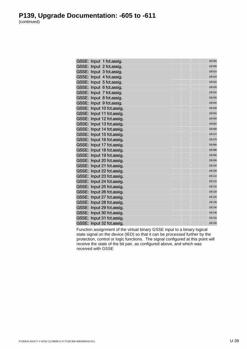
P139, Upgrade Documentation: -605 to -611 (continued)
P139/EN AD/A77 // AFSV.12.09690 D /// P139-306-408/409/410-611 U-39
GSSE: Input 1 fct.assig. 105 004
GSSE: Input 2 fct.assig. 105 009
GSSE: Input 3 fct.assig. 105 014
GSSE: Input 4 fct.assig. 105 019
GSSE: Input 5 fct.assig. 105 024
GSSE: Input 6 fct.assig. 105 029
GSSE: Input 7 fct.assig. 105 034
GSSE: Input 8 fct.assig. 105 039
GSSE: Input 9 fct.assig. 105 044
GSSE: Input 10 fct.assig. 105 049
GSSE: Input 11 fct.assig. 105 054
GSSE: Input 12 fct.assig. 105 059
GSSE: Input 13 fct.assig. 105 064
GSSE: Input 14 fct.assig. 105 069
GSSE: Input 15 fct.assig. 105 074
GSSE: Input 16 fct.assig. 105 079
GSSE: Input 17 fct.assig. 105 084
GSSE: Input 18 fct.assig. 105 089
GSSE: Input 19 fct.assig. 105 094
GSSE: Input 20 fct.assig. 105 099
GSSE: Input 21 fct.assig. 105 104
GSSE: Input 22 fct.assig. 105 109
GSSE: Input 23 fct.assig. 105 114
GSSE: Input 24 fct.assig. 105 119
GSSE: Input 25 fct.assig. 105 124
GSSE: Input 26 fct.assig. 105 129
GSSE: Input 27 fct.assig. 105 134
GSSE: Input 28 fct.assig. 105 139
GSSE: Input 29 fct.assig. 105 144
GSSE: Input 30 fct.assig. 105 149
GSSE: Input 31 fct.assig. 105 154
GSSE: Input 32 fct.assig. 105 159
Function assignment of the virtual binary GSSE input to a binary logical state signal on the device (IED) so that it can be processed further by the protection, control or logic functions. The signal configured at this point will receive the state of the bit pair, as configured above, and which was received with GSSE
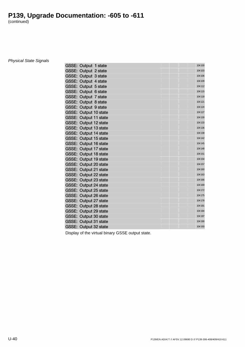
P139, Upgrade Documentation: -605 to -611 (continued)
U-40 P139/EN AD/A77 // AFSV.12.09690 D /// P139-306-408/409/410-611
Physical State Signals GSSE: Output 1 state 104 100
GSSE: Output 2 state 104 103
GSSE: Output 3 state 104 106
GSSE: Output 4 state 104 109
GSSE: Output 5 state 104 112
GSSE: Output 6 state 104 115
GSSE: Output 7 state 104 118
GSSE: Output 8 state 104 121
GSSE: Output 9 state 104 124
GSSE: Output 10 state 104 127
GSSE: Output 11 state 104 130
GSSE: Output 12 state 104 133
GSSE: Output 13 state 104 136
GSSE: Output 14 state 104 139
GSSE: Output 15 state 104 142
GSSE: Output 16 state 104 145
GSSE: Output 17 state 104 148
GSSE: Output 18 state 104 151
GSSE: Output 19 state 104 154
GSSE: Output 20 state 104 157
GSSE: Output 21 state 104 160
GSSE: Output 22 state 104 163
GSSE: Output 23 state 104 166
GSSE: Output 24 state 104 169
GSSE: Output 25 state 104 172
GSSE: Output 26 state 104 175
GSSE: Output 27 state 104 178
GSSE: Output 28 state 104 181
GSSE: Output 29 state 104 184
GSSE: Output 30 state 104 187
GSSE: Output 31 state 104 190
GSSE: Output 32 state 104 193
Display of the virtual binary GSSE output state.
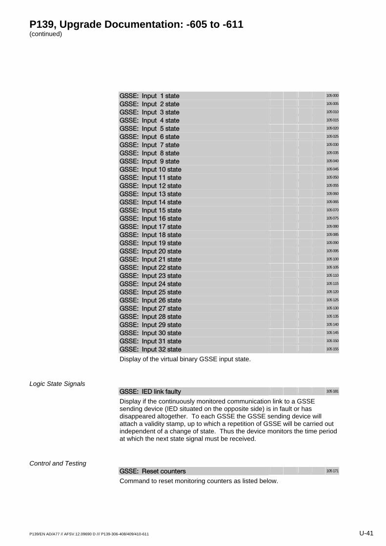
P139, Upgrade Documentation: -605 to -611 (continued)
P139/EN AD/A77 // AFSV.12.09690 D /// P139-306-408/409/410-611 U-41
GSSE: Input 1 state 105 000
GSSE: Input 2 state 105 005
GSSE: Input 3 state 105 010
GSSE: Input 4 state 105 015
GSSE: Input 5 state 105 020
GSSE: Input 6 state 105 025
GSSE: Input 7 state 105 030
GSSE: Input 8 state 105 035
GSSE: Input 9 state 105 040
GSSE: Input 10 state 105 045
GSSE: Input 11 state 105 050
GSSE: Input 12 state 105 055
GSSE: Input 13 state 105 060
GSSE: Input 14 state 105 065
GSSE: Input 15 state 105 070
GSSE: Input 16 state 105 075
GSSE: Input 17 state 105 080
GSSE: Input 18 state 105 085
GSSE: Input 19 state 105 090
GSSE: Input 20 state 105 095
GSSE: Input 21 state 105 100
GSSE: Input 22 state 105 105
GSSE: Input 23 state 105 110
GSSE: Input 24 state 105 115
GSSE: Input 25 state 105 120
GSSE: Input 26 state 105 125
GSSE: Input 27 state 105 130
GSSE: Input 28 state 105 135
GSSE: Input 29 state 105 140
GSSE: Input 30 state 105 145
GSSE: Input 31 state 105 150
GSSE: Input 32 state 105 155
Display of the virtual binary GSSE input state.
Logic State Signals GSSE: IED link faulty 105 181
Display if the continuously monitored communication link to a GSSE sending device (IED situated on the opposite side) is in fault or has disappeared altogether. To each GSSE the GSSE sending device will attach a validity stamp, up to which a repetition of GSSE will be carried out independent of a change of state. Thus the device monitors the time period at which the next state signal must be received.
Control and Testing GSSE: Reset counters 105 171
Command to reset monitoring counters as listed below.
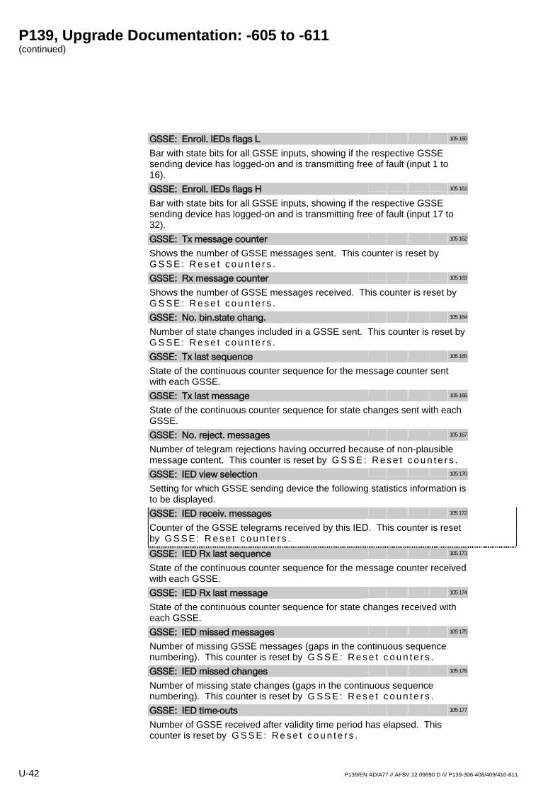
P139, Upgrade Documentation: -605 to -611 (continued)
U-42 P139/EN AD/A77 // AFSV.12.09690 D /// P139-306-408/409/410-611
GSSE: Enroll. IEDs flags L 105 160
Bar with state bits for all GSSE inputs, showing if the respective GSSE sending device has logged-on and is transmitting free of fault (input 1 to 16).
GSSE: Enroll. IEDs flags H 105 161
Bar with state bits for all GSSE inputs, showing if the respective GSSE sending device has logged-on and is transmitting free of fault (input 17 to 32).
GSSE: Tx message counter 105 162
Shows the number of GSSE messages sent. This counter is reset by G S S E : R e s e t c o u n t e r s .
GSSE: Rx message counter 105 163
Shows the number of GSSE messages received. This counter is reset by G S S E : R e s e t c o u n t e r s .
GSSE: No. bin.state chang. 105 164
Number of state changes included in a GSSE sent. This counter is reset by G S S E : R e s e t c o u n t e r s .
GSSE: Tx last sequence 105 165
State of the continuous counter sequence for the message counter sent with each GSSE.
GSSE: Tx last message 105 166
State of the continuous counter sequence for state changes sent with each GSSE.
GSSE: No. reject. messages 105 167
Number of telegram rejections having occurred because of non-plausible message content. This counter is reset by G S S E : R e s e t c o u n t e r s .
GSSE: IED view selection 105 170
Setting for which GSSE sending device the following statistics information is to be displayed.
GSSE: IED receiv. messages 105 172
Counter of the GSSE telegrams received by this IED. This counter is reset by G S S E : R e s e t c o u n t e r s .
GSSE: IED Rx last sequence 105 173
State of the continuous counter sequence for the message counter received with each GSSE.
GSSE: IED Rx last message 105 174
State of the continuous counter sequence for state changes received with each GSSE.
GSSE: IED missed messages 105 175
Number of missing GSSE messages (gaps in the continuous sequence numbering). This counter is reset by G S S E : R e s e t c o u n t e r s .
GSSE: IED missed changes 105 176
Number of missing state changes (gaps in the continuous sequence numbering). This counter is reset by G S S E : R e s e t c o u n t e r s .
GSSE: IED time-outs 105 177
Number of GSSE received after validity time period has elapsed. This counter is reset by G S S E : R e s e t c o u n t e r s .
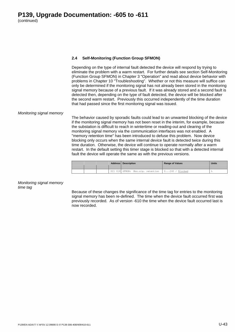
P139, Upgrade Documentation: -605 to -611 (continued)
P139/EN AD/A77 // AFSV.12.09690 D /// P139-306-408/409/410-611 U-43
2.4 Self-Monitoring (Function Group SFMON)
Depending on the type of internal fault detected the device will respond by trying to eliminate the problem with a warm restart. For further details see section Self-Monitoring (Function Group SFMON) in Chapter 3 "Operation" and read about device behavior with problems in Chapter 10 "Troubleshooting". Whether or not this measure will suffice can only be determined if the monitoring signal has not already been stored in the monitoring signal memory because of a previous fault. If it was already stored and a second fault is detected then, depending on the type of fault detected, the device will be blocked after the second warm restart. Previously this occurred independently of the time duration that had passed since the first monitoring signal was issued.
Monitoring signal memory The behavior caused by sporadic faults could lead to an unwanted blocking of the device if the monitoring signal memory has not been reset in the interim, for example, because the substation is difficult to reach in wintertime or reading-out and clearing of the monitoring signal memory via the communication interfaces was not enabled. A "memory retention time" has been introduced to defuse this problem. Now device blocking only occurs when the same internal device fault is detected twice during this time duration. Otherwise, the device will continue to operate normally after a warm restart. In the default setting this timer stage is blocked so that with a detected internal fault the device will operate the same as with the previous versions.
Address Description Range of Values Units
021 018 SFMON: Mon.sig. retention 0...240 / Blocked h
Monitoring signal memory time tag
Because of these changes the significance of the time tag for entries to the monitoring signal memory has been re-defined. The time when the device fault occurred first was previously recorded. As of version -610 the time when the device fault occurred last is now recorded.
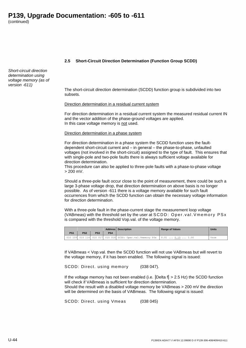
P139, Upgrade Documentation: -605 to -611 (continued)
U-44 P139/EN AD/A77 // AFSV.12.09690 D /// P139-306-408/409/410-611
2.5 Short-Circuit Direction Determination (Function Group SCDD)
Short-circuit direction determination using voltage memory (as of version -611)
The short-circuit direction determination (SCDD) function group is subdivided into two subsets.
Direction determination in a residual current system
For direction determination in a residual current system the measured residual current IN and the vector addition of the phase-ground voltages are applied. In this case voltage memory is not used.
Direction determination in a phase system
For direction determination in a phase system the SCDD function uses the fault-dependent short-circuit current and – in general – the phase-to-phase, unfaulted voltages (not involved in the short-circuit) assigned to the type of fault. This ensures that with single-pole and two-pole faults there is always sufficient voltage available for direction determination. This procedure can also be applied to three-pole faults with a phase-to-phase voltage > 200 mV.
Should a three-pole fault occur close to the point of measurement, there could be such a large 3-phase voltage drop, that direction determination on above basis is no longer possible. As of version -611 there is a voltage memory available for such fault occurrences from which the SCDD function can obtain the necessary voltage information for direction determination.
With a three-pole fault in the phase-current stage the measurement loop voltage (VABmeas) with the threshold set by the user at S C D D : O p e r . v a l . V m e m o r y P S x is compared with the threshold Vop.val. of the voltage memory.
Address Description Range of Values Units PS1 PS2 PS3 PS4
010 109 010 116 010 017 010 018 SCDD: Oper.val.Vmemory PSx 0.01 ... 0.15 ... 1.00 Vnom
If VABmeas < Vop.val. then the SCDD function will not use VABmeas but will revert to the voltage memory, if it has been enabled. The following signal is issued:
SCDD: Direct . using memory (038 047).
If the voltage memory has not been enabled (i.e. |Delta f| > 2.5 Hz) the SCDD function will check if VABmeas is sufficient for direction determination. Should the result with a disabled voltage memory be VABmeas > 200 mV the direction will be determined on the basis of VABmeas. The following signal is issued:
SCDD: Direct . using Vmeas (038 045)
P139, Upgrade Documentation: -605 to -611 (continued)
P139/EN AD/A77 // AFSV.12.09690 D /// P139-306-408/409/410-611 U-45
If V12meas < 200 mV, a forward fault is detected if the voltage memory is disabled and if the pre-orientation is active (set under S C D D : T r i p b i a s ), otherwise the directional decision is blocked. The following signal is issued:
SCDD: Forw. w/o measurem. (038 044). These signals are additionally delivered to the following signals:
SCDD: Faul t P forward SCDD: Faul t P backward SCDD: Faul t P or G forwd. SCDD: Faul t P or G backw.
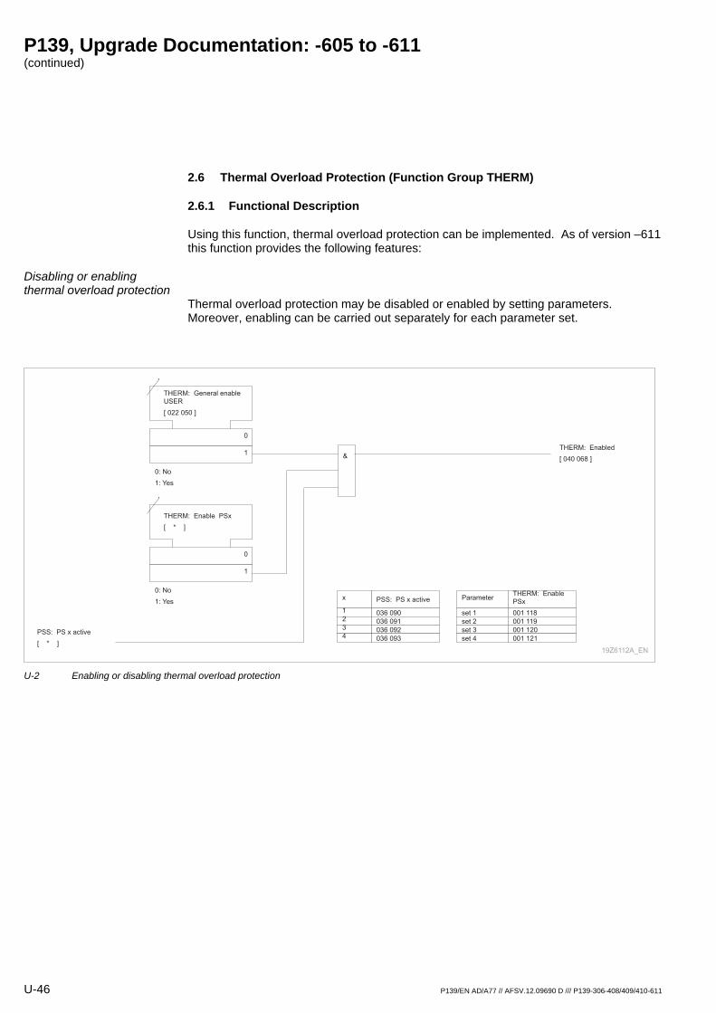
P139, Upgrade Documentation: -605 to -611 (continued)
U-46 P139/EN AD/A77 // AFSV.12.09690 D /// P139-306-408/409/410-611
2.6 Thermal Overload Protection (Function Group THERM)
2.6.1 Functional Description
Using this function, thermal overload protection can be implemented. As of version –611 this function provides the following features:
Disabling or enabling thermal overload protection
Thermal overload protection may be disabled or enabled by setting parameters. Moreover, enabling can be carried out separately for each parameter set.
0
THERM: General enable
USER
[ 022 050 ]
1
0: No
1: Yes
0
THERM: Enable PSx
[ * ]
1
0: No
1: Yes
&
THERM: Enabled
[ 040 068 ]
PSS: PS x active
[ * ]
Parameter
set 1
set 2
set 3
set 4
THERM: Enable
PSx
001 118
001 119
001 120
001 121
PSS: PS x active
036 090
036 091
036 092
036 093
x
1
2
3
4
19Z6112A_EN
U-2 Enabling or disabling thermal overload protection
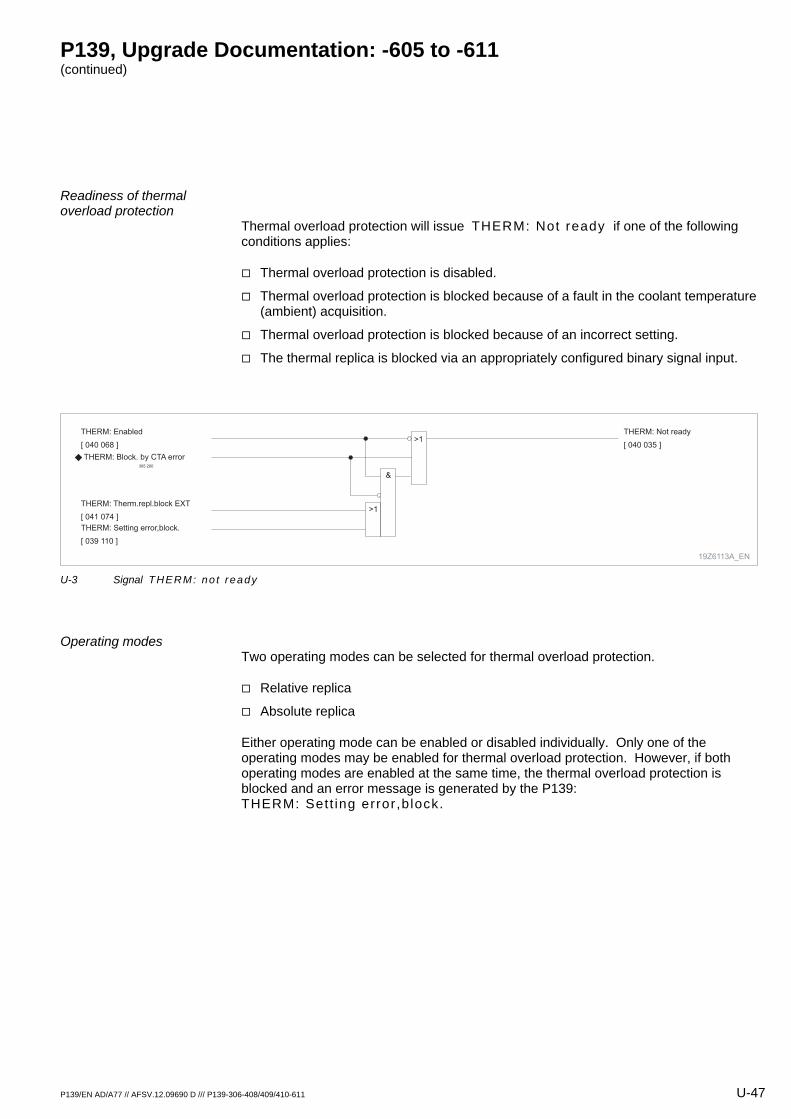
P139, Upgrade Documentation: -605 to -611 (continued)
P139/EN AD/A77 // AFSV.12.09690 D /// P139-306-408/409/410-611 U-47
Readiness of thermal overload protection
Thermal overload protection will issue THERM: Not ready if one of the following conditions applies:
Thermal overload protection is disabled.
Thermal overload protection is blocked because of a fault in the coolant temperature (ambient) acquisition.
Thermal overload protection is blocked because of an incorrect setting.
The thermal replica is blocked via an appropriately configured binary signal input.
19Z6113A_EN
THERM: Enabled
[ 040 068 ]
&
>1THERM: Not ready
[ 040 035 ]
THERM: Block. by CTA error 305 200
>1THERM: Therm.repl.block EXT
[ 041 074 ]
THERM: Setting error,block.
[ 039 110 ]
U-3 Signal THERM: no t ready
Operating modes Two operating modes can be selected for thermal overload protection.
Relative replica
Absolute replica
Either operating mode can be enabled or disabled individually. Only one of the operating modes may be enabled for thermal overload protection. However, if both operating modes are enabled at the same time, the thermal overload protection is blocked and an error message is generated by the P139: THERM: Sett ing error ,b lock.
P139, Upgrade Documentation: -605 to -611 (continued)
U-48 P139/EN AD/A77 // AFSV.12.09690 D /// P139-306-408/409/410-611
Coolant temperature effect To permit coolant temperature (ambient) acquisition, one of the analog modules Y must be fitted, either the analog (I/O) module Y with a 20 mA current input and the "PT100" input or the temperature p/c board (the RTD module) with the temperature sensor inputs T1 to T9.
One of the 11 measuring inputs listed above is selected for the primary measurement of coolant temperature by setting the parameter T H E R M : Select meas. inputPSx.
In addition the parameter THERM: Sel . backup th. PSx is set to select which of these 11 measuring inputs is to be used as a backup to measure the coolant temperature when the primary measuring input has failed.
If the parameters T H E R M : Select meas. inputPSx or THERM: Sel . Backup th. PSx have been set incorrectly the thermal overload protection is blocked and an error message is generated by the P139: THERM: Sett ing error ,b lock.
An open measuring circuit, due to a broken wire, is determined by the measured value inputs (function group MEASI). This will result in the issuance of these signals:
M E A S I : O p e n c i r c . 2 0 m A i n p .
M E A S I : P T 1 0 0 o p e n c i r c u i t
M E A S I : T 1 o p e n c i r c . to M E A S I : T 9 o p e n c i r c .
The thermal model uses these signals as a criterion to determine a fault in the coolant temperature measurement. A fault at both measured value inputs selected will lead to the issuance of the signal T H E R M : C T A e r r o r .
P139, Upgrade Documentation: -605 to -611 (continued)
P139/EN AD/A77 // AFSV.12.09690 D /// P139-306-408/409/410-611 U-49
The setting of T H E R M : F u n c t . f . C T A f a i l . P S x determines how the thermal overload protection is to continue functioning when the coolant temperature measurement has failed. The following functions can be selected to guarantee continued and stable performance of the thermal overload protection when the coolant temperature measurement has failed.
Default temperature value: The coolant temperature set at T H E R M : D e f a u l t C T A P S x is applied. The thermal overload protection is not blocked.
Last measured temperature: As a rule there is an erratic change of the measured value when a fault has occurred in the coolant temperature measurement. The temperature measured before such an erratic change is stored and applied. The thermal overload protection is not blocked.
The coolant temperature set at T H E R M : D e f a u l t C T A P S x is applied if no last measured values are available because a device warm restart or a parameter subset selection was carried out.
Blocking: The signals THERM: Warning and THERM: Tr ip s ignal are reset and blocked. The thermal model will then be continued and displayed on the basis of the measured current alone. All further measurands are issued as "not measured".
All relevant parameters for coolant temperature (ambient) acquisition are hidden if none of the two analog modules Y available have been fitted. The tripping time is calculated by including the setting for T H E R M : D e f a u l t C T A P S x .
Thermal overload protection operation without coolant temperature (ambient) acquisition
In order to guarantee thermal overload protection, without considering an offset due to a variable coolant temperature, it is recommended to set the parameter T H E R M : D e f a u l t C T A P S x to the maximum permitted coolant temperature.
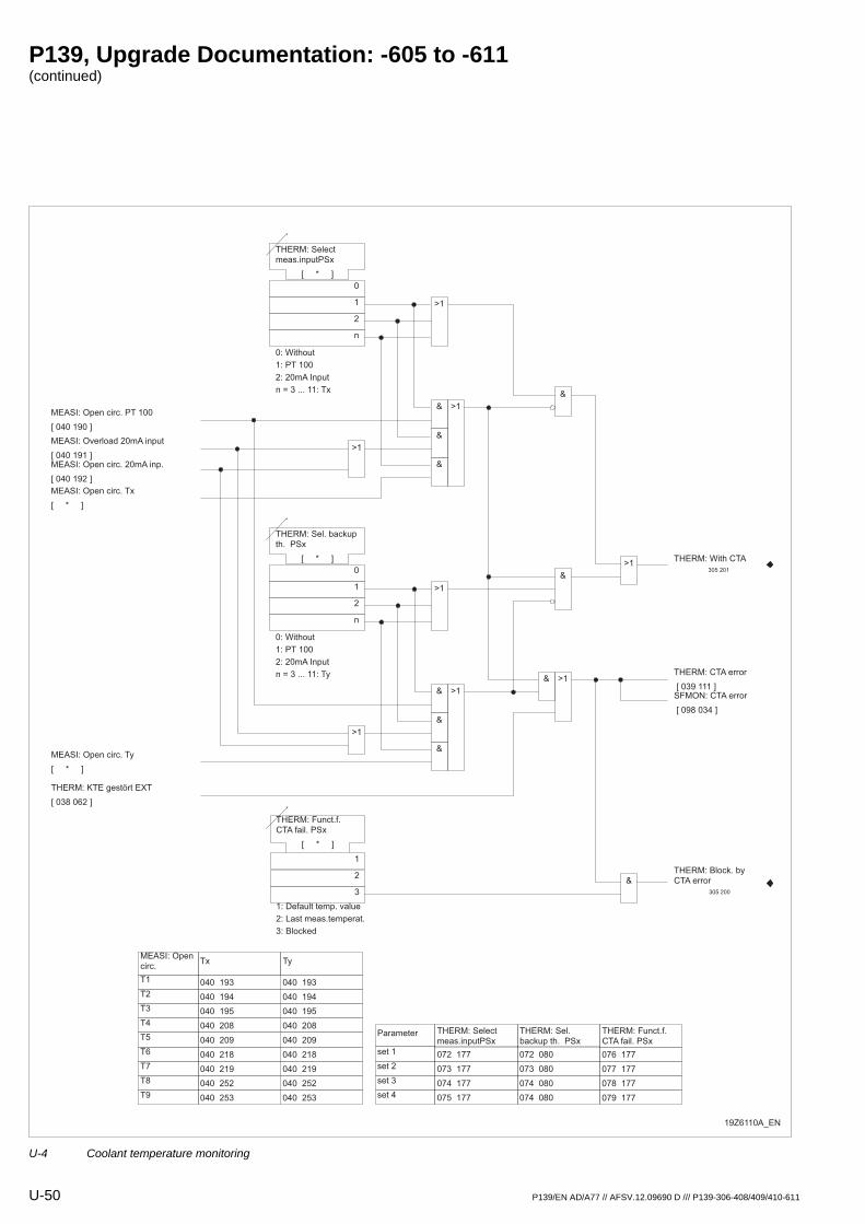
P139, Upgrade Documentation: -605 to -611 (continued)
U-50 P139/EN AD/A77 // AFSV.12.09690 D /// P139-306-408/409/410-611
THERM: With CTA
305 201
MEASI: Open circ. PT 100
[ 040 190 ]
MEASI: Overload 20mA input
[ 040 191 ]
&
0
0: Without
1: PT 100
>1
THERM: Select
meas.inputPSx
[ * ]
THERM: Sel.
backup th. PSx
THERM: Select
meas.inputPSx
072 177 072 080
073 177 073 080
074 177 074 080
075 177 074 080
Parameter
set 1
set 2
set 3
set 4
2: 20mA Input
&
>1
MEASI: Open circ. 20mA inp.
[ 040 192 ]
>1
THERM: KTE gestört EXT
[ 038 062 ]
THERM: CTA error
[ 039 111 ]SFMON: CTA error
[ 098 034 ]
THERM: Block. by
CTA error
305 200
1
2
n
n = 3 ... 11: Tx
MEASI: Open circ. Tx
[ * ]
&
&
0
0: Without
1: PT 100
>1
THERM: Sel. backup
th. PSx
[ * ]
2: 20mA Input
&
>1
>1
1
2
n
n = 3 ... 11: Ty
MEASI: Open circ. Ty
[ * ]
&
&
>1
& >1
1
1: Default temp. value
2: Last meas.temperat.
THERM: Funct.f.
CTA fail. PSx
[ * ]
3: Blocked
2
3
&
&
076 177
077 177
078 177
079 177
040 218
040 219
040 252
040 253
T6
T7
T8
T9
040 194
040 195
040 208
040 209
T2
T3
T4
T5
TyTx
040 193
MEASI: Open
circ.
T1
040 218
040 219
040 252
040 253
040 194
040 195
040 208
040 209
040 193
THERM: Funct.f.
CTA fail. PSx
19Z6110A_EN
U-4 Coolant temperature monitoring
P139, Upgrade Documentation: -605 to -611 (continued)
P139/EN AD/A77 // AFSV.12.09690 D /// P139-306-408/409/410-611 U-51
Relative replica The rated operating current of the protected object and its overload tolerance for maximum coolant (ambient) temperature are the basis of the relative thermal replica.
In the "Relative replica" operating mode, the following settings have to be made for thermal overload protection:
The rated operating current of the protected object T H E R M : I r e f P S x
The tripping threshold ∆ϑtrip is set at T H E R M : R e l . O / T t r i p P S x
If coolant temperature (ambient) acquisition is used, the following parameters must be set:
The maximum permissible temperature of the protected object Θmax T H E R M : M a x . p e r m . o b j . t m p . P S x
The maximum coolant temperature (maximum ambient) Θa,max T H E R M : M a x . p e r m . c o o l . t m p P S x
Absolute replica The thermal limit current of the protected object is the reference current of the absolute thermal replica. For this limit current, an overtemperature results at the maximum coolant temperature.
In the "Absolute replica" operating mode, the following parameters have to be set for thermal overload protection:
The thermal limit current of the protected object T H E R M : I r e f P S x
The limit temperature for tripping Θmax T H E R M : M a x . p e r m . o b j . t m p . P S x
The overtemperature as a result of a persistent limit current (Θmax - Θa,max ) T H E R M : O / T f . I r e f p e r s . P S x
Note: The maximum permissible coolant temperature Θa,max is derived from the difference between the parameters THERM: Max.perm.obj . tmp.PSx and THERM: O/T f . I ref pers. PSx
Tripping characteristics The maximum RMS phase current I is used to track a first-order thermal replica as specified in IEC 255-8. Other than the operating mode dependent settings the following parameters will govern the tripping time:
The set thermal time constant τ of the protected object THERM: Tim.const.1,>Ibl PS
The accumulated thermal load ∆ϑ0.
The current measured coolant temperature Θa.
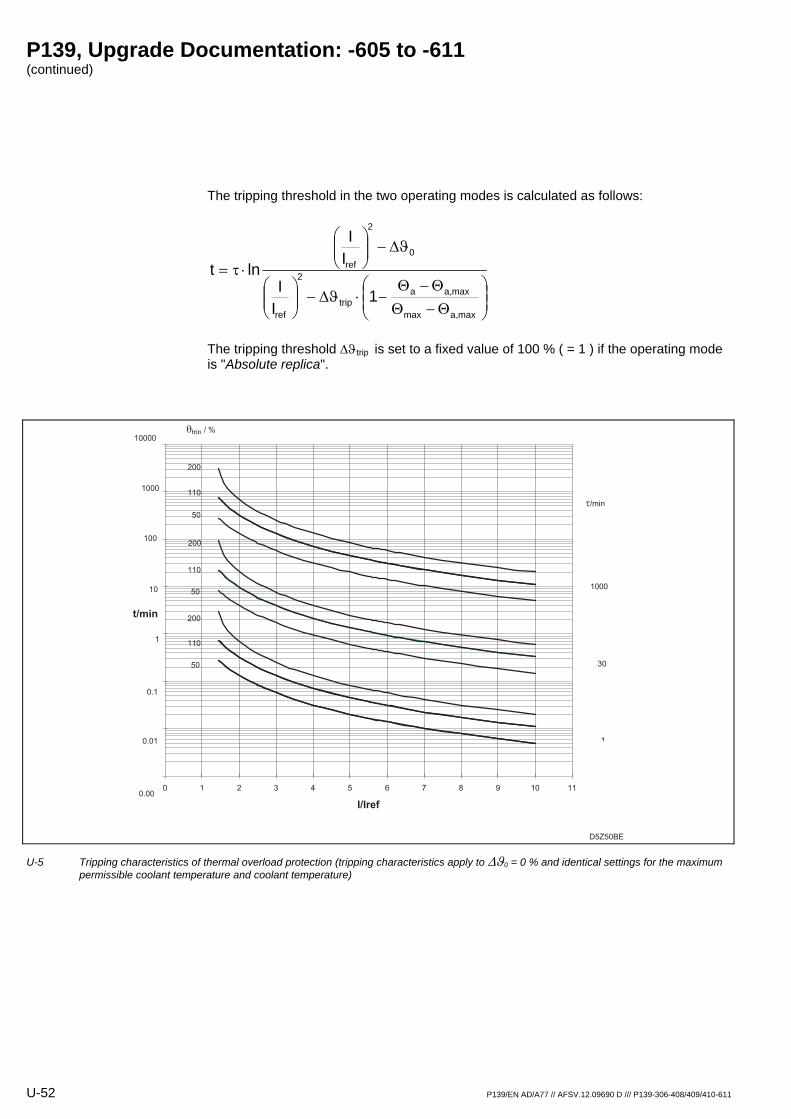
P139, Upgrade Documentation: -605 to -611 (continued)
U-52 P139/EN AD/A77 // AFSV.12.09690 D /// P139-306-408/409/410-611
The tripping threshold in the two operating modes is calculated as follows:
⎟⎟⎠
⎞⎜⎜⎝
⎛Θ−ΘΘ−Θ
−⋅ϑ∆−⎟⎟⎠
⎞⎜⎜⎝
⎛
ϑ∆−⎟⎟⎠
⎞⎜⎜⎝
⎛
⋅τ=
max,amax
max,aatrip
2
ref
0
2
ref
1II
II
lnt
The tripping threshold ∆ϑtrip is set to a fixed value of 100 % ( = 1 ) if the operating mode is "Absolute replica".
0 1 2 3 4 5 6 7 8 9 10 11
I/Iref
t/min
D5Z50BE
30
1000
1
τ/min
θtrip / %
1000
10000
100
10
1
0.1
0.01
0.00
200
110
50
200
200
110
110
50
50
U-5 Tripping characteristics of thermal overload protection (tripping characteristics apply to ∆ϑ0 = 0 % and identical settings for the maximum permissible coolant temperature and coolant temperature)
P139, Upgrade Documentation: -605 to -611 (continued)
P139/EN AD/A77 // AFSV.12.09690 D /// P139-306-408/409/410-611 U-53
Warning Depending on the selected operating mode, a warning signal can be set at one of the following parameters:
Relative replica: THERM: Rel . O/T warning PSx
Absolute replica: THERM: Warning temp. PSx
Additionally, a pre-trip time limit can be set; when the time left until tripping falls below this pre-trip limit, a warning will be issued.
Trip
The trip threshold is set according to the selected operating mode with the following parameters:
Relative replica: THERM: Rel . O/T t r ip PSx
Absolute replica: THERM: Max.perm.obj . tmp.PSx
If a trip command is issued, the trip signal is maintained until the status of the thermal replica has decreased by the value T H E R M : T r i p H y s t e r e s i s P S x , at least for a fixed time of 5s.
Cooling
If the current falls below the default threshold of 0.1 Iref, the thermal replica is applied with the set time constant THERM: Tim.const.2,<Ibl PSx. This element in the thermal model takes account of the cooling characteristics of stopped motors.
Note: These two time constants should be set to the same value for transformers and power lines.
Operation together with the motor protection function
If the thermal overload protection function is operated together with the motor protection function (function group MP) and if another startup of an asynchronous motor occurs (other than the first startup), then the thermal overload protection function will be temporarily blocked during the startup time.
The motor protection will effect the thermal overload protection and not vice versa if both protection functions are applied simultaneously.
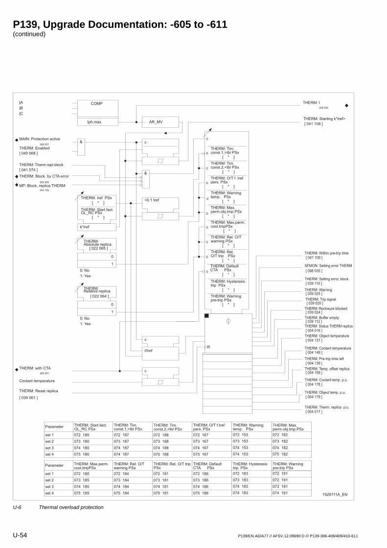
P139, Upgrade Documentation: -605 to -611 (continued)
U-54 P139/EN AD/A77 // AFSV.12.09690 D /// P139-306-408/409/410-611
MAIN: Protection active
306 001
Iph,maxTHERM: Starting k*Iref>
[ 041 108 ]
&
IA
IB
IC
COMP
AR_MV
THERM: I
305 202
c
THERM: Enabled
[ 040 068 ]
MP: Block. replica THERM304 700
&THERM: Block. by CTA error
305 200
THERM: Therm.repl.block
[ 041 074 ]
THERM: Iref PSx
[ * ]
k*Iref
THERM: Start.fact. OL_RC PSx
[ * ]
<0.1 Iref
THERM:Absolute replica
[ 022 065 ]
0
1
0: No
1: Yes
THERM:Relative replica
[ 022 064 ]
0
1
0: No
1: Yes
c
I/Iref
THERM: with CTA
305 201
Coolant temperature
R
THERM: Reset replica
[ 039 061 ]
cTHERM: Tim. const.1,>Ibl PSx
[ * ]
THERM: Tim. const.2,<Ibl PSx
[ * ]
THERM: Default CTA PSx
[ * ]
THERM: O/T f. Iref pers. PSx
[ * ]
THERM: Warning temp. PSx
[ * ]
THERM: Max. perm.obj.tmp.PSx
[ * ]
THERM: Max.perm. cool.tmpPSx
[ * ]
THERM: Rel. O/T warning PSx
[ * ]
THERM: Rel. O/T trip PSx
[ * ]
THERM: Hysteresis trip PSx
[ * ]
THERM: Warning pre-trip PSx
[ * ]
THERM: Therm. replica p.u. [ 004 017 ]
THERM: Object temp. p.u. [ 004 179 ]
THERM: Coolant temp. p.u. [ 004 178 ]
THERM: Temp. offset replica [ 004 109 ]
THERM: Pre-trip time left [ 004 139 ]
THERM: Coolant temperature [ 004 149 ]
THERM: Object temperature [ 004 137 ]
THERM: Status THERM replica [ 004 016 ]
THERM: Buffer empty [ 039 112 ]
THERM: Reclosure blocked [ 039 024 ]
THERM: Trip signal [ 039 020 ]
THERM: Warning [ 039 025 ]
THERM: Setting error, block. [ 039 110 ]
SFMON: Setting error THERM
[ 098 035 ]
THERM: Within pre-trip time
[ 041 109 ]
c
c
c
c
c
c
c
c
c
THERM: Tim. const.1,>Ibl PSx
THERM: Start.fact. OL_RC PSx
072 180 072 187
073 180 073 187
074 180 074 187
075 180 074 187
Parameter
set 1
set 2
set 3
set 4
THERM: Tim. const.2,<Ibl PSx
072 188
073 188
074 188
075 188
THERM: Warning temp. PSx
THERM: O/T f.Iref pers. PSx
072 167 072 153
073 167 073 153
074 167 074 153
075 167 074 153
THERM: Max. perm.obj.tmp.PSx
072 182
073 182
074 182
075 182
THERM: Rel. O/T warning PSx
THERM: Max.perm. cool.tmpPSx
072 185 072 184
073 185 073 184
074 185 074 184
075 185 075 184
Parameter
set 1
set 2
set 3
set 4
THERM: Rel. O/T trip PSx
072 181
073 181
074 181
075 181
THERM: Hysteresis trip PSx
THERM: Default CTA PSx
072 186 072 183
073 186 073 183
074 186 074 183
075 186 074 183
THERM: Warning pre-trip PSx
072 191
072 191
073 191
074 191
c
19Z6111A_EN
U-6 Thermal overload protection
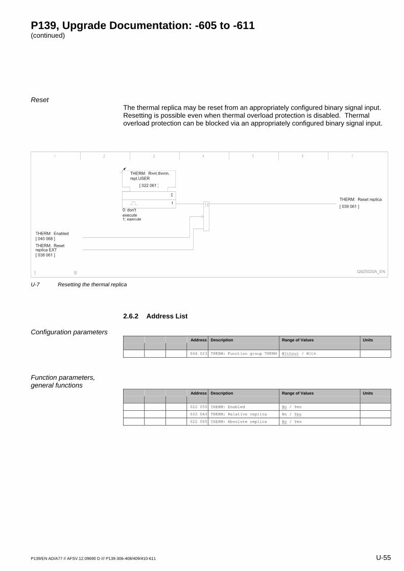
P139, Upgrade Documentation: -605 to -611 (continued)
P139/EN AD/A77 // AFSV.12.09690 D /// P139-306-408/409/410-611 U-55
Reset The thermal replica may be reset from an appropriately configured binary signal input. Resetting is possible even when thermal overload protection is disabled. Thermal overload protection can be blocked via an appropriately configured binary signal input.
THERM: Reset replica
[ 039 061 ]
Q9Z5020A_EN
THERM: Rset.therm.
repl.USER
[ 022 061 ]
0: don't
execute1: execute
1
0
THERM: Enabled
[ 040 068 ]
THERM: Reset replica EXT
[ 038 061 ]
U-7 Resetting the thermal replica
2.6.2 Address List
Configuration parameters Address Description Range of Values Units
056 023 THERM: Function group THERM Without / With
Function parameters, general functions
Address Description Range of Values Units
022 050 THERM: Enabled No / Yes
022 064 THERM: Relative replica No / Yes
022 065 THERM: Absolute replica No / Yes
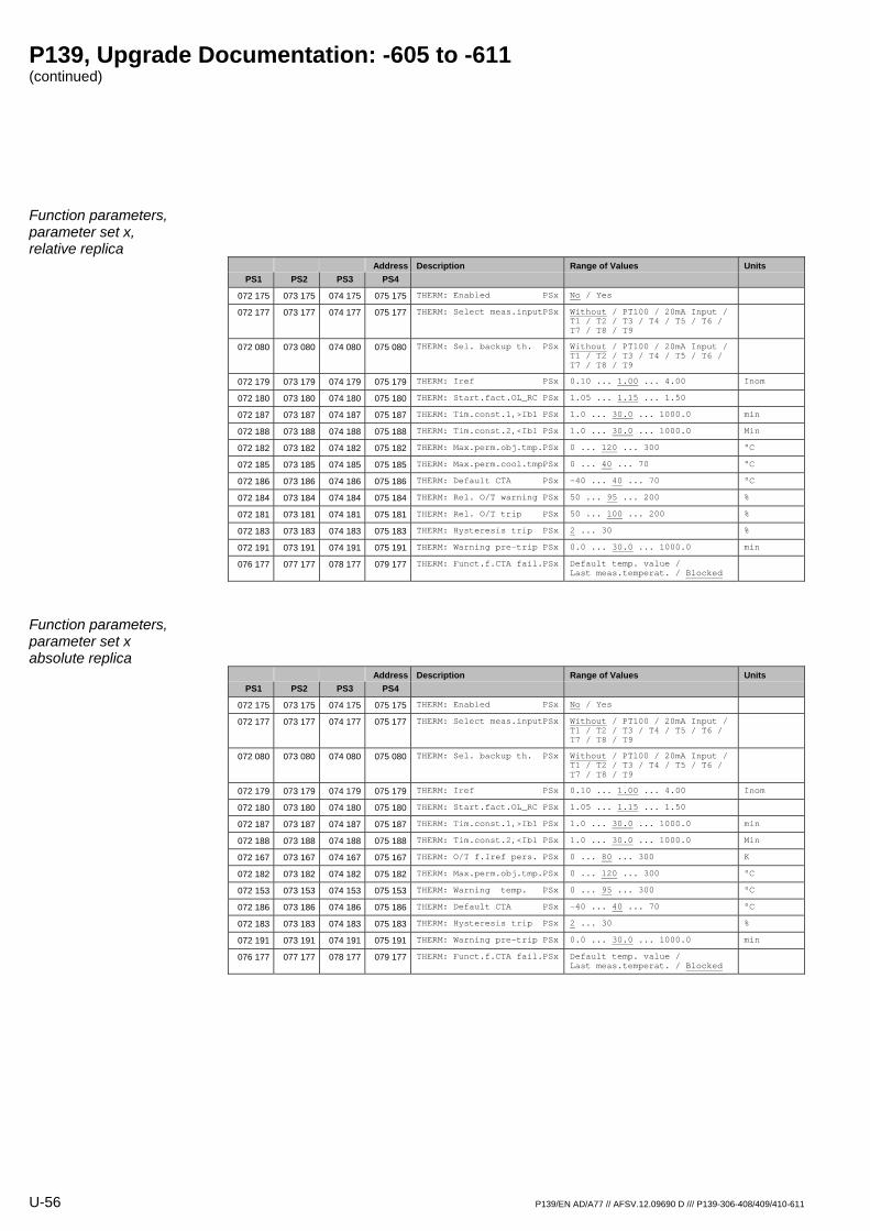
P139, Upgrade Documentation: -605 to -611 (continued)
U-56 P139/EN AD/A77 // AFSV.12.09690 D /// P139-306-408/409/410-611
Function parameters, parameter set x, relative replica
Address Description Range of Values Units PS1 PS2 PS3 PS4
072 175 073 175 074 175 075 175 THERM: Enabled PSx No / Yes
072 177 073 177 074 177 075 177 THERM: Select meas.inputPSx Without / PT100 / 20mA Input / T1 / T2 / T3 / T4 / T5 / T6 / T7 / T8 / T9
072 080 073 080 074 080 075 080 THERM: Sel. backup th. PSx Without / PT100 / 20mA Input / T1 / T2 / T3 / T4 / T5 / T6 / T7 / T8 / T9
072 179 073 179 074 179 075 179 THERM: Iref PSx 0.10 ... 1.00 ... 4.00 Inom
072 180 073 180 074 180 075 180 THERM: Start.fact.OL_RC PSx 1.05 ... 1.15 ... 1.50
072 187 073 187 074 187 075 187 THERM: Tim.const.1,>Ibl PSx 1.0 ... 30.0 ... 1000.0 min
072 188 073 188 074 188 075 188 THERM: Tim.const.2,<Ibl PSx 1.0 ... 30.0 ... 1000.0 Min
072 182 073 182 074 182 075 182 THERM: Max.perm.obj.tmp.PSx 0 ... 120 ... 300 °C
072 185 073 185 074 185 075 185 THERM: Max.perm.cool.tmpPSx 0 ... 40 ... 70 °C
072 186 073 186 074 186 075 186 THERM: Default CTA PSx -40 ... 40 ... 70 °C
072 184 073 184 074 184 075 184 THERM: Rel. O/T warning PSx 50 ... 95 ... 200 %
072 181 073 181 074 181 075 181 THERM: Rel. O/T trip PSx 50 ... 100 ... 200 %
072 183 073 183 074 183 075 183 THERM: Hysteresis trip PSx 2 ... 30 %
072 191 073 191 074 191 075 191 THERM: Warning pre-trip PSx 0.0 ... 30.0 ... 1000.0 min
076 177 077 177 078 177 079 177 THERM: Funct.f.CTA fail.PSx Default temp. value / Last meas.temperat. / Blocked
Function parameters, parameter set x absolute replica
Address Description Range of Values Units PS1 PS2 PS3 PS4
072 175 073 175 074 175 075 175 THERM: Enabled PSx No / Yes
072 177 073 177 074 177 075 177 THERM: Select meas.inputPSx Without / PT100 / 20mA Input / T1 / T2 / T3 / T4 / T5 / T6 / T7 / T8 / T9
072 080 073 080 074 080 075 080 THERM: Sel. backup th. PSx Without / PT100 / 20mA Input / T1 / T2 / T3 / T4 / T5 / T6 / T7 / T8 / T9
072 179 073 179 074 179 075 179 THERM: Iref PSx 0.10 ... 1.00 ... 4.00 Inom
072 180 073 180 074 180 075 180 THERM: Start.fact.OL_RC PSx 1.05 ... 1.15 ... 1.50
072 187 073 187 074 187 075 187 THERM: Tim.const.1,>Ibl PSx 1.0 ... 30.0 ... 1000.0 min
072 188 073 188 074 188 075 188 THERM: Tim.const.2,<Ibl PSx 1.0 ... 30.0 ... 1000.0 Min
072 167 073 167 074 167 075 167 THERM: O/T f.Iref pers. PSx 0 ... 80 ... 300 K
072 182 073 182 074 182 075 182 THERM: Max.perm.obj.tmp.PSx 0 ... 120 ... 300 °C
072 153 073 153 074 153 075 153 THERM: Warning temp. PSx 0 ... 95 ... 300 °C
072 186 073 186 074 186 075 186 THERM: Default CTA PSx -40 ... 40 ... 70 °C
072 183 073 183 074 183 075 183 THERM: Hysteresis trip PSx 2 ... 30 %
072 191 073 191 074 191 075 191 THERM: Warning pre-trip PSx 0.0 ... 30.0 ... 1000.0 min
076 177 077 177 078 177 079 177 THERM: Funct.f.CTA fail.PSx Default temp. value / Last meas.temperat. / Blocked
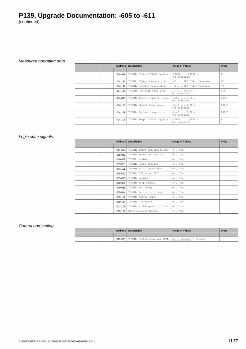
P139, Upgrade Documentation: -605 to -611 (continued)
P139/EN AD/A77 // AFSV.12.09690 D /// P139-306-408/409/410-611 U-57
Measured operating data Address Description Range of Values Units
004 016 THERM: Status THERM replica -25000 ... 25000 / Not measured
%
004 137 THERM: Object temperature -40 ... 300 / Not measured °C
004 149 THERM: Coolant temperature -40 ... 200 / Not measured °C
004 139 THERM: Pre-trip time left 0.0 ... 1000.0 / Not measured
Min
004 017 THERM: Therm. replica p.u. -2.50 ... 2.50 / Not measured
100%
004 179 THERM: Object temp. p.u. -0.40 ... 3.00 / Not measured
100°C
004 178 THERM: Coolant temp. p.u. -0.40 ... 2.00 / Not measured
100°C
004 109 THERM: Temp. offset replica -25000 ... 25000 / Not measured
%
Logic state signals Address Description Range of Values Units
041 074 THERM: Therm.repl.block EXT No / Yes
038 061 THERM: Reset replica EXT No / Yes
040 068 THERM: Enabled No / Yes
039 061 THERM: Reset replica No / Yes
041 108 THERM: Starting k*Iref> No / Yes
038 062 THERM: CTA error EXT No / Yes
039 025 THERM: Warning No / Yes
039 020 THERM: Trip signal No / Yes
040 035 THERM: Not ready No / Yes
039 024 THERM: Reclosure blocked No / Yes
039 112 THERM: Buffer empty No / Yes
039 111 THERM: CTA error No / Yes
041 109 THERM: Within pre-trip time No / Yes
039 110 Setting error,block. No / Yes
Control and testing Address Description Range of Values Units
022 061 THERM: Rset.therm.repl.USER don't execute / execute
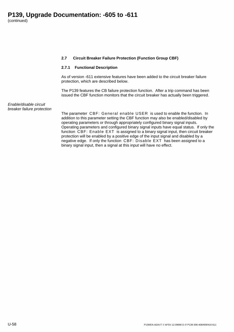
P139, Upgrade Documentation: -605 to -611 (continued)
U-58 P139/EN AD/A77 // AFSV.12.09690 D /// P139-306-408/409/410-611
2.7 Circuit Breaker Failure Protection (Function Group CBF)
2.7.1 Functional Description
As of version -611 extensive features have been added to the circuit breaker failure protection, which are described below.
The P139 features the CB failure protection function. After a trip command has been issued the CBF function monitors that the circuit breaker has actually been triggered.
Enable/disable circuit breaker failure protection
The parameter CBF: General enable USER is used to enable the function. In addition to this parameter setting the CBF function may also be enabled/disabled by operating parameters or through appropriately configured binary signal inputs. Operating parameters and configured binary signal inputs have equal status. If only the function CBF: Enable EXT is assigned to a binary signal input, then circuit breaker protection will be enabled by a positive edge of the input signal and disabled by a negative edge. If only the function CBF: Disable EXT has been assigned to a binary signal input, then a signal at this input will have no effect.
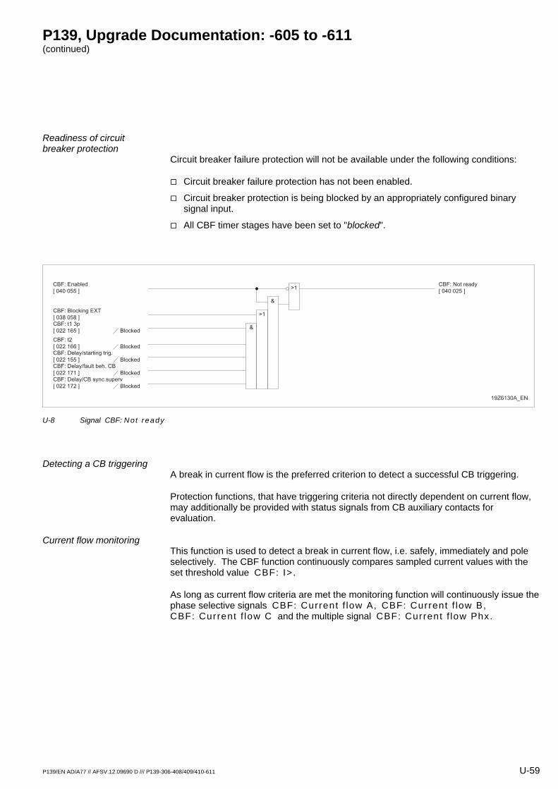
P139, Upgrade Documentation: -605 to -611 (continued)
P139/EN AD/A77 // AFSV.12.09690 D /// P139-306-408/409/410-611 U-59
Readiness of circuit breaker protection
Circuit breaker failure protection will not be available under the following conditions:
Circuit breaker failure protection has not been enabled.
Circuit breaker protection is being blocked by an appropriately configured binary signal input.
All CBF timer stages have been set to "blocked".
19Z6130A_EN
CBF: Enabled
[ 040 055 ]
&
>1CBF: Not ready
[ 040 025 ]
>1CBF: Blocking EXT
[ 038 058 ]CBF: t1 3p
[ 022 165 ] Blocked&
CBF: t2
[ 022 166 ] BlockedCBF: Delay/starting trig.
[ 022 155 ] BlockedCBF: Delay/fault beh. CB
[ 022 171 ] BlockedCBF: Delay/CB sync.superv
[ 022 172 ] Blocked
U-8 Signal CBF: No t ready
Detecting a CB triggering A break in current flow is the preferred criterion to detect a successful CB triggering.
Protection functions, that have triggering criteria not directly dependent on current flow, may additionally be provided with status signals from CB auxiliary contacts for evaluation.
Current flow monitoring This function is used to detect a break in current flow, i.e. safely, immediately and pole selectively. The CBF function continuously compares sampled current values with the set threshold value CBF: I>.
As long as current flow criteria are met the monitoring function will continuously issue the phase selective signals CBF: Current f low A, CBF: Current f low B, CBF: Current f low C and the multiple signal CBF: Current f low Phx.
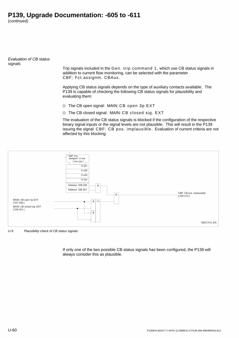
P139, Upgrade Documentation: -605 to -611 (continued)
U-60 P139/EN AD/A77 // AFSV.12.09690 D /// P139-306-408/409/410-611
Evaluation of CB status signals
Trip signals included in the Gen. t r ip command 1, which use CB status signals in addition to current flow monitoring, can be selected with the parameter CBF: Fct .assignm. CBAux.
Applying CB status signals depends on the type of auxiliary contacts available. The P139 is capable of checking the following CB status signals for plausibility and evaluating them:
The CB open signal: MAIN: CB open 3p EXT
The CB closed signal: MAIN: CB c losed s ig. EXT
The evaluation of the CB status signals is blocked if the configuration of the respective binary signal inputs or the signal levels are not plausible. This will result in the P139 issuing the signal CBF: CB pos. implausib le . Evaluation of current criteria are not affected by this blocking.
&
MAIN: CB open 3p EXT
[ 031 028 ]
INP: Fct. assignm. U xxx
[ xxx yyy ]
U x01
U x02
U x03
U xxx
Address 036 028
Address 036 051
MAIN: CB closed sig. EXT
[ 036 051 ]
&
&
>1
&CBF: CB pos. implausible
[ 038 210 ]
19Z6131A_EN
U-9 Plausibility check of CB status signals
If only one of the two possible CB status signals has been configured, the P139 will always consider this as plausible.
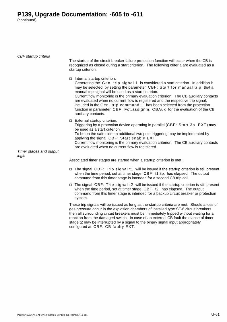
P139, Upgrade Documentation: -605 to -611 (continued)
P139/EN AD/A77 // AFSV.12.09690 D /// P139-306-408/409/410-611 U-61
CBF startup criteria The startup of the circuit breaker failure protection function will occur when the CB is recognized as closed during a start criterion. The following criteria are evaluated as a startup criterion:
Internal startup criterion: Generating the Gen. t r ip s ignal 1 is considered a start criterion. In addition it may be selected, by setting the parameter CBF: Start for manual t r ip, that a manual trip signal will be used as a start criterion. Current flow monitoring is the primary evaluation criterion. The CB auxiliary contacts are evaluated when no current flow is registered and the respective trip signal, included in the Gen. t r ip command 1, has been selected from the protection function in parameter CBF: Fct.assignm. CBAux for the evaluation of the CB auxiliary contacts.
External startup criterion: Triggering by a protection device operating in parallel (CBF: Star t 3p EXT) may be used as a start criterion. To be on the safe side an additional two pole triggering may be implemented by applying the signal CBF: Star t enable EXT. Current flow monitoring is the primary evaluation criterion. The CB auxiliary contacts are evaluated when no current flow is registered.
Timer stages and output logic
Associated timer stages are started when a startup criterion is met.
The signal CBF: Tr ip s ignal t1 will be issued if the startup criterion is still present when the time period, set at timer stage CBF: t1 3p, has elapsed. The output command from this timer stage is intended for a second CB trip coil.
The signal CBF: Tr ip s ignal t2 will be issued if the startup criterion is still present when the time period, set at timer stage CBF: t2, has elapsed. The output command from this timer stage is intended for a backup circuit breaker or protection system.
These trip signals will be issued as long as the startup criteria are met. Should a loss of gas pressure occur in the explosion chambers of installed type SF-6 circuit breakers then all surrounding circuit breakers must be immediately tripped without waiting for a reaction from the damaged switch. In case of an external CB fault the elapse of timer stage t2 may be interrupted by a signal to the binary signal input appropriately configured at CBF: CB faul ty EXT.
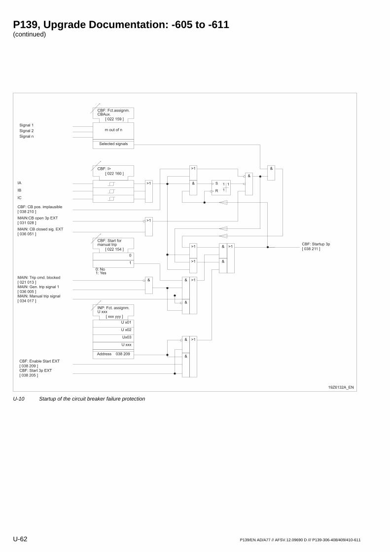
P139, Upgrade Documentation: -605 to -611 (continued)
U-62 P139/EN AD/A77 // AFSV.12.09690 D /// P139-306-408/409/410-611
19Z6132A_EN
m out of n
Signal 1
Signal 2
Signal n
Selected signals
CBF: I>
[ 022 160 ]
IA
IB
IC
>1
CBF: CB pos. implausible
[ 038 210 ]
MAIN:CB open 3p EXT
[ 031 028 ]
MAIN: CB closed sig. EXT
[ 036 051 ]
>1
&
>1
1
1
1S
R
&
&
>1
>1
&
&
>1CBF: Startup 3p
[ 038 211 ]
MAIN: Gen. trip signal 1
[ 036 005 ]
INP: Fct. assignm. U xxx
[ xxx yyy ]
U x01
U x02
Ux03
U xxx
Address 038 209
CBF: Enable Start EXT
[ 038 209 ]
&
CBF: Start 3p EXT
[ 038 205 ]
& >1
CBF: Start for manual trip
[ 022 154 ]
0
1
0: No 1: Yes
&
MAIN: Manual trip signal
[ 034 017 ]
& >1&MAIN: Trip cmd. blocked
[ 021 013 ]
CBF: Fct.assignm. CBAux.
[ 022 159 ]
U-10 Startup of the circuit breaker failure protection
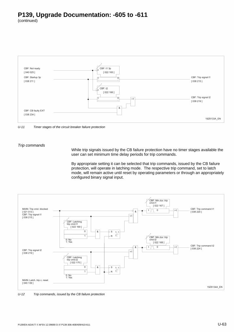
P139, Upgrade Documentation: -605 to -611 (continued)
P139/EN AD/A77 // AFSV.12.09690 D /// P139-306-408/409/410-611 U-63
19Z6133A_EN
c
t 0
CBF: Not ready
[ 040 025 ]
CBF: Startup 3p
[ 038 211 ]
CBF: Trip signal t1
[ 038 215 ]
CBF: Trip signal t2
[ 038 219 ]
&
>1
CBF: CB faulty EXT
[ 038 234 ]
CBF: t1 3p
[ 022 165 ]
c
t 0
CBF: t2
[ 022 166 ]
U-11 Timer stages of the circuit breaker failure protection
Trip commands While trip signals issued by the CB failure protection have no timer stages available the user can set minimum time delay periods for trip commands.
By appropriate setting it can be selected that trip commands, issued by the CB failure protection, will operate in latching mode. The respective trip command, set to latch mode, will remain active until reset by operating parameters or through an appropriately configured binary signal input.
CBF: Trip signal t1
[ 038 215 ]
CBF: Trip command t1
[ 038 220 ]&
MAIN: Latch. trip c. reset
[ 040 139 ]
t 0
CBF: Min.dur. trip cmd.t1
[ 022 167 ]
1
1
1S
R
MAIN: Trip cmd. blocked
[ 021 013 ]
CBF: Latching trip cmd.t1
[ 022 169 ]
&0
1
0: No 1: Yes
>1
>1
19Z6134A_EN
CBF: Trip signal t2
[ 038 219 ]
CBF: Trip command t2
[ 038 224 ]& t 0
CBF: Min.dur. trip cmd.t2
[ 022 168 ]
1
1
1S
R
CBF: Latching trip cmd.t2
[ 022 170 ]
&0
1
0: No 1: Yes
>1
>1
U-12 Trip commands, issued by the CB failure protection
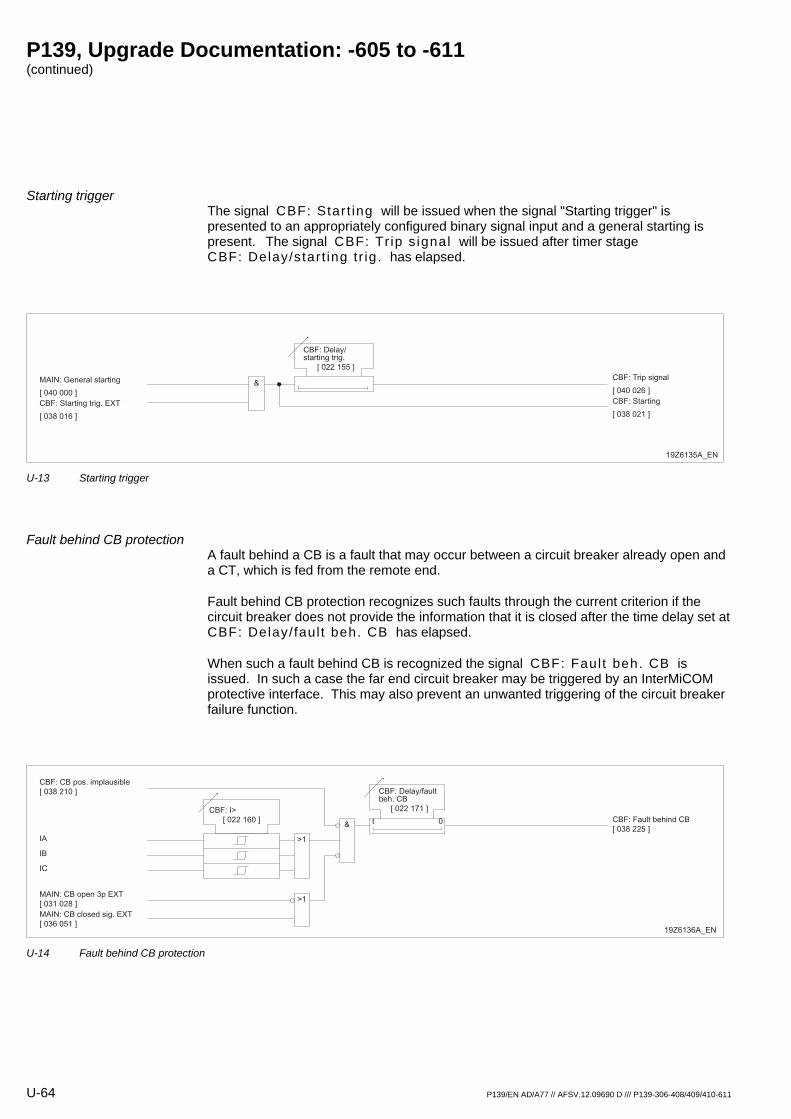
P139, Upgrade Documentation: -605 to -611 (continued)
U-64 P139/EN AD/A77 // AFSV.12.09690 D /// P139-306-408/409/410-611
Starting trigger The signal CBF: Star t ing will be issued when the signal "Starting trigger" is presented to an appropriately configured binary signal input and a general starting is present. The signal CBF: Tr ip s ignal will be issued after timer stage CBF: Delay/star t ing tr ig. has elapsed.
19Z6135A_EN
MAIN: General starting
[ 040 000 ]
CBF: Starting trig. EXT
[ 038 016 ]
CBF: Trip signal
[ 040 026 ]
CBF: Starting
[ 038 021 ]
&
CBF: Delay/ starting trig.
[ 022 155 ]
U-13 Starting trigger
Fault behind CB protection A fault behind a CB is a fault that may occur between a circuit breaker already open and a CT, which is fed from the remote end.
Fault behind CB protection recognizes such faults through the current criterion if the circuit breaker does not provide the information that it is closed after the time delay set at CBF: Delay/ faul t beh. CB has elapsed.
When such a fault behind CB is recognized the signal CBF: Faul t beh. CB is issued. In such a case the far end circuit breaker may be triggered by an InterMiCOM protective interface. This may also prevent an unwanted triggering of the circuit breaker failure function.
19Z6136A_EN
t 0 CBF: Fault behind CB
[ 038 225 ]&
CBF: Delay/fault beh. CB
[ 022 171 ]CBF: I>
[ 022 160 ]
IA
IB
IC
>1
CBF: CB pos. implausible
[ 038 210 ]
MAIN: CB open 3p EXT
[ 031 028 ]
MAIN: CB closed sig. EXT
[ 036 051 ]
>1
U-14 Fault behind CB protection
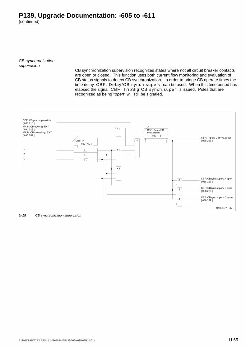
P139, Upgrade Documentation: -605 to -611 (continued)
P139/EN AD/A77 // AFSV.12.09690 D /// P139-306-408/409/410-611 U-65
CB synchronization supervision
CB synchronization supervision recognizes states where not all circuit breaker contacts are open or closed. This function uses both current flow monitoring and evaluation of CB status signals to detect CB synchronization. In order to bridge CB operate times the time delay CBF: Delay/CB synch.superv can be used. When this time period has elapsed the signal CBF: Tr ipSig CB synch.super is issued. Poles that are recognized as being "open" will still be signaled.
19Z6137A_EN
t 0CBF: TripSig CBsync.super
[ 038 226 ]&
CBF: Delay/CB sync.superv
[ 022 172 ]
CBF: I>
[ 022 160 ]
IA
IB
IC
>1
CBF: CB pos. implausible
[ 038 210 ]
MAIN: CB open 3p EXT
[ 031 028 ]MAIN: CB closed sig. EXT
[ 036 051 ]
>1
<3
&
&
&CBF: CBsync.superv C open
[ 038 229 ]
CBF: CBsync.superv B open
[ 038 228 ]
CBF: CBsync.superv A open
[ 038 227 ]
U-15 CB synchronization supervision
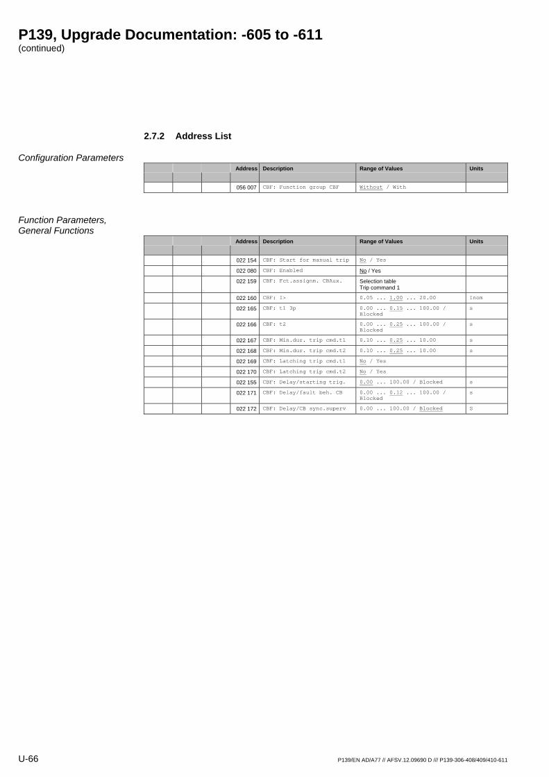
P139, Upgrade Documentation: -605 to -611 (continued)
U-66 P139/EN AD/A77 // AFSV.12.09690 D /// P139-306-408/409/410-611
2.7.2 Address List
Configuration Parameters Address Description Range of Values Units
056 007 CBF: Function group CBF Without / With
Function Parameters, General Functions
Address Description Range of Values Units
022 154 CBF: Start for manual trip No / Yes
022 080 CBF: Enabled No / Yes
022 159 CBF: Fct.assignm. CBAux. Selection table Trip command 1
022 160 CBF: I> 0.05 ... 1.00 ... 20.00 Inom
022 165 CBF: t1 3p 0.00 ... 0.15 ... 100.00 / Blocked
s
022 166 CBF: t2 0.00 ... 0.25 ... 100.00 / Blocked
s
022 167 CBF: Min.dur. trip cmd.t1 0.10 ... 0.25 ... 10.00 s
022 168 CBF: Min.dur. trip cmd.t2 0.10 ... 0.25 ... 10.00 s
022 169 CBF: Latching trip cmd.t1 No / Yes
022 170 CBF: Latching trip cmd.t2 No / Yes
022 155 CBF: Delay/starting trig. 0.00 ... 100.00 / Blocked s
022 171 CBF: Delay/fault beh. CB 0.00 ... 0.12 ... 100.00 / Blocked
s
022 172 CBF: Delay/CB sync.superv 0.00 ... 100.00 / Blocked S
P139, Upgrade Documentation: -605 to -611 (continued)
P139/EN AD/A77 // AFSV.12.09690 D /// P139-306-408/409/410-611 U-67
Logic state signals Address Description Range of Values Units
038 009 CBF: Ready No / Yes
038 211 CBF: Startup 3p No / Yes
038 016 CBF: Starting trig. EXT No / Yes
038 058 CBF: Blocking EXT No / Yes
038 041 CBF: Enable EXT No / Yes
038 042 CBF: Disable EXT No / Yes
040 055 CBF: Enabled No / Yes
040 025 CBF: Not ready No / Yes
040 026 CBF: Trip signal No / Yes
038 021 CBF: Starting No / Yes
038 040 CBF: Ext./user enabled No / Yes
038 205 CBF: Start 3p EXT No / Yes
038 209 CBF: Start enable EXT No / Yes
038 210 CBF: CB pos. implausible No / Yes
038 215 CBF: Trip signal t1 No / Yes
038 219 CBF: Trip signal t2 No / Yes
038 220 CBF: Trip command t1 No / Yes
038 224 CBF: Trip command t2 No / Yes
038 225 CBF: Fault behind CB No / Yes
038 226 CBF: TripSig CBsync.super No / Yes
038 227 CBF: CBsync.superv A open No / Yes
038 228 CBF: CBsync.superv B open No / Yes
038 229 CBF: CBsync.superv C open No / Yes
038 230 CBF: Current flow A No / Yes
038 231 CBF: Current flow B No / Yes
038 232 CBF: Current flow C No / Yes
038 233 CBF: Current flow Phx No / Yes
038 234 CBF: CB faulty EXT No / Yes
Control and Testing Address Description Range of Values Units
003 016 CBF: Enable USER don't execute / execute
003 015 CBF: Disable USER don't execute / execute
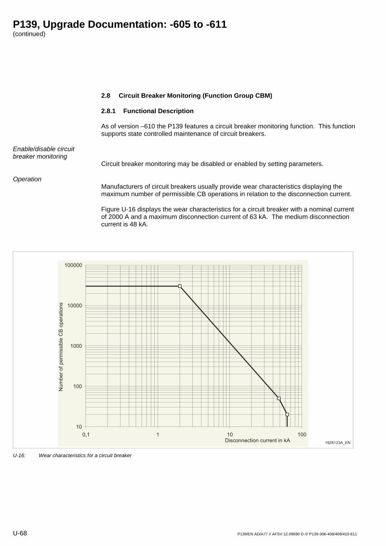
P139, Upgrade Documentation: -605 to -611 (continued)
U-68 P139/EN AD/A77 // AFSV.12.09690 D /// P139-306-408/409/410-611
2.8 Circuit Breaker Monitoring (Function Group CBM)
2.8.1 Functional Description
As of version –610 the P139 features a circuit breaker monitoring function. This function supports state controlled maintenance of circuit breakers.
Enable/disable circuit breaker monitoring
Circuit breaker monitoring may be disabled or enabled by setting parameters.
Operation Manufacturers of circuit breakers usually provide wear characteristics displaying the maximum number of permissible CB operations in relation to the disconnection current.
Figure U-16 displays the wear characteristics for a circuit breaker with a nominal current of 2000 A and a maximum disconnection current of 63 kA. The medium disconnection current is 48 kA.
19Z6123A_EN
10
100
1000
10000
100000
0,1 1 10 100 Disconnection current in kA
Nu
mb
er
of
pe
rmis
sib
le C
B o
pe
ratio
ns
U-16: Wear characteristics for a circuit breaker
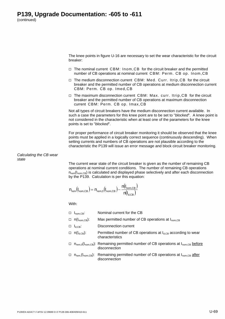
P139, Upgrade Documentation: -605 to -611 (continued)
P139/EN AD/A77 // AFSV.12.09690 D /// P139-306-408/409/410-611 U-69
The knee points in figure U-16 are necessary to set the wear characteristic for the circuit breaker:
The nominal current CBM: Inom,CB for the circuit breaker and the permitted number of CB operations at nominal current CBM: Perm. CB op. Inom,CB
The medium disconnection current CBM: Med. Curr . I t r ip,CB for the circuit breaker and the permitted number of CB operations at medium disconnection current CBM: Perm. CB op. Imed,CB
The maximum disconnection current CBM: Max. curr . I t r ip,CB for the circuit breaker and the permitted number of CB operations at maximum disconnection current CBM: Perm. CB op. Imax,CB
Not all types of circuit breakers have the medium disconnection current available. In such a case the parameters for this knee point are to be set to "blocked". A knee point is not considered in the characteristic when at least one of the parameters for the knee points is set to "blocked".
For proper performance of circuit breaker monitoring it should be observed that the knee points must be applied in a logically correct sequence (continuously descending). When setting currents and numbers of CB operations are not plausible according to the characteristic the P139 will issue an error message and block circuit breaker monitoring.
Calculating the CB wear state
The current wear state of the circuit breaker is given as the number of remaining CB operations at nominal current conditions. The number of remaining CB operations nrem(Inom,CB) is calculated and displayed phase selectively and after each disconnection by the P139. Calculation is per this equation:
( ) ( ) ( )( )CB,d
CB,nomCB,nom0,remCB,nomrem In
InInIn −=
With:
Inom,CB: Nominal current for the CB
n(Inom,CB): Max permitted number of CB operations at Inom,CB
Id,CB: Disconnection current
n(Id,CB): Permitted number of CB operations at Id,CB according to wear characteristics
nrem,0(Inom,CB): Remaining permitted number of CB operations at Inom,CB before disconnection
nrem,(Inom,CB): Remaining permitted number of CB operations at Inom,CB after disconnection
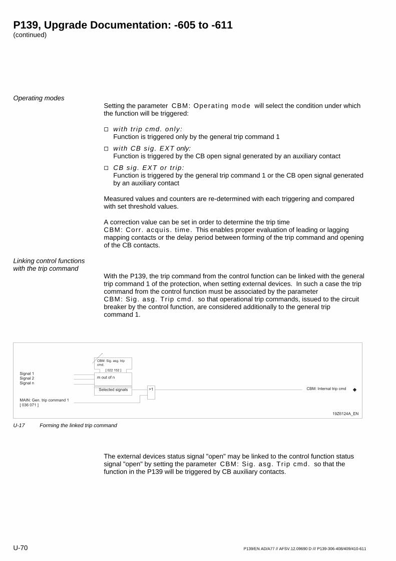
P139, Upgrade Documentation: -605 to -611 (continued)
U-70 P139/EN AD/A77 // AFSV.12.09690 D /// P139-306-408/409/410-611
Operating modes Setting the parameter CBM: Operat ing mode will select the condition under which the function will be triggered:
with t r ip cmd. only : Function is triggered only by the general trip command 1
with CB s ig. EXT only: Function is triggered by the CB open signal generated by an auxiliary contact
CB s ig. EXT or t r ip : Function is triggered by the general trip command 1 or the CB open signal generated by an auxiliary contact
Measured values and counters are re-determined with each triggering and compared with set threshold values.
A correction value can be set in order to determine the trip time CBM: Corr . acquis. t ime. This enables proper evaluation of leading or lagging mapping contacts or the delay period between forming of the trip command and opening of the CB contacts.
Linking control functions with the trip command
With the P139, the trip command from the control function can be linked with the general trip command 1 of the protection, when setting external devices. In such a case the trip command from the control function must be associated by the parameter CBM: Sig. asg. Tr ip cmd. so that operational trip commands, issued to the circuit breaker by the control function, are considered additionally to the general trip command 1.
19Z6124A_EN
CBM: Sig. asg. trip
cmd.
[ 022 152 ]
m out of nSignal 1
Signal 2
Signal n
Selected signals CBM: Internal trip cmd
MAIN: Gen. trip command 1
[ 036 071 ]
>1
U-17 Forming the linked trip command
The external devices status signal "open" may be linked to the control function status signal "open" by setting the parameter CBM: Sig. asg. Tr ip cmd. so that the function in the P139 will be triggered by CB auxiliary contacts.
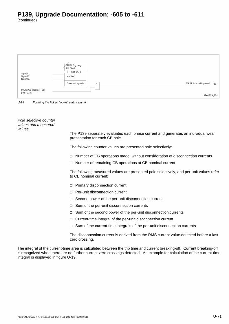
P139, Upgrade Documentation: -605 to -611 (continued)
P139/EN AD/A77 // AFSV.12.09690 D /// P139-306-408/409/410-611 U-71
19Z6125A_EN
MAIN: Sig. asg.
CB open
[ 021 017 ]
m out of n
Signal 1
Signal 2
Signal n
Selected signals MAIN: Internal trip cmd
MAIN: CB Open 3P Ext
[ 031 028 ]
>1
U-18 Forming the linked "open" status signal
Pole selective counter values and measured values
The P139 separately evaluates each phase current and generates an individual wear presentation for each CB pole.
The following counter values are presented pole selectively:
Number of CB operations made, without consideration of disconnection currents
Number of remaining CB operations at CB nominal current
The following measured values are presented pole selectively, and per-unit values refer to CB nominal current:
Primary disconnection current
Per-unit disconnection current
Second power of the per-unit disconnection current
Sum of the per-unit disconnection currents
Sum of the second power of the per-unit disconnection currents
Current-time integral of the per-unit disconnection current
Sum of the current-time integrals of the per-unit disconnection currents
The disconnection current is derived from the RMS current value detected before a last zero crossing.
The integral of the current-time area is calculated between the trip time and current breaking-off. Current breaking-off is recognized when there are no further current zero crossings detected. An example for calculation of the current-time integral is displayed in figure U-19.
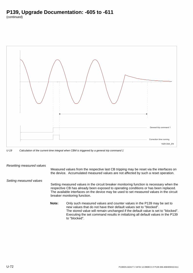
P139, Upgrade Documentation: -605 to -611 (continued)
U-72 P139/EN AD/A77 // AFSV.12.09690 D /// P139-306-408/409/410-611
Berechnung des Strom - Zeit - Integrals-20,00
-15,00
-10,00
-5,00
0,00
5,00
10,00
15,00
20,00
General trip command 1
19Z6126A_EN
Correction time running
U-19 Calculation of the current-time integral when CBM is triggered by a general trip command 1
Resetting measured values Measured values from the respective last CB tripping may be reset via the interfaces on the device. Accumulated measured values are not affected by such a reset operation.
Setting measured values Setting measured values in the circuit breaker monitoring function is necessary when the respective CB has already been exposed to operating conditions or has been replaced. The available interfaces on the device may be used to set measured values in the circuit breaker monitoring function.
Note: Only such measured values and counter values in the P139 may be set to new values that do not have their default values set to "blocked". The stored value will remain unchanged if the default value is set to "blocked". Executing the set command results in initializing all default values in the P139 to "blocked".
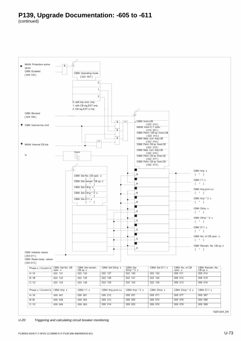
P139, Upgrade Documentation: -605 to -611 (continued)
P139/EN AD/A77 // AFSV.12.09690 D /// P139-306-408/409/410-611 U-73
MAIN: Protection active
306 001
&
0
1
0: with trip cmd. only
1: with CB sig.EXT only
2
2: CB sig.EXT or trip
&
CBM: Enabled
[ 044 130 ]
CBM: Itrip x
[ * ]
&
CBM: Operating mode
[ 022 007 ]
c
&
MAIN: Internal CB trip
>1
>1
c
c
Ix
fnom
CBM: Blocked
[ 044 199 ]
R
R
R
CBM: Itrip,prim Lx
[ * ]
CBM: Itrip**2 x
[ * ] R
CBM: I*t x
[ * ]
CBM: –Itrip x
[ * ]
CBM: –Itrip**2 x
[ * ]
CBM: –I*t x
[ * ]
CBM: No. of CB oper. x
[ * ]
CBM: Remain. No. CB op. x
[ * ]
CBM: Reset meas. values
[ 003 013 ]
S
S
S
S
S
c
CBM: Initialize values
[ 003 011 ]
CBM: Set No. CB oper. x
022 131 022 134
022 132 022 135
022 133 022 136
CBM: Set remain. CB op. x
CBM: Set –Itrip x CBM: Set –Itrip**2 x
CBM: Set –I*t x CBM: No. of CB oper. x
CBM: Remain. No. CB op. x
Phase x / Current Ix
A / IA
B / IB
C / IC
022 137 022 140
022 138 022 141
022 139 022 142
022 143
022 144
022 145
008 011
008 012
008 013
008 014
008 015
008 016
CBM: Itrip x
009 047 009 061
009 048 009 062
009 049 009 063
CBM: I*t x CBM: Itrip,prim Lx CBM: Itrip**2 x CBM: –Itrip x CBM: –Itrip**2 x CBM: –I*t xPhase x / Current Ix
A / IA
B/ IB
C / IC
009 212 009 051
009 213 009 052
009 214 009 053
009 071
009 073
009 076
009 077
009 078
009 079
009 087
009 088
009 089
CBM: Internal trip cmd
19Z6120A_EN
CBM: Inom,CB
[ 022 012 ]MAIN: Inom C.T. prim.
[ 010 001 ]
CBM: Perm. CB op. Inom,CB
[ 022 013 ]
CBM: Perm. CB op. Imax,CB
[ 022 017 ]
CBM: Max. curr. Itrip,CB
[ 022 016 ]
CBM: Perm. CB op. Imed,CB
[ 022 015 ]
CBM: Med. curr. Itrip,CB
[ 022 014 ]
CBM: Perm. CB op. Inom,CB
[ 022 013 ]
CBM: Set No. CB oper. x
[ * ] CBM: Set remain. CB op. x
[ * ]
CBM: Set –Itrip x
[ * ] CBM: Set –Itrip**2 x
[ * ]
CBM: Set –I*t x
[ * ]
U-20 Triggering and calculating circuit breaker monitoring
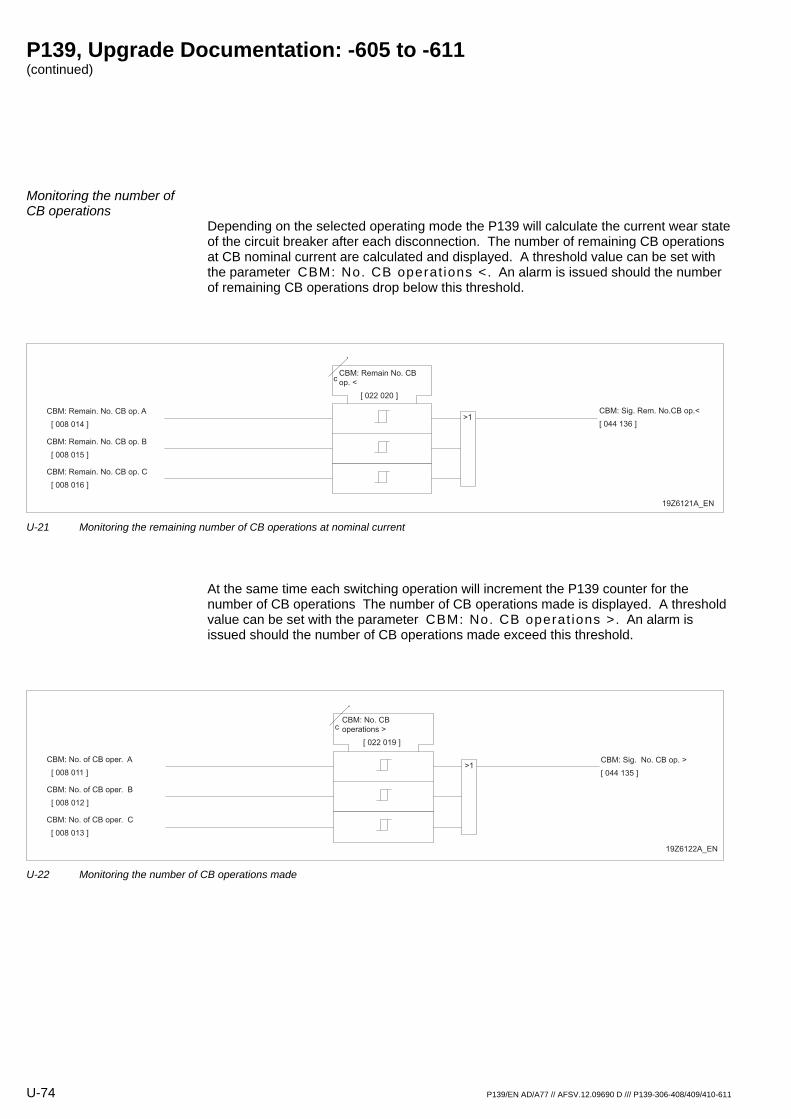
P139, Upgrade Documentation: -605 to -611 (continued)
U-74 P139/EN AD/A77 // AFSV.12.09690 D /// P139-306-408/409/410-611
Monitoring the number of CB operations
Depending on the selected operating mode the P139 will calculate the current wear state of the circuit breaker after each disconnection. The number of remaining CB operations at CB nominal current are calculated and displayed. A threshold value can be set with the parameter CBM: No. CB operat ions <. An alarm is issued should the number of remaining CB operations drop below this threshold.
19Z6121A_EN
>1CBM: Sig. Rem. No.CB op.<
[ 044 136 ]
CBM: Remain No. CB
op. <
[ 022 020 ]
c
CBM: Remain. No. CB op. A
[ 008 014 ]
CBM: Remain. No. CB op. B
[ 008 015 ]
CBM: Remain. No. CB op. C
[ 008 016 ]
U-21 Monitoring the remaining number of CB operations at nominal current
At the same time each switching operation will increment the P139 counter for the number of CB operations The number of CB operations made is displayed. A threshold value can be set with the parameter CBM: No. CB operat ions >. An alarm is issued should the number of CB operations made exceed this threshold.
19Z6122A_EN
>1CBM: Sig. No. CB op. >
[ 044 135 ]
CBM: No. CB
operations >
[ 022 019 ]
c
CBM: No. of CB oper. A
[ 008 011 ]
CBM: No. of CB oper. B
[ 008 012 ]
CBM: No. of CB oper. C
[ 008 013 ]
U-22 Monitoring the number of CB operations made
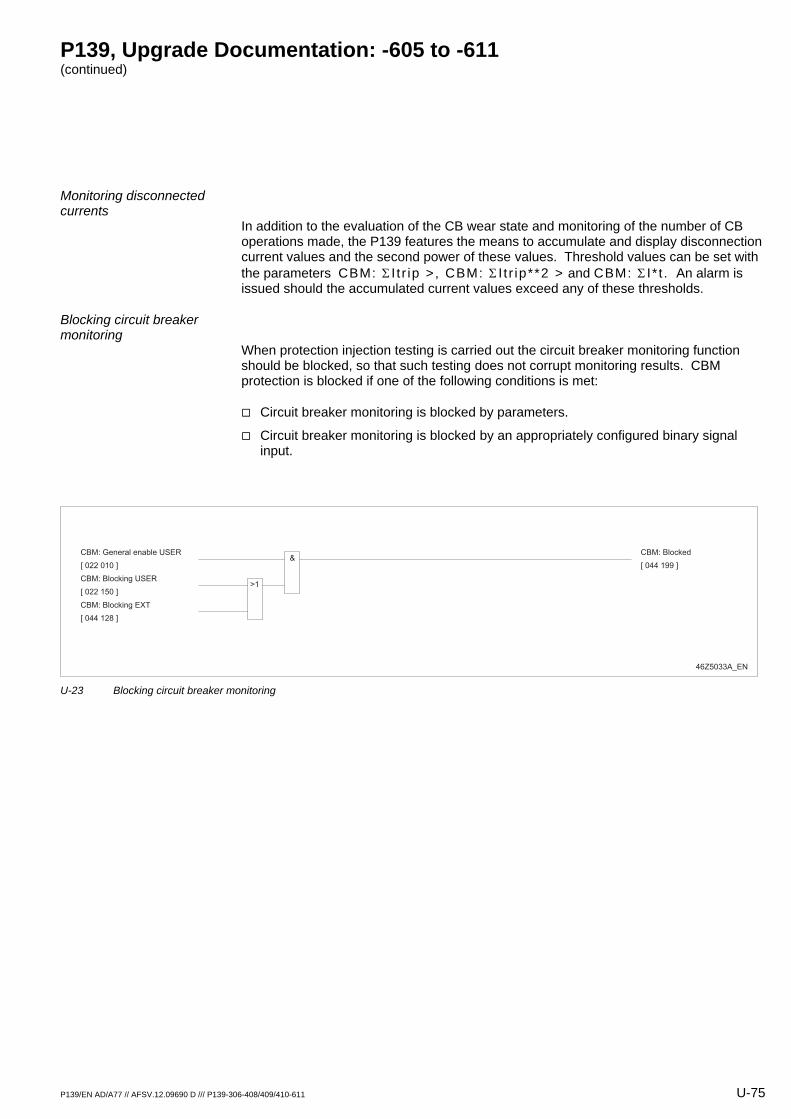
P139, Upgrade Documentation: -605 to -611 (continued)
P139/EN AD/A77 // AFSV.12.09690 D /// P139-306-408/409/410-611 U-75
Monitoring disconnected currents
In addition to the evaluation of the CB wear state and monitoring of the number of CB operations made, the P139 features the means to accumulate and display disconnection current values and the second power of these values. Threshold values can be set with the parameters CBM: Σ I t r ip >, CBM: Σ I t r ip**2 > and CBM: Σ I * t . An alarm is issued should the accumulated current values exceed any of these thresholds.
Blocking circuit breaker monitoring
When protection injection testing is carried out the circuit breaker monitoring function should be blocked, so that such testing does not corrupt monitoring results. CBM protection is blocked if one of the following conditions is met:
Circuit breaker monitoring is blocked by parameters.
Circuit breaker monitoring is blocked by an appropriately configured binary signal input.
46Z5033A_EN
>1
CBM: General enable USER
[ 022 010 ]
CBM: Blocked
[ 044 199 ]
CBM: Blocking USER
[ 022 150 ]
CBM: Blocking EXT
[ 044 128 ]
&
U-23 Blocking circuit breaker monitoring
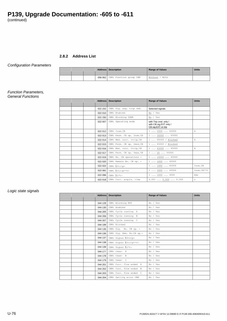
P139, Upgrade Documentation: -605 to -611 (continued)
U-76 P139/EN AD/A77 // AFSV.12.09690 D /// P139-306-408/409/410-611
2.8.2 Address List
Configuration Parameters Address Description Range of Values Units
056 062 CBM: Function group CBM Without / With
Function Parameters, General Functions
Address Description Range of Values Units
022 152 CBM: Sig. asg. trip cmd. Selected signals
022 010 CBM: Enabled No / Yes
022 150 CBM: Blocking USER No / Yes
022 007 CBM: Operating mode with Trip cmd. only / with CB sig.EXT only / CB sig.EXT or trip
022 012 CBM: Inom,CB 1 ... 2000 ... 65000 A
022 013 CBM: Perm. CB op. Inom,CB 1 ... 30000 ... 65000
022 014 CBM: Med. curr. Itrip,CB 1 ... 65000 / Blocked A
022 015 CBM: Perm. CB op. Imed,CB 1 ... 65000 / Blocked
022 016 CBM: Max. curr. Itrip,CB 1 ... 63000 ... 65000 A
022 017 CBM: Perm. CB op. Imax,CB 1 ... 20 ... 65000
022 019 CBM: No. CB operations > 1 ... 10000 ... 65000
022 020 CBM: Remain No. CB op. < 1 ... 1000 ... 65000
022 022 CBM: ΣItrip> 1 ... 1000 ... 65000 Inom,CB
022 081 CBM: ΣItrip**2> 1 ... 1000 ... 65000 Inom,CB**2
022 096 CBM: ΣI*t> 1 ... 1000 ... 4000 kAs
022 018 CBM: Corr. acquis. time 0.001 ... 0.000 ... 0.200 s
Logic state signals Address Description Range of Values Units
044 128 CBM: Blocking EXT No / Yes
044 130 CBM: Enabled No / Yes
044 205 CBM: Cycle running A No / Yes
044 206 CBM: Cycle running B No / Yes
044 207 CBM: Cycle running C No / Yes
044 199 CBM: Blocked No / Yes
044 135 CBM: Sig. No. CB op. > No / Yes
044 136 CBM: Sig. Rem. No.CB op.< No / Yes
044 137 CBM: Signal ΣItrip> No / Yes
044 138 CBM: Signal ΣItrip**2> No / Yes
044 139 CBM: Signal ΣI*t> No / Yes
044 177 CBM: tmax> A No / Yes
044 178 CBM: tmax> B No / Yes
044 179 CBM: tmax> C No / Yes
044 201 CBM: Curr. flow ended A No / Yes
044 202 CBM: Curr. flow ended B No / Yes
044 203 CBM: Curr. flow ended C No / Yes
044 204 CBM: Setting error CBM No / Yes
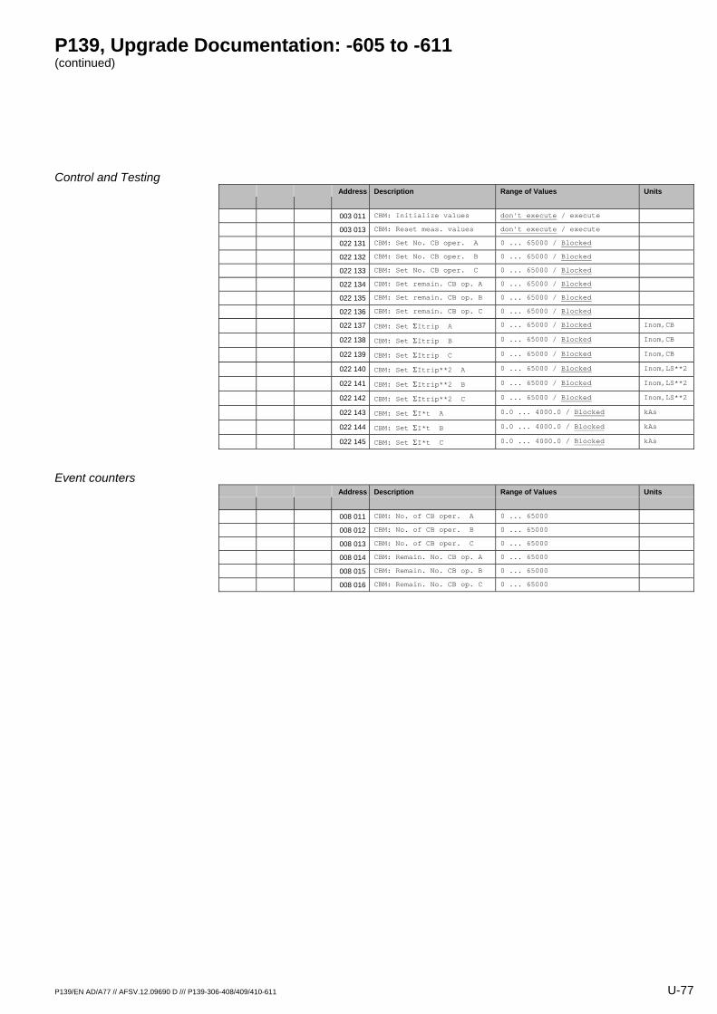
P139, Upgrade Documentation: -605 to -611 (continued)
P139/EN AD/A77 // AFSV.12.09690 D /// P139-306-408/409/410-611 U-77
Control and Testing Address Description Range of Values Units
003 011 CBM: Initialize values don't execute / execute
003 013 CBM: Reset meas. values don't execute / execute
022 131 CBM: Set No. CB oper. A 0 ... 65000 / Blocked
022 132 CBM: Set No. CB oper. B 0 ... 65000 / Blocked
022 133 CBM: Set No. CB oper. C 0 ... 65000 / Blocked
022 134 CBM: Set remain. CB op. A 0 ... 65000 / Blocked
022 135 CBM: Set remain. CB op. B 0 ... 65000 / Blocked
022 136 CBM: Set remain. CB op. C 0 ... 65000 / Blocked
022 137 CBM: Set ΣItrip A 0 ... 65000 / Blocked Inom,CB
022 138 CBM: Set ΣItrip B 0 ... 65000 / Blocked Inom,CB
022 139 CBM: Set ΣItrip C 0 ... 65000 / Blocked Inom,CB
022 140 CBM: Set ΣItrip**2 A 0 ... 65000 / Blocked Inom,LS**2
022 141 CBM: Set ΣItrip**2 B 0 ... 65000 / Blocked Inom,LS**2
022 142 CBM: Set ΣItrip**2 C 0 ... 65000 / Blocked Inom,LS**2
022 143 CBM: Set ΣI*t A 0.0 ... 4000.0 / Blocked kAs
022 144 CBM: Set ΣI*t B 0.0 ... 4000.0 / Blocked kAs
022 145 CBM: Set ΣI*t C 0.0 ... 4000.0 / Blocked kAs
Event counters Address Description Range of Values Units
008 011 CBM: No. of CB oper. A 0 ... 65000
008 012 CBM: No. of CB oper. B 0 ... 65000
008 013 CBM: No. of CB oper. C 0 ... 65000
008 014 CBM: Remain. No. CB op. A 0 ... 65000
008 015 CBM: Remain. No. CB op. B 0 ... 65000
008 016 CBM: Remain. No. CB op. C 0 ... 65000
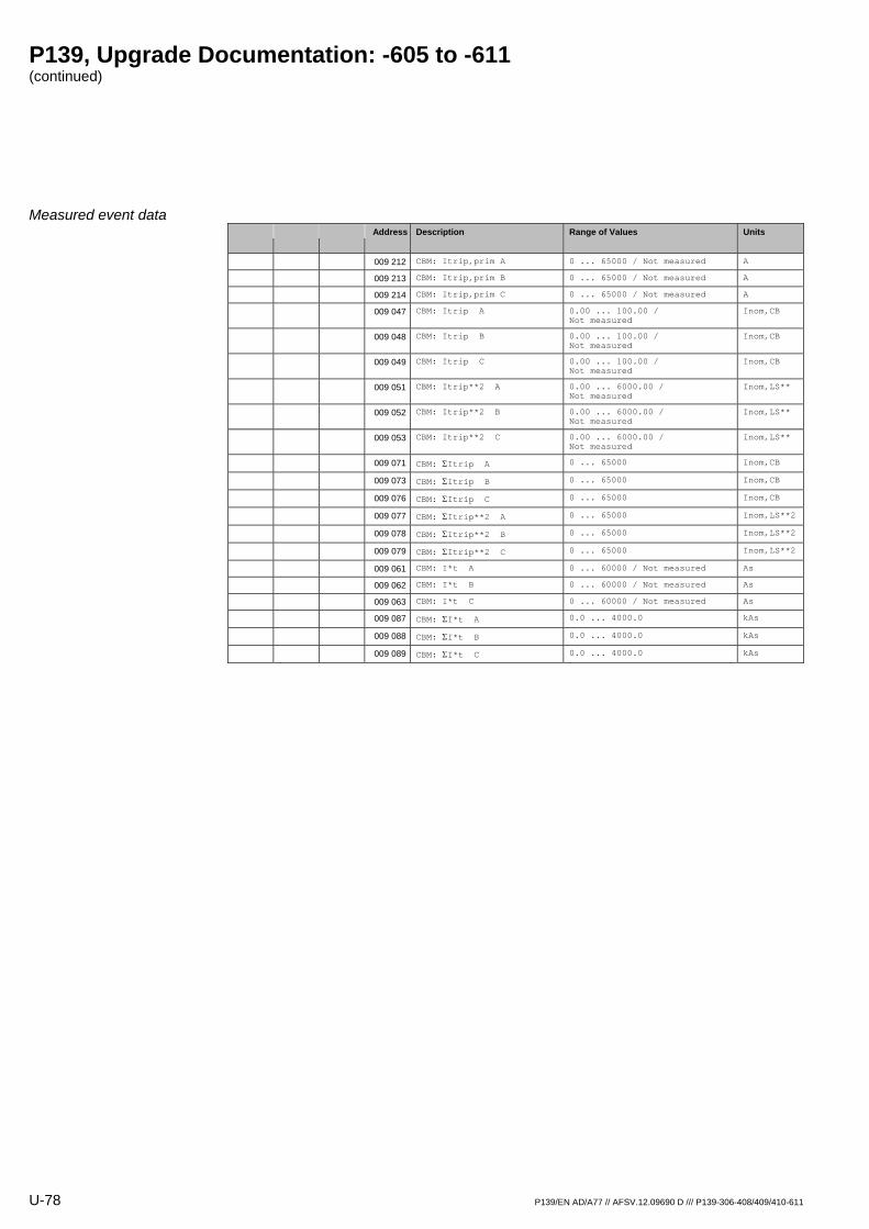
P139, Upgrade Documentation: -605 to -611 (continued)
U-78 P139/EN AD/A77 // AFSV.12.09690 D /// P139-306-408/409/410-611
Measured event data Address Description Range of Values Units
009 212 CBM: Itrip,prim A 0 ... 65000 / Not measured A
009 213 CBM: Itrip,prim B 0 ... 65000 / Not measured A
009 214 CBM: Itrip,prim C 0 ... 65000 / Not measured A
009 047 CBM: Itrip A 0.00 ... 100.00 / Not measured
Inom,CB
009 048 CBM: Itrip B 0.00 ... 100.00 / Not measured
Inom,CB
009 049 CBM: Itrip C 0.00 ... 100.00 / Not measured
Inom,CB
009 051 CBM: Itrip**2 A 0.00 ... 6000.00 / Not measured
Inom,LS**
009 052 CBM: Itrip**2 B 0.00 ... 6000.00 / Not measured
Inom,LS**
009 053 CBM: Itrip**2 C 0.00 ... 6000.00 / Not measured
Inom,LS**
009 071 CBM: ΣItrip A 0 ... 65000 Inom,CB
009 073 CBM: ΣItrip B 0 ... 65000 Inom,CB
009 076 CBM: ΣItrip C 0 ... 65000 Inom,CB
009 077 CBM: ΣItrip**2 A 0 ... 65000 Inom,LS**2
009 078 CBM: ΣItrip**2 B 0 ... 65000 Inom,LS**2
009 079 CBM: ΣItrip**2 C 0 ... 65000 Inom,LS**2
009 061 CBM: I*t A 0 ... 60000 / Not measured As
009 062 CBM: I*t B 0 ... 60000 / Not measured As
009 063 CBM: I*t C 0 ... 60000 / Not measured As
009 087 CBM: ΣI*t A 0.0 ... 4000.0 kAs
009 088 CBM: ΣI*t B 0.0 ... 4000.0 kAs
009 089 CBM: ΣI*t C 0.0 ... 4000.0 kAs

P139/EN AD/A77 // AFSV.12.09690 D /// P139-306-408/409/410-611 Ä-79
AREVA T&D's Automation & Information Systems Business www.areva-td.com T&D Worldwide Contact Centre online 24 hours a day: +44 (0) 1785 25 00 70 http://www.areva-td.com/contactcentre/
Pu
blic
atio
n:
P1
39
/EN
AD
/A7
7 (A
FSV
.12
.09
69
0.D
)

MiCOM P139 Feeder Management and Bay
Control Version: P139 -306 -408/409/410 -611 P139 -307 -411/412/413 -612
Upgrade Documentation
P139/EN AD/A88 (AFSV.12.09950.D)

P139 -612 Upgrade Description
P139/EN AD/A88 // AFSV.12.09950 D /// P139-307-411/412/413-612 U-3
Contents
1 Overview U-5
2 Functional Details U-9
2.1 Detachable HMI U-9
2.1.1 Address List U-11
P139 -612 Upgrade Description (continued)
U-4 P139/EN AD/A88 // AFSV.12.09950 D /// P139-307-411/412/413-612
In the new version of the P139 several enhanced features and changes on existing features have been included. These are described with references to the Technical Manual and Upgrade Documentation listed below.
References Released Version Documentation
28.11.2003 P139-304-405/406/407-605 Technical Manual AFSV.12.09450/1 EN
07.11.2005 P139-306-408/409/410-611 Upgrade Documentation AFSV.12.09660 EN
P139 -612 Upgrade Description (continued)
P139/EN AD/A88 // AFSV.12.09950 D /// P139-307-411/412/413-612 U-5
1 Overview
Version Changes
This is a preliminary IEC 61850 version, which is project-specific and only available on request!
P139-306-408/409/410-611-706 Release: 21.12.2005
Hardware No modifications
Diagram No modifications
Software
ASC Bug fixing: When the automatic synchronism check (ASC) was linked to the control of an external device and a close command was issued to this external device from the local control panel, the external device was always blocked from closing by the ASC function. This error occurred only when the communication protocol per IEC 61850 was used with the protection and control unit.
P139-306-408/409/410-611-707 Release: 16.02.2006
Hardware No modifications
Diagram No modifications
Software
IEC Bug fixing: The range of the internal values assigned to the various operating modes of the parameter IEC: DEV control model (221 081) now starts with a '1' instead of a '0'.
INP The request routine for binary signal inputs has been enhanced to suppress external interference.
P139-306-408/409/410-611-709 Release: 05.10.2006
Hardware No modifications
Diagram No modifications
Software
IEC Bug fixing: If communication was interrupted during control access via the Ethernet interface using the operating program MiCOM S1, renewed control access was only possible after a warm restart of the protection and control unit.
Bug fixing: If a 'Select' or 'Operate' command for an external device, in which the interlock bit had been set, was sent from a client to the protection and control unit it could occur that such a command was rejected.
P139 -612 Upgrade Description (continued)
U-6 P139/EN AD/A88 // AFSV.12.09950 D /// P139-307-411/412/413-612
Version Changes
P139-307-411/412/413-612 Hardware As an ordering option for the 40TE and 84TE model versions there is now a variant available with a detachable HMI. The detachable HMI is always supplied with a case width of 40TE. The freely configurable LED indicators H4 to H16 on the detachable HMI are provided as multi-color LEDs.
The ordering option Ethernet module with 100 Mbit/s glass fiber and ST connector has replaced the ordering option Ethernet module with 10 Mbit/s glass fiber and ST connector.
Diagram The updated connection diagrams now include the interfaces to connect the detachable HMI.
P139.411 (for 40TE case, with pin-terminal connection)
P132.412 (for 40TE case, transformer module: ring-terminal connection; other modules: pin-terminal connection)
P139.413 (for 84TE case, with ring-terminal connection)
Software
DVICE Because of the ordering option "detachable HMI" these additional Device Identification parameters are now available:
DVICE: SW version DHMI (002 131) DVICE: SW version DHMI DM (002 132)
LOC Because of the ordering option "detachable HMI" this additional Device Identification parameter is now available: LOC: Local HMI exists (221 099).
Additional item in the selection table for the operation panel: COUNT: Count 1 (217 100).
COMM1 When the protocols per IEC 60870-5-101 or IEC 60870-5-103 are used, the message COMM1: Buffer overrun (221 100) is issued when an internal buffer overrun of the spontaneous control function signals has occurred.
P139 -612 Upgrade Description (continued)
P139/EN AD/A88 // AFSV.12.09950 D /// P139-307-411/412/413-612 U-7
Version Changes
IEC Implementation of active monitoring of the communications data links to logged-on clients with the parameter IEC: TCP keep-al ive t imer (104 062). This active monitoring now replaces previous passive monitoring by parameter IEC: Inact iv i ty t imer (104 050).
Implementation of an automatic switchover to daylight saving time, activated by parameter IEC: Switch.dayl .sav.t ime (104 219). Switchover times for the automatic switch to daylight saving time are governed by the following settings:
IEC: Dayl .sav.t ime star t (104 220) IEC: Dayl .sav.t ime st . d (104 221) IEC: Dayl .sav.t ime st . m (104 222) IEC: Dayl .sav. t .s t .0:00 + (104 223) IEC: Dayl .sav. t ime end (104 225) IEC: Dayl .sav. t ime end d (104 226) IEC: Dayl .sav. t ime end m (104 227) IEC: Dayl .sav. t .end 0:00+ (104 228)
A second SNTP server may now be applied for time synchronization. Should no answer be transmitted by the first SNTP server the next request is automatically transferred to the second SNTP server (backup function).
IEC: SNTP server 1 IP (104 202) IEC: SNTP server 2 IP (104 210)
Instead of setting a router address and target network, so as to establish a communication link to a client situated exterior to the local network, now only the setting of the gateway address is required via IEC: Gateway address (104 011).
Now 'unbuffered reports' are available for all logical nodes.
GOOSE VLAN priority for GOOSE is set via GOOSE: VLAN Pr ior i ty (106 007).
The dataset reference for GOOSE is displayed via the measured value GOOSE: DataSet Reference (106 008).
INP Bug fixing: The input signal MAIN: Man. Tr ip cmd. EXT (037 018) did not operate when it was set as a receive signal for COMM3, GSSE or GOOSE and triggered via this communication link. (Triggering via a binary signal input operated correctly.)
LED The operating mode for the LED indicators has been extended by the operating mode LED flashing.
Configuration, operating mode and physical state of the permanently configured LED indicators H1 and H17 are now displayed via configuration parameters and physical state signals.
The freely configurable LED indicators H4 to H16 on the variant with a detachable HMI may now be assigned two signals, each with a different color (red or green). If both assigned signals are active the resulting LED color will be 'amber' (yellow).
P139 -612 Upgrade Description (continued)
U-8 P139/EN AD/A88 // AFSV.12.09950 D /// P139-307-411/412/413-612
Version Changes
MAIN The parameter MAIN: Time Tag (221 098) has replaced the previous parameter MAIN: TimeTagAfterDebounce (217 083). In addition there is a third operating mode available for selection.
COUNT The settable debouncing time for count value acquisition is no longer required.
P139-307-411/412/413-612-710 Release: 14.12.2006
Hardware No modifications
Diagram No modifications
Software
IEC Bug fixing: If communication was interrupted during control access via the Ethernet interface using the operating program MiCOM S1, renewed control access was only possible after a warm restart of the protection and control unit.
P139-307-411/412/413-612-712 and P139-306-408/409/410-611-711 Release: 14.02.2007
Hardware No modifications
Diagram No modifications
Software
IEC Bug fixing: Previously a break in the client-server communications link could occur after approximately 49 days for about 20 minutes. GOOSE and GSSE are not affected.
P139 -612 Upgrade Description (continued)
P139/EN AD/A88 // AFSV.12.09950 D /// P139-307-411/412/413-612 U-9
2 Functional Details
2.1 Detachable HMI
Application As a further option in the model versions there is now a variant available that includes a detachable HMI. This variant is especially designed for applications where protection and control units are directly installed into bay panels situated in medium-voltage substations and, because of constructural constraints, there is only limited space available. The detachable HMI with its small dimensions may be fitted here in a convenient spot and at an ergonomic height.
Detachable HMI The detachable HMI is mounted in a 40TE case and provides an integrated local control panel and a PC interface for configuration and operation of the protection and control unit. To connect the detachable HMI to the protection and control unit, standard RJ45 cables (Ethernet cable, length max. 10 m) may be used. A 3 m standard RJ45 Ethernet cable is included with the shipment.
A connection to the detachable HMI may be established or separated at any time as the detachable HMI is recognized automatically and completely.
Basic unit For the detachable HMI option, the basic unit is available with case widths of 40TE or 84TE in either a flush-mounted or a surface-mounted case and is provided in several variants for an effortless adaptation to meet local operating conditions. The front plate includes 4 LED indicators for display purposes as well as the RJ45 interface to connect the detachable HMI.
Operation without the detachable HMI
The function of the protection and control unit is fully guaranteed even when the detachable HMI is not connected or the communication link between detachable HMI and the basic unit is interrupted. In such a case the basic unit is accessed via its PC interface. The function parameters for the local control panel and for LED indicators available only on the detachable HMI are automatically hidden in this event.
LED indicators on the detachable HMI
The freely configurable LED indicators H4 to H16 on the detachable HMI offer multi-color function assignment. Separate function assignments with a red and a green LED indicator are available. When both the red and the green LED indicators are simultaneously active the resulting color will be amber (yellow).
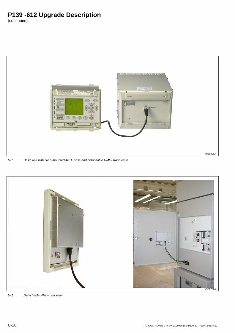
P139 -612 Upgrade Description (continued)
U-10 P139/EN AD/A88 // AFSV.12.09950 D /// P139-307-411/412/413-612
49Z6201A_
U-1 Basic unit with flush-mounted 40TE case and detachable HMI – front views
49Z6202A_
U-2 Detachable HMI – rear view
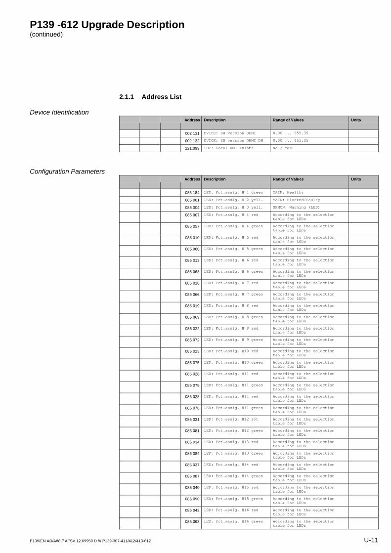
P139 -612 Upgrade Description (continued)
P139/EN AD/A88 // AFSV.12.09950 D /// P139-307-411/412/413-612 U-11
2.1.1 Address List
Device Identification Address Description Range of Values Units
002 131 DVICE: SW version DHMI 0.00 ... 655.35
002 132 DVICE: SW version DHMI DM 0.00 ... 655.35
221.099 LOC: Local HMI exists No / Yes
Configuration Parameters Address Description Range of Values Units
085 184 LED: Fct.assig. H 1 green MAIN: Healthy
085 001 LED: Fct.assig. H 2 yell. MAIN: Blocked/Faulty
085 004 LED: Fct.assig. H 3 yell. SFMON: Warning (LED)
085 007 LED: Fct.assig. H 4 red According to the selection table for LEDs
085 057 LED: Fct.assig. H 4 green According to the selection table for LEDs
085 010 LED: Fct.assig. H 5 red According to the selection table for LEDs
085 060 LED: Fct.assig. H 5 green According to the selection table for LEDs
085 013 LED: Fct.assig. H 6 red According to the selection table for LEDs
085 063 LED: Fct.assig. H 6 green According to the selection table for LEDs
085 016 LED: Fct.assig. H 7 red According to the selection table for LEDs
085 066 LED: Fct.assig. H 7 green According to the selection table for LEDs
085 019 LED: Fct.assig. H 8 red According to the selection table for LEDs
085 069 LED: Fct.assig. H 8 green According to the selection table for LEDs
085 022 LED: Fct.assig. H 9 red According to the selection table for LEDs
085 072 LED: Fct.assig. H 9 green According to the selection table for LEDs
085 025 LED: Fct.assig. H10 red According to the selection table for LEDs
085 075 LED: Fct.assig. H10 green According to the selection table for LEDs
085 028 LED: Fct.assig. H11 red According to the selection table for LEDs
085 078 LED: Fct.assig. H11 green According to the selection table for LEDs
085 028 LED: Fct.assig. H11 red According to the selection table for LEDs
085 078 LED: Fct.assig. H11 green According to the selection table for LEDs
085 031 LED: Fct.assig. H12 rot According to the selection table for LEDs
085 081 LED: Fct.assig. H12 green According to the selection table for LEDs
085 034 LED: Fct.assig. H13 red According to the selection table for LEDs
085 084 LED: Fct.assig. H13 green According to the selection table for LEDs
085 037 LED: Fct.assig. H14 red According to the selection table for LEDs
085 087 LED: Fct.assig. H14 green According to the selection table for LEDs
085 040 LED: Fct.assig. H15 red According to the selection table for LEDs
085 090 LED: Fct.assig. H15 green According to the selection table for LEDs
085 043 LED: Fct.assig. H16 red According to the selection table for LEDs
085 093 LED: Fct.assig. H16 green According to the selection table for LEDs
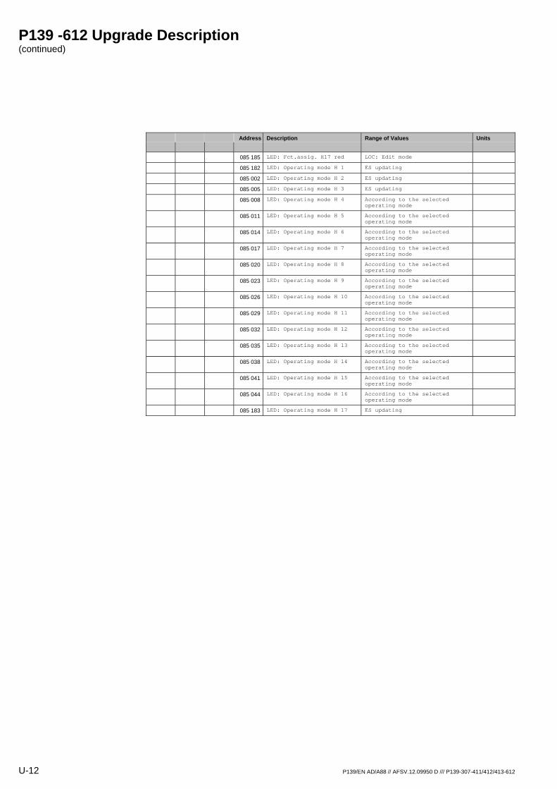
P139 -612 Upgrade Description (continued)
U-12 P139/EN AD/A88 // AFSV.12.09950 D /// P139-307-411/412/413-612
Address Description Range of Values Units
085 185 LED: Fct.assig. H17 red LOC: Edit mode
085 182 LED: Operating mode H 1 ES updating
085 002 LED: Operating mode H 2 ES updating
085 005 LED: Operating mode H 3 ES updating
085 008 LED: Operating mode H 4 According to the selected operating mode
085 011 LED: Operating mode H 5 According to the selected operating mode
085 014 LED: Operating mode H 6 According to the selected operating mode
085 017 LED: Operating mode H 7 According to the selected operating mode
085 020 LED: Operating mode H 8 According to the selected operating mode
085 023 LED: Operating mode H 9 According to the selected operating mode
085 026 LED: Operating mode H 10 According to the selected operating mode
085 029 LED: Operating mode H 11 According to the selected operating mode
085 032 LED: Operating mode H 12 According to the selected operating mode
085 035 LED: Operating mode H 13 According to the selected operating mode
085 038 LED: Operating mode H 14 According to the selected operating mode
085 041 LED: Operating mode H 15 According to the selected operating mode
085 044 LED: Operating mode H 16 According to the selected operating mode
085 183 LED: Operating mode H 17 ES updating


AREVA T&D's Automation & Information Systems Business www.areva-td.com T&D Worldwide Contact Centre online 24 hours a day: +44 (0) 1785 25 00 70 http://www.areva-td.com/contactcentre/
Pu
blic
atio
n:
P1
39
/EN
AD
/A8
8 (A
FSV
.12
.09
95
0.D
)


AREVA T&D's Automation & Information Systems Business www.areva-td.com T&D Worldwide Contact Centre online 24 hours a day: +44 (0) 1785 25 00 70 http://www.areva-td.com/contactcentre/
Pub
licat
ion:
P13
9/E
N M
/A88
– V
OL.
1/2