Embed Size (px)
Citation preview

MIAT_STM32內部與外部SRAM存取控制實驗
WU-YANG
浯陽科技有限公司
Technology Co Ltd
Declared Version
Training Only
Declare
Document Number
Document Version 100
Release Date
Document Title MIAT_STM32 內部與外部SRAM存取控制實驗
Exercise Time
Platform MIAT_STM32V2MIAT IOB V1PlatformMIAT IOBV1
Peripheral
Author WU-YANG Technology Co Ltd
2
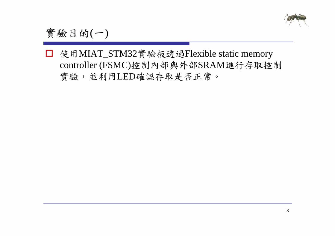
實驗目的(一)( )
使用MIAT_STM32實驗板透過Flexible static memory controller (FSMC)控制內部與外部SRAM進行存取控制controller (FSMC)控制內部與外部SRAM進行存取控制實驗並利用LED確認存取是否正常
3
實驗原理
System architecture E b dd d SRAM Embedded SRAM Features Memory map RVMDK環境設定
External SRAM IS61LV25616AL FSMC (flexible static memory controller)
Development Flow ARM Configure
4
System architecturey
5
Embedded SRAM
Features 48Kb f b dd d SRAM 48Kbytes of embedded SRAM accessed (readwrite) at CPU clock speed with 0 wait
statesstates
6
Embedded SRAM Memory mapy p
7
RVMDK環境設定
STMF103ZC有48K Bytes的SRAM位置由0x20000000至0x2000C000
8
External SRAM (IS61LV25616AL)( )
Features Hi h d i 10 High-speed access time 10 ns 256K x 16
9
FUNCTIONAL BLOCK DIAGRAM
10
PIN DESCRIPTIONS
11
READ CYCLE
12
READ CYCLE SWITCHING CHARACTERISTICS
13
WRITE CYCLE
14
WRITE CYCLE SWITCHING CHARACTERISTICS
15
FSMC
Features I f i h i d d i Interfaces with static memory-mapped devices
including Static random access memor (SRAM) Static random access memory (SRAM) Read-only memory (ROM) NOR Fl h NOR Flash memory PSRAM (4 memory banks)8- or 16-bit wide databus
8 16 bit id d t b 8- or 16-bit wide databus Independent chip select control for each memory bank
I d d fi i f h b k Independent configuration for each memory bank
16
FSMC
Programmable timings to support a wide range of devices in particulardevices in particular Programmable wait states (up to 15) Programmable b s t rnaro nd c cles ( p to 15) Programmable bus turnaround cycles (up to 15) Programmable output enable and write enable delays
(up to 15)(up to 15) Independent read and write timings and protocol so
as to support the widest variety of memories andas to support the widest variety of memories and timings
17
NORPSRAM address mappingpp g
NORPSRAM bank selection
External memory address
18
External memory interface signalsy g
19
NOR FlashPSRAM controller timing diagramsg g
read accesses
20
NOR FlashPSRAM controller timing diagramsg g
write accesses
21
FSMC Memory mapy p
22
Development Flowp
Embedded Software Side
int main(void)
Bootup STM32F10x
ProgrammingBootupSTM32F10x RCC Configure
NVIC Configure
int main(void)ifdef DEBUGdebug()
endif
FSMC SRAM Init
System Clocks Configuration RCC_Configuration()
NVIC Configuration
GPIO Configure
gNVIC_Configuration()
GPIO Configuration GPIO_Configuration()
GPIO Configure
FSMC Configure
Writeread tofrom FSMC SRAM memory
Configure FSMC Bank1 NORSRAM1 FSMC_SRAM_Init()
SRAM memory RW operation FSMC SRAM WriteBuffer
FSMC SRAM ReadBuffer
helliphelliphelliphelliphelliphelliphelliphelliphelliphelliphelliphelliphelliphelliphelliphelliphelliphelliphelliphelliphelliphelliphellipCheck content
Display Result
23
Configure FSMC IOg
Function name Description
RCC_APB2PeriphClockCmd(RCC_APB2Periph_GPIOD | RCC_APB2Periph_GPIOG | RCC_APB2Periph_GPIOE | RCC_APB2Periph_GPIOF ENABLE)
‐‐ GPIO Configuration ‐‐‐‐‐‐‐‐‐‐‐‐‐‐‐‐‐‐‐‐‐‐‐‐‐‐‐‐‐‐‐‐‐‐‐‐‐‐‐‐‐‐‐‐‐‐‐‐‐
GPIO FwLib Functions List
Function name Description
RCC_APB2PeriphClockCmd
Enables or disables the High Speed APB (APB2) peripheralclock
GPIO I it I iti li th GPIO
GPIO Configuration SRAM Data lines configuration GPIO_InitStructureGPIO_Pin = GPIO_Pin_0 | GPIO_Pin_1 | GPIO_Pin_8 |
GPIO_Pin_9 | GPIO_Pin_10 | GPIO_Pin_14 | GPIO_Pin_15GPIO_InitStructureGPIO_Mode = GPIO_Mode_AF_PPGPIO_InitStructureGPIO_Speed = GPIO_Speed_50MHzGPIO_Init(GPIOD ampGPIO_InitStructure) GPIO_Init Initializes the GPIOx
peripheral according to the specified parametersin the GPIO_InitStruct
RCC AHBPeriphClock Enables or disables the AHB
_ ( _ )GPIO_InitStructureGPIO_Pin = GPIO_Pin_7 | GPIO_Pin_8 | GPIO_Pin_9 |
GPIO_Pin_10 | GPIO_Pin_11 | GPIO_Pin_12 | GPIO_Pin_13 | GPIO_Pin_14 | GPIO_Pin_15
GPIO_Init(GPIOE ampGPIO_InitStructure) SRAM Address lines configuration GPIO_InitStructureGPIO_Pin = GPIO_Pin_0 | GPIO_Pin_1 | GPIO_Pin_2 |
| | | | |RCC_AHBPeriphClockCmd
Enables or disables the AHB peripheral clock
GPIO_Pin_3 | GPIO_Pin_4 | GPIO_Pin_5 | GPIO_Pin_12 | GPIO_Pin_13 | GPIO_Pin_14 | GPIO_Pin_15
GPIO_Init(GPIOF ampGPIO_InitStructure) GPIO_InitStructureGPIO_Pin = GPIO_Pin_0 | GPIO_Pin_1 | GPIO_Pin_2 |
GPIO_Pin_3 | GPIO_Pin_4 | GPIO_Pin_5GPIO_Init(GPIOG ampGPIO_InitStructure)GPIO InitStructure GPIO Pin GPIO Pin 11 | GPIO Pin 12 | GPIO Pin 13 GPIO_InitStructureGPIO_Pin = GPIO_Pin_11 | GPIO_Pin_12 | GPIO_Pin_13 GPIO_Init(GPIOD ampGPIO_InitStructure) NOE and NWE configuration GPIO_InitStructureGPIO_Pin = GPIO_Pin_4 |GPIO_Pin_5GPIO_Init(GPIOD ampGPIO_InitStructure) NE1configuration GPIO InitStructure GPIO Pin = GPIO Pin 7 GPIO_InitStructureGPIO_Pin = GPIO_Pin_7 GPIO_Init(GPIOD ampGPIO_InitStructure) NBL0 NBL1 configuration GPIO_InitStructureGPIO_Pin = GPIO_Pin_0 | GPIO_Pin_1 GPIO_Init(GPIOE ampGPIO_InitStructure) Enable the FSMC Clock RCC_AHBPeriphClockCmd(RCC_AHBPeriph_FSMC ENABLE)
24
_ p ( _ p _ )
Configure FSMCg
Function name Description
Enable the FSMC Clock RCC_AHBPeriphClockCmd(RCC_AHBPeriph_FSMC ENABLE)
‐‐ FSMC Configuration ‐‐
FSMC FwLib Functions List
Function name Description
RCC_AHBPeriphClockCmd
Enables or disables the AHB peripheral clock
FSMC_NORSRAMInit Initializes the FSMC NOR b k di t th
FSMC Configuration pFSMC_AddressSetupTime = 0pFSMC_AddressHoldTime = 0pFSMC_DataSetupTime = 2pFSMC_BusTurnAroundDuration = 0pFSMC_CLKDivision = 0pFSMC_DataLatency = 0memory bank according to the
parameters specified in FSMC_NORInitStruct
FSMC_NORSRAMCm Enables or disables the NORSRAM memory bank1
p _ y pFSMC_AccessMode = FSMC_AccessMode_AFSMC_NORSRAMInitStructureFSMC_Bank = FSMC_Bank1_NORSRAM1FSMC_NORSRAMInitStructureFSMC_DataAddressMux =
FSMC_DataAddressMux_DisableFSMC_NORSRAMInitStructureFSMC_MemoryType = FSMC_MemoryType_SRAMFSMC_NORSRAMInitStructureFSMC_MemoryDataWidth = FSMC_MemoryDataWidth_16bNORSRAM memory bank1 FSMC_NORSRAMInitStructureFSMC_BurstAccessMode =
FSMC_BurstAccessMode_DisableFSMC_NORSRAMInitStructureFSMC_WaitSignalPolarity =
FSMC_WaitSignalPolarity_LowFSMC_NORSRAMInitStructureFSMC_WrapMode = FSMC_WrapMode_DisableFSMC_NORSRAMInitStructureFSMC_WaitSignalActive =
FSMC WaitSignalActive BeforeWaitStateFSMC_WaitSignalActive_BeforeWaitStateFSMC_NORSRAMInitStructureFSMC_WriteOperation =
FSMC_WriteOperation_EnableFSMC_NORSRAMInitStructureFSMC_WaitSignal = FSMC_WaitSignal_DisableFSMC_NORSRAMInitStructureFSMC_ExtendedMode = FSMC_ExtendedMode_DisableFSMC_NORSRAMInitStructureFSMC_AsyncWait = FSMC_AsyncWait_DisableFSMC NORSRAMInitStructure FSMC WriteBurst = FSMC WriteBurst DisableFSMC_NORSRAMInitStructureFSMC_WriteBurst = FSMC_WriteBurst_DisableFSMC_NORSRAMInitStructureFSMC_ReadWriteTimingStruct = amppFSMC_NORSRAMInitStructureFSMC_WriteTimingStruct = amppFSMC_NORSRAMInit(ampFSMC_NORSRAMInitStructure)
Enable FSMC Bank1_SRAM Bank FSMC_NORSRAMCmd(FSMC_Bank1_NORSRAM1 ENABLE)
25
_ ( _ _ )
硬體電路配置
Mapping Table
Num SRAM STM32 Num SRAM STM32 Num SRAM STM32
1 A0 FSMC_A0 14 A13 FSMC_A13 27 IO8 FSMC_D82 A1 FSMC A1 15 A14 FSMC A14 28 IO9 FSMC D9_ _ _3 A2 FSMC_A2 16 A15 FSMC_A15 29 IO10 FSMC_D104 A3 FSMC_A3 17 A16 FSMC_A16 30 IO11 FSMC_D115 A4 FSMC_A4 18 A17 FSMC_A17 31 IO12 FSMC_D126 A5 FSMC_A5 19 IO0 FSMC_D0 32 IO13 FSMC_D137 A6 FSMC_A6 20 IO1 FSMC_D1 33 IO14 FSMC_D148 A7 FSMC_A7 21 IO2 FSMC_D2 34 IO15 FSMC_D159 A8 FSMC A8 22 IO3 FSMC D3 35 CE FSMC nNE19 A8 FSMC_A8 22 IO3 FSMC_D3 35 CE FSMC_nNE110 A9 FSMC_A9 23 IO4 FSMC_D4 36 OE FSMC_nOE11 A10 FSMC_A10 24 IO5 FSMC_D5 37 WE FSMC_nWE12 A11 FSMC A11 25 IO6 FSMC D6 38 UB FSMC NBL1_ _ _13 A12 FSMC_A12 26 IO7 FSMC_D7 39 LB FSMC_NBL0
26
實驗步驟
範例目錄架構
範例說明 範例說明
預設定義說明
燒錄 燒錄MIAT_STM32
27
範例目錄架構
範例目錄
測試映像檔 測試映像檔
含括檔
函式庫 函式庫
專案檔
原始碼 原始碼
28
範例說明
Embedded Software Side
Write data to FSMC SRAM memory
SRAM memory RW operation
Write data to FSMC SRAM memory Fill the buffer to send Fill_Buffer(TxBuffer BUFFER_SIZE 0x3212)FSMC_SRAM_WriteBuffer(TxBuffer WRITE_READ_ADDR BUFFER_SIZE)
SRAM memory RW operation
FSMC SRAM WriteBuffer
Read data from FSMC SRAM memory FSMC_SRAM_ReadBuffer(RxBuffer WRITE_READ_ADDR BUFFER_SIZE)
Read back SRAM memory and check content correctness
FSMC SRAM ReadBuffer
Check content
Display Result yfor (Index = 0x00 (Index lt BUFFER_SIZE) ampamp (WriteReadStatus == 0)
Index++)if (RxBuffer[Index] = TxBuffer[Index])
Display Result
WriteReadStatus = Index + 1
29
範例說明
Embedded Software Side
while (1)
Display Result
while (1)if (WriteReadStatus == 0) OK Turn on USERLED
GPIO SetBits(GPIOF GPIO Pin 11)
SRAM memory RW operation
FSMC SRAM WriteBufferGPIO_SetBits(GPIOF GPIO_Pin_11)
else KO Turn off USERLED
GPIO ResetBits(GPIOF GPIO Pin 11)
FSMC SRAM ReadBuffer
Check content
Display Result
如果寫入與讀取Buffer內容相同外部記憶體使用正常USERLED紅燈GPIO_ResetBits(GPIOF GPIO_Pin_11)
Insert delay Delay(0xAFFFF) Turn on USERLED GPIO SetBits(GPIOF GPIO Pin 11)
Display Result恆亮
GPIO_SetBits(GPIOF GPIO_Pin_11) Insert delay Delay(0xAFFFF)
如果寫入與讀取Buffer內容不同外部記憶體使用異常 USERLED紅燈閃爍
30
預設定義說明
define Bank1_SRAM1_ADDR ((u32)0x60000000) 定義SRAM起始點 定義SRAM起始點
define BUFFER_SIZE 0x400定義測試資料大小 定義測試資料大小
資料大小必需小於0xC000 define WRITE_READ_ADDR 0x8000 定義SRAM寫入起始點
寫入起始點WRITE_READ_ADDR + BUFFER_SIZE必需小於0x6000C000
31
燒錄MIAT STM32_
Rebuilder all target files產生HEX DFU Fil M 轉換HEX產生DFU DFU File Manager轉換HEX產生DFU DfuSe Demonstration燒錄DFU d Leave DFU mode
32
內部與外部SRAM存取控制實驗
實驗一
WU-YANGTechnology Co Ltd
實驗一練習
練習 修改寫入位置測試是否正常 修改寫入位置測試是否正常
修改寫入資料大小測試是否正常
取消 i 測試是否正常 取消FSMC_SRAM_Init測試是否正常
34
實驗目的(二)( )
使用MIAT_STM32實驗板透過FSMC控制外部SRAM並設定為data memory進行存取控制實驗同樣利用LED設定為data memory進行存取控制實驗同樣利用LED確認存取是否正常
35
實驗原理
External SRAM RVMDK環境設定 RVMDK環境設定
Development Flow fi ARM Configure Startup Code
36
RVMDK環境設定
外部SRAM有512K Bytes位置由0x60000000至0x60080000
37
Development Flowp
Embedded Software Side
int main(void)
Bootup STM32F10x
Programming
Bootup
int main(void)ifdef DEBUGdebug()
endif
Startup Code
BootupSTM32F10x
RCC Configure
NVIC Configure
System Clocks Configuration RCC_Configuration()
NVIC Configuration g gNVIC_Configuration()
GPIO Configuration GPIO_Configuration()
GPIO Configure
for (Index = 0 Index lt1024 Index++)
Tab[Index] =IndexT bAdd ( 32)T b h ld b 0 600000
Check operation
Check pointer value
Display Result TabAddr = (u32)Tab should be 0x600000xx
Get main stack pointer value MSPValue = __MRS_MSP() should be 0x2000xxxx
helliphelliphelliphelliphelliphelliphelliphelliphelliphelliphelliphelliphelliphelliphelliphelliphelliphelliphelliphelliphelliphelliphellip
Display Result
38
Startup Codep
Register boundary addresses RCC Configure
Enable FSMC clock
LDR R0= 0x00000114
LDR R1= 0x40021014
STR R0[R1]
Enable GPIOD GPIOE GPIOF and GPIOG clocks
LDR R0= 0x000001E0
LDR R1= 0x40021018
RCC register map
STR R0[R1]
39
RCC Register g
Bit 8 FSMCEN FSMC clock enableAHB Peripheral Clock enable register (RCC_AHBENR)
Bit 8 FSMCEN FSMC clock enableSet and cleared by software0 FSMC clock disabled
APB2 peripheral clock enable register (RCC_APB2ENR)
1 FSMC clock enabled
Bit 8765 IOPGEN IO port GFED clock enableSet and cleared by software0 IO port GFED clock disabled1 IO port GFED clock enabled
40
1 IO port GFED clock enabled
Startup Codep
Register boundary addresses GPIO Configure
SRAM Data lines NOE and NWE configuration SRAM Address lines configuration NOE NEW NE1 NBL0 NBL1 configuration LDR R0= 0xB4BB44BB LDR R1= 0x40011400STR R0[R1]LDR R0= 0xBBBBBBBB LDR R1= 0x40011404STR R0[R1]LDR R0 = 0xB44444BBLDR R0= 0xB44444BB LDR R1= 0x40011800STR R0[R1]LDR R0= 0xBBBBBBBB LDR R1= 0x40011804
GPIO register map
STR R0[R1]LDR R0= 0x44BBBBBB LDR R1= 0x40011C00STR R0[R1]LDR R0= 0xBBBB4444 LDR R1= 0x40011C04STR R0[R1]LDR R0= 0x44BBBBBBLDR R1= 0x40012000STR R0 [R1]
41
STR R0[R1]
GPIO Register g
Bit 8 FSMCEN FSMC clock enablePort configuration register low
Port configuration register high
Bits 2928 2524Bits 3130 2726 2322 1918 1514 1110 76 32 Bits 2928 25242120 1716 131298 54 10MODEy[10] Port x mode bits (y= 0 15)00 Input mode (reset state)01 Output mode max speed 10 MHz
Bits 3130 27262322 1918 15141110 76 32CNFy[10] Port x configuration bits (y= 0 15)In input mode (MODE[10]=00)00 Analog input mode01 Floating input (reset state)10 Input with pull-up pull-down
10 Output mode max speed 2 MHz11 Output mode max speed 50 MHz
11 ReservedIn output mode (MODE[10] gt00)00 General purpose output push-pull01 General purpose output Open-drain10 Alternate function output Push-pull11 Alternate function output Open-drain
42
11 Alternate function output Open drain
Startup Codep
FSMCregister map FSMC Configure
FSMC Configuration Enable FSMC Bank1_SRAM Bank
LDR R0= 0x00001011
LDR R1= 0xA0000000
STR R0[R1]
LDR R0= 0x00000200
LDR R1= 0xA0000004
STR R0[R1]
43
FSMC Register g
Bit 8 FSMCEN FSMC clock enableSRAMNOR-Flash chip-select control registers 1 (FSMC_BCR1)
Bit 12 WREN Write enable bitThis bit indicates whether write operations are enableddisabled in the bank by the FSMC0 Write operations are disabled in the bank by the FSMC an AHB error is reported1 Write operations are enabled for the bank by the FSMC (default after reset) p y ( )Bits 54 MWID Memory databus widthDefines the external memory device width valid for all type of memories00 8 bits01 16 bits (default after reset)10 reserved do not use10 reserved do not use11 reserved do not use Bit 0 MBKEN Memory bank enable bitEnables the memory bank After reset Bank1 is enabled all others are disabled Accessing adisabled bank causes an ERROR on AHB bus0 C di b k i di bl d0 Corresponding memory bank is disabled1 Corresponding memory bank is enabled
44
FSMC Register g
Bit 8 FSMCEN FSMC clock enableSRAMNOR-Flash chip-select timing registers 1 (FSMC_BTR1)
Bits 158 DATAST Data-phase duration0000 0000 Reserved0000 0001 DATAST phase duration = 2 times HCLK clock cycles0000 0010 DATAST phase duration = 3 times HCLK clock cycles1111 1111 DATAST phase duration = 256 times HCLK clock cycles (default value after reset)Bits 74 ADDHLD Address-hold phase duration0000 Reserved0001 ADDHLD phase duration = 2 times HCLK clock cycle0010 ADDHLD phase duration = 3 times HCLK clock cycle1111 ADDHLD phase duration = 16 times HCLK clock cycles (default value after reset)Bits 30 ADDSET Address setup phase durationThese bits are written by software to define the duration of the address setup phase (refer toFigure 162 to Figure 172) used in SRAMs ROMs and asynchronous NOR Flash0000 ADDSET phase duration = 1 times HCLK clock cycle1111 ADDSET phase duration = 16 times HCLK clock cycles (default value after reset)
45
實驗步驟
範例目錄架構
範例說明 範例說明
預設定義說明
46
範例目錄架構
範例目錄
測試映像檔 測試映像檔
含括檔
函式庫 函式庫
專案檔
原始碼 原始碼
47
範例說明
Embedded Software Side
Infinite loop
Display Result
Infinite loop while (1)if (((TabAddramp0xFFFFFF00) == 0x60000000) ampamp
((MSPValueamp0xFFFF0000) == 0x20000000))
Check operation
Check pointer value((MSPValueamp0xFFFF0000) == 0x20000000))
OK Turn on USERLED GPIO_SetBits(GPIOF GPIO_Pin_11)
else
Display Result
else KO Turn off USERLED
GPIO_ResetBits(GPIOF GPIO_Pin_11) Insert delay Delay(0xAFFFF)
如果Tab位置在0x600000且Stack pointer位置在0x2000 外部記憶體使用正常USERLED紅燈恆亮Delay(0xAFFFF)
Turn on USERLED GPIO_SetBits(GPIOF GPIO_Pin_11) Insert delay Delay(0xAFFFF)
紅燈恆亮
如果 b位置不在0 600000或Delay(0xAFFFF)
如果Tab位置不在0x600000或Stack pointer位置不在0x2000 外部記憶體使用異常USERLED紅燈閃爍
48
預設定義說明
DATA_IN_ExtSRAM EQU 1 E l SRAM C fi i External SRAM Configuration 0=gt DISABLE 1=gt ENABLE
u32 Tab[1024]宣告於外部 的記憶體 宣告於外部SRAM的記憶體
49
data memory存取控制實驗
實驗二
WU-YANGTechnology Co Ltd
實驗二練習
練習 取消RVMDK環境外部SRAM設定測試是否正常 取消RVMDK環境外部SRAM設定測試是否正常
修改DATA_IN_ExtSRAM EQU 0測試是否正常
修改外部 記憶體 b變數大小測試是否正常 修改外部SRAM記憶體Tab變數大小測試是否正常
51
Q amp A
WU-YANGTechnology Co Ltd
MIAT_STM32內部Flash存取控制實驗
WU-YANG
浯陽科技有限公司
Technology Co Ltd
Declared Version
Training Only
Declare
Document Number
Document Version 100
Release Date
Document Title MIAT_STM32 內部FLASH存取控制實驗
Exercise Time
Platform MIAT_STM32V2MIAT IOB V1PlatformMIAT IOBV1
Peripheral
Author WU-YANG Technology Co Ltd
2
實驗目的(一)( )
使用MIAT_STM32實驗板透過Flash memory interface (FLITF)控制內部Flash進行存取控制實驗並利用LED(FLITF)控制內部Flash進行存取控制實驗並利用LED確認存取是否正常
3
實驗原理
System architecture E b dd d Fl h Embedded Flash Features Memory map RVMDK環境設定
FLITF Flash module organization
Flash library function Development Flow ARM Configure
4
System architecturey
5
Embedded Flash
Features 256 Kb up to 256 Kbytes Memory organization the Flash memory is organized as a
main block and an information blockmain block and an information block Main memory block of size t 32 Kb 64 bit di id d i t 128 f 2 up to 32 Kb times 64 bits divided into 128 pages of 2
Kbytes Information block of size Information block of size 258 times 64 bits
6
Embedded Flash Memory mapy p
7
Flash Memoryy
8
RVMDK環境設定
STMF103ZC有256K Bytes的Flash位置由0x8000000至0x8040000
9
FLITF
Features R d i f i h f h b ff (2 64 bi d ) Read interface with prefetch buffer (2x64-bit words) Option byte Loader
l h i Flash Program Erase operation Read Write protection
10
Flash memory interfacey
11
Flash memory interface registery g
Bit 8 FSMCEN FSMC clock enableFlash status register (FLASH_SR)
Bits 316 Reserved must be kept clearedBit 5 EOP End of operation
Bit 2 PGERR Programming errorSet by hardware when an address to be programmed p
Set by hardware when a Flash operation (programming erase) is completed Reset by writing a 1Note EOP is asserted at the end of each successful
y p gcontains a value different from 0xFFFF before programmingReset by writing 1Note The STRT bit in the FLASH_CR register f f
program or erase operationBit 4 WRPRTERR Write protection errorSet by hardware when programming a write-protected address of the Flash memory
_ gshould be reset before starting a programmingoperationBit 1 Reserved must be kept clearedBit 0 BSY Busyp y
Reset by writing 1Bit 3 Reserved must be kept cleared
This indicates that a Flash operation is in progress This is set on the beginning of a Flash operation and reset when the operation finishes or when an error occurs
12
Flash memory interface registery g
Flash control register (FLASH_CR)
Bit 9 OPTWRE Option bytes write enableWhen set the option bytes can be programmed This
Bit 6 STRT StartThis bit triggers an ERASE operation when set This bit is set only
bit is set on writing the correct key sequence to the FLASH_OPTKEYR registerThis bit can be reset by softwareBit 8 Reserved must be kept clearedBit 7 LOCK Lock
by software and reset when the BSY bit is resetBit 5 OPTER Option byte eraseOption byte erase chosenBit 4 OPTPG Option byte programmingOption byte programming chosenBit 7 LOCK Lock
Write to 1 only When it is set it indicates that the FPEC and FLASH_CR are locked This bit is reset by hardware after detecting the unlock sequenceIn the event of unsuccessful unlock operation this bit remains set until the next reset
p y p g gBit 3 Reserved must be kept clearedBit 2 MER Mass eraseErase of all user pages chosenBit 1 PER Page erasePage Erase chosenremains set until the next reset Page Erase chosenBit 0 PG ProgrammingFlash programming chosen
13
Main Flash memory programmingy p g g
14
Flash memory Page Erasey g
15
Flash memory Mass Erasey
16
Option byte programmingp y p g g
17
Option byte Erasep y
18
FLASH library functiony
19
FLASH library functiony
20
Development Flowp
Embedded Software Side
int main(void)
Bootup STM32F10x
ProgrammingBootupSTM32F10x RCC Configure
NVIC Configure
int main(void)ifdef DEBUGdebug()
endifendif
FLASHStatus = FLASH_COMPLETEMemoryProgramStatus = PASSEDData = 0x15041975
GPIO Configure
Data = 0x15041975
RCC Configuration RCC_Configuration()
Flash memory RW operation FLASH Unlock
FLASH ClearFlag NVIC Configuration NVIC_Configuration()
GPIO Configuration
FLASH ClearFlag
FLASH ErasePage
FLASH ProgramWord GPIO Configuration GPIO_Configuration()
helliphelliphelliphelliphelliphelliphelliphelliphelliphelliphelliphelliphelliphelliphelliphelliphellipDisplay Result
Check content
21
實驗步驟
範例目錄架構
範例說明 範例說明
預設定義說明
燒錄 燒錄MIAT_STM32
22
範例目錄架構
範例目錄
測試映像檔 測試映像檔
含括檔
函式庫 函式庫
專案檔
原始碼 原始碼
23
範例說明
Function name Description
Unlock the Flash Program Erase controller FLASH_Unlock()
D fi h b f b d
Flash FwLib Functions List
Function name Description
FLASH_Unlock Unlocks the FLASH Program Erase Controller
FLASH_ClearFlag Clears the FLASH pending fl
Define the number of page to be erased NbrOfPage = (EndAddr - StartAddr) FLASH_PAGE_SIZE
Clear All pending flags FLASH_ClearFlag(FLASH_FLAG_BSY | FLASH_FLAG_EOP | FLASH_FLAG_PGERR |
FLASH FLAG WRPRTERR)flags
FLASH_ErasePage Erases a specified FLASH page
FLASH_ProgramWord Programs a word at a specified
_ _ )
Erase the FLASH pages for(EraseCounter = 0 (EraseCounter lt NbrOfPage) ampamp (FLASHStatus ==
FLASH_COMPLETE) EraseCounter++)FLASHStatus = FLASH ErasePage(StartAddr + (FLASH PAGE SIZE EraseCounter))address FLASHStatus = FLASH_ErasePage(StartAddr + (FLASH_PAGE_SIZE EraseCounter))
FLASH Word program of data 0x15041979 at addresses defined by StartAddr and EndAddrAddress = StartAddr
while((Address lt EndAddr) ampamp (FLASHStatus == FLASH_COMPLETE))FLASHStatus = FLASH_ProgramWord(Address Data)Address = Address + 4
24
範例說明
Embedded Software Side
Check the corectness of written data
Display Result
Check the corectness of written data Address = StartAddr
while((Address lt EndAddr) ampamp (MemoryProgramStatus = FAILED))if(((vu32) Address) = Data)
Flash memory RW operation
MemoryProgramStatus = FAILED
Address += 4
Check content
Display Result while (1)if (MemoryProgramStatus == PASSED) OK Turn on USERLED GPIO_SetBits(GPIOF GPIO_Pin_11)
Display Result
else KO Turn off USERLED GPIO_ResetBits(GPIOF GPIO_Pin_11) Insert delay Delay(0xAFFFF)
如果寫入與讀取Flash內容相同Flash記憶體使用正常USERLED紅燈恆亮
Turn on USERLED GPIO_SetBits(GPIOF GPIO_Pin_11) Insert delay Delay(0xAFFFF)
如果寫入與讀取Flash內容不同Flash記憶體使用異常USERLED紅燈閃爍
25
預設定義說明
define StartAddr ((u32)0x08008000) 定義Flash使用起始點 定義Flash使用起始點
使用起始點必需大於0x8003000 + Code Size 附註 0x8000000~0x8003000為DFU程式區塊使用此區塊
將造成無法燒錄程式
Code Size可由產生的HEX檔得知
d fi E dAdd (( 32)0 0800C000) define EndAddr ((u32)0x0800C000) 定義Flash使用結束點
使用起始點必需小於0x8040000使用起始點必需小於
Data = 0x15041975 寫入資料
32Bit define FLASH_PAGE_SIZE ((u16)0x800)
每一個Page有2KByte26
每一個Page有2KByte
Intel HEX Format
aaaa tt dd cc
field Description
the colon that starts every Intel HEX record
the record-length field that represents the number of data bytes (dd) in the record
aaaa the address field that represents the starting address for subsequent data in the record
tt the field that represents the HEX record type which may be one of the following00 - data record01 - end-of-file record02 - extended segment address recordg04 - extended linear address record
dd a data field that represents one byte of data A record may have multiple data bytes The number of data bytes in the record must match the number specified by the field
cc the checksum field that represents the checksum of the record The checksum is calculated by summing the values of all hexadecimal digit pairs in the record modulo 256 and taking the twos complement
27
HEX Examplep
020000040800F2103000001814002045310008D9340008CD340008D8103000001814002045310008D9340008CD340008D8helliphelliphellip1038200042370008000000000000000000000000170C3830000000000000000000000000008C
資料填入起始位置為
0C3830000000000000000000000000008C04000005080031318D00000001FF
資料填入起始位置為0x08003000 每一行有0x10(16)個Bytes 最後一筆資料為
資料結束點為0x0803383004000005080031318D
(0x08003830 -0x08000000)0x800 = 7 需以0x800為單位所以使用的位置起點為0x08004000
28
燒錄MIAT STM32_
Rebuilder all target files產生HEX DFU Fil M 轉換HEX產生DFU DFU File Manager轉換HEX產生DFU DfuSe Demonstration燒錄DFU d Leave DFU mode
29
內部Flash存取控制實驗
實驗一
WU-YANGTechnology Co Ltd
實驗一練習
注意 請使用預設0 08008000之後的位置 避免覆蓋DFU 請使用預設0x08008000之後的位置避免覆蓋DFU
與使用者程式碼區塊
練習 練習 修改存取位置測試是否正常
修改寫入資料測試是否正常 修改寫入資料測試是否正常
修改寫入資料後取消FLASH_Unlock測試是否正常
修改寫入資料後取消FLASH E P 測試是否正 修改寫入資料後取消FLASH_ErasePage測試是否正常
31
實驗目的(二)( )
使用MIAT_STM32實驗板透過Flash memory interface (FLITF)控制內部Flash進行存取控制實驗並利用SW(FLITF)控制內部Flash進行存取控制實驗並利用SWKEY決定資料寫入與讀取LCD顯示狀態
32
實驗原理
System requirement E b dd d Fl h Embedded Flash LCD KEY SW
Development Flow ARM Configure
33
Development Flowp
Embedded Software Side
int main(void)
Bootup STM32F10x
ProgrammingBootupSTM32F10x RCC Configure
NVIC Configure
int main(void)ifdef DEBUGdebug()
endif
FLASHStatus = FLASH_COMPLETE
RCC Configuration RCC Configuration()
GPIO Configure
BasicIO Configure_ g ()
NVIC Configuration NVIC_Configuration()
GPIO Configuration Flash memory RW ti
lcd Configure
GPIO Configuration GPIO_Configuration()
Init_BasicIO()
l d i i () LCD I i i li i
RW operation
Example
FLASH Unlock
FLASH ClearFlag
lcd_init() LCD Initialization
helliphelliphelliphelliphelliphelliphelliphelliphelliphelliphelliphelliphelliphelliphelliphelliphelliphelliphelliphelliphelliphelliphellip
p
34
硬體電路配置
Mapping Table
Num MIAT_STM32V2 MIAT_IOBV1 Num MIAT_STM32V2 MIAT_IOBV1
1 PC8 (326) SW1 10 PE6 (15) LCD_EN2 PC9 (327) SW2 11 PF6 (118) LCD RW ( ) ( ) _3 PC10 (43) SW3 12 PF7 (119) LCD_RS 4 PC11 (44) SW4 13 PF8(120) LCD_D4 5 PB5 (427) KEY1 14 PF9 (121) LCD_D5 6 PB6 (428) KEY2 15 PF10 (122) LCD_D6 7 PB7 (429) KEY3 16 PF11 (213) LCD_D7 8 PB8 (431) KEY4 17 VDD (236) VCC33V 9 VCC5V (1 36) VCC5V 18 GND (1 35) GND9 VCC5V (136) VCC5V 18 GND (135) GND
35
實驗步驟
範例目錄架構
範例說明 範例說明
預設定義說明
36
範例目錄架構
範例目錄
測試映像檔 測試映像檔
含括檔
函式庫 函式庫
專案檔
原始碼 原始碼
37
範例說明
Embedded Software Side
lcd clear()
FLASH memory RW operation
lcd_clear()lcd_print (MIAT_STM32 DEMO )
Unlock the Flash Program Erase controller FLASH_Unlock()
Flash memory RW operation
FLASH Unlock
Clear All pending flags FLASH_ClearFlag(FLASH_FLAG_BSY | FLASH_FLAG_EOP | FLASH_FLAG_PGERR |
FLASH_FLAG_WRPRTERR)
while(1)
Example
FLASH ClearFlag
( )
KEY_Buffer=Key_Scan()set_cursor (0 1)lcd_print (SW Value = 0x)lcd putchar(((SWamp0x7)+0x30))lcd_putchar(((SWamp0x7)+0x30))if(KEY_Buffer==1)Address=(StartAddr|(SWltlt12))set_cursor (0 0)lcd_print (Set Addr = 0x)
掃描KEY是否按下與顯示SW數值LCD Line2顯示SW Value = 0x(SW)
lcd_putchar(((SWamp0x7)+0x30))lcd_print ( )
如果KEY1按下記錄SW數值至Address LCD Line1顯示Set Adde = 0x(Address)
38
範例說明
Embedded Software Side
else if(KEY Buffer==2)
FLASH memory RW operation
else if(KEY_Buffer==2)
Erase the FLASH pages FLASHStatus = FLASH_ErasePage(Address)
FLASH Word program of data at addresses defined by SW
SRAM memory RW operation
p g yFLASHStatus = FLASH_ProgramWord(Address (SWamp0x7))
set_cursor (0 0)lcd_print (Write 0x)lcd_putchar(((SWamp0x7)+0x30))l d i t ( t 0 )
Example如果KEY2按下清除Address所處區塊並寫入SW數值 lcd_print ( at 0x)
lcd_putchar((((Addressgtgt12)amp0x7)+0x30))else if(KEY_Buffer==3)
Data=(u16 )Address
所處區塊並寫入SW數值LCD Line1顯示Write 0x(SW) at 0x(Adddress)
Data (u16 )Addressset_cursor (0 0)lcd_print (Addr 0x)lcd_putchar((((Addressgtgt12)amp0x7)+0x30))lcd_print ( = 0x)lcd_putchar(((Dataamp0x7)+0x30))lcd_print ( )
如果KEY3按下讀取Address紀錄數值LCD Line1顯示Addr 0x(Adddress) = 0x
39
預設定義說明
define StartAddr ((u32)0x08020000) 定義Flash使用起始點 定義Flash使用起始點
使用起始點必需大於0x8003000 + Code Size 附註 0x8000000~0x8003000為DFU程式區塊使用此區塊
將造成無法燒錄程式
Code Size可由產生的HEX檔得知
32 Add 0 08020000 u32 Address = 0x08020000 定義Address初始值
初始值必需與Flash使用起始點相同初始值必需與 使用起始點相同
Address=(StartAddr|(SWltlt12)) Example StartAddr = 0x08020000 SW = 1 Address = 0x08021000
StartAddr = 0x08020000 SW = 7 Address = 0x08027000 StartAddr|(7ltlt12)必需小於0x8040000
40
使用者界面與Flash存取控制實驗
實驗二
WU-YANGTechnology Co Ltd
實驗二練習
注意 請使用預設0 08020000之後的位置 避免覆蓋DFU 請使用預設0x08020000之後的位置避免覆蓋DFU
與使用者程式碼區塊
練習 練習 利用SW與KEY測試Flash寫入與讀取是否正常
Fl h寫入後電源關閉 再開啟後寫入資料是否仍存 Flash寫入後電源關閉再開啟後寫入資料是否仍存在
修改存取位置測試是否正常 修改存取位置測試是否正常
42
實驗目的(三)( )
使用MIAT_STM32實驗板透過Flash memory interface (FLITF)控制內部Flash進行存取控制實驗並藉由填入(FLITF)控制內部Flash進行存取控制實驗並藉由填入Option Bytes 設定寫入鎖定保護Page鎖定不被覆蓋
43
Development Flowp
Embedded Software Side
int main(void)
Bootup STM32F10x
ProgrammingBootupSTM32F10x RCC Configure
NVIC Configure
int main(void)ifdef DEBUGdebug()
endifendif
FLASHStatus = FLASH_COMPLETEMemoryProgramStatus = PASSEDData = 0x1753
GPIO Configure
Data = 0x1753
RCC Configuration RCC_Configuration()
Flash memory RW operation FLASH Unlock
FLASH ClearFlag NVIC Configuration NVIC_Configuration()
GPIO Configuration
FLASH ClearFlag
FLASH ErasePage
FLASH ProgramHalfWord GPIO Configuration GPIO_Configuration()
Display Result
Check content
44
helliphelliphelliphelliphelliphelliphelliphelliphelliphelliphelliphelliphelliphelliphelliphelliphelliphelliphellip
實驗步驟
範例目錄架構
範例說明 範例說明
預設定義說明
45
範例目錄架構
範例目錄
測試映像檔 測試映像檔
含括檔
函式庫 函式庫
專案檔
原始碼 原始碼
46
範例說明
Function name Description
Unlock the Flash Program Erase controller FLASH_Unlock()
Define the number of page to be erased
Flash FwLib Functions List
Function name Description
FLASH_Unlock Unlocks the FLASH Program Erase Controller
FLASH_ClearFlag Clears the FLASH pending fl
Define the number of page to be erased NbrOfPage = (EndAddr ‐ StartAddr) FLASH_PAGE_SIZE
FLASH_ClearFlag(FLASH_FLAG_BSY | FLASH_FLAG_EOP|FLASH_FLAG_PGERR |FLASH_FLAG_WRPRTERR)
Get pages write protection status flags
FLASH_EraseOptionBytes
Erases the FLASH option bytes
FLASH_EnableWritePro Write protects the desired
p g pWRPR_Value = FLASH_GetWriteProtectionOptionByte()ProtectedPages = WRPR_Value amp 0x000000C0
ifdef WriteProtection_Disableif (ProtectedPages == 0x00) Pages are write protected
tection pages
NVIC_GenerateSystemReset
Generate a system reset
Disable the write protection FLASHStatus = FLASH_EraseOptionBytes() Generate System Reset to load the new option byte values NVIC_GenerateSystemReset()
elseifdef WriteProtection Enableifdef WriteProtection_Enableif (ProtectedPages = 0x00) Pages not write protected
FLASHStatus = FLASH_EraseOptionBytes() Enable the pages write protection FLASHStatus = FLASH_EnableWriteProtection(FLASH_WRProt_Pages12to13
|FLASH WRProt Pages14to15)|FLASH_WRProt_Pages14to15) Generate System Reset to load the new option byte values NVIC_GenerateSystemReset()
endifendif
47
範例說明
if (ProtectedPages = 0x00) Clear All pending flags
Flash FwLib Functions List
Function name DescriptionFLASH_ClearFlag(FLASH_FLAG_BSY |
FLASH_FLAG_EOP|FLASH_FLAG_PGERR |FLASH_FLAG_WRPRTERR)
erase the FLASH pages for(EraseCounter = 0 (EraseCounter lt NbrOfPage) ampamp (FLASHStatus ==
Function name Description
FLASH_ErasePage Erases a specified FLASH page
FLASH_ProgramHalfWod
Programs a half word at a ifi d dd FLASH_COMPLETE) EraseCounter++)
FLASHStatus = FLASH_ErasePage(StartAddr + (FLASH_PAGE_SIZE
EraseCounter))
rd specified address
FLASH Half Word program of data 0x1753 at addresses defined by StartAddrand EndAddr
Address = StartAddr
hil ((Add E dAdd ) ampamp (FLASHSt t FLASH COMPLETE))while((Address lt EndAddr) ampamp (FLASHStatus == FLASH_COMPLETE))
FLASHStatus = FLASH_ProgramHalfWord(Address Data)Address = Address + 2
48
範例說明
Embedded Software Side
Check the corectness of written data
Display Result
Check the corectness of written data Address = StartAddr
while((Address lt EndAddr) ampamp (MemoryProgramStatus = FAILED))if(((vu16) Address) = Data)
Flash memory RW operation
MemoryProgramStatus = FAILED
Address += 2
Check content
Display Result while (1)if (MemoryProgramStatus == PASSED) OK Turn on USERLED GPIO_SetBits(GPIOF GPIO_Pin_11)
Display Result
else KO Turn off USERLED GPIO_ResetBits(GPIOF GPIO_Pin_11) Insert delay Delay(0xAFFFF)
如果寫入與讀取Flash內容相同Flash記憶體可以寫入USERLED紅燈恆亮
Turn on USERLED GPIO_SetBits(GPIOF GPIO_Pin_11) Insert delay Delay(0xAFFFF)
如果寫入與讀取Flash內容不同Flash記憶體不能寫入USERLED紅燈閃爍
49
預設定義說明
define StartAddr ((u32) 0x08006000) 定義Flash使用起始點 定義Flash使用起始點
使用起始點必需大於0x8003000 + Code Size 附註 0x8000000~0x8003000為DFU程式區塊使用此區塊
將造成無法燒錄程式
Code Size可由產生的HEX檔得知
d fi E dAdd (( 32) 0 08008000) define EndAddr ((u32) 0x08008000) 定義Flash使用結束點
使用起始點必需小於0x8040000使用起始點必需小於
Data = 0x1753 寫入資料
16Bit define FLASH_PAGE_SIZE ((u16)0x800) 每一個Page有2KByte
50
每一個Page有2KByte
預設定義說明
define WriteProtection_Enable U hi li E bl W i P i Uncomment this line to Enable Write Protection
define WriteProtection_Disablehi li i bl i i Uncomment this line to Disable Write Protection
FLASH_EnableWriteProtection設定影響 個 設定影響2個Page FLASH_WRProt_Pages0to1 FLASH_WRProt_Pages1to2 helliphellip FLASH_WRProt_Pages60to61
設定影響多個Page FLASH_WRProt_Pages62to255
51
FLASH EnableWriteProtection_
Example
位置0x08006000 ~ 0x08007000每一個Page有0x800ByteStartPage = (0x08006000-0x08000000)0x800 = 12EndPage = ((0x08007000-0x08000000)0x800)-1 = 13執行執行FLASH_EnableWriteProtection(FLASH_WRProt_Pages12to13)將影響Pages12 Pages13
52
內部Flash寫入鎖定存取控制實驗
實驗三
WU-YANGTechnology Co Ltd
實驗三練習
注意 請使用預設0 08006000之後的位置 避免覆蓋DFU 請使用預設0x08006000之後的位置避免覆蓋DFU
與使用者程式碼區塊
更改寫入位置測試寫入鎖定時需同時更改 更改寫入位置測試寫入鎖定時需同時更改FLASH_EnableWriteProtection鎖定之Page
練習 練習 打開define WriteProtection_Enable測試是否可寫入
打開define WriteProtection Disable測試是否可寫入 打開define WriteProtection_Disable測試是否可寫入
修改存取位置測試是否正常
修改寫入資料測試是否正常 修改寫入資料測試是否正常
54
Q amp A
WU-YANGTechnology Co Ltd

Declared Version
Training Only
Declare
Document Number
Document Version 100
Release Date
Document Title MIAT_STM32 內部與外部SRAM存取控制實驗
Exercise Time
Platform MIAT_STM32V2MIAT IOB V1PlatformMIAT IOBV1
Peripheral
Author WU-YANG Technology Co Ltd
2
實驗目的(一)( )
使用MIAT_STM32實驗板透過Flexible static memory controller (FSMC)控制內部與外部SRAM進行存取控制controller (FSMC)控制內部與外部SRAM進行存取控制實驗並利用LED確認存取是否正常
3
實驗原理
System architecture E b dd d SRAM Embedded SRAM Features Memory map RVMDK環境設定
External SRAM IS61LV25616AL FSMC (flexible static memory controller)
Development Flow ARM Configure
4
System architecturey
5
Embedded SRAM
Features 48Kb f b dd d SRAM 48Kbytes of embedded SRAM accessed (readwrite) at CPU clock speed with 0 wait
statesstates
6
Embedded SRAM Memory mapy p
7
RVMDK環境設定
STMF103ZC有48K Bytes的SRAM位置由0x20000000至0x2000C000
8
External SRAM (IS61LV25616AL)( )
Features Hi h d i 10 High-speed access time 10 ns 256K x 16
9
FUNCTIONAL BLOCK DIAGRAM
10
PIN DESCRIPTIONS
11
READ CYCLE
12
READ CYCLE SWITCHING CHARACTERISTICS
13
WRITE CYCLE
14
WRITE CYCLE SWITCHING CHARACTERISTICS
15
FSMC
Features I f i h i d d i Interfaces with static memory-mapped devices
including Static random access memor (SRAM) Static random access memory (SRAM) Read-only memory (ROM) NOR Fl h NOR Flash memory PSRAM (4 memory banks)8- or 16-bit wide databus
8 16 bit id d t b 8- or 16-bit wide databus Independent chip select control for each memory bank
I d d fi i f h b k Independent configuration for each memory bank
16
FSMC
Programmable timings to support a wide range of devices in particulardevices in particular Programmable wait states (up to 15) Programmable b s t rnaro nd c cles ( p to 15) Programmable bus turnaround cycles (up to 15) Programmable output enable and write enable delays
(up to 15)(up to 15) Independent read and write timings and protocol so
as to support the widest variety of memories andas to support the widest variety of memories and timings
17
NORPSRAM address mappingpp g
NORPSRAM bank selection
External memory address
18
External memory interface signalsy g
19
NOR FlashPSRAM controller timing diagramsg g
read accesses
20
NOR FlashPSRAM controller timing diagramsg g
write accesses
21
FSMC Memory mapy p
22
Development Flowp
Embedded Software Side
int main(void)
Bootup STM32F10x
ProgrammingBootupSTM32F10x RCC Configure
NVIC Configure
int main(void)ifdef DEBUGdebug()
endif
FSMC SRAM Init
System Clocks Configuration RCC_Configuration()
NVIC Configuration
GPIO Configure
gNVIC_Configuration()
GPIO Configuration GPIO_Configuration()
GPIO Configure
FSMC Configure
Writeread tofrom FSMC SRAM memory
Configure FSMC Bank1 NORSRAM1 FSMC_SRAM_Init()
SRAM memory RW operation FSMC SRAM WriteBuffer
FSMC SRAM ReadBuffer
helliphelliphelliphelliphelliphelliphelliphelliphelliphelliphelliphelliphelliphelliphelliphelliphelliphelliphelliphelliphelliphelliphellipCheck content
Display Result
23
Configure FSMC IOg
Function name Description
RCC_APB2PeriphClockCmd(RCC_APB2Periph_GPIOD | RCC_APB2Periph_GPIOG | RCC_APB2Periph_GPIOE | RCC_APB2Periph_GPIOF ENABLE)
‐‐ GPIO Configuration ‐‐‐‐‐‐‐‐‐‐‐‐‐‐‐‐‐‐‐‐‐‐‐‐‐‐‐‐‐‐‐‐‐‐‐‐‐‐‐‐‐‐‐‐‐‐‐‐‐
GPIO FwLib Functions List
Function name Description
RCC_APB2PeriphClockCmd
Enables or disables the High Speed APB (APB2) peripheralclock
GPIO I it I iti li th GPIO
GPIO Configuration SRAM Data lines configuration GPIO_InitStructureGPIO_Pin = GPIO_Pin_0 | GPIO_Pin_1 | GPIO_Pin_8 |
GPIO_Pin_9 | GPIO_Pin_10 | GPIO_Pin_14 | GPIO_Pin_15GPIO_InitStructureGPIO_Mode = GPIO_Mode_AF_PPGPIO_InitStructureGPIO_Speed = GPIO_Speed_50MHzGPIO_Init(GPIOD ampGPIO_InitStructure) GPIO_Init Initializes the GPIOx
peripheral according to the specified parametersin the GPIO_InitStruct
RCC AHBPeriphClock Enables or disables the AHB
_ ( _ )GPIO_InitStructureGPIO_Pin = GPIO_Pin_7 | GPIO_Pin_8 | GPIO_Pin_9 |
GPIO_Pin_10 | GPIO_Pin_11 | GPIO_Pin_12 | GPIO_Pin_13 | GPIO_Pin_14 | GPIO_Pin_15
GPIO_Init(GPIOE ampGPIO_InitStructure) SRAM Address lines configuration GPIO_InitStructureGPIO_Pin = GPIO_Pin_0 | GPIO_Pin_1 | GPIO_Pin_2 |
| | | | |RCC_AHBPeriphClockCmd
Enables or disables the AHB peripheral clock
GPIO_Pin_3 | GPIO_Pin_4 | GPIO_Pin_5 | GPIO_Pin_12 | GPIO_Pin_13 | GPIO_Pin_14 | GPIO_Pin_15
GPIO_Init(GPIOF ampGPIO_InitStructure) GPIO_InitStructureGPIO_Pin = GPIO_Pin_0 | GPIO_Pin_1 | GPIO_Pin_2 |
GPIO_Pin_3 | GPIO_Pin_4 | GPIO_Pin_5GPIO_Init(GPIOG ampGPIO_InitStructure)GPIO InitStructure GPIO Pin GPIO Pin 11 | GPIO Pin 12 | GPIO Pin 13 GPIO_InitStructureGPIO_Pin = GPIO_Pin_11 | GPIO_Pin_12 | GPIO_Pin_13 GPIO_Init(GPIOD ampGPIO_InitStructure) NOE and NWE configuration GPIO_InitStructureGPIO_Pin = GPIO_Pin_4 |GPIO_Pin_5GPIO_Init(GPIOD ampGPIO_InitStructure) NE1configuration GPIO InitStructure GPIO Pin = GPIO Pin 7 GPIO_InitStructureGPIO_Pin = GPIO_Pin_7 GPIO_Init(GPIOD ampGPIO_InitStructure) NBL0 NBL1 configuration GPIO_InitStructureGPIO_Pin = GPIO_Pin_0 | GPIO_Pin_1 GPIO_Init(GPIOE ampGPIO_InitStructure) Enable the FSMC Clock RCC_AHBPeriphClockCmd(RCC_AHBPeriph_FSMC ENABLE)
24
_ p ( _ p _ )
Configure FSMCg
Function name Description
Enable the FSMC Clock RCC_AHBPeriphClockCmd(RCC_AHBPeriph_FSMC ENABLE)
‐‐ FSMC Configuration ‐‐
FSMC FwLib Functions List
Function name Description
RCC_AHBPeriphClockCmd
Enables or disables the AHB peripheral clock
FSMC_NORSRAMInit Initializes the FSMC NOR b k di t th
FSMC Configuration pFSMC_AddressSetupTime = 0pFSMC_AddressHoldTime = 0pFSMC_DataSetupTime = 2pFSMC_BusTurnAroundDuration = 0pFSMC_CLKDivision = 0pFSMC_DataLatency = 0memory bank according to the
parameters specified in FSMC_NORInitStruct
FSMC_NORSRAMCm Enables or disables the NORSRAM memory bank1
p _ y pFSMC_AccessMode = FSMC_AccessMode_AFSMC_NORSRAMInitStructureFSMC_Bank = FSMC_Bank1_NORSRAM1FSMC_NORSRAMInitStructureFSMC_DataAddressMux =
FSMC_DataAddressMux_DisableFSMC_NORSRAMInitStructureFSMC_MemoryType = FSMC_MemoryType_SRAMFSMC_NORSRAMInitStructureFSMC_MemoryDataWidth = FSMC_MemoryDataWidth_16bNORSRAM memory bank1 FSMC_NORSRAMInitStructureFSMC_BurstAccessMode =
FSMC_BurstAccessMode_DisableFSMC_NORSRAMInitStructureFSMC_WaitSignalPolarity =
FSMC_WaitSignalPolarity_LowFSMC_NORSRAMInitStructureFSMC_WrapMode = FSMC_WrapMode_DisableFSMC_NORSRAMInitStructureFSMC_WaitSignalActive =
FSMC WaitSignalActive BeforeWaitStateFSMC_WaitSignalActive_BeforeWaitStateFSMC_NORSRAMInitStructureFSMC_WriteOperation =
FSMC_WriteOperation_EnableFSMC_NORSRAMInitStructureFSMC_WaitSignal = FSMC_WaitSignal_DisableFSMC_NORSRAMInitStructureFSMC_ExtendedMode = FSMC_ExtendedMode_DisableFSMC_NORSRAMInitStructureFSMC_AsyncWait = FSMC_AsyncWait_DisableFSMC NORSRAMInitStructure FSMC WriteBurst = FSMC WriteBurst DisableFSMC_NORSRAMInitStructureFSMC_WriteBurst = FSMC_WriteBurst_DisableFSMC_NORSRAMInitStructureFSMC_ReadWriteTimingStruct = amppFSMC_NORSRAMInitStructureFSMC_WriteTimingStruct = amppFSMC_NORSRAMInit(ampFSMC_NORSRAMInitStructure)
Enable FSMC Bank1_SRAM Bank FSMC_NORSRAMCmd(FSMC_Bank1_NORSRAM1 ENABLE)
25
_ ( _ _ )
硬體電路配置
Mapping Table
Num SRAM STM32 Num SRAM STM32 Num SRAM STM32
1 A0 FSMC_A0 14 A13 FSMC_A13 27 IO8 FSMC_D82 A1 FSMC A1 15 A14 FSMC A14 28 IO9 FSMC D9_ _ _3 A2 FSMC_A2 16 A15 FSMC_A15 29 IO10 FSMC_D104 A3 FSMC_A3 17 A16 FSMC_A16 30 IO11 FSMC_D115 A4 FSMC_A4 18 A17 FSMC_A17 31 IO12 FSMC_D126 A5 FSMC_A5 19 IO0 FSMC_D0 32 IO13 FSMC_D137 A6 FSMC_A6 20 IO1 FSMC_D1 33 IO14 FSMC_D148 A7 FSMC_A7 21 IO2 FSMC_D2 34 IO15 FSMC_D159 A8 FSMC A8 22 IO3 FSMC D3 35 CE FSMC nNE19 A8 FSMC_A8 22 IO3 FSMC_D3 35 CE FSMC_nNE110 A9 FSMC_A9 23 IO4 FSMC_D4 36 OE FSMC_nOE11 A10 FSMC_A10 24 IO5 FSMC_D5 37 WE FSMC_nWE12 A11 FSMC A11 25 IO6 FSMC D6 38 UB FSMC NBL1_ _ _13 A12 FSMC_A12 26 IO7 FSMC_D7 39 LB FSMC_NBL0
26
實驗步驟
範例目錄架構
範例說明 範例說明
預設定義說明
燒錄 燒錄MIAT_STM32
27
範例目錄架構
範例目錄
測試映像檔 測試映像檔
含括檔
函式庫 函式庫
專案檔
原始碼 原始碼
28
範例說明
Embedded Software Side
Write data to FSMC SRAM memory
SRAM memory RW operation
Write data to FSMC SRAM memory Fill the buffer to send Fill_Buffer(TxBuffer BUFFER_SIZE 0x3212)FSMC_SRAM_WriteBuffer(TxBuffer WRITE_READ_ADDR BUFFER_SIZE)
SRAM memory RW operation
FSMC SRAM WriteBuffer
Read data from FSMC SRAM memory FSMC_SRAM_ReadBuffer(RxBuffer WRITE_READ_ADDR BUFFER_SIZE)
Read back SRAM memory and check content correctness
FSMC SRAM ReadBuffer
Check content
Display Result yfor (Index = 0x00 (Index lt BUFFER_SIZE) ampamp (WriteReadStatus == 0)
Index++)if (RxBuffer[Index] = TxBuffer[Index])
Display Result
WriteReadStatus = Index + 1
29
範例說明
Embedded Software Side
while (1)
Display Result
while (1)if (WriteReadStatus == 0) OK Turn on USERLED
GPIO SetBits(GPIOF GPIO Pin 11)
SRAM memory RW operation
FSMC SRAM WriteBufferGPIO_SetBits(GPIOF GPIO_Pin_11)
else KO Turn off USERLED
GPIO ResetBits(GPIOF GPIO Pin 11)
FSMC SRAM ReadBuffer
Check content
Display Result
如果寫入與讀取Buffer內容相同外部記憶體使用正常USERLED紅燈GPIO_ResetBits(GPIOF GPIO_Pin_11)
Insert delay Delay(0xAFFFF) Turn on USERLED GPIO SetBits(GPIOF GPIO Pin 11)
Display Result恆亮
GPIO_SetBits(GPIOF GPIO_Pin_11) Insert delay Delay(0xAFFFF)
如果寫入與讀取Buffer內容不同外部記憶體使用異常 USERLED紅燈閃爍
30
預設定義說明
define Bank1_SRAM1_ADDR ((u32)0x60000000) 定義SRAM起始點 定義SRAM起始點
define BUFFER_SIZE 0x400定義測試資料大小 定義測試資料大小
資料大小必需小於0xC000 define WRITE_READ_ADDR 0x8000 定義SRAM寫入起始點
寫入起始點WRITE_READ_ADDR + BUFFER_SIZE必需小於0x6000C000
31
燒錄MIAT STM32_
Rebuilder all target files產生HEX DFU Fil M 轉換HEX產生DFU DFU File Manager轉換HEX產生DFU DfuSe Demonstration燒錄DFU d Leave DFU mode
32
內部與外部SRAM存取控制實驗
實驗一
WU-YANGTechnology Co Ltd
實驗一練習
練習 修改寫入位置測試是否正常 修改寫入位置測試是否正常
修改寫入資料大小測試是否正常
取消 i 測試是否正常 取消FSMC_SRAM_Init測試是否正常
34
實驗目的(二)( )
使用MIAT_STM32實驗板透過FSMC控制外部SRAM並設定為data memory進行存取控制實驗同樣利用LED設定為data memory進行存取控制實驗同樣利用LED確認存取是否正常
35
實驗原理
External SRAM RVMDK環境設定 RVMDK環境設定
Development Flow fi ARM Configure Startup Code
36
RVMDK環境設定
外部SRAM有512K Bytes位置由0x60000000至0x60080000
37
Development Flowp
Embedded Software Side
int main(void)
Bootup STM32F10x
Programming
Bootup
int main(void)ifdef DEBUGdebug()
endif
Startup Code
BootupSTM32F10x
RCC Configure
NVIC Configure
System Clocks Configuration RCC_Configuration()
NVIC Configuration g gNVIC_Configuration()
GPIO Configuration GPIO_Configuration()
GPIO Configure
for (Index = 0 Index lt1024 Index++)
Tab[Index] =IndexT bAdd ( 32)T b h ld b 0 600000
Check operation
Check pointer value
Display Result TabAddr = (u32)Tab should be 0x600000xx
Get main stack pointer value MSPValue = __MRS_MSP() should be 0x2000xxxx
helliphelliphelliphelliphelliphelliphelliphelliphelliphelliphelliphelliphelliphelliphelliphelliphelliphelliphelliphelliphelliphelliphellip
Display Result
38
Startup Codep
Register boundary addresses RCC Configure
Enable FSMC clock
LDR R0= 0x00000114
LDR R1= 0x40021014
STR R0[R1]
Enable GPIOD GPIOE GPIOF and GPIOG clocks
LDR R0= 0x000001E0
LDR R1= 0x40021018
RCC register map
STR R0[R1]
39
RCC Register g
Bit 8 FSMCEN FSMC clock enableAHB Peripheral Clock enable register (RCC_AHBENR)
Bit 8 FSMCEN FSMC clock enableSet and cleared by software0 FSMC clock disabled
APB2 peripheral clock enable register (RCC_APB2ENR)
1 FSMC clock enabled
Bit 8765 IOPGEN IO port GFED clock enableSet and cleared by software0 IO port GFED clock disabled1 IO port GFED clock enabled
40
1 IO port GFED clock enabled
Startup Codep
Register boundary addresses GPIO Configure
SRAM Data lines NOE and NWE configuration SRAM Address lines configuration NOE NEW NE1 NBL0 NBL1 configuration LDR R0= 0xB4BB44BB LDR R1= 0x40011400STR R0[R1]LDR R0= 0xBBBBBBBB LDR R1= 0x40011404STR R0[R1]LDR R0 = 0xB44444BBLDR R0= 0xB44444BB LDR R1= 0x40011800STR R0[R1]LDR R0= 0xBBBBBBBB LDR R1= 0x40011804
GPIO register map
STR R0[R1]LDR R0= 0x44BBBBBB LDR R1= 0x40011C00STR R0[R1]LDR R0= 0xBBBB4444 LDR R1= 0x40011C04STR R0[R1]LDR R0= 0x44BBBBBBLDR R1= 0x40012000STR R0 [R1]
41
STR R0[R1]
GPIO Register g
Bit 8 FSMCEN FSMC clock enablePort configuration register low
Port configuration register high
Bits 2928 2524Bits 3130 2726 2322 1918 1514 1110 76 32 Bits 2928 25242120 1716 131298 54 10MODEy[10] Port x mode bits (y= 0 15)00 Input mode (reset state)01 Output mode max speed 10 MHz
Bits 3130 27262322 1918 15141110 76 32CNFy[10] Port x configuration bits (y= 0 15)In input mode (MODE[10]=00)00 Analog input mode01 Floating input (reset state)10 Input with pull-up pull-down
10 Output mode max speed 2 MHz11 Output mode max speed 50 MHz
11 ReservedIn output mode (MODE[10] gt00)00 General purpose output push-pull01 General purpose output Open-drain10 Alternate function output Push-pull11 Alternate function output Open-drain
42
11 Alternate function output Open drain
Startup Codep
FSMCregister map FSMC Configure
FSMC Configuration Enable FSMC Bank1_SRAM Bank
LDR R0= 0x00001011
LDR R1= 0xA0000000
STR R0[R1]
LDR R0= 0x00000200
LDR R1= 0xA0000004
STR R0[R1]
43
FSMC Register g
Bit 8 FSMCEN FSMC clock enableSRAMNOR-Flash chip-select control registers 1 (FSMC_BCR1)
Bit 12 WREN Write enable bitThis bit indicates whether write operations are enableddisabled in the bank by the FSMC0 Write operations are disabled in the bank by the FSMC an AHB error is reported1 Write operations are enabled for the bank by the FSMC (default after reset) p y ( )Bits 54 MWID Memory databus widthDefines the external memory device width valid for all type of memories00 8 bits01 16 bits (default after reset)10 reserved do not use10 reserved do not use11 reserved do not use Bit 0 MBKEN Memory bank enable bitEnables the memory bank After reset Bank1 is enabled all others are disabled Accessing adisabled bank causes an ERROR on AHB bus0 C di b k i di bl d0 Corresponding memory bank is disabled1 Corresponding memory bank is enabled
44
FSMC Register g
Bit 8 FSMCEN FSMC clock enableSRAMNOR-Flash chip-select timing registers 1 (FSMC_BTR1)
Bits 158 DATAST Data-phase duration0000 0000 Reserved0000 0001 DATAST phase duration = 2 times HCLK clock cycles0000 0010 DATAST phase duration = 3 times HCLK clock cycles1111 1111 DATAST phase duration = 256 times HCLK clock cycles (default value after reset)Bits 74 ADDHLD Address-hold phase duration0000 Reserved0001 ADDHLD phase duration = 2 times HCLK clock cycle0010 ADDHLD phase duration = 3 times HCLK clock cycle1111 ADDHLD phase duration = 16 times HCLK clock cycles (default value after reset)Bits 30 ADDSET Address setup phase durationThese bits are written by software to define the duration of the address setup phase (refer toFigure 162 to Figure 172) used in SRAMs ROMs and asynchronous NOR Flash0000 ADDSET phase duration = 1 times HCLK clock cycle1111 ADDSET phase duration = 16 times HCLK clock cycles (default value after reset)
45
實驗步驟
範例目錄架構
範例說明 範例說明
預設定義說明
46
範例目錄架構
範例目錄
測試映像檔 測試映像檔
含括檔
函式庫 函式庫
專案檔
原始碼 原始碼
47
範例說明
Embedded Software Side
Infinite loop
Display Result
Infinite loop while (1)if (((TabAddramp0xFFFFFF00) == 0x60000000) ampamp
((MSPValueamp0xFFFF0000) == 0x20000000))
Check operation
Check pointer value((MSPValueamp0xFFFF0000) == 0x20000000))
OK Turn on USERLED GPIO_SetBits(GPIOF GPIO_Pin_11)
else
Display Result
else KO Turn off USERLED
GPIO_ResetBits(GPIOF GPIO_Pin_11) Insert delay Delay(0xAFFFF)
如果Tab位置在0x600000且Stack pointer位置在0x2000 外部記憶體使用正常USERLED紅燈恆亮Delay(0xAFFFF)
Turn on USERLED GPIO_SetBits(GPIOF GPIO_Pin_11) Insert delay Delay(0xAFFFF)
紅燈恆亮
如果 b位置不在0 600000或Delay(0xAFFFF)
如果Tab位置不在0x600000或Stack pointer位置不在0x2000 外部記憶體使用異常USERLED紅燈閃爍
48
預設定義說明
DATA_IN_ExtSRAM EQU 1 E l SRAM C fi i External SRAM Configuration 0=gt DISABLE 1=gt ENABLE
u32 Tab[1024]宣告於外部 的記憶體 宣告於外部SRAM的記憶體
49
data memory存取控制實驗
實驗二
WU-YANGTechnology Co Ltd
實驗二練習
練習 取消RVMDK環境外部SRAM設定測試是否正常 取消RVMDK環境外部SRAM設定測試是否正常
修改DATA_IN_ExtSRAM EQU 0測試是否正常
修改外部 記憶體 b變數大小測試是否正常 修改外部SRAM記憶體Tab變數大小測試是否正常
51
Q amp A
WU-YANGTechnology Co Ltd
MIAT_STM32內部Flash存取控制實驗
WU-YANG
浯陽科技有限公司
Technology Co Ltd
Declared Version
Training Only
Declare
Document Number
Document Version 100
Release Date
Document Title MIAT_STM32 內部FLASH存取控制實驗
Exercise Time
Platform MIAT_STM32V2MIAT IOB V1PlatformMIAT IOBV1
Peripheral
Author WU-YANG Technology Co Ltd
2
實驗目的(一)( )
使用MIAT_STM32實驗板透過Flash memory interface (FLITF)控制內部Flash進行存取控制實驗並利用LED(FLITF)控制內部Flash進行存取控制實驗並利用LED確認存取是否正常
3
實驗原理
System architecture E b dd d Fl h Embedded Flash Features Memory map RVMDK環境設定
FLITF Flash module organization
Flash library function Development Flow ARM Configure
4
System architecturey
5
Embedded Flash
Features 256 Kb up to 256 Kbytes Memory organization the Flash memory is organized as a
main block and an information blockmain block and an information block Main memory block of size t 32 Kb 64 bit di id d i t 128 f 2 up to 32 Kb times 64 bits divided into 128 pages of 2
Kbytes Information block of size Information block of size 258 times 64 bits
6
Embedded Flash Memory mapy p
7
Flash Memoryy
8
RVMDK環境設定
STMF103ZC有256K Bytes的Flash位置由0x8000000至0x8040000
9
FLITF
Features R d i f i h f h b ff (2 64 bi d ) Read interface with prefetch buffer (2x64-bit words) Option byte Loader
l h i Flash Program Erase operation Read Write protection
10
Flash memory interfacey
11
Flash memory interface registery g
Bit 8 FSMCEN FSMC clock enableFlash status register (FLASH_SR)
Bits 316 Reserved must be kept clearedBit 5 EOP End of operation
Bit 2 PGERR Programming errorSet by hardware when an address to be programmed p
Set by hardware when a Flash operation (programming erase) is completed Reset by writing a 1Note EOP is asserted at the end of each successful
y p gcontains a value different from 0xFFFF before programmingReset by writing 1Note The STRT bit in the FLASH_CR register f f
program or erase operationBit 4 WRPRTERR Write protection errorSet by hardware when programming a write-protected address of the Flash memory
_ gshould be reset before starting a programmingoperationBit 1 Reserved must be kept clearedBit 0 BSY Busyp y
Reset by writing 1Bit 3 Reserved must be kept cleared
This indicates that a Flash operation is in progress This is set on the beginning of a Flash operation and reset when the operation finishes or when an error occurs
12
Flash memory interface registery g
Flash control register (FLASH_CR)
Bit 9 OPTWRE Option bytes write enableWhen set the option bytes can be programmed This
Bit 6 STRT StartThis bit triggers an ERASE operation when set This bit is set only
bit is set on writing the correct key sequence to the FLASH_OPTKEYR registerThis bit can be reset by softwareBit 8 Reserved must be kept clearedBit 7 LOCK Lock
by software and reset when the BSY bit is resetBit 5 OPTER Option byte eraseOption byte erase chosenBit 4 OPTPG Option byte programmingOption byte programming chosenBit 7 LOCK Lock
Write to 1 only When it is set it indicates that the FPEC and FLASH_CR are locked This bit is reset by hardware after detecting the unlock sequenceIn the event of unsuccessful unlock operation this bit remains set until the next reset
p y p g gBit 3 Reserved must be kept clearedBit 2 MER Mass eraseErase of all user pages chosenBit 1 PER Page erasePage Erase chosenremains set until the next reset Page Erase chosenBit 0 PG ProgrammingFlash programming chosen
13
Main Flash memory programmingy p g g
14
Flash memory Page Erasey g
15
Flash memory Mass Erasey
16
Option byte programmingp y p g g
17
Option byte Erasep y
18
FLASH library functiony
19
FLASH library functiony
20
Development Flowp
Embedded Software Side
int main(void)
Bootup STM32F10x
ProgrammingBootupSTM32F10x RCC Configure
NVIC Configure
int main(void)ifdef DEBUGdebug()
endifendif
FLASHStatus = FLASH_COMPLETEMemoryProgramStatus = PASSEDData = 0x15041975
GPIO Configure
Data = 0x15041975
RCC Configuration RCC_Configuration()
Flash memory RW operation FLASH Unlock
FLASH ClearFlag NVIC Configuration NVIC_Configuration()
GPIO Configuration
FLASH ClearFlag
FLASH ErasePage
FLASH ProgramWord GPIO Configuration GPIO_Configuration()
helliphelliphelliphelliphelliphelliphelliphelliphelliphelliphelliphelliphelliphelliphelliphelliphellipDisplay Result
Check content
21
實驗步驟
範例目錄架構
範例說明 範例說明
預設定義說明
燒錄 燒錄MIAT_STM32
22
範例目錄架構
範例目錄
測試映像檔 測試映像檔
含括檔
函式庫 函式庫
專案檔
原始碼 原始碼
23
範例說明
Function name Description
Unlock the Flash Program Erase controller FLASH_Unlock()
D fi h b f b d
Flash FwLib Functions List
Function name Description
FLASH_Unlock Unlocks the FLASH Program Erase Controller
FLASH_ClearFlag Clears the FLASH pending fl
Define the number of page to be erased NbrOfPage = (EndAddr - StartAddr) FLASH_PAGE_SIZE
Clear All pending flags FLASH_ClearFlag(FLASH_FLAG_BSY | FLASH_FLAG_EOP | FLASH_FLAG_PGERR |
FLASH FLAG WRPRTERR)flags
FLASH_ErasePage Erases a specified FLASH page
FLASH_ProgramWord Programs a word at a specified
_ _ )
Erase the FLASH pages for(EraseCounter = 0 (EraseCounter lt NbrOfPage) ampamp (FLASHStatus ==
FLASH_COMPLETE) EraseCounter++)FLASHStatus = FLASH ErasePage(StartAddr + (FLASH PAGE SIZE EraseCounter))address FLASHStatus = FLASH_ErasePage(StartAddr + (FLASH_PAGE_SIZE EraseCounter))
FLASH Word program of data 0x15041979 at addresses defined by StartAddr and EndAddrAddress = StartAddr
while((Address lt EndAddr) ampamp (FLASHStatus == FLASH_COMPLETE))FLASHStatus = FLASH_ProgramWord(Address Data)Address = Address + 4
24
範例說明
Embedded Software Side
Check the corectness of written data
Display Result
Check the corectness of written data Address = StartAddr
while((Address lt EndAddr) ampamp (MemoryProgramStatus = FAILED))if(((vu32) Address) = Data)
Flash memory RW operation
MemoryProgramStatus = FAILED
Address += 4
Check content
Display Result while (1)if (MemoryProgramStatus == PASSED) OK Turn on USERLED GPIO_SetBits(GPIOF GPIO_Pin_11)
Display Result
else KO Turn off USERLED GPIO_ResetBits(GPIOF GPIO_Pin_11) Insert delay Delay(0xAFFFF)
如果寫入與讀取Flash內容相同Flash記憶體使用正常USERLED紅燈恆亮
Turn on USERLED GPIO_SetBits(GPIOF GPIO_Pin_11) Insert delay Delay(0xAFFFF)
如果寫入與讀取Flash內容不同Flash記憶體使用異常USERLED紅燈閃爍
25
預設定義說明
define StartAddr ((u32)0x08008000) 定義Flash使用起始點 定義Flash使用起始點
使用起始點必需大於0x8003000 + Code Size 附註 0x8000000~0x8003000為DFU程式區塊使用此區塊
將造成無法燒錄程式
Code Size可由產生的HEX檔得知
d fi E dAdd (( 32)0 0800C000) define EndAddr ((u32)0x0800C000) 定義Flash使用結束點
使用起始點必需小於0x8040000使用起始點必需小於
Data = 0x15041975 寫入資料
32Bit define FLASH_PAGE_SIZE ((u16)0x800)
每一個Page有2KByte26
每一個Page有2KByte
Intel HEX Format
aaaa tt dd cc
field Description
the colon that starts every Intel HEX record
the record-length field that represents the number of data bytes (dd) in the record
aaaa the address field that represents the starting address for subsequent data in the record
tt the field that represents the HEX record type which may be one of the following00 - data record01 - end-of-file record02 - extended segment address recordg04 - extended linear address record
dd a data field that represents one byte of data A record may have multiple data bytes The number of data bytes in the record must match the number specified by the field
cc the checksum field that represents the checksum of the record The checksum is calculated by summing the values of all hexadecimal digit pairs in the record modulo 256 and taking the twos complement
27
HEX Examplep
020000040800F2103000001814002045310008D9340008CD340008D8103000001814002045310008D9340008CD340008D8helliphelliphellip1038200042370008000000000000000000000000170C3830000000000000000000000000008C
資料填入起始位置為
0C3830000000000000000000000000008C04000005080031318D00000001FF
資料填入起始位置為0x08003000 每一行有0x10(16)個Bytes 最後一筆資料為
資料結束點為0x0803383004000005080031318D
(0x08003830 -0x08000000)0x800 = 7 需以0x800為單位所以使用的位置起點為0x08004000
28
燒錄MIAT STM32_
Rebuilder all target files產生HEX DFU Fil M 轉換HEX產生DFU DFU File Manager轉換HEX產生DFU DfuSe Demonstration燒錄DFU d Leave DFU mode
29
內部Flash存取控制實驗
實驗一
WU-YANGTechnology Co Ltd
實驗一練習
注意 請使用預設0 08008000之後的位置 避免覆蓋DFU 請使用預設0x08008000之後的位置避免覆蓋DFU
與使用者程式碼區塊
練習 練習 修改存取位置測試是否正常
修改寫入資料測試是否正常 修改寫入資料測試是否正常
修改寫入資料後取消FLASH_Unlock測試是否正常
修改寫入資料後取消FLASH E P 測試是否正 修改寫入資料後取消FLASH_ErasePage測試是否正常
31
實驗目的(二)( )
使用MIAT_STM32實驗板透過Flash memory interface (FLITF)控制內部Flash進行存取控制實驗並利用SW(FLITF)控制內部Flash進行存取控制實驗並利用SWKEY決定資料寫入與讀取LCD顯示狀態
32
實驗原理
System requirement E b dd d Fl h Embedded Flash LCD KEY SW
Development Flow ARM Configure
33
Development Flowp
Embedded Software Side
int main(void)
Bootup STM32F10x
ProgrammingBootupSTM32F10x RCC Configure
NVIC Configure
int main(void)ifdef DEBUGdebug()
endif
FLASHStatus = FLASH_COMPLETE
RCC Configuration RCC Configuration()
GPIO Configure
BasicIO Configure_ g ()
NVIC Configuration NVIC_Configuration()
GPIO Configuration Flash memory RW ti
lcd Configure
GPIO Configuration GPIO_Configuration()
Init_BasicIO()
l d i i () LCD I i i li i
RW operation
Example
FLASH Unlock
FLASH ClearFlag
lcd_init() LCD Initialization
helliphelliphelliphelliphelliphelliphelliphelliphelliphelliphelliphelliphelliphelliphelliphelliphelliphelliphelliphelliphelliphelliphellip
p
34
硬體電路配置
Mapping Table
Num MIAT_STM32V2 MIAT_IOBV1 Num MIAT_STM32V2 MIAT_IOBV1
1 PC8 (326) SW1 10 PE6 (15) LCD_EN2 PC9 (327) SW2 11 PF6 (118) LCD RW ( ) ( ) _3 PC10 (43) SW3 12 PF7 (119) LCD_RS 4 PC11 (44) SW4 13 PF8(120) LCD_D4 5 PB5 (427) KEY1 14 PF9 (121) LCD_D5 6 PB6 (428) KEY2 15 PF10 (122) LCD_D6 7 PB7 (429) KEY3 16 PF11 (213) LCD_D7 8 PB8 (431) KEY4 17 VDD (236) VCC33V 9 VCC5V (1 36) VCC5V 18 GND (1 35) GND9 VCC5V (136) VCC5V 18 GND (135) GND
35
實驗步驟
範例目錄架構
範例說明 範例說明
預設定義說明
36
範例目錄架構
範例目錄
測試映像檔 測試映像檔
含括檔
函式庫 函式庫
專案檔
原始碼 原始碼
37
範例說明
Embedded Software Side
lcd clear()
FLASH memory RW operation
lcd_clear()lcd_print (MIAT_STM32 DEMO )
Unlock the Flash Program Erase controller FLASH_Unlock()
Flash memory RW operation
FLASH Unlock
Clear All pending flags FLASH_ClearFlag(FLASH_FLAG_BSY | FLASH_FLAG_EOP | FLASH_FLAG_PGERR |
FLASH_FLAG_WRPRTERR)
while(1)
Example
FLASH ClearFlag
( )
KEY_Buffer=Key_Scan()set_cursor (0 1)lcd_print (SW Value = 0x)lcd putchar(((SWamp0x7)+0x30))lcd_putchar(((SWamp0x7)+0x30))if(KEY_Buffer==1)Address=(StartAddr|(SWltlt12))set_cursor (0 0)lcd_print (Set Addr = 0x)
掃描KEY是否按下與顯示SW數值LCD Line2顯示SW Value = 0x(SW)
lcd_putchar(((SWamp0x7)+0x30))lcd_print ( )
如果KEY1按下記錄SW數值至Address LCD Line1顯示Set Adde = 0x(Address)
38
範例說明
Embedded Software Side
else if(KEY Buffer==2)
FLASH memory RW operation
else if(KEY_Buffer==2)
Erase the FLASH pages FLASHStatus = FLASH_ErasePage(Address)
FLASH Word program of data at addresses defined by SW
SRAM memory RW operation
p g yFLASHStatus = FLASH_ProgramWord(Address (SWamp0x7))
set_cursor (0 0)lcd_print (Write 0x)lcd_putchar(((SWamp0x7)+0x30))l d i t ( t 0 )
Example如果KEY2按下清除Address所處區塊並寫入SW數值 lcd_print ( at 0x)
lcd_putchar((((Addressgtgt12)amp0x7)+0x30))else if(KEY_Buffer==3)
Data=(u16 )Address
所處區塊並寫入SW數值LCD Line1顯示Write 0x(SW) at 0x(Adddress)
Data (u16 )Addressset_cursor (0 0)lcd_print (Addr 0x)lcd_putchar((((Addressgtgt12)amp0x7)+0x30))lcd_print ( = 0x)lcd_putchar(((Dataamp0x7)+0x30))lcd_print ( )
如果KEY3按下讀取Address紀錄數值LCD Line1顯示Addr 0x(Adddress) = 0x
39
預設定義說明
define StartAddr ((u32)0x08020000) 定義Flash使用起始點 定義Flash使用起始點
使用起始點必需大於0x8003000 + Code Size 附註 0x8000000~0x8003000為DFU程式區塊使用此區塊
將造成無法燒錄程式
Code Size可由產生的HEX檔得知
32 Add 0 08020000 u32 Address = 0x08020000 定義Address初始值
初始值必需與Flash使用起始點相同初始值必需與 使用起始點相同
Address=(StartAddr|(SWltlt12)) Example StartAddr = 0x08020000 SW = 1 Address = 0x08021000
StartAddr = 0x08020000 SW = 7 Address = 0x08027000 StartAddr|(7ltlt12)必需小於0x8040000
40
使用者界面與Flash存取控制實驗
實驗二
WU-YANGTechnology Co Ltd
實驗二練習
注意 請使用預設0 08020000之後的位置 避免覆蓋DFU 請使用預設0x08020000之後的位置避免覆蓋DFU
與使用者程式碼區塊
練習 練習 利用SW與KEY測試Flash寫入與讀取是否正常
Fl h寫入後電源關閉 再開啟後寫入資料是否仍存 Flash寫入後電源關閉再開啟後寫入資料是否仍存在
修改存取位置測試是否正常 修改存取位置測試是否正常
42
實驗目的(三)( )
使用MIAT_STM32實驗板透過Flash memory interface (FLITF)控制內部Flash進行存取控制實驗並藉由填入(FLITF)控制內部Flash進行存取控制實驗並藉由填入Option Bytes 設定寫入鎖定保護Page鎖定不被覆蓋
43
Development Flowp
Embedded Software Side
int main(void)
Bootup STM32F10x
ProgrammingBootupSTM32F10x RCC Configure
NVIC Configure
int main(void)ifdef DEBUGdebug()
endifendif
FLASHStatus = FLASH_COMPLETEMemoryProgramStatus = PASSEDData = 0x1753
GPIO Configure
Data = 0x1753
RCC Configuration RCC_Configuration()
Flash memory RW operation FLASH Unlock
FLASH ClearFlag NVIC Configuration NVIC_Configuration()
GPIO Configuration
FLASH ClearFlag
FLASH ErasePage
FLASH ProgramHalfWord GPIO Configuration GPIO_Configuration()
Display Result
Check content
44
helliphelliphelliphelliphelliphelliphelliphelliphelliphelliphelliphelliphelliphelliphelliphelliphelliphelliphellip
實驗步驟
範例目錄架構
範例說明 範例說明
預設定義說明
45
範例目錄架構
範例目錄
測試映像檔 測試映像檔
含括檔
函式庫 函式庫
專案檔
原始碼 原始碼
46
範例說明
Function name Description
Unlock the Flash Program Erase controller FLASH_Unlock()
Define the number of page to be erased
Flash FwLib Functions List
Function name Description
FLASH_Unlock Unlocks the FLASH Program Erase Controller
FLASH_ClearFlag Clears the FLASH pending fl
Define the number of page to be erased NbrOfPage = (EndAddr ‐ StartAddr) FLASH_PAGE_SIZE
FLASH_ClearFlag(FLASH_FLAG_BSY | FLASH_FLAG_EOP|FLASH_FLAG_PGERR |FLASH_FLAG_WRPRTERR)
Get pages write protection status flags
FLASH_EraseOptionBytes
Erases the FLASH option bytes
FLASH_EnableWritePro Write protects the desired
p g pWRPR_Value = FLASH_GetWriteProtectionOptionByte()ProtectedPages = WRPR_Value amp 0x000000C0
ifdef WriteProtection_Disableif (ProtectedPages == 0x00) Pages are write protected
tection pages
NVIC_GenerateSystemReset
Generate a system reset
Disable the write protection FLASHStatus = FLASH_EraseOptionBytes() Generate System Reset to load the new option byte values NVIC_GenerateSystemReset()
elseifdef WriteProtection Enableifdef WriteProtection_Enableif (ProtectedPages = 0x00) Pages not write protected
FLASHStatus = FLASH_EraseOptionBytes() Enable the pages write protection FLASHStatus = FLASH_EnableWriteProtection(FLASH_WRProt_Pages12to13
|FLASH WRProt Pages14to15)|FLASH_WRProt_Pages14to15) Generate System Reset to load the new option byte values NVIC_GenerateSystemReset()
endifendif
47
範例說明
if (ProtectedPages = 0x00) Clear All pending flags
Flash FwLib Functions List
Function name DescriptionFLASH_ClearFlag(FLASH_FLAG_BSY |
FLASH_FLAG_EOP|FLASH_FLAG_PGERR |FLASH_FLAG_WRPRTERR)
erase the FLASH pages for(EraseCounter = 0 (EraseCounter lt NbrOfPage) ampamp (FLASHStatus ==
Function name Description
FLASH_ErasePage Erases a specified FLASH page
FLASH_ProgramHalfWod
Programs a half word at a ifi d dd FLASH_COMPLETE) EraseCounter++)
FLASHStatus = FLASH_ErasePage(StartAddr + (FLASH_PAGE_SIZE
EraseCounter))
rd specified address
FLASH Half Word program of data 0x1753 at addresses defined by StartAddrand EndAddr
Address = StartAddr
hil ((Add E dAdd ) ampamp (FLASHSt t FLASH COMPLETE))while((Address lt EndAddr) ampamp (FLASHStatus == FLASH_COMPLETE))
FLASHStatus = FLASH_ProgramHalfWord(Address Data)Address = Address + 2
48
範例說明
Embedded Software Side
Check the corectness of written data
Display Result
Check the corectness of written data Address = StartAddr
while((Address lt EndAddr) ampamp (MemoryProgramStatus = FAILED))if(((vu16) Address) = Data)
Flash memory RW operation
MemoryProgramStatus = FAILED
Address += 2
Check content
Display Result while (1)if (MemoryProgramStatus == PASSED) OK Turn on USERLED GPIO_SetBits(GPIOF GPIO_Pin_11)
Display Result
else KO Turn off USERLED GPIO_ResetBits(GPIOF GPIO_Pin_11) Insert delay Delay(0xAFFFF)
如果寫入與讀取Flash內容相同Flash記憶體可以寫入USERLED紅燈恆亮
Turn on USERLED GPIO_SetBits(GPIOF GPIO_Pin_11) Insert delay Delay(0xAFFFF)
如果寫入與讀取Flash內容不同Flash記憶體不能寫入USERLED紅燈閃爍
49
預設定義說明
define StartAddr ((u32) 0x08006000) 定義Flash使用起始點 定義Flash使用起始點
使用起始點必需大於0x8003000 + Code Size 附註 0x8000000~0x8003000為DFU程式區塊使用此區塊
將造成無法燒錄程式
Code Size可由產生的HEX檔得知
d fi E dAdd (( 32) 0 08008000) define EndAddr ((u32) 0x08008000) 定義Flash使用結束點
使用起始點必需小於0x8040000使用起始點必需小於
Data = 0x1753 寫入資料
16Bit define FLASH_PAGE_SIZE ((u16)0x800) 每一個Page有2KByte
50
每一個Page有2KByte
預設定義說明
define WriteProtection_Enable U hi li E bl W i P i Uncomment this line to Enable Write Protection
define WriteProtection_Disablehi li i bl i i Uncomment this line to Disable Write Protection
FLASH_EnableWriteProtection設定影響 個 設定影響2個Page FLASH_WRProt_Pages0to1 FLASH_WRProt_Pages1to2 helliphellip FLASH_WRProt_Pages60to61
設定影響多個Page FLASH_WRProt_Pages62to255
51
FLASH EnableWriteProtection_
Example
位置0x08006000 ~ 0x08007000每一個Page有0x800ByteStartPage = (0x08006000-0x08000000)0x800 = 12EndPage = ((0x08007000-0x08000000)0x800)-1 = 13執行執行FLASH_EnableWriteProtection(FLASH_WRProt_Pages12to13)將影響Pages12 Pages13
52
內部Flash寫入鎖定存取控制實驗
實驗三
WU-YANGTechnology Co Ltd
實驗三練習
注意 請使用預設0 08006000之後的位置 避免覆蓋DFU 請使用預設0x08006000之後的位置避免覆蓋DFU
與使用者程式碼區塊
更改寫入位置測試寫入鎖定時需同時更改 更改寫入位置測試寫入鎖定時需同時更改FLASH_EnableWriteProtection鎖定之Page
練習 練習 打開define WriteProtection_Enable測試是否可寫入
打開define WriteProtection Disable測試是否可寫入 打開define WriteProtection_Disable測試是否可寫入
修改存取位置測試是否正常
修改寫入資料測試是否正常 修改寫入資料測試是否正常
54
Q amp A
WU-YANGTechnology Co Ltd
實驗目的(一)( )
使用MIAT_STM32實驗板透過Flexible static memory controller (FSMC)控制內部與外部SRAM進行存取控制controller (FSMC)控制內部與外部SRAM進行存取控制實驗並利用LED確認存取是否正常
3
實驗原理
System architecture E b dd d SRAM Embedded SRAM Features Memory map RVMDK環境設定
External SRAM IS61LV25616AL FSMC (flexible static memory controller)
Development Flow ARM Configure
4
System architecturey
5
Embedded SRAM
Features 48Kb f b dd d SRAM 48Kbytes of embedded SRAM accessed (readwrite) at CPU clock speed with 0 wait
statesstates
6
Embedded SRAM Memory mapy p
7
RVMDK環境設定
STMF103ZC有48K Bytes的SRAM位置由0x20000000至0x2000C000
8
External SRAM (IS61LV25616AL)( )
Features Hi h d i 10 High-speed access time 10 ns 256K x 16
9
FUNCTIONAL BLOCK DIAGRAM
10
PIN DESCRIPTIONS
11
READ CYCLE
12
READ CYCLE SWITCHING CHARACTERISTICS
13
WRITE CYCLE
14
WRITE CYCLE SWITCHING CHARACTERISTICS
15
FSMC
Features I f i h i d d i Interfaces with static memory-mapped devices
including Static random access memor (SRAM) Static random access memory (SRAM) Read-only memory (ROM) NOR Fl h NOR Flash memory PSRAM (4 memory banks)8- or 16-bit wide databus
8 16 bit id d t b 8- or 16-bit wide databus Independent chip select control for each memory bank
I d d fi i f h b k Independent configuration for each memory bank
16
FSMC
Programmable timings to support a wide range of devices in particulardevices in particular Programmable wait states (up to 15) Programmable b s t rnaro nd c cles ( p to 15) Programmable bus turnaround cycles (up to 15) Programmable output enable and write enable delays
(up to 15)(up to 15) Independent read and write timings and protocol so
as to support the widest variety of memories andas to support the widest variety of memories and timings
17
NORPSRAM address mappingpp g
NORPSRAM bank selection
External memory address
18
External memory interface signalsy g
19
NOR FlashPSRAM controller timing diagramsg g
read accesses
20
NOR FlashPSRAM controller timing diagramsg g
write accesses
21
FSMC Memory mapy p
22
Development Flowp
Embedded Software Side
int main(void)
Bootup STM32F10x
ProgrammingBootupSTM32F10x RCC Configure
NVIC Configure
int main(void)ifdef DEBUGdebug()
endif
FSMC SRAM Init
System Clocks Configuration RCC_Configuration()
NVIC Configuration
GPIO Configure
gNVIC_Configuration()
GPIO Configuration GPIO_Configuration()
GPIO Configure
FSMC Configure
Writeread tofrom FSMC SRAM memory
Configure FSMC Bank1 NORSRAM1 FSMC_SRAM_Init()
SRAM memory RW operation FSMC SRAM WriteBuffer
FSMC SRAM ReadBuffer
helliphelliphelliphelliphelliphelliphelliphelliphelliphelliphelliphelliphelliphelliphelliphelliphelliphelliphelliphelliphelliphelliphellipCheck content
Display Result
23
Configure FSMC IOg
Function name Description
RCC_APB2PeriphClockCmd(RCC_APB2Periph_GPIOD | RCC_APB2Periph_GPIOG | RCC_APB2Periph_GPIOE | RCC_APB2Periph_GPIOF ENABLE)
‐‐ GPIO Configuration ‐‐‐‐‐‐‐‐‐‐‐‐‐‐‐‐‐‐‐‐‐‐‐‐‐‐‐‐‐‐‐‐‐‐‐‐‐‐‐‐‐‐‐‐‐‐‐‐‐
GPIO FwLib Functions List
Function name Description
RCC_APB2PeriphClockCmd
Enables or disables the High Speed APB (APB2) peripheralclock
GPIO I it I iti li th GPIO
GPIO Configuration SRAM Data lines configuration GPIO_InitStructureGPIO_Pin = GPIO_Pin_0 | GPIO_Pin_1 | GPIO_Pin_8 |
GPIO_Pin_9 | GPIO_Pin_10 | GPIO_Pin_14 | GPIO_Pin_15GPIO_InitStructureGPIO_Mode = GPIO_Mode_AF_PPGPIO_InitStructureGPIO_Speed = GPIO_Speed_50MHzGPIO_Init(GPIOD ampGPIO_InitStructure) GPIO_Init Initializes the GPIOx
peripheral according to the specified parametersin the GPIO_InitStruct
RCC AHBPeriphClock Enables or disables the AHB
_ ( _ )GPIO_InitStructureGPIO_Pin = GPIO_Pin_7 | GPIO_Pin_8 | GPIO_Pin_9 |
GPIO_Pin_10 | GPIO_Pin_11 | GPIO_Pin_12 | GPIO_Pin_13 | GPIO_Pin_14 | GPIO_Pin_15
GPIO_Init(GPIOE ampGPIO_InitStructure) SRAM Address lines configuration GPIO_InitStructureGPIO_Pin = GPIO_Pin_0 | GPIO_Pin_1 | GPIO_Pin_2 |
| | | | |RCC_AHBPeriphClockCmd
Enables or disables the AHB peripheral clock
GPIO_Pin_3 | GPIO_Pin_4 | GPIO_Pin_5 | GPIO_Pin_12 | GPIO_Pin_13 | GPIO_Pin_14 | GPIO_Pin_15
GPIO_Init(GPIOF ampGPIO_InitStructure) GPIO_InitStructureGPIO_Pin = GPIO_Pin_0 | GPIO_Pin_1 | GPIO_Pin_2 |
GPIO_Pin_3 | GPIO_Pin_4 | GPIO_Pin_5GPIO_Init(GPIOG ampGPIO_InitStructure)GPIO InitStructure GPIO Pin GPIO Pin 11 | GPIO Pin 12 | GPIO Pin 13 GPIO_InitStructureGPIO_Pin = GPIO_Pin_11 | GPIO_Pin_12 | GPIO_Pin_13 GPIO_Init(GPIOD ampGPIO_InitStructure) NOE and NWE configuration GPIO_InitStructureGPIO_Pin = GPIO_Pin_4 |GPIO_Pin_5GPIO_Init(GPIOD ampGPIO_InitStructure) NE1configuration GPIO InitStructure GPIO Pin = GPIO Pin 7 GPIO_InitStructureGPIO_Pin = GPIO_Pin_7 GPIO_Init(GPIOD ampGPIO_InitStructure) NBL0 NBL1 configuration GPIO_InitStructureGPIO_Pin = GPIO_Pin_0 | GPIO_Pin_1 GPIO_Init(GPIOE ampGPIO_InitStructure) Enable the FSMC Clock RCC_AHBPeriphClockCmd(RCC_AHBPeriph_FSMC ENABLE)
24
_ p ( _ p _ )
Configure FSMCg
Function name Description
Enable the FSMC Clock RCC_AHBPeriphClockCmd(RCC_AHBPeriph_FSMC ENABLE)
‐‐ FSMC Configuration ‐‐
FSMC FwLib Functions List
Function name Description
RCC_AHBPeriphClockCmd
Enables or disables the AHB peripheral clock
FSMC_NORSRAMInit Initializes the FSMC NOR b k di t th
FSMC Configuration pFSMC_AddressSetupTime = 0pFSMC_AddressHoldTime = 0pFSMC_DataSetupTime = 2pFSMC_BusTurnAroundDuration = 0pFSMC_CLKDivision = 0pFSMC_DataLatency = 0memory bank according to the
parameters specified in FSMC_NORInitStruct
FSMC_NORSRAMCm Enables or disables the NORSRAM memory bank1
p _ y pFSMC_AccessMode = FSMC_AccessMode_AFSMC_NORSRAMInitStructureFSMC_Bank = FSMC_Bank1_NORSRAM1FSMC_NORSRAMInitStructureFSMC_DataAddressMux =
FSMC_DataAddressMux_DisableFSMC_NORSRAMInitStructureFSMC_MemoryType = FSMC_MemoryType_SRAMFSMC_NORSRAMInitStructureFSMC_MemoryDataWidth = FSMC_MemoryDataWidth_16bNORSRAM memory bank1 FSMC_NORSRAMInitStructureFSMC_BurstAccessMode =
FSMC_BurstAccessMode_DisableFSMC_NORSRAMInitStructureFSMC_WaitSignalPolarity =
FSMC_WaitSignalPolarity_LowFSMC_NORSRAMInitStructureFSMC_WrapMode = FSMC_WrapMode_DisableFSMC_NORSRAMInitStructureFSMC_WaitSignalActive =
FSMC WaitSignalActive BeforeWaitStateFSMC_WaitSignalActive_BeforeWaitStateFSMC_NORSRAMInitStructureFSMC_WriteOperation =
FSMC_WriteOperation_EnableFSMC_NORSRAMInitStructureFSMC_WaitSignal = FSMC_WaitSignal_DisableFSMC_NORSRAMInitStructureFSMC_ExtendedMode = FSMC_ExtendedMode_DisableFSMC_NORSRAMInitStructureFSMC_AsyncWait = FSMC_AsyncWait_DisableFSMC NORSRAMInitStructure FSMC WriteBurst = FSMC WriteBurst DisableFSMC_NORSRAMInitStructureFSMC_WriteBurst = FSMC_WriteBurst_DisableFSMC_NORSRAMInitStructureFSMC_ReadWriteTimingStruct = amppFSMC_NORSRAMInitStructureFSMC_WriteTimingStruct = amppFSMC_NORSRAMInit(ampFSMC_NORSRAMInitStructure)
Enable FSMC Bank1_SRAM Bank FSMC_NORSRAMCmd(FSMC_Bank1_NORSRAM1 ENABLE)
25
_ ( _ _ )
硬體電路配置
Mapping Table
Num SRAM STM32 Num SRAM STM32 Num SRAM STM32
1 A0 FSMC_A0 14 A13 FSMC_A13 27 IO8 FSMC_D82 A1 FSMC A1 15 A14 FSMC A14 28 IO9 FSMC D9_ _ _3 A2 FSMC_A2 16 A15 FSMC_A15 29 IO10 FSMC_D104 A3 FSMC_A3 17 A16 FSMC_A16 30 IO11 FSMC_D115 A4 FSMC_A4 18 A17 FSMC_A17 31 IO12 FSMC_D126 A5 FSMC_A5 19 IO0 FSMC_D0 32 IO13 FSMC_D137 A6 FSMC_A6 20 IO1 FSMC_D1 33 IO14 FSMC_D148 A7 FSMC_A7 21 IO2 FSMC_D2 34 IO15 FSMC_D159 A8 FSMC A8 22 IO3 FSMC D3 35 CE FSMC nNE19 A8 FSMC_A8 22 IO3 FSMC_D3 35 CE FSMC_nNE110 A9 FSMC_A9 23 IO4 FSMC_D4 36 OE FSMC_nOE11 A10 FSMC_A10 24 IO5 FSMC_D5 37 WE FSMC_nWE12 A11 FSMC A11 25 IO6 FSMC D6 38 UB FSMC NBL1_ _ _13 A12 FSMC_A12 26 IO7 FSMC_D7 39 LB FSMC_NBL0
26
實驗步驟
範例目錄架構
範例說明 範例說明
預設定義說明
燒錄 燒錄MIAT_STM32
27
範例目錄架構
範例目錄
測試映像檔 測試映像檔
含括檔
函式庫 函式庫
專案檔
原始碼 原始碼
28
範例說明
Embedded Software Side
Write data to FSMC SRAM memory
SRAM memory RW operation
Write data to FSMC SRAM memory Fill the buffer to send Fill_Buffer(TxBuffer BUFFER_SIZE 0x3212)FSMC_SRAM_WriteBuffer(TxBuffer WRITE_READ_ADDR BUFFER_SIZE)
SRAM memory RW operation
FSMC SRAM WriteBuffer
Read data from FSMC SRAM memory FSMC_SRAM_ReadBuffer(RxBuffer WRITE_READ_ADDR BUFFER_SIZE)
Read back SRAM memory and check content correctness
FSMC SRAM ReadBuffer
Check content
Display Result yfor (Index = 0x00 (Index lt BUFFER_SIZE) ampamp (WriteReadStatus == 0)
Index++)if (RxBuffer[Index] = TxBuffer[Index])
Display Result
WriteReadStatus = Index + 1
29
範例說明
Embedded Software Side
while (1)
Display Result
while (1)if (WriteReadStatus == 0) OK Turn on USERLED
GPIO SetBits(GPIOF GPIO Pin 11)
SRAM memory RW operation
FSMC SRAM WriteBufferGPIO_SetBits(GPIOF GPIO_Pin_11)
else KO Turn off USERLED
GPIO ResetBits(GPIOF GPIO Pin 11)
FSMC SRAM ReadBuffer
Check content
Display Result
如果寫入與讀取Buffer內容相同外部記憶體使用正常USERLED紅燈GPIO_ResetBits(GPIOF GPIO_Pin_11)
Insert delay Delay(0xAFFFF) Turn on USERLED GPIO SetBits(GPIOF GPIO Pin 11)
Display Result恆亮
GPIO_SetBits(GPIOF GPIO_Pin_11) Insert delay Delay(0xAFFFF)
如果寫入與讀取Buffer內容不同外部記憶體使用異常 USERLED紅燈閃爍
30
預設定義說明
define Bank1_SRAM1_ADDR ((u32)0x60000000) 定義SRAM起始點 定義SRAM起始點
define BUFFER_SIZE 0x400定義測試資料大小 定義測試資料大小
資料大小必需小於0xC000 define WRITE_READ_ADDR 0x8000 定義SRAM寫入起始點
寫入起始點WRITE_READ_ADDR + BUFFER_SIZE必需小於0x6000C000
31
燒錄MIAT STM32_
Rebuilder all target files產生HEX DFU Fil M 轉換HEX產生DFU DFU File Manager轉換HEX產生DFU DfuSe Demonstration燒錄DFU d Leave DFU mode
32
內部與外部SRAM存取控制實驗
實驗一
WU-YANGTechnology Co Ltd
實驗一練習
練習 修改寫入位置測試是否正常 修改寫入位置測試是否正常
修改寫入資料大小測試是否正常
取消 i 測試是否正常 取消FSMC_SRAM_Init測試是否正常
34
實驗目的(二)( )
使用MIAT_STM32實驗板透過FSMC控制外部SRAM並設定為data memory進行存取控制實驗同樣利用LED設定為data memory進行存取控制實驗同樣利用LED確認存取是否正常
35
實驗原理
External SRAM RVMDK環境設定 RVMDK環境設定
Development Flow fi ARM Configure Startup Code
36
RVMDK環境設定
外部SRAM有512K Bytes位置由0x60000000至0x60080000
37
Development Flowp
Embedded Software Side
int main(void)
Bootup STM32F10x
Programming
Bootup
int main(void)ifdef DEBUGdebug()
endif
Startup Code
BootupSTM32F10x
RCC Configure
NVIC Configure
System Clocks Configuration RCC_Configuration()
NVIC Configuration g gNVIC_Configuration()
GPIO Configuration GPIO_Configuration()
GPIO Configure
for (Index = 0 Index lt1024 Index++)
Tab[Index] =IndexT bAdd ( 32)T b h ld b 0 600000
Check operation
Check pointer value
Display Result TabAddr = (u32)Tab should be 0x600000xx
Get main stack pointer value MSPValue = __MRS_MSP() should be 0x2000xxxx
helliphelliphelliphelliphelliphelliphelliphelliphelliphelliphelliphelliphelliphelliphelliphelliphelliphelliphelliphelliphelliphelliphellip
Display Result
38
Startup Codep
Register boundary addresses RCC Configure
Enable FSMC clock
LDR R0= 0x00000114
LDR R1= 0x40021014
STR R0[R1]
Enable GPIOD GPIOE GPIOF and GPIOG clocks
LDR R0= 0x000001E0
LDR R1= 0x40021018
RCC register map
STR R0[R1]
39
RCC Register g
Bit 8 FSMCEN FSMC clock enableAHB Peripheral Clock enable register (RCC_AHBENR)
Bit 8 FSMCEN FSMC clock enableSet and cleared by software0 FSMC clock disabled
APB2 peripheral clock enable register (RCC_APB2ENR)
1 FSMC clock enabled
Bit 8765 IOPGEN IO port GFED clock enableSet and cleared by software0 IO port GFED clock disabled1 IO port GFED clock enabled
40
1 IO port GFED clock enabled
Startup Codep
Register boundary addresses GPIO Configure
SRAM Data lines NOE and NWE configuration SRAM Address lines configuration NOE NEW NE1 NBL0 NBL1 configuration LDR R0= 0xB4BB44BB LDR R1= 0x40011400STR R0[R1]LDR R0= 0xBBBBBBBB LDR R1= 0x40011404STR R0[R1]LDR R0 = 0xB44444BBLDR R0= 0xB44444BB LDR R1= 0x40011800STR R0[R1]LDR R0= 0xBBBBBBBB LDR R1= 0x40011804
GPIO register map
STR R0[R1]LDR R0= 0x44BBBBBB LDR R1= 0x40011C00STR R0[R1]LDR R0= 0xBBBB4444 LDR R1= 0x40011C04STR R0[R1]LDR R0= 0x44BBBBBBLDR R1= 0x40012000STR R0 [R1]
41
STR R0[R1]
GPIO Register g
Bit 8 FSMCEN FSMC clock enablePort configuration register low
Port configuration register high
Bits 2928 2524Bits 3130 2726 2322 1918 1514 1110 76 32 Bits 2928 25242120 1716 131298 54 10MODEy[10] Port x mode bits (y= 0 15)00 Input mode (reset state)01 Output mode max speed 10 MHz
Bits 3130 27262322 1918 15141110 76 32CNFy[10] Port x configuration bits (y= 0 15)In input mode (MODE[10]=00)00 Analog input mode01 Floating input (reset state)10 Input with pull-up pull-down
10 Output mode max speed 2 MHz11 Output mode max speed 50 MHz
11 ReservedIn output mode (MODE[10] gt00)00 General purpose output push-pull01 General purpose output Open-drain10 Alternate function output Push-pull11 Alternate function output Open-drain
42
11 Alternate function output Open drain
Startup Codep
FSMCregister map FSMC Configure
FSMC Configuration Enable FSMC Bank1_SRAM Bank
LDR R0= 0x00001011
LDR R1= 0xA0000000
STR R0[R1]
LDR R0= 0x00000200
LDR R1= 0xA0000004
STR R0[R1]
43
FSMC Register g
Bit 8 FSMCEN FSMC clock enableSRAMNOR-Flash chip-select control registers 1 (FSMC_BCR1)
Bit 12 WREN Write enable bitThis bit indicates whether write operations are enableddisabled in the bank by the FSMC0 Write operations are disabled in the bank by the FSMC an AHB error is reported1 Write operations are enabled for the bank by the FSMC (default after reset) p y ( )Bits 54 MWID Memory databus widthDefines the external memory device width valid for all type of memories00 8 bits01 16 bits (default after reset)10 reserved do not use10 reserved do not use11 reserved do not use Bit 0 MBKEN Memory bank enable bitEnables the memory bank After reset Bank1 is enabled all others are disabled Accessing adisabled bank causes an ERROR on AHB bus0 C di b k i di bl d0 Corresponding memory bank is disabled1 Corresponding memory bank is enabled
44
FSMC Register g
Bit 8 FSMCEN FSMC clock enableSRAMNOR-Flash chip-select timing registers 1 (FSMC_BTR1)
Bits 158 DATAST Data-phase duration0000 0000 Reserved0000 0001 DATAST phase duration = 2 times HCLK clock cycles0000 0010 DATAST phase duration = 3 times HCLK clock cycles1111 1111 DATAST phase duration = 256 times HCLK clock cycles (default value after reset)Bits 74 ADDHLD Address-hold phase duration0000 Reserved0001 ADDHLD phase duration = 2 times HCLK clock cycle0010 ADDHLD phase duration = 3 times HCLK clock cycle1111 ADDHLD phase duration = 16 times HCLK clock cycles (default value after reset)Bits 30 ADDSET Address setup phase durationThese bits are written by software to define the duration of the address setup phase (refer toFigure 162 to Figure 172) used in SRAMs ROMs and asynchronous NOR Flash0000 ADDSET phase duration = 1 times HCLK clock cycle1111 ADDSET phase duration = 16 times HCLK clock cycles (default value after reset)
45
實驗步驟
範例目錄架構
範例說明 範例說明
預設定義說明
46
範例目錄架構
範例目錄
測試映像檔 測試映像檔
含括檔
函式庫 函式庫
專案檔
原始碼 原始碼
47
範例說明
Embedded Software Side
Infinite loop
Display Result
Infinite loop while (1)if (((TabAddramp0xFFFFFF00) == 0x60000000) ampamp
((MSPValueamp0xFFFF0000) == 0x20000000))
Check operation
Check pointer value((MSPValueamp0xFFFF0000) == 0x20000000))
OK Turn on USERLED GPIO_SetBits(GPIOF GPIO_Pin_11)
else
Display Result
else KO Turn off USERLED
GPIO_ResetBits(GPIOF GPIO_Pin_11) Insert delay Delay(0xAFFFF)
如果Tab位置在0x600000且Stack pointer位置在0x2000 外部記憶體使用正常USERLED紅燈恆亮Delay(0xAFFFF)
Turn on USERLED GPIO_SetBits(GPIOF GPIO_Pin_11) Insert delay Delay(0xAFFFF)
紅燈恆亮
如果 b位置不在0 600000或Delay(0xAFFFF)
如果Tab位置不在0x600000或Stack pointer位置不在0x2000 外部記憶體使用異常USERLED紅燈閃爍
48
預設定義說明
DATA_IN_ExtSRAM EQU 1 E l SRAM C fi i External SRAM Configuration 0=gt DISABLE 1=gt ENABLE
u32 Tab[1024]宣告於外部 的記憶體 宣告於外部SRAM的記憶體
49
data memory存取控制實驗
實驗二
WU-YANGTechnology Co Ltd
實驗二練習
練習 取消RVMDK環境外部SRAM設定測試是否正常 取消RVMDK環境外部SRAM設定測試是否正常
修改DATA_IN_ExtSRAM EQU 0測試是否正常
修改外部 記憶體 b變數大小測試是否正常 修改外部SRAM記憶體Tab變數大小測試是否正常
51
Q amp A
WU-YANGTechnology Co Ltd
MIAT_STM32內部Flash存取控制實驗
WU-YANG
浯陽科技有限公司
Technology Co Ltd
Declared Version
Training Only
Declare
Document Number
Document Version 100
Release Date
Document Title MIAT_STM32 內部FLASH存取控制實驗
Exercise Time
Platform MIAT_STM32V2MIAT IOB V1PlatformMIAT IOBV1
Peripheral
Author WU-YANG Technology Co Ltd
2
實驗目的(一)( )
使用MIAT_STM32實驗板透過Flash memory interface (FLITF)控制內部Flash進行存取控制實驗並利用LED(FLITF)控制內部Flash進行存取控制實驗並利用LED確認存取是否正常
3
實驗原理
System architecture E b dd d Fl h Embedded Flash Features Memory map RVMDK環境設定
FLITF Flash module organization
Flash library function Development Flow ARM Configure
4
System architecturey
5
Embedded Flash
Features 256 Kb up to 256 Kbytes Memory organization the Flash memory is organized as a
main block and an information blockmain block and an information block Main memory block of size t 32 Kb 64 bit di id d i t 128 f 2 up to 32 Kb times 64 bits divided into 128 pages of 2
Kbytes Information block of size Information block of size 258 times 64 bits
6
Embedded Flash Memory mapy p
7
Flash Memoryy
8
RVMDK環境設定
STMF103ZC有256K Bytes的Flash位置由0x8000000至0x8040000
9
FLITF
Features R d i f i h f h b ff (2 64 bi d ) Read interface with prefetch buffer (2x64-bit words) Option byte Loader
l h i Flash Program Erase operation Read Write protection
10
Flash memory interfacey
11
Flash memory interface registery g
Bit 8 FSMCEN FSMC clock enableFlash status register (FLASH_SR)
Bits 316 Reserved must be kept clearedBit 5 EOP End of operation
Bit 2 PGERR Programming errorSet by hardware when an address to be programmed p
Set by hardware when a Flash operation (programming erase) is completed Reset by writing a 1Note EOP is asserted at the end of each successful
y p gcontains a value different from 0xFFFF before programmingReset by writing 1Note The STRT bit in the FLASH_CR register f f
program or erase operationBit 4 WRPRTERR Write protection errorSet by hardware when programming a write-protected address of the Flash memory
_ gshould be reset before starting a programmingoperationBit 1 Reserved must be kept clearedBit 0 BSY Busyp y
Reset by writing 1Bit 3 Reserved must be kept cleared
This indicates that a Flash operation is in progress This is set on the beginning of a Flash operation and reset when the operation finishes or when an error occurs
12
Flash memory interface registery g
Flash control register (FLASH_CR)
Bit 9 OPTWRE Option bytes write enableWhen set the option bytes can be programmed This
Bit 6 STRT StartThis bit triggers an ERASE operation when set This bit is set only
bit is set on writing the correct key sequence to the FLASH_OPTKEYR registerThis bit can be reset by softwareBit 8 Reserved must be kept clearedBit 7 LOCK Lock
by software and reset when the BSY bit is resetBit 5 OPTER Option byte eraseOption byte erase chosenBit 4 OPTPG Option byte programmingOption byte programming chosenBit 7 LOCK Lock
Write to 1 only When it is set it indicates that the FPEC and FLASH_CR are locked This bit is reset by hardware after detecting the unlock sequenceIn the event of unsuccessful unlock operation this bit remains set until the next reset
p y p g gBit 3 Reserved must be kept clearedBit 2 MER Mass eraseErase of all user pages chosenBit 1 PER Page erasePage Erase chosenremains set until the next reset Page Erase chosenBit 0 PG ProgrammingFlash programming chosen
13
Main Flash memory programmingy p g g
14
Flash memory Page Erasey g
15
Flash memory Mass Erasey
16
Option byte programmingp y p g g
17
Option byte Erasep y
18
FLASH library functiony
19
FLASH library functiony
20
Development Flowp
Embedded Software Side
int main(void)
Bootup STM32F10x
ProgrammingBootupSTM32F10x RCC Configure
NVIC Configure
int main(void)ifdef DEBUGdebug()
endifendif
FLASHStatus = FLASH_COMPLETEMemoryProgramStatus = PASSEDData = 0x15041975
GPIO Configure
Data = 0x15041975
RCC Configuration RCC_Configuration()
Flash memory RW operation FLASH Unlock
FLASH ClearFlag NVIC Configuration NVIC_Configuration()
GPIO Configuration
FLASH ClearFlag
FLASH ErasePage
FLASH ProgramWord GPIO Configuration GPIO_Configuration()
helliphelliphelliphelliphelliphelliphelliphelliphelliphelliphelliphelliphelliphelliphelliphelliphellipDisplay Result
Check content
21
實驗步驟
範例目錄架構
範例說明 範例說明
預設定義說明
燒錄 燒錄MIAT_STM32
22
範例目錄架構
範例目錄
測試映像檔 測試映像檔
含括檔
函式庫 函式庫
專案檔
原始碼 原始碼
23
範例說明
Function name Description
Unlock the Flash Program Erase controller FLASH_Unlock()
D fi h b f b d
Flash FwLib Functions List
Function name Description
FLASH_Unlock Unlocks the FLASH Program Erase Controller
FLASH_ClearFlag Clears the FLASH pending fl
Define the number of page to be erased NbrOfPage = (EndAddr - StartAddr) FLASH_PAGE_SIZE
Clear All pending flags FLASH_ClearFlag(FLASH_FLAG_BSY | FLASH_FLAG_EOP | FLASH_FLAG_PGERR |
FLASH FLAG WRPRTERR)flags
FLASH_ErasePage Erases a specified FLASH page
FLASH_ProgramWord Programs a word at a specified
_ _ )
Erase the FLASH pages for(EraseCounter = 0 (EraseCounter lt NbrOfPage) ampamp (FLASHStatus ==
FLASH_COMPLETE) EraseCounter++)FLASHStatus = FLASH ErasePage(StartAddr + (FLASH PAGE SIZE EraseCounter))address FLASHStatus = FLASH_ErasePage(StartAddr + (FLASH_PAGE_SIZE EraseCounter))
FLASH Word program of data 0x15041979 at addresses defined by StartAddr and EndAddrAddress = StartAddr
while((Address lt EndAddr) ampamp (FLASHStatus == FLASH_COMPLETE))FLASHStatus = FLASH_ProgramWord(Address Data)Address = Address + 4
24
範例說明
Embedded Software Side
Check the corectness of written data
Display Result
Check the corectness of written data Address = StartAddr
while((Address lt EndAddr) ampamp (MemoryProgramStatus = FAILED))if(((vu32) Address) = Data)
Flash memory RW operation
MemoryProgramStatus = FAILED
Address += 4
Check content
Display Result while (1)if (MemoryProgramStatus == PASSED) OK Turn on USERLED GPIO_SetBits(GPIOF GPIO_Pin_11)
Display Result
else KO Turn off USERLED GPIO_ResetBits(GPIOF GPIO_Pin_11) Insert delay Delay(0xAFFFF)
如果寫入與讀取Flash內容相同Flash記憶體使用正常USERLED紅燈恆亮
Turn on USERLED GPIO_SetBits(GPIOF GPIO_Pin_11) Insert delay Delay(0xAFFFF)
如果寫入與讀取Flash內容不同Flash記憶體使用異常USERLED紅燈閃爍
25
預設定義說明
define StartAddr ((u32)0x08008000) 定義Flash使用起始點 定義Flash使用起始點
使用起始點必需大於0x8003000 + Code Size 附註 0x8000000~0x8003000為DFU程式區塊使用此區塊
將造成無法燒錄程式
Code Size可由產生的HEX檔得知
d fi E dAdd (( 32)0 0800C000) define EndAddr ((u32)0x0800C000) 定義Flash使用結束點
使用起始點必需小於0x8040000使用起始點必需小於
Data = 0x15041975 寫入資料
32Bit define FLASH_PAGE_SIZE ((u16)0x800)
每一個Page有2KByte26
每一個Page有2KByte
Intel HEX Format
aaaa tt dd cc
field Description
the colon that starts every Intel HEX record
the record-length field that represents the number of data bytes (dd) in the record
aaaa the address field that represents the starting address for subsequent data in the record
tt the field that represents the HEX record type which may be one of the following00 - data record01 - end-of-file record02 - extended segment address recordg04 - extended linear address record
dd a data field that represents one byte of data A record may have multiple data bytes The number of data bytes in the record must match the number specified by the field
cc the checksum field that represents the checksum of the record The checksum is calculated by summing the values of all hexadecimal digit pairs in the record modulo 256 and taking the twos complement
27
HEX Examplep
020000040800F2103000001814002045310008D9340008CD340008D8103000001814002045310008D9340008CD340008D8helliphelliphellip1038200042370008000000000000000000000000170C3830000000000000000000000000008C
資料填入起始位置為
0C3830000000000000000000000000008C04000005080031318D00000001FF
資料填入起始位置為0x08003000 每一行有0x10(16)個Bytes 最後一筆資料為
資料結束點為0x0803383004000005080031318D
(0x08003830 -0x08000000)0x800 = 7 需以0x800為單位所以使用的位置起點為0x08004000
28
燒錄MIAT STM32_
Rebuilder all target files產生HEX DFU Fil M 轉換HEX產生DFU DFU File Manager轉換HEX產生DFU DfuSe Demonstration燒錄DFU d Leave DFU mode
29
內部Flash存取控制實驗
實驗一
WU-YANGTechnology Co Ltd
實驗一練習
注意 請使用預設0 08008000之後的位置 避免覆蓋DFU 請使用預設0x08008000之後的位置避免覆蓋DFU
與使用者程式碼區塊
練習 練習 修改存取位置測試是否正常
修改寫入資料測試是否正常 修改寫入資料測試是否正常
修改寫入資料後取消FLASH_Unlock測試是否正常
修改寫入資料後取消FLASH E P 測試是否正 修改寫入資料後取消FLASH_ErasePage測試是否正常
31
實驗目的(二)( )
使用MIAT_STM32實驗板透過Flash memory interface (FLITF)控制內部Flash進行存取控制實驗並利用SW(FLITF)控制內部Flash進行存取控制實驗並利用SWKEY決定資料寫入與讀取LCD顯示狀態
32
實驗原理
System requirement E b dd d Fl h Embedded Flash LCD KEY SW
Development Flow ARM Configure
33
Development Flowp
Embedded Software Side
int main(void)
Bootup STM32F10x
ProgrammingBootupSTM32F10x RCC Configure
NVIC Configure
int main(void)ifdef DEBUGdebug()
endif
FLASHStatus = FLASH_COMPLETE
RCC Configuration RCC Configuration()
GPIO Configure
BasicIO Configure_ g ()
NVIC Configuration NVIC_Configuration()
GPIO Configuration Flash memory RW ti
lcd Configure
GPIO Configuration GPIO_Configuration()
Init_BasicIO()
l d i i () LCD I i i li i
RW operation
Example
FLASH Unlock
FLASH ClearFlag
lcd_init() LCD Initialization
helliphelliphelliphelliphelliphelliphelliphelliphelliphelliphelliphelliphelliphelliphelliphelliphelliphelliphelliphelliphelliphelliphellip
p
34
硬體電路配置
Mapping Table
Num MIAT_STM32V2 MIAT_IOBV1 Num MIAT_STM32V2 MIAT_IOBV1
1 PC8 (326) SW1 10 PE6 (15) LCD_EN2 PC9 (327) SW2 11 PF6 (118) LCD RW ( ) ( ) _3 PC10 (43) SW3 12 PF7 (119) LCD_RS 4 PC11 (44) SW4 13 PF8(120) LCD_D4 5 PB5 (427) KEY1 14 PF9 (121) LCD_D5 6 PB6 (428) KEY2 15 PF10 (122) LCD_D6 7 PB7 (429) KEY3 16 PF11 (213) LCD_D7 8 PB8 (431) KEY4 17 VDD (236) VCC33V 9 VCC5V (1 36) VCC5V 18 GND (1 35) GND9 VCC5V (136) VCC5V 18 GND (135) GND
35
實驗步驟
範例目錄架構
範例說明 範例說明
預設定義說明
36
範例目錄架構
範例目錄
測試映像檔 測試映像檔
含括檔
函式庫 函式庫
專案檔
原始碼 原始碼
37
範例說明
Embedded Software Side
lcd clear()
FLASH memory RW operation
lcd_clear()lcd_print (MIAT_STM32 DEMO )
Unlock the Flash Program Erase controller FLASH_Unlock()
Flash memory RW operation
FLASH Unlock
Clear All pending flags FLASH_ClearFlag(FLASH_FLAG_BSY | FLASH_FLAG_EOP | FLASH_FLAG_PGERR |
FLASH_FLAG_WRPRTERR)
while(1)
Example
FLASH ClearFlag
( )
KEY_Buffer=Key_Scan()set_cursor (0 1)lcd_print (SW Value = 0x)lcd putchar(((SWamp0x7)+0x30))lcd_putchar(((SWamp0x7)+0x30))if(KEY_Buffer==1)Address=(StartAddr|(SWltlt12))set_cursor (0 0)lcd_print (Set Addr = 0x)
掃描KEY是否按下與顯示SW數值LCD Line2顯示SW Value = 0x(SW)
lcd_putchar(((SWamp0x7)+0x30))lcd_print ( )
如果KEY1按下記錄SW數值至Address LCD Line1顯示Set Adde = 0x(Address)
38
範例說明
Embedded Software Side
else if(KEY Buffer==2)
FLASH memory RW operation
else if(KEY_Buffer==2)
Erase the FLASH pages FLASHStatus = FLASH_ErasePage(Address)
FLASH Word program of data at addresses defined by SW
SRAM memory RW operation
p g yFLASHStatus = FLASH_ProgramWord(Address (SWamp0x7))
set_cursor (0 0)lcd_print (Write 0x)lcd_putchar(((SWamp0x7)+0x30))l d i t ( t 0 )
Example如果KEY2按下清除Address所處區塊並寫入SW數值 lcd_print ( at 0x)
lcd_putchar((((Addressgtgt12)amp0x7)+0x30))else if(KEY_Buffer==3)
Data=(u16 )Address
所處區塊並寫入SW數值LCD Line1顯示Write 0x(SW) at 0x(Adddress)
Data (u16 )Addressset_cursor (0 0)lcd_print (Addr 0x)lcd_putchar((((Addressgtgt12)amp0x7)+0x30))lcd_print ( = 0x)lcd_putchar(((Dataamp0x7)+0x30))lcd_print ( )
如果KEY3按下讀取Address紀錄數值LCD Line1顯示Addr 0x(Adddress) = 0x
39
預設定義說明
define StartAddr ((u32)0x08020000) 定義Flash使用起始點 定義Flash使用起始點
使用起始點必需大於0x8003000 + Code Size 附註 0x8000000~0x8003000為DFU程式區塊使用此區塊
將造成無法燒錄程式
Code Size可由產生的HEX檔得知
32 Add 0 08020000 u32 Address = 0x08020000 定義Address初始值
初始值必需與Flash使用起始點相同初始值必需與 使用起始點相同
Address=(StartAddr|(SWltlt12)) Example StartAddr = 0x08020000 SW = 1 Address = 0x08021000
StartAddr = 0x08020000 SW = 7 Address = 0x08027000 StartAddr|(7ltlt12)必需小於0x8040000
40
使用者界面與Flash存取控制實驗
實驗二
WU-YANGTechnology Co Ltd
實驗二練習
注意 請使用預設0 08020000之後的位置 避免覆蓋DFU 請使用預設0x08020000之後的位置避免覆蓋DFU
與使用者程式碼區塊
練習 練習 利用SW與KEY測試Flash寫入與讀取是否正常
Fl h寫入後電源關閉 再開啟後寫入資料是否仍存 Flash寫入後電源關閉再開啟後寫入資料是否仍存在
修改存取位置測試是否正常 修改存取位置測試是否正常
42
實驗目的(三)( )
使用MIAT_STM32實驗板透過Flash memory interface (FLITF)控制內部Flash進行存取控制實驗並藉由填入(FLITF)控制內部Flash進行存取控制實驗並藉由填入Option Bytes 設定寫入鎖定保護Page鎖定不被覆蓋
43
Development Flowp
Embedded Software Side
int main(void)
Bootup STM32F10x
ProgrammingBootupSTM32F10x RCC Configure
NVIC Configure
int main(void)ifdef DEBUGdebug()
endifendif
FLASHStatus = FLASH_COMPLETEMemoryProgramStatus = PASSEDData = 0x1753
GPIO Configure
Data = 0x1753
RCC Configuration RCC_Configuration()
Flash memory RW operation FLASH Unlock
FLASH ClearFlag NVIC Configuration NVIC_Configuration()
GPIO Configuration
FLASH ClearFlag
FLASH ErasePage
FLASH ProgramHalfWord GPIO Configuration GPIO_Configuration()
Display Result
Check content
44
helliphelliphelliphelliphelliphelliphelliphelliphelliphelliphelliphelliphelliphelliphelliphelliphelliphelliphellip
實驗步驟
範例目錄架構
範例說明 範例說明
預設定義說明
45
範例目錄架構
範例目錄
測試映像檔 測試映像檔
含括檔
函式庫 函式庫
專案檔
原始碼 原始碼
46
範例說明
Function name Description
Unlock the Flash Program Erase controller FLASH_Unlock()
Define the number of page to be erased
Flash FwLib Functions List
Function name Description
FLASH_Unlock Unlocks the FLASH Program Erase Controller
FLASH_ClearFlag Clears the FLASH pending fl
Define the number of page to be erased NbrOfPage = (EndAddr ‐ StartAddr) FLASH_PAGE_SIZE
FLASH_ClearFlag(FLASH_FLAG_BSY | FLASH_FLAG_EOP|FLASH_FLAG_PGERR |FLASH_FLAG_WRPRTERR)
Get pages write protection status flags
FLASH_EraseOptionBytes
Erases the FLASH option bytes
FLASH_EnableWritePro Write protects the desired
p g pWRPR_Value = FLASH_GetWriteProtectionOptionByte()ProtectedPages = WRPR_Value amp 0x000000C0
ifdef WriteProtection_Disableif (ProtectedPages == 0x00) Pages are write protected
tection pages
NVIC_GenerateSystemReset
Generate a system reset
Disable the write protection FLASHStatus = FLASH_EraseOptionBytes() Generate System Reset to load the new option byte values NVIC_GenerateSystemReset()
elseifdef WriteProtection Enableifdef WriteProtection_Enableif (ProtectedPages = 0x00) Pages not write protected
FLASHStatus = FLASH_EraseOptionBytes() Enable the pages write protection FLASHStatus = FLASH_EnableWriteProtection(FLASH_WRProt_Pages12to13
|FLASH WRProt Pages14to15)|FLASH_WRProt_Pages14to15) Generate System Reset to load the new option byte values NVIC_GenerateSystemReset()
endifendif
47
範例說明
if (ProtectedPages = 0x00) Clear All pending flags
Flash FwLib Functions List
Function name DescriptionFLASH_ClearFlag(FLASH_FLAG_BSY |
FLASH_FLAG_EOP|FLASH_FLAG_PGERR |FLASH_FLAG_WRPRTERR)
erase the FLASH pages for(EraseCounter = 0 (EraseCounter lt NbrOfPage) ampamp (FLASHStatus ==
Function name Description
FLASH_ErasePage Erases a specified FLASH page
FLASH_ProgramHalfWod
Programs a half word at a ifi d dd FLASH_COMPLETE) EraseCounter++)
FLASHStatus = FLASH_ErasePage(StartAddr + (FLASH_PAGE_SIZE
EraseCounter))
rd specified address
FLASH Half Word program of data 0x1753 at addresses defined by StartAddrand EndAddr
Address = StartAddr
hil ((Add E dAdd ) ampamp (FLASHSt t FLASH COMPLETE))while((Address lt EndAddr) ampamp (FLASHStatus == FLASH_COMPLETE))
FLASHStatus = FLASH_ProgramHalfWord(Address Data)Address = Address + 2
48
範例說明
Embedded Software Side
Check the corectness of written data
Display Result
Check the corectness of written data Address = StartAddr
while((Address lt EndAddr) ampamp (MemoryProgramStatus = FAILED))if(((vu16) Address) = Data)
Flash memory RW operation
MemoryProgramStatus = FAILED
Address += 2
Check content
Display Result while (1)if (MemoryProgramStatus == PASSED) OK Turn on USERLED GPIO_SetBits(GPIOF GPIO_Pin_11)
Display Result
else KO Turn off USERLED GPIO_ResetBits(GPIOF GPIO_Pin_11) Insert delay Delay(0xAFFFF)
如果寫入與讀取Flash內容相同Flash記憶體可以寫入USERLED紅燈恆亮
Turn on USERLED GPIO_SetBits(GPIOF GPIO_Pin_11) Insert delay Delay(0xAFFFF)
如果寫入與讀取Flash內容不同Flash記憶體不能寫入USERLED紅燈閃爍
49
預設定義說明
define StartAddr ((u32) 0x08006000) 定義Flash使用起始點 定義Flash使用起始點
使用起始點必需大於0x8003000 + Code Size 附註 0x8000000~0x8003000為DFU程式區塊使用此區塊
將造成無法燒錄程式
Code Size可由產生的HEX檔得知
d fi E dAdd (( 32) 0 08008000) define EndAddr ((u32) 0x08008000) 定義Flash使用結束點
使用起始點必需小於0x8040000使用起始點必需小於
Data = 0x1753 寫入資料
16Bit define FLASH_PAGE_SIZE ((u16)0x800) 每一個Page有2KByte
50
每一個Page有2KByte
預設定義說明
define WriteProtection_Enable U hi li E bl W i P i Uncomment this line to Enable Write Protection
define WriteProtection_Disablehi li i bl i i Uncomment this line to Disable Write Protection
FLASH_EnableWriteProtection設定影響 個 設定影響2個Page FLASH_WRProt_Pages0to1 FLASH_WRProt_Pages1to2 helliphellip FLASH_WRProt_Pages60to61
設定影響多個Page FLASH_WRProt_Pages62to255
51
FLASH EnableWriteProtection_
Example
位置0x08006000 ~ 0x08007000每一個Page有0x800ByteStartPage = (0x08006000-0x08000000)0x800 = 12EndPage = ((0x08007000-0x08000000)0x800)-1 = 13執行執行FLASH_EnableWriteProtection(FLASH_WRProt_Pages12to13)將影響Pages12 Pages13
52
內部Flash寫入鎖定存取控制實驗
實驗三
WU-YANGTechnology Co Ltd
實驗三練習
注意 請使用預設0 08006000之後的位置 避免覆蓋DFU 請使用預設0x08006000之後的位置避免覆蓋DFU
與使用者程式碼區塊
更改寫入位置測試寫入鎖定時需同時更改 更改寫入位置測試寫入鎖定時需同時更改FLASH_EnableWriteProtection鎖定之Page
練習 練習 打開define WriteProtection_Enable測試是否可寫入
打開define WriteProtection Disable測試是否可寫入 打開define WriteProtection_Disable測試是否可寫入
修改存取位置測試是否正常
修改寫入資料測試是否正常 修改寫入資料測試是否正常
54
Q amp A
WU-YANGTechnology Co Ltd
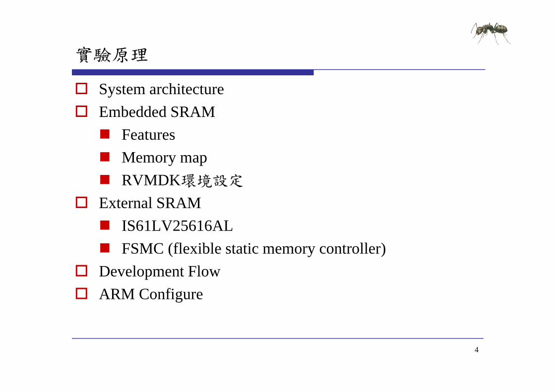
實驗原理
System architecture E b dd d SRAM Embedded SRAM Features Memory map RVMDK環境設定
External SRAM IS61LV25616AL FSMC (flexible static memory controller)
Development Flow ARM Configure
4
System architecturey
5
Embedded SRAM
Features 48Kb f b dd d SRAM 48Kbytes of embedded SRAM accessed (readwrite) at CPU clock speed with 0 wait
statesstates
6
Embedded SRAM Memory mapy p
7
RVMDK環境設定
STMF103ZC有48K Bytes的SRAM位置由0x20000000至0x2000C000
8
External SRAM (IS61LV25616AL)( )
Features Hi h d i 10 High-speed access time 10 ns 256K x 16
9
FUNCTIONAL BLOCK DIAGRAM
10
PIN DESCRIPTIONS
11
READ CYCLE
12
READ CYCLE SWITCHING CHARACTERISTICS
13
WRITE CYCLE
14
WRITE CYCLE SWITCHING CHARACTERISTICS
15
FSMC
Features I f i h i d d i Interfaces with static memory-mapped devices
including Static random access memor (SRAM) Static random access memory (SRAM) Read-only memory (ROM) NOR Fl h NOR Flash memory PSRAM (4 memory banks)8- or 16-bit wide databus
8 16 bit id d t b 8- or 16-bit wide databus Independent chip select control for each memory bank
I d d fi i f h b k Independent configuration for each memory bank
16
FSMC
Programmable timings to support a wide range of devices in particulardevices in particular Programmable wait states (up to 15) Programmable b s t rnaro nd c cles ( p to 15) Programmable bus turnaround cycles (up to 15) Programmable output enable and write enable delays
(up to 15)(up to 15) Independent read and write timings and protocol so
as to support the widest variety of memories andas to support the widest variety of memories and timings
17
NORPSRAM address mappingpp g
NORPSRAM bank selection
External memory address
18
External memory interface signalsy g
19
NOR FlashPSRAM controller timing diagramsg g
read accesses
20
NOR FlashPSRAM controller timing diagramsg g
write accesses
21
FSMC Memory mapy p
22
Development Flowp
Embedded Software Side
int main(void)
Bootup STM32F10x
ProgrammingBootupSTM32F10x RCC Configure
NVIC Configure
int main(void)ifdef DEBUGdebug()
endif
FSMC SRAM Init
System Clocks Configuration RCC_Configuration()
NVIC Configuration
GPIO Configure
gNVIC_Configuration()
GPIO Configuration GPIO_Configuration()
GPIO Configure
FSMC Configure
Writeread tofrom FSMC SRAM memory
Configure FSMC Bank1 NORSRAM1 FSMC_SRAM_Init()
SRAM memory RW operation FSMC SRAM WriteBuffer
FSMC SRAM ReadBuffer
helliphelliphelliphelliphelliphelliphelliphelliphelliphelliphelliphelliphelliphelliphelliphelliphelliphelliphelliphelliphelliphelliphellipCheck content
Display Result
23
Configure FSMC IOg
Function name Description
RCC_APB2PeriphClockCmd(RCC_APB2Periph_GPIOD | RCC_APB2Periph_GPIOG | RCC_APB2Periph_GPIOE | RCC_APB2Periph_GPIOF ENABLE)
‐‐ GPIO Configuration ‐‐‐‐‐‐‐‐‐‐‐‐‐‐‐‐‐‐‐‐‐‐‐‐‐‐‐‐‐‐‐‐‐‐‐‐‐‐‐‐‐‐‐‐‐‐‐‐‐
GPIO FwLib Functions List
Function name Description
RCC_APB2PeriphClockCmd
Enables or disables the High Speed APB (APB2) peripheralclock
GPIO I it I iti li th GPIO
GPIO Configuration SRAM Data lines configuration GPIO_InitStructureGPIO_Pin = GPIO_Pin_0 | GPIO_Pin_1 | GPIO_Pin_8 |
GPIO_Pin_9 | GPIO_Pin_10 | GPIO_Pin_14 | GPIO_Pin_15GPIO_InitStructureGPIO_Mode = GPIO_Mode_AF_PPGPIO_InitStructureGPIO_Speed = GPIO_Speed_50MHzGPIO_Init(GPIOD ampGPIO_InitStructure) GPIO_Init Initializes the GPIOx
peripheral according to the specified parametersin the GPIO_InitStruct
RCC AHBPeriphClock Enables or disables the AHB
_ ( _ )GPIO_InitStructureGPIO_Pin = GPIO_Pin_7 | GPIO_Pin_8 | GPIO_Pin_9 |
GPIO_Pin_10 | GPIO_Pin_11 | GPIO_Pin_12 | GPIO_Pin_13 | GPIO_Pin_14 | GPIO_Pin_15
GPIO_Init(GPIOE ampGPIO_InitStructure) SRAM Address lines configuration GPIO_InitStructureGPIO_Pin = GPIO_Pin_0 | GPIO_Pin_1 | GPIO_Pin_2 |
| | | | |RCC_AHBPeriphClockCmd
Enables or disables the AHB peripheral clock
GPIO_Pin_3 | GPIO_Pin_4 | GPIO_Pin_5 | GPIO_Pin_12 | GPIO_Pin_13 | GPIO_Pin_14 | GPIO_Pin_15
GPIO_Init(GPIOF ampGPIO_InitStructure) GPIO_InitStructureGPIO_Pin = GPIO_Pin_0 | GPIO_Pin_1 | GPIO_Pin_2 |
GPIO_Pin_3 | GPIO_Pin_4 | GPIO_Pin_5GPIO_Init(GPIOG ampGPIO_InitStructure)GPIO InitStructure GPIO Pin GPIO Pin 11 | GPIO Pin 12 | GPIO Pin 13 GPIO_InitStructureGPIO_Pin = GPIO_Pin_11 | GPIO_Pin_12 | GPIO_Pin_13 GPIO_Init(GPIOD ampGPIO_InitStructure) NOE and NWE configuration GPIO_InitStructureGPIO_Pin = GPIO_Pin_4 |GPIO_Pin_5GPIO_Init(GPIOD ampGPIO_InitStructure) NE1configuration GPIO InitStructure GPIO Pin = GPIO Pin 7 GPIO_InitStructureGPIO_Pin = GPIO_Pin_7 GPIO_Init(GPIOD ampGPIO_InitStructure) NBL0 NBL1 configuration GPIO_InitStructureGPIO_Pin = GPIO_Pin_0 | GPIO_Pin_1 GPIO_Init(GPIOE ampGPIO_InitStructure) Enable the FSMC Clock RCC_AHBPeriphClockCmd(RCC_AHBPeriph_FSMC ENABLE)
24
_ p ( _ p _ )
Configure FSMCg
Function name Description
Enable the FSMC Clock RCC_AHBPeriphClockCmd(RCC_AHBPeriph_FSMC ENABLE)
‐‐ FSMC Configuration ‐‐
FSMC FwLib Functions List
Function name Description
RCC_AHBPeriphClockCmd
Enables or disables the AHB peripheral clock
FSMC_NORSRAMInit Initializes the FSMC NOR b k di t th
FSMC Configuration pFSMC_AddressSetupTime = 0pFSMC_AddressHoldTime = 0pFSMC_DataSetupTime = 2pFSMC_BusTurnAroundDuration = 0pFSMC_CLKDivision = 0pFSMC_DataLatency = 0memory bank according to the
parameters specified in FSMC_NORInitStruct
FSMC_NORSRAMCm Enables or disables the NORSRAM memory bank1
p _ y pFSMC_AccessMode = FSMC_AccessMode_AFSMC_NORSRAMInitStructureFSMC_Bank = FSMC_Bank1_NORSRAM1FSMC_NORSRAMInitStructureFSMC_DataAddressMux =
FSMC_DataAddressMux_DisableFSMC_NORSRAMInitStructureFSMC_MemoryType = FSMC_MemoryType_SRAMFSMC_NORSRAMInitStructureFSMC_MemoryDataWidth = FSMC_MemoryDataWidth_16bNORSRAM memory bank1 FSMC_NORSRAMInitStructureFSMC_BurstAccessMode =
FSMC_BurstAccessMode_DisableFSMC_NORSRAMInitStructureFSMC_WaitSignalPolarity =
FSMC_WaitSignalPolarity_LowFSMC_NORSRAMInitStructureFSMC_WrapMode = FSMC_WrapMode_DisableFSMC_NORSRAMInitStructureFSMC_WaitSignalActive =
FSMC WaitSignalActive BeforeWaitStateFSMC_WaitSignalActive_BeforeWaitStateFSMC_NORSRAMInitStructureFSMC_WriteOperation =
FSMC_WriteOperation_EnableFSMC_NORSRAMInitStructureFSMC_WaitSignal = FSMC_WaitSignal_DisableFSMC_NORSRAMInitStructureFSMC_ExtendedMode = FSMC_ExtendedMode_DisableFSMC_NORSRAMInitStructureFSMC_AsyncWait = FSMC_AsyncWait_DisableFSMC NORSRAMInitStructure FSMC WriteBurst = FSMC WriteBurst DisableFSMC_NORSRAMInitStructureFSMC_WriteBurst = FSMC_WriteBurst_DisableFSMC_NORSRAMInitStructureFSMC_ReadWriteTimingStruct = amppFSMC_NORSRAMInitStructureFSMC_WriteTimingStruct = amppFSMC_NORSRAMInit(ampFSMC_NORSRAMInitStructure)
Enable FSMC Bank1_SRAM Bank FSMC_NORSRAMCmd(FSMC_Bank1_NORSRAM1 ENABLE)
25
_ ( _ _ )
硬體電路配置
Mapping Table
Num SRAM STM32 Num SRAM STM32 Num SRAM STM32
1 A0 FSMC_A0 14 A13 FSMC_A13 27 IO8 FSMC_D82 A1 FSMC A1 15 A14 FSMC A14 28 IO9 FSMC D9_ _ _3 A2 FSMC_A2 16 A15 FSMC_A15 29 IO10 FSMC_D104 A3 FSMC_A3 17 A16 FSMC_A16 30 IO11 FSMC_D115 A4 FSMC_A4 18 A17 FSMC_A17 31 IO12 FSMC_D126 A5 FSMC_A5 19 IO0 FSMC_D0 32 IO13 FSMC_D137 A6 FSMC_A6 20 IO1 FSMC_D1 33 IO14 FSMC_D148 A7 FSMC_A7 21 IO2 FSMC_D2 34 IO15 FSMC_D159 A8 FSMC A8 22 IO3 FSMC D3 35 CE FSMC nNE19 A8 FSMC_A8 22 IO3 FSMC_D3 35 CE FSMC_nNE110 A9 FSMC_A9 23 IO4 FSMC_D4 36 OE FSMC_nOE11 A10 FSMC_A10 24 IO5 FSMC_D5 37 WE FSMC_nWE12 A11 FSMC A11 25 IO6 FSMC D6 38 UB FSMC NBL1_ _ _13 A12 FSMC_A12 26 IO7 FSMC_D7 39 LB FSMC_NBL0
26
實驗步驟
範例目錄架構
範例說明 範例說明
預設定義說明
燒錄 燒錄MIAT_STM32
27
範例目錄架構
範例目錄
測試映像檔 測試映像檔
含括檔
函式庫 函式庫
專案檔
原始碼 原始碼
28
範例說明
Embedded Software Side
Write data to FSMC SRAM memory
SRAM memory RW operation
Write data to FSMC SRAM memory Fill the buffer to send Fill_Buffer(TxBuffer BUFFER_SIZE 0x3212)FSMC_SRAM_WriteBuffer(TxBuffer WRITE_READ_ADDR BUFFER_SIZE)
SRAM memory RW operation
FSMC SRAM WriteBuffer
Read data from FSMC SRAM memory FSMC_SRAM_ReadBuffer(RxBuffer WRITE_READ_ADDR BUFFER_SIZE)
Read back SRAM memory and check content correctness
FSMC SRAM ReadBuffer
Check content
Display Result yfor (Index = 0x00 (Index lt BUFFER_SIZE) ampamp (WriteReadStatus == 0)
Index++)if (RxBuffer[Index] = TxBuffer[Index])
Display Result
WriteReadStatus = Index + 1
29
範例說明
Embedded Software Side
while (1)
Display Result
while (1)if (WriteReadStatus == 0) OK Turn on USERLED
GPIO SetBits(GPIOF GPIO Pin 11)
SRAM memory RW operation
FSMC SRAM WriteBufferGPIO_SetBits(GPIOF GPIO_Pin_11)
else KO Turn off USERLED
GPIO ResetBits(GPIOF GPIO Pin 11)
FSMC SRAM ReadBuffer
Check content
Display Result
如果寫入與讀取Buffer內容相同外部記憶體使用正常USERLED紅燈GPIO_ResetBits(GPIOF GPIO_Pin_11)
Insert delay Delay(0xAFFFF) Turn on USERLED GPIO SetBits(GPIOF GPIO Pin 11)
Display Result恆亮
GPIO_SetBits(GPIOF GPIO_Pin_11) Insert delay Delay(0xAFFFF)
如果寫入與讀取Buffer內容不同外部記憶體使用異常 USERLED紅燈閃爍
30
預設定義說明
define Bank1_SRAM1_ADDR ((u32)0x60000000) 定義SRAM起始點 定義SRAM起始點
define BUFFER_SIZE 0x400定義測試資料大小 定義測試資料大小
資料大小必需小於0xC000 define WRITE_READ_ADDR 0x8000 定義SRAM寫入起始點
寫入起始點WRITE_READ_ADDR + BUFFER_SIZE必需小於0x6000C000
31
燒錄MIAT STM32_
Rebuilder all target files產生HEX DFU Fil M 轉換HEX產生DFU DFU File Manager轉換HEX產生DFU DfuSe Demonstration燒錄DFU d Leave DFU mode
32
內部與外部SRAM存取控制實驗
實驗一
WU-YANGTechnology Co Ltd
實驗一練習
練習 修改寫入位置測試是否正常 修改寫入位置測試是否正常
修改寫入資料大小測試是否正常
取消 i 測試是否正常 取消FSMC_SRAM_Init測試是否正常
34
實驗目的(二)( )
使用MIAT_STM32實驗板透過FSMC控制外部SRAM並設定為data memory進行存取控制實驗同樣利用LED設定為data memory進行存取控制實驗同樣利用LED確認存取是否正常
35
實驗原理
External SRAM RVMDK環境設定 RVMDK環境設定
Development Flow fi ARM Configure Startup Code
36
RVMDK環境設定
外部SRAM有512K Bytes位置由0x60000000至0x60080000
37
Development Flowp
Embedded Software Side
int main(void)
Bootup STM32F10x
Programming
Bootup
int main(void)ifdef DEBUGdebug()
endif
Startup Code
BootupSTM32F10x
RCC Configure
NVIC Configure
System Clocks Configuration RCC_Configuration()
NVIC Configuration g gNVIC_Configuration()
GPIO Configuration GPIO_Configuration()
GPIO Configure
for (Index = 0 Index lt1024 Index++)
Tab[Index] =IndexT bAdd ( 32)T b h ld b 0 600000
Check operation
Check pointer value
Display Result TabAddr = (u32)Tab should be 0x600000xx
Get main stack pointer value MSPValue = __MRS_MSP() should be 0x2000xxxx
helliphelliphelliphelliphelliphelliphelliphelliphelliphelliphelliphelliphelliphelliphelliphelliphelliphelliphelliphelliphelliphelliphellip
Display Result
38
Startup Codep
Register boundary addresses RCC Configure
Enable FSMC clock
LDR R0= 0x00000114
LDR R1= 0x40021014
STR R0[R1]
Enable GPIOD GPIOE GPIOF and GPIOG clocks
LDR R0= 0x000001E0
LDR R1= 0x40021018
RCC register map
STR R0[R1]
39
RCC Register g
Bit 8 FSMCEN FSMC clock enableAHB Peripheral Clock enable register (RCC_AHBENR)
Bit 8 FSMCEN FSMC clock enableSet and cleared by software0 FSMC clock disabled
APB2 peripheral clock enable register (RCC_APB2ENR)
1 FSMC clock enabled
Bit 8765 IOPGEN IO port GFED clock enableSet and cleared by software0 IO port GFED clock disabled1 IO port GFED clock enabled
40
1 IO port GFED clock enabled
Startup Codep
Register boundary addresses GPIO Configure
SRAM Data lines NOE and NWE configuration SRAM Address lines configuration NOE NEW NE1 NBL0 NBL1 configuration LDR R0= 0xB4BB44BB LDR R1= 0x40011400STR R0[R1]LDR R0= 0xBBBBBBBB LDR R1= 0x40011404STR R0[R1]LDR R0 = 0xB44444BBLDR R0= 0xB44444BB LDR R1= 0x40011800STR R0[R1]LDR R0= 0xBBBBBBBB LDR R1= 0x40011804
GPIO register map
STR R0[R1]LDR R0= 0x44BBBBBB LDR R1= 0x40011C00STR R0[R1]LDR R0= 0xBBBB4444 LDR R1= 0x40011C04STR R0[R1]LDR R0= 0x44BBBBBBLDR R1= 0x40012000STR R0 [R1]
41
STR R0[R1]
GPIO Register g
Bit 8 FSMCEN FSMC clock enablePort configuration register low
Port configuration register high
Bits 2928 2524Bits 3130 2726 2322 1918 1514 1110 76 32 Bits 2928 25242120 1716 131298 54 10MODEy[10] Port x mode bits (y= 0 15)00 Input mode (reset state)01 Output mode max speed 10 MHz
Bits 3130 27262322 1918 15141110 76 32CNFy[10] Port x configuration bits (y= 0 15)In input mode (MODE[10]=00)00 Analog input mode01 Floating input (reset state)10 Input with pull-up pull-down
10 Output mode max speed 2 MHz11 Output mode max speed 50 MHz
11 ReservedIn output mode (MODE[10] gt00)00 General purpose output push-pull01 General purpose output Open-drain10 Alternate function output Push-pull11 Alternate function output Open-drain
42
11 Alternate function output Open drain
Startup Codep
FSMCregister map FSMC Configure
FSMC Configuration Enable FSMC Bank1_SRAM Bank
LDR R0= 0x00001011
LDR R1= 0xA0000000
STR R0[R1]
LDR R0= 0x00000200
LDR R1= 0xA0000004
STR R0[R1]
43
FSMC Register g
Bit 8 FSMCEN FSMC clock enableSRAMNOR-Flash chip-select control registers 1 (FSMC_BCR1)
Bit 12 WREN Write enable bitThis bit indicates whether write operations are enableddisabled in the bank by the FSMC0 Write operations are disabled in the bank by the FSMC an AHB error is reported1 Write operations are enabled for the bank by the FSMC (default after reset) p y ( )Bits 54 MWID Memory databus widthDefines the external memory device width valid for all type of memories00 8 bits01 16 bits (default after reset)10 reserved do not use10 reserved do not use11 reserved do not use Bit 0 MBKEN Memory bank enable bitEnables the memory bank After reset Bank1 is enabled all others are disabled Accessing adisabled bank causes an ERROR on AHB bus0 C di b k i di bl d0 Corresponding memory bank is disabled1 Corresponding memory bank is enabled
44
FSMC Register g
Bit 8 FSMCEN FSMC clock enableSRAMNOR-Flash chip-select timing registers 1 (FSMC_BTR1)
Bits 158 DATAST Data-phase duration0000 0000 Reserved0000 0001 DATAST phase duration = 2 times HCLK clock cycles0000 0010 DATAST phase duration = 3 times HCLK clock cycles1111 1111 DATAST phase duration = 256 times HCLK clock cycles (default value after reset)Bits 74 ADDHLD Address-hold phase duration0000 Reserved0001 ADDHLD phase duration = 2 times HCLK clock cycle0010 ADDHLD phase duration = 3 times HCLK clock cycle1111 ADDHLD phase duration = 16 times HCLK clock cycles (default value after reset)Bits 30 ADDSET Address setup phase durationThese bits are written by software to define the duration of the address setup phase (refer toFigure 162 to Figure 172) used in SRAMs ROMs and asynchronous NOR Flash0000 ADDSET phase duration = 1 times HCLK clock cycle1111 ADDSET phase duration = 16 times HCLK clock cycles (default value after reset)
45
實驗步驟
範例目錄架構
範例說明 範例說明
預設定義說明
46
範例目錄架構
範例目錄
測試映像檔 測試映像檔
含括檔
函式庫 函式庫
專案檔
原始碼 原始碼
47
範例說明
Embedded Software Side
Infinite loop
Display Result
Infinite loop while (1)if (((TabAddramp0xFFFFFF00) == 0x60000000) ampamp
((MSPValueamp0xFFFF0000) == 0x20000000))
Check operation
Check pointer value((MSPValueamp0xFFFF0000) == 0x20000000))
OK Turn on USERLED GPIO_SetBits(GPIOF GPIO_Pin_11)
else
Display Result
else KO Turn off USERLED
GPIO_ResetBits(GPIOF GPIO_Pin_11) Insert delay Delay(0xAFFFF)
如果Tab位置在0x600000且Stack pointer位置在0x2000 外部記憶體使用正常USERLED紅燈恆亮Delay(0xAFFFF)
Turn on USERLED GPIO_SetBits(GPIOF GPIO_Pin_11) Insert delay Delay(0xAFFFF)
紅燈恆亮
如果 b位置不在0 600000或Delay(0xAFFFF)
如果Tab位置不在0x600000或Stack pointer位置不在0x2000 外部記憶體使用異常USERLED紅燈閃爍
48
預設定義說明
DATA_IN_ExtSRAM EQU 1 E l SRAM C fi i External SRAM Configuration 0=gt DISABLE 1=gt ENABLE
u32 Tab[1024]宣告於外部 的記憶體 宣告於外部SRAM的記憶體
49
data memory存取控制實驗
實驗二
WU-YANGTechnology Co Ltd
實驗二練習
練習 取消RVMDK環境外部SRAM設定測試是否正常 取消RVMDK環境外部SRAM設定測試是否正常
修改DATA_IN_ExtSRAM EQU 0測試是否正常
修改外部 記憶體 b變數大小測試是否正常 修改外部SRAM記憶體Tab變數大小測試是否正常
51
Q amp A
WU-YANGTechnology Co Ltd
MIAT_STM32內部Flash存取控制實驗
WU-YANG
浯陽科技有限公司
Technology Co Ltd
Declared Version
Training Only
Declare
Document Number
Document Version 100
Release Date
Document Title MIAT_STM32 內部FLASH存取控制實驗
Exercise Time
Platform MIAT_STM32V2MIAT IOB V1PlatformMIAT IOBV1
Peripheral
Author WU-YANG Technology Co Ltd
2
實驗目的(一)( )
使用MIAT_STM32實驗板透過Flash memory interface (FLITF)控制內部Flash進行存取控制實驗並利用LED(FLITF)控制內部Flash進行存取控制實驗並利用LED確認存取是否正常
3
實驗原理
System architecture E b dd d Fl h Embedded Flash Features Memory map RVMDK環境設定
FLITF Flash module organization
Flash library function Development Flow ARM Configure
4
System architecturey
5
Embedded Flash
Features 256 Kb up to 256 Kbytes Memory organization the Flash memory is organized as a
main block and an information blockmain block and an information block Main memory block of size t 32 Kb 64 bit di id d i t 128 f 2 up to 32 Kb times 64 bits divided into 128 pages of 2
Kbytes Information block of size Information block of size 258 times 64 bits
6
Embedded Flash Memory mapy p
7
Flash Memoryy
8
RVMDK環境設定
STMF103ZC有256K Bytes的Flash位置由0x8000000至0x8040000
9
FLITF
Features R d i f i h f h b ff (2 64 bi d ) Read interface with prefetch buffer (2x64-bit words) Option byte Loader
l h i Flash Program Erase operation Read Write protection
10
Flash memory interfacey
11
Flash memory interface registery g
Bit 8 FSMCEN FSMC clock enableFlash status register (FLASH_SR)
Bits 316 Reserved must be kept clearedBit 5 EOP End of operation
Bit 2 PGERR Programming errorSet by hardware when an address to be programmed p
Set by hardware when a Flash operation (programming erase) is completed Reset by writing a 1Note EOP is asserted at the end of each successful
y p gcontains a value different from 0xFFFF before programmingReset by writing 1Note The STRT bit in the FLASH_CR register f f
program or erase operationBit 4 WRPRTERR Write protection errorSet by hardware when programming a write-protected address of the Flash memory
_ gshould be reset before starting a programmingoperationBit 1 Reserved must be kept clearedBit 0 BSY Busyp y
Reset by writing 1Bit 3 Reserved must be kept cleared
This indicates that a Flash operation is in progress This is set on the beginning of a Flash operation and reset when the operation finishes or when an error occurs
12
Flash memory interface registery g
Flash control register (FLASH_CR)
Bit 9 OPTWRE Option bytes write enableWhen set the option bytes can be programmed This
Bit 6 STRT StartThis bit triggers an ERASE operation when set This bit is set only
bit is set on writing the correct key sequence to the FLASH_OPTKEYR registerThis bit can be reset by softwareBit 8 Reserved must be kept clearedBit 7 LOCK Lock
by software and reset when the BSY bit is resetBit 5 OPTER Option byte eraseOption byte erase chosenBit 4 OPTPG Option byte programmingOption byte programming chosenBit 7 LOCK Lock
Write to 1 only When it is set it indicates that the FPEC and FLASH_CR are locked This bit is reset by hardware after detecting the unlock sequenceIn the event of unsuccessful unlock operation this bit remains set until the next reset
p y p g gBit 3 Reserved must be kept clearedBit 2 MER Mass eraseErase of all user pages chosenBit 1 PER Page erasePage Erase chosenremains set until the next reset Page Erase chosenBit 0 PG ProgrammingFlash programming chosen
13
Main Flash memory programmingy p g g
14
Flash memory Page Erasey g
15
Flash memory Mass Erasey
16
Option byte programmingp y p g g
17
Option byte Erasep y
18
FLASH library functiony
19
FLASH library functiony
20
Development Flowp
Embedded Software Side
int main(void)
Bootup STM32F10x
ProgrammingBootupSTM32F10x RCC Configure
NVIC Configure
int main(void)ifdef DEBUGdebug()
endifendif
FLASHStatus = FLASH_COMPLETEMemoryProgramStatus = PASSEDData = 0x15041975
GPIO Configure
Data = 0x15041975
RCC Configuration RCC_Configuration()
Flash memory RW operation FLASH Unlock
FLASH ClearFlag NVIC Configuration NVIC_Configuration()
GPIO Configuration
FLASH ClearFlag
FLASH ErasePage
FLASH ProgramWord GPIO Configuration GPIO_Configuration()
helliphelliphelliphelliphelliphelliphelliphelliphelliphelliphelliphelliphelliphelliphelliphelliphellipDisplay Result
Check content
21
實驗步驟
範例目錄架構
範例說明 範例說明
預設定義說明
燒錄 燒錄MIAT_STM32
22
範例目錄架構
範例目錄
測試映像檔 測試映像檔
含括檔
函式庫 函式庫
專案檔
原始碼 原始碼
23
範例說明
Function name Description
Unlock the Flash Program Erase controller FLASH_Unlock()
D fi h b f b d
Flash FwLib Functions List
Function name Description
FLASH_Unlock Unlocks the FLASH Program Erase Controller
FLASH_ClearFlag Clears the FLASH pending fl
Define the number of page to be erased NbrOfPage = (EndAddr - StartAddr) FLASH_PAGE_SIZE
Clear All pending flags FLASH_ClearFlag(FLASH_FLAG_BSY | FLASH_FLAG_EOP | FLASH_FLAG_PGERR |
FLASH FLAG WRPRTERR)flags
FLASH_ErasePage Erases a specified FLASH page
FLASH_ProgramWord Programs a word at a specified
_ _ )
Erase the FLASH pages for(EraseCounter = 0 (EraseCounter lt NbrOfPage) ampamp (FLASHStatus ==
FLASH_COMPLETE) EraseCounter++)FLASHStatus = FLASH ErasePage(StartAddr + (FLASH PAGE SIZE EraseCounter))address FLASHStatus = FLASH_ErasePage(StartAddr + (FLASH_PAGE_SIZE EraseCounter))
FLASH Word program of data 0x15041979 at addresses defined by StartAddr and EndAddrAddress = StartAddr
while((Address lt EndAddr) ampamp (FLASHStatus == FLASH_COMPLETE))FLASHStatus = FLASH_ProgramWord(Address Data)Address = Address + 4
24
範例說明
Embedded Software Side
Check the corectness of written data
Display Result
Check the corectness of written data Address = StartAddr
while((Address lt EndAddr) ampamp (MemoryProgramStatus = FAILED))if(((vu32) Address) = Data)
Flash memory RW operation
MemoryProgramStatus = FAILED
Address += 4
Check content
Display Result while (1)if (MemoryProgramStatus == PASSED) OK Turn on USERLED GPIO_SetBits(GPIOF GPIO_Pin_11)
Display Result
else KO Turn off USERLED GPIO_ResetBits(GPIOF GPIO_Pin_11) Insert delay Delay(0xAFFFF)
如果寫入與讀取Flash內容相同Flash記憶體使用正常USERLED紅燈恆亮
Turn on USERLED GPIO_SetBits(GPIOF GPIO_Pin_11) Insert delay Delay(0xAFFFF)
如果寫入與讀取Flash內容不同Flash記憶體使用異常USERLED紅燈閃爍
25
預設定義說明
define StartAddr ((u32)0x08008000) 定義Flash使用起始點 定義Flash使用起始點
使用起始點必需大於0x8003000 + Code Size 附註 0x8000000~0x8003000為DFU程式區塊使用此區塊
將造成無法燒錄程式
Code Size可由產生的HEX檔得知
d fi E dAdd (( 32)0 0800C000) define EndAddr ((u32)0x0800C000) 定義Flash使用結束點
使用起始點必需小於0x8040000使用起始點必需小於
Data = 0x15041975 寫入資料
32Bit define FLASH_PAGE_SIZE ((u16)0x800)
每一個Page有2KByte26
每一個Page有2KByte
Intel HEX Format
aaaa tt dd cc
field Description
the colon that starts every Intel HEX record
the record-length field that represents the number of data bytes (dd) in the record
aaaa the address field that represents the starting address for subsequent data in the record
tt the field that represents the HEX record type which may be one of the following00 - data record01 - end-of-file record02 - extended segment address recordg04 - extended linear address record
dd a data field that represents one byte of data A record may have multiple data bytes The number of data bytes in the record must match the number specified by the field
cc the checksum field that represents the checksum of the record The checksum is calculated by summing the values of all hexadecimal digit pairs in the record modulo 256 and taking the twos complement
27
HEX Examplep
020000040800F2103000001814002045310008D9340008CD340008D8103000001814002045310008D9340008CD340008D8helliphelliphellip1038200042370008000000000000000000000000170C3830000000000000000000000000008C
資料填入起始位置為
0C3830000000000000000000000000008C04000005080031318D00000001FF
資料填入起始位置為0x08003000 每一行有0x10(16)個Bytes 最後一筆資料為
資料結束點為0x0803383004000005080031318D
(0x08003830 -0x08000000)0x800 = 7 需以0x800為單位所以使用的位置起點為0x08004000
28
燒錄MIAT STM32_
Rebuilder all target files產生HEX DFU Fil M 轉換HEX產生DFU DFU File Manager轉換HEX產生DFU DfuSe Demonstration燒錄DFU d Leave DFU mode
29
內部Flash存取控制實驗
實驗一
WU-YANGTechnology Co Ltd
實驗一練習
注意 請使用預設0 08008000之後的位置 避免覆蓋DFU 請使用預設0x08008000之後的位置避免覆蓋DFU
與使用者程式碼區塊
練習 練習 修改存取位置測試是否正常
修改寫入資料測試是否正常 修改寫入資料測試是否正常
修改寫入資料後取消FLASH_Unlock測試是否正常
修改寫入資料後取消FLASH E P 測試是否正 修改寫入資料後取消FLASH_ErasePage測試是否正常
31
實驗目的(二)( )
使用MIAT_STM32實驗板透過Flash memory interface (FLITF)控制內部Flash進行存取控制實驗並利用SW(FLITF)控制內部Flash進行存取控制實驗並利用SWKEY決定資料寫入與讀取LCD顯示狀態
32
實驗原理
System requirement E b dd d Fl h Embedded Flash LCD KEY SW
Development Flow ARM Configure
33
Development Flowp
Embedded Software Side
int main(void)
Bootup STM32F10x
ProgrammingBootupSTM32F10x RCC Configure
NVIC Configure
int main(void)ifdef DEBUGdebug()
endif
FLASHStatus = FLASH_COMPLETE
RCC Configuration RCC Configuration()
GPIO Configure
BasicIO Configure_ g ()
NVIC Configuration NVIC_Configuration()
GPIO Configuration Flash memory RW ti
lcd Configure
GPIO Configuration GPIO_Configuration()
Init_BasicIO()
l d i i () LCD I i i li i
RW operation
Example
FLASH Unlock
FLASH ClearFlag
lcd_init() LCD Initialization
helliphelliphelliphelliphelliphelliphelliphelliphelliphelliphelliphelliphelliphelliphelliphelliphelliphelliphelliphelliphelliphelliphellip
p
34
硬體電路配置
Mapping Table
Num MIAT_STM32V2 MIAT_IOBV1 Num MIAT_STM32V2 MIAT_IOBV1
1 PC8 (326) SW1 10 PE6 (15) LCD_EN2 PC9 (327) SW2 11 PF6 (118) LCD RW ( ) ( ) _3 PC10 (43) SW3 12 PF7 (119) LCD_RS 4 PC11 (44) SW4 13 PF8(120) LCD_D4 5 PB5 (427) KEY1 14 PF9 (121) LCD_D5 6 PB6 (428) KEY2 15 PF10 (122) LCD_D6 7 PB7 (429) KEY3 16 PF11 (213) LCD_D7 8 PB8 (431) KEY4 17 VDD (236) VCC33V 9 VCC5V (1 36) VCC5V 18 GND (1 35) GND9 VCC5V (136) VCC5V 18 GND (135) GND
35
實驗步驟
範例目錄架構
範例說明 範例說明
預設定義說明
36
範例目錄架構
範例目錄
測試映像檔 測試映像檔
含括檔
函式庫 函式庫
專案檔
原始碼 原始碼
37
範例說明
Embedded Software Side
lcd clear()
FLASH memory RW operation
lcd_clear()lcd_print (MIAT_STM32 DEMO )
Unlock the Flash Program Erase controller FLASH_Unlock()
Flash memory RW operation
FLASH Unlock
Clear All pending flags FLASH_ClearFlag(FLASH_FLAG_BSY | FLASH_FLAG_EOP | FLASH_FLAG_PGERR |
FLASH_FLAG_WRPRTERR)
while(1)
Example
FLASH ClearFlag
( )
KEY_Buffer=Key_Scan()set_cursor (0 1)lcd_print (SW Value = 0x)lcd putchar(((SWamp0x7)+0x30))lcd_putchar(((SWamp0x7)+0x30))if(KEY_Buffer==1)Address=(StartAddr|(SWltlt12))set_cursor (0 0)lcd_print (Set Addr = 0x)
掃描KEY是否按下與顯示SW數值LCD Line2顯示SW Value = 0x(SW)
lcd_putchar(((SWamp0x7)+0x30))lcd_print ( )
如果KEY1按下記錄SW數值至Address LCD Line1顯示Set Adde = 0x(Address)
38
範例說明
Embedded Software Side
else if(KEY Buffer==2)
FLASH memory RW operation
else if(KEY_Buffer==2)
Erase the FLASH pages FLASHStatus = FLASH_ErasePage(Address)
FLASH Word program of data at addresses defined by SW
SRAM memory RW operation
p g yFLASHStatus = FLASH_ProgramWord(Address (SWamp0x7))
set_cursor (0 0)lcd_print (Write 0x)lcd_putchar(((SWamp0x7)+0x30))l d i t ( t 0 )
Example如果KEY2按下清除Address所處區塊並寫入SW數值 lcd_print ( at 0x)
lcd_putchar((((Addressgtgt12)amp0x7)+0x30))else if(KEY_Buffer==3)
Data=(u16 )Address
所處區塊並寫入SW數值LCD Line1顯示Write 0x(SW) at 0x(Adddress)
Data (u16 )Addressset_cursor (0 0)lcd_print (Addr 0x)lcd_putchar((((Addressgtgt12)amp0x7)+0x30))lcd_print ( = 0x)lcd_putchar(((Dataamp0x7)+0x30))lcd_print ( )
如果KEY3按下讀取Address紀錄數值LCD Line1顯示Addr 0x(Adddress) = 0x
39
預設定義說明
define StartAddr ((u32)0x08020000) 定義Flash使用起始點 定義Flash使用起始點
使用起始點必需大於0x8003000 + Code Size 附註 0x8000000~0x8003000為DFU程式區塊使用此區塊
將造成無法燒錄程式
Code Size可由產生的HEX檔得知
32 Add 0 08020000 u32 Address = 0x08020000 定義Address初始值
初始值必需與Flash使用起始點相同初始值必需與 使用起始點相同
Address=(StartAddr|(SWltlt12)) Example StartAddr = 0x08020000 SW = 1 Address = 0x08021000
StartAddr = 0x08020000 SW = 7 Address = 0x08027000 StartAddr|(7ltlt12)必需小於0x8040000
40
使用者界面與Flash存取控制實驗
實驗二
WU-YANGTechnology Co Ltd
實驗二練習
注意 請使用預設0 08020000之後的位置 避免覆蓋DFU 請使用預設0x08020000之後的位置避免覆蓋DFU
與使用者程式碼區塊
練習 練習 利用SW與KEY測試Flash寫入與讀取是否正常
Fl h寫入後電源關閉 再開啟後寫入資料是否仍存 Flash寫入後電源關閉再開啟後寫入資料是否仍存在
修改存取位置測試是否正常 修改存取位置測試是否正常
42
實驗目的(三)( )
使用MIAT_STM32實驗板透過Flash memory interface (FLITF)控制內部Flash進行存取控制實驗並藉由填入(FLITF)控制內部Flash進行存取控制實驗並藉由填入Option Bytes 設定寫入鎖定保護Page鎖定不被覆蓋
43
Development Flowp
Embedded Software Side
int main(void)
Bootup STM32F10x
ProgrammingBootupSTM32F10x RCC Configure
NVIC Configure
int main(void)ifdef DEBUGdebug()
endifendif
FLASHStatus = FLASH_COMPLETEMemoryProgramStatus = PASSEDData = 0x1753
GPIO Configure
Data = 0x1753
RCC Configuration RCC_Configuration()
Flash memory RW operation FLASH Unlock
FLASH ClearFlag NVIC Configuration NVIC_Configuration()
GPIO Configuration
FLASH ClearFlag
FLASH ErasePage
FLASH ProgramHalfWord GPIO Configuration GPIO_Configuration()
Display Result
Check content
44
helliphelliphelliphelliphelliphelliphelliphelliphelliphelliphelliphelliphelliphelliphelliphelliphelliphelliphellip
實驗步驟
範例目錄架構
範例說明 範例說明
預設定義說明
45
範例目錄架構
範例目錄
測試映像檔 測試映像檔
含括檔
函式庫 函式庫
專案檔
原始碼 原始碼
46
範例說明
Function name Description
Unlock the Flash Program Erase controller FLASH_Unlock()
Define the number of page to be erased
Flash FwLib Functions List
Function name Description
FLASH_Unlock Unlocks the FLASH Program Erase Controller
FLASH_ClearFlag Clears the FLASH pending fl
Define the number of page to be erased NbrOfPage = (EndAddr ‐ StartAddr) FLASH_PAGE_SIZE
FLASH_ClearFlag(FLASH_FLAG_BSY | FLASH_FLAG_EOP|FLASH_FLAG_PGERR |FLASH_FLAG_WRPRTERR)
Get pages write protection status flags
FLASH_EraseOptionBytes
Erases the FLASH option bytes
FLASH_EnableWritePro Write protects the desired
p g pWRPR_Value = FLASH_GetWriteProtectionOptionByte()ProtectedPages = WRPR_Value amp 0x000000C0
ifdef WriteProtection_Disableif (ProtectedPages == 0x00) Pages are write protected
tection pages
NVIC_GenerateSystemReset
Generate a system reset
Disable the write protection FLASHStatus = FLASH_EraseOptionBytes() Generate System Reset to load the new option byte values NVIC_GenerateSystemReset()
elseifdef WriteProtection Enableifdef WriteProtection_Enableif (ProtectedPages = 0x00) Pages not write protected
FLASHStatus = FLASH_EraseOptionBytes() Enable the pages write protection FLASHStatus = FLASH_EnableWriteProtection(FLASH_WRProt_Pages12to13
|FLASH WRProt Pages14to15)|FLASH_WRProt_Pages14to15) Generate System Reset to load the new option byte values NVIC_GenerateSystemReset()
endifendif
47
範例說明
if (ProtectedPages = 0x00) Clear All pending flags
Flash FwLib Functions List
Function name DescriptionFLASH_ClearFlag(FLASH_FLAG_BSY |
FLASH_FLAG_EOP|FLASH_FLAG_PGERR |FLASH_FLAG_WRPRTERR)
erase the FLASH pages for(EraseCounter = 0 (EraseCounter lt NbrOfPage) ampamp (FLASHStatus ==
Function name Description
FLASH_ErasePage Erases a specified FLASH page
FLASH_ProgramHalfWod
Programs a half word at a ifi d dd FLASH_COMPLETE) EraseCounter++)
FLASHStatus = FLASH_ErasePage(StartAddr + (FLASH_PAGE_SIZE
EraseCounter))
rd specified address
FLASH Half Word program of data 0x1753 at addresses defined by StartAddrand EndAddr
Address = StartAddr
hil ((Add E dAdd ) ampamp (FLASHSt t FLASH COMPLETE))while((Address lt EndAddr) ampamp (FLASHStatus == FLASH_COMPLETE))
FLASHStatus = FLASH_ProgramHalfWord(Address Data)Address = Address + 2
48
範例說明
Embedded Software Side
Check the corectness of written data
Display Result
Check the corectness of written data Address = StartAddr
while((Address lt EndAddr) ampamp (MemoryProgramStatus = FAILED))if(((vu16) Address) = Data)
Flash memory RW operation
MemoryProgramStatus = FAILED
Address += 2
Check content
Display Result while (1)if (MemoryProgramStatus == PASSED) OK Turn on USERLED GPIO_SetBits(GPIOF GPIO_Pin_11)
Display Result
else KO Turn off USERLED GPIO_ResetBits(GPIOF GPIO_Pin_11) Insert delay Delay(0xAFFFF)
如果寫入與讀取Flash內容相同Flash記憶體可以寫入USERLED紅燈恆亮
Turn on USERLED GPIO_SetBits(GPIOF GPIO_Pin_11) Insert delay Delay(0xAFFFF)
如果寫入與讀取Flash內容不同Flash記憶體不能寫入USERLED紅燈閃爍
49
預設定義說明
define StartAddr ((u32) 0x08006000) 定義Flash使用起始點 定義Flash使用起始點
使用起始點必需大於0x8003000 + Code Size 附註 0x8000000~0x8003000為DFU程式區塊使用此區塊
將造成無法燒錄程式
Code Size可由產生的HEX檔得知
d fi E dAdd (( 32) 0 08008000) define EndAddr ((u32) 0x08008000) 定義Flash使用結束點
使用起始點必需小於0x8040000使用起始點必需小於
Data = 0x1753 寫入資料
16Bit define FLASH_PAGE_SIZE ((u16)0x800) 每一個Page有2KByte
50
每一個Page有2KByte
預設定義說明
define WriteProtection_Enable U hi li E bl W i P i Uncomment this line to Enable Write Protection
define WriteProtection_Disablehi li i bl i i Uncomment this line to Disable Write Protection
FLASH_EnableWriteProtection設定影響 個 設定影響2個Page FLASH_WRProt_Pages0to1 FLASH_WRProt_Pages1to2 helliphellip FLASH_WRProt_Pages60to61
設定影響多個Page FLASH_WRProt_Pages62to255
51
FLASH EnableWriteProtection_
Example
位置0x08006000 ~ 0x08007000每一個Page有0x800ByteStartPage = (0x08006000-0x08000000)0x800 = 12EndPage = ((0x08007000-0x08000000)0x800)-1 = 13執行執行FLASH_EnableWriteProtection(FLASH_WRProt_Pages12to13)將影響Pages12 Pages13
52
內部Flash寫入鎖定存取控制實驗
實驗三
WU-YANGTechnology Co Ltd
實驗三練習
注意 請使用預設0 08006000之後的位置 避免覆蓋DFU 請使用預設0x08006000之後的位置避免覆蓋DFU
與使用者程式碼區塊
更改寫入位置測試寫入鎖定時需同時更改 更改寫入位置測試寫入鎖定時需同時更改FLASH_EnableWriteProtection鎖定之Page
練習 練習 打開define WriteProtection_Enable測試是否可寫入
打開define WriteProtection Disable測試是否可寫入 打開define WriteProtection_Disable測試是否可寫入
修改存取位置測試是否正常
修改寫入資料測試是否正常 修改寫入資料測試是否正常
54
Q amp A
WU-YANGTechnology Co Ltd
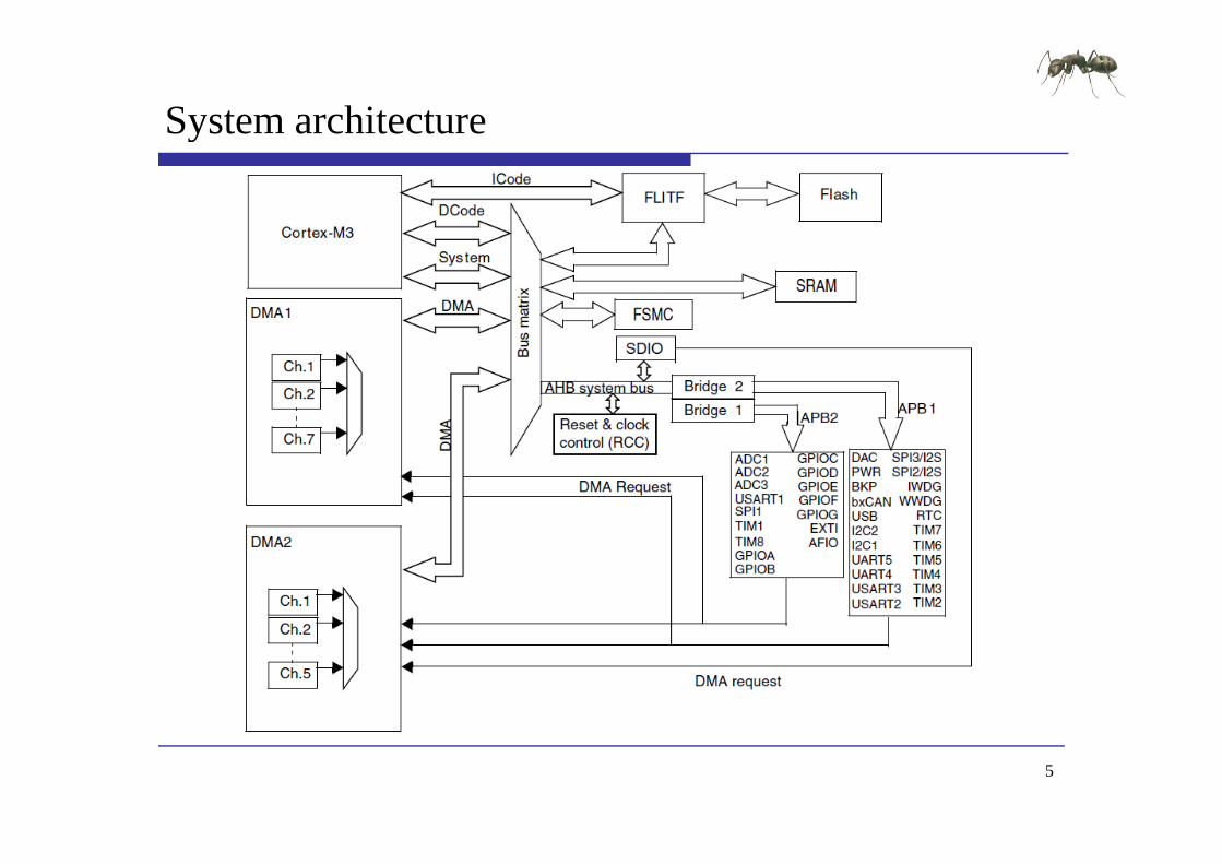
System architecturey
5
Embedded SRAM
Features 48Kb f b dd d SRAM 48Kbytes of embedded SRAM accessed (readwrite) at CPU clock speed with 0 wait
statesstates
6
Embedded SRAM Memory mapy p
7
RVMDK環境設定
STMF103ZC有48K Bytes的SRAM位置由0x20000000至0x2000C000
8
External SRAM (IS61LV25616AL)( )
Features Hi h d i 10 High-speed access time 10 ns 256K x 16
9
FUNCTIONAL BLOCK DIAGRAM
10
PIN DESCRIPTIONS
11
READ CYCLE
12
READ CYCLE SWITCHING CHARACTERISTICS
13
WRITE CYCLE
14
WRITE CYCLE SWITCHING CHARACTERISTICS
15
FSMC
Features I f i h i d d i Interfaces with static memory-mapped devices
including Static random access memor (SRAM) Static random access memory (SRAM) Read-only memory (ROM) NOR Fl h NOR Flash memory PSRAM (4 memory banks)8- or 16-bit wide databus
8 16 bit id d t b 8- or 16-bit wide databus Independent chip select control for each memory bank
I d d fi i f h b k Independent configuration for each memory bank
16
FSMC
Programmable timings to support a wide range of devices in particulardevices in particular Programmable wait states (up to 15) Programmable b s t rnaro nd c cles ( p to 15) Programmable bus turnaround cycles (up to 15) Programmable output enable and write enable delays
(up to 15)(up to 15) Independent read and write timings and protocol so
as to support the widest variety of memories andas to support the widest variety of memories and timings
17
NORPSRAM address mappingpp g
NORPSRAM bank selection
External memory address
18
External memory interface signalsy g
19
NOR FlashPSRAM controller timing diagramsg g
read accesses
20
NOR FlashPSRAM controller timing diagramsg g
write accesses
21
FSMC Memory mapy p
22
Development Flowp
Embedded Software Side
int main(void)
Bootup STM32F10x
ProgrammingBootupSTM32F10x RCC Configure
NVIC Configure
int main(void)ifdef DEBUGdebug()
endif
FSMC SRAM Init
System Clocks Configuration RCC_Configuration()
NVIC Configuration
GPIO Configure
gNVIC_Configuration()
GPIO Configuration GPIO_Configuration()
GPIO Configure
FSMC Configure
Writeread tofrom FSMC SRAM memory
Configure FSMC Bank1 NORSRAM1 FSMC_SRAM_Init()
SRAM memory RW operation FSMC SRAM WriteBuffer
FSMC SRAM ReadBuffer
helliphelliphelliphelliphelliphelliphelliphelliphelliphelliphelliphelliphelliphelliphelliphelliphelliphelliphelliphelliphelliphelliphellipCheck content
Display Result
23
Configure FSMC IOg
Function name Description
RCC_APB2PeriphClockCmd(RCC_APB2Periph_GPIOD | RCC_APB2Periph_GPIOG | RCC_APB2Periph_GPIOE | RCC_APB2Periph_GPIOF ENABLE)
‐‐ GPIO Configuration ‐‐‐‐‐‐‐‐‐‐‐‐‐‐‐‐‐‐‐‐‐‐‐‐‐‐‐‐‐‐‐‐‐‐‐‐‐‐‐‐‐‐‐‐‐‐‐‐‐
GPIO FwLib Functions List
Function name Description
RCC_APB2PeriphClockCmd
Enables or disables the High Speed APB (APB2) peripheralclock
GPIO I it I iti li th GPIO
GPIO Configuration SRAM Data lines configuration GPIO_InitStructureGPIO_Pin = GPIO_Pin_0 | GPIO_Pin_1 | GPIO_Pin_8 |
GPIO_Pin_9 | GPIO_Pin_10 | GPIO_Pin_14 | GPIO_Pin_15GPIO_InitStructureGPIO_Mode = GPIO_Mode_AF_PPGPIO_InitStructureGPIO_Speed = GPIO_Speed_50MHzGPIO_Init(GPIOD ampGPIO_InitStructure) GPIO_Init Initializes the GPIOx
peripheral according to the specified parametersin the GPIO_InitStruct
RCC AHBPeriphClock Enables or disables the AHB
_ ( _ )GPIO_InitStructureGPIO_Pin = GPIO_Pin_7 | GPIO_Pin_8 | GPIO_Pin_9 |
GPIO_Pin_10 | GPIO_Pin_11 | GPIO_Pin_12 | GPIO_Pin_13 | GPIO_Pin_14 | GPIO_Pin_15
GPIO_Init(GPIOE ampGPIO_InitStructure) SRAM Address lines configuration GPIO_InitStructureGPIO_Pin = GPIO_Pin_0 | GPIO_Pin_1 | GPIO_Pin_2 |
| | | | |RCC_AHBPeriphClockCmd
Enables or disables the AHB peripheral clock
GPIO_Pin_3 | GPIO_Pin_4 | GPIO_Pin_5 | GPIO_Pin_12 | GPIO_Pin_13 | GPIO_Pin_14 | GPIO_Pin_15
GPIO_Init(GPIOF ampGPIO_InitStructure) GPIO_InitStructureGPIO_Pin = GPIO_Pin_0 | GPIO_Pin_1 | GPIO_Pin_2 |
GPIO_Pin_3 | GPIO_Pin_4 | GPIO_Pin_5GPIO_Init(GPIOG ampGPIO_InitStructure)GPIO InitStructure GPIO Pin GPIO Pin 11 | GPIO Pin 12 | GPIO Pin 13 GPIO_InitStructureGPIO_Pin = GPIO_Pin_11 | GPIO_Pin_12 | GPIO_Pin_13 GPIO_Init(GPIOD ampGPIO_InitStructure) NOE and NWE configuration GPIO_InitStructureGPIO_Pin = GPIO_Pin_4 |GPIO_Pin_5GPIO_Init(GPIOD ampGPIO_InitStructure) NE1configuration GPIO InitStructure GPIO Pin = GPIO Pin 7 GPIO_InitStructureGPIO_Pin = GPIO_Pin_7 GPIO_Init(GPIOD ampGPIO_InitStructure) NBL0 NBL1 configuration GPIO_InitStructureGPIO_Pin = GPIO_Pin_0 | GPIO_Pin_1 GPIO_Init(GPIOE ampGPIO_InitStructure) Enable the FSMC Clock RCC_AHBPeriphClockCmd(RCC_AHBPeriph_FSMC ENABLE)
24
_ p ( _ p _ )
Configure FSMCg
Function name Description
Enable the FSMC Clock RCC_AHBPeriphClockCmd(RCC_AHBPeriph_FSMC ENABLE)
‐‐ FSMC Configuration ‐‐
FSMC FwLib Functions List
Function name Description
RCC_AHBPeriphClockCmd
Enables or disables the AHB peripheral clock
FSMC_NORSRAMInit Initializes the FSMC NOR b k di t th
FSMC Configuration pFSMC_AddressSetupTime = 0pFSMC_AddressHoldTime = 0pFSMC_DataSetupTime = 2pFSMC_BusTurnAroundDuration = 0pFSMC_CLKDivision = 0pFSMC_DataLatency = 0memory bank according to the
parameters specified in FSMC_NORInitStruct
FSMC_NORSRAMCm Enables or disables the NORSRAM memory bank1
p _ y pFSMC_AccessMode = FSMC_AccessMode_AFSMC_NORSRAMInitStructureFSMC_Bank = FSMC_Bank1_NORSRAM1FSMC_NORSRAMInitStructureFSMC_DataAddressMux =
FSMC_DataAddressMux_DisableFSMC_NORSRAMInitStructureFSMC_MemoryType = FSMC_MemoryType_SRAMFSMC_NORSRAMInitStructureFSMC_MemoryDataWidth = FSMC_MemoryDataWidth_16bNORSRAM memory bank1 FSMC_NORSRAMInitStructureFSMC_BurstAccessMode =
FSMC_BurstAccessMode_DisableFSMC_NORSRAMInitStructureFSMC_WaitSignalPolarity =
FSMC_WaitSignalPolarity_LowFSMC_NORSRAMInitStructureFSMC_WrapMode = FSMC_WrapMode_DisableFSMC_NORSRAMInitStructureFSMC_WaitSignalActive =
FSMC WaitSignalActive BeforeWaitStateFSMC_WaitSignalActive_BeforeWaitStateFSMC_NORSRAMInitStructureFSMC_WriteOperation =
FSMC_WriteOperation_EnableFSMC_NORSRAMInitStructureFSMC_WaitSignal = FSMC_WaitSignal_DisableFSMC_NORSRAMInitStructureFSMC_ExtendedMode = FSMC_ExtendedMode_DisableFSMC_NORSRAMInitStructureFSMC_AsyncWait = FSMC_AsyncWait_DisableFSMC NORSRAMInitStructure FSMC WriteBurst = FSMC WriteBurst DisableFSMC_NORSRAMInitStructureFSMC_WriteBurst = FSMC_WriteBurst_DisableFSMC_NORSRAMInitStructureFSMC_ReadWriteTimingStruct = amppFSMC_NORSRAMInitStructureFSMC_WriteTimingStruct = amppFSMC_NORSRAMInit(ampFSMC_NORSRAMInitStructure)
Enable FSMC Bank1_SRAM Bank FSMC_NORSRAMCmd(FSMC_Bank1_NORSRAM1 ENABLE)
25
_ ( _ _ )
硬體電路配置
Mapping Table
Num SRAM STM32 Num SRAM STM32 Num SRAM STM32
1 A0 FSMC_A0 14 A13 FSMC_A13 27 IO8 FSMC_D82 A1 FSMC A1 15 A14 FSMC A14 28 IO9 FSMC D9_ _ _3 A2 FSMC_A2 16 A15 FSMC_A15 29 IO10 FSMC_D104 A3 FSMC_A3 17 A16 FSMC_A16 30 IO11 FSMC_D115 A4 FSMC_A4 18 A17 FSMC_A17 31 IO12 FSMC_D126 A5 FSMC_A5 19 IO0 FSMC_D0 32 IO13 FSMC_D137 A6 FSMC_A6 20 IO1 FSMC_D1 33 IO14 FSMC_D148 A7 FSMC_A7 21 IO2 FSMC_D2 34 IO15 FSMC_D159 A8 FSMC A8 22 IO3 FSMC D3 35 CE FSMC nNE19 A8 FSMC_A8 22 IO3 FSMC_D3 35 CE FSMC_nNE110 A9 FSMC_A9 23 IO4 FSMC_D4 36 OE FSMC_nOE11 A10 FSMC_A10 24 IO5 FSMC_D5 37 WE FSMC_nWE12 A11 FSMC A11 25 IO6 FSMC D6 38 UB FSMC NBL1_ _ _13 A12 FSMC_A12 26 IO7 FSMC_D7 39 LB FSMC_NBL0
26
實驗步驟
範例目錄架構
範例說明 範例說明
預設定義說明
燒錄 燒錄MIAT_STM32
27
範例目錄架構
範例目錄
測試映像檔 測試映像檔
含括檔
函式庫 函式庫
專案檔
原始碼 原始碼
28
範例說明
Embedded Software Side
Write data to FSMC SRAM memory
SRAM memory RW operation
Write data to FSMC SRAM memory Fill the buffer to send Fill_Buffer(TxBuffer BUFFER_SIZE 0x3212)FSMC_SRAM_WriteBuffer(TxBuffer WRITE_READ_ADDR BUFFER_SIZE)
SRAM memory RW operation
FSMC SRAM WriteBuffer
Read data from FSMC SRAM memory FSMC_SRAM_ReadBuffer(RxBuffer WRITE_READ_ADDR BUFFER_SIZE)
Read back SRAM memory and check content correctness
FSMC SRAM ReadBuffer
Check content
Display Result yfor (Index = 0x00 (Index lt BUFFER_SIZE) ampamp (WriteReadStatus == 0)
Index++)if (RxBuffer[Index] = TxBuffer[Index])
Display Result
WriteReadStatus = Index + 1
29
範例說明
Embedded Software Side
while (1)
Display Result
while (1)if (WriteReadStatus == 0) OK Turn on USERLED
GPIO SetBits(GPIOF GPIO Pin 11)
SRAM memory RW operation
FSMC SRAM WriteBufferGPIO_SetBits(GPIOF GPIO_Pin_11)
else KO Turn off USERLED
GPIO ResetBits(GPIOF GPIO Pin 11)
FSMC SRAM ReadBuffer
Check content
Display Result
如果寫入與讀取Buffer內容相同外部記憶體使用正常USERLED紅燈GPIO_ResetBits(GPIOF GPIO_Pin_11)
Insert delay Delay(0xAFFFF) Turn on USERLED GPIO SetBits(GPIOF GPIO Pin 11)
Display Result恆亮
GPIO_SetBits(GPIOF GPIO_Pin_11) Insert delay Delay(0xAFFFF)
如果寫入與讀取Buffer內容不同外部記憶體使用異常 USERLED紅燈閃爍
30
預設定義說明
define Bank1_SRAM1_ADDR ((u32)0x60000000) 定義SRAM起始點 定義SRAM起始點
define BUFFER_SIZE 0x400定義測試資料大小 定義測試資料大小
資料大小必需小於0xC000 define WRITE_READ_ADDR 0x8000 定義SRAM寫入起始點
寫入起始點WRITE_READ_ADDR + BUFFER_SIZE必需小於0x6000C000
31
燒錄MIAT STM32_
Rebuilder all target files產生HEX DFU Fil M 轉換HEX產生DFU DFU File Manager轉換HEX產生DFU DfuSe Demonstration燒錄DFU d Leave DFU mode
32
內部與外部SRAM存取控制實驗
實驗一
WU-YANGTechnology Co Ltd
實驗一練習
練習 修改寫入位置測試是否正常 修改寫入位置測試是否正常
修改寫入資料大小測試是否正常
取消 i 測試是否正常 取消FSMC_SRAM_Init測試是否正常
34
實驗目的(二)( )
使用MIAT_STM32實驗板透過FSMC控制外部SRAM並設定為data memory進行存取控制實驗同樣利用LED設定為data memory進行存取控制實驗同樣利用LED確認存取是否正常
35
實驗原理
External SRAM RVMDK環境設定 RVMDK環境設定
Development Flow fi ARM Configure Startup Code
36
RVMDK環境設定
外部SRAM有512K Bytes位置由0x60000000至0x60080000
37
Development Flowp
Embedded Software Side
int main(void)
Bootup STM32F10x
Programming
Bootup
int main(void)ifdef DEBUGdebug()
endif
Startup Code
BootupSTM32F10x
RCC Configure
NVIC Configure
System Clocks Configuration RCC_Configuration()
NVIC Configuration g gNVIC_Configuration()
GPIO Configuration GPIO_Configuration()
GPIO Configure
for (Index = 0 Index lt1024 Index++)
Tab[Index] =IndexT bAdd ( 32)T b h ld b 0 600000
Check operation
Check pointer value
Display Result TabAddr = (u32)Tab should be 0x600000xx
Get main stack pointer value MSPValue = __MRS_MSP() should be 0x2000xxxx
helliphelliphelliphelliphelliphelliphelliphelliphelliphelliphelliphelliphelliphelliphelliphelliphelliphelliphelliphelliphelliphelliphellip
Display Result
38
Startup Codep
Register boundary addresses RCC Configure
Enable FSMC clock
LDR R0= 0x00000114
LDR R1= 0x40021014
STR R0[R1]
Enable GPIOD GPIOE GPIOF and GPIOG clocks
LDR R0= 0x000001E0
LDR R1= 0x40021018
RCC register map
STR R0[R1]
39
RCC Register g
Bit 8 FSMCEN FSMC clock enableAHB Peripheral Clock enable register (RCC_AHBENR)
Bit 8 FSMCEN FSMC clock enableSet and cleared by software0 FSMC clock disabled
APB2 peripheral clock enable register (RCC_APB2ENR)
1 FSMC clock enabled
Bit 8765 IOPGEN IO port GFED clock enableSet and cleared by software0 IO port GFED clock disabled1 IO port GFED clock enabled
40
1 IO port GFED clock enabled
Startup Codep
Register boundary addresses GPIO Configure
SRAM Data lines NOE and NWE configuration SRAM Address lines configuration NOE NEW NE1 NBL0 NBL1 configuration LDR R0= 0xB4BB44BB LDR R1= 0x40011400STR R0[R1]LDR R0= 0xBBBBBBBB LDR R1= 0x40011404STR R0[R1]LDR R0 = 0xB44444BBLDR R0= 0xB44444BB LDR R1= 0x40011800STR R0[R1]LDR R0= 0xBBBBBBBB LDR R1= 0x40011804
GPIO register map
STR R0[R1]LDR R0= 0x44BBBBBB LDR R1= 0x40011C00STR R0[R1]LDR R0= 0xBBBB4444 LDR R1= 0x40011C04STR R0[R1]LDR R0= 0x44BBBBBBLDR R1= 0x40012000STR R0 [R1]
41
STR R0[R1]
GPIO Register g
Bit 8 FSMCEN FSMC clock enablePort configuration register low
Port configuration register high
Bits 2928 2524Bits 3130 2726 2322 1918 1514 1110 76 32 Bits 2928 25242120 1716 131298 54 10MODEy[10] Port x mode bits (y= 0 15)00 Input mode (reset state)01 Output mode max speed 10 MHz
Bits 3130 27262322 1918 15141110 76 32CNFy[10] Port x configuration bits (y= 0 15)In input mode (MODE[10]=00)00 Analog input mode01 Floating input (reset state)10 Input with pull-up pull-down
10 Output mode max speed 2 MHz11 Output mode max speed 50 MHz
11 ReservedIn output mode (MODE[10] gt00)00 General purpose output push-pull01 General purpose output Open-drain10 Alternate function output Push-pull11 Alternate function output Open-drain
42
11 Alternate function output Open drain
Startup Codep
FSMCregister map FSMC Configure
FSMC Configuration Enable FSMC Bank1_SRAM Bank
LDR R0= 0x00001011
LDR R1= 0xA0000000
STR R0[R1]
LDR R0= 0x00000200
LDR R1= 0xA0000004
STR R0[R1]
43
FSMC Register g
Bit 8 FSMCEN FSMC clock enableSRAMNOR-Flash chip-select control registers 1 (FSMC_BCR1)
Bit 12 WREN Write enable bitThis bit indicates whether write operations are enableddisabled in the bank by the FSMC0 Write operations are disabled in the bank by the FSMC an AHB error is reported1 Write operations are enabled for the bank by the FSMC (default after reset) p y ( )Bits 54 MWID Memory databus widthDefines the external memory device width valid for all type of memories00 8 bits01 16 bits (default after reset)10 reserved do not use10 reserved do not use11 reserved do not use Bit 0 MBKEN Memory bank enable bitEnables the memory bank After reset Bank1 is enabled all others are disabled Accessing adisabled bank causes an ERROR on AHB bus0 C di b k i di bl d0 Corresponding memory bank is disabled1 Corresponding memory bank is enabled
44
FSMC Register g
Bit 8 FSMCEN FSMC clock enableSRAMNOR-Flash chip-select timing registers 1 (FSMC_BTR1)
Bits 158 DATAST Data-phase duration0000 0000 Reserved0000 0001 DATAST phase duration = 2 times HCLK clock cycles0000 0010 DATAST phase duration = 3 times HCLK clock cycles1111 1111 DATAST phase duration = 256 times HCLK clock cycles (default value after reset)Bits 74 ADDHLD Address-hold phase duration0000 Reserved0001 ADDHLD phase duration = 2 times HCLK clock cycle0010 ADDHLD phase duration = 3 times HCLK clock cycle1111 ADDHLD phase duration = 16 times HCLK clock cycles (default value after reset)Bits 30 ADDSET Address setup phase durationThese bits are written by software to define the duration of the address setup phase (refer toFigure 162 to Figure 172) used in SRAMs ROMs and asynchronous NOR Flash0000 ADDSET phase duration = 1 times HCLK clock cycle1111 ADDSET phase duration = 16 times HCLK clock cycles (default value after reset)
45
實驗步驟
範例目錄架構
範例說明 範例說明
預設定義說明
46
範例目錄架構
範例目錄
測試映像檔 測試映像檔
含括檔
函式庫 函式庫
專案檔
原始碼 原始碼
47
範例說明
Embedded Software Side
Infinite loop
Display Result
Infinite loop while (1)if (((TabAddramp0xFFFFFF00) == 0x60000000) ampamp
((MSPValueamp0xFFFF0000) == 0x20000000))
Check operation
Check pointer value((MSPValueamp0xFFFF0000) == 0x20000000))
OK Turn on USERLED GPIO_SetBits(GPIOF GPIO_Pin_11)
else
Display Result
else KO Turn off USERLED
GPIO_ResetBits(GPIOF GPIO_Pin_11) Insert delay Delay(0xAFFFF)
如果Tab位置在0x600000且Stack pointer位置在0x2000 外部記憶體使用正常USERLED紅燈恆亮Delay(0xAFFFF)
Turn on USERLED GPIO_SetBits(GPIOF GPIO_Pin_11) Insert delay Delay(0xAFFFF)
紅燈恆亮
如果 b位置不在0 600000或Delay(0xAFFFF)
如果Tab位置不在0x600000或Stack pointer位置不在0x2000 外部記憶體使用異常USERLED紅燈閃爍
48
預設定義說明
DATA_IN_ExtSRAM EQU 1 E l SRAM C fi i External SRAM Configuration 0=gt DISABLE 1=gt ENABLE
u32 Tab[1024]宣告於外部 的記憶體 宣告於外部SRAM的記憶體
49
data memory存取控制實驗
實驗二
WU-YANGTechnology Co Ltd
實驗二練習
練習 取消RVMDK環境外部SRAM設定測試是否正常 取消RVMDK環境外部SRAM設定測試是否正常
修改DATA_IN_ExtSRAM EQU 0測試是否正常
修改外部 記憶體 b變數大小測試是否正常 修改外部SRAM記憶體Tab變數大小測試是否正常
51
Q amp A
WU-YANGTechnology Co Ltd
MIAT_STM32內部Flash存取控制實驗
WU-YANG
浯陽科技有限公司
Technology Co Ltd
Declared Version
Training Only
Declare
Document Number
Document Version 100
Release Date
Document Title MIAT_STM32 內部FLASH存取控制實驗
Exercise Time
Platform MIAT_STM32V2MIAT IOB V1PlatformMIAT IOBV1
Peripheral
Author WU-YANG Technology Co Ltd
2
實驗目的(一)( )
使用MIAT_STM32實驗板透過Flash memory interface (FLITF)控制內部Flash進行存取控制實驗並利用LED(FLITF)控制內部Flash進行存取控制實驗並利用LED確認存取是否正常
3
實驗原理
System architecture E b dd d Fl h Embedded Flash Features Memory map RVMDK環境設定
FLITF Flash module organization
Flash library function Development Flow ARM Configure
4
System architecturey
5
Embedded Flash
Features 256 Kb up to 256 Kbytes Memory organization the Flash memory is organized as a
main block and an information blockmain block and an information block Main memory block of size t 32 Kb 64 bit di id d i t 128 f 2 up to 32 Kb times 64 bits divided into 128 pages of 2
Kbytes Information block of size Information block of size 258 times 64 bits
6
Embedded Flash Memory mapy p
7
Flash Memoryy
8
RVMDK環境設定
STMF103ZC有256K Bytes的Flash位置由0x8000000至0x8040000
9
FLITF
Features R d i f i h f h b ff (2 64 bi d ) Read interface with prefetch buffer (2x64-bit words) Option byte Loader
l h i Flash Program Erase operation Read Write protection
10
Flash memory interfacey
11
Flash memory interface registery g
Bit 8 FSMCEN FSMC clock enableFlash status register (FLASH_SR)
Bits 316 Reserved must be kept clearedBit 5 EOP End of operation
Bit 2 PGERR Programming errorSet by hardware when an address to be programmed p
Set by hardware when a Flash operation (programming erase) is completed Reset by writing a 1Note EOP is asserted at the end of each successful
y p gcontains a value different from 0xFFFF before programmingReset by writing 1Note The STRT bit in the FLASH_CR register f f
program or erase operationBit 4 WRPRTERR Write protection errorSet by hardware when programming a write-protected address of the Flash memory
_ gshould be reset before starting a programmingoperationBit 1 Reserved must be kept clearedBit 0 BSY Busyp y
Reset by writing 1Bit 3 Reserved must be kept cleared
This indicates that a Flash operation is in progress This is set on the beginning of a Flash operation and reset when the operation finishes or when an error occurs
12
Flash memory interface registery g
Flash control register (FLASH_CR)
Bit 9 OPTWRE Option bytes write enableWhen set the option bytes can be programmed This
Bit 6 STRT StartThis bit triggers an ERASE operation when set This bit is set only
bit is set on writing the correct key sequence to the FLASH_OPTKEYR registerThis bit can be reset by softwareBit 8 Reserved must be kept clearedBit 7 LOCK Lock
by software and reset when the BSY bit is resetBit 5 OPTER Option byte eraseOption byte erase chosenBit 4 OPTPG Option byte programmingOption byte programming chosenBit 7 LOCK Lock
Write to 1 only When it is set it indicates that the FPEC and FLASH_CR are locked This bit is reset by hardware after detecting the unlock sequenceIn the event of unsuccessful unlock operation this bit remains set until the next reset
p y p g gBit 3 Reserved must be kept clearedBit 2 MER Mass eraseErase of all user pages chosenBit 1 PER Page erasePage Erase chosenremains set until the next reset Page Erase chosenBit 0 PG ProgrammingFlash programming chosen
13
Main Flash memory programmingy p g g
14
Flash memory Page Erasey g
15
Flash memory Mass Erasey
16
Option byte programmingp y p g g
17
Option byte Erasep y
18
FLASH library functiony
19
FLASH library functiony
20
Development Flowp
Embedded Software Side
int main(void)
Bootup STM32F10x
ProgrammingBootupSTM32F10x RCC Configure
NVIC Configure
int main(void)ifdef DEBUGdebug()
endifendif
FLASHStatus = FLASH_COMPLETEMemoryProgramStatus = PASSEDData = 0x15041975
GPIO Configure
Data = 0x15041975
RCC Configuration RCC_Configuration()
Flash memory RW operation FLASH Unlock
FLASH ClearFlag NVIC Configuration NVIC_Configuration()
GPIO Configuration
FLASH ClearFlag
FLASH ErasePage
FLASH ProgramWord GPIO Configuration GPIO_Configuration()
helliphelliphelliphelliphelliphelliphelliphelliphelliphelliphelliphelliphelliphelliphelliphelliphellipDisplay Result
Check content
21
實驗步驟
範例目錄架構
範例說明 範例說明
預設定義說明
燒錄 燒錄MIAT_STM32
22
範例目錄架構
範例目錄
測試映像檔 測試映像檔
含括檔
函式庫 函式庫
專案檔
原始碼 原始碼
23
範例說明
Function name Description
Unlock the Flash Program Erase controller FLASH_Unlock()
D fi h b f b d
Flash FwLib Functions List
Function name Description
FLASH_Unlock Unlocks the FLASH Program Erase Controller
FLASH_ClearFlag Clears the FLASH pending fl
Define the number of page to be erased NbrOfPage = (EndAddr - StartAddr) FLASH_PAGE_SIZE
Clear All pending flags FLASH_ClearFlag(FLASH_FLAG_BSY | FLASH_FLAG_EOP | FLASH_FLAG_PGERR |
FLASH FLAG WRPRTERR)flags
FLASH_ErasePage Erases a specified FLASH page
FLASH_ProgramWord Programs a word at a specified
_ _ )
Erase the FLASH pages for(EraseCounter = 0 (EraseCounter lt NbrOfPage) ampamp (FLASHStatus ==
FLASH_COMPLETE) EraseCounter++)FLASHStatus = FLASH ErasePage(StartAddr + (FLASH PAGE SIZE EraseCounter))address FLASHStatus = FLASH_ErasePage(StartAddr + (FLASH_PAGE_SIZE EraseCounter))
FLASH Word program of data 0x15041979 at addresses defined by StartAddr and EndAddrAddress = StartAddr
while((Address lt EndAddr) ampamp (FLASHStatus == FLASH_COMPLETE))FLASHStatus = FLASH_ProgramWord(Address Data)Address = Address + 4
24
範例說明
Embedded Software Side
Check the corectness of written data
Display Result
Check the corectness of written data Address = StartAddr
while((Address lt EndAddr) ampamp (MemoryProgramStatus = FAILED))if(((vu32) Address) = Data)
Flash memory RW operation
MemoryProgramStatus = FAILED
Address += 4
Check content
Display Result while (1)if (MemoryProgramStatus == PASSED) OK Turn on USERLED GPIO_SetBits(GPIOF GPIO_Pin_11)
Display Result
else KO Turn off USERLED GPIO_ResetBits(GPIOF GPIO_Pin_11) Insert delay Delay(0xAFFFF)
如果寫入與讀取Flash內容相同Flash記憶體使用正常USERLED紅燈恆亮
Turn on USERLED GPIO_SetBits(GPIOF GPIO_Pin_11) Insert delay Delay(0xAFFFF)
如果寫入與讀取Flash內容不同Flash記憶體使用異常USERLED紅燈閃爍
25
預設定義說明
define StartAddr ((u32)0x08008000) 定義Flash使用起始點 定義Flash使用起始點
使用起始點必需大於0x8003000 + Code Size 附註 0x8000000~0x8003000為DFU程式區塊使用此區塊
將造成無法燒錄程式
Code Size可由產生的HEX檔得知
d fi E dAdd (( 32)0 0800C000) define EndAddr ((u32)0x0800C000) 定義Flash使用結束點
使用起始點必需小於0x8040000使用起始點必需小於
Data = 0x15041975 寫入資料
32Bit define FLASH_PAGE_SIZE ((u16)0x800)
每一個Page有2KByte26
每一個Page有2KByte
Intel HEX Format
aaaa tt dd cc
field Description
the colon that starts every Intel HEX record
the record-length field that represents the number of data bytes (dd) in the record
aaaa the address field that represents the starting address for subsequent data in the record
tt the field that represents the HEX record type which may be one of the following00 - data record01 - end-of-file record02 - extended segment address recordg04 - extended linear address record
dd a data field that represents one byte of data A record may have multiple data bytes The number of data bytes in the record must match the number specified by the field
cc the checksum field that represents the checksum of the record The checksum is calculated by summing the values of all hexadecimal digit pairs in the record modulo 256 and taking the twos complement
27
HEX Examplep
020000040800F2103000001814002045310008D9340008CD340008D8103000001814002045310008D9340008CD340008D8helliphelliphellip1038200042370008000000000000000000000000170C3830000000000000000000000000008C
資料填入起始位置為
0C3830000000000000000000000000008C04000005080031318D00000001FF
資料填入起始位置為0x08003000 每一行有0x10(16)個Bytes 最後一筆資料為
資料結束點為0x0803383004000005080031318D
(0x08003830 -0x08000000)0x800 = 7 需以0x800為單位所以使用的位置起點為0x08004000
28
燒錄MIAT STM32_
Rebuilder all target files產生HEX DFU Fil M 轉換HEX產生DFU DFU File Manager轉換HEX產生DFU DfuSe Demonstration燒錄DFU d Leave DFU mode
29
內部Flash存取控制實驗
實驗一
WU-YANGTechnology Co Ltd
實驗一練習
注意 請使用預設0 08008000之後的位置 避免覆蓋DFU 請使用預設0x08008000之後的位置避免覆蓋DFU
與使用者程式碼區塊
練習 練習 修改存取位置測試是否正常
修改寫入資料測試是否正常 修改寫入資料測試是否正常
修改寫入資料後取消FLASH_Unlock測試是否正常
修改寫入資料後取消FLASH E P 測試是否正 修改寫入資料後取消FLASH_ErasePage測試是否正常
31
實驗目的(二)( )
使用MIAT_STM32實驗板透過Flash memory interface (FLITF)控制內部Flash進行存取控制實驗並利用SW(FLITF)控制內部Flash進行存取控制實驗並利用SWKEY決定資料寫入與讀取LCD顯示狀態
32
實驗原理
System requirement E b dd d Fl h Embedded Flash LCD KEY SW
Development Flow ARM Configure
33
Development Flowp
Embedded Software Side
int main(void)
Bootup STM32F10x
ProgrammingBootupSTM32F10x RCC Configure
NVIC Configure
int main(void)ifdef DEBUGdebug()
endif
FLASHStatus = FLASH_COMPLETE
RCC Configuration RCC Configuration()
GPIO Configure
BasicIO Configure_ g ()
NVIC Configuration NVIC_Configuration()
GPIO Configuration Flash memory RW ti
lcd Configure
GPIO Configuration GPIO_Configuration()
Init_BasicIO()
l d i i () LCD I i i li i
RW operation
Example
FLASH Unlock
FLASH ClearFlag
lcd_init() LCD Initialization
helliphelliphelliphelliphelliphelliphelliphelliphelliphelliphelliphelliphelliphelliphelliphelliphelliphelliphelliphelliphelliphelliphellip
p
34
硬體電路配置
Mapping Table
Num MIAT_STM32V2 MIAT_IOBV1 Num MIAT_STM32V2 MIAT_IOBV1
1 PC8 (326) SW1 10 PE6 (15) LCD_EN2 PC9 (327) SW2 11 PF6 (118) LCD RW ( ) ( ) _3 PC10 (43) SW3 12 PF7 (119) LCD_RS 4 PC11 (44) SW4 13 PF8(120) LCD_D4 5 PB5 (427) KEY1 14 PF9 (121) LCD_D5 6 PB6 (428) KEY2 15 PF10 (122) LCD_D6 7 PB7 (429) KEY3 16 PF11 (213) LCD_D7 8 PB8 (431) KEY4 17 VDD (236) VCC33V 9 VCC5V (1 36) VCC5V 18 GND (1 35) GND9 VCC5V (136) VCC5V 18 GND (135) GND
35
實驗步驟
範例目錄架構
範例說明 範例說明
預設定義說明
36
範例目錄架構
範例目錄
測試映像檔 測試映像檔
含括檔
函式庫 函式庫
專案檔
原始碼 原始碼
37
範例說明
Embedded Software Side
lcd clear()
FLASH memory RW operation
lcd_clear()lcd_print (MIAT_STM32 DEMO )
Unlock the Flash Program Erase controller FLASH_Unlock()
Flash memory RW operation
FLASH Unlock
Clear All pending flags FLASH_ClearFlag(FLASH_FLAG_BSY | FLASH_FLAG_EOP | FLASH_FLAG_PGERR |
FLASH_FLAG_WRPRTERR)
while(1)
Example
FLASH ClearFlag
( )
KEY_Buffer=Key_Scan()set_cursor (0 1)lcd_print (SW Value = 0x)lcd putchar(((SWamp0x7)+0x30))lcd_putchar(((SWamp0x7)+0x30))if(KEY_Buffer==1)Address=(StartAddr|(SWltlt12))set_cursor (0 0)lcd_print (Set Addr = 0x)
掃描KEY是否按下與顯示SW數值LCD Line2顯示SW Value = 0x(SW)
lcd_putchar(((SWamp0x7)+0x30))lcd_print ( )
如果KEY1按下記錄SW數值至Address LCD Line1顯示Set Adde = 0x(Address)
38
範例說明
Embedded Software Side
else if(KEY Buffer==2)
FLASH memory RW operation
else if(KEY_Buffer==2)
Erase the FLASH pages FLASHStatus = FLASH_ErasePage(Address)
FLASH Word program of data at addresses defined by SW
SRAM memory RW operation
p g yFLASHStatus = FLASH_ProgramWord(Address (SWamp0x7))
set_cursor (0 0)lcd_print (Write 0x)lcd_putchar(((SWamp0x7)+0x30))l d i t ( t 0 )
Example如果KEY2按下清除Address所處區塊並寫入SW數值 lcd_print ( at 0x)
lcd_putchar((((Addressgtgt12)amp0x7)+0x30))else if(KEY_Buffer==3)
Data=(u16 )Address
所處區塊並寫入SW數值LCD Line1顯示Write 0x(SW) at 0x(Adddress)
Data (u16 )Addressset_cursor (0 0)lcd_print (Addr 0x)lcd_putchar((((Addressgtgt12)amp0x7)+0x30))lcd_print ( = 0x)lcd_putchar(((Dataamp0x7)+0x30))lcd_print ( )
如果KEY3按下讀取Address紀錄數值LCD Line1顯示Addr 0x(Adddress) = 0x
39
預設定義說明
define StartAddr ((u32)0x08020000) 定義Flash使用起始點 定義Flash使用起始點
使用起始點必需大於0x8003000 + Code Size 附註 0x8000000~0x8003000為DFU程式區塊使用此區塊
將造成無法燒錄程式
Code Size可由產生的HEX檔得知
32 Add 0 08020000 u32 Address = 0x08020000 定義Address初始值
初始值必需與Flash使用起始點相同初始值必需與 使用起始點相同
Address=(StartAddr|(SWltlt12)) Example StartAddr = 0x08020000 SW = 1 Address = 0x08021000
StartAddr = 0x08020000 SW = 7 Address = 0x08027000 StartAddr|(7ltlt12)必需小於0x8040000
40
使用者界面與Flash存取控制實驗
實驗二
WU-YANGTechnology Co Ltd
實驗二練習
注意 請使用預設0 08020000之後的位置 避免覆蓋DFU 請使用預設0x08020000之後的位置避免覆蓋DFU
與使用者程式碼區塊
練習 練習 利用SW與KEY測試Flash寫入與讀取是否正常
Fl h寫入後電源關閉 再開啟後寫入資料是否仍存 Flash寫入後電源關閉再開啟後寫入資料是否仍存在
修改存取位置測試是否正常 修改存取位置測試是否正常
42
實驗目的(三)( )
使用MIAT_STM32實驗板透過Flash memory interface (FLITF)控制內部Flash進行存取控制實驗並藉由填入(FLITF)控制內部Flash進行存取控制實驗並藉由填入Option Bytes 設定寫入鎖定保護Page鎖定不被覆蓋
43
Development Flowp
Embedded Software Side
int main(void)
Bootup STM32F10x
ProgrammingBootupSTM32F10x RCC Configure
NVIC Configure
int main(void)ifdef DEBUGdebug()
endifendif
FLASHStatus = FLASH_COMPLETEMemoryProgramStatus = PASSEDData = 0x1753
GPIO Configure
Data = 0x1753
RCC Configuration RCC_Configuration()
Flash memory RW operation FLASH Unlock
FLASH ClearFlag NVIC Configuration NVIC_Configuration()
GPIO Configuration
FLASH ClearFlag
FLASH ErasePage
FLASH ProgramHalfWord GPIO Configuration GPIO_Configuration()
Display Result
Check content
44
helliphelliphelliphelliphelliphelliphelliphelliphelliphelliphelliphelliphelliphelliphelliphelliphelliphelliphellip
實驗步驟
範例目錄架構
範例說明 範例說明
預設定義說明
45
範例目錄架構
範例目錄
測試映像檔 測試映像檔
含括檔
函式庫 函式庫
專案檔
原始碼 原始碼
46
範例說明
Function name Description
Unlock the Flash Program Erase controller FLASH_Unlock()
Define the number of page to be erased
Flash FwLib Functions List
Function name Description
FLASH_Unlock Unlocks the FLASH Program Erase Controller
FLASH_ClearFlag Clears the FLASH pending fl
Define the number of page to be erased NbrOfPage = (EndAddr ‐ StartAddr) FLASH_PAGE_SIZE
FLASH_ClearFlag(FLASH_FLAG_BSY | FLASH_FLAG_EOP|FLASH_FLAG_PGERR |FLASH_FLAG_WRPRTERR)
Get pages write protection status flags
FLASH_EraseOptionBytes
Erases the FLASH option bytes
FLASH_EnableWritePro Write protects the desired
p g pWRPR_Value = FLASH_GetWriteProtectionOptionByte()ProtectedPages = WRPR_Value amp 0x000000C0
ifdef WriteProtection_Disableif (ProtectedPages == 0x00) Pages are write protected
tection pages
NVIC_GenerateSystemReset
Generate a system reset
Disable the write protection FLASHStatus = FLASH_EraseOptionBytes() Generate System Reset to load the new option byte values NVIC_GenerateSystemReset()
elseifdef WriteProtection Enableifdef WriteProtection_Enableif (ProtectedPages = 0x00) Pages not write protected
FLASHStatus = FLASH_EraseOptionBytes() Enable the pages write protection FLASHStatus = FLASH_EnableWriteProtection(FLASH_WRProt_Pages12to13
|FLASH WRProt Pages14to15)|FLASH_WRProt_Pages14to15) Generate System Reset to load the new option byte values NVIC_GenerateSystemReset()
endifendif
47
範例說明
if (ProtectedPages = 0x00) Clear All pending flags
Flash FwLib Functions List
Function name DescriptionFLASH_ClearFlag(FLASH_FLAG_BSY |
FLASH_FLAG_EOP|FLASH_FLAG_PGERR |FLASH_FLAG_WRPRTERR)
erase the FLASH pages for(EraseCounter = 0 (EraseCounter lt NbrOfPage) ampamp (FLASHStatus ==
Function name Description
FLASH_ErasePage Erases a specified FLASH page
FLASH_ProgramHalfWod
Programs a half word at a ifi d dd FLASH_COMPLETE) EraseCounter++)
FLASHStatus = FLASH_ErasePage(StartAddr + (FLASH_PAGE_SIZE
EraseCounter))
rd specified address
FLASH Half Word program of data 0x1753 at addresses defined by StartAddrand EndAddr
Address = StartAddr
hil ((Add E dAdd ) ampamp (FLASHSt t FLASH COMPLETE))while((Address lt EndAddr) ampamp (FLASHStatus == FLASH_COMPLETE))
FLASHStatus = FLASH_ProgramHalfWord(Address Data)Address = Address + 2
48
範例說明
Embedded Software Side
Check the corectness of written data
Display Result
Check the corectness of written data Address = StartAddr
while((Address lt EndAddr) ampamp (MemoryProgramStatus = FAILED))if(((vu16) Address) = Data)
Flash memory RW operation
MemoryProgramStatus = FAILED
Address += 2
Check content
Display Result while (1)if (MemoryProgramStatus == PASSED) OK Turn on USERLED GPIO_SetBits(GPIOF GPIO_Pin_11)
Display Result
else KO Turn off USERLED GPIO_ResetBits(GPIOF GPIO_Pin_11) Insert delay Delay(0xAFFFF)
如果寫入與讀取Flash內容相同Flash記憶體可以寫入USERLED紅燈恆亮
Turn on USERLED GPIO_SetBits(GPIOF GPIO_Pin_11) Insert delay Delay(0xAFFFF)
如果寫入與讀取Flash內容不同Flash記憶體不能寫入USERLED紅燈閃爍
49
預設定義說明
define StartAddr ((u32) 0x08006000) 定義Flash使用起始點 定義Flash使用起始點
使用起始點必需大於0x8003000 + Code Size 附註 0x8000000~0x8003000為DFU程式區塊使用此區塊
將造成無法燒錄程式
Code Size可由產生的HEX檔得知
d fi E dAdd (( 32) 0 08008000) define EndAddr ((u32) 0x08008000) 定義Flash使用結束點
使用起始點必需小於0x8040000使用起始點必需小於
Data = 0x1753 寫入資料
16Bit define FLASH_PAGE_SIZE ((u16)0x800) 每一個Page有2KByte
50
每一個Page有2KByte
預設定義說明
define WriteProtection_Enable U hi li E bl W i P i Uncomment this line to Enable Write Protection
define WriteProtection_Disablehi li i bl i i Uncomment this line to Disable Write Protection
FLASH_EnableWriteProtection設定影響 個 設定影響2個Page FLASH_WRProt_Pages0to1 FLASH_WRProt_Pages1to2 helliphellip FLASH_WRProt_Pages60to61
設定影響多個Page FLASH_WRProt_Pages62to255
51
FLASH EnableWriteProtection_
Example
位置0x08006000 ~ 0x08007000每一個Page有0x800ByteStartPage = (0x08006000-0x08000000)0x800 = 12EndPage = ((0x08007000-0x08000000)0x800)-1 = 13執行執行FLASH_EnableWriteProtection(FLASH_WRProt_Pages12to13)將影響Pages12 Pages13
52
內部Flash寫入鎖定存取控制實驗
實驗三
WU-YANGTechnology Co Ltd
實驗三練習
注意 請使用預設0 08006000之後的位置 避免覆蓋DFU 請使用預設0x08006000之後的位置避免覆蓋DFU
與使用者程式碼區塊
更改寫入位置測試寫入鎖定時需同時更改 更改寫入位置測試寫入鎖定時需同時更改FLASH_EnableWriteProtection鎖定之Page
練習 練習 打開define WriteProtection_Enable測試是否可寫入
打開define WriteProtection Disable測試是否可寫入 打開define WriteProtection_Disable測試是否可寫入
修改存取位置測試是否正常
修改寫入資料測試是否正常 修改寫入資料測試是否正常
54
Q amp A
WU-YANGTechnology Co Ltd
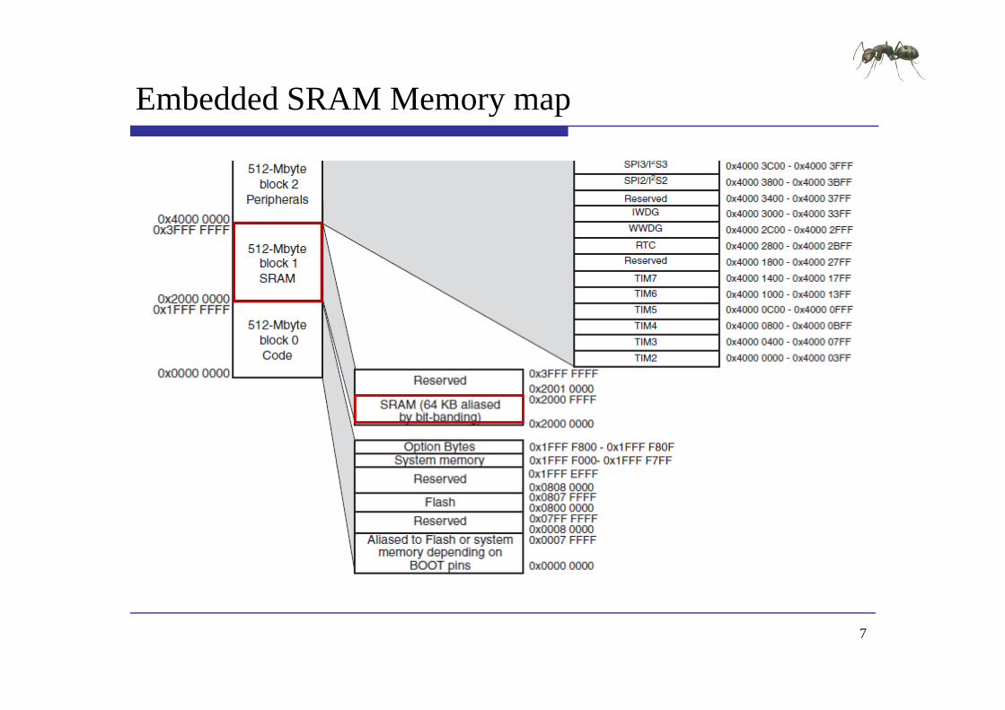

RVMDK環境設定
STMF103ZC有48K Bytes的SRAM位置由0x20000000至0x2000C000
8
External SRAM (IS61LV25616AL)( )
Features Hi h d i 10 High-speed access time 10 ns 256K x 16
9
FUNCTIONAL BLOCK DIAGRAM
10
PIN DESCRIPTIONS
11
READ CYCLE
12
READ CYCLE SWITCHING CHARACTERISTICS
13
WRITE CYCLE
14
WRITE CYCLE SWITCHING CHARACTERISTICS
15
FSMC
Features I f i h i d d i Interfaces with static memory-mapped devices
including Static random access memor (SRAM) Static random access memory (SRAM) Read-only memory (ROM) NOR Fl h NOR Flash memory PSRAM (4 memory banks)8- or 16-bit wide databus
8 16 bit id d t b 8- or 16-bit wide databus Independent chip select control for each memory bank
I d d fi i f h b k Independent configuration for each memory bank
16
FSMC
Programmable timings to support a wide range of devices in particulardevices in particular Programmable wait states (up to 15) Programmable b s t rnaro nd c cles ( p to 15) Programmable bus turnaround cycles (up to 15) Programmable output enable and write enable delays
(up to 15)(up to 15) Independent read and write timings and protocol so
as to support the widest variety of memories andas to support the widest variety of memories and timings
17
NORPSRAM address mappingpp g
NORPSRAM bank selection
External memory address
18
External memory interface signalsy g
19
NOR FlashPSRAM controller timing diagramsg g
read accesses
20
NOR FlashPSRAM controller timing diagramsg g
write accesses
21
FSMC Memory mapy p
22
Development Flowp
Embedded Software Side
int main(void)
Bootup STM32F10x
ProgrammingBootupSTM32F10x RCC Configure
NVIC Configure
int main(void)ifdef DEBUGdebug()
endif
FSMC SRAM Init
System Clocks Configuration RCC_Configuration()
NVIC Configuration
GPIO Configure
gNVIC_Configuration()
GPIO Configuration GPIO_Configuration()
GPIO Configure
FSMC Configure
Writeread tofrom FSMC SRAM memory
Configure FSMC Bank1 NORSRAM1 FSMC_SRAM_Init()
SRAM memory RW operation FSMC SRAM WriteBuffer
FSMC SRAM ReadBuffer
helliphelliphelliphelliphelliphelliphelliphelliphelliphelliphelliphelliphelliphelliphelliphelliphelliphelliphelliphelliphelliphelliphellipCheck content
Display Result
23
Configure FSMC IOg
Function name Description
RCC_APB2PeriphClockCmd(RCC_APB2Periph_GPIOD | RCC_APB2Periph_GPIOG | RCC_APB2Periph_GPIOE | RCC_APB2Periph_GPIOF ENABLE)
‐‐ GPIO Configuration ‐‐‐‐‐‐‐‐‐‐‐‐‐‐‐‐‐‐‐‐‐‐‐‐‐‐‐‐‐‐‐‐‐‐‐‐‐‐‐‐‐‐‐‐‐‐‐‐‐
GPIO FwLib Functions List
Function name Description
RCC_APB2PeriphClockCmd
Enables or disables the High Speed APB (APB2) peripheralclock
GPIO I it I iti li th GPIO
GPIO Configuration SRAM Data lines configuration GPIO_InitStructureGPIO_Pin = GPIO_Pin_0 | GPIO_Pin_1 | GPIO_Pin_8 |
GPIO_Pin_9 | GPIO_Pin_10 | GPIO_Pin_14 | GPIO_Pin_15GPIO_InitStructureGPIO_Mode = GPIO_Mode_AF_PPGPIO_InitStructureGPIO_Speed = GPIO_Speed_50MHzGPIO_Init(GPIOD ampGPIO_InitStructure) GPIO_Init Initializes the GPIOx
peripheral according to the specified parametersin the GPIO_InitStruct
RCC AHBPeriphClock Enables or disables the AHB
_ ( _ )GPIO_InitStructureGPIO_Pin = GPIO_Pin_7 | GPIO_Pin_8 | GPIO_Pin_9 |
GPIO_Pin_10 | GPIO_Pin_11 | GPIO_Pin_12 | GPIO_Pin_13 | GPIO_Pin_14 | GPIO_Pin_15
GPIO_Init(GPIOE ampGPIO_InitStructure) SRAM Address lines configuration GPIO_InitStructureGPIO_Pin = GPIO_Pin_0 | GPIO_Pin_1 | GPIO_Pin_2 |
| | | | |RCC_AHBPeriphClockCmd
Enables or disables the AHB peripheral clock
GPIO_Pin_3 | GPIO_Pin_4 | GPIO_Pin_5 | GPIO_Pin_12 | GPIO_Pin_13 | GPIO_Pin_14 | GPIO_Pin_15
GPIO_Init(GPIOF ampGPIO_InitStructure) GPIO_InitStructureGPIO_Pin = GPIO_Pin_0 | GPIO_Pin_1 | GPIO_Pin_2 |
GPIO_Pin_3 | GPIO_Pin_4 | GPIO_Pin_5GPIO_Init(GPIOG ampGPIO_InitStructure)GPIO InitStructure GPIO Pin GPIO Pin 11 | GPIO Pin 12 | GPIO Pin 13 GPIO_InitStructureGPIO_Pin = GPIO_Pin_11 | GPIO_Pin_12 | GPIO_Pin_13 GPIO_Init(GPIOD ampGPIO_InitStructure) NOE and NWE configuration GPIO_InitStructureGPIO_Pin = GPIO_Pin_4 |GPIO_Pin_5GPIO_Init(GPIOD ampGPIO_InitStructure) NE1configuration GPIO InitStructure GPIO Pin = GPIO Pin 7 GPIO_InitStructureGPIO_Pin = GPIO_Pin_7 GPIO_Init(GPIOD ampGPIO_InitStructure) NBL0 NBL1 configuration GPIO_InitStructureGPIO_Pin = GPIO_Pin_0 | GPIO_Pin_1 GPIO_Init(GPIOE ampGPIO_InitStructure) Enable the FSMC Clock RCC_AHBPeriphClockCmd(RCC_AHBPeriph_FSMC ENABLE)
24
_ p ( _ p _ )
Configure FSMCg
Function name Description
Enable the FSMC Clock RCC_AHBPeriphClockCmd(RCC_AHBPeriph_FSMC ENABLE)
‐‐ FSMC Configuration ‐‐
FSMC FwLib Functions List
Function name Description
RCC_AHBPeriphClockCmd
Enables or disables the AHB peripheral clock
FSMC_NORSRAMInit Initializes the FSMC NOR b k di t th
FSMC Configuration pFSMC_AddressSetupTime = 0pFSMC_AddressHoldTime = 0pFSMC_DataSetupTime = 2pFSMC_BusTurnAroundDuration = 0pFSMC_CLKDivision = 0pFSMC_DataLatency = 0memory bank according to the
parameters specified in FSMC_NORInitStruct
FSMC_NORSRAMCm Enables or disables the NORSRAM memory bank1
p _ y pFSMC_AccessMode = FSMC_AccessMode_AFSMC_NORSRAMInitStructureFSMC_Bank = FSMC_Bank1_NORSRAM1FSMC_NORSRAMInitStructureFSMC_DataAddressMux =
FSMC_DataAddressMux_DisableFSMC_NORSRAMInitStructureFSMC_MemoryType = FSMC_MemoryType_SRAMFSMC_NORSRAMInitStructureFSMC_MemoryDataWidth = FSMC_MemoryDataWidth_16bNORSRAM memory bank1 FSMC_NORSRAMInitStructureFSMC_BurstAccessMode =
FSMC_BurstAccessMode_DisableFSMC_NORSRAMInitStructureFSMC_WaitSignalPolarity =
FSMC_WaitSignalPolarity_LowFSMC_NORSRAMInitStructureFSMC_WrapMode = FSMC_WrapMode_DisableFSMC_NORSRAMInitStructureFSMC_WaitSignalActive =
FSMC WaitSignalActive BeforeWaitStateFSMC_WaitSignalActive_BeforeWaitStateFSMC_NORSRAMInitStructureFSMC_WriteOperation =
FSMC_WriteOperation_EnableFSMC_NORSRAMInitStructureFSMC_WaitSignal = FSMC_WaitSignal_DisableFSMC_NORSRAMInitStructureFSMC_ExtendedMode = FSMC_ExtendedMode_DisableFSMC_NORSRAMInitStructureFSMC_AsyncWait = FSMC_AsyncWait_DisableFSMC NORSRAMInitStructure FSMC WriteBurst = FSMC WriteBurst DisableFSMC_NORSRAMInitStructureFSMC_WriteBurst = FSMC_WriteBurst_DisableFSMC_NORSRAMInitStructureFSMC_ReadWriteTimingStruct = amppFSMC_NORSRAMInitStructureFSMC_WriteTimingStruct = amppFSMC_NORSRAMInit(ampFSMC_NORSRAMInitStructure)
Enable FSMC Bank1_SRAM Bank FSMC_NORSRAMCmd(FSMC_Bank1_NORSRAM1 ENABLE)
25
_ ( _ _ )
硬體電路配置
Mapping Table
Num SRAM STM32 Num SRAM STM32 Num SRAM STM32
1 A0 FSMC_A0 14 A13 FSMC_A13 27 IO8 FSMC_D82 A1 FSMC A1 15 A14 FSMC A14 28 IO9 FSMC D9_ _ _3 A2 FSMC_A2 16 A15 FSMC_A15 29 IO10 FSMC_D104 A3 FSMC_A3 17 A16 FSMC_A16 30 IO11 FSMC_D115 A4 FSMC_A4 18 A17 FSMC_A17 31 IO12 FSMC_D126 A5 FSMC_A5 19 IO0 FSMC_D0 32 IO13 FSMC_D137 A6 FSMC_A6 20 IO1 FSMC_D1 33 IO14 FSMC_D148 A7 FSMC_A7 21 IO2 FSMC_D2 34 IO15 FSMC_D159 A8 FSMC A8 22 IO3 FSMC D3 35 CE FSMC nNE19 A8 FSMC_A8 22 IO3 FSMC_D3 35 CE FSMC_nNE110 A9 FSMC_A9 23 IO4 FSMC_D4 36 OE FSMC_nOE11 A10 FSMC_A10 24 IO5 FSMC_D5 37 WE FSMC_nWE12 A11 FSMC A11 25 IO6 FSMC D6 38 UB FSMC NBL1_ _ _13 A12 FSMC_A12 26 IO7 FSMC_D7 39 LB FSMC_NBL0
26
實驗步驟
範例目錄架構
範例說明 範例說明
預設定義說明
燒錄 燒錄MIAT_STM32
27
範例目錄架構
範例目錄
測試映像檔 測試映像檔
含括檔
函式庫 函式庫
專案檔
原始碼 原始碼
28
範例說明
Embedded Software Side
Write data to FSMC SRAM memory
SRAM memory RW operation
Write data to FSMC SRAM memory Fill the buffer to send Fill_Buffer(TxBuffer BUFFER_SIZE 0x3212)FSMC_SRAM_WriteBuffer(TxBuffer WRITE_READ_ADDR BUFFER_SIZE)
SRAM memory RW operation
FSMC SRAM WriteBuffer
Read data from FSMC SRAM memory FSMC_SRAM_ReadBuffer(RxBuffer WRITE_READ_ADDR BUFFER_SIZE)
Read back SRAM memory and check content correctness
FSMC SRAM ReadBuffer
Check content
Display Result yfor (Index = 0x00 (Index lt BUFFER_SIZE) ampamp (WriteReadStatus == 0)
Index++)if (RxBuffer[Index] = TxBuffer[Index])
Display Result
WriteReadStatus = Index + 1
29
範例說明
Embedded Software Side
while (1)
Display Result
while (1)if (WriteReadStatus == 0) OK Turn on USERLED
GPIO SetBits(GPIOF GPIO Pin 11)
SRAM memory RW operation
FSMC SRAM WriteBufferGPIO_SetBits(GPIOF GPIO_Pin_11)
else KO Turn off USERLED
GPIO ResetBits(GPIOF GPIO Pin 11)
FSMC SRAM ReadBuffer
Check content
Display Result
如果寫入與讀取Buffer內容相同外部記憶體使用正常USERLED紅燈GPIO_ResetBits(GPIOF GPIO_Pin_11)
Insert delay Delay(0xAFFFF) Turn on USERLED GPIO SetBits(GPIOF GPIO Pin 11)
Display Result恆亮
GPIO_SetBits(GPIOF GPIO_Pin_11) Insert delay Delay(0xAFFFF)
如果寫入與讀取Buffer內容不同外部記憶體使用異常 USERLED紅燈閃爍
30
預設定義說明
define Bank1_SRAM1_ADDR ((u32)0x60000000) 定義SRAM起始點 定義SRAM起始點
define BUFFER_SIZE 0x400定義測試資料大小 定義測試資料大小
資料大小必需小於0xC000 define WRITE_READ_ADDR 0x8000 定義SRAM寫入起始點
寫入起始點WRITE_READ_ADDR + BUFFER_SIZE必需小於0x6000C000
31
燒錄MIAT STM32_
Rebuilder all target files產生HEX DFU Fil M 轉換HEX產生DFU DFU File Manager轉換HEX產生DFU DfuSe Demonstration燒錄DFU d Leave DFU mode
32
內部與外部SRAM存取控制實驗
實驗一
WU-YANGTechnology Co Ltd
實驗一練習
練習 修改寫入位置測試是否正常 修改寫入位置測試是否正常
修改寫入資料大小測試是否正常
取消 i 測試是否正常 取消FSMC_SRAM_Init測試是否正常
34
實驗目的(二)( )
使用MIAT_STM32實驗板透過FSMC控制外部SRAM並設定為data memory進行存取控制實驗同樣利用LED設定為data memory進行存取控制實驗同樣利用LED確認存取是否正常
35
實驗原理
External SRAM RVMDK環境設定 RVMDK環境設定
Development Flow fi ARM Configure Startup Code
36
RVMDK環境設定
外部SRAM有512K Bytes位置由0x60000000至0x60080000
37
Development Flowp
Embedded Software Side
int main(void)
Bootup STM32F10x
Programming
Bootup
int main(void)ifdef DEBUGdebug()
endif
Startup Code
BootupSTM32F10x
RCC Configure
NVIC Configure
System Clocks Configuration RCC_Configuration()
NVIC Configuration g gNVIC_Configuration()
GPIO Configuration GPIO_Configuration()
GPIO Configure
for (Index = 0 Index lt1024 Index++)
Tab[Index] =IndexT bAdd ( 32)T b h ld b 0 600000
Check operation
Check pointer value
Display Result TabAddr = (u32)Tab should be 0x600000xx
Get main stack pointer value MSPValue = __MRS_MSP() should be 0x2000xxxx
helliphelliphelliphelliphelliphelliphelliphelliphelliphelliphelliphelliphelliphelliphelliphelliphelliphelliphelliphelliphelliphelliphellip
Display Result
38
Startup Codep
Register boundary addresses RCC Configure
Enable FSMC clock
LDR R0= 0x00000114
LDR R1= 0x40021014
STR R0[R1]
Enable GPIOD GPIOE GPIOF and GPIOG clocks
LDR R0= 0x000001E0
LDR R1= 0x40021018
RCC register map
STR R0[R1]
39
RCC Register g
Bit 8 FSMCEN FSMC clock enableAHB Peripheral Clock enable register (RCC_AHBENR)
Bit 8 FSMCEN FSMC clock enableSet and cleared by software0 FSMC clock disabled
APB2 peripheral clock enable register (RCC_APB2ENR)
1 FSMC clock enabled
Bit 8765 IOPGEN IO port GFED clock enableSet and cleared by software0 IO port GFED clock disabled1 IO port GFED clock enabled
40
1 IO port GFED clock enabled
Startup Codep
Register boundary addresses GPIO Configure
SRAM Data lines NOE and NWE configuration SRAM Address lines configuration NOE NEW NE1 NBL0 NBL1 configuration LDR R0= 0xB4BB44BB LDR R1= 0x40011400STR R0[R1]LDR R0= 0xBBBBBBBB LDR R1= 0x40011404STR R0[R1]LDR R0 = 0xB44444BBLDR R0= 0xB44444BB LDR R1= 0x40011800STR R0[R1]LDR R0= 0xBBBBBBBB LDR R1= 0x40011804
GPIO register map
STR R0[R1]LDR R0= 0x44BBBBBB LDR R1= 0x40011C00STR R0[R1]LDR R0= 0xBBBB4444 LDR R1= 0x40011C04STR R0[R1]LDR R0= 0x44BBBBBBLDR R1= 0x40012000STR R0 [R1]
41
STR R0[R1]
GPIO Register g
Bit 8 FSMCEN FSMC clock enablePort configuration register low
Port configuration register high
Bits 2928 2524Bits 3130 2726 2322 1918 1514 1110 76 32 Bits 2928 25242120 1716 131298 54 10MODEy[10] Port x mode bits (y= 0 15)00 Input mode (reset state)01 Output mode max speed 10 MHz
Bits 3130 27262322 1918 15141110 76 32CNFy[10] Port x configuration bits (y= 0 15)In input mode (MODE[10]=00)00 Analog input mode01 Floating input (reset state)10 Input with pull-up pull-down
10 Output mode max speed 2 MHz11 Output mode max speed 50 MHz
11 ReservedIn output mode (MODE[10] gt00)00 General purpose output push-pull01 General purpose output Open-drain10 Alternate function output Push-pull11 Alternate function output Open-drain
42
11 Alternate function output Open drain
Startup Codep
FSMCregister map FSMC Configure
FSMC Configuration Enable FSMC Bank1_SRAM Bank
LDR R0= 0x00001011
LDR R1= 0xA0000000
STR R0[R1]
LDR R0= 0x00000200
LDR R1= 0xA0000004
STR R0[R1]
43
FSMC Register g
Bit 8 FSMCEN FSMC clock enableSRAMNOR-Flash chip-select control registers 1 (FSMC_BCR1)
Bit 12 WREN Write enable bitThis bit indicates whether write operations are enableddisabled in the bank by the FSMC0 Write operations are disabled in the bank by the FSMC an AHB error is reported1 Write operations are enabled for the bank by the FSMC (default after reset) p y ( )Bits 54 MWID Memory databus widthDefines the external memory device width valid for all type of memories00 8 bits01 16 bits (default after reset)10 reserved do not use10 reserved do not use11 reserved do not use Bit 0 MBKEN Memory bank enable bitEnables the memory bank After reset Bank1 is enabled all others are disabled Accessing adisabled bank causes an ERROR on AHB bus0 C di b k i di bl d0 Corresponding memory bank is disabled1 Corresponding memory bank is enabled
44
FSMC Register g
Bit 8 FSMCEN FSMC clock enableSRAMNOR-Flash chip-select timing registers 1 (FSMC_BTR1)
Bits 158 DATAST Data-phase duration0000 0000 Reserved0000 0001 DATAST phase duration = 2 times HCLK clock cycles0000 0010 DATAST phase duration = 3 times HCLK clock cycles1111 1111 DATAST phase duration = 256 times HCLK clock cycles (default value after reset)Bits 74 ADDHLD Address-hold phase duration0000 Reserved0001 ADDHLD phase duration = 2 times HCLK clock cycle0010 ADDHLD phase duration = 3 times HCLK clock cycle1111 ADDHLD phase duration = 16 times HCLK clock cycles (default value after reset)Bits 30 ADDSET Address setup phase durationThese bits are written by software to define the duration of the address setup phase (refer toFigure 162 to Figure 172) used in SRAMs ROMs and asynchronous NOR Flash0000 ADDSET phase duration = 1 times HCLK clock cycle1111 ADDSET phase duration = 16 times HCLK clock cycles (default value after reset)
45
實驗步驟
範例目錄架構
範例說明 範例說明
預設定義說明
46
範例目錄架構
範例目錄
測試映像檔 測試映像檔
含括檔
函式庫 函式庫
專案檔
原始碼 原始碼
47
範例說明
Embedded Software Side
Infinite loop
Display Result
Infinite loop while (1)if (((TabAddramp0xFFFFFF00) == 0x60000000) ampamp
((MSPValueamp0xFFFF0000) == 0x20000000))
Check operation
Check pointer value((MSPValueamp0xFFFF0000) == 0x20000000))
OK Turn on USERLED GPIO_SetBits(GPIOF GPIO_Pin_11)
else
Display Result
else KO Turn off USERLED
GPIO_ResetBits(GPIOF GPIO_Pin_11) Insert delay Delay(0xAFFFF)
如果Tab位置在0x600000且Stack pointer位置在0x2000 外部記憶體使用正常USERLED紅燈恆亮Delay(0xAFFFF)
Turn on USERLED GPIO_SetBits(GPIOF GPIO_Pin_11) Insert delay Delay(0xAFFFF)
紅燈恆亮
如果 b位置不在0 600000或Delay(0xAFFFF)
如果Tab位置不在0x600000或Stack pointer位置不在0x2000 外部記憶體使用異常USERLED紅燈閃爍
48
預設定義說明
DATA_IN_ExtSRAM EQU 1 E l SRAM C fi i External SRAM Configuration 0=gt DISABLE 1=gt ENABLE
u32 Tab[1024]宣告於外部 的記憶體 宣告於外部SRAM的記憶體
49
data memory存取控制實驗
實驗二
WU-YANGTechnology Co Ltd
實驗二練習
練習 取消RVMDK環境外部SRAM設定測試是否正常 取消RVMDK環境外部SRAM設定測試是否正常
修改DATA_IN_ExtSRAM EQU 0測試是否正常
修改外部 記憶體 b變數大小測試是否正常 修改外部SRAM記憶體Tab變數大小測試是否正常
51
Q amp A
WU-YANGTechnology Co Ltd
MIAT_STM32內部Flash存取控制實驗
WU-YANG
浯陽科技有限公司
Technology Co Ltd
Declared Version
Training Only
Declare
Document Number
Document Version 100
Release Date
Document Title MIAT_STM32 內部FLASH存取控制實驗
Exercise Time
Platform MIAT_STM32V2MIAT IOB V1PlatformMIAT IOBV1
Peripheral
Author WU-YANG Technology Co Ltd
2
實驗目的(一)( )
使用MIAT_STM32實驗板透過Flash memory interface (FLITF)控制內部Flash進行存取控制實驗並利用LED(FLITF)控制內部Flash進行存取控制實驗並利用LED確認存取是否正常
3
實驗原理
System architecture E b dd d Fl h Embedded Flash Features Memory map RVMDK環境設定
FLITF Flash module organization
Flash library function Development Flow ARM Configure
4
System architecturey
5
Embedded Flash
Features 256 Kb up to 256 Kbytes Memory organization the Flash memory is organized as a
main block and an information blockmain block and an information block Main memory block of size t 32 Kb 64 bit di id d i t 128 f 2 up to 32 Kb times 64 bits divided into 128 pages of 2
Kbytes Information block of size Information block of size 258 times 64 bits
6
Embedded Flash Memory mapy p
7
Flash Memoryy
8
RVMDK環境設定
STMF103ZC有256K Bytes的Flash位置由0x8000000至0x8040000
9
FLITF
Features R d i f i h f h b ff (2 64 bi d ) Read interface with prefetch buffer (2x64-bit words) Option byte Loader
l h i Flash Program Erase operation Read Write protection
10
Flash memory interfacey
11
Flash memory interface registery g
Bit 8 FSMCEN FSMC clock enableFlash status register (FLASH_SR)
Bits 316 Reserved must be kept clearedBit 5 EOP End of operation
Bit 2 PGERR Programming errorSet by hardware when an address to be programmed p
Set by hardware when a Flash operation (programming erase) is completed Reset by writing a 1Note EOP is asserted at the end of each successful
y p gcontains a value different from 0xFFFF before programmingReset by writing 1Note The STRT bit in the FLASH_CR register f f
program or erase operationBit 4 WRPRTERR Write protection errorSet by hardware when programming a write-protected address of the Flash memory
_ gshould be reset before starting a programmingoperationBit 1 Reserved must be kept clearedBit 0 BSY Busyp y
Reset by writing 1Bit 3 Reserved must be kept cleared
This indicates that a Flash operation is in progress This is set on the beginning of a Flash operation and reset when the operation finishes or when an error occurs
12
Flash memory interface registery g
Flash control register (FLASH_CR)
Bit 9 OPTWRE Option bytes write enableWhen set the option bytes can be programmed This
Bit 6 STRT StartThis bit triggers an ERASE operation when set This bit is set only
bit is set on writing the correct key sequence to the FLASH_OPTKEYR registerThis bit can be reset by softwareBit 8 Reserved must be kept clearedBit 7 LOCK Lock
by software and reset when the BSY bit is resetBit 5 OPTER Option byte eraseOption byte erase chosenBit 4 OPTPG Option byte programmingOption byte programming chosenBit 7 LOCK Lock
Write to 1 only When it is set it indicates that the FPEC and FLASH_CR are locked This bit is reset by hardware after detecting the unlock sequenceIn the event of unsuccessful unlock operation this bit remains set until the next reset
p y p g gBit 3 Reserved must be kept clearedBit 2 MER Mass eraseErase of all user pages chosenBit 1 PER Page erasePage Erase chosenremains set until the next reset Page Erase chosenBit 0 PG ProgrammingFlash programming chosen
13
Main Flash memory programmingy p g g
14
Flash memory Page Erasey g
15
Flash memory Mass Erasey
16
Option byte programmingp y p g g
17
Option byte Erasep y
18
FLASH library functiony
19
FLASH library functiony
20
Development Flowp
Embedded Software Side
int main(void)
Bootup STM32F10x
ProgrammingBootupSTM32F10x RCC Configure
NVIC Configure
int main(void)ifdef DEBUGdebug()
endifendif
FLASHStatus = FLASH_COMPLETEMemoryProgramStatus = PASSEDData = 0x15041975
GPIO Configure
Data = 0x15041975
RCC Configuration RCC_Configuration()
Flash memory RW operation FLASH Unlock
FLASH ClearFlag NVIC Configuration NVIC_Configuration()
GPIO Configuration
FLASH ClearFlag
FLASH ErasePage
FLASH ProgramWord GPIO Configuration GPIO_Configuration()
helliphelliphelliphelliphelliphelliphelliphelliphelliphelliphelliphelliphelliphelliphelliphelliphellipDisplay Result
Check content
21
實驗步驟
範例目錄架構
範例說明 範例說明
預設定義說明
燒錄 燒錄MIAT_STM32
22
範例目錄架構
範例目錄
測試映像檔 測試映像檔
含括檔
函式庫 函式庫
專案檔
原始碼 原始碼
23
範例說明
Function name Description
Unlock the Flash Program Erase controller FLASH_Unlock()
D fi h b f b d
Flash FwLib Functions List
Function name Description
FLASH_Unlock Unlocks the FLASH Program Erase Controller
FLASH_ClearFlag Clears the FLASH pending fl
Define the number of page to be erased NbrOfPage = (EndAddr - StartAddr) FLASH_PAGE_SIZE
Clear All pending flags FLASH_ClearFlag(FLASH_FLAG_BSY | FLASH_FLAG_EOP | FLASH_FLAG_PGERR |
FLASH FLAG WRPRTERR)flags
FLASH_ErasePage Erases a specified FLASH page
FLASH_ProgramWord Programs a word at a specified
_ _ )
Erase the FLASH pages for(EraseCounter = 0 (EraseCounter lt NbrOfPage) ampamp (FLASHStatus ==
FLASH_COMPLETE) EraseCounter++)FLASHStatus = FLASH ErasePage(StartAddr + (FLASH PAGE SIZE EraseCounter))address FLASHStatus = FLASH_ErasePage(StartAddr + (FLASH_PAGE_SIZE EraseCounter))
FLASH Word program of data 0x15041979 at addresses defined by StartAddr and EndAddrAddress = StartAddr
while((Address lt EndAddr) ampamp (FLASHStatus == FLASH_COMPLETE))FLASHStatus = FLASH_ProgramWord(Address Data)Address = Address + 4
24
範例說明
Embedded Software Side
Check the corectness of written data
Display Result
Check the corectness of written data Address = StartAddr
while((Address lt EndAddr) ampamp (MemoryProgramStatus = FAILED))if(((vu32) Address) = Data)
Flash memory RW operation
MemoryProgramStatus = FAILED
Address += 4
Check content
Display Result while (1)if (MemoryProgramStatus == PASSED) OK Turn on USERLED GPIO_SetBits(GPIOF GPIO_Pin_11)
Display Result
else KO Turn off USERLED GPIO_ResetBits(GPIOF GPIO_Pin_11) Insert delay Delay(0xAFFFF)
如果寫入與讀取Flash內容相同Flash記憶體使用正常USERLED紅燈恆亮
Turn on USERLED GPIO_SetBits(GPIOF GPIO_Pin_11) Insert delay Delay(0xAFFFF)
如果寫入與讀取Flash內容不同Flash記憶體使用異常USERLED紅燈閃爍
25
預設定義說明
define StartAddr ((u32)0x08008000) 定義Flash使用起始點 定義Flash使用起始點
使用起始點必需大於0x8003000 + Code Size 附註 0x8000000~0x8003000為DFU程式區塊使用此區塊
將造成無法燒錄程式
Code Size可由產生的HEX檔得知
d fi E dAdd (( 32)0 0800C000) define EndAddr ((u32)0x0800C000) 定義Flash使用結束點
使用起始點必需小於0x8040000使用起始點必需小於
Data = 0x15041975 寫入資料
32Bit define FLASH_PAGE_SIZE ((u16)0x800)
每一個Page有2KByte26
每一個Page有2KByte
Intel HEX Format
aaaa tt dd cc
field Description
the colon that starts every Intel HEX record
the record-length field that represents the number of data bytes (dd) in the record
aaaa the address field that represents the starting address for subsequent data in the record
tt the field that represents the HEX record type which may be one of the following00 - data record01 - end-of-file record02 - extended segment address recordg04 - extended linear address record
dd a data field that represents one byte of data A record may have multiple data bytes The number of data bytes in the record must match the number specified by the field
cc the checksum field that represents the checksum of the record The checksum is calculated by summing the values of all hexadecimal digit pairs in the record modulo 256 and taking the twos complement
27
HEX Examplep
020000040800F2103000001814002045310008D9340008CD340008D8103000001814002045310008D9340008CD340008D8helliphelliphellip1038200042370008000000000000000000000000170C3830000000000000000000000000008C
資料填入起始位置為
0C3830000000000000000000000000008C04000005080031318D00000001FF
資料填入起始位置為0x08003000 每一行有0x10(16)個Bytes 最後一筆資料為
資料結束點為0x0803383004000005080031318D
(0x08003830 -0x08000000)0x800 = 7 需以0x800為單位所以使用的位置起點為0x08004000
28
燒錄MIAT STM32_
Rebuilder all target files產生HEX DFU Fil M 轉換HEX產生DFU DFU File Manager轉換HEX產生DFU DfuSe Demonstration燒錄DFU d Leave DFU mode
29
內部Flash存取控制實驗
實驗一
WU-YANGTechnology Co Ltd
實驗一練習
注意 請使用預設0 08008000之後的位置 避免覆蓋DFU 請使用預設0x08008000之後的位置避免覆蓋DFU
與使用者程式碼區塊
練習 練習 修改存取位置測試是否正常
修改寫入資料測試是否正常 修改寫入資料測試是否正常
修改寫入資料後取消FLASH_Unlock測試是否正常
修改寫入資料後取消FLASH E P 測試是否正 修改寫入資料後取消FLASH_ErasePage測試是否正常
31
實驗目的(二)( )
使用MIAT_STM32實驗板透過Flash memory interface (FLITF)控制內部Flash進行存取控制實驗並利用SW(FLITF)控制內部Flash進行存取控制實驗並利用SWKEY決定資料寫入與讀取LCD顯示狀態
32
實驗原理
System requirement E b dd d Fl h Embedded Flash LCD KEY SW
Development Flow ARM Configure
33
Development Flowp
Embedded Software Side
int main(void)
Bootup STM32F10x
ProgrammingBootupSTM32F10x RCC Configure
NVIC Configure
int main(void)ifdef DEBUGdebug()
endif
FLASHStatus = FLASH_COMPLETE
RCC Configuration RCC Configuration()
GPIO Configure
BasicIO Configure_ g ()
NVIC Configuration NVIC_Configuration()
GPIO Configuration Flash memory RW ti
lcd Configure
GPIO Configuration GPIO_Configuration()
Init_BasicIO()
l d i i () LCD I i i li i
RW operation
Example
FLASH Unlock
FLASH ClearFlag
lcd_init() LCD Initialization
helliphelliphelliphelliphelliphelliphelliphelliphelliphelliphelliphelliphelliphelliphelliphelliphelliphelliphelliphelliphelliphelliphellip
p
34
硬體電路配置
Mapping Table
Num MIAT_STM32V2 MIAT_IOBV1 Num MIAT_STM32V2 MIAT_IOBV1
1 PC8 (326) SW1 10 PE6 (15) LCD_EN2 PC9 (327) SW2 11 PF6 (118) LCD RW ( ) ( ) _3 PC10 (43) SW3 12 PF7 (119) LCD_RS 4 PC11 (44) SW4 13 PF8(120) LCD_D4 5 PB5 (427) KEY1 14 PF9 (121) LCD_D5 6 PB6 (428) KEY2 15 PF10 (122) LCD_D6 7 PB7 (429) KEY3 16 PF11 (213) LCD_D7 8 PB8 (431) KEY4 17 VDD (236) VCC33V 9 VCC5V (1 36) VCC5V 18 GND (1 35) GND9 VCC5V (136) VCC5V 18 GND (135) GND
35
實驗步驟
範例目錄架構
範例說明 範例說明
預設定義說明
36
範例目錄架構
範例目錄
測試映像檔 測試映像檔
含括檔
函式庫 函式庫
專案檔
原始碼 原始碼
37
範例說明
Embedded Software Side
lcd clear()
FLASH memory RW operation
lcd_clear()lcd_print (MIAT_STM32 DEMO )
Unlock the Flash Program Erase controller FLASH_Unlock()
Flash memory RW operation
FLASH Unlock
Clear All pending flags FLASH_ClearFlag(FLASH_FLAG_BSY | FLASH_FLAG_EOP | FLASH_FLAG_PGERR |
FLASH_FLAG_WRPRTERR)
while(1)
Example
FLASH ClearFlag
( )
KEY_Buffer=Key_Scan()set_cursor (0 1)lcd_print (SW Value = 0x)lcd putchar(((SWamp0x7)+0x30))lcd_putchar(((SWamp0x7)+0x30))if(KEY_Buffer==1)Address=(StartAddr|(SWltlt12))set_cursor (0 0)lcd_print (Set Addr = 0x)
掃描KEY是否按下與顯示SW數值LCD Line2顯示SW Value = 0x(SW)
lcd_putchar(((SWamp0x7)+0x30))lcd_print ( )
如果KEY1按下記錄SW數值至Address LCD Line1顯示Set Adde = 0x(Address)
38
範例說明
Embedded Software Side
else if(KEY Buffer==2)
FLASH memory RW operation
else if(KEY_Buffer==2)
Erase the FLASH pages FLASHStatus = FLASH_ErasePage(Address)
FLASH Word program of data at addresses defined by SW
SRAM memory RW operation
p g yFLASHStatus = FLASH_ProgramWord(Address (SWamp0x7))
set_cursor (0 0)lcd_print (Write 0x)lcd_putchar(((SWamp0x7)+0x30))l d i t ( t 0 )
Example如果KEY2按下清除Address所處區塊並寫入SW數值 lcd_print ( at 0x)
lcd_putchar((((Addressgtgt12)amp0x7)+0x30))else if(KEY_Buffer==3)
Data=(u16 )Address
所處區塊並寫入SW數值LCD Line1顯示Write 0x(SW) at 0x(Adddress)
Data (u16 )Addressset_cursor (0 0)lcd_print (Addr 0x)lcd_putchar((((Addressgtgt12)amp0x7)+0x30))lcd_print ( = 0x)lcd_putchar(((Dataamp0x7)+0x30))lcd_print ( )
如果KEY3按下讀取Address紀錄數值LCD Line1顯示Addr 0x(Adddress) = 0x
39
預設定義說明
define StartAddr ((u32)0x08020000) 定義Flash使用起始點 定義Flash使用起始點
使用起始點必需大於0x8003000 + Code Size 附註 0x8000000~0x8003000為DFU程式區塊使用此區塊
將造成無法燒錄程式
Code Size可由產生的HEX檔得知
32 Add 0 08020000 u32 Address = 0x08020000 定義Address初始值
初始值必需與Flash使用起始點相同初始值必需與 使用起始點相同
Address=(StartAddr|(SWltlt12)) Example StartAddr = 0x08020000 SW = 1 Address = 0x08021000
StartAddr = 0x08020000 SW = 7 Address = 0x08027000 StartAddr|(7ltlt12)必需小於0x8040000
40
使用者界面與Flash存取控制實驗
實驗二
WU-YANGTechnology Co Ltd
實驗二練習
注意 請使用預設0 08020000之後的位置 避免覆蓋DFU 請使用預設0x08020000之後的位置避免覆蓋DFU
與使用者程式碼區塊
練習 練習 利用SW與KEY測試Flash寫入與讀取是否正常
Fl h寫入後電源關閉 再開啟後寫入資料是否仍存 Flash寫入後電源關閉再開啟後寫入資料是否仍存在
修改存取位置測試是否正常 修改存取位置測試是否正常
42
實驗目的(三)( )
使用MIAT_STM32實驗板透過Flash memory interface (FLITF)控制內部Flash進行存取控制實驗並藉由填入(FLITF)控制內部Flash進行存取控制實驗並藉由填入Option Bytes 設定寫入鎖定保護Page鎖定不被覆蓋
43
Development Flowp
Embedded Software Side
int main(void)
Bootup STM32F10x
ProgrammingBootupSTM32F10x RCC Configure
NVIC Configure
int main(void)ifdef DEBUGdebug()
endifendif
FLASHStatus = FLASH_COMPLETEMemoryProgramStatus = PASSEDData = 0x1753
GPIO Configure
Data = 0x1753
RCC Configuration RCC_Configuration()
Flash memory RW operation FLASH Unlock
FLASH ClearFlag NVIC Configuration NVIC_Configuration()
GPIO Configuration
FLASH ClearFlag
FLASH ErasePage
FLASH ProgramHalfWord GPIO Configuration GPIO_Configuration()
Display Result
Check content
44
helliphelliphelliphelliphelliphelliphelliphelliphelliphelliphelliphelliphelliphelliphelliphelliphelliphelliphellip
實驗步驟
範例目錄架構
範例說明 範例說明
預設定義說明
45
範例目錄架構
範例目錄
測試映像檔 測試映像檔
含括檔
函式庫 函式庫
專案檔
原始碼 原始碼
46
範例說明
Function name Description
Unlock the Flash Program Erase controller FLASH_Unlock()
Define the number of page to be erased
Flash FwLib Functions List
Function name Description
FLASH_Unlock Unlocks the FLASH Program Erase Controller
FLASH_ClearFlag Clears the FLASH pending fl
Define the number of page to be erased NbrOfPage = (EndAddr ‐ StartAddr) FLASH_PAGE_SIZE
FLASH_ClearFlag(FLASH_FLAG_BSY | FLASH_FLAG_EOP|FLASH_FLAG_PGERR |FLASH_FLAG_WRPRTERR)
Get pages write protection status flags
FLASH_EraseOptionBytes
Erases the FLASH option bytes
FLASH_EnableWritePro Write protects the desired
p g pWRPR_Value = FLASH_GetWriteProtectionOptionByte()ProtectedPages = WRPR_Value amp 0x000000C0
ifdef WriteProtection_Disableif (ProtectedPages == 0x00) Pages are write protected
tection pages
NVIC_GenerateSystemReset
Generate a system reset
Disable the write protection FLASHStatus = FLASH_EraseOptionBytes() Generate System Reset to load the new option byte values NVIC_GenerateSystemReset()
elseifdef WriteProtection Enableifdef WriteProtection_Enableif (ProtectedPages = 0x00) Pages not write protected
FLASHStatus = FLASH_EraseOptionBytes() Enable the pages write protection FLASHStatus = FLASH_EnableWriteProtection(FLASH_WRProt_Pages12to13
|FLASH WRProt Pages14to15)|FLASH_WRProt_Pages14to15) Generate System Reset to load the new option byte values NVIC_GenerateSystemReset()
endifendif
47
範例說明
if (ProtectedPages = 0x00) Clear All pending flags
Flash FwLib Functions List
Function name DescriptionFLASH_ClearFlag(FLASH_FLAG_BSY |
FLASH_FLAG_EOP|FLASH_FLAG_PGERR |FLASH_FLAG_WRPRTERR)
erase the FLASH pages for(EraseCounter = 0 (EraseCounter lt NbrOfPage) ampamp (FLASHStatus ==
Function name Description
FLASH_ErasePage Erases a specified FLASH page
FLASH_ProgramHalfWod
Programs a half word at a ifi d dd FLASH_COMPLETE) EraseCounter++)
FLASHStatus = FLASH_ErasePage(StartAddr + (FLASH_PAGE_SIZE
EraseCounter))
rd specified address
FLASH Half Word program of data 0x1753 at addresses defined by StartAddrand EndAddr
Address = StartAddr
hil ((Add E dAdd ) ampamp (FLASHSt t FLASH COMPLETE))while((Address lt EndAddr) ampamp (FLASHStatus == FLASH_COMPLETE))
FLASHStatus = FLASH_ProgramHalfWord(Address Data)Address = Address + 2
48
範例說明
Embedded Software Side
Check the corectness of written data
Display Result
Check the corectness of written data Address = StartAddr
while((Address lt EndAddr) ampamp (MemoryProgramStatus = FAILED))if(((vu16) Address) = Data)
Flash memory RW operation
MemoryProgramStatus = FAILED
Address += 2
Check content
Display Result while (1)if (MemoryProgramStatus == PASSED) OK Turn on USERLED GPIO_SetBits(GPIOF GPIO_Pin_11)
Display Result
else KO Turn off USERLED GPIO_ResetBits(GPIOF GPIO_Pin_11) Insert delay Delay(0xAFFFF)
如果寫入與讀取Flash內容相同Flash記憶體可以寫入USERLED紅燈恆亮
Turn on USERLED GPIO_SetBits(GPIOF GPIO_Pin_11) Insert delay Delay(0xAFFFF)
如果寫入與讀取Flash內容不同Flash記憶體不能寫入USERLED紅燈閃爍
49
預設定義說明
define StartAddr ((u32) 0x08006000) 定義Flash使用起始點 定義Flash使用起始點
使用起始點必需大於0x8003000 + Code Size 附註 0x8000000~0x8003000為DFU程式區塊使用此區塊
將造成無法燒錄程式
Code Size可由產生的HEX檔得知
d fi E dAdd (( 32) 0 08008000) define EndAddr ((u32) 0x08008000) 定義Flash使用結束點
使用起始點必需小於0x8040000使用起始點必需小於
Data = 0x1753 寫入資料
16Bit define FLASH_PAGE_SIZE ((u16)0x800) 每一個Page有2KByte
50
每一個Page有2KByte
預設定義說明
define WriteProtection_Enable U hi li E bl W i P i Uncomment this line to Enable Write Protection
define WriteProtection_Disablehi li i bl i i Uncomment this line to Disable Write Protection
FLASH_EnableWriteProtection設定影響 個 設定影響2個Page FLASH_WRProt_Pages0to1 FLASH_WRProt_Pages1to2 helliphellip FLASH_WRProt_Pages60to61
設定影響多個Page FLASH_WRProt_Pages62to255
51
FLASH EnableWriteProtection_
Example
位置0x08006000 ~ 0x08007000每一個Page有0x800ByteStartPage = (0x08006000-0x08000000)0x800 = 12EndPage = ((0x08007000-0x08000000)0x800)-1 = 13執行執行FLASH_EnableWriteProtection(FLASH_WRProt_Pages12to13)將影響Pages12 Pages13
52
內部Flash寫入鎖定存取控制實驗
實驗三
WU-YANGTechnology Co Ltd
實驗三練習
注意 請使用預設0 08006000之後的位置 避免覆蓋DFU 請使用預設0x08006000之後的位置避免覆蓋DFU
與使用者程式碼區塊
更改寫入位置測試寫入鎖定時需同時更改 更改寫入位置測試寫入鎖定時需同時更改FLASH_EnableWriteProtection鎖定之Page
練習 練習 打開define WriteProtection_Enable測試是否可寫入
打開define WriteProtection Disable測試是否可寫入 打開define WriteProtection_Disable測試是否可寫入
修改存取位置測試是否正常
修改寫入資料測試是否正常 修改寫入資料測試是否正常
54
Q amp A
WU-YANGTechnology Co Ltd
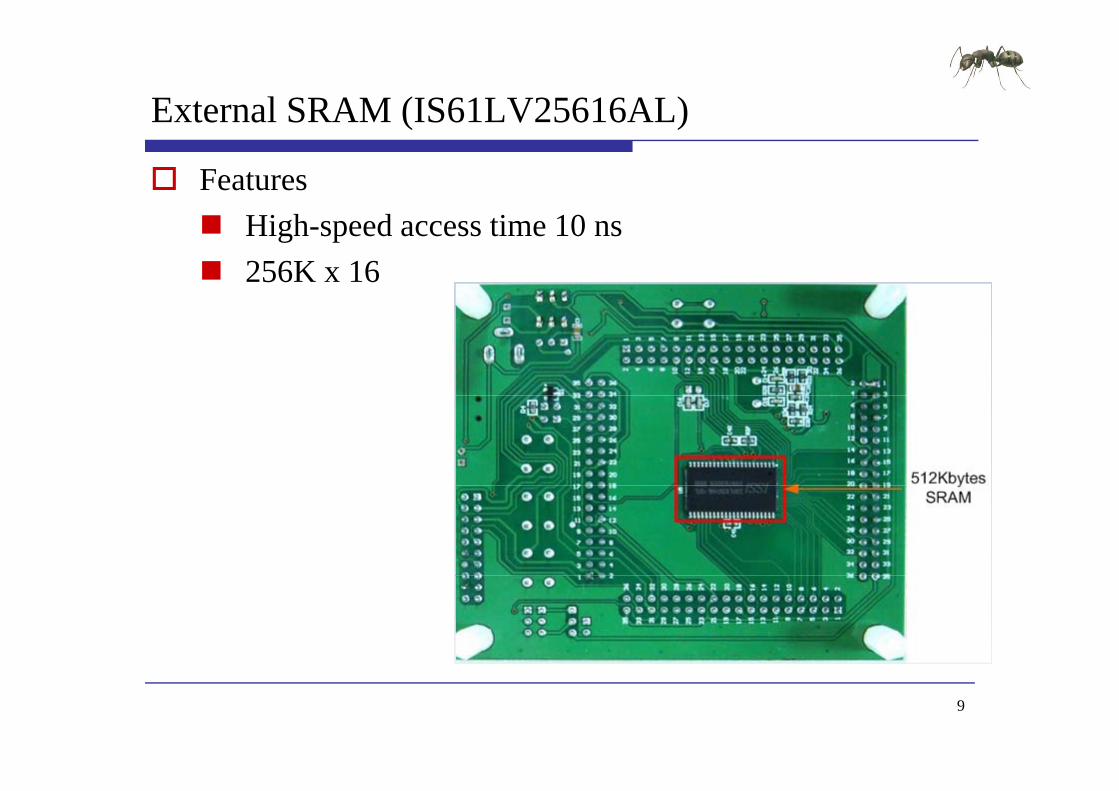
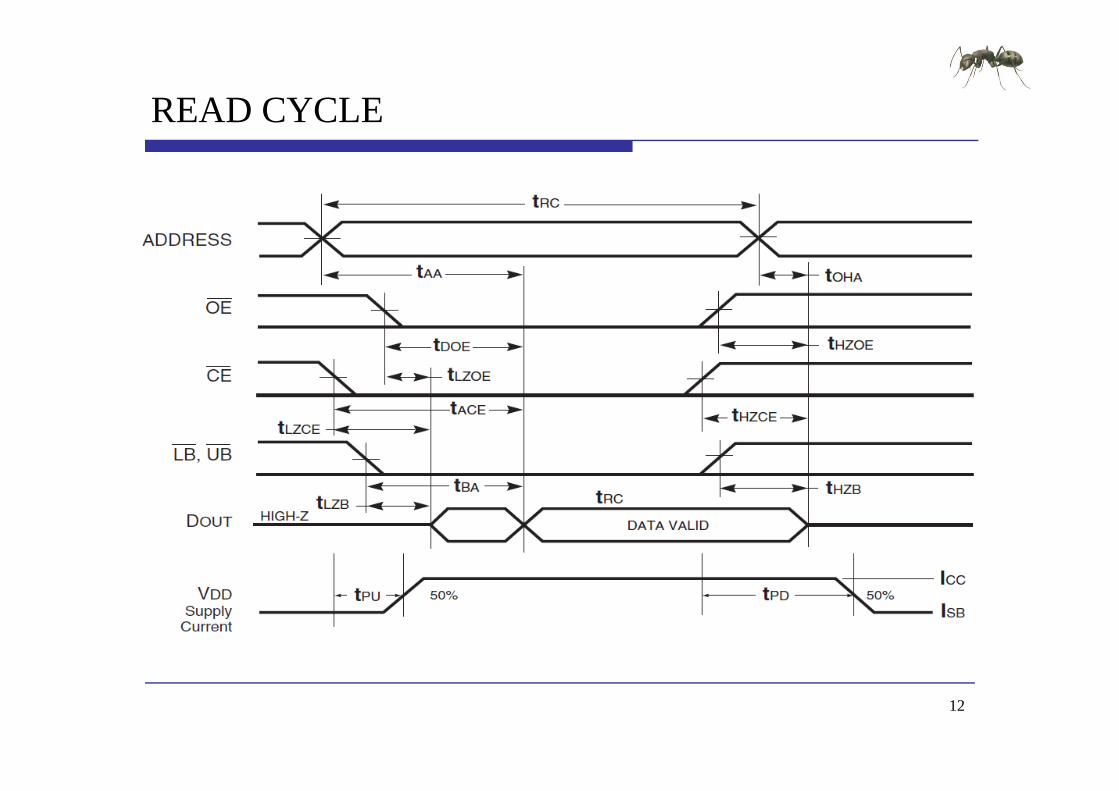
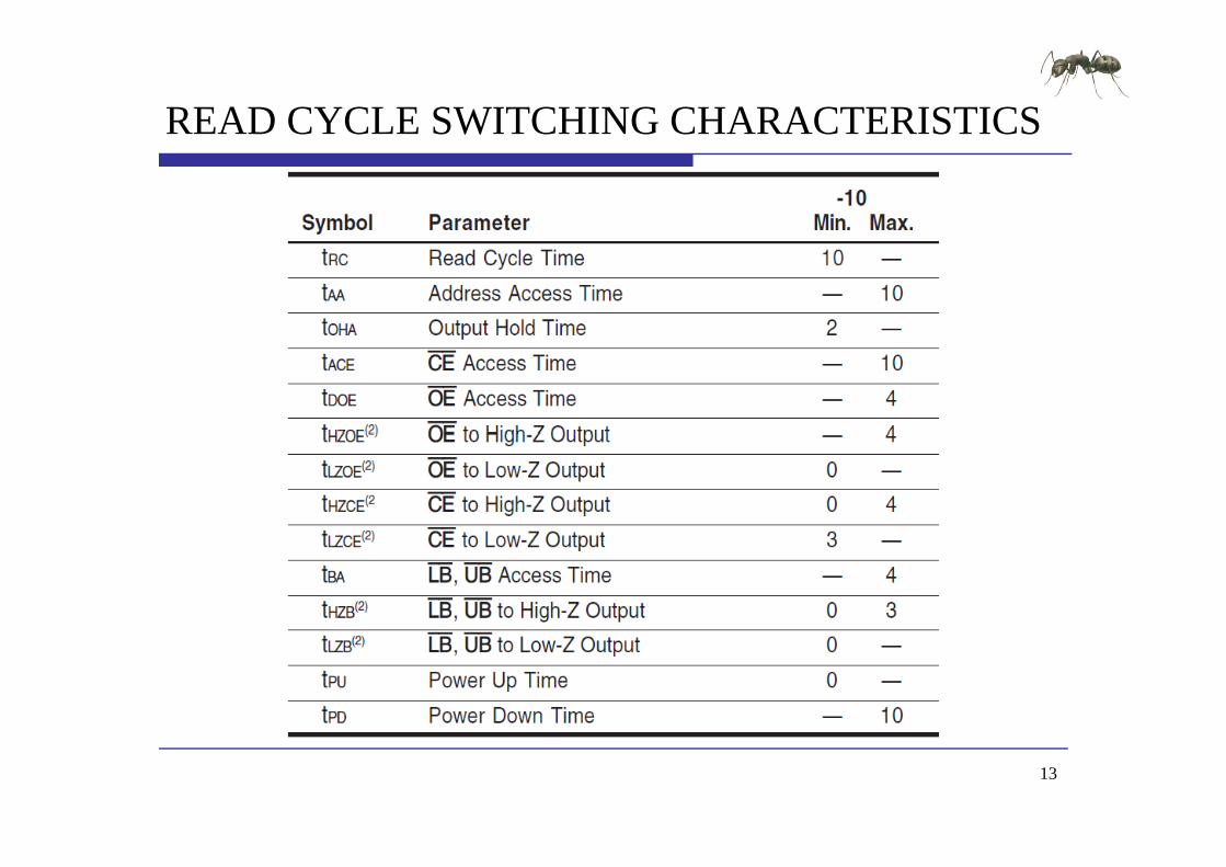

FSMC
Programmable timings to support a wide range of devices in particulardevices in particular Programmable wait states (up to 15) Programmable b s t rnaro nd c cles ( p to 15) Programmable bus turnaround cycles (up to 15) Programmable output enable and write enable delays
(up to 15)(up to 15) Independent read and write timings and protocol so
as to support the widest variety of memories andas to support the widest variety of memories and timings
17
NORPSRAM address mappingpp g
NORPSRAM bank selection
External memory address
18
External memory interface signalsy g
19
NOR FlashPSRAM controller timing diagramsg g
read accesses
20
NOR FlashPSRAM controller timing diagramsg g
write accesses
21
FSMC Memory mapy p
22
Development Flowp
Embedded Software Side
int main(void)
Bootup STM32F10x
ProgrammingBootupSTM32F10x RCC Configure
NVIC Configure
int main(void)ifdef DEBUGdebug()
endif
FSMC SRAM Init
System Clocks Configuration RCC_Configuration()
NVIC Configuration
GPIO Configure
gNVIC_Configuration()
GPIO Configuration GPIO_Configuration()
GPIO Configure
FSMC Configure
Writeread tofrom FSMC SRAM memory
Configure FSMC Bank1 NORSRAM1 FSMC_SRAM_Init()
SRAM memory RW operation FSMC SRAM WriteBuffer
FSMC SRAM ReadBuffer
helliphelliphelliphelliphelliphelliphelliphelliphelliphelliphelliphelliphelliphelliphelliphelliphelliphelliphelliphelliphelliphelliphellipCheck content
Display Result
23
Configure FSMC IOg
Function name Description
RCC_APB2PeriphClockCmd(RCC_APB2Periph_GPIOD | RCC_APB2Periph_GPIOG | RCC_APB2Periph_GPIOE | RCC_APB2Periph_GPIOF ENABLE)
‐‐ GPIO Configuration ‐‐‐‐‐‐‐‐‐‐‐‐‐‐‐‐‐‐‐‐‐‐‐‐‐‐‐‐‐‐‐‐‐‐‐‐‐‐‐‐‐‐‐‐‐‐‐‐‐
GPIO FwLib Functions List
Function name Description
RCC_APB2PeriphClockCmd
Enables or disables the High Speed APB (APB2) peripheralclock
GPIO I it I iti li th GPIO
GPIO Configuration SRAM Data lines configuration GPIO_InitStructureGPIO_Pin = GPIO_Pin_0 | GPIO_Pin_1 | GPIO_Pin_8 |
GPIO_Pin_9 | GPIO_Pin_10 | GPIO_Pin_14 | GPIO_Pin_15GPIO_InitStructureGPIO_Mode = GPIO_Mode_AF_PPGPIO_InitStructureGPIO_Speed = GPIO_Speed_50MHzGPIO_Init(GPIOD ampGPIO_InitStructure) GPIO_Init Initializes the GPIOx
peripheral according to the specified parametersin the GPIO_InitStruct
RCC AHBPeriphClock Enables or disables the AHB
_ ( _ )GPIO_InitStructureGPIO_Pin = GPIO_Pin_7 | GPIO_Pin_8 | GPIO_Pin_9 |
GPIO_Pin_10 | GPIO_Pin_11 | GPIO_Pin_12 | GPIO_Pin_13 | GPIO_Pin_14 | GPIO_Pin_15
GPIO_Init(GPIOE ampGPIO_InitStructure) SRAM Address lines configuration GPIO_InitStructureGPIO_Pin = GPIO_Pin_0 | GPIO_Pin_1 | GPIO_Pin_2 |
| | | | |RCC_AHBPeriphClockCmd
Enables or disables the AHB peripheral clock
GPIO_Pin_3 | GPIO_Pin_4 | GPIO_Pin_5 | GPIO_Pin_12 | GPIO_Pin_13 | GPIO_Pin_14 | GPIO_Pin_15
GPIO_Init(GPIOF ampGPIO_InitStructure) GPIO_InitStructureGPIO_Pin = GPIO_Pin_0 | GPIO_Pin_1 | GPIO_Pin_2 |
GPIO_Pin_3 | GPIO_Pin_4 | GPIO_Pin_5GPIO_Init(GPIOG ampGPIO_InitStructure)GPIO InitStructure GPIO Pin GPIO Pin 11 | GPIO Pin 12 | GPIO Pin 13 GPIO_InitStructureGPIO_Pin = GPIO_Pin_11 | GPIO_Pin_12 | GPIO_Pin_13 GPIO_Init(GPIOD ampGPIO_InitStructure) NOE and NWE configuration GPIO_InitStructureGPIO_Pin = GPIO_Pin_4 |GPIO_Pin_5GPIO_Init(GPIOD ampGPIO_InitStructure) NE1configuration GPIO InitStructure GPIO Pin = GPIO Pin 7 GPIO_InitStructureGPIO_Pin = GPIO_Pin_7 GPIO_Init(GPIOD ampGPIO_InitStructure) NBL0 NBL1 configuration GPIO_InitStructureGPIO_Pin = GPIO_Pin_0 | GPIO_Pin_1 GPIO_Init(GPIOE ampGPIO_InitStructure) Enable the FSMC Clock RCC_AHBPeriphClockCmd(RCC_AHBPeriph_FSMC ENABLE)
24
_ p ( _ p _ )
Configure FSMCg
Function name Description
Enable the FSMC Clock RCC_AHBPeriphClockCmd(RCC_AHBPeriph_FSMC ENABLE)
‐‐ FSMC Configuration ‐‐
FSMC FwLib Functions List
Function name Description
RCC_AHBPeriphClockCmd
Enables or disables the AHB peripheral clock
FSMC_NORSRAMInit Initializes the FSMC NOR b k di t th
FSMC Configuration pFSMC_AddressSetupTime = 0pFSMC_AddressHoldTime = 0pFSMC_DataSetupTime = 2pFSMC_BusTurnAroundDuration = 0pFSMC_CLKDivision = 0pFSMC_DataLatency = 0memory bank according to the
parameters specified in FSMC_NORInitStruct
FSMC_NORSRAMCm Enables or disables the NORSRAM memory bank1
p _ y pFSMC_AccessMode = FSMC_AccessMode_AFSMC_NORSRAMInitStructureFSMC_Bank = FSMC_Bank1_NORSRAM1FSMC_NORSRAMInitStructureFSMC_DataAddressMux =
FSMC_DataAddressMux_DisableFSMC_NORSRAMInitStructureFSMC_MemoryType = FSMC_MemoryType_SRAMFSMC_NORSRAMInitStructureFSMC_MemoryDataWidth = FSMC_MemoryDataWidth_16bNORSRAM memory bank1 FSMC_NORSRAMInitStructureFSMC_BurstAccessMode =
FSMC_BurstAccessMode_DisableFSMC_NORSRAMInitStructureFSMC_WaitSignalPolarity =
FSMC_WaitSignalPolarity_LowFSMC_NORSRAMInitStructureFSMC_WrapMode = FSMC_WrapMode_DisableFSMC_NORSRAMInitStructureFSMC_WaitSignalActive =
FSMC WaitSignalActive BeforeWaitStateFSMC_WaitSignalActive_BeforeWaitStateFSMC_NORSRAMInitStructureFSMC_WriteOperation =
FSMC_WriteOperation_EnableFSMC_NORSRAMInitStructureFSMC_WaitSignal = FSMC_WaitSignal_DisableFSMC_NORSRAMInitStructureFSMC_ExtendedMode = FSMC_ExtendedMode_DisableFSMC_NORSRAMInitStructureFSMC_AsyncWait = FSMC_AsyncWait_DisableFSMC NORSRAMInitStructure FSMC WriteBurst = FSMC WriteBurst DisableFSMC_NORSRAMInitStructureFSMC_WriteBurst = FSMC_WriteBurst_DisableFSMC_NORSRAMInitStructureFSMC_ReadWriteTimingStruct = amppFSMC_NORSRAMInitStructureFSMC_WriteTimingStruct = amppFSMC_NORSRAMInit(ampFSMC_NORSRAMInitStructure)
Enable FSMC Bank1_SRAM Bank FSMC_NORSRAMCmd(FSMC_Bank1_NORSRAM1 ENABLE)
25
_ ( _ _ )
硬體電路配置
Mapping Table
Num SRAM STM32 Num SRAM STM32 Num SRAM STM32
1 A0 FSMC_A0 14 A13 FSMC_A13 27 IO8 FSMC_D82 A1 FSMC A1 15 A14 FSMC A14 28 IO9 FSMC D9_ _ _3 A2 FSMC_A2 16 A15 FSMC_A15 29 IO10 FSMC_D104 A3 FSMC_A3 17 A16 FSMC_A16 30 IO11 FSMC_D115 A4 FSMC_A4 18 A17 FSMC_A17 31 IO12 FSMC_D126 A5 FSMC_A5 19 IO0 FSMC_D0 32 IO13 FSMC_D137 A6 FSMC_A6 20 IO1 FSMC_D1 33 IO14 FSMC_D148 A7 FSMC_A7 21 IO2 FSMC_D2 34 IO15 FSMC_D159 A8 FSMC A8 22 IO3 FSMC D3 35 CE FSMC nNE19 A8 FSMC_A8 22 IO3 FSMC_D3 35 CE FSMC_nNE110 A9 FSMC_A9 23 IO4 FSMC_D4 36 OE FSMC_nOE11 A10 FSMC_A10 24 IO5 FSMC_D5 37 WE FSMC_nWE12 A11 FSMC A11 25 IO6 FSMC D6 38 UB FSMC NBL1_ _ _13 A12 FSMC_A12 26 IO7 FSMC_D7 39 LB FSMC_NBL0
26
實驗步驟
範例目錄架構
範例說明 範例說明
預設定義說明
燒錄 燒錄MIAT_STM32
27
範例目錄架構
範例目錄
測試映像檔 測試映像檔
含括檔
函式庫 函式庫
專案檔
原始碼 原始碼
28
範例說明
Embedded Software Side
Write data to FSMC SRAM memory
SRAM memory RW operation
Write data to FSMC SRAM memory Fill the buffer to send Fill_Buffer(TxBuffer BUFFER_SIZE 0x3212)FSMC_SRAM_WriteBuffer(TxBuffer WRITE_READ_ADDR BUFFER_SIZE)
SRAM memory RW operation
FSMC SRAM WriteBuffer
Read data from FSMC SRAM memory FSMC_SRAM_ReadBuffer(RxBuffer WRITE_READ_ADDR BUFFER_SIZE)
Read back SRAM memory and check content correctness
FSMC SRAM ReadBuffer
Check content
Display Result yfor (Index = 0x00 (Index lt BUFFER_SIZE) ampamp (WriteReadStatus == 0)
Index++)if (RxBuffer[Index] = TxBuffer[Index])
Display Result
WriteReadStatus = Index + 1
29
範例說明
Embedded Software Side
while (1)
Display Result
while (1)if (WriteReadStatus == 0) OK Turn on USERLED
GPIO SetBits(GPIOF GPIO Pin 11)
SRAM memory RW operation
FSMC SRAM WriteBufferGPIO_SetBits(GPIOF GPIO_Pin_11)
else KO Turn off USERLED
GPIO ResetBits(GPIOF GPIO Pin 11)
FSMC SRAM ReadBuffer
Check content
Display Result
如果寫入與讀取Buffer內容相同外部記憶體使用正常USERLED紅燈GPIO_ResetBits(GPIOF GPIO_Pin_11)
Insert delay Delay(0xAFFFF) Turn on USERLED GPIO SetBits(GPIOF GPIO Pin 11)
Display Result恆亮
GPIO_SetBits(GPIOF GPIO_Pin_11) Insert delay Delay(0xAFFFF)
如果寫入與讀取Buffer內容不同外部記憶體使用異常 USERLED紅燈閃爍
30
預設定義說明
define Bank1_SRAM1_ADDR ((u32)0x60000000) 定義SRAM起始點 定義SRAM起始點
define BUFFER_SIZE 0x400定義測試資料大小 定義測試資料大小
資料大小必需小於0xC000 define WRITE_READ_ADDR 0x8000 定義SRAM寫入起始點
寫入起始點WRITE_READ_ADDR + BUFFER_SIZE必需小於0x6000C000
31
燒錄MIAT STM32_
Rebuilder all target files產生HEX DFU Fil M 轉換HEX產生DFU DFU File Manager轉換HEX產生DFU DfuSe Demonstration燒錄DFU d Leave DFU mode
32
內部與外部SRAM存取控制實驗
實驗一
WU-YANGTechnology Co Ltd
實驗一練習
練習 修改寫入位置測試是否正常 修改寫入位置測試是否正常
修改寫入資料大小測試是否正常
取消 i 測試是否正常 取消FSMC_SRAM_Init測試是否正常
34
實驗目的(二)( )
使用MIAT_STM32實驗板透過FSMC控制外部SRAM並設定為data memory進行存取控制實驗同樣利用LED設定為data memory進行存取控制實驗同樣利用LED確認存取是否正常
35
實驗原理
External SRAM RVMDK環境設定 RVMDK環境設定
Development Flow fi ARM Configure Startup Code
36
RVMDK環境設定
外部SRAM有512K Bytes位置由0x60000000至0x60080000
37
Development Flowp
Embedded Software Side
int main(void)
Bootup STM32F10x
Programming
Bootup
int main(void)ifdef DEBUGdebug()
endif
Startup Code
BootupSTM32F10x
RCC Configure
NVIC Configure
System Clocks Configuration RCC_Configuration()
NVIC Configuration g gNVIC_Configuration()
GPIO Configuration GPIO_Configuration()
GPIO Configure
for (Index = 0 Index lt1024 Index++)
Tab[Index] =IndexT bAdd ( 32)T b h ld b 0 600000
Check operation
Check pointer value
Display Result TabAddr = (u32)Tab should be 0x600000xx
Get main stack pointer value MSPValue = __MRS_MSP() should be 0x2000xxxx
helliphelliphelliphelliphelliphelliphelliphelliphelliphelliphelliphelliphelliphelliphelliphelliphelliphelliphelliphelliphelliphelliphellip
Display Result
38
Startup Codep
Register boundary addresses RCC Configure
Enable FSMC clock
LDR R0= 0x00000114
LDR R1= 0x40021014
STR R0[R1]
Enable GPIOD GPIOE GPIOF and GPIOG clocks
LDR R0= 0x000001E0
LDR R1= 0x40021018
RCC register map
STR R0[R1]
39
RCC Register g
Bit 8 FSMCEN FSMC clock enableAHB Peripheral Clock enable register (RCC_AHBENR)
Bit 8 FSMCEN FSMC clock enableSet and cleared by software0 FSMC clock disabled
APB2 peripheral clock enable register (RCC_APB2ENR)
1 FSMC clock enabled
Bit 8765 IOPGEN IO port GFED clock enableSet and cleared by software0 IO port GFED clock disabled1 IO port GFED clock enabled
40
1 IO port GFED clock enabled
Startup Codep
Register boundary addresses GPIO Configure
SRAM Data lines NOE and NWE configuration SRAM Address lines configuration NOE NEW NE1 NBL0 NBL1 configuration LDR R0= 0xB4BB44BB LDR R1= 0x40011400STR R0[R1]LDR R0= 0xBBBBBBBB LDR R1= 0x40011404STR R0[R1]LDR R0 = 0xB44444BBLDR R0= 0xB44444BB LDR R1= 0x40011800STR R0[R1]LDR R0= 0xBBBBBBBB LDR R1= 0x40011804
GPIO register map
STR R0[R1]LDR R0= 0x44BBBBBB LDR R1= 0x40011C00STR R0[R1]LDR R0= 0xBBBB4444 LDR R1= 0x40011C04STR R0[R1]LDR R0= 0x44BBBBBBLDR R1= 0x40012000STR R0 [R1]
41
STR R0[R1]
GPIO Register g
Bit 8 FSMCEN FSMC clock enablePort configuration register low
Port configuration register high
Bits 2928 2524Bits 3130 2726 2322 1918 1514 1110 76 32 Bits 2928 25242120 1716 131298 54 10MODEy[10] Port x mode bits (y= 0 15)00 Input mode (reset state)01 Output mode max speed 10 MHz
Bits 3130 27262322 1918 15141110 76 32CNFy[10] Port x configuration bits (y= 0 15)In input mode (MODE[10]=00)00 Analog input mode01 Floating input (reset state)10 Input with pull-up pull-down
10 Output mode max speed 2 MHz11 Output mode max speed 50 MHz
11 ReservedIn output mode (MODE[10] gt00)00 General purpose output push-pull01 General purpose output Open-drain10 Alternate function output Push-pull11 Alternate function output Open-drain
42
11 Alternate function output Open drain
Startup Codep
FSMCregister map FSMC Configure
FSMC Configuration Enable FSMC Bank1_SRAM Bank
LDR R0= 0x00001011
LDR R1= 0xA0000000
STR R0[R1]
LDR R0= 0x00000200
LDR R1= 0xA0000004
STR R0[R1]
43
FSMC Register g
Bit 8 FSMCEN FSMC clock enableSRAMNOR-Flash chip-select control registers 1 (FSMC_BCR1)
Bit 12 WREN Write enable bitThis bit indicates whether write operations are enableddisabled in the bank by the FSMC0 Write operations are disabled in the bank by the FSMC an AHB error is reported1 Write operations are enabled for the bank by the FSMC (default after reset) p y ( )Bits 54 MWID Memory databus widthDefines the external memory device width valid for all type of memories00 8 bits01 16 bits (default after reset)10 reserved do not use10 reserved do not use11 reserved do not use Bit 0 MBKEN Memory bank enable bitEnables the memory bank After reset Bank1 is enabled all others are disabled Accessing adisabled bank causes an ERROR on AHB bus0 C di b k i di bl d0 Corresponding memory bank is disabled1 Corresponding memory bank is enabled
44
FSMC Register g
Bit 8 FSMCEN FSMC clock enableSRAMNOR-Flash chip-select timing registers 1 (FSMC_BTR1)
Bits 158 DATAST Data-phase duration0000 0000 Reserved0000 0001 DATAST phase duration = 2 times HCLK clock cycles0000 0010 DATAST phase duration = 3 times HCLK clock cycles1111 1111 DATAST phase duration = 256 times HCLK clock cycles (default value after reset)Bits 74 ADDHLD Address-hold phase duration0000 Reserved0001 ADDHLD phase duration = 2 times HCLK clock cycle0010 ADDHLD phase duration = 3 times HCLK clock cycle1111 ADDHLD phase duration = 16 times HCLK clock cycles (default value after reset)Bits 30 ADDSET Address setup phase durationThese bits are written by software to define the duration of the address setup phase (refer toFigure 162 to Figure 172) used in SRAMs ROMs and asynchronous NOR Flash0000 ADDSET phase duration = 1 times HCLK clock cycle1111 ADDSET phase duration = 16 times HCLK clock cycles (default value after reset)
45
實驗步驟
範例目錄架構
範例說明 範例說明
預設定義說明
46
範例目錄架構
範例目錄
測試映像檔 測試映像檔
含括檔
函式庫 函式庫
專案檔
原始碼 原始碼
47
範例說明
Embedded Software Side
Infinite loop
Display Result
Infinite loop while (1)if (((TabAddramp0xFFFFFF00) == 0x60000000) ampamp
((MSPValueamp0xFFFF0000) == 0x20000000))
Check operation
Check pointer value((MSPValueamp0xFFFF0000) == 0x20000000))
OK Turn on USERLED GPIO_SetBits(GPIOF GPIO_Pin_11)
else
Display Result
else KO Turn off USERLED
GPIO_ResetBits(GPIOF GPIO_Pin_11) Insert delay Delay(0xAFFFF)
如果Tab位置在0x600000且Stack pointer位置在0x2000 外部記憶體使用正常USERLED紅燈恆亮Delay(0xAFFFF)
Turn on USERLED GPIO_SetBits(GPIOF GPIO_Pin_11) Insert delay Delay(0xAFFFF)
紅燈恆亮
如果 b位置不在0 600000或Delay(0xAFFFF)
如果Tab位置不在0x600000或Stack pointer位置不在0x2000 外部記憶體使用異常USERLED紅燈閃爍
48
預設定義說明
DATA_IN_ExtSRAM EQU 1 E l SRAM C fi i External SRAM Configuration 0=gt DISABLE 1=gt ENABLE
u32 Tab[1024]宣告於外部 的記憶體 宣告於外部SRAM的記憶體
49
data memory存取控制實驗
實驗二
WU-YANGTechnology Co Ltd
實驗二練習
練習 取消RVMDK環境外部SRAM設定測試是否正常 取消RVMDK環境外部SRAM設定測試是否正常
修改DATA_IN_ExtSRAM EQU 0測試是否正常
修改外部 記憶體 b變數大小測試是否正常 修改外部SRAM記憶體Tab變數大小測試是否正常
51
Q amp A
WU-YANGTechnology Co Ltd
MIAT_STM32內部Flash存取控制實驗
WU-YANG
浯陽科技有限公司
Technology Co Ltd
Declared Version
Training Only
Declare
Document Number
Document Version 100
Release Date
Document Title MIAT_STM32 內部FLASH存取控制實驗
Exercise Time
Platform MIAT_STM32V2MIAT IOB V1PlatformMIAT IOBV1
Peripheral
Author WU-YANG Technology Co Ltd
2
實驗目的(一)( )
使用MIAT_STM32實驗板透過Flash memory interface (FLITF)控制內部Flash進行存取控制實驗並利用LED(FLITF)控制內部Flash進行存取控制實驗並利用LED確認存取是否正常
3
實驗原理
System architecture E b dd d Fl h Embedded Flash Features Memory map RVMDK環境設定
FLITF Flash module organization
Flash library function Development Flow ARM Configure
4
System architecturey
5
Embedded Flash
Features 256 Kb up to 256 Kbytes Memory organization the Flash memory is organized as a
main block and an information blockmain block and an information block Main memory block of size t 32 Kb 64 bit di id d i t 128 f 2 up to 32 Kb times 64 bits divided into 128 pages of 2
Kbytes Information block of size Information block of size 258 times 64 bits
6
Embedded Flash Memory mapy p
7
Flash Memoryy
8
RVMDK環境設定
STMF103ZC有256K Bytes的Flash位置由0x8000000至0x8040000
9
FLITF
Features R d i f i h f h b ff (2 64 bi d ) Read interface with prefetch buffer (2x64-bit words) Option byte Loader
l h i Flash Program Erase operation Read Write protection
10
Flash memory interfacey
11
Flash memory interface registery g
Bit 8 FSMCEN FSMC clock enableFlash status register (FLASH_SR)
Bits 316 Reserved must be kept clearedBit 5 EOP End of operation
Bit 2 PGERR Programming errorSet by hardware when an address to be programmed p
Set by hardware when a Flash operation (programming erase) is completed Reset by writing a 1Note EOP is asserted at the end of each successful
y p gcontains a value different from 0xFFFF before programmingReset by writing 1Note The STRT bit in the FLASH_CR register f f
program or erase operationBit 4 WRPRTERR Write protection errorSet by hardware when programming a write-protected address of the Flash memory
_ gshould be reset before starting a programmingoperationBit 1 Reserved must be kept clearedBit 0 BSY Busyp y
Reset by writing 1Bit 3 Reserved must be kept cleared
This indicates that a Flash operation is in progress This is set on the beginning of a Flash operation and reset when the operation finishes or when an error occurs
12
Flash memory interface registery g
Flash control register (FLASH_CR)
Bit 9 OPTWRE Option bytes write enableWhen set the option bytes can be programmed This
Bit 6 STRT StartThis bit triggers an ERASE operation when set This bit is set only
bit is set on writing the correct key sequence to the FLASH_OPTKEYR registerThis bit can be reset by softwareBit 8 Reserved must be kept clearedBit 7 LOCK Lock
by software and reset when the BSY bit is resetBit 5 OPTER Option byte eraseOption byte erase chosenBit 4 OPTPG Option byte programmingOption byte programming chosenBit 7 LOCK Lock
Write to 1 only When it is set it indicates that the FPEC and FLASH_CR are locked This bit is reset by hardware after detecting the unlock sequenceIn the event of unsuccessful unlock operation this bit remains set until the next reset
p y p g gBit 3 Reserved must be kept clearedBit 2 MER Mass eraseErase of all user pages chosenBit 1 PER Page erasePage Erase chosenremains set until the next reset Page Erase chosenBit 0 PG ProgrammingFlash programming chosen
13
Main Flash memory programmingy p g g
14
Flash memory Page Erasey g
15
Flash memory Mass Erasey
16
Option byte programmingp y p g g
17
Option byte Erasep y
18
FLASH library functiony
19
FLASH library functiony
20
Development Flowp
Embedded Software Side
int main(void)
Bootup STM32F10x
ProgrammingBootupSTM32F10x RCC Configure
NVIC Configure
int main(void)ifdef DEBUGdebug()
endifendif
FLASHStatus = FLASH_COMPLETEMemoryProgramStatus = PASSEDData = 0x15041975
GPIO Configure
Data = 0x15041975
RCC Configuration RCC_Configuration()
Flash memory RW operation FLASH Unlock
FLASH ClearFlag NVIC Configuration NVIC_Configuration()
GPIO Configuration
FLASH ClearFlag
FLASH ErasePage
FLASH ProgramWord GPIO Configuration GPIO_Configuration()
helliphelliphelliphelliphelliphelliphelliphelliphelliphelliphelliphelliphelliphelliphelliphelliphellipDisplay Result
Check content
21
實驗步驟
範例目錄架構
範例說明 範例說明
預設定義說明
燒錄 燒錄MIAT_STM32
22
範例目錄架構
範例目錄
測試映像檔 測試映像檔
含括檔
函式庫 函式庫
專案檔
原始碼 原始碼
23
範例說明
Function name Description
Unlock the Flash Program Erase controller FLASH_Unlock()
D fi h b f b d
Flash FwLib Functions List
Function name Description
FLASH_Unlock Unlocks the FLASH Program Erase Controller
FLASH_ClearFlag Clears the FLASH pending fl
Define the number of page to be erased NbrOfPage = (EndAddr - StartAddr) FLASH_PAGE_SIZE
Clear All pending flags FLASH_ClearFlag(FLASH_FLAG_BSY | FLASH_FLAG_EOP | FLASH_FLAG_PGERR |
FLASH FLAG WRPRTERR)flags
FLASH_ErasePage Erases a specified FLASH page
FLASH_ProgramWord Programs a word at a specified
_ _ )
Erase the FLASH pages for(EraseCounter = 0 (EraseCounter lt NbrOfPage) ampamp (FLASHStatus ==
FLASH_COMPLETE) EraseCounter++)FLASHStatus = FLASH ErasePage(StartAddr + (FLASH PAGE SIZE EraseCounter))address FLASHStatus = FLASH_ErasePage(StartAddr + (FLASH_PAGE_SIZE EraseCounter))
FLASH Word program of data 0x15041979 at addresses defined by StartAddr and EndAddrAddress = StartAddr
while((Address lt EndAddr) ampamp (FLASHStatus == FLASH_COMPLETE))FLASHStatus = FLASH_ProgramWord(Address Data)Address = Address + 4
24
範例說明
Embedded Software Side
Check the corectness of written data
Display Result
Check the corectness of written data Address = StartAddr
while((Address lt EndAddr) ampamp (MemoryProgramStatus = FAILED))if(((vu32) Address) = Data)
Flash memory RW operation
MemoryProgramStatus = FAILED
Address += 4
Check content
Display Result while (1)if (MemoryProgramStatus == PASSED) OK Turn on USERLED GPIO_SetBits(GPIOF GPIO_Pin_11)
Display Result
else KO Turn off USERLED GPIO_ResetBits(GPIOF GPIO_Pin_11) Insert delay Delay(0xAFFFF)
如果寫入與讀取Flash內容相同Flash記憶體使用正常USERLED紅燈恆亮
Turn on USERLED GPIO_SetBits(GPIOF GPIO_Pin_11) Insert delay Delay(0xAFFFF)
如果寫入與讀取Flash內容不同Flash記憶體使用異常USERLED紅燈閃爍
25
預設定義說明
define StartAddr ((u32)0x08008000) 定義Flash使用起始點 定義Flash使用起始點
使用起始點必需大於0x8003000 + Code Size 附註 0x8000000~0x8003000為DFU程式區塊使用此區塊
將造成無法燒錄程式
Code Size可由產生的HEX檔得知
d fi E dAdd (( 32)0 0800C000) define EndAddr ((u32)0x0800C000) 定義Flash使用結束點
使用起始點必需小於0x8040000使用起始點必需小於
Data = 0x15041975 寫入資料
32Bit define FLASH_PAGE_SIZE ((u16)0x800)
每一個Page有2KByte26
每一個Page有2KByte
Intel HEX Format
aaaa tt dd cc
field Description
the colon that starts every Intel HEX record
the record-length field that represents the number of data bytes (dd) in the record
aaaa the address field that represents the starting address for subsequent data in the record
tt the field that represents the HEX record type which may be one of the following00 - data record01 - end-of-file record02 - extended segment address recordg04 - extended linear address record
dd a data field that represents one byte of data A record may have multiple data bytes The number of data bytes in the record must match the number specified by the field
cc the checksum field that represents the checksum of the record The checksum is calculated by summing the values of all hexadecimal digit pairs in the record modulo 256 and taking the twos complement
27
HEX Examplep
020000040800F2103000001814002045310008D9340008CD340008D8103000001814002045310008D9340008CD340008D8helliphelliphellip1038200042370008000000000000000000000000170C3830000000000000000000000000008C
資料填入起始位置為
0C3830000000000000000000000000008C04000005080031318D00000001FF
資料填入起始位置為0x08003000 每一行有0x10(16)個Bytes 最後一筆資料為
資料結束點為0x0803383004000005080031318D
(0x08003830 -0x08000000)0x800 = 7 需以0x800為單位所以使用的位置起點為0x08004000
28
燒錄MIAT STM32_
Rebuilder all target files產生HEX DFU Fil M 轉換HEX產生DFU DFU File Manager轉換HEX產生DFU DfuSe Demonstration燒錄DFU d Leave DFU mode
29
內部Flash存取控制實驗
實驗一
WU-YANGTechnology Co Ltd
實驗一練習
注意 請使用預設0 08008000之後的位置 避免覆蓋DFU 請使用預設0x08008000之後的位置避免覆蓋DFU
與使用者程式碼區塊
練習 練習 修改存取位置測試是否正常
修改寫入資料測試是否正常 修改寫入資料測試是否正常
修改寫入資料後取消FLASH_Unlock測試是否正常
修改寫入資料後取消FLASH E P 測試是否正 修改寫入資料後取消FLASH_ErasePage測試是否正常
31
實驗目的(二)( )
使用MIAT_STM32實驗板透過Flash memory interface (FLITF)控制內部Flash進行存取控制實驗並利用SW(FLITF)控制內部Flash進行存取控制實驗並利用SWKEY決定資料寫入與讀取LCD顯示狀態
32
實驗原理
System requirement E b dd d Fl h Embedded Flash LCD KEY SW
Development Flow ARM Configure
33
Development Flowp
Embedded Software Side
int main(void)
Bootup STM32F10x
ProgrammingBootupSTM32F10x RCC Configure
NVIC Configure
int main(void)ifdef DEBUGdebug()
endif
FLASHStatus = FLASH_COMPLETE
RCC Configuration RCC Configuration()
GPIO Configure
BasicIO Configure_ g ()
NVIC Configuration NVIC_Configuration()
GPIO Configuration Flash memory RW ti
lcd Configure
GPIO Configuration GPIO_Configuration()
Init_BasicIO()
l d i i () LCD I i i li i
RW operation
Example
FLASH Unlock
FLASH ClearFlag
lcd_init() LCD Initialization
helliphelliphelliphelliphelliphelliphelliphelliphelliphelliphelliphelliphelliphelliphelliphelliphelliphelliphelliphelliphelliphelliphellip
p
34
硬體電路配置
Mapping Table
Num MIAT_STM32V2 MIAT_IOBV1 Num MIAT_STM32V2 MIAT_IOBV1
1 PC8 (326) SW1 10 PE6 (15) LCD_EN2 PC9 (327) SW2 11 PF6 (118) LCD RW ( ) ( ) _3 PC10 (43) SW3 12 PF7 (119) LCD_RS 4 PC11 (44) SW4 13 PF8(120) LCD_D4 5 PB5 (427) KEY1 14 PF9 (121) LCD_D5 6 PB6 (428) KEY2 15 PF10 (122) LCD_D6 7 PB7 (429) KEY3 16 PF11 (213) LCD_D7 8 PB8 (431) KEY4 17 VDD (236) VCC33V 9 VCC5V (1 36) VCC5V 18 GND (1 35) GND9 VCC5V (136) VCC5V 18 GND (135) GND
35
實驗步驟
範例目錄架構
範例說明 範例說明
預設定義說明
36
範例目錄架構
範例目錄
測試映像檔 測試映像檔
含括檔
函式庫 函式庫
專案檔
原始碼 原始碼
37
範例說明
Embedded Software Side
lcd clear()
FLASH memory RW operation
lcd_clear()lcd_print (MIAT_STM32 DEMO )
Unlock the Flash Program Erase controller FLASH_Unlock()
Flash memory RW operation
FLASH Unlock
Clear All pending flags FLASH_ClearFlag(FLASH_FLAG_BSY | FLASH_FLAG_EOP | FLASH_FLAG_PGERR |
FLASH_FLAG_WRPRTERR)
while(1)
Example
FLASH ClearFlag
( )
KEY_Buffer=Key_Scan()set_cursor (0 1)lcd_print (SW Value = 0x)lcd putchar(((SWamp0x7)+0x30))lcd_putchar(((SWamp0x7)+0x30))if(KEY_Buffer==1)Address=(StartAddr|(SWltlt12))set_cursor (0 0)lcd_print (Set Addr = 0x)
掃描KEY是否按下與顯示SW數值LCD Line2顯示SW Value = 0x(SW)
lcd_putchar(((SWamp0x7)+0x30))lcd_print ( )
如果KEY1按下記錄SW數值至Address LCD Line1顯示Set Adde = 0x(Address)
38
範例說明
Embedded Software Side
else if(KEY Buffer==2)
FLASH memory RW operation
else if(KEY_Buffer==2)
Erase the FLASH pages FLASHStatus = FLASH_ErasePage(Address)
FLASH Word program of data at addresses defined by SW
SRAM memory RW operation
p g yFLASHStatus = FLASH_ProgramWord(Address (SWamp0x7))
set_cursor (0 0)lcd_print (Write 0x)lcd_putchar(((SWamp0x7)+0x30))l d i t ( t 0 )
Example如果KEY2按下清除Address所處區塊並寫入SW數值 lcd_print ( at 0x)
lcd_putchar((((Addressgtgt12)amp0x7)+0x30))else if(KEY_Buffer==3)
Data=(u16 )Address
所處區塊並寫入SW數值LCD Line1顯示Write 0x(SW) at 0x(Adddress)
Data (u16 )Addressset_cursor (0 0)lcd_print (Addr 0x)lcd_putchar((((Addressgtgt12)amp0x7)+0x30))lcd_print ( = 0x)lcd_putchar(((Dataamp0x7)+0x30))lcd_print ( )
如果KEY3按下讀取Address紀錄數值LCD Line1顯示Addr 0x(Adddress) = 0x
39
預設定義說明
define StartAddr ((u32)0x08020000) 定義Flash使用起始點 定義Flash使用起始點
使用起始點必需大於0x8003000 + Code Size 附註 0x8000000~0x8003000為DFU程式區塊使用此區塊
將造成無法燒錄程式
Code Size可由產生的HEX檔得知
32 Add 0 08020000 u32 Address = 0x08020000 定義Address初始值
初始值必需與Flash使用起始點相同初始值必需與 使用起始點相同
Address=(StartAddr|(SWltlt12)) Example StartAddr = 0x08020000 SW = 1 Address = 0x08021000
StartAddr = 0x08020000 SW = 7 Address = 0x08027000 StartAddr|(7ltlt12)必需小於0x8040000
40
使用者界面與Flash存取控制實驗
實驗二
WU-YANGTechnology Co Ltd
實驗二練習
注意 請使用預設0 08020000之後的位置 避免覆蓋DFU 請使用預設0x08020000之後的位置避免覆蓋DFU
與使用者程式碼區塊
練習 練習 利用SW與KEY測試Flash寫入與讀取是否正常
Fl h寫入後電源關閉 再開啟後寫入資料是否仍存 Flash寫入後電源關閉再開啟後寫入資料是否仍存在
修改存取位置測試是否正常 修改存取位置測試是否正常
42
實驗目的(三)( )
使用MIAT_STM32實驗板透過Flash memory interface (FLITF)控制內部Flash進行存取控制實驗並藉由填入(FLITF)控制內部Flash進行存取控制實驗並藉由填入Option Bytes 設定寫入鎖定保護Page鎖定不被覆蓋
43
Development Flowp
Embedded Software Side
int main(void)
Bootup STM32F10x
ProgrammingBootupSTM32F10x RCC Configure
NVIC Configure
int main(void)ifdef DEBUGdebug()
endifendif
FLASHStatus = FLASH_COMPLETEMemoryProgramStatus = PASSEDData = 0x1753
GPIO Configure
Data = 0x1753
RCC Configuration RCC_Configuration()
Flash memory RW operation FLASH Unlock
FLASH ClearFlag NVIC Configuration NVIC_Configuration()
GPIO Configuration
FLASH ClearFlag
FLASH ErasePage
FLASH ProgramHalfWord GPIO Configuration GPIO_Configuration()
Display Result
Check content
44
helliphelliphelliphelliphelliphelliphelliphelliphelliphelliphelliphelliphelliphelliphelliphelliphelliphelliphellip
實驗步驟
範例目錄架構
範例說明 範例說明
預設定義說明
45
範例目錄架構
範例目錄
測試映像檔 測試映像檔
含括檔
函式庫 函式庫
專案檔
原始碼 原始碼
46
範例說明
Function name Description
Unlock the Flash Program Erase controller FLASH_Unlock()
Define the number of page to be erased
Flash FwLib Functions List
Function name Description
FLASH_Unlock Unlocks the FLASH Program Erase Controller
FLASH_ClearFlag Clears the FLASH pending fl
Define the number of page to be erased NbrOfPage = (EndAddr ‐ StartAddr) FLASH_PAGE_SIZE
FLASH_ClearFlag(FLASH_FLAG_BSY | FLASH_FLAG_EOP|FLASH_FLAG_PGERR |FLASH_FLAG_WRPRTERR)
Get pages write protection status flags
FLASH_EraseOptionBytes
Erases the FLASH option bytes
FLASH_EnableWritePro Write protects the desired
p g pWRPR_Value = FLASH_GetWriteProtectionOptionByte()ProtectedPages = WRPR_Value amp 0x000000C0
ifdef WriteProtection_Disableif (ProtectedPages == 0x00) Pages are write protected
tection pages
NVIC_GenerateSystemReset
Generate a system reset
Disable the write protection FLASHStatus = FLASH_EraseOptionBytes() Generate System Reset to load the new option byte values NVIC_GenerateSystemReset()
elseifdef WriteProtection Enableifdef WriteProtection_Enableif (ProtectedPages = 0x00) Pages not write protected
FLASHStatus = FLASH_EraseOptionBytes() Enable the pages write protection FLASHStatus = FLASH_EnableWriteProtection(FLASH_WRProt_Pages12to13
|FLASH WRProt Pages14to15)|FLASH_WRProt_Pages14to15) Generate System Reset to load the new option byte values NVIC_GenerateSystemReset()
endifendif
47
範例說明
if (ProtectedPages = 0x00) Clear All pending flags
Flash FwLib Functions List
Function name DescriptionFLASH_ClearFlag(FLASH_FLAG_BSY |
FLASH_FLAG_EOP|FLASH_FLAG_PGERR |FLASH_FLAG_WRPRTERR)
erase the FLASH pages for(EraseCounter = 0 (EraseCounter lt NbrOfPage) ampamp (FLASHStatus ==
Function name Description
FLASH_ErasePage Erases a specified FLASH page
FLASH_ProgramHalfWod
Programs a half word at a ifi d dd FLASH_COMPLETE) EraseCounter++)
FLASHStatus = FLASH_ErasePage(StartAddr + (FLASH_PAGE_SIZE
EraseCounter))
rd specified address
FLASH Half Word program of data 0x1753 at addresses defined by StartAddrand EndAddr
Address = StartAddr
hil ((Add E dAdd ) ampamp (FLASHSt t FLASH COMPLETE))while((Address lt EndAddr) ampamp (FLASHStatus == FLASH_COMPLETE))
FLASHStatus = FLASH_ProgramHalfWord(Address Data)Address = Address + 2
48
範例說明
Embedded Software Side
Check the corectness of written data
Display Result
Check the corectness of written data Address = StartAddr
while((Address lt EndAddr) ampamp (MemoryProgramStatus = FAILED))if(((vu16) Address) = Data)
Flash memory RW operation
MemoryProgramStatus = FAILED
Address += 2
Check content
Display Result while (1)if (MemoryProgramStatus == PASSED) OK Turn on USERLED GPIO_SetBits(GPIOF GPIO_Pin_11)
Display Result
else KO Turn off USERLED GPIO_ResetBits(GPIOF GPIO_Pin_11) Insert delay Delay(0xAFFFF)
如果寫入與讀取Flash內容相同Flash記憶體可以寫入USERLED紅燈恆亮
Turn on USERLED GPIO_SetBits(GPIOF GPIO_Pin_11) Insert delay Delay(0xAFFFF)
如果寫入與讀取Flash內容不同Flash記憶體不能寫入USERLED紅燈閃爍
49
預設定義說明
define StartAddr ((u32) 0x08006000) 定義Flash使用起始點 定義Flash使用起始點
使用起始點必需大於0x8003000 + Code Size 附註 0x8000000~0x8003000為DFU程式區塊使用此區塊
將造成無法燒錄程式
Code Size可由產生的HEX檔得知
d fi E dAdd (( 32) 0 08008000) define EndAddr ((u32) 0x08008000) 定義Flash使用結束點
使用起始點必需小於0x8040000使用起始點必需小於
Data = 0x1753 寫入資料
16Bit define FLASH_PAGE_SIZE ((u16)0x800) 每一個Page有2KByte
50
每一個Page有2KByte
預設定義說明
define WriteProtection_Enable U hi li E bl W i P i Uncomment this line to Enable Write Protection
define WriteProtection_Disablehi li i bl i i Uncomment this line to Disable Write Protection
FLASH_EnableWriteProtection設定影響 個 設定影響2個Page FLASH_WRProt_Pages0to1 FLASH_WRProt_Pages1to2 helliphellip FLASH_WRProt_Pages60to61
設定影響多個Page FLASH_WRProt_Pages62to255
51
FLASH EnableWriteProtection_
Example
位置0x08006000 ~ 0x08007000每一個Page有0x800ByteStartPage = (0x08006000-0x08000000)0x800 = 12EndPage = ((0x08007000-0x08000000)0x800)-1 = 13執行執行FLASH_EnableWriteProtection(FLASH_WRProt_Pages12to13)將影響Pages12 Pages13
52
內部Flash寫入鎖定存取控制實驗
實驗三
WU-YANGTechnology Co Ltd
實驗三練習
注意 請使用預設0 08006000之後的位置 避免覆蓋DFU 請使用預設0x08006000之後的位置避免覆蓋DFU
與使用者程式碼區塊
更改寫入位置測試寫入鎖定時需同時更改 更改寫入位置測試寫入鎖定時需同時更改FLASH_EnableWriteProtection鎖定之Page
練習 練習 打開define WriteProtection_Enable測試是否可寫入
打開define WriteProtection Disable測試是否可寫入 打開define WriteProtection_Disable測試是否可寫入
修改存取位置測試是否正常
修改寫入資料測試是否正常 修改寫入資料測試是否正常
54
Q amp A
WU-YANGTechnology Co Ltd

NOR FlashPSRAM controller timing diagramsg g
read accesses
20
NOR FlashPSRAM controller timing diagramsg g
write accesses
21
FSMC Memory mapy p
22
Development Flowp
Embedded Software Side
int main(void)
Bootup STM32F10x
ProgrammingBootupSTM32F10x RCC Configure
NVIC Configure
int main(void)ifdef DEBUGdebug()
endif
FSMC SRAM Init
System Clocks Configuration RCC_Configuration()
NVIC Configuration
GPIO Configure
gNVIC_Configuration()
GPIO Configuration GPIO_Configuration()
GPIO Configure
FSMC Configure
Writeread tofrom FSMC SRAM memory
Configure FSMC Bank1 NORSRAM1 FSMC_SRAM_Init()
SRAM memory RW operation FSMC SRAM WriteBuffer
FSMC SRAM ReadBuffer
helliphelliphelliphelliphelliphelliphelliphelliphelliphelliphelliphelliphelliphelliphelliphelliphelliphelliphelliphelliphelliphelliphellipCheck content
Display Result
23
Configure FSMC IOg
Function name Description
RCC_APB2PeriphClockCmd(RCC_APB2Periph_GPIOD | RCC_APB2Periph_GPIOG | RCC_APB2Periph_GPIOE | RCC_APB2Periph_GPIOF ENABLE)
‐‐ GPIO Configuration ‐‐‐‐‐‐‐‐‐‐‐‐‐‐‐‐‐‐‐‐‐‐‐‐‐‐‐‐‐‐‐‐‐‐‐‐‐‐‐‐‐‐‐‐‐‐‐‐‐
GPIO FwLib Functions List
Function name Description
RCC_APB2PeriphClockCmd
Enables or disables the High Speed APB (APB2) peripheralclock
GPIO I it I iti li th GPIO
GPIO Configuration SRAM Data lines configuration GPIO_InitStructureGPIO_Pin = GPIO_Pin_0 | GPIO_Pin_1 | GPIO_Pin_8 |
GPIO_Pin_9 | GPIO_Pin_10 | GPIO_Pin_14 | GPIO_Pin_15GPIO_InitStructureGPIO_Mode = GPIO_Mode_AF_PPGPIO_InitStructureGPIO_Speed = GPIO_Speed_50MHzGPIO_Init(GPIOD ampGPIO_InitStructure) GPIO_Init Initializes the GPIOx
peripheral according to the specified parametersin the GPIO_InitStruct
RCC AHBPeriphClock Enables or disables the AHB
_ ( _ )GPIO_InitStructureGPIO_Pin = GPIO_Pin_7 | GPIO_Pin_8 | GPIO_Pin_9 |
GPIO_Pin_10 | GPIO_Pin_11 | GPIO_Pin_12 | GPIO_Pin_13 | GPIO_Pin_14 | GPIO_Pin_15
GPIO_Init(GPIOE ampGPIO_InitStructure) SRAM Address lines configuration GPIO_InitStructureGPIO_Pin = GPIO_Pin_0 | GPIO_Pin_1 | GPIO_Pin_2 |
| | | | |RCC_AHBPeriphClockCmd
Enables or disables the AHB peripheral clock
GPIO_Pin_3 | GPIO_Pin_4 | GPIO_Pin_5 | GPIO_Pin_12 | GPIO_Pin_13 | GPIO_Pin_14 | GPIO_Pin_15
GPIO_Init(GPIOF ampGPIO_InitStructure) GPIO_InitStructureGPIO_Pin = GPIO_Pin_0 | GPIO_Pin_1 | GPIO_Pin_2 |
GPIO_Pin_3 | GPIO_Pin_4 | GPIO_Pin_5GPIO_Init(GPIOG ampGPIO_InitStructure)GPIO InitStructure GPIO Pin GPIO Pin 11 | GPIO Pin 12 | GPIO Pin 13 GPIO_InitStructureGPIO_Pin = GPIO_Pin_11 | GPIO_Pin_12 | GPIO_Pin_13 GPIO_Init(GPIOD ampGPIO_InitStructure) NOE and NWE configuration GPIO_InitStructureGPIO_Pin = GPIO_Pin_4 |GPIO_Pin_5GPIO_Init(GPIOD ampGPIO_InitStructure) NE1configuration GPIO InitStructure GPIO Pin = GPIO Pin 7 GPIO_InitStructureGPIO_Pin = GPIO_Pin_7 GPIO_Init(GPIOD ampGPIO_InitStructure) NBL0 NBL1 configuration GPIO_InitStructureGPIO_Pin = GPIO_Pin_0 | GPIO_Pin_1 GPIO_Init(GPIOE ampGPIO_InitStructure) Enable the FSMC Clock RCC_AHBPeriphClockCmd(RCC_AHBPeriph_FSMC ENABLE)
24
_ p ( _ p _ )
Configure FSMCg
Function name Description
Enable the FSMC Clock RCC_AHBPeriphClockCmd(RCC_AHBPeriph_FSMC ENABLE)
‐‐ FSMC Configuration ‐‐
FSMC FwLib Functions List
Function name Description
RCC_AHBPeriphClockCmd
Enables or disables the AHB peripheral clock
FSMC_NORSRAMInit Initializes the FSMC NOR b k di t th
FSMC Configuration pFSMC_AddressSetupTime = 0pFSMC_AddressHoldTime = 0pFSMC_DataSetupTime = 2pFSMC_BusTurnAroundDuration = 0pFSMC_CLKDivision = 0pFSMC_DataLatency = 0memory bank according to the
parameters specified in FSMC_NORInitStruct
FSMC_NORSRAMCm Enables or disables the NORSRAM memory bank1
p _ y pFSMC_AccessMode = FSMC_AccessMode_AFSMC_NORSRAMInitStructureFSMC_Bank = FSMC_Bank1_NORSRAM1FSMC_NORSRAMInitStructureFSMC_DataAddressMux =
FSMC_DataAddressMux_DisableFSMC_NORSRAMInitStructureFSMC_MemoryType = FSMC_MemoryType_SRAMFSMC_NORSRAMInitStructureFSMC_MemoryDataWidth = FSMC_MemoryDataWidth_16bNORSRAM memory bank1 FSMC_NORSRAMInitStructureFSMC_BurstAccessMode =
FSMC_BurstAccessMode_DisableFSMC_NORSRAMInitStructureFSMC_WaitSignalPolarity =
FSMC_WaitSignalPolarity_LowFSMC_NORSRAMInitStructureFSMC_WrapMode = FSMC_WrapMode_DisableFSMC_NORSRAMInitStructureFSMC_WaitSignalActive =
FSMC WaitSignalActive BeforeWaitStateFSMC_WaitSignalActive_BeforeWaitStateFSMC_NORSRAMInitStructureFSMC_WriteOperation =
FSMC_WriteOperation_EnableFSMC_NORSRAMInitStructureFSMC_WaitSignal = FSMC_WaitSignal_DisableFSMC_NORSRAMInitStructureFSMC_ExtendedMode = FSMC_ExtendedMode_DisableFSMC_NORSRAMInitStructureFSMC_AsyncWait = FSMC_AsyncWait_DisableFSMC NORSRAMInitStructure FSMC WriteBurst = FSMC WriteBurst DisableFSMC_NORSRAMInitStructureFSMC_WriteBurst = FSMC_WriteBurst_DisableFSMC_NORSRAMInitStructureFSMC_ReadWriteTimingStruct = amppFSMC_NORSRAMInitStructureFSMC_WriteTimingStruct = amppFSMC_NORSRAMInit(ampFSMC_NORSRAMInitStructure)
Enable FSMC Bank1_SRAM Bank FSMC_NORSRAMCmd(FSMC_Bank1_NORSRAM1 ENABLE)
25
_ ( _ _ )
硬體電路配置
Mapping Table
Num SRAM STM32 Num SRAM STM32 Num SRAM STM32
1 A0 FSMC_A0 14 A13 FSMC_A13 27 IO8 FSMC_D82 A1 FSMC A1 15 A14 FSMC A14 28 IO9 FSMC D9_ _ _3 A2 FSMC_A2 16 A15 FSMC_A15 29 IO10 FSMC_D104 A3 FSMC_A3 17 A16 FSMC_A16 30 IO11 FSMC_D115 A4 FSMC_A4 18 A17 FSMC_A17 31 IO12 FSMC_D126 A5 FSMC_A5 19 IO0 FSMC_D0 32 IO13 FSMC_D137 A6 FSMC_A6 20 IO1 FSMC_D1 33 IO14 FSMC_D148 A7 FSMC_A7 21 IO2 FSMC_D2 34 IO15 FSMC_D159 A8 FSMC A8 22 IO3 FSMC D3 35 CE FSMC nNE19 A8 FSMC_A8 22 IO3 FSMC_D3 35 CE FSMC_nNE110 A9 FSMC_A9 23 IO4 FSMC_D4 36 OE FSMC_nOE11 A10 FSMC_A10 24 IO5 FSMC_D5 37 WE FSMC_nWE12 A11 FSMC A11 25 IO6 FSMC D6 38 UB FSMC NBL1_ _ _13 A12 FSMC_A12 26 IO7 FSMC_D7 39 LB FSMC_NBL0
26
實驗步驟
範例目錄架構
範例說明 範例說明
預設定義說明
燒錄 燒錄MIAT_STM32
27
範例目錄架構
範例目錄
測試映像檔 測試映像檔
含括檔
函式庫 函式庫
專案檔
原始碼 原始碼
28
範例說明
Embedded Software Side
Write data to FSMC SRAM memory
SRAM memory RW operation
Write data to FSMC SRAM memory Fill the buffer to send Fill_Buffer(TxBuffer BUFFER_SIZE 0x3212)FSMC_SRAM_WriteBuffer(TxBuffer WRITE_READ_ADDR BUFFER_SIZE)
SRAM memory RW operation
FSMC SRAM WriteBuffer
Read data from FSMC SRAM memory FSMC_SRAM_ReadBuffer(RxBuffer WRITE_READ_ADDR BUFFER_SIZE)
Read back SRAM memory and check content correctness
FSMC SRAM ReadBuffer
Check content
Display Result yfor (Index = 0x00 (Index lt BUFFER_SIZE) ampamp (WriteReadStatus == 0)
Index++)if (RxBuffer[Index] = TxBuffer[Index])
Display Result
WriteReadStatus = Index + 1
29
範例說明
Embedded Software Side
while (1)
Display Result
while (1)if (WriteReadStatus == 0) OK Turn on USERLED
GPIO SetBits(GPIOF GPIO Pin 11)
SRAM memory RW operation
FSMC SRAM WriteBufferGPIO_SetBits(GPIOF GPIO_Pin_11)
else KO Turn off USERLED
GPIO ResetBits(GPIOF GPIO Pin 11)
FSMC SRAM ReadBuffer
Check content
Display Result
如果寫入與讀取Buffer內容相同外部記憶體使用正常USERLED紅燈GPIO_ResetBits(GPIOF GPIO_Pin_11)
Insert delay Delay(0xAFFFF) Turn on USERLED GPIO SetBits(GPIOF GPIO Pin 11)
Display Result恆亮
GPIO_SetBits(GPIOF GPIO_Pin_11) Insert delay Delay(0xAFFFF)
如果寫入與讀取Buffer內容不同外部記憶體使用異常 USERLED紅燈閃爍
30
預設定義說明
define Bank1_SRAM1_ADDR ((u32)0x60000000) 定義SRAM起始點 定義SRAM起始點
define BUFFER_SIZE 0x400定義測試資料大小 定義測試資料大小
資料大小必需小於0xC000 define WRITE_READ_ADDR 0x8000 定義SRAM寫入起始點
寫入起始點WRITE_READ_ADDR + BUFFER_SIZE必需小於0x6000C000
31
燒錄MIAT STM32_
Rebuilder all target files產生HEX DFU Fil M 轉換HEX產生DFU DFU File Manager轉換HEX產生DFU DfuSe Demonstration燒錄DFU d Leave DFU mode
32
內部與外部SRAM存取控制實驗
實驗一
WU-YANGTechnology Co Ltd
實驗一練習
練習 修改寫入位置測試是否正常 修改寫入位置測試是否正常
修改寫入資料大小測試是否正常
取消 i 測試是否正常 取消FSMC_SRAM_Init測試是否正常
34
實驗目的(二)( )
使用MIAT_STM32實驗板透過FSMC控制外部SRAM並設定為data memory進行存取控制實驗同樣利用LED設定為data memory進行存取控制實驗同樣利用LED確認存取是否正常
35
實驗原理
External SRAM RVMDK環境設定 RVMDK環境設定
Development Flow fi ARM Configure Startup Code
36
RVMDK環境設定
外部SRAM有512K Bytes位置由0x60000000至0x60080000
37
Development Flowp
Embedded Software Side
int main(void)
Bootup STM32F10x
Programming
Bootup
int main(void)ifdef DEBUGdebug()
endif
Startup Code
BootupSTM32F10x
RCC Configure
NVIC Configure
System Clocks Configuration RCC_Configuration()
NVIC Configuration g gNVIC_Configuration()
GPIO Configuration GPIO_Configuration()
GPIO Configure
for (Index = 0 Index lt1024 Index++)
Tab[Index] =IndexT bAdd ( 32)T b h ld b 0 600000
Check operation
Check pointer value
Display Result TabAddr = (u32)Tab should be 0x600000xx
Get main stack pointer value MSPValue = __MRS_MSP() should be 0x2000xxxx
helliphelliphelliphelliphelliphelliphelliphelliphelliphelliphelliphelliphelliphelliphelliphelliphelliphelliphelliphelliphelliphelliphellip
Display Result
38
Startup Codep
Register boundary addresses RCC Configure
Enable FSMC clock
LDR R0= 0x00000114
LDR R1= 0x40021014
STR R0[R1]
Enable GPIOD GPIOE GPIOF and GPIOG clocks
LDR R0= 0x000001E0
LDR R1= 0x40021018
RCC register map
STR R0[R1]
39
RCC Register g
Bit 8 FSMCEN FSMC clock enableAHB Peripheral Clock enable register (RCC_AHBENR)
Bit 8 FSMCEN FSMC clock enableSet and cleared by software0 FSMC clock disabled
APB2 peripheral clock enable register (RCC_APB2ENR)
1 FSMC clock enabled
Bit 8765 IOPGEN IO port GFED clock enableSet and cleared by software0 IO port GFED clock disabled1 IO port GFED clock enabled
40
1 IO port GFED clock enabled
Startup Codep
Register boundary addresses GPIO Configure
SRAM Data lines NOE and NWE configuration SRAM Address lines configuration NOE NEW NE1 NBL0 NBL1 configuration LDR R0= 0xB4BB44BB LDR R1= 0x40011400STR R0[R1]LDR R0= 0xBBBBBBBB LDR R1= 0x40011404STR R0[R1]LDR R0 = 0xB44444BBLDR R0= 0xB44444BB LDR R1= 0x40011800STR R0[R1]LDR R0= 0xBBBBBBBB LDR R1= 0x40011804
GPIO register map
STR R0[R1]LDR R0= 0x44BBBBBB LDR R1= 0x40011C00STR R0[R1]LDR R0= 0xBBBB4444 LDR R1= 0x40011C04STR R0[R1]LDR R0= 0x44BBBBBBLDR R1= 0x40012000STR R0 [R1]
41
STR R0[R1]
GPIO Register g
Bit 8 FSMCEN FSMC clock enablePort configuration register low
Port configuration register high
Bits 2928 2524Bits 3130 2726 2322 1918 1514 1110 76 32 Bits 2928 25242120 1716 131298 54 10MODEy[10] Port x mode bits (y= 0 15)00 Input mode (reset state)01 Output mode max speed 10 MHz
Bits 3130 27262322 1918 15141110 76 32CNFy[10] Port x configuration bits (y= 0 15)In input mode (MODE[10]=00)00 Analog input mode01 Floating input (reset state)10 Input with pull-up pull-down
10 Output mode max speed 2 MHz11 Output mode max speed 50 MHz
11 ReservedIn output mode (MODE[10] gt00)00 General purpose output push-pull01 General purpose output Open-drain10 Alternate function output Push-pull11 Alternate function output Open-drain
42
11 Alternate function output Open drain
Startup Codep
FSMCregister map FSMC Configure
FSMC Configuration Enable FSMC Bank1_SRAM Bank
LDR R0= 0x00001011
LDR R1= 0xA0000000
STR R0[R1]
LDR R0= 0x00000200
LDR R1= 0xA0000004
STR R0[R1]
43
FSMC Register g
Bit 8 FSMCEN FSMC clock enableSRAMNOR-Flash chip-select control registers 1 (FSMC_BCR1)
Bit 12 WREN Write enable bitThis bit indicates whether write operations are enableddisabled in the bank by the FSMC0 Write operations are disabled in the bank by the FSMC an AHB error is reported1 Write operations are enabled for the bank by the FSMC (default after reset) p y ( )Bits 54 MWID Memory databus widthDefines the external memory device width valid for all type of memories00 8 bits01 16 bits (default after reset)10 reserved do not use10 reserved do not use11 reserved do not use Bit 0 MBKEN Memory bank enable bitEnables the memory bank After reset Bank1 is enabled all others are disabled Accessing adisabled bank causes an ERROR on AHB bus0 C di b k i di bl d0 Corresponding memory bank is disabled1 Corresponding memory bank is enabled
44
FSMC Register g
Bit 8 FSMCEN FSMC clock enableSRAMNOR-Flash chip-select timing registers 1 (FSMC_BTR1)
Bits 158 DATAST Data-phase duration0000 0000 Reserved0000 0001 DATAST phase duration = 2 times HCLK clock cycles0000 0010 DATAST phase duration = 3 times HCLK clock cycles1111 1111 DATAST phase duration = 256 times HCLK clock cycles (default value after reset)Bits 74 ADDHLD Address-hold phase duration0000 Reserved0001 ADDHLD phase duration = 2 times HCLK clock cycle0010 ADDHLD phase duration = 3 times HCLK clock cycle1111 ADDHLD phase duration = 16 times HCLK clock cycles (default value after reset)Bits 30 ADDSET Address setup phase durationThese bits are written by software to define the duration of the address setup phase (refer toFigure 162 to Figure 172) used in SRAMs ROMs and asynchronous NOR Flash0000 ADDSET phase duration = 1 times HCLK clock cycle1111 ADDSET phase duration = 16 times HCLK clock cycles (default value after reset)
45
實驗步驟
範例目錄架構
範例說明 範例說明
預設定義說明
46
範例目錄架構
範例目錄
測試映像檔 測試映像檔
含括檔
函式庫 函式庫
專案檔
原始碼 原始碼
47
範例說明
Embedded Software Side
Infinite loop
Display Result
Infinite loop while (1)if (((TabAddramp0xFFFFFF00) == 0x60000000) ampamp
((MSPValueamp0xFFFF0000) == 0x20000000))
Check operation
Check pointer value((MSPValueamp0xFFFF0000) == 0x20000000))
OK Turn on USERLED GPIO_SetBits(GPIOF GPIO_Pin_11)
else
Display Result
else KO Turn off USERLED
GPIO_ResetBits(GPIOF GPIO_Pin_11) Insert delay Delay(0xAFFFF)
如果Tab位置在0x600000且Stack pointer位置在0x2000 外部記憶體使用正常USERLED紅燈恆亮Delay(0xAFFFF)
Turn on USERLED GPIO_SetBits(GPIOF GPIO_Pin_11) Insert delay Delay(0xAFFFF)
紅燈恆亮
如果 b位置不在0 600000或Delay(0xAFFFF)
如果Tab位置不在0x600000或Stack pointer位置不在0x2000 外部記憶體使用異常USERLED紅燈閃爍
48
預設定義說明
DATA_IN_ExtSRAM EQU 1 E l SRAM C fi i External SRAM Configuration 0=gt DISABLE 1=gt ENABLE
u32 Tab[1024]宣告於外部 的記憶體 宣告於外部SRAM的記憶體
49
data memory存取控制實驗
實驗二
WU-YANGTechnology Co Ltd
實驗二練習
練習 取消RVMDK環境外部SRAM設定測試是否正常 取消RVMDK環境外部SRAM設定測試是否正常
修改DATA_IN_ExtSRAM EQU 0測試是否正常
修改外部 記憶體 b變數大小測試是否正常 修改外部SRAM記憶體Tab變數大小測試是否正常
51
Q amp A
WU-YANGTechnology Co Ltd
MIAT_STM32內部Flash存取控制實驗
WU-YANG
浯陽科技有限公司
Technology Co Ltd
Declared Version
Training Only
Declare
Document Number
Document Version 100
Release Date
Document Title MIAT_STM32 內部FLASH存取控制實驗
Exercise Time
Platform MIAT_STM32V2MIAT IOB V1PlatformMIAT IOBV1
Peripheral
Author WU-YANG Technology Co Ltd
2
實驗目的(一)( )
使用MIAT_STM32實驗板透過Flash memory interface (FLITF)控制內部Flash進行存取控制實驗並利用LED(FLITF)控制內部Flash進行存取控制實驗並利用LED確認存取是否正常
3
實驗原理
System architecture E b dd d Fl h Embedded Flash Features Memory map RVMDK環境設定
FLITF Flash module organization
Flash library function Development Flow ARM Configure
4
System architecturey
5
Embedded Flash
Features 256 Kb up to 256 Kbytes Memory organization the Flash memory is organized as a
main block and an information blockmain block and an information block Main memory block of size t 32 Kb 64 bit di id d i t 128 f 2 up to 32 Kb times 64 bits divided into 128 pages of 2
Kbytes Information block of size Information block of size 258 times 64 bits
6
Embedded Flash Memory mapy p
7
Flash Memoryy
8
RVMDK環境設定
STMF103ZC有256K Bytes的Flash位置由0x8000000至0x8040000
9
FLITF
Features R d i f i h f h b ff (2 64 bi d ) Read interface with prefetch buffer (2x64-bit words) Option byte Loader
l h i Flash Program Erase operation Read Write protection
10
Flash memory interfacey
11
Flash memory interface registery g
Bit 8 FSMCEN FSMC clock enableFlash status register (FLASH_SR)
Bits 316 Reserved must be kept clearedBit 5 EOP End of operation
Bit 2 PGERR Programming errorSet by hardware when an address to be programmed p
Set by hardware when a Flash operation (programming erase) is completed Reset by writing a 1Note EOP is asserted at the end of each successful
y p gcontains a value different from 0xFFFF before programmingReset by writing 1Note The STRT bit in the FLASH_CR register f f
program or erase operationBit 4 WRPRTERR Write protection errorSet by hardware when programming a write-protected address of the Flash memory
_ gshould be reset before starting a programmingoperationBit 1 Reserved must be kept clearedBit 0 BSY Busyp y
Reset by writing 1Bit 3 Reserved must be kept cleared
This indicates that a Flash operation is in progress This is set on the beginning of a Flash operation and reset when the operation finishes or when an error occurs
12
Flash memory interface registery g
Flash control register (FLASH_CR)
Bit 9 OPTWRE Option bytes write enableWhen set the option bytes can be programmed This
Bit 6 STRT StartThis bit triggers an ERASE operation when set This bit is set only
bit is set on writing the correct key sequence to the FLASH_OPTKEYR registerThis bit can be reset by softwareBit 8 Reserved must be kept clearedBit 7 LOCK Lock
by software and reset when the BSY bit is resetBit 5 OPTER Option byte eraseOption byte erase chosenBit 4 OPTPG Option byte programmingOption byte programming chosenBit 7 LOCK Lock
Write to 1 only When it is set it indicates that the FPEC and FLASH_CR are locked This bit is reset by hardware after detecting the unlock sequenceIn the event of unsuccessful unlock operation this bit remains set until the next reset
p y p g gBit 3 Reserved must be kept clearedBit 2 MER Mass eraseErase of all user pages chosenBit 1 PER Page erasePage Erase chosenremains set until the next reset Page Erase chosenBit 0 PG ProgrammingFlash programming chosen
13
Main Flash memory programmingy p g g
14
Flash memory Page Erasey g
15
Flash memory Mass Erasey
16
Option byte programmingp y p g g
17
Option byte Erasep y
18
FLASH library functiony
19
FLASH library functiony
20
Development Flowp
Embedded Software Side
int main(void)
Bootup STM32F10x
ProgrammingBootupSTM32F10x RCC Configure
NVIC Configure
int main(void)ifdef DEBUGdebug()
endifendif
FLASHStatus = FLASH_COMPLETEMemoryProgramStatus = PASSEDData = 0x15041975
GPIO Configure
Data = 0x15041975
RCC Configuration RCC_Configuration()
Flash memory RW operation FLASH Unlock
FLASH ClearFlag NVIC Configuration NVIC_Configuration()
GPIO Configuration
FLASH ClearFlag
FLASH ErasePage
FLASH ProgramWord GPIO Configuration GPIO_Configuration()
helliphelliphelliphelliphelliphelliphelliphelliphelliphelliphelliphelliphelliphelliphelliphelliphellipDisplay Result
Check content
21
實驗步驟
範例目錄架構
範例說明 範例說明
預設定義說明
燒錄 燒錄MIAT_STM32
22
範例目錄架構
範例目錄
測試映像檔 測試映像檔
含括檔
函式庫 函式庫
專案檔
原始碼 原始碼
23
範例說明
Function name Description
Unlock the Flash Program Erase controller FLASH_Unlock()
D fi h b f b d
Flash FwLib Functions List
Function name Description
FLASH_Unlock Unlocks the FLASH Program Erase Controller
FLASH_ClearFlag Clears the FLASH pending fl
Define the number of page to be erased NbrOfPage = (EndAddr - StartAddr) FLASH_PAGE_SIZE
Clear All pending flags FLASH_ClearFlag(FLASH_FLAG_BSY | FLASH_FLAG_EOP | FLASH_FLAG_PGERR |
FLASH FLAG WRPRTERR)flags
FLASH_ErasePage Erases a specified FLASH page
FLASH_ProgramWord Programs a word at a specified
_ _ )
Erase the FLASH pages for(EraseCounter = 0 (EraseCounter lt NbrOfPage) ampamp (FLASHStatus ==
FLASH_COMPLETE) EraseCounter++)FLASHStatus = FLASH ErasePage(StartAddr + (FLASH PAGE SIZE EraseCounter))address FLASHStatus = FLASH_ErasePage(StartAddr + (FLASH_PAGE_SIZE EraseCounter))
FLASH Word program of data 0x15041979 at addresses defined by StartAddr and EndAddrAddress = StartAddr
while((Address lt EndAddr) ampamp (FLASHStatus == FLASH_COMPLETE))FLASHStatus = FLASH_ProgramWord(Address Data)Address = Address + 4
24
範例說明
Embedded Software Side
Check the corectness of written data
Display Result
Check the corectness of written data Address = StartAddr
while((Address lt EndAddr) ampamp (MemoryProgramStatus = FAILED))if(((vu32) Address) = Data)
Flash memory RW operation
MemoryProgramStatus = FAILED
Address += 4
Check content
Display Result while (1)if (MemoryProgramStatus == PASSED) OK Turn on USERLED GPIO_SetBits(GPIOF GPIO_Pin_11)
Display Result
else KO Turn off USERLED GPIO_ResetBits(GPIOF GPIO_Pin_11) Insert delay Delay(0xAFFFF)
如果寫入與讀取Flash內容相同Flash記憶體使用正常USERLED紅燈恆亮
Turn on USERLED GPIO_SetBits(GPIOF GPIO_Pin_11) Insert delay Delay(0xAFFFF)
如果寫入與讀取Flash內容不同Flash記憶體使用異常USERLED紅燈閃爍
25
預設定義說明
define StartAddr ((u32)0x08008000) 定義Flash使用起始點 定義Flash使用起始點
使用起始點必需大於0x8003000 + Code Size 附註 0x8000000~0x8003000為DFU程式區塊使用此區塊
將造成無法燒錄程式
Code Size可由產生的HEX檔得知
d fi E dAdd (( 32)0 0800C000) define EndAddr ((u32)0x0800C000) 定義Flash使用結束點
使用起始點必需小於0x8040000使用起始點必需小於
Data = 0x15041975 寫入資料
32Bit define FLASH_PAGE_SIZE ((u16)0x800)
每一個Page有2KByte26
每一個Page有2KByte
Intel HEX Format
aaaa tt dd cc
field Description
the colon that starts every Intel HEX record
the record-length field that represents the number of data bytes (dd) in the record
aaaa the address field that represents the starting address for subsequent data in the record
tt the field that represents the HEX record type which may be one of the following00 - data record01 - end-of-file record02 - extended segment address recordg04 - extended linear address record
dd a data field that represents one byte of data A record may have multiple data bytes The number of data bytes in the record must match the number specified by the field
cc the checksum field that represents the checksum of the record The checksum is calculated by summing the values of all hexadecimal digit pairs in the record modulo 256 and taking the twos complement
27
HEX Examplep
020000040800F2103000001814002045310008D9340008CD340008D8103000001814002045310008D9340008CD340008D8helliphelliphellip1038200042370008000000000000000000000000170C3830000000000000000000000000008C
資料填入起始位置為
0C3830000000000000000000000000008C04000005080031318D00000001FF
資料填入起始位置為0x08003000 每一行有0x10(16)個Bytes 最後一筆資料為
資料結束點為0x0803383004000005080031318D
(0x08003830 -0x08000000)0x800 = 7 需以0x800為單位所以使用的位置起點為0x08004000
28
燒錄MIAT STM32_
Rebuilder all target files產生HEX DFU Fil M 轉換HEX產生DFU DFU File Manager轉換HEX產生DFU DfuSe Demonstration燒錄DFU d Leave DFU mode
29
內部Flash存取控制實驗
實驗一
WU-YANGTechnology Co Ltd
實驗一練習
注意 請使用預設0 08008000之後的位置 避免覆蓋DFU 請使用預設0x08008000之後的位置避免覆蓋DFU
與使用者程式碼區塊
練習 練習 修改存取位置測試是否正常
修改寫入資料測試是否正常 修改寫入資料測試是否正常
修改寫入資料後取消FLASH_Unlock測試是否正常
修改寫入資料後取消FLASH E P 測試是否正 修改寫入資料後取消FLASH_ErasePage測試是否正常
31
實驗目的(二)( )
使用MIAT_STM32實驗板透過Flash memory interface (FLITF)控制內部Flash進行存取控制實驗並利用SW(FLITF)控制內部Flash進行存取控制實驗並利用SWKEY決定資料寫入與讀取LCD顯示狀態
32
實驗原理
System requirement E b dd d Fl h Embedded Flash LCD KEY SW
Development Flow ARM Configure
33
Development Flowp
Embedded Software Side
int main(void)
Bootup STM32F10x
ProgrammingBootupSTM32F10x RCC Configure
NVIC Configure
int main(void)ifdef DEBUGdebug()
endif
FLASHStatus = FLASH_COMPLETE
RCC Configuration RCC Configuration()
GPIO Configure
BasicIO Configure_ g ()
NVIC Configuration NVIC_Configuration()
GPIO Configuration Flash memory RW ti
lcd Configure
GPIO Configuration GPIO_Configuration()
Init_BasicIO()
l d i i () LCD I i i li i
RW operation
Example
FLASH Unlock
FLASH ClearFlag
lcd_init() LCD Initialization
helliphelliphelliphelliphelliphelliphelliphelliphelliphelliphelliphelliphelliphelliphelliphelliphelliphelliphelliphelliphelliphelliphellip
p
34
硬體電路配置
Mapping Table
Num MIAT_STM32V2 MIAT_IOBV1 Num MIAT_STM32V2 MIAT_IOBV1
1 PC8 (326) SW1 10 PE6 (15) LCD_EN2 PC9 (327) SW2 11 PF6 (118) LCD RW ( ) ( ) _3 PC10 (43) SW3 12 PF7 (119) LCD_RS 4 PC11 (44) SW4 13 PF8(120) LCD_D4 5 PB5 (427) KEY1 14 PF9 (121) LCD_D5 6 PB6 (428) KEY2 15 PF10 (122) LCD_D6 7 PB7 (429) KEY3 16 PF11 (213) LCD_D7 8 PB8 (431) KEY4 17 VDD (236) VCC33V 9 VCC5V (1 36) VCC5V 18 GND (1 35) GND9 VCC5V (136) VCC5V 18 GND (135) GND
35
實驗步驟
範例目錄架構
範例說明 範例說明
預設定義說明
36
範例目錄架構
範例目錄
測試映像檔 測試映像檔
含括檔
函式庫 函式庫
專案檔
原始碼 原始碼
37
範例說明
Embedded Software Side
lcd clear()
FLASH memory RW operation
lcd_clear()lcd_print (MIAT_STM32 DEMO )
Unlock the Flash Program Erase controller FLASH_Unlock()
Flash memory RW operation
FLASH Unlock
Clear All pending flags FLASH_ClearFlag(FLASH_FLAG_BSY | FLASH_FLAG_EOP | FLASH_FLAG_PGERR |
FLASH_FLAG_WRPRTERR)
while(1)
Example
FLASH ClearFlag
( )
KEY_Buffer=Key_Scan()set_cursor (0 1)lcd_print (SW Value = 0x)lcd putchar(((SWamp0x7)+0x30))lcd_putchar(((SWamp0x7)+0x30))if(KEY_Buffer==1)Address=(StartAddr|(SWltlt12))set_cursor (0 0)lcd_print (Set Addr = 0x)
掃描KEY是否按下與顯示SW數值LCD Line2顯示SW Value = 0x(SW)
lcd_putchar(((SWamp0x7)+0x30))lcd_print ( )
如果KEY1按下記錄SW數值至Address LCD Line1顯示Set Adde = 0x(Address)
38
範例說明
Embedded Software Side
else if(KEY Buffer==2)
FLASH memory RW operation
else if(KEY_Buffer==2)
Erase the FLASH pages FLASHStatus = FLASH_ErasePage(Address)
FLASH Word program of data at addresses defined by SW
SRAM memory RW operation
p g yFLASHStatus = FLASH_ProgramWord(Address (SWamp0x7))
set_cursor (0 0)lcd_print (Write 0x)lcd_putchar(((SWamp0x7)+0x30))l d i t ( t 0 )
Example如果KEY2按下清除Address所處區塊並寫入SW數值 lcd_print ( at 0x)
lcd_putchar((((Addressgtgt12)amp0x7)+0x30))else if(KEY_Buffer==3)
Data=(u16 )Address
所處區塊並寫入SW數值LCD Line1顯示Write 0x(SW) at 0x(Adddress)
Data (u16 )Addressset_cursor (0 0)lcd_print (Addr 0x)lcd_putchar((((Addressgtgt12)amp0x7)+0x30))lcd_print ( = 0x)lcd_putchar(((Dataamp0x7)+0x30))lcd_print ( )
如果KEY3按下讀取Address紀錄數值LCD Line1顯示Addr 0x(Adddress) = 0x
39
預設定義說明
define StartAddr ((u32)0x08020000) 定義Flash使用起始點 定義Flash使用起始點
使用起始點必需大於0x8003000 + Code Size 附註 0x8000000~0x8003000為DFU程式區塊使用此區塊
將造成無法燒錄程式
Code Size可由產生的HEX檔得知
32 Add 0 08020000 u32 Address = 0x08020000 定義Address初始值
初始值必需與Flash使用起始點相同初始值必需與 使用起始點相同
Address=(StartAddr|(SWltlt12)) Example StartAddr = 0x08020000 SW = 1 Address = 0x08021000
StartAddr = 0x08020000 SW = 7 Address = 0x08027000 StartAddr|(7ltlt12)必需小於0x8040000
40
使用者界面與Flash存取控制實驗
實驗二
WU-YANGTechnology Co Ltd
實驗二練習
注意 請使用預設0 08020000之後的位置 避免覆蓋DFU 請使用預設0x08020000之後的位置避免覆蓋DFU
與使用者程式碼區塊
練習 練習 利用SW與KEY測試Flash寫入與讀取是否正常
Fl h寫入後電源關閉 再開啟後寫入資料是否仍存 Flash寫入後電源關閉再開啟後寫入資料是否仍存在
修改存取位置測試是否正常 修改存取位置測試是否正常
42
實驗目的(三)( )
使用MIAT_STM32實驗板透過Flash memory interface (FLITF)控制內部Flash進行存取控制實驗並藉由填入(FLITF)控制內部Flash進行存取控制實驗並藉由填入Option Bytes 設定寫入鎖定保護Page鎖定不被覆蓋
43
Development Flowp
Embedded Software Side
int main(void)
Bootup STM32F10x
ProgrammingBootupSTM32F10x RCC Configure
NVIC Configure
int main(void)ifdef DEBUGdebug()
endifendif
FLASHStatus = FLASH_COMPLETEMemoryProgramStatus = PASSEDData = 0x1753
GPIO Configure
Data = 0x1753
RCC Configuration RCC_Configuration()
Flash memory RW operation FLASH Unlock
FLASH ClearFlag NVIC Configuration NVIC_Configuration()
GPIO Configuration
FLASH ClearFlag
FLASH ErasePage
FLASH ProgramHalfWord GPIO Configuration GPIO_Configuration()
Display Result
Check content
44
helliphelliphelliphelliphelliphelliphelliphelliphelliphelliphelliphelliphelliphelliphelliphelliphelliphelliphellip
實驗步驟
範例目錄架構
範例說明 範例說明
預設定義說明
45
範例目錄架構
範例目錄
測試映像檔 測試映像檔
含括檔
函式庫 函式庫
專案檔
原始碼 原始碼
46
範例說明
Function name Description
Unlock the Flash Program Erase controller FLASH_Unlock()
Define the number of page to be erased
Flash FwLib Functions List
Function name Description
FLASH_Unlock Unlocks the FLASH Program Erase Controller
FLASH_ClearFlag Clears the FLASH pending fl
Define the number of page to be erased NbrOfPage = (EndAddr ‐ StartAddr) FLASH_PAGE_SIZE
FLASH_ClearFlag(FLASH_FLAG_BSY | FLASH_FLAG_EOP|FLASH_FLAG_PGERR |FLASH_FLAG_WRPRTERR)
Get pages write protection status flags
FLASH_EraseOptionBytes
Erases the FLASH option bytes
FLASH_EnableWritePro Write protects the desired
p g pWRPR_Value = FLASH_GetWriteProtectionOptionByte()ProtectedPages = WRPR_Value amp 0x000000C0
ifdef WriteProtection_Disableif (ProtectedPages == 0x00) Pages are write protected
tection pages
NVIC_GenerateSystemReset
Generate a system reset
Disable the write protection FLASHStatus = FLASH_EraseOptionBytes() Generate System Reset to load the new option byte values NVIC_GenerateSystemReset()
elseifdef WriteProtection Enableifdef WriteProtection_Enableif (ProtectedPages = 0x00) Pages not write protected
FLASHStatus = FLASH_EraseOptionBytes() Enable the pages write protection FLASHStatus = FLASH_EnableWriteProtection(FLASH_WRProt_Pages12to13
|FLASH WRProt Pages14to15)|FLASH_WRProt_Pages14to15) Generate System Reset to load the new option byte values NVIC_GenerateSystemReset()
endifendif
47
範例說明
if (ProtectedPages = 0x00) Clear All pending flags
Flash FwLib Functions List
Function name DescriptionFLASH_ClearFlag(FLASH_FLAG_BSY |
FLASH_FLAG_EOP|FLASH_FLAG_PGERR |FLASH_FLAG_WRPRTERR)
erase the FLASH pages for(EraseCounter = 0 (EraseCounter lt NbrOfPage) ampamp (FLASHStatus ==
Function name Description
FLASH_ErasePage Erases a specified FLASH page
FLASH_ProgramHalfWod
Programs a half word at a ifi d dd FLASH_COMPLETE) EraseCounter++)
FLASHStatus = FLASH_ErasePage(StartAddr + (FLASH_PAGE_SIZE
EraseCounter))
rd specified address
FLASH Half Word program of data 0x1753 at addresses defined by StartAddrand EndAddr
Address = StartAddr
hil ((Add E dAdd ) ampamp (FLASHSt t FLASH COMPLETE))while((Address lt EndAddr) ampamp (FLASHStatus == FLASH_COMPLETE))
FLASHStatus = FLASH_ProgramHalfWord(Address Data)Address = Address + 2
48
範例說明
Embedded Software Side
Check the corectness of written data
Display Result
Check the corectness of written data Address = StartAddr
while((Address lt EndAddr) ampamp (MemoryProgramStatus = FAILED))if(((vu16) Address) = Data)
Flash memory RW operation
MemoryProgramStatus = FAILED
Address += 2
Check content
Display Result while (1)if (MemoryProgramStatus == PASSED) OK Turn on USERLED GPIO_SetBits(GPIOF GPIO_Pin_11)
Display Result
else KO Turn off USERLED GPIO_ResetBits(GPIOF GPIO_Pin_11) Insert delay Delay(0xAFFFF)
如果寫入與讀取Flash內容相同Flash記憶體可以寫入USERLED紅燈恆亮
Turn on USERLED GPIO_SetBits(GPIOF GPIO_Pin_11) Insert delay Delay(0xAFFFF)
如果寫入與讀取Flash內容不同Flash記憶體不能寫入USERLED紅燈閃爍
49
預設定義說明
define StartAddr ((u32) 0x08006000) 定義Flash使用起始點 定義Flash使用起始點
使用起始點必需大於0x8003000 + Code Size 附註 0x8000000~0x8003000為DFU程式區塊使用此區塊
將造成無法燒錄程式
Code Size可由產生的HEX檔得知
d fi E dAdd (( 32) 0 08008000) define EndAddr ((u32) 0x08008000) 定義Flash使用結束點
使用起始點必需小於0x8040000使用起始點必需小於
Data = 0x1753 寫入資料
16Bit define FLASH_PAGE_SIZE ((u16)0x800) 每一個Page有2KByte
50
每一個Page有2KByte
預設定義說明
define WriteProtection_Enable U hi li E bl W i P i Uncomment this line to Enable Write Protection
define WriteProtection_Disablehi li i bl i i Uncomment this line to Disable Write Protection
FLASH_EnableWriteProtection設定影響 個 設定影響2個Page FLASH_WRProt_Pages0to1 FLASH_WRProt_Pages1to2 helliphellip FLASH_WRProt_Pages60to61
設定影響多個Page FLASH_WRProt_Pages62to255
51
FLASH EnableWriteProtection_
Example
位置0x08006000 ~ 0x08007000每一個Page有0x800ByteStartPage = (0x08006000-0x08000000)0x800 = 12EndPage = ((0x08007000-0x08000000)0x800)-1 = 13執行執行FLASH_EnableWriteProtection(FLASH_WRProt_Pages12to13)將影響Pages12 Pages13
52
內部Flash寫入鎖定存取控制實驗
實驗三
WU-YANGTechnology Co Ltd
實驗三練習
注意 請使用預設0 08006000之後的位置 避免覆蓋DFU 請使用預設0x08006000之後的位置避免覆蓋DFU
與使用者程式碼區塊
更改寫入位置測試寫入鎖定時需同時更改 更改寫入位置測試寫入鎖定時需同時更改FLASH_EnableWriteProtection鎖定之Page
練習 練習 打開define WriteProtection_Enable測試是否可寫入
打開define WriteProtection Disable測試是否可寫入 打開define WriteProtection_Disable測試是否可寫入
修改存取位置測試是否正常
修改寫入資料測試是否正常 修改寫入資料測試是否正常
54
Q amp A
WU-YANGTechnology Co Ltd
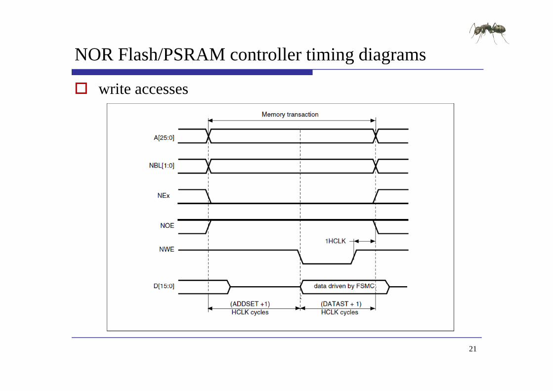
NOR FlashPSRAM controller timing diagramsg g
write accesses
21
FSMC Memory mapy p
22
Development Flowp
Embedded Software Side
int main(void)
Bootup STM32F10x
ProgrammingBootupSTM32F10x RCC Configure
NVIC Configure
int main(void)ifdef DEBUGdebug()
endif
FSMC SRAM Init
System Clocks Configuration RCC_Configuration()
NVIC Configuration
GPIO Configure
gNVIC_Configuration()
GPIO Configuration GPIO_Configuration()
GPIO Configure
FSMC Configure
Writeread tofrom FSMC SRAM memory
Configure FSMC Bank1 NORSRAM1 FSMC_SRAM_Init()
SRAM memory RW operation FSMC SRAM WriteBuffer
FSMC SRAM ReadBuffer
helliphelliphelliphelliphelliphelliphelliphelliphelliphelliphelliphelliphelliphelliphelliphelliphelliphelliphelliphelliphelliphelliphellipCheck content
Display Result
23
Configure FSMC IOg
Function name Description
RCC_APB2PeriphClockCmd(RCC_APB2Periph_GPIOD | RCC_APB2Periph_GPIOG | RCC_APB2Periph_GPIOE | RCC_APB2Periph_GPIOF ENABLE)
‐‐ GPIO Configuration ‐‐‐‐‐‐‐‐‐‐‐‐‐‐‐‐‐‐‐‐‐‐‐‐‐‐‐‐‐‐‐‐‐‐‐‐‐‐‐‐‐‐‐‐‐‐‐‐‐
GPIO FwLib Functions List
Function name Description
RCC_APB2PeriphClockCmd
Enables or disables the High Speed APB (APB2) peripheralclock
GPIO I it I iti li th GPIO
GPIO Configuration SRAM Data lines configuration GPIO_InitStructureGPIO_Pin = GPIO_Pin_0 | GPIO_Pin_1 | GPIO_Pin_8 |
GPIO_Pin_9 | GPIO_Pin_10 | GPIO_Pin_14 | GPIO_Pin_15GPIO_InitStructureGPIO_Mode = GPIO_Mode_AF_PPGPIO_InitStructureGPIO_Speed = GPIO_Speed_50MHzGPIO_Init(GPIOD ampGPIO_InitStructure) GPIO_Init Initializes the GPIOx
peripheral according to the specified parametersin the GPIO_InitStruct
RCC AHBPeriphClock Enables or disables the AHB
_ ( _ )GPIO_InitStructureGPIO_Pin = GPIO_Pin_7 | GPIO_Pin_8 | GPIO_Pin_9 |
GPIO_Pin_10 | GPIO_Pin_11 | GPIO_Pin_12 | GPIO_Pin_13 | GPIO_Pin_14 | GPIO_Pin_15
GPIO_Init(GPIOE ampGPIO_InitStructure) SRAM Address lines configuration GPIO_InitStructureGPIO_Pin = GPIO_Pin_0 | GPIO_Pin_1 | GPIO_Pin_2 |
| | | | |RCC_AHBPeriphClockCmd
Enables or disables the AHB peripheral clock
GPIO_Pin_3 | GPIO_Pin_4 | GPIO_Pin_5 | GPIO_Pin_12 | GPIO_Pin_13 | GPIO_Pin_14 | GPIO_Pin_15
GPIO_Init(GPIOF ampGPIO_InitStructure) GPIO_InitStructureGPIO_Pin = GPIO_Pin_0 | GPIO_Pin_1 | GPIO_Pin_2 |
GPIO_Pin_3 | GPIO_Pin_4 | GPIO_Pin_5GPIO_Init(GPIOG ampGPIO_InitStructure)GPIO InitStructure GPIO Pin GPIO Pin 11 | GPIO Pin 12 | GPIO Pin 13 GPIO_InitStructureGPIO_Pin = GPIO_Pin_11 | GPIO_Pin_12 | GPIO_Pin_13 GPIO_Init(GPIOD ampGPIO_InitStructure) NOE and NWE configuration GPIO_InitStructureGPIO_Pin = GPIO_Pin_4 |GPIO_Pin_5GPIO_Init(GPIOD ampGPIO_InitStructure) NE1configuration GPIO InitStructure GPIO Pin = GPIO Pin 7 GPIO_InitStructureGPIO_Pin = GPIO_Pin_7 GPIO_Init(GPIOD ampGPIO_InitStructure) NBL0 NBL1 configuration GPIO_InitStructureGPIO_Pin = GPIO_Pin_0 | GPIO_Pin_1 GPIO_Init(GPIOE ampGPIO_InitStructure) Enable the FSMC Clock RCC_AHBPeriphClockCmd(RCC_AHBPeriph_FSMC ENABLE)
24
_ p ( _ p _ )
Configure FSMCg
Function name Description
Enable the FSMC Clock RCC_AHBPeriphClockCmd(RCC_AHBPeriph_FSMC ENABLE)
‐‐ FSMC Configuration ‐‐
FSMC FwLib Functions List
Function name Description
RCC_AHBPeriphClockCmd
Enables or disables the AHB peripheral clock
FSMC_NORSRAMInit Initializes the FSMC NOR b k di t th
FSMC Configuration pFSMC_AddressSetupTime = 0pFSMC_AddressHoldTime = 0pFSMC_DataSetupTime = 2pFSMC_BusTurnAroundDuration = 0pFSMC_CLKDivision = 0pFSMC_DataLatency = 0memory bank according to the
parameters specified in FSMC_NORInitStruct
FSMC_NORSRAMCm Enables or disables the NORSRAM memory bank1
p _ y pFSMC_AccessMode = FSMC_AccessMode_AFSMC_NORSRAMInitStructureFSMC_Bank = FSMC_Bank1_NORSRAM1FSMC_NORSRAMInitStructureFSMC_DataAddressMux =
FSMC_DataAddressMux_DisableFSMC_NORSRAMInitStructureFSMC_MemoryType = FSMC_MemoryType_SRAMFSMC_NORSRAMInitStructureFSMC_MemoryDataWidth = FSMC_MemoryDataWidth_16bNORSRAM memory bank1 FSMC_NORSRAMInitStructureFSMC_BurstAccessMode =
FSMC_BurstAccessMode_DisableFSMC_NORSRAMInitStructureFSMC_WaitSignalPolarity =
FSMC_WaitSignalPolarity_LowFSMC_NORSRAMInitStructureFSMC_WrapMode = FSMC_WrapMode_DisableFSMC_NORSRAMInitStructureFSMC_WaitSignalActive =
FSMC WaitSignalActive BeforeWaitStateFSMC_WaitSignalActive_BeforeWaitStateFSMC_NORSRAMInitStructureFSMC_WriteOperation =
FSMC_WriteOperation_EnableFSMC_NORSRAMInitStructureFSMC_WaitSignal = FSMC_WaitSignal_DisableFSMC_NORSRAMInitStructureFSMC_ExtendedMode = FSMC_ExtendedMode_DisableFSMC_NORSRAMInitStructureFSMC_AsyncWait = FSMC_AsyncWait_DisableFSMC NORSRAMInitStructure FSMC WriteBurst = FSMC WriteBurst DisableFSMC_NORSRAMInitStructureFSMC_WriteBurst = FSMC_WriteBurst_DisableFSMC_NORSRAMInitStructureFSMC_ReadWriteTimingStruct = amppFSMC_NORSRAMInitStructureFSMC_WriteTimingStruct = amppFSMC_NORSRAMInit(ampFSMC_NORSRAMInitStructure)
Enable FSMC Bank1_SRAM Bank FSMC_NORSRAMCmd(FSMC_Bank1_NORSRAM1 ENABLE)
25
_ ( _ _ )
硬體電路配置
Mapping Table
Num SRAM STM32 Num SRAM STM32 Num SRAM STM32
1 A0 FSMC_A0 14 A13 FSMC_A13 27 IO8 FSMC_D82 A1 FSMC A1 15 A14 FSMC A14 28 IO9 FSMC D9_ _ _3 A2 FSMC_A2 16 A15 FSMC_A15 29 IO10 FSMC_D104 A3 FSMC_A3 17 A16 FSMC_A16 30 IO11 FSMC_D115 A4 FSMC_A4 18 A17 FSMC_A17 31 IO12 FSMC_D126 A5 FSMC_A5 19 IO0 FSMC_D0 32 IO13 FSMC_D137 A6 FSMC_A6 20 IO1 FSMC_D1 33 IO14 FSMC_D148 A7 FSMC_A7 21 IO2 FSMC_D2 34 IO15 FSMC_D159 A8 FSMC A8 22 IO3 FSMC D3 35 CE FSMC nNE19 A8 FSMC_A8 22 IO3 FSMC_D3 35 CE FSMC_nNE110 A9 FSMC_A9 23 IO4 FSMC_D4 36 OE FSMC_nOE11 A10 FSMC_A10 24 IO5 FSMC_D5 37 WE FSMC_nWE12 A11 FSMC A11 25 IO6 FSMC D6 38 UB FSMC NBL1_ _ _13 A12 FSMC_A12 26 IO7 FSMC_D7 39 LB FSMC_NBL0
26
實驗步驟
範例目錄架構
範例說明 範例說明
預設定義說明
燒錄 燒錄MIAT_STM32
27
範例目錄架構
範例目錄
測試映像檔 測試映像檔
含括檔
函式庫 函式庫
專案檔
原始碼 原始碼
28
範例說明
Embedded Software Side
Write data to FSMC SRAM memory
SRAM memory RW operation
Write data to FSMC SRAM memory Fill the buffer to send Fill_Buffer(TxBuffer BUFFER_SIZE 0x3212)FSMC_SRAM_WriteBuffer(TxBuffer WRITE_READ_ADDR BUFFER_SIZE)
SRAM memory RW operation
FSMC SRAM WriteBuffer
Read data from FSMC SRAM memory FSMC_SRAM_ReadBuffer(RxBuffer WRITE_READ_ADDR BUFFER_SIZE)
Read back SRAM memory and check content correctness
FSMC SRAM ReadBuffer
Check content
Display Result yfor (Index = 0x00 (Index lt BUFFER_SIZE) ampamp (WriteReadStatus == 0)
Index++)if (RxBuffer[Index] = TxBuffer[Index])
Display Result
WriteReadStatus = Index + 1
29
範例說明
Embedded Software Side
while (1)
Display Result
while (1)if (WriteReadStatus == 0) OK Turn on USERLED
GPIO SetBits(GPIOF GPIO Pin 11)
SRAM memory RW operation
FSMC SRAM WriteBufferGPIO_SetBits(GPIOF GPIO_Pin_11)
else KO Turn off USERLED
GPIO ResetBits(GPIOF GPIO Pin 11)
FSMC SRAM ReadBuffer
Check content
Display Result
如果寫入與讀取Buffer內容相同外部記憶體使用正常USERLED紅燈GPIO_ResetBits(GPIOF GPIO_Pin_11)
Insert delay Delay(0xAFFFF) Turn on USERLED GPIO SetBits(GPIOF GPIO Pin 11)
Display Result恆亮
GPIO_SetBits(GPIOF GPIO_Pin_11) Insert delay Delay(0xAFFFF)
如果寫入與讀取Buffer內容不同外部記憶體使用異常 USERLED紅燈閃爍
30
預設定義說明
define Bank1_SRAM1_ADDR ((u32)0x60000000) 定義SRAM起始點 定義SRAM起始點
define BUFFER_SIZE 0x400定義測試資料大小 定義測試資料大小
資料大小必需小於0xC000 define WRITE_READ_ADDR 0x8000 定義SRAM寫入起始點
寫入起始點WRITE_READ_ADDR + BUFFER_SIZE必需小於0x6000C000
31
燒錄MIAT STM32_
Rebuilder all target files產生HEX DFU Fil M 轉換HEX產生DFU DFU File Manager轉換HEX產生DFU DfuSe Demonstration燒錄DFU d Leave DFU mode
32
內部與外部SRAM存取控制實驗
實驗一
WU-YANGTechnology Co Ltd
實驗一練習
練習 修改寫入位置測試是否正常 修改寫入位置測試是否正常
修改寫入資料大小測試是否正常
取消 i 測試是否正常 取消FSMC_SRAM_Init測試是否正常
34
實驗目的(二)( )
使用MIAT_STM32實驗板透過FSMC控制外部SRAM並設定為data memory進行存取控制實驗同樣利用LED設定為data memory進行存取控制實驗同樣利用LED確認存取是否正常
35
實驗原理
External SRAM RVMDK環境設定 RVMDK環境設定
Development Flow fi ARM Configure Startup Code
36
RVMDK環境設定
外部SRAM有512K Bytes位置由0x60000000至0x60080000
37
Development Flowp
Embedded Software Side
int main(void)
Bootup STM32F10x
Programming
Bootup
int main(void)ifdef DEBUGdebug()
endif
Startup Code
BootupSTM32F10x
RCC Configure
NVIC Configure
System Clocks Configuration RCC_Configuration()
NVIC Configuration g gNVIC_Configuration()
GPIO Configuration GPIO_Configuration()
GPIO Configure
for (Index = 0 Index lt1024 Index++)
Tab[Index] =IndexT bAdd ( 32)T b h ld b 0 600000
Check operation
Check pointer value
Display Result TabAddr = (u32)Tab should be 0x600000xx
Get main stack pointer value MSPValue = __MRS_MSP() should be 0x2000xxxx
helliphelliphelliphelliphelliphelliphelliphelliphelliphelliphelliphelliphelliphelliphelliphelliphelliphelliphelliphelliphelliphelliphellip
Display Result
38
Startup Codep
Register boundary addresses RCC Configure
Enable FSMC clock
LDR R0= 0x00000114
LDR R1= 0x40021014
STR R0[R1]
Enable GPIOD GPIOE GPIOF and GPIOG clocks
LDR R0= 0x000001E0
LDR R1= 0x40021018
RCC register map
STR R0[R1]
39
RCC Register g
Bit 8 FSMCEN FSMC clock enableAHB Peripheral Clock enable register (RCC_AHBENR)
Bit 8 FSMCEN FSMC clock enableSet and cleared by software0 FSMC clock disabled
APB2 peripheral clock enable register (RCC_APB2ENR)
1 FSMC clock enabled
Bit 8765 IOPGEN IO port GFED clock enableSet and cleared by software0 IO port GFED clock disabled1 IO port GFED clock enabled
40
1 IO port GFED clock enabled
Startup Codep
Register boundary addresses GPIO Configure
SRAM Data lines NOE and NWE configuration SRAM Address lines configuration NOE NEW NE1 NBL0 NBL1 configuration LDR R0= 0xB4BB44BB LDR R1= 0x40011400STR R0[R1]LDR R0= 0xBBBBBBBB LDR R1= 0x40011404STR R0[R1]LDR R0 = 0xB44444BBLDR R0= 0xB44444BB LDR R1= 0x40011800STR R0[R1]LDR R0= 0xBBBBBBBB LDR R1= 0x40011804
GPIO register map
STR R0[R1]LDR R0= 0x44BBBBBB LDR R1= 0x40011C00STR R0[R1]LDR R0= 0xBBBB4444 LDR R1= 0x40011C04STR R0[R1]LDR R0= 0x44BBBBBBLDR R1= 0x40012000STR R0 [R1]
41
STR R0[R1]
GPIO Register g
Bit 8 FSMCEN FSMC clock enablePort configuration register low
Port configuration register high
Bits 2928 2524Bits 3130 2726 2322 1918 1514 1110 76 32 Bits 2928 25242120 1716 131298 54 10MODEy[10] Port x mode bits (y= 0 15)00 Input mode (reset state)01 Output mode max speed 10 MHz
Bits 3130 27262322 1918 15141110 76 32CNFy[10] Port x configuration bits (y= 0 15)In input mode (MODE[10]=00)00 Analog input mode01 Floating input (reset state)10 Input with pull-up pull-down
10 Output mode max speed 2 MHz11 Output mode max speed 50 MHz
11 ReservedIn output mode (MODE[10] gt00)00 General purpose output push-pull01 General purpose output Open-drain10 Alternate function output Push-pull11 Alternate function output Open-drain
42
11 Alternate function output Open drain
Startup Codep
FSMCregister map FSMC Configure
FSMC Configuration Enable FSMC Bank1_SRAM Bank
LDR R0= 0x00001011
LDR R1= 0xA0000000
STR R0[R1]
LDR R0= 0x00000200
LDR R1= 0xA0000004
STR R0[R1]
43
FSMC Register g
Bit 8 FSMCEN FSMC clock enableSRAMNOR-Flash chip-select control registers 1 (FSMC_BCR1)
Bit 12 WREN Write enable bitThis bit indicates whether write operations are enableddisabled in the bank by the FSMC0 Write operations are disabled in the bank by the FSMC an AHB error is reported1 Write operations are enabled for the bank by the FSMC (default after reset) p y ( )Bits 54 MWID Memory databus widthDefines the external memory device width valid for all type of memories00 8 bits01 16 bits (default after reset)10 reserved do not use10 reserved do not use11 reserved do not use Bit 0 MBKEN Memory bank enable bitEnables the memory bank After reset Bank1 is enabled all others are disabled Accessing adisabled bank causes an ERROR on AHB bus0 C di b k i di bl d0 Corresponding memory bank is disabled1 Corresponding memory bank is enabled
44
FSMC Register g
Bit 8 FSMCEN FSMC clock enableSRAMNOR-Flash chip-select timing registers 1 (FSMC_BTR1)
Bits 158 DATAST Data-phase duration0000 0000 Reserved0000 0001 DATAST phase duration = 2 times HCLK clock cycles0000 0010 DATAST phase duration = 3 times HCLK clock cycles1111 1111 DATAST phase duration = 256 times HCLK clock cycles (default value after reset)Bits 74 ADDHLD Address-hold phase duration0000 Reserved0001 ADDHLD phase duration = 2 times HCLK clock cycle0010 ADDHLD phase duration = 3 times HCLK clock cycle1111 ADDHLD phase duration = 16 times HCLK clock cycles (default value after reset)Bits 30 ADDSET Address setup phase durationThese bits are written by software to define the duration of the address setup phase (refer toFigure 162 to Figure 172) used in SRAMs ROMs and asynchronous NOR Flash0000 ADDSET phase duration = 1 times HCLK clock cycle1111 ADDSET phase duration = 16 times HCLK clock cycles (default value after reset)
45
實驗步驟
範例目錄架構
範例說明 範例說明
預設定義說明
46
範例目錄架構
範例目錄
測試映像檔 測試映像檔
含括檔
函式庫 函式庫
專案檔
原始碼 原始碼
47
範例說明
Embedded Software Side
Infinite loop
Display Result
Infinite loop while (1)if (((TabAddramp0xFFFFFF00) == 0x60000000) ampamp
((MSPValueamp0xFFFF0000) == 0x20000000))
Check operation
Check pointer value((MSPValueamp0xFFFF0000) == 0x20000000))
OK Turn on USERLED GPIO_SetBits(GPIOF GPIO_Pin_11)
else
Display Result
else KO Turn off USERLED
GPIO_ResetBits(GPIOF GPIO_Pin_11) Insert delay Delay(0xAFFFF)
如果Tab位置在0x600000且Stack pointer位置在0x2000 外部記憶體使用正常USERLED紅燈恆亮Delay(0xAFFFF)
Turn on USERLED GPIO_SetBits(GPIOF GPIO_Pin_11) Insert delay Delay(0xAFFFF)
紅燈恆亮
如果 b位置不在0 600000或Delay(0xAFFFF)
如果Tab位置不在0x600000或Stack pointer位置不在0x2000 外部記憶體使用異常USERLED紅燈閃爍
48
預設定義說明
DATA_IN_ExtSRAM EQU 1 E l SRAM C fi i External SRAM Configuration 0=gt DISABLE 1=gt ENABLE
u32 Tab[1024]宣告於外部 的記憶體 宣告於外部SRAM的記憶體
49
data memory存取控制實驗
實驗二
WU-YANGTechnology Co Ltd
實驗二練習
練習 取消RVMDK環境外部SRAM設定測試是否正常 取消RVMDK環境外部SRAM設定測試是否正常
修改DATA_IN_ExtSRAM EQU 0測試是否正常
修改外部 記憶體 b變數大小測試是否正常 修改外部SRAM記憶體Tab變數大小測試是否正常
51
Q amp A
WU-YANGTechnology Co Ltd
MIAT_STM32內部Flash存取控制實驗
WU-YANG
浯陽科技有限公司
Technology Co Ltd
Declared Version
Training Only
Declare
Document Number
Document Version 100
Release Date
Document Title MIAT_STM32 內部FLASH存取控制實驗
Exercise Time
Platform MIAT_STM32V2MIAT IOB V1PlatformMIAT IOBV1
Peripheral
Author WU-YANG Technology Co Ltd
2
實驗目的(一)( )
使用MIAT_STM32實驗板透過Flash memory interface (FLITF)控制內部Flash進行存取控制實驗並利用LED(FLITF)控制內部Flash進行存取控制實驗並利用LED確認存取是否正常
3
實驗原理
System architecture E b dd d Fl h Embedded Flash Features Memory map RVMDK環境設定
FLITF Flash module organization
Flash library function Development Flow ARM Configure
4
System architecturey
5
Embedded Flash
Features 256 Kb up to 256 Kbytes Memory organization the Flash memory is organized as a
main block and an information blockmain block and an information block Main memory block of size t 32 Kb 64 bit di id d i t 128 f 2 up to 32 Kb times 64 bits divided into 128 pages of 2
Kbytes Information block of size Information block of size 258 times 64 bits
6
Embedded Flash Memory mapy p
7
Flash Memoryy
8
RVMDK環境設定
STMF103ZC有256K Bytes的Flash位置由0x8000000至0x8040000
9
FLITF
Features R d i f i h f h b ff (2 64 bi d ) Read interface with prefetch buffer (2x64-bit words) Option byte Loader
l h i Flash Program Erase operation Read Write protection
10
Flash memory interfacey
11
Flash memory interface registery g
Bit 8 FSMCEN FSMC clock enableFlash status register (FLASH_SR)
Bits 316 Reserved must be kept clearedBit 5 EOP End of operation
Bit 2 PGERR Programming errorSet by hardware when an address to be programmed p
Set by hardware when a Flash operation (programming erase) is completed Reset by writing a 1Note EOP is asserted at the end of each successful
y p gcontains a value different from 0xFFFF before programmingReset by writing 1Note The STRT bit in the FLASH_CR register f f
program or erase operationBit 4 WRPRTERR Write protection errorSet by hardware when programming a write-protected address of the Flash memory
_ gshould be reset before starting a programmingoperationBit 1 Reserved must be kept clearedBit 0 BSY Busyp y
Reset by writing 1Bit 3 Reserved must be kept cleared
This indicates that a Flash operation is in progress This is set on the beginning of a Flash operation and reset when the operation finishes or when an error occurs
12
Flash memory interface registery g
Flash control register (FLASH_CR)
Bit 9 OPTWRE Option bytes write enableWhen set the option bytes can be programmed This
Bit 6 STRT StartThis bit triggers an ERASE operation when set This bit is set only
bit is set on writing the correct key sequence to the FLASH_OPTKEYR registerThis bit can be reset by softwareBit 8 Reserved must be kept clearedBit 7 LOCK Lock
by software and reset when the BSY bit is resetBit 5 OPTER Option byte eraseOption byte erase chosenBit 4 OPTPG Option byte programmingOption byte programming chosenBit 7 LOCK Lock
Write to 1 only When it is set it indicates that the FPEC and FLASH_CR are locked This bit is reset by hardware after detecting the unlock sequenceIn the event of unsuccessful unlock operation this bit remains set until the next reset
p y p g gBit 3 Reserved must be kept clearedBit 2 MER Mass eraseErase of all user pages chosenBit 1 PER Page erasePage Erase chosenremains set until the next reset Page Erase chosenBit 0 PG ProgrammingFlash programming chosen
13
Main Flash memory programmingy p g g
14
Flash memory Page Erasey g
15
Flash memory Mass Erasey
16
Option byte programmingp y p g g
17
Option byte Erasep y
18
FLASH library functiony
19
FLASH library functiony
20
Development Flowp
Embedded Software Side
int main(void)
Bootup STM32F10x
ProgrammingBootupSTM32F10x RCC Configure
NVIC Configure
int main(void)ifdef DEBUGdebug()
endifendif
FLASHStatus = FLASH_COMPLETEMemoryProgramStatus = PASSEDData = 0x15041975
GPIO Configure
Data = 0x15041975
RCC Configuration RCC_Configuration()
Flash memory RW operation FLASH Unlock
FLASH ClearFlag NVIC Configuration NVIC_Configuration()
GPIO Configuration
FLASH ClearFlag
FLASH ErasePage
FLASH ProgramWord GPIO Configuration GPIO_Configuration()
helliphelliphelliphelliphelliphelliphelliphelliphelliphelliphelliphelliphelliphelliphelliphelliphellipDisplay Result
Check content
21
實驗步驟
範例目錄架構
範例說明 範例說明
預設定義說明
燒錄 燒錄MIAT_STM32
22
範例目錄架構
範例目錄
測試映像檔 測試映像檔
含括檔
函式庫 函式庫
專案檔
原始碼 原始碼
23
範例說明
Function name Description
Unlock the Flash Program Erase controller FLASH_Unlock()
D fi h b f b d
Flash FwLib Functions List
Function name Description
FLASH_Unlock Unlocks the FLASH Program Erase Controller
FLASH_ClearFlag Clears the FLASH pending fl
Define the number of page to be erased NbrOfPage = (EndAddr - StartAddr) FLASH_PAGE_SIZE
Clear All pending flags FLASH_ClearFlag(FLASH_FLAG_BSY | FLASH_FLAG_EOP | FLASH_FLAG_PGERR |
FLASH FLAG WRPRTERR)flags
FLASH_ErasePage Erases a specified FLASH page
FLASH_ProgramWord Programs a word at a specified
_ _ )
Erase the FLASH pages for(EraseCounter = 0 (EraseCounter lt NbrOfPage) ampamp (FLASHStatus ==
FLASH_COMPLETE) EraseCounter++)FLASHStatus = FLASH ErasePage(StartAddr + (FLASH PAGE SIZE EraseCounter))address FLASHStatus = FLASH_ErasePage(StartAddr + (FLASH_PAGE_SIZE EraseCounter))
FLASH Word program of data 0x15041979 at addresses defined by StartAddr and EndAddrAddress = StartAddr
while((Address lt EndAddr) ampamp (FLASHStatus == FLASH_COMPLETE))FLASHStatus = FLASH_ProgramWord(Address Data)Address = Address + 4
24
範例說明
Embedded Software Side
Check the corectness of written data
Display Result
Check the corectness of written data Address = StartAddr
while((Address lt EndAddr) ampamp (MemoryProgramStatus = FAILED))if(((vu32) Address) = Data)
Flash memory RW operation
MemoryProgramStatus = FAILED
Address += 4
Check content
Display Result while (1)if (MemoryProgramStatus == PASSED) OK Turn on USERLED GPIO_SetBits(GPIOF GPIO_Pin_11)
Display Result
else KO Turn off USERLED GPIO_ResetBits(GPIOF GPIO_Pin_11) Insert delay Delay(0xAFFFF)
如果寫入與讀取Flash內容相同Flash記憶體使用正常USERLED紅燈恆亮
Turn on USERLED GPIO_SetBits(GPIOF GPIO_Pin_11) Insert delay Delay(0xAFFFF)
如果寫入與讀取Flash內容不同Flash記憶體使用異常USERLED紅燈閃爍
25
預設定義說明
define StartAddr ((u32)0x08008000) 定義Flash使用起始點 定義Flash使用起始點
使用起始點必需大於0x8003000 + Code Size 附註 0x8000000~0x8003000為DFU程式區塊使用此區塊
將造成無法燒錄程式
Code Size可由產生的HEX檔得知
d fi E dAdd (( 32)0 0800C000) define EndAddr ((u32)0x0800C000) 定義Flash使用結束點
使用起始點必需小於0x8040000使用起始點必需小於
Data = 0x15041975 寫入資料
32Bit define FLASH_PAGE_SIZE ((u16)0x800)
每一個Page有2KByte26
每一個Page有2KByte
Intel HEX Format
aaaa tt dd cc
field Description
the colon that starts every Intel HEX record
the record-length field that represents the number of data bytes (dd) in the record
aaaa the address field that represents the starting address for subsequent data in the record
tt the field that represents the HEX record type which may be one of the following00 - data record01 - end-of-file record02 - extended segment address recordg04 - extended linear address record
dd a data field that represents one byte of data A record may have multiple data bytes The number of data bytes in the record must match the number specified by the field
cc the checksum field that represents the checksum of the record The checksum is calculated by summing the values of all hexadecimal digit pairs in the record modulo 256 and taking the twos complement
27
HEX Examplep
020000040800F2103000001814002045310008D9340008CD340008D8103000001814002045310008D9340008CD340008D8helliphelliphellip1038200042370008000000000000000000000000170C3830000000000000000000000000008C
資料填入起始位置為
0C3830000000000000000000000000008C04000005080031318D00000001FF
資料填入起始位置為0x08003000 每一行有0x10(16)個Bytes 最後一筆資料為
資料結束點為0x0803383004000005080031318D
(0x08003830 -0x08000000)0x800 = 7 需以0x800為單位所以使用的位置起點為0x08004000
28
燒錄MIAT STM32_
Rebuilder all target files產生HEX DFU Fil M 轉換HEX產生DFU DFU File Manager轉換HEX產生DFU DfuSe Demonstration燒錄DFU d Leave DFU mode
29
內部Flash存取控制實驗
實驗一
WU-YANGTechnology Co Ltd
實驗一練習
注意 請使用預設0 08008000之後的位置 避免覆蓋DFU 請使用預設0x08008000之後的位置避免覆蓋DFU
與使用者程式碼區塊
練習 練習 修改存取位置測試是否正常
修改寫入資料測試是否正常 修改寫入資料測試是否正常
修改寫入資料後取消FLASH_Unlock測試是否正常
修改寫入資料後取消FLASH E P 測試是否正 修改寫入資料後取消FLASH_ErasePage測試是否正常
31
實驗目的(二)( )
使用MIAT_STM32實驗板透過Flash memory interface (FLITF)控制內部Flash進行存取控制實驗並利用SW(FLITF)控制內部Flash進行存取控制實驗並利用SWKEY決定資料寫入與讀取LCD顯示狀態
32
實驗原理
System requirement E b dd d Fl h Embedded Flash LCD KEY SW
Development Flow ARM Configure
33
Development Flowp
Embedded Software Side
int main(void)
Bootup STM32F10x
ProgrammingBootupSTM32F10x RCC Configure
NVIC Configure
int main(void)ifdef DEBUGdebug()
endif
FLASHStatus = FLASH_COMPLETE
RCC Configuration RCC Configuration()
GPIO Configure
BasicIO Configure_ g ()
NVIC Configuration NVIC_Configuration()
GPIO Configuration Flash memory RW ti
lcd Configure
GPIO Configuration GPIO_Configuration()
Init_BasicIO()
l d i i () LCD I i i li i
RW operation
Example
FLASH Unlock
FLASH ClearFlag
lcd_init() LCD Initialization
helliphelliphelliphelliphelliphelliphelliphelliphelliphelliphelliphelliphelliphelliphelliphelliphelliphelliphelliphelliphelliphelliphellip
p
34
硬體電路配置
Mapping Table
Num MIAT_STM32V2 MIAT_IOBV1 Num MIAT_STM32V2 MIAT_IOBV1
1 PC8 (326) SW1 10 PE6 (15) LCD_EN2 PC9 (327) SW2 11 PF6 (118) LCD RW ( ) ( ) _3 PC10 (43) SW3 12 PF7 (119) LCD_RS 4 PC11 (44) SW4 13 PF8(120) LCD_D4 5 PB5 (427) KEY1 14 PF9 (121) LCD_D5 6 PB6 (428) KEY2 15 PF10 (122) LCD_D6 7 PB7 (429) KEY3 16 PF11 (213) LCD_D7 8 PB8 (431) KEY4 17 VDD (236) VCC33V 9 VCC5V (1 36) VCC5V 18 GND (1 35) GND9 VCC5V (136) VCC5V 18 GND (135) GND
35
實驗步驟
範例目錄架構
範例說明 範例說明
預設定義說明
36
範例目錄架構
範例目錄
測試映像檔 測試映像檔
含括檔
函式庫 函式庫
專案檔
原始碼 原始碼
37
範例說明
Embedded Software Side
lcd clear()
FLASH memory RW operation
lcd_clear()lcd_print (MIAT_STM32 DEMO )
Unlock the Flash Program Erase controller FLASH_Unlock()
Flash memory RW operation
FLASH Unlock
Clear All pending flags FLASH_ClearFlag(FLASH_FLAG_BSY | FLASH_FLAG_EOP | FLASH_FLAG_PGERR |
FLASH_FLAG_WRPRTERR)
while(1)
Example
FLASH ClearFlag
( )
KEY_Buffer=Key_Scan()set_cursor (0 1)lcd_print (SW Value = 0x)lcd putchar(((SWamp0x7)+0x30))lcd_putchar(((SWamp0x7)+0x30))if(KEY_Buffer==1)Address=(StartAddr|(SWltlt12))set_cursor (0 0)lcd_print (Set Addr = 0x)
掃描KEY是否按下與顯示SW數值LCD Line2顯示SW Value = 0x(SW)
lcd_putchar(((SWamp0x7)+0x30))lcd_print ( )
如果KEY1按下記錄SW數值至Address LCD Line1顯示Set Adde = 0x(Address)
38
範例說明
Embedded Software Side
else if(KEY Buffer==2)
FLASH memory RW operation
else if(KEY_Buffer==2)
Erase the FLASH pages FLASHStatus = FLASH_ErasePage(Address)
FLASH Word program of data at addresses defined by SW
SRAM memory RW operation
p g yFLASHStatus = FLASH_ProgramWord(Address (SWamp0x7))
set_cursor (0 0)lcd_print (Write 0x)lcd_putchar(((SWamp0x7)+0x30))l d i t ( t 0 )
Example如果KEY2按下清除Address所處區塊並寫入SW數值 lcd_print ( at 0x)
lcd_putchar((((Addressgtgt12)amp0x7)+0x30))else if(KEY_Buffer==3)
Data=(u16 )Address
所處區塊並寫入SW數值LCD Line1顯示Write 0x(SW) at 0x(Adddress)
Data (u16 )Addressset_cursor (0 0)lcd_print (Addr 0x)lcd_putchar((((Addressgtgt12)amp0x7)+0x30))lcd_print ( = 0x)lcd_putchar(((Dataamp0x7)+0x30))lcd_print ( )
如果KEY3按下讀取Address紀錄數值LCD Line1顯示Addr 0x(Adddress) = 0x
39
預設定義說明
define StartAddr ((u32)0x08020000) 定義Flash使用起始點 定義Flash使用起始點
使用起始點必需大於0x8003000 + Code Size 附註 0x8000000~0x8003000為DFU程式區塊使用此區塊
將造成無法燒錄程式
Code Size可由產生的HEX檔得知
32 Add 0 08020000 u32 Address = 0x08020000 定義Address初始值
初始值必需與Flash使用起始點相同初始值必需與 使用起始點相同
Address=(StartAddr|(SWltlt12)) Example StartAddr = 0x08020000 SW = 1 Address = 0x08021000
StartAddr = 0x08020000 SW = 7 Address = 0x08027000 StartAddr|(7ltlt12)必需小於0x8040000
40
使用者界面與Flash存取控制實驗
實驗二
WU-YANGTechnology Co Ltd
實驗二練習
注意 請使用預設0 08020000之後的位置 避免覆蓋DFU 請使用預設0x08020000之後的位置避免覆蓋DFU
與使用者程式碼區塊
練習 練習 利用SW與KEY測試Flash寫入與讀取是否正常
Fl h寫入後電源關閉 再開啟後寫入資料是否仍存 Flash寫入後電源關閉再開啟後寫入資料是否仍存在
修改存取位置測試是否正常 修改存取位置測試是否正常
42
實驗目的(三)( )
使用MIAT_STM32實驗板透過Flash memory interface (FLITF)控制內部Flash進行存取控制實驗並藉由填入(FLITF)控制內部Flash進行存取控制實驗並藉由填入Option Bytes 設定寫入鎖定保護Page鎖定不被覆蓋
43
Development Flowp
Embedded Software Side
int main(void)
Bootup STM32F10x
ProgrammingBootupSTM32F10x RCC Configure
NVIC Configure
int main(void)ifdef DEBUGdebug()
endifendif
FLASHStatus = FLASH_COMPLETEMemoryProgramStatus = PASSEDData = 0x1753
GPIO Configure
Data = 0x1753
RCC Configuration RCC_Configuration()
Flash memory RW operation FLASH Unlock
FLASH ClearFlag NVIC Configuration NVIC_Configuration()
GPIO Configuration
FLASH ClearFlag
FLASH ErasePage
FLASH ProgramHalfWord GPIO Configuration GPIO_Configuration()
Display Result
Check content
44
helliphelliphelliphelliphelliphelliphelliphelliphelliphelliphelliphelliphelliphelliphelliphelliphelliphelliphellip
實驗步驟
範例目錄架構
範例說明 範例說明
預設定義說明
45
範例目錄架構
範例目錄
測試映像檔 測試映像檔
含括檔
函式庫 函式庫
專案檔
原始碼 原始碼
46
範例說明
Function name Description
Unlock the Flash Program Erase controller FLASH_Unlock()
Define the number of page to be erased
Flash FwLib Functions List
Function name Description
FLASH_Unlock Unlocks the FLASH Program Erase Controller
FLASH_ClearFlag Clears the FLASH pending fl
Define the number of page to be erased NbrOfPage = (EndAddr ‐ StartAddr) FLASH_PAGE_SIZE
FLASH_ClearFlag(FLASH_FLAG_BSY | FLASH_FLAG_EOP|FLASH_FLAG_PGERR |FLASH_FLAG_WRPRTERR)
Get pages write protection status flags
FLASH_EraseOptionBytes
Erases the FLASH option bytes
FLASH_EnableWritePro Write protects the desired
p g pWRPR_Value = FLASH_GetWriteProtectionOptionByte()ProtectedPages = WRPR_Value amp 0x000000C0
ifdef WriteProtection_Disableif (ProtectedPages == 0x00) Pages are write protected
tection pages
NVIC_GenerateSystemReset
Generate a system reset
Disable the write protection FLASHStatus = FLASH_EraseOptionBytes() Generate System Reset to load the new option byte values NVIC_GenerateSystemReset()
elseifdef WriteProtection Enableifdef WriteProtection_Enableif (ProtectedPages = 0x00) Pages not write protected
FLASHStatus = FLASH_EraseOptionBytes() Enable the pages write protection FLASHStatus = FLASH_EnableWriteProtection(FLASH_WRProt_Pages12to13
|FLASH WRProt Pages14to15)|FLASH_WRProt_Pages14to15) Generate System Reset to load the new option byte values NVIC_GenerateSystemReset()
endifendif
47
範例說明
if (ProtectedPages = 0x00) Clear All pending flags
Flash FwLib Functions List
Function name DescriptionFLASH_ClearFlag(FLASH_FLAG_BSY |
FLASH_FLAG_EOP|FLASH_FLAG_PGERR |FLASH_FLAG_WRPRTERR)
erase the FLASH pages for(EraseCounter = 0 (EraseCounter lt NbrOfPage) ampamp (FLASHStatus ==
Function name Description
FLASH_ErasePage Erases a specified FLASH page
FLASH_ProgramHalfWod
Programs a half word at a ifi d dd FLASH_COMPLETE) EraseCounter++)
FLASHStatus = FLASH_ErasePage(StartAddr + (FLASH_PAGE_SIZE
EraseCounter))
rd specified address
FLASH Half Word program of data 0x1753 at addresses defined by StartAddrand EndAddr
Address = StartAddr
hil ((Add E dAdd ) ampamp (FLASHSt t FLASH COMPLETE))while((Address lt EndAddr) ampamp (FLASHStatus == FLASH_COMPLETE))
FLASHStatus = FLASH_ProgramHalfWord(Address Data)Address = Address + 2
48
範例說明
Embedded Software Side
Check the corectness of written data
Display Result
Check the corectness of written data Address = StartAddr
while((Address lt EndAddr) ampamp (MemoryProgramStatus = FAILED))if(((vu16) Address) = Data)
Flash memory RW operation
MemoryProgramStatus = FAILED
Address += 2
Check content
Display Result while (1)if (MemoryProgramStatus == PASSED) OK Turn on USERLED GPIO_SetBits(GPIOF GPIO_Pin_11)
Display Result
else KO Turn off USERLED GPIO_ResetBits(GPIOF GPIO_Pin_11) Insert delay Delay(0xAFFFF)
如果寫入與讀取Flash內容相同Flash記憶體可以寫入USERLED紅燈恆亮
Turn on USERLED GPIO_SetBits(GPIOF GPIO_Pin_11) Insert delay Delay(0xAFFFF)
如果寫入與讀取Flash內容不同Flash記憶體不能寫入USERLED紅燈閃爍
49
預設定義說明
define StartAddr ((u32) 0x08006000) 定義Flash使用起始點 定義Flash使用起始點
使用起始點必需大於0x8003000 + Code Size 附註 0x8000000~0x8003000為DFU程式區塊使用此區塊
將造成無法燒錄程式
Code Size可由產生的HEX檔得知
d fi E dAdd (( 32) 0 08008000) define EndAddr ((u32) 0x08008000) 定義Flash使用結束點
使用起始點必需小於0x8040000使用起始點必需小於
Data = 0x1753 寫入資料
16Bit define FLASH_PAGE_SIZE ((u16)0x800) 每一個Page有2KByte
50
每一個Page有2KByte
預設定義說明
define WriteProtection_Enable U hi li E bl W i P i Uncomment this line to Enable Write Protection
define WriteProtection_Disablehi li i bl i i Uncomment this line to Disable Write Protection
FLASH_EnableWriteProtection設定影響 個 設定影響2個Page FLASH_WRProt_Pages0to1 FLASH_WRProt_Pages1to2 helliphellip FLASH_WRProt_Pages60to61
設定影響多個Page FLASH_WRProt_Pages62to255
51
FLASH EnableWriteProtection_
Example
位置0x08006000 ~ 0x08007000每一個Page有0x800ByteStartPage = (0x08006000-0x08000000)0x800 = 12EndPage = ((0x08007000-0x08000000)0x800)-1 = 13執行執行FLASH_EnableWriteProtection(FLASH_WRProt_Pages12to13)將影響Pages12 Pages13
52
內部Flash寫入鎖定存取控制實驗
實驗三
WU-YANGTechnology Co Ltd
實驗三練習
注意 請使用預設0 08006000之後的位置 避免覆蓋DFU 請使用預設0x08006000之後的位置避免覆蓋DFU
與使用者程式碼區塊
更改寫入位置測試寫入鎖定時需同時更改 更改寫入位置測試寫入鎖定時需同時更改FLASH_EnableWriteProtection鎖定之Page
練習 練習 打開define WriteProtection_Enable測試是否可寫入
打開define WriteProtection Disable測試是否可寫入 打開define WriteProtection_Disable測試是否可寫入
修改存取位置測試是否正常
修改寫入資料測試是否正常 修改寫入資料測試是否正常
54
Q amp A
WU-YANGTechnology Co Ltd

Development Flowp
Embedded Software Side
int main(void)
Bootup STM32F10x
ProgrammingBootupSTM32F10x RCC Configure
NVIC Configure
int main(void)ifdef DEBUGdebug()
endif
FSMC SRAM Init
System Clocks Configuration RCC_Configuration()
NVIC Configuration
GPIO Configure
gNVIC_Configuration()
GPIO Configuration GPIO_Configuration()
GPIO Configure
FSMC Configure
Writeread tofrom FSMC SRAM memory
Configure FSMC Bank1 NORSRAM1 FSMC_SRAM_Init()
SRAM memory RW operation FSMC SRAM WriteBuffer
FSMC SRAM ReadBuffer
helliphelliphelliphelliphelliphelliphelliphelliphelliphelliphelliphelliphelliphelliphelliphelliphelliphelliphelliphelliphelliphelliphellipCheck content
Display Result
23
Configure FSMC IOg
Function name Description
RCC_APB2PeriphClockCmd(RCC_APB2Periph_GPIOD | RCC_APB2Periph_GPIOG | RCC_APB2Periph_GPIOE | RCC_APB2Periph_GPIOF ENABLE)
‐‐ GPIO Configuration ‐‐‐‐‐‐‐‐‐‐‐‐‐‐‐‐‐‐‐‐‐‐‐‐‐‐‐‐‐‐‐‐‐‐‐‐‐‐‐‐‐‐‐‐‐‐‐‐‐
GPIO FwLib Functions List
Function name Description
RCC_APB2PeriphClockCmd
Enables or disables the High Speed APB (APB2) peripheralclock
GPIO I it I iti li th GPIO
GPIO Configuration SRAM Data lines configuration GPIO_InitStructureGPIO_Pin = GPIO_Pin_0 | GPIO_Pin_1 | GPIO_Pin_8 |
GPIO_Pin_9 | GPIO_Pin_10 | GPIO_Pin_14 | GPIO_Pin_15GPIO_InitStructureGPIO_Mode = GPIO_Mode_AF_PPGPIO_InitStructureGPIO_Speed = GPIO_Speed_50MHzGPIO_Init(GPIOD ampGPIO_InitStructure) GPIO_Init Initializes the GPIOx
peripheral according to the specified parametersin the GPIO_InitStruct
RCC AHBPeriphClock Enables or disables the AHB
_ ( _ )GPIO_InitStructureGPIO_Pin = GPIO_Pin_7 | GPIO_Pin_8 | GPIO_Pin_9 |
GPIO_Pin_10 | GPIO_Pin_11 | GPIO_Pin_12 | GPIO_Pin_13 | GPIO_Pin_14 | GPIO_Pin_15
GPIO_Init(GPIOE ampGPIO_InitStructure) SRAM Address lines configuration GPIO_InitStructureGPIO_Pin = GPIO_Pin_0 | GPIO_Pin_1 | GPIO_Pin_2 |
| | | | |RCC_AHBPeriphClockCmd
Enables or disables the AHB peripheral clock
GPIO_Pin_3 | GPIO_Pin_4 | GPIO_Pin_5 | GPIO_Pin_12 | GPIO_Pin_13 | GPIO_Pin_14 | GPIO_Pin_15
GPIO_Init(GPIOF ampGPIO_InitStructure) GPIO_InitStructureGPIO_Pin = GPIO_Pin_0 | GPIO_Pin_1 | GPIO_Pin_2 |
GPIO_Pin_3 | GPIO_Pin_4 | GPIO_Pin_5GPIO_Init(GPIOG ampGPIO_InitStructure)GPIO InitStructure GPIO Pin GPIO Pin 11 | GPIO Pin 12 | GPIO Pin 13 GPIO_InitStructureGPIO_Pin = GPIO_Pin_11 | GPIO_Pin_12 | GPIO_Pin_13 GPIO_Init(GPIOD ampGPIO_InitStructure) NOE and NWE configuration GPIO_InitStructureGPIO_Pin = GPIO_Pin_4 |GPIO_Pin_5GPIO_Init(GPIOD ampGPIO_InitStructure) NE1configuration GPIO InitStructure GPIO Pin = GPIO Pin 7 GPIO_InitStructureGPIO_Pin = GPIO_Pin_7 GPIO_Init(GPIOD ampGPIO_InitStructure) NBL0 NBL1 configuration GPIO_InitStructureGPIO_Pin = GPIO_Pin_0 | GPIO_Pin_1 GPIO_Init(GPIOE ampGPIO_InitStructure) Enable the FSMC Clock RCC_AHBPeriphClockCmd(RCC_AHBPeriph_FSMC ENABLE)
24
_ p ( _ p _ )
Configure FSMCg
Function name Description
Enable the FSMC Clock RCC_AHBPeriphClockCmd(RCC_AHBPeriph_FSMC ENABLE)
‐‐ FSMC Configuration ‐‐
FSMC FwLib Functions List
Function name Description
RCC_AHBPeriphClockCmd
Enables or disables the AHB peripheral clock
FSMC_NORSRAMInit Initializes the FSMC NOR b k di t th
FSMC Configuration pFSMC_AddressSetupTime = 0pFSMC_AddressHoldTime = 0pFSMC_DataSetupTime = 2pFSMC_BusTurnAroundDuration = 0pFSMC_CLKDivision = 0pFSMC_DataLatency = 0memory bank according to the
parameters specified in FSMC_NORInitStruct
FSMC_NORSRAMCm Enables or disables the NORSRAM memory bank1
p _ y pFSMC_AccessMode = FSMC_AccessMode_AFSMC_NORSRAMInitStructureFSMC_Bank = FSMC_Bank1_NORSRAM1FSMC_NORSRAMInitStructureFSMC_DataAddressMux =
FSMC_DataAddressMux_DisableFSMC_NORSRAMInitStructureFSMC_MemoryType = FSMC_MemoryType_SRAMFSMC_NORSRAMInitStructureFSMC_MemoryDataWidth = FSMC_MemoryDataWidth_16bNORSRAM memory bank1 FSMC_NORSRAMInitStructureFSMC_BurstAccessMode =
FSMC_BurstAccessMode_DisableFSMC_NORSRAMInitStructureFSMC_WaitSignalPolarity =
FSMC_WaitSignalPolarity_LowFSMC_NORSRAMInitStructureFSMC_WrapMode = FSMC_WrapMode_DisableFSMC_NORSRAMInitStructureFSMC_WaitSignalActive =
FSMC WaitSignalActive BeforeWaitStateFSMC_WaitSignalActive_BeforeWaitStateFSMC_NORSRAMInitStructureFSMC_WriteOperation =
FSMC_WriteOperation_EnableFSMC_NORSRAMInitStructureFSMC_WaitSignal = FSMC_WaitSignal_DisableFSMC_NORSRAMInitStructureFSMC_ExtendedMode = FSMC_ExtendedMode_DisableFSMC_NORSRAMInitStructureFSMC_AsyncWait = FSMC_AsyncWait_DisableFSMC NORSRAMInitStructure FSMC WriteBurst = FSMC WriteBurst DisableFSMC_NORSRAMInitStructureFSMC_WriteBurst = FSMC_WriteBurst_DisableFSMC_NORSRAMInitStructureFSMC_ReadWriteTimingStruct = amppFSMC_NORSRAMInitStructureFSMC_WriteTimingStruct = amppFSMC_NORSRAMInit(ampFSMC_NORSRAMInitStructure)
Enable FSMC Bank1_SRAM Bank FSMC_NORSRAMCmd(FSMC_Bank1_NORSRAM1 ENABLE)
25
_ ( _ _ )
硬體電路配置
Mapping Table
Num SRAM STM32 Num SRAM STM32 Num SRAM STM32
1 A0 FSMC_A0 14 A13 FSMC_A13 27 IO8 FSMC_D82 A1 FSMC A1 15 A14 FSMC A14 28 IO9 FSMC D9_ _ _3 A2 FSMC_A2 16 A15 FSMC_A15 29 IO10 FSMC_D104 A3 FSMC_A3 17 A16 FSMC_A16 30 IO11 FSMC_D115 A4 FSMC_A4 18 A17 FSMC_A17 31 IO12 FSMC_D126 A5 FSMC_A5 19 IO0 FSMC_D0 32 IO13 FSMC_D137 A6 FSMC_A6 20 IO1 FSMC_D1 33 IO14 FSMC_D148 A7 FSMC_A7 21 IO2 FSMC_D2 34 IO15 FSMC_D159 A8 FSMC A8 22 IO3 FSMC D3 35 CE FSMC nNE19 A8 FSMC_A8 22 IO3 FSMC_D3 35 CE FSMC_nNE110 A9 FSMC_A9 23 IO4 FSMC_D4 36 OE FSMC_nOE11 A10 FSMC_A10 24 IO5 FSMC_D5 37 WE FSMC_nWE12 A11 FSMC A11 25 IO6 FSMC D6 38 UB FSMC NBL1_ _ _13 A12 FSMC_A12 26 IO7 FSMC_D7 39 LB FSMC_NBL0
26
實驗步驟
範例目錄架構
範例說明 範例說明
預設定義說明
燒錄 燒錄MIAT_STM32
27
範例目錄架構
範例目錄
測試映像檔 測試映像檔
含括檔
函式庫 函式庫
專案檔
原始碼 原始碼
28
範例說明
Embedded Software Side
Write data to FSMC SRAM memory
SRAM memory RW operation
Write data to FSMC SRAM memory Fill the buffer to send Fill_Buffer(TxBuffer BUFFER_SIZE 0x3212)FSMC_SRAM_WriteBuffer(TxBuffer WRITE_READ_ADDR BUFFER_SIZE)
SRAM memory RW operation
FSMC SRAM WriteBuffer
Read data from FSMC SRAM memory FSMC_SRAM_ReadBuffer(RxBuffer WRITE_READ_ADDR BUFFER_SIZE)
Read back SRAM memory and check content correctness
FSMC SRAM ReadBuffer
Check content
Display Result yfor (Index = 0x00 (Index lt BUFFER_SIZE) ampamp (WriteReadStatus == 0)
Index++)if (RxBuffer[Index] = TxBuffer[Index])
Display Result
WriteReadStatus = Index + 1
29
範例說明
Embedded Software Side
while (1)
Display Result
while (1)if (WriteReadStatus == 0) OK Turn on USERLED
GPIO SetBits(GPIOF GPIO Pin 11)
SRAM memory RW operation
FSMC SRAM WriteBufferGPIO_SetBits(GPIOF GPIO_Pin_11)
else KO Turn off USERLED
GPIO ResetBits(GPIOF GPIO Pin 11)
FSMC SRAM ReadBuffer
Check content
Display Result
如果寫入與讀取Buffer內容相同外部記憶體使用正常USERLED紅燈GPIO_ResetBits(GPIOF GPIO_Pin_11)
Insert delay Delay(0xAFFFF) Turn on USERLED GPIO SetBits(GPIOF GPIO Pin 11)
Display Result恆亮
GPIO_SetBits(GPIOF GPIO_Pin_11) Insert delay Delay(0xAFFFF)
如果寫入與讀取Buffer內容不同外部記憶體使用異常 USERLED紅燈閃爍
30
預設定義說明
define Bank1_SRAM1_ADDR ((u32)0x60000000) 定義SRAM起始點 定義SRAM起始點
define BUFFER_SIZE 0x400定義測試資料大小 定義測試資料大小
資料大小必需小於0xC000 define WRITE_READ_ADDR 0x8000 定義SRAM寫入起始點
寫入起始點WRITE_READ_ADDR + BUFFER_SIZE必需小於0x6000C000
31
燒錄MIAT STM32_
Rebuilder all target files產生HEX DFU Fil M 轉換HEX產生DFU DFU File Manager轉換HEX產生DFU DfuSe Demonstration燒錄DFU d Leave DFU mode
32
內部與外部SRAM存取控制實驗
實驗一
WU-YANGTechnology Co Ltd
實驗一練習
練習 修改寫入位置測試是否正常 修改寫入位置測試是否正常
修改寫入資料大小測試是否正常
取消 i 測試是否正常 取消FSMC_SRAM_Init測試是否正常
34
實驗目的(二)( )
使用MIAT_STM32實驗板透過FSMC控制外部SRAM並設定為data memory進行存取控制實驗同樣利用LED設定為data memory進行存取控制實驗同樣利用LED確認存取是否正常
35
實驗原理
External SRAM RVMDK環境設定 RVMDK環境設定
Development Flow fi ARM Configure Startup Code
36
RVMDK環境設定
外部SRAM有512K Bytes位置由0x60000000至0x60080000
37
Development Flowp
Embedded Software Side
int main(void)
Bootup STM32F10x
Programming
Bootup
int main(void)ifdef DEBUGdebug()
endif
Startup Code
BootupSTM32F10x
RCC Configure
NVIC Configure
System Clocks Configuration RCC_Configuration()
NVIC Configuration g gNVIC_Configuration()
GPIO Configuration GPIO_Configuration()
GPIO Configure
for (Index = 0 Index lt1024 Index++)
Tab[Index] =IndexT bAdd ( 32)T b h ld b 0 600000
Check operation
Check pointer value
Display Result TabAddr = (u32)Tab should be 0x600000xx
Get main stack pointer value MSPValue = __MRS_MSP() should be 0x2000xxxx
helliphelliphelliphelliphelliphelliphelliphelliphelliphelliphelliphelliphelliphelliphelliphelliphelliphelliphelliphelliphelliphelliphellip
Display Result
38
Startup Codep
Register boundary addresses RCC Configure
Enable FSMC clock
LDR R0= 0x00000114
LDR R1= 0x40021014
STR R0[R1]
Enable GPIOD GPIOE GPIOF and GPIOG clocks
LDR R0= 0x000001E0
LDR R1= 0x40021018
RCC register map
STR R0[R1]
39
RCC Register g
Bit 8 FSMCEN FSMC clock enableAHB Peripheral Clock enable register (RCC_AHBENR)
Bit 8 FSMCEN FSMC clock enableSet and cleared by software0 FSMC clock disabled
APB2 peripheral clock enable register (RCC_APB2ENR)
1 FSMC clock enabled
Bit 8765 IOPGEN IO port GFED clock enableSet and cleared by software0 IO port GFED clock disabled1 IO port GFED clock enabled
40
1 IO port GFED clock enabled
Startup Codep
Register boundary addresses GPIO Configure
SRAM Data lines NOE and NWE configuration SRAM Address lines configuration NOE NEW NE1 NBL0 NBL1 configuration LDR R0= 0xB4BB44BB LDR R1= 0x40011400STR R0[R1]LDR R0= 0xBBBBBBBB LDR R1= 0x40011404STR R0[R1]LDR R0 = 0xB44444BBLDR R0= 0xB44444BB LDR R1= 0x40011800STR R0[R1]LDR R0= 0xBBBBBBBB LDR R1= 0x40011804
GPIO register map
STR R0[R1]LDR R0= 0x44BBBBBB LDR R1= 0x40011C00STR R0[R1]LDR R0= 0xBBBB4444 LDR R1= 0x40011C04STR R0[R1]LDR R0= 0x44BBBBBBLDR R1= 0x40012000STR R0 [R1]
41
STR R0[R1]
GPIO Register g
Bit 8 FSMCEN FSMC clock enablePort configuration register low
Port configuration register high
Bits 2928 2524Bits 3130 2726 2322 1918 1514 1110 76 32 Bits 2928 25242120 1716 131298 54 10MODEy[10] Port x mode bits (y= 0 15)00 Input mode (reset state)01 Output mode max speed 10 MHz
Bits 3130 27262322 1918 15141110 76 32CNFy[10] Port x configuration bits (y= 0 15)In input mode (MODE[10]=00)00 Analog input mode01 Floating input (reset state)10 Input with pull-up pull-down
10 Output mode max speed 2 MHz11 Output mode max speed 50 MHz
11 ReservedIn output mode (MODE[10] gt00)00 General purpose output push-pull01 General purpose output Open-drain10 Alternate function output Push-pull11 Alternate function output Open-drain
42
11 Alternate function output Open drain
Startup Codep
FSMCregister map FSMC Configure
FSMC Configuration Enable FSMC Bank1_SRAM Bank
LDR R0= 0x00001011
LDR R1= 0xA0000000
STR R0[R1]
LDR R0= 0x00000200
LDR R1= 0xA0000004
STR R0[R1]
43
FSMC Register g
Bit 8 FSMCEN FSMC clock enableSRAMNOR-Flash chip-select control registers 1 (FSMC_BCR1)
Bit 12 WREN Write enable bitThis bit indicates whether write operations are enableddisabled in the bank by the FSMC0 Write operations are disabled in the bank by the FSMC an AHB error is reported1 Write operations are enabled for the bank by the FSMC (default after reset) p y ( )Bits 54 MWID Memory databus widthDefines the external memory device width valid for all type of memories00 8 bits01 16 bits (default after reset)10 reserved do not use10 reserved do not use11 reserved do not use Bit 0 MBKEN Memory bank enable bitEnables the memory bank After reset Bank1 is enabled all others are disabled Accessing adisabled bank causes an ERROR on AHB bus0 C di b k i di bl d0 Corresponding memory bank is disabled1 Corresponding memory bank is enabled
44
FSMC Register g
Bit 8 FSMCEN FSMC clock enableSRAMNOR-Flash chip-select timing registers 1 (FSMC_BTR1)
Bits 158 DATAST Data-phase duration0000 0000 Reserved0000 0001 DATAST phase duration = 2 times HCLK clock cycles0000 0010 DATAST phase duration = 3 times HCLK clock cycles1111 1111 DATAST phase duration = 256 times HCLK clock cycles (default value after reset)Bits 74 ADDHLD Address-hold phase duration0000 Reserved0001 ADDHLD phase duration = 2 times HCLK clock cycle0010 ADDHLD phase duration = 3 times HCLK clock cycle1111 ADDHLD phase duration = 16 times HCLK clock cycles (default value after reset)Bits 30 ADDSET Address setup phase durationThese bits are written by software to define the duration of the address setup phase (refer toFigure 162 to Figure 172) used in SRAMs ROMs and asynchronous NOR Flash0000 ADDSET phase duration = 1 times HCLK clock cycle1111 ADDSET phase duration = 16 times HCLK clock cycles (default value after reset)
45
實驗步驟
範例目錄架構
範例說明 範例說明
預設定義說明
46
範例目錄架構
範例目錄
測試映像檔 測試映像檔
含括檔
函式庫 函式庫
專案檔
原始碼 原始碼
47
範例說明
Embedded Software Side
Infinite loop
Display Result
Infinite loop while (1)if (((TabAddramp0xFFFFFF00) == 0x60000000) ampamp
((MSPValueamp0xFFFF0000) == 0x20000000))
Check operation
Check pointer value((MSPValueamp0xFFFF0000) == 0x20000000))
OK Turn on USERLED GPIO_SetBits(GPIOF GPIO_Pin_11)
else
Display Result
else KO Turn off USERLED
GPIO_ResetBits(GPIOF GPIO_Pin_11) Insert delay Delay(0xAFFFF)
如果Tab位置在0x600000且Stack pointer位置在0x2000 外部記憶體使用正常USERLED紅燈恆亮Delay(0xAFFFF)
Turn on USERLED GPIO_SetBits(GPIOF GPIO_Pin_11) Insert delay Delay(0xAFFFF)
紅燈恆亮
如果 b位置不在0 600000或Delay(0xAFFFF)
如果Tab位置不在0x600000或Stack pointer位置不在0x2000 外部記憶體使用異常USERLED紅燈閃爍
48
預設定義說明
DATA_IN_ExtSRAM EQU 1 E l SRAM C fi i External SRAM Configuration 0=gt DISABLE 1=gt ENABLE
u32 Tab[1024]宣告於外部 的記憶體 宣告於外部SRAM的記憶體
49
data memory存取控制實驗
實驗二
WU-YANGTechnology Co Ltd
實驗二練習
練習 取消RVMDK環境外部SRAM設定測試是否正常 取消RVMDK環境外部SRAM設定測試是否正常
修改DATA_IN_ExtSRAM EQU 0測試是否正常
修改外部 記憶體 b變數大小測試是否正常 修改外部SRAM記憶體Tab變數大小測試是否正常
51
Q amp A
WU-YANGTechnology Co Ltd
MIAT_STM32內部Flash存取控制實驗
WU-YANG
浯陽科技有限公司
Technology Co Ltd
Declared Version
Training Only
Declare
Document Number
Document Version 100
Release Date
Document Title MIAT_STM32 內部FLASH存取控制實驗
Exercise Time
Platform MIAT_STM32V2MIAT IOB V1PlatformMIAT IOBV1
Peripheral
Author WU-YANG Technology Co Ltd
2
實驗目的(一)( )
使用MIAT_STM32實驗板透過Flash memory interface (FLITF)控制內部Flash進行存取控制實驗並利用LED(FLITF)控制內部Flash進行存取控制實驗並利用LED確認存取是否正常
3
實驗原理
System architecture E b dd d Fl h Embedded Flash Features Memory map RVMDK環境設定
FLITF Flash module organization
Flash library function Development Flow ARM Configure
4
System architecturey
5
Embedded Flash
Features 256 Kb up to 256 Kbytes Memory organization the Flash memory is organized as a
main block and an information blockmain block and an information block Main memory block of size t 32 Kb 64 bit di id d i t 128 f 2 up to 32 Kb times 64 bits divided into 128 pages of 2
Kbytes Information block of size Information block of size 258 times 64 bits
6
Embedded Flash Memory mapy p
7
Flash Memoryy
8
RVMDK環境設定
STMF103ZC有256K Bytes的Flash位置由0x8000000至0x8040000
9
FLITF
Features R d i f i h f h b ff (2 64 bi d ) Read interface with prefetch buffer (2x64-bit words) Option byte Loader
l h i Flash Program Erase operation Read Write protection
10
Flash memory interfacey
11
Flash memory interface registery g
Bit 8 FSMCEN FSMC clock enableFlash status register (FLASH_SR)
Bits 316 Reserved must be kept clearedBit 5 EOP End of operation
Bit 2 PGERR Programming errorSet by hardware when an address to be programmed p
Set by hardware when a Flash operation (programming erase) is completed Reset by writing a 1Note EOP is asserted at the end of each successful
y p gcontains a value different from 0xFFFF before programmingReset by writing 1Note The STRT bit in the FLASH_CR register f f
program or erase operationBit 4 WRPRTERR Write protection errorSet by hardware when programming a write-protected address of the Flash memory
_ gshould be reset before starting a programmingoperationBit 1 Reserved must be kept clearedBit 0 BSY Busyp y
Reset by writing 1Bit 3 Reserved must be kept cleared
This indicates that a Flash operation is in progress This is set on the beginning of a Flash operation and reset when the operation finishes or when an error occurs
12
Flash memory interface registery g
Flash control register (FLASH_CR)
Bit 9 OPTWRE Option bytes write enableWhen set the option bytes can be programmed This
Bit 6 STRT StartThis bit triggers an ERASE operation when set This bit is set only
bit is set on writing the correct key sequence to the FLASH_OPTKEYR registerThis bit can be reset by softwareBit 8 Reserved must be kept clearedBit 7 LOCK Lock
by software and reset when the BSY bit is resetBit 5 OPTER Option byte eraseOption byte erase chosenBit 4 OPTPG Option byte programmingOption byte programming chosenBit 7 LOCK Lock
Write to 1 only When it is set it indicates that the FPEC and FLASH_CR are locked This bit is reset by hardware after detecting the unlock sequenceIn the event of unsuccessful unlock operation this bit remains set until the next reset
p y p g gBit 3 Reserved must be kept clearedBit 2 MER Mass eraseErase of all user pages chosenBit 1 PER Page erasePage Erase chosenremains set until the next reset Page Erase chosenBit 0 PG ProgrammingFlash programming chosen
13
Main Flash memory programmingy p g g
14
Flash memory Page Erasey g
15
Flash memory Mass Erasey
16
Option byte programmingp y p g g
17
Option byte Erasep y
18
FLASH library functiony
19
FLASH library functiony
20
Development Flowp
Embedded Software Side
int main(void)
Bootup STM32F10x
ProgrammingBootupSTM32F10x RCC Configure
NVIC Configure
int main(void)ifdef DEBUGdebug()
endifendif
FLASHStatus = FLASH_COMPLETEMemoryProgramStatus = PASSEDData = 0x15041975
GPIO Configure
Data = 0x15041975
RCC Configuration RCC_Configuration()
Flash memory RW operation FLASH Unlock
FLASH ClearFlag NVIC Configuration NVIC_Configuration()
GPIO Configuration
FLASH ClearFlag
FLASH ErasePage
FLASH ProgramWord GPIO Configuration GPIO_Configuration()
helliphelliphelliphelliphelliphelliphelliphelliphelliphelliphelliphelliphelliphelliphelliphelliphellipDisplay Result
Check content
21
實驗步驟
範例目錄架構
範例說明 範例說明
預設定義說明
燒錄 燒錄MIAT_STM32
22
範例目錄架構
範例目錄
測試映像檔 測試映像檔
含括檔
函式庫 函式庫
專案檔
原始碼 原始碼
23
範例說明
Function name Description
Unlock the Flash Program Erase controller FLASH_Unlock()
D fi h b f b d
Flash FwLib Functions List
Function name Description
FLASH_Unlock Unlocks the FLASH Program Erase Controller
FLASH_ClearFlag Clears the FLASH pending fl
Define the number of page to be erased NbrOfPage = (EndAddr - StartAddr) FLASH_PAGE_SIZE
Clear All pending flags FLASH_ClearFlag(FLASH_FLAG_BSY | FLASH_FLAG_EOP | FLASH_FLAG_PGERR |
FLASH FLAG WRPRTERR)flags
FLASH_ErasePage Erases a specified FLASH page
FLASH_ProgramWord Programs a word at a specified
_ _ )
Erase the FLASH pages for(EraseCounter = 0 (EraseCounter lt NbrOfPage) ampamp (FLASHStatus ==
FLASH_COMPLETE) EraseCounter++)FLASHStatus = FLASH ErasePage(StartAddr + (FLASH PAGE SIZE EraseCounter))address FLASHStatus = FLASH_ErasePage(StartAddr + (FLASH_PAGE_SIZE EraseCounter))
FLASH Word program of data 0x15041979 at addresses defined by StartAddr and EndAddrAddress = StartAddr
while((Address lt EndAddr) ampamp (FLASHStatus == FLASH_COMPLETE))FLASHStatus = FLASH_ProgramWord(Address Data)Address = Address + 4
24
範例說明
Embedded Software Side
Check the corectness of written data
Display Result
Check the corectness of written data Address = StartAddr
while((Address lt EndAddr) ampamp (MemoryProgramStatus = FAILED))if(((vu32) Address) = Data)
Flash memory RW operation
MemoryProgramStatus = FAILED
Address += 4
Check content
Display Result while (1)if (MemoryProgramStatus == PASSED) OK Turn on USERLED GPIO_SetBits(GPIOF GPIO_Pin_11)
Display Result
else KO Turn off USERLED GPIO_ResetBits(GPIOF GPIO_Pin_11) Insert delay Delay(0xAFFFF)
如果寫入與讀取Flash內容相同Flash記憶體使用正常USERLED紅燈恆亮
Turn on USERLED GPIO_SetBits(GPIOF GPIO_Pin_11) Insert delay Delay(0xAFFFF)
如果寫入與讀取Flash內容不同Flash記憶體使用異常USERLED紅燈閃爍
25
預設定義說明
define StartAddr ((u32)0x08008000) 定義Flash使用起始點 定義Flash使用起始點
使用起始點必需大於0x8003000 + Code Size 附註 0x8000000~0x8003000為DFU程式區塊使用此區塊
將造成無法燒錄程式
Code Size可由產生的HEX檔得知
d fi E dAdd (( 32)0 0800C000) define EndAddr ((u32)0x0800C000) 定義Flash使用結束點
使用起始點必需小於0x8040000使用起始點必需小於
Data = 0x15041975 寫入資料
32Bit define FLASH_PAGE_SIZE ((u16)0x800)
每一個Page有2KByte26
每一個Page有2KByte
Intel HEX Format
aaaa tt dd cc
field Description
the colon that starts every Intel HEX record
the record-length field that represents the number of data bytes (dd) in the record
aaaa the address field that represents the starting address for subsequent data in the record
tt the field that represents the HEX record type which may be one of the following00 - data record01 - end-of-file record02 - extended segment address recordg04 - extended linear address record
dd a data field that represents one byte of data A record may have multiple data bytes The number of data bytes in the record must match the number specified by the field
cc the checksum field that represents the checksum of the record The checksum is calculated by summing the values of all hexadecimal digit pairs in the record modulo 256 and taking the twos complement
27
HEX Examplep
020000040800F2103000001814002045310008D9340008CD340008D8103000001814002045310008D9340008CD340008D8helliphelliphellip1038200042370008000000000000000000000000170C3830000000000000000000000000008C
資料填入起始位置為
0C3830000000000000000000000000008C04000005080031318D00000001FF
資料填入起始位置為0x08003000 每一行有0x10(16)個Bytes 最後一筆資料為
資料結束點為0x0803383004000005080031318D
(0x08003830 -0x08000000)0x800 = 7 需以0x800為單位所以使用的位置起點為0x08004000
28
燒錄MIAT STM32_
Rebuilder all target files產生HEX DFU Fil M 轉換HEX產生DFU DFU File Manager轉換HEX產生DFU DfuSe Demonstration燒錄DFU d Leave DFU mode
29
內部Flash存取控制實驗
實驗一
WU-YANGTechnology Co Ltd
實驗一練習
注意 請使用預設0 08008000之後的位置 避免覆蓋DFU 請使用預設0x08008000之後的位置避免覆蓋DFU
與使用者程式碼區塊
練習 練習 修改存取位置測試是否正常
修改寫入資料測試是否正常 修改寫入資料測試是否正常
修改寫入資料後取消FLASH_Unlock測試是否正常
修改寫入資料後取消FLASH E P 測試是否正 修改寫入資料後取消FLASH_ErasePage測試是否正常
31
實驗目的(二)( )
使用MIAT_STM32實驗板透過Flash memory interface (FLITF)控制內部Flash進行存取控制實驗並利用SW(FLITF)控制內部Flash進行存取控制實驗並利用SWKEY決定資料寫入與讀取LCD顯示狀態
32
實驗原理
System requirement E b dd d Fl h Embedded Flash LCD KEY SW
Development Flow ARM Configure
33
Development Flowp
Embedded Software Side
int main(void)
Bootup STM32F10x
ProgrammingBootupSTM32F10x RCC Configure
NVIC Configure
int main(void)ifdef DEBUGdebug()
endif
FLASHStatus = FLASH_COMPLETE
RCC Configuration RCC Configuration()
GPIO Configure
BasicIO Configure_ g ()
NVIC Configuration NVIC_Configuration()
GPIO Configuration Flash memory RW ti
lcd Configure
GPIO Configuration GPIO_Configuration()
Init_BasicIO()
l d i i () LCD I i i li i
RW operation
Example
FLASH Unlock
FLASH ClearFlag
lcd_init() LCD Initialization
helliphelliphelliphelliphelliphelliphelliphelliphelliphelliphelliphelliphelliphelliphelliphelliphelliphelliphelliphelliphelliphelliphellip
p
34
硬體電路配置
Mapping Table
Num MIAT_STM32V2 MIAT_IOBV1 Num MIAT_STM32V2 MIAT_IOBV1
1 PC8 (326) SW1 10 PE6 (15) LCD_EN2 PC9 (327) SW2 11 PF6 (118) LCD RW ( ) ( ) _3 PC10 (43) SW3 12 PF7 (119) LCD_RS 4 PC11 (44) SW4 13 PF8(120) LCD_D4 5 PB5 (427) KEY1 14 PF9 (121) LCD_D5 6 PB6 (428) KEY2 15 PF10 (122) LCD_D6 7 PB7 (429) KEY3 16 PF11 (213) LCD_D7 8 PB8 (431) KEY4 17 VDD (236) VCC33V 9 VCC5V (1 36) VCC5V 18 GND (1 35) GND9 VCC5V (136) VCC5V 18 GND (135) GND
35
實驗步驟
範例目錄架構
範例說明 範例說明
預設定義說明
36
範例目錄架構
範例目錄
測試映像檔 測試映像檔
含括檔
函式庫 函式庫
專案檔
原始碼 原始碼
37
範例說明
Embedded Software Side
lcd clear()
FLASH memory RW operation
lcd_clear()lcd_print (MIAT_STM32 DEMO )
Unlock the Flash Program Erase controller FLASH_Unlock()
Flash memory RW operation
FLASH Unlock
Clear All pending flags FLASH_ClearFlag(FLASH_FLAG_BSY | FLASH_FLAG_EOP | FLASH_FLAG_PGERR |
FLASH_FLAG_WRPRTERR)
while(1)
Example
FLASH ClearFlag
( )
KEY_Buffer=Key_Scan()set_cursor (0 1)lcd_print (SW Value = 0x)lcd putchar(((SWamp0x7)+0x30))lcd_putchar(((SWamp0x7)+0x30))if(KEY_Buffer==1)Address=(StartAddr|(SWltlt12))set_cursor (0 0)lcd_print (Set Addr = 0x)
掃描KEY是否按下與顯示SW數值LCD Line2顯示SW Value = 0x(SW)
lcd_putchar(((SWamp0x7)+0x30))lcd_print ( )
如果KEY1按下記錄SW數值至Address LCD Line1顯示Set Adde = 0x(Address)
38
範例說明
Embedded Software Side
else if(KEY Buffer==2)
FLASH memory RW operation
else if(KEY_Buffer==2)
Erase the FLASH pages FLASHStatus = FLASH_ErasePage(Address)
FLASH Word program of data at addresses defined by SW
SRAM memory RW operation
p g yFLASHStatus = FLASH_ProgramWord(Address (SWamp0x7))
set_cursor (0 0)lcd_print (Write 0x)lcd_putchar(((SWamp0x7)+0x30))l d i t ( t 0 )
Example如果KEY2按下清除Address所處區塊並寫入SW數值 lcd_print ( at 0x)
lcd_putchar((((Addressgtgt12)amp0x7)+0x30))else if(KEY_Buffer==3)
Data=(u16 )Address
所處區塊並寫入SW數值LCD Line1顯示Write 0x(SW) at 0x(Adddress)
Data (u16 )Addressset_cursor (0 0)lcd_print (Addr 0x)lcd_putchar((((Addressgtgt12)amp0x7)+0x30))lcd_print ( = 0x)lcd_putchar(((Dataamp0x7)+0x30))lcd_print ( )
如果KEY3按下讀取Address紀錄數值LCD Line1顯示Addr 0x(Adddress) = 0x
39
預設定義說明
define StartAddr ((u32)0x08020000) 定義Flash使用起始點 定義Flash使用起始點
使用起始點必需大於0x8003000 + Code Size 附註 0x8000000~0x8003000為DFU程式區塊使用此區塊
將造成無法燒錄程式
Code Size可由產生的HEX檔得知
32 Add 0 08020000 u32 Address = 0x08020000 定義Address初始值
初始值必需與Flash使用起始點相同初始值必需與 使用起始點相同
Address=(StartAddr|(SWltlt12)) Example StartAddr = 0x08020000 SW = 1 Address = 0x08021000
StartAddr = 0x08020000 SW = 7 Address = 0x08027000 StartAddr|(7ltlt12)必需小於0x8040000
40
使用者界面與Flash存取控制實驗
實驗二
WU-YANGTechnology Co Ltd
實驗二練習
注意 請使用預設0 08020000之後的位置 避免覆蓋DFU 請使用預設0x08020000之後的位置避免覆蓋DFU
與使用者程式碼區塊
練習 練習 利用SW與KEY測試Flash寫入與讀取是否正常
Fl h寫入後電源關閉 再開啟後寫入資料是否仍存 Flash寫入後電源關閉再開啟後寫入資料是否仍存在
修改存取位置測試是否正常 修改存取位置測試是否正常
42
實驗目的(三)( )
使用MIAT_STM32實驗板透過Flash memory interface (FLITF)控制內部Flash進行存取控制實驗並藉由填入(FLITF)控制內部Flash進行存取控制實驗並藉由填入Option Bytes 設定寫入鎖定保護Page鎖定不被覆蓋
43
Development Flowp
Embedded Software Side
int main(void)
Bootup STM32F10x
ProgrammingBootupSTM32F10x RCC Configure
NVIC Configure
int main(void)ifdef DEBUGdebug()
endifendif
FLASHStatus = FLASH_COMPLETEMemoryProgramStatus = PASSEDData = 0x1753
GPIO Configure
Data = 0x1753
RCC Configuration RCC_Configuration()
Flash memory RW operation FLASH Unlock
FLASH ClearFlag NVIC Configuration NVIC_Configuration()
GPIO Configuration
FLASH ClearFlag
FLASH ErasePage
FLASH ProgramHalfWord GPIO Configuration GPIO_Configuration()
Display Result
Check content
44
helliphelliphelliphelliphelliphelliphelliphelliphelliphelliphelliphelliphelliphelliphelliphelliphelliphelliphellip
實驗步驟
範例目錄架構
範例說明 範例說明
預設定義說明
45
範例目錄架構
範例目錄
測試映像檔 測試映像檔
含括檔
函式庫 函式庫
專案檔
原始碼 原始碼
46
範例說明
Function name Description
Unlock the Flash Program Erase controller FLASH_Unlock()
Define the number of page to be erased
Flash FwLib Functions List
Function name Description
FLASH_Unlock Unlocks the FLASH Program Erase Controller
FLASH_ClearFlag Clears the FLASH pending fl
Define the number of page to be erased NbrOfPage = (EndAddr ‐ StartAddr) FLASH_PAGE_SIZE
FLASH_ClearFlag(FLASH_FLAG_BSY | FLASH_FLAG_EOP|FLASH_FLAG_PGERR |FLASH_FLAG_WRPRTERR)
Get pages write protection status flags
FLASH_EraseOptionBytes
Erases the FLASH option bytes
FLASH_EnableWritePro Write protects the desired
p g pWRPR_Value = FLASH_GetWriteProtectionOptionByte()ProtectedPages = WRPR_Value amp 0x000000C0
ifdef WriteProtection_Disableif (ProtectedPages == 0x00) Pages are write protected
tection pages
NVIC_GenerateSystemReset
Generate a system reset
Disable the write protection FLASHStatus = FLASH_EraseOptionBytes() Generate System Reset to load the new option byte values NVIC_GenerateSystemReset()
elseifdef WriteProtection Enableifdef WriteProtection_Enableif (ProtectedPages = 0x00) Pages not write protected
FLASHStatus = FLASH_EraseOptionBytes() Enable the pages write protection FLASHStatus = FLASH_EnableWriteProtection(FLASH_WRProt_Pages12to13
|FLASH WRProt Pages14to15)|FLASH_WRProt_Pages14to15) Generate System Reset to load the new option byte values NVIC_GenerateSystemReset()
endifendif
47
範例說明
if (ProtectedPages = 0x00) Clear All pending flags
Flash FwLib Functions List
Function name DescriptionFLASH_ClearFlag(FLASH_FLAG_BSY |
FLASH_FLAG_EOP|FLASH_FLAG_PGERR |FLASH_FLAG_WRPRTERR)
erase the FLASH pages for(EraseCounter = 0 (EraseCounter lt NbrOfPage) ampamp (FLASHStatus ==
Function name Description
FLASH_ErasePage Erases a specified FLASH page
FLASH_ProgramHalfWod
Programs a half word at a ifi d dd FLASH_COMPLETE) EraseCounter++)
FLASHStatus = FLASH_ErasePage(StartAddr + (FLASH_PAGE_SIZE
EraseCounter))
rd specified address
FLASH Half Word program of data 0x1753 at addresses defined by StartAddrand EndAddr
Address = StartAddr
hil ((Add E dAdd ) ampamp (FLASHSt t FLASH COMPLETE))while((Address lt EndAddr) ampamp (FLASHStatus == FLASH_COMPLETE))
FLASHStatus = FLASH_ProgramHalfWord(Address Data)Address = Address + 2
48
範例說明
Embedded Software Side
Check the corectness of written data
Display Result
Check the corectness of written data Address = StartAddr
while((Address lt EndAddr) ampamp (MemoryProgramStatus = FAILED))if(((vu16) Address) = Data)
Flash memory RW operation
MemoryProgramStatus = FAILED
Address += 2
Check content
Display Result while (1)if (MemoryProgramStatus == PASSED) OK Turn on USERLED GPIO_SetBits(GPIOF GPIO_Pin_11)
Display Result
else KO Turn off USERLED GPIO_ResetBits(GPIOF GPIO_Pin_11) Insert delay Delay(0xAFFFF)
如果寫入與讀取Flash內容相同Flash記憶體可以寫入USERLED紅燈恆亮
Turn on USERLED GPIO_SetBits(GPIOF GPIO_Pin_11) Insert delay Delay(0xAFFFF)
如果寫入與讀取Flash內容不同Flash記憶體不能寫入USERLED紅燈閃爍
49
預設定義說明
define StartAddr ((u32) 0x08006000) 定義Flash使用起始點 定義Flash使用起始點
使用起始點必需大於0x8003000 + Code Size 附註 0x8000000~0x8003000為DFU程式區塊使用此區塊
將造成無法燒錄程式
Code Size可由產生的HEX檔得知
d fi E dAdd (( 32) 0 08008000) define EndAddr ((u32) 0x08008000) 定義Flash使用結束點
使用起始點必需小於0x8040000使用起始點必需小於
Data = 0x1753 寫入資料
16Bit define FLASH_PAGE_SIZE ((u16)0x800) 每一個Page有2KByte
50
每一個Page有2KByte
預設定義說明
define WriteProtection_Enable U hi li E bl W i P i Uncomment this line to Enable Write Protection
define WriteProtection_Disablehi li i bl i i Uncomment this line to Disable Write Protection
FLASH_EnableWriteProtection設定影響 個 設定影響2個Page FLASH_WRProt_Pages0to1 FLASH_WRProt_Pages1to2 helliphellip FLASH_WRProt_Pages60to61
設定影響多個Page FLASH_WRProt_Pages62to255
51
FLASH EnableWriteProtection_
Example
位置0x08006000 ~ 0x08007000每一個Page有0x800ByteStartPage = (0x08006000-0x08000000)0x800 = 12EndPage = ((0x08007000-0x08000000)0x800)-1 = 13執行執行FLASH_EnableWriteProtection(FLASH_WRProt_Pages12to13)將影響Pages12 Pages13
52
內部Flash寫入鎖定存取控制實驗
實驗三
WU-YANGTechnology Co Ltd
實驗三練習
注意 請使用預設0 08006000之後的位置 避免覆蓋DFU 請使用預設0x08006000之後的位置避免覆蓋DFU
與使用者程式碼區塊
更改寫入位置測試寫入鎖定時需同時更改 更改寫入位置測試寫入鎖定時需同時更改FLASH_EnableWriteProtection鎖定之Page
練習 練習 打開define WriteProtection_Enable測試是否可寫入
打開define WriteProtection Disable測試是否可寫入 打開define WriteProtection_Disable測試是否可寫入
修改存取位置測試是否正常
修改寫入資料測試是否正常 修改寫入資料測試是否正常
54
Q amp A
WU-YANGTechnology Co Ltd
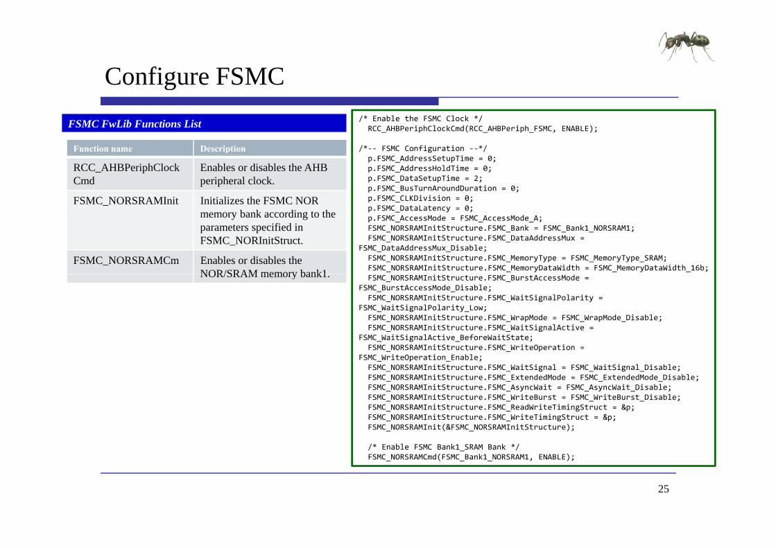
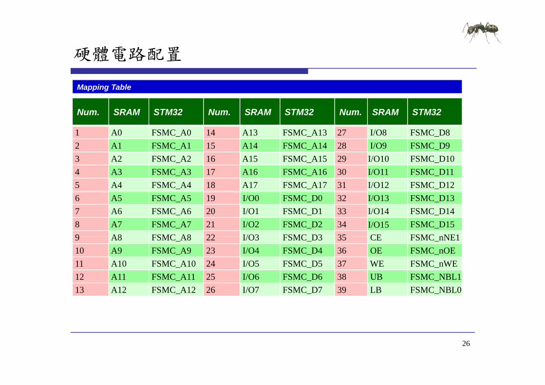
硬體電路配置
Mapping Table
Num SRAM STM32 Num SRAM STM32 Num SRAM STM32
1 A0 FSMC_A0 14 A13 FSMC_A13 27 IO8 FSMC_D82 A1 FSMC A1 15 A14 FSMC A14 28 IO9 FSMC D9_ _ _3 A2 FSMC_A2 16 A15 FSMC_A15 29 IO10 FSMC_D104 A3 FSMC_A3 17 A16 FSMC_A16 30 IO11 FSMC_D115 A4 FSMC_A4 18 A17 FSMC_A17 31 IO12 FSMC_D126 A5 FSMC_A5 19 IO0 FSMC_D0 32 IO13 FSMC_D137 A6 FSMC_A6 20 IO1 FSMC_D1 33 IO14 FSMC_D148 A7 FSMC_A7 21 IO2 FSMC_D2 34 IO15 FSMC_D159 A8 FSMC A8 22 IO3 FSMC D3 35 CE FSMC nNE19 A8 FSMC_A8 22 IO3 FSMC_D3 35 CE FSMC_nNE110 A9 FSMC_A9 23 IO4 FSMC_D4 36 OE FSMC_nOE11 A10 FSMC_A10 24 IO5 FSMC_D5 37 WE FSMC_nWE12 A11 FSMC A11 25 IO6 FSMC D6 38 UB FSMC NBL1_ _ _13 A12 FSMC_A12 26 IO7 FSMC_D7 39 LB FSMC_NBL0
26
實驗步驟
範例目錄架構
範例說明 範例說明
預設定義說明
燒錄 燒錄MIAT_STM32
27
範例目錄架構
範例目錄
測試映像檔 測試映像檔
含括檔
函式庫 函式庫
專案檔
原始碼 原始碼
28
範例說明
Embedded Software Side
Write data to FSMC SRAM memory
SRAM memory RW operation
Write data to FSMC SRAM memory Fill the buffer to send Fill_Buffer(TxBuffer BUFFER_SIZE 0x3212)FSMC_SRAM_WriteBuffer(TxBuffer WRITE_READ_ADDR BUFFER_SIZE)
SRAM memory RW operation
FSMC SRAM WriteBuffer
Read data from FSMC SRAM memory FSMC_SRAM_ReadBuffer(RxBuffer WRITE_READ_ADDR BUFFER_SIZE)
Read back SRAM memory and check content correctness
FSMC SRAM ReadBuffer
Check content
Display Result yfor (Index = 0x00 (Index lt BUFFER_SIZE) ampamp (WriteReadStatus == 0)
Index++)if (RxBuffer[Index] = TxBuffer[Index])
Display Result
WriteReadStatus = Index + 1
29
範例說明
Embedded Software Side
while (1)
Display Result
while (1)if (WriteReadStatus == 0) OK Turn on USERLED
GPIO SetBits(GPIOF GPIO Pin 11)
SRAM memory RW operation
FSMC SRAM WriteBufferGPIO_SetBits(GPIOF GPIO_Pin_11)
else KO Turn off USERLED
GPIO ResetBits(GPIOF GPIO Pin 11)
FSMC SRAM ReadBuffer
Check content
Display Result
如果寫入與讀取Buffer內容相同外部記憶體使用正常USERLED紅燈GPIO_ResetBits(GPIOF GPIO_Pin_11)
Insert delay Delay(0xAFFFF) Turn on USERLED GPIO SetBits(GPIOF GPIO Pin 11)
Display Result恆亮
GPIO_SetBits(GPIOF GPIO_Pin_11) Insert delay Delay(0xAFFFF)
如果寫入與讀取Buffer內容不同外部記憶體使用異常 USERLED紅燈閃爍
30
預設定義說明
define Bank1_SRAM1_ADDR ((u32)0x60000000) 定義SRAM起始點 定義SRAM起始點
define BUFFER_SIZE 0x400定義測試資料大小 定義測試資料大小
資料大小必需小於0xC000 define WRITE_READ_ADDR 0x8000 定義SRAM寫入起始點
寫入起始點WRITE_READ_ADDR + BUFFER_SIZE必需小於0x6000C000
31
燒錄MIAT STM32_
Rebuilder all target files產生HEX DFU Fil M 轉換HEX產生DFU DFU File Manager轉換HEX產生DFU DfuSe Demonstration燒錄DFU d Leave DFU mode
32
內部與外部SRAM存取控制實驗
實驗一
WU-YANGTechnology Co Ltd
實驗一練習
練習 修改寫入位置測試是否正常 修改寫入位置測試是否正常
修改寫入資料大小測試是否正常
取消 i 測試是否正常 取消FSMC_SRAM_Init測試是否正常
34
實驗目的(二)( )
使用MIAT_STM32實驗板透過FSMC控制外部SRAM並設定為data memory進行存取控制實驗同樣利用LED設定為data memory進行存取控制實驗同樣利用LED確認存取是否正常
35
實驗原理
External SRAM RVMDK環境設定 RVMDK環境設定
Development Flow fi ARM Configure Startup Code
36
RVMDK環境設定
外部SRAM有512K Bytes位置由0x60000000至0x60080000
37
Development Flowp
Embedded Software Side
int main(void)
Bootup STM32F10x
Programming
Bootup
int main(void)ifdef DEBUGdebug()
endif
Startup Code
BootupSTM32F10x
RCC Configure
NVIC Configure
System Clocks Configuration RCC_Configuration()
NVIC Configuration g gNVIC_Configuration()
GPIO Configuration GPIO_Configuration()
GPIO Configure
for (Index = 0 Index lt1024 Index++)
Tab[Index] =IndexT bAdd ( 32)T b h ld b 0 600000
Check operation
Check pointer value
Display Result TabAddr = (u32)Tab should be 0x600000xx
Get main stack pointer value MSPValue = __MRS_MSP() should be 0x2000xxxx
helliphelliphelliphelliphelliphelliphelliphelliphelliphelliphelliphelliphelliphelliphelliphelliphelliphelliphelliphelliphelliphelliphellip
Display Result
38
Startup Codep
Register boundary addresses RCC Configure
Enable FSMC clock
LDR R0= 0x00000114
LDR R1= 0x40021014
STR R0[R1]
Enable GPIOD GPIOE GPIOF and GPIOG clocks
LDR R0= 0x000001E0
LDR R1= 0x40021018
RCC register map
STR R0[R1]
39
RCC Register g
Bit 8 FSMCEN FSMC clock enableAHB Peripheral Clock enable register (RCC_AHBENR)
Bit 8 FSMCEN FSMC clock enableSet and cleared by software0 FSMC clock disabled
APB2 peripheral clock enable register (RCC_APB2ENR)
1 FSMC clock enabled
Bit 8765 IOPGEN IO port GFED clock enableSet and cleared by software0 IO port GFED clock disabled1 IO port GFED clock enabled
40
1 IO port GFED clock enabled
Startup Codep
Register boundary addresses GPIO Configure
SRAM Data lines NOE and NWE configuration SRAM Address lines configuration NOE NEW NE1 NBL0 NBL1 configuration LDR R0= 0xB4BB44BB LDR R1= 0x40011400STR R0[R1]LDR R0= 0xBBBBBBBB LDR R1= 0x40011404STR R0[R1]LDR R0 = 0xB44444BBLDR R0= 0xB44444BB LDR R1= 0x40011800STR R0[R1]LDR R0= 0xBBBBBBBB LDR R1= 0x40011804
GPIO register map
STR R0[R1]LDR R0= 0x44BBBBBB LDR R1= 0x40011C00STR R0[R1]LDR R0= 0xBBBB4444 LDR R1= 0x40011C04STR R0[R1]LDR R0= 0x44BBBBBBLDR R1= 0x40012000STR R0 [R1]
41
STR R0[R1]
GPIO Register g
Bit 8 FSMCEN FSMC clock enablePort configuration register low
Port configuration register high
Bits 2928 2524Bits 3130 2726 2322 1918 1514 1110 76 32 Bits 2928 25242120 1716 131298 54 10MODEy[10] Port x mode bits (y= 0 15)00 Input mode (reset state)01 Output mode max speed 10 MHz
Bits 3130 27262322 1918 15141110 76 32CNFy[10] Port x configuration bits (y= 0 15)In input mode (MODE[10]=00)00 Analog input mode01 Floating input (reset state)10 Input with pull-up pull-down
10 Output mode max speed 2 MHz11 Output mode max speed 50 MHz
11 ReservedIn output mode (MODE[10] gt00)00 General purpose output push-pull01 General purpose output Open-drain10 Alternate function output Push-pull11 Alternate function output Open-drain
42
11 Alternate function output Open drain
Startup Codep
FSMCregister map FSMC Configure
FSMC Configuration Enable FSMC Bank1_SRAM Bank
LDR R0= 0x00001011
LDR R1= 0xA0000000
STR R0[R1]
LDR R0= 0x00000200
LDR R1= 0xA0000004
STR R0[R1]
43
FSMC Register g
Bit 8 FSMCEN FSMC clock enableSRAMNOR-Flash chip-select control registers 1 (FSMC_BCR1)
Bit 12 WREN Write enable bitThis bit indicates whether write operations are enableddisabled in the bank by the FSMC0 Write operations are disabled in the bank by the FSMC an AHB error is reported1 Write operations are enabled for the bank by the FSMC (default after reset) p y ( )Bits 54 MWID Memory databus widthDefines the external memory device width valid for all type of memories00 8 bits01 16 bits (default after reset)10 reserved do not use10 reserved do not use11 reserved do not use Bit 0 MBKEN Memory bank enable bitEnables the memory bank After reset Bank1 is enabled all others are disabled Accessing adisabled bank causes an ERROR on AHB bus0 C di b k i di bl d0 Corresponding memory bank is disabled1 Corresponding memory bank is enabled
44
FSMC Register g
Bit 8 FSMCEN FSMC clock enableSRAMNOR-Flash chip-select timing registers 1 (FSMC_BTR1)
Bits 158 DATAST Data-phase duration0000 0000 Reserved0000 0001 DATAST phase duration = 2 times HCLK clock cycles0000 0010 DATAST phase duration = 3 times HCLK clock cycles1111 1111 DATAST phase duration = 256 times HCLK clock cycles (default value after reset)Bits 74 ADDHLD Address-hold phase duration0000 Reserved0001 ADDHLD phase duration = 2 times HCLK clock cycle0010 ADDHLD phase duration = 3 times HCLK clock cycle1111 ADDHLD phase duration = 16 times HCLK clock cycles (default value after reset)Bits 30 ADDSET Address setup phase durationThese bits are written by software to define the duration of the address setup phase (refer toFigure 162 to Figure 172) used in SRAMs ROMs and asynchronous NOR Flash0000 ADDSET phase duration = 1 times HCLK clock cycle1111 ADDSET phase duration = 16 times HCLK clock cycles (default value after reset)
45
實驗步驟
範例目錄架構
範例說明 範例說明
預設定義說明
46
範例目錄架構
範例目錄
測試映像檔 測試映像檔
含括檔
函式庫 函式庫
專案檔
原始碼 原始碼
47
範例說明
Embedded Software Side
Infinite loop
Display Result
Infinite loop while (1)if (((TabAddramp0xFFFFFF00) == 0x60000000) ampamp
((MSPValueamp0xFFFF0000) == 0x20000000))
Check operation
Check pointer value((MSPValueamp0xFFFF0000) == 0x20000000))
OK Turn on USERLED GPIO_SetBits(GPIOF GPIO_Pin_11)
else
Display Result
else KO Turn off USERLED
GPIO_ResetBits(GPIOF GPIO_Pin_11) Insert delay Delay(0xAFFFF)
如果Tab位置在0x600000且Stack pointer位置在0x2000 外部記憶體使用正常USERLED紅燈恆亮Delay(0xAFFFF)
Turn on USERLED GPIO_SetBits(GPIOF GPIO_Pin_11) Insert delay Delay(0xAFFFF)
紅燈恆亮
如果 b位置不在0 600000或Delay(0xAFFFF)
如果Tab位置不在0x600000或Stack pointer位置不在0x2000 外部記憶體使用異常USERLED紅燈閃爍
48
預設定義說明
DATA_IN_ExtSRAM EQU 1 E l SRAM C fi i External SRAM Configuration 0=gt DISABLE 1=gt ENABLE
u32 Tab[1024]宣告於外部 的記憶體 宣告於外部SRAM的記憶體
49
data memory存取控制實驗
實驗二
WU-YANGTechnology Co Ltd
實驗二練習
練習 取消RVMDK環境外部SRAM設定測試是否正常 取消RVMDK環境外部SRAM設定測試是否正常
修改DATA_IN_ExtSRAM EQU 0測試是否正常
修改外部 記憶體 b變數大小測試是否正常 修改外部SRAM記憶體Tab變數大小測試是否正常
51
Q amp A
WU-YANGTechnology Co Ltd
MIAT_STM32內部Flash存取控制實驗
WU-YANG
浯陽科技有限公司
Technology Co Ltd
Declared Version
Training Only
Declare
Document Number
Document Version 100
Release Date
Document Title MIAT_STM32 內部FLASH存取控制實驗
Exercise Time
Platform MIAT_STM32V2MIAT IOB V1PlatformMIAT IOBV1
Peripheral
Author WU-YANG Technology Co Ltd
2
實驗目的(一)( )
使用MIAT_STM32實驗板透過Flash memory interface (FLITF)控制內部Flash進行存取控制實驗並利用LED(FLITF)控制內部Flash進行存取控制實驗並利用LED確認存取是否正常
3
實驗原理
System architecture E b dd d Fl h Embedded Flash Features Memory map RVMDK環境設定
FLITF Flash module organization
Flash library function Development Flow ARM Configure
4
System architecturey
5
Embedded Flash
Features 256 Kb up to 256 Kbytes Memory organization the Flash memory is organized as a
main block and an information blockmain block and an information block Main memory block of size t 32 Kb 64 bit di id d i t 128 f 2 up to 32 Kb times 64 bits divided into 128 pages of 2
Kbytes Information block of size Information block of size 258 times 64 bits
6
Embedded Flash Memory mapy p
7
Flash Memoryy
8
RVMDK環境設定
STMF103ZC有256K Bytes的Flash位置由0x8000000至0x8040000
9
FLITF
Features R d i f i h f h b ff (2 64 bi d ) Read interface with prefetch buffer (2x64-bit words) Option byte Loader
l h i Flash Program Erase operation Read Write protection
10
Flash memory interfacey
11
Flash memory interface registery g
Bit 8 FSMCEN FSMC clock enableFlash status register (FLASH_SR)
Bits 316 Reserved must be kept clearedBit 5 EOP End of operation
Bit 2 PGERR Programming errorSet by hardware when an address to be programmed p
Set by hardware when a Flash operation (programming erase) is completed Reset by writing a 1Note EOP is asserted at the end of each successful
y p gcontains a value different from 0xFFFF before programmingReset by writing 1Note The STRT bit in the FLASH_CR register f f
program or erase operationBit 4 WRPRTERR Write protection errorSet by hardware when programming a write-protected address of the Flash memory
_ gshould be reset before starting a programmingoperationBit 1 Reserved must be kept clearedBit 0 BSY Busyp y
Reset by writing 1Bit 3 Reserved must be kept cleared
This indicates that a Flash operation is in progress This is set on the beginning of a Flash operation and reset when the operation finishes or when an error occurs
12
Flash memory interface registery g
Flash control register (FLASH_CR)
Bit 9 OPTWRE Option bytes write enableWhen set the option bytes can be programmed This
Bit 6 STRT StartThis bit triggers an ERASE operation when set This bit is set only
bit is set on writing the correct key sequence to the FLASH_OPTKEYR registerThis bit can be reset by softwareBit 8 Reserved must be kept clearedBit 7 LOCK Lock
by software and reset when the BSY bit is resetBit 5 OPTER Option byte eraseOption byte erase chosenBit 4 OPTPG Option byte programmingOption byte programming chosenBit 7 LOCK Lock
Write to 1 only When it is set it indicates that the FPEC and FLASH_CR are locked This bit is reset by hardware after detecting the unlock sequenceIn the event of unsuccessful unlock operation this bit remains set until the next reset
p y p g gBit 3 Reserved must be kept clearedBit 2 MER Mass eraseErase of all user pages chosenBit 1 PER Page erasePage Erase chosenremains set until the next reset Page Erase chosenBit 0 PG ProgrammingFlash programming chosen
13
Main Flash memory programmingy p g g
14
Flash memory Page Erasey g
15
Flash memory Mass Erasey
16
Option byte programmingp y p g g
17
Option byte Erasep y
18
FLASH library functiony
19
FLASH library functiony
20
Development Flowp
Embedded Software Side
int main(void)
Bootup STM32F10x
ProgrammingBootupSTM32F10x RCC Configure
NVIC Configure
int main(void)ifdef DEBUGdebug()
endifendif
FLASHStatus = FLASH_COMPLETEMemoryProgramStatus = PASSEDData = 0x15041975
GPIO Configure
Data = 0x15041975
RCC Configuration RCC_Configuration()
Flash memory RW operation FLASH Unlock
FLASH ClearFlag NVIC Configuration NVIC_Configuration()
GPIO Configuration
FLASH ClearFlag
FLASH ErasePage
FLASH ProgramWord GPIO Configuration GPIO_Configuration()
helliphelliphelliphelliphelliphelliphelliphelliphelliphelliphelliphelliphelliphelliphelliphelliphellipDisplay Result
Check content
21
實驗步驟
範例目錄架構
範例說明 範例說明
預設定義說明
燒錄 燒錄MIAT_STM32
22
範例目錄架構
範例目錄
測試映像檔 測試映像檔
含括檔
函式庫 函式庫
專案檔
原始碼 原始碼
23
範例說明
Function name Description
Unlock the Flash Program Erase controller FLASH_Unlock()
D fi h b f b d
Flash FwLib Functions List
Function name Description
FLASH_Unlock Unlocks the FLASH Program Erase Controller
FLASH_ClearFlag Clears the FLASH pending fl
Define the number of page to be erased NbrOfPage = (EndAddr - StartAddr) FLASH_PAGE_SIZE
Clear All pending flags FLASH_ClearFlag(FLASH_FLAG_BSY | FLASH_FLAG_EOP | FLASH_FLAG_PGERR |
FLASH FLAG WRPRTERR)flags
FLASH_ErasePage Erases a specified FLASH page
FLASH_ProgramWord Programs a word at a specified
_ _ )
Erase the FLASH pages for(EraseCounter = 0 (EraseCounter lt NbrOfPage) ampamp (FLASHStatus ==
FLASH_COMPLETE) EraseCounter++)FLASHStatus = FLASH ErasePage(StartAddr + (FLASH PAGE SIZE EraseCounter))address FLASHStatus = FLASH_ErasePage(StartAddr + (FLASH_PAGE_SIZE EraseCounter))
FLASH Word program of data 0x15041979 at addresses defined by StartAddr and EndAddrAddress = StartAddr
while((Address lt EndAddr) ampamp (FLASHStatus == FLASH_COMPLETE))FLASHStatus = FLASH_ProgramWord(Address Data)Address = Address + 4
24
範例說明
Embedded Software Side
Check the corectness of written data
Display Result
Check the corectness of written data Address = StartAddr
while((Address lt EndAddr) ampamp (MemoryProgramStatus = FAILED))if(((vu32) Address) = Data)
Flash memory RW operation
MemoryProgramStatus = FAILED
Address += 4
Check content
Display Result while (1)if (MemoryProgramStatus == PASSED) OK Turn on USERLED GPIO_SetBits(GPIOF GPIO_Pin_11)
Display Result
else KO Turn off USERLED GPIO_ResetBits(GPIOF GPIO_Pin_11) Insert delay Delay(0xAFFFF)
如果寫入與讀取Flash內容相同Flash記憶體使用正常USERLED紅燈恆亮
Turn on USERLED GPIO_SetBits(GPIOF GPIO_Pin_11) Insert delay Delay(0xAFFFF)
如果寫入與讀取Flash內容不同Flash記憶體使用異常USERLED紅燈閃爍
25
預設定義說明
define StartAddr ((u32)0x08008000) 定義Flash使用起始點 定義Flash使用起始點
使用起始點必需大於0x8003000 + Code Size 附註 0x8000000~0x8003000為DFU程式區塊使用此區塊
將造成無法燒錄程式
Code Size可由產生的HEX檔得知
d fi E dAdd (( 32)0 0800C000) define EndAddr ((u32)0x0800C000) 定義Flash使用結束點
使用起始點必需小於0x8040000使用起始點必需小於
Data = 0x15041975 寫入資料
32Bit define FLASH_PAGE_SIZE ((u16)0x800)
每一個Page有2KByte26
每一個Page有2KByte
Intel HEX Format
aaaa tt dd cc
field Description
the colon that starts every Intel HEX record
the record-length field that represents the number of data bytes (dd) in the record
aaaa the address field that represents the starting address for subsequent data in the record
tt the field that represents the HEX record type which may be one of the following00 - data record01 - end-of-file record02 - extended segment address recordg04 - extended linear address record
dd a data field that represents one byte of data A record may have multiple data bytes The number of data bytes in the record must match the number specified by the field
cc the checksum field that represents the checksum of the record The checksum is calculated by summing the values of all hexadecimal digit pairs in the record modulo 256 and taking the twos complement
27
HEX Examplep
020000040800F2103000001814002045310008D9340008CD340008D8103000001814002045310008D9340008CD340008D8helliphelliphellip1038200042370008000000000000000000000000170C3830000000000000000000000000008C
資料填入起始位置為
0C3830000000000000000000000000008C04000005080031318D00000001FF
資料填入起始位置為0x08003000 每一行有0x10(16)個Bytes 最後一筆資料為
資料結束點為0x0803383004000005080031318D
(0x08003830 -0x08000000)0x800 = 7 需以0x800為單位所以使用的位置起點為0x08004000
28
燒錄MIAT STM32_
Rebuilder all target files產生HEX DFU Fil M 轉換HEX產生DFU DFU File Manager轉換HEX產生DFU DfuSe Demonstration燒錄DFU d Leave DFU mode
29
內部Flash存取控制實驗
實驗一
WU-YANGTechnology Co Ltd
實驗一練習
注意 請使用預設0 08008000之後的位置 避免覆蓋DFU 請使用預設0x08008000之後的位置避免覆蓋DFU
與使用者程式碼區塊
練習 練習 修改存取位置測試是否正常
修改寫入資料測試是否正常 修改寫入資料測試是否正常
修改寫入資料後取消FLASH_Unlock測試是否正常
修改寫入資料後取消FLASH E P 測試是否正 修改寫入資料後取消FLASH_ErasePage測試是否正常
31
實驗目的(二)( )
使用MIAT_STM32實驗板透過Flash memory interface (FLITF)控制內部Flash進行存取控制實驗並利用SW(FLITF)控制內部Flash進行存取控制實驗並利用SWKEY決定資料寫入與讀取LCD顯示狀態
32
實驗原理
System requirement E b dd d Fl h Embedded Flash LCD KEY SW
Development Flow ARM Configure
33
Development Flowp
Embedded Software Side
int main(void)
Bootup STM32F10x
ProgrammingBootupSTM32F10x RCC Configure
NVIC Configure
int main(void)ifdef DEBUGdebug()
endif
FLASHStatus = FLASH_COMPLETE
RCC Configuration RCC Configuration()
GPIO Configure
BasicIO Configure_ g ()
NVIC Configuration NVIC_Configuration()
GPIO Configuration Flash memory RW ti
lcd Configure
GPIO Configuration GPIO_Configuration()
Init_BasicIO()
l d i i () LCD I i i li i
RW operation
Example
FLASH Unlock
FLASH ClearFlag
lcd_init() LCD Initialization
helliphelliphelliphelliphelliphelliphelliphelliphelliphelliphelliphelliphelliphelliphelliphelliphelliphelliphelliphelliphelliphelliphellip
p
34
硬體電路配置
Mapping Table
Num MIAT_STM32V2 MIAT_IOBV1 Num MIAT_STM32V2 MIAT_IOBV1
1 PC8 (326) SW1 10 PE6 (15) LCD_EN2 PC9 (327) SW2 11 PF6 (118) LCD RW ( ) ( ) _3 PC10 (43) SW3 12 PF7 (119) LCD_RS 4 PC11 (44) SW4 13 PF8(120) LCD_D4 5 PB5 (427) KEY1 14 PF9 (121) LCD_D5 6 PB6 (428) KEY2 15 PF10 (122) LCD_D6 7 PB7 (429) KEY3 16 PF11 (213) LCD_D7 8 PB8 (431) KEY4 17 VDD (236) VCC33V 9 VCC5V (1 36) VCC5V 18 GND (1 35) GND9 VCC5V (136) VCC5V 18 GND (135) GND
35
實驗步驟
範例目錄架構
範例說明 範例說明
預設定義說明
36
範例目錄架構
範例目錄
測試映像檔 測試映像檔
含括檔
函式庫 函式庫
專案檔
原始碼 原始碼
37
範例說明
Embedded Software Side
lcd clear()
FLASH memory RW operation
lcd_clear()lcd_print (MIAT_STM32 DEMO )
Unlock the Flash Program Erase controller FLASH_Unlock()
Flash memory RW operation
FLASH Unlock
Clear All pending flags FLASH_ClearFlag(FLASH_FLAG_BSY | FLASH_FLAG_EOP | FLASH_FLAG_PGERR |
FLASH_FLAG_WRPRTERR)
while(1)
Example
FLASH ClearFlag
( )
KEY_Buffer=Key_Scan()set_cursor (0 1)lcd_print (SW Value = 0x)lcd putchar(((SWamp0x7)+0x30))lcd_putchar(((SWamp0x7)+0x30))if(KEY_Buffer==1)Address=(StartAddr|(SWltlt12))set_cursor (0 0)lcd_print (Set Addr = 0x)
掃描KEY是否按下與顯示SW數值LCD Line2顯示SW Value = 0x(SW)
lcd_putchar(((SWamp0x7)+0x30))lcd_print ( )
如果KEY1按下記錄SW數值至Address LCD Line1顯示Set Adde = 0x(Address)
38
範例說明
Embedded Software Side
else if(KEY Buffer==2)
FLASH memory RW operation
else if(KEY_Buffer==2)
Erase the FLASH pages FLASHStatus = FLASH_ErasePage(Address)
FLASH Word program of data at addresses defined by SW
SRAM memory RW operation
p g yFLASHStatus = FLASH_ProgramWord(Address (SWamp0x7))
set_cursor (0 0)lcd_print (Write 0x)lcd_putchar(((SWamp0x7)+0x30))l d i t ( t 0 )
Example如果KEY2按下清除Address所處區塊並寫入SW數值 lcd_print ( at 0x)
lcd_putchar((((Addressgtgt12)amp0x7)+0x30))else if(KEY_Buffer==3)
Data=(u16 )Address
所處區塊並寫入SW數值LCD Line1顯示Write 0x(SW) at 0x(Adddress)
Data (u16 )Addressset_cursor (0 0)lcd_print (Addr 0x)lcd_putchar((((Addressgtgt12)amp0x7)+0x30))lcd_print ( = 0x)lcd_putchar(((Dataamp0x7)+0x30))lcd_print ( )
如果KEY3按下讀取Address紀錄數值LCD Line1顯示Addr 0x(Adddress) = 0x
39
預設定義說明
define StartAddr ((u32)0x08020000) 定義Flash使用起始點 定義Flash使用起始點
使用起始點必需大於0x8003000 + Code Size 附註 0x8000000~0x8003000為DFU程式區塊使用此區塊
將造成無法燒錄程式
Code Size可由產生的HEX檔得知
32 Add 0 08020000 u32 Address = 0x08020000 定義Address初始值
初始值必需與Flash使用起始點相同初始值必需與 使用起始點相同
Address=(StartAddr|(SWltlt12)) Example StartAddr = 0x08020000 SW = 1 Address = 0x08021000
StartAddr = 0x08020000 SW = 7 Address = 0x08027000 StartAddr|(7ltlt12)必需小於0x8040000
40
使用者界面與Flash存取控制實驗
實驗二
WU-YANGTechnology Co Ltd
實驗二練習
注意 請使用預設0 08020000之後的位置 避免覆蓋DFU 請使用預設0x08020000之後的位置避免覆蓋DFU
與使用者程式碼區塊
練習 練習 利用SW與KEY測試Flash寫入與讀取是否正常
Fl h寫入後電源關閉 再開啟後寫入資料是否仍存 Flash寫入後電源關閉再開啟後寫入資料是否仍存在
修改存取位置測試是否正常 修改存取位置測試是否正常
42
實驗目的(三)( )
使用MIAT_STM32實驗板透過Flash memory interface (FLITF)控制內部Flash進行存取控制實驗並藉由填入(FLITF)控制內部Flash進行存取控制實驗並藉由填入Option Bytes 設定寫入鎖定保護Page鎖定不被覆蓋
43
Development Flowp
Embedded Software Side
int main(void)
Bootup STM32F10x
ProgrammingBootupSTM32F10x RCC Configure
NVIC Configure
int main(void)ifdef DEBUGdebug()
endifendif
FLASHStatus = FLASH_COMPLETEMemoryProgramStatus = PASSEDData = 0x1753
GPIO Configure
Data = 0x1753
RCC Configuration RCC_Configuration()
Flash memory RW operation FLASH Unlock
FLASH ClearFlag NVIC Configuration NVIC_Configuration()
GPIO Configuration
FLASH ClearFlag
FLASH ErasePage
FLASH ProgramHalfWord GPIO Configuration GPIO_Configuration()
Display Result
Check content
44
helliphelliphelliphelliphelliphelliphelliphelliphelliphelliphelliphelliphelliphelliphelliphelliphelliphelliphellip
實驗步驟
範例目錄架構
範例說明 範例說明
預設定義說明
45
範例目錄架構
範例目錄
測試映像檔 測試映像檔
含括檔
函式庫 函式庫
專案檔
原始碼 原始碼
46
範例說明
Function name Description
Unlock the Flash Program Erase controller FLASH_Unlock()
Define the number of page to be erased
Flash FwLib Functions List
Function name Description
FLASH_Unlock Unlocks the FLASH Program Erase Controller
FLASH_ClearFlag Clears the FLASH pending fl
Define the number of page to be erased NbrOfPage = (EndAddr ‐ StartAddr) FLASH_PAGE_SIZE
FLASH_ClearFlag(FLASH_FLAG_BSY | FLASH_FLAG_EOP|FLASH_FLAG_PGERR |FLASH_FLAG_WRPRTERR)
Get pages write protection status flags
FLASH_EraseOptionBytes
Erases the FLASH option bytes
FLASH_EnableWritePro Write protects the desired
p g pWRPR_Value = FLASH_GetWriteProtectionOptionByte()ProtectedPages = WRPR_Value amp 0x000000C0
ifdef WriteProtection_Disableif (ProtectedPages == 0x00) Pages are write protected
tection pages
NVIC_GenerateSystemReset
Generate a system reset
Disable the write protection FLASHStatus = FLASH_EraseOptionBytes() Generate System Reset to load the new option byte values NVIC_GenerateSystemReset()
elseifdef WriteProtection Enableifdef WriteProtection_Enableif (ProtectedPages = 0x00) Pages not write protected
FLASHStatus = FLASH_EraseOptionBytes() Enable the pages write protection FLASHStatus = FLASH_EnableWriteProtection(FLASH_WRProt_Pages12to13
|FLASH WRProt Pages14to15)|FLASH_WRProt_Pages14to15) Generate System Reset to load the new option byte values NVIC_GenerateSystemReset()
endifendif
47
範例說明
if (ProtectedPages = 0x00) Clear All pending flags
Flash FwLib Functions List
Function name DescriptionFLASH_ClearFlag(FLASH_FLAG_BSY |
FLASH_FLAG_EOP|FLASH_FLAG_PGERR |FLASH_FLAG_WRPRTERR)
erase the FLASH pages for(EraseCounter = 0 (EraseCounter lt NbrOfPage) ampamp (FLASHStatus ==
Function name Description
FLASH_ErasePage Erases a specified FLASH page
FLASH_ProgramHalfWod
Programs a half word at a ifi d dd FLASH_COMPLETE) EraseCounter++)
FLASHStatus = FLASH_ErasePage(StartAddr + (FLASH_PAGE_SIZE
EraseCounter))
rd specified address
FLASH Half Word program of data 0x1753 at addresses defined by StartAddrand EndAddr
Address = StartAddr
hil ((Add E dAdd ) ampamp (FLASHSt t FLASH COMPLETE))while((Address lt EndAddr) ampamp (FLASHStatus == FLASH_COMPLETE))
FLASHStatus = FLASH_ProgramHalfWord(Address Data)Address = Address + 2
48
範例說明
Embedded Software Side
Check the corectness of written data
Display Result
Check the corectness of written data Address = StartAddr
while((Address lt EndAddr) ampamp (MemoryProgramStatus = FAILED))if(((vu16) Address) = Data)
Flash memory RW operation
MemoryProgramStatus = FAILED
Address += 2
Check content
Display Result while (1)if (MemoryProgramStatus == PASSED) OK Turn on USERLED GPIO_SetBits(GPIOF GPIO_Pin_11)
Display Result
else KO Turn off USERLED GPIO_ResetBits(GPIOF GPIO_Pin_11) Insert delay Delay(0xAFFFF)
如果寫入與讀取Flash內容相同Flash記憶體可以寫入USERLED紅燈恆亮
Turn on USERLED GPIO_SetBits(GPIOF GPIO_Pin_11) Insert delay Delay(0xAFFFF)
如果寫入與讀取Flash內容不同Flash記憶體不能寫入USERLED紅燈閃爍
49
預設定義說明
define StartAddr ((u32) 0x08006000) 定義Flash使用起始點 定義Flash使用起始點
使用起始點必需大於0x8003000 + Code Size 附註 0x8000000~0x8003000為DFU程式區塊使用此區塊
將造成無法燒錄程式
Code Size可由產生的HEX檔得知
d fi E dAdd (( 32) 0 08008000) define EndAddr ((u32) 0x08008000) 定義Flash使用結束點
使用起始點必需小於0x8040000使用起始點必需小於
Data = 0x1753 寫入資料
16Bit define FLASH_PAGE_SIZE ((u16)0x800) 每一個Page有2KByte
50
每一個Page有2KByte
預設定義說明
define WriteProtection_Enable U hi li E bl W i P i Uncomment this line to Enable Write Protection
define WriteProtection_Disablehi li i bl i i Uncomment this line to Disable Write Protection
FLASH_EnableWriteProtection設定影響 個 設定影響2個Page FLASH_WRProt_Pages0to1 FLASH_WRProt_Pages1to2 helliphellip FLASH_WRProt_Pages60to61
設定影響多個Page FLASH_WRProt_Pages62to255
51
FLASH EnableWriteProtection_
Example
位置0x08006000 ~ 0x08007000每一個Page有0x800ByteStartPage = (0x08006000-0x08000000)0x800 = 12EndPage = ((0x08007000-0x08000000)0x800)-1 = 13執行執行FLASH_EnableWriteProtection(FLASH_WRProt_Pages12to13)將影響Pages12 Pages13
52
內部Flash寫入鎖定存取控制實驗
實驗三
WU-YANGTechnology Co Ltd
實驗三練習
注意 請使用預設0 08006000之後的位置 避免覆蓋DFU 請使用預設0x08006000之後的位置避免覆蓋DFU
與使用者程式碼區塊
更改寫入位置測試寫入鎖定時需同時更改 更改寫入位置測試寫入鎖定時需同時更改FLASH_EnableWriteProtection鎖定之Page
練習 練習 打開define WriteProtection_Enable測試是否可寫入
打開define WriteProtection Disable測試是否可寫入 打開define WriteProtection_Disable測試是否可寫入
修改存取位置測試是否正常
修改寫入資料測試是否正常 修改寫入資料測試是否正常
54
Q amp A
WU-YANGTechnology Co Ltd

實驗步驟
範例目錄架構
範例說明 範例說明
預設定義說明
燒錄 燒錄MIAT_STM32
27
範例目錄架構
範例目錄
測試映像檔 測試映像檔
含括檔
函式庫 函式庫
專案檔
原始碼 原始碼
28
範例說明
Embedded Software Side
Write data to FSMC SRAM memory
SRAM memory RW operation
Write data to FSMC SRAM memory Fill the buffer to send Fill_Buffer(TxBuffer BUFFER_SIZE 0x3212)FSMC_SRAM_WriteBuffer(TxBuffer WRITE_READ_ADDR BUFFER_SIZE)
SRAM memory RW operation
FSMC SRAM WriteBuffer
Read data from FSMC SRAM memory FSMC_SRAM_ReadBuffer(RxBuffer WRITE_READ_ADDR BUFFER_SIZE)
Read back SRAM memory and check content correctness
FSMC SRAM ReadBuffer
Check content
Display Result yfor (Index = 0x00 (Index lt BUFFER_SIZE) ampamp (WriteReadStatus == 0)
Index++)if (RxBuffer[Index] = TxBuffer[Index])
Display Result
WriteReadStatus = Index + 1
29
範例說明
Embedded Software Side
while (1)
Display Result
while (1)if (WriteReadStatus == 0) OK Turn on USERLED
GPIO SetBits(GPIOF GPIO Pin 11)
SRAM memory RW operation
FSMC SRAM WriteBufferGPIO_SetBits(GPIOF GPIO_Pin_11)
else KO Turn off USERLED
GPIO ResetBits(GPIOF GPIO Pin 11)
FSMC SRAM ReadBuffer
Check content
Display Result
如果寫入與讀取Buffer內容相同外部記憶體使用正常USERLED紅燈GPIO_ResetBits(GPIOF GPIO_Pin_11)
Insert delay Delay(0xAFFFF) Turn on USERLED GPIO SetBits(GPIOF GPIO Pin 11)
Display Result恆亮
GPIO_SetBits(GPIOF GPIO_Pin_11) Insert delay Delay(0xAFFFF)
如果寫入與讀取Buffer內容不同外部記憶體使用異常 USERLED紅燈閃爍
30
預設定義說明
define Bank1_SRAM1_ADDR ((u32)0x60000000) 定義SRAM起始點 定義SRAM起始點
define BUFFER_SIZE 0x400定義測試資料大小 定義測試資料大小
資料大小必需小於0xC000 define WRITE_READ_ADDR 0x8000 定義SRAM寫入起始點
寫入起始點WRITE_READ_ADDR + BUFFER_SIZE必需小於0x6000C000
31
燒錄MIAT STM32_
Rebuilder all target files產生HEX DFU Fil M 轉換HEX產生DFU DFU File Manager轉換HEX產生DFU DfuSe Demonstration燒錄DFU d Leave DFU mode
32
內部與外部SRAM存取控制實驗
實驗一
WU-YANGTechnology Co Ltd
實驗一練習
練習 修改寫入位置測試是否正常 修改寫入位置測試是否正常
修改寫入資料大小測試是否正常
取消 i 測試是否正常 取消FSMC_SRAM_Init測試是否正常
34
實驗目的(二)( )
使用MIAT_STM32實驗板透過FSMC控制外部SRAM並設定為data memory進行存取控制實驗同樣利用LED設定為data memory進行存取控制實驗同樣利用LED確認存取是否正常
35
實驗原理
External SRAM RVMDK環境設定 RVMDK環境設定
Development Flow fi ARM Configure Startup Code
36
RVMDK環境設定
外部SRAM有512K Bytes位置由0x60000000至0x60080000
37
Development Flowp
Embedded Software Side
int main(void)
Bootup STM32F10x
Programming
Bootup
int main(void)ifdef DEBUGdebug()
endif
Startup Code
BootupSTM32F10x
RCC Configure
NVIC Configure
System Clocks Configuration RCC_Configuration()
NVIC Configuration g gNVIC_Configuration()
GPIO Configuration GPIO_Configuration()
GPIO Configure
for (Index = 0 Index lt1024 Index++)
Tab[Index] =IndexT bAdd ( 32)T b h ld b 0 600000
Check operation
Check pointer value
Display Result TabAddr = (u32)Tab should be 0x600000xx
Get main stack pointer value MSPValue = __MRS_MSP() should be 0x2000xxxx
helliphelliphelliphelliphelliphelliphelliphelliphelliphelliphelliphelliphelliphelliphelliphelliphelliphelliphelliphelliphelliphelliphellip
Display Result
38
Startup Codep
Register boundary addresses RCC Configure
Enable FSMC clock
LDR R0= 0x00000114
LDR R1= 0x40021014
STR R0[R1]
Enable GPIOD GPIOE GPIOF and GPIOG clocks
LDR R0= 0x000001E0
LDR R1= 0x40021018
RCC register map
STR R0[R1]
39
RCC Register g
Bit 8 FSMCEN FSMC clock enableAHB Peripheral Clock enable register (RCC_AHBENR)
Bit 8 FSMCEN FSMC clock enableSet and cleared by software0 FSMC clock disabled
APB2 peripheral clock enable register (RCC_APB2ENR)
1 FSMC clock enabled
Bit 8765 IOPGEN IO port GFED clock enableSet and cleared by software0 IO port GFED clock disabled1 IO port GFED clock enabled
40
1 IO port GFED clock enabled
Startup Codep
Register boundary addresses GPIO Configure
SRAM Data lines NOE and NWE configuration SRAM Address lines configuration NOE NEW NE1 NBL0 NBL1 configuration LDR R0= 0xB4BB44BB LDR R1= 0x40011400STR R0[R1]LDR R0= 0xBBBBBBBB LDR R1= 0x40011404STR R0[R1]LDR R0 = 0xB44444BBLDR R0= 0xB44444BB LDR R1= 0x40011800STR R0[R1]LDR R0= 0xBBBBBBBB LDR R1= 0x40011804
GPIO register map
STR R0[R1]LDR R0= 0x44BBBBBB LDR R1= 0x40011C00STR R0[R1]LDR R0= 0xBBBB4444 LDR R1= 0x40011C04STR R0[R1]LDR R0= 0x44BBBBBBLDR R1= 0x40012000STR R0 [R1]
41
STR R0[R1]
GPIO Register g
Bit 8 FSMCEN FSMC clock enablePort configuration register low
Port configuration register high
Bits 2928 2524Bits 3130 2726 2322 1918 1514 1110 76 32 Bits 2928 25242120 1716 131298 54 10MODEy[10] Port x mode bits (y= 0 15)00 Input mode (reset state)01 Output mode max speed 10 MHz
Bits 3130 27262322 1918 15141110 76 32CNFy[10] Port x configuration bits (y= 0 15)In input mode (MODE[10]=00)00 Analog input mode01 Floating input (reset state)10 Input with pull-up pull-down
10 Output mode max speed 2 MHz11 Output mode max speed 50 MHz
11 ReservedIn output mode (MODE[10] gt00)00 General purpose output push-pull01 General purpose output Open-drain10 Alternate function output Push-pull11 Alternate function output Open-drain
42
11 Alternate function output Open drain
Startup Codep
FSMCregister map FSMC Configure
FSMC Configuration Enable FSMC Bank1_SRAM Bank
LDR R0= 0x00001011
LDR R1= 0xA0000000
STR R0[R1]
LDR R0= 0x00000200
LDR R1= 0xA0000004
STR R0[R1]
43
FSMC Register g
Bit 8 FSMCEN FSMC clock enableSRAMNOR-Flash chip-select control registers 1 (FSMC_BCR1)
Bit 12 WREN Write enable bitThis bit indicates whether write operations are enableddisabled in the bank by the FSMC0 Write operations are disabled in the bank by the FSMC an AHB error is reported1 Write operations are enabled for the bank by the FSMC (default after reset) p y ( )Bits 54 MWID Memory databus widthDefines the external memory device width valid for all type of memories00 8 bits01 16 bits (default after reset)10 reserved do not use10 reserved do not use11 reserved do not use Bit 0 MBKEN Memory bank enable bitEnables the memory bank After reset Bank1 is enabled all others are disabled Accessing adisabled bank causes an ERROR on AHB bus0 C di b k i di bl d0 Corresponding memory bank is disabled1 Corresponding memory bank is enabled
44
FSMC Register g
Bit 8 FSMCEN FSMC clock enableSRAMNOR-Flash chip-select timing registers 1 (FSMC_BTR1)
Bits 158 DATAST Data-phase duration0000 0000 Reserved0000 0001 DATAST phase duration = 2 times HCLK clock cycles0000 0010 DATAST phase duration = 3 times HCLK clock cycles1111 1111 DATAST phase duration = 256 times HCLK clock cycles (default value after reset)Bits 74 ADDHLD Address-hold phase duration0000 Reserved0001 ADDHLD phase duration = 2 times HCLK clock cycle0010 ADDHLD phase duration = 3 times HCLK clock cycle1111 ADDHLD phase duration = 16 times HCLK clock cycles (default value after reset)Bits 30 ADDSET Address setup phase durationThese bits are written by software to define the duration of the address setup phase (refer toFigure 162 to Figure 172) used in SRAMs ROMs and asynchronous NOR Flash0000 ADDSET phase duration = 1 times HCLK clock cycle1111 ADDSET phase duration = 16 times HCLK clock cycles (default value after reset)
45
實驗步驟
範例目錄架構
範例說明 範例說明
預設定義說明
46
範例目錄架構
範例目錄
測試映像檔 測試映像檔
含括檔
函式庫 函式庫
專案檔
原始碼 原始碼
47
範例說明
Embedded Software Side
Infinite loop
Display Result
Infinite loop while (1)if (((TabAddramp0xFFFFFF00) == 0x60000000) ampamp
((MSPValueamp0xFFFF0000) == 0x20000000))
Check operation
Check pointer value((MSPValueamp0xFFFF0000) == 0x20000000))
OK Turn on USERLED GPIO_SetBits(GPIOF GPIO_Pin_11)
else
Display Result
else KO Turn off USERLED
GPIO_ResetBits(GPIOF GPIO_Pin_11) Insert delay Delay(0xAFFFF)
如果Tab位置在0x600000且Stack pointer位置在0x2000 外部記憶體使用正常USERLED紅燈恆亮Delay(0xAFFFF)
Turn on USERLED GPIO_SetBits(GPIOF GPIO_Pin_11) Insert delay Delay(0xAFFFF)
紅燈恆亮
如果 b位置不在0 600000或Delay(0xAFFFF)
如果Tab位置不在0x600000或Stack pointer位置不在0x2000 外部記憶體使用異常USERLED紅燈閃爍
48
預設定義說明
DATA_IN_ExtSRAM EQU 1 E l SRAM C fi i External SRAM Configuration 0=gt DISABLE 1=gt ENABLE
u32 Tab[1024]宣告於外部 的記憶體 宣告於外部SRAM的記憶體
49
data memory存取控制實驗
實驗二
WU-YANGTechnology Co Ltd
實驗二練習
練習 取消RVMDK環境外部SRAM設定測試是否正常 取消RVMDK環境外部SRAM設定測試是否正常
修改DATA_IN_ExtSRAM EQU 0測試是否正常
修改外部 記憶體 b變數大小測試是否正常 修改外部SRAM記憶體Tab變數大小測試是否正常
51
Q amp A
WU-YANGTechnology Co Ltd
MIAT_STM32內部Flash存取控制實驗
WU-YANG
浯陽科技有限公司
Technology Co Ltd
Declared Version
Training Only
Declare
Document Number
Document Version 100
Release Date
Document Title MIAT_STM32 內部FLASH存取控制實驗
Exercise Time
Platform MIAT_STM32V2MIAT IOB V1PlatformMIAT IOBV1
Peripheral
Author WU-YANG Technology Co Ltd
2
實驗目的(一)( )
使用MIAT_STM32實驗板透過Flash memory interface (FLITF)控制內部Flash進行存取控制實驗並利用LED(FLITF)控制內部Flash進行存取控制實驗並利用LED確認存取是否正常
3
實驗原理
System architecture E b dd d Fl h Embedded Flash Features Memory map RVMDK環境設定
FLITF Flash module organization
Flash library function Development Flow ARM Configure
4
System architecturey
5
Embedded Flash
Features 256 Kb up to 256 Kbytes Memory organization the Flash memory is organized as a
main block and an information blockmain block and an information block Main memory block of size t 32 Kb 64 bit di id d i t 128 f 2 up to 32 Kb times 64 bits divided into 128 pages of 2
Kbytes Information block of size Information block of size 258 times 64 bits
6
Embedded Flash Memory mapy p
7
Flash Memoryy
8
RVMDK環境設定
STMF103ZC有256K Bytes的Flash位置由0x8000000至0x8040000
9
FLITF
Features R d i f i h f h b ff (2 64 bi d ) Read interface with prefetch buffer (2x64-bit words) Option byte Loader
l h i Flash Program Erase operation Read Write protection
10
Flash memory interfacey
11
Flash memory interface registery g
Bit 8 FSMCEN FSMC clock enableFlash status register (FLASH_SR)
Bits 316 Reserved must be kept clearedBit 5 EOP End of operation
Bit 2 PGERR Programming errorSet by hardware when an address to be programmed p
Set by hardware when a Flash operation (programming erase) is completed Reset by writing a 1Note EOP is asserted at the end of each successful
y p gcontains a value different from 0xFFFF before programmingReset by writing 1Note The STRT bit in the FLASH_CR register f f
program or erase operationBit 4 WRPRTERR Write protection errorSet by hardware when programming a write-protected address of the Flash memory
_ gshould be reset before starting a programmingoperationBit 1 Reserved must be kept clearedBit 0 BSY Busyp y
Reset by writing 1Bit 3 Reserved must be kept cleared
This indicates that a Flash operation is in progress This is set on the beginning of a Flash operation and reset when the operation finishes or when an error occurs
12
Flash memory interface registery g
Flash control register (FLASH_CR)
Bit 9 OPTWRE Option bytes write enableWhen set the option bytes can be programmed This
Bit 6 STRT StartThis bit triggers an ERASE operation when set This bit is set only
bit is set on writing the correct key sequence to the FLASH_OPTKEYR registerThis bit can be reset by softwareBit 8 Reserved must be kept clearedBit 7 LOCK Lock
by software and reset when the BSY bit is resetBit 5 OPTER Option byte eraseOption byte erase chosenBit 4 OPTPG Option byte programmingOption byte programming chosenBit 7 LOCK Lock
Write to 1 only When it is set it indicates that the FPEC and FLASH_CR are locked This bit is reset by hardware after detecting the unlock sequenceIn the event of unsuccessful unlock operation this bit remains set until the next reset
p y p g gBit 3 Reserved must be kept clearedBit 2 MER Mass eraseErase of all user pages chosenBit 1 PER Page erasePage Erase chosenremains set until the next reset Page Erase chosenBit 0 PG ProgrammingFlash programming chosen
13
Main Flash memory programmingy p g g
14
Flash memory Page Erasey g
15
Flash memory Mass Erasey
16
Option byte programmingp y p g g
17
Option byte Erasep y
18
FLASH library functiony
19
FLASH library functiony
20
Development Flowp
Embedded Software Side
int main(void)
Bootup STM32F10x
ProgrammingBootupSTM32F10x RCC Configure
NVIC Configure
int main(void)ifdef DEBUGdebug()
endifendif
FLASHStatus = FLASH_COMPLETEMemoryProgramStatus = PASSEDData = 0x15041975
GPIO Configure
Data = 0x15041975
RCC Configuration RCC_Configuration()
Flash memory RW operation FLASH Unlock
FLASH ClearFlag NVIC Configuration NVIC_Configuration()
GPIO Configuration
FLASH ClearFlag
FLASH ErasePage
FLASH ProgramWord GPIO Configuration GPIO_Configuration()
helliphelliphelliphelliphelliphelliphelliphelliphelliphelliphelliphelliphelliphelliphelliphelliphellipDisplay Result
Check content
21
實驗步驟
範例目錄架構
範例說明 範例說明
預設定義說明
燒錄 燒錄MIAT_STM32
22
範例目錄架構
範例目錄
測試映像檔 測試映像檔
含括檔
函式庫 函式庫
專案檔
原始碼 原始碼
23
範例說明
Function name Description
Unlock the Flash Program Erase controller FLASH_Unlock()
D fi h b f b d
Flash FwLib Functions List
Function name Description
FLASH_Unlock Unlocks the FLASH Program Erase Controller
FLASH_ClearFlag Clears the FLASH pending fl
Define the number of page to be erased NbrOfPage = (EndAddr - StartAddr) FLASH_PAGE_SIZE
Clear All pending flags FLASH_ClearFlag(FLASH_FLAG_BSY | FLASH_FLAG_EOP | FLASH_FLAG_PGERR |
FLASH FLAG WRPRTERR)flags
FLASH_ErasePage Erases a specified FLASH page
FLASH_ProgramWord Programs a word at a specified
_ _ )
Erase the FLASH pages for(EraseCounter = 0 (EraseCounter lt NbrOfPage) ampamp (FLASHStatus ==
FLASH_COMPLETE) EraseCounter++)FLASHStatus = FLASH ErasePage(StartAddr + (FLASH PAGE SIZE EraseCounter))address FLASHStatus = FLASH_ErasePage(StartAddr + (FLASH_PAGE_SIZE EraseCounter))
FLASH Word program of data 0x15041979 at addresses defined by StartAddr and EndAddrAddress = StartAddr
while((Address lt EndAddr) ampamp (FLASHStatus == FLASH_COMPLETE))FLASHStatus = FLASH_ProgramWord(Address Data)Address = Address + 4
24
範例說明
Embedded Software Side
Check the corectness of written data
Display Result
Check the corectness of written data Address = StartAddr
while((Address lt EndAddr) ampamp (MemoryProgramStatus = FAILED))if(((vu32) Address) = Data)
Flash memory RW operation
MemoryProgramStatus = FAILED
Address += 4
Check content
Display Result while (1)if (MemoryProgramStatus == PASSED) OK Turn on USERLED GPIO_SetBits(GPIOF GPIO_Pin_11)
Display Result
else KO Turn off USERLED GPIO_ResetBits(GPIOF GPIO_Pin_11) Insert delay Delay(0xAFFFF)
如果寫入與讀取Flash內容相同Flash記憶體使用正常USERLED紅燈恆亮
Turn on USERLED GPIO_SetBits(GPIOF GPIO_Pin_11) Insert delay Delay(0xAFFFF)
如果寫入與讀取Flash內容不同Flash記憶體使用異常USERLED紅燈閃爍
25
預設定義說明
define StartAddr ((u32)0x08008000) 定義Flash使用起始點 定義Flash使用起始點
使用起始點必需大於0x8003000 + Code Size 附註 0x8000000~0x8003000為DFU程式區塊使用此區塊
將造成無法燒錄程式
Code Size可由產生的HEX檔得知
d fi E dAdd (( 32)0 0800C000) define EndAddr ((u32)0x0800C000) 定義Flash使用結束點
使用起始點必需小於0x8040000使用起始點必需小於
Data = 0x15041975 寫入資料
32Bit define FLASH_PAGE_SIZE ((u16)0x800)
每一個Page有2KByte26
每一個Page有2KByte
Intel HEX Format
aaaa tt dd cc
field Description
the colon that starts every Intel HEX record
the record-length field that represents the number of data bytes (dd) in the record
aaaa the address field that represents the starting address for subsequent data in the record
tt the field that represents the HEX record type which may be one of the following00 - data record01 - end-of-file record02 - extended segment address recordg04 - extended linear address record
dd a data field that represents one byte of data A record may have multiple data bytes The number of data bytes in the record must match the number specified by the field
cc the checksum field that represents the checksum of the record The checksum is calculated by summing the values of all hexadecimal digit pairs in the record modulo 256 and taking the twos complement
27
HEX Examplep
020000040800F2103000001814002045310008D9340008CD340008D8103000001814002045310008D9340008CD340008D8helliphelliphellip1038200042370008000000000000000000000000170C3830000000000000000000000000008C
資料填入起始位置為
0C3830000000000000000000000000008C04000005080031318D00000001FF
資料填入起始位置為0x08003000 每一行有0x10(16)個Bytes 最後一筆資料為
資料結束點為0x0803383004000005080031318D
(0x08003830 -0x08000000)0x800 = 7 需以0x800為單位所以使用的位置起點為0x08004000
28
燒錄MIAT STM32_
Rebuilder all target files產生HEX DFU Fil M 轉換HEX產生DFU DFU File Manager轉換HEX產生DFU DfuSe Demonstration燒錄DFU d Leave DFU mode
29
內部Flash存取控制實驗
實驗一
WU-YANGTechnology Co Ltd
實驗一練習
注意 請使用預設0 08008000之後的位置 避免覆蓋DFU 請使用預設0x08008000之後的位置避免覆蓋DFU
與使用者程式碼區塊
練習 練習 修改存取位置測試是否正常
修改寫入資料測試是否正常 修改寫入資料測試是否正常
修改寫入資料後取消FLASH_Unlock測試是否正常
修改寫入資料後取消FLASH E P 測試是否正 修改寫入資料後取消FLASH_ErasePage測試是否正常
31
實驗目的(二)( )
使用MIAT_STM32實驗板透過Flash memory interface (FLITF)控制內部Flash進行存取控制實驗並利用SW(FLITF)控制內部Flash進行存取控制實驗並利用SWKEY決定資料寫入與讀取LCD顯示狀態
32
實驗原理
System requirement E b dd d Fl h Embedded Flash LCD KEY SW
Development Flow ARM Configure
33
Development Flowp
Embedded Software Side
int main(void)
Bootup STM32F10x
ProgrammingBootupSTM32F10x RCC Configure
NVIC Configure
int main(void)ifdef DEBUGdebug()
endif
FLASHStatus = FLASH_COMPLETE
RCC Configuration RCC Configuration()
GPIO Configure
BasicIO Configure_ g ()
NVIC Configuration NVIC_Configuration()
GPIO Configuration Flash memory RW ti
lcd Configure
GPIO Configuration GPIO_Configuration()
Init_BasicIO()
l d i i () LCD I i i li i
RW operation
Example
FLASH Unlock
FLASH ClearFlag
lcd_init() LCD Initialization
helliphelliphelliphelliphelliphelliphelliphelliphelliphelliphelliphelliphelliphelliphelliphelliphelliphelliphelliphelliphelliphelliphellip
p
34
硬體電路配置
Mapping Table
Num MIAT_STM32V2 MIAT_IOBV1 Num MIAT_STM32V2 MIAT_IOBV1
1 PC8 (326) SW1 10 PE6 (15) LCD_EN2 PC9 (327) SW2 11 PF6 (118) LCD RW ( ) ( ) _3 PC10 (43) SW3 12 PF7 (119) LCD_RS 4 PC11 (44) SW4 13 PF8(120) LCD_D4 5 PB5 (427) KEY1 14 PF9 (121) LCD_D5 6 PB6 (428) KEY2 15 PF10 (122) LCD_D6 7 PB7 (429) KEY3 16 PF11 (213) LCD_D7 8 PB8 (431) KEY4 17 VDD (236) VCC33V 9 VCC5V (1 36) VCC5V 18 GND (1 35) GND9 VCC5V (136) VCC5V 18 GND (135) GND
35
實驗步驟
範例目錄架構
範例說明 範例說明
預設定義說明
36
範例目錄架構
範例目錄
測試映像檔 測試映像檔
含括檔
函式庫 函式庫
專案檔
原始碼 原始碼
37
範例說明
Embedded Software Side
lcd clear()
FLASH memory RW operation
lcd_clear()lcd_print (MIAT_STM32 DEMO )
Unlock the Flash Program Erase controller FLASH_Unlock()
Flash memory RW operation
FLASH Unlock
Clear All pending flags FLASH_ClearFlag(FLASH_FLAG_BSY | FLASH_FLAG_EOP | FLASH_FLAG_PGERR |
FLASH_FLAG_WRPRTERR)
while(1)
Example
FLASH ClearFlag
( )
KEY_Buffer=Key_Scan()set_cursor (0 1)lcd_print (SW Value = 0x)lcd putchar(((SWamp0x7)+0x30))lcd_putchar(((SWamp0x7)+0x30))if(KEY_Buffer==1)Address=(StartAddr|(SWltlt12))set_cursor (0 0)lcd_print (Set Addr = 0x)
掃描KEY是否按下與顯示SW數值LCD Line2顯示SW Value = 0x(SW)
lcd_putchar(((SWamp0x7)+0x30))lcd_print ( )
如果KEY1按下記錄SW數值至Address LCD Line1顯示Set Adde = 0x(Address)
38
範例說明
Embedded Software Side
else if(KEY Buffer==2)
FLASH memory RW operation
else if(KEY_Buffer==2)
Erase the FLASH pages FLASHStatus = FLASH_ErasePage(Address)
FLASH Word program of data at addresses defined by SW
SRAM memory RW operation
p g yFLASHStatus = FLASH_ProgramWord(Address (SWamp0x7))
set_cursor (0 0)lcd_print (Write 0x)lcd_putchar(((SWamp0x7)+0x30))l d i t ( t 0 )
Example如果KEY2按下清除Address所處區塊並寫入SW數值 lcd_print ( at 0x)
lcd_putchar((((Addressgtgt12)amp0x7)+0x30))else if(KEY_Buffer==3)
Data=(u16 )Address
所處區塊並寫入SW數值LCD Line1顯示Write 0x(SW) at 0x(Adddress)
Data (u16 )Addressset_cursor (0 0)lcd_print (Addr 0x)lcd_putchar((((Addressgtgt12)amp0x7)+0x30))lcd_print ( = 0x)lcd_putchar(((Dataamp0x7)+0x30))lcd_print ( )
如果KEY3按下讀取Address紀錄數值LCD Line1顯示Addr 0x(Adddress) = 0x
39
預設定義說明
define StartAddr ((u32)0x08020000) 定義Flash使用起始點 定義Flash使用起始點
使用起始點必需大於0x8003000 + Code Size 附註 0x8000000~0x8003000為DFU程式區塊使用此區塊
將造成無法燒錄程式
Code Size可由產生的HEX檔得知
32 Add 0 08020000 u32 Address = 0x08020000 定義Address初始值
初始值必需與Flash使用起始點相同初始值必需與 使用起始點相同
Address=(StartAddr|(SWltlt12)) Example StartAddr = 0x08020000 SW = 1 Address = 0x08021000
StartAddr = 0x08020000 SW = 7 Address = 0x08027000 StartAddr|(7ltlt12)必需小於0x8040000
40
使用者界面與Flash存取控制實驗
實驗二
WU-YANGTechnology Co Ltd
實驗二練習
注意 請使用預設0 08020000之後的位置 避免覆蓋DFU 請使用預設0x08020000之後的位置避免覆蓋DFU
與使用者程式碼區塊
練習 練習 利用SW與KEY測試Flash寫入與讀取是否正常
Fl h寫入後電源關閉 再開啟後寫入資料是否仍存 Flash寫入後電源關閉再開啟後寫入資料是否仍存在
修改存取位置測試是否正常 修改存取位置測試是否正常
42
實驗目的(三)( )
使用MIAT_STM32實驗板透過Flash memory interface (FLITF)控制內部Flash進行存取控制實驗並藉由填入(FLITF)控制內部Flash進行存取控制實驗並藉由填入Option Bytes 設定寫入鎖定保護Page鎖定不被覆蓋
43
Development Flowp
Embedded Software Side
int main(void)
Bootup STM32F10x
ProgrammingBootupSTM32F10x RCC Configure
NVIC Configure
int main(void)ifdef DEBUGdebug()
endifendif
FLASHStatus = FLASH_COMPLETEMemoryProgramStatus = PASSEDData = 0x1753
GPIO Configure
Data = 0x1753
RCC Configuration RCC_Configuration()
Flash memory RW operation FLASH Unlock
FLASH ClearFlag NVIC Configuration NVIC_Configuration()
GPIO Configuration
FLASH ClearFlag
FLASH ErasePage
FLASH ProgramHalfWord GPIO Configuration GPIO_Configuration()
Display Result
Check content
44
helliphelliphelliphelliphelliphelliphelliphelliphelliphelliphelliphelliphelliphelliphelliphelliphelliphelliphellip
實驗步驟
範例目錄架構
範例說明 範例說明
預設定義說明
45
範例目錄架構
範例目錄
測試映像檔 測試映像檔
含括檔
函式庫 函式庫
專案檔
原始碼 原始碼
46
範例說明
Function name Description
Unlock the Flash Program Erase controller FLASH_Unlock()
Define the number of page to be erased
Flash FwLib Functions List
Function name Description
FLASH_Unlock Unlocks the FLASH Program Erase Controller
FLASH_ClearFlag Clears the FLASH pending fl
Define the number of page to be erased NbrOfPage = (EndAddr ‐ StartAddr) FLASH_PAGE_SIZE
FLASH_ClearFlag(FLASH_FLAG_BSY | FLASH_FLAG_EOP|FLASH_FLAG_PGERR |FLASH_FLAG_WRPRTERR)
Get pages write protection status flags
FLASH_EraseOptionBytes
Erases the FLASH option bytes
FLASH_EnableWritePro Write protects the desired
p g pWRPR_Value = FLASH_GetWriteProtectionOptionByte()ProtectedPages = WRPR_Value amp 0x000000C0
ifdef WriteProtection_Disableif (ProtectedPages == 0x00) Pages are write protected
tection pages
NVIC_GenerateSystemReset
Generate a system reset
Disable the write protection FLASHStatus = FLASH_EraseOptionBytes() Generate System Reset to load the new option byte values NVIC_GenerateSystemReset()
elseifdef WriteProtection Enableifdef WriteProtection_Enableif (ProtectedPages = 0x00) Pages not write protected
FLASHStatus = FLASH_EraseOptionBytes() Enable the pages write protection FLASHStatus = FLASH_EnableWriteProtection(FLASH_WRProt_Pages12to13
|FLASH WRProt Pages14to15)|FLASH_WRProt_Pages14to15) Generate System Reset to load the new option byte values NVIC_GenerateSystemReset()
endifendif
47
範例說明
if (ProtectedPages = 0x00) Clear All pending flags
Flash FwLib Functions List
Function name DescriptionFLASH_ClearFlag(FLASH_FLAG_BSY |
FLASH_FLAG_EOP|FLASH_FLAG_PGERR |FLASH_FLAG_WRPRTERR)
erase the FLASH pages for(EraseCounter = 0 (EraseCounter lt NbrOfPage) ampamp (FLASHStatus ==
Function name Description
FLASH_ErasePage Erases a specified FLASH page
FLASH_ProgramHalfWod
Programs a half word at a ifi d dd FLASH_COMPLETE) EraseCounter++)
FLASHStatus = FLASH_ErasePage(StartAddr + (FLASH_PAGE_SIZE
EraseCounter))
rd specified address
FLASH Half Word program of data 0x1753 at addresses defined by StartAddrand EndAddr
Address = StartAddr
hil ((Add E dAdd ) ampamp (FLASHSt t FLASH COMPLETE))while((Address lt EndAddr) ampamp (FLASHStatus == FLASH_COMPLETE))
FLASHStatus = FLASH_ProgramHalfWord(Address Data)Address = Address + 2
48
範例說明
Embedded Software Side
Check the corectness of written data
Display Result
Check the corectness of written data Address = StartAddr
while((Address lt EndAddr) ampamp (MemoryProgramStatus = FAILED))if(((vu16) Address) = Data)
Flash memory RW operation
MemoryProgramStatus = FAILED
Address += 2
Check content
Display Result while (1)if (MemoryProgramStatus == PASSED) OK Turn on USERLED GPIO_SetBits(GPIOF GPIO_Pin_11)
Display Result
else KO Turn off USERLED GPIO_ResetBits(GPIOF GPIO_Pin_11) Insert delay Delay(0xAFFFF)
如果寫入與讀取Flash內容相同Flash記憶體可以寫入USERLED紅燈恆亮
Turn on USERLED GPIO_SetBits(GPIOF GPIO_Pin_11) Insert delay Delay(0xAFFFF)
如果寫入與讀取Flash內容不同Flash記憶體不能寫入USERLED紅燈閃爍
49
預設定義說明
define StartAddr ((u32) 0x08006000) 定義Flash使用起始點 定義Flash使用起始點
使用起始點必需大於0x8003000 + Code Size 附註 0x8000000~0x8003000為DFU程式區塊使用此區塊
將造成無法燒錄程式
Code Size可由產生的HEX檔得知
d fi E dAdd (( 32) 0 08008000) define EndAddr ((u32) 0x08008000) 定義Flash使用結束點
使用起始點必需小於0x8040000使用起始點必需小於
Data = 0x1753 寫入資料
16Bit define FLASH_PAGE_SIZE ((u16)0x800) 每一個Page有2KByte
50
每一個Page有2KByte
預設定義說明
define WriteProtection_Enable U hi li E bl W i P i Uncomment this line to Enable Write Protection
define WriteProtection_Disablehi li i bl i i Uncomment this line to Disable Write Protection
FLASH_EnableWriteProtection設定影響 個 設定影響2個Page FLASH_WRProt_Pages0to1 FLASH_WRProt_Pages1to2 helliphellip FLASH_WRProt_Pages60to61
設定影響多個Page FLASH_WRProt_Pages62to255
51
FLASH EnableWriteProtection_
Example
位置0x08006000 ~ 0x08007000每一個Page有0x800ByteStartPage = (0x08006000-0x08000000)0x800 = 12EndPage = ((0x08007000-0x08000000)0x800)-1 = 13執行執行FLASH_EnableWriteProtection(FLASH_WRProt_Pages12to13)將影響Pages12 Pages13
52
內部Flash寫入鎖定存取控制實驗
實驗三
WU-YANGTechnology Co Ltd
實驗三練習
注意 請使用預設0 08006000之後的位置 避免覆蓋DFU 請使用預設0x08006000之後的位置避免覆蓋DFU
與使用者程式碼區塊
更改寫入位置測試寫入鎖定時需同時更改 更改寫入位置測試寫入鎖定時需同時更改FLASH_EnableWriteProtection鎖定之Page
練習 練習 打開define WriteProtection_Enable測試是否可寫入
打開define WriteProtection Disable測試是否可寫入 打開define WriteProtection_Disable測試是否可寫入
修改存取位置測試是否正常
修改寫入資料測試是否正常 修改寫入資料測試是否正常
54
Q amp A
WU-YANGTechnology Co Ltd
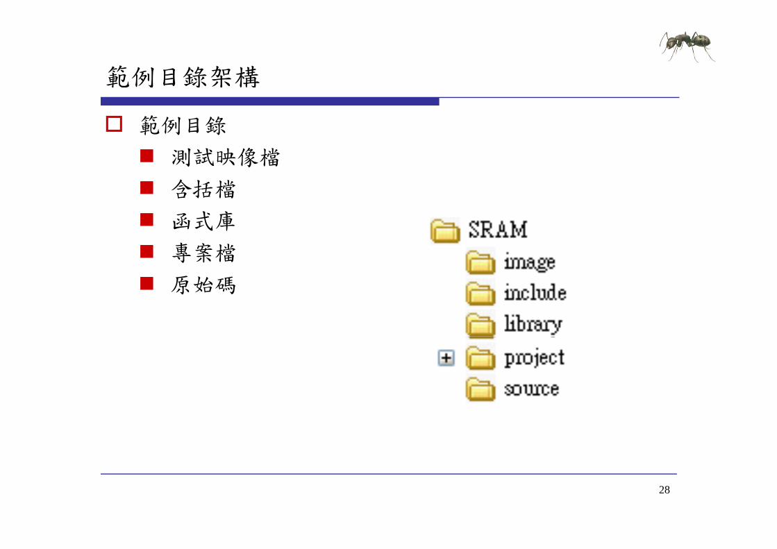
範例目錄架構
範例目錄
測試映像檔 測試映像檔
含括檔
函式庫 函式庫
專案檔
原始碼 原始碼
28
範例說明
Embedded Software Side
Write data to FSMC SRAM memory
SRAM memory RW operation
Write data to FSMC SRAM memory Fill the buffer to send Fill_Buffer(TxBuffer BUFFER_SIZE 0x3212)FSMC_SRAM_WriteBuffer(TxBuffer WRITE_READ_ADDR BUFFER_SIZE)
SRAM memory RW operation
FSMC SRAM WriteBuffer
Read data from FSMC SRAM memory FSMC_SRAM_ReadBuffer(RxBuffer WRITE_READ_ADDR BUFFER_SIZE)
Read back SRAM memory and check content correctness
FSMC SRAM ReadBuffer
Check content
Display Result yfor (Index = 0x00 (Index lt BUFFER_SIZE) ampamp (WriteReadStatus == 0)
Index++)if (RxBuffer[Index] = TxBuffer[Index])
Display Result
WriteReadStatus = Index + 1
29
範例說明
Embedded Software Side
while (1)
Display Result
while (1)if (WriteReadStatus == 0) OK Turn on USERLED
GPIO SetBits(GPIOF GPIO Pin 11)
SRAM memory RW operation
FSMC SRAM WriteBufferGPIO_SetBits(GPIOF GPIO_Pin_11)
else KO Turn off USERLED
GPIO ResetBits(GPIOF GPIO Pin 11)
FSMC SRAM ReadBuffer
Check content
Display Result
如果寫入與讀取Buffer內容相同外部記憶體使用正常USERLED紅燈GPIO_ResetBits(GPIOF GPIO_Pin_11)
Insert delay Delay(0xAFFFF) Turn on USERLED GPIO SetBits(GPIOF GPIO Pin 11)
Display Result恆亮
GPIO_SetBits(GPIOF GPIO_Pin_11) Insert delay Delay(0xAFFFF)
如果寫入與讀取Buffer內容不同外部記憶體使用異常 USERLED紅燈閃爍
30
預設定義說明
define Bank1_SRAM1_ADDR ((u32)0x60000000) 定義SRAM起始點 定義SRAM起始點
define BUFFER_SIZE 0x400定義測試資料大小 定義測試資料大小
資料大小必需小於0xC000 define WRITE_READ_ADDR 0x8000 定義SRAM寫入起始點
寫入起始點WRITE_READ_ADDR + BUFFER_SIZE必需小於0x6000C000
31
燒錄MIAT STM32_
Rebuilder all target files產生HEX DFU Fil M 轉換HEX產生DFU DFU File Manager轉換HEX產生DFU DfuSe Demonstration燒錄DFU d Leave DFU mode
32
內部與外部SRAM存取控制實驗
實驗一
WU-YANGTechnology Co Ltd
實驗一練習
練習 修改寫入位置測試是否正常 修改寫入位置測試是否正常
修改寫入資料大小測試是否正常
取消 i 測試是否正常 取消FSMC_SRAM_Init測試是否正常
34
實驗目的(二)( )
使用MIAT_STM32實驗板透過FSMC控制外部SRAM並設定為data memory進行存取控制實驗同樣利用LED設定為data memory進行存取控制實驗同樣利用LED確認存取是否正常
35
實驗原理
External SRAM RVMDK環境設定 RVMDK環境設定
Development Flow fi ARM Configure Startup Code
36
RVMDK環境設定
外部SRAM有512K Bytes位置由0x60000000至0x60080000
37
Development Flowp
Embedded Software Side
int main(void)
Bootup STM32F10x
Programming
Bootup
int main(void)ifdef DEBUGdebug()
endif
Startup Code
BootupSTM32F10x
RCC Configure
NVIC Configure
System Clocks Configuration RCC_Configuration()
NVIC Configuration g gNVIC_Configuration()
GPIO Configuration GPIO_Configuration()
GPIO Configure
for (Index = 0 Index lt1024 Index++)
Tab[Index] =IndexT bAdd ( 32)T b h ld b 0 600000
Check operation
Check pointer value
Display Result TabAddr = (u32)Tab should be 0x600000xx
Get main stack pointer value MSPValue = __MRS_MSP() should be 0x2000xxxx
helliphelliphelliphelliphelliphelliphelliphelliphelliphelliphelliphelliphelliphelliphelliphelliphelliphelliphelliphelliphelliphelliphellip
Display Result
38
Startup Codep
Register boundary addresses RCC Configure
Enable FSMC clock
LDR R0= 0x00000114
LDR R1= 0x40021014
STR R0[R1]
Enable GPIOD GPIOE GPIOF and GPIOG clocks
LDR R0= 0x000001E0
LDR R1= 0x40021018
RCC register map
STR R0[R1]
39
RCC Register g
Bit 8 FSMCEN FSMC clock enableAHB Peripheral Clock enable register (RCC_AHBENR)
Bit 8 FSMCEN FSMC clock enableSet and cleared by software0 FSMC clock disabled
APB2 peripheral clock enable register (RCC_APB2ENR)
1 FSMC clock enabled
Bit 8765 IOPGEN IO port GFED clock enableSet and cleared by software0 IO port GFED clock disabled1 IO port GFED clock enabled
40
1 IO port GFED clock enabled
Startup Codep
Register boundary addresses GPIO Configure
SRAM Data lines NOE and NWE configuration SRAM Address lines configuration NOE NEW NE1 NBL0 NBL1 configuration LDR R0= 0xB4BB44BB LDR R1= 0x40011400STR R0[R1]LDR R0= 0xBBBBBBBB LDR R1= 0x40011404STR R0[R1]LDR R0 = 0xB44444BBLDR R0= 0xB44444BB LDR R1= 0x40011800STR R0[R1]LDR R0= 0xBBBBBBBB LDR R1= 0x40011804
GPIO register map
STR R0[R1]LDR R0= 0x44BBBBBB LDR R1= 0x40011C00STR R0[R1]LDR R0= 0xBBBB4444 LDR R1= 0x40011C04STR R0[R1]LDR R0= 0x44BBBBBBLDR R1= 0x40012000STR R0 [R1]
41
STR R0[R1]
GPIO Register g
Bit 8 FSMCEN FSMC clock enablePort configuration register low
Port configuration register high
Bits 2928 2524Bits 3130 2726 2322 1918 1514 1110 76 32 Bits 2928 25242120 1716 131298 54 10MODEy[10] Port x mode bits (y= 0 15)00 Input mode (reset state)01 Output mode max speed 10 MHz
Bits 3130 27262322 1918 15141110 76 32CNFy[10] Port x configuration bits (y= 0 15)In input mode (MODE[10]=00)00 Analog input mode01 Floating input (reset state)10 Input with pull-up pull-down
10 Output mode max speed 2 MHz11 Output mode max speed 50 MHz
11 ReservedIn output mode (MODE[10] gt00)00 General purpose output push-pull01 General purpose output Open-drain10 Alternate function output Push-pull11 Alternate function output Open-drain
42
11 Alternate function output Open drain
Startup Codep
FSMCregister map FSMC Configure
FSMC Configuration Enable FSMC Bank1_SRAM Bank
LDR R0= 0x00001011
LDR R1= 0xA0000000
STR R0[R1]
LDR R0= 0x00000200
LDR R1= 0xA0000004
STR R0[R1]
43
FSMC Register g
Bit 8 FSMCEN FSMC clock enableSRAMNOR-Flash chip-select control registers 1 (FSMC_BCR1)
Bit 12 WREN Write enable bitThis bit indicates whether write operations are enableddisabled in the bank by the FSMC0 Write operations are disabled in the bank by the FSMC an AHB error is reported1 Write operations are enabled for the bank by the FSMC (default after reset) p y ( )Bits 54 MWID Memory databus widthDefines the external memory device width valid for all type of memories00 8 bits01 16 bits (default after reset)10 reserved do not use10 reserved do not use11 reserved do not use Bit 0 MBKEN Memory bank enable bitEnables the memory bank After reset Bank1 is enabled all others are disabled Accessing adisabled bank causes an ERROR on AHB bus0 C di b k i di bl d0 Corresponding memory bank is disabled1 Corresponding memory bank is enabled
44
FSMC Register g
Bit 8 FSMCEN FSMC clock enableSRAMNOR-Flash chip-select timing registers 1 (FSMC_BTR1)
Bits 158 DATAST Data-phase duration0000 0000 Reserved0000 0001 DATAST phase duration = 2 times HCLK clock cycles0000 0010 DATAST phase duration = 3 times HCLK clock cycles1111 1111 DATAST phase duration = 256 times HCLK clock cycles (default value after reset)Bits 74 ADDHLD Address-hold phase duration0000 Reserved0001 ADDHLD phase duration = 2 times HCLK clock cycle0010 ADDHLD phase duration = 3 times HCLK clock cycle1111 ADDHLD phase duration = 16 times HCLK clock cycles (default value after reset)Bits 30 ADDSET Address setup phase durationThese bits are written by software to define the duration of the address setup phase (refer toFigure 162 to Figure 172) used in SRAMs ROMs and asynchronous NOR Flash0000 ADDSET phase duration = 1 times HCLK clock cycle1111 ADDSET phase duration = 16 times HCLK clock cycles (default value after reset)
45
實驗步驟
範例目錄架構
範例說明 範例說明
預設定義說明
46
範例目錄架構
範例目錄
測試映像檔 測試映像檔
含括檔
函式庫 函式庫
專案檔
原始碼 原始碼
47
範例說明
Embedded Software Side
Infinite loop
Display Result
Infinite loop while (1)if (((TabAddramp0xFFFFFF00) == 0x60000000) ampamp
((MSPValueamp0xFFFF0000) == 0x20000000))
Check operation
Check pointer value((MSPValueamp0xFFFF0000) == 0x20000000))
OK Turn on USERLED GPIO_SetBits(GPIOF GPIO_Pin_11)
else
Display Result
else KO Turn off USERLED
GPIO_ResetBits(GPIOF GPIO_Pin_11) Insert delay Delay(0xAFFFF)
如果Tab位置在0x600000且Stack pointer位置在0x2000 外部記憶體使用正常USERLED紅燈恆亮Delay(0xAFFFF)
Turn on USERLED GPIO_SetBits(GPIOF GPIO_Pin_11) Insert delay Delay(0xAFFFF)
紅燈恆亮
如果 b位置不在0 600000或Delay(0xAFFFF)
如果Tab位置不在0x600000或Stack pointer位置不在0x2000 外部記憶體使用異常USERLED紅燈閃爍
48
預設定義說明
DATA_IN_ExtSRAM EQU 1 E l SRAM C fi i External SRAM Configuration 0=gt DISABLE 1=gt ENABLE
u32 Tab[1024]宣告於外部 的記憶體 宣告於外部SRAM的記憶體
49
data memory存取控制實驗
實驗二
WU-YANGTechnology Co Ltd
實驗二練習
練習 取消RVMDK環境外部SRAM設定測試是否正常 取消RVMDK環境外部SRAM設定測試是否正常
修改DATA_IN_ExtSRAM EQU 0測試是否正常
修改外部 記憶體 b變數大小測試是否正常 修改外部SRAM記憶體Tab變數大小測試是否正常
51
Q amp A
WU-YANGTechnology Co Ltd
MIAT_STM32內部Flash存取控制實驗
WU-YANG
浯陽科技有限公司
Technology Co Ltd
Declared Version
Training Only
Declare
Document Number
Document Version 100
Release Date
Document Title MIAT_STM32 內部FLASH存取控制實驗
Exercise Time
Platform MIAT_STM32V2MIAT IOB V1PlatformMIAT IOBV1
Peripheral
Author WU-YANG Technology Co Ltd
2
實驗目的(一)( )
使用MIAT_STM32實驗板透過Flash memory interface (FLITF)控制內部Flash進行存取控制實驗並利用LED(FLITF)控制內部Flash進行存取控制實驗並利用LED確認存取是否正常
3
實驗原理
System architecture E b dd d Fl h Embedded Flash Features Memory map RVMDK環境設定
FLITF Flash module organization
Flash library function Development Flow ARM Configure
4
System architecturey
5
Embedded Flash
Features 256 Kb up to 256 Kbytes Memory organization the Flash memory is organized as a
main block and an information blockmain block and an information block Main memory block of size t 32 Kb 64 bit di id d i t 128 f 2 up to 32 Kb times 64 bits divided into 128 pages of 2
Kbytes Information block of size Information block of size 258 times 64 bits
6
Embedded Flash Memory mapy p
7
Flash Memoryy
8
RVMDK環境設定
STMF103ZC有256K Bytes的Flash位置由0x8000000至0x8040000
9
FLITF
Features R d i f i h f h b ff (2 64 bi d ) Read interface with prefetch buffer (2x64-bit words) Option byte Loader
l h i Flash Program Erase operation Read Write protection
10
Flash memory interfacey
11
Flash memory interface registery g
Bit 8 FSMCEN FSMC clock enableFlash status register (FLASH_SR)
Bits 316 Reserved must be kept clearedBit 5 EOP End of operation
Bit 2 PGERR Programming errorSet by hardware when an address to be programmed p
Set by hardware when a Flash operation (programming erase) is completed Reset by writing a 1Note EOP is asserted at the end of each successful
y p gcontains a value different from 0xFFFF before programmingReset by writing 1Note The STRT bit in the FLASH_CR register f f
program or erase operationBit 4 WRPRTERR Write protection errorSet by hardware when programming a write-protected address of the Flash memory
_ gshould be reset before starting a programmingoperationBit 1 Reserved must be kept clearedBit 0 BSY Busyp y
Reset by writing 1Bit 3 Reserved must be kept cleared
This indicates that a Flash operation is in progress This is set on the beginning of a Flash operation and reset when the operation finishes or when an error occurs
12
Flash memory interface registery g
Flash control register (FLASH_CR)
Bit 9 OPTWRE Option bytes write enableWhen set the option bytes can be programmed This
Bit 6 STRT StartThis bit triggers an ERASE operation when set This bit is set only
bit is set on writing the correct key sequence to the FLASH_OPTKEYR registerThis bit can be reset by softwareBit 8 Reserved must be kept clearedBit 7 LOCK Lock
by software and reset when the BSY bit is resetBit 5 OPTER Option byte eraseOption byte erase chosenBit 4 OPTPG Option byte programmingOption byte programming chosenBit 7 LOCK Lock
Write to 1 only When it is set it indicates that the FPEC and FLASH_CR are locked This bit is reset by hardware after detecting the unlock sequenceIn the event of unsuccessful unlock operation this bit remains set until the next reset
p y p g gBit 3 Reserved must be kept clearedBit 2 MER Mass eraseErase of all user pages chosenBit 1 PER Page erasePage Erase chosenremains set until the next reset Page Erase chosenBit 0 PG ProgrammingFlash programming chosen
13
Main Flash memory programmingy p g g
14
Flash memory Page Erasey g
15
Flash memory Mass Erasey
16
Option byte programmingp y p g g
17
Option byte Erasep y
18
FLASH library functiony
19
FLASH library functiony
20
Development Flowp
Embedded Software Side
int main(void)
Bootup STM32F10x
ProgrammingBootupSTM32F10x RCC Configure
NVIC Configure
int main(void)ifdef DEBUGdebug()
endifendif
FLASHStatus = FLASH_COMPLETEMemoryProgramStatus = PASSEDData = 0x15041975
GPIO Configure
Data = 0x15041975
RCC Configuration RCC_Configuration()
Flash memory RW operation FLASH Unlock
FLASH ClearFlag NVIC Configuration NVIC_Configuration()
GPIO Configuration
FLASH ClearFlag
FLASH ErasePage
FLASH ProgramWord GPIO Configuration GPIO_Configuration()
helliphelliphelliphelliphelliphelliphelliphelliphelliphelliphelliphelliphelliphelliphelliphelliphellipDisplay Result
Check content
21
實驗步驟
範例目錄架構
範例說明 範例說明
預設定義說明
燒錄 燒錄MIAT_STM32
22
範例目錄架構
範例目錄
測試映像檔 測試映像檔
含括檔
函式庫 函式庫
專案檔
原始碼 原始碼
23
範例說明
Function name Description
Unlock the Flash Program Erase controller FLASH_Unlock()
D fi h b f b d
Flash FwLib Functions List
Function name Description
FLASH_Unlock Unlocks the FLASH Program Erase Controller
FLASH_ClearFlag Clears the FLASH pending fl
Define the number of page to be erased NbrOfPage = (EndAddr - StartAddr) FLASH_PAGE_SIZE
Clear All pending flags FLASH_ClearFlag(FLASH_FLAG_BSY | FLASH_FLAG_EOP | FLASH_FLAG_PGERR |
FLASH FLAG WRPRTERR)flags
FLASH_ErasePage Erases a specified FLASH page
FLASH_ProgramWord Programs a word at a specified
_ _ )
Erase the FLASH pages for(EraseCounter = 0 (EraseCounter lt NbrOfPage) ampamp (FLASHStatus ==
FLASH_COMPLETE) EraseCounter++)FLASHStatus = FLASH ErasePage(StartAddr + (FLASH PAGE SIZE EraseCounter))address FLASHStatus = FLASH_ErasePage(StartAddr + (FLASH_PAGE_SIZE EraseCounter))
FLASH Word program of data 0x15041979 at addresses defined by StartAddr and EndAddrAddress = StartAddr
while((Address lt EndAddr) ampamp (FLASHStatus == FLASH_COMPLETE))FLASHStatus = FLASH_ProgramWord(Address Data)Address = Address + 4
24
範例說明
Embedded Software Side
Check the corectness of written data
Display Result
Check the corectness of written data Address = StartAddr
while((Address lt EndAddr) ampamp (MemoryProgramStatus = FAILED))if(((vu32) Address) = Data)
Flash memory RW operation
MemoryProgramStatus = FAILED
Address += 4
Check content
Display Result while (1)if (MemoryProgramStatus == PASSED) OK Turn on USERLED GPIO_SetBits(GPIOF GPIO_Pin_11)
Display Result
else KO Turn off USERLED GPIO_ResetBits(GPIOF GPIO_Pin_11) Insert delay Delay(0xAFFFF)
如果寫入與讀取Flash內容相同Flash記憶體使用正常USERLED紅燈恆亮
Turn on USERLED GPIO_SetBits(GPIOF GPIO_Pin_11) Insert delay Delay(0xAFFFF)
如果寫入與讀取Flash內容不同Flash記憶體使用異常USERLED紅燈閃爍
25
預設定義說明
define StartAddr ((u32)0x08008000) 定義Flash使用起始點 定義Flash使用起始點
使用起始點必需大於0x8003000 + Code Size 附註 0x8000000~0x8003000為DFU程式區塊使用此區塊
將造成無法燒錄程式
Code Size可由產生的HEX檔得知
d fi E dAdd (( 32)0 0800C000) define EndAddr ((u32)0x0800C000) 定義Flash使用結束點
使用起始點必需小於0x8040000使用起始點必需小於
Data = 0x15041975 寫入資料
32Bit define FLASH_PAGE_SIZE ((u16)0x800)
每一個Page有2KByte26
每一個Page有2KByte
Intel HEX Format
aaaa tt dd cc
field Description
the colon that starts every Intel HEX record
the record-length field that represents the number of data bytes (dd) in the record
aaaa the address field that represents the starting address for subsequent data in the record
tt the field that represents the HEX record type which may be one of the following00 - data record01 - end-of-file record02 - extended segment address recordg04 - extended linear address record
dd a data field that represents one byte of data A record may have multiple data bytes The number of data bytes in the record must match the number specified by the field
cc the checksum field that represents the checksum of the record The checksum is calculated by summing the values of all hexadecimal digit pairs in the record modulo 256 and taking the twos complement
27
HEX Examplep
020000040800F2103000001814002045310008D9340008CD340008D8103000001814002045310008D9340008CD340008D8helliphelliphellip1038200042370008000000000000000000000000170C3830000000000000000000000000008C
資料填入起始位置為
0C3830000000000000000000000000008C04000005080031318D00000001FF
資料填入起始位置為0x08003000 每一行有0x10(16)個Bytes 最後一筆資料為
資料結束點為0x0803383004000005080031318D
(0x08003830 -0x08000000)0x800 = 7 需以0x800為單位所以使用的位置起點為0x08004000
28
燒錄MIAT STM32_
Rebuilder all target files產生HEX DFU Fil M 轉換HEX產生DFU DFU File Manager轉換HEX產生DFU DfuSe Demonstration燒錄DFU d Leave DFU mode
29
內部Flash存取控制實驗
實驗一
WU-YANGTechnology Co Ltd
實驗一練習
注意 請使用預設0 08008000之後的位置 避免覆蓋DFU 請使用預設0x08008000之後的位置避免覆蓋DFU
與使用者程式碼區塊
練習 練習 修改存取位置測試是否正常
修改寫入資料測試是否正常 修改寫入資料測試是否正常
修改寫入資料後取消FLASH_Unlock測試是否正常
修改寫入資料後取消FLASH E P 測試是否正 修改寫入資料後取消FLASH_ErasePage測試是否正常
31
實驗目的(二)( )
使用MIAT_STM32實驗板透過Flash memory interface (FLITF)控制內部Flash進行存取控制實驗並利用SW(FLITF)控制內部Flash進行存取控制實驗並利用SWKEY決定資料寫入與讀取LCD顯示狀態
32
實驗原理
System requirement E b dd d Fl h Embedded Flash LCD KEY SW
Development Flow ARM Configure
33
Development Flowp
Embedded Software Side
int main(void)
Bootup STM32F10x
ProgrammingBootupSTM32F10x RCC Configure
NVIC Configure
int main(void)ifdef DEBUGdebug()
endif
FLASHStatus = FLASH_COMPLETE
RCC Configuration RCC Configuration()
GPIO Configure
BasicIO Configure_ g ()
NVIC Configuration NVIC_Configuration()
GPIO Configuration Flash memory RW ti
lcd Configure
GPIO Configuration GPIO_Configuration()
Init_BasicIO()
l d i i () LCD I i i li i
RW operation
Example
FLASH Unlock
FLASH ClearFlag
lcd_init() LCD Initialization
helliphelliphelliphelliphelliphelliphelliphelliphelliphelliphelliphelliphelliphelliphelliphelliphelliphelliphelliphelliphelliphelliphellip
p
34
硬體電路配置
Mapping Table
Num MIAT_STM32V2 MIAT_IOBV1 Num MIAT_STM32V2 MIAT_IOBV1
1 PC8 (326) SW1 10 PE6 (15) LCD_EN2 PC9 (327) SW2 11 PF6 (118) LCD RW ( ) ( ) _3 PC10 (43) SW3 12 PF7 (119) LCD_RS 4 PC11 (44) SW4 13 PF8(120) LCD_D4 5 PB5 (427) KEY1 14 PF9 (121) LCD_D5 6 PB6 (428) KEY2 15 PF10 (122) LCD_D6 7 PB7 (429) KEY3 16 PF11 (213) LCD_D7 8 PB8 (431) KEY4 17 VDD (236) VCC33V 9 VCC5V (1 36) VCC5V 18 GND (1 35) GND9 VCC5V (136) VCC5V 18 GND (135) GND
35
實驗步驟
範例目錄架構
範例說明 範例說明
預設定義說明
36
範例目錄架構
範例目錄
測試映像檔 測試映像檔
含括檔
函式庫 函式庫
專案檔
原始碼 原始碼
37
範例說明
Embedded Software Side
lcd clear()
FLASH memory RW operation
lcd_clear()lcd_print (MIAT_STM32 DEMO )
Unlock the Flash Program Erase controller FLASH_Unlock()
Flash memory RW operation
FLASH Unlock
Clear All pending flags FLASH_ClearFlag(FLASH_FLAG_BSY | FLASH_FLAG_EOP | FLASH_FLAG_PGERR |
FLASH_FLAG_WRPRTERR)
while(1)
Example
FLASH ClearFlag
( )
KEY_Buffer=Key_Scan()set_cursor (0 1)lcd_print (SW Value = 0x)lcd putchar(((SWamp0x7)+0x30))lcd_putchar(((SWamp0x7)+0x30))if(KEY_Buffer==1)Address=(StartAddr|(SWltlt12))set_cursor (0 0)lcd_print (Set Addr = 0x)
掃描KEY是否按下與顯示SW數值LCD Line2顯示SW Value = 0x(SW)
lcd_putchar(((SWamp0x7)+0x30))lcd_print ( )
如果KEY1按下記錄SW數值至Address LCD Line1顯示Set Adde = 0x(Address)
38
範例說明
Embedded Software Side
else if(KEY Buffer==2)
FLASH memory RW operation
else if(KEY_Buffer==2)
Erase the FLASH pages FLASHStatus = FLASH_ErasePage(Address)
FLASH Word program of data at addresses defined by SW
SRAM memory RW operation
p g yFLASHStatus = FLASH_ProgramWord(Address (SWamp0x7))
set_cursor (0 0)lcd_print (Write 0x)lcd_putchar(((SWamp0x7)+0x30))l d i t ( t 0 )
Example如果KEY2按下清除Address所處區塊並寫入SW數值 lcd_print ( at 0x)
lcd_putchar((((Addressgtgt12)amp0x7)+0x30))else if(KEY_Buffer==3)
Data=(u16 )Address
所處區塊並寫入SW數值LCD Line1顯示Write 0x(SW) at 0x(Adddress)
Data (u16 )Addressset_cursor (0 0)lcd_print (Addr 0x)lcd_putchar((((Addressgtgt12)amp0x7)+0x30))lcd_print ( = 0x)lcd_putchar(((Dataamp0x7)+0x30))lcd_print ( )
如果KEY3按下讀取Address紀錄數值LCD Line1顯示Addr 0x(Adddress) = 0x
39
預設定義說明
define StartAddr ((u32)0x08020000) 定義Flash使用起始點 定義Flash使用起始點
使用起始點必需大於0x8003000 + Code Size 附註 0x8000000~0x8003000為DFU程式區塊使用此區塊
將造成無法燒錄程式
Code Size可由產生的HEX檔得知
32 Add 0 08020000 u32 Address = 0x08020000 定義Address初始值
初始值必需與Flash使用起始點相同初始值必需與 使用起始點相同
Address=(StartAddr|(SWltlt12)) Example StartAddr = 0x08020000 SW = 1 Address = 0x08021000
StartAddr = 0x08020000 SW = 7 Address = 0x08027000 StartAddr|(7ltlt12)必需小於0x8040000
40
使用者界面與Flash存取控制實驗
實驗二
WU-YANGTechnology Co Ltd
實驗二練習
注意 請使用預設0 08020000之後的位置 避免覆蓋DFU 請使用預設0x08020000之後的位置避免覆蓋DFU
與使用者程式碼區塊
練習 練習 利用SW與KEY測試Flash寫入與讀取是否正常
Fl h寫入後電源關閉 再開啟後寫入資料是否仍存 Flash寫入後電源關閉再開啟後寫入資料是否仍存在
修改存取位置測試是否正常 修改存取位置測試是否正常
42
實驗目的(三)( )
使用MIAT_STM32實驗板透過Flash memory interface (FLITF)控制內部Flash進行存取控制實驗並藉由填入(FLITF)控制內部Flash進行存取控制實驗並藉由填入Option Bytes 設定寫入鎖定保護Page鎖定不被覆蓋
43
Development Flowp
Embedded Software Side
int main(void)
Bootup STM32F10x
ProgrammingBootupSTM32F10x RCC Configure
NVIC Configure
int main(void)ifdef DEBUGdebug()
endifendif
FLASHStatus = FLASH_COMPLETEMemoryProgramStatus = PASSEDData = 0x1753
GPIO Configure
Data = 0x1753
RCC Configuration RCC_Configuration()
Flash memory RW operation FLASH Unlock
FLASH ClearFlag NVIC Configuration NVIC_Configuration()
GPIO Configuration
FLASH ClearFlag
FLASH ErasePage
FLASH ProgramHalfWord GPIO Configuration GPIO_Configuration()
Display Result
Check content
44
helliphelliphelliphelliphelliphelliphelliphelliphelliphelliphelliphelliphelliphelliphelliphelliphelliphelliphellip
實驗步驟
範例目錄架構
範例說明 範例說明
預設定義說明
45
範例目錄架構
範例目錄
測試映像檔 測試映像檔
含括檔
函式庫 函式庫
專案檔
原始碼 原始碼
46
範例說明
Function name Description
Unlock the Flash Program Erase controller FLASH_Unlock()
Define the number of page to be erased
Flash FwLib Functions List
Function name Description
FLASH_Unlock Unlocks the FLASH Program Erase Controller
FLASH_ClearFlag Clears the FLASH pending fl
Define the number of page to be erased NbrOfPage = (EndAddr ‐ StartAddr) FLASH_PAGE_SIZE
FLASH_ClearFlag(FLASH_FLAG_BSY | FLASH_FLAG_EOP|FLASH_FLAG_PGERR |FLASH_FLAG_WRPRTERR)
Get pages write protection status flags
FLASH_EraseOptionBytes
Erases the FLASH option bytes
FLASH_EnableWritePro Write protects the desired
p g pWRPR_Value = FLASH_GetWriteProtectionOptionByte()ProtectedPages = WRPR_Value amp 0x000000C0
ifdef WriteProtection_Disableif (ProtectedPages == 0x00) Pages are write protected
tection pages
NVIC_GenerateSystemReset
Generate a system reset
Disable the write protection FLASHStatus = FLASH_EraseOptionBytes() Generate System Reset to load the new option byte values NVIC_GenerateSystemReset()
elseifdef WriteProtection Enableifdef WriteProtection_Enableif (ProtectedPages = 0x00) Pages not write protected
FLASHStatus = FLASH_EraseOptionBytes() Enable the pages write protection FLASHStatus = FLASH_EnableWriteProtection(FLASH_WRProt_Pages12to13
|FLASH WRProt Pages14to15)|FLASH_WRProt_Pages14to15) Generate System Reset to load the new option byte values NVIC_GenerateSystemReset()
endifendif
47
範例說明
if (ProtectedPages = 0x00) Clear All pending flags
Flash FwLib Functions List
Function name DescriptionFLASH_ClearFlag(FLASH_FLAG_BSY |
FLASH_FLAG_EOP|FLASH_FLAG_PGERR |FLASH_FLAG_WRPRTERR)
erase the FLASH pages for(EraseCounter = 0 (EraseCounter lt NbrOfPage) ampamp (FLASHStatus ==
Function name Description
FLASH_ErasePage Erases a specified FLASH page
FLASH_ProgramHalfWod
Programs a half word at a ifi d dd FLASH_COMPLETE) EraseCounter++)
FLASHStatus = FLASH_ErasePage(StartAddr + (FLASH_PAGE_SIZE
EraseCounter))
rd specified address
FLASH Half Word program of data 0x1753 at addresses defined by StartAddrand EndAddr
Address = StartAddr
hil ((Add E dAdd ) ampamp (FLASHSt t FLASH COMPLETE))while((Address lt EndAddr) ampamp (FLASHStatus == FLASH_COMPLETE))
FLASHStatus = FLASH_ProgramHalfWord(Address Data)Address = Address + 2
48
範例說明
Embedded Software Side
Check the corectness of written data
Display Result
Check the corectness of written data Address = StartAddr
while((Address lt EndAddr) ampamp (MemoryProgramStatus = FAILED))if(((vu16) Address) = Data)
Flash memory RW operation
MemoryProgramStatus = FAILED
Address += 2
Check content
Display Result while (1)if (MemoryProgramStatus == PASSED) OK Turn on USERLED GPIO_SetBits(GPIOF GPIO_Pin_11)
Display Result
else KO Turn off USERLED GPIO_ResetBits(GPIOF GPIO_Pin_11) Insert delay Delay(0xAFFFF)
如果寫入與讀取Flash內容相同Flash記憶體可以寫入USERLED紅燈恆亮
Turn on USERLED GPIO_SetBits(GPIOF GPIO_Pin_11) Insert delay Delay(0xAFFFF)
如果寫入與讀取Flash內容不同Flash記憶體不能寫入USERLED紅燈閃爍
49
預設定義說明
define StartAddr ((u32) 0x08006000) 定義Flash使用起始點 定義Flash使用起始點
使用起始點必需大於0x8003000 + Code Size 附註 0x8000000~0x8003000為DFU程式區塊使用此區塊
將造成無法燒錄程式
Code Size可由產生的HEX檔得知
d fi E dAdd (( 32) 0 08008000) define EndAddr ((u32) 0x08008000) 定義Flash使用結束點
使用起始點必需小於0x8040000使用起始點必需小於
Data = 0x1753 寫入資料
16Bit define FLASH_PAGE_SIZE ((u16)0x800) 每一個Page有2KByte
50
每一個Page有2KByte
預設定義說明
define WriteProtection_Enable U hi li E bl W i P i Uncomment this line to Enable Write Protection
define WriteProtection_Disablehi li i bl i i Uncomment this line to Disable Write Protection
FLASH_EnableWriteProtection設定影響 個 設定影響2個Page FLASH_WRProt_Pages0to1 FLASH_WRProt_Pages1to2 helliphellip FLASH_WRProt_Pages60to61
設定影響多個Page FLASH_WRProt_Pages62to255
51
FLASH EnableWriteProtection_
Example
位置0x08006000 ~ 0x08007000每一個Page有0x800ByteStartPage = (0x08006000-0x08000000)0x800 = 12EndPage = ((0x08007000-0x08000000)0x800)-1 = 13執行執行FLASH_EnableWriteProtection(FLASH_WRProt_Pages12to13)將影響Pages12 Pages13
52
內部Flash寫入鎖定存取控制實驗
實驗三
WU-YANGTechnology Co Ltd
實驗三練習
注意 請使用預設0 08006000之後的位置 避免覆蓋DFU 請使用預設0x08006000之後的位置避免覆蓋DFU
與使用者程式碼區塊
更改寫入位置測試寫入鎖定時需同時更改 更改寫入位置測試寫入鎖定時需同時更改FLASH_EnableWriteProtection鎖定之Page
練習 練習 打開define WriteProtection_Enable測試是否可寫入
打開define WriteProtection Disable測試是否可寫入 打開define WriteProtection_Disable測試是否可寫入
修改存取位置測試是否正常
修改寫入資料測試是否正常 修改寫入資料測試是否正常
54
Q amp A
WU-YANGTechnology Co Ltd

範例說明
Embedded Software Side
while (1)
Display Result
while (1)if (WriteReadStatus == 0) OK Turn on USERLED
GPIO SetBits(GPIOF GPIO Pin 11)
SRAM memory RW operation
FSMC SRAM WriteBufferGPIO_SetBits(GPIOF GPIO_Pin_11)
else KO Turn off USERLED
GPIO ResetBits(GPIOF GPIO Pin 11)
FSMC SRAM ReadBuffer
Check content
Display Result
如果寫入與讀取Buffer內容相同外部記憶體使用正常USERLED紅燈GPIO_ResetBits(GPIOF GPIO_Pin_11)
Insert delay Delay(0xAFFFF) Turn on USERLED GPIO SetBits(GPIOF GPIO Pin 11)
Display Result恆亮
GPIO_SetBits(GPIOF GPIO_Pin_11) Insert delay Delay(0xAFFFF)
如果寫入與讀取Buffer內容不同外部記憶體使用異常 USERLED紅燈閃爍
30
預設定義說明
define Bank1_SRAM1_ADDR ((u32)0x60000000) 定義SRAM起始點 定義SRAM起始點
define BUFFER_SIZE 0x400定義測試資料大小 定義測試資料大小
資料大小必需小於0xC000 define WRITE_READ_ADDR 0x8000 定義SRAM寫入起始點
寫入起始點WRITE_READ_ADDR + BUFFER_SIZE必需小於0x6000C000
31
燒錄MIAT STM32_
Rebuilder all target files產生HEX DFU Fil M 轉換HEX產生DFU DFU File Manager轉換HEX產生DFU DfuSe Demonstration燒錄DFU d Leave DFU mode
32
內部與外部SRAM存取控制實驗
實驗一
WU-YANGTechnology Co Ltd
實驗一練習
練習 修改寫入位置測試是否正常 修改寫入位置測試是否正常
修改寫入資料大小測試是否正常
取消 i 測試是否正常 取消FSMC_SRAM_Init測試是否正常
34
實驗目的(二)( )
使用MIAT_STM32實驗板透過FSMC控制外部SRAM並設定為data memory進行存取控制實驗同樣利用LED設定為data memory進行存取控制實驗同樣利用LED確認存取是否正常
35
實驗原理
External SRAM RVMDK環境設定 RVMDK環境設定
Development Flow fi ARM Configure Startup Code
36
RVMDK環境設定
外部SRAM有512K Bytes位置由0x60000000至0x60080000
37
Development Flowp
Embedded Software Side
int main(void)
Bootup STM32F10x
Programming
Bootup
int main(void)ifdef DEBUGdebug()
endif
Startup Code
BootupSTM32F10x
RCC Configure
NVIC Configure
System Clocks Configuration RCC_Configuration()
NVIC Configuration g gNVIC_Configuration()
GPIO Configuration GPIO_Configuration()
GPIO Configure
for (Index = 0 Index lt1024 Index++)
Tab[Index] =IndexT bAdd ( 32)T b h ld b 0 600000
Check operation
Check pointer value
Display Result TabAddr = (u32)Tab should be 0x600000xx
Get main stack pointer value MSPValue = __MRS_MSP() should be 0x2000xxxx
helliphelliphelliphelliphelliphelliphelliphelliphelliphelliphelliphelliphelliphelliphelliphelliphelliphelliphelliphelliphelliphelliphellip
Display Result
38
Startup Codep
Register boundary addresses RCC Configure
Enable FSMC clock
LDR R0= 0x00000114
LDR R1= 0x40021014
STR R0[R1]
Enable GPIOD GPIOE GPIOF and GPIOG clocks
LDR R0= 0x000001E0
LDR R1= 0x40021018
RCC register map
STR R0[R1]
39
RCC Register g
Bit 8 FSMCEN FSMC clock enableAHB Peripheral Clock enable register (RCC_AHBENR)
Bit 8 FSMCEN FSMC clock enableSet and cleared by software0 FSMC clock disabled
APB2 peripheral clock enable register (RCC_APB2ENR)
1 FSMC clock enabled
Bit 8765 IOPGEN IO port GFED clock enableSet and cleared by software0 IO port GFED clock disabled1 IO port GFED clock enabled
40
1 IO port GFED clock enabled
Startup Codep
Register boundary addresses GPIO Configure
SRAM Data lines NOE and NWE configuration SRAM Address lines configuration NOE NEW NE1 NBL0 NBL1 configuration LDR R0= 0xB4BB44BB LDR R1= 0x40011400STR R0[R1]LDR R0= 0xBBBBBBBB LDR R1= 0x40011404STR R0[R1]LDR R0 = 0xB44444BBLDR R0= 0xB44444BB LDR R1= 0x40011800STR R0[R1]LDR R0= 0xBBBBBBBB LDR R1= 0x40011804
GPIO register map
STR R0[R1]LDR R0= 0x44BBBBBB LDR R1= 0x40011C00STR R0[R1]LDR R0= 0xBBBB4444 LDR R1= 0x40011C04STR R0[R1]LDR R0= 0x44BBBBBBLDR R1= 0x40012000STR R0 [R1]
41
STR R0[R1]
GPIO Register g
Bit 8 FSMCEN FSMC clock enablePort configuration register low
Port configuration register high
Bits 2928 2524Bits 3130 2726 2322 1918 1514 1110 76 32 Bits 2928 25242120 1716 131298 54 10MODEy[10] Port x mode bits (y= 0 15)00 Input mode (reset state)01 Output mode max speed 10 MHz
Bits 3130 27262322 1918 15141110 76 32CNFy[10] Port x configuration bits (y= 0 15)In input mode (MODE[10]=00)00 Analog input mode01 Floating input (reset state)10 Input with pull-up pull-down
10 Output mode max speed 2 MHz11 Output mode max speed 50 MHz
11 ReservedIn output mode (MODE[10] gt00)00 General purpose output push-pull01 General purpose output Open-drain10 Alternate function output Push-pull11 Alternate function output Open-drain
42
11 Alternate function output Open drain
Startup Codep
FSMCregister map FSMC Configure
FSMC Configuration Enable FSMC Bank1_SRAM Bank
LDR R0= 0x00001011
LDR R1= 0xA0000000
STR R0[R1]
LDR R0= 0x00000200
LDR R1= 0xA0000004
STR R0[R1]
43
FSMC Register g
Bit 8 FSMCEN FSMC clock enableSRAMNOR-Flash chip-select control registers 1 (FSMC_BCR1)
Bit 12 WREN Write enable bitThis bit indicates whether write operations are enableddisabled in the bank by the FSMC0 Write operations are disabled in the bank by the FSMC an AHB error is reported1 Write operations are enabled for the bank by the FSMC (default after reset) p y ( )Bits 54 MWID Memory databus widthDefines the external memory device width valid for all type of memories00 8 bits01 16 bits (default after reset)10 reserved do not use10 reserved do not use11 reserved do not use Bit 0 MBKEN Memory bank enable bitEnables the memory bank After reset Bank1 is enabled all others are disabled Accessing adisabled bank causes an ERROR on AHB bus0 C di b k i di bl d0 Corresponding memory bank is disabled1 Corresponding memory bank is enabled
44
FSMC Register g
Bit 8 FSMCEN FSMC clock enableSRAMNOR-Flash chip-select timing registers 1 (FSMC_BTR1)
Bits 158 DATAST Data-phase duration0000 0000 Reserved0000 0001 DATAST phase duration = 2 times HCLK clock cycles0000 0010 DATAST phase duration = 3 times HCLK clock cycles1111 1111 DATAST phase duration = 256 times HCLK clock cycles (default value after reset)Bits 74 ADDHLD Address-hold phase duration0000 Reserved0001 ADDHLD phase duration = 2 times HCLK clock cycle0010 ADDHLD phase duration = 3 times HCLK clock cycle1111 ADDHLD phase duration = 16 times HCLK clock cycles (default value after reset)Bits 30 ADDSET Address setup phase durationThese bits are written by software to define the duration of the address setup phase (refer toFigure 162 to Figure 172) used in SRAMs ROMs and asynchronous NOR Flash0000 ADDSET phase duration = 1 times HCLK clock cycle1111 ADDSET phase duration = 16 times HCLK clock cycles (default value after reset)
45
實驗步驟
範例目錄架構
範例說明 範例說明
預設定義說明
46
範例目錄架構
範例目錄
測試映像檔 測試映像檔
含括檔
函式庫 函式庫
專案檔
原始碼 原始碼
47
範例說明
Embedded Software Side
Infinite loop
Display Result
Infinite loop while (1)if (((TabAddramp0xFFFFFF00) == 0x60000000) ampamp
((MSPValueamp0xFFFF0000) == 0x20000000))
Check operation
Check pointer value((MSPValueamp0xFFFF0000) == 0x20000000))
OK Turn on USERLED GPIO_SetBits(GPIOF GPIO_Pin_11)
else
Display Result
else KO Turn off USERLED
GPIO_ResetBits(GPIOF GPIO_Pin_11) Insert delay Delay(0xAFFFF)
如果Tab位置在0x600000且Stack pointer位置在0x2000 外部記憶體使用正常USERLED紅燈恆亮Delay(0xAFFFF)
Turn on USERLED GPIO_SetBits(GPIOF GPIO_Pin_11) Insert delay Delay(0xAFFFF)
紅燈恆亮
如果 b位置不在0 600000或Delay(0xAFFFF)
如果Tab位置不在0x600000或Stack pointer位置不在0x2000 外部記憶體使用異常USERLED紅燈閃爍
48
預設定義說明
DATA_IN_ExtSRAM EQU 1 E l SRAM C fi i External SRAM Configuration 0=gt DISABLE 1=gt ENABLE
u32 Tab[1024]宣告於外部 的記憶體 宣告於外部SRAM的記憶體
49
data memory存取控制實驗
實驗二
WU-YANGTechnology Co Ltd
實驗二練習
練習 取消RVMDK環境外部SRAM設定測試是否正常 取消RVMDK環境外部SRAM設定測試是否正常
修改DATA_IN_ExtSRAM EQU 0測試是否正常
修改外部 記憶體 b變數大小測試是否正常 修改外部SRAM記憶體Tab變數大小測試是否正常
51
Q amp A
WU-YANGTechnology Co Ltd
MIAT_STM32內部Flash存取控制實驗
WU-YANG
浯陽科技有限公司
Technology Co Ltd
Declared Version
Training Only
Declare
Document Number
Document Version 100
Release Date
Document Title MIAT_STM32 內部FLASH存取控制實驗
Exercise Time
Platform MIAT_STM32V2MIAT IOB V1PlatformMIAT IOBV1
Peripheral
Author WU-YANG Technology Co Ltd
2
實驗目的(一)( )
使用MIAT_STM32實驗板透過Flash memory interface (FLITF)控制內部Flash進行存取控制實驗並利用LED(FLITF)控制內部Flash進行存取控制實驗並利用LED確認存取是否正常
3
實驗原理
System architecture E b dd d Fl h Embedded Flash Features Memory map RVMDK環境設定
FLITF Flash module organization
Flash library function Development Flow ARM Configure
4
System architecturey
5
Embedded Flash
Features 256 Kb up to 256 Kbytes Memory organization the Flash memory is organized as a
main block and an information blockmain block and an information block Main memory block of size t 32 Kb 64 bit di id d i t 128 f 2 up to 32 Kb times 64 bits divided into 128 pages of 2
Kbytes Information block of size Information block of size 258 times 64 bits
6
Embedded Flash Memory mapy p
7
Flash Memoryy
8
RVMDK環境設定
STMF103ZC有256K Bytes的Flash位置由0x8000000至0x8040000
9
FLITF
Features R d i f i h f h b ff (2 64 bi d ) Read interface with prefetch buffer (2x64-bit words) Option byte Loader
l h i Flash Program Erase operation Read Write protection
10
Flash memory interfacey
11
Flash memory interface registery g
Bit 8 FSMCEN FSMC clock enableFlash status register (FLASH_SR)
Bits 316 Reserved must be kept clearedBit 5 EOP End of operation
Bit 2 PGERR Programming errorSet by hardware when an address to be programmed p
Set by hardware when a Flash operation (programming erase) is completed Reset by writing a 1Note EOP is asserted at the end of each successful
y p gcontains a value different from 0xFFFF before programmingReset by writing 1Note The STRT bit in the FLASH_CR register f f
program or erase operationBit 4 WRPRTERR Write protection errorSet by hardware when programming a write-protected address of the Flash memory
_ gshould be reset before starting a programmingoperationBit 1 Reserved must be kept clearedBit 0 BSY Busyp y
Reset by writing 1Bit 3 Reserved must be kept cleared
This indicates that a Flash operation is in progress This is set on the beginning of a Flash operation and reset when the operation finishes or when an error occurs
12
Flash memory interface registery g
Flash control register (FLASH_CR)
Bit 9 OPTWRE Option bytes write enableWhen set the option bytes can be programmed This
Bit 6 STRT StartThis bit triggers an ERASE operation when set This bit is set only
bit is set on writing the correct key sequence to the FLASH_OPTKEYR registerThis bit can be reset by softwareBit 8 Reserved must be kept clearedBit 7 LOCK Lock
by software and reset when the BSY bit is resetBit 5 OPTER Option byte eraseOption byte erase chosenBit 4 OPTPG Option byte programmingOption byte programming chosenBit 7 LOCK Lock
Write to 1 only When it is set it indicates that the FPEC and FLASH_CR are locked This bit is reset by hardware after detecting the unlock sequenceIn the event of unsuccessful unlock operation this bit remains set until the next reset
p y p g gBit 3 Reserved must be kept clearedBit 2 MER Mass eraseErase of all user pages chosenBit 1 PER Page erasePage Erase chosenremains set until the next reset Page Erase chosenBit 0 PG ProgrammingFlash programming chosen
13
Main Flash memory programmingy p g g
14
Flash memory Page Erasey g
15
Flash memory Mass Erasey
16
Option byte programmingp y p g g
17
Option byte Erasep y
18
FLASH library functiony
19
FLASH library functiony
20
Development Flowp
Embedded Software Side
int main(void)
Bootup STM32F10x
ProgrammingBootupSTM32F10x RCC Configure
NVIC Configure
int main(void)ifdef DEBUGdebug()
endifendif
FLASHStatus = FLASH_COMPLETEMemoryProgramStatus = PASSEDData = 0x15041975
GPIO Configure
Data = 0x15041975
RCC Configuration RCC_Configuration()
Flash memory RW operation FLASH Unlock
FLASH ClearFlag NVIC Configuration NVIC_Configuration()
GPIO Configuration
FLASH ClearFlag
FLASH ErasePage
FLASH ProgramWord GPIO Configuration GPIO_Configuration()
helliphelliphelliphelliphelliphelliphelliphelliphelliphelliphelliphelliphelliphelliphelliphelliphellipDisplay Result
Check content
21
實驗步驟
範例目錄架構
範例說明 範例說明
預設定義說明
燒錄 燒錄MIAT_STM32
22
範例目錄架構
範例目錄
測試映像檔 測試映像檔
含括檔
函式庫 函式庫
專案檔
原始碼 原始碼
23
範例說明
Function name Description
Unlock the Flash Program Erase controller FLASH_Unlock()
D fi h b f b d
Flash FwLib Functions List
Function name Description
FLASH_Unlock Unlocks the FLASH Program Erase Controller
FLASH_ClearFlag Clears the FLASH pending fl
Define the number of page to be erased NbrOfPage = (EndAddr - StartAddr) FLASH_PAGE_SIZE
Clear All pending flags FLASH_ClearFlag(FLASH_FLAG_BSY | FLASH_FLAG_EOP | FLASH_FLAG_PGERR |
FLASH FLAG WRPRTERR)flags
FLASH_ErasePage Erases a specified FLASH page
FLASH_ProgramWord Programs a word at a specified
_ _ )
Erase the FLASH pages for(EraseCounter = 0 (EraseCounter lt NbrOfPage) ampamp (FLASHStatus ==
FLASH_COMPLETE) EraseCounter++)FLASHStatus = FLASH ErasePage(StartAddr + (FLASH PAGE SIZE EraseCounter))address FLASHStatus = FLASH_ErasePage(StartAddr + (FLASH_PAGE_SIZE EraseCounter))
FLASH Word program of data 0x15041979 at addresses defined by StartAddr and EndAddrAddress = StartAddr
while((Address lt EndAddr) ampamp (FLASHStatus == FLASH_COMPLETE))FLASHStatus = FLASH_ProgramWord(Address Data)Address = Address + 4
24
範例說明
Embedded Software Side
Check the corectness of written data
Display Result
Check the corectness of written data Address = StartAddr
while((Address lt EndAddr) ampamp (MemoryProgramStatus = FAILED))if(((vu32) Address) = Data)
Flash memory RW operation
MemoryProgramStatus = FAILED
Address += 4
Check content
Display Result while (1)if (MemoryProgramStatus == PASSED) OK Turn on USERLED GPIO_SetBits(GPIOF GPIO_Pin_11)
Display Result
else KO Turn off USERLED GPIO_ResetBits(GPIOF GPIO_Pin_11) Insert delay Delay(0xAFFFF)
如果寫入與讀取Flash內容相同Flash記憶體使用正常USERLED紅燈恆亮
Turn on USERLED GPIO_SetBits(GPIOF GPIO_Pin_11) Insert delay Delay(0xAFFFF)
如果寫入與讀取Flash內容不同Flash記憶體使用異常USERLED紅燈閃爍
25
預設定義說明
define StartAddr ((u32)0x08008000) 定義Flash使用起始點 定義Flash使用起始點
使用起始點必需大於0x8003000 + Code Size 附註 0x8000000~0x8003000為DFU程式區塊使用此區塊
將造成無法燒錄程式
Code Size可由產生的HEX檔得知
d fi E dAdd (( 32)0 0800C000) define EndAddr ((u32)0x0800C000) 定義Flash使用結束點
使用起始點必需小於0x8040000使用起始點必需小於
Data = 0x15041975 寫入資料
32Bit define FLASH_PAGE_SIZE ((u16)0x800)
每一個Page有2KByte26
每一個Page有2KByte
Intel HEX Format
aaaa tt dd cc
field Description
the colon that starts every Intel HEX record
the record-length field that represents the number of data bytes (dd) in the record
aaaa the address field that represents the starting address for subsequent data in the record
tt the field that represents the HEX record type which may be one of the following00 - data record01 - end-of-file record02 - extended segment address recordg04 - extended linear address record
dd a data field that represents one byte of data A record may have multiple data bytes The number of data bytes in the record must match the number specified by the field
cc the checksum field that represents the checksum of the record The checksum is calculated by summing the values of all hexadecimal digit pairs in the record modulo 256 and taking the twos complement
27
HEX Examplep
020000040800F2103000001814002045310008D9340008CD340008D8103000001814002045310008D9340008CD340008D8helliphelliphellip1038200042370008000000000000000000000000170C3830000000000000000000000000008C
資料填入起始位置為
0C3830000000000000000000000000008C04000005080031318D00000001FF
資料填入起始位置為0x08003000 每一行有0x10(16)個Bytes 最後一筆資料為
資料結束點為0x0803383004000005080031318D
(0x08003830 -0x08000000)0x800 = 7 需以0x800為單位所以使用的位置起點為0x08004000
28
燒錄MIAT STM32_
Rebuilder all target files產生HEX DFU Fil M 轉換HEX產生DFU DFU File Manager轉換HEX產生DFU DfuSe Demonstration燒錄DFU d Leave DFU mode
29
內部Flash存取控制實驗
實驗一
WU-YANGTechnology Co Ltd
實驗一練習
注意 請使用預設0 08008000之後的位置 避免覆蓋DFU 請使用預設0x08008000之後的位置避免覆蓋DFU
與使用者程式碼區塊
練習 練習 修改存取位置測試是否正常
修改寫入資料測試是否正常 修改寫入資料測試是否正常
修改寫入資料後取消FLASH_Unlock測試是否正常
修改寫入資料後取消FLASH E P 測試是否正 修改寫入資料後取消FLASH_ErasePage測試是否正常
31
實驗目的(二)( )
使用MIAT_STM32實驗板透過Flash memory interface (FLITF)控制內部Flash進行存取控制實驗並利用SW(FLITF)控制內部Flash進行存取控制實驗並利用SWKEY決定資料寫入與讀取LCD顯示狀態
32
實驗原理
System requirement E b dd d Fl h Embedded Flash LCD KEY SW
Development Flow ARM Configure
33
Development Flowp
Embedded Software Side
int main(void)
Bootup STM32F10x
ProgrammingBootupSTM32F10x RCC Configure
NVIC Configure
int main(void)ifdef DEBUGdebug()
endif
FLASHStatus = FLASH_COMPLETE
RCC Configuration RCC Configuration()
GPIO Configure
BasicIO Configure_ g ()
NVIC Configuration NVIC_Configuration()
GPIO Configuration Flash memory RW ti
lcd Configure
GPIO Configuration GPIO_Configuration()
Init_BasicIO()
l d i i () LCD I i i li i
RW operation
Example
FLASH Unlock
FLASH ClearFlag
lcd_init() LCD Initialization
helliphelliphelliphelliphelliphelliphelliphelliphelliphelliphelliphelliphelliphelliphelliphelliphelliphelliphelliphelliphelliphelliphellip
p
34
硬體電路配置
Mapping Table
Num MIAT_STM32V2 MIAT_IOBV1 Num MIAT_STM32V2 MIAT_IOBV1
1 PC8 (326) SW1 10 PE6 (15) LCD_EN2 PC9 (327) SW2 11 PF6 (118) LCD RW ( ) ( ) _3 PC10 (43) SW3 12 PF7 (119) LCD_RS 4 PC11 (44) SW4 13 PF8(120) LCD_D4 5 PB5 (427) KEY1 14 PF9 (121) LCD_D5 6 PB6 (428) KEY2 15 PF10 (122) LCD_D6 7 PB7 (429) KEY3 16 PF11 (213) LCD_D7 8 PB8 (431) KEY4 17 VDD (236) VCC33V 9 VCC5V (1 36) VCC5V 18 GND (1 35) GND9 VCC5V (136) VCC5V 18 GND (135) GND
35
實驗步驟
範例目錄架構
範例說明 範例說明
預設定義說明
36
範例目錄架構
範例目錄
測試映像檔 測試映像檔
含括檔
函式庫 函式庫
專案檔
原始碼 原始碼
37
範例說明
Embedded Software Side
lcd clear()
FLASH memory RW operation
lcd_clear()lcd_print (MIAT_STM32 DEMO )
Unlock the Flash Program Erase controller FLASH_Unlock()
Flash memory RW operation
FLASH Unlock
Clear All pending flags FLASH_ClearFlag(FLASH_FLAG_BSY | FLASH_FLAG_EOP | FLASH_FLAG_PGERR |
FLASH_FLAG_WRPRTERR)
while(1)
Example
FLASH ClearFlag
( )
KEY_Buffer=Key_Scan()set_cursor (0 1)lcd_print (SW Value = 0x)lcd putchar(((SWamp0x7)+0x30))lcd_putchar(((SWamp0x7)+0x30))if(KEY_Buffer==1)Address=(StartAddr|(SWltlt12))set_cursor (0 0)lcd_print (Set Addr = 0x)
掃描KEY是否按下與顯示SW數值LCD Line2顯示SW Value = 0x(SW)
lcd_putchar(((SWamp0x7)+0x30))lcd_print ( )
如果KEY1按下記錄SW數值至Address LCD Line1顯示Set Adde = 0x(Address)
38
範例說明
Embedded Software Side
else if(KEY Buffer==2)
FLASH memory RW operation
else if(KEY_Buffer==2)
Erase the FLASH pages FLASHStatus = FLASH_ErasePage(Address)
FLASH Word program of data at addresses defined by SW
SRAM memory RW operation
p g yFLASHStatus = FLASH_ProgramWord(Address (SWamp0x7))
set_cursor (0 0)lcd_print (Write 0x)lcd_putchar(((SWamp0x7)+0x30))l d i t ( t 0 )
Example如果KEY2按下清除Address所處區塊並寫入SW數值 lcd_print ( at 0x)
lcd_putchar((((Addressgtgt12)amp0x7)+0x30))else if(KEY_Buffer==3)
Data=(u16 )Address
所處區塊並寫入SW數值LCD Line1顯示Write 0x(SW) at 0x(Adddress)
Data (u16 )Addressset_cursor (0 0)lcd_print (Addr 0x)lcd_putchar((((Addressgtgt12)amp0x7)+0x30))lcd_print ( = 0x)lcd_putchar(((Dataamp0x7)+0x30))lcd_print ( )
如果KEY3按下讀取Address紀錄數值LCD Line1顯示Addr 0x(Adddress) = 0x
39
預設定義說明
define StartAddr ((u32)0x08020000) 定義Flash使用起始點 定義Flash使用起始點
使用起始點必需大於0x8003000 + Code Size 附註 0x8000000~0x8003000為DFU程式區塊使用此區塊
將造成無法燒錄程式
Code Size可由產生的HEX檔得知
32 Add 0 08020000 u32 Address = 0x08020000 定義Address初始值
初始值必需與Flash使用起始點相同初始值必需與 使用起始點相同
Address=(StartAddr|(SWltlt12)) Example StartAddr = 0x08020000 SW = 1 Address = 0x08021000
StartAddr = 0x08020000 SW = 7 Address = 0x08027000 StartAddr|(7ltlt12)必需小於0x8040000
40
使用者界面與Flash存取控制實驗
實驗二
WU-YANGTechnology Co Ltd
實驗二練習
注意 請使用預設0 08020000之後的位置 避免覆蓋DFU 請使用預設0x08020000之後的位置避免覆蓋DFU
與使用者程式碼區塊
練習 練習 利用SW與KEY測試Flash寫入與讀取是否正常
Fl h寫入後電源關閉 再開啟後寫入資料是否仍存 Flash寫入後電源關閉再開啟後寫入資料是否仍存在
修改存取位置測試是否正常 修改存取位置測試是否正常
42
實驗目的(三)( )
使用MIAT_STM32實驗板透過Flash memory interface (FLITF)控制內部Flash進行存取控制實驗並藉由填入(FLITF)控制內部Flash進行存取控制實驗並藉由填入Option Bytes 設定寫入鎖定保護Page鎖定不被覆蓋
43
Development Flowp
Embedded Software Side
int main(void)
Bootup STM32F10x
ProgrammingBootupSTM32F10x RCC Configure
NVIC Configure
int main(void)ifdef DEBUGdebug()
endifendif
FLASHStatus = FLASH_COMPLETEMemoryProgramStatus = PASSEDData = 0x1753
GPIO Configure
Data = 0x1753
RCC Configuration RCC_Configuration()
Flash memory RW operation FLASH Unlock
FLASH ClearFlag NVIC Configuration NVIC_Configuration()
GPIO Configuration
FLASH ClearFlag
FLASH ErasePage
FLASH ProgramHalfWord GPIO Configuration GPIO_Configuration()
Display Result
Check content
44
helliphelliphelliphelliphelliphelliphelliphelliphelliphelliphelliphelliphelliphelliphelliphelliphelliphelliphellip
實驗步驟
範例目錄架構
範例說明 範例說明
預設定義說明
45
範例目錄架構
範例目錄
測試映像檔 測試映像檔
含括檔
函式庫 函式庫
專案檔
原始碼 原始碼
46
範例說明
Function name Description
Unlock the Flash Program Erase controller FLASH_Unlock()
Define the number of page to be erased
Flash FwLib Functions List
Function name Description
FLASH_Unlock Unlocks the FLASH Program Erase Controller
FLASH_ClearFlag Clears the FLASH pending fl
Define the number of page to be erased NbrOfPage = (EndAddr ‐ StartAddr) FLASH_PAGE_SIZE
FLASH_ClearFlag(FLASH_FLAG_BSY | FLASH_FLAG_EOP|FLASH_FLAG_PGERR |FLASH_FLAG_WRPRTERR)
Get pages write protection status flags
FLASH_EraseOptionBytes
Erases the FLASH option bytes
FLASH_EnableWritePro Write protects the desired
p g pWRPR_Value = FLASH_GetWriteProtectionOptionByte()ProtectedPages = WRPR_Value amp 0x000000C0
ifdef WriteProtection_Disableif (ProtectedPages == 0x00) Pages are write protected
tection pages
NVIC_GenerateSystemReset
Generate a system reset
Disable the write protection FLASHStatus = FLASH_EraseOptionBytes() Generate System Reset to load the new option byte values NVIC_GenerateSystemReset()
elseifdef WriteProtection Enableifdef WriteProtection_Enableif (ProtectedPages = 0x00) Pages not write protected
FLASHStatus = FLASH_EraseOptionBytes() Enable the pages write protection FLASHStatus = FLASH_EnableWriteProtection(FLASH_WRProt_Pages12to13
|FLASH WRProt Pages14to15)|FLASH_WRProt_Pages14to15) Generate System Reset to load the new option byte values NVIC_GenerateSystemReset()
endifendif
47
範例說明
if (ProtectedPages = 0x00) Clear All pending flags
Flash FwLib Functions List
Function name DescriptionFLASH_ClearFlag(FLASH_FLAG_BSY |
FLASH_FLAG_EOP|FLASH_FLAG_PGERR |FLASH_FLAG_WRPRTERR)
erase the FLASH pages for(EraseCounter = 0 (EraseCounter lt NbrOfPage) ampamp (FLASHStatus ==
Function name Description
FLASH_ErasePage Erases a specified FLASH page
FLASH_ProgramHalfWod
Programs a half word at a ifi d dd FLASH_COMPLETE) EraseCounter++)
FLASHStatus = FLASH_ErasePage(StartAddr + (FLASH_PAGE_SIZE
EraseCounter))
rd specified address
FLASH Half Word program of data 0x1753 at addresses defined by StartAddrand EndAddr
Address = StartAddr
hil ((Add E dAdd ) ampamp (FLASHSt t FLASH COMPLETE))while((Address lt EndAddr) ampamp (FLASHStatus == FLASH_COMPLETE))
FLASHStatus = FLASH_ProgramHalfWord(Address Data)Address = Address + 2
48
範例說明
Embedded Software Side
Check the corectness of written data
Display Result
Check the corectness of written data Address = StartAddr
while((Address lt EndAddr) ampamp (MemoryProgramStatus = FAILED))if(((vu16) Address) = Data)
Flash memory RW operation
MemoryProgramStatus = FAILED
Address += 2
Check content
Display Result while (1)if (MemoryProgramStatus == PASSED) OK Turn on USERLED GPIO_SetBits(GPIOF GPIO_Pin_11)
Display Result
else KO Turn off USERLED GPIO_ResetBits(GPIOF GPIO_Pin_11) Insert delay Delay(0xAFFFF)
如果寫入與讀取Flash內容相同Flash記憶體可以寫入USERLED紅燈恆亮
Turn on USERLED GPIO_SetBits(GPIOF GPIO_Pin_11) Insert delay Delay(0xAFFFF)
如果寫入與讀取Flash內容不同Flash記憶體不能寫入USERLED紅燈閃爍
49
預設定義說明
define StartAddr ((u32) 0x08006000) 定義Flash使用起始點 定義Flash使用起始點
使用起始點必需大於0x8003000 + Code Size 附註 0x8000000~0x8003000為DFU程式區塊使用此區塊
將造成無法燒錄程式
Code Size可由產生的HEX檔得知
d fi E dAdd (( 32) 0 08008000) define EndAddr ((u32) 0x08008000) 定義Flash使用結束點
使用起始點必需小於0x8040000使用起始點必需小於
Data = 0x1753 寫入資料
16Bit define FLASH_PAGE_SIZE ((u16)0x800) 每一個Page有2KByte
50
每一個Page有2KByte
預設定義說明
define WriteProtection_Enable U hi li E bl W i P i Uncomment this line to Enable Write Protection
define WriteProtection_Disablehi li i bl i i Uncomment this line to Disable Write Protection
FLASH_EnableWriteProtection設定影響 個 設定影響2個Page FLASH_WRProt_Pages0to1 FLASH_WRProt_Pages1to2 helliphellip FLASH_WRProt_Pages60to61
設定影響多個Page FLASH_WRProt_Pages62to255
51
FLASH EnableWriteProtection_
Example
位置0x08006000 ~ 0x08007000每一個Page有0x800ByteStartPage = (0x08006000-0x08000000)0x800 = 12EndPage = ((0x08007000-0x08000000)0x800)-1 = 13執行執行FLASH_EnableWriteProtection(FLASH_WRProt_Pages12to13)將影響Pages12 Pages13
52
內部Flash寫入鎖定存取控制實驗
實驗三
WU-YANGTechnology Co Ltd
實驗三練習
注意 請使用預設0 08006000之後的位置 避免覆蓋DFU 請使用預設0x08006000之後的位置避免覆蓋DFU
與使用者程式碼區塊
更改寫入位置測試寫入鎖定時需同時更改 更改寫入位置測試寫入鎖定時需同時更改FLASH_EnableWriteProtection鎖定之Page
練習 練習 打開define WriteProtection_Enable測試是否可寫入
打開define WriteProtection Disable測試是否可寫入 打開define WriteProtection_Disable測試是否可寫入
修改存取位置測試是否正常
修改寫入資料測試是否正常 修改寫入資料測試是否正常
54
Q amp A
WU-YANGTechnology Co Ltd

預設定義說明
define Bank1_SRAM1_ADDR ((u32)0x60000000) 定義SRAM起始點 定義SRAM起始點
define BUFFER_SIZE 0x400定義測試資料大小 定義測試資料大小
資料大小必需小於0xC000 define WRITE_READ_ADDR 0x8000 定義SRAM寫入起始點
寫入起始點WRITE_READ_ADDR + BUFFER_SIZE必需小於0x6000C000
31
燒錄MIAT STM32_
Rebuilder all target files產生HEX DFU Fil M 轉換HEX產生DFU DFU File Manager轉換HEX產生DFU DfuSe Demonstration燒錄DFU d Leave DFU mode
32
內部與外部SRAM存取控制實驗
實驗一
WU-YANGTechnology Co Ltd
實驗一練習
練習 修改寫入位置測試是否正常 修改寫入位置測試是否正常
修改寫入資料大小測試是否正常
取消 i 測試是否正常 取消FSMC_SRAM_Init測試是否正常
34
實驗目的(二)( )
使用MIAT_STM32實驗板透過FSMC控制外部SRAM並設定為data memory進行存取控制實驗同樣利用LED設定為data memory進行存取控制實驗同樣利用LED確認存取是否正常
35
實驗原理
External SRAM RVMDK環境設定 RVMDK環境設定
Development Flow fi ARM Configure Startup Code
36
RVMDK環境設定
外部SRAM有512K Bytes位置由0x60000000至0x60080000
37
Development Flowp
Embedded Software Side
int main(void)
Bootup STM32F10x
Programming
Bootup
int main(void)ifdef DEBUGdebug()
endif
Startup Code
BootupSTM32F10x
RCC Configure
NVIC Configure
System Clocks Configuration RCC_Configuration()
NVIC Configuration g gNVIC_Configuration()
GPIO Configuration GPIO_Configuration()
GPIO Configure
for (Index = 0 Index lt1024 Index++)
Tab[Index] =IndexT bAdd ( 32)T b h ld b 0 600000
Check operation
Check pointer value
Display Result TabAddr = (u32)Tab should be 0x600000xx
Get main stack pointer value MSPValue = __MRS_MSP() should be 0x2000xxxx
helliphelliphelliphelliphelliphelliphelliphelliphelliphelliphelliphelliphelliphelliphelliphelliphelliphelliphelliphelliphelliphelliphellip
Display Result
38
Startup Codep
Register boundary addresses RCC Configure
Enable FSMC clock
LDR R0= 0x00000114
LDR R1= 0x40021014
STR R0[R1]
Enable GPIOD GPIOE GPIOF and GPIOG clocks
LDR R0= 0x000001E0
LDR R1= 0x40021018
RCC register map
STR R0[R1]
39
RCC Register g
Bit 8 FSMCEN FSMC clock enableAHB Peripheral Clock enable register (RCC_AHBENR)
Bit 8 FSMCEN FSMC clock enableSet and cleared by software0 FSMC clock disabled
APB2 peripheral clock enable register (RCC_APB2ENR)
1 FSMC clock enabled
Bit 8765 IOPGEN IO port GFED clock enableSet and cleared by software0 IO port GFED clock disabled1 IO port GFED clock enabled
40
1 IO port GFED clock enabled
Startup Codep
Register boundary addresses GPIO Configure
SRAM Data lines NOE and NWE configuration SRAM Address lines configuration NOE NEW NE1 NBL0 NBL1 configuration LDR R0= 0xB4BB44BB LDR R1= 0x40011400STR R0[R1]LDR R0= 0xBBBBBBBB LDR R1= 0x40011404STR R0[R1]LDR R0 = 0xB44444BBLDR R0= 0xB44444BB LDR R1= 0x40011800STR R0[R1]LDR R0= 0xBBBBBBBB LDR R1= 0x40011804
GPIO register map
STR R0[R1]LDR R0= 0x44BBBBBB LDR R1= 0x40011C00STR R0[R1]LDR R0= 0xBBBB4444 LDR R1= 0x40011C04STR R0[R1]LDR R0= 0x44BBBBBBLDR R1= 0x40012000STR R0 [R1]
41
STR R0[R1]
GPIO Register g
Bit 8 FSMCEN FSMC clock enablePort configuration register low
Port configuration register high
Bits 2928 2524Bits 3130 2726 2322 1918 1514 1110 76 32 Bits 2928 25242120 1716 131298 54 10MODEy[10] Port x mode bits (y= 0 15)00 Input mode (reset state)01 Output mode max speed 10 MHz
Bits 3130 27262322 1918 15141110 76 32CNFy[10] Port x configuration bits (y= 0 15)In input mode (MODE[10]=00)00 Analog input mode01 Floating input (reset state)10 Input with pull-up pull-down
10 Output mode max speed 2 MHz11 Output mode max speed 50 MHz
11 ReservedIn output mode (MODE[10] gt00)00 General purpose output push-pull01 General purpose output Open-drain10 Alternate function output Push-pull11 Alternate function output Open-drain
42
11 Alternate function output Open drain
Startup Codep
FSMCregister map FSMC Configure
FSMC Configuration Enable FSMC Bank1_SRAM Bank
LDR R0= 0x00001011
LDR R1= 0xA0000000
STR R0[R1]
LDR R0= 0x00000200
LDR R1= 0xA0000004
STR R0[R1]
43
FSMC Register g
Bit 8 FSMCEN FSMC clock enableSRAMNOR-Flash chip-select control registers 1 (FSMC_BCR1)
Bit 12 WREN Write enable bitThis bit indicates whether write operations are enableddisabled in the bank by the FSMC0 Write operations are disabled in the bank by the FSMC an AHB error is reported1 Write operations are enabled for the bank by the FSMC (default after reset) p y ( )Bits 54 MWID Memory databus widthDefines the external memory device width valid for all type of memories00 8 bits01 16 bits (default after reset)10 reserved do not use10 reserved do not use11 reserved do not use Bit 0 MBKEN Memory bank enable bitEnables the memory bank After reset Bank1 is enabled all others are disabled Accessing adisabled bank causes an ERROR on AHB bus0 C di b k i di bl d0 Corresponding memory bank is disabled1 Corresponding memory bank is enabled
44
FSMC Register g
Bit 8 FSMCEN FSMC clock enableSRAMNOR-Flash chip-select timing registers 1 (FSMC_BTR1)
Bits 158 DATAST Data-phase duration0000 0000 Reserved0000 0001 DATAST phase duration = 2 times HCLK clock cycles0000 0010 DATAST phase duration = 3 times HCLK clock cycles1111 1111 DATAST phase duration = 256 times HCLK clock cycles (default value after reset)Bits 74 ADDHLD Address-hold phase duration0000 Reserved0001 ADDHLD phase duration = 2 times HCLK clock cycle0010 ADDHLD phase duration = 3 times HCLK clock cycle1111 ADDHLD phase duration = 16 times HCLK clock cycles (default value after reset)Bits 30 ADDSET Address setup phase durationThese bits are written by software to define the duration of the address setup phase (refer toFigure 162 to Figure 172) used in SRAMs ROMs and asynchronous NOR Flash0000 ADDSET phase duration = 1 times HCLK clock cycle1111 ADDSET phase duration = 16 times HCLK clock cycles (default value after reset)
45
實驗步驟
範例目錄架構
範例說明 範例說明
預設定義說明
46
範例目錄架構
範例目錄
測試映像檔 測試映像檔
含括檔
函式庫 函式庫
專案檔
原始碼 原始碼
47
範例說明
Embedded Software Side
Infinite loop
Display Result
Infinite loop while (1)if (((TabAddramp0xFFFFFF00) == 0x60000000) ampamp
((MSPValueamp0xFFFF0000) == 0x20000000))
Check operation
Check pointer value((MSPValueamp0xFFFF0000) == 0x20000000))
OK Turn on USERLED GPIO_SetBits(GPIOF GPIO_Pin_11)
else
Display Result
else KO Turn off USERLED
GPIO_ResetBits(GPIOF GPIO_Pin_11) Insert delay Delay(0xAFFFF)
如果Tab位置在0x600000且Stack pointer位置在0x2000 外部記憶體使用正常USERLED紅燈恆亮Delay(0xAFFFF)
Turn on USERLED GPIO_SetBits(GPIOF GPIO_Pin_11) Insert delay Delay(0xAFFFF)
紅燈恆亮
如果 b位置不在0 600000或Delay(0xAFFFF)
如果Tab位置不在0x600000或Stack pointer位置不在0x2000 外部記憶體使用異常USERLED紅燈閃爍
48
預設定義說明
DATA_IN_ExtSRAM EQU 1 E l SRAM C fi i External SRAM Configuration 0=gt DISABLE 1=gt ENABLE
u32 Tab[1024]宣告於外部 的記憶體 宣告於外部SRAM的記憶體
49
data memory存取控制實驗
實驗二
WU-YANGTechnology Co Ltd
實驗二練習
練習 取消RVMDK環境外部SRAM設定測試是否正常 取消RVMDK環境外部SRAM設定測試是否正常
修改DATA_IN_ExtSRAM EQU 0測試是否正常
修改外部 記憶體 b變數大小測試是否正常 修改外部SRAM記憶體Tab變數大小測試是否正常
51
Q amp A
WU-YANGTechnology Co Ltd
MIAT_STM32內部Flash存取控制實驗
WU-YANG
浯陽科技有限公司
Technology Co Ltd
Declared Version
Training Only
Declare
Document Number
Document Version 100
Release Date
Document Title MIAT_STM32 內部FLASH存取控制實驗
Exercise Time
Platform MIAT_STM32V2MIAT IOB V1PlatformMIAT IOBV1
Peripheral
Author WU-YANG Technology Co Ltd
2
實驗目的(一)( )
使用MIAT_STM32實驗板透過Flash memory interface (FLITF)控制內部Flash進行存取控制實驗並利用LED(FLITF)控制內部Flash進行存取控制實驗並利用LED確認存取是否正常
3
實驗原理
System architecture E b dd d Fl h Embedded Flash Features Memory map RVMDK環境設定
FLITF Flash module organization
Flash library function Development Flow ARM Configure
4
System architecturey
5
Embedded Flash
Features 256 Kb up to 256 Kbytes Memory organization the Flash memory is organized as a
main block and an information blockmain block and an information block Main memory block of size t 32 Kb 64 bit di id d i t 128 f 2 up to 32 Kb times 64 bits divided into 128 pages of 2
Kbytes Information block of size Information block of size 258 times 64 bits
6
Embedded Flash Memory mapy p
7
Flash Memoryy
8
RVMDK環境設定
STMF103ZC有256K Bytes的Flash位置由0x8000000至0x8040000
9
FLITF
Features R d i f i h f h b ff (2 64 bi d ) Read interface with prefetch buffer (2x64-bit words) Option byte Loader
l h i Flash Program Erase operation Read Write protection
10
Flash memory interfacey
11
Flash memory interface registery g
Bit 8 FSMCEN FSMC clock enableFlash status register (FLASH_SR)
Bits 316 Reserved must be kept clearedBit 5 EOP End of operation
Bit 2 PGERR Programming errorSet by hardware when an address to be programmed p
Set by hardware when a Flash operation (programming erase) is completed Reset by writing a 1Note EOP is asserted at the end of each successful
y p gcontains a value different from 0xFFFF before programmingReset by writing 1Note The STRT bit in the FLASH_CR register f f
program or erase operationBit 4 WRPRTERR Write protection errorSet by hardware when programming a write-protected address of the Flash memory
_ gshould be reset before starting a programmingoperationBit 1 Reserved must be kept clearedBit 0 BSY Busyp y
Reset by writing 1Bit 3 Reserved must be kept cleared
This indicates that a Flash operation is in progress This is set on the beginning of a Flash operation and reset when the operation finishes or when an error occurs
12
Flash memory interface registery g
Flash control register (FLASH_CR)
Bit 9 OPTWRE Option bytes write enableWhen set the option bytes can be programmed This
Bit 6 STRT StartThis bit triggers an ERASE operation when set This bit is set only
bit is set on writing the correct key sequence to the FLASH_OPTKEYR registerThis bit can be reset by softwareBit 8 Reserved must be kept clearedBit 7 LOCK Lock
by software and reset when the BSY bit is resetBit 5 OPTER Option byte eraseOption byte erase chosenBit 4 OPTPG Option byte programmingOption byte programming chosenBit 7 LOCK Lock
Write to 1 only When it is set it indicates that the FPEC and FLASH_CR are locked This bit is reset by hardware after detecting the unlock sequenceIn the event of unsuccessful unlock operation this bit remains set until the next reset
p y p g gBit 3 Reserved must be kept clearedBit 2 MER Mass eraseErase of all user pages chosenBit 1 PER Page erasePage Erase chosenremains set until the next reset Page Erase chosenBit 0 PG ProgrammingFlash programming chosen
13
Main Flash memory programmingy p g g
14
Flash memory Page Erasey g
15
Flash memory Mass Erasey
16
Option byte programmingp y p g g
17
Option byte Erasep y
18
FLASH library functiony
19
FLASH library functiony
20
Development Flowp
Embedded Software Side
int main(void)
Bootup STM32F10x
ProgrammingBootupSTM32F10x RCC Configure
NVIC Configure
int main(void)ifdef DEBUGdebug()
endifendif
FLASHStatus = FLASH_COMPLETEMemoryProgramStatus = PASSEDData = 0x15041975
GPIO Configure
Data = 0x15041975
RCC Configuration RCC_Configuration()
Flash memory RW operation FLASH Unlock
FLASH ClearFlag NVIC Configuration NVIC_Configuration()
GPIO Configuration
FLASH ClearFlag
FLASH ErasePage
FLASH ProgramWord GPIO Configuration GPIO_Configuration()
helliphelliphelliphelliphelliphelliphelliphelliphelliphelliphelliphelliphelliphelliphelliphelliphellipDisplay Result
Check content
21
實驗步驟
範例目錄架構
範例說明 範例說明
預設定義說明
燒錄 燒錄MIAT_STM32
22
範例目錄架構
範例目錄
測試映像檔 測試映像檔
含括檔
函式庫 函式庫
專案檔
原始碼 原始碼
23
範例說明
Function name Description
Unlock the Flash Program Erase controller FLASH_Unlock()
D fi h b f b d
Flash FwLib Functions List
Function name Description
FLASH_Unlock Unlocks the FLASH Program Erase Controller
FLASH_ClearFlag Clears the FLASH pending fl
Define the number of page to be erased NbrOfPage = (EndAddr - StartAddr) FLASH_PAGE_SIZE
Clear All pending flags FLASH_ClearFlag(FLASH_FLAG_BSY | FLASH_FLAG_EOP | FLASH_FLAG_PGERR |
FLASH FLAG WRPRTERR)flags
FLASH_ErasePage Erases a specified FLASH page
FLASH_ProgramWord Programs a word at a specified
_ _ )
Erase the FLASH pages for(EraseCounter = 0 (EraseCounter lt NbrOfPage) ampamp (FLASHStatus ==
FLASH_COMPLETE) EraseCounter++)FLASHStatus = FLASH ErasePage(StartAddr + (FLASH PAGE SIZE EraseCounter))address FLASHStatus = FLASH_ErasePage(StartAddr + (FLASH_PAGE_SIZE EraseCounter))
FLASH Word program of data 0x15041979 at addresses defined by StartAddr and EndAddrAddress = StartAddr
while((Address lt EndAddr) ampamp (FLASHStatus == FLASH_COMPLETE))FLASHStatus = FLASH_ProgramWord(Address Data)Address = Address + 4
24
範例說明
Embedded Software Side
Check the corectness of written data
Display Result
Check the corectness of written data Address = StartAddr
while((Address lt EndAddr) ampamp (MemoryProgramStatus = FAILED))if(((vu32) Address) = Data)
Flash memory RW operation
MemoryProgramStatus = FAILED
Address += 4
Check content
Display Result while (1)if (MemoryProgramStatus == PASSED) OK Turn on USERLED GPIO_SetBits(GPIOF GPIO_Pin_11)
Display Result
else KO Turn off USERLED GPIO_ResetBits(GPIOF GPIO_Pin_11) Insert delay Delay(0xAFFFF)
如果寫入與讀取Flash內容相同Flash記憶體使用正常USERLED紅燈恆亮
Turn on USERLED GPIO_SetBits(GPIOF GPIO_Pin_11) Insert delay Delay(0xAFFFF)
如果寫入與讀取Flash內容不同Flash記憶體使用異常USERLED紅燈閃爍
25
預設定義說明
define StartAddr ((u32)0x08008000) 定義Flash使用起始點 定義Flash使用起始點
使用起始點必需大於0x8003000 + Code Size 附註 0x8000000~0x8003000為DFU程式區塊使用此區塊
將造成無法燒錄程式
Code Size可由產生的HEX檔得知
d fi E dAdd (( 32)0 0800C000) define EndAddr ((u32)0x0800C000) 定義Flash使用結束點
使用起始點必需小於0x8040000使用起始點必需小於
Data = 0x15041975 寫入資料
32Bit define FLASH_PAGE_SIZE ((u16)0x800)
每一個Page有2KByte26
每一個Page有2KByte
Intel HEX Format
aaaa tt dd cc
field Description
the colon that starts every Intel HEX record
the record-length field that represents the number of data bytes (dd) in the record
aaaa the address field that represents the starting address for subsequent data in the record
tt the field that represents the HEX record type which may be one of the following00 - data record01 - end-of-file record02 - extended segment address recordg04 - extended linear address record
dd a data field that represents one byte of data A record may have multiple data bytes The number of data bytes in the record must match the number specified by the field
cc the checksum field that represents the checksum of the record The checksum is calculated by summing the values of all hexadecimal digit pairs in the record modulo 256 and taking the twos complement
27
HEX Examplep
020000040800F2103000001814002045310008D9340008CD340008D8103000001814002045310008D9340008CD340008D8helliphelliphellip1038200042370008000000000000000000000000170C3830000000000000000000000000008C
資料填入起始位置為
0C3830000000000000000000000000008C04000005080031318D00000001FF
資料填入起始位置為0x08003000 每一行有0x10(16)個Bytes 最後一筆資料為
資料結束點為0x0803383004000005080031318D
(0x08003830 -0x08000000)0x800 = 7 需以0x800為單位所以使用的位置起點為0x08004000
28
燒錄MIAT STM32_
Rebuilder all target files產生HEX DFU Fil M 轉換HEX產生DFU DFU File Manager轉換HEX產生DFU DfuSe Demonstration燒錄DFU d Leave DFU mode
29
內部Flash存取控制實驗
實驗一
WU-YANGTechnology Co Ltd
實驗一練習
注意 請使用預設0 08008000之後的位置 避免覆蓋DFU 請使用預設0x08008000之後的位置避免覆蓋DFU
與使用者程式碼區塊
練習 練習 修改存取位置測試是否正常
修改寫入資料測試是否正常 修改寫入資料測試是否正常
修改寫入資料後取消FLASH_Unlock測試是否正常
修改寫入資料後取消FLASH E P 測試是否正 修改寫入資料後取消FLASH_ErasePage測試是否正常
31
實驗目的(二)( )
使用MIAT_STM32實驗板透過Flash memory interface (FLITF)控制內部Flash進行存取控制實驗並利用SW(FLITF)控制內部Flash進行存取控制實驗並利用SWKEY決定資料寫入與讀取LCD顯示狀態
32
實驗原理
System requirement E b dd d Fl h Embedded Flash LCD KEY SW
Development Flow ARM Configure
33
Development Flowp
Embedded Software Side
int main(void)
Bootup STM32F10x
ProgrammingBootupSTM32F10x RCC Configure
NVIC Configure
int main(void)ifdef DEBUGdebug()
endif
FLASHStatus = FLASH_COMPLETE
RCC Configuration RCC Configuration()
GPIO Configure
BasicIO Configure_ g ()
NVIC Configuration NVIC_Configuration()
GPIO Configuration Flash memory RW ti
lcd Configure
GPIO Configuration GPIO_Configuration()
Init_BasicIO()
l d i i () LCD I i i li i
RW operation
Example
FLASH Unlock
FLASH ClearFlag
lcd_init() LCD Initialization
helliphelliphelliphelliphelliphelliphelliphelliphelliphelliphelliphelliphelliphelliphelliphelliphelliphelliphelliphelliphelliphelliphellip
p
34
硬體電路配置
Mapping Table
Num MIAT_STM32V2 MIAT_IOBV1 Num MIAT_STM32V2 MIAT_IOBV1
1 PC8 (326) SW1 10 PE6 (15) LCD_EN2 PC9 (327) SW2 11 PF6 (118) LCD RW ( ) ( ) _3 PC10 (43) SW3 12 PF7 (119) LCD_RS 4 PC11 (44) SW4 13 PF8(120) LCD_D4 5 PB5 (427) KEY1 14 PF9 (121) LCD_D5 6 PB6 (428) KEY2 15 PF10 (122) LCD_D6 7 PB7 (429) KEY3 16 PF11 (213) LCD_D7 8 PB8 (431) KEY4 17 VDD (236) VCC33V 9 VCC5V (1 36) VCC5V 18 GND (1 35) GND9 VCC5V (136) VCC5V 18 GND (135) GND
35
實驗步驟
範例目錄架構
範例說明 範例說明
預設定義說明
36
範例目錄架構
範例目錄
測試映像檔 測試映像檔
含括檔
函式庫 函式庫
專案檔
原始碼 原始碼
37
範例說明
Embedded Software Side
lcd clear()
FLASH memory RW operation
lcd_clear()lcd_print (MIAT_STM32 DEMO )
Unlock the Flash Program Erase controller FLASH_Unlock()
Flash memory RW operation
FLASH Unlock
Clear All pending flags FLASH_ClearFlag(FLASH_FLAG_BSY | FLASH_FLAG_EOP | FLASH_FLAG_PGERR |
FLASH_FLAG_WRPRTERR)
while(1)
Example
FLASH ClearFlag
( )
KEY_Buffer=Key_Scan()set_cursor (0 1)lcd_print (SW Value = 0x)lcd putchar(((SWamp0x7)+0x30))lcd_putchar(((SWamp0x7)+0x30))if(KEY_Buffer==1)Address=(StartAddr|(SWltlt12))set_cursor (0 0)lcd_print (Set Addr = 0x)
掃描KEY是否按下與顯示SW數值LCD Line2顯示SW Value = 0x(SW)
lcd_putchar(((SWamp0x7)+0x30))lcd_print ( )
如果KEY1按下記錄SW數值至Address LCD Line1顯示Set Adde = 0x(Address)
38
範例說明
Embedded Software Side
else if(KEY Buffer==2)
FLASH memory RW operation
else if(KEY_Buffer==2)
Erase the FLASH pages FLASHStatus = FLASH_ErasePage(Address)
FLASH Word program of data at addresses defined by SW
SRAM memory RW operation
p g yFLASHStatus = FLASH_ProgramWord(Address (SWamp0x7))
set_cursor (0 0)lcd_print (Write 0x)lcd_putchar(((SWamp0x7)+0x30))l d i t ( t 0 )
Example如果KEY2按下清除Address所處區塊並寫入SW數值 lcd_print ( at 0x)
lcd_putchar((((Addressgtgt12)amp0x7)+0x30))else if(KEY_Buffer==3)
Data=(u16 )Address
所處區塊並寫入SW數值LCD Line1顯示Write 0x(SW) at 0x(Adddress)
Data (u16 )Addressset_cursor (0 0)lcd_print (Addr 0x)lcd_putchar((((Addressgtgt12)amp0x7)+0x30))lcd_print ( = 0x)lcd_putchar(((Dataamp0x7)+0x30))lcd_print ( )
如果KEY3按下讀取Address紀錄數值LCD Line1顯示Addr 0x(Adddress) = 0x
39
預設定義說明
define StartAddr ((u32)0x08020000) 定義Flash使用起始點 定義Flash使用起始點
使用起始點必需大於0x8003000 + Code Size 附註 0x8000000~0x8003000為DFU程式區塊使用此區塊
將造成無法燒錄程式
Code Size可由產生的HEX檔得知
32 Add 0 08020000 u32 Address = 0x08020000 定義Address初始值
初始值必需與Flash使用起始點相同初始值必需與 使用起始點相同
Address=(StartAddr|(SWltlt12)) Example StartAddr = 0x08020000 SW = 1 Address = 0x08021000
StartAddr = 0x08020000 SW = 7 Address = 0x08027000 StartAddr|(7ltlt12)必需小於0x8040000
40
使用者界面與Flash存取控制實驗
實驗二
WU-YANGTechnology Co Ltd
實驗二練習
注意 請使用預設0 08020000之後的位置 避免覆蓋DFU 請使用預設0x08020000之後的位置避免覆蓋DFU
與使用者程式碼區塊
練習 練習 利用SW與KEY測試Flash寫入與讀取是否正常
Fl h寫入後電源關閉 再開啟後寫入資料是否仍存 Flash寫入後電源關閉再開啟後寫入資料是否仍存在
修改存取位置測試是否正常 修改存取位置測試是否正常
42
實驗目的(三)( )
使用MIAT_STM32實驗板透過Flash memory interface (FLITF)控制內部Flash進行存取控制實驗並藉由填入(FLITF)控制內部Flash進行存取控制實驗並藉由填入Option Bytes 設定寫入鎖定保護Page鎖定不被覆蓋
43
Development Flowp
Embedded Software Side
int main(void)
Bootup STM32F10x
ProgrammingBootupSTM32F10x RCC Configure
NVIC Configure
int main(void)ifdef DEBUGdebug()
endifendif
FLASHStatus = FLASH_COMPLETEMemoryProgramStatus = PASSEDData = 0x1753
GPIO Configure
Data = 0x1753
RCC Configuration RCC_Configuration()
Flash memory RW operation FLASH Unlock
FLASH ClearFlag NVIC Configuration NVIC_Configuration()
GPIO Configuration
FLASH ClearFlag
FLASH ErasePage
FLASH ProgramHalfWord GPIO Configuration GPIO_Configuration()
Display Result
Check content
44
helliphelliphelliphelliphelliphelliphelliphelliphelliphelliphelliphelliphelliphelliphelliphelliphelliphelliphellip
實驗步驟
範例目錄架構
範例說明 範例說明
預設定義說明
45
範例目錄架構
範例目錄
測試映像檔 測試映像檔
含括檔
函式庫 函式庫
專案檔
原始碼 原始碼
46
範例說明
Function name Description
Unlock the Flash Program Erase controller FLASH_Unlock()
Define the number of page to be erased
Flash FwLib Functions List
Function name Description
FLASH_Unlock Unlocks the FLASH Program Erase Controller
FLASH_ClearFlag Clears the FLASH pending fl
Define the number of page to be erased NbrOfPage = (EndAddr ‐ StartAddr) FLASH_PAGE_SIZE
FLASH_ClearFlag(FLASH_FLAG_BSY | FLASH_FLAG_EOP|FLASH_FLAG_PGERR |FLASH_FLAG_WRPRTERR)
Get pages write protection status flags
FLASH_EraseOptionBytes
Erases the FLASH option bytes
FLASH_EnableWritePro Write protects the desired
p g pWRPR_Value = FLASH_GetWriteProtectionOptionByte()ProtectedPages = WRPR_Value amp 0x000000C0
ifdef WriteProtection_Disableif (ProtectedPages == 0x00) Pages are write protected
tection pages
NVIC_GenerateSystemReset
Generate a system reset
Disable the write protection FLASHStatus = FLASH_EraseOptionBytes() Generate System Reset to load the new option byte values NVIC_GenerateSystemReset()
elseifdef WriteProtection Enableifdef WriteProtection_Enableif (ProtectedPages = 0x00) Pages not write protected
FLASHStatus = FLASH_EraseOptionBytes() Enable the pages write protection FLASHStatus = FLASH_EnableWriteProtection(FLASH_WRProt_Pages12to13
|FLASH WRProt Pages14to15)|FLASH_WRProt_Pages14to15) Generate System Reset to load the new option byte values NVIC_GenerateSystemReset()
endifendif
47
範例說明
if (ProtectedPages = 0x00) Clear All pending flags
Flash FwLib Functions List
Function name DescriptionFLASH_ClearFlag(FLASH_FLAG_BSY |
FLASH_FLAG_EOP|FLASH_FLAG_PGERR |FLASH_FLAG_WRPRTERR)
erase the FLASH pages for(EraseCounter = 0 (EraseCounter lt NbrOfPage) ampamp (FLASHStatus ==
Function name Description
FLASH_ErasePage Erases a specified FLASH page
FLASH_ProgramHalfWod
Programs a half word at a ifi d dd FLASH_COMPLETE) EraseCounter++)
FLASHStatus = FLASH_ErasePage(StartAddr + (FLASH_PAGE_SIZE
EraseCounter))
rd specified address
FLASH Half Word program of data 0x1753 at addresses defined by StartAddrand EndAddr
Address = StartAddr
hil ((Add E dAdd ) ampamp (FLASHSt t FLASH COMPLETE))while((Address lt EndAddr) ampamp (FLASHStatus == FLASH_COMPLETE))
FLASHStatus = FLASH_ProgramHalfWord(Address Data)Address = Address + 2
48
範例說明
Embedded Software Side
Check the corectness of written data
Display Result
Check the corectness of written data Address = StartAddr
while((Address lt EndAddr) ampamp (MemoryProgramStatus = FAILED))if(((vu16) Address) = Data)
Flash memory RW operation
MemoryProgramStatus = FAILED
Address += 2
Check content
Display Result while (1)if (MemoryProgramStatus == PASSED) OK Turn on USERLED GPIO_SetBits(GPIOF GPIO_Pin_11)
Display Result
else KO Turn off USERLED GPIO_ResetBits(GPIOF GPIO_Pin_11) Insert delay Delay(0xAFFFF)
如果寫入與讀取Flash內容相同Flash記憶體可以寫入USERLED紅燈恆亮
Turn on USERLED GPIO_SetBits(GPIOF GPIO_Pin_11) Insert delay Delay(0xAFFFF)
如果寫入與讀取Flash內容不同Flash記憶體不能寫入USERLED紅燈閃爍
49
預設定義說明
define StartAddr ((u32) 0x08006000) 定義Flash使用起始點 定義Flash使用起始點
使用起始點必需大於0x8003000 + Code Size 附註 0x8000000~0x8003000為DFU程式區塊使用此區塊
將造成無法燒錄程式
Code Size可由產生的HEX檔得知
d fi E dAdd (( 32) 0 08008000) define EndAddr ((u32) 0x08008000) 定義Flash使用結束點
使用起始點必需小於0x8040000使用起始點必需小於
Data = 0x1753 寫入資料
16Bit define FLASH_PAGE_SIZE ((u16)0x800) 每一個Page有2KByte
50
每一個Page有2KByte
預設定義說明
define WriteProtection_Enable U hi li E bl W i P i Uncomment this line to Enable Write Protection
define WriteProtection_Disablehi li i bl i i Uncomment this line to Disable Write Protection
FLASH_EnableWriteProtection設定影響 個 設定影響2個Page FLASH_WRProt_Pages0to1 FLASH_WRProt_Pages1to2 helliphellip FLASH_WRProt_Pages60to61
設定影響多個Page FLASH_WRProt_Pages62to255
51
FLASH EnableWriteProtection_
Example
位置0x08006000 ~ 0x08007000每一個Page有0x800ByteStartPage = (0x08006000-0x08000000)0x800 = 12EndPage = ((0x08007000-0x08000000)0x800)-1 = 13執行執行FLASH_EnableWriteProtection(FLASH_WRProt_Pages12to13)將影響Pages12 Pages13
52
內部Flash寫入鎖定存取控制實驗
實驗三
WU-YANGTechnology Co Ltd
實驗三練習
注意 請使用預設0 08006000之後的位置 避免覆蓋DFU 請使用預設0x08006000之後的位置避免覆蓋DFU
與使用者程式碼區塊
更改寫入位置測試寫入鎖定時需同時更改 更改寫入位置測試寫入鎖定時需同時更改FLASH_EnableWriteProtection鎖定之Page
練習 練習 打開define WriteProtection_Enable測試是否可寫入
打開define WriteProtection Disable測試是否可寫入 打開define WriteProtection_Disable測試是否可寫入
修改存取位置測試是否正常
修改寫入資料測試是否正常 修改寫入資料測試是否正常
54
Q amp A
WU-YANGTechnology Co Ltd
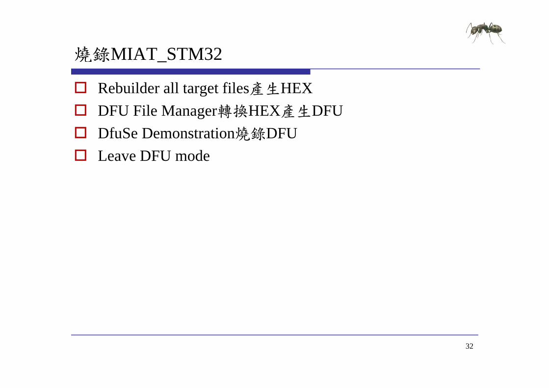
燒錄MIAT STM32_
Rebuilder all target files產生HEX DFU Fil M 轉換HEX產生DFU DFU File Manager轉換HEX產生DFU DfuSe Demonstration燒錄DFU d Leave DFU mode
32
內部與外部SRAM存取控制實驗
實驗一
WU-YANGTechnology Co Ltd
實驗一練習
練習 修改寫入位置測試是否正常 修改寫入位置測試是否正常
修改寫入資料大小測試是否正常
取消 i 測試是否正常 取消FSMC_SRAM_Init測試是否正常
34
實驗目的(二)( )
使用MIAT_STM32實驗板透過FSMC控制外部SRAM並設定為data memory進行存取控制實驗同樣利用LED設定為data memory進行存取控制實驗同樣利用LED確認存取是否正常
35
實驗原理
External SRAM RVMDK環境設定 RVMDK環境設定
Development Flow fi ARM Configure Startup Code
36
RVMDK環境設定
外部SRAM有512K Bytes位置由0x60000000至0x60080000
37
Development Flowp
Embedded Software Side
int main(void)
Bootup STM32F10x
Programming
Bootup
int main(void)ifdef DEBUGdebug()
endif
Startup Code
BootupSTM32F10x
RCC Configure
NVIC Configure
System Clocks Configuration RCC_Configuration()
NVIC Configuration g gNVIC_Configuration()
GPIO Configuration GPIO_Configuration()
GPIO Configure
for (Index = 0 Index lt1024 Index++)
Tab[Index] =IndexT bAdd ( 32)T b h ld b 0 600000
Check operation
Check pointer value
Display Result TabAddr = (u32)Tab should be 0x600000xx
Get main stack pointer value MSPValue = __MRS_MSP() should be 0x2000xxxx
helliphelliphelliphelliphelliphelliphelliphelliphelliphelliphelliphelliphelliphelliphelliphelliphelliphelliphelliphelliphelliphelliphellip
Display Result
38
Startup Codep
Register boundary addresses RCC Configure
Enable FSMC clock
LDR R0= 0x00000114
LDR R1= 0x40021014
STR R0[R1]
Enable GPIOD GPIOE GPIOF and GPIOG clocks
LDR R0= 0x000001E0
LDR R1= 0x40021018
RCC register map
STR R0[R1]
39
RCC Register g
Bit 8 FSMCEN FSMC clock enableAHB Peripheral Clock enable register (RCC_AHBENR)
Bit 8 FSMCEN FSMC clock enableSet and cleared by software0 FSMC clock disabled
APB2 peripheral clock enable register (RCC_APB2ENR)
1 FSMC clock enabled
Bit 8765 IOPGEN IO port GFED clock enableSet and cleared by software0 IO port GFED clock disabled1 IO port GFED clock enabled
40
1 IO port GFED clock enabled
Startup Codep
Register boundary addresses GPIO Configure
SRAM Data lines NOE and NWE configuration SRAM Address lines configuration NOE NEW NE1 NBL0 NBL1 configuration LDR R0= 0xB4BB44BB LDR R1= 0x40011400STR R0[R1]LDR R0= 0xBBBBBBBB LDR R1= 0x40011404STR R0[R1]LDR R0 = 0xB44444BBLDR R0= 0xB44444BB LDR R1= 0x40011800STR R0[R1]LDR R0= 0xBBBBBBBB LDR R1= 0x40011804
GPIO register map
STR R0[R1]LDR R0= 0x44BBBBBB LDR R1= 0x40011C00STR R0[R1]LDR R0= 0xBBBB4444 LDR R1= 0x40011C04STR R0[R1]LDR R0= 0x44BBBBBBLDR R1= 0x40012000STR R0 [R1]
41
STR R0[R1]
GPIO Register g
Bit 8 FSMCEN FSMC clock enablePort configuration register low
Port configuration register high
Bits 2928 2524Bits 3130 2726 2322 1918 1514 1110 76 32 Bits 2928 25242120 1716 131298 54 10MODEy[10] Port x mode bits (y= 0 15)00 Input mode (reset state)01 Output mode max speed 10 MHz
Bits 3130 27262322 1918 15141110 76 32CNFy[10] Port x configuration bits (y= 0 15)In input mode (MODE[10]=00)00 Analog input mode01 Floating input (reset state)10 Input with pull-up pull-down
10 Output mode max speed 2 MHz11 Output mode max speed 50 MHz
11 ReservedIn output mode (MODE[10] gt00)00 General purpose output push-pull01 General purpose output Open-drain10 Alternate function output Push-pull11 Alternate function output Open-drain
42
11 Alternate function output Open drain
Startup Codep
FSMCregister map FSMC Configure
FSMC Configuration Enable FSMC Bank1_SRAM Bank
LDR R0= 0x00001011
LDR R1= 0xA0000000
STR R0[R1]
LDR R0= 0x00000200
LDR R1= 0xA0000004
STR R0[R1]
43
FSMC Register g
Bit 8 FSMCEN FSMC clock enableSRAMNOR-Flash chip-select control registers 1 (FSMC_BCR1)
Bit 12 WREN Write enable bitThis bit indicates whether write operations are enableddisabled in the bank by the FSMC0 Write operations are disabled in the bank by the FSMC an AHB error is reported1 Write operations are enabled for the bank by the FSMC (default after reset) p y ( )Bits 54 MWID Memory databus widthDefines the external memory device width valid for all type of memories00 8 bits01 16 bits (default after reset)10 reserved do not use10 reserved do not use11 reserved do not use Bit 0 MBKEN Memory bank enable bitEnables the memory bank After reset Bank1 is enabled all others are disabled Accessing adisabled bank causes an ERROR on AHB bus0 C di b k i di bl d0 Corresponding memory bank is disabled1 Corresponding memory bank is enabled
44
FSMC Register g
Bit 8 FSMCEN FSMC clock enableSRAMNOR-Flash chip-select timing registers 1 (FSMC_BTR1)
Bits 158 DATAST Data-phase duration0000 0000 Reserved0000 0001 DATAST phase duration = 2 times HCLK clock cycles0000 0010 DATAST phase duration = 3 times HCLK clock cycles1111 1111 DATAST phase duration = 256 times HCLK clock cycles (default value after reset)Bits 74 ADDHLD Address-hold phase duration0000 Reserved0001 ADDHLD phase duration = 2 times HCLK clock cycle0010 ADDHLD phase duration = 3 times HCLK clock cycle1111 ADDHLD phase duration = 16 times HCLK clock cycles (default value after reset)Bits 30 ADDSET Address setup phase durationThese bits are written by software to define the duration of the address setup phase (refer toFigure 162 to Figure 172) used in SRAMs ROMs and asynchronous NOR Flash0000 ADDSET phase duration = 1 times HCLK clock cycle1111 ADDSET phase duration = 16 times HCLK clock cycles (default value after reset)
45
實驗步驟
範例目錄架構
範例說明 範例說明
預設定義說明
46
範例目錄架構
範例目錄
測試映像檔 測試映像檔
含括檔
函式庫 函式庫
專案檔
原始碼 原始碼
47
範例說明
Embedded Software Side
Infinite loop
Display Result
Infinite loop while (1)if (((TabAddramp0xFFFFFF00) == 0x60000000) ampamp
((MSPValueamp0xFFFF0000) == 0x20000000))
Check operation
Check pointer value((MSPValueamp0xFFFF0000) == 0x20000000))
OK Turn on USERLED GPIO_SetBits(GPIOF GPIO_Pin_11)
else
Display Result
else KO Turn off USERLED
GPIO_ResetBits(GPIOF GPIO_Pin_11) Insert delay Delay(0xAFFFF)
如果Tab位置在0x600000且Stack pointer位置在0x2000 外部記憶體使用正常USERLED紅燈恆亮Delay(0xAFFFF)
Turn on USERLED GPIO_SetBits(GPIOF GPIO_Pin_11) Insert delay Delay(0xAFFFF)
紅燈恆亮
如果 b位置不在0 600000或Delay(0xAFFFF)
如果Tab位置不在0x600000或Stack pointer位置不在0x2000 外部記憶體使用異常USERLED紅燈閃爍
48
預設定義說明
DATA_IN_ExtSRAM EQU 1 E l SRAM C fi i External SRAM Configuration 0=gt DISABLE 1=gt ENABLE
u32 Tab[1024]宣告於外部 的記憶體 宣告於外部SRAM的記憶體
49
data memory存取控制實驗
實驗二
WU-YANGTechnology Co Ltd
實驗二練習
練習 取消RVMDK環境外部SRAM設定測試是否正常 取消RVMDK環境外部SRAM設定測試是否正常
修改DATA_IN_ExtSRAM EQU 0測試是否正常
修改外部 記憶體 b變數大小測試是否正常 修改外部SRAM記憶體Tab變數大小測試是否正常
51
Q amp A
WU-YANGTechnology Co Ltd
MIAT_STM32內部Flash存取控制實驗
WU-YANG
浯陽科技有限公司
Technology Co Ltd
Declared Version
Training Only
Declare
Document Number
Document Version 100
Release Date
Document Title MIAT_STM32 內部FLASH存取控制實驗
Exercise Time
Platform MIAT_STM32V2MIAT IOB V1PlatformMIAT IOBV1
Peripheral
Author WU-YANG Technology Co Ltd
2
實驗目的(一)( )
使用MIAT_STM32實驗板透過Flash memory interface (FLITF)控制內部Flash進行存取控制實驗並利用LED(FLITF)控制內部Flash進行存取控制實驗並利用LED確認存取是否正常
3
實驗原理
System architecture E b dd d Fl h Embedded Flash Features Memory map RVMDK環境設定
FLITF Flash module organization
Flash library function Development Flow ARM Configure
4
System architecturey
5
Embedded Flash
Features 256 Kb up to 256 Kbytes Memory organization the Flash memory is organized as a
main block and an information blockmain block and an information block Main memory block of size t 32 Kb 64 bit di id d i t 128 f 2 up to 32 Kb times 64 bits divided into 128 pages of 2
Kbytes Information block of size Information block of size 258 times 64 bits
6
Embedded Flash Memory mapy p
7
Flash Memoryy
8
RVMDK環境設定
STMF103ZC有256K Bytes的Flash位置由0x8000000至0x8040000
9
FLITF
Features R d i f i h f h b ff (2 64 bi d ) Read interface with prefetch buffer (2x64-bit words) Option byte Loader
l h i Flash Program Erase operation Read Write protection
10
Flash memory interfacey
11
Flash memory interface registery g
Bit 8 FSMCEN FSMC clock enableFlash status register (FLASH_SR)
Bits 316 Reserved must be kept clearedBit 5 EOP End of operation
Bit 2 PGERR Programming errorSet by hardware when an address to be programmed p
Set by hardware when a Flash operation (programming erase) is completed Reset by writing a 1Note EOP is asserted at the end of each successful
y p gcontains a value different from 0xFFFF before programmingReset by writing 1Note The STRT bit in the FLASH_CR register f f
program or erase operationBit 4 WRPRTERR Write protection errorSet by hardware when programming a write-protected address of the Flash memory
_ gshould be reset before starting a programmingoperationBit 1 Reserved must be kept clearedBit 0 BSY Busyp y
Reset by writing 1Bit 3 Reserved must be kept cleared
This indicates that a Flash operation is in progress This is set on the beginning of a Flash operation and reset when the operation finishes or when an error occurs
12
Flash memory interface registery g
Flash control register (FLASH_CR)
Bit 9 OPTWRE Option bytes write enableWhen set the option bytes can be programmed This
Bit 6 STRT StartThis bit triggers an ERASE operation when set This bit is set only
bit is set on writing the correct key sequence to the FLASH_OPTKEYR registerThis bit can be reset by softwareBit 8 Reserved must be kept clearedBit 7 LOCK Lock
by software and reset when the BSY bit is resetBit 5 OPTER Option byte eraseOption byte erase chosenBit 4 OPTPG Option byte programmingOption byte programming chosenBit 7 LOCK Lock
Write to 1 only When it is set it indicates that the FPEC and FLASH_CR are locked This bit is reset by hardware after detecting the unlock sequenceIn the event of unsuccessful unlock operation this bit remains set until the next reset
p y p g gBit 3 Reserved must be kept clearedBit 2 MER Mass eraseErase of all user pages chosenBit 1 PER Page erasePage Erase chosenremains set until the next reset Page Erase chosenBit 0 PG ProgrammingFlash programming chosen
13
Main Flash memory programmingy p g g
14
Flash memory Page Erasey g
15
Flash memory Mass Erasey
16
Option byte programmingp y p g g
17
Option byte Erasep y
18
FLASH library functiony
19
FLASH library functiony
20
Development Flowp
Embedded Software Side
int main(void)
Bootup STM32F10x
ProgrammingBootupSTM32F10x RCC Configure
NVIC Configure
int main(void)ifdef DEBUGdebug()
endifendif
FLASHStatus = FLASH_COMPLETEMemoryProgramStatus = PASSEDData = 0x15041975
GPIO Configure
Data = 0x15041975
RCC Configuration RCC_Configuration()
Flash memory RW operation FLASH Unlock
FLASH ClearFlag NVIC Configuration NVIC_Configuration()
GPIO Configuration
FLASH ClearFlag
FLASH ErasePage
FLASH ProgramWord GPIO Configuration GPIO_Configuration()
helliphelliphelliphelliphelliphelliphelliphelliphelliphelliphelliphelliphelliphelliphelliphelliphellipDisplay Result
Check content
21
實驗步驟
範例目錄架構
範例說明 範例說明
預設定義說明
燒錄 燒錄MIAT_STM32
22
範例目錄架構
範例目錄
測試映像檔 測試映像檔
含括檔
函式庫 函式庫
專案檔
原始碼 原始碼
23
範例說明
Function name Description
Unlock the Flash Program Erase controller FLASH_Unlock()
D fi h b f b d
Flash FwLib Functions List
Function name Description
FLASH_Unlock Unlocks the FLASH Program Erase Controller
FLASH_ClearFlag Clears the FLASH pending fl
Define the number of page to be erased NbrOfPage = (EndAddr - StartAddr) FLASH_PAGE_SIZE
Clear All pending flags FLASH_ClearFlag(FLASH_FLAG_BSY | FLASH_FLAG_EOP | FLASH_FLAG_PGERR |
FLASH FLAG WRPRTERR)flags
FLASH_ErasePage Erases a specified FLASH page
FLASH_ProgramWord Programs a word at a specified
_ _ )
Erase the FLASH pages for(EraseCounter = 0 (EraseCounter lt NbrOfPage) ampamp (FLASHStatus ==
FLASH_COMPLETE) EraseCounter++)FLASHStatus = FLASH ErasePage(StartAddr + (FLASH PAGE SIZE EraseCounter))address FLASHStatus = FLASH_ErasePage(StartAddr + (FLASH_PAGE_SIZE EraseCounter))
FLASH Word program of data 0x15041979 at addresses defined by StartAddr and EndAddrAddress = StartAddr
while((Address lt EndAddr) ampamp (FLASHStatus == FLASH_COMPLETE))FLASHStatus = FLASH_ProgramWord(Address Data)Address = Address + 4
24
範例說明
Embedded Software Side
Check the corectness of written data
Display Result
Check the corectness of written data Address = StartAddr
while((Address lt EndAddr) ampamp (MemoryProgramStatus = FAILED))if(((vu32) Address) = Data)
Flash memory RW operation
MemoryProgramStatus = FAILED
Address += 4
Check content
Display Result while (1)if (MemoryProgramStatus == PASSED) OK Turn on USERLED GPIO_SetBits(GPIOF GPIO_Pin_11)
Display Result
else KO Turn off USERLED GPIO_ResetBits(GPIOF GPIO_Pin_11) Insert delay Delay(0xAFFFF)
如果寫入與讀取Flash內容相同Flash記憶體使用正常USERLED紅燈恆亮
Turn on USERLED GPIO_SetBits(GPIOF GPIO_Pin_11) Insert delay Delay(0xAFFFF)
如果寫入與讀取Flash內容不同Flash記憶體使用異常USERLED紅燈閃爍
25
預設定義說明
define StartAddr ((u32)0x08008000) 定義Flash使用起始點 定義Flash使用起始點
使用起始點必需大於0x8003000 + Code Size 附註 0x8000000~0x8003000為DFU程式區塊使用此區塊
將造成無法燒錄程式
Code Size可由產生的HEX檔得知
d fi E dAdd (( 32)0 0800C000) define EndAddr ((u32)0x0800C000) 定義Flash使用結束點
使用起始點必需小於0x8040000使用起始點必需小於
Data = 0x15041975 寫入資料
32Bit define FLASH_PAGE_SIZE ((u16)0x800)
每一個Page有2KByte26
每一個Page有2KByte
Intel HEX Format
aaaa tt dd cc
field Description
the colon that starts every Intel HEX record
the record-length field that represents the number of data bytes (dd) in the record
aaaa the address field that represents the starting address for subsequent data in the record
tt the field that represents the HEX record type which may be one of the following00 - data record01 - end-of-file record02 - extended segment address recordg04 - extended linear address record
dd a data field that represents one byte of data A record may have multiple data bytes The number of data bytes in the record must match the number specified by the field
cc the checksum field that represents the checksum of the record The checksum is calculated by summing the values of all hexadecimal digit pairs in the record modulo 256 and taking the twos complement
27
HEX Examplep
020000040800F2103000001814002045310008D9340008CD340008D8103000001814002045310008D9340008CD340008D8helliphelliphellip1038200042370008000000000000000000000000170C3830000000000000000000000000008C
資料填入起始位置為
0C3830000000000000000000000000008C04000005080031318D00000001FF
資料填入起始位置為0x08003000 每一行有0x10(16)個Bytes 最後一筆資料為
資料結束點為0x0803383004000005080031318D
(0x08003830 -0x08000000)0x800 = 7 需以0x800為單位所以使用的位置起點為0x08004000
28
燒錄MIAT STM32_
Rebuilder all target files產生HEX DFU Fil M 轉換HEX產生DFU DFU File Manager轉換HEX產生DFU DfuSe Demonstration燒錄DFU d Leave DFU mode
29
內部Flash存取控制實驗
實驗一
WU-YANGTechnology Co Ltd
實驗一練習
注意 請使用預設0 08008000之後的位置 避免覆蓋DFU 請使用預設0x08008000之後的位置避免覆蓋DFU
與使用者程式碼區塊
練習 練習 修改存取位置測試是否正常
修改寫入資料測試是否正常 修改寫入資料測試是否正常
修改寫入資料後取消FLASH_Unlock測試是否正常
修改寫入資料後取消FLASH E P 測試是否正 修改寫入資料後取消FLASH_ErasePage測試是否正常
31
實驗目的(二)( )
使用MIAT_STM32實驗板透過Flash memory interface (FLITF)控制內部Flash進行存取控制實驗並利用SW(FLITF)控制內部Flash進行存取控制實驗並利用SWKEY決定資料寫入與讀取LCD顯示狀態
32
實驗原理
System requirement E b dd d Fl h Embedded Flash LCD KEY SW
Development Flow ARM Configure
33
Development Flowp
Embedded Software Side
int main(void)
Bootup STM32F10x
ProgrammingBootupSTM32F10x RCC Configure
NVIC Configure
int main(void)ifdef DEBUGdebug()
endif
FLASHStatus = FLASH_COMPLETE
RCC Configuration RCC Configuration()
GPIO Configure
BasicIO Configure_ g ()
NVIC Configuration NVIC_Configuration()
GPIO Configuration Flash memory RW ti
lcd Configure
GPIO Configuration GPIO_Configuration()
Init_BasicIO()
l d i i () LCD I i i li i
RW operation
Example
FLASH Unlock
FLASH ClearFlag
lcd_init() LCD Initialization
helliphelliphelliphelliphelliphelliphelliphelliphelliphelliphelliphelliphelliphelliphelliphelliphelliphelliphelliphelliphelliphelliphellip
p
34
硬體電路配置
Mapping Table
Num MIAT_STM32V2 MIAT_IOBV1 Num MIAT_STM32V2 MIAT_IOBV1
1 PC8 (326) SW1 10 PE6 (15) LCD_EN2 PC9 (327) SW2 11 PF6 (118) LCD RW ( ) ( ) _3 PC10 (43) SW3 12 PF7 (119) LCD_RS 4 PC11 (44) SW4 13 PF8(120) LCD_D4 5 PB5 (427) KEY1 14 PF9 (121) LCD_D5 6 PB6 (428) KEY2 15 PF10 (122) LCD_D6 7 PB7 (429) KEY3 16 PF11 (213) LCD_D7 8 PB8 (431) KEY4 17 VDD (236) VCC33V 9 VCC5V (1 36) VCC5V 18 GND (1 35) GND9 VCC5V (136) VCC5V 18 GND (135) GND
35
實驗步驟
範例目錄架構
範例說明 範例說明
預設定義說明
36
範例目錄架構
範例目錄
測試映像檔 測試映像檔
含括檔
函式庫 函式庫
專案檔
原始碼 原始碼
37
範例說明
Embedded Software Side
lcd clear()
FLASH memory RW operation
lcd_clear()lcd_print (MIAT_STM32 DEMO )
Unlock the Flash Program Erase controller FLASH_Unlock()
Flash memory RW operation
FLASH Unlock
Clear All pending flags FLASH_ClearFlag(FLASH_FLAG_BSY | FLASH_FLAG_EOP | FLASH_FLAG_PGERR |
FLASH_FLAG_WRPRTERR)
while(1)
Example
FLASH ClearFlag
( )
KEY_Buffer=Key_Scan()set_cursor (0 1)lcd_print (SW Value = 0x)lcd putchar(((SWamp0x7)+0x30))lcd_putchar(((SWamp0x7)+0x30))if(KEY_Buffer==1)Address=(StartAddr|(SWltlt12))set_cursor (0 0)lcd_print (Set Addr = 0x)
掃描KEY是否按下與顯示SW數值LCD Line2顯示SW Value = 0x(SW)
lcd_putchar(((SWamp0x7)+0x30))lcd_print ( )
如果KEY1按下記錄SW數值至Address LCD Line1顯示Set Adde = 0x(Address)
38
範例說明
Embedded Software Side
else if(KEY Buffer==2)
FLASH memory RW operation
else if(KEY_Buffer==2)
Erase the FLASH pages FLASHStatus = FLASH_ErasePage(Address)
FLASH Word program of data at addresses defined by SW
SRAM memory RW operation
p g yFLASHStatus = FLASH_ProgramWord(Address (SWamp0x7))
set_cursor (0 0)lcd_print (Write 0x)lcd_putchar(((SWamp0x7)+0x30))l d i t ( t 0 )
Example如果KEY2按下清除Address所處區塊並寫入SW數值 lcd_print ( at 0x)
lcd_putchar((((Addressgtgt12)amp0x7)+0x30))else if(KEY_Buffer==3)
Data=(u16 )Address
所處區塊並寫入SW數值LCD Line1顯示Write 0x(SW) at 0x(Adddress)
Data (u16 )Addressset_cursor (0 0)lcd_print (Addr 0x)lcd_putchar((((Addressgtgt12)amp0x7)+0x30))lcd_print ( = 0x)lcd_putchar(((Dataamp0x7)+0x30))lcd_print ( )
如果KEY3按下讀取Address紀錄數值LCD Line1顯示Addr 0x(Adddress) = 0x
39
預設定義說明
define StartAddr ((u32)0x08020000) 定義Flash使用起始點 定義Flash使用起始點
使用起始點必需大於0x8003000 + Code Size 附註 0x8000000~0x8003000為DFU程式區塊使用此區塊
將造成無法燒錄程式
Code Size可由產生的HEX檔得知
32 Add 0 08020000 u32 Address = 0x08020000 定義Address初始值
初始值必需與Flash使用起始點相同初始值必需與 使用起始點相同
Address=(StartAddr|(SWltlt12)) Example StartAddr = 0x08020000 SW = 1 Address = 0x08021000
StartAddr = 0x08020000 SW = 7 Address = 0x08027000 StartAddr|(7ltlt12)必需小於0x8040000
40
使用者界面與Flash存取控制實驗
實驗二
WU-YANGTechnology Co Ltd
實驗二練習
注意 請使用預設0 08020000之後的位置 避免覆蓋DFU 請使用預設0x08020000之後的位置避免覆蓋DFU
與使用者程式碼區塊
練習 練習 利用SW與KEY測試Flash寫入與讀取是否正常
Fl h寫入後電源關閉 再開啟後寫入資料是否仍存 Flash寫入後電源關閉再開啟後寫入資料是否仍存在
修改存取位置測試是否正常 修改存取位置測試是否正常
42
實驗目的(三)( )
使用MIAT_STM32實驗板透過Flash memory interface (FLITF)控制內部Flash進行存取控制實驗並藉由填入(FLITF)控制內部Flash進行存取控制實驗並藉由填入Option Bytes 設定寫入鎖定保護Page鎖定不被覆蓋
43
Development Flowp
Embedded Software Side
int main(void)
Bootup STM32F10x
ProgrammingBootupSTM32F10x RCC Configure
NVIC Configure
int main(void)ifdef DEBUGdebug()
endifendif
FLASHStatus = FLASH_COMPLETEMemoryProgramStatus = PASSEDData = 0x1753
GPIO Configure
Data = 0x1753
RCC Configuration RCC_Configuration()
Flash memory RW operation FLASH Unlock
FLASH ClearFlag NVIC Configuration NVIC_Configuration()
GPIO Configuration
FLASH ClearFlag
FLASH ErasePage
FLASH ProgramHalfWord GPIO Configuration GPIO_Configuration()
Display Result
Check content
44
helliphelliphelliphelliphelliphelliphelliphelliphelliphelliphelliphelliphelliphelliphelliphelliphelliphelliphellip
實驗步驟
範例目錄架構
範例說明 範例說明
預設定義說明
45
範例目錄架構
範例目錄
測試映像檔 測試映像檔
含括檔
函式庫 函式庫
專案檔
原始碼 原始碼
46
範例說明
Function name Description
Unlock the Flash Program Erase controller FLASH_Unlock()
Define the number of page to be erased
Flash FwLib Functions List
Function name Description
FLASH_Unlock Unlocks the FLASH Program Erase Controller
FLASH_ClearFlag Clears the FLASH pending fl
Define the number of page to be erased NbrOfPage = (EndAddr ‐ StartAddr) FLASH_PAGE_SIZE
FLASH_ClearFlag(FLASH_FLAG_BSY | FLASH_FLAG_EOP|FLASH_FLAG_PGERR |FLASH_FLAG_WRPRTERR)
Get pages write protection status flags
FLASH_EraseOptionBytes
Erases the FLASH option bytes
FLASH_EnableWritePro Write protects the desired
p g pWRPR_Value = FLASH_GetWriteProtectionOptionByte()ProtectedPages = WRPR_Value amp 0x000000C0
ifdef WriteProtection_Disableif (ProtectedPages == 0x00) Pages are write protected
tection pages
NVIC_GenerateSystemReset
Generate a system reset
Disable the write protection FLASHStatus = FLASH_EraseOptionBytes() Generate System Reset to load the new option byte values NVIC_GenerateSystemReset()
elseifdef WriteProtection Enableifdef WriteProtection_Enableif (ProtectedPages = 0x00) Pages not write protected
FLASHStatus = FLASH_EraseOptionBytes() Enable the pages write protection FLASHStatus = FLASH_EnableWriteProtection(FLASH_WRProt_Pages12to13
|FLASH WRProt Pages14to15)|FLASH_WRProt_Pages14to15) Generate System Reset to load the new option byte values NVIC_GenerateSystemReset()
endifendif
47
範例說明
if (ProtectedPages = 0x00) Clear All pending flags
Flash FwLib Functions List
Function name DescriptionFLASH_ClearFlag(FLASH_FLAG_BSY |
FLASH_FLAG_EOP|FLASH_FLAG_PGERR |FLASH_FLAG_WRPRTERR)
erase the FLASH pages for(EraseCounter = 0 (EraseCounter lt NbrOfPage) ampamp (FLASHStatus ==
Function name Description
FLASH_ErasePage Erases a specified FLASH page
FLASH_ProgramHalfWod
Programs a half word at a ifi d dd FLASH_COMPLETE) EraseCounter++)
FLASHStatus = FLASH_ErasePage(StartAddr + (FLASH_PAGE_SIZE
EraseCounter))
rd specified address
FLASH Half Word program of data 0x1753 at addresses defined by StartAddrand EndAddr
Address = StartAddr
hil ((Add E dAdd ) ampamp (FLASHSt t FLASH COMPLETE))while((Address lt EndAddr) ampamp (FLASHStatus == FLASH_COMPLETE))
FLASHStatus = FLASH_ProgramHalfWord(Address Data)Address = Address + 2
48
範例說明
Embedded Software Side
Check the corectness of written data
Display Result
Check the corectness of written data Address = StartAddr
while((Address lt EndAddr) ampamp (MemoryProgramStatus = FAILED))if(((vu16) Address) = Data)
Flash memory RW operation
MemoryProgramStatus = FAILED
Address += 2
Check content
Display Result while (1)if (MemoryProgramStatus == PASSED) OK Turn on USERLED GPIO_SetBits(GPIOF GPIO_Pin_11)
Display Result
else KO Turn off USERLED GPIO_ResetBits(GPIOF GPIO_Pin_11) Insert delay Delay(0xAFFFF)
如果寫入與讀取Flash內容相同Flash記憶體可以寫入USERLED紅燈恆亮
Turn on USERLED GPIO_SetBits(GPIOF GPIO_Pin_11) Insert delay Delay(0xAFFFF)
如果寫入與讀取Flash內容不同Flash記憶體不能寫入USERLED紅燈閃爍
49
預設定義說明
define StartAddr ((u32) 0x08006000) 定義Flash使用起始點 定義Flash使用起始點
使用起始點必需大於0x8003000 + Code Size 附註 0x8000000~0x8003000為DFU程式區塊使用此區塊
將造成無法燒錄程式
Code Size可由產生的HEX檔得知
d fi E dAdd (( 32) 0 08008000) define EndAddr ((u32) 0x08008000) 定義Flash使用結束點
使用起始點必需小於0x8040000使用起始點必需小於
Data = 0x1753 寫入資料
16Bit define FLASH_PAGE_SIZE ((u16)0x800) 每一個Page有2KByte
50
每一個Page有2KByte
預設定義說明
define WriteProtection_Enable U hi li E bl W i P i Uncomment this line to Enable Write Protection
define WriteProtection_Disablehi li i bl i i Uncomment this line to Disable Write Protection
FLASH_EnableWriteProtection設定影響 個 設定影響2個Page FLASH_WRProt_Pages0to1 FLASH_WRProt_Pages1to2 helliphellip FLASH_WRProt_Pages60to61
設定影響多個Page FLASH_WRProt_Pages62to255
51
FLASH EnableWriteProtection_
Example
位置0x08006000 ~ 0x08007000每一個Page有0x800ByteStartPage = (0x08006000-0x08000000)0x800 = 12EndPage = ((0x08007000-0x08000000)0x800)-1 = 13執行執行FLASH_EnableWriteProtection(FLASH_WRProt_Pages12to13)將影響Pages12 Pages13
52
內部Flash寫入鎖定存取控制實驗
實驗三
WU-YANGTechnology Co Ltd
實驗三練習
注意 請使用預設0 08006000之後的位置 避免覆蓋DFU 請使用預設0x08006000之後的位置避免覆蓋DFU
與使用者程式碼區塊
更改寫入位置測試寫入鎖定時需同時更改 更改寫入位置測試寫入鎖定時需同時更改FLASH_EnableWriteProtection鎖定之Page
練習 練習 打開define WriteProtection_Enable測試是否可寫入
打開define WriteProtection Disable測試是否可寫入 打開define WriteProtection_Disable測試是否可寫入
修改存取位置測試是否正常
修改寫入資料測試是否正常 修改寫入資料測試是否正常
54
Q amp A
WU-YANGTechnology Co Ltd

實驗一練習
練習 修改寫入位置測試是否正常 修改寫入位置測試是否正常
修改寫入資料大小測試是否正常
取消 i 測試是否正常 取消FSMC_SRAM_Init測試是否正常
34
實驗目的(二)( )
使用MIAT_STM32實驗板透過FSMC控制外部SRAM並設定為data memory進行存取控制實驗同樣利用LED設定為data memory進行存取控制實驗同樣利用LED確認存取是否正常
35
實驗原理
External SRAM RVMDK環境設定 RVMDK環境設定
Development Flow fi ARM Configure Startup Code
36
RVMDK環境設定
外部SRAM有512K Bytes位置由0x60000000至0x60080000
37
Development Flowp
Embedded Software Side
int main(void)
Bootup STM32F10x
Programming
Bootup
int main(void)ifdef DEBUGdebug()
endif
Startup Code
BootupSTM32F10x
RCC Configure
NVIC Configure
System Clocks Configuration RCC_Configuration()
NVIC Configuration g gNVIC_Configuration()
GPIO Configuration GPIO_Configuration()
GPIO Configure
for (Index = 0 Index lt1024 Index++)
Tab[Index] =IndexT bAdd ( 32)T b h ld b 0 600000
Check operation
Check pointer value
Display Result TabAddr = (u32)Tab should be 0x600000xx
Get main stack pointer value MSPValue = __MRS_MSP() should be 0x2000xxxx
helliphelliphelliphelliphelliphelliphelliphelliphelliphelliphelliphelliphelliphelliphelliphelliphelliphelliphelliphelliphelliphelliphellip
Display Result
38
Startup Codep
Register boundary addresses RCC Configure
Enable FSMC clock
LDR R0= 0x00000114
LDR R1= 0x40021014
STR R0[R1]
Enable GPIOD GPIOE GPIOF and GPIOG clocks
LDR R0= 0x000001E0
LDR R1= 0x40021018
RCC register map
STR R0[R1]
39
RCC Register g
Bit 8 FSMCEN FSMC clock enableAHB Peripheral Clock enable register (RCC_AHBENR)
Bit 8 FSMCEN FSMC clock enableSet and cleared by software0 FSMC clock disabled
APB2 peripheral clock enable register (RCC_APB2ENR)
1 FSMC clock enabled
Bit 8765 IOPGEN IO port GFED clock enableSet and cleared by software0 IO port GFED clock disabled1 IO port GFED clock enabled
40
1 IO port GFED clock enabled
Startup Codep
Register boundary addresses GPIO Configure
SRAM Data lines NOE and NWE configuration SRAM Address lines configuration NOE NEW NE1 NBL0 NBL1 configuration LDR R0= 0xB4BB44BB LDR R1= 0x40011400STR R0[R1]LDR R0= 0xBBBBBBBB LDR R1= 0x40011404STR R0[R1]LDR R0 = 0xB44444BBLDR R0= 0xB44444BB LDR R1= 0x40011800STR R0[R1]LDR R0= 0xBBBBBBBB LDR R1= 0x40011804
GPIO register map
STR R0[R1]LDR R0= 0x44BBBBBB LDR R1= 0x40011C00STR R0[R1]LDR R0= 0xBBBB4444 LDR R1= 0x40011C04STR R0[R1]LDR R0= 0x44BBBBBBLDR R1= 0x40012000STR R0 [R1]
41
STR R0[R1]
GPIO Register g
Bit 8 FSMCEN FSMC clock enablePort configuration register low
Port configuration register high
Bits 2928 2524Bits 3130 2726 2322 1918 1514 1110 76 32 Bits 2928 25242120 1716 131298 54 10MODEy[10] Port x mode bits (y= 0 15)00 Input mode (reset state)01 Output mode max speed 10 MHz
Bits 3130 27262322 1918 15141110 76 32CNFy[10] Port x configuration bits (y= 0 15)In input mode (MODE[10]=00)00 Analog input mode01 Floating input (reset state)10 Input with pull-up pull-down
10 Output mode max speed 2 MHz11 Output mode max speed 50 MHz
11 ReservedIn output mode (MODE[10] gt00)00 General purpose output push-pull01 General purpose output Open-drain10 Alternate function output Push-pull11 Alternate function output Open-drain
42
11 Alternate function output Open drain
Startup Codep
FSMCregister map FSMC Configure
FSMC Configuration Enable FSMC Bank1_SRAM Bank
LDR R0= 0x00001011
LDR R1= 0xA0000000
STR R0[R1]
LDR R0= 0x00000200
LDR R1= 0xA0000004
STR R0[R1]
43
FSMC Register g
Bit 8 FSMCEN FSMC clock enableSRAMNOR-Flash chip-select control registers 1 (FSMC_BCR1)
Bit 12 WREN Write enable bitThis bit indicates whether write operations are enableddisabled in the bank by the FSMC0 Write operations are disabled in the bank by the FSMC an AHB error is reported1 Write operations are enabled for the bank by the FSMC (default after reset) p y ( )Bits 54 MWID Memory databus widthDefines the external memory device width valid for all type of memories00 8 bits01 16 bits (default after reset)10 reserved do not use10 reserved do not use11 reserved do not use Bit 0 MBKEN Memory bank enable bitEnables the memory bank After reset Bank1 is enabled all others are disabled Accessing adisabled bank causes an ERROR on AHB bus0 C di b k i di bl d0 Corresponding memory bank is disabled1 Corresponding memory bank is enabled
44
FSMC Register g
Bit 8 FSMCEN FSMC clock enableSRAMNOR-Flash chip-select timing registers 1 (FSMC_BTR1)
Bits 158 DATAST Data-phase duration0000 0000 Reserved0000 0001 DATAST phase duration = 2 times HCLK clock cycles0000 0010 DATAST phase duration = 3 times HCLK clock cycles1111 1111 DATAST phase duration = 256 times HCLK clock cycles (default value after reset)Bits 74 ADDHLD Address-hold phase duration0000 Reserved0001 ADDHLD phase duration = 2 times HCLK clock cycle0010 ADDHLD phase duration = 3 times HCLK clock cycle1111 ADDHLD phase duration = 16 times HCLK clock cycles (default value after reset)Bits 30 ADDSET Address setup phase durationThese bits are written by software to define the duration of the address setup phase (refer toFigure 162 to Figure 172) used in SRAMs ROMs and asynchronous NOR Flash0000 ADDSET phase duration = 1 times HCLK clock cycle1111 ADDSET phase duration = 16 times HCLK clock cycles (default value after reset)
45
實驗步驟
範例目錄架構
範例說明 範例說明
預設定義說明
46
範例目錄架構
範例目錄
測試映像檔 測試映像檔
含括檔
函式庫 函式庫
專案檔
原始碼 原始碼
47
範例說明
Embedded Software Side
Infinite loop
Display Result
Infinite loop while (1)if (((TabAddramp0xFFFFFF00) == 0x60000000) ampamp
((MSPValueamp0xFFFF0000) == 0x20000000))
Check operation
Check pointer value((MSPValueamp0xFFFF0000) == 0x20000000))
OK Turn on USERLED GPIO_SetBits(GPIOF GPIO_Pin_11)
else
Display Result
else KO Turn off USERLED
GPIO_ResetBits(GPIOF GPIO_Pin_11) Insert delay Delay(0xAFFFF)
如果Tab位置在0x600000且Stack pointer位置在0x2000 外部記憶體使用正常USERLED紅燈恆亮Delay(0xAFFFF)
Turn on USERLED GPIO_SetBits(GPIOF GPIO_Pin_11) Insert delay Delay(0xAFFFF)
紅燈恆亮
如果 b位置不在0 600000或Delay(0xAFFFF)
如果Tab位置不在0x600000或Stack pointer位置不在0x2000 外部記憶體使用異常USERLED紅燈閃爍
48
預設定義說明
DATA_IN_ExtSRAM EQU 1 E l SRAM C fi i External SRAM Configuration 0=gt DISABLE 1=gt ENABLE
u32 Tab[1024]宣告於外部 的記憶體 宣告於外部SRAM的記憶體
49
data memory存取控制實驗
實驗二
WU-YANGTechnology Co Ltd
實驗二練習
練習 取消RVMDK環境外部SRAM設定測試是否正常 取消RVMDK環境外部SRAM設定測試是否正常
修改DATA_IN_ExtSRAM EQU 0測試是否正常
修改外部 記憶體 b變數大小測試是否正常 修改外部SRAM記憶體Tab變數大小測試是否正常
51
Q amp A
WU-YANGTechnology Co Ltd
MIAT_STM32內部Flash存取控制實驗
WU-YANG
浯陽科技有限公司
Technology Co Ltd
Declared Version
Training Only
Declare
Document Number
Document Version 100
Release Date
Document Title MIAT_STM32 內部FLASH存取控制實驗
Exercise Time
Platform MIAT_STM32V2MIAT IOB V1PlatformMIAT IOBV1
Peripheral
Author WU-YANG Technology Co Ltd
2
實驗目的(一)( )
使用MIAT_STM32實驗板透過Flash memory interface (FLITF)控制內部Flash進行存取控制實驗並利用LED(FLITF)控制內部Flash進行存取控制實驗並利用LED確認存取是否正常
3
實驗原理
System architecture E b dd d Fl h Embedded Flash Features Memory map RVMDK環境設定
FLITF Flash module organization
Flash library function Development Flow ARM Configure
4
System architecturey
5
Embedded Flash
Features 256 Kb up to 256 Kbytes Memory organization the Flash memory is organized as a
main block and an information blockmain block and an information block Main memory block of size t 32 Kb 64 bit di id d i t 128 f 2 up to 32 Kb times 64 bits divided into 128 pages of 2
Kbytes Information block of size Information block of size 258 times 64 bits
6
Embedded Flash Memory mapy p
7
Flash Memoryy
8
RVMDK環境設定
STMF103ZC有256K Bytes的Flash位置由0x8000000至0x8040000
9
FLITF
Features R d i f i h f h b ff (2 64 bi d ) Read interface with prefetch buffer (2x64-bit words) Option byte Loader
l h i Flash Program Erase operation Read Write protection
10
Flash memory interfacey
11
Flash memory interface registery g
Bit 8 FSMCEN FSMC clock enableFlash status register (FLASH_SR)
Bits 316 Reserved must be kept clearedBit 5 EOP End of operation
Bit 2 PGERR Programming errorSet by hardware when an address to be programmed p
Set by hardware when a Flash operation (programming erase) is completed Reset by writing a 1Note EOP is asserted at the end of each successful
y p gcontains a value different from 0xFFFF before programmingReset by writing 1Note The STRT bit in the FLASH_CR register f f
program or erase operationBit 4 WRPRTERR Write protection errorSet by hardware when programming a write-protected address of the Flash memory
_ gshould be reset before starting a programmingoperationBit 1 Reserved must be kept clearedBit 0 BSY Busyp y
Reset by writing 1Bit 3 Reserved must be kept cleared
This indicates that a Flash operation is in progress This is set on the beginning of a Flash operation and reset when the operation finishes or when an error occurs
12
Flash memory interface registery g
Flash control register (FLASH_CR)
Bit 9 OPTWRE Option bytes write enableWhen set the option bytes can be programmed This
Bit 6 STRT StartThis bit triggers an ERASE operation when set This bit is set only
bit is set on writing the correct key sequence to the FLASH_OPTKEYR registerThis bit can be reset by softwareBit 8 Reserved must be kept clearedBit 7 LOCK Lock
by software and reset when the BSY bit is resetBit 5 OPTER Option byte eraseOption byte erase chosenBit 4 OPTPG Option byte programmingOption byte programming chosenBit 7 LOCK Lock
Write to 1 only When it is set it indicates that the FPEC and FLASH_CR are locked This bit is reset by hardware after detecting the unlock sequenceIn the event of unsuccessful unlock operation this bit remains set until the next reset
p y p g gBit 3 Reserved must be kept clearedBit 2 MER Mass eraseErase of all user pages chosenBit 1 PER Page erasePage Erase chosenremains set until the next reset Page Erase chosenBit 0 PG ProgrammingFlash programming chosen
13
Main Flash memory programmingy p g g
14
Flash memory Page Erasey g
15
Flash memory Mass Erasey
16
Option byte programmingp y p g g
17
Option byte Erasep y
18
FLASH library functiony
19
FLASH library functiony
20
Development Flowp
Embedded Software Side
int main(void)
Bootup STM32F10x
ProgrammingBootupSTM32F10x RCC Configure
NVIC Configure
int main(void)ifdef DEBUGdebug()
endifendif
FLASHStatus = FLASH_COMPLETEMemoryProgramStatus = PASSEDData = 0x15041975
GPIO Configure
Data = 0x15041975
RCC Configuration RCC_Configuration()
Flash memory RW operation FLASH Unlock
FLASH ClearFlag NVIC Configuration NVIC_Configuration()
GPIO Configuration
FLASH ClearFlag
FLASH ErasePage
FLASH ProgramWord GPIO Configuration GPIO_Configuration()
helliphelliphelliphelliphelliphelliphelliphelliphelliphelliphelliphelliphelliphelliphelliphelliphellipDisplay Result
Check content
21
實驗步驟
範例目錄架構
範例說明 範例說明
預設定義說明
燒錄 燒錄MIAT_STM32
22
範例目錄架構
範例目錄
測試映像檔 測試映像檔
含括檔
函式庫 函式庫
專案檔
原始碼 原始碼
23
範例說明
Function name Description
Unlock the Flash Program Erase controller FLASH_Unlock()
D fi h b f b d
Flash FwLib Functions List
Function name Description
FLASH_Unlock Unlocks the FLASH Program Erase Controller
FLASH_ClearFlag Clears the FLASH pending fl
Define the number of page to be erased NbrOfPage = (EndAddr - StartAddr) FLASH_PAGE_SIZE
Clear All pending flags FLASH_ClearFlag(FLASH_FLAG_BSY | FLASH_FLAG_EOP | FLASH_FLAG_PGERR |
FLASH FLAG WRPRTERR)flags
FLASH_ErasePage Erases a specified FLASH page
FLASH_ProgramWord Programs a word at a specified
_ _ )
Erase the FLASH pages for(EraseCounter = 0 (EraseCounter lt NbrOfPage) ampamp (FLASHStatus ==
FLASH_COMPLETE) EraseCounter++)FLASHStatus = FLASH ErasePage(StartAddr + (FLASH PAGE SIZE EraseCounter))address FLASHStatus = FLASH_ErasePage(StartAddr + (FLASH_PAGE_SIZE EraseCounter))
FLASH Word program of data 0x15041979 at addresses defined by StartAddr and EndAddrAddress = StartAddr
while((Address lt EndAddr) ampamp (FLASHStatus == FLASH_COMPLETE))FLASHStatus = FLASH_ProgramWord(Address Data)Address = Address + 4
24
範例說明
Embedded Software Side
Check the corectness of written data
Display Result
Check the corectness of written data Address = StartAddr
while((Address lt EndAddr) ampamp (MemoryProgramStatus = FAILED))if(((vu32) Address) = Data)
Flash memory RW operation
MemoryProgramStatus = FAILED
Address += 4
Check content
Display Result while (1)if (MemoryProgramStatus == PASSED) OK Turn on USERLED GPIO_SetBits(GPIOF GPIO_Pin_11)
Display Result
else KO Turn off USERLED GPIO_ResetBits(GPIOF GPIO_Pin_11) Insert delay Delay(0xAFFFF)
如果寫入與讀取Flash內容相同Flash記憶體使用正常USERLED紅燈恆亮
Turn on USERLED GPIO_SetBits(GPIOF GPIO_Pin_11) Insert delay Delay(0xAFFFF)
如果寫入與讀取Flash內容不同Flash記憶體使用異常USERLED紅燈閃爍
25
預設定義說明
define StartAddr ((u32)0x08008000) 定義Flash使用起始點 定義Flash使用起始點
使用起始點必需大於0x8003000 + Code Size 附註 0x8000000~0x8003000為DFU程式區塊使用此區塊
將造成無法燒錄程式
Code Size可由產生的HEX檔得知
d fi E dAdd (( 32)0 0800C000) define EndAddr ((u32)0x0800C000) 定義Flash使用結束點
使用起始點必需小於0x8040000使用起始點必需小於
Data = 0x15041975 寫入資料
32Bit define FLASH_PAGE_SIZE ((u16)0x800)
每一個Page有2KByte26
每一個Page有2KByte
Intel HEX Format
aaaa tt dd cc
field Description
the colon that starts every Intel HEX record
the record-length field that represents the number of data bytes (dd) in the record
aaaa the address field that represents the starting address for subsequent data in the record
tt the field that represents the HEX record type which may be one of the following00 - data record01 - end-of-file record02 - extended segment address recordg04 - extended linear address record
dd a data field that represents one byte of data A record may have multiple data bytes The number of data bytes in the record must match the number specified by the field
cc the checksum field that represents the checksum of the record The checksum is calculated by summing the values of all hexadecimal digit pairs in the record modulo 256 and taking the twos complement
27
HEX Examplep
020000040800F2103000001814002045310008D9340008CD340008D8103000001814002045310008D9340008CD340008D8helliphelliphellip1038200042370008000000000000000000000000170C3830000000000000000000000000008C
資料填入起始位置為
0C3830000000000000000000000000008C04000005080031318D00000001FF
資料填入起始位置為0x08003000 每一行有0x10(16)個Bytes 最後一筆資料為
資料結束點為0x0803383004000005080031318D
(0x08003830 -0x08000000)0x800 = 7 需以0x800為單位所以使用的位置起點為0x08004000
28
燒錄MIAT STM32_
Rebuilder all target files產生HEX DFU Fil M 轉換HEX產生DFU DFU File Manager轉換HEX產生DFU DfuSe Demonstration燒錄DFU d Leave DFU mode
29
內部Flash存取控制實驗
實驗一
WU-YANGTechnology Co Ltd
實驗一練習
注意 請使用預設0 08008000之後的位置 避免覆蓋DFU 請使用預設0x08008000之後的位置避免覆蓋DFU
與使用者程式碼區塊
練習 練習 修改存取位置測試是否正常
修改寫入資料測試是否正常 修改寫入資料測試是否正常
修改寫入資料後取消FLASH_Unlock測試是否正常
修改寫入資料後取消FLASH E P 測試是否正 修改寫入資料後取消FLASH_ErasePage測試是否正常
31
實驗目的(二)( )
使用MIAT_STM32實驗板透過Flash memory interface (FLITF)控制內部Flash進行存取控制實驗並利用SW(FLITF)控制內部Flash進行存取控制實驗並利用SWKEY決定資料寫入與讀取LCD顯示狀態
32
實驗原理
System requirement E b dd d Fl h Embedded Flash LCD KEY SW
Development Flow ARM Configure
33
Development Flowp
Embedded Software Side
int main(void)
Bootup STM32F10x
ProgrammingBootupSTM32F10x RCC Configure
NVIC Configure
int main(void)ifdef DEBUGdebug()
endif
FLASHStatus = FLASH_COMPLETE
RCC Configuration RCC Configuration()
GPIO Configure
BasicIO Configure_ g ()
NVIC Configuration NVIC_Configuration()
GPIO Configuration Flash memory RW ti
lcd Configure
GPIO Configuration GPIO_Configuration()
Init_BasicIO()
l d i i () LCD I i i li i
RW operation
Example
FLASH Unlock
FLASH ClearFlag
lcd_init() LCD Initialization
helliphelliphelliphelliphelliphelliphelliphelliphelliphelliphelliphelliphelliphelliphelliphelliphelliphelliphelliphelliphelliphelliphellip
p
34
硬體電路配置
Mapping Table
Num MIAT_STM32V2 MIAT_IOBV1 Num MIAT_STM32V2 MIAT_IOBV1
1 PC8 (326) SW1 10 PE6 (15) LCD_EN2 PC9 (327) SW2 11 PF6 (118) LCD RW ( ) ( ) _3 PC10 (43) SW3 12 PF7 (119) LCD_RS 4 PC11 (44) SW4 13 PF8(120) LCD_D4 5 PB5 (427) KEY1 14 PF9 (121) LCD_D5 6 PB6 (428) KEY2 15 PF10 (122) LCD_D6 7 PB7 (429) KEY3 16 PF11 (213) LCD_D7 8 PB8 (431) KEY4 17 VDD (236) VCC33V 9 VCC5V (1 36) VCC5V 18 GND (1 35) GND9 VCC5V (136) VCC5V 18 GND (135) GND
35
實驗步驟
範例目錄架構
範例說明 範例說明
預設定義說明
36
範例目錄架構
範例目錄
測試映像檔 測試映像檔
含括檔
函式庫 函式庫
專案檔
原始碼 原始碼
37
範例說明
Embedded Software Side
lcd clear()
FLASH memory RW operation
lcd_clear()lcd_print (MIAT_STM32 DEMO )
Unlock the Flash Program Erase controller FLASH_Unlock()
Flash memory RW operation
FLASH Unlock
Clear All pending flags FLASH_ClearFlag(FLASH_FLAG_BSY | FLASH_FLAG_EOP | FLASH_FLAG_PGERR |
FLASH_FLAG_WRPRTERR)
while(1)
Example
FLASH ClearFlag
( )
KEY_Buffer=Key_Scan()set_cursor (0 1)lcd_print (SW Value = 0x)lcd putchar(((SWamp0x7)+0x30))lcd_putchar(((SWamp0x7)+0x30))if(KEY_Buffer==1)Address=(StartAddr|(SWltlt12))set_cursor (0 0)lcd_print (Set Addr = 0x)
掃描KEY是否按下與顯示SW數值LCD Line2顯示SW Value = 0x(SW)
lcd_putchar(((SWamp0x7)+0x30))lcd_print ( )
如果KEY1按下記錄SW數值至Address LCD Line1顯示Set Adde = 0x(Address)
38
範例說明
Embedded Software Side
else if(KEY Buffer==2)
FLASH memory RW operation
else if(KEY_Buffer==2)
Erase the FLASH pages FLASHStatus = FLASH_ErasePage(Address)
FLASH Word program of data at addresses defined by SW
SRAM memory RW operation
p g yFLASHStatus = FLASH_ProgramWord(Address (SWamp0x7))
set_cursor (0 0)lcd_print (Write 0x)lcd_putchar(((SWamp0x7)+0x30))l d i t ( t 0 )
Example如果KEY2按下清除Address所處區塊並寫入SW數值 lcd_print ( at 0x)
lcd_putchar((((Addressgtgt12)amp0x7)+0x30))else if(KEY_Buffer==3)
Data=(u16 )Address
所處區塊並寫入SW數值LCD Line1顯示Write 0x(SW) at 0x(Adddress)
Data (u16 )Addressset_cursor (0 0)lcd_print (Addr 0x)lcd_putchar((((Addressgtgt12)amp0x7)+0x30))lcd_print ( = 0x)lcd_putchar(((Dataamp0x7)+0x30))lcd_print ( )
如果KEY3按下讀取Address紀錄數值LCD Line1顯示Addr 0x(Adddress) = 0x
39
預設定義說明
define StartAddr ((u32)0x08020000) 定義Flash使用起始點 定義Flash使用起始點
使用起始點必需大於0x8003000 + Code Size 附註 0x8000000~0x8003000為DFU程式區塊使用此區塊
將造成無法燒錄程式
Code Size可由產生的HEX檔得知
32 Add 0 08020000 u32 Address = 0x08020000 定義Address初始值
初始值必需與Flash使用起始點相同初始值必需與 使用起始點相同
Address=(StartAddr|(SWltlt12)) Example StartAddr = 0x08020000 SW = 1 Address = 0x08021000
StartAddr = 0x08020000 SW = 7 Address = 0x08027000 StartAddr|(7ltlt12)必需小於0x8040000
40
使用者界面與Flash存取控制實驗
實驗二
WU-YANGTechnology Co Ltd
實驗二練習
注意 請使用預設0 08020000之後的位置 避免覆蓋DFU 請使用預設0x08020000之後的位置避免覆蓋DFU
與使用者程式碼區塊
練習 練習 利用SW與KEY測試Flash寫入與讀取是否正常
Fl h寫入後電源關閉 再開啟後寫入資料是否仍存 Flash寫入後電源關閉再開啟後寫入資料是否仍存在
修改存取位置測試是否正常 修改存取位置測試是否正常
42
實驗目的(三)( )
使用MIAT_STM32實驗板透過Flash memory interface (FLITF)控制內部Flash進行存取控制實驗並藉由填入(FLITF)控制內部Flash進行存取控制實驗並藉由填入Option Bytes 設定寫入鎖定保護Page鎖定不被覆蓋
43
Development Flowp
Embedded Software Side
int main(void)
Bootup STM32F10x
ProgrammingBootupSTM32F10x RCC Configure
NVIC Configure
int main(void)ifdef DEBUGdebug()
endifendif
FLASHStatus = FLASH_COMPLETEMemoryProgramStatus = PASSEDData = 0x1753
GPIO Configure
Data = 0x1753
RCC Configuration RCC_Configuration()
Flash memory RW operation FLASH Unlock
FLASH ClearFlag NVIC Configuration NVIC_Configuration()
GPIO Configuration
FLASH ClearFlag
FLASH ErasePage
FLASH ProgramHalfWord GPIO Configuration GPIO_Configuration()
Display Result
Check content
44
helliphelliphelliphelliphelliphelliphelliphelliphelliphelliphelliphelliphelliphelliphelliphelliphelliphelliphellip
實驗步驟
範例目錄架構
範例說明 範例說明
預設定義說明
45
範例目錄架構
範例目錄
測試映像檔 測試映像檔
含括檔
函式庫 函式庫
專案檔
原始碼 原始碼
46
範例說明
Function name Description
Unlock the Flash Program Erase controller FLASH_Unlock()
Define the number of page to be erased
Flash FwLib Functions List
Function name Description
FLASH_Unlock Unlocks the FLASH Program Erase Controller
FLASH_ClearFlag Clears the FLASH pending fl
Define the number of page to be erased NbrOfPage = (EndAddr ‐ StartAddr) FLASH_PAGE_SIZE
FLASH_ClearFlag(FLASH_FLAG_BSY | FLASH_FLAG_EOP|FLASH_FLAG_PGERR |FLASH_FLAG_WRPRTERR)
Get pages write protection status flags
FLASH_EraseOptionBytes
Erases the FLASH option bytes
FLASH_EnableWritePro Write protects the desired
p g pWRPR_Value = FLASH_GetWriteProtectionOptionByte()ProtectedPages = WRPR_Value amp 0x000000C0
ifdef WriteProtection_Disableif (ProtectedPages == 0x00) Pages are write protected
tection pages
NVIC_GenerateSystemReset
Generate a system reset
Disable the write protection FLASHStatus = FLASH_EraseOptionBytes() Generate System Reset to load the new option byte values NVIC_GenerateSystemReset()
elseifdef WriteProtection Enableifdef WriteProtection_Enableif (ProtectedPages = 0x00) Pages not write protected
FLASHStatus = FLASH_EraseOptionBytes() Enable the pages write protection FLASHStatus = FLASH_EnableWriteProtection(FLASH_WRProt_Pages12to13
|FLASH WRProt Pages14to15)|FLASH_WRProt_Pages14to15) Generate System Reset to load the new option byte values NVIC_GenerateSystemReset()
endifendif
47
範例說明
if (ProtectedPages = 0x00) Clear All pending flags
Flash FwLib Functions List
Function name DescriptionFLASH_ClearFlag(FLASH_FLAG_BSY |
FLASH_FLAG_EOP|FLASH_FLAG_PGERR |FLASH_FLAG_WRPRTERR)
erase the FLASH pages for(EraseCounter = 0 (EraseCounter lt NbrOfPage) ampamp (FLASHStatus ==
Function name Description
FLASH_ErasePage Erases a specified FLASH page
FLASH_ProgramHalfWod
Programs a half word at a ifi d dd FLASH_COMPLETE) EraseCounter++)
FLASHStatus = FLASH_ErasePage(StartAddr + (FLASH_PAGE_SIZE
EraseCounter))
rd specified address
FLASH Half Word program of data 0x1753 at addresses defined by StartAddrand EndAddr
Address = StartAddr
hil ((Add E dAdd ) ampamp (FLASHSt t FLASH COMPLETE))while((Address lt EndAddr) ampamp (FLASHStatus == FLASH_COMPLETE))
FLASHStatus = FLASH_ProgramHalfWord(Address Data)Address = Address + 2
48
範例說明
Embedded Software Side
Check the corectness of written data
Display Result
Check the corectness of written data Address = StartAddr
while((Address lt EndAddr) ampamp (MemoryProgramStatus = FAILED))if(((vu16) Address) = Data)
Flash memory RW operation
MemoryProgramStatus = FAILED
Address += 2
Check content
Display Result while (1)if (MemoryProgramStatus == PASSED) OK Turn on USERLED GPIO_SetBits(GPIOF GPIO_Pin_11)
Display Result
else KO Turn off USERLED GPIO_ResetBits(GPIOF GPIO_Pin_11) Insert delay Delay(0xAFFFF)
如果寫入與讀取Flash內容相同Flash記憶體可以寫入USERLED紅燈恆亮
Turn on USERLED GPIO_SetBits(GPIOF GPIO_Pin_11) Insert delay Delay(0xAFFFF)
如果寫入與讀取Flash內容不同Flash記憶體不能寫入USERLED紅燈閃爍
49
預設定義說明
define StartAddr ((u32) 0x08006000) 定義Flash使用起始點 定義Flash使用起始點
使用起始點必需大於0x8003000 + Code Size 附註 0x8000000~0x8003000為DFU程式區塊使用此區塊
將造成無法燒錄程式
Code Size可由產生的HEX檔得知
d fi E dAdd (( 32) 0 08008000) define EndAddr ((u32) 0x08008000) 定義Flash使用結束點
使用起始點必需小於0x8040000使用起始點必需小於
Data = 0x1753 寫入資料
16Bit define FLASH_PAGE_SIZE ((u16)0x800) 每一個Page有2KByte
50
每一個Page有2KByte
預設定義說明
define WriteProtection_Enable U hi li E bl W i P i Uncomment this line to Enable Write Protection
define WriteProtection_Disablehi li i bl i i Uncomment this line to Disable Write Protection
FLASH_EnableWriteProtection設定影響 個 設定影響2個Page FLASH_WRProt_Pages0to1 FLASH_WRProt_Pages1to2 helliphellip FLASH_WRProt_Pages60to61
設定影響多個Page FLASH_WRProt_Pages62to255
51
FLASH EnableWriteProtection_
Example
位置0x08006000 ~ 0x08007000每一個Page有0x800ByteStartPage = (0x08006000-0x08000000)0x800 = 12EndPage = ((0x08007000-0x08000000)0x800)-1 = 13執行執行FLASH_EnableWriteProtection(FLASH_WRProt_Pages12to13)將影響Pages12 Pages13
52
內部Flash寫入鎖定存取控制實驗
實驗三
WU-YANGTechnology Co Ltd
實驗三練習
注意 請使用預設0 08006000之後的位置 避免覆蓋DFU 請使用預設0x08006000之後的位置避免覆蓋DFU
與使用者程式碼區塊
更改寫入位置測試寫入鎖定時需同時更改 更改寫入位置測試寫入鎖定時需同時更改FLASH_EnableWriteProtection鎖定之Page
練習 練習 打開define WriteProtection_Enable測試是否可寫入
打開define WriteProtection Disable測試是否可寫入 打開define WriteProtection_Disable測試是否可寫入
修改存取位置測試是否正常
修改寫入資料測試是否正常 修改寫入資料測試是否正常
54
Q amp A
WU-YANGTechnology Co Ltd

實驗目的(二)( )
使用MIAT_STM32實驗板透過FSMC控制外部SRAM並設定為data memory進行存取控制實驗同樣利用LED設定為data memory進行存取控制實驗同樣利用LED確認存取是否正常
35
實驗原理
External SRAM RVMDK環境設定 RVMDK環境設定
Development Flow fi ARM Configure Startup Code
36
RVMDK環境設定
外部SRAM有512K Bytes位置由0x60000000至0x60080000
37
Development Flowp
Embedded Software Side
int main(void)
Bootup STM32F10x
Programming
Bootup
int main(void)ifdef DEBUGdebug()
endif
Startup Code
BootupSTM32F10x
RCC Configure
NVIC Configure
System Clocks Configuration RCC_Configuration()
NVIC Configuration g gNVIC_Configuration()
GPIO Configuration GPIO_Configuration()
GPIO Configure
for (Index = 0 Index lt1024 Index++)
Tab[Index] =IndexT bAdd ( 32)T b h ld b 0 600000
Check operation
Check pointer value
Display Result TabAddr = (u32)Tab should be 0x600000xx
Get main stack pointer value MSPValue = __MRS_MSP() should be 0x2000xxxx
helliphelliphelliphelliphelliphelliphelliphelliphelliphelliphelliphelliphelliphelliphelliphelliphelliphelliphelliphelliphelliphelliphellip
Display Result
38
Startup Codep
Register boundary addresses RCC Configure
Enable FSMC clock
LDR R0= 0x00000114
LDR R1= 0x40021014
STR R0[R1]
Enable GPIOD GPIOE GPIOF and GPIOG clocks
LDR R0= 0x000001E0
LDR R1= 0x40021018
RCC register map
STR R0[R1]
39
RCC Register g
Bit 8 FSMCEN FSMC clock enableAHB Peripheral Clock enable register (RCC_AHBENR)
Bit 8 FSMCEN FSMC clock enableSet and cleared by software0 FSMC clock disabled
APB2 peripheral clock enable register (RCC_APB2ENR)
1 FSMC clock enabled
Bit 8765 IOPGEN IO port GFED clock enableSet and cleared by software0 IO port GFED clock disabled1 IO port GFED clock enabled
40
1 IO port GFED clock enabled
Startup Codep
Register boundary addresses GPIO Configure
SRAM Data lines NOE and NWE configuration SRAM Address lines configuration NOE NEW NE1 NBL0 NBL1 configuration LDR R0= 0xB4BB44BB LDR R1= 0x40011400STR R0[R1]LDR R0= 0xBBBBBBBB LDR R1= 0x40011404STR R0[R1]LDR R0 = 0xB44444BBLDR R0= 0xB44444BB LDR R1= 0x40011800STR R0[R1]LDR R0= 0xBBBBBBBB LDR R1= 0x40011804
GPIO register map
STR R0[R1]LDR R0= 0x44BBBBBB LDR R1= 0x40011C00STR R0[R1]LDR R0= 0xBBBB4444 LDR R1= 0x40011C04STR R0[R1]LDR R0= 0x44BBBBBBLDR R1= 0x40012000STR R0 [R1]
41
STR R0[R1]
GPIO Register g
Bit 8 FSMCEN FSMC clock enablePort configuration register low
Port configuration register high
Bits 2928 2524Bits 3130 2726 2322 1918 1514 1110 76 32 Bits 2928 25242120 1716 131298 54 10MODEy[10] Port x mode bits (y= 0 15)00 Input mode (reset state)01 Output mode max speed 10 MHz
Bits 3130 27262322 1918 15141110 76 32CNFy[10] Port x configuration bits (y= 0 15)In input mode (MODE[10]=00)00 Analog input mode01 Floating input (reset state)10 Input with pull-up pull-down
10 Output mode max speed 2 MHz11 Output mode max speed 50 MHz
11 ReservedIn output mode (MODE[10] gt00)00 General purpose output push-pull01 General purpose output Open-drain10 Alternate function output Push-pull11 Alternate function output Open-drain
42
11 Alternate function output Open drain
Startup Codep
FSMCregister map FSMC Configure
FSMC Configuration Enable FSMC Bank1_SRAM Bank
LDR R0= 0x00001011
LDR R1= 0xA0000000
STR R0[R1]
LDR R0= 0x00000200
LDR R1= 0xA0000004
STR R0[R1]
43
FSMC Register g
Bit 8 FSMCEN FSMC clock enableSRAMNOR-Flash chip-select control registers 1 (FSMC_BCR1)
Bit 12 WREN Write enable bitThis bit indicates whether write operations are enableddisabled in the bank by the FSMC0 Write operations are disabled in the bank by the FSMC an AHB error is reported1 Write operations are enabled for the bank by the FSMC (default after reset) p y ( )Bits 54 MWID Memory databus widthDefines the external memory device width valid for all type of memories00 8 bits01 16 bits (default after reset)10 reserved do not use10 reserved do not use11 reserved do not use Bit 0 MBKEN Memory bank enable bitEnables the memory bank After reset Bank1 is enabled all others are disabled Accessing adisabled bank causes an ERROR on AHB bus0 C di b k i di bl d0 Corresponding memory bank is disabled1 Corresponding memory bank is enabled
44
FSMC Register g
Bit 8 FSMCEN FSMC clock enableSRAMNOR-Flash chip-select timing registers 1 (FSMC_BTR1)
Bits 158 DATAST Data-phase duration0000 0000 Reserved0000 0001 DATAST phase duration = 2 times HCLK clock cycles0000 0010 DATAST phase duration = 3 times HCLK clock cycles1111 1111 DATAST phase duration = 256 times HCLK clock cycles (default value after reset)Bits 74 ADDHLD Address-hold phase duration0000 Reserved0001 ADDHLD phase duration = 2 times HCLK clock cycle0010 ADDHLD phase duration = 3 times HCLK clock cycle1111 ADDHLD phase duration = 16 times HCLK clock cycles (default value after reset)Bits 30 ADDSET Address setup phase durationThese bits are written by software to define the duration of the address setup phase (refer toFigure 162 to Figure 172) used in SRAMs ROMs and asynchronous NOR Flash0000 ADDSET phase duration = 1 times HCLK clock cycle1111 ADDSET phase duration = 16 times HCLK clock cycles (default value after reset)
45
實驗步驟
範例目錄架構
範例說明 範例說明
預設定義說明
46
範例目錄架構
範例目錄
測試映像檔 測試映像檔
含括檔
函式庫 函式庫
專案檔
原始碼 原始碼
47
範例說明
Embedded Software Side
Infinite loop
Display Result
Infinite loop while (1)if (((TabAddramp0xFFFFFF00) == 0x60000000) ampamp
((MSPValueamp0xFFFF0000) == 0x20000000))
Check operation
Check pointer value((MSPValueamp0xFFFF0000) == 0x20000000))
OK Turn on USERLED GPIO_SetBits(GPIOF GPIO_Pin_11)
else
Display Result
else KO Turn off USERLED
GPIO_ResetBits(GPIOF GPIO_Pin_11) Insert delay Delay(0xAFFFF)
如果Tab位置在0x600000且Stack pointer位置在0x2000 外部記憶體使用正常USERLED紅燈恆亮Delay(0xAFFFF)
Turn on USERLED GPIO_SetBits(GPIOF GPIO_Pin_11) Insert delay Delay(0xAFFFF)
紅燈恆亮
如果 b位置不在0 600000或Delay(0xAFFFF)
如果Tab位置不在0x600000或Stack pointer位置不在0x2000 外部記憶體使用異常USERLED紅燈閃爍
48
預設定義說明
DATA_IN_ExtSRAM EQU 1 E l SRAM C fi i External SRAM Configuration 0=gt DISABLE 1=gt ENABLE
u32 Tab[1024]宣告於外部 的記憶體 宣告於外部SRAM的記憶體
49
data memory存取控制實驗
實驗二
WU-YANGTechnology Co Ltd
實驗二練習
練習 取消RVMDK環境外部SRAM設定測試是否正常 取消RVMDK環境外部SRAM設定測試是否正常
修改DATA_IN_ExtSRAM EQU 0測試是否正常
修改外部 記憶體 b變數大小測試是否正常 修改外部SRAM記憶體Tab變數大小測試是否正常
51
Q amp A
WU-YANGTechnology Co Ltd
MIAT_STM32內部Flash存取控制實驗
WU-YANG
浯陽科技有限公司
Technology Co Ltd
Declared Version
Training Only
Declare
Document Number
Document Version 100
Release Date
Document Title MIAT_STM32 內部FLASH存取控制實驗
Exercise Time
Platform MIAT_STM32V2MIAT IOB V1PlatformMIAT IOBV1
Peripheral
Author WU-YANG Technology Co Ltd
2
實驗目的(一)( )
使用MIAT_STM32實驗板透過Flash memory interface (FLITF)控制內部Flash進行存取控制實驗並利用LED(FLITF)控制內部Flash進行存取控制實驗並利用LED確認存取是否正常
3
實驗原理
System architecture E b dd d Fl h Embedded Flash Features Memory map RVMDK環境設定
FLITF Flash module organization
Flash library function Development Flow ARM Configure
4
System architecturey
5
Embedded Flash
Features 256 Kb up to 256 Kbytes Memory organization the Flash memory is organized as a
main block and an information blockmain block and an information block Main memory block of size t 32 Kb 64 bit di id d i t 128 f 2 up to 32 Kb times 64 bits divided into 128 pages of 2
Kbytes Information block of size Information block of size 258 times 64 bits
6
Embedded Flash Memory mapy p
7
Flash Memoryy
8
RVMDK環境設定
STMF103ZC有256K Bytes的Flash位置由0x8000000至0x8040000
9
FLITF
Features R d i f i h f h b ff (2 64 bi d ) Read interface with prefetch buffer (2x64-bit words) Option byte Loader
l h i Flash Program Erase operation Read Write protection
10
Flash memory interfacey
11
Flash memory interface registery g
Bit 8 FSMCEN FSMC clock enableFlash status register (FLASH_SR)
Bits 316 Reserved must be kept clearedBit 5 EOP End of operation
Bit 2 PGERR Programming errorSet by hardware when an address to be programmed p
Set by hardware when a Flash operation (programming erase) is completed Reset by writing a 1Note EOP is asserted at the end of each successful
y p gcontains a value different from 0xFFFF before programmingReset by writing 1Note The STRT bit in the FLASH_CR register f f
program or erase operationBit 4 WRPRTERR Write protection errorSet by hardware when programming a write-protected address of the Flash memory
_ gshould be reset before starting a programmingoperationBit 1 Reserved must be kept clearedBit 0 BSY Busyp y
Reset by writing 1Bit 3 Reserved must be kept cleared
This indicates that a Flash operation is in progress This is set on the beginning of a Flash operation and reset when the operation finishes or when an error occurs
12
Flash memory interface registery g
Flash control register (FLASH_CR)
Bit 9 OPTWRE Option bytes write enableWhen set the option bytes can be programmed This
Bit 6 STRT StartThis bit triggers an ERASE operation when set This bit is set only
bit is set on writing the correct key sequence to the FLASH_OPTKEYR registerThis bit can be reset by softwareBit 8 Reserved must be kept clearedBit 7 LOCK Lock
by software and reset when the BSY bit is resetBit 5 OPTER Option byte eraseOption byte erase chosenBit 4 OPTPG Option byte programmingOption byte programming chosenBit 7 LOCK Lock
Write to 1 only When it is set it indicates that the FPEC and FLASH_CR are locked This bit is reset by hardware after detecting the unlock sequenceIn the event of unsuccessful unlock operation this bit remains set until the next reset
p y p g gBit 3 Reserved must be kept clearedBit 2 MER Mass eraseErase of all user pages chosenBit 1 PER Page erasePage Erase chosenremains set until the next reset Page Erase chosenBit 0 PG ProgrammingFlash programming chosen
13
Main Flash memory programmingy p g g
14
Flash memory Page Erasey g
15
Flash memory Mass Erasey
16
Option byte programmingp y p g g
17
Option byte Erasep y
18
FLASH library functiony
19
FLASH library functiony
20
Development Flowp
Embedded Software Side
int main(void)
Bootup STM32F10x
ProgrammingBootupSTM32F10x RCC Configure
NVIC Configure
int main(void)ifdef DEBUGdebug()
endifendif
FLASHStatus = FLASH_COMPLETEMemoryProgramStatus = PASSEDData = 0x15041975
GPIO Configure
Data = 0x15041975
RCC Configuration RCC_Configuration()
Flash memory RW operation FLASH Unlock
FLASH ClearFlag NVIC Configuration NVIC_Configuration()
GPIO Configuration
FLASH ClearFlag
FLASH ErasePage
FLASH ProgramWord GPIO Configuration GPIO_Configuration()
helliphelliphelliphelliphelliphelliphelliphelliphelliphelliphelliphelliphelliphelliphelliphelliphellipDisplay Result
Check content
21
實驗步驟
範例目錄架構
範例說明 範例說明
預設定義說明
燒錄 燒錄MIAT_STM32
22
範例目錄架構
範例目錄
測試映像檔 測試映像檔
含括檔
函式庫 函式庫
專案檔
原始碼 原始碼
23
範例說明
Function name Description
Unlock the Flash Program Erase controller FLASH_Unlock()
D fi h b f b d
Flash FwLib Functions List
Function name Description
FLASH_Unlock Unlocks the FLASH Program Erase Controller
FLASH_ClearFlag Clears the FLASH pending fl
Define the number of page to be erased NbrOfPage = (EndAddr - StartAddr) FLASH_PAGE_SIZE
Clear All pending flags FLASH_ClearFlag(FLASH_FLAG_BSY | FLASH_FLAG_EOP | FLASH_FLAG_PGERR |
FLASH FLAG WRPRTERR)flags
FLASH_ErasePage Erases a specified FLASH page
FLASH_ProgramWord Programs a word at a specified
_ _ )
Erase the FLASH pages for(EraseCounter = 0 (EraseCounter lt NbrOfPage) ampamp (FLASHStatus ==
FLASH_COMPLETE) EraseCounter++)FLASHStatus = FLASH ErasePage(StartAddr + (FLASH PAGE SIZE EraseCounter))address FLASHStatus = FLASH_ErasePage(StartAddr + (FLASH_PAGE_SIZE EraseCounter))
FLASH Word program of data 0x15041979 at addresses defined by StartAddr and EndAddrAddress = StartAddr
while((Address lt EndAddr) ampamp (FLASHStatus == FLASH_COMPLETE))FLASHStatus = FLASH_ProgramWord(Address Data)Address = Address + 4
24
範例說明
Embedded Software Side
Check the corectness of written data
Display Result
Check the corectness of written data Address = StartAddr
while((Address lt EndAddr) ampamp (MemoryProgramStatus = FAILED))if(((vu32) Address) = Data)
Flash memory RW operation
MemoryProgramStatus = FAILED
Address += 4
Check content
Display Result while (1)if (MemoryProgramStatus == PASSED) OK Turn on USERLED GPIO_SetBits(GPIOF GPIO_Pin_11)
Display Result
else KO Turn off USERLED GPIO_ResetBits(GPIOF GPIO_Pin_11) Insert delay Delay(0xAFFFF)
如果寫入與讀取Flash內容相同Flash記憶體使用正常USERLED紅燈恆亮
Turn on USERLED GPIO_SetBits(GPIOF GPIO_Pin_11) Insert delay Delay(0xAFFFF)
如果寫入與讀取Flash內容不同Flash記憶體使用異常USERLED紅燈閃爍
25
預設定義說明
define StartAddr ((u32)0x08008000) 定義Flash使用起始點 定義Flash使用起始點
使用起始點必需大於0x8003000 + Code Size 附註 0x8000000~0x8003000為DFU程式區塊使用此區塊
將造成無法燒錄程式
Code Size可由產生的HEX檔得知
d fi E dAdd (( 32)0 0800C000) define EndAddr ((u32)0x0800C000) 定義Flash使用結束點
使用起始點必需小於0x8040000使用起始點必需小於
Data = 0x15041975 寫入資料
32Bit define FLASH_PAGE_SIZE ((u16)0x800)
每一個Page有2KByte26
每一個Page有2KByte
Intel HEX Format
aaaa tt dd cc
field Description
the colon that starts every Intel HEX record
the record-length field that represents the number of data bytes (dd) in the record
aaaa the address field that represents the starting address for subsequent data in the record
tt the field that represents the HEX record type which may be one of the following00 - data record01 - end-of-file record02 - extended segment address recordg04 - extended linear address record
dd a data field that represents one byte of data A record may have multiple data bytes The number of data bytes in the record must match the number specified by the field
cc the checksum field that represents the checksum of the record The checksum is calculated by summing the values of all hexadecimal digit pairs in the record modulo 256 and taking the twos complement
27
HEX Examplep
020000040800F2103000001814002045310008D9340008CD340008D8103000001814002045310008D9340008CD340008D8helliphelliphellip1038200042370008000000000000000000000000170C3830000000000000000000000000008C
資料填入起始位置為
0C3830000000000000000000000000008C04000005080031318D00000001FF
資料填入起始位置為0x08003000 每一行有0x10(16)個Bytes 最後一筆資料為
資料結束點為0x0803383004000005080031318D
(0x08003830 -0x08000000)0x800 = 7 需以0x800為單位所以使用的位置起點為0x08004000
28
燒錄MIAT STM32_
Rebuilder all target files產生HEX DFU Fil M 轉換HEX產生DFU DFU File Manager轉換HEX產生DFU DfuSe Demonstration燒錄DFU d Leave DFU mode
29
內部Flash存取控制實驗
實驗一
WU-YANGTechnology Co Ltd
實驗一練習
注意 請使用預設0 08008000之後的位置 避免覆蓋DFU 請使用預設0x08008000之後的位置避免覆蓋DFU
與使用者程式碼區塊
練習 練習 修改存取位置測試是否正常
修改寫入資料測試是否正常 修改寫入資料測試是否正常
修改寫入資料後取消FLASH_Unlock測試是否正常
修改寫入資料後取消FLASH E P 測試是否正 修改寫入資料後取消FLASH_ErasePage測試是否正常
31
實驗目的(二)( )
使用MIAT_STM32實驗板透過Flash memory interface (FLITF)控制內部Flash進行存取控制實驗並利用SW(FLITF)控制內部Flash進行存取控制實驗並利用SWKEY決定資料寫入與讀取LCD顯示狀態
32
實驗原理
System requirement E b dd d Fl h Embedded Flash LCD KEY SW
Development Flow ARM Configure
33
Development Flowp
Embedded Software Side
int main(void)
Bootup STM32F10x
ProgrammingBootupSTM32F10x RCC Configure
NVIC Configure
int main(void)ifdef DEBUGdebug()
endif
FLASHStatus = FLASH_COMPLETE
RCC Configuration RCC Configuration()
GPIO Configure
BasicIO Configure_ g ()
NVIC Configuration NVIC_Configuration()
GPIO Configuration Flash memory RW ti
lcd Configure
GPIO Configuration GPIO_Configuration()
Init_BasicIO()
l d i i () LCD I i i li i
RW operation
Example
FLASH Unlock
FLASH ClearFlag
lcd_init() LCD Initialization
helliphelliphelliphelliphelliphelliphelliphelliphelliphelliphelliphelliphelliphelliphelliphelliphelliphelliphelliphelliphelliphelliphellip
p
34
硬體電路配置
Mapping Table
Num MIAT_STM32V2 MIAT_IOBV1 Num MIAT_STM32V2 MIAT_IOBV1
1 PC8 (326) SW1 10 PE6 (15) LCD_EN2 PC9 (327) SW2 11 PF6 (118) LCD RW ( ) ( ) _3 PC10 (43) SW3 12 PF7 (119) LCD_RS 4 PC11 (44) SW4 13 PF8(120) LCD_D4 5 PB5 (427) KEY1 14 PF9 (121) LCD_D5 6 PB6 (428) KEY2 15 PF10 (122) LCD_D6 7 PB7 (429) KEY3 16 PF11 (213) LCD_D7 8 PB8 (431) KEY4 17 VDD (236) VCC33V 9 VCC5V (1 36) VCC5V 18 GND (1 35) GND9 VCC5V (136) VCC5V 18 GND (135) GND
35
實驗步驟
範例目錄架構
範例說明 範例說明
預設定義說明
36
範例目錄架構
範例目錄
測試映像檔 測試映像檔
含括檔
函式庫 函式庫
專案檔
原始碼 原始碼
37
範例說明
Embedded Software Side
lcd clear()
FLASH memory RW operation
lcd_clear()lcd_print (MIAT_STM32 DEMO )
Unlock the Flash Program Erase controller FLASH_Unlock()
Flash memory RW operation
FLASH Unlock
Clear All pending flags FLASH_ClearFlag(FLASH_FLAG_BSY | FLASH_FLAG_EOP | FLASH_FLAG_PGERR |
FLASH_FLAG_WRPRTERR)
while(1)
Example
FLASH ClearFlag
( )
KEY_Buffer=Key_Scan()set_cursor (0 1)lcd_print (SW Value = 0x)lcd putchar(((SWamp0x7)+0x30))lcd_putchar(((SWamp0x7)+0x30))if(KEY_Buffer==1)Address=(StartAddr|(SWltlt12))set_cursor (0 0)lcd_print (Set Addr = 0x)
掃描KEY是否按下與顯示SW數值LCD Line2顯示SW Value = 0x(SW)
lcd_putchar(((SWamp0x7)+0x30))lcd_print ( )
如果KEY1按下記錄SW數值至Address LCD Line1顯示Set Adde = 0x(Address)
38
範例說明
Embedded Software Side
else if(KEY Buffer==2)
FLASH memory RW operation
else if(KEY_Buffer==2)
Erase the FLASH pages FLASHStatus = FLASH_ErasePage(Address)
FLASH Word program of data at addresses defined by SW
SRAM memory RW operation
p g yFLASHStatus = FLASH_ProgramWord(Address (SWamp0x7))
set_cursor (0 0)lcd_print (Write 0x)lcd_putchar(((SWamp0x7)+0x30))l d i t ( t 0 )
Example如果KEY2按下清除Address所處區塊並寫入SW數值 lcd_print ( at 0x)
lcd_putchar((((Addressgtgt12)amp0x7)+0x30))else if(KEY_Buffer==3)
Data=(u16 )Address
所處區塊並寫入SW數值LCD Line1顯示Write 0x(SW) at 0x(Adddress)
Data (u16 )Addressset_cursor (0 0)lcd_print (Addr 0x)lcd_putchar((((Addressgtgt12)amp0x7)+0x30))lcd_print ( = 0x)lcd_putchar(((Dataamp0x7)+0x30))lcd_print ( )
如果KEY3按下讀取Address紀錄數值LCD Line1顯示Addr 0x(Adddress) = 0x
39
預設定義說明
define StartAddr ((u32)0x08020000) 定義Flash使用起始點 定義Flash使用起始點
使用起始點必需大於0x8003000 + Code Size 附註 0x8000000~0x8003000為DFU程式區塊使用此區塊
將造成無法燒錄程式
Code Size可由產生的HEX檔得知
32 Add 0 08020000 u32 Address = 0x08020000 定義Address初始值
初始值必需與Flash使用起始點相同初始值必需與 使用起始點相同
Address=(StartAddr|(SWltlt12)) Example StartAddr = 0x08020000 SW = 1 Address = 0x08021000
StartAddr = 0x08020000 SW = 7 Address = 0x08027000 StartAddr|(7ltlt12)必需小於0x8040000
40
使用者界面與Flash存取控制實驗
實驗二
WU-YANGTechnology Co Ltd
實驗二練習
注意 請使用預設0 08020000之後的位置 避免覆蓋DFU 請使用預設0x08020000之後的位置避免覆蓋DFU
與使用者程式碼區塊
練習 練習 利用SW與KEY測試Flash寫入與讀取是否正常
Fl h寫入後電源關閉 再開啟後寫入資料是否仍存 Flash寫入後電源關閉再開啟後寫入資料是否仍存在
修改存取位置測試是否正常 修改存取位置測試是否正常
42
實驗目的(三)( )
使用MIAT_STM32實驗板透過Flash memory interface (FLITF)控制內部Flash進行存取控制實驗並藉由填入(FLITF)控制內部Flash進行存取控制實驗並藉由填入Option Bytes 設定寫入鎖定保護Page鎖定不被覆蓋
43
Development Flowp
Embedded Software Side
int main(void)
Bootup STM32F10x
ProgrammingBootupSTM32F10x RCC Configure
NVIC Configure
int main(void)ifdef DEBUGdebug()
endifendif
FLASHStatus = FLASH_COMPLETEMemoryProgramStatus = PASSEDData = 0x1753
GPIO Configure
Data = 0x1753
RCC Configuration RCC_Configuration()
Flash memory RW operation FLASH Unlock
FLASH ClearFlag NVIC Configuration NVIC_Configuration()
GPIO Configuration
FLASH ClearFlag
FLASH ErasePage
FLASH ProgramHalfWord GPIO Configuration GPIO_Configuration()
Display Result
Check content
44
helliphelliphelliphelliphelliphelliphelliphelliphelliphelliphelliphelliphelliphelliphelliphelliphelliphelliphellip
實驗步驟
範例目錄架構
範例說明 範例說明
預設定義說明
45
範例目錄架構
範例目錄
測試映像檔 測試映像檔
含括檔
函式庫 函式庫
專案檔
原始碼 原始碼
46
範例說明
Function name Description
Unlock the Flash Program Erase controller FLASH_Unlock()
Define the number of page to be erased
Flash FwLib Functions List
Function name Description
FLASH_Unlock Unlocks the FLASH Program Erase Controller
FLASH_ClearFlag Clears the FLASH pending fl
Define the number of page to be erased NbrOfPage = (EndAddr ‐ StartAddr) FLASH_PAGE_SIZE
FLASH_ClearFlag(FLASH_FLAG_BSY | FLASH_FLAG_EOP|FLASH_FLAG_PGERR |FLASH_FLAG_WRPRTERR)
Get pages write protection status flags
FLASH_EraseOptionBytes
Erases the FLASH option bytes
FLASH_EnableWritePro Write protects the desired
p g pWRPR_Value = FLASH_GetWriteProtectionOptionByte()ProtectedPages = WRPR_Value amp 0x000000C0
ifdef WriteProtection_Disableif (ProtectedPages == 0x00) Pages are write protected
tection pages
NVIC_GenerateSystemReset
Generate a system reset
Disable the write protection FLASHStatus = FLASH_EraseOptionBytes() Generate System Reset to load the new option byte values NVIC_GenerateSystemReset()
elseifdef WriteProtection Enableifdef WriteProtection_Enableif (ProtectedPages = 0x00) Pages not write protected
FLASHStatus = FLASH_EraseOptionBytes() Enable the pages write protection FLASHStatus = FLASH_EnableWriteProtection(FLASH_WRProt_Pages12to13
|FLASH WRProt Pages14to15)|FLASH_WRProt_Pages14to15) Generate System Reset to load the new option byte values NVIC_GenerateSystemReset()
endifendif
47
範例說明
if (ProtectedPages = 0x00) Clear All pending flags
Flash FwLib Functions List
Function name DescriptionFLASH_ClearFlag(FLASH_FLAG_BSY |
FLASH_FLAG_EOP|FLASH_FLAG_PGERR |FLASH_FLAG_WRPRTERR)
erase the FLASH pages for(EraseCounter = 0 (EraseCounter lt NbrOfPage) ampamp (FLASHStatus ==
Function name Description
FLASH_ErasePage Erases a specified FLASH page
FLASH_ProgramHalfWod
Programs a half word at a ifi d dd FLASH_COMPLETE) EraseCounter++)
FLASHStatus = FLASH_ErasePage(StartAddr + (FLASH_PAGE_SIZE
EraseCounter))
rd specified address
FLASH Half Word program of data 0x1753 at addresses defined by StartAddrand EndAddr
Address = StartAddr
hil ((Add E dAdd ) ampamp (FLASHSt t FLASH COMPLETE))while((Address lt EndAddr) ampamp (FLASHStatus == FLASH_COMPLETE))
FLASHStatus = FLASH_ProgramHalfWord(Address Data)Address = Address + 2
48
範例說明
Embedded Software Side
Check the corectness of written data
Display Result
Check the corectness of written data Address = StartAddr
while((Address lt EndAddr) ampamp (MemoryProgramStatus = FAILED))if(((vu16) Address) = Data)
Flash memory RW operation
MemoryProgramStatus = FAILED
Address += 2
Check content
Display Result while (1)if (MemoryProgramStatus == PASSED) OK Turn on USERLED GPIO_SetBits(GPIOF GPIO_Pin_11)
Display Result
else KO Turn off USERLED GPIO_ResetBits(GPIOF GPIO_Pin_11) Insert delay Delay(0xAFFFF)
如果寫入與讀取Flash內容相同Flash記憶體可以寫入USERLED紅燈恆亮
Turn on USERLED GPIO_SetBits(GPIOF GPIO_Pin_11) Insert delay Delay(0xAFFFF)
如果寫入與讀取Flash內容不同Flash記憶體不能寫入USERLED紅燈閃爍
49
預設定義說明
define StartAddr ((u32) 0x08006000) 定義Flash使用起始點 定義Flash使用起始點
使用起始點必需大於0x8003000 + Code Size 附註 0x8000000~0x8003000為DFU程式區塊使用此區塊
將造成無法燒錄程式
Code Size可由產生的HEX檔得知
d fi E dAdd (( 32) 0 08008000) define EndAddr ((u32) 0x08008000) 定義Flash使用結束點
使用起始點必需小於0x8040000使用起始點必需小於
Data = 0x1753 寫入資料
16Bit define FLASH_PAGE_SIZE ((u16)0x800) 每一個Page有2KByte
50
每一個Page有2KByte
預設定義說明
define WriteProtection_Enable U hi li E bl W i P i Uncomment this line to Enable Write Protection
define WriteProtection_Disablehi li i bl i i Uncomment this line to Disable Write Protection
FLASH_EnableWriteProtection設定影響 個 設定影響2個Page FLASH_WRProt_Pages0to1 FLASH_WRProt_Pages1to2 helliphellip FLASH_WRProt_Pages60to61
設定影響多個Page FLASH_WRProt_Pages62to255
51
FLASH EnableWriteProtection_
Example
位置0x08006000 ~ 0x08007000每一個Page有0x800ByteStartPage = (0x08006000-0x08000000)0x800 = 12EndPage = ((0x08007000-0x08000000)0x800)-1 = 13執行執行FLASH_EnableWriteProtection(FLASH_WRProt_Pages12to13)將影響Pages12 Pages13
52
內部Flash寫入鎖定存取控制實驗
實驗三
WU-YANGTechnology Co Ltd
實驗三練習
注意 請使用預設0 08006000之後的位置 避免覆蓋DFU 請使用預設0x08006000之後的位置避免覆蓋DFU
與使用者程式碼區塊
更改寫入位置測試寫入鎖定時需同時更改 更改寫入位置測試寫入鎖定時需同時更改FLASH_EnableWriteProtection鎖定之Page
練習 練習 打開define WriteProtection_Enable測試是否可寫入
打開define WriteProtection Disable測試是否可寫入 打開define WriteProtection_Disable測試是否可寫入
修改存取位置測試是否正常
修改寫入資料測試是否正常 修改寫入資料測試是否正常
54
Q amp A
WU-YANGTechnology Co Ltd

實驗原理
External SRAM RVMDK環境設定 RVMDK環境設定
Development Flow fi ARM Configure Startup Code
36
RVMDK環境設定
外部SRAM有512K Bytes位置由0x60000000至0x60080000
37
Development Flowp
Embedded Software Side
int main(void)
Bootup STM32F10x
Programming
Bootup
int main(void)ifdef DEBUGdebug()
endif
Startup Code
BootupSTM32F10x
RCC Configure
NVIC Configure
System Clocks Configuration RCC_Configuration()
NVIC Configuration g gNVIC_Configuration()
GPIO Configuration GPIO_Configuration()
GPIO Configure
for (Index = 0 Index lt1024 Index++)
Tab[Index] =IndexT bAdd ( 32)T b h ld b 0 600000
Check operation
Check pointer value
Display Result TabAddr = (u32)Tab should be 0x600000xx
Get main stack pointer value MSPValue = __MRS_MSP() should be 0x2000xxxx
helliphelliphelliphelliphelliphelliphelliphelliphelliphelliphelliphelliphelliphelliphelliphelliphelliphelliphelliphelliphelliphelliphellip
Display Result
38
Startup Codep
Register boundary addresses RCC Configure
Enable FSMC clock
LDR R0= 0x00000114
LDR R1= 0x40021014
STR R0[R1]
Enable GPIOD GPIOE GPIOF and GPIOG clocks
LDR R0= 0x000001E0
LDR R1= 0x40021018
RCC register map
STR R0[R1]
39
RCC Register g
Bit 8 FSMCEN FSMC clock enableAHB Peripheral Clock enable register (RCC_AHBENR)
Bit 8 FSMCEN FSMC clock enableSet and cleared by software0 FSMC clock disabled
APB2 peripheral clock enable register (RCC_APB2ENR)
1 FSMC clock enabled
Bit 8765 IOPGEN IO port GFED clock enableSet and cleared by software0 IO port GFED clock disabled1 IO port GFED clock enabled
40
1 IO port GFED clock enabled
Startup Codep
Register boundary addresses GPIO Configure
SRAM Data lines NOE and NWE configuration SRAM Address lines configuration NOE NEW NE1 NBL0 NBL1 configuration LDR R0= 0xB4BB44BB LDR R1= 0x40011400STR R0[R1]LDR R0= 0xBBBBBBBB LDR R1= 0x40011404STR R0[R1]LDR R0 = 0xB44444BBLDR R0= 0xB44444BB LDR R1= 0x40011800STR R0[R1]LDR R0= 0xBBBBBBBB LDR R1= 0x40011804
GPIO register map
STR R0[R1]LDR R0= 0x44BBBBBB LDR R1= 0x40011C00STR R0[R1]LDR R0= 0xBBBB4444 LDR R1= 0x40011C04STR R0[R1]LDR R0= 0x44BBBBBBLDR R1= 0x40012000STR R0 [R1]
41
STR R0[R1]
GPIO Register g
Bit 8 FSMCEN FSMC clock enablePort configuration register low
Port configuration register high
Bits 2928 2524Bits 3130 2726 2322 1918 1514 1110 76 32 Bits 2928 25242120 1716 131298 54 10MODEy[10] Port x mode bits (y= 0 15)00 Input mode (reset state)01 Output mode max speed 10 MHz
Bits 3130 27262322 1918 15141110 76 32CNFy[10] Port x configuration bits (y= 0 15)In input mode (MODE[10]=00)00 Analog input mode01 Floating input (reset state)10 Input with pull-up pull-down
10 Output mode max speed 2 MHz11 Output mode max speed 50 MHz
11 ReservedIn output mode (MODE[10] gt00)00 General purpose output push-pull01 General purpose output Open-drain10 Alternate function output Push-pull11 Alternate function output Open-drain
42
11 Alternate function output Open drain
Startup Codep
FSMCregister map FSMC Configure
FSMC Configuration Enable FSMC Bank1_SRAM Bank
LDR R0= 0x00001011
LDR R1= 0xA0000000
STR R0[R1]
LDR R0= 0x00000200
LDR R1= 0xA0000004
STR R0[R1]
43
FSMC Register g
Bit 8 FSMCEN FSMC clock enableSRAMNOR-Flash chip-select control registers 1 (FSMC_BCR1)
Bit 12 WREN Write enable bitThis bit indicates whether write operations are enableddisabled in the bank by the FSMC0 Write operations are disabled in the bank by the FSMC an AHB error is reported1 Write operations are enabled for the bank by the FSMC (default after reset) p y ( )Bits 54 MWID Memory databus widthDefines the external memory device width valid for all type of memories00 8 bits01 16 bits (default after reset)10 reserved do not use10 reserved do not use11 reserved do not use Bit 0 MBKEN Memory bank enable bitEnables the memory bank After reset Bank1 is enabled all others are disabled Accessing adisabled bank causes an ERROR on AHB bus0 C di b k i di bl d0 Corresponding memory bank is disabled1 Corresponding memory bank is enabled
44
FSMC Register g
Bit 8 FSMCEN FSMC clock enableSRAMNOR-Flash chip-select timing registers 1 (FSMC_BTR1)
Bits 158 DATAST Data-phase duration0000 0000 Reserved0000 0001 DATAST phase duration = 2 times HCLK clock cycles0000 0010 DATAST phase duration = 3 times HCLK clock cycles1111 1111 DATAST phase duration = 256 times HCLK clock cycles (default value after reset)Bits 74 ADDHLD Address-hold phase duration0000 Reserved0001 ADDHLD phase duration = 2 times HCLK clock cycle0010 ADDHLD phase duration = 3 times HCLK clock cycle1111 ADDHLD phase duration = 16 times HCLK clock cycles (default value after reset)Bits 30 ADDSET Address setup phase durationThese bits are written by software to define the duration of the address setup phase (refer toFigure 162 to Figure 172) used in SRAMs ROMs and asynchronous NOR Flash0000 ADDSET phase duration = 1 times HCLK clock cycle1111 ADDSET phase duration = 16 times HCLK clock cycles (default value after reset)
45
實驗步驟
範例目錄架構
範例說明 範例說明
預設定義說明
46
範例目錄架構
範例目錄
測試映像檔 測試映像檔
含括檔
函式庫 函式庫
專案檔
原始碼 原始碼
47
範例說明
Embedded Software Side
Infinite loop
Display Result
Infinite loop while (1)if (((TabAddramp0xFFFFFF00) == 0x60000000) ampamp
((MSPValueamp0xFFFF0000) == 0x20000000))
Check operation
Check pointer value((MSPValueamp0xFFFF0000) == 0x20000000))
OK Turn on USERLED GPIO_SetBits(GPIOF GPIO_Pin_11)
else
Display Result
else KO Turn off USERLED
GPIO_ResetBits(GPIOF GPIO_Pin_11) Insert delay Delay(0xAFFFF)
如果Tab位置在0x600000且Stack pointer位置在0x2000 外部記憶體使用正常USERLED紅燈恆亮Delay(0xAFFFF)
Turn on USERLED GPIO_SetBits(GPIOF GPIO_Pin_11) Insert delay Delay(0xAFFFF)
紅燈恆亮
如果 b位置不在0 600000或Delay(0xAFFFF)
如果Tab位置不在0x600000或Stack pointer位置不在0x2000 外部記憶體使用異常USERLED紅燈閃爍
48
預設定義說明
DATA_IN_ExtSRAM EQU 1 E l SRAM C fi i External SRAM Configuration 0=gt DISABLE 1=gt ENABLE
u32 Tab[1024]宣告於外部 的記憶體 宣告於外部SRAM的記憶體
49
data memory存取控制實驗
實驗二
WU-YANGTechnology Co Ltd
實驗二練習
練習 取消RVMDK環境外部SRAM設定測試是否正常 取消RVMDK環境外部SRAM設定測試是否正常
修改DATA_IN_ExtSRAM EQU 0測試是否正常
修改外部 記憶體 b變數大小測試是否正常 修改外部SRAM記憶體Tab變數大小測試是否正常
51
Q amp A
WU-YANGTechnology Co Ltd
MIAT_STM32內部Flash存取控制實驗
WU-YANG
浯陽科技有限公司
Technology Co Ltd
Declared Version
Training Only
Declare
Document Number
Document Version 100
Release Date
Document Title MIAT_STM32 內部FLASH存取控制實驗
Exercise Time
Platform MIAT_STM32V2MIAT IOB V1PlatformMIAT IOBV1
Peripheral
Author WU-YANG Technology Co Ltd
2
實驗目的(一)( )
使用MIAT_STM32實驗板透過Flash memory interface (FLITF)控制內部Flash進行存取控制實驗並利用LED(FLITF)控制內部Flash進行存取控制實驗並利用LED確認存取是否正常
3
實驗原理
System architecture E b dd d Fl h Embedded Flash Features Memory map RVMDK環境設定
FLITF Flash module organization
Flash library function Development Flow ARM Configure
4
System architecturey
5
Embedded Flash
Features 256 Kb up to 256 Kbytes Memory organization the Flash memory is organized as a
main block and an information blockmain block and an information block Main memory block of size t 32 Kb 64 bit di id d i t 128 f 2 up to 32 Kb times 64 bits divided into 128 pages of 2
Kbytes Information block of size Information block of size 258 times 64 bits
6
Embedded Flash Memory mapy p
7
Flash Memoryy
8
RVMDK環境設定
STMF103ZC有256K Bytes的Flash位置由0x8000000至0x8040000
9
FLITF
Features R d i f i h f h b ff (2 64 bi d ) Read interface with prefetch buffer (2x64-bit words) Option byte Loader
l h i Flash Program Erase operation Read Write protection
10
Flash memory interfacey
11
Flash memory interface registery g
Bit 8 FSMCEN FSMC clock enableFlash status register (FLASH_SR)
Bits 316 Reserved must be kept clearedBit 5 EOP End of operation
Bit 2 PGERR Programming errorSet by hardware when an address to be programmed p
Set by hardware when a Flash operation (programming erase) is completed Reset by writing a 1Note EOP is asserted at the end of each successful
y p gcontains a value different from 0xFFFF before programmingReset by writing 1Note The STRT bit in the FLASH_CR register f f
program or erase operationBit 4 WRPRTERR Write protection errorSet by hardware when programming a write-protected address of the Flash memory
_ gshould be reset before starting a programmingoperationBit 1 Reserved must be kept clearedBit 0 BSY Busyp y
Reset by writing 1Bit 3 Reserved must be kept cleared
This indicates that a Flash operation is in progress This is set on the beginning of a Flash operation and reset when the operation finishes or when an error occurs
12
Flash memory interface registery g
Flash control register (FLASH_CR)
Bit 9 OPTWRE Option bytes write enableWhen set the option bytes can be programmed This
Bit 6 STRT StartThis bit triggers an ERASE operation when set This bit is set only
bit is set on writing the correct key sequence to the FLASH_OPTKEYR registerThis bit can be reset by softwareBit 8 Reserved must be kept clearedBit 7 LOCK Lock
by software and reset when the BSY bit is resetBit 5 OPTER Option byte eraseOption byte erase chosenBit 4 OPTPG Option byte programmingOption byte programming chosenBit 7 LOCK Lock
Write to 1 only When it is set it indicates that the FPEC and FLASH_CR are locked This bit is reset by hardware after detecting the unlock sequenceIn the event of unsuccessful unlock operation this bit remains set until the next reset
p y p g gBit 3 Reserved must be kept clearedBit 2 MER Mass eraseErase of all user pages chosenBit 1 PER Page erasePage Erase chosenremains set until the next reset Page Erase chosenBit 0 PG ProgrammingFlash programming chosen
13
Main Flash memory programmingy p g g
14
Flash memory Page Erasey g
15
Flash memory Mass Erasey
16
Option byte programmingp y p g g
17
Option byte Erasep y
18
FLASH library functiony
19
FLASH library functiony
20
Development Flowp
Embedded Software Side
int main(void)
Bootup STM32F10x
ProgrammingBootupSTM32F10x RCC Configure
NVIC Configure
int main(void)ifdef DEBUGdebug()
endifendif
FLASHStatus = FLASH_COMPLETEMemoryProgramStatus = PASSEDData = 0x15041975
GPIO Configure
Data = 0x15041975
RCC Configuration RCC_Configuration()
Flash memory RW operation FLASH Unlock
FLASH ClearFlag NVIC Configuration NVIC_Configuration()
GPIO Configuration
FLASH ClearFlag
FLASH ErasePage
FLASH ProgramWord GPIO Configuration GPIO_Configuration()
helliphelliphelliphelliphelliphelliphelliphelliphelliphelliphelliphelliphelliphelliphelliphelliphellipDisplay Result
Check content
21
實驗步驟
範例目錄架構
範例說明 範例說明
預設定義說明
燒錄 燒錄MIAT_STM32
22
範例目錄架構
範例目錄
測試映像檔 測試映像檔
含括檔
函式庫 函式庫
專案檔
原始碼 原始碼
23
範例說明
Function name Description
Unlock the Flash Program Erase controller FLASH_Unlock()
D fi h b f b d
Flash FwLib Functions List
Function name Description
FLASH_Unlock Unlocks the FLASH Program Erase Controller
FLASH_ClearFlag Clears the FLASH pending fl
Define the number of page to be erased NbrOfPage = (EndAddr - StartAddr) FLASH_PAGE_SIZE
Clear All pending flags FLASH_ClearFlag(FLASH_FLAG_BSY | FLASH_FLAG_EOP | FLASH_FLAG_PGERR |
FLASH FLAG WRPRTERR)flags
FLASH_ErasePage Erases a specified FLASH page
FLASH_ProgramWord Programs a word at a specified
_ _ )
Erase the FLASH pages for(EraseCounter = 0 (EraseCounter lt NbrOfPage) ampamp (FLASHStatus ==
FLASH_COMPLETE) EraseCounter++)FLASHStatus = FLASH ErasePage(StartAddr + (FLASH PAGE SIZE EraseCounter))address FLASHStatus = FLASH_ErasePage(StartAddr + (FLASH_PAGE_SIZE EraseCounter))
FLASH Word program of data 0x15041979 at addresses defined by StartAddr and EndAddrAddress = StartAddr
while((Address lt EndAddr) ampamp (FLASHStatus == FLASH_COMPLETE))FLASHStatus = FLASH_ProgramWord(Address Data)Address = Address + 4
24
範例說明
Embedded Software Side
Check the corectness of written data
Display Result
Check the corectness of written data Address = StartAddr
while((Address lt EndAddr) ampamp (MemoryProgramStatus = FAILED))if(((vu32) Address) = Data)
Flash memory RW operation
MemoryProgramStatus = FAILED
Address += 4
Check content
Display Result while (1)if (MemoryProgramStatus == PASSED) OK Turn on USERLED GPIO_SetBits(GPIOF GPIO_Pin_11)
Display Result
else KO Turn off USERLED GPIO_ResetBits(GPIOF GPIO_Pin_11) Insert delay Delay(0xAFFFF)
如果寫入與讀取Flash內容相同Flash記憶體使用正常USERLED紅燈恆亮
Turn on USERLED GPIO_SetBits(GPIOF GPIO_Pin_11) Insert delay Delay(0xAFFFF)
如果寫入與讀取Flash內容不同Flash記憶體使用異常USERLED紅燈閃爍
25
預設定義說明
define StartAddr ((u32)0x08008000) 定義Flash使用起始點 定義Flash使用起始點
使用起始點必需大於0x8003000 + Code Size 附註 0x8000000~0x8003000為DFU程式區塊使用此區塊
將造成無法燒錄程式
Code Size可由產生的HEX檔得知
d fi E dAdd (( 32)0 0800C000) define EndAddr ((u32)0x0800C000) 定義Flash使用結束點
使用起始點必需小於0x8040000使用起始點必需小於
Data = 0x15041975 寫入資料
32Bit define FLASH_PAGE_SIZE ((u16)0x800)
每一個Page有2KByte26
每一個Page有2KByte
Intel HEX Format
aaaa tt dd cc
field Description
the colon that starts every Intel HEX record
the record-length field that represents the number of data bytes (dd) in the record
aaaa the address field that represents the starting address for subsequent data in the record
tt the field that represents the HEX record type which may be one of the following00 - data record01 - end-of-file record02 - extended segment address recordg04 - extended linear address record
dd a data field that represents one byte of data A record may have multiple data bytes The number of data bytes in the record must match the number specified by the field
cc the checksum field that represents the checksum of the record The checksum is calculated by summing the values of all hexadecimal digit pairs in the record modulo 256 and taking the twos complement
27
HEX Examplep
020000040800F2103000001814002045310008D9340008CD340008D8103000001814002045310008D9340008CD340008D8helliphelliphellip1038200042370008000000000000000000000000170C3830000000000000000000000000008C
資料填入起始位置為
0C3830000000000000000000000000008C04000005080031318D00000001FF
資料填入起始位置為0x08003000 每一行有0x10(16)個Bytes 最後一筆資料為
資料結束點為0x0803383004000005080031318D
(0x08003830 -0x08000000)0x800 = 7 需以0x800為單位所以使用的位置起點為0x08004000
28
燒錄MIAT STM32_
Rebuilder all target files產生HEX DFU Fil M 轉換HEX產生DFU DFU File Manager轉換HEX產生DFU DfuSe Demonstration燒錄DFU d Leave DFU mode
29
內部Flash存取控制實驗
實驗一
WU-YANGTechnology Co Ltd
實驗一練習
注意 請使用預設0 08008000之後的位置 避免覆蓋DFU 請使用預設0x08008000之後的位置避免覆蓋DFU
與使用者程式碼區塊
練習 練習 修改存取位置測試是否正常
修改寫入資料測試是否正常 修改寫入資料測試是否正常
修改寫入資料後取消FLASH_Unlock測試是否正常
修改寫入資料後取消FLASH E P 測試是否正 修改寫入資料後取消FLASH_ErasePage測試是否正常
31
實驗目的(二)( )
使用MIAT_STM32實驗板透過Flash memory interface (FLITF)控制內部Flash進行存取控制實驗並利用SW(FLITF)控制內部Flash進行存取控制實驗並利用SWKEY決定資料寫入與讀取LCD顯示狀態
32
實驗原理
System requirement E b dd d Fl h Embedded Flash LCD KEY SW
Development Flow ARM Configure
33
Development Flowp
Embedded Software Side
int main(void)
Bootup STM32F10x
ProgrammingBootupSTM32F10x RCC Configure
NVIC Configure
int main(void)ifdef DEBUGdebug()
endif
FLASHStatus = FLASH_COMPLETE
RCC Configuration RCC Configuration()
GPIO Configure
BasicIO Configure_ g ()
NVIC Configuration NVIC_Configuration()
GPIO Configuration Flash memory RW ti
lcd Configure
GPIO Configuration GPIO_Configuration()
Init_BasicIO()
l d i i () LCD I i i li i
RW operation
Example
FLASH Unlock
FLASH ClearFlag
lcd_init() LCD Initialization
helliphelliphelliphelliphelliphelliphelliphelliphelliphelliphelliphelliphelliphelliphelliphelliphelliphelliphelliphelliphelliphelliphellip
p
34
硬體電路配置
Mapping Table
Num MIAT_STM32V2 MIAT_IOBV1 Num MIAT_STM32V2 MIAT_IOBV1
1 PC8 (326) SW1 10 PE6 (15) LCD_EN2 PC9 (327) SW2 11 PF6 (118) LCD RW ( ) ( ) _3 PC10 (43) SW3 12 PF7 (119) LCD_RS 4 PC11 (44) SW4 13 PF8(120) LCD_D4 5 PB5 (427) KEY1 14 PF9 (121) LCD_D5 6 PB6 (428) KEY2 15 PF10 (122) LCD_D6 7 PB7 (429) KEY3 16 PF11 (213) LCD_D7 8 PB8 (431) KEY4 17 VDD (236) VCC33V 9 VCC5V (1 36) VCC5V 18 GND (1 35) GND9 VCC5V (136) VCC5V 18 GND (135) GND
35
實驗步驟
範例目錄架構
範例說明 範例說明
預設定義說明
36
範例目錄架構
範例目錄
測試映像檔 測試映像檔
含括檔
函式庫 函式庫
專案檔
原始碼 原始碼
37
範例說明
Embedded Software Side
lcd clear()
FLASH memory RW operation
lcd_clear()lcd_print (MIAT_STM32 DEMO )
Unlock the Flash Program Erase controller FLASH_Unlock()
Flash memory RW operation
FLASH Unlock
Clear All pending flags FLASH_ClearFlag(FLASH_FLAG_BSY | FLASH_FLAG_EOP | FLASH_FLAG_PGERR |
FLASH_FLAG_WRPRTERR)
while(1)
Example
FLASH ClearFlag
( )
KEY_Buffer=Key_Scan()set_cursor (0 1)lcd_print (SW Value = 0x)lcd putchar(((SWamp0x7)+0x30))lcd_putchar(((SWamp0x7)+0x30))if(KEY_Buffer==1)Address=(StartAddr|(SWltlt12))set_cursor (0 0)lcd_print (Set Addr = 0x)
掃描KEY是否按下與顯示SW數值LCD Line2顯示SW Value = 0x(SW)
lcd_putchar(((SWamp0x7)+0x30))lcd_print ( )
如果KEY1按下記錄SW數值至Address LCD Line1顯示Set Adde = 0x(Address)
38
範例說明
Embedded Software Side
else if(KEY Buffer==2)
FLASH memory RW operation
else if(KEY_Buffer==2)
Erase the FLASH pages FLASHStatus = FLASH_ErasePage(Address)
FLASH Word program of data at addresses defined by SW
SRAM memory RW operation
p g yFLASHStatus = FLASH_ProgramWord(Address (SWamp0x7))
set_cursor (0 0)lcd_print (Write 0x)lcd_putchar(((SWamp0x7)+0x30))l d i t ( t 0 )
Example如果KEY2按下清除Address所處區塊並寫入SW數值 lcd_print ( at 0x)
lcd_putchar((((Addressgtgt12)amp0x7)+0x30))else if(KEY_Buffer==3)
Data=(u16 )Address
所處區塊並寫入SW數值LCD Line1顯示Write 0x(SW) at 0x(Adddress)
Data (u16 )Addressset_cursor (0 0)lcd_print (Addr 0x)lcd_putchar((((Addressgtgt12)amp0x7)+0x30))lcd_print ( = 0x)lcd_putchar(((Dataamp0x7)+0x30))lcd_print ( )
如果KEY3按下讀取Address紀錄數值LCD Line1顯示Addr 0x(Adddress) = 0x
39
預設定義說明
define StartAddr ((u32)0x08020000) 定義Flash使用起始點 定義Flash使用起始點
使用起始點必需大於0x8003000 + Code Size 附註 0x8000000~0x8003000為DFU程式區塊使用此區塊
將造成無法燒錄程式
Code Size可由產生的HEX檔得知
32 Add 0 08020000 u32 Address = 0x08020000 定義Address初始值
初始值必需與Flash使用起始點相同初始值必需與 使用起始點相同
Address=(StartAddr|(SWltlt12)) Example StartAddr = 0x08020000 SW = 1 Address = 0x08021000
StartAddr = 0x08020000 SW = 7 Address = 0x08027000 StartAddr|(7ltlt12)必需小於0x8040000
40
使用者界面與Flash存取控制實驗
實驗二
WU-YANGTechnology Co Ltd
實驗二練習
注意 請使用預設0 08020000之後的位置 避免覆蓋DFU 請使用預設0x08020000之後的位置避免覆蓋DFU
與使用者程式碼區塊
練習 練習 利用SW與KEY測試Flash寫入與讀取是否正常
Fl h寫入後電源關閉 再開啟後寫入資料是否仍存 Flash寫入後電源關閉再開啟後寫入資料是否仍存在
修改存取位置測試是否正常 修改存取位置測試是否正常
42
實驗目的(三)( )
使用MIAT_STM32實驗板透過Flash memory interface (FLITF)控制內部Flash進行存取控制實驗並藉由填入(FLITF)控制內部Flash進行存取控制實驗並藉由填入Option Bytes 設定寫入鎖定保護Page鎖定不被覆蓋
43
Development Flowp
Embedded Software Side
int main(void)
Bootup STM32F10x
ProgrammingBootupSTM32F10x RCC Configure
NVIC Configure
int main(void)ifdef DEBUGdebug()
endifendif
FLASHStatus = FLASH_COMPLETEMemoryProgramStatus = PASSEDData = 0x1753
GPIO Configure
Data = 0x1753
RCC Configuration RCC_Configuration()
Flash memory RW operation FLASH Unlock
FLASH ClearFlag NVIC Configuration NVIC_Configuration()
GPIO Configuration
FLASH ClearFlag
FLASH ErasePage
FLASH ProgramHalfWord GPIO Configuration GPIO_Configuration()
Display Result
Check content
44
helliphelliphelliphelliphelliphelliphelliphelliphelliphelliphelliphelliphelliphelliphelliphelliphelliphelliphellip
實驗步驟
範例目錄架構
範例說明 範例說明
預設定義說明
45
範例目錄架構
範例目錄
測試映像檔 測試映像檔
含括檔
函式庫 函式庫
專案檔
原始碼 原始碼
46
範例說明
Function name Description
Unlock the Flash Program Erase controller FLASH_Unlock()
Define the number of page to be erased
Flash FwLib Functions List
Function name Description
FLASH_Unlock Unlocks the FLASH Program Erase Controller
FLASH_ClearFlag Clears the FLASH pending fl
Define the number of page to be erased NbrOfPage = (EndAddr ‐ StartAddr) FLASH_PAGE_SIZE
FLASH_ClearFlag(FLASH_FLAG_BSY | FLASH_FLAG_EOP|FLASH_FLAG_PGERR |FLASH_FLAG_WRPRTERR)
Get pages write protection status flags
FLASH_EraseOptionBytes
Erases the FLASH option bytes
FLASH_EnableWritePro Write protects the desired
p g pWRPR_Value = FLASH_GetWriteProtectionOptionByte()ProtectedPages = WRPR_Value amp 0x000000C0
ifdef WriteProtection_Disableif (ProtectedPages == 0x00) Pages are write protected
tection pages
NVIC_GenerateSystemReset
Generate a system reset
Disable the write protection FLASHStatus = FLASH_EraseOptionBytes() Generate System Reset to load the new option byte values NVIC_GenerateSystemReset()
elseifdef WriteProtection Enableifdef WriteProtection_Enableif (ProtectedPages = 0x00) Pages not write protected
FLASHStatus = FLASH_EraseOptionBytes() Enable the pages write protection FLASHStatus = FLASH_EnableWriteProtection(FLASH_WRProt_Pages12to13
|FLASH WRProt Pages14to15)|FLASH_WRProt_Pages14to15) Generate System Reset to load the new option byte values NVIC_GenerateSystemReset()
endifendif
47
範例說明
if (ProtectedPages = 0x00) Clear All pending flags
Flash FwLib Functions List
Function name DescriptionFLASH_ClearFlag(FLASH_FLAG_BSY |
FLASH_FLAG_EOP|FLASH_FLAG_PGERR |FLASH_FLAG_WRPRTERR)
erase the FLASH pages for(EraseCounter = 0 (EraseCounter lt NbrOfPage) ampamp (FLASHStatus ==
Function name Description
FLASH_ErasePage Erases a specified FLASH page
FLASH_ProgramHalfWod
Programs a half word at a ifi d dd FLASH_COMPLETE) EraseCounter++)
FLASHStatus = FLASH_ErasePage(StartAddr + (FLASH_PAGE_SIZE
EraseCounter))
rd specified address
FLASH Half Word program of data 0x1753 at addresses defined by StartAddrand EndAddr
Address = StartAddr
hil ((Add E dAdd ) ampamp (FLASHSt t FLASH COMPLETE))while((Address lt EndAddr) ampamp (FLASHStatus == FLASH_COMPLETE))
FLASHStatus = FLASH_ProgramHalfWord(Address Data)Address = Address + 2
48
範例說明
Embedded Software Side
Check the corectness of written data
Display Result
Check the corectness of written data Address = StartAddr
while((Address lt EndAddr) ampamp (MemoryProgramStatus = FAILED))if(((vu16) Address) = Data)
Flash memory RW operation
MemoryProgramStatus = FAILED
Address += 2
Check content
Display Result while (1)if (MemoryProgramStatus == PASSED) OK Turn on USERLED GPIO_SetBits(GPIOF GPIO_Pin_11)
Display Result
else KO Turn off USERLED GPIO_ResetBits(GPIOF GPIO_Pin_11) Insert delay Delay(0xAFFFF)
如果寫入與讀取Flash內容相同Flash記憶體可以寫入USERLED紅燈恆亮
Turn on USERLED GPIO_SetBits(GPIOF GPIO_Pin_11) Insert delay Delay(0xAFFFF)
如果寫入與讀取Flash內容不同Flash記憶體不能寫入USERLED紅燈閃爍
49
預設定義說明
define StartAddr ((u32) 0x08006000) 定義Flash使用起始點 定義Flash使用起始點
使用起始點必需大於0x8003000 + Code Size 附註 0x8000000~0x8003000為DFU程式區塊使用此區塊
將造成無法燒錄程式
Code Size可由產生的HEX檔得知
d fi E dAdd (( 32) 0 08008000) define EndAddr ((u32) 0x08008000) 定義Flash使用結束點
使用起始點必需小於0x8040000使用起始點必需小於
Data = 0x1753 寫入資料
16Bit define FLASH_PAGE_SIZE ((u16)0x800) 每一個Page有2KByte
50
每一個Page有2KByte
預設定義說明
define WriteProtection_Enable U hi li E bl W i P i Uncomment this line to Enable Write Protection
define WriteProtection_Disablehi li i bl i i Uncomment this line to Disable Write Protection
FLASH_EnableWriteProtection設定影響 個 設定影響2個Page FLASH_WRProt_Pages0to1 FLASH_WRProt_Pages1to2 helliphellip FLASH_WRProt_Pages60to61
設定影響多個Page FLASH_WRProt_Pages62to255
51
FLASH EnableWriteProtection_
Example
位置0x08006000 ~ 0x08007000每一個Page有0x800ByteStartPage = (0x08006000-0x08000000)0x800 = 12EndPage = ((0x08007000-0x08000000)0x800)-1 = 13執行執行FLASH_EnableWriteProtection(FLASH_WRProt_Pages12to13)將影響Pages12 Pages13
52
內部Flash寫入鎖定存取控制實驗
實驗三
WU-YANGTechnology Co Ltd
實驗三練習
注意 請使用預設0 08006000之後的位置 避免覆蓋DFU 請使用預設0x08006000之後的位置避免覆蓋DFU
與使用者程式碼區塊
更改寫入位置測試寫入鎖定時需同時更改 更改寫入位置測試寫入鎖定時需同時更改FLASH_EnableWriteProtection鎖定之Page
練習 練習 打開define WriteProtection_Enable測試是否可寫入
打開define WriteProtection Disable測試是否可寫入 打開define WriteProtection_Disable測試是否可寫入
修改存取位置測試是否正常
修改寫入資料測試是否正常 修改寫入資料測試是否正常
54
Q amp A
WU-YANGTechnology Co Ltd
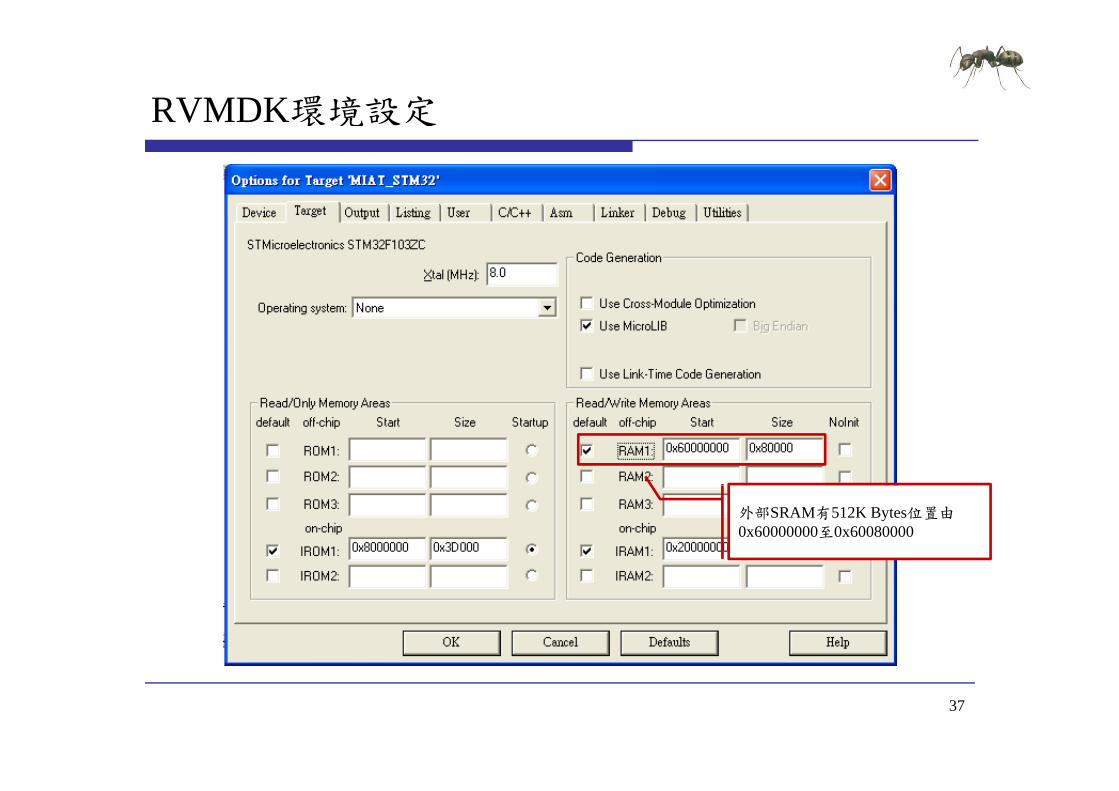
RVMDK環境設定
外部SRAM有512K Bytes位置由0x60000000至0x60080000
37
Development Flowp
Embedded Software Side
int main(void)
Bootup STM32F10x
Programming
Bootup
int main(void)ifdef DEBUGdebug()
endif
Startup Code
BootupSTM32F10x
RCC Configure
NVIC Configure
System Clocks Configuration RCC_Configuration()
NVIC Configuration g gNVIC_Configuration()
GPIO Configuration GPIO_Configuration()
GPIO Configure
for (Index = 0 Index lt1024 Index++)
Tab[Index] =IndexT bAdd ( 32)T b h ld b 0 600000
Check operation
Check pointer value
Display Result TabAddr = (u32)Tab should be 0x600000xx
Get main stack pointer value MSPValue = __MRS_MSP() should be 0x2000xxxx
helliphelliphelliphelliphelliphelliphelliphelliphelliphelliphelliphelliphelliphelliphelliphelliphelliphelliphelliphelliphelliphelliphellip
Display Result
38
Startup Codep
Register boundary addresses RCC Configure
Enable FSMC clock
LDR R0= 0x00000114
LDR R1= 0x40021014
STR R0[R1]
Enable GPIOD GPIOE GPIOF and GPIOG clocks
LDR R0= 0x000001E0
LDR R1= 0x40021018
RCC register map
STR R0[R1]
39
RCC Register g
Bit 8 FSMCEN FSMC clock enableAHB Peripheral Clock enable register (RCC_AHBENR)
Bit 8 FSMCEN FSMC clock enableSet and cleared by software0 FSMC clock disabled
APB2 peripheral clock enable register (RCC_APB2ENR)
1 FSMC clock enabled
Bit 8765 IOPGEN IO port GFED clock enableSet and cleared by software0 IO port GFED clock disabled1 IO port GFED clock enabled
40
1 IO port GFED clock enabled
Startup Codep
Register boundary addresses GPIO Configure
SRAM Data lines NOE and NWE configuration SRAM Address lines configuration NOE NEW NE1 NBL0 NBL1 configuration LDR R0= 0xB4BB44BB LDR R1= 0x40011400STR R0[R1]LDR R0= 0xBBBBBBBB LDR R1= 0x40011404STR R0[R1]LDR R0 = 0xB44444BBLDR R0= 0xB44444BB LDR R1= 0x40011800STR R0[R1]LDR R0= 0xBBBBBBBB LDR R1= 0x40011804
GPIO register map
STR R0[R1]LDR R0= 0x44BBBBBB LDR R1= 0x40011C00STR R0[R1]LDR R0= 0xBBBB4444 LDR R1= 0x40011C04STR R0[R1]LDR R0= 0x44BBBBBBLDR R1= 0x40012000STR R0 [R1]
41
STR R0[R1]
GPIO Register g
Bit 8 FSMCEN FSMC clock enablePort configuration register low
Port configuration register high
Bits 2928 2524Bits 3130 2726 2322 1918 1514 1110 76 32 Bits 2928 25242120 1716 131298 54 10MODEy[10] Port x mode bits (y= 0 15)00 Input mode (reset state)01 Output mode max speed 10 MHz
Bits 3130 27262322 1918 15141110 76 32CNFy[10] Port x configuration bits (y= 0 15)In input mode (MODE[10]=00)00 Analog input mode01 Floating input (reset state)10 Input with pull-up pull-down
10 Output mode max speed 2 MHz11 Output mode max speed 50 MHz
11 ReservedIn output mode (MODE[10] gt00)00 General purpose output push-pull01 General purpose output Open-drain10 Alternate function output Push-pull11 Alternate function output Open-drain
42
11 Alternate function output Open drain
Startup Codep
FSMCregister map FSMC Configure
FSMC Configuration Enable FSMC Bank1_SRAM Bank
LDR R0= 0x00001011
LDR R1= 0xA0000000
STR R0[R1]
LDR R0= 0x00000200
LDR R1= 0xA0000004
STR R0[R1]
43
FSMC Register g
Bit 8 FSMCEN FSMC clock enableSRAMNOR-Flash chip-select control registers 1 (FSMC_BCR1)
Bit 12 WREN Write enable bitThis bit indicates whether write operations are enableddisabled in the bank by the FSMC0 Write operations are disabled in the bank by the FSMC an AHB error is reported1 Write operations are enabled for the bank by the FSMC (default after reset) p y ( )Bits 54 MWID Memory databus widthDefines the external memory device width valid for all type of memories00 8 bits01 16 bits (default after reset)10 reserved do not use10 reserved do not use11 reserved do not use Bit 0 MBKEN Memory bank enable bitEnables the memory bank After reset Bank1 is enabled all others are disabled Accessing adisabled bank causes an ERROR on AHB bus0 C di b k i di bl d0 Corresponding memory bank is disabled1 Corresponding memory bank is enabled
44
FSMC Register g
Bit 8 FSMCEN FSMC clock enableSRAMNOR-Flash chip-select timing registers 1 (FSMC_BTR1)
Bits 158 DATAST Data-phase duration0000 0000 Reserved0000 0001 DATAST phase duration = 2 times HCLK clock cycles0000 0010 DATAST phase duration = 3 times HCLK clock cycles1111 1111 DATAST phase duration = 256 times HCLK clock cycles (default value after reset)Bits 74 ADDHLD Address-hold phase duration0000 Reserved0001 ADDHLD phase duration = 2 times HCLK clock cycle0010 ADDHLD phase duration = 3 times HCLK clock cycle1111 ADDHLD phase duration = 16 times HCLK clock cycles (default value after reset)Bits 30 ADDSET Address setup phase durationThese bits are written by software to define the duration of the address setup phase (refer toFigure 162 to Figure 172) used in SRAMs ROMs and asynchronous NOR Flash0000 ADDSET phase duration = 1 times HCLK clock cycle1111 ADDSET phase duration = 16 times HCLK clock cycles (default value after reset)
45
實驗步驟
範例目錄架構
範例說明 範例說明
預設定義說明
46
範例目錄架構
範例目錄
測試映像檔 測試映像檔
含括檔
函式庫 函式庫
專案檔
原始碼 原始碼
47
範例說明
Embedded Software Side
Infinite loop
Display Result
Infinite loop while (1)if (((TabAddramp0xFFFFFF00) == 0x60000000) ampamp
((MSPValueamp0xFFFF0000) == 0x20000000))
Check operation
Check pointer value((MSPValueamp0xFFFF0000) == 0x20000000))
OK Turn on USERLED GPIO_SetBits(GPIOF GPIO_Pin_11)
else
Display Result
else KO Turn off USERLED
GPIO_ResetBits(GPIOF GPIO_Pin_11) Insert delay Delay(0xAFFFF)
如果Tab位置在0x600000且Stack pointer位置在0x2000 外部記憶體使用正常USERLED紅燈恆亮Delay(0xAFFFF)
Turn on USERLED GPIO_SetBits(GPIOF GPIO_Pin_11) Insert delay Delay(0xAFFFF)
紅燈恆亮
如果 b位置不在0 600000或Delay(0xAFFFF)
如果Tab位置不在0x600000或Stack pointer位置不在0x2000 外部記憶體使用異常USERLED紅燈閃爍
48
預設定義說明
DATA_IN_ExtSRAM EQU 1 E l SRAM C fi i External SRAM Configuration 0=gt DISABLE 1=gt ENABLE
u32 Tab[1024]宣告於外部 的記憶體 宣告於外部SRAM的記憶體
49
data memory存取控制實驗
實驗二
WU-YANGTechnology Co Ltd
實驗二練習
練習 取消RVMDK環境外部SRAM設定測試是否正常 取消RVMDK環境外部SRAM設定測試是否正常
修改DATA_IN_ExtSRAM EQU 0測試是否正常
修改外部 記憶體 b變數大小測試是否正常 修改外部SRAM記憶體Tab變數大小測試是否正常
51
Q amp A
WU-YANGTechnology Co Ltd
MIAT_STM32內部Flash存取控制實驗
WU-YANG
浯陽科技有限公司
Technology Co Ltd
Declared Version
Training Only
Declare
Document Number
Document Version 100
Release Date
Document Title MIAT_STM32 內部FLASH存取控制實驗
Exercise Time
Platform MIAT_STM32V2MIAT IOB V1PlatformMIAT IOBV1
Peripheral
Author WU-YANG Technology Co Ltd
2
實驗目的(一)( )
使用MIAT_STM32實驗板透過Flash memory interface (FLITF)控制內部Flash進行存取控制實驗並利用LED(FLITF)控制內部Flash進行存取控制實驗並利用LED確認存取是否正常
3
實驗原理
System architecture E b dd d Fl h Embedded Flash Features Memory map RVMDK環境設定
FLITF Flash module organization
Flash library function Development Flow ARM Configure
4
System architecturey
5
Embedded Flash
Features 256 Kb up to 256 Kbytes Memory organization the Flash memory is organized as a
main block and an information blockmain block and an information block Main memory block of size t 32 Kb 64 bit di id d i t 128 f 2 up to 32 Kb times 64 bits divided into 128 pages of 2
Kbytes Information block of size Information block of size 258 times 64 bits
6
Embedded Flash Memory mapy p
7
Flash Memoryy
8
RVMDK環境設定
STMF103ZC有256K Bytes的Flash位置由0x8000000至0x8040000
9
FLITF
Features R d i f i h f h b ff (2 64 bi d ) Read interface with prefetch buffer (2x64-bit words) Option byte Loader
l h i Flash Program Erase operation Read Write protection
10
Flash memory interfacey
11
Flash memory interface registery g
Bit 8 FSMCEN FSMC clock enableFlash status register (FLASH_SR)
Bits 316 Reserved must be kept clearedBit 5 EOP End of operation
Bit 2 PGERR Programming errorSet by hardware when an address to be programmed p
Set by hardware when a Flash operation (programming erase) is completed Reset by writing a 1Note EOP is asserted at the end of each successful
y p gcontains a value different from 0xFFFF before programmingReset by writing 1Note The STRT bit in the FLASH_CR register f f
program or erase operationBit 4 WRPRTERR Write protection errorSet by hardware when programming a write-protected address of the Flash memory
_ gshould be reset before starting a programmingoperationBit 1 Reserved must be kept clearedBit 0 BSY Busyp y
Reset by writing 1Bit 3 Reserved must be kept cleared
This indicates that a Flash operation is in progress This is set on the beginning of a Flash operation and reset when the operation finishes or when an error occurs
12
Flash memory interface registery g
Flash control register (FLASH_CR)
Bit 9 OPTWRE Option bytes write enableWhen set the option bytes can be programmed This
Bit 6 STRT StartThis bit triggers an ERASE operation when set This bit is set only
bit is set on writing the correct key sequence to the FLASH_OPTKEYR registerThis bit can be reset by softwareBit 8 Reserved must be kept clearedBit 7 LOCK Lock
by software and reset when the BSY bit is resetBit 5 OPTER Option byte eraseOption byte erase chosenBit 4 OPTPG Option byte programmingOption byte programming chosenBit 7 LOCK Lock
Write to 1 only When it is set it indicates that the FPEC and FLASH_CR are locked This bit is reset by hardware after detecting the unlock sequenceIn the event of unsuccessful unlock operation this bit remains set until the next reset
p y p g gBit 3 Reserved must be kept clearedBit 2 MER Mass eraseErase of all user pages chosenBit 1 PER Page erasePage Erase chosenremains set until the next reset Page Erase chosenBit 0 PG ProgrammingFlash programming chosen
13
Main Flash memory programmingy p g g
14
Flash memory Page Erasey g
15
Flash memory Mass Erasey
16
Option byte programmingp y p g g
17
Option byte Erasep y
18
FLASH library functiony
19
FLASH library functiony
20
Development Flowp
Embedded Software Side
int main(void)
Bootup STM32F10x
ProgrammingBootupSTM32F10x RCC Configure
NVIC Configure
int main(void)ifdef DEBUGdebug()
endifendif
FLASHStatus = FLASH_COMPLETEMemoryProgramStatus = PASSEDData = 0x15041975
GPIO Configure
Data = 0x15041975
RCC Configuration RCC_Configuration()
Flash memory RW operation FLASH Unlock
FLASH ClearFlag NVIC Configuration NVIC_Configuration()
GPIO Configuration
FLASH ClearFlag
FLASH ErasePage
FLASH ProgramWord GPIO Configuration GPIO_Configuration()
helliphelliphelliphelliphelliphelliphelliphelliphelliphelliphelliphelliphelliphelliphelliphelliphellipDisplay Result
Check content
21
實驗步驟
範例目錄架構
範例說明 範例說明
預設定義說明
燒錄 燒錄MIAT_STM32
22
範例目錄架構
範例目錄
測試映像檔 測試映像檔
含括檔
函式庫 函式庫
專案檔
原始碼 原始碼
23
範例說明
Function name Description
Unlock the Flash Program Erase controller FLASH_Unlock()
D fi h b f b d
Flash FwLib Functions List
Function name Description
FLASH_Unlock Unlocks the FLASH Program Erase Controller
FLASH_ClearFlag Clears the FLASH pending fl
Define the number of page to be erased NbrOfPage = (EndAddr - StartAddr) FLASH_PAGE_SIZE
Clear All pending flags FLASH_ClearFlag(FLASH_FLAG_BSY | FLASH_FLAG_EOP | FLASH_FLAG_PGERR |
FLASH FLAG WRPRTERR)flags
FLASH_ErasePage Erases a specified FLASH page
FLASH_ProgramWord Programs a word at a specified
_ _ )
Erase the FLASH pages for(EraseCounter = 0 (EraseCounter lt NbrOfPage) ampamp (FLASHStatus ==
FLASH_COMPLETE) EraseCounter++)FLASHStatus = FLASH ErasePage(StartAddr + (FLASH PAGE SIZE EraseCounter))address FLASHStatus = FLASH_ErasePage(StartAddr + (FLASH_PAGE_SIZE EraseCounter))
FLASH Word program of data 0x15041979 at addresses defined by StartAddr and EndAddrAddress = StartAddr
while((Address lt EndAddr) ampamp (FLASHStatus == FLASH_COMPLETE))FLASHStatus = FLASH_ProgramWord(Address Data)Address = Address + 4
24
範例說明
Embedded Software Side
Check the corectness of written data
Display Result
Check the corectness of written data Address = StartAddr
while((Address lt EndAddr) ampamp (MemoryProgramStatus = FAILED))if(((vu32) Address) = Data)
Flash memory RW operation
MemoryProgramStatus = FAILED
Address += 4
Check content
Display Result while (1)if (MemoryProgramStatus == PASSED) OK Turn on USERLED GPIO_SetBits(GPIOF GPIO_Pin_11)
Display Result
else KO Turn off USERLED GPIO_ResetBits(GPIOF GPIO_Pin_11) Insert delay Delay(0xAFFFF)
如果寫入與讀取Flash內容相同Flash記憶體使用正常USERLED紅燈恆亮
Turn on USERLED GPIO_SetBits(GPIOF GPIO_Pin_11) Insert delay Delay(0xAFFFF)
如果寫入與讀取Flash內容不同Flash記憶體使用異常USERLED紅燈閃爍
25
預設定義說明
define StartAddr ((u32)0x08008000) 定義Flash使用起始點 定義Flash使用起始點
使用起始點必需大於0x8003000 + Code Size 附註 0x8000000~0x8003000為DFU程式區塊使用此區塊
將造成無法燒錄程式
Code Size可由產生的HEX檔得知
d fi E dAdd (( 32)0 0800C000) define EndAddr ((u32)0x0800C000) 定義Flash使用結束點
使用起始點必需小於0x8040000使用起始點必需小於
Data = 0x15041975 寫入資料
32Bit define FLASH_PAGE_SIZE ((u16)0x800)
每一個Page有2KByte26
每一個Page有2KByte
Intel HEX Format
aaaa tt dd cc
field Description
the colon that starts every Intel HEX record
the record-length field that represents the number of data bytes (dd) in the record
aaaa the address field that represents the starting address for subsequent data in the record
tt the field that represents the HEX record type which may be one of the following00 - data record01 - end-of-file record02 - extended segment address recordg04 - extended linear address record
dd a data field that represents one byte of data A record may have multiple data bytes The number of data bytes in the record must match the number specified by the field
cc the checksum field that represents the checksum of the record The checksum is calculated by summing the values of all hexadecimal digit pairs in the record modulo 256 and taking the twos complement
27
HEX Examplep
020000040800F2103000001814002045310008D9340008CD340008D8103000001814002045310008D9340008CD340008D8helliphelliphellip1038200042370008000000000000000000000000170C3830000000000000000000000000008C
資料填入起始位置為
0C3830000000000000000000000000008C04000005080031318D00000001FF
資料填入起始位置為0x08003000 每一行有0x10(16)個Bytes 最後一筆資料為
資料結束點為0x0803383004000005080031318D
(0x08003830 -0x08000000)0x800 = 7 需以0x800為單位所以使用的位置起點為0x08004000
28
燒錄MIAT STM32_
Rebuilder all target files產生HEX DFU Fil M 轉換HEX產生DFU DFU File Manager轉換HEX產生DFU DfuSe Demonstration燒錄DFU d Leave DFU mode
29
內部Flash存取控制實驗
實驗一
WU-YANGTechnology Co Ltd
實驗一練習
注意 請使用預設0 08008000之後的位置 避免覆蓋DFU 請使用預設0x08008000之後的位置避免覆蓋DFU
與使用者程式碼區塊
練習 練習 修改存取位置測試是否正常
修改寫入資料測試是否正常 修改寫入資料測試是否正常
修改寫入資料後取消FLASH_Unlock測試是否正常
修改寫入資料後取消FLASH E P 測試是否正 修改寫入資料後取消FLASH_ErasePage測試是否正常
31
實驗目的(二)( )
使用MIAT_STM32實驗板透過Flash memory interface (FLITF)控制內部Flash進行存取控制實驗並利用SW(FLITF)控制內部Flash進行存取控制實驗並利用SWKEY決定資料寫入與讀取LCD顯示狀態
32
實驗原理
System requirement E b dd d Fl h Embedded Flash LCD KEY SW
Development Flow ARM Configure
33
Development Flowp
Embedded Software Side
int main(void)
Bootup STM32F10x
ProgrammingBootupSTM32F10x RCC Configure
NVIC Configure
int main(void)ifdef DEBUGdebug()
endif
FLASHStatus = FLASH_COMPLETE
RCC Configuration RCC Configuration()
GPIO Configure
BasicIO Configure_ g ()
NVIC Configuration NVIC_Configuration()
GPIO Configuration Flash memory RW ti
lcd Configure
GPIO Configuration GPIO_Configuration()
Init_BasicIO()
l d i i () LCD I i i li i
RW operation
Example
FLASH Unlock
FLASH ClearFlag
lcd_init() LCD Initialization
helliphelliphelliphelliphelliphelliphelliphelliphelliphelliphelliphelliphelliphelliphelliphelliphelliphelliphelliphelliphelliphelliphellip
p
34
硬體電路配置
Mapping Table
Num MIAT_STM32V2 MIAT_IOBV1 Num MIAT_STM32V2 MIAT_IOBV1
1 PC8 (326) SW1 10 PE6 (15) LCD_EN2 PC9 (327) SW2 11 PF6 (118) LCD RW ( ) ( ) _3 PC10 (43) SW3 12 PF7 (119) LCD_RS 4 PC11 (44) SW4 13 PF8(120) LCD_D4 5 PB5 (427) KEY1 14 PF9 (121) LCD_D5 6 PB6 (428) KEY2 15 PF10 (122) LCD_D6 7 PB7 (429) KEY3 16 PF11 (213) LCD_D7 8 PB8 (431) KEY4 17 VDD (236) VCC33V 9 VCC5V (1 36) VCC5V 18 GND (1 35) GND9 VCC5V (136) VCC5V 18 GND (135) GND
35
實驗步驟
範例目錄架構
範例說明 範例說明
預設定義說明
36
範例目錄架構
範例目錄
測試映像檔 測試映像檔
含括檔
函式庫 函式庫
專案檔
原始碼 原始碼
37
範例說明
Embedded Software Side
lcd clear()
FLASH memory RW operation
lcd_clear()lcd_print (MIAT_STM32 DEMO )
Unlock the Flash Program Erase controller FLASH_Unlock()
Flash memory RW operation
FLASH Unlock
Clear All pending flags FLASH_ClearFlag(FLASH_FLAG_BSY | FLASH_FLAG_EOP | FLASH_FLAG_PGERR |
FLASH_FLAG_WRPRTERR)
while(1)
Example
FLASH ClearFlag
( )
KEY_Buffer=Key_Scan()set_cursor (0 1)lcd_print (SW Value = 0x)lcd putchar(((SWamp0x7)+0x30))lcd_putchar(((SWamp0x7)+0x30))if(KEY_Buffer==1)Address=(StartAddr|(SWltlt12))set_cursor (0 0)lcd_print (Set Addr = 0x)
掃描KEY是否按下與顯示SW數值LCD Line2顯示SW Value = 0x(SW)
lcd_putchar(((SWamp0x7)+0x30))lcd_print ( )
如果KEY1按下記錄SW數值至Address LCD Line1顯示Set Adde = 0x(Address)
38
範例說明
Embedded Software Side
else if(KEY Buffer==2)
FLASH memory RW operation
else if(KEY_Buffer==2)
Erase the FLASH pages FLASHStatus = FLASH_ErasePage(Address)
FLASH Word program of data at addresses defined by SW
SRAM memory RW operation
p g yFLASHStatus = FLASH_ProgramWord(Address (SWamp0x7))
set_cursor (0 0)lcd_print (Write 0x)lcd_putchar(((SWamp0x7)+0x30))l d i t ( t 0 )
Example如果KEY2按下清除Address所處區塊並寫入SW數值 lcd_print ( at 0x)
lcd_putchar((((Addressgtgt12)amp0x7)+0x30))else if(KEY_Buffer==3)
Data=(u16 )Address
所處區塊並寫入SW數值LCD Line1顯示Write 0x(SW) at 0x(Adddress)
Data (u16 )Addressset_cursor (0 0)lcd_print (Addr 0x)lcd_putchar((((Addressgtgt12)amp0x7)+0x30))lcd_print ( = 0x)lcd_putchar(((Dataamp0x7)+0x30))lcd_print ( )
如果KEY3按下讀取Address紀錄數值LCD Line1顯示Addr 0x(Adddress) = 0x
39
預設定義說明
define StartAddr ((u32)0x08020000) 定義Flash使用起始點 定義Flash使用起始點
使用起始點必需大於0x8003000 + Code Size 附註 0x8000000~0x8003000為DFU程式區塊使用此區塊
將造成無法燒錄程式
Code Size可由產生的HEX檔得知
32 Add 0 08020000 u32 Address = 0x08020000 定義Address初始值
初始值必需與Flash使用起始點相同初始值必需與 使用起始點相同
Address=(StartAddr|(SWltlt12)) Example StartAddr = 0x08020000 SW = 1 Address = 0x08021000
StartAddr = 0x08020000 SW = 7 Address = 0x08027000 StartAddr|(7ltlt12)必需小於0x8040000
40
使用者界面與Flash存取控制實驗
實驗二
WU-YANGTechnology Co Ltd
實驗二練習
注意 請使用預設0 08020000之後的位置 避免覆蓋DFU 請使用預設0x08020000之後的位置避免覆蓋DFU
與使用者程式碼區塊
練習 練習 利用SW與KEY測試Flash寫入與讀取是否正常
Fl h寫入後電源關閉 再開啟後寫入資料是否仍存 Flash寫入後電源關閉再開啟後寫入資料是否仍存在
修改存取位置測試是否正常 修改存取位置測試是否正常
42
實驗目的(三)( )
使用MIAT_STM32實驗板透過Flash memory interface (FLITF)控制內部Flash進行存取控制實驗並藉由填入(FLITF)控制內部Flash進行存取控制實驗並藉由填入Option Bytes 設定寫入鎖定保護Page鎖定不被覆蓋
43
Development Flowp
Embedded Software Side
int main(void)
Bootup STM32F10x
ProgrammingBootupSTM32F10x RCC Configure
NVIC Configure
int main(void)ifdef DEBUGdebug()
endifendif
FLASHStatus = FLASH_COMPLETEMemoryProgramStatus = PASSEDData = 0x1753
GPIO Configure
Data = 0x1753
RCC Configuration RCC_Configuration()
Flash memory RW operation FLASH Unlock
FLASH ClearFlag NVIC Configuration NVIC_Configuration()
GPIO Configuration
FLASH ClearFlag
FLASH ErasePage
FLASH ProgramHalfWord GPIO Configuration GPIO_Configuration()
Display Result
Check content
44
helliphelliphelliphelliphelliphelliphelliphelliphelliphelliphelliphelliphelliphelliphelliphelliphelliphelliphellip
實驗步驟
範例目錄架構
範例說明 範例說明
預設定義說明
45
範例目錄架構
範例目錄
測試映像檔 測試映像檔
含括檔
函式庫 函式庫
專案檔
原始碼 原始碼
46
範例說明
Function name Description
Unlock the Flash Program Erase controller FLASH_Unlock()
Define the number of page to be erased
Flash FwLib Functions List
Function name Description
FLASH_Unlock Unlocks the FLASH Program Erase Controller
FLASH_ClearFlag Clears the FLASH pending fl
Define the number of page to be erased NbrOfPage = (EndAddr ‐ StartAddr) FLASH_PAGE_SIZE
FLASH_ClearFlag(FLASH_FLAG_BSY | FLASH_FLAG_EOP|FLASH_FLAG_PGERR |FLASH_FLAG_WRPRTERR)
Get pages write protection status flags
FLASH_EraseOptionBytes
Erases the FLASH option bytes
FLASH_EnableWritePro Write protects the desired
p g pWRPR_Value = FLASH_GetWriteProtectionOptionByte()ProtectedPages = WRPR_Value amp 0x000000C0
ifdef WriteProtection_Disableif (ProtectedPages == 0x00) Pages are write protected
tection pages
NVIC_GenerateSystemReset
Generate a system reset
Disable the write protection FLASHStatus = FLASH_EraseOptionBytes() Generate System Reset to load the new option byte values NVIC_GenerateSystemReset()
elseifdef WriteProtection Enableifdef WriteProtection_Enableif (ProtectedPages = 0x00) Pages not write protected
FLASHStatus = FLASH_EraseOptionBytes() Enable the pages write protection FLASHStatus = FLASH_EnableWriteProtection(FLASH_WRProt_Pages12to13
|FLASH WRProt Pages14to15)|FLASH_WRProt_Pages14to15) Generate System Reset to load the new option byte values NVIC_GenerateSystemReset()
endifendif
47
範例說明
if (ProtectedPages = 0x00) Clear All pending flags
Flash FwLib Functions List
Function name DescriptionFLASH_ClearFlag(FLASH_FLAG_BSY |
FLASH_FLAG_EOP|FLASH_FLAG_PGERR |FLASH_FLAG_WRPRTERR)
erase the FLASH pages for(EraseCounter = 0 (EraseCounter lt NbrOfPage) ampamp (FLASHStatus ==
Function name Description
FLASH_ErasePage Erases a specified FLASH page
FLASH_ProgramHalfWod
Programs a half word at a ifi d dd FLASH_COMPLETE) EraseCounter++)
FLASHStatus = FLASH_ErasePage(StartAddr + (FLASH_PAGE_SIZE
EraseCounter))
rd specified address
FLASH Half Word program of data 0x1753 at addresses defined by StartAddrand EndAddr
Address = StartAddr
hil ((Add E dAdd ) ampamp (FLASHSt t FLASH COMPLETE))while((Address lt EndAddr) ampamp (FLASHStatus == FLASH_COMPLETE))
FLASHStatus = FLASH_ProgramHalfWord(Address Data)Address = Address + 2
48
範例說明
Embedded Software Side
Check the corectness of written data
Display Result
Check the corectness of written data Address = StartAddr
while((Address lt EndAddr) ampamp (MemoryProgramStatus = FAILED))if(((vu16) Address) = Data)
Flash memory RW operation
MemoryProgramStatus = FAILED
Address += 2
Check content
Display Result while (1)if (MemoryProgramStatus == PASSED) OK Turn on USERLED GPIO_SetBits(GPIOF GPIO_Pin_11)
Display Result
else KO Turn off USERLED GPIO_ResetBits(GPIOF GPIO_Pin_11) Insert delay Delay(0xAFFFF)
如果寫入與讀取Flash內容相同Flash記憶體可以寫入USERLED紅燈恆亮
Turn on USERLED GPIO_SetBits(GPIOF GPIO_Pin_11) Insert delay Delay(0xAFFFF)
如果寫入與讀取Flash內容不同Flash記憶體不能寫入USERLED紅燈閃爍
49
預設定義說明
define StartAddr ((u32) 0x08006000) 定義Flash使用起始點 定義Flash使用起始點
使用起始點必需大於0x8003000 + Code Size 附註 0x8000000~0x8003000為DFU程式區塊使用此區塊
將造成無法燒錄程式
Code Size可由產生的HEX檔得知
d fi E dAdd (( 32) 0 08008000) define EndAddr ((u32) 0x08008000) 定義Flash使用結束點
使用起始點必需小於0x8040000使用起始點必需小於
Data = 0x1753 寫入資料
16Bit define FLASH_PAGE_SIZE ((u16)0x800) 每一個Page有2KByte
50
每一個Page有2KByte
預設定義說明
define WriteProtection_Enable U hi li E bl W i P i Uncomment this line to Enable Write Protection
define WriteProtection_Disablehi li i bl i i Uncomment this line to Disable Write Protection
FLASH_EnableWriteProtection設定影響 個 設定影響2個Page FLASH_WRProt_Pages0to1 FLASH_WRProt_Pages1to2 helliphellip FLASH_WRProt_Pages60to61
設定影響多個Page FLASH_WRProt_Pages62to255
51
FLASH EnableWriteProtection_
Example
位置0x08006000 ~ 0x08007000每一個Page有0x800ByteStartPage = (0x08006000-0x08000000)0x800 = 12EndPage = ((0x08007000-0x08000000)0x800)-1 = 13執行執行FLASH_EnableWriteProtection(FLASH_WRProt_Pages12to13)將影響Pages12 Pages13
52
內部Flash寫入鎖定存取控制實驗
實驗三
WU-YANGTechnology Co Ltd
實驗三練習
注意 請使用預設0 08006000之後的位置 避免覆蓋DFU 請使用預設0x08006000之後的位置避免覆蓋DFU
與使用者程式碼區塊
更改寫入位置測試寫入鎖定時需同時更改 更改寫入位置測試寫入鎖定時需同時更改FLASH_EnableWriteProtection鎖定之Page
練習 練習 打開define WriteProtection_Enable測試是否可寫入
打開define WriteProtection Disable測試是否可寫入 打開define WriteProtection_Disable測試是否可寫入
修改存取位置測試是否正常
修改寫入資料測試是否正常 修改寫入資料測試是否正常
54
Q amp A
WU-YANGTechnology Co Ltd

Development Flowp
Embedded Software Side
int main(void)
Bootup STM32F10x
Programming
Bootup
int main(void)ifdef DEBUGdebug()
endif
Startup Code
BootupSTM32F10x
RCC Configure
NVIC Configure
System Clocks Configuration RCC_Configuration()
NVIC Configuration g gNVIC_Configuration()
GPIO Configuration GPIO_Configuration()
GPIO Configure
for (Index = 0 Index lt1024 Index++)
Tab[Index] =IndexT bAdd ( 32)T b h ld b 0 600000
Check operation
Check pointer value
Display Result TabAddr = (u32)Tab should be 0x600000xx
Get main stack pointer value MSPValue = __MRS_MSP() should be 0x2000xxxx
helliphelliphelliphelliphelliphelliphelliphelliphelliphelliphelliphelliphelliphelliphelliphelliphelliphelliphelliphelliphelliphelliphellip
Display Result
38
Startup Codep
Register boundary addresses RCC Configure
Enable FSMC clock
LDR R0= 0x00000114
LDR R1= 0x40021014
STR R0[R1]
Enable GPIOD GPIOE GPIOF and GPIOG clocks
LDR R0= 0x000001E0
LDR R1= 0x40021018
RCC register map
STR R0[R1]
39
RCC Register g
Bit 8 FSMCEN FSMC clock enableAHB Peripheral Clock enable register (RCC_AHBENR)
Bit 8 FSMCEN FSMC clock enableSet and cleared by software0 FSMC clock disabled
APB2 peripheral clock enable register (RCC_APB2ENR)
1 FSMC clock enabled
Bit 8765 IOPGEN IO port GFED clock enableSet and cleared by software0 IO port GFED clock disabled1 IO port GFED clock enabled
40
1 IO port GFED clock enabled
Startup Codep
Register boundary addresses GPIO Configure
SRAM Data lines NOE and NWE configuration SRAM Address lines configuration NOE NEW NE1 NBL0 NBL1 configuration LDR R0= 0xB4BB44BB LDR R1= 0x40011400STR R0[R1]LDR R0= 0xBBBBBBBB LDR R1= 0x40011404STR R0[R1]LDR R0 = 0xB44444BBLDR R0= 0xB44444BB LDR R1= 0x40011800STR R0[R1]LDR R0= 0xBBBBBBBB LDR R1= 0x40011804
GPIO register map
STR R0[R1]LDR R0= 0x44BBBBBB LDR R1= 0x40011C00STR R0[R1]LDR R0= 0xBBBB4444 LDR R1= 0x40011C04STR R0[R1]LDR R0= 0x44BBBBBBLDR R1= 0x40012000STR R0 [R1]
41
STR R0[R1]
GPIO Register g
Bit 8 FSMCEN FSMC clock enablePort configuration register low
Port configuration register high
Bits 2928 2524Bits 3130 2726 2322 1918 1514 1110 76 32 Bits 2928 25242120 1716 131298 54 10MODEy[10] Port x mode bits (y= 0 15)00 Input mode (reset state)01 Output mode max speed 10 MHz
Bits 3130 27262322 1918 15141110 76 32CNFy[10] Port x configuration bits (y= 0 15)In input mode (MODE[10]=00)00 Analog input mode01 Floating input (reset state)10 Input with pull-up pull-down
10 Output mode max speed 2 MHz11 Output mode max speed 50 MHz
11 ReservedIn output mode (MODE[10] gt00)00 General purpose output push-pull01 General purpose output Open-drain10 Alternate function output Push-pull11 Alternate function output Open-drain
42
11 Alternate function output Open drain
Startup Codep
FSMCregister map FSMC Configure
FSMC Configuration Enable FSMC Bank1_SRAM Bank
LDR R0= 0x00001011
LDR R1= 0xA0000000
STR R0[R1]
LDR R0= 0x00000200
LDR R1= 0xA0000004
STR R0[R1]
43
FSMC Register g
Bit 8 FSMCEN FSMC clock enableSRAMNOR-Flash chip-select control registers 1 (FSMC_BCR1)
Bit 12 WREN Write enable bitThis bit indicates whether write operations are enableddisabled in the bank by the FSMC0 Write operations are disabled in the bank by the FSMC an AHB error is reported1 Write operations are enabled for the bank by the FSMC (default after reset) p y ( )Bits 54 MWID Memory databus widthDefines the external memory device width valid for all type of memories00 8 bits01 16 bits (default after reset)10 reserved do not use10 reserved do not use11 reserved do not use Bit 0 MBKEN Memory bank enable bitEnables the memory bank After reset Bank1 is enabled all others are disabled Accessing adisabled bank causes an ERROR on AHB bus0 C di b k i di bl d0 Corresponding memory bank is disabled1 Corresponding memory bank is enabled
44
FSMC Register g
Bit 8 FSMCEN FSMC clock enableSRAMNOR-Flash chip-select timing registers 1 (FSMC_BTR1)
Bits 158 DATAST Data-phase duration0000 0000 Reserved0000 0001 DATAST phase duration = 2 times HCLK clock cycles0000 0010 DATAST phase duration = 3 times HCLK clock cycles1111 1111 DATAST phase duration = 256 times HCLK clock cycles (default value after reset)Bits 74 ADDHLD Address-hold phase duration0000 Reserved0001 ADDHLD phase duration = 2 times HCLK clock cycle0010 ADDHLD phase duration = 3 times HCLK clock cycle1111 ADDHLD phase duration = 16 times HCLK clock cycles (default value after reset)Bits 30 ADDSET Address setup phase durationThese bits are written by software to define the duration of the address setup phase (refer toFigure 162 to Figure 172) used in SRAMs ROMs and asynchronous NOR Flash0000 ADDSET phase duration = 1 times HCLK clock cycle1111 ADDSET phase duration = 16 times HCLK clock cycles (default value after reset)
45
實驗步驟
範例目錄架構
範例說明 範例說明
預設定義說明
46
範例目錄架構
範例目錄
測試映像檔 測試映像檔
含括檔
函式庫 函式庫
專案檔
原始碼 原始碼
47
範例說明
Embedded Software Side
Infinite loop
Display Result
Infinite loop while (1)if (((TabAddramp0xFFFFFF00) == 0x60000000) ampamp
((MSPValueamp0xFFFF0000) == 0x20000000))
Check operation
Check pointer value((MSPValueamp0xFFFF0000) == 0x20000000))
OK Turn on USERLED GPIO_SetBits(GPIOF GPIO_Pin_11)
else
Display Result
else KO Turn off USERLED
GPIO_ResetBits(GPIOF GPIO_Pin_11) Insert delay Delay(0xAFFFF)
如果Tab位置在0x600000且Stack pointer位置在0x2000 外部記憶體使用正常USERLED紅燈恆亮Delay(0xAFFFF)
Turn on USERLED GPIO_SetBits(GPIOF GPIO_Pin_11) Insert delay Delay(0xAFFFF)
紅燈恆亮
如果 b位置不在0 600000或Delay(0xAFFFF)
如果Tab位置不在0x600000或Stack pointer位置不在0x2000 外部記憶體使用異常USERLED紅燈閃爍
48
預設定義說明
DATA_IN_ExtSRAM EQU 1 E l SRAM C fi i External SRAM Configuration 0=gt DISABLE 1=gt ENABLE
u32 Tab[1024]宣告於外部 的記憶體 宣告於外部SRAM的記憶體
49
data memory存取控制實驗
實驗二
WU-YANGTechnology Co Ltd
實驗二練習
練習 取消RVMDK環境外部SRAM設定測試是否正常 取消RVMDK環境外部SRAM設定測試是否正常
修改DATA_IN_ExtSRAM EQU 0測試是否正常
修改外部 記憶體 b變數大小測試是否正常 修改外部SRAM記憶體Tab變數大小測試是否正常
51
Q amp A
WU-YANGTechnology Co Ltd
MIAT_STM32內部Flash存取控制實驗
WU-YANG
浯陽科技有限公司
Technology Co Ltd
Declared Version
Training Only
Declare
Document Number
Document Version 100
Release Date
Document Title MIAT_STM32 內部FLASH存取控制實驗
Exercise Time
Platform MIAT_STM32V2MIAT IOB V1PlatformMIAT IOBV1
Peripheral
Author WU-YANG Technology Co Ltd
2
實驗目的(一)( )
使用MIAT_STM32實驗板透過Flash memory interface (FLITF)控制內部Flash進行存取控制實驗並利用LED(FLITF)控制內部Flash進行存取控制實驗並利用LED確認存取是否正常
3
實驗原理
System architecture E b dd d Fl h Embedded Flash Features Memory map RVMDK環境設定
FLITF Flash module organization
Flash library function Development Flow ARM Configure
4
System architecturey
5
Embedded Flash
Features 256 Kb up to 256 Kbytes Memory organization the Flash memory is organized as a
main block and an information blockmain block and an information block Main memory block of size t 32 Kb 64 bit di id d i t 128 f 2 up to 32 Kb times 64 bits divided into 128 pages of 2
Kbytes Information block of size Information block of size 258 times 64 bits
6
Embedded Flash Memory mapy p
7
Flash Memoryy
8
RVMDK環境設定
STMF103ZC有256K Bytes的Flash位置由0x8000000至0x8040000
9
FLITF
Features R d i f i h f h b ff (2 64 bi d ) Read interface with prefetch buffer (2x64-bit words) Option byte Loader
l h i Flash Program Erase operation Read Write protection
10
Flash memory interfacey
11
Flash memory interface registery g
Bit 8 FSMCEN FSMC clock enableFlash status register (FLASH_SR)
Bits 316 Reserved must be kept clearedBit 5 EOP End of operation
Bit 2 PGERR Programming errorSet by hardware when an address to be programmed p
Set by hardware when a Flash operation (programming erase) is completed Reset by writing a 1Note EOP is asserted at the end of each successful
y p gcontains a value different from 0xFFFF before programmingReset by writing 1Note The STRT bit in the FLASH_CR register f f
program or erase operationBit 4 WRPRTERR Write protection errorSet by hardware when programming a write-protected address of the Flash memory
_ gshould be reset before starting a programmingoperationBit 1 Reserved must be kept clearedBit 0 BSY Busyp y
Reset by writing 1Bit 3 Reserved must be kept cleared
This indicates that a Flash operation is in progress This is set on the beginning of a Flash operation and reset when the operation finishes or when an error occurs
12
Flash memory interface registery g
Flash control register (FLASH_CR)
Bit 9 OPTWRE Option bytes write enableWhen set the option bytes can be programmed This
Bit 6 STRT StartThis bit triggers an ERASE operation when set This bit is set only
bit is set on writing the correct key sequence to the FLASH_OPTKEYR registerThis bit can be reset by softwareBit 8 Reserved must be kept clearedBit 7 LOCK Lock
by software and reset when the BSY bit is resetBit 5 OPTER Option byte eraseOption byte erase chosenBit 4 OPTPG Option byte programmingOption byte programming chosenBit 7 LOCK Lock
Write to 1 only When it is set it indicates that the FPEC and FLASH_CR are locked This bit is reset by hardware after detecting the unlock sequenceIn the event of unsuccessful unlock operation this bit remains set until the next reset
p y p g gBit 3 Reserved must be kept clearedBit 2 MER Mass eraseErase of all user pages chosenBit 1 PER Page erasePage Erase chosenremains set until the next reset Page Erase chosenBit 0 PG ProgrammingFlash programming chosen
13
Main Flash memory programmingy p g g
14
Flash memory Page Erasey g
15
Flash memory Mass Erasey
16
Option byte programmingp y p g g
17
Option byte Erasep y
18
FLASH library functiony
19
FLASH library functiony
20
Development Flowp
Embedded Software Side
int main(void)
Bootup STM32F10x
ProgrammingBootupSTM32F10x RCC Configure
NVIC Configure
int main(void)ifdef DEBUGdebug()
endifendif
FLASHStatus = FLASH_COMPLETEMemoryProgramStatus = PASSEDData = 0x15041975
GPIO Configure
Data = 0x15041975
RCC Configuration RCC_Configuration()
Flash memory RW operation FLASH Unlock
FLASH ClearFlag NVIC Configuration NVIC_Configuration()
GPIO Configuration
FLASH ClearFlag
FLASH ErasePage
FLASH ProgramWord GPIO Configuration GPIO_Configuration()
helliphelliphelliphelliphelliphelliphelliphelliphelliphelliphelliphelliphelliphelliphelliphelliphellipDisplay Result
Check content
21
實驗步驟
範例目錄架構
範例說明 範例說明
預設定義說明
燒錄 燒錄MIAT_STM32
22
範例目錄架構
範例目錄
測試映像檔 測試映像檔
含括檔
函式庫 函式庫
專案檔
原始碼 原始碼
23
範例說明
Function name Description
Unlock the Flash Program Erase controller FLASH_Unlock()
D fi h b f b d
Flash FwLib Functions List
Function name Description
FLASH_Unlock Unlocks the FLASH Program Erase Controller
FLASH_ClearFlag Clears the FLASH pending fl
Define the number of page to be erased NbrOfPage = (EndAddr - StartAddr) FLASH_PAGE_SIZE
Clear All pending flags FLASH_ClearFlag(FLASH_FLAG_BSY | FLASH_FLAG_EOP | FLASH_FLAG_PGERR |
FLASH FLAG WRPRTERR)flags
FLASH_ErasePage Erases a specified FLASH page
FLASH_ProgramWord Programs a word at a specified
_ _ )
Erase the FLASH pages for(EraseCounter = 0 (EraseCounter lt NbrOfPage) ampamp (FLASHStatus ==
FLASH_COMPLETE) EraseCounter++)FLASHStatus = FLASH ErasePage(StartAddr + (FLASH PAGE SIZE EraseCounter))address FLASHStatus = FLASH_ErasePage(StartAddr + (FLASH_PAGE_SIZE EraseCounter))
FLASH Word program of data 0x15041979 at addresses defined by StartAddr and EndAddrAddress = StartAddr
while((Address lt EndAddr) ampamp (FLASHStatus == FLASH_COMPLETE))FLASHStatus = FLASH_ProgramWord(Address Data)Address = Address + 4
24
範例說明
Embedded Software Side
Check the corectness of written data
Display Result
Check the corectness of written data Address = StartAddr
while((Address lt EndAddr) ampamp (MemoryProgramStatus = FAILED))if(((vu32) Address) = Data)
Flash memory RW operation
MemoryProgramStatus = FAILED
Address += 4
Check content
Display Result while (1)if (MemoryProgramStatus == PASSED) OK Turn on USERLED GPIO_SetBits(GPIOF GPIO_Pin_11)
Display Result
else KO Turn off USERLED GPIO_ResetBits(GPIOF GPIO_Pin_11) Insert delay Delay(0xAFFFF)
如果寫入與讀取Flash內容相同Flash記憶體使用正常USERLED紅燈恆亮
Turn on USERLED GPIO_SetBits(GPIOF GPIO_Pin_11) Insert delay Delay(0xAFFFF)
如果寫入與讀取Flash內容不同Flash記憶體使用異常USERLED紅燈閃爍
25
預設定義說明
define StartAddr ((u32)0x08008000) 定義Flash使用起始點 定義Flash使用起始點
使用起始點必需大於0x8003000 + Code Size 附註 0x8000000~0x8003000為DFU程式區塊使用此區塊
將造成無法燒錄程式
Code Size可由產生的HEX檔得知
d fi E dAdd (( 32)0 0800C000) define EndAddr ((u32)0x0800C000) 定義Flash使用結束點
使用起始點必需小於0x8040000使用起始點必需小於
Data = 0x15041975 寫入資料
32Bit define FLASH_PAGE_SIZE ((u16)0x800)
每一個Page有2KByte26
每一個Page有2KByte
Intel HEX Format
aaaa tt dd cc
field Description
the colon that starts every Intel HEX record
the record-length field that represents the number of data bytes (dd) in the record
aaaa the address field that represents the starting address for subsequent data in the record
tt the field that represents the HEX record type which may be one of the following00 - data record01 - end-of-file record02 - extended segment address recordg04 - extended linear address record
dd a data field that represents one byte of data A record may have multiple data bytes The number of data bytes in the record must match the number specified by the field
cc the checksum field that represents the checksum of the record The checksum is calculated by summing the values of all hexadecimal digit pairs in the record modulo 256 and taking the twos complement
27
HEX Examplep
020000040800F2103000001814002045310008D9340008CD340008D8103000001814002045310008D9340008CD340008D8helliphelliphellip1038200042370008000000000000000000000000170C3830000000000000000000000000008C
資料填入起始位置為
0C3830000000000000000000000000008C04000005080031318D00000001FF
資料填入起始位置為0x08003000 每一行有0x10(16)個Bytes 最後一筆資料為
資料結束點為0x0803383004000005080031318D
(0x08003830 -0x08000000)0x800 = 7 需以0x800為單位所以使用的位置起點為0x08004000
28
燒錄MIAT STM32_
Rebuilder all target files產生HEX DFU Fil M 轉換HEX產生DFU DFU File Manager轉換HEX產生DFU DfuSe Demonstration燒錄DFU d Leave DFU mode
29
內部Flash存取控制實驗
實驗一
WU-YANGTechnology Co Ltd
實驗一練習
注意 請使用預設0 08008000之後的位置 避免覆蓋DFU 請使用預設0x08008000之後的位置避免覆蓋DFU
與使用者程式碼區塊
練習 練習 修改存取位置測試是否正常
修改寫入資料測試是否正常 修改寫入資料測試是否正常
修改寫入資料後取消FLASH_Unlock測試是否正常
修改寫入資料後取消FLASH E P 測試是否正 修改寫入資料後取消FLASH_ErasePage測試是否正常
31
實驗目的(二)( )
使用MIAT_STM32實驗板透過Flash memory interface (FLITF)控制內部Flash進行存取控制實驗並利用SW(FLITF)控制內部Flash進行存取控制實驗並利用SWKEY決定資料寫入與讀取LCD顯示狀態
32
實驗原理
System requirement E b dd d Fl h Embedded Flash LCD KEY SW
Development Flow ARM Configure
33
Development Flowp
Embedded Software Side
int main(void)
Bootup STM32F10x
ProgrammingBootupSTM32F10x RCC Configure
NVIC Configure
int main(void)ifdef DEBUGdebug()
endif
FLASHStatus = FLASH_COMPLETE
RCC Configuration RCC Configuration()
GPIO Configure
BasicIO Configure_ g ()
NVIC Configuration NVIC_Configuration()
GPIO Configuration Flash memory RW ti
lcd Configure
GPIO Configuration GPIO_Configuration()
Init_BasicIO()
l d i i () LCD I i i li i
RW operation
Example
FLASH Unlock
FLASH ClearFlag
lcd_init() LCD Initialization
helliphelliphelliphelliphelliphelliphelliphelliphelliphelliphelliphelliphelliphelliphelliphelliphelliphelliphelliphelliphelliphelliphellip
p
34
硬體電路配置
Mapping Table
Num MIAT_STM32V2 MIAT_IOBV1 Num MIAT_STM32V2 MIAT_IOBV1
1 PC8 (326) SW1 10 PE6 (15) LCD_EN2 PC9 (327) SW2 11 PF6 (118) LCD RW ( ) ( ) _3 PC10 (43) SW3 12 PF7 (119) LCD_RS 4 PC11 (44) SW4 13 PF8(120) LCD_D4 5 PB5 (427) KEY1 14 PF9 (121) LCD_D5 6 PB6 (428) KEY2 15 PF10 (122) LCD_D6 7 PB7 (429) KEY3 16 PF11 (213) LCD_D7 8 PB8 (431) KEY4 17 VDD (236) VCC33V 9 VCC5V (1 36) VCC5V 18 GND (1 35) GND9 VCC5V (136) VCC5V 18 GND (135) GND
35
實驗步驟
範例目錄架構
範例說明 範例說明
預設定義說明
36
範例目錄架構
範例目錄
測試映像檔 測試映像檔
含括檔
函式庫 函式庫
專案檔
原始碼 原始碼
37
範例說明
Embedded Software Side
lcd clear()
FLASH memory RW operation
lcd_clear()lcd_print (MIAT_STM32 DEMO )
Unlock the Flash Program Erase controller FLASH_Unlock()
Flash memory RW operation
FLASH Unlock
Clear All pending flags FLASH_ClearFlag(FLASH_FLAG_BSY | FLASH_FLAG_EOP | FLASH_FLAG_PGERR |
FLASH_FLAG_WRPRTERR)
while(1)
Example
FLASH ClearFlag
( )
KEY_Buffer=Key_Scan()set_cursor (0 1)lcd_print (SW Value = 0x)lcd putchar(((SWamp0x7)+0x30))lcd_putchar(((SWamp0x7)+0x30))if(KEY_Buffer==1)Address=(StartAddr|(SWltlt12))set_cursor (0 0)lcd_print (Set Addr = 0x)
掃描KEY是否按下與顯示SW數值LCD Line2顯示SW Value = 0x(SW)
lcd_putchar(((SWamp0x7)+0x30))lcd_print ( )
如果KEY1按下記錄SW數值至Address LCD Line1顯示Set Adde = 0x(Address)
38
範例說明
Embedded Software Side
else if(KEY Buffer==2)
FLASH memory RW operation
else if(KEY_Buffer==2)
Erase the FLASH pages FLASHStatus = FLASH_ErasePage(Address)
FLASH Word program of data at addresses defined by SW
SRAM memory RW operation
p g yFLASHStatus = FLASH_ProgramWord(Address (SWamp0x7))
set_cursor (0 0)lcd_print (Write 0x)lcd_putchar(((SWamp0x7)+0x30))l d i t ( t 0 )
Example如果KEY2按下清除Address所處區塊並寫入SW數值 lcd_print ( at 0x)
lcd_putchar((((Addressgtgt12)amp0x7)+0x30))else if(KEY_Buffer==3)
Data=(u16 )Address
所處區塊並寫入SW數值LCD Line1顯示Write 0x(SW) at 0x(Adddress)
Data (u16 )Addressset_cursor (0 0)lcd_print (Addr 0x)lcd_putchar((((Addressgtgt12)amp0x7)+0x30))lcd_print ( = 0x)lcd_putchar(((Dataamp0x7)+0x30))lcd_print ( )
如果KEY3按下讀取Address紀錄數值LCD Line1顯示Addr 0x(Adddress) = 0x
39
預設定義說明
define StartAddr ((u32)0x08020000) 定義Flash使用起始點 定義Flash使用起始點
使用起始點必需大於0x8003000 + Code Size 附註 0x8000000~0x8003000為DFU程式區塊使用此區塊
將造成無法燒錄程式
Code Size可由產生的HEX檔得知
32 Add 0 08020000 u32 Address = 0x08020000 定義Address初始值
初始值必需與Flash使用起始點相同初始值必需與 使用起始點相同
Address=(StartAddr|(SWltlt12)) Example StartAddr = 0x08020000 SW = 1 Address = 0x08021000
StartAddr = 0x08020000 SW = 7 Address = 0x08027000 StartAddr|(7ltlt12)必需小於0x8040000
40
使用者界面與Flash存取控制實驗
實驗二
WU-YANGTechnology Co Ltd
實驗二練習
注意 請使用預設0 08020000之後的位置 避免覆蓋DFU 請使用預設0x08020000之後的位置避免覆蓋DFU
與使用者程式碼區塊
練習 練習 利用SW與KEY測試Flash寫入與讀取是否正常
Fl h寫入後電源關閉 再開啟後寫入資料是否仍存 Flash寫入後電源關閉再開啟後寫入資料是否仍存在
修改存取位置測試是否正常 修改存取位置測試是否正常
42
實驗目的(三)( )
使用MIAT_STM32實驗板透過Flash memory interface (FLITF)控制內部Flash進行存取控制實驗並藉由填入(FLITF)控制內部Flash進行存取控制實驗並藉由填入Option Bytes 設定寫入鎖定保護Page鎖定不被覆蓋
43
Development Flowp
Embedded Software Side
int main(void)
Bootup STM32F10x
ProgrammingBootupSTM32F10x RCC Configure
NVIC Configure
int main(void)ifdef DEBUGdebug()
endifendif
FLASHStatus = FLASH_COMPLETEMemoryProgramStatus = PASSEDData = 0x1753
GPIO Configure
Data = 0x1753
RCC Configuration RCC_Configuration()
Flash memory RW operation FLASH Unlock
FLASH ClearFlag NVIC Configuration NVIC_Configuration()
GPIO Configuration
FLASH ClearFlag
FLASH ErasePage
FLASH ProgramHalfWord GPIO Configuration GPIO_Configuration()
Display Result
Check content
44
helliphelliphelliphelliphelliphelliphelliphelliphelliphelliphelliphelliphelliphelliphelliphelliphelliphelliphellip
實驗步驟
範例目錄架構
範例說明 範例說明
預設定義說明
45
範例目錄架構
範例目錄
測試映像檔 測試映像檔
含括檔
函式庫 函式庫
專案檔
原始碼 原始碼
46
範例說明
Function name Description
Unlock the Flash Program Erase controller FLASH_Unlock()
Define the number of page to be erased
Flash FwLib Functions List
Function name Description
FLASH_Unlock Unlocks the FLASH Program Erase Controller
FLASH_ClearFlag Clears the FLASH pending fl
Define the number of page to be erased NbrOfPage = (EndAddr ‐ StartAddr) FLASH_PAGE_SIZE
FLASH_ClearFlag(FLASH_FLAG_BSY | FLASH_FLAG_EOP|FLASH_FLAG_PGERR |FLASH_FLAG_WRPRTERR)
Get pages write protection status flags
FLASH_EraseOptionBytes
Erases the FLASH option bytes
FLASH_EnableWritePro Write protects the desired
p g pWRPR_Value = FLASH_GetWriteProtectionOptionByte()ProtectedPages = WRPR_Value amp 0x000000C0
ifdef WriteProtection_Disableif (ProtectedPages == 0x00) Pages are write protected
tection pages
NVIC_GenerateSystemReset
Generate a system reset
Disable the write protection FLASHStatus = FLASH_EraseOptionBytes() Generate System Reset to load the new option byte values NVIC_GenerateSystemReset()
elseifdef WriteProtection Enableifdef WriteProtection_Enableif (ProtectedPages = 0x00) Pages not write protected
FLASHStatus = FLASH_EraseOptionBytes() Enable the pages write protection FLASHStatus = FLASH_EnableWriteProtection(FLASH_WRProt_Pages12to13
|FLASH WRProt Pages14to15)|FLASH_WRProt_Pages14to15) Generate System Reset to load the new option byte values NVIC_GenerateSystemReset()
endifendif
47
範例說明
if (ProtectedPages = 0x00) Clear All pending flags
Flash FwLib Functions List
Function name DescriptionFLASH_ClearFlag(FLASH_FLAG_BSY |
FLASH_FLAG_EOP|FLASH_FLAG_PGERR |FLASH_FLAG_WRPRTERR)
erase the FLASH pages for(EraseCounter = 0 (EraseCounter lt NbrOfPage) ampamp (FLASHStatus ==
Function name Description
FLASH_ErasePage Erases a specified FLASH page
FLASH_ProgramHalfWod
Programs a half word at a ifi d dd FLASH_COMPLETE) EraseCounter++)
FLASHStatus = FLASH_ErasePage(StartAddr + (FLASH_PAGE_SIZE
EraseCounter))
rd specified address
FLASH Half Word program of data 0x1753 at addresses defined by StartAddrand EndAddr
Address = StartAddr
hil ((Add E dAdd ) ampamp (FLASHSt t FLASH COMPLETE))while((Address lt EndAddr) ampamp (FLASHStatus == FLASH_COMPLETE))
FLASHStatus = FLASH_ProgramHalfWord(Address Data)Address = Address + 2
48
範例說明
Embedded Software Side
Check the corectness of written data
Display Result
Check the corectness of written data Address = StartAddr
while((Address lt EndAddr) ampamp (MemoryProgramStatus = FAILED))if(((vu16) Address) = Data)
Flash memory RW operation
MemoryProgramStatus = FAILED
Address += 2
Check content
Display Result while (1)if (MemoryProgramStatus == PASSED) OK Turn on USERLED GPIO_SetBits(GPIOF GPIO_Pin_11)
Display Result
else KO Turn off USERLED GPIO_ResetBits(GPIOF GPIO_Pin_11) Insert delay Delay(0xAFFFF)
如果寫入與讀取Flash內容相同Flash記憶體可以寫入USERLED紅燈恆亮
Turn on USERLED GPIO_SetBits(GPIOF GPIO_Pin_11) Insert delay Delay(0xAFFFF)
如果寫入與讀取Flash內容不同Flash記憶體不能寫入USERLED紅燈閃爍
49
預設定義說明
define StartAddr ((u32) 0x08006000) 定義Flash使用起始點 定義Flash使用起始點
使用起始點必需大於0x8003000 + Code Size 附註 0x8000000~0x8003000為DFU程式區塊使用此區塊
將造成無法燒錄程式
Code Size可由產生的HEX檔得知
d fi E dAdd (( 32) 0 08008000) define EndAddr ((u32) 0x08008000) 定義Flash使用結束點
使用起始點必需小於0x8040000使用起始點必需小於
Data = 0x1753 寫入資料
16Bit define FLASH_PAGE_SIZE ((u16)0x800) 每一個Page有2KByte
50
每一個Page有2KByte
預設定義說明
define WriteProtection_Enable U hi li E bl W i P i Uncomment this line to Enable Write Protection
define WriteProtection_Disablehi li i bl i i Uncomment this line to Disable Write Protection
FLASH_EnableWriteProtection設定影響 個 設定影響2個Page FLASH_WRProt_Pages0to1 FLASH_WRProt_Pages1to2 helliphellip FLASH_WRProt_Pages60to61
設定影響多個Page FLASH_WRProt_Pages62to255
51
FLASH EnableWriteProtection_
Example
位置0x08006000 ~ 0x08007000每一個Page有0x800ByteStartPage = (0x08006000-0x08000000)0x800 = 12EndPage = ((0x08007000-0x08000000)0x800)-1 = 13執行執行FLASH_EnableWriteProtection(FLASH_WRProt_Pages12to13)將影響Pages12 Pages13
52
內部Flash寫入鎖定存取控制實驗
實驗三
WU-YANGTechnology Co Ltd
實驗三練習
注意 請使用預設0 08006000之後的位置 避免覆蓋DFU 請使用預設0x08006000之後的位置避免覆蓋DFU
與使用者程式碼區塊
更改寫入位置測試寫入鎖定時需同時更改 更改寫入位置測試寫入鎖定時需同時更改FLASH_EnableWriteProtection鎖定之Page
練習 練習 打開define WriteProtection_Enable測試是否可寫入
打開define WriteProtection Disable測試是否可寫入 打開define WriteProtection_Disable測試是否可寫入
修改存取位置測試是否正常
修改寫入資料測試是否正常 修改寫入資料測試是否正常
54
Q amp A
WU-YANGTechnology Co Ltd

Startup Codep
Register boundary addresses RCC Configure
Enable FSMC clock
LDR R0= 0x00000114
LDR R1= 0x40021014
STR R0[R1]
Enable GPIOD GPIOE GPIOF and GPIOG clocks
LDR R0= 0x000001E0
LDR R1= 0x40021018
RCC register map
STR R0[R1]
39
RCC Register g
Bit 8 FSMCEN FSMC clock enableAHB Peripheral Clock enable register (RCC_AHBENR)
Bit 8 FSMCEN FSMC clock enableSet and cleared by software0 FSMC clock disabled
APB2 peripheral clock enable register (RCC_APB2ENR)
1 FSMC clock enabled
Bit 8765 IOPGEN IO port GFED clock enableSet and cleared by software0 IO port GFED clock disabled1 IO port GFED clock enabled
40
1 IO port GFED clock enabled
Startup Codep
Register boundary addresses GPIO Configure
SRAM Data lines NOE and NWE configuration SRAM Address lines configuration NOE NEW NE1 NBL0 NBL1 configuration LDR R0= 0xB4BB44BB LDR R1= 0x40011400STR R0[R1]LDR R0= 0xBBBBBBBB LDR R1= 0x40011404STR R0[R1]LDR R0 = 0xB44444BBLDR R0= 0xB44444BB LDR R1= 0x40011800STR R0[R1]LDR R0= 0xBBBBBBBB LDR R1= 0x40011804
GPIO register map
STR R0[R1]LDR R0= 0x44BBBBBB LDR R1= 0x40011C00STR R0[R1]LDR R0= 0xBBBB4444 LDR R1= 0x40011C04STR R0[R1]LDR R0= 0x44BBBBBBLDR R1= 0x40012000STR R0 [R1]
41
STR R0[R1]
GPIO Register g
Bit 8 FSMCEN FSMC clock enablePort configuration register low
Port configuration register high
Bits 2928 2524Bits 3130 2726 2322 1918 1514 1110 76 32 Bits 2928 25242120 1716 131298 54 10MODEy[10] Port x mode bits (y= 0 15)00 Input mode (reset state)01 Output mode max speed 10 MHz
Bits 3130 27262322 1918 15141110 76 32CNFy[10] Port x configuration bits (y= 0 15)In input mode (MODE[10]=00)00 Analog input mode01 Floating input (reset state)10 Input with pull-up pull-down
10 Output mode max speed 2 MHz11 Output mode max speed 50 MHz
11 ReservedIn output mode (MODE[10] gt00)00 General purpose output push-pull01 General purpose output Open-drain10 Alternate function output Push-pull11 Alternate function output Open-drain
42
11 Alternate function output Open drain
Startup Codep
FSMCregister map FSMC Configure
FSMC Configuration Enable FSMC Bank1_SRAM Bank
LDR R0= 0x00001011
LDR R1= 0xA0000000
STR R0[R1]
LDR R0= 0x00000200
LDR R1= 0xA0000004
STR R0[R1]
43
FSMC Register g
Bit 8 FSMCEN FSMC clock enableSRAMNOR-Flash chip-select control registers 1 (FSMC_BCR1)
Bit 12 WREN Write enable bitThis bit indicates whether write operations are enableddisabled in the bank by the FSMC0 Write operations are disabled in the bank by the FSMC an AHB error is reported1 Write operations are enabled for the bank by the FSMC (default after reset) p y ( )Bits 54 MWID Memory databus widthDefines the external memory device width valid for all type of memories00 8 bits01 16 bits (default after reset)10 reserved do not use10 reserved do not use11 reserved do not use Bit 0 MBKEN Memory bank enable bitEnables the memory bank After reset Bank1 is enabled all others are disabled Accessing adisabled bank causes an ERROR on AHB bus0 C di b k i di bl d0 Corresponding memory bank is disabled1 Corresponding memory bank is enabled
44
FSMC Register g
Bit 8 FSMCEN FSMC clock enableSRAMNOR-Flash chip-select timing registers 1 (FSMC_BTR1)
Bits 158 DATAST Data-phase duration0000 0000 Reserved0000 0001 DATAST phase duration = 2 times HCLK clock cycles0000 0010 DATAST phase duration = 3 times HCLK clock cycles1111 1111 DATAST phase duration = 256 times HCLK clock cycles (default value after reset)Bits 74 ADDHLD Address-hold phase duration0000 Reserved0001 ADDHLD phase duration = 2 times HCLK clock cycle0010 ADDHLD phase duration = 3 times HCLK clock cycle1111 ADDHLD phase duration = 16 times HCLK clock cycles (default value after reset)Bits 30 ADDSET Address setup phase durationThese bits are written by software to define the duration of the address setup phase (refer toFigure 162 to Figure 172) used in SRAMs ROMs and asynchronous NOR Flash0000 ADDSET phase duration = 1 times HCLK clock cycle1111 ADDSET phase duration = 16 times HCLK clock cycles (default value after reset)
45
實驗步驟
範例目錄架構
範例說明 範例說明
預設定義說明
46
範例目錄架構
範例目錄
測試映像檔 測試映像檔
含括檔
函式庫 函式庫
專案檔
原始碼 原始碼
47
範例說明
Embedded Software Side
Infinite loop
Display Result
Infinite loop while (1)if (((TabAddramp0xFFFFFF00) == 0x60000000) ampamp
((MSPValueamp0xFFFF0000) == 0x20000000))
Check operation
Check pointer value((MSPValueamp0xFFFF0000) == 0x20000000))
OK Turn on USERLED GPIO_SetBits(GPIOF GPIO_Pin_11)
else
Display Result
else KO Turn off USERLED
GPIO_ResetBits(GPIOF GPIO_Pin_11) Insert delay Delay(0xAFFFF)
如果Tab位置在0x600000且Stack pointer位置在0x2000 外部記憶體使用正常USERLED紅燈恆亮Delay(0xAFFFF)
Turn on USERLED GPIO_SetBits(GPIOF GPIO_Pin_11) Insert delay Delay(0xAFFFF)
紅燈恆亮
如果 b位置不在0 600000或Delay(0xAFFFF)
如果Tab位置不在0x600000或Stack pointer位置不在0x2000 外部記憶體使用異常USERLED紅燈閃爍
48
預設定義說明
DATA_IN_ExtSRAM EQU 1 E l SRAM C fi i External SRAM Configuration 0=gt DISABLE 1=gt ENABLE
u32 Tab[1024]宣告於外部 的記憶體 宣告於外部SRAM的記憶體
49
data memory存取控制實驗
實驗二
WU-YANGTechnology Co Ltd
實驗二練習
練習 取消RVMDK環境外部SRAM設定測試是否正常 取消RVMDK環境外部SRAM設定測試是否正常
修改DATA_IN_ExtSRAM EQU 0測試是否正常
修改外部 記憶體 b變數大小測試是否正常 修改外部SRAM記憶體Tab變數大小測試是否正常
51
Q amp A
WU-YANGTechnology Co Ltd
MIAT_STM32內部Flash存取控制實驗
WU-YANG
浯陽科技有限公司
Technology Co Ltd
Declared Version
Training Only
Declare
Document Number
Document Version 100
Release Date
Document Title MIAT_STM32 內部FLASH存取控制實驗
Exercise Time
Platform MIAT_STM32V2MIAT IOB V1PlatformMIAT IOBV1
Peripheral
Author WU-YANG Technology Co Ltd
2
實驗目的(一)( )
使用MIAT_STM32實驗板透過Flash memory interface (FLITF)控制內部Flash進行存取控制實驗並利用LED(FLITF)控制內部Flash進行存取控制實驗並利用LED確認存取是否正常
3
實驗原理
System architecture E b dd d Fl h Embedded Flash Features Memory map RVMDK環境設定
FLITF Flash module organization
Flash library function Development Flow ARM Configure
4
System architecturey
5
Embedded Flash
Features 256 Kb up to 256 Kbytes Memory organization the Flash memory is organized as a
main block and an information blockmain block and an information block Main memory block of size t 32 Kb 64 bit di id d i t 128 f 2 up to 32 Kb times 64 bits divided into 128 pages of 2
Kbytes Information block of size Information block of size 258 times 64 bits
6
Embedded Flash Memory mapy p
7
Flash Memoryy
8
RVMDK環境設定
STMF103ZC有256K Bytes的Flash位置由0x8000000至0x8040000
9
FLITF
Features R d i f i h f h b ff (2 64 bi d ) Read interface with prefetch buffer (2x64-bit words) Option byte Loader
l h i Flash Program Erase operation Read Write protection
10
Flash memory interfacey
11
Flash memory interface registery g
Bit 8 FSMCEN FSMC clock enableFlash status register (FLASH_SR)
Bits 316 Reserved must be kept clearedBit 5 EOP End of operation
Bit 2 PGERR Programming errorSet by hardware when an address to be programmed p
Set by hardware when a Flash operation (programming erase) is completed Reset by writing a 1Note EOP is asserted at the end of each successful
y p gcontains a value different from 0xFFFF before programmingReset by writing 1Note The STRT bit in the FLASH_CR register f f
program or erase operationBit 4 WRPRTERR Write protection errorSet by hardware when programming a write-protected address of the Flash memory
_ gshould be reset before starting a programmingoperationBit 1 Reserved must be kept clearedBit 0 BSY Busyp y
Reset by writing 1Bit 3 Reserved must be kept cleared
This indicates that a Flash operation is in progress This is set on the beginning of a Flash operation and reset when the operation finishes or when an error occurs
12
Flash memory interface registery g
Flash control register (FLASH_CR)
Bit 9 OPTWRE Option bytes write enableWhen set the option bytes can be programmed This
Bit 6 STRT StartThis bit triggers an ERASE operation when set This bit is set only
bit is set on writing the correct key sequence to the FLASH_OPTKEYR registerThis bit can be reset by softwareBit 8 Reserved must be kept clearedBit 7 LOCK Lock
by software and reset when the BSY bit is resetBit 5 OPTER Option byte eraseOption byte erase chosenBit 4 OPTPG Option byte programmingOption byte programming chosenBit 7 LOCK Lock
Write to 1 only When it is set it indicates that the FPEC and FLASH_CR are locked This bit is reset by hardware after detecting the unlock sequenceIn the event of unsuccessful unlock operation this bit remains set until the next reset
p y p g gBit 3 Reserved must be kept clearedBit 2 MER Mass eraseErase of all user pages chosenBit 1 PER Page erasePage Erase chosenremains set until the next reset Page Erase chosenBit 0 PG ProgrammingFlash programming chosen
13
Main Flash memory programmingy p g g
14
Flash memory Page Erasey g
15
Flash memory Mass Erasey
16
Option byte programmingp y p g g
17
Option byte Erasep y
18
FLASH library functiony
19
FLASH library functiony
20
Development Flowp
Embedded Software Side
int main(void)
Bootup STM32F10x
ProgrammingBootupSTM32F10x RCC Configure
NVIC Configure
int main(void)ifdef DEBUGdebug()
endifendif
FLASHStatus = FLASH_COMPLETEMemoryProgramStatus = PASSEDData = 0x15041975
GPIO Configure
Data = 0x15041975
RCC Configuration RCC_Configuration()
Flash memory RW operation FLASH Unlock
FLASH ClearFlag NVIC Configuration NVIC_Configuration()
GPIO Configuration
FLASH ClearFlag
FLASH ErasePage
FLASH ProgramWord GPIO Configuration GPIO_Configuration()
helliphelliphelliphelliphelliphelliphelliphelliphelliphelliphelliphelliphelliphelliphelliphelliphellipDisplay Result
Check content
21
實驗步驟
範例目錄架構
範例說明 範例說明
預設定義說明
燒錄 燒錄MIAT_STM32
22
範例目錄架構
範例目錄
測試映像檔 測試映像檔
含括檔
函式庫 函式庫
專案檔
原始碼 原始碼
23
範例說明
Function name Description
Unlock the Flash Program Erase controller FLASH_Unlock()
D fi h b f b d
Flash FwLib Functions List
Function name Description
FLASH_Unlock Unlocks the FLASH Program Erase Controller
FLASH_ClearFlag Clears the FLASH pending fl
Define the number of page to be erased NbrOfPage = (EndAddr - StartAddr) FLASH_PAGE_SIZE
Clear All pending flags FLASH_ClearFlag(FLASH_FLAG_BSY | FLASH_FLAG_EOP | FLASH_FLAG_PGERR |
FLASH FLAG WRPRTERR)flags
FLASH_ErasePage Erases a specified FLASH page
FLASH_ProgramWord Programs a word at a specified
_ _ )
Erase the FLASH pages for(EraseCounter = 0 (EraseCounter lt NbrOfPage) ampamp (FLASHStatus ==
FLASH_COMPLETE) EraseCounter++)FLASHStatus = FLASH ErasePage(StartAddr + (FLASH PAGE SIZE EraseCounter))address FLASHStatus = FLASH_ErasePage(StartAddr + (FLASH_PAGE_SIZE EraseCounter))
FLASH Word program of data 0x15041979 at addresses defined by StartAddr and EndAddrAddress = StartAddr
while((Address lt EndAddr) ampamp (FLASHStatus == FLASH_COMPLETE))FLASHStatus = FLASH_ProgramWord(Address Data)Address = Address + 4
24
範例說明
Embedded Software Side
Check the corectness of written data
Display Result
Check the corectness of written data Address = StartAddr
while((Address lt EndAddr) ampamp (MemoryProgramStatus = FAILED))if(((vu32) Address) = Data)
Flash memory RW operation
MemoryProgramStatus = FAILED
Address += 4
Check content
Display Result while (1)if (MemoryProgramStatus == PASSED) OK Turn on USERLED GPIO_SetBits(GPIOF GPIO_Pin_11)
Display Result
else KO Turn off USERLED GPIO_ResetBits(GPIOF GPIO_Pin_11) Insert delay Delay(0xAFFFF)
如果寫入與讀取Flash內容相同Flash記憶體使用正常USERLED紅燈恆亮
Turn on USERLED GPIO_SetBits(GPIOF GPIO_Pin_11) Insert delay Delay(0xAFFFF)
如果寫入與讀取Flash內容不同Flash記憶體使用異常USERLED紅燈閃爍
25
預設定義說明
define StartAddr ((u32)0x08008000) 定義Flash使用起始點 定義Flash使用起始點
使用起始點必需大於0x8003000 + Code Size 附註 0x8000000~0x8003000為DFU程式區塊使用此區塊
將造成無法燒錄程式
Code Size可由產生的HEX檔得知
d fi E dAdd (( 32)0 0800C000) define EndAddr ((u32)0x0800C000) 定義Flash使用結束點
使用起始點必需小於0x8040000使用起始點必需小於
Data = 0x15041975 寫入資料
32Bit define FLASH_PAGE_SIZE ((u16)0x800)
每一個Page有2KByte26
每一個Page有2KByte
Intel HEX Format
aaaa tt dd cc
field Description
the colon that starts every Intel HEX record
the record-length field that represents the number of data bytes (dd) in the record
aaaa the address field that represents the starting address for subsequent data in the record
tt the field that represents the HEX record type which may be one of the following00 - data record01 - end-of-file record02 - extended segment address recordg04 - extended linear address record
dd a data field that represents one byte of data A record may have multiple data bytes The number of data bytes in the record must match the number specified by the field
cc the checksum field that represents the checksum of the record The checksum is calculated by summing the values of all hexadecimal digit pairs in the record modulo 256 and taking the twos complement
27
HEX Examplep
020000040800F2103000001814002045310008D9340008CD340008D8103000001814002045310008D9340008CD340008D8helliphelliphellip1038200042370008000000000000000000000000170C3830000000000000000000000000008C
資料填入起始位置為
0C3830000000000000000000000000008C04000005080031318D00000001FF
資料填入起始位置為0x08003000 每一行有0x10(16)個Bytes 最後一筆資料為
資料結束點為0x0803383004000005080031318D
(0x08003830 -0x08000000)0x800 = 7 需以0x800為單位所以使用的位置起點為0x08004000
28
燒錄MIAT STM32_
Rebuilder all target files產生HEX DFU Fil M 轉換HEX產生DFU DFU File Manager轉換HEX產生DFU DfuSe Demonstration燒錄DFU d Leave DFU mode
29
內部Flash存取控制實驗
實驗一
WU-YANGTechnology Co Ltd
實驗一練習
注意 請使用預設0 08008000之後的位置 避免覆蓋DFU 請使用預設0x08008000之後的位置避免覆蓋DFU
與使用者程式碼區塊
練習 練習 修改存取位置測試是否正常
修改寫入資料測試是否正常 修改寫入資料測試是否正常
修改寫入資料後取消FLASH_Unlock測試是否正常
修改寫入資料後取消FLASH E P 測試是否正 修改寫入資料後取消FLASH_ErasePage測試是否正常
31
實驗目的(二)( )
使用MIAT_STM32實驗板透過Flash memory interface (FLITF)控制內部Flash進行存取控制實驗並利用SW(FLITF)控制內部Flash進行存取控制實驗並利用SWKEY決定資料寫入與讀取LCD顯示狀態
32
實驗原理
System requirement E b dd d Fl h Embedded Flash LCD KEY SW
Development Flow ARM Configure
33
Development Flowp
Embedded Software Side
int main(void)
Bootup STM32F10x
ProgrammingBootupSTM32F10x RCC Configure
NVIC Configure
int main(void)ifdef DEBUGdebug()
endif
FLASHStatus = FLASH_COMPLETE
RCC Configuration RCC Configuration()
GPIO Configure
BasicIO Configure_ g ()
NVIC Configuration NVIC_Configuration()
GPIO Configuration Flash memory RW ti
lcd Configure
GPIO Configuration GPIO_Configuration()
Init_BasicIO()
l d i i () LCD I i i li i
RW operation
Example
FLASH Unlock
FLASH ClearFlag
lcd_init() LCD Initialization
helliphelliphelliphelliphelliphelliphelliphelliphelliphelliphelliphelliphelliphelliphelliphelliphelliphelliphelliphelliphelliphelliphellip
p
34
硬體電路配置
Mapping Table
Num MIAT_STM32V2 MIAT_IOBV1 Num MIAT_STM32V2 MIAT_IOBV1
1 PC8 (326) SW1 10 PE6 (15) LCD_EN2 PC9 (327) SW2 11 PF6 (118) LCD RW ( ) ( ) _3 PC10 (43) SW3 12 PF7 (119) LCD_RS 4 PC11 (44) SW4 13 PF8(120) LCD_D4 5 PB5 (427) KEY1 14 PF9 (121) LCD_D5 6 PB6 (428) KEY2 15 PF10 (122) LCD_D6 7 PB7 (429) KEY3 16 PF11 (213) LCD_D7 8 PB8 (431) KEY4 17 VDD (236) VCC33V 9 VCC5V (1 36) VCC5V 18 GND (1 35) GND9 VCC5V (136) VCC5V 18 GND (135) GND
35
實驗步驟
範例目錄架構
範例說明 範例說明
預設定義說明
36
範例目錄架構
範例目錄
測試映像檔 測試映像檔
含括檔
函式庫 函式庫
專案檔
原始碼 原始碼
37
範例說明
Embedded Software Side
lcd clear()
FLASH memory RW operation
lcd_clear()lcd_print (MIAT_STM32 DEMO )
Unlock the Flash Program Erase controller FLASH_Unlock()
Flash memory RW operation
FLASH Unlock
Clear All pending flags FLASH_ClearFlag(FLASH_FLAG_BSY | FLASH_FLAG_EOP | FLASH_FLAG_PGERR |
FLASH_FLAG_WRPRTERR)
while(1)
Example
FLASH ClearFlag
( )
KEY_Buffer=Key_Scan()set_cursor (0 1)lcd_print (SW Value = 0x)lcd putchar(((SWamp0x7)+0x30))lcd_putchar(((SWamp0x7)+0x30))if(KEY_Buffer==1)Address=(StartAddr|(SWltlt12))set_cursor (0 0)lcd_print (Set Addr = 0x)
掃描KEY是否按下與顯示SW數值LCD Line2顯示SW Value = 0x(SW)
lcd_putchar(((SWamp0x7)+0x30))lcd_print ( )
如果KEY1按下記錄SW數值至Address LCD Line1顯示Set Adde = 0x(Address)
38
範例說明
Embedded Software Side
else if(KEY Buffer==2)
FLASH memory RW operation
else if(KEY_Buffer==2)
Erase the FLASH pages FLASHStatus = FLASH_ErasePage(Address)
FLASH Word program of data at addresses defined by SW
SRAM memory RW operation
p g yFLASHStatus = FLASH_ProgramWord(Address (SWamp0x7))
set_cursor (0 0)lcd_print (Write 0x)lcd_putchar(((SWamp0x7)+0x30))l d i t ( t 0 )
Example如果KEY2按下清除Address所處區塊並寫入SW數值 lcd_print ( at 0x)
lcd_putchar((((Addressgtgt12)amp0x7)+0x30))else if(KEY_Buffer==3)
Data=(u16 )Address
所處區塊並寫入SW數值LCD Line1顯示Write 0x(SW) at 0x(Adddress)
Data (u16 )Addressset_cursor (0 0)lcd_print (Addr 0x)lcd_putchar((((Addressgtgt12)amp0x7)+0x30))lcd_print ( = 0x)lcd_putchar(((Dataamp0x7)+0x30))lcd_print ( )
如果KEY3按下讀取Address紀錄數值LCD Line1顯示Addr 0x(Adddress) = 0x
39
預設定義說明
define StartAddr ((u32)0x08020000) 定義Flash使用起始點 定義Flash使用起始點
使用起始點必需大於0x8003000 + Code Size 附註 0x8000000~0x8003000為DFU程式區塊使用此區塊
將造成無法燒錄程式
Code Size可由產生的HEX檔得知
32 Add 0 08020000 u32 Address = 0x08020000 定義Address初始值
初始值必需與Flash使用起始點相同初始值必需與 使用起始點相同
Address=(StartAddr|(SWltlt12)) Example StartAddr = 0x08020000 SW = 1 Address = 0x08021000
StartAddr = 0x08020000 SW = 7 Address = 0x08027000 StartAddr|(7ltlt12)必需小於0x8040000
40
使用者界面與Flash存取控制實驗
實驗二
WU-YANGTechnology Co Ltd
實驗二練習
注意 請使用預設0 08020000之後的位置 避免覆蓋DFU 請使用預設0x08020000之後的位置避免覆蓋DFU
與使用者程式碼區塊
練習 練習 利用SW與KEY測試Flash寫入與讀取是否正常
Fl h寫入後電源關閉 再開啟後寫入資料是否仍存 Flash寫入後電源關閉再開啟後寫入資料是否仍存在
修改存取位置測試是否正常 修改存取位置測試是否正常
42
實驗目的(三)( )
使用MIAT_STM32實驗板透過Flash memory interface (FLITF)控制內部Flash進行存取控制實驗並藉由填入(FLITF)控制內部Flash進行存取控制實驗並藉由填入Option Bytes 設定寫入鎖定保護Page鎖定不被覆蓋
43
Development Flowp
Embedded Software Side
int main(void)
Bootup STM32F10x
ProgrammingBootupSTM32F10x RCC Configure
NVIC Configure
int main(void)ifdef DEBUGdebug()
endifendif
FLASHStatus = FLASH_COMPLETEMemoryProgramStatus = PASSEDData = 0x1753
GPIO Configure
Data = 0x1753
RCC Configuration RCC_Configuration()
Flash memory RW operation FLASH Unlock
FLASH ClearFlag NVIC Configuration NVIC_Configuration()
GPIO Configuration
FLASH ClearFlag
FLASH ErasePage
FLASH ProgramHalfWord GPIO Configuration GPIO_Configuration()
Display Result
Check content
44
helliphelliphelliphelliphelliphelliphelliphelliphelliphelliphelliphelliphelliphelliphelliphelliphelliphelliphellip
實驗步驟
範例目錄架構
範例說明 範例說明
預設定義說明
45
範例目錄架構
範例目錄
測試映像檔 測試映像檔
含括檔
函式庫 函式庫
專案檔
原始碼 原始碼
46
範例說明
Function name Description
Unlock the Flash Program Erase controller FLASH_Unlock()
Define the number of page to be erased
Flash FwLib Functions List
Function name Description
FLASH_Unlock Unlocks the FLASH Program Erase Controller
FLASH_ClearFlag Clears the FLASH pending fl
Define the number of page to be erased NbrOfPage = (EndAddr ‐ StartAddr) FLASH_PAGE_SIZE
FLASH_ClearFlag(FLASH_FLAG_BSY | FLASH_FLAG_EOP|FLASH_FLAG_PGERR |FLASH_FLAG_WRPRTERR)
Get pages write protection status flags
FLASH_EraseOptionBytes
Erases the FLASH option bytes
FLASH_EnableWritePro Write protects the desired
p g pWRPR_Value = FLASH_GetWriteProtectionOptionByte()ProtectedPages = WRPR_Value amp 0x000000C0
ifdef WriteProtection_Disableif (ProtectedPages == 0x00) Pages are write protected
tection pages
NVIC_GenerateSystemReset
Generate a system reset
Disable the write protection FLASHStatus = FLASH_EraseOptionBytes() Generate System Reset to load the new option byte values NVIC_GenerateSystemReset()
elseifdef WriteProtection Enableifdef WriteProtection_Enableif (ProtectedPages = 0x00) Pages not write protected
FLASHStatus = FLASH_EraseOptionBytes() Enable the pages write protection FLASHStatus = FLASH_EnableWriteProtection(FLASH_WRProt_Pages12to13
|FLASH WRProt Pages14to15)|FLASH_WRProt_Pages14to15) Generate System Reset to load the new option byte values NVIC_GenerateSystemReset()
endifendif
47
範例說明
if (ProtectedPages = 0x00) Clear All pending flags
Flash FwLib Functions List
Function name DescriptionFLASH_ClearFlag(FLASH_FLAG_BSY |
FLASH_FLAG_EOP|FLASH_FLAG_PGERR |FLASH_FLAG_WRPRTERR)
erase the FLASH pages for(EraseCounter = 0 (EraseCounter lt NbrOfPage) ampamp (FLASHStatus ==
Function name Description
FLASH_ErasePage Erases a specified FLASH page
FLASH_ProgramHalfWod
Programs a half word at a ifi d dd FLASH_COMPLETE) EraseCounter++)
FLASHStatus = FLASH_ErasePage(StartAddr + (FLASH_PAGE_SIZE
EraseCounter))
rd specified address
FLASH Half Word program of data 0x1753 at addresses defined by StartAddrand EndAddr
Address = StartAddr
hil ((Add E dAdd ) ampamp (FLASHSt t FLASH COMPLETE))while((Address lt EndAddr) ampamp (FLASHStatus == FLASH_COMPLETE))
FLASHStatus = FLASH_ProgramHalfWord(Address Data)Address = Address + 2
48
範例說明
Embedded Software Side
Check the corectness of written data
Display Result
Check the corectness of written data Address = StartAddr
while((Address lt EndAddr) ampamp (MemoryProgramStatus = FAILED))if(((vu16) Address) = Data)
Flash memory RW operation
MemoryProgramStatus = FAILED
Address += 2
Check content
Display Result while (1)if (MemoryProgramStatus == PASSED) OK Turn on USERLED GPIO_SetBits(GPIOF GPIO_Pin_11)
Display Result
else KO Turn off USERLED GPIO_ResetBits(GPIOF GPIO_Pin_11) Insert delay Delay(0xAFFFF)
如果寫入與讀取Flash內容相同Flash記憶體可以寫入USERLED紅燈恆亮
Turn on USERLED GPIO_SetBits(GPIOF GPIO_Pin_11) Insert delay Delay(0xAFFFF)
如果寫入與讀取Flash內容不同Flash記憶體不能寫入USERLED紅燈閃爍
49
預設定義說明
define StartAddr ((u32) 0x08006000) 定義Flash使用起始點 定義Flash使用起始點
使用起始點必需大於0x8003000 + Code Size 附註 0x8000000~0x8003000為DFU程式區塊使用此區塊
將造成無法燒錄程式
Code Size可由產生的HEX檔得知
d fi E dAdd (( 32) 0 08008000) define EndAddr ((u32) 0x08008000) 定義Flash使用結束點
使用起始點必需小於0x8040000使用起始點必需小於
Data = 0x1753 寫入資料
16Bit define FLASH_PAGE_SIZE ((u16)0x800) 每一個Page有2KByte
50
每一個Page有2KByte
預設定義說明
define WriteProtection_Enable U hi li E bl W i P i Uncomment this line to Enable Write Protection
define WriteProtection_Disablehi li i bl i i Uncomment this line to Disable Write Protection
FLASH_EnableWriteProtection設定影響 個 設定影響2個Page FLASH_WRProt_Pages0to1 FLASH_WRProt_Pages1to2 helliphellip FLASH_WRProt_Pages60to61
設定影響多個Page FLASH_WRProt_Pages62to255
51
FLASH EnableWriteProtection_
Example
位置0x08006000 ~ 0x08007000每一個Page有0x800ByteStartPage = (0x08006000-0x08000000)0x800 = 12EndPage = ((0x08007000-0x08000000)0x800)-1 = 13執行執行FLASH_EnableWriteProtection(FLASH_WRProt_Pages12to13)將影響Pages12 Pages13
52
內部Flash寫入鎖定存取控制實驗
實驗三
WU-YANGTechnology Co Ltd
實驗三練習
注意 請使用預設0 08006000之後的位置 避免覆蓋DFU 請使用預設0x08006000之後的位置避免覆蓋DFU
與使用者程式碼區塊
更改寫入位置測試寫入鎖定時需同時更改 更改寫入位置測試寫入鎖定時需同時更改FLASH_EnableWriteProtection鎖定之Page
練習 練習 打開define WriteProtection_Enable測試是否可寫入
打開define WriteProtection Disable測試是否可寫入 打開define WriteProtection_Disable測試是否可寫入
修改存取位置測試是否正常
修改寫入資料測試是否正常 修改寫入資料測試是否正常
54
Q amp A
WU-YANGTechnology Co Ltd
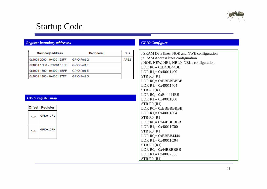
Startup Codep
Register boundary addresses GPIO Configure
SRAM Data lines NOE and NWE configuration SRAM Address lines configuration NOE NEW NE1 NBL0 NBL1 configuration LDR R0= 0xB4BB44BB LDR R1= 0x40011400STR R0[R1]LDR R0= 0xBBBBBBBB LDR R1= 0x40011404STR R0[R1]LDR R0 = 0xB44444BBLDR R0= 0xB44444BB LDR R1= 0x40011800STR R0[R1]LDR R0= 0xBBBBBBBB LDR R1= 0x40011804
GPIO register map
STR R0[R1]LDR R0= 0x44BBBBBB LDR R1= 0x40011C00STR R0[R1]LDR R0= 0xBBBB4444 LDR R1= 0x40011C04STR R0[R1]LDR R0= 0x44BBBBBBLDR R1= 0x40012000STR R0 [R1]
41
STR R0[R1]
GPIO Register g
Bit 8 FSMCEN FSMC clock enablePort configuration register low
Port configuration register high
Bits 2928 2524Bits 3130 2726 2322 1918 1514 1110 76 32 Bits 2928 25242120 1716 131298 54 10MODEy[10] Port x mode bits (y= 0 15)00 Input mode (reset state)01 Output mode max speed 10 MHz
Bits 3130 27262322 1918 15141110 76 32CNFy[10] Port x configuration bits (y= 0 15)In input mode (MODE[10]=00)00 Analog input mode01 Floating input (reset state)10 Input with pull-up pull-down
10 Output mode max speed 2 MHz11 Output mode max speed 50 MHz
11 ReservedIn output mode (MODE[10] gt00)00 General purpose output push-pull01 General purpose output Open-drain10 Alternate function output Push-pull11 Alternate function output Open-drain
42
11 Alternate function output Open drain
Startup Codep
FSMCregister map FSMC Configure
FSMC Configuration Enable FSMC Bank1_SRAM Bank
LDR R0= 0x00001011
LDR R1= 0xA0000000
STR R0[R1]
LDR R0= 0x00000200
LDR R1= 0xA0000004
STR R0[R1]
43
FSMC Register g
Bit 8 FSMCEN FSMC clock enableSRAMNOR-Flash chip-select control registers 1 (FSMC_BCR1)
Bit 12 WREN Write enable bitThis bit indicates whether write operations are enableddisabled in the bank by the FSMC0 Write operations are disabled in the bank by the FSMC an AHB error is reported1 Write operations are enabled for the bank by the FSMC (default after reset) p y ( )Bits 54 MWID Memory databus widthDefines the external memory device width valid for all type of memories00 8 bits01 16 bits (default after reset)10 reserved do not use10 reserved do not use11 reserved do not use Bit 0 MBKEN Memory bank enable bitEnables the memory bank After reset Bank1 is enabled all others are disabled Accessing adisabled bank causes an ERROR on AHB bus0 C di b k i di bl d0 Corresponding memory bank is disabled1 Corresponding memory bank is enabled
44
FSMC Register g
Bit 8 FSMCEN FSMC clock enableSRAMNOR-Flash chip-select timing registers 1 (FSMC_BTR1)
Bits 158 DATAST Data-phase duration0000 0000 Reserved0000 0001 DATAST phase duration = 2 times HCLK clock cycles0000 0010 DATAST phase duration = 3 times HCLK clock cycles1111 1111 DATAST phase duration = 256 times HCLK clock cycles (default value after reset)Bits 74 ADDHLD Address-hold phase duration0000 Reserved0001 ADDHLD phase duration = 2 times HCLK clock cycle0010 ADDHLD phase duration = 3 times HCLK clock cycle1111 ADDHLD phase duration = 16 times HCLK clock cycles (default value after reset)Bits 30 ADDSET Address setup phase durationThese bits are written by software to define the duration of the address setup phase (refer toFigure 162 to Figure 172) used in SRAMs ROMs and asynchronous NOR Flash0000 ADDSET phase duration = 1 times HCLK clock cycle1111 ADDSET phase duration = 16 times HCLK clock cycles (default value after reset)
45
實驗步驟
範例目錄架構
範例說明 範例說明
預設定義說明
46
範例目錄架構
範例目錄
測試映像檔 測試映像檔
含括檔
函式庫 函式庫
專案檔
原始碼 原始碼
47
範例說明
Embedded Software Side
Infinite loop
Display Result
Infinite loop while (1)if (((TabAddramp0xFFFFFF00) == 0x60000000) ampamp
((MSPValueamp0xFFFF0000) == 0x20000000))
Check operation
Check pointer value((MSPValueamp0xFFFF0000) == 0x20000000))
OK Turn on USERLED GPIO_SetBits(GPIOF GPIO_Pin_11)
else
Display Result
else KO Turn off USERLED
GPIO_ResetBits(GPIOF GPIO_Pin_11) Insert delay Delay(0xAFFFF)
如果Tab位置在0x600000且Stack pointer位置在0x2000 外部記憶體使用正常USERLED紅燈恆亮Delay(0xAFFFF)
Turn on USERLED GPIO_SetBits(GPIOF GPIO_Pin_11) Insert delay Delay(0xAFFFF)
紅燈恆亮
如果 b位置不在0 600000或Delay(0xAFFFF)
如果Tab位置不在0x600000或Stack pointer位置不在0x2000 外部記憶體使用異常USERLED紅燈閃爍
48
預設定義說明
DATA_IN_ExtSRAM EQU 1 E l SRAM C fi i External SRAM Configuration 0=gt DISABLE 1=gt ENABLE
u32 Tab[1024]宣告於外部 的記憶體 宣告於外部SRAM的記憶體
49
data memory存取控制實驗
實驗二
WU-YANGTechnology Co Ltd
實驗二練習
練習 取消RVMDK環境外部SRAM設定測試是否正常 取消RVMDK環境外部SRAM設定測試是否正常
修改DATA_IN_ExtSRAM EQU 0測試是否正常
修改外部 記憶體 b變數大小測試是否正常 修改外部SRAM記憶體Tab變數大小測試是否正常
51
Q amp A
WU-YANGTechnology Co Ltd
MIAT_STM32內部Flash存取控制實驗
WU-YANG
浯陽科技有限公司
Technology Co Ltd
Declared Version
Training Only
Declare
Document Number
Document Version 100
Release Date
Document Title MIAT_STM32 內部FLASH存取控制實驗
Exercise Time
Platform MIAT_STM32V2MIAT IOB V1PlatformMIAT IOBV1
Peripheral
Author WU-YANG Technology Co Ltd
2
實驗目的(一)( )
使用MIAT_STM32實驗板透過Flash memory interface (FLITF)控制內部Flash進行存取控制實驗並利用LED(FLITF)控制內部Flash進行存取控制實驗並利用LED確認存取是否正常
3
實驗原理
System architecture E b dd d Fl h Embedded Flash Features Memory map RVMDK環境設定
FLITF Flash module organization
Flash library function Development Flow ARM Configure
4
System architecturey
5
Embedded Flash
Features 256 Kb up to 256 Kbytes Memory organization the Flash memory is organized as a
main block and an information blockmain block and an information block Main memory block of size t 32 Kb 64 bit di id d i t 128 f 2 up to 32 Kb times 64 bits divided into 128 pages of 2
Kbytes Information block of size Information block of size 258 times 64 bits
6
Embedded Flash Memory mapy p
7
Flash Memoryy
8
RVMDK環境設定
STMF103ZC有256K Bytes的Flash位置由0x8000000至0x8040000
9
FLITF
Features R d i f i h f h b ff (2 64 bi d ) Read interface with prefetch buffer (2x64-bit words) Option byte Loader
l h i Flash Program Erase operation Read Write protection
10
Flash memory interfacey
11
Flash memory interface registery g
Bit 8 FSMCEN FSMC clock enableFlash status register (FLASH_SR)
Bits 316 Reserved must be kept clearedBit 5 EOP End of operation
Bit 2 PGERR Programming errorSet by hardware when an address to be programmed p
Set by hardware when a Flash operation (programming erase) is completed Reset by writing a 1Note EOP is asserted at the end of each successful
y p gcontains a value different from 0xFFFF before programmingReset by writing 1Note The STRT bit in the FLASH_CR register f f
program or erase operationBit 4 WRPRTERR Write protection errorSet by hardware when programming a write-protected address of the Flash memory
_ gshould be reset before starting a programmingoperationBit 1 Reserved must be kept clearedBit 0 BSY Busyp y
Reset by writing 1Bit 3 Reserved must be kept cleared
This indicates that a Flash operation is in progress This is set on the beginning of a Flash operation and reset when the operation finishes or when an error occurs
12
Flash memory interface registery g
Flash control register (FLASH_CR)
Bit 9 OPTWRE Option bytes write enableWhen set the option bytes can be programmed This
Bit 6 STRT StartThis bit triggers an ERASE operation when set This bit is set only
bit is set on writing the correct key sequence to the FLASH_OPTKEYR registerThis bit can be reset by softwareBit 8 Reserved must be kept clearedBit 7 LOCK Lock
by software and reset when the BSY bit is resetBit 5 OPTER Option byte eraseOption byte erase chosenBit 4 OPTPG Option byte programmingOption byte programming chosenBit 7 LOCK Lock
Write to 1 only When it is set it indicates that the FPEC and FLASH_CR are locked This bit is reset by hardware after detecting the unlock sequenceIn the event of unsuccessful unlock operation this bit remains set until the next reset
p y p g gBit 3 Reserved must be kept clearedBit 2 MER Mass eraseErase of all user pages chosenBit 1 PER Page erasePage Erase chosenremains set until the next reset Page Erase chosenBit 0 PG ProgrammingFlash programming chosen
13
Main Flash memory programmingy p g g
14
Flash memory Page Erasey g
15
Flash memory Mass Erasey
16
Option byte programmingp y p g g
17
Option byte Erasep y
18
FLASH library functiony
19
FLASH library functiony
20
Development Flowp
Embedded Software Side
int main(void)
Bootup STM32F10x
ProgrammingBootupSTM32F10x RCC Configure
NVIC Configure
int main(void)ifdef DEBUGdebug()
endifendif
FLASHStatus = FLASH_COMPLETEMemoryProgramStatus = PASSEDData = 0x15041975
GPIO Configure
Data = 0x15041975
RCC Configuration RCC_Configuration()
Flash memory RW operation FLASH Unlock
FLASH ClearFlag NVIC Configuration NVIC_Configuration()
GPIO Configuration
FLASH ClearFlag
FLASH ErasePage
FLASH ProgramWord GPIO Configuration GPIO_Configuration()
helliphelliphelliphelliphelliphelliphelliphelliphelliphelliphelliphelliphelliphelliphelliphelliphellipDisplay Result
Check content
21
實驗步驟
範例目錄架構
範例說明 範例說明
預設定義說明
燒錄 燒錄MIAT_STM32
22
範例目錄架構
範例目錄
測試映像檔 測試映像檔
含括檔
函式庫 函式庫
專案檔
原始碼 原始碼
23
範例說明
Function name Description
Unlock the Flash Program Erase controller FLASH_Unlock()
D fi h b f b d
Flash FwLib Functions List
Function name Description
FLASH_Unlock Unlocks the FLASH Program Erase Controller
FLASH_ClearFlag Clears the FLASH pending fl
Define the number of page to be erased NbrOfPage = (EndAddr - StartAddr) FLASH_PAGE_SIZE
Clear All pending flags FLASH_ClearFlag(FLASH_FLAG_BSY | FLASH_FLAG_EOP | FLASH_FLAG_PGERR |
FLASH FLAG WRPRTERR)flags
FLASH_ErasePage Erases a specified FLASH page
FLASH_ProgramWord Programs a word at a specified
_ _ )
Erase the FLASH pages for(EraseCounter = 0 (EraseCounter lt NbrOfPage) ampamp (FLASHStatus ==
FLASH_COMPLETE) EraseCounter++)FLASHStatus = FLASH ErasePage(StartAddr + (FLASH PAGE SIZE EraseCounter))address FLASHStatus = FLASH_ErasePage(StartAddr + (FLASH_PAGE_SIZE EraseCounter))
FLASH Word program of data 0x15041979 at addresses defined by StartAddr and EndAddrAddress = StartAddr
while((Address lt EndAddr) ampamp (FLASHStatus == FLASH_COMPLETE))FLASHStatus = FLASH_ProgramWord(Address Data)Address = Address + 4
24
範例說明
Embedded Software Side
Check the corectness of written data
Display Result
Check the corectness of written data Address = StartAddr
while((Address lt EndAddr) ampamp (MemoryProgramStatus = FAILED))if(((vu32) Address) = Data)
Flash memory RW operation
MemoryProgramStatus = FAILED
Address += 4
Check content
Display Result while (1)if (MemoryProgramStatus == PASSED) OK Turn on USERLED GPIO_SetBits(GPIOF GPIO_Pin_11)
Display Result
else KO Turn off USERLED GPIO_ResetBits(GPIOF GPIO_Pin_11) Insert delay Delay(0xAFFFF)
如果寫入與讀取Flash內容相同Flash記憶體使用正常USERLED紅燈恆亮
Turn on USERLED GPIO_SetBits(GPIOF GPIO_Pin_11) Insert delay Delay(0xAFFFF)
如果寫入與讀取Flash內容不同Flash記憶體使用異常USERLED紅燈閃爍
25
預設定義說明
define StartAddr ((u32)0x08008000) 定義Flash使用起始點 定義Flash使用起始點
使用起始點必需大於0x8003000 + Code Size 附註 0x8000000~0x8003000為DFU程式區塊使用此區塊
將造成無法燒錄程式
Code Size可由產生的HEX檔得知
d fi E dAdd (( 32)0 0800C000) define EndAddr ((u32)0x0800C000) 定義Flash使用結束點
使用起始點必需小於0x8040000使用起始點必需小於
Data = 0x15041975 寫入資料
32Bit define FLASH_PAGE_SIZE ((u16)0x800)
每一個Page有2KByte26
每一個Page有2KByte
Intel HEX Format
aaaa tt dd cc
field Description
the colon that starts every Intel HEX record
the record-length field that represents the number of data bytes (dd) in the record
aaaa the address field that represents the starting address for subsequent data in the record
tt the field that represents the HEX record type which may be one of the following00 - data record01 - end-of-file record02 - extended segment address recordg04 - extended linear address record
dd a data field that represents one byte of data A record may have multiple data bytes The number of data bytes in the record must match the number specified by the field
cc the checksum field that represents the checksum of the record The checksum is calculated by summing the values of all hexadecimal digit pairs in the record modulo 256 and taking the twos complement
27
HEX Examplep
020000040800F2103000001814002045310008D9340008CD340008D8103000001814002045310008D9340008CD340008D8helliphelliphellip1038200042370008000000000000000000000000170C3830000000000000000000000000008C
資料填入起始位置為
0C3830000000000000000000000000008C04000005080031318D00000001FF
資料填入起始位置為0x08003000 每一行有0x10(16)個Bytes 最後一筆資料為
資料結束點為0x0803383004000005080031318D
(0x08003830 -0x08000000)0x800 = 7 需以0x800為單位所以使用的位置起點為0x08004000
28
燒錄MIAT STM32_
Rebuilder all target files產生HEX DFU Fil M 轉換HEX產生DFU DFU File Manager轉換HEX產生DFU DfuSe Demonstration燒錄DFU d Leave DFU mode
29
內部Flash存取控制實驗
實驗一
WU-YANGTechnology Co Ltd
實驗一練習
注意 請使用預設0 08008000之後的位置 避免覆蓋DFU 請使用預設0x08008000之後的位置避免覆蓋DFU
與使用者程式碼區塊
練習 練習 修改存取位置測試是否正常
修改寫入資料測試是否正常 修改寫入資料測試是否正常
修改寫入資料後取消FLASH_Unlock測試是否正常
修改寫入資料後取消FLASH E P 測試是否正 修改寫入資料後取消FLASH_ErasePage測試是否正常
31
實驗目的(二)( )
使用MIAT_STM32實驗板透過Flash memory interface (FLITF)控制內部Flash進行存取控制實驗並利用SW(FLITF)控制內部Flash進行存取控制實驗並利用SWKEY決定資料寫入與讀取LCD顯示狀態
32
實驗原理
System requirement E b dd d Fl h Embedded Flash LCD KEY SW
Development Flow ARM Configure
33
Development Flowp
Embedded Software Side
int main(void)
Bootup STM32F10x
ProgrammingBootupSTM32F10x RCC Configure
NVIC Configure
int main(void)ifdef DEBUGdebug()
endif
FLASHStatus = FLASH_COMPLETE
RCC Configuration RCC Configuration()
GPIO Configure
BasicIO Configure_ g ()
NVIC Configuration NVIC_Configuration()
GPIO Configuration Flash memory RW ti
lcd Configure
GPIO Configuration GPIO_Configuration()
Init_BasicIO()
l d i i () LCD I i i li i
RW operation
Example
FLASH Unlock
FLASH ClearFlag
lcd_init() LCD Initialization
helliphelliphelliphelliphelliphelliphelliphelliphelliphelliphelliphelliphelliphelliphelliphelliphelliphelliphelliphelliphelliphelliphellip
p
34
硬體電路配置
Mapping Table
Num MIAT_STM32V2 MIAT_IOBV1 Num MIAT_STM32V2 MIAT_IOBV1
1 PC8 (326) SW1 10 PE6 (15) LCD_EN2 PC9 (327) SW2 11 PF6 (118) LCD RW ( ) ( ) _3 PC10 (43) SW3 12 PF7 (119) LCD_RS 4 PC11 (44) SW4 13 PF8(120) LCD_D4 5 PB5 (427) KEY1 14 PF9 (121) LCD_D5 6 PB6 (428) KEY2 15 PF10 (122) LCD_D6 7 PB7 (429) KEY3 16 PF11 (213) LCD_D7 8 PB8 (431) KEY4 17 VDD (236) VCC33V 9 VCC5V (1 36) VCC5V 18 GND (1 35) GND9 VCC5V (136) VCC5V 18 GND (135) GND
35
實驗步驟
範例目錄架構
範例說明 範例說明
預設定義說明
36
範例目錄架構
範例目錄
測試映像檔 測試映像檔
含括檔
函式庫 函式庫
專案檔
原始碼 原始碼
37
範例說明
Embedded Software Side
lcd clear()
FLASH memory RW operation
lcd_clear()lcd_print (MIAT_STM32 DEMO )
Unlock the Flash Program Erase controller FLASH_Unlock()
Flash memory RW operation
FLASH Unlock
Clear All pending flags FLASH_ClearFlag(FLASH_FLAG_BSY | FLASH_FLAG_EOP | FLASH_FLAG_PGERR |
FLASH_FLAG_WRPRTERR)
while(1)
Example
FLASH ClearFlag
( )
KEY_Buffer=Key_Scan()set_cursor (0 1)lcd_print (SW Value = 0x)lcd putchar(((SWamp0x7)+0x30))lcd_putchar(((SWamp0x7)+0x30))if(KEY_Buffer==1)Address=(StartAddr|(SWltlt12))set_cursor (0 0)lcd_print (Set Addr = 0x)
掃描KEY是否按下與顯示SW數值LCD Line2顯示SW Value = 0x(SW)
lcd_putchar(((SWamp0x7)+0x30))lcd_print ( )
如果KEY1按下記錄SW數值至Address LCD Line1顯示Set Adde = 0x(Address)
38
範例說明
Embedded Software Side
else if(KEY Buffer==2)
FLASH memory RW operation
else if(KEY_Buffer==2)
Erase the FLASH pages FLASHStatus = FLASH_ErasePage(Address)
FLASH Word program of data at addresses defined by SW
SRAM memory RW operation
p g yFLASHStatus = FLASH_ProgramWord(Address (SWamp0x7))
set_cursor (0 0)lcd_print (Write 0x)lcd_putchar(((SWamp0x7)+0x30))l d i t ( t 0 )
Example如果KEY2按下清除Address所處區塊並寫入SW數值 lcd_print ( at 0x)
lcd_putchar((((Addressgtgt12)amp0x7)+0x30))else if(KEY_Buffer==3)
Data=(u16 )Address
所處區塊並寫入SW數值LCD Line1顯示Write 0x(SW) at 0x(Adddress)
Data (u16 )Addressset_cursor (0 0)lcd_print (Addr 0x)lcd_putchar((((Addressgtgt12)amp0x7)+0x30))lcd_print ( = 0x)lcd_putchar(((Dataamp0x7)+0x30))lcd_print ( )
如果KEY3按下讀取Address紀錄數值LCD Line1顯示Addr 0x(Adddress) = 0x
39
預設定義說明
define StartAddr ((u32)0x08020000) 定義Flash使用起始點 定義Flash使用起始點
使用起始點必需大於0x8003000 + Code Size 附註 0x8000000~0x8003000為DFU程式區塊使用此區塊
將造成無法燒錄程式
Code Size可由產生的HEX檔得知
32 Add 0 08020000 u32 Address = 0x08020000 定義Address初始值
初始值必需與Flash使用起始點相同初始值必需與 使用起始點相同
Address=(StartAddr|(SWltlt12)) Example StartAddr = 0x08020000 SW = 1 Address = 0x08021000
StartAddr = 0x08020000 SW = 7 Address = 0x08027000 StartAddr|(7ltlt12)必需小於0x8040000
40
使用者界面與Flash存取控制實驗
實驗二
WU-YANGTechnology Co Ltd
實驗二練習
注意 請使用預設0 08020000之後的位置 避免覆蓋DFU 請使用預設0x08020000之後的位置避免覆蓋DFU
與使用者程式碼區塊
練習 練習 利用SW與KEY測試Flash寫入與讀取是否正常
Fl h寫入後電源關閉 再開啟後寫入資料是否仍存 Flash寫入後電源關閉再開啟後寫入資料是否仍存在
修改存取位置測試是否正常 修改存取位置測試是否正常
42
實驗目的(三)( )
使用MIAT_STM32實驗板透過Flash memory interface (FLITF)控制內部Flash進行存取控制實驗並藉由填入(FLITF)控制內部Flash進行存取控制實驗並藉由填入Option Bytes 設定寫入鎖定保護Page鎖定不被覆蓋
43
Development Flowp
Embedded Software Side
int main(void)
Bootup STM32F10x
ProgrammingBootupSTM32F10x RCC Configure
NVIC Configure
int main(void)ifdef DEBUGdebug()
endifendif
FLASHStatus = FLASH_COMPLETEMemoryProgramStatus = PASSEDData = 0x1753
GPIO Configure
Data = 0x1753
RCC Configuration RCC_Configuration()
Flash memory RW operation FLASH Unlock
FLASH ClearFlag NVIC Configuration NVIC_Configuration()
GPIO Configuration
FLASH ClearFlag
FLASH ErasePage
FLASH ProgramHalfWord GPIO Configuration GPIO_Configuration()
Display Result
Check content
44
helliphelliphelliphelliphelliphelliphelliphelliphelliphelliphelliphelliphelliphelliphelliphelliphelliphelliphellip
實驗步驟
範例目錄架構
範例說明 範例說明
預設定義說明
45
範例目錄架構
範例目錄
測試映像檔 測試映像檔
含括檔
函式庫 函式庫
專案檔
原始碼 原始碼
46
範例說明
Function name Description
Unlock the Flash Program Erase controller FLASH_Unlock()
Define the number of page to be erased
Flash FwLib Functions List
Function name Description
FLASH_Unlock Unlocks the FLASH Program Erase Controller
FLASH_ClearFlag Clears the FLASH pending fl
Define the number of page to be erased NbrOfPage = (EndAddr ‐ StartAddr) FLASH_PAGE_SIZE
FLASH_ClearFlag(FLASH_FLAG_BSY | FLASH_FLAG_EOP|FLASH_FLAG_PGERR |FLASH_FLAG_WRPRTERR)
Get pages write protection status flags
FLASH_EraseOptionBytes
Erases the FLASH option bytes
FLASH_EnableWritePro Write protects the desired
p g pWRPR_Value = FLASH_GetWriteProtectionOptionByte()ProtectedPages = WRPR_Value amp 0x000000C0
ifdef WriteProtection_Disableif (ProtectedPages == 0x00) Pages are write protected
tection pages
NVIC_GenerateSystemReset
Generate a system reset
Disable the write protection FLASHStatus = FLASH_EraseOptionBytes() Generate System Reset to load the new option byte values NVIC_GenerateSystemReset()
elseifdef WriteProtection Enableifdef WriteProtection_Enableif (ProtectedPages = 0x00) Pages not write protected
FLASHStatus = FLASH_EraseOptionBytes() Enable the pages write protection FLASHStatus = FLASH_EnableWriteProtection(FLASH_WRProt_Pages12to13
|FLASH WRProt Pages14to15)|FLASH_WRProt_Pages14to15) Generate System Reset to load the new option byte values NVIC_GenerateSystemReset()
endifendif
47
範例說明
if (ProtectedPages = 0x00) Clear All pending flags
Flash FwLib Functions List
Function name DescriptionFLASH_ClearFlag(FLASH_FLAG_BSY |
FLASH_FLAG_EOP|FLASH_FLAG_PGERR |FLASH_FLAG_WRPRTERR)
erase the FLASH pages for(EraseCounter = 0 (EraseCounter lt NbrOfPage) ampamp (FLASHStatus ==
Function name Description
FLASH_ErasePage Erases a specified FLASH page
FLASH_ProgramHalfWod
Programs a half word at a ifi d dd FLASH_COMPLETE) EraseCounter++)
FLASHStatus = FLASH_ErasePage(StartAddr + (FLASH_PAGE_SIZE
EraseCounter))
rd specified address
FLASH Half Word program of data 0x1753 at addresses defined by StartAddrand EndAddr
Address = StartAddr
hil ((Add E dAdd ) ampamp (FLASHSt t FLASH COMPLETE))while((Address lt EndAddr) ampamp (FLASHStatus == FLASH_COMPLETE))
FLASHStatus = FLASH_ProgramHalfWord(Address Data)Address = Address + 2
48
範例說明
Embedded Software Side
Check the corectness of written data
Display Result
Check the corectness of written data Address = StartAddr
while((Address lt EndAddr) ampamp (MemoryProgramStatus = FAILED))if(((vu16) Address) = Data)
Flash memory RW operation
MemoryProgramStatus = FAILED
Address += 2
Check content
Display Result while (1)if (MemoryProgramStatus == PASSED) OK Turn on USERLED GPIO_SetBits(GPIOF GPIO_Pin_11)
Display Result
else KO Turn off USERLED GPIO_ResetBits(GPIOF GPIO_Pin_11) Insert delay Delay(0xAFFFF)
如果寫入與讀取Flash內容相同Flash記憶體可以寫入USERLED紅燈恆亮
Turn on USERLED GPIO_SetBits(GPIOF GPIO_Pin_11) Insert delay Delay(0xAFFFF)
如果寫入與讀取Flash內容不同Flash記憶體不能寫入USERLED紅燈閃爍
49
預設定義說明
define StartAddr ((u32) 0x08006000) 定義Flash使用起始點 定義Flash使用起始點
使用起始點必需大於0x8003000 + Code Size 附註 0x8000000~0x8003000為DFU程式區塊使用此區塊
將造成無法燒錄程式
Code Size可由產生的HEX檔得知
d fi E dAdd (( 32) 0 08008000) define EndAddr ((u32) 0x08008000) 定義Flash使用結束點
使用起始點必需小於0x8040000使用起始點必需小於
Data = 0x1753 寫入資料
16Bit define FLASH_PAGE_SIZE ((u16)0x800) 每一個Page有2KByte
50
每一個Page有2KByte
預設定義說明
define WriteProtection_Enable U hi li E bl W i P i Uncomment this line to Enable Write Protection
define WriteProtection_Disablehi li i bl i i Uncomment this line to Disable Write Protection
FLASH_EnableWriteProtection設定影響 個 設定影響2個Page FLASH_WRProt_Pages0to1 FLASH_WRProt_Pages1to2 helliphellip FLASH_WRProt_Pages60to61
設定影響多個Page FLASH_WRProt_Pages62to255
51
FLASH EnableWriteProtection_
Example
位置0x08006000 ~ 0x08007000每一個Page有0x800ByteStartPage = (0x08006000-0x08000000)0x800 = 12EndPage = ((0x08007000-0x08000000)0x800)-1 = 13執行執行FLASH_EnableWriteProtection(FLASH_WRProt_Pages12to13)將影響Pages12 Pages13
52
內部Flash寫入鎖定存取控制實驗
實驗三
WU-YANGTechnology Co Ltd
實驗三練習
注意 請使用預設0 08006000之後的位置 避免覆蓋DFU 請使用預設0x08006000之後的位置避免覆蓋DFU
與使用者程式碼區塊
更改寫入位置測試寫入鎖定時需同時更改 更改寫入位置測試寫入鎖定時需同時更改FLASH_EnableWriteProtection鎖定之Page
練習 練習 打開define WriteProtection_Enable測試是否可寫入
打開define WriteProtection Disable測試是否可寫入 打開define WriteProtection_Disable測試是否可寫入
修改存取位置測試是否正常
修改寫入資料測試是否正常 修改寫入資料測試是否正常
54
Q amp A
WU-YANGTechnology Co Ltd

FSMC Register g
Bit 8 FSMCEN FSMC clock enableSRAMNOR-Flash chip-select control registers 1 (FSMC_BCR1)
Bit 12 WREN Write enable bitThis bit indicates whether write operations are enableddisabled in the bank by the FSMC0 Write operations are disabled in the bank by the FSMC an AHB error is reported1 Write operations are enabled for the bank by the FSMC (default after reset) p y ( )Bits 54 MWID Memory databus widthDefines the external memory device width valid for all type of memories00 8 bits01 16 bits (default after reset)10 reserved do not use10 reserved do not use11 reserved do not use Bit 0 MBKEN Memory bank enable bitEnables the memory bank After reset Bank1 is enabled all others are disabled Accessing adisabled bank causes an ERROR on AHB bus0 C di b k i di bl d0 Corresponding memory bank is disabled1 Corresponding memory bank is enabled
44
FSMC Register g
Bit 8 FSMCEN FSMC clock enableSRAMNOR-Flash chip-select timing registers 1 (FSMC_BTR1)
Bits 158 DATAST Data-phase duration0000 0000 Reserved0000 0001 DATAST phase duration = 2 times HCLK clock cycles0000 0010 DATAST phase duration = 3 times HCLK clock cycles1111 1111 DATAST phase duration = 256 times HCLK clock cycles (default value after reset)Bits 74 ADDHLD Address-hold phase duration0000 Reserved0001 ADDHLD phase duration = 2 times HCLK clock cycle0010 ADDHLD phase duration = 3 times HCLK clock cycle1111 ADDHLD phase duration = 16 times HCLK clock cycles (default value after reset)Bits 30 ADDSET Address setup phase durationThese bits are written by software to define the duration of the address setup phase (refer toFigure 162 to Figure 172) used in SRAMs ROMs and asynchronous NOR Flash0000 ADDSET phase duration = 1 times HCLK clock cycle1111 ADDSET phase duration = 16 times HCLK clock cycles (default value after reset)
45
實驗步驟
範例目錄架構
範例說明 範例說明
預設定義說明
46
範例目錄架構
範例目錄
測試映像檔 測試映像檔
含括檔
函式庫 函式庫
專案檔
原始碼 原始碼
47
範例說明
Embedded Software Side
Infinite loop
Display Result
Infinite loop while (1)if (((TabAddramp0xFFFFFF00) == 0x60000000) ampamp
((MSPValueamp0xFFFF0000) == 0x20000000))
Check operation
Check pointer value((MSPValueamp0xFFFF0000) == 0x20000000))
OK Turn on USERLED GPIO_SetBits(GPIOF GPIO_Pin_11)
else
Display Result
else KO Turn off USERLED
GPIO_ResetBits(GPIOF GPIO_Pin_11) Insert delay Delay(0xAFFFF)
如果Tab位置在0x600000且Stack pointer位置在0x2000 外部記憶體使用正常USERLED紅燈恆亮Delay(0xAFFFF)
Turn on USERLED GPIO_SetBits(GPIOF GPIO_Pin_11) Insert delay Delay(0xAFFFF)
紅燈恆亮
如果 b位置不在0 600000或Delay(0xAFFFF)
如果Tab位置不在0x600000或Stack pointer位置不在0x2000 外部記憶體使用異常USERLED紅燈閃爍
48
預設定義說明
DATA_IN_ExtSRAM EQU 1 E l SRAM C fi i External SRAM Configuration 0=gt DISABLE 1=gt ENABLE
u32 Tab[1024]宣告於外部 的記憶體 宣告於外部SRAM的記憶體
49
data memory存取控制實驗
實驗二
WU-YANGTechnology Co Ltd
實驗二練習
練習 取消RVMDK環境外部SRAM設定測試是否正常 取消RVMDK環境外部SRAM設定測試是否正常
修改DATA_IN_ExtSRAM EQU 0測試是否正常
修改外部 記憶體 b變數大小測試是否正常 修改外部SRAM記憶體Tab變數大小測試是否正常
51
Q amp A
WU-YANGTechnology Co Ltd
MIAT_STM32內部Flash存取控制實驗
WU-YANG
浯陽科技有限公司
Technology Co Ltd
Declared Version
Training Only
Declare
Document Number
Document Version 100
Release Date
Document Title MIAT_STM32 內部FLASH存取控制實驗
Exercise Time
Platform MIAT_STM32V2MIAT IOB V1PlatformMIAT IOBV1
Peripheral
Author WU-YANG Technology Co Ltd
2
實驗目的(一)( )
使用MIAT_STM32實驗板透過Flash memory interface (FLITF)控制內部Flash進行存取控制實驗並利用LED(FLITF)控制內部Flash進行存取控制實驗並利用LED確認存取是否正常
3
實驗原理
System architecture E b dd d Fl h Embedded Flash Features Memory map RVMDK環境設定
FLITF Flash module organization
Flash library function Development Flow ARM Configure
4
System architecturey
5
Embedded Flash
Features 256 Kb up to 256 Kbytes Memory organization the Flash memory is organized as a
main block and an information blockmain block and an information block Main memory block of size t 32 Kb 64 bit di id d i t 128 f 2 up to 32 Kb times 64 bits divided into 128 pages of 2
Kbytes Information block of size Information block of size 258 times 64 bits
6
Embedded Flash Memory mapy p
7
Flash Memoryy
8
RVMDK環境設定
STMF103ZC有256K Bytes的Flash位置由0x8000000至0x8040000
9
FLITF
Features R d i f i h f h b ff (2 64 bi d ) Read interface with prefetch buffer (2x64-bit words) Option byte Loader
l h i Flash Program Erase operation Read Write protection
10
Flash memory interfacey
11
Flash memory interface registery g
Bit 8 FSMCEN FSMC clock enableFlash status register (FLASH_SR)
Bits 316 Reserved must be kept clearedBit 5 EOP End of operation
Bit 2 PGERR Programming errorSet by hardware when an address to be programmed p
Set by hardware when a Flash operation (programming erase) is completed Reset by writing a 1Note EOP is asserted at the end of each successful
y p gcontains a value different from 0xFFFF before programmingReset by writing 1Note The STRT bit in the FLASH_CR register f f
program or erase operationBit 4 WRPRTERR Write protection errorSet by hardware when programming a write-protected address of the Flash memory
_ gshould be reset before starting a programmingoperationBit 1 Reserved must be kept clearedBit 0 BSY Busyp y
Reset by writing 1Bit 3 Reserved must be kept cleared
This indicates that a Flash operation is in progress This is set on the beginning of a Flash operation and reset when the operation finishes or when an error occurs
12
Flash memory interface registery g
Flash control register (FLASH_CR)
Bit 9 OPTWRE Option bytes write enableWhen set the option bytes can be programmed This
Bit 6 STRT StartThis bit triggers an ERASE operation when set This bit is set only
bit is set on writing the correct key sequence to the FLASH_OPTKEYR registerThis bit can be reset by softwareBit 8 Reserved must be kept clearedBit 7 LOCK Lock
by software and reset when the BSY bit is resetBit 5 OPTER Option byte eraseOption byte erase chosenBit 4 OPTPG Option byte programmingOption byte programming chosenBit 7 LOCK Lock
Write to 1 only When it is set it indicates that the FPEC and FLASH_CR are locked This bit is reset by hardware after detecting the unlock sequenceIn the event of unsuccessful unlock operation this bit remains set until the next reset
p y p g gBit 3 Reserved must be kept clearedBit 2 MER Mass eraseErase of all user pages chosenBit 1 PER Page erasePage Erase chosenremains set until the next reset Page Erase chosenBit 0 PG ProgrammingFlash programming chosen
13
Main Flash memory programmingy p g g
14
Flash memory Page Erasey g
15
Flash memory Mass Erasey
16
Option byte programmingp y p g g
17
Option byte Erasep y
18
FLASH library functiony
19
FLASH library functiony
20
Development Flowp
Embedded Software Side
int main(void)
Bootup STM32F10x
ProgrammingBootupSTM32F10x RCC Configure
NVIC Configure
int main(void)ifdef DEBUGdebug()
endifendif
FLASHStatus = FLASH_COMPLETEMemoryProgramStatus = PASSEDData = 0x15041975
GPIO Configure
Data = 0x15041975
RCC Configuration RCC_Configuration()
Flash memory RW operation FLASH Unlock
FLASH ClearFlag NVIC Configuration NVIC_Configuration()
GPIO Configuration
FLASH ClearFlag
FLASH ErasePage
FLASH ProgramWord GPIO Configuration GPIO_Configuration()
helliphelliphelliphelliphelliphelliphelliphelliphelliphelliphelliphelliphelliphelliphelliphelliphellipDisplay Result
Check content
21
實驗步驟
範例目錄架構
範例說明 範例說明
預設定義說明
燒錄 燒錄MIAT_STM32
22
範例目錄架構
範例目錄
測試映像檔 測試映像檔
含括檔
函式庫 函式庫
專案檔
原始碼 原始碼
23
範例說明
Function name Description
Unlock the Flash Program Erase controller FLASH_Unlock()
D fi h b f b d
Flash FwLib Functions List
Function name Description
FLASH_Unlock Unlocks the FLASH Program Erase Controller
FLASH_ClearFlag Clears the FLASH pending fl
Define the number of page to be erased NbrOfPage = (EndAddr - StartAddr) FLASH_PAGE_SIZE
Clear All pending flags FLASH_ClearFlag(FLASH_FLAG_BSY | FLASH_FLAG_EOP | FLASH_FLAG_PGERR |
FLASH FLAG WRPRTERR)flags
FLASH_ErasePage Erases a specified FLASH page
FLASH_ProgramWord Programs a word at a specified
_ _ )
Erase the FLASH pages for(EraseCounter = 0 (EraseCounter lt NbrOfPage) ampamp (FLASHStatus ==
FLASH_COMPLETE) EraseCounter++)FLASHStatus = FLASH ErasePage(StartAddr + (FLASH PAGE SIZE EraseCounter))address FLASHStatus = FLASH_ErasePage(StartAddr + (FLASH_PAGE_SIZE EraseCounter))
FLASH Word program of data 0x15041979 at addresses defined by StartAddr and EndAddrAddress = StartAddr
while((Address lt EndAddr) ampamp (FLASHStatus == FLASH_COMPLETE))FLASHStatus = FLASH_ProgramWord(Address Data)Address = Address + 4
24
範例說明
Embedded Software Side
Check the corectness of written data
Display Result
Check the corectness of written data Address = StartAddr
while((Address lt EndAddr) ampamp (MemoryProgramStatus = FAILED))if(((vu32) Address) = Data)
Flash memory RW operation
MemoryProgramStatus = FAILED
Address += 4
Check content
Display Result while (1)if (MemoryProgramStatus == PASSED) OK Turn on USERLED GPIO_SetBits(GPIOF GPIO_Pin_11)
Display Result
else KO Turn off USERLED GPIO_ResetBits(GPIOF GPIO_Pin_11) Insert delay Delay(0xAFFFF)
如果寫入與讀取Flash內容相同Flash記憶體使用正常USERLED紅燈恆亮
Turn on USERLED GPIO_SetBits(GPIOF GPIO_Pin_11) Insert delay Delay(0xAFFFF)
如果寫入與讀取Flash內容不同Flash記憶體使用異常USERLED紅燈閃爍
25
預設定義說明
define StartAddr ((u32)0x08008000) 定義Flash使用起始點 定義Flash使用起始點
使用起始點必需大於0x8003000 + Code Size 附註 0x8000000~0x8003000為DFU程式區塊使用此區塊
將造成無法燒錄程式
Code Size可由產生的HEX檔得知
d fi E dAdd (( 32)0 0800C000) define EndAddr ((u32)0x0800C000) 定義Flash使用結束點
使用起始點必需小於0x8040000使用起始點必需小於
Data = 0x15041975 寫入資料
32Bit define FLASH_PAGE_SIZE ((u16)0x800)
每一個Page有2KByte26
每一個Page有2KByte
Intel HEX Format
aaaa tt dd cc
field Description
the colon that starts every Intel HEX record
the record-length field that represents the number of data bytes (dd) in the record
aaaa the address field that represents the starting address for subsequent data in the record
tt the field that represents the HEX record type which may be one of the following00 - data record01 - end-of-file record02 - extended segment address recordg04 - extended linear address record
dd a data field that represents one byte of data A record may have multiple data bytes The number of data bytes in the record must match the number specified by the field
cc the checksum field that represents the checksum of the record The checksum is calculated by summing the values of all hexadecimal digit pairs in the record modulo 256 and taking the twos complement
27
HEX Examplep
020000040800F2103000001814002045310008D9340008CD340008D8103000001814002045310008D9340008CD340008D8helliphelliphellip1038200042370008000000000000000000000000170C3830000000000000000000000000008C
資料填入起始位置為
0C3830000000000000000000000000008C04000005080031318D00000001FF
資料填入起始位置為0x08003000 每一行有0x10(16)個Bytes 最後一筆資料為
資料結束點為0x0803383004000005080031318D
(0x08003830 -0x08000000)0x800 = 7 需以0x800為單位所以使用的位置起點為0x08004000
28
燒錄MIAT STM32_
Rebuilder all target files產生HEX DFU Fil M 轉換HEX產生DFU DFU File Manager轉換HEX產生DFU DfuSe Demonstration燒錄DFU d Leave DFU mode
29
內部Flash存取控制實驗
實驗一
WU-YANGTechnology Co Ltd
實驗一練習
注意 請使用預設0 08008000之後的位置 避免覆蓋DFU 請使用預設0x08008000之後的位置避免覆蓋DFU
與使用者程式碼區塊
練習 練習 修改存取位置測試是否正常
修改寫入資料測試是否正常 修改寫入資料測試是否正常
修改寫入資料後取消FLASH_Unlock測試是否正常
修改寫入資料後取消FLASH E P 測試是否正 修改寫入資料後取消FLASH_ErasePage測試是否正常
31
實驗目的(二)( )
使用MIAT_STM32實驗板透過Flash memory interface (FLITF)控制內部Flash進行存取控制實驗並利用SW(FLITF)控制內部Flash進行存取控制實驗並利用SWKEY決定資料寫入與讀取LCD顯示狀態
32
實驗原理
System requirement E b dd d Fl h Embedded Flash LCD KEY SW
Development Flow ARM Configure
33
Development Flowp
Embedded Software Side
int main(void)
Bootup STM32F10x
ProgrammingBootupSTM32F10x RCC Configure
NVIC Configure
int main(void)ifdef DEBUGdebug()
endif
FLASHStatus = FLASH_COMPLETE
RCC Configuration RCC Configuration()
GPIO Configure
BasicIO Configure_ g ()
NVIC Configuration NVIC_Configuration()
GPIO Configuration Flash memory RW ti
lcd Configure
GPIO Configuration GPIO_Configuration()
Init_BasicIO()
l d i i () LCD I i i li i
RW operation
Example
FLASH Unlock
FLASH ClearFlag
lcd_init() LCD Initialization
helliphelliphelliphelliphelliphelliphelliphelliphelliphelliphelliphelliphelliphelliphelliphelliphelliphelliphelliphelliphelliphelliphellip
p
34
硬體電路配置
Mapping Table
Num MIAT_STM32V2 MIAT_IOBV1 Num MIAT_STM32V2 MIAT_IOBV1
1 PC8 (326) SW1 10 PE6 (15) LCD_EN2 PC9 (327) SW2 11 PF6 (118) LCD RW ( ) ( ) _3 PC10 (43) SW3 12 PF7 (119) LCD_RS 4 PC11 (44) SW4 13 PF8(120) LCD_D4 5 PB5 (427) KEY1 14 PF9 (121) LCD_D5 6 PB6 (428) KEY2 15 PF10 (122) LCD_D6 7 PB7 (429) KEY3 16 PF11 (213) LCD_D7 8 PB8 (431) KEY4 17 VDD (236) VCC33V 9 VCC5V (1 36) VCC5V 18 GND (1 35) GND9 VCC5V (136) VCC5V 18 GND (135) GND
35
實驗步驟
範例目錄架構
範例說明 範例說明
預設定義說明
36
範例目錄架構
範例目錄
測試映像檔 測試映像檔
含括檔
函式庫 函式庫
專案檔
原始碼 原始碼
37
範例說明
Embedded Software Side
lcd clear()
FLASH memory RW operation
lcd_clear()lcd_print (MIAT_STM32 DEMO )
Unlock the Flash Program Erase controller FLASH_Unlock()
Flash memory RW operation
FLASH Unlock
Clear All pending flags FLASH_ClearFlag(FLASH_FLAG_BSY | FLASH_FLAG_EOP | FLASH_FLAG_PGERR |
FLASH_FLAG_WRPRTERR)
while(1)
Example
FLASH ClearFlag
( )
KEY_Buffer=Key_Scan()set_cursor (0 1)lcd_print (SW Value = 0x)lcd putchar(((SWamp0x7)+0x30))lcd_putchar(((SWamp0x7)+0x30))if(KEY_Buffer==1)Address=(StartAddr|(SWltlt12))set_cursor (0 0)lcd_print (Set Addr = 0x)
掃描KEY是否按下與顯示SW數值LCD Line2顯示SW Value = 0x(SW)
lcd_putchar(((SWamp0x7)+0x30))lcd_print ( )
如果KEY1按下記錄SW數值至Address LCD Line1顯示Set Adde = 0x(Address)
38
範例說明
Embedded Software Side
else if(KEY Buffer==2)
FLASH memory RW operation
else if(KEY_Buffer==2)
Erase the FLASH pages FLASHStatus = FLASH_ErasePage(Address)
FLASH Word program of data at addresses defined by SW
SRAM memory RW operation
p g yFLASHStatus = FLASH_ProgramWord(Address (SWamp0x7))
set_cursor (0 0)lcd_print (Write 0x)lcd_putchar(((SWamp0x7)+0x30))l d i t ( t 0 )
Example如果KEY2按下清除Address所處區塊並寫入SW數值 lcd_print ( at 0x)
lcd_putchar((((Addressgtgt12)amp0x7)+0x30))else if(KEY_Buffer==3)
Data=(u16 )Address
所處區塊並寫入SW數值LCD Line1顯示Write 0x(SW) at 0x(Adddress)
Data (u16 )Addressset_cursor (0 0)lcd_print (Addr 0x)lcd_putchar((((Addressgtgt12)amp0x7)+0x30))lcd_print ( = 0x)lcd_putchar(((Dataamp0x7)+0x30))lcd_print ( )
如果KEY3按下讀取Address紀錄數值LCD Line1顯示Addr 0x(Adddress) = 0x
39
預設定義說明
define StartAddr ((u32)0x08020000) 定義Flash使用起始點 定義Flash使用起始點
使用起始點必需大於0x8003000 + Code Size 附註 0x8000000~0x8003000為DFU程式區塊使用此區塊
將造成無法燒錄程式
Code Size可由產生的HEX檔得知
32 Add 0 08020000 u32 Address = 0x08020000 定義Address初始值
初始值必需與Flash使用起始點相同初始值必需與 使用起始點相同
Address=(StartAddr|(SWltlt12)) Example StartAddr = 0x08020000 SW = 1 Address = 0x08021000
StartAddr = 0x08020000 SW = 7 Address = 0x08027000 StartAddr|(7ltlt12)必需小於0x8040000
40
使用者界面與Flash存取控制實驗
實驗二
WU-YANGTechnology Co Ltd
實驗二練習
注意 請使用預設0 08020000之後的位置 避免覆蓋DFU 請使用預設0x08020000之後的位置避免覆蓋DFU
與使用者程式碼區塊
練習 練習 利用SW與KEY測試Flash寫入與讀取是否正常
Fl h寫入後電源關閉 再開啟後寫入資料是否仍存 Flash寫入後電源關閉再開啟後寫入資料是否仍存在
修改存取位置測試是否正常 修改存取位置測試是否正常
42
實驗目的(三)( )
使用MIAT_STM32實驗板透過Flash memory interface (FLITF)控制內部Flash進行存取控制實驗並藉由填入(FLITF)控制內部Flash進行存取控制實驗並藉由填入Option Bytes 設定寫入鎖定保護Page鎖定不被覆蓋
43
Development Flowp
Embedded Software Side
int main(void)
Bootup STM32F10x
ProgrammingBootupSTM32F10x RCC Configure
NVIC Configure
int main(void)ifdef DEBUGdebug()
endifendif
FLASHStatus = FLASH_COMPLETEMemoryProgramStatus = PASSEDData = 0x1753
GPIO Configure
Data = 0x1753
RCC Configuration RCC_Configuration()
Flash memory RW operation FLASH Unlock
FLASH ClearFlag NVIC Configuration NVIC_Configuration()
GPIO Configuration
FLASH ClearFlag
FLASH ErasePage
FLASH ProgramHalfWord GPIO Configuration GPIO_Configuration()
Display Result
Check content
44
helliphelliphelliphelliphelliphelliphelliphelliphelliphelliphelliphelliphelliphelliphelliphelliphelliphelliphellip
實驗步驟
範例目錄架構
範例說明 範例說明
預設定義說明
45
範例目錄架構
範例目錄
測試映像檔 測試映像檔
含括檔
函式庫 函式庫
專案檔
原始碼 原始碼
46
範例說明
Function name Description
Unlock the Flash Program Erase controller FLASH_Unlock()
Define the number of page to be erased
Flash FwLib Functions List
Function name Description
FLASH_Unlock Unlocks the FLASH Program Erase Controller
FLASH_ClearFlag Clears the FLASH pending fl
Define the number of page to be erased NbrOfPage = (EndAddr ‐ StartAddr) FLASH_PAGE_SIZE
FLASH_ClearFlag(FLASH_FLAG_BSY | FLASH_FLAG_EOP|FLASH_FLAG_PGERR |FLASH_FLAG_WRPRTERR)
Get pages write protection status flags
FLASH_EraseOptionBytes
Erases the FLASH option bytes
FLASH_EnableWritePro Write protects the desired
p g pWRPR_Value = FLASH_GetWriteProtectionOptionByte()ProtectedPages = WRPR_Value amp 0x000000C0
ifdef WriteProtection_Disableif (ProtectedPages == 0x00) Pages are write protected
tection pages
NVIC_GenerateSystemReset
Generate a system reset
Disable the write protection FLASHStatus = FLASH_EraseOptionBytes() Generate System Reset to load the new option byte values NVIC_GenerateSystemReset()
elseifdef WriteProtection Enableifdef WriteProtection_Enableif (ProtectedPages = 0x00) Pages not write protected
FLASHStatus = FLASH_EraseOptionBytes() Enable the pages write protection FLASHStatus = FLASH_EnableWriteProtection(FLASH_WRProt_Pages12to13
|FLASH WRProt Pages14to15)|FLASH_WRProt_Pages14to15) Generate System Reset to load the new option byte values NVIC_GenerateSystemReset()
endifendif
47
範例說明
if (ProtectedPages = 0x00) Clear All pending flags
Flash FwLib Functions List
Function name DescriptionFLASH_ClearFlag(FLASH_FLAG_BSY |
FLASH_FLAG_EOP|FLASH_FLAG_PGERR |FLASH_FLAG_WRPRTERR)
erase the FLASH pages for(EraseCounter = 0 (EraseCounter lt NbrOfPage) ampamp (FLASHStatus ==
Function name Description
FLASH_ErasePage Erases a specified FLASH page
FLASH_ProgramHalfWod
Programs a half word at a ifi d dd FLASH_COMPLETE) EraseCounter++)
FLASHStatus = FLASH_ErasePage(StartAddr + (FLASH_PAGE_SIZE
EraseCounter))
rd specified address
FLASH Half Word program of data 0x1753 at addresses defined by StartAddrand EndAddr
Address = StartAddr
hil ((Add E dAdd ) ampamp (FLASHSt t FLASH COMPLETE))while((Address lt EndAddr) ampamp (FLASHStatus == FLASH_COMPLETE))
FLASHStatus = FLASH_ProgramHalfWord(Address Data)Address = Address + 2
48
範例說明
Embedded Software Side
Check the corectness of written data
Display Result
Check the corectness of written data Address = StartAddr
while((Address lt EndAddr) ampamp (MemoryProgramStatus = FAILED))if(((vu16) Address) = Data)
Flash memory RW operation
MemoryProgramStatus = FAILED
Address += 2
Check content
Display Result while (1)if (MemoryProgramStatus == PASSED) OK Turn on USERLED GPIO_SetBits(GPIOF GPIO_Pin_11)
Display Result
else KO Turn off USERLED GPIO_ResetBits(GPIOF GPIO_Pin_11) Insert delay Delay(0xAFFFF)
如果寫入與讀取Flash內容相同Flash記憶體可以寫入USERLED紅燈恆亮
Turn on USERLED GPIO_SetBits(GPIOF GPIO_Pin_11) Insert delay Delay(0xAFFFF)
如果寫入與讀取Flash內容不同Flash記憶體不能寫入USERLED紅燈閃爍
49
預設定義說明
define StartAddr ((u32) 0x08006000) 定義Flash使用起始點 定義Flash使用起始點
使用起始點必需大於0x8003000 + Code Size 附註 0x8000000~0x8003000為DFU程式區塊使用此區塊
將造成無法燒錄程式
Code Size可由產生的HEX檔得知
d fi E dAdd (( 32) 0 08008000) define EndAddr ((u32) 0x08008000) 定義Flash使用結束點
使用起始點必需小於0x8040000使用起始點必需小於
Data = 0x1753 寫入資料
16Bit define FLASH_PAGE_SIZE ((u16)0x800) 每一個Page有2KByte
50
每一個Page有2KByte
預設定義說明
define WriteProtection_Enable U hi li E bl W i P i Uncomment this line to Enable Write Protection
define WriteProtection_Disablehi li i bl i i Uncomment this line to Disable Write Protection
FLASH_EnableWriteProtection設定影響 個 設定影響2個Page FLASH_WRProt_Pages0to1 FLASH_WRProt_Pages1to2 helliphellip FLASH_WRProt_Pages60to61
設定影響多個Page FLASH_WRProt_Pages62to255
51
FLASH EnableWriteProtection_
Example
位置0x08006000 ~ 0x08007000每一個Page有0x800ByteStartPage = (0x08006000-0x08000000)0x800 = 12EndPage = ((0x08007000-0x08000000)0x800)-1 = 13執行執行FLASH_EnableWriteProtection(FLASH_WRProt_Pages12to13)將影響Pages12 Pages13
52
內部Flash寫入鎖定存取控制實驗
實驗三
WU-YANGTechnology Co Ltd
實驗三練習
注意 請使用預設0 08006000之後的位置 避免覆蓋DFU 請使用預設0x08006000之後的位置避免覆蓋DFU
與使用者程式碼區塊
更改寫入位置測試寫入鎖定時需同時更改 更改寫入位置測試寫入鎖定時需同時更改FLASH_EnableWriteProtection鎖定之Page
練習 練習 打開define WriteProtection_Enable測試是否可寫入
打開define WriteProtection Disable測試是否可寫入 打開define WriteProtection_Disable測試是否可寫入
修改存取位置測試是否正常
修改寫入資料測試是否正常 修改寫入資料測試是否正常
54
Q amp A
WU-YANGTechnology Co Ltd
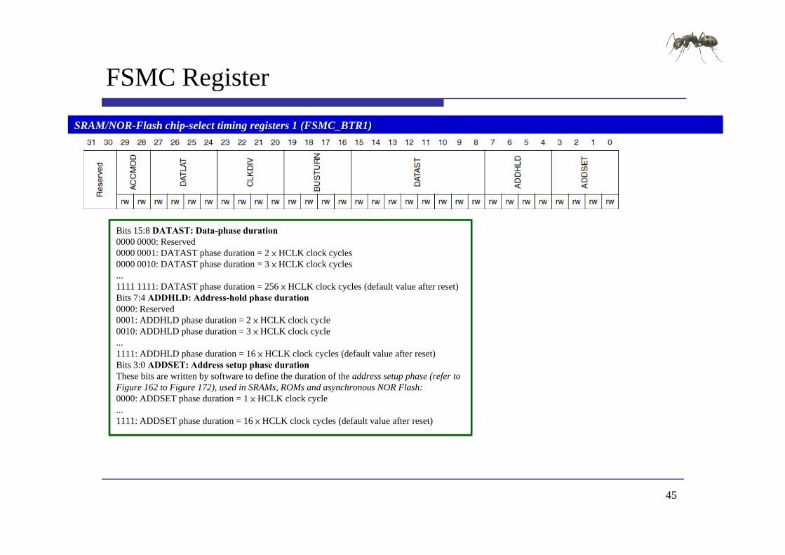
FSMC Register g
Bit 8 FSMCEN FSMC clock enableSRAMNOR-Flash chip-select timing registers 1 (FSMC_BTR1)
Bits 158 DATAST Data-phase duration0000 0000 Reserved0000 0001 DATAST phase duration = 2 times HCLK clock cycles0000 0010 DATAST phase duration = 3 times HCLK clock cycles1111 1111 DATAST phase duration = 256 times HCLK clock cycles (default value after reset)Bits 74 ADDHLD Address-hold phase duration0000 Reserved0001 ADDHLD phase duration = 2 times HCLK clock cycle0010 ADDHLD phase duration = 3 times HCLK clock cycle1111 ADDHLD phase duration = 16 times HCLK clock cycles (default value after reset)Bits 30 ADDSET Address setup phase durationThese bits are written by software to define the duration of the address setup phase (refer toFigure 162 to Figure 172) used in SRAMs ROMs and asynchronous NOR Flash0000 ADDSET phase duration = 1 times HCLK clock cycle1111 ADDSET phase duration = 16 times HCLK clock cycles (default value after reset)
45
實驗步驟
範例目錄架構
範例說明 範例說明
預設定義說明
46
範例目錄架構
範例目錄
測試映像檔 測試映像檔
含括檔
函式庫 函式庫
專案檔
原始碼 原始碼
47
範例說明
Embedded Software Side
Infinite loop
Display Result
Infinite loop while (1)if (((TabAddramp0xFFFFFF00) == 0x60000000) ampamp
((MSPValueamp0xFFFF0000) == 0x20000000))
Check operation
Check pointer value((MSPValueamp0xFFFF0000) == 0x20000000))
OK Turn on USERLED GPIO_SetBits(GPIOF GPIO_Pin_11)
else
Display Result
else KO Turn off USERLED
GPIO_ResetBits(GPIOF GPIO_Pin_11) Insert delay Delay(0xAFFFF)
如果Tab位置在0x600000且Stack pointer位置在0x2000 外部記憶體使用正常USERLED紅燈恆亮Delay(0xAFFFF)
Turn on USERLED GPIO_SetBits(GPIOF GPIO_Pin_11) Insert delay Delay(0xAFFFF)
紅燈恆亮
如果 b位置不在0 600000或Delay(0xAFFFF)
如果Tab位置不在0x600000或Stack pointer位置不在0x2000 外部記憶體使用異常USERLED紅燈閃爍
48
預設定義說明
DATA_IN_ExtSRAM EQU 1 E l SRAM C fi i External SRAM Configuration 0=gt DISABLE 1=gt ENABLE
u32 Tab[1024]宣告於外部 的記憶體 宣告於外部SRAM的記憶體
49
data memory存取控制實驗
實驗二
WU-YANGTechnology Co Ltd
實驗二練習
練習 取消RVMDK環境外部SRAM設定測試是否正常 取消RVMDK環境外部SRAM設定測試是否正常
修改DATA_IN_ExtSRAM EQU 0測試是否正常
修改外部 記憶體 b變數大小測試是否正常 修改外部SRAM記憶體Tab變數大小測試是否正常
51
Q amp A
WU-YANGTechnology Co Ltd
MIAT_STM32內部Flash存取控制實驗
WU-YANG
浯陽科技有限公司
Technology Co Ltd
Declared Version
Training Only
Declare
Document Number
Document Version 100
Release Date
Document Title MIAT_STM32 內部FLASH存取控制實驗
Exercise Time
Platform MIAT_STM32V2MIAT IOB V1PlatformMIAT IOBV1
Peripheral
Author WU-YANG Technology Co Ltd
2
實驗目的(一)( )
使用MIAT_STM32實驗板透過Flash memory interface (FLITF)控制內部Flash進行存取控制實驗並利用LED(FLITF)控制內部Flash進行存取控制實驗並利用LED確認存取是否正常
3
實驗原理
System architecture E b dd d Fl h Embedded Flash Features Memory map RVMDK環境設定
FLITF Flash module organization
Flash library function Development Flow ARM Configure
4
System architecturey
5
Embedded Flash
Features 256 Kb up to 256 Kbytes Memory organization the Flash memory is organized as a
main block and an information blockmain block and an information block Main memory block of size t 32 Kb 64 bit di id d i t 128 f 2 up to 32 Kb times 64 bits divided into 128 pages of 2
Kbytes Information block of size Information block of size 258 times 64 bits
6
Embedded Flash Memory mapy p
7
Flash Memoryy
8
RVMDK環境設定
STMF103ZC有256K Bytes的Flash位置由0x8000000至0x8040000
9
FLITF
Features R d i f i h f h b ff (2 64 bi d ) Read interface with prefetch buffer (2x64-bit words) Option byte Loader
l h i Flash Program Erase operation Read Write protection
10
Flash memory interfacey
11
Flash memory interface registery g
Bit 8 FSMCEN FSMC clock enableFlash status register (FLASH_SR)
Bits 316 Reserved must be kept clearedBit 5 EOP End of operation
Bit 2 PGERR Programming errorSet by hardware when an address to be programmed p
Set by hardware when a Flash operation (programming erase) is completed Reset by writing a 1Note EOP is asserted at the end of each successful
y p gcontains a value different from 0xFFFF before programmingReset by writing 1Note The STRT bit in the FLASH_CR register f f
program or erase operationBit 4 WRPRTERR Write protection errorSet by hardware when programming a write-protected address of the Flash memory
_ gshould be reset before starting a programmingoperationBit 1 Reserved must be kept clearedBit 0 BSY Busyp y
Reset by writing 1Bit 3 Reserved must be kept cleared
This indicates that a Flash operation is in progress This is set on the beginning of a Flash operation and reset when the operation finishes or when an error occurs
12
Flash memory interface registery g
Flash control register (FLASH_CR)
Bit 9 OPTWRE Option bytes write enableWhen set the option bytes can be programmed This
Bit 6 STRT StartThis bit triggers an ERASE operation when set This bit is set only
bit is set on writing the correct key sequence to the FLASH_OPTKEYR registerThis bit can be reset by softwareBit 8 Reserved must be kept clearedBit 7 LOCK Lock
by software and reset when the BSY bit is resetBit 5 OPTER Option byte eraseOption byte erase chosenBit 4 OPTPG Option byte programmingOption byte programming chosenBit 7 LOCK Lock
Write to 1 only When it is set it indicates that the FPEC and FLASH_CR are locked This bit is reset by hardware after detecting the unlock sequenceIn the event of unsuccessful unlock operation this bit remains set until the next reset
p y p g gBit 3 Reserved must be kept clearedBit 2 MER Mass eraseErase of all user pages chosenBit 1 PER Page erasePage Erase chosenremains set until the next reset Page Erase chosenBit 0 PG ProgrammingFlash programming chosen
13
Main Flash memory programmingy p g g
14
Flash memory Page Erasey g
15
Flash memory Mass Erasey
16
Option byte programmingp y p g g
17
Option byte Erasep y
18
FLASH library functiony
19
FLASH library functiony
20
Development Flowp
Embedded Software Side
int main(void)
Bootup STM32F10x
ProgrammingBootupSTM32F10x RCC Configure
NVIC Configure
int main(void)ifdef DEBUGdebug()
endifendif
FLASHStatus = FLASH_COMPLETEMemoryProgramStatus = PASSEDData = 0x15041975
GPIO Configure
Data = 0x15041975
RCC Configuration RCC_Configuration()
Flash memory RW operation FLASH Unlock
FLASH ClearFlag NVIC Configuration NVIC_Configuration()
GPIO Configuration
FLASH ClearFlag
FLASH ErasePage
FLASH ProgramWord GPIO Configuration GPIO_Configuration()
helliphelliphelliphelliphelliphelliphelliphelliphelliphelliphelliphelliphelliphelliphelliphelliphellipDisplay Result
Check content
21
實驗步驟
範例目錄架構
範例說明 範例說明
預設定義說明
燒錄 燒錄MIAT_STM32
22
範例目錄架構
範例目錄
測試映像檔 測試映像檔
含括檔
函式庫 函式庫
專案檔
原始碼 原始碼
23
範例說明
Function name Description
Unlock the Flash Program Erase controller FLASH_Unlock()
D fi h b f b d
Flash FwLib Functions List
Function name Description
FLASH_Unlock Unlocks the FLASH Program Erase Controller
FLASH_ClearFlag Clears the FLASH pending fl
Define the number of page to be erased NbrOfPage = (EndAddr - StartAddr) FLASH_PAGE_SIZE
Clear All pending flags FLASH_ClearFlag(FLASH_FLAG_BSY | FLASH_FLAG_EOP | FLASH_FLAG_PGERR |
FLASH FLAG WRPRTERR)flags
FLASH_ErasePage Erases a specified FLASH page
FLASH_ProgramWord Programs a word at a specified
_ _ )
Erase the FLASH pages for(EraseCounter = 0 (EraseCounter lt NbrOfPage) ampamp (FLASHStatus ==
FLASH_COMPLETE) EraseCounter++)FLASHStatus = FLASH ErasePage(StartAddr + (FLASH PAGE SIZE EraseCounter))address FLASHStatus = FLASH_ErasePage(StartAddr + (FLASH_PAGE_SIZE EraseCounter))
FLASH Word program of data 0x15041979 at addresses defined by StartAddr and EndAddrAddress = StartAddr
while((Address lt EndAddr) ampamp (FLASHStatus == FLASH_COMPLETE))FLASHStatus = FLASH_ProgramWord(Address Data)Address = Address + 4
24
範例說明
Embedded Software Side
Check the corectness of written data
Display Result
Check the corectness of written data Address = StartAddr
while((Address lt EndAddr) ampamp (MemoryProgramStatus = FAILED))if(((vu32) Address) = Data)
Flash memory RW operation
MemoryProgramStatus = FAILED
Address += 4
Check content
Display Result while (1)if (MemoryProgramStatus == PASSED) OK Turn on USERLED GPIO_SetBits(GPIOF GPIO_Pin_11)
Display Result
else KO Turn off USERLED GPIO_ResetBits(GPIOF GPIO_Pin_11) Insert delay Delay(0xAFFFF)
如果寫入與讀取Flash內容相同Flash記憶體使用正常USERLED紅燈恆亮
Turn on USERLED GPIO_SetBits(GPIOF GPIO_Pin_11) Insert delay Delay(0xAFFFF)
如果寫入與讀取Flash內容不同Flash記憶體使用異常USERLED紅燈閃爍
25
預設定義說明
define StartAddr ((u32)0x08008000) 定義Flash使用起始點 定義Flash使用起始點
使用起始點必需大於0x8003000 + Code Size 附註 0x8000000~0x8003000為DFU程式區塊使用此區塊
將造成無法燒錄程式
Code Size可由產生的HEX檔得知
d fi E dAdd (( 32)0 0800C000) define EndAddr ((u32)0x0800C000) 定義Flash使用結束點
使用起始點必需小於0x8040000使用起始點必需小於
Data = 0x15041975 寫入資料
32Bit define FLASH_PAGE_SIZE ((u16)0x800)
每一個Page有2KByte26
每一個Page有2KByte
Intel HEX Format
aaaa tt dd cc
field Description
the colon that starts every Intel HEX record
the record-length field that represents the number of data bytes (dd) in the record
aaaa the address field that represents the starting address for subsequent data in the record
tt the field that represents the HEX record type which may be one of the following00 - data record01 - end-of-file record02 - extended segment address recordg04 - extended linear address record
dd a data field that represents one byte of data A record may have multiple data bytes The number of data bytes in the record must match the number specified by the field
cc the checksum field that represents the checksum of the record The checksum is calculated by summing the values of all hexadecimal digit pairs in the record modulo 256 and taking the twos complement
27
HEX Examplep
020000040800F2103000001814002045310008D9340008CD340008D8103000001814002045310008D9340008CD340008D8helliphelliphellip1038200042370008000000000000000000000000170C3830000000000000000000000000008C
資料填入起始位置為
0C3830000000000000000000000000008C04000005080031318D00000001FF
資料填入起始位置為0x08003000 每一行有0x10(16)個Bytes 最後一筆資料為
資料結束點為0x0803383004000005080031318D
(0x08003830 -0x08000000)0x800 = 7 需以0x800為單位所以使用的位置起點為0x08004000
28
燒錄MIAT STM32_
Rebuilder all target files產生HEX DFU Fil M 轉換HEX產生DFU DFU File Manager轉換HEX產生DFU DfuSe Demonstration燒錄DFU d Leave DFU mode
29
內部Flash存取控制實驗
實驗一
WU-YANGTechnology Co Ltd
實驗一練習
注意 請使用預設0 08008000之後的位置 避免覆蓋DFU 請使用預設0x08008000之後的位置避免覆蓋DFU
與使用者程式碼區塊
練習 練習 修改存取位置測試是否正常
修改寫入資料測試是否正常 修改寫入資料測試是否正常
修改寫入資料後取消FLASH_Unlock測試是否正常
修改寫入資料後取消FLASH E P 測試是否正 修改寫入資料後取消FLASH_ErasePage測試是否正常
31
實驗目的(二)( )
使用MIAT_STM32實驗板透過Flash memory interface (FLITF)控制內部Flash進行存取控制實驗並利用SW(FLITF)控制內部Flash進行存取控制實驗並利用SWKEY決定資料寫入與讀取LCD顯示狀態
32
實驗原理
System requirement E b dd d Fl h Embedded Flash LCD KEY SW
Development Flow ARM Configure
33
Development Flowp
Embedded Software Side
int main(void)
Bootup STM32F10x
ProgrammingBootupSTM32F10x RCC Configure
NVIC Configure
int main(void)ifdef DEBUGdebug()
endif
FLASHStatus = FLASH_COMPLETE
RCC Configuration RCC Configuration()
GPIO Configure
BasicIO Configure_ g ()
NVIC Configuration NVIC_Configuration()
GPIO Configuration Flash memory RW ti
lcd Configure
GPIO Configuration GPIO_Configuration()
Init_BasicIO()
l d i i () LCD I i i li i
RW operation
Example
FLASH Unlock
FLASH ClearFlag
lcd_init() LCD Initialization
helliphelliphelliphelliphelliphelliphelliphelliphelliphelliphelliphelliphelliphelliphelliphelliphelliphelliphelliphelliphelliphelliphellip
p
34
硬體電路配置
Mapping Table
Num MIAT_STM32V2 MIAT_IOBV1 Num MIAT_STM32V2 MIAT_IOBV1
1 PC8 (326) SW1 10 PE6 (15) LCD_EN2 PC9 (327) SW2 11 PF6 (118) LCD RW ( ) ( ) _3 PC10 (43) SW3 12 PF7 (119) LCD_RS 4 PC11 (44) SW4 13 PF8(120) LCD_D4 5 PB5 (427) KEY1 14 PF9 (121) LCD_D5 6 PB6 (428) KEY2 15 PF10 (122) LCD_D6 7 PB7 (429) KEY3 16 PF11 (213) LCD_D7 8 PB8 (431) KEY4 17 VDD (236) VCC33V 9 VCC5V (1 36) VCC5V 18 GND (1 35) GND9 VCC5V (136) VCC5V 18 GND (135) GND
35
實驗步驟
範例目錄架構
範例說明 範例說明
預設定義說明
36
範例目錄架構
範例目錄
測試映像檔 測試映像檔
含括檔
函式庫 函式庫
專案檔
原始碼 原始碼
37
範例說明
Embedded Software Side
lcd clear()
FLASH memory RW operation
lcd_clear()lcd_print (MIAT_STM32 DEMO )
Unlock the Flash Program Erase controller FLASH_Unlock()
Flash memory RW operation
FLASH Unlock
Clear All pending flags FLASH_ClearFlag(FLASH_FLAG_BSY | FLASH_FLAG_EOP | FLASH_FLAG_PGERR |
FLASH_FLAG_WRPRTERR)
while(1)
Example
FLASH ClearFlag
( )
KEY_Buffer=Key_Scan()set_cursor (0 1)lcd_print (SW Value = 0x)lcd putchar(((SWamp0x7)+0x30))lcd_putchar(((SWamp0x7)+0x30))if(KEY_Buffer==1)Address=(StartAddr|(SWltlt12))set_cursor (0 0)lcd_print (Set Addr = 0x)
掃描KEY是否按下與顯示SW數值LCD Line2顯示SW Value = 0x(SW)
lcd_putchar(((SWamp0x7)+0x30))lcd_print ( )
如果KEY1按下記錄SW數值至Address LCD Line1顯示Set Adde = 0x(Address)
38
範例說明
Embedded Software Side
else if(KEY Buffer==2)
FLASH memory RW operation
else if(KEY_Buffer==2)
Erase the FLASH pages FLASHStatus = FLASH_ErasePage(Address)
FLASH Word program of data at addresses defined by SW
SRAM memory RW operation
p g yFLASHStatus = FLASH_ProgramWord(Address (SWamp0x7))
set_cursor (0 0)lcd_print (Write 0x)lcd_putchar(((SWamp0x7)+0x30))l d i t ( t 0 )
Example如果KEY2按下清除Address所處區塊並寫入SW數值 lcd_print ( at 0x)
lcd_putchar((((Addressgtgt12)amp0x7)+0x30))else if(KEY_Buffer==3)
Data=(u16 )Address
所處區塊並寫入SW數值LCD Line1顯示Write 0x(SW) at 0x(Adddress)
Data (u16 )Addressset_cursor (0 0)lcd_print (Addr 0x)lcd_putchar((((Addressgtgt12)amp0x7)+0x30))lcd_print ( = 0x)lcd_putchar(((Dataamp0x7)+0x30))lcd_print ( )
如果KEY3按下讀取Address紀錄數值LCD Line1顯示Addr 0x(Adddress) = 0x
39
預設定義說明
define StartAddr ((u32)0x08020000) 定義Flash使用起始點 定義Flash使用起始點
使用起始點必需大於0x8003000 + Code Size 附註 0x8000000~0x8003000為DFU程式區塊使用此區塊
將造成無法燒錄程式
Code Size可由產生的HEX檔得知
32 Add 0 08020000 u32 Address = 0x08020000 定義Address初始值
初始值必需與Flash使用起始點相同初始值必需與 使用起始點相同
Address=(StartAddr|(SWltlt12)) Example StartAddr = 0x08020000 SW = 1 Address = 0x08021000
StartAddr = 0x08020000 SW = 7 Address = 0x08027000 StartAddr|(7ltlt12)必需小於0x8040000
40
使用者界面與Flash存取控制實驗
實驗二
WU-YANGTechnology Co Ltd
實驗二練習
注意 請使用預設0 08020000之後的位置 避免覆蓋DFU 請使用預設0x08020000之後的位置避免覆蓋DFU
與使用者程式碼區塊
練習 練習 利用SW與KEY測試Flash寫入與讀取是否正常
Fl h寫入後電源關閉 再開啟後寫入資料是否仍存 Flash寫入後電源關閉再開啟後寫入資料是否仍存在
修改存取位置測試是否正常 修改存取位置測試是否正常
42
實驗目的(三)( )
使用MIAT_STM32實驗板透過Flash memory interface (FLITF)控制內部Flash進行存取控制實驗並藉由填入(FLITF)控制內部Flash進行存取控制實驗並藉由填入Option Bytes 設定寫入鎖定保護Page鎖定不被覆蓋
43
Development Flowp
Embedded Software Side
int main(void)
Bootup STM32F10x
ProgrammingBootupSTM32F10x RCC Configure
NVIC Configure
int main(void)ifdef DEBUGdebug()
endifendif
FLASHStatus = FLASH_COMPLETEMemoryProgramStatus = PASSEDData = 0x1753
GPIO Configure
Data = 0x1753
RCC Configuration RCC_Configuration()
Flash memory RW operation FLASH Unlock
FLASH ClearFlag NVIC Configuration NVIC_Configuration()
GPIO Configuration
FLASH ClearFlag
FLASH ErasePage
FLASH ProgramHalfWord GPIO Configuration GPIO_Configuration()
Display Result
Check content
44
helliphelliphelliphelliphelliphelliphelliphelliphelliphelliphelliphelliphelliphelliphelliphelliphelliphelliphellip
實驗步驟
範例目錄架構
範例說明 範例說明
預設定義說明
45
範例目錄架構
範例目錄
測試映像檔 測試映像檔
含括檔
函式庫 函式庫
專案檔
原始碼 原始碼
46
範例說明
Function name Description
Unlock the Flash Program Erase controller FLASH_Unlock()
Define the number of page to be erased
Flash FwLib Functions List
Function name Description
FLASH_Unlock Unlocks the FLASH Program Erase Controller
FLASH_ClearFlag Clears the FLASH pending fl
Define the number of page to be erased NbrOfPage = (EndAddr ‐ StartAddr) FLASH_PAGE_SIZE
FLASH_ClearFlag(FLASH_FLAG_BSY | FLASH_FLAG_EOP|FLASH_FLAG_PGERR |FLASH_FLAG_WRPRTERR)
Get pages write protection status flags
FLASH_EraseOptionBytes
Erases the FLASH option bytes
FLASH_EnableWritePro Write protects the desired
p g pWRPR_Value = FLASH_GetWriteProtectionOptionByte()ProtectedPages = WRPR_Value amp 0x000000C0
ifdef WriteProtection_Disableif (ProtectedPages == 0x00) Pages are write protected
tection pages
NVIC_GenerateSystemReset
Generate a system reset
Disable the write protection FLASHStatus = FLASH_EraseOptionBytes() Generate System Reset to load the new option byte values NVIC_GenerateSystemReset()
elseifdef WriteProtection Enableifdef WriteProtection_Enableif (ProtectedPages = 0x00) Pages not write protected
FLASHStatus = FLASH_EraseOptionBytes() Enable the pages write protection FLASHStatus = FLASH_EnableWriteProtection(FLASH_WRProt_Pages12to13
|FLASH WRProt Pages14to15)|FLASH_WRProt_Pages14to15) Generate System Reset to load the new option byte values NVIC_GenerateSystemReset()
endifendif
47
範例說明
if (ProtectedPages = 0x00) Clear All pending flags
Flash FwLib Functions List
Function name DescriptionFLASH_ClearFlag(FLASH_FLAG_BSY |
FLASH_FLAG_EOP|FLASH_FLAG_PGERR |FLASH_FLAG_WRPRTERR)
erase the FLASH pages for(EraseCounter = 0 (EraseCounter lt NbrOfPage) ampamp (FLASHStatus ==
Function name Description
FLASH_ErasePage Erases a specified FLASH page
FLASH_ProgramHalfWod
Programs a half word at a ifi d dd FLASH_COMPLETE) EraseCounter++)
FLASHStatus = FLASH_ErasePage(StartAddr + (FLASH_PAGE_SIZE
EraseCounter))
rd specified address
FLASH Half Word program of data 0x1753 at addresses defined by StartAddrand EndAddr
Address = StartAddr
hil ((Add E dAdd ) ampamp (FLASHSt t FLASH COMPLETE))while((Address lt EndAddr) ampamp (FLASHStatus == FLASH_COMPLETE))
FLASHStatus = FLASH_ProgramHalfWord(Address Data)Address = Address + 2
48
範例說明
Embedded Software Side
Check the corectness of written data
Display Result
Check the corectness of written data Address = StartAddr
while((Address lt EndAddr) ampamp (MemoryProgramStatus = FAILED))if(((vu16) Address) = Data)
Flash memory RW operation
MemoryProgramStatus = FAILED
Address += 2
Check content
Display Result while (1)if (MemoryProgramStatus == PASSED) OK Turn on USERLED GPIO_SetBits(GPIOF GPIO_Pin_11)
Display Result
else KO Turn off USERLED GPIO_ResetBits(GPIOF GPIO_Pin_11) Insert delay Delay(0xAFFFF)
如果寫入與讀取Flash內容相同Flash記憶體可以寫入USERLED紅燈恆亮
Turn on USERLED GPIO_SetBits(GPIOF GPIO_Pin_11) Insert delay Delay(0xAFFFF)
如果寫入與讀取Flash內容不同Flash記憶體不能寫入USERLED紅燈閃爍
49
預設定義說明
define StartAddr ((u32) 0x08006000) 定義Flash使用起始點 定義Flash使用起始點
使用起始點必需大於0x8003000 + Code Size 附註 0x8000000~0x8003000為DFU程式區塊使用此區塊
將造成無法燒錄程式
Code Size可由產生的HEX檔得知
d fi E dAdd (( 32) 0 08008000) define EndAddr ((u32) 0x08008000) 定義Flash使用結束點
使用起始點必需小於0x8040000使用起始點必需小於
Data = 0x1753 寫入資料
16Bit define FLASH_PAGE_SIZE ((u16)0x800) 每一個Page有2KByte
50
每一個Page有2KByte
預設定義說明
define WriteProtection_Enable U hi li E bl W i P i Uncomment this line to Enable Write Protection
define WriteProtection_Disablehi li i bl i i Uncomment this line to Disable Write Protection
FLASH_EnableWriteProtection設定影響 個 設定影響2個Page FLASH_WRProt_Pages0to1 FLASH_WRProt_Pages1to2 helliphellip FLASH_WRProt_Pages60to61
設定影響多個Page FLASH_WRProt_Pages62to255
51
FLASH EnableWriteProtection_
Example
位置0x08006000 ~ 0x08007000每一個Page有0x800ByteStartPage = (0x08006000-0x08000000)0x800 = 12EndPage = ((0x08007000-0x08000000)0x800)-1 = 13執行執行FLASH_EnableWriteProtection(FLASH_WRProt_Pages12to13)將影響Pages12 Pages13
52
內部Flash寫入鎖定存取控制實驗
實驗三
WU-YANGTechnology Co Ltd
實驗三練習
注意 請使用預設0 08006000之後的位置 避免覆蓋DFU 請使用預設0x08006000之後的位置避免覆蓋DFU
與使用者程式碼區塊
更改寫入位置測試寫入鎖定時需同時更改 更改寫入位置測試寫入鎖定時需同時更改FLASH_EnableWriteProtection鎖定之Page
練習 練習 打開define WriteProtection_Enable測試是否可寫入
打開define WriteProtection Disable測試是否可寫入 打開define WriteProtection_Disable測試是否可寫入
修改存取位置測試是否正常
修改寫入資料測試是否正常 修改寫入資料測試是否正常
54
Q amp A
WU-YANGTechnology Co Ltd

實驗步驟
範例目錄架構
範例說明 範例說明
預設定義說明
46
範例目錄架構
範例目錄
測試映像檔 測試映像檔
含括檔
函式庫 函式庫
專案檔
原始碼 原始碼
47
範例說明
Embedded Software Side
Infinite loop
Display Result
Infinite loop while (1)if (((TabAddramp0xFFFFFF00) == 0x60000000) ampamp
((MSPValueamp0xFFFF0000) == 0x20000000))
Check operation
Check pointer value((MSPValueamp0xFFFF0000) == 0x20000000))
OK Turn on USERLED GPIO_SetBits(GPIOF GPIO_Pin_11)
else
Display Result
else KO Turn off USERLED
GPIO_ResetBits(GPIOF GPIO_Pin_11) Insert delay Delay(0xAFFFF)
如果Tab位置在0x600000且Stack pointer位置在0x2000 外部記憶體使用正常USERLED紅燈恆亮Delay(0xAFFFF)
Turn on USERLED GPIO_SetBits(GPIOF GPIO_Pin_11) Insert delay Delay(0xAFFFF)
紅燈恆亮
如果 b位置不在0 600000或Delay(0xAFFFF)
如果Tab位置不在0x600000或Stack pointer位置不在0x2000 外部記憶體使用異常USERLED紅燈閃爍
48
預設定義說明
DATA_IN_ExtSRAM EQU 1 E l SRAM C fi i External SRAM Configuration 0=gt DISABLE 1=gt ENABLE
u32 Tab[1024]宣告於外部 的記憶體 宣告於外部SRAM的記憶體
49
data memory存取控制實驗
實驗二
WU-YANGTechnology Co Ltd
實驗二練習
練習 取消RVMDK環境外部SRAM設定測試是否正常 取消RVMDK環境外部SRAM設定測試是否正常
修改DATA_IN_ExtSRAM EQU 0測試是否正常
修改外部 記憶體 b變數大小測試是否正常 修改外部SRAM記憶體Tab變數大小測試是否正常
51
Q amp A
WU-YANGTechnology Co Ltd
MIAT_STM32內部Flash存取控制實驗
WU-YANG
浯陽科技有限公司
Technology Co Ltd
Declared Version
Training Only
Declare
Document Number
Document Version 100
Release Date
Document Title MIAT_STM32 內部FLASH存取控制實驗
Exercise Time
Platform MIAT_STM32V2MIAT IOB V1PlatformMIAT IOBV1
Peripheral
Author WU-YANG Technology Co Ltd
2
實驗目的(一)( )
使用MIAT_STM32實驗板透過Flash memory interface (FLITF)控制內部Flash進行存取控制實驗並利用LED(FLITF)控制內部Flash進行存取控制實驗並利用LED確認存取是否正常
3
實驗原理
System architecture E b dd d Fl h Embedded Flash Features Memory map RVMDK環境設定
FLITF Flash module organization
Flash library function Development Flow ARM Configure
4
System architecturey
5
Embedded Flash
Features 256 Kb up to 256 Kbytes Memory organization the Flash memory is organized as a
main block and an information blockmain block and an information block Main memory block of size t 32 Kb 64 bit di id d i t 128 f 2 up to 32 Kb times 64 bits divided into 128 pages of 2
Kbytes Information block of size Information block of size 258 times 64 bits
6
Embedded Flash Memory mapy p
7
Flash Memoryy
8
RVMDK環境設定
STMF103ZC有256K Bytes的Flash位置由0x8000000至0x8040000
9
FLITF
Features R d i f i h f h b ff (2 64 bi d ) Read interface with prefetch buffer (2x64-bit words) Option byte Loader
l h i Flash Program Erase operation Read Write protection
10
Flash memory interfacey
11
Flash memory interface registery g
Bit 8 FSMCEN FSMC clock enableFlash status register (FLASH_SR)
Bits 316 Reserved must be kept clearedBit 5 EOP End of operation
Bit 2 PGERR Programming errorSet by hardware when an address to be programmed p
Set by hardware when a Flash operation (programming erase) is completed Reset by writing a 1Note EOP is asserted at the end of each successful
y p gcontains a value different from 0xFFFF before programmingReset by writing 1Note The STRT bit in the FLASH_CR register f f
program or erase operationBit 4 WRPRTERR Write protection errorSet by hardware when programming a write-protected address of the Flash memory
_ gshould be reset before starting a programmingoperationBit 1 Reserved must be kept clearedBit 0 BSY Busyp y
Reset by writing 1Bit 3 Reserved must be kept cleared
This indicates that a Flash operation is in progress This is set on the beginning of a Flash operation and reset when the operation finishes or when an error occurs
12
Flash memory interface registery g
Flash control register (FLASH_CR)
Bit 9 OPTWRE Option bytes write enableWhen set the option bytes can be programmed This
Bit 6 STRT StartThis bit triggers an ERASE operation when set This bit is set only
bit is set on writing the correct key sequence to the FLASH_OPTKEYR registerThis bit can be reset by softwareBit 8 Reserved must be kept clearedBit 7 LOCK Lock
by software and reset when the BSY bit is resetBit 5 OPTER Option byte eraseOption byte erase chosenBit 4 OPTPG Option byte programmingOption byte programming chosenBit 7 LOCK Lock
Write to 1 only When it is set it indicates that the FPEC and FLASH_CR are locked This bit is reset by hardware after detecting the unlock sequenceIn the event of unsuccessful unlock operation this bit remains set until the next reset
p y p g gBit 3 Reserved must be kept clearedBit 2 MER Mass eraseErase of all user pages chosenBit 1 PER Page erasePage Erase chosenremains set until the next reset Page Erase chosenBit 0 PG ProgrammingFlash programming chosen
13
Main Flash memory programmingy p g g
14
Flash memory Page Erasey g
15
Flash memory Mass Erasey
16
Option byte programmingp y p g g
17
Option byte Erasep y
18
FLASH library functiony
19
FLASH library functiony
20
Development Flowp
Embedded Software Side
int main(void)
Bootup STM32F10x
ProgrammingBootupSTM32F10x RCC Configure
NVIC Configure
int main(void)ifdef DEBUGdebug()
endifendif
FLASHStatus = FLASH_COMPLETEMemoryProgramStatus = PASSEDData = 0x15041975
GPIO Configure
Data = 0x15041975
RCC Configuration RCC_Configuration()
Flash memory RW operation FLASH Unlock
FLASH ClearFlag NVIC Configuration NVIC_Configuration()
GPIO Configuration
FLASH ClearFlag
FLASH ErasePage
FLASH ProgramWord GPIO Configuration GPIO_Configuration()
helliphelliphelliphelliphelliphelliphelliphelliphelliphelliphelliphelliphelliphelliphelliphelliphellipDisplay Result
Check content
21
實驗步驟
範例目錄架構
範例說明 範例說明
預設定義說明
燒錄 燒錄MIAT_STM32
22
範例目錄架構
範例目錄
測試映像檔 測試映像檔
含括檔
函式庫 函式庫
專案檔
原始碼 原始碼
23
範例說明
Function name Description
Unlock the Flash Program Erase controller FLASH_Unlock()
D fi h b f b d
Flash FwLib Functions List
Function name Description
FLASH_Unlock Unlocks the FLASH Program Erase Controller
FLASH_ClearFlag Clears the FLASH pending fl
Define the number of page to be erased NbrOfPage = (EndAddr - StartAddr) FLASH_PAGE_SIZE
Clear All pending flags FLASH_ClearFlag(FLASH_FLAG_BSY | FLASH_FLAG_EOP | FLASH_FLAG_PGERR |
FLASH FLAG WRPRTERR)flags
FLASH_ErasePage Erases a specified FLASH page
FLASH_ProgramWord Programs a word at a specified
_ _ )
Erase the FLASH pages for(EraseCounter = 0 (EraseCounter lt NbrOfPage) ampamp (FLASHStatus ==
FLASH_COMPLETE) EraseCounter++)FLASHStatus = FLASH ErasePage(StartAddr + (FLASH PAGE SIZE EraseCounter))address FLASHStatus = FLASH_ErasePage(StartAddr + (FLASH_PAGE_SIZE EraseCounter))
FLASH Word program of data 0x15041979 at addresses defined by StartAddr and EndAddrAddress = StartAddr
while((Address lt EndAddr) ampamp (FLASHStatus == FLASH_COMPLETE))FLASHStatus = FLASH_ProgramWord(Address Data)Address = Address + 4
24
範例說明
Embedded Software Side
Check the corectness of written data
Display Result
Check the corectness of written data Address = StartAddr
while((Address lt EndAddr) ampamp (MemoryProgramStatus = FAILED))if(((vu32) Address) = Data)
Flash memory RW operation
MemoryProgramStatus = FAILED
Address += 4
Check content
Display Result while (1)if (MemoryProgramStatus == PASSED) OK Turn on USERLED GPIO_SetBits(GPIOF GPIO_Pin_11)
Display Result
else KO Turn off USERLED GPIO_ResetBits(GPIOF GPIO_Pin_11) Insert delay Delay(0xAFFFF)
如果寫入與讀取Flash內容相同Flash記憶體使用正常USERLED紅燈恆亮
Turn on USERLED GPIO_SetBits(GPIOF GPIO_Pin_11) Insert delay Delay(0xAFFFF)
如果寫入與讀取Flash內容不同Flash記憶體使用異常USERLED紅燈閃爍
25
預設定義說明
define StartAddr ((u32)0x08008000) 定義Flash使用起始點 定義Flash使用起始點
使用起始點必需大於0x8003000 + Code Size 附註 0x8000000~0x8003000為DFU程式區塊使用此區塊
將造成無法燒錄程式
Code Size可由產生的HEX檔得知
d fi E dAdd (( 32)0 0800C000) define EndAddr ((u32)0x0800C000) 定義Flash使用結束點
使用起始點必需小於0x8040000使用起始點必需小於
Data = 0x15041975 寫入資料
32Bit define FLASH_PAGE_SIZE ((u16)0x800)
每一個Page有2KByte26
每一個Page有2KByte
Intel HEX Format
aaaa tt dd cc
field Description
the colon that starts every Intel HEX record
the record-length field that represents the number of data bytes (dd) in the record
aaaa the address field that represents the starting address for subsequent data in the record
tt the field that represents the HEX record type which may be one of the following00 - data record01 - end-of-file record02 - extended segment address recordg04 - extended linear address record
dd a data field that represents one byte of data A record may have multiple data bytes The number of data bytes in the record must match the number specified by the field
cc the checksum field that represents the checksum of the record The checksum is calculated by summing the values of all hexadecimal digit pairs in the record modulo 256 and taking the twos complement
27
HEX Examplep
020000040800F2103000001814002045310008D9340008CD340008D8103000001814002045310008D9340008CD340008D8helliphelliphellip1038200042370008000000000000000000000000170C3830000000000000000000000000008C
資料填入起始位置為
0C3830000000000000000000000000008C04000005080031318D00000001FF
資料填入起始位置為0x08003000 每一行有0x10(16)個Bytes 最後一筆資料為
資料結束點為0x0803383004000005080031318D
(0x08003830 -0x08000000)0x800 = 7 需以0x800為單位所以使用的位置起點為0x08004000
28
燒錄MIAT STM32_
Rebuilder all target files產生HEX DFU Fil M 轉換HEX產生DFU DFU File Manager轉換HEX產生DFU DfuSe Demonstration燒錄DFU d Leave DFU mode
29
內部Flash存取控制實驗
實驗一
WU-YANGTechnology Co Ltd
實驗一練習
注意 請使用預設0 08008000之後的位置 避免覆蓋DFU 請使用預設0x08008000之後的位置避免覆蓋DFU
與使用者程式碼區塊
練習 練習 修改存取位置測試是否正常
修改寫入資料測試是否正常 修改寫入資料測試是否正常
修改寫入資料後取消FLASH_Unlock測試是否正常
修改寫入資料後取消FLASH E P 測試是否正 修改寫入資料後取消FLASH_ErasePage測試是否正常
31
實驗目的(二)( )
使用MIAT_STM32實驗板透過Flash memory interface (FLITF)控制內部Flash進行存取控制實驗並利用SW(FLITF)控制內部Flash進行存取控制實驗並利用SWKEY決定資料寫入與讀取LCD顯示狀態
32
實驗原理
System requirement E b dd d Fl h Embedded Flash LCD KEY SW
Development Flow ARM Configure
33
Development Flowp
Embedded Software Side
int main(void)
Bootup STM32F10x
ProgrammingBootupSTM32F10x RCC Configure
NVIC Configure
int main(void)ifdef DEBUGdebug()
endif
FLASHStatus = FLASH_COMPLETE
RCC Configuration RCC Configuration()
GPIO Configure
BasicIO Configure_ g ()
NVIC Configuration NVIC_Configuration()
GPIO Configuration Flash memory RW ti
lcd Configure
GPIO Configuration GPIO_Configuration()
Init_BasicIO()
l d i i () LCD I i i li i
RW operation
Example
FLASH Unlock
FLASH ClearFlag
lcd_init() LCD Initialization
helliphelliphelliphelliphelliphelliphelliphelliphelliphelliphelliphelliphelliphelliphelliphelliphelliphelliphelliphelliphelliphelliphellip
p
34
硬體電路配置
Mapping Table
Num MIAT_STM32V2 MIAT_IOBV1 Num MIAT_STM32V2 MIAT_IOBV1
1 PC8 (326) SW1 10 PE6 (15) LCD_EN2 PC9 (327) SW2 11 PF6 (118) LCD RW ( ) ( ) _3 PC10 (43) SW3 12 PF7 (119) LCD_RS 4 PC11 (44) SW4 13 PF8(120) LCD_D4 5 PB5 (427) KEY1 14 PF9 (121) LCD_D5 6 PB6 (428) KEY2 15 PF10 (122) LCD_D6 7 PB7 (429) KEY3 16 PF11 (213) LCD_D7 8 PB8 (431) KEY4 17 VDD (236) VCC33V 9 VCC5V (1 36) VCC5V 18 GND (1 35) GND9 VCC5V (136) VCC5V 18 GND (135) GND
35
實驗步驟
範例目錄架構
範例說明 範例說明
預設定義說明
36
範例目錄架構
範例目錄
測試映像檔 測試映像檔
含括檔
函式庫 函式庫
專案檔
原始碼 原始碼
37
範例說明
Embedded Software Side
lcd clear()
FLASH memory RW operation
lcd_clear()lcd_print (MIAT_STM32 DEMO )
Unlock the Flash Program Erase controller FLASH_Unlock()
Flash memory RW operation
FLASH Unlock
Clear All pending flags FLASH_ClearFlag(FLASH_FLAG_BSY | FLASH_FLAG_EOP | FLASH_FLAG_PGERR |
FLASH_FLAG_WRPRTERR)
while(1)
Example
FLASH ClearFlag
( )
KEY_Buffer=Key_Scan()set_cursor (0 1)lcd_print (SW Value = 0x)lcd putchar(((SWamp0x7)+0x30))lcd_putchar(((SWamp0x7)+0x30))if(KEY_Buffer==1)Address=(StartAddr|(SWltlt12))set_cursor (0 0)lcd_print (Set Addr = 0x)
掃描KEY是否按下與顯示SW數值LCD Line2顯示SW Value = 0x(SW)
lcd_putchar(((SWamp0x7)+0x30))lcd_print ( )
如果KEY1按下記錄SW數值至Address LCD Line1顯示Set Adde = 0x(Address)
38
範例說明
Embedded Software Side
else if(KEY Buffer==2)
FLASH memory RW operation
else if(KEY_Buffer==2)
Erase the FLASH pages FLASHStatus = FLASH_ErasePage(Address)
FLASH Word program of data at addresses defined by SW
SRAM memory RW operation
p g yFLASHStatus = FLASH_ProgramWord(Address (SWamp0x7))
set_cursor (0 0)lcd_print (Write 0x)lcd_putchar(((SWamp0x7)+0x30))l d i t ( t 0 )
Example如果KEY2按下清除Address所處區塊並寫入SW數值 lcd_print ( at 0x)
lcd_putchar((((Addressgtgt12)amp0x7)+0x30))else if(KEY_Buffer==3)
Data=(u16 )Address
所處區塊並寫入SW數值LCD Line1顯示Write 0x(SW) at 0x(Adddress)
Data (u16 )Addressset_cursor (0 0)lcd_print (Addr 0x)lcd_putchar((((Addressgtgt12)amp0x7)+0x30))lcd_print ( = 0x)lcd_putchar(((Dataamp0x7)+0x30))lcd_print ( )
如果KEY3按下讀取Address紀錄數值LCD Line1顯示Addr 0x(Adddress) = 0x
39
預設定義說明
define StartAddr ((u32)0x08020000) 定義Flash使用起始點 定義Flash使用起始點
使用起始點必需大於0x8003000 + Code Size 附註 0x8000000~0x8003000為DFU程式區塊使用此區塊
將造成無法燒錄程式
Code Size可由產生的HEX檔得知
32 Add 0 08020000 u32 Address = 0x08020000 定義Address初始值
初始值必需與Flash使用起始點相同初始值必需與 使用起始點相同
Address=(StartAddr|(SWltlt12)) Example StartAddr = 0x08020000 SW = 1 Address = 0x08021000
StartAddr = 0x08020000 SW = 7 Address = 0x08027000 StartAddr|(7ltlt12)必需小於0x8040000
40
使用者界面與Flash存取控制實驗
實驗二
WU-YANGTechnology Co Ltd
實驗二練習
注意 請使用預設0 08020000之後的位置 避免覆蓋DFU 請使用預設0x08020000之後的位置避免覆蓋DFU
與使用者程式碼區塊
練習 練習 利用SW與KEY測試Flash寫入與讀取是否正常
Fl h寫入後電源關閉 再開啟後寫入資料是否仍存 Flash寫入後電源關閉再開啟後寫入資料是否仍存在
修改存取位置測試是否正常 修改存取位置測試是否正常
42
實驗目的(三)( )
使用MIAT_STM32實驗板透過Flash memory interface (FLITF)控制內部Flash進行存取控制實驗並藉由填入(FLITF)控制內部Flash進行存取控制實驗並藉由填入Option Bytes 設定寫入鎖定保護Page鎖定不被覆蓋
43
Development Flowp
Embedded Software Side
int main(void)
Bootup STM32F10x
ProgrammingBootupSTM32F10x RCC Configure
NVIC Configure
int main(void)ifdef DEBUGdebug()
endifendif
FLASHStatus = FLASH_COMPLETEMemoryProgramStatus = PASSEDData = 0x1753
GPIO Configure
Data = 0x1753
RCC Configuration RCC_Configuration()
Flash memory RW operation FLASH Unlock
FLASH ClearFlag NVIC Configuration NVIC_Configuration()
GPIO Configuration
FLASH ClearFlag
FLASH ErasePage
FLASH ProgramHalfWord GPIO Configuration GPIO_Configuration()
Display Result
Check content
44
helliphelliphelliphelliphelliphelliphelliphelliphelliphelliphelliphelliphelliphelliphelliphelliphelliphelliphellip
實驗步驟
範例目錄架構
範例說明 範例說明
預設定義說明
45
範例目錄架構
範例目錄
測試映像檔 測試映像檔
含括檔
函式庫 函式庫
專案檔
原始碼 原始碼
46
範例說明
Function name Description
Unlock the Flash Program Erase controller FLASH_Unlock()
Define the number of page to be erased
Flash FwLib Functions List
Function name Description
FLASH_Unlock Unlocks the FLASH Program Erase Controller
FLASH_ClearFlag Clears the FLASH pending fl
Define the number of page to be erased NbrOfPage = (EndAddr ‐ StartAddr) FLASH_PAGE_SIZE
FLASH_ClearFlag(FLASH_FLAG_BSY | FLASH_FLAG_EOP|FLASH_FLAG_PGERR |FLASH_FLAG_WRPRTERR)
Get pages write protection status flags
FLASH_EraseOptionBytes
Erases the FLASH option bytes
FLASH_EnableWritePro Write protects the desired
p g pWRPR_Value = FLASH_GetWriteProtectionOptionByte()ProtectedPages = WRPR_Value amp 0x000000C0
ifdef WriteProtection_Disableif (ProtectedPages == 0x00) Pages are write protected
tection pages
NVIC_GenerateSystemReset
Generate a system reset
Disable the write protection FLASHStatus = FLASH_EraseOptionBytes() Generate System Reset to load the new option byte values NVIC_GenerateSystemReset()
elseifdef WriteProtection Enableifdef WriteProtection_Enableif (ProtectedPages = 0x00) Pages not write protected
FLASHStatus = FLASH_EraseOptionBytes() Enable the pages write protection FLASHStatus = FLASH_EnableWriteProtection(FLASH_WRProt_Pages12to13
|FLASH WRProt Pages14to15)|FLASH_WRProt_Pages14to15) Generate System Reset to load the new option byte values NVIC_GenerateSystemReset()
endifendif
47
範例說明
if (ProtectedPages = 0x00) Clear All pending flags
Flash FwLib Functions List
Function name DescriptionFLASH_ClearFlag(FLASH_FLAG_BSY |
FLASH_FLAG_EOP|FLASH_FLAG_PGERR |FLASH_FLAG_WRPRTERR)
erase the FLASH pages for(EraseCounter = 0 (EraseCounter lt NbrOfPage) ampamp (FLASHStatus ==
Function name Description
FLASH_ErasePage Erases a specified FLASH page
FLASH_ProgramHalfWod
Programs a half word at a ifi d dd FLASH_COMPLETE) EraseCounter++)
FLASHStatus = FLASH_ErasePage(StartAddr + (FLASH_PAGE_SIZE
EraseCounter))
rd specified address
FLASH Half Word program of data 0x1753 at addresses defined by StartAddrand EndAddr
Address = StartAddr
hil ((Add E dAdd ) ampamp (FLASHSt t FLASH COMPLETE))while((Address lt EndAddr) ampamp (FLASHStatus == FLASH_COMPLETE))
FLASHStatus = FLASH_ProgramHalfWord(Address Data)Address = Address + 2
48
範例說明
Embedded Software Side
Check the corectness of written data
Display Result
Check the corectness of written data Address = StartAddr
while((Address lt EndAddr) ampamp (MemoryProgramStatus = FAILED))if(((vu16) Address) = Data)
Flash memory RW operation
MemoryProgramStatus = FAILED
Address += 2
Check content
Display Result while (1)if (MemoryProgramStatus == PASSED) OK Turn on USERLED GPIO_SetBits(GPIOF GPIO_Pin_11)
Display Result
else KO Turn off USERLED GPIO_ResetBits(GPIOF GPIO_Pin_11) Insert delay Delay(0xAFFFF)
如果寫入與讀取Flash內容相同Flash記憶體可以寫入USERLED紅燈恆亮
Turn on USERLED GPIO_SetBits(GPIOF GPIO_Pin_11) Insert delay Delay(0xAFFFF)
如果寫入與讀取Flash內容不同Flash記憶體不能寫入USERLED紅燈閃爍
49
預設定義說明
define StartAddr ((u32) 0x08006000) 定義Flash使用起始點 定義Flash使用起始點
使用起始點必需大於0x8003000 + Code Size 附註 0x8000000~0x8003000為DFU程式區塊使用此區塊
將造成無法燒錄程式
Code Size可由產生的HEX檔得知
d fi E dAdd (( 32) 0 08008000) define EndAddr ((u32) 0x08008000) 定義Flash使用結束點
使用起始點必需小於0x8040000使用起始點必需小於
Data = 0x1753 寫入資料
16Bit define FLASH_PAGE_SIZE ((u16)0x800) 每一個Page有2KByte
50
每一個Page有2KByte
預設定義說明
define WriteProtection_Enable U hi li E bl W i P i Uncomment this line to Enable Write Protection
define WriteProtection_Disablehi li i bl i i Uncomment this line to Disable Write Protection
FLASH_EnableWriteProtection設定影響 個 設定影響2個Page FLASH_WRProt_Pages0to1 FLASH_WRProt_Pages1to2 helliphellip FLASH_WRProt_Pages60to61
設定影響多個Page FLASH_WRProt_Pages62to255
51
FLASH EnableWriteProtection_
Example
位置0x08006000 ~ 0x08007000每一個Page有0x800ByteStartPage = (0x08006000-0x08000000)0x800 = 12EndPage = ((0x08007000-0x08000000)0x800)-1 = 13執行執行FLASH_EnableWriteProtection(FLASH_WRProt_Pages12to13)將影響Pages12 Pages13
52
內部Flash寫入鎖定存取控制實驗
實驗三
WU-YANGTechnology Co Ltd
實驗三練習
注意 請使用預設0 08006000之後的位置 避免覆蓋DFU 請使用預設0x08006000之後的位置避免覆蓋DFU
與使用者程式碼區塊
更改寫入位置測試寫入鎖定時需同時更改 更改寫入位置測試寫入鎖定時需同時更改FLASH_EnableWriteProtection鎖定之Page
練習 練習 打開define WriteProtection_Enable測試是否可寫入
打開define WriteProtection Disable測試是否可寫入 打開define WriteProtection_Disable測試是否可寫入
修改存取位置測試是否正常
修改寫入資料測試是否正常 修改寫入資料測試是否正常
54
Q amp A
WU-YANGTechnology Co Ltd

範例目錄架構
範例目錄
測試映像檔 測試映像檔
含括檔
函式庫 函式庫
專案檔
原始碼 原始碼
47
範例說明
Embedded Software Side
Infinite loop
Display Result
Infinite loop while (1)if (((TabAddramp0xFFFFFF00) == 0x60000000) ampamp
((MSPValueamp0xFFFF0000) == 0x20000000))
Check operation
Check pointer value((MSPValueamp0xFFFF0000) == 0x20000000))
OK Turn on USERLED GPIO_SetBits(GPIOF GPIO_Pin_11)
else
Display Result
else KO Turn off USERLED
GPIO_ResetBits(GPIOF GPIO_Pin_11) Insert delay Delay(0xAFFFF)
如果Tab位置在0x600000且Stack pointer位置在0x2000 外部記憶體使用正常USERLED紅燈恆亮Delay(0xAFFFF)
Turn on USERLED GPIO_SetBits(GPIOF GPIO_Pin_11) Insert delay Delay(0xAFFFF)
紅燈恆亮
如果 b位置不在0 600000或Delay(0xAFFFF)
如果Tab位置不在0x600000或Stack pointer位置不在0x2000 外部記憶體使用異常USERLED紅燈閃爍
48
預設定義說明
DATA_IN_ExtSRAM EQU 1 E l SRAM C fi i External SRAM Configuration 0=gt DISABLE 1=gt ENABLE
u32 Tab[1024]宣告於外部 的記憶體 宣告於外部SRAM的記憶體
49
data memory存取控制實驗
實驗二
WU-YANGTechnology Co Ltd
實驗二練習
練習 取消RVMDK環境外部SRAM設定測試是否正常 取消RVMDK環境外部SRAM設定測試是否正常
修改DATA_IN_ExtSRAM EQU 0測試是否正常
修改外部 記憶體 b變數大小測試是否正常 修改外部SRAM記憶體Tab變數大小測試是否正常
51
Q amp A
WU-YANGTechnology Co Ltd
MIAT_STM32內部Flash存取控制實驗
WU-YANG
浯陽科技有限公司
Technology Co Ltd
Declared Version
Training Only
Declare
Document Number
Document Version 100
Release Date
Document Title MIAT_STM32 內部FLASH存取控制實驗
Exercise Time
Platform MIAT_STM32V2MIAT IOB V1PlatformMIAT IOBV1
Peripheral
Author WU-YANG Technology Co Ltd
2
實驗目的(一)( )
使用MIAT_STM32實驗板透過Flash memory interface (FLITF)控制內部Flash進行存取控制實驗並利用LED(FLITF)控制內部Flash進行存取控制實驗並利用LED確認存取是否正常
3
實驗原理
System architecture E b dd d Fl h Embedded Flash Features Memory map RVMDK環境設定
FLITF Flash module organization
Flash library function Development Flow ARM Configure
4
System architecturey
5
Embedded Flash
Features 256 Kb up to 256 Kbytes Memory organization the Flash memory is organized as a
main block and an information blockmain block and an information block Main memory block of size t 32 Kb 64 bit di id d i t 128 f 2 up to 32 Kb times 64 bits divided into 128 pages of 2
Kbytes Information block of size Information block of size 258 times 64 bits
6
Embedded Flash Memory mapy p
7
Flash Memoryy
8
RVMDK環境設定
STMF103ZC有256K Bytes的Flash位置由0x8000000至0x8040000
9
FLITF
Features R d i f i h f h b ff (2 64 bi d ) Read interface with prefetch buffer (2x64-bit words) Option byte Loader
l h i Flash Program Erase operation Read Write protection
10
Flash memory interfacey
11
Flash memory interface registery g
Bit 8 FSMCEN FSMC clock enableFlash status register (FLASH_SR)
Bits 316 Reserved must be kept clearedBit 5 EOP End of operation
Bit 2 PGERR Programming errorSet by hardware when an address to be programmed p
Set by hardware when a Flash operation (programming erase) is completed Reset by writing a 1Note EOP is asserted at the end of each successful
y p gcontains a value different from 0xFFFF before programmingReset by writing 1Note The STRT bit in the FLASH_CR register f f
program or erase operationBit 4 WRPRTERR Write protection errorSet by hardware when programming a write-protected address of the Flash memory
_ gshould be reset before starting a programmingoperationBit 1 Reserved must be kept clearedBit 0 BSY Busyp y
Reset by writing 1Bit 3 Reserved must be kept cleared
This indicates that a Flash operation is in progress This is set on the beginning of a Flash operation and reset when the operation finishes or when an error occurs
12
Flash memory interface registery g
Flash control register (FLASH_CR)
Bit 9 OPTWRE Option bytes write enableWhen set the option bytes can be programmed This
Bit 6 STRT StartThis bit triggers an ERASE operation when set This bit is set only
bit is set on writing the correct key sequence to the FLASH_OPTKEYR registerThis bit can be reset by softwareBit 8 Reserved must be kept clearedBit 7 LOCK Lock
by software and reset when the BSY bit is resetBit 5 OPTER Option byte eraseOption byte erase chosenBit 4 OPTPG Option byte programmingOption byte programming chosenBit 7 LOCK Lock
Write to 1 only When it is set it indicates that the FPEC and FLASH_CR are locked This bit is reset by hardware after detecting the unlock sequenceIn the event of unsuccessful unlock operation this bit remains set until the next reset
p y p g gBit 3 Reserved must be kept clearedBit 2 MER Mass eraseErase of all user pages chosenBit 1 PER Page erasePage Erase chosenremains set until the next reset Page Erase chosenBit 0 PG ProgrammingFlash programming chosen
13
Main Flash memory programmingy p g g
14
Flash memory Page Erasey g
15
Flash memory Mass Erasey
16
Option byte programmingp y p g g
17
Option byte Erasep y
18
FLASH library functiony
19
FLASH library functiony
20
Development Flowp
Embedded Software Side
int main(void)
Bootup STM32F10x
ProgrammingBootupSTM32F10x RCC Configure
NVIC Configure
int main(void)ifdef DEBUGdebug()
endifendif
FLASHStatus = FLASH_COMPLETEMemoryProgramStatus = PASSEDData = 0x15041975
GPIO Configure
Data = 0x15041975
RCC Configuration RCC_Configuration()
Flash memory RW operation FLASH Unlock
FLASH ClearFlag NVIC Configuration NVIC_Configuration()
GPIO Configuration
FLASH ClearFlag
FLASH ErasePage
FLASH ProgramWord GPIO Configuration GPIO_Configuration()
helliphelliphelliphelliphelliphelliphelliphelliphelliphelliphelliphelliphelliphelliphelliphelliphellipDisplay Result
Check content
21
實驗步驟
範例目錄架構
範例說明 範例說明
預設定義說明
燒錄 燒錄MIAT_STM32
22
範例目錄架構
範例目錄
測試映像檔 測試映像檔
含括檔
函式庫 函式庫
專案檔
原始碼 原始碼
23
範例說明
Function name Description
Unlock the Flash Program Erase controller FLASH_Unlock()
D fi h b f b d
Flash FwLib Functions List
Function name Description
FLASH_Unlock Unlocks the FLASH Program Erase Controller
FLASH_ClearFlag Clears the FLASH pending fl
Define the number of page to be erased NbrOfPage = (EndAddr - StartAddr) FLASH_PAGE_SIZE
Clear All pending flags FLASH_ClearFlag(FLASH_FLAG_BSY | FLASH_FLAG_EOP | FLASH_FLAG_PGERR |
FLASH FLAG WRPRTERR)flags
FLASH_ErasePage Erases a specified FLASH page
FLASH_ProgramWord Programs a word at a specified
_ _ )
Erase the FLASH pages for(EraseCounter = 0 (EraseCounter lt NbrOfPage) ampamp (FLASHStatus ==
FLASH_COMPLETE) EraseCounter++)FLASHStatus = FLASH ErasePage(StartAddr + (FLASH PAGE SIZE EraseCounter))address FLASHStatus = FLASH_ErasePage(StartAddr + (FLASH_PAGE_SIZE EraseCounter))
FLASH Word program of data 0x15041979 at addresses defined by StartAddr and EndAddrAddress = StartAddr
while((Address lt EndAddr) ampamp (FLASHStatus == FLASH_COMPLETE))FLASHStatus = FLASH_ProgramWord(Address Data)Address = Address + 4
24
範例說明
Embedded Software Side
Check the corectness of written data
Display Result
Check the corectness of written data Address = StartAddr
while((Address lt EndAddr) ampamp (MemoryProgramStatus = FAILED))if(((vu32) Address) = Data)
Flash memory RW operation
MemoryProgramStatus = FAILED
Address += 4
Check content
Display Result while (1)if (MemoryProgramStatus == PASSED) OK Turn on USERLED GPIO_SetBits(GPIOF GPIO_Pin_11)
Display Result
else KO Turn off USERLED GPIO_ResetBits(GPIOF GPIO_Pin_11) Insert delay Delay(0xAFFFF)
如果寫入與讀取Flash內容相同Flash記憶體使用正常USERLED紅燈恆亮
Turn on USERLED GPIO_SetBits(GPIOF GPIO_Pin_11) Insert delay Delay(0xAFFFF)
如果寫入與讀取Flash內容不同Flash記憶體使用異常USERLED紅燈閃爍
25
預設定義說明
define StartAddr ((u32)0x08008000) 定義Flash使用起始點 定義Flash使用起始點
使用起始點必需大於0x8003000 + Code Size 附註 0x8000000~0x8003000為DFU程式區塊使用此區塊
將造成無法燒錄程式
Code Size可由產生的HEX檔得知
d fi E dAdd (( 32)0 0800C000) define EndAddr ((u32)0x0800C000) 定義Flash使用結束點
使用起始點必需小於0x8040000使用起始點必需小於
Data = 0x15041975 寫入資料
32Bit define FLASH_PAGE_SIZE ((u16)0x800)
每一個Page有2KByte26
每一個Page有2KByte
Intel HEX Format
aaaa tt dd cc
field Description
the colon that starts every Intel HEX record
the record-length field that represents the number of data bytes (dd) in the record
aaaa the address field that represents the starting address for subsequent data in the record
tt the field that represents the HEX record type which may be one of the following00 - data record01 - end-of-file record02 - extended segment address recordg04 - extended linear address record
dd a data field that represents one byte of data A record may have multiple data bytes The number of data bytes in the record must match the number specified by the field
cc the checksum field that represents the checksum of the record The checksum is calculated by summing the values of all hexadecimal digit pairs in the record modulo 256 and taking the twos complement
27
HEX Examplep
020000040800F2103000001814002045310008D9340008CD340008D8103000001814002045310008D9340008CD340008D8helliphelliphellip1038200042370008000000000000000000000000170C3830000000000000000000000000008C
資料填入起始位置為
0C3830000000000000000000000000008C04000005080031318D00000001FF
資料填入起始位置為0x08003000 每一行有0x10(16)個Bytes 最後一筆資料為
資料結束點為0x0803383004000005080031318D
(0x08003830 -0x08000000)0x800 = 7 需以0x800為單位所以使用的位置起點為0x08004000
28
燒錄MIAT STM32_
Rebuilder all target files產生HEX DFU Fil M 轉換HEX產生DFU DFU File Manager轉換HEX產生DFU DfuSe Demonstration燒錄DFU d Leave DFU mode
29
內部Flash存取控制實驗
實驗一
WU-YANGTechnology Co Ltd
實驗一練習
注意 請使用預設0 08008000之後的位置 避免覆蓋DFU 請使用預設0x08008000之後的位置避免覆蓋DFU
與使用者程式碼區塊
練習 練習 修改存取位置測試是否正常
修改寫入資料測試是否正常 修改寫入資料測試是否正常
修改寫入資料後取消FLASH_Unlock測試是否正常
修改寫入資料後取消FLASH E P 測試是否正 修改寫入資料後取消FLASH_ErasePage測試是否正常
31
實驗目的(二)( )
使用MIAT_STM32實驗板透過Flash memory interface (FLITF)控制內部Flash進行存取控制實驗並利用SW(FLITF)控制內部Flash進行存取控制實驗並利用SWKEY決定資料寫入與讀取LCD顯示狀態
32
實驗原理
System requirement E b dd d Fl h Embedded Flash LCD KEY SW
Development Flow ARM Configure
33
Development Flowp
Embedded Software Side
int main(void)
Bootup STM32F10x
ProgrammingBootupSTM32F10x RCC Configure
NVIC Configure
int main(void)ifdef DEBUGdebug()
endif
FLASHStatus = FLASH_COMPLETE
RCC Configuration RCC Configuration()
GPIO Configure
BasicIO Configure_ g ()
NVIC Configuration NVIC_Configuration()
GPIO Configuration Flash memory RW ti
lcd Configure
GPIO Configuration GPIO_Configuration()
Init_BasicIO()
l d i i () LCD I i i li i
RW operation
Example
FLASH Unlock
FLASH ClearFlag
lcd_init() LCD Initialization
helliphelliphelliphelliphelliphelliphelliphelliphelliphelliphelliphelliphelliphelliphelliphelliphelliphelliphelliphelliphelliphelliphellip
p
34
硬體電路配置
Mapping Table
Num MIAT_STM32V2 MIAT_IOBV1 Num MIAT_STM32V2 MIAT_IOBV1
1 PC8 (326) SW1 10 PE6 (15) LCD_EN2 PC9 (327) SW2 11 PF6 (118) LCD RW ( ) ( ) _3 PC10 (43) SW3 12 PF7 (119) LCD_RS 4 PC11 (44) SW4 13 PF8(120) LCD_D4 5 PB5 (427) KEY1 14 PF9 (121) LCD_D5 6 PB6 (428) KEY2 15 PF10 (122) LCD_D6 7 PB7 (429) KEY3 16 PF11 (213) LCD_D7 8 PB8 (431) KEY4 17 VDD (236) VCC33V 9 VCC5V (1 36) VCC5V 18 GND (1 35) GND9 VCC5V (136) VCC5V 18 GND (135) GND
35
實驗步驟
範例目錄架構
範例說明 範例說明
預設定義說明
36
範例目錄架構
範例目錄
測試映像檔 測試映像檔
含括檔
函式庫 函式庫
專案檔
原始碼 原始碼
37
範例說明
Embedded Software Side
lcd clear()
FLASH memory RW operation
lcd_clear()lcd_print (MIAT_STM32 DEMO )
Unlock the Flash Program Erase controller FLASH_Unlock()
Flash memory RW operation
FLASH Unlock
Clear All pending flags FLASH_ClearFlag(FLASH_FLAG_BSY | FLASH_FLAG_EOP | FLASH_FLAG_PGERR |
FLASH_FLAG_WRPRTERR)
while(1)
Example
FLASH ClearFlag
( )
KEY_Buffer=Key_Scan()set_cursor (0 1)lcd_print (SW Value = 0x)lcd putchar(((SWamp0x7)+0x30))lcd_putchar(((SWamp0x7)+0x30))if(KEY_Buffer==1)Address=(StartAddr|(SWltlt12))set_cursor (0 0)lcd_print (Set Addr = 0x)
掃描KEY是否按下與顯示SW數值LCD Line2顯示SW Value = 0x(SW)
lcd_putchar(((SWamp0x7)+0x30))lcd_print ( )
如果KEY1按下記錄SW數值至Address LCD Line1顯示Set Adde = 0x(Address)
38
範例說明
Embedded Software Side
else if(KEY Buffer==2)
FLASH memory RW operation
else if(KEY_Buffer==2)
Erase the FLASH pages FLASHStatus = FLASH_ErasePage(Address)
FLASH Word program of data at addresses defined by SW
SRAM memory RW operation
p g yFLASHStatus = FLASH_ProgramWord(Address (SWamp0x7))
set_cursor (0 0)lcd_print (Write 0x)lcd_putchar(((SWamp0x7)+0x30))l d i t ( t 0 )
Example如果KEY2按下清除Address所處區塊並寫入SW數值 lcd_print ( at 0x)
lcd_putchar((((Addressgtgt12)amp0x7)+0x30))else if(KEY_Buffer==3)
Data=(u16 )Address
所處區塊並寫入SW數值LCD Line1顯示Write 0x(SW) at 0x(Adddress)
Data (u16 )Addressset_cursor (0 0)lcd_print (Addr 0x)lcd_putchar((((Addressgtgt12)amp0x7)+0x30))lcd_print ( = 0x)lcd_putchar(((Dataamp0x7)+0x30))lcd_print ( )
如果KEY3按下讀取Address紀錄數值LCD Line1顯示Addr 0x(Adddress) = 0x
39
預設定義說明
define StartAddr ((u32)0x08020000) 定義Flash使用起始點 定義Flash使用起始點
使用起始點必需大於0x8003000 + Code Size 附註 0x8000000~0x8003000為DFU程式區塊使用此區塊
將造成無法燒錄程式
Code Size可由產生的HEX檔得知
32 Add 0 08020000 u32 Address = 0x08020000 定義Address初始值
初始值必需與Flash使用起始點相同初始值必需與 使用起始點相同
Address=(StartAddr|(SWltlt12)) Example StartAddr = 0x08020000 SW = 1 Address = 0x08021000
StartAddr = 0x08020000 SW = 7 Address = 0x08027000 StartAddr|(7ltlt12)必需小於0x8040000
40
使用者界面與Flash存取控制實驗
實驗二
WU-YANGTechnology Co Ltd
實驗二練習
注意 請使用預設0 08020000之後的位置 避免覆蓋DFU 請使用預設0x08020000之後的位置避免覆蓋DFU
與使用者程式碼區塊
練習 練習 利用SW與KEY測試Flash寫入與讀取是否正常
Fl h寫入後電源關閉 再開啟後寫入資料是否仍存 Flash寫入後電源關閉再開啟後寫入資料是否仍存在
修改存取位置測試是否正常 修改存取位置測試是否正常
42
實驗目的(三)( )
使用MIAT_STM32實驗板透過Flash memory interface (FLITF)控制內部Flash進行存取控制實驗並藉由填入(FLITF)控制內部Flash進行存取控制實驗並藉由填入Option Bytes 設定寫入鎖定保護Page鎖定不被覆蓋
43
Development Flowp
Embedded Software Side
int main(void)
Bootup STM32F10x
ProgrammingBootupSTM32F10x RCC Configure
NVIC Configure
int main(void)ifdef DEBUGdebug()
endifendif
FLASHStatus = FLASH_COMPLETEMemoryProgramStatus = PASSEDData = 0x1753
GPIO Configure
Data = 0x1753
RCC Configuration RCC_Configuration()
Flash memory RW operation FLASH Unlock
FLASH ClearFlag NVIC Configuration NVIC_Configuration()
GPIO Configuration
FLASH ClearFlag
FLASH ErasePage
FLASH ProgramHalfWord GPIO Configuration GPIO_Configuration()
Display Result
Check content
44
helliphelliphelliphelliphelliphelliphelliphelliphelliphelliphelliphelliphelliphelliphelliphelliphelliphelliphellip
實驗步驟
範例目錄架構
範例說明 範例說明
預設定義說明
45
範例目錄架構
範例目錄
測試映像檔 測試映像檔
含括檔
函式庫 函式庫
專案檔
原始碼 原始碼
46
範例說明
Function name Description
Unlock the Flash Program Erase controller FLASH_Unlock()
Define the number of page to be erased
Flash FwLib Functions List
Function name Description
FLASH_Unlock Unlocks the FLASH Program Erase Controller
FLASH_ClearFlag Clears the FLASH pending fl
Define the number of page to be erased NbrOfPage = (EndAddr ‐ StartAddr) FLASH_PAGE_SIZE
FLASH_ClearFlag(FLASH_FLAG_BSY | FLASH_FLAG_EOP|FLASH_FLAG_PGERR |FLASH_FLAG_WRPRTERR)
Get pages write protection status flags
FLASH_EraseOptionBytes
Erases the FLASH option bytes
FLASH_EnableWritePro Write protects the desired
p g pWRPR_Value = FLASH_GetWriteProtectionOptionByte()ProtectedPages = WRPR_Value amp 0x000000C0
ifdef WriteProtection_Disableif (ProtectedPages == 0x00) Pages are write protected
tection pages
NVIC_GenerateSystemReset
Generate a system reset
Disable the write protection FLASHStatus = FLASH_EraseOptionBytes() Generate System Reset to load the new option byte values NVIC_GenerateSystemReset()
elseifdef WriteProtection Enableifdef WriteProtection_Enableif (ProtectedPages = 0x00) Pages not write protected
FLASHStatus = FLASH_EraseOptionBytes() Enable the pages write protection FLASHStatus = FLASH_EnableWriteProtection(FLASH_WRProt_Pages12to13
|FLASH WRProt Pages14to15)|FLASH_WRProt_Pages14to15) Generate System Reset to load the new option byte values NVIC_GenerateSystemReset()
endifendif
47
範例說明
if (ProtectedPages = 0x00) Clear All pending flags
Flash FwLib Functions List
Function name DescriptionFLASH_ClearFlag(FLASH_FLAG_BSY |
FLASH_FLAG_EOP|FLASH_FLAG_PGERR |FLASH_FLAG_WRPRTERR)
erase the FLASH pages for(EraseCounter = 0 (EraseCounter lt NbrOfPage) ampamp (FLASHStatus ==
Function name Description
FLASH_ErasePage Erases a specified FLASH page
FLASH_ProgramHalfWod
Programs a half word at a ifi d dd FLASH_COMPLETE) EraseCounter++)
FLASHStatus = FLASH_ErasePage(StartAddr + (FLASH_PAGE_SIZE
EraseCounter))
rd specified address
FLASH Half Word program of data 0x1753 at addresses defined by StartAddrand EndAddr
Address = StartAddr
hil ((Add E dAdd ) ampamp (FLASHSt t FLASH COMPLETE))while((Address lt EndAddr) ampamp (FLASHStatus == FLASH_COMPLETE))
FLASHStatus = FLASH_ProgramHalfWord(Address Data)Address = Address + 2
48
範例說明
Embedded Software Side
Check the corectness of written data
Display Result
Check the corectness of written data Address = StartAddr
while((Address lt EndAddr) ampamp (MemoryProgramStatus = FAILED))if(((vu16) Address) = Data)
Flash memory RW operation
MemoryProgramStatus = FAILED
Address += 2
Check content
Display Result while (1)if (MemoryProgramStatus == PASSED) OK Turn on USERLED GPIO_SetBits(GPIOF GPIO_Pin_11)
Display Result
else KO Turn off USERLED GPIO_ResetBits(GPIOF GPIO_Pin_11) Insert delay Delay(0xAFFFF)
如果寫入與讀取Flash內容相同Flash記憶體可以寫入USERLED紅燈恆亮
Turn on USERLED GPIO_SetBits(GPIOF GPIO_Pin_11) Insert delay Delay(0xAFFFF)
如果寫入與讀取Flash內容不同Flash記憶體不能寫入USERLED紅燈閃爍
49
預設定義說明
define StartAddr ((u32) 0x08006000) 定義Flash使用起始點 定義Flash使用起始點
使用起始點必需大於0x8003000 + Code Size 附註 0x8000000~0x8003000為DFU程式區塊使用此區塊
將造成無法燒錄程式
Code Size可由產生的HEX檔得知
d fi E dAdd (( 32) 0 08008000) define EndAddr ((u32) 0x08008000) 定義Flash使用結束點
使用起始點必需小於0x8040000使用起始點必需小於
Data = 0x1753 寫入資料
16Bit define FLASH_PAGE_SIZE ((u16)0x800) 每一個Page有2KByte
50
每一個Page有2KByte
預設定義說明
define WriteProtection_Enable U hi li E bl W i P i Uncomment this line to Enable Write Protection
define WriteProtection_Disablehi li i bl i i Uncomment this line to Disable Write Protection
FLASH_EnableWriteProtection設定影響 個 設定影響2個Page FLASH_WRProt_Pages0to1 FLASH_WRProt_Pages1to2 helliphellip FLASH_WRProt_Pages60to61
設定影響多個Page FLASH_WRProt_Pages62to255
51
FLASH EnableWriteProtection_
Example
位置0x08006000 ~ 0x08007000每一個Page有0x800ByteStartPage = (0x08006000-0x08000000)0x800 = 12EndPage = ((0x08007000-0x08000000)0x800)-1 = 13執行執行FLASH_EnableWriteProtection(FLASH_WRProt_Pages12to13)將影響Pages12 Pages13
52
內部Flash寫入鎖定存取控制實驗
實驗三
WU-YANGTechnology Co Ltd
實驗三練習
注意 請使用預設0 08006000之後的位置 避免覆蓋DFU 請使用預設0x08006000之後的位置避免覆蓋DFU
與使用者程式碼區塊
更改寫入位置測試寫入鎖定時需同時更改 更改寫入位置測試寫入鎖定時需同時更改FLASH_EnableWriteProtection鎖定之Page
練習 練習 打開define WriteProtection_Enable測試是否可寫入
打開define WriteProtection Disable測試是否可寫入 打開define WriteProtection_Disable測試是否可寫入
修改存取位置測試是否正常
修改寫入資料測試是否正常 修改寫入資料測試是否正常
54
Q amp A
WU-YANGTechnology Co Ltd

範例說明
Embedded Software Side
Infinite loop
Display Result
Infinite loop while (1)if (((TabAddramp0xFFFFFF00) == 0x60000000) ampamp
((MSPValueamp0xFFFF0000) == 0x20000000))
Check operation
Check pointer value((MSPValueamp0xFFFF0000) == 0x20000000))
OK Turn on USERLED GPIO_SetBits(GPIOF GPIO_Pin_11)
else
Display Result
else KO Turn off USERLED
GPIO_ResetBits(GPIOF GPIO_Pin_11) Insert delay Delay(0xAFFFF)
如果Tab位置在0x600000且Stack pointer位置在0x2000 外部記憶體使用正常USERLED紅燈恆亮Delay(0xAFFFF)
Turn on USERLED GPIO_SetBits(GPIOF GPIO_Pin_11) Insert delay Delay(0xAFFFF)
紅燈恆亮
如果 b位置不在0 600000或Delay(0xAFFFF)
如果Tab位置不在0x600000或Stack pointer位置不在0x2000 外部記憶體使用異常USERLED紅燈閃爍
48
預設定義說明
DATA_IN_ExtSRAM EQU 1 E l SRAM C fi i External SRAM Configuration 0=gt DISABLE 1=gt ENABLE
u32 Tab[1024]宣告於外部 的記憶體 宣告於外部SRAM的記憶體
49
data memory存取控制實驗
實驗二
WU-YANGTechnology Co Ltd
實驗二練習
練習 取消RVMDK環境外部SRAM設定測試是否正常 取消RVMDK環境外部SRAM設定測試是否正常
修改DATA_IN_ExtSRAM EQU 0測試是否正常
修改外部 記憶體 b變數大小測試是否正常 修改外部SRAM記憶體Tab變數大小測試是否正常
51
Q amp A
WU-YANGTechnology Co Ltd
MIAT_STM32內部Flash存取控制實驗
WU-YANG
浯陽科技有限公司
Technology Co Ltd
Declared Version
Training Only
Declare
Document Number
Document Version 100
Release Date
Document Title MIAT_STM32 內部FLASH存取控制實驗
Exercise Time
Platform MIAT_STM32V2MIAT IOB V1PlatformMIAT IOBV1
Peripheral
Author WU-YANG Technology Co Ltd
2
實驗目的(一)( )
使用MIAT_STM32實驗板透過Flash memory interface (FLITF)控制內部Flash進行存取控制實驗並利用LED(FLITF)控制內部Flash進行存取控制實驗並利用LED確認存取是否正常
3
實驗原理
System architecture E b dd d Fl h Embedded Flash Features Memory map RVMDK環境設定
FLITF Flash module organization
Flash library function Development Flow ARM Configure
4
System architecturey
5
Embedded Flash
Features 256 Kb up to 256 Kbytes Memory organization the Flash memory is organized as a
main block and an information blockmain block and an information block Main memory block of size t 32 Kb 64 bit di id d i t 128 f 2 up to 32 Kb times 64 bits divided into 128 pages of 2
Kbytes Information block of size Information block of size 258 times 64 bits
6
Embedded Flash Memory mapy p
7
Flash Memoryy
8
RVMDK環境設定
STMF103ZC有256K Bytes的Flash位置由0x8000000至0x8040000
9
FLITF
Features R d i f i h f h b ff (2 64 bi d ) Read interface with prefetch buffer (2x64-bit words) Option byte Loader
l h i Flash Program Erase operation Read Write protection
10
Flash memory interfacey
11
Flash memory interface registery g
Bit 8 FSMCEN FSMC clock enableFlash status register (FLASH_SR)
Bits 316 Reserved must be kept clearedBit 5 EOP End of operation
Bit 2 PGERR Programming errorSet by hardware when an address to be programmed p
Set by hardware when a Flash operation (programming erase) is completed Reset by writing a 1Note EOP is asserted at the end of each successful
y p gcontains a value different from 0xFFFF before programmingReset by writing 1Note The STRT bit in the FLASH_CR register f f
program or erase operationBit 4 WRPRTERR Write protection errorSet by hardware when programming a write-protected address of the Flash memory
_ gshould be reset before starting a programmingoperationBit 1 Reserved must be kept clearedBit 0 BSY Busyp y
Reset by writing 1Bit 3 Reserved must be kept cleared
This indicates that a Flash operation is in progress This is set on the beginning of a Flash operation and reset when the operation finishes or when an error occurs
12
Flash memory interface registery g
Flash control register (FLASH_CR)
Bit 9 OPTWRE Option bytes write enableWhen set the option bytes can be programmed This
Bit 6 STRT StartThis bit triggers an ERASE operation when set This bit is set only
bit is set on writing the correct key sequence to the FLASH_OPTKEYR registerThis bit can be reset by softwareBit 8 Reserved must be kept clearedBit 7 LOCK Lock
by software and reset when the BSY bit is resetBit 5 OPTER Option byte eraseOption byte erase chosenBit 4 OPTPG Option byte programmingOption byte programming chosenBit 7 LOCK Lock
Write to 1 only When it is set it indicates that the FPEC and FLASH_CR are locked This bit is reset by hardware after detecting the unlock sequenceIn the event of unsuccessful unlock operation this bit remains set until the next reset
p y p g gBit 3 Reserved must be kept clearedBit 2 MER Mass eraseErase of all user pages chosenBit 1 PER Page erasePage Erase chosenremains set until the next reset Page Erase chosenBit 0 PG ProgrammingFlash programming chosen
13
Main Flash memory programmingy p g g
14
Flash memory Page Erasey g
15
Flash memory Mass Erasey
16
Option byte programmingp y p g g
17
Option byte Erasep y
18
FLASH library functiony
19
FLASH library functiony
20
Development Flowp
Embedded Software Side
int main(void)
Bootup STM32F10x
ProgrammingBootupSTM32F10x RCC Configure
NVIC Configure
int main(void)ifdef DEBUGdebug()
endifendif
FLASHStatus = FLASH_COMPLETEMemoryProgramStatus = PASSEDData = 0x15041975
GPIO Configure
Data = 0x15041975
RCC Configuration RCC_Configuration()
Flash memory RW operation FLASH Unlock
FLASH ClearFlag NVIC Configuration NVIC_Configuration()
GPIO Configuration
FLASH ClearFlag
FLASH ErasePage
FLASH ProgramWord GPIO Configuration GPIO_Configuration()
helliphelliphelliphelliphelliphelliphelliphelliphelliphelliphelliphelliphelliphelliphelliphelliphellipDisplay Result
Check content
21
實驗步驟
範例目錄架構
範例說明 範例說明
預設定義說明
燒錄 燒錄MIAT_STM32
22
範例目錄架構
範例目錄
測試映像檔 測試映像檔
含括檔
函式庫 函式庫
專案檔
原始碼 原始碼
23
範例說明
Function name Description
Unlock the Flash Program Erase controller FLASH_Unlock()
D fi h b f b d
Flash FwLib Functions List
Function name Description
FLASH_Unlock Unlocks the FLASH Program Erase Controller
FLASH_ClearFlag Clears the FLASH pending fl
Define the number of page to be erased NbrOfPage = (EndAddr - StartAddr) FLASH_PAGE_SIZE
Clear All pending flags FLASH_ClearFlag(FLASH_FLAG_BSY | FLASH_FLAG_EOP | FLASH_FLAG_PGERR |
FLASH FLAG WRPRTERR)flags
FLASH_ErasePage Erases a specified FLASH page
FLASH_ProgramWord Programs a word at a specified
_ _ )
Erase the FLASH pages for(EraseCounter = 0 (EraseCounter lt NbrOfPage) ampamp (FLASHStatus ==
FLASH_COMPLETE) EraseCounter++)FLASHStatus = FLASH ErasePage(StartAddr + (FLASH PAGE SIZE EraseCounter))address FLASHStatus = FLASH_ErasePage(StartAddr + (FLASH_PAGE_SIZE EraseCounter))
FLASH Word program of data 0x15041979 at addresses defined by StartAddr and EndAddrAddress = StartAddr
while((Address lt EndAddr) ampamp (FLASHStatus == FLASH_COMPLETE))FLASHStatus = FLASH_ProgramWord(Address Data)Address = Address + 4
24
範例說明
Embedded Software Side
Check the corectness of written data
Display Result
Check the corectness of written data Address = StartAddr
while((Address lt EndAddr) ampamp (MemoryProgramStatus = FAILED))if(((vu32) Address) = Data)
Flash memory RW operation
MemoryProgramStatus = FAILED
Address += 4
Check content
Display Result while (1)if (MemoryProgramStatus == PASSED) OK Turn on USERLED GPIO_SetBits(GPIOF GPIO_Pin_11)
Display Result
else KO Turn off USERLED GPIO_ResetBits(GPIOF GPIO_Pin_11) Insert delay Delay(0xAFFFF)
如果寫入與讀取Flash內容相同Flash記憶體使用正常USERLED紅燈恆亮
Turn on USERLED GPIO_SetBits(GPIOF GPIO_Pin_11) Insert delay Delay(0xAFFFF)
如果寫入與讀取Flash內容不同Flash記憶體使用異常USERLED紅燈閃爍
25
預設定義說明
define StartAddr ((u32)0x08008000) 定義Flash使用起始點 定義Flash使用起始點
使用起始點必需大於0x8003000 + Code Size 附註 0x8000000~0x8003000為DFU程式區塊使用此區塊
將造成無法燒錄程式
Code Size可由產生的HEX檔得知
d fi E dAdd (( 32)0 0800C000) define EndAddr ((u32)0x0800C000) 定義Flash使用結束點
使用起始點必需小於0x8040000使用起始點必需小於
Data = 0x15041975 寫入資料
32Bit define FLASH_PAGE_SIZE ((u16)0x800)
每一個Page有2KByte26
每一個Page有2KByte
Intel HEX Format
aaaa tt dd cc
field Description
the colon that starts every Intel HEX record
the record-length field that represents the number of data bytes (dd) in the record
aaaa the address field that represents the starting address for subsequent data in the record
tt the field that represents the HEX record type which may be one of the following00 - data record01 - end-of-file record02 - extended segment address recordg04 - extended linear address record
dd a data field that represents one byte of data A record may have multiple data bytes The number of data bytes in the record must match the number specified by the field
cc the checksum field that represents the checksum of the record The checksum is calculated by summing the values of all hexadecimal digit pairs in the record modulo 256 and taking the twos complement
27
HEX Examplep
020000040800F2103000001814002045310008D9340008CD340008D8103000001814002045310008D9340008CD340008D8helliphelliphellip1038200042370008000000000000000000000000170C3830000000000000000000000000008C
資料填入起始位置為
0C3830000000000000000000000000008C04000005080031318D00000001FF
資料填入起始位置為0x08003000 每一行有0x10(16)個Bytes 最後一筆資料為
資料結束點為0x0803383004000005080031318D
(0x08003830 -0x08000000)0x800 = 7 需以0x800為單位所以使用的位置起點為0x08004000
28
燒錄MIAT STM32_
Rebuilder all target files產生HEX DFU Fil M 轉換HEX產生DFU DFU File Manager轉換HEX產生DFU DfuSe Demonstration燒錄DFU d Leave DFU mode
29
內部Flash存取控制實驗
實驗一
WU-YANGTechnology Co Ltd
實驗一練習
注意 請使用預設0 08008000之後的位置 避免覆蓋DFU 請使用預設0x08008000之後的位置避免覆蓋DFU
與使用者程式碼區塊
練習 練習 修改存取位置測試是否正常
修改寫入資料測試是否正常 修改寫入資料測試是否正常
修改寫入資料後取消FLASH_Unlock測試是否正常
修改寫入資料後取消FLASH E P 測試是否正 修改寫入資料後取消FLASH_ErasePage測試是否正常
31
實驗目的(二)( )
使用MIAT_STM32實驗板透過Flash memory interface (FLITF)控制內部Flash進行存取控制實驗並利用SW(FLITF)控制內部Flash進行存取控制實驗並利用SWKEY決定資料寫入與讀取LCD顯示狀態
32
實驗原理
System requirement E b dd d Fl h Embedded Flash LCD KEY SW
Development Flow ARM Configure
33
Development Flowp
Embedded Software Side
int main(void)
Bootup STM32F10x
ProgrammingBootupSTM32F10x RCC Configure
NVIC Configure
int main(void)ifdef DEBUGdebug()
endif
FLASHStatus = FLASH_COMPLETE
RCC Configuration RCC Configuration()
GPIO Configure
BasicIO Configure_ g ()
NVIC Configuration NVIC_Configuration()
GPIO Configuration Flash memory RW ti
lcd Configure
GPIO Configuration GPIO_Configuration()
Init_BasicIO()
l d i i () LCD I i i li i
RW operation
Example
FLASH Unlock
FLASH ClearFlag
lcd_init() LCD Initialization
helliphelliphelliphelliphelliphelliphelliphelliphelliphelliphelliphelliphelliphelliphelliphelliphelliphelliphelliphelliphelliphelliphellip
p
34
硬體電路配置
Mapping Table
Num MIAT_STM32V2 MIAT_IOBV1 Num MIAT_STM32V2 MIAT_IOBV1
1 PC8 (326) SW1 10 PE6 (15) LCD_EN2 PC9 (327) SW2 11 PF6 (118) LCD RW ( ) ( ) _3 PC10 (43) SW3 12 PF7 (119) LCD_RS 4 PC11 (44) SW4 13 PF8(120) LCD_D4 5 PB5 (427) KEY1 14 PF9 (121) LCD_D5 6 PB6 (428) KEY2 15 PF10 (122) LCD_D6 7 PB7 (429) KEY3 16 PF11 (213) LCD_D7 8 PB8 (431) KEY4 17 VDD (236) VCC33V 9 VCC5V (1 36) VCC5V 18 GND (1 35) GND9 VCC5V (136) VCC5V 18 GND (135) GND
35
實驗步驟
範例目錄架構
範例說明 範例說明
預設定義說明
36
範例目錄架構
範例目錄
測試映像檔 測試映像檔
含括檔
函式庫 函式庫
專案檔
原始碼 原始碼
37
範例說明
Embedded Software Side
lcd clear()
FLASH memory RW operation
lcd_clear()lcd_print (MIAT_STM32 DEMO )
Unlock the Flash Program Erase controller FLASH_Unlock()
Flash memory RW operation
FLASH Unlock
Clear All pending flags FLASH_ClearFlag(FLASH_FLAG_BSY | FLASH_FLAG_EOP | FLASH_FLAG_PGERR |
FLASH_FLAG_WRPRTERR)
while(1)
Example
FLASH ClearFlag
( )
KEY_Buffer=Key_Scan()set_cursor (0 1)lcd_print (SW Value = 0x)lcd putchar(((SWamp0x7)+0x30))lcd_putchar(((SWamp0x7)+0x30))if(KEY_Buffer==1)Address=(StartAddr|(SWltlt12))set_cursor (0 0)lcd_print (Set Addr = 0x)
掃描KEY是否按下與顯示SW數值LCD Line2顯示SW Value = 0x(SW)
lcd_putchar(((SWamp0x7)+0x30))lcd_print ( )
如果KEY1按下記錄SW數值至Address LCD Line1顯示Set Adde = 0x(Address)
38
範例說明
Embedded Software Side
else if(KEY Buffer==2)
FLASH memory RW operation
else if(KEY_Buffer==2)
Erase the FLASH pages FLASHStatus = FLASH_ErasePage(Address)
FLASH Word program of data at addresses defined by SW
SRAM memory RW operation
p g yFLASHStatus = FLASH_ProgramWord(Address (SWamp0x7))
set_cursor (0 0)lcd_print (Write 0x)lcd_putchar(((SWamp0x7)+0x30))l d i t ( t 0 )
Example如果KEY2按下清除Address所處區塊並寫入SW數值 lcd_print ( at 0x)
lcd_putchar((((Addressgtgt12)amp0x7)+0x30))else if(KEY_Buffer==3)
Data=(u16 )Address
所處區塊並寫入SW數值LCD Line1顯示Write 0x(SW) at 0x(Adddress)
Data (u16 )Addressset_cursor (0 0)lcd_print (Addr 0x)lcd_putchar((((Addressgtgt12)amp0x7)+0x30))lcd_print ( = 0x)lcd_putchar(((Dataamp0x7)+0x30))lcd_print ( )
如果KEY3按下讀取Address紀錄數值LCD Line1顯示Addr 0x(Adddress) = 0x
39
預設定義說明
define StartAddr ((u32)0x08020000) 定義Flash使用起始點 定義Flash使用起始點
使用起始點必需大於0x8003000 + Code Size 附註 0x8000000~0x8003000為DFU程式區塊使用此區塊
將造成無法燒錄程式
Code Size可由產生的HEX檔得知
32 Add 0 08020000 u32 Address = 0x08020000 定義Address初始值
初始值必需與Flash使用起始點相同初始值必需與 使用起始點相同
Address=(StartAddr|(SWltlt12)) Example StartAddr = 0x08020000 SW = 1 Address = 0x08021000
StartAddr = 0x08020000 SW = 7 Address = 0x08027000 StartAddr|(7ltlt12)必需小於0x8040000
40
使用者界面與Flash存取控制實驗
實驗二
WU-YANGTechnology Co Ltd
實驗二練習
注意 請使用預設0 08020000之後的位置 避免覆蓋DFU 請使用預設0x08020000之後的位置避免覆蓋DFU
與使用者程式碼區塊
練習 練習 利用SW與KEY測試Flash寫入與讀取是否正常
Fl h寫入後電源關閉 再開啟後寫入資料是否仍存 Flash寫入後電源關閉再開啟後寫入資料是否仍存在
修改存取位置測試是否正常 修改存取位置測試是否正常
42
實驗目的(三)( )
使用MIAT_STM32實驗板透過Flash memory interface (FLITF)控制內部Flash進行存取控制實驗並藉由填入(FLITF)控制內部Flash進行存取控制實驗並藉由填入Option Bytes 設定寫入鎖定保護Page鎖定不被覆蓋
43
Development Flowp
Embedded Software Side
int main(void)
Bootup STM32F10x
ProgrammingBootupSTM32F10x RCC Configure
NVIC Configure
int main(void)ifdef DEBUGdebug()
endifendif
FLASHStatus = FLASH_COMPLETEMemoryProgramStatus = PASSEDData = 0x1753
GPIO Configure
Data = 0x1753
RCC Configuration RCC_Configuration()
Flash memory RW operation FLASH Unlock
FLASH ClearFlag NVIC Configuration NVIC_Configuration()
GPIO Configuration
FLASH ClearFlag
FLASH ErasePage
FLASH ProgramHalfWord GPIO Configuration GPIO_Configuration()
Display Result
Check content
44
helliphelliphelliphelliphelliphelliphelliphelliphelliphelliphelliphelliphelliphelliphelliphelliphelliphelliphellip
實驗步驟
範例目錄架構
範例說明 範例說明
預設定義說明
45
範例目錄架構
範例目錄
測試映像檔 測試映像檔
含括檔
函式庫 函式庫
專案檔
原始碼 原始碼
46
範例說明
Function name Description
Unlock the Flash Program Erase controller FLASH_Unlock()
Define the number of page to be erased
Flash FwLib Functions List
Function name Description
FLASH_Unlock Unlocks the FLASH Program Erase Controller
FLASH_ClearFlag Clears the FLASH pending fl
Define the number of page to be erased NbrOfPage = (EndAddr ‐ StartAddr) FLASH_PAGE_SIZE
FLASH_ClearFlag(FLASH_FLAG_BSY | FLASH_FLAG_EOP|FLASH_FLAG_PGERR |FLASH_FLAG_WRPRTERR)
Get pages write protection status flags
FLASH_EraseOptionBytes
Erases the FLASH option bytes
FLASH_EnableWritePro Write protects the desired
p g pWRPR_Value = FLASH_GetWriteProtectionOptionByte()ProtectedPages = WRPR_Value amp 0x000000C0
ifdef WriteProtection_Disableif (ProtectedPages == 0x00) Pages are write protected
tection pages
NVIC_GenerateSystemReset
Generate a system reset
Disable the write protection FLASHStatus = FLASH_EraseOptionBytes() Generate System Reset to load the new option byte values NVIC_GenerateSystemReset()
elseifdef WriteProtection Enableifdef WriteProtection_Enableif (ProtectedPages = 0x00) Pages not write protected
FLASHStatus = FLASH_EraseOptionBytes() Enable the pages write protection FLASHStatus = FLASH_EnableWriteProtection(FLASH_WRProt_Pages12to13
|FLASH WRProt Pages14to15)|FLASH_WRProt_Pages14to15) Generate System Reset to load the new option byte values NVIC_GenerateSystemReset()
endifendif
47
範例說明
if (ProtectedPages = 0x00) Clear All pending flags
Flash FwLib Functions List
Function name DescriptionFLASH_ClearFlag(FLASH_FLAG_BSY |
FLASH_FLAG_EOP|FLASH_FLAG_PGERR |FLASH_FLAG_WRPRTERR)
erase the FLASH pages for(EraseCounter = 0 (EraseCounter lt NbrOfPage) ampamp (FLASHStatus ==
Function name Description
FLASH_ErasePage Erases a specified FLASH page
FLASH_ProgramHalfWod
Programs a half word at a ifi d dd FLASH_COMPLETE) EraseCounter++)
FLASHStatus = FLASH_ErasePage(StartAddr + (FLASH_PAGE_SIZE
EraseCounter))
rd specified address
FLASH Half Word program of data 0x1753 at addresses defined by StartAddrand EndAddr
Address = StartAddr
hil ((Add E dAdd ) ampamp (FLASHSt t FLASH COMPLETE))while((Address lt EndAddr) ampamp (FLASHStatus == FLASH_COMPLETE))
FLASHStatus = FLASH_ProgramHalfWord(Address Data)Address = Address + 2
48
範例說明
Embedded Software Side
Check the corectness of written data
Display Result
Check the corectness of written data Address = StartAddr
while((Address lt EndAddr) ampamp (MemoryProgramStatus = FAILED))if(((vu16) Address) = Data)
Flash memory RW operation
MemoryProgramStatus = FAILED
Address += 2
Check content
Display Result while (1)if (MemoryProgramStatus == PASSED) OK Turn on USERLED GPIO_SetBits(GPIOF GPIO_Pin_11)
Display Result
else KO Turn off USERLED GPIO_ResetBits(GPIOF GPIO_Pin_11) Insert delay Delay(0xAFFFF)
如果寫入與讀取Flash內容相同Flash記憶體可以寫入USERLED紅燈恆亮
Turn on USERLED GPIO_SetBits(GPIOF GPIO_Pin_11) Insert delay Delay(0xAFFFF)
如果寫入與讀取Flash內容不同Flash記憶體不能寫入USERLED紅燈閃爍
49
預設定義說明
define StartAddr ((u32) 0x08006000) 定義Flash使用起始點 定義Flash使用起始點
使用起始點必需大於0x8003000 + Code Size 附註 0x8000000~0x8003000為DFU程式區塊使用此區塊
將造成無法燒錄程式
Code Size可由產生的HEX檔得知
d fi E dAdd (( 32) 0 08008000) define EndAddr ((u32) 0x08008000) 定義Flash使用結束點
使用起始點必需小於0x8040000使用起始點必需小於
Data = 0x1753 寫入資料
16Bit define FLASH_PAGE_SIZE ((u16)0x800) 每一個Page有2KByte
50
每一個Page有2KByte
預設定義說明
define WriteProtection_Enable U hi li E bl W i P i Uncomment this line to Enable Write Protection
define WriteProtection_Disablehi li i bl i i Uncomment this line to Disable Write Protection
FLASH_EnableWriteProtection設定影響 個 設定影響2個Page FLASH_WRProt_Pages0to1 FLASH_WRProt_Pages1to2 helliphellip FLASH_WRProt_Pages60to61
設定影響多個Page FLASH_WRProt_Pages62to255
51
FLASH EnableWriteProtection_
Example
位置0x08006000 ~ 0x08007000每一個Page有0x800ByteStartPage = (0x08006000-0x08000000)0x800 = 12EndPage = ((0x08007000-0x08000000)0x800)-1 = 13執行執行FLASH_EnableWriteProtection(FLASH_WRProt_Pages12to13)將影響Pages12 Pages13
52
內部Flash寫入鎖定存取控制實驗
實驗三
WU-YANGTechnology Co Ltd
實驗三練習
注意 請使用預設0 08006000之後的位置 避免覆蓋DFU 請使用預設0x08006000之後的位置避免覆蓋DFU
與使用者程式碼區塊
更改寫入位置測試寫入鎖定時需同時更改 更改寫入位置測試寫入鎖定時需同時更改FLASH_EnableWriteProtection鎖定之Page
練習 練習 打開define WriteProtection_Enable測試是否可寫入
打開define WriteProtection Disable測試是否可寫入 打開define WriteProtection_Disable測試是否可寫入
修改存取位置測試是否正常
修改寫入資料測試是否正常 修改寫入資料測試是否正常
54
Q amp A
WU-YANGTechnology Co Ltd

預設定義說明
DATA_IN_ExtSRAM EQU 1 E l SRAM C fi i External SRAM Configuration 0=gt DISABLE 1=gt ENABLE
u32 Tab[1024]宣告於外部 的記憶體 宣告於外部SRAM的記憶體
49
data memory存取控制實驗
實驗二
WU-YANGTechnology Co Ltd
實驗二練習
練習 取消RVMDK環境外部SRAM設定測試是否正常 取消RVMDK環境外部SRAM設定測試是否正常
修改DATA_IN_ExtSRAM EQU 0測試是否正常
修改外部 記憶體 b變數大小測試是否正常 修改外部SRAM記憶體Tab變數大小測試是否正常
51
Q amp A
WU-YANGTechnology Co Ltd
MIAT_STM32內部Flash存取控制實驗
WU-YANG
浯陽科技有限公司
Technology Co Ltd
Declared Version
Training Only
Declare
Document Number
Document Version 100
Release Date
Document Title MIAT_STM32 內部FLASH存取控制實驗
Exercise Time
Platform MIAT_STM32V2MIAT IOB V1PlatformMIAT IOBV1
Peripheral
Author WU-YANG Technology Co Ltd
2
實驗目的(一)( )
使用MIAT_STM32實驗板透過Flash memory interface (FLITF)控制內部Flash進行存取控制實驗並利用LED(FLITF)控制內部Flash進行存取控制實驗並利用LED確認存取是否正常
3
實驗原理
System architecture E b dd d Fl h Embedded Flash Features Memory map RVMDK環境設定
FLITF Flash module organization
Flash library function Development Flow ARM Configure
4
System architecturey
5
Embedded Flash
Features 256 Kb up to 256 Kbytes Memory organization the Flash memory is organized as a
main block and an information blockmain block and an information block Main memory block of size t 32 Kb 64 bit di id d i t 128 f 2 up to 32 Kb times 64 bits divided into 128 pages of 2
Kbytes Information block of size Information block of size 258 times 64 bits
6
Embedded Flash Memory mapy p
7
Flash Memoryy
8
RVMDK環境設定
STMF103ZC有256K Bytes的Flash位置由0x8000000至0x8040000
9
FLITF
Features R d i f i h f h b ff (2 64 bi d ) Read interface with prefetch buffer (2x64-bit words) Option byte Loader
l h i Flash Program Erase operation Read Write protection
10
Flash memory interfacey
11
Flash memory interface registery g
Bit 8 FSMCEN FSMC clock enableFlash status register (FLASH_SR)
Bits 316 Reserved must be kept clearedBit 5 EOP End of operation
Bit 2 PGERR Programming errorSet by hardware when an address to be programmed p
Set by hardware when a Flash operation (programming erase) is completed Reset by writing a 1Note EOP is asserted at the end of each successful
y p gcontains a value different from 0xFFFF before programmingReset by writing 1Note The STRT bit in the FLASH_CR register f f
program or erase operationBit 4 WRPRTERR Write protection errorSet by hardware when programming a write-protected address of the Flash memory
_ gshould be reset before starting a programmingoperationBit 1 Reserved must be kept clearedBit 0 BSY Busyp y
Reset by writing 1Bit 3 Reserved must be kept cleared
This indicates that a Flash operation is in progress This is set on the beginning of a Flash operation and reset when the operation finishes or when an error occurs
12
Flash memory interface registery g
Flash control register (FLASH_CR)
Bit 9 OPTWRE Option bytes write enableWhen set the option bytes can be programmed This
Bit 6 STRT StartThis bit triggers an ERASE operation when set This bit is set only
bit is set on writing the correct key sequence to the FLASH_OPTKEYR registerThis bit can be reset by softwareBit 8 Reserved must be kept clearedBit 7 LOCK Lock
by software and reset when the BSY bit is resetBit 5 OPTER Option byte eraseOption byte erase chosenBit 4 OPTPG Option byte programmingOption byte programming chosenBit 7 LOCK Lock
Write to 1 only When it is set it indicates that the FPEC and FLASH_CR are locked This bit is reset by hardware after detecting the unlock sequenceIn the event of unsuccessful unlock operation this bit remains set until the next reset
p y p g gBit 3 Reserved must be kept clearedBit 2 MER Mass eraseErase of all user pages chosenBit 1 PER Page erasePage Erase chosenremains set until the next reset Page Erase chosenBit 0 PG ProgrammingFlash programming chosen
13
Main Flash memory programmingy p g g
14
Flash memory Page Erasey g
15
Flash memory Mass Erasey
16
Option byte programmingp y p g g
17
Option byte Erasep y
18
FLASH library functiony
19
FLASH library functiony
20
Development Flowp
Embedded Software Side
int main(void)
Bootup STM32F10x
ProgrammingBootupSTM32F10x RCC Configure
NVIC Configure
int main(void)ifdef DEBUGdebug()
endifendif
FLASHStatus = FLASH_COMPLETEMemoryProgramStatus = PASSEDData = 0x15041975
GPIO Configure
Data = 0x15041975
RCC Configuration RCC_Configuration()
Flash memory RW operation FLASH Unlock
FLASH ClearFlag NVIC Configuration NVIC_Configuration()
GPIO Configuration
FLASH ClearFlag
FLASH ErasePage
FLASH ProgramWord GPIO Configuration GPIO_Configuration()
helliphelliphelliphelliphelliphelliphelliphelliphelliphelliphelliphelliphelliphelliphelliphelliphellipDisplay Result
Check content
21
實驗步驟
範例目錄架構
範例說明 範例說明
預設定義說明
燒錄 燒錄MIAT_STM32
22
範例目錄架構
範例目錄
測試映像檔 測試映像檔
含括檔
函式庫 函式庫
專案檔
原始碼 原始碼
23
範例說明
Function name Description
Unlock the Flash Program Erase controller FLASH_Unlock()
D fi h b f b d
Flash FwLib Functions List
Function name Description
FLASH_Unlock Unlocks the FLASH Program Erase Controller
FLASH_ClearFlag Clears the FLASH pending fl
Define the number of page to be erased NbrOfPage = (EndAddr - StartAddr) FLASH_PAGE_SIZE
Clear All pending flags FLASH_ClearFlag(FLASH_FLAG_BSY | FLASH_FLAG_EOP | FLASH_FLAG_PGERR |
FLASH FLAG WRPRTERR)flags
FLASH_ErasePage Erases a specified FLASH page
FLASH_ProgramWord Programs a word at a specified
_ _ )
Erase the FLASH pages for(EraseCounter = 0 (EraseCounter lt NbrOfPage) ampamp (FLASHStatus ==
FLASH_COMPLETE) EraseCounter++)FLASHStatus = FLASH ErasePage(StartAddr + (FLASH PAGE SIZE EraseCounter))address FLASHStatus = FLASH_ErasePage(StartAddr + (FLASH_PAGE_SIZE EraseCounter))
FLASH Word program of data 0x15041979 at addresses defined by StartAddr and EndAddrAddress = StartAddr
while((Address lt EndAddr) ampamp (FLASHStatus == FLASH_COMPLETE))FLASHStatus = FLASH_ProgramWord(Address Data)Address = Address + 4
24
範例說明
Embedded Software Side
Check the corectness of written data
Display Result
Check the corectness of written data Address = StartAddr
while((Address lt EndAddr) ampamp (MemoryProgramStatus = FAILED))if(((vu32) Address) = Data)
Flash memory RW operation
MemoryProgramStatus = FAILED
Address += 4
Check content
Display Result while (1)if (MemoryProgramStatus == PASSED) OK Turn on USERLED GPIO_SetBits(GPIOF GPIO_Pin_11)
Display Result
else KO Turn off USERLED GPIO_ResetBits(GPIOF GPIO_Pin_11) Insert delay Delay(0xAFFFF)
如果寫入與讀取Flash內容相同Flash記憶體使用正常USERLED紅燈恆亮
Turn on USERLED GPIO_SetBits(GPIOF GPIO_Pin_11) Insert delay Delay(0xAFFFF)
如果寫入與讀取Flash內容不同Flash記憶體使用異常USERLED紅燈閃爍
25
預設定義說明
define StartAddr ((u32)0x08008000) 定義Flash使用起始點 定義Flash使用起始點
使用起始點必需大於0x8003000 + Code Size 附註 0x8000000~0x8003000為DFU程式區塊使用此區塊
將造成無法燒錄程式
Code Size可由產生的HEX檔得知
d fi E dAdd (( 32)0 0800C000) define EndAddr ((u32)0x0800C000) 定義Flash使用結束點
使用起始點必需小於0x8040000使用起始點必需小於
Data = 0x15041975 寫入資料
32Bit define FLASH_PAGE_SIZE ((u16)0x800)
每一個Page有2KByte26
每一個Page有2KByte
Intel HEX Format
aaaa tt dd cc
field Description
the colon that starts every Intel HEX record
the record-length field that represents the number of data bytes (dd) in the record
aaaa the address field that represents the starting address for subsequent data in the record
tt the field that represents the HEX record type which may be one of the following00 - data record01 - end-of-file record02 - extended segment address recordg04 - extended linear address record
dd a data field that represents one byte of data A record may have multiple data bytes The number of data bytes in the record must match the number specified by the field
cc the checksum field that represents the checksum of the record The checksum is calculated by summing the values of all hexadecimal digit pairs in the record modulo 256 and taking the twos complement
27
HEX Examplep
020000040800F2103000001814002045310008D9340008CD340008D8103000001814002045310008D9340008CD340008D8helliphelliphellip1038200042370008000000000000000000000000170C3830000000000000000000000000008C
資料填入起始位置為
0C3830000000000000000000000000008C04000005080031318D00000001FF
資料填入起始位置為0x08003000 每一行有0x10(16)個Bytes 最後一筆資料為
資料結束點為0x0803383004000005080031318D
(0x08003830 -0x08000000)0x800 = 7 需以0x800為單位所以使用的位置起點為0x08004000
28
燒錄MIAT STM32_
Rebuilder all target files產生HEX DFU Fil M 轉換HEX產生DFU DFU File Manager轉換HEX產生DFU DfuSe Demonstration燒錄DFU d Leave DFU mode
29
內部Flash存取控制實驗
實驗一
WU-YANGTechnology Co Ltd
實驗一練習
注意 請使用預設0 08008000之後的位置 避免覆蓋DFU 請使用預設0x08008000之後的位置避免覆蓋DFU
與使用者程式碼區塊
練習 練習 修改存取位置測試是否正常
修改寫入資料測試是否正常 修改寫入資料測試是否正常
修改寫入資料後取消FLASH_Unlock測試是否正常
修改寫入資料後取消FLASH E P 測試是否正 修改寫入資料後取消FLASH_ErasePage測試是否正常
31
實驗目的(二)( )
使用MIAT_STM32實驗板透過Flash memory interface (FLITF)控制內部Flash進行存取控制實驗並利用SW(FLITF)控制內部Flash進行存取控制實驗並利用SWKEY決定資料寫入與讀取LCD顯示狀態
32
實驗原理
System requirement E b dd d Fl h Embedded Flash LCD KEY SW
Development Flow ARM Configure
33
Development Flowp
Embedded Software Side
int main(void)
Bootup STM32F10x
ProgrammingBootupSTM32F10x RCC Configure
NVIC Configure
int main(void)ifdef DEBUGdebug()
endif
FLASHStatus = FLASH_COMPLETE
RCC Configuration RCC Configuration()
GPIO Configure
BasicIO Configure_ g ()
NVIC Configuration NVIC_Configuration()
GPIO Configuration Flash memory RW ti
lcd Configure
GPIO Configuration GPIO_Configuration()
Init_BasicIO()
l d i i () LCD I i i li i
RW operation
Example
FLASH Unlock
FLASH ClearFlag
lcd_init() LCD Initialization
helliphelliphelliphelliphelliphelliphelliphelliphelliphelliphelliphelliphelliphelliphelliphelliphelliphelliphelliphelliphelliphelliphellip
p
34
硬體電路配置
Mapping Table
Num MIAT_STM32V2 MIAT_IOBV1 Num MIAT_STM32V2 MIAT_IOBV1
1 PC8 (326) SW1 10 PE6 (15) LCD_EN2 PC9 (327) SW2 11 PF6 (118) LCD RW ( ) ( ) _3 PC10 (43) SW3 12 PF7 (119) LCD_RS 4 PC11 (44) SW4 13 PF8(120) LCD_D4 5 PB5 (427) KEY1 14 PF9 (121) LCD_D5 6 PB6 (428) KEY2 15 PF10 (122) LCD_D6 7 PB7 (429) KEY3 16 PF11 (213) LCD_D7 8 PB8 (431) KEY4 17 VDD (236) VCC33V 9 VCC5V (1 36) VCC5V 18 GND (1 35) GND9 VCC5V (136) VCC5V 18 GND (135) GND
35
實驗步驟
範例目錄架構
範例說明 範例說明
預設定義說明
36
範例目錄架構
範例目錄
測試映像檔 測試映像檔
含括檔
函式庫 函式庫
專案檔
原始碼 原始碼
37
範例說明
Embedded Software Side
lcd clear()
FLASH memory RW operation
lcd_clear()lcd_print (MIAT_STM32 DEMO )
Unlock the Flash Program Erase controller FLASH_Unlock()
Flash memory RW operation
FLASH Unlock
Clear All pending flags FLASH_ClearFlag(FLASH_FLAG_BSY | FLASH_FLAG_EOP | FLASH_FLAG_PGERR |
FLASH_FLAG_WRPRTERR)
while(1)
Example
FLASH ClearFlag
( )
KEY_Buffer=Key_Scan()set_cursor (0 1)lcd_print (SW Value = 0x)lcd putchar(((SWamp0x7)+0x30))lcd_putchar(((SWamp0x7)+0x30))if(KEY_Buffer==1)Address=(StartAddr|(SWltlt12))set_cursor (0 0)lcd_print (Set Addr = 0x)
掃描KEY是否按下與顯示SW數值LCD Line2顯示SW Value = 0x(SW)
lcd_putchar(((SWamp0x7)+0x30))lcd_print ( )
如果KEY1按下記錄SW數值至Address LCD Line1顯示Set Adde = 0x(Address)
38
範例說明
Embedded Software Side
else if(KEY Buffer==2)
FLASH memory RW operation
else if(KEY_Buffer==2)
Erase the FLASH pages FLASHStatus = FLASH_ErasePage(Address)
FLASH Word program of data at addresses defined by SW
SRAM memory RW operation
p g yFLASHStatus = FLASH_ProgramWord(Address (SWamp0x7))
set_cursor (0 0)lcd_print (Write 0x)lcd_putchar(((SWamp0x7)+0x30))l d i t ( t 0 )
Example如果KEY2按下清除Address所處區塊並寫入SW數值 lcd_print ( at 0x)
lcd_putchar((((Addressgtgt12)amp0x7)+0x30))else if(KEY_Buffer==3)
Data=(u16 )Address
所處區塊並寫入SW數值LCD Line1顯示Write 0x(SW) at 0x(Adddress)
Data (u16 )Addressset_cursor (0 0)lcd_print (Addr 0x)lcd_putchar((((Addressgtgt12)amp0x7)+0x30))lcd_print ( = 0x)lcd_putchar(((Dataamp0x7)+0x30))lcd_print ( )
如果KEY3按下讀取Address紀錄數值LCD Line1顯示Addr 0x(Adddress) = 0x
39
預設定義說明
define StartAddr ((u32)0x08020000) 定義Flash使用起始點 定義Flash使用起始點
使用起始點必需大於0x8003000 + Code Size 附註 0x8000000~0x8003000為DFU程式區塊使用此區塊
將造成無法燒錄程式
Code Size可由產生的HEX檔得知
32 Add 0 08020000 u32 Address = 0x08020000 定義Address初始值
初始值必需與Flash使用起始點相同初始值必需與 使用起始點相同
Address=(StartAddr|(SWltlt12)) Example StartAddr = 0x08020000 SW = 1 Address = 0x08021000
StartAddr = 0x08020000 SW = 7 Address = 0x08027000 StartAddr|(7ltlt12)必需小於0x8040000
40
使用者界面與Flash存取控制實驗
實驗二
WU-YANGTechnology Co Ltd
實驗二練習
注意 請使用預設0 08020000之後的位置 避免覆蓋DFU 請使用預設0x08020000之後的位置避免覆蓋DFU
與使用者程式碼區塊
練習 練習 利用SW與KEY測試Flash寫入與讀取是否正常
Fl h寫入後電源關閉 再開啟後寫入資料是否仍存 Flash寫入後電源關閉再開啟後寫入資料是否仍存在
修改存取位置測試是否正常 修改存取位置測試是否正常
42
實驗目的(三)( )
使用MIAT_STM32實驗板透過Flash memory interface (FLITF)控制內部Flash進行存取控制實驗並藉由填入(FLITF)控制內部Flash進行存取控制實驗並藉由填入Option Bytes 設定寫入鎖定保護Page鎖定不被覆蓋
43
Development Flowp
Embedded Software Side
int main(void)
Bootup STM32F10x
ProgrammingBootupSTM32F10x RCC Configure
NVIC Configure
int main(void)ifdef DEBUGdebug()
endifendif
FLASHStatus = FLASH_COMPLETEMemoryProgramStatus = PASSEDData = 0x1753
GPIO Configure
Data = 0x1753
RCC Configuration RCC_Configuration()
Flash memory RW operation FLASH Unlock
FLASH ClearFlag NVIC Configuration NVIC_Configuration()
GPIO Configuration
FLASH ClearFlag
FLASH ErasePage
FLASH ProgramHalfWord GPIO Configuration GPIO_Configuration()
Display Result
Check content
44
helliphelliphelliphelliphelliphelliphelliphelliphelliphelliphelliphelliphelliphelliphelliphelliphelliphelliphellip
實驗步驟
範例目錄架構
範例說明 範例說明
預設定義說明
45
範例目錄架構
範例目錄
測試映像檔 測試映像檔
含括檔
函式庫 函式庫
專案檔
原始碼 原始碼
46
範例說明
Function name Description
Unlock the Flash Program Erase controller FLASH_Unlock()
Define the number of page to be erased
Flash FwLib Functions List
Function name Description
FLASH_Unlock Unlocks the FLASH Program Erase Controller
FLASH_ClearFlag Clears the FLASH pending fl
Define the number of page to be erased NbrOfPage = (EndAddr ‐ StartAddr) FLASH_PAGE_SIZE
FLASH_ClearFlag(FLASH_FLAG_BSY | FLASH_FLAG_EOP|FLASH_FLAG_PGERR |FLASH_FLAG_WRPRTERR)
Get pages write protection status flags
FLASH_EraseOptionBytes
Erases the FLASH option bytes
FLASH_EnableWritePro Write protects the desired
p g pWRPR_Value = FLASH_GetWriteProtectionOptionByte()ProtectedPages = WRPR_Value amp 0x000000C0
ifdef WriteProtection_Disableif (ProtectedPages == 0x00) Pages are write protected
tection pages
NVIC_GenerateSystemReset
Generate a system reset
Disable the write protection FLASHStatus = FLASH_EraseOptionBytes() Generate System Reset to load the new option byte values NVIC_GenerateSystemReset()
elseifdef WriteProtection Enableifdef WriteProtection_Enableif (ProtectedPages = 0x00) Pages not write protected
FLASHStatus = FLASH_EraseOptionBytes() Enable the pages write protection FLASHStatus = FLASH_EnableWriteProtection(FLASH_WRProt_Pages12to13
|FLASH WRProt Pages14to15)|FLASH_WRProt_Pages14to15) Generate System Reset to load the new option byte values NVIC_GenerateSystemReset()
endifendif
47
範例說明
if (ProtectedPages = 0x00) Clear All pending flags
Flash FwLib Functions List
Function name DescriptionFLASH_ClearFlag(FLASH_FLAG_BSY |
FLASH_FLAG_EOP|FLASH_FLAG_PGERR |FLASH_FLAG_WRPRTERR)
erase the FLASH pages for(EraseCounter = 0 (EraseCounter lt NbrOfPage) ampamp (FLASHStatus ==
Function name Description
FLASH_ErasePage Erases a specified FLASH page
FLASH_ProgramHalfWod
Programs a half word at a ifi d dd FLASH_COMPLETE) EraseCounter++)
FLASHStatus = FLASH_ErasePage(StartAddr + (FLASH_PAGE_SIZE
EraseCounter))
rd specified address
FLASH Half Word program of data 0x1753 at addresses defined by StartAddrand EndAddr
Address = StartAddr
hil ((Add E dAdd ) ampamp (FLASHSt t FLASH COMPLETE))while((Address lt EndAddr) ampamp (FLASHStatus == FLASH_COMPLETE))
FLASHStatus = FLASH_ProgramHalfWord(Address Data)Address = Address + 2
48
範例說明
Embedded Software Side
Check the corectness of written data
Display Result
Check the corectness of written data Address = StartAddr
while((Address lt EndAddr) ampamp (MemoryProgramStatus = FAILED))if(((vu16) Address) = Data)
Flash memory RW operation
MemoryProgramStatus = FAILED
Address += 2
Check content
Display Result while (1)if (MemoryProgramStatus == PASSED) OK Turn on USERLED GPIO_SetBits(GPIOF GPIO_Pin_11)
Display Result
else KO Turn off USERLED GPIO_ResetBits(GPIOF GPIO_Pin_11) Insert delay Delay(0xAFFFF)
如果寫入與讀取Flash內容相同Flash記憶體可以寫入USERLED紅燈恆亮
Turn on USERLED GPIO_SetBits(GPIOF GPIO_Pin_11) Insert delay Delay(0xAFFFF)
如果寫入與讀取Flash內容不同Flash記憶體不能寫入USERLED紅燈閃爍
49
預設定義說明
define StartAddr ((u32) 0x08006000) 定義Flash使用起始點 定義Flash使用起始點
使用起始點必需大於0x8003000 + Code Size 附註 0x8000000~0x8003000為DFU程式區塊使用此區塊
將造成無法燒錄程式
Code Size可由產生的HEX檔得知
d fi E dAdd (( 32) 0 08008000) define EndAddr ((u32) 0x08008000) 定義Flash使用結束點
使用起始點必需小於0x8040000使用起始點必需小於
Data = 0x1753 寫入資料
16Bit define FLASH_PAGE_SIZE ((u16)0x800) 每一個Page有2KByte
50
每一個Page有2KByte
預設定義說明
define WriteProtection_Enable U hi li E bl W i P i Uncomment this line to Enable Write Protection
define WriteProtection_Disablehi li i bl i i Uncomment this line to Disable Write Protection
FLASH_EnableWriteProtection設定影響 個 設定影響2個Page FLASH_WRProt_Pages0to1 FLASH_WRProt_Pages1to2 helliphellip FLASH_WRProt_Pages60to61
設定影響多個Page FLASH_WRProt_Pages62to255
51
FLASH EnableWriteProtection_
Example
位置0x08006000 ~ 0x08007000每一個Page有0x800ByteStartPage = (0x08006000-0x08000000)0x800 = 12EndPage = ((0x08007000-0x08000000)0x800)-1 = 13執行執行FLASH_EnableWriteProtection(FLASH_WRProt_Pages12to13)將影響Pages12 Pages13
52
內部Flash寫入鎖定存取控制實驗
實驗三
WU-YANGTechnology Co Ltd
實驗三練習
注意 請使用預設0 08006000之後的位置 避免覆蓋DFU 請使用預設0x08006000之後的位置避免覆蓋DFU
與使用者程式碼區塊
更改寫入位置測試寫入鎖定時需同時更改 更改寫入位置測試寫入鎖定時需同時更改FLASH_EnableWriteProtection鎖定之Page
練習 練習 打開define WriteProtection_Enable測試是否可寫入
打開define WriteProtection Disable測試是否可寫入 打開define WriteProtection_Disable測試是否可寫入
修改存取位置測試是否正常
修改寫入資料測試是否正常 修改寫入資料測試是否正常
54
Q amp A
WU-YANGTechnology Co Ltd

實驗二練習
練習 取消RVMDK環境外部SRAM設定測試是否正常 取消RVMDK環境外部SRAM設定測試是否正常
修改DATA_IN_ExtSRAM EQU 0測試是否正常
修改外部 記憶體 b變數大小測試是否正常 修改外部SRAM記憶體Tab變數大小測試是否正常
51
Q amp A
WU-YANGTechnology Co Ltd
MIAT_STM32內部Flash存取控制實驗
WU-YANG
浯陽科技有限公司
Technology Co Ltd
Declared Version
Training Only
Declare
Document Number
Document Version 100
Release Date
Document Title MIAT_STM32 內部FLASH存取控制實驗
Exercise Time
Platform MIAT_STM32V2MIAT IOB V1PlatformMIAT IOBV1
Peripheral
Author WU-YANG Technology Co Ltd
2
實驗目的(一)( )
使用MIAT_STM32實驗板透過Flash memory interface (FLITF)控制內部Flash進行存取控制實驗並利用LED(FLITF)控制內部Flash進行存取控制實驗並利用LED確認存取是否正常
3
實驗原理
System architecture E b dd d Fl h Embedded Flash Features Memory map RVMDK環境設定
FLITF Flash module organization
Flash library function Development Flow ARM Configure
4
System architecturey
5
Embedded Flash
Features 256 Kb up to 256 Kbytes Memory organization the Flash memory is organized as a
main block and an information blockmain block and an information block Main memory block of size t 32 Kb 64 bit di id d i t 128 f 2 up to 32 Kb times 64 bits divided into 128 pages of 2
Kbytes Information block of size Information block of size 258 times 64 bits
6
Embedded Flash Memory mapy p
7
Flash Memoryy
8
RVMDK環境設定
STMF103ZC有256K Bytes的Flash位置由0x8000000至0x8040000
9
FLITF
Features R d i f i h f h b ff (2 64 bi d ) Read interface with prefetch buffer (2x64-bit words) Option byte Loader
l h i Flash Program Erase operation Read Write protection
10
Flash memory interfacey
11
Flash memory interface registery g
Bit 8 FSMCEN FSMC clock enableFlash status register (FLASH_SR)
Bits 316 Reserved must be kept clearedBit 5 EOP End of operation
Bit 2 PGERR Programming errorSet by hardware when an address to be programmed p
Set by hardware when a Flash operation (programming erase) is completed Reset by writing a 1Note EOP is asserted at the end of each successful
y p gcontains a value different from 0xFFFF before programmingReset by writing 1Note The STRT bit in the FLASH_CR register f f
program or erase operationBit 4 WRPRTERR Write protection errorSet by hardware when programming a write-protected address of the Flash memory
_ gshould be reset before starting a programmingoperationBit 1 Reserved must be kept clearedBit 0 BSY Busyp y
Reset by writing 1Bit 3 Reserved must be kept cleared
This indicates that a Flash operation is in progress This is set on the beginning of a Flash operation and reset when the operation finishes or when an error occurs
12
Flash memory interface registery g
Flash control register (FLASH_CR)
Bit 9 OPTWRE Option bytes write enableWhen set the option bytes can be programmed This
Bit 6 STRT StartThis bit triggers an ERASE operation when set This bit is set only
bit is set on writing the correct key sequence to the FLASH_OPTKEYR registerThis bit can be reset by softwareBit 8 Reserved must be kept clearedBit 7 LOCK Lock
by software and reset when the BSY bit is resetBit 5 OPTER Option byte eraseOption byte erase chosenBit 4 OPTPG Option byte programmingOption byte programming chosenBit 7 LOCK Lock
Write to 1 only When it is set it indicates that the FPEC and FLASH_CR are locked This bit is reset by hardware after detecting the unlock sequenceIn the event of unsuccessful unlock operation this bit remains set until the next reset
p y p g gBit 3 Reserved must be kept clearedBit 2 MER Mass eraseErase of all user pages chosenBit 1 PER Page erasePage Erase chosenremains set until the next reset Page Erase chosenBit 0 PG ProgrammingFlash programming chosen
13
Main Flash memory programmingy p g g
14
Flash memory Page Erasey g
15
Flash memory Mass Erasey
16
Option byte programmingp y p g g
17
Option byte Erasep y
18
FLASH library functiony
19
FLASH library functiony
20
Development Flowp
Embedded Software Side
int main(void)
Bootup STM32F10x
ProgrammingBootupSTM32F10x RCC Configure
NVIC Configure
int main(void)ifdef DEBUGdebug()
endifendif
FLASHStatus = FLASH_COMPLETEMemoryProgramStatus = PASSEDData = 0x15041975
GPIO Configure
Data = 0x15041975
RCC Configuration RCC_Configuration()
Flash memory RW operation FLASH Unlock
FLASH ClearFlag NVIC Configuration NVIC_Configuration()
GPIO Configuration
FLASH ClearFlag
FLASH ErasePage
FLASH ProgramWord GPIO Configuration GPIO_Configuration()
helliphelliphelliphelliphelliphelliphelliphelliphelliphelliphelliphelliphelliphelliphelliphelliphellipDisplay Result
Check content
21
實驗步驟
範例目錄架構
範例說明 範例說明
預設定義說明
燒錄 燒錄MIAT_STM32
22
範例目錄架構
範例目錄
測試映像檔 測試映像檔
含括檔
函式庫 函式庫
專案檔
原始碼 原始碼
23
範例說明
Function name Description
Unlock the Flash Program Erase controller FLASH_Unlock()
D fi h b f b d
Flash FwLib Functions List
Function name Description
FLASH_Unlock Unlocks the FLASH Program Erase Controller
FLASH_ClearFlag Clears the FLASH pending fl
Define the number of page to be erased NbrOfPage = (EndAddr - StartAddr) FLASH_PAGE_SIZE
Clear All pending flags FLASH_ClearFlag(FLASH_FLAG_BSY | FLASH_FLAG_EOP | FLASH_FLAG_PGERR |
FLASH FLAG WRPRTERR)flags
FLASH_ErasePage Erases a specified FLASH page
FLASH_ProgramWord Programs a word at a specified
_ _ )
Erase the FLASH pages for(EraseCounter = 0 (EraseCounter lt NbrOfPage) ampamp (FLASHStatus ==
FLASH_COMPLETE) EraseCounter++)FLASHStatus = FLASH ErasePage(StartAddr + (FLASH PAGE SIZE EraseCounter))address FLASHStatus = FLASH_ErasePage(StartAddr + (FLASH_PAGE_SIZE EraseCounter))
FLASH Word program of data 0x15041979 at addresses defined by StartAddr and EndAddrAddress = StartAddr
while((Address lt EndAddr) ampamp (FLASHStatus == FLASH_COMPLETE))FLASHStatus = FLASH_ProgramWord(Address Data)Address = Address + 4
24
範例說明
Embedded Software Side
Check the corectness of written data
Display Result
Check the corectness of written data Address = StartAddr
while((Address lt EndAddr) ampamp (MemoryProgramStatus = FAILED))if(((vu32) Address) = Data)
Flash memory RW operation
MemoryProgramStatus = FAILED
Address += 4
Check content
Display Result while (1)if (MemoryProgramStatus == PASSED) OK Turn on USERLED GPIO_SetBits(GPIOF GPIO_Pin_11)
Display Result
else KO Turn off USERLED GPIO_ResetBits(GPIOF GPIO_Pin_11) Insert delay Delay(0xAFFFF)
如果寫入與讀取Flash內容相同Flash記憶體使用正常USERLED紅燈恆亮
Turn on USERLED GPIO_SetBits(GPIOF GPIO_Pin_11) Insert delay Delay(0xAFFFF)
如果寫入與讀取Flash內容不同Flash記憶體使用異常USERLED紅燈閃爍
25
預設定義說明
define StartAddr ((u32)0x08008000) 定義Flash使用起始點 定義Flash使用起始點
使用起始點必需大於0x8003000 + Code Size 附註 0x8000000~0x8003000為DFU程式區塊使用此區塊
將造成無法燒錄程式
Code Size可由產生的HEX檔得知
d fi E dAdd (( 32)0 0800C000) define EndAddr ((u32)0x0800C000) 定義Flash使用結束點
使用起始點必需小於0x8040000使用起始點必需小於
Data = 0x15041975 寫入資料
32Bit define FLASH_PAGE_SIZE ((u16)0x800)
每一個Page有2KByte26
每一個Page有2KByte
Intel HEX Format
aaaa tt dd cc
field Description
the colon that starts every Intel HEX record
the record-length field that represents the number of data bytes (dd) in the record
aaaa the address field that represents the starting address for subsequent data in the record
tt the field that represents the HEX record type which may be one of the following00 - data record01 - end-of-file record02 - extended segment address recordg04 - extended linear address record
dd a data field that represents one byte of data A record may have multiple data bytes The number of data bytes in the record must match the number specified by the field
cc the checksum field that represents the checksum of the record The checksum is calculated by summing the values of all hexadecimal digit pairs in the record modulo 256 and taking the twos complement
27
HEX Examplep
020000040800F2103000001814002045310008D9340008CD340008D8103000001814002045310008D9340008CD340008D8helliphelliphellip1038200042370008000000000000000000000000170C3830000000000000000000000000008C
資料填入起始位置為
0C3830000000000000000000000000008C04000005080031318D00000001FF
資料填入起始位置為0x08003000 每一行有0x10(16)個Bytes 最後一筆資料為
資料結束點為0x0803383004000005080031318D
(0x08003830 -0x08000000)0x800 = 7 需以0x800為單位所以使用的位置起點為0x08004000
28
燒錄MIAT STM32_
Rebuilder all target files產生HEX DFU Fil M 轉換HEX產生DFU DFU File Manager轉換HEX產生DFU DfuSe Demonstration燒錄DFU d Leave DFU mode
29
內部Flash存取控制實驗
實驗一
WU-YANGTechnology Co Ltd
實驗一練習
注意 請使用預設0 08008000之後的位置 避免覆蓋DFU 請使用預設0x08008000之後的位置避免覆蓋DFU
與使用者程式碼區塊
練習 練習 修改存取位置測試是否正常
修改寫入資料測試是否正常 修改寫入資料測試是否正常
修改寫入資料後取消FLASH_Unlock測試是否正常
修改寫入資料後取消FLASH E P 測試是否正 修改寫入資料後取消FLASH_ErasePage測試是否正常
31
實驗目的(二)( )
使用MIAT_STM32實驗板透過Flash memory interface (FLITF)控制內部Flash進行存取控制實驗並利用SW(FLITF)控制內部Flash進行存取控制實驗並利用SWKEY決定資料寫入與讀取LCD顯示狀態
32
實驗原理
System requirement E b dd d Fl h Embedded Flash LCD KEY SW
Development Flow ARM Configure
33
Development Flowp
Embedded Software Side
int main(void)
Bootup STM32F10x
ProgrammingBootupSTM32F10x RCC Configure
NVIC Configure
int main(void)ifdef DEBUGdebug()
endif
FLASHStatus = FLASH_COMPLETE
RCC Configuration RCC Configuration()
GPIO Configure
BasicIO Configure_ g ()
NVIC Configuration NVIC_Configuration()
GPIO Configuration Flash memory RW ti
lcd Configure
GPIO Configuration GPIO_Configuration()
Init_BasicIO()
l d i i () LCD I i i li i
RW operation
Example
FLASH Unlock
FLASH ClearFlag
lcd_init() LCD Initialization
helliphelliphelliphelliphelliphelliphelliphelliphelliphelliphelliphelliphelliphelliphelliphelliphelliphelliphelliphelliphelliphelliphellip
p
34
硬體電路配置
Mapping Table
Num MIAT_STM32V2 MIAT_IOBV1 Num MIAT_STM32V2 MIAT_IOBV1
1 PC8 (326) SW1 10 PE6 (15) LCD_EN2 PC9 (327) SW2 11 PF6 (118) LCD RW ( ) ( ) _3 PC10 (43) SW3 12 PF7 (119) LCD_RS 4 PC11 (44) SW4 13 PF8(120) LCD_D4 5 PB5 (427) KEY1 14 PF9 (121) LCD_D5 6 PB6 (428) KEY2 15 PF10 (122) LCD_D6 7 PB7 (429) KEY3 16 PF11 (213) LCD_D7 8 PB8 (431) KEY4 17 VDD (236) VCC33V 9 VCC5V (1 36) VCC5V 18 GND (1 35) GND9 VCC5V (136) VCC5V 18 GND (135) GND
35
實驗步驟
範例目錄架構
範例說明 範例說明
預設定義說明
36
範例目錄架構
範例目錄
測試映像檔 測試映像檔
含括檔
函式庫 函式庫
專案檔
原始碼 原始碼
37
範例說明
Embedded Software Side
lcd clear()
FLASH memory RW operation
lcd_clear()lcd_print (MIAT_STM32 DEMO )
Unlock the Flash Program Erase controller FLASH_Unlock()
Flash memory RW operation
FLASH Unlock
Clear All pending flags FLASH_ClearFlag(FLASH_FLAG_BSY | FLASH_FLAG_EOP | FLASH_FLAG_PGERR |
FLASH_FLAG_WRPRTERR)
while(1)
Example
FLASH ClearFlag
( )
KEY_Buffer=Key_Scan()set_cursor (0 1)lcd_print (SW Value = 0x)lcd putchar(((SWamp0x7)+0x30))lcd_putchar(((SWamp0x7)+0x30))if(KEY_Buffer==1)Address=(StartAddr|(SWltlt12))set_cursor (0 0)lcd_print (Set Addr = 0x)
掃描KEY是否按下與顯示SW數值LCD Line2顯示SW Value = 0x(SW)
lcd_putchar(((SWamp0x7)+0x30))lcd_print ( )
如果KEY1按下記錄SW數值至Address LCD Line1顯示Set Adde = 0x(Address)
38
範例說明
Embedded Software Side
else if(KEY Buffer==2)
FLASH memory RW operation
else if(KEY_Buffer==2)
Erase the FLASH pages FLASHStatus = FLASH_ErasePage(Address)
FLASH Word program of data at addresses defined by SW
SRAM memory RW operation
p g yFLASHStatus = FLASH_ProgramWord(Address (SWamp0x7))
set_cursor (0 0)lcd_print (Write 0x)lcd_putchar(((SWamp0x7)+0x30))l d i t ( t 0 )
Example如果KEY2按下清除Address所處區塊並寫入SW數值 lcd_print ( at 0x)
lcd_putchar((((Addressgtgt12)amp0x7)+0x30))else if(KEY_Buffer==3)
Data=(u16 )Address
所處區塊並寫入SW數值LCD Line1顯示Write 0x(SW) at 0x(Adddress)
Data (u16 )Addressset_cursor (0 0)lcd_print (Addr 0x)lcd_putchar((((Addressgtgt12)amp0x7)+0x30))lcd_print ( = 0x)lcd_putchar(((Dataamp0x7)+0x30))lcd_print ( )
如果KEY3按下讀取Address紀錄數值LCD Line1顯示Addr 0x(Adddress) = 0x
39
預設定義說明
define StartAddr ((u32)0x08020000) 定義Flash使用起始點 定義Flash使用起始點
使用起始點必需大於0x8003000 + Code Size 附註 0x8000000~0x8003000為DFU程式區塊使用此區塊
將造成無法燒錄程式
Code Size可由產生的HEX檔得知
32 Add 0 08020000 u32 Address = 0x08020000 定義Address初始值
初始值必需與Flash使用起始點相同初始值必需與 使用起始點相同
Address=(StartAddr|(SWltlt12)) Example StartAddr = 0x08020000 SW = 1 Address = 0x08021000
StartAddr = 0x08020000 SW = 7 Address = 0x08027000 StartAddr|(7ltlt12)必需小於0x8040000
40
使用者界面與Flash存取控制實驗
實驗二
WU-YANGTechnology Co Ltd
實驗二練習
注意 請使用預設0 08020000之後的位置 避免覆蓋DFU 請使用預設0x08020000之後的位置避免覆蓋DFU
與使用者程式碼區塊
練習 練習 利用SW與KEY測試Flash寫入與讀取是否正常
Fl h寫入後電源關閉 再開啟後寫入資料是否仍存 Flash寫入後電源關閉再開啟後寫入資料是否仍存在
修改存取位置測試是否正常 修改存取位置測試是否正常
42
實驗目的(三)( )
使用MIAT_STM32實驗板透過Flash memory interface (FLITF)控制內部Flash進行存取控制實驗並藉由填入(FLITF)控制內部Flash進行存取控制實驗並藉由填入Option Bytes 設定寫入鎖定保護Page鎖定不被覆蓋
43
Development Flowp
Embedded Software Side
int main(void)
Bootup STM32F10x
ProgrammingBootupSTM32F10x RCC Configure
NVIC Configure
int main(void)ifdef DEBUGdebug()
endifendif
FLASHStatus = FLASH_COMPLETEMemoryProgramStatus = PASSEDData = 0x1753
GPIO Configure
Data = 0x1753
RCC Configuration RCC_Configuration()
Flash memory RW operation FLASH Unlock
FLASH ClearFlag NVIC Configuration NVIC_Configuration()
GPIO Configuration
FLASH ClearFlag
FLASH ErasePage
FLASH ProgramHalfWord GPIO Configuration GPIO_Configuration()
Display Result
Check content
44
helliphelliphelliphelliphelliphelliphelliphelliphelliphelliphelliphelliphelliphelliphelliphelliphelliphelliphellip
實驗步驟
範例目錄架構
範例說明 範例說明
預設定義說明
45
範例目錄架構
範例目錄
測試映像檔 測試映像檔
含括檔
函式庫 函式庫
專案檔
原始碼 原始碼
46
範例說明
Function name Description
Unlock the Flash Program Erase controller FLASH_Unlock()
Define the number of page to be erased
Flash FwLib Functions List
Function name Description
FLASH_Unlock Unlocks the FLASH Program Erase Controller
FLASH_ClearFlag Clears the FLASH pending fl
Define the number of page to be erased NbrOfPage = (EndAddr ‐ StartAddr) FLASH_PAGE_SIZE
FLASH_ClearFlag(FLASH_FLAG_BSY | FLASH_FLAG_EOP|FLASH_FLAG_PGERR |FLASH_FLAG_WRPRTERR)
Get pages write protection status flags
FLASH_EraseOptionBytes
Erases the FLASH option bytes
FLASH_EnableWritePro Write protects the desired
p g pWRPR_Value = FLASH_GetWriteProtectionOptionByte()ProtectedPages = WRPR_Value amp 0x000000C0
ifdef WriteProtection_Disableif (ProtectedPages == 0x00) Pages are write protected
tection pages
NVIC_GenerateSystemReset
Generate a system reset
Disable the write protection FLASHStatus = FLASH_EraseOptionBytes() Generate System Reset to load the new option byte values NVIC_GenerateSystemReset()
elseifdef WriteProtection Enableifdef WriteProtection_Enableif (ProtectedPages = 0x00) Pages not write protected
FLASHStatus = FLASH_EraseOptionBytes() Enable the pages write protection FLASHStatus = FLASH_EnableWriteProtection(FLASH_WRProt_Pages12to13
|FLASH WRProt Pages14to15)|FLASH_WRProt_Pages14to15) Generate System Reset to load the new option byte values NVIC_GenerateSystemReset()
endifendif
47
範例說明
if (ProtectedPages = 0x00) Clear All pending flags
Flash FwLib Functions List
Function name DescriptionFLASH_ClearFlag(FLASH_FLAG_BSY |
FLASH_FLAG_EOP|FLASH_FLAG_PGERR |FLASH_FLAG_WRPRTERR)
erase the FLASH pages for(EraseCounter = 0 (EraseCounter lt NbrOfPage) ampamp (FLASHStatus ==
Function name Description
FLASH_ErasePage Erases a specified FLASH page
FLASH_ProgramHalfWod
Programs a half word at a ifi d dd FLASH_COMPLETE) EraseCounter++)
FLASHStatus = FLASH_ErasePage(StartAddr + (FLASH_PAGE_SIZE
EraseCounter))
rd specified address
FLASH Half Word program of data 0x1753 at addresses defined by StartAddrand EndAddr
Address = StartAddr
hil ((Add E dAdd ) ampamp (FLASHSt t FLASH COMPLETE))while((Address lt EndAddr) ampamp (FLASHStatus == FLASH_COMPLETE))
FLASHStatus = FLASH_ProgramHalfWord(Address Data)Address = Address + 2
48
範例說明
Embedded Software Side
Check the corectness of written data
Display Result
Check the corectness of written data Address = StartAddr
while((Address lt EndAddr) ampamp (MemoryProgramStatus = FAILED))if(((vu16) Address) = Data)
Flash memory RW operation
MemoryProgramStatus = FAILED
Address += 2
Check content
Display Result while (1)if (MemoryProgramStatus == PASSED) OK Turn on USERLED GPIO_SetBits(GPIOF GPIO_Pin_11)
Display Result
else KO Turn off USERLED GPIO_ResetBits(GPIOF GPIO_Pin_11) Insert delay Delay(0xAFFFF)
如果寫入與讀取Flash內容相同Flash記憶體可以寫入USERLED紅燈恆亮
Turn on USERLED GPIO_SetBits(GPIOF GPIO_Pin_11) Insert delay Delay(0xAFFFF)
如果寫入與讀取Flash內容不同Flash記憶體不能寫入USERLED紅燈閃爍
49
預設定義說明
define StartAddr ((u32) 0x08006000) 定義Flash使用起始點 定義Flash使用起始點
使用起始點必需大於0x8003000 + Code Size 附註 0x8000000~0x8003000為DFU程式區塊使用此區塊
將造成無法燒錄程式
Code Size可由產生的HEX檔得知
d fi E dAdd (( 32) 0 08008000) define EndAddr ((u32) 0x08008000) 定義Flash使用結束點
使用起始點必需小於0x8040000使用起始點必需小於
Data = 0x1753 寫入資料
16Bit define FLASH_PAGE_SIZE ((u16)0x800) 每一個Page有2KByte
50
每一個Page有2KByte
預設定義說明
define WriteProtection_Enable U hi li E bl W i P i Uncomment this line to Enable Write Protection
define WriteProtection_Disablehi li i bl i i Uncomment this line to Disable Write Protection
FLASH_EnableWriteProtection設定影響 個 設定影響2個Page FLASH_WRProt_Pages0to1 FLASH_WRProt_Pages1to2 helliphellip FLASH_WRProt_Pages60to61
設定影響多個Page FLASH_WRProt_Pages62to255
51
FLASH EnableWriteProtection_
Example
位置0x08006000 ~ 0x08007000每一個Page有0x800ByteStartPage = (0x08006000-0x08000000)0x800 = 12EndPage = ((0x08007000-0x08000000)0x800)-1 = 13執行執行FLASH_EnableWriteProtection(FLASH_WRProt_Pages12to13)將影響Pages12 Pages13
52
內部Flash寫入鎖定存取控制實驗
實驗三
WU-YANGTechnology Co Ltd
實驗三練習
注意 請使用預設0 08006000之後的位置 避免覆蓋DFU 請使用預設0x08006000之後的位置避免覆蓋DFU
與使用者程式碼區塊
更改寫入位置測試寫入鎖定時需同時更改 更改寫入位置測試寫入鎖定時需同時更改FLASH_EnableWriteProtection鎖定之Page
練習 練習 打開define WriteProtection_Enable測試是否可寫入
打開define WriteProtection Disable測試是否可寫入 打開define WriteProtection_Disable測試是否可寫入
修改存取位置測試是否正常
修改寫入資料測試是否正常 修改寫入資料測試是否正常
54
Q amp A
WU-YANGTechnology Co Ltd

Q amp A
WU-YANGTechnology Co Ltd
MIAT_STM32內部Flash存取控制實驗
WU-YANG
浯陽科技有限公司
Technology Co Ltd
Declared Version
Training Only
Declare
Document Number
Document Version 100
Release Date
Document Title MIAT_STM32 內部FLASH存取控制實驗
Exercise Time
Platform MIAT_STM32V2MIAT IOB V1PlatformMIAT IOBV1
Peripheral
Author WU-YANG Technology Co Ltd
2
實驗目的(一)( )
使用MIAT_STM32實驗板透過Flash memory interface (FLITF)控制內部Flash進行存取控制實驗並利用LED(FLITF)控制內部Flash進行存取控制實驗並利用LED確認存取是否正常
3
實驗原理
System architecture E b dd d Fl h Embedded Flash Features Memory map RVMDK環境設定
FLITF Flash module organization
Flash library function Development Flow ARM Configure
4
System architecturey
5
Embedded Flash
Features 256 Kb up to 256 Kbytes Memory organization the Flash memory is organized as a
main block and an information blockmain block and an information block Main memory block of size t 32 Kb 64 bit di id d i t 128 f 2 up to 32 Kb times 64 bits divided into 128 pages of 2
Kbytes Information block of size Information block of size 258 times 64 bits
6
Embedded Flash Memory mapy p
7
Flash Memoryy
8
RVMDK環境設定
STMF103ZC有256K Bytes的Flash位置由0x8000000至0x8040000
9
FLITF
Features R d i f i h f h b ff (2 64 bi d ) Read interface with prefetch buffer (2x64-bit words) Option byte Loader
l h i Flash Program Erase operation Read Write protection
10
Flash memory interfacey
11
Flash memory interface registery g
Bit 8 FSMCEN FSMC clock enableFlash status register (FLASH_SR)
Bits 316 Reserved must be kept clearedBit 5 EOP End of operation
Bit 2 PGERR Programming errorSet by hardware when an address to be programmed p
Set by hardware when a Flash operation (programming erase) is completed Reset by writing a 1Note EOP is asserted at the end of each successful
y p gcontains a value different from 0xFFFF before programmingReset by writing 1Note The STRT bit in the FLASH_CR register f f
program or erase operationBit 4 WRPRTERR Write protection errorSet by hardware when programming a write-protected address of the Flash memory
_ gshould be reset before starting a programmingoperationBit 1 Reserved must be kept clearedBit 0 BSY Busyp y
Reset by writing 1Bit 3 Reserved must be kept cleared
This indicates that a Flash operation is in progress This is set on the beginning of a Flash operation and reset when the operation finishes or when an error occurs
12
Flash memory interface registery g
Flash control register (FLASH_CR)
Bit 9 OPTWRE Option bytes write enableWhen set the option bytes can be programmed This
Bit 6 STRT StartThis bit triggers an ERASE operation when set This bit is set only
bit is set on writing the correct key sequence to the FLASH_OPTKEYR registerThis bit can be reset by softwareBit 8 Reserved must be kept clearedBit 7 LOCK Lock
by software and reset when the BSY bit is resetBit 5 OPTER Option byte eraseOption byte erase chosenBit 4 OPTPG Option byte programmingOption byte programming chosenBit 7 LOCK Lock
Write to 1 only When it is set it indicates that the FPEC and FLASH_CR are locked This bit is reset by hardware after detecting the unlock sequenceIn the event of unsuccessful unlock operation this bit remains set until the next reset
p y p g gBit 3 Reserved must be kept clearedBit 2 MER Mass eraseErase of all user pages chosenBit 1 PER Page erasePage Erase chosenremains set until the next reset Page Erase chosenBit 0 PG ProgrammingFlash programming chosen
13
Main Flash memory programmingy p g g
14
Flash memory Page Erasey g
15
Flash memory Mass Erasey
16
Option byte programmingp y p g g
17
Option byte Erasep y
18
FLASH library functiony
19
FLASH library functiony
20
Development Flowp
Embedded Software Side
int main(void)
Bootup STM32F10x
ProgrammingBootupSTM32F10x RCC Configure
NVIC Configure
int main(void)ifdef DEBUGdebug()
endifendif
FLASHStatus = FLASH_COMPLETEMemoryProgramStatus = PASSEDData = 0x15041975
GPIO Configure
Data = 0x15041975
RCC Configuration RCC_Configuration()
Flash memory RW operation FLASH Unlock
FLASH ClearFlag NVIC Configuration NVIC_Configuration()
GPIO Configuration
FLASH ClearFlag
FLASH ErasePage
FLASH ProgramWord GPIO Configuration GPIO_Configuration()
helliphelliphelliphelliphelliphelliphelliphelliphelliphelliphelliphelliphelliphelliphelliphelliphellipDisplay Result
Check content
21
實驗步驟
範例目錄架構
範例說明 範例說明
預設定義說明
燒錄 燒錄MIAT_STM32
22
範例目錄架構
範例目錄
測試映像檔 測試映像檔
含括檔
函式庫 函式庫
專案檔
原始碼 原始碼
23
範例說明
Function name Description
Unlock the Flash Program Erase controller FLASH_Unlock()
D fi h b f b d
Flash FwLib Functions List
Function name Description
FLASH_Unlock Unlocks the FLASH Program Erase Controller
FLASH_ClearFlag Clears the FLASH pending fl
Define the number of page to be erased NbrOfPage = (EndAddr - StartAddr) FLASH_PAGE_SIZE
Clear All pending flags FLASH_ClearFlag(FLASH_FLAG_BSY | FLASH_FLAG_EOP | FLASH_FLAG_PGERR |
FLASH FLAG WRPRTERR)flags
FLASH_ErasePage Erases a specified FLASH page
FLASH_ProgramWord Programs a word at a specified
_ _ )
Erase the FLASH pages for(EraseCounter = 0 (EraseCounter lt NbrOfPage) ampamp (FLASHStatus ==
FLASH_COMPLETE) EraseCounter++)FLASHStatus = FLASH ErasePage(StartAddr + (FLASH PAGE SIZE EraseCounter))address FLASHStatus = FLASH_ErasePage(StartAddr + (FLASH_PAGE_SIZE EraseCounter))
FLASH Word program of data 0x15041979 at addresses defined by StartAddr and EndAddrAddress = StartAddr
while((Address lt EndAddr) ampamp (FLASHStatus == FLASH_COMPLETE))FLASHStatus = FLASH_ProgramWord(Address Data)Address = Address + 4
24
範例說明
Embedded Software Side
Check the corectness of written data
Display Result
Check the corectness of written data Address = StartAddr
while((Address lt EndAddr) ampamp (MemoryProgramStatus = FAILED))if(((vu32) Address) = Data)
Flash memory RW operation
MemoryProgramStatus = FAILED
Address += 4
Check content
Display Result while (1)if (MemoryProgramStatus == PASSED) OK Turn on USERLED GPIO_SetBits(GPIOF GPIO_Pin_11)
Display Result
else KO Turn off USERLED GPIO_ResetBits(GPIOF GPIO_Pin_11) Insert delay Delay(0xAFFFF)
如果寫入與讀取Flash內容相同Flash記憶體使用正常USERLED紅燈恆亮
Turn on USERLED GPIO_SetBits(GPIOF GPIO_Pin_11) Insert delay Delay(0xAFFFF)
如果寫入與讀取Flash內容不同Flash記憶體使用異常USERLED紅燈閃爍
25
預設定義說明
define StartAddr ((u32)0x08008000) 定義Flash使用起始點 定義Flash使用起始點
使用起始點必需大於0x8003000 + Code Size 附註 0x8000000~0x8003000為DFU程式區塊使用此區塊
將造成無法燒錄程式
Code Size可由產生的HEX檔得知
d fi E dAdd (( 32)0 0800C000) define EndAddr ((u32)0x0800C000) 定義Flash使用結束點
使用起始點必需小於0x8040000使用起始點必需小於
Data = 0x15041975 寫入資料
32Bit define FLASH_PAGE_SIZE ((u16)0x800)
每一個Page有2KByte26
每一個Page有2KByte
Intel HEX Format
aaaa tt dd cc
field Description
the colon that starts every Intel HEX record
the record-length field that represents the number of data bytes (dd) in the record
aaaa the address field that represents the starting address for subsequent data in the record
tt the field that represents the HEX record type which may be one of the following00 - data record01 - end-of-file record02 - extended segment address recordg04 - extended linear address record
dd a data field that represents one byte of data A record may have multiple data bytes The number of data bytes in the record must match the number specified by the field
cc the checksum field that represents the checksum of the record The checksum is calculated by summing the values of all hexadecimal digit pairs in the record modulo 256 and taking the twos complement
27
HEX Examplep
020000040800F2103000001814002045310008D9340008CD340008D8103000001814002045310008D9340008CD340008D8helliphelliphellip1038200042370008000000000000000000000000170C3830000000000000000000000000008C
資料填入起始位置為
0C3830000000000000000000000000008C04000005080031318D00000001FF
資料填入起始位置為0x08003000 每一行有0x10(16)個Bytes 最後一筆資料為
資料結束點為0x0803383004000005080031318D
(0x08003830 -0x08000000)0x800 = 7 需以0x800為單位所以使用的位置起點為0x08004000
28
燒錄MIAT STM32_
Rebuilder all target files產生HEX DFU Fil M 轉換HEX產生DFU DFU File Manager轉換HEX產生DFU DfuSe Demonstration燒錄DFU d Leave DFU mode
29
內部Flash存取控制實驗
實驗一
WU-YANGTechnology Co Ltd
實驗一練習
注意 請使用預設0 08008000之後的位置 避免覆蓋DFU 請使用預設0x08008000之後的位置避免覆蓋DFU
與使用者程式碼區塊
練習 練習 修改存取位置測試是否正常
修改寫入資料測試是否正常 修改寫入資料測試是否正常
修改寫入資料後取消FLASH_Unlock測試是否正常
修改寫入資料後取消FLASH E P 測試是否正 修改寫入資料後取消FLASH_ErasePage測試是否正常
31
實驗目的(二)( )
使用MIAT_STM32實驗板透過Flash memory interface (FLITF)控制內部Flash進行存取控制實驗並利用SW(FLITF)控制內部Flash進行存取控制實驗並利用SWKEY決定資料寫入與讀取LCD顯示狀態
32
實驗原理
System requirement E b dd d Fl h Embedded Flash LCD KEY SW
Development Flow ARM Configure
33
Development Flowp
Embedded Software Side
int main(void)
Bootup STM32F10x
ProgrammingBootupSTM32F10x RCC Configure
NVIC Configure
int main(void)ifdef DEBUGdebug()
endif
FLASHStatus = FLASH_COMPLETE
RCC Configuration RCC Configuration()
GPIO Configure
BasicIO Configure_ g ()
NVIC Configuration NVIC_Configuration()
GPIO Configuration Flash memory RW ti
lcd Configure
GPIO Configuration GPIO_Configuration()
Init_BasicIO()
l d i i () LCD I i i li i
RW operation
Example
FLASH Unlock
FLASH ClearFlag
lcd_init() LCD Initialization
helliphelliphelliphelliphelliphelliphelliphelliphelliphelliphelliphelliphelliphelliphelliphelliphelliphelliphelliphelliphelliphelliphellip
p
34
硬體電路配置
Mapping Table
Num MIAT_STM32V2 MIAT_IOBV1 Num MIAT_STM32V2 MIAT_IOBV1
1 PC8 (326) SW1 10 PE6 (15) LCD_EN2 PC9 (327) SW2 11 PF6 (118) LCD RW ( ) ( ) _3 PC10 (43) SW3 12 PF7 (119) LCD_RS 4 PC11 (44) SW4 13 PF8(120) LCD_D4 5 PB5 (427) KEY1 14 PF9 (121) LCD_D5 6 PB6 (428) KEY2 15 PF10 (122) LCD_D6 7 PB7 (429) KEY3 16 PF11 (213) LCD_D7 8 PB8 (431) KEY4 17 VDD (236) VCC33V 9 VCC5V (1 36) VCC5V 18 GND (1 35) GND9 VCC5V (136) VCC5V 18 GND (135) GND
35
實驗步驟
範例目錄架構
範例說明 範例說明
預設定義說明
36
範例目錄架構
範例目錄
測試映像檔 測試映像檔
含括檔
函式庫 函式庫
專案檔
原始碼 原始碼
37
範例說明
Embedded Software Side
lcd clear()
FLASH memory RW operation
lcd_clear()lcd_print (MIAT_STM32 DEMO )
Unlock the Flash Program Erase controller FLASH_Unlock()
Flash memory RW operation
FLASH Unlock
Clear All pending flags FLASH_ClearFlag(FLASH_FLAG_BSY | FLASH_FLAG_EOP | FLASH_FLAG_PGERR |
FLASH_FLAG_WRPRTERR)
while(1)
Example
FLASH ClearFlag
( )
KEY_Buffer=Key_Scan()set_cursor (0 1)lcd_print (SW Value = 0x)lcd putchar(((SWamp0x7)+0x30))lcd_putchar(((SWamp0x7)+0x30))if(KEY_Buffer==1)Address=(StartAddr|(SWltlt12))set_cursor (0 0)lcd_print (Set Addr = 0x)
掃描KEY是否按下與顯示SW數值LCD Line2顯示SW Value = 0x(SW)
lcd_putchar(((SWamp0x7)+0x30))lcd_print ( )
如果KEY1按下記錄SW數值至Address LCD Line1顯示Set Adde = 0x(Address)
38
範例說明
Embedded Software Side
else if(KEY Buffer==2)
FLASH memory RW operation
else if(KEY_Buffer==2)
Erase the FLASH pages FLASHStatus = FLASH_ErasePage(Address)
FLASH Word program of data at addresses defined by SW
SRAM memory RW operation
p g yFLASHStatus = FLASH_ProgramWord(Address (SWamp0x7))
set_cursor (0 0)lcd_print (Write 0x)lcd_putchar(((SWamp0x7)+0x30))l d i t ( t 0 )
Example如果KEY2按下清除Address所處區塊並寫入SW數值 lcd_print ( at 0x)
lcd_putchar((((Addressgtgt12)amp0x7)+0x30))else if(KEY_Buffer==3)
Data=(u16 )Address
所處區塊並寫入SW數值LCD Line1顯示Write 0x(SW) at 0x(Adddress)
Data (u16 )Addressset_cursor (0 0)lcd_print (Addr 0x)lcd_putchar((((Addressgtgt12)amp0x7)+0x30))lcd_print ( = 0x)lcd_putchar(((Dataamp0x7)+0x30))lcd_print ( )
如果KEY3按下讀取Address紀錄數值LCD Line1顯示Addr 0x(Adddress) = 0x
39
預設定義說明
define StartAddr ((u32)0x08020000) 定義Flash使用起始點 定義Flash使用起始點
使用起始點必需大於0x8003000 + Code Size 附註 0x8000000~0x8003000為DFU程式區塊使用此區塊
將造成無法燒錄程式
Code Size可由產生的HEX檔得知
32 Add 0 08020000 u32 Address = 0x08020000 定義Address初始值
初始值必需與Flash使用起始點相同初始值必需與 使用起始點相同
Address=(StartAddr|(SWltlt12)) Example StartAddr = 0x08020000 SW = 1 Address = 0x08021000
StartAddr = 0x08020000 SW = 7 Address = 0x08027000 StartAddr|(7ltlt12)必需小於0x8040000
40
使用者界面與Flash存取控制實驗
實驗二
WU-YANGTechnology Co Ltd
實驗二練習
注意 請使用預設0 08020000之後的位置 避免覆蓋DFU 請使用預設0x08020000之後的位置避免覆蓋DFU
與使用者程式碼區塊
練習 練習 利用SW與KEY測試Flash寫入與讀取是否正常
Fl h寫入後電源關閉 再開啟後寫入資料是否仍存 Flash寫入後電源關閉再開啟後寫入資料是否仍存在
修改存取位置測試是否正常 修改存取位置測試是否正常
42
實驗目的(三)( )
使用MIAT_STM32實驗板透過Flash memory interface (FLITF)控制內部Flash進行存取控制實驗並藉由填入(FLITF)控制內部Flash進行存取控制實驗並藉由填入Option Bytes 設定寫入鎖定保護Page鎖定不被覆蓋
43
Development Flowp
Embedded Software Side
int main(void)
Bootup STM32F10x
ProgrammingBootupSTM32F10x RCC Configure
NVIC Configure
int main(void)ifdef DEBUGdebug()
endifendif
FLASHStatus = FLASH_COMPLETEMemoryProgramStatus = PASSEDData = 0x1753
GPIO Configure
Data = 0x1753
RCC Configuration RCC_Configuration()
Flash memory RW operation FLASH Unlock
FLASH ClearFlag NVIC Configuration NVIC_Configuration()
GPIO Configuration
FLASH ClearFlag
FLASH ErasePage
FLASH ProgramHalfWord GPIO Configuration GPIO_Configuration()
Display Result
Check content
44
helliphelliphelliphelliphelliphelliphelliphelliphelliphelliphelliphelliphelliphelliphelliphelliphelliphelliphellip
實驗步驟
範例目錄架構
範例說明 範例說明
預設定義說明
45
範例目錄架構
範例目錄
測試映像檔 測試映像檔
含括檔
函式庫 函式庫
專案檔
原始碼 原始碼
46
範例說明
Function name Description
Unlock the Flash Program Erase controller FLASH_Unlock()
Define the number of page to be erased
Flash FwLib Functions List
Function name Description
FLASH_Unlock Unlocks the FLASH Program Erase Controller
FLASH_ClearFlag Clears the FLASH pending fl
Define the number of page to be erased NbrOfPage = (EndAddr ‐ StartAddr) FLASH_PAGE_SIZE
FLASH_ClearFlag(FLASH_FLAG_BSY | FLASH_FLAG_EOP|FLASH_FLAG_PGERR |FLASH_FLAG_WRPRTERR)
Get pages write protection status flags
FLASH_EraseOptionBytes
Erases the FLASH option bytes
FLASH_EnableWritePro Write protects the desired
p g pWRPR_Value = FLASH_GetWriteProtectionOptionByte()ProtectedPages = WRPR_Value amp 0x000000C0
ifdef WriteProtection_Disableif (ProtectedPages == 0x00) Pages are write protected
tection pages
NVIC_GenerateSystemReset
Generate a system reset
Disable the write protection FLASHStatus = FLASH_EraseOptionBytes() Generate System Reset to load the new option byte values NVIC_GenerateSystemReset()
elseifdef WriteProtection Enableifdef WriteProtection_Enableif (ProtectedPages = 0x00) Pages not write protected
FLASHStatus = FLASH_EraseOptionBytes() Enable the pages write protection FLASHStatus = FLASH_EnableWriteProtection(FLASH_WRProt_Pages12to13
|FLASH WRProt Pages14to15)|FLASH_WRProt_Pages14to15) Generate System Reset to load the new option byte values NVIC_GenerateSystemReset()
endifendif
47
範例說明
if (ProtectedPages = 0x00) Clear All pending flags
Flash FwLib Functions List
Function name DescriptionFLASH_ClearFlag(FLASH_FLAG_BSY |
FLASH_FLAG_EOP|FLASH_FLAG_PGERR |FLASH_FLAG_WRPRTERR)
erase the FLASH pages for(EraseCounter = 0 (EraseCounter lt NbrOfPage) ampamp (FLASHStatus ==
Function name Description
FLASH_ErasePage Erases a specified FLASH page
FLASH_ProgramHalfWod
Programs a half word at a ifi d dd FLASH_COMPLETE) EraseCounter++)
FLASHStatus = FLASH_ErasePage(StartAddr + (FLASH_PAGE_SIZE
EraseCounter))
rd specified address
FLASH Half Word program of data 0x1753 at addresses defined by StartAddrand EndAddr
Address = StartAddr
hil ((Add E dAdd ) ampamp (FLASHSt t FLASH COMPLETE))while((Address lt EndAddr) ampamp (FLASHStatus == FLASH_COMPLETE))
FLASHStatus = FLASH_ProgramHalfWord(Address Data)Address = Address + 2
48
範例說明
Embedded Software Side
Check the corectness of written data
Display Result
Check the corectness of written data Address = StartAddr
while((Address lt EndAddr) ampamp (MemoryProgramStatus = FAILED))if(((vu16) Address) = Data)
Flash memory RW operation
MemoryProgramStatus = FAILED
Address += 2
Check content
Display Result while (1)if (MemoryProgramStatus == PASSED) OK Turn on USERLED GPIO_SetBits(GPIOF GPIO_Pin_11)
Display Result
else KO Turn off USERLED GPIO_ResetBits(GPIOF GPIO_Pin_11) Insert delay Delay(0xAFFFF)
如果寫入與讀取Flash內容相同Flash記憶體可以寫入USERLED紅燈恆亮
Turn on USERLED GPIO_SetBits(GPIOF GPIO_Pin_11) Insert delay Delay(0xAFFFF)
如果寫入與讀取Flash內容不同Flash記憶體不能寫入USERLED紅燈閃爍
49
預設定義說明
define StartAddr ((u32) 0x08006000) 定義Flash使用起始點 定義Flash使用起始點
使用起始點必需大於0x8003000 + Code Size 附註 0x8000000~0x8003000為DFU程式區塊使用此區塊
將造成無法燒錄程式
Code Size可由產生的HEX檔得知
d fi E dAdd (( 32) 0 08008000) define EndAddr ((u32) 0x08008000) 定義Flash使用結束點
使用起始點必需小於0x8040000使用起始點必需小於
Data = 0x1753 寫入資料
16Bit define FLASH_PAGE_SIZE ((u16)0x800) 每一個Page有2KByte
50
每一個Page有2KByte
預設定義說明
define WriteProtection_Enable U hi li E bl W i P i Uncomment this line to Enable Write Protection
define WriteProtection_Disablehi li i bl i i Uncomment this line to Disable Write Protection
FLASH_EnableWriteProtection設定影響 個 設定影響2個Page FLASH_WRProt_Pages0to1 FLASH_WRProt_Pages1to2 helliphellip FLASH_WRProt_Pages60to61
設定影響多個Page FLASH_WRProt_Pages62to255
51
FLASH EnableWriteProtection_
Example
位置0x08006000 ~ 0x08007000每一個Page有0x800ByteStartPage = (0x08006000-0x08000000)0x800 = 12EndPage = ((0x08007000-0x08000000)0x800)-1 = 13執行執行FLASH_EnableWriteProtection(FLASH_WRProt_Pages12to13)將影響Pages12 Pages13
52
內部Flash寫入鎖定存取控制實驗
實驗三
WU-YANGTechnology Co Ltd
實驗三練習
注意 請使用預設0 08006000之後的位置 避免覆蓋DFU 請使用預設0x08006000之後的位置避免覆蓋DFU
與使用者程式碼區塊
更改寫入位置測試寫入鎖定時需同時更改 更改寫入位置測試寫入鎖定時需同時更改FLASH_EnableWriteProtection鎖定之Page
練習 練習 打開define WriteProtection_Enable測試是否可寫入
打開define WriteProtection Disable測試是否可寫入 打開define WriteProtection_Disable測試是否可寫入
修改存取位置測試是否正常
修改寫入資料測試是否正常 修改寫入資料測試是否正常
54
Q amp A
WU-YANGTechnology Co Ltd
實驗原理
System architecture E b dd d Fl h Embedded Flash Features Memory map RVMDK環境設定
FLITF Flash module organization
Flash library function Development Flow ARM Configure
4
System architecturey
5
Embedded Flash
Features 256 Kb up to 256 Kbytes Memory organization the Flash memory is organized as a
main block and an information blockmain block and an information block Main memory block of size t 32 Kb 64 bit di id d i t 128 f 2 up to 32 Kb times 64 bits divided into 128 pages of 2
Kbytes Information block of size Information block of size 258 times 64 bits
6
Embedded Flash Memory mapy p
7
Flash Memoryy
8
RVMDK環境設定
STMF103ZC有256K Bytes的Flash位置由0x8000000至0x8040000
9
FLITF
Features R d i f i h f h b ff (2 64 bi d ) Read interface with prefetch buffer (2x64-bit words) Option byte Loader
l h i Flash Program Erase operation Read Write protection
10
Flash memory interfacey
11
Flash memory interface registery g
Bit 8 FSMCEN FSMC clock enableFlash status register (FLASH_SR)
Bits 316 Reserved must be kept clearedBit 5 EOP End of operation
Bit 2 PGERR Programming errorSet by hardware when an address to be programmed p
Set by hardware when a Flash operation (programming erase) is completed Reset by writing a 1Note EOP is asserted at the end of each successful
y p gcontains a value different from 0xFFFF before programmingReset by writing 1Note The STRT bit in the FLASH_CR register f f
program or erase operationBit 4 WRPRTERR Write protection errorSet by hardware when programming a write-protected address of the Flash memory
_ gshould be reset before starting a programmingoperationBit 1 Reserved must be kept clearedBit 0 BSY Busyp y
Reset by writing 1Bit 3 Reserved must be kept cleared
This indicates that a Flash operation is in progress This is set on the beginning of a Flash operation and reset when the operation finishes or when an error occurs
12
Flash memory interface registery g
Flash control register (FLASH_CR)
Bit 9 OPTWRE Option bytes write enableWhen set the option bytes can be programmed This
Bit 6 STRT StartThis bit triggers an ERASE operation when set This bit is set only
bit is set on writing the correct key sequence to the FLASH_OPTKEYR registerThis bit can be reset by softwareBit 8 Reserved must be kept clearedBit 7 LOCK Lock
by software and reset when the BSY bit is resetBit 5 OPTER Option byte eraseOption byte erase chosenBit 4 OPTPG Option byte programmingOption byte programming chosenBit 7 LOCK Lock
Write to 1 only When it is set it indicates that the FPEC and FLASH_CR are locked This bit is reset by hardware after detecting the unlock sequenceIn the event of unsuccessful unlock operation this bit remains set until the next reset
p y p g gBit 3 Reserved must be kept clearedBit 2 MER Mass eraseErase of all user pages chosenBit 1 PER Page erasePage Erase chosenremains set until the next reset Page Erase chosenBit 0 PG ProgrammingFlash programming chosen
13
Main Flash memory programmingy p g g
14
Flash memory Page Erasey g
15
Flash memory Mass Erasey
16
Option byte programmingp y p g g
17
Option byte Erasep y
18
FLASH library functiony
19
FLASH library functiony
20
Development Flowp
Embedded Software Side
int main(void)
Bootup STM32F10x
ProgrammingBootupSTM32F10x RCC Configure
NVIC Configure
int main(void)ifdef DEBUGdebug()
endifendif
FLASHStatus = FLASH_COMPLETEMemoryProgramStatus = PASSEDData = 0x15041975
GPIO Configure
Data = 0x15041975
RCC Configuration RCC_Configuration()
Flash memory RW operation FLASH Unlock
FLASH ClearFlag NVIC Configuration NVIC_Configuration()
GPIO Configuration
FLASH ClearFlag
FLASH ErasePage
FLASH ProgramWord GPIO Configuration GPIO_Configuration()
helliphelliphelliphelliphelliphelliphelliphelliphelliphelliphelliphelliphelliphelliphelliphelliphellipDisplay Result
Check content
21
實驗步驟
範例目錄架構
範例說明 範例說明
預設定義說明
燒錄 燒錄MIAT_STM32
22
範例目錄架構
範例目錄
測試映像檔 測試映像檔
含括檔
函式庫 函式庫
專案檔
原始碼 原始碼
23
範例說明
Function name Description
Unlock the Flash Program Erase controller FLASH_Unlock()
D fi h b f b d
Flash FwLib Functions List
Function name Description
FLASH_Unlock Unlocks the FLASH Program Erase Controller
FLASH_ClearFlag Clears the FLASH pending fl
Define the number of page to be erased NbrOfPage = (EndAddr - StartAddr) FLASH_PAGE_SIZE
Clear All pending flags FLASH_ClearFlag(FLASH_FLAG_BSY | FLASH_FLAG_EOP | FLASH_FLAG_PGERR |
FLASH FLAG WRPRTERR)flags
FLASH_ErasePage Erases a specified FLASH page
FLASH_ProgramWord Programs a word at a specified
_ _ )
Erase the FLASH pages for(EraseCounter = 0 (EraseCounter lt NbrOfPage) ampamp (FLASHStatus ==
FLASH_COMPLETE) EraseCounter++)FLASHStatus = FLASH ErasePage(StartAddr + (FLASH PAGE SIZE EraseCounter))address FLASHStatus = FLASH_ErasePage(StartAddr + (FLASH_PAGE_SIZE EraseCounter))
FLASH Word program of data 0x15041979 at addresses defined by StartAddr and EndAddrAddress = StartAddr
while((Address lt EndAddr) ampamp (FLASHStatus == FLASH_COMPLETE))FLASHStatus = FLASH_ProgramWord(Address Data)Address = Address + 4
24
範例說明
Embedded Software Side
Check the corectness of written data
Display Result
Check the corectness of written data Address = StartAddr
while((Address lt EndAddr) ampamp (MemoryProgramStatus = FAILED))if(((vu32) Address) = Data)
Flash memory RW operation
MemoryProgramStatus = FAILED
Address += 4
Check content
Display Result while (1)if (MemoryProgramStatus == PASSED) OK Turn on USERLED GPIO_SetBits(GPIOF GPIO_Pin_11)
Display Result
else KO Turn off USERLED GPIO_ResetBits(GPIOF GPIO_Pin_11) Insert delay Delay(0xAFFFF)
如果寫入與讀取Flash內容相同Flash記憶體使用正常USERLED紅燈恆亮
Turn on USERLED GPIO_SetBits(GPIOF GPIO_Pin_11) Insert delay Delay(0xAFFFF)
如果寫入與讀取Flash內容不同Flash記憶體使用異常USERLED紅燈閃爍
25
預設定義說明
define StartAddr ((u32)0x08008000) 定義Flash使用起始點 定義Flash使用起始點
使用起始點必需大於0x8003000 + Code Size 附註 0x8000000~0x8003000為DFU程式區塊使用此區塊
將造成無法燒錄程式
Code Size可由產生的HEX檔得知
d fi E dAdd (( 32)0 0800C000) define EndAddr ((u32)0x0800C000) 定義Flash使用結束點
使用起始點必需小於0x8040000使用起始點必需小於
Data = 0x15041975 寫入資料
32Bit define FLASH_PAGE_SIZE ((u16)0x800)
每一個Page有2KByte26
每一個Page有2KByte
Intel HEX Format
aaaa tt dd cc
field Description
the colon that starts every Intel HEX record
the record-length field that represents the number of data bytes (dd) in the record
aaaa the address field that represents the starting address for subsequent data in the record
tt the field that represents the HEX record type which may be one of the following00 - data record01 - end-of-file record02 - extended segment address recordg04 - extended linear address record
dd a data field that represents one byte of data A record may have multiple data bytes The number of data bytes in the record must match the number specified by the field
cc the checksum field that represents the checksum of the record The checksum is calculated by summing the values of all hexadecimal digit pairs in the record modulo 256 and taking the twos complement
27
HEX Examplep
020000040800F2103000001814002045310008D9340008CD340008D8103000001814002045310008D9340008CD340008D8helliphelliphellip1038200042370008000000000000000000000000170C3830000000000000000000000000008C
資料填入起始位置為
0C3830000000000000000000000000008C04000005080031318D00000001FF
資料填入起始位置為0x08003000 每一行有0x10(16)個Bytes 最後一筆資料為
資料結束點為0x0803383004000005080031318D
(0x08003830 -0x08000000)0x800 = 7 需以0x800為單位所以使用的位置起點為0x08004000
28
燒錄MIAT STM32_
Rebuilder all target files產生HEX DFU Fil M 轉換HEX產生DFU DFU File Manager轉換HEX產生DFU DfuSe Demonstration燒錄DFU d Leave DFU mode
29
內部Flash存取控制實驗
實驗一
WU-YANGTechnology Co Ltd
實驗一練習
注意 請使用預設0 08008000之後的位置 避免覆蓋DFU 請使用預設0x08008000之後的位置避免覆蓋DFU
與使用者程式碼區塊
練習 練習 修改存取位置測試是否正常
修改寫入資料測試是否正常 修改寫入資料測試是否正常
修改寫入資料後取消FLASH_Unlock測試是否正常
修改寫入資料後取消FLASH E P 測試是否正 修改寫入資料後取消FLASH_ErasePage測試是否正常
31
實驗目的(二)( )
使用MIAT_STM32實驗板透過Flash memory interface (FLITF)控制內部Flash進行存取控制實驗並利用SW(FLITF)控制內部Flash進行存取控制實驗並利用SWKEY決定資料寫入與讀取LCD顯示狀態
32
實驗原理
System requirement E b dd d Fl h Embedded Flash LCD KEY SW
Development Flow ARM Configure
33
Development Flowp
Embedded Software Side
int main(void)
Bootup STM32F10x
ProgrammingBootupSTM32F10x RCC Configure
NVIC Configure
int main(void)ifdef DEBUGdebug()
endif
FLASHStatus = FLASH_COMPLETE
RCC Configuration RCC Configuration()
GPIO Configure
BasicIO Configure_ g ()
NVIC Configuration NVIC_Configuration()
GPIO Configuration Flash memory RW ti
lcd Configure
GPIO Configuration GPIO_Configuration()
Init_BasicIO()
l d i i () LCD I i i li i
RW operation
Example
FLASH Unlock
FLASH ClearFlag
lcd_init() LCD Initialization
helliphelliphelliphelliphelliphelliphelliphelliphelliphelliphelliphelliphelliphelliphelliphelliphelliphelliphelliphelliphelliphelliphellip
p
34
硬體電路配置
Mapping Table
Num MIAT_STM32V2 MIAT_IOBV1 Num MIAT_STM32V2 MIAT_IOBV1
1 PC8 (326) SW1 10 PE6 (15) LCD_EN2 PC9 (327) SW2 11 PF6 (118) LCD RW ( ) ( ) _3 PC10 (43) SW3 12 PF7 (119) LCD_RS 4 PC11 (44) SW4 13 PF8(120) LCD_D4 5 PB5 (427) KEY1 14 PF9 (121) LCD_D5 6 PB6 (428) KEY2 15 PF10 (122) LCD_D6 7 PB7 (429) KEY3 16 PF11 (213) LCD_D7 8 PB8 (431) KEY4 17 VDD (236) VCC33V 9 VCC5V (1 36) VCC5V 18 GND (1 35) GND9 VCC5V (136) VCC5V 18 GND (135) GND
35
實驗步驟
範例目錄架構
範例說明 範例說明
預設定義說明
36
範例目錄架構
範例目錄
測試映像檔 測試映像檔
含括檔
函式庫 函式庫
專案檔
原始碼 原始碼
37
範例說明
Embedded Software Side
lcd clear()
FLASH memory RW operation
lcd_clear()lcd_print (MIAT_STM32 DEMO )
Unlock the Flash Program Erase controller FLASH_Unlock()
Flash memory RW operation
FLASH Unlock
Clear All pending flags FLASH_ClearFlag(FLASH_FLAG_BSY | FLASH_FLAG_EOP | FLASH_FLAG_PGERR |
FLASH_FLAG_WRPRTERR)
while(1)
Example
FLASH ClearFlag
( )
KEY_Buffer=Key_Scan()set_cursor (0 1)lcd_print (SW Value = 0x)lcd putchar(((SWamp0x7)+0x30))lcd_putchar(((SWamp0x7)+0x30))if(KEY_Buffer==1)Address=(StartAddr|(SWltlt12))set_cursor (0 0)lcd_print (Set Addr = 0x)
掃描KEY是否按下與顯示SW數值LCD Line2顯示SW Value = 0x(SW)
lcd_putchar(((SWamp0x7)+0x30))lcd_print ( )
如果KEY1按下記錄SW數值至Address LCD Line1顯示Set Adde = 0x(Address)
38
範例說明
Embedded Software Side
else if(KEY Buffer==2)
FLASH memory RW operation
else if(KEY_Buffer==2)
Erase the FLASH pages FLASHStatus = FLASH_ErasePage(Address)
FLASH Word program of data at addresses defined by SW
SRAM memory RW operation
p g yFLASHStatus = FLASH_ProgramWord(Address (SWamp0x7))
set_cursor (0 0)lcd_print (Write 0x)lcd_putchar(((SWamp0x7)+0x30))l d i t ( t 0 )
Example如果KEY2按下清除Address所處區塊並寫入SW數值 lcd_print ( at 0x)
lcd_putchar((((Addressgtgt12)amp0x7)+0x30))else if(KEY_Buffer==3)
Data=(u16 )Address
所處區塊並寫入SW數值LCD Line1顯示Write 0x(SW) at 0x(Adddress)
Data (u16 )Addressset_cursor (0 0)lcd_print (Addr 0x)lcd_putchar((((Addressgtgt12)amp0x7)+0x30))lcd_print ( = 0x)lcd_putchar(((Dataamp0x7)+0x30))lcd_print ( )
如果KEY3按下讀取Address紀錄數值LCD Line1顯示Addr 0x(Adddress) = 0x
39
預設定義說明
define StartAddr ((u32)0x08020000) 定義Flash使用起始點 定義Flash使用起始點
使用起始點必需大於0x8003000 + Code Size 附註 0x8000000~0x8003000為DFU程式區塊使用此區塊
將造成無法燒錄程式
Code Size可由產生的HEX檔得知
32 Add 0 08020000 u32 Address = 0x08020000 定義Address初始值
初始值必需與Flash使用起始點相同初始值必需與 使用起始點相同
Address=(StartAddr|(SWltlt12)) Example StartAddr = 0x08020000 SW = 1 Address = 0x08021000
StartAddr = 0x08020000 SW = 7 Address = 0x08027000 StartAddr|(7ltlt12)必需小於0x8040000
40
使用者界面與Flash存取控制實驗
實驗二
WU-YANGTechnology Co Ltd
實驗二練習
注意 請使用預設0 08020000之後的位置 避免覆蓋DFU 請使用預設0x08020000之後的位置避免覆蓋DFU
與使用者程式碼區塊
練習 練習 利用SW與KEY測試Flash寫入與讀取是否正常
Fl h寫入後電源關閉 再開啟後寫入資料是否仍存 Flash寫入後電源關閉再開啟後寫入資料是否仍存在
修改存取位置測試是否正常 修改存取位置測試是否正常
42
實驗目的(三)( )
使用MIAT_STM32實驗板透過Flash memory interface (FLITF)控制內部Flash進行存取控制實驗並藉由填入(FLITF)控制內部Flash進行存取控制實驗並藉由填入Option Bytes 設定寫入鎖定保護Page鎖定不被覆蓋
43
Development Flowp
Embedded Software Side
int main(void)
Bootup STM32F10x
ProgrammingBootupSTM32F10x RCC Configure
NVIC Configure
int main(void)ifdef DEBUGdebug()
endifendif
FLASHStatus = FLASH_COMPLETEMemoryProgramStatus = PASSEDData = 0x1753
GPIO Configure
Data = 0x1753
RCC Configuration RCC_Configuration()
Flash memory RW operation FLASH Unlock
FLASH ClearFlag NVIC Configuration NVIC_Configuration()
GPIO Configuration
FLASH ClearFlag
FLASH ErasePage
FLASH ProgramHalfWord GPIO Configuration GPIO_Configuration()
Display Result
Check content
44
helliphelliphelliphelliphelliphelliphelliphelliphelliphelliphelliphelliphelliphelliphelliphelliphelliphelliphellip
實驗步驟
範例目錄架構
範例說明 範例說明
預設定義說明
45
範例目錄架構
範例目錄
測試映像檔 測試映像檔
含括檔
函式庫 函式庫
專案檔
原始碼 原始碼
46
範例說明
Function name Description
Unlock the Flash Program Erase controller FLASH_Unlock()
Define the number of page to be erased
Flash FwLib Functions List
Function name Description
FLASH_Unlock Unlocks the FLASH Program Erase Controller
FLASH_ClearFlag Clears the FLASH pending fl
Define the number of page to be erased NbrOfPage = (EndAddr ‐ StartAddr) FLASH_PAGE_SIZE
FLASH_ClearFlag(FLASH_FLAG_BSY | FLASH_FLAG_EOP|FLASH_FLAG_PGERR |FLASH_FLAG_WRPRTERR)
Get pages write protection status flags
FLASH_EraseOptionBytes
Erases the FLASH option bytes
FLASH_EnableWritePro Write protects the desired
p g pWRPR_Value = FLASH_GetWriteProtectionOptionByte()ProtectedPages = WRPR_Value amp 0x000000C0
ifdef WriteProtection_Disableif (ProtectedPages == 0x00) Pages are write protected
tection pages
NVIC_GenerateSystemReset
Generate a system reset
Disable the write protection FLASHStatus = FLASH_EraseOptionBytes() Generate System Reset to load the new option byte values NVIC_GenerateSystemReset()
elseifdef WriteProtection Enableifdef WriteProtection_Enableif (ProtectedPages = 0x00) Pages not write protected
FLASHStatus = FLASH_EraseOptionBytes() Enable the pages write protection FLASHStatus = FLASH_EnableWriteProtection(FLASH_WRProt_Pages12to13
|FLASH WRProt Pages14to15)|FLASH_WRProt_Pages14to15) Generate System Reset to load the new option byte values NVIC_GenerateSystemReset()
endifendif
47
範例說明
if (ProtectedPages = 0x00) Clear All pending flags
Flash FwLib Functions List
Function name DescriptionFLASH_ClearFlag(FLASH_FLAG_BSY |
FLASH_FLAG_EOP|FLASH_FLAG_PGERR |FLASH_FLAG_WRPRTERR)
erase the FLASH pages for(EraseCounter = 0 (EraseCounter lt NbrOfPage) ampamp (FLASHStatus ==
Function name Description
FLASH_ErasePage Erases a specified FLASH page
FLASH_ProgramHalfWod
Programs a half word at a ifi d dd FLASH_COMPLETE) EraseCounter++)
FLASHStatus = FLASH_ErasePage(StartAddr + (FLASH_PAGE_SIZE
EraseCounter))
rd specified address
FLASH Half Word program of data 0x1753 at addresses defined by StartAddrand EndAddr
Address = StartAddr
hil ((Add E dAdd ) ampamp (FLASHSt t FLASH COMPLETE))while((Address lt EndAddr) ampamp (FLASHStatus == FLASH_COMPLETE))
FLASHStatus = FLASH_ProgramHalfWord(Address Data)Address = Address + 2
48
範例說明
Embedded Software Side
Check the corectness of written data
Display Result
Check the corectness of written data Address = StartAddr
while((Address lt EndAddr) ampamp (MemoryProgramStatus = FAILED))if(((vu16) Address) = Data)
Flash memory RW operation
MemoryProgramStatus = FAILED
Address += 2
Check content
Display Result while (1)if (MemoryProgramStatus == PASSED) OK Turn on USERLED GPIO_SetBits(GPIOF GPIO_Pin_11)
Display Result
else KO Turn off USERLED GPIO_ResetBits(GPIOF GPIO_Pin_11) Insert delay Delay(0xAFFFF)
如果寫入與讀取Flash內容相同Flash記憶體可以寫入USERLED紅燈恆亮
Turn on USERLED GPIO_SetBits(GPIOF GPIO_Pin_11) Insert delay Delay(0xAFFFF)
如果寫入與讀取Flash內容不同Flash記憶體不能寫入USERLED紅燈閃爍
49
預設定義說明
define StartAddr ((u32) 0x08006000) 定義Flash使用起始點 定義Flash使用起始點
使用起始點必需大於0x8003000 + Code Size 附註 0x8000000~0x8003000為DFU程式區塊使用此區塊
將造成無法燒錄程式
Code Size可由產生的HEX檔得知
d fi E dAdd (( 32) 0 08008000) define EndAddr ((u32) 0x08008000) 定義Flash使用結束點
使用起始點必需小於0x8040000使用起始點必需小於
Data = 0x1753 寫入資料
16Bit define FLASH_PAGE_SIZE ((u16)0x800) 每一個Page有2KByte
50
每一個Page有2KByte
預設定義說明
define WriteProtection_Enable U hi li E bl W i P i Uncomment this line to Enable Write Protection
define WriteProtection_Disablehi li i bl i i Uncomment this line to Disable Write Protection
FLASH_EnableWriteProtection設定影響 個 設定影響2個Page FLASH_WRProt_Pages0to1 FLASH_WRProt_Pages1to2 helliphellip FLASH_WRProt_Pages60to61
設定影響多個Page FLASH_WRProt_Pages62to255
51
FLASH EnableWriteProtection_
Example
位置0x08006000 ~ 0x08007000每一個Page有0x800ByteStartPage = (0x08006000-0x08000000)0x800 = 12EndPage = ((0x08007000-0x08000000)0x800)-1 = 13執行執行FLASH_EnableWriteProtection(FLASH_WRProt_Pages12to13)將影響Pages12 Pages13
52
內部Flash寫入鎖定存取控制實驗
實驗三
WU-YANGTechnology Co Ltd
實驗三練習
注意 請使用預設0 08006000之後的位置 避免覆蓋DFU 請使用預設0x08006000之後的位置避免覆蓋DFU
與使用者程式碼區塊
更改寫入位置測試寫入鎖定時需同時更改 更改寫入位置測試寫入鎖定時需同時更改FLASH_EnableWriteProtection鎖定之Page
練習 練習 打開define WriteProtection_Enable測試是否可寫入
打開define WriteProtection Disable測試是否可寫入 打開define WriteProtection_Disable測試是否可寫入
修改存取位置測試是否正常
修改寫入資料測試是否正常 修改寫入資料測試是否正常
54
Q amp A
WU-YANGTechnology Co Ltd
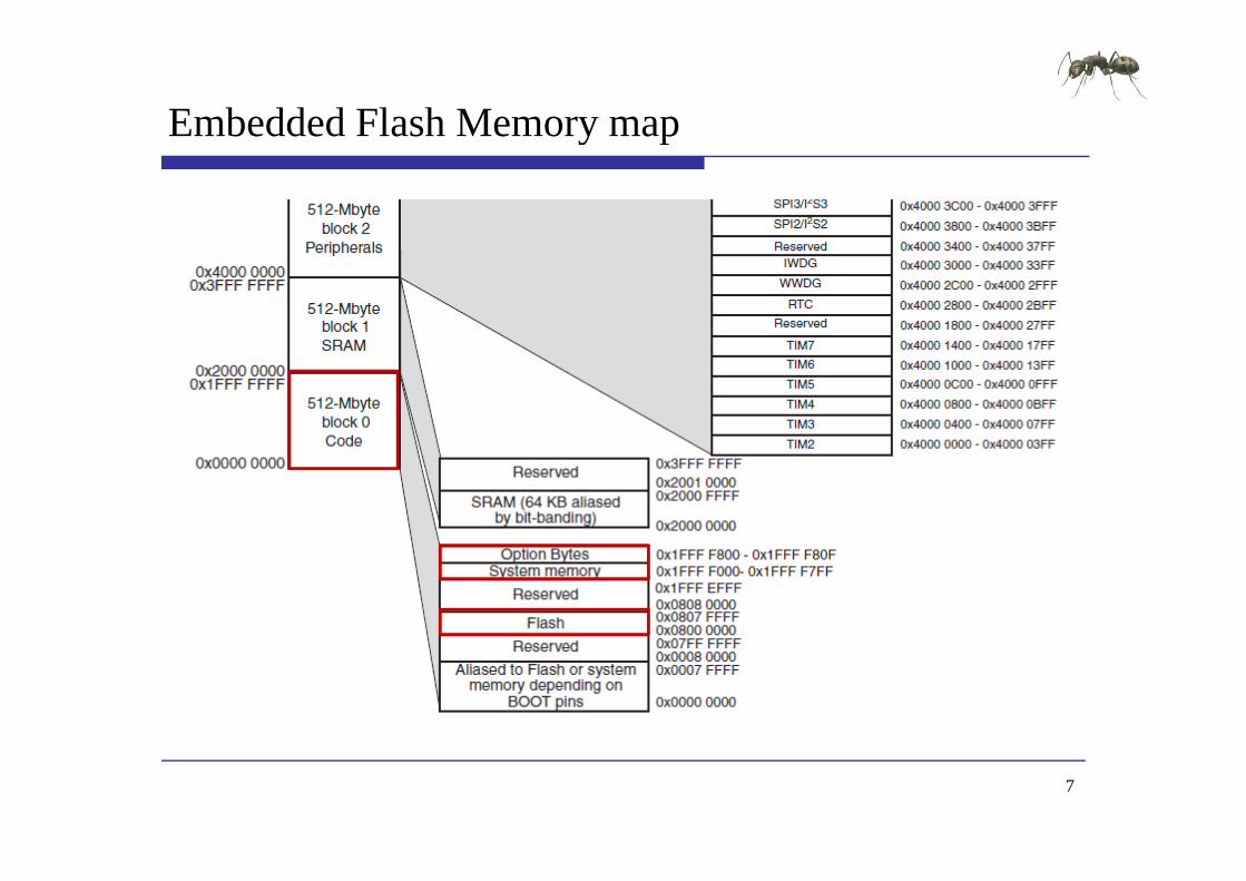
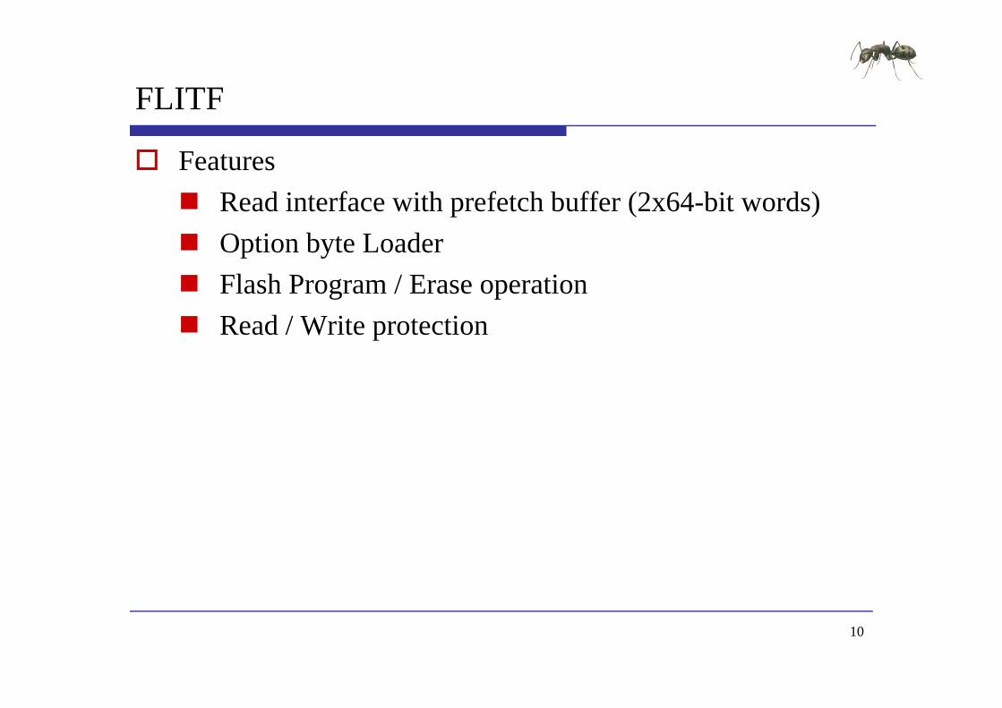
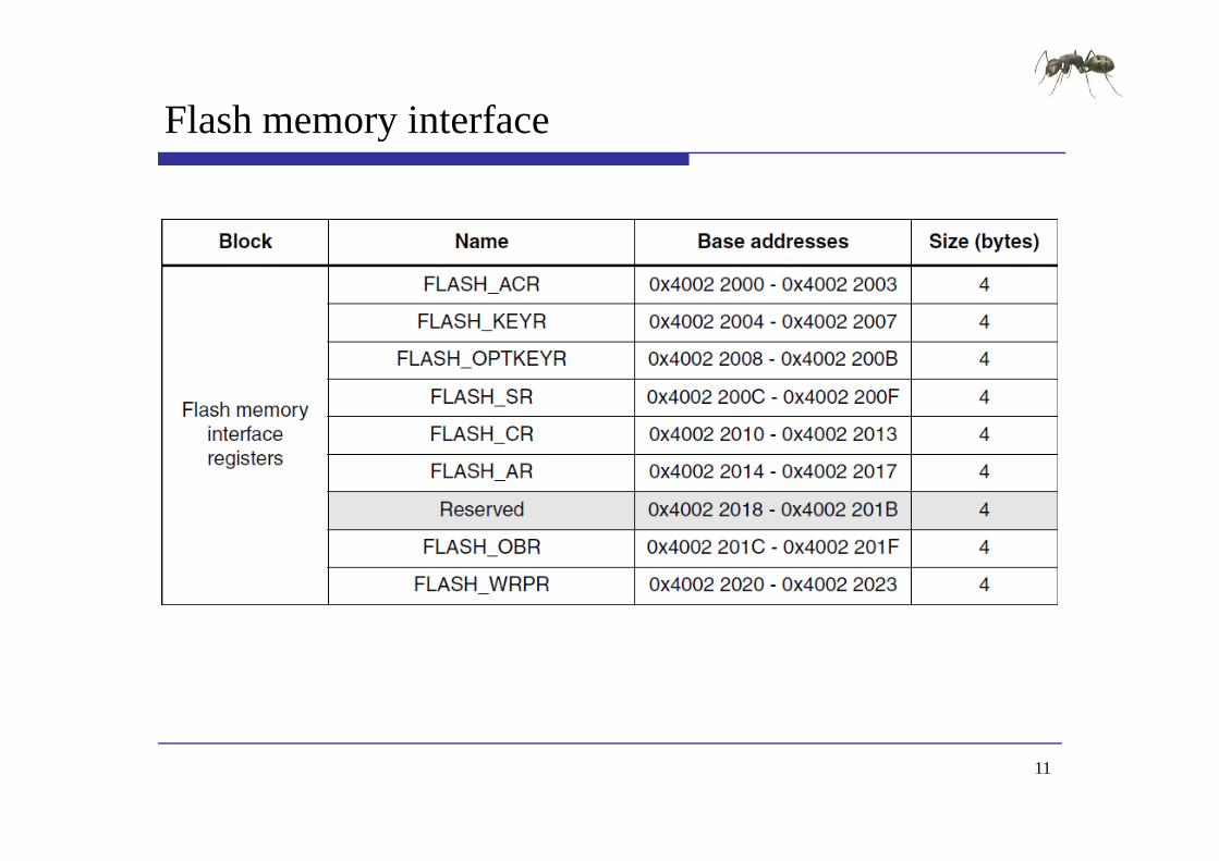

Flash memory interface registery g
Bit 8 FSMCEN FSMC clock enableFlash status register (FLASH_SR)
Bits 316 Reserved must be kept clearedBit 5 EOP End of operation
Bit 2 PGERR Programming errorSet by hardware when an address to be programmed p
Set by hardware when a Flash operation (programming erase) is completed Reset by writing a 1Note EOP is asserted at the end of each successful
y p gcontains a value different from 0xFFFF before programmingReset by writing 1Note The STRT bit in the FLASH_CR register f f
program or erase operationBit 4 WRPRTERR Write protection errorSet by hardware when programming a write-protected address of the Flash memory
_ gshould be reset before starting a programmingoperationBit 1 Reserved must be kept clearedBit 0 BSY Busyp y
Reset by writing 1Bit 3 Reserved must be kept cleared
This indicates that a Flash operation is in progress This is set on the beginning of a Flash operation and reset when the operation finishes or when an error occurs
12
Flash memory interface registery g
Flash control register (FLASH_CR)
Bit 9 OPTWRE Option bytes write enableWhen set the option bytes can be programmed This
Bit 6 STRT StartThis bit triggers an ERASE operation when set This bit is set only
bit is set on writing the correct key sequence to the FLASH_OPTKEYR registerThis bit can be reset by softwareBit 8 Reserved must be kept clearedBit 7 LOCK Lock
by software and reset when the BSY bit is resetBit 5 OPTER Option byte eraseOption byte erase chosenBit 4 OPTPG Option byte programmingOption byte programming chosenBit 7 LOCK Lock
Write to 1 only When it is set it indicates that the FPEC and FLASH_CR are locked This bit is reset by hardware after detecting the unlock sequenceIn the event of unsuccessful unlock operation this bit remains set until the next reset
p y p g gBit 3 Reserved must be kept clearedBit 2 MER Mass eraseErase of all user pages chosenBit 1 PER Page erasePage Erase chosenremains set until the next reset Page Erase chosenBit 0 PG ProgrammingFlash programming chosen
13
Main Flash memory programmingy p g g
14
Flash memory Page Erasey g
15
Flash memory Mass Erasey
16
Option byte programmingp y p g g
17
Option byte Erasep y
18
FLASH library functiony
19
FLASH library functiony
20
Development Flowp
Embedded Software Side
int main(void)
Bootup STM32F10x
ProgrammingBootupSTM32F10x RCC Configure
NVIC Configure
int main(void)ifdef DEBUGdebug()
endifendif
FLASHStatus = FLASH_COMPLETEMemoryProgramStatus = PASSEDData = 0x15041975
GPIO Configure
Data = 0x15041975
RCC Configuration RCC_Configuration()
Flash memory RW operation FLASH Unlock
FLASH ClearFlag NVIC Configuration NVIC_Configuration()
GPIO Configuration
FLASH ClearFlag
FLASH ErasePage
FLASH ProgramWord GPIO Configuration GPIO_Configuration()
helliphelliphelliphelliphelliphelliphelliphelliphelliphelliphelliphelliphelliphelliphelliphelliphellipDisplay Result
Check content
21
實驗步驟
範例目錄架構
範例說明 範例說明
預設定義說明
燒錄 燒錄MIAT_STM32
22
範例目錄架構
範例目錄
測試映像檔 測試映像檔
含括檔
函式庫 函式庫
專案檔
原始碼 原始碼
23
範例說明
Function name Description
Unlock the Flash Program Erase controller FLASH_Unlock()
D fi h b f b d
Flash FwLib Functions List
Function name Description
FLASH_Unlock Unlocks the FLASH Program Erase Controller
FLASH_ClearFlag Clears the FLASH pending fl
Define the number of page to be erased NbrOfPage = (EndAddr - StartAddr) FLASH_PAGE_SIZE
Clear All pending flags FLASH_ClearFlag(FLASH_FLAG_BSY | FLASH_FLAG_EOP | FLASH_FLAG_PGERR |
FLASH FLAG WRPRTERR)flags
FLASH_ErasePage Erases a specified FLASH page
FLASH_ProgramWord Programs a word at a specified
_ _ )
Erase the FLASH pages for(EraseCounter = 0 (EraseCounter lt NbrOfPage) ampamp (FLASHStatus ==
FLASH_COMPLETE) EraseCounter++)FLASHStatus = FLASH ErasePage(StartAddr + (FLASH PAGE SIZE EraseCounter))address FLASHStatus = FLASH_ErasePage(StartAddr + (FLASH_PAGE_SIZE EraseCounter))
FLASH Word program of data 0x15041979 at addresses defined by StartAddr and EndAddrAddress = StartAddr
while((Address lt EndAddr) ampamp (FLASHStatus == FLASH_COMPLETE))FLASHStatus = FLASH_ProgramWord(Address Data)Address = Address + 4
24
範例說明
Embedded Software Side
Check the corectness of written data
Display Result
Check the corectness of written data Address = StartAddr
while((Address lt EndAddr) ampamp (MemoryProgramStatus = FAILED))if(((vu32) Address) = Data)
Flash memory RW operation
MemoryProgramStatus = FAILED
Address += 4
Check content
Display Result while (1)if (MemoryProgramStatus == PASSED) OK Turn on USERLED GPIO_SetBits(GPIOF GPIO_Pin_11)
Display Result
else KO Turn off USERLED GPIO_ResetBits(GPIOF GPIO_Pin_11) Insert delay Delay(0xAFFFF)
如果寫入與讀取Flash內容相同Flash記憶體使用正常USERLED紅燈恆亮
Turn on USERLED GPIO_SetBits(GPIOF GPIO_Pin_11) Insert delay Delay(0xAFFFF)
如果寫入與讀取Flash內容不同Flash記憶體使用異常USERLED紅燈閃爍
25
預設定義說明
define StartAddr ((u32)0x08008000) 定義Flash使用起始點 定義Flash使用起始點
使用起始點必需大於0x8003000 + Code Size 附註 0x8000000~0x8003000為DFU程式區塊使用此區塊
將造成無法燒錄程式
Code Size可由產生的HEX檔得知
d fi E dAdd (( 32)0 0800C000) define EndAddr ((u32)0x0800C000) 定義Flash使用結束點
使用起始點必需小於0x8040000使用起始點必需小於
Data = 0x15041975 寫入資料
32Bit define FLASH_PAGE_SIZE ((u16)0x800)
每一個Page有2KByte26
每一個Page有2KByte
Intel HEX Format
aaaa tt dd cc
field Description
the colon that starts every Intel HEX record
the record-length field that represents the number of data bytes (dd) in the record
aaaa the address field that represents the starting address for subsequent data in the record
tt the field that represents the HEX record type which may be one of the following00 - data record01 - end-of-file record02 - extended segment address recordg04 - extended linear address record
dd a data field that represents one byte of data A record may have multiple data bytes The number of data bytes in the record must match the number specified by the field
cc the checksum field that represents the checksum of the record The checksum is calculated by summing the values of all hexadecimal digit pairs in the record modulo 256 and taking the twos complement
27
HEX Examplep
020000040800F2103000001814002045310008D9340008CD340008D8103000001814002045310008D9340008CD340008D8helliphelliphellip1038200042370008000000000000000000000000170C3830000000000000000000000000008C
資料填入起始位置為
0C3830000000000000000000000000008C04000005080031318D00000001FF
資料填入起始位置為0x08003000 每一行有0x10(16)個Bytes 最後一筆資料為
資料結束點為0x0803383004000005080031318D
(0x08003830 -0x08000000)0x800 = 7 需以0x800為單位所以使用的位置起點為0x08004000
28
燒錄MIAT STM32_
Rebuilder all target files產生HEX DFU Fil M 轉換HEX產生DFU DFU File Manager轉換HEX產生DFU DfuSe Demonstration燒錄DFU d Leave DFU mode
29
內部Flash存取控制實驗
實驗一
WU-YANGTechnology Co Ltd
實驗一練習
注意 請使用預設0 08008000之後的位置 避免覆蓋DFU 請使用預設0x08008000之後的位置避免覆蓋DFU
與使用者程式碼區塊
練習 練習 修改存取位置測試是否正常
修改寫入資料測試是否正常 修改寫入資料測試是否正常
修改寫入資料後取消FLASH_Unlock測試是否正常
修改寫入資料後取消FLASH E P 測試是否正 修改寫入資料後取消FLASH_ErasePage測試是否正常
31
實驗目的(二)( )
使用MIAT_STM32實驗板透過Flash memory interface (FLITF)控制內部Flash進行存取控制實驗並利用SW(FLITF)控制內部Flash進行存取控制實驗並利用SWKEY決定資料寫入與讀取LCD顯示狀態
32
實驗原理
System requirement E b dd d Fl h Embedded Flash LCD KEY SW
Development Flow ARM Configure
33
Development Flowp
Embedded Software Side
int main(void)
Bootup STM32F10x
ProgrammingBootupSTM32F10x RCC Configure
NVIC Configure
int main(void)ifdef DEBUGdebug()
endif
FLASHStatus = FLASH_COMPLETE
RCC Configuration RCC Configuration()
GPIO Configure
BasicIO Configure_ g ()
NVIC Configuration NVIC_Configuration()
GPIO Configuration Flash memory RW ti
lcd Configure
GPIO Configuration GPIO_Configuration()
Init_BasicIO()
l d i i () LCD I i i li i
RW operation
Example
FLASH Unlock
FLASH ClearFlag
lcd_init() LCD Initialization
helliphelliphelliphelliphelliphelliphelliphelliphelliphelliphelliphelliphelliphelliphelliphelliphelliphelliphelliphelliphelliphelliphellip
p
34
硬體電路配置
Mapping Table
Num MIAT_STM32V2 MIAT_IOBV1 Num MIAT_STM32V2 MIAT_IOBV1
1 PC8 (326) SW1 10 PE6 (15) LCD_EN2 PC9 (327) SW2 11 PF6 (118) LCD RW ( ) ( ) _3 PC10 (43) SW3 12 PF7 (119) LCD_RS 4 PC11 (44) SW4 13 PF8(120) LCD_D4 5 PB5 (427) KEY1 14 PF9 (121) LCD_D5 6 PB6 (428) KEY2 15 PF10 (122) LCD_D6 7 PB7 (429) KEY3 16 PF11 (213) LCD_D7 8 PB8 (431) KEY4 17 VDD (236) VCC33V 9 VCC5V (1 36) VCC5V 18 GND (1 35) GND9 VCC5V (136) VCC5V 18 GND (135) GND
35
實驗步驟
範例目錄架構
範例說明 範例說明
預設定義說明
36
範例目錄架構
範例目錄
測試映像檔 測試映像檔
含括檔
函式庫 函式庫
專案檔
原始碼 原始碼
37
範例說明
Embedded Software Side
lcd clear()
FLASH memory RW operation
lcd_clear()lcd_print (MIAT_STM32 DEMO )
Unlock the Flash Program Erase controller FLASH_Unlock()
Flash memory RW operation
FLASH Unlock
Clear All pending flags FLASH_ClearFlag(FLASH_FLAG_BSY | FLASH_FLAG_EOP | FLASH_FLAG_PGERR |
FLASH_FLAG_WRPRTERR)
while(1)
Example
FLASH ClearFlag
( )
KEY_Buffer=Key_Scan()set_cursor (0 1)lcd_print (SW Value = 0x)lcd putchar(((SWamp0x7)+0x30))lcd_putchar(((SWamp0x7)+0x30))if(KEY_Buffer==1)Address=(StartAddr|(SWltlt12))set_cursor (0 0)lcd_print (Set Addr = 0x)
掃描KEY是否按下與顯示SW數值LCD Line2顯示SW Value = 0x(SW)
lcd_putchar(((SWamp0x7)+0x30))lcd_print ( )
如果KEY1按下記錄SW數值至Address LCD Line1顯示Set Adde = 0x(Address)
38
範例說明
Embedded Software Side
else if(KEY Buffer==2)
FLASH memory RW operation
else if(KEY_Buffer==2)
Erase the FLASH pages FLASHStatus = FLASH_ErasePage(Address)
FLASH Word program of data at addresses defined by SW
SRAM memory RW operation
p g yFLASHStatus = FLASH_ProgramWord(Address (SWamp0x7))
set_cursor (0 0)lcd_print (Write 0x)lcd_putchar(((SWamp0x7)+0x30))l d i t ( t 0 )
Example如果KEY2按下清除Address所處區塊並寫入SW數值 lcd_print ( at 0x)
lcd_putchar((((Addressgtgt12)amp0x7)+0x30))else if(KEY_Buffer==3)
Data=(u16 )Address
所處區塊並寫入SW數值LCD Line1顯示Write 0x(SW) at 0x(Adddress)
Data (u16 )Addressset_cursor (0 0)lcd_print (Addr 0x)lcd_putchar((((Addressgtgt12)amp0x7)+0x30))lcd_print ( = 0x)lcd_putchar(((Dataamp0x7)+0x30))lcd_print ( )
如果KEY3按下讀取Address紀錄數值LCD Line1顯示Addr 0x(Adddress) = 0x
39
預設定義說明
define StartAddr ((u32)0x08020000) 定義Flash使用起始點 定義Flash使用起始點
使用起始點必需大於0x8003000 + Code Size 附註 0x8000000~0x8003000為DFU程式區塊使用此區塊
將造成無法燒錄程式
Code Size可由產生的HEX檔得知
32 Add 0 08020000 u32 Address = 0x08020000 定義Address初始值
初始值必需與Flash使用起始點相同初始值必需與 使用起始點相同
Address=(StartAddr|(SWltlt12)) Example StartAddr = 0x08020000 SW = 1 Address = 0x08021000
StartAddr = 0x08020000 SW = 7 Address = 0x08027000 StartAddr|(7ltlt12)必需小於0x8040000
40
使用者界面與Flash存取控制實驗
實驗二
WU-YANGTechnology Co Ltd
實驗二練習
注意 請使用預設0 08020000之後的位置 避免覆蓋DFU 請使用預設0x08020000之後的位置避免覆蓋DFU
與使用者程式碼區塊
練習 練習 利用SW與KEY測試Flash寫入與讀取是否正常
Fl h寫入後電源關閉 再開啟後寫入資料是否仍存 Flash寫入後電源關閉再開啟後寫入資料是否仍存在
修改存取位置測試是否正常 修改存取位置測試是否正常
42
實驗目的(三)( )
使用MIAT_STM32實驗板透過Flash memory interface (FLITF)控制內部Flash進行存取控制實驗並藉由填入(FLITF)控制內部Flash進行存取控制實驗並藉由填入Option Bytes 設定寫入鎖定保護Page鎖定不被覆蓋
43
Development Flowp
Embedded Software Side
int main(void)
Bootup STM32F10x
ProgrammingBootupSTM32F10x RCC Configure
NVIC Configure
int main(void)ifdef DEBUGdebug()
endifendif
FLASHStatus = FLASH_COMPLETEMemoryProgramStatus = PASSEDData = 0x1753
GPIO Configure
Data = 0x1753
RCC Configuration RCC_Configuration()
Flash memory RW operation FLASH Unlock
FLASH ClearFlag NVIC Configuration NVIC_Configuration()
GPIO Configuration
FLASH ClearFlag
FLASH ErasePage
FLASH ProgramHalfWord GPIO Configuration GPIO_Configuration()
Display Result
Check content
44
helliphelliphelliphelliphelliphelliphelliphelliphelliphelliphelliphelliphelliphelliphelliphelliphelliphelliphellip
實驗步驟
範例目錄架構
範例說明 範例說明
預設定義說明
45
範例目錄架構
範例目錄
測試映像檔 測試映像檔
含括檔
函式庫 函式庫
專案檔
原始碼 原始碼
46
範例說明
Function name Description
Unlock the Flash Program Erase controller FLASH_Unlock()
Define the number of page to be erased
Flash FwLib Functions List
Function name Description
FLASH_Unlock Unlocks the FLASH Program Erase Controller
FLASH_ClearFlag Clears the FLASH pending fl
Define the number of page to be erased NbrOfPage = (EndAddr ‐ StartAddr) FLASH_PAGE_SIZE
FLASH_ClearFlag(FLASH_FLAG_BSY | FLASH_FLAG_EOP|FLASH_FLAG_PGERR |FLASH_FLAG_WRPRTERR)
Get pages write protection status flags
FLASH_EraseOptionBytes
Erases the FLASH option bytes
FLASH_EnableWritePro Write protects the desired
p g pWRPR_Value = FLASH_GetWriteProtectionOptionByte()ProtectedPages = WRPR_Value amp 0x000000C0
ifdef WriteProtection_Disableif (ProtectedPages == 0x00) Pages are write protected
tection pages
NVIC_GenerateSystemReset
Generate a system reset
Disable the write protection FLASHStatus = FLASH_EraseOptionBytes() Generate System Reset to load the new option byte values NVIC_GenerateSystemReset()
elseifdef WriteProtection Enableifdef WriteProtection_Enableif (ProtectedPages = 0x00) Pages not write protected
FLASHStatus = FLASH_EraseOptionBytes() Enable the pages write protection FLASHStatus = FLASH_EnableWriteProtection(FLASH_WRProt_Pages12to13
|FLASH WRProt Pages14to15)|FLASH_WRProt_Pages14to15) Generate System Reset to load the new option byte values NVIC_GenerateSystemReset()
endifendif
47
範例說明
if (ProtectedPages = 0x00) Clear All pending flags
Flash FwLib Functions List
Function name DescriptionFLASH_ClearFlag(FLASH_FLAG_BSY |
FLASH_FLAG_EOP|FLASH_FLAG_PGERR |FLASH_FLAG_WRPRTERR)
erase the FLASH pages for(EraseCounter = 0 (EraseCounter lt NbrOfPage) ampamp (FLASHStatus ==
Function name Description
FLASH_ErasePage Erases a specified FLASH page
FLASH_ProgramHalfWod
Programs a half word at a ifi d dd FLASH_COMPLETE) EraseCounter++)
FLASHStatus = FLASH_ErasePage(StartAddr + (FLASH_PAGE_SIZE
EraseCounter))
rd specified address
FLASH Half Word program of data 0x1753 at addresses defined by StartAddrand EndAddr
Address = StartAddr
hil ((Add E dAdd ) ampamp (FLASHSt t FLASH COMPLETE))while((Address lt EndAddr) ampamp (FLASHStatus == FLASH_COMPLETE))
FLASHStatus = FLASH_ProgramHalfWord(Address Data)Address = Address + 2
48
範例說明
Embedded Software Side
Check the corectness of written data
Display Result
Check the corectness of written data Address = StartAddr
while((Address lt EndAddr) ampamp (MemoryProgramStatus = FAILED))if(((vu16) Address) = Data)
Flash memory RW operation
MemoryProgramStatus = FAILED
Address += 2
Check content
Display Result while (1)if (MemoryProgramStatus == PASSED) OK Turn on USERLED GPIO_SetBits(GPIOF GPIO_Pin_11)
Display Result
else KO Turn off USERLED GPIO_ResetBits(GPIOF GPIO_Pin_11) Insert delay Delay(0xAFFFF)
如果寫入與讀取Flash內容相同Flash記憶體可以寫入USERLED紅燈恆亮
Turn on USERLED GPIO_SetBits(GPIOF GPIO_Pin_11) Insert delay Delay(0xAFFFF)
如果寫入與讀取Flash內容不同Flash記憶體不能寫入USERLED紅燈閃爍
49
預設定義說明
define StartAddr ((u32) 0x08006000) 定義Flash使用起始點 定義Flash使用起始點
使用起始點必需大於0x8003000 + Code Size 附註 0x8000000~0x8003000為DFU程式區塊使用此區塊
將造成無法燒錄程式
Code Size可由產生的HEX檔得知
d fi E dAdd (( 32) 0 08008000) define EndAddr ((u32) 0x08008000) 定義Flash使用結束點
使用起始點必需小於0x8040000使用起始點必需小於
Data = 0x1753 寫入資料
16Bit define FLASH_PAGE_SIZE ((u16)0x800) 每一個Page有2KByte
50
每一個Page有2KByte
預設定義說明
define WriteProtection_Enable U hi li E bl W i P i Uncomment this line to Enable Write Protection
define WriteProtection_Disablehi li i bl i i Uncomment this line to Disable Write Protection
FLASH_EnableWriteProtection設定影響 個 設定影響2個Page FLASH_WRProt_Pages0to1 FLASH_WRProt_Pages1to2 helliphellip FLASH_WRProt_Pages60to61
設定影響多個Page FLASH_WRProt_Pages62to255
51
FLASH EnableWriteProtection_
Example
位置0x08006000 ~ 0x08007000每一個Page有0x800ByteStartPage = (0x08006000-0x08000000)0x800 = 12EndPage = ((0x08007000-0x08000000)0x800)-1 = 13執行執行FLASH_EnableWriteProtection(FLASH_WRProt_Pages12to13)將影響Pages12 Pages13
52
內部Flash寫入鎖定存取控制實驗
實驗三
WU-YANGTechnology Co Ltd
實驗三練習
注意 請使用預設0 08006000之後的位置 避免覆蓋DFU 請使用預設0x08006000之後的位置避免覆蓋DFU
與使用者程式碼區塊
更改寫入位置測試寫入鎖定時需同時更改 更改寫入位置測試寫入鎖定時需同時更改FLASH_EnableWriteProtection鎖定之Page
練習 練習 打開define WriteProtection_Enable測試是否可寫入
打開define WriteProtection Disable測試是否可寫入 打開define WriteProtection_Disable測試是否可寫入
修改存取位置測試是否正常
修改寫入資料測試是否正常 修改寫入資料測試是否正常
54
Q amp A
WU-YANGTechnology Co Ltd
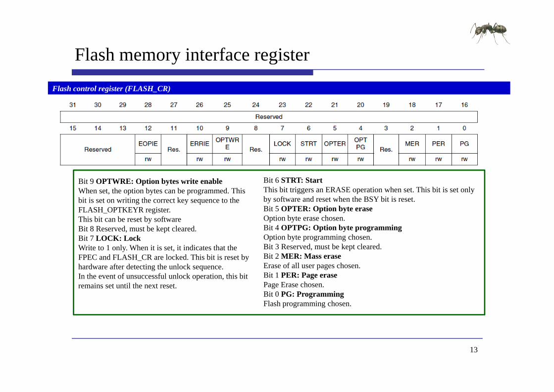
Flash memory interface registery g
Flash control register (FLASH_CR)
Bit 9 OPTWRE Option bytes write enableWhen set the option bytes can be programmed This
Bit 6 STRT StartThis bit triggers an ERASE operation when set This bit is set only
bit is set on writing the correct key sequence to the FLASH_OPTKEYR registerThis bit can be reset by softwareBit 8 Reserved must be kept clearedBit 7 LOCK Lock
by software and reset when the BSY bit is resetBit 5 OPTER Option byte eraseOption byte erase chosenBit 4 OPTPG Option byte programmingOption byte programming chosenBit 7 LOCK Lock
Write to 1 only When it is set it indicates that the FPEC and FLASH_CR are locked This bit is reset by hardware after detecting the unlock sequenceIn the event of unsuccessful unlock operation this bit remains set until the next reset
p y p g gBit 3 Reserved must be kept clearedBit 2 MER Mass eraseErase of all user pages chosenBit 1 PER Page erasePage Erase chosenremains set until the next reset Page Erase chosenBit 0 PG ProgrammingFlash programming chosen
13
Main Flash memory programmingy p g g
14
Flash memory Page Erasey g
15
Flash memory Mass Erasey
16
Option byte programmingp y p g g
17
Option byte Erasep y
18
FLASH library functiony
19
FLASH library functiony
20
Development Flowp
Embedded Software Side
int main(void)
Bootup STM32F10x
ProgrammingBootupSTM32F10x RCC Configure
NVIC Configure
int main(void)ifdef DEBUGdebug()
endifendif
FLASHStatus = FLASH_COMPLETEMemoryProgramStatus = PASSEDData = 0x15041975
GPIO Configure
Data = 0x15041975
RCC Configuration RCC_Configuration()
Flash memory RW operation FLASH Unlock
FLASH ClearFlag NVIC Configuration NVIC_Configuration()
GPIO Configuration
FLASH ClearFlag
FLASH ErasePage
FLASH ProgramWord GPIO Configuration GPIO_Configuration()
helliphelliphelliphelliphelliphelliphelliphelliphelliphelliphelliphelliphelliphelliphelliphelliphellipDisplay Result
Check content
21
實驗步驟
範例目錄架構
範例說明 範例說明
預設定義說明
燒錄 燒錄MIAT_STM32
22
範例目錄架構
範例目錄
測試映像檔 測試映像檔
含括檔
函式庫 函式庫
專案檔
原始碼 原始碼
23
範例說明
Function name Description
Unlock the Flash Program Erase controller FLASH_Unlock()
D fi h b f b d
Flash FwLib Functions List
Function name Description
FLASH_Unlock Unlocks the FLASH Program Erase Controller
FLASH_ClearFlag Clears the FLASH pending fl
Define the number of page to be erased NbrOfPage = (EndAddr - StartAddr) FLASH_PAGE_SIZE
Clear All pending flags FLASH_ClearFlag(FLASH_FLAG_BSY | FLASH_FLAG_EOP | FLASH_FLAG_PGERR |
FLASH FLAG WRPRTERR)flags
FLASH_ErasePage Erases a specified FLASH page
FLASH_ProgramWord Programs a word at a specified
_ _ )
Erase the FLASH pages for(EraseCounter = 0 (EraseCounter lt NbrOfPage) ampamp (FLASHStatus ==
FLASH_COMPLETE) EraseCounter++)FLASHStatus = FLASH ErasePage(StartAddr + (FLASH PAGE SIZE EraseCounter))address FLASHStatus = FLASH_ErasePage(StartAddr + (FLASH_PAGE_SIZE EraseCounter))
FLASH Word program of data 0x15041979 at addresses defined by StartAddr and EndAddrAddress = StartAddr
while((Address lt EndAddr) ampamp (FLASHStatus == FLASH_COMPLETE))FLASHStatus = FLASH_ProgramWord(Address Data)Address = Address + 4
24
範例說明
Embedded Software Side
Check the corectness of written data
Display Result
Check the corectness of written data Address = StartAddr
while((Address lt EndAddr) ampamp (MemoryProgramStatus = FAILED))if(((vu32) Address) = Data)
Flash memory RW operation
MemoryProgramStatus = FAILED
Address += 4
Check content
Display Result while (1)if (MemoryProgramStatus == PASSED) OK Turn on USERLED GPIO_SetBits(GPIOF GPIO_Pin_11)
Display Result
else KO Turn off USERLED GPIO_ResetBits(GPIOF GPIO_Pin_11) Insert delay Delay(0xAFFFF)
如果寫入與讀取Flash內容相同Flash記憶體使用正常USERLED紅燈恆亮
Turn on USERLED GPIO_SetBits(GPIOF GPIO_Pin_11) Insert delay Delay(0xAFFFF)
如果寫入與讀取Flash內容不同Flash記憶體使用異常USERLED紅燈閃爍
25
預設定義說明
define StartAddr ((u32)0x08008000) 定義Flash使用起始點 定義Flash使用起始點
使用起始點必需大於0x8003000 + Code Size 附註 0x8000000~0x8003000為DFU程式區塊使用此區塊
將造成無法燒錄程式
Code Size可由產生的HEX檔得知
d fi E dAdd (( 32)0 0800C000) define EndAddr ((u32)0x0800C000) 定義Flash使用結束點
使用起始點必需小於0x8040000使用起始點必需小於
Data = 0x15041975 寫入資料
32Bit define FLASH_PAGE_SIZE ((u16)0x800)
每一個Page有2KByte26
每一個Page有2KByte
Intel HEX Format
aaaa tt dd cc
field Description
the colon that starts every Intel HEX record
the record-length field that represents the number of data bytes (dd) in the record
aaaa the address field that represents the starting address for subsequent data in the record
tt the field that represents the HEX record type which may be one of the following00 - data record01 - end-of-file record02 - extended segment address recordg04 - extended linear address record
dd a data field that represents one byte of data A record may have multiple data bytes The number of data bytes in the record must match the number specified by the field
cc the checksum field that represents the checksum of the record The checksum is calculated by summing the values of all hexadecimal digit pairs in the record modulo 256 and taking the twos complement
27
HEX Examplep
020000040800F2103000001814002045310008D9340008CD340008D8103000001814002045310008D9340008CD340008D8helliphelliphellip1038200042370008000000000000000000000000170C3830000000000000000000000000008C
資料填入起始位置為
0C3830000000000000000000000000008C04000005080031318D00000001FF
資料填入起始位置為0x08003000 每一行有0x10(16)個Bytes 最後一筆資料為
資料結束點為0x0803383004000005080031318D
(0x08003830 -0x08000000)0x800 = 7 需以0x800為單位所以使用的位置起點為0x08004000
28
燒錄MIAT STM32_
Rebuilder all target files產生HEX DFU Fil M 轉換HEX產生DFU DFU File Manager轉換HEX產生DFU DfuSe Demonstration燒錄DFU d Leave DFU mode
29
內部Flash存取控制實驗
實驗一
WU-YANGTechnology Co Ltd
實驗一練習
注意 請使用預設0 08008000之後的位置 避免覆蓋DFU 請使用預設0x08008000之後的位置避免覆蓋DFU
與使用者程式碼區塊
練習 練習 修改存取位置測試是否正常
修改寫入資料測試是否正常 修改寫入資料測試是否正常
修改寫入資料後取消FLASH_Unlock測試是否正常
修改寫入資料後取消FLASH E P 測試是否正 修改寫入資料後取消FLASH_ErasePage測試是否正常
31
實驗目的(二)( )
使用MIAT_STM32實驗板透過Flash memory interface (FLITF)控制內部Flash進行存取控制實驗並利用SW(FLITF)控制內部Flash進行存取控制實驗並利用SWKEY決定資料寫入與讀取LCD顯示狀態
32
實驗原理
System requirement E b dd d Fl h Embedded Flash LCD KEY SW
Development Flow ARM Configure
33
Development Flowp
Embedded Software Side
int main(void)
Bootup STM32F10x
ProgrammingBootupSTM32F10x RCC Configure
NVIC Configure
int main(void)ifdef DEBUGdebug()
endif
FLASHStatus = FLASH_COMPLETE
RCC Configuration RCC Configuration()
GPIO Configure
BasicIO Configure_ g ()
NVIC Configuration NVIC_Configuration()
GPIO Configuration Flash memory RW ti
lcd Configure
GPIO Configuration GPIO_Configuration()
Init_BasicIO()
l d i i () LCD I i i li i
RW operation
Example
FLASH Unlock
FLASH ClearFlag
lcd_init() LCD Initialization
helliphelliphelliphelliphelliphelliphelliphelliphelliphelliphelliphelliphelliphelliphelliphelliphelliphelliphelliphelliphelliphelliphellip
p
34
硬體電路配置
Mapping Table
Num MIAT_STM32V2 MIAT_IOBV1 Num MIAT_STM32V2 MIAT_IOBV1
1 PC8 (326) SW1 10 PE6 (15) LCD_EN2 PC9 (327) SW2 11 PF6 (118) LCD RW ( ) ( ) _3 PC10 (43) SW3 12 PF7 (119) LCD_RS 4 PC11 (44) SW4 13 PF8(120) LCD_D4 5 PB5 (427) KEY1 14 PF9 (121) LCD_D5 6 PB6 (428) KEY2 15 PF10 (122) LCD_D6 7 PB7 (429) KEY3 16 PF11 (213) LCD_D7 8 PB8 (431) KEY4 17 VDD (236) VCC33V 9 VCC5V (1 36) VCC5V 18 GND (1 35) GND9 VCC5V (136) VCC5V 18 GND (135) GND
35
實驗步驟
範例目錄架構
範例說明 範例說明
預設定義說明
36
範例目錄架構
範例目錄
測試映像檔 測試映像檔
含括檔
函式庫 函式庫
專案檔
原始碼 原始碼
37
範例說明
Embedded Software Side
lcd clear()
FLASH memory RW operation
lcd_clear()lcd_print (MIAT_STM32 DEMO )
Unlock the Flash Program Erase controller FLASH_Unlock()
Flash memory RW operation
FLASH Unlock
Clear All pending flags FLASH_ClearFlag(FLASH_FLAG_BSY | FLASH_FLAG_EOP | FLASH_FLAG_PGERR |
FLASH_FLAG_WRPRTERR)
while(1)
Example
FLASH ClearFlag
( )
KEY_Buffer=Key_Scan()set_cursor (0 1)lcd_print (SW Value = 0x)lcd putchar(((SWamp0x7)+0x30))lcd_putchar(((SWamp0x7)+0x30))if(KEY_Buffer==1)Address=(StartAddr|(SWltlt12))set_cursor (0 0)lcd_print (Set Addr = 0x)
掃描KEY是否按下與顯示SW數值LCD Line2顯示SW Value = 0x(SW)
lcd_putchar(((SWamp0x7)+0x30))lcd_print ( )
如果KEY1按下記錄SW數值至Address LCD Line1顯示Set Adde = 0x(Address)
38
範例說明
Embedded Software Side
else if(KEY Buffer==2)
FLASH memory RW operation
else if(KEY_Buffer==2)
Erase the FLASH pages FLASHStatus = FLASH_ErasePage(Address)
FLASH Word program of data at addresses defined by SW
SRAM memory RW operation
p g yFLASHStatus = FLASH_ProgramWord(Address (SWamp0x7))
set_cursor (0 0)lcd_print (Write 0x)lcd_putchar(((SWamp0x7)+0x30))l d i t ( t 0 )
Example如果KEY2按下清除Address所處區塊並寫入SW數值 lcd_print ( at 0x)
lcd_putchar((((Addressgtgt12)amp0x7)+0x30))else if(KEY_Buffer==3)
Data=(u16 )Address
所處區塊並寫入SW數值LCD Line1顯示Write 0x(SW) at 0x(Adddress)
Data (u16 )Addressset_cursor (0 0)lcd_print (Addr 0x)lcd_putchar((((Addressgtgt12)amp0x7)+0x30))lcd_print ( = 0x)lcd_putchar(((Dataamp0x7)+0x30))lcd_print ( )
如果KEY3按下讀取Address紀錄數值LCD Line1顯示Addr 0x(Adddress) = 0x
39
預設定義說明
define StartAddr ((u32)0x08020000) 定義Flash使用起始點 定義Flash使用起始點
使用起始點必需大於0x8003000 + Code Size 附註 0x8000000~0x8003000為DFU程式區塊使用此區塊
將造成無法燒錄程式
Code Size可由產生的HEX檔得知
32 Add 0 08020000 u32 Address = 0x08020000 定義Address初始值
初始值必需與Flash使用起始點相同初始值必需與 使用起始點相同
Address=(StartAddr|(SWltlt12)) Example StartAddr = 0x08020000 SW = 1 Address = 0x08021000
StartAddr = 0x08020000 SW = 7 Address = 0x08027000 StartAddr|(7ltlt12)必需小於0x8040000
40
使用者界面與Flash存取控制實驗
實驗二
WU-YANGTechnology Co Ltd
實驗二練習
注意 請使用預設0 08020000之後的位置 避免覆蓋DFU 請使用預設0x08020000之後的位置避免覆蓋DFU
與使用者程式碼區塊
練習 練習 利用SW與KEY測試Flash寫入與讀取是否正常
Fl h寫入後電源關閉 再開啟後寫入資料是否仍存 Flash寫入後電源關閉再開啟後寫入資料是否仍存在
修改存取位置測試是否正常 修改存取位置測試是否正常
42
實驗目的(三)( )
使用MIAT_STM32實驗板透過Flash memory interface (FLITF)控制內部Flash進行存取控制實驗並藉由填入(FLITF)控制內部Flash進行存取控制實驗並藉由填入Option Bytes 設定寫入鎖定保護Page鎖定不被覆蓋
43
Development Flowp
Embedded Software Side
int main(void)
Bootup STM32F10x
ProgrammingBootupSTM32F10x RCC Configure
NVIC Configure
int main(void)ifdef DEBUGdebug()
endifendif
FLASHStatus = FLASH_COMPLETEMemoryProgramStatus = PASSEDData = 0x1753
GPIO Configure
Data = 0x1753
RCC Configuration RCC_Configuration()
Flash memory RW operation FLASH Unlock
FLASH ClearFlag NVIC Configuration NVIC_Configuration()
GPIO Configuration
FLASH ClearFlag
FLASH ErasePage
FLASH ProgramHalfWord GPIO Configuration GPIO_Configuration()
Display Result
Check content
44
helliphelliphelliphelliphelliphelliphelliphelliphelliphelliphelliphelliphelliphelliphelliphelliphelliphelliphellip
實驗步驟
範例目錄架構
範例說明 範例說明
預設定義說明
45
範例目錄架構
範例目錄
測試映像檔 測試映像檔
含括檔
函式庫 函式庫
專案檔
原始碼 原始碼
46
範例說明
Function name Description
Unlock the Flash Program Erase controller FLASH_Unlock()
Define the number of page to be erased
Flash FwLib Functions List
Function name Description
FLASH_Unlock Unlocks the FLASH Program Erase Controller
FLASH_ClearFlag Clears the FLASH pending fl
Define the number of page to be erased NbrOfPage = (EndAddr ‐ StartAddr) FLASH_PAGE_SIZE
FLASH_ClearFlag(FLASH_FLAG_BSY | FLASH_FLAG_EOP|FLASH_FLAG_PGERR |FLASH_FLAG_WRPRTERR)
Get pages write protection status flags
FLASH_EraseOptionBytes
Erases the FLASH option bytes
FLASH_EnableWritePro Write protects the desired
p g pWRPR_Value = FLASH_GetWriteProtectionOptionByte()ProtectedPages = WRPR_Value amp 0x000000C0
ifdef WriteProtection_Disableif (ProtectedPages == 0x00) Pages are write protected
tection pages
NVIC_GenerateSystemReset
Generate a system reset
Disable the write protection FLASHStatus = FLASH_EraseOptionBytes() Generate System Reset to load the new option byte values NVIC_GenerateSystemReset()
elseifdef WriteProtection Enableifdef WriteProtection_Enableif (ProtectedPages = 0x00) Pages not write protected
FLASHStatus = FLASH_EraseOptionBytes() Enable the pages write protection FLASHStatus = FLASH_EnableWriteProtection(FLASH_WRProt_Pages12to13
|FLASH WRProt Pages14to15)|FLASH_WRProt_Pages14to15) Generate System Reset to load the new option byte values NVIC_GenerateSystemReset()
endifendif
47
範例說明
if (ProtectedPages = 0x00) Clear All pending flags
Flash FwLib Functions List
Function name DescriptionFLASH_ClearFlag(FLASH_FLAG_BSY |
FLASH_FLAG_EOP|FLASH_FLAG_PGERR |FLASH_FLAG_WRPRTERR)
erase the FLASH pages for(EraseCounter = 0 (EraseCounter lt NbrOfPage) ampamp (FLASHStatus ==
Function name Description
FLASH_ErasePage Erases a specified FLASH page
FLASH_ProgramHalfWod
Programs a half word at a ifi d dd FLASH_COMPLETE) EraseCounter++)
FLASHStatus = FLASH_ErasePage(StartAddr + (FLASH_PAGE_SIZE
EraseCounter))
rd specified address
FLASH Half Word program of data 0x1753 at addresses defined by StartAddrand EndAddr
Address = StartAddr
hil ((Add E dAdd ) ampamp (FLASHSt t FLASH COMPLETE))while((Address lt EndAddr) ampamp (FLASHStatus == FLASH_COMPLETE))
FLASHStatus = FLASH_ProgramHalfWord(Address Data)Address = Address + 2
48
範例說明
Embedded Software Side
Check the corectness of written data
Display Result
Check the corectness of written data Address = StartAddr
while((Address lt EndAddr) ampamp (MemoryProgramStatus = FAILED))if(((vu16) Address) = Data)
Flash memory RW operation
MemoryProgramStatus = FAILED
Address += 2
Check content
Display Result while (1)if (MemoryProgramStatus == PASSED) OK Turn on USERLED GPIO_SetBits(GPIOF GPIO_Pin_11)
Display Result
else KO Turn off USERLED GPIO_ResetBits(GPIOF GPIO_Pin_11) Insert delay Delay(0xAFFFF)
如果寫入與讀取Flash內容相同Flash記憶體可以寫入USERLED紅燈恆亮
Turn on USERLED GPIO_SetBits(GPIOF GPIO_Pin_11) Insert delay Delay(0xAFFFF)
如果寫入與讀取Flash內容不同Flash記憶體不能寫入USERLED紅燈閃爍
49
預設定義說明
define StartAddr ((u32) 0x08006000) 定義Flash使用起始點 定義Flash使用起始點
使用起始點必需大於0x8003000 + Code Size 附註 0x8000000~0x8003000為DFU程式區塊使用此區塊
將造成無法燒錄程式
Code Size可由產生的HEX檔得知
d fi E dAdd (( 32) 0 08008000) define EndAddr ((u32) 0x08008000) 定義Flash使用結束點
使用起始點必需小於0x8040000使用起始點必需小於
Data = 0x1753 寫入資料
16Bit define FLASH_PAGE_SIZE ((u16)0x800) 每一個Page有2KByte
50
每一個Page有2KByte
預設定義說明
define WriteProtection_Enable U hi li E bl W i P i Uncomment this line to Enable Write Protection
define WriteProtection_Disablehi li i bl i i Uncomment this line to Disable Write Protection
FLASH_EnableWriteProtection設定影響 個 設定影響2個Page FLASH_WRProt_Pages0to1 FLASH_WRProt_Pages1to2 helliphellip FLASH_WRProt_Pages60to61
設定影響多個Page FLASH_WRProt_Pages62to255
51
FLASH EnableWriteProtection_
Example
位置0x08006000 ~ 0x08007000每一個Page有0x800ByteStartPage = (0x08006000-0x08000000)0x800 = 12EndPage = ((0x08007000-0x08000000)0x800)-1 = 13執行執行FLASH_EnableWriteProtection(FLASH_WRProt_Pages12to13)將影響Pages12 Pages13
52
內部Flash寫入鎖定存取控制實驗
實驗三
WU-YANGTechnology Co Ltd
實驗三練習
注意 請使用預設0 08006000之後的位置 避免覆蓋DFU 請使用預設0x08006000之後的位置避免覆蓋DFU
與使用者程式碼區塊
更改寫入位置測試寫入鎖定時需同時更改 更改寫入位置測試寫入鎖定時需同時更改FLASH_EnableWriteProtection鎖定之Page
練習 練習 打開define WriteProtection_Enable測試是否可寫入
打開define WriteProtection Disable測試是否可寫入 打開define WriteProtection_Disable測試是否可寫入
修改存取位置測試是否正常
修改寫入資料測試是否正常 修改寫入資料測試是否正常
54
Q amp A
WU-YANGTechnology Co Ltd
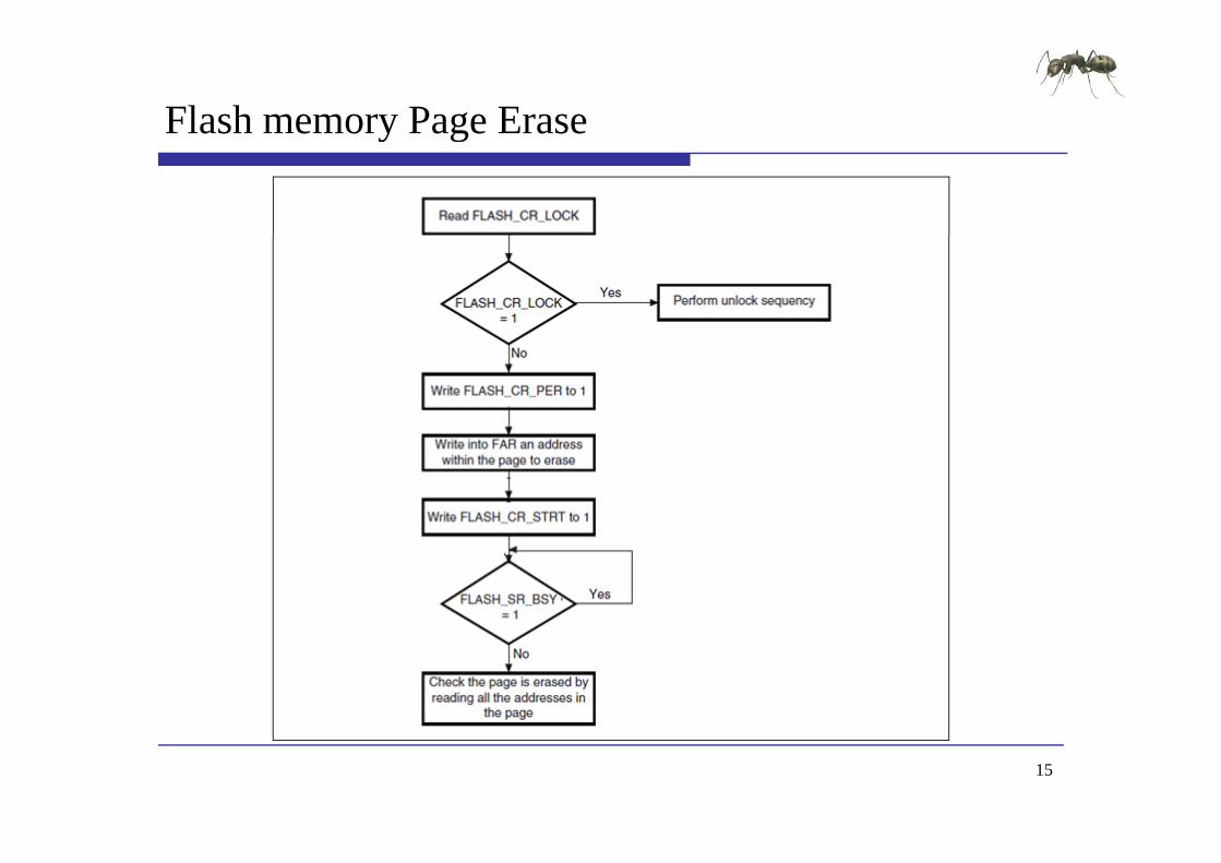
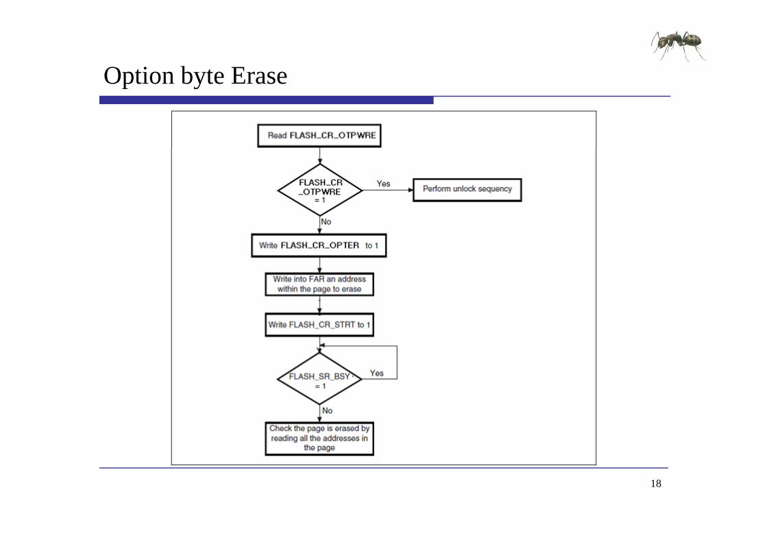

FLASH library functiony
19
FLASH library functiony
20
Development Flowp
Embedded Software Side
int main(void)
Bootup STM32F10x
ProgrammingBootupSTM32F10x RCC Configure
NVIC Configure
int main(void)ifdef DEBUGdebug()
endifendif
FLASHStatus = FLASH_COMPLETEMemoryProgramStatus = PASSEDData = 0x15041975
GPIO Configure
Data = 0x15041975
RCC Configuration RCC_Configuration()
Flash memory RW operation FLASH Unlock
FLASH ClearFlag NVIC Configuration NVIC_Configuration()
GPIO Configuration
FLASH ClearFlag
FLASH ErasePage
FLASH ProgramWord GPIO Configuration GPIO_Configuration()
helliphelliphelliphelliphelliphelliphelliphelliphelliphelliphelliphelliphelliphelliphelliphelliphellipDisplay Result
Check content
21
實驗步驟
範例目錄架構
範例說明 範例說明
預設定義說明
燒錄 燒錄MIAT_STM32
22
範例目錄架構
範例目錄
測試映像檔 測試映像檔
含括檔
函式庫 函式庫
專案檔
原始碼 原始碼
23
範例說明
Function name Description
Unlock the Flash Program Erase controller FLASH_Unlock()
D fi h b f b d
Flash FwLib Functions List
Function name Description
FLASH_Unlock Unlocks the FLASH Program Erase Controller
FLASH_ClearFlag Clears the FLASH pending fl
Define the number of page to be erased NbrOfPage = (EndAddr - StartAddr) FLASH_PAGE_SIZE
Clear All pending flags FLASH_ClearFlag(FLASH_FLAG_BSY | FLASH_FLAG_EOP | FLASH_FLAG_PGERR |
FLASH FLAG WRPRTERR)flags
FLASH_ErasePage Erases a specified FLASH page
FLASH_ProgramWord Programs a word at a specified
_ _ )
Erase the FLASH pages for(EraseCounter = 0 (EraseCounter lt NbrOfPage) ampamp (FLASHStatus ==
FLASH_COMPLETE) EraseCounter++)FLASHStatus = FLASH ErasePage(StartAddr + (FLASH PAGE SIZE EraseCounter))address FLASHStatus = FLASH_ErasePage(StartAddr + (FLASH_PAGE_SIZE EraseCounter))
FLASH Word program of data 0x15041979 at addresses defined by StartAddr and EndAddrAddress = StartAddr
while((Address lt EndAddr) ampamp (FLASHStatus == FLASH_COMPLETE))FLASHStatus = FLASH_ProgramWord(Address Data)Address = Address + 4
24
範例說明
Embedded Software Side
Check the corectness of written data
Display Result
Check the corectness of written data Address = StartAddr
while((Address lt EndAddr) ampamp (MemoryProgramStatus = FAILED))if(((vu32) Address) = Data)
Flash memory RW operation
MemoryProgramStatus = FAILED
Address += 4
Check content
Display Result while (1)if (MemoryProgramStatus == PASSED) OK Turn on USERLED GPIO_SetBits(GPIOF GPIO_Pin_11)
Display Result
else KO Turn off USERLED GPIO_ResetBits(GPIOF GPIO_Pin_11) Insert delay Delay(0xAFFFF)
如果寫入與讀取Flash內容相同Flash記憶體使用正常USERLED紅燈恆亮
Turn on USERLED GPIO_SetBits(GPIOF GPIO_Pin_11) Insert delay Delay(0xAFFFF)
如果寫入與讀取Flash內容不同Flash記憶體使用異常USERLED紅燈閃爍
25
預設定義說明
define StartAddr ((u32)0x08008000) 定義Flash使用起始點 定義Flash使用起始點
使用起始點必需大於0x8003000 + Code Size 附註 0x8000000~0x8003000為DFU程式區塊使用此區塊
將造成無法燒錄程式
Code Size可由產生的HEX檔得知
d fi E dAdd (( 32)0 0800C000) define EndAddr ((u32)0x0800C000) 定義Flash使用結束點
使用起始點必需小於0x8040000使用起始點必需小於
Data = 0x15041975 寫入資料
32Bit define FLASH_PAGE_SIZE ((u16)0x800)
每一個Page有2KByte26
每一個Page有2KByte
Intel HEX Format
aaaa tt dd cc
field Description
the colon that starts every Intel HEX record
the record-length field that represents the number of data bytes (dd) in the record
aaaa the address field that represents the starting address for subsequent data in the record
tt the field that represents the HEX record type which may be one of the following00 - data record01 - end-of-file record02 - extended segment address recordg04 - extended linear address record
dd a data field that represents one byte of data A record may have multiple data bytes The number of data bytes in the record must match the number specified by the field
cc the checksum field that represents the checksum of the record The checksum is calculated by summing the values of all hexadecimal digit pairs in the record modulo 256 and taking the twos complement
27
HEX Examplep
020000040800F2103000001814002045310008D9340008CD340008D8103000001814002045310008D9340008CD340008D8helliphelliphellip1038200042370008000000000000000000000000170C3830000000000000000000000000008C
資料填入起始位置為
0C3830000000000000000000000000008C04000005080031318D00000001FF
資料填入起始位置為0x08003000 每一行有0x10(16)個Bytes 最後一筆資料為
資料結束點為0x0803383004000005080031318D
(0x08003830 -0x08000000)0x800 = 7 需以0x800為單位所以使用的位置起點為0x08004000
28
燒錄MIAT STM32_
Rebuilder all target files產生HEX DFU Fil M 轉換HEX產生DFU DFU File Manager轉換HEX產生DFU DfuSe Demonstration燒錄DFU d Leave DFU mode
29
內部Flash存取控制實驗
實驗一
WU-YANGTechnology Co Ltd
實驗一練習
注意 請使用預設0 08008000之後的位置 避免覆蓋DFU 請使用預設0x08008000之後的位置避免覆蓋DFU
與使用者程式碼區塊
練習 練習 修改存取位置測試是否正常
修改寫入資料測試是否正常 修改寫入資料測試是否正常
修改寫入資料後取消FLASH_Unlock測試是否正常
修改寫入資料後取消FLASH E P 測試是否正 修改寫入資料後取消FLASH_ErasePage測試是否正常
31
實驗目的(二)( )
使用MIAT_STM32實驗板透過Flash memory interface (FLITF)控制內部Flash進行存取控制實驗並利用SW(FLITF)控制內部Flash進行存取控制實驗並利用SWKEY決定資料寫入與讀取LCD顯示狀態
32
實驗原理
System requirement E b dd d Fl h Embedded Flash LCD KEY SW
Development Flow ARM Configure
33
Development Flowp
Embedded Software Side
int main(void)
Bootup STM32F10x
ProgrammingBootupSTM32F10x RCC Configure
NVIC Configure
int main(void)ifdef DEBUGdebug()
endif
FLASHStatus = FLASH_COMPLETE
RCC Configuration RCC Configuration()
GPIO Configure
BasicIO Configure_ g ()
NVIC Configuration NVIC_Configuration()
GPIO Configuration Flash memory RW ti
lcd Configure
GPIO Configuration GPIO_Configuration()
Init_BasicIO()
l d i i () LCD I i i li i
RW operation
Example
FLASH Unlock
FLASH ClearFlag
lcd_init() LCD Initialization
helliphelliphelliphelliphelliphelliphelliphelliphelliphelliphelliphelliphelliphelliphelliphelliphelliphelliphelliphelliphelliphelliphellip
p
34
硬體電路配置
Mapping Table
Num MIAT_STM32V2 MIAT_IOBV1 Num MIAT_STM32V2 MIAT_IOBV1
1 PC8 (326) SW1 10 PE6 (15) LCD_EN2 PC9 (327) SW2 11 PF6 (118) LCD RW ( ) ( ) _3 PC10 (43) SW3 12 PF7 (119) LCD_RS 4 PC11 (44) SW4 13 PF8(120) LCD_D4 5 PB5 (427) KEY1 14 PF9 (121) LCD_D5 6 PB6 (428) KEY2 15 PF10 (122) LCD_D6 7 PB7 (429) KEY3 16 PF11 (213) LCD_D7 8 PB8 (431) KEY4 17 VDD (236) VCC33V 9 VCC5V (1 36) VCC5V 18 GND (1 35) GND9 VCC5V (136) VCC5V 18 GND (135) GND
35
實驗步驟
範例目錄架構
範例說明 範例說明
預設定義說明
36
範例目錄架構
範例目錄
測試映像檔 測試映像檔
含括檔
函式庫 函式庫
專案檔
原始碼 原始碼
37
範例說明
Embedded Software Side
lcd clear()
FLASH memory RW operation
lcd_clear()lcd_print (MIAT_STM32 DEMO )
Unlock the Flash Program Erase controller FLASH_Unlock()
Flash memory RW operation
FLASH Unlock
Clear All pending flags FLASH_ClearFlag(FLASH_FLAG_BSY | FLASH_FLAG_EOP | FLASH_FLAG_PGERR |
FLASH_FLAG_WRPRTERR)
while(1)
Example
FLASH ClearFlag
( )
KEY_Buffer=Key_Scan()set_cursor (0 1)lcd_print (SW Value = 0x)lcd putchar(((SWamp0x7)+0x30))lcd_putchar(((SWamp0x7)+0x30))if(KEY_Buffer==1)Address=(StartAddr|(SWltlt12))set_cursor (0 0)lcd_print (Set Addr = 0x)
掃描KEY是否按下與顯示SW數值LCD Line2顯示SW Value = 0x(SW)
lcd_putchar(((SWamp0x7)+0x30))lcd_print ( )
如果KEY1按下記錄SW數值至Address LCD Line1顯示Set Adde = 0x(Address)
38
範例說明
Embedded Software Side
else if(KEY Buffer==2)
FLASH memory RW operation
else if(KEY_Buffer==2)
Erase the FLASH pages FLASHStatus = FLASH_ErasePage(Address)
FLASH Word program of data at addresses defined by SW
SRAM memory RW operation
p g yFLASHStatus = FLASH_ProgramWord(Address (SWamp0x7))
set_cursor (0 0)lcd_print (Write 0x)lcd_putchar(((SWamp0x7)+0x30))l d i t ( t 0 )
Example如果KEY2按下清除Address所處區塊並寫入SW數值 lcd_print ( at 0x)
lcd_putchar((((Addressgtgt12)amp0x7)+0x30))else if(KEY_Buffer==3)
Data=(u16 )Address
所處區塊並寫入SW數值LCD Line1顯示Write 0x(SW) at 0x(Adddress)
Data (u16 )Addressset_cursor (0 0)lcd_print (Addr 0x)lcd_putchar((((Addressgtgt12)amp0x7)+0x30))lcd_print ( = 0x)lcd_putchar(((Dataamp0x7)+0x30))lcd_print ( )
如果KEY3按下讀取Address紀錄數值LCD Line1顯示Addr 0x(Adddress) = 0x
39
預設定義說明
define StartAddr ((u32)0x08020000) 定義Flash使用起始點 定義Flash使用起始點
使用起始點必需大於0x8003000 + Code Size 附註 0x8000000~0x8003000為DFU程式區塊使用此區塊
將造成無法燒錄程式
Code Size可由產生的HEX檔得知
32 Add 0 08020000 u32 Address = 0x08020000 定義Address初始值
初始值必需與Flash使用起始點相同初始值必需與 使用起始點相同
Address=(StartAddr|(SWltlt12)) Example StartAddr = 0x08020000 SW = 1 Address = 0x08021000
StartAddr = 0x08020000 SW = 7 Address = 0x08027000 StartAddr|(7ltlt12)必需小於0x8040000
40
使用者界面與Flash存取控制實驗
實驗二
WU-YANGTechnology Co Ltd
實驗二練習
注意 請使用預設0 08020000之後的位置 避免覆蓋DFU 請使用預設0x08020000之後的位置避免覆蓋DFU
與使用者程式碼區塊
練習 練習 利用SW與KEY測試Flash寫入與讀取是否正常
Fl h寫入後電源關閉 再開啟後寫入資料是否仍存 Flash寫入後電源關閉再開啟後寫入資料是否仍存在
修改存取位置測試是否正常 修改存取位置測試是否正常
42
實驗目的(三)( )
使用MIAT_STM32實驗板透過Flash memory interface (FLITF)控制內部Flash進行存取控制實驗並藉由填入(FLITF)控制內部Flash進行存取控制實驗並藉由填入Option Bytes 設定寫入鎖定保護Page鎖定不被覆蓋
43
Development Flowp
Embedded Software Side
int main(void)
Bootup STM32F10x
ProgrammingBootupSTM32F10x RCC Configure
NVIC Configure
int main(void)ifdef DEBUGdebug()
endifendif
FLASHStatus = FLASH_COMPLETEMemoryProgramStatus = PASSEDData = 0x1753
GPIO Configure
Data = 0x1753
RCC Configuration RCC_Configuration()
Flash memory RW operation FLASH Unlock
FLASH ClearFlag NVIC Configuration NVIC_Configuration()
GPIO Configuration
FLASH ClearFlag
FLASH ErasePage
FLASH ProgramHalfWord GPIO Configuration GPIO_Configuration()
Display Result
Check content
44
helliphelliphelliphelliphelliphelliphelliphelliphelliphelliphelliphelliphelliphelliphelliphelliphelliphelliphellip
實驗步驟
範例目錄架構
範例說明 範例說明
預設定義說明
45
範例目錄架構
範例目錄
測試映像檔 測試映像檔
含括檔
函式庫 函式庫
專案檔
原始碼 原始碼
46
範例說明
Function name Description
Unlock the Flash Program Erase controller FLASH_Unlock()
Define the number of page to be erased
Flash FwLib Functions List
Function name Description
FLASH_Unlock Unlocks the FLASH Program Erase Controller
FLASH_ClearFlag Clears the FLASH pending fl
Define the number of page to be erased NbrOfPage = (EndAddr ‐ StartAddr) FLASH_PAGE_SIZE
FLASH_ClearFlag(FLASH_FLAG_BSY | FLASH_FLAG_EOP|FLASH_FLAG_PGERR |FLASH_FLAG_WRPRTERR)
Get pages write protection status flags
FLASH_EraseOptionBytes
Erases the FLASH option bytes
FLASH_EnableWritePro Write protects the desired
p g pWRPR_Value = FLASH_GetWriteProtectionOptionByte()ProtectedPages = WRPR_Value amp 0x000000C0
ifdef WriteProtection_Disableif (ProtectedPages == 0x00) Pages are write protected
tection pages
NVIC_GenerateSystemReset
Generate a system reset
Disable the write protection FLASHStatus = FLASH_EraseOptionBytes() Generate System Reset to load the new option byte values NVIC_GenerateSystemReset()
elseifdef WriteProtection Enableifdef WriteProtection_Enableif (ProtectedPages = 0x00) Pages not write protected
FLASHStatus = FLASH_EraseOptionBytes() Enable the pages write protection FLASHStatus = FLASH_EnableWriteProtection(FLASH_WRProt_Pages12to13
|FLASH WRProt Pages14to15)|FLASH_WRProt_Pages14to15) Generate System Reset to load the new option byte values NVIC_GenerateSystemReset()
endifendif
47
範例說明
if (ProtectedPages = 0x00) Clear All pending flags
Flash FwLib Functions List
Function name DescriptionFLASH_ClearFlag(FLASH_FLAG_BSY |
FLASH_FLAG_EOP|FLASH_FLAG_PGERR |FLASH_FLAG_WRPRTERR)
erase the FLASH pages for(EraseCounter = 0 (EraseCounter lt NbrOfPage) ampamp (FLASHStatus ==
Function name Description
FLASH_ErasePage Erases a specified FLASH page
FLASH_ProgramHalfWod
Programs a half word at a ifi d dd FLASH_COMPLETE) EraseCounter++)
FLASHStatus = FLASH_ErasePage(StartAddr + (FLASH_PAGE_SIZE
EraseCounter))
rd specified address
FLASH Half Word program of data 0x1753 at addresses defined by StartAddrand EndAddr
Address = StartAddr
hil ((Add E dAdd ) ampamp (FLASHSt t FLASH COMPLETE))while((Address lt EndAddr) ampamp (FLASHStatus == FLASH_COMPLETE))
FLASHStatus = FLASH_ProgramHalfWord(Address Data)Address = Address + 2
48
範例說明
Embedded Software Side
Check the corectness of written data
Display Result
Check the corectness of written data Address = StartAddr
while((Address lt EndAddr) ampamp (MemoryProgramStatus = FAILED))if(((vu16) Address) = Data)
Flash memory RW operation
MemoryProgramStatus = FAILED
Address += 2
Check content
Display Result while (1)if (MemoryProgramStatus == PASSED) OK Turn on USERLED GPIO_SetBits(GPIOF GPIO_Pin_11)
Display Result
else KO Turn off USERLED GPIO_ResetBits(GPIOF GPIO_Pin_11) Insert delay Delay(0xAFFFF)
如果寫入與讀取Flash內容相同Flash記憶體可以寫入USERLED紅燈恆亮
Turn on USERLED GPIO_SetBits(GPIOF GPIO_Pin_11) Insert delay Delay(0xAFFFF)
如果寫入與讀取Flash內容不同Flash記憶體不能寫入USERLED紅燈閃爍
49
預設定義說明
define StartAddr ((u32) 0x08006000) 定義Flash使用起始點 定義Flash使用起始點
使用起始點必需大於0x8003000 + Code Size 附註 0x8000000~0x8003000為DFU程式區塊使用此區塊
將造成無法燒錄程式
Code Size可由產生的HEX檔得知
d fi E dAdd (( 32) 0 08008000) define EndAddr ((u32) 0x08008000) 定義Flash使用結束點
使用起始點必需小於0x8040000使用起始點必需小於
Data = 0x1753 寫入資料
16Bit define FLASH_PAGE_SIZE ((u16)0x800) 每一個Page有2KByte
50
每一個Page有2KByte
預設定義說明
define WriteProtection_Enable U hi li E bl W i P i Uncomment this line to Enable Write Protection
define WriteProtection_Disablehi li i bl i i Uncomment this line to Disable Write Protection
FLASH_EnableWriteProtection設定影響 個 設定影響2個Page FLASH_WRProt_Pages0to1 FLASH_WRProt_Pages1to2 helliphellip FLASH_WRProt_Pages60to61
設定影響多個Page FLASH_WRProt_Pages62to255
51
FLASH EnableWriteProtection_
Example
位置0x08006000 ~ 0x08007000每一個Page有0x800ByteStartPage = (0x08006000-0x08000000)0x800 = 12EndPage = ((0x08007000-0x08000000)0x800)-1 = 13執行執行FLASH_EnableWriteProtection(FLASH_WRProt_Pages12to13)將影響Pages12 Pages13
52
內部Flash寫入鎖定存取控制實驗
實驗三
WU-YANGTechnology Co Ltd
實驗三練習
注意 請使用預設0 08006000之後的位置 避免覆蓋DFU 請使用預設0x08006000之後的位置避免覆蓋DFU
與使用者程式碼區塊
更改寫入位置測試寫入鎖定時需同時更改 更改寫入位置測試寫入鎖定時需同時更改FLASH_EnableWriteProtection鎖定之Page
練習 練習 打開define WriteProtection_Enable測試是否可寫入
打開define WriteProtection Disable測試是否可寫入 打開define WriteProtection_Disable測試是否可寫入
修改存取位置測試是否正常
修改寫入資料測試是否正常 修改寫入資料測試是否正常
54
Q amp A
WU-YANGTechnology Co Ltd
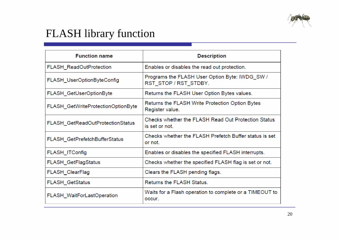
FLASH library functiony
20
Development Flowp
Embedded Software Side
int main(void)
Bootup STM32F10x
ProgrammingBootupSTM32F10x RCC Configure
NVIC Configure
int main(void)ifdef DEBUGdebug()
endifendif
FLASHStatus = FLASH_COMPLETEMemoryProgramStatus = PASSEDData = 0x15041975
GPIO Configure
Data = 0x15041975
RCC Configuration RCC_Configuration()
Flash memory RW operation FLASH Unlock
FLASH ClearFlag NVIC Configuration NVIC_Configuration()
GPIO Configuration
FLASH ClearFlag
FLASH ErasePage
FLASH ProgramWord GPIO Configuration GPIO_Configuration()
helliphelliphelliphelliphelliphelliphelliphelliphelliphelliphelliphelliphelliphelliphelliphelliphellipDisplay Result
Check content
21
實驗步驟
範例目錄架構
範例說明 範例說明
預設定義說明
燒錄 燒錄MIAT_STM32
22
範例目錄架構
範例目錄
測試映像檔 測試映像檔
含括檔
函式庫 函式庫
專案檔
原始碼 原始碼
23
範例說明
Function name Description
Unlock the Flash Program Erase controller FLASH_Unlock()
D fi h b f b d
Flash FwLib Functions List
Function name Description
FLASH_Unlock Unlocks the FLASH Program Erase Controller
FLASH_ClearFlag Clears the FLASH pending fl
Define the number of page to be erased NbrOfPage = (EndAddr - StartAddr) FLASH_PAGE_SIZE
Clear All pending flags FLASH_ClearFlag(FLASH_FLAG_BSY | FLASH_FLAG_EOP | FLASH_FLAG_PGERR |
FLASH FLAG WRPRTERR)flags
FLASH_ErasePage Erases a specified FLASH page
FLASH_ProgramWord Programs a word at a specified
_ _ )
Erase the FLASH pages for(EraseCounter = 0 (EraseCounter lt NbrOfPage) ampamp (FLASHStatus ==
FLASH_COMPLETE) EraseCounter++)FLASHStatus = FLASH ErasePage(StartAddr + (FLASH PAGE SIZE EraseCounter))address FLASHStatus = FLASH_ErasePage(StartAddr + (FLASH_PAGE_SIZE EraseCounter))
FLASH Word program of data 0x15041979 at addresses defined by StartAddr and EndAddrAddress = StartAddr
while((Address lt EndAddr) ampamp (FLASHStatus == FLASH_COMPLETE))FLASHStatus = FLASH_ProgramWord(Address Data)Address = Address + 4
24
範例說明
Embedded Software Side
Check the corectness of written data
Display Result
Check the corectness of written data Address = StartAddr
while((Address lt EndAddr) ampamp (MemoryProgramStatus = FAILED))if(((vu32) Address) = Data)
Flash memory RW operation
MemoryProgramStatus = FAILED
Address += 4
Check content
Display Result while (1)if (MemoryProgramStatus == PASSED) OK Turn on USERLED GPIO_SetBits(GPIOF GPIO_Pin_11)
Display Result
else KO Turn off USERLED GPIO_ResetBits(GPIOF GPIO_Pin_11) Insert delay Delay(0xAFFFF)
如果寫入與讀取Flash內容相同Flash記憶體使用正常USERLED紅燈恆亮
Turn on USERLED GPIO_SetBits(GPIOF GPIO_Pin_11) Insert delay Delay(0xAFFFF)
如果寫入與讀取Flash內容不同Flash記憶體使用異常USERLED紅燈閃爍
25
預設定義說明
define StartAddr ((u32)0x08008000) 定義Flash使用起始點 定義Flash使用起始點
使用起始點必需大於0x8003000 + Code Size 附註 0x8000000~0x8003000為DFU程式區塊使用此區塊
將造成無法燒錄程式
Code Size可由產生的HEX檔得知
d fi E dAdd (( 32)0 0800C000) define EndAddr ((u32)0x0800C000) 定義Flash使用結束點
使用起始點必需小於0x8040000使用起始點必需小於
Data = 0x15041975 寫入資料
32Bit define FLASH_PAGE_SIZE ((u16)0x800)
每一個Page有2KByte26
每一個Page有2KByte
Intel HEX Format
aaaa tt dd cc
field Description
the colon that starts every Intel HEX record
the record-length field that represents the number of data bytes (dd) in the record
aaaa the address field that represents the starting address for subsequent data in the record
tt the field that represents the HEX record type which may be one of the following00 - data record01 - end-of-file record02 - extended segment address recordg04 - extended linear address record
dd a data field that represents one byte of data A record may have multiple data bytes The number of data bytes in the record must match the number specified by the field
cc the checksum field that represents the checksum of the record The checksum is calculated by summing the values of all hexadecimal digit pairs in the record modulo 256 and taking the twos complement
27
HEX Examplep
020000040800F2103000001814002045310008D9340008CD340008D8103000001814002045310008D9340008CD340008D8helliphelliphellip1038200042370008000000000000000000000000170C3830000000000000000000000000008C
資料填入起始位置為
0C3830000000000000000000000000008C04000005080031318D00000001FF
資料填入起始位置為0x08003000 每一行有0x10(16)個Bytes 最後一筆資料為
資料結束點為0x0803383004000005080031318D
(0x08003830 -0x08000000)0x800 = 7 需以0x800為單位所以使用的位置起點為0x08004000
28
燒錄MIAT STM32_
Rebuilder all target files產生HEX DFU Fil M 轉換HEX產生DFU DFU File Manager轉換HEX產生DFU DfuSe Demonstration燒錄DFU d Leave DFU mode
29
內部Flash存取控制實驗
實驗一
WU-YANGTechnology Co Ltd
實驗一練習
注意 請使用預設0 08008000之後的位置 避免覆蓋DFU 請使用預設0x08008000之後的位置避免覆蓋DFU
與使用者程式碼區塊
練習 練習 修改存取位置測試是否正常
修改寫入資料測試是否正常 修改寫入資料測試是否正常
修改寫入資料後取消FLASH_Unlock測試是否正常
修改寫入資料後取消FLASH E P 測試是否正 修改寫入資料後取消FLASH_ErasePage測試是否正常
31
實驗目的(二)( )
使用MIAT_STM32實驗板透過Flash memory interface (FLITF)控制內部Flash進行存取控制實驗並利用SW(FLITF)控制內部Flash進行存取控制實驗並利用SWKEY決定資料寫入與讀取LCD顯示狀態
32
實驗原理
System requirement E b dd d Fl h Embedded Flash LCD KEY SW
Development Flow ARM Configure
33
Development Flowp
Embedded Software Side
int main(void)
Bootup STM32F10x
ProgrammingBootupSTM32F10x RCC Configure
NVIC Configure
int main(void)ifdef DEBUGdebug()
endif
FLASHStatus = FLASH_COMPLETE
RCC Configuration RCC Configuration()
GPIO Configure
BasicIO Configure_ g ()
NVIC Configuration NVIC_Configuration()
GPIO Configuration Flash memory RW ti
lcd Configure
GPIO Configuration GPIO_Configuration()
Init_BasicIO()
l d i i () LCD I i i li i
RW operation
Example
FLASH Unlock
FLASH ClearFlag
lcd_init() LCD Initialization
helliphelliphelliphelliphelliphelliphelliphelliphelliphelliphelliphelliphelliphelliphelliphelliphelliphelliphelliphelliphelliphelliphellip
p
34
硬體電路配置
Mapping Table
Num MIAT_STM32V2 MIAT_IOBV1 Num MIAT_STM32V2 MIAT_IOBV1
1 PC8 (326) SW1 10 PE6 (15) LCD_EN2 PC9 (327) SW2 11 PF6 (118) LCD RW ( ) ( ) _3 PC10 (43) SW3 12 PF7 (119) LCD_RS 4 PC11 (44) SW4 13 PF8(120) LCD_D4 5 PB5 (427) KEY1 14 PF9 (121) LCD_D5 6 PB6 (428) KEY2 15 PF10 (122) LCD_D6 7 PB7 (429) KEY3 16 PF11 (213) LCD_D7 8 PB8 (431) KEY4 17 VDD (236) VCC33V 9 VCC5V (1 36) VCC5V 18 GND (1 35) GND9 VCC5V (136) VCC5V 18 GND (135) GND
35
實驗步驟
範例目錄架構
範例說明 範例說明
預設定義說明
36
範例目錄架構
範例目錄
測試映像檔 測試映像檔
含括檔
函式庫 函式庫
專案檔
原始碼 原始碼
37
範例說明
Embedded Software Side
lcd clear()
FLASH memory RW operation
lcd_clear()lcd_print (MIAT_STM32 DEMO )
Unlock the Flash Program Erase controller FLASH_Unlock()
Flash memory RW operation
FLASH Unlock
Clear All pending flags FLASH_ClearFlag(FLASH_FLAG_BSY | FLASH_FLAG_EOP | FLASH_FLAG_PGERR |
FLASH_FLAG_WRPRTERR)
while(1)
Example
FLASH ClearFlag
( )
KEY_Buffer=Key_Scan()set_cursor (0 1)lcd_print (SW Value = 0x)lcd putchar(((SWamp0x7)+0x30))lcd_putchar(((SWamp0x7)+0x30))if(KEY_Buffer==1)Address=(StartAddr|(SWltlt12))set_cursor (0 0)lcd_print (Set Addr = 0x)
掃描KEY是否按下與顯示SW數值LCD Line2顯示SW Value = 0x(SW)
lcd_putchar(((SWamp0x7)+0x30))lcd_print ( )
如果KEY1按下記錄SW數值至Address LCD Line1顯示Set Adde = 0x(Address)
38
範例說明
Embedded Software Side
else if(KEY Buffer==2)
FLASH memory RW operation
else if(KEY_Buffer==2)
Erase the FLASH pages FLASHStatus = FLASH_ErasePage(Address)
FLASH Word program of data at addresses defined by SW
SRAM memory RW operation
p g yFLASHStatus = FLASH_ProgramWord(Address (SWamp0x7))
set_cursor (0 0)lcd_print (Write 0x)lcd_putchar(((SWamp0x7)+0x30))l d i t ( t 0 )
Example如果KEY2按下清除Address所處區塊並寫入SW數值 lcd_print ( at 0x)
lcd_putchar((((Addressgtgt12)amp0x7)+0x30))else if(KEY_Buffer==3)
Data=(u16 )Address
所處區塊並寫入SW數值LCD Line1顯示Write 0x(SW) at 0x(Adddress)
Data (u16 )Addressset_cursor (0 0)lcd_print (Addr 0x)lcd_putchar((((Addressgtgt12)amp0x7)+0x30))lcd_print ( = 0x)lcd_putchar(((Dataamp0x7)+0x30))lcd_print ( )
如果KEY3按下讀取Address紀錄數值LCD Line1顯示Addr 0x(Adddress) = 0x
39
預設定義說明
define StartAddr ((u32)0x08020000) 定義Flash使用起始點 定義Flash使用起始點
使用起始點必需大於0x8003000 + Code Size 附註 0x8000000~0x8003000為DFU程式區塊使用此區塊
將造成無法燒錄程式
Code Size可由產生的HEX檔得知
32 Add 0 08020000 u32 Address = 0x08020000 定義Address初始值
初始值必需與Flash使用起始點相同初始值必需與 使用起始點相同
Address=(StartAddr|(SWltlt12)) Example StartAddr = 0x08020000 SW = 1 Address = 0x08021000
StartAddr = 0x08020000 SW = 7 Address = 0x08027000 StartAddr|(7ltlt12)必需小於0x8040000
40
使用者界面與Flash存取控制實驗
實驗二
WU-YANGTechnology Co Ltd
實驗二練習
注意 請使用預設0 08020000之後的位置 避免覆蓋DFU 請使用預設0x08020000之後的位置避免覆蓋DFU
與使用者程式碼區塊
練習 練習 利用SW與KEY測試Flash寫入與讀取是否正常
Fl h寫入後電源關閉 再開啟後寫入資料是否仍存 Flash寫入後電源關閉再開啟後寫入資料是否仍存在
修改存取位置測試是否正常 修改存取位置測試是否正常
42
實驗目的(三)( )
使用MIAT_STM32實驗板透過Flash memory interface (FLITF)控制內部Flash進行存取控制實驗並藉由填入(FLITF)控制內部Flash進行存取控制實驗並藉由填入Option Bytes 設定寫入鎖定保護Page鎖定不被覆蓋
43
Development Flowp
Embedded Software Side
int main(void)
Bootup STM32F10x
ProgrammingBootupSTM32F10x RCC Configure
NVIC Configure
int main(void)ifdef DEBUGdebug()
endifendif
FLASHStatus = FLASH_COMPLETEMemoryProgramStatus = PASSEDData = 0x1753
GPIO Configure
Data = 0x1753
RCC Configuration RCC_Configuration()
Flash memory RW operation FLASH Unlock
FLASH ClearFlag NVIC Configuration NVIC_Configuration()
GPIO Configuration
FLASH ClearFlag
FLASH ErasePage
FLASH ProgramHalfWord GPIO Configuration GPIO_Configuration()
Display Result
Check content
44
helliphelliphelliphelliphelliphelliphelliphelliphelliphelliphelliphelliphelliphelliphelliphelliphelliphelliphellip
實驗步驟
範例目錄架構
範例說明 範例說明
預設定義說明
45
範例目錄架構
範例目錄
測試映像檔 測試映像檔
含括檔
函式庫 函式庫
專案檔
原始碼 原始碼
46
範例說明
Function name Description
Unlock the Flash Program Erase controller FLASH_Unlock()
Define the number of page to be erased
Flash FwLib Functions List
Function name Description
FLASH_Unlock Unlocks the FLASH Program Erase Controller
FLASH_ClearFlag Clears the FLASH pending fl
Define the number of page to be erased NbrOfPage = (EndAddr ‐ StartAddr) FLASH_PAGE_SIZE
FLASH_ClearFlag(FLASH_FLAG_BSY | FLASH_FLAG_EOP|FLASH_FLAG_PGERR |FLASH_FLAG_WRPRTERR)
Get pages write protection status flags
FLASH_EraseOptionBytes
Erases the FLASH option bytes
FLASH_EnableWritePro Write protects the desired
p g pWRPR_Value = FLASH_GetWriteProtectionOptionByte()ProtectedPages = WRPR_Value amp 0x000000C0
ifdef WriteProtection_Disableif (ProtectedPages == 0x00) Pages are write protected
tection pages
NVIC_GenerateSystemReset
Generate a system reset
Disable the write protection FLASHStatus = FLASH_EraseOptionBytes() Generate System Reset to load the new option byte values NVIC_GenerateSystemReset()
elseifdef WriteProtection Enableifdef WriteProtection_Enableif (ProtectedPages = 0x00) Pages not write protected
FLASHStatus = FLASH_EraseOptionBytes() Enable the pages write protection FLASHStatus = FLASH_EnableWriteProtection(FLASH_WRProt_Pages12to13
|FLASH WRProt Pages14to15)|FLASH_WRProt_Pages14to15) Generate System Reset to load the new option byte values NVIC_GenerateSystemReset()
endifendif
47
範例說明
if (ProtectedPages = 0x00) Clear All pending flags
Flash FwLib Functions List
Function name DescriptionFLASH_ClearFlag(FLASH_FLAG_BSY |
FLASH_FLAG_EOP|FLASH_FLAG_PGERR |FLASH_FLAG_WRPRTERR)
erase the FLASH pages for(EraseCounter = 0 (EraseCounter lt NbrOfPage) ampamp (FLASHStatus ==
Function name Description
FLASH_ErasePage Erases a specified FLASH page
FLASH_ProgramHalfWod
Programs a half word at a ifi d dd FLASH_COMPLETE) EraseCounter++)
FLASHStatus = FLASH_ErasePage(StartAddr + (FLASH_PAGE_SIZE
EraseCounter))
rd specified address
FLASH Half Word program of data 0x1753 at addresses defined by StartAddrand EndAddr
Address = StartAddr
hil ((Add E dAdd ) ampamp (FLASHSt t FLASH COMPLETE))while((Address lt EndAddr) ampamp (FLASHStatus == FLASH_COMPLETE))
FLASHStatus = FLASH_ProgramHalfWord(Address Data)Address = Address + 2
48
範例說明
Embedded Software Side
Check the corectness of written data
Display Result
Check the corectness of written data Address = StartAddr
while((Address lt EndAddr) ampamp (MemoryProgramStatus = FAILED))if(((vu16) Address) = Data)
Flash memory RW operation
MemoryProgramStatus = FAILED
Address += 2
Check content
Display Result while (1)if (MemoryProgramStatus == PASSED) OK Turn on USERLED GPIO_SetBits(GPIOF GPIO_Pin_11)
Display Result
else KO Turn off USERLED GPIO_ResetBits(GPIOF GPIO_Pin_11) Insert delay Delay(0xAFFFF)
如果寫入與讀取Flash內容相同Flash記憶體可以寫入USERLED紅燈恆亮
Turn on USERLED GPIO_SetBits(GPIOF GPIO_Pin_11) Insert delay Delay(0xAFFFF)
如果寫入與讀取Flash內容不同Flash記憶體不能寫入USERLED紅燈閃爍
49
預設定義說明
define StartAddr ((u32) 0x08006000) 定義Flash使用起始點 定義Flash使用起始點
使用起始點必需大於0x8003000 + Code Size 附註 0x8000000~0x8003000為DFU程式區塊使用此區塊
將造成無法燒錄程式
Code Size可由產生的HEX檔得知
d fi E dAdd (( 32) 0 08008000) define EndAddr ((u32) 0x08008000) 定義Flash使用結束點
使用起始點必需小於0x8040000使用起始點必需小於
Data = 0x1753 寫入資料
16Bit define FLASH_PAGE_SIZE ((u16)0x800) 每一個Page有2KByte
50
每一個Page有2KByte
預設定義說明
define WriteProtection_Enable U hi li E bl W i P i Uncomment this line to Enable Write Protection
define WriteProtection_Disablehi li i bl i i Uncomment this line to Disable Write Protection
FLASH_EnableWriteProtection設定影響 個 設定影響2個Page FLASH_WRProt_Pages0to1 FLASH_WRProt_Pages1to2 helliphellip FLASH_WRProt_Pages60to61
設定影響多個Page FLASH_WRProt_Pages62to255
51
FLASH EnableWriteProtection_
Example
位置0x08006000 ~ 0x08007000每一個Page有0x800ByteStartPage = (0x08006000-0x08000000)0x800 = 12EndPage = ((0x08007000-0x08000000)0x800)-1 = 13執行執行FLASH_EnableWriteProtection(FLASH_WRProt_Pages12to13)將影響Pages12 Pages13
52
內部Flash寫入鎖定存取控制實驗
實驗三
WU-YANGTechnology Co Ltd
實驗三練習
注意 請使用預設0 08006000之後的位置 避免覆蓋DFU 請使用預設0x08006000之後的位置避免覆蓋DFU
與使用者程式碼區塊
更改寫入位置測試寫入鎖定時需同時更改 更改寫入位置測試寫入鎖定時需同時更改FLASH_EnableWriteProtection鎖定之Page
練習 練習 打開define WriteProtection_Enable測試是否可寫入
打開define WriteProtection Disable測試是否可寫入 打開define WriteProtection_Disable測試是否可寫入
修改存取位置測試是否正常
修改寫入資料測試是否正常 修改寫入資料測試是否正常
54
Q amp A
WU-YANGTechnology Co Ltd

Development Flowp
Embedded Software Side
int main(void)
Bootup STM32F10x
ProgrammingBootupSTM32F10x RCC Configure
NVIC Configure
int main(void)ifdef DEBUGdebug()
endifendif
FLASHStatus = FLASH_COMPLETEMemoryProgramStatus = PASSEDData = 0x15041975
GPIO Configure
Data = 0x15041975
RCC Configuration RCC_Configuration()
Flash memory RW operation FLASH Unlock
FLASH ClearFlag NVIC Configuration NVIC_Configuration()
GPIO Configuration
FLASH ClearFlag
FLASH ErasePage
FLASH ProgramWord GPIO Configuration GPIO_Configuration()
helliphelliphelliphelliphelliphelliphelliphelliphelliphelliphelliphelliphelliphelliphelliphelliphellipDisplay Result
Check content
21
實驗步驟
範例目錄架構
範例說明 範例說明
預設定義說明
燒錄 燒錄MIAT_STM32
22
範例目錄架構
範例目錄
測試映像檔 測試映像檔
含括檔
函式庫 函式庫
專案檔
原始碼 原始碼
23
範例說明
Function name Description
Unlock the Flash Program Erase controller FLASH_Unlock()
D fi h b f b d
Flash FwLib Functions List
Function name Description
FLASH_Unlock Unlocks the FLASH Program Erase Controller
FLASH_ClearFlag Clears the FLASH pending fl
Define the number of page to be erased NbrOfPage = (EndAddr - StartAddr) FLASH_PAGE_SIZE
Clear All pending flags FLASH_ClearFlag(FLASH_FLAG_BSY | FLASH_FLAG_EOP | FLASH_FLAG_PGERR |
FLASH FLAG WRPRTERR)flags
FLASH_ErasePage Erases a specified FLASH page
FLASH_ProgramWord Programs a word at a specified
_ _ )
Erase the FLASH pages for(EraseCounter = 0 (EraseCounter lt NbrOfPage) ampamp (FLASHStatus ==
FLASH_COMPLETE) EraseCounter++)FLASHStatus = FLASH ErasePage(StartAddr + (FLASH PAGE SIZE EraseCounter))address FLASHStatus = FLASH_ErasePage(StartAddr + (FLASH_PAGE_SIZE EraseCounter))
FLASH Word program of data 0x15041979 at addresses defined by StartAddr and EndAddrAddress = StartAddr
while((Address lt EndAddr) ampamp (FLASHStatus == FLASH_COMPLETE))FLASHStatus = FLASH_ProgramWord(Address Data)Address = Address + 4
24
範例說明
Embedded Software Side
Check the corectness of written data
Display Result
Check the corectness of written data Address = StartAddr
while((Address lt EndAddr) ampamp (MemoryProgramStatus = FAILED))if(((vu32) Address) = Data)
Flash memory RW operation
MemoryProgramStatus = FAILED
Address += 4
Check content
Display Result while (1)if (MemoryProgramStatus == PASSED) OK Turn on USERLED GPIO_SetBits(GPIOF GPIO_Pin_11)
Display Result
else KO Turn off USERLED GPIO_ResetBits(GPIOF GPIO_Pin_11) Insert delay Delay(0xAFFFF)
如果寫入與讀取Flash內容相同Flash記憶體使用正常USERLED紅燈恆亮
Turn on USERLED GPIO_SetBits(GPIOF GPIO_Pin_11) Insert delay Delay(0xAFFFF)
如果寫入與讀取Flash內容不同Flash記憶體使用異常USERLED紅燈閃爍
25
預設定義說明
define StartAddr ((u32)0x08008000) 定義Flash使用起始點 定義Flash使用起始點
使用起始點必需大於0x8003000 + Code Size 附註 0x8000000~0x8003000為DFU程式區塊使用此區塊
將造成無法燒錄程式
Code Size可由產生的HEX檔得知
d fi E dAdd (( 32)0 0800C000) define EndAddr ((u32)0x0800C000) 定義Flash使用結束點
使用起始點必需小於0x8040000使用起始點必需小於
Data = 0x15041975 寫入資料
32Bit define FLASH_PAGE_SIZE ((u16)0x800)
每一個Page有2KByte26
每一個Page有2KByte
Intel HEX Format
aaaa tt dd cc
field Description
the colon that starts every Intel HEX record
the record-length field that represents the number of data bytes (dd) in the record
aaaa the address field that represents the starting address for subsequent data in the record
tt the field that represents the HEX record type which may be one of the following00 - data record01 - end-of-file record02 - extended segment address recordg04 - extended linear address record
dd a data field that represents one byte of data A record may have multiple data bytes The number of data bytes in the record must match the number specified by the field
cc the checksum field that represents the checksum of the record The checksum is calculated by summing the values of all hexadecimal digit pairs in the record modulo 256 and taking the twos complement
27
HEX Examplep
020000040800F2103000001814002045310008D9340008CD340008D8103000001814002045310008D9340008CD340008D8helliphelliphellip1038200042370008000000000000000000000000170C3830000000000000000000000000008C
資料填入起始位置為
0C3830000000000000000000000000008C04000005080031318D00000001FF
資料填入起始位置為0x08003000 每一行有0x10(16)個Bytes 最後一筆資料為
資料結束點為0x0803383004000005080031318D
(0x08003830 -0x08000000)0x800 = 7 需以0x800為單位所以使用的位置起點為0x08004000
28
燒錄MIAT STM32_
Rebuilder all target files產生HEX DFU Fil M 轉換HEX產生DFU DFU File Manager轉換HEX產生DFU DfuSe Demonstration燒錄DFU d Leave DFU mode
29
內部Flash存取控制實驗
實驗一
WU-YANGTechnology Co Ltd
實驗一練習
注意 請使用預設0 08008000之後的位置 避免覆蓋DFU 請使用預設0x08008000之後的位置避免覆蓋DFU
與使用者程式碼區塊
練習 練習 修改存取位置測試是否正常
修改寫入資料測試是否正常 修改寫入資料測試是否正常
修改寫入資料後取消FLASH_Unlock測試是否正常
修改寫入資料後取消FLASH E P 測試是否正 修改寫入資料後取消FLASH_ErasePage測試是否正常
31
實驗目的(二)( )
使用MIAT_STM32實驗板透過Flash memory interface (FLITF)控制內部Flash進行存取控制實驗並利用SW(FLITF)控制內部Flash進行存取控制實驗並利用SWKEY決定資料寫入與讀取LCD顯示狀態
32
實驗原理
System requirement E b dd d Fl h Embedded Flash LCD KEY SW
Development Flow ARM Configure
33
Development Flowp
Embedded Software Side
int main(void)
Bootup STM32F10x
ProgrammingBootupSTM32F10x RCC Configure
NVIC Configure
int main(void)ifdef DEBUGdebug()
endif
FLASHStatus = FLASH_COMPLETE
RCC Configuration RCC Configuration()
GPIO Configure
BasicIO Configure_ g ()
NVIC Configuration NVIC_Configuration()
GPIO Configuration Flash memory RW ti
lcd Configure
GPIO Configuration GPIO_Configuration()
Init_BasicIO()
l d i i () LCD I i i li i
RW operation
Example
FLASH Unlock
FLASH ClearFlag
lcd_init() LCD Initialization
helliphelliphelliphelliphelliphelliphelliphelliphelliphelliphelliphelliphelliphelliphelliphelliphelliphelliphelliphelliphelliphelliphellip
p
34
硬體電路配置
Mapping Table
Num MIAT_STM32V2 MIAT_IOBV1 Num MIAT_STM32V2 MIAT_IOBV1
1 PC8 (326) SW1 10 PE6 (15) LCD_EN2 PC9 (327) SW2 11 PF6 (118) LCD RW ( ) ( ) _3 PC10 (43) SW3 12 PF7 (119) LCD_RS 4 PC11 (44) SW4 13 PF8(120) LCD_D4 5 PB5 (427) KEY1 14 PF9 (121) LCD_D5 6 PB6 (428) KEY2 15 PF10 (122) LCD_D6 7 PB7 (429) KEY3 16 PF11 (213) LCD_D7 8 PB8 (431) KEY4 17 VDD (236) VCC33V 9 VCC5V (1 36) VCC5V 18 GND (1 35) GND9 VCC5V (136) VCC5V 18 GND (135) GND
35
實驗步驟
範例目錄架構
範例說明 範例說明
預設定義說明
36
範例目錄架構
範例目錄
測試映像檔 測試映像檔
含括檔
函式庫 函式庫
專案檔
原始碼 原始碼
37
範例說明
Embedded Software Side
lcd clear()
FLASH memory RW operation
lcd_clear()lcd_print (MIAT_STM32 DEMO )
Unlock the Flash Program Erase controller FLASH_Unlock()
Flash memory RW operation
FLASH Unlock
Clear All pending flags FLASH_ClearFlag(FLASH_FLAG_BSY | FLASH_FLAG_EOP | FLASH_FLAG_PGERR |
FLASH_FLAG_WRPRTERR)
while(1)
Example
FLASH ClearFlag
( )
KEY_Buffer=Key_Scan()set_cursor (0 1)lcd_print (SW Value = 0x)lcd putchar(((SWamp0x7)+0x30))lcd_putchar(((SWamp0x7)+0x30))if(KEY_Buffer==1)Address=(StartAddr|(SWltlt12))set_cursor (0 0)lcd_print (Set Addr = 0x)
掃描KEY是否按下與顯示SW數值LCD Line2顯示SW Value = 0x(SW)
lcd_putchar(((SWamp0x7)+0x30))lcd_print ( )
如果KEY1按下記錄SW數值至Address LCD Line1顯示Set Adde = 0x(Address)
38
範例說明
Embedded Software Side
else if(KEY Buffer==2)
FLASH memory RW operation
else if(KEY_Buffer==2)
Erase the FLASH pages FLASHStatus = FLASH_ErasePage(Address)
FLASH Word program of data at addresses defined by SW
SRAM memory RW operation
p g yFLASHStatus = FLASH_ProgramWord(Address (SWamp0x7))
set_cursor (0 0)lcd_print (Write 0x)lcd_putchar(((SWamp0x7)+0x30))l d i t ( t 0 )
Example如果KEY2按下清除Address所處區塊並寫入SW數值 lcd_print ( at 0x)
lcd_putchar((((Addressgtgt12)amp0x7)+0x30))else if(KEY_Buffer==3)
Data=(u16 )Address
所處區塊並寫入SW數值LCD Line1顯示Write 0x(SW) at 0x(Adddress)
Data (u16 )Addressset_cursor (0 0)lcd_print (Addr 0x)lcd_putchar((((Addressgtgt12)amp0x7)+0x30))lcd_print ( = 0x)lcd_putchar(((Dataamp0x7)+0x30))lcd_print ( )
如果KEY3按下讀取Address紀錄數值LCD Line1顯示Addr 0x(Adddress) = 0x
39
預設定義說明
define StartAddr ((u32)0x08020000) 定義Flash使用起始點 定義Flash使用起始點
使用起始點必需大於0x8003000 + Code Size 附註 0x8000000~0x8003000為DFU程式區塊使用此區塊
將造成無法燒錄程式
Code Size可由產生的HEX檔得知
32 Add 0 08020000 u32 Address = 0x08020000 定義Address初始值
初始值必需與Flash使用起始點相同初始值必需與 使用起始點相同
Address=(StartAddr|(SWltlt12)) Example StartAddr = 0x08020000 SW = 1 Address = 0x08021000
StartAddr = 0x08020000 SW = 7 Address = 0x08027000 StartAddr|(7ltlt12)必需小於0x8040000
40
使用者界面與Flash存取控制實驗
實驗二
WU-YANGTechnology Co Ltd
實驗二練習
注意 請使用預設0 08020000之後的位置 避免覆蓋DFU 請使用預設0x08020000之後的位置避免覆蓋DFU
與使用者程式碼區塊
練習 練習 利用SW與KEY測試Flash寫入與讀取是否正常
Fl h寫入後電源關閉 再開啟後寫入資料是否仍存 Flash寫入後電源關閉再開啟後寫入資料是否仍存在
修改存取位置測試是否正常 修改存取位置測試是否正常
42
實驗目的(三)( )
使用MIAT_STM32實驗板透過Flash memory interface (FLITF)控制內部Flash進行存取控制實驗並藉由填入(FLITF)控制內部Flash進行存取控制實驗並藉由填入Option Bytes 設定寫入鎖定保護Page鎖定不被覆蓋
43
Development Flowp
Embedded Software Side
int main(void)
Bootup STM32F10x
ProgrammingBootupSTM32F10x RCC Configure
NVIC Configure
int main(void)ifdef DEBUGdebug()
endifendif
FLASHStatus = FLASH_COMPLETEMemoryProgramStatus = PASSEDData = 0x1753
GPIO Configure
Data = 0x1753
RCC Configuration RCC_Configuration()
Flash memory RW operation FLASH Unlock
FLASH ClearFlag NVIC Configuration NVIC_Configuration()
GPIO Configuration
FLASH ClearFlag
FLASH ErasePage
FLASH ProgramHalfWord GPIO Configuration GPIO_Configuration()
Display Result
Check content
44
helliphelliphelliphelliphelliphelliphelliphelliphelliphelliphelliphelliphelliphelliphelliphelliphelliphelliphellip
實驗步驟
範例目錄架構
範例說明 範例說明
預設定義說明
45
範例目錄架構
範例目錄
測試映像檔 測試映像檔
含括檔
函式庫 函式庫
專案檔
原始碼 原始碼
46
範例說明
Function name Description
Unlock the Flash Program Erase controller FLASH_Unlock()
Define the number of page to be erased
Flash FwLib Functions List
Function name Description
FLASH_Unlock Unlocks the FLASH Program Erase Controller
FLASH_ClearFlag Clears the FLASH pending fl
Define the number of page to be erased NbrOfPage = (EndAddr ‐ StartAddr) FLASH_PAGE_SIZE
FLASH_ClearFlag(FLASH_FLAG_BSY | FLASH_FLAG_EOP|FLASH_FLAG_PGERR |FLASH_FLAG_WRPRTERR)
Get pages write protection status flags
FLASH_EraseOptionBytes
Erases the FLASH option bytes
FLASH_EnableWritePro Write protects the desired
p g pWRPR_Value = FLASH_GetWriteProtectionOptionByte()ProtectedPages = WRPR_Value amp 0x000000C0
ifdef WriteProtection_Disableif (ProtectedPages == 0x00) Pages are write protected
tection pages
NVIC_GenerateSystemReset
Generate a system reset
Disable the write protection FLASHStatus = FLASH_EraseOptionBytes() Generate System Reset to load the new option byte values NVIC_GenerateSystemReset()
elseifdef WriteProtection Enableifdef WriteProtection_Enableif (ProtectedPages = 0x00) Pages not write protected
FLASHStatus = FLASH_EraseOptionBytes() Enable the pages write protection FLASHStatus = FLASH_EnableWriteProtection(FLASH_WRProt_Pages12to13
|FLASH WRProt Pages14to15)|FLASH_WRProt_Pages14to15) Generate System Reset to load the new option byte values NVIC_GenerateSystemReset()
endifendif
47
範例說明
if (ProtectedPages = 0x00) Clear All pending flags
Flash FwLib Functions List
Function name DescriptionFLASH_ClearFlag(FLASH_FLAG_BSY |
FLASH_FLAG_EOP|FLASH_FLAG_PGERR |FLASH_FLAG_WRPRTERR)
erase the FLASH pages for(EraseCounter = 0 (EraseCounter lt NbrOfPage) ampamp (FLASHStatus ==
Function name Description
FLASH_ErasePage Erases a specified FLASH page
FLASH_ProgramHalfWod
Programs a half word at a ifi d dd FLASH_COMPLETE) EraseCounter++)
FLASHStatus = FLASH_ErasePage(StartAddr + (FLASH_PAGE_SIZE
EraseCounter))
rd specified address
FLASH Half Word program of data 0x1753 at addresses defined by StartAddrand EndAddr
Address = StartAddr
hil ((Add E dAdd ) ampamp (FLASHSt t FLASH COMPLETE))while((Address lt EndAddr) ampamp (FLASHStatus == FLASH_COMPLETE))
FLASHStatus = FLASH_ProgramHalfWord(Address Data)Address = Address + 2
48
範例說明
Embedded Software Side
Check the corectness of written data
Display Result
Check the corectness of written data Address = StartAddr
while((Address lt EndAddr) ampamp (MemoryProgramStatus = FAILED))if(((vu16) Address) = Data)
Flash memory RW operation
MemoryProgramStatus = FAILED
Address += 2
Check content
Display Result while (1)if (MemoryProgramStatus == PASSED) OK Turn on USERLED GPIO_SetBits(GPIOF GPIO_Pin_11)
Display Result
else KO Turn off USERLED GPIO_ResetBits(GPIOF GPIO_Pin_11) Insert delay Delay(0xAFFFF)
如果寫入與讀取Flash內容相同Flash記憶體可以寫入USERLED紅燈恆亮
Turn on USERLED GPIO_SetBits(GPIOF GPIO_Pin_11) Insert delay Delay(0xAFFFF)
如果寫入與讀取Flash內容不同Flash記憶體不能寫入USERLED紅燈閃爍
49
預設定義說明
define StartAddr ((u32) 0x08006000) 定義Flash使用起始點 定義Flash使用起始點
使用起始點必需大於0x8003000 + Code Size 附註 0x8000000~0x8003000為DFU程式區塊使用此區塊
將造成無法燒錄程式
Code Size可由產生的HEX檔得知
d fi E dAdd (( 32) 0 08008000) define EndAddr ((u32) 0x08008000) 定義Flash使用結束點
使用起始點必需小於0x8040000使用起始點必需小於
Data = 0x1753 寫入資料
16Bit define FLASH_PAGE_SIZE ((u16)0x800) 每一個Page有2KByte
50
每一個Page有2KByte
預設定義說明
define WriteProtection_Enable U hi li E bl W i P i Uncomment this line to Enable Write Protection
define WriteProtection_Disablehi li i bl i i Uncomment this line to Disable Write Protection
FLASH_EnableWriteProtection設定影響 個 設定影響2個Page FLASH_WRProt_Pages0to1 FLASH_WRProt_Pages1to2 helliphellip FLASH_WRProt_Pages60to61
設定影響多個Page FLASH_WRProt_Pages62to255
51
FLASH EnableWriteProtection_
Example
位置0x08006000 ~ 0x08007000每一個Page有0x800ByteStartPage = (0x08006000-0x08000000)0x800 = 12EndPage = ((0x08007000-0x08000000)0x800)-1 = 13執行執行FLASH_EnableWriteProtection(FLASH_WRProt_Pages12to13)將影響Pages12 Pages13
52
內部Flash寫入鎖定存取控制實驗
實驗三
WU-YANGTechnology Co Ltd
實驗三練習
注意 請使用預設0 08006000之後的位置 避免覆蓋DFU 請使用預設0x08006000之後的位置避免覆蓋DFU
與使用者程式碼區塊
更改寫入位置測試寫入鎖定時需同時更改 更改寫入位置測試寫入鎖定時需同時更改FLASH_EnableWriteProtection鎖定之Page
練習 練習 打開define WriteProtection_Enable測試是否可寫入
打開define WriteProtection Disable測試是否可寫入 打開define WriteProtection_Disable測試是否可寫入
修改存取位置測試是否正常
修改寫入資料測試是否正常 修改寫入資料測試是否正常
54
Q amp A
WU-YANGTechnology Co Ltd

實驗步驟
範例目錄架構
範例說明 範例說明
預設定義說明
燒錄 燒錄MIAT_STM32
22
範例目錄架構
範例目錄
測試映像檔 測試映像檔
含括檔
函式庫 函式庫
專案檔
原始碼 原始碼
23
範例說明
Function name Description
Unlock the Flash Program Erase controller FLASH_Unlock()
D fi h b f b d
Flash FwLib Functions List
Function name Description
FLASH_Unlock Unlocks the FLASH Program Erase Controller
FLASH_ClearFlag Clears the FLASH pending fl
Define the number of page to be erased NbrOfPage = (EndAddr - StartAddr) FLASH_PAGE_SIZE
Clear All pending flags FLASH_ClearFlag(FLASH_FLAG_BSY | FLASH_FLAG_EOP | FLASH_FLAG_PGERR |
FLASH FLAG WRPRTERR)flags
FLASH_ErasePage Erases a specified FLASH page
FLASH_ProgramWord Programs a word at a specified
_ _ )
Erase the FLASH pages for(EraseCounter = 0 (EraseCounter lt NbrOfPage) ampamp (FLASHStatus ==
FLASH_COMPLETE) EraseCounter++)FLASHStatus = FLASH ErasePage(StartAddr + (FLASH PAGE SIZE EraseCounter))address FLASHStatus = FLASH_ErasePage(StartAddr + (FLASH_PAGE_SIZE EraseCounter))
FLASH Word program of data 0x15041979 at addresses defined by StartAddr and EndAddrAddress = StartAddr
while((Address lt EndAddr) ampamp (FLASHStatus == FLASH_COMPLETE))FLASHStatus = FLASH_ProgramWord(Address Data)Address = Address + 4
24
範例說明
Embedded Software Side
Check the corectness of written data
Display Result
Check the corectness of written data Address = StartAddr
while((Address lt EndAddr) ampamp (MemoryProgramStatus = FAILED))if(((vu32) Address) = Data)
Flash memory RW operation
MemoryProgramStatus = FAILED
Address += 4
Check content
Display Result while (1)if (MemoryProgramStatus == PASSED) OK Turn on USERLED GPIO_SetBits(GPIOF GPIO_Pin_11)
Display Result
else KO Turn off USERLED GPIO_ResetBits(GPIOF GPIO_Pin_11) Insert delay Delay(0xAFFFF)
如果寫入與讀取Flash內容相同Flash記憶體使用正常USERLED紅燈恆亮
Turn on USERLED GPIO_SetBits(GPIOF GPIO_Pin_11) Insert delay Delay(0xAFFFF)
如果寫入與讀取Flash內容不同Flash記憶體使用異常USERLED紅燈閃爍
25
預設定義說明
define StartAddr ((u32)0x08008000) 定義Flash使用起始點 定義Flash使用起始點
使用起始點必需大於0x8003000 + Code Size 附註 0x8000000~0x8003000為DFU程式區塊使用此區塊
將造成無法燒錄程式
Code Size可由產生的HEX檔得知
d fi E dAdd (( 32)0 0800C000) define EndAddr ((u32)0x0800C000) 定義Flash使用結束點
使用起始點必需小於0x8040000使用起始點必需小於
Data = 0x15041975 寫入資料
32Bit define FLASH_PAGE_SIZE ((u16)0x800)
每一個Page有2KByte26
每一個Page有2KByte
Intel HEX Format
aaaa tt dd cc
field Description
the colon that starts every Intel HEX record
the record-length field that represents the number of data bytes (dd) in the record
aaaa the address field that represents the starting address for subsequent data in the record
tt the field that represents the HEX record type which may be one of the following00 - data record01 - end-of-file record02 - extended segment address recordg04 - extended linear address record
dd a data field that represents one byte of data A record may have multiple data bytes The number of data bytes in the record must match the number specified by the field
cc the checksum field that represents the checksum of the record The checksum is calculated by summing the values of all hexadecimal digit pairs in the record modulo 256 and taking the twos complement
27
HEX Examplep
020000040800F2103000001814002045310008D9340008CD340008D8103000001814002045310008D9340008CD340008D8helliphelliphellip1038200042370008000000000000000000000000170C3830000000000000000000000000008C
資料填入起始位置為
0C3830000000000000000000000000008C04000005080031318D00000001FF
資料填入起始位置為0x08003000 每一行有0x10(16)個Bytes 最後一筆資料為
資料結束點為0x0803383004000005080031318D
(0x08003830 -0x08000000)0x800 = 7 需以0x800為單位所以使用的位置起點為0x08004000
28
燒錄MIAT STM32_
Rebuilder all target files產生HEX DFU Fil M 轉換HEX產生DFU DFU File Manager轉換HEX產生DFU DfuSe Demonstration燒錄DFU d Leave DFU mode
29
內部Flash存取控制實驗
實驗一
WU-YANGTechnology Co Ltd
實驗一練習
注意 請使用預設0 08008000之後的位置 避免覆蓋DFU 請使用預設0x08008000之後的位置避免覆蓋DFU
與使用者程式碼區塊
練習 練習 修改存取位置測試是否正常
修改寫入資料測試是否正常 修改寫入資料測試是否正常
修改寫入資料後取消FLASH_Unlock測試是否正常
修改寫入資料後取消FLASH E P 測試是否正 修改寫入資料後取消FLASH_ErasePage測試是否正常
31
實驗目的(二)( )
使用MIAT_STM32實驗板透過Flash memory interface (FLITF)控制內部Flash進行存取控制實驗並利用SW(FLITF)控制內部Flash進行存取控制實驗並利用SWKEY決定資料寫入與讀取LCD顯示狀態
32
實驗原理
System requirement E b dd d Fl h Embedded Flash LCD KEY SW
Development Flow ARM Configure
33
Development Flowp
Embedded Software Side
int main(void)
Bootup STM32F10x
ProgrammingBootupSTM32F10x RCC Configure
NVIC Configure
int main(void)ifdef DEBUGdebug()
endif
FLASHStatus = FLASH_COMPLETE
RCC Configuration RCC Configuration()
GPIO Configure
BasicIO Configure_ g ()
NVIC Configuration NVIC_Configuration()
GPIO Configuration Flash memory RW ti
lcd Configure
GPIO Configuration GPIO_Configuration()
Init_BasicIO()
l d i i () LCD I i i li i
RW operation
Example
FLASH Unlock
FLASH ClearFlag
lcd_init() LCD Initialization
helliphelliphelliphelliphelliphelliphelliphelliphelliphelliphelliphelliphelliphelliphelliphelliphelliphelliphelliphelliphelliphelliphellip
p
34
硬體電路配置
Mapping Table
Num MIAT_STM32V2 MIAT_IOBV1 Num MIAT_STM32V2 MIAT_IOBV1
1 PC8 (326) SW1 10 PE6 (15) LCD_EN2 PC9 (327) SW2 11 PF6 (118) LCD RW ( ) ( ) _3 PC10 (43) SW3 12 PF7 (119) LCD_RS 4 PC11 (44) SW4 13 PF8(120) LCD_D4 5 PB5 (427) KEY1 14 PF9 (121) LCD_D5 6 PB6 (428) KEY2 15 PF10 (122) LCD_D6 7 PB7 (429) KEY3 16 PF11 (213) LCD_D7 8 PB8 (431) KEY4 17 VDD (236) VCC33V 9 VCC5V (1 36) VCC5V 18 GND (1 35) GND9 VCC5V (136) VCC5V 18 GND (135) GND
35
實驗步驟
範例目錄架構
範例說明 範例說明
預設定義說明
36
範例目錄架構
範例目錄
測試映像檔 測試映像檔
含括檔
函式庫 函式庫
專案檔
原始碼 原始碼
37
範例說明
Embedded Software Side
lcd clear()
FLASH memory RW operation
lcd_clear()lcd_print (MIAT_STM32 DEMO )
Unlock the Flash Program Erase controller FLASH_Unlock()
Flash memory RW operation
FLASH Unlock
Clear All pending flags FLASH_ClearFlag(FLASH_FLAG_BSY | FLASH_FLAG_EOP | FLASH_FLAG_PGERR |
FLASH_FLAG_WRPRTERR)
while(1)
Example
FLASH ClearFlag
( )
KEY_Buffer=Key_Scan()set_cursor (0 1)lcd_print (SW Value = 0x)lcd putchar(((SWamp0x7)+0x30))lcd_putchar(((SWamp0x7)+0x30))if(KEY_Buffer==1)Address=(StartAddr|(SWltlt12))set_cursor (0 0)lcd_print (Set Addr = 0x)
掃描KEY是否按下與顯示SW數值LCD Line2顯示SW Value = 0x(SW)
lcd_putchar(((SWamp0x7)+0x30))lcd_print ( )
如果KEY1按下記錄SW數值至Address LCD Line1顯示Set Adde = 0x(Address)
38
範例說明
Embedded Software Side
else if(KEY Buffer==2)
FLASH memory RW operation
else if(KEY_Buffer==2)
Erase the FLASH pages FLASHStatus = FLASH_ErasePage(Address)
FLASH Word program of data at addresses defined by SW
SRAM memory RW operation
p g yFLASHStatus = FLASH_ProgramWord(Address (SWamp0x7))
set_cursor (0 0)lcd_print (Write 0x)lcd_putchar(((SWamp0x7)+0x30))l d i t ( t 0 )
Example如果KEY2按下清除Address所處區塊並寫入SW數值 lcd_print ( at 0x)
lcd_putchar((((Addressgtgt12)amp0x7)+0x30))else if(KEY_Buffer==3)
Data=(u16 )Address
所處區塊並寫入SW數值LCD Line1顯示Write 0x(SW) at 0x(Adddress)
Data (u16 )Addressset_cursor (0 0)lcd_print (Addr 0x)lcd_putchar((((Addressgtgt12)amp0x7)+0x30))lcd_print ( = 0x)lcd_putchar(((Dataamp0x7)+0x30))lcd_print ( )
如果KEY3按下讀取Address紀錄數值LCD Line1顯示Addr 0x(Adddress) = 0x
39
預設定義說明
define StartAddr ((u32)0x08020000) 定義Flash使用起始點 定義Flash使用起始點
使用起始點必需大於0x8003000 + Code Size 附註 0x8000000~0x8003000為DFU程式區塊使用此區塊
將造成無法燒錄程式
Code Size可由產生的HEX檔得知
32 Add 0 08020000 u32 Address = 0x08020000 定義Address初始值
初始值必需與Flash使用起始點相同初始值必需與 使用起始點相同
Address=(StartAddr|(SWltlt12)) Example StartAddr = 0x08020000 SW = 1 Address = 0x08021000
StartAddr = 0x08020000 SW = 7 Address = 0x08027000 StartAddr|(7ltlt12)必需小於0x8040000
40
使用者界面與Flash存取控制實驗
實驗二
WU-YANGTechnology Co Ltd
實驗二練習
注意 請使用預設0 08020000之後的位置 避免覆蓋DFU 請使用預設0x08020000之後的位置避免覆蓋DFU
與使用者程式碼區塊
練習 練習 利用SW與KEY測試Flash寫入與讀取是否正常
Fl h寫入後電源關閉 再開啟後寫入資料是否仍存 Flash寫入後電源關閉再開啟後寫入資料是否仍存在
修改存取位置測試是否正常 修改存取位置測試是否正常
42
實驗目的(三)( )
使用MIAT_STM32實驗板透過Flash memory interface (FLITF)控制內部Flash進行存取控制實驗並藉由填入(FLITF)控制內部Flash進行存取控制實驗並藉由填入Option Bytes 設定寫入鎖定保護Page鎖定不被覆蓋
43
Development Flowp
Embedded Software Side
int main(void)
Bootup STM32F10x
ProgrammingBootupSTM32F10x RCC Configure
NVIC Configure
int main(void)ifdef DEBUGdebug()
endifendif
FLASHStatus = FLASH_COMPLETEMemoryProgramStatus = PASSEDData = 0x1753
GPIO Configure
Data = 0x1753
RCC Configuration RCC_Configuration()
Flash memory RW operation FLASH Unlock
FLASH ClearFlag NVIC Configuration NVIC_Configuration()
GPIO Configuration
FLASH ClearFlag
FLASH ErasePage
FLASH ProgramHalfWord GPIO Configuration GPIO_Configuration()
Display Result
Check content
44
helliphelliphelliphelliphelliphelliphelliphelliphelliphelliphelliphelliphelliphelliphelliphelliphelliphelliphellip
實驗步驟
範例目錄架構
範例說明 範例說明
預設定義說明
45
範例目錄架構
範例目錄
測試映像檔 測試映像檔
含括檔
函式庫 函式庫
專案檔
原始碼 原始碼
46
範例說明
Function name Description
Unlock the Flash Program Erase controller FLASH_Unlock()
Define the number of page to be erased
Flash FwLib Functions List
Function name Description
FLASH_Unlock Unlocks the FLASH Program Erase Controller
FLASH_ClearFlag Clears the FLASH pending fl
Define the number of page to be erased NbrOfPage = (EndAddr ‐ StartAddr) FLASH_PAGE_SIZE
FLASH_ClearFlag(FLASH_FLAG_BSY | FLASH_FLAG_EOP|FLASH_FLAG_PGERR |FLASH_FLAG_WRPRTERR)
Get pages write protection status flags
FLASH_EraseOptionBytes
Erases the FLASH option bytes
FLASH_EnableWritePro Write protects the desired
p g pWRPR_Value = FLASH_GetWriteProtectionOptionByte()ProtectedPages = WRPR_Value amp 0x000000C0
ifdef WriteProtection_Disableif (ProtectedPages == 0x00) Pages are write protected
tection pages
NVIC_GenerateSystemReset
Generate a system reset
Disable the write protection FLASHStatus = FLASH_EraseOptionBytes() Generate System Reset to load the new option byte values NVIC_GenerateSystemReset()
elseifdef WriteProtection Enableifdef WriteProtection_Enableif (ProtectedPages = 0x00) Pages not write protected
FLASHStatus = FLASH_EraseOptionBytes() Enable the pages write protection FLASHStatus = FLASH_EnableWriteProtection(FLASH_WRProt_Pages12to13
|FLASH WRProt Pages14to15)|FLASH_WRProt_Pages14to15) Generate System Reset to load the new option byte values NVIC_GenerateSystemReset()
endifendif
47
範例說明
if (ProtectedPages = 0x00) Clear All pending flags
Flash FwLib Functions List
Function name DescriptionFLASH_ClearFlag(FLASH_FLAG_BSY |
FLASH_FLAG_EOP|FLASH_FLAG_PGERR |FLASH_FLAG_WRPRTERR)
erase the FLASH pages for(EraseCounter = 0 (EraseCounter lt NbrOfPage) ampamp (FLASHStatus ==
Function name Description
FLASH_ErasePage Erases a specified FLASH page
FLASH_ProgramHalfWod
Programs a half word at a ifi d dd FLASH_COMPLETE) EraseCounter++)
FLASHStatus = FLASH_ErasePage(StartAddr + (FLASH_PAGE_SIZE
EraseCounter))
rd specified address
FLASH Half Word program of data 0x1753 at addresses defined by StartAddrand EndAddr
Address = StartAddr
hil ((Add E dAdd ) ampamp (FLASHSt t FLASH COMPLETE))while((Address lt EndAddr) ampamp (FLASHStatus == FLASH_COMPLETE))
FLASHStatus = FLASH_ProgramHalfWord(Address Data)Address = Address + 2
48
範例說明
Embedded Software Side
Check the corectness of written data
Display Result
Check the corectness of written data Address = StartAddr
while((Address lt EndAddr) ampamp (MemoryProgramStatus = FAILED))if(((vu16) Address) = Data)
Flash memory RW operation
MemoryProgramStatus = FAILED
Address += 2
Check content
Display Result while (1)if (MemoryProgramStatus == PASSED) OK Turn on USERLED GPIO_SetBits(GPIOF GPIO_Pin_11)
Display Result
else KO Turn off USERLED GPIO_ResetBits(GPIOF GPIO_Pin_11) Insert delay Delay(0xAFFFF)
如果寫入與讀取Flash內容相同Flash記憶體可以寫入USERLED紅燈恆亮
Turn on USERLED GPIO_SetBits(GPIOF GPIO_Pin_11) Insert delay Delay(0xAFFFF)
如果寫入與讀取Flash內容不同Flash記憶體不能寫入USERLED紅燈閃爍
49
預設定義說明
define StartAddr ((u32) 0x08006000) 定義Flash使用起始點 定義Flash使用起始點
使用起始點必需大於0x8003000 + Code Size 附註 0x8000000~0x8003000為DFU程式區塊使用此區塊
將造成無法燒錄程式
Code Size可由產生的HEX檔得知
d fi E dAdd (( 32) 0 08008000) define EndAddr ((u32) 0x08008000) 定義Flash使用結束點
使用起始點必需小於0x8040000使用起始點必需小於
Data = 0x1753 寫入資料
16Bit define FLASH_PAGE_SIZE ((u16)0x800) 每一個Page有2KByte
50
每一個Page有2KByte
預設定義說明
define WriteProtection_Enable U hi li E bl W i P i Uncomment this line to Enable Write Protection
define WriteProtection_Disablehi li i bl i i Uncomment this line to Disable Write Protection
FLASH_EnableWriteProtection設定影響 個 設定影響2個Page FLASH_WRProt_Pages0to1 FLASH_WRProt_Pages1to2 helliphellip FLASH_WRProt_Pages60to61
設定影響多個Page FLASH_WRProt_Pages62to255
51
FLASH EnableWriteProtection_
Example
位置0x08006000 ~ 0x08007000每一個Page有0x800ByteStartPage = (0x08006000-0x08000000)0x800 = 12EndPage = ((0x08007000-0x08000000)0x800)-1 = 13執行執行FLASH_EnableWriteProtection(FLASH_WRProt_Pages12to13)將影響Pages12 Pages13
52
內部Flash寫入鎖定存取控制實驗
實驗三
WU-YANGTechnology Co Ltd
實驗三練習
注意 請使用預設0 08006000之後的位置 避免覆蓋DFU 請使用預設0x08006000之後的位置避免覆蓋DFU
與使用者程式碼區塊
更改寫入位置測試寫入鎖定時需同時更改 更改寫入位置測試寫入鎖定時需同時更改FLASH_EnableWriteProtection鎖定之Page
練習 練習 打開define WriteProtection_Enable測試是否可寫入
打開define WriteProtection Disable測試是否可寫入 打開define WriteProtection_Disable測試是否可寫入
修改存取位置測試是否正常
修改寫入資料測試是否正常 修改寫入資料測試是否正常
54
Q amp A
WU-YANGTechnology Co Ltd

範例目錄架構
範例目錄
測試映像檔 測試映像檔
含括檔
函式庫 函式庫
專案檔
原始碼 原始碼
23
範例說明
Function name Description
Unlock the Flash Program Erase controller FLASH_Unlock()
D fi h b f b d
Flash FwLib Functions List
Function name Description
FLASH_Unlock Unlocks the FLASH Program Erase Controller
FLASH_ClearFlag Clears the FLASH pending fl
Define the number of page to be erased NbrOfPage = (EndAddr - StartAddr) FLASH_PAGE_SIZE
Clear All pending flags FLASH_ClearFlag(FLASH_FLAG_BSY | FLASH_FLAG_EOP | FLASH_FLAG_PGERR |
FLASH FLAG WRPRTERR)flags
FLASH_ErasePage Erases a specified FLASH page
FLASH_ProgramWord Programs a word at a specified
_ _ )
Erase the FLASH pages for(EraseCounter = 0 (EraseCounter lt NbrOfPage) ampamp (FLASHStatus ==
FLASH_COMPLETE) EraseCounter++)FLASHStatus = FLASH ErasePage(StartAddr + (FLASH PAGE SIZE EraseCounter))address FLASHStatus = FLASH_ErasePage(StartAddr + (FLASH_PAGE_SIZE EraseCounter))
FLASH Word program of data 0x15041979 at addresses defined by StartAddr and EndAddrAddress = StartAddr
while((Address lt EndAddr) ampamp (FLASHStatus == FLASH_COMPLETE))FLASHStatus = FLASH_ProgramWord(Address Data)Address = Address + 4
24
範例說明
Embedded Software Side
Check the corectness of written data
Display Result
Check the corectness of written data Address = StartAddr
while((Address lt EndAddr) ampamp (MemoryProgramStatus = FAILED))if(((vu32) Address) = Data)
Flash memory RW operation
MemoryProgramStatus = FAILED
Address += 4
Check content
Display Result while (1)if (MemoryProgramStatus == PASSED) OK Turn on USERLED GPIO_SetBits(GPIOF GPIO_Pin_11)
Display Result
else KO Turn off USERLED GPIO_ResetBits(GPIOF GPIO_Pin_11) Insert delay Delay(0xAFFFF)
如果寫入與讀取Flash內容相同Flash記憶體使用正常USERLED紅燈恆亮
Turn on USERLED GPIO_SetBits(GPIOF GPIO_Pin_11) Insert delay Delay(0xAFFFF)
如果寫入與讀取Flash內容不同Flash記憶體使用異常USERLED紅燈閃爍
25
預設定義說明
define StartAddr ((u32)0x08008000) 定義Flash使用起始點 定義Flash使用起始點
使用起始點必需大於0x8003000 + Code Size 附註 0x8000000~0x8003000為DFU程式區塊使用此區塊
將造成無法燒錄程式
Code Size可由產生的HEX檔得知
d fi E dAdd (( 32)0 0800C000) define EndAddr ((u32)0x0800C000) 定義Flash使用結束點
使用起始點必需小於0x8040000使用起始點必需小於
Data = 0x15041975 寫入資料
32Bit define FLASH_PAGE_SIZE ((u16)0x800)
每一個Page有2KByte26
每一個Page有2KByte
Intel HEX Format
aaaa tt dd cc
field Description
the colon that starts every Intel HEX record
the record-length field that represents the number of data bytes (dd) in the record
aaaa the address field that represents the starting address for subsequent data in the record
tt the field that represents the HEX record type which may be one of the following00 - data record01 - end-of-file record02 - extended segment address recordg04 - extended linear address record
dd a data field that represents one byte of data A record may have multiple data bytes The number of data bytes in the record must match the number specified by the field
cc the checksum field that represents the checksum of the record The checksum is calculated by summing the values of all hexadecimal digit pairs in the record modulo 256 and taking the twos complement
27
HEX Examplep
020000040800F2103000001814002045310008D9340008CD340008D8103000001814002045310008D9340008CD340008D8helliphelliphellip1038200042370008000000000000000000000000170C3830000000000000000000000000008C
資料填入起始位置為
0C3830000000000000000000000000008C04000005080031318D00000001FF
資料填入起始位置為0x08003000 每一行有0x10(16)個Bytes 最後一筆資料為
資料結束點為0x0803383004000005080031318D
(0x08003830 -0x08000000)0x800 = 7 需以0x800為單位所以使用的位置起點為0x08004000
28
燒錄MIAT STM32_
Rebuilder all target files產生HEX DFU Fil M 轉換HEX產生DFU DFU File Manager轉換HEX產生DFU DfuSe Demonstration燒錄DFU d Leave DFU mode
29
內部Flash存取控制實驗
實驗一
WU-YANGTechnology Co Ltd
實驗一練習
注意 請使用預設0 08008000之後的位置 避免覆蓋DFU 請使用預設0x08008000之後的位置避免覆蓋DFU
與使用者程式碼區塊
練習 練習 修改存取位置測試是否正常
修改寫入資料測試是否正常 修改寫入資料測試是否正常
修改寫入資料後取消FLASH_Unlock測試是否正常
修改寫入資料後取消FLASH E P 測試是否正 修改寫入資料後取消FLASH_ErasePage測試是否正常
31
實驗目的(二)( )
使用MIAT_STM32實驗板透過Flash memory interface (FLITF)控制內部Flash進行存取控制實驗並利用SW(FLITF)控制內部Flash進行存取控制實驗並利用SWKEY決定資料寫入與讀取LCD顯示狀態
32
實驗原理
System requirement E b dd d Fl h Embedded Flash LCD KEY SW
Development Flow ARM Configure
33
Development Flowp
Embedded Software Side
int main(void)
Bootup STM32F10x
ProgrammingBootupSTM32F10x RCC Configure
NVIC Configure
int main(void)ifdef DEBUGdebug()
endif
FLASHStatus = FLASH_COMPLETE
RCC Configuration RCC Configuration()
GPIO Configure
BasicIO Configure_ g ()
NVIC Configuration NVIC_Configuration()
GPIO Configuration Flash memory RW ti
lcd Configure
GPIO Configuration GPIO_Configuration()
Init_BasicIO()
l d i i () LCD I i i li i
RW operation
Example
FLASH Unlock
FLASH ClearFlag
lcd_init() LCD Initialization
helliphelliphelliphelliphelliphelliphelliphelliphelliphelliphelliphelliphelliphelliphelliphelliphelliphelliphelliphelliphelliphelliphellip
p
34
硬體電路配置
Mapping Table
Num MIAT_STM32V2 MIAT_IOBV1 Num MIAT_STM32V2 MIAT_IOBV1
1 PC8 (326) SW1 10 PE6 (15) LCD_EN2 PC9 (327) SW2 11 PF6 (118) LCD RW ( ) ( ) _3 PC10 (43) SW3 12 PF7 (119) LCD_RS 4 PC11 (44) SW4 13 PF8(120) LCD_D4 5 PB5 (427) KEY1 14 PF9 (121) LCD_D5 6 PB6 (428) KEY2 15 PF10 (122) LCD_D6 7 PB7 (429) KEY3 16 PF11 (213) LCD_D7 8 PB8 (431) KEY4 17 VDD (236) VCC33V 9 VCC5V (1 36) VCC5V 18 GND (1 35) GND9 VCC5V (136) VCC5V 18 GND (135) GND
35
實驗步驟
範例目錄架構
範例說明 範例說明
預設定義說明
36
範例目錄架構
範例目錄
測試映像檔 測試映像檔
含括檔
函式庫 函式庫
專案檔
原始碼 原始碼
37
範例說明
Embedded Software Side
lcd clear()
FLASH memory RW operation
lcd_clear()lcd_print (MIAT_STM32 DEMO )
Unlock the Flash Program Erase controller FLASH_Unlock()
Flash memory RW operation
FLASH Unlock
Clear All pending flags FLASH_ClearFlag(FLASH_FLAG_BSY | FLASH_FLAG_EOP | FLASH_FLAG_PGERR |
FLASH_FLAG_WRPRTERR)
while(1)
Example
FLASH ClearFlag
( )
KEY_Buffer=Key_Scan()set_cursor (0 1)lcd_print (SW Value = 0x)lcd putchar(((SWamp0x7)+0x30))lcd_putchar(((SWamp0x7)+0x30))if(KEY_Buffer==1)Address=(StartAddr|(SWltlt12))set_cursor (0 0)lcd_print (Set Addr = 0x)
掃描KEY是否按下與顯示SW數值LCD Line2顯示SW Value = 0x(SW)
lcd_putchar(((SWamp0x7)+0x30))lcd_print ( )
如果KEY1按下記錄SW數值至Address LCD Line1顯示Set Adde = 0x(Address)
38
範例說明
Embedded Software Side
else if(KEY Buffer==2)
FLASH memory RW operation
else if(KEY_Buffer==2)
Erase the FLASH pages FLASHStatus = FLASH_ErasePage(Address)
FLASH Word program of data at addresses defined by SW
SRAM memory RW operation
p g yFLASHStatus = FLASH_ProgramWord(Address (SWamp0x7))
set_cursor (0 0)lcd_print (Write 0x)lcd_putchar(((SWamp0x7)+0x30))l d i t ( t 0 )
Example如果KEY2按下清除Address所處區塊並寫入SW數值 lcd_print ( at 0x)
lcd_putchar((((Addressgtgt12)amp0x7)+0x30))else if(KEY_Buffer==3)
Data=(u16 )Address
所處區塊並寫入SW數值LCD Line1顯示Write 0x(SW) at 0x(Adddress)
Data (u16 )Addressset_cursor (0 0)lcd_print (Addr 0x)lcd_putchar((((Addressgtgt12)amp0x7)+0x30))lcd_print ( = 0x)lcd_putchar(((Dataamp0x7)+0x30))lcd_print ( )
如果KEY3按下讀取Address紀錄數值LCD Line1顯示Addr 0x(Adddress) = 0x
39
預設定義說明
define StartAddr ((u32)0x08020000) 定義Flash使用起始點 定義Flash使用起始點
使用起始點必需大於0x8003000 + Code Size 附註 0x8000000~0x8003000為DFU程式區塊使用此區塊
將造成無法燒錄程式
Code Size可由產生的HEX檔得知
32 Add 0 08020000 u32 Address = 0x08020000 定義Address初始值
初始值必需與Flash使用起始點相同初始值必需與 使用起始點相同
Address=(StartAddr|(SWltlt12)) Example StartAddr = 0x08020000 SW = 1 Address = 0x08021000
StartAddr = 0x08020000 SW = 7 Address = 0x08027000 StartAddr|(7ltlt12)必需小於0x8040000
40
使用者界面與Flash存取控制實驗
實驗二
WU-YANGTechnology Co Ltd
實驗二練習
注意 請使用預設0 08020000之後的位置 避免覆蓋DFU 請使用預設0x08020000之後的位置避免覆蓋DFU
與使用者程式碼區塊
練習 練習 利用SW與KEY測試Flash寫入與讀取是否正常
Fl h寫入後電源關閉 再開啟後寫入資料是否仍存 Flash寫入後電源關閉再開啟後寫入資料是否仍存在
修改存取位置測試是否正常 修改存取位置測試是否正常
42
實驗目的(三)( )
使用MIAT_STM32實驗板透過Flash memory interface (FLITF)控制內部Flash進行存取控制實驗並藉由填入(FLITF)控制內部Flash進行存取控制實驗並藉由填入Option Bytes 設定寫入鎖定保護Page鎖定不被覆蓋
43
Development Flowp
Embedded Software Side
int main(void)
Bootup STM32F10x
ProgrammingBootupSTM32F10x RCC Configure
NVIC Configure
int main(void)ifdef DEBUGdebug()
endifendif
FLASHStatus = FLASH_COMPLETEMemoryProgramStatus = PASSEDData = 0x1753
GPIO Configure
Data = 0x1753
RCC Configuration RCC_Configuration()
Flash memory RW operation FLASH Unlock
FLASH ClearFlag NVIC Configuration NVIC_Configuration()
GPIO Configuration
FLASH ClearFlag
FLASH ErasePage
FLASH ProgramHalfWord GPIO Configuration GPIO_Configuration()
Display Result
Check content
44
helliphelliphelliphelliphelliphelliphelliphelliphelliphelliphelliphelliphelliphelliphelliphelliphelliphelliphellip
實驗步驟
範例目錄架構
範例說明 範例說明
預設定義說明
45
範例目錄架構
範例目錄
測試映像檔 測試映像檔
含括檔
函式庫 函式庫
專案檔
原始碼 原始碼
46
範例說明
Function name Description
Unlock the Flash Program Erase controller FLASH_Unlock()
Define the number of page to be erased
Flash FwLib Functions List
Function name Description
FLASH_Unlock Unlocks the FLASH Program Erase Controller
FLASH_ClearFlag Clears the FLASH pending fl
Define the number of page to be erased NbrOfPage = (EndAddr ‐ StartAddr) FLASH_PAGE_SIZE
FLASH_ClearFlag(FLASH_FLAG_BSY | FLASH_FLAG_EOP|FLASH_FLAG_PGERR |FLASH_FLAG_WRPRTERR)
Get pages write protection status flags
FLASH_EraseOptionBytes
Erases the FLASH option bytes
FLASH_EnableWritePro Write protects the desired
p g pWRPR_Value = FLASH_GetWriteProtectionOptionByte()ProtectedPages = WRPR_Value amp 0x000000C0
ifdef WriteProtection_Disableif (ProtectedPages == 0x00) Pages are write protected
tection pages
NVIC_GenerateSystemReset
Generate a system reset
Disable the write protection FLASHStatus = FLASH_EraseOptionBytes() Generate System Reset to load the new option byte values NVIC_GenerateSystemReset()
elseifdef WriteProtection Enableifdef WriteProtection_Enableif (ProtectedPages = 0x00) Pages not write protected
FLASHStatus = FLASH_EraseOptionBytes() Enable the pages write protection FLASHStatus = FLASH_EnableWriteProtection(FLASH_WRProt_Pages12to13
|FLASH WRProt Pages14to15)|FLASH_WRProt_Pages14to15) Generate System Reset to load the new option byte values NVIC_GenerateSystemReset()
endifendif
47
範例說明
if (ProtectedPages = 0x00) Clear All pending flags
Flash FwLib Functions List
Function name DescriptionFLASH_ClearFlag(FLASH_FLAG_BSY |
FLASH_FLAG_EOP|FLASH_FLAG_PGERR |FLASH_FLAG_WRPRTERR)
erase the FLASH pages for(EraseCounter = 0 (EraseCounter lt NbrOfPage) ampamp (FLASHStatus ==
Function name Description
FLASH_ErasePage Erases a specified FLASH page
FLASH_ProgramHalfWod
Programs a half word at a ifi d dd FLASH_COMPLETE) EraseCounter++)
FLASHStatus = FLASH_ErasePage(StartAddr + (FLASH_PAGE_SIZE
EraseCounter))
rd specified address
FLASH Half Word program of data 0x1753 at addresses defined by StartAddrand EndAddr
Address = StartAddr
hil ((Add E dAdd ) ampamp (FLASHSt t FLASH COMPLETE))while((Address lt EndAddr) ampamp (FLASHStatus == FLASH_COMPLETE))
FLASHStatus = FLASH_ProgramHalfWord(Address Data)Address = Address + 2
48
範例說明
Embedded Software Side
Check the corectness of written data
Display Result
Check the corectness of written data Address = StartAddr
while((Address lt EndAddr) ampamp (MemoryProgramStatus = FAILED))if(((vu16) Address) = Data)
Flash memory RW operation
MemoryProgramStatus = FAILED
Address += 2
Check content
Display Result while (1)if (MemoryProgramStatus == PASSED) OK Turn on USERLED GPIO_SetBits(GPIOF GPIO_Pin_11)
Display Result
else KO Turn off USERLED GPIO_ResetBits(GPIOF GPIO_Pin_11) Insert delay Delay(0xAFFFF)
如果寫入與讀取Flash內容相同Flash記憶體可以寫入USERLED紅燈恆亮
Turn on USERLED GPIO_SetBits(GPIOF GPIO_Pin_11) Insert delay Delay(0xAFFFF)
如果寫入與讀取Flash內容不同Flash記憶體不能寫入USERLED紅燈閃爍
49
預設定義說明
define StartAddr ((u32) 0x08006000) 定義Flash使用起始點 定義Flash使用起始點
使用起始點必需大於0x8003000 + Code Size 附註 0x8000000~0x8003000為DFU程式區塊使用此區塊
將造成無法燒錄程式
Code Size可由產生的HEX檔得知
d fi E dAdd (( 32) 0 08008000) define EndAddr ((u32) 0x08008000) 定義Flash使用結束點
使用起始點必需小於0x8040000使用起始點必需小於
Data = 0x1753 寫入資料
16Bit define FLASH_PAGE_SIZE ((u16)0x800) 每一個Page有2KByte
50
每一個Page有2KByte
預設定義說明
define WriteProtection_Enable U hi li E bl W i P i Uncomment this line to Enable Write Protection
define WriteProtection_Disablehi li i bl i i Uncomment this line to Disable Write Protection
FLASH_EnableWriteProtection設定影響 個 設定影響2個Page FLASH_WRProt_Pages0to1 FLASH_WRProt_Pages1to2 helliphellip FLASH_WRProt_Pages60to61
設定影響多個Page FLASH_WRProt_Pages62to255
51
FLASH EnableWriteProtection_
Example
位置0x08006000 ~ 0x08007000每一個Page有0x800ByteStartPage = (0x08006000-0x08000000)0x800 = 12EndPage = ((0x08007000-0x08000000)0x800)-1 = 13執行執行FLASH_EnableWriteProtection(FLASH_WRProt_Pages12to13)將影響Pages12 Pages13
52
內部Flash寫入鎖定存取控制實驗
實驗三
WU-YANGTechnology Co Ltd
實驗三練習
注意 請使用預設0 08006000之後的位置 避免覆蓋DFU 請使用預設0x08006000之後的位置避免覆蓋DFU
與使用者程式碼區塊
更改寫入位置測試寫入鎖定時需同時更改 更改寫入位置測試寫入鎖定時需同時更改FLASH_EnableWriteProtection鎖定之Page
練習 練習 打開define WriteProtection_Enable測試是否可寫入
打開define WriteProtection Disable測試是否可寫入 打開define WriteProtection_Disable測試是否可寫入
修改存取位置測試是否正常
修改寫入資料測試是否正常 修改寫入資料測試是否正常
54
Q amp A
WU-YANGTechnology Co Ltd

範例說明
Function name Description
Unlock the Flash Program Erase controller FLASH_Unlock()
D fi h b f b d
Flash FwLib Functions List
Function name Description
FLASH_Unlock Unlocks the FLASH Program Erase Controller
FLASH_ClearFlag Clears the FLASH pending fl
Define the number of page to be erased NbrOfPage = (EndAddr - StartAddr) FLASH_PAGE_SIZE
Clear All pending flags FLASH_ClearFlag(FLASH_FLAG_BSY | FLASH_FLAG_EOP | FLASH_FLAG_PGERR |
FLASH FLAG WRPRTERR)flags
FLASH_ErasePage Erases a specified FLASH page
FLASH_ProgramWord Programs a word at a specified
_ _ )
Erase the FLASH pages for(EraseCounter = 0 (EraseCounter lt NbrOfPage) ampamp (FLASHStatus ==
FLASH_COMPLETE) EraseCounter++)FLASHStatus = FLASH ErasePage(StartAddr + (FLASH PAGE SIZE EraseCounter))address FLASHStatus = FLASH_ErasePage(StartAddr + (FLASH_PAGE_SIZE EraseCounter))
FLASH Word program of data 0x15041979 at addresses defined by StartAddr and EndAddrAddress = StartAddr
while((Address lt EndAddr) ampamp (FLASHStatus == FLASH_COMPLETE))FLASHStatus = FLASH_ProgramWord(Address Data)Address = Address + 4
24
範例說明
Embedded Software Side
Check the corectness of written data
Display Result
Check the corectness of written data Address = StartAddr
while((Address lt EndAddr) ampamp (MemoryProgramStatus = FAILED))if(((vu32) Address) = Data)
Flash memory RW operation
MemoryProgramStatus = FAILED
Address += 4
Check content
Display Result while (1)if (MemoryProgramStatus == PASSED) OK Turn on USERLED GPIO_SetBits(GPIOF GPIO_Pin_11)
Display Result
else KO Turn off USERLED GPIO_ResetBits(GPIOF GPIO_Pin_11) Insert delay Delay(0xAFFFF)
如果寫入與讀取Flash內容相同Flash記憶體使用正常USERLED紅燈恆亮
Turn on USERLED GPIO_SetBits(GPIOF GPIO_Pin_11) Insert delay Delay(0xAFFFF)
如果寫入與讀取Flash內容不同Flash記憶體使用異常USERLED紅燈閃爍
25
預設定義說明
define StartAddr ((u32)0x08008000) 定義Flash使用起始點 定義Flash使用起始點
使用起始點必需大於0x8003000 + Code Size 附註 0x8000000~0x8003000為DFU程式區塊使用此區塊
將造成無法燒錄程式
Code Size可由產生的HEX檔得知
d fi E dAdd (( 32)0 0800C000) define EndAddr ((u32)0x0800C000) 定義Flash使用結束點
使用起始點必需小於0x8040000使用起始點必需小於
Data = 0x15041975 寫入資料
32Bit define FLASH_PAGE_SIZE ((u16)0x800)
每一個Page有2KByte26
每一個Page有2KByte
Intel HEX Format
aaaa tt dd cc
field Description
the colon that starts every Intel HEX record
the record-length field that represents the number of data bytes (dd) in the record
aaaa the address field that represents the starting address for subsequent data in the record
tt the field that represents the HEX record type which may be one of the following00 - data record01 - end-of-file record02 - extended segment address recordg04 - extended linear address record
dd a data field that represents one byte of data A record may have multiple data bytes The number of data bytes in the record must match the number specified by the field
cc the checksum field that represents the checksum of the record The checksum is calculated by summing the values of all hexadecimal digit pairs in the record modulo 256 and taking the twos complement
27
HEX Examplep
020000040800F2103000001814002045310008D9340008CD340008D8103000001814002045310008D9340008CD340008D8helliphelliphellip1038200042370008000000000000000000000000170C3830000000000000000000000000008C
資料填入起始位置為
0C3830000000000000000000000000008C04000005080031318D00000001FF
資料填入起始位置為0x08003000 每一行有0x10(16)個Bytes 最後一筆資料為
資料結束點為0x0803383004000005080031318D
(0x08003830 -0x08000000)0x800 = 7 需以0x800為單位所以使用的位置起點為0x08004000
28
燒錄MIAT STM32_
Rebuilder all target files產生HEX DFU Fil M 轉換HEX產生DFU DFU File Manager轉換HEX產生DFU DfuSe Demonstration燒錄DFU d Leave DFU mode
29
內部Flash存取控制實驗
實驗一
WU-YANGTechnology Co Ltd
實驗一練習
注意 請使用預設0 08008000之後的位置 避免覆蓋DFU 請使用預設0x08008000之後的位置避免覆蓋DFU
與使用者程式碼區塊
練習 練習 修改存取位置測試是否正常
修改寫入資料測試是否正常 修改寫入資料測試是否正常
修改寫入資料後取消FLASH_Unlock測試是否正常
修改寫入資料後取消FLASH E P 測試是否正 修改寫入資料後取消FLASH_ErasePage測試是否正常
31
實驗目的(二)( )
使用MIAT_STM32實驗板透過Flash memory interface (FLITF)控制內部Flash進行存取控制實驗並利用SW(FLITF)控制內部Flash進行存取控制實驗並利用SWKEY決定資料寫入與讀取LCD顯示狀態
32
實驗原理
System requirement E b dd d Fl h Embedded Flash LCD KEY SW
Development Flow ARM Configure
33
Development Flowp
Embedded Software Side
int main(void)
Bootup STM32F10x
ProgrammingBootupSTM32F10x RCC Configure
NVIC Configure
int main(void)ifdef DEBUGdebug()
endif
FLASHStatus = FLASH_COMPLETE
RCC Configuration RCC Configuration()
GPIO Configure
BasicIO Configure_ g ()
NVIC Configuration NVIC_Configuration()
GPIO Configuration Flash memory RW ti
lcd Configure
GPIO Configuration GPIO_Configuration()
Init_BasicIO()
l d i i () LCD I i i li i
RW operation
Example
FLASH Unlock
FLASH ClearFlag
lcd_init() LCD Initialization
helliphelliphelliphelliphelliphelliphelliphelliphelliphelliphelliphelliphelliphelliphelliphelliphelliphelliphelliphelliphelliphelliphellip
p
34
硬體電路配置
Mapping Table
Num MIAT_STM32V2 MIAT_IOBV1 Num MIAT_STM32V2 MIAT_IOBV1
1 PC8 (326) SW1 10 PE6 (15) LCD_EN2 PC9 (327) SW2 11 PF6 (118) LCD RW ( ) ( ) _3 PC10 (43) SW3 12 PF7 (119) LCD_RS 4 PC11 (44) SW4 13 PF8(120) LCD_D4 5 PB5 (427) KEY1 14 PF9 (121) LCD_D5 6 PB6 (428) KEY2 15 PF10 (122) LCD_D6 7 PB7 (429) KEY3 16 PF11 (213) LCD_D7 8 PB8 (431) KEY4 17 VDD (236) VCC33V 9 VCC5V (1 36) VCC5V 18 GND (1 35) GND9 VCC5V (136) VCC5V 18 GND (135) GND
35
實驗步驟
範例目錄架構
範例說明 範例說明
預設定義說明
36
範例目錄架構
範例目錄
測試映像檔 測試映像檔
含括檔
函式庫 函式庫
專案檔
原始碼 原始碼
37
範例說明
Embedded Software Side
lcd clear()
FLASH memory RW operation
lcd_clear()lcd_print (MIAT_STM32 DEMO )
Unlock the Flash Program Erase controller FLASH_Unlock()
Flash memory RW operation
FLASH Unlock
Clear All pending flags FLASH_ClearFlag(FLASH_FLAG_BSY | FLASH_FLAG_EOP | FLASH_FLAG_PGERR |
FLASH_FLAG_WRPRTERR)
while(1)
Example
FLASH ClearFlag
( )
KEY_Buffer=Key_Scan()set_cursor (0 1)lcd_print (SW Value = 0x)lcd putchar(((SWamp0x7)+0x30))lcd_putchar(((SWamp0x7)+0x30))if(KEY_Buffer==1)Address=(StartAddr|(SWltlt12))set_cursor (0 0)lcd_print (Set Addr = 0x)
掃描KEY是否按下與顯示SW數值LCD Line2顯示SW Value = 0x(SW)
lcd_putchar(((SWamp0x7)+0x30))lcd_print ( )
如果KEY1按下記錄SW數值至Address LCD Line1顯示Set Adde = 0x(Address)
38
範例說明
Embedded Software Side
else if(KEY Buffer==2)
FLASH memory RW operation
else if(KEY_Buffer==2)
Erase the FLASH pages FLASHStatus = FLASH_ErasePage(Address)
FLASH Word program of data at addresses defined by SW
SRAM memory RW operation
p g yFLASHStatus = FLASH_ProgramWord(Address (SWamp0x7))
set_cursor (0 0)lcd_print (Write 0x)lcd_putchar(((SWamp0x7)+0x30))l d i t ( t 0 )
Example如果KEY2按下清除Address所處區塊並寫入SW數值 lcd_print ( at 0x)
lcd_putchar((((Addressgtgt12)amp0x7)+0x30))else if(KEY_Buffer==3)
Data=(u16 )Address
所處區塊並寫入SW數值LCD Line1顯示Write 0x(SW) at 0x(Adddress)
Data (u16 )Addressset_cursor (0 0)lcd_print (Addr 0x)lcd_putchar((((Addressgtgt12)amp0x7)+0x30))lcd_print ( = 0x)lcd_putchar(((Dataamp0x7)+0x30))lcd_print ( )
如果KEY3按下讀取Address紀錄數值LCD Line1顯示Addr 0x(Adddress) = 0x
39
預設定義說明
define StartAddr ((u32)0x08020000) 定義Flash使用起始點 定義Flash使用起始點
使用起始點必需大於0x8003000 + Code Size 附註 0x8000000~0x8003000為DFU程式區塊使用此區塊
將造成無法燒錄程式
Code Size可由產生的HEX檔得知
32 Add 0 08020000 u32 Address = 0x08020000 定義Address初始值
初始值必需與Flash使用起始點相同初始值必需與 使用起始點相同
Address=(StartAddr|(SWltlt12)) Example StartAddr = 0x08020000 SW = 1 Address = 0x08021000
StartAddr = 0x08020000 SW = 7 Address = 0x08027000 StartAddr|(7ltlt12)必需小於0x8040000
40
使用者界面與Flash存取控制實驗
實驗二
WU-YANGTechnology Co Ltd
實驗二練習
注意 請使用預設0 08020000之後的位置 避免覆蓋DFU 請使用預設0x08020000之後的位置避免覆蓋DFU
與使用者程式碼區塊
練習 練習 利用SW與KEY測試Flash寫入與讀取是否正常
Fl h寫入後電源關閉 再開啟後寫入資料是否仍存 Flash寫入後電源關閉再開啟後寫入資料是否仍存在
修改存取位置測試是否正常 修改存取位置測試是否正常
42
實驗目的(三)( )
使用MIAT_STM32實驗板透過Flash memory interface (FLITF)控制內部Flash進行存取控制實驗並藉由填入(FLITF)控制內部Flash進行存取控制實驗並藉由填入Option Bytes 設定寫入鎖定保護Page鎖定不被覆蓋
43
Development Flowp
Embedded Software Side
int main(void)
Bootup STM32F10x
ProgrammingBootupSTM32F10x RCC Configure
NVIC Configure
int main(void)ifdef DEBUGdebug()
endifendif
FLASHStatus = FLASH_COMPLETEMemoryProgramStatus = PASSEDData = 0x1753
GPIO Configure
Data = 0x1753
RCC Configuration RCC_Configuration()
Flash memory RW operation FLASH Unlock
FLASH ClearFlag NVIC Configuration NVIC_Configuration()
GPIO Configuration
FLASH ClearFlag
FLASH ErasePage
FLASH ProgramHalfWord GPIO Configuration GPIO_Configuration()
Display Result
Check content
44
helliphelliphelliphelliphelliphelliphelliphelliphelliphelliphelliphelliphelliphelliphelliphelliphelliphelliphellip
實驗步驟
範例目錄架構
範例說明 範例說明
預設定義說明
45
範例目錄架構
範例目錄
測試映像檔 測試映像檔
含括檔
函式庫 函式庫
專案檔
原始碼 原始碼
46
範例說明
Function name Description
Unlock the Flash Program Erase controller FLASH_Unlock()
Define the number of page to be erased
Flash FwLib Functions List
Function name Description
FLASH_Unlock Unlocks the FLASH Program Erase Controller
FLASH_ClearFlag Clears the FLASH pending fl
Define the number of page to be erased NbrOfPage = (EndAddr ‐ StartAddr) FLASH_PAGE_SIZE
FLASH_ClearFlag(FLASH_FLAG_BSY | FLASH_FLAG_EOP|FLASH_FLAG_PGERR |FLASH_FLAG_WRPRTERR)
Get pages write protection status flags
FLASH_EraseOptionBytes
Erases the FLASH option bytes
FLASH_EnableWritePro Write protects the desired
p g pWRPR_Value = FLASH_GetWriteProtectionOptionByte()ProtectedPages = WRPR_Value amp 0x000000C0
ifdef WriteProtection_Disableif (ProtectedPages == 0x00) Pages are write protected
tection pages
NVIC_GenerateSystemReset
Generate a system reset
Disable the write protection FLASHStatus = FLASH_EraseOptionBytes() Generate System Reset to load the new option byte values NVIC_GenerateSystemReset()
elseifdef WriteProtection Enableifdef WriteProtection_Enableif (ProtectedPages = 0x00) Pages not write protected
FLASHStatus = FLASH_EraseOptionBytes() Enable the pages write protection FLASHStatus = FLASH_EnableWriteProtection(FLASH_WRProt_Pages12to13
|FLASH WRProt Pages14to15)|FLASH_WRProt_Pages14to15) Generate System Reset to load the new option byte values NVIC_GenerateSystemReset()
endifendif
47
範例說明
if (ProtectedPages = 0x00) Clear All pending flags
Flash FwLib Functions List
Function name DescriptionFLASH_ClearFlag(FLASH_FLAG_BSY |
FLASH_FLAG_EOP|FLASH_FLAG_PGERR |FLASH_FLAG_WRPRTERR)
erase the FLASH pages for(EraseCounter = 0 (EraseCounter lt NbrOfPage) ampamp (FLASHStatus ==
Function name Description
FLASH_ErasePage Erases a specified FLASH page
FLASH_ProgramHalfWod
Programs a half word at a ifi d dd FLASH_COMPLETE) EraseCounter++)
FLASHStatus = FLASH_ErasePage(StartAddr + (FLASH_PAGE_SIZE
EraseCounter))
rd specified address
FLASH Half Word program of data 0x1753 at addresses defined by StartAddrand EndAddr
Address = StartAddr
hil ((Add E dAdd ) ampamp (FLASHSt t FLASH COMPLETE))while((Address lt EndAddr) ampamp (FLASHStatus == FLASH_COMPLETE))
FLASHStatus = FLASH_ProgramHalfWord(Address Data)Address = Address + 2
48
範例說明
Embedded Software Side
Check the corectness of written data
Display Result
Check the corectness of written data Address = StartAddr
while((Address lt EndAddr) ampamp (MemoryProgramStatus = FAILED))if(((vu16) Address) = Data)
Flash memory RW operation
MemoryProgramStatus = FAILED
Address += 2
Check content
Display Result while (1)if (MemoryProgramStatus == PASSED) OK Turn on USERLED GPIO_SetBits(GPIOF GPIO_Pin_11)
Display Result
else KO Turn off USERLED GPIO_ResetBits(GPIOF GPIO_Pin_11) Insert delay Delay(0xAFFFF)
如果寫入與讀取Flash內容相同Flash記憶體可以寫入USERLED紅燈恆亮
Turn on USERLED GPIO_SetBits(GPIOF GPIO_Pin_11) Insert delay Delay(0xAFFFF)
如果寫入與讀取Flash內容不同Flash記憶體不能寫入USERLED紅燈閃爍
49
預設定義說明
define StartAddr ((u32) 0x08006000) 定義Flash使用起始點 定義Flash使用起始點
使用起始點必需大於0x8003000 + Code Size 附註 0x8000000~0x8003000為DFU程式區塊使用此區塊
將造成無法燒錄程式
Code Size可由產生的HEX檔得知
d fi E dAdd (( 32) 0 08008000) define EndAddr ((u32) 0x08008000) 定義Flash使用結束點
使用起始點必需小於0x8040000使用起始點必需小於
Data = 0x1753 寫入資料
16Bit define FLASH_PAGE_SIZE ((u16)0x800) 每一個Page有2KByte
50
每一個Page有2KByte
預設定義說明
define WriteProtection_Enable U hi li E bl W i P i Uncomment this line to Enable Write Protection
define WriteProtection_Disablehi li i bl i i Uncomment this line to Disable Write Protection
FLASH_EnableWriteProtection設定影響 個 設定影響2個Page FLASH_WRProt_Pages0to1 FLASH_WRProt_Pages1to2 helliphellip FLASH_WRProt_Pages60to61
設定影響多個Page FLASH_WRProt_Pages62to255
51
FLASH EnableWriteProtection_
Example
位置0x08006000 ~ 0x08007000每一個Page有0x800ByteStartPage = (0x08006000-0x08000000)0x800 = 12EndPage = ((0x08007000-0x08000000)0x800)-1 = 13執行執行FLASH_EnableWriteProtection(FLASH_WRProt_Pages12to13)將影響Pages12 Pages13
52
內部Flash寫入鎖定存取控制實驗
實驗三
WU-YANGTechnology Co Ltd
實驗三練習
注意 請使用預設0 08006000之後的位置 避免覆蓋DFU 請使用預設0x08006000之後的位置避免覆蓋DFU
與使用者程式碼區塊
更改寫入位置測試寫入鎖定時需同時更改 更改寫入位置測試寫入鎖定時需同時更改FLASH_EnableWriteProtection鎖定之Page
練習 練習 打開define WriteProtection_Enable測試是否可寫入
打開define WriteProtection Disable測試是否可寫入 打開define WriteProtection_Disable測試是否可寫入
修改存取位置測試是否正常
修改寫入資料測試是否正常 修改寫入資料測試是否正常
54
Q amp A
WU-YANGTechnology Co Ltd
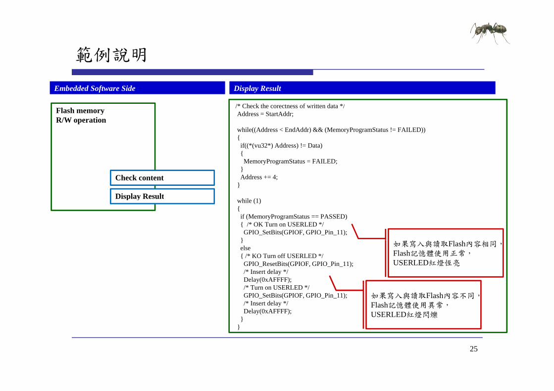
範例說明
Embedded Software Side
Check the corectness of written data
Display Result
Check the corectness of written data Address = StartAddr
while((Address lt EndAddr) ampamp (MemoryProgramStatus = FAILED))if(((vu32) Address) = Data)
Flash memory RW operation
MemoryProgramStatus = FAILED
Address += 4
Check content
Display Result while (1)if (MemoryProgramStatus == PASSED) OK Turn on USERLED GPIO_SetBits(GPIOF GPIO_Pin_11)
Display Result
else KO Turn off USERLED GPIO_ResetBits(GPIOF GPIO_Pin_11) Insert delay Delay(0xAFFFF)
如果寫入與讀取Flash內容相同Flash記憶體使用正常USERLED紅燈恆亮
Turn on USERLED GPIO_SetBits(GPIOF GPIO_Pin_11) Insert delay Delay(0xAFFFF)
如果寫入與讀取Flash內容不同Flash記憶體使用異常USERLED紅燈閃爍
25
預設定義說明
define StartAddr ((u32)0x08008000) 定義Flash使用起始點 定義Flash使用起始點
使用起始點必需大於0x8003000 + Code Size 附註 0x8000000~0x8003000為DFU程式區塊使用此區塊
將造成無法燒錄程式
Code Size可由產生的HEX檔得知
d fi E dAdd (( 32)0 0800C000) define EndAddr ((u32)0x0800C000) 定義Flash使用結束點
使用起始點必需小於0x8040000使用起始點必需小於
Data = 0x15041975 寫入資料
32Bit define FLASH_PAGE_SIZE ((u16)0x800)
每一個Page有2KByte26
每一個Page有2KByte
Intel HEX Format
aaaa tt dd cc
field Description
the colon that starts every Intel HEX record
the record-length field that represents the number of data bytes (dd) in the record
aaaa the address field that represents the starting address for subsequent data in the record
tt the field that represents the HEX record type which may be one of the following00 - data record01 - end-of-file record02 - extended segment address recordg04 - extended linear address record
dd a data field that represents one byte of data A record may have multiple data bytes The number of data bytes in the record must match the number specified by the field
cc the checksum field that represents the checksum of the record The checksum is calculated by summing the values of all hexadecimal digit pairs in the record modulo 256 and taking the twos complement
27
HEX Examplep
020000040800F2103000001814002045310008D9340008CD340008D8103000001814002045310008D9340008CD340008D8helliphelliphellip1038200042370008000000000000000000000000170C3830000000000000000000000000008C
資料填入起始位置為
0C3830000000000000000000000000008C04000005080031318D00000001FF
資料填入起始位置為0x08003000 每一行有0x10(16)個Bytes 最後一筆資料為
資料結束點為0x0803383004000005080031318D
(0x08003830 -0x08000000)0x800 = 7 需以0x800為單位所以使用的位置起點為0x08004000
28
燒錄MIAT STM32_
Rebuilder all target files產生HEX DFU Fil M 轉換HEX產生DFU DFU File Manager轉換HEX產生DFU DfuSe Demonstration燒錄DFU d Leave DFU mode
29
內部Flash存取控制實驗
實驗一
WU-YANGTechnology Co Ltd
實驗一練習
注意 請使用預設0 08008000之後的位置 避免覆蓋DFU 請使用預設0x08008000之後的位置避免覆蓋DFU
與使用者程式碼區塊
練習 練習 修改存取位置測試是否正常
修改寫入資料測試是否正常 修改寫入資料測試是否正常
修改寫入資料後取消FLASH_Unlock測試是否正常
修改寫入資料後取消FLASH E P 測試是否正 修改寫入資料後取消FLASH_ErasePage測試是否正常
31
實驗目的(二)( )
使用MIAT_STM32實驗板透過Flash memory interface (FLITF)控制內部Flash進行存取控制實驗並利用SW(FLITF)控制內部Flash進行存取控制實驗並利用SWKEY決定資料寫入與讀取LCD顯示狀態
32
實驗原理
System requirement E b dd d Fl h Embedded Flash LCD KEY SW
Development Flow ARM Configure
33
Development Flowp
Embedded Software Side
int main(void)
Bootup STM32F10x
ProgrammingBootupSTM32F10x RCC Configure
NVIC Configure
int main(void)ifdef DEBUGdebug()
endif
FLASHStatus = FLASH_COMPLETE
RCC Configuration RCC Configuration()
GPIO Configure
BasicIO Configure_ g ()
NVIC Configuration NVIC_Configuration()
GPIO Configuration Flash memory RW ti
lcd Configure
GPIO Configuration GPIO_Configuration()
Init_BasicIO()
l d i i () LCD I i i li i
RW operation
Example
FLASH Unlock
FLASH ClearFlag
lcd_init() LCD Initialization
helliphelliphelliphelliphelliphelliphelliphelliphelliphelliphelliphelliphelliphelliphelliphelliphelliphelliphelliphelliphelliphelliphellip
p
34
硬體電路配置
Mapping Table
Num MIAT_STM32V2 MIAT_IOBV1 Num MIAT_STM32V2 MIAT_IOBV1
1 PC8 (326) SW1 10 PE6 (15) LCD_EN2 PC9 (327) SW2 11 PF6 (118) LCD RW ( ) ( ) _3 PC10 (43) SW3 12 PF7 (119) LCD_RS 4 PC11 (44) SW4 13 PF8(120) LCD_D4 5 PB5 (427) KEY1 14 PF9 (121) LCD_D5 6 PB6 (428) KEY2 15 PF10 (122) LCD_D6 7 PB7 (429) KEY3 16 PF11 (213) LCD_D7 8 PB8 (431) KEY4 17 VDD (236) VCC33V 9 VCC5V (1 36) VCC5V 18 GND (1 35) GND9 VCC5V (136) VCC5V 18 GND (135) GND
35
實驗步驟
範例目錄架構
範例說明 範例說明
預設定義說明
36
範例目錄架構
範例目錄
測試映像檔 測試映像檔
含括檔
函式庫 函式庫
專案檔
原始碼 原始碼
37
範例說明
Embedded Software Side
lcd clear()
FLASH memory RW operation
lcd_clear()lcd_print (MIAT_STM32 DEMO )
Unlock the Flash Program Erase controller FLASH_Unlock()
Flash memory RW operation
FLASH Unlock
Clear All pending flags FLASH_ClearFlag(FLASH_FLAG_BSY | FLASH_FLAG_EOP | FLASH_FLAG_PGERR |
FLASH_FLAG_WRPRTERR)
while(1)
Example
FLASH ClearFlag
( )
KEY_Buffer=Key_Scan()set_cursor (0 1)lcd_print (SW Value = 0x)lcd putchar(((SWamp0x7)+0x30))lcd_putchar(((SWamp0x7)+0x30))if(KEY_Buffer==1)Address=(StartAddr|(SWltlt12))set_cursor (0 0)lcd_print (Set Addr = 0x)
掃描KEY是否按下與顯示SW數值LCD Line2顯示SW Value = 0x(SW)
lcd_putchar(((SWamp0x7)+0x30))lcd_print ( )
如果KEY1按下記錄SW數值至Address LCD Line1顯示Set Adde = 0x(Address)
38
範例說明
Embedded Software Side
else if(KEY Buffer==2)
FLASH memory RW operation
else if(KEY_Buffer==2)
Erase the FLASH pages FLASHStatus = FLASH_ErasePage(Address)
FLASH Word program of data at addresses defined by SW
SRAM memory RW operation
p g yFLASHStatus = FLASH_ProgramWord(Address (SWamp0x7))
set_cursor (0 0)lcd_print (Write 0x)lcd_putchar(((SWamp0x7)+0x30))l d i t ( t 0 )
Example如果KEY2按下清除Address所處區塊並寫入SW數值 lcd_print ( at 0x)
lcd_putchar((((Addressgtgt12)amp0x7)+0x30))else if(KEY_Buffer==3)
Data=(u16 )Address
所處區塊並寫入SW數值LCD Line1顯示Write 0x(SW) at 0x(Adddress)
Data (u16 )Addressset_cursor (0 0)lcd_print (Addr 0x)lcd_putchar((((Addressgtgt12)amp0x7)+0x30))lcd_print ( = 0x)lcd_putchar(((Dataamp0x7)+0x30))lcd_print ( )
如果KEY3按下讀取Address紀錄數值LCD Line1顯示Addr 0x(Adddress) = 0x
39
預設定義說明
define StartAddr ((u32)0x08020000) 定義Flash使用起始點 定義Flash使用起始點
使用起始點必需大於0x8003000 + Code Size 附註 0x8000000~0x8003000為DFU程式區塊使用此區塊
將造成無法燒錄程式
Code Size可由產生的HEX檔得知
32 Add 0 08020000 u32 Address = 0x08020000 定義Address初始值
初始值必需與Flash使用起始點相同初始值必需與 使用起始點相同
Address=(StartAddr|(SWltlt12)) Example StartAddr = 0x08020000 SW = 1 Address = 0x08021000
StartAddr = 0x08020000 SW = 7 Address = 0x08027000 StartAddr|(7ltlt12)必需小於0x8040000
40
使用者界面與Flash存取控制實驗
實驗二
WU-YANGTechnology Co Ltd
實驗二練習
注意 請使用預設0 08020000之後的位置 避免覆蓋DFU 請使用預設0x08020000之後的位置避免覆蓋DFU
與使用者程式碼區塊
練習 練習 利用SW與KEY測試Flash寫入與讀取是否正常
Fl h寫入後電源關閉 再開啟後寫入資料是否仍存 Flash寫入後電源關閉再開啟後寫入資料是否仍存在
修改存取位置測試是否正常 修改存取位置測試是否正常
42
實驗目的(三)( )
使用MIAT_STM32實驗板透過Flash memory interface (FLITF)控制內部Flash進行存取控制實驗並藉由填入(FLITF)控制內部Flash進行存取控制實驗並藉由填入Option Bytes 設定寫入鎖定保護Page鎖定不被覆蓋
43
Development Flowp
Embedded Software Side
int main(void)
Bootup STM32F10x
ProgrammingBootupSTM32F10x RCC Configure
NVIC Configure
int main(void)ifdef DEBUGdebug()
endifendif
FLASHStatus = FLASH_COMPLETEMemoryProgramStatus = PASSEDData = 0x1753
GPIO Configure
Data = 0x1753
RCC Configuration RCC_Configuration()
Flash memory RW operation FLASH Unlock
FLASH ClearFlag NVIC Configuration NVIC_Configuration()
GPIO Configuration
FLASH ClearFlag
FLASH ErasePage
FLASH ProgramHalfWord GPIO Configuration GPIO_Configuration()
Display Result
Check content
44
helliphelliphelliphelliphelliphelliphelliphelliphelliphelliphelliphelliphelliphelliphelliphelliphelliphelliphellip
實驗步驟
範例目錄架構
範例說明 範例說明
預設定義說明
45
範例目錄架構
範例目錄
測試映像檔 測試映像檔
含括檔
函式庫 函式庫
專案檔
原始碼 原始碼
46
範例說明
Function name Description
Unlock the Flash Program Erase controller FLASH_Unlock()
Define the number of page to be erased
Flash FwLib Functions List
Function name Description
FLASH_Unlock Unlocks the FLASH Program Erase Controller
FLASH_ClearFlag Clears the FLASH pending fl
Define the number of page to be erased NbrOfPage = (EndAddr ‐ StartAddr) FLASH_PAGE_SIZE
FLASH_ClearFlag(FLASH_FLAG_BSY | FLASH_FLAG_EOP|FLASH_FLAG_PGERR |FLASH_FLAG_WRPRTERR)
Get pages write protection status flags
FLASH_EraseOptionBytes
Erases the FLASH option bytes
FLASH_EnableWritePro Write protects the desired
p g pWRPR_Value = FLASH_GetWriteProtectionOptionByte()ProtectedPages = WRPR_Value amp 0x000000C0
ifdef WriteProtection_Disableif (ProtectedPages == 0x00) Pages are write protected
tection pages
NVIC_GenerateSystemReset
Generate a system reset
Disable the write protection FLASHStatus = FLASH_EraseOptionBytes() Generate System Reset to load the new option byte values NVIC_GenerateSystemReset()
elseifdef WriteProtection Enableifdef WriteProtection_Enableif (ProtectedPages = 0x00) Pages not write protected
FLASHStatus = FLASH_EraseOptionBytes() Enable the pages write protection FLASHStatus = FLASH_EnableWriteProtection(FLASH_WRProt_Pages12to13
|FLASH WRProt Pages14to15)|FLASH_WRProt_Pages14to15) Generate System Reset to load the new option byte values NVIC_GenerateSystemReset()
endifendif
47
範例說明
if (ProtectedPages = 0x00) Clear All pending flags
Flash FwLib Functions List
Function name DescriptionFLASH_ClearFlag(FLASH_FLAG_BSY |
FLASH_FLAG_EOP|FLASH_FLAG_PGERR |FLASH_FLAG_WRPRTERR)
erase the FLASH pages for(EraseCounter = 0 (EraseCounter lt NbrOfPage) ampamp (FLASHStatus ==
Function name Description
FLASH_ErasePage Erases a specified FLASH page
FLASH_ProgramHalfWod
Programs a half word at a ifi d dd FLASH_COMPLETE) EraseCounter++)
FLASHStatus = FLASH_ErasePage(StartAddr + (FLASH_PAGE_SIZE
EraseCounter))
rd specified address
FLASH Half Word program of data 0x1753 at addresses defined by StartAddrand EndAddr
Address = StartAddr
hil ((Add E dAdd ) ampamp (FLASHSt t FLASH COMPLETE))while((Address lt EndAddr) ampamp (FLASHStatus == FLASH_COMPLETE))
FLASHStatus = FLASH_ProgramHalfWord(Address Data)Address = Address + 2
48
範例說明
Embedded Software Side
Check the corectness of written data
Display Result
Check the corectness of written data Address = StartAddr
while((Address lt EndAddr) ampamp (MemoryProgramStatus = FAILED))if(((vu16) Address) = Data)
Flash memory RW operation
MemoryProgramStatus = FAILED
Address += 2
Check content
Display Result while (1)if (MemoryProgramStatus == PASSED) OK Turn on USERLED GPIO_SetBits(GPIOF GPIO_Pin_11)
Display Result
else KO Turn off USERLED GPIO_ResetBits(GPIOF GPIO_Pin_11) Insert delay Delay(0xAFFFF)
如果寫入與讀取Flash內容相同Flash記憶體可以寫入USERLED紅燈恆亮
Turn on USERLED GPIO_SetBits(GPIOF GPIO_Pin_11) Insert delay Delay(0xAFFFF)
如果寫入與讀取Flash內容不同Flash記憶體不能寫入USERLED紅燈閃爍
49
預設定義說明
define StartAddr ((u32) 0x08006000) 定義Flash使用起始點 定義Flash使用起始點
使用起始點必需大於0x8003000 + Code Size 附註 0x8000000~0x8003000為DFU程式區塊使用此區塊
將造成無法燒錄程式
Code Size可由產生的HEX檔得知
d fi E dAdd (( 32) 0 08008000) define EndAddr ((u32) 0x08008000) 定義Flash使用結束點
使用起始點必需小於0x8040000使用起始點必需小於
Data = 0x1753 寫入資料
16Bit define FLASH_PAGE_SIZE ((u16)0x800) 每一個Page有2KByte
50
每一個Page有2KByte
預設定義說明
define WriteProtection_Enable U hi li E bl W i P i Uncomment this line to Enable Write Protection
define WriteProtection_Disablehi li i bl i i Uncomment this line to Disable Write Protection
FLASH_EnableWriteProtection設定影響 個 設定影響2個Page FLASH_WRProt_Pages0to1 FLASH_WRProt_Pages1to2 helliphellip FLASH_WRProt_Pages60to61
設定影響多個Page FLASH_WRProt_Pages62to255
51
FLASH EnableWriteProtection_
Example
位置0x08006000 ~ 0x08007000每一個Page有0x800ByteStartPage = (0x08006000-0x08000000)0x800 = 12EndPage = ((0x08007000-0x08000000)0x800)-1 = 13執行執行FLASH_EnableWriteProtection(FLASH_WRProt_Pages12to13)將影響Pages12 Pages13
52
內部Flash寫入鎖定存取控制實驗
實驗三
WU-YANGTechnology Co Ltd
實驗三練習
注意 請使用預設0 08006000之後的位置 避免覆蓋DFU 請使用預設0x08006000之後的位置避免覆蓋DFU
與使用者程式碼區塊
更改寫入位置測試寫入鎖定時需同時更改 更改寫入位置測試寫入鎖定時需同時更改FLASH_EnableWriteProtection鎖定之Page
練習 練習 打開define WriteProtection_Enable測試是否可寫入
打開define WriteProtection Disable測試是否可寫入 打開define WriteProtection_Disable測試是否可寫入
修改存取位置測試是否正常
修改寫入資料測試是否正常 修改寫入資料測試是否正常
54
Q amp A
WU-YANGTechnology Co Ltd

預設定義說明
define StartAddr ((u32)0x08008000) 定義Flash使用起始點 定義Flash使用起始點
使用起始點必需大於0x8003000 + Code Size 附註 0x8000000~0x8003000為DFU程式區塊使用此區塊
將造成無法燒錄程式
Code Size可由產生的HEX檔得知
d fi E dAdd (( 32)0 0800C000) define EndAddr ((u32)0x0800C000) 定義Flash使用結束點
使用起始點必需小於0x8040000使用起始點必需小於
Data = 0x15041975 寫入資料
32Bit define FLASH_PAGE_SIZE ((u16)0x800)
每一個Page有2KByte26
每一個Page有2KByte
Intel HEX Format
aaaa tt dd cc
field Description
the colon that starts every Intel HEX record
the record-length field that represents the number of data bytes (dd) in the record
aaaa the address field that represents the starting address for subsequent data in the record
tt the field that represents the HEX record type which may be one of the following00 - data record01 - end-of-file record02 - extended segment address recordg04 - extended linear address record
dd a data field that represents one byte of data A record may have multiple data bytes The number of data bytes in the record must match the number specified by the field
cc the checksum field that represents the checksum of the record The checksum is calculated by summing the values of all hexadecimal digit pairs in the record modulo 256 and taking the twos complement
27
HEX Examplep
020000040800F2103000001814002045310008D9340008CD340008D8103000001814002045310008D9340008CD340008D8helliphelliphellip1038200042370008000000000000000000000000170C3830000000000000000000000000008C
資料填入起始位置為
0C3830000000000000000000000000008C04000005080031318D00000001FF
資料填入起始位置為0x08003000 每一行有0x10(16)個Bytes 最後一筆資料為
資料結束點為0x0803383004000005080031318D
(0x08003830 -0x08000000)0x800 = 7 需以0x800為單位所以使用的位置起點為0x08004000
28
燒錄MIAT STM32_
Rebuilder all target files產生HEX DFU Fil M 轉換HEX產生DFU DFU File Manager轉換HEX產生DFU DfuSe Demonstration燒錄DFU d Leave DFU mode
29
內部Flash存取控制實驗
實驗一
WU-YANGTechnology Co Ltd
實驗一練習
注意 請使用預設0 08008000之後的位置 避免覆蓋DFU 請使用預設0x08008000之後的位置避免覆蓋DFU
與使用者程式碼區塊
練習 練習 修改存取位置測試是否正常
修改寫入資料測試是否正常 修改寫入資料測試是否正常
修改寫入資料後取消FLASH_Unlock測試是否正常
修改寫入資料後取消FLASH E P 測試是否正 修改寫入資料後取消FLASH_ErasePage測試是否正常
31
實驗目的(二)( )
使用MIAT_STM32實驗板透過Flash memory interface (FLITF)控制內部Flash進行存取控制實驗並利用SW(FLITF)控制內部Flash進行存取控制實驗並利用SWKEY決定資料寫入與讀取LCD顯示狀態
32
實驗原理
System requirement E b dd d Fl h Embedded Flash LCD KEY SW
Development Flow ARM Configure
33
Development Flowp
Embedded Software Side
int main(void)
Bootup STM32F10x
ProgrammingBootupSTM32F10x RCC Configure
NVIC Configure
int main(void)ifdef DEBUGdebug()
endif
FLASHStatus = FLASH_COMPLETE
RCC Configuration RCC Configuration()
GPIO Configure
BasicIO Configure_ g ()
NVIC Configuration NVIC_Configuration()
GPIO Configuration Flash memory RW ti
lcd Configure
GPIO Configuration GPIO_Configuration()
Init_BasicIO()
l d i i () LCD I i i li i
RW operation
Example
FLASH Unlock
FLASH ClearFlag
lcd_init() LCD Initialization
helliphelliphelliphelliphelliphelliphelliphelliphelliphelliphelliphelliphelliphelliphelliphelliphelliphelliphelliphelliphelliphelliphellip
p
34
硬體電路配置
Mapping Table
Num MIAT_STM32V2 MIAT_IOBV1 Num MIAT_STM32V2 MIAT_IOBV1
1 PC8 (326) SW1 10 PE6 (15) LCD_EN2 PC9 (327) SW2 11 PF6 (118) LCD RW ( ) ( ) _3 PC10 (43) SW3 12 PF7 (119) LCD_RS 4 PC11 (44) SW4 13 PF8(120) LCD_D4 5 PB5 (427) KEY1 14 PF9 (121) LCD_D5 6 PB6 (428) KEY2 15 PF10 (122) LCD_D6 7 PB7 (429) KEY3 16 PF11 (213) LCD_D7 8 PB8 (431) KEY4 17 VDD (236) VCC33V 9 VCC5V (1 36) VCC5V 18 GND (1 35) GND9 VCC5V (136) VCC5V 18 GND (135) GND
35
實驗步驟
範例目錄架構
範例說明 範例說明
預設定義說明
36
範例目錄架構
範例目錄
測試映像檔 測試映像檔
含括檔
函式庫 函式庫
專案檔
原始碼 原始碼
37
範例說明
Embedded Software Side
lcd clear()
FLASH memory RW operation
lcd_clear()lcd_print (MIAT_STM32 DEMO )
Unlock the Flash Program Erase controller FLASH_Unlock()
Flash memory RW operation
FLASH Unlock
Clear All pending flags FLASH_ClearFlag(FLASH_FLAG_BSY | FLASH_FLAG_EOP | FLASH_FLAG_PGERR |
FLASH_FLAG_WRPRTERR)
while(1)
Example
FLASH ClearFlag
( )
KEY_Buffer=Key_Scan()set_cursor (0 1)lcd_print (SW Value = 0x)lcd putchar(((SWamp0x7)+0x30))lcd_putchar(((SWamp0x7)+0x30))if(KEY_Buffer==1)Address=(StartAddr|(SWltlt12))set_cursor (0 0)lcd_print (Set Addr = 0x)
掃描KEY是否按下與顯示SW數值LCD Line2顯示SW Value = 0x(SW)
lcd_putchar(((SWamp0x7)+0x30))lcd_print ( )
如果KEY1按下記錄SW數值至Address LCD Line1顯示Set Adde = 0x(Address)
38
範例說明
Embedded Software Side
else if(KEY Buffer==2)
FLASH memory RW operation
else if(KEY_Buffer==2)
Erase the FLASH pages FLASHStatus = FLASH_ErasePage(Address)
FLASH Word program of data at addresses defined by SW
SRAM memory RW operation
p g yFLASHStatus = FLASH_ProgramWord(Address (SWamp0x7))
set_cursor (0 0)lcd_print (Write 0x)lcd_putchar(((SWamp0x7)+0x30))l d i t ( t 0 )
Example如果KEY2按下清除Address所處區塊並寫入SW數值 lcd_print ( at 0x)
lcd_putchar((((Addressgtgt12)amp0x7)+0x30))else if(KEY_Buffer==3)
Data=(u16 )Address
所處區塊並寫入SW數值LCD Line1顯示Write 0x(SW) at 0x(Adddress)
Data (u16 )Addressset_cursor (0 0)lcd_print (Addr 0x)lcd_putchar((((Addressgtgt12)amp0x7)+0x30))lcd_print ( = 0x)lcd_putchar(((Dataamp0x7)+0x30))lcd_print ( )
如果KEY3按下讀取Address紀錄數值LCD Line1顯示Addr 0x(Adddress) = 0x
39
預設定義說明
define StartAddr ((u32)0x08020000) 定義Flash使用起始點 定義Flash使用起始點
使用起始點必需大於0x8003000 + Code Size 附註 0x8000000~0x8003000為DFU程式區塊使用此區塊
將造成無法燒錄程式
Code Size可由產生的HEX檔得知
32 Add 0 08020000 u32 Address = 0x08020000 定義Address初始值
初始值必需與Flash使用起始點相同初始值必需與 使用起始點相同
Address=(StartAddr|(SWltlt12)) Example StartAddr = 0x08020000 SW = 1 Address = 0x08021000
StartAddr = 0x08020000 SW = 7 Address = 0x08027000 StartAddr|(7ltlt12)必需小於0x8040000
40
使用者界面與Flash存取控制實驗
實驗二
WU-YANGTechnology Co Ltd
實驗二練習
注意 請使用預設0 08020000之後的位置 避免覆蓋DFU 請使用預設0x08020000之後的位置避免覆蓋DFU
與使用者程式碼區塊
練習 練習 利用SW與KEY測試Flash寫入與讀取是否正常
Fl h寫入後電源關閉 再開啟後寫入資料是否仍存 Flash寫入後電源關閉再開啟後寫入資料是否仍存在
修改存取位置測試是否正常 修改存取位置測試是否正常
42
實驗目的(三)( )
使用MIAT_STM32實驗板透過Flash memory interface (FLITF)控制內部Flash進行存取控制實驗並藉由填入(FLITF)控制內部Flash進行存取控制實驗並藉由填入Option Bytes 設定寫入鎖定保護Page鎖定不被覆蓋
43
Development Flowp
Embedded Software Side
int main(void)
Bootup STM32F10x
ProgrammingBootupSTM32F10x RCC Configure
NVIC Configure
int main(void)ifdef DEBUGdebug()
endifendif
FLASHStatus = FLASH_COMPLETEMemoryProgramStatus = PASSEDData = 0x1753
GPIO Configure
Data = 0x1753
RCC Configuration RCC_Configuration()
Flash memory RW operation FLASH Unlock
FLASH ClearFlag NVIC Configuration NVIC_Configuration()
GPIO Configuration
FLASH ClearFlag
FLASH ErasePage
FLASH ProgramHalfWord GPIO Configuration GPIO_Configuration()
Display Result
Check content
44
helliphelliphelliphelliphelliphelliphelliphelliphelliphelliphelliphelliphelliphelliphelliphelliphelliphelliphellip
實驗步驟
範例目錄架構
範例說明 範例說明
預設定義說明
45
範例目錄架構
範例目錄
測試映像檔 測試映像檔
含括檔
函式庫 函式庫
專案檔
原始碼 原始碼
46
範例說明
Function name Description
Unlock the Flash Program Erase controller FLASH_Unlock()
Define the number of page to be erased
Flash FwLib Functions List
Function name Description
FLASH_Unlock Unlocks the FLASH Program Erase Controller
FLASH_ClearFlag Clears the FLASH pending fl
Define the number of page to be erased NbrOfPage = (EndAddr ‐ StartAddr) FLASH_PAGE_SIZE
FLASH_ClearFlag(FLASH_FLAG_BSY | FLASH_FLAG_EOP|FLASH_FLAG_PGERR |FLASH_FLAG_WRPRTERR)
Get pages write protection status flags
FLASH_EraseOptionBytes
Erases the FLASH option bytes
FLASH_EnableWritePro Write protects the desired
p g pWRPR_Value = FLASH_GetWriteProtectionOptionByte()ProtectedPages = WRPR_Value amp 0x000000C0
ifdef WriteProtection_Disableif (ProtectedPages == 0x00) Pages are write protected
tection pages
NVIC_GenerateSystemReset
Generate a system reset
Disable the write protection FLASHStatus = FLASH_EraseOptionBytes() Generate System Reset to load the new option byte values NVIC_GenerateSystemReset()
elseifdef WriteProtection Enableifdef WriteProtection_Enableif (ProtectedPages = 0x00) Pages not write protected
FLASHStatus = FLASH_EraseOptionBytes() Enable the pages write protection FLASHStatus = FLASH_EnableWriteProtection(FLASH_WRProt_Pages12to13
|FLASH WRProt Pages14to15)|FLASH_WRProt_Pages14to15) Generate System Reset to load the new option byte values NVIC_GenerateSystemReset()
endifendif
47
範例說明
if (ProtectedPages = 0x00) Clear All pending flags
Flash FwLib Functions List
Function name DescriptionFLASH_ClearFlag(FLASH_FLAG_BSY |
FLASH_FLAG_EOP|FLASH_FLAG_PGERR |FLASH_FLAG_WRPRTERR)
erase the FLASH pages for(EraseCounter = 0 (EraseCounter lt NbrOfPage) ampamp (FLASHStatus ==
Function name Description
FLASH_ErasePage Erases a specified FLASH page
FLASH_ProgramHalfWod
Programs a half word at a ifi d dd FLASH_COMPLETE) EraseCounter++)
FLASHStatus = FLASH_ErasePage(StartAddr + (FLASH_PAGE_SIZE
EraseCounter))
rd specified address
FLASH Half Word program of data 0x1753 at addresses defined by StartAddrand EndAddr
Address = StartAddr
hil ((Add E dAdd ) ampamp (FLASHSt t FLASH COMPLETE))while((Address lt EndAddr) ampamp (FLASHStatus == FLASH_COMPLETE))
FLASHStatus = FLASH_ProgramHalfWord(Address Data)Address = Address + 2
48
範例說明
Embedded Software Side
Check the corectness of written data
Display Result
Check the corectness of written data Address = StartAddr
while((Address lt EndAddr) ampamp (MemoryProgramStatus = FAILED))if(((vu16) Address) = Data)
Flash memory RW operation
MemoryProgramStatus = FAILED
Address += 2
Check content
Display Result while (1)if (MemoryProgramStatus == PASSED) OK Turn on USERLED GPIO_SetBits(GPIOF GPIO_Pin_11)
Display Result
else KO Turn off USERLED GPIO_ResetBits(GPIOF GPIO_Pin_11) Insert delay Delay(0xAFFFF)
如果寫入與讀取Flash內容相同Flash記憶體可以寫入USERLED紅燈恆亮
Turn on USERLED GPIO_SetBits(GPIOF GPIO_Pin_11) Insert delay Delay(0xAFFFF)
如果寫入與讀取Flash內容不同Flash記憶體不能寫入USERLED紅燈閃爍
49
預設定義說明
define StartAddr ((u32) 0x08006000) 定義Flash使用起始點 定義Flash使用起始點
使用起始點必需大於0x8003000 + Code Size 附註 0x8000000~0x8003000為DFU程式區塊使用此區塊
將造成無法燒錄程式
Code Size可由產生的HEX檔得知
d fi E dAdd (( 32) 0 08008000) define EndAddr ((u32) 0x08008000) 定義Flash使用結束點
使用起始點必需小於0x8040000使用起始點必需小於
Data = 0x1753 寫入資料
16Bit define FLASH_PAGE_SIZE ((u16)0x800) 每一個Page有2KByte
50
每一個Page有2KByte
預設定義說明
define WriteProtection_Enable U hi li E bl W i P i Uncomment this line to Enable Write Protection
define WriteProtection_Disablehi li i bl i i Uncomment this line to Disable Write Protection
FLASH_EnableWriteProtection設定影響 個 設定影響2個Page FLASH_WRProt_Pages0to1 FLASH_WRProt_Pages1to2 helliphellip FLASH_WRProt_Pages60to61
設定影響多個Page FLASH_WRProt_Pages62to255
51
FLASH EnableWriteProtection_
Example
位置0x08006000 ~ 0x08007000每一個Page有0x800ByteStartPage = (0x08006000-0x08000000)0x800 = 12EndPage = ((0x08007000-0x08000000)0x800)-1 = 13執行執行FLASH_EnableWriteProtection(FLASH_WRProt_Pages12to13)將影響Pages12 Pages13
52
內部Flash寫入鎖定存取控制實驗
實驗三
WU-YANGTechnology Co Ltd
實驗三練習
注意 請使用預設0 08006000之後的位置 避免覆蓋DFU 請使用預設0x08006000之後的位置避免覆蓋DFU
與使用者程式碼區塊
更改寫入位置測試寫入鎖定時需同時更改 更改寫入位置測試寫入鎖定時需同時更改FLASH_EnableWriteProtection鎖定之Page
練習 練習 打開define WriteProtection_Enable測試是否可寫入
打開define WriteProtection Disable測試是否可寫入 打開define WriteProtection_Disable測試是否可寫入
修改存取位置測試是否正常
修改寫入資料測試是否正常 修改寫入資料測試是否正常
54
Q amp A
WU-YANGTechnology Co Ltd
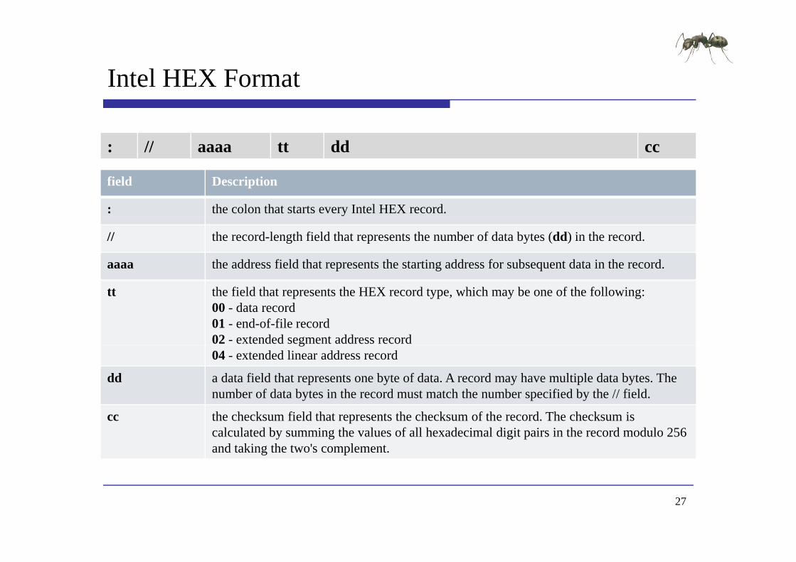
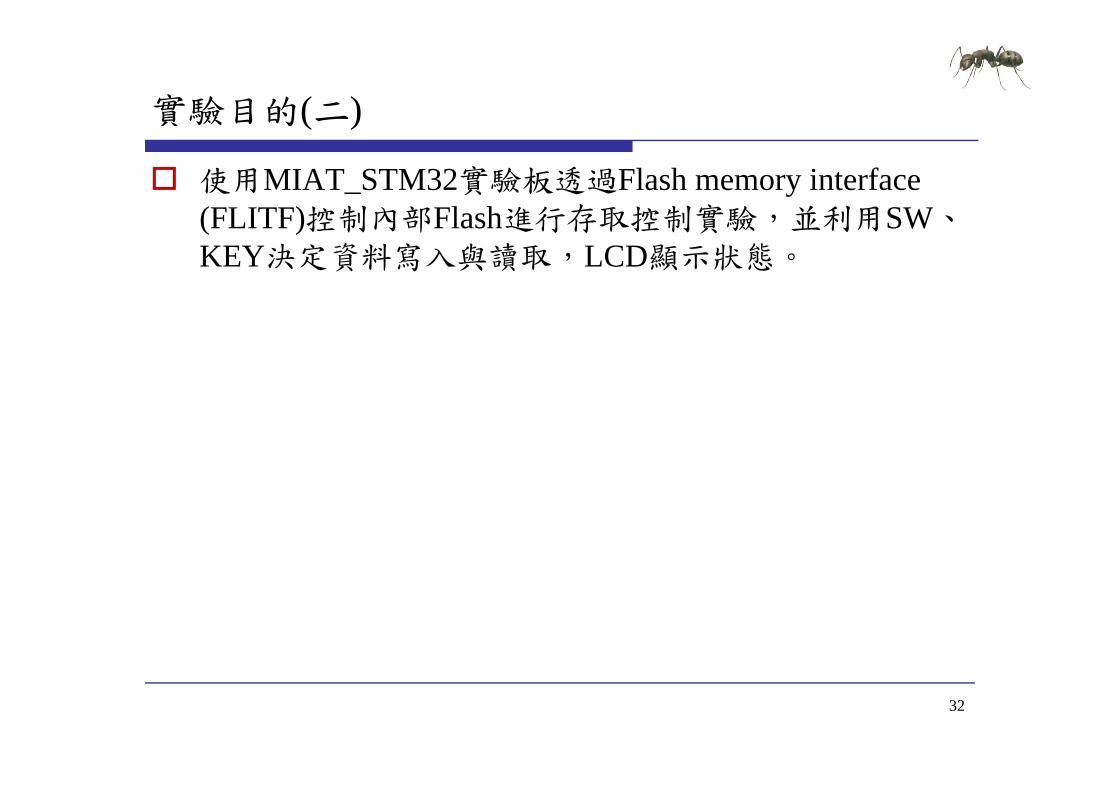

Development Flowp
Embedded Software Side
int main(void)
Bootup STM32F10x
ProgrammingBootupSTM32F10x RCC Configure
NVIC Configure
int main(void)ifdef DEBUGdebug()
endif
FLASHStatus = FLASH_COMPLETE
RCC Configuration RCC Configuration()
GPIO Configure
BasicIO Configure_ g ()
NVIC Configuration NVIC_Configuration()
GPIO Configuration Flash memory RW ti
lcd Configure
GPIO Configuration GPIO_Configuration()
Init_BasicIO()
l d i i () LCD I i i li i
RW operation
Example
FLASH Unlock
FLASH ClearFlag
lcd_init() LCD Initialization
helliphelliphelliphelliphelliphelliphelliphelliphelliphelliphelliphelliphelliphelliphelliphelliphelliphelliphelliphelliphelliphelliphellip
p
34
硬體電路配置
Mapping Table
Num MIAT_STM32V2 MIAT_IOBV1 Num MIAT_STM32V2 MIAT_IOBV1
1 PC8 (326) SW1 10 PE6 (15) LCD_EN2 PC9 (327) SW2 11 PF6 (118) LCD RW ( ) ( ) _3 PC10 (43) SW3 12 PF7 (119) LCD_RS 4 PC11 (44) SW4 13 PF8(120) LCD_D4 5 PB5 (427) KEY1 14 PF9 (121) LCD_D5 6 PB6 (428) KEY2 15 PF10 (122) LCD_D6 7 PB7 (429) KEY3 16 PF11 (213) LCD_D7 8 PB8 (431) KEY4 17 VDD (236) VCC33V 9 VCC5V (1 36) VCC5V 18 GND (1 35) GND9 VCC5V (136) VCC5V 18 GND (135) GND
35
實驗步驟
範例目錄架構
範例說明 範例說明
預設定義說明
36
範例目錄架構
範例目錄
測試映像檔 測試映像檔
含括檔
函式庫 函式庫
專案檔
原始碼 原始碼
37
範例說明
Embedded Software Side
lcd clear()
FLASH memory RW operation
lcd_clear()lcd_print (MIAT_STM32 DEMO )
Unlock the Flash Program Erase controller FLASH_Unlock()
Flash memory RW operation
FLASH Unlock
Clear All pending flags FLASH_ClearFlag(FLASH_FLAG_BSY | FLASH_FLAG_EOP | FLASH_FLAG_PGERR |
FLASH_FLAG_WRPRTERR)
while(1)
Example
FLASH ClearFlag
( )
KEY_Buffer=Key_Scan()set_cursor (0 1)lcd_print (SW Value = 0x)lcd putchar(((SWamp0x7)+0x30))lcd_putchar(((SWamp0x7)+0x30))if(KEY_Buffer==1)Address=(StartAddr|(SWltlt12))set_cursor (0 0)lcd_print (Set Addr = 0x)
掃描KEY是否按下與顯示SW數值LCD Line2顯示SW Value = 0x(SW)
lcd_putchar(((SWamp0x7)+0x30))lcd_print ( )
如果KEY1按下記錄SW數值至Address LCD Line1顯示Set Adde = 0x(Address)
38
範例說明
Embedded Software Side
else if(KEY Buffer==2)
FLASH memory RW operation
else if(KEY_Buffer==2)
Erase the FLASH pages FLASHStatus = FLASH_ErasePage(Address)
FLASH Word program of data at addresses defined by SW
SRAM memory RW operation
p g yFLASHStatus = FLASH_ProgramWord(Address (SWamp0x7))
set_cursor (0 0)lcd_print (Write 0x)lcd_putchar(((SWamp0x7)+0x30))l d i t ( t 0 )
Example如果KEY2按下清除Address所處區塊並寫入SW數值 lcd_print ( at 0x)
lcd_putchar((((Addressgtgt12)amp0x7)+0x30))else if(KEY_Buffer==3)
Data=(u16 )Address
所處區塊並寫入SW數值LCD Line1顯示Write 0x(SW) at 0x(Adddress)
Data (u16 )Addressset_cursor (0 0)lcd_print (Addr 0x)lcd_putchar((((Addressgtgt12)amp0x7)+0x30))lcd_print ( = 0x)lcd_putchar(((Dataamp0x7)+0x30))lcd_print ( )
如果KEY3按下讀取Address紀錄數值LCD Line1顯示Addr 0x(Adddress) = 0x
39
預設定義說明
define StartAddr ((u32)0x08020000) 定義Flash使用起始點 定義Flash使用起始點
使用起始點必需大於0x8003000 + Code Size 附註 0x8000000~0x8003000為DFU程式區塊使用此區塊
將造成無法燒錄程式
Code Size可由產生的HEX檔得知
32 Add 0 08020000 u32 Address = 0x08020000 定義Address初始值
初始值必需與Flash使用起始點相同初始值必需與 使用起始點相同
Address=(StartAddr|(SWltlt12)) Example StartAddr = 0x08020000 SW = 1 Address = 0x08021000
StartAddr = 0x08020000 SW = 7 Address = 0x08027000 StartAddr|(7ltlt12)必需小於0x8040000
40
使用者界面與Flash存取控制實驗
實驗二
WU-YANGTechnology Co Ltd
實驗二練習
注意 請使用預設0 08020000之後的位置 避免覆蓋DFU 請使用預設0x08020000之後的位置避免覆蓋DFU
與使用者程式碼區塊
練習 練習 利用SW與KEY測試Flash寫入與讀取是否正常
Fl h寫入後電源關閉 再開啟後寫入資料是否仍存 Flash寫入後電源關閉再開啟後寫入資料是否仍存在
修改存取位置測試是否正常 修改存取位置測試是否正常
42
實驗目的(三)( )
使用MIAT_STM32實驗板透過Flash memory interface (FLITF)控制內部Flash進行存取控制實驗並藉由填入(FLITF)控制內部Flash進行存取控制實驗並藉由填入Option Bytes 設定寫入鎖定保護Page鎖定不被覆蓋
43
Development Flowp
Embedded Software Side
int main(void)
Bootup STM32F10x
ProgrammingBootupSTM32F10x RCC Configure
NVIC Configure
int main(void)ifdef DEBUGdebug()
endifendif
FLASHStatus = FLASH_COMPLETEMemoryProgramStatus = PASSEDData = 0x1753
GPIO Configure
Data = 0x1753
RCC Configuration RCC_Configuration()
Flash memory RW operation FLASH Unlock
FLASH ClearFlag NVIC Configuration NVIC_Configuration()
GPIO Configuration
FLASH ClearFlag
FLASH ErasePage
FLASH ProgramHalfWord GPIO Configuration GPIO_Configuration()
Display Result
Check content
44
helliphelliphelliphelliphelliphelliphelliphelliphelliphelliphelliphelliphelliphelliphelliphelliphelliphelliphellip
實驗步驟
範例目錄架構
範例說明 範例說明
預設定義說明
45
範例目錄架構
範例目錄
測試映像檔 測試映像檔
含括檔
函式庫 函式庫
專案檔
原始碼 原始碼
46
範例說明
Function name Description
Unlock the Flash Program Erase controller FLASH_Unlock()
Define the number of page to be erased
Flash FwLib Functions List
Function name Description
FLASH_Unlock Unlocks the FLASH Program Erase Controller
FLASH_ClearFlag Clears the FLASH pending fl
Define the number of page to be erased NbrOfPage = (EndAddr ‐ StartAddr) FLASH_PAGE_SIZE
FLASH_ClearFlag(FLASH_FLAG_BSY | FLASH_FLAG_EOP|FLASH_FLAG_PGERR |FLASH_FLAG_WRPRTERR)
Get pages write protection status flags
FLASH_EraseOptionBytes
Erases the FLASH option bytes
FLASH_EnableWritePro Write protects the desired
p g pWRPR_Value = FLASH_GetWriteProtectionOptionByte()ProtectedPages = WRPR_Value amp 0x000000C0
ifdef WriteProtection_Disableif (ProtectedPages == 0x00) Pages are write protected
tection pages
NVIC_GenerateSystemReset
Generate a system reset
Disable the write protection FLASHStatus = FLASH_EraseOptionBytes() Generate System Reset to load the new option byte values NVIC_GenerateSystemReset()
elseifdef WriteProtection Enableifdef WriteProtection_Enableif (ProtectedPages = 0x00) Pages not write protected
FLASHStatus = FLASH_EraseOptionBytes() Enable the pages write protection FLASHStatus = FLASH_EnableWriteProtection(FLASH_WRProt_Pages12to13
|FLASH WRProt Pages14to15)|FLASH_WRProt_Pages14to15) Generate System Reset to load the new option byte values NVIC_GenerateSystemReset()
endifendif
47
範例說明
if (ProtectedPages = 0x00) Clear All pending flags
Flash FwLib Functions List
Function name DescriptionFLASH_ClearFlag(FLASH_FLAG_BSY |
FLASH_FLAG_EOP|FLASH_FLAG_PGERR |FLASH_FLAG_WRPRTERR)
erase the FLASH pages for(EraseCounter = 0 (EraseCounter lt NbrOfPage) ampamp (FLASHStatus ==
Function name Description
FLASH_ErasePage Erases a specified FLASH page
FLASH_ProgramHalfWod
Programs a half word at a ifi d dd FLASH_COMPLETE) EraseCounter++)
FLASHStatus = FLASH_ErasePage(StartAddr + (FLASH_PAGE_SIZE
EraseCounter))
rd specified address
FLASH Half Word program of data 0x1753 at addresses defined by StartAddrand EndAddr
Address = StartAddr
hil ((Add E dAdd ) ampamp (FLASHSt t FLASH COMPLETE))while((Address lt EndAddr) ampamp (FLASHStatus == FLASH_COMPLETE))
FLASHStatus = FLASH_ProgramHalfWord(Address Data)Address = Address + 2
48
範例說明
Embedded Software Side
Check the corectness of written data
Display Result
Check the corectness of written data Address = StartAddr
while((Address lt EndAddr) ampamp (MemoryProgramStatus = FAILED))if(((vu16) Address) = Data)
Flash memory RW operation
MemoryProgramStatus = FAILED
Address += 2
Check content
Display Result while (1)if (MemoryProgramStatus == PASSED) OK Turn on USERLED GPIO_SetBits(GPIOF GPIO_Pin_11)
Display Result
else KO Turn off USERLED GPIO_ResetBits(GPIOF GPIO_Pin_11) Insert delay Delay(0xAFFFF)
如果寫入與讀取Flash內容相同Flash記憶體可以寫入USERLED紅燈恆亮
Turn on USERLED GPIO_SetBits(GPIOF GPIO_Pin_11) Insert delay Delay(0xAFFFF)
如果寫入與讀取Flash內容不同Flash記憶體不能寫入USERLED紅燈閃爍
49
預設定義說明
define StartAddr ((u32) 0x08006000) 定義Flash使用起始點 定義Flash使用起始點
使用起始點必需大於0x8003000 + Code Size 附註 0x8000000~0x8003000為DFU程式區塊使用此區塊
將造成無法燒錄程式
Code Size可由產生的HEX檔得知
d fi E dAdd (( 32) 0 08008000) define EndAddr ((u32) 0x08008000) 定義Flash使用結束點
使用起始點必需小於0x8040000使用起始點必需小於
Data = 0x1753 寫入資料
16Bit define FLASH_PAGE_SIZE ((u16)0x800) 每一個Page有2KByte
50
每一個Page有2KByte
預設定義說明
define WriteProtection_Enable U hi li E bl W i P i Uncomment this line to Enable Write Protection
define WriteProtection_Disablehi li i bl i i Uncomment this line to Disable Write Protection
FLASH_EnableWriteProtection設定影響 個 設定影響2個Page FLASH_WRProt_Pages0to1 FLASH_WRProt_Pages1to2 helliphellip FLASH_WRProt_Pages60to61
設定影響多個Page FLASH_WRProt_Pages62to255
51
FLASH EnableWriteProtection_
Example
位置0x08006000 ~ 0x08007000每一個Page有0x800ByteStartPage = (0x08006000-0x08000000)0x800 = 12EndPage = ((0x08007000-0x08000000)0x800)-1 = 13執行執行FLASH_EnableWriteProtection(FLASH_WRProt_Pages12to13)將影響Pages12 Pages13
52
內部Flash寫入鎖定存取控制實驗
實驗三
WU-YANGTechnology Co Ltd
實驗三練習
注意 請使用預設0 08006000之後的位置 避免覆蓋DFU 請使用預設0x08006000之後的位置避免覆蓋DFU
與使用者程式碼區塊
更改寫入位置測試寫入鎖定時需同時更改 更改寫入位置測試寫入鎖定時需同時更改FLASH_EnableWriteProtection鎖定之Page
練習 練習 打開define WriteProtection_Enable測試是否可寫入
打開define WriteProtection Disable測試是否可寫入 打開define WriteProtection_Disable測試是否可寫入
修改存取位置測試是否正常
修改寫入資料測試是否正常 修改寫入資料測試是否正常
54
Q amp A
WU-YANGTechnology Co Ltd

實驗步驟
範例目錄架構
範例說明 範例說明
預設定義說明
36
範例目錄架構
範例目錄
測試映像檔 測試映像檔
含括檔
函式庫 函式庫
專案檔
原始碼 原始碼
37
範例說明
Embedded Software Side
lcd clear()
FLASH memory RW operation
lcd_clear()lcd_print (MIAT_STM32 DEMO )
Unlock the Flash Program Erase controller FLASH_Unlock()
Flash memory RW operation
FLASH Unlock
Clear All pending flags FLASH_ClearFlag(FLASH_FLAG_BSY | FLASH_FLAG_EOP | FLASH_FLAG_PGERR |
FLASH_FLAG_WRPRTERR)
while(1)
Example
FLASH ClearFlag
( )
KEY_Buffer=Key_Scan()set_cursor (0 1)lcd_print (SW Value = 0x)lcd putchar(((SWamp0x7)+0x30))lcd_putchar(((SWamp0x7)+0x30))if(KEY_Buffer==1)Address=(StartAddr|(SWltlt12))set_cursor (0 0)lcd_print (Set Addr = 0x)
掃描KEY是否按下與顯示SW數值LCD Line2顯示SW Value = 0x(SW)
lcd_putchar(((SWamp0x7)+0x30))lcd_print ( )
如果KEY1按下記錄SW數值至Address LCD Line1顯示Set Adde = 0x(Address)
38
範例說明
Embedded Software Side
else if(KEY Buffer==2)
FLASH memory RW operation
else if(KEY_Buffer==2)
Erase the FLASH pages FLASHStatus = FLASH_ErasePage(Address)
FLASH Word program of data at addresses defined by SW
SRAM memory RW operation
p g yFLASHStatus = FLASH_ProgramWord(Address (SWamp0x7))
set_cursor (0 0)lcd_print (Write 0x)lcd_putchar(((SWamp0x7)+0x30))l d i t ( t 0 )
Example如果KEY2按下清除Address所處區塊並寫入SW數值 lcd_print ( at 0x)
lcd_putchar((((Addressgtgt12)amp0x7)+0x30))else if(KEY_Buffer==3)
Data=(u16 )Address
所處區塊並寫入SW數值LCD Line1顯示Write 0x(SW) at 0x(Adddress)
Data (u16 )Addressset_cursor (0 0)lcd_print (Addr 0x)lcd_putchar((((Addressgtgt12)amp0x7)+0x30))lcd_print ( = 0x)lcd_putchar(((Dataamp0x7)+0x30))lcd_print ( )
如果KEY3按下讀取Address紀錄數值LCD Line1顯示Addr 0x(Adddress) = 0x
39
預設定義說明
define StartAddr ((u32)0x08020000) 定義Flash使用起始點 定義Flash使用起始點
使用起始點必需大於0x8003000 + Code Size 附註 0x8000000~0x8003000為DFU程式區塊使用此區塊
將造成無法燒錄程式
Code Size可由產生的HEX檔得知
32 Add 0 08020000 u32 Address = 0x08020000 定義Address初始值
初始值必需與Flash使用起始點相同初始值必需與 使用起始點相同
Address=(StartAddr|(SWltlt12)) Example StartAddr = 0x08020000 SW = 1 Address = 0x08021000
StartAddr = 0x08020000 SW = 7 Address = 0x08027000 StartAddr|(7ltlt12)必需小於0x8040000
40
使用者界面與Flash存取控制實驗
實驗二
WU-YANGTechnology Co Ltd
實驗二練習
注意 請使用預設0 08020000之後的位置 避免覆蓋DFU 請使用預設0x08020000之後的位置避免覆蓋DFU
與使用者程式碼區塊
練習 練習 利用SW與KEY測試Flash寫入與讀取是否正常
Fl h寫入後電源關閉 再開啟後寫入資料是否仍存 Flash寫入後電源關閉再開啟後寫入資料是否仍存在
修改存取位置測試是否正常 修改存取位置測試是否正常
42
實驗目的(三)( )
使用MIAT_STM32實驗板透過Flash memory interface (FLITF)控制內部Flash進行存取控制實驗並藉由填入(FLITF)控制內部Flash進行存取控制實驗並藉由填入Option Bytes 設定寫入鎖定保護Page鎖定不被覆蓋
43
Development Flowp
Embedded Software Side
int main(void)
Bootup STM32F10x
ProgrammingBootupSTM32F10x RCC Configure
NVIC Configure
int main(void)ifdef DEBUGdebug()
endifendif
FLASHStatus = FLASH_COMPLETEMemoryProgramStatus = PASSEDData = 0x1753
GPIO Configure
Data = 0x1753
RCC Configuration RCC_Configuration()
Flash memory RW operation FLASH Unlock
FLASH ClearFlag NVIC Configuration NVIC_Configuration()
GPIO Configuration
FLASH ClearFlag
FLASH ErasePage
FLASH ProgramHalfWord GPIO Configuration GPIO_Configuration()
Display Result
Check content
44
helliphelliphelliphelliphelliphelliphelliphelliphelliphelliphelliphelliphelliphelliphelliphelliphelliphelliphellip
實驗步驟
範例目錄架構
範例說明 範例說明
預設定義說明
45
範例目錄架構
範例目錄
測試映像檔 測試映像檔
含括檔
函式庫 函式庫
專案檔
原始碼 原始碼
46
範例說明
Function name Description
Unlock the Flash Program Erase controller FLASH_Unlock()
Define the number of page to be erased
Flash FwLib Functions List
Function name Description
FLASH_Unlock Unlocks the FLASH Program Erase Controller
FLASH_ClearFlag Clears the FLASH pending fl
Define the number of page to be erased NbrOfPage = (EndAddr ‐ StartAddr) FLASH_PAGE_SIZE
FLASH_ClearFlag(FLASH_FLAG_BSY | FLASH_FLAG_EOP|FLASH_FLAG_PGERR |FLASH_FLAG_WRPRTERR)
Get pages write protection status flags
FLASH_EraseOptionBytes
Erases the FLASH option bytes
FLASH_EnableWritePro Write protects the desired
p g pWRPR_Value = FLASH_GetWriteProtectionOptionByte()ProtectedPages = WRPR_Value amp 0x000000C0
ifdef WriteProtection_Disableif (ProtectedPages == 0x00) Pages are write protected
tection pages
NVIC_GenerateSystemReset
Generate a system reset
Disable the write protection FLASHStatus = FLASH_EraseOptionBytes() Generate System Reset to load the new option byte values NVIC_GenerateSystemReset()
elseifdef WriteProtection Enableifdef WriteProtection_Enableif (ProtectedPages = 0x00) Pages not write protected
FLASHStatus = FLASH_EraseOptionBytes() Enable the pages write protection FLASHStatus = FLASH_EnableWriteProtection(FLASH_WRProt_Pages12to13
|FLASH WRProt Pages14to15)|FLASH_WRProt_Pages14to15) Generate System Reset to load the new option byte values NVIC_GenerateSystemReset()
endifendif
47
範例說明
if (ProtectedPages = 0x00) Clear All pending flags
Flash FwLib Functions List
Function name DescriptionFLASH_ClearFlag(FLASH_FLAG_BSY |
FLASH_FLAG_EOP|FLASH_FLAG_PGERR |FLASH_FLAG_WRPRTERR)
erase the FLASH pages for(EraseCounter = 0 (EraseCounter lt NbrOfPage) ampamp (FLASHStatus ==
Function name Description
FLASH_ErasePage Erases a specified FLASH page
FLASH_ProgramHalfWod
Programs a half word at a ifi d dd FLASH_COMPLETE) EraseCounter++)
FLASHStatus = FLASH_ErasePage(StartAddr + (FLASH_PAGE_SIZE
EraseCounter))
rd specified address
FLASH Half Word program of data 0x1753 at addresses defined by StartAddrand EndAddr
Address = StartAddr
hil ((Add E dAdd ) ampamp (FLASHSt t FLASH COMPLETE))while((Address lt EndAddr) ampamp (FLASHStatus == FLASH_COMPLETE))
FLASHStatus = FLASH_ProgramHalfWord(Address Data)Address = Address + 2
48
範例說明
Embedded Software Side
Check the corectness of written data
Display Result
Check the corectness of written data Address = StartAddr
while((Address lt EndAddr) ampamp (MemoryProgramStatus = FAILED))if(((vu16) Address) = Data)
Flash memory RW operation
MemoryProgramStatus = FAILED
Address += 2
Check content
Display Result while (1)if (MemoryProgramStatus == PASSED) OK Turn on USERLED GPIO_SetBits(GPIOF GPIO_Pin_11)
Display Result
else KO Turn off USERLED GPIO_ResetBits(GPIOF GPIO_Pin_11) Insert delay Delay(0xAFFFF)
如果寫入與讀取Flash內容相同Flash記憶體可以寫入USERLED紅燈恆亮
Turn on USERLED GPIO_SetBits(GPIOF GPIO_Pin_11) Insert delay Delay(0xAFFFF)
如果寫入與讀取Flash內容不同Flash記憶體不能寫入USERLED紅燈閃爍
49
預設定義說明
define StartAddr ((u32) 0x08006000) 定義Flash使用起始點 定義Flash使用起始點
使用起始點必需大於0x8003000 + Code Size 附註 0x8000000~0x8003000為DFU程式區塊使用此區塊
將造成無法燒錄程式
Code Size可由產生的HEX檔得知
d fi E dAdd (( 32) 0 08008000) define EndAddr ((u32) 0x08008000) 定義Flash使用結束點
使用起始點必需小於0x8040000使用起始點必需小於
Data = 0x1753 寫入資料
16Bit define FLASH_PAGE_SIZE ((u16)0x800) 每一個Page有2KByte
50
每一個Page有2KByte
預設定義說明
define WriteProtection_Enable U hi li E bl W i P i Uncomment this line to Enable Write Protection
define WriteProtection_Disablehi li i bl i i Uncomment this line to Disable Write Protection
FLASH_EnableWriteProtection設定影響 個 設定影響2個Page FLASH_WRProt_Pages0to1 FLASH_WRProt_Pages1to2 helliphellip FLASH_WRProt_Pages60to61
設定影響多個Page FLASH_WRProt_Pages62to255
51
FLASH EnableWriteProtection_
Example
位置0x08006000 ~ 0x08007000每一個Page有0x800ByteStartPage = (0x08006000-0x08000000)0x800 = 12EndPage = ((0x08007000-0x08000000)0x800)-1 = 13執行執行FLASH_EnableWriteProtection(FLASH_WRProt_Pages12to13)將影響Pages12 Pages13
52
內部Flash寫入鎖定存取控制實驗
實驗三
WU-YANGTechnology Co Ltd
實驗三練習
注意 請使用預設0 08006000之後的位置 避免覆蓋DFU 請使用預設0x08006000之後的位置避免覆蓋DFU
與使用者程式碼區塊
更改寫入位置測試寫入鎖定時需同時更改 更改寫入位置測試寫入鎖定時需同時更改FLASH_EnableWriteProtection鎖定之Page
練習 練習 打開define WriteProtection_Enable測試是否可寫入
打開define WriteProtection Disable測試是否可寫入 打開define WriteProtection_Disable測試是否可寫入
修改存取位置測試是否正常
修改寫入資料測試是否正常 修改寫入資料測試是否正常
54
Q amp A
WU-YANGTechnology Co Ltd

範例目錄架構
範例目錄
測試映像檔 測試映像檔
含括檔
函式庫 函式庫
專案檔
原始碼 原始碼
37
範例說明
Embedded Software Side
lcd clear()
FLASH memory RW operation
lcd_clear()lcd_print (MIAT_STM32 DEMO )
Unlock the Flash Program Erase controller FLASH_Unlock()
Flash memory RW operation
FLASH Unlock
Clear All pending flags FLASH_ClearFlag(FLASH_FLAG_BSY | FLASH_FLAG_EOP | FLASH_FLAG_PGERR |
FLASH_FLAG_WRPRTERR)
while(1)
Example
FLASH ClearFlag
( )
KEY_Buffer=Key_Scan()set_cursor (0 1)lcd_print (SW Value = 0x)lcd putchar(((SWamp0x7)+0x30))lcd_putchar(((SWamp0x7)+0x30))if(KEY_Buffer==1)Address=(StartAddr|(SWltlt12))set_cursor (0 0)lcd_print (Set Addr = 0x)
掃描KEY是否按下與顯示SW數值LCD Line2顯示SW Value = 0x(SW)
lcd_putchar(((SWamp0x7)+0x30))lcd_print ( )
如果KEY1按下記錄SW數值至Address LCD Line1顯示Set Adde = 0x(Address)
38
範例說明
Embedded Software Side
else if(KEY Buffer==2)
FLASH memory RW operation
else if(KEY_Buffer==2)
Erase the FLASH pages FLASHStatus = FLASH_ErasePage(Address)
FLASH Word program of data at addresses defined by SW
SRAM memory RW operation
p g yFLASHStatus = FLASH_ProgramWord(Address (SWamp0x7))
set_cursor (0 0)lcd_print (Write 0x)lcd_putchar(((SWamp0x7)+0x30))l d i t ( t 0 )
Example如果KEY2按下清除Address所處區塊並寫入SW數值 lcd_print ( at 0x)
lcd_putchar((((Addressgtgt12)amp0x7)+0x30))else if(KEY_Buffer==3)
Data=(u16 )Address
所處區塊並寫入SW數值LCD Line1顯示Write 0x(SW) at 0x(Adddress)
Data (u16 )Addressset_cursor (0 0)lcd_print (Addr 0x)lcd_putchar((((Addressgtgt12)amp0x7)+0x30))lcd_print ( = 0x)lcd_putchar(((Dataamp0x7)+0x30))lcd_print ( )
如果KEY3按下讀取Address紀錄數值LCD Line1顯示Addr 0x(Adddress) = 0x
39
預設定義說明
define StartAddr ((u32)0x08020000) 定義Flash使用起始點 定義Flash使用起始點
使用起始點必需大於0x8003000 + Code Size 附註 0x8000000~0x8003000為DFU程式區塊使用此區塊
將造成無法燒錄程式
Code Size可由產生的HEX檔得知
32 Add 0 08020000 u32 Address = 0x08020000 定義Address初始值
初始值必需與Flash使用起始點相同初始值必需與 使用起始點相同
Address=(StartAddr|(SWltlt12)) Example StartAddr = 0x08020000 SW = 1 Address = 0x08021000
StartAddr = 0x08020000 SW = 7 Address = 0x08027000 StartAddr|(7ltlt12)必需小於0x8040000
40
使用者界面與Flash存取控制實驗
實驗二
WU-YANGTechnology Co Ltd
實驗二練習
注意 請使用預設0 08020000之後的位置 避免覆蓋DFU 請使用預設0x08020000之後的位置避免覆蓋DFU
與使用者程式碼區塊
練習 練習 利用SW與KEY測試Flash寫入與讀取是否正常
Fl h寫入後電源關閉 再開啟後寫入資料是否仍存 Flash寫入後電源關閉再開啟後寫入資料是否仍存在
修改存取位置測試是否正常 修改存取位置測試是否正常
42
實驗目的(三)( )
使用MIAT_STM32實驗板透過Flash memory interface (FLITF)控制內部Flash進行存取控制實驗並藉由填入(FLITF)控制內部Flash進行存取控制實驗並藉由填入Option Bytes 設定寫入鎖定保護Page鎖定不被覆蓋
43
Development Flowp
Embedded Software Side
int main(void)
Bootup STM32F10x
ProgrammingBootupSTM32F10x RCC Configure
NVIC Configure
int main(void)ifdef DEBUGdebug()
endifendif
FLASHStatus = FLASH_COMPLETEMemoryProgramStatus = PASSEDData = 0x1753
GPIO Configure
Data = 0x1753
RCC Configuration RCC_Configuration()
Flash memory RW operation FLASH Unlock
FLASH ClearFlag NVIC Configuration NVIC_Configuration()
GPIO Configuration
FLASH ClearFlag
FLASH ErasePage
FLASH ProgramHalfWord GPIO Configuration GPIO_Configuration()
Display Result
Check content
44
helliphelliphelliphelliphelliphelliphelliphelliphelliphelliphelliphelliphelliphelliphelliphelliphelliphelliphellip
實驗步驟
範例目錄架構
範例說明 範例說明
預設定義說明
45
範例目錄架構
範例目錄
測試映像檔 測試映像檔
含括檔
函式庫 函式庫
專案檔
原始碼 原始碼
46
範例說明
Function name Description
Unlock the Flash Program Erase controller FLASH_Unlock()
Define the number of page to be erased
Flash FwLib Functions List
Function name Description
FLASH_Unlock Unlocks the FLASH Program Erase Controller
FLASH_ClearFlag Clears the FLASH pending fl
Define the number of page to be erased NbrOfPage = (EndAddr ‐ StartAddr) FLASH_PAGE_SIZE
FLASH_ClearFlag(FLASH_FLAG_BSY | FLASH_FLAG_EOP|FLASH_FLAG_PGERR |FLASH_FLAG_WRPRTERR)
Get pages write protection status flags
FLASH_EraseOptionBytes
Erases the FLASH option bytes
FLASH_EnableWritePro Write protects the desired
p g pWRPR_Value = FLASH_GetWriteProtectionOptionByte()ProtectedPages = WRPR_Value amp 0x000000C0
ifdef WriteProtection_Disableif (ProtectedPages == 0x00) Pages are write protected
tection pages
NVIC_GenerateSystemReset
Generate a system reset
Disable the write protection FLASHStatus = FLASH_EraseOptionBytes() Generate System Reset to load the new option byte values NVIC_GenerateSystemReset()
elseifdef WriteProtection Enableifdef WriteProtection_Enableif (ProtectedPages = 0x00) Pages not write protected
FLASHStatus = FLASH_EraseOptionBytes() Enable the pages write protection FLASHStatus = FLASH_EnableWriteProtection(FLASH_WRProt_Pages12to13
|FLASH WRProt Pages14to15)|FLASH_WRProt_Pages14to15) Generate System Reset to load the new option byte values NVIC_GenerateSystemReset()
endifendif
47
範例說明
if (ProtectedPages = 0x00) Clear All pending flags
Flash FwLib Functions List
Function name DescriptionFLASH_ClearFlag(FLASH_FLAG_BSY |
FLASH_FLAG_EOP|FLASH_FLAG_PGERR |FLASH_FLAG_WRPRTERR)
erase the FLASH pages for(EraseCounter = 0 (EraseCounter lt NbrOfPage) ampamp (FLASHStatus ==
Function name Description
FLASH_ErasePage Erases a specified FLASH page
FLASH_ProgramHalfWod
Programs a half word at a ifi d dd FLASH_COMPLETE) EraseCounter++)
FLASHStatus = FLASH_ErasePage(StartAddr + (FLASH_PAGE_SIZE
EraseCounter))
rd specified address
FLASH Half Word program of data 0x1753 at addresses defined by StartAddrand EndAddr
Address = StartAddr
hil ((Add E dAdd ) ampamp (FLASHSt t FLASH COMPLETE))while((Address lt EndAddr) ampamp (FLASHStatus == FLASH_COMPLETE))
FLASHStatus = FLASH_ProgramHalfWord(Address Data)Address = Address + 2
48
範例說明
Embedded Software Side
Check the corectness of written data
Display Result
Check the corectness of written data Address = StartAddr
while((Address lt EndAddr) ampamp (MemoryProgramStatus = FAILED))if(((vu16) Address) = Data)
Flash memory RW operation
MemoryProgramStatus = FAILED
Address += 2
Check content
Display Result while (1)if (MemoryProgramStatus == PASSED) OK Turn on USERLED GPIO_SetBits(GPIOF GPIO_Pin_11)
Display Result
else KO Turn off USERLED GPIO_ResetBits(GPIOF GPIO_Pin_11) Insert delay Delay(0xAFFFF)
如果寫入與讀取Flash內容相同Flash記憶體可以寫入USERLED紅燈恆亮
Turn on USERLED GPIO_SetBits(GPIOF GPIO_Pin_11) Insert delay Delay(0xAFFFF)
如果寫入與讀取Flash內容不同Flash記憶體不能寫入USERLED紅燈閃爍
49
預設定義說明
define StartAddr ((u32) 0x08006000) 定義Flash使用起始點 定義Flash使用起始點
使用起始點必需大於0x8003000 + Code Size 附註 0x8000000~0x8003000為DFU程式區塊使用此區塊
將造成無法燒錄程式
Code Size可由產生的HEX檔得知
d fi E dAdd (( 32) 0 08008000) define EndAddr ((u32) 0x08008000) 定義Flash使用結束點
使用起始點必需小於0x8040000使用起始點必需小於
Data = 0x1753 寫入資料
16Bit define FLASH_PAGE_SIZE ((u16)0x800) 每一個Page有2KByte
50
每一個Page有2KByte
預設定義說明
define WriteProtection_Enable U hi li E bl W i P i Uncomment this line to Enable Write Protection
define WriteProtection_Disablehi li i bl i i Uncomment this line to Disable Write Protection
FLASH_EnableWriteProtection設定影響 個 設定影響2個Page FLASH_WRProt_Pages0to1 FLASH_WRProt_Pages1to2 helliphellip FLASH_WRProt_Pages60to61
設定影響多個Page FLASH_WRProt_Pages62to255
51
FLASH EnableWriteProtection_
Example
位置0x08006000 ~ 0x08007000每一個Page有0x800ByteStartPage = (0x08006000-0x08000000)0x800 = 12EndPage = ((0x08007000-0x08000000)0x800)-1 = 13執行執行FLASH_EnableWriteProtection(FLASH_WRProt_Pages12to13)將影響Pages12 Pages13
52
內部Flash寫入鎖定存取控制實驗
實驗三
WU-YANGTechnology Co Ltd
實驗三練習
注意 請使用預設0 08006000之後的位置 避免覆蓋DFU 請使用預設0x08006000之後的位置避免覆蓋DFU
與使用者程式碼區塊
更改寫入位置測試寫入鎖定時需同時更改 更改寫入位置測試寫入鎖定時需同時更改FLASH_EnableWriteProtection鎖定之Page
練習 練習 打開define WriteProtection_Enable測試是否可寫入
打開define WriteProtection Disable測試是否可寫入 打開define WriteProtection_Disable測試是否可寫入
修改存取位置測試是否正常
修改寫入資料測試是否正常 修改寫入資料測試是否正常
54
Q amp A
WU-YANGTechnology Co Ltd

範例說明
Embedded Software Side
else if(KEY Buffer==2)
FLASH memory RW operation
else if(KEY_Buffer==2)
Erase the FLASH pages FLASHStatus = FLASH_ErasePage(Address)
FLASH Word program of data at addresses defined by SW
SRAM memory RW operation
p g yFLASHStatus = FLASH_ProgramWord(Address (SWamp0x7))
set_cursor (0 0)lcd_print (Write 0x)lcd_putchar(((SWamp0x7)+0x30))l d i t ( t 0 )
Example如果KEY2按下清除Address所處區塊並寫入SW數值 lcd_print ( at 0x)
lcd_putchar((((Addressgtgt12)amp0x7)+0x30))else if(KEY_Buffer==3)
Data=(u16 )Address
所處區塊並寫入SW數值LCD Line1顯示Write 0x(SW) at 0x(Adddress)
Data (u16 )Addressset_cursor (0 0)lcd_print (Addr 0x)lcd_putchar((((Addressgtgt12)amp0x7)+0x30))lcd_print ( = 0x)lcd_putchar(((Dataamp0x7)+0x30))lcd_print ( )
如果KEY3按下讀取Address紀錄數值LCD Line1顯示Addr 0x(Adddress) = 0x
39
預設定義說明
define StartAddr ((u32)0x08020000) 定義Flash使用起始點 定義Flash使用起始點
使用起始點必需大於0x8003000 + Code Size 附註 0x8000000~0x8003000為DFU程式區塊使用此區塊
將造成無法燒錄程式
Code Size可由產生的HEX檔得知
32 Add 0 08020000 u32 Address = 0x08020000 定義Address初始值
初始值必需與Flash使用起始點相同初始值必需與 使用起始點相同
Address=(StartAddr|(SWltlt12)) Example StartAddr = 0x08020000 SW = 1 Address = 0x08021000
StartAddr = 0x08020000 SW = 7 Address = 0x08027000 StartAddr|(7ltlt12)必需小於0x8040000
40
使用者界面與Flash存取控制實驗
實驗二
WU-YANGTechnology Co Ltd
實驗二練習
注意 請使用預設0 08020000之後的位置 避免覆蓋DFU 請使用預設0x08020000之後的位置避免覆蓋DFU
與使用者程式碼區塊
練習 練習 利用SW與KEY測試Flash寫入與讀取是否正常
Fl h寫入後電源關閉 再開啟後寫入資料是否仍存 Flash寫入後電源關閉再開啟後寫入資料是否仍存在
修改存取位置測試是否正常 修改存取位置測試是否正常
42
實驗目的(三)( )
使用MIAT_STM32實驗板透過Flash memory interface (FLITF)控制內部Flash進行存取控制實驗並藉由填入(FLITF)控制內部Flash進行存取控制實驗並藉由填入Option Bytes 設定寫入鎖定保護Page鎖定不被覆蓋
43
Development Flowp
Embedded Software Side
int main(void)
Bootup STM32F10x
ProgrammingBootupSTM32F10x RCC Configure
NVIC Configure
int main(void)ifdef DEBUGdebug()
endifendif
FLASHStatus = FLASH_COMPLETEMemoryProgramStatus = PASSEDData = 0x1753
GPIO Configure
Data = 0x1753
RCC Configuration RCC_Configuration()
Flash memory RW operation FLASH Unlock
FLASH ClearFlag NVIC Configuration NVIC_Configuration()
GPIO Configuration
FLASH ClearFlag
FLASH ErasePage
FLASH ProgramHalfWord GPIO Configuration GPIO_Configuration()
Display Result
Check content
44
helliphelliphelliphelliphelliphelliphelliphelliphelliphelliphelliphelliphelliphelliphelliphelliphelliphelliphellip
實驗步驟
範例目錄架構
範例說明 範例說明
預設定義說明
45
範例目錄架構
範例目錄
測試映像檔 測試映像檔
含括檔
函式庫 函式庫
專案檔
原始碼 原始碼
46
範例說明
Function name Description
Unlock the Flash Program Erase controller FLASH_Unlock()
Define the number of page to be erased
Flash FwLib Functions List
Function name Description
FLASH_Unlock Unlocks the FLASH Program Erase Controller
FLASH_ClearFlag Clears the FLASH pending fl
Define the number of page to be erased NbrOfPage = (EndAddr ‐ StartAddr) FLASH_PAGE_SIZE
FLASH_ClearFlag(FLASH_FLAG_BSY | FLASH_FLAG_EOP|FLASH_FLAG_PGERR |FLASH_FLAG_WRPRTERR)
Get pages write protection status flags
FLASH_EraseOptionBytes
Erases the FLASH option bytes
FLASH_EnableWritePro Write protects the desired
p g pWRPR_Value = FLASH_GetWriteProtectionOptionByte()ProtectedPages = WRPR_Value amp 0x000000C0
ifdef WriteProtection_Disableif (ProtectedPages == 0x00) Pages are write protected
tection pages
NVIC_GenerateSystemReset
Generate a system reset
Disable the write protection FLASHStatus = FLASH_EraseOptionBytes() Generate System Reset to load the new option byte values NVIC_GenerateSystemReset()
elseifdef WriteProtection Enableifdef WriteProtection_Enableif (ProtectedPages = 0x00) Pages not write protected
FLASHStatus = FLASH_EraseOptionBytes() Enable the pages write protection FLASHStatus = FLASH_EnableWriteProtection(FLASH_WRProt_Pages12to13
|FLASH WRProt Pages14to15)|FLASH_WRProt_Pages14to15) Generate System Reset to load the new option byte values NVIC_GenerateSystemReset()
endifendif
47
範例說明
if (ProtectedPages = 0x00) Clear All pending flags
Flash FwLib Functions List
Function name DescriptionFLASH_ClearFlag(FLASH_FLAG_BSY |
FLASH_FLAG_EOP|FLASH_FLAG_PGERR |FLASH_FLAG_WRPRTERR)
erase the FLASH pages for(EraseCounter = 0 (EraseCounter lt NbrOfPage) ampamp (FLASHStatus ==
Function name Description
FLASH_ErasePage Erases a specified FLASH page
FLASH_ProgramHalfWod
Programs a half word at a ifi d dd FLASH_COMPLETE) EraseCounter++)
FLASHStatus = FLASH_ErasePage(StartAddr + (FLASH_PAGE_SIZE
EraseCounter))
rd specified address
FLASH Half Word program of data 0x1753 at addresses defined by StartAddrand EndAddr
Address = StartAddr
hil ((Add E dAdd ) ampamp (FLASHSt t FLASH COMPLETE))while((Address lt EndAddr) ampamp (FLASHStatus == FLASH_COMPLETE))
FLASHStatus = FLASH_ProgramHalfWord(Address Data)Address = Address + 2
48
範例說明
Embedded Software Side
Check the corectness of written data
Display Result
Check the corectness of written data Address = StartAddr
while((Address lt EndAddr) ampamp (MemoryProgramStatus = FAILED))if(((vu16) Address) = Data)
Flash memory RW operation
MemoryProgramStatus = FAILED
Address += 2
Check content
Display Result while (1)if (MemoryProgramStatus == PASSED) OK Turn on USERLED GPIO_SetBits(GPIOF GPIO_Pin_11)
Display Result
else KO Turn off USERLED GPIO_ResetBits(GPIOF GPIO_Pin_11) Insert delay Delay(0xAFFFF)
如果寫入與讀取Flash內容相同Flash記憶體可以寫入USERLED紅燈恆亮
Turn on USERLED GPIO_SetBits(GPIOF GPIO_Pin_11) Insert delay Delay(0xAFFFF)
如果寫入與讀取Flash內容不同Flash記憶體不能寫入USERLED紅燈閃爍
49
預設定義說明
define StartAddr ((u32) 0x08006000) 定義Flash使用起始點 定義Flash使用起始點
使用起始點必需大於0x8003000 + Code Size 附註 0x8000000~0x8003000為DFU程式區塊使用此區塊
將造成無法燒錄程式
Code Size可由產生的HEX檔得知
d fi E dAdd (( 32) 0 08008000) define EndAddr ((u32) 0x08008000) 定義Flash使用結束點
使用起始點必需小於0x8040000使用起始點必需小於
Data = 0x1753 寫入資料
16Bit define FLASH_PAGE_SIZE ((u16)0x800) 每一個Page有2KByte
50
每一個Page有2KByte
預設定義說明
define WriteProtection_Enable U hi li E bl W i P i Uncomment this line to Enable Write Protection
define WriteProtection_Disablehi li i bl i i Uncomment this line to Disable Write Protection
FLASH_EnableWriteProtection設定影響 個 設定影響2個Page FLASH_WRProt_Pages0to1 FLASH_WRProt_Pages1to2 helliphellip FLASH_WRProt_Pages60to61
設定影響多個Page FLASH_WRProt_Pages62to255
51
FLASH EnableWriteProtection_
Example
位置0x08006000 ~ 0x08007000每一個Page有0x800ByteStartPage = (0x08006000-0x08000000)0x800 = 12EndPage = ((0x08007000-0x08000000)0x800)-1 = 13執行執行FLASH_EnableWriteProtection(FLASH_WRProt_Pages12to13)將影響Pages12 Pages13
52
內部Flash寫入鎖定存取控制實驗
實驗三
WU-YANGTechnology Co Ltd
實驗三練習
注意 請使用預設0 08006000之後的位置 避免覆蓋DFU 請使用預設0x08006000之後的位置避免覆蓋DFU
與使用者程式碼區塊
更改寫入位置測試寫入鎖定時需同時更改 更改寫入位置測試寫入鎖定時需同時更改FLASH_EnableWriteProtection鎖定之Page
練習 練習 打開define WriteProtection_Enable測試是否可寫入
打開define WriteProtection Disable測試是否可寫入 打開define WriteProtection_Disable測試是否可寫入
修改存取位置測試是否正常
修改寫入資料測試是否正常 修改寫入資料測試是否正常
54
Q amp A
WU-YANGTechnology Co Ltd
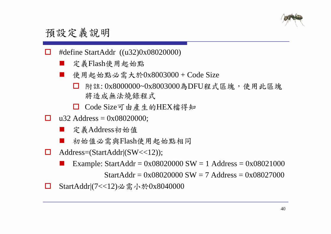
預設定義說明
define StartAddr ((u32)0x08020000) 定義Flash使用起始點 定義Flash使用起始點
使用起始點必需大於0x8003000 + Code Size 附註 0x8000000~0x8003000為DFU程式區塊使用此區塊
將造成無法燒錄程式
Code Size可由產生的HEX檔得知
32 Add 0 08020000 u32 Address = 0x08020000 定義Address初始值
初始值必需與Flash使用起始點相同初始值必需與 使用起始點相同
Address=(StartAddr|(SWltlt12)) Example StartAddr = 0x08020000 SW = 1 Address = 0x08021000
StartAddr = 0x08020000 SW = 7 Address = 0x08027000 StartAddr|(7ltlt12)必需小於0x8040000
40
使用者界面與Flash存取控制實驗
實驗二
WU-YANGTechnology Co Ltd
實驗二練習
注意 請使用預設0 08020000之後的位置 避免覆蓋DFU 請使用預設0x08020000之後的位置避免覆蓋DFU
與使用者程式碼區塊
練習 練習 利用SW與KEY測試Flash寫入與讀取是否正常
Fl h寫入後電源關閉 再開啟後寫入資料是否仍存 Flash寫入後電源關閉再開啟後寫入資料是否仍存在
修改存取位置測試是否正常 修改存取位置測試是否正常
42
實驗目的(三)( )
使用MIAT_STM32實驗板透過Flash memory interface (FLITF)控制內部Flash進行存取控制實驗並藉由填入(FLITF)控制內部Flash進行存取控制實驗並藉由填入Option Bytes 設定寫入鎖定保護Page鎖定不被覆蓋
43
Development Flowp
Embedded Software Side
int main(void)
Bootup STM32F10x
ProgrammingBootupSTM32F10x RCC Configure
NVIC Configure
int main(void)ifdef DEBUGdebug()
endifendif
FLASHStatus = FLASH_COMPLETEMemoryProgramStatus = PASSEDData = 0x1753
GPIO Configure
Data = 0x1753
RCC Configuration RCC_Configuration()
Flash memory RW operation FLASH Unlock
FLASH ClearFlag NVIC Configuration NVIC_Configuration()
GPIO Configuration
FLASH ClearFlag
FLASH ErasePage
FLASH ProgramHalfWord GPIO Configuration GPIO_Configuration()
Display Result
Check content
44
helliphelliphelliphelliphelliphelliphelliphelliphelliphelliphelliphelliphelliphelliphelliphelliphelliphelliphellip
實驗步驟
範例目錄架構
範例說明 範例說明
預設定義說明
45
範例目錄架構
範例目錄
測試映像檔 測試映像檔
含括檔
函式庫 函式庫
專案檔
原始碼 原始碼
46
範例說明
Function name Description
Unlock the Flash Program Erase controller FLASH_Unlock()
Define the number of page to be erased
Flash FwLib Functions List
Function name Description
FLASH_Unlock Unlocks the FLASH Program Erase Controller
FLASH_ClearFlag Clears the FLASH pending fl
Define the number of page to be erased NbrOfPage = (EndAddr ‐ StartAddr) FLASH_PAGE_SIZE
FLASH_ClearFlag(FLASH_FLAG_BSY | FLASH_FLAG_EOP|FLASH_FLAG_PGERR |FLASH_FLAG_WRPRTERR)
Get pages write protection status flags
FLASH_EraseOptionBytes
Erases the FLASH option bytes
FLASH_EnableWritePro Write protects the desired
p g pWRPR_Value = FLASH_GetWriteProtectionOptionByte()ProtectedPages = WRPR_Value amp 0x000000C0
ifdef WriteProtection_Disableif (ProtectedPages == 0x00) Pages are write protected
tection pages
NVIC_GenerateSystemReset
Generate a system reset
Disable the write protection FLASHStatus = FLASH_EraseOptionBytes() Generate System Reset to load the new option byte values NVIC_GenerateSystemReset()
elseifdef WriteProtection Enableifdef WriteProtection_Enableif (ProtectedPages = 0x00) Pages not write protected
FLASHStatus = FLASH_EraseOptionBytes() Enable the pages write protection FLASHStatus = FLASH_EnableWriteProtection(FLASH_WRProt_Pages12to13
|FLASH WRProt Pages14to15)|FLASH_WRProt_Pages14to15) Generate System Reset to load the new option byte values NVIC_GenerateSystemReset()
endifendif
47
範例說明
if (ProtectedPages = 0x00) Clear All pending flags
Flash FwLib Functions List
Function name DescriptionFLASH_ClearFlag(FLASH_FLAG_BSY |
FLASH_FLAG_EOP|FLASH_FLAG_PGERR |FLASH_FLAG_WRPRTERR)
erase the FLASH pages for(EraseCounter = 0 (EraseCounter lt NbrOfPage) ampamp (FLASHStatus ==
Function name Description
FLASH_ErasePage Erases a specified FLASH page
FLASH_ProgramHalfWod
Programs a half word at a ifi d dd FLASH_COMPLETE) EraseCounter++)
FLASHStatus = FLASH_ErasePage(StartAddr + (FLASH_PAGE_SIZE
EraseCounter))
rd specified address
FLASH Half Word program of data 0x1753 at addresses defined by StartAddrand EndAddr
Address = StartAddr
hil ((Add E dAdd ) ampamp (FLASHSt t FLASH COMPLETE))while((Address lt EndAddr) ampamp (FLASHStatus == FLASH_COMPLETE))
FLASHStatus = FLASH_ProgramHalfWord(Address Data)Address = Address + 2
48
範例說明
Embedded Software Side
Check the corectness of written data
Display Result
Check the corectness of written data Address = StartAddr
while((Address lt EndAddr) ampamp (MemoryProgramStatus = FAILED))if(((vu16) Address) = Data)
Flash memory RW operation
MemoryProgramStatus = FAILED
Address += 2
Check content
Display Result while (1)if (MemoryProgramStatus == PASSED) OK Turn on USERLED GPIO_SetBits(GPIOF GPIO_Pin_11)
Display Result
else KO Turn off USERLED GPIO_ResetBits(GPIOF GPIO_Pin_11) Insert delay Delay(0xAFFFF)
如果寫入與讀取Flash內容相同Flash記憶體可以寫入USERLED紅燈恆亮
Turn on USERLED GPIO_SetBits(GPIOF GPIO_Pin_11) Insert delay Delay(0xAFFFF)
如果寫入與讀取Flash內容不同Flash記憶體不能寫入USERLED紅燈閃爍
49
預設定義說明
define StartAddr ((u32) 0x08006000) 定義Flash使用起始點 定義Flash使用起始點
使用起始點必需大於0x8003000 + Code Size 附註 0x8000000~0x8003000為DFU程式區塊使用此區塊
將造成無法燒錄程式
Code Size可由產生的HEX檔得知
d fi E dAdd (( 32) 0 08008000) define EndAddr ((u32) 0x08008000) 定義Flash使用結束點
使用起始點必需小於0x8040000使用起始點必需小於
Data = 0x1753 寫入資料
16Bit define FLASH_PAGE_SIZE ((u16)0x800) 每一個Page有2KByte
50
每一個Page有2KByte
預設定義說明
define WriteProtection_Enable U hi li E bl W i P i Uncomment this line to Enable Write Protection
define WriteProtection_Disablehi li i bl i i Uncomment this line to Disable Write Protection
FLASH_EnableWriteProtection設定影響 個 設定影響2個Page FLASH_WRProt_Pages0to1 FLASH_WRProt_Pages1to2 helliphellip FLASH_WRProt_Pages60to61
設定影響多個Page FLASH_WRProt_Pages62to255
51
FLASH EnableWriteProtection_
Example
位置0x08006000 ~ 0x08007000每一個Page有0x800ByteStartPage = (0x08006000-0x08000000)0x800 = 12EndPage = ((0x08007000-0x08000000)0x800)-1 = 13執行執行FLASH_EnableWriteProtection(FLASH_WRProt_Pages12to13)將影響Pages12 Pages13
52
內部Flash寫入鎖定存取控制實驗
實驗三
WU-YANGTechnology Co Ltd
實驗三練習
注意 請使用預設0 08006000之後的位置 避免覆蓋DFU 請使用預設0x08006000之後的位置避免覆蓋DFU
與使用者程式碼區塊
更改寫入位置測試寫入鎖定時需同時更改 更改寫入位置測試寫入鎖定時需同時更改FLASH_EnableWriteProtection鎖定之Page
練習 練習 打開define WriteProtection_Enable測試是否可寫入
打開define WriteProtection Disable測試是否可寫入 打開define WriteProtection_Disable測試是否可寫入
修改存取位置測試是否正常
修改寫入資料測試是否正常 修改寫入資料測試是否正常
54
Q amp A
WU-YANGTechnology Co Ltd
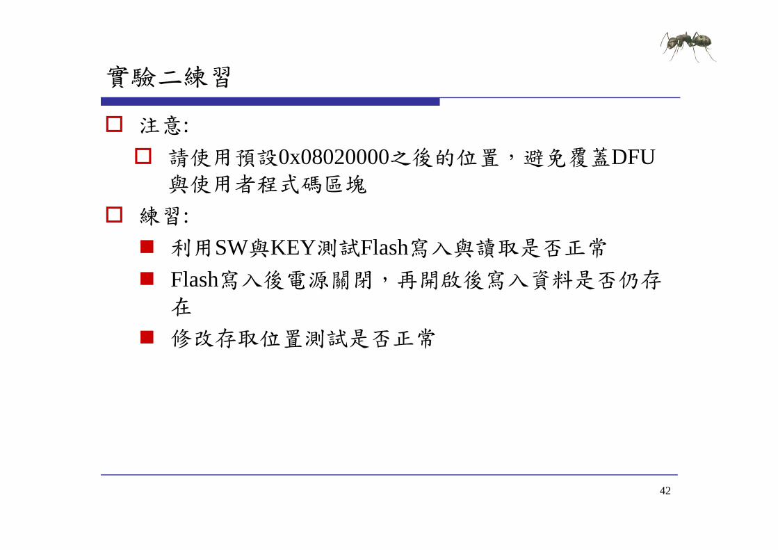
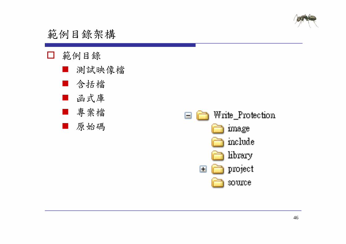
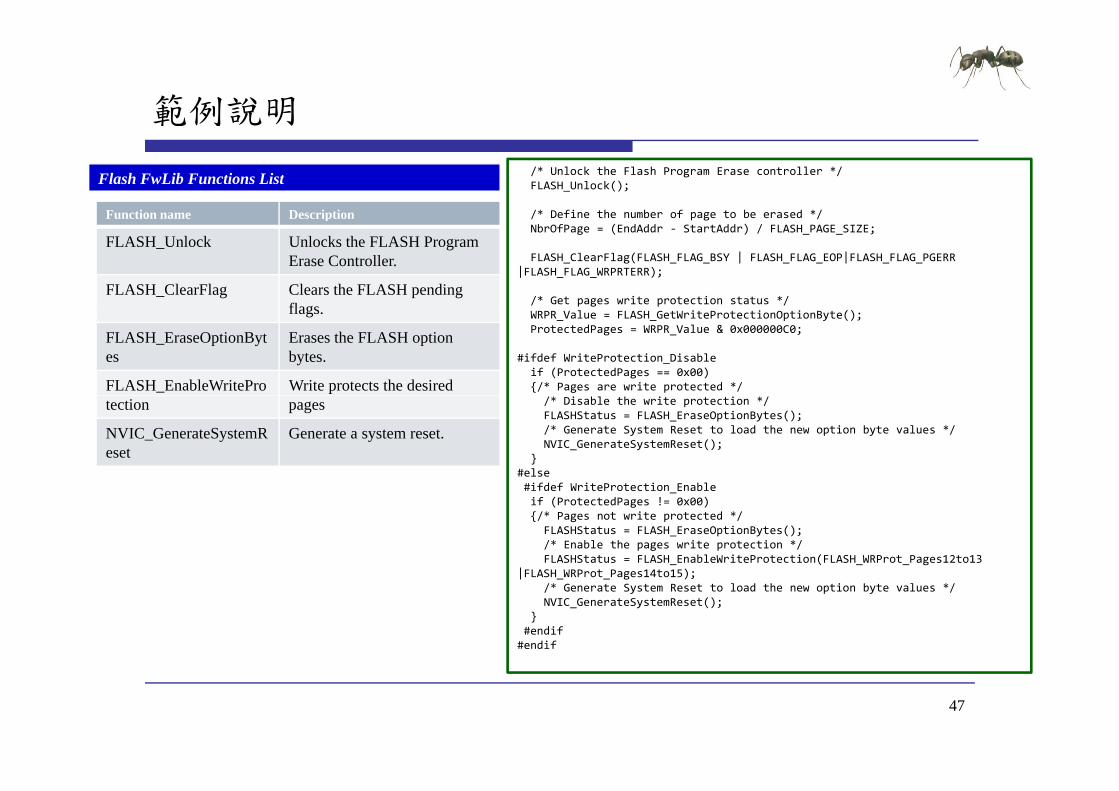
範例說明
Function name Description
Unlock the Flash Program Erase controller FLASH_Unlock()
Define the number of page to be erased
Flash FwLib Functions List
Function name Description
FLASH_Unlock Unlocks the FLASH Program Erase Controller
FLASH_ClearFlag Clears the FLASH pending fl
Define the number of page to be erased NbrOfPage = (EndAddr ‐ StartAddr) FLASH_PAGE_SIZE
FLASH_ClearFlag(FLASH_FLAG_BSY | FLASH_FLAG_EOP|FLASH_FLAG_PGERR |FLASH_FLAG_WRPRTERR)
Get pages write protection status flags
FLASH_EraseOptionBytes
Erases the FLASH option bytes
FLASH_EnableWritePro Write protects the desired
p g pWRPR_Value = FLASH_GetWriteProtectionOptionByte()ProtectedPages = WRPR_Value amp 0x000000C0
ifdef WriteProtection_Disableif (ProtectedPages == 0x00) Pages are write protected
tection pages
NVIC_GenerateSystemReset
Generate a system reset
Disable the write protection FLASHStatus = FLASH_EraseOptionBytes() Generate System Reset to load the new option byte values NVIC_GenerateSystemReset()
elseifdef WriteProtection Enableifdef WriteProtection_Enableif (ProtectedPages = 0x00) Pages not write protected
FLASHStatus = FLASH_EraseOptionBytes() Enable the pages write protection FLASHStatus = FLASH_EnableWriteProtection(FLASH_WRProt_Pages12to13
|FLASH WRProt Pages14to15)|FLASH_WRProt_Pages14to15) Generate System Reset to load the new option byte values NVIC_GenerateSystemReset()
endifendif
47
範例說明
if (ProtectedPages = 0x00) Clear All pending flags
Flash FwLib Functions List
Function name DescriptionFLASH_ClearFlag(FLASH_FLAG_BSY |
FLASH_FLAG_EOP|FLASH_FLAG_PGERR |FLASH_FLAG_WRPRTERR)
erase the FLASH pages for(EraseCounter = 0 (EraseCounter lt NbrOfPage) ampamp (FLASHStatus ==
Function name Description
FLASH_ErasePage Erases a specified FLASH page
FLASH_ProgramHalfWod
Programs a half word at a ifi d dd FLASH_COMPLETE) EraseCounter++)
FLASHStatus = FLASH_ErasePage(StartAddr + (FLASH_PAGE_SIZE
EraseCounter))
rd specified address
FLASH Half Word program of data 0x1753 at addresses defined by StartAddrand EndAddr
Address = StartAddr
hil ((Add E dAdd ) ampamp (FLASHSt t FLASH COMPLETE))while((Address lt EndAddr) ampamp (FLASHStatus == FLASH_COMPLETE))
FLASHStatus = FLASH_ProgramHalfWord(Address Data)Address = Address + 2
48
範例說明
Embedded Software Side
Check the corectness of written data
Display Result
Check the corectness of written data Address = StartAddr
while((Address lt EndAddr) ampamp (MemoryProgramStatus = FAILED))if(((vu16) Address) = Data)
Flash memory RW operation
MemoryProgramStatus = FAILED
Address += 2
Check content
Display Result while (1)if (MemoryProgramStatus == PASSED) OK Turn on USERLED GPIO_SetBits(GPIOF GPIO_Pin_11)
Display Result
else KO Turn off USERLED GPIO_ResetBits(GPIOF GPIO_Pin_11) Insert delay Delay(0xAFFFF)
如果寫入與讀取Flash內容相同Flash記憶體可以寫入USERLED紅燈恆亮
Turn on USERLED GPIO_SetBits(GPIOF GPIO_Pin_11) Insert delay Delay(0xAFFFF)
如果寫入與讀取Flash內容不同Flash記憶體不能寫入USERLED紅燈閃爍
49
預設定義說明
define StartAddr ((u32) 0x08006000) 定義Flash使用起始點 定義Flash使用起始點
使用起始點必需大於0x8003000 + Code Size 附註 0x8000000~0x8003000為DFU程式區塊使用此區塊
將造成無法燒錄程式
Code Size可由產生的HEX檔得知
d fi E dAdd (( 32) 0 08008000) define EndAddr ((u32) 0x08008000) 定義Flash使用結束點
使用起始點必需小於0x8040000使用起始點必需小於
Data = 0x1753 寫入資料
16Bit define FLASH_PAGE_SIZE ((u16)0x800) 每一個Page有2KByte
50
每一個Page有2KByte
預設定義說明
define WriteProtection_Enable U hi li E bl W i P i Uncomment this line to Enable Write Protection
define WriteProtection_Disablehi li i bl i i Uncomment this line to Disable Write Protection
FLASH_EnableWriteProtection設定影響 個 設定影響2個Page FLASH_WRProt_Pages0to1 FLASH_WRProt_Pages1to2 helliphellip FLASH_WRProt_Pages60to61
設定影響多個Page FLASH_WRProt_Pages62to255
51
FLASH EnableWriteProtection_
Example
位置0x08006000 ~ 0x08007000每一個Page有0x800ByteStartPage = (0x08006000-0x08000000)0x800 = 12EndPage = ((0x08007000-0x08000000)0x800)-1 = 13執行執行FLASH_EnableWriteProtection(FLASH_WRProt_Pages12to13)將影響Pages12 Pages13
52
內部Flash寫入鎖定存取控制實驗
實驗三
WU-YANGTechnology Co Ltd
實驗三練習
注意 請使用預設0 08006000之後的位置 避免覆蓋DFU 請使用預設0x08006000之後的位置避免覆蓋DFU
與使用者程式碼區塊
更改寫入位置測試寫入鎖定時需同時更改 更改寫入位置測試寫入鎖定時需同時更改FLASH_EnableWriteProtection鎖定之Page
練習 練習 打開define WriteProtection_Enable測試是否可寫入
打開define WriteProtection Disable測試是否可寫入 打開define WriteProtection_Disable測試是否可寫入
修改存取位置測試是否正常
修改寫入資料測試是否正常 修改寫入資料測試是否正常
54
Q amp A
WU-YANGTechnology Co Ltd

範例說明
Embedded Software Side
Check the corectness of written data
Display Result
Check the corectness of written data Address = StartAddr
while((Address lt EndAddr) ampamp (MemoryProgramStatus = FAILED))if(((vu16) Address) = Data)
Flash memory RW operation
MemoryProgramStatus = FAILED
Address += 2
Check content
Display Result while (1)if (MemoryProgramStatus == PASSED) OK Turn on USERLED GPIO_SetBits(GPIOF GPIO_Pin_11)
Display Result
else KO Turn off USERLED GPIO_ResetBits(GPIOF GPIO_Pin_11) Insert delay Delay(0xAFFFF)
如果寫入與讀取Flash內容相同Flash記憶體可以寫入USERLED紅燈恆亮
Turn on USERLED GPIO_SetBits(GPIOF GPIO_Pin_11) Insert delay Delay(0xAFFFF)
如果寫入與讀取Flash內容不同Flash記憶體不能寫入USERLED紅燈閃爍
49
預設定義說明
define StartAddr ((u32) 0x08006000) 定義Flash使用起始點 定義Flash使用起始點
使用起始點必需大於0x8003000 + Code Size 附註 0x8000000~0x8003000為DFU程式區塊使用此區塊
將造成無法燒錄程式
Code Size可由產生的HEX檔得知
d fi E dAdd (( 32) 0 08008000) define EndAddr ((u32) 0x08008000) 定義Flash使用結束點
使用起始點必需小於0x8040000使用起始點必需小於
Data = 0x1753 寫入資料
16Bit define FLASH_PAGE_SIZE ((u16)0x800) 每一個Page有2KByte
50
每一個Page有2KByte
預設定義說明
define WriteProtection_Enable U hi li E bl W i P i Uncomment this line to Enable Write Protection
define WriteProtection_Disablehi li i bl i i Uncomment this line to Disable Write Protection
FLASH_EnableWriteProtection設定影響 個 設定影響2個Page FLASH_WRProt_Pages0to1 FLASH_WRProt_Pages1to2 helliphellip FLASH_WRProt_Pages60to61
設定影響多個Page FLASH_WRProt_Pages62to255
51
FLASH EnableWriteProtection_
Example
位置0x08006000 ~ 0x08007000每一個Page有0x800ByteStartPage = (0x08006000-0x08000000)0x800 = 12EndPage = ((0x08007000-0x08000000)0x800)-1 = 13執行執行FLASH_EnableWriteProtection(FLASH_WRProt_Pages12to13)將影響Pages12 Pages13
52
內部Flash寫入鎖定存取控制實驗
實驗三
WU-YANGTechnology Co Ltd
實驗三練習
注意 請使用預設0 08006000之後的位置 避免覆蓋DFU 請使用預設0x08006000之後的位置避免覆蓋DFU
與使用者程式碼區塊
更改寫入位置測試寫入鎖定時需同時更改 更改寫入位置測試寫入鎖定時需同時更改FLASH_EnableWriteProtection鎖定之Page
練習 練習 打開define WriteProtection_Enable測試是否可寫入
打開define WriteProtection Disable測試是否可寫入 打開define WriteProtection_Disable測試是否可寫入
修改存取位置測試是否正常
修改寫入資料測試是否正常 修改寫入資料測試是否正常
54
Q amp A
WU-YANGTechnology Co Ltd

預設定義說明
define WriteProtection_Enable U hi li E bl W i P i Uncomment this line to Enable Write Protection
define WriteProtection_Disablehi li i bl i i Uncomment this line to Disable Write Protection
FLASH_EnableWriteProtection設定影響 個 設定影響2個Page FLASH_WRProt_Pages0to1 FLASH_WRProt_Pages1to2 helliphellip FLASH_WRProt_Pages60to61
設定影響多個Page FLASH_WRProt_Pages62to255
51
FLASH EnableWriteProtection_
Example
位置0x08006000 ~ 0x08007000每一個Page有0x800ByteStartPage = (0x08006000-0x08000000)0x800 = 12EndPage = ((0x08007000-0x08000000)0x800)-1 = 13執行執行FLASH_EnableWriteProtection(FLASH_WRProt_Pages12to13)將影響Pages12 Pages13
52
內部Flash寫入鎖定存取控制實驗
實驗三
WU-YANGTechnology Co Ltd
實驗三練習
注意 請使用預設0 08006000之後的位置 避免覆蓋DFU 請使用預設0x08006000之後的位置避免覆蓋DFU
與使用者程式碼區塊
更改寫入位置測試寫入鎖定時需同時更改 更改寫入位置測試寫入鎖定時需同時更改FLASH_EnableWriteProtection鎖定之Page
練習 練習 打開define WriteProtection_Enable測試是否可寫入
打開define WriteProtection Disable測試是否可寫入 打開define WriteProtection_Disable測試是否可寫入
修改存取位置測試是否正常
修改寫入資料測試是否正常 修改寫入資料測試是否正常
54
Q amp A
WU-YANGTechnology Co Ltd

Q amp A
WU-YANGTechnology Co Ltd