Embed Size (px)
Citation preview
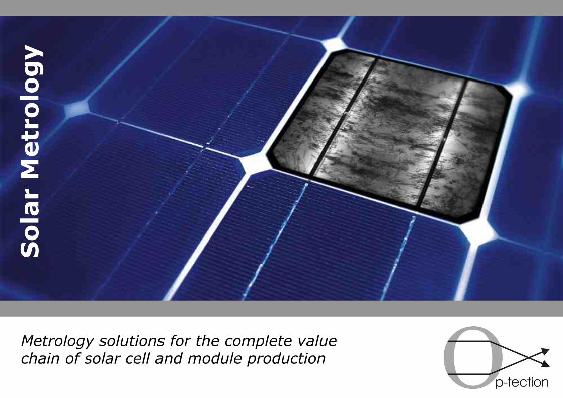
So
lar
Metr
olo
gy
Metrology solutions for the complete valuechain of solar cell and module production
In the next minutes you will:
! Get an introduction of the company Op-tection GmbH
! Get introduced to a selection of the metrology systems we built
! Discover the capabilities these systems provide you
INTRODUCTION WAFER INSPECTION CELL INSPECTION MODULE INSPECTION
- 2 -

Op-tection GmbH...
INTRODUCTION WAFER INSPECTION CELL INSPECTION MODULE INSPECTION
- 3 -
INTRODUCTION WAFER INSPECTION CELL INSPECTION MODULE INSPECTION
- 4 -
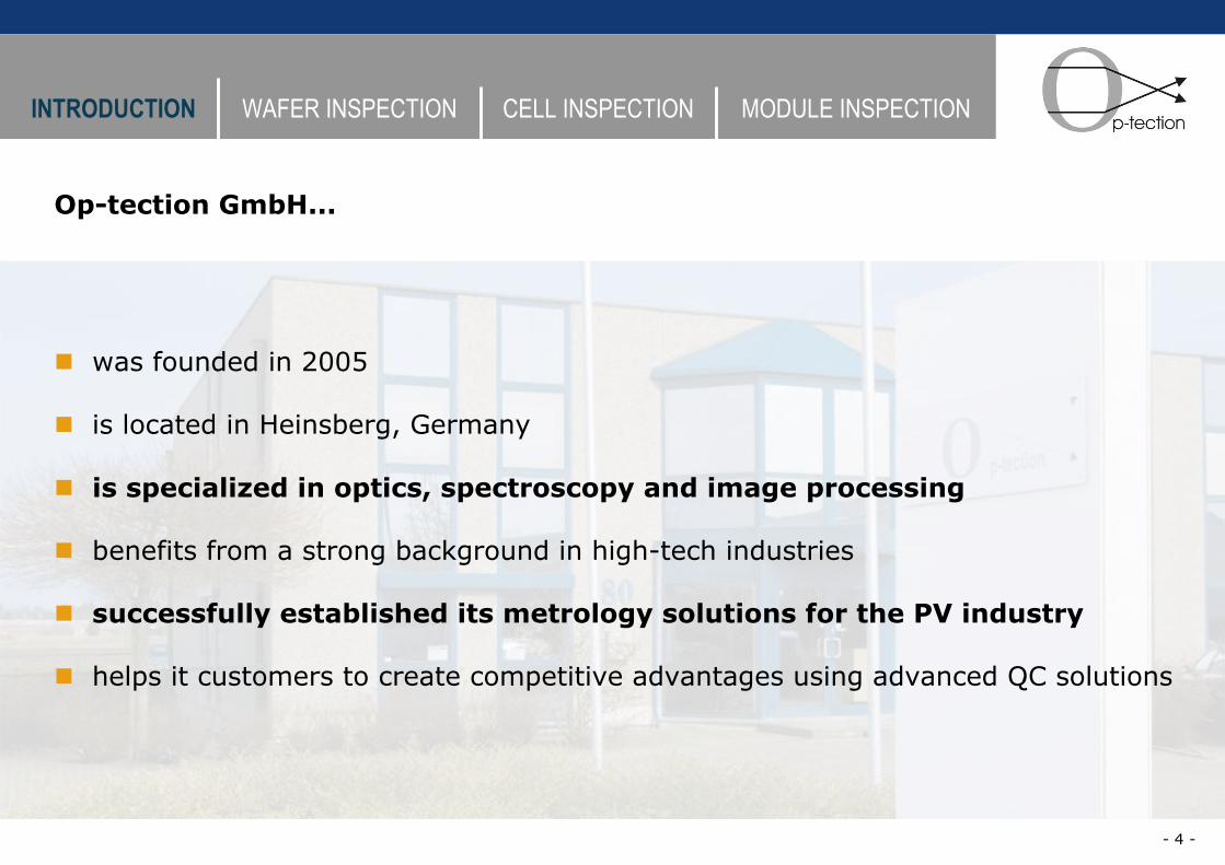
Op-tection GmbH...
! was founded in 2005
! is located in Heinsberg, Germany
! is specialized in optics, spectroscopy and image processing
! benefits from a strong background in high-tech industries
! successfully established its metrology solutions for the PV industry
! helps it customers to create competitive advantages using advanced QC solutions
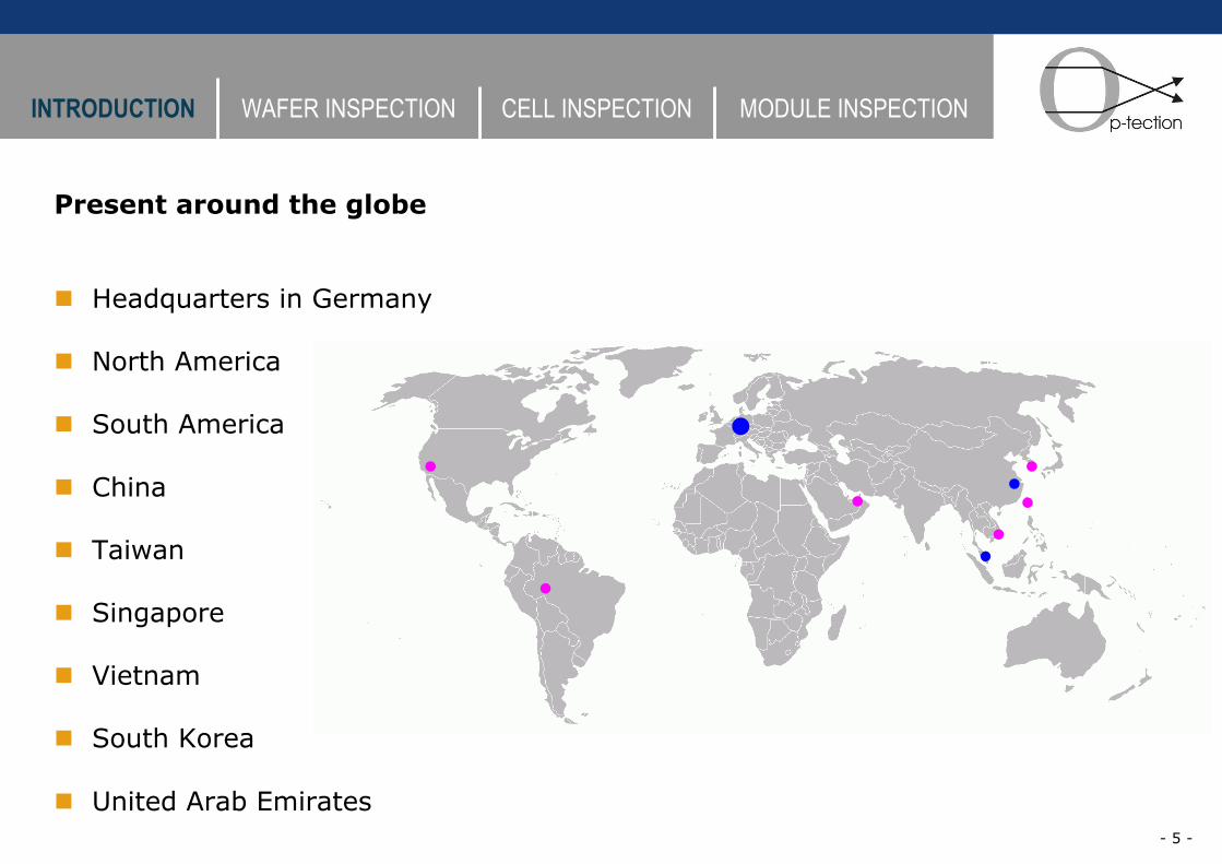
Present around the globe
! Headquarters in Germany
! North America
! South America
! China
! Taiwan
! Singapore
! Vietnam
! South Korea
! United Arab Emirates- 5 -
INTRODUCTION WAFER INSPECTION CELL INSPECTION MODULE INSPECTION
INTRODUCTION WAFER INSPECTION CELL INSPECTION MODULE INSPECTION
- 6 -
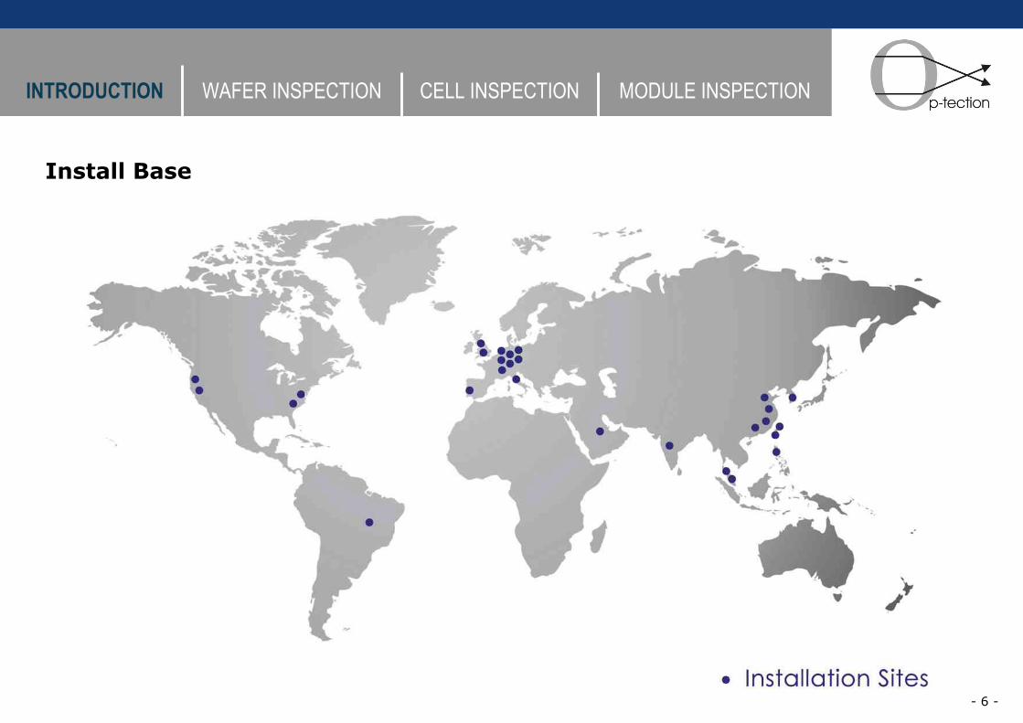
Install Base
INTRODUCTION
- 7 -
WAFER INSPECTION CELL INSPECTION MODULE INSPECTION
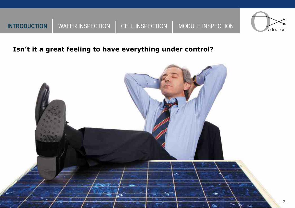
Isn’t it a great feeling to have everything under control?
INTRODUCTION WAFER INSPECTION CELL INSPECTION MODULE INSPECTION
- 8 -
Now you can!
Our metrology solutions for all critical process steps enable you to:
! Ensure using the best raw materials
! Produce solar cells and modules with consistent high quality
! Lower cost and create attractive pricing for your customers
! Create ultimate trust in you product using comprehensive QC solutions
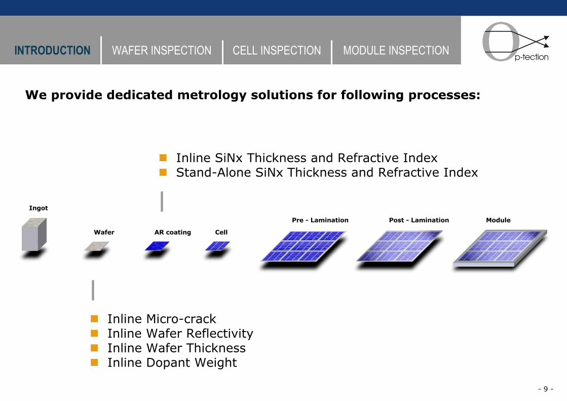
We provide dedicated metrology solutions for following processes:
INTRODUCTION WAFER INSPECTION CELL INSPECTION MODULE INSPECTION
- 9 -
Ingot
Wafer AR coating
Pre - Lamination Post - Lamination Module
Cell
! Inline Micro-crack! Inline Wafer Reflectivity! Inline Wafer Thickness! Inline Dopant Weight
! Inline SiNx Thickness and Refractive Index! Stand-Alone SiNx Thickness and Refractive Index
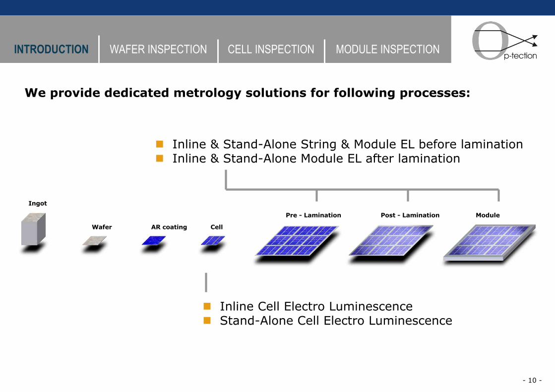
We provide dedicated metrology solutions for following processes:
INTRODUCTION WAFER INSPECTION CELL INSPECTION MODULE INSPECTION
- 10 -
Ingot
Wafer AR coating
Pre - Lamination Post - Lamination Module
Cell
! Inline Cell Electro Luminescence! Stand-Alone Cell Electro Luminescence
! Inline & Stand-Alone String & Module EL before lamination! Inline & Stand-Alone Module EL after lamination
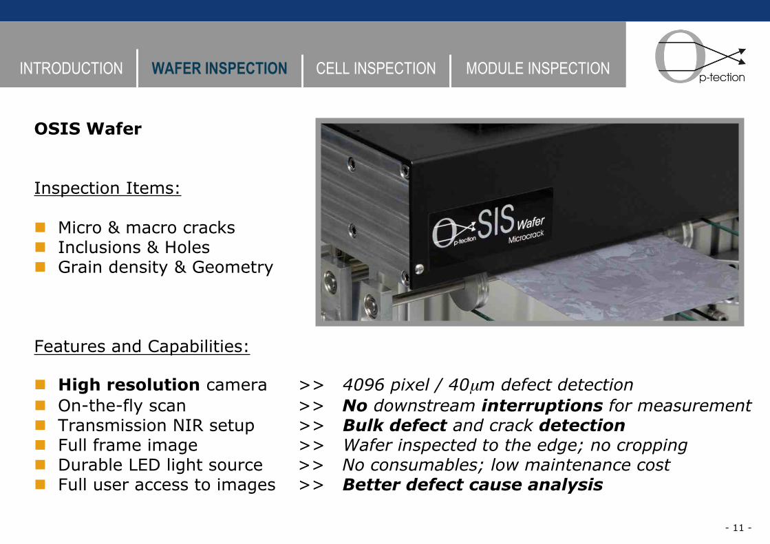
OSIS Wafer
Inspection Items:
! Micro & macro cracks! Inclusions & Holes! Grain density & Geometry
Features and Capabilities:
! High resolution camera >> 4096 pixel / 40µm defect detection! On-the-fly scan >> No downstream interruptions for measurement! Transmission NIR setup >> Bulk defect and crack detection! Full frame image >> Wafer inspected to the edge; no cropping! Durable LED light source >> No consumables; low maintenance cost! Full user access to images >> Better defect cause analysis
INTRODUCTION WAFER INSPECTION CELL INSPECTION MODULE INSPECTION
- 11 -
INTRODUCTION WAFER INSPECTION CELL INSPECTION MODULE INSPECTION
- 12 -
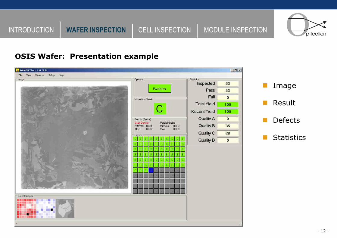
! Image
! Result
! Defects
! Statistics
OSIS Wafer: Presentation example
INTRODUCTION WAFER INSPECTION CELL INSPECTION MODULE INSPECTION
- 13 -
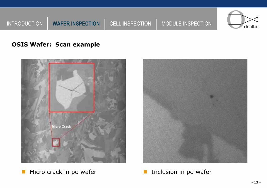
OSIS Wafer: Scan example
! Inclusion in pc-wafer! Micro crack in pc-wafer

INTRODUCTION WAFER INSPECTION CELL INSPECTION MODULE INSPECTION
- 14 -
OSIS Wafer: Grain geometry and properties
! High grain density in pc-wafer
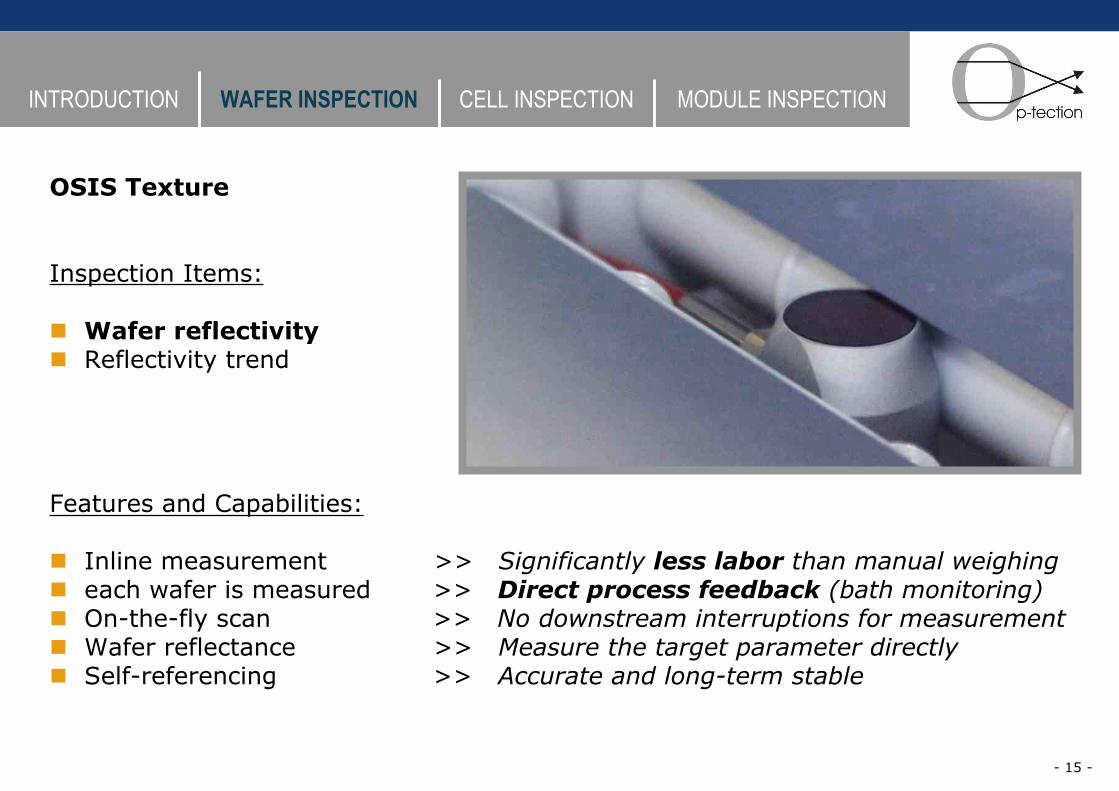
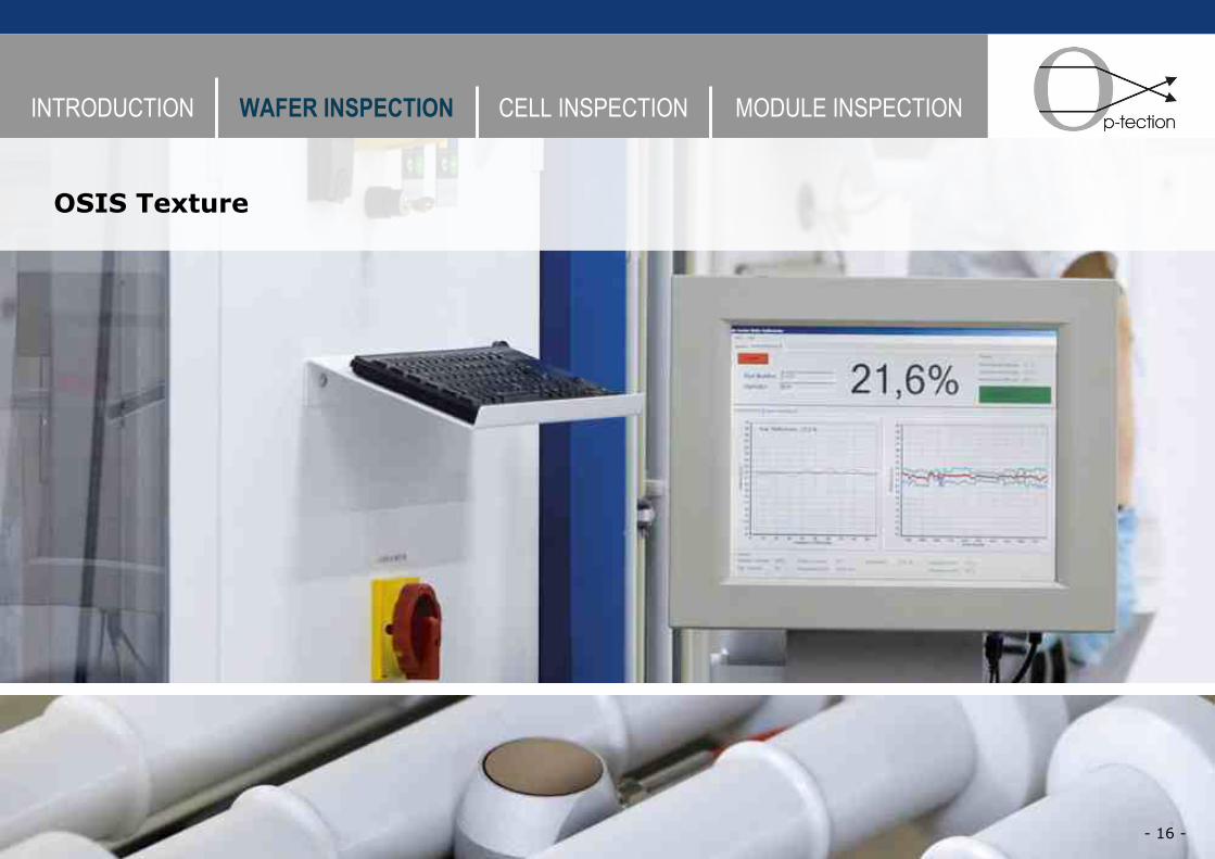
OSIS Texture
Inspection Items:
! Wafer reflectivity! Reflectivity trend
Features and Capabilities:
! Inline measurement >> Significantly less labor than manual weighing! each wafer is measured >> Direct process feedback (bath monitoring)! On-the-fly scan >> No downstream interruptions for measurement! Wafer reflectance >> Measure the target parameter directly! Self-referencing >> Accurate and long-term stable
INTRODUCTION WAFER INSPECTION CELL INSPECTION MODULE INSPECTION
- 15 -
INTRODUCTION WAFER INSPECTION CELL INSPECTION MODULE INSPECTION
- 16 -
OSIS Texture
INTRODUCTION WAFER INSPECTION CELL INSPECTION MODULE INSPECTION
- 17 -
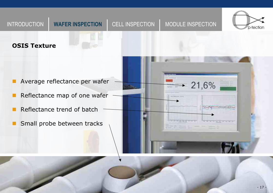
OSIS Texture
! Average reflectance per wafer
! Reflectance map of one wafer
! Reflectance trend of batch
! Small probe between tracks
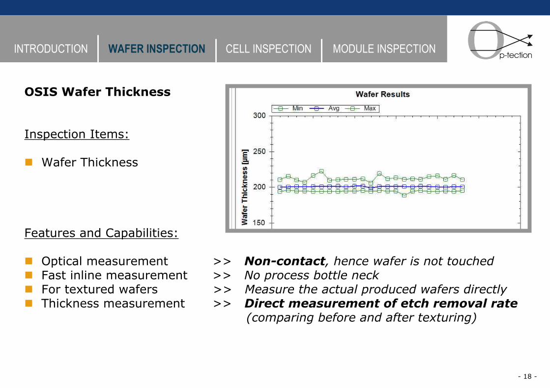
OSIS Wafer Thickness
Inspection Items:
! Wafer Thickness
Features and Capabilities:
! Optical measurement >> Non-contact, hence wafer is not touched! Fast inline measurement >> No process bottle neck! For textured wafers >> Measure the actual produced wafers directly! Thickness measurement >> Direct measurement of etch removal rate
(comparing before and after texturing)
INTRODUCTION WAFER INSPECTION CELL INSPECTION MODULE INSPECTION
- 18 -
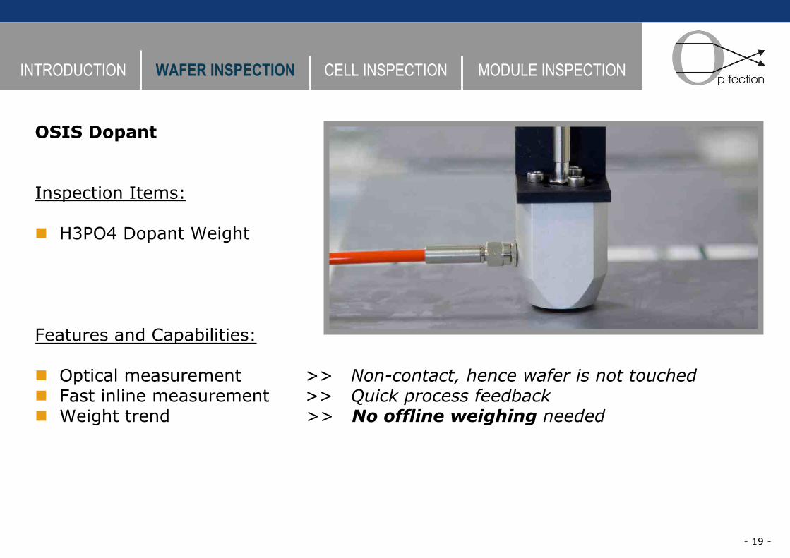
OSIS Dopant
Inspection Items:
! H3PO4 Dopant Weight
Features and Capabilities:
! Optical measurement >> Non-contact, hence wafer is not touched! Fast inline measurement >> Quick process feedback! Weight trend >> No offline weighing needed
INTRODUCTION WAFER INSPECTION CELL INSPECTION MODULE INSPECTION
- 19 -
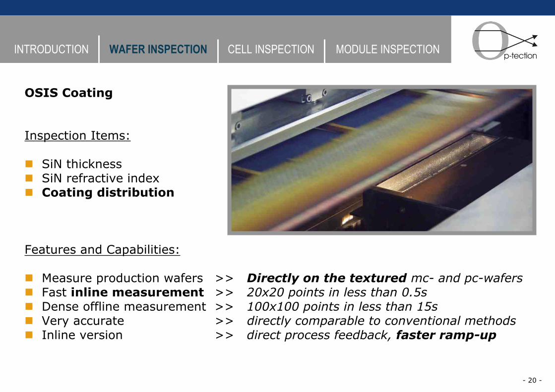
OSIS Coating
Inspection Items:
! SiN thickness! SiN refractive index! Coating distribution
Features and Capabilities:
! Measure production wafers >> Directly on the textured mc- and pc-wafers! Fast inline measurement >> 20x20 points in less than 0.5s! Dense offline measurement >> 100x100 points in less than 15s! Very accurate >> directly comparable to conventional methods! Inline version >> direct process feedback, faster ramp-up
INTRODUCTION WAFER INSPECTION CELL INSPECTION MODULE INSPECTION
- 20 -
INTRODUCTION WAFER INSPECTION CELL INSPECTION MODULE INSPECTION
- 21 -
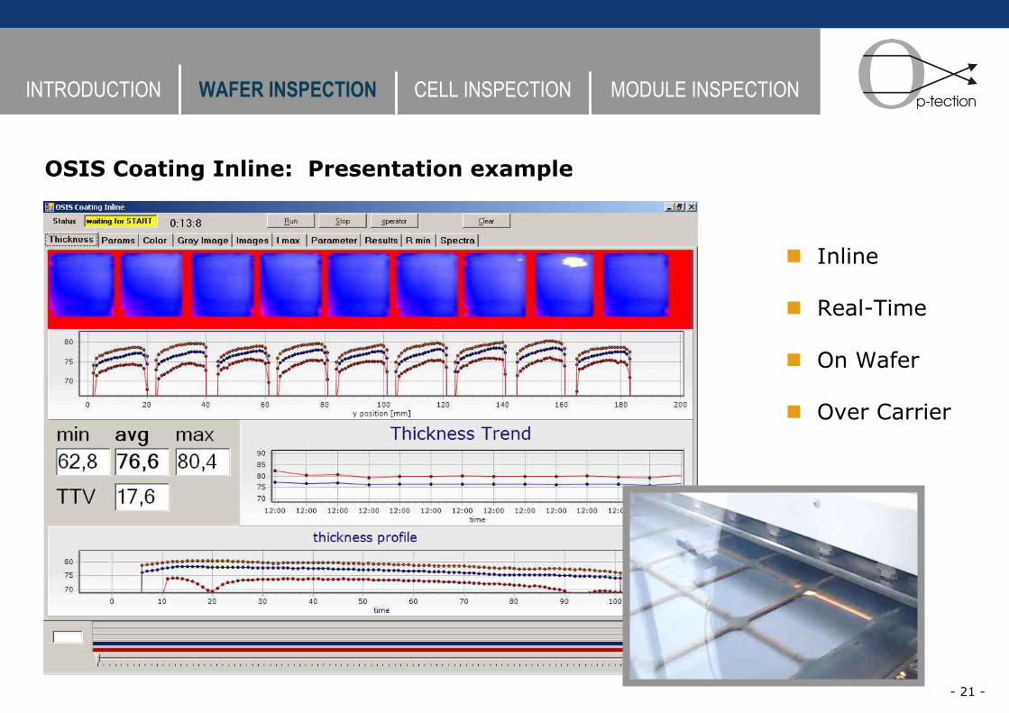
! Inline
! Real-Time
! On Wafer
! Over Carrier
OSIS Coating Inline: Presentation example
INTRODUCTION WAFER INSPECTION CELL INSPECTION MODULE INSPECTION
- 22 -
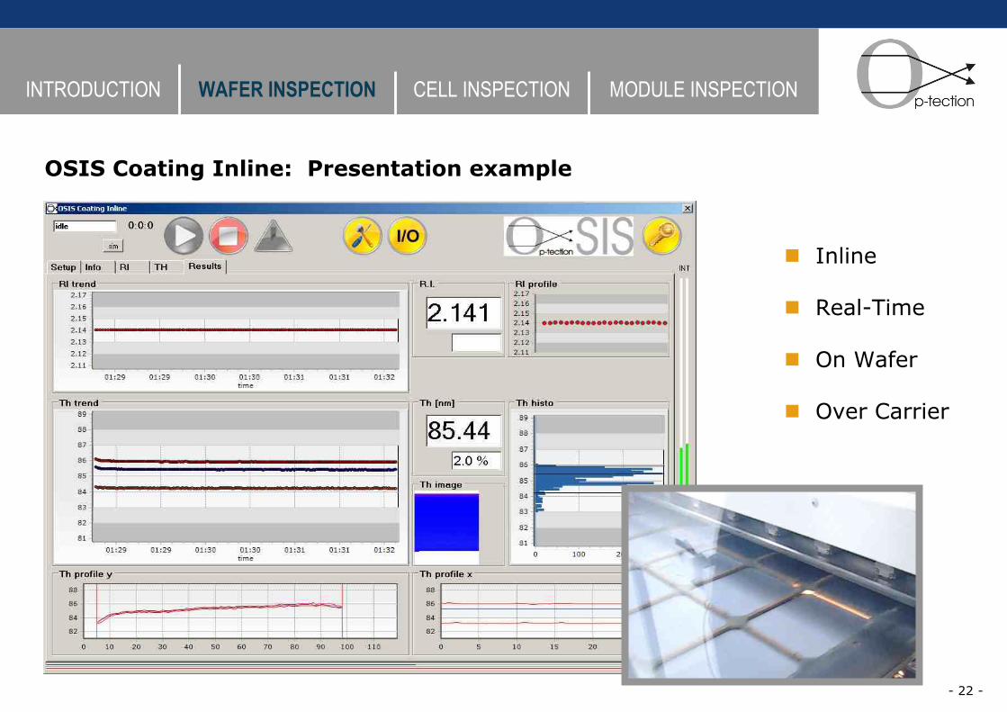
! Inline
! Real-Time
! On Wafer
! Over Carrier
OSIS Coating Inline: Presentation example
INTRODUCTION WAFER INSPECTION CELL INSPECTION MODULE INSPECTION
- 23 -
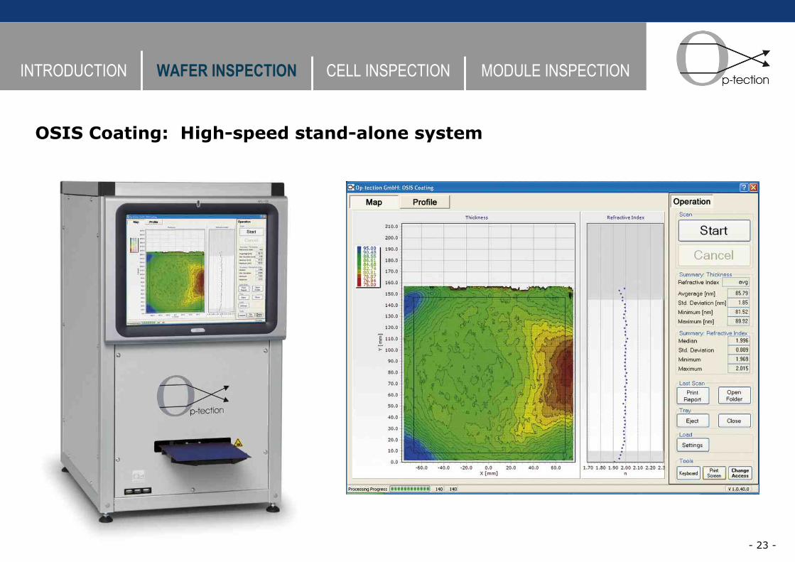
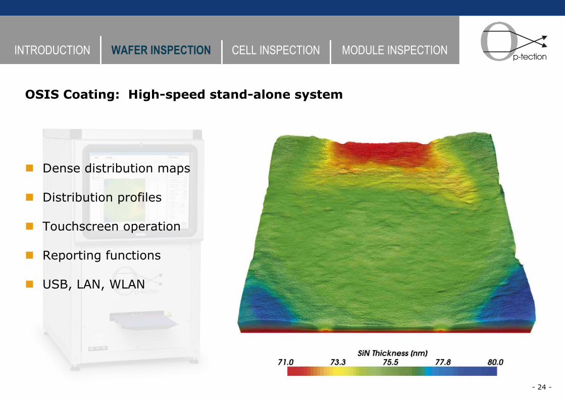
OSIS Coating: High-speed stand-alone system
INTRODUCTION WAFER INSPECTION CELL INSPECTION MODULE INSPECTION
- 24 -
OSIS Coating: High-speed stand-alone system
! Dense distribution maps
! Distribution profiles
! Touchscreen operation
! Reporting functions
! USB, LAN, WLAN

INTRODUCTION WAFER INSPECTION CELL INSPECTION MODULE INSPECTION
- 25 -
OSIS Cell
Inspection Items:
! Cracks! Dislocations! Dark areas! Shunts
Features and Capabilities:
! Defect detection by software>> Fast and consistent sorting! Adjustable quality limits >> Convenient sorting! Flexible platform >> Automatic + sorter / automatic / manual! Make the invisible visible >> Find and diagnose process errors
INTRODUCTION WAFER INSPECTION CELL INSPECTION MODULE INSPECTION
- 26 -
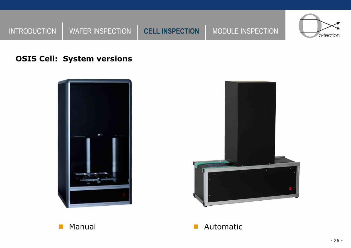
! Automatic! Manual
OSIS Cell: System versions
INTRODUCTION WAFER INSPECTION CELL INSPECTION MODULE INSPECTION
- 27 -
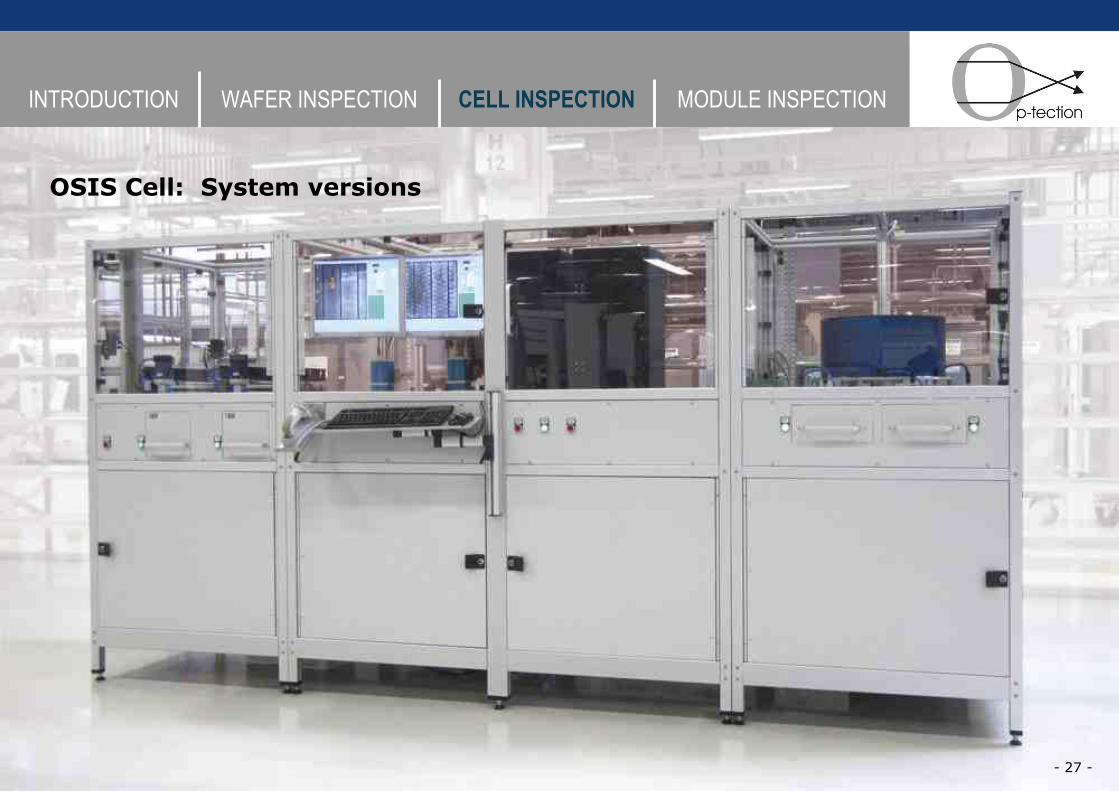
OSIS Cell: System versions

INTRODUCTION WAFER INSPECTION CELL INSPECTION MODULE INSPECTION
OSIS Cell: Cell Sorting
Highlights:
! 4 Input boxes! 5 Sorting boxes/classes! 1800 cells/hour! automatic sorting! gentle cell handling! optional IV-tester! optional AOI
- 28 -
INTRODUCTION WAFER INSPECTION CELL INSPECTION MODULE INSPECTION
- 29 -
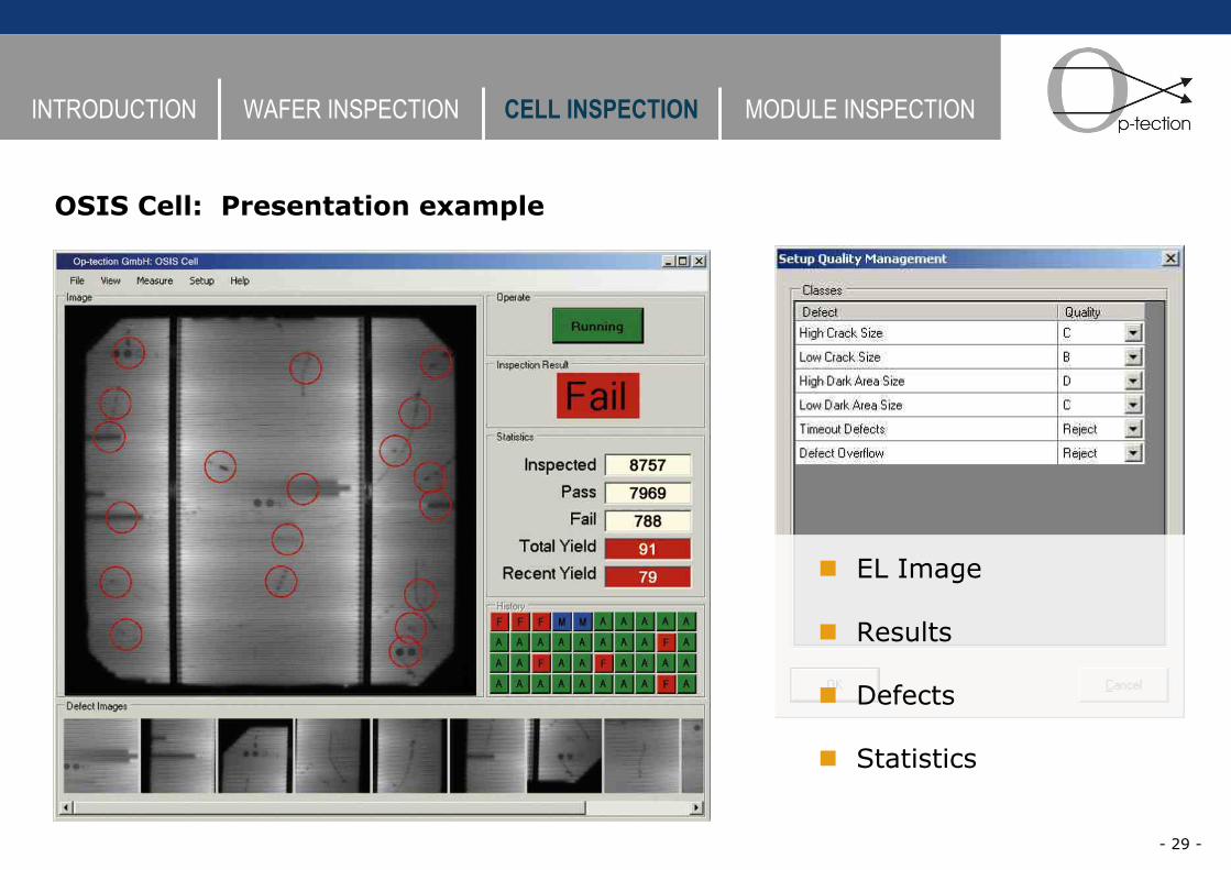
OSIS Cell: Presentation example
! EL Image
! Results
! Defects
! Statistics
INTRODUCTION WAFER INSPECTION CELL INSPECTION MODULE INSPECTION
- 30 -
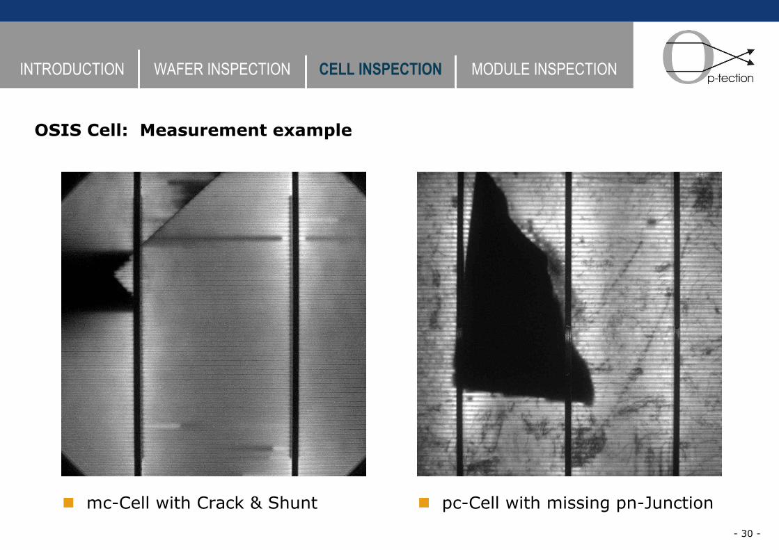
OSIS Cell: Measurement example
! pc-Cell with missing pn-Junction! mc-Cell with Crack & Shunt
INTRODUCTION WAFER INSPECTION CELL INSPECTION MODULE INSPECTION
- 31 -
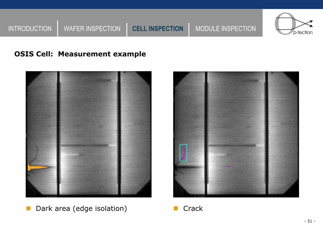
OSIS Cell: Measurement example
! Crack! Dark area (edge isolation)
INTRODUCTION WAFER INSPECTION CELL INSPECTION MODULE INSPECTION
- 32 -
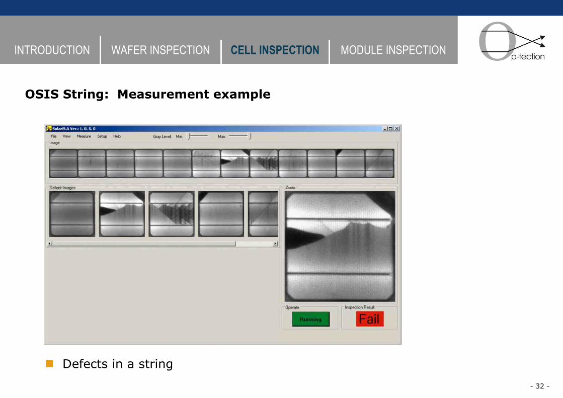
OSIS String: Measurement example
! Defects in a string
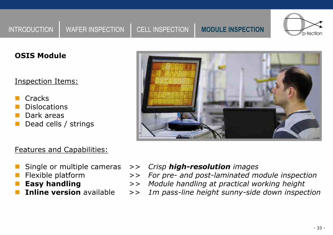
OSIS Module
Inspection Items:
! Cracks! Dislocations! Dark areas! Dead cells / strings
Features and Capabilities:
! Single or multiple cameras >> Crisp high-resolution images! Flexible platform >> For pre- and post-laminated module inspection! Easy handling >> Module handling at practical working height! Inline version available >> 1m pass-line height sunny-side down inspection
- 33 -
INTRODUCTION WAFER INSPECTION CELL INSPECTION MODULE INSPECTION
- 34 -
INTRODUCTION WAFER INSPECTION CELL INSPECTION MODULE INSPECTION
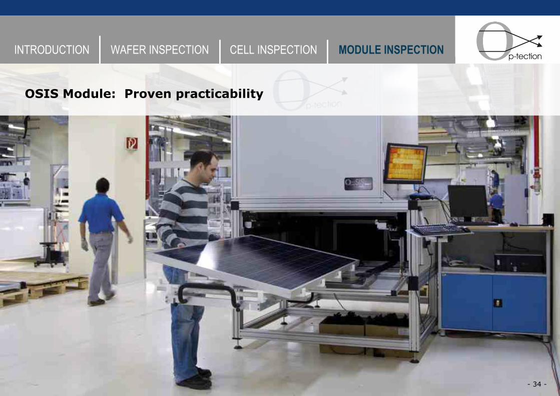
OSIS Module: Proven practicability
INTRODUCTION WAFER INSPECTION CELL INSPECTION MODULE INSPECTION
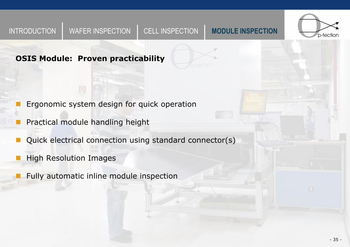
OSIS Module: Proven practicability
! Ergonomic system design for quick operation
! Practical module handling height
! Quick electrical connection using standard connector(s)
! High Resolution Images
! Fully automatic inline module inspection
- 35 -

INTRODUCTION WAFER INSPECTION CELL INSPECTION MODULE INSPECTION
OSIS Module-I: Inline Module Inspection
- 36 -
INTRODUCTION WAFER INSPECTION CELL INSPECTION MODULE INSPECTION
- 37 -
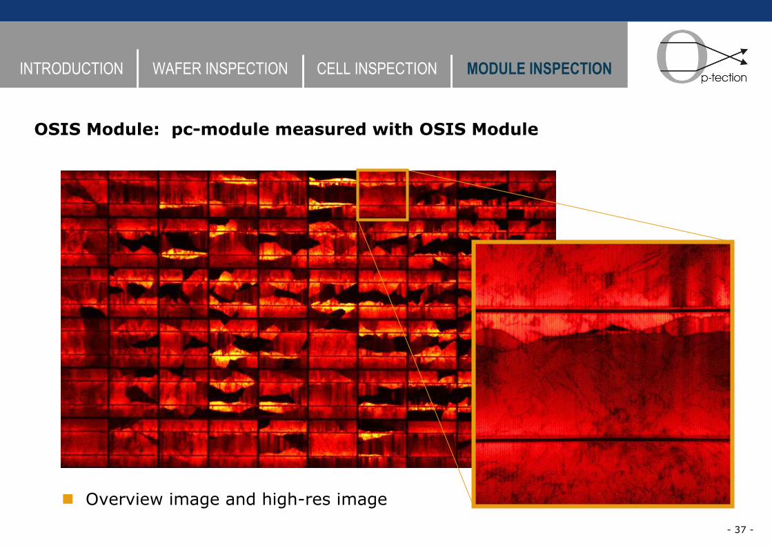
OSIS Module: pc-module measured with OSIS Module
! Overview image and high-res image

INTRODUCTION WAFER INSPECTION CELL INSPECTION MODULE INSPECTION
- 38 -
OSIS Module: CIGS panel measured with OSIS Module
! Small anomalies can be found
INTRODUCTION WAFER INSPECTION CELL INSPECTION MODULE INSPECTION
- 39 -
- 40 -
Value for solar panel producers:
! Direct insight in correlation of process steps and parameters
! Excellent accessibility of production data
! 100% traceability from raw material to end-product
! Competitive advantage while ensuring product lifetime
Combining OSIS Metrology tools with cmNavigo MES
INTRODUCTION WAFER INSPECTION CELL INSPECTION MODULE INSPECTION
INTRODUCTION WAFER INSPECTION CELL INSPECTION MODULE INSPECTION
- 41 -
Now, what can we do for you?
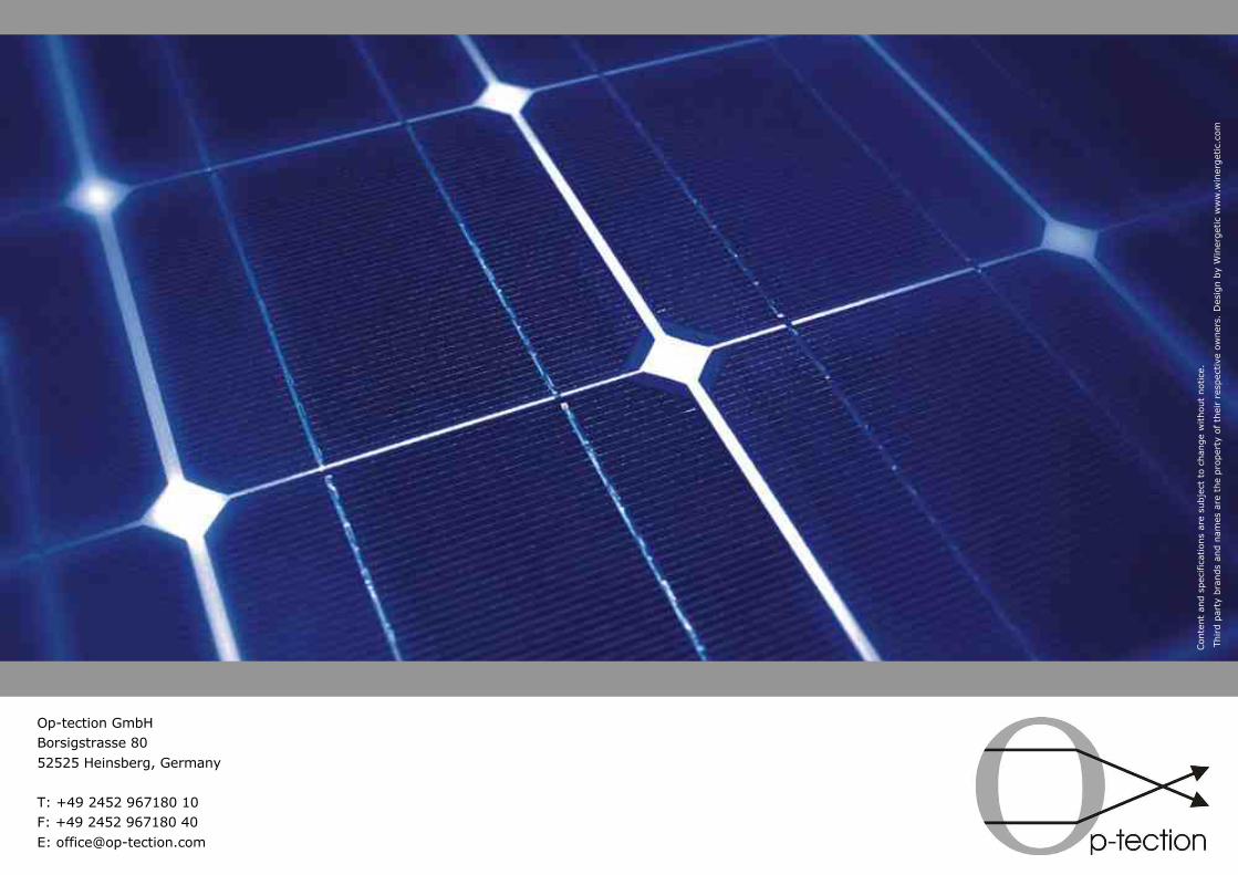
Op-tection GmbHBorsigstrasse 8052525 Heinsberg, Germany
T: +49 2452 967180 10F: +49 2452 967180 40E: [email protected]
Conte
nt
and s
pec
ific
atio
ns
are
subje
ct t
o c
han
ge
without
notice
.
Third p
arty
bra
nds
and n
ames
are
the
pro
per
ty o
f th
eir
resp
ective
ow
ner
s. D
esig
n b
y W
iner
get
ic w
ww
.win
erget
ic.c
om