Embed Size (px)
Citation preview
Metrology Considerations for Accurate Characterization of High-Bandwidth Power Electronics
Components & Applications
Andy Lemmon, Ph.D., P.E.Assistant Professor
Dept. of Electrical & Computer EngineeringThe University of Alabama
April 23, 2019

Research Sponsors - Government
Acknowledgments - SponsorsResearch Sponsors - Industry

Acknowledgments - Collaborators
Students (Current & Former)
Brian Deboi, Holden DeGrave, Levi Gant, Ryan Graves, Sam Griffin, Tyler Hill, Blake Nelson, Chris New, Marshal Olimmah, Ali Shahabi
Collaborating U.A. Faculty
Dr. Aaron Brovont, Assistant Professor
• Introduction• Metrological Challenges for WBG Systems
− Example 1: Voltage measurements− Example 2: Current measurements − Example 3: Packaging Impedance measurements
• Look Ahead & Conclusion
Overview
INTRODUCTION
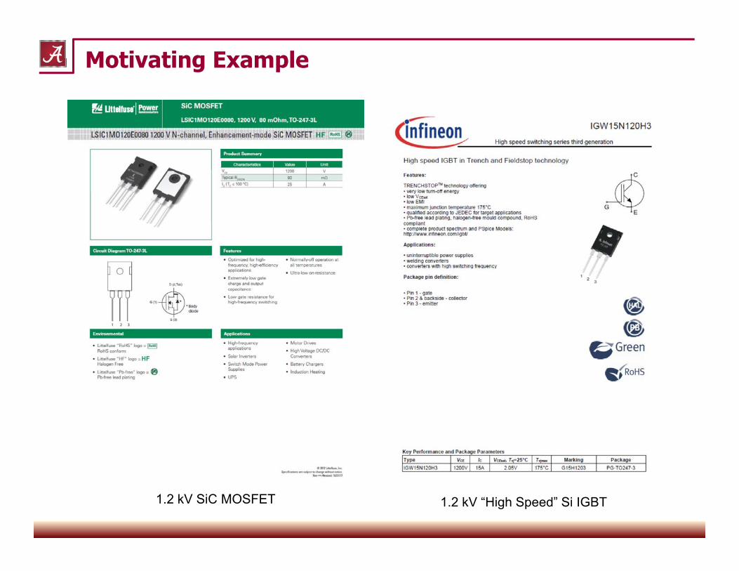
Motivating Example
1.2 kV SiC MOSFET 1.2 kV “High Speed” Si IGBT
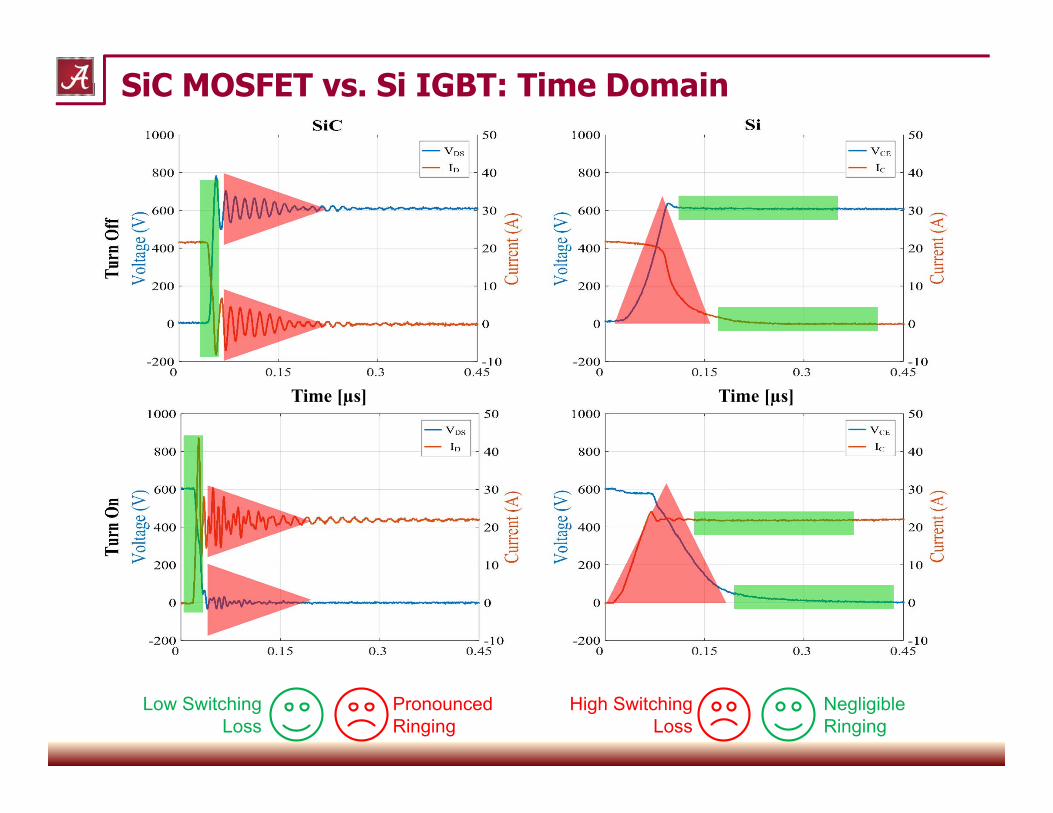
SiC MOSFET vs. Si IGBT: Time Domain
Time [µs] Time [µs]
Low Switching Loss
Pronounced Ringing
High Switching Loss
Negligible Ringing
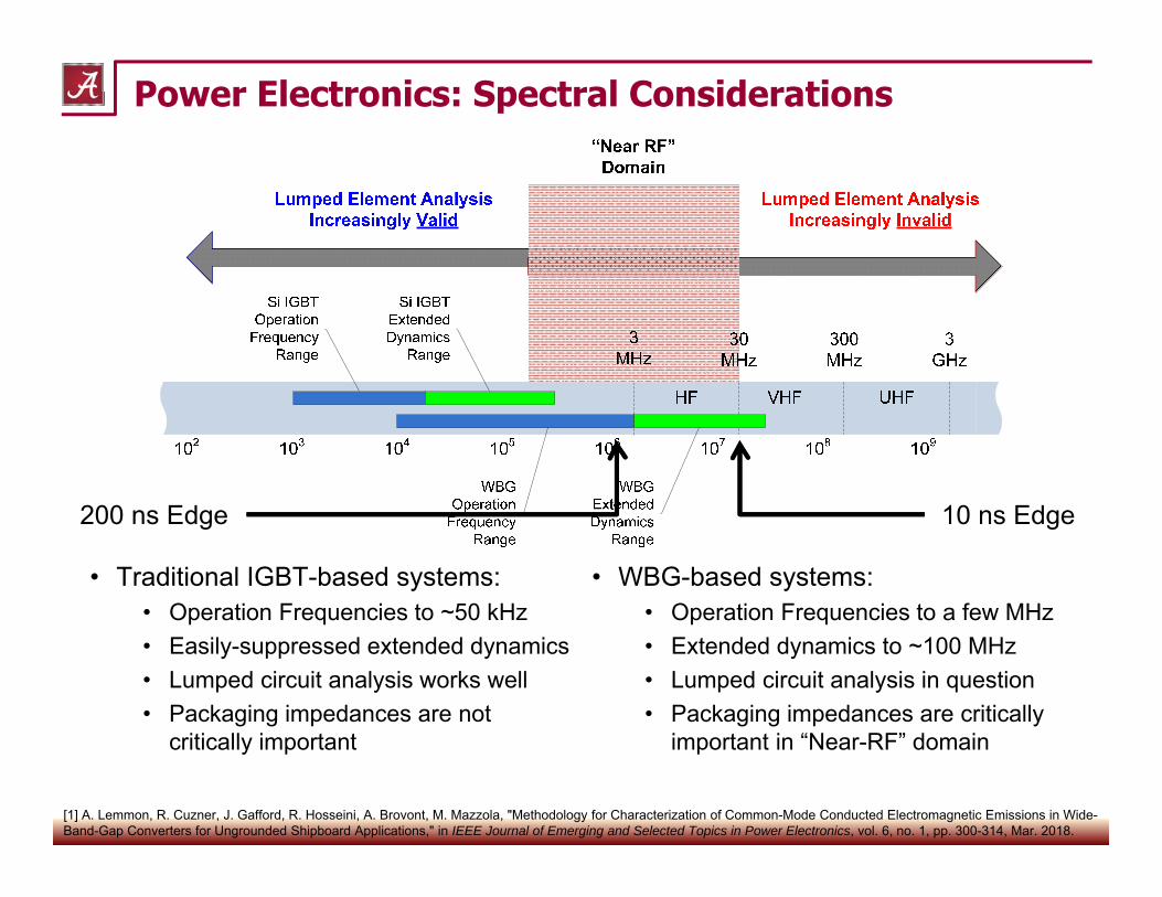
Power Electronics: Spectral Considerations
• Traditional IGBT-based systems:• Operation Frequencies to ~50 kHz• Easily-suppressed extended dynamics• Lumped circuit analysis works well• Packaging impedances are not
critically important
• WBG-based systems:• Operation Frequencies to a few MHz• Extended dynamics to ~100 MHz• Lumped circuit analysis in question• Packaging impedances are critically
important in “Near-RF” domain
200 ns Edge 10 ns Edge
[1] A. Lemmon, R. Cuzner, J. Gafford, R. Hosseini, A. Brovont, M. Mazzola, "Methodology for Characterization of Common-Mode Conducted Electromagnetic Emissions in Wide-Band-Gap Converters for Ungrounded Shipboard Applications," in IEEE Journal of Emerging and Selected Topics in Power Electronics, vol. 6, no. 1, pp. 300-314, Mar. 2018.
EXAMPLE 1Fast, High-Voltage Measurements
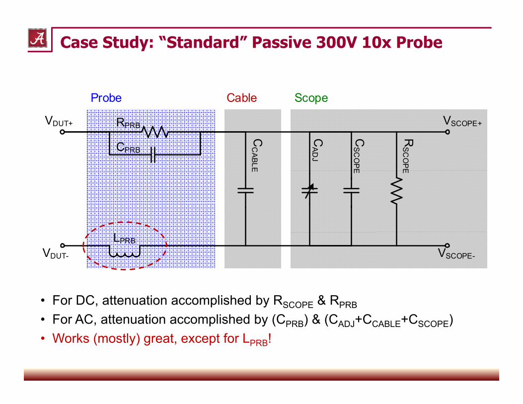
Case Study: “Standard” Passive 300V 10x Probe
• For DC, attenuation accomplished by RSCOPE & RPRB
• For AC, attenuation accomplished by (CPRB) & (CADJ+CCABLE+CSCOPE)• Works (mostly) great, except for LPRB!
VDUT+
VDUT-
VSCOPE+
VSCOPE-
RPRB
CPRB
CAD
J
LPRB
CC
ABLE
RSC
OPE
CSC
OPE
Probe Cable Scope
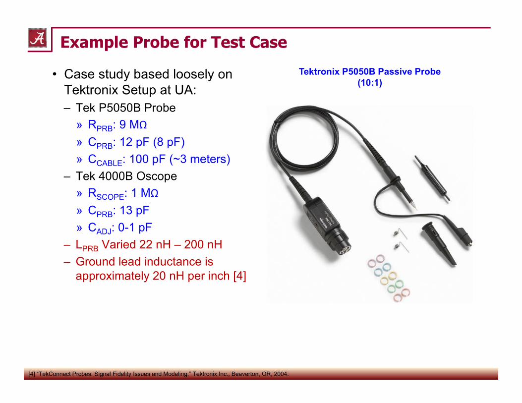
Example Probe for Test Case
• Case study based loosely on Tektronix Setup at UA:– Tek P5050B Probe
» RPRB: 9 MΩ» CPRB: 12 pF (8 pF)» CCABLE: 100 pF (~3 meters)
– Tek 4000B Oscope» RSCOPE: 1 MΩ» CPRB: 13 pF» CADJ: 0-1 pF
– LPRB Varied 22 nH – 200 nH– Ground lead inductance is
approximately 20 nH per inch [4]
Tektronix P5050B Passive Probe(10:1)
[4] “TekConnect Probes: Signal Fidelity Issues and Modeling,” Tektronix Inc., Beaverton, OR, 2004.
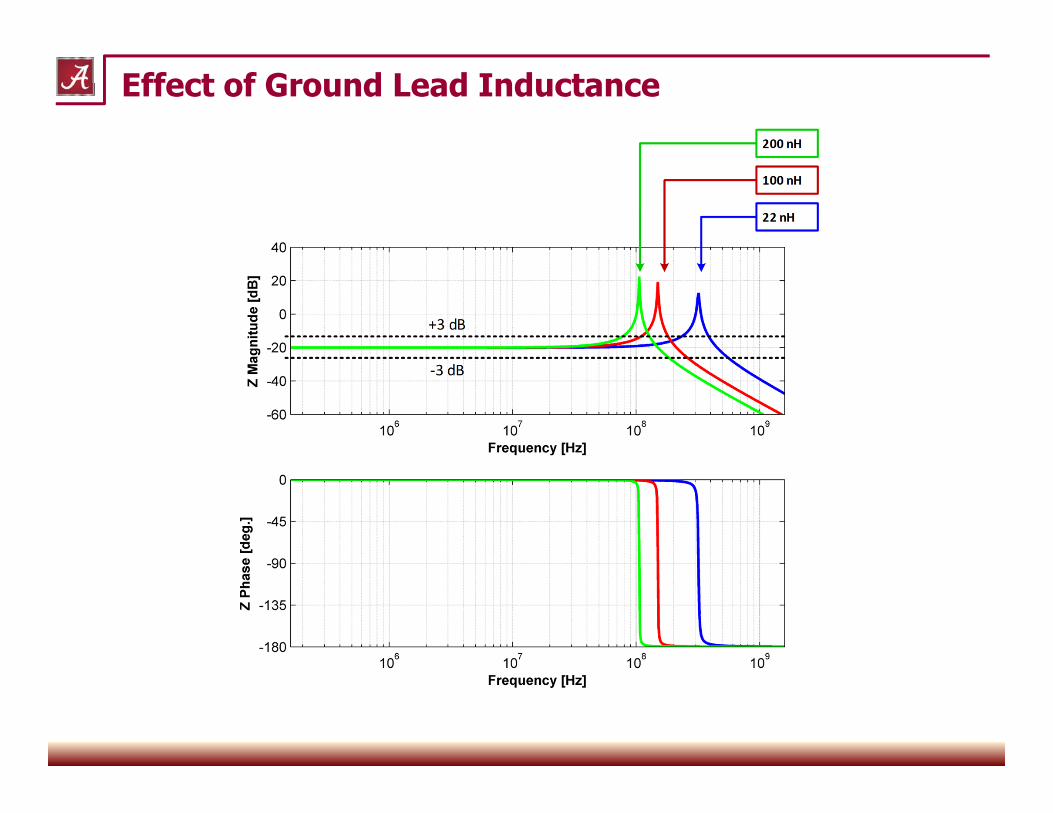
Effect of Ground Lead Inductance
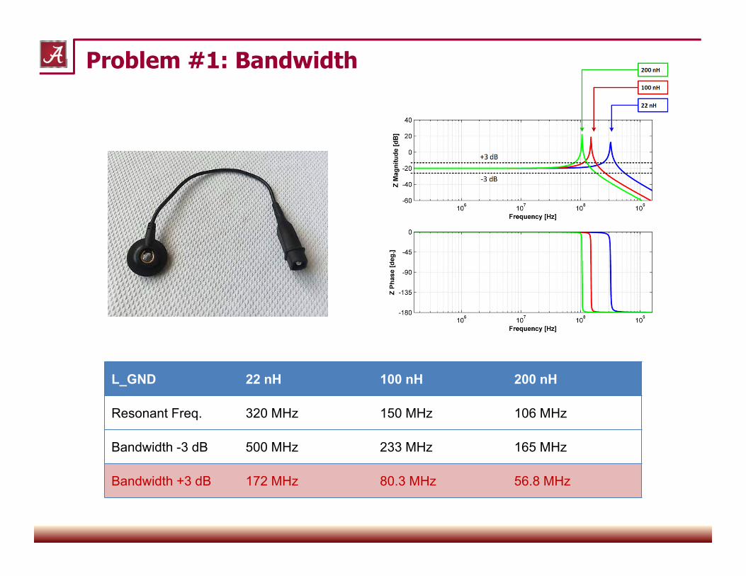
L_GND 22 nH 100 nH 200 nH
Resonant Freq. 320 MHz 150 MHz 106 MHz
Bandwidth -3 dB 500 MHz 233 MHz 165 MHz
Bandwidth +3 dB 172 MHz 80.3 MHz 56.8 MHz
Problem #1: Bandwidth
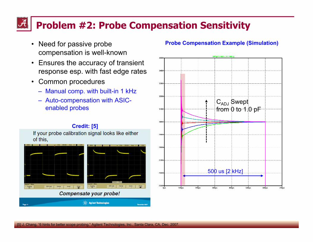
Problem #2: Probe Compensation Sensitivity
• Need for passive probe compensation is well-known
• Ensures the accuracy of transient response esp. with fast edge rates
• Common procedures– Manual comp. with built-in 1 kHz – Auto-compensation with ASIC-
enabled probesCADJ Swept from 0 to 1.0 pF
500 us [2 kHz]
[5] J. Chang, “6 hints for better scope probing,” Agilent Technologies, Inc., Santa Clara, CA, Dec. 2007.
Probe Compensation Example (Simulation)
Credit: [5]
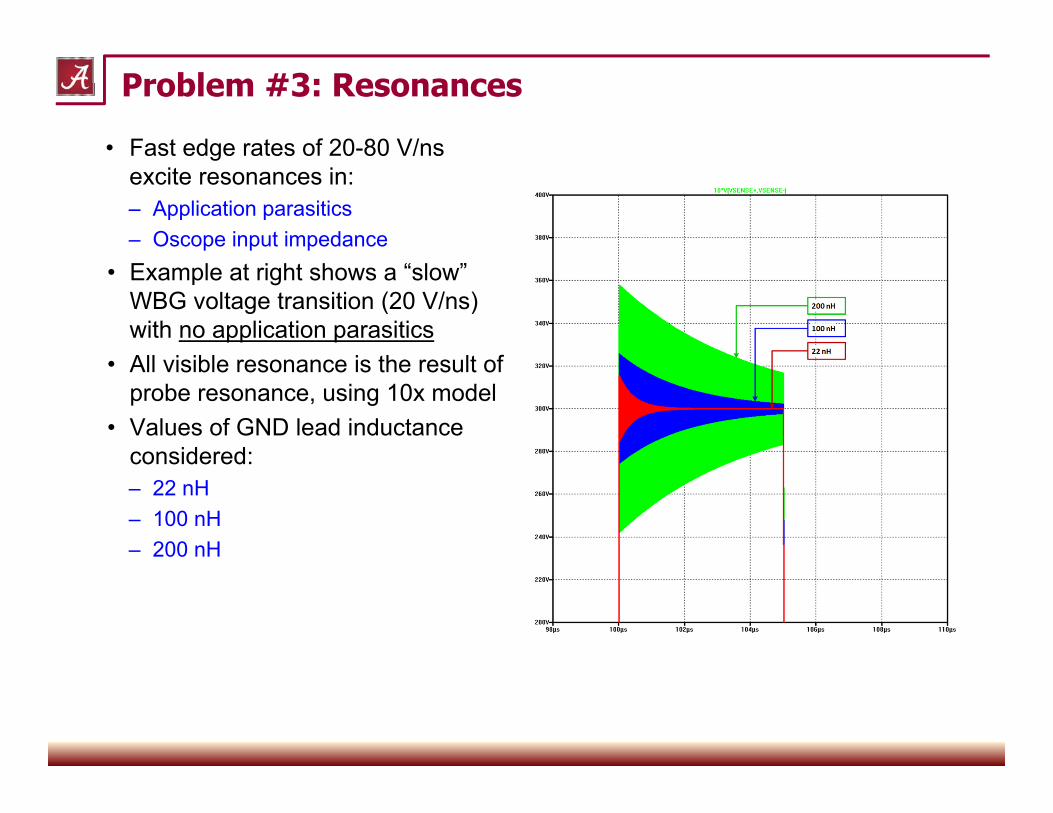
Problem #3: Resonances
• Fast edge rates of 20-80 V/ns excite resonances in:– Application parasitics– Oscope input impedance
• Example at right shows a “slow” WBG voltage transition (20 V/ns) with no application parasitics
• All visible resonance is the result of probe resonance, using 10x model
• Values of GND lead inductance considered:– 22 nH– 100 nH – 200 nH
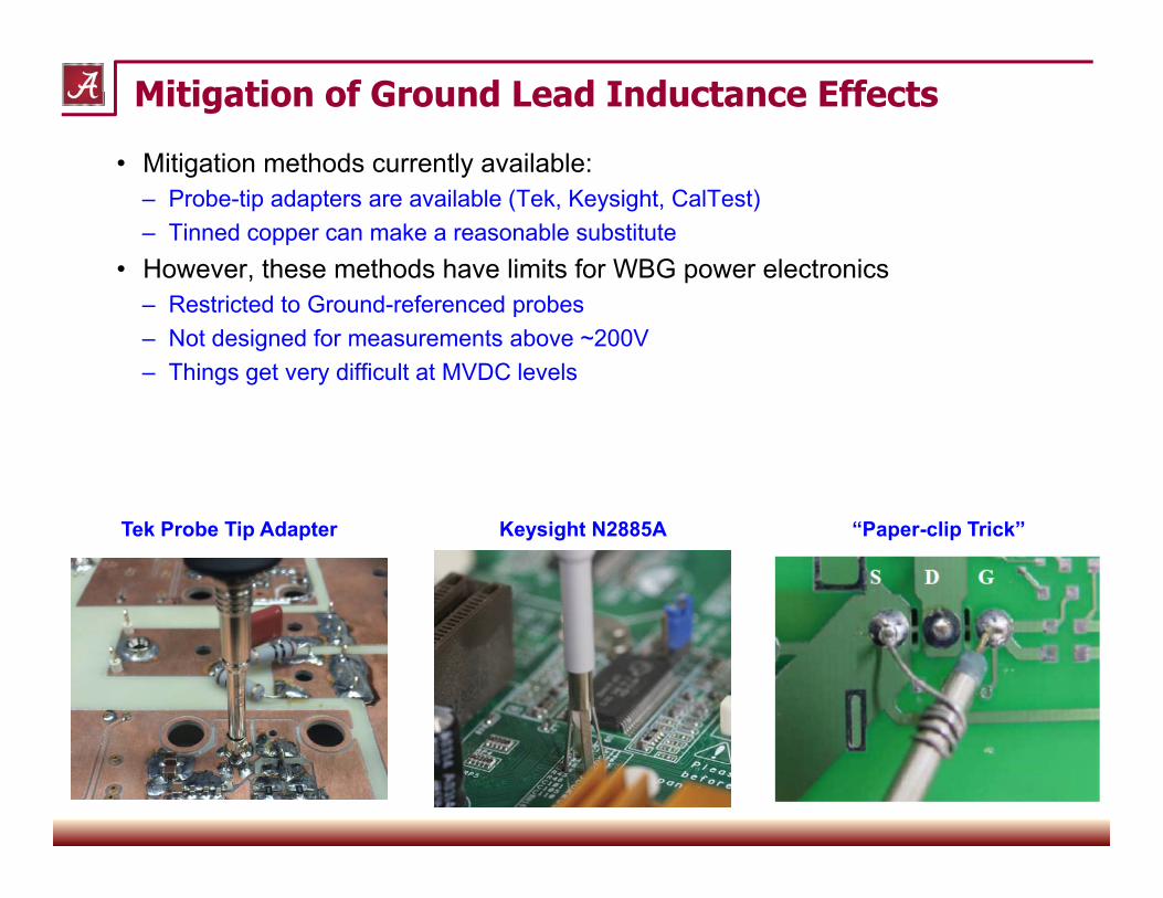
Mitigation of Ground Lead Inductance Effects
• Mitigation methods currently available:– Probe-tip adapters are available (Tek, Keysight, CalTest)– Tinned copper can make a reasonable substitute
• However, these methods have limits for WBG power electronics– Restricted to Ground-referenced probes– Not designed for measurements above ~200V– Things get very difficult at MVDC levels
Tek Probe Tip Adapter “Paper-clip Trick”Keysight N2885A
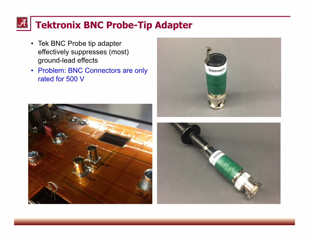
Tektronix BNC Probe-Tip Adapter
• Tek BNC Probe tip adapter effectively suppresses (most) ground-lead effects
• Problem: BNC Connectors are only rated for 500 V
EXAMPLE 2High-Bandwidth Current Measurement
21
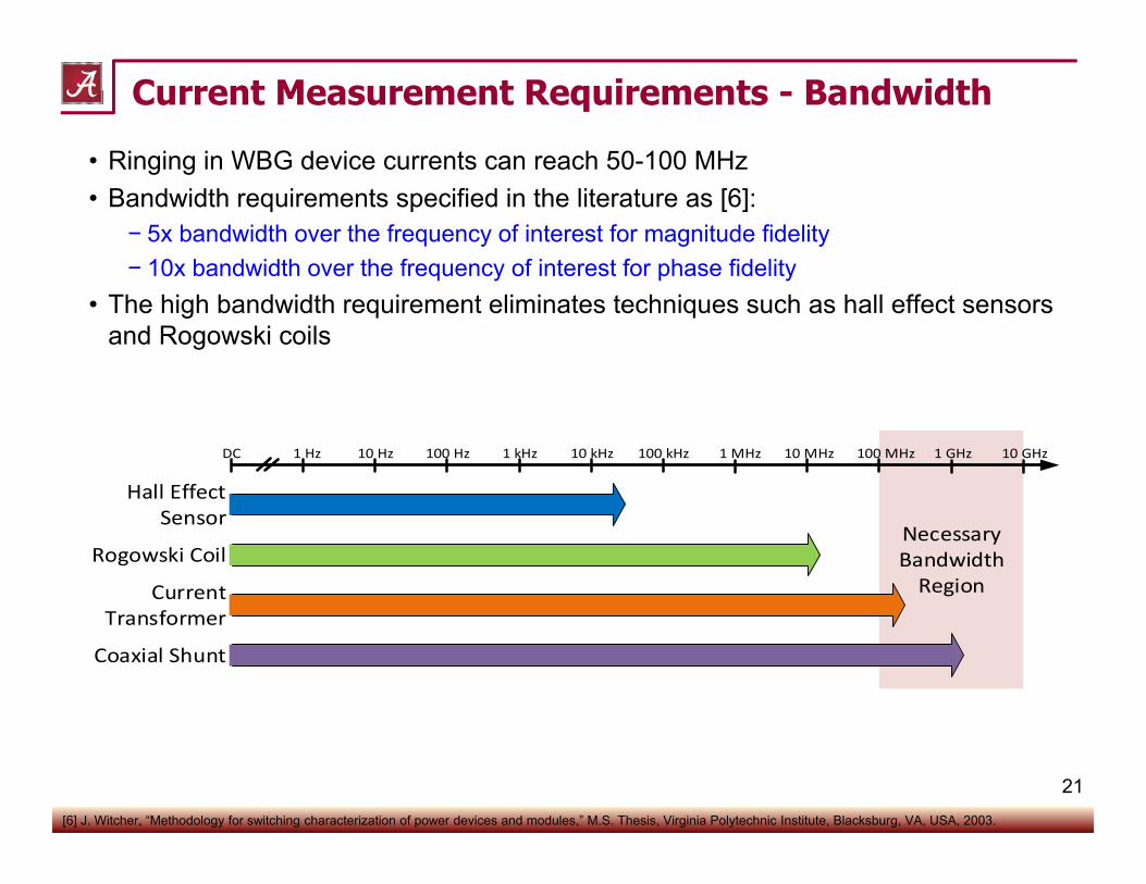
• Ringing in WBG device currents can reach 50-100 MHz• Bandwidth requirements specified in the literature as [6]:
− 5x bandwidth over the frequency of interest for magnitude fidelity− 10x bandwidth over the frequency of interest for phase fidelity
• The high bandwidth requirement eliminates techniques such as hall effect sensors and Rogowski coils
Current Measurement Requirements - Bandwidth
Necessary Bandwidth Region
DC 1 Hz 10 Hz 100 Hz 1 kHz 10 kHz 100 kHz 1 MHz 10 MHz 100 MHz 1 GHz 10 GHz
Hall Effect Sensor
Rogowski Coil
Current Transformer
Coaxial Shunt
[6] J. Witcher, “Methodology for switching characterization of power devices and modules,” M.S. Thesis, Virginia Polytechnic Institute, Blacksburg, VA, USA, 2003.
22
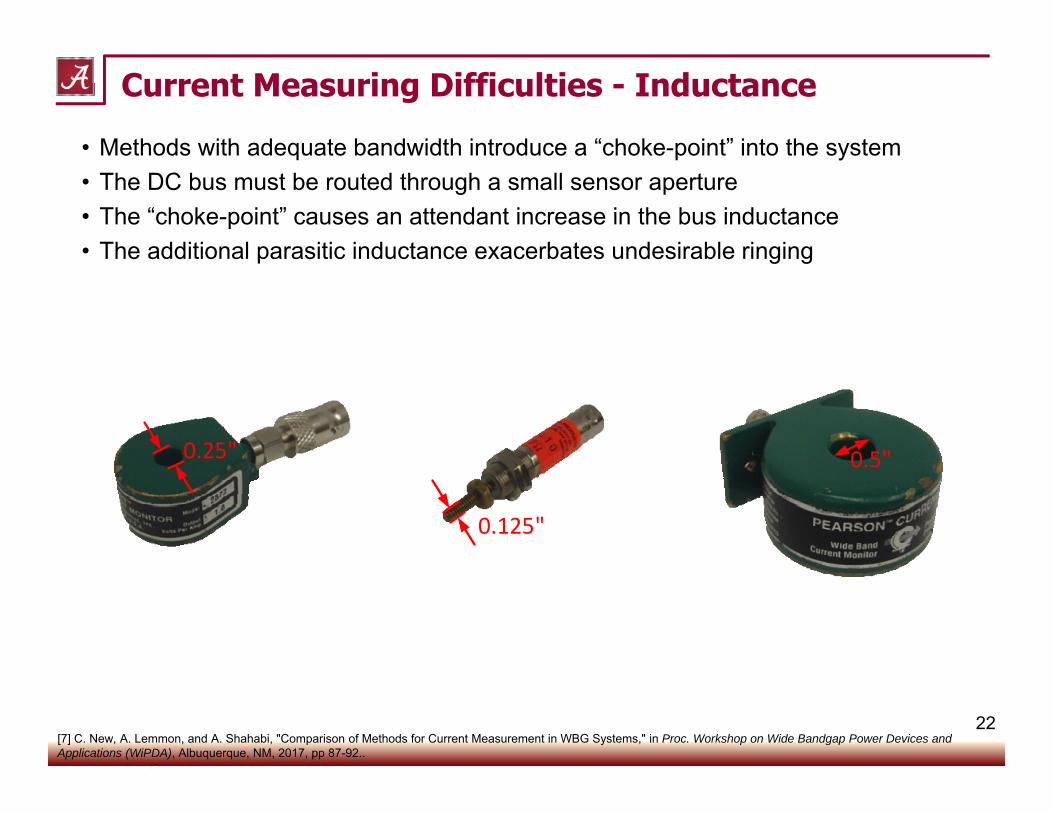
• Methods with adequate bandwidth introduce a “choke-point” into the system• The DC bus must be routed through a small sensor aperture• The “choke-point” causes an attendant increase in the bus inductance• The additional parasitic inductance exacerbates undesirable ringing
Current Measuring Difficulties - Inductance
0.125"
0.25" 0.5"
[7] C. New, A. Lemmon, and A. Shahabi, "Comparison of Methods for Current Measurement in WBG Systems," in Proc. Workshop on Wide Bandgap Power Devices and Applications (WiPDA), Albuquerque, NM, 2017, pp 87-92..
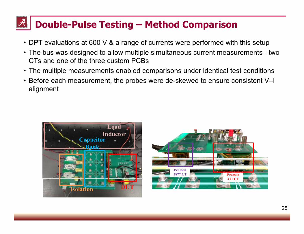
25
• DPT evaluations at 600 V & a range of currents were performed with this setup• The bus was designed to allow multiple simultaneous current measurements - two
CTs and one of the three custom PCBs• The multiple measurements enabled comparisons under identical test conditions• Before each measurement, the probes were de-skewed to ensure consistent V–I
alignment
Double-Pulse Testing – Method Comparison
DUT
Load Inductor
Capacitor Bank
Isolation
Pearson 411 CT
Pearson 2877 CT
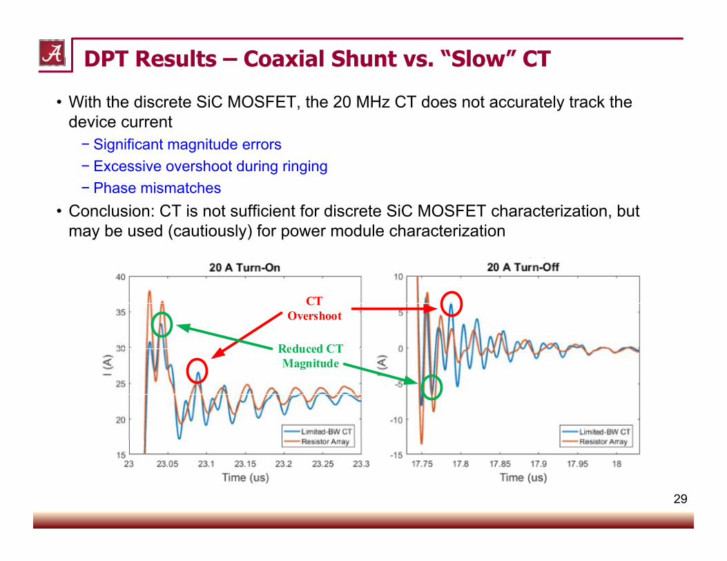
29
• With the discrete SiC MOSFET, the 20 MHz CT does not accurately track the device current
− Significant magnitude errors − Excessive overshoot during ringing− Phase mismatches
• Conclusion: CT is not sufficient for discrete SiC MOSFET characterization, but may be used (cautiously) for power module characterization
DPT Results – Coaxial Shunt vs. “Slow” CT
CT Overshoot
Reduced CT Magnitude
30
EXAMPLE 3Packaging Impedance Measurement
32
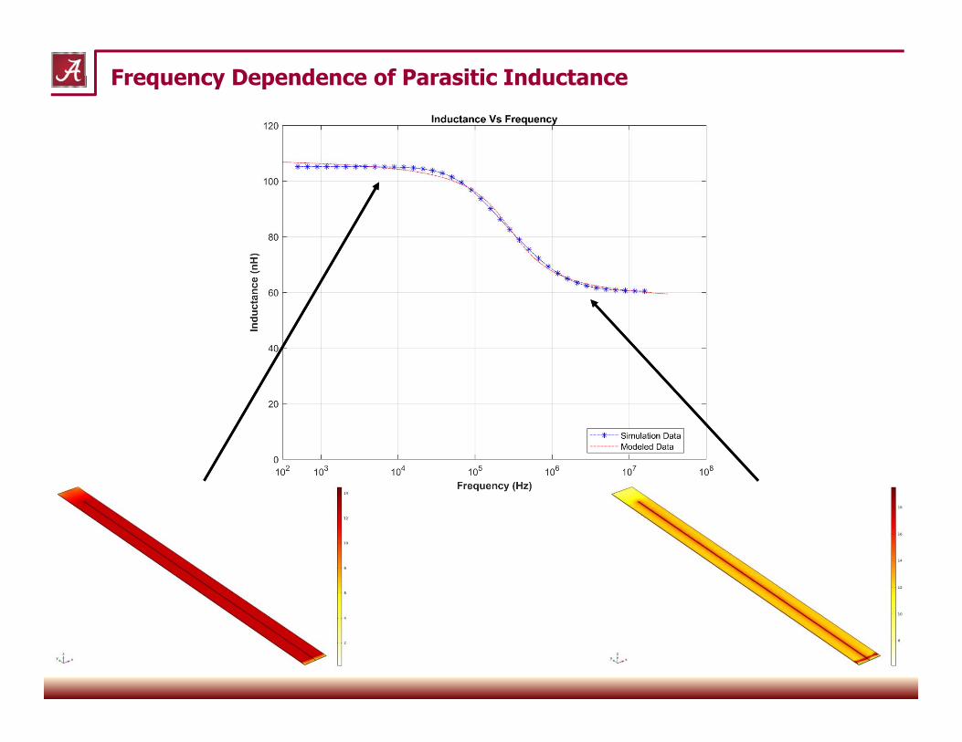
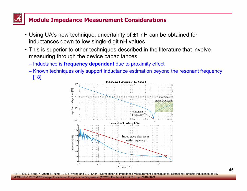
Frequency Dependence of Parasitic Inductance
33
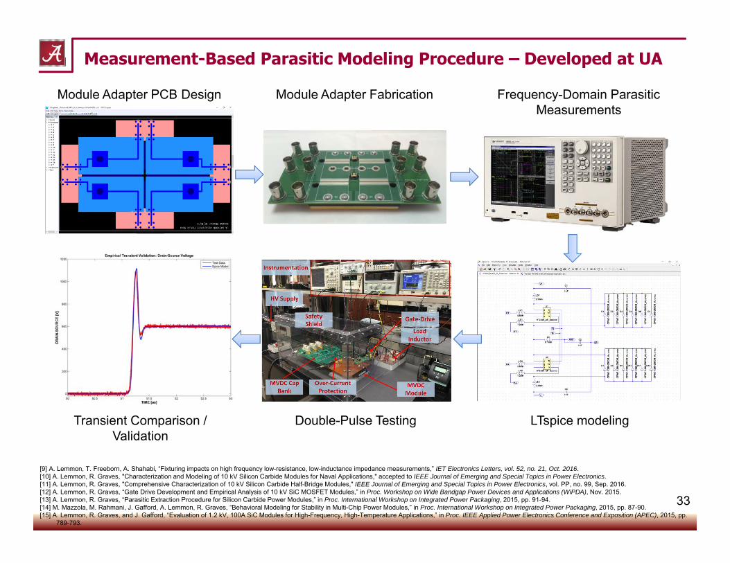
Measurement-Based Parasitic Modeling Procedure – Developed at UA
Module Adapter PCB Design Module Adapter Fabrication Frequency-Domain Parasitic Measurements
Transient Comparison / Validation
Double-Pulse Testing LTspice modeling
[9] A. Lemmon, T. Freeborn, A. Shahabi, “Fixturing impacts on high frequency low-resistance, low-inductance impedance measurements,” IET Electronics Letters, vol. 52, no. 21, Oct. 2016.[10] A. Lemmon, R. Graves, "Characterization and Modeling of 10 kV Silicon Carbide Modules for Naval Applications," accepted to IEEE Journal of Emerging and Special Topics in Power Electronics.[11] A. Lemmon, R. Graves, "Comprehensive Characterization of 10 kV Silicon Carbide Half-Bridge Modules," IEEE Journal of Emerging and Special Topics in Power Electronics, vol. PP, no. 99, Sep. 2016.[12] A. Lemmon, R. Graves, “Gate Drive Development and Empirical Analysis of 10 kV SiC MOSFET Modules,” in Proc. Workshop on Wide Bandgap Power Devices and Applications (WiPDA), Nov. 2015.[13] A. Lemmon, R. Graves, “Parasitic Extraction Procedure for Silicon Carbide Power Modules,” in Proc. International Workshop on Integrated Power Packaging, 2015, pp. 91-94.[14] M. Mazzola, M. Rahmani, J. Gafford, A. Lemmon, R. Graves, “Behavioral Modeling for Stability in Multi-Chip Power Modules,” in Proc. International Workshop on Integrated Power Packaging, 2015, pp. 87-90.[15] A. Lemmon, R. Graves, and J. Gafford, “Evaluation of 1.2 kV, 100A SiC Modules for High-Frequency, High-Temperature Applications,” in Proc. IEEE Applied Power Electronics Conference and Exposition (APEC), 2015, pp.
789-793.
34
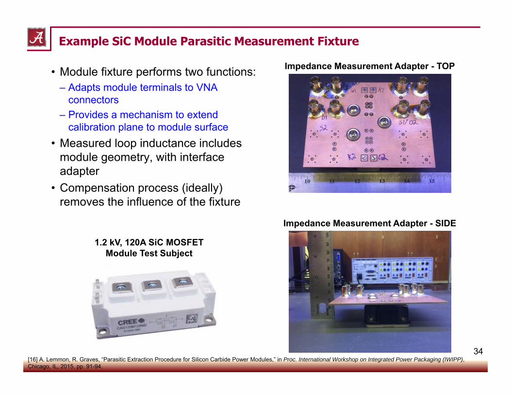
Example SiC Module Parasitic Measurement Fixture
• Module fixture performs two functions:– Adapts module terminals to VNA
connectors– Provides a mechanism to extend
calibration plane to module surface• Measured loop inductance includes
module geometry, with interface adapter
• Compensation process (ideally) removes the influence of the fixture
Impedance Measurement Adapter - TOP
1.2 kV, 120A SiC MOSFET Module Test Subject
Impedance Measurement Adapter - SIDE
[16] A. Lemmon, R. Graves, “Parasitic Extraction Procedure for Silicon Carbide Power Modules,” in Proc. International Workshop on Integrated Power Packaging (IWIPP), Chicago, IL, 2015, pp. 91-94.
35
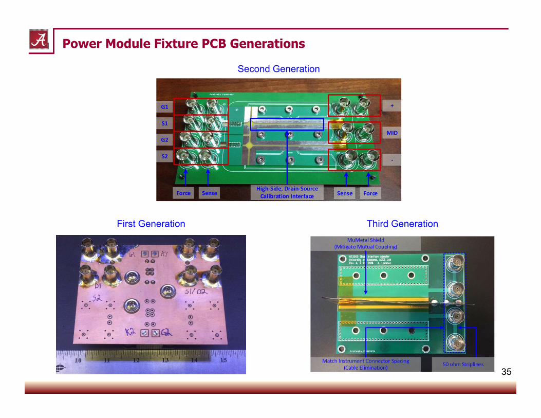
Power Module Fixture PCB Generations
First Generation
Second Generation
Third Generation
36
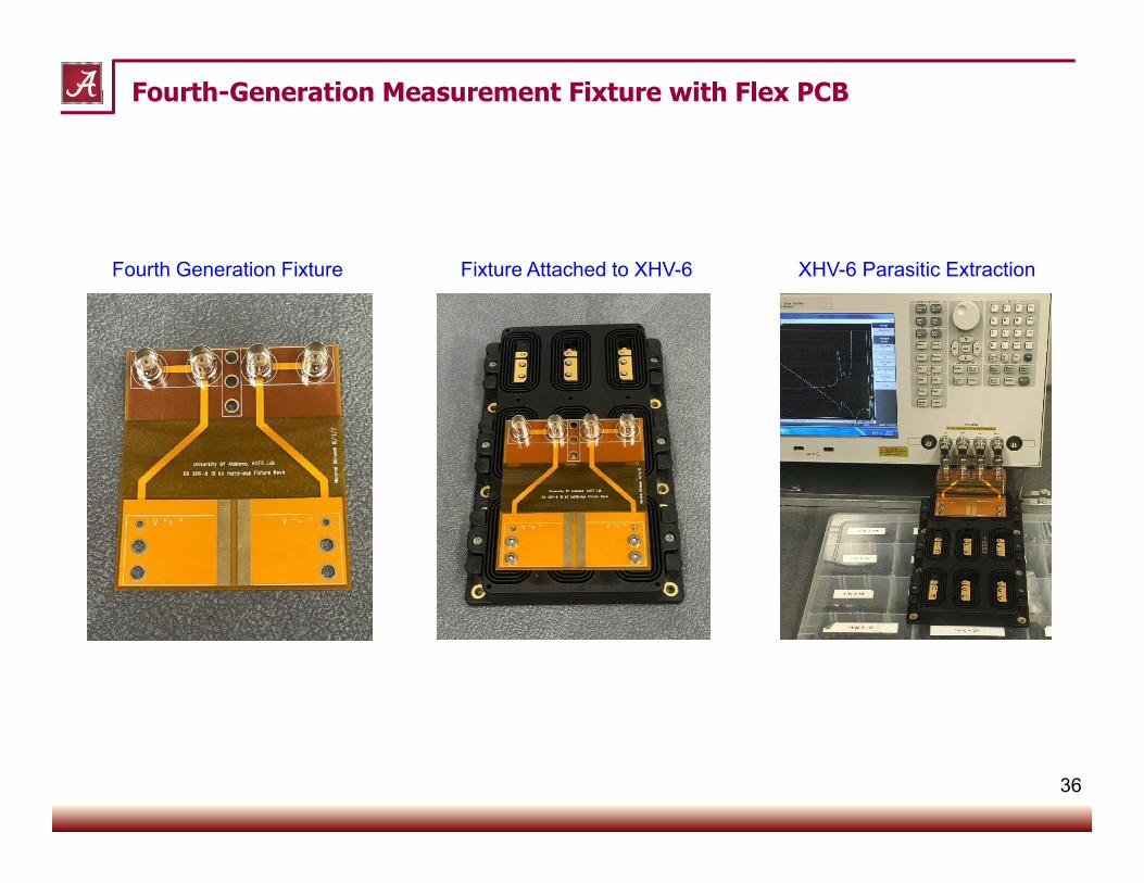
Fourth-Generation Measurement Fixture with Flex PCB
Fourth Generation Fixture Fixture Attached to XHV-6 XHV-6 Parasitic Extraction
37
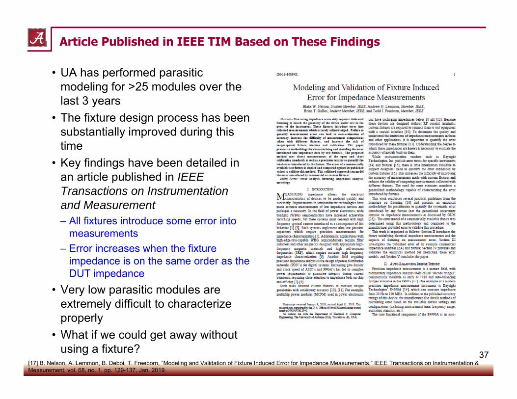
Article Published in IEEE TIM Based on These Findings
• UA has performed parasitic modeling for >25 modules over the last 3 years
• The fixture design process has been substantially improved during this time
• Key findings have been detailed in an article published in IEEE Transactions on Instrumentation and Measurement– All fixtures introduce some error into
measurements– Error increases when the fixture
impedance is on the same order as the DUT impedance
• Very low parasitic modules are extremely difficult to characterize properly
• What if we could get away without using a fixture?
[17] B. Nelson, A. Lemmon, B. Deboi, T. Freeborn, “Modeling and Validation of Fixture Induced Error for Impedance Measurements,” IEEE Transactions on Instrumentation & Measurement, vol. 68, no. 1, pp. 129-137, Jan. 2019.
38
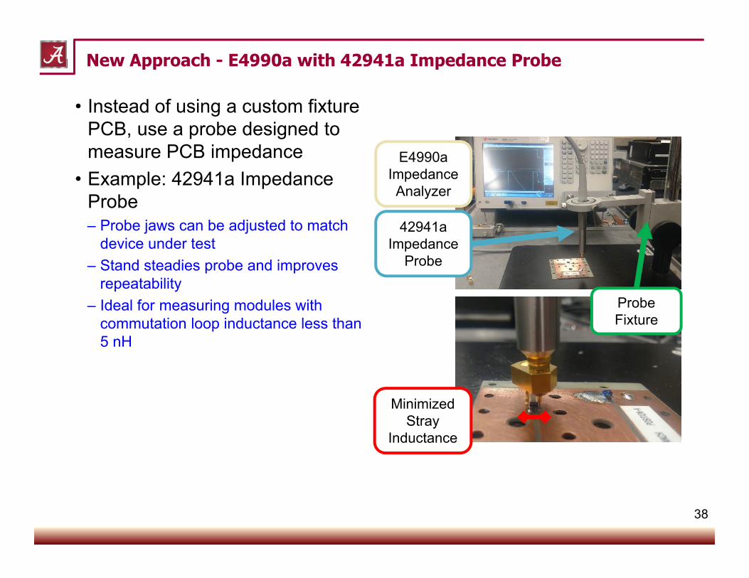
New Approach - E4990a with 42941a Impedance Probe
Minimized Stray
Inductance
E4990a Impedance Analyzer
42941a Impedance
Probe
Probe Fixture
• Instead of using a custom fixture PCB, use a probe designed to measure PCB impedance
• Example: 42941a Impedance Probe – Probe jaws can be adjusted to match
device under test– Stand steadies probe and improves
repeatability– Ideal for measuring modules with
commutation loop inductance less than 5 nH
39
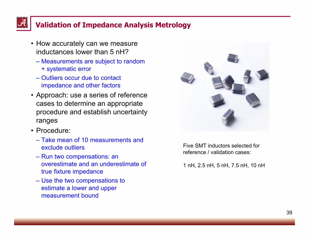
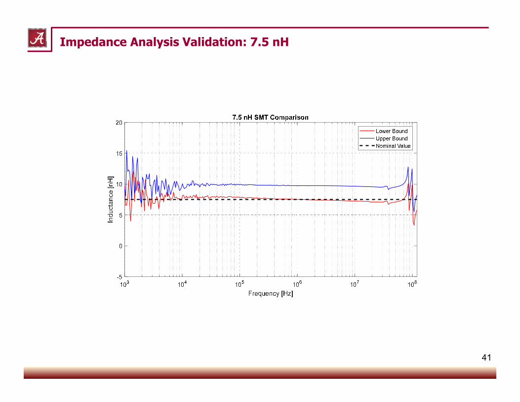
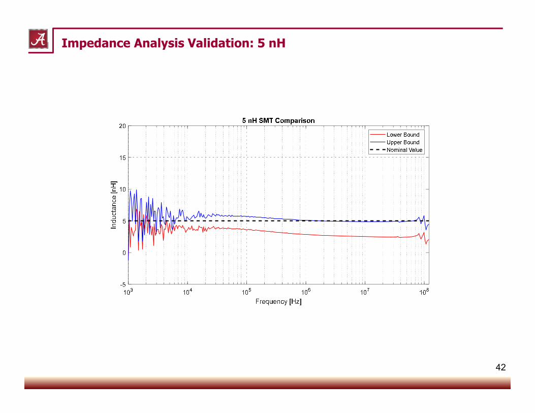
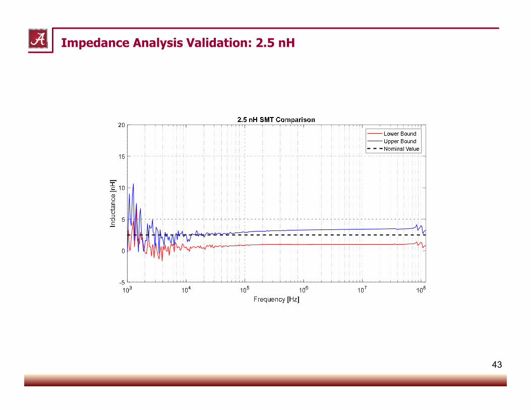
Validation of Impedance Analysis Metrology
• How accurately can we measure inductances lower than 5 nH?– Measurements are subject to random
+ systematic error– Outliers occur due to contact
impedance and other factors• Approach: use a series of reference
cases to determine an appropriate procedure and establish uncertainty ranges
• Procedure: – Take mean of 10 measurements and
exclude outliers– Run two compensations: an
overestimate and an underestimate of true fixture impedance
– Use the two compensations to estimate a lower and upper measurement bound
Five SMT inductors selected for reference / validation cases:
1 nH, 2.5 nH, 5 nH, 7.5 nH, 10 nH
40
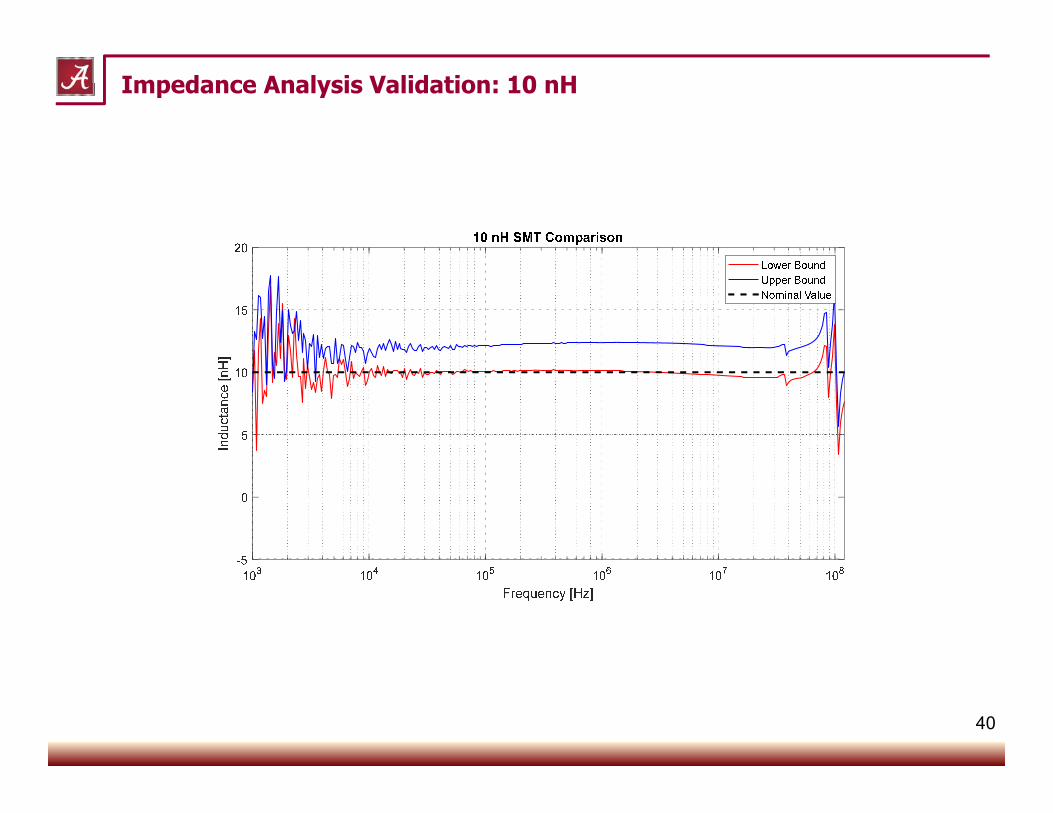
Impedance Analysis Validation: 10 nH
41
Impedance Analysis Validation: 7.5 nH
42
Impedance Analysis Validation: 5 nH
43
Impedance Analysis Validation: 2.5 nH

44
Impedance Analysis Validation: 1 nH
45
Module Impedance Measurement Considerations
Impe
danc
e M
agni
tude
[]
Indu
ctan
ce [n
H]
Resonant Frequency
Inductance extraction range
Inductance decreases with frequency
[18] T. Liu, Y. Feng, Y. Zhou, R. Ning, T. T. Y. Wong and Z. J. Shen, "Comparison of Impedance Measurement Techniques for Extracting Parasitic Inductance of SiC MOSFETs," 2018 IEEE Energy Conversion Congress and Exposition (ECCE), Portland, OR, 2018, pp. 7016-7023.
• Using UA’s new technique, uncertainty of ±1 nH can be obtained for inductances down to low single-digit nH values
• This is superior to other techniques described in the literature that involve measuring through the device capacitances– Inductance is frequency dependent due to proximity effect– Known techniques only support inductance estimation beyond the resonant frequency
[18]
CONCLUSIONS
• WBG application design stands at the junction of power electronics & RF design• Resulting “near-RF” behavior has significant implications for WBG-based systems• Current metrology practices for power electronics are not adequate for
measurement of these circuits• The power electronics community is beginning to realize the implications of fast-
switching for metrology• Better metrology techniques are clearly needed at multiple “layers”:
− Better equipment / probes− Better sensor attachments
• This is likely to be an active area of research for many years to come, particularly at medium voltage levels
Conclusions
For Further Reading