Embed Size (px)
Citation preview

University of South Carolina University of South Carolina
Scholar Commons Scholar Commons
Theses and Dissertations
Fall 2020
Methods for Dynamic Stabilization, Performance Improvement, Methods for Dynamic Stabilization, Performance Improvement,
and Load Power Sharing In DC Power Distribution Systems and Load Power Sharing In DC Power Distribution Systems
Hessamaldin Abdollahi
Follow this and additional works at: https://scholarcommons.sc.edu/etd
Part of the Electrical and Computer Engineering Commons
Recommended Citation Recommended Citation Abdollahi, H.(2020). Methods for Dynamic Stabilization, Performance Improvement, and Load Power Sharing In DC Power Distribution Systems. (Doctoral dissertation). Retrieved from https://scholarcommons.sc.edu/etd/6101
This Open Access Dissertation is brought to you by Scholar Commons. It has been accepted for inclusion in Theses and Dissertations by an authorized administrator of Scholar Commons. For more information, please contact [email protected].

Methods for Dynamic Stabilization, Performance Improvement, andLoad Power Sharing in DC Power Distribution Systems
by
Hessamaldin Abdollahi
Bachelor of ScienceQazvin Azad University, 2011
Master of SciencePolitecnico di Milano, 2015
Submitted in Partial Fulfillment of the Requirements
for the Degree of Doctor of Philosophy in
Electrical Engineering
College of Engineering and Computing
University of South Carolina
2020
Accepted by:
Enrico Santi, Major Professor
Paolo Mattavelli, Committee Member
Herbert L. Ginn, Committee Member
Bin Zhang, Committee Member
Cheryl L. Addy, Vice Provost and Dean of the Graduate School

c© Copyright by Hessamaldin Abdollahi, 2020All Rights Reserved.
ii

Acknowledgments
I would like to dedicate my greatest appreciation to my Academic Advisor Dr. Enrico
Santi. I would like to thank him for believing in me and providing an opportunity
to pursue my Ph.D. under his supervision. Over the course of my doctoral studies,
thanks to his guidance, I was able to develop my knowledge and expand my skills
as a graduate student, academic researcher, and an engineer. I am sincerely grateful
for all his encouragements over the past years which played a key role in my thrive
during my journey as a Ph.D. student.
I would like to express my gratitude to my doctoral committee members, Dr.
Herbert Ginn, Dr. Paolo Mattavelli, and Dr. Bin Zhang for their valuable comments
and ideas in the preparation of this dissertation. Also, I would like to thank them
for their flexibility as well as their time and effort.
I would like to thank the administrative staff of the Electrical Engineering Depart-
ment at the University of South Carolina. In particular, I am thankful for the Power
Electronics Group program coordinator Hope Johnson, former graduate coordinator
Ashley Burt, current graduate coordinator Jenny Balestrero, and Computer Support
Manager David London. Also, I would like to thank David Metts for his friendship
and the support he provided during my teaching assistantship.
I am very grateful for the friendship and collaborations of several former and
current members of the Power Electronics Group as well as other members of the
Electrical Engineering Graduate program. I would like to thank Dr. Jonathan Siegers
for all his help and guidance during the first year of my Ph.D. studies. I would like to
appreciate Dr. Soheila Eskandari and Hossein Baninajar for their lasting friendship
iii

and their help during these years. I am also thankful to Dr. Silvia Arrua for her
collaboration during various projects. I would like to thank Dr. Tomi Roinila for his
friendship which has resulted in very good memories and for our fruitful academic
collaboration. I am also very grateful to all my friends in the Iranian community of
Columbia who made my time here joyful and memorable.
I would like to acknowledge the support of the Office of Naval Research (ONR)
that provided partial funding for this research under grant number N00014-16-1-2956.
I am also grateful to the support that I have received from the Electrical Engineering
Department at the University of South Carolina.
Finally, I want to express my gratitude to my family and parents for their unending
support and love. The inspiration and motivation that I have received from my loved
ones have led me to achieve beyond what I could have imagined. I am sincerely
grateful to my lovely wife Faraneh, she has been with me during all my up and downs
with her unconditional love, companionship, support, and encouragement. I am
greatly indebted to all my family members and words certainly fall short to describe
my gratitude.
This dissertation has been cleared for public release by the Office of Naval Research
with DCN# 43-7111-20.
iv

Abstract
Modern DC power distribution systems (DC-PDS) offer high efficiency and flexibil-
ity which make them ideal for mission-critical applications such as on-board power
systems of All-Electric ships, electric vehicles, More-Electric-Aircrafts, and DC Mi-
crogrids. Despite these attractive features, there are still challenges that need to be
addressed. The two most important challenges are system stability and load power
sharing. The stability and performance are of concern because DC-PDS are typically
formed by the interconnection of several feedback-controlled power converters. The
resulting interactions can lead to destabilizing dynamics. Likewise, in a DC-PDS
there are several source converters that are operating in parallel to supply the total
load power. This improves the system reliability through structural redundancy. Im-
proper load sharing, however, leads to overloading of some of the source converters
which might result in cascaded failures.
Several stability criteria are proposed in the literature. Among all, the impedance-
based approaches are well accepted for stability analysis and stabilizing controllers
design. These methods are based on evaluating the system impedances using linear
control theory and small-signal dynamic analysis. So, using such methods, stabi-
lization is accomplished in an intuitive and design-oriented manner. However, an
important disadvantage of linear methods is that their range of effectiveness is lim-
ited to a small-signal region around an operating point of the system wherein the
non-linear system can be approximated by a linear one. Likewise, DC-PDS often
experience large-signal transients and operating point variations. Thus, linear con-
trollers may fail to preserve the stability and performance for large-signal transients.
v

Therefore, there is a need to develop new methods that guarantee system stability
and performance during such large-signal transients.
To solve the problem of load power sharing in DC-PDS, various methods can
be found in the literature. Load sharing mechanisms can be categorized as Droop
methods and active sharing techniques. In the conventional Droop method, a virtual
resistance is added to the output impedance of the source converter and a decentral-
ized load sharing is achieved. Although simple and effective, Droop control causes
a variable bus voltage drop which requires additional control measures to achieve
tight voltage regulation. Active methods, on the other hand, manage to achieve
load sharing at the cost of additional control requirements such as high bandwidth
communication links among the source converters which increase the complexity and
cost. Thus, it is desirable to develop new methods to solve the problem of proper
load sharing in a simple, efficient, and inexpensive manner.
To address the above challenges, in this dissertation, a generic DC-PDS is consid-
ered and the system dynamics is studied for small-signal and large-signal operations.
Based on this analysis, novel stabilizing control methods are proposed that are im-
plemented in a source converter. The proposed approach manages to guarantees
stability and performance for various operating scenarios. Additionally, to solve the
load-sharing problem, a novel communication-less current-sharing control scheme is
proposed. This method guarantees proper distributed load sharing among several
source converters without any bus voltage drop and requiring any physical commu-
nication network.
vi

Table of Contents
Acknowledgments . . . . . . . . . . . . . . . . . . . . . . . . . . . . . iii
Abstract . . . . . . . . . . . . . . . . . . . . . . . . . . . . . . . . . . . v
List of Figures . . . . . . . . . . . . . . . . . . . . . . . . . . . . . . . ix
Chapter 1 Introduction . . . . . . . . . . . . . . . . . . . . . . . . . 1
1.1 Stability and Performance . . . . . . . . . . . . . . . . . . . . . . . . 3
1.2 Load Power Sharing . . . . . . . . . . . . . . . . . . . . . . . . . . . 8
Chapter 2 Stabilization of DC Power Distribution SystemsUsing An Impedance-Based Approach and Resonance-Enhanced Voltage Controller . . . . . . . . . . . . . . 13
2.1 State-of-the-art Impedance-based Stabilization Methods . . . . . . . . 14
2.2 PBSC and AIR . . . . . . . . . . . . . . . . . . . . . . . . . . . . . . 17
2.3 Source Converter Output Impedance . . . . . . . . . . . . . . . . . . 20
2.4 Resonance-enhanced Voltage Controller . . . . . . . . . . . . . . . . . 23
2.5 Design Procedure for Resonance-enhanced Voltage Controller . . . . . 26
2.6 Experimental Verification . . . . . . . . . . . . . . . . . . . . . . . . 29
2.7 Conclusion and Future Work . . . . . . . . . . . . . . . . . . . . . . . 33
Chapter 3 Large-signal Transient Performance Improvementof DC Power Distribution Systems Using a NovelHybrid Stabilizing Voltage Controller . . . . . . . . 37
vii
3.1 State-of-the-art Stabilization Methods . . . . . . . . . . . . . . . . . 41
3.2 System Under Study and Dynamic Analysis . . . . . . . . . . . . . . 43
3.3 Proposed Hybrid Stabilizing Control Method . . . . . . . . . . . . . . 51
3.4 Simulation Results . . . . . . . . . . . . . . . . . . . . . . . . . . . . 57
3.5 Experimental Verification . . . . . . . . . . . . . . . . . . . . . . . . 60
3.6 Robustness to Errors in Load Power Estimation . . . . . . . . . . . . 70
3.7 Conclusion and Future Work . . . . . . . . . . . . . . . . . . . . . . . 73
Chapter 4 A Communication-less Consensus-based load Cur-rent Sharing Control Scheme for DC Power Dis-tribution Systems . . . . . . . . . . . . . . . . . . . . . . 77
4.1 State-of-the-art and background . . . . . . . . . . . . . . . . . . . . . 78
4.2 Proposed current sharing method . . . . . . . . . . . . . . . . . . . . 80
4.3 Simulation Results . . . . . . . . . . . . . . . . . . . . . . . . . . . . 95
4.4 Conclusion and Future Work . . . . . . . . . . . . . . . . . . . . . . . 101
Bibliography . . . . . . . . . . . . . . . . . . . . . . . . . . . . . . . . 106
viii

List of Figures
Figure 1.1 Notional MVDC power distribution system. G stands for gen-eration unit and M stands for motor loads. . . . . . . . . . . . . . 2
Figure 1.2 A simplified generic representation of the system shown in Fig. 1.1. 4
Figure 1.3 The v-i characteristic of a constant power load. . . . . . . . . . . 5
Figure 1.4 The system impedances including the source, ZS, load, ZL, andbus, Zbus, impedances. The system minor-loop-gain, Tmlg, isalso shown. . . . . . . . . . . . . . . . . . . . . . . . . . . . . . . 6
Figure 1.5 The ac-coupled step response of the bus voltage, v. . . . . . . . . 6
Figure 1.6 Equivalent circuit of two source converters in parallel sharingthe total load power based on Droop control. . . . . . . . . . . . . 9
Figure 1.7 Droop P-V characteristic showing the compromise between volt-age regulation and load power sharing accuracy. The figurerepresents the case of two source converters (solid and dashed-dotted lines) with a certain amount of mismatch for the case oflarge Droop gains (case 1) and small Droop gains (case 2). . . . . 11
Figure 2.1 A generic representation of a DC PDS. ZS is the overall sourcesubsystem output impedance, ZL is the overall load subsysteminput impedance, and Zbus is the system bus impedance whichis the parallel combination of ZS and ZL. The current sourceiinj represents a current perturbation injection for Zbus measure-ment. In the block diagram, the system input is the imposedcurrent disturbance, iinj, and the output is the bus voltage, vbus. . 18
Figure 2.2 PBSC and AIR requirements. PBSC requires the Nyquist con-tour of the normalized bus impedance, Zbus−N , to lie whollyin the right-half-plane to ensure passivity and hence stability.AIR requires Zbus−N to be confined within a region with a cer-tain damping margin, Km, to ensure a minimum damping inthe system. . . . . . . . . . . . . . . . . . . . . . . . . . . . . . . 19
ix

Figure 2.3 The system under study includes a generic DC-DC source con-verter under the conventional two-loop control scheme. . . . . . . 21
Figure 2.4 Control block diagram of the system in Fig. 2.3 where thesource converter block represents the converter model with theinner current-loop closed. . . . . . . . . . . . . . . . . . . . . . . 21
Figure 2.5 Control block diagram of the system in Fig. 2.5 where thesource converter block represents the converter model with theinner current-loop closed. The nominal PI voltage regulator,Gcv, is augmented with the resonance term, Gr. . . . . . . . . . . 24
Figure 2.6 The block diagram representation of the experimentally imple-mented system. The system consists of a source Buck con-verter supplying a load Buck converter drawing a total load ofPL=400W at a bus voltage of 100V . . . . . . . . . . . . . . . . . 30
Figure 2.7 System impedances measured under PI control only, the sourceoutput impedance is ZS, the load input impedance is ZL, andthe system bus impedance is Zbus. . . . . . . . . . . . . . . . . . . 32
Figure 2.8 The bus voltage transient response to a step variation in theload power. VbusP I
is when the source is under PI controland VbusP I−R
is when the source is enabled with the resonance-enhanced voltage cnotroller. . . . . . . . . . . . . . . . . . . . . . 32
Figure 2.9 The Nyquist contour of the system bus impedances under PIand PI-R control schemes. The AIR and passivity boundariesare shown as well. . . . . . . . . . . . . . . . . . . . . . . . . . . . 33
Figure 2.10 The system bus impedances under PI and PI-R control schemes.ZbusP I−R
is considerably damped as compared to the bus impedancemeasured under the nominal PI control. . . . . . . . . . . . . . . 34
Figure 2.11 The experimentally measured voltage loop-gains of the sourceconverter under nominal PI and PI-R control schemes. . . . . . . 34
Figure 3.1 The simulated DC power distribution system. The source Bucklinear nominal controllers are tuned to achieve the desired sta-bility margins and bandwidths. . . . . . . . . . . . . . . . . . . . 39
Figure 3.2 Bus voltage and source converter inductor current. The tran-sient responses to step variations in the source converter’s volt-age reference. . . . . . . . . . . . . . . . . . . . . . . . . . . . . . 40
x

Figure 3.3 Bus voltage and source converter inductor current. The tran-sient responses to step variations in the load power. . . . . . . . . 41
Figure 3.4 The system under study consists of a generic source converterand a load subsystem which has CPL characteristic. . . . . . . . . 44
Figure 3.5 The control block diagram of the source converter under two-loop control. The plant is represented by a generic untermi-nated state-space model. . . . . . . . . . . . . . . . . . . . . . . . 45
Figure 3.6 The quasi-steady-state model of the source converter undertwo-loop control wherein the inner-loop is replaced by a unity gain. 46
Figure 3.7 The quasi-steady-state model of the system shown in Fig. 3.4obtained using the presented dynamic analysis. . . . . . . . . . . 46
Figure 3.8 Step response of the bus voltage: the slow-model response(dashed line) against the responses of the full-order model forthree different current controllers (solid lines) . . . . . . . . . . . 47
Figure 3.9 Non-linear function f(vbus) for a fixed value of the load power,bus reference voltage, and different values of vbus. . . . . . . . . . 50
Figure 3.10 The state trajectories of the system in (3.6) for a load power ofPL = 1kW . . . . . . . . . . . . . . . . . . . . . . . . . . . . . . . 50
Figure 3.11 The state trajectories of the system in (3.6) for a load power ofPL = 3kW . . . . . . . . . . . . . . . . . . . . . . . . . . . . . . . 52
Figure 3.12 The state trajectories of the system in (3.6) for a load power ofPL = 3.5kW . . . . . . . . . . . . . . . . . . . . . . . . . . . . . . 52
Figure 3.13 The quasi-steady-state model of the system shown in Fig. 3.4with the additional control input ν. . . . . . . . . . . . . . . . . . 53
Figure 3.14 The quasi-steady-state model of the system with the non-linearfeedback term implementing h(vbus). . . . . . . . . . . . . . . . . 55
Figure 3.15 The full implementation of the proposed hybrid stabilizing con-troller in the control platform of a source converter. . . . . . . . . 56
Figure 3.16 The system responses to step variation in the bus referencevoltage. The step change is from the nominal voltage of 200Vto 150V and back up to 200V . . . . . . . . . . . . . . . . . . . . . 59
xi

Figure 3.17 The system responses to step variation in the load power. Thestep change is from 3kW to 1.5kW and back up to 3kW . . . . . . 59
Figure 3.18 The system responses to step variation in the bus referencevoltage. The step change is from the nominal voltage of 200Vto 150V and back up to 200V . . . . . . . . . . . . . . . . . . . . . 61
Figure 3.19 The system responses to step variation in the load power. Thestep change is from 3kW to 1.5kW and back up to 3kW . . . . . . 61
Figure 3.20 The block diagram representation of the experimentally imple-mented system. The system consists of a source Buck con-verter supplying a load Buck converter drawing a total load ofPL=550W at a bus voltage of 100V . . . . . . . . . . . . . . . . . 63
Figure 3.21 dSPACE ControlDesk layout created for the real-time controlof both source and load Buck converters. The figure shows thecontrol of the system during operation with live measurementsof bus voltage, load Buck output voltage, source converter in-ductor current, and load power. . . . . . . . . . . . . . . . . . . . 64
Figure 3.22 The oscilloscope capture showing the steady-state operation ofthe system. Channel 1 shows the bus voltage, Channel 2 showsthe output voltage of the load Buck converter, and Channel 3shows the source converter inductor current at a scale of 5A/div. 65
Figure 3.23 The ac−coupled bus voltage step response under nominal PIvoltage controller in the source Buck converter. The large tran-sient is due to a 75% step variation in the load power. . . . . . . . 66
Figure 3.24 The measured load input impedance, ZL, source output impedance,ZS, and bus impedance, Zbus. . . . . . . . . . . . . . . . . . . . . 66
Figure 3.25 The system bus impedances under PI voltage controller only(Zbus−PI) and with the resonant controller, Gr, activated (Zbus−PI−R). 67
Figure 3.26 The Nyquist contours of the measured bus impedances nor-malized by the bus characteristic impedance under PI control,Zbus−PI−N , and with the resonant controller activated, Zbus−PI−R−N . 67
Figure 3.27 The ac−coupled bus voltage transient response to the same75% step variation in the load power with the designed resonantcontroller activated in the source converter. . . . . . . . . . . . . 68
xii
Figure 3.28 The ac−coupled bus voltage transient response to the same75% step variation in the load power with the proposed HybridNon-linear stabilizing controller activated in the source converter. 69
Figure 3.29 The contributions of the resonance controller, Gr, and the non-linear feedback h( ˜vbus) term to the overall inductor currentreference. Note that the output of the non-linear feedback isnegated and summed with the outputs of the nominal PI andresonance controllers. . . . . . . . . . . . . . . . . . . . . . . . . . 70
Figure 3.30 The source inductor current response to the load power stepvariation with PI voltage control only, IL−PI , resonance-enhancedvoltage controller, IL−PI−R, and the proposed hybrid stabilizingcontroller, IL−PI−R−NL. . . . . . . . . . . . . . . . . . . . . . . . . 71
Figure 3.31 The ac−coupled bus voltage transient response to a 75% loadpower step variation. Other than the results for the mentionedthree cases, the results under the resonance-enhanced voltagecontroller, vbus−PI−R, and the proposed hybrid stabilizing con-troller with real-time load power estimation, vbus−PI−R−NL, arealso presented. . . . . . . . . . . . . . . . . . . . . . . . . . . . . 72
Figure 4.1 The main idea of the proposed communication-less consensus-based current sharing scheme depicted in a multi-source system. 81
Figure 4.2 The proposed communication-less consensus-based current shar-ing control scheme implemented in block diagram. . . . . . . . . . 82
Figure 4.3 The proposed small sinusoidal signal injection technique. . . . . . 84
Figure 4.4 Three cascaded detection blocks incorporated in the first con-verter’s control platform for a DC-PDS with three source con-verters. . . . . . . . . . . . . . . . . . . . . . . . . . . . . . . . . 86
Figure 4.5 The pole-zero map of the second-order IIR notch filter for dif-ferent notch frequencies shown by different colors. . . . . . . . . . 89
Figure 4.6 The frequency response of the second-order IIR notch filter,Hn(z), for ωn=0.5π and ρ=0.99. . . . . . . . . . . . . . . . . . . . 89
Figure 4.7 The frequency response of the gradient filter, Hs(z), given in(4.8) for the normalized notch frequency of ωn=0.5π and ρ=0.99. 91
xiii

Figure 4.8 The block diagram representation of the implemented adaptivenotch filter (ANF). . . . . . . . . . . . . . . . . . . . . . . . . . . 91
Figure 4.9 The modified sinusoidal injection technique. . . . . . . . . . . . . 93
Figure 4.10 The modified ANF-based frequency detection block. . . . . . . . . 93
Figure 4.11 The i-th converter’s control platform enabled with the proposedcommunication-less consensus-based current sharing scheme (therelated blocks are highlighted in yellow). . . . . . . . . . . . . . . 94
Figure 4.12 The simulated DC-PDS with three source converters and a loadsubsystem including a three-phase VSI some passive load. Thetotal load power is PL = 5kW . . . . . . . . . . . . . . . . . . . . 96
Figure 4.13 The parameters of the signal injection and detection blocks ofthe proposed current sharing method for the simulated DC-PDS. 96
Figure 4.14 The bus voltage and output currents of the simulated systemin the case of source converters of equal rated currents. . . . . . . 98
Figure 4.15 The actual measured output currents (solid lines) against theoutput currents estimated by the proposed ANF-based detec-tion block in the first converter (dashed lines). . . . . . . . . . . . 98
Figure 4.16 The actual measured output currents (solid lines) against theoutput currents estimated by the proposed ANF-based detec-tion block in the second converter (dashed lines). . . . . . . . . . 99
Figure 4.17 The bus voltage and output currents of the simulated systemin the case of source converters with different rated currents. . . . 100
Figure 4.18 The actual measured output currents (solid lines) against theoutput currents estimated by the proposed ANF-based detec-tion block in the first converter (dashed lines). . . . . . . . . . . . 101
Figure 4.19 The actual measured output currents (solid lines) against theoutput currents estimated by the proposed ANF-based detec-tion block in the second converter (dashed lines). . . . . . . . . . 101
Figure 4.20 The proposed current sharing method can be used at secondarylevel to compensate for bus voltage drop caused by a Droop-based current sharing implemented at the primary level. . . . . . 103
xiv

Figure 4.21 The proposed current sharing method can be used along withthe hybrid stabilization method, introduced in the previouschapter, to ensure proportional current sharing and stabilityof DC systems. . . . . . . . . . . . . . . . . . . . . . . . . . . . . 105
xv

Chapter 1
Introduction
Modern power systems are experiencing a revolutionary change of paradigm at the
distribution level where DC systems are becoming more and more widespread. This
is mainly due to the significant advancements in the fields of semiconductors, control,
and power electronics [1]. Also, the emerging renewable energy resources, e.g. solar,
and storage units such as batteries, are all DC in nature. This fact lends itself to
the increasing popularity of DC power distribution systems (DC-PDS) where high
efficiency and flexibility are achievable and unnecessary power conversion stages are
avoided [2]. Additionally, DC systems provide more availability and easier scalability
– the properties that make them ideal candidates for mission-critical applications.
DC power distribution systems are employed in various applications such as on-board
power systems of All-Electric Ships, Electric Vehicles, More-Electric-Aircrafts, and
DC Microgrids [3].
The significance of the inherent advantages of DC distribution systems can be
better understood when they are compared against the traditional AC systems. In
DC-PDS, unlike the traditional AC systems, the problems with reactive power flow
and frequency control are naturally eliminated and there is no need for bulky low-
frequency transformers. Also, phase synchronization among parallel sources is not
required and multiple generator units and storage systems can be easily interfaced
with the DC bus through power converters. High level of flexibility and controlla-
bility allow rapid system reconfiguration which is required often in mission-critical
applications with frequent dynamic variations in the load demand [3–5].
1

Figure 1.1: Notional MVDC power distribution system. G stands for generation unitand M stands for motor loads.
Motivated by the aforementioned advantages, the U.S. Navy is very interested
in developing All-Electric Ships (AES) with on-board integrated DC-PDS. The high
power demand and highly dynamic nature of the loads as well as the need for fuel-
efficient operation have resulted in the adoption of kV -range voltage levels. A simpli-
fied representation of the considered medium-voltage DC (MVDC) system is shown
in Fig. 1.1 which can be seen as an islanded DC Microgrid [6]. The operation of
such a system is heavily dominated by and reliant upon the power converter units.
In particular, sources of various types, including storage units, and the loads with
2

different nature, such as radar and pulsed loads, are interfaced with the main MVDC
bus through power converter units [7, 8]. The operation of the system is well reg-
ulated through the implementation of feedback control methods at various control
layers which accomplish different objectives such as bus voltage regulation and out-
put regulation of load converters at various voltage levels [9].
In spite of all the advantages of DC-PDS, there are still several challenges that need
to be addressed. Two of the most important ones relate to the system stability and the
problem of load power sharing among several source converters. These two aspects of
DC-PDS operation are of concern in this work and so they will be introduced briefly
in the following sections. The discussions and methods proposed later-on can be
generalized to various applications and operation scenarios. However, the introduced
MVDC system intended for AES application is mainly considered in this research.
1.1 Stability and Performance
The safe and reliable operation of a DC-PDS is ensured if the system dynamic sta-
bility and high performance are guaranteed at all operating conditions [4, 9]. Unlike
the traditional AC systems, DC-PDS exhibit low inertia and therefore are prone to
instability depending on the operating conditions [2].
In a typical DC system, such as the one shown in Fig. 1.1, each of the source and
load converters are under feedback control and are designed to be standalone stable,
so that they achieve tight regulation of their terminal variables: voltages and currents.
However, the interconnection of these converters leads to dynamic interactions that
can significantly degrade the system performance or destabilize the system [10]. More
particularly, tightly-regulated load converters, within their bandwidths, attempt to
provide constant power at their output terminals and therefore they tend to consume
constant power from the source subsystem. This constant power load (CPL) char-
3

Figure 1.2: A simplified generic representation of the systemshown in Fig. 1.1.
acteristic of the load subsystem can be shown to have detrimental impacts on the
system stability and performance [11].
To better understand the involved dynamic mechanism, the system shown in Fig.
1.2 is considered. This system is a simplified generic representation of the notional
MVDC system of AES, as shown in Fig. 1.1. The load subsystem is a CPL which
collectively represents all the feedback-regulated load converters. A CPL, within its
bandwidth, manages to consume constant power from the source which implies a
constant product of the bus voltage, v, and the drawn current, i. As a result, the
non-linear v-i characteristic of a CPL is as shown in Fig. 1.3 where it is seen that
any increase/decrease in the voltage is associated with a decrease/increase in the
current. This non-linear characteristic has a strong destabilizing effect on the overall
interconnected system [11–14].
The CPL-induced instability problem was described and analyzed by Middlebrook
in [15], where the interactions between an input filter and a closed-loop power con-
verter were studied and a set of design criteria were proposed to ensure the stability
of the interconnected system. It was found that the linearization around a certain op-
erating point results is a line with a negative slope. This implies that, for small-signal
variations around an operating point, the load subsystem has an input impedance
equivalent to a negative incremental resistance equal to −v2/PL where v is the bus
voltage and PL is the load power. This is also shown in Fig. 1.3. The so-called
Middlebrook criterion defines the minor-loop-gain as the ratio of the source and
4

Figure 1.3: The v-i characteristic of a constant power load.
load impedances, i.e. Tmlg = ZS/ZL [15]. The phase-margin of this open loop-gain
represents a stability margin for the interconnected system [9].
More recently, the passivity of the system bus impedance has been used for the
system stability and performance analysis. This is proposed as the passivity-based
stability criterion (PBSC) [10]. The bus impedance is a closed-loop quantity and is
defined as the parallel combination of the source and load impedances as in (1.1).
Zbus = ZLZSZL + ZS
= ZS1 + Tmlg
(1.1)
In short, the Middlebrook criterion requires that, for the system to have better
stability and performance, the source and load impedances be well separated in mag-
nitude and the minor-loop-gain to have sufficient phase-margin [16]. Similarly, the
PBSC requires that the system bus impedance contain no right-half-plane poles with
positive damping in the whole frequency range of interest and have a phase response
confined within the passivity boundaries, ±90 [10].
5

100
101
102
103
-50
0
50
Magnitude(dB)
System Impedances and minor-loop-gain
100
101
102
103
Frequency[Hz]
-200
-100
0
100
200
Phase(deg)
Zbus
Tmlg
ZL ZS
Figure 1.4: The system impedances including the source, ZS, load, ZL, and bus, Zbus,impedances. The system minor-loop-gain, Tmlg, is also shown.
0 0.05 0.1 0.15 0.2 0.25 0.3 0.35 0.4
Time[s]
-15
-10
-5
0
5
10
15
Voltage[V
]
Bus V oltage Step Response
Figure 1.5: The ac-coupled step response of the bus voltage, v.
6

For a system as in Fig. 1.2, the frequency response of the closed-loop system
impedances and minor-loop-gain are shown in Fig. 1.4. It is seen that at low-
frequency, the load input impedance, ZL, is resistive with a phase of −180. Since the
bandwidth of the load subsystem is practically limited, the response of the impedance
ZL deviates from a negative resistance at high frequencies. However, in the mid-
frequency range where the source and load impedances, ZS and ZL, become compa-
rable in magnitude, the minor-loop-gain approaches unity in magnitude and 180 in
phase, resulting in a very small phase-margin. Therefore, the denominator of the last
fraction in (1.1) becomes very small and so the bus impedance, Zbus, exhibits a very
large resonant peak. This is the origin of performance degradation which could lead
to instability in case of variations in the system such as the change in the CPL power.
The lack of performance for this system is also confirmed by the time-domain result
shown in Fig. 1.5 where the step response of the bus voltage, v, is poorly damped
and oscillatory.
The stability problem of DC-PDS has brought many challenges in the design and
operation stages of large interconnected systems. This issue is of critical significance
for on-board power systems such as the ship MVDC system where there are dynam-
ically changing loads and the system can experience a reconfiguration as the mission
changes [3, 5, 9]. Therefore, active stabilization methods are necessary to guarantee
system stability and high performance despite the inevitable small- and large-signal
transients and disturbances.
In this dissertation, the stability issue is considered for both small-signal and
large-signal transients and disturbances. For small-signal transients, an impedance-
based stability analysis method based on passivity is adopted and a stabilizing control
method is proposed in Chapter 2 that ensures stability and high performance. For
large-signal operation, the stability is analyzed considering the inherent system non-
7

linearity and a novel hybrid stabilizing control method is proposed in Chapter 3 which
ensures stability under large transients.
1.2 Load Power Sharing
In a typical DC-PDS, the DC bus is supplied by several source converters in parallel
configuration (see Fig. 1.1). This permits to achieve several desirable characteristics:
a seamless supply of power, ability to interface energy sources of different natures
such as generation and storage units, ability to satisfy high power demand from the
load side, reliability of the system, and structural redundancy [4,17]. In this situation,
the total load power sharing or current sharing among the parallel source converters
is critically important. To achieve this requirement, appropriate measures must be
incorporated within the system control schemes [6, 18].
Theoretically, if the source converters are identical, in terms of power stage com-
ponents and dynamic characteristics such as control bandwidths, they should share
the total load current equally. However, this is very rarely the case as there are always
mismatches in components and dynamic characteristics. Additionally, for large-scale
systems such as terrestrial DC Microgrids where the source converters might be lo-
cated in locations far from each other, non-negligible line impedances can give rise to
unbalanced current sharing [2]. If significant, this current unbalance can considerably
overload some source converters which would result in abnormal thermal stresses and
possible cascaded failures [17, 18]. To overcome this problem, several load sharing
methods are proposed in the literature which mostly fall into two categories: Droop
methods and active sharing methods [4].
In a DC-PDS, load current sharing via Droop method is typically accomplished
by incorporating an additional feedback loop on top of the inner control loops which
regulate a source converter’s inductor current and output voltage [17]. In its most
basic form, this additional control loop creates a droop in the output voltage by
8

Figure 1.6: Equivalent circuit of two source converters in parallel sharingthe total load power based on Droop control.
subtracting a proportional part of the converter’s output power or current from its
output voltage reference [19]. The net effect is a virtual output resistance which
naturally provides Droop control.
A simple equivalent circuit for the case of two source converters in parallel opera-
tion under Droop control is shown in Fig. 1.6, where each converter is represented by
an ideal voltage source behind a series output resistance [4]. In this figure, v∗oi, is the
reference output voltage of each converter, rdiis the virtual Droop resistance, ioi
is
the output current, Pi is output power, and rli is the physical line resistance between
each source and load. The relationship between the output voltages and currents of
each source converter can be written as (1.2).
vbus = v∗o1 − (rd1 + rl1)io1
vbus = v∗o2 − (rd2 + rl2)io2
(1.2)
The two sources have equal output voltages due to the parallel operation, vo1 =
vo2 , and also the reference voltages are typically equal, i.e. v∗o1 = v∗o2 . Thus, using
(1.2), the ratio of the output currents of the two converters is obtained as (1.3). This
implies that, if we neglect the line resistances, by incorporating Droop control in each
9

of the sources and properly choosing the Droop gains, rd1 and rd2 , the two converters
can maintain a proportional load current sharing. The special case of equal current
sharing is achieved when rd1 is chosen to be equal to rd2 .
io1
io2
= rd2 + rl2rd1 + rl1
(1.3)
Droop technique is a simple and inexpensive approach to achieve load sharing.
However, there are major drawbacks with this method including bus voltage drop
and power sharing inaccuracy [4, 17]. These issues are represented in Fig. 1.7 which
is the power-voltage, P -V , Droop characteristic for two source converters in parallel
operation [19]. The slopes of the lines, in this figure, are proportional to the inverse
of the adopted Droop gains. Two cases are considered: the first case is when large
Droop gains are adopted which result in smaller slopes and the second case is when
small Droop gains are used which result in large slopes.
Fig. 1.7 shows the power vs. voltage DC characteristic of two paralleled sources
with a certain amount of mismatch. The characteristics are approximately linear.
Fig. 1.7 shows a trade-off between load sharing accuracy and bus voltage regulation.
In particular, large Droop gains ensure good accuracy in load power sharing but result
in poor bus voltage regulation (see ∆P1 and ∆V1 in Fig. 1.7). This is while small
Droop coefficients ensure tight bus voltage regulation but results in poor load power
sharing accuracy (see ∆P2 and ∆V2 in Fig. 1.7).
The issues with Droop methods are very challenging for the operation and control
of DC systems and require additional control measures and layers which are, in turn,
complicating and costly [2,3]. For example, the current sharing accuracy is sensitive
to the line resistance which was neglected in the above analysis. To cope with this
issue, either very large Droop gains should be used which causes large voltage drop
or additional control methods should be implemented to identify the line impedance
[20]. Similarly, poor voltage regulation is very undesirable as it can cause several
10
Figure 1.7: Droop P-V characteristic showing the compromise between volt-age regulation and load power sharing accuracy. The figure represents thecase of two source converters (solid and dashed-dotted lines) with a certainamount of mismatch for the case of large Droop gains (case 1) and smallDroop gains (case 2).
other issues such as stability problem, as is discussed in Section 1.1, considering
the existence of constant power loads in the system [4]. To overcome this issue,
additional control loops should be implemented at a secondary layer, in the overall
control hierarchy, to ensure good bus voltage regulation. These additional control
layers further complicate the system which is not desirable [17].
Several active methods are proposed in the literature which manage to achieve
load power sharing and overcome the problems with conventional Droop methods [3].
Various approaches are available such as Master-slave and coordinated consensus-
based methods [18]. These methods mostly require a high-bandwidth communication
network for the converters to exchange information including measured variables, such
as output currents. In these control schemes, a coordinated control is implemented
either in a centralized or distributed fashion.
11

In centralized approaches, a central control unit receives information from individ-
ual converters and transmits appropriate control commands via the communication
links. In distributed methods, on the other hand, there is no central controller and the
control objectives are achieved by coordination among the source converters which
is again implemented using the existing communication links. The major drawbacks
with these approaches include higher cost, lower reliability due to the potential fail-
ure of some communication links, the problem of single-point-of-failure in the case
of the centralized methods, resulting in vulnerability to cyber-physical attacks which
can result in security problems by degrading the system resiliency, and sensitivity to
communication delays which degrades control robustness [2, 4, 17, 21].
The load power sharing issue in DC systems is a challenging problem which is
very actively being researched [1,17]. This issue is of critical importance for on-board
DC power systems, such as shipboard DC-PDS, where very power-demanding and
dynamically changing loads must be supplied by various source converters [3,5,9,22].
Therefore, novel methods are necessary to ensure accurate load power sharing while
maintaining tight bus voltage regulation and to enhance the system reliability.
In this dissertation, a novel communication-less consensus-based current sharing
control scheme is proposed in Chapter 4. The method relies on a virtual communica-
tion network that is established among several source converters by having them inject
properly generated sinusoidal components into the bus voltage which is available to
all source converters. The method eliminates the need for a physical communication
network and can achieve good accuracy and dynamic response without degrading bus
voltage regulation.
12

Chapter 2
Stabilization of DC Power Distribution Systems
Using An Impedance-Based Approach and
Resonance-Enhanced Voltage Controller
Modern DC Power Distribution Systems (PDS) are increasingly adopted as the en-
abling technology in different applications such as All-Electric Ships, More-Electric-
Aircrafts, data centers and servers, and DC Microgrids. This is due to significant
advancements in semiconductor devices, control platforms, and power electronics in
general [9, 18].
The system shown in Fig. 1.1 depicts a typical DC-PDS that is formed by the
interconnection of several source and load feedback-controlled power converters. Such
an interconnection results in a dynamically complex system that can experience emer-
gent destabilizing interactions. Additionally, a DC-PDS can typically experience se-
vere transients due to the operation of impulsive loads or frequent variations in the
system operating point [7,8]. An example is the medium voltage DC (MVDC) system
on-board of the U.S. Navy All-Electric Ship. In this system, small and large transients
are imposed, under different operating scenarios, by high-power impulsive loads or
by frequent changes in the system configuration during various missions [3, 23, 24].
In this context, one of the main control objectives is the tight regulation of the DC
bus voltage at all operating conditions including during transients [23,25,26]. There
are various factors that can negatively impact bus voltage regulation, but unexpected
behavior due to emergent dynamic interactions among power converters is known to
13

appear commonly with severe consequences [4, 18, 27]. These consequences could
include significant performance degradation, in a milder situation, or instability of
the whole system, in a more severe condition.
At the design stage, the individual power converters are designed to be standalone-
stable with satisfactory stability margins and good performance. However, the inter-
connection of these converters in a DC-PDS causes stability problems due to dynamic
interactions among the control loops of the converters [18,25]. One of the major rea-
sons for such destabilizing interactions is the constant power load (CPL) character-
istic of the tightly regulated load converters. In a small-signal sense and within the
control bandwidth of the load subsystem, it is shown that the CPL characteristic is
equivalent to a negative incremental resistance connected to the DC bus [15]. Thus,
depending on the bandwidths of the source and load converters, the stability and
performance of the interconnected system can significantly degrade because of the
CPL phenomenon [9].
Therefore, to be able to predict the potentially destabilizing dynamic interactions,
it is very important to perform a thorough stability and performance analysis under
different operating scenarios. Also, to guarantee stable and reliable operation of DC
power distribution systems, it is desirable to properly design and incorporate spe-
cialized control measures which ensure good stability margins and high performance
under all operating conditions.
2.1 State-of-the-art Impedance-based Stabilization Methods
Different methods are proposed in the literature for the stability analysis of DC-
PDS [10, 14]. Most of these methods are applied to the system minor-loop-gain
(MLG), defined as the ratio of the source and load impedances (see ZS and ZL in Fig.
1.2). There are some limitations with such criteria including the dependence on how
subsystems are grouped [10], dependence on power flow direction, and resulting over
14

conservative designs [18]. The recently proposed passivity-based stability criterion
(PBSC) along with the concept of Allowable Impedance Region (AIR), also proposed
recently, allow system stability and dynamic performance to be studied without such
limitations [28]. The stability and performance analysis based on PBSC and AIR is
accomplished using the system bus impedance, Zbus, defined as the parallel combi-
nation of ZS and ZL (see Fig. 1.2). PBSC and AIR are adopted in this work for
stability analysis and stabilizing controller design.
Different stabilization methods can be categorized into passive and active ap-
proaches. Passive methods generally require extra hardware to achieve sufficient
damping in the system, so that the stabilization is achieved at the cost of increased
losses, weight, and additional components [4, 29]. Different active methods are pro-
posed that manage to modify the input impedance of the load converters [9, 30].
Such methods mostly modify the control scheme of the load converter, for example
by adding a positive feed-forward path using an additional measurement of the bus
voltage. It is imperative to preserve the normal operation of the regulating feedback
loops, thus, using these methods, the design of the stabilizing controller requires
the knowledge of other frequency responses of the load converter such as the loop-
gain and closed-loop control-to-input-current transfer function. The experimental
measurement of these transfer functions requires lengthy procedures and causes ad-
ditional complication. Alternatively, model-based quantities could be used, but this
may degrade the effectiveness of the stabilization method because of possible mod-
eling inaccuracies. Likewise, the load-side stabilization methods can adversely affect
the audio-susceptibility and bandwidth of load converters [9,30]. This results in qual-
ity degradation of the power delivered to the load, which is not desirable, especially
for sensitive loads.
Other active stabilization methods which are implemented on source-side are also
presented in [31–33]. In [31], the proposed method is based on using a frequency-
15

dependent Droop controller. This method has limited application to multi-source
systems and when a Droop scheme is used. In [32], the proposed method is based
on series virtual impedance implemented on the source-side converter. The stabiliza-
tion method requires an additional bus current measurement, and more importantly,
depends on other system transfer functions, such as loop-gain and control-to-output
voltage, which introduce limitations as explained above. Likewise, the stabilizing
impedance appearing in series with the source output impedance can potentially
cause additional steady-state bus voltage drop. The method in [33] modifies the
source impedance in a wide frequency range and is implementable only if a low-pass
filter is used. This might degrade the stability margins by introducing extra delays
in the feedback loop.
To overcome the aforementioned limitations, in this chapter, a novel stabilization
method is proposed that is implemented on the source-side. The method is based on
PBSC and AIR in which the system bus impedance, Zbus, is the quantity of interest.
It is shown that Zbus follows the source output impedance in the entire frequency
range except around the resonance frequency where the maximum interaction occurs
between the source and load subsystems. The main idea is to properly damp the
source output impedance in a frequency range around the resonance frequency. It will
be shown that the proposed control method effectively damps the source impedance
which, in turn, introduces considerable damping in the system bus impedance. Thus,
a properly damped bus impedance is obtained that ensures system stability and high
performance.
In the following sections, a brief review of passivity-based stability criterion and
allowable impedance region concept is presented. The source converter model is also
presented. Finally, the stabilization method based on Resonance-enhanced voltage
controller is proposed and validated using simulation and experimental results.
16

2.2 PBSC and AIR
A generic DC-PDS is shown in Fig. 2.1 where a source subsystem with the overall out-
put impedance of ZS is supplying a load subsystem with an overall input impedance
of ZL. The overall system bus impedance is Zbus which is the parallel combination of
ZS and ZL. In steady-state and for small-signal transients around a certain operating
point, the system stability can be analyzed using the system bus impedance. Using
the block diagram in Fig. 2.1, the system bus impedance, Zbus, which is the closed-
loop transfer function from the system input, iinj, to the output, vbus, is obtained as
in (2.1) where Tmlg = Zs/Zl is the system minor-loop-gain (MLG) [15].
Zbus = vbus
iinj= Zs
1 + Tmlg= Zs‖Zl (2.1)
For the stable operation of a DC-PDS, the passivity-based stability criterion
(PBSC) requires that the system bus impedance satisfies the passivity conditions [10]:
1) Zbus(jω) contains no right-half-plane poles,
2) ReZbus(jω)≥ 0 ∀ω.
The second condition is equivalent to−90≤argZbus(jω)≤+90 ∀ω that requires
the existence of a positive resistance at all frequencies. It must be noted that PBSC
is only a sufficient condition for stability [9].
The overall stability of a DC-PDS can be analyzed using PBSC applied to the
system bus impedance, Zbus. However, this stability analysis does not provide much
insight into the system performance and damping level which are very important for
stabilization and controller design purposes. This limitation is overcome by the allow-
able impedance region (AIR) concept, proposed in [28], which defines a semicircular
region within the right-half-side of the complex plane. AIR requires that the Nyquist
contour of the system bus impedance, Zbus, be confined within this region.
17

Figure 2.1: A generic representation of a DC PDS. ZS is the overallsource subsystem output impedance, ZL is the overall load subsysteminput impedance, and Zbus is the system bus impedance which is theparallel combination of ZS and ZL. The current source iinj representsa current perturbation injection for Zbus measurement. In the blockdiagram, the system input is the imposed current disturbance, iinj, andthe output is the bus voltage, vbus.
In a DC-PDS, the bus impedance can exhibit several resonant peaks at different
frequencies. However, it can be shown that Zbus is typically dominated by a single res-
onant peak in the mid-range where PBSC and AIR are often violated. This behavior
is approximated using a simplified second-order transfer function as in (2.2) [28,34].
Zbus = Zosωo
s2 + sωo/Qb + ω2o
(2.2)
In (2.2), Zo is the bus characteristic impedance, ωo is the resonance frequency of
the bus impedance, and Qb is the quality factor. At ωo, the bus impedance is a real
value equal to Zo·Qb. The AIR requires that the bus impedance normalized by its
characteristic impedance, Zbus−N , given in (2.3), be located within a region bounded
by M(θ), given in (2.4), wherein Qmax is the maximum allowed quality factor and is
18

Figure 2.2: PBSC and AIR requirements. PBSC requires the Nyquistcontour of the normalized bus impedance, Zbus−N , to lie wholly in theright-half-plane to ensure passivity and hence stability. AIR requiresZbus−N to be confined within a region with a certain damping margin,Km, to ensure a minimum damping in the system.
typically chosen to be unity (equivalent to a minimum allowed damping factor of ζ
= 0.5) [28].
Zbus−N = ZbusZo
(2.3)
M(θ) = Qmaxejθfor − π/2 ≤ θ ≤ π/2 (2.4)
The requirements imposed by PBSC and AIR are summarized pictorially in Fig.
2.2. This figure also represents the scenarios wherein either of the PBSC or AIR are
violated. It is seen that, for a good design, Zbus−N is separated by a damping margin,
Km, from the AIR boundary, M(θ). This damping margin determines the damping
level in the system and is a design input.
19

2.3 Source Converter Output Impedance
The system bus impedance, Zbus, is the parallel combination of the source subsystem
output impedance, ZS, and the load subsystem input impedance, ZL. In a DC-PDS,
Zbus is typically dominated by the source impedance in the entire frequency range
except around the resonance frequency [28]. This is mainly due to the fact that
ZS is much smaller than ZL at low- and high-frequencies and hence it dominates
in parallel combination. However, in the mid-range where a resonant peak appears
in ZS, the magnitude of ZS and ZL become comparable and so Zbus deviates from
the source impedance and undergoes a resonant peak at the resonance frequency of
ωo (see Fig. 1.4). Therefore, the system bus impedance commonly violates PBSC
and AIR requirements around ωo resulting in poor stability and performance of the
interconnected system. Hence, the main idea is to damp Zbus in an interval around ωo
by modifying the source converter’s control scheme such that the closed-loop source
output impedance, ZS, is well-damped in this range. It must be noted that this also
tends to reduce the amplitude of the system MLG, so that Zbus is mostly determined
by the damped ZS, (see (2.1)). In this section, the source converter is modeled and
its closed-loop output impedance is obtained, ZS.
The system under study, shown in Fig. 2.3, includes a generic DC-DC source
converter connected to the DC bus. The converter is under the conventional two-loop
control wherein an outer voltage loop provides reference to an inner inductor current
loop [17, 18]. Both the voltage and current regulators are based on the PI control
strategy: Gcv = Kp−v+Ki−v/s and Gci = Kp−i+Ki−i/s, respectively. In steady-state,
the unterminated small-signal model of the open-loop converter is as given in (2.5),
the detailed transfer functions can be found in [28].
20

Figure 2.3: The system under study includes a generic DC-DCsource converter under the conventional two-loop control scheme.
Figure 2.4: Control block diagram of the system in Fig. 2.3 wherethe source converter block represents the converter model with theinner current-loop closed.
21

ig
vo
il
=
Yin Gig−io Gig−d
Gv−g −Zout Gv−d
Gil−ig Gil−io Gil−d
vg
io
d
(2.5)
The source converter control block diagram is shown in Fig. 2.4 wherein the
current-controlled converter represents the model with the inner current-loop closed.
The small-signal model of the current-mode converter is as given in (2.6). In (2.6),
the system inputs are the input voltage, vg, output current, io, and inductor current
reference, ilcm . The system outputs are the input current, ig, and the output (bus)
voltage, vo.
igvo
=
Yincm Gig−ocm Gig−ccm
Gv−gcm −Zoutcm Gv−ccm
vg
io
ilcm
(2.6)
In this model, with the current loop closed, the control-to-output transfer function
for the voltage loop is the one from the inductor current reference, ilcm , to the output
voltage, vo. This transfer function is Gv−ccm and is given in (2.7) wherein Ti(s) is the
current loop-gain (see Fig. 2.3) as given in (2.8).
Gv−ccm(s) = Gv−d(s)Gil−d(s)
Ti(s)1 + Ti(s)
(2.7)
Ti(s) = Gci(s)Gil−d(s) (2.8)
In (2.7), Gv−d and Gil−d are the open-loop transfer functions from duty-cycle
to output voltage and inductor current, respectively. The output impedance with
current loop closed is given in (2.9) wherein Zout and Gil−io are the open-loop output
impedance and the transfer function from the output current to inductor current (see
(2.5)).
22

Zoutcm(s) = Zout(s) + Gv−d(s)Gil−io(s)Gil−d(s)
Ti(s)1 + Ti(s)
(2.9)
Therefore, the source converter’s output impedance with the voltage loop closed
is obtained as given in (2.10), wherein TvP Iis the voltage loop-gain as in (2.11).
ZsP I(s) = Zoutcm(s)
1 + TvP I(s) (2.10)
TvP I(s) = Gcv(s)Gv−ccm(s) (2.11)
In the following section, a resonance controller is introduced to be added in the
overall voltage controller. The effect of this resonance controller is that it appears as a
virtual damping impedance in parallel with the system bus impedance and introduces
a desired amount of damping.
2.4 Resonance-enhanced Voltage Controller
As explained earlier, the system bus impedance is dominated by the source output
impedance at low and high frequencies except for the resonant peak that appears
in the mid-range. This peak occurs because the magnitudes of the source and load
impedances become comparable in this frequency range. Therefore, the objective is
to damp the source output impedance which will result in an equally well-damped bus
impedance. To this end, in this section a novel resonance-enhanced voltage controller
is proposed. In particular, the nominal PI voltage controller is augmented with a
properly designed resonance term resulting in a desirable increase in the voltage
loop-gain in a frequency range around the bus impedance resonance frequency. An
increased loop-gain, in that frequency range, will ensure additional damping in both
the source output and bus impedances. The details of the proposed control method
23

Figure 2.5: Control block diagram of the systemin Fig. 2.5 where the source converter block repre-sents the converter model with the inner current-loop closed. The nominal PI voltage regulator, Gcv,is augmented with the resonance term, Gr.
and the model of the source converter with the resonance-enhance voltage controller
(PI-R) are presented next.
The control block diagram of the source converter with the current-loop closed
is shown in Fig. 2.5. The nominal PI voltage controller, Gcv, is enhanced to PI-
R by adding the resonance term, Gr. The adopted resonance controller is given in
(2.12) [35].
Gr(s) = 2Krωrs
s2 + 2ωrs+ ω2o
(2.12)
In (2.12), ωo is the resonance frequency of Zbus, ωr is the bandwidth, and Kr
determines the peak value of the resonance controller, Gr.
24

The effect of the resonance-enhanced controller can be better understood by eval-
uating the closed-loop system model using GPI−R as the effective voltage controller.
The system block diagram with the current loop closed is shown in Fig. 2.5. Based on
this model, the overall resonance-enhanced voltage controller and the voltage loop-
gain are obtained as (2.13) and (2.14).
GPI−R(s) = Gcv(s) +Gr(s) (2.13)
TvP I−R(s) = GPI−R(s) ·Gv−ccm (2.14)
In (2.13), the nominal PI voltage regulator is responsible for voltage regulation
while the resonance term, Gr, performs DC-PDS stabilization. The source converter
closed-loop impedance with GPI−R as the effective voltage controller is obtained as
in (2.15).
ZsP I−R(s) = Zoutcm(s)
1 + TvP I−R(s) (2.15)
The output impedance with current-loop closed, Zoutcm , in (2.15), can be rewritten
in terms of the source output impedance and voltage loop-gain under PI control only
(see (2.10)). Thus, the source output impedance under PI-R control is obtained as
in (2.16).
ZsP I−R(s) = ZsP I
(s)1 + Gv−ccm (s)Gr(s)
1+Gv−ccm (s)Gcv(s)
(2.16)
Based on (2.16), the source output impedance under PI-R control can be written
as the parallel combination the source closed-loop impedance under PI control and a
virtual damping impedance term as reported in (2.17).
1ZsP I−R
(s) = 1ZsP I
(s) + Gv−ccm(s)Zoutcm(s) ·Gr (2.17)
25

In (2.17), Gv−ccm/Zoutcm is basically the closed-loop response of the inner current-
loop which is equal to unity within the bandwidth of the current-loop and specifically
around resonance frequency of the bus impedance, ωo. This is to be expected, because
the resonance occurs within the outer voltage-loop bandwidth, which is typically de-
signed to be smaller than the inner current-loop bandwidth to decouple the dynamics
of the two loops. Given that Gr needs to be effective only around ωo, in (2.17), the
second term is replaced with Gr, since closed-loop response of the current-loop is
equal to unity within its bandwidth. Therefore, the system bus impedance with the
effect of the resonance-enhanced voltage controller included, ZbusP I−R, is obtained as
in (2.18) with Zdamp given in (2.19).
ZbusP I−R(s) = ZbusP I
(s)‖Zdamp(s) (2.18)
Zdamp(s) = 1Gr(s)
(2.19)
Thus, the net effect of the PI-R controller is equivalent to the introduction of
a virtual damping impedance, Zdamp, in parallel with the original bus impedance
obtained under PI control only. A properly designed resonance controller can then
introduce sufficient damping to stabilize the entire system. In the following section,
a simple and intuitive impedance-based design procedure for the resonance controller
is presented.
2.5 Design Procedure for Resonance-enhanced Voltage Controller
As presented earlier, an appropriately designed resonance controller can effectively
damp the system bus impedance and improve stability and transient performance of
a DC-PDS. In this section, a simple and intuitive impedance-based design procedure
is proposed.
26

The design of the nominal PI voltage controller is based on the desired crossover
frequency and phase-margin [36, 37]. The proportional and integral control parame-
ters can then be found using the conditions ‖TvP I(jωc)‖ = 1 and ∠TvP I
(jωc) = φm
− π wherein ωc and φm are the desired bandwidth and phase-margin. The voltage
loop-gain with the nominal PI controller is given in (2.11).
The resonance controller, Gr, is tuned at the resonance frequency of Zbus, i.e.
ωo and thus the parameters that need to be designed are Kr and ωr (see (2.12)).
The parameter Kr determines the amount of damping at ωo and ωr determines the
bandwidth in which the resonance term is effective. The following design procedure
is based on the requirements prescribed by PBSC and AIR.
In (2.18), it is shown that the overall bus impedance, under PI-R control scheme,
is the parallel combination of the bus impedance under nominal PI control, ZbusP I,
and the virtual damping impedance, Zdamp. This relationship allows the design of
the desired Zdamp which makes ZbusP I−Rmeet PBSC and AIR requirements. Then
we can obtain Kr and ωr using (2.19) and implement Gr. To this end, a damping
impedance of the form given in (2.20) is considered [28]. This is equivalent to a series
RLC impedance with its natural frequency tuned at the bus impedance resonance
frequency and with the desired quality factor of Qd.
Zdamp(s) = Zo−damps2 + sωo/Qd + ω2
o
sωo(2.20)
The allowable impedance region (AIR) concept is applied to the system bus
impedance normalized by its characteristic impedance, Zo (see (2.3)). Thus, con-
sidering (2.18), the normalized bus impedance under PI-R control, ZbusP I−R−N, that
is evaluated at the resonance frequency of ωo is given by (2.21).
‖ZbusP I−R−N(jωo)‖ =
∥∥∥∥∥ZbusP I(jωo)‖Zdamp(jωo)
Zo
∥∥∥∥∥ (2.21)
27

Since the maximum interaction occurs at the resonance frequency of the bus
impedance, ωo, a condition can be formulated as in (2.22) that requires ZbusP I−R−N
to be located within the allowable region with its peak value separated from the AIR
boundary’s real axis intersect (set by the design choice of Qmax) by a damping margin
of Km (see Fig. 2.2). This margin can take any value in the range of 0 ≤ Km <
Qmax.
‖ZbusP I−R−N(jωo)‖ = Qmax −Km (2.22)
The simplified transfer function in (2.2) is considered for the nominal bus impedance,
i.e. ZbusP I, and ZbusP I
(jωo) = Zo∗QbusP Iis obtained. The values of Zo and QbusP I
can be found from the measured bus impedance. For Zo, the magnitude of the bus
impedance at frequency ω1 ωo is used. Then the bus characteristic impedance is
calculated as Zo = ‖ZbusP I(jω1)‖∗ωo/ω1. The measured bus impedance quality factor
is then found using the magnitude of the bus impedance at the resonance frequency
as QbusP I= ‖ZbusP I
(jωo)‖/Zo. Similarly, based on (2.20), Zdamp(jωo) = Zo−damp/Qd
is obtained. Substituting these back in (2.21) and (2.22), Zo−damp can be found as
(2.23).
Zo−damp = ZoQdQbusP I
(Qmax −Km)QbusP I
− (Qmax −Km) (2.23)
Substituting (2.23) into (2.20), the desired damping impedance is obtained. This
damping impedance is realized by the resonance controller, Gr, based on (2.19). Using
(2.12) and (2.19), the unknown parameters, Kr and ωr, of the resonance controller,
Gr, are found as in (2.24).
Kr = Qd
Zo−damp;ωr = ωo
2Qd
(2.24)
28

To give an overview of the presented design procedure, the necessary steps for the
design of the resonance controller are summarized as follows,
1) Measure the system bus impedance under PI control, ZbusP I,
2) From the measurement find ‖ZbusP I(jω1)‖ and ‖ZbusP I
(jωo)‖,
3) Calculate Zo = ‖ZbusP I(jω1)‖∗ωo/ω1 and QbusP I
= ‖ZbusP I(jωo)‖/Zo,
4) Choose Qd, Qmax, Km, and calculate Zo−damp from (2.23),
5) Calculate Kr and ωr from (2.24).
Therefore, a necessary information for the design of the resonance controller is the
system bus impedance. The system Zbus can be obtained either through measure-
ment or using model-based approaches. More details on the design procedure and
impedance measurements can be found in [38–41].
2.6 Experimental Verification
In this section, the effectiveness of the proposed stabilization method based on resonance-
enhanced voltage controller is examined through an experimental study. The pro-
posed method is validated using a DC-PDS based on custom-designed and built-in-
house power converters. The system consists of two Buck converters serving as source
and load converters. Both converters are under two-loop PI-based inductor current
and voltage control scheme. The control algorithms are implemented in a dSPACE
DS1104 control platform. A block diagram representation of the built experimental
setup along with the relevant parameters are shown in Fig. 2.6. The system frequency
responses including impedances and loop-gains are measured using the MIMO system
identification method based on orthogonal perturbation sequences [39].
The system impedances are measured once the source converter is under PI control
only and the results are shown in Fig. 2.7. The load input impedance, ZL, has
29

Figure 2.6: The block diagram representation of the experimentally implemented sys-tem. The system consists of a source Buck converter supplying a load Buck converterdrawing a total load of PL=400W at a bus voltage of 100V .
negative incremental resistance characteristic at low-frequency. The source output
impedance under PI control, ZSP I, exhibits a resonant peak at around its voltage-
loop crossover frequency of 100Hz. At this point, the maximum interactions occur
between the two subsystems. Accordingly, the calculated system bus impedance,
ZbusP I, exhibits a large resonant peak at fo = 100Hz, while it follows ZSP I
at low- and
high-frequencies. These results are well in-line with the theoretical analysis presented
in Section 2.3 and Section 2.4. The bus voltage transient response to a step variation
in the load power is shown in Fig. 2.8. The response when the source is under the
30

nominal PI control only, VbusP I, exhibits an under-damped oscillatory behavior with
its oscillation frequency matching fo.
Based on the measured bus impedance, the PBSC requirement is satisfied in the
frequency range of interest and thus the system is stable (see Section 2.2). However,
the large resonant peak in ZbusP Iresults in significantly degraded transient perfor-
mance which implies that AIR requirement is most likely violated. The Nyquist
contour of the system bus impedance under PI control normalized by its character-
istic impedance is shown in Fig. 2.9. It is seen that ZbusP Iviolates AIR and even
violates passivity boundary at very high frequencies.
From Fig. 2.7, Zo = 7.27 and QbusP I= 11.37 are obtained (choosing ω1 = 0.1·ωo).
The value ofQmax is chosen to be unity. The desired quality factor, Qd, and separation
margin, Km, are chosen to be 0.1 and 0.3. Following the proposed design procedure
in Section 2.5, the values of Kr = 0.1842 and ωr = 2π(506.5)rad/s are obtained and
the resonance controller is implemented in the source converter.
The system bus impedance with PI-R controller in effect is measured and the
results are depicted in Fig. 2.10, showing significant damping. The Nyquist plot of
ZbusP I−Rnormalized by Zo is shown in Fig. 2.9. It is seen that the system is well
stabilized and the normalized bus impedance, ZbusP I−R−N, is within the passive region
and well confined within the AIR boundary with a damping margin of Km = 0.3, as
was the design target. The system response to the same step change in the load power
with the source under PI-R control, is also shown in Fig. 2.8, confirming considerable
improvement is system’s dynamic performance.
The voltage loop-gain of the source converter is measured under the nominal
PI control and the resonance-enhanced voltage controller, PI-R. The measurement
method is based on loop injection as in [42]. The results are shown in Fig. 2.11. It is
seen that under PI control only, TvP Iexhibits a phase-margin of about 3 which, due
to CPL-effect imposed by the load converter, is significantly degraded from the design
31

Figure 2.7: System impedances measured under PI control only, the sourceoutput impedance is ZS, the load input impedance is ZL, and the systembus impedance is Zbus.
18.24 18.26 18.28 18.3 18.32 18.34 18.36 18.38 18.4
T ime[s]
-15
-10
-5
0
5
10
15
vbu
s[V
]
Bus V oltage Step Response
Vbus−PI−R
Vbus−PI
Figure 2.8: The bus voltage transient response to a step variation in theload power. VbusP I
is when the source is under PI control and VbusP I−Ris
when the source is enabled with the resonance-enhanced voltage cnotroller.
32

0 0.1 0.2 0.3 0.4 0.5 0.6 0.7 0.8 0.9 1
Real
-1
-0.8
-0.6
-0.4
-0.2
0
0.2
0.4
0.6
0.8
1
Imag
Nyquist Contour of Bus impedance
AIRPassivity
Boundary
Km = 0.3
ZbusPI−R−N
ZbusPI−N
Figure 2.9: The Nyquist contour of the system bus impedances under PIand PI-R control schemes. The AIR and passivity boundaries are shown aswell.
target of 65. However, the activation of the resonance controller, Gr, increases the
bandwidth to about 130Hz and the phase-margin is boosted to about 40 which is
a considerable improvement. More experimental and simulation results as well as
a study of the robustness of the proposed method against noise and measurement
errors can be found in [38].
2.7 Conclusion and Future Work
In this chapter the stability and dynamic performance degradation issue of DC power
distribution systems is analyzed. The impedance-based passivity-based stability cri-
terion is adopted for stability analysis. Also, the system dynamic performance is
studied using the allowable impedance region (AIR) concept. To improve system
stability and transient performance a control-based active stabilization method is
proposed which consists of two major steps. First, the system impedances are mea-
33
Figure 2.10: The system bus impedances under PI and PI-R control schemes.ZbusP I−R
is considerably damped as compared to the bus impedance measuredunder the nominal PI control.
Figure 2.11: The experimentally measured voltage loop-gains of the sourceconverter under nominal PI and PI-R control schemes.
34

sured using a wideband system identification method and the system bus impedance
is obtained. The second step is the introduction of a resonance controller in the source
converter control scheme that stabilizes the system by properly damping the source
output impedance and hence the system overall bus impedance. A simple and intu-
itive design procedure based on PBSC and AIR is proposed which only requires the
knowledge of the bus impedance. Using the proposed method, the impedance mea-
surement and stabilizing controller design can be performed at system commissioning
time or periodically during the system operation, allowing an adaptive adjustment in
the control parameters with respect to the most recent variations in the system oper-
ating conditions. Based on the proposed method, the stabilizing controller is designed
to be effective only in the frequency range around the resonance frequency of the bus
impedance, where maximum destabilizing interactions occur between source and load
subsystems. Using this method, a single converter can perform the impedance mea-
surement and stabilization tasks.
The presented work can be further extended in future with respect to the following
considerations. First, in the presented work, a single source operation is considered.
However, in a more realistic scenario, there are typically several source converters
operating in parallel supplying the load subsystem. Therefore, such a scenario should
be considered and the stability analysis as well as the proposed stabilization method
should be extended with proper modifications and improvements.
Second,typically in multi-source operations a specialized load sharing control layer
is incorporated to ensure proportional current sharing among the sources. In this
scenario, the system stability should be analyzed and the effectiveness of the proposed
stabilization method should be verified. In line with this idea, some work has been
done considering a Droop-based load sharing control scheme.
Finally, to improve system reliability, the stabilization task can be accomplished
cooperatively by several source converters. This is a desirable scenario because there
35

is always a source converter that takes care of system stabilization. This is particu-
larly important in case that the specialized stabilizing converter is not in operation for
some reason. Another way of achieving this goal is through a communication network
among the source converters. In this case, the adaptive stabilization of DC systems
can be achieved in a distributed fashion which has considerable advantages from reli-
ability perspective [3,4]. The proposed resonance-enhanced voltage control method is
very suitable to be incorporated in an adaptive distributed stabilizing control scheme.
36

Chapter 3
Large-signal Transient Performance
Improvement of DC Power Distribution Systems
Using a Novel Hybrid Stabilizing Voltage
Controller
Modern DC power distribution systems are typically formed by the interconnection
of feedback controlled power converters wherein several source converters supply mul-
tiple load converters (see Fig. 1.1). The individual converters are designed to have
satisfactory stability margins with good performance for their operation in standalone
mode. However, in a multi-converter system such as a DC-PDS, the stability and
performance of the overall interconnected system is jeopardized due to the constant
power load (CPL) nature of the load converters [9]. The CPLs, as discussed in sec-
tion 1.1, within their control bandwidths, attempt to supply constant power at their
output terminals and hence consume constant power at their input terminals from
the source subsystem. This property of CPLs introduces an inherent non-linearity
(see Fig. 1.3) which can negatively impact the stability and dynamic performance of
the overall interconnected system [11,15,43].
The linear control theory offers well-established and powerful tools for intuitive
and design-oriented analysis of complex dynamic systems [44]. As a result, linear
controllers are very popular and are commonly adopted for the control of power
converters [36, 37, 45]. In DC systems, this includes the use of nominal linear con-
37

trollers which regulate the currents and voltages of a power converter as well as
adopting linear stabilizing controllers for the stabilization of the interconnected sys-
tem [3,4, 9, 10,17,22].
Linear controllers are generally designed based on linearized models of the original
non-linear systems. Therefore, properly designed linear controllers are only effective
for small-signal transients and disturbances around a certain operating point of the
system. However, as reported in the literature, DC power distribution systems typ-
ically experience frequent large-signal transients and variations in their operating
conditions [3, 11, 13, 43]. Various examples include frequent mission-dependent on-
board power system reconfiguration in All-Electric ships and More-Electric-Aircrafts
[22, 24, 46], dynamic positioning and maneuvering of industrial ships and vessels [3],
frequent operating point variations in DC Microgrids and data center DC power sys-
tems [47, 48], and operation of high-power impulsive loads [23]. Therefore, although
well-designed linear controllers are able to guarantee small-signal stability of DC sys-
tems at certain operating points, there is no guarantee that the system can survive
such large-signal transients and disturbances in a stable and well-performing fashion.
A simulation study can show how well-designed linear controllers fail to preserve
the stability when large-signal transients occur in the system. To this end, the system
shown in Fig. 3.1 is simulated in Matlab/Simulink. The system comprises of a source
DC-DC Buck converter supplying a load subsystem formed by three similar three-
phase voltage source Inverters (VSI). A total power of PL = 4.5kW is consumed
by the load subsystem which has constant power load characteristic. The source
converter is under the conventional two-loop control wherein an inner-loop regulates
the inductor current and outer-loop regulates the bus voltage by setting the current
reference [37]. Both of the nominal current and voltage controllers, Gci and Gcv
respectively, are based on the proportional-integral (PI) control strategy and are
designed conservatively such that the standalone Buck converter has good stability
38

Figure 3.1: The simulated DC power distribution system. The source Bucklinear nominal controllers are tuned to achieve the desired stability margins andbandwidths.
margins and dynamic performance [36]. Also, in order to guarantee the small-signal
stability of the interconnected system, linear resonance stabilizing controller, Gr, is
utilized which is also conservatively designed following the design procedure presented
in the previous chapter.
The system dynamic performance is evaluated in time-domain for step changes in
the source converter output voltage reference and load power. The results are shown
in Fig. 3.2 for step variations in the bus voltage and Fig. 3.3 for step changes in the
load power.
In Fig. 3.2, at t = 0.3s the reference voltage drops to Vref = 180V from the
nominal bus voltage of 200V . It is seen that the source is able to preserve the voltage
regulation with some oscillatory transient response. However, once the bus voltage
39

drops further to 150V at t = 0.5s, the system cannot fully recover regulation. A
similar behavior is observed in Fig. 3.3 where for a smaller step variation in load
power, i.e. 16% of the total load, the regulation is preserved while for a larger
step change, i.e. 50% of the total load, the source cannot preserve the bus voltage
regulation.
The above simulation study confirms that properly designed linear controllers are
mostly effective for small-signal transients around a certain operating point of the
system and can fail to preserve stability and performance for large-signal transients.
Therefore, the large-signal system dynamics should be analyzed and appropriate sta-
bilizing control measures must be incorporated in the system to guarantee stability
and good performance for such large disturbances and variations.
0 0.2 0.4 0.6 0.8 1 1.2
0
100
200
300
400
Vbu
s[V
]
Bus V oltage and Inductor Current
0 0.2 0.4 0.6 0.8 1 1.2
T ime[s]
0
20
40
60
I L[A
]
Vref → 180V
Vref → 150V
Figure 3.2: Bus voltage and source converter inductor current. The transientresponses to step variations in the source converter’s voltage reference.
To this end, one objective of this research is to study and analyze the large-signal
stability and transient performance of DC power distribution systems. This analysis
will give more insight into large-signal dynamic performance of the system and how
40

0 0.2 0.4 0.6 0.8 1 1.2
0
100
200
300
400
Vbu
s[V
]
Bus V oltage and Inductor Current
0 0.2 0.4 0.6 0.8 1 1.2
T ime[s]
0
20
40
60
I L[A
]
50% of PL
16% of PL
Figure 3.3: Bus voltage and source converter inductor current. The transientresponses to step variations in the load power.
its inherent non-linearity can affect the stability. The other objective is to develop a
novel control method which ensures stability and good dynamic performance of the
system with a specific attention paid to the large-signal transients and disturbances.
The results of this work could be applied to various DC systems such as shipboard
power systems, More-Electric-Aircraft power system, and DC Microgrids.
3.1 State-of-the-art Stabilization Methods
Various methods are proposed in the literature for the stabilization of DC power
distribution systems. These methods can be categorized into passive and active
methods [4, 10]. Passive methods typically propose the use of additional passive
components to stabilize the system [49]. The main disadvantages of such methods
are considerable power losses in the stabilizing passive components, extra hardware
weight, and additional cost [10]. Active methods, on the other hand, typically in-
clude modifying or incorporating additional control measures in the system control
41

platforms [4, 45]. Therefore, active methods are superior to the passive ones because
they can stabilize the system without requiring additional hardware or incurring extra
losses in the system.
Active methods can be further categorized into linear controllers and non-linear
controllers [4,45]. Stabilization methods based on linear controllers typically include
modifying the nominal control schemes of the existing converters in a DC-PDS, ei-
ther on the source or the load sides, by adding properly designed linear stabilizing
controllers [28, 30, 38, 50]. They mostly offer ease-of-implementation and intuitive
design-oriented approaches based on linear control theory. However, as will be shown
in this chapter, they are effective only for small-signal disturbances which is a disad-
vantage when large-signal transients are considered [46,51].
Non-linear stabilization control approaches are typically effective for large-signal
stabilization and performance improvement of DC-PDS [51–55]. However, there are
several disadvantages with these methods. First, these methods are mostly model-
based which significantly degrades scalability and modularity – major requirements
of DC-PDS [18,19]. Second, model-based approaches are typically sensitive to para-
metric uncertainties and variations which, in turn, calls for the complicating addition
of observers and methods for parameter estimation [52, 53]. Third, non-model-based
approaches mostly result in variable switching frequency operation or they still suffer
from the sensitivity to parametric variations [13, 56]. Fourth, the stability analyses
are mostly complicated from the mathematical standpoint and result in non-intuitive
design procedures as compared to linear methods [52,53]. Finally, these methods are
mostly computationally expensive and often require online optimization and heavy
calculations which put additional computation burden on the control platform [55].
To overcome the aforementioned limitations, in this chapter, a method is proposed
for large-signal transient performance improvement of DC power distribution systems.
This is accomplished using a novel hybrid stabilizing voltage controller that is a
42

combination of a non-linear part and a linear part. An inherent advantage of the
proposed method is that all the good features offered by the linear control theory can
be fully utilized to form a simple and intuitive stabilizing controller design procedure.
Additionally, with a simple modification of the existing control scheme, the system
stability and performance for large-signal operation are significantly improved. In the
following sections, the system under study is introduced and a large-signal stability
analysis is presented. Based on the results of this analysis, the novel hybrid stabilizing
control method is proposed and the effectiveness is validated through simulation and
experimental results.
3.2 System Under Study and Dynamic Analysis
In this section the system under study is introduced and a dynamic analysis is pre-
sented. The DC-PDS under study, shown in Fig. 3.4, consists of a source DC-DC
converter and a load subsystem. This system is consistent with the generic system
introduced earlier in Fig. 1.2. The load subsystem is an aggregated representation of
several feedback-controlled load power converters, with constant power load (CPL)
characteristics, and any other loads such as passive loads. However, in this analysis,
the load subsystem is assumed to be heavily dominated by CPLs, because they have
the worst impact on the system stability and performance degradation. The source
converter is considered to be under the conventional two-loop current and voltage con-
trol [37]. The inductor current controller, Gci, and the output voltage controller, Gcv,
are both based on the proportional-integral (PI) control strategy [18]. In this section,
under certain assumptions, a simplified model is derived for the system which makes
the analysis much easier and insightful. Also, the obtained model explicitly shows
the inherent non-linearity of the system due to the CPL existence. This non-linearity
can have negative impact on system stability especially for large-signal transients.
Thus, the system stability is studied for large-signal transients and disturbances.
43

Figure 3.4: The system under study consists of a generic source converter and aload subsystem which has CPL characteristic.
3.2.1 Derivation of the Simplified Model
For stability analysis, a simplified model that contains all the necessary dynamics
of the system can greatly help to gain meaningful insight into the system large-
signal operation. To derive such a model, for the case of the source power converter
under two-loop control strategy, we can take advantage of the inherent two-time-scale
operation of the closed-loop system. In order to avoid any undesirable interactions
between the two nested control loops, the outer-loop is generally designed to have
much lower bandwidth than the inner-loop [36, 37]. As a result, from the inner-
loop perspective, the outer-loop appears to be almost stationary. Therefore, thanks
to this time-scale separation between the two control loops, we can represent the
closed-loop source converter with a quasi-steady-state model which is also known as
slow-model [11, 46,57].
To this end, the control block diagram of the source converter is shown in Fig. 3.5
wherein the plant is represented by a generic unterminated state-space model [10,28].
In Fig. 3.5, the starred variables are the command signals for the inner and outer
loops, u is the control input to the plant, which is basically the duty-cycle, and y1
44

Figure 3.5: The control block diagram of the source converter under two-loopcontrol. The plant is represented by a generic unterminated state-space model.
and y2 are the output variables which are the inductor current and output voltage,
respectively.
The control input, u, is set by the inner-loop with the control law given in (3.1)
that represents the PI control strategy. The first term on the right-hand-side is mostly
effective on a very fast time-scale while for stability analysis we are typically concerned
with the system dynamics on a much slower time-scale [16,46,50]. Therefore, for the
sake of this analysis, the first term in (3.1) is neglected and the control law is simplified
as in (3.2).
u = kp1(y∗1 − y1) + ki1s
(y∗1 − y1) (3.1)
u ≈ ki1s
(y∗1 − y1) (3.2)
Therefore, the system with the inner-loop closed can be described by the state-
space model as in (3.3) where ε = 1/ki1 . For this system, y∗1 is the control input
(command signal) that is set by the outer-loop.
x = Ax+Bu
εu ≈ (y∗1 − y1)(3.3)
Given that typically ki 1 =⇒ ε ≈ 0, the second equation in (3.3) degenerates
to y∗1 ≈ y1 which is its equilibrium. Also, since the velocity of u, i.e. u ≈ (y∗1 − y1)/ε,
is large, the system with the inner-loop closed will rapidly track the command, y∗1.
45

Figure 3.6: The quasi-steady-state model of the source converter under two-loopcontrol wherein the inner-loop is replaced by a unity gain.
Therefore, the system with sufficiently fast inner-loop can be represented by a quasi-
steady-statemodel or slow-model, shown in Fig. 3.6, which is a reduced-order version
of the original system. The above analysis is based on the standard Singular Pertur-
bation theory which allows a simplified analysis of multi-time-scale systems [57].
The equivalent quasi-steady-state model for the system shown in Fig. 3.4 is
obtained, enforcing the results of the above analysis, as shown in Fig. 3.7. In this
model, an ideal CPL is considered which casts the worst case stability-related issues
and is shown by a current sink [46, 56]. In this model, i∗l is the inductor current
reference set by the outer voltage control loop, PL is the load power, Cbus is the total
bus capacitance which was considered as part of the source converter block in Fig.
3.4, vref is the bus voltage reference, il is the inductor current, iload is the load current,
and vbus is the bus voltage.
Figure 3.7: The quasi-steady-state model of the system shown in Fig. 3.4obtained using the presented dynamic analysis.
To verify the validity of the obtained reduced-order slow-model in Fig. 3.7, the
case of a source Buck converter is considered and the simplified model is simulated
46

4.995 5 5.005 5.01 5.015 5.02 5.025 5.03
Time[s]
195
200
205
210
215
220
225
Vbu
s[V
]
Bus V oltage Step Response
Nominal PI
PI with 3Ki
DeadBeat
Slow-Model
Figure 3.8: Step response of the bus voltage: the slow-model response (dashedline) against the responses of the full-order model for three different currentcontrollers (solid lines)
.
against the original full-order converter model. Both the full-order model and the
simplified model are loaded by the same ideal CPL.
Three case studies are considered. The first case is when the nominal PI current
controller, designed for a bandwidth of fci= 1.5kHz and a phase-margin of φm =
80, is used in the full-order model which has an integrator gain of ki1 = 34.55. The
second case is with the same controller with an integrator gain three times larger,
resulting in fci= 1.6kHz and φm = 65. Note that, based on (3.3), a larger integral
gain results in a smaller ε and hence y∗1 ≈ y1 is better satisfied. The third case is
when the current PI controller is replaced with a Deadbeat current controller which
is significantly faster than the nominal PI controller [58]. The response of the bus
voltage to a step load power change for the above three cases is shown in Fig. 3.8.
The best match between the responses of the slow-model and the full-order model
is obtained when the Deadbeat current controller is used. This is expected because
47

this controller is significantly faster than both PI controllers. Thus, in this case, the
assumption of fast inner-loop is better satisfied and hence a better match is obtained.
However, for the nominal PI controller and the PI controller with larger integral
gain, the responses are sufficiently close, allowing the slow-model to be adopted with
acceptable approximation. Therefore, the simplified quasi-steady-state reduced-order
model is used for dynamic stability analysis of the interconnected system and to
develop a new hybrid stabilizing control method.
3.2.2 Dynamic Stability Analysis
The stability analysis in this section is based on the reduced-order slow-model shown
in Fig. 3.7. The voltage controller, Gcv, is a PI controller with the proportional
and integral gains of kp and ki, respectively. Based on the analysis presented in the
previous section, it can be assumed that il ≈ i∗l , where i∗l is the inductor current
reference set by the outer voltage loop.
With reference to Fig. 3.7, the simplified model is of second-order with the closed-
loop state-space equations given in (3.4). In this model, one state-variable is the bus
voltage, vbus, and the other state-variable is related to the voltage controller’s integral
function, xi.
Cbusvbus = kp(vref − vbus) + kixi − PL
vbus
xi = vref − vbus(3.4)
With the closed-loop equations given in (3.4), the system equilibrium point is
obtained as in (3.5).
Xeq =
Vbus−oXi−o
=
VrefPL
kiVref
(3.5)
48

The closed-loop system equilibrium is shifted to the origin with a simple change
of variable as x = x−Xeq. This simplifies the analysis and allows a better charac-
terization of the inherent non-linear dynamics of the system. Using (3.4), (3.5), and
the above change of variable, the closed-loop second-order non-linear system with its
equilibrium at the origin is obtained as in (3.6).
Cbus ˙vbus = −kpvbus + kixi + f(vbus)
˙xi = −vbus
f(vbus) = PLvbus
Vbus−o(vbus+Vbus−o)
(3.6)
In (3.6), the function f(vbus) explicitly represents the system non-linearity due to
the constant-power nature of the load. This function, shown in Fig. 3.9, depends
on the system state-variable, vbus, its equilibrium value, Vbus−o, and the load power,
PL. This non-linear function contributes to the system dynamics depending on the
load power and bus voltage. As seen from Fig. 3.9, the contribution of the non-linear
function is stronger for large-signal transients while it is negligible for small-signal
variations around the origin where the system can be approximated linearly.
The non-linear dynamic behavior of the system can be better evaluated with the
phase-portrait of the state-variables for various initial conditions of vbus. To this end,
the state trajectories of the system in (3.6) are studied for the nominal PI parameters,
kp = 0.08 and ki = 35, obtained for a bandwidth of fcv=150Hz and phase-margin of
φm=80, Cbus = 90µF , Vref = 200V , with xi(0) = 0, and vbus(0) ∈ [−80, 80]. The
results are shown in Fig. 3.10 to Fig. 3.12 for three different load powers: PL = 1kW ,
PL = 3kW , and PL = 3.5kW .
It is seen in Fig. 3.10 that for all the initial conditions in the considered range, the
state trajectories converge to the origin implying system stability. The performance,
however, degrades for the initial conditions which are further away from the origin.
49

-100 -80 -60 -40 -20 0 20 40 60 80 100
vbus
-20
-15
-10
-5
0
5
10
f(˜
vbus)
Figure 3.9: Non-linear function f(vbus) for a fixed value of the load power, busreference voltage, and different values of vbus.
Figure 3.10: The state trajectories of the system in (3.6) for a load power of PL= 1kW .
50

Fig. 3.11 shows that for three-times larger load power, the system performance
is significantly degraded and for some initial conditions, specially on the far-negative
side, the state trajectories diverge. Finally, for a relatively small increase in load
power to PL = 3.5kW , shown in Fig. 3.12, the trajectories do not converge for any of
the tested initial conditions: for some milder variations, they converge to a limit-cycle
around the origin and for larger transients the trajectories diverge.
The presented analysis exhibits the large-signal non-linear dynamic behavior of
the system and proves that the adopted linear voltage controller, which is designed to
provide good stability margins and performance, is mostly effective for small-signal
variations around an operating point of the system: it can fail to preserve system
stability for large-signal transients and disturbances. To guarantee system stability
and high performance at all operating conditions, such large transients must be con-
sidered at the design stage by incorporating appropriate control measures. To this
end, the presented simplified model can be used. This model explicitly represents
the inherent non-linearity in the system, due to CPL existence, which strongly con-
tributes to the system dynamics for large-signal transients. In the following section,
based on the presented analysis a novel control method is proposed that extends the
range of effectiveness of the linear controllers and improves the system large-signal
stability and transient performance.
3.3 Proposed Hybrid Stabilizing Control Method
Based on the presented analysis in the previous section, the system non-linearity can
negatively impact stability especially for large-signal operation. Using the presented
quasi-steady-state reduced-order model, this non-linearity, originated by the exis-
tence of CPL, is explicitly obtained. Accordingly, the main idea here is to develop
a new stabilizing control method that is able to guarantee system stability and high
51

Figure 3.11: The state trajectories of the system in (3.6) for a load power of PL= 3kW .
Figure 3.12: The state trajectories of the system in (3.6) for a load power of PL= 3.5kW .
52

Figure 3.13: The quasi-steady-state model of the system shown in Fig. 3.4 withthe additional control input ν.
performance for both small- and large-signal transients. The derivation of the hybrid
stabilizing control scheme is presented next.
With the introduction of a new control input, ν, which will be used for stabilization
and performance improvement, the modified system control block diagram is shown
in Fig. 3.13. Using this model, the system closed-loop state-space equations and
equilibrium point are obtained as in (3.7) and (3.8).
Cbusvbus = kp(vref − vbus) + kixi + ν − PL
vbus
xi = vref − vbus(3.7)
Xeq =
Vbus−oXi−o
=
Vref
PL
kiVref− νo
ki
(3.8)
It should be noted that the control input ν is solely used for dynamic stabilization
and it should not disturb the system operating point under steady-state operation.
Thus, the choice of νo = 0 at the equilibrium point ensures that the system steady-
state equilibrium point is effectively unchanged and the control action imposed by
the introduced input ν is only effective during transients.
Following a similar approach as presented earlier in Section 3.2.2, using the change
of variable, x = x−Xeq, the equilibrium point is shifted to the origin. The additional
control input is defined as ν , h + u, which allows the introduction of two sep-
arate control terms for the purpose of stabilization and performance improvement.
53

Therefore, the system closed-loop non-linear state-space equations are obtained as in
(3.9).
Cbus ˙vbus = −kpvbus + kixi + h+ u+ f(vbus)
˙xi = −vbus
f(vbus) = PLvbus
Vbus−o(vbus+Vbus−o)
(3.9)
It is seen in the model and (3.9) that the function f(vbus) represents the system
non-linearity caused by the constant-power nature of the load. The analysis presented
in the previous section proved that this non-linearity can result in the failure of the
well-designed linear controller in preserving system stability and performance under
large-signal transients. Therefore, a proper choice of an additional feedback term
using one the additional control inputs can effectively eliminate this non-linearity,
resulting in a purely linear system. To this end, the control input h is chosen as in
(3.10). Substituting h in (3.9) with (3.10), the non-linear term, f(vbus), is canceled-
out resulting in pure linear dynamics. Note that the unused control input u provides
an additional degree-of-freedom which will be used for further performance improve-
ment, as is explained later.
h(vbus) = −PLvbus
Vbus−o(vbus + Vbus−o), h(0) = 0 (3.10)
The proposed linearization method can be practically achieved by incorporating a
non-linear feedback, in a source converter control platform, that basically implements
the function h(vbus), proposed in (3.10). The system control block diagram with the
proposed non-linear feedback is shown in Fig. 3.14. It should be noted that vbus =
vbus − vref is the error signal with a negative sign. Also note that, since h(0) = 0,
the non-linear feedback is only effective during the transients when the error signal
is non-zero. This implies that the non-linear feedback does not disturb the system
54

Figure 3.14: The quasi-steady-state model of the system with the non-linearfeedback term implementing h(vbus).
steady-state operation at a certain operating point which is regulated by the nominal
voltage controller, Gcv.
The introduced non-linear feedback eliminates the system non-linearity resulting
in linear dynamic performance. However, this does not necessarily mean that the
system is properly damped and has good stability margin and dynamic performance.
This is particularly important when we consider the small-signal transients around
the steady-state operating point of the system. Therefore, the additional control
input, u, is still needed to guarantee system stability and high performance.
In this work, the control input u is used to introduce a linear stabilizing resonant
controller, Gr, which is introduced in Chapter 2. This linear stabilizing controller is
designed using an impedance-based approach following the passivity-based stability
criterion (PBSC) and allowable impedance region (AIR) concept [38]. More details
on the design and implementation of the resonant controller are found in Chapter 2.
The proposed non-linear feedback term, as in (3.10), in conjunction with the
linear resonant controller, Gr, form a hybrid stabilizing control scheme which is im-
plemented on top of the nominal voltage regulator of the source converter. The full
implementation of the proposed hybrid controller is shown in Fig. 3.15. Note that,
based on (3.10), the load power, PL, is required for the complete elimination of the
system non-linearity through the non-linear feedback. This is obtained using the lo-
cally available measurements of the bus voltage and inductor current, which can be
55

Figure 3.15: The full implementation of the proposed hybrid stabilizing controllerin the control platform of a source converter.
passed through a simple low-pass filter, Glpf . The low-pass filter is optional and can
be added to obtain the average inductor current and eliminate the switching ripple,
the filter is not required if a measurement of the output current is available.
The proposed hybrid stabilizing controller is an effective and yet easy-to-implement
method for large-signal stabilization and transient performance improvement of DC-
PDS. This methods extends the region of effectiveness of the linear controllers in-
cluding the stabilizing resonant controller and allow the nominal voltage regulator to
preserve stability and performance for large-signal variations in the system. Addi-
tionally, unlike most of the state-of-the-art non-linear control methods, the proposed
hybrid controller only depends on the load power and has no other dependence on
system parameters. This implies potential significant advantages in terms of robust-
ness to parametric variations. The study of the dependence on the load power and
robustness to errors in the PL estimation is presented in a separate section.
56

3.4 Simulation Results
To verify the effectiveness of the proposed method, the results of a simulation study
are presented in this section. The system in Fig. 3.15 is simulated in Matlab/Simulink.
The source converter is chosen to be a Buck converter which supplies a load subsys-
tem consisting of two three-phase voltage source inverters with the total load power of
PL = 3kW . For the source converter, the nominal current controller, Gci, is designed
to achieve a bandwidth of fci=1.5kHz and phase-margin of φmi = 80. Similarly, the
voltage controller, Gcv, is designed to obtain a bandwidth of fcv = 150Hz and phase-
margin of φmv = 80. Both controllers are based on PI control strategy. The nominal
voltage controller is augmented with the proposed hybrid stabilizing controller. The
details of the design of Gr are omitted for brevity. The design method is based PBSC
and AIR to guarantee a desired minimum amount of damping in the system. The
details are presented in the previous chapter and also can be found in [38].
To independently evaluate the effects of the proposed non-linear feedback, h(vbus),
and the linear parts, including the resonant controller and the nominal voltage con-
troller, two different scenarios are studied. In the first scenario, the system is initial-
ized with the nominal PI voltage controller and the proposed hybrid controller, i.e.
the overall controller in effect is Gcv+Gr+h(vbus). Then, the non-linear feedback is
deactivated, resulting in a combination of linear controllers only, i.e. Gcv+Gr, to be
effective. Finally, the resonant controller is deactivated resulting in the nominal PI
controller only, Gcv, regulating the converter’s operation.
In the second scenario, the system is initialized with all terms engaged as in the
first scenario, i.e the effective controller is Gcv+Gr+h(vbus), then the resonant term is
deactivated, resulting in Gcv+h(vbus), and finally the non-linear term is deactivated
to have the nominal controller in effect only. It should be noted that as the proposed
hybrid stabilizing controller has no effect on the system equilibrium point, activation
57

or deactivation of h(vbus) and Gr won’t disturb the system steady-state operation. In
each of the scenarios above, the system responses to large step variations in the bus
reference voltage and load power are presented.
For the first scenario, the results are shown in Fig. 3.16 and Fig. 3.17. It is seen
in Fig. 3.16 that when the proposed hybrid stabilizing controller is fully engaged,
the system handles the large-signal transients very well and the bus voltage is well
regulated with relatively small overshoots and undershoots. However, when the non-
linear feedback is deactivated resulting in the linear controllers PI+R, representing
Gcv and Gr, the system goes unstable on step-downs of the bus voltage and recovers
regulation in step ups. Finally, when the resonant term is also deactivated, resulting
in the nominal PI controller only, the system goes unstable on step-downs and cannot
recover regulation even at step-ups.
In Fig. 3.17, initially the system handles the large load step variation very well
when the proposed hybrid stabilizing controller is fully engaged: the bus voltage is
well regulated with relatively small overshoots and undershoots. Once the non-linear
feedback is deactivated, the system remains stable with a degraded performance on
load step-ups. However, when the resonant term is also deactivated, resulting in the
nominal voltage controller only, the source converter loses the bus voltage regulation
and the system goes unstable.
For the second scenario, the results are shown in Fig. 3.18 and Fig. 3.19. It is seen
in Fig. 3.18 that when the proposed hybrid controller is fully engaged, the system
handles the large-signal transients very well and the bus voltage is well regulated
with relatively small overshoots and undershoots. Once the resonant controller is
deactivated, resulting in PI+h(vbus), the system loses some performance but still
can well handle the large step changes in the bus voltage. Finally, with the nominal
controller only, the source loses the voltage regulation and the system goes unstable.
58

0 0.5 1 1.5
-20
0
20
40
60
I L[A
]Inductor Current and Bus V oltage
0 0.5 1 1.5
T ime[s]
0
100
200
300
400
Vbu
s[V
]
200V → 150V
PI+R PIHybrid V oltage
Controller
(PI+R+h(vbus))
Figure 3.16: The system responses to step variation in the bus reference voltage.The step change is from the nominal voltage of 200V to 150V and back up to 200V .
0 0.5 1 1.5
-10
0
10
20
30
40
I L[A
]
Inductor Current and Bus V oltage
0 0.5 1 1.5
T ime[s]
0
100
200
300
400
Vbu
s[V
]
15A → 7.5A
PI + R PIHybrid V oltage
Controller
(PI+R+h(vbus))
Figure 3.17: The system responses to step variation in the load power. The stepchange is from 3kW to 1.5kW and back up to 3kW .
59

In Fig. 3.19, initially the system handles the large load step variation very well
when the proposed hybrid controller is fully engaged: the bus voltage is well regulated
with relatively small overshoots and undershoots. Once the resonant controller is
deactivated, the system remains stable with a degraded performance, i.e. larger
overshoots and undershoots. Finally, with the deactivation of the non-linear feedback,
the system goes unstable on load step-ups.
The presented simulation results lead to several conclusions. First, it is observed,
in all four cases, that the conservatively designed nominal linear voltage controller,
Gcv, fails to preserve stability for large-signal transients, hence proving the need for
additional stabilization measures. This is consistent with the preliminary simulation
results presented at the beginning of this chapter. Second, all four cases show that the
proposed hybrid controller is much superior in preserving large-signal stability and
improving dynamic performance as compared to the nominal controller alone or the
combined linear controllers, i.e. Gcv+Gr. Finally, it is seen that both the non-linear
term, h(vbus), and the linear stabilizing controller, Gr, are needed for best dynamic
performance. The non-linear feedback effectively eliminates the system non-linearity
which gets stronger for large transients. This results in linear dynamic behavior which
is improved by the linear stabilizing controller. Thus, the non-linear feedback extends
the range of effectiveness of the linear controllers and the deactivation of any of the
two terms, i.e. h(vbus) and Gr, can lead to performance degradation or instability.
3.5 Experimental Verification
The effectiveness of the proposed hybrid stabilizing control scheme is validated ex-
perimentally. The block diagram representation of the experimentally implemented
system is shown in Fig. 3.20. The system consists of a source Buck converter with
the input voltage of 200V creating a bus voltage of 100V . The load subsystem is
another Buck converter supplying a resistive load of 10.3Ω at 75V resulting in a total
60

0 0.5 1 1.5
-20
0
20
40
60I L[A
]Inductor Current and Bus V oltage
0 0.5 1 1.5
T ime[s]
0
100
200
300
400
Vbu
s[V
]
200V → 150V
PIHybrid V oltage
Controller
(PI+R+h(vbus))
PI+h(vbus)
Figure 3.18: The system responses to step variation in the bus reference voltage.The step change is from the nominal voltage of 200V to 150V and back up to 200V .
0 0.5 1 1.5
-10
0
10
20
30
40
50
I L[A
]
Inductor Current and Bus V oltage
0 0.5 1 1.5
T ime[s]
0
100
200
300
400
Vbu
s[V
]
15A → 7.5A
PIHybrid V oltage
Controller
(PI+R+h(vbus))
PI+h(vbus)
Figure 3.19: The system responses to step variation in the load power. The stepchange is from 3kW to 1.5kW and back up to 3kW .
61

load power of about PL=550W . Both converters are under two-loop control scheme
with an inner inductor current loop and an outer voltage loop. All nominal current
and voltage regulators, for both converters, are based on proportional-integral (PI)
control strategy. The parameters of the controllers are properly designed to achieve
the desired bandwidths and phase-margins that are also reported in Fig. 3.20 [36,37].
The subscript i is related to current-loop parameters and the subscript v is for the
voltage-loop parameters.
Both converters are controlled using the dSPACE DS1104 control platform and
the real-time control of both converters are carried out using dSPACE ControlDesk
software with the created layout as shown in Fig. 3.21. The steady-state operation of
the system is captured on oscilloscope and is shown in Fig. 3.22, which confirms that
the system is able to converge to the nominal operating point in a stable manner.
During these experiments, the system stability under nominal PI voltage controller
is evaluated first. Then, the resonant controller, Gr, is designed and activated in
the source Buck control platform and the system stability is evaluated. Finally, the
non-linear feedback, h(vbus), is activated in the source converter and the stability is
examined again.
With the nominal PI voltage controller engaged in the source Buck converter, the
bus voltage transient response to a large step variation in the load power is captured.
The load step variation is about 75% of the nominal load power, i.e. from 550W
down to 137W back up to 550W . The result is shown in Fig. 3.23, it is seen that the
system cannot handle the large transient at the load step-up and goes unstable. At
t = 0.025s, the over-voltage protection triggers and shuts the system down to avoid
any damage to the converters.
To properly design the linear stabilizing resonant controller, Gr, following the de-
sign procedure described in Section 2.5, the system impedances, including the source
and load impedances, are measured when the nominal PI voltage controller is only
62

Figure 3.20: The block diagram representation of the experimentally implementedsystem. The system consists of a source Buck converter supplying a load Buck con-verter drawing a total load of PL=550W at a bus voltage of 100V .
63

Figure 3.21: dSPACE ControlDesk layout created for the real-time control ofboth source and load Buck converters. The figure shows the control of the sys-tem during operation with live measurements of bus voltage, load Buck outputvoltage, source converter inductor current, and load power.
engaged in the source Buck converter. The system impedances are measured using
the wide-band impedance identification method based on orthogonal binary sequences
as in [59]. To obtain a better frequency response measurement, in both converters’
control platforms, the generated orthogonal sequences are properly scaled and added
to the voltage reference and duty-cycle signals [41]. The injections are scaled to be
within 5−10% of the steady-state values of the bus voltage and duty-cycle. The mea-
sured system impedances are shown in Fig. 3.24. It is seen that the bus impedance
exhibits a very large resonant peak at fo = 97Hz which confirms the poor stability
condition of the system.
Using the measured bus impedance, the resonant controller is designed with the
choice of Qd = 0.1 and Km = 0.1 which result in the resonant controller parameters
64

Figure 3.22: The oscilloscope capture showing the steady-state operation of thesystem. Channel 1 shows the bus voltage, Channel 2 shows the output voltageof the load Buck converter, and Channel 3 shows the source converter inductorcurrent at a scale of 5A/div.
Kr = 0.1334 and ωr = 3030 rad/s. The transfer function of the implemented resonant
controller is reported in (3.11).
Gr(s) = 808.4ss2 + 6060s+ 367200 (3.11)
Once the resonant controller is activated in the source converter, the system bus
impedance is measured again and is shown in Fig. 3.25. It is seen that the large res-
onant peak is very well damped and a very smooth phase transition around the reso-
nance frequency is obtained. The Nyquist contours of the normalized bus impedances
(see Chapter 2) under PI control and with the designed resonant controller activated
are shown in Fig. 3.26. It is seen that, the bus impedance under PI controller ex-
ceeds the AIR boundary (with Qmax = 1, see Chapter 2) and at some frequencies
even exceeds the passivity boundary. However, the normalized bus impedance with
65

0 0.005 0.01 0.015 0.02 0.025 0.03 0.035 0.04
T ime[s]
-80
-60
-40
-20
0
20
40
vbu
s[V
]
Bus V oltage
Figure 3.23: The ac−coupled bus voltage step response under nominal PI voltagecontroller in the source Buck converter. The large transient is due to a 75% stepvariation in the load power.
Figure 3.24: The measured load input impedance, ZL, source output impedance,ZS, and bus impedance, Zbus.
66

Figure 3.25: The system bus impedances under PI voltage controller only(Zbus−PI) and with the resonant controller, Gr, activated (Zbus−PI−R).
0 0.2 0.4 0.6 0.8 1 1.2 1.4
Real
-1
-0.8
-0.6
-0.4
-0.2
0
0.2
0.4
0.6
0.8
1
Imag
Nyquist plots of Bus Impedances
AIR
Zbus-PI
Zbus-PI-R
Km ≈ 0.1
Zbus−PI−N
Passivity
Boundary
Zbus−PI−R−N
Figure 3.26: The Nyquist contours of the measured bus impedances normalizedby the bus characteristic impedance under PI control, Zbus−PI−N , and with theresonant controller activated, Zbus−PI−R−N .
67

0 0.005 0.01 0.015 0.02 0.025 0.03 0.035 0.04
T ime[s]
-30
-25
-20
-15
-10
-5
0
5
10
15
vbu
s[V
]
Bus V oltage
Figure 3.27: The ac−coupled bus voltage transient response to the same 75%step variation in the load power with the designed resonant controller activatedin the source converter.
the resonant controller activated is well within the passive region and confined with
AIR with a damping margin of Km ≈ 0.1, as was the design target.
With the resonant controller activated, the transient response of the bus voltage
to the same 75% step variation in the load power is shown in Fig. 3.27 which exhibits
considerable improvement as compared to response under PI controller only.
In the final step, to further improve the large-signal stability and dynamic perfor-
mance of the system, the linear controllers, including the nominal PI and resonant
controllers, are augmented with the non-linear feedback implementing the function
h(vbus) given in (3.10). With the full proposed hybrid stabilizing controller engaged,
the bus voltage transient response to the same large step variation in the load power
is shown in Fig. 3.28. As can be compared with responses under PI control only
and with the resonant controller activated, the bus voltage transient response is sig-
68
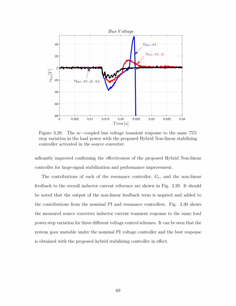
0 0.005 0.01 0.015 0.02 0.025 0.03 0.035 0.04
T ime[s]
-80
-60
-40
-20
0
20
40
vbu
s[V
]
Bus V oltage
vbus−PI
vbus−PI−R
vbus−PI−R−NL
Figure 3.28: The ac−coupled bus voltage transient response to the same 75%step variation in the load power with the proposed Hybrid Non-linear stabilizingcontroller activated in the source converter.
nificantly improved confirming the effectiveness of the proposed Hybrid Non-linear
controller for large-signal stabilization and performance improvement.
The contributions of each of the resonance controller, Gr, and the non-linear
feedback to the overall inductor current reference are shown in Fig. 3.29. It should
be noted that the output of the non-linear feedback term is negated and added to
the contributions from the nominal PI and resonance controllers. Fig. 3.30 shows
the measured source converter inductor current transient response to the same load
power step variation for three different voltage control schemes. It can be seen that the
system goes unstable under the nominal PI voltage controller and the best response
is obtained with the proposed hybrid stabilizing controller in effect.
69

0.05 0.1 0.15 0.2
T ime[s]
-4
-2
0
2
4
6
8
10
I[A
]
Nonlinear and Resonant Terms Contributions
Gr
h(vbus)
i∗l
Figure 3.29: The contributions of the resonance controller, Gr, and the non-linear feedback h( ˜vbus) term to the overall inductor current reference. Note thatthe output of the non-linear feedback is negated and summed with the outputsof the nominal PI and resonance controllers.
3.6 Robustness to Errors in Load Power Estimation
In previous sections, the effectiveness of the proposed hybrid stabilizing controller
was verified through simulation and experimental results. It was pointed out that
the design of the resonance controller, Gr, is based on the measurement of the system
bus impedance and the procedure presented in Section 2.5. The other term of the
proposed hybrid stabilizing controller is the additional feedback implementing the
non-linear function, h(vbus), given in (3.10). A nice feature of the proposed control
method is that all the required components to implement h(vbus) are locally available
to the controller. These include the voltage error signal and the voltage reference. The
only additional requirement is to obtain an estimation of the load power, PL, for the
accurate implementation of h(vbus). This estimation can be obtained using the locally-
available measurements of the converter’s inductor (or output) current and output
70

0 0.005 0.01 0.015 0.02 0.025 0.03 0.035 0.04
T ime[s]
-10
-8
-6
-4
-2
0
2
4
6
8
10
IL[A
]
Source Inductor Current
IL−PI−R−NL
IL−PI−R
IL−PI
Figure 3.30: The source inductor current response to the load power step varia-tion with PI voltage control only, IL−PI , resonance-enhanced voltage controller,IL−PI−R, and the proposed hybrid stabilizing controller, IL−PI−R−NL.
voltage. However, it is worth verifying how potential errors in the estimation of the
load power can affect the performance of the proposed hybrid stabilizing controller.
To this end, an experimental robustness study is performed on the setup shown
above in Fig. 3.20 with similar parameters. In this study, the real-time load power
estimation path based on the product of the measured inductor current and output
voltage is deactivated. Instead, a constant load power value is provided to the hybrid
stabilizing controller and the bus voltage transient response to the same 75% load
power step variation is captured. For this study three different cases are considered:
a) the hybrid stabilizing controller is provided with a constant load power
equal to 33% of the nominal load power,
b) the hybrid stabilizing controller is provided with a constant load power
equal to 50% of the nominal load power,
71
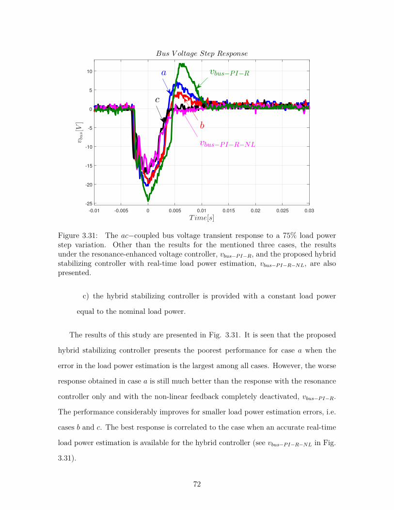
-0.01 -0.005 0 0.005 0.01 0.015 0.02 0.025 0.03
T ime[s]
-25
-20
-15
-10
-5
0
5
10
vbu
s[V
]
Bus V oltage Step Response
vbus−PI−R
vbus−PI−R−NL
a
b
c
Figure 3.31: The ac−coupled bus voltage transient response to a 75% load powerstep variation. Other than the results for the mentioned three cases, the resultsunder the resonance-enhanced voltage controller, vbus−PI−R, and the proposed hybridstabilizing controller with real-time load power estimation, vbus−PI−R−NL, are alsopresented.
c) the hybrid stabilizing controller is provided with a constant load power
equal to the nominal load power.
The results of this study are presented in Fig. 3.31. It is seen that the proposed
hybrid stabilizing controller presents the poorest performance for case a when the
error in the load power estimation is the largest among all cases. However, the worse
response obtained in case a is still much better than the response with the resonance
controller only and with the non-linear feedback completely deactivated, vbus−PI−R.
The performance considerably improves for smaller load power estimation errors, i.e.
cases b and c. The best response is correlated to the case when an accurate real-time
load power estimation is available for the hybrid controller (see vbus−PI−R−NL in Fig.
3.31).
72

Therefore, the only requirement of the non-linear feedback for accurate implemen-
tation of function h(vbus) is an estimation of the overall load power. The presented
results confirm the robustness of the proposed hybrid stabilization control scheme
to errors in the load power estimation as large as 67%. For much larger errors and
the worst case scenario, the stabilization quality degrades to the case in which the
non-linear feedback is completely deactivated and only the resonance controller, Gr,
is engaged. It must be noted that the stability is still preserved in that case but
at the cost of a degraded transient performance as compared to the case when the
non-linear feedback is also contributing to the stabilization.
3.7 Conclusion and Future Work
In this chapter the stability issue of DC power distribution systems is analyzed with
specific attention paid to large-signal transients and disturbances. A detailed large-
signal stability analysis of a DC-PDS with constant power loads is presented. The
analysis proposed a simplified reduced-order quasi-steady-state model of the sys-
tem. This model is obtained by taking advantage of the inherent two-time-scale
operation and dynamics of the system and utilizing the results of the Singular Per-
turbation theory. The large-signal stability analysis confirmed that well-designed
linear controllers can easily fail to preserve the system stability for large-signal oper-
ation. This is mainly because linear controllers are designed using linearized models
of the system which are only valid in a small-signal region around a certain operating
point. Thus, such control methods can lose system regulation in case of transients
and disturbances which are large enough to drive the system out of the small-signal
operation region. Also, the obtained model allows an explicit representation of the
system non-linearity caused by the existence of constant power loads. It is shown that
this inherent non-linearity can negatively impact the system stability and dynamic
performance, especially for large-signal transients.
73

This issue is tackled in this chapter and a hybrid stabilizing control scheme is pro-
posed based on the presented stability analysis. In the presented method, the source
converter inductor current reference is modified by incorporating two additional con-
trol inputs. To further improve system stability and performance for small-signal op-
eration, one of these inputs is used to introduce the linear resonance controller which
is designed based on passivity-based stability criterion and allowable impedance re-
gion concept (as introduced in Chapter 2). Additionally, to improve system stability
for large-signal transients, the other control input is used to properly implement a
non-linear feedback term that effectively eliminates the system inherent destabilizing
non-linearity. As a result, having the system non-linearity eliminated by the incorpo-
rated feedback term, the system exhibits purely linear dynamics during large-signal
transients. The resonance controller and the proposed non-linear feedback term form
the overall hybrid stabilizing controller that is added on top of the nominal voltage
regulator of the source converter.
The proposed hybrid stabilizing control method is effective, easy-to-implement,
and well-suited for large-signal stabilization and transient performance improvement.
A key advantage of the proposed method is that, by eliminating the system non-
linearity, it extends the region of effectiveness of the linear controllers to preserve
the system stability and performance in the case of large-signal disturbances. Unlike
most of the state-of-the-art non-linear control approaches, the proposed method has
no dependence on system parameters. This implies potential significant advantages
in terms of system robustness to parametric uncertainties and variations. Similarly,
the proposed method has no dependence on the system model, unlike other methods,
which implies that the hybrid stabilization method is easily scalable without requir-
ing any additional observer unit. The method has proven to be effective through
simulation and experimental validation. The systems that were originally unstable
for large-signal operation are well stabilized using the hybrid stabilizing controller.
74

The proposed method requires the knowledge of the total load power drawn from
the source subsystem. An experimental study is presented to verify the robustness of
the method to potential errors in the load power estimation. The results confirmed
that the proposed control method can provide good stabilization action even in case
of large errors in the load power estimation.
The presented work can be further extended in future considering the following
ideas. First, in the presented work, the stability analysis and derivation of the pro-
posed control approach are carried out considering nominal two-loop control scheme
based on proportional-integral control strategy for the source converter. Such a con-
trol scheme is very popular and is commonly adopted in various applications. Nev-
ertheless, it is worth considering other nominal control methods for the source con-
verter, e.g. direct PID-based voltage-mode control, and extend the proposed stability
analysis and stabilization methods.
Second, in this work a single source operation is considered to better represent the
fundamentals of the proposed stability analysis and stabilization method. However,
in a more realistic scenario, there are typically several source converters operating in
parallel configuration. In this case, a Droop-based current-sharing control scheme is
incorporated to ensure proportional load power sharing among several source convert-
ers [2,17]. Thus, the proposed analysis and hybrid stabilizing control methods should
be extended to the case of multi-source operation with Droop-based load sharing
control scheme.
Third, in this work the source converter is considered to be a Buck converter.
However, practically other converter topologies such as Boost and Buck-Boost are
also used in DC power distribution systems. Therefore, the extension of the pre-
sented stability analysis and proposed stabilization method to other source converter
topologies can be of interest.
75

Finally, the proposed hybrid stabilizing control method requires the knowledge of
the total load power. In multi-source operation, however, each of the source converters
provides only a portion of the total load demand. Therefore, the stabilizing converter,
in which the proposed control method is implemented, needs to estimate the overall
load power to achieve the best stabilization performance. This can be achieved using
a communication-based current sharing control scheme which provides the instanta-
neous output currents of other sources to a certain source converter. Other methods
can also be used such as the communication-less consensus-based current sharing
control scheme that is proposed in the next chapter.
76

Chapter 4
A Communication-less Consensus-based load
Current Sharing Control Scheme for DC
Power Distribution Systems
In modern DC-PDS, energy sources of different natures are interfaced to the DC
bus through several source converters which results in a distributed structure. As
opposed to centralized generation, distributed structures offer improved efficiency,
reliability, scalability, and better stability [60,61]. In a multi-source system, improper
load current sharing leads to overloading some of source converters which imposes
additional thermal stress on their components and can eventually reduce reliability
and result in cascaded failures [4, 62]. Therefore, the main control objectives in DC
systems are to enforce proportional load sharing among the participating sources and
to ensure bus voltage regulation [18,63].
The current sharing issue in DC distribution systems is a challenging problem
which is actively under research [4, 29]. The challenges are particularly critical for
on-board DC power systems, such as the shipboard DC-PDS, where high power and
dynamically varying loads must be supplied reliably by various sources [64]. In an
ideal case, if all the source converters are identical, in terms of components and
control bandwidths, they might be able to achieve a natural proportional load sharing
scheme. However, this situation almost never happens practically due to inevitable
component mismatches and differences in dynamic behaviors. To ensure proportional
load sharing among multiple sources, various methods are proposed in the literature
77

such Droop-based control schemes as well as other active control-based current sharing
methods.
In this chapter, a novel communication-less consensus-based load power shar-
ing method is proposed. The proposed method basically implements a coopera-
tive consensus-based current sharing control scheme. The main advantage of the
consensus-based algorithm applied for load sharing purposes is its reliability and the
fact that it does not disturb the bus voltage regulation. However, a fundamental
requirement for the implementation of the conventional consensus-based methods
is the existence of a physical communication network among the source converters.
This can increase system complexity and overall cost while creating a vulnerability
to cyber attacks [65, 66]. In the proposed method, however, the physical commu-
nication network is replaced with a virtual network utilizing the bus voltage as the
main medium of communication. Therefore, all the advantages of the conventional
cooperative consensus-based current sharing scheme are preserved while the need for
a physical communication network is eliminated.
4.1 State-of-the-art and background
Different current sharing methods can be classified into two categories: Droop meth-
ods and active sharing methods [4]. In the conventional Droop methods, introduced
earlier in section 1.2, a virtual series resistance is added to the output impedance of
a source converter through additional feedback loops: the output voltage decreases
as the converter’s output current increases. Droop methods allows the total load
power to be passively shared among the source converters and provide a modular
design [18]. However, the major drawbacks with Droop methods, as pointed out in
section 1.2, are the bus voltage variable drop and power sharing inaccuracy [4]. These
issues are very challenging for the operation and control of DC-PDS and generally
require additional specialized control layers which are complicating and costly [17].
78

Various active sharing methods are proposed in the literature which achieve cur-
rent sharing and overcome the problems with the conventional Droop methods [29].
Methods based on master-slave operation are proposed in the literature [67]. Al-
though effective in achieving current sharing without any voltage drop, such methods
suffer from the lack of reliability. This is because the bus voltage is basically regulated
by a master converter and this could be a single point of failure [4].
In [68, 69], the average value of the current and Droop gains are communicated
among the parallel converters to achieve current sharing. Droop gains adaptation is
proposed in [70] which is based on the information communicated among the sources.
In [61, 63], average consensus method is adopted which guarantees load power shar-
ing and relies on a communication network among the neighboring source converters.
These methods are effective but the major problem is that they require a communi-
cation network among the converters. Therefore, such approaches impose additional
costs while suffering from the lack of reliability due to the potential communication
links failures [29]. Also, such methods are prone to cyber-physical attacks which can
result in security problems by degrading the system resiliency [21].
Other methods based on ac-signal injection into the DC voltage are also available
that achieve current sharing without requiring a communication network [71, 72].
However, these method are rather complicated: most of them require the estimation
of the reactive power flow among the sources, and they require synchronization of the
injected frequencies among the source converters [29,73].
To overcome these limitations, in this chapter, a novel current sharing method
is proposed for DC power distribution systems. The proposed method relies on the
injection of small sinusoidal signals into the bus voltage which is available to all
source converters. The sinusoidal signals have their frequencies proportional to the
injecting converter’s output current. Each converter is equipped with a method based
on adaptive notch filters for decomposing the measured bus voltage to obtain the
79

frequencies of the injected signals. Consequently, a certain source converter can gain
an explicit knowledge of the output currents of other converters. Finally, a cooperative
consensus-based approach is adopted to ensure accurate proportional load current
sharing without any voltage drop at the DC bus.
In the following sections, the main idea of the proposed communication-less consensus-
based current sharing control scheme is described. Then, relevant details are pre-
sented about each of the involved blocks of the proposed load sharing scheme. Fi-
nally, the effectiveness of the proposed control method is validated through simulation
results.
4.2 Proposed current sharing method
In this section the main idea of the proposed load sharing control scheme is pre-
sented. A multi-source DC-PDS such as the one shown in Fig. 1.1 is considered.
In this system, several source power converters supply the overall load demand. In
such a multi-source system, one control objective is to achieve a current sharing
scheme among the source converters that allows them to provide a share of the total
load current proportional to their rated powers. To meet this requirement, a novel
communication-less consensus-based current sharing control scheme is proposed. The
main idea of the proposed scheme is shown pictorially in Fig. 4.1.
In the proposed control method, each source converter injects a small sinusoidal
signal into the bus voltage. In each converter, the frequency of the generated si-
nusoidal signal is proportional to its instantaneous output current and the signal is
properly scaled and injected into the converter’s duty-cycle. As a result, having all
sources injecting sinusoidal signals of frequencies proportional to their output cur-
rents, the bus voltage, that is available to all converters in parallel connection, serves
as a global medium of communication. In this sense, the bus voltage contains compo-
nents of different frequencies which are basically all the necessary information needed
80

Figure 4.1: The main idea of the proposed communication-less consensus-basedcurrent sharing scheme depicted in a multi-source system.
to enforce a distributed cooperative load sharing scheme among multiple sources
(“agents”) [61, 74]. Consider the first converter in Fig. 4.1, the bus voltage is mea-
sured and passed through a frequency decomposition block that reads the frequencies
of the injected sinusoidal components (see Read block in Fig. 4.1). Accordingly,
using this decomposition method, the converter is enabled to extract the values of
the output currents of its neighbor source converters. Then, it uses the extracted
information to implement an average consensus-based current sharing algorithm that
adjusts its output current such that a proportional load sharing is obtained globally
in the system [66].
Different methods can be used for the frequency detection such a Fast Fourier
Transform (FFT). However, in this work a method based on Adaptive Notch Filters
81

Figure 4.2: The proposed communication-less consensus-based current sharing con-trol scheme implemented in block diagram.
(ANF) is proposed. Based on this method, in each converter’s control platform, a
series of cascaded ANFs, equal to the number of source converters in the system,
are incorporated. The measured bus voltage is passed through the cascaded ANFs.
The notch frequency of each of these filters is varied adaptively until it converges to
the frequency of one of the injected sinusoidal components in the bus voltage. That
component gets significantly attenuated by the notch filter, after the notch frequency
convergence, and the signal containing the rest of the injected components is passed
to the next ANF in the chain. This continues until all ANFs converge. At the end, the
notch frequencies in the cascaded ANFs are equal to the frequencies of the injected
sinusoidal components which are proportional to the output currents of the neighbor
source converters (see Fig. 4.1).
The control block diagram of the proposed method is shown in Fig. 4.2. The
method is comprised of three major blocks. First, a sinusoidal generation and in-
82

jection block that takes in a measurement of the converter’s output current and
generates a sinusoidal signal with its frequency proportional to the measured output
current. Second, a frequency detection block based on adaptive notch filters. The
measured output (bus) voltage, that contains the injected sinusoidal components, is
fed to this block which outputs an array containing the output currents of all neigh-
boring source converters. Finally, the array of the detected output currents is fed to
a block implementing a consensus algorithm that tries to minimize the error between
the i-th converter output current and the output currents of its neighboring sources.
This algorithm adjusts the voltage reference of a certain source converter until a dis-
tributed proportional load sharing scheme is fully established and the current sharing
error converges to zero. In the following sections, more details are presented on the
functionality of each of the introduced blocks.
4.2.1 ac-Signal Injection for Communication
In the proposed method, in order to achieve current sharing, a source converter must
explicitly know the amount of load current supplied by its neighbor sources. The sim-
plest approach would be to have a communication network among the sources which
has several disadvantages as discussed earlier. These issues are obviated through the
method proposed here which is based on injecting a small sinusoidal signal into the
bus voltage. The frequency of this signal is proportional to the output current of each
source converter which is locally measurable by the injecting converter.
The proposed small sinusoidal signal injection technique is depicted in Fig. 4.3.
Based on this setup, the injected signal, uinji, can be obtained as in (4.1) wherein fi
= kfiipuoi
is the effective frequency of injection.
uinji= kai
sin(2πfit) (4.1)
83

Figure 4.3: The proposed small sinusoidal signal injection technique.
The measured output current of the converter is passed through a properly de-
signed low-pass filter, Glpf1 , to find its average value, i.e. ioi, which is then scaled
by the rated current of the converter, Iri, yielding a per-unit value. This guarantees
a current sharing scheme that is proportional to the rated power of the individual
source converter: various converters can use different values as their rated currents
to accommodate different loading percentages [70]. Note that in the especial case of
source converters with equal rated powers, the proportional scheme reduces down to
an equal-sharing one.
The gain kfiis chosen to properly scale the injection frequency of the i-th converter
to be within the range of interest depending on the converter’s sampling frequency.
Also, the gain kaiis used to adjust the injection amplitude properly. In a later section,
it will be shown that the generated signal, uinji, is added to the i-th converter’s duty
cycle such that it appears in its output voltage which is also the bus voltage and is
measured by all source converters. Therefore, the amplitude of the injection cannot
be very large and the gain kaiis used to adjust the injection strength to be within
5− 10% of the steady-state duty-cycle value.
4.2.2 A Method for the detection of the injected signals
Using the method proposed in the previous part, all source converters inject into the
bus voltage sinusoidal signals with frequencies proportional to their measured output
currents. Thus, if a certain source converter manages to decompose the measured
bus voltage to detect the frequencies of the injected sinusoidal components, it can
obtain explicit knowledge of the output currents of its neighbor sources. To this end,
84

different methods can be adopted such as the conventional FFT algorithms or other
methods such as Goertzel algorithm. The latter is previously used for the detection of
an LCL filter resonance frequency [75]. However, these methods introduce additional
computational burden and more delays into the control scheme.
To overcome these issues, in this work, an innovative approach is proposed that
employs adaptive notch filters (ANF) for frequency detection [76–78]. ANFs are very
similar to the conventional notch filters with significant attenuation at the notch
frequency applied to their input signal. The major difference is that, in ANFs, the
notch frequency is adjusted on-the-fly by means of an adaptive algorithm. Such an
adaptive mechanism allows automatic detection and elimination of a sinusoidal sig-
nal, with unknown frequency, that is immersed in the filter’s input signal. Adaptive
notch filters are well known and are applied in various areas such as radars, industrial
applications, and wireless communications [78]. The main idea of the proposed fre-
quency detection method based on ANFs and implementation details are presented
next.
The main idea
In this work, to enable a certain source converter to detect the frequencies of the
injected sinusoidal components in the bus voltage, the cascaded adaptive notch filters
are utilized [77]. In particular, for a DC-PDS with n source converters, n-1 frequency
detection blocks are connected in a cascaded fashion and are incorporated in the
control platform of each converter. Each detection block consists of an ANF block
followed by a scaling and filtering block that performs some simple post-processing
and signal conditioning.
The bus voltage contains all the injected sinusoidal components. However, a
converter knows its own output current because it is locally measured. Thus, in the
i-th converter, the ac-coupled bus voltage, vbus, is fed to a regular notch filter (NF)
85

Figure 4.4: Three cascaded detection blocks incorporated in the first converter’scontrol platform for a DC-PDS with three source converters.
whose notch frequency is set equal to the injection frequency of that converter, that
is proportional to its own output current. Therefore, the i-th injected component will
be eliminated from the measured voltage and the signal containing the components
injected by other converters will be passed to the first detection block. As a result, a
converter only needs n-1 cascaded ANF-based frequency detection blocks.
The ANF, within each block, implements an adaptive gradient descent algorithm
which varies the notch frequency of that filter, ωni, until it matches the frequency
of a sinusoidal components in the input signal, e.g. ωi = 2πfi. Once the adaptive
algorithm converges, i.e. ωni= ωi, that sinusoidal component will be significantly
attenuated from the input signal. Then, the signal containing the rest of the compo-
nents is passed to the next detection block in the chain. The same will happen in the
ANFs of other blocks until they all converge and all the components are attenuated.
Within each detection block, the outputs of the ANFs are their notch frequencies,
ωni, after convergence of the adaptive algorithm. The obtained notch frequencies are
basically equivalent to the frequencies of the injected sinusoidal components which
are, in turn, proportional to the output currents of the other source converters. Thus,
an array of all output currents, except for the i-th converter, is obtained after some
simple post-processing and scaling. For a DC-PDS with three source converters,
two ANF-based detection blocks are incorporated in the control platform of each
86

converter. For example, the detection blocks implemented in the first converter are
depicted in Fig. 4.4.
Implemented Adaptive Notch Filter (ANF)
Various implementations of adaptive notch filters are proposed in the related liter-
ature. Most popular ANFs are typically based on the second-order infinite impulse
response (IIR) notch filters [78]. In this work, the method adopted for the design
and implementation of the ANF block is a constrained poles and zeros-based ANF
(CPZ-ANF) approach proposed in [76].
The transfer function of the notch filter, Hn(z), is given in (4.2) [79]. In this
transfer function a(k) is the parameter that controls the notch frequency, ωn, at time
k and ρ is the parameter that sets the notch width, B. The notch filter given in
(4.2) is basically a second-order infinite impulse response filter. This IIR filter has
a pair of complex conjugate zeros that are placed on the unit circle to create a very
deep notch. The bandwidth of the notch, that determines the selectivity of the filter,
is controlled by a pair of complex conjugate poles which are located at distance ρ
from the origin. The angle of these poles and zeros with respect to the horizontal
line sets the frequency, ωn. The pole-zero map of the notch filter for different notch
frequencies is shown in Fig. 4.5.
Hn(z) = y(z)x(z) = 1 + a(k)z−1 + z−2
1 + ρa(k)z−1 + ρ2z−2 (4.2)
The relationship between a(k) and the notch frequency as well as that of ρ and
the notch width are given in (4.3) and (4.4).
a(k) = −2 cos(ωn(k)) (4.3)
B = π(1− ρ) (4.4)
87

The frequency response of a notch filter with transfer function Hn(z) for ωn = 0.5π
and ρ = 0.99 is shown in Fig. 4.6. It has a band-stop response with a very selective
notch, controlled by the choice of ρ, occurring at the specified notch frequency, ωn.
For the adaptation of a(k) parameter, or equivalently the notch frequency ωn, a
gradient descent algorithm, proposed in [80], is used with the implementation pro-
posed in [79]. In this algorithm, the cost function is given by the mean-square of
the output of the filter at time-instant k, i.e. E[y2(k)] [80]. This is minimized by
controlling the parameter a(k) following the update equation given in (4.5) where
µ is the parameter update step-size and ∇(k) is the instantaneous estimate of the
gradient of E[y2(k)] with respect to a(k).
a(k + 1) = a(k)− µ∇(k) (4.5)
The gradient estimation, ∇(k), can be found as in (4.6) and (4.7) where x(k) is
the input to the filter. The approximation in (4.7) is valid for a sufficiently small
step-size, µ, which ensures that a(k) varies much slower than x(k) [80].
∇(k) = 2y(k)∂y(k)∂a(k) (4.6)
s(k) = ∂y(k)∂a(k) ≈ x(k − 1)− ρy(k − 1)− ρa(k)s(k − 1)− ρ2s(k − 2) (4.7)
The signal s(k) is needed to calculate the instantaneous value of ∇(k) and can
be obtained with the simpler transfer function implementation given in (4.8) which
is obtained using (4.2). Hs(z) is called the gradient filter and its frequency response
if shown in Fig. 4.7. It has a band-pass response with its peak occurring at the filter
notch frequency.
Hs(z) = s(z)x(z) = (1− ρ)z−1 − ρ(1− ρ)z−3
1 + ρa(k)z−1 + ρ2z−2 (4.8)
88
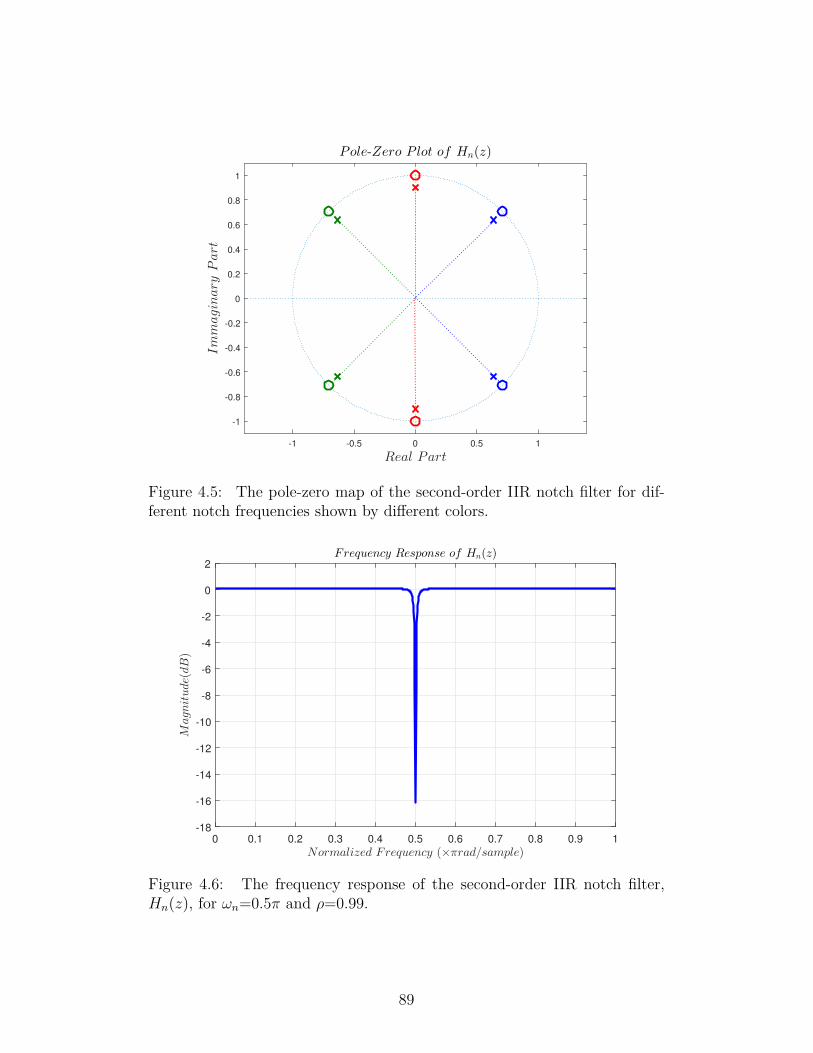
-1 -0.5 0 0.5 1
Real Part
-1
-0.8
-0.6
-0.4
-0.2
0
0.2
0.4
0.6
0.8
1
ImmaginaryPart
P ole-Zero P lot of Hn(z)
Figure 4.5: The pole-zero map of the second-order IIR notch filter for dif-ferent notch frequencies shown by different colors.
0 0.1 0.2 0.3 0.4 0.5 0.6 0.7 0.8 0.9 1
Normalized Frequency (×πrad/sample)
-18
-16
-14
-12
-10
-8
-6
-4
-2
0
2
Magnitude(dB)
Frequency Response of Hn(z)
Figure 4.6: The frequency response of the second-order IIR notch filter,Hn(z), for ωn=0.5π and ρ=0.99.
89

Based on (4.6) and (4.7), the update algorithm in (4.5) can be rewritten as the
expression given in (4.9).
a(k + 1) = a(k)− 2µy(k)s(k) (4.9)
A block diagram representation of the adaptive notch filter is shown in Fig. 4.8
where x(k) is the input to the ANF and the notch frequency, ωn, is the desired
output of the block. It must be noted that ωn is the adaptive filter’s notch frequency
normalized by the sampling frequency.
4.2.3 Current Sharing Using a Consensus Protocol
In a network of dynamic systems (or agents), consensus means that the systems reach
an agreement regarding the value of a certain quantity or state-variable [74]. Var-
ious distributed consensus-based control schemes are proposed in the literature for
current sharing and voltage regulation of DC systems [29,63,70]. These methods are
effective in achieving such control objectives and provide particular advantages for
load sharing purposes including ensuring current sharing without disturbing the bus
voltage regulation. However, almost all of the consensus-based methods exclusively
rely on the existence of a communication network among different source converters.
Consequently, several issues have been found with such methods such as lack of relia-
bility, stability problems due to inherent delays, additional hardware, cost, potential
security issues, and complexity [4, 18,66].
Using the proposed sinusoidal injection and ANF-based frequency detection meth-
ods, the need for a physical communication channel is effectively eliminated and thus
the related issues can be avoided. As a result, the methods proposed in the previous
sections are adopted along with the conventional consensus protocol which is given
in (4.10) for the i-th source converter [74].
90

0 0.1 0.2 0.3 0.4 0.5 0.6 0.7 0.8 0.9 1
Normalized Frequency (×πrad/sample)
-90
-80
-70
-60
-50
-40
-30
-20
-10
0
Magnitude(dB)
Frequency Response of Hs(z)
Figure 4.7: The frequency response of the gradient filter, Hs(z), given in (4.8) forthe normalized notch frequency of ωn=0.5π and ρ=0.99.
Figure 4.8: The block diagram representation of the implemented adaptive notchfilter (ANF).
91

δvi =∑j∈Ni
(ipuoj − ipuoi ) (4.10)
In (4.10), ipuoj is the per-unit output current of the j-th converter which is detected
by the proposed ANF-based frequency detection block, Ni is a set that includes all
the neighbor source converters to the i-th converter, and ipuoi is the per-unit output
current of the i-th source converter itself.
This simple control law, generates a voltage correction term, δvi, by comparing
the local per-unit output current with the detected per-unit currents of other source
converters. This correction term is then added to the voltage reference of the i-th
source converter. As a result, the output voltage of this source converter is adjusted
such that the difference between its output current and those of the other source
converters is minimized. More details on current sharing schemes based on consensus
algorithm can be found in [29,63,70].
4.2.4 The overall current sharing control scheme
In this section, some final considerations and discussions related to the proposed
current sharing control scheme are presented.
One consideration relates to the steady-state operation of the proposed current
sharing method. In particular, in steady-state, the output currents of all converters
are equal and they inject sinusoidal signals with similar frequencies. Therefore, if the
proposed detection method, shown in Fig. 4.4, is adopted without any modifications,
once an ANF converges, it removes all the components in the input signal and nothing
would be left for the rest of the detection blocks in the chain. This may cause some
convergence and stability issues for the adaptive algorithms implemented in the filter.
This issue can be avoided with a simple modification as described below.
The idea is to use a simple linear transformation to map the output current of the
i-th source converter, that determines its injection frequency, to a pre-specified range
92

Figure 4.9: The modified sinusoidal injection technique.
Figure 4.10: The modified ANF-based frequency detection block.
within [Iil , Iiu ]. This range is defined distinctly for each of the source converters.
As a result, despite the fact that, in steady-state and after convergence, the actual
output currents of different converters are the same, the sinusoidal signals are injected
with frequencies in different pre-defined ranges. In this scenario, a certain converter
can obtain the actual output currents of the other sources by inverse-mapping the
detected notch frequencies. Using this technique, the proposed injection and detection
methods can be used with the simple modifications shown in Fig. 4.9 and Fig. 4.10.
In Fig. 4.9, block T implements a linear mapping as given in (4.11). The function
T (ioi) maps any value of ioi
∈ [Ii−min, Ii−max] to io−ti ∈ [Iil , Iiu ]. Note that Ii−min and
Ii−max are the minimum and maximum allowed currents depending on a converter’s
operational requirements and protections. Also, note that Iil and Iiu are chosen as
lower-bound and upper-bound for a certain converter. Therefore, a source converter
injects sinusoidal signals with frequencies bounded to fi ∈ [fil , fiu ], where fil = kfiIil
and fiu = kfiIiu . Likewise, in Fig. 4.10, the block Tinv (io−ti) implements the linear
inverse-mapping functions which is basically (4.11), rearranged to obtain ioi.
io−ti = (ioi− Ii−min) Iiu − Iil
Ii−max − Ii−min+ Iil (4.11)
93

Figure 4.11: The i-th converter’s control platform enabled with the proposedcommunication-less consensus-based current sharing scheme (the related blocks arehighlighted in yellow).
Another consideration is related to the fact that, in the proposed scheme, the bus
voltage is the only medium of communication among the source converters. Therefore,
some potential issues could arise in case of high noise levels which is probable in
practical systems. To improve the noise immunity, a low-pass filter, Glpf2 , is used
in the detection block in Fig. 4.10, after the inverse-mapping block, which results
in an almost constant detected value and eliminates any potential fluctuations. The
inclusion of the additional low-pass filter is not necessary for the operation of the
proposed scheme. However, incorporation of this filter will increase the robustness
for the operation in noisy and high-disturbance environments.
The overall proposed current sharing control scheme for the i-th converter in a
DC-PDS with multiple sources is shown in Fig. 4.11. The three introduced parts,
including the sinusoidal injection block, shown in Fig. 4.9, the ANF-based frequency
detection block, shown in Fig. 4.4 with the individual blocks as in Fig. 4.10, and the
cooperative consensus protocol given in (4.10), are put together to form the proposed
current sharing control scheme.
94

In Fig. 4.11, the global voltage reference, vref , is the desired bus voltage set by
the higher-level controllers [29]. The output voltage correction term, δvi, is generated
by the consensus controller. The protocol uses the i-th converter’s per-unit output
current, ipuoi, and the output currents of other source converters which are detected
by the ANF-based detection block. Additionally, this converter indirectly communi-
cates the information about its own share of the total load current by generating and
injecting a sinusoidal signal proportional to its measured output current. The gener-
ated signal, uinji , is added directly to the converter’s duty-cycle: this will simplify the
operation of the proposed scheme by allowing its operation in a frequency range well
beyond the control bandwidths. This scheme is implemented in all source converters
which guarantees that the control objective of proportional load sharing is achieved.
4.3 Simulation Results
To verify the effectiveness of the proposed current sharing method the system shown
in Fig. 4.12 is simulated in Matlab/Simulink. In this system, three source Buck
converters are supplying a load subsystem that includes passive loads and a voltage
source inverter (VSI) which behaves like a constant power load. The bus voltage, Vbus,
is 200V and the total load power is PL=5kW . The parameters used for this simulation
study are reported in Fig. 4.13. The parameters of the sinusoidal injection block are
fo1 which is the cut-off frequency of Glpf1 , Iil and Iiu , and kfi. The parameters of the
ANF-based detection block are ρ that sets the selectivity of the filter, µi which is the
adaptive algorithm’s step-size, and fo2 which is the cut-off frequency of Glpf2 .
The two low-pass filters, Glpf1 and Glpf2 , are used for averaging purposes and so,
for simplicity, are chosen to be first-order filters with sufficiently low cut-off frequen-
cies. The parameters Iil , Iiu , and kfiare chosen such that different converters inject
signals with well separated frequencies. The minimum and the maximum allowed
currents for all three converters are assumed to be 1A and 30A, respectively. Also,
95

Figure 4.12: The simulated DC-PDS with three source converters and a load sub-system including a three-phase VSI some passive load. The total load power is PL =5kW .
Figure 4.13: The parameters of the signal injection and detection blocksof the proposed current sharing method for the simulated DC-PDS.
the injection amplitude gains, kai, for all converters are chosen to be 0.15. In each
converter, the adopted regular notch filter is based on Hn(z), given in (4.2), with ρ
= 0.99, and the notch frequency set based on the instantaneous injection frequency
of that converter which is proportional to its output current.
96

Two scenarios are considered: one is when the three sources are with identical
rated currents, for the case of equal current sharing, and the other one when the
sources have different current ratings, for the more general case of proportional load
sharing. The bus voltage and the output currents of the three sources are monitored
in the time-domain. The performance of the proposed current sharing method is
evaluated for steady-state operation and in response to step variations in the load
power. The results are presented in Fig. 4.14 to Fig. 4.19.
In Fig. 4.14, the bus voltage and the output currents of the three sources are
shown for the case of equal current sharing. In this case, all three converters are
assumed to have similar rated currents with Ir1,2,3 = 10A. It is seen that with the
proposed current sharing scheme being initially deactivated, the converters, which
have different dynamic and control bandwidths, pick up different shares of the total
load current which is 25A. In particular, the third converter provides the largest
share of the total current and then the second converter has the largest share of the
total load. However, once the proposed method is activated, at t=0.65s, the output
currents begin to converge together and, after about 0.2s, they reach a consensus
value of about 8.33A.
The zoom-in of the bus voltage, in Fig. 4.14, shows that the injected sinusoidal
signals, for the purpose of current sharing, are very small and do not disturb the
bus voltage regulation. To assess the performance of the proposed scheme under
transients, step variations occur in the load power starting at t=1.5s. It is seen
that the proposed control method is capable to guarantee accurate dynamic current
sharing with good transient performance.
Fig. 4.15 and Fig. 4.16 show the performance of the proposed ANF-based de-
tection blocks for the first and the second source converters. The results for the
third converter is similar and so omitted for brevity. These figures show the output
currents, measured at the output of the converters against the currents estimated by
97
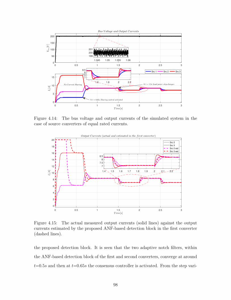
0 0.5 1 1.5 2 2.5 3
0
50
100
150
200
Vbu
s[V
]
Bus V oltage and Output Currents
0 0.5 1 1.5 2 2.5 3
Time[s]
0
5
10
15
I o[A
]
Src 1 Src 2 Src 3
1.6 1.8 2 2.2
7
7.5
8
8.5
1.045 1.05 1.055 1.06
199
200
201
No Current Sharing
@ t = 0.65s Sharing control activated
@ t = 1.5s Load power step-changes
Figure 4.14: The bus voltage and output currents of the simulated system in thecase of source converters of equal rated currents.
0 0.5 1 1.5 2 2.5 3
Time[s]
0
2
4
6
8
10
12
14
16
18
20
I o[A
]
Output Currents (actual and estimated in the first converter)
Src 2
Src 3
Src 2 est
Src 3 est
1.4 1.5 1.6 1.7 1.8 1.9 2 2.1 2.2
7
7.5
8
8.5
Figure 4.15: The actual measured output currents (solid lines) against the outputcurrents estimated by the proposed ANF-based detection block in the first converter(dashed lines).
the proposed detection block. It is seen that the two adaptive notch filters, within
the ANF-based detection block of the first and second converters, converge at around
t=0.5s and then at t=0.65s the consensus controller is activated. From the step vari-
98
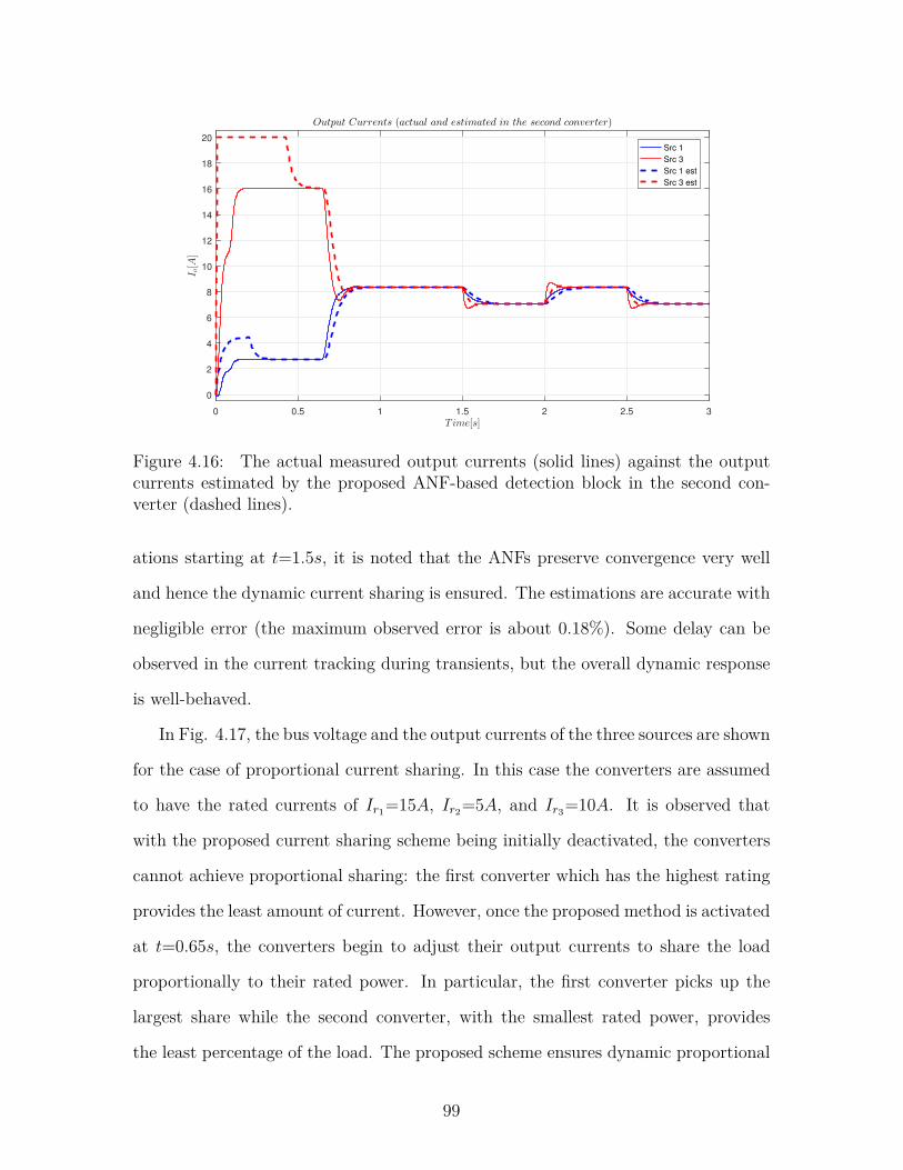
0 0.5 1 1.5 2 2.5 3
Time[s]
0
2
4
6
8
10
12
14
16
18
20
I o[A
]
Output Currents (actual and estimated in the second converter)
Src 1
Src 3
Src 1 est
Src 3 est
Figure 4.16: The actual measured output currents (solid lines) against the outputcurrents estimated by the proposed ANF-based detection block in the second con-verter (dashed lines).
ations starting at t=1.5s, it is noted that the ANFs preserve convergence very well
and hence the dynamic current sharing is ensured. The estimations are accurate with
negligible error (the maximum observed error is about 0.18%). Some delay can be
observed in the current tracking during transients, but the overall dynamic response
is well-behaved.
In Fig. 4.17, the bus voltage and the output currents of the three sources are shown
for the case of proportional current sharing. In this case the converters are assumed
to have the rated currents of Ir1=15A, Ir2=5A, and Ir3=10A. It is observed that
with the proposed current sharing scheme being initially deactivated, the converters
cannot achieve proportional sharing: the first converter which has the highest rating
provides the least amount of current. However, once the proposed method is activated
at t=0.65s, the converters begin to adjust their output currents to share the load
proportionally to their rated power. In particular, the first converter picks up the
largest share while the second converter, with the smallest rated power, provides
the least percentage of the load. The proposed scheme ensures dynamic proportional
99

0 0.5 1 1.5 2 2.5 3
0
50
100
150
200
Vbu
s[V
]
Bus V oltage and Output Currents
0 0.5 1 1.5 2 2.5 3
Time[s]
0
5
10
15
I o[A
]
Src 1 Src 2 Src 3
1.1 1.102 1.104 1.106 1.108
199
200
201
No Current Sharing
@ t = 1.5s Load power step-changes
@ t = 0.65s Sharing control activated
Figure 4.17: The bus voltage and output currents of the simulated system in thecase of source converters with different rated currents.
sharing when the step variations occur in the load power starting at t=1.5s. Also, the
zoom-in of the bus voltage shows that the injected sinusoidal signals do not disturb
the normal operation of the system.
Fig. 4.18 and Fig. 4.19 show the performance of the proposed ANF-based detec-
tion block for the first and the second source converters under proportional current
sharing. These figures show the output currents, measured at the output of the con-
verters, against the currents estimated by the proposed detection block. It is seen
that both ANFs, in each converter, converge at around t=0.5s in an accurate manner
with minimal error (the maximum observed error is less than 0.15%). The conver-
gence is well preserved in all cases, even with the step variations starting at t=1.5s
which implies that the dynamic current sharing is ensured.
In all the above results, it is seen that the bus voltage regulation is unaffected
by the proposed current sharing scheme. This is unlike the conventional methods,
such as Droop control, where additional control layers and complicating measures are
required to compensate the bus voltage drop introduced by current sharing control.
100

0 0.5 1 1.5 2 2.5 3
Time[s]
0
2
4
6
8
10
12
14
16
18
20
I o[A
]
Output Currents (actual and estimated in the first converter)
Src 2
Src 3
Src 2 est
Src 3 est
Figure 4.18: The actual measured output currents (solid lines) against the outputcurrents estimated by the proposed ANF-based detection block in the first converter(dashed lines).
0 0.5 1 1.5 2 2.5 3
Time[s]
0
2
4
6
8
10
12
14
16
18
20
I o[A
]
Output Currents (actual and estimated in the second converter)
Src 1
Src 3
Src 1 est
Src 3 est
Figure 4.19: The actual measured output currents (solid lines) against the outputcurrents estimated by the proposed ANF-based detection block in the second con-verter (dashed lines).
4.4 Conclusion and Future Work
In this chapter the load sharing problem of DC power distribution systems is con-
sidered. A novel communication-less consensus-based load current sharing control
101

scheme is proposed. In this method, a virtual communication network is established
among the source converters which replaces a physical network that is convention-
ally needed in similar approaches. To achieve this, the source converters inject small
sinusoidal components into the bus voltage. The frequencies of these components
are proportional to the output currents of each of the sources. Likewise, a frequency
detection method based on adaptive notch filters is proposed. In this method, a
cascade of ANFs is implemented in the control platform of each converter. The pro-
posed ANF-based method enables each source converter to effectively extract the
needed information for current sharing control only from the measured bus voltage.
The proposed methods are combined with the average consensus algorithm to form
a cooperative control scheme that guarantees proportional and equal load sharing
among the paralleled source converters. The presented simulation results confirm
the effectiveness and very good performance of the proposed current sharing control
method.
The presented work can be further extended in future considering the following
ideas. First, the steady-state and dynamic performance of the proposed load sharing
method should be studied in more details through Experimental validation. Various
implementation and operation aspects as well as proper design guidelines should be
provided. It must be noted that for the experimental results to be relevant and
meaningful, it is recommended that the experiments be carried out on a system
with at least three source converters. The main reason relates to the cooperative
control scheme and graph theory concepts behind the communication network design
procedure. More details can be found in the relevant literature such as [29,61].
Second, considering a hierarchical control structure, the proposed method is more
suited for implementation at the primary control layer [3, 17]. However, in the case
of a Droop-controller DC system, the proposed method can be implemented at a
secondary level to compensate for bus voltage drop caused by Droop control. This
102

Figure 4.20: The proposed current sharing method can be used at secondary levelto compensate for bus voltage drop caused by a Droop-based current sharing imple-mented at the primary level.
idea is shown in Fig. 4.20. In particular, the same virtual communication network is
established and a voltage correction term is generated using the consensus algorithm
that compensates for the bus voltage drop caused by the operation of the Droop
control.
Third, in the proposed method, it is assumed that all source converters are inject-
ing properly generated sinusoidal components in the bus voltage. This implies that a
fully connected communication network is established and n-1 adaptive notch filters
103

must be used in each converter. For very large-scale systems with a large number
of sources, some scalability issues may arise using the proposed method due to the
large number of required ANFs. This issue can be avoided by taking advantage of the
consensus algorithm properties and by a more careful design of the communication
graph based on which the sources inject sinusoidal signals. This extension will allow
equally good results, in terms of load sharing performance, to be achieved relying on
a sparse communication network which allows a lower number of ANFs to be utilized
in each converter.
Fourth, in this work the effect of line impedance was neglected. This is an ac-
ceptable approximation for relatively small systems. However, the line impedance
is non-negligible for large-scale and extended DC systems. Thus, the effect of line
impedance on the proposed load sharing method should be studied.
Finally, the hybrid stabilizing control method proposed in the previous chapter
requires the knowledge of the total load power. This is easy to be estimated in a single
source system. However, in a multi-source system, each source provides a certain
amount of the total load demand. So, the converter that performs the stabilization
needs to somehow obtain an estimation of the total load so that it can implement the
proposed stabilizing control method. To cope with this issue, the proposed current
sharing method can be used along with the hybrid stabilizing controller. This idea
is shown in Fig. 4.21. The current sharing control scheme provides an estimation of
the output currents of all source converters. Thus, the stabilizing source converter
can easily calculate the total load demand. The combination of these two methods
guarantees accurate current sharing and stability of DC systems.
104

Figure 4.21: The proposed current sharing method can be used along with the hy-brid stabilization method, introduced in the previous chapter, to ensure proportionalcurrent sharing and stability of DC systems.
105

Bibliography[1] F. Blaabjerg, A. Consoli, J. A. Ferreira, and J. D. van Wyk, “The future of
electronic power processing and conversion,” IEEE Transactions on Power Elec-tronics, vol. 20, no. 3, pp. 715–720, 2005.
[2] T. Dragicevic, J. C. Vasquez, J. M. Guerrero, and D. Skrlec, “Advanced lvdcelectrical power architectures and microgrids: A step toward a new generationof power distribution networks.” IEEE Electrification Magazine, vol. 2, no. 1, pp.54–65, March 2014.
[3] Z. Jin, L. Meng, J. M. Guerrero, and R. Han, “Hierarchical control design for ashipboard power system with dc distribution and energy storage aboard futuremore-electric ships,” IEEE Transactions on Industrial Informatics, vol. 14, no. 2,pp. 703–714, Feb 2018.
[4] Y. Han, X. Ning, P. Yang, and L. Xu, “Review of power sharing, voltage restora-tion and stabilization techniques in hierarchical controlled dc microgrids,” IEEEAccess, vol. 7, pp. 149 202–149 223, 2019.
[5] H. Zhang, F. Mollet, C. Saudemont, and B. Robyns, “Experimental validation ofenergy storage system management strategies for a local dc distribution systemof more electric aircraft,” IEEE Transactions on Industrial Electronics, vol. 57,no. 12, pp. 3905–3916, Dec 2010.
[6] S. D. Sudhoff, S. Pekarek, B. Kuhn, S. Glover, J. Sauer, and D. Delisle, “Navalcombat survivability testbeds for investigation of issues in shipboard power elec-tronics based power and propulsion systems,” in IEEE Power Engineering Soci-ety Summer Meeting,, vol. 1, July 2002, pp. 347–350 vol.1.
[7] M. Farhadi and O. Mohammed, “Adaptive energy management in redundanthybrid dc microgrid for pulse load mitigation,” IEEE Transactions on SmartGrid, vol. 6, no. 1, pp. 54–62, 2015.
[8] M. Farhadi and O. A. Mohammed, “Performance enhancement of actively con-trolled hybrid dc microgrid incorporating pulsed load,” IEEE Transactions onIndustry Applications, vol. 51, no. 5, pp. 3570–3578, 2015.
106

[9] A. Riccobono, M. Cupelli, A. Monti, E. Santi, T. Roinila, H. Abdollahi, S. Ar-rua, and R. A. Dougal, “Stability of shipboard dc power distribution: Onlineimpedance-based systems methods,” IEEE Electrification Magazine, vol. 5, no. 3,pp. 55–67, Sept 2017.
[10] A. Riccobono and E. Santi, “Comprehensive review of stability criteria fordc power distribution systems,” IEEE Transactions on Industry Applications,vol. 50, no. 5, pp. 3525–3535, Sept 2014.
[11] A. Emadi, A. Khaligh, C. H. Rivetta, and G. A. Williamson, “Constant powerloads and negative impedance instability in automotive systems: definition, mod-eling, stability, and control of power electronic converters and motor drives,”IEEE Transactions on Vehicular Technology, vol. 55, no. 4, pp. 1112–1125, July2006.
[12] M. Belkhayat, R. Cooley, and A. Witulski, “Large signal stability criteria fordistributed systems with constant power loads,” in Proceedings of PESC ’95 -Power Electronics Specialist Conference, vol. 2, June 1995, pp. 1333–1338 vol.2.
[13] J. G. Ciezki and R. W. Ashton, “The design of stabilizing controls for ship-board dc-to-dc buck choppers using feedback linearization techniques,” in PESC98 Record. 29th Annual IEEE Power Electronics Specialists Conference (Cat.No.98CH36196), vol. 1, May 1998, pp. 335–341 vol.1.
[14] E. Santi, H. Y. Cho, A. B. Barkley, D. Martin, and A. Riccobono, “Tools toaddress system level issues in power electronics: The digital network analyzermethod and the positive feedforward control technique,” in 8th InternationalConference on Power Electronics - ECCE Asia, May 2011, pp. 2106–2113.
[15] R. D. D. Middlebrook, “Input filter consideration in design and application ofswitching regulators,” in IEEE Ind. Applicat. Soc. Annu. Meeting, 1976, pp.366–382.
[16] C. M. Wildrick, F. C. Lee, B. H. Cho, and B. Choi, “A method of definingthe load impedance specification for a stable distributed power system,” IEEETransactions on Power Electronics, vol. 10, no. 3, pp. 280–285, May 1995.
[17] J. M. Guerrero, J. C. Vasquez, J. Matas, L. G. de Vicuna, and M. Castilla,“Hierarchical control of droop-controlled ac and dc microgrids-a general approachtoward standardization,” IEEE Transactions on Industrial Electronics, vol. 58,no. 1, pp. 158–172, Jan 2011.
107

[18] T. Dragičević, X. Lu, J. C. Vasquez, and J. M. Guerrero, “Dc microgrids—part i:A review of control strategies and stabilization techniques,” IEEE Transactionson Power Electronics, vol. 31, no. 7, pp. 4876–4891, July 2016.
[19] Shiguo Luo, Zhihong Ye, Ray-Lee Lin, and F. C. Lee, “A classification andevaluation of paralleling methods for power supply modules,” in 30th AnnualIEEE Power Electronics Specialists Conference. Record. (Cat. No.99CH36321),vol. 2, July 1999, pp. 901–908 vol.2.
[20] C. Liu, J. Zhao, S. Wang, W. Lu, and K. Qu, “Active identification method forline resistance in dc microgrid based on single pulse injection,” IEEE Transac-tions on Power Electronics, vol. 33, no. 7, pp. 5561–5564, July 2018.
[21] H. Modares, B. Kiumarsi, F. L. Lewis, F. Ferrese, and A. Davoudi, “Resilientand robust synchronization of multiagent systems under attacks on sensors andactuators,” IEEE Transactions on Cybernetics, vol. 50, no. 3, pp. 1240–1250,March 2020.
[22] F. Gao, S. Bozhko, A. Costabeber, G. Asher, and P. Wheeler, “Control designand voltage stability analysis of a droop-controlled electrical power system formore electric aircraft,” IEEE Transactions on Industrial Electronics, vol. 64,no. 12, pp. 9271–9281, Dec 2017.
[23] L. Chen, S. Shao, Q. Xiao, L. Tarisciotti, P. W. Wheeler, and T. Dragiče-vić, “Model predictive control for dual-active-bridge converters supplying pulsedpower loads in naval dc micro-grids,” IEEE Transactions on Power Electronics,vol. 35, no. 2, pp. 1957–1966, 2020.
[24] N. Doerry, “Next Generation Integrated Power Systems NGIPS Technology De-velopment Roadmap,” 2007, p. 120.
[25] G. Sulligoi, D. Bosich, G. Giadrossi, L. Zhu, M. Cupelli, and A. Monti, “Mul-ticonverter medium voltage dc power systems on ships: Constant-power loadsinstability solution using linearization via state feedback control,” IEEE Trans-actions on Smart Grid, vol. 5, no. 5, pp. 2543–2552, 2014.
[26] F. Chen, R. Burgos, D. Boroyevich, J. C. Vasquez, and J. M. Guerrero, “Investi-gation of nonlinear droop control in dc power distribution systems: Load sharing,voltage regulation, efficiency, and stability,” IEEE Transactions on Power Elec-tronics, vol. 34, no. 10, pp. 9404–9421, 2019.
108

[27] A. Khodamoradi, G. Liu, P. Mattavelli, T. Caldognetto, and P. Magnone, “Anal-ysis of an online stability monitoring approach for dc microgrid power convert-ers,” IEEE Transactions on Power Electronics, vol. 34, no. 5, pp. 4794–4806,2019.
[28] J. Siegers, S. Arrua, and E. Santi, “Stabilizing controller design for multibusmvdc distribution systems using a passivity-based stability criterion and positivefeedforward control,” IEEE Journal of Emerging and Selected Topics in PowerElectronics, vol. 5, no. 1, pp. 14–27, March 2017.
[29] L. Meng, Q. Shafiee, G. F. Trecate, H. Karimi, D. Fulwani, X. Lu, and J. M.Guerrero, “Review on control of dc microgrids and multiple microgrid clusters,”IEEE Journal of Emerging and Selected Topics in Power Electronics, vol. 5,no. 3, pp. 928–948, Sep. 2017.
[30] X. Zhang, Q. C. Zhong, andW. L. Ming, “Stabilization of a cascaded dc convertersystem via adding a virtual adaptive parallel impedance to the input of the loadconverter,” IEEE Transactions on Power Electronics, vol. 31, no. 3, pp. 1826–1832, March 2016.
[31] L. Guo, S. Zhang, X. Li, Y. W. Li, C. Wang, and Y. Feng, “Stability analy-sis and damping enhancement based on frequency-dependent virtual impedancefor dc microgrids,” IEEE Journal of Emerging and Selected Topics in PowerElectronics, vol. 5, no. 1, pp. 338–350, 2017.
[32] X. Zhang, Q. Zhong, V. Kadirkamanathan, J. He, and J. Huang, “Source-sideseries-virtual-impedance control to improve the cascaded system stability andthe dynamic performance of its source converter,” IEEE Transactions on PowerElectronics, vol. 34, no. 6, pp. 5854–5866, 2019.
[33] A. Aldhaheri and A. H. Etemadi, “Stabilization and performance preservationof dc–dc cascaded systems by diminishing output impedance magnitude,” IEEETransactions on Industry Applications, vol. 54, no. 2, pp. 1481–1489, 2018.
[34] S. K. Pidaparthy, B. Choi, and Y. Kim, “A load impedance specification of dcpower systems for desired dc-link dynamics and reduced conservativeness,” IEEETransactions on Power Electronics, vol. 34, no. 2, pp. 1407–1419, 2019.
[35] D. N. Zmood and D. G. Holmes, “Stationary frame current regulation of pwminverters with zero steady-state error,” IEEE Transactions on Power Electronics,vol. 18, no. 3, pp. 814–822, 2003.
109

[36] R. W. Erickson, Fundamentals of Power Electronics, 2002, vol. 49.
[37] L. Corradini, Digital Control of High-Frequency Switched-Mode Power Convert-ers, 2015.
[38] H. Abdollahi, S. Arrua, T. Roinila, and E. Santi, “A novel dc power distribu-tion system stabilization method based on adaptive resonance-enhanced voltagecontroller,” IEEE Transactions on Industrial Electronics, pp. 1–1, 2018.
[39] T. Roinila, H. Abdollahi, S. Arrua, and E. Santi, “Real-time stability analysisand control of multi-converter systems by using mimo-identification techniques,”IEEE Transactions on Power Electronics, pp. 1–1, 2018.
[40] H. Abdollahi, A. Khodamoradi, E. Santi, and P. Mattavelli, “Online busimpedance estimation and stabilization of dc power distribution systems: Amethod based on source converter loop-gain measurement,” in 2020 IEEE Ap-plied Power Electronics Conference and Exposition (APEC), 2020, pp. 3371–3378.
[41] H. Abdollahi, T. Roinila, S. Arrua, and E. Santi, “Online stabilization of dcpower distribution systems applying mimo-identification method and resonance-enhanced voltage controller,” in 2019 IEEE Energy Conversion Congress andExposition (ECCE), 2019, pp. 990–997.
[42] T. Roinila, H. Abdollahi, S. Arrua, and E. Santi, “Adaptive control of dcpower distribution systems: Applying pseudo-random sequences and fouriertechniques,” in 2018 International Power Electronics Conference (IPEC-Niigata2018 -ECCE Asia), May 2018, pp. 1719–1723.
[43] W. Xie, M. Han, W. Cao, J. M. Guerrero, and J. Vasquez, “System-level large-signal stability analysis of droop-controlled dc microgrids,” IEEE Transactionson Power Electronics, pp. 1–1, 2020.
[44] K. Ogata, Modern Control Engineering, 4th ed. Prentice Hall PTR, 2001.
[45] S. Ansari, A. Chandel, and M. Tariq, “A comprehensive review on power con-verters control and control strategies of ac/dc microgrid,” IEEE Access, pp. 1–1,2020.
[46] C. H. Rivetta, A. Emadi, G. A. Williamson, R. Jayabalan, and B. Fahimi, “Anal-ysis and control of a buck dc-dc converter operating with constant power load in
110

sea and undersea vehicles,” IEEE Transactions on Industry Applications, vol. 42,no. 2, pp. 559–572, March 2006.
[47] Y. Gu, X. Xiang, W. Li, and X. He, “Mode-adaptive decentralized control forrenewable dc microgrid with enhanced reliability and flexibility,” IEEE Trans-actions on Power Electronics, vol. 29, no. 9, pp. 5072–5080, Sep. 2014.
[48] D. Salomonsson, L. Soder, and A. Sannino, “An adaptive control system fora dc microgrid for data centers,” IEEE Transactions on Industry Applications,vol. 44, no. 6, pp. 1910–1917, Nov 2008.
[49] M. Cespedes, L. Xing, and J. Sun, “Constant-power load system stabilization bypassive damping,” IEEE Transactions on Power Electronics, vol. 26, no. 7, pp.1832–1836, July 2011.
[50] S. K. Pidaparthy, B. Choi, H. Kim, and Y. Kim, “Stabilizing effects of loadsubsystem in multistage dc-to-dc power conversion systems,” IEEE Journal ofEmerging and Selected Topics in Power Electronics, vol. 5, no. 4, pp. 1589–1603,Dec 2017.
[51] Q. Xu, C. Zhang, C. Wen, and P. Wang, “A novel composite nonlinear controllerfor stabilization of constant power load in dc microgrid,” IEEE Transactions onSmart Grid, vol. 10, no. 1, pp. 752–761, Jan 2019.
[52] S. Yousefizadeh, J. D. Bendtsen, N. Vafamand, M. H. Khooban, T. Dragičević,and F. Blaabjerg, “Ekf-based predictive stabilization of shipboard dc microgridswith uncertain time-varying load,” IEEE Journal of Emerging and Selected Top-ics in Power Electronics, vol. 7, no. 2, pp. 901–909, June 2019.
[53] P. Lin, C. Zhang, J. Wang, C. Jin, and P. Wang, “On autonomous large signalstabilization for islanded multi-bus dc microgrids: A uniform nonsmooth controlscheme,” IEEE Transactions on Industrial Electronics, pp. 1–1, 2019.
[54] Q. Xu, W. Jiang, F. Blaabjerg, C. Zhang, X. Zhang, and T. Fernando, “Back-stepping control for large signal stability of high boost ratio interleaved con-verter interfaced dc microgrids with constant power loads,” IEEE Transactionson Power Electronics, pp. 1–1, 2019.
[55] Q. Xu, Y. Yan, C. Zhang, T. Dragicevic, and F. Blaabjerg, “An offset-free com-posite model predictive control strategy for dc/dc buck converter feeding con-stant power loads,” IEEE Transactions on Power Electronics, pp. 1–1, 2019.
111

[56] M. A. Bianchi, I. G. Zurbriggen, F. Paz, and M. Ordonez, “Improving dc micro-grid dynamic performance using a fast state-plane-based source-end controller,”IEEE Transactions on Power Electronics, vol. 34, no. 8, pp. 8062–8078, Aug2019.
[57] H. K. Khalil, Nonlinear Systems, 1996.
[58] S. Bibian and Hua Jin, “High performance predictive dead-beat digital controllerfor dc power supplies,” IEEE Transactions on Power Electronics, vol. 17, no. 3,pp. 420–427, May 2002.
[59] K. Godfrey, Ed., Perturbation Signals for System Identification. Hertfordshire,UK, UK: Prentice Hall International (UK) Ltd., 1993.
[60] P. C. Loh, D. Li, Y. K. Chai, and F. Blaabjerg, “Autonomous operation of hybridmicrogrid with ac and dc subgrids,” IEEE Transactions on Power Electronics,vol. 28, no. 5, pp. 2214–2223, May 2013.
[61] V. Nasirian, S. Moayedi, A. Davoudi, and F. L. Lewis, “Distributed cooperativecontrol of dc microgrids,” IEEE Transactions on Power Electronics, vol. 30,no. 4, pp. 2288–2303, April 2015.
[62] Y. Huang and C. K. Tse, “Circuit theoretic classification of parallel connecteddc–dc converters,” IEEE Transactions on Circuits and Systems I: Regular Pa-pers, vol. 54, no. 5, pp. 1099–1108, May 2007.
[63] S. Moayedi, V. Nasirian, F. L. Lewis, and A. Davoudi, “Team-oriented load shar-ing in parallel dc–dc converters,” IEEE Transactions on Industry Applications,vol. 51, no. 1, pp. 479–490, Jan 2015.
[64] Z. Jin, G. Sulligoi, R. Cuzner, L. Meng, J. C. Vasquez, and J. M. Guerrero,“Next-generation shipboard dc power system: Introduction smart grid and dcmicrogrid technologies into maritime electrical netowrks,” IEEE ElectrificationMagazine, vol. 4, no. 2, pp. 45–57, June 2016.
[65] S. Zuo, T. Altun, F. L. Lewis, and A. Davoudi, “Distributed resilient secondarycontrol of dc microgrids against unbounded attacks,” IEEE Transactions onSmart Grid, vol. 11, no. 5, pp. 3850–3859, 2020.
[66] S. Abhinav, H. Modares, F. L. Lewis, and A. Davoudi, “Resilient cooperativecontrol of dc microgrids,” IEEE Transactions on Smart Grid, vol. 10, no. 1, pp.1083–1085, 2019.
112

[67] J. Rajagopalan, K. Xing, Y. Guo, F. C. Lee, and B. Manners, “Modeling anddynamic analysis of paralleled dc/dc converters with master-slave current sharingcontrol,” in Proceedings of Applied Power Electronics Conference. APEC ’96,vol. 2, March 1996, pp. 678–684 vol.2.
[68] S. Anand, B. G. Fernandes, and J. Guerrero, “Distributed control to ensure pro-portional load sharing and improve voltage regulation in low-voltage dc micro-grids,” IEEE Transactions on Power Electronics, vol. 28, no. 4, pp. 1900–1913,April 2013.
[69] P. Wang, X. Lu, X. Yang, W. Wang, and D. Xu, “An improved distributed sec-ondary control method for dc microgrids with enhanced dynamic current sharingperformance,” IEEE Transactions on Power Electronics, vol. 31, no. 9, pp. 6658–6673, Sep. 2016.
[70] V. Nasirian, A. Davoudi, F. L. Lewis, and J. M. Guerrero, “Distributed adap-tive droop control for dc distribution systems,” IEEE Transactions on EnergyConversion, vol. 29, no. 4, pp. 944–956, Dec 2014.
[71] S. Peyghami, P. Davari, H. Mokhtari, P. C. Loh, and F. Blaabjerg,“Synchronverter-enabled dc power sharing approach for lvdc microgrids,” IEEETransactions on Power Electronics, vol. 32, no. 10, pp. 8089–8099, Oct 2017.
[72] S. Peyghami, H. Mokhtari, P. C. Loh, P. Davari, and F. Blaabjerg, “Distributedprimary and secondary power sharing in a droop-controlled lvdc microgrid withmerged ac and dc characteristics,” IEEE Transactions on Smart Grid, vol. 9,no. 3, pp. 2284–2294, May 2018.
[73] A. Kirakosyan, E. F. El-Saadany, M. S. E. Moursi, A. H. Yazdavar, and A. Al-Durra, “Communication-free current sharing control strategy for dc microgridsand its application for ac/dc hybrid microgrids,” IEEE Transactions on PowerSystems, vol. 35, no. 1, pp. 140–151, Jan 2020.
[74] R. Olfati-Saber, J. A. Fax, and R. M. Murray, “Consensus and cooperation innetworked multi-agent systems,” Proceedings of the IEEE, vol. 95, no. 1, pp.215–233, Jan 2007.
[75] R. Peña-Alzola, M. Liserre, F. Blaabjerg, M. Ordonez, and T. Kerekes, “A self-commissioning notch filter for active damping in a three-phase lcl -filter-basedgrid-tie converter,” IEEE Transactions on Power Electronics, vol. 29, no. 12, pp.6754–6761, Dec 2014.
113

[76] A. Nehorai, “A minimal parameter adaptive notch filter with constrained polesand zeros,” IEEE Transactions on Acoustics, Speech, and Signal Processing,vol. 33, no. 4, pp. 983–996, August 1985.
[77] T. Kwan and K. Martin, “Adaptive detection and enhancement of multiple si-nusoids using a cascade iir filter,” IEEE Transactions on Circuits and Systems,vol. 36, no. 7, pp. 937–947, July 1989.
[78] M. R. Petraglia, S. K. Mitra, and J. Szczupak, “Adaptive sinusoid detection usingiir notch filters and multirate techniques,” IEEE Transactions on Circuits andSystems II: Analog and Digital Signal Processing, vol. 41, no. 11, pp. 709–717,Nov 1994.
[79] S. Ishibashi, S. Koshita, M. Abe, and M. Kawamata, “Dsp implementation ofadaptive notch filters with overflow avoidance in fixed-point arithmetic,” in 2018Asia-Pacific Signal and Information Processing Association Annual Summit andConference (APSIPA ASC), Nov 2018, pp. 1355–1360.
[80] J. F. Chicharo and T. S. Ng, “Gradient-based adaptive iir notch filtering for fre-quency estimation,” IEEE Transactions on Acoustics, Speech, and Signal Pro-cessing, vol. 38, no. 5, pp. 769–777, May 1990.
114