Embed Size (px)
Citation preview
> REPLACE THIS LINE WITH YOUR PAPER IDENTIFICATION NUMBER (DOUBLE-CLICK HERE TO EDIT) <
1
Abstract— This article presents the design of an innovative,
low-cost, uncooled, metamaterial based terahertz (THz) focal plane array (FPA). A single pixel is composed of a resonant metamaterial absorber and micro-bolometer sensor integrated in a standard 180 nm CMOS process. The metamaterial is made directly in the metallic and insulating layers available in the six metal layer CMOS foundry process. THz absorption is determined by the geometry of the metamaterial absorber which can be customized for different frequencies. The initial prototype consists of a 5 x 5 pixel array with a pixel size of 30 µm x 30 µm and is readily scalable to more commercially viable array sizes. The FPA imaging capability is demonstrated in a transmission and reflection mode experiment by scanning a metallic object hidden in a manila envelope.
Index Terms— Imaging, Metamaterial, Terahertz
I. INTRODUCTION
he attractive prospects of Terahertz technology research in the area of sensing and imaging arise from the absorption
characteristics at these wavelengths, enabling penetration of common non-conductive materials such as clothing, paper and plastics. Terahertz radiation is also non-ionizing, thus non-hazardous to human tissue, making it a promising candidate for a variety of applications ranging from airport security, package inspection, medical imaging and drug detection [1, 2]. Furthermore, Terahertz spectroscopy provides a means of identifying specific materials through their unique Terahertz fingerprint allowing identification of explosives, hazardous chemicals and illicit drugs [3].
Despite these notable opportunities, Terahertz technology has struggled to make a major impact within society. In order to bring Terahertz technology to the forefront of many applications, compact, inexpensive and room-temperature sources and detectors are required. Current approaches to Terahertz imaging suffer from major limitations: bulky and expensive equipment, the necessity for cryogenic cooling, slow read out speed, or the challenge of scaling to array formats required for focal plane arrays (FPAs) [4]. The
This work is supported by the Engineering and Physical Sciences Research
Council grant numbers EP/I017461/1 and EP/J018678/1. Special thanks to the staff of the James Watt Nanofabrication Centre at Glasgow University for their contributions and Texas Instruments for provision of CMOS fabrication. The first author was supported by a Ph.D. scholarship from CONACyT- Mexico.
I. E. Carranza, J. Grant and D.R.S. Cumming are with the Microsystems Technology Group, School of Engineering, University of Glasgow, Glasgow, Scotland, UK (email: [email protected])
J. Gough is with Texas Instruments, Greenock, Scotland, UK (email: [email protected])
development of FPAs using cheap silicon-based technology for visible light imaging has revolutionized photography. It is anticipated that the realization of high sensitivity, room temperature and low cost Terahertz FPAs will rapidly promote the exploitation of Terahertz imaging systems in many applications. As a major step towards these goals, we present the development of a room temperature, 2.5 THz FPA made on a complementary metal oxide semiconductor (CMOS) technology that exhibits high sensitivity by uniquely exploiting novel metamaterial structures. We demonstrate the use of the technology in stand-off imaging using both transmission and reflection modes.
Research has demonstrated CMOS-based radio frequency imaging devices such as field effect transistors (FETs) that can operate as broadband detectors of Terahertz radiation [5]. Detection at frequencies as high as 4.25 THz has been demonstrated however the detector did not have any addressing capabilities and a single pixel had to be raster scanned to form the image [6]. Adding the necessary electronics required to form a focal plane array, and thus obtain a practical Terahertz camera, significantly reduces the detector performance on account of the increased noise contribution. A CMOS FET architecture operating at 0.65 THz that does have the necessary addressing capability has been developed by Al Hadi et. al [7]. However operation at frequencies above 1 THz is desirable as the shorter wavelength enables better spatial resolution. In addition Terahertz sources with sufficient power (> 1 mW) e.g. quantum cascade lasers (QCL) are becoming available [8]. In this work we have chosen to work at 2.5 THz since there is a natural atmospheric transmission window, reducing the signal loss in our system [9]. Notwithstanding these benefits, improved detector sensitivity is highly desirable to improve image quality, stand-off distance and resolution. Ultimately, improved sensors may lead to the development of passive imaging systems.
Uncooled bolometric CMOS FPAs first developed for the mid IR region have recently been customized to operate at Terahertz frequencies by either extending the traditional quarter wavelength approach by simply increasing the distance from the sensor to the CMOS IC or by introducing a thin metal layer into the membrane structure to increase the absorption magnitude at the desired frequency [10, 11]. Impressive NEPs of 1 pW• Hz have been obtained however a great deal of fabrication post processing complexity and therefore cost is necessary to realize the final device [10].
Non-silicon based solutions have been demonstrated, including the use of pyroelectric detectors [12]. Unfortunately, pyroelectric sensors suffer from slow response; the speed can be increased by either employing a small area detector or by using fast laser pulse detection, but at the expense of
Metamaterial Based Terahertz Imaging
Ivonne Escorcia Carranza, James Grant, John Gough, David R.S. Cumming, Fellow, IEEE
T
> REPLACE THIS LINE WITH YOUR PAPER IDENTIFICATION NUMBER (DOUBLE-CLICK HERE TO EDIT) <
2
sensitivity, and the method inherently lacks the attractive potential for efficient integration that is offered by CMOS [13].
In order to make an efficient CMOS Terahertz detector it is necessary to have a strong absorber. The self-same properties of the low interaction of Terahertz radiation with many materials makes the implementation of a good detector difficult. The innovation of creating new materials that exhibit properties not available in nature has led to the design of metamaterials (MMs) that have the ability to absorb Terahertz radiation. They are periodic structures made of sub-wavelength arrays whose electromagnetic properties are determined by the size, shape and structure of the layout rather than their material composition [14]. MMs are engineered structures designed to mimic the electromagnetic response that occurs naturally in many materials at shorter wavelengths, and can be used to manipulate electromagnetic radiation and create resonant absorbers [15]. Applications include cloaking [16], superlensing [17] and Terahertz absorption [18].
The use of MMs coupled with a suitable sensor leads to a new approach towards Terahertz imaging. The MM structure absorbs the Terahertz wave while the sensor detects the localized temperature change, depending on the magnitude of the radiation. Using this insight we have been able to derive a considerably improved Terahertz imaging technology by the integration of the MM, sensor and readout electronics into a CMOS process making a Terahertz FPA that is compact, sensitive and cost-effective. In our approach a periodic cross-shaped MM array was fabricated into the metallic and insulating layers of a 180 nm CMOS chip (Texas Instruments CMOS9T5V process) that contained the front-end readout electronics. A vanadium oxide (VOx) micro-bolometer was integrated into each pixel by post-processing steps. We have previously reported a MM absorber integrated in a CMOS platform however in forming the membrane all of the underlying silicon was removed [19, 20]. As a consequence, each pixel could not be addressed. In the present work we have back etched the 5 x 5 array FPA to leave 25 µm of silicon, rendering a total membrane thickness of 34 µm, and maintaining the ability to address all 25 pixels. The imaging capability of our MM FPA-based pixel is demonstrated in both transmission and reflection mode experiments. Our approach to detecting Terahertz radiation and the inherent scalability to large array formats is a significant advance toward compact, uncooled, low-cost and real-time Terahertz imaging systems.
II. PIXEL DESIGN, SPECTRAL RESPONSE AND CMOS POST
PROCESSING
A 3D schematic diagram of one pixel of the MM based Terahertz FPA is shown in Fig. 1a-c. A single pixel is composed of a MM absorber that is thermally coupled with a VOx micro-bolometer sensor. The MM absorber is built from three cross-shaped electric ring resonators (ERRs) and a continuous ground plane. ERRs couple strongly to uniform electric fields but not to magnetic fields. By pairing the ERR with a ground plane, the magnetic component of the incident Terahertz wave induces a current through the ERR parallel sections in the direction of the electric field [18]. The result is at the resonance frequency the electric and magnetic
component of the incident Terahertz wave is absorbed by the metamaterial structure. Our previous studies have shown that by manipulating the inter-metal dielectric layer thickness, refractive index, loss component and ERR geometric shape the narrowband absorption magnitude and resonance frequency can be customized [21]. In this work we sought to exploit as much of the available process layers of the CMOS technology, including the metal and insulating layers, to design the MM absorber, thus substantially reducing the need for costly full-custom processing. Bespoke MM absorbers have previously been fabricated in our research facilities requiring many processing steps [21-23]. Whilst attaining our objective of creating a relatively cheap detector technology, the standard CMOS process uses fixed proprietary thickness of the metal and inter-metal dielectric layers, creating a design challenge for large absorption at 2.5 THz, our target operating frequency, that we have overcome.
An optical image of a section of the post-processed CMOS chip is shown in Fig. 1d. The image shows the VOx micro-bolometers placed above the cross-shaped ERRs. The micro-bolometers are connected to M6 studs on the CMOS chip using additional Ti/Al tracks. The studs are interconnecting vias used to connect the VOx sensor through all lower metal layers until contacting the electronics in the silicon and the bottom two CMOS metal layers.
To evaluate the capability of our MM based FPA we used a CO2 pumped methanol vapor laser operating at 2.5 THz. The CH3OH (methanol) molecule at 119 µm has a narrow emission linewidth of approximately 5 MHz. Single band MM absorbers also have narrow bandwidths, thus to maximize the likelihood of attaining appreciable absorption at 2.5 THz three ERRs were stacked on top of the ground plane to make a broadband absorber. Previous research has shown that stacking ERRs on top of a ground plane broadens the full width half maximum (FWHM) of the absorption peak to 48% of the central resonance frequency whereas the FWHM of a single band absorber is typically only 20% of the central resonance frequency [23]. The ERRs are constructed in the top three metal layers (M4, M5 and M6) separated by the respective insulating layers (fluorosilicate glass) according to the six metal layer CMOS foundry process of Texas Instruments as shown in Fig. 1c. The third metal layer (M3) is used as a continuous metallic ground plane, leaving metal 1 and 2 for electronics routing. The metal and inter-metal dielectric thicknesses of the CMOS layers are process dependent. The geometric parameters of the ERRs are as follows: M4 cross arm length = 24.5 µm, M5 cross arm length = 23.5 µm, M6 cross arm length = 22.5 µm, and cross arm width = 2.5 µm.
Micro-bolometers are uncooled thermal detectors composed of an element that measures the incident electromagnetic power by detecting a change in resistance in response to a temperature change [24]. The sensing material chosen for the micro-bolometer has a large influence in the sensitivity of the FPA. It is important to have a high temperature coefficient of resistance (TCR) to detect signal changes per degree of temperature. The ability to integrate to a CMOS process is another important consideration when choosing the appropriate sensing material. The most common materials used in micro-bolometers are VOx, amorphous
> REPLACE THIS LINE WITH YOUR PAPER IDENTIFICATION NUMBER (DOUBLE-CLICK HERE TO EDIT) <
3
silicon (±-Si) and P+/Nwell silicon diodes [25]. These materials have been previously used in FPAs to detect wavelengths in the visible and infrared (IR) radiation spectrum. The advantages of the VOx sensor are its high TCR properties (-2 %/K to -3 %/K) at room temperature and relatively mature deposition technology [26].
The VOx micro-bolometer sensor is added above the MM absorber in each pixel. The post-processing involves patterning the micro-bolometer sensor on top of the MM absorber structure, and the interconnecting Ti/Al tracks. The pixel’s geometric parameters were: pixel size = 30 µm x 30 µm; bolometer thickness = 300 nm; and Ti/Al tracks thickness = 1000 nm. Finally, the silicon substrate underneath the pixel was etched using a standard dry etch process to make a membrane to minimize the thermal capacitance, thus reducing the thermal time constant and improving the detector responsivity.
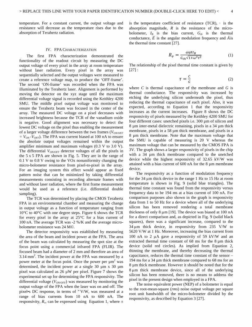
The optimized MM absorber structure was designed using 3D finite difference time domain (FDTD) simulations (Lumerical Inc.) as described elsewhere [19]. Figure 2a shows the spectral characteristics from FDTD simulation data of each cross shaped ERR single absorber (M4, M5 and M6) and experimental data from the three stacked ERRs. The simulation results reveal that the single absorbers have a narrow absorption peak at 2.1 THz, 2.36 THz and 2.65 THz with an absorption magnitude of 42 %, 99 % and 88 % respectively. The three stacked ERRs have a broad absorption peak at 2.65 THz with a maximum absorption magnitude of 88.2 %. Complete post-processed devices were experimentally characterized under vacuum in a Bruker IFS 66v/S Fourier Transform Infrared Spectrometer in transmission mode at normal incidence and in reflection mode at 30° incidence. The measured transmission spectra were normalized with respect to the signal measured from a 4 mm diameter open aperture and the reflection spectra were normalized to that of a gold mirror. The resulting absorption, A, was therefore calculated using A(É) = 1 – R(É) – T(É) where R is the reflection coefficient and T the transmission coefficient. As the thickness of the ground plane is much greater than the typical skin depth in the Terahertz regime the reflection is the only factor limiting absorption. In the experimental results the stacked ERRs have two broad absorption peaks: 2.78 THz and 2.5 THz with an absorption magnitude of 71.4 % and 56.4 % respectively, confirming that the MM absorbs at the required frequency of 2.5 THz. The MM absorber simulation and experimental results differ slightly due to the assumed value of the inter-metal dielectric refractive index and potential thickness non-uniformity of the three inter-metal dielectric layers. As discussed in [19, 21] the ERR cross arm length dictates the resonant frequency position while the insulating layer thickness and refractive index properties determine the absorption magnitude.
Figure 2b shows the refractive index of the different materials that compose the MM absorber. The metallic layers are shown in red and the dielectric insulating layers in blue. The simulated absorption distribution in the x-z plane shown in Fig. 2c reveals that the majority of the Terahertz radiation is absorbed within the first micrometer of the metallic layer and also in the first 200 nm of inter-metal dielectric beneath the M6 ERR. Therefore, the required approach is to place the
micro-bolometer (heat sensor) above the uppermost ERR in order to maximize the detector responsivity. Figure 2d shows the simulated Terahertz absorption distribution below the M6 ERR in the x-y plane.
III. FOCAL PLANE ARRAY ARCHITECTURE
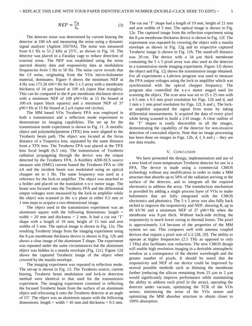
The first fabricated FPA containing 5 different arrays and testing circuits is shown in Fig. 3a. Three arrays had the same readout circuitry while the other two contained single pixels routed to output pads. The main difference between arrays was the number of ERRs on the pixels. The array pixels were composed of single, double and triple metallic ERRs for testing purposes. By testing several different structures and exploring the vast parameter space thoroughly we were able to select the prototype that demonstrated the best performance. The best absorption characteristics at the design frequency occurred in the array with three stacked metallic ERRs, as expected from the simulation results shown in Fig. 2a. This design contained a 5 x 5 FPA with three cross-shaped metallic ERR absorbers in every pixel. Figure 3b shows the pixel’s layout with the color/stipple-coded legend for each metallic layer. As already described, the ERRs are in metals 4, 5 and 6 and a continuous ground plane is in metal 3. The top left corner of the pixel shows the addressing electronics (transmission gate) in metals 1 and 2 and stacked vias from M2 to M6 where the VOx sensor connects to the electronics.
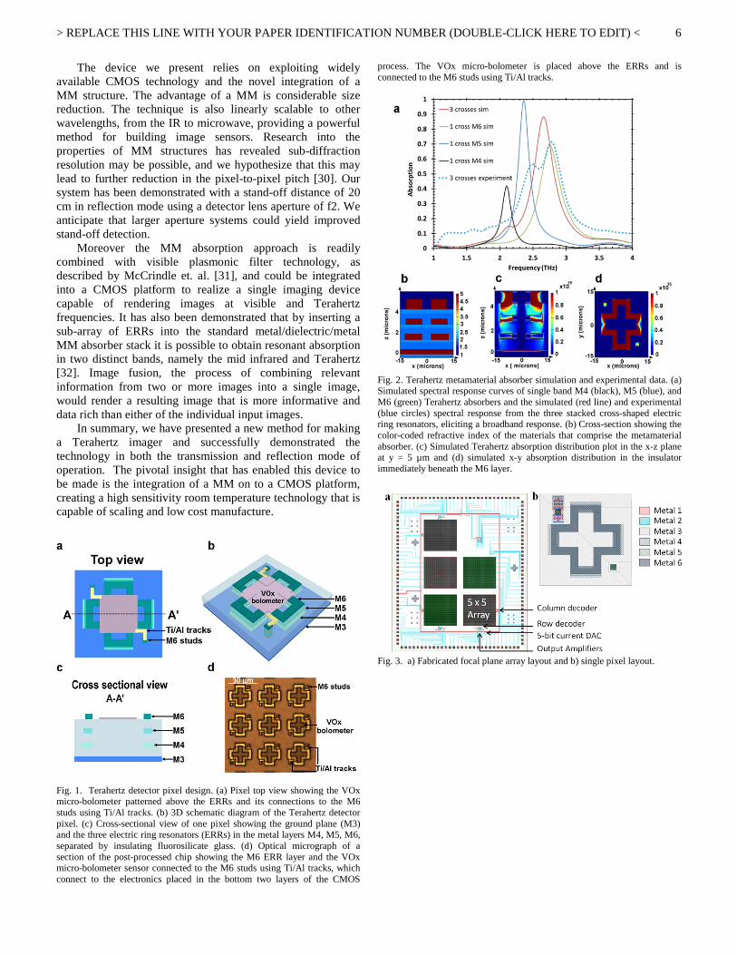
The CMOS readout schematic of the fabricated 5 x 5 VOx Terahertz FPA is shown in Fig. 4. The FPA readout was designed using Cadence tools and the Texas Instruments 180 nm foundry process (CMOS9T5V). The readout circuit is composed of five operational transconductance amplifiers (OTAs), a 5-bit current Digital-to-Analog converter (DAC), row and column decoders, as well as transmission gates (TGs) in every pixel used for pixel selection. The readout topology consists in current biasing the sensor and detecting the voltage change while the sensor is being radiated. The sensor is connected in feedback with the OTA’s inverting input. The noninverting input is the reference voltage biased by an external voltage source to 0.3 V. The output voltage is measured in the OTA’s output pin for every column. In the schematic the variable resistors represent the VOx micro-bolometers and are added for simulation purposes, their value depends on the VOx resistance which can vary from 10 k© to 5 M© depending on the deposition process.
The readout process starts with the micro-bolometers being properly biased by the current DAC to provide output voltages within the OTA output voltage range (0 V to 3.3 V). After the current has been binary-weighted with the external digital input-code using Labview, the readout process begins by selecting one row and one column at a time. There are five amplifiers (one per column) and a total of 25 pixels. The first column is selected by closing a TG that connects the current DAC to the respective column, each pixel from the selected column is readout serially through the respective OTA. The process repeats for the remaining 4 columns to complete 1 frame. Only one column at a time is biased to reduce power consumption and output load for the current DAC. When the pixel is biased, the amplifiers output a voltage depending on the resistance value which depends on the micro-bolometer’s
> REPLACE THIS LINE WITH YOUR PAPER IDENTIFICATION NUMBER (DOUBLE-CLICK HERE TO EDIT) <
4
temperature. For a constant current, the output voltage and resistance will decrease as the temperature rises due to the absorption of Terahertz radiation.
IV. FPA CHARACTERIZATION
The first FPA characterization demonstrated the functionality of the readout circuit by measuring the DC output voltage of every pixel in the array at room temperature without laser radiation. Every pixel in the array was sequentially selected and the output voltages were measured to create a reference voltage map, to produce the ‘OFF-frame’. The second ‘ON-frame’ was recorded when the FPA was illuminated by the Terahertz laser. Alignment is performed by moving the detector on the xyz stage until the maximum differential voltage signal is recorded using the Keithley 4200 SMU. The middle pixel output voltage was monitored to ensure the Terahertz beam was focused in the center of the array. The measured DC voltage on a pixel decreases with increased brightness because the TCR of the vanadium oxide is negative. Good alignment was necessary to detect the lowest DC voltage on the pixel thus enabling the measurement of a larger voltage difference between the two frames (VON/OFF
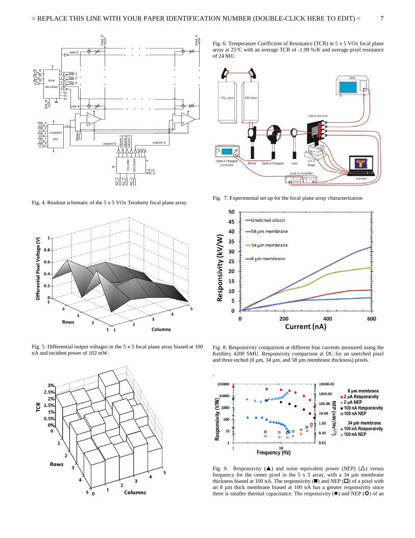
= VON -VOFF). The FPA was current biased at 100 nA to ensure the absolute output voltages remained within the output amplifier minimum and maximum voltages (0.3 V to 3.0 V). The differential VON/OFF detector voltages of all the pixels in the 5 x 5 FPA are shown in Fig. 5. They are in the range of 0.1 V to 0.8 V owing to the VOx nonuniformity changing the micro-bolometer resistance from pixel-to-pixel in the array. For an imaging system this effect would appear as fixed pattern noise that can be minimized by taking differential measurements consisting in recording alternate frames with and without laser radiation, where the first frame measurement would be used as a reference (i.e. differential double sampling).
The TCR was determined by placing the CMOS Terahertz FPA in an environmental chamber and measuring the change in output voltage as a function of temperature ranging from 10°C to 40°C with one degree steps. Figure 6 shows the TCR for every pixel in the array at 25°C for a bias current of 100 nA. The average TCR was -2 %/K and the average micro-bolometer resistance was 24 M©.
The detector responsivity was established by measuring the area of the beam and incident power at the FPA. The area of the beam was calculated by measuring the spot size at the focus point using a commercial infrared FPA (FLIR). The focused beam had a diameter of 2 mm and therefore an area of 3.14 mm2. The incident power at the FPA was measured by a power meter at the focus point. Once the power per µm2 was determined, the incident power at a single 30 µm x 30 µm pixel was calculated as 26 µW per pixel. Figure 7 shows the experimental set up for determining the FPA responsivity. The differential voltage (VON/OFF) was measured by monitoring the output voltage of the FPA when the laser was on and off. The pixel•s DC response, in terms of ” V/W, was measured at a range of bias currents from 10 nA to 600 nA. The responsivity, Rv, can be expressed using Equation 1, where ±
is the temperature coefficient of resistance (TCR), · is the absorption magnitude, R is the resistance of the micro-bolometer, IB is the bias current, Gth is the thermal conductance, É is the angular modulation frequency and Ä is the thermal time constant [27].
𝑅𝑣 = 𝛼𝜂𝑅𝐼𝐵𝐺𝑡ℎ√1+𝜔2𝜏2
(1)
The relationship of the pixel thermal time constant is given by [27] :
𝜏 = 𝐶𝐺
(2)
where C is thermal capacitance of the membrane and G is thermal conductance. The responsivity was increased by etching the underlying silicon underneath the pixel, thus reducing the thermal capacitance of each pixel. Also, it was expected, according to Equation 1 that the responsivity increases as the current increases. Figure 8 shows the DC responsivity of pixels measured by the Keithley 4200 SMU for four different cases: unetched pixels i.e. 300 µm of silicon and 8 µm inter-metal dielectric remaining, pixels in a 34 µm thick membrane, pixels in a 58 µm thick membrane, and pixels in a 8 µm thick membrane. Note that the maximum voltage that the SMU is capable of measuring is 20 V whereas the maximum voltage that can be measured by the CMOS FPA is 3V. The graph shows a larger responsivity of pixels in the chip with a 34 µm thick membrane compared to the unetched device while the highest responsivity of 32.65 kV/W was attained with a bias current of 600 nA for the 8 µm membrane device.
The responsivity as a function of modulation frequency for the 34 µm thick device in the range 1 Hz to 15 Hz at room temperature is shown in Fig. 9 (solid blue triangles). The thermal time constant was found from the responsivity versus frequency data to be 194 ms at a bias current of 100 nA. For comparison purposes also shown in the graph is responsivity data from 1 to 50 Hz for a device where all of the underlying silicon has been removed rendering a total membrane thickness of only 8 µm [19]. The device was biased at 100 nA for a direct comparison and, as depicted in Fig. 9 (solid black squares), there was a significant increase, compared to the 34 µm thick device, in responsivity from 235 V/W to 5620 V/W at 1 Hz. Moreover, increasing the bias current from 100 nA to 2 µA gave a responsivity of 59 kV/W and an extracted thermal time constant of 68 ms for the 8 µm thick device (solid red circles). As implied from Equation 2, thinning the membrane, and thereby decreasing the thermal capacitance, reduces the thermal time constant of the sensor – 194 ms for a 34 µm thick membrane compared to 68 ms for an 8 µm thick membrane. However it should be noted that for the 8 µm thick membrane device, since all of the underlying silicon has been removed, there is no means to address the pixel in the present design when employed in a FPA.
The noise equivalent power (NEP) of a bolometer is equal to the root-mean-square (rms) noise output voltage per square root unit bandwidth of the micro-bolometer divided by the responsivity, as described by Equation 3 [27].
> REPLACE THIS LINE WITH YOUR PAPER IDENTIFICATION NUMBER (DOUBLE-CLICK HERE TO EDIT) <
5
𝑁𝐸𝑃 = 𝑉𝑁𝑅𝑣
(3)
The detector noise was determined by current biasing the
detector at 100 nA and measuring the noise using a dynamic signal analyzer (Agilent 35670A). The noise was measured from 0.1 Hz to 51.2 kHz at 25°C, as shown in Fig. 10. The detector was placed in a Faraday cage to reduce detection of external noise. The NEP was established using the noise spectral density data and responsivity data at modulation frequencies from 1 Hz to 50 Hz. The noise curve reveals that the 1/f noise, originating from the VOx micro-bolometer material, dominates. Figure 9 shows the minimum NEP at 4 Hz was 173.26 nW/• Hz for the 5 x 5 array with a membrane thickness of 34 µm biased at 100 nA (open blue triangles). This can be compared to the 8 µm membrane thickness device with a minimum NEP of 108 pW/• Hz at 15 Hz biased at 100 nA (open black squares) and a minimum NEP of 37 pW/• Hz at 15 Hz biased at 2 µA (open red circles).
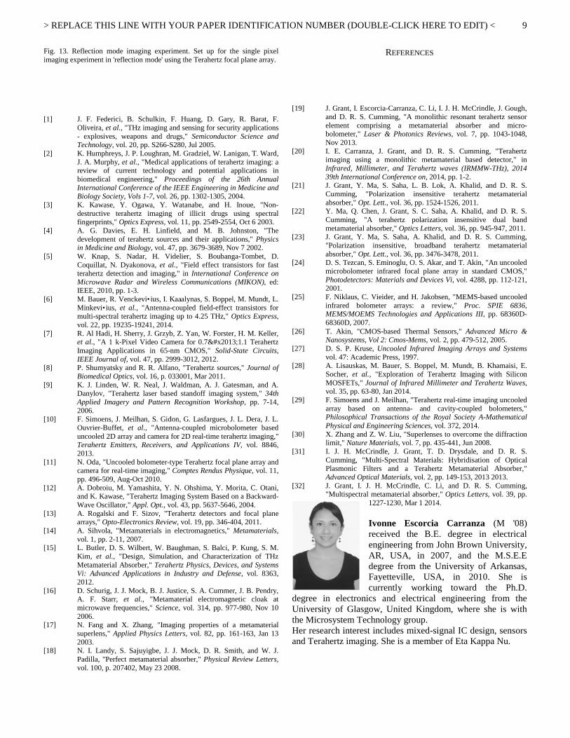
The MM based VOx Terahertz FPA was employed in both a transmission and a reflection mode experiment to demonstrate its imaging capabilities. The set up for the transmission mode experiment is shown in Fig. 11. A metallic object and polymethylpentene (TPX) lens were aligned to the Terahertz beam path. The object was located at the focus distance of a Tsupurica lens, separated by the same distance from a TPX lens. The Terahertz FPA was placed at the TPX lens focal length (6.5 cm). The transmission of Terahertz radiation propagating through the device was the output detected by the Terahertz FPA. A Keithley 4200-SCS source measure unit (SMU) current biased the Terahertz FPA to 100 nA and the incident beam was modulated using an optical chopper set to 1 Hz. The same frequency was used as a reference for the lock-in amplifier. The object was attached to a holder and placed on the translation x-y-z motor stage. The beam was focused onto the Terahertz FPA and the differential output voltages were measured by the lock-in amplifier while the object was scanned in the x-y plane in either 0.5 mm or 1 mm steps to acquire a two-dimensional image.
The object used in the transmission experiment was an aluminum square with the following dimensions: length = width = 20 mm and thickness = 2 mm. It had a cut out ‘T’ shape with a length of 10 mm, height of 15 mm and arm widths of 3 mm. The optical image is shown in Fig. 12a. The resulting Terahertz image from the imaging experiment using the 8 µm membrane thickness device is shown in Fig. 12b and shows a clear image of the aluminum T shape. The experiment was repeated under the same circumstances but the aluminum object was hidden in a manila envelope (Fig. 12c). Figure 12d shows the captured Terahertz image of the object when covered by the manila envelope.
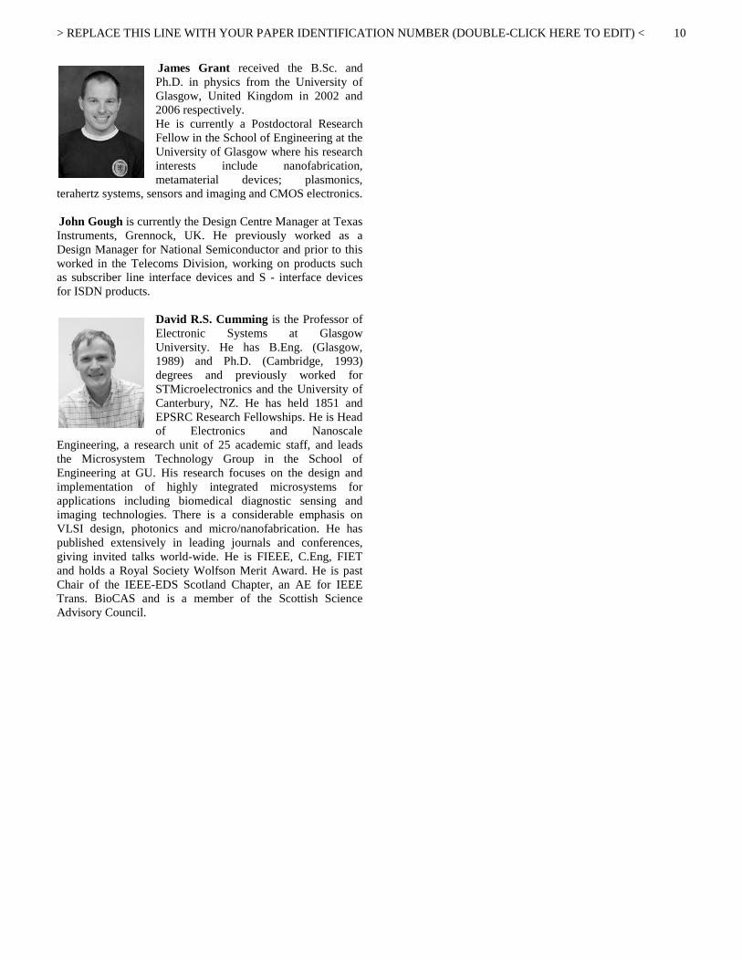
The imaging experiment was repeated in reflection mode. The set-up is shown in Fig. 13. The Terahertz source, current biasing, Terahertz beam modulation and lock-in detection method were identical to that used for the transmission experiment. The imaging experiment consisted in reflecting the focused Terahertz beam from the surface of an aluminum object and refocusing it onto the Terahertz detector at an angle of 15°. The object was an aluminum square with the following dimensions: length = width = 45 mm and thickness = 0.5 mm.
The cut out ‘T’ shape had a length of 19 mm, height of 21 mm and arm widths of 5 mm. The optical image is shown in Fig. 12e. The captured image from the reflection experiment using the 8 µm membrane thickness device is shown in Fig. 12f. The experiment was repeated by covering the object with a manila envelope as shown in Fig. 12g and its respective captured Terahertz image is shown in Fig. 12h. The stand-off distance was 20 cm. The device with a 34 µm thick membrane containing the 5 x 5 pixel array was also used as the detector in a transmission mode imaging experiment. Figure 12i shows the object and Fig. 12j shows the transmission image obtained. For all experiments a Labview program was used to measure the FPA output voltages using the lock-in amplifier which was synchronized with the optical chopper frequency. The program also controlled the x-y-z motor staged used for scanning the object. The scan area was set to 25 x 25 mm with a 0.5 mm x 0.5 mm pixel resolution for Figs. 12b and d, and 1 mm x 1 mm pixel resolution for Figs. 12f, h and j. The lock-in amplifier separated the signal from noise by taking differential measurements. It acquired the data of every pixel while being scanned to build a 2-D image. A clear outline of the ‘T’ shapes is easily discernible in all the images, demonstrating the capability of the detector for non-invasive detection of concealed objects. Note that no image processing has been done on images in Figs. 12b, d, f, h and j – they are raw data results.
V. CONCLUSION
We have presented the design, implementation and use of a new kind of room temperature Terahertz detector for use in a FPA. The device is made using a commercial CMOS technology without any modification in order to make a MM structure that absorbs up to 50% of the radiation arriving at the surface of the detector, and to integrate all the required electronics to address the array. The transduction mechanism is provided by adding a single process layer of VOx to make bolometers that are fully integrated with the CMOS electronics and photonics. The 5 x 5 array was also fully back etched to improve the responsivity and NEP, showing Rv up to 60 kV/W and a minimum NEP of 37 pW/• Hz when the membrane was 8 µm thick. Without back-side etching the responsivity is much lower owing to thermal losses. The pixel is approximately λ/4 because of the properties of the MM system we use. This compares well with antenna coupled devices that require a pixel size of λ/2 [28, 29]. The ability to operate at higher frequencies (2.5 THz as opposed to only 1 THz) also facilitates size reduction. The new CMOS design will enable high resolution imaging in a desirable atmospheric window as a consequence of the shorter wavelength and the greater number of pixels. It should be noted that the responsivity and NEP of our device could be improved by several possible methods such as thinning the membrane further (reducing the silicon remaining from 25 µm to 2 µm would significantly improve performance while maintaining the ability to address each pixel in the array), operating the detector under vacuum, optimizing the TCR of the VOx sensor, minimizing the noise of the VOx sensor and optimizing the MM absorber structure to obtain closer to 100% absorption.
> REPLACE THIS LINE WITH YOUR PAPER IDENTIFICATION NUMBER (DOUBLE-CLICK HERE TO EDIT) <
6
The device we present relies on exploiting widely available CMOS technology and the novel integration of a MM structure. The advantage of a MM is considerable size reduction. The technique is also linearly scalable to other wavelengths, from the IR to microwave, providing a powerful method for building image sensors. Research into the properties of MM structures has revealed sub-diffraction resolution may be possible, and we hypothesize that this may lead to further reduction in the pixel-to-pixel pitch [30]. Our system has been demonstrated with a stand-off distance of 20 cm in reflection mode using a detector lens aperture of f2. We anticipate that larger aperture systems could yield improved stand-off detection.
Moreover the MM absorption approach is readily combined with visible plasmonic filter technology, as described by McCrindle et. al. [31], and could be integrated into a CMOS platform to realize a single imaging device capable of rendering images at visible and Terahertz frequencies. It has also been demonstrated that by inserting a sub-array of ERRs into the standard metal/dielectric/metal MM absorber stack it is possible to obtain resonant absorption in two distinct bands, namely the mid infrared and Terahertz [32]. Image fusion, the process of combining relevant information from two or more images into a single image, would render a resulting image that is more informative and data rich than either of the individual input images.
In summary, we have presented a new method for making a Terahertz imager and successfully demonstrated the technology in both the transmission and reflection mode of operation. The pivotal insight that has enabled this device to be made is the integration of a MM on to a CMOS platform, creating a high sensitivity room temperature technology that is capable of scaling and low cost manufacture.
Fig. 1. Terahertz detector pixel design. (a) Pixel top view showing the VOx micro-bolometer patterned above the ERRs and its connections to the M6 studs using Ti/Al tracks. (b) 3D schematic diagram of the Terahertz detector pixel. (c) Cross-sectional view of one pixel showing the ground plane (M3) and the three electric ring resonators (ERRs) in the metal layers M4, M5, M6, separated by insulating fluorosilicate glass. (d) Optical micrograph of a section of the post-processed chip showing the M6 ERR layer and the VOx micro-bolometer sensor connected to the M6 studs using Ti/Al tracks, which connect to the electronics placed in the bottom two layers of the CMOS
process. The VOx micro-bolometer is placed above the ERRs and is connected to the M6 studs using Ti/Al tracks.
Fig. 2. Terahertz metamaterial absorber simulation and experimental data. (a) Simulated spectral response curves of single band M4 (black), M5 (blue), and M6 (green) Terahertz absorbers and the simulated (red line) and experimental (blue circles) spectral response from the three stacked cross-shaped electric ring resonators, eliciting a broadband response. (b) Cross-section showing the color-coded refractive index of the materials that comprise the metamaterial absorber. (c) Simulated Terahertz absorption distribution plot in the x-z plane at y = 5 µm and (d) simulated x-y absorption distribution in the insulator immediately beneath the M6 layer.
Fig. 3. a) Fabricated focal plane array layout and b) single pixel layout.
> REPLACE THIS LINE WITH YOUR PAPER IDENTIFICATION NUMBER (DOUBLE-CLICK HERE TO EDIT) <
7
CO
LUM
N
DE
CO
DE
R
A2 _
C
A1_
C
A0_
C
EN_C
Vbi
as+
ROW
DECODER
A1
A1
A1
A2_R
A1_R
A0_R
A1 row 1
A1 row 2
A1row 3
A1
EN
_R
Vou
t_0
Vou
t_4
NC
NC
NC
NCNCNC
CURRENT
DAC
Vbit_4
Vbit_3
Vbit_2
Vbit_1
Vbit_0
row 0
column 0
colu
mn
1co
lum
n 2
colu
mn
3
row 4
column 4
Fig. 4. Readout schematic of the 5 x 5 VOx Terahertz focal plane array.
Fig. 5. Differential output voltages in the 5 x 5 focal plane array biased at 100 nA and incident power of 102 mW.
Fig. 6. Temperature Coefficient of Resistance (TCR) in 5 x 5 VOx focal plane array at 25°C with an average TCR of -1.99 %/K and average pixel resistance of 24 M©.
Fig. 7. Experimental set up for the focal plane array characterization
Fig. 8. Responsivity comparison at different bias currents measured using the Keithley 4200 SMU. Responsivity comparison at DC for an unetched pixel and three etched (8 µm, 34 µm, and 58 µm membrane thickness) pixels.
Fig. 9. Responsivity () and noise equivalent power (NEP) () versus frequency for the center pixel in the 5 x 5 array, with a 34 µm membrane thickness biased at 100 nA. The responsivity () and NEP () of a pixel with an 8 µm thick membrane biased at 100 nA has a greater responsivity since there is smaller thermal capacitance. The responsivity () and NEP () of an
> REPLACE THIS LINE WITH YOUR PAPER IDENTIFICATION NUMBER (DOUBLE-CLICK HERE TO EDIT) <
8
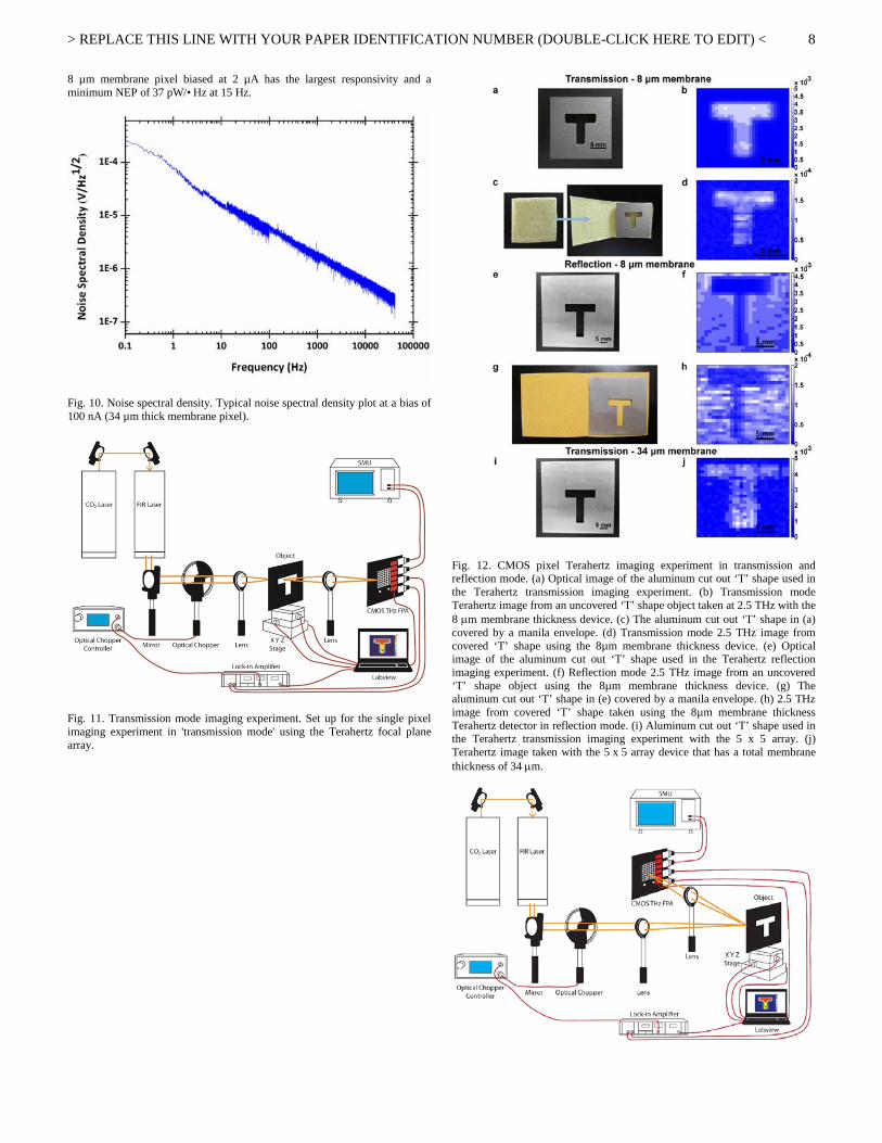
8 µm membrane pixel biased at 2 µA has the largest responsivity and a minimum NEP of 37 pW/• Hz at 15 Hz.
Fig. 10. Noise spectral density. Typical noise spectral density plot at a bias of 100 nA (34 µm thick membrane pixel).
Fig. 11. Transmission mode imaging experiment. Set up for the single pixel imaging experiment in 'transmission mode' using the Terahertz focal plane array.
Fig. 12. CMOS pixel Terahertz imaging experiment in transmission and reflection mode. (a) Optical image of the aluminum cut out ‘T’ shape used in the Terahertz transmission imaging experiment. (b) Transmission mode Terahertz image from an uncovered ‘T’ shape object taken at 2.5 THz with the 8 µm membrane thickness device. (c) The aluminum cut out ‘T’ shape in (a) covered by a manila envelope. (d) Transmission mode 2.5 THz image from covered ‘T’ shape using the 8µm membrane thickness device. (e) Optical image of the aluminum cut out ‘T’ shape used in the Terahertz reflection imaging experiment. (f) Reflection mode 2.5 THz image from an uncovered ‘T’ shape object using the 8µm membrane thickness device. (g) The aluminum cut out ‘T’ shape in (e) covered by a manila envelope. (h) 2.5 THz image from covered ‘T’ shape taken using the 8µm membrane thickness Terahertz detector in reflection mode. (i) Aluminum cut out ‘T’ shape used in the Terahertz transmission imaging experiment with the 5 x 5 array. (j) Terahertz image taken with the 5 x 5 array device that has a total membrane thickness of 34 µm.
> REPLACE THIS LINE WITH YOUR PAPER IDENTIFICATION NUMBER (DOUBLE-CLICK HERE TO EDIT) <
9
Fig. 13. Reflection mode imaging experiment. Set up for the single pixel imaging experiment in 'reflection mode' using the Terahertz focal plane array.
REFERENCES
[1] J. F. Federici, B. Schulkin, F. Huang, D. Gary, R. Barat, F.
Oliveira, et al., "THz imaging and sensing for security applications - explosives, weapons and drugs," Semiconductor Science and Technology, vol. 20, pp. S266-S280, Jul 2005.
[2] K. Humphreys, J. P. Loughran, M. Gradziel, W. Lanigan, T. Ward, J. A. Murphy, et al., "Medical applications of terahertz imaging: a review of current technology and potential applications in biomedical engineering," Proceedings of the 26th Annual International Conference of the IEEE Engineering in Medicine and Biology Society, Vols 1-7, vol. 26, pp. 1302-1305, 2004.
[3] K. Kawase, Y. Ogawa, Y. Watanabe, and H. Inoue, "Non-destructive terahertz imaging of illicit drugs using spectral fingerprints," Optics Express, vol. 11, pp. 2549-2554, Oct 6 2003.
[4] A. G. Davies, E. H. Linfield, and M. B. Johnston, "The development of terahertz sources and their applications," Physics in Medicine and Biology, vol. 47, pp. 3679-3689, Nov 7 2002.
[5] W. Knap, S. Nadar, H. Videlier, S. Boubanga-Tombet, D. Coquillat, N. Dyakonova, et al., "Field effect transistors for fast terahertz detection and imaging," in International Conference on Microwave Radar and Wireless Communications (MIKON), ed: IEEE, 2010, pp. 1-3.
[6] M. Bauer, R. Venckevi• ius, I. Kaaalynas, S. Boppel, M. Mundt, L. Minkevi• ius, et al., "Antenna-coupled field-effect transistors for multi-spectral terahertz imaging up to 4.25 THz," Optics Express, vol. 22, pp. 19235-19241, 2014.
[7] R. Al Hadi, H. Sherry, J. Grzyb, Z. Yan, W. Forster, H. M. Keller, et al., "A 1 k-Pixel Video Camera for 0.7–1.1 Terahertz Imaging Applications in 65-nm CMOS," Solid-State Circuits, IEEE Journal of, vol. 47, pp. 2999-3012, 2012.
[8] P. Shumyatsky and R. R. Alfano, "Terahertz sources," Journal of Biomedical Optics, vol. 16, p. 033001, Mar 2011.
[9] K. J. Linden, W. R. Neal, J. Waldman, A. J. Gatesman, and A. Danylov, "Terahertz laser based standoff imaging system," 34th Applied Imagery and Pattern Recognition Workshop, pp. 7-14, 2006.
[10] F. Simoens, J. Meilhan, S. Gidon, G. Lasfargues, J. L. Dera, J. L. Ouvrier-Buffet, et al., "Antenna-coupled microbolometer based uncooled 2D array and camera for 2D real-time terahertz imaging," Terahertz Emitters, Receivers, and Applications IV, vol. 8846, 2013.
[11] N. Oda, "Uncooled bolometer-type Terahertz focal plane array and camera for real-time imaging," Comptes Rendus Physique, vol. 11, pp. 496-509, Aug-Oct 2010.
[12] A. Dobroiu, M. Yamashita, Y. N. Ohshima, Y. Morita, C. Otani, and K. Kawase, "Terahertz Imaging System Based on a Backward-Wave Oscillator," Appl. Opt., vol. 43, pp. 5637-5646, 2004.
[13] A. Rogalski and F. Sizov, "Terahertz detectors and focal plane arrays," Opto-Electronics Review, vol. 19, pp. 346-404, 2011.
[14] A. Sihvola, "Metamaterials in electromagnetics," Metamaterials, vol. 1, pp. 2-11, 2007.
[15] L. Butler, D. S. Wilbert, W. Baughman, S. Balci, P. Kung, S. M. Kim, et al., "Design, Simulation, and Characterization of THz Metamaterial Absorber," Terahertz Physics, Devices, and Systems Vi: Advanced Applications in Industry and Defense, vol. 8363, 2012.
[16] D. Schurig, J. J. Mock, B. J. Justice, S. A. Cummer, J. B. Pendry, A. F. Starr, et al., "Metamaterial electromagnetic cloak at microwave frequencies," Science, vol. 314, pp. 977-980, Nov 10 2006.
[17] N. Fang and X. Zhang, "Imaging properties of a metamaterial superlens," Applied Physics Letters, vol. 82, pp. 161-163, Jan 13 2003.
[18] N. I. Landy, S. Sajuyigbe, J. J. Mock, D. R. Smith, and W. J. Padilla, "Perfect metamaterial absorber," Physical Review Letters, vol. 100, p. 207402, May 23 2008.
[19] J. Grant, I. Escorcia-Carranza, C. Li, I. J. H. McCrindle, J. Gough, and D. R. S. Cumming, "A monolithic resonant terahertz sensor element comprising a metamaterial absorber and micro-bolometer," Laser & Photonics Reviews, vol. 7, pp. 1043-1048, Nov 2013.
[20] I. E. Carranza, J. Grant, and D. R. S. Cumming, "Terahertz imaging using a monolithic metamaterial based detector," in Infrared, Millimeter, and Terahertz waves (IRMMW-THz), 2014 39th International Conference on, 2014, pp. 1-2.
[21] J. Grant, Y. Ma, S. Saha, L. B. Lok, A. Khalid, and D. R. S. Cumming, "Polarization insensitive terahertz metamaterial absorber," Opt. Lett., vol. 36, pp. 1524-1526, 2011.
[22] Y. Ma, Q. Chen, J. Grant, S. C. Saha, A. Khalid, and D. R. S. Cumming, "A terahertz polarization insensitive dual band metamaterial absorber," Optics Letters, vol. 36, pp. 945-947, 2011.
[23] J. Grant, Y. Ma, S. Saha, A. Khalid, and D. R. S. Cumming, "Polarization insensitive, broadband terahertz metamaterial absorber," Opt. Lett., vol. 36, pp. 3476-3478, 2011.
[24] D. S. Tezcan, S. Eminoglu, O. S. Akar, and T. Akin, "An uncooled microbolometer infrared focal plane array in standard CMOS," Photodetectors: Materials and Devices Vi, vol. 4288, pp. 112-121, 2001.
[25] F. Niklaus, C. Vieider, and H. Jakobsen, "MEMS-based uncooled infrared bolometer arrays: a review," Proc. SPIE 6836, MEMS/MOEMS Technologies and Applications III, pp. 68360D-68360D, 2007.
[26] T. Akin, "CMOS-based Thermal Sensors," Advanced Micro & Nanosystems, Vol 2: Cmos-Mems, vol. 2, pp. 479-512, 2005.
[27] D. S. P. Kruse, Uncooled Infrared Imaging Arrays and Systems vol. 47: Academic Press, 1997.
[28] A. Lisauskas, M. Bauer, S. Boppel, M. Mundt, B. Khamaisi, E. Socher, et al., "Exploration of Terahertz Imaging with Silicon MOSFETs," Journal of Infrared Millimeter and Terahertz Waves, vol. 35, pp. 63-80, Jan 2014.
[29] F. Simoens and J. Meilhan, "Terahertz real-time imaging uncooled array based on antenna- and cavity-coupled bolometers," Philosophical Transactions of the Royal Society A-Mathematical Physical and Engineering Sciences, vol. 372, 2014.
[30] X. Zhang and Z. W. Liu, "Superlenses to overcome the diffraction limit," Nature Materials, vol. 7, pp. 435-441, Jun 2008.
[31] I. J. H. McCrindle, J. Grant, T. D. Drysdale, and D. R. S. Cumming, "Multi-Spectral Materials: Hybridisation of Optical Plasmonic Filters and a Terahertz Metamaterial Absorber," Advanced Optical Materials, vol. 2, pp. 149-153, 2013 2013.
[32] J. Grant, I. J. H. McCrindle, C. Li, and D. R. S. Cumming, "Multispectral metamaterial absorber," Optics Letters, vol. 39, pp.
1227-1230, Mar 1 2014. Ivonne Escorcia Carranza (M '08) received the B.E. degree in electrical engineering from John Brown University, AR, USA, in 2007, and the M.S.E.E degree from the University of Arkansas, Fayetteville, USA, in 2010. She is currently working toward the Ph.D.
degree in electronics and electrical engineering from the University of Glasgow, United Kingdom, where she is with the Microsystem Technology group. Her research interest includes mixed-signal IC design, sensors and Terahertz imaging. She is a member of Eta Kappa Nu.
> REPLACE THIS LINE WITH YOUR PAPER IDENTIFICATION NUMBER (DOUBLE-CLICK HERE TO EDIT) <
10
James Grant received the B.Sc. and Ph.D. in physics from the University of Glasgow, United Kingdom in 2002 and 2006 respectively. He is currently a Postdoctoral Research Fellow in the School of Engineering at the University of Glasgow where his research interests include nanofabrication, metamaterial devices; plasmonics,
terahertz systems, sensors and imaging and CMOS electronics. John Gough is currently the Design Centre Manager at Texas Instruments, Grennock, UK. He previously worked as a Design Manager for National Semiconductor and prior to this worked in the Telecoms Division, working on products such as subscriber line interface devices and S - interface devices for ISDN products.
David R.S. Cumming is the Professor of Electronic Systems at Glasgow University. He has B.Eng. (Glasgow, 1989) and Ph.D. (Cambridge, 1993) degrees and previously worked for STMicroelectronics and the University of Canterbury, NZ. He has held 1851 and EPSRC Research Fellowships. He is Head of Electronics and Nanoscale
Engineering, a research unit of 25 academic staff, and leads the Microsystem Technology Group in the School of Engineering at GU. His research focuses on the design and implementation of highly integrated microsystems for applications including biomedical diagnostic sensing and imaging technologies. There is a considerable emphasis on VLSI design, photonics and micro/nanofabrication. He has published extensively in leading journals and conferences, giving invited talks world-wide. He is FIEEE, C.Eng, FIET and holds a Royal Society Wolfson Merit Award. He is past Chair of the IEEE-EDS Scotland Chapter, an AE for IEEE Trans. BioCAS and is a member of the Scottish Science Advisory Council.