Embed Size (px)
Citation preview

1
MERCURY: A FAST AND ENERGY-EFFICIENT MULTI LEVEL CELL BASED PHASE CHANGE MEMORY SYSTEM
By
MADHURA JOSHI
A THESIS PRESENTED TO THE GRADUATE SCHOOL OF THE UNIVERSITY OF FLORIDA IN PARTIAL FULFILLMENT
OF THE REQUIREMENTS FOR THE DEGREE OF MASTER OF SCIENCE
UNIVERSITY OF FLORIDA
2010

2
© 2010 Madhura R. Joshi

3
To my family, friends and well wishers

4
ACKNOWLEDGMENTS
First and foremost, I would like to thank Dr. Tao Li for his help, support and
guidance throughout my master’s program. I am grateful to him not only for helping me
in successful completion of this work but also motivating me to aim higher, work harder
and strive for perfection.
I am also thankful to Dr. Jose Fortes and Dr. Jing Guo for their valuable guidance
in this project and for being there on the supervisory committee. I thank Dr. Geoffrey
W. Burr, Dr. Angeliki Pantazi (IBM Research), Dr. Roberto Faravelli, Dr. Alessandro
Cabrini and Dr. Guido Torelli (University of Pavia, Italy) for helping me to understand the
numerous complicated concepts of phase change memory. I owe my gratitude to Dr. K.
Sonoda and Dr. Chubing Peng for their invaluable guidance in building the
mathematical models of phase change memory cell.
Last but not the least; I would like to thank my mentor Wangyuan Zhang for
sharing knowledge with me through numerous interesting discussions. I would also like
to thank my lab mates, friends and family without whose support, timely help as well as
critique; this thesis would not have been materialized.
5
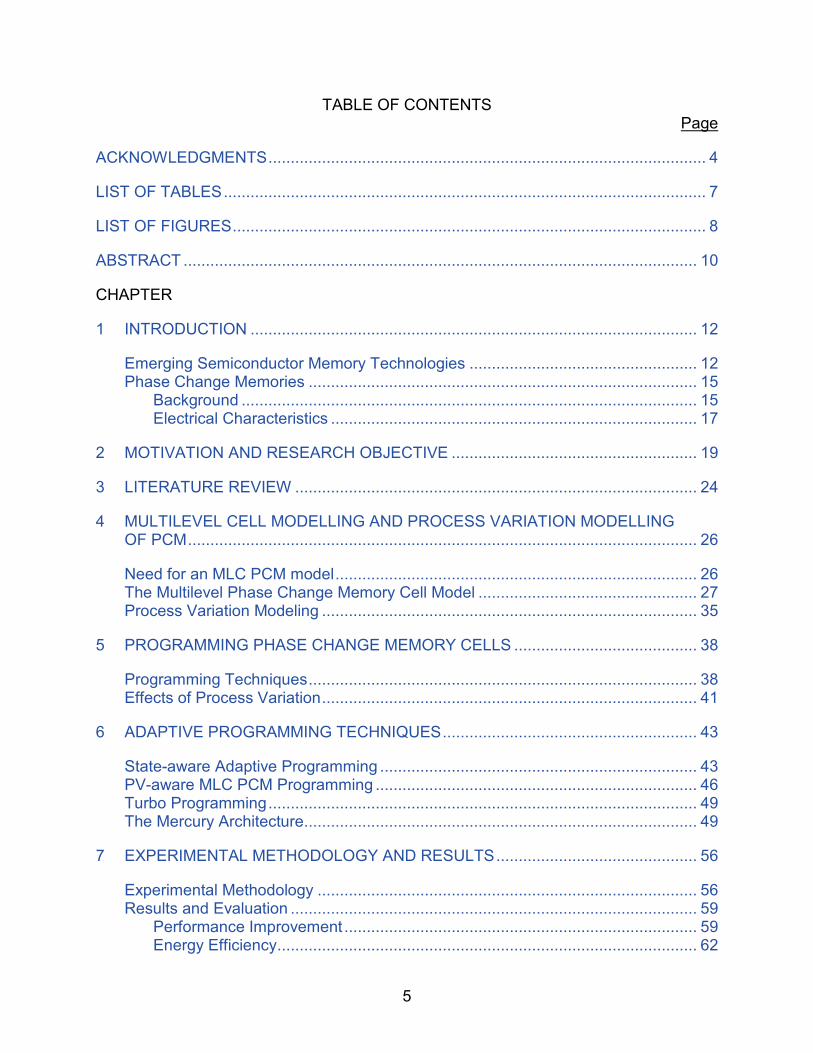
TABLE OF CONTENTS Page
ACKNOWLEDGMENTS .................................................................................................. 4
LIST OF TABLES ............................................................................................................ 7
LIST OF FIGURES .......................................................................................................... 8
ABSTRACT ................................................................................................................... 10
CHAPTER
1 INTRODUCTION .................................................................................................... 12
Emerging Semiconductor Memory Technologies ................................................... 12 Phase Change Memories ....................................................................................... 15
Background ...................................................................................................... 15 Electrical Characteristics .................................................................................. 17
2 MOTIVATION AND RESEARCH OBJECTIVE ....................................................... 19
3 LITERATURE REVIEW .......................................................................................... 24
4 MULTILEVEL CELL MODELLING AND PROCESS VARIATION MODELLING OF PCM .................................................................................................................. 26
Need for an MLC PCM model ................................................................................. 26 The Multilevel Phase Change Memory Cell Model ................................................. 27 Process Variation Modeling .................................................................................... 35
5 PROGRAMMING PHASE CHANGE MEMORY CELLS ......................................... 38
Programming Techniques ....................................................................................... 38 Effects of Process Variation .................................................................................... 41
6 ADAPTIVE PROGRAMMING TECHNIQUES ......................................................... 43
State-aware Adaptive Programming ....................................................................... 43 PV-aware MLC PCM Programming ........................................................................ 46 Turbo Programming ................................................................................................ 49 The Mercury Architecture ........................................................................................ 49
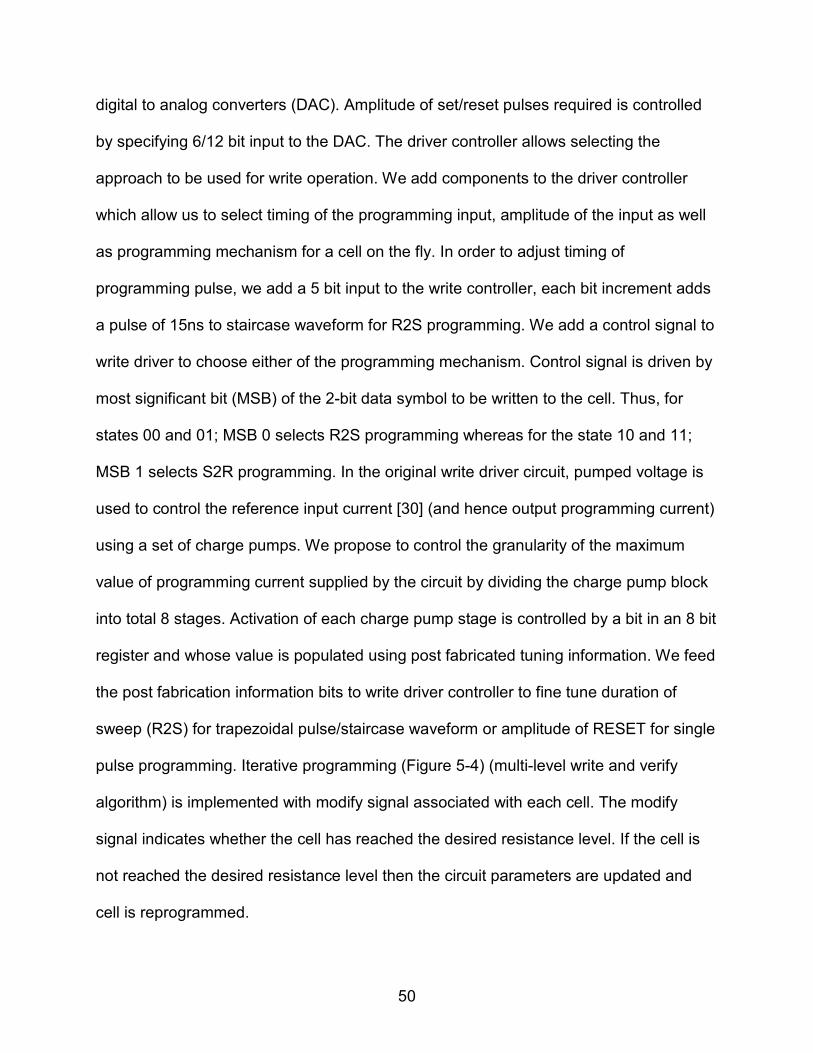
7 EXPERIMENTAL METHODOLOGY AND RESULTS ............................................. 56
Experimental Methodology ..................................................................................... 56 Results and Evaluation ........................................................................................... 59
Performance Improvement ............................................................................... 59 Energy Efficiency .............................................................................................. 62
6
Power Enhancement ........................................................................................ 64
8 CONCLUSION AND FUTURE WORK .................................................................... 65
Conclusion .............................................................................................................. 65 Future Work ............................................................................................................ 65
LIST OF REFERENCES ............................................................................................... 67
BIOGRAPHICAL SKETCH ............................................................................................ 70
7
LIST OF TABLES
Table page 1-1 Comparison of traditional and emerging memory technologies .......................... 14
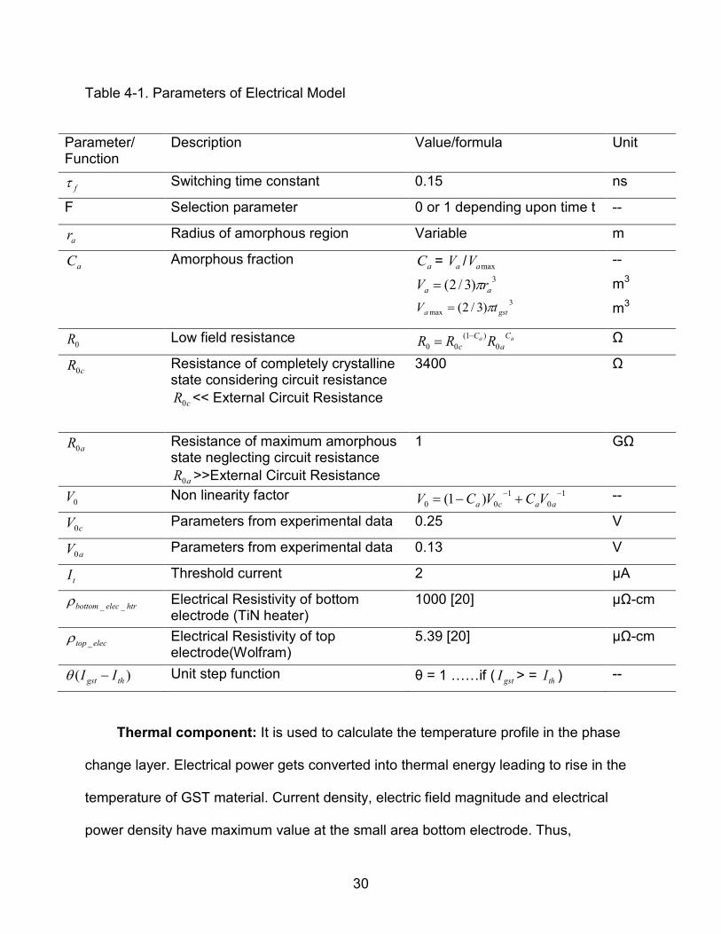
4-1 Parameters of Electrical Model ........................................................................... 30
4-2 Parameters of Thermal Model ............................................................................ 32
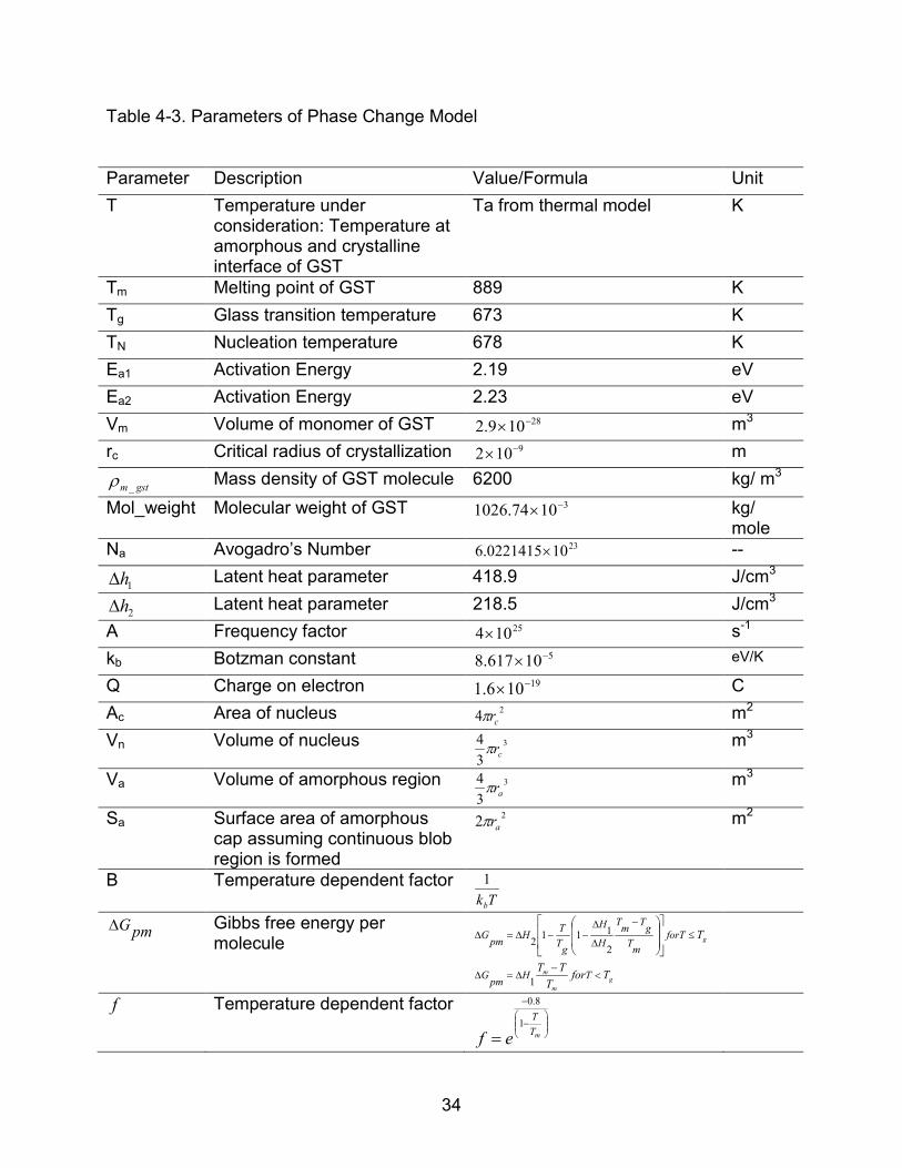
4-3 Parameters of Phase Change Model .................................................................. 34
6-1 Area and latency overhead of BCH code ........................................................... 53
7-1 Baseline Machine Configuration ......................................................................... 57
7-2 PCM Parameters ................................................................................................ 57

8
LIST OF FIGURES
Figure page 1-1 Categories of semiconductor memories ............................................................. 13
1-2 Temperature profile required for phase change of chalcogenide........................ 16
1-3 (a) Cell with amorphous GST (b) PCM 1R-1T structure (c) Cell with crystalline GST ................................................................................................... 17
1-4 Cell resistance as a function of program current [1] ........................................... 17
1-5 I-V characteristics measured on programming [1] .............................................. 17
4-1 Physical View of PCM Cell ................................................................................. 27
4-2 Flow of modeling PCM cell ................................................................................. 27
4-3 Representation of spherical correlation function ................................................. 36
5-1 Approach 1: Increasing amorphous region (h1 corresponds to resistance R1, h2 corresponds to resistance R2 , h2>h1 => R2>R1) ............................................ 38
5-2 Approach 2: Increasing crystalline filaments (w1 corresponds to resistance R1, w2 corresponds to resistance R2 , w2>w1 => R2<R1) ................................ 38
5-3 SET to RESET programming.............................................................................. 40
5-4 RESET to SET programming.............................................................................. 40
5-5 Distribution of amorphous fraction and resistance with programming current in RESET to SET programming. Parameter variation is introduced in bottom electrode contact diameter. ................................................................................ 41
5-6 Distribution of amorphous fraction and resistance with programming current in RESET to SET programming. Parameter variation is introduced in thickness of heater ............................................................................................. 41
6-1 Programming to different states using R2S ........................................................ 44
6-2 Programming to different states using S2R ........................................................ 44
6-3 States 11 and 10 are programmed using SET to RESET(S2R) programming whereas states 01 and 00 are programmed using RESET to SET(R2S) programming ...................................................................................................... 45
6-4 Histogram of number of pulses required to program states 11 to 00 .................. 47

9
6-5 Programming with variation ................................................................................ 48
6-6 Flowchart of adaptive programming ................................................................... 52
6-7 W-2W DAC Adaptable Programming Circuit ...................................................... 52
6-8 Adaptive writes: Mercury architecture ................................................................. 53
7-1 Performance Improvement ................................................................................. 60
7-2 State Wise Writes without DCW ......................................................................... 61
7-3 State Wise Writes with DCW .............................................................................. 62
7-4 Read-Write Relative Statistics ............................................................................ 62
7-5 Absolute Number of Read-Write Accesses ........................................................ 63
7-6 Improvement in Energy ...................................................................................... 63
7-7 Power Reduction ................................................................................................ 64
10
Abstract of Thesis Presented to the Graduate School of the University of Florida in Partial Fulfillment of the Requirements for the Degree of Master of Science
MERCURY: A FAST AND ENERGY-EFFICIENT MULTI LEVEL CELL BASED PHASE
CHANGE MEMORY SYSTEM
By
Madhura Joshi
December 2010
Chair: Tao Li Major: Electrical and Computer Engineering
Phase Change Memory (PCM) is one of the most promising technologies among
emerging non-volatile memories. PCM stores data in crystalline and amorphous phases
of GST material having large difference in their electrical resistivity. Though it is possible
to design a high capacity memory system by storing multiple bits at intermediate levels
between highest and lowest resistance state of PCM, it is difficult to obtain tight
distribution required for correct reading of data. Moreover, the write latency and
programming energy for an MLC PCM cell are not trivial and act as a major hurdle in
applying multi-level PCM in high density memory architecture design. Effect of process
variation (PV) on PCM cell exacerbates the variability in necessary programming
current and hence the target resistance spread leading to the demand for high-latency,
multi-iteration-based programming, write verify schemes for MLC-PCM. PV aware
control of programming current, programming using staircase down pulses of current or
increasing reset current pulses are some of the traditional techniques used to achieve
optimum programming energy, write latency and better accuracy, but they are usually
able to optimize only one aspect of the design. This work addresses the high write
latency and process variation issue of MLC-PCM by introducing a fast and energy
11
efficient multi-level cell based phase change memory architecture. This architecture
adapts the programming scheme of a multi-level cell by considering the initial state of
the cell, the target resistance to be programmed and the effect of process variation in
programming current profile of the cell. The proposed techniques act at circuit as well as
micro-architecture levels. Simulation results show that we achieve 10% saving in
programming latency and 25% saving in programming energy for the PCM memory
system compared to traditional methods.
12
CHAPTER 1 INTRODUCTION
Emerging Semiconductor Memory Technologies
Intel co-founder Gordon Moore predicted a trend in 1965 quoting that the number
of components in an integrated circuit would double every 18 months. Though this
prediction known as “Moore’s Law” was only for 10 years, it has proven accurate till now
as the law is used in semiconductor industry to guide long term planning and set targets
for R&D. In past decade, processors as well as memory technology has seen
tremendous improvement. But, uneven growth in cycle speed of processor and
reduction in access latency of memories has lead to the situation popularly known as
“hitting the memory wall” where growth in processor speed will no longer cause an
improvement in overall system performance. Apart from this, continuous growth in
embedded system market is demanding growth in memory density, reliability,
performance as well as reduction in cost and power consumption. This has triggered the
exploration of new technologies for volatile as well as non volatile memory systems.
This chapter introduces a few emerging semiconductor memories and compares their
major characteristics. The family of semiconductor memories is characterized by
following parameters
• Retention : Ability to maintain the information over time • Endurance : The number of write cycles that the memory cell bears before
submitting failures • Granularity : Minimum number of cells that can be programmed independently
without having to change the contents of other cells • Access time : Average time required to read certain memory location and time
required to write to a location • Scalability : Ability of a cell to shrink in size with advances in device fabrication
procedures • Density of integration • Possibility to modify stored data
13
Based on the property of retaining data on removal of electrical power; memories
can be divided into two major categories, namely volatile and non-volatile memories.
Figure 1-1 below shows the classification of semiconductor memories
Figure 1-1. Categories of semiconductor memories
Volatile random access memories (RAM) are read-write memories which retain the
data stored as long as supply voltage is present. Non-volatile Memories are able to
retain the information even without the supply voltage. The Read Only Memory (ROM)
subtype does not allow changing of the stored data. It can be one time programmable in
which data is stored in the form of matrix of diode or transistors and selective
connections of the matrix are enabled by burning a connecting fuse. Among read-write
type of non-volatile memories, different principles of data storage are used. Table 1-1
gives the comparison of properties of different types of volatile as well as non-volatile
memories and briefly explains the storage mechanism used in each.
Memories
Non-volatileVolatile
DRAMSRAM
RRAMMRAMFeRAMPCMFlash(NAND,
NOR)
Others(Polymer,Thyristor, 3D)

14
Table 1-1. Comparison of traditional and emerging memory technologies [1]
Property
SRAM
DRAM
Flash
PCM
FeRAM
MRAM
RRAM
Storage Mechanism
Six transistor latch structure
Charge on Capacitor
Charge in floating gate
Amorphous –Crystalline Phases of GST alloy (Resistance of material)
Permanent polarization of ferroelectric material
Permanent magnetization of ferroelectric material
Resistance Change due to change in material dimensions
Cellsize (F2) ITRS
-- 6-8 5-10 5-6 22 - 16 22 - 16 --
Volatile Yes Yes No No No No No Scalability Good Poor Poor Good Poor Poor Very good Endurance Unlimited Unlimited 10^4 10 ^12 > 10^10 > 10^10 10^5 Bit alterable
Yes Yes No Yes Yes Yes Yes
Power High High due to refresh cycles
Low Low Low High Low
Reads Non-Destructive
Destructive
Non-Destructive
Non-Destructive
Destructive
Non-Destructive
Non-Destructive
Read Latency
Very low 10ns low ~ 50ns -- -- --
Write latency
low 10ns high ~ 150ns -- -- --
MLC capacity
No No Yes Yes -- -- --
ECC used?
No Yes Yes Yes -- -- --
Application Very High speed Memory
Caches, Main memory
NAND: Storage Disks, NOR: Embedded systems
Stand alone/ Embedded, High density, Low cost
Embedded, Low Density
Embedded, Low Density
Large density storage, Neural networks
Maturity Widely used
Widely used
Widely used
Prototypes Limited production
Test Chips Test arrays
As seen from literature, present non-volatile memories are starting to encounter
physical scaling limitation. Flash memories have problem of limited endurance. NOR
flash has high write latency and NAND flash has high random read latency. Moreover,
flash cannot be written at bit level granularity, entire block of memory needs to be
erased before writing to a location in the block. Among current volatile memories,
DRAM is facing scaling limitations beyond 50nm. As the DRAM cell requires periodic
15
refresh, it is power hungry technology making it unsuitable for myriad of embedded
systems applications today. These shortcomings of current memory technologies are
inspiring research towards new memories exploring new storage device physics.
Referring to Table 1-1, it is observed that PCM, MRAM, FeRAM and RRAM are strong
contenders for future memory devices. But, PCM is identified as best candidate among
them due to small size of the cell, good scalability, lower power, multilevel storage
potential, compatibility with existing technologies and maturity of process technology to
fabricate the chip. The next subsection explains the key concepts of PCM necessary for
diving deep into the topic.
Phase Change Memories
Background
Phase change memory is a type of non-volatile memory which uses difference in
electrical resistance of the phases of material to store the data. Material used in PCM is
chalcogenide alloy which is composed of the elements of IVth group, Vth group and VIth
group of the periodic table. The properties of these alloys have been studied by
S. Ovshinsky in 1960s(and for this reason that the phase change memories are also
called OUM, Ovonic Unified Memory).Nearly all the prototype devices make use of
chalcogenide material of germanium, antimony and tellurium (Ge2Sb2Te5) called GST.
The chalcogenides can be present both in amorphous phase and crystalline phase.
Crystalline phase is the stable phase at room temperature. Amorphous phase has high
electrical resistivity and low optical reflectivity whereas crystalline phase exhibits low
electrical resistivity and high optical reflectivity. The change in phase is achieved by
heating the material either using electrical power or by means of laser beam of
appropriate power. The optical properties of chalcogenides were exploited since long
16
time in rewritable optical storage media (CDs and DVDs). The transition from
amorphous to crystalline phase and vice versa is completely reversible and it depends
upon the application of different thermal profile to the material. As shown in the Figure
1-2, if the temperature of the material is raised above the melting point of GST for short
duration of time (50ns), GST melts to form amorphous volume. Amorphous volume is
preserved as the short duration of the pulse does not give enough time for the material
to crystallize. On the contrary, if the material is held at a temperature between
crystallization temperature and melting temperature of GST for longer time duration
(300ns), atomic re-arrangement takes place to form a crystalline structure.
Figure 1-2. Temperature profile required for phase change of chalcogenide
The PCM cell (Figure 1-3 (b)) consists of a transistor and a programmable resistor
formed by sandwiching a thin layer of GST material between two metallic electrodes.
Additional heater electrode is added to improve the heating efficiency. The cell
resistance varies from a few kilo-ohms for fully crystalline GST (Figure 1-3(a)) to a few
Mega-ohms for maximum amorphous GST (Figure 1-3 (c)) which are used to store
logical 1 and logical 0 respectively.
Temperature(T)
Tm
Tx
GST Melting Temperature(800 K)
GST Crystallization Temperature (600 K)
Pulse Time(t)
17
Figure 1-3 (a) Cell with amorphous GST (b) PCM 1R-1T structure(c) Cell with crystalline GST
Electrical Characteristics
Figure 1-4 shows resistance-current curve for PCM and Figure 1-5 shows the,
current-voltage curve. The current and voltage values are dimension dependent and
vary from one device structure to other.
Figure 1-4. Cell resistance as a function
of program current [2] Figure 1-5. I-V characteristics measured
on programming [2]

18
Completely crystalline lower resistance state of PCM cell is referred as set state
whereas higher resistance amorphous state is reset state. The current voltage
characteristic depends upon the state in which cell resides initially. Starting from the
reset state, if low voltage is applied, current through the cell is negligible and cell is said
to be in OFF state. As the voltage is increased beyond a threshold, significantly large
current flows through the cell switching the cell to ON state. This phenomenon of abrupt
change in resistance due to applied electric field is known as threshold switching.
However, if the cell is in set state, two distinct areas of operations are not observed. The
resistance of the cell changes as per the applied voltage. Both the characteristics
shown above decide current-voltage applied in order to store data in the cell. Phase
transition takes place when the cell is in ON state, whereas read operation is performed
at very low voltage level where the cell is in OFF state [3] [4].
Knowing the electrical characteristics of memory, the next chapter elaborates
more about motivation of this work.
19
CHAPTER 2 MOTIVATION AND RESEARCH OBJECTIVE
Phase Change Memory (PCM) is emerging as one of the most promising memory
technologies due to its superior scalability, negligible standby power, low access latency
and high endurance. The data storage capability of phase change memory is based on
the property of GST material to switch between amorphous and crystalline states in
short time when current/voltage pulse of adequate amplitude is applied. The resistivity
of amorphous state is 3-4 orders of magnitude higher than that of crystalline state [1] [5]
[6]. As a result, purely amorphous and purely crystalline state of PCM has 2-3 orders of
difference in their resistance, which offers opportunity to use multiple resistance levels
in between to store multiple bits per cell [5].
Although Multi-Level Cell (MLC) PCM can achieve high-capacity and high-density
memory design, the latency and energy to program MLC PCM is considerably greater
than that of Single-Level-Cell PCM (SLC-PCM). For example, single MLC write request
requires 1000ns compared to just 250ns write time of SLC PCM [7] [8]. To program a
cell to an intermediate resistance state, partial crystallization of the GST material is
performed, which is a slow process and requires optimal combination of input current as
well as programming time. Phase change depends on the efficient heating of the GST
layer which requires high currents leading to high energy consumption. Comparison of
energy requirements of a PCM main memory system to a DRAM main memory system
shows that PCM based system requires 2.2X more energy [7]. Thus, there is a need to
reduce energy gap between PCM and DRAM for efficient use of PCM at various levels
of memory hierarchy.
20
The resistance levels for MLC are differentiated by variation in current measured
by sense amplifier when applying read voltage across a PCM cell. Usually, there are
approximately 5X resistance difference between resistance values of two adjacent
states to tolerate the effect of resistance drifts and prevent overlapping between the
states [9]. In addition, process variation leads to deviation in physical dimensions across
cells. Consequentially, programming current, a critical characteristic of PCM cell, can
vary largely across cells. When cells are programmed to a resistance level using same
programming impulse, all the cells may not get programmed to the desired value.
Efforts [8] [9] have been made to obtain tight distribution of resistances to avoid mixing
of states and allow more levels to be stored in a single cell. Chapter 5 summarizes
various programming methods which are used to program a multi-level PCM cell to the
desired resistance value. A popular technique of MLC programming involves application
of several current pulses of decreasing amplitude starting with reset current amplitude;
each pulse with short duration (e.g. 15ns). Due to process variation, multiple write
attempts (e.g. 2 to 8), each of duration between 200-300ns, may be required to take a
cell to the desired resistance band. Variation in differential decrease in amplitude of
pulses leads to variation in programming energy. A read operation is performed after
each write attempt to provide feedbacks for adjusting following write operations. This
process is referred as program-and-verify [8].
Write energy and write latency vary greatly with target resistance level and initial
state of PCM cell. As an example, to achieve a resistance level close to completely set
state (crystalline lowest resistance state) of the cell compared to completely reset state
(maximum amorphous highest resistance state), if the cell is already in the set state;

21
less programming efforts in terms of time and energy are required. On the contrary, to
obtain a resistance level closer to the highest resistance reset state, it would be a good
approach to perform complete reset operation on the cell and then reduce the
resistance. While employing these methods, variation in accuracy of final resistance
value should be taken into consideration. Process variation may have a positive or
negative impact on accuracy of cell resistance and write latency which can be explored
further. Thus, there is tradeoff between accuracy of the resistance level achieved on
programming, write energy and write latency. An efficient programming scheme is
essential to achieve the optimum level of accuracy with low write latency and write
energy. When devising such a scheme, it is necessary to consider initial state of PCM
cell, target resistance, device variability and intricacies of different PCM programming
techniques.
These issues are addressed in this work, by developing a model of MLC PCM cell
which quantifies the impact of different programming techniques on MLC output
resistance, programming energy and latency. The model is extended to quantify the
effects of variation in physical dimensions of the device on the output resistance when
the cells are programmed with same input impulse. We propose Mercury, a low-write-
latency and energy-efficient MLC based phase change memory system. Our system
employs an adaptive programming scheme, which can effectively reduce programming
latency and energy by using single reset pulse programming [10] [11] for states mapped
at lower resistance values and switches to staircase programming [8] for states mapped
at higher resistance values. Our design tunes the programming current as well as
programming mechanism based on the positive or negative impact of the process
22
variation in a chip area. In addition, Mercury adopts data comparison writes (DCW) to
enhance the effect of the proposed programming technique and skipping initialization
sequence for programming when the cell is already present in the stable, completely set
state, thereby further improving write latency and energy saving. The following
contributions are made through this work:
The impact of programming techniques on MLC PCM programming energy and
latency is analyzed. A MLC PCM cell resistance profile under different input impulses is
generated. We observe that, to go to a resistance state closer to the purely crystalline
state (Lowest resistance value), the latency and energy required is higher if the cell
initially has maximum amount of amorphous volume (Highest resistance value). If the
cell is taken to higher resistance value from lowest resistance crystalline state, the
latency and energy is lower compared to the case stated earlier. Using this
phenomenon, a novel technique is proposed to adaptively select programming
mechanism based on data pattern to be stored and resistance level to be attained. We
observe reduction of 10% in latency and reduction in energy by 25%.
The impact of process variation on programming of MLC PCM is observed.
Process variation leads to variation in bottom electrode contact diameter (BECD) as
well as heater thickness which in turn affects the reset current of the cell. This changes
the overall programming current profile for different levels of target resistances. Using
the post fabrication tuning information, the programming scheme (i.e. number of current
pulses and amplitude) can be adjusted to harvest the benefit of process variation. PV
aware technique leads to 6% savings in energy and 3% faster programming
performance.

23
The data storage pattern of single threaded benchmarks for a MLC PCM main
memory system is characterized. We also propose a micro-architecture level
optimization which skips the initialization programming sequence depending on the
current state of the cell and further enhances savings in energy as well as programming
time. Combining all the proposed techniques gives 25% of reduction in energy and 10%
reduction in latency of the entire system.
The rest of this work is organized as follows- Chapter 4 provides brief background
on MLC PCM cell modeling. Chapter 5 describes programming techniques for MLC
PCM cell and the effect of process variation on programming current and energy.
Chapter 6 proposes Mercury, a fast and energy efficient multi-level cell based phase
change memory system. Chapter 7 describes experimental methodology including
machine configuration, simulation framework and workloads. Chapter 8 presents the
evaluation results.
24
CHAPTER 3 LITERATURE REVIEW
With lower write latencies and more write granularity, PCM is seen as good option
for flash memories. To obtain storage density similar to multilevel NAND flash
memories, efforts are being made to improve the write circuitry as well as multilevel
write algorithms for an MLC PCM cell. Literature survey cites the work done at device
level as well as architecture level and examines trade-offs of using the PCM at a
particular level of memory hierarchy.
[1] Presents an in depth survey of current technology of PCM and compares PCM
with other emerging as well as established memories. Many PCM write techniques are
proposed to obtain tight distribution of resistances for an MLC PCM cell and to store
more bits in a single cell by reducing margin between two resistance levels. [8]
Proposes the use of staircase down programming pulses of short duration for the same.
It also shows effectiveness of iterative writes to program a PCM cell with better
accuracy. [9] Proposes an algorithm to program MLC PCM cell to get tight distribution of
resistances and evaluates the performance of the same for 256MB-90 um technology
chip. Impact of process variation in SLC PCM is examined in [12] and hardware as well
as OS level techniques are shown to reduce PRAM programming power by 50%,
increase endurance by 13050X over conventional designs.
Slower write performance of PCM compared to DRAM is always a set-back for
PCM memory. Memory system designs are being explored to improve write latencies,
tolerate the effects of drift and improve endurance. Write cancellation and write pausing
techniques introduced in [13] show an improvement in the performance of reads
requests in the iteratively programmed MLC PCM system when the reads are blocked

25
by very long latency iterative writes. Considering the slow write characteristics of PCM,
a main memory system which uses combination of PCM and DRAM is shown in [7].
PRAM buffer organization is examined in [14] and partial writes are proposed to tolerate
long latency, energy of writes. [15] Proposes a combined SLC-MLC system which
leverages the capacity benefits of MLC at the cost of performance whenever workload
requires high memory capacity. The memory system switches back to SLC to avoid
increased energy and latency when workload requirements can be satisfied with SLC.
Our work is distinct from the above mentioned techniques as it makes intelligent use of
different programming algorithms for MLC PCM based on initial state and state to be
programmed. Also, we show the effect of process variation on programming
characteristics of MLC PCM.
A mathematical model of PCM is necessary for fast, accurate evaluation of the
effect of variation in physical dimensions as well as the effect of programming on a cell.
[16; 17; 18; 19] Propose the SPICE based mathematical models which focus on
modeling the electrical characteristics of a cell. Partial differentiation based heat
conduction models [20; 21] simulate the process of heat transfer, crystallization and
nucleation. These models are complicated and require more time for execution. Some
models focus on a specific phenomenon of PCM such as [22] models reset operation in
the cell. We have built a model of PCM cell based on work done in [23] which combines
electrical, thermal and physical characteristics of PCM in a set of compact differential
equations. The model is extended to incorporate the effects of physical dimensions of
cell and process variation.

26
CHAPTER 4 MULTILEVEL CELL MODELLING AND PROCESS VARIATION MODELLING OF PCM
Need for an MLC PCM model
To quantify the performance and power of phase change memories at
architectural and system levels, an accurate and compact model of phase change
memory cell is essential. Many mathematical models are proposed to simulate the
behavior of PCM cell storing one bit in amorphous or crystalline form. PCM being strong
competitor of flash memories, research is moving towards increasing the storage
capacity of single PCM cell by storing multiple bits. An N-level memory cell offer log2 (n)
time’s storage density of traditional single level cell. PCM technology uses different
resistance values from incomplete crystallization or amorphization of GST to represent
multiple logic levels. Mathematical model of a multi-level cell has to incorporate the
effects of physical dimensions of the device; thermal, electrical behavior and process of
nucleation/crystallization in order to predict the output resistance level accurately but in
reasonable time.
We have built a model of PCM cell based on work done in [23] which combines
electrical, thermal and physical characteristics of PCM. It uses the process of
crystallization of phase change material based on ‘Nucleation-growth model’. It
calculates the crystallization rate of the amorphous material as a function of
temperature. The ratio of amorphous volume obtained using crystallization rate is then
used to predict the cell resistance. We extend this model to include the effect of
variation of physical parameters of the device. The method used in this work is similar to
system based approach developed in [24] which models the interplay between
electrical, thermal and phase change processes in the PCM cell.

27
The Multilevel Phase Change Memory Cell Model
The PCM model consists of three components: electrical, thermal and phase
change which are represented by electrical equivalent circuits.
Figure 4-2 shows the flow of modeling the PCM cell. The model captures non-
linear I-V behavior of PCM cell in set to reset as well as reset to set programming.PCM
cell can be programmed by using either voltage or current pulse method. The memory
cell is selected by applying input pulse to word-line whereas voltage applied at the bit-
line decides among the read/write operation to be performed. The amorphous fraction of
the cell, the current through phase change material and time duration of the current
pulse are the three input parameters to the model.
Figure 4-1. Physical View of PCM Cell
Figure 4-2. Flow of modeling PCM cell

28
Figure 4-1 shows the physical view of the PCM cell. Presence of high resistivity
amorphous GST and low resistivity crystalline GST causes the cell to be in intermediate
resistance state.
The amorphous fraction (Ca) is defined as ratio of amorphous volume of phase
change material in the cell to maximum amorphous volume that can be reached in the
complete reset state of the material. For a phase change material with thickness gstt ;
the maximum amorphous volume that can be reached in complete reset state is
3max )3/2( gsta tV π=
The electrical component of the model calculates the power generated due to
electrical input signal. The change in the temperature profile of the phase change
material due to the input electrical power and thermal properties of GST material is
captured by thermal component. Phase change component predicts the rate of
crystallization based on temperature at amorphous-crystalline interface and hence
calculates the volume of amorphous GST material. Iterating through the system model
for given duration of the input pulse, final amorphous fraction of the cell is estimated
which is used further to calculate the cell resistance.
Electrical component: The current-voltage characteristic of the memory cell is
obtained using electrical component. The resistance of phase change material (Rgst)
depends upon amorphous ratio. Electrical characteristics of PCM cells are governed by
two physical processes namely threshold switching and Poole-Frankel conduction. The
process of threshold switching is responsible for sudden change in conductivity of
material as current or voltage value exceeds the threshold value. Poole-Frankel
conduction phenomenon describes the conduction of electric current in material with low

29
electrical conductivity under the influence of applied electric field. The current after
threshold switching becomes independent of the amorphous fraction. The total current
through phase change memory cell is function of current during sub-threshold
conduction and current after threshold switching denoted by 𝐼𝑜𝑓𝑓 and 𝐼𝑜𝑛 respectively as
seen from equation below.
onoffgst IIFI +−= )1(
Change in the current due to threshold switching is assumed to happen with time
constant 𝜏𝑓.
f
thgst IIFdtdF
τθ ))(( −−
−=
𝐼𝑜𝑓𝑓 and 𝐼𝑜𝑛 are calculated using the following equations and parameters
described in the Table 4-1.
0
00 )/sinh(R
VVVI gst
off =on
ongstonon R
VVVI
0
00 )/sinh(=
Though phase change of chalcogenide material is triggered by self-heating; an
additional TiN heating element is added as extension of bottom electrode to improve the
heating efficiency of the cell. Resistance of the bottom electrode is calculated as
)/( ____ htrbothtrbothtrelecbottombottom AlR ρ=
Electrical power between bottom electrode and phase change material causes
change in the temperature profile of GST material
gstbottomgstt IVVP )( +=
30
Table 4-1. Parameters of Electrical Model
Parameter/ Function
Description Value/formula Unit
fτ Switching time constant 0.15 ns
F Selection parameter 0 or 1 depending upon time t --
ar Radius of amorphous region Variable m
aC Amorphous fraction aC = aV / maxaV 3)3/2( aa rV π=
3max )3/2( gsta tV π=
--
m3
m3
0R Low field resistance aa Ca
Cc RRR 0
)1(00
−= Ω
cR0 Resistance of completely crystalline state considering circuit resistance
cR0 << External Circuit Resistance
3400 Ω
aR0 Resistance of maximum amorphous state neglecting circuit resistance
aR0 >>External Circuit Resistance
1 GΩ
0V Non linearity factor 10
100 )1( −− +−= aaca VCVCV --
cV0 Parameters from experimental data 0.25 V
aV0 Parameters from experimental data 0.13 V
tI Threshold current 2 µA
htrelecbottom __ρ Electrical Resistivity of bottom electrode (TiN heater)
1000 [20] µΩ-cm
electop _ρ Electrical Resistivity of top electrode(Wolfram)
5.39 [20] µΩ-cm
)( thgst II −θ Unit step function θ = 1 ……if ( gstI > = thI )
--
Thermal component: It is used to calculate the temperature profile in the phase
change layer. Electrical power gets converted into thermal energy leading to rise in the
temperature of GST material. Current density, electric field magnitude and electrical
power density have maximum value at the small area bottom electrode. Thus,

31
temperature at the bottom of phase change layer is highest whereas it reduces towards
the top electrode. Maximum heat dissipation occurs through top electrode compared to
small area bottom electrode. When the temperature goes above the melting point of
GST, amorphous volume starts forming in the GST material. Exact configuration of the
amorphous volume is unknown but it can have series/random/parallel physical
distribution. Thermal resistance of the phase change layer depends upon amorphous
ratio because of different thermal conductivities of amorphous and crystalline layer.
Thermal resistance is calculated using following relation.
00)1( taatcatgst RCRCR +−=
Thermal resistances Rtt and Rtb characterize heat dissipating upward and
downward from phase change layer. They also take into consideration the thermal
boundary resistances. Using the thermal equivalent circuit, ambient temperature and
electrical power input; temperature at amorphous and crystalline interface of phase
change material is obtained using the following set of equations.
Rt indicates the total thermal resistance of the circuit.
)1)(
1(1
tbtttgst
t
RRRR
++=
Temperatures at bottom electrode, top electrode and amorphous-crystalline GST
interface are calculated using following three equations
0TRPT ttb +=
0))/(( TRRRRRPT tttbtttgsttbttt +++=
tgsttcabtaata RRCTRCTT /))1(( 00 −+=

32
Table 4-2. Parameters of Thermal Model
Variable Description Value Units cσ Thermal conductivity of crystalline
state 0.5 W/(K m)
aσ Thermal conductivity of amorphous state
0.2 W/(K m)
tinσ Thermal conductivity of TiN 0.44 W/(K m)
0T Ambient temperature 300 K
0tcR Thermal resistance of completely crystalline state )( 20
cb
gsttc W
tRσ
= K/W
0taR Thermal resistance of completely amorphous state )( 20
ab
gstta W
tRσ
= K/W
ttR Thermal boundary resistance – top layer
7*106 K/W
tbR Thermal boundary resistance – bottom layer
)4//( 2tinbheater Wt σπ K/W
Phase-change component: The temperature at the boundary of crystalline and
amorphous volume interface in the GST material decides the rate of crystallization or
amorphization in the material. The phase change model is described by the rate
equations of amorphous volume. The rate of change of amorphous volume becomes
positive or negative depending upon crystallization or amorphization process. During
the process of phase change of any material, small crystalline sites called nuclei are
formed. The crystal growth takes place around these nuclei depending upon their size
and surface energy interactions. The rate of volume change at crystallization �𝑑𝑉𝑎𝑑𝑡�𝑐is
sum of nucleation and growth rates
These processes are mathematically expressed by following equations.
+−=
gam
ann
c
a VSVVVP
dtdV
33
𝑃𝑛 is the probability of nucleation whereas crystal Vg is growth velocity and the
other parameters are explained in the table.
∆
−−
=2)1( pmG
A
eaEenP
ββ
α
( )( )ββα pma GEg eefaV ∆−− −= 1)(
02
The rate of volume change at amorphization �𝑑𝑉𝑎𝑑𝑡�𝑐 depends on power dissipation
in the phase change layer and latent heat of the material.
)( max1
aat
ma
a
a VVhRTT
dtdV
−
∆−
=
θ
If the temperature of amorphous-crystalline interface increases beyond the melting
point of the GST material, amorphization causes the amorphous volume to increase. If
the temperature is suitable for crystallization and below melting point, the rate of
crystallization causes reduction in amorphous volume of GST.
)()( maa
aam
c
aa TTdt
dVTTdt
dVdt
dV−
+−
=
θθ
where
aTmTaTmT ≤=− 0)(θ
aTmTaTmT >=− 1)(θ
Amorphous volume can be obtained by solving the differential equations for the amount
of time for which current pulse is applied.
34
Table 4-3. Parameters of Phase Change Model
Parameter Description Value/Formula Unit T Temperature under
consideration: Temperature at amorphous and crystalline interface of GST
Ta from thermal model K
Tm Melting point of GST 889 K Tg Glass transition temperature 673 K TN Nucleation temperature 678 K Ea1 Activation Energy 2.19 eV Ea2 Activation Energy 2.23 eV Vm Volume of monomer of GST 28109.2 −× m3 rc Critical radius of crystallization 9102 −× m
gstm _ρ Mass density of GST molecule 6200 kg/ m3 Mol_weight Molecular weight of GST 31074.1026 −× kg/
mole Na Avogadro’s Number 23106.0221415× --
1h∆ Latent heat parameter 418.9 J/cm3
2h∆ Latent heat parameter 218.5 J/cm3 Α Frequency factor 25104× s-1 kb Botzman constant 510617.8 −× eV/K
Q Charge on electron 19106.1 −× C Ac Area of nucleus 24 crπ m2 Vn Volume of nucleus 3
34
crπ m3
Va Volume of amorphous region 3
34
arπ m3
Sa Surface area of amorphous cap assuming continuous blob region is formed
22 arπ m2
Β Temperature dependent factor Tkb
1
pmG∆ Gibbs free energy per molecule
gm
m
g
TforT
TT
T
THpmG
forTmT
gTmT
H
H
gTTHpmG
<∆=∆
≤−
∆
∆−−∆=∆
−
1
2
1112
f Temperature dependent factor
−
−
= mTT
ef1
8.0
35
Change in amorphous volume in turn affects electrical and thermal resistances of the
GST material. By iterating repetitively through various components of this model,
resistance distribution for given set of input parameters is obtained.
Process Variation Modeling
Process variation is caused by inability to precisely control the fabrication process
at small feature technologies. Variation is inter-processes (lot to lot, wafer to wafer) as
well as intra-process (die to die).
We use the process variation model called ‘VARIUS’ [24] to quantify the effect of
process variation in PCM cells.
This model uses multivariate analysis to model parameter variation. Parameter
variations are broken into two components, namely die to die variations denoted by
Δ𝑃𝐷2𝐷 and within die variations denoted by Δ𝑃𝑊𝐼𝐷. Within die variations are further
divided into random and systematic components. Systematic effects are observed due
to limited resolution of lithographic lens; whereas doping density fluctuation, fluctuation
of oxide thickness contributes to random effects.
WIDDD PPP ∆+∆=∆ 2
sysrandDD PPPP ∆+∆+∆=∆ 2
Die to die variation (Δ𝑃𝐷2𝐷) is random in nature and is modeled by adding a
random number offset to all units within a die.
The two components of within die process variation ( randP∆ and sysP∆ ) are
modeled with normal distributions. Systematic variation ( sysP∆ ) exhibits a spatial
structure with a certain scale of parameter changes over the two-dimensional space
whereas random variations ( randP∆ ) have a different profile for each structure and are in

36
effect noise superimposed on the systematic variation. In case of systematic variation,
adjacent areas on chip have roughly the same systematic components.
In this approach of process variation modeling, chip is divided into N rectangular
cells. Value of parameter under consideration is assumed to be constant within one cell.
For all the cells in the chip, parameter has normal distribution with mean µ, standard
deviation σ and spatial correlation [26]. Distribution of the parameter is treated as
isotropic. Correlation between the two points depends only upon distance between the
two points and is independent of direction
The spatial correlation between two points x and y on the chip is expressed by the
following function
( ) ( ) ( ) 2/3/2/31 φφρ rrr +−= If (r ≤ φ) for r = |x-y|
( ) 0=rρ If (r > φ)
Where ( ) 0=∞ρ Indicates totally uncorrelated points and
( ) 10 =ρ Indicates totally correlated points
Figure 4-3. Representation of spherical correlation function
At a finite distance φ i.e. range, the function converges to zero. This implies
parameter is correlated in its immediate vicinity. The correlation decreases linearly with
distance at small distances and later it reduces more slowly. At distance φ, there is no
37
longer any correlation. φ is used as a fraction of the chip’s width. A large φ implies that
large sections of the chip are correlated with each other.
The variation graphs are generated using geoR statistical package. Random and
systematic correlations were combined by using the following equations
sysrandtotal µµµ +=
222sysrandtotal σσσ +=
Where randµ , sysµ and randσ , sysσ are mean values for random and systematic
variations respectively. ( 2/σσσ == sysrand ) and %10_/ =normalthth VVσ for transistor
threshold voltage based on variability projections from [25].For other PCM cell
parameters such as bottom electrode contact diameter, thickness of GST and
thickness of heater; the µσ / value is assumed to be 12%.We model 2GB PRAM with 8
banks. Considering each cell stores data in 4 distinct resistance levels i.e. 2 bits/cell; we
model variation for cell matrix of 128 X 128.
The next chapter focuses on the use of the models to study interaction of different
programming techniques on parameters of phase change memory and process
variation.
38
CHAPTER 5 PROGRAMMING PHASE CHANGE MEMORY CELLS
Programming Techniques
Since the highest and the lowest resistance values in a PCM cell differ by 3 orders
of magnitude [1], the cell can store information in the form of ‘n’ different resistance
levels which represents log2n bits. As the number of resistance levels stored in a cell
increases, the resistance spread around the mean value that each level can tolerate
without mixing to the adjacent resistance states decreases. Moreover, read and write
latencies vary based on resistance value to be read/ written. The MLC programming
techniques play a critical role in achieving the desired distribution of resistances despite
of process, design and environmental variations across cells. To program a cell to any
of the intermediate states, the active portion of GST must be partially crystallized or
partially amorphized. The amorphous fraction of the GST material has to be precisely
controlled in order to obtain a required resistance value within the predefined margin
(e.g. +/- 30-50% of the nominal value) [9].
Figure 5-1. Approach 1: Increasing amorphous region (h1 corresponds to resistance R1, h2 corresponds to resistance R2 , h2>h1 => R2>R1)
Figure 5-2. Approach 2: Increasing crystalline filaments (w1 corresponds to resistance R1, w2 corresponds to resistance R2 , w2>w1 => R2<R1)
h1
h2
tgst
Amorphous GSTCrystalline GST
w1w2
tgst
Amorphous GSTCrystalline GST
CrystallineFilament
39
There are two approaches to program a MLC PCM cell, i.e. SET to RESET (S2R)
and RESET to SET (R2S) programming. In the first approach, the initial phase of the
GST material is made completely crystalline. Amorphous region is built by applying
reset pulses of different amplitudes. A reset pulse causes temperature of the GST
material to exceed above melting temperature leaving no time for crystallization due to
rapid quench. This technique causes amorphous and crystalline GST to be in series
with each other as shown in Figure 5-1. The size of the amorphous cap is controlled to
place the cell in different resistance states. As shown in Figure 5-1, amorphous cap with
height h2 has more volume than that with height h1. Higher volume of high resistivity
amorphous material causes the cell with amorphous cap of height h2 to have higher
resistance. In second approach, the cell to be programmed is assumed to be in a
completely reset state (i.e. having maximum volume of amorphous GST material). By
applying set current pulses, crystalline filament is built in the amorphous cap as shown
in Figure 5-2. Crystallization process is used to modulate the crystalline volume around
the filament. This leads to parallel configuration of amorphous and crystalline GST thus
placing the cell in intermediate resistance states.
Although resistance change can be made by applying a single set or reset pulse
as the way to program SLC, such method results in poorly separated resistance values
due to variation in physical dimension of cells in MLC memory array [9; 27]. To achieve
better control on the intermediate resistance values, staircase programming or sweep
programming is used in which initial pulse of high amplitude causes GST to melt. Long
sweep time and discrete step or continuous decrease in amplitude of this pulse triggers
crystallization in the material to reach an intermediate resistance state. To enhance the
40
accuracy further, an iterative programming approach is often used [8; 9]. With this
approach each attempt to write to PCM cell is followed by read operation to obtain the
feedback on the success of earlier programming pulse which helps in planning the next
pulse accurately.
In light of multiple pulse based programming, an initial set pulse is used in S2R to
program the cell in completely set state (i.e. the lowest resistance level). This is followed
by one or more single reset pulse of varying amplitude to program the cell in desired
resistance level. Note that this method is consistent with programming mechanism
described in Figure 5-1.With R2S, the cell is first placed into the highest resistance state
by initial reset pulse. Train of short pulses is applied in order to partially crystallize the
GST to achieve intermediate resistance levels. R2S method follows the programming
mechanism described in Figure 5-2. A read operation is performed to check if desired
resistance level is reached in both R2S and S2R methods.
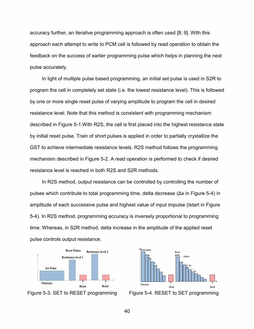
In R2S method, output resistance can be controlled by controlling the number of
pulses which contribute to total programming time, delta decrease (Δx in Figure 5-4) in
amplitude of each successive pulse and highest value of input impulse (Istart in Figure
5-4). In R2S method, programming accuracy is inversely proportional to programming
time. Whereas, in S2R method, delta increase in the amplitude of the applied reset
pulse controls output resistance.
Figure 5-3. SET to RESET programming Figure 5-4. RESET to SET programming
Set Pulse
Time(ns)
Reset Pulses
Resistance level 1
Resistance level 2
Read Read Time(ns)
Reset pulse
Read Read
Δx
Reset pulse Istart

41
Effects of Process Variation
Process variation affects the physical dimensions of the PCM device including
bottom contact electrode diameter (BECD), thickness of the heating element (theater),
thickness of the GST material (tgst) and the gate length of the transistor (lgate_length).
Changes in the physical dimensions are reflected by change in the minimum reset
current required to take the device in completely reset state. Detailed characterization of
the effect of process variation on PCM programming current is done in [12].
Figure 5-5. Distribution of amorphous fraction and resistance with programming current in RESET to SET programming. Parameter variation is introduced in bottom electrode contact diameter.
Figure 5-6. Distribution of amorphous fraction and resistance with programming current in RESET to SET programming. Parameter variation is introduced in thickness of heater
0 100 200 300 400 500 6000
0.2
0.4
0.6
0.8
1
Step Current(uA)
Cal
cula
ted
Ca
Bottom Electrode Contact Diameter (Mean = 90nm, SD=12%)
57 nm73 nm90 nm106 nm122 nm
080160240320400480Time(ns)
0 100 200 300 400 500 600103
104
105
106
107
Step Current(uA)
Res
ista
nce(
ohm
)
57 nm73 nm90 nm106 nm122 nm
080160240320400480
Time(ns)
Pulse 1
Pulse 32
0 100 200 300 400 500 6000
0.2
0.4
0.6
0.8
1
Step Current(uA)
Cal
cula
ted
Ca
Heater Thickness (Mean = 40nm, SD=12%)
25 nm32 nm40 nm47 nm54 nm
080160240320400480Time(ns)
0 100 200 300 400 500 600103
104
105
106
107
Step Current(uA)
Res
ista
nce(
ohm
)
25 nm
32 nm
40 nm
47 nm
54 nm
080160240320400480Time(ns)
Pulse 1
Pulse 32
42
The variation in reset current of the device changes the overall statistics for the
programming of the MLC PCM cell. When a RESET to SET method is used for
programming a cell, the number of pulses required for programming varies due to
process variation. If slope of the programming pulse is estimated by standard cell
dimensions without considering process variation, the required amorphous ratio may not
be achieved. Consequently, to obtain the desired resistance level, multiple
programming efforts are required. Process variation varies the number of programming
attempts required to program a cell in desired resistance state.
As shown in Figure 5-6, the increase of heater thickness leads to less number of
pulses required for a cell to program to the same resistance level than that of a cell with
smaller heater thickness. Also, the average number of pulses required to achieve the
resistance between 10k to100k is much higher than that of 100k to 1M. In this work we
try to leverage the effect of process variation to reduce MLC programming latency and
power by effectively employing different available MLC programming methods.
43
CHAPTER 6 ADAPTIVE PROGRAMMING TECHNIQUES
This work, proposes Mercury, a fast and energy-efficient multi-level cell based
phase change memory system. The Mercury consists of several key components such
as state-aware adaptive programming, PV-aware programming and turbo programming.
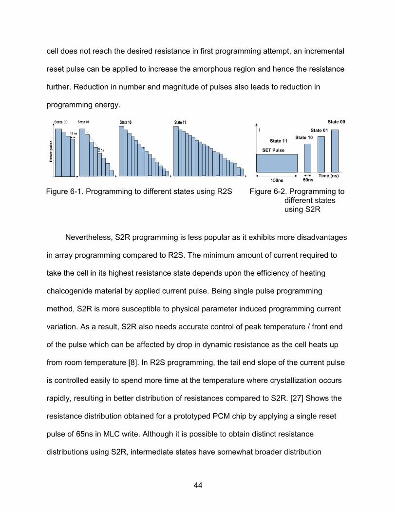
State-aware Adaptive Programming
The required energy-timing-accuracy budget to reach a given resistance level
varies with different programming techniques. With our adaptive programming
technique, every MLC state can be programmed either using R2S or S2R scheme. R2S
programming (Figure 6-1) takes the cell to intermediate states by application of multiple
short duration pulses each causing the cell to step through series of temperatures,
amorphous GST volumes and resistances. Application of short duration pulses is
continued till the desired resistance range is reached. Using the MLC PCM cell model
and the physical dimensions of the cell, we analyze the number of pulses required for a
cell to reach a given resistance level using R2S programming method. We observed
that to reach the completely set state (e.g. state ‘11’ in 2 bit MLC) or a state closer to
completely set state (e.g. state ‘10’) for the assumed cell dimension; approximately 20
to 25 pulses of 15ns (e.g. 300-375 ns) are required. In contrast, the state ‘01’ can be
reached using 13-15 pulses (e.g. 225 ns) and the purely RESET state (state ‘00’) can
be reached in 4-5 pulses (e.g.75 ns).
In the case of S2R programming, the cell resistance is gradually increased using
reset pulses, therefore it is possible to reach intermediate states having low resistance
with a single set pulse and a reset pulse of appropriate amplitude to form amorphous
cap of high resistance. This method reduces the timing to 250-320ns. Moreover, if the
44
cell does not reach the desired resistance in first programming attempt, an incremental
reset pulse can be applied to increase the amorphous region and hence the resistance
further. Reduction in number and magnitude of pulses also leads to reduction in
programming energy.
Figure 6-1. Programming to different states using R2S Figure 6-2. Programming to different states using S2R
Nevertheless, S2R programming is less popular as it exhibits more disadvantages
in array programming compared to R2S. The minimum amount of current required to
take the cell in its highest resistance state depends upon the efficiency of heating
chalcogenide material by applied current pulse. Being single pulse programming
method, S2R is more susceptible to physical parameter induced programming current
variation. As a result, S2R also needs accurate control of peak temperature / front end
of the pulse which can be affected by drop in dynamic resistance as the cell heats up
from room temperature [8]. In R2S programming, the tail end slope of the current pulse
is controlled easily to spend more time at the temperature where crystallization occurs
rapidly, resulting in better distribution of resistances compared to S2R. [27] Shows the
resistance distribution obtained for a prototyped PCM chip by applying a single reset
pulse of 65ns in MLC write. Although it is possible to obtain distinct resistance
distributions using S2R, intermediate states have somewhat broader distribution
Res
et p
ulse
State 00
15 ns
Δx
State 01 State 10 State 11
SET Pulse
State 11State 10
State 01
150nsTime (ns)
50ns
I
State 00
45
compared to R2S programming. Another disadvantage of S2R is that, during
programming of lower resistance states, amorphous volume present in the cell is lower
compared to R2S programming and it forms a series configuration of amorphous and
crystalline material as explained earlier. There is a possibility of formation of crystalline
path through this volume over time due to spontaneous crystallization process of GST
material which leads to lowering resistance of cell. Lower amorphous plug volume
created during S2R programming has higher risk of formation of crystalline path leading
to erroneous data. Fortunately spontaneous crystalline path formation is a long term
process [28] and has minimum probability to cause such erroneous alteration of cell
resistance for average lifetime of data in main memory, making S2R still safe to use.
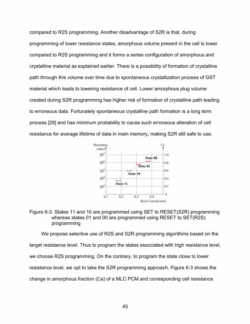
Figure 6-3. States 11 and 10 are programmed using SET to RESET(S2R) programming whereas states 01 and 00 are programmed using RESET to SET(R2S) programming
We propose selective use of R2S and S2R programming algorithms based on the
target resistance level. Thus to program the states associated with high resistance level,
we choose R2S programming. On the contrary, to program the state close to lower
resistance level, we opt to take the S2R programming approach. Figure 6-3 shows the
change in amorphous fraction (Ca) of a MLC PCM and corresponding cell resistance
103
106
105
104
107
Resistance (ohm)
Reset Current (mA)0.40.30.20.1
State 00
State 11
State 10
State 01
Ca
0
0.8
0.6
0.4
0.2
1.0
46
value with increasing reset current. State mapping and mean resistance level with
preferred programming mechanism for each state are highlighted.
After a PCM cell is programmed, its resistance value increases with time due to
structural changes in GST material. This phenomenon is known as resistance drift and it
can worsen the readout errors. It has been observed [29] that drift is becomes more
significant as we go to higher resistance states (e.g. “10”, “01”, “00”), in which
increasing volume of the phase change material is programmed to the amorphous
states in the MLCs, whereas the low resistance state (e.g. “11”) shows a nearly
negligible dependence of resistance on time. As the less accurate S2R technique is
used for programming drift free or drift-insensitive states, addition of errors is mitigated.
PV-aware MLC PCM Programming
Process variation leads to different current pulse magnitude/timing required to
reach the desired resistance level. When an array of cells is programmed using S2R
programming, the reset pulse magnitude which represents worst case is conservatively
applied to program all cells. As stated in earlier section, this causes large spread of
resistances for intermediate resistance levels (e.g. the level used to represent state 01)
thus making S2R programming less accurate. R2S algorithm is better resilient to
resistance spread due to process variation as the large pulse train allows catering
current requirements of different cells. Even with R2S, it is difficult to achieve the target
resistance level with single iteration. Previous studies [13] indicate that 3 to 8 iterations
(as shown in Figure 5-3 and Figure 5-4) are required to program the cell within target
resistance range. Statistical analysis of programming parameters performed over 16K
sample cells with different physical dimensions shows the distribution of number of
programming pulses (Figure 6-4)
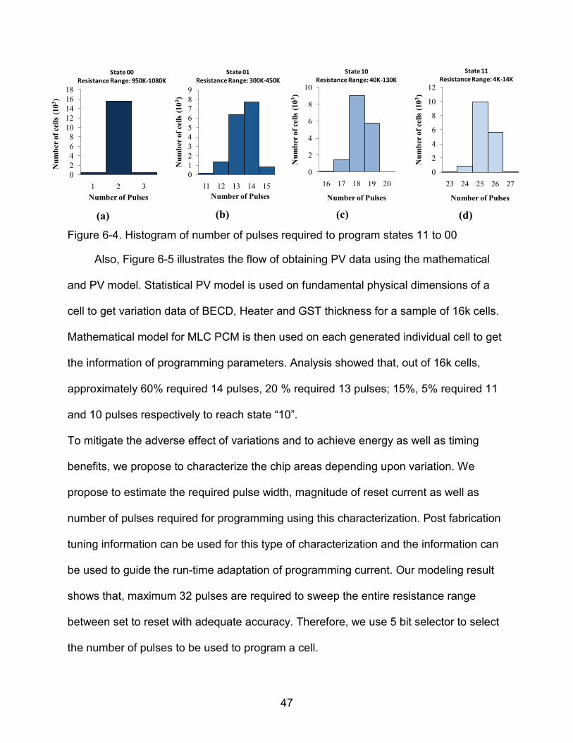
47
(a)
(b)
(c)
(d)
Figure 6-4. Histogram of number of pulses required to program states 11 to 00
Also, Figure 6-5 illustrates the flow of obtaining PV data using the mathematical
and PV model. Statistical PV model is used on fundamental physical dimensions of a
cell to get variation data of BECD, Heater and GST thickness for a sample of 16k cells.
Mathematical model for MLC PCM is then used on each generated individual cell to get
the information of programming parameters. Analysis showed that, out of 16k cells,
approximately 60% required 14 pulses, 20 % required 13 pulses; 15%, 5% required 11
and 10 pulses respectively to reach state “10”.
To mitigate the adverse effect of variations and to achieve energy as well as timing
benefits, we propose to characterize the chip areas depending upon variation. We
propose to estimate the required pulse width, magnitude of reset current as well as
number of pulses required for programming using this characterization. Post fabrication
tuning information can be used for this type of characterization and the information can
be used to guide the run-time adaptation of programming current. Our modeling result
shows that, maximum 32 pulses are required to sweep the entire resistance range
between set to reset with adequate accuracy. Therefore, we use 5 bit selector to select
the number of pulses to be used to program a cell.
02468
1012141618
1 2 3
Num
ber o
f cel
ls (1
03 )
Number of Pulses
State 00Resistance Range: 950K-1080K
0123456789
11 12 13 14 15N
umbe
r of c
ells
(103 )
Number of Pulses
State 01Resistance Range: 300K-450K
0
2
4
6
8
10
16 17 18 19 20
Num
ber o
f cel
ls (1
03 )
Number of Pulses
State 10Resistance Range: 40K-130K
0
2
4
6
8
10
12
23 24 25 26 27
Num
ber o
f cel
ls (1
03 )
Number of Pulses
State 11Resistance Range: 4K-14K

48
Figure 6-5. Programming with variation
Flash memory can be used to store the memory characterization information in
form of deviation in number of pulses and change in magnitude of reset current. Given a
write address, write driver block performs lookup in the post fabrication tuning area to
determine the deviation in magnitude of reset current and number of pulses required to
program the cell array in PV affected area. The bit pattern stored in cell is used to
determine signals to write driver controller to program array of cells. Variation in
physical parameters is spatially correlated. Therefore storing the information about
every single cell in the memory does not provide any benefit; moreover it causes area
and time overhead to lookup the PV data. Cells in the same block are likely to have
similar physical parameters, thus information can be stored at granularity of block rather
than a single cell. Increasing the granularity at which PV information is stored does not
Cell Dimensions affected by PV1.Heater Thickness(theater)
2.Heater Diameter/Bottom Electrode Contact Area(Wb)
3.Thickness of GST material(tgst)4.Transistor gate length
(Distribution for PCM chip)
MLC PCM Model
Variation Model
Basic Parameters of PCM Cell1.Heater Thickness(theater)
2.Heater Diameter/Bottom Electrode Contact Area(Wb)
3.Thickness of GST material(tgst)4.Transistor gate length
For each state-Minimum SET/RESET current
Minimum Number : Programming Pulses
R2S
Time(ns)
Reset pulse
Δx
Reset pulseIstart
Set Pulse
Reset Pulse
Set Pulse
Reset Pulse
S2R
49
give us significant improvement with respect to area and time overhead. We choose to
store the information at level of a single memory array page of 4kB. Considering 2GB of
PCM capacity, the flash memory required to store the PV data is approximately 2MB
which is less than 2% of the total memory capacity.
Turbo Programming
In order to reduce the write overhead further, we propose modifying the
initialization sequence of programming as well as examining the redundancy in writes.
Regardless of the initial state of a cell, S2R programming uses a set pulse to program
the cell to the lowest resistance state and later, it increases the resistance by using
successive reset pulses. If the cell is already in the lowest resistance state, the set step
for initializing the cell can be eliminated. By eliminating the set process which requires
about 250ns pulse, write time as well as energy can be saved. Moreover, if the n-bit
word to be written to a memory cell is unchanged then write operation can be skipped
altogether. By integrating the Data Comparison Write method (DCW) [30]; we can read
the memory line to be modified and perform a write only if new data is different. As PCM
reads are faster (50ns) and they are not destructive, overhead caused by an additional
read in DCW will be negligible during a write operation.
The Mercury Architecture
In this section, we describe the architecture support for Mercury and the
associated overhead. At the circuit level, we adopt MLC PCM programming circuit given
in [31] and propose modification in write driver to support adaptive programming. The
modified write driver circuit block for adaptive programming is shown in Figure 6-7. The
original circuit can support both staircase/set sweep (R2S) as well as single pulse (S2R)
programming. It uses current mirrors to implement binary weighted current steering
50
digital to analog converters (DAC). Amplitude of set/reset pulses required is controlled
by specifying 6/12 bit input to the DAC. The driver controller allows selecting the
approach to be used for write operation. We add components to the driver controller
which allow us to select timing of the programming input, amplitude of the input as well
as programming mechanism for a cell on the fly. In order to adjust timing of
programming pulse, we add a 5 bit input to the write controller, each bit increment adds
a pulse of 15ns to staircase waveform for R2S programming. We add a control signal to
write driver to choose either of the programming mechanism. Control signal is driven by
most significant bit (MSB) of the 2-bit data symbol to be written to the cell. Thus, for
states 00 and 01; MSB 0 selects R2S programming whereas for the state 10 and 11;
MSB 1 selects S2R programming. In the original write driver circuit, pumped voltage is
used to control the reference input current [30] (and hence output programming current)
using a set of charge pumps. We propose to control the granularity of the maximum
value of programming current supplied by the circuit by dividing the charge pump block
into total 8 stages. Activation of each charge pump stage is controlled by a bit in an 8 bit
register and whose value is populated using post fabricated tuning information. We feed
the post fabrication information bits to write driver controller to fine tune duration of
sweep (R2S) for trapezoidal pulse/staircase waveform or amplitude of RESET for single
pulse programming. Iterative programming (Figure 5-4) (multi-level write and verify
algorithm) is implemented with modify signal associated with each cell. The modify
signal indicates whether the cell has reached the desired resistance level. If the cell is
not reached the desired resistance level then the circuit parameters are updated and
cell is reprogrammed.

51
In addition to modification of write driver circuit, we need slight modification at
PCM controller level to support the adaptive data comparison write (DCW) technique.
For the memory controller, we add a new command to perform bit by bit comparison
between the previously stored data (data read out from memory and stored in read
latches) and new data to be written into cells (stored in write FIFO). Thus, each memory
transaction will require two additional commands including command to read the stored
data and to compare it with current data. We add a simple XOR gate based circuit to
perform this comparison. The output of this operation is used to enable/disable the write
operation for ‘n’ bits where ‘n’ represents the number of bits stored in the single PCM
cell.
When DCW is enabled, the extra read operation increases the latency of each
write operation by 50ns. Note that the advantage of our adaptive programming
technique depends upon the presence of states 11 and 10 in the data written to
memory. When DCW scheme is not used, statistically, the probability of writing data in
each state is 25%.When we use DCW, the distribution of states changes dramatically.
We performed analysis of data patterns written to main memory using several
benchmarks from NAS parallel suite and SPEC 2000 suite. We found that before using
DCW, more than 60% of the memory cells were written with data pattern ‘00’ whereas
the remaining states were distributed evenly. After applying DCW, repetitive writes of
data pattern 00 were avoided; thus increasing the percentage of states for which
adaptive programming can be used efficiently. Thus, overhead added by read operation
is negligible compared to benefits.

52
The support for turbo programming is added to circuit by addition of gates to
control the initialization sequence for a PCM cell. When a cell is programmed with S2R
technique, previous data pattern is wiped out by performing set operation on the cell. An
XOR gate whose one input is always 0, is added to check if the cell is already in
completely SET state. If the bit pattern indicates that the cell is in completely SET state
(i.e. the lowest resistance state) and the new pattern to be programmed has resistance
value which will be programmed using S2R method, the initialization sequence to bring
the cell in SET state is skipped. The above two checks can be performed in parallel.
The circuit output enables/disables the initialization pulse at write driver. For 128bit
writes, the area overhead of total 128 XOR gates is required. In addition to read time of
50ns for DCW, we assume additional circuit delay of 5ns to perform the initialization
pulse check.
Figure 6-6. Flowchart of adaptive programming
Figure 6-7. W-2W DAC Adaptable Programming Circuit
Examine Target State
Target Different from current state?
Skip Write
YES
NO
Target Level >= L/2?(L = Total Number of Levels in MLC
including complete SET and RESET)
Use R2S Programming
Target Resistance closer to complete
reset state
Target Resistance closer to complete
set stateYES
NO
Is current state of cell=completely SET state?
Use S2R Programming
Use S2R ProgrammingSKIP INITIALIZATION
YES
NO
12 bit W-2W DAC
Signal for reset currentAmplitude control
Staircase UpWrite and verify
sequence
SET Pulse Setting• Staircase Down• Slow quench• Multiple step
down pulse
N
Controller
ROW
DECODER
PCM ARRAY
Row Address
Column Address
COLUMN DECODER
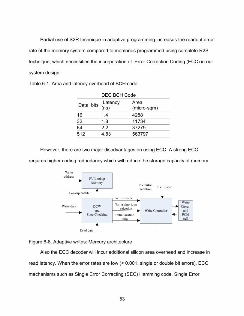
53
Partial use of S2R technique in adaptive programming increases the readout error
rate of the memory system compared to memories programmed using complete R2S
technique, which necessities the incorporation of Error Correction Coding (ECC) in our
system design.
Table 6-1. Area and latency overhead of BCH code
However, there are two major disadvantages on using ECC. A strong ECC
requires higher coding redundancy which will reduce the storage capacity of memory.
Figure 6-8. Adaptive writes: Mercury architecture
Also the ECC decoder will incur additional silicon area overhead and increase in
read latency. When the error rates are low (< 0.001, single or double bit errors), ECC
mechanisms such as Single Error Correcting (SEC) Hamming code, Single Error
Write Controller
PV Lookup Memory
Write address
DCWand
State Checking
Write data
Read data
Lookup enableWrite enable
Initialiazation skip
Write algorithm selection
PV Enable
Write Circuit
and PCM cell
PV pulse variation
DEC BCH Code
Data bits Latency (ns)
Area (micro-sqm)
16 1.4 4288 32 1.8 11734 64 2.2 37279 512 4.83 563797
54
Correcting Double Error Detecting (SEC-DED) extended –Hamming or SEC-DED Hsio
codes can be used. With multi-bit errors; conventional SEC or SEC-DED fails to satisfy
the reliability requirements. Cycling codes such as BCH codes and RS codes are used
traditionally for multi-bit error correction. As the probability of multi-bit errors in adaptive
scheme is higher, we propose to use strong error correcting BCH codes for Mercury
architecture to reach the required reliability levels. BCH codes are used at granularity of
single cache line size. For a message length of k bits, a n-bit BCH codeword comprising
of both data and ECC check-bits can be constructed to correct up to t bit errors. The
length of the codeword should satisfy 1212 )1( −<=<−− mm n and kntm −<=* where m is
minimum number of redundant ECC bits required for every error correction. For 1 bit
error correction over 512 bits, additional 10 redundant ECC bits are required [32]. This
implies the overhead for correcting up to 8 bit errors per 64 bytes is 10 bytes. Table 6-1
shows the trend in silicon area and latency overhead for dual error correcting codes
In S2R programming scheme, more errors are introduced in intermediate states
due to large distribution of resistances; whereas in the R2S programming error rate is
negligible. With adaptive technique, the errors will be introduced in half of the
intermediate states compared to errors introduced in all intermediate states for S2R.
Though this does not improve the overall system performance of adaptive scheme with
respect to S2R, the overhead of storage of ECC bits and hardware complexity of
decoder is significantly reduced. This will reduce the number of memory pages required
to store redundant check bits. Capacity required for ECC storage thus ranges from 15%
of memory capacity for 8 bit error correction to 4% for 4 bit error correction.
55
The modified write driver circuit (Figure 6-7) as well as controller implementing
state aware adaptive programming (Figure 6-6) together form Mercury architecture
presented in Figure 6-8. On initiating a write operation, the data stored at memory
location to be written is read and compared with the new data to be written. If both the
values are different, write driver block is enabled. In the PV flash memory, parallel
lookup of write address is performed to obtain variation information giving programming
time and amplitude. The information is used to control the activation of charge pump
stages as well as addition of programming pulses in R2S programming. Specialized
ECC hardware computes the check bits for the entire data word of 512bits.The
programming mechanism is selected depending upon state to be written to the cell. We
also check if initial state of the cell is SET state. “Skip initialization” signal is enabled if
the cell has state transition from completely set state to state 10. When the write
controller receives the PV information, programming mechanism selection and skip
initialization selection signal; it generates the programming pulse sequence for the cell.
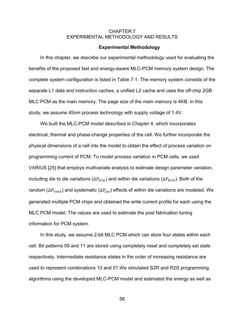
56
CHAPTER 7 EXPERIMENTAL METHODOLOGY AND RESULTS
Experimental Methodology
In this chapter, we describe our experimental methodology used for evaluating the
benefits of the proposed fast and energy-aware MLC-PCM memory system design. The
complete system configuration is listed in Table 7-1. The memory system consists of the
separate L1 data and instruction caches, a unified L2 cache and uses the off-chip 2GB
MLC PCM as the main memory. The page size of the main memory is 4KB. In this
study, we assume 45nm process technology with supply voltage of 1.4V.
We built the MLC-PCM model described in Chapter 4, which incorporates
electrical, thermal and phase-change properties of the cell. We further incorporate the
physical dimensions of a cell into the model to obtain the effect of process variation on
programming current of PCM. To model process variation in PCM cells, we used
VARIUS [25] that employs multivariate analysis to estimate design parameter variation,
including die to die variations (Δ𝑃𝐷2𝐷) and within die variations (Δ𝑃𝑊𝐼𝐷). Both of the
random (Δ𝑃𝑟𝑎𝑛𝑑) and systematic (Δ𝑃𝑠𝑦𝑠) effects of within die variations are modeled. We
generated multiple PCM chips and obtained the write current profile for each using the
MLC PCM model. The values are used to estimate the post fabrication tuning
information for PCM system.
In this study, we assume 2-bit MLC PCM which can store four states within each
cell. Bit patterns 00 and 11 are stored using completely reset and completely set state
respectively. Intermediate resistance states in the order of increasing resistance are
used to represent combinations 10 and 01.We simulated S2R and R2S programming
algorithms using the developed MLC-PCM model and estimated the energy as well as

57
timing budgets required to take the cell to a resistance level by varying the physical
parameters of the cell.
Table 7-1. Baseline Machine Configuration
Table 7-2. PCM Parameters
Read Parameters Read Current 40uA Read Voltage 1.1V
Write Parameters R2S Programming (Without PV) S2R Programming (Without PV)
State Pulses Set Current 150uA Reset Current 250uA State 00 (RESET) 5 Set Timing 200ns Set Current 150uA State 01 14 Reset Current 200uA Pulse duration 15ns State 10 18 Reset Timing 50ns Write Voltage 1.6V State 11(SET) 28 Set to Reset Step 25uA
Parameter Configuration Parameter Configuration
Frequency 3GHz LDQ 48 entries
Width 4-wide fetch/decode/issue/commit STQ 32 entries
IQ 128 entries Int. ALU 4 I-ALU, 2 I-MUL/DIV, 1 load/Store
ITLB 128 entries, 4-way FP ALU 2 FP-ALU, 2 FP-MUL/DIV/SQRT
Branch Pred.
2K entries Gshare, 10-bit global history DTLB 256 entries, 4-way
BTB 2K entries, 4-way L1 D-Cache
64KB, 4-way, 64 Byte/line, 2 ports, 3 cycle
RAS 32 entries RAS L2 Cache Shared 1MB, 16-way, 64 Byte/line, 12 cycle
L1 I-Cache 64KB, 4-way, 64 Byte/line, 2 ports, 3 cycle Memory MLC-PCM(2GB effective
capacity, 8 banks)
ROB 128 entries Write Buffer 32 entries, 64B per entry

58
For performance evaluation of the complete system, we developed a framework
using full-system simulator PTLSim/X [33] integrated with memory model of DRAMSim
[34]. PTLSim with Xen is a fast full-system cycle accurate simulator which supports x86
ISA and partial simulation in native mode. We extended the simulator to support the
PCM memory system with two-level write-back cache. To model the latency and energy
of PCM system, we enhanced DRAMSim module to emulate the effect of PCM specific
structures such as current sense amplifier and write driver blocks. The range of
parameter values listed in Table 7-2 was obtained through simulations performed using
MLC PCM model. The correctness of values was verified using parameters obtained
from extensive literature search. The set to reset step indicates change in reset current
value when going from state 11 to state 00 in S2R programming for programming of
intermediate states. The Table 7-2 also mentions the number of 15ns pulses required to
program each state using R2S programming.
As mentioned in Chapter 6, to correct readout errors, ECC mechanism is
employed in our system design. To determine the ECC latency and area overhead, we
used the PCM cell model to calculate probability of error for R2S mechanism as well as
designed a probability based error model for S2R mechanism to obtain the different
error percentage for each state. We assume that the lowest and the highest resistance
states are not subjected to error, only intermediate states have errors due to
programming mechanism. We assume error correction latency of 15 cycles per error
We use diverse set of workloads from SPEC2000 and NAS benchmark suites to
evaluate our technique. The workloads are selected so as to cover wide range of data
59
access patterns, miss rates and working set sizes. All the benchmarks are compiled
using GCC or FORTRAN compiler with optimization level –O3.
Results and Evaluation
In this section, we evaluate the performance and energy benefit of our proposed
PV and state aware adaptive programming techniques. We compare Mercury (adaptive
programming with PV awareness and turbo programming) with R2S, PV-aware R2S
programming (R2S+PV), S2R, adaptive programming (adaptive), adaptive programming
with PV (adaptive+PV) and use R2S as the baseline for all comparisons. Note that the
results are reported for each benchmark and normalized to the baseline case of that
benchmark. We apply data comparison writes in all the techniques so as to reduce the
redundant write accesses to memory. To improve the performance of MLC PCM
system, we implement the write optimization techniques (e.g. write cancelling and write
pausing) proposed in [13].
Performance Improvement
Figure 7-1 shows the normalized execution time of all the examined scenarios. On
average, Mercury achieves 10% performance improvement over R2S programming
across all the benchmarks. We observed that floating point benchmarks such as lucas,
mesa and swim show higher improvement compared to integer benchmarks such as
crafty. Also, benchmarks from NAS suite (eg.bt) show higher performance
improvement. Further analysis shows that performance improvement depends upon the
total number of read and writes to memory, the ratio of reads to writes as well as state
wise distribution of accesses. We performed in depth analysis of memory access
statistics to obtain the distribution of states in writes without DCW as well as with DCW
(Figure 7-2 and Figure 7-3 respectively). We collected the number of read-write
60
accesses presented in Figure 7-4 and Figure 7-5 by running workloads for 50 million
instructions. From the access statistics in Figure 7-5, it is evident that lucas, mesa and
bt have more accesses to memory compared to benchmarks such as crafty and
sixtrack. Moreover as Figure 7-4 points out, they have equal percentage of reads and
writes. Benchmarks having higher percentage of write to states 10 and 11 show higher
improvements as adaptive programming improves write latency of these states. Though
crafty shows higher distribution of states 10 and 11; the total number of memory
accesses is small with more percentage of reads. Similarly sixtrack has much higher
reads compared to writes. Here, the performance gets heavily penalized due to error
correction latency incurred in reads when S2R programming is used.
Figure 7-1. Performance Improvement
We observe about 4% improvement when PV-aware programming is combined
with R2S technique. Experiments performed using mathematical model show that
maximum 2-3 pulses can be saved in each state due to PV-aware programming and
maximum three states (i.e. 11,10 and 01 ) can be benefited in R2S+PV. However
visibility of reduction in execution time is limited due to dominating write latency of PCM.
In adaptive programming, R2S programming is used only in states 00, state 01 for
0
0.2
0.4
0.6
0.8
1
1.2
Nor
mal
ized
Exe
cutio
n T
ime R2S R2S+PV S2R Adaptive Adaptive+PV Mercury
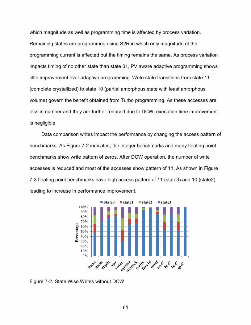
61
which magnitude as well as programming time is affected by process variation.
Remaining states are programmed using S2R in which only magnitude of the
programming current is affected but the timing remains the same. As process variation
impacts timing of no other state than state 01, PV aware adaptive programming shows
little improvement over adaptive programming. Write state transitions from state 11
(complete crystallized) to state 10 (partial amorphous state with least amorphous
volume) govern the benefit obtained from Turbo programming. As these accesses are
less in number and they are further reduced due to DCW, execution time improvement
is negligible.
Data comparison writes impact the performance by changing the access pattern of
benchmarks. As Figure 7-2 indicates, the integer benchmarks and many floating point
benchmarks show write pattern of zeros. After DCW operation, the number of write
accesses is reduced and most of the accesses show pattern of 11. As shown in Figure
7-3 floating point benchmarks have high access pattern of 11 (state3) and 10 (state2),
leading to increase in performance improvement.
Figure 7-2. State Wise Writes without DCW
0%10%20%30%40%50%60%70%80%90%
100%
Perc
enta
ge
State0 state1 state2 state3
62
Figure 7-3. State Wise Writes with DCW
Energy Efficiency
Figure 7-6 shows the impact on the energy of the system when each programming
technique is applied incrementally. PV-aware programming achieves 7% improvement
in energy whereas adaptive programming gives about 25% improvement in energy.
Combining the PV-aware programming with adaptive technique, further improvement of
2-3% is obtained.
Figure 7-4. Read-Write Relative Statistics
0%10%20%30%40%50%60%70%80%90%
100%
Perc
enta
ge
state0 state1 state2 state3
0%10%20%30%40%50%60%70%80%90%
100%
Perc
enta
ge
Write Read Ifetch

63
Figure 7-5. Absolute Number of Read-Write Accesses
Equake and swim yield 29% of energy improvement with respect to the baseline.
On application of PV-aware programming, the energy improvement increases to 32%
and 33% respectively as they have more writes to state 11. Energy improvement in
case of mesa and bt is 20 % more compared to others.
Figure 7-6. Improvement in Energy
This is because, both the benchmarks have read to write ratio of 1:1 (as shown in
Figure 7-4) and maximum writes are of state 11 (as shown in Figure 7-3) which gives
them an advantage when adaptive programming is used. Note that, energy values
0
200
400
600
800
1000
1200
1400
1600
Wri
te /
Rea
d X
100
0
Write Read
0
0.2
0.4
0.6
0.8
1
1.2
Nor
mal
ized
Ene
rgy
R2S R2S+PV S2R Adaptive Adaptive+PV Mercury
64
shown in Figure 7-6 consider energy due to writes. When total energy of the system is
considered, 20% energy improvement is observed over baseline.
Power Enhancement
As shown in Figure 7-7, adaptive programming achieves 8-10% power saving over
the baseline R2S programming. However, it consumes 5% more power compared to the
S2R mechanism. PV-aware programming shows power reduction by additional 3-4%.
Power improvement is more noticeable on benchmarks having more writes. R2S
programming current has several short duration high current pulses, leading to more
power consumption. S2R programming uses single pulse whose amplitude is lower than
R2S. Adaptive programming uses R2S waveform for half of states leading to increased
power consumption in adaptive.
Figure 7-7. Power Reduction
As mentioned in Chapter 6, S2R has more errors in readout compared to adaptive.
This forces an additional area overhead to store ECC bits as well as incur correction
overhead per read error. This makes adaptive programming more promising compared
to S2R even though both show almost similar performance on execution time and
energy.
0.75
0.8
0.85
0.9
0.95
1
1.05
Nor
mal
ized
Pow
er
R2S R2S+PV S2R Adaptive Adaptive+PV Mercury
65
CHAPTER 8 CONCLUSION AND FUTURE WORK
Conclusion
MLC PCM systems provide high storage capacity at the expense of increased
programming energy and latency. The presence of process variation makes the MLC
programming even worse as the minimum time and energy requirements of cells differ
according to physical dimensions. Different MLC programming techniques offer tradeoff
between accuracy, programming time and programming energy, depending on the
target resistance level as well as initial resistance state of the cell. We propose selection
of programming techniques adaptively to optimize accuracy with programming energy
and latency. We also propose tuning the techniques by using process variation data
collected at the post fabrication stage. We performed detailed modeling of the MLC
PCM cell as well as extended the model to include the effect of variation of physical
dimensions of the device to obtain energy and timing budgets for different resistance
states for MLC. Our experiments show that the proposed adaptive programming
technique achieves performance benefit of 10% and energy benefit of 20% over
conventional R2S programming methods. Employing PV-aware technique further
improves energy performance to 23-25%.
Future Work
This project explored different programming techniques which can be used to
program a MLC PCM cell. Also we built a MLC PCM model and modified it to
incorporate the effect of variation of physical dimensions of the cell. Although the model
is able to simulate most of the cases observed in MLC programming, it fails to simulate
66
some programming algorithms. We aim to modify the model to simulate these
algorithms to represent MLC PCM programming phenomenon more accurately.
The workloads currently being used in simulation of the system are single
threaded workloads. Also, the memory footprint of many of the workloads is not large
enough to stress the memory system. We plan to evaluate the system with more
memory intensive workloads. Moreover, we plan to perform simulations with multi-
threaded workloads to have realistic evaluation as most of the computer systems
are many-core/multi-core systems. We would also like to observe the combined effect of
this technique with other cutting edge PCM micro-architecture level techniques.
Hardware interface of PCM is not well defined. There is very little literature
available about the interface and it is assumed to be similar to DRAM. Overhead of Any
modification at micro-architecture level is highly dependent on the underlying hardware
interface. We propose to model the PCM interfaces in more detail in future work.
We would like to explore the arena of error correction coding for phase change
memories in our further work.
67
LIST OF REFERENCES
[1]. G. Burr, M. Breitwisch, D. Garetto et. al., Phase change memory technology, JVSTB, 2010 [2]. D., Ielmini et. al., Analysis of Phase Distribution in Phase-Change Nonvolatile Memories., IEEE Electron Device Letters, July 2004. [3]. S. Lai, T. Lowrey, OVM – A 180 nm Nonvolatile Memory Cell Element Technology For Stand Alone and Embedded Applications, IEDM, 2001. [4]. S. Lai, Current status of the phase change memory and its future, Intel Corporation. [5]. F. Rao, Z. Song, M. Zhong, L. Wu, G. Feng, B. Liu, S. Feng, and B. Chen., Multilevel Data Storage Characteristics of Phase Change Memory Cell with Doublelayer Chalcogenide Films (Ge2Sb2Te5 and Sb2Te3). ,In JJAP, 2007. [6]. S. Raux, G. W. Burr, M. J. Breitwisch et. al. Phase-change random access memory : A scalable technology, IBM Journal of Research and Development, 2008 [7]. B. C. Lee, E. Ipek,O. Mutlu, and D. Burger, 2009. Architecting phase change memory as a scalable dram alternative, In ISCA 2009. [8]. T.Nirschl, J.B. Phipp,T.D. Happ,G. Burr,B. Rajendran, M.H.Lee, A.Schrott, M. Yang, M. Breitwisch,C.F. Chen, E. Joseph, M. Lamorey, R.Cheek, S.H. Chen,S. Zaidi, S. Raoux, Y. C. Chen, Y. Zhu, R.Bergmann,H. Lung,C. Lam, Write Strategies for 2 and 4-bit Multi-Level Phase-Change Memory, IEDM, 2007. [9]. F. Bedeschi, R. Fackenthal, C. Resta,E.M. Donze,M. Jagasivamani, E.C. Buda,F. Pellizzer, D.W. Chow,A. Cabrini, G.Calvi, R.Faravelli, A. Fantini, G. Torelli, D.Mills, R. Gastaldi, G. Casagrande, A Bipolar-Selected Phase Change Memory Featuring Multi-Level Cell Storage, JSSC 2009. [10]. F. Bedeschi, C. Resta, O. Khouri, E. Buda, L. Costa, M. Ferraro,F. Pellizzer, F. Ottogalli, A. Pirovano, M. Tosi, R. Bez, R. Gastaldi and G. Casagrande ,An 8Mb demonstrator for high-density 1.8V Phase-Change Memories,Symposium on VLSI Circuits. Digest of Technical Papers., June 2004. [11]. F. Bedeschi, E. Bonizzoni, G. Casagrande, R. Gastaldi, C. Resta,G. Torelli, and D. ZelLa, SET and RESET pulse characterization in BJT-selected phase-change memories.,ISCAS 2005. [12]. W. Zhang, and T. Li,Characterizing and Mitigating the Impact of Process Variations on Phase Change based Memory Systems, MICRO, 2009.

68
[13]. M. Qureshi, M. Franceschini, and L. Lastras,Improving Read Performance of Phase Change Memories via Write Cancellation and Write Pausing, HPCA, 2010. [14]. M. Qureshi,V. Srinivasan,J.Rivers,Scalable High-Performance Main Memory System Using Phase-Change Memory Technology, ISCA, 2009. [15]. M.Qureshi, M Franceschini, L Lastras, J.Karidis. ,Morphable Memory System: A Robust Architecture for Exploiting Multi-Level Phase Change Memories, ISCA, 2010 [16]. P. Fantini, A Benvenuti, F. Pellizzer et. al, A compact model for Phase Change Memories, SISPAD 2006 [17]. X. Q. Wei, L.P. Shi, R. Walia, HSPICE Macromodel of PCRAM for Binary and Multilevel Storage, TED 2005 [18]. D. Ventrice, P. Fantini, A. Redaelli et. al, A Phase Change Memory Compact Model for Multilevel Applications, TED 2007 [19]. R. Cobley, C. D. Wright, Parameterized SPICE Model for a Phase-Change RAM Device, TED 2005 [20]. D. Kang, D. Ahn, K. Kim, J. F. Webb, K. Yi, One-dimensional heat conduction model for an electrical phase change random access memory device with 8F2 memory cell (F=0.15 µm), JAP 2003 [21]. C. Peng, L. Cheng, M. Mansuripur, Experimental and theoretical investigations of laser induced crystallization and amorphization in phase-change optical recording media, JAP 1997. [22]. S. Braga, A. Cabrini, G. Torelli, Theoretical analysis of the RESET operation in phase-change memories, IOP 2009 [23]. K. Sonoda, A. Sakai, M. Moniwa, K. Ishikawa,O. Tsuchiya, Y. Inoue, A Compact Model of Phase-Change Memory Based on Rate Equations of Crystallization and Amorphization, TED, 2008. [24]. A. Pantazi et. al,Multilevel Phase-Change Memory Modeling and Experimental Characterization, EPCOS, 2009. [25]. S.R. Sarangi et al.,VARIUS: A Model of Process Variation and Resulting Timing Errors for Microarchitects.,IEEE Transactions on Semiconductor Manufacturing, Feb. 2008. [26]. A. Kahn, How much variability can designers tolerate? Design & Test of Computers . 2003.
69
[27]. T.D. Happ., M. Breitwitsch, A. Schrott , J.B. Philipp, M.H. Lee, R. Cheek, T. Nirschl, M. Lamorey, C. H. Ho, S. H. Chen, C.F Chen,E. Joseph, S. Zaidi,Burr G.W, B. Yee, Y. C. Chen, S Raoux, H. L. Lung, R. Burgmann, C. Lam.,Novel One-Mask Self-Heating Pillar Phase Change Memory.,Symposium of VLSI Technology, 2006 [28]. R. Faravelli, http://www-3.unipv.it/dottIEIE/tesi/2008/r_faravelli.pdf. [Online] [29]. D. Ielmini, S. Lavizarri, D. Sharma, A.L. Lacaita,Physical Interpretation, modeling and impact of phase change memory (PCM) reliability of resistance drift due to chalcogenide structural relaxation.,IEDM, 2007. [30]. P. Zhou, B. Zhao, J. Yang and Y. Zhang.,A Durable and Energy Efficient Main Memory Using Phase Change Memory Technology, ISCA, 2009. [31]. S. Gupta , V. Saxena,K. Campbell,J. Baker,W-2W Current Steering DAC for Programming Phase Change Memory,WMED, 2009. [32]. J. Kong,H. Zhou,Improving privacy and lifetime of PCM based main memory,DSN, 2010. [33]. M. T. Yourst, PTLSim: A cycle accurate full system x86-64 Microarchitectural simulator, ISPASS, 2007. [34]. D. Wang, B. Ganesh, N. Tuaychareon, K. Baynes,A. Jaleel, B. Jacob. ,DRAMSim: A memory system simulator, SIGARCH, 2005.
70
BIOGRAPHICAL SKETCH
The author was born in the city of Mumbai (formerly known as Bombay), India.
After finishing her high school education in 2003, she completed her undergraduate
degree in electronics engineering at the University of Mumbai, India in 2007. She
worked as a Software Engineer at Infosys Technologies Ltd for one year until she
decided to pursue her master’s degree in electrical and computer engineering at
University of Florida; Gainesville starting from fall 2008. Computer architecture and
embedded systems are her areas of specialization. She has worked as firmware design
intern with Circuitwerkes Technologies Ltd. for summer 2009. She has been working as
a research assistant under Dr. Tao Li in IDEAL research (Intelligent Design of Efficient
Architecture Lab) since January 2010.