Embed Size (px)
Citation preview

The RF MEMS acronym stands for radio frequency microelectromechanical system, and refers to components of which moving sub-millimeter-sized parts provide RF functionality. RF functionality can be implemented using a variety of RF technologies. Besides RF MEMS technology, ferrite, ferroelectric, GaAs, GaN, InP, RF CMOS, SiC, and SiGe technology are available to the RF designer. Each of the RF technologies offers a distinct trade-off between cost, frequency, gain, large scale integration, lifetime, linearity, noise figure, packaging, power consumption, power handling, reliability, repeatability, ruggedness, size, supply voltage, switching time and weight.
Resonators
More to come.
[edit] Switches, switched capacitors and varactors
RF MEMS switches, switched capacitors and varactors, which can replace field effect transistor (FET) switches and PIN diodes, are classified by actuation method (electrostatic, electrothermal, magnetic, piezoelectric), by axis of deflection (laterally, vertically), by circuit configuration (series, shunt), by clamp configuration (cantilever, fixed-fixed beam), or by contact interface (capacitive, ohmic) [2]. Electrostatically-actuated RF MEMS components offer low insertion loss and high isolation, high linearity, high power handling and high Q factor, do not consume power, but require a high supply voltage and hermetic wafer level packaging (WLP) (anodic or glas frit wafer bonding) or single chip packaging (SCP) (thin film capping, liquid crystal polymer (LCP) or low temperature co-fired ceramic (LTCC) packaging).
RF MEMS switches were pioneered by Hughes Research Laboratories, Malibu, CA [3], Raytheon, Dallas, TX [4][5], and Rockwell Science, Thousand Oaks, CA [6], during the nineties. The component shown in Fig. 1, is a center-pulled capacitive fixed-fixed beam RF MEMS switch, developed and patented by Raytheon in 1994. A capacitive fixed-fixed beam RF MEMS switch is in essence a micro-machined capacitor with a moving top electrode - i.e. the beam.
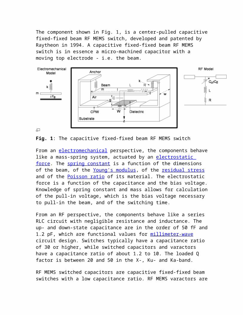
Fig. 1: The capacitive fixed-fixed beam RF MEMS switch
From an electromechanical perspective, the components behave like a mass-spring system, actuated by an electrostatic force. The spring constant is a function of the dimensions of the beam, of the Young's modulus, of the residual stress and of the Poisson ratio of its material. The electrostatic force is a function of the capacitance and the bias voltage. Knowledge of spring constant and mass allows for calculation of the pull-in voltage, which is the bias voltage necessary to pull-in the beam, and of the switching time.
From an RF perspective, the components behave like a series RLC circuit with negligible resistance and inductance. The up- and down-state capacitance are in the order of 50 fF and 1.2 pF, which are functional values for millimeter-wave circuit design. Switches typically have a capacitance ratio of 30 or higher, while switched capacitors and varactors have a capacitance ratio of about 1.2 to 10. The loaded Q factor is between 20 and 50 in the X-, Ku- and Ka-band.
RF MEMS switched capacitors are capacitive fixed-fixed beam switches with a low capacitance ratio. RF MEMS varactors are capacitive fixed-fixed beam switches which are biased below pull-in voltage. Other examples of RF MEMS switches are ohmic cantilever switches, and capacitive single pole N throw (SPNT) switches based on the axial gap wobble motor [7].
[edit] Microfabrication
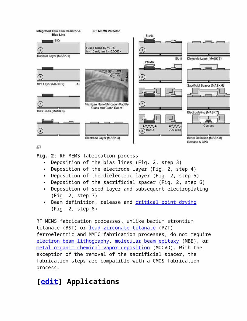
An RF MEMS fabrication process allows for integration of SiCr or TaN thin film resistors (TFR), metal-air-metal (MAM) capacitors, metal-insulator-metal (MIM) capacitors, and RF MEMS components. An RF MEMS fabrication process can be realized on a variety of wafers: fused silica (quartz), borosilicate glass, LCP, sapphire, and passivated silicon and III-V compound semiconducting wafers. As shown in Fig. 2, RF MEMS components can be fabricated in class 100 clean rooms using 6 to 8 optical lithography steps with a 5 μm contact alignment error, whereas state-of-the-art monolithic microwave integrated circuit (MMIC) and radio frequency integrated circuit (RFIC) fabrication processes require 13 to 25 lithography steps. The essential microfabrication steps are:
Fig. 2: RF MEMS fabrication process Deposition of the bias lines (Fig. 2, step 3) Deposition of the electrode layer (Fig. 2, step 4) Deposition of the dielectric layer (Fig. 2, step 5) Deposition of the sacrificial spacer (Fig. 2, step 6) Deposition of seed layer and subsequent electroplating (Fig. 2, step 7) Beam definition, release and critical point drying (Fig. 2, step 8)
RF MEMS fabrication processes, unlike barium strontium titanate (BST) or lead zirconate titanate (PZT) ferroelectric and MMIC fabrication processes, do not require electron beam lithography, molecular beam epitaxy (MBE), or metal organic chemical vapor deposition (MOCVD). With the exception of the removal of the sacrificial spacer, the fabrication steps are compatible with a CMOS fabrication process.
[edit] Applications
Applications of RF MEMS resonators and switches include oscillators and routing networks. RF MEMS components are also applied in radar sensors (passive electronically scanned (sub)arrays and T/R modules) and software-defined radio (reconfigurable antennas, tunable band-pass filters).
[edit] Antennas
Polarization and radiation pattern reconfigurability, and frequency tunability, are usually achieved by incorporation of lumped components based on III-V semiconductor technology, such as single pole single throw (SPST) switches or varactor diodes. However, these components can be readily replaced by RF MEMS switches and varactors in order to take advantage of the low insertion loss and high Q factor offered by RF MEMS technology. In addition, RF MEMS components can be integrated monolithically on low-loss dielectric substrates, such as borosilicate glass, fused silica or LCP, whereas III-V semiconducting substrates are generally lossy and have a high dielectric constant. A low loss tangent and low dielectric constant are of importance for the efficiency and the bandwidth of the antenna.
The prior art includes an RF MEMS frequency tunable fractal antenna for the 0.1–6 GHz frequency range [8], and the actual integration of RF-MEMS on a self-similar Sierpinski gasket antenna to increase its number of resonant frequencies, extending its range to 8 GHz, 14 GHz and 25 GHz [9],[10], an RF MEMS radiation pattern reconfigurable spiral antenna for 6 and 10 GHz [11], an RF MEMS radiation pattern reconfigurable spiral antenna for the 6–7 GHz frequency band based on packaged Radant MEMS SPST-RMSW100 switches [12], an RF MEMS multiband Sierpinski fractal antenna, again with integrated RF MEMS switches, functioning at different bands from 2.4 to 18 GHz [13], and a 2-bit Ka-band RF MEMS frequency tunable slot antenna [14].
[edit] Filters
RF bandpass filters are used to increase out-of-band rejection, if the antenna fails to provide sufficient selectivity. Out-of-band rejection eases the dynamic range requirement of low noise amplifier LNA and mixer in the light of interference. Off-chip RF bandpass filters based on lumped bulk acoustic wave (BAW), ceramic, surface acoustic wave (SAW), quartz crystal, and thin film bulk acoustic resonator (FBAR) resonators have superseded distributed RF bandpass filters based on transmission line resonators, printed on substrates with low loss tangent, or based on waveguide cavities. RF MEMS resonators offer the potential of on-chip integration of high-Q resonators and low-loss bandpass filters. The Q factor of RF MEMS resonators is in the order of 1000-1000 [15].
Tunable RF bandpass filters offer a significant size reduction over switched RF bandpass filter banks. They can be implemented using III-V semiconducting varactors, BST or PZT ferroelectric and RF MEMS switches, switched capacitors and varactors, and yttrium iron garnet (YIG) ferrites. RF MEMS technology offers the tunable filter designer a compelling trade-off between insertion loss, linearity, power consumption, power handling, size, and switching time [16].
RF MEMS SWITCHES: STATUS OF THE TECHNOLOGY
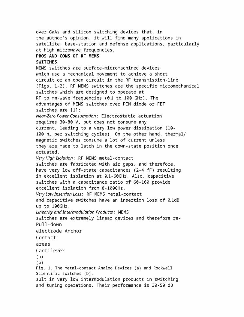
Gabriel M. RebeizThis paper presents the latest accomplishments inRF MEMS switches, and at the same time, an assessmentof their potential applications in defense andcommercial systems. It is seen that RF MEMS devicesoffer spectacular performance at microwave frequencies,but suffer from reliability problems and thepotential of relatively high-cost hermetic packaging.Still, this technology offers such tremendous advantagesover GaAs and silicon switching devices that, inthe author’s opinion, it will find many applications insatellite, base-station and defense applications, particularlyat high microwave frequencies.PROS AND CONS OF RF MEMSSWITCHESMEMS switches are surface-micromachined deviceswhich use a mechanical movement to achieve a shortcircuit or an open circuit in the RF transmission-line(Figs. 1-2). RF MEMS switches are the specific micromechanicalswitches which are designed to operate atRF to mm-wave frequencies (0.1 to 100 GHz). Theadvantages of MEMS switches over PIN diode or FETswitches are [1]:Near-Zero Power Consumption: Electrostatic actuationrequires 30-80 V, but does not consume anycurrent, leading to a very low power dissipation (10-100 nJ per switching cycles). On the other hand, thermal/magnetic switches consume a lot of current unlessthey are made to latch in the down-state position onceactuated.Very High Isolation: RF MEMS metal-contactswitches are fabricated with air gaps, and therefore,have very low off-state capacitances (2-4 fF) resultingin excellent isolation at 0.1-60GHz. Also, capacitiveswitches with a capacitance ratio of 60-160 provideexcellent isolation from 8-100GHz.Very Low Insertion Loss: RF MEMS metal-contactand capacitive switches have an insertion loss of 0.1dBup to 100GHz.Linearity and Intermodulation Products: MEMSswitches are extremely linear devices and therefore re-Pull-downelectrode AnchorContactareasCantilever(a)(b)Fig. 1. The metal-contact Analog Devices (a) and RockwellScientific switches (b).
sult in very low intermodulation products in switchingand tuning operations. Their performance is 30-50 dBbetter than PIN or FET switches.Potential for Low Cost: RF MEMS switches arefabricated using surface micromachining techniquesand can be built on quartz, Pyrex, LTCC, mechanicalgradehigh-resistivity silicon or GaAs substrates.RF MEMS switches also have their share of problems,and these are:Relatively Low Speeds: The switching speed ofmost electrostatic MEMS switches is 2-40 μs, and4A1.4TRANSDUCERS ‘03The 12th International Conference on Solid State Sensors, Actuators and Microsystems, Boston, June 8-12, 2003
0-7803-
[edit] Phase shifters
RF MEMS phase shifters have enabled wide-angle passive electronically scanned arrays, such as lenses, reflect arrays, subarrays and switched beamforming networks, with high effective isotropically radiated power (EIRP), also referred to as the power-aperture product, and high Gr/T. EIRP is the product of the transmit gain, Gt, and the transmit power, Pt. Gr/T is the quotient of the receive gain and the antenna noise temperature. A high EIRP and Gr/T are a prerequisite for long-range detection. The EIRP and Gr/T are a function of the number of antenna elements per subarray and of the maximum scanning angle. The number of antenna elements per subarray should be chosen to optimize the EIRP or the EIRP x Gr/T product, as shown in Fig. 3 and Fig. 4.
Fig. 3: Radar sensor sensitivity: EIRP x Gr/T
Passive subarrays based on RF MEMS phase shifters may be used to lower the amount of T/R modules in an active electronically scanned array. The statement is illustrated with
examples in Fig. 3: assume a one-by-eight passive subarray is used for transmit as well as receive, with following characteristics: f = 38 GHz, Gr = Gt = 10 dBi, BW = 2 GHz, Pt = 4 W. The low loss (6.75 ps/dB) and good power handling (500 mW) of the RF MEMS phase shifters allow an EIRP of 40 W and a Gr/T of 0.036 1/K. The number of antenna elements per subarray should be chosen in order to optimize the EIRP or the EIRP x Gr/T product, as shown in Fig. 3 and Fig. 4. The radar range equation can be used to calculate the maximum range for which targets can be detected with 10 dB of SNR at the input of the receiver.
Fig. 4: EIRP versus number of antenna elements in a passive subarray.
Fig. 5: EIRP x Gr/T versus number of antenna elements in a passive subarray.
in which kB is the Boltzmann constant, λ is the free-space wavelength, and σ is the RCS of the target. Range values are tabulated in Table 1
for following targets: a sphere with a radius, a, of 10 cm (σ = π a2), a dihedral corner reflector with facet size, a, of 10 cm (σ = 12 a4/λ2), the rear of a car (σ = 20 m2) and for a contemporary non-evasive fighter jet (σ = 400 m2). A Ka-band hybrid ESA capable of detecting a car 100 m in front and engaging a fighter jet at 10 km can be realized using
2.5 and 422 passive subarrays (and T/R modules), respectively.
Table 1: Maximum Detectable Range(SNR = 10 dB)
RCS (m2) Range (m)Sphere 0.0314 10
Rear of Car 20 51Dihedral Corner Reflector 60.9 67Fighter Jet 400 107
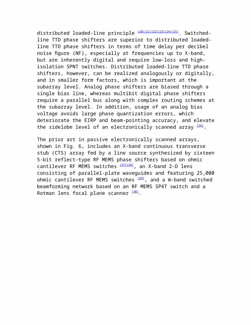
The usage of true-time-delay TTD phase shifters instead of RF MEMS phase shifters allows ultra-wideband (UWB) radar waveforms with associated high range resolution, and avoids beam squinting or frequency scanning. TTD phase shifters are designed using the switched-line principle [17][18][19] or the distributed loaded-line principle [20][21][22][23][24][25]. Switched-line TTD phase shifters are superior to distributed loaded-line TTD phase shifters in terms of time delay per decibel noise figure (NF), especially at frequencies up to X-band, but are inherently digital and require low-loss and high-isolation SPNT switches. Distributed loaded-line TTD phase shifters, however, can be realized analogously or digitally, and in smaller form factors, which is important at the subarray level. Analog phase shifters are biased through a single bias line, whereas multibit digital phase shifters require a parallel bus along with complex routing schemes at the subarray level. In addition, usage of an analog bias voltage avoids large phase quantization errors, which deteriorate the EIRP and beam-pointing accuracy, and elevate the sidelobe level of an electronically scanned array [26].
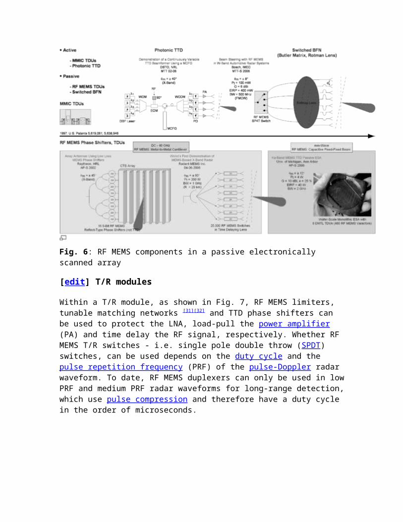
The prior art in passive electronically scanned arrays, shown in Fig. 6, includes an X-band continuous transverse stub (CTS) array fed by a line source synthesized by sixteen 5-bit reflect-type RF MEMS phase shifters based on ohmic cantilever RF MEMS switches [27][28], an X-band 2-D lens consisting of parallel-plate waveguides and featuring 25,000 ohmic cantilever RF MEMS switches [29], and a W-band switched beamforming network based on an RF MEMS SP4T switch and a Rotman lens focal plane scanner [30].
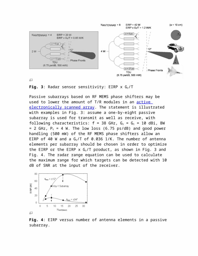
Fig. 6: RF MEMS components in a passive electronically scanned array
[edit] T/R modules
Within a T/R module, as shown in Fig. 7, RF MEMS limiters, tunable matching networks [31][32] and TTD phase shifters can be used to protect the LNA, load-pull the power amplifier (PA) and time delay the RF signal, respectively. Whether RF MEMS T/R switches - i.e. single pole double throw (SPDT) switches, can be used depends on the duty cycle and the pulse repetition frequency (PRF) of the pulse-Doppler radar waveform. To date, RF MEMS duplexers can only be used in low PRF and medium PRF radar waveforms for long-range detection, which use pulse compression and therefore have a duty cycle in the order of microseconds.
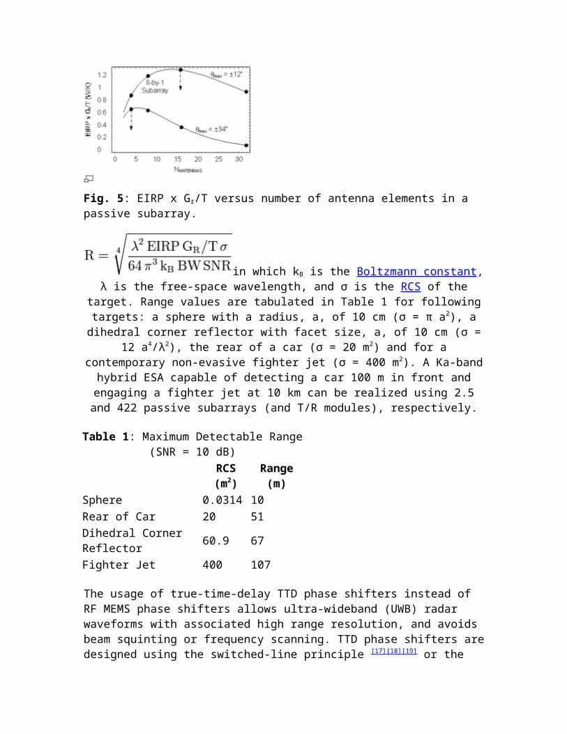
Fig. 7: RF MEMS components in a T/R module.
[edit] References
MicroElectroMechanical Systems, MEMS
This is the Home page for the research on RF MEMS at the Department of Informatics, University of Oslo.(This page is under construction!)
What is MEMS?MEMS at the MES groupResearch focus: RF MEMSPeopleCourse: INF5490 RF MEMSRelevant material and resources
Send us an e-mail
What is MEMS?
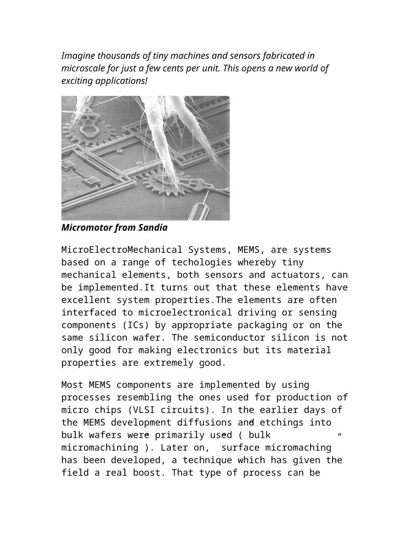
Imagine thousands of tiny machines and sensors fabricated in microscale for just a few cents per unit. This opens a new world of exciting applications!
Micromotor from Sandia
MicroElectroMechanical Systems, MEMS, are systems based on a range of techologies whereby tiny mechanical elements, both sensors and actuators, can be implemented.It turns out that these elements have excellent system properties.The elements are often interfaced to microelectronical driving or sensing components (ICs) by appropriate packaging or on the same silicon wafer. The semiconductor silicon is not only good for making electronics but its material properties are extremely good.
Most MEMS components are implemented by using processes resembling the ones used for production of micro chips (VLSI circuits). In the earlier days of the MEMS development diffusions and etchings into bulk wafers were primarily used (”bulk micromachining”). Later on, ”surface micromaching” has been developed, a technique which has given the field a real boost. That type of process can be compared to baking a cream cake by stacking various layers. The ”cream” in the cake resembles what is called ”sacrificial layers” which separate other ”structural layers” when building up the unit. The sacrificial layers are spacers which later on are removed, causing the structural layers to be released. Thereby mechanical elements such as beams, diaphragms or disks are free to move as intended. The advantage of using techniques from IC processing is not only to be able to implement the microstructures, but also to allow thousands or millions of equal elements to be fabricated at the same time to a low cost (batch processing).
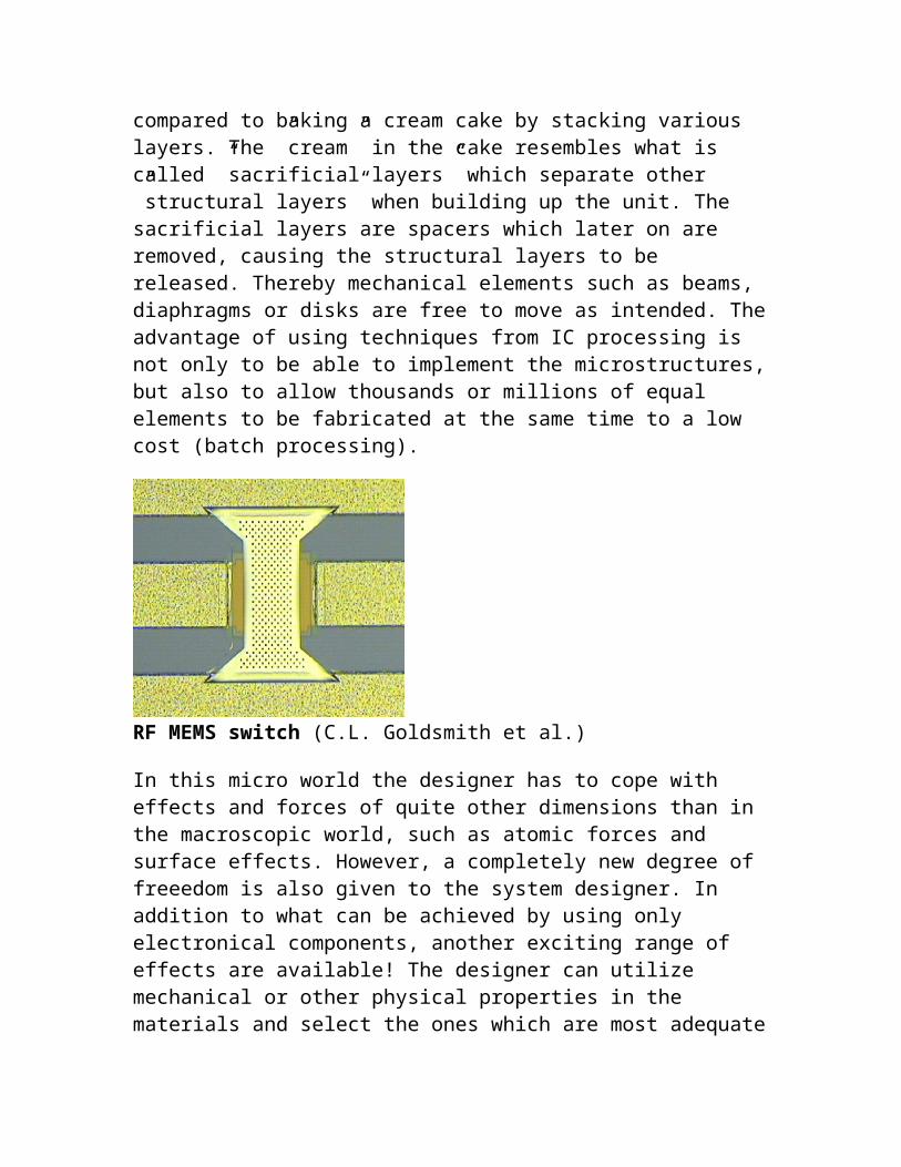
RF MEMS switch (C.L. Goldsmith et al.)
In this micro world the designer has to cope with effects and forces of quite other dimensions than in the macroscopic world, such as atomic forces and surface effects. However, a completely new degree of freeedom is also given to the system designer. In addition to what can be achieved by using only electronical components, another exciting range of effects are available! The designer can utilize mechanical or other physical properties in the materials and select the ones which are most adequate for his application. A whole bunch of physical principles exist when selecting the one to be used for instance in an actual detector design. Typically, a capacitor or resistor value can change when an elastic microbeam or thin membrane is deflected. The change of mechanical stress in a structure can be the result when the MEMS experience an accelleration or by an applied pressure load (sensing). Microelements can be forced to move using electrostatic activation (actuation). Thereby micro motors, movable micromirrors or steerable gratings can be implemented, or small fluidic particles can be forced through different temperature zones etc. To implement complete systems it is essential that the physical effects on the micro elements, such as strain and stress, can be converted to electrical currents and potential differences which further on can be handled by microelectronics in more or less integrated ways (e.g. integrated sensors).
MEMS have been used in accelerators detecting when an airbag should be released, in video projectors having a million individually controlled micromirrors, in gyroscopes, pressure gauges (for instance in the tires of cars) or as micro optical systems for fiber optical communication. Very exciting is MEMS used for fast electrophoresis in DNA amplification and separation, various systems for biological analysis or other biomedical applications, microrobotics, micro tweezers and neural probes. It seems to be a considerable potential for using microsystems within areas such as medicin, car industry,
space technology, within communication, security and in a lot of the components surrounding us in our daily life.
Today there is an increasing activity in developing MEMS processes, design tools and applications. Great expectations exist as to the importance of the field in the future. In the same way as microelectronics and PCs have revolutionized our daily life and reached a widespread use, it seems likely, according to the most enthusiastic researchers, that microsystems might be the next wave. Numerous types of units based on MEMS technology could be produced in large quantities and spread around for diverse applications which directly or indirectly could detect or help us control our physical environment. Some people say that this field will have a huge and penetrating impact on the development in our society.
The MEMS field is by its nature a mixture of quite diverse disciplines such as physics, chemistry, mathematics and informatics, where material technology, electronics, modeling and CAD tools should be emphasized. The research field is quite diverse, comprising fields as developing new fabrication and processing techniques, investigating new physical principles and structures, ASIC (Application Specific Integrated Circuits) for MEMS, design tools, applications etc. A continuing development towards miniaturization (nano technology) and thereby a denser integration, is a strong driving force.
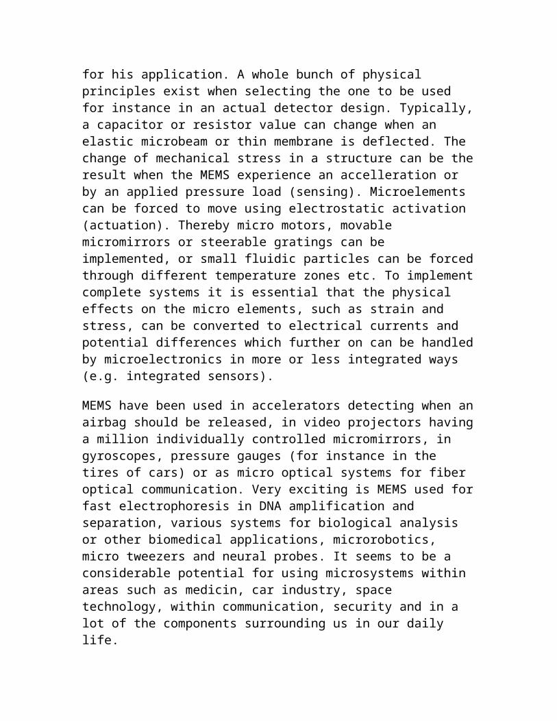
MEMS inductor (J.-B. Yoon et al.)
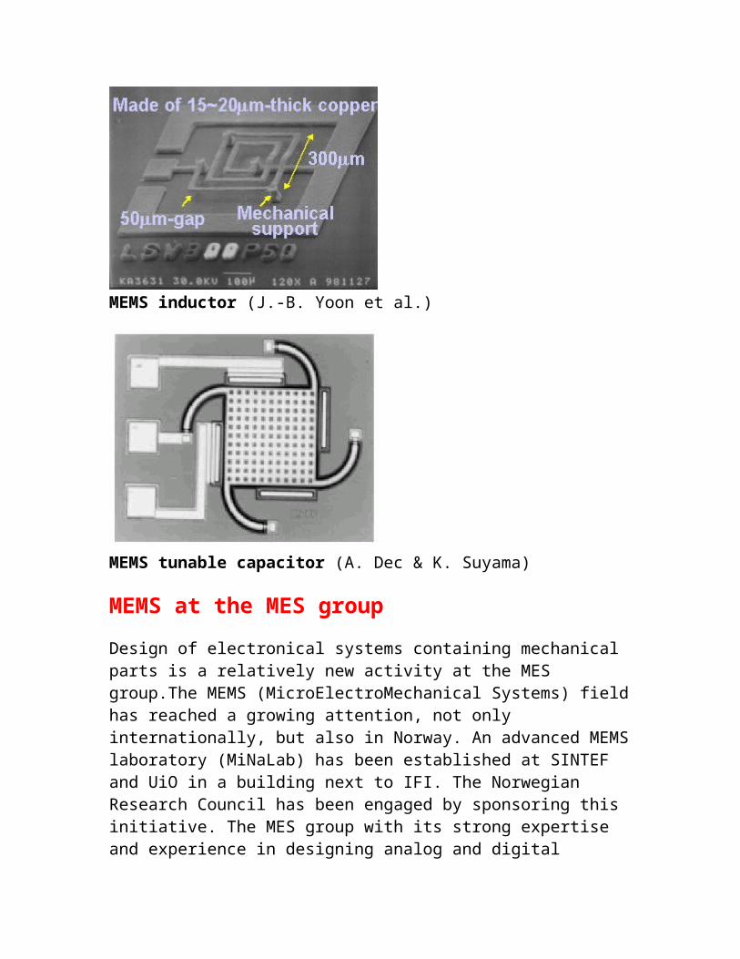
MEMS tunable capacitor (A. Dec & K. Suyama)
MEMS at the MES group
Design of electronical systems containing mechanical parts is a relatively new activity at the MES group.The MEMS (MicroElectroMechanical Systems) field has reached a growing attention, not only internationally, but also in Norway. An advanced MEMS laboratory (MiNaLab) has been established at SINTEF and UiO in a building next to IFI. The Norwegian Research Council has been engaged by sponsoring this initiative. The MES group with its strong expertise and experience in designing analog and digital systems seems to have a lot to contribute to developing MEMS systems in a broader context.
My personal interests in this area is more specifically directed towards design activities where the MEMS units are used in a larger system context. Central to this is interfacing the mechanical to the electrical world and investigating the possibility of implementing systems containing both MEMS components and surrounding microelectronics integrated on-chip. This will comprise activities towards design methods, modeling and analysis, and designing and implementing actual systems. Due to the very broad MEMS research field I have restricted my activities to cover systems which are central to and can be used in high frequency radio systems for wireless transmission, RF MEMS (Radio Transmission MEMS). This is a very interesting and exciting field in fast development. As a background to the field, intended for Master and Ph.D. students, a brand new course in RF MEMS has been developed (INF5490 RF MEMS) and taught for the first time in the spring 2005.
Research focus: RF MEMS
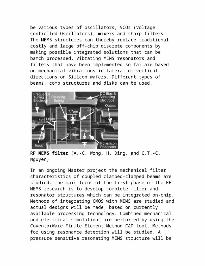
MEMS technology can be used to implement high quality switches, varactors (variable reactors), inductors, resonators, filters and phase shifters. Among the broad range of applications the MEMS technology gives a unique possibility to implement micromechanical resonatores and filters with high performance regarding selectivity and Q-factors. When combining these mechanical structures with microelectronics, central parts in wireless systems, RF systems (Radio Frequency systems) can be implemented. Examples can be various types of oscillators, VCOs (Voltage Controlled Oscillators), mixers and sharp filters. The MEMS structures can thereby replace traditional costly and large off-chip discrete components by making possible integrated solutions that can be batch processed. Vibrating MEMS resonators and filters that have been implemented so far are based on mechanical vibrations in lateral or vertical directions on Silicon wafers. Different types of beams, comb structures and disks can be used.
RF MEMS filter (A.-C. Wong, H. Ding, and C.T.-C. Nguyen)
In an ongoing Master project the mechanical filter characteristics of coupled clamped-clamped beams are studied. The main focus of the first phase of the RF MEMS research is to develop complete filter and resonator structures which can be integrated on-chip. Methods of integrating CMOS with MEMS are studied and actual designs will be made, based on currently available processing technology. Combined mechanical and electrical simulations are performed by using the CoventorWare Finite Element Method CAD tool. Methods for using resonance detection will be studied. A pressure sensitive resonating MEMS structure will be designed allowing pressure to be measured by alternating the vibration frequency. See Master-degree projects for further details.
Abstract Radio frequency microelectromechanical systems (RF MEMS) are heralded a technology fit for the 21st centaury, offering unsurpassed RF performance over more conventional solid-state electronic devices. In recent years, this technology has seen a rapid growth in its development. Indeed, within the US, Asia and Europe, R&D is almost at fever pitch. The high levels of investment come second only to the expectations for commercial exploitation.
Surprisingly, the first RF MEMS device was reported more than 25 years ago by IBM. Even more surprisingly, to date, the only true RF MEMS device that is commercially available is a simple cantilever switch, and even this is restricted to the US market. So why does this technology appear to be stalling? This lecture aims to address some of the main issues that are impeding the progress of RF MEMS from the laboratory to ubiquity. Microelectromechanical system (MEMS) and devices have advanced rapidly and have
transitioned into many defense and commercial applications. Common MEMS switch types are
a thin metal cantilever, air bridge, diaphragm, or some other structure electrically configured
in series or parallel with an RF transmission line and designed to open the line or shunt it to
ground upon actuation of the MEMS. Such switches have displayed excellent RF
characteristics, including insertion loss values of approximately 0.1 dB and isolation values of
approximately –30 dB in series-configured switches at lower RF frequencies (VHF to ~10 GHz)
and in shunt-configured switches at higher frequencies (~10 to 100 GHz). Such performance
enables superior performance in many traditional RF circuits, such as switchable routing in RF
system front-ends, direct connection to capacitor banks, and routing in time-delay phase-
shifter networks. It is also anticipated that RF MEMS will enable a new class of antenna system
that are electrically reconfigurable. In all these applications being considered, RF MEMS
switches are promising to replace traditional switches with consideration on both performance
and cost.
Micro-Electro-Mechanical Systems (MEMS) is the integration of mechanical elements, sensors,
actuators, and electronics on a common silicon substrate through microfabrication technology.
While the electronics are fabricated using integrated circuit (IC) process sequences (e.g.,
CMOS, Bipolar, or BICMOS processes), the micromechanical components are fabricated using
compatible “micromachining” processes that selectively etch away parts of the silicon wafer or
add new structural layers to form the mechanical and electromechanical devices.
MEMS promises to revolutionize nearly every product category by bringing together silicon-
based microelectronics with micromachining technology, making possible the realization of
complete systems-on-a-chip. MEMS is an enabling technology allowing the development of
smart products, augmenting the computational ability of microelectronics with the perception
and control capabilities of microsensors and microactuators and expanding the space of
possible designs and applications.
Microelectronic integrated circuits can be thought of as the “brains” of a system and MEMS
augments this decision-making capability with “eyes” and “arms”, to allow microsystems to

sense and control the environment. Sensors gather information from the environment through
measuring mechanical, thermal, biological, chemical, optical, and magnetic phenomena. The
electronics then process the information derived from the sensors and through some decision
making capability direct the actuators to respond by moving, positioning, regulating, pumping,
and filtering, thereby controlling the environment for some desired outcome or purpose.
Because MEMS devices are manufactured using batch fabrication techniques similar to those
used for integrated circuits, unprecedented levels of functionality, reliability, and sophistication
can be placed on a small silicon chip at a relatively low cost.
At higher frequencies, basic circuit theory runs into problems. For
example, if wires are electrically long, transmission line effects can occur.
The basic theory no longer applies because electromagnetic wave reflections
bouncing back and forth along the wires cause problems. These
electromagnetic wave reflections can cause constructive or destructive
interference resulting in the breakdown of basic circuit theory. In fact,
when a transmission line has a length equal to one quarter wavelength
of the signal, a short placed at the end will appear as an open circuit at
the other end! Certainly, effects like this cannot be ignored. Furthermore,
at higher frequencies, circuits can radiate energy much more
readily; that is circuits can turn into antennas. Parasitic capacitances and
inductances can cause problems too. No component can ever be truly
ideal. The small inductance of component leads and wires can cause
significant voltage drops at high frequencies, and stray capacitances
between the leads of the component packages can affect the operation
of a high-frequency circuit. These parasitic elements are sometimes
called “the hidden schematic” because they typically are not included
on the schematic symbol.
How do you define the high-frequency regime? There is no exact
border, but when the wavelengths of the signals are similar in size or
smaller than the wire lengths, high-frequency effects become important;
in other words, when a wire or circuit element becomes electrically long,
you are dealing with the high-frequency regime. An equivalent way to
state this is that when the signal period is comparable in magnitude
or smaller than the delay through the interconnecting wires, highfrequency
effects become apparent. It is important to note that for digital
signals, the designer must compare the rise and fall times of the digital signal
to the wire delay. For example, a 10 MHz digital clock signal may only have
a signal period of 100nsec, but its rise time may be as low as 5nsec.
Hence, the RF regime doesn’t signify a specific frequency range, but
signifies frequencies where the rules of basic circuit theory breakdown.
A good rule of thumb is that when the electrical length of a circuit element
reaches 1/20, RF (or high-speed digital) techniques may need to be used.
When working with RF and high-frequency electronics it is important
to have an understanding of electromagnetics. At these higher frequencies,
you must understand that the analogy of electrons acting like
water through a pipe is really more of a myth than a reality. In truth,
circuits are characterized by metal conductors (wires) that serve to guide
electromagnetic energy. The circuit energy (and therefore the signal) is
carried between the wires, and not inside the wires. For an example, consider
the power transmission lines that deliver the electricity to our
homes at 60Hz. The electrons in the wires do not directly transport the
energy from the power plant to our homes. On the contrary, the energy
is carried in the electromagnetic field between the wires. This fact is
often confusing and hard to accept for circuit designers. The wire electrons
are not experiencing any net movement. They just slosh back and
forth, and through this movement they propagate the field energy down
MEMS switches have been in development for over 20 yearsat numerous industrial, academic and government research laboratories. Low insertion loss, high isolation, low power consumption, extreme linearity and the ability to be integrated with other electronics make MEMS switches an attractive alternative to other mechanical and solid-state switches. This seemingly simple device has been fraught with reliability and packaging issues that have prevented commercial success – that is, until now. Improvements in reliability and MEMS packaging have occurred at a rapid pace over the past 5 to 10 years. The U.S. Defense Advanced Research Projects Agency (DARPA) has contributed significantly to the funding of these efforts as they look to apply this technology to future U.S. Department of Defense (DoD) programs.
To date, RF MEMS switches have been employed for a variety of military demonstration systems including an electronically steerable radar antenna at X-band containing 25,000 MEMS switches, low
frequency tunable filters for radio communication, various reconfigurable antenna concepts and reconfigurable receiver front-ends, to name a few. However, the earlier issues with switch reliability (that have since been resolved) and cost have prevented RF MEMS insertion into a currently fielded system. This will be short-lived as many design teams are currently evaluating and designing MEMS into future systems. Device cost for sample quantities for a MEMS SPST switch (such as the Radant RMSW101) is approximately $20. This price decreases with volume purchases and will decrease further over time as the overall MEMS switch market volume matures.
Radant MEMS, Inc. (RMI) has developed an electrostatically actuated broadband ohmic microswitch, as shown in the figures, which has applications from DC through the microwave region. Ohmic MEMS switches are characterized by having direct metal-metal (i.e. ohmic) switching contact. The microswitch is a 3-terminal device based on a cantilever beam and is fabricated using an all-metal, surface micromachining process that operates in a hermetic environment obtained through a wafer-bonding process. At RMI, we have improved ohmic MEMS switch reliability by greater than 10,000 fold over the course of the last 8 years.
SEM micrograph of a Radant SPST electrostatically actuated microswitch showing the
cantilever beam which can be electrostatically pulled down to provide continuity between the
Source and Drain terminals.
Extensive lifetime testing has been conducted on RMI switches by Radant as well as independently by each of the Tri-Service DoD laboratories (Air Force Research Laboratory, Army Research Laboratory and Naval Research Laboratory) under the auspices of a DARPA program. This testing lead to a median cycle to switch failure of greater than 1 trillion switching cycles with the longest recorded lifetimes exceeding 1.5 trillion switch cycles before the test was halted after 30 continuous months of testing. Infant failure modes are currently being eliminated via device screening and on-going process improvements. Research in contact physics, materials and packaging has contributed to the impressive progress that has been made in improving RF MEMS switch reliability. The number of required switching cycles for a specific application is quite variable and can range from 25,000 cycles for an active missile seeker that is only employed for final engagement to over 1 trillion cycles for Transmit/Receive applications. Many military applications (such as radar) can be satisfied with a more conservative 100 billion cycle rating while some commercial ATE applications will find 100 million cycles exceeding current technologies by an order of magnitude. Typical RF mechanical relays have rated lifetimes on the order of 10 million cycles, which is 10 to 100 thousand times smaller than what is currently achievable with MEMS switches!
Schematic representation of the microswitch shown in the figure above; a 90V actuation
signal is applied between the Gate and Source terminals results in continuity between the
Source and Drain terminals.
In contrast to ohmic MEMS switches, capacitive MEMS switches contain a dielectric in the switching region so that direct ohmic contact is not made upon switch closing and they instead rely on capacitive coupling through this dielectric. Hence, unlike ohmic switches, capacitive switch performance degrades at low-frequencies and they are unable to operate at DC. However, capacitive switches tend to have lower insertion loss than their ohmic counterparts at millimeter wave frequencies. The failure mechanisms of ohmic and capacitive MEMS switches are also quite different. Ohmic switches typically fail because of adhesion, called “stiction”, in the metal-metal contact region. Whereas, electrostatic actuated capacitive MEMS switches experience stiction due to charging of the dielectric layer which can produce a sufficiently strong electrostatic field to hold the switch in the down state without an actuation signal applied. Capacitive MEMS switches have shown an equally impressive improvement in switch reliability over the last 5 years as evidenced by the recent results at MEMtronics and MIT Lincoln Laboratory.
Radant and other RF MEMS developers, including WiSpry, MEMtronics and XCOM Wireless, are striving to make these products a commercial success. With the release of nine commercial off-the-shelf (COTS) discrete MEMS switch products, Radant is supplying both military and commercial early adopters of MEMS switch technology. A variety of Single Pole N Throw (SPNT) devices including SPST, SPDT, SP4T and SP6T MEMS switches with broadband, low-loss and extremely linear performance can be readily obtained. Recent developments in higher power handling at Radant have resulted in the introduction two high-power models that are capable of handling 10W.
SEM micrograph of the Radant MEMS RMSW220HP high-power SPDT switch containing two
microswitches similar to that shown in the above figure and obtained through a wafer
bonding process.
The future appears brighter than it did in the early stages of MEMS switch development. Applications with clear performance advantages are seeking out MEMS switches to evaluate for future designs. Despite the current extended economic downturn, Radant feels that the RF MEMS industry is well poised to participate and benefit from the eventual global recovery.
The primary challenges to MEMS switch commercialization are cost and overcoming the inertia of employing legacy switching technologies. Our initial application focus have been those with less cost sensitivity such as the military and aerospace markets and select commercial applications (such as ATE) where the combination of high-frequency operation and high-reliability of MEMS switches far exceed existing technologies. As the MEMS switch market grows and volume expands, MEMS switch cost will dramatically decrease which will facilitate entry into low-cost, high volume markets.
Insertion loss of a typical PIN diode switch is approximately 1.5 dB at 25 GHz versus less than 0.5 dB from DC to 40 GHz for the low-loss, broadband Radant RMSW200 MEMS switch. Another important consideration for many applications is linearity. The third order intercept point (IP3) is approximately 30 dBm for many PIN diode switches. MEMS switches are extremely linear with measured IP3’s exceeding 65 dBm which is greater than 35 dB better than most PIN diode switches. This aspect can be extraordinarily important for many receiver applications. Bias power consumption of MEMS switches is virtually zero and only occurs during the switch transition. In contrast, PIN diodes require significant amounts of power, typically greater than 25 mW, to remain in the low-loss ON-state while MEMS switches require nearly zero power to electrostatically hold the switch closed.
*********************************************Dr. John Maciel is the Vice President and Chief Operating Officer of Radant MEMS, Inc. and Manager, Electromagnetics Technology of Radant Technologies, Inc. He has more than 25 years of experience in the RF, Microwave and Microelectronics industries. Dr. Maciel manages the MEMS development effort at Radant MEMS as well as its daily operations. Dr. Maciel received a Ph.D. and a Master of Science, both in Electrical Engineering, from the Polytechnic University of New York in 1990 and 1986, respectively, and a BSEE degree from Northeastern University, Boston, MA in 1983. Dr. Maciel can be reached at [email protected].