Embed Size (px)
Citation preview
1
MEMS Made Easy!Instructor: Riadh W. Y. Habash
Students are presented with aspects of general production and manufacturing of electromechanical systems to enable them to better liaise with and participate in the manufacturing industry sector.
2
MicroElectroMechanical Systems
• In the United States, the technology is known as microElectroMechanical systems (MEMS); in Europe it is called microsystems technology (MST).
• MEMS is a portfolio of techniques and processes to design and create miniature systems;
• It is a physical product often specialized and unique to a finalapplication-one can seldom by a generic MEMS product from the electronic shop;
• MEMS is a way of making things. These things merge the functions of sensing and actuation with computation and communication to locally control physical parameters at the microscale.
3
This Subject is Called
• MicroElectroMechanical System (MEMS) in the United States.
• Microsystem in Europe• Micromachines in Japan.
4
History• 1750s Electrostatic motors demonstrated by Benjamin Franklin and
Andrew Gordon.• 1824 Discovery of Silicon by Berzelius.• 1927 Field effect transistor patented to Lilienfield. • 1947 Invention of the transistor (made from germanium).• 1954 Piezoresistive effect in Germanium and Silicon invented by C.
S. Smith. • 1958 Silicon strain gauges available in the market.• 1961 Silicon pressure sensor demonstrated by Kulite• 1967 Surface micromachining invented.• 1970 First silicon accelerometer demonstrated by Kulite.• 1977 First capacitive pressure sensor demonstrated in Stanford.• 1980 Silicon torsional Scanning Mirror demonstrated by K. E.
Petersen.• 1982 Demonstration of disposable blood pressure transducer.
5
History, Cont.• 1982 Active on-chip signal conditioning.• 1984 First polysilicon MEMS device (Howe, Muller).• 1988 Rotary electrostatic side drive motors (Fan, Tai, Muller).• 1989 Lateral comb drive (Tang, Nguyen, Howe).• 1991 Polysilicon hinge (Pister, Judy, Burgett, Fearing).• 1992 Grating light modulator (Solgaard, Sandejas, Bloom).• 1992 MCNC starts MUMPS.• 1993 Digital mirror display by Texas Instruments• 1993 First surface micromachined accelerometer sold. • 1994 XeF2 used for MEMS.• 1999 Optical network switch by Lucent Technologies.
– Adapted from: Veljko Milanovic, Lecture Notes at Bekerly
6
What are MEMS?
• MEMS is a class of systems that are physically small. These systems have both electrical and mechanical components. MEMS originally used modified integrated circuit (computer chip) fabrication techniques and materials to create these very small mechanical devices. Today there are many more fabrication techniques and materials available.
• Sensors and actuators are the two main categories of MEMS. Sensors are non-invasive while actuators modify the environment. Micro sensors are useful because their physical size allows them to be less invasive. Micro actuators are useful because the amount of work they perform on the environment is small and therefore can be very precise.
7
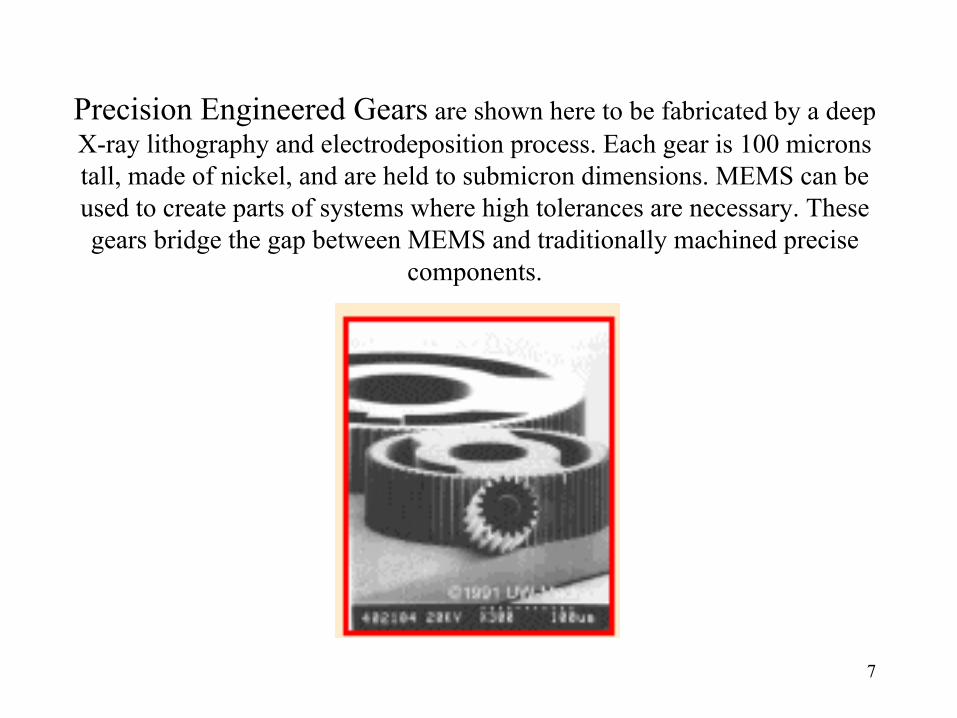
Precision Engineered Gears are shown here to be fabricated by a deep X-ray lithography and electrodeposition process. Each gear is 100 microns tall, made of nickel, and are held to submicron dimensions. MEMS can be used to create parts of systems where high tolerances are necessary. These gears bridge the gap between MEMS and traditionally machined precise
components.
8
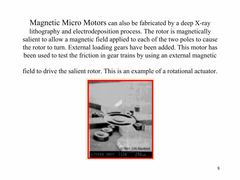
Magnetic Micro Motors can also be fabricated by a deep X-ray lithography and electrodeposition process. The rotor is magnetically
salient to allow a magnetic field applied to each of the two poles to cause the rotor to turn. External loading gears have been added. This motor has been used to test the friction in gear trains by using an external magnetic
field to drive the salient rotor. This is an example of a rotational actuator.
9
But, Not Only Miniaturization
MEMS devices are manufactured in a similar fashion to computer microchips. The biggest advantage here is not necessarily that the system can be minuaturized, but rather that the lithographic techniques that now mass-produce thousands of complex microchips simultaneously can also be used to manufacture mechanical sensors and actuators. As the price of these components is reduced to nearly zero, as has happened with microprocessors, they can deployed pervasively, revolutionizing future society to a greater extent, possibly, than even the microprocessor.
10
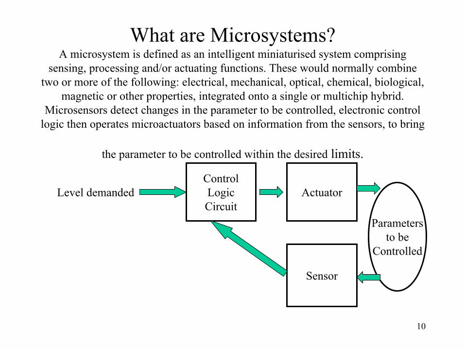
What are Microsystems?A microsystem is defined as an intelligent miniaturised system comprising
sensing, processing and/or actuating functions. These would normally combine two or more of the following: electrical, mechanical, optical, chemical, biological,
magnetic or other properties, integrated onto a single or multichip hybrid. Microsensors detect changes in the parameter to be controlled, electronic control
logic then operates microactuators based on information from the sensors, to bring
the parameter to be controlled within the desired limits.
Level demandedControlLogicCircuit
Actuator
Parametersto be
Controlled
Sensor
11
Sensors• Micro sensors measure the environment without modifying it. Micro sensors
are useful because their small physical size allows them to be less invasive and work in smaller areas. So far, microengineering as a manufacturing technology has been applied most successfully to sensors. The pay-off in terms of miniaturization, improved performance, and reduced production cost have transformed the market in pressure sensors in particular.
• Microphones.• Accelerometers.• Vibration analyzers.• Flow meters.• Gas sensors.• Radiation detectors.• Chemical sensors.• Ion sensors.
12
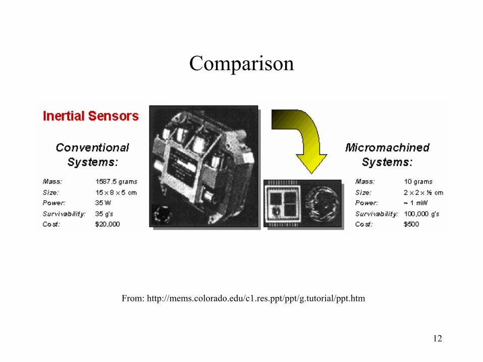
Comparison
From: http://mems.colorado.edu/c1.res.ppt/ppt/g.tutorial/ppt.htm
13
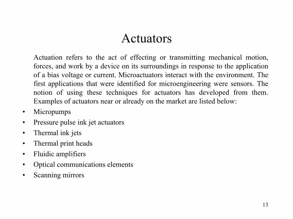
Actuators Actuation refers to the act of effecting or transmitting mechanical motion,
forces, and work by a device on its surroundings in response to the application of a bias voltage or current. Microactuators interact with the environment. The first applications that were identified for microengineering were sensors. The notion of using these techniques for actuators has developed from them. Examples of actuators near or already on the market are listed below:
• Micropumps• Pressure pulse ink jet actuators• Thermal ink jets• Thermal print heads• Fluidic amplifiers• Optical communications elements• Scanning mirrors
14
Microstructures
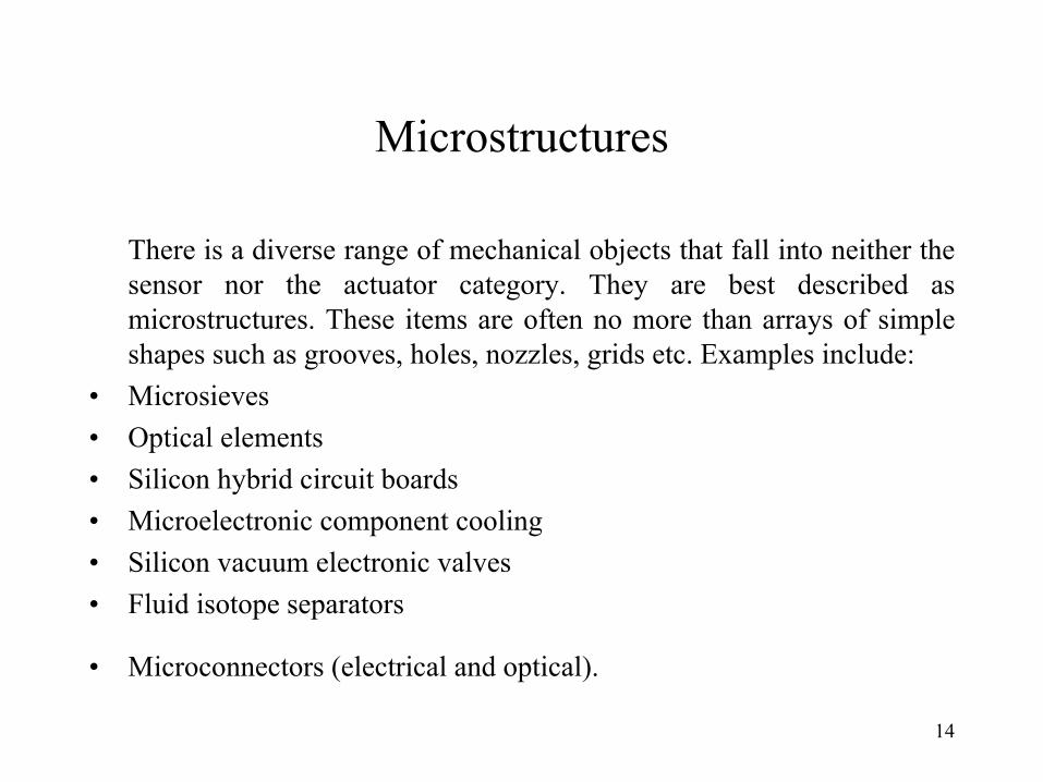
There is a diverse range of mechanical objects that fall into neither the sensor nor the actuator category. They are best described as microstructures. These items are often no more than arrays of simple shapes such as grooves, holes, nozzles, grids etc. Examples include:
• Microsieves• Optical elements• Silicon hybrid circuit boards• Microelectronic component cooling• Silicon vacuum electronic valves• Fluid isotope separators
• Microconnectors (electrical and optical).
15
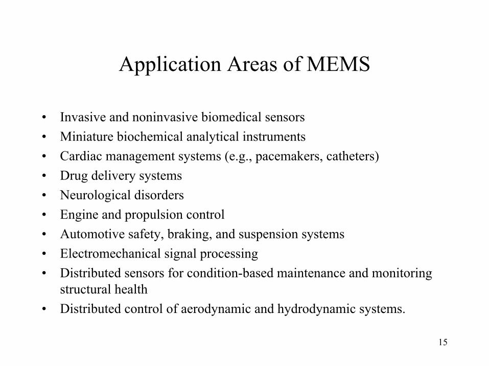
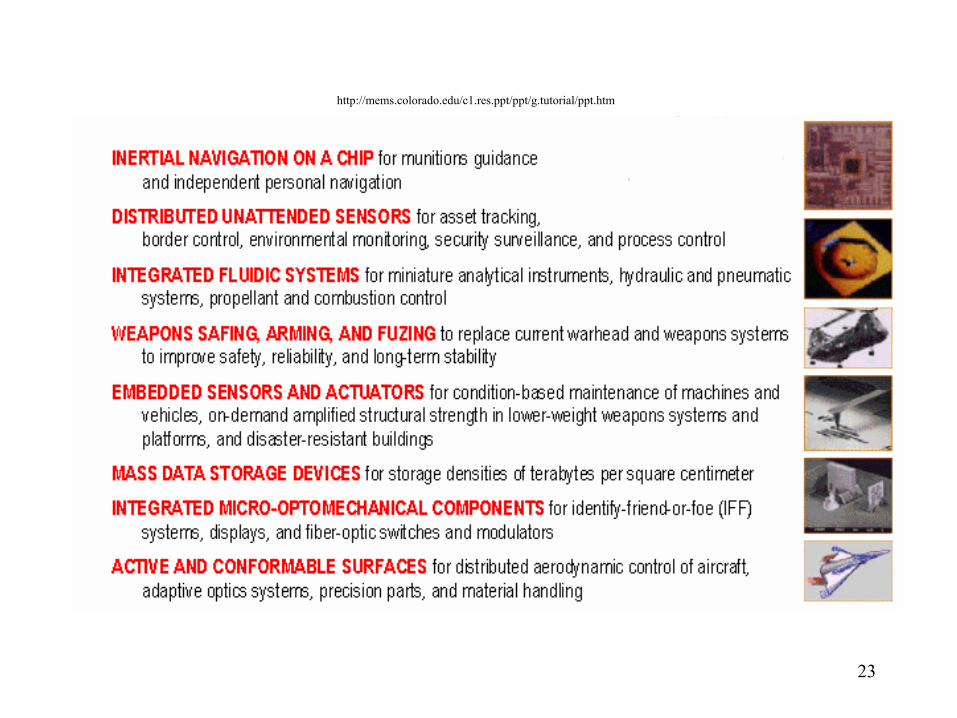
Application Areas of MEMS
• Invasive and noninvasive biomedical sensors• Miniature biochemical analytical instruments• Cardiac management systems (e.g., pacemakers, catheters)• Drug delivery systems• Neurological disorders• Engine and propulsion control• Automotive safety, braking, and suspension systems• Electromechanical signal processing• Distributed sensors for condition-based maintenance and monitoring
structural health• Distributed control of aerodynamic and hydrodynamic systems.
16
Why is MEMS Useful?
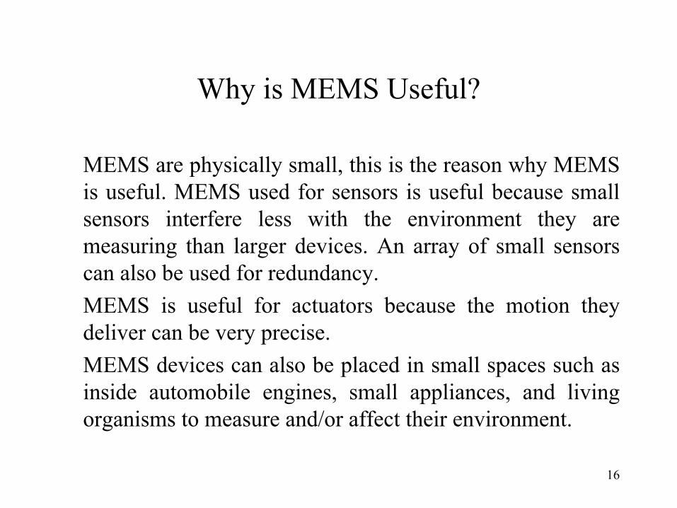
MEMS are physically small, this is the reason why MEMS is useful. MEMS used for sensors is useful because small sensors interfere less with the environment they are measuring than larger devices. An array of small sensors can also be used for redundancy.
MEMS is useful for actuators because the motion they deliver can be very precise.
MEMS devices can also be placed in small spaces such as inside automobile engines, small appliances, and living organisms to measure and/or affect their environment.
17
What is Microengineering?
• Microengineering refers to the technologies and practice of making three dimensional structures and devices with dimensions in the order of micrometers.
• The two constructional technologies of microengineering are microelectronics and micromachining.
• Microelectronics, producing electronic circuitry on silicon chips, is a very well developed technology. Micromachining is the name for the techniques used to produce the structures and moving parts of microengineered devices.
• One of the main goals of Microengineering is to be able to integrate microelectronic circuitry into micromachined structures, to produce completely integrated systems (microsystems). Such systems could have have the same advantages of low cost, reliability and small size as silicon chips produced in the microelectronics industry.
18
Microengineering Enables• The production of smaller, lighter, and faster versions of existing mechanical
devices, with increased dimensional accuracy, e.g. micromotors.• The production of sensors, mainly exploiting the electromechanical properties
of silicon, where electrical characteristics change in response to a change in a particular external parameter, e.g. temperature, pressure, acceleration, humidity and radiation.
• The use of materials and processes common to integrated microelectronics with micromechanical components bringing improvements in performance and cost.
• Batch processing to fabricate large volumes of miniature components at low cost, e.g. ink jet nozzles.
• The opportunity to extend process technology to include materials and techniques not used in microelectronics, but which offer specific advantages to micromechanical devices.
• The economic integrated manufacture of complete systems to include sensing, computation and actuation.
19
Markets for Microengineered Products
• Microengineering not only provides a new manufacturing route forexisting products, but also, importantly, allows the creation ofcompletely new products and new markets.
• Microengineering is already established in the sensor market, providing large volumes of low cost sensors to the automotive industry, and low volume high performance, small and light weight sensors to aerospace and defence. The sensor market is expected to grow significantly in the next few years, with exceptional growth in the sub-category of miniaturized sensors.
• The projected MEMS market for the year 2002 is expected to reach6.7B$.
20
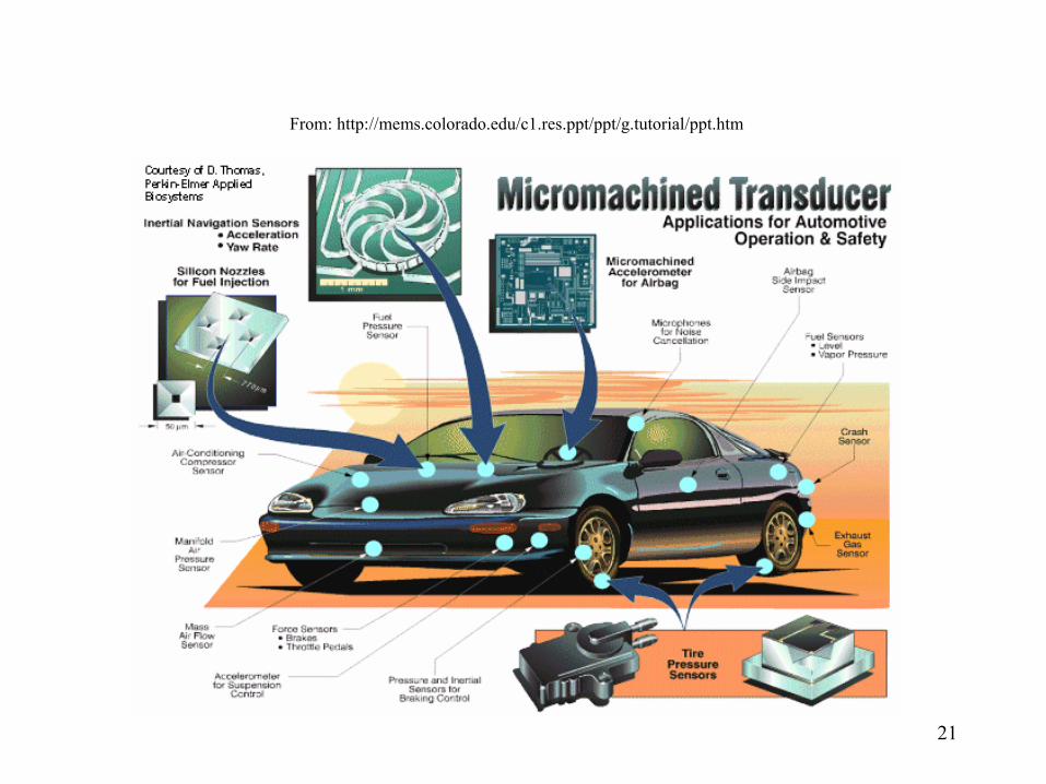
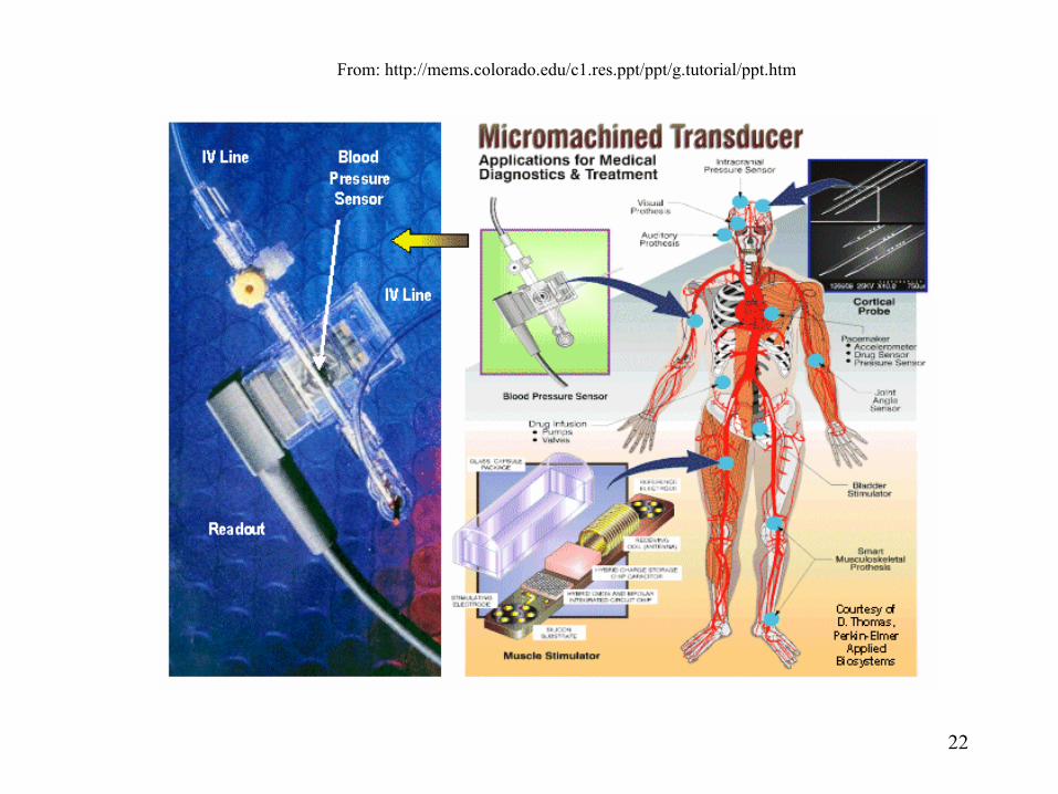
Successful Applications
• Automotive Industry– Manifold air pressure sensors– Air Bag Sensors
• Health and Medicine– Blood Pressure Sensors– Muscle Simulator
• Digital Mirror Display– Video Projection System
• Printers– HP and Canon.
21
From: http://mems.colorado.edu/c1.res.ppt/ppt/g.tutorial/ppt.htm
22
From: http://mems.colorado.edu/c1.res.ppt/ppt/g.tutorial/ppt.htm
23
http://mems.colorado.edu/c1.res.ppt/ppt/g.tutorial/ppt.htm
24
What is Micromachining?• Micromachining is the set of design and fabrication tools that precisely
machine and form structures and elements at a scale below the limits of our human preceptive faculties-the microscale.
• Micromachining is the underlying of MEMS fabrication; it is the tool box of MEMS.
• The micromachining is the Underlying of MEMS fabrication; it is the tool box of MEMS.
• The berth of the first micromachined components dates back many decades, but it was the well-established integrated circuit industry that indirectly played an indispensable role in fostering an environment suitable for the development and growth of micromachining technologies.
25
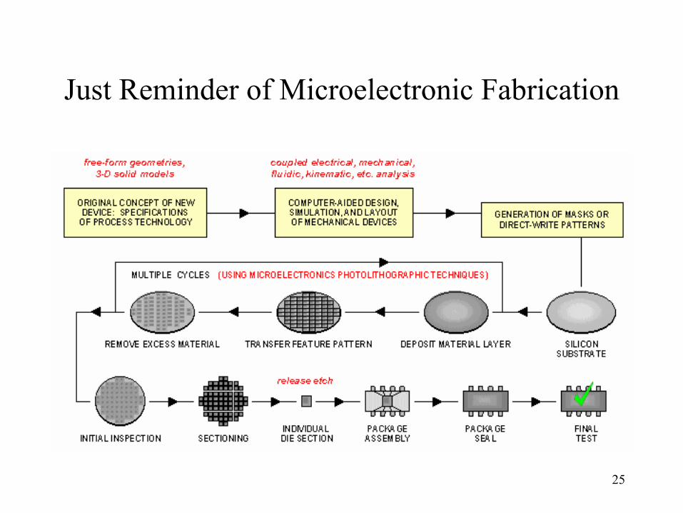
Just Reminder of Microelectronic Fabrication
26
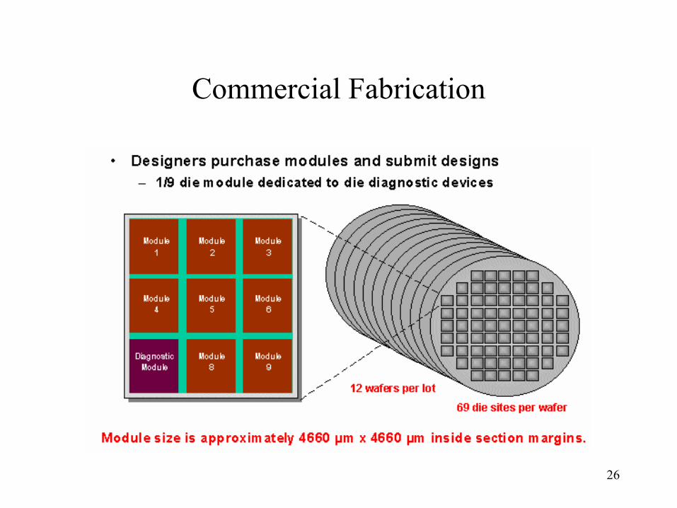
Commercial Fabrication
27
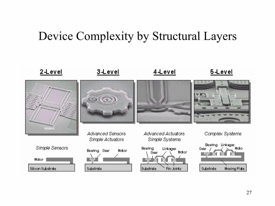
Device Complexity by Structural Layers
28
• Common processing techniques that are used to sculpt mechanical structures include:– bulk micromachining.– Wafer-to-wafer bonding.– Surface micromachining.– High-aspect ratio micromachining.
29
Bulk Micromachining
Bulk micromachining is the term applied to a variety of etching procedures that selectively remove material, typically with a chemical etchant whose etching properties are dependent on the crystallographic structure of the bulk material.
30
Wafer-to-Wafer Wafer-to-wafer bonding is a strategy commonly employed
to get around the restrictions in the type of structures that can be fabricated using bulk micromachining.
Because anisotropic etching, by definition, only removes material, bonding of wafers allows for the addition of material to the bulk micromachining repertoire.
31
Surface Micromachining
In surface micromachining (SMM), alternating layers of structural (usually Polysilicon) and sacrificial material (usually silicon dioxide) are deposited and etched to form the shape required.
Surface micromachining enables the fabrication of free-form, complex and multi-component integrated electromechanical structures, giving freedom to fabricate devices and systems without constraints on materials, geometry, assembly and interconnections that is the source for the richness and depth of MEMS applications that cut across so many areas.
More than any other factor, it is surface micromachining that has ignited and is at the heart of the current scientific and commercial activity in MEMS.
32
Testing
• Testing is very important for quality and reliability purposes. Testing MEMS devices is unique. Compared to electronic devices, that have electric voltage/current as input and electric voltage/current as output, MEMS devices may have a closed loop from sensors to actuators.
• The input can be temperature, humidity, loudness, acceleration ... and the output can be various electrical or mechanical responses. Testing MEMS devices require the proper setup of inputs and accurate measure of the outputs.
33
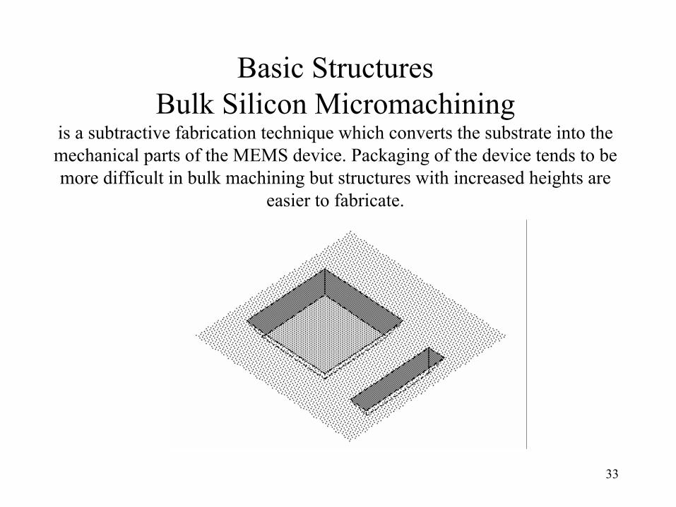
Basic StructuresBulk Silicon Micromachining
is a subtractive fabrication technique which converts the substrate into the mechanical parts of the MEMS device. Packaging of the device tends to be more difficult in bulk machining but structures with increased heights are
easier to fabricate.
34
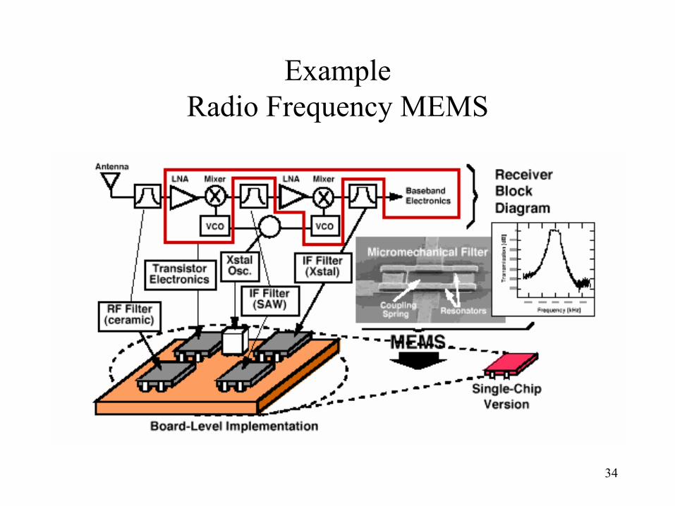
ExampleRadio Frequency MEMS
35
Materials• Metals
– Al, Au, Cu, W, Ni, TiNi, NiFe, • Insulators
– SiO2 - thermally grown or vapor deposited (CVD)– Si3N4 - CVD
• Polymers • The King of Semiconductors: Silicon
– stronger than steel, lighter than aluminum– single crystal or polycrystalline– 10nm to 10mm