Embed Size (px)
Citation preview
1
Loadpoint Loadpoint MEMS MEMS
TechnologyTechnology
2
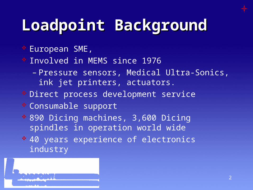
Loadpoint BackgroundLoadpoint Background European SME, Involved in MEMS since 1976
– Pressure sensors, Medical Ultra-Sonics, ink jet printers, actuators.
Direct process development service Consumable support 890 Dicing machines, 3,600 Dicing spindles
in operation world wide 40 years experience of electronics industry
3
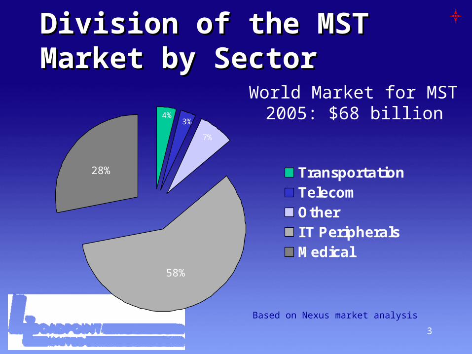
Division of the MST Division of the MST Market by SectorMarket by Sector
World Market for MST 2005: $68 billion
TransportationTelecomOtherIT PeripheralsMedical
Based on Nexus market analysis
4%3%
7%
58%
28%
4
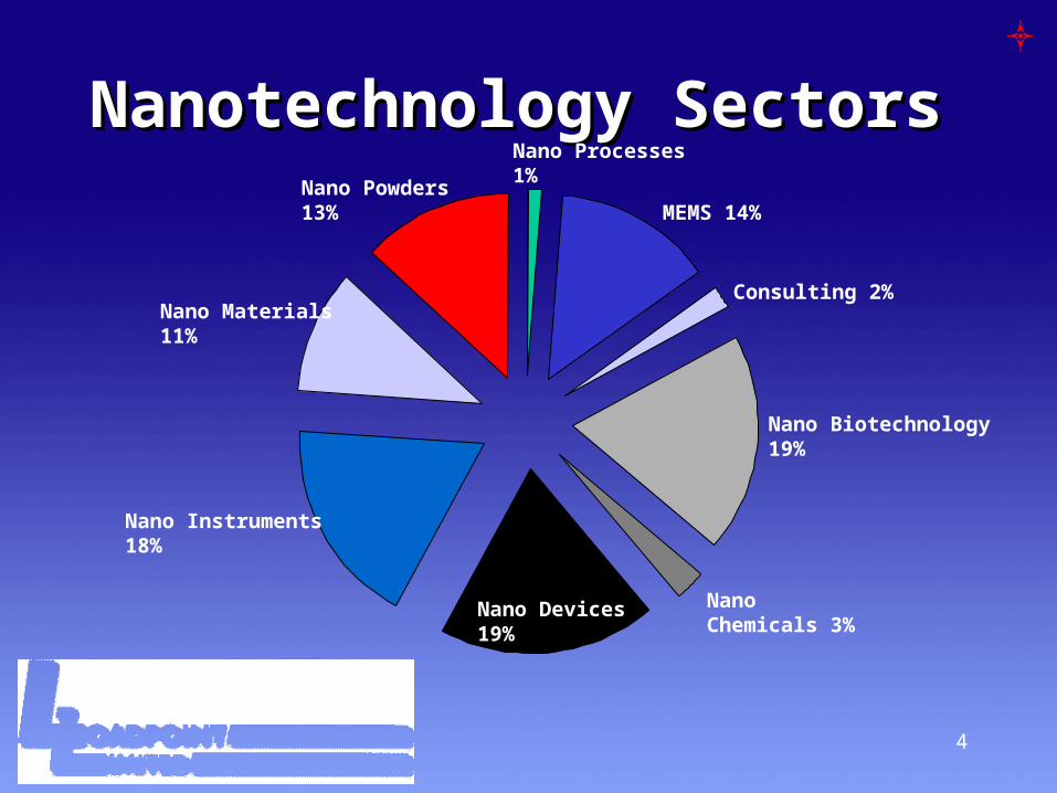
Nanotechnology Nanotechnology SectorsSectors
Nano Biotechnology 19%
Nano Chemicals 3%
Nano Devices 19%
Nano Instruments 18%
Nano Materials 11%
Nano Powders 13%
Nano Processes 1%
MEMS 14%
Consulting 2%
5
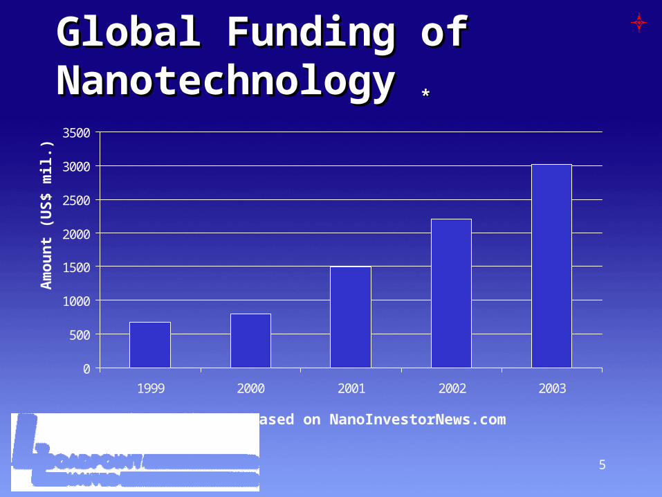
Global Funding of Global Funding of Nanotechnology Nanotechnology **
0
500
1000
1500
2000
2500
3000
3500
1999 2000 2001 2002 2003
Am
ou
nt
(US
$ m
il.)
* Approximate figures based on NanoInvestorNews.com
6
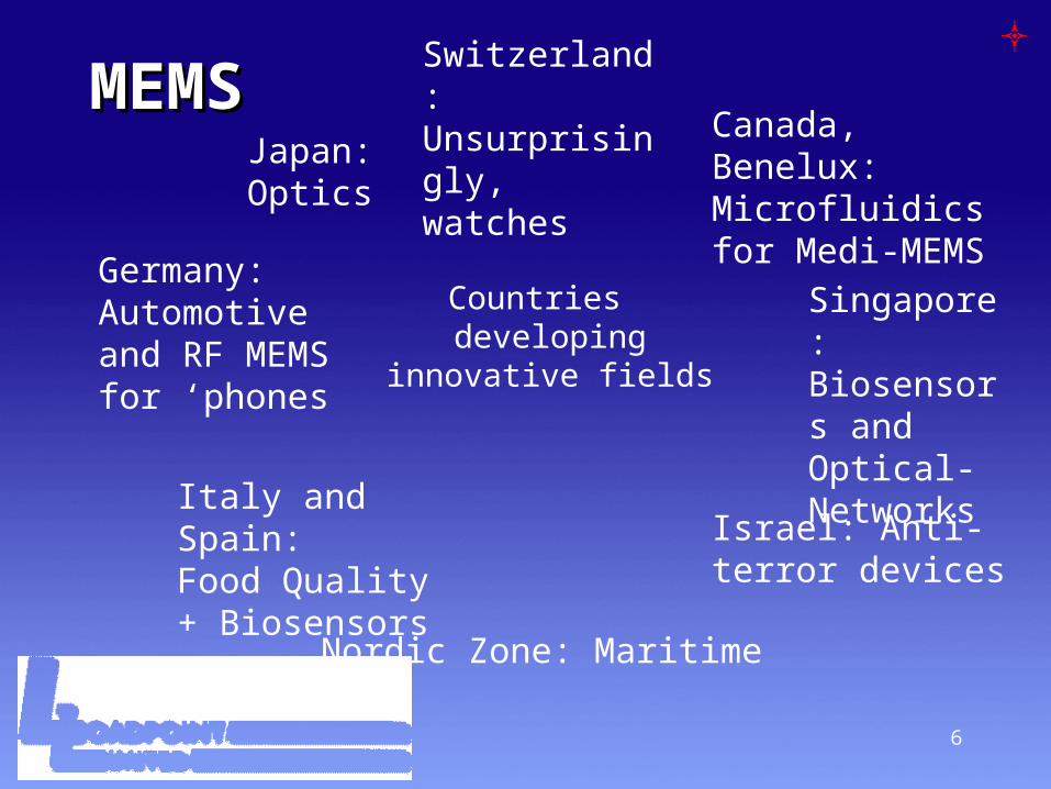
MEMMEMSS
Countries developing
innovative fields
Germany:Automotive and RF MEMS for ‘phones
Nordic Zone: Maritime
Italy and Spain:Food Quality + Biosensors
Israel: Anti-terror devices
Japan: Optics
Singapore: Biosensors and Optical-Networks
Canada, Benelux: Microfluidics for Medi-MEMS
Switzerland: Unsurprisingly, watches
7
MEMS The role of SME’sMEMS The role of SME’s
Highest costs are in Test and Packaging Unavailability of machinery for flexible or small
batch production leading to specialist service providers Small flexible SME’s providing appropriate
technology
8
MEMS ChinaMEMS China China, 2002 200 Million Yuan approved for MEMS
special project under five years plan 863 (high Tech and Development Research Programme
Fundamental Research Programme 973 (since 1997): 134 projects, 2.5B Yuan, MOEMS project, Nano Materials Project and Nano Electronics projects included
One of the few countries including agricultural research as part of nanotechnology.
13th Institute of China Electronics Technology Group offering flexible 3/4 inch MEMS fabrication line with test and packaging equipment
9
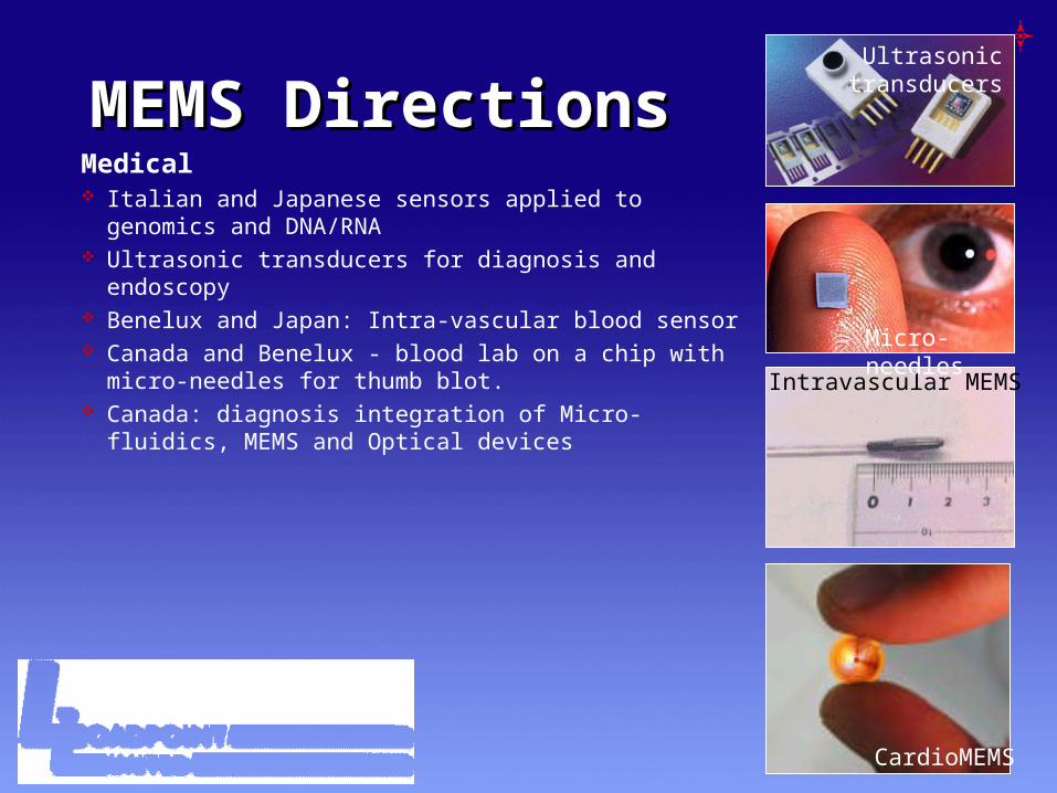
MEMS DirectionsMEMS DirectionsMedical Italian and Japanese sensors applied to genomics
and DNA/RNA Ultrasonic transducers for diagnosis and
endoscopy Benelux and Japan: Intra-vascular blood sensor Canada and Benelux - blood lab on a chip with
micro-needles for thumb blot. Canada: diagnosis integration of Micro-fluidics,
MEMS and Optical devices
CardioMEMS
Intravascular MEMS
Micro-needles
Ultrasonic transducers
10
MEMS DirectionsMEMS Directions
Automotive Sensors becoming the key to the Safe-Car
– Micro-accelerometers– Crash Sensors– Roll Sensors– Tyre pressure sensors
– Vision Assistance etc.
11
CommunicationsCommunications RF MEMS and Optical devices are the
focus Australian development in relays Canada showing particular interest in RF
and now X-ray MEMS Taiwan, biggest government investment
of MST is in this area - US$ 200 Million Optical and DisplayOptical and Display USA & Israel Micro-mirror arrays
12
Fuel injectors for automotive industry Blood sampling and other medical uses
MicrofluidicsMicrofluidics
MicroassemblyMicroassembly Synchrotron Projects - for imaging at
molecular levelAustralia spending $206M, other projects in Canada and Germany
Microfluidics will be important for this area, fine spraying seems to be the best emerging method of production for nano-materials
13
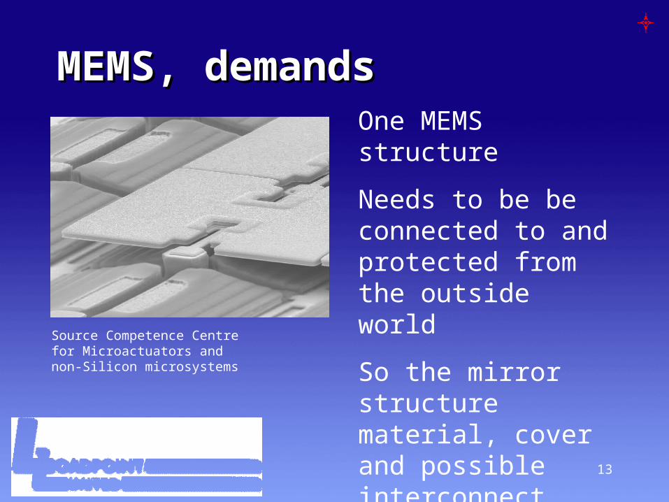
MEMS, demandsMEMS, demandsOne MEMS structure
Needs to be be connected to and protected from the outside world
So the mirror structure material, cover and possible interconnect layer need to be diced
Source Competence Centre for Microactuators and non-Silicon microsystems
14
Applications, driving forces Applications, driving forces for convergence for MEMS for convergence for MEMS dicingdicing MEMS CSP WSP BGA, UBGA, FR3 / FR4 & copper sub-frame Silicon, Glass, Quartz, Ceramic substrates, LTCC and similar PZT integrated transducers & actuators Stainless steel, copper etc. GaAs and SAWF materials and similar
15
MEMS Process Points 1MEMS Process Points 1 MEMS, BGA, BGA or similar converge at
WSP level Material thickness, hardness and poly-
material layers Cutting energy dissipation and strength of
material Sensitive surface topography and
coatings. Process Temperature control Keeping cutting swarf out of mechanisms
16
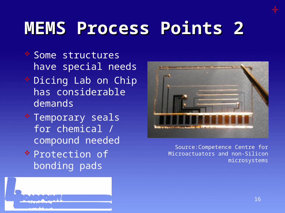
MEMS Process Points 2MEMS Process Points 2 Some structures
have special needs Dicing Lab on Chip
has considerable demands
Temporary seals for chemical / compound needed
Protection of bonding pads
Source:Competence Centre for Microactuators and non-Silicon
microsystems

17
MEMS MEMS OutlinesOutlinesPackages have standard features and these outlines indicate some seen.
Solutions exist for all of these although some development is usually needed to determine full process
Combination with BGA coming
18
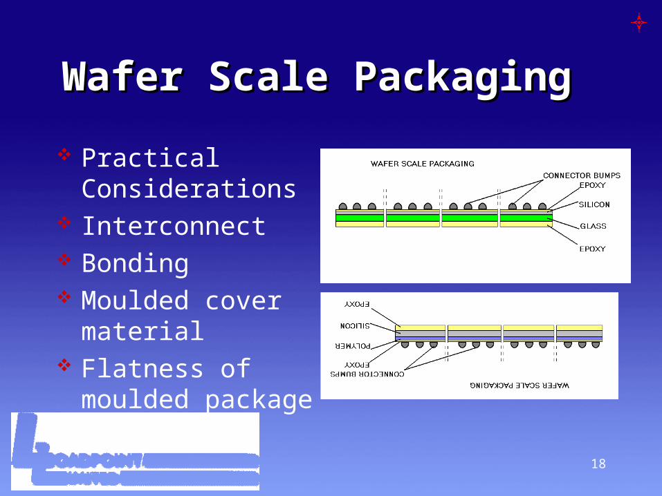
Wafer Scale PackagingWafer Scale Packaging
Practical Considerations
Interconnect Bonding Moulded cover
material Flatness of
moulded package
19
Large Area MEMSLarge Area MEMS
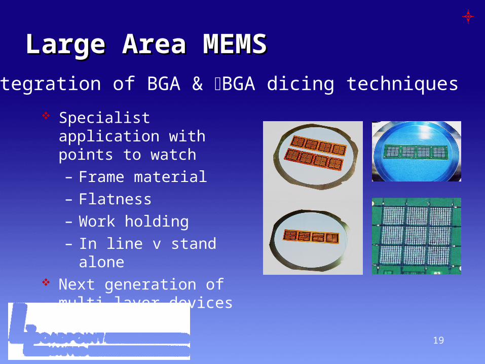
Specialist application with points to watch– Frame material– Flatness – Work holding– In line v stand
alone Next generation of
multi layer devices
Integration of BGA & BGA dicing techniques
20
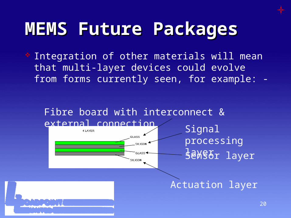
MEMS Future PackagesMEMS Future Packages Integration of other materials will mean
that multi-layer devices could evolve from forms currently seen, for example: -
Fibre board with interconnect & external connection Signal processing
layer
Sensor layer
Actuation layer
21
MEMS - the futureMEMS - the future Integration of more materials into the structure, up
to at least 6 layers Move to low profile wafer scale packaging with
BGA concepts Issues
– Grinding and surface finishing for layer bonding– Dicing a mixture of materials with diverse
characteristics, design for dicing Accurate break down into process elements for
process development Design for dicing!
22
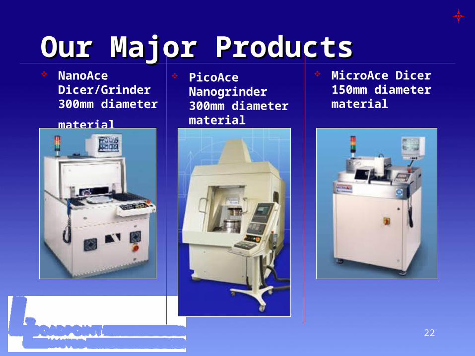
Our Major ProductsOur Major Products NanoAce
Dicer/Grinder 300mm diameter
material
PicoAce Nanogrinder 300mm diameter material
MicroAce Dicer 150mm diameter material

23
Chelworth IE, Cricklade, Swindon, Wiltshire, SN6 6HE, UK
Tel ++441 793 751160; email [email protected]
Web: www.loadpoint.co.uk
The information outlined in this presentation is considered in the public domain so free of any IPR restrictions other than that protecting Loadpoint’s general IPR by copyright © and registered design ®. All ideas and concepts offered are in good faith and require confirmation by either sampling or through extended research and development programmes. Sources of pictures from the WWW have been acknowledged as far as practical, there is no intention of infringing the IPR of the owners of those images as their sole purpose is to illustrate the point made in the presentation
LoadpointLoadpoint