Embed Size (px)
Citation preview
1

2
Memory interfacing is an essential topic for digital system design. In fact the among silicon area devoted to memory in a typical digital embedded system or a computer system is substantial. For example, in a mobile phone, the number of transistors devoted to memory is many times more than those used for computation. For the second year course, I will only focus on interfacing to static memory, known as RAM (Random Access Memory) or ROM (Read-Only Memory). There are other types of memory such as dynamic memory (DRAM), Synchronous DRAM (SDRAM) and flash memory (Flash RAM) which will not be covered on this course.
In this lecture, we will consider the various type of storage (memory) that FPGAs allow us to implement. The major advantage of FPGAs is that it contains lots of small blocks of memory modules, which can either be used independently, or combined to form larger memory blocks. They also provide various configurations such as multi-port or registered input/output for data and address.
There are various useful references you can look up if you are interested to learn more about this. For the purpose of examination, the contents in this lecture and in the VERI experiment are sufficient.

3
This slide shows a typical organisation inside a RAM chip. Memory cells are usually organised in the form of a 2-D array of RAM cells. These are accessed first in a row, then in a column. The address bus is divided into two components, the row address (8-bit in the example here) and the column address (4-bit in this example). There is a decode to translate the 8-bit row address into one-hot outputs in order to specify which row is being accessed. Only ONE ROW will be enable at any one time (hence one-hot).
The second part of the address (normally the less significant bits) is used as select signal into the output mux. This is because when memory is accessed, they are normally read or written in a sequence. Using LSB for column decoding means that one stays on the same row of memory as much as possible. Staying in the same row uses significantly lower energy than switching between rows in memory accesses. In the example here, the 4-bit column address is used to select from a 16-to-1 mux to provide the correct location in memory to access. There are 16 identical blocks, each providing one-bit of the data output.
The output enable signal OE allows the selected data value be driven on the data bus.

4
Here is a 8K x 8 static RAM chip and its associated digital signals. The 13-bit address bus A12:0, the 8-bit data bus D7:0 are mandatory. There are three more control signals: Output Enable OE which we have seen before, Chip Enable CE which is used to address or select this particular memory chip (hence the name), and finally the WRITE ENABLE signal WE, which, when set high, indicates that you are writing to the RAM chip, and is normally low (i.e. reading).
Note that the data bus has an inverted triangle sign, indicating that this is a tri-state bus. This means that the pin could be an input pin, output pin, or an open-circuit pin (i.e. not connected to anything – we call the signal floating). The truth table shown here specifies the behaviour of the data bus in one of the three possible states.

5
For a 8k x 8 RAM, there are 8 data bits, and therefore 8 separate 1-bit arrays. Let us assume that each data bit array is organised as a 256 rows x 32 column (=8192) of memory cells. Eight such array are placed next to each other to form the 8 data bits required. This makes the memory chip roughly square (which is generally desirable). You can think of the row decoder and the column selector driven by the 13-bit address as a 8192 way multiplexer, selecting one of 8192 cells organised as 256 x 32, to be accessed. The simplified circuit of each memory cell shown here consists of two inverters and two switches is a schematic of the read-write circuit. When reading from the cell, A12:0 select one of 8192 cells to route its signal via the right inverter to Dn. Now Dn is an output pin. This only happens if CE*OE* !WR = 1 (i.e. asserting CE and OE, but not asserting WR). When writing to the memory cell, the right switch is open, Dn is an input pin driving the left hand inverter and the output switch from that inverter is closed because both CE and WR are asserted.Some memory chips have separate Din and Dout pins, but that’s expensive on pins and is not particularly common nowadays.

6
Here is a slide showing a generic interfacing between a microprocessor and a memory sub-system. We assume that we use a 16-bit address bus and an 8-bit data bus. The control signals go between the two to control the transfer of information, and is in general governed by the microprocessor which acts as the “master”.

7
While we show memory as a block, in a real system, the memory address space is divided into many different partitions. Here we use ‘$’ (instead of 16’hxxxx) to indicate that the addresses are hexadecimal numbers. The left hand diagram shows the memory being partitioned into 32k of RAM, 16k of ROM and 4k space for input/output devices.A design needs to take the upper bits of the address bus and decode these bits into enable signals for the three different partitions. In this case, we can see that we only need to decode A15:12 according to the Boolean equations shown here. What about A11:0? These are the address bits used inside the RAM, ROM and input/output modules to select particular locations.

8
Selecting which memory sub-system and therefore which memory chip to enable is the job of the address decoder circuit. This circuit takes the upper bits of the address bus, and produce enable signals for RAM, ROM and INOUTx for a particular I/O device. In the previous slide, we showed that the input/output occupies 4k of memory space. This is uncommon. Typically an I/O device may take up, say, 4 memory locations. In this example, INOUTx occupies only the address space $F574 - $F577, i.e. 4 locations. Therefore we need to decode lots of address signals: A15:2.Can you work out the Boolean equations for the address decoder shown here?The ROM CE signal is another challenge. The ROM is enable if the address A15:A12 falls between the range 4’b1011 and 4’b1110. You should prove for yourself that the Boolean equation to decode the address for the ROM is as shown here.

9
In addition to the address decoder circuit, we need to provide the control signals from the microprocessor to the memory chips. Here we assume there exists at least two control signals from the microprocessor: MCLOCK which is memory clock signal (which may be different from the system clock signal CLOCK), and a WRITE signal, which is high when writing to memory, but low otherwise.The interaction between the microprocessor and memory can be separated into two types of transactions: a Read Cycle and a Write Cycle.During Read Cycle, the microprocessor asserts the address A15:0 and the control signals MCLOCK and WRITE. Shortly after the beginning of the Read Cycle, the microprocessor must STOP driving the data bus D7:0, and on the second half of the cycle, we assume that memory will then provide the data for the microprocessor to read. Reading is actually performed at the end of the Read Cycle, on the falling edge of MCLOCK. Note that I use red colour to indicate the action of the microprocessor on the data bus, and blue colour for the action by the memory chip on the data bus.During a Write Cycle, the microprocessor drives everything. Writing also occurs on the falling edge of MCLOCK in our case. (Note that other system may have a different protocol than the one shown here.)

10
This slide shows the control circuit used to interface the microprocessor to the 32k x 8 RAM chip. Chip Enable (CE) is driven by the output from the address decoder, which we have considered in an earlier slide. Remember the colour code I am using: RED driven by the microprocessor, BLUE driven by memory.

11
Let us now consider the timing constraints imposed by memory during a Read Cycle. First thing that happens would be a valid address A12:0 being presented at (1). As a typical example for memory timing, it is assume that data D7:0 holds for at least 2ns before changing, but it is guaranteed to provide the correct D7:0 at the new address in 8ns or earlier. This is address to data ACCESS TIME for this RAM. Note that even if new and old location have the same data value, there will be period when D7:0 contain rubbish –beware. Also note that memory is providing data to be read by the microprocessor, CE, OE and ~WR must all be asserted (i.e. ‘1’).At (2), memory is deselected or output not enabled, or we are no longer reading from memory. D7:0 again is guaranteed to go high-impedance after 2ns.Some time later, if member is selected again at (3), it takes 2ns before memory start to drive D7:0, but guaranteed to provide correct data after 4ns.The most important delay here is that from address or OE to data. They are called address access time and output enable access time. Usually address access timing is longer (here it is 8ns) than OE access time (4ns) because output enable simply enable the output multiplex stage, which is close to the data output pin. Address access involves decoding the address values to produce the one-hot row select signal (known as the WORD line), and then the row of memory cells needs to present its data to the column multiplexer. Selecting which row to access is generally a much slower process than the column multiplexer.

12
Here is the timing for the Write Cycle. Remember that Write Cycle timing is particularly important – any timing error here could result in corrupting the contents store in RAM.
(1)The write pulse is signified by CE and WR both being asserted (i.e. TRUE). There is usually a minimum period specified – here 10ns. Also as soon as the WR is asserted, WR = 1 and D7:0 must go high-impedance within 2ns (i.e. memory no longer driving the data bus).(2)The address A12:0 must be stable at least 2ns before the write pulse, and it must hold for another 2ns after the write pulse.(3)The data is written to memory on the falling edge of the write pulse. The setup and hold time is 4ns and 1ns respectively.(4)This is when the Write Cycle finishes, and we go back to Read Cycle. Expect D7:0 stays high impedance for at least 2ns.

13
The simplest form of storage is a register file. All microprocessors have register files, which are known as “registers” in the architectural context.
Register files are fast, large and flexible. They are generally used to store temporary data for easy access by the ALU or floating point unit of a microprocessor, or for computational engine of a application specify digital system.
On the FPGA, register files are often implemented with the D-FF’s in the Adaptive Logic Modules (ALMs). Each ALM has two D-FFs. Therefore a 32-bit register will take up 16 ALMs. Alternatively one could also use the static memory blocks for this purpose.

14
The circuit of a register file is simple – it consists of arrays of D-FFs, which can be disable (and output becomes high impedance). The register select signals sel_reg0, sel_reg1 etc. enable the correct register to put the data on the data line (called bit line here). The read/write control signal WE is used to determine if you are reading or writing to the register.

15
The register identification (regid) determines which register you are trying to access. This is achieved through a standard decoder, which generate a one-hot code word to select the appropriate register to access.

16
Now let us turn to the Cyclone V FPGA. The FPGA has many different type of resources in additional to Adaptive Logic Modules (ALMs). These are: memory blocks, Digital Signal Processing (DSP) units, phase-locked loops and input/output pads. In addition, there is a dual-core ARM processor and its associated bus interface circuit (shown in light green).
Here we focus on memory. In the C5-SE-A5 series, which is the one we use in the DE1 board, there are near 400 separate memory blocks, each with 10k bits of storage. Together with the ALMs, there is 4.45 Mbits of flexible memory storage available to the designer.

17
Each of these blocks (known as M10K) can be configured with different depth and data width as shown in the able above.
Even more importantly, the can also be configured to act as conventional single-port memory, or simple dual-port with one port for read and one port for write.
Further, they can be made to be true dual-port, both ports being read/write ports, or as a shift register, a ROM or a first-in-first-out buffer (FIFO).

18
As you have seen in the VERI experiment, if the memory block is a ROM (or even as a RAM), its content can be configured via a memory initialization file .mif. The format of the file is shown here. Typing the contents of a 1024 ROM module by hand is silly and impractical. I wrote two versions of a simple programme to generate this .mif file, one in Matlab and one in Python. Below is the code for the Matlab version.The ROM is produced using the IP Catalog tool. Here is a 1024 x 10 bit ROM generated with all input and output registered and synchronised with the clock signal.
19
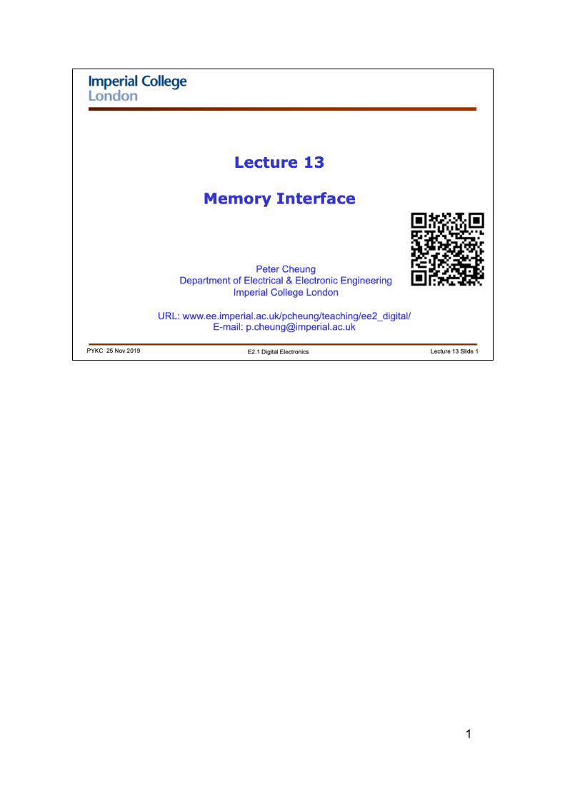
In the experiment, you have already implemented a sine wave generator using the ROM to store one cycle of a sine wave. The counter is used to advance the phase of the sine wave, which is specified as the address X of the ROM. The content of the ROM, y= F(x) is the content of the ROM and is the generated wave form. Instead of storing a sine wave, you can easily store any other signal (such as a voice or music segment).In order implement a variable frequency sinewave, you could modify the address counter so that it is goes up not only by 1 count for each clock cycle, but by N. For example if N is 2, then the address counter will skip every other sample in the ROM and therefore the generated sinewave will be at twice the signal frequency.

20
Here is a generated single-port memory with ALL possible signals included. The meaning of all the signals are self explanatory.

21
Here is an example of using the MegaWizard manager tool in Quartus. We are producing a 1-port RAM with 1024 x 8, all signals are clocked. The generator produces a sample header file (a template) which defines the interface signal to the generated block. Remember you must tick the Verilog HDL radio button.

22
You can also configure the M9K memory block as a shift register. Here is an 8-bit 16 stage SR. In addition, it provides “tap” outputs for every stage, i.e. 16 x 8 = 128 output signals. This is very useful to implement FIR filter or perform time domain convolution.

In the Part IV of the VERI experiment, you will be using a FIFO to implement an echo synthesizer. The action of a FIFO is shown in the diagram above.
23

Here is a generic block diagram of a FIFO with its typical interface signals. FIFO is a form of queue. Internally there typically two counters, one keeping track of the read address (or read pointer) and another counter keeping track of the write address (write pointer). There needs to be status signals such as FULL, which is asserted if the FIFO is completely filled and writing any more words to it will destroy stored data, or EMPTY, which signifies that there are no data left to read.
24
25
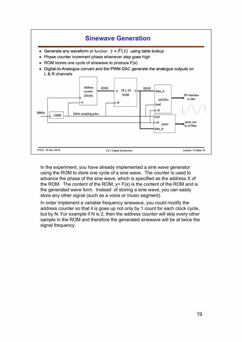
FIFO can be generated using the IP Catalog manager tool. Here is an example of a 32 word x 8 bit FIFO.