Embed Size (px)
Citation preview
Memory Device EvolutionCassino May 2008
Maurizio Di Zenzo
Applications Lab Mgr

May, 2008
Cassino University Lecture
2
©2007 Micron Technology, Inc. All rights reserved.
Agenda
• Random access memoriesA quick comparison of technologiesDetails of external memory technologies
Solutions for lowpower and mobile applications
Solutions for high performance
• Nonvolatile memoriesA quick comparison of technologies
Details of external memory options

May, 2008
Cassino University Lecture
3
©2007 Micron Technology, Inc. All rights reserved.
Random Access Memory Technologies(Relative Comparison)
Technology HighSpeedSRAM
LowPowerSRAM
Embedded DRAM
External DRAM
PseudoStatic
RAM
Power
Medium density
Costs
Density
Area
Speed
OtherFeatures
Widebusses
High density
May, 2008
Cassino University Lecture
4
©2007 Micron Technology, Inc. All rights reserved.
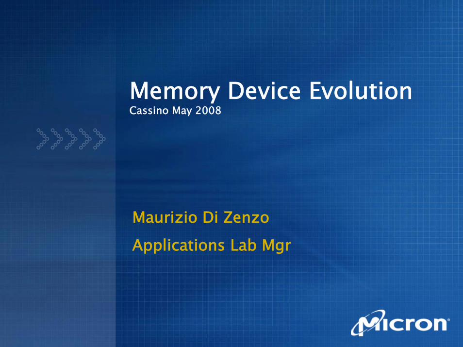
Architecture of a DRAM Memory device
Timing and Control
Column AddressBuffers(12)
Row AddressBuffers(12)
A<11:0>
8M x 8 = 64M
1Mx8=8M128k 128kx8=1M
128k 128kx8=1M
Sense AmpsColumn Decode
1Mx8=8M128k 128kx8=1M
128k 128kx8=1M
Sense AmpsColumn Decode
1Mx8=8M128k 128kx8=1M
128k 128kx8=1M
Sense AmpsColumn Decode
1Mx8=8M128k 128kx8=1M
128k 128kx8=1M
Sense AmpsColumn Decode
Row
Dec
ode
Row
Dec
ode
I/OBuffers
4 out of 16Selection
DataOutReg(4)
DataIn
Reg(4)
DQ
<3:
0>
RAS_ CAS_ W_ OE_Reference Voltages
&Pumps
May, 2008
Cassino University Lecture
5
©2007 Micron Technology, Inc. All rights reserved.
SDRAM Architecture
CLK
Sense Amps
Column Address Counter & Decode
7ns
OutputBuffer
Pipeline Queue
SA0
SA2
SA3
SA4
SA5
SA6
SA7
SA1
Sense Amps Mid-Amp
Column Decode
OutputBuffer
30ns
DRAM
SDRAM
Mid-Amp

May, 2008
Cassino University Lecture
6
©2007 Micron Technology, Inc. All rights reserved.
Why Refresh?
Charge leaks away over time. If nothing is done, in about a quarter of a second (200-300 milli-seconds), capacitors that were storing ones will be storing zeros!
Leakage PathsWordline
(Row)
Bit Line (Column)
DRAM Storage Cell
May, 2008
Cassino University Lecture
7
©2007 Micron Technology, Inc. All rights reserved.
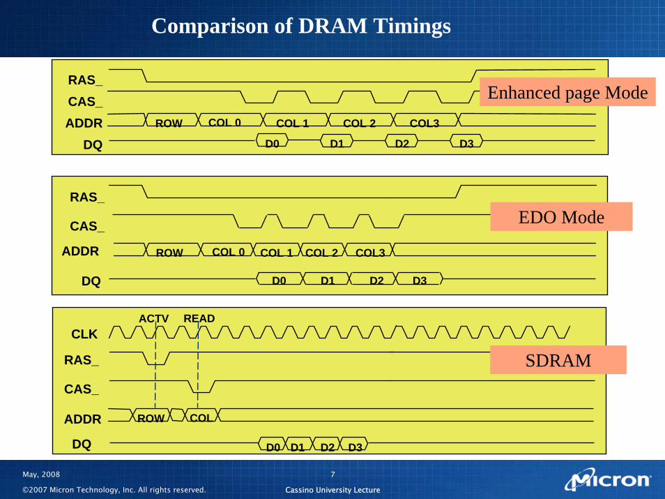
Comparison of DRAM Timings
ADDR
ACTV READ
ROW COL
D0 D1 D2 D3
CLK
RAS_
CAS_
DQ
SDRAM
RAS_CAS_
DQADDR
D0 D1 D2 D3
Enhanced page ModeCOL3ROW COL 1 COL 2COL 0
ADDR
RAS_
CAS_
DQ D1 D2 D3
COL3ROW COL 1 COL 2COL 0
EDO Mode
D0

May, 2008
Cassino University Lecture
8
©2007 Micron Technology, Inc. All rights reserved.
Basic DDR Differences from SDR
• Differential clock vs. singleended clock
• Differential clock (crossing) more accurate than rising edge

May, 2008
Cassino University Lecture
9
©2007 Micron Technology, Inc. All rights reserved.
DDR DQS Strobe – READ/WRITE
READ
WRITE

May, 2008
Cassino University Lecture
10
©2007 Micron Technology, Inc. All rights reserved.
Ideal Signal Waveforms
RAS_
CAS_
Note that an ideal signalis relatively smooth.
May, 2008
Cassino University Lecture
11
©2007 Micron Technology, Inc. All rights reserved.
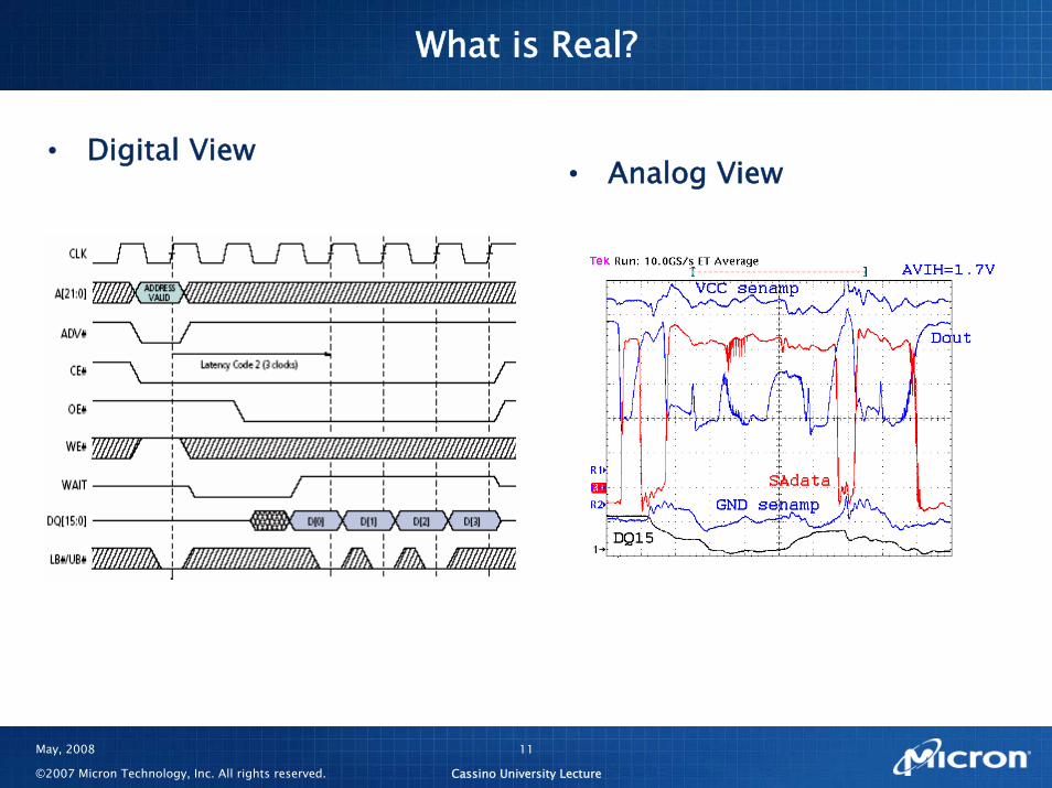
What is Real?
• Digital View• Analog View
May, 2008
Cassino University Lecture
12
©2007 Micron Technology, Inc. All rights reserved.
Basic DDR Differences from SDR
• Bi-directional data strobe (DQS) added to data bus
Why a data strobe?Compensates for temperature, voltage, and loading
Strobe travels with dataDuring a WRITE to the DRAM, memory controller generates strobe
• Strobe occurs at beginning of data valid
During a READ from the DRAM, the DRAM generates the strobe
• Strobe occurs at midpoint of data valid

May, 2008
Cassino University Lecture
13
©2007 Micron Technology, Inc. All rights reserved.
Major differences from DDR to DDR3
Feature/Option DDR DDR2 DDR3
Package TSOP (66 pins)
FBGA only FPGA 78-ball: x4, x8FPGA 96-ball: x16
Voltage 2.5V2.5V I/O
1.8V1.8V I/O
1.5V
Densities 128Mb–1Gb 256Mb–2Gb 512Mb – 8Gb
Internal Banks 4 4 and 8 8
Prefetch(MIN WRITE Burst) 2 4 8
Speed (Data Pin)200 MHz, 266 MHz,
333 MHz, and 400 MHz400 MHz, 533 MHz,
and 667 MHz800, 1600 Mb/s
READ Latency 2, 2.5, 3 CLK CL + AL CL = 3, 4, 5
CL + AL CL = 3, 4, 5
WRITE Latency 1 clock READ latency – 1AL + CWL
CWL = 5,6,7,8

May, 2008
Cassino University Lecture
14
©2007 Micron Technology, Inc. All rights reserved.
DRAM Technology Trends
FP/EDORDRAM®
SDRAM
DDR
DDR2
DDR3
0%
10%
20%
30%
40%
50%
60%
70%
80%
90%
100%
2000 2001 2002 2003 2004 2005F 2006F 2007F 2008F 2009F
Perc
ent
of T
otal
Meg
abit
s Sh
ippe
d
RDRAM is a registered trademark of Rambus Inc. Source: Micron market research, iSuppli 03/05
May, 2008
Cassino University Lecture
15
©2007 Micron Technology, Inc. All rights reserved.
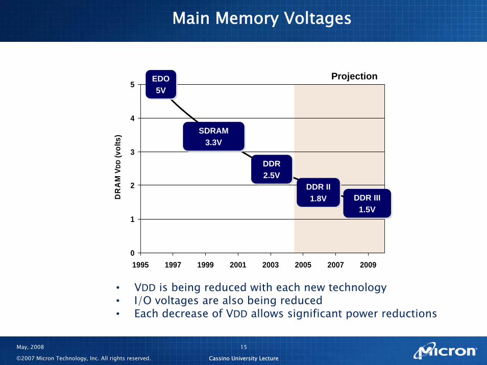
Main Memory Voltages
• VDD is being reduced with each new technology• I/O voltages are also being reduced• Each decrease of VDD allows significant power reductions
0
1
2
3
4
5
1995 1997 1999 2001 2003 2005 2007 2009
DR
AM
VDD
(vol
ts)
EDO5V
EDO5V
SDRAM3.3V
SDRAM3.3V
DDR2.5VDDR2.5V
DDR II1.8V
DDR II1.8V DDR III
1.5VDDR III
1.5V
Projection
May, 2008
Cassino University Lecture
16
©2007 Micron Technology, Inc. All rights reserved.
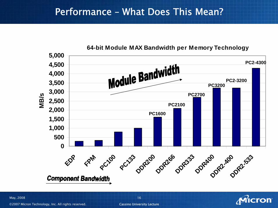
64-bit Module MAX Bandwidth per Memory Technology
0500
1,0001,5002,0002,5003,0003,5004,0004,5005,000
EDP
FPMPC10
0PC13
3DDR200DDR266DDR333DDR400
DDR2-400
DDR2-533
MB
/s
PC1600
PC2100
PC2700
PC3200PC2-3200
PC2-4300
Performance – What Does This Mean?
May, 2008
Cassino University Lecture
17
©2007 Micron Technology, Inc. All rights reserved.
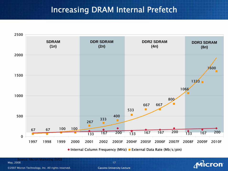
Increasing DRAM Internal Prefetch
SDRAM(1n)
DDR SDRAM(2n)
DDR2 SDRAM(4n)
DDR3 SDRAM(8n)
200200133 167 133 167 167 133 167 20067
1600
1333
1066
800667667
533400
267
67 100 100
333
0
500
1000
1500
2000
2500
1997 1998 1999 2000 2001 2002 2003F 2004F 2005F 2006F 2007F 2008F 2009F 2010F
Internal Column Frequency (MHz) External Data Rate (Mb/s/pin)
Source: Micron Marketing 09/03

May, 2008
Cassino University Lecture
18
©2007 Micron Technology, Inc. All rights reserved.
Maximum Bandwidth Comparison
067
133200267333400467533600667733800867933
1,0001,0671,1331,2001,2671,333
0.01 0.10 1.00 10.00 100.00Read/Write Ratio
Band
wid
th p
er D
ata
Pin
(Mb/
s)
DDR2800 BL4 DDR2800 BL8RLDRAM533 SIO BL2 RLDRAM533 SIO BL4, BL8RLDRAM533 CIO BL2 RLDRAM533 CIO BL4RLDRAM533 CIO BL8 DDR3 1333 BL4DDR3 1333 BL8

May, 2008
Cassino University Lecture
19
©2007 Micron Technology, Inc. All rights reserved.
Pricing Comparison by Technology
Price vs. Latency
0
1
2
3
4
0 10 20 30 40 50 60 70
ns
1Gb DDR2576Mb
Relative Price
Speed
72Mb36Mb
18Mb
288Mb
256Mb
18Mb9Mb
512Mb DDR256Mb SDR
16Mb 4Mb
RLDRAM
ZBT SRAM
Async SRAM
QDR/DDR SRAM
1Gb DDR3

May, 2008
Cassino University Lecture
20
©2007 Micron Technology, Inc. All rights reserved.
Technology Price/Mb Comparison
Price/Mb vs. Latency
0
10
20
30
40
0.0 10.0 20.0 30.0 40.0 50.0 60.0 70.0
Relative Price
ns
QDR/DDR SRAM
Commodity DRAMRLDRAM
ZBT SRAMAsync SRAM

LowPower, Mobile Solutions

May, 2008
Cassino University Lecture
22
©2007 Micron Technology, Inc. All rights reserved.
• Lower Power – Targets top four power issues (Supply and I/O Voltage, Self Refresh Current and Operating Current)
Typically 1.8V VDD and VDDQ option offered
TCSR – Temperature Compensated Self Refresh
PASR – Partial Array Self Refresh
Deep Power Down Feature
• Variable Drive Strength
• VFBGA Packaging - Smaller Form Factor
Mobile FeaturesWhat Distinguishes it from Std SDRAM?

May, 2008
Cassino University Lecture
23
©2007 Micron Technology, Inc. All rights reserved.
• First generation Mobile SDRAM designs allow manual setting of TCSR through the EMR (Extended Mode Register)
• All new (and some improved) designs incorporate an on-chip temperature sensor to dynamically control the self refresh rate automatically
• JEDEC LP-DDR specification had TCSR as optional – if an on-chip temp sensor is used, the EMR bits must be a “don’t care” to allow backward compatibility
Mobile FeaturesTemperature Compensated Self Refresh
May, 2008
Cassino University Lecture
24
©2007 Micron Technology, Inc. All rights reserved.
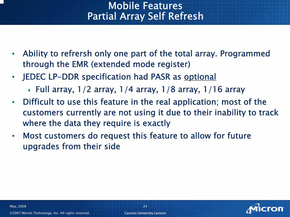
• Ability to refrersh only one part of the total array. Programmed through the EMR (extended mode register)
• JEDEC LP-DDR specification had PASR as optional Full array, 1/2 array, 1/4 array, 1/8 array, 1/16 array
• Difficult to use this feature in the real application; most of the customers currently are not using it due to their inability to track where the data they require is exactly
• Most customers do request this feature to allow for future upgrades from their side
Mobile FeaturesPartial Array Self Refresh

May, 2008
Cassino University Lecture
25
©2007 Micron Technology, Inc. All rights reserved.
• JEDEC LP-DDR specification shows Deep Power Down as a design requirement
Device must be in all banks idle state prior to entering DPD
All memory data is lost
DRAM must be fully re-initialized to ensure proper functionality –LMR and EMR must be reloaded
• No customer usage currently known and no requests made to have this feature in future designs
Micron will continue to offer this feature to be fully JEDEC compliant
Mobile FeaturesDeep Power Down

May, 2008
Cassino University Lecture
26
©2007 Micron Technology, Inc. All rights reserved.
• Offers customers the option to use a lower drive strength for lighter system loads or point-to-point environments
• Programmed through the EMR (extended mode register) – standard full and half drive settings
New series Mobile SDR/DDR SDRAM will include 1/4 and 1/8 drive setting in response to customer requests
• Customers are using this feature – especially for the SDR parts that exhibit higher full drive strength than they required
Mobile FeaturesVariable Output Drive Strength

May, 2008
Cassino University Lecture
27
©2007 Micron Technology, Inc. All rights reserved.
• Design DifferencesDLL Omitted from Design
Reduces power consumptionMinimizes the DRAM’s ability to run at higher frequencies
• currently specified to 200MHz CL=3 and is pushing the limits of the design - customers pushing for tighter tAC specifications
No external VREF – internal to the DRAM designDifferent initialization sequence requiredOffered in x32 configuration
• Main Specification DifferencesLower IDD values – Operating current and Self RefreshSome variations in timing
Minimum speed specified on Std DDR, LP-DDR can run at very slow speedsMuch higher tAC (access time from CK/CK#)
No DLL
DDR Mobile SDRAMHow Does it Differ From Std DDR?

May, 2008
Cassino University Lecture
28
©2007 Micron Technology, Inc. All rights reserved.
Mobile Memory Comparison
PSRAM LP-SDR LP-DDR LP-DDR2 (S4)MAX frequency 133 MHz 166 MHz CL = 3 200 MHz CL = 3 533 MHz CL = 8Data rate (0% interleaving, 1:1 R/W, 1 Byte/access)
26.6 MB/s @ 133 MHz 16.6 MB/s @ 166 MHz 19.0 MB/s @ 200 MHz 16.7 MB/s @ 533 MHz
Data rate (25% interleaving, 1:1 R/W, 1Byte-32Byte/access)
168.5 MB/s @ 133 MHz 120.7 MB/s @ 166 MHz (x16)177.3 MB/s @ 166 MHz (x32)
269.0 MB/s @ 200 MHz (x16)318.9 MB/s @ 200 MHz (x32) 310.0 MB/s @ 533 MHz (x32)
Data rate (85% interleaving, 1:1 R/W, 32 Byte/access)
212.8 MB/sec @ 133 MHz
167.2 MB/s @ 166 MHz (x16)316.7 MB/s @ 166 MHz (x32)
684.5 MB/s @ 200 MHz (x16)1196.3 MB/s @ 200 MHz (x32)
2061.1 MB/s @ 533 MHz (x32)
Bus width(per device) x16 x16, x32 x16, x32 x16, x32
Density 4–128Mb 64–512Mb 64Mb–1Gb 1–8GbBanks 1 4 4 8
VDD/VDDQ 1.8V/3.3V 1.8V/1.8V1.8V/1.8V1.8V/1.2V*1.2V/1.2V*
1.8V/1.2V/1.2V/1.2V**
Package 54-ball VFBGA 54ball VFBGA (x16)90ball VFBGA (x32)
60ball VFBGA (x16)90ball VFBGA (x32)152ball VFBGA PoP*
TBDJEDEC
Functional pin Count (MAX density, MAX width)
Std (128Mb): 47 AD MUX (64Mb): 31 (512Mb-x32): 57 (1Gb-x32): 62 (8Gb-x32***): 59
Burst options 4, 8, 16, 32* 1, 2, 4, 8 page 2, 4, 8, 16* 4, 8, 16
* Note: Not available for all densities; contact factory for availability** Note: LPDDR2 has four supplies: VDD1/VDD2/VDDCA/VDDIO*** Note: Pin count does not change with density for LPDDR2 due to muxed cmd/addr bus

May, 2008
Cassino University Lecture
29
©2007 Micron Technology, Inc. All rights reserved.
What is a PSRAM?
• Psuedo-SRAM’s name comes from its similarity to SRAM; however, internally PSRAM is a DRAM—combining the best of both products
PSRAM1T cell architecture
Broadside addressing
(A0–Axx)
Volatile—hidden refresh
Low power
Higher bandwidth
Asynchronous accessSynchronous access
SRAM6T cell architecture
Broadside addressing
(A0–Axx)
Volatile—hidden refresh
Low power
Low bandwidth
Asynchronous access
DRAM1T cell architecture
MUX’d addressing (row–col)
Volatile—refresh required
High power
High bandwidth
Synchronous access

May, 2008
Cassino University Lecture
30
©2007 Micron Technology, Inc. All rights reserved.
Architectural ComparisonCellularRAM® (PSRAM) LPSDRAM
Addressing Broadside Multiplexed
Refresh modes Hidden Auto/Self
Row size 2k 4k (128K device)
Interface optimized for?
Random access Multibank access
64Mb–1Gb (DDR)
Voltage (Vccq/Vddq) 1.7–3.6V 1.8V
Bank architecture Single (1) bank Multiple (4) banks
64–512Mb (SDR)Density 4–128Mb
Voltage (Vcc/Vdd) 1.7–3.6V 1.8V

May, 2008
Cassino University Lecture
31
©2007 Micron Technology, Inc. All rights reserved.
Why Use PSRAM instead of SRAM?
PSRAM can be used to replace sockets where SRAM has been traditionally used
Feature
• Smaller die size (6T vs. 1T/2T)
• Increased density offering
• Asynchronous interface
• Burst interface with variable latency
• FBGA and TSOP* package
Benefit
• Lower cost part
• Ability to increase complexity and performance of end design
• Dropin replacement
• Increased throughput and performance
• Small footprint for mobile applications
* In design

Nonvolatile Technologies

May, 2008
Cassino University Lecture
33
©2007 Micron Technology, Inc. All rights reserved.
Nonvolatile Technologies(Relative Comparison)
TechnologyFuse
(OTP)NOR NAND eMMC MRAM PCRAM
Power
ReliabilityRequires ECC
and block management
Density
Speed read
EnduranceRequires block management
Speed write NA
Availability Protos
May, 2008
Cassino University Lecture
34
©2007 Micron Technology, Inc. All rights reserved.
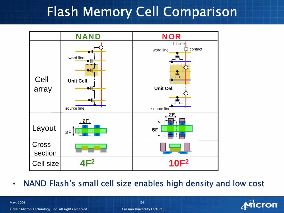
word linebit line
source line
Unit Cell
contact
5F
2F
10F2
NOR
Cell size
2F
2F
4F2
NAND
source line
word line
Unit Cell
Layout
Cross-section
Cellarray
Flash Memory Cell Comparison
• NAND Flash’s small cell size enables high density and low cost
May, 2008
Cassino University Lecture
35
©2007 Micron Technology, Inc. All rights reserved.
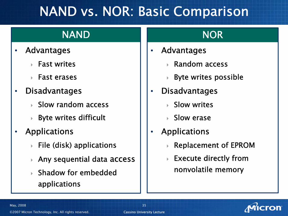
NAND NOR
NAND vs. NOR: Basic Comparison
• AdvantagesFast writes
Fast erases
• DisadvantagesSlow random access
Byte writes difficult
• ApplicationsFile (disk) applications
Any sequential data accessShadow for embedded applications
• AdvantagesRandom access
Byte writes possible
• DisadvantagesSlow writes
Slow erase
• ApplicationsReplacement of EPROM
Execute directly from nonvolatile memory

May, 2008
Cassino University Lecture
36
©2007 Micron Technology, Inc. All rights reserved.
CharacteristicNAND Flash (SLC)
MT29F4G08ANOR (QFlash®)
MT28F128J3
Random access read25µs (first byte)
25ns each for remaining 2,111 bytes
0.12µs
Sustained read speed (sector basis)
33 MB/s (x8) 20.5 MB/s (x8)
Random write speed ~220µs/2,112 bytes 180µs/32 bytes
Sustained write speed (sector basis)
19 MB/s 0.178 MB/s
Erase block size 128KB 128KB
Erase time per block (TYP)
2ms 750ms
NAND vs. NOR: Strengths and Weaknesses
NOR Flash is ideal for direct code execution (boot code).
NAND Flash is ideal for file storage, such as data or image files. If code is stored, it must be shadowed to RAM
first (as in a PC).

May, 2008
Cassino University Lecture
37
©2007 Micron Technology, Inc. All rights reserved.
MLC vs. SLC
MLC SLCFeaturesBits per cell 2 1
Voltage 3.3V 3.3V, 1.8V
Data width (bits) x8 x8, x16
ArchitectureNumber of planes 2 1 or 2
Page size 2,112–4,314 bytes 2,112 bytes
Pages per block 128 64
ReliabilityNOP (partial page programming) 1 4
ECC (per 512 bytes) 4+ 1
Endurance (ERASE/PROGRAM cycles) ~10K ~100K
Array OperationstR (Max) 50µs 25µstPROG (TYP) 600–900µs 200–300µs
tBERS (TYP) 3ms 1.5–2ms
Relative price 1X 2X
Reliability of SLC is 10 times
better!
Performance of SLC ~3 times
better!
Cost premium is only about
2X
May, 2008
Cassino University Lecture
38
©2007 Micron Technology, Inc. All rights reserved.
Another Option: eMMC (Managed NAND)
• The next logical step in the highdensity NAND evolution for embedded applications
• Turns MLC NAND into a robust simple write/read memory
• Insulates the host from unnecessary details, including NAND block sizes, page sizes, planes, new features, process generation, MLC vs. SLC, wear leveling, and ECC requirements

May, 2008
Cassino University Lecture
39
©2007 Micron Technology, Inc. All rights reserved.
What is Managed NAND (eMMC)?
• Managed NAND combines the advantages of MLC NAND with a controller, which address all of the complexities of MLC (ECC, wear leveling, and block management)
• Provides MLC densities at close to MLC prices
Managed NAND (eMMC)
Higher density (over SLC)
Improved cost (over SLC)
Improved reliability
Higher performance (over MLC)
Standard interface (MMC)
Single BGA package
MLC NANDAdvantages Disadvantages
Lower reliability (than SLC) Lower performance
High density
Lower cost (than SLC) Advanced performance (dual
channel)
Advanced block management
Advanced wear leveling
Advanced ECC
Controller
May, 2008
Cassino University Lecture
40
©2007 Micron Technology, Inc. All rights reserved.
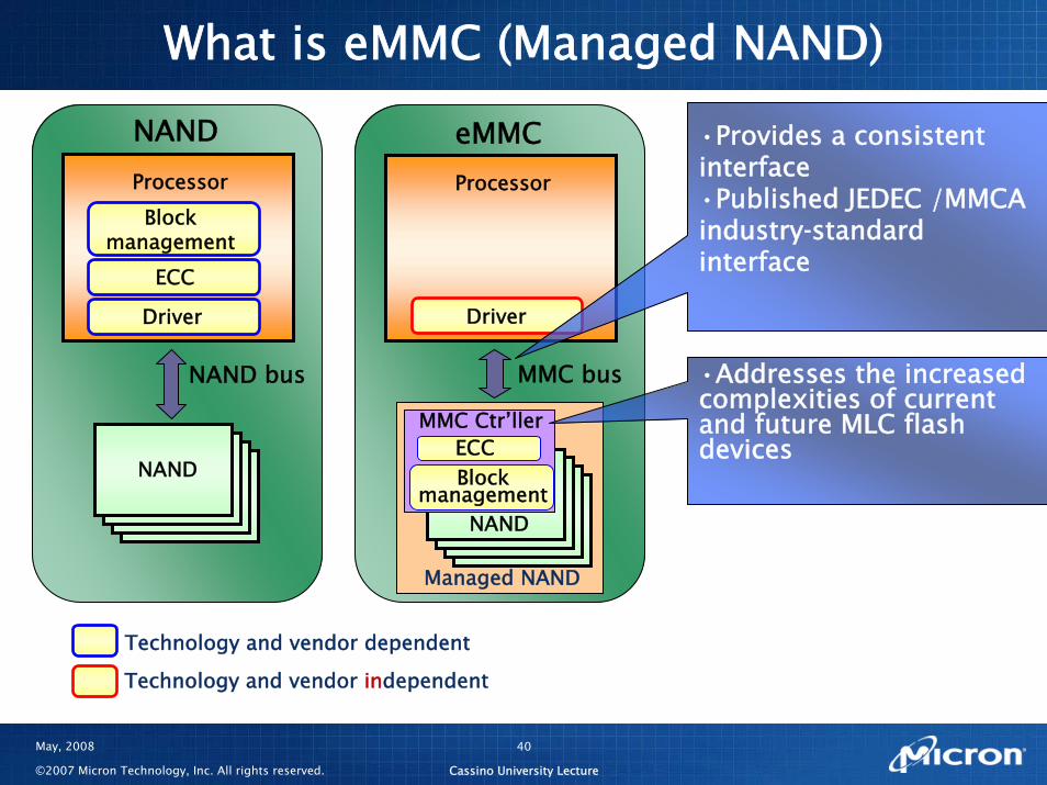
What is eMMC (Managed NAND)
Technology and vendor dependent
Technology and vendor independent
NAND
Block management
ECC
Driver
Processor
NAND
NAND bus
Driver
Processor
eMMC
MMC bus
NAND
ECCBlock
management
MMC Ctr’ller
Managed NAND
•Provides a consistent interface•Published JEDEC /MMCA industrystandardinterface
•Addresses the increased complexities of current and future MLC flash devices

May, 2008
Cassino University Lecture
41
©2007 Micron Technology, Inc. All rights reserved.
Summary