Embed Size (px)
Citation preview
®
Please do not distribute without written permission of Amorphyx
Meeting the Rising Demand for Improved UHD Backplane Performance
An overview of Amorphyx Technology
Sean Muir, VP Device Technology
SEMI & CSMC Webinar on Emerging Amorphous
Metal Thin Film Technologies for Electronics
®
Please do not distribute without written permission of Amorphyx
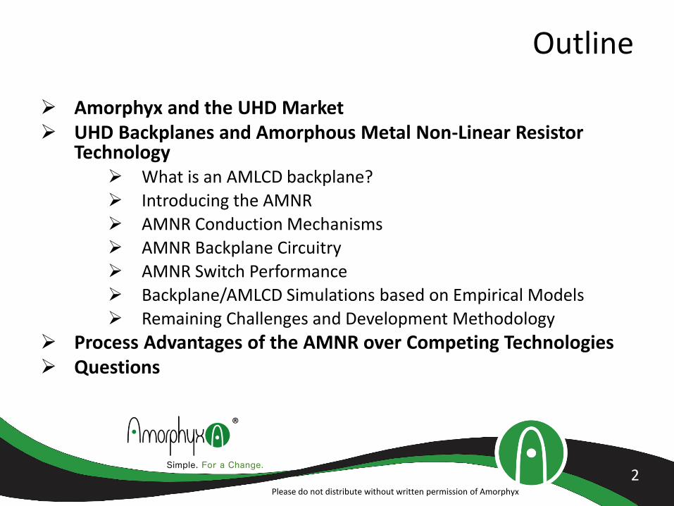
Outline
Amorphyx and the UHD Market UHD Backplanes and Amorphous Metal Non-Linear Resistor
Technology What is an AMLCD backplane?
Introducing the AMNR
AMNR Conduction Mechanisms
AMNR Backplane Circuitry
AMNR Switch Performance
Backplane/AMLCD Simulations based on Empirical Models
Remaining Challenges and Development Methodology
Process Advantages of the AMNR over Competing Technologies Questions
2
®
Please do not distribute without written permission of Amorphyx3
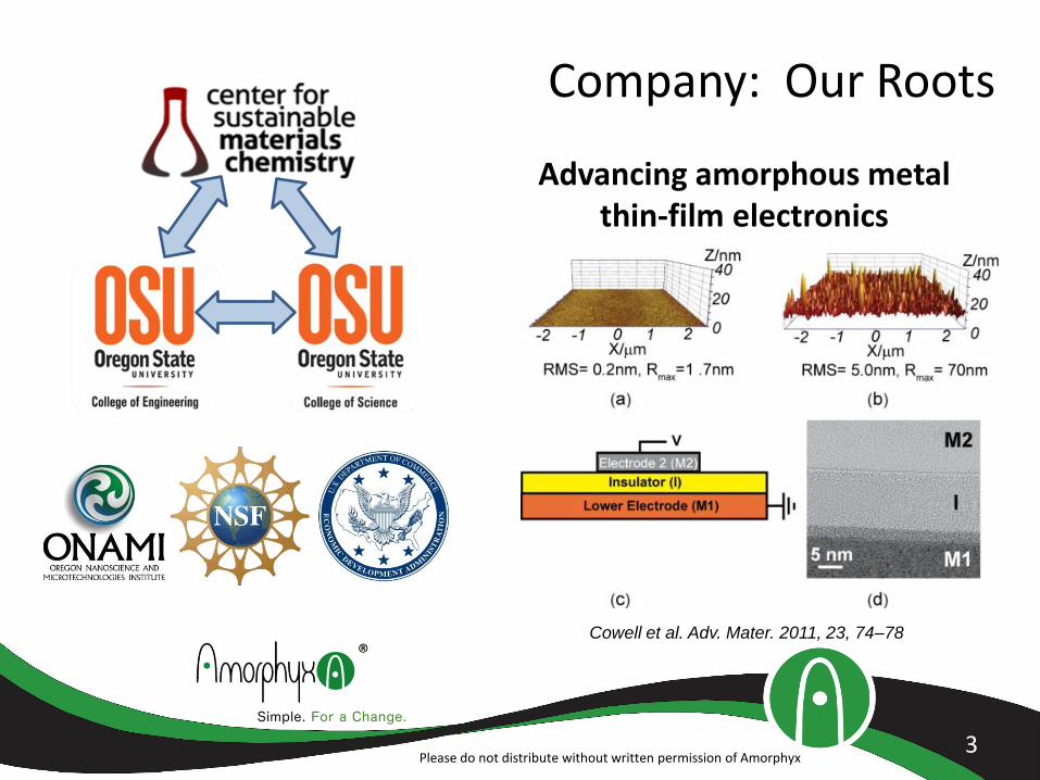
Advancing amorphous metal thin-film electronics
Company: Our Roots
Cowell et al. Adv. Mater. 2011, 23, 74–78
®
Please do not distribute without written permission of Amorphyx4
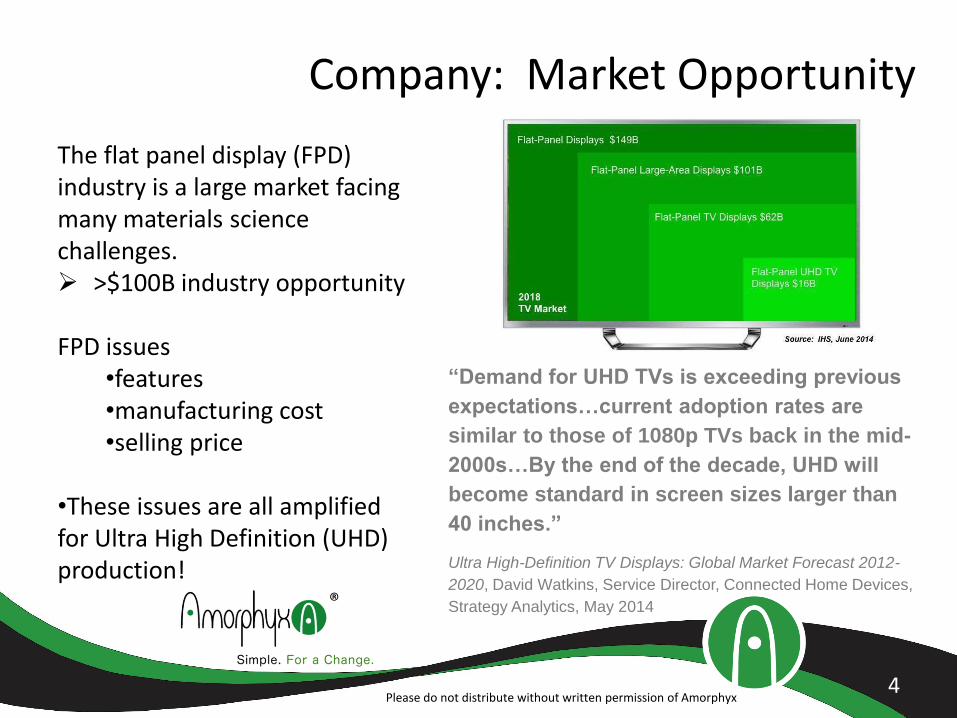
The flat panel display (FPD) industry is a large market facing many materials science challenges. >$100B industry opportunity
FPD issues•features•manufacturing cost •selling price
•These issues are all amplified for Ultra High Definition (UHD) production!
Company: Market Opportunity
“Demand for UHD TVs is exceeding previous
expectations…current adoption rates are
similar to those of 1080p TVs back in the mid-
2000s…By the end of the decade, UHD will
become standard in screen sizes larger than
40 inches.”
Ultra High-Definition TV Displays: Global Market Forecast 2012-
2020, David Watkins, Service Director, Connected Home Devices,
Strategy Analytics, May 2014
®
Please do not distribute without written permission of Amorphyx
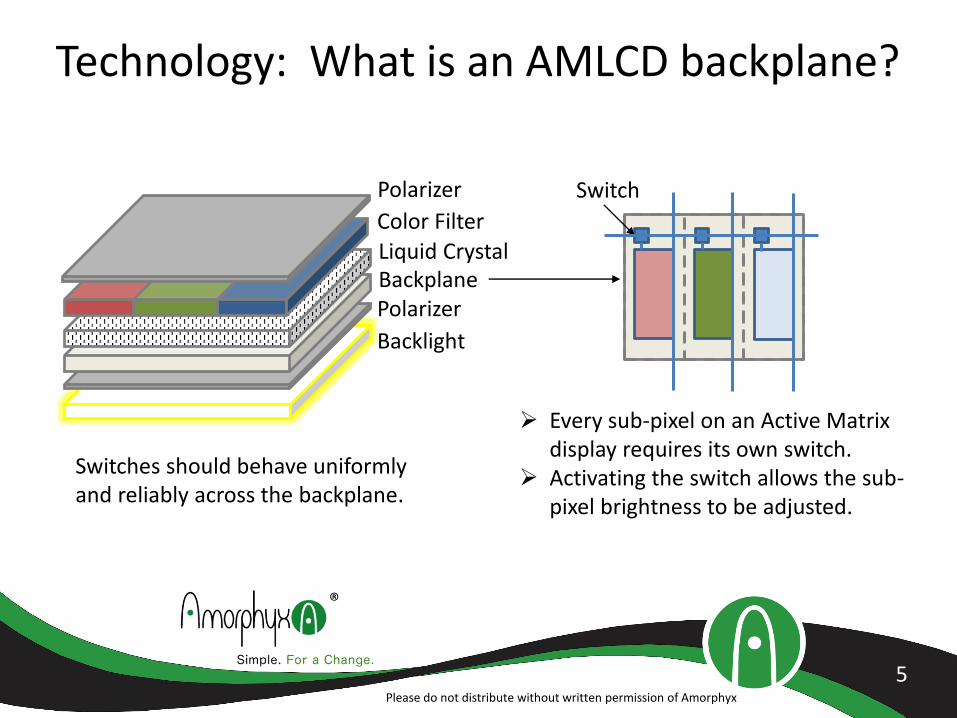
Technology: What is an AMLCD backplane?
5
Backlight
PolarizerBackplaneLiquid Crystal
Color Filter
Polarizer Switch
Every sub-pixel on an Active Matrix display requires its own switch.
Activating the switch allows the sub-pixel brightness to be adjusted.
Switches should behave uniformly and reliably across the backplane.
®
Please do not distribute without written permission of Amorphyx
6
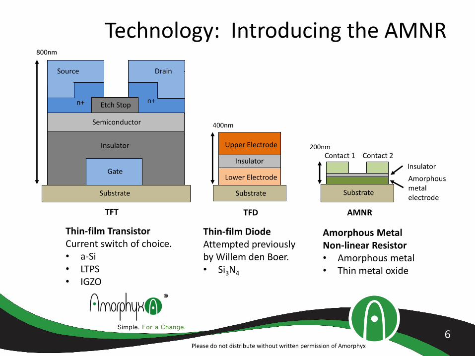
Technology: Introducing the AMNR
Substrate
Gate
Insulator
Semiconductor
Etch Stopn+ n+
Source Drain
800nm
TFT
Substrate
Lower Electrode
Insulator
Upper Electrode
400nm
TFD
Substrate
Insulator
Amorphous metal electrode
Contact 1 Contact 2200nm
AMNR
Thin-film TransistorCurrent switch of choice.• a-Si• LTPS• IGZO
Thin-film DiodeAttempted previously by Willem den Boer.• Si3N4
Amorphous Metal Non-linear Resistor• Amorphous metal• Thin metal oxide
®
Please do not distribute without written permission of Amorphyx
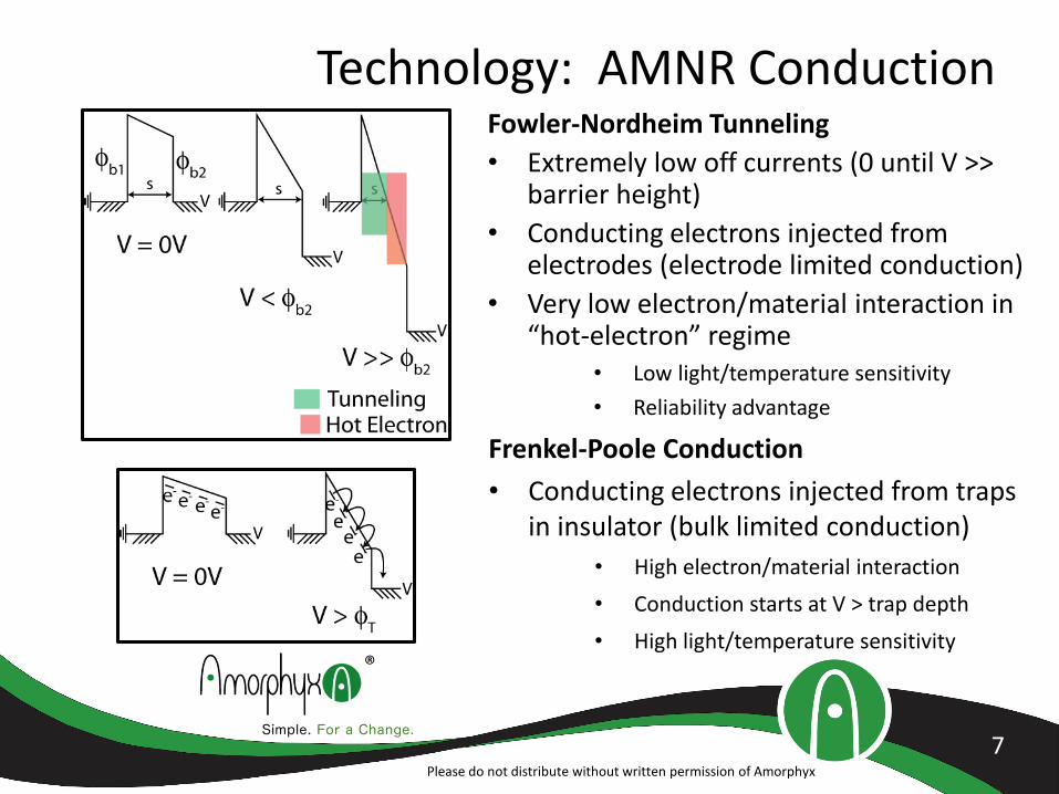
Technology: AMNR ConductionFowler-Nordheim Tunneling
• Extremely low off currents (0 until V >> barrier height)
• Conducting electrons injected from electrodes (electrode limited conduction)
• Very low electron/material interaction in “hot-electron” regime
• Low light/temperature sensitivity
• Reliability advantage
7
Frenkel-Poole Conduction
• Conducting electrons injected from traps in insulator (bulk limited conduction)
• High electron/material interaction
• Conduction starts at V > trap depth
• High light/temperature sensitivity
®
Please do not distribute without written permission of Amorphyx
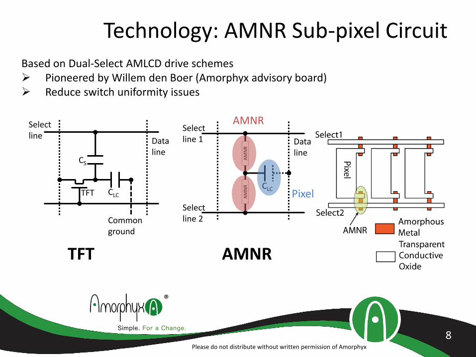
Technology: AMNR Sub-pixel Circuit
8
Based on Dual-Select AMLCD drive schemes Pioneered by Willem den Boer (Amorphyx advisory board) Reduce switch uniformity issues
Data line
Select line
CS
CLC
Common ground
TFT
TFTA
MN
RA
MN
R CLC
Data line
Select line 2
Select line 1
AMNR
Pixel
AMNR
®
Please do not distribute without written permission of Amorphyx
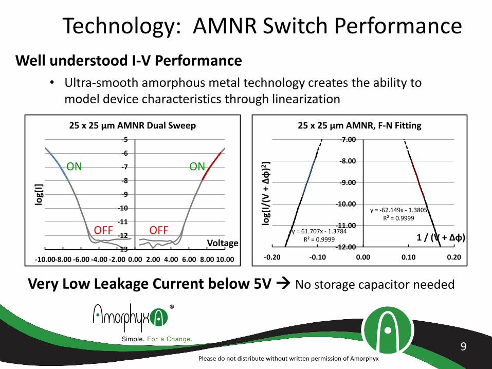
Technology: AMNR Switch Performance
Well understood I-V Performance
• Ultra-smooth amorphous metal technology creates the ability to model device characteristics through linearization
9
Very Low Leakage Current below 5V No storage capacitor needed
y = 61.707x - 1.3784R² = 0.9999
y = -62.149x - 1.3805R² = 0.9999
-12.00
-11.00
-10.00
-9.00
-8.00
-7.00
-0.20 -0.10 0.00 0.10 0.20lo
g[I/
(V +
∆φ
)2]
1 / (V + ∆φ)
25 x 25 µm AMNR, F-N Fitting
-13
-12
-11
-10
-9
-8
-7
-6
-5
-10.00-8.00 -6.00 -4.00 -2.00 0.00 2.00 4.00 6.00 8.00 10.00
log[
I]
Voltage
25 x 25 µm AMNR Dual Sweep
OFF OFF
ONON
®
Please do not distribute without written permission of Amorphyx
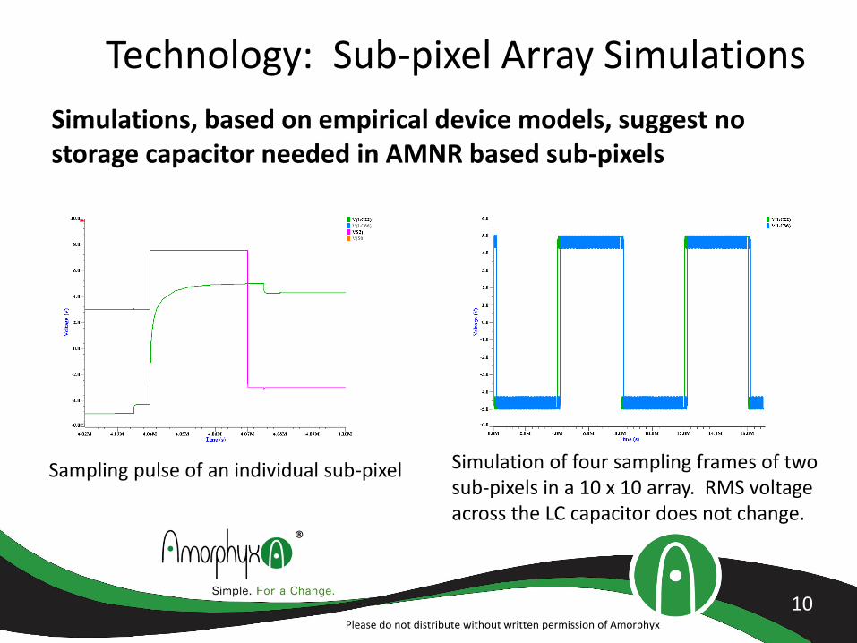
Technology: Sub-pixel Array Simulations
Simulations, based on empirical device models, suggest no storage capacitor needed in AMNR based sub-pixels
10
Simulation of four sampling frames of two sub-pixels in a 10 x 10 array. RMS voltage across the LC capacitor does not change.
Sampling pulse of an individual sub-pixel
®
Please do not distribute without written permission of Amorphyx
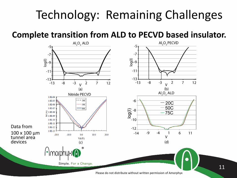
Technology: Remaining Challenges
Complete transition from ALD to PECVD based insulator.
11
Data from 100 x 100 µm tunnel area devices
®
Please do not distribute without written permission of Amorphyx
Technology: Remaining Challenges
12
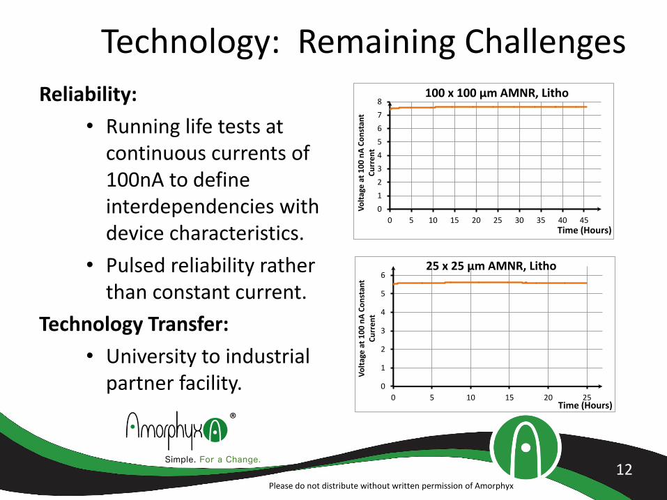
Reliability:
• Running life tests at continuous currents of 100nA to define interdependencies with device characteristics.
• Pulsed reliability rather than constant current.
Technology Transfer:
• University to industrial partner facility.
0
1
2
3
4
5
6
7
8
0 5 10 15 20 25 30 35 40 45
Vo
ltag
e at
10
0 n
A C
on
stan
t C
urr
ent
Time (Hours)
100 x 100 µm AMNR, Litho
0
1
2
3
4
5
6
0 5 10 15 20 25
Vo
ltag
e at
10
0 n
A C
on
stan
t C
urr
ent
Time (Hours)
25 x 25 µm AMNR, Litho
®
Please do not distribute without written permission of Amorphyx
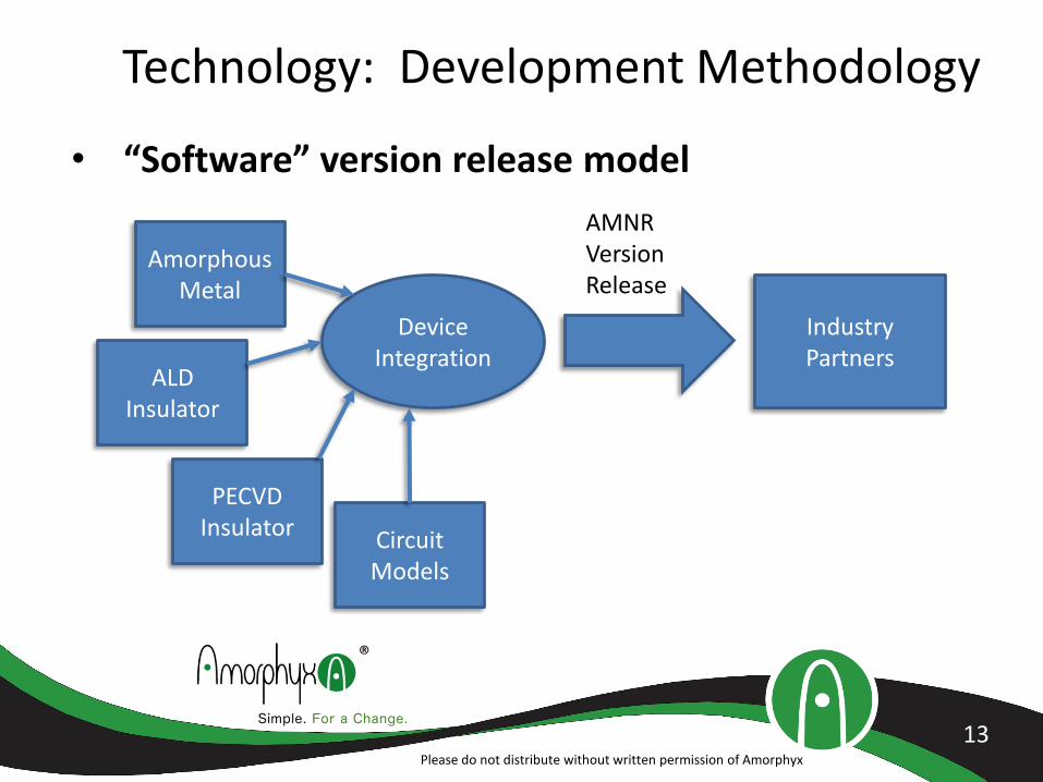
Technology: Development Methodology
13
• “Software” version release model
Amorphous Metal
ALD Insulator
PECVD Insulator Circuit
Models
Device Integration
Industry Partners
AMNR Version Release
®
Please do not distribute without written permission of Amorphyx
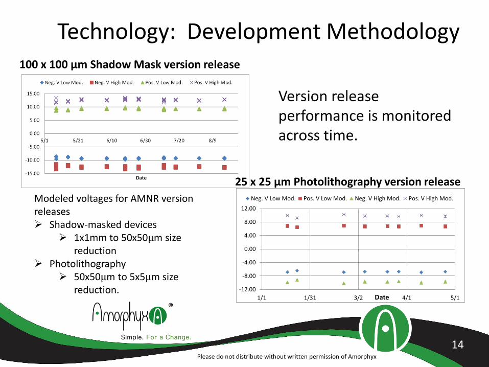
Technology: Development Methodology
14
-12.00
-8.00
-4.00
0.00
4.00
8.00
12.00
1/1 1/31 3/2 4/1 5/1Date
Neg. V Low Mod. Pos. V Low Mod. Neg. V High Mod. Pos. V High Mod.
25 x 25 µm Photolithography version release
100 x 100 µm Shadow Mask version release
Version release performance is monitored across time.
Modeled voltages for AMNR version releases Shadow-masked devices
1x1mm to 50x50µm size reduction
Photolithography 50x50µm to 5x5µm size
reduction.
®
Please do not distribute without written permission of Amorphyx
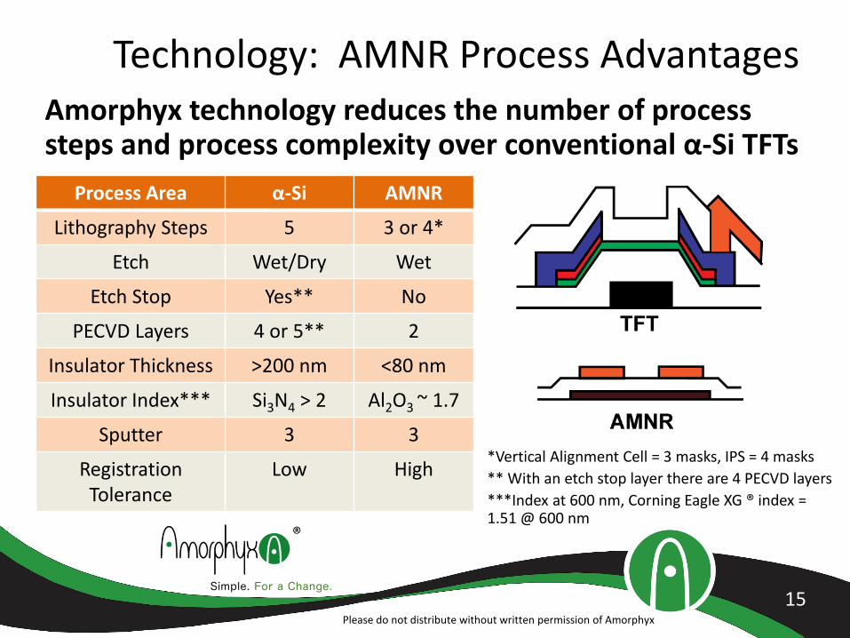
Technology: AMNR Process AdvantagesAmorphyx technology reduces the number of process steps and process complexity over conventional α-Si TFTs
15
Process Area α-Si AMNR
Lithography Steps 5 3 or 4*
Etch Wet/Dry Wet
Etch Stop Yes** No
PECVD Layers 4 or 5** 2
Insulator Thickness >200 nm <80 nm
Insulator Index*** Si3N4 > 2 Al2O3 ~ 1.7
Sputter 3 3
Registration Tolerance
Low High*Vertical Alignment Cell = 3 masks, IPS = 4 masks
** With an etch stop layer there are 4 PECVD layers
***Index at 600 nm, Corning Eagle XG ® index = 1.51 @ 600 nm
®
Please do not distribute without written permission of Amorphyx
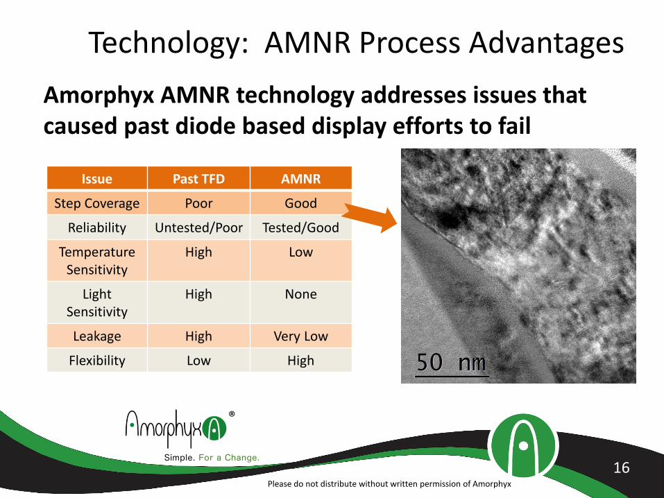
Technology: AMNR Process Advantages
Amorphyx AMNR technology addresses issues that caused past diode based display efforts to fail
16
Issue Past TFD AMNR
Step Coverage Poor Good
Reliability Untested/Poor Tested/Good
Temperature Sensitivity
High Low
Light Sensitivity
High None
Leakage High Very Low
Flexibility Low High

®
Please do not distribute without written permission of Amorphyx
Thank you.
17
Questions?

®
Please do not distribute without written permission of Amorphyx
Backup
18
®
Please do not distribute without written permission of Amorphyx
Amorphyx Quotes
19
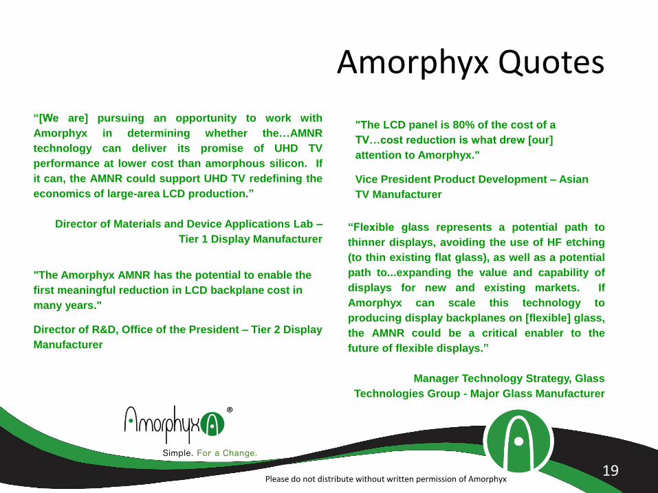
“[We are] pursuing an opportunity to work with
Amorphyx in determining whether the…AMNR
technology can deliver its promise of UHD TV
performance at lower cost than amorphous silicon. If
it can, the AMNR could support UHD TV redefining the
economics of large-area LCD production.”
Director of Materials and Device Applications Lab –
Tier 1 Display Manufacturer
"The LCD panel is 80% of the cost of a
TV…cost reduction is what drew [our]
attention to Amorphyx."
Vice President Product Development – Asian
TV Manufacturer
"The Amorphyx AMNR has the potential to enable the
first meaningful reduction in LCD backplane cost in
many years."
Director of R&D, Office of the President – Tier 2 Display
Manufacturer
“Flexible glass represents a potential path to
thinner displays, avoiding the use of HF etching
(to thin existing flat glass), as well as a potential
path to...expanding the value and capability of
displays for new and existing markets. If
Amorphyx can scale this technology to
producing display backplanes on [flexible] glass,
the AMNR could be a critical enabler to the
future of flexible displays.”
Manager Technology Strategy, Glass
Technologies Group - Major Glass Manufacturer
®
Please do not distribute without written permission of Amorphyx
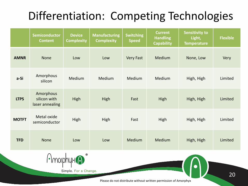
Differentiation: Competing Technologies
SemiconductorContent
Device Complexity
ManufacturingComplexity
Switching Speed
Current Handling Capability
Sensitivity to Light,
TemperatureFlexible
AMNR None Low Low Very Fast Medium None, Low Very
a-SiAmorphous
siliconMedium Medium Medium Medium High, High Limited
LTPSAmorphous silicon with
laser annealingHigh High Fast High High, High Limited
MOTFTMetal oxide
semiconductorHigh High Fast High High, High Limited
TFD None Low Low Medium Medium High, High Limited
20
®
Please do not distribute without written permission of Amorphyx
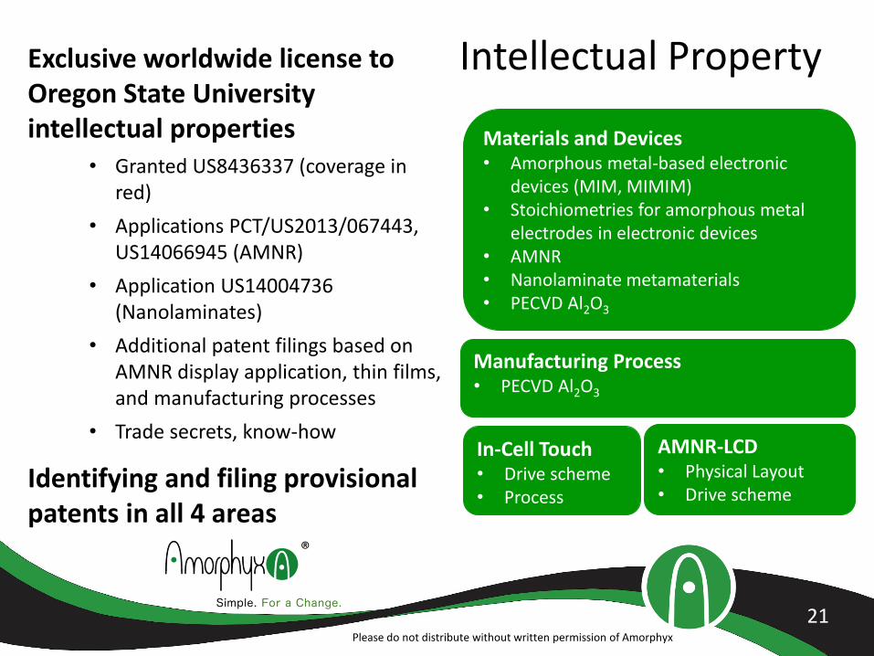
Intellectual PropertyExclusive worldwide license to Oregon State University intellectual properties
• Granted US8436337 (coverage in red)
• Applications PCT/US2013/067443, US14066945 (AMNR)
• Application US14004736 (Nanolaminates)
• Additional patent filings based on AMNR display application, thin films, and manufacturing processes
• Trade secrets, know-how
Identifying and filing provisional patents in all 4 areas
21
Materials and Devices• Amorphous metal-based electronic
devices (MIM, MIMIM)• Stoichiometries for amorphous metal
electrodes in electronic devices• AMNR• Nanolaminate metamaterials• PECVD Al2O3
Manufacturing Process• PECVD Al2O3
AMNR-LCD• Physical Layout• Drive scheme
In-Cell Touch• Drive scheme• Process


![Smart DMB based on Hybrid DMB - ITU15 (July, 2015) UHD 1 UHD 2 UHD 3 UHD 4 UHD 5 698 704 710 718 728 753 759 765 771773 783 803 [MHz] 806 National Disaster Safety Comm. ↑ National](https://img.pdfslide.us/doc/110x75/5f1bd0c17a9742053249fa91/smart-dmb-based-on-hybrid-dmb-itu-15-july-2015-uhd-1-uhd-2-uhd-3-uhd-4-uhd.jpg)