Embed Size (px)
Citation preview

MECHANICAL PROPERTIES OF ONE-DIMENSIONAL NANOSTRCTURES,
EXPERIMENTAL MEASUREMENT AND NUMERICAL SIMULATION
by
Xiaoxia Wu
A dissertation submitted to the faculty of
The University of North Carolina at Charlotte
in partial fulfillment of the requirements
for the degree of Doctor of Philosophy in
Mechanical Engineering
Charlotte
2012
Approved by:
Dr. Terry T. Xu
Dr. Ronald E. Smelser
Dr. Aixi Zhou
Dr. Doug Cooper

ii
©2012
Xiaoxia Wu
ALL RIGHTS RESERVED
iii
ABSTRACT
XIAOXIA WU. Mechanical properties of one-dimensional nanostructures, experimental
measurement and numerical simulation (Under the direction of DR. TERRY T. XU)
One-Dimensional (1D) nanostructures are generally defined as having at least one
dimension between 1 and 100 nm. Investigations of their mechanical properties are
important from both fundamental study and application point of view. Different methods
such as in-situ tensile test and Atomic Force Microscopy (AFM) bending test have been
used to explore the mechanical properties of 1D nanostructures. However, searching for
reliable measurement of 1D nanostructures is still under way. In this dissertation, two
methods, Atomic Force Acoustic Microscopy (AFAM)-based method and
nanoindentation, were explored to realize reliable study of mechanical properties of two
kinds of energy conversion-related nanomaterials: single crystalline rutile TiO2
nanoribbons and alkaline earth metal hexaboride MB6 (M=Ca, Sr, Ba) 1D nanostructures.
The work principle of AFAM-based method is: while an AFM cantilever is in
contact with a tested nanostructure, its contact resonance frequencies are different from
its free resonance frequencies. The cantilever resonant frequency shift is correlated to the
Young’s modulus of the tested nanostructure based on Hertz contact mechanics. The
measured modulus of BaB6 nanostructures was 129 GPa, which is much lower than the
value determined using the nanoindentation method. Due to the small load (120 nN)
applied on the nanostructure during the experiment, the AFAM-based method may
actually measure the mechanical property of the outside oxidation layers of BaB6
nanostructures.

iv
Nanoindentation is capable of giving insights to both Young’s modulus and
hardness of bulk elastic-plastic materials. The assumptions behind this method are that
the material being tested is a homogeneous half-space. Cares must be taken to extract
properties of tested materials when those assumptions are broken down. Nanoindentation
on a 1D nanostructure is one of such cases that those assumptions are invalid. However,
this invalidity was not realized in most published work on nanoindentation of 1D
nanostructures, resulting in unreliable data on mechanical properties of 1D nanostructures.
In this work, factors which could affect measured nanostructure-on-substrate system
modulus such as the selection of a substrate to support the nanostructure, the cross
section of a nanostructure, the width-to-thickness ratio (or diameter) of a nanostructure,
and the nanostructure-substrate contact mechanism were first subjected to a systematic
experimental investigation. A Finite Element Modeling (FEM)-based data inverse
analysis process was then proposed to extract the intrinsic modulus of nanostructures
from measured system modulus. This data inverse process solved the intrinsic modulus
of nanostructures by equalizing the simulated nanostructure-on-substrate modulus with
the experimentally measured system modulus. In finite element simulation, another
important aspect: the experimental indenter area function in addition to aforementioned
other factors was carefully considered. Based on systematic experimental and numerical
investigations, the Young’s modulus of rutile TiO2 nanoribbons, CaB6 nanostructures,
SrB6 nanostructures and BaB6 nanostructures was determined to be 360, 175-365, 300-
425 and 270-475 GPa, respectively. These numbers are the first reported mechanical
properties for these nanomaterials. Besides the finite element simulation, an ―analytical‖
solution to obtain a nanostructure-on-substrate system modulus is also presented.

v
Compared to the finite element simulation, the solution could significantly reduce
processing time for the data inverse method. It is applicable to a nanostructure with a
width to thickness ratio larger than 4. This part of dissertation work clearly demonstrates
that both experimental and numerical investigations are needed for studying of
mechanical properties of 1D nanostructures by nanoindentation.

vi
ACKNOWLEDGMENTS
My deepest gratitude is to my advisor, Dr. Terry T. Xu. I would not have gone
this far without her encouragement and support from every aspects, research and personal
life. Dr. Xu is so knowledgeable that she always can guide me to a meaningful research
direction. She sponsored me to attend workshops and conferences, which definitely
broaden my horizon and sharpen my skills of presentation. I thank her for being a good
role model in paying attention to details, organizing data and thoughts clearly and
thoroughly. I am also truly indebted to Dr. Ronald E. Smelser, who inspired me with his
personal experiences in pursuit his PHD degree. His long-term spiritual support and
encouragement will be valuable treasures throughout my life. I am grateful to Dr. Aixi
Zhou and Dr. Doug Couper for their insightful comments on the topic, which motivate
me for a clear presentation. I am thankful to the Center of Metrology, Department of
Mechanical Engineering and Engineering Science, and the Center of Optoelectronics and
Optical Communications at UNC Charlotte for providing multi-user SEM, AFM and
nanoindentation. I appreciate the valuable suggestions and comments from Professor
Xiaodong Li at University of South Carolina, Professor Gang Feng at Villanova
University and supporting staff at Agilent Technology nanomechanics division for
nanoindentation usage. I thank Professor Stuart Smith and his group for helping me with
LabVIEW programming and hardware hook-up in the AFAM based method. I would like
to thank Dr. Haitao Zhang for all the advice, suggestions and training. I am thankful to Dr.
Harish Cherukuri for his guidance and advice regarding course works and graduate study.
I also thank helps and supports from my fellow students and friends, Zhiliang Pan, Zhe
Guan, Youfei Jiang, Jing Bi among many others.

vii
I appreciate the financial support from the National Science Foundation (CMMI
0800366 and 0748090), the American Chemical Society - Petroleum Research Fund
(PRF No. 44245-G10), and The University of North Carolina at Charlotte (UNC
Charlotte).
Finally, I thank my parents, Jun Wu and Guolan Jiang, for their love,
encouragement and inspiration. My appreciation also goes to my husband, Jinquan Cheng,
for his support.

viii
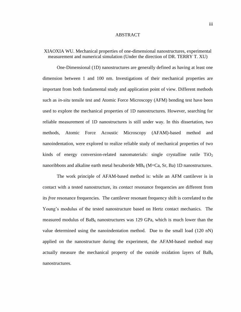
TABLE OF CONTENTS
LISTS OF TABLES xi
LISTS OF FIGURES xii
CHAPTER 1: INTRODUCTION 1
1.1 Motivation 1
1.2 Some General Terms 2
1.2.1 EBID 3
1.2.2 AFM 3
1.3 Current Mechanical Property of 1D Nanostructures Testing Methods 7
1.3.1 Axial Tensile Test 7
1.3.2 Electrically/Magnetically Driven Vibration 15
1.3.3 AFM Based Methods 19
1.3.4 Nanoindentation 33
1.3.5 Other Techniques 38
1.4 Methods Used in This Dissertation 39
1.5 Dissertation Outline 40
CHAPTER 2: MEASUREMENT OF MECHANICAL PROPERTY USING 42
AN ATOMIC FORCE ACOUSTIC MICROSCOPY (AFAM)
2.1 Introduction 42
2.2 AFAM Based Method to Measure Mechanical Property 42
2.2.1 Cantilever Dynamics 43
2.2.2 Working Principle of AFAM Based Method 46
2.3 Experimental Setup 51
2.4 Results and Discussion 58
ix
2.5 Discussions 62
CHAPTER 3: NANOINDENTATION ON TiO2 NANORIBBONS 63
3.1 Introduction 63
3.2 Experimental Details 66
3.3 Finite Element Modeling 69
3.4 Results and Discussion 71
3.4.1 Experimental Results 71
3.4.2 Simulation Results 73
3.4.3 Data Analysis 78
3.4.4 A General Rule for Studying Young’s Modulus of 1D 80
Nanostructures by Nanoindentation
3.5 Conclusions 80
CHAPTER 4: MEASUREMENT OF MECHANICAL PROPERTIES OF 82
ALKALINE EARTH METAL HEXABORIDE ONE-
DIMENSIONAL NANOSTRUCTURES BY NANOINDENTATION
4.1 Introduction 82
4.2 Experimental Details 83
4.3 Modeling of Nanoindentation Experiment 85
4.3.1 A Better Way to Simulate Nanoindenter 85
4.3.2 Finite Element Modeling 87
4.4 Results and Discussion 89
4.4.1 Experimental Results 89
4.4.2 Numerical Simulation 97
4.5 Data Analysis 102
4.6 Conclusions 103

x
CHAPTER 5: NANOINDENTATION-THEORETICAL MODELING 105
5.1 Introduction 105
5.2 Chebyshev Polynomial 105
5.3 Formulation of the Indentation on Nanostructures (2w/t)-on- 107
Substrate System
5.4 Numerical Observations 113
5.5 Applicable Range for 2w/t Assumption 118
5.6 Conclusions 119
CHAPTER 6: CONCLUSIONS AND FUTURE WORK 120
6.1 Conclusions 120
6.2 Future Work 121
REFERENCES 125

xi
LISTS OF TABLES
Table 1.1: Lists of common procedures for different tensile tests 15
Table 1.2: Techniques of measuring resonant frequency of a nanostructure 19
Table 1.3: Comparison of different AFM modes for 1D nanostructure mechanical test 33
Table 2.1: Solutions of knL from equation (2-12) (Rabe, et al., 1996). Some 50
spaces are left empty because the difference between contact and free
end case is less than 0.001.
Table 2.2: Frequency ratio fn/fn0 for different deflection modes of a cantilever 51
Table 2.3: AFM cantilever contact resonant frequency on SiO2/Si and nanostructures 59
Table 4.1: Dimensions for nanostructures and sapphire substrate used in simulation. 88
The units are nm.
Table 4.2: Experimental and theoretical values of elastic constants of some 96
Hexaborides
Table 4.3: Measured nanostructure-on-substrate system moduli and 103
corrected nanostructure moduli for two different nanostructure-
substrate contact interactions.
Table 5.1: Unknowns and equations for the three indenters 112
Table 5.2: Spreadsheet configuration of derived results from the Fredholm 112
equation for the general indenter
xii
LISTS OF FIGURES
Figure 1.1: (A) Schematic illustration of the main components of an AFM. (B) An 4
AFM cantilever with a sharp tip on one end and attaches to a chip on
the other end. (Image courtesy www.schaefer-tec.com)
Figure 1.2: (A) SEM image of a NT tensile test setup; (B) schematic drawing 9 shows the principle of a tensile test. When the top rigid cantilever 1 was
driven upward, the lower cantilever bent upward by a distance d, while
the NT was stretched from its initial length of L to L+L because of force
exerted by the AFM tips. Force was calculated as kd, where k was the
spring constant of the lower cantilever 2, and the strain of NT was L/L
(Yu, et al., 2000).
Figure 1.3: Set-up of a ensile test for nanofibers (Tan, et al., 2005) 11
Figure 1.4: Setup of MEMs for 1D nanostructure tensile testing 12
(Zhu and Espinosa, 2005)
Figure 1.5: Schematic illustration of the microelectronic device. The device 13
was driven by an in-situ nanoindenter. 1D nanostructures sit on the
sample state shuttle (Lu, et al., 2010).
Figure 1.6: TEM image of an extruded NT. (A) an uncharged NT. (B) charged 16
NT bending toward a counter electrode. The counter electrode
at the bottom of the image was not shown (Poncharal, et al., 1999).
Figure 1.7: (a) Schematic illustration of a lateral bending (Wu, et al., 2005) and 21
(b) a normal bending using AFM.
Figure 1.8: A schematic illustration of a one end clamped NT deflected by 22
an AFM tip laterally (Wong, et al., 1997)
Figure 1.9: Comparison of experimental and model predicted deflections 27
for silver NWs of different diameters (Chen, et al., 2006)
Figure 1.10: The schematic illustration of the experimental apparatus for AFAM 31
based mechanical property testing method(Hurley, et al., 2007)
Figure 1.11: A typical load-displacement curve of nanoindentation 36
result(Oliver and Pharr, 1992)
Figure 2.1: Schematic resonant spectrum of a forced vibration 46
Figure 2.2: (A) A beam dynamics model for AFAM based method. A one- 47
end clamped rectangular cantilever beam with a stiffness kc was

xiii
coupled to tested sample through a spring of stiffness k* based
on contact mechanic model. (B) Resonant spectra of an AFM
cantilever. The first contact resonance calculated from the beam
dynamic model shown in (A) was higher than first free resonance
of the AFM cantilever but lower than its second free
resonance (Hurley, et al., 2007).
Figure 2.3: Schematic illustration of an AFAM setup for measuring AFM 56
cantilever resonant frequency
Figure 2.4: Signal in and out from a lock-in amplifier 56
Figure 2.5: Screen shot of the LabVIEW program, (a) Front panel and 57
(b) block diagram, used to measure the AFM cantilever contact
resonant frequency
Figure 2.6: SEM images of (a) a typical worn tip, and (b) a new AFM tip 60
Figure 3.1: (a) the SEM image of as-synthesized TiO2 1D nanostructures 67
on a Ti powder. (b) an AFM image of a single TiO2 nanoribbon. The inset
is a cross-sectional profile of the nanoribbon, showing the nanoribbon
is around 150 nm wide and 30 nm thick.
Figure 3.2: Simulated maximum load applied on a bare substrate of different 71
thickness at an indentation depth of 15 nm. The Young’s modulus
of the substrate was 300 GPa. Tip radius of the spherical indenter
in the simulation was 30 nm. The dotted line represented the analytical
solution of the maximum load based on Hertz contact mechanics.
Figure 3.3: (a) AFM image of an indented nanoribbon on a sapphire(0001) 73
substrate. Five well-centered residual indentations are shown.
Sites where indentation-induced fracture occurred are indicated
by black arrows. (b) Typical load-indenter displacement (P-h)
curves for TiO2 nanoribbons on three different substrates. The
circles correspond to the possible pop-in phenomena.
Figure 3.4: (a) Typical simulated deformation pattern of a nanoribbon- 74
on-sapphire system under indentation. The edges of the nanoribbons
are clearly lift-up. (b) Typical AFM image of a nanoribbon after
nanoindentation. The brighter portion between the two residue
indentations implies the nanoribbon was lifted up.
Figure 3.5: Plots of a2/t vs α obtained from the receding contact model 75
(Keer, et al., 1972), the plate-on-foundation model (Kauzlarich
and Greenwood, 2001), and the current FEM results. This
analysis validates the reliability of the FEM model.

xiv
Figure 3.6: (a) Simulated P-h curves for nanoindentation of several 78
nanoribbon-on-substrate systems as well as ―half space‖ curves.
The simulated ―350 on sapphire‖ curve overlaps the ―350 half space‖
curve, indicating the measured modulus is close to the intrinsic modulus
of TiO2 nanoribbons when sapphire (0001) is used as the substrate.
(b) Simulated P-h curves for nanoindentation of a nanoribbon with assumed
modulus as 350 GPa on three substrates. This result further illustrates the
substrate effect on measurement reliability. (c) Simulated P-h curves for
nanoindentation of nanoribbons with different width on a sapphire substrate.
The width effect is significant when the width of a nanoribbon is close
to the indenter size.
Figure 3.7: A general data inverse process of extracting the intrinsic 79
modulus of a nanoribbion from the measured system modulus
Figure 4.1: Projected contact area A vs. contact depth hc curves. The 87
solid line was obtained from a tip geometry calibration experiment of a
Berkovich indenter. The dashed line was calculated assuming the
intender is conical whose tip apex R is 80 nm.
Figure 4.2: (a) An AFM image of a part of a SrB6 nanowire on sapphire. 91
The inset is the result of section analysis, revealing the nanostructure
has a rectangular cross section. Its thickness and width is about 108 nm
(vertical distance between two green arrows) and 100 nm (horizontal
distance between two red arrows), respectively. (b) A typical load-
indenter displacement (P-h) curve of the SrB6 nanostructure-on-
sapphire system. (c) Measured modulus and (d) ―nanohardness‖
given automatically by the software associated with the nanoindenter.
The values were calculated using the Oliver-Pharr method. Note:
the noisy data points within the initial contact range (i.e., between
0 and 4 nm) were removed for clarity.
Figure 4.3: A P-h curve of a SrB6 nanostructure experiencing sudden 92
fracture during an indentation process
Figure 4.4: Measured moduli of (a) the CaB6 nanostructure-on-sapphire 95
system, (b) the SrB6 nanostructure-on-sapphire system, and (c) the BaB6
nanostructure-on-sapphire system.
Figure 4.5: (a) AFM image of a tapered SrB6 nanostructure on sapphire. 96
(b) Zoom-in SFM image of an indented section of the nanostructure.
The white triangle frame outlines the residual indentation. (c) Zoom-in
SFM image of a section before indentation. The width of the two
sections is obviously different.
Figure 4.6: Simulated P-h curves for studying of various factors 101
affecting measured moduli. These factors include (a) the width of

xv
a nanostructure with a rectangular cross section, (b) the interaction
between a nanostructure and a substrate, (c) the cross section of a
nanostructure, (d) the diameter of a nanostructure with a circular
cross section and (e) the oxide layer on a nanostructure.
Figure 5.1: A composite system of an elastic nanostructure either perfect 108
bond or frictionlessly overlaid on a half-space substrate
indented by an indenter.
Figure 5.2: vs. for different elastic mismatchs with a conical 116
indenter of half-angle α = 70.3 for (a) perfect bond and (b) frictionless
contact between a nanostructure and a substrate. And (c) its dependence on
the half angle of a conical indenter for the perfect bond interaction while
() and for frictionless contact interaction while (----).
Figure 5.3: 1/sysM M vs. for different elastic mismatchs with a spherical 117
indenter for (a) perfect bond and (b) frictionless contact between a
nanostructure and a substrate when t/R = 1. And (c) its dependence on
t/R for the perfect bond interaction while () and for
frictionless contact interaction while λ
(----).
Figure 5.4: Comparison of vs. between a conical indenter 118
and a general indenter in a nanoindentation test. The modulus of a
nanostructure-on-substrate system using a general indenter is function
of t and h/t, where the modulus of the system using a conical indenter
is only function of h/t.
Figure 5.5: Normalized interface stress between a nanostructure and a 119
substrate, which are perfectly bonded, under indentation with a
a conical indenter. 1 = 0.3, a/t = 0.1.
1/sysM M

CHAPTER 1: INTRODUCTION
1.1 Motivation
One-Dimensional (1D) nanostructures are generally defined as having at least one
dimension in somewhere between 1 and 100 nm (Xia, et al., 2003). Depending on their
morphology, 1D nanostructures can be further divided into nanobelts (NB), nanotubes
(NT), nanowires (NW), nanorods, nanosprings, and nanoribbons etc.
From a theoretical point of view, nanostructures are different from their bulk
counterparts in the following two ways: (i) the extremely small scale of nanostructures
could result in a less-defect structure. The mechanical properties, such as Young’s
modulus and yield strength, could reach the theoretical limit. For example, single wall
carbon NTs have demonstrated exceptional mechanical properties: very high Young’s
modulus of 1.25 TPa (Krishnan, et al., 1998) and tensile strength of 200 GPa (Zhao, et al.,
2002); fully reversible bending for high bending angles (Iijima, et al., 1996). (ii) large
surface area to volume ratio, which might results in size effect of nanostructures. Surface
atoms have different electron densities and fewer bonding neighbors than atoms inside a
nanostructure. Molecular dynamic simulations have revealed that surface atoms could
either increase or decrease the elastic stiffness (Miller and Shenoy, 2000, Park, et al.,
2009). With an electric-field-induced resonance method, Young’s modulus of ZnO NWs
was found to increase dramatically as diameters decrease (Chen, et al., 2006). However,
recent in-situ tensile tests of Si NW indicated that Young’s modulus decreased from their
bulk Young’s modulus for NWs with diameters being less than 30 nm (Zhu, et al.,

2
2009). Moreover, bending tests showed that Young’s modulus of gold NWs was
essentially diameter independent (Wu, et al., 2005). In summary, nanostructures could
show higher, lower or comparable modulus to their bulk counterparts. But the questions
are: will all nanostructures have a mechanical property that’s upto their theoretical limit
just like single wall carbon nanotubes? Or are the mechanical properties close to their
bulk counterparts? Will mechanical properties of 1D nanostructures show size effect or
not? To answer these questions, the mechanical property of a 1D nanostructure needs to
be carefully studied from a theoretical and an experimental point of view.
On the other hand, studying the mechanical property of the 1D nanostructures is
important from an application point of view. If nanostructures are to play some roles in a
building block for future nanotechnology, a thorough understanding of their mechanical
behavior is essential. As we know, for bulk material applications in engineering,
structural engineering design always requires a safety factor (SF), which is defined as
SF=UTS/R, where R is the applied stress and UTS is the ultimate tensile strength. The
same philosophy applies to possible design of a nanostructure device. The applied stress
on a nanostructure needs to be carefully designed so that the nanostructure can be
operated safely. To design the working stress, mechanical properties, such as Young’s
modulus and yield strength need to be well understood. As a result, studying mechanical
property of nanostructures is important from an application point of view.
1.2 Some General Terms
Before discussing the currently available techniques for mechanical tests of 1D
nanostructures, it is beneficial to describe some general terms which will be used
extensively throughout the dissertation.

3
1.2.1 EBID
Electron Beam Induced Deposition (EBID) is a material deposition technique that
has been around since 1934 when Steward found contamination growth in his electron
optical system (van Dorp and Hagen, 2008). The basic principle of EBID is: Gas
molecules - from either contamination or introduced precursor gas, liquid or solid
material in a Scanning Electron Microscope (SEM) chamber - are dissociated into
volatile and nonvolatile components under the influence of a SEM e-beam. Nonvolatile
components adhere to the substrate, where deposition is supposed to occur, and form
deposition (EBID). Alternatively, nonvolatile components react with substrate to form
volatile components and leave a trench on the substrate.
In mechanical testing of nanostructures, EBID is generally used to bond
nanostructures onto a test apparatus. The general procedures are: (i) Attach the
nanostructure onto the test apparatus and locate one end of the nanostructure under SEM;
(ii) Zoom in to the end of the nanostructure with the image center being the location
where deposition will occur. Choose a right accelerating voltage and spot size of SEM;
(iii) contamination inside the SEM chamber will be dissociated, and carbon will deposit
onto the nanostructure and affix the nanostructure onto the test apparatus.
1.2.2 AFM
Atomic Force Microscopy (AFM), invented by Binnig, Quate and Gerber in 1986
(Binnig, et al., 1986), is one of several very high-resolution Scanning Probe Microscopes
(SPM). It has resolution of a nanometer, which is more than 1000 times larger than the
optical diffraction limit. As shown in Figure 1.1 (A), AFM consists of the following main
parts: (1) a cantilever, the sensing part of the AFM. It is typically made of silicon or

4
silicon nitride with a sharp tip at its end. Figure 1.1 (B) shows a commercial AFM
cantilever with a rectangular cross section. There are also triangular cantilevers, which
typically have a smaller spring constant; (2) a PZT scanner to move the AFM tip related
to the tested sample. Depending on the AFM mode, the scanner could be affixed to the
sample stage and the cantilever will hold still during the scanning process, as shown in
Figure 1.1 (A). The scanner could also be affixed to the cantilever holder while the
sample is stationary; (3) laser and photodiode used to detect AFM cantilever deflection
and (4) feedback electronics to control the scanner’s up and down movement so that the
AFM cantilever deflection is kept constant. The trace of the scanner movement
corresponds to the sample topography.
Figure 1.1: (A) Schematic illustration of the main components of an AFM. (B) An AFM
cantilever with a sharp tip on one end and attaches to a chip on the other end. (Image
courtesy www.schaefer-tec.com)
Depending on an application, AFM is working either in image mode or force
mode. In image mode, the cantilever tip is brought into contact with the sample through
extending the PZT scanner or the sample stage. Interaction forces between the AFM tip

5
and the sample, such as Van der Waals force, contact force or adhesion, are kept constant
by holding the AFM cantilever deflection constant. While in force mode, the cantilever is
continuously pushed against the tested sample. In other words, the load applied on the
tested sample increases with time. With a well-calibrated cantilever spring constant kc,
the force-scanner movement curve could be used to extract the mechanical property of a
tested sample, as discussed in Section 1.3.3.
Since the forces applied on a sample by an AFM cantilever are determined by
cantilever spring constant and its defection, accurately calibrating cantilever spring
constant is critical for AFM based mechanical measurement methods. There are many
different ways to calibrate the cantilever spring constant kc, as reviewed by Butt et al.
(Butt, et al., 2005), Pettersson et al. (Pettersson, et al., 2007) and Palacio and Bhushan
(Palacio and Bhushan, 2010). Here we have briefly summarized their findings. For
normal cantilever spring constant calibration, the AFM cantilever is pushed vertically
against a tested structure. The calibration methods include, but are not limited to, the
following: (1) Calculation from its geometry parameters. For a cantilever with a constant
rectangular cross-section,
, where E is Young’s modulus of the material that the
cantilever is made of, w, t, L are width, thickness and length of the cantilever,
respectively. The calculated spring constant is typically different from the experimentally
determined ones. This discrepancy is due to many reasons, such as a non-uniform
cantilever thickness, and the oxidation layer on the top and bottom of the cantilever,
among others. (2) Measurement using a thermal noise method (Hutter and Bechhoefer,
1993). It is one of the widely used methods and implemented in many commercial AFMs.
A cantilever is generally simplified as a spring-mass system. The effective spring

6
constant is related to its mean square deflection under thermal fluctuation, that
is,
, where is the Boltzmann constant and T is the absolute temperature of
the calibration. (3) Measurement by adding a known mass. The spring constant is
extracted from shift of the resonance frequencies before and after a known mass is added.
Note that adding mass to a cantilever tip and sticking them together could be a nontrivial
job. (4) Measurement using a reference cantilever
(meetings.aps.org/meeting/MAR07/event/) or by directly applying a known force to the
cantilever and measuring its deflection. The cantilever spring constant can be determined
from the force-deflection curve. Nowadays, some AFM cantilever vendors calibrate their
cantilevers individually using one of the aforementioned methods. In such case, no
further cantilever spring constant is needed.
For lateral cantilever spring constant calibration, currently available calibration
methods include, but are not limited to the following: (1) Calculating from its geometry
parameters. Similar to the normal spring constant calibration, this method could suffer
from significant errors because of the uncertainty of the AFM cantilever dimension; (2)
Scanning tip on an inclined surface with a known slope and obtaining the spring constant
through force balance equations (Ogletree, et al., 1996). The method is very complicated
and could wear the AFM tip; and (3) The resonant frequency method (Jeon, et al., 2004).
By applying an electrical current to a triangular cantilever in a magnetic field, the
cantilever is excited into torsion. The cantilever lateral spring constant can be calculated
from the torsional resonant frequency. Unfortunately, this method could not be used for
cantilevers with a rectangular cross section. Cantilever lateral spring constant is generally
more difficult to calibrate than normal spring constant.

7
Cantilevers are typically mounted under a certain tilt angle with respect to
sample’s surface. The tilt is necessary to ensure that the tip, rather than the chip onto
which the cantilever is attached, touches the sample first (Heim, et al., 2004, Stiernstedt,
et al., 2005). The tilt angle ranges from 7o to 20
o in commercial AFMs. Due to the tilt, the
effective spring constant of a rectangular cantilever should be obtained by dividing the
calibrated spring constant by a factor2cos (1 2 tan / )D L , where is the tilt angle, D
is height of tip, and L is length of the cantilever. The effective spring constant is typically
10 to 15% higher than the one calibrated using the aforementioned methods.
1.3 Current Mechanical Property of 1D Nanostructures Testing Methods
Due to their small dimensions, mechanical characterization of 1D nanostructures
remains challenging. Several experimental techniques, as reviewed by Zhu et al. (Zhu, et
al., 2007) and Agrawal et al.(Agrawal and Espinosa, 2009)., have been developed and
used to measure the mechanical properties of 1D nanostructures. These techniques
include, but are not limited to the following: (i) axial tensile tests, (ii)
electrically/magnetically driven resonant method, (iii) AFM-based methods, including (a)
lateral force approach, (b) normal force approach, (c) Atomic Force Acoustic Microscopy
(AFAM) based method and (d) AFM nanoindentation and (iv) nanoindentation using
commercial nanoindenters. The techniques, including sample manipulation, working
principle, pros and cons, are reviewed in the following sections.
1.3.1 Axial Tensile Test
A tensile test is one of the most traditional methods to measure material
mechanical properties of bulk material. It has fully standardized testing procedures to
determine Young’s modulus, yield strength, which generally following the 0.2% offset

8
strain rule, tensile strength, and ultimate tensile strength of a substance. The failure
pattern of tested material, ductile or brittle, can be observed during the experiment.
A tensile test has also been used to measure mechanical properties of 1D
nanostructures. A successful axial tensile test on 1D nanostructures includes four main
steps: (i) pick up a single nanostructure and properly align and fix the nanostructure in
such a way that the load direction is along the axial direction of the nanostructure; (ii)
accurately measure the force applied on the nanostructure; (iii) make precise diameter
measurement and obtain cross section area of the nanostructure. Whether the cross
section is rectangular, circular, elliptical, solid or tube-like will affect the cross section
area, from which stress applied on the nanostructure will be calculated; and (iv)
accurately calculate deformation of the nanostructure, strain under tensile load.
With a custom-made manipulator, Young’s modulus of single NTs was measured
inside a SEM (Yu, et al., 1999, Yu, et al., 2000). The whole setup is shown in Figure
1.2(A). The picking up and fixing NT to a test apparatus process were as follows: (1)
Because of electrostatic attraction or Van der Waals forces between a NT and an AFM tip,
one or several CNTs ―jump‖ to the AFM tip when they were brought close to each other,;
(2) A strong bonding of about 100 nm2 in size was made using EBID to fix CNT on the
tip of an AFM cantilever 1. The other end of the NT was attached to the tip of another
AFM cantilever 2 using EBID. The cantilever 2 had a smaller spring constant compared
to cantilever 1. The principle of applying force and measuring NT deformation, as
illustrated in Figure 1.2 (B), is: as the top relative rigid cantilever 1 was driven up
vertically, the deflection of bottom flexible cantilever 2 and length change of the NT
were simultaneously captured by a series of SEM images. Given the deflection of the

9
AFM cantilever 2 and its calibrated spring constant, force applied on the NT was
calculated. The strain of NT was determined from its length change from the recorded
SEM images. The technique pioneered tensile tests for 1D nanostructures, however, a
few aspects of the test can be improved: (1) it was difficult to align the NT with applied
force to pure tensile stress with minimum bending stresses. (2) force and strain of the NT
determination could suffer from image reading errors.
Figure 1.2: (A) SEM image of a NT tensile test setup; (B) schematic drawing shows the
principle of a tensile test. When the top rigid cantilever 1 was driven upward, the lower
cantilever bent upward by a distance d, while the NT was stretched from its initial length
of L to L+L because of force exerted by the AFM tips. Force was calculated as kd,
where k was the spring constant of the lower cantilever 2, and the strain of NT was L/L
(Yu, et al., 2000).
To make the pick-up and alignment process of a nanostructure easier, a sharp
tungsten tip with a high aspect ratio fixed on a nanomanipulator (Klocke Nanotechnik,
Germany) was used to pick up Si NWs (Zhu, et al., 2009). The ultra sharp tungsten tip
was better than an AFM tip in terms of pick-up of nanostructures, and was widely used in
many kinds of nanomanipulators. One possible reason could be that charges accumulate
on the sharp probe tip and make the electric field the stronger at the tip. As a result, the

10
force between a sharp tungsten tip and a nanostructure was larger than that between an
AFM tip with a bigger aspect ratio and an nanostructure. The other end of the NW was
fixed on the side of an AFM cantilever, which has a small spring constant of 0.70 0.05
N/m. Fixing nanostructures on the side of an AFM cantilever was easier than putting
them onto an AFM tip. However, this could introduce torsion of the cantilever, which the
authors believed to have minor effect on the nanostructure’s mechanical properties
measurement. Similar to Yu’s tensile test (Yu, et al., 2000), force applied on the NW was
calculated from cantilever deflection. Both cantilever deflection and NW elongation were
determined from SEM images taken during the tensile test, which could induce some
measurement uncertainties.
A tensile test of electrospun polyethylene oxide nanofibers with a diameter of
around 700 nm was carried out (Tan, et al., 2005). The pick-up and alignment process of
the nanofibers were as follows: (1) a wood frame with strings was placed between two
electrodes of an electrospinning device. Aligned nanofibers were deposited between the
two strings of the wood frame and were further fixed to the coverslip with a masking tape.
Tensile force were applied on the nanofibers and was measured by a piezoresistive AFM
cantilever with a typical spring constant of 8 N/m, as shown in Figure 1.3. The piezo-
resisitive cantilever had a resistive gauge integrated into its arm to sense its deflection.
Force can be calculated from deflection of the cantilever and its spring constant.
Nanofiber deformation and its diameter were measured by a CCD camera. The force
resolution was ±0.2 N, and the displacement resolution was ±0.2 m. The set-up suffers
from the complication of glass fiber and superglue used to attach the AFM cantilever to
the nanofiber, lower displacement resolution and possible nanofiber dimension

11
measurement error under the CCD camera. Despite the shortcomings of the method, and
the large diameter of the nanofiber here which is actually out of nano range, the setup
was reviewed here to emphasize the importance of good sample alignment, and force
measurement with a separate sensor, the piezo-resistive cantilever. However, different
from the aforementioned tensile tests, the set-up uncoupled deformation of the cantilever
and nanostructure, which could improve measurement accuracy.
Figure 1.3: Set-up of a ensile test for nanofiber (Tan, et al., 2005)
A Microelectromechanical/nanoelectromechanical system (MEMs/NEMs)
(Espinosa, et al., 2007, Zhang, et al., 2010, Zhu and Espinosa, 2005) was also used to
measure the mechanical properties of 1D nanostructures inside a Transmission Electron
Microscope (TEM). The MEMs system included of three parts: a load sensor, a specimen
holder to hold 1D nanostructures, and a thermal actuator, as shown in Figure 1.4 (from
left to right). Pd NWs were manipulated onto the specimen holder following steps: (1)
disperse Pd NWs in solution and put a few drops of solution onto a TEM grid; (2) pick up
a single NW from the TEM grid using a nanomanipulator, and fix the NW to the
nanomanipulator using EBID; (3) Move the NW-nanomanipulator assembly to the edges
of the specimen holder and fix the free end of the NW to the specimen holder; (4) cut the

12
NW off from the nanomanipulator using a focused iron beam and fix the end of NW onto
the other half of the specimen holder. The load on the NW was applied by the thermal
actuator but measured by the separate load sensor, which is essential for a successful
tensile test. The tensile test also has good strain measurement strategy. The strain of the
NW was measured through length change between two marks generated by EBID,
similar to use an extensometer to measure strain on macro-scale specimens. However,
shortcomings of the test include: (i) Complication in device manufacturing and sample
manipulation; (ii) challenge of load measurement. The load was related to a capacitance
change with sub-fermto-Farad resolution, which was very challenging to measure.
Figure 1.4: Setup of MEMs for 1D nanostructure tensile testing (Zhu and Espinosa, 2005)
In conjunction with a quantitative nanoindenter, a micromechanical device was
proposed to perform uni-axial tensile testing on 1D nanostructures (Lu, et al., 2010). The
whole setup, shown in Figure 1.5, could be put inside a SEM or TEM. Force resolution of
the nanoindenter is about a few tens of nN. Based on finite element simulations, Young’s
modulus of the tested nanostructures was extracted from measured load vs. nanoindenter
displacement curve.

13
Figure 1.5: Schematic illustration of the microelectronic device. The device was driven
by an in-situ nanoindenter. 1D nanostructures sit on the sample state shuttle (Lu, et al.,
2010).
Besides using a complicated device to apply force on a nanostructure and measure
its mechanical properties, an easy way to apply tensile force on NWs inside TEM was
proposed (Han, et al., 2007). NWs were randomly distributed onto carbon supporting
film on a TEM Cu grid. NWs found bridged on a broken part of the supporting film were
identified for tensile testing. Irradiated by an electron beam, the supporting carbon thin
film polymerized and shrunk 4 to 5%, stretched and applied load to the NW. Similar
force using a force mediation polymer was used to selectively bend the NWs for strains
up to 24% (Walavalkar, et al., 2010). This loading method allowed for conducting atomic
level structural investigation under tension inside a TEM. However, it is not clear how to
fix a NW onto the carbon thin film. Load that applied on NW is not calibrated, neither.
Additionally, the observed plastic like deformation of NW could be because of the
metastability of NWs (Burki, et al., 2005) under electron irradiation.
In summary, significant progress has been made in tensile tests of 1D
nanostructures, from sample picking-up and aligning, to force applying and measuring, to

14
strain of a nanostructure measuring. Detailed lists of common procedures for different
tensile tests are shown in Table 1.1. The highlighted methods are preferred when
compared to other available methods. For sample picking-up and aligning, an ultra sharp
probe is preferred to picking up nanostructures. Self-assembly is a better option for
nanostructure alignment on a test apparatus. For force applying and measuring, a separate
sensor measuring load applied on nanostructure has an advantage over cases where the
cantilever serves as both sensor and actuator at same time, where displacement of a
cantilever and a nanostructure are coupled with each other and special attention is needed
for decoupling those two terms. Force measurement at micro and nano range remains
challenging. Furthermore, the strain of a nanostructure is better calculated from a gauge
length change, instead of a ―Cross-head‖ deformation which measures the average
deformation along nanostructure length. As to the tensile test used in reference (Han, et
al., 2007), the amount of load applied on nanostructures needs further investigation.
Whether electron irradiation will alter deformation pattern of nanostructures is still
debatable.

15
Table 1.1: Lists of common procedures for different tensile tests
References Sample picking-up;
aligning and fixing
Force applying and
measuring Strain measuring
(Zhu, et al.,
2009), (Yu,
et al., 1999,
Yu, et al.,
2000)
AFM tip/ultra sharp
tungsten probe to pick
up sample and fix it
using EBID.
One AFM cantilever to
apply force. Deformation
of the other cantilever is
correlated to force.
SEM images,
―cross-head‖ strain
(Tan, et al.,
2005)
Self-assembly
nanostructure and fix it
using a masking tape.
A piezoresistive
cantilever to apply and
measure force.
Optical images,
―cross-head‖ strain
(Espinosa,
et al., 2007,
Zhang, et
al., 2010,
Zhu and
Espinosa,
2005)
Ultra sharp tungsten
probe to pick up sample
and fix it using EBID.
A thermal actuator to
apply force and a
separate sensor to
measure force.
SEM images; gage
strain, gages
defined by two
marks generaged by
EBID.
(Han, et al.,
2007)
Randomly distributed on
a supporting film. No
alignment
Irradiate electron beam
on the supporting film to
make it shrink and apply
force
TEM images,
―cross-head‖ strain
1.3.2 Electrically/Magnetically Driven Vibration
According to continuum mechanics, resonant frequency of either a one-end
clamped or a both-ends clamped (clamped-clamped) beam is proportional to , where E
is Young’s modulus of the beam. 1D nanostructure was generally simplified as a
continuum beam. As a result, given resonant frequency of the 1D nanostructures, their
Young’s modulus can be deduced. Young’s modulus measurement of a nanostructure
consists of three main steps: (1) manipulating the nanostructure; (2) exciting the
nanostructure into resonance; and (3) detecting the vibration and determining its resonant
frequency.

16
Poncharal et al.(Poncharal, et al., 1999) electrically drove a NT/NW into
vibration inside a TEM. The sample manipulation processes were as follows: (i) A fiber
composed of carbon NTs was attached to a fine golden wire, which was mounted on a
small electrically insulated support so that a potential could be applied; (ii) the assembly
was inserted into a custom-built specimen holder, which was provided with a piezo-
driven translational and rotational stages to accurately position the NTs relative to a
counter electrode, as shown in Figure 1.6(A). NTs became electrically charged and one of
them was attracted to the counter electrode when a static potential sV was applied, as
shown in Figure 1.6(B). After an AC voltage applied, the NT vibrated due to alternating
attractive and repulsive force. By sweeping frequency of the AC voltage, and monitoring
the vibration amplitude of NT based on TEM images, the resonant frequency that gave
the maximum NT vibration amplitude was determined. Depending on the relative
orientation of the NW to the counter electrode, the NW can either be axially excited
(parametric vibration) or vertically excited (Chen, et al., 2006). Failing to properly
distinguish the two modes could lead to large deviation between a measured and the
actual Young’s modulus.
Figure 1.6: TEM image of an extruded NT. (A) an uncharged NT. (B) charged NT
bending toward a counter electrode. The counter electrode at the bottom of the image was
not shown (Poncharal, et al., 1999).
u

17
Instead of using TEM/SEM images to determine whether 1D nanostructure was in
resonance or not, Rao’s group (Ciocan, et al., 2005, Gaillard, et al., 2005) designed a
built-in integrated circuit to measure the resonant frequency of a cantilever NT. Basically,
an ac voltage, Vac, as well as a dc voltage, Vdc, induced charges on multiwall NT, and the
electric force between charges residing on NT and counter electrode caused the NT to
oscillate. The modulated charge on the NT was detected coherently using a lock-in
amplifier set for the NT’s 2nd
resonant frequency detection. The 2nd
resonant frequency
was used because of the relatively small error (3%) in frequency estimation compared to
the first order one (18%). The calculated bending modulus of NTs from their 2nd
resonant
frequency was in excellent agreement with those reported in literature, which indicated
that resonant frequency could be accurately measured using the integrated circuit.
In addition to excite NWs electrically, a magnetomotive technique (Tabib-Azar, et
al., 2005) was also used to excite nanostructures into resonance. NWs were grown
laterally across a trench. When an NW was placed in an uniform magnetic field B and
passed through an alternative current ID(t) perpendicular to the magnetic field, Lorentz
force was generated on the NW and caused it to move perpendicular to ID(t) and B
direction. The movement of NW through a magnetic field generated an electromotive
force/voltage across two ends of the NW, which was measured with a network analyzer.
By sweeping the frequency of the alternative current ID(t), the electromotive voltage
spectra was obtained and frequency corresponding to maximum electromotive voltage
was considered as the resonant frequency of the NW. The technique acquired NW
resonant frequency using a circuit rather than depending on an image. Therefore, it can be
conducted under ambient conditions instead of inside a SEM or a TEM. However, it

18
suffers from drawbacks of the following aspects: (1) it requires an intense magnetic field
(0.4 T-1.2 T); (2) the Q factor of electromotive voltage spectra was small, which caused
uncertainty in determining the resonant frequency of NW and (3) it only works for
conducting NWs.
There are also other techniques to excite a NW into vibration and monitor its
resonant frequency. A piezo-electric element was used to excite a Si NW directly grown
across the trench of a Si die. Displacement of the nanostructure was detected using an
interferometric method (Belov, et al., 2008). When driving frequency of the piezo-
electric element was the same as the resonant frequency of the Si NW, the motion of NW
relative to bottom of the trench created a moving fringe pattern, from which NW resonant
frequency could be determined. The technique does not require electrical contacts of NW
to allow a current path through it, and it can detect vibration of multiple NWs
simultaneously. However, the resolution of detecting displacement in 1D nanostructures
using the interferometric method, is limited by diffraction of light as a general.
The above mentioned magnetomotive technique and piezo-electric exciting/
interferometric detecting method were applied for Si NEMS resonators characterization.
Theoretically, any combination of exciting/displacement detecting methods for NEMS
resonators hold promise for measuring the resonant frequency of 1D nanostructures
which can be correlated to their Young’s modulus. Most of the current available NEMS
exciting and displacement detecting methods and their pros and cons are reviewed by
Ekinci et al.(Ekinci and Roukes, 2005).
In summary, Young’s modulus of nanostructures can be determined from their
resonant frequency based on beam continuum mechanics. The main focus of these

19
techniques is determination resonant frequency of a nanostructure. Any technique which
can detect resonant frequency of a nanostructure has the potential to obtain its modulus.
Table 1.2 lists a few techniques, including their exciting and detecting methods, and pros
and cons, used in measuring resonant frequency of a nanostructure.
Table 1.2: Techniques of measuring resonant frequency of a nanostructure
References Exciting Detecting Pros Cons
(Poncharal
, et al.,
1999)
Electric force
between a NT
and a counter
electrode
TEM images Pioneered the
technique
Obtain resonant
frequency based on
images
(Ciocan, et
al., 2005,
Gaillard, et
al., 2005)
Same as above
Modulated
charges on a
NT
Overcomes cons
of above
Challenge in
measuring charge
(Tabib-
Azar, et
al., 2005)
Lorentz force
Electromotive
voltage across
two ends of
NW
Can be done in
ambient
condition
Intense magnet field;
Small Q; NWs need
be conduct
(Belov, et
al., 2008)
Piezo-electric
element drove a
NW and the
supporting die
Light
interferometry
Easy to drive
NW into
resonance
Detection limited by
diffraction of light
1.3.3 AFM Based Methods
AFM has been widely used to study mechanical properties of 1D nanostructures
(Li, et al., 2010). The general principle of using an AFM to measure mechanical
properties of 1D nanostructure is as follows: when an AFM cantilever is pressed against a
tested nanostructure, force acting on nanostructure is given by c N NF k S U , where SN is
the sensitivity of the AFM photodiode and UN is the photodiode voltage change before
and after the cantilever is pressed against the nanostructure. The system displacement d,

20
from deformation of both the cantilever and the nanostructure, is AFM scanner (or
sample stage) extension depending on model of the AFM. The system stiffness of the
cantilever and the nanostructure can be obtained from F and d. Furthermore, the stiffness
due to deformation of the nanostructure alone can be extracted from the system stiffness.
The mechanical property of the nanostructure can be extracted from its stiffness based on
(i) the continuum beam bending theory (for lateral and normal force approach), (ii) the
static Hertz contact (for AFM nanoindentation) and (iii) the dynamic contact (Atomic
Force Acoustic Microscopy).
(i) Bending Tests
AFM bending tests were based on the continuum beam bending theory. For a
continuum cantilever beam under load F at distance x from the clamped end, deflection at
the load point is
(1-1)
And Young’s modulus of beam can be calculated by
(1-2)
where d(x) is the beam deflection, I is its moment of inertia. is its stiffness.
Likewise, the deflection of a clamped-clamped beam is
(1-3)
And its Young’s modulus is
(1-4)
where L is length of the beam. For a simply-supported beam,
(1-5)
21
And its Young’s modulus is given by
(1-6)
The cantilever deflection also can be obtained for other boundary conditions, such as a
clamped-simply-supported boundary condition.
It is generally accepted that the continuum beam bending theory can be extended
to study mechanical properties of 1D nanostructures with cross section dimensions being
larger than a few tens of nanometers. In other words, nanostructure Young’s modulus can
be calculated from the equation (1-2), (1-4) and (1-6) would a bending test F-d curve on
nanostructure be available.
Depending on the direction of a force applied with respect to the axis of a
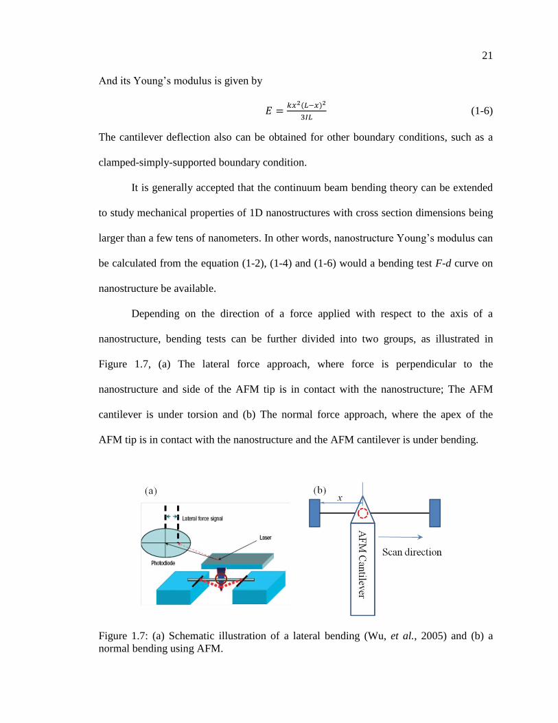
nanostructure, bending tests can be further divided into two groups, as illustrated in
Figure 1.7, (a) The lateral force approach, where force is perpendicular to the
nanostructure and side of the AFM tip is in contact with the nanostructure; The AFM
cantilever is under torsion and (b) The normal force approach, where the apex of the
AFM tip is in contact with the nanostructure and the AFM cantilever is under bending.
Figure 1.7: (a) Schematic illustration of a lateral bending (Wu, et al., 2005) and (b) a
normal bending using AFM.

22
(a) Lateral Force Approach
Wong et al. (Wong, et al., 1997) pioneered the technique using an AFM lateral
force mode to bend multi-walled carbon NTs (MWNTs) and SiC nanorods. 1-D
nanostructures were randomly dispersed onto a substrate and selectively clamped down
to substrate by the islands, the yellow part shown in Figure 1.8, which was fabricated
with a conventional lithography method. As the AFM tip is scanned perpendicularly to
the nanostructure under a lateral force of F=7.7 nN, deflection of the nanostructure d(x) at
a distance x from the clamped end was recorded by AFM images. According to the
continuum beam model, Young’s modulus of nanostructure was calculated from Eq. (1-
2). This method could suffer from complications due to nanostructures-substrate friction.
Furthermore, the effective bonding location of between the nanostructures and substrate
could be uncertain due to possible leakage of the pinning materials in the shadow-mask
process (Wu, et al., 2005). The uncertainty would affect the x determination and Young’s
modulus of nanostructure as a result. On the other hand, d(x) actually includes deflection
of both the cantilever and the nanostructure. Ignoring deflection of the cantilever could
lead to underestimation of the Young’s modulus of a nanostructure.
Figure 1.8: A schematic illustration of a one end clamped NT deflected by an AFM tip
laterally (Wong, et al., 1997)

23
To overcome the above mentioned complications due to nanostructures-substrate
friction, Song et al. (Song, et al., 2005) and Chueh et al. (Chueh, et al., 2007) directly
bent vertically grown ZnO and RuO2 NWs by scanning across those nanostructures using
an AFM tip with a 20 cone angle. Cantilevers had a normal spring constant of 4.5 N/m.
As the tip scanned over the top of the NWs, force and deflection of NWs were
determined from AFM images and modulus of the nanostructures was calculated similar
to reference (Wong, et al., 1997). This technique allows mechanical properties
measurement of individual NWs of different lengths in an aligned array without any
sample manipulation. However, as the authors pointed out, a disadvantage of the
technique is its inaccuracy in evaluating the size of individual NWs. Another uncertainty
for this technique is: the AFM tip could apply an eccentric force on the NWs and
underestimate their Young’s modulus. For a 45 nm ZnO NW, the measured elastic
modulus was 298 GPa, which is far smaller than that of bulk ZnO.
Clamped-clamped nanostructures-over-trench configuration has also been used to
study Young’s modulus, yield strength and the strain hardening effect of Au (Wu, et al.,
2005), Ag (Wu, et al., 2006) and Ge (Ngo, et al., 2006) nanostructures under lateral
bending approach. The experimental setup is shown in Figure 1.7 (a). The procedures of
sample preparation were as follows: (1) the nanostructures were dispersed into solutions;
(2) a few drops were put onto the substrate with trench and (3) A single nanostructure
across the trench was located and the ends of the nanostructure were fixed to the edges of
the trench using EBID. Rectangular cantilevers with average normal force constant of 20
to 40 N/m and 1 to 3 N/m were used. A Dimension 3100 AFM from DI instruments,
equipped with a Nanoman software package and x-y closed loop control, was used to

24
conduct the lateral bending test. The lateral force F vs. displacement at mid-point of NW
d was analyzed to determine its Young’s modulus and yield strength. During data
analysis, steps to obtain nanostructure modulus were: (i) calculate the spring constant of a
combined nanostructure-AFM cantilever system obs
Fk
d . (ii) obtain spring constant of
the nanostructure as obs cw
c obs
k kk
k k
, where ck was the lateral bending spring constant,
calibrated by lateral bend cantilever over edge of the trench. (iii) Young’s modulus of
NW was then calculated using Eq. 1.4 at x=L/2. Experimental results showed that yield
strength of NWs was close to theoretical limit, whereas Young’s modulus was diameter
independent and closed to their bulk counterpart. As the authors pointed out, errors of this
method stem from estimation of the NW and cantilever physical dimensions, AFM
photodetector sensitivity and uncertainty due to lack of z closed-loop control. Without a z
closed-loop control, AFM tip-nanostructure contact location, as illustrated in the green
circle of Figure 1.7 (a), is unknown, which will cause uncertainty of the force on
nanostructure estimation and Young’s modulus measurement.
(b) Normal Force Approach
Normal force approach, as illustrated in Figure 1-7(b), applies a force on a
nanostructure perpendicular to the surface supporting it. The dashed line red circle stands
for AFM tip and AFM tip apex is in contact with the nanostructure. Depending on the
operation mode of AFM, normal force approach is divided into two groups: (i) AFM
cantilever scanned along the nanostructure at a constant load and (ii) AFM tip
continuously pressed against the nanostructure at a fixed location x.
25
For the first group, orientation of the cantilever was perpendicular to the
nanostructure and scan direction, as shown in Figure 1.7 (b). Two scans with a zero force
and a constant force (F), respectively, along a nanostructure were conducted. Scanner
extensions along the nanostructure at zero force (curve 1) and at the constant force (curve
2) were recorded. Scanner extension due to applied force d(x) was obtained by
subtracting curve 1 from curve 2. By doing this, the authors believed that possible initial
slack of the nanostructure could be removed. Young’s modulus was calculated from Eq.
(1-2) (San Paulo, et al., 2005, Silva, et al., 2006) for one end clamped nanostructures and
Eq. (1-4) for clamped-clamped nanostructures(Chen, et al., 2006, Chen, et al., 2007, Mai
and Wang, 2006, San Paulo, et al., 2005, Tabib-Azar, et al., 2005).
The second group operated at the force mode of an AFM. Force applied on a
nanostructure vs. extension of the scanner, a linear curve (curve i), was obtained at a
distance x away from the fixed end. Force vs. extension of the scanner curve on an
infinitely hard substrate (curve ii) was also acquired. Authors tried to eliminate deflection
of the AFM cantilever and obtain the pure deformation of the nanostructure by
subtracting curve i from curve ii. The force on nanostructure (F) vs. the nanostructure
deflection curve was obtained. Young’s modulus of nanostructures was calculated from
Eq. (1-2) for one end clamped nanostructure (San Paulo, et al., 2005, Xiong, et al., 2006).
A similar approach was used to study the mechanical property of a vertically grown
silicon NW (Gordon, et al., 2009). Note that force on the AFM tip and the nanostructure
are same while their deflections are different during a measurement. Trying to eliminate
deflection of the AFM cantilever by subtracting cantilever F vs. deflection curve from
cantilever-on-nanostructure F vs. deflection curve is problematic. The method in
26
reference (Wu, et al., 2005) is better in terms of eliminating deflection of the AFM
cantilever and obtaining nanostructure modulus accurately.
For lateral or normal bending tests, knowing the correct boundary condition
between a nanostructure and trench edge is critical in extracting the mechanical
properties of 1D nanostructures from load vs. scanner extension curves (Chen, et al.,
2006, Chen, et al., 2007, Mai and Wang, 2006). Figure 1.9 shows a comparison of
experimental vs. model predicted deflection of a nanostructure under different boundary
conditions (clamped-clamped Eq. (1.3), simply–supported Eq. (1.5), and one simply
supported end with one fixed end) for silver NWs. While Figure 1.9 (a) and (b)
confirmed that a clamped-clamped boundary condition described the nanostructure and
edge of trench well, Figure 1.9 (c-e) indicated that a simple support boundary condition
was more appropriate for those particular cases. As a result, simply assuming a clamped-
clamped boundary condition for NW and edge of trench could underestimate Young’s
modulus of the nanostructure. To eliminate measurement uncertainty associated with
unsure of boundary condition, experimental data was compared with model results using
different boundary conditions, and the boundary condition gave a maximum match
between experiment and model results was used to extract Young’s modulus of the
nanostructure.

27
Figure 1.9: Comparison of experimental and model predicted deflections for silver NWs
of different diameters (Chen, et al., 2006)
Another issue in bending testing is the ―swing effect‖/slippage (Chen, et al., 2006)
of an AFM tip off the tested nanostructure, which typically happened in the normal force
bending mode. If the AFM tip moves off axis of the nanostructures, it will apply an
eccentric force on nanostructures and make them swing to the side. The slippage could
introduce a substantial uncertainty of Young’s modulus. To mitigate slippage effect on
mechanical property measurement, AFM tip scanned along NW many times and the load-
deflection profile gave the largest vertical component of the AFM cantilever deflection

28
was selected to extract Young’s modulus of the nanostructure. Another approach to
minimize slippage effect is using a special AFM cantilever tip, which was modified by a
FIB milling process to produce a ―tooth‖ shape groove with a dent width of 150 nm. The
groove can secure the AFM tip on the nanostructure during the measurement process
(Zhang, et al., 2008).
The normal force bending test was also used to study the mechanical properties of
graphene, a one-atom-thick carbon, as reviewed by Zhu et al. (Zhu, et al., 2010).
Graphene were suspended over a photolithographically defined circular holes etched with
buffered hydrofluoric acid (Lee, et al., 2008, Poot and van der Zant, 2008) or a trench of
width between 0.5 m and 5 m (Frank, et al., 2007, Gomez-Navarro, et al., 2008).
Suspended graphene were obtained by mechanically exfoliating kish graphite across
trenches (Bunch, et al., 2007). As the AFM tip being pushed against a suspended
graphene sheet, force vs. extension of AFM scanner curve was obtained. The curve could
give effective spring constant of the suspended graphene. Assuming graphene was
clamped to the edge of circular hole or trench, Young’s modulus of the graphene was
extracted based on theory of a macroscopic plate (Poot and van der Zant, 2008) or a beam
(Frank, et al., 2007) bending under tension. A series of load and unloading curves on
graphene matched each other well, which indicated that clamped boundary condition
between graphene and the edge of trench was a valid assumption (Lee, et al., 2008).
Membrane theory was recently proved to be best in describing graphene’s mechanical
behavior. Young’s modulus and fracture strength of graphene was measured to be 1.0
TPa and 130 GPa. For this kind of setup to measure mechanical property of graphene,
Frank et al. emphasized that the spring constant of AFM cantilever should be comparable
29
to that of graphene sheets. Either too stiff or too flex cantilever could lead to inaccurate
determination of graphene’s mechanical properties.
(ii) AFM Nanoindentation
AFM nanoindentation test has been used to study mechanical property of polymer
(Cappella and Silbernagl, 2008, Jee and Lee, 2010, Kovalev, et al., 2004). The test is also
used to measure mechanical properties of a nanostructure (Sohn, et al., 2010) and its
plastic deformation (Lucas, et al., 2008, Lucas, et al., 2007). The extraction of
mechanical properties in a nanoindentation test was based on the Hertz contact theory, in
contrast to the beam bending theory in bending tests. Sample preparation for
nanoindentation test is simple compared to AFM bending tests, where only samples
across trench are good for further testing. The sample preparation procedures for
nanoindentation tests were as follows: (1) nanostructures were scraped from the substrate
where they grew and dispersed into solutions through ultrasoincation; (2) a few drops of
solution were placed onto a clean substrate and (3) an individual nanostructure was
located through an AFM scanning for further testing. 2-spring-in series model (one for
AFM cantilever and the other for contact interaction between the AFM tip and the
nanostructure) was typically used to extract modulus of a nanostructure from F-d curve.
Like a thin film material, a nanostructure needs to be supported by a substrate.
The substrate, used to support a nanostructure, will affect the F-d curve and the Young’s
modulus measurement. Recently, substrate effect on the Young’s modulus measurement
of a NB with AFM nanoindentation method was theoretically modeled (Zhang, 2010). In
their model, a 3-spring-in-series model was used to model the indentation process. The
model was based on the 2-spring-in-series model discussed above but with an extra

30
spring. The extra spring accounted for the nanostructure and substrate receding contact
stiffness. In summary, due to the small dimension of nanostructures, the substrate effect,
the extra spring, needs to be considered. Otherwise, extracted nanostructure modulus is
error prone.
AFM nanoindentation test was not extensively adopted to study the mechanical
property of 1D nanostructures. Reasons could be as follows: (1) the complicated
theoretical model makes extracting nanostructures mechanical property non-trivial. (2)
the parasitic lateral motion of the AFM tip during indentation (Huang, et al., 2007) makes
mechanical property measurement even harder. An AFM indentation test may result in
unwanted lateral motion. The lateral motion makes indentation test on nanostructures
with a circular cross section, such as NWs and NTs, almost impossible.
(iii) Atomic Force Acoustic Microscopy (AFAM) Based Method
AFAM based method is another technique to evaluate the near-surface
mechanical property (Rabe, et al., 2000, Rabe, et al., 1996). This method has been used
to study the mechanical property of ZnO NWs (Stan, et al., 2007), Te NWs and faceted
aluminum nitride NTs (Stan, et al., 2009), SiO2 NWs with a Si core (Stan, et al., 2010).
The method correlates the mechanical property of nanostructures to resonant frequency
of the AFM cantilever while being pressed against a tested sample under a certain load.
Sample preparation procedures for AFAM tests are similar to AFM nanoindentation: (1)
disperse as-grown nanostructure into a solution; (2) put a few drops of solution onto a
substrate; (3) locate an individual nanostructure and land the AFM tip onto it and (4)
sweep driving frequency of the AFM cantilever and obtain its contact resonant frequency.
A schematic illustration of AFAM setup to measure the cantilever resonant frequency is

31
shown in Figure 1.10. The detailed procedures to correlate the contact resonance
frequencies with mechanical properties of the tested materials will be discussed in
Chapter 2.
Figure 1.10: The schematic illustration of the experimental apparatus for AFAM based
mechanical property testing method. (Hurley, et al., 2007)
When conducting mechanical property tests on 1D nanostructures with AFAM,
certain restrictions/requirements apply, which are listed as follows: (1) a closed-loop
AFM scanner. Otherwise, indenting right on top of the nanostructures is challenging. A
successful mechanical property test on a nanostructure with AFAM consists of two steps,
i.e. (i) locating the nanostructure through AFM tapping mode scanning and (ii)
withdrawing cantilever from the surface of nanostructure and re-engaging the cantilever
under contact mode with a scan area of zero on top of the nanostructure. Most of AFM
scanners now available on the market are made of PZT, which shows creep and
hysteresis behavior. Without a proper feed-back (closed-loop) control to compensate the
creep and hysteresis behavior, landing exactly on top of a nanostructure is ambitious. (2)
the engagement of an AFM cantilever on the surface of a nanostructure must be gentle or
32
tip of the cantilever will be blunted because of the impact force during engaging. (3) this
AFAM based method is improper for the nanostructures with high Young’s modulus,
since most of AFM tip on nanostructure system deformation will comes from the AFM
tip. The technique is inapplicable for measuring materials with very low modulus, like
biomaterials, neither. The contact stiffness between the AFM tip and a material of low
modulus is so small that the contact resonant frequency of the AFM cantilever will be
close to its free resonant frequency, no matter the cantilever is in contact with a soft
material A or a soft material B. Therefore, materials A and B are indistinguishable.
(iv) Summary of AFM Related Measurement Techniques
AFM based techniques use the AFM cantilever as a force sensor to measure the
load applied on nanostructures. The cantilever itself deflects while indenting or bending
nanostructures. As a result, cantilever-on-nanostructure generally needs to be modeled
with 2-spring-in-series system, i.e. a spring for cantilever itself (spring 1) and a spring for
nanostructure bending/AFM tip indenting on nanostructure (spring 2). A properly chosen
cantilever with suitable spring stiffness is important for all the AFM based techniques.
Two extreme cases should generally be avoided: (1) spring stiffness of spring 1 is much
lower than that of spring 2. System deformation for this case will be mainly from spring 1
so that the nanostructure would be like rigid comparing to cantilever. It is impossible for
cantilever to distinguish one tested material from another; (2) spring stiffness of spring 1
is much larger than spring 2. The force resolution is low due to the small displacement of
spring 1. An ideal case would be spring 1 and 2 having similar stiffness.
Among three AFM based techniques, bending test was most often used due to its
simplicity in extracting nanostructure mechanical properties based on the beam bending
33
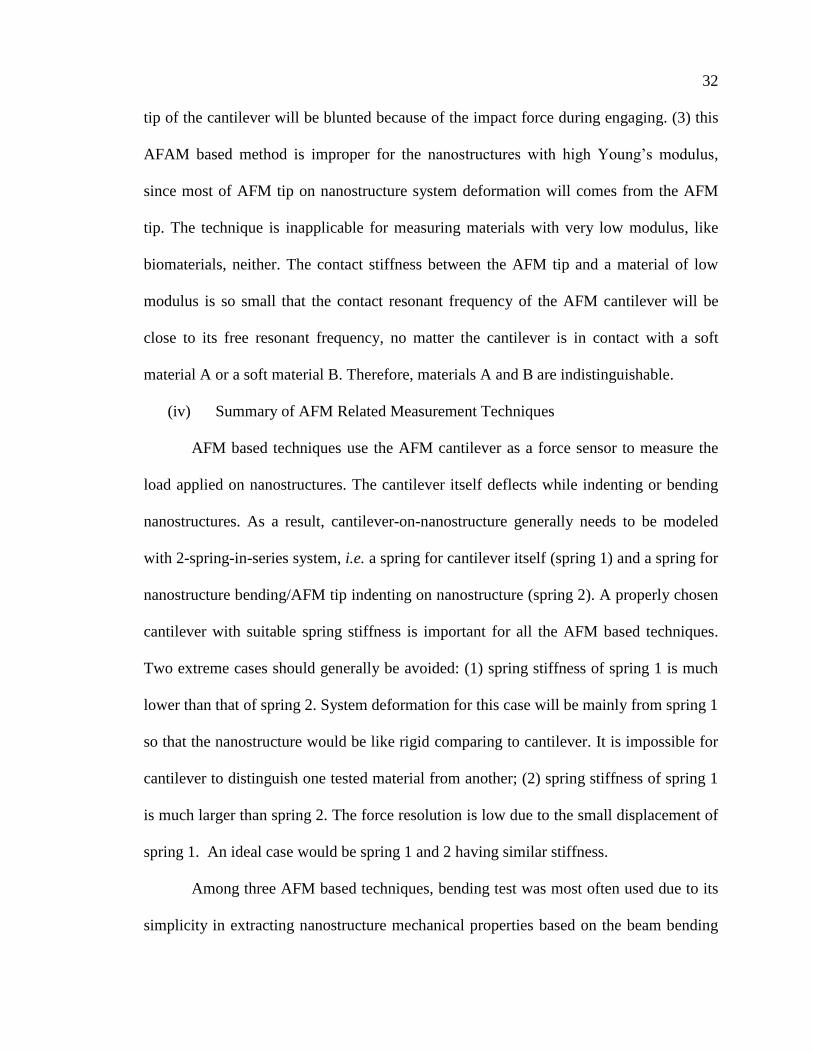
theory. Each technique has its advantages and limitations as shown in Table 1.3.
Researchers should choose a proper technique to measure mechanical property of
nanostructures, based on their AFM hardware capability and willingness to analyze
complex interaction models between cantilever and nanostructure or not.
Table 1.3: Comparison of different AFM modes for 1D nanostructure mechanical test
Operation Mode Pros Cons
Bending
Lateral
force mode
Extracting mechanical
property is based on
simple beam bending
theory.
Difficult to calibrate the cantilever
lateral spring constant; Depending on
AFM hardware: The distance between
cantilever tip apex and contact point
between cantilever and nanostructure,
which will affect applied torsion on
nanostructure, is uncertain without a
Z-closed loop control of AFM scanner.
Normal
force mode
Extracting mechanical
property is based on
simple beam bending
theory.
Eccentric force could be applied on
nanostructure and ―swing
effect‖/slippage, making it hard to
scan exactly on top of a nanostructure.
Nanoindentation
Straightforward for
wide nanostructures,
such as a NB.
Complicated in extracting mechanical
property from contact model;
Substrate effect, unwanted AFM tip
lateral motion are hard to deal with.
AFAM
Contact resonant
frequency of AFM
cantilever can be
accurately measured.
Depending on accurate AFM
cantilever dynamic analysis, tip-
sample contact modeling and AFM
hardware.
1.3.4 Nanoindentation
Nanoindentation is another method to study mechanical properties of 1D
nanostructures. Different from AFM based nanoindentation, where force sensor—AFM
cantilever deflects itself during measurements, nanoindenter has a separate force and
displacement sensor. It is widely used for material mechanical property characterization,

34
especially for bulk materials. Among many techniques used to characterize mechanical
properties of nanostructures discussed so far, nanoindentation is attractive because (i) it is
a relatively easy and quick testing technique; (ii) it can achieve excellent force resolution
and control (better than 1.0 N), and fine displacement resolution (better than 0.1 nm)
(Oliver and Pharr, 1992); and (iii) it can provide a wealth of information regarding
mechanical properties of a material. Both hardness and Young’s modulus of the tested
sample can be obtained from one single nanoindentation test.
The Hertz contact problem—an elastic half space indented by a rigid,
axisymmetric indenter is the foundation of nanoindentation(Oliver and Pharr, 1992).
Solutions for the elastic contact problem indicated that
(1-7)
Where P is the load applied on indenter and h is the indenter displacement into surface.
is a constant. m = 1.0 for flat-punch indenter; m = 1.5 for a spherical indenter and m = 2.0
for a conical indenter.
Berkovich, or cube corner indenter, is typically used for small scale
nanoindentation tests. Because of sharpness of the indenter, plasticity is generally
induced beneath the indenter, which makes analysis of load-displacement curve much
more complicated. Analysis of nanoindentation load-displacement curves to obtain
mechanical properties of a tested material is generally divided into two types: (1) forward
analysis, where mechanical properties are fitted from the loading part of a load-
displacement curve (Hainsworth, et al., 1996, Jha, et al., 2010); (2) backward analysis,
where mechanical properties are extracted from unloading part of the load-displacement
curve.

35
Forward analysis is initially studied for materials with considerable elastic
recovery during unloading, such as very hard material and heterogeneous systems like
hard coating on substrate system. The procedure to obtain the mechanical property of test
material is: (1) Assume an indenter shape (equivalent conical indenter is assumed to
approximate Berkovich indenter) and constitutive equation of the tested materials; (2) Fit
load-displacement curve to the equation (Hainsworth, et al., 1996)
(1-8)
Where and are indenter constants. (3) Given one of E and H, the other can be
fitted from equation (1-8). Based on the procedures of obtaining mechanical properties,
we see that disadvantages of the method are: (i) it is based on the assumption of an ideal
indenter shape, such as a conical indenter which has a very sharp tip. However, the
indenters used in most experiments are typically blunted especially after being used for a
long time. The tip radius is around tens or even hundreds of nanometers. The minimum
load for the assumption to be true is 1 mN, and (ii) the constitutive equation of materials
could be very complicated. For example, fitting of equation (1-8) for a material showing
strain hardening could be problematic.
Backward analysis, on the other hand, is a general practice of most
nanoindentation data analysis and is adapted by commercial nanoindenters. Unloading
part of the load-displacement curve, shown in Figure 1.11, is elastic, and the stiffness of
the initial unloading part is given by (Oliver and Pharr, 1992):
(1-9)
(1-10)
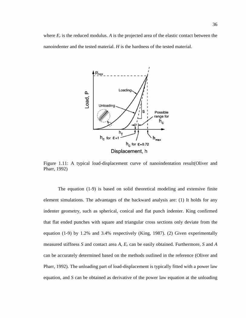
36
where Er is the reduced modulus. A is the projected area of the elastic contact between the
nanoindenter and the tested material. H is the hardness of the tested material.
Figure 1.11: A typical load-displacement curve of nanoindentation result(Oliver and
Pharr, 1992)
The equation (1-9) is based on solid theoretical modeling and extensive finite
element simulations. The advantages of the backward analysis are: (1) It holds for any
indenter geometry, such as spherical, conical and flat punch indenter. King confirmed
that flat ended punches with square and triangular cross sections only deviate from the
equation (1-9) by 1.2% and 3.4% respectively (King, 1987). (2) Given experimentally
measured stiffness S and contact area A, Er can be easily obtained. Furthermore, S and A
can be accurately determined based on the methods outlined in the reference (Oliver and
Pharr, 1992). The unloading part of load-displacement is typically fitted with a power law
equation, and S can be obtained as derivative of the power law equation at the unloading

37
point. A is calibrated with a standard reference sample such as silica. The area function,
which gives a correct modulus of a standard reference sample, is considered area function
of the indenter.
One obvious disadvantage of back analysis is: it uses a standard reference sample
to calibrate indenter area function A. Depending on the tested material yielding property,
―pile-up‖ could happen for materials like aluminum and ―sink-in‖ could happen for stiff
materials. To correct the pile-up/sink-in caused uncertainty of contact area, Joslin and
Oliver eliminated contact area from the equation (1-9) and (1-10) for elastic
homogeneous system (Joslin and Oliver, 1990). They obtained the following
(1-11)
P/S2 is often plotted to check whether
are constant. If either H or Er
2 is known, the
other can be determined from the above equation.
Even though nanoindentation was designed for studying the mechanical property
of homogeneous bulk material, it has been extended to study Trabecular bone with
porous structure (Gan, et al., 2010) and mechanical properties of nanostructures, such as
ZnO and SnO2 semiconducting nanobelts (Mao, et al., 2003), ZnS (Li, et al., 2005, Yang,
et al., 2005), Al4B2O9 and Al18B4O33 NWs (Tao, et al., 2007) and GaN and ZnO NWs
(Feng, et al., 2006), vanadium doped ZnO nanofibers (Chen, et al., 2010), and Indium
nano/microwires (Kumar and Kiran, 2010). It is worth pointing out that a few steps need
to be carefully followed while indenting nanostructures: (1) Different from AFM based
nanoindentation or AFAM method, the indenter used in nanoindentation is made of
diamond, which is rigid compared to most tested materials. The indenter shape is
persevered and thereby contact area is well determined throughout the indentation

38
process. The diamond indenter, however, could damage a nanostructure surface while
scanning and locating a single nanostructure to perform an indentation test. It is critical to
choose a proper scanning load to minimize damage to the nanostructure. (2) Similar to
most of the AFM based methods, nanoindentation also depends on the hardware
resolution while positioning the indenter on top of the tested nanostructures. The sample
stage is mostly controlled by PZT materials, which show hysteresis effect. The effect
could cause the target scanning area to be a little bit off the actual one. To make the target
and actual areas overlap and indent exactly on top of a nanostructure, the offset should be
manually compensated while choosing the scan area. (3) The tested nanostructures are
expected to be reasonably smooth. Otherwise, there will be large uncertainty associated
with the contact area between the nanostructure and the nanoindenter and thereby cause
inaccurate measurement of nanostructures’ mechanical property. (4) Due to the large
force applied on the sample during indentation, the underline substrate effect could come
into play, similar to a thin film on a substrate system. What the nanoindenter measured is
actually an effective modulus of the nanostructure-on-substrate system. As a result,
extracting the mechanical property of a tested material from the effective system modulus
is critical for a nanoindentation test (Feng, et al., 2006, Shu, et al., 2009).
1.3.5 Other Techniques
The flow induced by a single laser-induced cavitation bubble was used to
manipulate and measure Young’s modulus of a single Co NW with a diameter of about
40 nm (Huang, et al., 2010). The as-grown NWs were dispersed into ink and the solution
was filled into a gap formed by two glass slides. A laser beam created cavitation bubbles
inside the gap. During the bubble expansion and further collapse process, some of the
39
NWs near the bubble were bent by the force generated due to different velocity across
their length. The dynamics of the NW was recorded with a high speed camera at a
framing rate of up to 450,000 per second. By analyzing those images in conjunction with
the hydrodynamic beam equation, Young’s modulus of the NW was obtained. The
obtained Young’s modulus was only tenth of their bulk counterpart, which could possibly
be due to low resolution of the high speed camera. Furthermore, improvement for both
experiment and modeling is needed to make this method suitable for mechanical property
measurement of a nanostructure.
1.4 Methods Used in This Dissertation
In reviewing the current available testing methods of 1D nanostructures’
mechanical property, we noticed that tensile tests require a manipulator, either home-
made or commercially available, to apply load and displacement to a nanostructure.
Alignment of a nanostructure to make it under pure tension is challenging. Furthermore,
obtaining the strain of a nanostructure from recorded SEM images could be problematic.
On the other hand, the pros and cons of the techniques for obtaining Young’s modulus
from their dynamic resonant frequency are listed in Table 1.2. Measuring the resonant
frequency of a modulated charge could be challenging too. Additionally, for AFM based
nanostructure bending methods, the normal bending mode could suffer from
nanostructure slippage and eccentric loading. Without an AFM closed loop control in z-
direction, uncertainty of contact location between the side of an AFM tip and a
nanostructure could lead to error in determining mechanical properties of nanostructures
using the lateral bending mode.
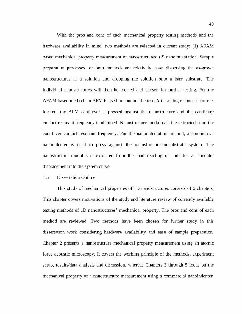
40
With the pros and cons of each mechanical property testing methods and the
hardware availability in mind, two methods are selected in current study: (1) AFAM
based mechanical property measurement of nanostructures; (2) nanoindentation. Sample
preparation processes for both methods are relatively easy: dispersing the as-grown
nanostructures in a solution and dropping the solution onto a bare substrate. The
individual nanostructures will then be located and chosen for further testing. For the
AFAM based method, an AFM is used to conduct the test. After a single nanostructure is
located, the AFM cantilever is pressed against the nanostructure and the cantilever
contact resonant frequency is obtained. Nanostructure modulus is the extracted from the
cantilever contact resonant frequency. For the nanoindentation method, a commercial
nanoindenter is used to press against the nanostructure-on-substrate system. The
nanostructure modulus is extracted from the load reacting on indenter vs. indenter
displacement into the system curve
1.5 Dissertation Outline
This study of mechanical properties of 1D nanostructures consists of 6 chapters.
This chapter covers motivations of the study and literature review of currently available
testing methods of 1D nanostructures’ mechanical property. The pros and cons of each
method are reviewed. Two methods have been chosen for further study in this
dissertation work considering hardware availability and ease of sample preparation.
Chapter 2 presents a nanostructure mechanical property measurement using an atomic
force acoustic microscopy. It covers the working principle of the methods, experiment
setup, results/data analysis and discussion, whereas Chapters 3 through 5 focus on the
mechanical property of a nanostructure measurement using a commercial nanoindenter.
41
Chapter 3 studies the mechanical property of TiO2 nanoribbons, which have width-to-
thickness ratios about 5. The nanoribbon has been laid on three different substrates. Our
results indicated that sapphire is the best substrate for the nanoindentation test of these
particular nanoribbons. A substrate selection rule for general nanostructure mechanical
property test is presented for the first time. Chapter 4 studies the mechanical properties of
divalent alkaline earth metal hexboride MB6 nanostructures, which have a width-to-
thickness ratios falling between 1 and 2. Chapter 5 provides a semi-analytical solution for
the nanoindentation on a nanoribbon-on-substrate system. Chapter 6 summarizes studies
in the present dissertation and postulates possible future works.

CHAPTER 2: MEASUREMENT OF MECHANICAL PROPERTY USING AN
ATOMIC FORCE ACOUSTIC MICROSCOPY (AFAM)
2.1 Introduction
Atomic force microscopy has been widely used to measure the mechanical
property of 1D nanostructures, as reviewed in Chapter 1. This chapter discusses one of
those AFM based methods. The method is called the AFAM based method. It is used to
study the Young’s modulus of a BaB6 nanostructure due to (1) its high force and
displacement resolution, and (2) relative easiness in sample manipulation. While an AFM
cantilever is in contact with a tested nanostructure, its contact resonance frequencies are
different from its free resonance frequencies. The shift of the resonant frequency is
correlated to the Young’s modulus of the nanostructure. An add-in transducer to an AFM
makes the cantilever resonant frequency measurement possible.
Section 2.2 presents the AFM cantilever dynamics and the working principle of
using AFAM based method for mechanical property measurement of nanostructures.
Section 2.3 includes the experimental setup of the AFAM based method and the detailed
procedures to measure AFM cantilever contact resonant frequency. Section 2.4 focuses
on results and data analysis and Section 2.5 discusses the method.
2.2 AFAM Based Method to Measure Mechanical Property
AFAM based method measures mechanical property of 1D nanostructures by
indirectly measuring the AFM cantilever resonant frequency while it is pressed again a

43
tested 1D nanostructures. Cantilever dynamics and the formula for its contact resonant
frequency are reviewed in this section.
2.2.1 Cantilever Dynamics
The AFM cantilever dynamics are highly nonlinear and remain challenging, as
reviewed in by Raman et al. (Raman, et al., 2008). Understanding the cantilever
dynamics is important to make a full and good use of an AFM. Raman et al. pointed out
that ―…understanding these phenomena can offer deep insight into the physics of
dynamic atomic force microscopy and provide exciting possibilities for achieving
improved material contrast with gentle imaging force in the next generation of
instruments…‖ (Raman, et al., 2008). Here we review the AFM cantilever dynamics.
(a) Continuous Model of the Cantilever
AFM cantilever is generally described as a rectangular and homogeneous Euler
beam. Its dynamics is captured by the Euler-Bernoulli equation. The equation for a beam
with external forces applied at its free end is given by (Lozano and Garcia, 2009, Turner,
et al., 1997):
(2-1)
E and are Young’s modulus and mass density of the cantilever material. a ,b and L are
width, thickness and length of the cantilever, respectively. I is its moment of inertia;
w(x,t) is the time-dependent vertical displacement of the beam at a distance x away from
the end that is fixed to the cantilever holder using a spring leaf. a0 is the hydrodynamic
damping coefficient. The generalized function is infinity when x is zero and is
zero otherwise. accounts for the concentrated load applied at x = L. is
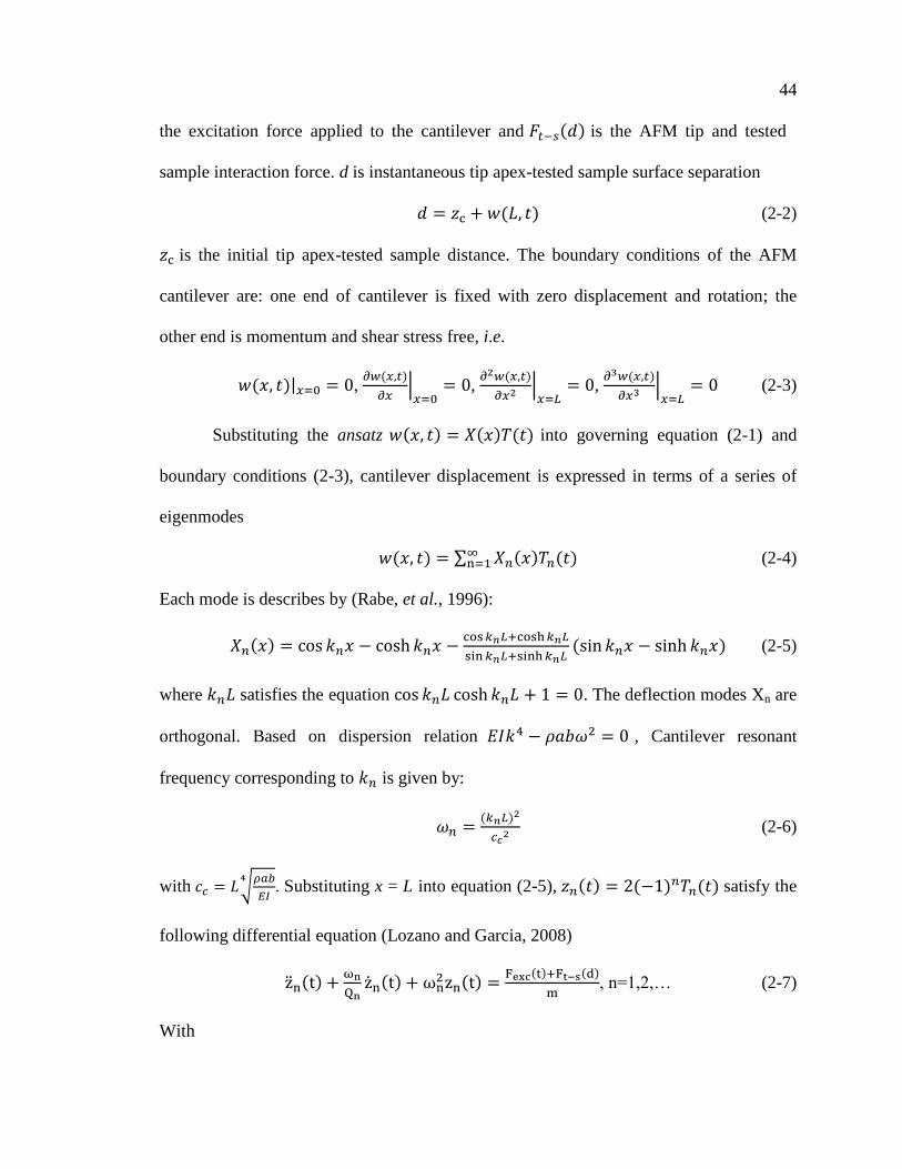
44
the excitation force applied to the cantilever and is the AFM tip and tested
sample interaction force. d is instantaneous tip apex-tested sample surface separation
(2-2)
is the initial tip apex-tested sample distance. The boundary conditions of the AFM
cantilever are: one end of cantilever is fixed with zero displacement and rotation; the
other end is momentum and shear stress free, i.e.
,
,
,
(2-3)
Substituting the ansatz into governing equation (2-1) and
boundary conditions (2-3), cantilever displacement is expressed in terms of a series of
eigenmodes
(2-4)
Each mode is describes by (Rabe, et al., 1996):
(2-5)
where satisfies the equation . The deflection modes Xn are
orthogonal. Based on dispersion relation , Cantilever resonant
frequency corresponding to is given by:
(2-6)
with
. Substituting x = L into equation (2-5), satisfy the
following differential equation (Lozano and Garcia, 2008)
, n=1,2,… (2-7)
With
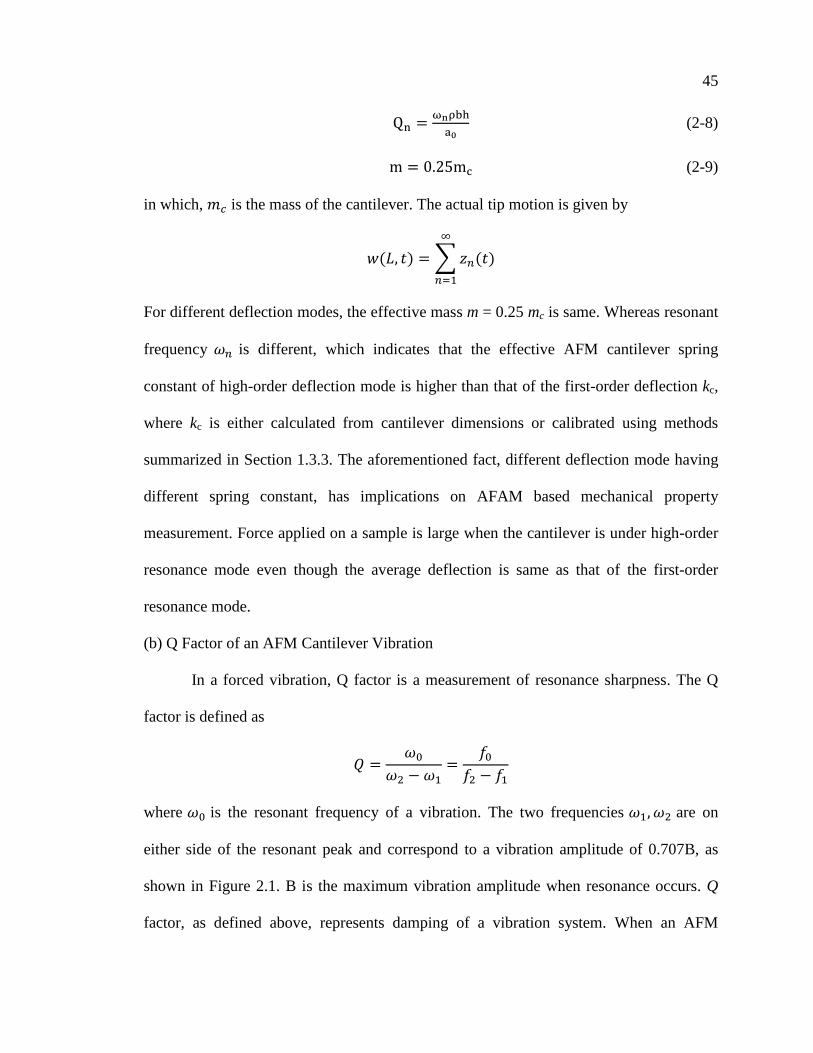
45
(2-8)
(2-9)
in which, is the mass of the cantilever. The actual tip motion is given by
For different deflection modes, the effective mass m = 0.25 mc is same. Whereas resonant
frequency is different, which indicates that the effective AFM cantilever spring
constant of high-order deflection mode is higher than that of the first-order deflection kc,
where kc is either calculated from cantilever dimensions or calibrated using methods
summarized in Section 1.3.3. The aforementioned fact, different deflection mode having
different spring constant, has implications on AFAM based mechanical property
measurement. Force applied on a sample is large when the cantilever is under high-order
resonance mode even though the average deflection is same as that of the first-order
resonance mode.
(b) Q Factor of an AFM Cantilever Vibration
In a forced vibration, Q factor is a measurement of resonance sharpness. The Q
factor is defined as
where is the resonant frequency of a vibration. The two frequencies are on
either side of the resonant peak and correspond to a vibration amplitude of 0.707B, as
shown in Figure 2.1. B is the maximum vibration amplitude when resonance occurs. Q
factor, as defined above, represents damping of a vibration system. When an AFM
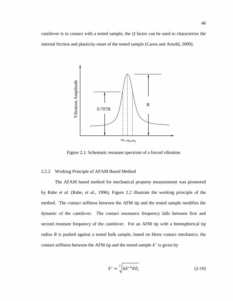
46
cantilever is in contact with a tested sample, the Q factor can be used to characterize the
internal friction and plasticity onset of the tested sample (Caron and Arnold, 2009).
Figure 2.1: Schematic resonant spectrum of a forced vibration
2.2.2 Working Principle of AFAM Based Method
The AFAM based method for mechanical property measurement was pioneered
by Rabe et al. (Rabe, et al., 1996). Figure 2.2 illustrate the working principle of the
method. The contact stiffness between the AFM tip and the tested sample modifies the
dynamic of the cantilever. The contact resonance frequency falls between first and
second resonant frequency of the cantilever. For an AFM tip with a hemispherical tip
radius R is pushed against a tested bulk sample, based on Hertz contact mechanics, the
contact stiffness between the AFM tip and the tested sample is given by
(2-10)
Vib
rati
on
Am
pli
tud
e
0 2 1
B 0.707B

47
where is the reduced elastic modulus of the AFM tip-on-tested sample system, and is
defined as
Es, ET, s, T are Young’s modulus and Poisson’s ratio of the tested sample and the
material of the AFM tip, respectively. Fc is the load applied on the tested sample by the
AFM cantilever.
Figure 2.2: (A) A beam dynamics model for AFAM based method. A one-end clamped
rectangular cantilever beam with a stiffness kc was coupled to tested sample through a
spring of stiffness k* based on contact mechanic model. (B) Resonant spectra of an AFM
cantilever. The first contact resonance calculated from the beam dynamic model shown in
(A) was higher than first free resonance of the AFM cantilever but lower than its second
free resonance (Hurley, et al., 2007).
The contact stiffness between an AFM tip and a tested sample k* generates a force
between them and modifies the fourth boundary condition of the AFM cantilever, listed
in (2-3), to
(2-11)

48
for a cantilever with a total length of L. L1 is the tip location. is the distance between
AFM tip and cantilever free end. Based on the method discussed in Section 2.2.1, ,
wave number of the nth
AFM cantilever contact resonance, satisfies the following
characteristic equation (Rabe, et al., 1996):
(2-12)
As discussed in Chapter 1, to make sure the AFM tip touches the tested sample
surface first, AFM cantilever is usually tilted with respect to the tested sample at an angle
α. A tangential spring constant κ between the AFM tip and the tested sample, in addition
to the contact stiffness , needs to be considered in the dynamic cantilever modeling.
Assume that the AFM tip height is h, and the cantilever spring constant is kc, the
characteristic equation for the tilted cantilever in contact with the tested sample system is
summarized as following (Hurley and Turner, 2007):
(2-13)
where
with

49
In summary, can be solved from either characteristic equation (2-12) or (2-13).
Equation (2-13) is for a tilted cantilever. Furthermore, the contact resonance frequencies
of a cantilever are obtained from the following dispersion relation (Rabe, et al., 1996):
(2-14)
Whereas the free resonance frequencies of a cantilever are given by:
(2-15)
where are the solutions of
. Combing equation (2-14)
and (2-15), the AFM cantilever contact resonant frequencies are given by
(2-16)
The above equation circumvents the necessity to know density and Young’s modulus of
the cantilever.

50
For cantilevers with a tip being located at end of the AFM cantilever, i.e. =0,
knL was solved from equation (2-12) for different k*/kc, which were listed in Table 2.1.
Substituting knL values in Table 2.1 into equation (2-16), AFM cantilever contact
resonant frequency and its free resonant frequency ratios were obtained, as listed in Table
2.2. From the Table, several important conclusions can be drawn: (1) For the first-order
cantilever deflection mode, contact resonance is insensitive to k* when k*/kc<1 or
k*/kc>100. In other words, changing of k* in those two zones does not significantly alters
the cantilever contact resonant frequency. As a result, AFAM based method in ineffective
to mechanical properties of a tested material in the two zones. (2) For higher-order
deflection modes, such as n=4, contact resonant frequency is sensitive to k* only when
k*/kc>100, which indicates that high deflection mode should be used for materials with
high modulus. However, it is worth pointing out that the effective high-order spring
constant knc is higher than kc, as discussed in Section 2.2.1. Contact load Fc on tested
material and k* as a result will be larger for high-order resonance of the cantilever.
Table 2.1: Solutions of knL from equation (2-12) (Rabe, et al., 1996). Some spaces are
left empty because the difference between contact and free end case is less than 0.001.
n Free end
k*=0 k*/kc=0.1 k*/kc=1 k*/kc=10 k*/kc=100
Pinned end
k*=
1 1.8751 1.91891 2.2135 3.16765 3.82981 3.9266
2 4.69409 4.69699 4.7234 5.00112 6.40415 7.06858
3 7.85476 7.85538 7.86097 7.91896 8.58742 10.2102
4 10.9955 10.9958 10.9978 11.0185 11.2559 13.3518
5 14.1372 14.1373 14.1382 14.1479 14.2523 16.4934
6 17.2788 17.2793 17.2846 17.3396 19.635
7 20.4205 20.4239 20.4567 22.7765

51
Table 2.2: Frequency ratio fn/fn0 for different deflection modes of a cantilever
n
fn/fn0
k*/kc=0.1 k*/kc=1 k*/kc=10 k*/kc=100 Pinned end
k*=
1 1.047274 1.39351 2.853813 4.1716282 4.385150033
2 1.001236 1.012527 1.135094 1.8613162 2.267574325
3 1.000158 1.001582 1.016414 1.1952522 1.689672978
4 1.000055 1.000418 1.004188 1.0479257 1.474516616
With a known contact stiffness between an AFM tip and a tested material, AFM
cantilever contact resonant frequency will be determined. Vice versa, given the contact
resonant frequency of an AFM cantilever, the contact stiffness between the AFM tip and
a tested material can be determined. So is Young’s modulus of tested material. The
general procedures to extract mechanical property from contact resonant frequency are as
follows: (1) Experimentally measure contact resonant frequency , n = 1 case is often
used; (2) Obtain from equation (2-16); (3) Calculate from equation (2-12) or (2-13)
when AFM cantilever tilting is considered; and (4) Substitute into equation (2-10) and
obtain tested material Young’s modulus assuming Poisson’s ratio is close to bulk material
value considering that variation of Poisson’s ratio has minor effect on simulated load vs.
displacement curve (Chen and Vlassak, 2001). Due to the difficulty of directly measuring
the tip radius, a reference sample is generally used to circumvent the necessity of
measuring AFM tip radius R, which will be discussed in a later section.
2.3 Experimental Setup
To measure mechanical property of 1D nanostructures, the nanostructures was
deposited on a substrate. The AFAM based method is for a single nanostructure, instead
of bundled nanostructures. The sample preparation procedure was as follows: (i) the as-
52
grown nanostructures were scraped from the substrate where they were grown, and
dispersed into a solution through ultrasonication. (ii) A few drops of solution were
dropped onto a clean substrate. After the solution was evaporated, some isolated
nanostructures were left on the substrate. (iii) A individual nanostructure was then
located and further tested.
Two types of methods were tried to excite an AFM cantilever into resonance: (1)
directly excite the PZT inside the AFM cantilever holder. The external PZT driving
signal was connected to the AFM Signal Access Module (SAM). (2) put tested
nanostructure-on-substrate system onto a piezoelectric transducer at ultrasonic
frequencies (V106-RM, 2.25 MHz, 0.50’ element diameter, Panametrics). SWC (shear
wave couplant, Olympus Inspection and Measurement System) was used to transmit an
acoustic wave from the transducer surface to the substrate, and then the nanostructure,
and AFM cantilever. The nanostructure-on-substrate on transducer system preparing
processes were as follows: (i) clean the piezoelectric transducer surface with alcohol
using a cotton swab; (ii) scrape a bit of TWC couplant, put it onto the transducer surface,
and the bit was flatten with a sharp knife edge to form a thin layer of couplant on the
transducer surface; (iii) lay the substrate, with nanostructure deposited on its top surface,
onto the thin layer of couplant and press the substrate at its corners against the transducer
surface with tweezers. By carefully following these steps, the acoustic wave can be
effectively transmitted to the nanostructure, and then AFM cantilever. Glycerin was also
tried as a couplant. However, it quickly spread onto the top surface of substrate where the
nanostructures were deposited. To eliminate the possible adverse effect on mechanical
property measurement of a nanostructure, glycerin was abandoned for further usage.

53
Comparing the two aforementioned cantilever excitation methods, the first one
directly excites the PZT inside cantilever holder. No extra component is required.
However, the obtained contact frequency spectrum was quite noisy. Many resonant peaks,
beside the cantilever contact resonance peak, were found in the spectrum. Factors, such
as resonant frequency of the part where cantilever was connected, cantilever itself and
insecure bond between PZT and other adjacent components, could be the reasons for
those extra peaks. Properly picking the right cantilever contact resonant frequency from
the noisy spectrum was challenging. As a result, the second type of excitation method
was used throughout the experiment. A clean cantilever frequency spectrum could be
easily obtained.
Different cantilevers with a variety of free resonant frequencies (from 100 KHz to
400 KHz), and wide spring constant range (between a few to 40 N/m) were tried. A sharp
and distinctive resonant frequency spectrum could be easily obtained using commercial
silicon cantilevers (PPP-SEIH, Nanosensors). The cantilevers were chosen for further
study as a result. The nominal thickness, length and width of those cantilevers were
5.01.0, 22510 and 338 m, respectively. The spring constant of each cantilever was
individually calibrated by the manufacturer. They were between 8 and 12 N/m. The free
resonant frequency of a cantilever was about 130 KHz. The cantilever contact resonant
frequency was about 4 times of its free resonant frequency.
A schematic diagram of the experimental setup of AFAM is shown in Figure 2.3.
A function generator drives the piezoelectric transducer, which stays on the AFM sample
stage, with a sinusoidal sine wave (sint). The wave is subsequently transmitted to the
substrate supporting 1D nanostructures, the nanostructure, and the AFM cantilever
54
pressed against the nanostructure. The same sinusoidal sine wave is also served as a
reference signal to a lock-in amplifier (SR844 RF, Stanford Research Systems). The
AFM cantilever deflection signal, accessed through the AFM Signal Access Module
(SAM), is input into the lock-in amplifier, as illustrated in Figure 2.4. The sint
component of the cantilever deflection is measured by the lock-in amplifier using a
LabVIEW (National Instruments) program, as shown in Figure 2.5. By sweeping the
driving frequency to the function generator, the cantilever spectrum while in contacting
with the tested nanostructure, amplitude vs. driving frequency, is obtained. The frequency
gives the maximum vibration amplitude is the contact resonant frequency of the
cantilever at the load .
An AFM (Dimension 3100, Veeco Instruments Inc.) in Optical Center of UNC
Charlotte was used to conduct AFAM based nanostructure mechanical property
measurement. The X-Y scanner scan range (90 m) is much larger than a multimode
SPM, which has been generally used in an AFAM based method to measure material
properties of those small-scale structures (Stan, et al., 2007). The larger scan range
requires extra noise dampening precautions at small-scale scans. This could be the reason
for less accurate in software controlling. The larger scanner could also cause issues while
landing an AFM tip right on top of a nanostructure. Equipped with a Signal Access
Module (SAM), the AFM can take external driving signals to control the PZT insider the
cantilever holder. The signal then excites the AFM cantilever, whose deflection signal
can also be accessed through the SAM, an essential component for any AFAM based
testing. The AFM also has NANOMAN software installed. The software enables user to
switch between a tapping mode (for surface scanning to locate an interesting area) and a

55
contact mode (for local oxidation) while the AFM tip is engaged on a surface. This
capacity makes the AFAM based measurement method feasible for nanostructure
mechanical property measurement even with the large scanning range scanner. The
general procedures to measure the contact resonant frequency of an AFM cantilever are
as follows:
(1) Entering NANOMAN workspace;
(2) Setting the tapping mode scanning parameters, such as scan area, set point
driving amplitude etc; Tuning the cantilever and recording its free resonant frequency;
Setting the contact mode parameters, such as set point voltage, which determines applied
load on a tested sample for the subsequent AFAM based mechanical property testing. The
scan area for contact mode is set as zero. Correctly setting the contact mode parameters is
extremely important. Wrong parameters could cause the AFM tip blunting during the
cantilever engaging process.
(3) Scanning and locating a single nanostructure under tapping mode. Zooming in
and trying to capture an image with minimum size but still be able to capture cross-
sectional profile of the nanostructure. The center of AFM scanning is set as the target
testing location.
(4) Switching to contact mode of the AFM and the AFM tip will land on the
center of scanned image/targeted testing location.
(5) Sweeping driving frequency of the input signal to the transducer, and
obtaining cantilever contact frequency spectrum. The cantilever contact resonant
frequency is determined from the spectrum.

56
Figure 2.3: Schematic illustration of an AFAM setup for measuring AFM cantilever
resonant frequency
Figure 2.4: Signal in and out from a lock-in amplifier
Transducer

57
Figure 2.5: Screen shot of the LabVIEW program, (a) Front panel and (b) block diagram,
used to measure the AFM cantilever contact resonant frequency
(a)
(b)

58
2.4 Results and Discussion
Using the procedures listed in Section 2.3, contact resonance frequencies of three
cantilevers while contacting a single BaB6 nanostructure-on-substrate system, and a Si
substrate with 1 m thick SiO2 layer on top(SiO2/Si) were measured. The frequencies on
the system and SiO2 on Si are listed in Table 2.3.
As discussed in Section 2.2, wave number of an AFM cantilever, while
contacting with a tested sample, is related to contact resonant frequency of the cantilever,
see equation (2-14) or (2-16). The AFM tip–tested sample contact stiffness can be
calculated from based on cantilever dynamics, see equation (2-12) or (2-13). Young’s
modulus of the tested sample will be extracted from based on equation (2-10). The
AFM tip worn out makes tip radius determination tricky. To avoid measuring the AFM
tip apex radius, cantilever contact resonant frequency was also measured on a reference
material, SiO2/Si. Assume the AFM tip apex radius are same during the tests on the
reference material and the system, and with a same applied load Fc, the ratio of equation
(2-10) for the test system over that for reference material is
(2-17)
where subscript S and R stands for the tested system and the reference material,
respectively. Assume Young’s modulus and Poisson’s ratio of SiO2/Si is 70 GPa and 0.3,
respectively, and Young’s modulus and Poisson’s ratio of AFM tip material are 150 GPa
and 0.17. The extracted Young’s modulus of the tested BaB6 nanostructure was listed in
the last column of Table 2.3. The above procedure is a general practice in AFAM based
mechanical property measurement, as adopted by some researchers (Stan, et al., 2009).

59
Table 2.3: AFM cantilever contact resonant frequency on SiO2/Si and nanostructures
Cantilever
Contact resonant
frequency on SiO2/Si
(KHz)
Contact resonance
frequency on
NW(KHz)
Calculated Young’s
modulus of a BaB6
nanostructure (GPa)
1 474 497 131.68
2 486 509 132.09
3 470 489 121.96
The obtained Young’s modulus of the BaB6 nanostructure is significantly lower
than that of bulk BaB6 materials (Kosolapova, 1990) and that measured using
nanoindentation (as listed in Chapter 4). The discrepancy could be due to the following
reasons:
1. AFM tip shape uncertainty: with a non-wearable AFM tip, the Young’s
modulus of tested material has a well defined relationship with AFM tip –
tested material contact stiffness according to Equation (2-10). However, we
noticed that the AFM tip continuously worn throughout the experiment. The
AFM tips were examined inside a SEM before and after each contact resonant
frequency measurement. Figure 2.6 shows SEM images of a typical worn tip
and a new AFM tip. The tip wearing can also be inferred by the contact
resonant frequency shift on one material before and after an experiment on
glass (Hurley and Turner, 2007). The evolving of silicon AFM tip geometry
during experiment has been found by previous researchers. Kopycinska-
Muller, Geiss et al. (Kopycinska-Muller, et al., 2006) conducted contact
resonance spectroscopy measurements using ten AFM cantilevers. They found
that neither punch nor hemisphere shape could successfully represent the
shape of those AFM tips. Instead, the measured contact resonance frequencies

60
were successfully correlated to mechanical properties assuming contact
stiffness and applied load on a tested sample satisfied an equation n
cFk * ,
where is a factor depending on tip geometry and elastic properties of the tip
and tested sample. n varies from 0 for a flat punch to 1/3 for a spherical
indenter. Continuing tip blunting during experiment caused tremendous
uncertainty of the measurements.
Figure 2.6: SEM images of (a) a typical worn tip, and (b) a new AFM tip
2. While the silicon AFM tip is contacted with materials of high modulus, like
TiO2 or MB6 nanostructures, most of the deformation of an AFM tip-on-
nanostructure system comes from the AFM tip. It could cause: (1) continuing
blunting of the AFM tip; (2)the AFM cantilever contact resonant frequency
actually being correlated to silicon modulus, while irrelevant to the properties
of the tested materials, i.e. the AFAM based method can’t be used to measure
(a) (b)

61
mechanical properties of materials with high modulus. A diamond indenter
should be used to measure their mechanical properties.
3. The tested BaB6 nanostructures typically have oxidation layers, which will be
discussed in Chapter 4. Moreover, a gentle load, 120 nN, was applied on the
nanostructure by the AFM cantilever. The load induced deformation of the
nanostructure could be confined in the oxidation layer. The measured modulus
listed in Table 2.3 is slightly bigger than the Young’s modulus of BaO
calculated using first-principle (Ghebouli, et al.). The calculated Young’s
modulus at zero pressure is 104.51 GPa. In other words, the measured
modulus could be modulus of the oxidation layer.
4. AFAM based method depends on the AFM hardware capability. Even though
the AFM used is equipped with Nanoman software, which enables the AFM
to switch between tapping mode and contact mode while the cantilever is
engaged on a tested sample. The scanner in our AFM system is designed for
large area scanning, which makes landing exactly on top of a nanostructure
challenging. The inability to land at the target area and stay there during the
whole testing process makes the tested results error prone.
5. In the aforementioned data analysis procedure, the AFM tip modulus was
assumed to be same as their bulk counterparts. However, the two could be
different due to the small radius of the AFM tip. Method using a second
reference material to avoid the assumption has been introduced by Stan and
Price (Stan and Price, 2006). The method improves the accuracy of the
measured modulus of nanostructures.

62
2.5 Discussions
Mechanical property measurement of a 1D nanostructure using an AFAM was
reviewed. Three tests on a 1D BaB6 nanostructure were conducted and the nanostructure
Young’s moduli were analyzed. The obtained Young’s modulus of the nanostructure is
significantly lower than that measured by nanoindentation. Possible reasons to cause this
discrepancy were discussed. As a conclusion, the AFAM based method is improper for
measuring mechanical property of BaB6 nanostructures due to (1) significant AFM tip
blunting during the measurement, (2) the measured property could be for the oxidation
layer of the nanostructure, instead of nanostructure itself because of the relative small
load applied on the nanostructure. Nanoindentation was then mainly adopted for
mechanical property measurement of 1D nanostructures in this dissertation.

CHAPTER 3: NANOINDENTATION ON TiO2 NANORIBBONS
3.1 Introduction
As discussed in Chapter 1 and 2, nanoindentation is mainly used to measure
mechanical property of 1D nanostructures throughout this dissertation work. Though
nanoindentation can be performed relatively easily, a variety of factors need to be
carefully considered to assure the accuracy of test results. For example, when studying
the mechanical properties of thin films using nanoindentation, the underlying substrate
could affect the measurement results significantly. In order to avoid the substrate effect,
Bückle’s rule (Bückle, 1973) is generally followed. The rule assumes that the substrate
will not significantly affect the mechanical properties of a thin film if the indentation
depth is less than 10% of the film thickness. However, it is often impractical to follow
Bückle’s rule as the thickness of films continuously decreases in many applications.
Moreover, for a hard material on compliant substrate system, Bückle’s rule is unrealistic
due to the deformation of the substrate even under low load (Geng, et al., 2008). Recently,
the substrate effect has been extensively studied both numerically and experimentally in
elastically mismatched film-on-substrate systems (Chen and Vlassak, 2001, Clifford and
Seah, 2009, Gao, et al., 2008, Han, et al., 2006). It has been shown that the substrate
effects are significant: depending on the mismatch parameter between the elastic modulus
of thin film and substrate, the effective modulus of the film-on-substrate system could be
up to 10 times the modulus of the thin film itself (Gao, et al., 2008). On the other hand,

64
to overcome many experimental issues associated with shallow indentation, such as
indenter tip-film surface adhesion, specimen surface roughness, indenter tip bluntness
and strain gradient effects, the substrate effect has been used to extrapolate the thin film
elastic-plastic parameters from a moderate depth load-indenter displacement curve (Zhao,
et al., 2008). There is no doubt that the substrate effect is a very important consideration
when determining mechanical properties of thin films.
In a similar manner, when performing the nanoindentation of a 1D nanostructure
laid on a substrate, the substrate effect could also exist. To assure the testing accuracy,
several questions need to be explicitly answered: How will the substrate affect the
mechanical properties measurement of the 1D nanostructure? Will the substrate make the
1D nanostructure look more compliant or stiff? Are data produced by the software
associated with the nanoindenter, the modulus of a nanostructure-on-substrate system,
close to the ―intrinsic‖ properties of the 1D nanostructure? An intrinsic property denotes
the inherent property of the nanostructure, which is dependent mainly on the chemical
composition or structure of the nanostructure. It is independent of how the nanostructure
is measured. In the great majority of papers published on the nanoindentation of 1D
nanostructures, the compliance induced by the contact between the nanostructure and the
substrate was assumed to be negligible (Li, et al., 2005, Mao, et al., 2003). In other
words, the measured modulus of nanostructure-on-substrate system was assumed as the
intrinsic modulus of the nanostructure. Is this assumption reasonable? A double contact
model for the nanoindentation of a nanowire on a flat substrate was proposed (Feng, et al.,
2006). The model considered two contacts in a series. One was the contact between the
nanowire and the indenter (contact 1), modeled as an elliptical contact. The other was the

65
contact between the nanowire and the substrate (contact 2), modeled as a receding contact.
Due to the difficulty to obtain the contact stiffness from the receding theory alone, the
contact stiffness for contact 2 (S2) was calculated using the analytical solutions derived
from the elliptical contact theory with contact dimensions obtained from the receding
contact theory. The calculated contact stiffness S2 was much larger than the contact
stiffness for contact 1 (S1). Thus, a conclusion that contact 2 (i.e., the substrate effect)
could be ignored was drawn. However, an interesting question is raised: could the contact
stiffness between the nanowire and the substrate be overestimated? Recently, Shu et al.
numerically studied the nanoindentation of nanowires on elastic-plastic substrates and
concluded that the measured hardness and Young’s modulus of nanowires could be
significantly influenced by the mechanical properties of the substrates (Shu, et al., 2009).
Is there any experimental evidence for this conclusion?
The present work is motivated by above research efforts and for the better
understanding of the mechanical property measurement of 1D nanostructures with
nanoindentation. Our focus is to explore how the substrate could affect the measured
Young’s modulus of 1D nanostructures. The work was done on titanium dioxide (TiO2)
nanoribbons. They are a class of nanomaterials with unique materials properties and
promising applications in photo-catalysis, gas sensing, and photovoltaic devices (Chen
and Mao, 2007). Both experimental work and numerical simulation were performed to
study the Young’s modulus of TiO2 nanoribbons dispersed on three different substrates.
Results showed that the properties of substrates significantly influenced the measured
system modulus. To obtain reliable mechanical properties of a nanoribbon, suitable
substrates need to be chosen. Otherwise, the Young’s modulus of the nanoribbon could
66
be either overestimated or underestimated. For the single crystalline rutile TiO2
nanoribbons, the measured modulus was close to the intrinsic modulus when
sapphire(0001) was used as the substrate. The Young’s modulus of TiO2 nanoribbons
with an average thickness of 30 nm and a half-width of 80 nm was determined to be
around 360 GPa. To the best of our knowledge, this is the first time the Young’s modulus
of a rutile TiO2 nanoribbon has been reported.
3.2 Experimental Details
Using a similar methodology described in our previous publication (Amin, et al.,
2007), TiO2 1D nanostructures (Figure 3.1(a)) including both nanowires and nanoribbons
were synthesized by annealing Ni-coated Ti powders. The 1D nanostructures were
characterized to be single crystalline rutile with [110] as the preferred growth direction.
The as-synthesized TiO2 nanostructures were scraped off from powders and dispersed
uniformly into absolute alcohol by ultrasonication. A few drops of alcohol solution were
then deposited onto a substrate (1 cm × 1 cm). To study the substrate effect on the
measurement of mechanical properties of 1D nanostructures, three different substrate
materials including silicon substrate with 1 m thick SiO2 layer on top (SiO2/Si), Si(100)
and sapphire(0001) were used. Optical microscopy (Olympus BX51 research-level
microscope; dark field) was employed to locate individual TiO2 nanostructures on the
substrate and to differentiate their morphologies. Under the optical microscope, the
nanowires and nanoribbons appeared to be black and white, respectively. Our previous
experience demonstrated that sliding of the nanostructure could occur, especially during
the nanoindentation of a nanowire with a circular cross-section. The sliding phenomenon
was more obvious when the expected Young’s modulus of the nanowire was higher than

67
that of the substrate. Thus, to avoid the sliding problem during nanoindentation, only
TiO2 nanoribbons with rectangular cross-sections were selected and studied in this work.
The nanoribbons identified by optical microscopy were further examined by Atomic
Force Microscopy (AFM; Dimension 3100, Veeco Instruments Inc.) to verify their
geometry and obtain dimensional information. The nanoribbons had an average thickness
of 30 nm and a width of 150 nm. Figure 3.1(b) shows a representative AFM image of a
single TiO2 nanoribbon and the corresponding line profile. The selected nanoribbons
were then subjected to nanoindentation without any further treatment.
Figure 3.1: (a) the SEM image of as-synthesized TiO2 1D nanostructures on a Ti powder.
(b) an AFM image of a single TiO2 nanoribbon. The inset is a cross-sectional profile of
the nanoribbon, showing the nanoribbon is around 150 nm wide and 30 nm thick.
Nanoindentation was performed on both substrates and TiO2 nanoribbons, using
an Agilent Technology G200 nanoindenter equipped with the nanoVision Scanning Force
Microscopy (SFM) option, the Continuous Stiffness Measurement (CSM) option and the

68
Dynamic Contact Module (DCM) option. The DCM head provides superior load
resolution (1 nN) and displacement resolution (0.0002 nm) (MTS, 2007). A Berkovich
indenter with a calibrated tip radius of ~ 80 nm was used. The tip radius was calibrated
with a standard reference silica sample. The indentation processes were as follows: load
to a set displacement with a constant strain rate of 0.05 s-1
; unload with the same strain
rate to 10% of the maximum load and hold for 50 s to correct thermal drift; then complete
the unloading. During the entire loading process, a harmonic perturbation with a 1 nm
sinusoidal displacement was superimposed to the quasi-static main loading process for all
tests. The amplitude and phase of the indenter displacement were measured with a
synchronous detector. The harmonic contact stiffness S was determined continuously as a
function of depth. (i) Nanoindentation of substrates. The loading depth was set to 120 nm.
For each substrate material, 72 indentations clustered into two 6 6 matrices were made.
The indentation data was processed by the software associated with the nanoindenter, by
which the Young’s modulus was calculated based on the standard Oliver-Pharr method
(Oliver and Pharr, 1992). The obtained Young’s moduli were averaged and presented in
later sections. (ii) Nanoindentation of nanoribbons. Using the nanoVision SFM option,
the DCM head was able to image (scan time: 15 s, scan load applied: 0.001 times the load
that must be applied to the tip to keep it on the surface when traveling on a 45 slope
(MTS, 2007) and indent individual nanoribbons. For each nanoindentation test, a
maximum depth of 15 nm was employed. To obtain reliable data, at least 10 nanoribbons
on each substrate were tested. After indentation, the residual indentations were examined
by both the nanoVision SFM and AFM. Only the data obtained from those nanoribbons

69
with well-centered residual indentations were accepted and processed by the software
associated with the nanoindenter.
3.3 Finite Element Modeling
Three-dimensional (3D) finite element modeling (FEM) was carried out to
simulate indenting the nanoribbon-on-substrate system using the commercial software
ABAQUS. The Berkovich indenter was modeled as a rigid cone indenter with a half-
included angle of 70.3, and an apex radius of the indenter at 80 nm. Due to symmetry,
only a quarter of the nanoribbon-on-substrate system was considered. The bottom of the
substrate was constrained in the x-, y- and z-directions. Symmetry conditions were
applied on all symmetry planes. The contact between the indenter and the nanoribbon
was assumed to be frictionless, as was the interaction between the nanoribbon and the
substrate. Bulk parts of the nanoribbon and the substrate were modeled with C3D20R
brick elements. The remaining elements where contact may occur were C3D27R brick
elements, the midface nodes were added on the contact slave surface. The meshes
gradually coarsened with the increasing distance from the indentation center to optimize
the computational cost and accuracy. The minimum element size was 2.53 nm. And the
number of elements increased during indentation process. At maximum indentation depth,
at least 10 elements were in contact. The load (P) – indenter displacement (h) curve was
obtained by recording the reaction force acting on the indenter and the corresponding
indenter displacement.
The standard thickness and half-width of a nanoribbon was assumed to be 30 nm
and 80 nm, respectively. The Young’s modulus of the nanoribbon was assumed to be
110 GPa, 200 GPa and 350 GPa, respectively. As discussed in Section 3.4, these values

70
were chosen because of their closeness to the experimentally measured values of three
different nanoribbon-on-substrate systems. The thickness and half-width of substrates
were chosen to be 200 nm and 80 nm, respectively. This selection was based on a few
simulations to ensure that the effect of substrate boundary conditions on the simulated
reaction force of an indentation test on a half-space was within ~ 4% of the analytical
solution, as shown in Figure 3.2. To save computational time and cost, the so-called
infinite element method which simulates an infinite domain through a proper mapping
(Zienkiewicz, 1989) could be used to simulate the substrate in this work. However, it is
believed the results produced by the current simulation and the infinite element method
will be similar. The Young’s moduli of the substrates were assumed to be 90 GPa, 180
GPa and 500 GPa, respectively. These values correspond to the experimental values of
SiO2/Si, Si(100) and sapphire(0001), as discussed later in the text. The Poisson’s ratio
was 0.3 for both the nanoribbon and the substrate. Since the unloading process is elastic
during the nanoindentation even if the tested material has undergone significant plastic
deformation on loading, both the nanoribbon and the substrate were assumed to be elastic,
homogeneous and isotropic when investigating the substrate effect on the Young’s
modulus of a nanoribbon. The basis of the assumption that both the nanoribbon and the
substrate could be elastic is a few FEM results (Chen and Vlassak, 2001), which
confirmed that contact stiffness must be the same for both elastic and elastic-plastic
materials, as long as the contact area between an indenter and the tested material is the
same. Note that for the elastic simulations, the loading and unloading curves are
overlapped. If the nanostructure is anisotropic, a correction factor to the isotropic model
could be introduced to a good approximation (Vlassak and Nix, 1994). That is, given

71
anisotropic factor a crystal, the indenation modulus on any surface can be easily obtained
based on the isotropic model we studied here. For an isotropic material, the only two
impendent materials constant is Young’s modulus E and Possion’s ratio.
Figure 3.2: Simulated maximum load applied on a bare substrate of different thickness at
an indentation depth of 15 nm. The Young’s modulus of the substrate was 300 GPa. Tip
radius of the spherical indenter in the simulation was 30 nm. The dotted line represented
the analytical solution of the maximum load based on Hertz contact mechanics.
3.4 Results and Discussion
3.4.1 Experimental Results
3.4.1.1. Bare substrate characterization. The three substrates used in this study
were subjected to nanoindentation as described in Section 3.2. The measured Young’s
moduli were 85 ± 1 GPa for SiO2/Si, 185 ± 2 GPa for Si (100) and 503 ± 6 GPa for

72
sapphire (0001), respectively. These data provide references when performing the
numerical simulation.
3.4.1.2. Nanoribbon-on-substrate system characterization. Nanoindentation was
performed on individual TiO2 nanoribbons dispersed on SiO2/Si, Si(100) and
sapphire(0001), respectively. After indentation, AFM was used to examine the residue
indentation on nanoribbons. For the indentation of nanoribbon-on-SiO2/Si, no residual
indentation could be detected, indicating the yielding of SiO2/Si substrate. For
nanoindentation of nanoribbon-on-Si and nanoribbon-on-sapphire, clear residual
indentations can be identified, implying that the hardness of the nanoribbon is
comparable to or less than Si and sapphire. Figure 3.2(a) is a representative AFM image
of an indented TiO2 nanoribbon on a sapphire substrate. Several well-centered residual
indentations can be observed. Additionally, indentation-induced fracture is seen at three
indentation sites (indicated by the black arrows). It seems the crack initiated at the tips of
indentation where stress concentration exists. These experimental observations not only
qualitatively demonstrated that the substrate could affect the measurement results, but
also provided fundamental information about the fracture behavior of TiO2 nanoribbons.
Figure 3.2(b) shows the typical P-h curves for TiO2 nanoribbons on three different
substrates. A pop-in phenomenon was observed in some test results, indicating the
possible initiation and propagation of an indentation-induced crack (Yang, et al., 2005).
Based on these P-h curves, the Young’s moduli calculated by the Oliver-Pharr method
were around 110 GPa for a nanoribbon-on-SiO2/Si, 200 GPa for a nanoribbon-on-Si, and
350 GPa for a nanoribbon-on-sapphire, respectively. There is no doubt that the substrate
affects the accurate determination of the Young’s modulus of TiO2 nanoribbons. So

73
which experimental data is more reliable and close to the intrinsic modulus of TiO2
nanoribbons?
Figure 3.3: (a) AFM image of an indented nanoribbon on a sapphire(0001) substrate. Five
well-centered residual indentations are shown. Sites where indentation-induced fracture
occurred are indicated by black arrows. (b) Typical load-indenter displacement (P-h)
curves for TiO2 nanoribbons on three different substrates. The circles correspond to the
possible pop-in phenomena.
3.4.2 Simulation Results
3.4.2.1. The contact between the nanoribbon and the substrate
Figure 3.3(a) is a typical simulated deformation pattern of a nanoribbon under
indentation. The edges of the nanoribbon are lift-up, indicating the contact between the
nanoribbon and the substrate is close to a receding contact (Keer, et al., 1972). Figure
3.3(b) shows a typical AFM image of a TiO2 nanoribbon after indentation. The brighter
part between the two residue indentations implies the adhesion between nanoribbon and
the substrate was weak so that the nanoribbon was lifted up during the indenting process.
From both the simulated deformation pattern and the experimental observation, we

74
believe that receding contact mechanics should be a good approximation for the contact
between the TiO2 nanoribbon and the substrate.
Figure 3.4: (a) Typical simulated deformation pattern of a nanoribbon-on-sapphire
system under indentation. The edges of the nanoribbons are clearly lift-up. (b) Typical
AFM image of a nanoribbon after nanoindentation. The brighter portion between the two
residue indentations implies the nanoribbon was lifted up.
To validate the reliability of the FEM model and further understand the contact
mechanics between the nanoribbon and the substrate, the analysis of the contact radius
and the Dundurs parameter was carried out. The contact area between the nanoribbon and
the substrate is a circle with a radius of a2, and its value could be obtained from
simulation. The Dundurs parameter α is given by
, where the reduced Young’s
modulus is defined as E/(1-ν2), and E and ν are the Young’s modulus and Poisson’s
ratio. (Note: the subscripts ―sub‖ and ―n‖ denote substrate and nanoribbon, respectively.)
The relation between the ratio a2/t (where t is the thickness of the nanoribbon and was
assumed to be 30 nm in this work) and the Dundurs parameter α is plotted in Figure 3.4.

75
Figure 3.5: Plots of a2/t vs α obtained from the receding contact model (Keer, et al.,
1972), the plate-on-foundation model (Kauzlarich and Greenwood, 2001), and the current
FEM results. This analysis validates the reliability of the FEM model.
When Esub is less than En ((i.e., α < 0), the ratio a2/t agrees well with that calculated from
the plate bending theory (Kauzlarich and Greenwood, 2001), indicating that the
indentation test on nanoribbon-on-substrate system is better described by the classical
plate-on-foundation model. On the other hand, when Esub is larger than En (i.e., α >0), the
ratio a2/t agrees well with that calculated by the axisymmetric receding contact theory
(Keer, et al., 1972). This analysis demonstrates that the FEM model is reliable.
3.4.2.2. Implication of the simulation results
Using the above validated FEM model, simulation of nanoindentation on three
nanoribbon-on-substrate systems was carried out. The simulation results help us to
answer two questions:
Question 1: As reported in Section 3.4.1.2, different values of Young’s modulus
were obtained when individual nanoribbons were put on different substrates (e.g., 110
GPa for a nanoribbon-on-SiO2/Si, 200 GPa for a nanoribbon-on-Si, and 350 GPa for a
Current FEM
Kauzlarich et al.
Keer et al.

76
nanoribbon-on-sapphire). Are any of these measured values close to the intrinsic Young’s
modulus of TiO2 nanoribbons? If yes, which one? In other words, to get a reliable
Young’s modulus of an individual TiO2 nanoribbon, which substrate should be chosen
for nanoindentation tests? To answer these questions, the P-h curves of several
nanoribbon-on-substrate systems as well as ―half space‖ curves (i.e., the P-h curve of an
indentation into a homogeneous half-space that is made from the same material as the
nanoribbon) were simulated (Figure 3.5(a)). By comparing the P-h curve of a
nanoribbon-on-substrate system with its corresponding ―half space‖ curve, whether the
measured modulus is close to the intrinsic modulus can be identified.
The measured modulus of a TiO2 nanoribbon was ~ 110 GPa when the
nanoribbon was laid on a SiO2/Si substrate. Assuming this value represents the intrinsic
modulus of the nanoribbon, two P-h curves were simulated using the aforementioned
FEM model. The curve denoted as ―110 on SiO2/Si‖ represents the P-h curve of an
indentation of a nanoribbon (assumed Young’s modulus: 110 GPa) on a SiO2/Si substrate
(assumed Young’s modulus: 90 GPa) system. The assumed values correspond to the
experimental values. The curve denoted as ―110 half space‖ is the P-h curve of an
indentation into a homogeneous half-space that is made from the same material as the
TiO2 nanoribbon whose Young’s modulus was assumed as 110 GPa. The two simulated
curves do not overlap with each other, indicating the measured modulus of 110 GPa is
not the intrinsic modulus of TiO2 nanoribbons. Similarly, by comparing the simulated
curve of ―200 on Si‖ with that of ―200 half space‖, one can find out that the measured
modulus of 200 GPa from a nanoribbon-on-Si system is not the intrinsic modulus of TiO2
nanoribbons either. However, when sapphire was used as the substrate, the simulated P-h
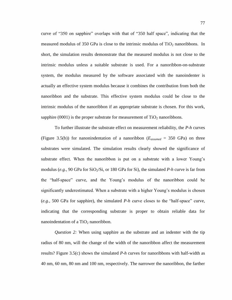
77
curve of ―350 on sapphire‖ overlaps with that of ―350 half space‖, indicating that the
measured modulus of 350 GPa is close to the intrinsic modulus of TiO2 nanoribbons. In
short, the simulation results demonstrate that the measured modulus is not close to the
intrinsic modulus unless a suitable substrate is used. For a nanoribbon-on-substrate
system, the modulus measured by the software associated with the nanoindenter is
actually an effective system modulus because it combines the contribution from both the
nanoribbon and the substrate. This effective system modulus could be close to the
intrinsic modulus of the nanoribbon if an appropriate substrate is chosen. For this work,
sapphire (0001) is the proper substrate for measurement of TiO2 nanoribbons.
To further illustrate the substrate effect on measurement reliability, the P-h curves
(Figure 3.5(b)) for nanonindentation of a nanoribbon (Eassumed = 350 GPa) on three
substrates were simulated. The simulation results clearly showed the significance of
substrate effect. When the nanoribbon is put on a substrate with a lower Young’s
modulus (e.g., 90 GPa for SiO2/Si, or 180 GPa for Si), the simulated P-h curve is far from
the ―half-space‖ curve, and the Young’s modulus of the nanoribbon could be
significantly underestimated. When a substrate with a higher Young’s modulus is chosen
(e.g., 500 GPa for sapphire), the simulated P-h curve closes to the ―half-space‖ curve,
indicating that the corresponding substrate is proper to obtain reliable data for
nanoindentation of a TiO2 nanoribbon.
Question 2: When using sapphire as the substrate and an indenter with the tip
radius of 80 nm, will the change of the width of the nanoribbon affect the measurement
results? Figure 3.5(c) shows the simulated P-h curves for nanoribbons with half-width as
40 nm, 60 nm, 80 nm and 100 nm, respectively. The narrower the nanoribbon, the farther
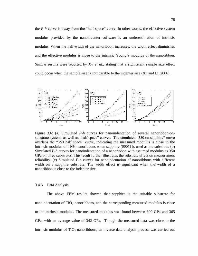
78
the P-h curve is away from the ―half-space‖ curve. In other words, the effective system
modulus provided by the nanoindenter software is an underestimation of intrinsic
modulus. When the half-width of the nanoribbon increases, the width effect diminishes
and the effective modulus is close to the intrinsic Young’s modulus of the nanoribbon.
Similar results were reported by Xu et al., stating that a significant sample size effect
could occur when the sample size is comparable to the indenter size (Xu and Li, 2006).
Figure 3.6: (a) Simulated P-h curves for nanoindentation of several nanoribbon-on-
substrate systems as well as ―half space‖ curves. The simulated ―350 on sapphire‖ curve
overlaps the ―350 half space‖ curve, indicating the measured modulus is close to the
intrinsic modulus of TiO2 nanoribbons when sapphire (0001) is used as the substrate. (b)
Simulated P-h curves for nanoindentation of a nanoribbon with assumed modulus as 350
GPa on three substrates. This result further illustrates the substrate effect on measurement
reliability. (c) Simulated P-h curves for nanoindentation of nanoribbons with different
width on a sapphire substrate. The width effect is significant when the width of a
nanoribbon is close to the indenter size.
3.4.3 Data Analysis
The above FEM results showed that sapphire is the suitable substrate for
nanoindentation of TiO2 nanoribbons, and the corresponding measured modulus is close
to the intrinsic modulus. The measured modulus was found between 300 GPa and 365
GPa, with an average value of 342 GPa. Though the measured data was close to the
intrinsic modulus of TiO2 nanoribbons, an inverse data analysis process was carried out
79
to obtain more accurate intrinsic values. The inverse process, as shown in Figure 3.7, was
as follows: (i) taking the measured modulus m0 as an initial guess of the intrinsic modulus
of nanoribbons m1, simulated the modulus of ―m1 on Sapphire‖, m; (ii) compared m and
m0, then increased or decreased the initial modulus value m1 to a value m so that the
modulus of ―m on sapphire‖ equals to m0; (iii) m1 was the intrinsic modulus of the
nanoribbon. For the nanoribbons with system moduli of 342 GPa, the extracted the
moduli of nanoribbons was 360 GPa.
Figure 3.7: A general data inverse process of extracting the intrinsic modulus of a
nanoribbon from the measured system modulus
Since the exact crystallographic information relating to the indented surfaces is
unknown, it is difficult to make an accurate comparison between our results and the
available Young’s modulus data of bulk rutile TiO2. However, it seems that the obtained
Young’s modulus of TiO2 nanoribbons (i.e., ~360 GPa) is comparable to that of bulk
rutile TiO2 (e.g., E(110)=368.8 GPa, E(001)=385.8 GPa, E(111)=318.9 GPa) (Li and Bradt,

80
1993). The measured hardness is around 15 GPa, which is also comparable to the
hardness of bulk rutile TiO2 (i.e.,13 GPa (Mayo, et al., 1990)).
3.4.4 A General Rule for Studying Young’s Modulus of 1D Nanostructures by
Nanoindentation
The current work demonstrates that the selection of a proper substrate is one key
factor to obtain reliable measurement results of Young’s modulus of 1D nanostructures
by nanoindentation. The measurement from a single nanostructure-on-substrate system
cannot produce reliable results. For example, if we only performed nanoindentation on
TiO2 nanoribbons laid on Si substrates, the obtained modulus of 200 GPa would be a
significant underestimation of intrinsic modulus of TiO2 nanoribbons.
Thus, to study the Young’s modulus of 1D nanostructures by nanoindentation,
experimental work need to be first performed on different nanostructure-on-substrate
systems. For each nanostructure-on-substrate system, by comparing the measured
modulus (En (measured)) with the Young’s modulus of the substrate (Esub), the substrate is
identified as either proper or not. If En(measured) > Esub, the substrate is not proper and the
measured value is an underestimation of intrinsic modulus of the nanostructure. If
En(measured) < Esub, the substrate can be proper. However, the measured value might be
overestimated. As a result, FEM work (such as the aforementioned inverse data analysis
process) needs to be carried out to obtain a more reliable Young’s modulus.
3.5 Conclusions
In summary, both experimental and numerical studies were carried out to
investigate the Young’s modulus of single crystalline rutile TiO2 nanoribbons under
nanoindentation. Three different substrates, including SiO2/Si, Si(100) and

81
sapphire(0001), were used to support nanoribbons. Results show that the receding contact
mechanics is a good approximation when describing the contact between the nanoribbon
and the substrate. In addition, results demonstrate that a suitable substrate is one of the
keys to obtain reliable measurement data of 1D nanostructures. The Young’s modulus of
TiO2 nanoribbons was found to be around 360 GPa, comparable to that of bulk TiO2. The
work done here is a good example, demonstrating that both experimental and numerical
investigations are needed for studying the mechanical properties of 1D nanostructures by
nanoindentation. Otherwise, the Young’s modulus of the nanoribbon could either be
overestimated or underestimated.
To further improve the accuracy of results, there are several issues that need
future consideration. For example, (i) Information related to the indenter tip radius/shape
and nanoribbon width is critical for a quantitative mechanical properties extraction.
Given this information, the intrinsic mechanical properties of the nanoribbon can be
deduced more accurately through the aforementioned inverse process. (ii) Although the
Young’s modulus of the nanoribbon can be deduced from the elastic model of
nanoribbon and substrate, the actual hardness of the nanoribbon should be studied based
on a model including the plastic deformation.

CHAPTER 4: MEASUREMENT OF MECHANICAL PROPERTIES OF ALKALINE
EARTH METAL HEXABORIDE ONE-DIMENSIONAL NANOSTRUCTURES BY
NANOINDENTATION
4.1 Introduction
In Chapter 3, nanoindentation test on TiO2 nanoribbons with width to thickness ratio
about 5 was conducted. A general rule on selecting a proper substrate to support a
nanostructure so that the measured nanostructure-on-substrate system modulus is closed to
the nanostructure’s modulus itself was discussed. Will the rule works for MB6 nanostructures
which have a width to thickness ratio about 1 to 2? This chapter tries to answer the question.
The divalent alkaline earth metal hexaborides MB6 (M=Ca, Sr, Ba) crystallize in a
CsCl-type structure with the cubic symmetry as Pm3m (Adams, 1964). The B6 boron
octahedra are at eight corners of a cube, whereas the metal atom is at the cubic body center
(Adams, 1964). The B6 boron octahedra link to each other by B-B bonds to form a rigid
three-dimensional boron framework (Adams, 1964). As a result, MB6 materials have
properties of low densities, low thermal expansion coefficients, high hardness, high melting
points and good chemical stability (Adams, 1964). They are also promising n-type high
temperature thermoelectric materials because of their rising Seebeck coefficients (absolute
value) and electrical conductivities as temperature increases (Imai, et al., 2001, Takeda, et al.,
2006). Recent advances have shown that low-dimensional materials such as quantum dots,
one-dimensional (1D) nanostructures and thin films provide new opportunities to achieve
enhanced thermoelectric figure-of-merit (Dresselhaus, et al., 2007, Dresselhaus, et al., 1999).

83
Our latest synthesis of single crystalline MB6 1D nanostructures, nanowires, has made the
exploration of their thermoelectric performance possible (Amin, et al., 2009, Xu, et al.,
2004). In addition to the study of thermoelectric properties, understanding the mechanical
behavior of these MB6 1D nanostructure is essential before they can be integrated into
new devices. However, there have been no reports on mechanical properties of MB6 1D
nanostructures. Even for bulk MB6 materials, only scarce data can be found (Grechnev, et
al., 2008, Kosolapova, 1990, Shang, et al., 2007(Wei, et al., 2011), Datta, 1975).
The aim of this chapter is to measure the mechanical properties of 1D MB6
nanostructures using nanoindentation. The measured moduli were quite scattering. Both
experimental observation and numerical simulation demonstrate that the data scattering
was due to several factors such as the width-to-thickness ratio of a nanostructure, the
interaction between a nanostructure and a substrate, and the cross section of a
nanostructure. A smaller nanostructure width-to-thickness ratio, a frictionless receding
interaction and a circular cross section could all lead to a lower measured modulus. To
find out the intrinsic Young’s modulus of a nanostructure, the data inverse process was
used to correct the experimentally measured modulus. The extracted intrinsic modulus of
SrB6, BaB6 and CaB6 1D nanostructures fell within ranges of 300-425, 270-475, and 175-
365 GPa, respectively.
4.2 Experimental Details
Using the methodology described in our previous reports (Amin, et al., 2009, Xu,
et al., 2004), single crystalline MB6 1D nanostructures were synthesized by pyrolysis of
diborane over nickel-coated alkaline earth metal oxide (MO) powders at elevated
temperature and low pressure. The as-synthesized MB6 nanostructures grew on top of

84
MO powders, forming an urchin-like geometry (Amin, et al., 2009). The nanostructures
were transferred to two different substrates: silicon(100) and sapphire(0001). The width
and length of each substrate were about 0.5 cm and 1 cm, respectively. Two different
methods were used for transferring nanostructures. (i) ―Wet transfer‖ method. The
nanostructures were scraped off from powders and dispersed uniformly into absolute
alcohol by ultrasonication. A few drops of alcohol solution were deposited onto
substrates which were subsequently blow dried by compressed nitrogen. (ii) ―Dry transfer‖
method. Bare substrates were slid against powders for direct transferring of
nanostructures. The substrates were then gently washed by stream alcohol and blow dried.
Although it was confirmed later that the testing results were not affected by sample
transfer methods, the ―dry‖ one is preferred because it can transfer more nanostructures to
a substrate. Optical microscopy (Olympus BX51 research-level microscope; dark field)
was used to locate individual MB6 nanostructures on substrates. The nanostructures were
then studied by Atomic Force Microscopy (AFM; Dimension 3100, Veeco Instruments
Inc.) to examine their geometry and obtain dimensional information. To avoid the sliding
problem during nanoindentation, nanostructures with rectangular cross sections are
preferred, as discussed in Chapter 3. Experimental results presented in Section 4.4.1 are
all from nanostructures with well-defined rectangular cross sections. Both selected SrB6
and BaB6 nanostructures had a width of ~ 100-200 nm. However, the average thickness
of SrB6 nanostructures was ~ 100 nm and that of BaB6 nanostructures was ~ 160 nm. The
CaB6 nanostructures were relatively small. Most of them had both thickness and width
less than 100 nm. A few CaB6 nanostructures were found to have circular cross sections.
85
Sliding phenomenon was observed for these CaB6 nanostructures whose corresponding
experimental results were discarded without further analysis.
All nanoindentation tests were conducted in the continuous-stiffness-
measurement (CSM) mode of an Agilent Technology G200 nanoindenter, which is
equipped with the nanoVision Scanning Force Microscopy (SFM) option and the
Dynamic Contact Module (DCM) option. The indentation-loading scheme was similar to
those described in Chapter 3. For general measurements of modulus and hardness, the
maximum indenter displacement was set to 20 nm for SrB6 and BaB6 nanostructures, and
15 nm for CaB6 nanostructures. For fracture behavior studies, the maximum indenter
displacement was set to 30 nm for SrB6 and BaB6, and 20 nm for CaB6. For each material,
at least ten nanostructures on sapphire substrates were tested. For each nanostructure,
multiple indentation tests were performed along its preferred growth direction. The
residual indentations (1-2 nm) were checked by the nanoVision SFM. Data analyses
were only done on those nanostructures with well-centered residual indentations.
4.3 Modeling of Nanoindentation Experiment
4.3.1 A Better Way to Simulate Nanoindenter
For depth-sensing nanoindentation, with the help of an experimentally obtained
indentation load - displacement (P-h) curve, the reduced elastic modulus Er of a tested
material can be determined based on the Sneddon theory (Oliver and Pharr, 1992)
Adh
dpEr
1
2
(4-1)
where P is the load applied on the indenter, h is the indenter displacement into the surface
of a tested material, dP/dh is the slope of the P-h curve upon unloading and A is the

86
projected contact area between the indenter and the tested material. Given Er, Young’s
modulus for the tested material (E) can be obtained from the following equation with
minor algebraic manipulation
E
v
E
v
E i
i
r
22111
(4-2)
where v is Poisson’s ratio of tested material, and Ei and vi are elastic properties of the
indenter.
By observing the above two equations, the projected contact area A is obviously
one important parameter need to be carefully analyzed. For example, an underestimation
of A could lead to an over-determination of E. Thus, when performing numerical
simulation, the shape of an indenter needs to be properly modeled to assure that the
simulated values of A is close to the experimental data.
The solid line in Figure 4.1 is a plot of A vs. hc (contact depth) obtained from our
tip geometry calibration experiment. The line can be mathematically represented by the
following functional form
cc hhA 22
1 (4-3)
where α1 = 24.427 and α2 = 500. In Chapter 3, a conical indenter with a tip apex of R =
/2π were used to mimic the Berkovich indenter. The corresponding A-hc curve is
calculated and presented as the dashed line in Figure 4.1. The curve is obviously not
overlapped with the experimental A-hc curve, indicating the Berkovich indenter in our
experiment should not be simply modeled as a conical one. Inspired by the work done by
the Pharr’s group (Bei, et al., 2005), a rigid axially symmetric indenter of a revolution
spline is used to simulate the Berkovich indenter. The inset in Figure 4.1 illustrates the
2
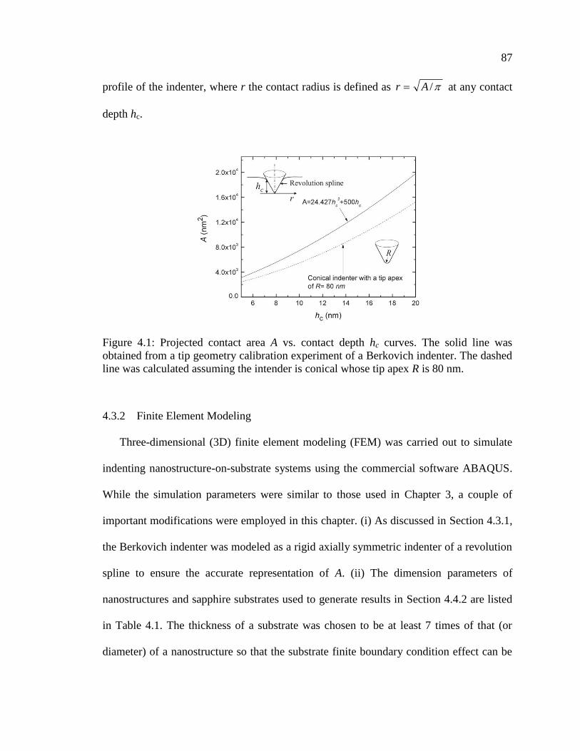
87
profile of the indenter, where r the contact radius is defined as /Ar at any contact
depth hc.
Figure 4.1: Projected contact area A vs. contact depth hc curves. The solid line was
obtained from a tip geometry calibration experiment of a Berkovich indenter. The dashed
line was calculated assuming the intender is conical whose tip apex R is 80 nm.
4.3.2 Finite Element Modeling
Three-dimensional (3D) finite element modeling (FEM) was carried out to simulate
indenting nanostructure-on-substrate systems using the commercial software ABAQUS.
While the simulation parameters were similar to those used in Chapter 3, a couple of
important modifications were employed in this chapter. (i) As discussed in Section 4.3.1,
the Berkovich indenter was modeled as a rigid axially symmetric indenter of a revolution
spline to ensure the accurate representation of A. (ii) The dimension parameters of
nanostructures and sapphire substrates used to generate results in Section 4.4.2 are listed
in Table 4.1. The thickness of a substrate was chosen to be at least 7 times of that (or
diameter) of a nanostructure so that the substrate finite boundary condition effect can be
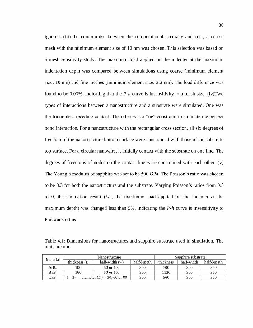
88
ignored. (iii) To compromise between the computational accuracy and cost, a coarse
mesh with the minimum element size of 10 nm was chosen. This selection was based on
a mesh sensitivity study. The maximum load applied on the indenter at the maximum
indentation depth was compared between simulations using coarse (minimum element
size: 10 nm) and fine meshes (minimum element size: 3.2 nm). The load difference was
found to be 0.03%, indicating that the P-h curve is insensitivity to a mesh size. (iv)Two
types of interactions between a nanostructure and a substrate were simulated. One was
the frictionless receding contact. The other was a ―tie‖ constraint to simulate the perfect
bond interaction. For a nanostructure with the rectangular cross section, all six degrees of
freedom of the nanostructure bottom surface were constrained with those of the substrate
top surface. For a circular nanowire, it initially contact with the substrate on one line. The
degrees of freedoms of nodes on the contact line were constrained with each other. (v)
The Young’s modulus of sapphire was set to be 500 GPa. The Poisson’s ratio was chosen
to be 0.3 for both the nanostructure and the substrate. Varying Poisson’s ratios from 0.3
to 0, the simulation result (i.e., the maximum load applied on the indenter at the
maximum depth) was changed less than 5%, indicating the P-h curve is insensitivity to
Poisson’s ratios.
Table 4.1: Dimensions for nanostructures and sapphire substrate used in simulation. The
units are nm.
Material Nanostructure Sapphire substrate
thickness (t) half-width (w) half-length thickness half-width half-length
SrB6 100 50 or 100 300 700 300 300
BaB6 160 50 or 100 300 1120 300 300
CaB6 t = 2w = diameter (D) = 30, 60 or 80 300 560 300 300

89
4.4 Results and Discussion
4.4.1 Experimental Results
Preliminary tests were done on both nanostructure-on-silicon and nanostructure-on-
sapphire systems. Sliding phenomenon was observed when indenting individual
nanostructures on silicon, producing unreliable testing results. Thus, sapphire was chosen
as the proper substrate to support MB6 nanostructures for later nanoindentation tests.
Since similar experimental phenomena were observed for nanoindenting of MB6
nanostructure-on-sapphire systems, only results for SrB6 nanostructures are qualitatively
described here. Figure 4.2(a) is a representative AFM image, showing a part of a SrB6
nanostructure lying on sapphire. The inset presents the result of section analysis,
revealing the nanostructure has a rectangular cross section and its thickness and width are
~ 108 nm and 100 nm, respectively. Figure 4.2(b) shows a typical P-h curve of a
deformation process of the SrB6 nanostructure-on-sapphire system. The elastic-like
deformation behavior is observed. Figure 4.2(c) and (d) present the measured Young’s
modulus and ―nanohardness‖, respectively. These data were automatically produced by
the software associated with the nanoindenter, by which they were calculated based on
the Oliver-Pharr method (Oliver and Pharr, 1992). The measured modulus seems to be
constant when the indenter displacement is larger than 8 nm. The data variation at the
initial stage could be due to the indenter tip rounding, surface roughness and machine
resolution (Chen, et al., 2005). Generally, the ―nanohardness‖ (H) is defined as the peak
load (Pmax) applied during a nanoindentation divided by the projected contact area (A) of
the indentation (Oliver and Pharr, 1992). It can also be considered as mean contact
pressure (Pm) for a material under an elastic deformation. Depending on the indenter tip

90
geometry, various expressions of ―nanohardness‖ with respect to the indenter
displacement for elastic deformation was derived based on contact mechanics (Maugis,
2000). For a spherical indenter, the ―nanohardness‖ is proportional to the square root of
the indenter displacement (i.e., hH ). For a conical indenter, the ―nanohardness‖ is
independent of the indenter displacement. For a flat punch, the ―nanohardness‖ is directly
proportional to the indenter displacement (i.e., hH ). Carefully analyzing Figure
4.2(d), one can find that the ―nanohardness‖ increases with the indenter displacement in
an asymptotic manner (i.e., hH ~ , 0.5α1), which indicates that the geometry of the
indenter tip in our experiments is neither spherical nor conical indenter nor flat punch.
This observation is consistent with the result obtained by analyzing the projected contact
area A, as discussed in Section 4.3.1.
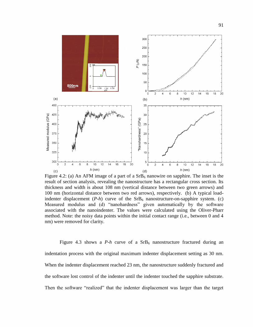
91
Figure 4.2: (a) An AFM image of a part of a SrB6 nanowire on sapphire. The inset is the
result of section analysis, revealing the nanostructure has a rectangular cross section. Its
thickness and width is about 108 nm (vertical distance between two green arrows) and
100 nm (horizontal distance between two red arrows), respectively. (b) A typical load-
indenter displacement (P-h) curve of the SrB6 nanostructure-on-sapphire system. (c)
Measured modulus and (d) ―nanohardness‖ given automatically by the software
associated with the nanoindenter. The values were calculated using the Oliver-Pharr
method. Note: the noisy data points within the initial contact range (i.e., between 0 and 4
nm) were removed for clarity.
Figure 4.3 shows a P-h curve of a SrB6 nanostructure fractured during an
indentation process with the original maximum indenter displacement setting as 30 nm.
When the indenter displacement reached 23 nm, the nanostructure suddenly fractured and
the software lost control of the indenter until the indenter touched the sapphire substrate.
Then the software ―realized‖ that the indenter displacement was larger than the target

92
displacement and started to unload. Cracks might initiate when the indenter displacement
was close to 23 nm, follow by a quick propagation and catastrophic fracture of the
nanostructure. For total nine MB6 nanostructures subjected to fracture behavior studies,
similar P-h curves as shown in Figure 4.3 were observed. SrB6 and BaB6 nanostructures
typically fractured when the indenter displacement was around 25 nm, whereas CaB6
nanostructures failed when the indenter displacement was around 19 nm. The above
indenter displacement at fracture is typically less than 30% of the thickness of a
nanostructure. Each nanostructure broke into two parts, which was confirmed by the
follow-up OM or AFM examination. This observed catastrophic fracture is different from
other indentation-induced failure behavior reported for SnO2 nanobelts (Mao, et al., 2003)
and ZnS nanobelts (Li, et al., 2005, Yang, et al., 2005) from which only crack initiation
at the edges of the residual indentation or limited amount of crack propagation was found
even the indentation displacement is about 40% of the thickness of the nanostructure.
This study of fracture processes demonstrates the brittle nature of as-synthesized MB6 1D
nanostructures.
Figure 4.3: A P-h curve of a SrB6 nanostructure experiencing sudden fracture during an
indentation process

93
As mentioned in Section 4.2, multiple indentation tests were performed along the
preferred growth direction of each tested 1D nanostructure. Most of time, two to four
tests would be found valid (i.e., a test produces a well-centered residual indentation),
generating useful experimental data. As shown in Figure 4.4, for each tested
nanostructure, the measured moduli are presented as a symbol against a vertical line. The
symbol represents the mean value, whereas the ends of the vertical line (terminated by
horizontal bars) indicate the minimum and maximum values. Analyzing experimental
results presented in Figure 4.4, three important issues can be identified. (i) The measured
moduli for MB6 nanostructure-on-sapphire systems are scattering, and generally lower
than the Young’s modulus of MB6 bulk materials (see dashed lines in Figure 4.4 and
detailed data in Table 4.2). (ii) Special attention was paid to those data points (cf. SrB6 at
103 and 117 nm thickness in Figure 4.4(b) and BaB6 at 127 and 137 nm thickness in
Figure 4.4(c)) associated with longer vertical lines (i.e., have larger difference between
the maximum and minimum values). It was found that these data were obtained from
tapered nanostructures. Figure 4.5(a) is an AFM image of a typical tapered SrB6
nanostructure. Two areas subjected to nanoindentation tests are outlined by white frames.
The two areas are 2 m apart. They are further enlarged in Figure 4.5(b) and (c) which
were images produced by nanoVision SFM. Each image represents a 0.4 m 0.4 m
area, showing a part of the tested nanostructure. The black portion corresponds to the flat
top of the nanostructure, from which the width of the nanowire can be determined. The
width of the part of the nanostructure shown in Figure 4.5(b) is about 150 nm, while that
in Figure 4.5(c) is about 200 nm. The corresponding measured modulus in these two
areas is (b) 340 GPa and (c) 380 GPa, respectively. This result indicates that the

94
measured modulus is sensitive to the width of a nanostructure. (iii) Further examination
of those data (−◊−) with lower measured modulus shown in Figure 4.4(b) and (c)
revealed that the associated tested nanostructures were ~ 25-50% narrower than other
tested nanostructures. For example, in Figure 4.4(b), the nanostructure of 108 nm in
thickness was only 100 nm in width, and the nanostructure of 113 nm in thickness was
about 150 nm in width. Other tested SrB6 nanostructures were about 200 nm in width.
This result again demonstrated that the measured modulus of a nanostructure-on-substrate
system is sensitive to the width of the nanostructure. The narrower the nanostructure is,
the lower the measured modulus can be.

95
Figure 4.4: Measured moduli of (a) the CaB6 nanostructure-on-sapphire system, (b) the
SrB6 nanostructure-on-sapphire system, and (c) the BaB6 nanostructure-on-sapphire
system.

96
Table 4.2: Experimental and theoretical values of elastic constants of some hexaborides
Materials C11
(GPa)
C44
(GPa)
C12
(GPa)
Bexp
(GPa)
Btheory
(GPa)
E
(GPa)
CaB6 423a 43
a 5.6
a − 145
a,159
b,139
c 423
a,467
d, 365-399
e
SrB6 − − − − 160b,141
c 415
d
BaB6 − − − − 162b,139
c 393
d
LaB6 463b 89
b 45
b 184
b 185
b 488
d,439
f
B=(C11+2C12)/3 is the bulk modulus. a Theoretical data at 0 K(Wei, et al., 2011)
b Experimental and theoretical data at 78K (Grechnev, et al., 2008)
c Theoretical data at 298K (Shang, et al., 2007)
d Calculated or experimental (hot-pressed) data (Kosolapova, 1990)
f Experimental (hot-pressed) data (Dutta, 1975)
f Single crystal nanostructure (Zhang, et al., 2008)
Figure 4.5: (a) AFM image of a tapered SrB6 nanostructure on sapphire. (b) Zoom-in
SFM image of an indented section of the nanostructure. The white triangle frame outlines
the residual indentation. (c) Zoom-in SFM image of a section before indentation. The
width of the two sections is obviously different.

97
4.4.2 Numerical Simulation
The aforementioned experimental results unambiguously demonstrate the
scattering of measured moduli could be due to several factors such as the width-to-
thickness ratio of a nanostructure with a rectangular cross section. To further study the
effects of these factors, FEM-based simulation of nanoindentation on nanostructure-on-
substrate systems were carried out. The dimensions listed in Table 4.1 were used for
simulation. Due to the similarity of simulation results obtained from three MB6
nanomaterials, data presented here is typically for SrB6 unless noted otherwise.
Factor 1: the width of a nanostructure with a rectangular cross section. Figure
4.6(a) shows the simulated P-h curves of nanostructures with different width. The legend
―w=100 400 on 500 perfect bond‖ represents a nanostructure with a half-width w of 100
nm and a Young’s modulus of 400 GPa is perfectly bonded to a sapphire substrate with a
Young’s modulus of 500 GPa. ―400 half space‖ denotes a homogeneous half space with a
modulus of 400 GPa. The P-h curve of ―w=100 400 on 500 perfect bond‖ is steeper than
that of ―400 half space‖ (note: comparison was done on the slope dP/dh upon unloading
of each curve), indicating that the measured modulus of this nanostructure-on-sapphire
system would be higher than the intrinsic nanostructure modulus: 400 GPa. When the
half-width of the nanostructure is reduced to 50 nm, the corresponding P-h curve of
―w=50 400 on 500 perfect bond‖ is now less steep than that of ―400 half space‖, implying
the measured modulus will be lower than 400 GPa. These simulation results are
consistent with aforementioned experimental findings. They clearly demonstrate that the
measured modulus is not the intrinsic nanostructure modulus and can be affected by the
width of a nanostructure. The measured modulus decreases as the width of a

98
nanostructure decreases. This conclusion is also valid when the interaction between a
nanostructure and a substrate becomes frictionless receding contact.
The width effect is qualitatively illustrated in the inset of Figure 4.6(a).
Considering a nanostructure with an infinite width and finite thickness t laid on a
substrate, the interaction radius between the nanostructure and the substrate is a2 during
an indentation of a certain indentation depth-to-nanostructure thickness (h/t) ratio. When
the width of the nanostructure becomes finite, two situations exist. (i) The half-width w of
the nanostructure is larger than a2. Indentation on this type of nanostructures is same as
indentation on infinite wide nanostructures. In other words, no width effect exists. (ii)
The half-width of the nanostructure is smaller than a2. Indentation of these narrower
nanostructures deviates from that of infinite wide nanostructures. The deviation increases
as the half-width of the nanostructure decreases. One implication is that the rule on
selecting a proper substrate, proposed in Chapter 3, is invalid for a nanostructure with a
half-width less than a2. Detailed studies of the width effect have been carried out and the
results will be discussed in Chapter 5. It was found that analytical solution can be used to
study nanoindenting of wider nanostructures whereas FEM-based modeling is needed for
narrower nanostructures.
Factor 2: the interaction between a nanostructure and a substrate. As shown in
Figure 4.6(b), the P-h curve of ―w=100 400 on 500 perfect bond‖ is steeper than that of
―w=100 400 on 500 receding‖. This result indicates a perfect bond interaction between a
nanostructure and a substrate could lead to a higher measured modulus. Based on the
inverse data analysis method introduced in Chapter 3, it can also be derived that a perfect
bond interaction could lead to a corrected modulus at the lower bound.

99
Factor 3: the cross section of a nanostructure. As mentioned in Section 4.2, a few
CaB6 nanostructures were found to have circular cross sections. Although
nanoindentation on these circular nanostructures not produces reliable testing results due
to the sliding problem, it is natural to ask ourselves a question: ―Is there any effect of
cross section on measured moduli if no sliding happens?‖ Simulations were done on
nanostructures with two different cross sections: square and circular. The square has an
edge length of 80 nm, whereas the circle has a diameter of 80 nm. Receding contact
interaction was considered between the nanostructure (assumed modulus: 300 GPa) and
the substrate (assumed modulus: 500 GPa). As shown in Figure 4.6(c), the simulated P-h
curve for a nanostructure with a circular cross section is less steep than that with a square
cross section, and also the ―300 half space‖ curve. In other words, a circular cross section
could result in a lower measured system modulus. This result is qualitatively consistent
with the previous work (Shu et al., 2009), in which they concluded that for a
nanostructure with a circular cross section, the measured moduli could be 50% lower than
the intrinsic modulus of the nanostructure.
Factor 4: the diameter of a nanostructure with a circular cross section. Most of
the tested CaB6 nanostructures have circular cross sections. How does the diameter (D) of
a nanostructure affect measured moduli? Our simulation results revealed that the
diameter effect is tangled with the substrate effect. A smaller diameter indicates a smaller
contact width (which is the short axis of the contact ellipse) between a nanostructure and
a substrate, which shall result in a lower measured modulus. However, a smaller diameter
also means that the nanostructure is shallow and the measured modulus is prone to be
affected by the underlining substrate. Several P-h curves of nanoindenting nanostructures
100
of different diameters are shown in Figure 4.6(d). The assumed modulus of the
nanostructure is 400 GPa, whereas that of the substrate is 500 GPa. The P-h curve of a
nanostructure with a diameter of 60 nm is less steep than that of 80 nm, implying the
measured modulus decreases as diameter decreases. However, when the diameter is
further decreased to 30 nm, the corresponding P-h curve becomes steeper, indicating that
a higher measured modulus would be obtained. The inset in Figure 4.6(d) shows the load
at the maximum indentation depth: 15 nm for three different diameters, from which no
linear relation between P and D can be found. These results demonstrate that the
reduction of diameter does not always lead to a lower measured modulus. When the
diameter is smaller than a certain value, substrate effect could show out, resulting in a
higher measured modulus.
Factor 5: the oxide layer surrounding a nanostructure. Each as-synthesized
nanostructure has a core-sheath geometry (Amin, et al., 2009, Xu, et al., 2004). The core
is crystalline MB6. The sheath is amorphous oxide whose thickness can be up to 4 nm.
Will this oxide layer affect the P-h curve of a nanostructure-on-substrate system when the
maximum indentation depth is 20 nm? To answer this question, simulation was
conducted on a sandwich nanostructure combining of a thick core and two thin oxide
surface layers. The thickness of the core and each oxide layer is 92 nm and 4 nm,
respectively. Simulation was also done on a ―pure nanostructure‖ whose thickness is 100
nm. The half-width of both nanostructures is 100 nm. The core and oxide layer modulus
were assumed to be 400 and 150 GPa respectively. Both perfect bond and receding
contact interaction were considered, and similar results were obtained. As revealed in
Figure 4.6(e), the difference between the slope dP/dh upon unloading for the simulated

101
P-h curves of a ―pure nanostructure‖ and a ―sandwich nanostructure‖ is less than 3%. In
other words, the oxide layer has minor effects on nanoindentation tests. This is due to the
factor that the effective flexural rigidity of the sandwich nanostructure is close to that of a
pure material (Chen, et al., 2006).
Figure 4.6: Simulated P-h curves for studying of various factors affecting measured
moduli. These factors include (a) the width of a nanostructure with a rectangular cross
section, (b) the interaction between a nanostructure and a substrate, (c) the cross section
of a nanostructure, (d) the diameter of a nanostructure with a circular cross section and (e)
the oxide layer on a nanostructure.

102
4.5 Data Analysis
The aforementioned experimental results and numerical simulation have clearly
revealed that the measured modulus generally cannot represent the intrinsic Young’s
modulus of a nanostructure. In addition, the measured modulus can be easily affected by
several factors. A narrower nanostructure, a frictionless receding contact and a circular
cross section can all generally result in a lower measured modulus. To obtain a reliable
value of Young’s modulus of a nanostructure, the data inverse method proposed in
Chapter 3 is used to correct the measured modulus.
As outlined in the introduction section, correction needs to be done for both the
perfect bond and the frictionless receding interaction mechanisms. The perfect bond
interaction leads to a corrected modulus at the lower bound, whereas the frictionless
receding contact interaction yields a modulus at the upper bound. The intrinsic modulus
shall fall between the two bounds. It is possible that the value is more towards to the
lower bound since ultrasonication tests revealed relatively strong adhesion between the
nanostructures and the substrate. Table 4.3 shows the data analysis results for a couple of
tested 1D nanostructures. For each material, data correction was done on two
nanostructures. The two nanostructures were chosen because their width-to-thickness
ratio and measured modulus are the maximum and minimum among all tested
nanostructure. As shown in Table 4.3, it seems that the intrinsic modulus of MB6
nanostructures is dependent on the width-to thickness ratio. The larger the width-to-
thickness ratio is, the higher the intrinsic modulus can be.

103
Table 4.3: Measured nanostructure-on-substrate system moduli and corrected
nanostructure moduli for two different nanostructure-substrate contact interactions.
Material
Thickness
Width
(nm nm)
Width-to-
thickness
ratio
Measured
Modulus
(GPa)
Corrected Modulus (GPa)
Receding Perfect Bond
CaB6 66 95 1.43 350 365 300
78 84 1.08 205 210 175
SrB6 86 200 2.33 413 425 325
108 100 0.93 260 370 300
BaB6 143 183 1.28 360 475 400
129 129 1.00 273 330 270
Mechanical properties of single crystals are commonly anisotropic. Therefore, it is
important to correlate the measured properties with crystallographic information. The
surfaces of as-synthesized MB6 1D nanostructures are (100) planes (Futamoto, et al.,
1979, Xin, et al., 2011, Zhang, et al., 2008). In other words, the nanoindentation loading
direction is perpendicular to (100) planes. MB6 materials have a cubic symmetry,
indicating only three elastic constants are needed to estimate the crystallographic
direction-dependent Young’s moduli. Unfortunately, rare experimental and theoretical
data about the elastic constants of MB6 can be found after extensive literature search
(Table 4.2). The unavailability of reliable information on elastic constants prevented us to
estimate effective modulus for indenting against MB6 nanostructures, study their
anisotropic ratio, and make detailed comparison between experimental data and
theoretical values.
4.6 Conclusions
In summary, Young’s moduli of alkaline-earth metal hexaboride 1D
nanostructures were studied by nanoindentation. The experimentally measured moduli
were scattering. Systematic experimental investigation and numerical simulation

104
revealed that the data scattering can be caused by several factors such as the width of a
nanostructure with a rectangular cross section and the interaction between a nanostructure
and a substrate. A narrower nanostructure, a frictionless receding interaction, a circular
cross section can all lead to a lower measured modulus. To obtain a reliable intrinsic
modulus of a nanostructure, a FEM-based inverse data processing method was used. The
modulus extracted based on the receding contact and the perfect bond interaction gives
upper and lower bound values of the intrinsic modulus of the nanostructure, respectively.
The intrinsic modulus of MB6 nanostructures is dependent on the width-to thickness ratio.
The larger the width-to-thickness ratio is, the higher the intrinsic modulus can be.

CHAPTER 5: NANOINDENTATION-THEORETICAL MODELING
5.1 Introduction
In Chapter 3 and 4, nanoindentation was conducted on TiO2 nanoribbons and
MB6 nanostructures. The measured nanostructure-on-substrate system modulus could be
significantly different from modulus of the nanostructure itself. This chapter revisited the
semi-analytical solution of nanoindentation on a nanostructure-on-substrate system. A
Mathematica program was developed to calculate system modulus under nanoindentation
using a conical, spherical indenter or a general indenter with a given area function. Two
different interactions between a nanostructure and a substrate, i.e. perfect bond and
frictionless contact, were considered in the semi-analytical solution.
5.2 Chebyshev Polynomial
Chebyshev polynomials have been used to solve integral equations. They will be
used to solve the Fredholm equation in Section 5.4. The properties of the polynomials,
expression a function with the polynomials, derivative and integral of the function are
reviewed in this section.
The mth
Chebyshev polynomial has m distinct roots on [-1,1], where the roots
are:
The Chebyshev polynomials are discrete orthogonal. In other words, for all , the
following relationship holds true (Chen, et al., 2005),

106
(5-1)
To approximate a function defined on [-1,1] using the first m=n+1 Chebyshev
polynomials, the j weights needs to be given. To solve the weights,
(5-2)
Multiply both sides by , getting
Sum across k=1,2,…, m, getting
According to the discrete orthogonality property, the terms on the left side where
are equal to zero. Thus
Hence,
A continuous and bounded variation function can be approximated in the interval [-
1, 1] by the formula

107
The integral can be computed as
5.3 Formulation of the Indentation on Nanostructures (2w/t)-on-Substrate System
For a nanostructure with width to thickness ratio approaches infinite, the
nanostructure-on-substrate system is similar to a thin film-on-substrate system, which
was solved by Yu et al (Yu, et al., 1990). In their approach, two pairs of harmonic
Papkovich-Neuber functions were used to formulate the thin film and the substrate
respectively. Substituting the two functions into boundary conditions and continuity
conditions between the nanostructure and the substrate, nanoindentation on
nanostructure-on-substrate system was transformed into a Fredholm integral equation.
The kernel of the Fredholm integral equation was complicated. In this Chapter, Airy’s
stress function was used to formulate the thin film and the substrate respectively so that
the kernel of the Fredholm integral equation was greatly simplified. Equations to obtain
P–h curves of nanoindentation on a nanostructure-on-substrate system and system
modulus were presented. Interface stress between the nanostructure and substrate was
also included to justify the applicable range for 2w/t assumption.
Here, three rigid axisymmetric indenters indenting on a nanostructure with elastic
constant 1 1, -on-substrate with elastic constant
2 2, system were considered. The
indenters were chosen because they could represent an actual indenter used in an
experiment. A cylindrical coordinate system, as shown in Figure 5.1 was used, where z
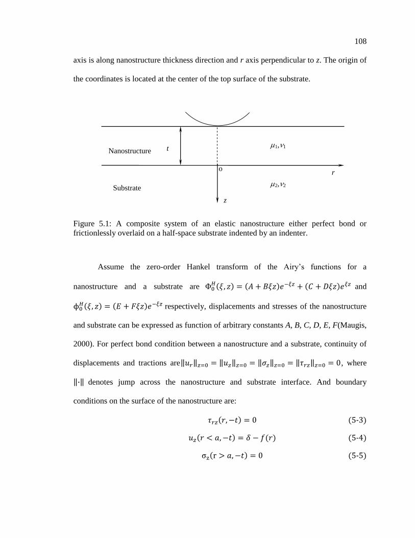
108
axis is along nanostructure thickness direction and r axis perpendicular to z. The origin of
the coordinates is located at the center of the top surface of the substrate.
Figure 5.1: A composite system of an elastic nanostructure either perfect bond or
frictionlessly overlaid on a half-space substrate indented by an indenter.
Assume the zero-order Hankel transform of the Airy’s functions for a
nanostructure and a substrate are and
respectively, displacements and stresses of the nanostructure
and substrate can be expressed as function of arbitrary constants A, B, C, D, E, F(Maugis,
2000). For perfect bond condition between a nanostructure and a substrate, continuity of
displacements and tractions are , where
denotes jump across the nanostructure and substrate interface. And boundary
conditions on the surface of the nanostructure are:
(5-3)
(5-4)
(5-5)
t
Substrate
r
Nanostructure
z
1,1
2,2
o

109
where is the profile of an indenter. cot)( rrf , ))/1(1()( 2/122 RrRrf and
)2/()4()( 12
1222 rrf , ar 0 for a conical, a spherical indenter
and an axial symmetry general indenter with an area function cc hhA 2
2
1
respectively. is the half-angle of a conical indenter and R is the radius of the spherical
indenter. 1 and 2 are experimentally calibrated indenter parameter.
A, B, C, D and E were solved in terms of F from the continuity condition and
boundary condition (5-3). And displacement and stress boundary conditions (5-4) and (5-
5) were expressed as follows:
(5-6)
(5-7)
Where,
))(1)(21()2exp()1)(1(
))exp()()exp())(1(4)3exp()1(()(
12121
2
1
2
2212
2
2
2
tt
ttttFM
2
2
2
1
2
21212
22
2
2
1
2
2212
2
2
)2exp())(2))(1()(4()4exp()1(
)2exp())(1(4)4exp()1(1)(
ttt
tttg
The above formulations used the generalized Dundurs parameters
Assuming dsssgMa
0
)cos()())(1()( ,
and
a
x
the above two equations were solved if satisfied the following Fredholm integral
equation:
(5-8)
110
(5-9)
The kernel of the integral equation is dxgxG 0 )cos()()( .
0 ( )F depends on the
shape of a indenter. 0( ) 1F for a conical indenter and
2 2
0 ( ) 1F for a spherical
indenter while indentation depth is less than 0.2 t (Yu, et al., 1990). For the
aforementioned general indenter, dssa
sa
h
aF
2
0 222
1
2
2
0
)sin(4
sin21)(
.
Likewise, for indentation on a nanostructure frictionlessly in contact with a
substrate, the nanoindentation problem satisfies the same Fredholm integral equation (5-8)
and (5-9) except for a different kernel
The Fredholm integral equations ((5-8) and (5-9)) were solved numerically using
the Elgendi’s method (El-gendi, 1969). The detailed procedures were as follows: (i)
Approximating ( )H with first N+1 Chebyshev polynomial (N≥5), as discussed in
Section 5.2, and substituting it into equations (5-8) and (5-9), N+2 linear algebraic
equations with N+2 unknowns (in Table 5.1) were obtained at a given a/t. Instead of
guessing a value for j (j = c, s) and solving )( iH from equation (5-8) and iterating the
procedure until equation (5-9) was satisfied, as suggested in reference (Yu, et al., 1990),
all the unknowns were solved directly by solving (5-8) and (5-9) together by a direct
matrix inversion. The computation time was greatly minimized by using the scheme
compared to the iterative one. For a conical and spherical indenter, j (j = c, s) was
deliberately chosen as an unknown. Once the linear equations were solved for a a/t
through the direct matrix inversion using MATHEMATICA 5.1, ah was calculated from
aj and the corresponding h, t given in Table 5.1. For a general indenter, ht / was

111
chosen as an unknown and solved instead. (ii) P was expressed in terms of unknowns, as
listed in Table 5.1. System modulus was defined as aSM syssys 2/ , whereas
nanostructure modulus was defined as haSM 2/11 . )/(/ 11 SSMM jsyssys was derived
from the definition of the two modulus. where stiffness Sj (j = sys and 1) is the derivation
of P with respect to h, which was numerically determined using a central difference
scheme )21/()(21
hhPPhhhh
, in which 1h and 2h were small deviation
from h. For indentations with a conical or a spherical indenter, the numerically
determined stiffness of indenting a half-space was carefully compared with the analytical
solutions. The closeness of the two values gives confidence of using the central
difference scheme to determine stiffness.
For a conical and a spherical indenter, all relevant information can be assembled
in a spreadsheet (Han, et al., 2006) and 1/ MM sys can be readily calculated at any h. For
the general indenter, the calculation was conducted in a different way and results were
organized in a format shown in Table 5.2. The first four columns are a/t, load P, h and
stiffness of a nanostructure-on-substrate system. The fifth column is a’h/t for a half-space
made of the nanostructure, which is same as first column. The sixth and seventh columns
are corresponding load and displacement into the nanostructure/system. Note that column
six and seven corresponding to a different displacement into surface as listed in column
three. The eighth and ninth columns list the interpolated load and ah/t at a given
indentation depth h so that 1/ MM sys can be calculated at that depth. Stiffness and
1/ MM sys were then calculated and listed in the following two columns.
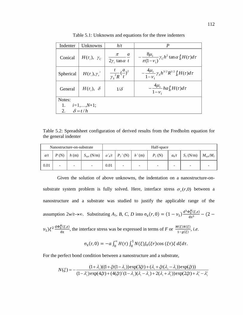
112
Table 5.1: Unknowns and equations for the three indenters
Indenter Unknowns h/t P
Conical CiH ),( t
a
C
tan2
1
0
2
1
1 )(tan)1(
8
dHhC
Spherical 2
),(Si
H 2
2)(
t
a
R
t
S
1
0
2/12/3
1
1 )(1
4
dHRhS
General ),( iH 1/
1
0
1
1 )(1
4
dHha
Notes:
1. i=1,…,N+1;
2. ht /
Table 5.2: Spreadsheet configuration of derived results from the Fredholm equation for
the general indenter
Nanostructure-on-substrate Half-space
a/t P (N) h (m) Ssys (N/m) a’h/t P1’ (N) h’ (m) P1 (N) ah/t S1 (N/m) Msys/M1
0.01 - - - 0.01 - - - - - -
Given the solution of above unknowns, the indentation on a nanostructure-on-
substrate system problem is fully solved. Here, interface stress )0,(rz between a
nanostructure and a substrate was studied to justify the applicable range of the
assumption 2w/t. Substituting A1, B, C, D into
, the interface stress was be expressed in terms of F or
, i.e.
.
For the perfect bond condition between a nanostructure and a substrate,
2
2
2
1
2
21212
22
2
12121
)2exp())(2))(1()(4()4exp()1(
))exp())(()3exp())1(1)((1()(
ttt
ttttN

113
And for frictionless contact condition between a nanostructure and a substrate,
1111
2
1
)2exp()1)1(2)1()(2()4exp(
)exp())1)(2exp(1)(1()(
tttt
ttttN
5.4 Numerical Observations
Assuming both nanostructure and substrate are elastic, 1/sysM M vs. th / for a
perfect bond and a frictionless contact between a nanostructure and a substrate were
calculated and shown in Figure 5.2(for a conical indenter) and Figure 5.3 (for a spherical
indenter) respectively. The range of a/t studied here was from 0 to 1 with increments of
0.01. The Modulus mismatch between a nanostructure and a substrate (1) was from -0.5
to 0.5 with a step size of 0.1. Assuming the nanostructure and substrate have same
Poisson’s ratio 0.3, the relationship between the Dundurs is given by 2 = 1/3.5. Note
that all calculations for a spherical indenter listed in Figure 5.3 were based on an
assumption that the indentation depth was small, i.e. indentation depth is less than 0.2t.
Some findings were listed as follows:
1. Nanostructure and substrate contact effect. For both contact conditions
between a nanostructure and a substrate, system modulus is different from nanostructure
modulus (Msys/M1 1) for a large modulus mismatch between a nanostructure and a
substrate 1 and a relative indentation depth larger than 0.1, 1.0/ th . The System
elastic modulus further deviates from the modulus of a nanostructure as the indentation
depth increases. As th / approaches zero, i.e., h approaches zero (a shallow
indentation) or t increases to (a very thick nanostructure), the system modulus
approaches to that of a nanostructure. In Figure 5.2 (a) and (b), the dotted lines
correspond to contour of constant contact area a/t = 1 and 0.5. Smaller 1 implies larger

114
h/t at same a/h, which indicates that the substrate with lower modulus can accommodate
larger deformation and larger h/t, whereas substrate with higher modulus confines the
deformation of the nanostructure with lower modulus and gives smaller h/t. Same
conclusions hold true for a spherical and any other general indenter.
On the other hand, different interaction conditions imply different system moduli
while other variables such as th / and 1 are same. For perfect bond condition, the
nanostructure-on-substrate system modulus is same as the modulus of the nanostructure,
i.e. Msys/M1 = 1, when the nanostructure and the substrate are identical materials.
Nonetheless, system modulus is less than the modulus of the nanostructure, Msys/M1 < 1,
when the nanostructure and the substrate have same modulus and be frictionlessly
contacted with each other. Instead, Msys/M1 = 1 when the nanostructure is put on a
substrate with higher modulus, which gives a Dundurs parameter 1 is about 0.2.
Moreover, for a nanostructure with high modulus on a substrate with a low modulus,
frictionless contact interaction condition shows larger mperc (percent difference between
system modulus and nanostructure modulus) than its perfect bond counterpart.
2. Indenter type effect. For a conical indenter, modulus of the system
depends on half-angle of the indenter for both perfect bond and frictionless contact
interactions, as shown in Figure 5.2(c), where and 1 = 0.3. The larger the indenter
half-angle, the further the deviation of system modulus from modulus of the
nanostructure. As a result, a cube corner indenter with a smaller equivalent half-angle of
42.3o (Zhang, et al.) is more preferable to probe the mechanical properties of small-scale
structures than a Berkovich indenter, which typically has an equivalent half-angle of
70.3o. For a spherical indenter, modulus of the system depends on radius R of the
th /

115
indenter. System modulus further deviates from the modulus of a nanostructure as the
radius increases.
For both conical and spherical indenters, the Fredholm integral equation is only a
function of a/t, which is related to h/t. 1/sysM M is a function of h/t instead of h as a result,
whereas the equation depends on both a/t and the thickness t of the nanostructure for a
general indenter, which implies that 1/sysM M is function of t as shown in Figure 5.4,
where dash line shows 1/sysM M for a conical indenter on a nanostructure perfectly
bonded with a substrate system and 1 = 0.3. The solid lines represent a general indenter
with area function cc hhA 500427.242 indenting on the same nanostructure-on-
substrate system but with different nanostructure thickness. Thinner nanostructure
demonstrates that system modulus is more affected by underlying substrate.

116
Figure 5.2: vs. for different elastic mismatch with a conical indenter of
half-angle α = 70.3 for (a) perfect bond and (b) frictionless contact between a
nanostructure and a substrate. And (c) its dependence on the half angle of a conical
indenter for the perfect bond interaction while () and for frictionless contact
interaction while (----).

117
Figure 5.3: 1/sysM M vs. for different elastic mismatch with a spherical indenter for (a)
perfect bond and (b) frictionless contact between a nanostructure and a substrate when t/R
= 1. And (c) its dependence on t/R for the perfect bond interaction while ()
and for frictionless contact interaction while (----).

118
Figure 5.4: Comparison of vs. between a conical indenter and a general
indenter in a nanoindentation test. The modulus of a nanostructure-on-substrate system
using a general indenter is function of t and h/t, where the modulus of the system using a
conical indenter is only function of h/t.
5.5 Applicable Range for 2w/t Assumption
In Section 5.3, mathematical equations have been developed to evaluate system
modulus of an infinite wide nanostructure-on-substrate system. However, what is the
applicable range for infinite wide assumption? When can nanostructure be considered as
infinite wide in reality? Using the equations derived in Section 5.3, normalized interface
stress between a perfectly bonded nanostructure and substrate along radius
direction (r/t) when 1 = 0.3 and a/t = 0.1 is calculated and shown in Figure 5.5. The
interface stress quickly decays to zero as r/t approaches 2, which indicates that the
infinite wide assumption for nanostructure is valid when half-width to thickness ratio, w/t,
is larger than 2. In other words, the solution derived in this chapter is inapplicable for
nanostructures with a width to thickness ratio being less than 4, for example, the MB6
nanostructures we studied in Chapter 4. Finite element modeling, which was used in
1/sysM M
)0,(rz

119
Chapter 3 and 4, should be used to study the nanostructure-on-substrate system. The
conclusion we drew here holds true for any indenters and interaction conditions between
a nanostructure and a substrate.
Figure 5.5: Normalized interface stress between a nanostructure and a substrate, which
are perfectly bonded, under indentation using a conical indenter. 1 = 0.3, a/t = 0.1.
5.6 Conclusions
In summary, the nanoindentation on a nanostructure-on-substrate system was
revisited. Using Airy’s functions, the kernel of the Fredholm integral equation was
simplified. Modulus of a nanostructure-on-substrate system under a conical, spherical
and a general indenter with calibrated area function vs. contact indentation depth were
calculated. Compared to the finite element model presented in Chapter 3 and 4, the semi-
analytical solution could greatly reduce the time of extracting the modulus of a
nanostructure from a measured modulus of a nanostructure-on-substrate system.
Moreover, the applicable range for the solution was discussed. The solution applies to a
nanostructure with a width-to-thickness ratio larger than 4.

CHAPTER 6: CONCLUSIONS AND FUTURE WORK
6.1 Conclusions
AFAM based method was used to measure mechanical property of a BaB6
nanostructure. During the experiment, an AFM tip could be easily blunted while it was in
contact with a material having a Young’s modulus higher than the material of tip, Si.
Moreover, the mechanical property of the surface layer of the nanostructure could be
measured because of the small load applied in the experiment, as discussed in Chapter 2.
As a result, nanoindentation was mainly used to study mechanical property of
nanostructures throughout the dissertation. Both experimental and numerical studies were
carried out to investigate Young’s modulus of nanostructures.
In single crystalline rutile TiO2 nanoribbons under nanoindentation experiments,
three different substrates, including SiO2/Si, Si(100) and sapphire(0001), were used to
support nanoribbons. AFM images of the nanoribbons after nanoindentation tests showed
that the receding contact mechanics described the contact between the TiO2 nanoribbons
and a substrate well. In addition, finite element simulations demonstrated that sapphire
was the best substrate to support TiO2 nanoribbons. The modulus of a nanoribbon-on-
sapphire system was close to the modulus of the nanoribbon itself, whereas the moduli of
a nanoribbon-on-SiO2/Si or a nanoribbon-on-Si system were quite different from
modulus of the nanoribbon. The Young’s modulus of TiO2 nanoribbons was found to be
around 360 GPa, which is comparable to that of bulk TiO2.

121
In alkaline-earth metal hexaboride 1D nanostructures nanoindentation
experiments, experimentally measured nanostructure-on-system moduli were scattering.
Systematic experimental and numerical investigation revealed possible reasons for the
data scattering, for example, the width and cross section of a nanostructure, the interaction
between a nanostructure and a substrate. Using a rigid axi-symmetric indenter of a
revolution spline, based on experimentally calibrated projected area of contact vs. hc
curve, modulus of a nanostructure was extracted from the measured modulus of the
nanostructure-on-substrate system. The modulus was determined to fall between two
bounds set by the receding contact and the perfect bond contact mechanisms between a
nanostructure and a substrate, respectively. The extracted modulus increases as the width-
to-thickness ratio of a nanostructure increases from one to two.
The process of extracting the modulus of a nanostructure from the measured
system modulus is an iterative process–iteratively finds such a modulus of a
nanostructure that the simulated modulus of the nanostructure-on-substrate system equals
to the measured system modulus. Each simulation of nanostructure-on-substrate system
modulus using a finite element model is time consuming. To speed-up the process,
nanoindentation on a nanostructure-on-substrate system was ―analytically‖ solved. The
analytical solution applies to any nanostructures with a width to thickness ratio larger
than 4.
6.2 Future Work
The dissertation mainly studied the mechanical properties of TiO2 nanoribbons
and MB6 nanostructures using nanoindentation. An elastic finite element model and
analytical solution were used in conjunction with experimental measurement to obtain

122
accurate intrinsic modulus of a nanostructure. There are a few areas could be improved
along with the current research.
(i) Although Young’s modulus of nanostructures can be deduced from the
measured system modulus based on an elastic model of a nanostructure
and a substrate, the hardness of the nanostructure should be extracted from
measured system hardness based on a model including the plastic
deformation for both the nanostructure and substrate. However, the
elastic-plastic constitutive equations for the nanostructures studied here
are lacking. Whether nanostructures are perfect-plastic or showing strain
hardening are unclear at current stage. Future work could include
obtaining a full stress-strain curve by conventional tensile tests for the
studied materials.
(ii) Exploring of other mechanical property testing methods of nanostructures,
such as a lateral three point bending test, and cross comparing the
measured mechanical properties with current measured ones using
nanoindentation. The lateral three point bending method is advantageous
over a normal three point bending because it avoids contact of an AFM tip
apex with nanostructures. The contact could be challenging when the tip
size is comparable with dimension of a nanostructure so that sliding off
could occur. The challenge does not exist for lateral three point bending,
where side of a tip is in contact with the tested nanostructure. However,
the AFM used to conduct a lateral bending test should be equipped with a
closed-loop control in z-direction. With the control, the distance between

123
the AFM tip apex and the contact point between the nanostructure and side
of AFM tip can be known. Moreover, the lateral spring constant of the
AFM cantilever should be well calibrated. The spring constant should be
comparable to that of the nanostructure under three point bending, as
defined in Section 1.3.3. An AFM cantilever with too high spring constant
is insensitive to the deflection of a nanostructure. An easy analogy to this
would be: a weight scale for adult may not accurately measure the weight
of a new-born baby. On the other hand, a cantilever with too small spring
constant is insensitive to the deflection of the nanostructure neither since
most deformation will come from the cantilever. Moreover, the sensitivity
of AFM photodiode needs to be well calibrated so that the load applied on
a nanostructure can be accurately determined.
(iii) Software development. Nanoindentation is mainly for mechanical property
measurement of bulk materials. It gives a system modulus when a
nanostructure or thin film-on-substrate system is tested. Complementary
software may directly correlate the measured system modulus with the
intrinsic modulus of the nanostructure or thin film. For nanostructures
with large width to thickness ratio, such as a TiO2 nanoribbon, the system
modulus of a nanostructure-on-substrate system is discussed in Chapter 5.
Given the system modulus Msys, substrate modus 2 2, , indenter
displacement over thickness , type of indenter (spherical, conical or a
general indenter with calibrated area function vs. contact depth) and
interaction boundary conditions between the nanostructure and the

124
substrate (frictionless contact or perfect bond) as inputs, the software
should be able to extract modulus of the nanostructure directly using the
data inverse process proposed in the Section 3.4.3.
125
REFERENCES
1. Adams, R. M., 1964. Boron, metallo-boron, compounds and boranes. Interscience
Publishers, New York.
2. Agrawal, R., and Espinosa, H. D., 2009. Multiscale experiments: state of the art
and remaining challenges. Journal of Engineering Materials and Technology-
Transactions of the ASME 131, 041208.
3. Amin, S. S., Li, S. Y., Roth, J. R., and Xu, T. T., 2009. Single crystalline alkaline-
earth metal hexaboride One-Dimensional (1D) nanostructures: synthesis and
characterization. Chemistry of Materials 21, 763-770.
4. Amin, S. S., Nicholls, A. W., and Xu, T. T., 2007. A facile approach to synthesize
single-crystalline rutile TiO2 one-dimensional nanostructures. Nanotechnology 18,
445609.
5. Bei, H., George, E. P., Hay, J. L., and Pharr, G. M., 2005. Influence of indenter
tip geometry on elastic deformation during nanoindentation. Physical Review
Letters 95, 045501.
6. Belov, M., Quitoriano, N. J., Sharma, S., Hiebert, W. K., Kamins, T. I., and Evoy,
S., 2008. Mechanical resonance of clamped silicon nanowires measured by
optical interferometry. Journal of Applied Physics 103, 074304.
7. Binnig, G., Quate, C. F., and Gerber, C., 1986. Atomic force microscope. Physical
Review Letters 56, 930-933.
8. Bückle, H., 1973. The science of hardness testing and its research applications.
American Society for Materials.
9. Bunch, J. S., van der Zande, A. M., Verbridge, S. S., Frank, I. W., Tanenbaum, D.
M., Parpia, J. M., Craighead, H. G., and McEuen, P. L., 2007. Electromechanical
resonators from graphene sheets. Science 315, 490-493.
10. Burki, J., Stafford, C. A., and Stein, D. L., 2005. Theory of metastability in simple
metal nanowires. Physical Review Letters 95, 090601.
11. Butt, H. J., Cappella, B., and Kappl, M., 2005. Force measurements with the
atomic force microscope: technique, interpretation and applications. Surface
Science Reports 59, 1-152.
12. Cappella, B., and Silbernagl, D., 2008. Nanomechanical properties of polymer
thin films measured by force-distance curves. Thin Solid Films 516, 1952-1960.
126
13. Caron, A., and Arnold, W., 2009. Observation of local internal friction and
plasticity onset in nanocrystalline nickel by atomic force acoustic microscopy.
Acta Materialia 57, 4353-4363.
14. Chen, C. Q., Shi, Y., Zhang, Y. S., Zhu, J., and Yan, Y. J., 2006. Size dependence
of Young's modulus in ZnO nanowires. Physical Review Letters 96, 075505.
15. Chen, S. H., Liu, L., and Wang, T. C., 2005. Investigation of the mechanical
properties of thin films by nanoindentation, considering the effects of thickness
and different coating-substrate combinations. Surface & Coatings Technology
191, 25-32.
16. Chen, X., and Mao, S. S., 2007. Titanium dioxide nanomaterials: Synthesis,
properties, modifications, and applications. Chemical Reviews 107, 2891-2959.
17. Chen, X., and Vlassak, J. J., 2001. Numerical study on the measurement of thin
film mechanical properties by means of nanoindentation. Journal of Materials
Research 16, 2974-2982.
18. Chen, Y. Q., Zheng, X. J., Mao, S. X., and Li, W., 2010. Nanoscale mechanical
behavior of vanadium doped ZnO piezoelectric nanofiber by nanoindentation
technique. Journal of Applied Physics 107, 094302.
19. Chen, Y. X., Dorgan, B. L., McIlroy, D. N., and Aston, D. E., 2006. On the
importance of boundary conditions on nanomechanical bending behavior and
elastic modulus determination of silver nanowires. Journal of Applied Physics
100, 104301.
20. Chen, Y. X., Stevenson, I., Pouy, R., Wang, L. D., McIlroy, D. N., Pounds, T.,
Norton, M. G., and Aston, D. E., 2007. Mechanical elasticity of vapour-liquid-
solid grown GaN nanowires. Nanotechnology 18, 135708.
21. Chueh, Y. L., Hsieh, C. H., Chang, M. T., Chou, L. J., Lao, C. S., Song, J. H.,
Gan, J. Y., and Wang, Z. L., 2007. RuO2 nanowires and RuO2/TiO2 core/shell
nanowires: From synthesis to mechanical, optical, electrical, and photoconductive
properties. Advanced Materials 19, 143-149.
22. Ciocan, R., Gaillard, J., Skove, M. J., and Rao, A. M., 2005. Determination of the
bending modulus of an individual multiwall carbon nanotube using an electric
harmonic detection of resonance technique. Nano Letters 5, 2389-2393.
23. Clifford, C. A., and Seah, M. P., 2009. Nanoindentation measurement of Young's
modulus for compliant layers on stiffer substrates including the effect of Poisson's
ratios. Nanotechnology 20, 145708.
24. Dutta, S.K., 1975. Hot processing, strength and fracture of Calcium hexaboride.
American Ceramic Society Bulletin 54, 727.

127
25. Dresselhaus, M. S., Chen, G., Tang, M. Y., Yang, R. G., Lee, H., Wang, D. Z.,
Ren, Z. F., Fleurial, J. P., and Gogna, P., 2007. New directions for low-
dimensional thermoelectric materials. Advanced Materials 19, 1043-1053.
26. Dresselhaus, M. S., Dresselhaus, G., Sun, X., Zhang, Z., Cronin, S. B., and Koga,
T., 1999. Low-dimensional thermoelectric materials. Physics of the Solid State 41,
679-682.
27. Ekinci, K. L., and Roukes, M. L., 2005. Nanoelectromechanical systems. Review
of Scientific Instruments 76, 061101
28. El-gendi, S. E., 1969. Chebyshev solution of differential, integral and integro-
differential equations. Computer Journal 12, 282-287.
29. Espinosa, H. D., Zhu, Y., and Moldovan, N., 2007. Design and operation of a
MEMS-based material testing system for nanomechanical characterization.
Journal of Microelectromechanical Systems 16, 1219-1231.
30. Feng, G., Nix, W. D., Yoon, Y., and Lee, C. J., 2006. A study of the mechanical
properties of nanowires using nanoindentation. Journal of Applied Physics 99,
074304.
31. Frank, I. W., Tanenbaum, D. M., Van der Zande, A. M., and McEuen, P. L., 2007.
Mechanical properties of suspended graphene sheets. Journal of Vacuum Science
& Technology B 25, 2558-2561.
32. Futamoto, M., Aita, T., and Kawabe, U., 1979. Microhardness of hexaboride
single-crystals. Materials Research Bulletin 14, 1329-1334.
33. Gaillard, J., Skove, M., and Rao, A. M., 2005. Mechanical properties of chemical
vapor deposition-grown multiwalled carbon nanotubes. Applied Physics Letters
86, 233109.
34. Gan, M., Samvedi, V., Cerrone, A., Dubey, D. K., and Tomar, V., 2010. Effect of
compressive straining on nanoindentation elastic modulus of trabecular bone.
Experimental Mechanics 50, 773-781.
35. Gao, Y. F., Xu, H. T., Oliver, W. C., and Pharr, G. M., 2008. Effective elastic
modulus of film-on-substrate systems under normal and tangential contact.
Journal of the Mechanics and Physics of Solids 56, 402-416.
36. Geng, K., Yang, F., and Grulke, E. A., 2008. Nanoindentation of submicron
polymeric coating systems. Materials Science and Engineering: A 479, 157-163.
37. Ghebouli, B., Ghebouli, M. A., Fatmi, M., and Benkerri, M., First-principles
calculations of structural, elastic, electronic and optical properties of XO (X=Ca,

128
Sr and Ba) compounds under pressure effect. Materials Science in Semiconductor
Processing 13, 92-101.
38. Gomez-Navarro, C., Burghard, M., and Kern, K., 2008. Elastic properties of
chemically derived single graphene sheets. Nano Letters 8, 2045-2049.
39. Gordon, M. J., Baron, T., Dhalluin, F., Gentile, P., and Ferret, P., 2009. Size
effects in mechanical deformation and fracture of cantilevered silicon nanowires.
Nano Letters 9, 525-529.
40. Grechnev, G. E., Baranovskiy, A. E., Fil, V. D., Ignatova, T. V., Kolobov, I. G.,
Logosha, A. V., Shitsevalova, N. Y., Filippov, V. B., and Eriksson, O., 2008.
Electronic structure and bulk properties of MB6 and MB12 borides. Low
Temperature Physics 34, 921-929.
41. Hainsworth, S. V., Chandler, H. W., and Page, T. F., 1996. Analysis of
nanoindentation load-displacement loading curves. Journal of Materials Research
11, 1987-1995.
42. Han, S. M., Saha, R., and Nix, W. D., 2006. Determining hardness of thin films in
elastically mismatched film-on-substrate systems using nanoindentation. Acta
Materialia 54, 1571-1581.
43. Han, X. D., Zheng, K., Zhang, Y. F., Zhang, X. N., Zhang, Z., and Wang, Z. L.,
2007. Low-temperature in situ large-strain plasticity of silicon nanowires.
Advanced Materials 19, 2112-2118.
44. Hao, F., Fang, D., and Xu, Z., 2011. Mechanical and thermal transport properties
of graphene with defects. Applied Physics Letters 99, 041901.
45. Heim, L. O., Kappl, M., and Butt, H. J., 2004. Tilt of atomic force microscope
cantilevers: Effect on spring constant and adhesion measurements. Langmuir 20,
2760-2764.
46. Huang, L., Meyer, C., and Prater, C., 2007. Eliminating lateral forces during AFM
indentation. Journal of Physics: Conference Series 61, 805-809.
47. Huang, X. H., Quinto-Su, P. A., Gonzalez-Avila, S. R., Wu, T., and Ohl, C. D.,
2010. Controlled manipulation and in situ mechanical measurement of single Co
nanowire with a laser-induced cavitation bubble. Nano Letters 10, 3846-3851.
48. Hurley, D. C., Kopycinska-Muller, M., and Kos, A. B., 2007. Mapping
mechanical properties on the nanoscale using atomic-force acoustic microscopy.
Jom 59, 23-29.

129
49. Hurley, D. C., and Turner, J. A., 2007. Measurement of Poisson's ratio with
contact-resonance atomic force microscopy. Journal of Applied Physics 102,
033509.
50. Hutter, J. L., and Bechhoefer, J., 1993. Calibration of atomic-force microscope
tips. Review of Scientific Instruments 64, 1868-1873.
51. Iijima, S., Brabec, C., Maiti, A., and Bernholc, J., 1996. Structural flexibility of
carbon nanotubes. Journal of Chemical Physics 104, 2089-2092.
52. Imai, Y., Mukaida, M., Ueda, M., and Watanabe, A., 2001. Screening of the
possible boron-based n-type thermoelectric conversion materials on the basis of
the calculated densities of states of metal borides and doped beta-boron.
Intermetallics 9, 721-734.
53. Jee, A. Y., and Lee, M., 2010. Comparative analysis on the nanoindentation of
polymers using atomic force microscopy. Polymer Testing 29, 95-99.
54. Jeon, S., Braiman, Y., and Thundat, T., 2004. Torsional spring constant obtained
for an atomic force microscope cantilever. Applied Physics Letters 84, 1795-1797.
55. Jha, K. K., Suksawang, N., and Agarwal, A., 2010. Analytical method for the
determination of indenter constants used in the analysis of nanoindentation
loading curves. Scripta Materialia 63, 281-284.
56. Joslin, D. L., and Oliver, W. C., 1990. A new method for analyzing data from
continuous depth-sensing microindentation test. Journal of Materials Research 5,
123-126.
57. Kauzlarich, J. J., and Greenwood, J. A., 2001. Contact between a centrally loaded
plate and a rigid or elastic base, with application to pivoted pad bearings.
Proceedings of the Institution of Mechanical Engineers Part C-Journal of
Mechanical Engineering Science 215, 623-628.
58. Keer, L. M., Dundurs, J., and Tsai, K. C., 1972. Problems involving a receding
contact between a layer and a half space. Journal of Applied Mechanics-
Transactions of the ASME 39, 1115-1120.
59. King, R. B., 1987. Elastic analysis of some punch problems for a layered medium.
International Journal of Solids and Structures 23, 1657-1664.
60. Kopycinska-Muller, M., Geiss, R. H., and Hurley, D. C., 2006. Contact
mechanics and tip shape in AFM-based nanomechanical measurements.
Ultramicroscopy 106, 466-474.
61. Kosolapova, T. Y., 1990. Handbook of high temperature compounds: properties,
production, applications. Hemisphere, New York.

130
62. Kovalev, A., Shulha, H., Lemieux, M., Myshkin, N., and Tsukruk, V. V., 2004.
Nanomechanical probing of layered nanoscale polymer films with atomic force
microscopy. Journal of Materials Research 19, 716-728.
63. Krishnan, A., Dujardin, E., Ebbesen, T. W., Yianilos, P. N., and Treacy, M. M. J.,
1998. Young's modulus of single-walled nanotubes. Physical Review B 58,
14013-14019.
64. Kumar, P., and Kiran, M., 2010. Nanomechanical characterization of Indium
nano/microwires. Nanoscale Research Letters 5, 1085-1092.
65. Lee, C., Wei, X. D., Kysar, J. W., and Hone, J., 2008. Measurement of the elastic
properties and intrinsic strength of monolayer graphene. Science 321, 385-388.
66. Li, H., and Bradt, R., 1993. The microhardness indentation load/size effect in
rutile and cassiterite single crystals. Journal of Materials Science 28, 917-926.
67. Li, X. D., Chasiotis, I., and Kitamura, T., 2010. In situ scanning probe microscopy
nanomechanical testing. MRS Bulletin 35, 361-367.
68. Li, X. D., Wang, X. N., Xiong, Q. H., and Eklund, P. C., 2005. Mechanical
properties of ZnS nanobelts. Nano Letters 5, 1982-1986.
69. Lozano, J. R., and Garcia, R., 2008. Theory of multifrequency atomic force
microscopy. Physical Review Letters 100, 076102.
70. Lozano, J. R., and Garcia, R., 2009. Theory of phase spectroscopy in bimodal
atomic force microscopy. Physical Review B 79, 014110.
71. Lu, Y., Ganesan, Y., and Lou, J., 2010. A multi-step method for in situ
mechanical characterization of 1-D nanostructures using a novel micromechanical
device. Experimental Mechanics 50, 47-54.
72. Lucas, M., Leach, A. M., McDowell, M. T., Hunyadi, S. E., Gall, K., Murphy, C.
J., and Riedo, E., 2008. Plastic deformation of pentagonal silver nanowires:
Comparison between AFM nanoindentation and atomistic simulations. Physical
Review B 77, 245420.
73. Lucas, M., Mai, W. J., Yang, R. S., Wang, Z. L., and Riedo, E., 2007. Size
dependence of the mechanical properties of ZnO nanobelts. Philosophical
Magazine 87, 2135-2141.
74. Mai, W. J., and Wang, Z. L., 2006. Quantifying the elastic deformation behavior
of bridged nanobelts. Applied Physics Letters 89, 073112.
75. Mao, S. X., Zhao, M. H., and Wang, Z. L., 2003. Nanoscale mechanical behavior
of individual semiconducting nanobelts. Applied Physics Letters 83, 993-995.

131
76. Maugis, D., 2000. Contact, adhesion and rupture of elastic solids. Springer, Berlin.
77. Mayo, M. J., Siegel, R. W., Narayanasamy, A., and Nix, W. D., 1990. Mechanical
properties of nanophase TiO2 as determined by nanoindentation. Journal of
Materials Research 5, 1073-1082.
78. Miller, R. E., and Shenoy, V. B., 2000. Size-dependent elastic properties of
nanosized structural elements. Nanotechnology 11, 139-147.
79. MTS, 2007. G200 nanoindenter manual. Document No. G2A-13192-0.
80. Ngo, L. T., Almecija, D., Sader, J. E., Daly, B., Petkov, N., Holmes, J. D., Erts,
D., and Boland, J. J., 2006. Ultimate-strength germanium nanowires. Nano Letters
6, 2964-2968.
81. Ogletree, D. F., Carpick, R. W., and Salmeron, M., 1996. Calibration of frictional
forces in atomic force microscopy. Review of Scientific Instruments 67, 3298-
3306.
82. Oliver, W. C., and Pharr, G. M., 1992. An improved technique for determining
hardness and elastic-modulus using load and displacement sensing indentation
experiments. Journal of Materials Research 7, 1564-1583.
83. Palacio, M. L. B., and Bhushan, B., 2010. Normal and lateral force calibration
techniques for AFM cantilevers. Critical Reviews in Solid State and Materials
Sciences 35, 73-104.
84. Park, H. S., Cai, W., Espinosa, H. D., and Huang, H. C., 2009. Mechanics of
crystalline nanowires. MRS Bulletin 34, 178-183.
85. Pettersson, T., Nordgren, N., and Rutland, M. W., 2007. Comparison of different
methods to calibrate torsional spring constant and photodetector for atomic force
microscopy friction measurements in air and liquid. Review of Scientific
Instruments 78, 093702.
86. Poncharal, P., Wang, Z. L., Ugarte, D., and de Heer, W. A., 1999. Electrostatic
deflections and electromechanical resonances of carbon nanotubes. Science 283,
1513-1516.
87. Poot, M., and van der Zant, H. S. J., 2008. Nanomechanical properties of few-
layer graphene membranes. Applied Physics Letters 92, 063111.
88. Rabe, U., Amelio, S., Kester, E., Scherer, V., Hirsekorn, S., and Arnold, W.,
Quantitative determination of contact stiffness using atomic force acoustic
microscopy. 2000, 38, 430-437.

132
89. Rabe, U., Janser, K., and Arnold, W., 1996. Vibrations of free and surface-
coupled atomic force microscope cantilevers: Theory and experiment. Review of
Scientific Instruments 67, 3281-3293.
90. Raman, A., Melcher, J., and Tung, R., 2008. Cantilever dynamics in atomic force
microscopy. Nano Today 3, 20-27.
91. San Paulo, A., Bokor, J., Howe, R. T., He, R., Yang, P., Gao, D., Carraro, C., and
Maboudian, R., 2005. Mechanical elasticity of single and double clamped silicon
nanobeams fabricated by the vapor-liquid-solid method. Applied Physics Letters
87, 053111.
92. Shang, S. L., Wang, Y., and Liu, Z. K., 2007. First-principles calculations of
phonon and thermodynamic properties in the boron-alkaline earth metal binary
systems: B-Ca, B-Sr, and B-Ba. Physical Review B 75, 024302.
93. Shu, S. Q., Yang, Y., Fu, T., Wen, C. S., and Lu, J., 2009. Can Young's modulus
and hardness of wire structural materials be directly measured using
nanoindentation? Journal of Materials Research 24, 1054-1058.
94. Silva, E., Tong, L. M., Yip, S., and Van Vliet, K. J., 2006. Size effects on the
stiffness of silica nanowires. Small 2, 239-243.
95. Sohn, Y. S., Park, J., Yoon, G., Song, J., Jee, S. W., Lee, J. H., Na, S., Kwon, T.,
and Eom, K., 2010. Mechanical properties of silicon nanowires. Nanoscale
Research Letters 5, 211-216.
96. Song, J. H., Wang, X. D., Riedo, E., and Wang, Z. L., 2005. Elastic property of
vertically aligned nanowires. Nano Letters 5, 1954-1958.
97. Stan, G., Ciobanu, C. V., Parthangal, P. M., and Cook, R. F., 2007. Diameter-
dependent radial and tangential elastic moduli of ZnO nanowires. Nano Letters 7,
3691-3697.
98. Stan, G., Ciobanu, C. V., Thayer, T. P., Wang, G. T., Creighton, J. R.,
Purushotham, K. P., Bendersky, L. A., and Cook, R. F., 2009. Elastic moduli of
faceted aluminum nitride nanotubes measured by contact resonance atomic force
microscopy. Nanotechnology 20, 035706.
99. Stan, G., Krylyuk, S., Davydov, A. V., and Cook, R. F., 2010. Compressive stress
effect on the radial elastic modulus of oxidized Si nanowires. Nano Letters 10,
2031-2037.
100. Stan, G., Krylyuk, S., Davydov, A. V., Vaudin, M. D., Bendersky, L. A., and
Cook, R. F., Contact-resonance atomic force microscopy for nanoscale elastic
property measurements: Spectroscopy and imaging. 2009, 108, 929-936.

133
101. Stan, G., and Price, W., 2006. Quantitative measurements of indentation moduli
by atomic force acoustic microscopy using a dual reference method. Review of
Scientific Instruments 77, 103707.
102. Stiernstedt, J., Rutland, M. W., and Attard, P., 2005. A novel technique for the in
situ calibration and measurement of friction with the atomic force microscope.
Review of Scientific Instruments 76, 083710.
103. Tabib-Azar, M., Nassirou, M., Wang, R., Sharma, S., Kamins, T. I., Islam, M. S.,
and Williams, R. S., 2005. Mechanical properties of self-welded silicon
nanobridges. Applied Physics Letters 87, 113102.
104. Takeda, M., Terui, M., Takahashi, N., and Ueda, N., 2006. Improvement of
thermoelectric properties of alkaline-earth hexaborides. Journal of Solid State
Chemistry 179, 2823-2826.
105. Tan, E. P. S., Goh, C. N., Sow, C. H., and Lim, C. T., 2005. Tensile test of a
single nanofiber using an atomic force microscope tip. Applied Physics Letters 86,
073115.
106. Tao, X. Y., Wang, X. N., and Li, X. D., 2007. Nanomechanical characterization
of one-step, combustion-synthesized Al4B2O9 and Al18B4O33 nanowires. Nano
Letters 7, 3172-3176.
107. Turner, J. A., Hirsekorn, S., Rabe, U., and Arnold, W., 1997. High-frequency
response of atomic-force microscope cantilevers. Journal of Applied Physics 82,
966-979.
108. Van Dorp, W. F., and Hagen, C. W., 2008. A critical literature review of focused
electron beam induced deposition. Journal of Applied Physics 104, 081301.
109. Vlassak, J. J., and Nix, W. D., 1994. Measuring the elastic properties of
anisotropic materials by means of indentation experiments. Journal of the
Mechanics and Physics of Solids 42, 1223-1245.
110. Walavalkar, S. S., Homyk, A. P., Henry, M. D., and Scherer, A., 2010.
Controllable deformation of silicon nanowires with strain up to 24%. Journal of
Applied Physics 107, 124314.
111. Wei, Y.-K., Yu, J.-X., Li, Z.-G., Cheng, Y., and Ji, G.-F., 2011. Elastic and
thermodynamic properties of CaB6 under pressure from first principles. Physica B:
Condensed Matter 406, 4476-4482.
112. Wong, E. W., Sheehan, P. E., and Lieber, C. M., 1997. Nanobeam mechanics:
Elasticity, strength, and toughness of nanorods and nanotubes. Science 277, 1971-
1975.

134
113. Wu, B., Heidelberg, A., and Boland, J. J., 2005. Mechanical properties of
ultrahigh-strength gold nanowires. Nature Materials 4, 525-529.
114. Wu, B., Heidelberg, A., Boland, J. J., Sader, J. E., Sun, X. M., and Li, Y. D., 2006.
Microstructure-hardened silver nanowires. Nano Letters 6, 468-472.
115. Xia, Y. N., Yang, P. D., Sun, Y. G., Wu, Y. Y., Mayers, B., Gates, B., Yin, Y. D.,
Kim, F., and Yan, Y. Q., 2003. One-dimensional nanostructures: Synthesis,
characterization, and applications. Advanced Materials 15, 353-389.
116. Xin, S., Liu, S., Wang, N., Han, X., Wang, L., Xu, B., Tian, Y., Liu, Z., He, J.,
and Yu, D., 2011. Formation and properties of SrB6 single crystals synthesized
under high pressure and temperature. Journal of Alloys and Compounds 509,
7927-7930.
117. Xiong, Q. H., Duarte, N., Tadigadapa, S., and Eklund, P. C., 2006. Force-
deflection spectroscopy: A new method to determine the Young's modulus of
nanofilaments. Nano Letters 6, 1904-1909.
118. Xu, T. T., Zheng, J. G., Nicholls, A. W., Stankovich, S., Piner, R. D., and Ruoff,
R. S., 2004. Single-crystal calcium hexaboride nanowires: Synthesis and
characterization. Nano Letters 4, 2051-2055.
119. Xu, Z.-H., and Li, X., 2006. Sample size effect on nanoindentation of micro-
/nanostructures. Acta Materialia 54, 1699-1703.
120. Yang, F. Q., Jiang, C. B., Du, W. W., Zhang, Z. Q., Li, S. X., and Mao, S. X.,
2005. Nanomechanical characterization of ZnS nanobelts. Nanotechnology 16,
1073-1077.
121. Yu, H. Y., Sanday, S. C., and Rath, B. B., 1990. The effect of substrate on the
elastic properties of films determined by the indentation test - Axisymmetrical
Boussinesq problem. Journal of the Mechanics and Physics of Solids 38, 745-764.
122. Yu, M. F., Dyer, M. J., Skidmore, G. D., Rohrs, H. W., Lu, X. K., Ausman, K. D.,
Von Ehr, J. R., and Ruoff, R. S., 1999. Three-dimensional manipulation of carbon
nanotubes under a scanning electron microscope. Nanotechnology 10, 244-252.
123. Yu, M. F., Lourie, O., Dyer, M. J., Moloni, K., Kelly, T. F., and Ruoff, R. S.,
2000. Strength and breaking mechanism of multiwalled carbon nanotubes under
tensile load. Science 287, 637-640.
124. Zhang, D. F., Breguet, J. M., Clavel, R., Sivakov, V., Christiansen, S., and
Michler, J., 2010. Electron microscopy mechanical testing of silicon nanowires
using electrostatically actuated tensile stages. Journal of Microelectromechanical
Systems 19, 663-674.

135
125. Zhang, H., Tang, J., Zhang, L., An, B., and Qin, L. C., 2008. Atomic force
microscopy measurement of the Young's modulus and hardness of single LaB6
nanowires. Applied Physics Letters 92, 173121.
126. Zhang, T. H., Feng, Y. H., Yang, R., and Jiang, P., A method to determine
fracture toughness using cube-corner indentation. Scripta Materialia 62, 199-201.
127. Zhang, Y., 2010. Extracting nanobelt mechanical properties from nanoindentation.
Journal of Applied Physics 107, 123518.
128. Zhao, M. H., Xiang, Y., Xu, J., Ogasawara, N., Chiba, N., and Chen, X., 2008.
Determining mechanical properties of thin films from the loading curve of
nanoindentation testing. Thin Solid Films 516, 7571-7580.
129. Zhao, Q. Z., Nardelli, M. B., and Bernholc, J., 2002. Ultimate strength of carbon
nanotubes: A theoretical study. Physical Review B 65, 144105.
130. Zhu, Y., and Espinosa, H. D., 2005. An electromechanical material testing system
for in situ electron microscopy and applications. Proceedings of the National
Academy of Sciences of the United States of America 102, 14503-14508.
131. Zhu, Y., Ke, C., and Espinosa, H. D., 2007. Experimental techniques for the
mechanical characterization of one-dimensional nanostructures. Experimental
Mechanics 47, 7-24.
132. Zhu, Y., Xu, F., Qin, Q. Q., Fung, W. Y., and Lu, W., 2009. Mechanical
properties of vapor-liquid-solid synthesized silicon nanowires. Nano Letters 9,
3934-3939.
133. Zhu, Y. W., Murali, S., Cai, W. W., Li, X. S., Suk, J. W., Potts, J. R., and Ruoff,
R. S., 2010. Graphene and graphene oxide: Synthesis, properties, and applications.
Advanced Materials 22, 3906-3924.
134. Zienkiewicz, O. C., 1989. The finite element method. McGraw-Hill, London.