Embed Size (px)
Citation preview

MEC142xKeyboard and Embedded Controller Products for
Notebook PC
Common Features
• 3.3V and 1.8V Operation
• ACPI 3.0 Compliant
• VTR (standby) and VBAT Power Planes
- Low Standby Current in Sleep Mode
• Configuration Register Set
- Compatible with ISA Plug-and-Play Standard
- EC-Programmable Base Address
• MIPS32 M14K™ Microcontroller Core
- microMIPS-Compatible Instruction Set
- High-performance Multiply/Divide Unit
- Programmable clock frequencies: 48MHz, 12MHz, 3MHz, and 1MHz
- Sleep mode
- 2-wire Debug Interface (ICSP)
- 6 Breakpoints (4-instruction; 2-data)
- Enhanced to Support Debug in Heavy and Deep Sleep States
• Secure Boot ROM Loader
- 2 Code Images in Shared Flash Supported
- Crisis Recovery over Keyboard matrix Scan Pins
- Supports CRC-32 and AES-128 Encryption
• Enhanced Serial Peripheral Interface (eSPI)
- Intel eSPI Specification compliant
- Support for Slave Attached Flash Sharing (SAFS)
- Support for Master Attached Flash Sharing (MAFS)
- Supports four channels/interfaces:
- Peripheral channel Interface
- Virtual Wire Interface
- Out of Band Channel Interface
- Flash Channel Interface
- Supports EC Bus Master to Host Memory
- Supports up to 66 MHz maximum operating fre-quency
• LPC Host Interface
- LPC Specification 1.1 Compatible
- LPC I/O and Memory Cycles Decoded
- Supports optional signals: CLKRUN#, LPCPD#, SERIRQ, SMI#, EC_SCI# (ACPI PME Event)
- Supports 19.2 MHz to 33 MHz nominal bus clock speeds
• System to EC Message Interface
- One Embedded Memory Interface
- Host Serial or Parallel IRQ Source
- Provides Two Windows to On-Chip SRAM for Host Access
- Two Register Mailbox Command Interface
- Mailbox Registers Interface
- Thirty-two 8-Bit Scratch Registers
- Two Register Mailbox Command Interface
- Two Register SMI Source Interface
- Five ACPI Embedded Controller Interfaces
- Four EC Interfaces
- One Power Management Interface
• 8042 Emulated Keyboard Controller
- 8042 Style Host Interface
- Port 92 Legacy A20M Support
- Fast GATEA20 & Fast CPU_RESET
• Vectored Interrupt Controller
- Maskable Interrupt controller
- Maskable Hardware Wake-Up Events
- Supports legacy aggregated mode
- Supports Vector Generation per Status Bit
• Battery Backed Resources
- VBAT-Powered Control Interface (VCI)
- 2 Active-low VCI Inputs
- 1 Active-high VCI Input
- 1 Active-high VCI Output Pin
- Optional filter and latching
- Power-Fail Status Register
- 64 Bytes Battery Powered SRAM
- Battery-Powered General Purpose Output (BGPO)
• 32kHz Clock Source
- Internal 32kHz Oscillator
- External 32kHz Clock Source
- 32kHz Crystal (XTAL) Supported
- Single-Ended 32kHz Clock Source
• Trace FIFO Debug Port (TFDP)
• Internal DMA Controller
- Hardware or Firmware Flow Control
- Firmware Initiated Memory-to-Memory transfers
- 11-Hardware DMA Channels support five SMBus
2017 Microchip Technology Inc. DS00002343C-page 1

MEC142x
Master/Slave Controllers and one SPI Controller
- Hardware CRC-32 Generator on Channel 0
• Programmable 16-bit Timer
- Four 16-bit Auto-restarting Timer Instances
- Two Operating Modes per Instance: Continuous and One-shot.
• 32-bit RTOS Timer
- Runs Off 32kHz Clock Source
- Continues Counting in all the Chip Sleep States Regardless of Processor Sleep State
- Counter is Halted when Embedded Controller is Halted (e.g., JTAG debugger active, break points)
- Generates wake-capable interrupt event
• Watch Dog Timer (WDT)
• Hibernation Timer Interface
- One 32.768 KHz Driven Timer
- Programmable Wake-up from 0.5ms to 128 Min-utes
• Week Timer
- System Power Present Input Pin
- Week Alarm Event only generated when Sys-tem Power is Available
- Power-up Event
- Week Alarm Interrupt with 1 Second to 8.5 Year Time-out
- Sub-Week Alarm Interrupt with 0.50 Seconds - 72.67 hours time-out
- 1 Second and Sub-second Interrupts
• Port 80 BIOS Debug Port
- Two Ports, Assignable to Any LPC IO Address
- 24-bit Timestamp with Adjustable Timebase
- 16-Entry FIFO
• PECI Interface 3.0
• Two Programmable Comparators
- Independent Outputs per Comparator
- Voltage Reference Input Pin
- Can be used for Thermistor Voltage Sensing
• Integrated Standby Power Reset Generator
• XNOR Test Mode
Product Dependent Features
• Internal Memory
- Boot ROM
- 32 kB Data Optimized SRAM
- Code Optimized SRAM Options from 96 kB to 160 kB
- 64 Bytes Battery Powered SRAM
• Keyboard Matrix Scan Controller
- Supports 18x8 Matrix
- Pre-Drive Mode Supported
• Up To Five EC-based SMBus 2.0 Host Controllers
- Allows Master or Dual Slave Operation
- Controllers are Fully Operational on Standby Power
- I2C Datalink Compatibility Mode
- Multi-Master Capable
- Supports Clock Stretching
- Programmable Bus Speeds
- 1 MHz Capable
- SMBus Time-outs Interface
- Up to 7 Port Flexible Multiplexing
- Up to 6 ports with 1.8V or 3.3V Configurable Input Threshold
- 1 port with VTT level signaling (i.e., AMD SB-TSI Port)
- Supports DMA Network Layer
• Up To Two PS/2 Controllers
- Independent Hardware Driven PS/2 Ports
- Fully functional on Main and/or Suspend Power
- PS/2 Edge Wake Capable
- 3.6V Tolerant I/O Suitable for Internal Board Routing
• General Purpose I/O Pins
- Inputs
- Asynchronous rising and falling edge wakeup detection Interrupt High or Low Level
- Outputs:
- Push Pull or Open Drain output
- Programmable power well emulation
- Pull up or pull down resistor control
- Automatically disabling pull-up resistors when output driven low
- Automatically disabling pull-down resistors when output driven high
- Group- or individual control of GPIO data
- Over voltage and under voltage support (not all pins have both)
- Two regions of configurable 1.8V or 3.3V I/O
• Up To Three LEDs
- Programmable Blink Rates
- Piecewise Linear Breathing LED Output Control-ler
- Provides for programmable rise and fall waveforms
- Operational in EC Sleep States
• One Serial Peripheral Interface (SPI) Controller
- Master Only SPI Controller
- Mappable to three ports (only 1 port active at a
DS00002343C-page 2 2017 Microchip Technology Inc.
MEC142x
time)
- 1 shared SPI Interface
- 1 General Purpose SPI Interface (package dependent)
- 1 Crisis recovery SPI Interface (located on Keyboard Matrix Scan connector)
- Dual and Quad I/O Support
- Flexible Clock Rates
- Support for 1.8V and 3.3V slave devices
- SPI Burst Capable
- SPI Controller Operates with Internal DMA Con-troller with CRC Generation
• ADC Interface
- Up to 8 Channels
- 10-bit Conversion in 10s
- Integral Non-Linearity of ±0.5 LSB; Differential Non-Linearity of ±0.5 LSB
- External Analog Voltage Reference
• FAN Support
- Up to 8 Programmable Pulse-Width Modulator (PWM) Outputs, for Fan or General Use
- Multiple Clock Rates
- 16-Bit ON & 16-Bit OFF Counters
- Up to Four Fan Tachometer Inputs
- 16 Bit Resolution
• Two Buffered PCI Reset Outputs
• Universal Asynchronous Receiver Transmitter (UART)
- Full function Serial Port or 2-Pin Debug Port (product dependent)
- High Speed NS16C550A Compatible UART with Send/Receive 16-Byte FIFOs
- Accessible from Host and EC
- Full Duplex Operation
- Programmable Input/output Pin Polarity Inver-sion
- Programmable Main Power or Standby Power Functionality
- Standard Baud Rates to 115.2 Kbps, Custom Baud Rates to 1.5 Mbps
• Package
- 128 VTQFP RoHS Compliant Package- 128 WFBGA RoHS Compliant Package- 144 WFBGA RoHS Compliant Package- 84 WFBGA RoHS Compliant Package
Products
Note: This table shows the total number of instances available per product. However, not all features may beused simultaneously since they are multiplexed on the same pins. See the Pin Description chapter to deter-mine specific chip configuration options.
Catalog Part Number
PackageHost
Interfaces
SRAM Memory(Code +
Data)
Key
bo
ard
Ma
trix
Sca
nC
on
tro
ller
SM
Bu
s 2.
0 P
ort
s
PS
/2 C
on
tro
llers
GP
IOs
SP
I In
terf
aces
AD
C C
ha
nn
els
Bu
ffer
ed
PC
I Re
set
Ou
tpu
ts
PW
Ms
TAC
Hs
LE
Ds
UA
RT
MEC1424-SX 84-WFBGA • eSPI
• LPC
• I2C
128 kB No 5 1 65 1 2 0 6 1 1 2-pin
MEC1424-TF 128-WFBGA Yes 7 2 108 3 8 2 8 4 3 full
MEC1424-NU 128-VTQFP
MEC1424-SZ 144-WFBGA
MEC1426-SX 84-WFBGA • eSPI
• LPC
• I2C
160 kB No 5 1 65 1 2 0 6 1 1 2-pin
MEC1426-TF 128-WFBGA Yes 7 2 108 3 8 2 8 4 3 full
MEC1426-NU 128-VTQFP
MEC1426-SZ 144-WFBGA
MEC1428-SX 84-WFBGA • eSPI
• LPC
• I2C
192 kB No 5 1 65 1 2 0 6 1 1 2-pin
MEC1428-TF 128-WFBGA Yes 7 2 108 3 8 2 8 4 3 full
MEC1428-NU 128-VTQFP
MEC1428-SZ 144-WFBGA
2017 Microchip Technology Inc. DS00002343C-page 3

MEC142x
TO OUR VALUED CUSTOMERS
It is our intention to provide our valued customers with the best documentation possible to ensure successful use of your Microchipproducts. To this end, we will continue to improve our publications to better suit your needs. Our publications will be refined andenhanced as new volumes and updates are introduced.
If you have any questions or comments regarding this publication, please contact the Marketing Communications Department viaE-mail at [email protected]. We welcome your feedback.
Most Current Data SheetTo obtain the most up-to-date version of this data sheet, please register at our Worldwide Web site at:
http://www.microchip.com
You can determine the version of a data sheet by examining its literature number found on the bottom outside corner of any page. The last character of the literature number is the version number, (e.g., DS30000000A is version A of document DS30000000).
ErrataAn errata sheet, describing minor operational differences from the data sheet and recommended workarounds, may exist for cur-rent devices. As device/documentation issues become known to us, we will publish an errata sheet. The errata will specify therevision of silicon and revision of document to which it applies.
To determine if an errata sheet exists for a particular device, please check with one of the following:• Microchip’s Worldwide Web site; http://www.microchip.com• Your local Microchip sales office (see last page)
When contacting a sales office, please specify which device, revision of silicon and data sheet (include -literature number) you areusing.
Customer Notification SystemRegister on our web site at www.microchip.com to receive the most current information on all of our products.
DS00002343C-page 4 2017 Microchip Technology Inc.
2017 Microchip Technology Inc. DS00002343C-page 5
MEC142x
Table of Contents
1.0 General Description ........................................................................................................................................................................ 62.0 Pin Configuration .......................................................................................................................................................................... 123.0 Power, Clocks, and Resets ........................................................................................................................................................... 484.0 LPC Interface ................................................................................................................................................................................ 815.0 Enhanced Serial Peripheral Interface (eSPI) .............................................................................................................................. 1136.0 Quad SPI Master Controller ........................................................................................................................................................ 1317.0 Chip Configuration ...................................................................................................................................................................... 1518.0 MIPS32 M14K Embedded Controller .......................................................................................................................................... 1559.0 Memory Organization .................................................................................................................................................................. 16110.0 Jump Table Vectored Interrupt Controller (JTVIC) ................................................................................................................... 16211.0 Watchdog Timer (WDT) ............................................................................................................................................................ 19412.0 Embedded Memory Interface (EMI) .......................................................................................................................................... 19913.0 Mailbox Interface ....................................................................................................................................................................... 21714.0 ACPI Embedded Controller Interface (ACPI-ECI) ..................................................................................................................... 22615.0 ACPI PM1 Block Interface ........................................................................................................................................................ 24616.0 8042 Emulated Keyboard Controller ......................................................................................................................................... 25617.0 UART ........................................................................................................................................................................................ 27518.0 Basic Timer ............................................................................................................................................................................... 29419.0 RTOS Timer .............................................................................................................................................................................. 30020.0 Hibernation Timer ..................................................................................................................................................................... 30721.0 RTC/Week Timer ...................................................................................................................................................................... 31122.0 GPIO Interface .......................................................................................................................................................................... 32123.0 SMBus Interface ....................................................................................................................................................................... 34024.0 Internal DMA Controller ............................................................................................................................................................ 34425.0 PECI Interface ........................................................................................................................................................................... 36126.0 Tachometer ............................................................................................................................................................................... 36527.0 PWM ......................................................................................................................................................................................... 37328.0 Blinking/Breathing PWM ........................................................................................................................................................... 37929.0 PS/2 Interface ........................................................................................................................................................................... 39830.0 Keyboard Matrix Scan Interface ................................................................................................................................................ 40831.0 Trace FIFO Debug Port (TFDP) ................................................................................................................................................ 41632.0 Port 80 BIOS Debug Port .......................................................................................................................................................... 42133.0 Buffered PCI Reset Outputs ..................................................................................................................................................... 42934.0 EC Subsystem Registers .......................................................................................................................................................... 43135.0 Scratch Memory (32 Bytes) ...................................................................................................................................................... 43636.0 VBAT Register Bank ................................................................................................................................................................. 43837.0 VBAT-Powered RAM ................................................................................................................................................................ 44438.0 VBAT-Powered Control Interface .............................................................................................................................................. 44739.0 Analog to Digital Converter ....................................................................................................................................................... 45840.0 Analog Comparator ................................................................................................................................................................... 46741.0 Test Mechanisms ...................................................................................................................................................................... 47042.0 Electrical Specifications ............................................................................................................................................................ 48343.0 Timing Diagrams ....................................................................................................................................................................... 49444.0 Register Memory Map ............................................................................................................................................................... 524Appendix A: Data Sheet Revision History ......................................................................................................................................... 569

MEC142x
1.0 GENERAL DESCRIPTION
The MEC142x is a family of low power integrated embedded controllers designs customized for notebooks and tabletplatforms. The MEC142x family is a highly-configurable, mixed signal, advanced I/O controller architecture. Everydevice in the family incorporates a 32-bit MIPS32 M14K Microcontroller core with a closely-coupled SRAM for codeand data. A secure boot-loader is used to download the custom firmware image from the system’s shared SPI Flashdevice, thereby allowing system designers to customize the device’s behavior.
The MEC142x may be configured to communicate with the system host through one of three host interfaces: Intel’sLow Pin Count (LPC), eSPI or I2C®.
The MEC142x is directly powered by a minimum of two separate suspend supply planes (VBAT and VTR) and sensesa third runtime power plane (VCC) to provide “instant on’ and system power management functions. In addition, thisfamily of products has the option to connect the VTR_LPC_ESPI power pin to either a 3.3V VTR power supply or a 1.8Vpower supply. This option may only be used with the eSPI Host Interface or the I2C Host Interface. In systems using theI2C Host Interface, ten GPIOs are powered by VTR_LPC_ESPI, thereby allowing them to operate at either 3.3V or 1.8V.There is also a separate group of 25 pins powered by VTR_33_18, allowing the shared SPI port and other GPIO pinsto operate at either a 3.3V VTR power supply or a 1.8V power supply. All the devices are equipped with a Power Man-agement Interface that supports low-power states and are capable of operating in a Connected Standby system.
The MEC142x family of devices offer a software development system interface that includes a Trace FIFO Debug port,a host accessible serial debug port with a 16C550A register interface, a Port 80 BIOS Debug Port, and an In-circuitSerial Programming (ICSP) interface.
1.1 ROM
Following the release of the EC_PROC_RESET# signal, the processor will start executing the Boot ROM code in theROM. The Boot ROM executes the SPI Flash Loader, which downloads User Code from an external SPI Flash andstores it in the internal Code RAM. Upon completion, the Boot ROM jumps into the User Code and starts executing asdefined in the MEC142x ROM Description Addendum document.
1.2 Initialize Host Interface
By default, this device powers up all the interfaces, except the VBAT powered interfaces and select signals, to GPIOinputs. The Boot ROM is used to download code from an external flash via either the Shared Flash Interface, the eSPIflash channel or the Private Flash Interface. The downloaded code must configure the device’s pins according to theplatform’s needs. This includes initializing the Host Interface.
Once the device is configured for operation, the downloaded code must deassert the system’s RSMRST# (ResumeReset) signal. If the Shared Flash Interface is used to boot the system, then any GPIO may be selected for theRSMRST# function; this is up to the system board designer. The only requirement is that the board designer attach anexternal pull-down on the GPIO pin being used for the RSMRST# function. This will ensure the RSMRST# pin isasserted low by default and does not glitch during power-up. In the case of booting from eSPI flash channel using MasterAttached Flash Sharing (MAFS) a specific pin must be used for RSMRST#; see Note 1: on page 44.
This family of devices has up to three Host Interface options. It may be configured as an LPC Device, an eSPI Device,or I2C device. See Products on page 7 for the features supported in each device.
On a VTR POR, all the host interface pins default to GPIO inputs.
1.2.1 CONFIGURE LPC INTERFACE
The downloaded firmware must configure the GPIO Pin Control registers for the LPC alternate function, configure theLPC Base Address Register (BAR), and activate the LPC block.
Example:
• GPIO034 Pin Control Register = 0x1000; //ALT FUNC1 – PCI_CLK
• GPIO040 Pin Control Register = 0x1000; //ALT FUNC1 – LAD0
• GPIO041 Pin Control Register = 0x1000; //ALT FUNC1 – LAD1
• GPIO042 Pin Control Register = 0x1000; //ALT FUNC1 – LAD2
• GPIO043 Pin Control Register = 0x1000; //ALT FUNC1 – LAD3
• GPIO044 Pin Control Register = 0x1000; //ALT FUNC1 – LFRAME_N
• GPIO061 Pin Control Register = 0x1000; //ALT FUNC1 – LPC_PD_N
• GPIO063 Pin Control Register = 0x1000; //ALT FUNC1 – SER_IRQ
DS00002343C-page 6 2017 Microchip Technology Inc.
MEC142x
• GPIO064 Pin Control Register = 0x1000; //ALT FUNC1 – PCI_RESET
• GPIO067 Pin Control Register = 0x1000; //ALT FUNC1 – CLKRUN
• LPC Interface (Configuration Port) BAR = 0x002E_8C01; //set bit 15
• LPC Activate Register = 0x01;
1.2.2 CONFIGURE ESPI INTERFACE
The downloaded firmware must configure the GPIO Pin Control registers for the eSPI alternate function, configure theeSPI I/O Component (Configuration Port) Base Address Register (BAR), and activate the eSPI block.
Example:
• GPIO034 Pin Control Register = 0x2000; //ALT FUNC2 – ESPI_CLK
• GPIO044 Pin Control Register = 0x2000; //ALT FUNC2 – ESPI_CS#
• GPIO040 Pin Control Register = 0x2000; //ALT FUNC2 – ESPI_IO0
• GPIO041 Pin Control Register = 0x2000; //ALT FUNC2 – ESPI_IO1
• GPIO042 Pin Control Register = 0x2000; //ALT FUNC2 – ESPI_IO2
• GPIO043 Pin Control Register = 0x2000; //ALT FUNC2 – ESPI_IO3
• GPIO063 Pin Control Register = 0x2000; //ALT FUNC2 – ESPI_ALERT#
• GPIO061 Pin Control Register = 0x2000; //ALT FUNC2 – ESPI_RESET#
• eSPI I/O Component (Configuration Port) BAR = 0x002E_0001; //set bit 15
• eSPI Activate Register = 0x01;
1.2.3 CONFIGURE I2C INTERFACE
Similar to the LPC and eSPI interfaces, the downloaded firmware must configure the GPIO Pin Control registers for theSMBus alternate function and activate the associated SMB/I2C Controller.
1.3 Initialize Peripheral Interfaces
This will be system dependent, however, this section outlines some recommendations when enabling certain interfaces.
1.3.1 KEYBOARD SCAN INTERFACE
The Keyboard Scan Interface has been multiplexed onto GPIO pins. Internal pull-up resistors, enabled via the GPIO PinControl Registers, may be used on the KSI and KSO pins instead of external pull-ups. However, if internal pull-ups areused then the PreDrive Mode must be enabled. The GPIO Pin Control register format is defined in Section 22.6.1.1,"Pin Control Register," on page 331. The PreDrive Mode is defined in Section 30.10.2, "PreDrive Mode," on page 410.
2017 Microchip Technology Inc. DS00002343C-page 7

MEC142x
1.4 System Block Diagrams
1.4.1 LPC HOST SYSTEM BLOCK DIAGRAM
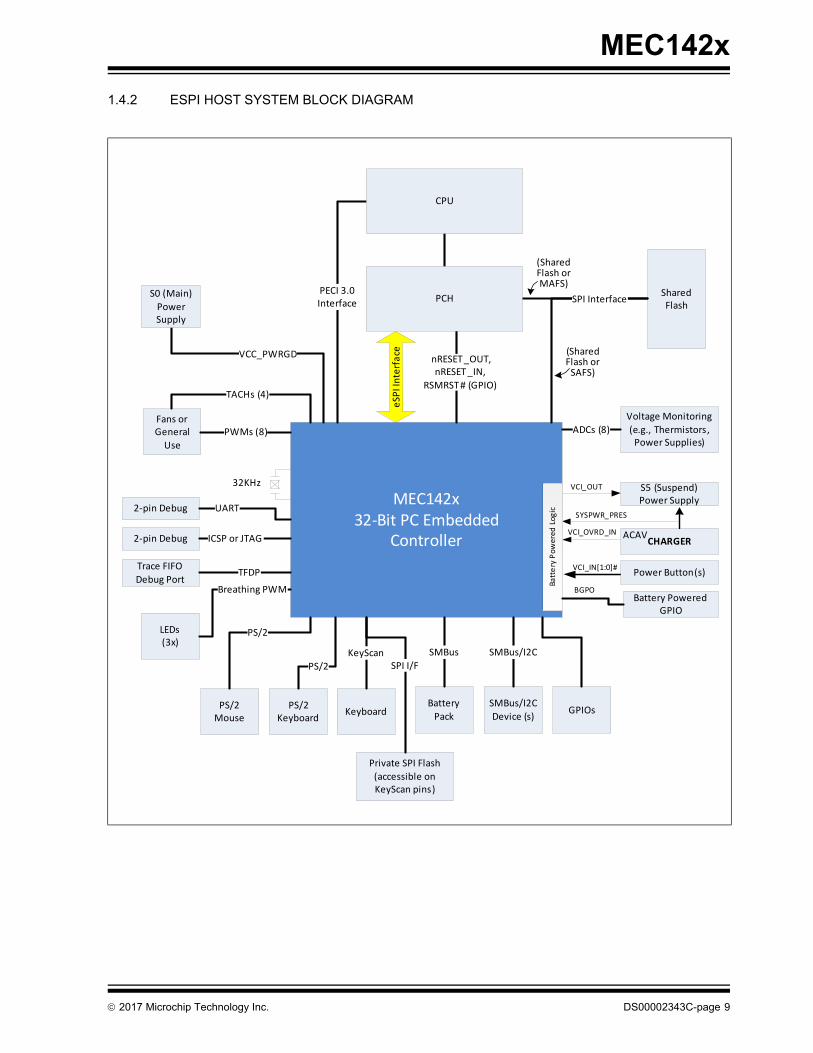
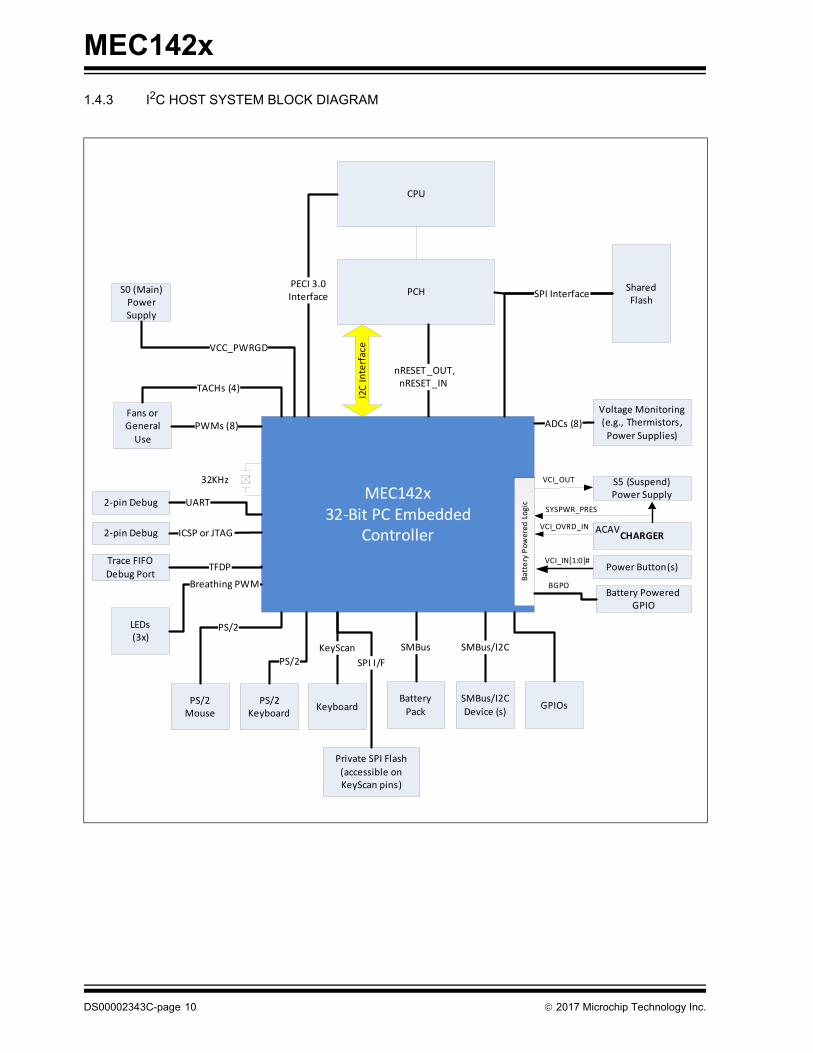
Note: Not all features shown are available on all devices. Refer to Products on page 7 for a list of the features bydevice.
CPU
PCH
MEC142x32‐Bit PC Embedded
Controller
PS/2 Mouse
PS/2 Keyboard
Keyboard
PS/2
PS/2
KeyScan
SMBus
Battery
Pack
SMBus
Fans or General
Use
PWMs (8)
TACHs (4)
2‐pin Debug UART
LEDs(3x)
Breathing PWM
Trace FIFO
Debug PortTFDP
PECI 3.0 Interface
SMBus/I2C
Device(s)
SMBus/I2C
GPIOs
Shared Flash
A20M, KBRST, nRESET_OUT, nRESET_IN,
SMI, SCI, SIRQ
SPI Interface
Private SPI Flash
(accessible on KeyScan pins)
SPI I/F
Voltage Monitoring(e.g., Thermistors,
Power Supplies)
ADCs (8)
S0 (Main) Power Supply
VCC_PWRGD
S5 (Suspend)Power Supply
Power Button(s)
CHARGERACAV
Battery Powered
Logic
Battery Powered GPIO
2‐pin Debug ICSP or JTAG
VCI_OUT
SYSPWR_PRES
VCI_OVRD_IN
VCI_IN[1:0]#
BGPO
32KHz
LPC Interface
DS00002343C-page 8 2017 Microchip Technology Inc.
MEC142x
1.4.2 ESPI HOST SYSTEM BLOCK DIAGRAM
MEC142x32‐Bit PC Embedded
Controller
eSPI Interface
32KHz
PS/2 Mouse
PS/2 Keyboard
Keyboard
PS/2
PS/2
KeyScan
Battery
Pack
SMBus
Fans or General
Use
PWMs (8)
TACHs (4)
2‐pin Debug UART
LEDs(3x)
Breathing PWM
Trace FIFO
Debug PortTFDP
PECI 3.0 Interface
SMBus/I2C
Device (s)
SMBus/I2C
GPIOs
Shared Flash
SPI Interface
Private SPI Flash
(accessible on KeyScan pins)
SPI I/F
Voltage Monitoring
(e.g., Thermistors, Power Supplies)
ADCs (8)
VCC_PWRGD
S5 (Suspend)Power Supply
VCI_OUT
VCI_IN[1:0]#Power Button(s)
CHARGERVCI_OVRD_IN ACAV
SYSPWR_PRES
BGPO
Battery Pow
ered
Logic
Battery Powered GPIO
2‐pin Debug ICSP or JTAG
nRESET_OUT, nRESET_IN,
RSMRST# (GPIO)
(Shared Flash or SAFS)
(Shared Flash or MAFS)
PCH
CPU
S0 (Main)
Power Supply
2017 Microchip Technology Inc. DS00002343C-page 9
MEC142x
1.4.3 I2C HOST SYSTEM BLOCK DIAGRAM
CPU
PCH
MEC142x32‐Bit PC Embedded
Controller
PS/2 Mouse
PS/2 Keyboard
Keyboard
PS/2
PS/2
KeyScan
Battery
Pack
SMBus
Fans or General
Use
PWMs (8)
TACHs (4)
2‐pin Debug UART
LEDs(3x)
Breathing PWM
Trace FIFO
Debug PortTFDP
PECI 3.0 Interface
SMBus/I2C
Device (s)
SMBus/I2C
GPIOs
Shared Flash
nRESET_OUT, nRESET_IN
SPI Interface
Private SPI Flash
(accessible on KeyScan pins)
SPI I/F
Voltage Monitoring(e.g., Thermistors,
Power Supplies)ADCs (8)
S0 (Main) Power Supply
VCC_PWRGD
S5 (Suspend)Power Supply
Power Button(s)
CHARGERACAV
Battery Powered
Logic
Battery Powered GPIO
2‐pin Debug ICSP or JTAG
VCI_OUT
SYSPWR_PRES
VCI_OVRD_IN
VCI_IN[1:0]#
BGPO
32KHz
I2C Interface
DS00002343C-page 10 2017 Microchip Technology Inc.
MEC142x
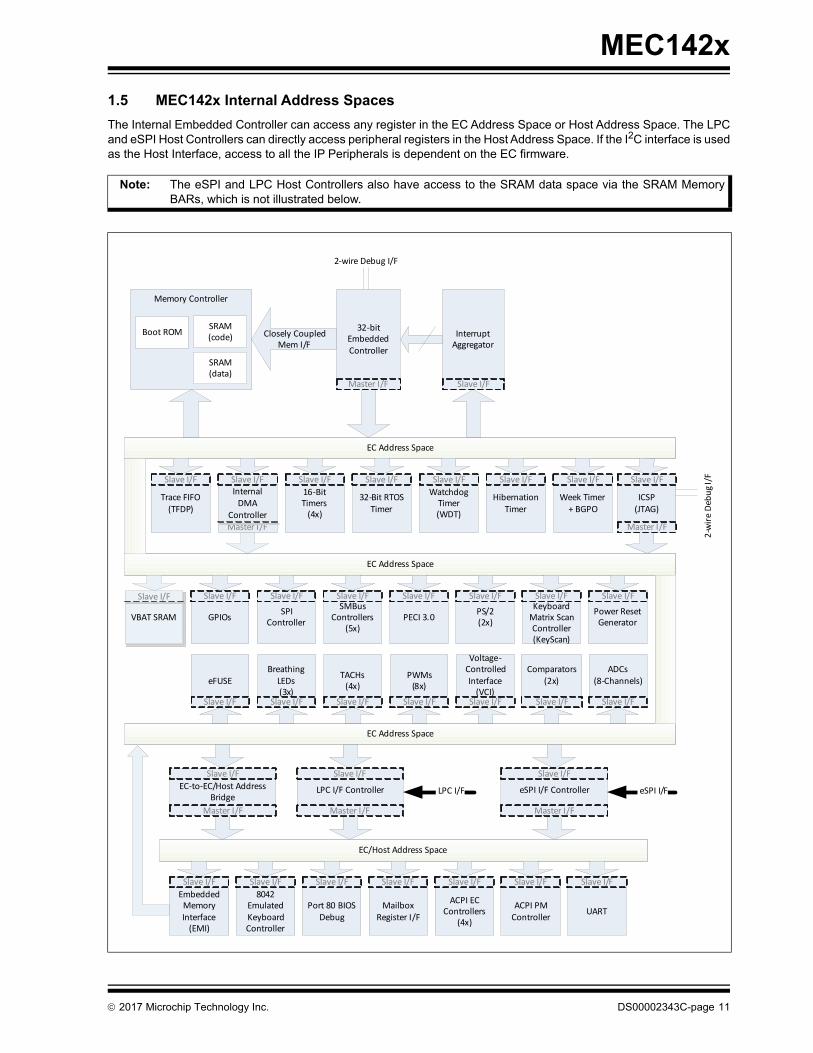
1.5 MEC142x Internal Address Spaces
The Internal Embedded Controller can access any register in the EC Address Space or Host Address Space. The LPCand eSPI Host Controllers can directly access peripheral registers in the Host Address Space. If the I2C interface is usedas the Host Interface, access to all the IP Peripherals is dependent on the EC firmware.
Note: The eSPI and LPC Host Controllers also have access to the SRAM data space via the SRAM MemoryBARs, which is not illustrated below.
Comparators(2x)
Week Timer + BGPO
32‐bit Embedded Controller
Memory Controller
Boot ROMSRAM (code)
SRAM (data)
Closely Coupled Mem I/F
EC Address Space
2‐wire Debug I/F
Trace FIFO(TFDP)
Internal DMA
Controller Master I/F
EC Address Space
Interrupt Aggregator
PECI 3.0PS/2(2x)
ICSP(JTAG)
eFUSE
SPI Controller
ADCs(8‐Channels)
PWMs(8x)
TACHs(4x)
Breathing LEDs(3x)
GPIOsPower Reset Generator
LPC I/F Controller
8042 Emulated Keyboard Controller
Port 80 BIOS Debug
EC/Host Address Space
Mailbox Register I/F
ACPI EC Controllers
(4x)
ACPI PM Controller
16‐Bit Timers(4x)
32‐Bit RTOS Timer
Watchdog Timer(WDT)
Hibernation Timer
Voltage‐Controlled Interface(VCI)
Keyboard Matrix Scan Controller(KeyScan)
Embedded Memory Interface (EMI)
SMBus Controllers
(5x)
EC Address Space
EC‐to‐EC/Host Address Bridge
LPC I/F
UART
2‐wire Debug I/F
Slave I/F
Slave I/FSlave I/F Slave I/F Slave I/F Slave I/F Slave I/F Slave I/F
Slave I/F Slave I/F Slave I/F Slave I/F Slave I/F Slave I/F Slave I/F Slave I/F
Master I/F
Slave I/F Slave I/F Slave I/F Slave I/F Slave I/F Slave I/F Slave I/F
Slave I/F Slave I/F Slave I/F Slave I/F Slave I/F Slave I/F Slave I/F
Master I/F
Slave I/F
Master I/F
Slave I/FMaster I/F
eSPI I/F Controller eSPI I/F
Slave I/F
Master I/F
Slave I/F
VBAT SRAM
2017 Microchip Technology Inc. DS00002343C-page 11
MEC142x
2.0 PIN CONFIGURATION
2.1 Description
The Pin Configuration chapter includes Pin List, Pin Description, Pin Multiplexing, Notes for Tables in this Chapter, PinStates After VTR Power-On, and Packages.
2.2 Terminology and Symbols for Pins/Buffers
2.2.1 BUFFER TERMINOLOGY
Note 2-1 See the “PCI Local Bus Specification,” Revision 2.1, Section 4.2.2.
Note 2-2 See the “PCI Local Bus Specification,” Revision 2.1, Section 4.2.2 and 4.2.3.
2.2.2 PIN NAMING CONVENTIONS
1. Pin Name is composed of the multiplexed options separated by ‘/’. E.g., GPIOxxxx/SignalA/SignalB.
2. The first signal shown in a pin name is the default signal. E.g., GPIOxxxx/SignalA/SignalB means the GPIO isthe default signal.
3. Parenthesis ‘()’ are used to list aliases or alternate functionality for a single mux option. E.g. GPIOxxx(Alias)/Sig-nalA/SignalB. The Alias is the intended usage for a specific GPIO. E.g., GPIOxxx(ICSP_DATA) is intended toindicate that ICSP_DATA signal may come out on this pin when the Mux Control is set for GPIOxxx. In this case,enabling the test mode takes precedence over the Mux Control selection.
4. Square brackets ‘[ ]’ are used to indicate there is a Strap Option on a pin. This is always shown as the last signalon the Pin Name.
5. Signal Names appended with a numeric value indicates the Instance Number, except for SMBus Pins. E.g.,PWM0, PWM1, etc. indicates that PWM0 is the PWM output for PWM Instance 0, PWM1 is the PWM output forPWM Instance 1, etc. Note that this same instance number is shown in the Register Base Address tables linkingthe specific PWM block instance to a specific signal on the pinout. The instance number may be omitted if therein only one instance of the IP block implemented.
Term Definition
# The ‘#’ sign at the end of a signal name indicates an active-low signal
n The lowercase ‘n’ preceding a signal name indicates an active-low signal
PWR Power
I Digital Input
IS Input with Schmitt Trigger
I_AN Analog Input
O Push-Pull Output
OD Open Drain Output
IO Bi-directional pin
IOD Bi-directional pin with Open Drain Output
PIO Programmable as Input, Output, Open Drain Output, Bi-directional or Bi-directional with OpenDrain Output. Configurable drive strength from 2ma to12ma.
Note: All GPIOs have programmable drive strength options of 2ma, 4ma, 8ma and 12ma.GPIO pin drive strength is determined by the DRIVE_STRENGTH field in the PinControl 2 Register.
PCI_IO Input/Output These pins meet the PCI 3.3V AC and DC Characteristics. (Note 2-1)
PECI_IO PECI Input/Output. These pins operate at the processor voltage level (VREF_CPU)
SB-TSI SB-TSI Input/Output. These pins operate at the processor voltage level (VREF_CPU)
Note: The numeric value appended to the end of the SMBus pins indicates they are 1.8V I/O signaling. E.g.SMB03_DATA vs SMB03_DATA18. The SMB03_DATA signal uses standard 3.3V I/O signaling. TheSMB03_DATA18 signal operates at 1.8V I/O signaling levels.
DS00002343C-page 12 2017 Microchip Technology Inc.

MEC142x
6. SMBus Port pins can be mapped to any SMB Controller. The number in the SMBus signal names (SMBxx_DATA)indicates the port value. E.g. SMB01_DATA represents SMBus Data Port 1.
2.3 Notes for Tables in this Chapter
Note Description
Note 1 The LAD and SER_IRQ pins require an external weak pull-up resistor of 10k-100k ohms.
Note 2 The ICSP_MCLR pin is used to enable JTAG. The part requires a pull-up on the ICSP_MCLR pin to keep it from entering debug mode. When debug mode is entered the ICSP_DATA and ICSP_CLOCK signals are automatically enabled on their respective pins. The System Board Designer should place a pull-up resistor of 10k ohms (recommended) to VTR on the ICSP_M-CLR pin.
Note 3 An external cap must be connected as close to the CAP pin/ball as possible with a routing resistance and CAP ESR of less than 100mohms. The capacitor value is 1uF and must be ceramic with X5R or X7R dielectric. The cap pin/ball should remain on the top layer of the PCB and traced to the CAP. Avoid adding vias to other layers to minimize inductance.
Note 4 This SMBus ports supports 1 Mbps operation as defined by I2C. For 1 Mbps I2C recom-mended capacitance/pull-up relationships from Intel, refer to the Shark Bay platform guide, Intel ref number 486714. Refer to the PCH - SMBus 2.0/SMLink Interface Design Guidelines, Table 20-5 Bus Capacitance/Pull-Up Resistor Relationship.
Note 5 The RESET_OUT# pin must be pulled to ground via an external 8.2k ohm resistor. This will ensure the glitch-free tristate GPIO input will not glitch high on a power on reset (POR) event.
Note 6 In order to achieve the lowest leakage current when both PECI and SB TSI are not used, set the VREF_CPU Disable bit to 1.
Note 7 The SMB05 pins operate at the voltage of the VTR_33_18 pin.
Note 8 The voltage on the ADC pins must not exceed 3.6 V or damage to the device will occur.
Note 9 The XTAL1 pin should be left floating when using the XTAL2 pin for the single ended clock input.
Note 10 The Boot ROM manipulates the pins associated with the Shared SPI interface and the Private SPI interface to access the external flash. Before exiting, the Boot ROM tristates these inter-faces by returning them to their default hardware state (i.e., GPIO input).
Note 11 When the SMBxx_xxxx18 functions are selected, the pins operate at 1.8V I/O signal levels.
Note 12 The GPIO assignment on this pin only provides interrupt and wakeup capability. This is pro-vided by the Interrupt Detection field in the Pin Control register. The Mux control field in the Pin Control Register should not be set to 00 = GPIO or undesirable results may occur. In order to emphasize the prohibition on using the GPIO Signal Pin Function, the Pin Chapter does not list the GPIO signal pin function assigned to this pin; however, the GPIO chapter does so the inter-rupt can be used.
Note 13 This signal is a test signal used to detect when the internal 48MHz clock is toggling or stopped in heavy and deepest sleep modes.
Note 14 The VCI pins may be used as GPIOs. The VCI input signals are not gated by selecting the GPIO alternate function. Firmware must disable (i.e., gate) these inputs by writing the bits in the VCI Input Enable Register when the GPIO function is enabled.
Note 15 The KSI and KSO Key Scan pins require pull-up resistors. The system designer may opt to use either use the internal pull-up resistors or populate external pull-up resistors.
Note 16 If the eSPI Flash Channel is used for booting, the GPIO123/SHD_CS0# pin must be used as RSMRST#. This pin will be driven high by the boot ROM code in order to activate the eSPI flash channel. Also, the GPIO136/SHD_IO3 pin must be used as DSW_PWROK. This pin will also be driven high by the boot ROM code to support DSW timing requirements. If the SHD_SPI port is used for booting (including SAFS), then any unused GPIO may be used for RSMRST# and DSW_PWROK.
2017 Microchip Technology Inc. DS00002343C-page 13
MEC142x
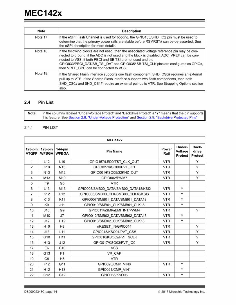
2.4 Pin List
2.4.1 PIN LIST
Note 17 If the eSPI Flash Channel is used for booting, the GPIO135/SHD_IO2 pin must be used to determine that the primary power rails are stable before RSMRST# can be de-asserted. See the eSPI description for more details.
Note 18 If the following blocks are not used, then the associated voltage reference pin may be con-nected to ground: if the ADC is not used and the block is disabled, ADC_VREF can be con-nected to VSS; if both PECI and SB TSI are not used and the GPIO033/PECI_DAT/SB_TSI_DAT and GPIO035/ SB-TSI_CLK pins are configured as GPIOs, then VREF_CPU can be connected to VSS.
Note 19 If the Shared Flash interface supports one flash component, SHD_CS0# requires an external pull-up to VTR. If the Shared Flash interface supports two flash components, then both SHD_CS0# and SHD_CS1# require an external pull-up to VTR. See Strapping Options section also.
Note: In the columns labeled “Under-Voltage Protect” and “Backdrive Protect” a “Y” means that the pin supportsthis feature. See Section 2.8, "Under-Voltage Protection" and Section 2.9, "Backdrive Protected Pins".
MEC142x
128-pinVTQFP
128-pinWFBGA
144-pinWFBGA
Pin NamePower
Rail
Under-VoltageProtect
Back-drive
Protect
1 L12 L10 GPIO157/LED0/TST_CLK_OUT VTR Y
2 K10 N13 GPIO027/KSO00/PVT_IO1 VTR Y
3 N13 M12 GPIO001/KSO05/32KHZ_OUT VTR Y
4 M13 M10 GPIO002/PWM7 VTR Y
5 F9 G5 VTR
6 L13 M13 GPIO005/SMB00_DATA/SMB00_DATA18/KSI2 VTR Y
7 K12 L12 GPIO006/SMB00_CLK/SMB00_CLK18/KSI3 VTR Y
8 K13 K11 GPIO007/SMB01_DATA/SMB01_DATA18 VTR Y
9 K9 J11 GPIO010/SMB01_CLK/SMB01_CLK18 VTR Y
10 J10 G9 GPIO011/nSMI/nEMI_INT/PWM4 VTR Y
11 M10 J7 GPIO012/SMB02_DATA/SMB02_DATA18 VTR Y
12 J12 H12 GPIO013/SMB02_CLK/SMB02_CLK18 VTR Y
13 H10 H8 nRESET_IN/GPIO014 VTR Y
14 J13 L11 GPIO015/KSO01/PVT_CS# VTR Y
15 G10 H11 GPIO016/KSO02/PVT_SCLK VTR Y
16 H13 J12 GPIO017/KSO03/PVT_IO0 VTR Y
17 E6 C10 VSS
18 G13 F1 VR_CAP
19 G9 H5 VTR
20 F12 G11 GPIO020/CMP_VIN0 VTR Y
21 H12 H13 GPIO021/CMP_VIN1 Y
22 G12 G12 GPIO066/KSO06 VTR Y
Note Description
DS00002343C-page 14 2017 Microchip Technology Inc.
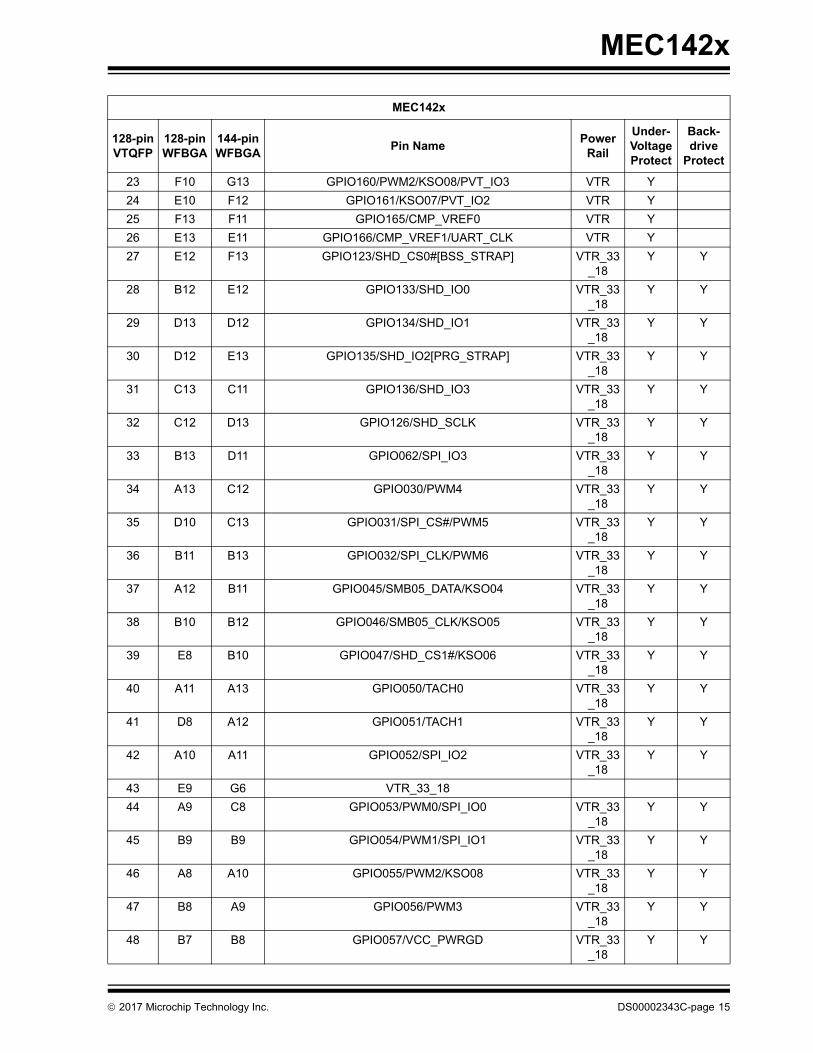
MEC142x
23 F10 G13 GPIO160/PWM2/KSO08/PVT_IO3 VTR Y
24 E10 F12 GPIO161/KSO07/PVT_IO2 VTR Y
25 F13 F11 GPIO165/CMP_VREF0 VTR Y
26 E13 E11 GPIO166/CMP_VREF1/UART_CLK VTR Y
27 E12 F13 GPIO123/SHD_CS0#[BSS_STRAP] VTR_33_18
Y Y
28 B12 E12 GPIO133/SHD_IO0 VTR_33_18
Y Y
29 D13 D12 GPIO134/SHD_IO1 VTR_33_18
Y Y
30 D12 E13 GPIO135/SHD_IO2[PRG_STRAP] VTR_33_18
Y Y
31 C13 C11 GPIO136/SHD_IO3 VTR_33_18
Y Y
32 C12 D13 GPIO126/SHD_SCLK VTR_33_18
Y Y
33 B13 D11 GPIO062/SPI_IO3 VTR_33_18
Y Y
34 A13 C12 GPIO030/PWM4 VTR_33_18
Y Y
35 D10 C13 GPIO031/SPI_CS#/PWM5 VTR_33_18
Y Y
36 B11 B13 GPIO032/SPI_CLK/PWM6 VTR_33_18
Y Y
37 A12 B11 GPIO045/SMB05_DATA/KSO04 VTR_33_18
Y Y
38 B10 B12 GPIO046/SMB05_CLK/KSO05 VTR_33_18
Y Y
39 E8 B10 GPIO047/SHD_CS1#/KSO06 VTR_33_18
Y Y
40 A11 A13 GPIO050/TACH0 VTR_33_18
Y Y
41 D8 A12 GPIO051/TACH1 VTR_33_18
Y Y
42 A10 A11 GPIO052/SPI_IO2 VTR_33_18
Y Y
43 E9 G6 VTR_33_18
44 A9 C8 GPIO053/PWM0/SPI_IO0 VTR_33_18
Y Y
45 B9 B9 GPIO054/PWM1/SPI_IO1 VTR_33_18
Y Y
46 A8 A10 GPIO055/PWM2/KSO08 VTR_33_18
Y Y
47 B8 A9 GPIO056/PWM3 VTR_33_18
Y Y
48 B7 B8 GPIO057/VCC_PWRGD VTR_33_18
Y Y
MEC142x
128-pinVTQFP
128-pinWFBGA
144-pinWFBGA
Pin NamePower
Rail
Under-VoltageProtect
Back-drive
Protect
2017 Microchip Technology Inc. DS00002343C-page 15

MEC142x
49 A7 B7 GPIO060/KBRST VTR_33_18
Y Y
50 D7 A8 GPIO025/KSO07 VTR_33_18
Y Y
51 D9 C9 GPIO167 VTR_33_18
Y Y
52 B6 C7 GPIO026/PS2_CLK1B VTR_33_18
Y Y
53 A6 A7 GPIO061/LPCPD#/ESPI_RESET# VTR_LPC_ESPI
Y
54 E5 H7 VTR_LPC_ESPI
55 B5 C6 GPIO063/SER_IRQ/ESPI_ALERT# VTR_LPC_ESPI
56 A5 B6 GPIO064/LRESET# VTR_LPC_ESPI
Y
57 B4 A6 GPIO034/PCI_CLK/ESPI_CLK VTR_LPC_ESPI
Y
58 A4 B5 GPIO044/LFRAME#/ESPI_CS# VTR_LPC_ESPI
Y
59 A3 A5 GPIO040/LAD0/ESPI_IO0 VTR_LPC_ESPI
60 A2 A4 GPIO041/LAD1/ESPI_IO1 VTR_LPC_ESPI
61 B3 C5 GPIO042/LAD2/ESPI_IO2 VTR_LPC_ESPI
62 B2 C4 GPIO043/LAD3/ESPI_IO3 VTR_LPC_ESPI
63 A1 B4 GPIO067/CLKRUN# VTR_LPC_ESPI
Y
64 E7 D1 VSS
65 G5 J5 VTR
66 B1 C3 GPIO100/nEC_SCI VTR Y
67 C2 C2 GPIO101/KSO04 VTR Y
68 D6 A3 GPIO102/KSO09[CR_STRAP] VTR Y
69 C1 B3 GPIO103/VCC_PWRGD VTR Y
70 D5 A2 GPIO104/LED2 VTR Y
71 D4 E2 GPIO105/PS2_CLK1B/PWM0 VTR Y
72 D1 C1 GPIO106/KSO10/PCIRST_OUT0# VTR Y
73 D2 D2 GPIO107/nRESET_OUT VTR Y
74 F4 B2 GPIO110/KSO11/TACH2 VTR Y
75 E4 F2 GPIO111/KSO12/TACH3 VTR Y
76 E1 A1 GPIO112/PS2_CLK1A/KSO13 VTR Y
77 G4 G3 GPIO113/PS2_DAT1A/KSO14 VTR Y
78 F2 E1 GPIO114/PS2_CLK0 VTR Y
79 E2 B1 GPIO115/PS2_DAT0 VTR Y
MEC142x
128-pinVTQFP
128-pinWFBGA
144-pinWFBGA
Pin NamePower
Rail
Under-VoltageProtect
Back-drive
Protect
DS00002343C-page 16 2017 Microchip Technology Inc.

MEC142x
80 F1 G1 GPIO116/TFDP_DATA/UART_RX VTR Y
81 G2 G2 GPIO117/TFDP_CLK/UART_TX[VL_STRAP] VTR Y
82 H5 J6 VTR
83 H4 H2 GPIO120/CMP_VOUT1 VTR Y
84 F5 D3 VSS
85 H2 H1 GPIO124/CMP_VOUT0 VTR Y
86 G1 H3 GPIO125/KSO15/PCIRST_OUT1# VTR Y
87 J1 K1 ICSP_MCLR VTR Y
88 H1 J1 GPIO127/PS2_DAT1B/TACH0 VTR Y
89 K1 K2 GPIO130/SMB03_DATA/SMB03_DATA18 VTR Y
90 K2 J2 GPIO035/SB-TSI_CLK/PWM3 VTR Y
91 J2 L1 GPIO131/SMB03_CLK/SMB03_CLK18 VTR Y
92 L1 M1 GPIO132/KSO16/PCI_RESET# VTR Y
93 L2 N1 GPIO140/KSO17/PWM5 VTR Y
94 M1 K3 GPIO033/PECI_DAT/SB_TSI_DAT VTR Y
95 J5 L5 VREF_CPU
96 N1 J3 GPIO141/SMB04_DATA/SMB04_DATA18 VTR Y
97 M2 L3 GPIO142/SMB04_CLK/SMB04_CLK18 VTR Y
98 N2 L4 GPIO143/KSI0/DTR# VTR Y
99 N3 L2 GPIO144/KSI1/DCD# VTR Y
100 H9 F3 VSS
101 M3 M2 GPIO145(ICSP_CLOCK) VTR Y
102 M4 M3 GPIO146(ICSP_DATA) VTR Y
103 J6 H6 VTR
104 N4 N2 GPIO147/KSI4/DSR# VTR Y
105 K5 M4 GPIO150/KSI5/RI# VTR Y
106 N5 N3 GPIO156/LED1 VTR Y
107 J4 N4 GPIO151/KSI6/RTS# VTR Y
108 K4 N5 GPIO152/KSI7/CTS# VTR Y
109 N6 N6 GPIO153/ADC4 VTR Y
110 M6 L7 GPIO154/ADC3 VTR Y
111 M7 M6 GPIO155/ADC2 VTR Y
112 J7 M7 AVSS
113 K7 L6 GPIO122/ADC1 VTR Y
114 N7 N7 GPIO121/ADC0 VTR Y
115 M5 M5 ADC_VREF VTR Y
116 N8 N8 GPIO022/ADC5/PWM1 VTR Y
117 M8 L9 GPIO023/ADC6/A20M/TACH1 VTR Y
118 K6 N9 GPIO024/ADC7 VTR Y
119 K8 N10 BGPO/GPIO004 VBAT Y
120 M9 M9 SYSPWR_PRES/GPIO003 VBAT Y
121 N10 M8 VCI_OUT/GPIO036 VBAT Y
MEC142x
128-pinVTQFP
128-pinWFBGA
144-pinWFBGA
Pin NamePower
Rail
Under-VoltageProtect
Back-drive
Protect
2017 Microchip Technology Inc. DS00002343C-page 17

MEC142x
2.5 5 Volt Tolerant Pins
There are no 5 Volt tolerant pins in the MEC142x.
2.6 1.8V or 3.3V I/O Pins
There is a group of signals that are powered by the VTR_LPC_ESPI power supply. This supply pin determines the oper-ating voltage range for these signals.
• See “Power Rail” column in Pin List on page 14.
There is a group of signals that are powered by the VTR_33_18 power supply. This supply pin determines the operatingvoltage range for these signals. The VL_STRAP pin is used to indicate to the boot ROM what the voltage level is onthese pins. See Voltage Level Strap on page 44.
• See “Power Rail” column in Pin List on page 14.
122 J9 K12 VBAT
123 N9 J13 XTAL1 VBAT
124 J8 E3 VSS_VBAT
125 N11 L13 XTAL2 VBAT
126 M11 N12 VCI_IN1#/GPIO162 VBAT Y
127 N12 N11 VCI_IN0#/GPIO163 VBAT Y
128 M12 M11 VCI_OVRD_IN/GPIO164 VBAT Y
H9 VSS
J8 VSS
J9 VSS
K13 VSS
E5 No Connect
E6 No Connect
E7 No Connect
E8 No Connect
E9 No Connect
F5 No Connect
F6 No Connect
F7 No Connect
F8 No Connect
F9 No Connect
G8 No Connect
L8 No Connect
Note: The LPC Interface signals require the VTR_LPC_ESPI power pin to be connected to the 3.3V VTR rail.The eSPI Interface signals require the VTR_LPC_ESPI power pin to be connected to the 1.8V rail. TheGPIO signals on these pins will operate at either 1.8V or 3.3V as determined by the VTR_LPC_ESPI powerpin.
MEC142x
128-pinVTQFP
128-pinWFBGA
144-pinWFBGA
Pin NamePower
Rail
Under-VoltageProtect
Back-drive
Protect
DS00002343C-page 18 2017 Microchip Technology Inc.
MEC142x
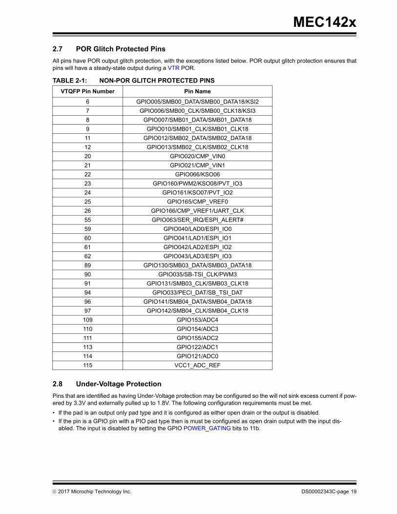
2.7 POR Glitch Protected Pins
All pins have POR output glitch protection, with the exceptions listed below. POR output glitch protection ensures thatpins will have a steady-state output during a VTR POR.
2.8 Under-Voltage Protection
Pins that are identified as having Under-Voltage protection may be configured so the will not sink excess current if pow-ered by 3.3V and externally pulled up to 1.8V. The following configuration requirements must be met.
• If the pad is an output only pad type and it is configured as either open drain or the output is disabled.
• If the pin is a GPIO pin with a PIO pad type then is must be configured as open drain output with the input dis-abled. The input is disabled by setting the GPIO POWER_GATING bits to 11b.
TABLE 2-1: NON-POR GLITCH PROTECTED PINS
VTQFP Pin Number Pin Name
6 GPIO005/SMB00_DATA/SMB00_DATA18/KSI2
7 GPIO006/SMB00_CLK/SMB00_CLK18/KSI3
8 GPIO007/SMB01_DATA/SMB01_DATA18
9 GPIO010/SMB01_CLK/SMB01_CLK18
11 GPIO012/SMB02_DATA/SMB02_DATA18
12 GPIO013/SMB02_CLK/SMB02_CLK18
20 GPIO020/CMP_VIN0
21 GPIO021/CMP_VIN1
22 GPIO066/KSO06
23 GPIO160/PWM2/KSO08/PVT_IO3
24 GPIO161/KSO07/PVT_IO2
25 GPIO165/CMP_VREF0
26 GPIO166/CMP_VREF1/UART_CLK
55 GPIO063/SER_IRQ/ESPI_ALERT#
59 GPIO040/LAD0/ESPI_IO0
60 GPIO041/LAD1/ESPI_IO1
61 GPIO042/LAD2/ESPI_IO2
62 GPIO043/LAD3/ESPI_IO3
89 GPIO130/SMB03_DATA/SMB03_DATA18
90 GPIO035/SB-TSI_CLK/PWM3
91 GPIO131/SMB03_CLK/SMB03_CLK18
94 GPIO033/PECI_DAT/SB_TSI_DAT
96 GPIO141/SMB04_DATA/SMB04_DATA18
97 GPIO142/SMB04_CLK/SMB04_CLK18
109 GPIO153/ADC4
110 GPIO154/ADC3
111 GPIO155/ADC2
113 GPIO122/ADC1
114 GPIO121/ADC0
115 VCC1_ADC_REF
2017 Microchip Technology Inc. DS00002343C-page 19

MEC142x
2.9 Backdrive Protected Pins
Assuming that the external voltage on the pin is within the parameters defined for the specific pad type, the backdriveprotected pin will not sink excess current when it is at a lower potential than the external circuit. There are two caseswhere this occurs:
• The pad power is off and the external circuit is powered
• The pad power is on and the external circuitry is pulled to a higher potential than the pad power.
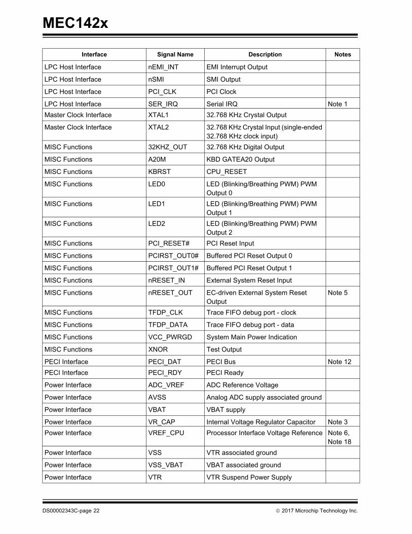
2.10 Pin Description
Note: See Section 2.3, "Notes for Tables in this Chapter," on page 13 for notes that are referenced in the PinDescription table.
Interface Signal Name Description Notes
Analog Data Acquisition Interface ADC0 ADC channel 0 Note 8
Analog Data Acquisition Interface ADC1 ADC channel 1 Note 8
Analog Data Acquisition Interface ADC2 ADC channel 2 Note 8
Analog Data Acquisition Interface ADC3 ADC channel 3 Note 8
Analog Data Acquisition Interface ADC4 ADC channel 4 Note 8
Analog Data Acquisition Interface ADC5 ADC channel 5 Note 8
Analog Data Acquisition Interface ADC6 ADC channel 6 Note 8
Analog Data Acquisition Interface ADC7 ADC channel 7 Note 8
Comparator Interface CMP_VIN0 Comparator 0 Positive Input
Comparator Interface CMP_VIN1 Comparator 1 Positive Input
Comparator Interface CMP_VOUT0 Comparator 0 Output
Comparator Interface CMP_VOUT1 Comparator 1 Output
Comparator Interface CMP_VREF0 Comparator 0 Negative Input
Comparator Interface CMP_VREF1 Comparator 1 Negative Input
eSPI Host Interface ESPI_ALERT# eSPI Alert
eSPI Host Interface ESPI_CLK eSPI Clock
eSPI Host Interface ESPI_CS# eSPI Chip Select
eSPI Host Interface ESPI_IO0 eSPI Data Pin 0
eSPI Host Interface ESPI_IO1 eSPI Data Pin 1
eSPI Host Interface ESPI_IO2 eSPI Data Pin 2
eSPI Host Interface ESPI_IO3 eSPI Data Pin 3
eSPI Host Interface ESPI_RESET# eSPI Reset
GPIO Interface GPIO General Purpose Input Output Pins
ICSP Interface ICSP_CLOCK 2-Wire Debug Clock Note 2
ICSP Interface ICSP_DATA 2-Wire Debug Data Note 2
ICSP Interface ICSP_MCLR 2-Wire Debug Master Reset Note 2
Keyboard Scan Interface KSI0 Keyboard Scan Matrix Input 0 Note 15
DS00002343C-page 20 2017 Microchip Technology Inc.
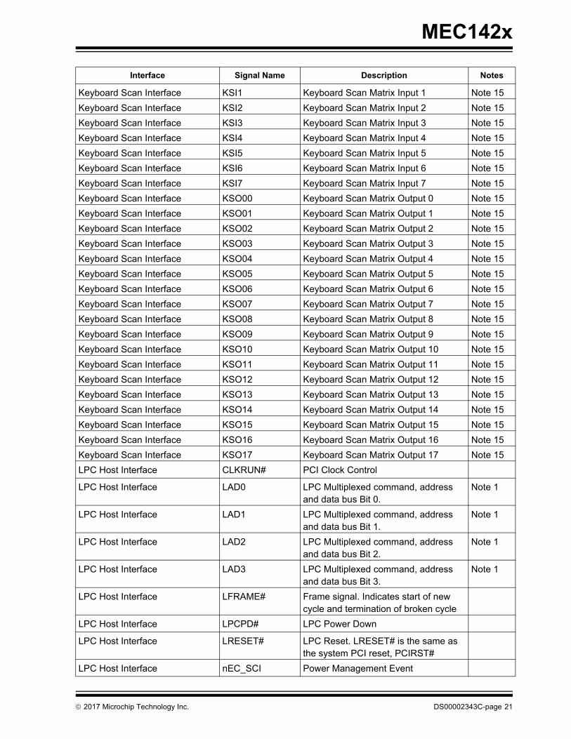
MEC142x
Keyboard Scan Interface KSI1 Keyboard Scan Matrix Input 1 Note 15
Keyboard Scan Interface KSI2 Keyboard Scan Matrix Input 2 Note 15
Keyboard Scan Interface KSI3 Keyboard Scan Matrix Input 3 Note 15
Keyboard Scan Interface KSI4 Keyboard Scan Matrix Input 4 Note 15
Keyboard Scan Interface KSI5 Keyboard Scan Matrix Input 5 Note 15
Keyboard Scan Interface KSI6 Keyboard Scan Matrix Input 6 Note 15
Keyboard Scan Interface KSI7 Keyboard Scan Matrix Input 7 Note 15
Keyboard Scan Interface KSO00 Keyboard Scan Matrix Output 0 Note 15
Keyboard Scan Interface KSO01 Keyboard Scan Matrix Output 1 Note 15
Keyboard Scan Interface KSO02 Keyboard Scan Matrix Output 2 Note 15
Keyboard Scan Interface KSO03 Keyboard Scan Matrix Output 3 Note 15
Keyboard Scan Interface KSO04 Keyboard Scan Matrix Output 4 Note 15
Keyboard Scan Interface KSO05 Keyboard Scan Matrix Output 5 Note 15
Keyboard Scan Interface KSO06 Keyboard Scan Matrix Output 6 Note 15
Keyboard Scan Interface KSO07 Keyboard Scan Matrix Output 7 Note 15
Keyboard Scan Interface KSO08 Keyboard Scan Matrix Output 8 Note 15
Keyboard Scan Interface KSO09 Keyboard Scan Matrix Output 9 Note 15
Keyboard Scan Interface KSO10 Keyboard Scan Matrix Output 10 Note 15
Keyboard Scan Interface KSO11 Keyboard Scan Matrix Output 11 Note 15
Keyboard Scan Interface KSO12 Keyboard Scan Matrix Output 12 Note 15
Keyboard Scan Interface KSO13 Keyboard Scan Matrix Output 13 Note 15
Keyboard Scan Interface KSO14 Keyboard Scan Matrix Output 14 Note 15
Keyboard Scan Interface KSO15 Keyboard Scan Matrix Output 15 Note 15
Keyboard Scan Interface KSO16 Keyboard Scan Matrix Output 16 Note 15
Keyboard Scan Interface KSO17 Keyboard Scan Matrix Output 17 Note 15
LPC Host Interface CLKRUN# PCI Clock Control
LPC Host Interface LAD0 LPC Multiplexed command, address and data bus Bit 0.
Note 1
LPC Host Interface LAD1 LPC Multiplexed command, address and data bus Bit 1.
Note 1
LPC Host Interface LAD2 LPC Multiplexed command, address and data bus Bit 2.
Note 1
LPC Host Interface LAD3 LPC Multiplexed command, address and data bus Bit 3.
Note 1
LPC Host Interface LFRAME# Frame signal. Indicates start of new cycle and termination of broken cycle
LPC Host Interface LPCPD# LPC Power Down
LPC Host Interface LRESET# LPC Reset. LRESET# is the same as the system PCI reset, PCIRST#
LPC Host Interface nEC_SCI Power Management Event
Interface Signal Name Description Notes
2017 Microchip Technology Inc. DS00002343C-page 21
MEC142x
LPC Host Interface nEMI_INT EMI Interrupt Output
LPC Host Interface nSMI SMI Output
LPC Host Interface PCI_CLK PCI Clock
LPC Host Interface SER_IRQ Serial IRQ Note 1
Master Clock Interface XTAL1 32.768 KHz Crystal Output
Master Clock Interface XTAL2 32.768 KHz Crystal Input (single-ended 32.768 KHz clock input)
MISC Functions 32KHZ_OUT 32.768 KHz Digital Output
MISC Functions A20M KBD GATEA20 Output
MISC Functions KBRST CPU_RESET
MISC Functions LED0 LED (Blinking/Breathing PWM) PWM Output 0
MISC Functions LED1 LED (Blinking/Breathing PWM) PWM Output 1
MISC Functions LED2 LED (Blinking/Breathing PWM) PWM Output 2
MISC Functions PCI_RESET# PCI Reset Input
MISC Functions PCIRST_OUT0# Buffered PCI Reset Output 0
MISC Functions PCIRST_OUT1# Buffered PCI Reset Output 1
MISC Functions nRESET_IN External System Reset Input
MISC Functions nRESET_OUT EC-driven External System Reset Output
Note 5
MISC Functions TFDP_CLK Trace FIFO debug port - clock
MISC Functions TFDP_DATA Trace FIFO debug port - data
MISC Functions VCC_PWRGD System Main Power Indication
MISC Functions XNOR Test Output
PECI Interface PECI_DAT PECI Bus Note 12
PECI Interface PECI_RDY PECI Ready
Power Interface ADC_VREF ADC Reference Voltage
Power Interface AVSS Analog ADC supply associated ground
Power Interface VBAT VBAT supply
Power Interface VR_CAP Internal Voltage Regulator Capacitor Note 3
Power Interface VREF_CPU Processor Interface Voltage Reference Note 6, Note 18
Power Interface VSS VTR associated ground
Power Interface VSS_VBAT VBAT associated ground
Power Interface VTR VTR Suspend Power Supply
Interface Signal Name Description Notes
DS00002343C-page 22 2017 Microchip Technology Inc.
MEC142x
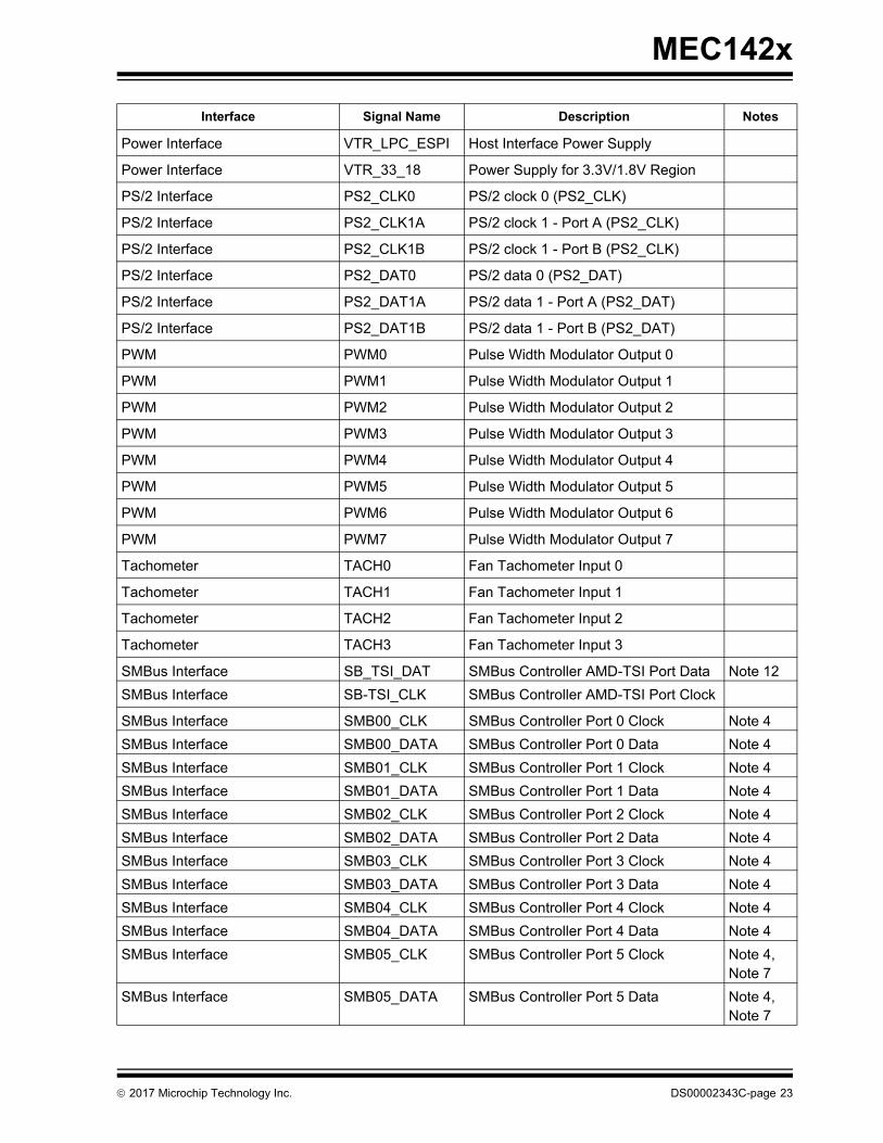
Power Interface VTR_LPC_ESPI Host Interface Power Supply
Power Interface VTR_33_18 Power Supply for 3.3V/1.8V Region
PS/2 Interface PS2_CLK0 PS/2 clock 0 (PS2_CLK)
PS/2 Interface PS2_CLK1A PS/2 clock 1 - Port A (PS2_CLK)
PS/2 Interface PS2_CLK1B PS/2 clock 1 - Port B (PS2_CLK)
PS/2 Interface PS2_DAT0 PS/2 data 0 (PS2_DAT)
PS/2 Interface PS2_DAT1A PS/2 data 1 - Port A (PS2_DAT)
PS/2 Interface PS2_DAT1B PS/2 data 1 - Port B (PS2_DAT)
PWM PWM0 Pulse Width Modulator Output 0
PWM PWM1 Pulse Width Modulator Output 1
PWM PWM2 Pulse Width Modulator Output 2
PWM PWM3 Pulse Width Modulator Output 3
PWM PWM4 Pulse Width Modulator Output 4
PWM PWM5 Pulse Width Modulator Output 5
PWM PWM6 Pulse Width Modulator Output 6
PWM PWM7 Pulse Width Modulator Output 7
Tachometer TACH0 Fan Tachometer Input 0
Tachometer TACH1 Fan Tachometer Input 1
Tachometer TACH2 Fan Tachometer Input 2
Tachometer TACH3 Fan Tachometer Input 3
SMBus Interface SB_TSI_DAT SMBus Controller AMD-TSI Port Data Note 12
SMBus Interface SB-TSI_CLK SMBus Controller AMD-TSI Port Clock
SMBus Interface SMB00_CLK SMBus Controller Port 0 Clock Note 4
SMBus Interface SMB00_DATA SMBus Controller Port 0 Data Note 4
SMBus Interface SMB01_CLK SMBus Controller Port 1 Clock Note 4
SMBus Interface SMB01_DATA SMBus Controller Port 1 Data Note 4
SMBus Interface SMB02_CLK SMBus Controller Port 2 Clock Note 4
SMBus Interface SMB02_DATA SMBus Controller Port 2 Data Note 4
SMBus Interface SMB03_CLK SMBus Controller Port 3 Clock Note 4
SMBus Interface SMB03_DATA SMBus Controller Port 3 Data Note 4
SMBus Interface SMB04_CLK SMBus Controller Port 4 Clock Note 4
SMBus Interface SMB04_DATA SMBus Controller Port 4 Data Note 4
SMBus Interface SMB05_CLK SMBus Controller Port 5 Clock Note 4, Note 7
SMBus Interface SMB05_DATA SMBus Controller Port 5 Data Note 4, Note 7
Interface Signal Name Description Notes
2017 Microchip Technology Inc. DS00002343C-page 23
MEC142x
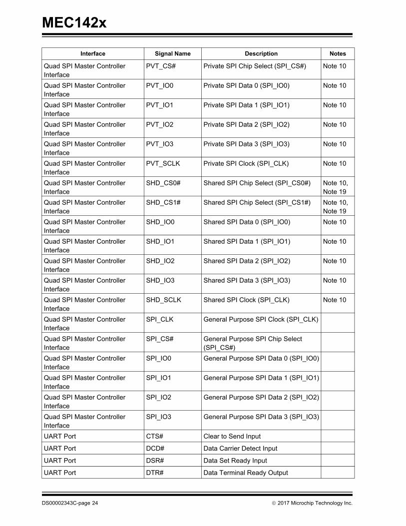
Quad SPI Master Controller Interface
PVT_CS# Private SPI Chip Select (SPI_CS#) Note 10
Quad SPI Master Controller Interface
PVT_IO0 Private SPI Data 0 (SPI_IO0) Note 10
Quad SPI Master Controller Interface
PVT_IO1 Private SPI Data 1 (SPI_IO1) Note 10
Quad SPI Master Controller Interface
PVT_IO2 Private SPI Data 2 (SPI_IO2) Note 10
Quad SPI Master Controller Interface
PVT_IO3 Private SPI Data 3 (SPI_IO3) Note 10
Quad SPI Master Controller Interface
PVT_SCLK Private SPI Clock (SPI_CLK) Note 10
Quad SPI Master Controller Interface
SHD_CS0# Shared SPI Chip Select (SPI_CS0#) Note 10, Note 19
Quad SPI Master Controller Interface
SHD_CS1# Shared SPI Chip Select (SPI_CS1#) Note 10, Note 19
Quad SPI Master Controller Interface
SHD_IO0 Shared SPI Data 0 (SPI_IO0) Note 10
Quad SPI Master Controller Interface
SHD_IO1 Shared SPI Data 1 (SPI_IO1) Note 10
Quad SPI Master Controller Interface
SHD_IO2 Shared SPI Data 2 (SPI_IO2) Note 10
Quad SPI Master Controller Interface
SHD_IO3 Shared SPI Data 3 (SPI_IO3) Note 10
Quad SPI Master Controller Interface
SHD_SCLK Shared SPI Clock (SPI_CLK) Note 10
Quad SPI Master Controller Interface
SPI_CLK General Purpose SPI Clock (SPI_CLK)
Quad SPI Master Controller Interface
SPI_CS# General Purpose SPI Chip Select (SPI_CS#)
Quad SPI Master Controller Interface
SPI_IO0 General Purpose SPI Data 0 (SPI_IO0)
Quad SPI Master Controller Interface
SPI_IO1 General Purpose SPI Data 1 (SPI_IO1)
Quad SPI Master Controller Interface
SPI_IO2 General Purpose SPI Data 2 (SPI_IO2)
Quad SPI Master Controller Interface
SPI_IO3 General Purpose SPI Data 3 (SPI_IO3)
UART Port CTS# Clear to Send Input
UART Port DCD# Data Carrier Detect Input
UART Port DSR# Data Set Ready Input
UART Port DTR# Data Terminal Ready Output
Interface Signal Name Description Notes
DS00002343C-page 24 2017 Microchip Technology Inc.

MEC142x
2.11 Pin Multiplexing
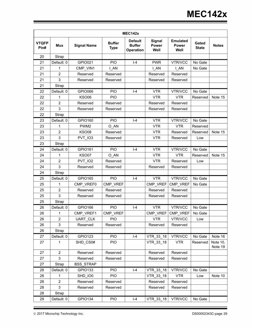
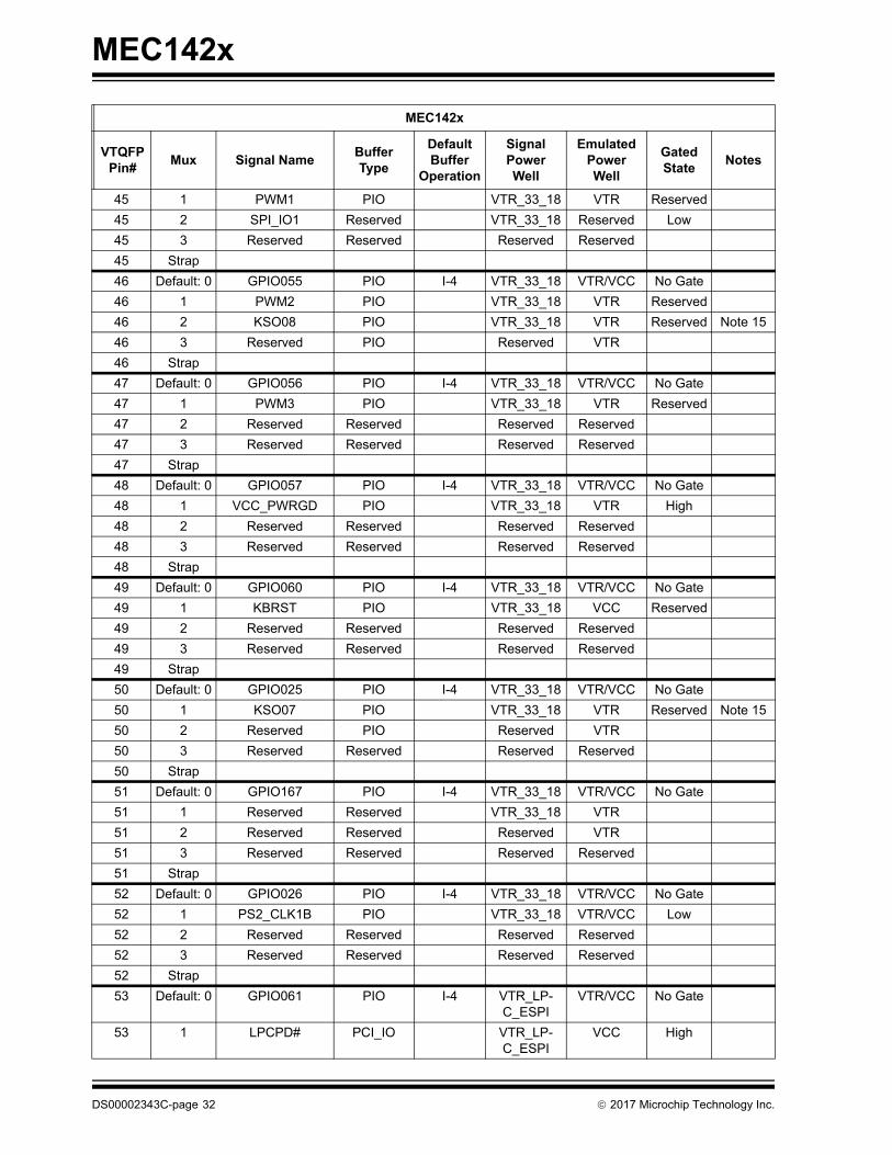
Multifunction Pin Multiplexing in the MEC142x is controlled by the GPIO Interface and illustrated in the Pin MultiplexingTable in this section. See Section 2.3, "Notes for Tables in this Chapter," on page 13 for notes that are referenced inthe Pin Multiplexing Table. See Pin Control Register on page 331 for Pin Multiplexing programming details.
Pin signal functions that exhibit power domain emulation (see Pin Multiplexing Table below) have a different power sup-ply designation in the “Emulated Power Well” column and “Signal Power Well” column.
2.11.1 VCC POWER DOMAIN EMULATION
The System Runtime Supply power VCC is not connected to the MEC142x. The VCC_PWRGD signal is used to indicatewhen power is applied to the System Runtime Supply.
Pin signal functions with VCC power domain emulation are documented in the Pin Multiplexing Table as “Signal PowerWell” = VTR and “Emulated Power Well” = VCC. These pins are powered by VTR and controlled by the VCC_PWRGDsignal input. Outputs on VCC power domain emulation pin signal functions are tri-stated when VCC_PWRGD is notasserted and are functional when VCC_PWRGD is active. Inputs on VCC power domain emulation pin signal functionsare gated according as defined by the Gated State column in the following tables.
Power well emulation for GPIOs and for signals that are multiplexed with GPIO signals is controlled by the Power GatingSignals field in the GPIO Pin Control Register.
2.11.2 PIN MULTIPLEXING TABLE
In the following table, the columns have the following meanings:
MUX
If the pin has an associated GPIO, then the MUX column refers to the Mux Control field in the GPIO Pin Control Register.Setting the Mux Control field to value listed in the row will configure the pin for the signal listed in the Signal column onthe same row. The row marked “Default” is the setting that is assigned on system reset.
If there is no GPIO associated with a pin, then the pin has a single function.
UART Port RI# Ring Indicator Input
UART Port RTS# Request to Send Output
UART Port UART_CLK UART Baud Clock Input
UART Port UART_RX UART Receive Data (RXD)
UART Port UART_TX UART Transmit Data (TXD)
VBAT-Powered Control Interface BGPO Battery Powered General Purpose Output
VBAT-Powered Control Interface SYSPWR_PRES Battery Powered System Power Present Input
Note 12
VBAT-Powered Control Interface VCI_IN0# Input can cause wakeup or interrupt event
Note 14
VBAT-Powered Control Interface VCI_IN1# Input can cause wakeup or interrupt event
Note 14
VBAT-Powered Control Interface VCI_OUT Output from combinatorial logic and/or EC
VBAT-Powered Control Interface VCI_OVRD_IN Input can cause wakeup or interrupt event
Note 14
Interface Signal Name Description Notes
2017 Microchip Technology Inc. DS00002343C-page 25

MEC142x
SIGNAL
This column lists the signals that can appear on each pin, as configured by the MUX control.
BUFFER TYPE
Pin buffer types are defined in Table 42-5, “DC Electrical Characteristics,” on page 485.
Note that all GPIO pins are of buffer type PIO, which may be configured as input/output, push-pull/OD etc. via the GPIOPin Control Register and Pin Control Register 2. There are some pins where the buffer type is configured by the alternatefunction selection, in which case that buffer type is shown in this column.
DEFAULT BUFFER OPERATION
This column gives the pin behavior following the power-up of VTR. All GPIO pins are programmable after this event.This default pin behavior corresponds to the row marked “Default” in the MUX column.
SIGNAL POWER WELL
This column defines the power well that powers the pin.
EMULATED POWER WELL
Power well emulation for GPIOs and for signals that are multiplexed with GPIO signals is controlled by the Power GatingSignals field in the GPIO Pin Control Register. Power well emulation for signals that are not multiplexed with GPIO sig-nals is defined by the entries in this column. See Section 2.11.1, "VCC Power Domain Emulation".
GATED STATE
This column defines the internal value of an input signal when either its emulated power well is inactive or it is notselected by the GPIO alternate function MUX. A value of “No Gate” means that the internal signal always follows thepin even when the emulated power well is inactive.
TABLE 2-2: PIN MULTIPLEXING
Note: Gated state is only meaningful to the operation of input signals. A gated state on an output pin defines theinternal behavior of the GPIO MUX and does not imply pin behavior.
MEC142x
VTQFP Pin#
Mux Signal NameBufferType
DefaultBuffer
Operation
SignalPowerWell
EmulatedPowerWell
GatedState
Notes
1 Default: 0 GPIO157 PIO I-4 VTR VTR/VCC No Gate
1 1 LED0 PIO VTR VTR Reserved
1 2 TST_CLK_OUT PIO VTR VTR Reserved Note 13
1 3 Reserved Reserved Reserved Reserved
1 Strap
2 Default: 0 GPIO027 PIO I-4 VTR VTR/VCC No Gate
2 1 KSO00 PIO VTR VTR Reserved Note 15
2 2 PVT_IO1 PIO VTR VTR Low Note 10
2 3 Reserved Reserved Reserved Reserved
2 Strap
3 Default: 0 GPIO001 PIO I-4 VTR VTR/VCC No Gate
3 1 KSO05 PIO VTR VTR Reserved Note 15
3 2 32KHZ_OUT PIO VTR VTR Reserved
3 3 Reserved Reserved Reserved Reserved
3 Strap
DS00002343C-page 26 2017 Microchip Technology Inc.

MEC142x
4 Default: 0 GPIO002 PIO I-4 VTR VTR/VCC No Gate
4 1 PWM7 PIO VTR VTR Reserved
4 2 Reserved Reserved Reserved Reserved
4 3 Reserved Reserved Reserved Reserved
4 Strap
5 VTR PWR PWR PWR
5
5
5
5 Strap
6 Default: 0 GPIO005 PIO I-4 VTR VTR/VCC No Gate
6 1 SMB00_DATA PIO VTR VTR High Note 4
6 2 SMB00_DATA18 PIO VTR VTR High Note 11
6 3 KSI2 PIO VTR VTR Low Note 15
6 Strap
7 Default: 0 GPIO006 PIO I-4 VTR VTR/VCC No Gate
7 1 SMB00_CLK PIO VTR VTR High Note 4
7 2 SMB00_CLK18 PIO VTR VTR High Note 11
7 3 KSI3 PIO VTR VTR Low Note 15
7 Strap
8 Default: 0 GPIO007 PIO I-4 VTR VTR/VCC No Gate
8 1 SMB01_DATA PIO VTR VTR High Note 4
8 2 SMB01_DATA18 PIO VTR VTR High Note 11
8 3 Reserved Reserved Reserved Reserved
8 Strap
9 Default: 0 GPIO010 PIO I-4 VTR VTR/VCC No Gate
9 1 SMB01_CLK PIO VTR VTR High Note 4
9 2 SMB01_CLK18 PIO VTR VTR High Note 11
9 3 Reserved Reserved Reserved Reserved
9 Strap
10 Default: 0 GPIO011 PIO I-4 VTR VTR/VCC No Gate
10 1 nSMI PIO VTR VTR Reserved
10 2 nEMI_INT PIO VTR VTR Reserved
10 3 PWM4 Reserved VTR Reserved Reserved
10 Strap
11 Default: 0 GPIO012 PIO I-4 VTR VTR/VCC No Gate
11 1 SMB02_DATA PIO VTR VTR High Note 4
11 2 SMB02_DATA18 PIO VTR VTR High Note 11
11 3 Reserved Reserved Reserved Reserved
11 Strap
12 Default: 0 GPIO013 PIO I-4 VTR VTR/VCC No Gate
12 1 SMB02_CLK PIO VTR VTR High Note 4
MEC142x
VTQFP Pin#
Mux Signal NameBufferType
DefaultBuffer
Operation
SignalPowerWell
EmulatedPowerWell
GatedState
Notes
2017 Microchip Technology Inc. DS00002343C-page 27
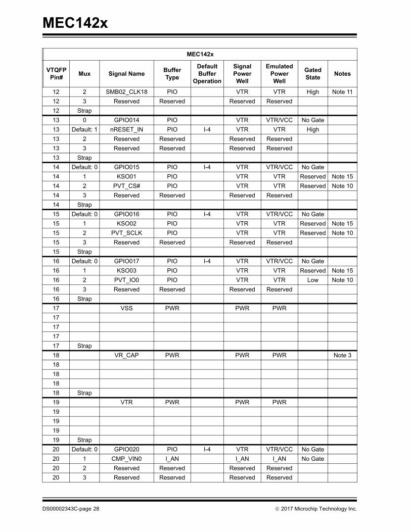
MEC142x
12 2 SMB02_CLK18 PIO VTR VTR High Note 11
12 3 Reserved Reserved Reserved Reserved
12 Strap
13 0 GPIO014 PIO VTR VTR/VCC No Gate
13 Default: 1 nRESET_IN PIO I-4 VTR VTR High
13 2 Reserved Reserved Reserved Reserved
13 3 Reserved Reserved Reserved Reserved
13 Strap
14 Default: 0 GPIO015 PIO I-4 VTR VTR/VCC No Gate
14 1 KSO01 PIO VTR VTR Reserved Note 15
14 2 PVT_CS# PIO VTR VTR Reserved Note 10
14 3 Reserved Reserved Reserved Reserved
14 Strap
15 Default: 0 GPIO016 PIO I-4 VTR VTR/VCC No Gate
15 1 KSO02 PIO VTR VTR Reserved Note 15
15 2 PVT_SCLK PIO VTR VTR Reserved Note 10
15 3 Reserved Reserved Reserved Reserved
15 Strap
16 Default: 0 GPIO017 PIO I-4 VTR VTR/VCC No Gate
16 1 KSO03 PIO VTR VTR Reserved Note 15
16 2 PVT_IO0 PIO VTR VTR Low Note 10
16 3 Reserved Reserved Reserved Reserved
16 Strap
17 VSS PWR PWR PWR
17
17
17
17 Strap
18 VR_CAP PWR PWR PWR Note 3
18
18
18
18 Strap
19 VTR PWR PWR PWR
19
19
19
19 Strap
20 Default: 0 GPIO020 PIO I-4 VTR VTR/VCC No Gate
20 1 CMP_VIN0 I_AN I_AN I_AN No Gate
20 2 Reserved Reserved Reserved Reserved
20 3 Reserved Reserved Reserved Reserved
MEC142x
VTQFP Pin#
Mux Signal NameBufferType
DefaultBuffer
Operation
SignalPowerWell
EmulatedPowerWell
GatedState
Notes
DS00002343C-page 28 2017 Microchip Technology Inc.
MEC142x
20 Strap
21 Default: 0 GPIO021 PIO I-4 PWR VTR/VCC No Gate
21 1 CMP_VIN1 I_AN I_AN I_AN No Gate
21 2 Reserved Reserved Reserved Reserved
21 3 Reserved Reserved Reserved Reserved
21 Strap
22 Default: 0 GPIO066 PIO I-4 VTR VTR/VCC No Gate
22 1 KSO06 PIO VTR VTR Reserved Note 15
22 2 Reserved Reserved Reserved Reserved
22 3 Reserved Reserved Reserved Reserved
22 Strap
23 Default: 0 GPIO160 PIO I-4 VTR VTR/VCC No Gate
23 1 PWM2 O_AN VTR VTR Reserved
23 2 KSO08 Reserved VTR Reserved Reserved Note 15
23 3 PVT_IO3 Reserved VTR Reserved Low
23 Strap
24 Default: 0 GPIO161 PIO I-4 VTR VTR/VCC No Gate
24 1 KSO07 O_AN VTR VTR Reserved Note 15
24 2 PVT_IO2 Reserved VTR Reserved Low
24 3 Reserved Reserved Reserved Reserved
24 Strap
25 Default: 0 GPIO165 PIO I-4 VTR VTR/VCC No Gate
25 1 CMP_VREF0 CMP_VREF CMP_VREF CMP_VREF No Gate
25 2 Reserved Reserved Reserved Reserved
25 3 Reserved Reserved Reserved Reserved
25 Strap
26 Default: 0 GPIO166 PIO I-4 VTR VTR/VCC No Gate
26 1 CMP_VREF1 CMP_VREF CMP_VREF CMP_VREF No Gate
26 2 UART_CLK PIO VTR VTR/VCC Low
26 3 Reserved Reserved Reserved Reserved
26 Strap
27 Default: 0 GPIO123 PIO I-4 VTR_33_18 VTR/VCC No Gate Note 16
27 1 SHD_CS0# PIO VTR_33_18 VTR Reserved Note 10, Note 19
27 2 Reserved Reserved Reserved Reserved
27 3 Reserved Reserved Reserved Reserved
27 Strap BSS_STRAP
28 Default: 0 GPIO133 PIO I-4 VTR_33_18 VTR/VCC No Gate
28 1 SHD_IO0 PIO VTR_33_18 VTR Low Note 10
28 2 Reserved Reserved Reserved Reserved
28 3 Reserved Reserved Reserved Reserved
28 Strap
29 Default: 0 GPIO134 PIO I-4 VTR_33_18 VTR/VCC No Gate
MEC142x
VTQFP Pin#
Mux Signal NameBufferType
DefaultBuffer
Operation
SignalPowerWell
EmulatedPowerWell
GatedState
Notes
2017 Microchip Technology Inc. DS00002343C-page 29

MEC142x
29 1 SHD_IO1 PIO VTR_33_18 VTR Low Note 10
29 2 Reserved Reserved Reserved Reserved
29 3 Reserved Reserved Reserved Reserved
29 Strap
30 Default: 0 GPIO135 PIO I-4 VTR_33_18 VTR/VCC No Gate Note 17
30 1 SHD_IO2 PIO VTR_33_18 VTR Low Note 10
30 2 Reserved Reserved Reserved Reserved
30 3 Reserved Reserved Reserved Reserved
30 Strap PRG_STRAP
31 Default: 0 GPIO136 PIO I-4 VTR_33_18 VTR/VCC No Gate
31 1 SHD_IO3 PIO VTR_33_18 VTR Low Note 10
31 2 Reserved Reserved Reserved Reserved
31 3 Reserved Reserved Reserved Reserved
31 Strap
32 Default: 0 GPIO126 PIO I-4 VTR_33_18 VTR/VCC No Gate
32 1 SHD_SCLK PIO VTR_33_18 VTR Reserved Note 10
32 2 Reserved Reserved Reserved Reserved
32 3 Reserved Reserved Reserved Reserved
32 Strap
33 Default: 0 GPIO062 PIO I-4 VTR_33_18 VTR/VCC No Gate
33 1 SPI_IO3 PIO VTR_33_18 VTR Low
33 2 Reserved Reserved Reserved Reserved
33 3 Reserved Reserved Reserved Reserved
33 Strap
34 Default: 0 GPIO030 PIO I-4 VTR_33_18 VTR/VCC No Gate
34 1 Reserved PIO Reserved VTR
34 2 PWM4 PIO VTR_33_18 VTR Reserved
34 3 Reserved Reserved Reserved Reserved
34 Strap
35 Default: 0 GPIO031 PIO I-4 VTR_33_18 VTR/VCC No Gate
35 1 SPI_CS# PIO VTR_33_18 VTR Reserved
35 2 PWM5 PIO VTR_33_18 VTR Reserved
35 3 Reserved Reserved Reserved Reserved
35 Strap
36 Default: 0 GPIO032 PIO I-4 VTR_33_18 VTR/VCC No Gate
36 1 SPI_CLK PIO VTR_33_18 VTR Reserved
36 2 PWM6 PIO VTR_33_18 VTR Reserved
36 3 Reserved Reserved Reserved Reserved
36 Strap
MEC142x
VTQFP Pin#
Mux Signal NameBufferType
DefaultBuffer
Operation
SignalPowerWell
EmulatedPowerWell
GatedState
Notes
DS00002343C-page 30 2017 Microchip Technology Inc.

MEC142x
37 Default: 0 GPIO045 PIO I-4 VTR_33_18 VTR/VCC No Gate
37 1 SMB05_DATA PIO VTR_33_18 VTR High Note 7
37 2 KSO04 PIO VTR_33_18 VTR Reserved Note 15
37 3 Reserved Reserved Reserved Reserved
37 Strap
38 Default: 0 GPIO046 PIO I-4 VTR_33_18 VTR/VCC No Gate
38 1 SMB05_CLK PIO VTR_33_18 VTR High Note 7
38 2 KSO05 PIO VTR_33_18 VTR Reserved Note 15
38 3 Reserved Reserved Reserved Reserved
38 Strap
39 Default: 0 GPIO047 PIO I-4 VTR_33_18 VTR/VCC No Gate
39 1 SHD_CS1# PIO VTR_33_18 VTR Reserved Note 10, Note 19
39 2 KSO06 PIO VTR_33_18 VTR Reserved Note 15
39 3 Reserved Reserved Reserved Reserved
39 Strap
40 Default: 0 GPIO050 PIO I-4 VTR_33_18 VTR/VCC No Gate
40 1 TACH0 PIO VTR_33_18 VTR Low
40 2 Reserved Reserved Reserved Reserved
40 3 Reserved Reserved Reserved Reserved
40 Strap
41 Default: 0 GPIO051 PIO I-4 VTR_33_18 VTR/VCC No Gate
41 1 TACH1 PIO VTR_33_18 VTR Low
41 2 Reserved Reserved Reserved Reserved
41 3 Reserved Reserved Reserved Reserved
41 Strap
42 Default: 0 GPIO052 PIO I-4 VTR_33_18 VTR/VCC No Gate
42 1 SPI_IO2 PIO VTR_33_18 VTR Low
42 2 Reserved Reserved Reserved Reserved
42 3 Reserved Reserved Reserved Reserved
42 Strap
43 VTR_33_18 PWR PWR PWR
43
43
43
43 Strap
44 Default: 0 GPIO053 PIO I-4 VTR_33_18 VTR/VCC No Gate
44 1 PWM0 PIO VTR_33_18 VTR Reserved
44 2 SPI_IO0 Reserved VTR_33_18 Reserved Low
44 3 Reserved Reserved Reserved Reserved
44 Strap
45 Default: 0 GPIO054 PIO I-4 VTR_33_18 VTR/VCC No Gate
MEC142x
VTQFP Pin#
Mux Signal NameBufferType
DefaultBuffer
Operation
SignalPowerWell
EmulatedPowerWell
GatedState
Notes
2017 Microchip Technology Inc. DS00002343C-page 31
MEC142x
45 1 PWM1 PIO VTR_33_18 VTR Reserved
45 2 SPI_IO1 Reserved VTR_33_18 Reserved Low
45 3 Reserved Reserved Reserved Reserved
45 Strap
46 Default: 0 GPIO055 PIO I-4 VTR_33_18 VTR/VCC No Gate
46 1 PWM2 PIO VTR_33_18 VTR Reserved
46 2 KSO08 PIO VTR_33_18 VTR Reserved Note 15
46 3 Reserved PIO Reserved VTR
46 Strap
47 Default: 0 GPIO056 PIO I-4 VTR_33_18 VTR/VCC No Gate
47 1 PWM3 PIO VTR_33_18 VTR Reserved
47 2 Reserved Reserved Reserved Reserved
47 3 Reserved Reserved Reserved Reserved
47 Strap
48 Default: 0 GPIO057 PIO I-4 VTR_33_18 VTR/VCC No Gate
48 1 VCC_PWRGD PIO VTR_33_18 VTR High
48 2 Reserved Reserved Reserved Reserved
48 3 Reserved Reserved Reserved Reserved
48 Strap
49 Default: 0 GPIO060 PIO I-4 VTR_33_18 VTR/VCC No Gate
49 1 KBRST PIO VTR_33_18 VCC Reserved
49 2 Reserved Reserved Reserved Reserved
49 3 Reserved Reserved Reserved Reserved
49 Strap
50 Default: 0 GPIO025 PIO I-4 VTR_33_18 VTR/VCC No Gate
50 1 KSO07 PIO VTR_33_18 VTR Reserved Note 15
50 2 Reserved PIO Reserved VTR
50 3 Reserved Reserved Reserved Reserved
50 Strap
51 Default: 0 GPIO167 PIO I-4 VTR_33_18 VTR/VCC No Gate
51 1 Reserved Reserved VTR_33_18 VTR
51 2 Reserved Reserved Reserved VTR
51 3 Reserved Reserved Reserved Reserved
51 Strap
52 Default: 0 GPIO026 PIO I-4 VTR_33_18 VTR/VCC No Gate
52 1 PS2_CLK1B PIO VTR_33_18 VTR/VCC Low
52 2 Reserved Reserved Reserved Reserved
52 3 Reserved Reserved Reserved Reserved
52 Strap
53 Default: 0 GPIO061 PIO I-4 VTR_LP-C_ESPI
VTR/VCC No Gate
53 1 LPCPD# PCI_IO VTR_LP-C_ESPI
VCC High
MEC142x
VTQFP Pin#
Mux Signal NameBufferType
DefaultBuffer
Operation
SignalPowerWell
EmulatedPowerWell
GatedState
Notes
DS00002343C-page 32 2017 Microchip Technology Inc.

MEC142x
53 2 ESPI_RESET# PIO VTR_LP-C_ESPI
VTR Low
53 3 Reserved Reserved Reserved Reserved
53 Strap
54 VTR_LPC_ESPI PWR PWR VTR
54
54
54
54 Strap
55 Default: 0 GPIO063 PIO I-4 VTR_LP-C_ESPI
VTR/VCC No Gate
55 1 SER_IRQ PCI_IO VTR_LP-C_ESPI
VCC High Note 1
55 2 ESPI_ALERT# PIO VTR_LP-C_ESPI
VTR Reserved
55 3 Reserved Reserved Reserved Reserved
55 Strap
56 Default: 0 GPIO064 PCI_PIO I-4 VTR_LP-C_ESPI
VTR/VCC No Gate
56 1 LRESET# PCI_IO VTR_LP-C_ESPI
VCC Low
56 2 Reserved Reserved VTR_LP-C_ESPI
Reserved
56 3 Reserved Reserved Reserved Reserved
56 Strap
57 Default: 0 GPIO034 PIO I-4 VTR_LP-C_ESPI
VTR/VCC No Gate
57 1 PCI_CLK PCI_IO VTR_LP-C_ESPI
VCC Low
57 2 ESPI_CLK PIO VTR_LP-C_ESPI
VTR Low
57 3 Reserved Reserved Reserved Reserved
57 Strap
58 Default: 0 GPIO044 PIO I-4 VTR_LP-C_ESPI
VTR/VCC No Gate
58 1 LFRAME# PCI_IO VTR_LP-C_ESPI
VCC High
58 2 ESPI_CS# PIO VTR_LP-C_ESPI
VTR High
58 3 Reserved Reserved Reserved Reserved
58 Strap
59 Default: 0 GPIO040 PIO I-4 VTR_LP-C_ESPI
VTR/VCC No Gate
59 1 LAD0 PCI_IO VTR_LP-C_ESPI
VCC High Note 1
MEC142x
VTQFP Pin#
Mux Signal NameBufferType
DefaultBuffer
Operation
SignalPowerWell
EmulatedPowerWell
GatedState
Notes
2017 Microchip Technology Inc. DS00002343C-page 33

MEC142x
59 2 ESPI_IO0 PIO VTR_LP-C_ESPI
VTR Low
59 3 Reserved Reserved Reserved Reserved
59 Strap
60 Default: 0 GPIO041 PIO I-4 VTR_LP-C_ESPI
VTR/VCC No Gate
60 1 LAD1 PCI_IO VTR_LP-C_ESPI
VCC High Note 1
60 2 ESPI_IO1 PIO VTR_LP-C_ESPI
VTR Low
60 3 Reserved Reserved Reserved Reserved
60 Strap
61 Default: 0 GPIO042 PIO I-4 VTR_LP-C_ESPI
VTR/VCC No Gate
61 1 LAD2 PCI_IO VTR_LP-C_ESPI
VCC High Note 1
61 2 ESPI_IO2 PIO VTR_LP-C_ESPI
VTR Low
61 3 Reserved Reserved Reserved Reserved
61 Strap
62 Default: 0 GPIO043 PIO I-4 VTR_LP-C_ESPI
VTR/VCC No Gate
62 1 LAD3 PCI_IO VTR_LP-C_ESPI
VCC High Note 1
62 2 ESPI_IO3 PIO VTR_LP-C_ESPI
VTR Low
62 3 Reserved Reserved Reserved Reserved
62 Strap
63 Default: 0 GPIO067 PCI_PIO I-4 VTR_LP-C_ESPI
VTR/VCC No Gate
63 1 CLKRUN# PCI_IO VTR_LP-C_ESPI
VCC Low
63 2 Reserved Reserved Reserved Reserved
63 3 Reserved Reserved Reserved Reserved
63 Strap
64 VSS PWR PWR PWR
64
64
64
64 Strap
65 VTR PWR PWR PWR
65
65
65
65 Strap
MEC142x
VTQFP Pin#
Mux Signal NameBufferType
DefaultBuffer
Operation
SignalPowerWell
EmulatedPowerWell
GatedState
Notes
DS00002343C-page 34 2017 Microchip Technology Inc.

MEC142x
66 Default: 0 GPIO100 PIO I-4 VTR VTR/VCC No Gate
66 1 nEC_SCI PIO VTR VTR Reserved
66 2 Reserved Reserved Reserved Reserved
66 3 Reserved Reserved Reserved Reserved
66 Strap
67 Default: 0 GPIO101 PIO I-4 VTR VTR/VCC No Gate
67 1 KSO04 PIO VTR VTR Reserved Note 15
67 2 Reserved Reserved Reserved Reserved
67 3 Reserved Reserved Reserved Reserved
67 Strap
68 Default: 0 GPIO102 PIO I-4 VTR VTR/VCC No Gate
68 1 KSO09 PIO VTR VTR Reserved Note 15
68 2 Reserved Reserved Reserved Reserved
68 3 Reserved Reserved Reserved Reserved
68 Strap CR_STRAP
69 Default: 0 GPIO103 PIO I-4 VTR VTR/VCC No Gate
69 1 VCC_PWRGD PIO VTR VTR High
69 2 Reserved Reserved Reserved Reserved
69 3 Reserved Reserved Reserved Reserved
69 Strap
70 Default: 0 GPIO104 PIO I-4 VTR VTR/VCC No Gate
70 1 LED2 PIO VTR VTR Reserved
70 2 Reserved Reserved Reserved Reserved
70 3 Reserved Reserved Reserved Reserved
70 Strap
71 Default: 0 GPIO105 PIO I-4 VTR VTR/VCC No Gate
71 1 PS2_CLK1B PIO VTR VTR Low
71 2 PWM0 Reserved VTR Reserved Reserved
71 3 Reserved Reserved Reserved Reserved
71 Strap
72 Default: 0 GPIO106 PIO I-4 VTR VTR/VCC No Gate
72 1 KSO10 PIO VTR VTR Reserved Note 15
72 2 PCIRST_OUT0# Reserved Reserved Reserved Reserved
72 3 Reserved Reserved Reserved Reserved
72 Strap
73 Default: 0 GPIO107 PIO I-4 VTR VTR/VCC No Gate Note 5
73 1 nRESET_OUT PIO VTR VTR Reserved Note 5
73 2 Reserved Reserved Reserved Reserved
73 3 Reserved Reserved Reserved Reserved
73 Strap
74 Default: 0 GPIO110 PIO I-4 VTR VTR/VCC No Gate
74 1 KSO11 PIO VTR VTR Reserved Note 15
MEC142x
VTQFP Pin#
Mux Signal NameBufferType
DefaultBuffer
Operation
SignalPowerWell
EmulatedPowerWell
GatedState
Notes
2017 Microchip Technology Inc. DS00002343C-page 35

MEC142x
74 2 TACH2 Reserved Reserved Reserved Reserved
74 3 Reserved Reserved Reserved Reserved
74 Strap
75 Default: 0 GPIO111 PIO I-4 VTR VTR/VCC No Gate
75 1 KSO12 PIO VTR VTR Reserved Note 15
75 2 TACH3 Reserved Reserved Reserved Reserved
75 3 Reserved Reserved Reserved Reserved
75 Strap
76 Default: 0 GPIO112 PIO I-4 VTR VTR/VCC No Gate
76 1 PS2_CLK1A PIO VTR VTR/VCC Low
76 2 KSO13 PIO VTR VTR Reserved Note 15
76 3 Reserved Reserved Reserved Reserved
76 Strap
77 Default: 0 GPIO113 PIO I-4 VTR VTR/VCC No Gate
77 1 PS2_DAT1A PIO VTR VTR/VCC Low
77 2 KSO14 PIO VTR VTR Reserved Note 15
77 3 Reserved Reserved Reserved Reserved
77 Strap
78 Default: 0 GPIO114 PIO I-4 VTR VTR/VCC No Gate
78 1 PS2_CLK0 PIO VTR VTR/VCC Low
78 2 Reserved Reserved Reserved Reserved
78 3 Reserved Reserved Reserved Reserved
78 Strap
79 Default: 0 GPIO115 PIO I-4 VTR VTR/VCC No Gate
79 1 PS2_DAT0 PIO VTR VTR/VCC Low
79 2 Reserved Reserved Reserved Reserved
79 3 Reserved Reserved Reserved Reserved
79 Strap
80 Default: 0 GPIO116 PIO I-4 VTR VTR/VCC No Gate
80 1 TFDP_DATA PIO VTR VTR Low
80 2 UART_RX PIO VTR VTR High
80 3 Reserved Reserved Reserved Reserved
80 Strap
81 Default: 0 GPIO117 PIO I-4 VTR VTR/VCC No Gate
81 1 TFDP_CLK PIO VTR VTR Low
81 2 UART_TX PIO VTR VTR Reserved
81 3 Reserved Reserved Reserved Reserved
81 Strap VL_STRAP
82 VTR PWR PWR PWR
82
82
82
MEC142x
VTQFP Pin#
Mux Signal NameBufferType
DefaultBuffer
Operation
SignalPowerWell
EmulatedPowerWell
GatedState
Notes
DS00002343C-page 36 2017 Microchip Technology Inc.
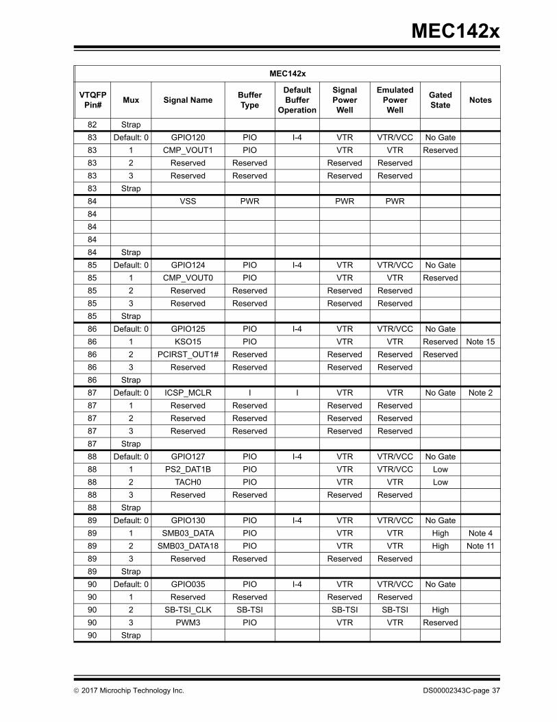
MEC142x
82 Strap
83 Default: 0 GPIO120 PIO I-4 VTR VTR/VCC No Gate
83 1 CMP_VOUT1 PIO VTR VTR Reserved
83 2 Reserved Reserved Reserved Reserved
83 3 Reserved Reserved Reserved Reserved
83 Strap
84 VSS PWR PWR PWR
84
84
84
84 Strap
85 Default: 0 GPIO124 PIO I-4 VTR VTR/VCC No Gate
85 1 CMP_VOUT0 PIO VTR VTR Reserved
85 2 Reserved Reserved Reserved Reserved
85 3 Reserved Reserved Reserved Reserved
85 Strap
86 Default: 0 GPIO125 PIO I-4 VTR VTR/VCC No Gate
86 1 KSO15 PIO VTR VTR Reserved Note 15
86 2 PCIRST_OUT1# Reserved Reserved Reserved Reserved
86 3 Reserved Reserved Reserved Reserved
86 Strap
87 Default: 0 ICSP_MCLR I I VTR VTR No Gate Note 2
87 1 Reserved Reserved Reserved Reserved
87 2 Reserved Reserved Reserved Reserved
87 3 Reserved Reserved Reserved Reserved
87 Strap
88 Default: 0 GPIO127 PIO I-4 VTR VTR/VCC No Gate
88 1 PS2_DAT1B PIO VTR VTR/VCC Low
88 2 TACH0 PIO VTR VTR Low
88 3 Reserved Reserved Reserved Reserved
88 Strap
89 Default: 0 GPIO130 PIO I-4 VTR VTR/VCC No Gate
89 1 SMB03_DATA PIO VTR VTR High Note 4
89 2 SMB03_DATA18 PIO VTR VTR High Note 11
89 3 Reserved Reserved Reserved Reserved
89 Strap
90 Default: 0 GPIO035 PIO I-4 VTR VTR/VCC No Gate
90 1 Reserved Reserved Reserved Reserved
90 2 SB-TSI_CLK SB-TSI SB-TSI SB-TSI High
90 3 PWM3 PIO VTR VTR Reserved
90 Strap
MEC142x
VTQFP Pin#
Mux Signal NameBufferType
DefaultBuffer
Operation
SignalPowerWell
EmulatedPowerWell
GatedState
Notes
2017 Microchip Technology Inc. DS00002343C-page 37

MEC142x
91 Default: 0 GPIO131 PIO I-4 VTR VTR/VCC No Gate
91 1 SMB03_CLK PIO VTR VTR High Note 4
91 2 SMB03_CLK18 PIO VTR VTR High Note 11
91 3 Reserved Reserved Reserved Reserved
91 Strap
92 Default: 0 GPIO132 PIO I-4 VTR VTR/VCC No Gate
92 1 KSO16 PIO VTR VTR Reserved Note 15
92 2 PCI_RESET# Reserved Reserved Reserved Reserved
92 3 Reserved Reserved Reserved Reserved
92 Strap
93 Default: 0 GPIO140 PIO I-4 VTR VTR/VCC No Gate
93 1 KSO17 PIO VTR VTR Reserved Note 15
93 2 PWM5 PIO VTR VTR Reserved
93 3 Reserved Reserved Reserved Reserved
93 Strap
94 Default: 0 GPIO033 PIO I-4 VTR VTR/VCC No Gate
94 1 PECI_DAT PECI_IO PECI_IO PECI_IO Low Note 12
94 2 SB_TSI_DAT SB-TSI SB-TSI SB-TSI Low Note 12
94 3 Reserved Reserved Reserved Reserved
94 Strap
95 VREF_CPU VREF_CPU VREF_CPU VREF_CPU Note 6, Note 18
95
95
95
95 Strap
96 Default: 0 GPIO141 PIO I-4 VTR VTR/VCC No Gate
96 1 SMB04_DATA PIO VTR VTR High Note 4
96 2 SMB04_DATA18 PIO VTR VTR High Note 11
96 3 Reserved Reserved Reserved Reserved
96 Strap
97 Default: 0 GPIO142 PIO I-4 VTR VTR/VCC No Gate
97 1 SMB04_CLK PIO VTR VTR High Note 4
97 2 SMB04_CLK18 PIO VTR VTR High Note 11
97 3 Reserved Reserved Reserved Reserved
97 Strap
98 Default: 0 GPIO143 PIO I-4 VTR VTR/VCC No Gate Note 9
98 1 KSI0 PIO VTR VTR Low Note 15
98 2 DTR# PIO VTR VTR Reserved
98 3 Reserved Reserved Reserved Reserved
98 Strap
99 Default: 0 GPIO144 PIO I-4 VTR VTR/VCC No Gate
99 1 KSI1 PIO VTR VTR Low Note 15
MEC142x
VTQFP Pin#
Mux Signal NameBufferType
DefaultBuffer
Operation
SignalPowerWell
EmulatedPowerWell
GatedState
Notes
DS00002343C-page 38 2017 Microchip Technology Inc.

MEC142x
99 2 DCD# PIO VTR VTR High
99 3 Reserved Reserved Reserved Reserved
99 Strap
100 VSS PWR PWR PWR
100
100
100
100 Strap
101 Default: 0 GPIO145 (ICSP_-CLOCK)
PIO I-4 VTR VTR/VCC No Gate Note 2
101 1 Reserved PIO Reserved Reserved
101 2 Reserved Reserved Reserved Reserved
101 3 Reserved Reserved Reserved Reserved
101 Strap
102 Default: 0 GPIO146 (ICSP_-DATA)
PIO I-4 VTR VTR/VCC No Gate Note 2
102 1 Reserved PIO Reserved Reserved
102 2 Reserved Reserved Reserved Reserved
102 3 Reserved Reserved Reserved Reserved
102 Strap
103 VTR PWR PWR PWR
103
103
103
103 Strap
104 Default: 0 GPIO147 PIO I-4 VTR VTR/VCC No Gate
104 1 KSI4 PIO VTR VTR Low Note 15
104 2 DSR# PIO VTR VTR High
104 3 Reserved Reserved Reserved Reserved
104 Strap
105 Default: 0 GPIO150 PIO I-4 VTR VTR/VCC No Gate
105 1 KSI5 PIO VTR VTR Low Note 15
105 2 RI# PIO VTR VTR High
105 3 Reserved Reserved Reserved Reserved
105 Strap
106 Default: 0 GPIO156 PIO I-4 VTR VTR/VCC No Gate
106 1 LED1 PIO VTR VTR Reserved
106 2 Reserved Reserved Reserved Reserved
106 3 Reserved Reserved Reserved Reserved
106 Strap
107 Default: 0 GPIO151 PIO I-4 VTR VTR/VCC No Gate
107 1 KSI6 PIO VTR VTR Low Note 15
107 2 RTS# PIO VTR VTR Reserved
MEC142x
VTQFP Pin#
Mux Signal NameBufferType
DefaultBuffer
Operation
SignalPowerWell
EmulatedPowerWell
GatedState
Notes
2017 Microchip Technology Inc. DS00002343C-page 39

MEC142x
107 3 Reserved Reserved Reserved Reserved
107 Strap
108 Default: 0 GPIO152 PIO I-4 VTR VTR/VCC No Gate
108 1 KSI7 PIO VTR VTR Low Note 15
108 2 CTS# PIO VTR VTR High
108 3 Reserved Reserved Reserved Reserved
108 Strap
109 Default: 0 GPIO153 PIO I-2 VTR VTR/VCC No Gate
109 1 ADC4 I_AN I_AN I_AN No Gate Note 8
109 2 Reserved Reserved Reserved Reserved
109 3 Reserved Reserved Reserved Reserved
109 Strap
110 Default: 0 GPIO154 PIO I-2 VTR VTR/VCC No Gate
110 1 ADC3 I_AN I_AN I_AN No Gate Note 8
110 2 Reserved Reserved Reserved Reserved
110 3 Reserved Reserved Reserved Reserved
110 Strap
111 Default: 0 GPIO155 PIO I-2 VTR VTR/VCC No Gate
111 1 ADC2 I_AN I_AN I_AN No Gate Note 8
111 2 Reserved Reserved Reserved Reserved
111 3 Reserved Reserved Reserved Reserved
111 Strap
112 AVSS PWR PWR PWR
112
112
112
112 Strap
113 Default: 0 GPIO122 PIO I-2 VTR VTR/VCC No Gate
113 1 ADC1 I_AN I_AN I_AN No Gate Note 8
113 2 Reserved Reserved Reserved Reserved
113 3 Reserved Reserved Reserved Reserved
113 Strap
114 Default: 0 GPIO121 PIO I-2 VTR VTR/VCC No Gate
114 1 ADC0 I_AN I_AN I_AN No Gate Note 8
114 2 Reserved Reserved Reserved Reserved
114 3 Reserved Reserved Reserved Reserved
114 Strap
115 0 Reserved Reserved Reserved Reserved
115 Default: 1 ADC_VREF ADC_VREF ADC_VREF ADC_VREF No Gate
115 2 Reserved Reserved Reserved Reserved
115 3 Reserved Reserved Reserved Reserved
115 Strap
MEC142x
VTQFP Pin#
Mux Signal NameBufferType
DefaultBuffer
Operation
SignalPowerWell
EmulatedPowerWell
GatedState
Notes
DS00002343C-page 40 2017 Microchip Technology Inc.
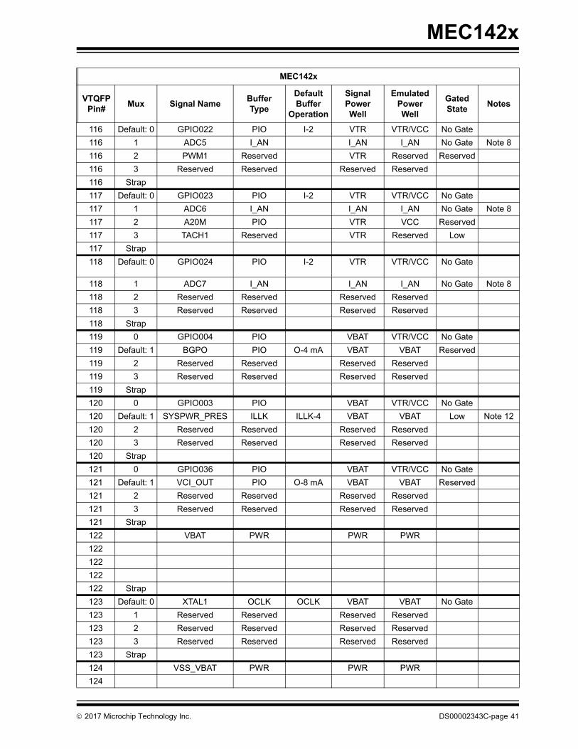
MEC142x
116 Default: 0 GPIO022 PIO I-2 VTR VTR/VCC No Gate
116 1 ADC5 I_AN I_AN I_AN No Gate Note 8
116 2 PWM1 Reserved VTR Reserved Reserved
116 3 Reserved Reserved Reserved Reserved
116 Strap
117 Default: 0 GPIO023 PIO I-2 VTR VTR/VCC No Gate
117 1 ADC6 I_AN I_AN I_AN No Gate Note 8
117 2 A20M PIO VTR VCC Reserved
117 3 TACH1 Reserved VTR Reserved Low
117 Strap
118 Default: 0 GPIO024 PIO I-2 VTR VTR/VCC No Gate
118 1 ADC7 I_AN I_AN I_AN No Gate Note 8
118 2 Reserved Reserved Reserved Reserved
118 3 Reserved Reserved Reserved Reserved
118 Strap
119 0 GPIO004 PIO VBAT VTR/VCC No Gate
119 Default: 1 BGPO PIO O-4 mA VBAT VBAT Reserved
119 2 Reserved Reserved Reserved Reserved
119 3 Reserved Reserved Reserved Reserved
119 Strap
120 0 GPIO003 PIO VBAT VTR/VCC No Gate
120 Default: 1 SYSPWR_PRES ILLK ILLK-4 VBAT VBAT Low Note 12
120 2 Reserved Reserved Reserved Reserved
120 3 Reserved Reserved Reserved Reserved
120 Strap
121 0 GPIO036 PIO VBAT VTR/VCC No Gate
121 Default: 1 VCI_OUT PIO O-8 mA VBAT VBAT Reserved
121 2 Reserved Reserved Reserved Reserved
121 3 Reserved Reserved Reserved Reserved
121 Strap
122 VBAT PWR PWR PWR
122
122
122
122 Strap
123 Default: 0 XTAL1 OCLK OCLK VBAT VBAT No Gate
123 1 Reserved Reserved Reserved Reserved
123 2 Reserved Reserved Reserved Reserved
123 3 Reserved Reserved Reserved Reserved
123 Strap
124 VSS_VBAT PWR PWR PWR
124
MEC142x
VTQFP Pin#
Mux Signal NameBufferType
DefaultBuffer
Operation
SignalPowerWell
EmulatedPowerWell
GatedState
Notes
2017 Microchip Technology Inc. DS00002343C-page 41
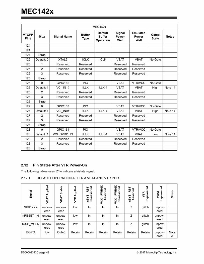
MEC142x
2.12 Pin States After VTR Power-On
The following tables uses ‘Z’ to indicate a tristate signal.
2.12.1 DEFAULT OPERATION AFTER A VBAT AND VTR POR
124
124
124 Strap
125 Default: 0 XTAL2 ICLK ICLK VBAT VBAT No Gate
125 1 Reserved Reserved Reserved Reserved
125 2 Reserved Reserved Reserved Reserved
125 3 Reserved Reserved Reserved Reserved
125 Strap
126 0 GPIO162 PIO VBAT VTR/VCC No Gate
126 Default: 1 VCI_IN1# ILLK ILLK-4 VBAT VBAT High Note 14
126 2 Reserved Reserved Reserved Reserved
126 3 Reserved Reserved Reserved Reserved
126 Strap
127 0 GPIO163 PIO VBAT VTR/VCC No Gate
127 Default: 1 VCI_IN0# ILLK ILLK-4 VBAT VBAT High Note 14
127 2 Reserved Reserved Reserved Reserved
127 3 Reserved Reserved Reserved Reserved
127 Strap
128 0 GPIO164 PIO VBAT VTR/VCC No Gate
128 Default: 1 VCI_OVRD_IN ILLK ILLK-4 VBAT VBAT Low Note 14
128 2 Reserved Reserved Reserved Reserved
128 3 Reserved Reserved Reserved Reserved
128 Strap
Sig
nal
VB
AT
Ap
pli
ed
VB
AT
Sta
ble
VT
R A
pp
lie
d
nS
YS
_R
ST
D
e-a
sse
rte
d
VC
C_
PW
RG
DA
ss
ert
ed
VC
C_
PW
RG
DD
e-a
sse
rte
d
nS
YS
_ R
ST
As
se
rte
d
VT
R
Un
-po
we
red
VB
AT
Un
-po
we
red
No
tes
GPIOXXX unpow-ered
unpow-ered
low In In In Z glitch unpow-ered
nRESET_IN unpow-ered
unpow-ered
low In In In Z glitch unpow-ered
ICSP_MCLR unpow-ered
unpow-ered
low In In In Z glitch unpow-ered
BGPO low Out=0 Retain Retain Retain Retain Retain Retain unpow-ered
Note A
MEC142x
VTQFP Pin#
Mux Signal NameBufferType
DefaultBuffer
Operation
SignalPowerWell
EmulatedPowerWell
GatedState
Notes
DS00002343C-page 42 2017 Microchip Technology Inc.

MEC142x
2.12.2 DEFAULT OPERATION AFTER A VTR POR ONLY (VBAT REMAINS ON)
The following table lists the VTR POR default conditions for VBAT powered pins where the EC had selected an alternatefunction that was not the default function.
2.13 Strapping Options
2.13.1 CRISIS RECOVERY AND BOOT SOURCE SELECT STRAPS
The Crisis Recovery Strap option (CR_STRAP) is implemented on GPIO102/KSO09[CR_STRAP].
The Boot Source Select Strap option (BSS_STRAP) is implemented on GPIO123/SHD_CS0#[BSS_STRAP].
• If the CR_STRAP pin is connected to ground the Boot ROM will load the SPI Flash image from the SPI Flash located on the Private SPI Interface (PVT_xxxx).
• If this pin is pulled high, which is the normal operation for the Key Scan Interface, the Boot ROM will load the SPI Flash image from the Shared Flash Interface (SHD_xxxx) or the eSPI Flash channel as selected by the Boot Source Select Strap (BSS_STRAP) on the GPIO123/SHD_CS0# pin. A 10k-100k ohm pull-up resistor to VTR is recommended to insure that this pin is sampled as high.
SYS-PWR_PRES
In In In In In In In In unpow-ered
VCI_INx# In In In In In In In In unpow-ered
VCI_OUT Out logic Out logic Out logic Out logic Out logic Out logic Out logic Out logic unpow-ered
Note B
VCI_OVRD_IN
In In In In In In In In unpow-ered
Note:
- Note A: Pin is programmable by the EC and retains its value through a VTR power cycle.
- Note B: Pin is programmable by the EC and affected by other VBAT inputs pins.
Sig
na
l
VB
AT
Ap
pli
ed
VB
AT
Sta
ble
VT
R A
pp
lie
d
nS
YS
_R
ST
De-
as
se
rte
d
VC
C_
PW
RG
DA
sser
ted
VC
C_
PW
RG
DD
e-a
ss
ert
ed
nS
YS
_ R
ST
Ass
erte
d
VT
R
Un
-po
we
red
VB
AT
U
n-p
ow
ere
d
No
tes
GPIO003 N/A N/A low In In In Z In unpowered Note C
GPIO004 N/A N/A low In In In Z In unpowered Note C
GPIO036 N/A N/A low In In In Z In unpowered Note C
GPIO162 N/A N/A low In In In Z In unpowered Note C
GPIO163 N/A N/A low In In In Z In unpowered Note C
GPIO164 N/A N/A low In In In Z In unpowered Note C
Note:
- Note C: The GPIO Control logic is powered by VTR and loses its configuration through a VTR POR.
Sig
na
l
VB
AT
Ap
pli
ed
VB
AT
Sta
ble
VT
R A
pp
lie
d
nS
YS
_R
ST
D
e-as
se
rte
d
VC
C_
PW
RG
DA
ss
erte
d
VC
C_
PW
RG
DD
e-as
se
rte
d
nS
YS
_ R
ST
As
ser
ted
VT
R
Un
-po
we
red
VB
AT
Un
-po
we
red
No
tes
2017 Microchip Technology Inc. DS00002343C-page 43
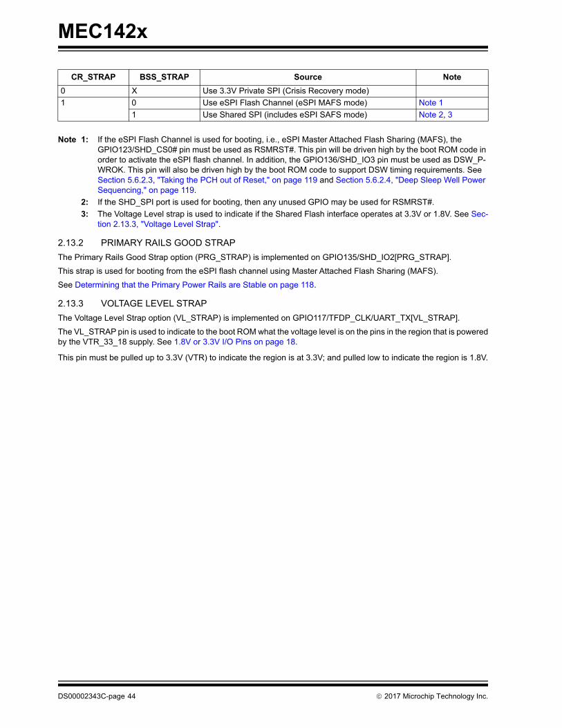
MEC142x
Note 1: If the eSPI Flash Channel is used for booting, i.e., eSPI Master Attached Flash Sharing (MAFS), the GPIO123/SHD_CS0# pin must be used as RSMRST#. This pin will be driven high by the boot ROM code in order to activate the eSPI flash channel. In addition, the GPIO136/SHD_IO3 pin must be used as DSW_P-WROK. This pin will also be driven high by the boot ROM code to support DSW timing requirements. See Section 5.6.2.3, "Taking the PCH out of Reset," on page 119 and Section 5.6.2.4, "Deep Sleep Well Power Sequencing," on page 119.
2: If the SHD_SPI port is used for booting, then any unused GPIO may be used for RSMRST#.
3: The Voltage Level strap is used to indicate if the Shared Flash interface operates at 3.3V or 1.8V. See Sec-tion 2.13.3, "Voltage Level Strap".
2.13.2 PRIMARY RAILS GOOD STRAP
The Primary Rails Good Strap option (PRG_STRAP) is implemented on GPIO135/SHD_IO2[PRG_STRAP].
This strap is used for booting from the eSPI flash channel using Master Attached Flash Sharing (MAFS).
See Determining that the Primary Power Rails are Stable on page 118.
2.13.3 VOLTAGE LEVEL STRAP
The Voltage Level Strap option (VL_STRAP) is implemented on GPIO117/TFDP_CLK/UART_TX[VL_STRAP].
The VL_STRAP pin is used to indicate to the boot ROM what the voltage level is on the pins in the region that is poweredby the VTR_33_18 supply. See 1.8V or 3.3V I/O Pins on page 18.
This pin must be pulled up to 3.3V (VTR) to indicate the region is at 3.3V; and pulled low to indicate the region is 1.8V.
CR_STRAP BSS_STRAP Source Note
0 X Use 3.3V Private SPI (Crisis Recovery mode)
1 0 Use eSPI Flash Channel (eSPI MAFS mode) Note 1
1 Use Shared SPI (includes eSPI SAFS mode) Note 2, 3
DS00002343C-page 44 2017 Microchip Technology Inc.

MEC142x
2.14 Packages
2.14.1 128-PIN VTQFP PACKAGE OUTLINE
Note: For the most current package drawings, see the Microchip Packaging Specification at http://www.microchip.com/packaging.
2017 Microchip Technology Inc. DS00002343C-page 45
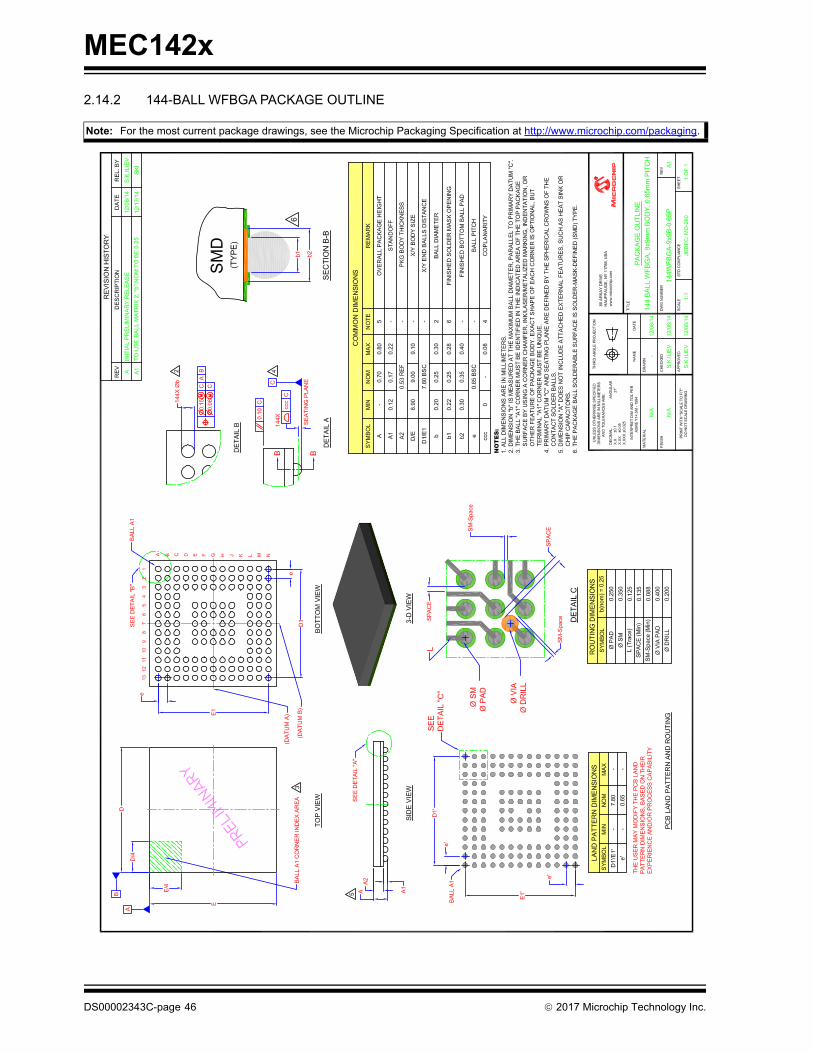
MEC142x
2.14.2 144-BALL WFBGA PACKAGE OUTLINE
Note: For the most current package drawings, see the Microchip Packaging Specification at http://www.microchip.com/packaging.
DS00002343C-page 46 2017 Microchip Technology Inc.
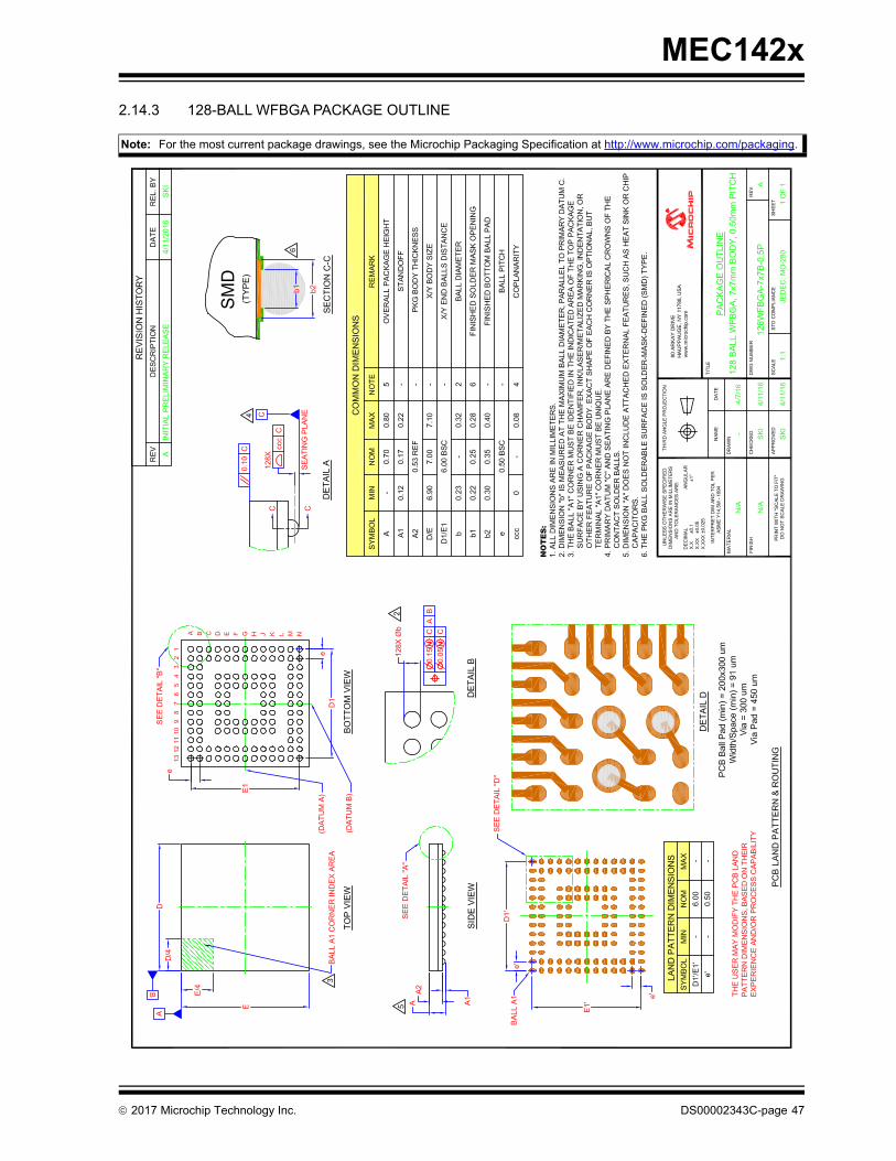
MEC142x
2.14.3 128-BALL WFBGA PACKAGE OUTLINE
Note: For the most current package drawings, see the Microchip Packaging Specification at http://www.microchip.com/packaging.
2017 Microchip Technology Inc. DS00002343C-page 47

MEC142x
3.0 POWER, CLOCKS, AND RESETS
3.1 Introduction
The Power, Clocks, and Resets (PCR) chapter identifies all the power supplies, clock sources, and reset inputs to thechip and defines all the derived power, clock, and reset signals. In addition, this section identifies Power, Clock, andReset events that may be used to generate an interrupt event, as well as, the Chip Power Management Features.
3.2 References
No references have been cited for this chapter.
3.3 Interrupts
The Power, Clocks, and Resets logic generates no events
3.4 Power
3.4.1 POWER SOURCES
Table 3-1 lists the power supplies from which the MEC142x draws current. These current values are defined in Section42.3, "Power Consumption," on page 492.
TABLE 3-1: POWER SOURCE DEFINITIONS
Power WellNominal Voltage
Description Source
VTR 3.3V 3.3V System Power Supply.This is typically connected to the “Always-on” or “Suspend” supply rails in system. This supply must be on prior to the system RSMRST# sig-nal being deasserted.
This supply is used to derive the chip’s core power and to supply the 3.3V I/O rail.
Pin Interface
VTR_33_18 3.3V or 1.8V 3.3V or 1.8V System Power Supply.This supply is used to power one pin region of the chip. See Section 2.6, "1.8V or 3.3V I/O Pins," on page 18.
This is typically connected to the “Always-on” or “Suspend” supply rails in system. This supply must be on prior to the system RSMRST# sig-nal being deasserted.
It is either connected to 3.3V VTR power supply or the eSPI 1.8V power supply.
Pin Interface
VTR_LPC_ESPI 3.3V or 1.8V 3.3V or 1.8V System Power Supply.This supply is used to power the host interface to this chip.
It is either connected to 3.3V VTR power supply or the eSPI 1.8V power supply.
Pin Interface
VBAT(Note 3-1)
3.0V System Battery Back-up Power Well. This is the “coin-cell” battery.
Pin Interface
DS00002343C-page 48 2017 Microchip Technology Inc.
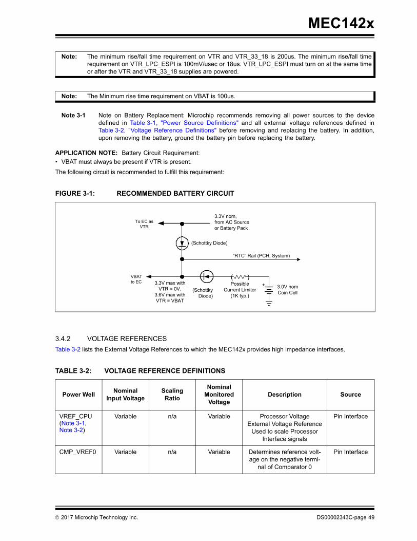
MEC142x
Note 3-1 Note on Battery Replacement: Microchip recommends removing all power sources to the devicedefined in Table 3-1, "Power Source Definitions" and all external voltage references defined inTable 3-2, "Voltage Reference Definitions" before removing and replacing the battery. In addition,upon removing the battery, ground the battery pin before replacing the battery.
APPLICATION NOTE: Battery Circuit Requirement:
• VBAT must always be present if VTR is present.
The following circuit is recommended to fulfill this requirement:
3.4.2 VOLTAGE REFERENCES
Table 3-2 lists the External Voltage References to which the MEC142x provides high impedance interfaces.
Note: The minimum rise/fall time requirement on VTR and VTR_33_18 is 200us. The minimum rise/fall timerequirement on VTR_LPC_ESPI is 100mV/usec or 18us. VTR_LPC_ESPI must turn on at the same timeor after the VTR and VTR_33_18 supplies are powered.
Note: The Minimum rise time requirement on VBAT is 100us.
FIGURE 3-1: RECOMMENDED BATTERY CIRCUIT
TABLE 3-2: VOLTAGE REFERENCE DEFINITIONS
Power WellNominal
Input VoltageScaling Ratio
Nominal Monitored
VoltageDescription Source
VREF_CPU(Note 3-1, Note 3-2)
Variable n/a Variable Processor Voltage External Voltage Reference
Used to scale Processor Interface signals
Pin Interface
CMP_VREF0 Variable n/a Variable Determines reference volt-age on the negative termi-
nal of Comparator 0
Pin Interface
VBAT to EC
To EC asVTR
3.0V nom Coin Cell
“RTC” Rail (PCH, System)
+(Schottky
Diode)
(Schottky Diode)
3.3V nom, from AC Source or Battery Pack
( )Possible
Current Limiter(1K typ.)
3.3V max with VTR = 0V,
3.6V max with VTR = VBAT
2017 Microchip Technology Inc. DS00002343C-page 49

MEC142x
Note 3-1 For specific electrical characteristics for the voltage reference inputs see Table 42-5, “DC ElectricalCharacteristics,” on page 485.
Note 3-2 In order to achieve the lowest leakage current when both PECI and SB TSI are not used, set theVREF_CPU Disable bit to 1. This bit is defined in Section 34.8.5, VREF_CPU DISABLE.
3.4.3 POWER GOOD SIGNALS
The power good timing and thresholds are defined in the Section 43.1, "Voltage Thresholds and Power Good Timing,"on page 494.
3.4.4 SYSTEM POWER SEQUENCING
The following table defines the behavior of the Power Sources in each of the defined ACPI power states.
CMP_VREF1 Variable n/a Variable Determines reference volt-age on the negative termi-
nal of Comparator 1
Pin Interface
ADC_VREF Variable n/a Variable ADC Reference Voltage Pin Interface
TABLE 3-3: POWER GOOD SIGNAL DEFINITIONS
Power Good Signal
Description Source
VTRGD VTRGD is an internal power good signal used to indicate when the VTR rail is on and stable.
VTRGD is asserted following a delay after the VTR power well exceeds its preset voltage threshold. VTRGD is de-asserted as soon as either of these voltages drop below this thresh-old.
Note: See Section 43.1.1, "VTR Thresh-old and VTRGD Timing," onpage 494.
VCC_PWRGD VCC_PWRGD is used to indicate when the main power rail voltage is on and stable.
VCC_PWRGD Input pin
TABLE 3-4: TYPICAL POWER SUPPLIES VS. ACPI POWER STATES
SupplyName
ACPI Power State
DescriptionS0(FULL ON)
S1(POS)
S3(STR)
S4(STD)
S5(Soft Off)
G3(MECH
Off)
VTR_LPC_ESPI
ON ON ON/OFF ON/OFF ON/OFF OFF LPC/eSPI Host Interface Power Supply.
VTR ON ON ON ON ON OFF “Always-on” Supply. (Note 3-3)
TABLE 3-2: VOLTAGE REFERENCE DEFINITIONS (CONTINUED)
Power WellNominal
Input VoltageScaling Ratio
Nominal Monitored
VoltageDescription Source
DS00002343C-page 50 2017 Microchip Technology Inc.
MEC142x
Note 3-3 VTR and VTR_33_18 power supply is always on while the battery pack or ac power is applied to thesystem.
Note 3-4 This device requires that the VBAT power is on when the VTR power supply is on. External circuitry,a diode isolation circuit, is implemented on the motherboard to extend the battery life. This externalcircuitry ensures the VBAT pin will derive power from the VTR power well when it is on. Therefore,the VBAT supply will never appear to be off when the VTR rail is on. See APPLICATION NOTE: onpage 49.
3.5 Clocks
The following section defines the clocks that are generated and derived.
3.5.1 RAW CLOCK SOURCES
The table defines raw clocks that are either generated externally or via an internal oscillator.
VTR_33_18 ON ON ON ON ON OFF “Always-on” Supply. (Note 3-3)
VBAT ON ON ON ON(Note 3-4)
ON (Note 3-4)
ON(Note 3-4)
Battery Back-up Supply
TABLE 3-5: SOURCE CLOCK DEFINITIONS
Clock Name Frequency Description Source
SUSCLK 32.768 kHz 32.768 kHz Suspend Well Clock Source is a single-ended input that is an accurate 32.768 kHz clock. (Note 3-5)
Pin Interface (XTAL2)
32.768 kHz Crystal Oscillator
32.768 kHz A 32.768 kHz parallel resonant crys-tal connected between the XTAL1 and XTAL2 pins.
Pin Interface (XTAL1 and XTAL2)
48 MHz Ring Oscillator
48 MHz The 48 MHz Ring Oscillator is a high-accuracy, low power, low start-up latency 48 MHz Ring Oscillator.
Internal Oscillator powered by VTR. May be stopped by Chip Power Management Features.
(Note 3-6)
32kHz_INT_OSC 32.768 kHz 32.768 kHz low power, lower accu-racy Internal Oscillator powered by VBAT supply.
Note: This clock may be usedwhen the external 32kHz clock is unavailable,and will allow the 48MHz clock to reach fre-quency lock.
Internal Oscillator
Note: This clock source isenabled via the ClockEnable Register on page440.
TABLE 3-4: TYPICAL POWER SUPPLIES VS. ACPI POWER STATES (CONTINUED)
SupplyName
ACPI Power State
DescriptionS0(FULL ON)
S1(POS)
S3(STR)
S4(STD)
S5(Soft Off)
G3(MECH
Off)
2017 Microchip Technology Inc. DS00002343C-page 51
MEC142x
Note 3-5 The chipset will not produce a valid 32 kHz clock until about 5 ms (PCH) or 110 ms (ICH) after thedeassertion of RSMRST#. See chipset specification for the actual timing.
Note 3-6 The 48 MHz Ring Oscillator will reach frequency lock if either the external 32kHz clock source or the32 kHz Internal Oscillator is used, as selected via the 48MHz Oscillator Reference Select bit in theClock Enable Register on page 440. The external 32k Hz clock source provides a stable timebasefor the 48 MHz Ring Oscillator as well as the clock source for the 32 kHz Clock Domain. After VBATPOR there is a 500ms max time for the 48 MHz Ring Oscillator to become accurate. See Section43.2, "Clocking AC Timing Characteristics," on page 497.
Note 3-7 Without the external clock, the 48MHz clock will vary up to +/-4% which may affect the timingparameters of certain blocks. In particular it may not be accurate enough to ensure that the UARTwill work, depending on the accuracy of the clock of the external device.
3.5.2 DERIVED CLOCKS
This table defines the clocks derived from the raw clock sources.
TABLE 3-6: DERIVED CLOCK DEFINITIONS
Clock Name Frequency Description Source
EC_PROC_CLK Programma-ble
Derived clock for Embedded Con-troller/Processor
48 MHz Ring Oscillator
24MHz_Clk 24 MHz Derived clock for UART 48 MHz Ring Oscillator
16MHz_Clk 16 MHz Derived clock for SMBus Controller 48 MHz Ring Oscillator
2MHz_Clk 2 MHz Derived clock for PS/2 Controller 48 MHz Ring Oscillator
1.8432MHz_Clk 1.843 MHz Derived clock for UART 48 MHz Ring Oscillator
1MHz_Clk 1 MHz Derived clock for 8042 Emulated Keyboard Controller
48 MHz Ring Oscillator
100kHz_Clk 100 kHz Derived clock for PWM and TACH blocks
48 MHz Ring Oscillator
32KHz_Clk 32.768 kHz Internal 32kHz clock domain Pin Interface or 48 MHz Ring Oscil-lator:
Pins:XTAL2: 32 kHz Crystal input/ single-ended clock source input pin.XTAL1: 32 kHz Crystal output
The XOSEL bit configures the source of this clock domain as either a single-ended 32.768 kHz clock input (SUSCLK) or the 32.768 kHz Crystal Oscillator. If neither of these is available, this clock domain is derived from the 32kHz_INT_OSC or the 48 MHz Ring Oscillator, as configured by bits in the Clock Enable Register.
(See Note 3-8)
5Hz_Clk 5 Hz Derived clock for Breathing LED block
48 MHz Ring Oscillator
DS00002343C-page 52 2017 Microchip Technology Inc.

MEC142x
Note 3-8 Bits[4:0] of the Clock Enable Register on page 440 determine the source of the 32KHz_Clk.
3.5.3 GENERATED CLOCK OUTPUTS
This section describes clocks generated by the MEC142x that may be used by the external system.
3.5.4 32 KHZ CLOCK SWITCHING
The 32kHz clock switching logic switches the clock source of the 32kHz clock domain to be either the single-ended32.768 kHz clock input (SUSCLK), the 32.768 kHz Crystal Oscillator, the 32kHz_INT_OSC or 48 MHz Ring Oscillator.Following a VBAT_POR, the XOSEL, 32KHz Clock Switcher Control, INT_32K_OSC_EN and EXT_32K_OSC_EN bitsin the Clock Enable Register are programmed to configure the source of this clock domain. See Table 36-3, “32kHzClock Control,” on page 442.
Note 1: Switching delay when configuring the 32k Hz clock source will be on the order of 100 us or three 32k Hzclocks.
2: The 48 MHz Ring Oscillator will reach frequency lock if either the external 32kHz clock source or the 32 kHzInternal Oscillator is used, as selected via the 48MHz Oscillator Reference Select bit in the Clock EnableRegister on page 440. The 48 MHz Ring Oscillator will remain locked when the external 32kHz clock sourceis removed.
3.5.5 CLOCK DOMAINS VS. ACPI POWER STATES
Table 3-8, "Typical MEC142x Clocks vs. ACPI Power States" shows the relationship between ACPI power states andMEC142x clock domains:
TABLE 3-7: GENERATED CLOCK DEFINITIONS
Clock Name Frequency Description Source
32KHZ_OUT 32.768 kHz 32.768 kHz output.Configured 32kHz clock source routed to pin interface.
Derived 32KHz_Clk
TABLE 3-8: TYPICAL MEC142X CLOCKS VS. ACPI POWER STATES
ClockName
ACPI Power State
DescriptionS0(FULLON)
S1(POS)
S3(STR)
S4(STD)
S5(SoftOff)
G3(MECH
Off)
SUSCLK ON ON ON ON ON OFF This clock is the system suspend clock source. (Note 3-5).
32.768 kHz Crystal Oscillator
ON ON ON ON ON ON This clock is generated from a 32.768 kHz par-allel resonant crystal connected between the XTAL1 and XTAL2 pins.
2017 Microchip Technology Inc. DS00002343C-page 53

MEC142x
32KHz_Clk ON ON ON ON ON ON/ OFF
This clock domain is generated from the 32 kHz clock input (SUS-CLK) when available or the crystal oscillator pins. Otherwise it is generated internally from the 32kHz_INT_OSC or the 48 MHz Ring Oscillator.
48 MHz Ring Oscil-lator
ON ON ON ON ON OFF This clock is powered by the MEC142x sus-pend supply (VTR) but may start and stop as described in Section 3.7, "Chip Power Man-agement Features," on page 56 (see also Note 3-3).
32kHz_INT_OSC ON ON ON ON ON OFF This clock is powered by the MEC142x VBAT power supply. This clock may be used when 48 MHz Ring Oscillator is not avail-able.
TABLE 3-8: TYPICAL MEC142X CLOCKS VS. ACPI POWER STATES (CONTINUED)
ClockName
ACPI Power State
DescriptionS0(FULLON)
S1(POS)
S3(STR)
S4(STD)
S5(SoftOff)
G3(MECH
Off)
DS00002343C-page 54 2017 Microchip Technology Inc.
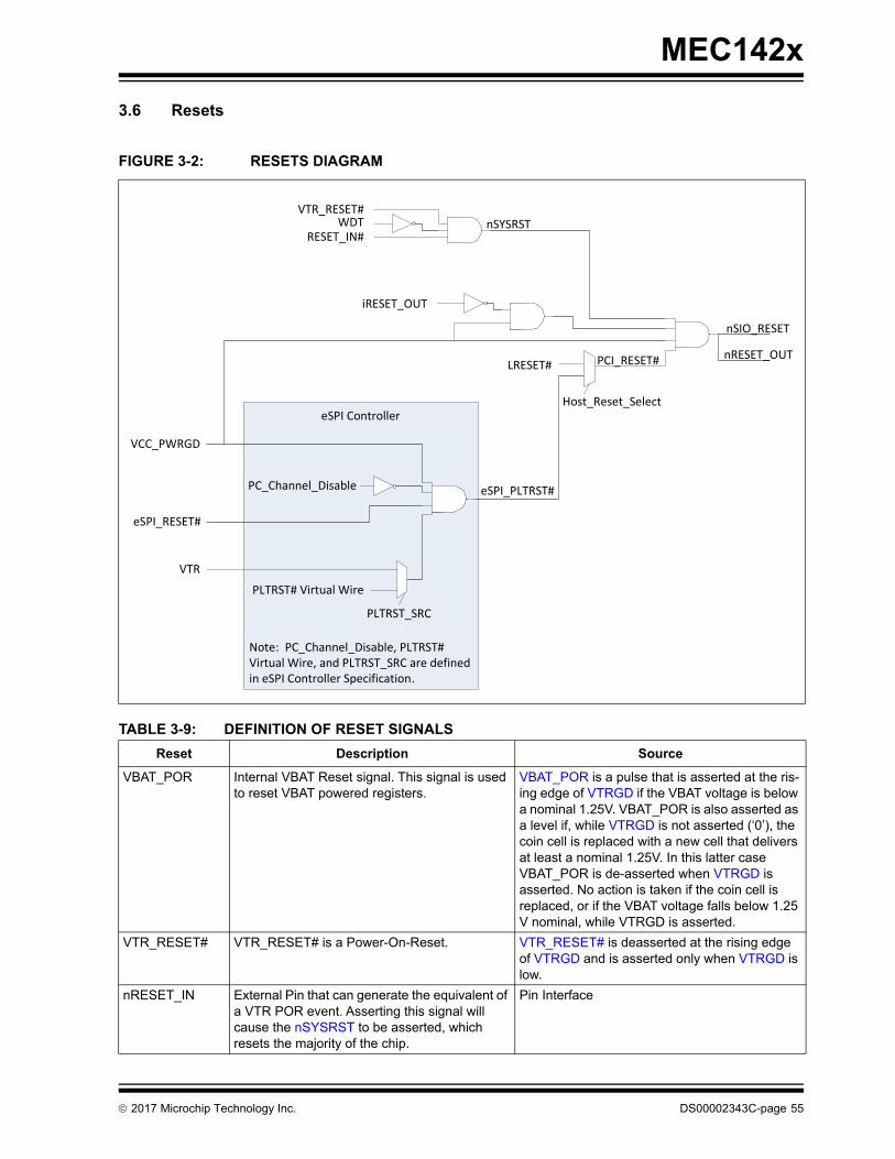
MEC142x
3.6 Resets
FIGURE 3-2: RESETS DIAGRAM
TABLE 3-9: DEFINITION OF RESET SIGNALS
Reset Description Source
VBAT_POR Internal VBAT Reset signal. This signal is used to reset VBAT powered registers.
VBAT_POR is a pulse that is asserted at the ris-ing edge of VTRGD if the VBAT voltage is below a nominal 1.25V. VBAT_POR is also asserted as a level if, while VTRGD is not asserted (‘0’), the coin cell is replaced with a new cell that delivers at least a nominal 1.25V. In this latter case VBAT_POR is de-asserted when VTRGD is asserted. No action is taken if the coin cell is replaced, or if the VBAT voltage falls below 1.25 V nominal, while VTRGD is asserted.
VTR_RESET# VTR_RESET# is a Power-On-Reset. VTR_RESET# is deasserted at the rising edge of VTRGD and is asserted only when VTRGD is low.
nRESET_IN External Pin that can generate the equivalent of a VTR POR event. Asserting this signal will cause the nSYSRST to be asserted, which resets the majority of the chip.
Pin Interface
eSPI Controller
VTR_RESET#WDT
RESET_IN#nSYSRST
iRESET_OUT
LRESET#
eSPI_PLTRST#
eSPI_RESET#
PC_Channel_Disable
VCC_PWRGD
PLTRST# Virtual Wire
Host_Reset_Select
nSIO_RESET
nRESET_OUT
PLTRST_SRC
Note: PC_Channel_Disable, PLTRST# Virtual Wire, and PLTRST_SRC are defined in eSPI Controller Specification.
VTR
PCI_RESET#
2017 Microchip Technology Inc. DS00002343C-page 55

MEC142x
3.7 Chip Power Management Features
This device is designed to always operate in its lowest power state during normal operation. In addition, this deviceoffers additional programmable options to put individual logical blocks to sleep as defined in Section 3.7.1, "Block LowPower Modes," on page 56 and to gate off or power down the internal oscillator as described in Section 3.7.2, "Config-uring the Chip’s Sleep States," on page 57.
3.7.1 BLOCK LOW POWER MODES
All power related control signals are generated and monitored centrally in the chip’s Power, Clocks, and Resets (PCR)block. The power manager of the PCR block uses a sleep interface to communicate with all the blocks. The sleep inter-face consists of three signals:
nRESET_OUT External Pin that can generate the equivalent of a VCC POR or main reset event to other exter-nal devices.
This signal is asserted low when the nSIO_RE-SET is asserted low.
nSYSRST Internal VTR Reset signal. This signal is used to reset VTR powered registers.
nSYSRST is asserted when VTRGDis low, when a WDT_RESET event occurs, when the nRESET_IN pin is asserted low, or when the EJTAG.PrRST bit is asserted. It is only deas-serted when VTRGD is high, nRESET_IN is high, the EJTAG.PrRST bit is deasserted,.and their is no WDT_RESET event active.The EJTAG.PrRST bit is defined in the MIPS® EJTAG Specification, DN: MD00047, Rev 5.06, March 05, 2011.
LRESET# System reset signal connected to the LPC LRE-SET# pin (also referred to as PCI Reset).
Pin Interface
eSPI_RESET# System reset signal connected to the eSPI eSPI_RESET# pin
Pin Interface
eSPI_PLTRST# Platform Reset. Generated by the eSPI Block when VCC_P-WRGD is low, when eSPI_RESET# is low, by a Virtual Wire, or by PC_Channel_Disable.
PCI_RESET# System reset signal Generated by either the LPC LRESET# pin (also referred to as PCI Reset) or the eSPI_PLTRST# depending on the configuration of the Host_Re-set_Select bit.
nSIO_RESET Performs a reset when VCC is turned off or when the system host resets the LPC or eSPI Host Interfaces.
nSIO_RESET is a signal that is asserted if nSYSRST is low, VCC_PWRGD is low, or PCI_RESET# is asserted low and may be deas-serted when these three signals are all high. The iRESET_OUT bit controls the deassertion of nSIO_RESET. A WDT_RESET event will also cause an nSIO_RESET assertion.
WDT_RESET Internal WDT Reset signal. This signal resets VTR powered registers with the exception of the WDT Event Count register. Note that the glitch protect circuits do not activate on a WDT reset. WDT_RESETdoes not reset VBAT regis-ters or logic.
A WDT_RESET is asserted by a WDT Event.This event is indicated by the WDT bit in the Power-Fail and Reset Status Register
EC_PROC_RESET#
Internal reset signal to reset the processor in the EC Subsystem.
An EC_PROC_RESET# is a stretched version of the nSYSRST. This reset asserts at the same time that nSYSRST asserts and is held asserted for 1ms after the nSYSRST deasserts.
TABLE 3-9: DEFINITION OF RESET SIGNALS (CONTINUED)
Reset Description Source
DS00002343C-page 56 2017 Microchip Technology Inc.
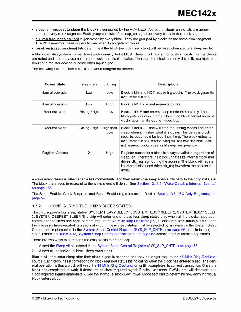
MEC142x
• sleep_en (request to sleep the block) is generated by the PCR block. A group of sleep_en signals are gener-ated for every clock segment. Each group consists of a sleep_en signal for every block in that clock segment.
• clk_req (request clock on) is generated by every block. They are grouped by blocks on the same clock segment. The PCR monitors these signals to see when it can gate off clocks.
• reset_en (reset on sleep) bits determine if the block (including registers) will be reset when it enters sleep mode.
A block can always drive clk_req low synchronously, but it MUST drive it high asynchronously since its internal clocksare gated and it has to assume that the clock input itself is gated. Therefore the block can only drive clk_req high as aresult of a register access or some other input signal.
The following table defines a block’s power management protocol:
A wake event clears all sleep enable bits momentarily, and then returns the sleep enable bits back to their original state.The block that needs to respond to the wake event will do so. See Section 10.11.3, "Wake-Capable Interrupt Events,"on page 165.
The Sleep Enable, Clock Required and Reset Enable registers are defined in Section 3.8, "EC-Only Registers," onpage 59.
3.7.2 CONFIGURING THE CHIP’S SLEEP STATES
The chip supports four sleep states: SYSTEM HEAVY SLEEP 1, SYSTEM HEAVY SLEEP 2, SYSTEM HEAVY SLEEP3, SYSTEM DEEPEST SLEEP. The chip will enter one of these four sleep states only when all the blocks have beencommanded to sleep and none of them require the 48 MHz Ring Oscillator (i.e., all clock required status bits = 0), andthe processor has executed its sleep instruction. These sleep states must be selected by firmware via the System SleepControl bits implemented in the System Sleep Control Register (SYS_SLP_CNTRL) on page 66 prior to issuing thesleep instruction. Table 3-12, “System Sleep Control Bit Encoding,” on page 68 defines each of these sleep states.
There are two ways to command the chip blocks to enter sleep.
1. Assert the Sleep All bit located in the System Sleep Control Register (SYS_SLP_CNTRL) on page 66
2. Assert all the individual block sleep enable bits
Blocks will only enter sleep after their sleep signal is asserted and they no longer require the 48 MHz Ring Oscillatorsource. Each block has a corresponding clock required status bit indicating when the block has entered sleep. The gen-eral operation is that a block will keep the 48 MHz Ring Oscillator on until it completes its current transaction. Once theblock has completed its work, it deasserts its clock required signal. Blocks like timers, PWMs, etc. will deassert theirclock required signals immediately. See the individual block Low Power Mode sections to determine how each individualblock enters sleep.
Power State sleep_en clk_req Description
Normal operation Low Low Block is idle and NOT requesting clocks. The block gates its own internal clock.
Normal operation Low High Block is NOT idle and requests clocks.
Request sleep Rising Edge Low Block is IDLE and enters sleep mode immediately. The block gates its own internal clock. The block cannot request clocks again until sleep_en goes low.
Request sleep Rising Edge High then Low
Block is not IDLE and will stop requesting clocks and enter sleep when it finishes what it is doing. This delay is block specific, but should be less than 1 ms. The block gates its own internal clock. After driving clk_req low, the block can-not request clocks again until sleep_en goes low.
Register Access X High Register access to a block is always available regardless of sleep_en. Therefore the block ungates its internal clock and drives clk_req high during the access. The block will regate its internal clock and drive clk_req low when the access is done.
2017 Microchip Technology Inc. DS00002343C-page 57
MEC142x
3.7.3 DETERMINING WHEN THE CHIP IS SLEEPING
There are two methods to verify the chip’s clock has stopped, which indicates the device is in one of these three sleepstates: SYSTEM HEAVY SLEEP 2, SYSTEM HEAVY SLEEP 3, SYSTEM DEEPEST SLEEP. Note that the 48 MHz RingOscillator continues to run in the SYSTEM HEAVY SLEEP 1 state to minimize wake latency.
Option 1: TST_CLK_OUT pin
The TST_CLK_OUT, which is located on the GPIO157/LED0/TST_CLK_OUT pin, is used to route the internal 48 MHzRing Oscillator to a pin. If the clock is toggling the chip is in the full on running state. if the clock is not toggling the chiphas entered the programmed sleep state.
Option 2: MTAP Test Bit
Bit [1] SLEEPING has been implemented in the MTAP registers (MCHP_CMD <0x07>) to allow the firmware developerto determine if the chip is sleeping via the ICSP debug port. This MTAP command does not require the 48 MHz RingOscillator to be clocking and therefore will not change the chip’s sleep state. Note that all of the ICSP debugger com-mands that access the processor JTAG port will bring the device out of sleep.
3.7.4 WAKING THE CHIP FROM SLEEPING STATE
The chip will remain in the configured sleep state until it detects either a wake event, an ICSP access, or a full VTRPOR. All the wake-capable interrupt events are defined in the Section 10.0, "Jump Table Vectored Interrupt Controller(JTVIC)". They are identified as Wake Events in Table 10-2, “Interrupt Source, Enable Set, Enable Clear, and Result BitAssignments,” on page 167.
3.7.4.1 Wake-Only Events
Two GIRQ registers have been reserved for special wake events. GIRQ16 is used for wake-events that do not requiresoftware processing. These events are used to turn the clock on so the peripherals can start processing the data. Thereis no information for the firmware to process. When GIRQ16 is active the firmware can simply clear the source andreturn to the sleep state. GIRQ22 is a duplicate of GIRQ16 with one major difference. GIRQ22 does not generate a pro-cessor interrupt. It only wakes the 48 MHz Ring Oscillator so the peripherals can start processing the data.
Example: LPC I/O Traffic targeting EMI block.
The LPC Interface detects traffic on the bus and requires the clock to be on to process the incoming data. If GIRQ22 isenabled, the LPC block will be able to autonomously receive data for the programmed I/O ranges without processorintervention. Once the data is loaded into the HOST-to-EC Mailbox Register the Host-to-EC IRQ will trigger an interruptto the embedded controller to service this command.
An alternate solution would be to enable the GIRQ16 LPC interrupt. The process is similar, except the embedded con-troller will receive an interrupt for the LPC activity, as well as the Host-to-EC IRQ, and will need to clear this event also.
3.7.4.2 ICSP Debugger Wake Events
The ICSP Debugger will cause the chip to wake and run debug code. Auto Clear Sleep and Sleep Debug bits have beenimplemented to allow firmware to re-enter sleep following a debug access. It is recommended to set these bits to ‘1’ asdescribed in the following Application Note.
APPLICATION NOTE: Methods for putting the device back to sleep after a debug access.
Option 1: Automatically Re-enter Sleep after Debug Wake Event (preferred)
To automatically re-enter sleep after a debug wake event the firmware should follow this recommended usage model
1. FW has decided to go to sleep.
2. Set sleep_all bit to command all blocks to sleep.
3. Set sleep_debug bit.
4. Set auto_clr_sleep to make sure sleep_all and sleep_debug will clear automatically when the processor vec-tors to an interrupt.
5. Issue processor sleep instruction. Note that you must use a do...while around the sleep instruction (WAIT).
Note:
• Steps 2-4 can be done in one write to System Sleep Control Register (SYS_SLP_CNTRL) register.
• The sleep_all and the sleep_debug bits MUST not be set in an interrupt handler.
DS00002343C-page 58 2017 Microchip Technology Inc.
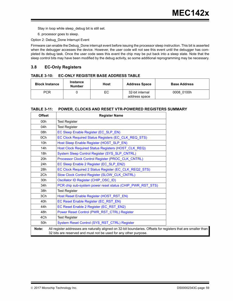
MEC142x
Stay in loop while sleep_debug bit is still set.
6. processor goes to sleep.
Option 2: Debug_Done Interrupt Event
Firmware can enable the Debug_Done interrupt event before issuing the processor sleep instruction. This bit is assertedwhen the debugger accesses the device. However, the user code will not see this event until the debugger has com-pleted its debug task. Once the user code sees this event the chip may be put back into a sleep state. Note that thesleep control bits may have been modified by the debug activity, so some additional reprogramming may be necessary.
3.8 EC-Only Registers
TABLE 3-10: EC-ONLY REGISTER BASE ADDRESS TABLE
Block InstanceInstance Number
Host Address Space Base Address
PCR 0 EC 32-bit internal address space
0008_0100h
TABLE 3-11: POWER, CLOCKS AND RESET VTR-POWERED REGISTERS SUMMARY
Offset Register Name
00h Test Register
04h Test Register
08h EC Sleep Enable Register (EC_SLP_EN)
0Ch EC Clock Required Status Registers (EC_CLK_REQ_STS)
10h Host Sleep Enable Register (HOST_SLP_EN)
14h Host Clock Required Status Registers (HOST_CLK_REQ)
18h System Sleep Control Register (SYS_SLP_CNTRL)
20h Processor Clock Control Register (PROC_CLK_CNTRL)
24h EC Sleep Enable 2 Register (EC_SLP_EN2)
28h EC Clock Required 2 Status Register (EC_CLK_REQ2_STS)
2Ch Slow Clock Control Register (SLOW_CLK_CNTRL)
30h Oscillator ID Register (CHIP_OSC_ID)
34h PCR chip sub-system power reset status (CHIP_PWR_RST_STS)
38h Test Register
3Ch Host Reset Enable Register (HOST_RST_EN)
40h EC Reset Enable Register (EC_RST_EN)
44h EC Reset Enable 2 Register (EC_RST_EN2)
48h Power Reset Control (PWR_RST_CTRL) Register
4Ch Test Register
50h System Reset Control (SYS_RST_CTRL) Register
Note: All register addresses are naturally aligned on 32-bit boundaries. Offsets for registers that are smaller than32 bits are reserved and must not be used for any other purpose.
2017 Microchip Technology Inc. DS00002343C-page 59

MEC142x
3.9 Sleep Enable and Clock Required Registers
The following are the Sleep Enable and Clock Required registers for the MEC142x.
3.9.1 EC SLEEP ENABLE REGISTER (EC_SLP_EN)
Offset 08h
Bits Description Type DefaultReset Event
31 TIMER16_1 Sleep Enable
0: block is free to use clocks as necessary.1: block is commanded to sleep at next available moment.See Note: on page 62.
R/W 0h nSYSRST
30 TIMER16_0 Sleep Enable
0: block is free to use clocks as necessary.1: block is commanded to sleep at next available moment.See Note: on page 62.
R/W 0h nSYSRST
29 EC_REG_BANK Sleep Enable
0: block is free to use clocks as necessary.1: block is commanded to sleep at next available moment.
R/W 0h nSYSRST
28:27 RESERVED RES
26 PWM7 Sleep Enable
0: block is free to use clocks as necessary.1: block is commanded to sleep at next available moment.
R/W 0h nSYSRST
25 PWM6 Sleep Enable
0: block is free to use clocks as necessary.1: block is commanded to sleep at next available moment.
R/W 0h nSYSRST
24 PWM5 Sleep Enable
0: block is free to use clocks as necessary.1: block is commanded to sleep at next available moment.
R/W 0h nSYSRST
23 PWM4 Sleep Enable
0: block is free to use clocks as necessary.1: block is commanded to sleep at next available moment.
R/W 0h nSYSRST
22 PWM3 Sleep Enable
0: block is free to use clocks as necessary.1: block is commanded to sleep at next available moment.
R/W 0h nSYSRST
21 PWM2 Sleep Enable
0: block is free to use clocks as necessary.1: block is commanded to sleep at next available moment.
R/W 0h nSYSRST
20 PWM1 Sleep Enable
0: block is free to use clocks as necessary.1: block is commanded to sleep at next available moment.
R/W 0h nSYSRST
19:14 RESERVED RES
DS00002343C-page 60 2017 Microchip Technology Inc.
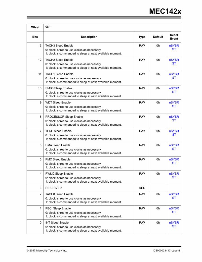
MEC142x
13 TACH3 Sleep Enable
0: block is free to use clocks as necessary.1: block is commanded to sleep at next available moment.
R/W 0h nSYSRST
12 TACH2 Sleep Enable
0: block is free to use clocks as necessary.1: block is commanded to sleep at next available moment.
R/W 0h nSYSRST
11 TACH1 Sleep Enable
0: block is free to use clocks as necessary.1: block is commanded to sleep at next available moment.
R/W 0h nSYSRST
10 SMB0 Sleep Enable
0: block is free to use clocks as necessary.1: block is commanded to sleep at next available moment.
R/W 0h nSYSRST
9 WDT Sleep Enable
0: block is free to use clocks as necessary.1: block is commanded to sleep at next available moment.
R/W 0h nSYSRST
8 PROCESSOR Sleep Enable
0: block is free to use clocks as necessary.1: block is commanded to sleep at next available moment.
R/W 0h nSYSRST
7 TFDP Sleep Enable
0: block is free to use clocks as necessary.1: block is commanded to sleep at next available moment.
R/W 0h nSYSRST
6 DMA Sleep Enable
0: block is free to use clocks as necessary.1: block is commanded to sleep at next available moment.
R/W 0h nSYSRST
5 PMC Sleep Enable
0: block is free to use clocks as necessary.1: block is commanded to sleep at next available moment.
R/W 0h nSYSRST
4 PWM0 Sleep Enable
0: block is free to use clocks as necessary.1: block is commanded to sleep at next available moment.
R/W 0h nSYSRST
3 RESERVED RES
2 TACH0 Sleep Enable
0: block is free to use clocks as necessary.1: block is commanded to sleep at next available moment.
R/W 0h nSYSRST
1 PECI Sleep Enable
0: block is free to use clocks as necessary.1: block is commanded to sleep at next available moment.
R/W 0h nSYSRST
0 INT Sleep Enable
0: block is free to use clocks as necessary.1: block is commanded to sleep at next available moment.
R/W 0h nSYSRST
Offset 08h
Bits Description Type DefaultReset Event
2017 Microchip Technology Inc. DS00002343C-page 61

MEC142x
3.9.2 EC CLOCK REQUIRED STATUS REGISTERS (EC_CLK_REQ_STS)
Note: The basic timers in this device have an auto-reload mode. When this mode is selected, the block's clk_reqequation is always asserted, which will prevent the device from gating its clock tree and going to sleep.When the firmware intends to put the device to sleep, none of the timers should be in auto-reload mode.Alternatively, use the timer's HALT function inside the control register to stop the timer in auto-reload modeso it can go to sleep.
Offset 0Ch
Bits Description Type DefaultReset Event
31 TIMER16_1 Clock Required
0: block does NOT need clocks.1: block requires clocks.
R 0h nSYSRST
30 TIMER16_0 Clock Required
0: block does NOT need clocks.1: block requires clocks.
R 0h nSYSRST
29 EC_REG_BANK Clock Required
0: block does NOT need clocks.1: block requires clocks.
R 0h nSYSRST
28:27 RESERVED RES
26 PWM7 Clock Required
0: block does NOT need clocks.1: block requires clocks.
R 0h nSYSRST
25 PWM6 Clock Required
0: block does NOT need clocks.1: block requires clocks.
R 0h nSYSRST
24 PWM5 Clock Required
0: block does NOT need clocks.1: block requires clocks.
R 0h nSYSRST
23 PWM4 Clock Required
0: block does NOT need clocks.1: block requires clocks.
R 0h nSYSRST
22 PWM3 Clock Required
0: block does NOT need clocks.1: block requires clocks.
R 0h nSYSRST
21 PWM2 Clock Required
0: block does NOT need clocks.1: block requires clocks.
R 0h nSYSRST
20 PWM1 Clock Required
0: block does NOT need clocks.1: block requires clocks.
R 0h nSYSRST
19:14 RESERVED RES
DS00002343C-page 62 2017 Microchip Technology Inc.
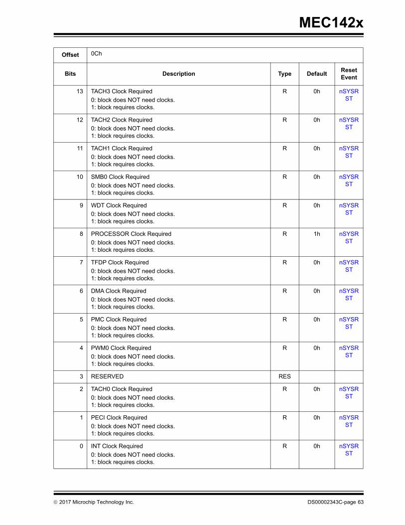
MEC142x
13 TACH3 Clock Required
0: block does NOT need clocks.1: block requires clocks.
R 0h nSYSRST
12 TACH2 Clock Required
0: block does NOT need clocks.1: block requires clocks.
R 0h nSYSRST
11 TACH1 Clock Required
0: block does NOT need clocks.1: block requires clocks.
R 0h nSYSRST
10 SMB0 Clock Required
0: block does NOT need clocks.1: block requires clocks.
R 0h nSYSRST
9 WDT Clock Required
0: block does NOT need clocks.1: block requires clocks.
R 0h nSYSRST
8 PROCESSOR Clock Required
0: block does NOT need clocks.1: block requires clocks.
R 1h nSYSRST
7 TFDP Clock Required
0: block does NOT need clocks.1: block requires clocks.
R 0h nSYSRST
6 DMA Clock Required
0: block does NOT need clocks.1: block requires clocks.
R 0h nSYSRST
5 PMC Clock Required
0: block does NOT need clocks.1: block requires clocks.
R 0h nSYSRST
4 PWM0 Clock Required
0: block does NOT need clocks.1: block requires clocks.
R 0h nSYSRST
3 RESERVED RES
2 TACH0 Clock Required
0: block does NOT need clocks.1: block requires clocks.
R 0h nSYSRST
1 PECI Clock Required
0: block does NOT need clocks.1: block requires clocks.
R 0h nSYSRST
0 INT Clock Required
0: block does NOT need clocks.1: block requires clocks.
R 0h nSYSRST
Offset 0Ch
Bits Description Type DefaultReset Event
2017 Microchip Technology Inc. DS00002343C-page 63

MEC142x
3.9.3 HOST SLEEP ENABLE REGISTER (HOST_SLP_EN)
Offset 10h
Bits Description Type DefaultReset Event
31:21 RESERVED RES
20 32 Byte Scratch Block Sleep Enable
0: block is free to use clocks as necessary.1: block is commanded to sleep at next available moment.
R/W 0h nSYSRST
19 eSPI Sleep Enable 0: block is free to use clocks as necessary.1: block is commanded to sleep at next available moment.
R/W 0h nSYSRST
18 SAF Bridge Sleep Enable 0: block is free to use clocks as necessary.1: block is commanded to sleep at next available moment.
R/W 0h nSYSRST
17 Mailbox Sleep Enable
0: block is free to use clocks as necessary.1: block is commanded to sleep at next available moment.
R/W 0h nSYSRST
16 8042EM Sleep Enable
0: block is free to use clocks as necessary.1: block is commanded to sleep at next available moment.
R/W 0h nSYSRST
15 ACPI PM1 Sleep Enable
0: block is free to use clocks as necessary.1: block is commanded to sleep at next available moment.
R/W 0h nSYSRST
14 ACPI EC 1 Sleep Enable
0: block is free to use clocks as necessary.1: block is commanded to sleep at next available moment.
R/W 0h nSYSRST
13 ACPI EC 0 Sleep Enable
0: block is free to use clocks as necessary.1: block is commanded to sleep at next available moment
R/W 0h nSYSRST
12 GLBL_CFG
0: block is free to use clocks as necessary.1: block is commanded to sleep at next available moment.
R/W 0h nSYSRST
11 ACPI_EC3 Sleep Enable
0: block is free to use clocks as necessary.1: block is commanded to sleep at next available moment.
R/W 0h nSYSRST
10 ACPI_EC2 Sleep Enable
0: block is free to use clocks as necessary.1: block is commanded to sleep at next available moment.
R/W 0h nSYSRST
9:4 RESERVED RES
3 BIOS1 Sleep Enable
0: block is free to use clocks as necessary.1: block is commanded to sleep at next available moment.
R/W 0h nSYSRST
DS00002343C-page 64 2017 Microchip Technology Inc.
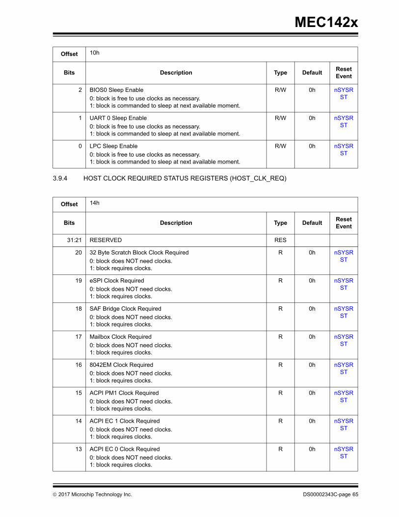
MEC142x
3.9.4 HOST CLOCK REQUIRED STATUS REGISTERS (HOST_CLK_REQ)
2 BIOS0 Sleep Enable
0: block is free to use clocks as necessary.1: block is commanded to sleep at next available moment.
R/W 0h nSYSRST
1 UART 0 Sleep Enable
0: block is free to use clocks as necessary.1: block is commanded to sleep at next available moment.
R/W 0h nSYSRST
0 LPC Sleep Enable
0: block is free to use clocks as necessary.1: block is commanded to sleep at next available moment.
R/W 0h nSYSRST
Offset 14h
Bits Description Type DefaultReset Event
31:21 RESERVED RES
20 32 Byte Scratch Block Clock Required
0: block does NOT need clocks.1: block requires clocks.
R 0h nSYSRST
19 eSPI Clock Required
0: block does NOT need clocks.1: block requires clocks.
R 0h nSYSRST
18 SAF Bridge Clock Required
0: block does NOT need clocks.1: block requires clocks.
R 0h nSYSRST
17 Mailbox Clock Required
0: block does NOT need clocks.1: block requires clocks.
R 0h nSYSRST
16 8042EM Clock Required
0: block does NOT need clocks.1: block requires clocks.
R 0h nSYSRST
15 ACPI PM1 Clock Required
0: block does NOT need clocks.1: block requires clocks.
R 0h nSYSRST
14 ACPI EC 1 Clock Required
0: block does NOT need clocks.1: block requires clocks.
R 0h nSYSRST
13 ACPI EC 0 Clock Required
0: block does NOT need clocks.1: block requires clocks.
R 0h nSYSRST
Offset 10h
Bits Description Type DefaultReset Event
2017 Microchip Technology Inc. DS00002343C-page 65
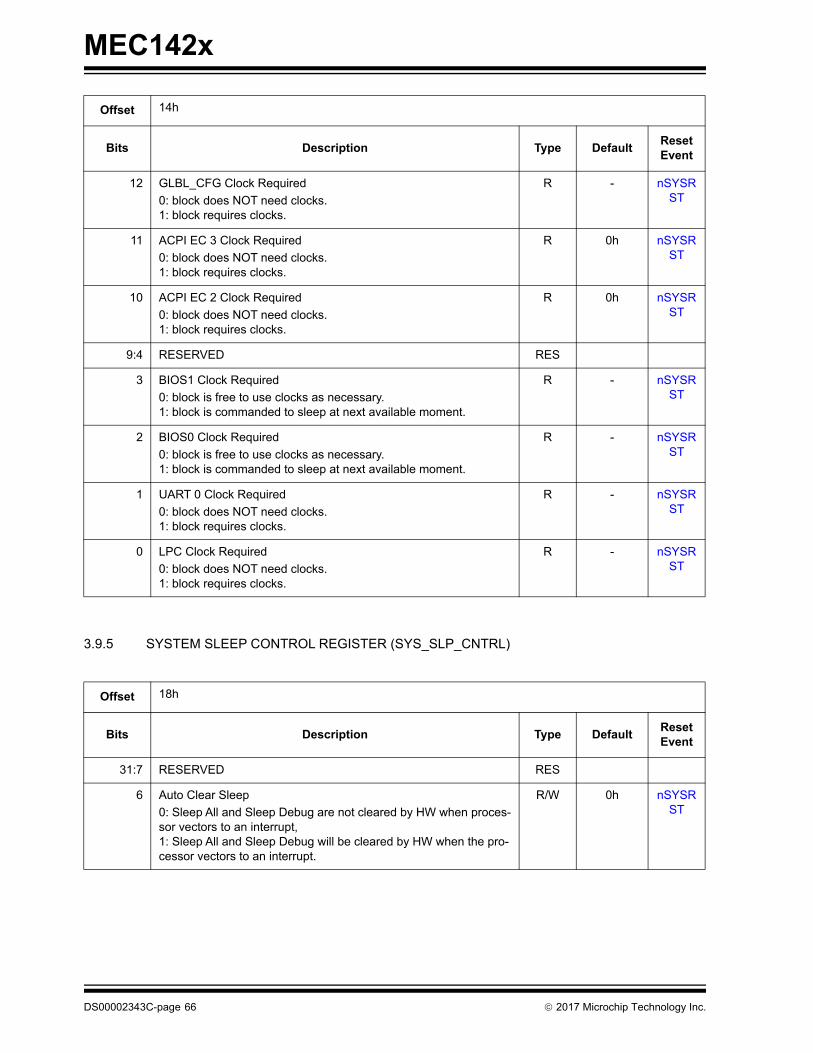
MEC142x
3.9.5 SYSTEM SLEEP CONTROL REGISTER (SYS_SLP_CNTRL)
12 GLBL_CFG Clock Required
0: block does NOT need clocks.1: block requires clocks.
R - nSYSRST
11 ACPI EC 3 Clock Required
0: block does NOT need clocks.1: block requires clocks.
R 0h nSYSRST
10 ACPI EC 2 Clock Required
0: block does NOT need clocks.1: block requires clocks.
R 0h nSYSRST
9:4 RESERVED RES
3 BIOS1 Clock Required
0: block is free to use clocks as necessary.1: block is commanded to sleep at next available moment.
R - nSYSRST
2 BIOS0 Clock Required
0: block is free to use clocks as necessary.1: block is commanded to sleep at next available moment.
R - nSYSRST
1 UART 0 Clock Required
0: block does NOT need clocks.1: block requires clocks.
R - nSYSRST
0 LPC Clock Required
0: block does NOT need clocks.1: block requires clocks.
R - nSYSRST
Offset 18h
Bits Description Type DefaultReset Event
31:7 RESERVED RES
6 Auto Clear Sleep
0: Sleep All and Sleep Debug are not cleared by HW when proces-sor vectors to an interrupt, 1: Sleep All and Sleep Debug will be cleared by HW when the pro-cessor vectors to an interrupt.
R/W 0h nSYSRST
Offset 14h
Bits Description Type DefaultReset Event
DS00002343C-page 66 2017 Microchip Technology Inc.
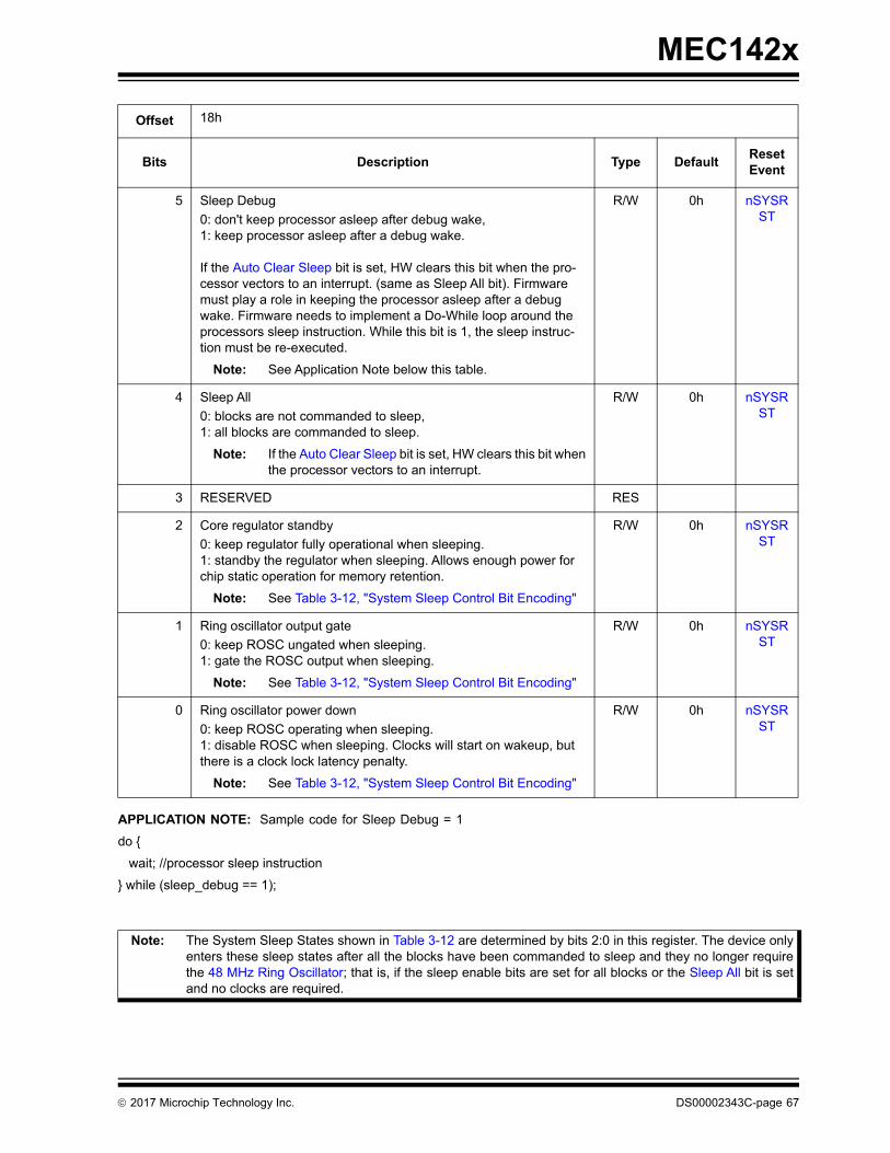
MEC142x
APPLICATION NOTE: Sample code for Sleep Debug = 1
do
wait; //processor sleep instruction
while (sleep_debug == 1);
5 Sleep Debug
0: don't keep processor asleep after debug wake, 1: keep processor asleep after a debug wake.
If the Auto Clear Sleep bit is set, HW clears this bit when the pro-cessor vectors to an interrupt. (same as Sleep All bit). Firmware must play a role in keeping the processor asleep after a debug wake. Firmware needs to implement a Do-While loop around the processors sleep instruction. While this bit is 1, the sleep instruc-tion must be re-executed.
Note: See Application Note below this table.
R/W 0h nSYSRST
4 Sleep All
0: blocks are not commanded to sleep, 1: all blocks are commanded to sleep.
Note: If the Auto Clear Sleep bit is set, HW clears this bit whenthe processor vectors to an interrupt.
R/W 0h nSYSRST
3 RESERVED RES
2 Core regulator standby
0: keep regulator fully operational when sleeping.1: standby the regulator when sleeping. Allows enough power for chip static operation for memory retention.
Note: See Table 3-12, "System Sleep Control Bit Encoding"
R/W 0h nSYSRST
1 Ring oscillator output gate
0: keep ROSC ungated when sleeping.1: gate the ROSC output when sleeping.
Note: See Table 3-12, "System Sleep Control Bit Encoding"
R/W 0h nSYSRST
0 Ring oscillator power down
0: keep ROSC operating when sleeping.1: disable ROSC when sleeping. Clocks will start on wakeup, but there is a clock lock latency penalty.
Note: See Table 3-12, "System Sleep Control Bit Encoding"
R/W 0h nSYSRST
Note: The System Sleep States shown in Table 3-12 are determined by bits 2:0 in this register. The device onlyenters these sleep states after all the blocks have been commanded to sleep and they no longer requirethe 48 MHz Ring Oscillator; that is, if the sleep enable bits are set for all blocks or the Sleep All bit is setand no clocks are required.
Offset 18h
Bits Description Type DefaultReset Event
2017 Microchip Technology Inc. DS00002343C-page 67

MEC142x
Note 3-1 The latency following a wake event for the SMBus and UART is 600us (typ). It is less than 10us forLPC, eSPI and PS2.
3.9.6 PROCESSOR CLOCK CONTROL REGISTER (PROC_CLK_CNTRL)
3.9.7 EC SLEEP ENABLE 2 REGISTER (EC_SLP_EN2)
TABLE 3-12: SYSTEM SLEEP CONTROL BIT ENCODING
D2 D1 D0 Wake Latency Description
0 0 0 0 The Core regulator and the Ring Oscillator remain powered and run-ning during sleep cycles (SYSTEM HEAVY SLEEP 1) (DEFAULT)
0 1 0 0 The Core regulator remains powered and the Ring oscillator is run-ning but gated during sleep cycles (SYSTEM HEAVY SLEEP 2)
0 X 1 (Note 3-1) The Core regulator remains powered and the Ring oscillator is pow-ered down during sleep cycles (SYSTEM HEAVY SLEEP 3)
1 X 1 (Note 3-1) The Core regulator is put into standby state and the Ring oscillator is powered down during sleep cycles. (SYSTEM DEEPEST SLEEP)
Offset 20h
Bits Description Type DefaultReset Event
31:8 RESERVED RES
7:0 Processor Clock Divide Value
1: divide 48 MHz Ring Oscillator by 1 (i.e., 48 MHz).4: divide 48 MHz Ring Oscillator by 4 (i.e., 12 MHz).16: divide 48 MHz Ring Oscillator by 16 (i.e., 3 MHz).48: divide 48 MHz Ring Oscillator by 48 (i.e., 1 MHz).No other values are supported.
R/W 4h nSYSRST
Offset 24h
Bits Description Type DefaultReset Event
31:26 RESERVED RES
25 SMB4 Sleep Enable
0: block is free to use clocks as necessary.1: block is commanded to sleep at next available moment.
R/W 0h nSYSRST
24 SMB3 Sleep Enable
0: block is free to use clocks as necessary.1: block is commanded to sleep at next available moment.
R/W 0h nSYSRST
23 RESERVED RES
DS00002343C-page 68 2017 Microchip Technology Inc.
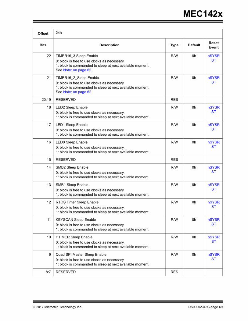
MEC142x
22 TIMER16_3 Sleep Enable
0: block is free to use clocks as necessary.1: block is commanded to sleep at next available moment.See Note: on page 62.
R/W 0h nSYSRST
21 TIMER16_2_Sleep Enable
0: block is free to use clocks as necessary.1: block is commanded to sleep at next available moment.See Note: on page 62.
R/W 0h nSYSRST
20:19 RESERVED RES
18 LED2 Sleep Enable
0: block is free to use clocks as necessary.1: block is commanded to sleep at next available moment.
R/W 0h nSYSRST
17 LED1 Sleep Enable
0: block is free to use clocks as necessary.1: block is commanded to sleep at next available moment.
R/W 0h nSYSRST
16 LED0 Sleep Enable
0: block is free to use clocks as necessary.1: block is commanded to sleep at next available moment.
R/W 0h nSYSRST
15 RESERVED RES
14 SMB2 Sleep Enable
0: block is free to use clocks as necessary.1: block is commanded to sleep at next available moment.
R/W 0h nSYSRST
13 SMB1 Sleep Enable
0: block is free to use clocks as necessary.1: block is commanded to sleep at next available moment.
R/W 0h nSYSRST
12 RTOS Timer Sleep Enable
0: block is free to use clocks as necessary.1: block is commanded to sleep at next available moment.
R/W 0h nSYSRST
11 KEYSCAN Sleep Enable
0: block is free to use clocks as necessary.1: block is commanded to sleep at next available moment.
R/W 0h nSYSRST
10 HTIMER Sleep Enable
0: block is free to use clocks as necessary.1: block is commanded to sleep at next available moment.
R/W 0h nSYSRST
9 Quad SPI Master Sleep Enable
0: block is free to use clocks as necessary.1: block is commanded to sleep at next available moment.
R/W 0h nSYSRST
8:7 RESERVED RES
Offset 24h
Bits Description Type DefaultReset Event
2017 Microchip Technology Inc. DS00002343C-page 69

MEC142x
Note 3-2 The PS2 block will only sleep while the PS2 is disabled or in Rx mode with no traffic on the bus.
3.9.8 EC CLOCK REQUIRED 2 STATUS REGISTER (EC_CLK_REQ2_STS)
6 PS2_1 Sleep Enable
0: block is free to use clocks as necessary.1: block is commanded to sleep at next available moment.See Note 3-2.
R/W 0h nSYSRST
5 PS2_0 Sleep Enable
0: block is free to use clocks as necessary.1: block is commanded to sleep at next available moment.See Note 3-2.
R/W 0h nSYSRST
4 RESERVED RES
3 ADC Sleep Enable
0: block is free to use clocks as necessary.1: block is commanded to sleep at next available moment.
R/W 0h nSYSRST
2:0 RESERVED RES
Offset 28h
Bits Description Type DefaultReset Event
31:26 RESERVED RES
25 SMB4 Clock Required
0: block does NOT need clocks.1: block requires clocks.
R 0h nSYSRST
24 SMB3 Clock Required
0: block does NOT need clocks.1: block requires clocks.
R 0h nSYSRST
23 RESERVED RES
22 TIMER16_3 Clock Required
0: block does NOT need clocks.1: block requires clocks.
R 0h nSYSRST
21 TIMER16_2_Clock Required
0: block does NOT need clocks.1: block requires clocks.
R 0h nSYSRST
20:19 RESERVED RES
18 LED2 Clock Required
0: block does NOT need clocks.1: block requires clocks.
R 0h nSYSRST
Offset 24h
Bits Description Type DefaultReset Event
DS00002343C-page 70 2017 Microchip Technology Inc.

MEC142x
17 LED1 Clock Required
0: block does NOT need clocks.1: block requires clocks.
R 0h nSYSRST
16 LED0 Clock Required
0: block does NOT need clocks.1: block requires clocks.
R 0h nSYSRST
15 RESERVED RES
14 SMB2 Clock Required
0: block does NOT need clocks.1: block requires clocks.
R 0h nSYSRST
13 SMB1 Clock Required
0: block does NOT need clocks.1: block requires clocks.
R 0h nSYSRST
12 RTOS Timer Clock Required
0: block does NOT need clocks.1: block requires clocks.
R 0h nSYSRST
11 KEYSCAN Clock Required
0: block does NOT need clocks.1: block requires clocks.
R 0h nSYSRST
10 HTIMER Clock Required
0: block does NOT need clocks.1: block requires clocks.
R 0h nSYSRST
9 Quad SPI Master Clock Required
0: block does NOT need clocks.1: block requires clocks.
R 0h nSYSRST
8:7 RESERVED RES
6 PS2_1 Clock Required
0: block does NOT need clocks.1: block requires clocks.
R 0h nSYSRST
5 PS2_0 Clock Required
0: block does NOT need clocks.1: block requires clocks.
R 0h nSYSRST
4 RESERVED RES
3 ADC Clock Required
0: block does NOT need clocks.1: block requires clocks.
R 0h nSYSRST
2:0 RESERVED RES
Offset 28h
Bits Description Type DefaultReset Event
2017 Microchip Technology Inc. DS00002343C-page 71

MEC142x
3.9.9 SLOW CLOCK CONTROL REGISTER (SLOW_CLK_CNTRL)
3.9.10 OSCILLATOR ID REGISTER (CHIP_OSC_ID)
3.9.11 PCR CHIP SUB-SYSTEM POWER RESET STATUS (CHIP_PWR_RST_STS)
Offset 2Ch
Bits Description Type DefaultReset Event
31:10 RESERVED RES
9:0 Slow Clock (100 kHz) Divide Value
Configures the 100kHz_Clk.0: Clock offn: divide by n. The Slow Clock value = 48 MHz Ring Oscillator / n.
Note: The default setting is for 100 kHz.
R/W 1E0h nSYSRST
Offset 30h
Bits Description Type DefaultReset Event
31:9 RESERVED RES
8 OSC_LOCK
Oscillator Lock Status
R 0h nSYSRST
7:0 Reserved R N/A nSYSRST
Offset 34h
Bits Description Type DefaultReset Event
31:12 RESERVED RES
11 PCICLK_ACTIVE
This bit monitors the state of the PCI clock input. This status bit detects edges on the clock input but does not validate the fre-quency.0: The 33MHz PCI clock input is not present.1: The 33MHz PCI clock is present.
R - nSYSRST
DS00002343C-page 72 2017 Microchip Technology Inc.

MEC142x
Note 3-3 This read-only status bit always reflects the current status of the event and is not affected by anyReset events.
3.9.12 HOST RESET ENABLE REGISTER (HOST_RST_EN)
10 32K_ACTIVE
This bit monitors the state of the external 32K clock input. This sta-tus bit detects edges on the clock input but does not validate the frequency.0: The external 32K clock input is not present.1: The external 32K clock input is present.
R - nSYSRST
9 TEST R - nSYSRST
8:7 RESERVED RES
6 VTR reset status
Indicates the status of nSYSRST.0 = No reset occurred since the last time this bit was cleared.
1 = A reset occurred.
R/WC 1h nSYSRST
5 TEST R/WC - nSYSRST
4 RESERVED RES
3 SIO_Reset Status
Indicates the status of nSIO_RESET.0 = reset active.1 = reset not active.
R xh Note 3-3
2 VCC_PWRGD Status
Indicates the status of VCC_PWRGD pin.0 = VCC_PWRGD not asserted (Low).1 = VCC_PWRGD asserted (High).
R xh Note 3-3
1:0 RESERVED RES
Offset 3Ch
Bits Description Type DefaultReset Event
31:21
20 32 Byte Scratch Block Reset Enable
0: block will not be reset on sleep.1: block will be reset on sleep.
R/W 0h nSYSRST
Offset 34h
Bits Description Type DefaultReset Event
2017 Microchip Technology Inc. DS00002343C-page 73

MEC142x
19 eSPI Reset Enable 0: block will not be reset on sleep.1: block will be reset on sleep.Note: If this bit is set, the SAF Bridge will also be reset on sleep.
R/W 0h nSYSRST
18 SCRATCH
This read/write bit has no effect on the operation of the chip.
R/W 0h nSYSRST
17 SCRATCH
This read/write bit has no effect on the operation of the chip.
R/W 0h nSYSRST
16 8042EM Reset Enable
0: block will not be reset on sleep.1: block will be reset on sleep.
R/W 0h nSYSRST
15 SCRATCH
This read/write bit has no effect on the operation of the chip.
R/W 0h nSYSRST
14 SCRATCH
This read/write bit has no effect on the operation of the chip.
R/W 0h nSYSRST
13 SCRATCH
This read/write bit has no effect on the operation of the chip.
R/W 0h nSYSRST
12 GLBL_CFG Reset Enable
0: block will not be reset on sleep.1: block will be reset on sleep.
R/W 0h nSYSRST
11 SCRATCH
This read/write bit has no effect on the operation of the chip.
R/W 0h nSYSRST
10 SCRATCH
This read/write bit has no effect on the operation of the chip.
R/W 0h nSYSRST
9:4 RESERVED RES
3 BIOS1 Reset Enable
0: block will not be reset on sleep.1: block will be reset on sleep.
R/W 0h nSYSRST
2 BIOS0 Reset Enable
0: block will not be reset on sleep.1: block will be reset on sleep.
R/W 0h nSYSRST
1 UART 0 Reset Enable
0: block will not be reset on sleep.1: block will be reset on sleep.
R/W 0h nSYSRST
0 SCRATCH
This read/write bit has no effect on the operation of the chip.
R/W 0h nSYSRST
Note: If a block is configured such that it is to be reset when it goes to sleep, then registers within the block maynot be writable when the block is asleep.
Offset 3Ch
Bits Description Type DefaultReset Event
DS00002343C-page 74 2017 Microchip Technology Inc.
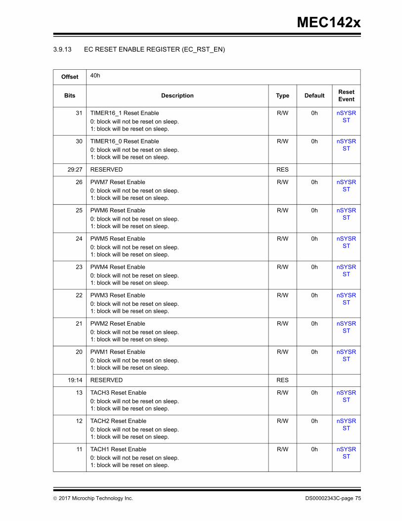
MEC142x
3.9.13 EC RESET ENABLE REGISTER (EC_RST_EN)
Offset 40h
Bits Description Type DefaultReset Event
31 TIMER16_1 Reset Enable
0: block will not be reset on sleep.1: block will be reset on sleep.
R/W 0h nSYSRST
30 TIMER16_0 Reset Enable
0: block will not be reset on sleep.1: block will be reset on sleep.
R/W 0h nSYSRST
29:27 RESERVED RES
26 PWM7 Reset Enable
0: block will not be reset on sleep.1: block will be reset on sleep.
R/W 0h nSYSRST
25 PWM6 Reset Enable
0: block will not be reset on sleep.1: block will be reset on sleep.
R/W 0h nSYSRST
24 PWM5 Reset Enable
0: block will not be reset on sleep.1: block will be reset on sleep.
R/W 0h nSYSRST
23 PWM4 Reset Enable
0: block will not be reset on sleep.1: block will be reset on sleep.
R/W 0h nSYSRST
22 PWM3 Reset Enable
0: block will not be reset on sleep.1: block will be reset on sleep.
R/W 0h nSYSRST
21 PWM2 Reset Enable
0: block will not be reset on sleep.1: block will be reset on sleep.
R/W 0h nSYSRST
20 PWM1 Reset Enable
0: block will not be reset on sleep.1: block will be reset on sleep.
R/W 0h nSYSRST
19:14 RESERVED RES
13 TACH3 Reset Enable
0: block will not be reset on sleep.1: block will be reset on sleep.
R/W 0h nSYSRST
12 TACH2 Reset Enable
0: block will not be reset on sleep.1: block will be reset on sleep.
R/W 0h nSYSRST
11 TACH1 Reset Enable
0: block will not be reset on sleep.1: block will be reset on sleep.
R/W 0h nSYSRST
2017 Microchip Technology Inc. DS00002343C-page 75
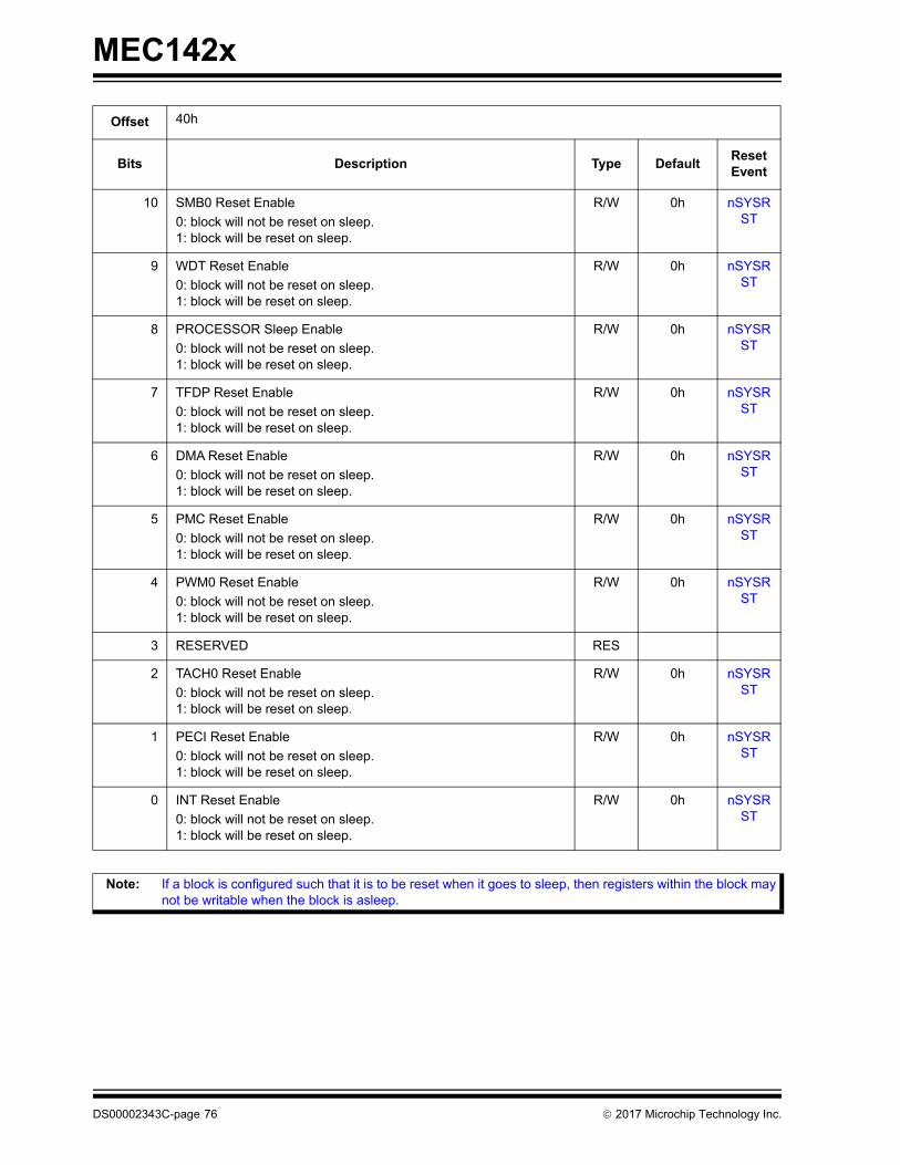
MEC142x
10 SMB0 Reset Enable
0: block will not be reset on sleep.1: block will be reset on sleep.
R/W 0h nSYSRST
9 WDT Reset Enable
0: block will not be reset on sleep.1: block will be reset on sleep.
R/W 0h nSYSRST
8 PROCESSOR Sleep Enable
0: block will not be reset on sleep.1: block will be reset on sleep.
R/W 0h nSYSRST
7 TFDP Reset Enable
0: block will not be reset on sleep.1: block will be reset on sleep.
R/W 0h nSYSRST
6 DMA Reset Enable
0: block will not be reset on sleep.1: block will be reset on sleep.
R/W 0h nSYSRST
5 PMC Reset Enable
0: block will not be reset on sleep.1: block will be reset on sleep.
R/W 0h nSYSRST
4 PWM0 Reset Enable
0: block will not be reset on sleep.1: block will be reset on sleep.
R/W 0h nSYSRST
3 RESERVED RES
2 TACH0 Reset Enable
0: block will not be reset on sleep.1: block will be reset on sleep.
R/W 0h nSYSRST
1 PECI Reset Enable
0: block will not be reset on sleep.1: block will be reset on sleep.
R/W 0h nSYSRST
0 INT Reset Enable
0: block will not be reset on sleep.1: block will be reset on sleep.
R/W 0h nSYSRST
Note: If a block is configured such that it is to be reset when it goes to sleep, then registers within the block maynot be writable when the block is asleep.
Offset 40h
Bits Description Type DefaultReset Event
DS00002343C-page 76 2017 Microchip Technology Inc.

MEC142x
3.9.14 EC RESET ENABLE 2 REGISTER (EC_RST_EN2)
Offset 44h
Bits Description Type DefaultReset Event
31:26 RESERVED RES
25 SMB4 Reset Enable
0: block will not be reset on sleep.1: block will be reset on sleep.
R/W 0h nSYSRST
24 SMB3 Reset Enable
0: block will not be reset on sleep.1: block will be reset on sleep.
R/W 0h nSYSRST
23 RESERVED RES
22 TIMER16_3 Reset Enable
0: block will not be reset on sleep.1: block will be reset on sleep.
R/W 0h nSYSRST
21 TIMER16_2_Reset Enable
0: block will not be reset on sleep.1: block will be reset on sleep.
R/W 0h nSYSRST
20:19 RESERVED RES
18 LED2 Reset Enable
0: block will not be reset on sleep.1: block will be reset on sleep.
R/W 0h nSYSRST
17 LED1 Reset Enable
0: block will not be reset on sleep.1: block will be reset on sleep.
R/W 0h nSYSRST
16 LED0 Reset Enable
0: block will not be reset on sleep.1: block will be reset on sleep.
R/W 0h nSYSRST
15 RESERVED RES
14 SMB2 Reset Enable
0: block will not be reset on sleep.1: block will be reset on sleep.
R/W 0h nSYSRST
13 SMB1 Reset Enable
0: block will not be reset on sleep.1: block will be reset on sleep.
R/W 0h nSYSRST
12 RTOS Timer Reset Enable
0: block will not be reset on sleep.1: block will be reset on sleep.
R 0h nSYSRST
11 KEYSCAN Reset Enable
0: block will not be reset on sleep.1: block will be reset on sleep.
R/W 0h nSYSRST
2017 Microchip Technology Inc. DS00002343C-page 77

MEC142x
3.9.15 POWER RESET CONTROL (PWR_RST_CTRL) REGISTER
10 HTIMER Reset Enable
0: block will not be reset on sleep.1: block will be reset on sleep.
R/W 0h nSYSRST
9 Quad SPI Master Sleep Enable
0: block is free to use clocks as necessary.1: block is commanded to sleep at next available moment.
R/W 0h nSYSRST
8:7 RESERVED RES
6 PS2_1 Reset Enable
0: block will not be reset on sleep.1: block will be reset on sleep.
R/W 0h nSYSRST
5 PS2_0 Reset Enable
0: block will not be reset on sleep.1: block will be reset on sleep.
R/W 0h nSYSRST
4 RESERVED RES
3 ADC Reset Enable
0: block will not be reset on sleep.1: block will be reset on sleep.
R/W 0h nSYSRST
2:0 RESERVED RES
Note: If a block is configured such that it is to be reset when it goes to sleep, then registers within the block maynot be writable when the block is asleep.
Offset 48h
Bits Description Type DefaultReset Event
31:2 RESERVED RES
Offset 44h
Bits Description Type DefaultReset Event
DS00002343C-page 78 2017 Microchip Technology Inc.
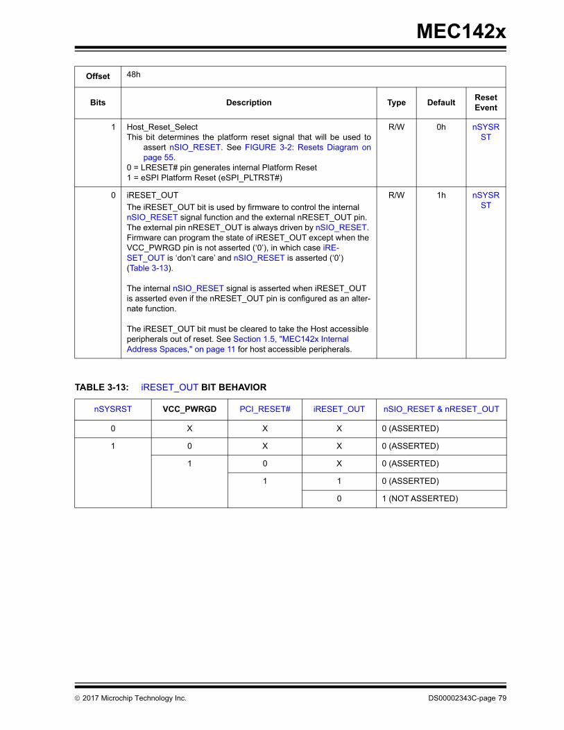
MEC142x
1 Host_Reset_SelectThis bit determines the platform reset signal that will be used to
assert nSIO_RESET. See FIGURE 3-2: Resets Diagram onpage 55.
0 = LRESET# pin generates internal Platform Reset1 = eSPI Platform Reset (eSPI_PLTRST#)
R/W 0h nSYSRST
0 iRESET_OUT
The iRESET_OUT bit is used by firmware to control the internal nSIO_RESET signal function and the external nRESET_OUT pin. The external pin nRESET_OUT is always driven by nSIO_RESET. Firmware can program the state of iRESET_OUT except when the VCC_PWRGD pin is not asserted (‘0’), in which case iRE-SET_OUT is ‘don’t care’ and nSIO_RESET is asserted (‘0’) (Table 3-13).
The internal nSIO_RESET signal is asserted when iRESET_OUT is asserted even if the nRESET_OUT pin is configured as an alter-nate function.
The iRESET_OUT bit must be cleared to take the Host accessible peripherals out of reset. See Section 1.5, "MEC142x Internal Address Spaces," on page 11 for host accessible peripherals.
R/W 1h nSYSRST
TABLE 3-13: iRESET_OUT BIT BEHAVIOR
nSYSRST VCC_PWRGD PCI_RESET# iRESET_OUT nSIO_RESET & nRESET_OUT
0 X X X 0 (ASSERTED)
1 0 X X 0 (ASSERTED)
1 0 X 0 (ASSERTED)
1 1 0 (ASSERTED)
0 1 (NOT ASSERTED)
Offset 48h
Bits Description Type DefaultReset Event
2017 Microchip Technology Inc. DS00002343C-page 79
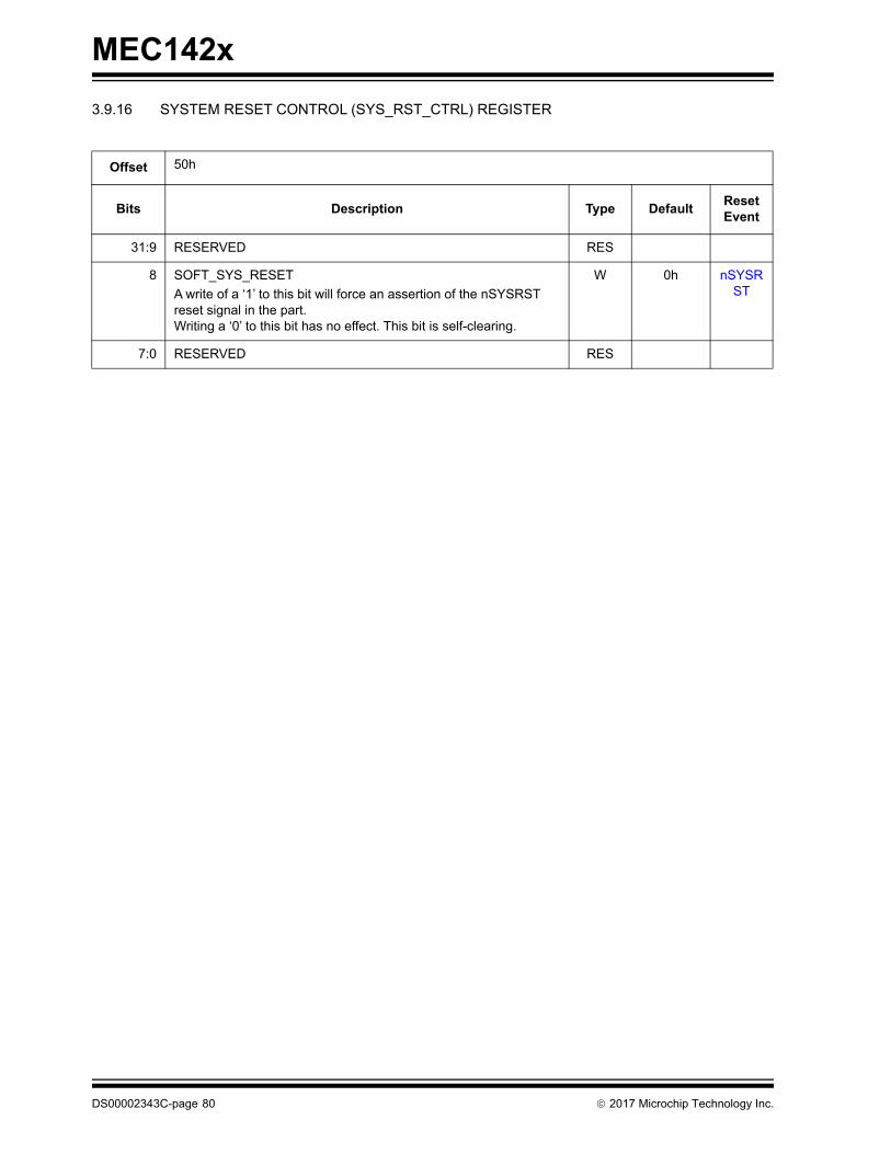
MEC142x
3.9.16 SYSTEM RESET CONTROL (SYS_RST_CTRL) REGISTER
Offset 50h
Bits Description Type DefaultReset Event
31:9 RESERVED RES
8 SOFT_SYS_RESET
A write of a ‘1’ to this bit will force an assertion of the nSYSRST reset signal in the part.Writing a ‘0’ to this bit has no effect. This bit is self-clearing.
W 0h nSYSRST
7:0 RESERVED RES
DS00002343C-page 80 2017 Microchip Technology Inc.
MEC142x
4.0 LPC INTERFACE
4.1 Introduction
The Intel® Low Pin Count (LPC) Interface is the LPC Interface used by the system host to configure the chip and com-municate with the logical devices implemented in the design through a series of read/write registers. Register access isaccomplished through the LPC transfer cycles defined in Table 4-5, "LPC Cycle Types Supported".
The Logical Devices implemented in the design are identified in Table 4-14, “I/O Base Address Registers,” on page 103.The Base Address Registers allow any logical device’s runtime registers to be relocated in LPC I/O space. All chip con-figuration registers for the device are accessed indirectly through the LPC I/O Configuration Port (see Section 4.8.3,"Configuration Port," on page 92).
4.2 References
• Intel® Low Pin Count (LPC) Interface Specification, v1.1
• PCI Local Bus Specification, Rev. 2.2
• Serial IRQ Specification for PCI Systems Version 6.0.
• PCI Mobile Design Guide Rev 1.0
4.3 Terminology
This table defines specialized terms localized to this feature.
TABLE 4-1: TERMINOLOGY
Term Definition
System Host Refers to the external CPU that communicates with this device via the LPC Inter-face.
Logical Devices Logical Devices are LPC accessible features that are allocated a Base Address and range in LPC I/O address space
Runtime Register Runtime Registers are register that are directly I/O accessible by the System Host via the LPC interface. These registers are defined in Section 4.10, "Runtime Regis-ters," on page 106.
Configuration Registers Registers that are only accessible in CONFIG_MODE. These registers are defined in Section 4.9, "LPC Configuration Registers," on page 99.
EC_Only Registers Registers that are not accessible by the System Host. They are only accessible by an internal embedded controller. These registers are defined in Section 4.11, "EC-Only Registers," on page 107.
2017 Microchip Technology Inc. DS00002343C-page 81

MEC142x
4.4 Interface
This block is designed to be accessed externally via the pin interface and internally via a registered host interface.
4.4.1 SIGNAL DESCRIPTION
FIGURE 4-1: BLOCK DIAGRAM OF LPC INTERFACE CONTROLLER WITH CLKRUN# SUPPORT
TABLE 4-2: SIGNAL DESCRIPTION TABLE
Name Direction Description
LAD0 Input/Output Bit[0] of the LPC multiplexed command, address, and data bus.
LAD1 Input/Output Bit[1] of the LPC multiplexed command, address, and data bus.
SERIRQ
LAD0
LAD1
LAD2
LAD3
LFRAME#
LRESET#
LCLK
LPC Interface(Logical Device Ch)
LPC Controller
Serial IRQState MachineInterface to
Configuration Registers
Con
figur
atio
n P
ort
CLKRUN#
LPC Config Registers
LPC Regis-ters
(Runtime, EC-Only)
Interface to Logical Device Register
DS00002343C-page 82 2017 Microchip Technology Inc.

MEC142x
4.4.2 REGISTER INTERFACES
The registers defined for the LPC Interface block are accessible by the various hosts as indicated in Section 4.9, "LPCConfiguration Registers", Section 4.11, "EC-Only Registers"and Section 4.10, "Runtime Registers".
4.5 Power, Clocks and Reset
This section defines the Power, Clock, and Reset parameters of the block.
4.5.1 POWER DOMAINS
4.5.2 CLOCK INPUTS
LAD2 Input/Output Bit[2] of the LPC multiplexed command, address, and data bus.
LAD3 Input/Output Bit[3] of the LPC multiplexed command, address, and data bus.
LFRAME# Input Active low signal indicates start of new cycle and termi-nation of broken cycle.
LRESET# Input Active low signal used as LPC Interface Reset. Same as PCI Reset on host.
Note: LRESET# is typically connected to the hostPCI RESET (PCIRST#) signal.
LCLK Input PCI clock input (PCI_CLK)
SERIRQ Input/Output Serial IRQ pin used with the LCLK signal to transfer interrupts to the host.
CLKRUN# Open-Drain Output Clock Control for LCLK
LPCPD# Input Power Down: Indicates that the device should prepare for power to be removed from the LPC I/F.
Name Description
VTR The LPC Interface block and registers are powered by VTR.
Name Description
LCLK This LPC Interface has a single clock input, called LCLK.
Note: The PCI_CLK input to LCLK can run at 24MHz or 33MHz. When the PCI_CLK input is 24MHz the Hand-shake bit in the EC Clock Control Register must be set to a ‘1’ to capture LPC transactions properly. SeeSection 4.11.4, "EC Clock Control Register," on page 110.
TABLE 4-2: SIGNAL DESCRIPTION TABLE (CONTINUED)
Name Direction Description
2017 Microchip Technology Inc. DS00002343C-page 83

MEC142x
4.5.3 RESETS
The following table defines the effective reset state that result from the combination of these three reset signals.
Note 4-1 The EC can determine the state of the LRESET# input using registers in LPC Bus Monitor Registeron page 108.
Note 4-2 nSYSRST is asserted when VTR is turned off and is released after VTR is turned on. The nSYSRSTwill be released before the System Host is expected to attempt communication over the LPCInterface.
Note 4-3 See the individual register descriptions to determine which registers are effected by nSIO_RESET.
Note 4-4 The LPC Interface will be ready to receive a new transaction when LRESET# is deasserted. See theindividual register descriptions to determine which registers are effected by this reset.
In system, the LPC Interface is required to be operational in ACPI Sleep States S0 - S2. When the system enters SleepStates S3 - S5 the LPC interface must tristate its outputs. The following table shows the behavior of LPC output andinput/output signals under reset conditions.
Name Description
nSYSRST Power on Reset to the block. This signal resets all the register and logic in this block to its default state.
nSIO_RESET This signal is used to indicate when the main power rail in the system is reset. The LPC interface is operational when main power is present. This signal is used to reset selected registers as defined in the Register Interfaces descriptions.
LRESET# The LRESET# signal comes from the LPC pin interface. This signal is defined in the Intel® Low Pin Count (LPC) Interface Specification, v1.1.
TABLE 4-3: LPC Interface BLOCK RESET STATES
nSYSRST(Note 4-2)
LRESET#(Note 4-1, Note 4-4)
nSIO_RESET(Note 4-3)
Reset State
Asserted X X Resets all registers and logic
Deasserted Asserted X Resets selected registers and logic
Deasserted Asserted Resets selected registers
Deasserted Nothing is in Reset
TABLE 4-4: LPC INTERFACE SIGNALS BEHAVIOR ON RESET
Pins nSYSRST nSIO_RESET LPCPD#LRESET#Asserted
LAD[3:0] Tri-state Tri-state Tri-state Tri-State
SERIRQ Tri-state Tri-state Tri-state Tri-State
CLKRUN# Tri-state Tri-state Tri-state Tri-State
DS00002343C-page 84 2017 Microchip Technology Inc.
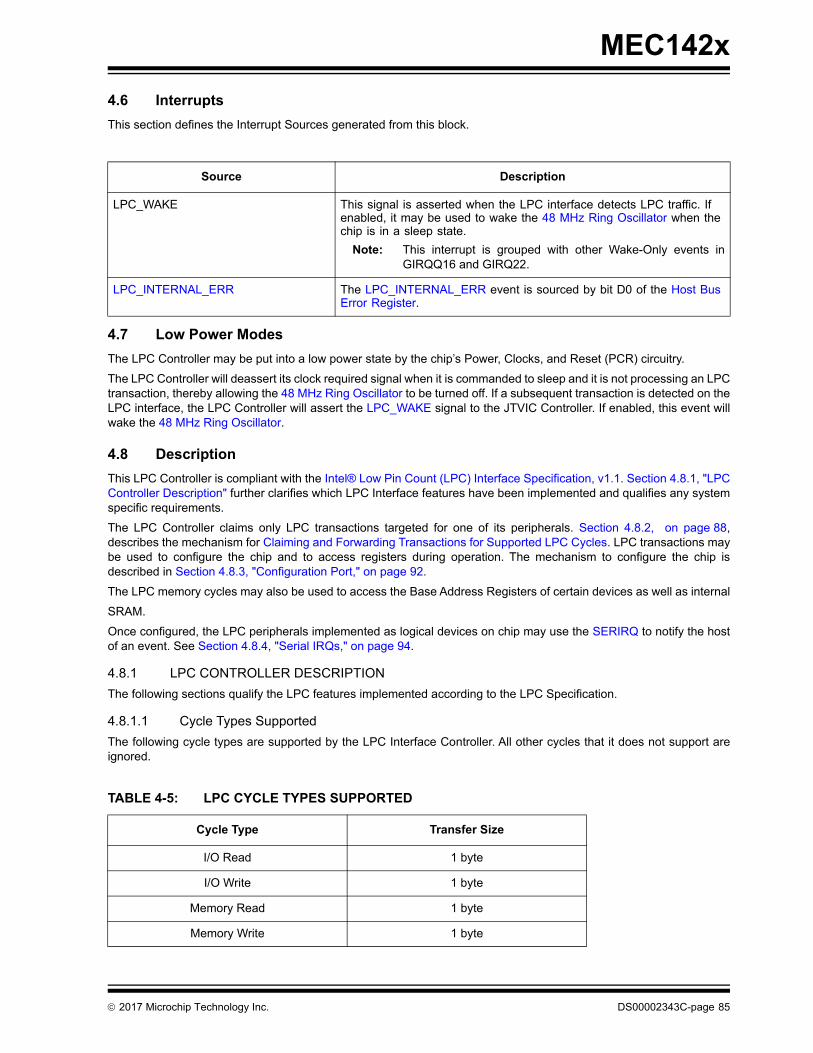
MEC142x
4.6 Interrupts
This section defines the Interrupt Sources generated from this block.
4.7 Low Power Modes
The LPC Controller may be put into a low power state by the chip’s Power, Clocks, and Reset (PCR) circuitry.
The LPC Controller will deassert its clock required signal when it is commanded to sleep and it is not processing an LPCtransaction, thereby allowing the 48 MHz Ring Oscillator to be turned off. If a subsequent transaction is detected on theLPC interface, the LPC Controller will assert the LPC_WAKE signal to the JTVIC Controller. If enabled, this event willwake the 48 MHz Ring Oscillator.
4.8 Description
This LPC Controller is compliant with the Intel® Low Pin Count (LPC) Interface Specification, v1.1. Section 4.8.1, "LPCController Description" further clarifies which LPC Interface features have been implemented and qualifies any systemspecific requirements.
The LPC Controller claims only LPC transactions targeted for one of its peripherals. Section 4.8.2, on page 88,describes the mechanism for Claiming and Forwarding Transactions for Supported LPC Cycles. LPC transactions maybe used to configure the chip and to access registers during operation. The mechanism to configure the chip isdescribed in Section 4.8.3, "Configuration Port," on page 92.
The LPC memory cycles may also be used to access the Base Address Registers of certain devices as well as internal
SRAM.
Once configured, the LPC peripherals implemented as logical devices on chip may use the SERIRQ to notify the hostof an event. See Section 4.8.4, "Serial IRQs," on page 94.
4.8.1 LPC CONTROLLER DESCRIPTION
The following sections qualify the LPC features implemented according to the LPC Specification.
4.8.1.1 Cycle Types Supported
The following cycle types are supported by the LPC Interface Controller. All other cycles that it does not support areignored.
Source Description
LPC_WAKE This signal is asserted when the LPC interface detects LPC traffic. If enabled, it may be used to wake the 48 MHz Ring Oscillator when the chip is in a sleep state.
Note: This interrupt is grouped with other Wake-Only events inGIRQQ16 and GIRQ22.
LPC_INTERNAL_ERR The LPC_INTERNAL_ERR event is sourced by bit D0 of the Host Bus Error Register.
TABLE 4-5: LPC CYCLE TYPES SUPPORTED
Cycle Type Transfer Size
I/O Read 1 byte
I/O Write 1 byte
Memory Read 1 byte
Memory Write 1 byte
2017 Microchip Technology Inc. DS00002343C-page 85

MEC142x
When the LPC Controller detects a transaction targeted for this device it will claims and forward that transaction asdefined in Section 4.8.2, "Claiming and Forwarding Transactions for Supported LPC Cycles," on page 88.
LPC I/O Cycles
The system host may use LPC I/O cycles to read/write the I/O mapped configuration and runtime registers implementedin this device. See the Intel® Low Pin Count (LPC) Interface Specification, v1.1, Section 5.2 for definition of LPC I/OCycles.
LPC Memory Cycles
The system host may use LPC memory cycles to access memory mapped registers and internal RAMs implemented inthis device. See the Intel® Low Pin Count (LPC) Interface Specification, v1.1, Section 5.1 for definition of LPC MemoryCycles.
4.8.1.2 LAD[3:0] Fields
The LAD[3:0] signals support multiple fields for each protocol as defined in section 4.2.1 LAD[3:0] of the Intel® Low PinCount (LPC) Interface Specification, v1.1. The following sections further qualify the fields supported.
Wait SYNCs on LPC
LPC transactions that access registers located on the device will require a minimum of two wait SYNCs on the LPC bus.The number of SYNCs may be larger if the internal bus is in use by the embedded controller, of if the data referencedby the host is not present in a register. The device always uses Long Wait SYNCs, rather than Short Wait SYNCs, whenresponding to an LPC bus request.
ERROR SYNCs on LPC
The device does not issue ERROR SYNC cycles.
4.8.1.3 LPC Clock Run and LPC Power Down Behavior
Using LPCPD#
The device tolerates the LPCPD# signal going active and then inactive again without LRESET# going active. This is arequirement for notebook power management functions.
The Intel® Low Pin Count (LPC) Interface Specification, v1.1, Section 8.2 states that “After LPCPD# is de-asserted, theLPC interface may be reset dependent upon the characteristics of system reset signal connected to LRESET#.” Thistext must be qualified for mobile systems where it is possible that when exiting a "light" sleep state (ACPI S1, APM POS),LPCPD# may be asserted but the LPC Bus power may not be removed, in which case LRESET# will not occur. Whenexiting a "deeper" sleep state (ACPI S3-S5, APM STR, STD, soft-off), LRESET# will occur.
The LPCPD# pin is implemented as a “local” powergood for the LPC bus in the device. It is not to be used as a globalpowergood for the chip. It is used to minimize the LPC power dissipation.
Prior to going to a low-power state, the system asserts the LPCPD# signal. LPCPD# goes active at least 30 microsec-onds prior to the LCLK signal stopping low and power being shut to the other LPC interface signals. Upon recognizingLPCPD# active, there are no further transactions on the LPC interface.
Using CLKRUN#
CLKRUN# is used to indicate the status of LCLK as well as to request that a stopped clock be started. See FIGURE4-2: CLKRUN# System Implementation Example on page 87, an example of a typical system implementation usingCLKRUN#.
LCLK Run Support can be enabled and disabled via SIRQ_MODE as shown in Table 4-6, "LPC Controller CLKRUN#Function". When the SIRQ_MODE is ‘0,’ Serial IRQs are disabled, the CLKRUN# pin is disabled, and the affects of Inter-rupt requests on CLKRUN# are ignored. When the SIRQ_MODE is ‘1,’ Serial IRQs are enabled, the CLKRUN# pin isenabled, and the CLKRUN# support related to Interrupts requests as described in the section below is enabled.
The CLKRUN# pin is an open drain output and input. Refer to the PCI Mobile Design Guide Rev 1.0 for a descriptionof the CLKRUN# function. If CLKRUN# is sampled “high”, LCLK is stopped or stopping. If CLKRUN# is sampled “low”,LCLK is starting or started (running).
Note: All LPC transactions are synchronized to the LCLK and will complete with a maximum of 8 wait states,unless otherwise noted.
DS00002343C-page 86 2017 Microchip Technology Inc.
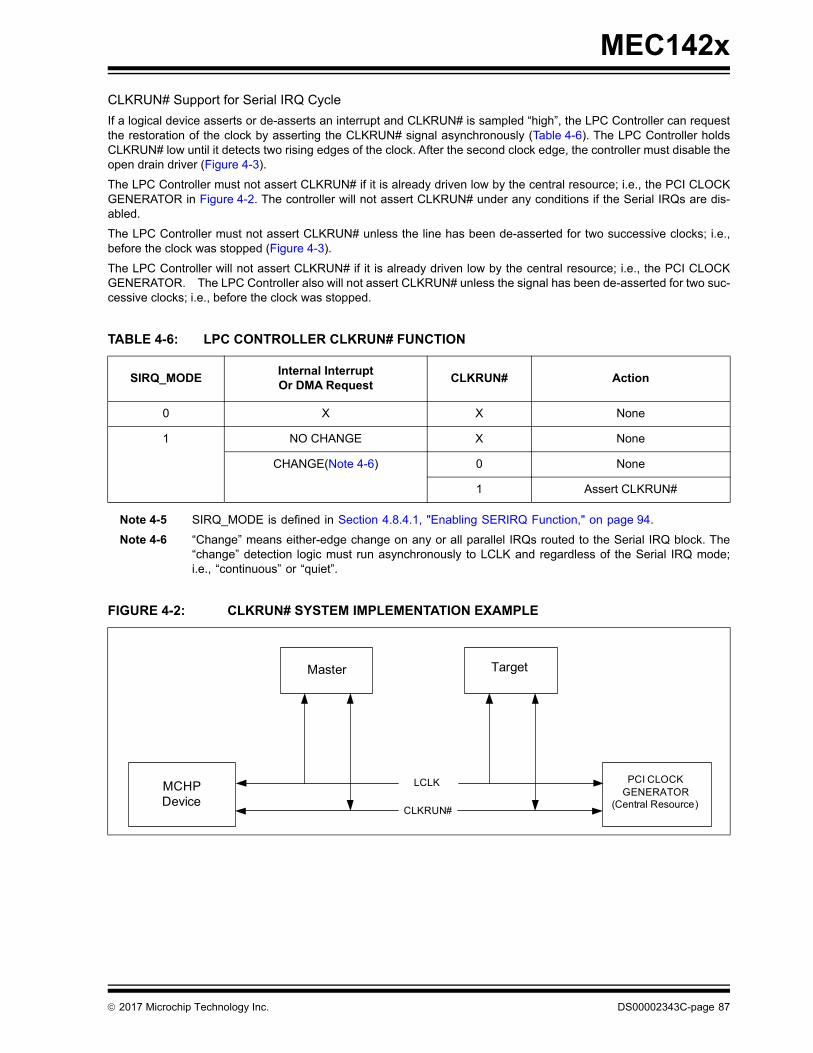
MEC142x
CLKRUN# Support for Serial IRQ Cycle
If a logical device asserts or de-asserts an interrupt and CLKRUN# is sampled “high”, the LPC Controller can requestthe restoration of the clock by asserting the CLKRUN# signal asynchronously (Table 4-6). The LPC Controller holdsCLKRUN# low until it detects two rising edges of the clock. After the second clock edge, the controller must disable theopen drain driver (Figure 4-3).
The LPC Controller must not assert CLKRUN# if it is already driven low by the central resource; i.e., the PCI CLOCKGENERATOR in Figure 4-2. The controller will not assert CLKRUN# under any conditions if the Serial IRQs are dis-abled.
The LPC Controller must not assert CLKRUN# unless the line has been de-asserted for two successive clocks; i.e.,before the clock was stopped (Figure 4-3).
The LPC Controller will not assert CLKRUN# if it is already driven low by the central resource; i.e., the PCI CLOCKGENERATOR. The LPC Controller also will not assert CLKRUN# unless the signal has been de-asserted for two suc-cessive clocks; i.e., before the clock was stopped.
Note 4-5 SIRQ_MODE is defined in Section 4.8.4.1, "Enabling SERIRQ Function," on page 94.
Note 4-6 “Change” means either-edge change on any or all parallel IRQs routed to the Serial IRQ block. The“change” detection logic must run asynchronously to LCLK and regardless of the Serial IRQ mode;i.e., “continuous” or “quiet”.
TABLE 4-6: LPC CONTROLLER CLKRUN# FUNCTION
SIRQ_MODEInternal InterruptOr DMA Request
CLKRUN# Action
0 X X None
1 NO CHANGE X None
CHANGE(Note 4-6) 0 None
1 Assert CLKRUN#
FIGURE 4-2: CLKRUN# SYSTEM IMPLEMENTATION EXAMPLE
CLKRUN#
LCLK
Target
PCI CLOCKGENERATOR
(Central Resource)
Master
MCHP Device
2017 Microchip Technology Inc. DS00002343C-page 87
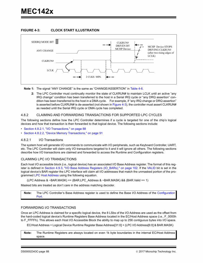
MEC142x
Note 1: The signal “ANY CHANGE” is the same as “CHANGE/ASSERTION” in Table 4-6.
2: The LPC Controller must continually monitor the state of CLKRUN# to maintain LCLK until an active “anyIRQ change” condition has been transferred to the host in a Serial IRQ cycle or “any DRQ assertion” con-dition has been transferred to the host in a DMA cycle. For example, if “any IRQ change or DRQ assertion”is asserted before CLKRUN# is de-asserted (not shown in Figure 4-3), the controller must assert CLKRUN#as needed until the Serial IRQ cycle or DMA cycle has completed.
4.8.2 CLAIMING AND FORWARDING TRANSACTIONS FOR SUPPORTED LPC CYCLES
The following sections define how the LPC Controller determines if a cycle is targeted for one of the chip’s logicaldevices and how that transaction is then forwarded to that logical device. The following sections include:
• Section 4.8.2.1, "I/O Transactions," on page 88
• Section 4.8.2.2, "Device Memory Transactions," on page 91
4.8.2.1 I/O Transactions
The system host will generate I/O commands to communicate with I/O peripherals, such as Keyboard Controller, UART,etc. The LPC Controller will claim only I/O transactions targeted to it and it will ignore all others. The following sectionsdescribe how I/O transactions are claimed and forwarded to access the Runtime and Configuration registers.
CLAIMING LPC I/O TRANSACTIONS
Each host I/O accessible block (i.e., logical device) has an associated I/O Base Address register. The format of this reg-ister is defined in Section 4.9.3, "I/O Base Address Registers (IO_BARs)," on page 102. If the VALID bit is set in thelogical device’s BAR register the LPC interface will claim all I/O addresses that match the unmasked portion of the pro-grammed LPC Host Address using the following equation.
(LPC Address & ~BAR.MASK) == (BAR.LPC_Address & ~BAR.MASK) && (BAR.Valid == 1)
Masked bits are treated as don’t care in the address matching decoder.
FORWARDING I/O TRANSACTIONS
Once an LPC Address is claimed for a specific logical device, the 8 LSbs of the I/O Address are used as the offset fromthe hard-coded logical device’s Runtime Registers Base Address located in the EC/Host Address space (i.e., F_0000hto F_FFFFh). This allows each Host I/O Accessible Block the ability to map up to 256 contiguous bytes into I/O space.
EC/Host Address = Logical Device Runtime Register Base Address[31:0] + (LPC I/O Address[6:0] & BAR.MASK)
FIGURE 4-3: CLOCK START ILLUSTRATION
Note: The LPC Controller’s Base Address register is used to define the Base I/O Address of the ConfigurationPort.
Note: The Runtime Registers are always located on even 1k byte boundaries in the internal EC/Host Addressspace.
LCLK
CLKRUN#
SERIRQ MODE BIT
ANY CHANGE
CLKRUN#DRIVEN BY MCHP Device
MCHP Device STOPS DRIVING CLKRUN# (after two rising edges of LCLK)
2 CLKS MIN.
DS00002343C-page 88 2017 Microchip Technology Inc.

MEC142x
EXAMPLE 4-1: LPC RUNTIME (CONFIGURATION PORT) ADDRESSING
The system host will use I/O transactions to access the Configuration and Runtime registers. To access the Runtimeregisters, the host must configure the I/O Base Address Registers (IO_BARs), which are accessible via the Configura-tion Port first. The Configuration Port, Logical Device Ch, is located at the Base I/O Address programmed in the BARConfiguration register located at offset 60h.
For illustration purposes only, lets examine two types of logical devices (these may or may not reside in this design).
EXAMPLE 4-2: KEYBOARD CONTROLLER
The Keyboard Controller (8042 Interface) Base Address Register has 60h in the LPC Address field, the Frame field is01h, and the MASK field is 04h. Because of the single ‘1b’ bit in MASK, the BAR will match LPC I/O patterns in the form‘0000_0000_0110_0x00b’, so both 60h and 64h will be matched and claimed by the LPC Controller.
EXAMPLE 4-3: 16550 UART
If a standard 16550 UART was located at LPC I/O address 238h, then the UART Receive buffer would appear ataddress 238h and the Line Status register at 23Dh. If the BAR for the UART was set to 0238_8047h, then the UARTwill be matched at I/O address 238h.
The following table illustrates the I/O Address Mapping for each logical device implemented in the MEC142x.
Configuration PortLPC I/O Address
EC/Host Address Register
002Eh F_3000h INDEX
002Fh F_3001h DATA
Note: The Logical Device number for the matching device is located in the Frame field of the BAR. The Framefield is mapped to bits [15:10] of the EC/Host Address space. In this example bits[15:10] = 00_1100 = Ch.
TABLE 4-7: LPC I/O REGISTER MAP
Logical DeviceBAR LPC
Host Address
Example BAR LPC
Host Address
LPC Address
Mask
Offsets Claimed
Register Name
LPC Interface (Con-figuration Port)
2 Byte Bound-ary
002Eh 1 BAR+0 INDEX
+1 DATA
EMI 0 16 Byte Boundary
0060h F BAR+0 Host-to-EC Mailbox
+1 EC-to-Host Mailbox
+2 EC Address LSB
+3 EC Address MSB
+4 EC Data Byte 0
+5 EC Data Byte 1
+6 EC Data Byte 2
+7 EC Data Byte 3
+8 Interrupt Source LSB
+9 Interrupt Source MSB
+A Interrupt Mask LSB
+B Interrupt Mask MSB
+C Application ID
2017 Microchip Technology Inc. DS00002343C-page 89

MEC142x
8042 Emulated Key-board Controller
Byte Boundary 0060h 4 BAR+0 Write: WRITE_DATARead: READ_DATA
+4 Write: WRITE_CMDRead: STATUS
ACPI EC0 Byte Boundary 0062h 4 BAR+0 ACPI_OS_DATA_BYTE_0
+4 Write: ACPI_OS_COMMANDRead: OS STATUS OS
ACPI EC1 8 Byte Bound-ary
0070h 7 BAR+0 ACPI_OS_DATA_BYTE_0
+1 ACPI_OS_DATA_BYTE_1
+2 ACPI_OS_DATA_BYTE_2
+3 ACPI_OS_DATA_BYTE_3
+4 Write: ACPI_OS_COMMANDRead: OS STATUS OS
+5 OS Byte Control
+6 Reserved
+7 Reserved
ACPI PM1 8 Byte Bound-ary
0078h 7 BAR+0 Power Management 1 Status 1
+1 Power Management 1 Status 2
+2 Power Management 1 Enable 1
+3 Power Management 1 Enable 2
+4 Power Management 1 Control 1
+5 Power Management 1 Control 2
+6 Power Management 2 Control 1
+7 Power Management 2 Control 2
Legacy Port92/GateA20
Any I/O Byte Address
0092h 0 BAR+0 Port 92
UART 0 8 Byte Bound-ary
03F0h 7 BAR+0 Write (DLAB=0): Transmit BufferRead (DLAB=0): Receive BufferR/W (DLAB=1): Programmable BAUD Rate Generator LSB
+1 R/W (DLAB=0): Interrupt Enable Regis-terR/W (DLAB=1): Programmable BAUD Rate Generator MSB
+2 Write: FIFO ControlRead: Interrupt Identification
+3 Line Control
+4 Modem Control
+5 Line Status
+6 Modem Status
+7 Scratchpad Register
Mailbox Interface 2 Byte Bound-ary
0100h 1 BAR+0 MBX_INDEX
+1 MBX_DATA
TABLE 4-7: LPC I/O REGISTER MAP (CONTINUED)
Logical DeviceBAR LPC
Host Address
Example BAR LPC
Host Address
LPC Address
Mask
Offsets Claimed
Register Name
DS00002343C-page 90 2017 Microchip Technology Inc.
MEC142x
4.8.2.2 Device Memory Transactions
LPC Memory cycles are single byte read or writes that occur in a 32-bit address range. The LPC block will claim a mem-ory transaction that is targeted for one of these logical devices. A Device Memory Base Address Register has beenimplemented for the logical devices listed in Table 4-15, “Device Memory Base Address Registers,” on page 105
On every LPC bus Memory access all Base Address Registers are checked in parallel and if any matches the LPC mem-ory address the LPC Interface claims the bus cycle. The memory address is claimed as described in I/O Transactionson page 88 except that the LPC memory cycle address is 32 bits instead of the 16 bit I/O cycle address.
Software should insure that no two BARs map the same LPC memory address. If two BARs do map to the sameaddress, the BAR_CONFLICT bit in the Host Bus Error Register is set when an LPC access targeting the BAR Conflictaddress. An EC interrupt can be generated.
Each Device Memory BAR is 48 bits wide. The format of each Device Memory BAR is summarized in Device MemoryBase Address Register Format. An LPC memory request is translated by the Device Memory BAR into an 8-bit read orwrite transaction on the AHB bus. The 32-bit LPC memory address is translated into a 32-bit AHB address.
The Base Address Register Table is itself part of the AHB address space. It resides in the Configuration quadrant ofLogical Device Ch, the LPC Interface.
4.8.2.3 SRAM Memory Transactions
In addition to mapping LPC Memory transactions into Logical Devices, Memory transactions can be mapped into inter-nal address space, as configured by the SRAM Memory BARs. LPC Memory cycles are single byte read or writes thatoccur in a 32-bit address range. The LPC block will claim LPC memory cycles that match the programmed SRAM Mem-ory BAR Register if the VALID in the SRAM Memory BAR Configuration is set to 1. No memory cycles will be claimedif this bit is cleared.
ACPI EC2 8 Byte Bound-ary
0030h 7 BAR+0 ACPI_OS_DATA_BYTE_0
+1 ACPI_OS_DATA_BYTE_1
+2 ACPI_OS_DATA_BYTE_2
+3 ACPI_OS_DATA_BYTE_3
+4 Write: ACPI_OS_COMMANDRead: OS STATUS OS
+5 OS Byte Control
+6 Reserved
+7 Reserved
ACPI EC3 8 Byte Bound-ary
0038h 7 BAR+0 ACPI_OS_DATA_BYTE_0
+1 ACPI_OS_DATA_BYTE_1
+2 ACPI_OS_DATA_BYTE_2
+3 ACPI_OS_DATA_BYTE_3
+4 Write: ACPI_OS_COMMANDRead: OS STATUS OS
+5 OS Byte Control
+6 Reserved
+7 Reserved
Port 80 BIOS Debug Port 0
Any I/O Byte Address
0080h 0 BAR+0 Host Data
Port 80 BIOS Debug Port 1
Any I/O Byte Address
0081h 0 BAR+0 Host Data
TABLE 4-7: LPC I/O REGISTER MAP (CONTINUED)
Logical DeviceBAR LPC
Host Address
Example BAR LPC
Host Address
LPC Address
Mask
Offsets Claimed
Register Name
2017 Microchip Technology Inc. DS00002343C-page 91
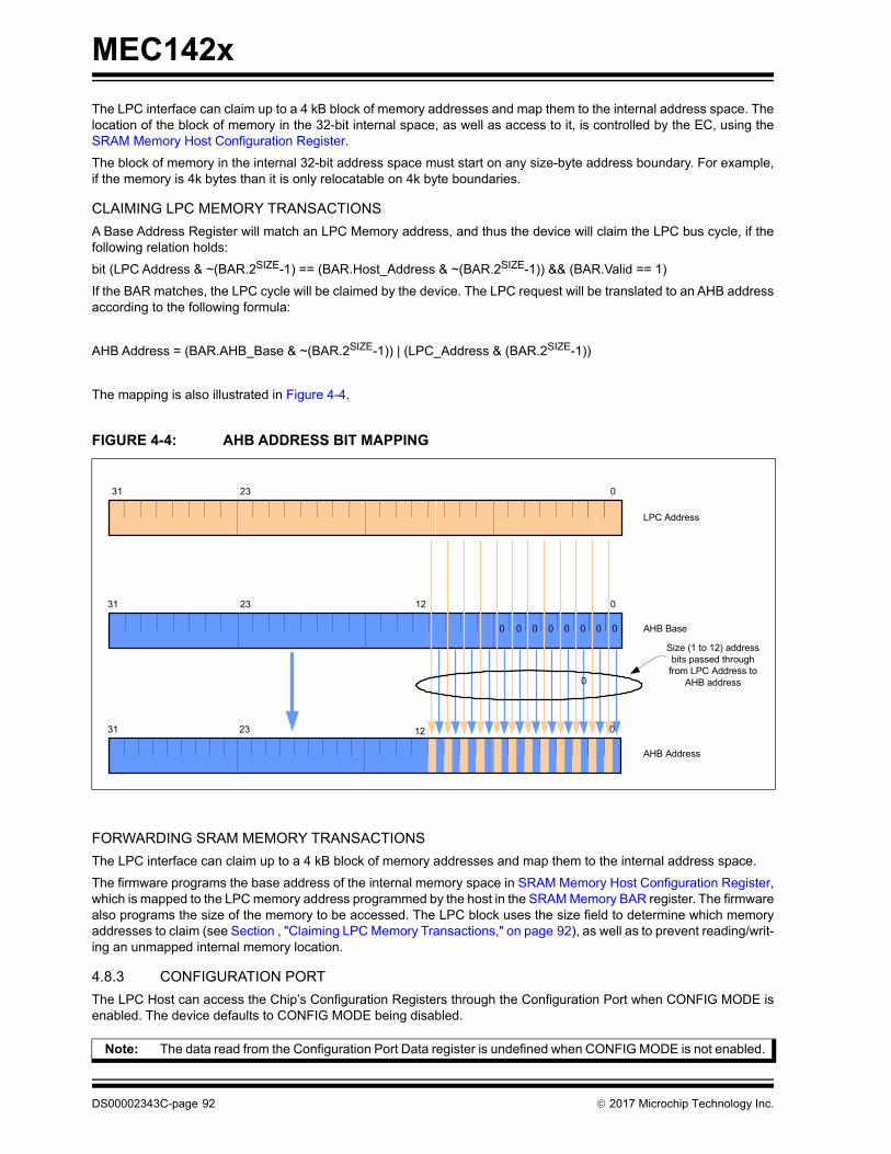
MEC142x
The LPC interface can claim up to a 4 kB block of memory addresses and map them to the internal address space. Thelocation of the block of memory in the 32-bit internal space, as well as access to it, is controlled by the EC, using theSRAM Memory Host Configuration Register.
The block of memory in the internal 32-bit address space must start on any size-byte address boundary. For example,if the memory is 4k bytes than it is only relocatable on 4k byte boundaries.
CLAIMING LPC MEMORY TRANSACTIONS
A Base Address Register will match an LPC Memory address, and thus the device will claim the LPC bus cycle, if thefollowing relation holds:
bit (LPC Address & ~(BAR.2SIZE-1) == (BAR.Host_Address & ~(BAR.2SIZE-1)) && (BAR.Valid == 1)
If the BAR matches, the LPC cycle will be claimed by the device. The LPC request will be translated to an AHB addressaccording to the following formula:
AHB Address = (BAR.AHB_Base & ~(BAR.2SIZE-1)) | (LPC_Address & (BAR.2SIZE-1))
The mapping is also illustrated in Figure 4-4.
FORWARDING SRAM MEMORY TRANSACTIONS
The LPC interface can claim up to a 4 kB block of memory addresses and map them to the internal address space.
The firmware programs the base address of the internal memory space in SRAM Memory Host Configuration Register,which is mapped to the LPC memory address programmed by the host in the SRAM Memory BAR register. The firmwarealso programs the size of the memory to be accessed. The LPC block uses the size field to determine which memoryaddresses to claim (see Section , "Claiming LPC Memory Transactions," on page 92), as well as to prevent reading/writ-ing an unmapped internal memory location.
4.8.3 CONFIGURATION PORT
The LPC Host can access the Chip’s Configuration Registers through the Configuration Port when CONFIG MODE isenabled. The device defaults to CONFIG MODE being disabled.
FIGURE 4-4: AHB ADDRESS BIT MAPPING
Note: The data read from the Configuration Port Data register is undefined when CONFIG MODE is not enabled.
031
23
23
LPC Address
AHB Base
AHB Address
0
Size (1 to 12) addressbits passed through from LPC Address to
AHB address
012
12
31
31
23
000000
0
0 0
DS00002343C-page 92 2017 Microchip Technology Inc.
MEC142x
The Configuration Port is composed of an INDEX and DATA Register. The INDEX register is used as an address pointerto an 8-bit configuration register and the DATA register is used to read or write the data value from the indexed config-uration register. Once CONFIG MODE is enabled, reading the Configuration Port Data register will return the data valuethat is in the indexed Configuration Register.
If no value was written to the INDEX register, reading the Data Register in the Configuration Port will return the value inConfiguration Address location 00h (default).
Note 4-7 The default Base I/O Address of the Configuration Port can be relocated by programming the BARregister for Logical Device Ch (LPC/Configuration Port) at offset 60h. The Relative Address showsthe general case for determining the I/O address for each register.
4.8.3.1 Enable CONFIG MODE
The INDEX and DATA registers are effective only when the chip is in CONFIG MODE. CONFIG MODE is enabled whenthe Config Entry Key is successfully written to the I/O address of the INDEX register of the CONFIG PORT while theCONFIG MODE is disabled (see Section 4.8.3.2, "Disable CONFIG MODE").
Config Entry Key = < 55h>
4.8.3.2 Disable CONFIG MODE
CONFIG MODE defaults to disabled on a nSYSRST, nSIO_RESET, and when LRESET# is asserted. CONFIG MODEis also disabled when the following Config Exit Key is successfully written to the I/O address of the INDEX PORT of theCONFIG PORT while CONFIG MODE is enabled.
Config Exit Key = < AAh>
4.8.3.3 Configuration Sequence Example
To program the configuration registers, the following sequence must be followed:
1. Enable Configuration State
2. Program the Configuration Registers
3. Disable Configuration State.
The following is an example of a configuration program in Intel 8086 assembly language.
;----------------------------.; ENABLE CONFIGURATION STATE;----------------------------'MOV DX,CONFIG_PORT_BASE_ADDRESSMOV AX,055H; Config Entry KeyOUT DX,AL;----------------------------.; CONFIGURE BASE ADDRESS, |; LOGICAL DEVICE 8 |;----------------------------'MOV DX,CONFIG_PORT_BASE_ADDRESSMOV AL,07HOUT DX,AL; Point to LD# Config RegMOV DX,CONFIG_PORT_BASE_ADDRESS+1
TABLE 4-8: CONFIGURATION PORT
Default I/O Address(Note 4-7)
Type Register Name Relative AddressDefault Value
Notes
002Eh Read / Write
INDEX Configuration Port’s Base Address + 0 00h Note 4-7
002Fh Read / Write
DATA Configuration Port’s Base Address + 1 00h
2017 Microchip Technology Inc. DS00002343C-page 93

MEC142x
MOV AL, 08HOUT DX,AL; Point to Logical Device 8;MOV DX,CONFIG_PORT_BASE_ADDRESSMOV AL,60HOUT DX,AL ; Point to BASE ADDRESS REGISTERMOV DX,CONFIG_PORT_BASE_ADDRESS+1MOV AL,02HOUT DX,AL ; Update BASE ADDRESS REGISTER;-----------------------------.; DISABLE CONFIGURATION STATE;-----------------------------'MOV DX,CONFIG_PORT_BASE_ADDRESSMOV AX,0AAH; Config Exit KeyOUT DX,AL.
4.8.4 SERIAL IRQS
The device supports the serial interrupt scheme, which is adopted by several companies, to transmit interrupt informa-tion to the system. The serial interrupt scheme adheres to the Serial IRQ Specification for PCI Systems Version 6.0..
4.8.4.1 Enabling SERIRQ Function
Each Serial IRQ channel defaults to disabled. To enable a Serial IRQ channel the host must program the Serial IRQConfiguration Registers on page 100.
4.8.4.2 TIMING DIAGRAMS for SERIRQ CYCLE
LCLK = LCLK pin
SERIRQ = Serial IRQ pin
Start Frame timing with source sampled a low pulse on IRQ1.
Start Frame pulse can be 4-8 clocks wide.
Stop Frame Timing with Host using 17 SERIRQ sampling period.
FIGURE 4-5: SERIAL INTERRUPTS WAVEFORM “START FRAME”
H=Host Control SL=Slave Control R=Recovery T=Turn-around S=Sample
R T S R T S
SERIRQ
LCLK
Host ControllerIRQ1 IRQ1Drive Source
R T
None
IRQ0 FRAME IRQ1 FRAME
S R T
IRQ2 FRAME
None
START
START FRAME
HSLor H
DS00002343C-page 94 2017 Microchip Technology Inc.
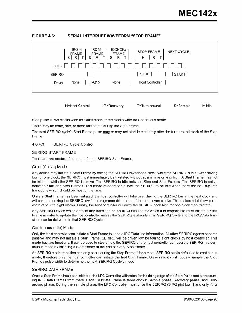
MEC142x
Stop pulse is two clocks wide for Quiet mode, three clocks wide for Continuous mode.
There may be none, one, or more Idle states during the Stop Frame.
The next SERIRQ cycle’s Start Frame pulse may or may not start immediately after the turn-around clock of the StopFrame.
4.8.4.3 SERIRQ Cycle Control
SERIRQ START FRAME
There are two modes of operation for the SERIRQ Start Frame.
Quiet (Active) Mode
Any device may initiate a Start Frame by driving the SERIRQ low for one clock, while the SERIRQ is Idle. After drivinglow for one clock, the SERIRQ must immediately be tri-stated without at any time driving high. A Start Frame may notbe initiated while the SERIRQ is active. The SERIRQ is Idle between Stop and Start Frames. The SERIRQ is activebetween Start and Stop Frames. This mode of operation allows the SERIRQ to be Idle when there are no IRQ/Datatransitions which should be most of the time.
Once a Start Frame has been initiated, the host controller will take over driving the SERIRQ low in the next clock andwill continue driving the SERIRQ low for a programmable period of three to seven clocks. This makes a total low pulsewidth of four to eight clocks. Finally, the host controller will drive the SERIRQ back high for one clock then tri-state.
Any SERIRQ Device which detects any transition on an IRQ/Data line for which it is responsible must initiate a StartFrame in order to update the host controller unless the SERIRQ is already in an SERIRQ Cycle and the IRQ/Data tran-sition can be delivered in that SERIRQ Cycle.
Continuous (Idle) Mode
Only the Host controller can initiate a Start Frame to update IRQ/Data line information. All other SERIRQ agents becomepassive and may not initiate a Start Frame. SERIRQ will be driven low for four to eight clocks by host controller. Thismode has two functions. It can be used to stop or idle the SERIRQ or the host controller can operate SERIRQ in a con-tinuous mode by initiating a Start Frame at the end of every Stop Frame.
An SERIRQ mode transition can only occur during the Stop Frame. Upon reset, SERIRQ bus is defaulted to continuousmode, therefore only the host controller can initiate the first Start Frame. Slaves must continuously sample the StopFrames pulse width to determine the next SERIRQ Cycle’s mode.
SERIRQ DATA FRAME
Once a Start Frame has been initiated, the LPC Controller will watch for the rising edge of the Start Pulse and start count-ing IRQ/Data Frames from there. Each IRQ/Data Frame is three clocks: Sample phase, Recovery phase, and Turn-around phase. During the sample phase, the LPC Controller must drive the SERIRQ (SIRQ pin) low, if and only if, its
FIGURE 4-6: SERIAL INTERRUPT WAVEFORM “STOP FRAME”
H=Host Control R=Recovery T=Turn-around S=Sample I= Idle
S R T S
SERIRQ
LCLK
Host ControllerIRQ15Driver
R T
None
IRQ14 IRQ15
S R T
IOCHCK#
None
STOP
R T
STOP FRAME
HI
START
NEXT CYCLE FRAMEFRAMEFRAME
2017 Microchip Technology Inc. DS00002343C-page 95

MEC142x
last detected IRQ/Data value was low. If its detected IRQ/Data value is high, SERIRQ must be left tri-stated. During therecovery phase, the LPC Controller must drive the SERIRQ high, if and only if, it had driven the SERIRQ low during theprevious sample phase. During the turn-around phase, the controller must tri-state the SERIRQ. The device drives theSERIRQ line low at the appropriate sample point if its associated IRQ/Data line is low, regardless of which device initi-ated the start frame.
The Sample phase for each IRQ/Data follows the low to high transition of the Start Frame pulse by a number of clocksequal to the IRQ/Data Frame times three, minus one e.g. The IRQ5 Sample clock is the sixth IRQ/Data Frame, then thesample phase is (6 x 3) - 1 = 17 the seventeenth clock after the rising edge of the Start Pulse.
The SIRQ data frame will now support IRQ2 from a logical device; previously SERIRQ Period 3 was reserved for useby the System Management Interrupt (LSMI#). When using Period 3 for IRQ2, the user should mask off the SMI via theESMI Mask Register. Likewise, when using Period 3 for LSMI#, the user should not configure any logical devices asusing IRQ2.
SERIRQ Period 14 is used to transfer IRQ13. Each Logical devices will have IRQ13 as a choice for their primary inter-rupt.
STOP CYCLE CONTROL
Once all IRQ/Data Frames have completed, the host controller will terminate SERIRQ activity by initiating a Stop Frame.Only the host controller can initiate the Stop Frame. A Stop Frame is indicated when the SERIRQ is low for two or threeclocks. If the Stop Frame’s low time is two clocks, then the next SERIRQ cycle’s sampled mode is the Quiet mode; andany SERIRQ device may initiate a Start Frame in the second clock or more after the rising edge of the Stop Frame’spulse. If the Stop Frame’s low time is three clocks, then the next SERIRQ cycle’s sampled mode is the continuous mode,and only the host controller may initiate a Start Frame in the second clock or more after the rising edge of the StopFrame’s pulse.
TABLE 4-9: SERIRQ SAMPLING PERIODS
SERIRQ Period Signal Sampled # of Clocks Past Start
1 Not Used 2
2 IRQ1 5
3 IRQ2 8
4 IRQ3 11
5 IRQ4 14
6 IRQ5 17
7 IRQ6 20
8 IRQ7 23
9 IRQ8 26
10 IRQ9 29
11 IRQ10 32
12 IRQ11 35
13 IRQ12 38
14 IRQ13 41
15 IRQ14 44
16 IRQ15 47
DS00002343C-page 96 2017 Microchip Technology Inc.
MEC142x
4.8.4.4 Latency
Latency for IRQ/Data updates over the SERIRQ bus in bridge-less systems with the minimum IRQ/Data Frames of 17will range up to 96 clocks (3.84S with a 25 MHz LCLK or 2.88s with a 33 MHz LCLK).
4.8.4.5 EOI/ISR Read Latency
Any serialized IRQ scheme has a potential implementation issue related to IRQ latency. IRQ latency could cause anEOI or ISR Read to precede an IRQ transition that it should have followed. This could cause a system fault. The hostinterrupt controller is responsible for ensuring that these latency issues are mitigated. The recommended solution is todelay EOIs and ISR Reads to the interrupt controller by the same amount as the SERIRQ Cycle latency in order toensure that these events do not occur out of order.
4.8.4.6 AC/DC Specification Issue
All Serial IRQ agents must drive/sample SERIRQ synchronously related to the rising edge of LCLK. The SERIRQ pinuses the electrical specification of the PCI bus. Electrical parameters will follow the PCI Local Bus Specification, Rev.2.2 definition of “sustained tri-state.”
4.8.4.7 Reset and Initialization
The SERIRQ bus uses LRESET# as its reset signal and follows the PCI bus reset mechanism. The SERIRQ pin is tri-stated by all agents while LRESET# is active. With reset, SERIRQ slaves and bridges are put into the (continuous) Idlemode. The host controller is responsible for starting the initial SERIRQ cycle to collect system’s IRQ/Data default values.The system then follows with the Continuous/Quiet mode protocol (Stop Frame pulse width) for subsequent SERIRQcycles. It is the host controller’s responsibility to provide the default values to the 8259’s and other system logic beforethe first SERIRQ cycle is performed. For SERIRQ system suspend, insertion, or removal application, the host controllershould be programmed into Continuous (IDLE) mode first. This is to ensure the SERIRQ bus is in Idle state before thesystem configuration changes.
4.8.4.8 SERIRQ Interrupts
The LPC Controller routes Logical Device interrupts onto SIRQ stream frames IRQ[0:15]. Routing is controlled by theSIRQ Interrupt Configuration Registers. There is one SIRQ Interrupt Configuration Register for each accessible SIRQFrame (IRQ); all 16 registers are listed in Table 4-13, "SIRQ Interrupt Configuration Register Map".
The format for each SIRQ Interrupt Configuration Register is described in Section 4.9.2.1, "SIRQ Configuration RegisterFormat," on page 100. Each Logical Device can have up to two LPC SERIRQ interrupts. When the device is polled bythe host, each SIRQ frame routes the level of the Logical Device interrupt (selected by the corresponding SIRQ InterruptConfiguration Register) to the SIRQ stream.
4.8.4.9 SERIRQ Routing
Each SIRQ Interrupt Configuration Register controls a series of multiplexers which route to a single Logical Device inter-rupt as illustrated in FIGURE 4-7: SIRQ Routing Internal Logical Devices on page 98. The following table defines theSerial IRQ routing for each logical device implemented in the chip.
Note: If one or more PCI to PCI Bridge is added to a system, the latency for IRQ/Data updates from the secondaryor tertiary buses will be a few clocks longer for synchronous buses, and approximately double for asyn-chronous buses.
TABLE 4-10: LOGICAL DEVICE SIRQ ROUTING TABLE
SIRQ Interrupt Configuration Register
Logical Device Interrupt Source
Select Device FrameLogical Device
(Block Instance - Note 26.2)Interrupt Source
0 0 C LPC Interface (Configuration Port) EC_IRQ
0 0 9 Mailbox Interface MBX_Host_SIRQ
2017 Microchip Technology Inc. DS00002343C-page 97
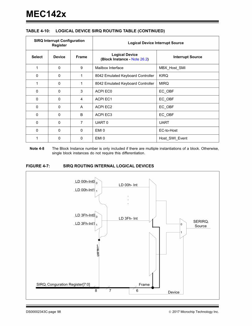
MEC142x
Note 4-8 The Block Instance number is only included if there are multiple instantiations of a block. Otherwise,single block instances do not require this differentiation.
1 0 9 Mailbox Interface MBX_Host_SMI
0 0 1 8042 Emulated Keyboard Controller KIRQ
1 0 1 8042 Emulated Keyboard Controller MIRQ
0 0 3 ACPI EC0 EC_OBF
0 0 4 ACPI EC1 EC_OBF
0 0 A ACPI EC2 EC_OBF
0 0 B ACPI EC3 EC_OBF
0 0 7 UART 0 UART
0 0 0 EMI 0 EC-to-Host
1 0 0 EMI 0 Host_SWI_Event
FIGURE 4-7: SIRQ ROUTING INTERNAL LOGICAL DEVICES
TABLE 4-10: LOGICAL DEVICE SIRQ ROUTING TABLE (CONTINUED)
SIRQ Interrupt Configuration Register
Logical Device Interrupt Source
Select Device FrameLogical Device
(Block Instance - Note 26.2)Interrupt Source
0
1
.
.
.
LD 00h- Int
LD 3Fh- Int
LD 00h-Int0
LD 00h-Int1
0
1
SIRQi Conguration Register[7:0]
Device
Frame
Select
SERIRQi
Source
8 7 6
0
1
LD 3Fh-Int0
LD 3Fh-Int1
DS00002343C-page 98 2017 Microchip Technology Inc.

MEC142x
4.9 LPC Configuration Registers
The configuration registers listed in Table 4-12, "Configuration Register Summary" are for a single instance of the LPCInterface. The addresses of each register listed in Table 4-12 are defined as a relative offset to the host “Begin Address”defined in Table 4-11.
Note 4-9 The Begin Address indicates where the first register can be accessed in a particular address spacefor a block instance.
Note: Two Logical Devices cannot share a Serial IRQ.
TABLE 4-11: CONFIGURATION REGISTER ADDRESS RANGE TABLE
Instance NAMEInstance Number
Host Address Space Begin Address
LPC Interface 0 LPC Configuration Port
INDEX = 00h
0 EC 32-bit internal address space
000F_3300h
TABLE 4-12: CONFIGURATION REGISTER SUMMARY
Register Name Offset Size Notes
LPC Activate Register 30h 8
SIRQ Configuration Register Format 40h - 4Fh 8
I/O Base Address Registers (IO_BARs) 60h - 9FhSee Table 4-
14
32
SRAM Memory BAR A0h 32
SRAM Memory BAR Configuration A4h 32
Device Memory Base Address Registers (DEV_MEM_BARs) C0h - FFhSee Table 4-
15
48
2017 Microchip Technology Inc. DS00002343C-page 99
MEC142x
4.9.1 LPC ACTIVATE REGISTER
The LPC Activate Register controls the LPC device itself. The Host can shut down the LPC Logical Device by clearingthe Activate bit, but it cannot restart the LPC interface, since once the LPC interface is inactive the Host has no accessto any registers on the device. The Embedded Controller can set or clear the Activate bit at any time.
APPLICATION NOTE: The bit in the LPC Activate Register should not be written ‘0’ to by the Host over LPC.
4.9.2 SERIAL IRQ CONFIGURATION REGISTERS
The LPC Controller implements 16 IRQ channels that may be configured to be asserted by any logical device.
• For a description of the SIRQ Configuration Register format see Table 4-13, “SIRQ Interrupt Configuration Regis-ter Map,” on page 101.
• For a summary of the SIRQ IRQ Configuration registers implemented see Table 4-14, “I/O Base Address Regis-ters,” on page 103.
• For a list of the SIRQ sources see Table 4-10, “Logical Device SIRQ Routing Table,” on page 97.
4.9.2.1 SIRQ Configuration Register Format
Offset 30h
Bits Description Type DefaultReset Event
7:1 RESERVED RES - -
0 ACTIVATE
1= ActivateWhen this bit is 1, the LPC Logical Device is powered and func-tional. 0= DeactivateWhen this bit is 0, the logical device is powered down and inactive. Except for the LPC Activate Register itself, clocks to the block are gated and the LPC Logical Device will permit the ring oscillator to be shut down (see Section 4.11.4, "EC Clock Control Register," on page 110). LPC bus output pads will be tri-stated.
R/W 0b nSYSRST
Offset See Table 4-13, “SIRQ Interrupt Configuration Register Map,” on page 101.
Bits Description Type DefaultReset Event
7 SELECT
If this bit is 0, the first interrupt signal from the Logical Device is selected for the SERIRQ vector. If this bit is 1, the second interrupt signal from the Logical Device is selected.
Note: The Keyboard Controller is an example of a LogicalDevices that requires a second interrupt signal. MostLogical Devices require only a single interrupt andignore this field as result.
R/W Note 4-10 nSIO_RESET
DS00002343C-page 100 2017 Microchip Technology Inc.
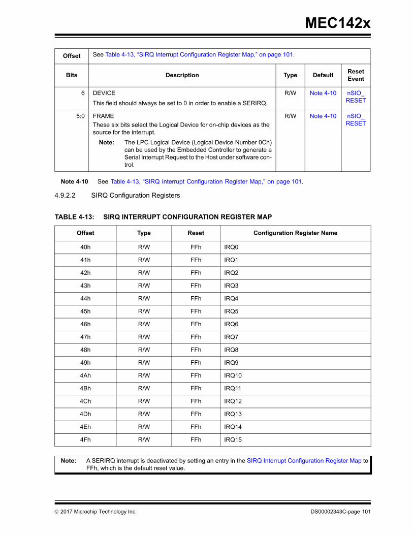
MEC142x
Note 4-10 See Table 4-13, “SIRQ Interrupt Configuration Register Map,” on page 101.
4.9.2.2 SIRQ Configuration Registers
6 DEVICE
This field should always be set to 0 in order to enable a SERIRQ.
R/W Note 4-10 nSIO_RESET
5:0 FRAME
These six bits select the Logical Device for on-chip devices as the source for the interrupt.
Note: The LPC Logical Device (Logical Device Number 0Ch)can be used by the Embedded Controller to generate aSerial Interrupt Request to the Host under software con-trol.
R/W Note 4-10 nSIO_RESET
TABLE 4-13: SIRQ INTERRUPT CONFIGURATION REGISTER MAP
Offset Type Reset Configuration Register Name
40h R/W FFh IRQ0
41h R/W FFh IRQ1
42h R/W FFh IRQ2
43h R/W FFh IRQ3
44h R/W FFh IRQ4
45h R/W FFh IRQ5
46h R/W FFh IRQ6
47h R/W FFh IRQ7
48h R/W FFh IRQ8
49h R/W FFh IRQ9
4Ah R/W FFh IRQ10
4Bh R/W FFh IRQ11
4Ch R/W FFh IRQ12
4Dh R/W FFh IRQ13
4Eh R/W FFh IRQ14
4Fh R/W FFh IRQ15
Note: A SERIRQ interrupt is deactivated by setting an entry in the SIRQ Interrupt Configuration Register Map toFFh, which is the default reset value.
Offset See Table 4-13, “SIRQ Interrupt Configuration Register Map,” on page 101.
Bits Description Type DefaultReset Event
2017 Microchip Technology Inc. DS00002343C-page 101
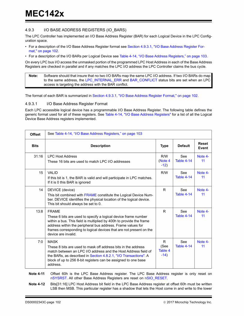
MEC142x
4.9.3 I/O BASE ADDRESS REGISTERS (IO_BARS)
The LPC Controller has implemented an I/O Base Address Register (BAR) for each Logical Device in the LPC Config-uration space.
• For a description of the I/O Base Address Register format see Section 4.9.3.1, "I/O Base Address Register For-mat," on page 102.
• For a description of the I/O BARs per Logical Device see Table 4-14, “I/O Base Address Registers,” on page 103.
On every LPC bus I/O access the unmasked portion of the programmed LPC Host Address in each of the Base AddressRegisters are checked in parallel and if any matches the LPC I/O address the LPC Controller claims the bus cycle.
The format of each BAR is summarized in Section 4.9.3.1, "I/O Base Address Register Format," on page 102.
4.9.3.1 I/O Base Address Register Format
Each LPC accessible logical device has a programmable I/O Base Address Register. The following table defines thegeneric format used for all of these registers. See Table 4-14, "I/O Base Address Registers" for a list of all the LogicalDevice Base Address registers implemented.
Note 4-11 Offset 60h is the LPC Base Address register. The LPC Base Address register is only reset onnSYSRST. All other Base Address Registers are reset on nSIO_RESET.
Note 4-12 Bits[31:16] LPC Host Address bit field in the LPC Base Address register at offset 60h must be writtenLSB then MSB. This particular register has a shadow that lets the Host come in and write to the lower
Note: Software should that insure that no two I/O BARs map the same LPC I/O address. If two I/O BARs do mapto the same address, the LPC_INTERNAL_ERR and BAR_CONFLICT status bits are set when an LPCaccess is targeting the address with the BAR conflict.
Offset See Table 4-14, “I/O Base Address Registers,” on page 103
Bits Description Type DefaultReset Event
31:16 LPC Host Address
These 16 bits are used to match LPC I/O addresses
R/W(Note 4
-12)
See Table 4-14
Note 4-11
15 VALID
If this bit is 1, the BAR is valid and will participate in LPC matches. If it is 0 this BAR is ignored
R/W See Table 4-14
Note 4-11
14 DEVICE (device)
This bit combined with FRAME constitute the Logical Device Num-ber. DEVICE identifies the physical location of the logical device. This bit should always be set to 0.
R See Table 4-14
Note 4-11
13:8 FRAME
These 6 bits are used to specify a logical device frame number within a bus. This field is multiplied by 400h to provide the frame address within the peripheral bus address. Frame values for frames corresponding to logical devices that are not present on the device are invalid.
R See Table 4-14
Note 4-11
7:0 MASK
These 8 bits are used to mask off address bits in the address match between an LPC I/O address and the Host Address field of the BARs, as described in Section 4.8.2.1, "I/O Transactions". A block of up to 256 8-bit registers can be assigned to one base address.
R(See
Table 4-14)
See Table 4-14
Note 4-11
DS00002343C-page 102 2017 Microchip Technology Inc.

MEC142x
byte of the 16-bit address, and the resulting 16-bit LPC Host address field does not update. Writingto the upper byte triggers a full 16-bit field update.
4.9.3.2 Logical Device IO_BAR Description
The following table defines the IO_BAR of each logical device implemented in the design.
TABLE 4-14: I/O BASE ADDRESS REGISTERS
Note: After the VCC_PWRGD signal is asserted, the iRESET_OUT bit of the Power Reset Control(PWR_RST_CTRL) Register must be cleared by firmware in order to write the BAR registers listed.
Bits [D31:D16] Bit [D15] Bit [D14]
Bits [D13:D8]
Bits [D6:D0]
Offset
Logical Device
Number (hex) Logical Devices Reset Default
Default LPC I/O
Host Address VALID DEVICE FRAME
MASK (Note 3)
60h CLPC Interface
(Configuration Port)002E_0C01
(Note 1) 002E 0 0 C 1
64h 0 EMI 0 0000_000F 0000 0 0 0 F
68h 18042 Emulated
Keyboard Controller 0060_0104 0060 0 0 1 4
6Ch 3 ACPI EC0 0062_0304 0062 0 0 3 4
70h 4 ACPI EC1 0066_0407 0066 0 0 4 7
74h 5 ACPI PM1 0000_0507 0000 0 0 5 7
78h 6 Legacy Port92/GateA20 0092_0600 0092 0 0 6 0
7Ch 7 UART 0 0000_0707 0000 0 0 7 7
80h 9 Mailbox Interface 0000_0901 0000 0 0 9 1
84h A ACPI EC2 0000_0A07 0000 0 0 A 7
88h B ACPI EC3 0000_0B07 0000 0 0 B 7
8Ch 15Port 80 BIOS Debug
Port 0 0000_1500 0000 0 0 15 0
90h 16Port 80 BIOS Debug
Port 1 0000_1600 0000 0 0 16 0
Base Address Register Bit Field Descriptions
Note 2: The FRAME and MASK fields for these Legacy devices are not used to determine which LPC I/O addresses to claim. The address range match is maintained within the blocks themselves.
Note 1: The default Base I/O Address of the Configuration Port can be relocated by programming the BAR register for
Note 3: The ACPI-ECx Mask bit field is a read/write bit field. All other MASK bit fields are read-only as defined in the register description.
2017 Microchip Technology Inc. DS00002343C-page 103

MEC142x
4.9.4 SRAM MEMORY BAR
4.9.5 SRAM MEMORY BAR CONFIGURATION
4.9.6 DEVICE MEMORY BASE ADDRESS REGISTERS (DEV_MEM_BARS)
Some Logical Devices have a Memory Base Address Register. These Device Memory BARs are located in blocks of
Configuration Registers in Logical Device 0Ch, in the AHB address range 000F_33C0h through 000F_33FFh. The fol-lowing table defines the generic format used for all of these registers.
Each DEV_MEM_BAR is 48 bits wide. The format of each Device Memory BAR is summarized in Section 4.9.6.1,"Device Memory Base Address Register Format". An LPC memory request is translated by the Device Memory BARinto an 8-bit read or write transaction on the AHB bus. The 32-bit LPC memory address is translated into a 32-bit AHBaddress.
4.9.6.1 Device Memory Base Address Register Format
Offset A0h
Bits Description Type DefaultReset Event
31:0 LPC Host Address[31:24]
These 32 bits are used to match LPC Memory addresses
R/W 0h nSIO_RESET
Offset A4h
Bits Description Type DefaultReset Event
31:8 RESERVED RES - -
7 VALID
If this bit is 1, the SRAM Memory BAR is valid and will participate in LPC matches. If it is 0 this SRAM Memory BAR is ignored.
R/W 0h nSIO_RESET
6:1 RESERVED RES - -
Offset See Table 4-15, “Device Memory Base Address Registers,” on page 105
Bits Description Type DefaultReset Event
47:16 LPC Host Address
These 16 bits are used to match LPC I/O addresses
R/W See Table 4-15
nSIO_RESET
15 VALID
If this bit is 1, the BAR is valid and will participate in LPC matches. If it is 0 this BAR is ignored
R/W See Table 4-15
nSIO_RESET
14 DEVICE (device)
This bit combined with FRAME constitute the Logical Device Num-ber. DEVICE identifies the physical location of the logical device. This bit should always be set to 0.
R See Table 4-15
nSIO_RESET
DS00002343C-page 104 2017 Microchip Technology Inc.
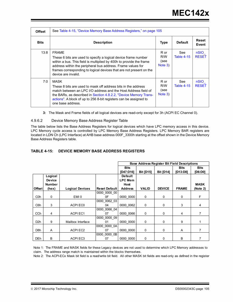
MEC142x
3: The Mask and Frame fields of all logical devices are read-only except for 3h (ACPI EC Channel 0).
4.9.6.2 Device Memory Base Address Register Table
The table below lists the Base Address Registers for logical devices which have LPC memory access in this device.LPC Memory cycle access is controlled by LPC Memory Base Address Registers. LPC Memory BAR registers arelocated in LDN Ch (LPC Interface) at AHB base address 000F_3300h starting at the offset shown in the Device MemoryBase Address Registers table..
13:8 FRAME
These 6 bits are used to specify a logical device frame number within a bus. This field is multiplied by 400h to provide the frame address within the peripheral bus address. Frame values for frames corresponding to logical devices that are not present on the device are invalid.
R or R/W(see
Note 3)
See Table 4-15
nSIO_RESET
7:0 MASK
These 8 bits are used to mask off address bits in the address match between an LPC I/O address and the Host Address field of the BARs, as described in Section 4.8.2.2, "Device Memory Trans-actions". A block of up to 256 8-bit registers can be assigned to one base address.
R or R/W(see
Note 3)
See Table 4-15
nSIO_RESET
TABLE 4-15: DEVICE MEMORY BASE ADDRESS REGISTERS
Offset See Table 4-15, “Device Memory Base Address Registers,” on page 105
Bits Description Type DefaultReset Event
Bits [D47:D16] Bit [D15] Bit [D14]
Bits [D13:D8]
Bits [D6:D0]
Offset
Logical Device
Number (hex) Logical Devices Reset Default
Default LPC Mem
Host Address VALID DEVICE FRAME
MASK (Note 2)
C0h 0 EMI 00000_0000_00
0F 0000_0000 0 0 0 F
C6h 3 ACPI EC00000_0062_03
04 0000_0062 0 0 3 4
CCh 4 ACPI EC10000_0066_04
07 0000_0066 0 0 4 7
D2h 9 Mailbox Interface0000_0000_09
01 0000_0000 0 0 9 1
D8h A ACPI EC20000_0000_0A
07 0000_0000 0 0 A 7
DEh B ACPI EC30000_0000_0B
07 0000_0000 0 0 B 7
Base Address Register Bit Field Descriptions
Note 1: The FRAME and MASK fields for these Legacy devices are not used to determine which LPC Memory addresses to claim. The address range match is maintained within the blocks themselves.Note 2: The ACPI-ECx Mask bit field is a read/write bit field. All other MASK bit fields are read-only as defined in the register
2017 Microchip Technology Inc. DS00002343C-page 105

MEC142x
4.10 Runtime Registers
The runtime registers listed in Table 4-17, "Runtime Register Summary" are for a single instance of the LPC Interface.The addresses of each register listed in Table 4-17 are defined as a relative offset to the host “Begin Address” define inTable 4-2.
4.10.1 INDEX REGISTER
TABLE 4-16: RUNTIME REGISTER ADDRESS RANGE TABLE
Instance NameInstance Number
Host Address Space Begin Address
LPC Interface
0 LPC I/O Programmed BAR
EC 32-bit internal address space
000F_3000h
Note 1: The Begin Address indicates where the first register can be accessed in a particular address space for ablock instance.
2: The LPC Runtime registers are only accessible from the LPC interface and are used to implement the LPCConfiguration Port. They are not accessible by any other Host.
TABLE 4-17: RUNTIME REGISTER SUMMARY
Offset Register Name
00h INDEX Register
01h DATA Register
Note: The LPC Runtime Register space has been used to implement the INDEX and DATA registers in the Con-figuration Port. In CONFIG_MODE, the Configuration Port is used to access the Configuration Registers.
Offset 00h
Bits Description Type DefaultReset Event
7:0 INDEX
The INDEX register, which is part of the Configuration Port, is used as a pointer to a Configuration Register Address.
Note: For a description of accessing the Configuration Portsee Section 4.8.3, "Configuration Port," on page 92.
R/W 0h nSYSRST
DS00002343C-page 106 2017 Microchip Technology Inc.

MEC142x
4.10.2 DATA REGISTER
4.11 EC-Only Registers
The registers listed in Table 4-19, "EC-Only Register Summary" are for a single instance of the LPC Interface. Theiraddresses are defined as a relative offset to the host base address defined in Table 4-18.
The following table defines the fixed host base address for each LPC Interface instance.
Offset 01h
Bits Description Type DefaultReset Event
7:0 DATA
The DATA register, which is part of the Configuration Port, is used to read or write data to the register currently being selected by the INDEX Register.
Note: For a description of accessing the Configuration Portsee Section 4.8.3, "Configuration Port," on page 92
R/W 0h nSYSRST
Note: EC-Only registers are not accessible by the LPC interface.
TABLE 4-18: EC-ONLY REGISTER ADDRESS RANGE TABLE
Instance NameInstance Number
Host Address Space Begin Address
LPC Interface 0 EC 32-bit internal address space
000F_3100h
Note: The Begin Address indicates where the first register can be accessed in a particular address space for ablock instance.
TABLE 4-19: EC-ONLY REGISTER SUMMARY
Offset Register Name
04h LPC Bus Monitor Register
08h Host Bus Error Register
0Ch EC SERIRQ Register
10h EC Clock Control Register
14h Test Register
18h Test Register
20h I/O BAR Inhibit Register
24h Reserved
2017 Microchip Technology Inc. DS00002343C-page 107

MEC142x
Note 4-1 Some Test registers are read/write registers. Modifying these registers may have unwanted results.
4.11.1 LPC BUS MONITOR REGISTER
4.11.2 HOST BUS ERROR REGISTER
28h Reserved
2Ch Reserved
30h LPC BAR Init Register
40h Device Memory BAR Inhibit Register
FCh SRAM Memory Host Configuration Register
Offset 04h
Bits Description Type DefaultReset Event
31:2 RESERVED RES - -
1 TEST R 0h nSYSRST
0 LPCPD_STATUS
This bit reflects the state of the LPCPD# input pin. TheLPCPD_STATUS bit is the inverse of the LPCPD# pin (see Section 4.8.1.3, "LPC Clock Run and LPC Power Down Behavior," on page 86).When the LPCPD_STATUS bit is ‘0b’, the LPCPD# input pin is deasserted (that is, the pin has the value ‘1b’). When theLPCPD_STATUS bit is ‘1b’, the LPCPD# input pin is asserted (thatis, the pin has the value ‘0b’).
R 0h nSYSRST
Offset 08h
Bits Description Type DefaultReset Event
31:8 ErrorAddress[23:16]
This 24-bit field captures the 24-bit internal address of every LPC transaction whenever the bit LPC_INTERNAL_ERR in this register is 0. When LPC_INTERNAL_ERR is 1 this register is not updated but retains its previous value. When bus errors occur this field saves the address of the first address that caused an error.
R 0h nSYSRST
5 DMA_ERR
This bit is set to 1 whenever EN_INTERNAL_ERR is 1 and an LPC DMA access causes an internal bus error. Once set, it remains set until cleared by being written with a 1.
R/WC 0h nSYSRST
TABLE 4-19: EC-ONLY REGISTER SUMMARY (CONTINUED)
Offset Register Name
DS00002343C-page 108 2017 Microchip Technology Inc.
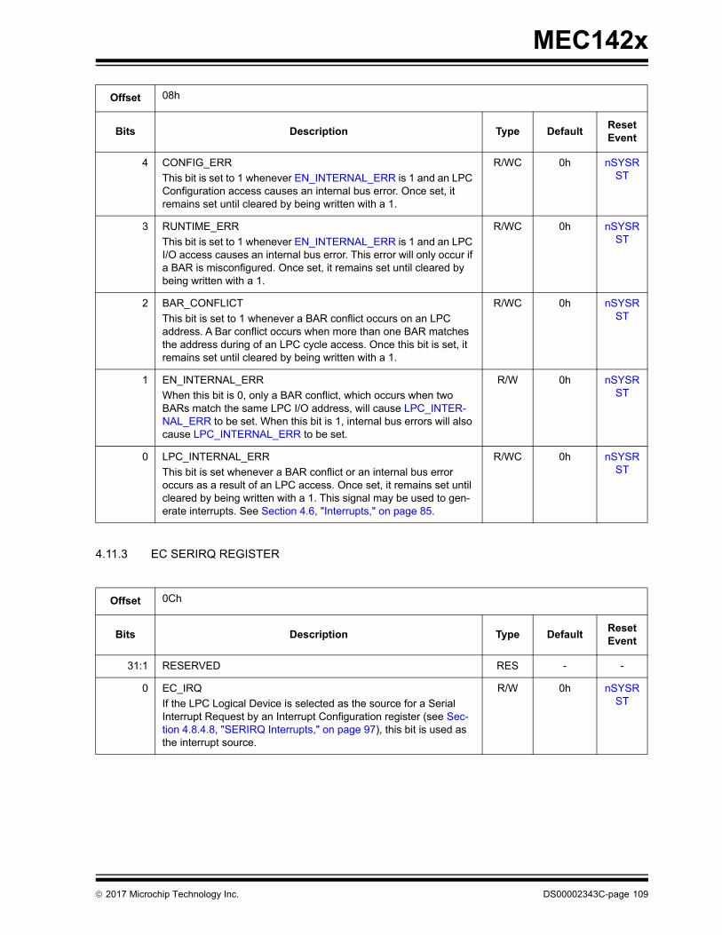
MEC142x
4.11.3 EC SERIRQ REGISTER
4 CONFIG_ERR
This bit is set to 1 whenever EN_INTERNAL_ERR is 1 and an LPC Configuration access causes an internal bus error. Once set, it remains set until cleared by being written with a 1.
R/WC 0h nSYSRST
3 RUNTIME_ERR
This bit is set to 1 whenever EN_INTERNAL_ERR is 1 and an LPC I/O access causes an internal bus error. This error will only occur if a BAR is misconfigured. Once set, it remains set until cleared by being written with a 1.
R/WC 0h nSYSRST
2 BAR_CONFLICT
This bit is set to 1 whenever a BAR conflict occurs on an LPC address. A Bar conflict occurs when more than one BAR matches the address during of an LPC cycle access. Once this bit is set, it remains set until cleared by being written with a 1.
R/WC 0h nSYSRST
1 EN_INTERNAL_ERR
When this bit is 0, only a BAR conflict, which occurs when two BARs match the same LPC I/O address, will cause LPC_INTER-NAL_ERR to be set. When this bit is 1, internal bus errors will also cause LPC_INTERNAL_ERR to be set.
R/W 0h nSYSRST
0 LPC_INTERNAL_ERR
This bit is set whenever a BAR conflict or an internal bus error occurs as a result of an LPC access. Once set, it remains set until cleared by being written with a 1. This signal may be used to gen-erate interrupts. See Section 4.6, "Interrupts," on page 85.
R/WC 0h nSYSRST
Offset 0Ch
Bits Description Type DefaultReset Event
31:1 RESERVED RES - -
0 EC_IRQ
If the LPC Logical Device is selected as the source for a Serial Interrupt Request by an Interrupt Configuration register (see Sec-tion 4.8.4.8, "SERIRQ Interrupts," on page 97), this bit is used as the interrupt source.
R/W 0h nSYSRST
Offset 08h
Bits Description Type DefaultReset Event
2017 Microchip Technology Inc. DS00002343C-page 109
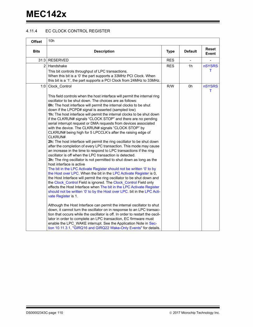
MEC142x
4.11.4 EC CLOCK CONTROL REGISTER
Offset 10h
Bits Description Type DefaultReset Event
31:3 RESERVED RES - -
2 Handshake
This bit controls throughput of LPC transactions.When this bit is a ‘0’ the part supports a 33MHz PCI Clock. When this bit is a ‘1’, the part supports a PCI Clock from 24MHz to 33MHz.
RES 1h nSYSRST
1:0 Clock_Control
This field controls when the host interface will permit the internal ring oscillator to be shut down. The choices are as follows:0h: The host interface will permit the internal clocks to be shutdown if the LPCPD# signal is asserted (sampled low)1h: The host interface will permit the internal clocks to be shut down if the CLKRUN# signals “CLOCK STOP” and there are no pending serial interrupt request or DMA requests from devices associated with the device. The CLKRUN# signals “CLOCK STOP” by CLKRUN# being high for 5 LPCCLK’s after the raising edge of CLKRUN#2h: The host interface will permit the ring oscillator to be shut down after the completion of every LPC transaction. This mode may cause an increase in the time to respond to LPC transactions if the ring oscillator is off when the LPC transaction is detected.3h: The ring oscillator is not permitted to shut down as long as the host interface is activeThe bit in the LPC Activate Register should not be written ‘0’ to by the Host over LPC. When the bit in the LPC Activate Register is 0, the Host Interface will permit the ring oscillator to be shut down and the Clock_Control Field is ignored. The Clock_Control Field only effects the Host Interface when The bit in the LPC Activate Register should not be written ‘0’ to by the Host over LPC. bit in the LPC Acti-vate Register is 1.
Although the Host Interface can permit the internal oscillator to shut down, it cannot turn the oscillator on in response to an LPC transac-tion that occurs while the oscillator is off. In order to restart the oscil-lator in order to complete an LPC transaction, EC firmware must enable the LPC_WAKE interrupt. See the Application Note in Sec-tion 10.11.3.1, "GIRQ16 and GIRQ22 Wake-Only Events" for details.
R/W 0h nSYSRST
DS00002343C-page 110 2017 Microchip Technology Inc.
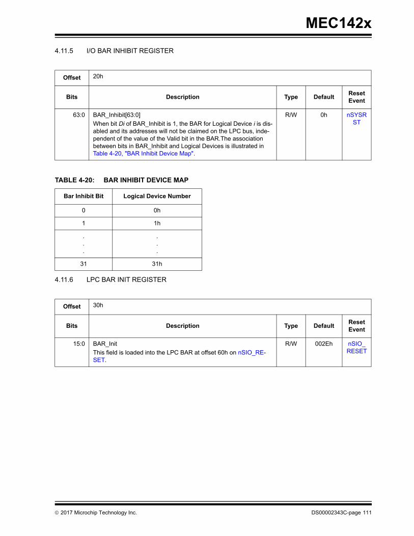
MEC142x
4.11.5 I/O BAR INHIBIT REGISTER
4.11.6 LPC BAR INIT REGISTER
Offset 20h
Bits Description Type DefaultReset Event
63:0 BAR_Inhibit[63:0]
When bit Di of BAR_Inhibit is 1, the BAR for Logical Device i is dis-abled and its addresses will not be claimed on the LPC bus, inde-pendent of the value of the Valid bit in the BAR.The association between bits in BAR_Inhibit and Logical Devices is illustrated in Table 4-20, "BAR Inhibit Device Map".
R/W 0h nSYSRST
TABLE 4-20: BAR INHIBIT DEVICE MAP
Bar Inhibit Bit Logical Device Number
0 0h
1 1h
.
.
.
.
.
.
31 31h
Offset 30h
Bits Description Type DefaultReset Event
15:0 BAR_Init
This field is loaded into the LPC BAR at offset 60h on nSIO_RE-SET.
R/W 002Eh nSIO_RESET
2017 Microchip Technology Inc. DS00002343C-page 111

MEC142x
4.11.7 DEVICE MEMORY BAR INHIBIT REGISTER
4.11.8 SRAM MEMORY HOST CONFIGURATION REGISTER
Offset 40h
Bits Description Type DefaultReset Event
63:0 Device Mem BAR_Inhibit[63:0]
When bit i of the Device Mem BAR_Inhibit[63:0] field is asserted (‘1’), where i is the logical device number of one of the Device Memory Base Address Registers, the BAR for the associated device is disabled and its LPC Memory addresses will not be claimed on the LPC bus, independent of the value of the Valid bit in the BAR.
When bit i is not asserted (default), BAR activity for the Logical Device is based on the Valid bit in the BAR.
All of the Device Mem BAR_Inhibit[63:0] bits are R/W and have no affect on reserved logical device numbers.
R/W 0h nSYSRST
Offset FCh
Bits Description Type DefaultReset Event
31:8 AHB Base
These 24 bits define the base of a region in AHB address space that will be mapped to the LPC Memory space. Valid AHB addresses are integer multiples of the memory size. For example, if the memory is 4k bytes than the AHB Base address must be located on a 4k byte boundary.
Note: The 24 bits in this field are left-shited by 8 bits to form a32-bit AHB address, so all memory blocks begin on a256-byte boundary.
R/W 0h nSYSRST
7 Inhibit
Host access to the memory block is inhibited when this bit is 1. The Host can access the memory region mapped by the fields AHB Base and Size when this bit is 0.
R/W 0h nSYSRST
6:4 RESERVED RES - -
3:0 Size
The number of address bits to pass unchanged when translating an LPC address to an AHB address. These 4 bits in effect define the size of the block to be claimed by the LPC bridge, defined as a power of 2. A value of 0 defines a 20 or a 1-byte region starting at LPC Host Address. A value of 12 defines a 212 or a 4K-byte region. Values larger than 12 are undefined.
R/W 0h nSYSRST
DS00002343C-page 112 2017 Microchip Technology Inc.

MEC142x
5.0 ENHANCED SERIAL PERIPHERAL INTERFACE (ESPI)
5.1 Introduction
The Intel® Enhanced Serial Peripheral Interface (eSPI) is used by the system host to configure the chip and communi-cate with the logical devices implemented in the design through a series of read/write registers. It is Intel’s successor tothe Low Pin Count (LPC) bus, used in previous devices to provide System Host access to devices internal to the Embed-ded Controller.
5.2 References
1. Intel, Enhanced Serial Peripheral Interface (eSPI): Interface Specification (for Client Platforms)
2. Intel, Skylake U and Y Platform Design Guide, Revision 2.0
3. Microchip “eSPI Controller with SAFS Support” Specification
5.3 Terminology
This table defines specialized terms localized to this feature.
TABLE 5-1: TERMINOLOGY
Term Definition
System Host Refers to the external CPU that communicates with this device via the eSPI Inter-face.
Logical Devices Logical Devices are System Host-accessible features that are allocated a Base Address and range in the System Host I/O address space
Runtime Register Runtime Registers are registers that are directly I/O accessible by the System Host via the eSPI interface.
Configuration Registers Registers that are only accessible in CONFIG_MODE.
EC_Only Registers Registers that are not accessible by the System Host. They are only accessible by an internal embedded controller.
2017 Microchip Technology Inc. DS00002343C-page 113

MEC142x
5.4 Interface
5.4.1 PIN INTERFACE
Table 5-2, "Signal Description Table" lists the signals that are typically routed to the pin interface.
FIGURE 5-1: Enhanced Serial Peripheral Interface (eSPI) INTERFACE DIAGRAM
TABLE 5-2: SIGNAL DESCRIPTION TABLE
Signal Name Direction Description
eSPI_CS# Input eSPI Chip Select, Low-Active
eSPI_CLOCK Input eSPI Clock
eSPI_ALERT# Output eSPI Alert signal, Low-Active. Exercised only if ALERT# is configured to be pre-sented separately from the IO1 pin.
eSPI_RESET# Input POR for eSPI bus power domain, and a Reset for serious errors. Low-Active.
eSPI_IO0 Input/Output eSPI Data Bus, bit 0.Input (MOSI) in x1 Bus Mode. Else, it holds the LS data bit.
eSPI_IO1 Input/Output eSPI Data Bus, bit 1. Output (MISO) in x1 Bus Mode. Also, by default, presents ALERT# state between frames.
eSPI_IO2 Input/Output eSPI Data Bus, bit 2. Used only in x4 mode.
eSPI_IO3 Input/Output eSPI Data Bus, bit 3. Used only in x4 mode, as MS bit.
GPIO123/SHD_CS0#/(RSMRST#)
[BSS_STRAP]
Input/Output eSPI/Shared SPI selection strap.RSMRST# signal to core logic (Note 1)
GPIO136/SHD_IO3/
(DSW_PWROK)
Input/Output DSW_PWROK signal to core logic (Note 1)
GPIO135/SHD_IO2
[PRG_STRAP]
Input/Output Primary rail power good input (Note 2)
Enhanced Serial Peripheral Inter-
Power, Clocks, and Resets
Interrupt Interface
Register Interface
Inte
rnal
Inte
rfac
es
Ext
ern
al In
terf
aces
Pin Interface
DS00002343C-page 114 2017 Microchip Technology Inc.
MEC142x
Note 1: If the eSPI Flash Channel is used for booting, i.e., eSPI Master Attached Flash Sharing (MAFS), the GPIO123/SHD_CS0# pin must be used as RSMRST#. This pin will be driven high by the boot ROM code in order to activate the eSPI flash channel. In addition, the GPIO136/SHD_IO3 pin must be used as DSW_P-WROK. This pin will also be driven high by the boot ROM code to support DSW timing requirements. See Section 5.6.2.3, "Taking the PCH out of Reset," on page 119 and Section 5.6.2.4, "Deep Sleep Well Power Sequencing," on page 119.
2: If the eSPI Flash Channel is used for booting, i.e., eSPI MAFS, the GPIO135/SHD_IO2 pin must be used to determine that the primary power rails are stable before RSMRST# can be de-asserted. See Section 5.6.2.2, "Determining that the Primary Power Rails are Stable," on page 118.
5.4.2 REGISTER INTERFACE
Each of the four channels contains registers that may be accessed by both the Host and the EC, as well as a set ofregisters than only be accessed by the EC.
5.4.3 POWER, CLOCKS, AND RESETS
This section defines the Power, Clock, and Reset parameters associated with this IP block.
5.4.3.1 Power
5.4.3.2 Clocks
This section describes all the clocks in the block, including those that are derived from the I/O Interface as well as theones that are derived or generated internally.
Name Description
VTR The Enhanced Serial Peripheral Interface (eSPI) block and registers are powered by VTR. This power rail may be present to the block while external power to the eSPI pins is not present. Therefore, this block remains passive on the eSPI bus pins whenever eSPI_RESET# is low.
Name Description
48 MHz Ring Oscillator The main internal clock
eSPI_CLOCK The eSPI clock provided by the System Host core logic
2017 Microchip Technology Inc. DS00002343C-page 115
MEC142x
5.4.3.3 Resets
This section describes all the resets associated with this IP block, including those that are derived from the I/O Interfaceas well as the ones that are derived or generated internally.
Name Description
nSYSRST This is the power-on-reset signal, which is asserted when VTR power is applied. Asserting this reset signal resets the eSPI IP block, including all registers, FIFOs, and state machines to their initial POR state.
eSPI_RESET# A general reset signal for the eSPI block. This reset is asserted with the eSPI_RESET# pin is asserted by the System Host core logic.
When this reset is asserted all eSPI Output signals and Input/Output sig-nals are tri-stated. Any transaction in progress is terminated and all FIFOs are flushed. All interrupt status flags are reset and all interrupts to the EC except eSPI_RESET# are suppressed.
When this reset is asserted, all eSPI Configuration Registers in the slave device are set to the default values, as per the Intel eSPI Specification. Fields in the eSPI Configuration Registers that are set from the eSPI Capabilities registers (see Section 5.7, "eSPI Register Summary") are not modified.
This reset is also asserted in the following cases:nSYSRST is asserted
eSPI_PLTRST# This is a reset that affects the Peripheral Channel. It is received by the Slave as a Virtual Wire (PLTRST#).
This reset is also asserted in the following cases:nSYSRST is assertedeSPI_RESET# is asserted
nSIO_RESET Reset signal asserted when the system main power rail is applied
This reset is also asserted in the following cases:• nSYSRST is asserted
• eSPI_RESET# is asserted
• eSPI_PLTRST# is asserted
• The eSPI Peripheral Channel is disabled by the Host
DS00002343C-page 116 2017 Microchip Technology Inc.
MEC142x
5.4.4 INTERRUPT INTERFACE
This section defines the interrupt Interface signals routed to the chip interrupt aggregator.
5.5 Low Power Modes
The eSPI block can enter a low power state when it is not in operation. When the eSPI block is operational it will keepthe main system clock from shutting down and entering its sleep state. When the eSPI_CS# pin is asserted the eSPIblock will wake the main system clock, if it is in a sleep state, and keep the system clock in its active state until the trans-action started by the Master has completed.
The low power behavior of the block is controlled by the BAR Inhibit Register. The block is not affected by a sleep_en-able signal from the chip’s Power, Clocks and Resets unit.
5.6 Description
The Intel® eSPI Interface is used by the system host to configure the chip and communicate with the logical devicesimplemented in the design through a series of read/write registers.
Source Description
Wake Only Event
ESPI_WAKE This signal is asserted when the eSPI interface detects eSPI traffic. If enabled, it may be used to wake the 48 MHz Ring Oscillator when the chip is in a sleep state.
Note: This interrupt is grouped with other Wake-Only events inGIRQQ16 and GIRQ22.
Peripheral Channel
INTR_PC Peripheral Channel Interrupt
INTR_BM1 Bus Mastering Channel 1 Interrupt
INTR_BM2 Bus Mastering Channel 2 Interrupt
INTR_LTR Peripheral Message (LTR) Interrupt
OOB Channel
INTR_OOB_UP Out of Band Channel Up Interrupt
INTR_OOB_DOWN Out of Band Channel Down Interrupt
Flash Channel
INTR_FLASH Flash Channel Interrupt
Virtual Wires Channel
MSVW[00:10]_SRC[3:0] Master-to-Slave Virtual Wire Interrupts
eSPI Global
eSPI_RESET eSPI Reset InterruptThis interrupt is generated whenever the external eSPI_RESET# pin changes state.
Note: In order to use eSPI, software must individually configure the mux control for every GPIO associated withan eSPI bus signal to the eSPI function. Pins are not automatically configured for eSPI operation when theeSPI Controller is enabled.
2017 Microchip Technology Inc. DS00002343C-page 117
MEC142x
5.6.1 OPERATING FREQUENCY
The part supports up to 66 MHz maximum operating frequency.
APPLICATION NOTE: The part defaults to a maximum operating frequency of 50MHz, but it can support 66MHzunder user control as outlined below.
This setting is changed by customer firmware by writing to the MAXIMUM_FREQUENCY_SUPPORTED field of theeSPI Capabilities Global Capabilities 1 Register. See Table 5-5, "eSPI I/O Component Register Summary".
If this field is changed before the RSMRST# pin is deasserted, then that is all that is required for this change to the max-imum operating frequency to take effect. This could be done by customer EC firmware that gets loaded from the SPIport when booting from shared SPI or SAFS.
If this field is not changed before the RSMRST# pin is deasserted (e.g., in the case of booting from MAFS) then thereare additional steps that must be taken in order for this new setting to take effect. In this case, the BIOS must generateeSPI configuration read and write cycles to change the value in the Operating Frequency field in the Config Offset8h=General Capabilities and Configurations register. The details of this procedure are outside of the scope of this doc-ument.
Changing the operating frequency to 66 MHz also requires changing the Drive Strength and Slew Rate fields of the PinControl Register 2 associated with the eSPI Data pins to 12mA and fast, respectively.
5.6.2 SYSTEM INTERFACE, MAFS
The EC has the option of loading its code image over the eSPI Flash Channel, i.e., eSPI Master Attached Flash Sharing(MAFS). In order to do so, the Boot ROM code will:
1. Determine that booting using the eSPI Flash Channel is required
2. Determine that the Primary power rails for the Intel PCH have ramped and are stable
3. Take the PCH out of reset so that the eSPI block in the PCH is operational
The following sections describe each of these three steps required for eSPI Master Attached Flash Sharing (MAFS).There is also a description of the support for the use of the Deep Sleep Well (DSW) system power rail when using MAFS.
5.6.2.1 Determining that the Flash Channel is Required
In order to select between a SPI Flash directly attached to the Shared SPI Flash port (including SAFS) and the eSPI Flash Channel as the source for EC code (MAFS), the EC examines a strap after a reset. The strap is the pin:• GPIO123/SHD_CS0# (RSMRST#) [BSS_STRAP]
This pin is on the VTR rail; VTR must be ramped and stable before the EC samples its state. If booting from the Shared SPI Flash is required, then this pin must be connected to the SPI Flash power supply through a weak pull-up resistor. If booting from the eSPI Flash Channel is required, then this pin must be connected to ground through a weak pull-down resistor.If booting over a Shared SPI Flash, the EC switches the pin to the SHD_CS0# pin function and proceeds to load over the Shared SPI Flash port. De-asserting RSMRST# is the responsibility of the loaded code and not the Boot ROM code; the RSMRST# function may be assigned to any GPIO which would then be controlled by the EC.If booting over the eSPI Flash Channel is selected, the GPIO123/SHD_CS0# (RSMRST#) pin must be used as the RSMRST# signal to the PCH. The EC will keep the pin as a GPIO; RSMRST# timing and behavior is covered in the next two sections.
5.6.2.2 Determining that the Primary Power Rails are Stable
Intel requires four Primary power rails to be ramped and stable before taking the PCH out of reset:• VCC_Prim 1.8V
• VCC_Prim 3.3V
• VCCPRIM_CORE
• VCC_Prim 1.0V
According to Intel’s requirements [2], all four rails must be ramped and stable for at least 20ms before RSMRST# can be de-asserted. The EC determines that at least one of the four rails has ramped by examining the following pin:• GPIO135/SHD_IO2[PRG_STRAP]
DS00002343C-page 118 2017 Microchip Technology Inc.

MEC142x
The EC will only examine this pin if loading code over the eSPI Flash Channel is required. This signal going high indicates that all of the Primary power rails are or will be valid within 20 ms. One solution is to connect this pin to the VCC_Prim 3.3V rail or a signal that indicated that the VCC_Prim 3.3V rail is valid.
5.6.2.3 Taking the PCH out of Reset
Once the EC detects a high on GPIO135/SHD_IO2[PRG_STRAP], it waits a sufficient time to satisfy Intel’s requirements for the deassertion of RSMRST# (see the Section 43.6, "eSPI Boot Timing," on page 501). After the time has expired, the EC drives the pin high, which has the effect of de-asserting RSMRST#, enables the eSPI interface, and then waits for the Host to begin eSPI operation.
5.6.2.4 Deep Sleep Well Power Sequencing
The part supports the use of the Deep Sleep Well (DSW) system power rail. This feature provides a DSW_PWROKoutput to meet DSW system timing requirements. It will allow the MEC142x to reset the system properly if it is poweredby the DSW supply.
This feature is only active when booting from the eSPI Flash Channel using Master Attached Flash Sharing (MAFS). Inthis case, the Boot ROM code also controls the RSMRST# pin.
5.6.2.4.1 Reference
Intel, Enhanced Serial Peripheral Interface (eSPI) Compatibility Specification For 2015/2016 Client, Desktop and ServerPlatforms, December 2015, Revision 0.96.
The issue and recommended solution are mentioned in the above referenced document:
“Conditions where the EC forces RSMRST# to assert without the PCH/SoC requesting a Deep-Sx entry (byasserting SLP_SUS#) are outside the scope of this document. The recommendation in such a situation is to forceboth RSMRST# to assert (1 0) and DPWROK to deassert (1 0), while keeping the PCH/SoC Primary and DeepSleep wells powered, to force the platform into G3 state. Simply forcing RSMRST# to 0 (which the PCH/SoC hasnot requested by asserting SLP_SUS#) without deasserting DPWROK may leave the platform in an undefinedstate.”
5.6.2.4.2 System Timing Issue
In an orderly shutdown sequence, the PCH controls when to sequence on/off the DSW_PWROK signal using the SLP_-SUS# signal. However, if RSMRST# is asserted low by the EC without the knowledge of the PCH, the EC is requiredto ensure the DSW_PWROK signal goes low at the same time the RSMRST# signal is set low. If DSW_PWROK doesnot go low at the same time as the RSMRST# signal the system may be left in an undefined state.
One scenario that can cause an unexpected RSMRST# assertion is a WDT Event. If the application code loaded by theBoot ROM enables the Watchdog Timer and it causes a WDT Event, the chip will be reset, causing the RSMRST# pin(GPIO123/SHD_CS0#) to tristate. The RSMRST# pin has an external pull-down on the board causing RSMRST# to beasserted low.
The DSW_PWROK signal on GPIO136/SHD_IO3 is used to reset the system properly following a POR event or a WDTEvent.
5.6.2.4.3 Implementation
If the MEC142x is configured to boot from the eSPI flash channel using MAFS, the EC will use GPIO136/SHD_IO3 asthe DSW_PWROK output signal.
The DSW_PWROK signal must be pulled low externally with a pull-down resistor. Following a POR or WDT Event allthe pins will tristate and the DSW_PWROK signal will be pulled low externally.
When RESETI# is set high and the EC starts executing, the Boot ROM checks bit[5] WDT of the POWER-FAIL ANDRESET STATUS REGISTER to determine if the MEC142x is powering on normally or recovering from a WDT Event.
• If bit[5] WDT is 1 (recovering from a WDT Event) then the Boot ROM will wait 120 ms (min) before driving DSW_PWROK high:
- Boot ROM waits 100 ms (min) for the primary rails to power down.
- Boot ROM waits 20 ms (min) from power on to drive DSW_PWROK high (Note 1).
• If bit[5] WDT is 0 (powering on normally) then the Boot ROM will wait 20 ms (min) before driving DSW_PWROK high:
- Boot ROM waits 20 ms (min) from power on to drive DSW_PWROK high (Note 1).
2017 Microchip Technology Inc. DS00002343C-page 119
MEC142x
Note 1: The EC is required to wait a minimum of 10 ms after the DSW well is powered before driving DSW_PWROKhigh (per Intel specification).
Note that customer application firmware must clear bit[5] WDT. The Boot ROM only reads this bit, it does not clear it.
After driving DSW_PWROK high the firmware continues with the normal eSPI MAFS boot sequence and begins sam-pling the GPIO135/SHD_IO2 pin to detect when at least one of the primary rails are good. It will wait up to 30 secondsfor the SHD_IO2 pin to go high after driving DSW_PWROK high. Once firmware detects SHD_IO2 pin is high it will waitan additional 35 ms (min) before driving RSMRST# high.
The eSPI boot timing sequence is show in Section 43.6, "eSPI Boot Timing," on page 501.
5.6.3 SYSTEM INTERFACE, SAFS
Support for eSPI Slave Attached Flash Sharing (SAFS) is described in the eSPI Controller with SAFS Support docu-ment.
The SAFS implementation provides for security which limits EC access to certain regions of the flash. This flash accessis programmable as described in the eSPI Slave Attached Flash document.
When SAFS mode is enabled, the QMSPI block is not directly accessible by EC firmware and is not available for gen-eral-purpose SPI operation. See eSPI Controller with SAFS Support document for more details (ref 3).
APPLICATION NOTE: The EC can access the SPI via the QMSPI block before SAFS mode is enabled,independent of the state of ESPI_RESET#. Once the SAF is enabled, the EC must wait untilESPI_RESET# is high before accessing the SPI via SAFS mode.
The GPIO pins associated with the Shared SPI port pins can also be locked to the Shared SPI functions, as described in the section below.
5.6.3.1 Locking the Shared SPI Port Pins
The GPIO pins associated with the Shared SPI port pins can be locked to the Shared SPI functions.
There is a runtime API in the ROM that locks the following GPIO pins to the associated Shared SPI pin functions untila VTR power cycle (nSYSRST):
- GPIO123/SHD_CS0#- GPIO126/SHD_SCLK- GPIO133/SHD_IO0- GPIO134/SHD_IO1- GPIO135/SHD_IO2- GPIO136/SHD_IO3
If SHD_CS1# is used, the API can optionally lock GPIO047/SHD_CS1# to the SHD_CS1# function.
5.6.4 ESPI CHANNELS
The eSPI interface consists of four channels:
• eSPI Peripheral Channel Interface
• eSPI Out Of Band Channel Interface
• eSPI Flash Channel Interface
• eSPI Virtual Wires Interface
DS00002343C-page 120 2017 Microchip Technology Inc.
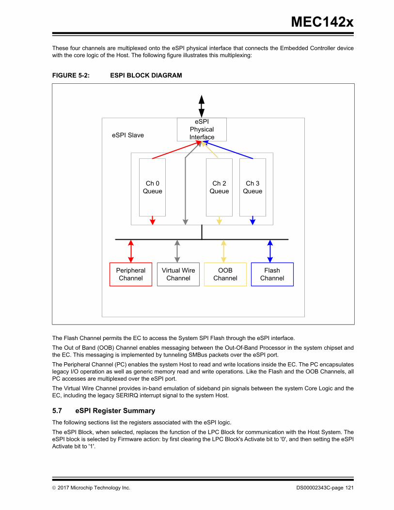
MEC142x
These four channels are multiplexed onto the eSPI physical interface that connects the Embedded Controller devicewith the core logic of the Host. The following figure illustrates this multiplexing:
The Flash Channel permits the EC to access the System SPI Flash through the eSPI interface.
The Out of Band (OOB) Channel enables messaging between the Out-Of-Band Processor in the system chipset andthe EC. This messaging is implemented by tunneling SMBus packets over the eSPI port.
The Peripheral Channel (PC) enables the system Host to read and write locations inside the EC. The PC encapsulateslegacy I/O operation as well as generic memory read and write operations. Like the Flash and the OOB Channels, allPC accesses are multiplexed over the eSPI port.
The Virtual Wire Channel provides in-band emulation of sideband pin signals between the system Core Logic and theEC, including the legacy SERIRQ interrupt signal to the system Host.
5.7 eSPI Register Summary
The following sections list the registers associated with the eSPI logic.
The eSPI Block, when selected, replaces the function of the LPC Block for communication with the Host System. TheeSPI block is selected by Firmware action: by first clearing the LPC Block's Activate bit to '0', and then setting the eSPIActivate bit to '1'.
FIGURE 5-2: ESPI BLOCK DIAGRAM
eSPI Slave
Virtual WireChannel
PeripheralChannel
FlashChannel
OOBChannel
Ch 0Queue
Ch 2Queue
Ch 3Queue
eSPIPhysicalInterface
2017 Microchip Technology Inc. DS00002343C-page 121
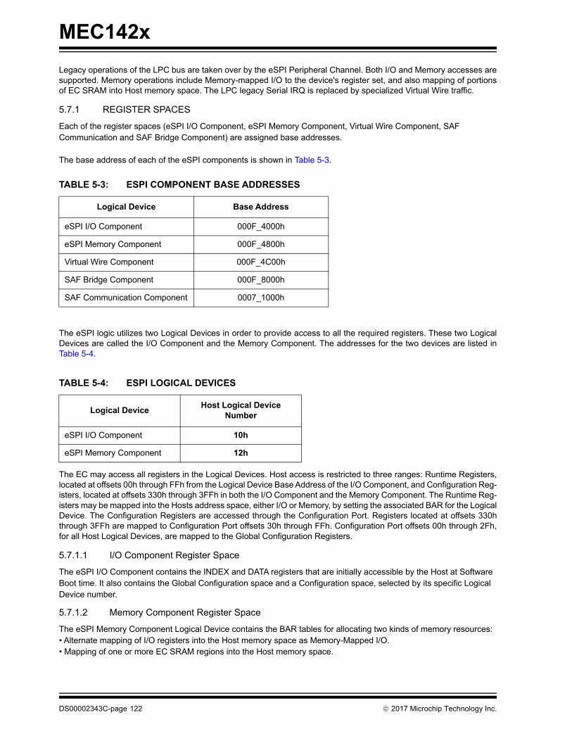
MEC142x
Legacy operations of the LPC bus are taken over by the eSPI Peripheral Channel. Both I/O and Memory accesses aresupported. Memory operations include Memory-mapped I/O to the device's register set, and also mapping of portionsof EC SRAM into Host memory space. The LPC legacy Serial IRQ is replaced by specialized Virtual Wire traffic.
5.7.1 REGISTER SPACES
Each of the register spaces (eSPI I/O Component, eSPI Memory Component, Virtual Wire Component, SAF Communication and SAF Bridge Component) are assigned base addresses.
The base address of each of the eSPI components is shown in Table 5-3.
The eSPI logic utilizes two Logical Devices in order to provide access to all the required registers. These two LogicalDevices are called the I/O Component and the Memory Component. The addresses for the two devices are listed inTable 5-4.
The EC may access all registers in the Logical Devices. Host access is restricted to three ranges: Runtime Registers,located at offsets 00h through FFh from the Logical Device Base Address of the I/O Component, and Configuration Reg-isters, located at offsets 330h through 3FFh in both the I/O Component and the Memory Component. The Runtime Reg-isters may be mapped into the Hosts address space, either I/O or Memory, by setting the associated BAR for the LogicalDevice. The Configuration Registers are accessed through the Configuration Port. Registers located at offsets 330hthrough 3FFh are mapped to Configuration Port offsets 30h through FFh. Configuration Port offsets 00h through 2Fh,for all Host Logical Devices, are mapped to the Global Configuration Registers.
5.7.1.1 I/O Component Register Space
The eSPI I/O Component contains the INDEX and DATA registers that are initially accessible by the Host at Software Boot time. It also contains the Global Configuration space and a Configuration space, selected by its specific Logical Device number.
5.7.1.2 Memory Component Register Space
The eSPI Memory Component Logical Device contains the BAR tables for allocating two kinds of memory resources:• Alternate mapping of I/O registers into the Host memory space as Memory-Mapped I/O.• Mapping of one or more EC SRAM regions into the Host memory space.
TABLE 5-3: ESPI COMPONENT BASE ADDRESSES
Logical Device Base Address
eSPI I/O Component 000F_4000h
eSPI Memory Component 000F_4800h
Virtual Wire Component 000F_4C00h
SAF Bridge Component 000F_8000h
SAF Communication Component 0007_1000h
TABLE 5-4: ESPI LOGICAL DEVICES
Logical DeviceHost Logical Device
Number
eSPI I/O Component 10h
eSPI Memory Component 12h
DS00002343C-page 122 2017 Microchip Technology Inc.

MEC142x
5.7.1.2.1 SRAM Base Address Registers (BARs)
Memory transactions can be mapped into any segment of internal address space, as configured by the SRAM BARs. Each segment has a size that is an integer power of 2, and can be for Host access that is read-only, read/write, or write-only, configured by EC firmware.
5.7.2 ESPI I/O COMPONENT
TABLE 5-5: ESPI I/O COMPONENT REGISTER SUMMARY
Host Offset EC Offset Register Name
RUNTIME REGISTERS
Peripheral Channel
00h 00h INDEX Register
01h 01h DATA Register
EC PRIVATE REGISTERS
Peripheral Channel
- 100h Peripheral Channel Last Cycle Register
- 10Ch Peripheral Channel Error Address Register
- 114h Peripheral Channel Status Register
- 118h Peripheral Channel Interrupt Enable Register
- 11Ch Reserved
- 120h BAR Inhibit Register
- 128h eSPI BAR Init Register
- 12Ch EC IRQ Register
- 130h Test
- 134h - 1A7h I/O Base Address Register Format, Internal ComponentSee Table 5-8, “I/O Logical Device BARs,” on page 127
- 220h LTR Peripheral Status Register
- 224h LTR Peripheral Enable Register
- 228h LTR Peripheral Control Register
- 22Ch LTR Peripheral Message Register
OOB Channel
- 240h OOB Channel Receive Address Register
- 248h OOB Channel Transmit Address Register
- 250h OOB Channel Receive Length Register
- 254h OOB Channel Transmit Length Register
- 258h OOB Channel Receive Control Register
- 25Ch OOB Channel Receive Interrupt Enable Register
2017 Microchip Technology Inc. DS00002343C-page 123

MEC142x
- 260h OOB Channel Receive Status Register
- 264h OOB Channel Transmit Control Register
- 268h OOB Channel Transmit Interrupt Enable Register
- 26Ch OOB Channel Transmit Status Register
Flash Channel
- 280h Flash Access Channel Flash Address Register
- 288h Flash Access Channel Buffer Address Register
- 290h Flash Access Channel Transfer Length Register
- 294h Flash Access Channel Control Register
- 298h Flash Access Channel Interrupt Enable Register
- 29Ch Flash Access Channel Configuration Register
- 2A0h Flash Access Channel Status Register
Virtual Wire Channel
- 2B0h Virtual Wire Status
eSPI Global
- 2E0h eSPI Capabilities ID Register
- 2E1h eSPI Capabilities Global Capabilities 0 Register
- 2E2h eSPI Capabilities Global Capabilities 1 Register
- 2E3h eSPI Peripheral Channel Capabilities Register
- 2E4h eSPI Virtual Wire Channel Capabilities Register
- 2E5h eSPI OOB Channel Capabilities Register
- 2E6h eSPI Flash Channel Capabilities Register
- 2E7h eSPI Peripheral Channel Ready Register
- 2E8h eSPI OOB Channel Ready Register
- 2E9h eSPI Flash Channel Ready Register
- 2EAh eSPI Reset Interrupt Status Register
- 2EBh eSPI Reset Interrupt Enable Register
- 2ECh PLTRST Source Register
- 2F0h Test
- 2F8h Test
CONFIGURATION REGISTERS
Peripheral Channel
TABLE 5-5: ESPI I/O COMPONENT REGISTER SUMMARY
Host Offset EC Offset Register Name
DS00002343C-page 124 2017 Microchip Technology Inc.
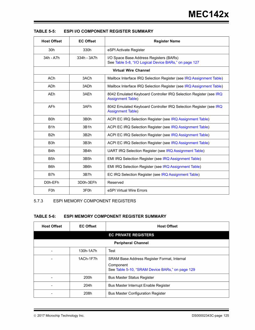
MEC142x
5.7.3 ESPI MEMORY COMPONENT REGISTERS
30h 330h eSPI Activate Register
34h - A7h 334h - 3A7h I/O Space Base Address Registers (BARs)See Table 5-8, “I/O Logical Device BARs,” on page 127
Virtual Wire Channel
ACh 3ACh Mailbox Interface IRQ Selection Register (see IRQ Assignment Table)
ADh 3ADh Mailbox Interface IRQ Selection Register (see IRQ Assignment Table)
AEh 3AEh 8042 Emulated Keyboard Controller IRQ Selection Register (see IRQ Assignment Table)
AFh 3AFh 8042 Emulated Keyboard Controller IRQ Selection Register (see IRQ Assignment Table)
B0h 3B0h ACPI EC IRQ Selection Register (see IRQ Assignment Table)
B1h 3B1h ACPI EC IRQ Selection Register (see IRQ Assignment Table)
B2h 3B2h ACPI EC IRQ Selection Register (see IRQ Assignment Table)
B3h 3B3h ACPI EC IRQ Selection Register (see IRQ Assignment Table)
B4h 3B4h UART IRQ Selection Register (see IRQ Assignment Table)
B5h 3B5h EMI IRQ Selection Register (see IRQ Assignment Table)
B6h 3B6h EMI IRQ Selection Register (see IRQ Assignment Table)
B7h 3B7h EC IRQ Selection Register (see IRQ Assignment Table)
D0h-EFh 3D0h-3EFh Reserved
F0h 3F0h eSPI Virtual Wire Errors
TABLE 5-6: ESPI MEMORY COMPONENT REGISTER SUMMARY
Host Offset EC Offset Host Offset
EC PRIVATE REGISTERS
Peripheral Channel
- 130h-1A7h Test
- 1ACh-1F7h SRAM Base Address Register Format, Internal
ComponentSee Table 5-10, “SRAM Device BARs,” on page 129
- 200h Bus Master Status Register
- 204h Bus Master Interrupt Enable Register
- 208h Bus Master Configuration Register
TABLE 5-5: ESPI I/O COMPONENT REGISTER SUMMARY
Host Offset EC Offset Register Name
2017 Microchip Technology Inc. DS00002343C-page 125

MEC142x
5.7.4 VIRTUAL WIRE REGISTERS
- 210h Bus Master 1 Control Register
- 214h Bus Master 1 Host Address Register
- 21Ch Bus Master 1 Internal Address Register
- 224h Bus Master 2 Control Register
- 228h Bus Master 2 Host Address Register
- 230h Bus Master 2 Internal Address Register
- 2E0h Test
- 2E4h Test
CONFIGURATION REGISTERS
30h-A7h 330h-3A7h Memory Base Address Configuration Register
See Table 5-9, “Memory Logical Device BARs,” on page 128
ACh-F7h 3ACh-3F7h SRAM Base Address Configuration RegisterSee Table 5-10, “SRAM Device BARs,” on page 129
B2h - F7h 3B2h - 3F7h Reserved
TABLE 5-7: VIRTUAL WIRES REGISTER SUMMARY
EC Offset Register Name
0h MSVW00 Register
Ch MSVW01 Register
18h MSVW02 Register
24h MSVW03 Register
30h MSVW04 Register
3Ch MSVW05 Register
48h MSVW06 Register
54h MSVW07 Register
60h MSVW08 Register
6Ch MSVW09 Register
78h MSVW10 Register
84h - 1FFh Reserved
200h SMVW00 Register
208h SMVW01 Register
TABLE 5-6: ESPI MEMORY COMPONENT REGISTER SUMMARY
Host Offset EC Offset Host Offset
DS00002343C-page 126 2017 Microchip Technology Inc.

MEC142x
5.8 Base Address Register Tables
TABLE 5-8: I/O LOGICAL DEVICE BARS
210h SMVW02 Register
218h SMVW03 Register
220h SMVW04 Register
228h SMVW05 Register
230h SMVW06 Register
238h SMVW07 Register
240h SMVW08 Register
248h SMVW09 Register
250h SMVW10 Register
258h - 2FFh Reserved
300h Test
302h Test
308h Test
30Ah Test
Logical Devices
Logical Device Number
(hex)
Configuration Register Bank EC Only Register Bank
Host Offset
EC Offset
Default eSPI I/O
Host Address
Reset DefaultEC
OffsetMASK Reset Default
eSPI I/O Component(Configuration Port)
10 34h 334h 002E 002E_0000h 134h 01 0000_1001h
eSPI Memory Compo-nent
12 38h 338h 0000 0000_0000h 138h 00 0000_1200h
Mailbox Interface 9 3Ch 33Ch 0000 0000_0000h 13Ch 01 0000_0901h
8042 Emulated Key-board Controller
1 40h 340h 0060 0060_0000h 140h 04 0000_0104h
ACPI EC0 3 44h 344h 0062 0062_0000h 144h 04 0000_0304h
ACPI EC1 4 48h 348h 0066 0066_0000h 148h 07 0000_0407h
ACPI EC2 A 4Ch 34Ch 0000 0000_0000h 14Ch 07 0000_0A07h
ACPI EC3 B 50h 350h 0000 0000_0000h 150h 07 0000_0B07h
ACPI PM1 5 54h 354h 0000 0000_0000h 154h 07 0000_0507h
TABLE 5-7: VIRTUAL WIRES REGISTER SUMMARY (CONTINUED)
EC Offset Register Name
2017 Microchip Technology Inc. DS00002343C-page 127

MEC142x
2: The MASK field for the ACPI EC Logical Devices is Read/Write.
UART 0 7 58h 358h 0000 0000_0000h 158h 07 0000_0707h
LegacyPort92/GateA20
6 5Ch 35Ch 0092 0092_0000h 15Ch 00 0000_0600h
EMI 0 0 60h 360h 0000 0000_0000h 160h 0F 0000_000Fh
Port 80 BIOS DebugPort 0
15 64h 364h 0000 0000_0000h 164h 00 0000_1500h
Port 80 BIOS DebugPort 1
16 68h 368h 0000 0000_0000h 168h 00 0000_1600h
32Byte Scratch Block 14 6Ch 36Ch 0000 0000_0000h 16Ch 0F 0000_140Fh
TABLE 5-9: MEMORY LOGICAL DEVICE BARS
Logical Devices
Logical Device Number
(Hex)
Configuration Register Bank
EC-Only Register Bank
Host Offset
EC Offset
Default Memory
Host Address
Reset Default
EC Offset
MASKReset
Default
Mailbox Interface 9 30h 330h 0h 0h 130h 1h 0901h
ACPI EC0 3 3Ah 33Ah 0h 0h 13Ah 4h 0304h
ACPI EC1 4 44h 344h 0h 0h 144h 7h 0407h
ACPI EC2 A 4Eh 34Eh 0h 0h 14Eh 7h 0A07h
ACPI EC3 B 58h 358h 0h 0h 158h 7h 0B07h
EMI 0 0 62h 362h 0h 0h 162h Fh 000Fh
32Byte ScratchBlock
14 6Ch 36Ch 0h 0h 16Ch Fh 140Fh
Note: The ACPI-ECx Mask bit field is a read/write bit field. All other MASK bit fields are read-only as defined inthe register description.
Logical Devices
Logical Device Number
(hex)
Configuration Register Bank EC Only Register Bank
Host Offset
EC Offset
Default eSPI I/O
Host Address
Reset DefaultEC
OffsetMASK Reset Default
DS00002343C-page 128 2017 Microchip Technology Inc.
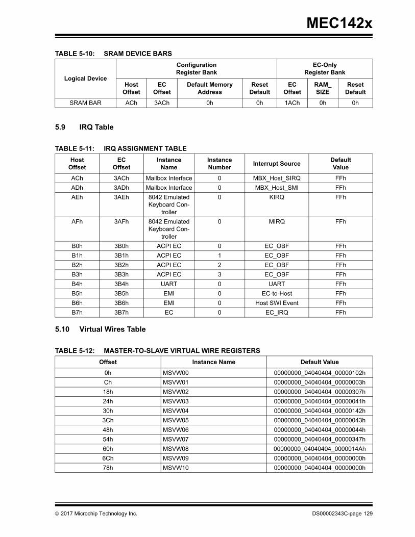
MEC142x
5.9 IRQ Table
5.10 Virtual Wires Table
TABLE 5-10: SRAM DEVICE BARS
Logical Device
ConfigurationRegister Bank
EC-Only Register Bank
HostOffset
ECOffset
Default MemoryAddress
ResetDefault
ECOffset
RAM_SIZE
ResetDefault
SRAM BAR ACh 3ACh 0h 0h 1ACh 0h 0h
TABLE 5-11: IRQ ASSIGNMENT TABLE
HostOffset
ECOffset
InstanceName
InstanceNumber
Interrupt SourceDefaultValue
ACh 3ACh Mailbox Interface 0 MBX_Host_SIRQ FFh
ADh 3ADh Mailbox Interface 0 MBX_Host_SMI FFh
AEh 3AEh 8042 Emulated Keyboard Con-
troller
0 KIRQ FFh
AFh 3AFh 8042 Emulated Keyboard Con-
troller
0 MIRQ FFh
B0h 3B0h ACPI EC 0 EC_OBF FFh
B1h 3B1h ACPI EC 1 EC_OBF FFh
B2h 3B2h ACPI EC 2 EC_OBF FFh
B3h 3B3h ACPI EC 3 EC_OBF FFh
B4h 3B4h UART 0 UART FFh
B5h 3B5h EMI 0 EC-to-Host FFh
B6h 3B6h EMI 0 Host SWI Event FFh
B7h 3B7h EC 0 EC_IRQ FFh
TABLE 5-12: MASTER-TO-SLAVE VIRTUAL WIRE REGISTERS
Offset Instance Name Default Value
0h MSVW00 00000000_04040404_00000102h
Ch MSVW01 00000000_04040404_00000003h
18h MSVW02 00000000_04040404_00000307h
24h MSVW03 00000000_04040404_00000041h
30h MSVW04 00000000_04040404_00000142h
3Ch MSVW05 00000000_04040404_00000043h
48h MSVW06 00000000_04040404_00000044h
54h MSVW07 00000000_04040404_00000347h
60h MSVW08 00000000_04040404_0000014Ah
6Ch MSVW09 00000000_04040404_00000000h
78h MSVW10 00000000_04040404_00000000h
2017 Microchip Technology Inc. DS00002343C-page 129
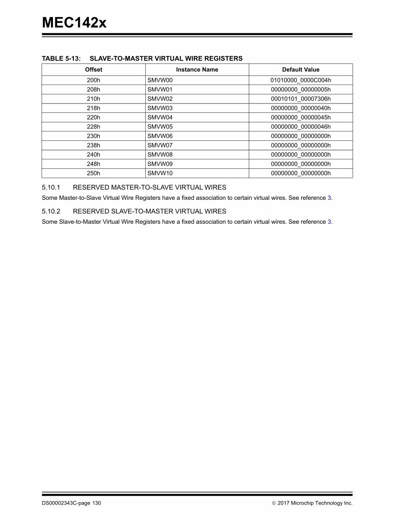
MEC142x
5.10.1 RESERVED MASTER-TO-SLAVE VIRTUAL WIRES
Some Master-to-Slave Virtual Wire Registers have a fixed association to certain virtual wires. See reference 3.
5.10.2 RESERVED SLAVE-TO-MASTER VIRTUAL WIRES
Some Slave-to-Master Virtual Wire Registers have a fixed association to certain virtual wires. See reference 3.
TABLE 5-13: SLAVE-TO-MASTER VIRTUAL WIRE REGISTERS
Offset Instance Name Default Value
200h SMVW00 01010000_0000C004h
208h SMVW01 00000000_00000005h
210h SMVW02 00010101_00007306h
218h SMVW03 00000000_00000040h
220h SMVW04 00000000_00000045h
228h SMVW05 00000000_00000046h
230h SMVW06 00000000_00000000h
238h SMVW07 00000000_00000000h
240h SMVW08 00000000_00000000h
248h SMVW09 00000000_00000000h
250h SMVW10 00000000_00000000h
DS00002343C-page 130 2017 Microchip Technology Inc.

MEC142x
6.0 QUAD SPI MASTER CONTROLLER
6.1 Overview
The Quad SPI Master Controller may be used to communicate with various peripheral devices that use a Serial Periph-eral Interface, such as EEPROMS, DACs and ADCs. The controller can be configured to support advanced SPI Flashdevices with multi-phase access protocols. Data can be transfered in Half Duplex, Single Data Rate, Dual Data Rateand Quad Data Rate modes. In all modes and all SPI clock speeds, the controller supports back-to-back reads andwrites without clock stretching if internal bandwidth permits.
6.2 References
No references have been cited for this feature.
6.3 Terminology
No terminology for this block.
6.4 Interface
This block is designed to be accessed externally via the pin interface and internally via a registered host interface.
6.5 Signal Description
FIGURE 6-1: I/O DIAGRAM OF BLOCK
TABLE 6-1: EXTERNAL SIGNAL DESCRIPTION
Name Direction Description
SPI_CLK Output SPI Clock output used to drive the SPCLK pin.
SPI_CS0# Output SPI chip select 0
SPI_CS1# Output SPI chip select 1
Quad SPI Master Controller
Interrupts
Power, Clocks and Reset
Host Interface
Signal Description
2017 Microchip Technology Inc. DS00002343C-page 131
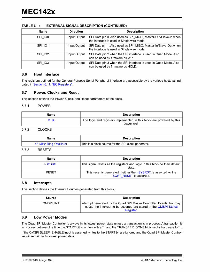
MEC142x
6.6 Host Interface
The registers defined for the General Purpose Serial Peripheral Interface are accessible by the various hosts as indi-cated in Section 6.11, "EC Registers".
6.7 Power, Clocks and Reset
This section defines the Power, Clock, and Reset parameters of the block.
6.7.1 POWER
6.7.2 CLOCKS
6.7.3 RESETS
6.8 Interrupts
This section defines the Interrupt Sources generated from this block.
6.9 Low Power Modes
The Quad SPI Master Controller is always in its lowest power state unless a transaction is in process. A transaction isin process between the time the START bit is written with a ‘1’ and the TRANSFER_DONE bit is set by hardware to ‘1’.
If the QMSPI SLEEP_ENABLE input is asserted, writes to the START bit are ignored and the Quad SPI Master Control-ler will remain in its lowest power state.
SPI_IO0 Input/Output SPI Data pin 0. Also used as SPI_MOSI, Master-Out/Slave-In when the interface is used in Single wire mode
SPI_IO1 Input/Output SPI Data pin 1. Also used as SPI_MISO, Master-In/Slave-Out when the interface is used in Single wire mode
SPI_IO2 Input/Output SPI Data pin 2 when the SPI interface is used in Quad Mode. Also can be used by firmware as WP.
SPI_IO3 Input/Output SPI Data pin 3 when the SPI interface is used in Quad Mode. Also can be used by firmware as HOLD.
Name Description
VTR The logic and registers implemented in this block are powered by this power well.
Name Description
48 MHz Ring Oscillator This is a clock source for the SPI clock generator.
Name Description
nSYSRST This signal resets all the registers and logic in this block to their default state.
RESET This reset is generated if either the nSYSRST is asserted or the SOFT_RESET is asserted.
Source Description
QMSPI_INT Interrupt generated by the Quad SPI Master Controller. Events that may cause the interrupt to be asserted are stored in the QMSPI Status
Register.
TABLE 6-1: EXTERNAL SIGNAL DESCRIPTION (CONTINUED)
Name Direction Description
DS00002343C-page 132 2017 Microchip Technology Inc.

MEC142x
6.10 Description
• Support for multiple SPI pin configurations
- Single wire half duplex
- Two wire full duplex
- Two wire double data rate
- Four wire quad data rate
• Supports two chip selects
• Separate FIFO buffers for Receive and Transmit
- 8 byte FIFO depth in each FIFO
- Each FIFO can be 1 byte, 2 bytes or 4 bytes wide
• Support for all four SPI clock formats
• Programmable SPI Clock generator, with clock polarity and phase controls
• Separate DMA support for Receive and Transmit data transfers
• Configurable interrupts, for errors, individual bytes, or entire transactions
• Descriptor Mode, in which a set of sixteen descriptor registers can configure the controller to autonomously per-form multi-phase SPI data transfers
• Capable of wire speed transfers in all SPI modes and all configurable SPI clock rates (internal bus contention may cause clock stretching)
FIGURE 6-2: QUAD MASTER SPI BLOCK DIAGRAM
ClockGenerator
Internal Data Bus
SPI_IO0
SPI_IO3
SPI_IO2
SPI_IO1
SPI_CK
StateMachine
SPI_CS0#
DescriptorRegisters
SPI_CS1#
2017 Microchip Technology Inc. DS00002343C-page 133

MEC142x
6.10.1 SPI CONFIGURATIONS MODES
• Half Duplex. All SPI data transfers take place on a single wire, SPI_IO0
• Full Duplex. This is the legacy SPI configuration, where all SPI data is transfered one bit at a time and data from the SPI Master to the SPI Slave takes place on SPI_MOSI (SPI_IO0) and at the same time data from the SPI Slave to the SPI Master takes place on SPI_MISO (SPI_IO1)
• Dual Data Rate. Data transfers between the SPI Master and the SPI Slave take place two bits at a time, using SPI_IO0 and SPI_IO1
• Quad Data Rate. Data transfers between the SPI Master and the SPI Slave take place four bits at a time, using all four SPI data wires, SPI_IO0, SPI_IO1, SPI_IO2 and SPI_IO3
6.10.2 SPI CONTROLLER MODES
• Manual. In this mode, firmware control all SPI data transfers byte at a time
• DMA. Firmware configures the SPI Master controller for characteristics like data width but the transfer of data between the FIFO buffers in the SPI controller and memory is controlled by the DMA controller. DMA transfers can take place from the Slave to the Master, from the Master to the Slave, or in both directions simultaneously
• Descriptor. Descriptor Mode extends the SPI Controller so that firmware can configure a multi-phase SPI transfer, in which each phase may have a different SPI bus width, a different direction, and a different length. For example, firmware can configure the controller so that a read from an advanced SPI Flash, which consists of a command phase, an address phase, a dummy cycle phase and the read phase, can take place as a single operation, with a single interrupt to firmware when the entire transfer is completed
6.10.3 SPI CLOCK
The SPI output clock is derived from the 48 MHz Ring Oscillator, divided by a value programmed in the CLOCK_DIVIDEfield of the QMSPI Mode Register. Sample frequencies are shown in the following table:
6.10.4 ERROR CONDITIONS
The Quad SPI Master Controller can detect some illegal configurations. When these errors are detected, an error issignaled via the PROGRAMMING_ERROR status bit. This bit is asserted when any of the following errors are detected:
• Both Receive and the Transmit transfers are enabled when the SPI Master Controller is configured for Dual Data Rate or Quad Data Rate
• Both Pull-up and Pull-down resistors are enabled on either the Receive data pins or the Transmit data pins
• The transfer length is programmed in bit mode, but the total number of bits is not a multiple of 2 (when the control-ler is configured for Dual Data Rate) or 4 (when the controller is configured for Quad Data Rate)
• Both the STOP bit and the START bits in the QMSPI Execute Register are set to ‘1’ simultaneously
TABLE 6-2: EXAMPLE SPI FREQUENCIES
CLOCK_DIVIDE SPI Clock Frequency
0 732.42 Hz
1 48 MHz
2 24 MHz
3 16 MHz
6 8 MHz
48 1 MHz
128 375 KHz
255 188.25 KHz
DS00002343C-page 134 2017 Microchip Technology Inc.

MEC142x
6.11 EC Registers
Registers for this block are shown in the following summary table. Addresses for each register are determined by addingthe offset to the Base Address for each instance of the Quad SPI Master Controller Block.
TABLE 6-3: REGISTER SUMMARY
Offset Register Name
0h QMSPI Mode Register
4h QMSPI Control Register
8h QMSPI Execute Register
Ch QMSPI Interface Control Register
10h QMSPI Status Register
14h QMSPI Buffer Count Status Register
18h QMSPI Interrupt Enable Register
1Ch QMSPI Buffer Count Trigger Register
20h QMSPI Transmit Buffer Register
24h QMSPI Receive Buffer Register
28h QMSPI Chip Select Timing Register
30h QMSPI Description Buffer 0 Register
34h QMSPI Description Buffer 1 Register
38h QMSPI Description Buffer 2 Register
3Ch QMSPI Description Buffer 3 Register
40h QMSPI Description Buffer 4 Register
44h QMSPI Description Buffer 5 Register
48h QMSPI Description Buffer 6 Register
4Ch QMSPI Description Buffer 7 Register
50h QMSPI Description Buffer 8 Register
54h QMSPI Description Buffer 9 Register
58h QMSPI Description Buffer 10 Register
5Ch QMSPI Description Buffer 11 Register
60h QMSPI Description Buffer 12 Register
64h QMSPI Description Buffer 13 Register
68h QMSPI Description Buffer 14 Register
6Ch QMSPI Description Buffer 15 Register
B0h Test
2017 Microchip Technology Inc. DS00002343C-page 135

MEC142x
6.11.1 QMSPI MODE REGISTER
Offset 00h
Bits Description Type DefaultReset Event
31:16 CLOCK_DIVIDE
The SPI clock divide in number of system clocks. A value of 1 divides the master clock by 1, a value of 255 divides the master clock by 255. A value of 0 divides the master clock by 65536. See Table 6-2, "Example SPI Frequencies" for examples.
R/W 0h RESET
15:14 Reserved R - -
13:12 CHIP_SELECTSelects which Chip Select line is active. The non-active CS line is driven high.00=Chip Select 001=Chip Select 11x=unused.
Note: Only the Shared SPI interface supports two chipselects; the other SPI interfaces do not.
R/W 0h RESET
11 Reserved R - -
10 CHPA_MISO
If CPOL=1:1=Data are captured on the rising edge of the SPI clock0=Data are captured on the falling edge of the SPI clock
If CPOL=0:1=Data are captured on the falling edge of the SPI clock0=Data are captured on the rising edge of the SPI clock
Application Notes:Common SPI Mode configurations:Common SPI Modes require the CHPA_MISO and CHPA_MOSI programmed to the same value. E.g.,
- Mode 0: CPOL=0; CHPA_MISO=0; CHPA_MOSI=0
- Mode 3: CPOL=1; CHPA_MISO=1; CHPA_MOSI=1
Alternative SPI Mode configurationsIn quad mode applications operating at 48MHz some slave config-urations may find it difficult to meet the minimum setup time using common SPI Mode configuration. If the Master-Slave turn-around time (TAR) ensures the minimum setup time will be met, the slave can configure the Master to both sample and change data on the same edge giving the slave more setup time.E.g.,
- Mode 0: CPOL=0; CHPA_MISO=1; CHPA_MOSI=0
- Mode 3: CPOL=1; CHPA_MISO=0; CHPA_MOSI=1
R/W 0h RESET
DS00002343C-page 136 2017 Microchip Technology Inc.
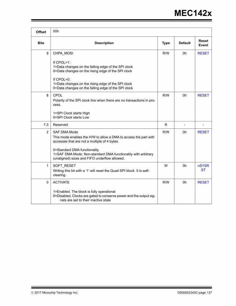
MEC142x
9 CHPA_MOSI
If CPOL=1:1=Data changes on the falling edge of the SPI clock0=Data changes on the rising edge of the SPI clock
If CPOL=0:1=Data changes on the rising edge of the SPI clock0=Data changes on the falling edge of the SPI clock
R/W 0h RESET
8 CPOL
Polarity of the SPI clock line when there are no transactions in pro-cess.
1=SPI Clock starts High0=SPI Clock starts Low
R/W 0h RESET
7:3 Reserved R - -
2 SAF DMA Mode
This mode enables the H/W to allow a DMA to access the part with accesses that are not a multiple of 4 bytes.
0=Standard DMA functionality1=SAF DMA Mode: Non-standard DMA functionality with arbitrary (unaligned) sizes and FIFO underflow allowed.
R/W 0h RESET
1 SOFT_RESET
Writing this bit with a ‘1’ will reset the Quad SPI block. It is self-clearing.
W 0h nSYSRST
0 ACTIVATE
1=Enabled. The block is fully operational0=Disabled. Clocks are gated to conserve power and the output sig-
nals are set to their inactive state
R/W 0h RESET
Offset 00h
Bits Description Type DefaultReset Event
2017 Microchip Technology Inc. DS00002343C-page 137

MEC142x
6.11.2 QMSPI CONTROL REGISTER
Offset 04h
Bits Description Type DefaultReset Event
31:17 TRANSFER_LENGTH
The length of the SPI transfer. The count is in bytes or bits, depending on the value of TRANSFER_LENGTH_BITS. A value of ‘0’ means an infinite length transfer.
R/W 0h RESET
16 DESCRIPTION_BUFFER_ENABLE
This enables the Description Buffers to be used.
1=Description Buffers in use. The first buffer is defined in DESCRIP-TION_BUFFER_POINTER
0=Description Buffers disabled
R/W 0h RESET
15:12 DESCRIPTION_BUFFER_POINTER
This field selects the first buffer used if Description Buffers are enabled.
R/W 0h RESET
11:10 TRANSFER_UNITS
3=TRANSFER_LENGTH defined in units of 16-byte segments2=TRANSFER_LENGTH defined in units of 4-byte segments1=TRANSFER_LENGTH defined in units of bytes0=TRANSFER_LENGTH defined in units of bits
R/W 0h RESET
9 CLOSE_TRANSFER_ENABLE
This selects what action is taken at the end of a transfer. When the transaction closes, the Chip Select de-asserts, the SPI interface returns to IDLE and the DMA interface terminates When Descrip-tion Buffers are in use this bit must be set only on the Last Buffer.
1=The transaction is terminated0=The transaction is not terminated
R/W 0h RESET
8:7 RX_DMA_ENABLE
This bit enables DMA support for Receive Transfer. If enabled, DMA will be requested to empty the FIFO until either the interface reaches TRANSFER_LENGTH or the DMA sends a termination request. The size defined here must match DMA programmed access size.
1=DMA is enabled.and set to 1 Byte2=DMA is enabled and set to 2 Bytes3=DMA is enabled and set to 4 Bytes0=DMA is disabled. All data in the Receive Buffer must be emptied
by firmware
R/W 0h RESET
6 RX_TRANSFER_ENABLE
This bit enables the receive function of the SPI interface.
1=Receive is enabled. Data received from the SPI Slave is storedin the Receive Buffer
0=Receive is disabled
R/W 0h RESET
DS00002343C-page 138 2017 Microchip Technology Inc.

MEC142x
6.11.3 QMSPI EXECUTE REGISTER
5:4 TX_DMA_ENABLE
This bit enables DMA support for Transmit Transfer. If enabled, DMA will be requested to fill the FIFO until either the interface reaches TRANSFER_LENGTH or the DMA sends a termination request. The size defined here must match DMA programmed access size.
1=DMA is enabled.and set to 1 Byte2=DMA is enabled and set to 2 Bytes3=DMA is enabled and set to 4 Bytes0=DMA is disabled. All data in the Transmit Buffer must be emptied
by firmware
R/W 0h RESET
3:2 TX_TRANSFER_ENABLE
This field bit selects the transmit function of the SPI interface.
3=Transmit Enabled in 1 Mode. The MOSI or IO Bus will send outonly 1's. The Transmit Buffer will not be used
2=Transmit Enabled in 0 Mode. The MOSI or IO Bus will send outonly 0's. The Transmit Buffer will not be used.
1=Transmit Enabled. Data will be fetched from the Transmit Bufferand sent out on the MOSI or IO Bus.
0=Transmit is Disabled. Not data is sent. This will cause the MOSIbe to be undriven, or the IO bus to be undriven if Receive isalso disabled.
R/W 0h RESET
1:0 INTERFACE_MODE
This field sets the transmission mode. If this field is set for Dual Mode or Quad Mode then either TX_TRANSFER_ENABLE or RX_TRANSFER_ENABLE must be 0.
3=Reserved2=Quad Mode1=Dual Mode0=Single/Duplex Mode
R/W 0h RESET
Offset 08h
Bits Description Type DefaultReset Event
31:3 Reserved R - -
2 CLEAR_DATA_BUFFER
Writing a ‘1’ to this bit will clear out the Transmit and Receive FIFOs. Any data stored in the FIFOs is discarded and all count fields are reset. Writing a ‘0’ to this bit has no effect. This bit is self-clearing.
W 0h RESET
Offset 04h
Bits Description Type DefaultReset Event
2017 Microchip Technology Inc. DS00002343C-page 139
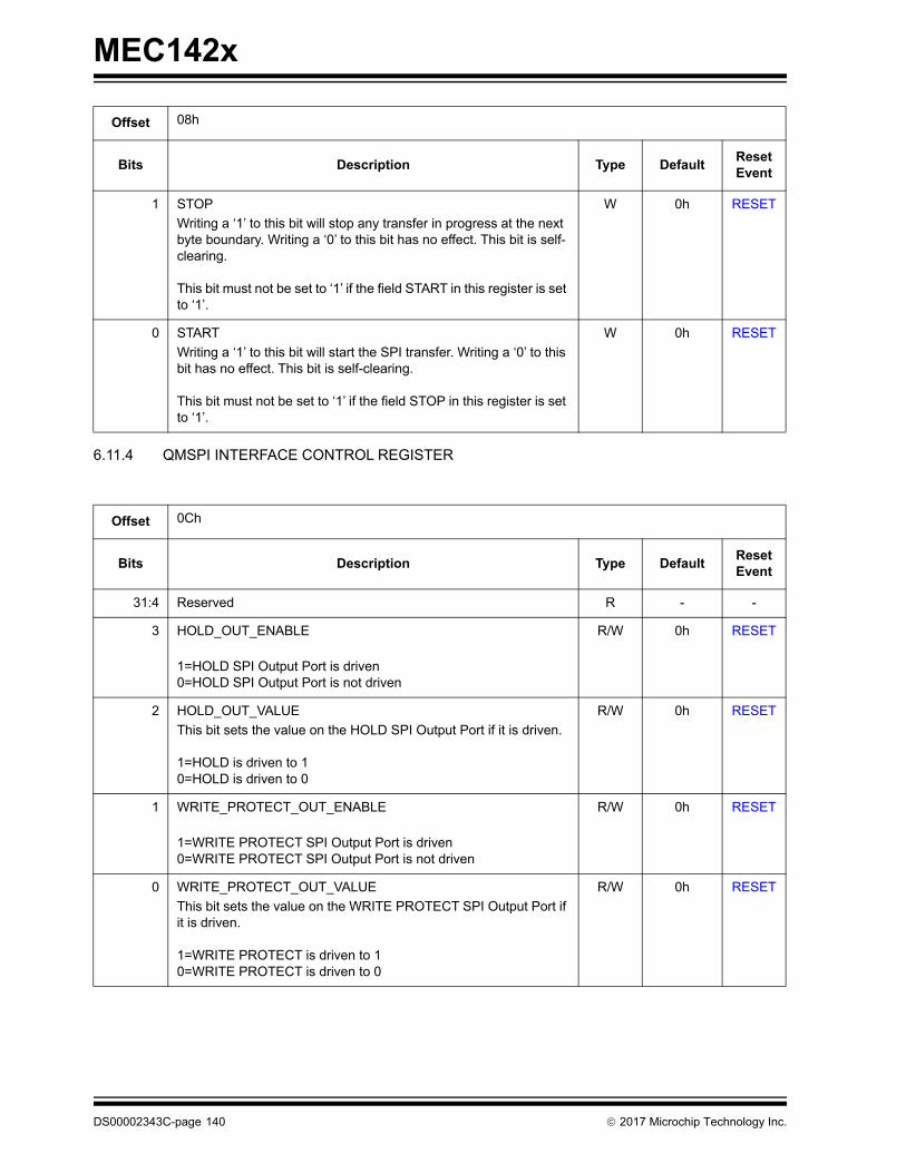
MEC142x
6.11.4 QMSPI INTERFACE CONTROL REGISTER
1 STOP
Writing a ‘1’ to this bit will stop any transfer in progress at the next byte boundary. Writing a ‘0’ to this bit has no effect. This bit is self-clearing.
This bit must not be set to ‘1’ if the field START in this register is set to ‘1’.
W 0h RESET
0 START
Writing a ‘1’ to this bit will start the SPI transfer. Writing a ‘0’ to this bit has no effect. This bit is self-clearing.
This bit must not be set to ‘1’ if the field STOP in this register is set to ‘1’.
W 0h RESET
Offset 0Ch
Bits Description Type DefaultReset Event
31:4 Reserved R - -
3 HOLD_OUT_ENABLE
1=HOLD SPI Output Port is driven0=HOLD SPI Output Port is not driven
R/W 0h RESET
2 HOLD_OUT_VALUE
This bit sets the value on the HOLD SPI Output Port if it is driven.
1=HOLD is driven to 10=HOLD is driven to 0
R/W 0h RESET
1 WRITE_PROTECT_OUT_ENABLE
1=WRITE PROTECT SPI Output Port is driven0=WRITE PROTECT SPI Output Port is not driven
R/W 0h RESET
0 WRITE_PROTECT_OUT_VALUE
This bit sets the value on the WRITE PROTECT SPI Output Port if it is driven.
1=WRITE PROTECT is driven to 10=WRITE PROTECT is driven to 0
R/W 0h RESET
Offset 08h
Bits Description Type DefaultReset Event
DS00002343C-page 140 2017 Microchip Technology Inc.

MEC142x
6.11.5 QMSPI STATUS REGISTER
Offset 10h
Bits Description Type DefaultReset Event
31:28 Reserved R - -
27:24 CURRENT_DESCRIPTION_BUFFER
This field shows the Description Buffer currently active. This field has no meaning if Description Buffers are not enabled.
R 0h RESET
23:17 Reserved R - -
16 TRANSFER_ACTIVE
1=A transfer is currently executing0=No transfer currently in progress
R 0h RESET
15 RECEIVE_BUFFER_STALL
1=The SPI interface had been stalled due to a flow issue (anattempt by the interface to write to a full Receive Buffer)
0=No stalls occurred
R/WC 0h RESET
14 RECEIVE_BUFFER_REQUEST
This status is asserted if the Receive Buffer reaches a high water mark established by the RECEIVE_BUFFER_TRIGGER field.
1=RECEIVE_BUFFER_COUNT is greater than or equal toRECEIVE_BUFFER_TRIGGER
0=RECEIVE_BUFFER_COUNT is less thanRECEIVE_BUFFER_TRIGGER
R/WC 0h RESET
13 RECEIVE_BUFFER_EMPTY
1=The Receive Buffer is empty0=The Receive Buffer is not empty
R 1h RESET
12 RECEIVE_BUFFER_FULL
1=The Receive Buffer is full0=The Receive Buffer is not full
R 0h RESET
11 TRANSMIT_BUFFER_STALL
1=The SPI interface had been stalled due to a flow issue (anattempt by the interface to read from an empty Transmit Buffer)
0=No stalls occurred
R/WC 0h RESET
2017 Microchip Technology Inc. DS00002343C-page 141

MEC142x
10 TRANSMIT_BUFFER_REQUEST
This status is asserted if the Transmit Buffer reaches a high water mark established by the TRANSMIT_BUFFER_TRIGGER field.
1=TRANSMIT_BUFFER_COUNT is less than or equal to TRANS-MIT_BUFFER_TRIGGER
0=TRANSMIT_BUFFER_COUNT is greater than TRANS-MIT_BUFFER_TRIGGER
R/WC 0h RESET
9 TRANSMIT_BUFFER_EMPTY
1=The Transmit Buffer is empty0=The Transmit Buffer is not empty
R 1h RESET
8 TRANSMIT_BUFFER_FULL
1=The Transmit Buffer is full0=The Transmit Buffer is not full
R 0h RESET
7:5 Reserved R - -
4 PROGRAMMING_ERROR
This bit if a programming error is detected. Programming errors are listed in Section 6.10.4, "Error Conditions".
1=Programming Error detected0=No programming error detected
R/WC 0h RESET
3 RECEIVE_BUFFER_ERROR
1=Underflow error occurred (attempt to read from an empty ReceiveBuffer)
0=No underflow occurred
R/WC 0h RESET
2 TRANSMIT_BUFFER_ERROR
1=Overflow error occurred (attempt to write to a full Transmit Buffer)0=No overflow occurred
R/WC 0h RESET
Offset 10h
Bits Description Type DefaultReset Event
DS00002343C-page 142 2017 Microchip Technology Inc.

MEC142x
6.11.6 QMSPI BUFFER COUNT STATUS REGISTER
1 DMA_COMPLETE
This field has no meaning if DMA is not enabled.
This bit will be set to ‘1’ when the DMA controller asserts the DONE signal to the SPI controller. This occurs either when the SPI con-troller has closed the DMA transfer, or the DMA channel has com-pleted its count. If both Transmit and Receive DMA transfers are active, then this bit will only assert after both have completed. If CLOSE_TRANSFER_ENABLE is enabled, DMA_COMPLETE and TRANSFER_COMPLETE will be asserted simultaneously. This status is not inhibited by the description buffers, so it can fire on all valid description buffers while operating in that mode.
1=DMA completed0=DMA not completed
R/WC 0h RESET
0 TRANSFER_COMPLETE
In Manual Mode (neither DMA nor Description Buffers are enabled), this bit will be set to ‘1’ when the transfer matches TRANSFER_LENGTH.
If DMA Mode is enabled, this bit will be set to ‘1’ when DMA_COM-PLETE is set to ‘1’.
In Description Buffer Mode, this bit will be set to ‘1’ only when the Last Buffer completes its transfer.
In all cases, this bit will be set to ‘1’ if the STOP bit is set to ‘1’ and the controller has completed the current 8 bits being copied.
1=Transfer completed0=Transfer not complete
R/WC 0h RESET
Offset 14h
Bits Description Type DefaultReset Event
31:16 RECEIVE_BUFFER_COUNT
This is a count of the number of bytes currently valid in the Receive Buffer.
R 0h RESET
15:0 TRANSMIT_BUFFER_COUNT
This is a count of the number of bytes currently valid in the Trans-mit Buffer.
R 0h RESET
Offset 10h
Bits Description Type DefaultReset Event
2017 Microchip Technology Inc. DS00002343C-page 143

MEC142x
6.11.7 QMSPI INTERRUPT ENABLE REGISTER
Offset 18h
Bits Description Type DefaultReset Event
31:16 Reserved R - -
15 RECEIVE_BUFFER_STALL_ENABLE
1=Enable an interrupt if RECEIVE_BUFFER_STALL is asserted0=Disable the interrupt
R/W 0h RESET
14 RECEIVE_BUFFER_REQUEST_ENABLE
1=Enable an interrupt if RECEIVE_BUFFER_REQUEST isasserted
0=Disable the interrupt
R/W 0h RESET
13 RECEIVE_BUFFER_EMPTY_ENABLE
1=Enable an interrupt if RECEIVE_BUFFER_EMPTY is asserted0=Disable the interrupt
R/W 0h RESET
12 RECEIVE_BUFFER_FULL_ENABLE
1=Enable an interrupt if RECEIVE_BUFFER_FULL is asserted0=Disable the interrupt
R/W 0h RESET
11 TRANSMIT_BUFFER_STALL_ENABLE
1=Enable an interrupt if TRANSMIT_BUFFER_STALL is asserted0=Disable the interrupt
R/W 0h RESET
10 TRANSMIT_BUFFER_REQUEST_ENABLE
1=Enable an interrupt if TRANSMIT_BUFFER_REQUEST isasserted
0=Disable the interrupt
R/W 0h RESET
9 TRANSMIT_BUFFER_EMPTY_ENABLE
1=Enable an interrupt if TRANSMIT_BUFFER_EMPTY is asserted0=Disable the interrupt
R/W 0h RESET
8 TRANSMIT_BUFFER_FULL_ENABLE
1=Enable an interrupt if TRANSMIT_BUFFER_FULL is asserted0=Disable the interrupt
R/W 0h RESET
7:5 Reserved R - -
4 PROGRAMMING_ERROR_ENABLE
1=Enable an interrupt if PROGRAMMING_ERROR is asserted0=Disable the interrupt
R/W 0h RESET
DS00002343C-page 144 2017 Microchip Technology Inc.

MEC142x
6.11.8 QMSPI BUFFER COUNT TRIGGER REGISTER
3 RECEIVE_BUFFER_ERROR_ENABLE
1=Enable an interrupt if RECEIVE_BUFFER_ERROR is asserted0=Disable the interrupt
R/W 0h RESET
2 TRANSMIT_BUFFER_ERROR_ENABLE
1=Enable an interrupt if TRANSMIT_BUFFER_ERROR is asserted0=Disable the interrupt
R/W 0h RESET
1 DMA_COMPLETE_ENABLE
1=Enable an interrupt if DMA_COMPLETE is asserted0=Disable the interrupt
R/W 0h RESET
0 TRANSFER_COMPLETE_ENABLE
1=Enable an interrupt if TRANSFER_COMPLETE is asserted0=Disable the interrupt
R/W 0h RESET
Offset 1Ch
Bits Description Type DefaultReset Event
31:16 RECEIVE_BUFFER_TRIGGER
An interrupt is triggered if the RECEIVE_BUFFER_COUNT field is greater than or equal to this value. A value of ‘0’ disables the inter-rupt.
R/W 0h RESET
15:0 TRANSMIT_BUFFER_TRIGGER
An interrupt is triggered if the TRANSMIT_BUFFER_COUNT field is less than or equal to this value. A value of ‘0’ disables the inter-rupt.
R/W 0h RESET
Offset 18h
Bits Description Type DefaultReset Event
2017 Microchip Technology Inc. DS00002343C-page 145
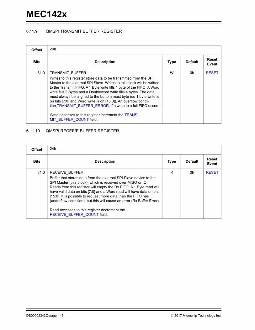
MEC142x
6.11.9 QMSPI TRANSMIT BUFFER REGISTER
6.11.10 QMSPI RECEIVE BUFFER REGISTER
Offset 20h
Bits Description Type DefaultReset Event
31:0 TRANSMIT_BUFFER
Writes to this register store data to be transmitted from the SPI Master to the external SPI Slave. Writes to this block will be written to the Transmit FIFO. A 1 Byte write fills 1 byte of the FIFO. A Word write fills 2 Bytes and a Doubleword write fills 4 bytes. The data must always be aligned to the bottom most byte (so 1 byte write is on bits [7:0] and Word write is on [15:0]). An overflow condi-tion,TRANSMIT_BUFFER_ERROR, if a write to a full FIFO occurs.
Write accesses to this register increment the TRANS-MIT_BUFFER_COUNT field.
W 0h RESET
Offset 24h
Bits Description Type DefaultReset Event
31:0 RECEIVE_BUFFER
Buffer that stores data from the external SPI Slave device to the SPI Master (this block), which is received over MISO or IO.Reads from this register will empty the Rx FIFO. A 1 Byte read will have valid data on bits [7:0] and a Word read will have data on bits [15:0]. It is possible to request more data than the FIFO has (underflow condition), but this will cause an error (Rx Buffer Error).
Read accesses to this register decrement the RECEIVE_BUFFER_COUNT field.
R 0h RESET
DS00002343C-page 146 2017 Microchip Technology Inc.

MEC142x
6.11.11 QMSPI CHIP SELECT TIMING REGISTER
Offset 28h
Bits Description Type DefaultReset Event
31:24 DELAY_CS_OFF_TO_CS_ONThis selects the number of system clock cycles between CS deassertion to CS assertion. This is the minimum pulse width of CS deassertion.
Note: this field delays the start of the next transaction, it doesnot delay the status of the current transaction.
R/W 06h RESET
23:20 RESERVED R 0h RESET
19:16 DELAY_LAST_DATA_HOLDThis selects the number of system clock cycles between CS deassertion to the data ports for WP and HOLD switching from input to output. This is only used if the WP/HOLD functions are in use and only on IO2/WP and IO3/HOLD pins.
R/W 6h RESET
15:12 RESERVED R 0h RESET
11:8 DELAY_CLK_STOP_TO_CS_OFFThis selects the number of system clock cycles between the last clock edge and the deassertion of CS.
R/W 4h RESET
7:4 RESERVED R 0h RESET
3:0 DELAY_CS_ON_TO_CLOCK_STARTThis selects the number of system clock cycles between CS assertion to the start of the SPI Clock. An additional ½ SPI Clock delay is inherently added to allow pre-set-up of the data ports.
R/W 6h RESET
2017 Microchip Technology Inc. DS00002343C-page 147

MEC142x
6.11.12 QMSPI DESCRIPTION BUFFER 0 REGISTER
Offset 30h
Bits Description Type DefaultReset Event
31:17 TRANSFER_LENGTH
The length of the SPI transfer. The count is in bytes or bits, depending on the value of TRANSFER_LENGTH_BITS. A value of ‘0’ means an infinite length transfer.
R/W 0h RESET
16 DESCRIPTION_BUFFER_LAST
If this bit is ‘1’ then this is the last Description Buffer in the chain. When the transfer described by this buffer completes the TRANS-FER_COMPLETE status will be set to ‘1’. If this bit is ‘0’, then this is not the last buffer in use. When the transfer completes the next buffer will be activated, and no additional status will be asserted.
R/W 0h RESET
15:12 DESCRIPTION_BUFFER_NEXT_POINTER
This defines the next buffer to be used if Description Buffers are enabled and this is not the last buffer. This can point to the current buffer, creating an infinite loop.
R/W 0h RESET
11:10 TRANSFER_UNITS
3=TRANSFER_LENGTH defined in units of 16-byte segments2=TRANSFER_LENGTH defined in units of 4-byte segments1=TRANSFER_LENGTH defined in units of bytes0=TRANSFER_LENGTH defined in units of bits
R/W 0h RESET
9 CLOSE_TRANFSER_ENABLE
This selects what action is taken at the end of a transfer. This bit must be set only on the Last Buffer.
1=The transfer is terminated. The Chip Select de-asserts, the SPIinterface returns to IDLE and the DMA interface completes thetransfer.
0=The transfer is not closed. Chip Select remains asserted and theDMA interface and the SPI interface remain active
R/W 0h RESET
8:7 RX_DMA_ENABLE
This bit enables DMA support for Receive Transfer. If enabled, DMA will be requested to empty the FIFO until either the interface reaches TRANSFER_LENGTH or the DMA sends a termination request. The size defined here must match DMA programmed access size.
1=DMA is enabled.and set to 1 Byte2=DMA is enabled and set to 2 Bytes3=DMA is enabled and set to 4 Bytes0=DMA is disabled. All data in the Receive Buffer must be emptied
by firmware
R/W 0h RESET
DS00002343C-page 148 2017 Microchip Technology Inc.

MEC142x
6.11.13 QMSPI DESCRIPTION BUFFER 1 REGISTER
The format for this register is the same as the format of the QMSPI Description Buffer 0 Register.
6.11.14 QMSPI DESCRIPTION BUFFER 2 REGISTER
The format for this register is the same as the format of the QMSPI Description Buffer 0 Register.
6.11.15 QMSPI DESCRIPTION BUFFER 3 REGISTER
The format for this register is the same as the format of the QMSPI Description Buffer 0 Register.
6 RX_TRANSFER_ENABLE
This bit enables the receive function of the SPI interface.
1=Receive is enabled. Data received from the SPI Slave is storedin the Receive Buffer
0=Receive is disabled
R/W 0h RESET
5:4 TX_DMA_ENABLE
This bit enables DMA support for Transmit Transfer. If enabled, DMA will be requested to fill the FIFO until either the interface reaches TRANSFER_LENGTH or the DMA sends a termination request. The size defined here must match DMA programmed access size.
1=DMA is enabled.and set to 1 Byte2=DMA is enabled and set to 2 Bytes3=DMA is enabled and set to 4 Bytes0=DMA is disabled. All data in the Transmit Buffer must be emptied
by firmware
R/W 0h RESET
3:2 TX_TRANSFER_ENABLE
This field bit selects the transmit function of the SPI interface.
3=Transmit Enabled in 1 Mode. The MOSI or IO Bus will send outonly 1's. The Transmit Buffer will not be used
2=Transmit Enabled in 0 Mode. The MOSI or IO Bus will send outonly 0's. The Transmit Buffer will not be used.
1=Transmit Enabled. Data will be fetched from the Transmit Bufferand sent out on the MOSI or IO Bus.
0=Transmit is Disabled. No data is sent. This will cause the MOSIbe to be undriven, or the IO bus to be undriven if Receive isalso disabled.
R/W 0h RESET
1:0 INTERFACE_MODE
This field sets the transmission mode. If this field is set for Dual Mode or Quad Mode then either TX_TRANSFER_ENABLE or RX_TRANSFER_ENABLE must be 0.
3=Reserved2=Quad Mode1=Dual Mode0=Single/Duplex Mode
R/W 0h RESET
Offset 30h
Bits Description Type DefaultReset Event
2017 Microchip Technology Inc. DS00002343C-page 149

MEC142x
6.11.16 QMSPI DESCRIPTION BUFFER 4 REGISTER
The format for this register is the same as the format of the QMSPI Description Buffer 0 Register.
6.11.17 QMSPI DESCRIPTION BUFFER 5 REGISTER
The format for this register is the same as the format of the QMSPI Description Buffer 0 Register.
6.11.18 QMSPI DESCRIPTION BUFFER 6 REGISTER
The format for this register is the same as the format of the QMSPI Description Buffer 0 Register.
6.11.19 QMSPI DESCRIPTION BUFFER 7 REGISTER
The format for this register is the same as the format of the QMSPI Description Buffer 0 Register.
6.11.20 QMSPI DESCRIPTION BUFFER 8 REGISTER
The format for this register is the same as the format of the QMSPI Description Buffer 0 Register.
6.11.21 QMSPI DESCRIPTION BUFFER 9 REGISTER
The format for this register is the same as the format of the QMSPI Description Buffer 0 Register.
6.11.22 QMSPI DESCRIPTION BUFFER 10 REGISTER
The format for this register is the same as the format of the QMSPI Description Buffer 0 Register.
6.11.23 QMSPI DESCRIPTION BUFFER 11 REGISTER
The format for this register is the same as the format of the QMSPI Description Buffer 0 Register.
6.11.24 QMSPI DESCRIPTION BUFFER 12 REGISTER
The format for this register is the same as the format of the QMSPI Description Buffer 0 Register.
6.11.25 QMSPI DESCRIPTION BUFFER 13 REGISTER
The format for this register is the same as the format of the QMSPI Description Buffer 0 Register.
6.11.26 QMSPI DESCRIPTION BUFFER 14 REGISTER
The format for this register is the same as the format of the QMSPI Description Buffer 0 Register.
6.11.27 QMSPI DESCRIPTION BUFFER 15 REGISTER
The format for this register is the same as the format of the QMSPI Description Buffer 0 Register.
DS00002343C-page 150 2017 Microchip Technology Inc.

MEC142x
7.0 CHIP CONFIGURATION
7.1 Introduction
This chapter defines the mechanism to configure the device.
7.2 Terminology
This section documents terms used locally in this chapter. Common terminology that is used in the chip specification iscaptured in the Chip-Level Terminology section.
7.3 Interface
This block is designed to be accessed via the Host accessible Configuration Port.
TABLE 7-1: TERMINOLOGY
Term Definition
Global Configuration Registers Registers used to configure the chip that are always accessible via the Configuration Port
Logical Device Configuration Regis-ters
Registers used to configure a logical device in the chip. These registers are only accessible via the Configuration Port when enabled via the Global Configuration registers.
FIGURE 7-1: BLOCK DIAGRAM OF CONFIGURATION PORT
00h –
2F
h30h
– F
Fh
Logical Device Configuration Registers
Chip-LevelGlobal Configuration Registers
Logica
l Dev
ices[0
:n]
Configuration Port
2017 Microchip Technology Inc. DS00002343C-page 151
MEC142x
7.3.1 HOST INTERFACE
The registers defined for the Chip Configuration are accessible by the Configuration Port when the device is in CONFIGMODE. For a description of the Configuration Port and CONFIG MODE see the description of the LPC Interface.
7.4 Power, Clocks and Reset
This section defines the Power, Clock, and Reset input parameters to this block.
7.4.1 POWER DOMAINS
7.4.2 CLOCK INPUTS
This block does not require any special clock inputs.
7.4.3 RESETS
7.5 Interrupts
This block does not generate any interrupts.
7.6 Low Power Modes
This block always automatically adjusts to operate in the lowest power mode.
7.7 Description
The Chip Configuration Registers are divided into two groups: Global Configuration Registers and Logical Device Con-figuration registers. The following descriptions assume that the LPC interface has already been configured to operatein CONFIG MODE.
• Global Configuration Registers are always accessible via the LPC Configuration Port.
• The Logical Device Configuration registers are only accessible via the LPC Configuration Port when the corre-sponding Logical Device Number is loaded in the Logical Device Number register. The Logical Device Number register is a Global Configuration Register.
There are 48 8-bit Global Configuration Registers (at offsets 00h through 2Fh), plus up to 208 8-bit registers associatedwith each Logical Device. The Logical Device is selected with the Logical Device Number Register (Global ConfigurationRegister 07h).
Sequence to Access Logical Device Configuration Register:
a) Write the number of the Logical Device being accessed in the Logical Device Number Configuration Register bywriting 07h into the INDEX PORT and the Logical Device Number into the DATA PORT.
b) Write the address of the desired logical device configuration register to the INDEX PORT and then write or readthe value of the configuration register through the DATA PORT.
Note: Each logical device has a bank of Configuration registers that are accessible at offsets 30h to FFh via theConfiguration Port. The Logical Device number programmed in offset 07h determines which bank of con-figuration registers is currently accessible.
Name Description
VTR The logic and registers implemented in this block reside on this singlepower well.
Name Description
nSYSRST Power on Reset to the block. This signal resets all the register and logic in this block to its default state.
DS00002343C-page 152 2017 Microchip Technology Inc.
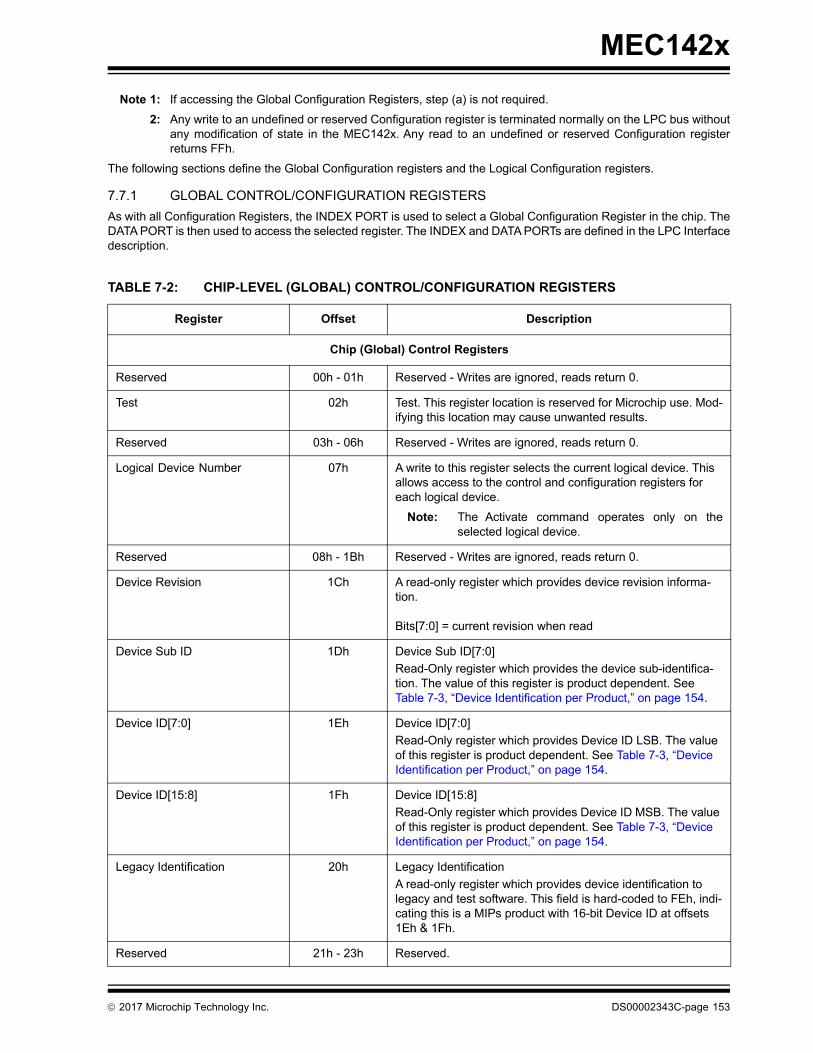
MEC142x
Note 1: If accessing the Global Configuration Registers, step (a) is not required.
2: Any write to an undefined or reserved Configuration register is terminated normally on the LPC bus withoutany modification of state in the MEC142x. Any read to an undefined or reserved Configuration registerreturns FFh.
The following sections define the Global Configuration registers and the Logical Configuration registers.
7.7.1 GLOBAL CONTROL/CONFIGURATION REGISTERS
As with all Configuration Registers, the INDEX PORT is used to select a Global Configuration Register in the chip. TheDATA PORT is then used to access the selected register. The INDEX and DATA PORTs are defined in the LPC Interfacedescription.
TABLE 7-2: CHIP-LEVEL (GLOBAL) CONTROL/CONFIGURATION REGISTERS
Register Offset Description
Chip (Global) Control Registers
Reserved 00h - 01h Reserved - Writes are ignored, reads return 0.
Test 02h Test. This register location is reserved for Microchip use. Mod-ifying this location may cause unwanted results.
Reserved 03h - 06h Reserved - Writes are ignored, reads return 0.
Logical Device Number 07h A write to this register selects the current logical device. This allows access to the control and configuration registers for each logical device.
Note: The Activate command operates only on theselected logical device.
Reserved 08h - 1Bh Reserved - Writes are ignored, reads return 0.
Device Revision 1Ch A read-only register which provides device revision informa-tion.
Bits[7:0] = current revision when read
Device Sub ID 1Dh Device Sub ID[7:0]
Read-Only register which provides the device sub-identifica-tion. The value of this register is product dependent. See Table 7-3, “Device Identification per Product,” on page 154.
Device ID[7:0] 1Eh Device ID[7:0]
Read-Only register which provides Device ID LSB. The value of this register is product dependent. See Table 7-3, “Device Identification per Product,” on page 154.
Device ID[15:8] 1Fh Device ID[15:8]
Read-Only register which provides Device ID MSB. The value of this register is product dependent. See Table 7-3, “Device Identification per Product,” on page 154.
Legacy Identification 20h Legacy Identification
A read-only register which provides device identification to legacy and test software. This field is hard-coded to FEh, indi-cating this is a MIPs product with 16-bit Device ID at offsets 1Eh & 1Fh.
Reserved 21h - 23h Reserved.
2017 Microchip Technology Inc. DS00002343C-page 153
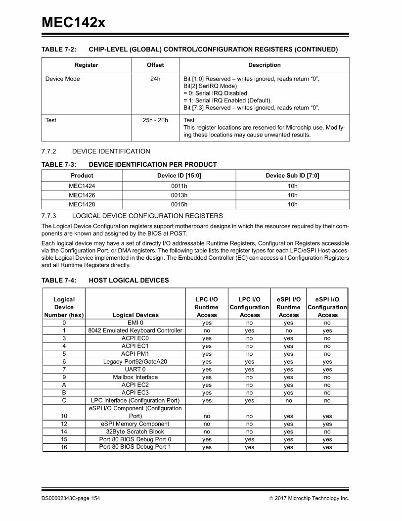
MEC142x
7.7.2 DEVICE IDENTIFICATION
7.7.3 LOGICAL DEVICE CONFIGURATION REGISTERS
The Logical Device Configuration registers support motherboard designs in which the resources required by their com-ponents are known and assigned by the BIOS at POST.
Each logical device may have a set of directly I/O addressable Runtime Registers, Configuration Registers accessiblevia the Configuration Port, or DMA registers. The following table lists the register types for each LPC/eSPI Host-acces-sible Logical Device implemented in the design. The Embedded Controller (EC) can access all Configuration Registersand all Runtime Registers directly.
TABLE 7-4: HOST LOGICAL DEVICES
Device Mode 24h Bit [1:0] Reserved – writes ignored, reads return “0”.Bit[2] SerIRQ Mode)= 0: Serial IRQ Disabled.= 1: Serial IRQ Enabled (Default).Bit [7:3] Reserved – writes ignored, reads return “0”.
Test 25h - 2Fh TestThis register locations are reserved for Microchip use. Modify-ing these locations may cause unwanted results.
TABLE 7-3: DEVICE IDENTIFICATION PER PRODUCT
Product Device ID [15:0] Device Sub ID [7:0]
MEC1424 0011h 10h
MEC1426 0013h 10h
MEC1428 0015h 10h
TABLE 7-2: CHIP-LEVEL (GLOBAL) CONTROL/CONFIGURATION REGISTERS (CONTINUED)
Register Offset Description
Logical Device
Number (hex) Logical Devices
LPC I/O Runtime Access
LPC I/O Configuration
Access
eSPI I/O Runtime Access
eSPI I/O Configuration
Access0 EMI 0 yes no yes no1 8042 Emulated Keyboard Controller no yes no yes3 ACPI EC0 yes no yes no4 ACPI EC1 yes no yes no5 ACPI PM1 yes no yes no6 Legacy Port92/GateA20 yes yes yes yes7 UART 0 yes yes yes yes9 Mailbox Interface yes no yes noA ACPI EC2 yes no yes noB ACPI EC3 yes no yes noC LPC Interface (Configuration Port) yes yes no no
10eSPI I/O Component (Configuration
Port) no no yes yes12 eSPI Memory Component no no yes yes14 32Byte Scratch Block no no yes no15 Port 80 BIOS Debug Port 0 yes yes yes yes16 Port 80 BIOS Debug Port 1 yes yes yes yes
DS00002343C-page 154 2017 Microchip Technology Inc.
MEC142x
8.0 MIPS32 M14K EMBEDDED CONTROLLER
8.1 Features
• A Modified 5-stage pipelined Harvard Architecture with a Closely-Coupled Data Memory and Instruction Memory interfaces
• Single Cycle 32-bit instruction set
• microMIPS-Compatible Instruction Set (default)
- microMIPS supports all MIPS32 instructions (except branch-likely instructions)
- Stack pointer implicit in instruction
- MIPS32 assembly and ABI (Application Binary Interface) compatible.
• External Interrupt Controller (EIC) mode.
- Programmable exception vector base
- Atomic interrupt enable/disable
- Bit field manipulation instructions
• Simple Fixed Mapping Translation (FMT) mechanism
• Multiply/Divide Unit (high-performance configuration)
- Maximum issue rate of one 32x16 multiply per clock via on-chip 32x16 hardware multiplier array.
- Maximum issue rate of one 32x32 multiply every other clock
- Early-in iterative divide. Minimum 11 and maximum 34 clock latency (dividend (rs) sign extension-dependent)
• Power Control
- Programmable Clock Rates: 48 MHz, 24 MHz, 3 MHz, and 1 MHz
- Sleep mode: Minimum frequency: 0 MHz
- Power-down mode (triggered by WAIT instruction)
- Clocks are gated in Low Power Modes
• EJTAG Debug Mechanism
- CPU control with start, stop, and single-stepping
- Virtual instruction and data address/value breakpoints
- Hardware breakpoint supports both address match and address range triggering.
- Simple hardware breakpoints on virtual addresses: 4I/2D breakpoints
- PC/Address Sampling function
- Support EJTAG (IEEE 1149.1)
- Supported by MPLAB REAL ICE tools
8.2 References
1. MIPS32 M14K™ Processor Core Software User’s Manual, Document Number: MD00668, Revision 02.03, April30, 2012
2. MIPS32 M14K™ Processor Core Data Sheet, Document Number MD00666, Revision 2.03, April 30, 2012
3. MIPS32 M14K™ Architecture for Programmers Volume I-B: Introduction to the microMIPS32™ Architecture,Document Number MD00741, Revision 3.02, March 21, 2011
4. MIPS32 M14K™ Architecture for Programmers Volume II-B: The microMIPS32™ Instruction Set, DocumentNumber MD00582, Revision 3.05, April 04, 2011
5. MIPS EJTAG Specification, Document Number MD00047, Revision 5.06, March 05, 2011
8.3 Terminology
There is no terminology defined for this chapter.
Note: Resources for the MIPS32® M4K™ Processor Core are available at: www.imgtec.com.
2017 Microchip Technology Inc. DS00002343C-page 155

MEC142x
8.4 Interfaces
The Embedded Controller (EC) has five interfaces: ISRAM Interface, DSRAM Interface, Debug (EJTAG) Interface, AHBSystem Interface, and an Interrupt Interface.
The EC executes instruction out of instruction memory (e.g., ROM) or data memory (e.g., RAM) via the ISRAM Interface;memory accesses are handled via the DSRAM Interface; and EC accesses the peripherals residing in the internaladdress space via the AHB interface. The host can probe the EC and all EC addressable memory via the eJTAG debuginterface.
8.4.1 EJTAG INTERFACE
FIGURE 8-1: MIPS32 M14K EMBEDDED CONTROLLER I/O BLOCK DIAGRAM
Note: Blocks in the diagram that are external to the M14K Core and are highlighted in blue are defined in theirrespective chapters.
TABLE 8-1: EJTAG SIGNAL DESCRIPTION TABLE
Signal Name Pin Name Direction Description
TCK JTAG_CLK Input Test Clock
TMS JTAG_TMS Input Test Mode Select
TDI JTAG_TDI Input Test Data In
TDO JTAG_TDO Output Test Data Out
TRST# JTAG_RST# Input Test Reset, low active
Decode
Execution UnitALU/Shift
Atomic/LdSt
System Coprocessor
microMIPS
GPR(no shadow sets)
MDU(Performance Opt)
DebugBreak Points
MMU
ISRAMInterface
SRAMController
DSRAMInterface
Power Mgt
ICSP
2‐wire debug
M14K Core
System Interface
Interrupt Interface
Memory Controller
eJTAG Interface
Interrupt Aggregator
EC Address Space
Processor‐to‐Memory Translator
M14K Core Wrapper
ISRAM I/F
DSRAM I/F
AHB I/F
DS00002343C-page 156 2017 Microchip Technology Inc.

MEC142x
8.4.1.1 Mapping ICSP to EJTAG Interface
The JTAG debug interface signals are connected internally to the ICSP block. The ICSP block converts the 2-wire ICSPinterface into standard EJTAG signaling. port that is connected to the external pin interface.
For a description of the ICSP Controller see Section 41.4, "ICSP Controller," on page 470.
8.4.2 AHB INTERFACE
A Processor-to-Memory Translator has been appended to the ISRAM and DSRAM interfaces. This translator will passtraffic to either the ISRAM, DSRAM, or AHB interface based on the address of the access. The AHB Interface is theembedded controller’s interface to the EC Address Space (i.e., 32-bit internal address space) that is not used as ECCode or Data space (e.g., Peripheral Registers).
The MIPS32 M14K core can have at most one access pending on the AHB at one time. It can perform 8-bit, 16-bit and32-bit loads and stores on the AHB.
Possible AHB bus errors are described in Section 8.4.2.1, "AHB & Code/Data Bus Errors," on page 157. The processorresponds to a bus error with Memory Error exception, except where noted.
8.4.2.1 AHB & Code/Data Bus Errors
AHB bus requests can be terminated with an AHB bus error. The handling of bus errors by the EC is described in Chap-ter 4, Exceptions and Interrupts in the M14K Core, of the MIPS32® M14K™ Processor Core Software User’s Manual,Document Number: MD00668, Revision 02.03, April 30, 2012.
Bus errors may be caused by:
• Code accesses to a memory location outside of the Code/ROM memory range will generate a processor excep-tion.
• Data accesses to out-of-bounds memory location in data region (0xBFD18000 - 0xBFFF_FFFF) returns garbage (no processor exception).
• EC I/O requests to undefined EC Address memory locations via the System AHB Interface.will generate a proces-sor exception.
FIGURE 8-2: ICSP-TO-EJTAG
Note: The MCLR# is pulled up internally and requires no external logic.
ICSP_CLK
ICSP_DAT
MCLR#
ICSP Controller MIPS M14K EJTAG
JTAG_TCK
JTAG_TMS
JTAG_TDI
JTAG_TDO
JTAG_RST#
PWR MTAPJTAG
2017 Microchip Technology Inc. DS00002343C-page 157

MEC142x
8.4.3 SYSTEM INTERFACE
8.4.4 ISRAM INTERFACE
The ISRAM interface is the embedded controller’s instruction fetch interface. Code Instructions may be executed fromthe Instruction Memory or the Data Memory.
8.4.5 DSRAM INTERFACE
The DSRAM Interface is the embedded controller’s data interface, which can access both the Data Memory and theInstruction Memory (literals).
8.4.6 INTERRUPT INTERFACE
The MIPS32 M14K™ Embedded Controller is configured for External Interrupt Controller (EIC) mode.
The interrupts implemented on this chip are defined in Section 10.0, "Jump Table Vectored Interrupt Controller (JTVIC),"on page 162. The interrupt unit generates interrupt requests (IRQs) to the CPU and has the ability to bring the CPU outof sleep mode when a valid wake-capable interrupt request is present.
All interrupts can either be pulse or level triggered as well as having individual mask bits and priority levels.
8.5 Power, Clocks and Reset
This section defines the Power, Clock, and Reset parameters of the block.
8.5.1 POWER DOMAINS
TABLE 8-2: SYSTEM INTERFACE SIGNAL DESCRIPTION TABLE
Signal Name Direction DescriptionConnected
at Chip-Level
SI_RP Output The SI_RP signal represents the state of the RP bit (27) in the CP0 Status register. This signal may be used at the chip-level to decide whether to enter a lower power state.
No
SI-EXL Output The SI_EXL signal represents the state of the EXL bit (1) in the CP0 Status register. This signal may be used for throttling the clock after a wake event.
No
SI_ERL Output The SI_ERL signal represents the state of the ERL bit (2) in the CP0 Status register. This signal indicates an error has occurred.
No
EJ_DebugM Output The EJ_DebugM signal indicates that the processor has entered debug mode.
Yes
Name Description
VTR The embedded controller is powered by VTR.
DS00002343C-page 158 2017 Microchip Technology Inc.

MEC142x
8.5.2 CLOCK INPUTS
8.5.3 RESETS
8.6 Interrupts
The embedded controller does not generate any interrupts.
8.7 Exceptions
Exceptions are synchronous to instructions, are not maskable, and have higher priority than interrupts.
8.8 Low Power Modes
The embedded controller may put itself and the chip into lower power states by configuring the chip’s Sleep logic imple-mented in the chip’s Power, Clocks, and Reset (PCR) circuitry and then executing the WAIT instruction.
The core provides two mechanisms for system-level, low-power support: Register-controlled power management andInstruction-controlled power management
8.8.1 REGISTER-CONTROLLED POWER MANAGEMENT
Register-Controlled Power Management is not supported.
8.8.2 INSTRUCTION-CONTROLLED POWER MANAGEMENT
In instruction-controlled power-down mode execution of the WAIT instruction is used to invoke low-power mode and putthe chip into sleep mode. It stays in sleep mode until an interrupt or restart occurs. Power consumption is reduced duringsleep mode since the pipeline ceases to change state, and the RAMs are disabled. More power reduction is achievedwhen clock gating option is used, whereby all non-essential clocks are switched off. The chip’s Power, Clocks, andReset (PCR) circuitry may be enabled to gate the clocks externally to the core when the embedded controller enters thesleep state.
Name Description
EC_PROC_CLK The EC clock is the clock source to the embedded controller.
Note: The EC clock can be throttled up or down externally by the chip’s Power, Clocks, and Reset (PCR) circuitry.
Name Description
EC_PROC_RESET# The embedded controller is reset by EC_PROC_RESET#.
Note: The embedded controller is equipped with an Interrupt Interface to respond to interrupts. See Section 8.4.6,"Interrupt Interface," on page 158.
Name Description
Reset_Exception The Reset_Exception is asserted when either an SI_RESET (i.e., Soft Reset) or a SI_ColdReset (i.e., POR) is asserted. Events that can cause a SI_RESET are a Soft Reset initiated by firmware or a WDT Event.
Debug_Exception The Debug_Exception is asserted for an EJTAG command.
NMI None - There are no NMI’s implemented in this device.
2017 Microchip Technology Inc. DS00002343C-page 159

MEC142x
8.9 Description
The block diagram shown in FIGURE 8-1: MIPS32 M14K Embedded Controller I/O Block Diagram on page 156 illus-trates the IP configuration selected. This EC design includes the Fixed/Required M14K features, such as the Decode,Execution Unit, etc that are shaded light gray. The EC design has also opted to include the microMIPs instruction setand Debug capabilities. All other optional features have not been implemented.
The following sections define the optional features and configuration options selected. This chapter is intended to beused in combination with the MIPS documentation, such as the MIPS32 M14K™ Processor Core Software User’sManual, listed in the Section 8.2, "References," on page 155.
8.9.1 POWER ON RESET
Following a power on reset event the EC_PROC_RESET# signal is de-asserted and the embedded controller startsexecuting code from the first physical address of the Boot ROM.
8.9.2 INSTRUCTION SET
The M14K core defaults to the microMIPS instruction set and is runtime configurable as either microMIPS Instructionset.
This device does not support the following atomic instructions. A critical section should be used instead of theseinstructions. NOTE: A critical section will not protect a memory location from DMA access.
LL – Load Linked Word. LL and SC must be used together to implement an atomic transaction.
SC – Store Conditional Word
ACLR – Atomically Clear Bit within Byte
ASET - Atomically Set Bit within Byte
The device does not support the following interrupt return instruction. This instruction requires additional shadow regis-ter set. Use ERET instead.
IRET – Interrupt Return with automated interrupt epilog handling.
8.9.3 EJTAG HARDWARE DEBUG BREAK POINTS
This M14K core is configured for two data and four instruction breakpoints, without complex breakpoints
8.9.4 GENERAL PURPOSED REGISTER (GPR) SHADOW REGISTERS
The M14K core contains thirty-two 32-bit general-purpose registers used for integer operations and address calculation.No optional register sets were implemented.
8.9.5 MULTIPLY/DIVIDE UNIT (MDU)
This device is configured for the higher performance 32x16 array option.
8.9.6 SYSTEM CONTROL COPROCESSOR (CP0)
8.9.6.1 System Interface
The System Interface signals are defined in the Interfaces section. See Section 8.4.3, "System Interface," on page 158.
8.9.6.2 Interrupt Handling
This device is configured for External Interrupt Controller (EIC) mode.
8.9.7 MEMORY MANAGEMENT UNIT (MMU)
The M14K core implements a simple Fixed Mapping (FM) memory management unit.
DS00002343C-page 160 2017 Microchip Technology Inc.
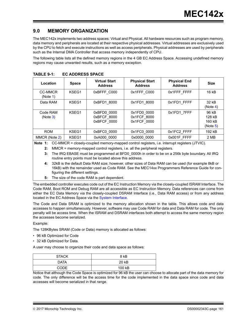
MEC142x
9.0 MEMORY ORGANIZATION
The MEC142x implements two address spaces: Virtual and Physical. All hardware resources such as program memory,data memory and peripherals are located at their respective physical addresses. Virtual addresses are exclusively usedby the CPU to fetch and execute instructions as well as access peripherals. Physical addresses are used by peripheralssuch as the Internal DMA Controller that access memory independently of CPU.
The following table lists all the defined memory regions in the 4 GB EC Address Space. Accessing undefined memoryregions may cause unwanted results, such as a memory exception.
The embedded controller executes code out of the EC Instruction Memory via the closely-coupled ISRAM Interface. TheCode RAM, Boot ROM and Debug RAM are all accessible as EC Instruction Memory. Data references can come fromeither the EC Data Memory via the closely-coupled DSRAM Interface (i.e., Data RAM access) or from any addresslocated in the EC Address Space via the System Interface.
The Code and Data SRAM is optimized to the memory allocation shown in the table. This allows code and dataaccesses to happen simultaneously. However, software may use Code RAM for data and Data RAM for code. The onlypenalty will be access time. When the ISRAM and DSRAM interfaces both attempt to access the same memory regionthe accesses become serialized.
Example:
The 128KBytes SRAM (Code or Data) memory is allocated as follows:
• 96 kB Optimized for Code
• 32 kB Optimized for Data.
A user may choose to organize their code and data space as follows:
Notice that although the Code Space is optimized for 96 kB the user can choose to allocate part of the data memory forcode. The only difference will be the access time for the code implemented in the data space since code and dataaccesses will become serialized in that range.
TABLE 9-1: EC ADDRESS SPACE
Location SpaceVirtual Start
AddressPhysical Start
AddressPhysical End
AddressSize
CC-MMCR (Note 1)
KSEG1 0xBFFF_C000 0x1FFF_C000 0x1FFF_FFFF 16 kB
Data RAM KSEG1 0xBFD1_8000 0x1FD1_8000 0x1FD1_FFFF 32 kB (Note 4)
Code RAM (Note 3)
KSEG1 0xBFD0_00000xBFCF_80000xBFCF_0000
0x1FD0_00000x1FCF_80000x1FCF_0000
0x1FD1_7FFF 96 kB128 kB160 kB(Note 5)
ROM KSEG1 0xBFC0_0000 0x1FC0_0000 0x1FC2_FFFF 192 kB
MMCR (Note 2) KSEG1 0xA000_0000 0x0000_0000 0x001F_FFFF 2 MB
Note 1: CC-MMCR = closely-coupled memory-mapped control registers, i.e. interrupt registers (JTVIC).
2: MMCR = memory-mapped control registers, i.e. all the peripheral registers.
3: The IRQ EBASE must be programmed at BFD0_0000h in order to be on a 256k byte boundary. All IRQ routine entry points must be located above this address.
4: 32kB is the default Data RAM size; however, other sizes of Data RAM can be used (for example 8kB or 16kB) with the remainder used as Code RAM. See the MEC14xx Programmers Reference Guide for con-figuring the different settings.
5: The size of the code RAM is part dependent.
STACK 8 kB
DATA 20 kB
CODE 100 kB
2017 Microchip Technology Inc. DS00002343C-page 161
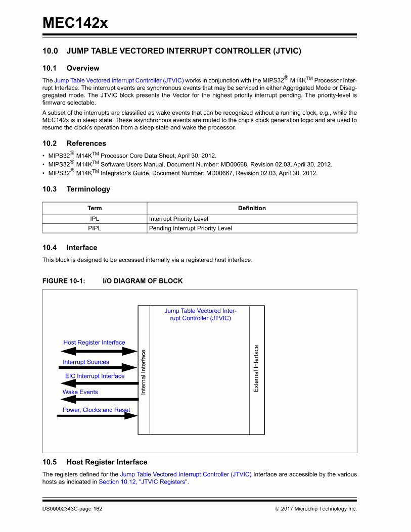
MEC142x
10.0 JUMP TABLE VECTORED INTERRUPT CONTROLLER (JTVIC)
10.1 Overview
The Jump Table Vectored Interrupt Controller (JTVIC) works in conjunction with the MIPS32 M14KTM Processor Inter-rupt Interface. The interrupt events are synchronous events that may be serviced in either Aggregated Mode or Disag-gregated mode. The JTVIC block presents the Vector for the highest priority interrupt pending. The priority-level isfirmware selectable.
A subset of the interrupts are classified as wake events that can be recognized without a running clock, e.g., while theMEC142x is in sleep state. These asynchronous events are routed to the chip’s clock generation logic and are used toresume the clock’s operation from a sleep state and wake the processor.
10.2 References
• MIPS32 M14KTM Processor Core Data Sheet, April 30, 2012.
• MIPS32 M14KTM Software Users Manual, Document Number: MD00668, Revision 02.03, April 30, 2012.
• MIPS32 M14KTM Integrator’s Guide, Document Number: MD00667, Revision 02.03, April 30, 2012.
10.3 Terminology
10.4 Interface
This block is designed to be accessed internally via a registered host interface.
10.5 Host Register Interface
The registers defined for the Jump Table Vectored Interrupt Controller (JTVIC) Interface are accessible by the varioushosts as indicated in Section 10.12, "JTVIC Registers".
Term Definition
IPL Interrupt Priority Level
PIPL Pending Interrupt Priority Level
FIGURE 10-1: I/O DIAGRAM OF BLOCK
Jump Table Vectored Inter-rupt Controller (JTVIC)
Power, Clocks and Reset
Host Register Interface
Interrupt Sources
EIC Interrupt Interface
Inte
rnal
Int
erfa
ce
Ext
erna
l In
terf
ace
Wake Events
DS00002343C-page 162 2017 Microchip Technology Inc.
MEC142x
10.6 Interrupt Sources
All the chip’s interrupt sources are routed to the Jump Table Vectored Interrupt Controller (JTVIC) GIRQx Source Reg-isters. The list of interrupt sources is defined in Table 10-2, “Interrupt Source, Enable Set, Enable Clear, and Result BitAssignments,” on page 167.
10.7 EIC Interrupt Interface
The Jump Table Vectored Interrupt Controller (JTVIC) is designed to generate interrupts to the Embedded Controller’sExternal Interrupt Controller (EIC) interface. This IP block aggregates all the chip’s interrupt Sources (defined inTable 10-2, “Interrupt Source, Enable Set, Enable Clear, and Result Bit Assignments,” on page 167), determines thehighest priority interrupt that is active, and generates the Offset Vector used to jump to the respective IRQ Handler.
10.7.1 EIC INTERRUPT SIGNALS
10.8 Wake Events
All interrupt sources that indicate they are wake-capable generate an asynchronous wake event to the chip’s sleep con-trol logic to restore the oscillator to the fully operational state. Wake-capable signals do not require the internal oscillatorto be running.
10.9 Power, Clocks and Reset
This section defines the Power, Clock, and Reset parameters of the block.
10.9.1 POWER
10.9.2 CLOCKS
Name Direction Description
Interrupt Request Output Signal to the processor that an interrupt request is pending
Vector_Address Output Offset appended to processor EBASE address to create pointer to IRQ handler.
Note: The processor EBASE must be programmed on a256k Byte boundary.
RIPL Output Requested Interrupt Priority Level.
Name Description
VTR The logic and registers implemented in this block are powered by this power well.
Name Description
48 MHz Ring Oscillator Clock used for register read/write access.
2017 Microchip Technology Inc. DS00002343C-page 163

MEC142x
10.9.3 RESETS
10.10 Low Power Modes
The JTVIC always operates in the lowest power state; gating its own clock when it is not required. The only time thisblock requires the 48 MHz Ring Oscillator is for register reads/writes and for propagating interrupt events to the embed-ded controller.
If the 48 MHz Ring Oscillator is off, the wake-capable interrupts may be used to resume operation thereby allowing theinterrupt events to propagate to the embedded controller.
10.11 Description
10.11.1 FEATURES
• Supports up to 1024 Interrupt Sources
• Aggregated and Disaggregated Modes of Operation
- Aggregated Mode offers a programmable Vector Offset per GIRQ
- Disaggregated Mode offers a programmable Vector Offset per Source Bit
• 4 levels of configurable priority
10.11.2 OVERVIEW
This module is a highly-configurable and expandable vectored interrupt controller which is designed to work with anMIPS M14k processor’s EIC (External Interrupt Controller) mode of interrupt operation, with direct vector addressing(i.e. direct address driven into the processor instead of an “interrupt vector number”). The controller supports four levelsof priority on a per-interrupt-source basis.
The controller operates in two different modes, aggregated and dis-aggregated (or mini-jump-table), on a grouped-IRQ(GIRQ) basis. NOTE: a GIRQ is a grouping of up to 32 interrupt sources.
Thus this controller can be configured as fully aggregated all the way to fully dis-aggregated, and everything in between.
In aggregated mode the controller stores ISR vector addresses in local registers, thus saving firmware from having tobuild ISR jump tables in local SRAM. One vector address per GIRQ.
In dis-aggregated/jump-table mode, the controller can selectively break apart individual GIRQ interrupt sources intoseparate vector addresses.
Name Description
VTR This signal resets all the registers and logic in this block to their default state.
DS00002343C-page 164 2017 Microchip Technology Inc.

MEC142x
10.11.3 WAKE-CAPABLE INTERRUPT EVENTS
Wake-capable interrupts are listed in Section 10.11.4, "List of Interrupt Events," on page 167 with a designation of ‘Yes’in the Wake Event column
All interrupts, except GIRQ22, generate an EC Interrupt event. They are routed to source bits that are synchronized tothe 48 MHz Ring Oscillator. If enabled, the Interrupt Result is fed into the Priority Encoder/Decision Logic, which gen-erates the interrupt vector to the EIC Interrupt Interface.
Some Interrupts, which are labeled Wake-Capable, are also routed as Wake Events to the Chip’s Wake Logic. Theseare asynchronous events that are used to resume the 48 MHz Ring Oscillator operation from a sleep state and wakethe processor.
FIGURE 10-2: TOP-LEVEL BLOCK DIAGRAM OF INTERRUPT GENERATION LOGIC
GIRQ # “n”
interrupt sources
32
Int src/result/enable
registers
GIRQ aggregator control, priority, and vector address
CPU read/write data bus
GIRQ # “n + 1”
Priority Encoder/decision logic and
EIC interface
requested interrupt priority level
interrupt vector address
requested shadow set
interrupt sources
CPU read/write data bus
Int src/result/enable
registers
GIRQ aggregator control, priority, and vector address
32
2017 Microchip Technology Inc. DS00002343C-page 165

MEC142x
10.11.3.1 GIRQ16 and GIRQ22 Wake-Only Events
GIRQ16 and GIRQ22 are reserved for Wake-Only events that do not require functional software service.
GIRQ16 will generate both a wake event and an interrupt vector to the EIC Interrupt Interface. This will require theembedded firmware to clear the interrupt status event and re-execute the sleep instruction. GIRQ16 is a legacy interruptused to ensure the 48 MHz Ring Oscillator remained on for the minimum time. This interrupt may be deprecated in futuredesigns
GIRQ22 does not generate an interrupt vector to the EIC Interrupt Interface. GIRQ22 only generates a wake event torestart the 48 MHz Ring Oscillator running. Hardware automatically wakes the oscillator to process the wake event,clears the event, and resumes sleeping without firmware intervention.
APPLICATION NOTE: Configuring Wake-Only Events
Wake-Only interrupt event should be enabled just before executing the EC sleep instruction. Firmware should executethe following sequence of events:
1. Set bits[2:0] in the System Sleep Control Register (SYS_SLP_CNTRL)
2. Enable Wake Events in either GIRQ16 or GIRQ22
3. Execute Sleep Instruction (_wait;)
FIGURE 10-3: INTERRUPT SOURCE, ENABLE, AND RESULT LOGIC
TABLE 10-1: WAKE-ONLY EVENTS
Wake Event Description
LPC_WAKE This bit is set when the LPC interface detects activity on the interface. It’s sole purpose is to restart the 48 MHz Ring Oscillator.
SMB_WAKE This bit is set when an I2C/SMBus interface detects a START event on the inter-face. It’s sole purpose is to restart the 48 MHz Ring Oscillator.
PS2_DATx_WAKE This bit is set when the PS/2 interface detects activity on it’s interface. It’s sole purpose is to restart the 48 MHz Ring Oscillator.
KSC_INT_WAKE This bit is set when the Keyboard Matrix Scan Controller detects activity on it’s interface. It’s sole purpose is to restart the 48 MHz Ring Oscillator.
DEBUG_DONE This bit is set when the ICSP debugger interface detects activity on the interface. It’s sole purpose is to notify the EC firmware that the 48 MHz Ring Oscillator was taken out of sleep state by the debug interface.
ESPI_WAKE This bit is set when the eSPI interface detects activity on the interface. It’s pur-pose is to restart the 48 MHz Ring Oscillator.
Note: The sleeping state of the chip is determined by bits[2:0] of the System Sleep Control Register (SYS-_SLP_CNTRL) on page 66.
Interrupt Event Interrupt Result
Clock
Interrupt Enable
Wake Event
Interrupt Source
DS00002343C-page 166 2017 Microchip Technology Inc.
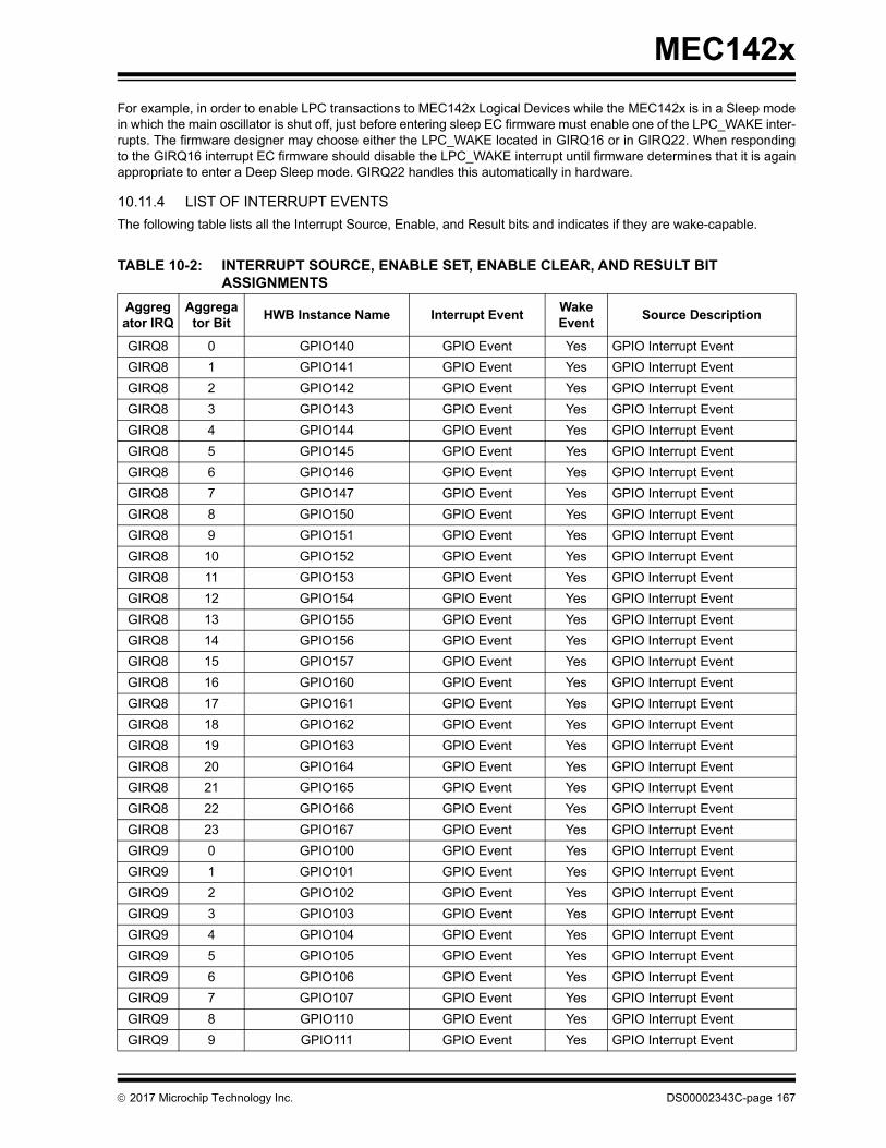
MEC142x
For example, in order to enable LPC transactions to MEC142x Logical Devices while the MEC142x is in a Sleep modein which the main oscillator is shut off, just before entering sleep EC firmware must enable one of the LPC_WAKE inter-rupts. The firmware designer may choose either the LPC_WAKE located in GIRQ16 or in GIRQ22. When respondingto the GIRQ16 interrupt EC firmware should disable the LPC_WAKE interrupt until firmware determines that it is againappropriate to enter a Deep Sleep mode. GIRQ22 handles this automatically in hardware.
10.11.4 LIST OF INTERRUPT EVENTS
The following table lists all the Interrupt Source, Enable, and Result bits and indicates if they are wake-capable.
TABLE 10-2: INTERRUPT SOURCE, ENABLE SET, ENABLE CLEAR, AND RESULT BIT ASSIGNMENTS
Aggregator IRQ
Aggregator Bit
HWB Instance Name Interrupt EventWake Event
Source Description
GIRQ8 0 GPIO140 GPIO Event Yes GPIO Interrupt Event
GIRQ8 1 GPIO141 GPIO Event Yes GPIO Interrupt Event
GIRQ8 2 GPIO142 GPIO Event Yes GPIO Interrupt Event
GIRQ8 3 GPIO143 GPIO Event Yes GPIO Interrupt Event
GIRQ8 4 GPIO144 GPIO Event Yes GPIO Interrupt Event
GIRQ8 5 GPIO145 GPIO Event Yes GPIO Interrupt Event
GIRQ8 6 GPIO146 GPIO Event Yes GPIO Interrupt Event
GIRQ8 7 GPIO147 GPIO Event Yes GPIO Interrupt Event
GIRQ8 8 GPIO150 GPIO Event Yes GPIO Interrupt Event
GIRQ8 9 GPIO151 GPIO Event Yes GPIO Interrupt Event
GIRQ8 10 GPIO152 GPIO Event Yes GPIO Interrupt Event
GIRQ8 11 GPIO153 GPIO Event Yes GPIO Interrupt Event
GIRQ8 12 GPIO154 GPIO Event Yes GPIO Interrupt Event
GIRQ8 13 GPIO155 GPIO Event Yes GPIO Interrupt Event
GIRQ8 14 GPIO156 GPIO Event Yes GPIO Interrupt Event
GIRQ8 15 GPIO157 GPIO Event Yes GPIO Interrupt Event
GIRQ8 16 GPIO160 GPIO Event Yes GPIO Interrupt Event
GIRQ8 17 GPIO161 GPIO Event Yes GPIO Interrupt Event
GIRQ8 18 GPIO162 GPIO Event Yes GPIO Interrupt Event
GIRQ8 19 GPIO163 GPIO Event Yes GPIO Interrupt Event
GIRQ8 20 GPIO164 GPIO Event Yes GPIO Interrupt Event
GIRQ8 21 GPIO165 GPIO Event Yes GPIO Interrupt Event
GIRQ8 22 GPIO166 GPIO Event Yes GPIO Interrupt Event
GIRQ8 23 GPIO167 GPIO Event Yes GPIO Interrupt Event
GIRQ9 0 GPIO100 GPIO Event Yes GPIO Interrupt Event
GIRQ9 1 GPIO101 GPIO Event Yes GPIO Interrupt Event
GIRQ9 2 GPIO102 GPIO Event Yes GPIO Interrupt Event
GIRQ9 3 GPIO103 GPIO Event Yes GPIO Interrupt Event
GIRQ9 4 GPIO104 GPIO Event Yes GPIO Interrupt Event
GIRQ9 5 GPIO105 GPIO Event Yes GPIO Interrupt Event
GIRQ9 6 GPIO106 GPIO Event Yes GPIO Interrupt Event
GIRQ9 7 GPIO107 GPIO Event Yes GPIO Interrupt Event
GIRQ9 8 GPIO110 GPIO Event Yes GPIO Interrupt Event
GIRQ9 9 GPIO111 GPIO Event Yes GPIO Interrupt Event
2017 Microchip Technology Inc. DS00002343C-page 167
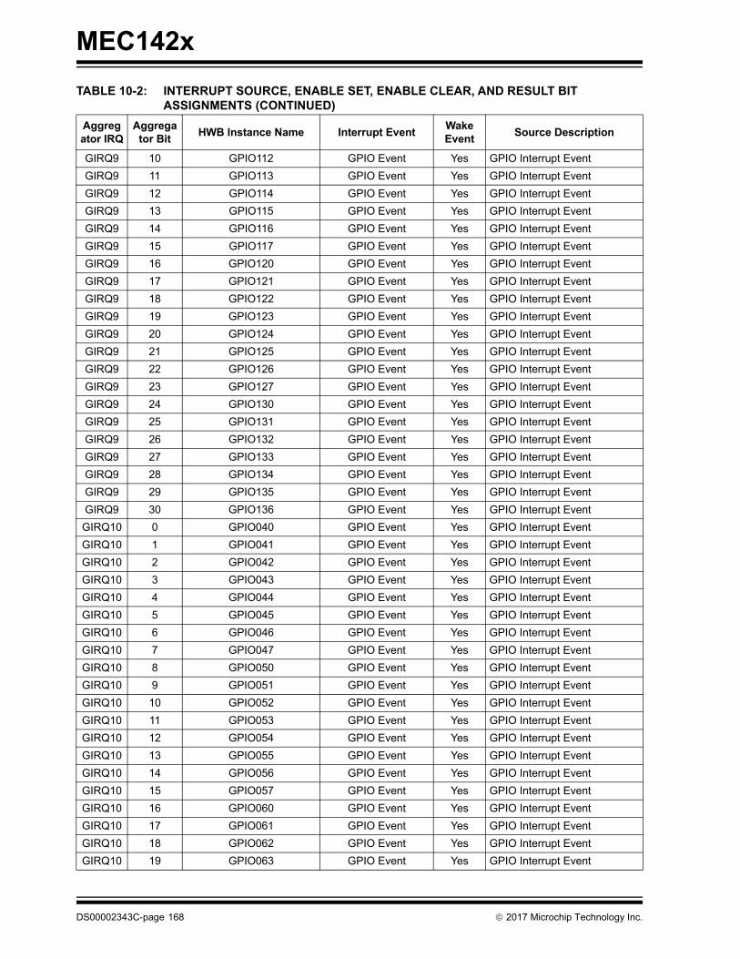
MEC142x
GIRQ9 10 GPIO112 GPIO Event Yes GPIO Interrupt Event
GIRQ9 11 GPIO113 GPIO Event Yes GPIO Interrupt Event
GIRQ9 12 GPIO114 GPIO Event Yes GPIO Interrupt Event
GIRQ9 13 GPIO115 GPIO Event Yes GPIO Interrupt Event
GIRQ9 14 GPIO116 GPIO Event Yes GPIO Interrupt Event
GIRQ9 15 GPIO117 GPIO Event Yes GPIO Interrupt Event
GIRQ9 16 GPIO120 GPIO Event Yes GPIO Interrupt Event
GIRQ9 17 GPIO121 GPIO Event Yes GPIO Interrupt Event
GIRQ9 18 GPIO122 GPIO Event Yes GPIO Interrupt Event
GIRQ9 19 GPIO123 GPIO Event Yes GPIO Interrupt Event
GIRQ9 20 GPIO124 GPIO Event Yes GPIO Interrupt Event
GIRQ9 21 GPIO125 GPIO Event Yes GPIO Interrupt Event
GIRQ9 22 GPIO126 GPIO Event Yes GPIO Interrupt Event
GIRQ9 23 GPIO127 GPIO Event Yes GPIO Interrupt Event
GIRQ9 24 GPIO130 GPIO Event Yes GPIO Interrupt Event
GIRQ9 25 GPIO131 GPIO Event Yes GPIO Interrupt Event
GIRQ9 26 GPIO132 GPIO Event Yes GPIO Interrupt Event
GIRQ9 27 GPIO133 GPIO Event Yes GPIO Interrupt Event
GIRQ9 28 GPIO134 GPIO Event Yes GPIO Interrupt Event
GIRQ9 29 GPIO135 GPIO Event Yes GPIO Interrupt Event
GIRQ9 30 GPIO136 GPIO Event Yes GPIO Interrupt Event
GIRQ10 0 GPIO040 GPIO Event Yes GPIO Interrupt Event
GIRQ10 1 GPIO041 GPIO Event Yes GPIO Interrupt Event
GIRQ10 2 GPIO042 GPIO Event Yes GPIO Interrupt Event
GIRQ10 3 GPIO043 GPIO Event Yes GPIO Interrupt Event
GIRQ10 4 GPIO044 GPIO Event Yes GPIO Interrupt Event
GIRQ10 5 GPIO045 GPIO Event Yes GPIO Interrupt Event
GIRQ10 6 GPIO046 GPIO Event Yes GPIO Interrupt Event
GIRQ10 7 GPIO047 GPIO Event Yes GPIO Interrupt Event
GIRQ10 8 GPIO050 GPIO Event Yes GPIO Interrupt Event
GIRQ10 9 GPIO051 GPIO Event Yes GPIO Interrupt Event
GIRQ10 10 GPIO052 GPIO Event Yes GPIO Interrupt Event
GIRQ10 11 GPIO053 GPIO Event Yes GPIO Interrupt Event
GIRQ10 12 GPIO054 GPIO Event Yes GPIO Interrupt Event
GIRQ10 13 GPIO055 GPIO Event Yes GPIO Interrupt Event
GIRQ10 14 GPIO056 GPIO Event Yes GPIO Interrupt Event
GIRQ10 15 GPIO057 GPIO Event Yes GPIO Interrupt Event
GIRQ10 16 GPIO060 GPIO Event Yes GPIO Interrupt Event
GIRQ10 17 GPIO061 GPIO Event Yes GPIO Interrupt Event
GIRQ10 18 GPIO062 GPIO Event Yes GPIO Interrupt Event
GIRQ10 19 GPIO063 GPIO Event Yes GPIO Interrupt Event
TABLE 10-2: INTERRUPT SOURCE, ENABLE SET, ENABLE CLEAR, AND RESULT BIT ASSIGNMENTS (CONTINUED)
Aggregator IRQ
Aggregator Bit
HWB Instance Name Interrupt EventWake Event
Source Description
DS00002343C-page 168 2017 Microchip Technology Inc.

MEC142x
GIRQ10 20 GPIO064 GPIO Event Yes GPIO Interrupt Event
GIRQ10 21-22 Test Test - -
GIRQ10 23 GPIO067 GPIO Event Yes GPIO Interrupt Event
GIRQ11 1 GPIO001 GPIO Event Yes GPIO Interrupt Event
GIRQ11 2 GPIO002 GPIO Event Yes GPIO Interrupt Event
GIRQ11 3 GPIO003 GPIO Event Yes GPIO Interrupt Event
GIRQ11 4 GPIO004 GPIO Event Yes GPIO Interrupt Event
GIRQ11 5 GPIO005 GPIO Event Yes GPIO Interrupt Event
GIRQ11 6 GPIO006 GPIO Event Yes GPIO Interrupt Event
GIRQ11 7 GPIO007 GPIO Event Yes GPIO Interrupt Event
GIRQ11 8 GPIO010 GPIO Event Yes GPIO Interrupt Event
GIRQ11 9 GPIO011 GPIO Event Yes GPIO Interrupt Event
GIRQ11 10 GPIO012 GPIO Event Yes GPIO Interrupt Event
GIRQ11 11 GPIO013 GPIO Event Yes GPIO Interrupt Event
GIRQ11 12 GPIO014 GPIO Event Yes GPIO Interrupt Event
GIRQ11 13 GPIO015 GPIO Event Yes GPIO Interrupt Event
GIRQ11 14 GPIO016 GPIO Event Yes GPIO Interrupt Event
GIRQ11 15 GPIO017 GPIO Event Yes GPIO Interrupt Event
GIRQ11 16 GPIO020 GPIO Event Yes GPIO Interrupt Event
GIRQ11 17 GPIO021 GPIO Event Yes GPIO Interrupt Event
GIRQ11 18 GPIO022 GPIO Event Yes GPIO Interrupt Event
GIRQ11 19 GPIO023 GPIO Event Yes GPIO Interrupt Event
GIRQ11 20 GPIO024 GPIO Event Yes GPIO Interrupt Event
GIRQ11 21 GPIO025 GPIO Event Yes GPIO Interrupt Event
GIRQ11 22 GPIO026 GPIO Event Yes GPIO Interrupt Event
GIRQ11 23 GPIO027 GPIO Event Yes GPIO Interrupt Event
GIRQ11 24 GPIO030 GPIO Event Yes GPIO Interrupt Event
GIRQ11 25 GPIO031 GPIO Event Yes GPIO Interrupt Event
GIRQ11 26 GPIO032 GPIO Event Yes GPIO Interrupt Event
GIRQ11 27 GPIO033 GPIO Event Yes GPIO Interrupt Event
GIRQ11 28 GPIO034 GPIO Event Yes GPIO Interrupt Event
GIRQ11 29 GPIO035 GPIO Event Yes GPIO Interrupt Event
GIRQ11 30 GPIO036 GPIO Event Yes GPIO Interrupt Event
GIRQ12 0 SMBus Controller 0 SMB No SMBus Controller 0 Interrupt Event
GIRQ12 1 SMBus Controller 1 SMB No SMBus Controller 1 Interrupt Event
GIRQ12 2 SMBus Controller 2 SMB No SMBus Controller 2 Interrupt Event
GIRQ12 3 SMBus Controller 3 SMB No SMBus Controller 3 Interrupt Event
GIRQ12 4 SMBus Controller 4 SMB No SMBus Controller 4 Interrupt Event
TABLE 10-2: INTERRUPT SOURCE, ENABLE SET, ENABLE CLEAR, AND RESULT BIT ASSIGNMENTS (CONTINUED)
Aggregator IRQ
Aggregator Bit
HWB Instance Name Interrupt EventWake Event
Source Description
2017 Microchip Technology Inc. DS00002343C-page 169

MEC142x
GIRQ13 0 DMA Controller DMA0 No DMA Controller - Channel 0 Interrupt Event
GIRQ13 1 DMA Controller DMA1 No DMA Controller - Channel 1 Interrupt Event
GIRQ13 2 DMA Controller DMA2 No DMA Controller - Channel 2 Interrupt Event
GIRQ13 3 DMA Controller DMA3 No DMA Controller - Channel 3 Interrupt Event
GIRQ13 4 DMA Controller DMA4 No DMA Controller - Channel 4 Interrupt Event
GIRQ13 5 DMA Controller DMA5 No DMA Controller - Channel 5 Interrupt Event
GIRQ13 6 DMA Controller DMA6 No DMA Controller - Channel 6 Interrupt Event
GIRQ13 7 DMA Controller DMA7 No DMA Controller - Channel 7 Interrupt Event
GIRQ13 8 DMA Controller DMA8 No DMA Controller - Channel 8 Interrupt Event
GIRQ13 9 DMA Controller DMA9 No DMA Controller - Channel 9 Interrupt Event
GIRQ13 10 DMA Controller DMA10 No DMA Controller - Channel 10 Interrupt Event
GIRQ14 0 LPC Interface LPC_INTER-NAL_ERR
No LPC Internal Error Event
GIRQ14 1 Power, Clocks, and Resets PFR_Status No Power-Fail and Reset Status Register Events
GIRQ14 2 Blinking/Breathing LED 0 PWM_WDT No Blinking/Breathing LED 0 - Watchdog Event
GIRQ14 3 Blinking/Breathing LED 1 PWM_WDT No Blinking/Breathing LED 1 - Watchdog Event
GIRQ14 4 Blinking/Breathing LED 2 PWM_WDT No Blinking/Breathing LED 2 - Watchdog Event
GIRQ14 5 Internal 32KHz INT_32K_RDY No Internal 32 KHz oscillator ready flag
GIRQ15 0 Mailbox Register Interface MBX Host-to-EC No Mailbox Register Interface - Host-to-EC Interrupt Event
GIRQ15 1 Reserved Reserved - -
GIRQ15 2 EMI 0 Host-to-EC No Embedded Memory Interface 0 - Host-to-EC Interrupt Event
GIRQ15 3 Reserved Reserved - -
GIRQ15 4 8042 Emulated Keyboard Controller
OBF No 8042 Emulated Keyboard Con-troller - Output Buffer Full Event
GIRQ15 5 8042 Emulated Keyboard Controller
IBF No 8042 Emulated Keyboard Con-troller - Input Buffer Full Event
GIRQ15 6 Port 80 BIOS Debug Port 0 BDP_INT No Port 80h BIOS Debug Port Event
TABLE 10-2: INTERRUPT SOURCE, ENABLE SET, ENABLE CLEAR, AND RESULT BIT ASSIGNMENTS (CONTINUED)
Aggregator IRQ
Aggregator Bit
HWB Instance Name Interrupt EventWake Event
Source Description
DS00002343C-page 170 2017 Microchip Technology Inc.
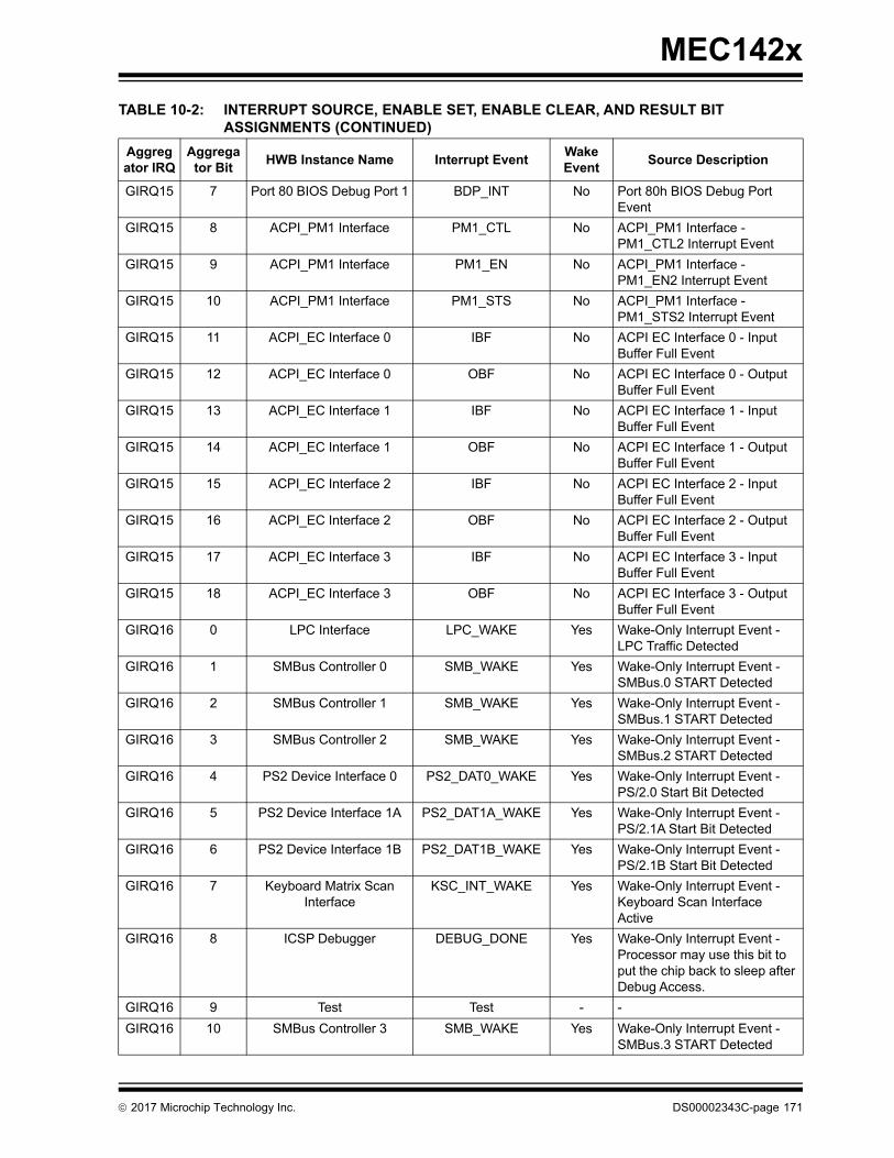
MEC142x
GIRQ15 7 Port 80 BIOS Debug Port 1 BDP_INT No Port 80h BIOS Debug Port Event
GIRQ15 8 ACPI_PM1 Interface PM1_CTL No ACPI_PM1 Interface - PM1_CTL2 Interrupt Event
GIRQ15 9 ACPI_PM1 Interface PM1_EN No ACPI_PM1 Interface - PM1_EN2 Interrupt Event
GIRQ15 10 ACPI_PM1 Interface PM1_STS No ACPI_PM1 Interface - PM1_STS2 Interrupt Event
GIRQ15 11 ACPI_EC Interface 0 IBF No ACPI EC Interface 0 - Input Buffer Full Event
GIRQ15 12 ACPI_EC Interface 0 OBF No ACPI EC Interface 0 - Output Buffer Full Event
GIRQ15 13 ACPI_EC Interface 1 IBF No ACPI EC Interface 1 - Input Buffer Full Event
GIRQ15 14 ACPI_EC Interface 1 OBF No ACPI EC Interface 1 - Output Buffer Full Event
GIRQ15 15 ACPI_EC Interface 2 IBF No ACPI EC Interface 2 - Input Buffer Full Event
GIRQ15 16 ACPI_EC Interface 2 OBF No ACPI EC Interface 2 - Output Buffer Full Event
GIRQ15 17 ACPI_EC Interface 3 IBF No ACPI EC Interface 3 - Input Buffer Full Event
GIRQ15 18 ACPI_EC Interface 3 OBF No ACPI EC Interface 3 - Output Buffer Full Event
GIRQ16 0 LPC Interface LPC_WAKE Yes Wake-Only Interrupt Event - LPC Traffic Detected
GIRQ16 1 SMBus Controller 0 SMB_WAKE Yes Wake-Only Interrupt Event - SMBus.0 START Detected
GIRQ16 2 SMBus Controller 1 SMB_WAKE Yes Wake-Only Interrupt Event - SMBus.1 START Detected
GIRQ16 3 SMBus Controller 2 SMB_WAKE Yes Wake-Only Interrupt Event - SMBus.2 START Detected
GIRQ16 4 PS2 Device Interface 0 PS2_DAT0_WAKE Yes Wake-Only Interrupt Event - PS/2.0 Start Bit Detected
GIRQ16 5 PS2 Device Interface 1A PS2_DAT1A_WAKE Yes Wake-Only Interrupt Event - PS/2.1A Start Bit Detected
GIRQ16 6 PS2 Device Interface 1B PS2_DAT1B_WAKE Yes Wake-Only Interrupt Event - PS/2.1B Start Bit Detected
GIRQ16 7 Keyboard Matrix Scan Interface
KSC_INT_WAKE Yes Wake-Only Interrupt Event - Keyboard Scan Interface Active
GIRQ16 8 ICSP Debugger DEBUG_DONE Yes Wake-Only Interrupt Event - Processor may use this bit to put the chip back to sleep after Debug Access.
GIRQ16 9 Test Test - -
GIRQ16 10 SMBus Controller 3 SMB_WAKE Yes Wake-Only Interrupt Event - SMBus.3 START Detected
TABLE 10-2: INTERRUPT SOURCE, ENABLE SET, ENABLE CLEAR, AND RESULT BIT ASSIGNMENTS (CONTINUED)
Aggregator IRQ
Aggregator Bit
HWB Instance Name Interrupt EventWake Event
Source Description
2017 Microchip Technology Inc. DS00002343C-page 171
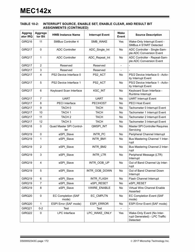
MEC142x
GIRQ16 11 SMBus Controller 4 SMB_WAKE Yes Wake-Only Interrupt Event - SMBus.4 START Detected
GIRQ17 0 ADC Controller ADC_Single_Int No ADC Controller - Single-Sam-ple ADC Conversion Event
GIRQ17 1 ADC Controller ADC_Repeat_Int No ADC Controller - Repeat-Sam-ple ADC Conversion Event
GIRQ17 2 Reserved Reserved - -
GIRQ17 3 Reserved Reserved - -
GIRQ17 4 PS2 Device Interface 0 PS2_ACT No PS/2 Device Interface 0 - Activ-ity Interrupt Event
GIRQ17 5 PS2 Device Interface 1 PS2_ACT No PS/2 Device Interface 1 - Activ-ity Interrupt Event
GIRQ17 6 Keyboard Scan Interface KSC_INT No Keyboard Scan Interface - Runtime Interrupt
GIRQ17 7 UART UART No UART Interrupt Event
GIRQ17 8 PECI Interface PECIHOST No PECI Host Event
GIRQ17 9 TACH 0 TACH No Tachometer 0 Interrupt Event
GIRQ17 10 TACH 1 TACH No Tachometer 1 Interrupt Event
GIRQ17 11 TACH 2 TACH No Tachometer 2 Interrupt Event
GIRQ17 12 TACH 3 TACH No Tachometer 3 Interrupt Event
GIRQ18 0 Quad Master SPI Control-ler
QMSPI_INT No Master SPI Controller Requires Servicing
GIRQ19 0 eSPI_Slave INTR_PC No Peripheral Channel Interrupt
GIRQ19 1 eSPI_Slave INTR_BM1 No Bus Mastering Channel 1 Inter-rupt
GIRQ19 2 eSPI_Slave INTR_BM2 No Bus Mastering Channel 2 Inter-rupt
GIRQ19 3 eSPI_Slave INTR_LTR No Peripheral Message (LTR) Interrupt
GIRQ19 4 eSPI_Slave INTR_OOB_UP No Out of Band Channel Up Inter-rupt
GIRQ19 5 eSPI_Slave INTR_OOB_DOWN No Out of Band Channel Down Interrupt
GIRQ19 6 eSPI_Slave INTR_FLASH No Flash Channel Interrupt
GIRQ19 7 eSPI_Slave eSPI_RESET No eSPI_RESET
GIRQ19 8 eSPI_Slave VWIRE_ENABLE No Virtual Wire Channel Enable Asserted
GIRQ20 0 EC Completion (SAF mode)
EC_CMPLTN No EC Completion Event (SAF mode)
GIRQ20 1 ESPI Error (SAF mode) ESPI_ERROR No ESPI Error Event (SAF mode)
GIRQ21 0-2 Test Test - -
GIRQ22 0 LPC Interface LPC_WAKE_ONLY Yes Wake-Only Event (No Inter-rupt Generated) - LPC Traffic Detected
TABLE 10-2: INTERRUPT SOURCE, ENABLE SET, ENABLE CLEAR, AND RESULT BIT ASSIGNMENTS (CONTINUED)
Aggregator IRQ
Aggregator Bit
HWB Instance Name Interrupt EventWake Event
Source Description
DS00002343C-page 172 2017 Microchip Technology Inc.

MEC142x
GIRQ22 1 SMBus Controller 0 SMB_WAKE_ONLY Yes Wake-Only Event (No Inter-rupt Generated) - SMBus.0 START Detected
GIRQ22 2 SMBus Controller 1 SMB_WAKE_ONLY Yes Wake-Only Event (No Inter-rupt Generated) - SMBus.1 START Detected
GIRQ22 3 SMBus Controller 2 SMB_WAKE_ONLY Yes Wake-Only Event (No Inter-rupt Generated) - SMBus.2 START Detected
GIRQ22 4 PS2 Device Interface 0 PS2_-DAT0_WAKE_ONLY
Yes Wake-Only Event (No Inter-rupt Generated) - PS/2.0 Start Bit Detected
GIRQ22 5 PS2 Device Interface 1A PS2_-DAT1A_WAKE_ONL
Y
Yes Wake-Only Event (No Inter-rupt Generated) - PS/2.1A Start Bit Detected
GIRQ22 6 PS2 Device Interface 1B PS2_-DAT1B_WAKE_ONL
Y
Yes Wake-Only Event (No Inter-rupt Generated) - PS/2.1B Start Bit Detected
GIRQ22 7 Keyboard Matrix Scan Interface
KSC_INT_WAKE_ONLY
Yes Wake-Only Event (No Inter-rupt Generated) - Keyboard Scan Interface Active
GIRQ22 8 ICSP Debugger DEBUG_-DONE_WAKE_ONLY
Yes Wake-Only Event (No Inter-rupt Generated) - Processor may use this bit to put the chip back to sleep after Debug Access.
GIRQ22 9 ESPI Interface ESPI_WAKE_ONLY Yes Wake-Only Event (No Inter-rupt Generated) - ESPI Traffic Detected
GIRQ22 10 SMBus Controller 3 SMB_WAKE_ONLY Yes Wake-Only Event (No Inter-rupt Generated) - SMBus.3 START Detected
GIRQ22 11 SMBus Controller 4 SMB_WAKE_ONLY Yes Wake-Only Event (No Inter-rupt Generated) - SMBus.4 START Detected
GIRQ23 0 16-Bit - Basic Timer 0 Timer_Event No Basic Timer Event
GIRQ23 1 16-Bit - Basic Timer 1 Timer_Event No Basic Timer Event
GIRQ23 2 16-Bit - Basic Timer 2 Timer_Event No Basic Timer Event
GIRQ23 3 16-Bit - Basic Timer 3 Timer_Event No Basic Timer Event
GIRQ23 4 RTOS Timer RTOS_TIMER Yes 32-bit RTOS Timer Event
GIRQ23 5 Hibernation Timer HTIMER Yes Hibernation Timer Event
GIRQ23 6 Week Alarm WEEK_ALARM_INT Yes Week Alarm Interrupt.
GIRQ23 7 Week Alarm SUB-_WEEK_ALARM_INT
Yes Sub-Week Alarm Interrupt
GIRQ23 8 Week Alarm ONE_SECOND Yes Week Alarm - One Second Interrupt
GIRQ23 9 Week Alarm SUB_SECOND Yes Week Alarm - Sub-second Interrupt
TABLE 10-2: INTERRUPT SOURCE, ENABLE SET, ENABLE CLEAR, AND RESULT BIT ASSIGNMENTS (CONTINUED)
Aggregator IRQ
Aggregator Bit
HWB Instance Name Interrupt EventWake Event
Source Description
2017 Microchip Technology Inc. DS00002343C-page 173

MEC142x
GIRQ23 10 Week Alarm SYSPWR_PRES Yes System Power Present Pin Interrupt
GIRQ23 11 VBAT-Powered Control Interface
VCI_OVRD_IN Yes VCI_OVRD_IN Active-high Input Pin Interrupt
GIRQ23 12 VBAT-Powered Control Interface
VCI_IN0 Yes VCI_IN0 Active-low Input Pin Interrupt
GIRQ23 13 VBAT-Powered Control Interface
VCI_IN1 Yes VCI_IN1 Active-low Input Pin Interrupt
GIRQ23 14 Reserved Reserved - -
GIRQ23 15 Reserved Reserved - -
GIRQ24 0 MIPS M14K Core Timer Interrupt No Core Timer Interrupt
GIRQ24 1 MIPS M14K Software Interrupt 0 No Software Interrupt 0
GIRQ24 2 MIPS M14K Software Interrupt 1 No Software Interrupt 1
GIRQ24 3 RTOS Timer RTOS_TIMER Yes 32-bit RTOS Timer Event
GIRQ25 0 eSPI_Slave MSVW00_SRC0 Yes Master-to-Slave Virtual Wire Interrupt Event
GIRQ25 1 eSPI_Slave MSVW00_SRC1 Yes Master-to-Slave Virtual Wire Interrupt Event
GIRQ25 2 eSPI_Slave MSVW00_SRC2 Yes Master-to-Slave Virtual Wire Interrupt Event
GIRQ25 3 eSPI_Slave MSVW00_SRC3 Yes Master-to-Slave Virtual Wire Interrupt Event
GIRQ25 4 eSPI_Slave MSVW01_SRC0 Yes Master-to-Slave Virtual Wire Interrupt Event
GIRQ25 5 eSPI_Slave MSVW01_SRC1 Yes Master-to-Slave Virtual Wire Interrupt Event
GIRQ25 6 eSPI_Slave MSVW01_SRC2 Yes Master-to-Slave Virtual Wire Interrupt Event
GIRQ25 7 eSPI_Slave MSVW01_SRC3 Yes Master-to-Slave Virtual Wire Interrupt Event
GIRQ25 8 eSPI_Slave MSVW02_SRC0 Yes Master-to-Slave Virtual Wire Interrupt Event
GIRQ25 9 eSPI_Slave MSVW02_SRC1 Yes Master-to-Slave Virtual Wire Interrupt Event
GIRQ25 10 eSPI_Slave MSVW02_SRC2 Yes Master-to-Slave Virtual Wire Interrupt Event
GIRQ25 11 eSPI_Slave MSVW02_SRC3 Yes Master-to-Slave Virtual Wire Interrupt Event
GIRQ25 12 eSPI_Slave MSVW03_SRC0 Yes Master-to-Slave Virtual Wire Interrupt Event
GIRQ25 13 eSPI_Slave MSVW03_SRC1 Yes Master-to-Slave Virtual Wire Interrupt Event
GIRQ25 14 eSPI_Slave MSVW03_SRC2 Yes Master-to-Slave Virtual Wire Interrupt Event
GIRQ25 15 eSPI_Slave MSVW03_SRC3 Yes Master-to-Slave Virtual Wire Interrupt Event
TABLE 10-2: INTERRUPT SOURCE, ENABLE SET, ENABLE CLEAR, AND RESULT BIT ASSIGNMENTS (CONTINUED)
Aggregator IRQ
Aggregator Bit
HWB Instance Name Interrupt EventWake Event
Source Description
DS00002343C-page 174 2017 Microchip Technology Inc.

MEC142x
GIRQ25 16 eSPI_Slave MSVW04_SRC0 Yes Master-to-Slave Virtual Wire Interrupt Event
GIRQ25 17 eSPI_Slave MSVW04_SRC1 Yes Master-to-Slave Virtual Wire Interrupt Event
GIRQ25 18 eSPI_Slave MSVW04_SRC2 Yes Master-to-Slave Virtual Wire Interrupt Event
GIRQ25 19 eSPI_Slave MSVW04_SRC3 Yes Master-to-Slave Virtual Wire Interrupt Event
GIRQ25 20 eSPI_Slave MSVW05_SRC0 Yes Master-to-Slave Virtual Wire Interrupt Event
GIRQ25 21 eSPI_Slave MSVW05_SRC1 Yes Master-to-Slave Virtual Wire Interrupt Event
GIRQ25 22 eSPI_Slave MSVW05_SRC2 Yes Master-to-Slave Virtual Wire Interrupt Event
GIRQ25 23 eSPI_Slave MSVW05_SRC3 Yes Master-to-Slave Virtual Wire Interrupt Event
GIRQ25 24 eSPI_Slave MSVW06_SRC0 Yes Master-to-Slave Virtual Wire Interrupt Event
GIRQ25 25 eSPI_Slave MSVW06_SRC1 Yes Master-to-Slave Virtual Wire Interrupt Event
GIRQ25 26 eSPI_Slave MSVW06_SRC2 Yes Master-to-Slave Virtual Wire Interrupt Event
GIRQ25 27 eSPI_Slave MSVW06_SRC3 Yes Master-to-Slave Virtual Wire Interrupt Event
GIRQ26 0 eSPI_Slave MSVW07_SRC0 Yes Master-to-Slave Virtual Wire Interrupt Event
GIRQ26 1 eSPI_Slave MSVW07_SRC1 Yes Master-to-Slave Virtual Wire Interrupt Event
GIRQ26 2 eSPI_Slave MSVW07_SRC2 Yes Master-to-Slave Virtual Wire Interrupt Event
GIRQ26 3 eSPI_Slave MSVW07_SRC3 Yes Master-to-Slave Virtual Wire Interrupt Event
GIRQ26 4 eSPI_Slave MSVW08_SRC0 Yes Master-to-Slave Virtual Wire Interrupt Event
GIRQ26 5 eSPI_Slave MSVW08_SRC1 Yes Master-to-Slave Virtual Wire Interrupt Event
GIRQ26 6 eSPI_Slave MSVW08_SRC2 Yes Master-to-Slave Virtual Wire Interrupt Event
GIRQ26 7 eSPI_Slave MSVW08_SRC3 Yes Master-to-Slave Virtual Wire Interrupt Event
GIRQ26 8 eSPI_Slave MSVW09_SRC0 Yes Master-to-Slave Virtual Wire Interrupt Event
GIRQ26 9 eSPI_Slave MSVW09_SRC1 Yes Master-to-Slave Virtual Wire Interrupt Event
GIRQ26 10 eSPI_Slave MSVW09_SRC2 Yes Master-to-Slave Virtual Wire Interrupt Event
GIRQ26 11 eSPI_Slave MSVW09_SRC3 Yes Master-to-Slave Virtual Wire Interrupt Event
TABLE 10-2: INTERRUPT SOURCE, ENABLE SET, ENABLE CLEAR, AND RESULT BIT ASSIGNMENTS (CONTINUED)
Aggregator IRQ
Aggregator Bit
HWB Instance Name Interrupt EventWake Event
Source Description
2017 Microchip Technology Inc. DS00002343C-page 175
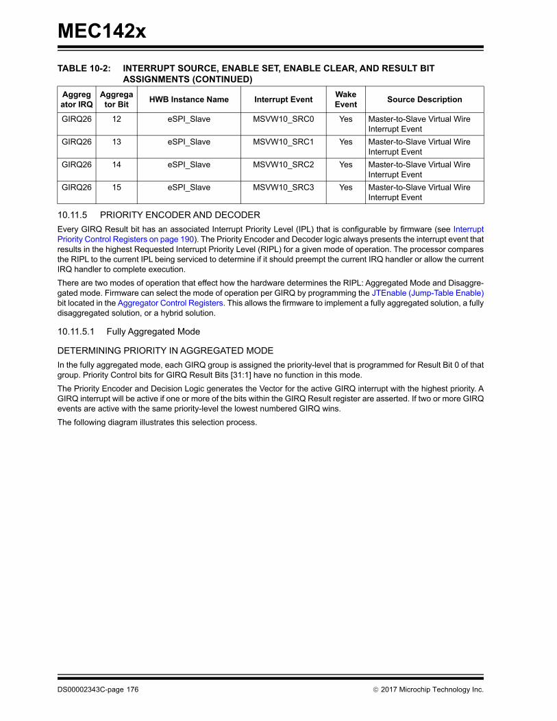
MEC142x
10.11.5 PRIORITY ENCODER AND DECODER
Every GIRQ Result bit has an associated Interrupt Priority Level (IPL) that is configurable by firmware (see InterruptPriority Control Registers on page 190). The Priority Encoder and Decoder logic always presents the interrupt event thatresults in the highest Requested Interrupt Priority Level (RIPL) for a given mode of operation. The processor comparesthe RIPL to the current IPL being serviced to determine if it should preempt the current IRQ handler or allow the currentIRQ handler to complete execution.
There are two modes of operation that effect how the hardware determines the RIPL: Aggregated Mode and Disaggre-gated mode. Firmware can select the mode of operation per GIRQ by programming the JTEnable (Jump-Table Enable)bit located in the Aggregator Control Registers. This allows the firmware to implement a fully aggregated solution, a fullydisaggregated solution, or a hybrid solution.
10.11.5.1 Fully Aggregated Mode
DETERMINING PRIORITY IN AGGREGATED MODE
In the fully aggregated mode, each GIRQ group is assigned the priority-level that is programmed for Result Bit 0 of thatgroup. Priority Control bits for GIRQ Result Bits [31:1] have no function in this mode.
The Priority Encoder and Decision Logic generates the Vector for the active GIRQ interrupt with the highest priority. AGIRQ interrupt will be active if one or more of the bits within the GIRQ Result register are asserted. If two or more GIRQevents are active with the same priority-level the lowest numbered GIRQ wins.
The following diagram illustrates this selection process.
GIRQ26 12 eSPI_Slave MSVW10_SRC0 Yes Master-to-Slave Virtual Wire Interrupt Event
GIRQ26 13 eSPI_Slave MSVW10_SRC1 Yes Master-to-Slave Virtual Wire Interrupt Event
GIRQ26 14 eSPI_Slave MSVW10_SRC2 Yes Master-to-Slave Virtual Wire Interrupt Event
GIRQ26 15 eSPI_Slave MSVW10_SRC3 Yes Master-to-Slave Virtual Wire Interrupt Event
TABLE 10-2: INTERRUPT SOURCE, ENABLE SET, ENABLE CLEAR, AND RESULT BIT ASSIGNMENTS (CONTINUED)
Aggregator IRQ
Aggregator Bit
HWB Instance Name Interrupt EventWake Event
Source Description
DS00002343C-page 176 2017 Microchip Technology Inc.

MEC142x
STEPS TO SET UP A PARTICULAR GIRQ GROUPING OF INTERRUPTS TO VECTOR TO AN ISR IN AGGREGATED MODE.
1. Determine location in code space of the ISR to handle GIRQ “n”. Program this 17-bit offset into the GIRQ aggre-gator control/vector address register. Of course, have the processor’s EBASE register programmed to the correctlocation as well.
2. (optional) Clear all source bits for the interrupts within GIRQ “n”.
3. Enable the individual interrupts within GIRQ “n” that you wish the ISR to handle.
4. Enable global interrupts in the processor.
ILLUSTRATIVE SCENARIO.
GIRQ #8 has 31 GPIOs from pins configured to generate interrupts that will be handled by an ISR labeled“GIRQ08_handler”. The 31 GPIOs are named (from GIRQ #8’s bit 0 through bit 30): GPIO001, GPIO002,….,GPIO030.
EBASE is at 0xbfd0_0000. The linker placed the handler at 0xbfd0_0500.
FIGURE 10-4: FULLY AGGREGATED PRIORITY ENCODER AND VECTOR ADDRESS
GIRQ8 Result
Bits [31:0]
OR
GIRQ8 ‐Bit[0] Priority[1:0]
Bit‐W
ise AND GIRQ8 Result
Priority
GIRQ(n‐1) Result
Bits [31:0]
OR
GIRQ(n‐1) ‐Bit[0] Priority[1:0]
Bit‐W
ise AND GIRQ(n‐1) Result
Priority
GIRQn Result
Bits [31:0]
OR
GIRQn ‐Bit[0] Priority[1:0]
Bit‐W
ise AND GIRQn Result
Priority
Highest Priority W
ins
(In case of a tie, the lowest GIRQ wins)
Vector Select
GIRQ[n:8] Aggregated Vector Address
Vector_Address
2017 Microchip Technology Inc. DS00002343C-page 177
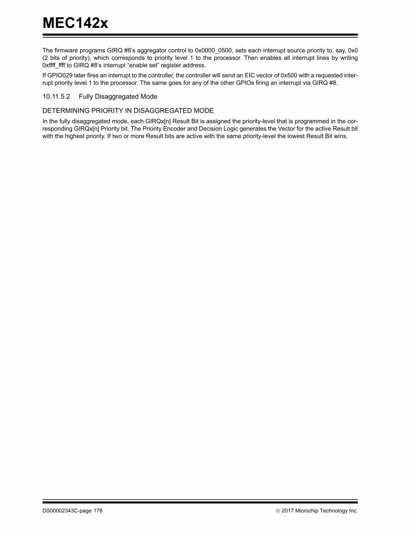
MEC142x
The firmware programs GIRQ #8’s aggregator control to 0x0000_0500, sets each interrupt source priority to, say, 0x0(2 bits of priority), which corresponds to priority level 1 to the processor. Then enables all interrupt lines by writing0xffff_ffff to GIRQ #8’s interrupt “enable set” register address.
If GPIO029 later fires an interrupt to the controller, the controller will send an EIC vector of 0x500 with a requested inter-rupt priority level 1 to the processor. The same goes for any of the other GPIOs firing an interrupt via GIRQ #8.
10.11.5.2 Fully Disaggregated Mode
DETERMINING PRIORITY IN DISAGGREGATED MODE
In the fully disaggregated mode, each GIRQx[n] Result Bit is assigned the priority-level that is programmed in the cor-responding GIRQx[n] Priority bit. The Priority Encoder and Decision Logic generates the Vector for the active Result bitwith the highest priority. If two or more Result bits are active with the same priority-level the lowest Result Bit wins.
DS00002343C-page 178 2017 Microchip Technology Inc.
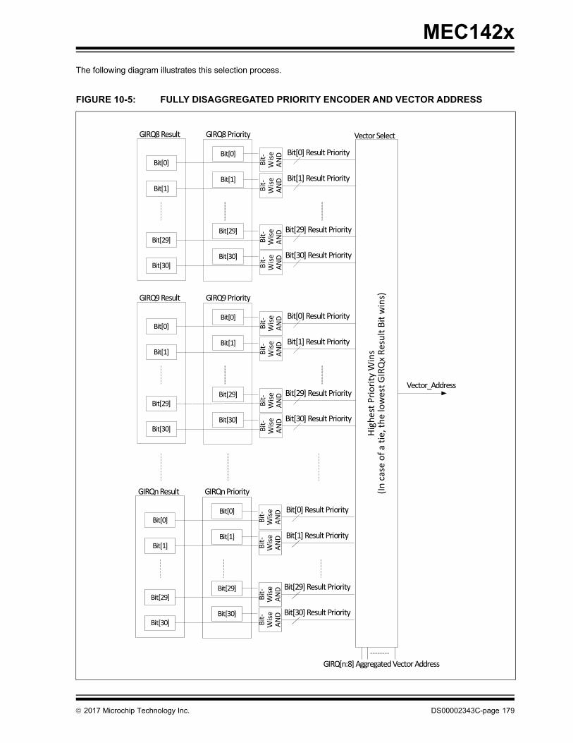
MEC142x
The following diagram illustrates this selection process.
FIGURE 10-5: FULLY DISAGGREGATED PRIORITY ENCODER AND VECTOR ADDRESS
GIRQ8 Result
Bit[0]
GIRQ8 Priority
Bit‐
Wise
AND Bit[0] Result Priority
Highest Priority W
ins
(In case of a tie, the lowest GIRQx Result Bit wins)
Vector Select
GIRQ[n:8] Aggregated Vector Address
Vector_Address
Bit[0]
Bit[1] Bit‐
Wise
AND Bit[1] Result PriorityBit[1]
Bit[29] Bit‐
Wise
AND Bit[29] Result PriorityBit[29]
Bit[30] Bit‐
Wise
AND Bit[30] Result PriorityBit[30]
GIRQ9 Result
Bit[0]
GIRQ9 Priority
Bit‐
Wise
AND Bit[0] Result PriorityBit[0]
Bit[1] Bit‐
Wise
AND Bit[1] Result PriorityBit[1]
Bit[29] Bit‐
Wise
AND Bit[29] Result PriorityBit[29]
Bit[30] Bit‐
Wise
AND Bit[30] Result PriorityBit[30]
GIRQn Result
Bit[0]
GIRQn Priority
Bit‐
Wise
AND Bit[0] Result PriorityBit[0]
Bit[1] Bit‐
Wise
AND Bit[1] Result PriorityBit[1]
Bit[29] Bit‐
Wise
AND Bit[29] Result PriorityBit[29]
Bit[30] Bit‐
Wise
AND Bit[30] Result PriorityBit[30]
2017 Microchip Technology Inc. DS00002343C-page 179

MEC142x
STEPS TO SET UP A PARTICULAR GIRQ GROUPING OF INTERRUPTS TO VECTOR TO AN ISR IN DISAGGREGATED/JT MODE.
1. Determine a location in code space to contain a mini-jump table, of size 31 entries or less, depending on howpopulated a particular GIRQ is (i.e. 15 populated sources = 15 jump table entries in SRAM).
2. Build up to 31 ISRs, one for each interrupt source in this GIRQ. The jump table gets populated with jump instruc-tions the locations of these ISRs.
3. Program the 17-bit offset for the entry location of the mini-jump table into the GIRQ aggregator control/vectoraddress register. EBASE must be programmed at 0xbfd0_0000.
4. (optional) Clear all source bits for the interrupts within GIRQ “n”.
5. Enable the individual interrupts within GIRQ “n” that you wish to be interrupt the processor.
6. Enable global interrupts in the processor.
ILLUSTRATIVE SCENARIO:
GIRQ #8 has 31 GPIOs from pins configured to generate interrupts that will be handled by an 31 ISRs labeled“GIRQ08_GPIO001_handler”, “GIRQ08_GPIO002_handler”, etc.
The 31 GPIOs are named (from GIRQ #8’s bit 0 through bit 30): GPIO001, GPIO002,….,GPIO030.
EBASE is at 0xbfd0_0000. Firmware places the jump table at address 0xbfd0_0500. The jump table gets populated withjump instructions to the 31 ISRs.
The firmware programs GIRQ #8’s aggregator control to 0x0000_0501 (bits 17:1 are the vector address, bit 0 is theGIRQ control to aggregate/dis-aggregate).
Firmware then sets each interrupt source priority to, say, 0x0 (2 bits of priority), which corresponds to priority level 1 tothe processor. Then enables all interrupt lines by writing 0xffff_ffff to GIRQ #8’s interrupt “enable set” register address.
If GPIO029 later fires an interrupt to the controller, the controller will send an EIC vector of 0x5e8 with a requested inter-rupt priority level 1 to the processor. This causes the processor to vector to the 30th entry in the mini-jump table, whichthen jumps to the “GIRQ08_GPIO029_handler” code.
This address: 0x5e8 = vector base + 29*(vector spacing) which is by default 8 bytes.
Later, GPIO002 fires an interrupt to the controller, which causes the controller to send an EIC vector of 0x510 with arequested interrupt priority level 1 to the processor. This causes the processor to vector to the 3rd entry in the mini-jumptable, which then jumps to the “GIRQ08_GPIO002_handler” code.
10.11.6 HYBRID MODE
The Hybrid is a combination of the aggregated and disaggregated modes.
Each GIRQ group has the option of operating in either aggregated mode or disaggregated mode. This mode is similarto the disaggregated mode, except the grouped GIRQs will OR their result through bit 0 of that GIRQ. Each GIRQx[n]Result Bit is assigned the priority-level that is programmed in the corresponding GIRQx[n] Priority bit. The PriorityEncoder and Decision Logic generates the Vector for the active Result bit with the highest priority. If two or more Resultbits are active with the same priority-level the lowest Result Bit wins.
DS00002343C-page 180 2017 Microchip Technology Inc.

MEC142x
The following diagram illustrates this selection process.
GIRQ8 Result
Bit[0]
GIRQ8 Priority
Bit‐
Wise
AND Bit[0] Result Priority
Highest Priority W
ins
(In case of a tie, the lowest GIRQx Result Bit wins)
Vector Select
GIRQ[n:8] Aggregated Vector Address
Vector_Address
Bit[0]
Bit[1] Bit‐
Wise
AND Bit[1] Result PriorityBit[1]
Bit[29] Bit‐
Wise
AND Bit[29] Result PriorityBit[29]
Bit[30] Bit‐
Wise
AND Bit[30] Result PriorityBit[30]
GIRQ9 Result
Bit[0]
GIRQ9 Priority
Bit‐
Wise
AND Bit[0] Result PriorityBit[0]
Bit[1]
Bit[29]
Bit[30]
GIRQn Result
Bit[0]
GIRQn Priority
Bit‐
Wise
AND Bit[0] Result PriorityBit[0]
Bit[1] Bit‐
Wise
AND Bit[1] Result PriorityBit[1]
Bit[29] Bit‐
Wise
AND Bit[29] Result PriorityBit[29]
Bit[30] Bit‐
Wise
AND Bit[30] Result PriorityBit[30]
OR
2017 Microchip Technology Inc. DS00002343C-page 181

MEC142x
10.12 JTVIC Registers
The registers listed in the JTVIC Register Summary table are for a single instance of the Jump Table Vectored InterruptController (JTVIC). The addresses of each register listed in this table are defined as a relative offset to the host “BaseAddress” defined in the EC-Only Register Base Address Table.
The Base Address indicates where the first register can be accessed in a particular address space for a block instance.
TABLE 10-3: EC-ONLY REGISTER BASE ADDRESS TABLE
Block InstanceInstance Number
Host Address Space Base Address
Interrupt Controller 0 EC 32-bit internal address space
1FFF_C000h
TABLE 10-4: JTVIC REGISTER SUMMARY
Offset Register Name
Interrupt Source, Enable Set, Enable Clear, and Result Registers
00h GIRQ8 Source Register
04h GIRQ8 Enable Set Register
08h GIRQ8 Enable Clear Register
0Ch GIRQ8 Result Register
10h GIRQ9 Source Register
14h GIRQ9 Enable Set Register
18h GIRQ9 Enable Clear Register
1Ch GIRQ9 Result Register
20h GIRQ10 Source Register
24h GIRQ10 Enable Set Register
28h GIRQ10 Enable Clear Register
2Ch GIRQ10 Result Register
30h GIRQ11 Source Register
34h GIRQ11 Enable Set Register
38h GIRQ11 Enable Clear Register
3Ch GIRQ11 Result Register
40h GIRQ12 Source Register
44h GIRQ12 Enable Set Register
48h GIRQ12 Enable Clear Register
4Ch GIRQ12 Result Register
DS00002343C-page 182 2017 Microchip Technology Inc.
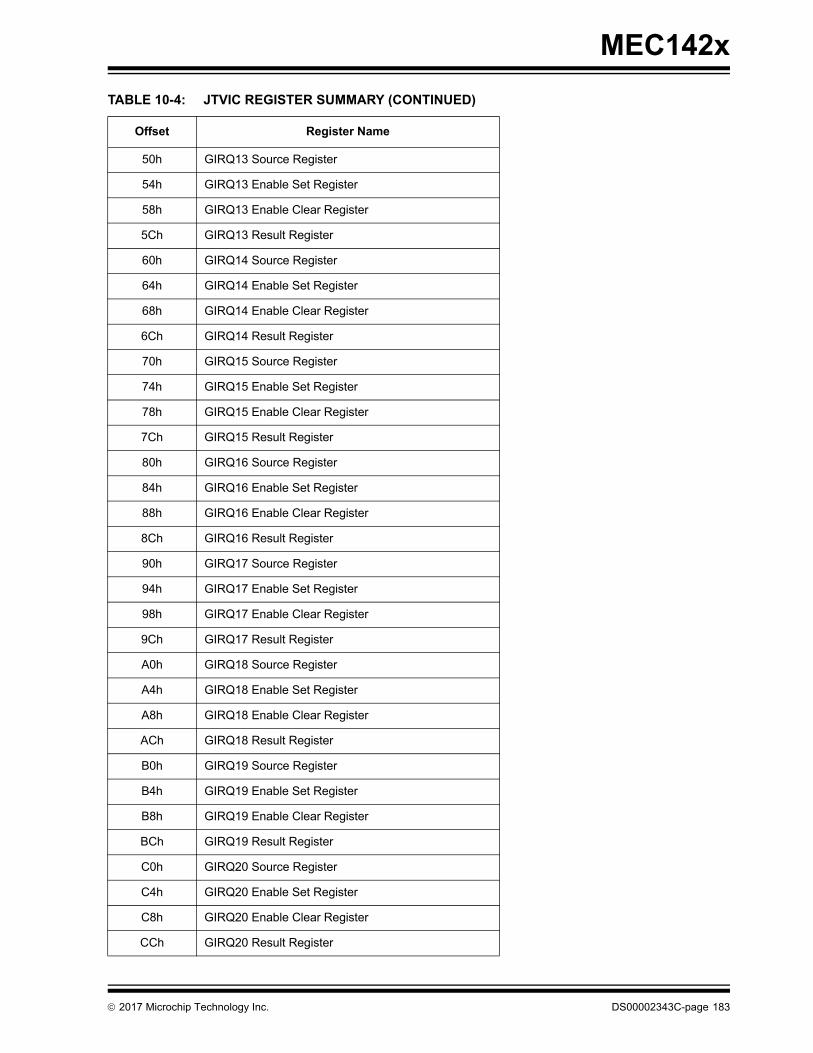
MEC142x
50h GIRQ13 Source Register
54h GIRQ13 Enable Set Register
58h GIRQ13 Enable Clear Register
5Ch GIRQ13 Result Register
60h GIRQ14 Source Register
64h GIRQ14 Enable Set Register
68h GIRQ14 Enable Clear Register
6Ch GIRQ14 Result Register
70h GIRQ15 Source Register
74h GIRQ15 Enable Set Register
78h GIRQ15 Enable Clear Register
7Ch GIRQ15 Result Register
80h GIRQ16 Source Register
84h GIRQ16 Enable Set Register
88h GIRQ16 Enable Clear Register
8Ch GIRQ16 Result Register
90h GIRQ17 Source Register
94h GIRQ17 Enable Set Register
98h GIRQ17 Enable Clear Register
9Ch GIRQ17 Result Register
A0h GIRQ18 Source Register
A4h GIRQ18 Enable Set Register
A8h GIRQ18 Enable Clear Register
ACh GIRQ18 Result Register
B0h GIRQ19 Source Register
B4h GIRQ19 Enable Set Register
B8h GIRQ19 Enable Clear Register
BCh GIRQ19 Result Register
C0h GIRQ20 Source Register
C4h GIRQ20 Enable Set Register
C8h GIRQ20 Enable Clear Register
CCh GIRQ20 Result Register
TABLE 10-4: JTVIC REGISTER SUMMARY (CONTINUED)
Offset Register Name
2017 Microchip Technology Inc. DS00002343C-page 183
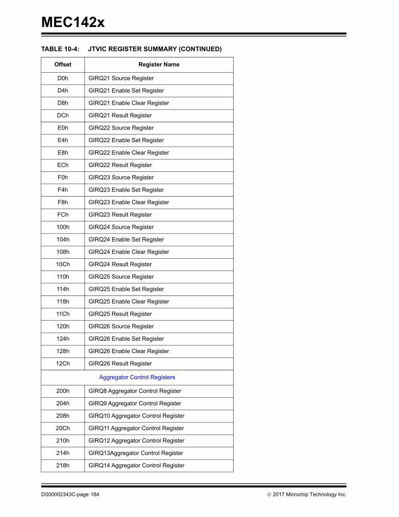
MEC142x
D0h GIRQ21 Source Register
D4h GIRQ21 Enable Set Register
D8h GIRQ21 Enable Clear Register
DCh GIRQ21 Result Register
E0h GIRQ22 Source Register
E4h GIRQ22 Enable Set Register
E8h GIRQ22 Enable Clear Register
ECh GIRQ22 Result Register
F0h GIRQ23 Source Register
F4h GIRQ23 Enable Set Register
F8h GIRQ23 Enable Clear Register
FCh GIRQ23 Result Register
100h GIRQ24 Source Register
104h GIRQ24 Enable Set Register
108h GIRQ24 Enable Clear Register
10Ch GIRQ24 Result Register
110h GIRQ25 Source Register
114h GIRQ25 Enable Set Register
118h GIRQ25 Enable Clear Register
11Ch GIRQ25 Result Register
120h GIRQ26 Source Register
124h GIRQ26 Enable Set Register
128h GIRQ26 Enable Clear Register
12Ch GIRQ26 Result Register
Aggregator Control Registers
200h GIRQ8 Aggregator Control Register
204h GIRQ9 Aggregator Control Register
208h GIRQ10 Aggregator Control Register
20Ch GIRQ11 Aggregator Control Register
210h GIRQ12 Aggregator Control Register
214h GIRQ13Aggregator Control Register
218h GIRQ14 Aggregator Control Register
TABLE 10-4: JTVIC REGISTER SUMMARY (CONTINUED)
Offset Register Name
DS00002343C-page 184 2017 Microchip Technology Inc.

MEC142x
21Ch GIRQ15 Aggregator Control Register
220h GIRQ16 Aggregator Control Register
224h GIRQ17Aggregator Control Register
228h GIRQ18 Aggregator Control Register
22Ch GIRQ19 Aggregator Control Register
230h GIRQ20 Aggregator Control Register
234h GIRQ21 Aggregator Control Register
238h GIRQ22 Aggregator Control Register
23Ch GIRQ23 Aggregator Control Register
240h GIRQ24 Aggregator Control Register
244h GIRQ25 Aggregator Control Register
248h GIRQ26 Aggregator Control Register
Interrupt Priority Control Registers
300h GIRQ8 [7:0] Interrupt Priority Register
304h GIRQ8 [15:8] Interrupt Priority Register
308h GIRQ8 [23:16] Interrupt Priority Register
30Ch GIRQ8 [31:24] Interrupt Priority Register
310h GIRQ9 [7:0] Interrupt Priority Register
314h GIRQ9 [15:8] Interrupt Priority Register
318h GIRQ9 [23:16] Interrupt Priority Register
31Ch GIRQ9 [31:24] Interrupt Priority Register
320h GIRQ10 [7:0] Interrupt Priority Register
324h GIRQ10 [15:8] Interrupt Priority Register
328h GIRQ10 [23:16] Interrupt Priority Register
32Ch GIRQ10 [31:24] Interrupt Priority Register
330h GIRQ11 [7:0] Interrupt Priority Register
334h GIRQ11 [15:8] Interrupt Priority Register
338h GIRQ11 [23:16] Interrupt Priority Register
33Ch GIRQ11 [31:24] Interrupt Priority Register
340h GIRQ12 [7:0] Interrupt Priority Register
344h GIRQ12 [15:8] Interrupt Priority Register
348h GIRQ12 [23:16] Interrupt Priority Register
TABLE 10-4: JTVIC REGISTER SUMMARY (CONTINUED)
Offset Register Name
2017 Microchip Technology Inc. DS00002343C-page 185
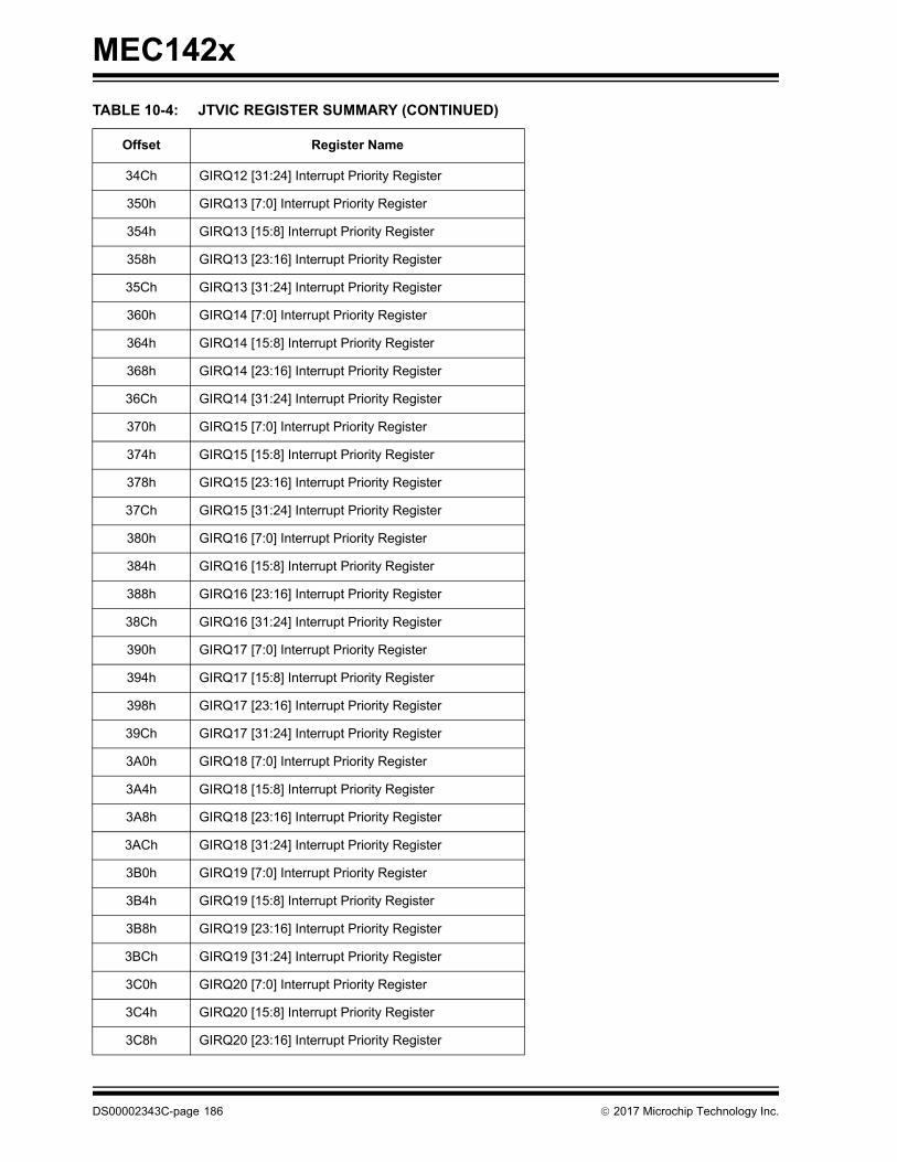
MEC142x
34Ch GIRQ12 [31:24] Interrupt Priority Register
350h GIRQ13 [7:0] Interrupt Priority Register
354h GIRQ13 [15:8] Interrupt Priority Register
358h GIRQ13 [23:16] Interrupt Priority Register
35Ch GIRQ13 [31:24] Interrupt Priority Register
360h GIRQ14 [7:0] Interrupt Priority Register
364h GIRQ14 [15:8] Interrupt Priority Register
368h GIRQ14 [23:16] Interrupt Priority Register
36Ch GIRQ14 [31:24] Interrupt Priority Register
370h GIRQ15 [7:0] Interrupt Priority Register
374h GIRQ15 [15:8] Interrupt Priority Register
378h GIRQ15 [23:16] Interrupt Priority Register
37Ch GIRQ15 [31:24] Interrupt Priority Register
380h GIRQ16 [7:0] Interrupt Priority Register
384h GIRQ16 [15:8] Interrupt Priority Register
388h GIRQ16 [23:16] Interrupt Priority Register
38Ch GIRQ16 [31:24] Interrupt Priority Register
390h GIRQ17 [7:0] Interrupt Priority Register
394h GIRQ17 [15:8] Interrupt Priority Register
398h GIRQ17 [23:16] Interrupt Priority Register
39Ch GIRQ17 [31:24] Interrupt Priority Register
3A0h GIRQ18 [7:0] Interrupt Priority Register
3A4h GIRQ18 [15:8] Interrupt Priority Register
3A8h GIRQ18 [23:16] Interrupt Priority Register
3ACh GIRQ18 [31:24] Interrupt Priority Register
3B0h GIRQ19 [7:0] Interrupt Priority Register
3B4h GIRQ19 [15:8] Interrupt Priority Register
3B8h GIRQ19 [23:16] Interrupt Priority Register
3BCh GIRQ19 [31:24] Interrupt Priority Register
3C0h GIRQ20 [7:0] Interrupt Priority Register
3C4h GIRQ20 [15:8] Interrupt Priority Register
3C8h GIRQ20 [23:16] Interrupt Priority Register
TABLE 10-4: JTVIC REGISTER SUMMARY (CONTINUED)
Offset Register Name
DS00002343C-page 186 2017 Microchip Technology Inc.

MEC142x
3CCh GIRQ20 [31:24] Interrupt Priority Register
3D0h GIRQ21 [7:0] Interrupt Priority Register
3D4h GIRQ21 [15:8] Interrupt Priority Register
3D8h GIRQ21 [23:16] Interrupt Priority Register
3DCh GIRQ21 [31:24] Interrupt Priority Register
3E0h GIRQ22 [7:0] Interrupt Priority Register
3E4h GIRQ22 [15:8] Interrupt Priority Register
3E8h GIRQ22 [23:16] Interrupt Priority Register
3ECh GIRQ22 [31:24] Interrupt Priority Register
3F0h GIRQ23 [7:0] Interrupt Priority Register
3F4h GIRQ23 [15:8] Interrupt Priority Register
3F8h GIRQ23 [23:16] Interrupt Priority Register
3FCh GIRQ23 [31:24] Interrupt Priority Register
400h GIRQ24 [7:0] Interrupt Priority Register
404h GIRQ24 [15:8] Interrupt Priority Register
408h GIRQ24 [23:16] Interrupt Priority Register
40Ch GIRQ24 [31:24] Interrupt Priority Register
410h GIRQ25 [7:0] Interrupt Priority Register
414h GIRQ25 [15:8] Interrupt Priority Register
418h GIRQ25 [23:16] Interrupt Priority Register
41Ch GIRQ25 [31:24] Interrupt Priority Register
420h GIRQ26 [7:0] Interrupt Priority Register
424h GIRQ26 [15:8] Interrupt Priority Register
428h GIRQ26 [23:16] Interrupt Priority Register
42Ch GIRQ26 [31:24] Interrupt Priority Register
JTVIC Control Registers
500h JTVIC Control Register
504h Interrupt Pending Register
508h Aggregated Group Enable Set Register
50Ch Aggregated Group Enabled Clear Register
510h GIRQ Active Register
TABLE 10-4: JTVIC REGISTER SUMMARY (CONTINUED)
Offset Register Name
2017 Microchip Technology Inc. DS00002343C-page 187
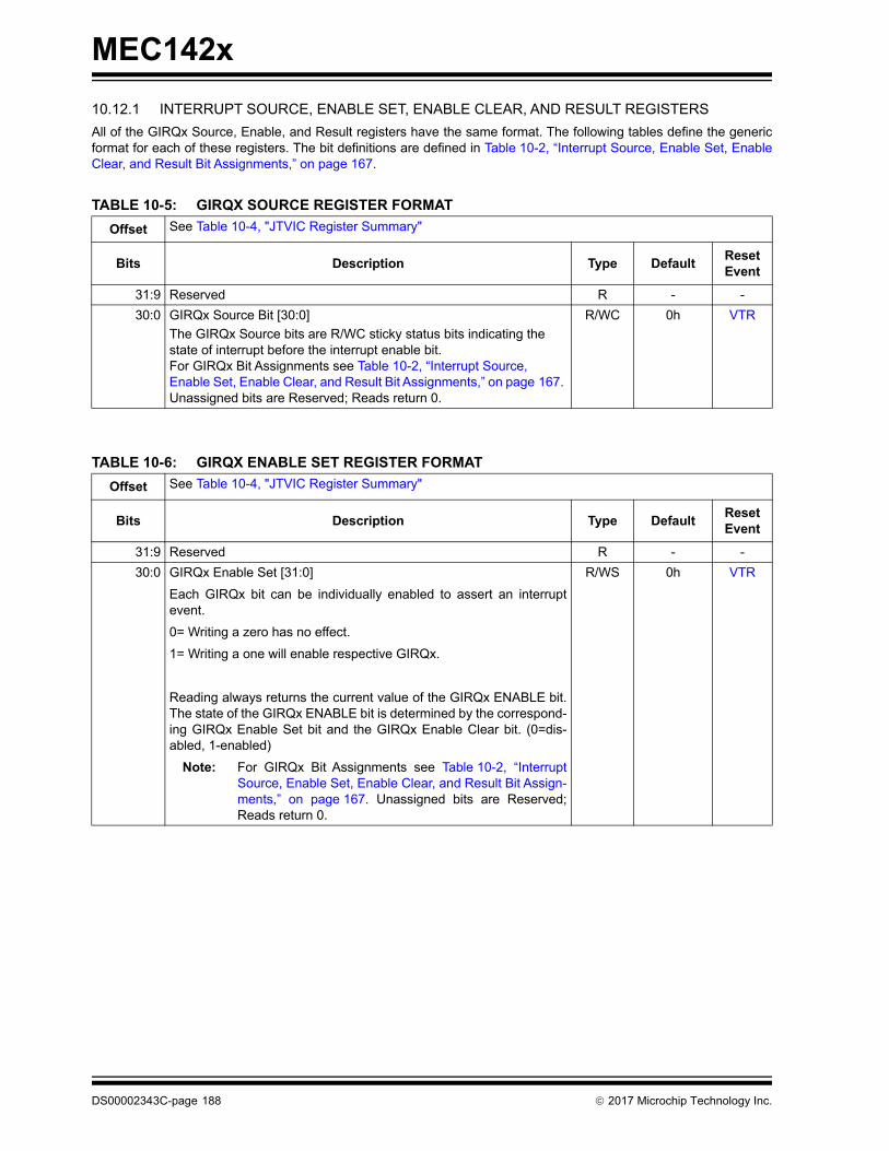
MEC142x
10.12.1 INTERRUPT SOURCE, ENABLE SET, ENABLE CLEAR, AND RESULT REGISTERS
All of the GIRQx Source, Enable, and Result registers have the same format. The following tables define the genericformat for each of these registers. The bit definitions are defined in Table 10-2, “Interrupt Source, Enable Set, EnableClear, and Result Bit Assignments,” on page 167.
TABLE 10-5: GIRQX SOURCE REGISTER FORMAT
Offset See Table 10-4, "JTVIC Register Summary"
Bits Description Type DefaultReset Event
31:9 Reserved R - -
30:0 GIRQx Source Bit [30:0]
The GIRQx Source bits are R/WC sticky status bits indicating the state of interrupt before the interrupt enable bit.For GIRQx Bit Assignments see Table 10-2, “Interrupt Source, Enable Set, Enable Clear, and Result Bit Assignments,” on page 167. Unassigned bits are Reserved; Reads return 0.
R/WC 0h VTR
TABLE 10-6: GIRQX ENABLE SET REGISTER FORMAT
Offset See Table 10-4, "JTVIC Register Summary"
Bits Description Type DefaultReset Event
31:9 Reserved R - -
30:0 GIRQx Enable Set [31:0]
Each GIRQx bit can be individually enabled to assert an interruptevent.
0= Writing a zero has no effect.
1= Writing a one will enable respective GIRQx.
Reading always returns the current value of the GIRQx ENABLE bit.The state of the GIRQx ENABLE bit is determined by the correspond-ing GIRQx Enable Set bit and the GIRQx Enable Clear bit. (0=dis-abled, 1-enabled)
Note: For GIRQx Bit Assignments see Table 10-2, “InterruptSource, Enable Set, Enable Clear, and Result Bit Assign-ments,” on page 167. Unassigned bits are Reserved;Reads return 0.
R/WS 0h VTR
DS00002343C-page 188 2017 Microchip Technology Inc.

MEC142x
TABLE 10-7: GIRQX ENABLE CLEAR REGISTER FORMAT
Offset See Table 10-4, "JTVIC Register Summary"
Bits Description Type DefaultReset Event
31:9 Reserved R - -
30:0 GIRQx Enable Clear[31:0]
Each GIRQx bit can be individually disabled to assert an interruptevent.
0= Writing a zero has no effect.
1= Writing a one will disable respective GIRQx.
Reading always returns the current value of the GIRQx ENABLE bit.The state of the GIRQx ENABLE bit is determined by the correspond-ing GIRQx Enable Set bit and the GIRQx Enable Clear bit. (0=dis-abled, 1-enabled)
Note: For GIRQx Bit Assignments see Table 10-2, “InterruptSource, Enable Set, Enable Clear, and Result Bit Assign-ments,” on page 167. Unassigned bits are Reserved;Reads return 0.
R/WC 0h VTR
TABLE 10-8: GIRQX RESULT REGISTER FORMAT
Offset See Table 10-4, "JTVIC Register Summary"
Bits Description Type DefaultReset Event
31 Bit D31 is hard-coded to ‘1’. R 1h -
30:0 GIRQx Interrupt Result
The GIRQx Result bits are Read-Only status bits indicating the state of interrupt after the interrupt enable bit.
Note: For GIRQx Bit Assignments see Table 10-2, “InterruptSource, Enable Set, Enable Clear, and Result Bit Assign-ments,” on page 167. Unassigned bits are Reserved;Reads return 0.
R 0h VTR
2017 Microchip Technology Inc. DS00002343C-page 189

MEC142x
10.12.2 AGGREGATOR CONTROL REGISTERS
10.12.3 INTERRUPT PRIORITY CONTROL REGISTERS
TABLE 10-9: GIRQX AGGREGATOR CONTROL REGISTER FORMAT
Offset -
Bits Description Type DefaultReset Event
31:18 Reserved R - -
17:1 Aggregator Vector Address
• In Aggregated Mode the Aggregated Vector Address is added to the processor EBASE to determine the physical jump address.
• In Disaggregated Mode this is used as part of the calculation to determine the Jump Table Vector physical address. See JTEn-able (Jump-Table Enable) bit description.
R/W 00h VTR
0 JTEnable (Jump-Table Enable)
0 = aggregated : present only the vector address from bits 17:1 1 = disaggregated/jump-table: present vector address from bits 17:1 + (vector_spacing)*(winning interrupt source bit position)
R/W 0h VTR
TABLE 10-10: GIRQX [N+7:N] INTERRUPT PRIORITY REGISTER FORMAT
Offset -
Bits Description Type DefaultReset Event
31:30 Reserved R - -
29:28 GIRQX [N+7] Priority
00 = Priority Level 101 = Priority Level 310 = Priority Level 511 = Priority Level 7
R/W 0h VTR
27:26 Reserved R - -
25:24 GIRQX [N+6] Priority
00 = Priority Level 101 = Priority Level 310 = Priority Level 511 = Priority Level 7
R/W 0h VTR
23:22 Reserved R - -
21:20 GIRQX [N+5] Priority
00 = Priority Level 101 = Priority Level 310 = Priority Level 511 = Priority Level 7
R/W 0h VTR
19:18 Reserved R - -
17:16 GIRQX [N+4] Priority
00 = Priority Level 101 = Priority Level 310 = Priority Level 511 = Priority Level 7
R/W 0h VTR
15:14 Reserved R - -
DS00002343C-page 190 2017 Microchip Technology Inc.

MEC142x
10.12.4 JTVIC CONTROL REGISTERS
13:12 GIRQX [N+3] Priority
00 = Priority Level 101 = Priority Level 310 = Priority Level 511 = Priority Level 7
R/W 0h VTR
11:10 Reserved R - -
9:8 GIRQX [N+2] Priority
00 = Priority Level 101 = Priority Level 310 = Priority Level 511 = Priority Level 7
R/W 0h VTR
7:6 Reserved R - -
5:4 GIRQX [N+1] Priority
00 = Priority Level 101 = Priority Level 310 = Priority Level 511 = Priority Level 7
R/W 0h VTR
3:2 Reserved R - -
1:0 GIRQX [N] Priority
00 = Priority Level 101 = Priority Level 310 = Priority Level 511 = Priority Level 7
R/W 0h VTR
TABLE 10-11: JTVIC CONTROL REGISTER
Offset 500h
Bits Description Type DefaultReset Event
31:9 Reserved R - -
8 Vector Spacing
0 = 8 Bytes1 = 512 Bytes
R/W 00h VTR
7:1 Reserved R - -
0 Soft Reset
Soft Reset resets all flops in the JTVIC block except the interrupt source bits and the soft reset bit itself. 0 = Not Reset - Normal Operation1 = Reset
R/W 0h VTR
TABLE 10-10: GIRQX [N+7:N] INTERRUPT PRIORITY REGISTER FORMAT (CONTINUED)
Offset -
Bits Description Type DefaultReset Event
2017 Microchip Technology Inc. DS00002343C-page 191

MEC142x
TABLE 10-12: INTERRUPT PENDING REGISTER
Offset 504h
Bits Description Type DefaultReset Event
31:19 Reserved R - -
18:0 GIRQ[26:8] Aggregated Group Interrupt Source Pending
This register shows the GIRQx pending interrupt sources. Each bit is the OR’d result of the corresponding GIRQx Interrupt Source regis-ter.
R 0h VTR
TABLE 10-13: AGGREGATED GROUP ENABLE SET REGISTER
Offset 508h
Bits Description Type DefaultReset Event
31:19 Reserved R - -
18:0 GIRQ[26:8] Aggregated Group Enable Set
Each IRQ Vector can be individually enabled to assert an interruptevent to the EC.
0= Writing a zero has no effect.
1= Writing a one will enable respective IRQi.
Reading always returns the current value of the IRQ i VECTORENABLE bit. The state of the IRQ i VECTOR ENABLE bit is deter-mined by the corresponding IRQ i Vector Enable Set bit and the IRQi Vector Enable Clear bit. (0=disabled, 1-enabled)
R/W 0h VTR
TABLE 10-14: AGGREGATED GROUP ENABLE CLEAR REGISTER
Offset 50Ch
Bits Description Type DefaultReset Event
31:19 Reserved R - -
18:0 GIRQ[26:8] Aggregated Group Enable Clear
Each IRQ Vector can be individually disabled to assert an interruptevent to the EC.
0= Writing a zero has no effect.
1= Writing a one will disable respective IRQi vector.
Reading always returns the current value of the IRQ i VECTORENABLE bit. The state of the IRQ i VECTOR ENABLE bit is deter-mined by the corresponding IRQ i Vector Enable Set bit and the IRQi Vector Enable Clear bit. (0=disabled, 1-enabled).
R/W 0h VTR
DS00002343C-page 192 2017 Microchip Technology Inc.
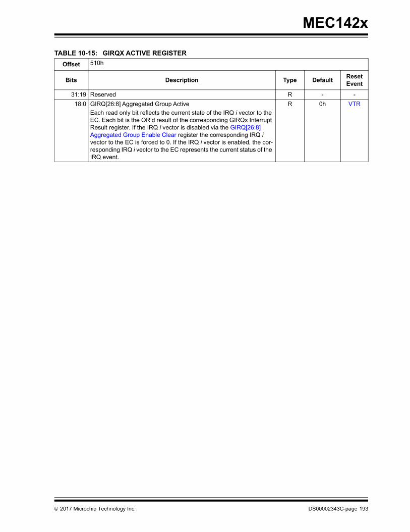
MEC142x
TABLE 10-15: GIRQX ACTIVE REGISTER
Offset 510h
Bits Description Type DefaultReset Event
31:19 Reserved R - -
18:0 GIRQ[26:8] Aggregated Group Active
Each read only bit reflects the current state of the IRQ i vector to the EC. Each bit is the OR’d result of the corresponding GIRQx Interrupt Result register. If the IRQ i vector is disabled via the GIRQ[26:8] Aggregated Group Enable Clear register the corresponding IRQ i vector to the EC is forced to 0. If the IRQ i vector is enabled, the cor-responding IRQ i vector to the EC represents the current status of the IRQ event.
R 0h VTR
2017 Microchip Technology Inc. DS00002343C-page 193

MEC142x
11.0 WATCHDOG TIMER (WDT)
11.1 Introduction
The function of the Watchdog Timer is to provide a mechanism to detect if the internal embedded controller has failed.
When enabled, the Watchdog Timer (WDT) circuit will generate a WDT Event if the user program fails to reload the WDTwithin a specified length of time known as the WDT Interval.
11.2 References
No references have been cited for this chapter.
11.3 Terminology
There is no terminology defined for this chapter.
11.4 Interface
This block is designed to be accessed internally via a registered host interface or externally via the signal interface.
11.4.1 SIGNAL DESCRIPTION
11.5 Host Interface
The registers defined for the Watchdog Timer (WDT) are accessible by the embedded controller as indicated in Section11.8, "EC-Only Registers". All registers accesses are synchronized to the host clock and complete immediately. Regis-ter reads/writes are not delayed by the 5Hz_Clk.
TABLE 11-1: SIGNAL DESCRIPTION TABLE
Name Direction Description
WDT_Stall[2:0] Input External 3-bit wide bus used to stall the WDT. Each of these sig-nals may prevent the WDT from generating false WDT Events.
TABLE 11-2: WDT_STALL CONNECTIONS
Signal Name Control Signals Description
WDT_Stall[0] Hibernation Timer If enabled via the WDT_STALL_EN[0], the WDT will be stalled when the Hibernation Timer is counting.
WDT_Stall[1] Week Timer Active If enabled via the WDT_STALL_EN[1], the WDT will be stalled if the Week Timer is counting.
WDT_Stall[2] ICSP Active If enabled via the WDT_STALL_EN[2], the WDT will be stalled if there is activity on the ICSP ports. This allows the ICSP to be enabled, via the ICSP_MCLR pin, but not stall the WDT if there is no activity on the interface.
The WDT_Stall[2] is also asserted when the WDT Enable bit in the ICDCON test register is 0.
DS00002343C-page 194 2017 Microchip Technology Inc.

MEC142x
11.6 Power, Clocks and Reset
This section defines the Power, Clock, and Reset parameters of the block.
11.6.1 POWER DOMAINS
11.6.2 CLOCK INPUTS
11.6.3 RESETS
11.7 Description
11.7.1 WDT OPERATION
11.7.1.1 WDT Activation Mechanism
The WDT is activated by the following sequence of operations during normal operation:
1. Load the WDT Load Register with the count value.
2. Set the WDT Enable bit in the WDT Control Register.
The WDT Activation Mechanism starts the WDT decrementing counter.
11.7.1.2 WDT Deactivation Mechanism
The WDT is deactivated by the clearing the WDT Enable bit in the WDT Control Register. The WDT Deactivation Mech-anism places the WDT in a low power state in which clock are gated and the counter stops decrementing.
11.7.1.3 WDT Reload Mechanism
The WDT must be reloaded within periods that are shorter than the programmed watchdog interval; otherwise, the WDTwill underflow and a WDT Event will be generated and the WDT bit will be set in the Power-Fail and Reset Status Reg-ister. It is the responsibility of the user program to continually execute code which reloads the watchdog timer, causingthe counter to be reloaded
Name Description
VTR The logic and registers implemented in this block reside on this singlepower well.
Name Description
5Hz_Clk The 5Hz_Clk clock input is the clock source to the Watchdog Timer functional logic, including the counter.
Name Description
nSYSRST Power on Reset to the block. This signal resets all the register and logic in this block to its default state.
Source Description
WDT Event Pulse generated when WDT expires. This signal is used to reset the embedded controller and its subsystem.
The event is cleared after an nSYSRST.
2017 Microchip Technology Inc. DS00002343C-page 195
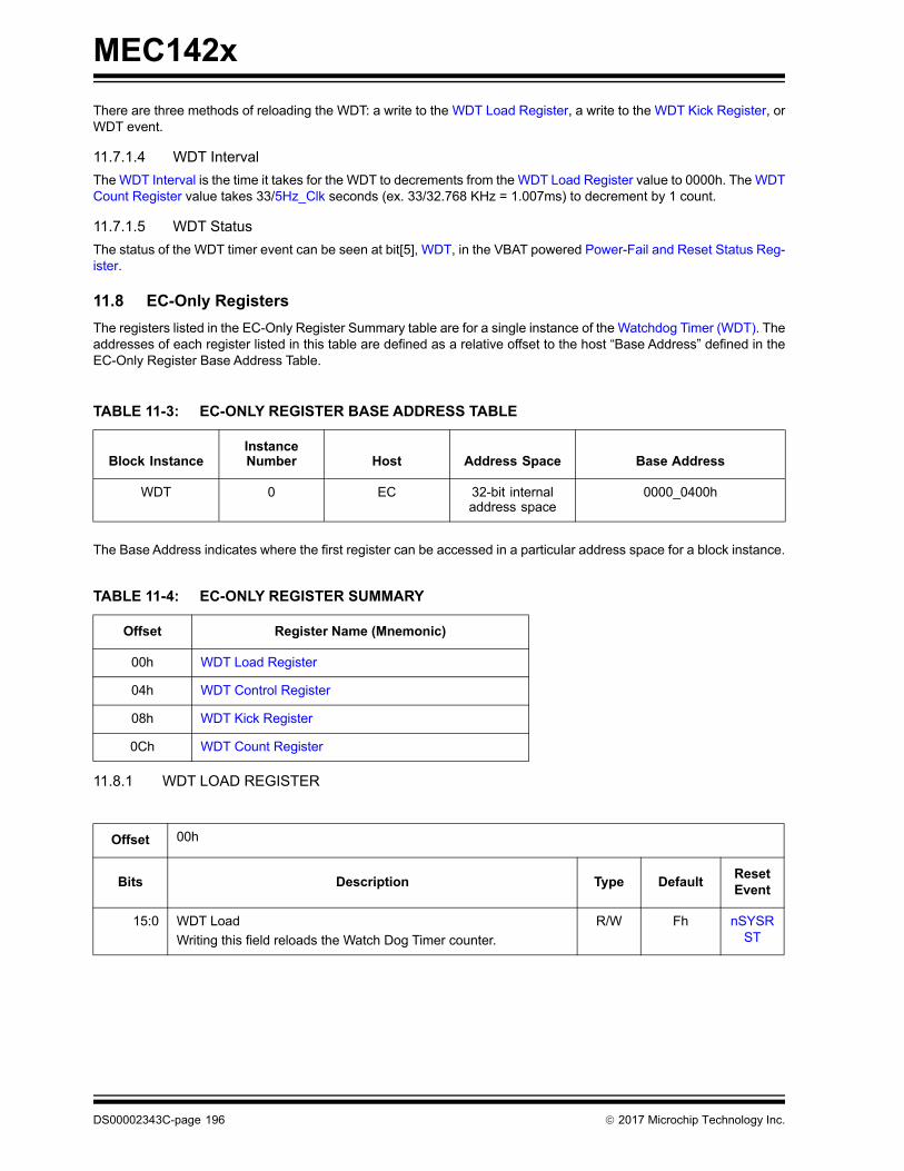
MEC142x
There are three methods of reloading the WDT: a write to the WDT Load Register, a write to the WDT Kick Register, orWDT event.
11.7.1.4 WDT Interval
The WDT Interval is the time it takes for the WDT to decrements from the WDT Load Register value to 0000h. The WDTCount Register value takes 33/5Hz_Clk seconds (ex. 33/32.768 KHz = 1.007ms) to decrement by 1 count.
11.7.1.5 WDT Status
The status of the WDT timer event can be seen at bit[5], WDT, in the VBAT powered Power-Fail and Reset Status Reg-ister.
11.8 EC-Only Registers
The registers listed in the EC-Only Register Summary table are for a single instance of the Watchdog Timer (WDT). Theaddresses of each register listed in this table are defined as a relative offset to the host “Base Address” defined in theEC-Only Register Base Address Table.
The Base Address indicates where the first register can be accessed in a particular address space for a block instance.
11.8.1 WDT LOAD REGISTER
TABLE 11-3: EC-ONLY REGISTER BASE ADDRESS TABLE
Block InstanceInstance Number Host Address Space Base Address
WDT 0 EC 32-bit internal address space
0000_0400h
TABLE 11-4: EC-ONLY REGISTER SUMMARY
Offset Register Name (Mnemonic)
00h WDT Load Register
04h WDT Control Register
08h WDT Kick Register
0Ch WDT Count Register
Offset 00h
Bits Description Type DefaultReset Event
15:0 WDT Load
Writing this field reloads the Watch Dog Timer counter.
R/W Fh nSYSRST
DS00002343C-page 196 2017 Microchip Technology Inc.

MEC142x
11.8.2 WDT CONTROL REGISTER
Offset 04h
Bits Description Type DefaultReset Event
7:5 RESERVED R - -
4 WDT_STALL_EN[2]
This bit is used to enable Bit[2] of the WDT_Stall[2:0] input bus.For a description of the stall feature see EC-Only Registers on page 196.
0= EC-Only Registers not enabled on WDT_Stall[2]1= EC-Only Registers enabled on WDT_Stall[2]
R/W 0b nSYSRST
3 WDT_STALL_EN[1]
This bit is used to enable Bit[1] of the WDT_Stall[2:0] input bus.For a description of the stall feature see EC-Only Registers on page 196.
0= EC-Only Registers not enabled on WDT_Stall[1]1= EC-Only Registers enabled on WDT_Stall[1]
R/W 0b nSYSRST
2 WDT_STALL_EN[0]
This bit is used to enable Bit[0] of the WDT_Stall[2:0] input bus.For a description of the stall feature see EC-Only Registers on page 196.
0= EC-Only Registers not enabled on WDT_Stall[0]1= EC-Only Registers enabled on WDT_Stall[0]
R/W 0b nSYSRST
1 Test R/WC 0b nSYSRST
0 WDT Enable
In WDT Operation, the WDT is activated by the sequence of opera-tions defined in Section 11.7.1.1, "WDT Activation Mechanism" and deactivated by the sequence of operations defined in Section 11.7.1.2, "WDT Deactivation Mechanism".
0 = block disabled1 = block enabled
Note: The default of the WDT is inactive.
R/W 0b nSYSRST
2017 Microchip Technology Inc. DS00002343C-page 197

MEC142x
11.8.3 WDT KICK REGISTER
11.8.4 WDT COUNT REGISTER
Offset 08h
Bits Description Type DefaultReset Event
7:0 Kick
The WDT Kick Register is a strobe. Reads of the WDT Kick Regis-ter return 0. Writes to the WDT Kick Register cause the WDT to reload the WDT Load Register value and start decrementing when the WDT Enable bit in the WDT Control Register is set to ‘1’. When the WDT Enable bit in the WDT Control Register is cleared to ‘0’, writes to the WDT Kick Register have no effect.
W n/a nSYSRST
Offset 00h
Bits Description Type DefaultReset Event
15:0 WDT Count
This read-only register provide the current WDT count.
R Fh nSYSRST
DS00002343C-page 198 2017 Microchip Technology Inc.

MEC142x
12.0 EMBEDDED MEMORY INTERFACE (EMI)
12.1 Introduction
The Embedded Memory Interface (EMI) provides a standard run-time mechanism for the system host to communicatewith the Embedded Controller (EC) and other logical components. The Embedded Memory Interface includes 13 byte-addressable registers in the Host’s address space, as well as 22 bytes of registers that are accessible only by the EC.The Embedded Memory Interface can be used by the Host to access bytes of memory designated by the EC withoutrequiring any assistance from the EC. The EC may configure these regions of memory as read-only, write-only, orread/write capable.
12.2 Interface
This block is designed to be accessed externally and internally via a register interface.
Note: The Embedded Memory Interface (EMI) is supported for both the LPC interface and eSPI.
FIGURE 12-1: I/O DIAGRAM OF BLOCK
Embedded Memory Interface (EMI)
Signal DescriptionClock Inputs
Interrupts
Resets
Host Interface
2017 Microchip Technology Inc. DS00002343C-page 199

MEC142x
12.3 Signal Description
12.4 Host Interface
The registers defined for the Embedded Memory Interface (EMI) are accessible by the System Host and the EmbeddedController as indicated in Section 12.10, "EC-Only Registers" and Section 12.9, "Runtime Registers".
12.5 Power, Clocks and Reset
This section defines the Power, Clock, and Reset parameters of the block.
12.5.1 POWER DOMAINS
12.5.2 CLOCK INPUTS
This block has no special clocking requirements. Host register accesses are synchronized to the host bus clock and ECregister accesses are synchronized to the EC bus clock, thereby allowing the transactions to complete in one bus clock.
12.5.3 RESETS
TABLE 12-1: SIGNAL DESCRIPTION TABLE
Name Direction Description
nEMI_INT OUTPUT Active-low signal asserted when either the EC-to-Host or the Host_SWI_Event is asserted. This signal can be routed to nSMI and nPME inputs in the system as required.
Name Description
VTR The logic and registers implemented in this block reside on this single power well.
Name Description
nSYSRST This reset signal resets all the logic and register in this block.
DS00002343C-page 200 2017 Microchip Technology Inc.

MEC142x
12.6 Interrupts
This section defines the Interrupt Sources generated from this block.
12.7 Low Power Modes
The Embedded Memory Interface (EMI) automatically enters low power mode when no transaction target it.
12.8 Description
The Embedded Memory Interface (EMI) is composed of a mailbox, a direct memory interface, and an Application IDregister.
The mailbox contains two registers, the HOST-to-EC Mailbox Register and the EC-to-HOST Mailbox Register, that actas a communication portal between the system host and the embedded controller. When the HOST-to-EC Mailbox Reg-ister is written an interrupt is generated to the embedded controller. Similarly, when the EC-to-HOST Mailbox Registeris written an interrupt is generated to the system host. The source of the system host interrupt may be read in the Inter-rupt Source Register. These interrupt events may be individually prevented from generating a Host_SWI_Event via theInterrupt Mask Register.
Source Description
EC-to-Host This interrupt source for the SIRQ logic is generated when the EC_WR bit is ‘1’ and enabled by the EC_WR_EN bit.
Host_SWI_Event This interrupt source for the SIRQ logic is generated when any of the EC_SWI bits are asserted and the corresponding EC_SWI_EN bit are asserted as well. This event is also asserted if the EC_WR/EC_WR_EN event occurs as well.
HOST-TO-EC Interrupt source for the Interrupt Aggregator, generated by the host writ-ing the HOST-to-EC Mailbox Register.
FIGURE 12-2: EMBEDDED MEMORY INTERFACE BLOCK DIAGRAM
Host-to-EC
EC-to-Host
Memory Region 0 & Memory Region 1
HOST EC
Host-to-EC Event
EC-to-Host Event
Host Interrupt Source
Embedded Memory Address
Embedded Memory Data
Addr Addr
Data Data
EMI
Host Event
2017 Microchip Technology Inc. DS00002343C-page 201
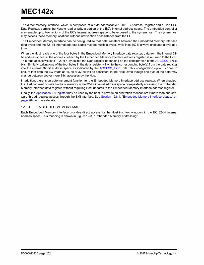
MEC142x
The direct memory interface, which is composed of a byte addressable 16-bit EC Address Register and a 32-bit ECData Register, permits the Host to read or write a portion of the EC’s internal address space. The embedded controllermay enable up to two regions of the EC’s internal address space to be exposed to the system host. The system hostmay access these memory locations without intervention or assistance from the EC.
The Embedded Memory Interface can be configured so that data transfers between the Embedded Memory Interfacedata bytes and the 32- bit internal address space may be multiple bytes, while Host I/O is always executed a byte at atime.
When the Host reads one of the four bytes in the Embedded Memory Interface data register, data from the internal 32-bit address space, at the address defined by the Embedded Memory Interface address register, is returned to the Host.This read access will load 1, 2, or 4 bytes into the Data register depending on the configuration of the ACCESS_TYPEbits. Similarly, writing one of the four bytes in the data register will write the corresponding byte(s) from the data registerinto the internal 32-bit address space as indicated by the ACCESS_TYPE bits. This configuration option is done toensure that data the EC treats as 16-bit or 32-bit will be consistent in the Host, even though one byte of the data maychange between two or more 8-bit accesses by the Host.
In addition, there is an auto-increment function for the Embedded Memory Interface address register. When enabled,the Host can read or write blocks of memory in the 32- bit internal address space by repeatedly accessing the EmbeddedMemory Interface data register, without requiring Host updates to the Embedded Memory Interface address register.
Finally, the Application ID Register may be used by the host to provide an arbitration mechanism if more than one soft-ware thread requires access through the EMI interface. See Section 12.8.4, "Embedded Memory Interface Usage," onpage 204 for more details.
12.8.1 EMBEDDED MEMORY MAP
Each Embedded Memory interface provides direct access for the Host into two windows in the EC 32-bit internaladdress space. This mapping is shown in Figure 12-3, "Embedded Memory Addressing":
DS00002343C-page 202 2017 Microchip Technology Inc.
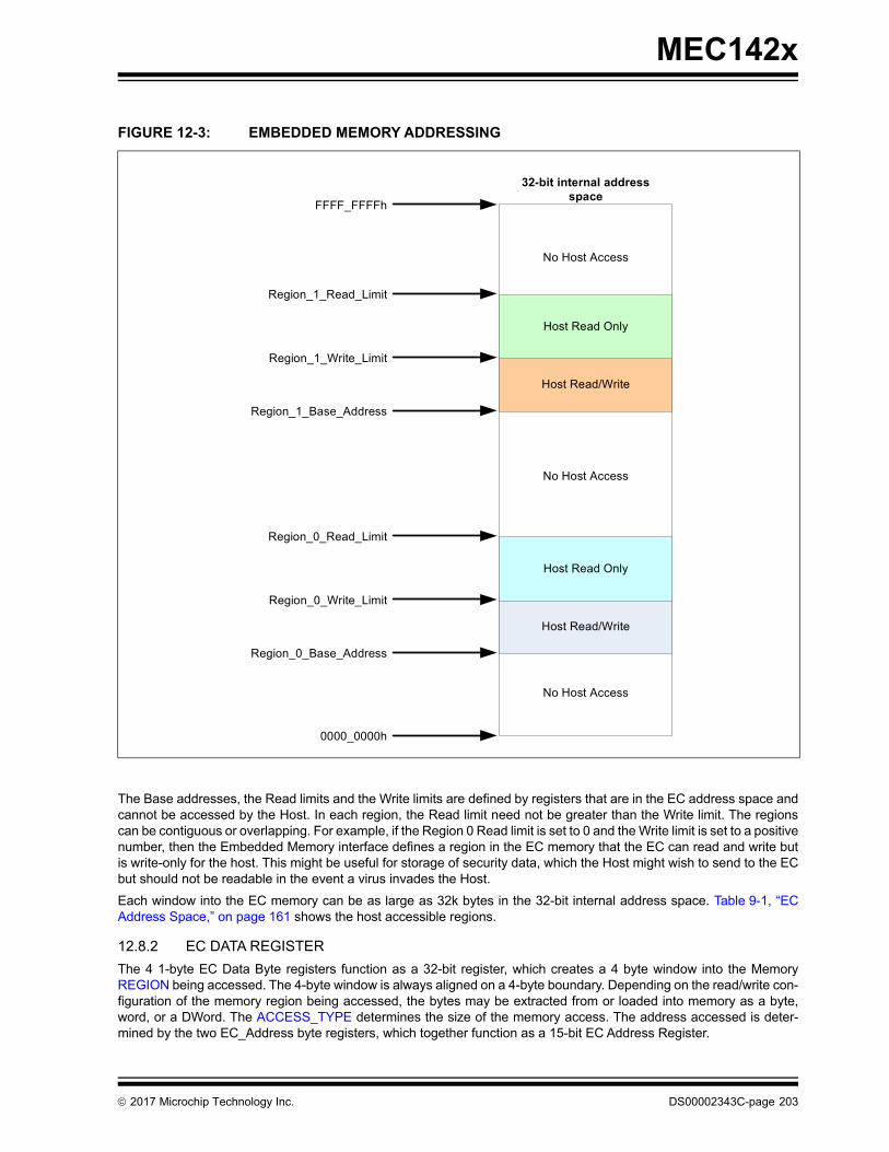
MEC142x
The Base addresses, the Read limits and the Write limits are defined by registers that are in the EC address space andcannot be accessed by the Host. In each region, the Read limit need not be greater than the Write limit. The regionscan be contiguous or overlapping. For example, if the Region 0 Read limit is set to 0 and the Write limit is set to a positivenumber, then the Embedded Memory interface defines a region in the EC memory that the EC can read and write butis write-only for the host. This might be useful for storage of security data, which the Host might wish to send to the ECbut should not be readable in the event a virus invades the Host.
Each window into the EC memory can be as large as 32k bytes in the 32-bit internal address space. Table 9-1, “ECAddress Space,” on page 161 shows the host accessible regions.
12.8.2 EC DATA REGISTER
The 4 1-byte EC Data Byte registers function as a 32-bit register, which creates a 4 byte window into the MemoryREGION being accessed. The 4-byte window is always aligned on a 4-byte boundary. Depending on the read/write con-figuration of the memory region being accessed, the bytes may be extracted from or loaded into memory as a byte,word, or a DWord. The ACCESS_TYPE determines the size of the memory access. The address accessed is deter-mined by the two EC_Address byte registers, which together function as a 15-bit EC Address Register.
FIGURE 12-3: EMBEDDED MEMORY ADDRESSING
32-bit internal address space
0000_0000h
FFFF_FFFFh
Region_0_Base_Address
Region_0_Write_Limit
Region_0_Read_Limit
Host Read/Write
Host Read Only
No Host Access
No Host Access
Region_1_Base_Address
Region_1_Write_Limit
Region_1_Read_Limit
Host Read/Write
Host Read Only
No Host Access
2017 Microchip Technology Inc. DS00002343C-page 203

MEC142x
• A write to the EC Data Register when the EC Address is in a read-only or a no-access region, as defined by the Memory Base and Limit registers, will update the EC Data Register but memory will not be modified.
• A read to the EC Data Register when the EC Address is in a no-access region, as defined by the Memory Base and Limit registers, will not trigger a memory read and will not modify the EC Data Register. In auto-increment mode (ACCESS_TYPE=11b), reads of Byte 3 of the EC Data Register will still trigger increments of the EC Address Register when the address is out of bounds, while writes of Byte 3 will not.
12.8.3 ACCESS TYPES
The access type field (ACCESS_TYPE in the EC Address LSB Register) defines the type of host access that occurswhen the EC Data Register is read or written.
11:Auto-increment 32-bit access. This defines a 32-bit access, as in the 10 case. In addition, any read or write of Byte3 in the EC Data Register causes the EC Data Register to be incremented by 1. That is, the EC_Address field will pointto the next 32-bit double word in the 32- bit internal address space.
10:32-bit access. A read of Byte 0 in the EC Data Register causes the 32 bits in the 32- bit internal address space at anoffset of EC_Address to be loaded into the entire EC Data Register. The read then returns the contents of Byte 0. A readof Byte 1, Byte 2 or Byte 3 in the EC Data Register returns the contents of the register, without any update from the 32-bit internal address space.
A write of Byte 3 in the EC Data Register causes the EC Data Register to be written into the 32 bits in the 32- bit internaladdress space at an offset of EC_Address. A write of Byte 0, Byte 1 or Byte 2 in the EC Data Register updates thecontents of the register, without any change to the 32- bit internal address space.
01:16-bit access. A read of Byte 0 in the EC Data Register causes the 16 bits in the 32- bit internal address space at anoffset of EC_Address to be loaded into Byte 0 and Byte 1 of the EC Data Register. The read then returns the contentsof Byte 0. A read of Byte 2 in the EC Data Register causes the 16 bits in the 32- bit internal address space at an offsetof EC_Address+2 to be loaded into Byte 2 and Byte 3 of the EC Data Register. The read then returns the contents ofByte 2. A read of Byte 1 or Byte 3 in the EC Data Register return the contents of the register, without any update fromthe 32- bit internal address space.
A write of Byte 1 in the EC Data Register causes Bytes 1 and 0 of the EC Data Register to be written into the 16 bits inthe 32- bit internal address space at an offset of EC_Address. A write of Byte 3 in the EC Data Register causes Bytes3 and 2 of the EC Data Register to be written into the 16 bits in the 32- bit internal address space at an offset of EC_Ad-dress+2. A write of Byte 0 or Byte 2 in the EC Data Register updates the contents of the register, without any changeto the 32- bit internal address space.
00:8-bit access. Any byte read of Byte 0 through Byte 3 in the EC Data Register causes the corresponding byte withinthe 32-bit double word addressed by EC_Address to be loaded into the byte of EC Data Register and returned by theread. Any byte write to Byte 0 through Byte 3 in the EC Data Register writes the corresponding byte within the 32-bitdouble word addressed by EC_Address, as well as the byte of the EC Data Register.
12.8.4 EMBEDDED MEMORY INTERFACE USAGE
The Embedded Memory Interface provides a generic facility for communication between the Host and the EC and canbe used for many functions. Some examples are:
• Virtual registers. A block of memory in the 32-bit internal address space can be used to implement a set of virtual registers. The Host is given direct read-only access to this address space, referred to as peek mode. The EC may read or write this memory as needed.
• Program downloading. Because the Instruction Closely Coupled Memory is implemented in the same 32-bit inter-nal address space, the Embedded Memory Interface can be used by the Host to download new program seg-ments for the EC in the upper 32KB SRAM. The Read/Write window would be configured by the Host to point to the beginning of the loadable program region, which could then be loaded by the Host.
• Data exchange. The Read/Write portion of the memory window can be used to contain a communication packet. The Host, by default, “owns” the packet, and can write it at any time. When the Host wishes to communicate with the EC, it sends the EC a command, through the Host-to-EC message facility, to read the packet and perform some operations as a result. When it is completed processing the packet, the EC can inform the Host, either through a message in the EC-to-Host channel or by triggering an event such as an SMI directly. If return results are required, the EC can write the results into the Read/Write region, which the Host can read directly when it is informed that the EC has completed processing. Depending on the command, the operations could entail update of virtual registers in the 32-bit internal address space, reads of any register in the EC address space, or writes of any register in the EC address space. Because there are two regions that are defined by the base registers, the memory used for the communication packet does not have to be contiguous with a set of virtual registers.
DS00002343C-page 204 2017 Microchip Technology Inc.

MEC142x
Because there are two Embedded Memory Interface memory regions, the Embedded Memory Interface cannot be usedfor more than two of these functions at a time. The Host can request that the EC switch from one function to anotherthrough the use of the Host-to-EC mailbox register.
The Application ID Register is provided to help software applications track ownership of an Embedded Memory Inter-face. An application can write the register with its Application ID, then immediately read it back. If the read value is notthe same as the value written, then another application has ownership of the interface.
12.9 Runtime Registers
The registers listed in the Runtime Register Summary table are for a single instance of the EMI. The addresses of eachregister listed in this table are defined as a relative offset to the host “Base Address” defined in the Runtime RegisterBase Address Table.
The Base Address indicates where the first register can be accessed in a particular address space for a block instance.
Note: The protocol used to pass commands back and forth through the Embedded Memory Interface RegistersInterface is left to the System designer. Microchip can provide an application example of working code inwhich the host uses the Embedded Memory Interface registers to gain access to all of the EC registers.
TABLE 12-2: RUNTIME REGISTER BASE ADDRESS TABLE
Block InstanceInstance Number
Host Address Space Base Address
EMI 0 EC 32-bit internal address space
000F_0000h
LPC/eSPI I/O Programmed BAR
TABLE 12-3: RUNTIME REGISTER SUMMARY
Offset Register Name (Mnemonic)
00h HOST-to-EC Mailbox Register
01h EC-to-HOST Mailbox Register
02h EC Address LSB Register
03h EC Address MSB Register
04h EC Data Byte 0 Register
05h EC Data Byte 1 Register
06h EC Data Byte 2 Register
07h EC Data Byte 3 Register
08h Interrupt Source LSB Register
09h Interrupt Source MSB Register
0Ah Interrupt Mask LSB Register
0Bh Interrupt Mask MSB Register
0Ch Application ID Register
2017 Microchip Technology Inc. DS00002343C-page 205

MEC142x
12.9.1 HOST-TO-EC MAILBOX REGISTER
12.9.2 EC-TO-HOST MAILBOX REGISTER
Offset 00h
Bits Description Type DefaultReset Event
7:0 HOST_EC_MBOX
8-bit mailbox used communicate information from the system host to the embedded controller. Writing this register generates an event to notify the embedded controller.
The embedded controller has the option of clearing some or all of the bits in this register. This is dependent on the protocol layer implemented using the EMI Mailbox. The host must know this pro-tocol to determine the meaning of the value that will be reported on a read.
This bit field is aliased to the HOST_EC_MBOX bit field in the HOST-to-EC Mailbox Register
R/W 0h nSYSRST
Offset 01h
Bits Description Type DefaultReset Event
7:0 EC_HOST_MBOX
8-bit mailbox used communicate information from the embedded controller to the system host. Writing this register generates an event to notify the system host.
The system host has the option of clearing some or all of the bits in this register. This is dependent on the protocol layer implemented using the EMI Mailbox. The embedded controller must know this protocol to determine the meaning of the value that will be reported on a read.
This bit field is aliased to the EC_HOST_MBOX bit field in the EC-to-HOST Mailbox Register
R/WC 0h nSYSRST
DS00002343C-page 206 2017 Microchip Technology Inc.
MEC142x
12.9.3 EC ADDRESS LSB REGISTER
12.9.4 EC ADDRESS MSB REGISTER
Offset 02h
Bits Description Type DefaultReset Event
7:2 EC_ADDRESS_LSBThis field defines bits[7:2] of EC_Address [15:0]. Bits[1:0] of the EC_Address are always forced to 00b.
The EC_Address is aligned on a DWord boundary. It is the address of the memory being accessed by EC Data Byte 0 Register, which is an offset from the programmed base address of the selected REGION.
R/W 0h nSYSRST
1:0 ACCESS_TYPE
This field defines the type of access that occurs when the EC Data Register is read or written.
11b=Auto-increment 32-bit access. 10b=32-bit access. 01b=16-bit access.00b=8-bit access.
Each of these access types are defined in detail in Section 12.8.3, "Access Types".
R/W 0h nSYSRST
Offset 03h
Bits Description Type DefaultReset Event
7 REGION
The field specifies which of two segments in the 32-bit internal address space is to be accessed by the EC_Address[14:2] to gen-erate accesses to the memory.
1= The address defined by EC_Address[14:2] is relative to the baseaddress specified by the Memory Base Address 1 Register.
0= The address defined by EC_Address[14:2] is relative to the baseaddress specified by the Memory Base Address 0 Register.
R/W 0h nSYSRST
6:0 EC_ADDRESS_MSB
This field defines bits[14:8] of EC_Address. Bits[1:0] of the EC_Ad-dress are always forced to 00b.
The EC_Address is aligned on a DWord boundary. It is the address of the memory being accessed by EC Data Byte 0 Register, which is an offset from the programmed base address of the selected REGION.
R/W 0h nSYSRST
2017 Microchip Technology Inc. DS00002343C-page 207

MEC142x
12.9.5 EC DATA BYTE 0 REGISTER
12.9.6 EC DATA BYTE 1 REGISTER
12.9.7 EC DATA BYTE 2 REGISTER
Offset 04h
Bits Description Type DefaultReset Event
7:0 EC_DATA_BYTE_0
This is byte 0 (Least Significant Byte) of the 32-bit EC Data Regis-ter.
Use of the Data Byte registers to access EC memory is defined in detail in Section 12.8.2, "EC Data Register".
R/W 0h nSYSRST
Offset 05h
Bits Description Type DefaultReset Event
7:0 EC_DATA_BYTE_1
This is byte 1 of the 32-bit EC Data Register.
Use of the Data Byte registers to access EC memory is defined in detail in Section 12.8.2, "EC Data Register".
R/W 0h nSYSRST
Offset 06h
Bits Description Type DefaultReset Event
7:0 EC_DATA_BYTE_2
This is byte 2 of the 32-bit EC Data Register.
Use of the Data Byte registers to access EC memory is defined in detail in Section 12.8.2, "EC Data Register".
R/W 0h nSYSRST
DS00002343C-page 208 2017 Microchip Technology Inc.

MEC142x
12.9.8 EC DATA BYTE 3 REGISTER
12.9.9 INTERRUPT SOURCE LSB REGISTER
Offset 07h
Bits Description Type DefaultReset Event
7:0 EC_DATA_BYTE_3
This is byte 3 (Most Significant Byte) of the 32-bit EC Data Register.
Use of the Data Byte registers to access EC memory is defined in detail in Section 12.8.2, "EC Data Register".
R/W 0h nSYSRST
Offset 08h
Bits Description Type DefaultReset Event
7:1 EC_SWI_LSB
EC Software Interrupt Least Significant Bits. These bits are soft-ware interrupt bits that may be set by the EC to notify the host of an event. The meaning of these bits is dependent on the firmware implementation.
Each bit in this field is cleared when written with a ‘1b’. The ability to clear the bit can be disabled by the EC if the corresponding bit in the Host Clear Enable Register is set to ‘0b’. This may be used by firmware for events that cannot be cleared while the event is still active.
R/WC 0h nSYSRST
0 EC_WR
EC Mailbox Write. This bit is set when the EC-to-HOST Mailbox Register has been written by the EC at offset 01h of the EC-Only registers.
R 0h nSYSRST
2017 Microchip Technology Inc. DS00002343C-page 209

MEC142x
12.9.10 INTERRUPT SOURCE MSB REGISTER
12.9.11 INTERRUPT MASK LSB REGISTER
12.9.12 INTERRUPT MASK MSB REGISTER
Offset 09h
Bits Description Type DefaultReset Event
7:0 EC_SWI_MSB
EC Software Interrupt Most Significant Bits. These bits are soft-ware interrupt bits that may be set by the EC to notify the host of an event. The meaning of these bits is dependent on the firmware implementation.
Each bit in this field is cleared when written with a ‘1b’. The ability to clear the bit can be disabled by the EC. if the corresponding bit in the Host Clear Enable Register is set to ‘0b’. This may be used by firmware for events that cannot be cleared while the event is still active.
R/WC 0h nSYSRST
Offset 0Ah
Bits Description Type DefaultReset Event
7:1 EC_SWI_EN_LSB
EC Software Interrupt Enable Least Significant Bits. Each bit that is set to ‘1b’ in this field enables the generation of a Host_SWI_Event interrupt by the corresponding bit in the EC_SWI field in the Inter-rupt Source LSB Register.
R/W 0h nSYSRST
0 EC_WR_EN
EC Mailbox Write.Interrupt Enable. If this bit is ‘1b’, the interrupt generated by bit EC_WR in the Interrupt Source LSB Register is enabled to generate a EC-to-Host interrupt event.
R/W 0h nSYSRST
Offset 0Bh
Bits Description Type DefaultReset Event
7:0 EC_SWI_EN_MSB
EC Software Interrupt Enable Most Significant Bits. Each bit that is set to ‘1b’ in this field enables the generation of a Host_SWI_Event interrupt by the corresponding bit in the EC_SWI field in the Inter-rupt Source MSB Register.
R/W 0h nSYSRST
DS00002343C-page 210 2017 Microchip Technology Inc.

MEC142x
12.9.13 APPLICATION ID REGISTER
12.10 EC-Only Registers
The registers listed in the EC-Only Register Summary table are for a single instance of the Embedded Memory Interface(EMI). The addresses of each register listed in this table are defined as a relative offset to the host “Base Address”defined in the EC-Only Register Base Address Table.
The Base Address indicates where the first register can be accessed in a particular address space for a block instance.
Offset 0Ch
Bits Description Type DefaultReset Event
7:0 APPLICATION_ID
When this field is 00h it can be written with any value. When set to a non-zero value, writing that value will clear this register to 00h. When set to a non-zero value, writing any value other than the cur-rent contents will have no effect.
R/W 0h nSYSRST
TABLE 12-4: EC-ONLY REGISTER BASE ADDRESS TABLE
Block InstanceInstance Number Host Address Space Base Address
EMI 0 EC 32-bit internal address space
000F_0100h
TABLE 12-5: EC-ONLY REGISTER SUMMARY
Offset Register Name (Mnemonic)
00h HOST-to-EC Mailbox Register
01h EC-to-HOST Mailbox Register
04h Memory Base Address 0 Register
08h Memory Read Limit 0 Register
0Ah Memory Write Limit 0 Register
0Ch Memory Base Address 1 Register
10h Memory Read Limit 1 Register
12h Memory Write Limit 1 Register
14h Interrupt Set Register
16h Host Clear Enable Register
2017 Microchip Technology Inc. DS00002343C-page 211

MEC142x
12.10.1 HOST-TO-EC MAILBOX REGISTER
12.10.2 EC-TO-HOST MAILBOX REGISTER
Offset 00h
Bits Description Type DefaultReset Event
7:0 HOST_EC_MBOX
8-bit mailbox used communicate information from the system host to the embedded controller. Writing this register generates an event to notify the embedded controller.
The embedded controller has the option of clearing some or all of the bits in this register. This is dependent on the protocol layer implemented using the EMI Mailbox. The host must know this pro-tocol to determine the meaning of the value that will be reported on a read.
This bit field is aliased to the HOST_EC_MBOX bit field in the HOST-to-EC Mailbox Register.
R/WC 0h nSYSRST
Offset 01h
Bits Description Type DefaultReset Event
7:0 EC_HOST_MBOX
8-bit mailbox used communicate information from the embedded controller to the system host. Writing this register generates an event to notify the system host.
The system host has the option of clearing some or all of the bits in this register. This is dependent on the protocol layer implemented using the EMI Mailbox. The embedded controller must know this protocol to determine the meaning of the value that will be reported on a read.
This bit field is aliased to EC_HOST_MBOX bit field in EC-to-HOST Mailbox Register (EC_TO_HOST) on page 129 defined in Section 10.10, "Runtime Registers".
R/W 0h nSYSRST
DS00002343C-page 212 2017 Microchip Technology Inc.
MEC142x
12.10.3 MEMORY BASE ADDRESS 0 REGISTER
12.10.4 MEMORY READ LIMIT 0 REGISTER
Offset 04h
Bits Description Type DefaultReset Event
31:2 MEMORY_BASE_ADDRESS_0
This memory base address defines the beginning of region 0 in the Embedded Controller’s 32-bit internal address space. Memory allo-cated to region 0 is intended to be shared between the Host and the EC. The region defined by this base register is used when bit 15 of the EC Address Register is 0. The access will be to a mem-ory location at an offset defined by the EC_Address relative to the beginning of the region defined by this register. Therefore, a read or write to the memory that is triggered by the EC Data Register will occur at Memory_Base_Address_0 + EC_Address.
R/W 0h nSYSRST
1:0 Reserved R - -
Offset 08h
Bits Description Type DefaultReset Event
15 Reserved R - -
14:2 MEMORY_READ_LIMIT_0
Whenever a read of any byte in the EC Data Register is attempted, and bit 15 of EC_Address is 0, the field EC_Address[14:2] in the EC_Address_Register is compared to this field. As long as EC_Ad-dress[14:2] is less than this field the EC_Data_Register will be loaded from the 32-bit internal address space.
R/W 0h nSYSRST
1:0 Reserved R - -
2017 Microchip Technology Inc. DS00002343C-page 213
MEC142x
12.10.5 MEMORY WRITE LIMIT 0 REGISTER
12.10.6 MEMORY BASE ADDRESS 1 REGISTER
Offset 0Ah
Bits Description Type DefaultReset Event
15 Reserved R - -
14:2 MEMORY_WRITE_LIMIT_0
Whenever a write of any byte in EC DATA Register is attempted and bit 15 of EC_Address is 0, the field EC_ADDRESS_MSB in the EC_Address Register is compared to this field. As long as EC_Address[14:2] is less than Memory_Write_Limit_0[14:2] the addressed bytes in the EC DATA Register will be written into the internal 32-bit address space. If EC_Address[14:2] is greater than or equal to the Memory_Write_Limit_0[14:2] no writes will take place.
R/W 0h nSYSRST
1:0 Reserved R - -
Offset 0Ch
Bits Description Type DefaultReset Event
31:2 MEMORY_BASE_ADDRESS_1
This memory base address defines the beginning of region 1 in the Embedded Controller’s 32-bit internal address space. Memory allo-cated to region 1 is intended to be shared between the Host and the EC. The region defined by this base register is used when bit 15 of the EC Address Register is 1. The access will be to a mem-ory location at an offset defined by the EC_Address relative to the beginning of the region defined by this register. Therefore, a read or write to the memory that is triggered by the EC Data Register will occur at Memory_Base_Address_1 + EC_Address.
R/W 0h nSYSRST
1:0 Reserved R - -
DS00002343C-page 214 2017 Microchip Technology Inc.

MEC142x
12.10.7 MEMORY READ LIMIT 1 REGISTER
12.10.8 MEMORY WRITE LIMIT 1 REGISTER
12.10.9 INTERRUPT SET REGISTER
Offset 10h
Bits Description Type DefaultReset Event
15 Reserved R - -
14:2 MEMORY_READ_LIMIT_1
Whenever a read of any byte in the EC Data Register is attempted, and bit 15 of EC_ADDRESS is 1, the field EC_ADDRESS in the EC_Address_Register is compared to this field. As long as EC_ADDRESS is less than this value, the EC_Data_Register will be loaded from the 32-bit internal address space.
R/W 0h nSYSRST
1:0 Reserved R - -
Offset 12h
Bits Description Type DefaultReset Event
15 Reserved R - -
14:2 MEMORY_WRITE_LIMIT_1
Whenever a write of any byte in EC DATA Register is attempted and bit 15 of EC_Address is 1, the field EC_Address[14:2] in the EC_Address Register is compared to this field. As long as EC_Ad-dress[14:2] is less than Memory_Write_Limit_1[14:2] the addressed bytes in the EC DATA Register will be written into the internal 32-bit address space. If EC_Address[14:2] is greater than or equal to the Memory_Write_Limit_1[14:2] no writes will take place.
R/W 0h nSYSRST
1:0 Reserved R - -
Offset 14h
Bits Description Type DefaultReset Event
15:1 EC_SWI_SET
EC Software Interrupt Set. This register provides the EC with a means of updating the Interrupt Source Registers. Writing a bit in this field with a ‘1b’ sets the corresponding bit in the Interrupt Source Register to ‘1b’. Writing a bit in this field with a ‘0b’ has no effect. Reading this field returns the current contents of the Inter-rupt Source Register.
R/WS 0h nSYSRST
0 Reserved R - -
2017 Microchip Technology Inc. DS00002343C-page 215
MEC142x
12.10.10 HOST CLEAR ENABLE REGISTER
Offset 16h
Bits Description Type DefaultReset Event
15:1 HOST_CLEAR_ENABLE
When a bit in this field is ‘0b’, the corresponding bit in the Interrupt Source Register cannot be cleared by writes to the Interrupt Source Register. When a bit in this field is ‘1b’, the corresponding bit in the Interrupt Source Register can be cleared when that regis-ter bit is written with a ‘1b’.
These bits allow the EC to control whether the status bits in the Interrupt Source Register are based on an edge or level event.
R/W 0h nSYSRST
0 Reserved R - -
DS00002343C-page 216 2017 Microchip Technology Inc.
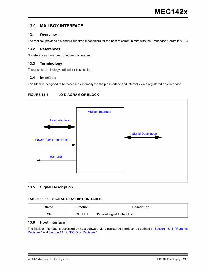
MEC142x
13.0 MAILBOX INTERFACE
13.1 Overview
The Mailbox provides a standard run-time mechanism for the host to communicate with the Embedded Controller (EC)
13.2 References
No references have been cited for this feature.
13.3 Terminology
There is no terminology defined for this section.
13.4 Interface
This block is designed to be accessed externally via the pin interface and internally via a registered host interface.
13.5 Signal Description
13.6 Host Interface
The Mailbox interface is accessed by host software via a registered interface, as defined in Section 13.11, "RuntimeRegisters" and Section 13.12, "EC-Only Registers".
FIGURE 13-1: I/O DIAGRAM OF BLOCK
TABLE 13-1: SIGNAL DESCRIPTION TABLE
Name Direction Description
nSMI OUTPUT SMI alert signal to the Host.
Mailbox Interface
Interrupts
Power, Clocks and Reset
Host Interface
Signal Description
2017 Microchip Technology Inc. DS00002343C-page 217
MEC142x
13.7 Power, Clocks and Reset
This section defines the Power, Clock, and Reset parameters of the block.
13.7.1 POWER DOMAINS
13.7.2 CLOCK INPUTS
13.7.3 RESETS
13.8 Interrupts
Name Description
VTR The logic and registers implemented in this block are powered by this power well.
Name Description
48 MHz Ring Oscillator This is the clock source for Mailbox logic.
Name Description
nSYSRST This signal resets all the registers and logic in this block to their default state.
VCC_PWRGD This signal is asserted when the main power rail is asserted. The Host Access Port is reset when this signal is de-asserted.
Source Description
MBX_Host_SIRQ This interrupt source for the SIRQ logic is generated when the EC_WR bit is ‘1’ and enabled by the EC_WR_EN bit.
MBX_Host_SMI This interrupt source for the SIRQ logic is generated when any of the EC_SWI bits are asserted and the corresponding EC_SWI_EN bit are asserted as well. This event is also asserted if the EC_WR/EC_WR_EN event occurs as well.
This bit is also routed to the nSMI pin.
Source Description
MBX Interrupt generated by the host writing the HOST-to-EC Mailbox register.
MBX_DATA Interrupt generated by the host writing the MBX_DATA register.
DS00002343C-page 218 2017 Microchip Technology Inc.
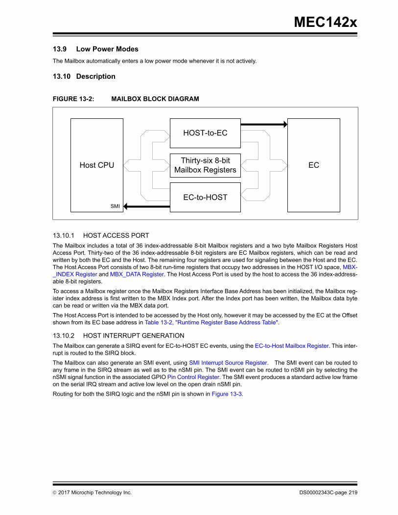
MEC142x
13.9 Low Power Modes
The Mailbox automatically enters a low power mode whenever it is not actively.
13.10 Description
13.10.1 HOST ACCESS PORT
The Mailbox includes a total of 36 index-addressable 8-bit Mailbox registers and a two byte Mailbox Registers HostAccess Port. Thirty-two of the 36 index-addressable 8-bit registers are EC Mailbox registers, which can be read andwritten by both the EC and the Host. The remaining four registers are used for signaling between the Host and the EC.The Host Access Port consists of two 8-bit run-time registers that occupy two addresses in the HOST I/O space, MBX-_INDEX Register and MBX_DATA Register. The Host Access Port is used by the host to access the 36 index-address-able 8-bit registers.
To access a Mailbox register once the Mailbox Registers Interface Base Address has been initialized, the Mailbox reg-ister index address is first written to the MBX Index port. After the Index port has been written, the Mailbox data bytecan be read or written via the MBX data port.
The Host Access Port is intended to be accessed by the Host only, however it may be accessed by the EC at the Offsetshown from its EC base address in Table 13-2, "Runtime Register Base Address Table".
13.10.2 HOST INTERRUPT GENERATION
The Mailbox can generate a SIRQ event for EC-to-HOST EC events, using the EC-to-Host Mailbox Register. This inter-rupt is routed to the SIRQ block.
The Mailbox can also generate an SMI event, using SMI Interrupt Source Register. The SMI event can be routed toany frame in the SIRQ stream as well as to the nSMI pin. The SMI event can be routed to nSMI pin by selecting thenSMI signal function in the associated GPIO Pin Control Register. The SMI event produces a standard active low frameon the serial IRQ stream and active low level on the open drain nSMI pin.
Routing for both the SIRQ logic and the nSMI pin is shown in Figure 13-3.
FIGURE 13-2: MAILBOX BLOCK DIAGRAM
HOST-to-EC
EC-to-HOST
Host CPU
SMI
ECThirty-six 8-bit
Mailbox Registers
2017 Microchip Technology Inc. DS00002343C-page 219
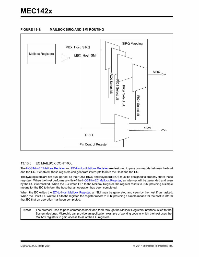
MEC142x
13.10.3 EC MAILBOX CONTROL
The HOST-to-EC Mailbox Register and EC-to-Host Mailbox Register are designed to pass commands between the hostand the EC. If enabled, these registers can generate interrupts to both the Host and the EC.
The two registers are not dual-ported, so the HOST BIOS and Keyboard BIOS must be designed to properly share theseregisters. When the host performs a write of the HOST-to-EC Mailbox Register, an interrupt will be generated and seenby the EC if unmasked. When the EC writes FFh to the Mailbox Register, the register resets to 00h, providing a simplemeans for the EC to inform the host that an operation has been completed.
When the EC writes the EC-to-Host Mailbox Register, an SMI may be generated and seen by the host if unmasked.When the Host CPU writes FFh to the register, the register resets to 00h, providing a simple means for the host to informthat EC that an operation has been completed.
FIGURE 13-3: MAILBOX SIRQ AND SMI ROUTING
Note: The protocol used to pass commands back and forth through the Mailbox Registers Interface is left to theSystem designer. Microchip can provide an application example of working code in which the host uses theMailbox registers to gain access to all of the EC registers.
Mailbox RegistersMBX_Host_SMI
GPIO
nSMI
Pin Control Register
SIRQ Mapping
SIRQ
MBX_Host_SIRQ
IRQ
0 Sele
ct bit
IRQ
1 S
elect bit
IRQ
2 Select bit
IRQ
n Select b
it
DS00002343C-page 220 2017 Microchip Technology Inc.
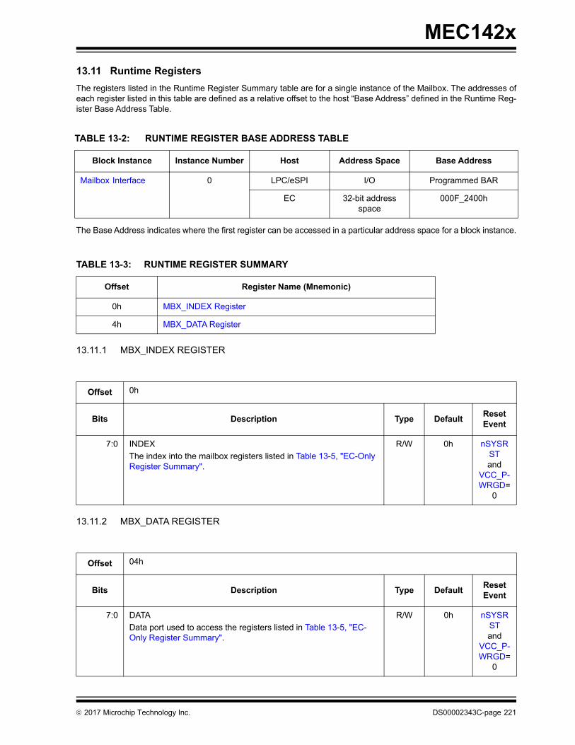
MEC142x
13.11 Runtime Registers
The registers listed in the Runtime Register Summary table are for a single instance of the Mailbox. The addresses ofeach register listed in this table are defined as a relative offset to the host “Base Address” defined in the Runtime Reg-ister Base Address Table.
The Base Address indicates where the first register can be accessed in a particular address space for a block instance.
13.11.1 MBX_INDEX REGISTER
13.11.2 MBX_DATA REGISTER
TABLE 13-2: RUNTIME REGISTER BASE ADDRESS TABLE
Block Instance Instance Number Host Address Space Base Address
Mailbox Interface 0 LPC/eSPI I/O Programmed BAR
EC 32-bit address space
000F_2400h
TABLE 13-3: RUNTIME REGISTER SUMMARY
Offset Register Name (Mnemonic)
0h MBX_INDEX Register
4h MBX_DATA Register
Offset 0h
Bits Description Type DefaultReset Event
7:0 INDEX
The index into the mailbox registers listed in Table 13-5, "EC-Only Register Summary".
R/W 0h nSYSRSTand
VCC_P-WRGD=
0
Offset 04h
Bits Description Type DefaultReset Event
7:0 DATA
Data port used to access the registers listed in Table 13-5, "EC-Only Register Summary".
R/W 0h nSYSRSTand
VCC_P-WRGD=
0
2017 Microchip Technology Inc. DS00002343C-page 221

MEC142x
13.12 EC-Only Registers
The registers listed in the EC-Only Register Summary table are for a single instance of the Mailbox. The addresses ofeach register listed in this table are defined as a relative offset to the host “Base Address” defined in the EC-Only Reg-ister Base Address Table.
The EC-Only registers can be accessed by the EC at the EC Offset from the Base Address. In addition, the registerscan be accessed through the Host Access Port, at the indexes listed in the following tables as “MBX_INDEX”.
TABLE 13-4: EC-ONLY REGISTER BASE ADDRESS TABLE
Block Instance Instance Number Host Address Space Base Address
Mailbox Interface 0 EC 32-bit address space
000F_2500h
TABLE 13-5: EC-ONLY REGISTER SUMMARY
EC OffsetHost I/O Index(MBX_INDEX)
Register Name (Mnemonic)
00h 00h HOST-to-EC Mailbox Register
04h 01h EC-to-Host Mailbox Register
08h 02h SMI Interrupt Source Register
0Ch 03h SMI Interrupt Mask Register
10h 10h Mailbox register [0]
11h Mailbox register [1]
12h Mailbox register [2]
13h Mailbox register [3]
14h 14h Mailbox register [4]
15h Mailbox register [5]
16h Mailbox register [6]
17h Mailbox register [7]
18h 18h Mailbox register [8]
19h Mailbox register [9]
1Ah Mailbox register [A]
1Bh Mailbox register [B]
1Ch 1Ch Mailbox register [C]
1Dh Mailbox register [D]
1Eh Mailbox register [E]
1Fh Mailbox register [F]
DS00002343C-page 222 2017 Microchip Technology Inc.
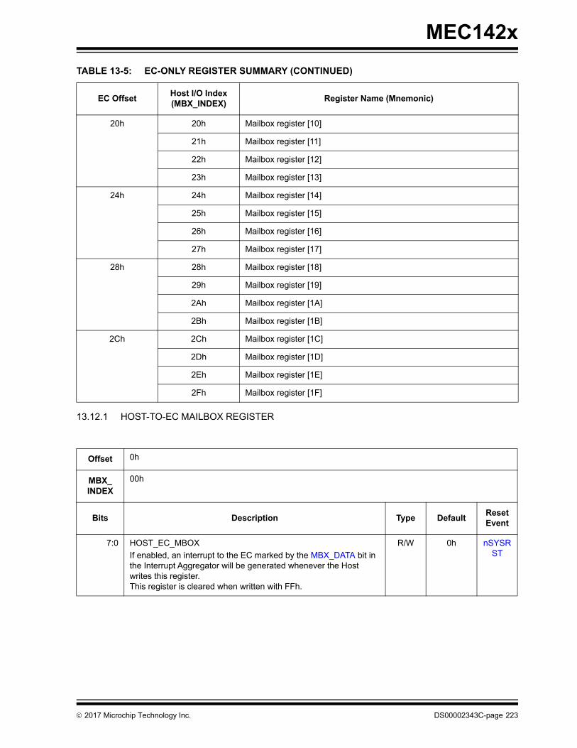
MEC142x
13.12.1 HOST-TO-EC MAILBOX REGISTER
20h 20h Mailbox register [10]
21h Mailbox register [11]
22h Mailbox register [12]
23h Mailbox register [13]
24h 24h Mailbox register [14]
25h Mailbox register [15]
26h Mailbox register [16]
27h Mailbox register [17]
28h 28h Mailbox register [18]
29h Mailbox register [19]
2Ah Mailbox register [1A]
2Bh Mailbox register [1B]
2Ch 2Ch Mailbox register [1C]
2Dh Mailbox register [1D]
2Eh Mailbox register [1E]
2Fh Mailbox register [1F]
Offset 0h
MBX_INDEX
00h
Bits Description Type DefaultReset Event
7:0 HOST_EC_MBOX
If enabled, an interrupt to the EC marked by the MBX_DATA bit in the Interrupt Aggregator will be generated whenever the Host writes this register.This register is cleared when written with FFh.
R/W 0h nSYSRST
TABLE 13-5: EC-ONLY REGISTER SUMMARY (CONTINUED)
EC OffsetHost I/O Index(MBX_INDEX)
Register Name (Mnemonic)
2017 Microchip Technology Inc. DS00002343C-page 223
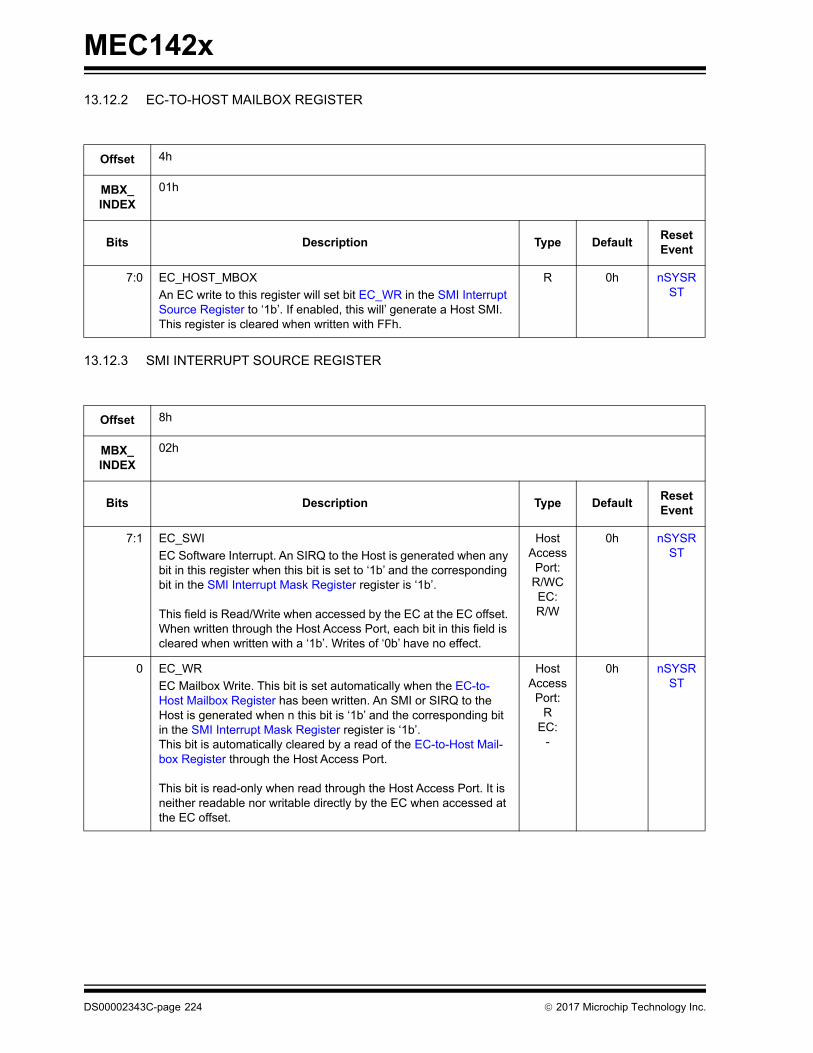
MEC142x
13.12.2 EC-TO-HOST MAILBOX REGISTER
13.12.3 SMI INTERRUPT SOURCE REGISTER
Offset 4h
MBX_INDEX
01h
Bits Description Type DefaultReset Event
7:0 EC_HOST_MBOX
An EC write to this register will set bit EC_WR in the SMI Interrupt Source Register to ‘1b’. If enabled, this will’ generate a Host SMI.This register is cleared when written with FFh.
R 0h nSYSRST
Offset 8h
MBX_INDEX
02h
Bits Description Type DefaultReset Event
7:1 EC_SWI
EC Software Interrupt. An SIRQ to the Host is generated when any bit in this register when this bit is set to ‘1b’ and the corresponding bit in the SMI Interrupt Mask Register register is ‘1b’.
This field is Read/Write when accessed by the EC at the EC offset. When written through the Host Access Port, each bit in this field is cleared when written with a ‘1b’. Writes of ‘0b’ have no effect.
Host Access Port:
R/WCEC:R/W
0h nSYSRST
0 EC_WR
EC Mailbox Write. This bit is set automatically when the EC-to-Host Mailbox Register has been written. An SMI or SIRQ to the Host is generated when n this bit is ‘1b’ and the corresponding bit in the SMI Interrupt Mask Register register is ‘1b’.This bit is automatically cleared by a read of the EC-to-Host Mail-box Register through the Host Access Port.
This bit is read-only when read through the Host Access Port. It is neither readable nor writable directly by the EC when accessed at the EC offset.
Host Access Port:
REC:
-
0h nSYSRST
DS00002343C-page 224 2017 Microchip Technology Inc.

MEC142x
13.12.4 SMI INTERRUPT MASK REGISTER
Offset Ch
MBX_INDEX
03h
Bits Description Type DefaultReset Event
7:1 EC_SWI_EN
EC Software Interrupt Enable. If this bit is ‘1b’, the bit EC_WR in the SMI Interrupt Source Register is enabled for the generation of SIRQ or nSMI events.
R/W 0h nSYSRST
0 EC_WR_EN
EC Mailbox Write.Interrupt Enable. Each bit in this field that is ‘1b’ enables the generation of SIRQ interrupts when the corresponding bit in the EC_SWI field in the SMI Interrupt Source Register is ‘1b’.
R 0h nSYSRST
2017 Microchip Technology Inc. DS00002343C-page 225
MEC142x
14.0 ACPI EMBEDDED CONTROLLER INTERFACE (ACPI-ECI)
14.1 Introduction
The ACPI Embedded Controller Interface (ACPI-ECI) is a Host/EC Message Interface. The ACPI specification definesthe standard hardware and software communications interface between the OS and an embedded controller. This inter-face allows the OS to support a standard driver that can directly communicate with the embedded controller, allowingother drivers within the system to communicate with and use the EC resources; for example, Smart Battery and AMLcode.
The ACPI Embedded Controller Interface (ACPI-ECI) provides a four byte full duplex data interface which is a supersetof the standard ACPI Embedded Controller Interface (ACPI-ECI) one byte data interface. The ACPI Embedded Control-ler Interface (ACPI-ECI) defaults to the standard one byte interface.
The MEC142x has two instances of the ACPI Embedded Controller Interface.
1. The EC host in Table 14-4 and Table 14-6 corresponds to the EC in the ACPI specification. This interface isreferred to elsewhere in this chapter as ACPI_EC.
2. The LPC host in Table 14-4 and Table 14-6 corresponds to the “System Host Interface to OS” in the ACPIspecification. This interface is referred to elsewhere in this chapter as ACPI_OS.
14.2 References
• Advanced Configuration and Power Interface Specification, Revision 4.0 June 16, 2009, Hewlett-Packard Corpo-ration Intel Corporation Microsoft Corporation Phoenix Technologies Ltd. Toshiba Corporation
14.3 Terminology
14.4 Interface
This block is designed to be accessed externally and internally via a register interface.
TABLE 14-1: TERMINOLOGY
Term Definition
ACPI_EC The EC host corresponding to the ACPI specification interface to the EC.
ACPI_OS The LPC host corresponding to the ACPI specification interface to the “System Host Interface to OS”.ACPI_OS terminology is not meant to distinguish the ACPI System Man-agement from Operating System but merely the hardware path upstream towards the CPU.
DS00002343C-page 226 2017 Microchip Technology Inc.

MEC142x
14.5 Signal Description
There are no external signals.
14.6 Host Interface
The registers defined for the ACPI Embedded Controller Interface (ACPI-ECI) are accessible by the System Host andthe Embedded Controller as indicated in Section 14.12, "Runtime Registers" and Section 14.13, "EC-Only Registers".
14.7 Power, Clocks and Reset
This section defines the Power, Clock, and Reset parameters of the block.
14.7.1 POWER DOMAINS
14.7.2 CLOCK INPUTS
This block only requires the Host interface clocks to synchronize registers access.
14.7.3 RESETS
FIGURE 14-1: I/O DIAGRAM OF BLOCK
Name Description
VTR The logic and registers implemented in this block reside on this single power well.
Name Description
nSYSRST nSYSRST resets all the logic and registers in ACPI Embedded Controller Interface (ACPI-ECI).
ACPI Embedded Controller Interface (ACPI-ECI)
Interrupts
Power, Clocks and Reset
Host Interface
Signal Description
2017 Microchip Technology Inc. DS00002343C-page 227

MEC142x
14.8 Interrupts
This section defines the Interrupt Sources generated from this block.
14.9 Low Power Modes
The ACPI Embedded Controller Interface (ACPI-ECI) automatically enters low power mode when no transaction targetsit.
14.10 Description
The ACPI Embedded Controller Interface (ACPI-ECI) provides an APCI-EC interface that adheres to the ACPI specifi-cation. The ACPI Embedded Controller Interface (ACPI-ECI) includes two modes of operation: Legacy Mode and Four-byte Mode.
The ACPI Embedded Controller Interface (ACPI-ECI) defaults to Legacy Mode which provides single byte Full Duplexoperation. Legacy Mode corresponds to the ACPI specification functionality as illustrated in FIGURE 14-2: on page 229.The EC interrupts in FIGURE 14-2: on page 229 are implemented as OBF & IBF. See Section 14.8, "Interrupts," onpage 228.
In Four-byte Mode, the ACPI Embedded Controller Interface (ACPI-ECI) provides four byte Full Duplex operation. Four-byte Mode is a superset of the ACPI specification functionality as illustrated in FIGURE 14-2: on page 229.
Both Legacy Mode & Four-byte Mode provide Full Duplex Communications which allows data/command transfers inone direction while maintaining data from the other direction; communications can flow both ways simultaneously.
In Legacy Mode, ACPI Embedded Controller Interface (ACPI-ECI) contains three registers: ACPI OS COMMAND Reg-ister, OS STATUS OS Register, and OS2EC Data EC Byte 0 Register. The standard ACPI Embedded Controller Inter-face (ACPI-ECI) registers occupy two addresses in the ACPI_OS space (Table 14-5).
The OS2EC Data EC Byte 0 Register and ACPI OS COMMAND Register registers appear as a single 8-bit data registerin the ACPI_EC. The CMD bit in the OS STATUS OS Register is used by the ACPI_EC to discriminate commands fromdata written by the ACPI_OS to the ACPI_EC. CMD bit is controlled by hardware: ACPI_OS writes to the OS2EC DataEC Byte 0 Register register clear the CMD bit; ACPI_OS writes to the ACPI OS COMMAND Register set the CMD bit.
Source Description
OBF OBF interrupt is asserted when the OBF in the EC STATUS Register is cleared to ‘0’.
IBF IBF interrupt is asserted when the IBF in the EC STATUS Register is set to ‘1’.
Note: The usage model from the ACPI specification requires both SMI’s and SCI’s. The ACPI_OS SMI & SCIinterrupts are not implemented in the ACPI Embedded Controller Interface (ACPI-ECI). The SMI_EVT andSCI_EVT bits in the OS STATUS OS Register are software flags and this block do not initiate SMI or SCIevents.
DS00002343C-page 228 2017 Microchip Technology Inc.

MEC142x
FIGURE 14-2: BLOCK DIAGRAM CORRESPONDING TO THE ACPI SPECIFICATION
Legacy Mode
Control Register
Status
CommandSystem Host
Interface to OS
EC InterruptsHost SMI & SCI interrupts
ECProcessorInterface
DataSingle Byte
Legend Legacy MCHP Proprietary
DataSingleByte
Full DuplexData flow in each
direction indipendent
2017 Microchip Technology Inc. DS00002343C-page 229

MEC142x
Four-byte Mode
FIGURE 14-2: BLOCK DIAGRAM CORRESPONDING TO THE ACPI SPECIFICATION
Status
Command
System Host
Interface to OS
EC InterruptsHost SMI & SCI interrupts
ECProcessorInterface
Data
0
21
3
Data
0
21
3
Full DuplexData flow in each
direction indipendent
Control Register
Legend Legacy MCHP Proprietary
DS00002343C-page 230 2017 Microchip Technology Inc.

MEC142x
14.11 Register Aliasing between Runtime and EC-Only Registers
Table 14-2, "Runtime Register Aliasing into EC-Only Registers" indicates the aliasing from Runtime registers to EC-Onlyregisters. The “Host/EC Access” column distinguishes the aliasing based on access type. See individual registerdescriptions for more details.
Table 14-3, "EC-Only Registers Summary" indicates the aliasing from EC-Only to Runtime registers. The “Host/ECAccess” column distinguishes the aliasing based on access type. See individual register descriptions for more details.
TABLE 14-2: RUNTIME REGISTER ALIASING INTO EC-ONLY REGISTERS
HostOffset
Runtime RegisterRegister Name (Mnemonic)
Host Access
EC Offset
Aliased EC-Only RegisterRegister Name (Mnemonic)
EC Access
00h ACPI OS Data Register Byte 0 Register
W 108h OS2EC Data EC Byte 0 Register R
00h ACPI OS Data Register Byte 0 Register
R 100h EC2OS Data EC Byte 0 Register W
01h ACPI OS Data Register Byte 1 Register
W 109h OS2EC Data EC Byte 1 Register R
01h ACPI OS Data Register Byte 1 Register
R 101h EC2OS Data EC Byte 1 Register W
02h ACPI OS Data Register Byte 2 Register
W 10Ah OS2EC Data EC Byte 2 Register R
02h ACPI OS Data Register Byte 2 Register
R 102h EC2OS Data EC Byte 2 Register W
03h ACPI OS Data Register Byte 3 Register
W 10Bh OS2EC Data EC Byte 3 Register R
03h ACPI OS Data Register Byte 3 Register
R 103h EC2OS Data EC Byte 3 Register W
04h ACPI OS COMMAND Register W 108h OS2EC Data EC Byte 0 Register R
04h OS STATUS OS Register R 104h EC STATUS Register W
05h OS Byte Control Register R 105h EC Byte Control Register R/W
06h Reserved 106h Reserved
07h Reserved 107h Reserved
TABLE 14-3: EC-ONLY REGISTERS SUMMARY
ECOffset
EC-Only RegistersRegister Name (Mnemonic)
EC Access
HostOffset
Aliased Runtime RegisterRegister Name (Mnemonic)
Host Access
108h OS2EC Data EC Byte 0 Register R 00h ACPI OS Data Register Byte 0 Register
W
108h OS2EC Data EC Byte 0 Register R 04h ACPI OS COMMAND Register W
2017 Microchip Technology Inc. DS00002343C-page 231

MEC142x
14.12 Runtime Registers
The registers listed in the Runtime Register Summary table are for four instances of the ACPI Embedded ControllerInterface (ACPI-ECI). The addresses of each register listed in this table are defined as a relative offset to the host“Base Address” defined in the Runtime Register Base Address Table.
109h OS2EC Data EC Byte 1 Register R 01h ACPI OS Data Register Byte 1 Register
W
10Ah OS2EC Data EC Byte 2 Register R 02h ACPI OS Data Register Byte 2 Register
W
10Bh OS2EC Data EC Byte 3 Register R 03h ACPI OS Data Register Byte 3 Register
W
104h EC STATUS Register W 04h OS STATUS OS Register W
105h EC Byte Control Register R/W 05h OS Byte Control Register R
106h Reserved R Reserved R
107h Reserved R Reserved R
100h EC2OS Data EC Byte 0 Register W 00h ACPI OS Data Register Byte 0 Register
R
101h EC2OS Data EC Byte 1 Register W 01h ACPI OS Data Register Byte 1 Register
R
102h EC2OS Data EC Byte 2 Register W 02h ACPI OS Data Register Byte 2 Register
R
103h EC2OS Data EC Byte 3 Register W 03h ACPI OS Data Register Byte 3 Register
R
Note: The Runtime registers may be accessed by the EC but typically the Host will access the Runtime Registersand the EC will access just the EC-Only registers.
TABLE 14-4: RUNTIME REGISTER BASE ADDRESS TABLE
Block InstanceInstance Number
Host Address Space Base Address
ACPI-EC 0 LPC/eSPI I/O Programmed BAR
EC 32-bit internal address space
000F_0C00h
ACPI-EC 1 LPC/eSPI I/O Programmed BAR
EC 32-bit internal address space
000F_1000h
ACPI-EC 2 LPC/eSPI I/O Programmed BAR
EC 32-bit internal address space
000F_2800h
TABLE 14-3: EC-ONLY REGISTERS SUMMARY (CONTINUED)
ECOffset
EC-Only RegistersRegister Name (Mnemonic)
EC Access
HostOffset
Aliased Runtime RegisterRegister Name (Mnemonic)
Host Access
DS00002343C-page 232 2017 Microchip Technology Inc.
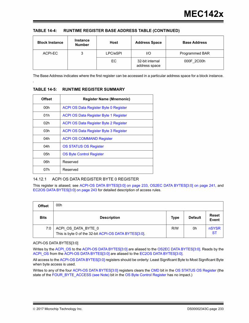
MEC142x
The Base Address indicates where the first register can be accessed in a particular address space for a block instance.
I
14.12.1 ACPI OS DATA REGISTER BYTE 0 REGISTER
This register is aliased; see ACPI-OS DATA BYTES[3:0] on page 233, OS2EC DATA BYTES[3:0] on page 241, andEC2OS DATA BYTES[3:0] on page 243 for detailed description of access rules.
ACPI-OS DATA BYTES[3:0]
Writes by the ACPI_OS to the ACPI-OS DATA BYTES[3:0] are aliased to the OS2EC DATA BYTES[3:0]. Reads by theACPI_OS from the ACPI-OS DATA BYTES[3:0] are aliased to the EC2OS DATA BYTES[3:0].
All access to the ACPI-OS DATA BYTES[3:0] registers should be orderly: Least Significant Byte to Most Significant Bytewhen byte access is used.
Writes to any of the four ACPI-OS DATA BYTES[3:0] registers clears the CMD bit in the OS STATUS OS Register (thestate of the FOUR_BYTE_ACCESS (see Note) bit in the OS Byte Control Register has no impact.)
ACPI-EC 3 LPC/eSPI I/O Programmed BAR
EC 32-bit internal address space
000F_2C00h
TABLE 14-5: RUNTIME REGISTER SUMMARY
Offset Register Name (Mnemonic)
00h ACPI OS Data Register Byte 0 Register
01h ACPI OS Data Register Byte 1 Register
02h ACPI OS Data Register Byte 2 Register
03h ACPI OS Data Register Byte 3 Register
04h ACPI OS COMMAND Register
04h OS STATUS OS Register
05h OS Byte Control Register
06h Reserved
07h Reserved
Offset 00h
Bits Description Type DefaultReset Event
7:0 ACPI_OS_DATA_BYTE_0
This is byte 0 of the 32-bit ACPI-OS DATA BYTES[3:0].
R/W 0h nSYSRST
TABLE 14-4: RUNTIME REGISTER BASE ADDRESS TABLE (CONTINUED)
Block InstanceInstance Number
Host Address Space Base Address
2017 Microchip Technology Inc. DS00002343C-page 233

MEC142x
When the FOUR_BYTE_ACCESS (see Note) bit in the OS Byte Control Register is cleared to ‘0’, the following accessrules apply:
1. Writes to the ACPI OS Data Register Byte 0 Register sets the IBF bit in the OS STATUS OS Register.
2. Reads from the ACPI OS Data Register Byte 0 Register clears the OBF bit in the OS STATUS OS Register.
3. All writes to ACPI-OS DATA BYTES[3:1] complete without error but the data are not registered.
4. All reads from ACPI-OS DATA BYTES[3:1] return 00h without error.
5. Access to ACPI-OS DATA BYTES[3:1] has no effect on the IBF & OBF bits in the OS STATUS OS Register.
When the Four Byte Access bit in the OS Byte Control Register is set to ‘1’, the following access rules apply (see Note):
1. Writes to the ACPI OS Data Register Byte 3 Register sets the IBF bit in the OS STATUS OS Register.
2. Reads from the ACPI OS Data Register Byte 3 Register clears the OBF bit in the OS STATUS OS Register.
14.12.2 ACPI OS DATA REGISTER BYTE 1 REGISTER
This register is aliased; see ACPI-OS DATA BYTES[3:0] on page 233, OS2EC DATA BYTES[3:0] on page 241, andEC2OS DATA BYTES[3:0] on page 243 for detailed description of access rules.
14.12.3 ACPI OS DATA REGISTER BYTE 2 REGISTER
This register is aliased; see ACPI-OS DATA BYTES[3:0] on page 233, OS2EC DATA BYTES[3:0] on page 241, andEC2OS DATA BYTES[3:0] on page 243 for detailed description of access rules.
Note: In eSPI mode, instance 0 of the ACPI Embedded Controller Interface (ACPI-EC0) only operates in LegacyMode which provides single byte Full Duplex operation. Four-byte Mode is not supported for ACPI-EC0 ineSPI mode.
Offset 01h
Bits Description Type DefaultReset Event
7:0 ACPI_OS_DATA_BYTE_1
This is byte 1 of the 32-bit ACPI-OS DATA BYTES[3:0].
R/W 0h nSYSRST
Offset 02h
Bits Description Type DefaultReset Event
7:0 ACPI_OS_DATA_BYTE_2
This is byte 2 of the 32-bit ACPI-OS DATA BYTES[3:0].
R/W 0h nSYSRST
DS00002343C-page 234 2017 Microchip Technology Inc.

MEC142x
14.12.4 ACPI OS DATA REGISTER BYTE 3 REGISTER
This register is aliased; see ACPI-OS DATA BYTES[3:0] on page 233, OS2EC DATA BYTES[3:0] on page 241, andEC2OS DATA BYTES[3:0] on page 243 for detailed description of access rules.
14.12.5 ACPI OS COMMAND REGISTER
Offset 03h
Bits Description Type DefaultReset Event
7:0 ACPI_OS_DATA_BYTE_3
This is byte 3 of the 32-bit ACPI-OS DATA BYTES[3:0].
R/W 0h nSYSRST
Offset 04h
Bits Description Type DefaultReset Event
7:0 ACPI_OSS_COMMAND
Writes to the this register are aliased in the OS2EC Data EC Byte 0 Register.
Writes to the this register also set the CMD and IBF bits in the OS STATUS OS Register
W 0h nSYSRST
2017 Microchip Technology Inc. DS00002343C-page 235
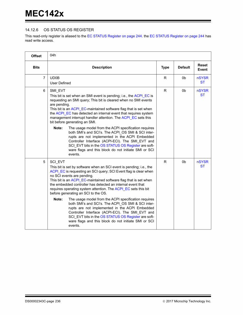
MEC142x
14.12.6 OS STATUS OS REGISTER
This read-only register is aliased to the EC STATUS Register on page 244. the EC STATUS Register on page 244 hasread write access.
Offset 04h
Bits Description Type DefaultReset Event
7 UD0B
User Defined
R 0b nSYSRST
6 SMI_EVT
This bit is set when an SMI event is pending; i.e., the ACPI_EC is requesting an SMI query; This bit is cleared when no SMI events are pending.This bit is an ACPI_EC-maintained software flag that is set when the ACPI_EC has detected an internal event that requires system management interrupt handler attention. The ACPI_EC sets this bit before generating an SMI.
Note: The usage model from the ACPI specification requiresboth SMI’s and SCI’s. The ACPI_OS SMI & SCI inter-rupts are not implemented in the ACPI EmbeddedController Interface (ACPI-ECI). The SMI_EVT andSCI_EVT bits in the OS STATUS OS Register are soft-ware flags and this block do not initiate SMI or SCIevents.
R 0b nSYSRST
5 SCI_EVT
This bit is set by software when an SCI event is pending; i.e., the ACPI_EC is requesting an SCI query; SCI Event flag is clear when no SCI events are pending.This bit is an ACPI_EC-maintained software flag that is set when the embedded controller has detected an internal event that requires operating system attention. The ACPI_EC sets this bit before generating an SCI to the OS.
Note: The usage model from the ACPI specification requiresboth SMI’s and SCI’s. The ACPI_OS SMI & SCI inter-rupts are not implemented in the ACPI EmbeddedController Interface (ACPI-ECI). The SMI_EVT andSCI_EVT bits in the OS STATUS OS Register are soft-ware flags and this block do not initiate SMI or SCIevents.
R 0b nSYSRST
DS00002343C-page 236 2017 Microchip Technology Inc.

MEC142x
4 BURST
The BURST bit is set when the ACPI_EC is in Burst Mode for polled command processing; the BURST bit is cleared when the ACPI_EC is in Normal mode for interrupt-driven command pro-cessing.The BURST bit is an ACPI_EC-maintained software flag that indi-cates the embedded controller has received the Burst Enable command from the host, has halted normal processing, and is waiting for a series of commands to be sent from the host. Burst Mode allows the OS or system management handler to quickly read and write several bytes of data at a time without the over-head of SCIs between commands.The BURST bit is maintained by ACPI_EC software, only.
R 0b nSYSRST
3 CMD
This bit is set when the OS2EC Data EC Byte 0 Register contains a command byte written into ACPI OS COMMAND Register; this bit is cleared when the OS2EC DATA BYTES[3:0] contains a data byte written into the ACPI-OS DATA BYTES[3:0].
This bit is hardware controlled: • ACPI_OS writes to any of the four ACPI-OS DATA
BYTES[3:0] bytes clears this bit• ACPI_OS writes to the ACPI OS COMMAND Register sets
this bit.
Note: This bit allows the embedded controller to differentiatethe start of a command sequence from a data bytewrite operation.
R 0b nSYSRST
2 UD1B
User Defined
R 0b nSYSRST
Offset 04h
Bits Description Type DefaultReset Event
2017 Microchip Technology Inc. DS00002343C-page 237

MEC142x
1 IBF
The Input Buffer Full bit is set to indicate that a the ACPI_OS has written a command or data to the ACPI_EC and that data is ready. This bit is automatically cleared when data has been read by the ACPI_EC.
Note: The setting and clearing of this IBF varies dependingon the setting of the following bits: CMD bit in this reg-ister and FOUR_BYTE_ACCESS (see Note) bit in theOS Byte Control Register. Three scenarios follow:
1. The IBF is set when the ACPI_OS writes to the ACPI OSCOMMAND Register. This same write autonomously setsthe CMD bit in this register.
The IBF is cleared if the CMD bit in this register is set and the ACPI_EC reads from the OS2EC Data EC Byte 0 Register.
Note: When CMD bit in this register is set the FOUR_BYTE_-ACCESS (see Note) bit in the OS Byte Control Regis-ter has no impact on the IBF bit behavior.
2. A write by the to the ACPI_OS to the ACPI OS Data RegisterByte 0 Register sets the IBF bit if the FOUR_BYTE_AC-CESS (see Note) bit in the OS Byte Control Register is in thecleared to ‘0’ state prior to this write. This same write auton-omously clears the CMD bit in this register.
A read of the OS2EC Data EC Byte 0 Register clears the IBF bit if the FOUR_BYTE_ACCESS (see Note) bit in the OS Byte Control Register is in the cleared to ‘0’ state prior to this read.
3. A write by the to the ACPI_OS to the ACPI OS Data RegisterByte 3 Register sets the IBF bit if the FOUR_BYTE_AC-CESS (see Note) bit in the OS Byte Control Register is in theset to ‘1’ state prior to this write. This same write autono-mously clears the CMD bit in this register.
A read of the OS2EC Data EC Byte 3 Register clears the IBF bit if the FOUR_BYTE_ACCESS (see Note) bit in the OS Byte Control Register is in the set to ‘1’ state prior to this read.
An IBF interrupt signals the ACPI_EC that there is data available. The ACPI Specification usage model is as follows:
1. The ACPI_EC reads the EC STATUS Register and sees theIBF flag set,
2. The ACPI_EC reads all the data available in the OS2ECDATA BYTES[3:0]. This causes the IBF bit to be automati-cally cleared by hardware.
3. The ACPI_EC must then generate a software interrupt (SeeNote: on page 228) to alert the ACPI_OS that the data hasbeen read and that the host is free to write more data to theACPI_EC as needed.
R 0h nSYSRST
Offset 04h
Bits Description Type DefaultReset Event
DS00002343C-page 238 2017 Microchip Technology Inc.
MEC142x
0 OBF
The Output Buffer Full bit is set to indicate that a the ACPI_EC has written a data to the ACPI_OS and that data is ready. This bit is automatically cleared when all the data has been read by the ACPI_OS.
Note: The setting and clearing of this OBF varies dependingon the setting FOUR_BYTE_ACCESS (see Note) bit inthe OS Byte Control Register. Two scenarios follow:
1. The OBF bit is set if the Four Byte Access bit in the OS ByteControl Register is ‘0’ when the ACPI_EC writes to theEC2OS Data EC Byte 0 Register.
The OBF is cleared if the Four Byte Access bit in the OS Byte Control Register is cleared to ‘0’ when the ACPI_OS reads from the ACPI OS Data Register Byte 0 Register.
2. The OBF is set if the Four Byte Access bit in the OS ByteControl Register is set to ‘1’ when the ACPI_EC writes to theEC2OS Data EC Byte 3 Register.
The OBF is cleared if the Four Byte Access bit in the OS Byte Control Register is set to ‘1’ when the ACPI_OS reads from the ACPI OS Data Register Byte 3 Register.
The ACPI Specification usage model is as follows:
1. The ACPI_EC must generate a software interrupt (SeeNote: on page 228) to alert the ACPI_OS that the data isavailable.
2. The ACPI_OS reads the OS STATUS OS Register and seesthe OBF flag set, the ACPI_OS reads all the data availablein the ACPI-OS DATA BYTES[3:0].
3. The ACPI_OS reads all the data available in the ACPI-OSDATA BYTES[3:0]. This causes the OBF bit to be automati-cally cleared by hardware and the associated OBF interruptto be asserted.
R 0h nSYSRST
Offset 04h
Bits Description Type DefaultReset Event
2017 Microchip Technology Inc. DS00002343C-page 239

MEC142x
14.12.7 OS BYTE CONTROL REGISTER
This register is aliased to the EC Byte Control Register on page 245. No behavioral differences occur due to addressaliasing.
14.13 EC-Only Registers
The registers listed in the EC-Only Register Summary table are for four instances of the ACPI Embedded ControllerInterface (ACPI-ECI). The addresses of each register listed in this table are defined as a relative offset to the host“Base Address” defined in the EC-Only Register Base Address Table.
The Base Address indicates where the first register can be accessed in a particular address space for a block instance.
Offset 05
Bits Description Type DefaultReset Event
7:1 Reserved R - -
0 FOUR_BYTE_ACCESS (see Note)
When this bit is set to ‘1’, the ACPI Embedded Controller Interface (ACPI-ECI) accesses four bytes through the ACPI-OS DATA BYTES[3:0].When this bit is cleared to ‘0’, the ACPI Embedded Controller Inter-face (ACPI-ECI) accesses one byte through the ACPI OS Data Register Byte 0 Register. The corresponds to Legacy Mode described in Section 14.10, "Description," on page 228.
Note 1: This bit effects the behavior of the IBF & OBF bits in theOS STATUS OS Register.
2: See ACPI-OS DATA BYTES[3:0] on page 233, OS2ECDATA BYTES[3:0] on page 241, and EC2OS DATABYTES[3:0] on page 243 for detailed description ofaccess rules.
R 0b nSYSRST
Note: The ACPI_OS access Base Address Register (BAR) should be configured to match the access widthselected by the Four Byte Access bit in the OS Byte Control Register. This BAR in not described in thischapter.
TABLE 14-6: EC-ONLY REGISTER BASE ADDRESS TABLE
Block InstanceInstance Number
Host Address Space Base Address
ACPI-EC 0 EC 32-bit internal address space
000F_0C00h
ACPI-EC 1 EC 32-bit internal address space
000F_1000h
ACPI-EC 2 EC 32-bit internal address space
000F_2800h
ACPI-EC 3 EC 32-bit internal address space
000F_2C00h
DS00002343C-page 240 2017 Microchip Technology Inc.

MEC142x
14.13.1 OS2EC DATA EC BYTE 0 REGISTER
This register is aliased; see ACPI-OS DATA BYTES[3:0] on page 233, OS2EC DATA BYTES[3:0] on page 241, andEC2OS DATA BYTES[3:0] on page 243 for detailed description of access rules.
OS2EC DATA BYTES[3:0]
When the CMD bit in the OS STATUS OS Register is cleared to ‘0’, reads by the ACPI_EC from the OS2EC DATABYTES[3:0] are aliased to the ACPI-OS DATA BYTES[3:0].
All access to the OS2EC DATA BYTES[3:0] registers should be orderly: Least Significant Byte to Most Significant Bytewhen byte access is used.
When the FOUR_BYTE_ACCESS (see Note) bit in the OS Byte Control Register is cleared to ‘0’, the following accessrules apply:
1. Writes to the OS2EC DATA BYTES[3:0] have no effect on the OBF bit in the OS STATUS OS Register.
2. Reads from the OS2EC Data EC Byte 0 Register clears the IBF bit in the OS STATUS OS Register.
3. All reads from OS2EC DATA BYTES[3:1] return 00h without error.
4. Access to OS2EC DATA BYTES[3:1 has no effect on the IBF & OBF bits in the OS STATUS OS Register.
TABLE 14-7: EC-ONLY REGISTER SUMMARY
Offset Register Name (Mnemonic)
100h EC2OS Data EC Byte 0 Register
101h EC2OS Data EC Byte 1 Register
102h EC2OS Data EC Byte 2 Register
103h EC2OS Data EC Byte 3 Register
104h EC STATUS Register
105h EC Byte Control Register
106h Reserved
107h Reserved
108h OS2EC Data EC Byte 0 Register
109h OS2EC Data EC Byte 1 Register
10Ah OS2EC Data EC Byte 2 Register
10Bh OS2EC Data EC Byte 3 Register
Offset 108h
Bits Description Type DefaultReset Event
7:0 OS_TO_EC_DATA_BYTE_0
This is byte 0 of the 32-bit OS2EC DATA BYTES[3:0].
R/W 0h nSYSRST
2017 Microchip Technology Inc. DS00002343C-page 241

MEC142x
When the FOUR_BYTE_ACCESS (see Note) bit in the OS Byte Control Register is set to ‘1’, the following access rulesapply:
1. Writes to the OS2EC DATA BYTES[3:0] have no effect on the OBF bit in the OS STATUS OS Register.
2. Reads from the OS2EC Data EC Byte 3 Register clears the IBF bit in the OS STATUS OS Register.
14.13.2 OS2EC DATA EC BYTE 1 REGISTER
This register is aliased; see ACPI-OS DATA BYTES[3:0] on page 233, OS2EC DATA BYTES[3:0] on page 241, andEC2OS DATA BYTES[3:0] on page 243 for detailed description of access rules.
14.13.3 OS2EC DATA EC BYTE 2 REGISTER
This register is aliased; see ACPI-OS DATA BYTES[3:0] on page 233, OS2EC DATA BYTES[3:0] on page 241, andEC2OS DATA BYTES[3:0] on page 243 for detailed description of access rules.
14.13.4 OS2EC DATA EC BYTE 3 REGISTER
This register is aliased; see ACPI-OS DATA BYTES[3:0] on page 233, OS2EC DATA BYTES[3:0] on page 241, andEC2OS DATA BYTES[3:0] on page 243 for detailed description of access rules.
Offset 109h
Bits Description Type DefaultReset Event
7:0 OS2EC_DATA_ BYTE_1
This is byte 1 of the 32-bit OS2EC DATA BYTES[3:0].
R/W 0h nSYSRST
Offset 10Ah
Bits Description Type DefaultReset Event
7:0 OS2EC_DATA_BYTE_2
This is byte 2 of the 32-bit OS2EC DATA BYTES[3:0].
R/W 0h nSYSRST
Offset 10Bh
Bits Description Type DefaultReset Event
7:0 OS2EC_DATA_BYTE_3
This is byte 3 of the 32-bit OS2EC DATA BYTES[3:0].
R/W 0h nSYSRST
DS00002343C-page 242 2017 Microchip Technology Inc.

MEC142x
14.13.5 EC2OS DATA EC BYTE 0 REGISTER
This register is aliased; see ACPI-OS DATA BYTES[3:0] on page 233, OS2EC DATA BYTES[3:0] on page 241, andEC2OS DATA BYTES[3:0] on page 243 for detailed description of access rules.
EC2OS DATA BYTES[3:0]
Writes by the ACPI_EC to the EC2OS DATA BYTES[3:0] are aliased to the ACPI-OS DATA BYTES[3:0]
All access to the EC2OS DATA BYTES[3:0] registers should be orderly: Least Significant Byte to Most Significant Bytewhen byte access is used.
When the FOUR_BYTE_ACCESS (see Note) bit in the OS Byte Control Register is cleared to ‘0’, the following accessrules apply:
1. Writes to the EC2OS Data EC Byte 0 Register set the OBF bit in the OS STATUS OS Register.
2. Reads from the EC2OS DATA BYTES[3:0] have no effect on the IBF bit in the OS STATUS OS Register.
3. All reads from EC2OS DATA BYTES[3:1] return 00h without error.
4. All writes to EC2OS DATA BYTES[3:1] complete without error but the data are not registered.
5. Access to EC2OS DATA BYTES[3:1] have no effect on the IBF & OBF bits in the OS STATUS OS Register.
When the FOUR_BYTE_ACCESS (see Note) bit in the OS Byte Control Register is set to ‘1’, the following access rulesapply:
1. Writes to the EC2OS Data EC Byte 3 Register set the OBF bit in the OS STATUS OS Register.
2. Reads from the EC2OS DATA BYTES[3:0] have no effect on the IBF bit in the OS STATUS OS Register.
14.13.6 EC2OS DATA EC BYTE 1 REGISTER
This register is aliased; see ACPI-OS DATA BYTES[3:0] on page 233, OS2EC DATA BYTES[3:0] on page 241, andEC2OS DATA BYTES[3:0] on page 243 for detailed description of access rules.
Offset 100h
Bits Description Type DefaultReset Event
7:0 EC2OS_DATA_BYTE_0
This is byte 0 of the 32-bit EC2OS DATA BYTES[3:0].
R/W 0h nSYSRST
Offset 101h
Bits Description Type DefaultReset Event
7:0 EC2OS_DATA_BYTE_1
This is byte 1 of the 32-bit EC2OS DATA BYTES[3:0].
R/W 0h nSYSRST
2017 Microchip Technology Inc. DS00002343C-page 243
MEC142x
14.13.7 EC2OS DATA EC BYTE 2 REGISTER
This register is aliased; see ACPI-OS DATA BYTES[3:0] on page 233, OS2EC DATA BYTES[3:0] on page 241, andEC2OS DATA BYTES[3:0] on page 243 for detailed description of access rules.
14.13.8 EC2OS DATA EC BYTE 3 REGISTER
This register is aliased; see ACPI-OS DATA BYTES[3:0] on page 233, OS2EC DATA BYTES[3:0] on page 241, andEC2OS DATA BYTES[3:0] on page 243 for detailed description of access rules.
14.13.9 EC STATUS REGISTER
This register is aliased to the OS STATUS OS Register on page 236. The OS STATUS OS Register is a read only versionof this register.
Offset 102h
Bits Description Type DefaultReset Event
7:0 EC2OS_DATA_BYTE_2
This is byte 2 of the 32-bit EC2OS DATA BYTES[3:0].
R/W 0h nSYSRST
Offset 103h
Bits Description Type DefaultReset Event
7:0 EC2OS_DATA_BYTE_3
This is byte 3 of the 32-bit EC2OS DATA BYTES[3:0].
R/W 0h nSYSRST
Offset 104h
Bits Description Type DefaultReset Event
7 UD0A
User Defined
R/W 0b nSYSRST
6 SMI_EVT
See SMI_EVT bit in OS STATUS OS Register on page 236 for bit description.
R/W 0b nSYSRST
5 SCI_EVT
See SMI_EVT bit in OS STATUS OS Register on page 236 for bit description.
R/W 0b nSYSRST
4 BURST
See BURST bit in OS STATUS OS Register on page 236 for bit description.
R/W 0b nSYSRST
3 CMD
See CMD bit in OS STATUS OS Register on page 236 for bit description.
R 0b nSYSRST
DS00002343C-page 244 2017 Microchip Technology Inc.
MEC142x
The IBF and OBF bits are not de-asserted by hardware when the host is powered off, or the LPC interface powers down;for example, following system state changes S3->S0, S5->S0, G3-> S0. For further information on how these bits arecleared, refer to IBF and OBF bit descriptions in the STATUS OS-Register definition.
14.13.10 EC BYTE CONTROL REGISTER
This register is aliased to the OS Byte Control Register on page 240. The OS Byte Control Register is a read only versionof this register.
2 UD1A
User Defined
R/W 0b nSYSRST
1 IBF
See IBF bit in OS STATUS OS Register on page 236 for bit description.
R 0h nSYSRST
0 OBF
See OBF bit in OS STATUS OS Register on page 236 for bit description.
R 0h nSYSRST
Offset 105h
Bits Description Type DefaultReset Event
7:1 Reserved R - -
0 FOUR_BYTE_ACCESSSee FOUR_BYTE_ACCESS (see Note) bit in OS Byte Control Register on page 240 for bit description.
R/W 0b nSYSRST
Offset 104h
Bits Description Type DefaultReset Event
2017 Microchip Technology Inc. DS00002343C-page 245
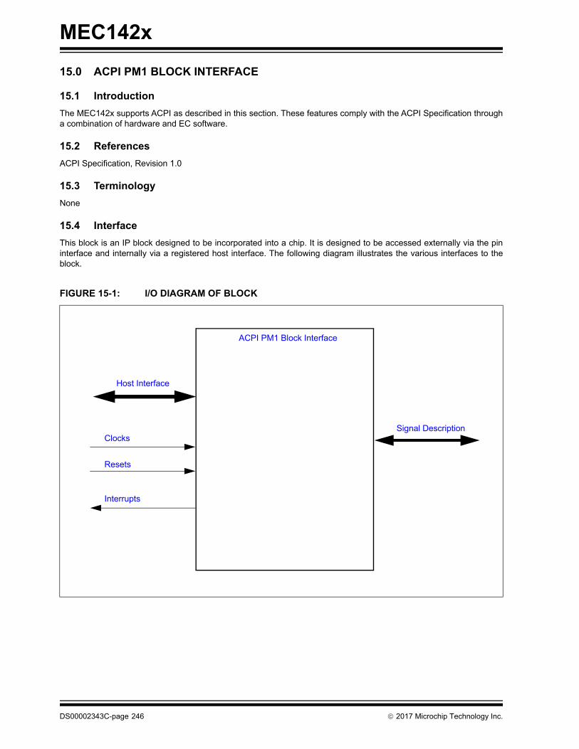
MEC142x
15.0 ACPI PM1 BLOCK INTERFACE
15.1 Introduction
The MEC142x supports ACPI as described in this section. These features comply with the ACPI Specification througha combination of hardware and EC software.
15.2 References
ACPI Specification, Revision 1.0
15.3 Terminology
None
15.4 Interface
This block is an IP block designed to be incorporated into a chip. It is designed to be accessed externally via the pininterface and internally via a registered host interface. The following diagram illustrates the various interfaces to theblock.
FIGURE 15-1: I/O DIAGRAM OF BLOCK
ACPI PM1 Block Interface
Signal DescriptionClocks
Interrupts
Resets
Host Interface
DS00002343C-page 246 2017 Microchip Technology Inc.

MEC142x
15.5 Signal Description
Table 15-1, "ACPI PM1 Signal Description Table" lists the signals that are typically routed to the pin interface.
15.6 Host Interface
The registers defined for the ACPI PM1 Block Interface are accessible by the various hosts as indicated in Section15.11, "Runtime Registers".
15.7 Power, Clocks and Resets
This section defines the Power, Clock, and Reset parameters of the block.
15.7.1 POWER DOMAINS
15.7.2 CLOCKS
This section describes all the clocks in the block, including those that are derived from the I/O Interface as well as theones that are derived or generated internally.
15.7.3 RESETS
TABLE 15-1: ACPI PM1 SIGNAL DESCRIPTION TABLE
Name Direction Description
EC_SCI# Output Any or all of the PWRBTN_STS, SLPBTN_STS, and RTC_STS bits in the Power Management 1 Status 2 Register can assert the EC_SCI# pin if enabled by the associated bits in the Power Man-agement 1 Enable 2 Register register. The EC_SCI_STS bit in the EC_PM_STS Register register can also be used to generate an SCI on the EC_SCI# pin.
Name Description
VTR This power well sources all of the registers and logic in this block, except where noted.
Name Description
48 MHz Ring Oscillator This clock signal drives selected logic (e.g., counters).
Name Description
nSYSRST This reset signal resets all of the registers and logic in this block.
2017 Microchip Technology Inc. DS00002343C-page 247

MEC142x
15.8 Interrupts
This section defines the Interrupt Sources generated from this block.
15.9 Low Power Modes
The ACPI PM1 Block Interface may be put into a low power state by the chip’s Power, Clocks, and Reset (PCR) circuitry.
15.10 Description
This section describes the functions of the ACPI PM1 Block Interface in more detail.
The MEC142x implements the ACPI fixed registers but includes only those bits that apply to the power button sleepbutton and RTC alarm events. The ACPI WAK_STS, SLP_TYP, and SLP_EN bits are also supported.
The MEC142x can generate SCI Interrupts to the Host. The functions described in the following sub-sections can gen-erate a SCI event on the EC_SCI# pin. In the MEC142x, an SCI event is considered the same as an ACPI wakeup orruntime event.
Source Description
PM1_CTL This Interrupt is generated to the EC by the Host writing to the Power Management 1 Control 2 Register register
PM1_EN This Interrupt is generated to the EC by the Host writing to the Power Management 1 Enable 2 Register register
PM1_STS This Interrupt is generated to the EC by the Host writing to the Power Management 1 Status 2 Register register
DS00002343C-page 248 2017 Microchip Technology Inc.
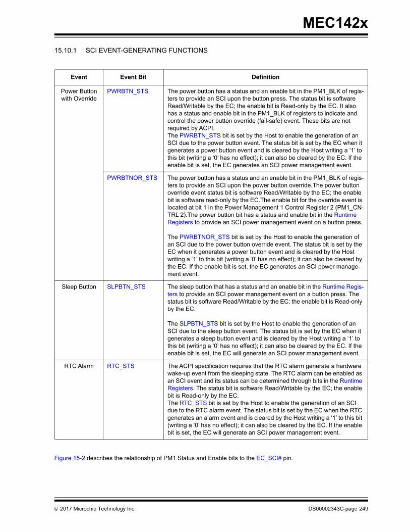
MEC142x
15.10.1 SCI EVENT-GENERATING FUNCTIONS
Figure 15-2 describes the relationship of PM1 Status and Enable bits to the EC_SCI# pin.
Event Event Bit Definition
Power Button with Override
PWRBTN_STS The power button has a status and an enable bit in the PM1_BLK of regis-ters to provide an SCI upon the button press. The status bit is software Read/Writable by the EC; the enable bit is Read-only by the EC. It also has a status and enable bit in the PM1_BLK of registers to indicate and control the power button override (fail-safe) event. These bits are not required by ACPI. The PWRBTN_STS bit is set by the Host to enable the generation of an SCI due to the power button event. The status bit is set by the EC when it generates a power button event and is cleared by the Host writing a ‘1’ to this bit (writing a ‘0’ has no effect); it can also be cleared by the EC. If the enable bit is set, the EC generates an SCI power management event.
PWRBTNOR_STS The power button has a status and an enable bit in the PM1_BLK of regis-ters to provide an SCI upon the power button override.The power button override event status bit is software Read/Writable by the EC; the enable bit is software read-only by the EC.The enable bit for the override event is located at bit 1 in the Power Management 1 Control Register 2 (PM1_CN-TRL 2).The power button bit has a status and enable bit in the Runtime Registers to provide an SCI power management event on a button press.
The PWRBTNOR_STS bit is set by the Host to enable the generation of an SCI due to the power button override event. The status bit is set by the EC when it generates a power button event and is cleared by the Host writing a ‘1’ to this bit (writing a ‘0’ has no effect); it can also be cleared by the EC. If the enable bit is set, the EC generates an SCI power manage-ment event.
Sleep Button SLPBTN_STS The sleep button that has a status and an enable bit in the Runtime Regis-ters to provide an SCI power management event on a button press. The status bit is software Read/Writable by the EC; the enable bit is Read-only by the EC.
The SLPBTN_STS bit is set by the Host to enable the generation of an SCI due to the sleep button event. The status bit is set by the EC when it generates a sleep button event and is cleared by the Host writing a ‘1’ to this bit (writing a ‘0’ has no effect); it can also be cleared by the EC. If the enable bit is set, the EC will generate an SCI power management event.
RTC Alarm RTC_STS The ACPI specification requires that the RTC alarm generate a hardware wake-up event from the sleeping state. The RTC alarm can be enabled as an SCI event and its status can be determined through bits in the Runtime Registers. The status bit is software Read/Writable by the EC; the enable bit is Read-only by the EC.The RTC_STS bit is set by the Host to enable the generation of an SCI due to the RTC alarm event. The status bit is set by the EC when the RTC generates an alarm event and is cleared by the Host writing a ‘1’ to this bit (writing a ‘0’ has no effect); it can also be cleared by the EC. If the enable bit is set, the EC will generate an SCI power management event.
2017 Microchip Technology Inc. DS00002343C-page 249

MEC142x
15.11 Runtime Registers
The registers listed in the Runtime Register Summary table are for a single instance of the ACPI PM1 interface. Theaddresses of each register listed in this table are defined as a relative offset to the host “Base Address” defined in theRuntime Register Base Address Table.
The Base Address indicates where the first register can be accessed in a particular address space for a block instance.
All the registers in Table 15-3, "Runtime Registers Summary" may be accessed by the Host and EC with the exceptionof the EC_PM_STS Register register which is EC-accessed only.
FIGURE 15-2: EC_SCI# INTERFACE
TABLE 15-2: RUNTIME REGISTER BASE ADDRESS TABLE
Block InstanceInstance Number
Host Address Space Base Address
ACPI PM1 Inter-face
0 LPC/eSPI I/O Programmed BAR
0 EC 32-bit internal address space
000F_1400h
TABLE 15-3: RUNTIME REGISTERS SUMMARY
Offset Register Name
00h Power Management 1 Status 1 Register
01h Power Management 1 Status 2 Register
02h Power Management 1 Enable 1 Register
03h Power Management 1 Enable 2 Register
04h Power Management 1 Control 1 Register
05h Power Management 1 Control 2 Register
06h Power Management 2 Control 1 Register
PM1_EN 2Register
PM1_STS 2 Register
PWRBTN_STS
SLPBTN_STS
RTC_STS
EC_SCI_STS
EC_PM_STS Register
EC_SCI#
DS00002343C-page 250 2017 Microchip Technology Inc.
MEC142x
15.11.1 POWER MANAGEMENT 1 STATUS 1 REGISTER
15.11.2 POWER MANAGEMENT 1 STATUS 2 REGISTER
07h Power Management 2 Control 2 Register
10h EC_PM_STS Register
Offset 00h
Bits Description Type DefaultReset Event
7:0 Reserved R - -
Offset 01h
Bits Description Type DefaultReset Event
7 WAK_STS
This bit can be set or cleared by the EC. The Host writing a one to this bit can also clear this bit.
R/WC(See
Note:)
00h nSYSRST
6:4 Reserved R - -
3 PWRBTNOR_STS
This bit can be set or cleared by the EC to simulate a Power button override event status if the power is controlled by the EC. The Host writing a one to this bit can also clear this bit. The EC must gener-ate the associated hardware event under software control.
R/WC(See
Note:)
00h nSYSRST
2 RTC_STS
This bit can be set or cleared by the EC to simulate a RTC status. The Host writing a one to this bit can also clear this bit. The EC must generate the associated SCI interrupt under software control.
R/WC(See
Note:)
00h nSYSRST
1 SLPBTN_STS
This bit can be set or cleared by the EC to simulate a Sleep button status if the sleep state is controlled by the EC. The Host writing a one to this bit can also clear this bit. The EC must generate the associated SCI interrupt under software control.
R/WC(See
Note:)
00h nSYSRST
0 PWRBTN_STS
This bit can be set or cleared by the EC to simulate a Power button status if the power is controlled by the EC. The Host writing a one to this bit can also clear this bit. The EC must generate the associ-ated SCI interrupt under software control.
R/WC(See
Note:)
00h nSYSRST
TABLE 15-3: RUNTIME REGISTERS SUMMARY (CONTINUED)
Offset Register Name
2017 Microchip Technology Inc. DS00002343C-page 251
MEC142x
15.11.3 POWER MANAGEMENT 1 ENABLE 1 REGISTER
15.11.4 POWER MANAGEMENT 1 ENABLE 2 REGISTER
15.11.5 POWER MANAGEMENT 1 CONTROL 1 REGISTER
Note: These bits are set/cleared by the EC directly i.e., writing ‘1’ sets the bit and writing ‘0’ clears it. These bitscan also be cleared by the Host software writing a one to this bit position and by nSYSRST. Writing a 0 bythe Host has no effect.
Offset 02h
Bits Description Type DefaultReset Event
7:0 Reserved R - -
Offset 03h
Bits Description Type DefaultReset Event
7:3 Reserved R - -
2 RTC_EN
This bit can be read or written by the Host. It can be read by the EC.
R/W (See
Note:)
00h nSYSRST
1 SLPBTN_EN
This bit can be read or written by the Host. It can be read by the EC.
R/W(See
Note:)
00h nSYSRST
0 PWRBTN_EN
This bit can be read or written by the Host. It can be read by the EC.
R/W(See
Note:)
00h nSYSRST
Note: These bits are read-only by the EC.
Offset 04h
Bits Description Type DefaultReset Event
7:0 Reserved R 0h nSYSRST
DS00002343C-page 252 2017 Microchip Technology Inc.
MEC142x
15.11.6 POWER MANAGEMENT 1 CONTROL 2 REGISTER
15.11.7 POWER MANAGEMENT 2 CONTROL 1 REGISTER
Offset 05h
Bits Description Type DefaultReset Event
7:6 Reserved R - -
5 SLP_EN
See Table 15-4.
See Table 1
5-4.
00h nSYSRST
4:2 SLP_TYP
These bits can be set or cleared by the Host, read by the EC.
R/W(See
Note:)
00h nSYSRST
1 PWRBTNOR_EN
This bit can be set or cleared by the Host, read by the EC.
R/W(See
Note:)
00h nSYSRST
0 Reserved R - -
Note: These bits are read-only by the EC.
TABLE 15-4: SLP_EN DEFINITION
Host / EC R/W Description
Host Read Always reads 0
Write Writing a 0 has no effect, Writing a 1 sets this bit
EC Read Reads the value of the bit
Write Writing a 0 has no effect, Writing a 1 clears this bit
Offset 06h
Bits Description Type DefaultReset Event
7:0 Reserved R - -
2017 Microchip Technology Inc. DS00002343C-page 253
MEC142x
15.11.8 POWER MANAGEMENT 2 CONTROL 2 REGISTER
15.11.9 EC_PM_STS REGISTER
15.12 EC-Only Registers
The registers listed in the EC-Only Register Summary table are for a single instance of the ACPI PM1 interface. Theaddresses of each register listed in this table are defined as a relative offset to the host “Base Address” defined in theEC-Only Register Base Address Table.
The Base Address indicates where the first register can be accessed in a particular address space for a block instance.
Offset 07h
Bits Description Type DefaultReset Event
7:0 Reserved R - -
Offset
Bits Description Type DefaultReset Event
7:1 UD R/W 00h nSYSRST
0 EC_SCI_STS
If the EC_SCI_STS bit is “1”, an interrupt is generated on the EC_SCI# pin.
R/W 00h nSYSRST
Note: These bits are only accessed by the EC. There is no host access to this register.
TABLE 15-5: EC-ONLY REGISTER BASE ADDRESS TABLE
Block Instance Instance Number Host Address Space Base Address
ACPI PM1 Interface 0 EC 32-bit address space
000F_1500h
TABLE 15-6: EC-ONLY REGISTERS SUMMARY
Offset Register Name
00h Power Management 1 Status 1 Register
01h Power Management 1 Status 2 Register
02h Power Management 1 Enable 1 Register
03h Power Management 1 Enable 2 Register
04h Power Management 1 Control 1 Register
05h Power Management 1 Control 2 Register
06h Power Management 2 Control 1 Register
07h Power Management 2 Control 2 Register
10h EC_PM_STS Register
DS00002343C-page 254 2017 Microchip Technology Inc.
MEC142x
15.12.1 EC_PM_STS REGISTER
Note: The Power Management Status, Enable and Control registers in Table 15-6, "EC-Only Registers Sum-mary" are described in Section 15.11, "Runtime Registers," on page 250.
Offset 10h
Bits Description Type DefaultReset Event
7:1 UD R/W 00h nSYSRST
0 EC_SCI_STS
If the EC_SCI_STS bit is “1”, an interrupt is generated on the EC_SCI# pin.
R/W 00h nSYSRST
Note: This register is only accessed by the EC. There is no host access to this register.
2017 Microchip Technology Inc. DS00002343C-page 255

MEC142x
16.0 8042 EMULATED KEYBOARD CONTROLLER
16.1 Introduction
The MEC142x keyboard controller uses the EC to produce a superset of the features provided by the industry-standard8042 keyboard controller. The 8042 Emulated Keyboard Controller is a Host/EC Message Interface with hardwareassists to emulate 8042 behavior and provide Legacy GATEA20 support.
16.2 References
There are no references for this block.
16.3 Interface
This block is designed to be accessed externally via the pin interface and internally via a registered host interface.
16.4 Signal Description
Note: There is no VCC emulation in hardware for this interface.
FIGURE 16-1: I/O DIAGRAM OF BLOCK
TABLE 16-1: SIGNAL DESCRIPTION TABLE
Name Direction Description
KBRST Output Keyboard Reset, routed to pin
8042 Emulated Keyboard Controller
Signal DescriptionClock Inputs
Interrupts
Resets
Host Interface
DS00002343C-page 256 2017 Microchip Technology Inc.

MEC142x
16.5 Host Interface
The 8042 interface is accessed by host software via a registered interface, as defined in Section 16.13, "ConfigurationRegisters" and Section 16.14, "Runtime Registers".
16.6 Power, Clocks and Reset
This section defines the Power, Clock, and Reset parameters of the block.
16.6.1 POWER DOMAINS
16.6.2 CLOCK INPUTS
16.6.3 RESETS
16.7 Interrupts
This section defines the Interrupt Sources generated from this block.
Name Description
VTR This Power Well is used to power the registers and logic in this block.
Name Description
1MHz Clock used for the counter in the CPU_RESET circuitry.
Name Description
nSYSRST This reset is asserted when VTR is applied.
VCC_PWRGD This signal is asserted when the main power rail is asserted.
PCI_RESET# This signal is asserted when LRESET# is asserted.
nSIO_RESET This signal is asserted when VTR is low, PWRGD is low, or LRESET# is asserted.
Source Description
KIRQ This interrupt source for the SIRQ logic, representing a Keyboard inter-rupt, is generated when the PCOBF status bit is ‘1’.
MIRQ This interrupt source for the SIRQ logic, representing a Mouse interrupt, is generated when the AUXOBF status bit is ‘1’.
Source Description
IBF Interrupt generated by the host writing either data or command to the data register
OBF Interrupt generated by the host reading either data or aux data from the data register
2017 Microchip Technology Inc. DS00002343C-page 257

MEC142x
16.8 Low Power Modes
The 8042 Interface may be put into a low power state by the chip’s Power, Clocks, and Reset (PCR) circuitry.
16.9 Description
16.9.1 BLOCK DIAGRAM
16.10 EC-to-Host Keyboard Communication
The EC can write to the EC_HOST Data / AUX Data Register by writing to the HOST2EC Data Register at EC-Onlyoffset 0h or the EC AUX Data Register at EC-Only offset Ch. A write to either of these addresses automatically sets bit0 (OBF) in the Status register. A write to the HOST2EC Data Register may also set PCOBF. A write to the EC AUX DataRegister may also set AUXOBF.
16.10.1 PCOBF DESCRIPTION
If enabled by the bit OBFEN, the bit PCOBF is gated onto KIRQ. The KIRQ signal is a system interrupt which signifiesthat the EC has written to the EC2Host Data Register (EC-Only offset 0h). On power-up, PCOBF is reset to 0. PCOBFwill normally reflect the status of writes to EC2Host Data Register, if PCOBFEN is “0”. PCOBF is cleared by hardwareon a HOST read of the EC_HOST Data / AUX Data Register.
KIRQ is normally selected as IRQ1 for keyboard support.
Additional flexibility has been added which allows firmware to directly control the PCOBF output signal, independent ofdata transfers to the host-interface data output register. This feature allows the MEC142x to be operated via the host“polled” mode. Firmware control is active when PCOBFEN is ‘1’. Firmware sets PCOBF high by writing a “1” to thePCOBF field of the PCOBF Register. Firmware must also clear PCOBF by writing a “0” to the PCOBF field.
FIGURE 16-2: BLOCK DIAGRAM OF 8042 Emulated Keyboard Controller
SPB offset =100hRead Data or CMD
AUXH = 1 Bit [5] is AUXOBFAUXH = 0 Bit [5] is UD
2 IBF SET on Host Write to LPC I/O Index =00h or 04h
IBF Cleared on EC Read to SPB Offset = 00h
3 OBF SET on EC Write to SPB offset = 100h or 10ChOBF Cleared by Read 0f
LPC I/O Index 00h
4 PCOBFEN = 1 PCOBF is contents of Bit 0 SPB offset = 114hPCOBFEN = 0 PCBOBF is set on EC Write of SPB offset = 100 h
PCOBF is cleared on Host Read of LPC I/O index = 00h
D7 D3D4D5D6 D0D1D2
D7UD
D3C/D
D4UD
D5AUXOBF / UD
D6UD
D0OBF3
D1IBF2
D2UD1
HOST_EC Data register
Status Register
Keyboard Control Register
WLPC I/O Index =00
Write Data
R
LPC I/O read index =04h
R
SPB offset =104h
R
W
EC Access
Host Access
1 This bit is reset by LPCRESET and VTR_POR
D7RES
D3RES
D4RES
D5RES
D6RES
D1RES
D2RES
PCOBF Register
R
FF_0514W
D7AUXH
D3UD
D4UD
D5OBFEN
D6UD
D0UD
D1SAEN
D2PCOBFEN
R
W
D7 D3D4D5D6 D0D1D2
R W
EC_HOST Data Register
SPB offset =10ChWrite Aux Data
SPB offset =100hWrite Data
FF_0508
D0PCOBF4
LPC I/O Index =04Write CMD
LPC I/O Index =00Read Data or AUX Data
DS00002343C-page 258 2017 Microchip Technology Inc.
MEC142x
The PCOBF register is also readable; the value read back on bit 0 of the register always reflects the present value ofthe PCOBF output. If PCOBFEN = 1, then this value reflects the output of the firmware latch in the PCOBF Register. IfPCOBFEN = 0, then the value read back reflects the in-process status of write cycles to the HOST2EC Data Register(i.e., if the value read back is high, the host interface output data register has just been written to). If OBFEN=0, thenKIRQ is driven inactive (low).
16.10.2 AUXOBF DESCRIPTION
If enabled by the bit OBFEN, the bit AUXOBF is multiplexed onto MIRQ. The AUXOBF/MIRQ signal is a system interruptwhich signifies that the EC has written to the EC_HOST Data / AUX Data Register. On power-up, after nSYSRST,AUXOBF is reset to 0. AUXOBF will normally reflects the status of writes to EC EC AUX Data Register (EC-Only offsetCh). AUXOBF is cleared by hardware on a read of the Host Data Register. If OBFEN=0, then MIRQ is driven inactive(low).
MIRQ is normally selected as IRQ12 for mouse support.
Firmware can also directly control the AUXOBF output signal, similar to the mechanism it can use to control PCOBF.Firmware control is active when AUXH is ‘0’. Firmware sets AUXOBF high by writing a “1” to the AUXOBF field of theEC Keyboard Status Register. Firmware must also clear AUXOBF by writing a “0” to the AUXOBF field.
16.11 Legacy Port92/GATEA20 Support
The MEC142x supports LPC I/O writes to port HOST I/O address 92h as a quick alternate mechanism for generating aCPU_RESET pulse or controlling the state of GATEA20. The Port92/GateA20 logic has a separate Logical Device Num-ber and Base Address register (see Section 16.16, "Legacy Port92/GATEA20 Configuration Registers" and Section16.17, "Legacy Port92/GATEA20 Runtime Registers". The Base Address Register for the Port92/GateA20 LogicalDevice has only one writable bit, the Valid Bit, since the only I/O accessible Register has a fixed address.
The Port 92 Register resides at HOST I/O address 92h and is used to support the alternate reset (ALT_RST#) and alter-nate GATEA20 (ALT_A20) functions. This register defaults to 00h on assertion of nSIO_RESET.
Setting the Port92 Enable bit (Port 92 Enable Register) enables the Port92h Register. When Port92 is disabled, by clear-ing the Port92 Enable bit, then access to this register is completely disabled (I/O writes to host 92h are ignored and I/Oreads float the system data bus SD[7:0]).
16.11.1 GATE A20 SPEEDUP
The MEC142x contains on-chip logic support for the GATEA20 hardware speed-up feature. GATEA20 is part of the con-trol required to mask address line A20 to emulate 8086 addressing.
In addition to the ability for the host to control the GATEA20 output signal directly, a configuration bit called SAEN in theKeyboard Control Register is provided; when set, SAEN allows firmware to control the GATEA20 output. When SAENis set, a 1 bit register (GATEA20 Control Register) controls the GATEA20 output.
TABLE 16-2: OBFEN AND PCOBFEN EFFECTS ON KIRQ
OBFEN PCOBFEN
0 X KIRQ is inactive and driven low
1 0 KIRQ = PCOBF (status of writes to HOST2EC Data Register)
1 1 KIRQ = PCOBF (status of writes to PCOBF Register)
TABLE 16-3: OBFEN AND AUXH EFFECTS ON MIRQ
OBFEN AUXH
0 X MIRQ is inactive and driven low
1 0 MIRQ = AUXOBF (status of writes to EC AUX Data Register)
1 1 MIRQ = AUXOBF (status of writes to AUXOBF in EC Keyboard Status Register)
2017 Microchip Technology Inc. DS00002343C-page 259
MEC142x
Host control and firmware control of GATEA20 affect two separate register elements. Read back of GATEA20 throughthe use of EC OFFSET 100h reflects the present state of the GATEA20 output signal: if SAEN is set, the value readback corresponds to the last firmware-initiated control of GATEA20; if SAEN is reset, the value read back correspondsto the last host-initiated control of GATEA20.
Host control of the GATEA20 output is provided by the hardware interpretation of the “GATEA20 sequence” (seeTable 16-4, "GATEA20 Command/Data Sequence Examples"). The foregoing description assumes that the SAEN con-figuration bit is reset.
When the MEC142x receives a “D1” command followed by data (via the host interface), the on-chip hardware copiesthe value of data bit 1 in the received data field to the GATEA20 host latch. At no time during this host-interface trans-action will PCOBF or the IBF flag (bit 1) in the EC Keyboard Status Register be activated; for example, this host controlof GATEA20 is transparent to firmware, with no consequent degradation of overall system performance. Table 16-4details the possible GATEA20 sequences and the MEC142x responses.
An additional level of control flexibility is offered via a memory-mapped synchronous set and reset capability. Any datawritten to the SETGA20L Register causes the GATEA20 host latch to be set; any data written to the RSTGA20L Registercauses it to be reset. This control mechanism should be used with caution. It was added to augment the “normal” controlflow as described above, not to replace it. Since the host and the firmware have asynchronous control capability of thehost latch via this mechanism, a potential conflict could arise. Therefore, after using the SETGA20L and RSTGA20Lregisters, firmware should read back the GATEA20 status via the GATEA20 Control Register (with SAEN = 0) to confirmthe actual GATEA20 response.
TABLE 16-4: GATEA20 COMMAND/DATA SEQUENCE EXAMPLES
Command(C)/ Data (D)
R/W D[7:0] IBF Flag GATEA20 Comments
CDC
WWW
D1DFFF
000
Q11
GATEA20 Turn-on Sequence
CDC
WWW
D1DDFF
000
Q00
GATEA20 Turn-off Sequence
CCDC
WWWW
D1D1DFFF
0000
QQ11
GATEA20 Turn-on Sequence(*)
CCDC
WWWW
D1D1DDFF
0000
QQ00
GATEA20 Turn-off Sequence(*)
CCC
WWW
D1XX**FF
011
QQQ
Invalid Sequence
DS00002343C-page 260 2017 Microchip Technology Inc.

MEC142x
The hardware GATEA20 state machine returns to state S1 from state S2 when CMD = D1, as shown in the followingfigures:.
Note: The following notes apply:
- All examples assume that the SAEN configuration bit is 0.
- “Q” indicates the bit remains set at the previous state.
- *Not a standard sequence.
- **XX = Anything except D1.
- If multiple data bytes, set IBF and wait at state 0. Let the software know something unusual happened.
- For data bytes, only D[1] is used; all other bits are don't care.
- Host Commands (FF, FE, & D1) do not cause IBF. The method of blocking IBF in Figure 16-4 is the nIOW not being asserted when FF, FE, & D1 Host commands are written”.
FIGURE 16-3: GATEA20 STATE MACHINE
S0
S2 S1
RESET
CMD !=D1 orDATA[IBF=1]
CMD = FF[IBF=0] CMD !=D1
orCMD !=FF orDATA[IBF=1]
CMD !=D1[IBF=1]
CMD = D1[IBF=0]
CMD = D1[IBF=0]
Data[IBF=0, Latch DIN
CMD = D1[IBF=0]
Notes: GateA20 Changes When in S1 going to S2 Clock = wrdinB CMD = [C/D=1] Data = [C/D=0]
2017 Microchip Technology Inc. DS00002343C-page 261
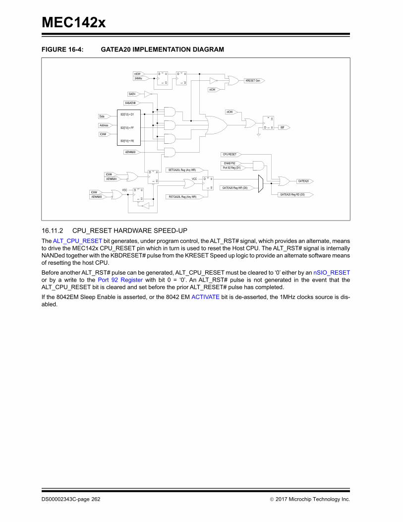
MEC142x
16.11.2 CPU_RESET HARDWARE SPEED-UP
The ALT_CPU_RESET bit generates, under program control, the ALT_RST# signal, which provides an alternate, meansto drive the MEC142x CPU_RESET pin which in turn is used to reset the Host CPU. The ALT_RST# signal is internallyNANDed together with the KBDRESET# pulse from the KRESET Speed up logic to provide an alternate software meansof resetting the host CPU.
Before another ALT_RST# pulse can be generated, ALT_CPU_RESET must be cleared to ‘0’ either by an nSIO_RESETor by a write to the Port 92 Register with bit 0 = ‘0’. An ALT_RST# pulse is not generated in the event that theALT_CPU_RESET bit is cleared and set before the prior ALT_RESET# pulse has completed.
If the 8042EM Sleep Enable is asserted, or the 8042 EM ACTIVATE bit is de-asserted, the 1MHz clocks source is dis-abled.
FIGURE 16-4: GATEA20 IMPLEMENTATION DIAGRAM
Q
Q
SET
CLRD
Q
QSET
CLR
D
Q
QSET
CLR
D
Q
QSET
CLR
D
SAEN
64&AEN#
Data
AEN#&60
Address
Q
QSET
CLR
D
Q
QSET
CLR
DSETGA20L Reg (Any WR)
RSTGA20L Reg (Any WR)
24MHz
IOW#
AEN#&64
GATEA20 Reg WR (D0)
GATEA20 Reg RD (D0)
CPU RESET
SD[7:0] = FE
SD[7:0] = FF
SD[7:0] = D1
IOW#
nIOW
nIOW
nIOW
IOW#
AEN#&60
KRESET Gen
IBF
ENAB P92
Port 92 Reg (D1)
GATEA20VCC
VCC
DS00002343C-page 262 2017 Microchip Technology Inc.

MEC142x
16.12 Instance Description
There are two blocks defined in this chapter: Emulated 8042 Interface and the Legacy Port92/GATEA20 Support. TheMEC142x has one instance of each block.
16.13 Configuration Registers
The registers listed in the Configuration Register Summary table are for a single instance of the Emulated 8042 Inter-face. The addresses of each register listed in this table are defined as a relative offset to the host “Base Address” definedin the Configuration Register Base Address Table.
Each Configuration register access through the Host Access Port is via its LDN and its Host Access Port Index. ECaccess is a relative offset to the EC Base Address.
FIGURE 16-5: CPU_RESET IMPLEMENTATION DIAGRAM
TABLE 16-5: CONFIGURATION REGISTER BASE ADDRESS TABLE
Block InstanceInstance Number
LogicalDeviceNumber
Host Address Space Base Address
Emulated 8042 Interface
0 1 LPC/eSPI Configuration Port INDEX = 00h
EC 32-bit internal address space
000F_0700h
TABLE 16-6: CONFIGURATION REGISTER SUMMARY
Offset Register Name (Mnemonic)
30h Activate Register
Pulse Generator
FE Command(From KRESETSpeed-up Logic)
Pulse Generator
SAEN
ENAB P92
CPU_RESET
6 s14 s
6 s14 s
KRESET
ALT_RST#Port 92 Reg (D0)
2017 Microchip Technology Inc. DS00002343C-page 263

MEC142x
16.13.1 ACTIVATE REGISTER
16.14 Runtime Registers
The registers listed in the Runtime Register Summary table are for a single instance of the Emulated 8042 Interface.The addresses of each register listed in this table are defined as a relative offset to the host “Base Address” defined inthe Runtime Register Base Address Table.
The Base Address indicates where the first register can be accessed in a particular address space for a block instance.
Offset 30h
Bits Description Type DefaultReset Event
7:1 Reserved R - -
0 ACTIVATE
1=The 8042 Interface is powered and functional. 0=The 8042 Interface is powered down and inactive.
R/W 0b VCC_P-WRGD
andnSYSRST
TABLE 16-7: RUNTIME REGISTER BASE ADDRESS TABLE
Block Instance Instance Number Host Address Space Base Address
Emulated 8042 Interface
0 LPC/eSPI I/O Programmed BAR
EC 32-bit address space
000F_0400h
TABLE 16-8: RUNTIME REGISTER SUMMARY
Offset Register Name (Mnemonic)
0h/04h HOST_EC Data / CMD Register
0h EC_HOST Data / AUX Data Register
4h Keyboard Status Read Register
DS00002343C-page 264 2017 Microchip Technology Inc.

MEC142x
16.14.1 HOST_EC DATA / CMD REGISTER
16.14.2 EC_HOST DATA / AUX DATA REGISTER
Offset 0h
Bits Description Type DefaultReset Event
7:0 WRITE_DATA
This 8-bit register is write-only. When written, the C/D bit in the Keyboard Status Read Register is cleared to ‘0’, signifying data, and the IBF in the same register is set to ‘1’.
When the Runtime Register at offset 0h is read by the Host, it func-tions as the EC_HOST Data / AUX Data Register.
W 0h nSYSRST
Offset 04h
Bits Description Type DefaultReset Event
7:0 WRITE_CMD
This 8-bit register is write-only and is an alias of the register at off-set 0h. When written, the C/D bit in the Keyboard Status Read Register is set to ‘1’, signifying a command, and the IBF in the same register is set to ‘1’.
When the Runtime Register at offset 4h is read by the Host, it func-tions as the Keyboard Status Read Register.
W 0h nSYSRST
Offset 0h
Bits Description Type DefaultReset Event
7:0 READ_DATA
This 8-bit register is read-only. When read by the Host, the PCOBF and/or AUXOBF interrupts are cleared and the OBF flag in the sta-tus register is cleared.
R 0h nSYSRST
2017 Microchip Technology Inc. DS00002343C-page 265
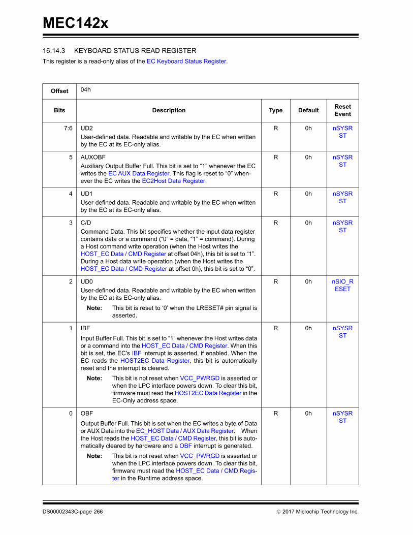
MEC142x
16.14.3 KEYBOARD STATUS READ REGISTER
This register is a read-only alias of the EC Keyboard Status Register.
Offset 04h
Bits Description Type DefaultReset Event
7:6 UD2
User-defined data. Readable and writable by the EC when written by the EC at its EC-only alias.
R 0h nSYSRST
5 AUXOBF
Auxiliary Output Buffer Full. This bit is set to “1” whenever the EC writes the EC AUX Data Register. This flag is reset to “0” when-ever the EC writes the EC2Host Data Register.
R 0h nSYSRST
4 UD1
User-defined data. Readable and writable by the EC when written by the EC at its EC-only alias.
R 0h nSYSRST
3 C/D
Command Data. This bit specifies whether the input data register contains data or a command (“0” = data, “1” = command). During a Host command write operation (when the Host writes the HOST_EC Data / CMD Register at offset 04h), this bit is set to “1”. During a Host data write operation (when the Host writes the HOST_EC Data / CMD Register at offset 0h), this bit is set to “0”.
R 0h nSYSRST
2 UD0
User-defined data. Readable and writable by the EC when written by the EC at its EC-only alias.
Note: This bit is reset to ‘0’ when the LRESET# pin signal isasserted.
R 0h nSIO_RESET
1 IBF
Input Buffer Full. This bit is set to “1” whenever the Host writes dataor a command into the HOST_EC Data / CMD Register. When thisbit is set, the EC's IBF interrupt is asserted, if enabled. When theEC reads the HOST2EC Data Register, this bit is automaticallyreset and the interrupt is cleared.
Note: This bit is not reset when VCC_PWRGD is asserted orwhen the LPC interface powers down. To clear this bit,firmware must read the HOST2EC Data Register in theEC-Only address space.
R 0h nSYSRST
0 OBF
Output Buffer Full. This bit is set when the EC writes a byte of Dataor AUX Data into the EC_HOST Data / AUX Data Register. Whenthe Host reads the HOST_EC Data / CMD Register, this bit is auto-matically cleared by hardware and a OBF interrupt is generated.
Note: This bit is not reset when VCC_PWRGD is asserted orwhen the LPC interface powers down. To clear this bit,firmware must read the HOST_EC Data / CMD Regis-ter in the Runtime address space.
R 0h nSYSRST
DS00002343C-page 266 2017 Microchip Technology Inc.
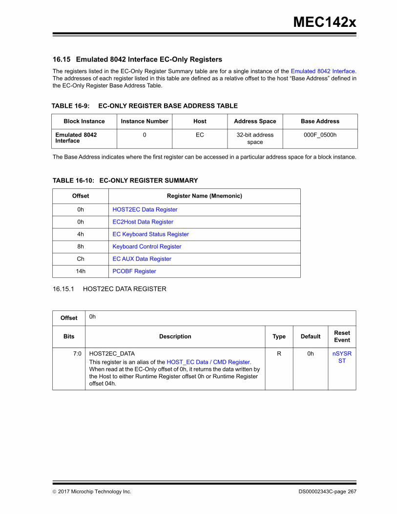
MEC142x
16.15 Emulated 8042 Interface EC-Only Registers
The registers listed in the EC-Only Register Summary table are for a single instance of the Emulated 8042 Interface.The addresses of each register listed in this table are defined as a relative offset to the host “Base Address” defined inthe EC-Only Register Base Address Table.
The Base Address indicates where the first register can be accessed in a particular address space for a block instance.
16.15.1 HOST2EC DATA REGISTER
TABLE 16-9: EC-ONLY REGISTER BASE ADDRESS TABLE
Block Instance Instance Number Host Address Space Base Address
Emulated 8042 Interface
0 EC 32-bit address space
000F_0500h
TABLE 16-10: EC-ONLY REGISTER SUMMARY
Offset Register Name (Mnemonic)
0h HOST2EC Data Register
0h EC2Host Data Register
4h EC Keyboard Status Register
8h Keyboard Control Register
Ch EC AUX Data Register
14h PCOBF Register
Offset 0h
Bits Description Type DefaultReset Event
7:0 HOST2EC_DATA
This register is an alias of the HOST_EC Data / CMD Register. When read at the EC-Only offset of 0h, it returns the data written by the Host to either Runtime Register offset 0h or Runtime Register offset 04h.
R 0h nSYSRST
2017 Microchip Technology Inc. DS00002343C-page 267

MEC142x
16.15.2 EC2HOST DATA REGISTER
16.15.3 EC KEYBOARD STATUS REGISTER
This register is an alias of the Keyboard Status Read Register. The fields C/D, IBF, and OBF remain read-only.
Offset 0h
Bits Description Type DefaultReset Event
7:0 EC2HOST_DATA
This register is an alias of the EC_HOST Data / AUX Data Regis-ter. Writing this register sets the OBF status bit.
W 0h nSYSRST
Offset 04h
Bits Description Type DefaultReset Event
7:6 UD2
User-defined data. Readable and writable by the EC.
R/W 0h nSYSRST
5 AUXOBF
Auxiliary Output Buffer Full. This bit is set to ‘1’ whenever the EC writes the EC AUX Data Register. This flag is reset to ‘0’ when-ever the EC writes the EC2Host Data Register.
R/W 0h nSYSRST
4 UD1
User-defined data. Readable and writable by the EC when written by the EC at its EC-only alias.
R/W 0h nSYSRST
3 C/D
Command Data. This bit specifies whether the input data register contains data or a command. During a Host command write oper-ation (when the Host writes the HOST_EC Data / CMD Register at offset 04h), this bit is set to ‘1’. During a Host data write operation (when the Host writes the HOST_EC Data / CMD Register at off-set 0h), this bit is set to ‘0’.
1=Command0=Data
R 0h nSYSRST
2 UD0
User-defined data. Readable and writable by the EC when written by the EC at its EC-only alias.
This bit is reset to ‘0’ when the LRESET# pin signal is asserted.
R/W 0h nSYSRST andPCI_RESET#
DS00002343C-page 268 2017 Microchip Technology Inc.

MEC142x
16.15.4 KEYBOARD CONTROL REGISTER
1 IBF
Input Buffer Full. This bit is set to “1” whenever the Host writes dataor a command into the HOST_EC Data / CMD Register. When thisbit is set, the EC's IBF interrupt is asserted, if enabled. When theEC reads the HOST2EC Data Register this bit is automaticallyreset and the interrupt is cleared.
This bit is not reset when VCC_PWRGD is asserted or when the LPC interface powers down. To clear this bit, firmware must read the HOST2EC Data Register in the EC-Only address space.
R 0h nSYSRST
0 OBF
Output Buffer Full. This bit is set when the EC writes a byte of Dataor AUX Data into the EC_HOST Data / AUX Data Register. Whenthe Host reads the HOST_EC Data / CMD Register, this bit is auto-matically cleared by hardware and a OBF interrupt is generated.
This bit is not reset when VCC_PWRGD is asserted or when the LPC interface powers down. To clear this bit, firmware must read the HOST_EC Data / CMD Register in the Runtime address space.
R 0h nSYSRST
Offset 08h
Bits Description Type DefaultReset Event
7 AUXH
AUX in Hardware.
1=AUXOBF of the Keyboard Status Read Register is set in hard-ware by a write to the EC AUX Data Register
0=AUXOBF is not modified in hardware, but can be read and writtenby the EC using the EC-Only alias of the EC Keyboard StatusRegister
R/W 0h nSYSRST
6 UD5
User-defined data. Readable and writable by the EC when written by the EC at its EC-only alias.
R/W 0h nSYSRST
5 OBFEN
When this bit is ‘1’, the system interrupt signal KIRQ is driven by thebit PCOBF and MIRQ is driven by AUXOBF. When this bit is ‘0’,KIRQ and MIRQ are driven low.
This bit must not be changed when OBF of the status register isequal to ‘1’.
R/W 0h nSYSRST
4:3 UD4
User-defined data. Readable and writable by the EC when written by the EC at its EC-only alias.
R/W 0h nSYSRST
Offset 04h
Bits Description Type DefaultReset Event
2017 Microchip Technology Inc. DS00002343C-page 269
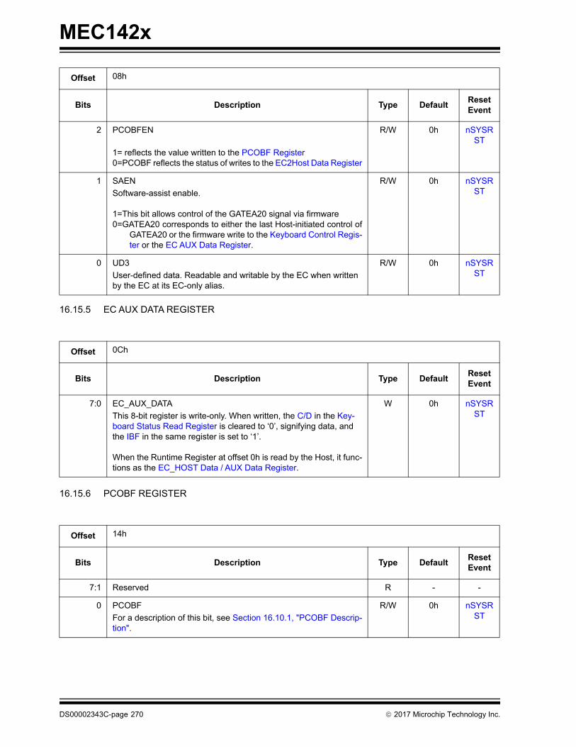
MEC142x
16.15.5 EC AUX DATA REGISTER
16.15.6 PCOBF REGISTER
2 PCOBFEN
1= reflects the value written to the PCOBF Register0=PCOBF reflects the status of writes to the EC2Host Data Register
R/W 0h nSYSRST
1 SAEN
Software-assist enable.
1=This bit allows control of the GATEA20 signal via firmware0=GATEA20 corresponds to either the last Host-initiated control of
GATEA20 or the firmware write to the Keyboard Control Regis-ter or the EC AUX Data Register.
R/W 0h nSYSRST
0 UD3
User-defined data. Readable and writable by the EC when written by the EC at its EC-only alias.
R/W 0h nSYSRST
Offset 0Ch
Bits Description Type DefaultReset Event
7:0 EC_AUX_DATA
This 8-bit register is write-only. When written, the C/D in the Key-board Status Read Register is cleared to ‘0’, signifying data, and the IBF in the same register is set to ‘1’.
When the Runtime Register at offset 0h is read by the Host, it func-tions as the EC_HOST Data / AUX Data Register.
W 0h nSYSRST
Offset 14h
Bits Description Type DefaultReset Event
7:1 Reserved R - -
0 PCOBF
For a description of this bit, see Section 16.10.1, "PCOBF Descrip-tion".
R/W 0h nSYSRST
Offset 08h
Bits Description Type DefaultReset Event
DS00002343C-page 270 2017 Microchip Technology Inc.
MEC142x
16.16 Legacy Port92/GATEA20 Configuration Registers
The registers listed in the Configuration Register Summary table are for a single instance of the LegacyPort92/GATEA20 logic. The addresses of each register listed in this table are defined as a relative offset to the host“Base Address” defined in the Configuration Register Base Address Table.
Each Configuration register access through the Host Access Port is via its LDN and its Host Access Port Index. ECaccess is a relative offset to the EC Base Address.
16.16.1 PORT 92 ENABLE REGISTER
TABLE 16-11: CONFIGURATION BASE ADDRESS TABLE
Block InstanceInstance Number
LogicalDeviceNumber
Host Address Space Base Address
Port92-Legacy 0 1 LPC/eSPI Configuration Port INDEX = 00h
EC 32-bit internal address space
000F_1800h
TABLE 16-12: CONFIGURATION REGISTER SUMMARY
Offset Register Name (Mnemonic)
30h Port 92 Enable Register
Offset 30h
Bits Description Type DefaultReset Event
7:1 Reserved R - -
0 P92_EN
When this bit is ‘1’, the Port92h Register is enabled. When this bit is ‘0’, the Port92h Register is disabled, and Host writes to LPC address 92h are ignored.
R/W 0h VCC_P-WRGD
andnSYSR
ST
2017 Microchip Technology Inc. DS00002343C-page 271
MEC142x
16.17 Legacy Port92/GATEA20 Runtime Registers
The registers listed in the Runtime Register Summary table are for a single instance of the Legacy Port92/GATEA20logic. The addresses of each register listed in this table are defined as a relative offset to the host “Base Address”defined in the Runtime Register Base Address Table.
The Base Address indicates where the first register can be accessed in a particular address space for a block instance.
16.17.1 PORT 92 REGISTER
TABLE 16-13: RUNTIME REGISTER BASE ADDRESS TABLE
Block Instance Instance Number Host Address Space Base Address
Port92-Legacy 0 LPC/eSPI I/O 0092h
EC 32-bit address space
000F_1800h
TABLE 16-14: RUNTIME REGISTER SUMMARY
Offset Register Name (Mnemonic)
0h Port 92 Register
Offset 0h
Bits Description Type DefaultReset Event
7:2 Reserved R - -
1 ALT_GATE_A20
This bit provides an alternate means for system control of theGATEA20 pin. ALT_A20 low drives GATEA20 low, if A20 from thekeyboard controller is also low. When Port 92 is enabled, writing a1 to this bit forces ALT_A20 high. ALT_A20 high drives GATEA20high regardless of the state of A20 from the keyboard controller.
0=ALT_A20 is driven low1=ALT_A20 is driven high
R/W 0h nSIO_RESET
0 ALT_CPU_RESET
This bit provides an alternate means to generate a CPU_RESET pulse. The CPU_RESET output provides a means to reset the sys-tem CPU to effect a mode switch from Protected Virtual Address Mode to the Real Address Mode. This provides a faster means of reset than is provided through the EC keyboard controller. Writing a “1” to this bit will cause the ALT_RST# internal signal to pulse (active low) for a minimum of 6s after a delay of 14s. Before another ALT_RST# pulse can be generated, this bit must be writ-ten back to “0”.
R/W 0h nSIO_RESET
DS00002343C-page 272 2017 Microchip Technology Inc.
MEC142x
16.18 Emulated 8042 Interface EC-Only Registers
The registers listed in the EC-Only Register Summary table are for a single instance of the Legacy Port92/GATEA20logic. The addresses of each register listed in this table are defined as a relative offset to the host “Base Address”defined in the EC-Only Register Base Address Table.
The Base Address indicates where the first register can be accessed in a particular address space for a block instance.
16.18.1 GATEA20 CONTROL REGISTER
16.18.2 SETGA20L REGISTER
TABLE 16-15: EC-ONLY REGISTER BASE ADDRESS TABLE
Block Instance Instance Number Host Address Space Base Address
Port92-Legacy 0 EC 32-bit address space
000F_1900h
TABLE 16-16: EC-ONLY REGISTER SUMMARY
Offset Register Name (Mnemonic)
0h GATEA20 Control Register
8h SETGA20L Register
Ch RSTGA20L Register
Offset 0h
Bits Description Type DefaultReset Event
7:1 Reserved R - -
0 GATEA20
0=The GATEA20 output is driven low1=The GATEA20 output is driven high
R/W 0h nSYSRST
Offset 08h
Bits Description Type DefaultReset Event
7:0 SETGA20L
See Section 16.11.1, "GATE A20 Speedup" for information on this register. A write to this register sets GATEA20 in the GATEA20 Control Register.
W - -
2017 Microchip Technology Inc. DS00002343C-page 273

MEC142x
16.18.3 RSTGA20L REGISTER
Offset 0Ch
Bits Description Type DefaultReset Event
7:0 RSTGA20L
See Section 16.11.1, "GATE A20 Speedup" for information on this register. A write to this register sets GATEA20 in the GATEA20 Control Register.
W - -
DS00002343C-page 274 2017 Microchip Technology Inc.
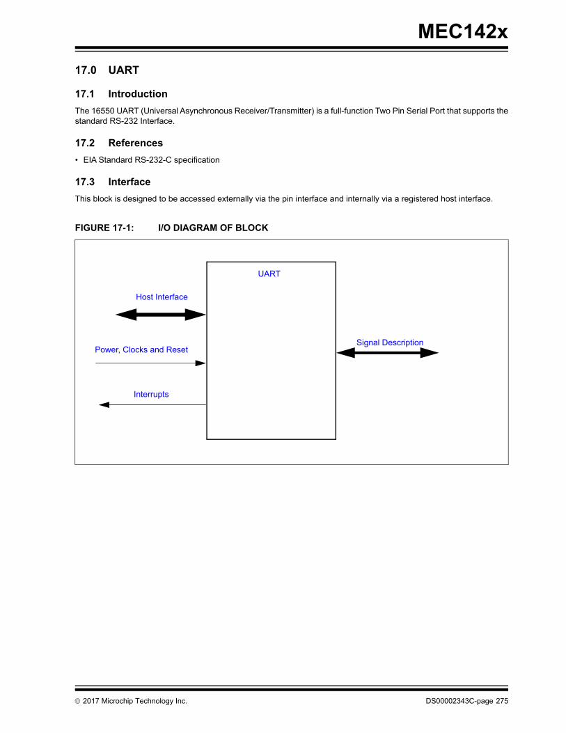
MEC142x
17.0 UART
17.1 Introduction
The 16550 UART (Universal Asynchronous Receiver/Transmitter) is a full-function Two Pin Serial Port that supports thestandard RS-232 Interface.
17.2 References
• EIA Standard RS-232-C specification
17.3 Interface
This block is designed to be accessed externally via the pin interface and internally via a registered host interface.
FIGURE 17-1: I/O DIAGRAM OF BLOCK
Signal Description
UART
Interrupts
Power, Clocks and Reset
Host Interface
2017 Microchip Technology Inc. DS00002343C-page 275

MEC142x
17.4 Signal Description
TABLE 17-1: SIGNAL DESCRIPTION TABLE
Name Direction Description
DTR# Output Active low Data Terminal ready output for the Serial Port.
Handshake output signal notifies modem that the UART is ready to transmit data. This signal can be programmed by writing to bit 1 of the Modem Control Register (MCR).
Note: Defaults to tri-state on V3_DUAL power on.
DCD# Output Active low Data Carrier Detect input for the serial port. Handshake signal which notifies the UART that carrier signal is detected by the modem. The CPU can monitor the status of DCD# signal by reading bit 7 of Modem Status Register (MSR). A DCD# signal state change from low to high after the last MSR read will set MSR bit 3 to a 1. If bit 3 of Interrupt Enable Register is set, the interrupt is generated when DCD # changes state.
DSR# Input Active low Data Set Ready input for the serial port. Handshake signal which notifies the UART that the modem is ready to estab-lish the communication link. The CPU can monitor the status of DSR# signal by reading bit 5 of Modem Status Register (MSR). A DSR# signal state change from low to high after the last MSR read will set MSR bit 1 to a 1. If bit 3 of Interrupt Enable Register is set, the interrupt is generated when DSR# changes state.
RI# Input Active low Ring Indicator input for the serial port. Handshake sig-nal which notifies the UART that the telephone ring signal is detected by the modem. The CPU can monitor the status of RI# signal by reading bit 6 of Modem Status Register (MSR). A RI# signal state change from low to high after the last MSR read will set MSR bit 2 to a 1. If bit 3 of Interrupt Enable Register is set, the interrupt is generated when nRI changes state.
RTS# Output Active low Request to Send output for the Serial Port. Handshake output signal notifies modem that the UART is ready to transmit data. This signal can be programmed by writing to bit 1 of the Modem Control Register (MCR). The hardware reset will reset the RTS# signal to inactive mode (high). RTS# is forced inactive during loop mode operation. Defaults to tri-state on V3_DUAL power on.
CTS# Input Active low Clear to Send input for the serial port. Handshake sig-nal which notifies the UART that the modem is ready to receive data. The CPU can monitor the status of CTS# signal by reading bit 4 of Modem Status Register (MSR). A CTS# signal state change from low to high after the last MSR read will set MSR bit 0 to a 1. If bit 3 of the Interrupt Enable Register is set, the interrupt is generated when CTS# changes state. The CTS# signal has no effect on the transmitter.
TXD Output Transmit serial data output.
RXD Input Receiver serial data input.
UART_CLK Input External Baud Clock Generator input. The source of the baud clock is controlled by CLK_SRC on page 280.
DS00002343C-page 276 2017 Microchip Technology Inc.

MEC142x
17.5 Host Interface
The UART is accessed by host software via a registered interface, as defined in Section 17.10, "Configuration Regis-ters"and Section 17.11, "Runtime Registers".
17.6 Power, Clocks and Reset
This section defines the Power, Clock, and Reset parameters of the block.
17.6.1 POWER DOMAINS
17.6.2 CLOCK INPUTS
17.6.3 RESETS
17.7 Interrupts
This section defines the Interrupt Sources generated from this block.
Name Description
VTR This Power Well is used to power the registers and logic in this block.
Name Description
1.8432MHz_Clk The UART requires a 1.8432 MHz ± 2% clock input for baud rate generation.
24MHz_Clk 24 MHz ± 2% clock input. This clock may be enabled to generate the baud rate, which requires a 1.8432 MHz ± 2% clock input.
Name Description
nSYSRST This reset is asserted when VTR is applied.
nSIO_RESET This is an alternate reset condition, typically asserted when the main power rail is asserted.
RESET This reset is determined by the POWER bit signal. When the power bit signal is 1, this signal is equal to nSIO_RESET. When the power bit signal is 0, this signal is equal to nSYSRST.
Source Description
UART The UART interrupt event output indicates if an interrupt is pending. See Table 17-9, “Interrupt Control Table,” on page 286.
Source Description
UART The UART interrupt event output indicates if an interrupt is pending. See Table 17-9, “Interrupt Control Table,” on page 286.
2017 Microchip Technology Inc. DS00002343C-page 277

MEC142x
17.8 Low Power Modes
The UART may be put into a low power state by the chip’s Power, Clocks, and Reset (PCR) circuitry.
17.9 Description
The UART is compatible with the 16450, the 16450 ACE registers and the 16C550A. The UART performs serial-to-par-allel conversions on received characters and parallel-to-serial conversions on transmit characters. Two sets of baudrates are provided. When the 1.8432 MHz source clock is selected, standard baud rates from 50 to 115.2K are available.When the source clock is 32.26 MHz, baud rates from 126K to 2,016K are available. The character options are program-mable for 1 start; 1, 1.5 or 2 stop bits; even, odd, sticky or no parity; and prioritized interrupts. The UART contains aprogrammable baud rate generator that is capable of dividing the input clock signal by 1 to 65535. The UART is alsocapable of supporting the MIDI data rate. Refer to the Configuration Registers for information on disabling, poweringdown and changing the base address of the UART. The UART interrupt is enabled by programming OUT2 of the UARTto logic “1.” Because OUT2 is logic “0,” it disables the UART's interrupt. The UART is accessible by both the Host andthe EC.
17.9.1 PROGRAMMABLE BAUD RATE
The Serial Port contains a programmable Baud Rate Generator that is capable of dividing the internal clock source byany divisor from 1 to 65535. The clock source is either the 1.8432MHz_Clk clock source or the 24MHz_Clk clock source.The output frequency of the Baud Rate Generator is 16x the Baud rate. Two eight bit latches store the divisor in 16 bitbinary format. These Divisor Latches must be loaded during initialization in order to ensure desired operation of theBaud Rate Generator. Upon loading either of the Divisor Latches, a 16 bit Baud counter is immediately loaded. Thisprevents long counts on initial load. If a 0 is loaded into the BRG registers, the output divides the clock by the number3. If a 1 is loaded, the output is the inverse of the input oscillator. If a two is loaded, the output is a divide by 2 signal witha 50% duty cycle. If a 3 or greater is loaded, the output is low for 2 bits and high for the remainder of the count.
The following tables show possible baud rates.
TABLE 17-2: UART BAUD RATES USING CLOCK SOURCE 1.8432MHz_Clk
Desired Baud Rate BAUD_CLOCK_SELDivisor Used to Generate
16X Clock
50 0 2304
75 0 1536
110 0 1047
134.5 0 857
150 0 768
300 0 384
600 0 192
1200 0 96
1800 0 64
2000 0 58
2400 0 48
3600 0 32
4800 0 24
7200 0 16
9600 0 12
DS00002343C-page 278 2017 Microchip Technology Inc.

MEC142x
17.10 Configuration Registers
The registers listed in the Configuration Register Summary table are for a single instance of the UART. The addressesof each register listed in this table are defined as a relative offset to the host “Base Address” defined in the ConfigurationRegister Base Address Table.
Each Configuration register access through the Host Access Port is via its LDN and its Host Access Port Index. ECaccess is a relative offset to the EC Base Address.
19200 0 6
38400 0 3
57600 0 2
115200 0 1
TABLE 17-3: UART BAUD RATES USING CLOCK SOURCE 24MHz_Clk
Desired Baud Rate BAUD_CLOCK_SELDivisor Used to Generate
16X Clock
125000 1 12
136400 1 11
150000 1 10
166700 1 9
187500 1 8
214300 1 7
250000 1 6
300000 1 5
375000 1 4
500000 1 3
750000 1 2
1500000 1 1
TABLE 17-4: CONFIGURATION REGISTER BASE ADDRESS TABLE
Block InstanceInstance Number
HostAddress Space Base Address
UART 0 LPC/eSPI Configuration Port INDEX = 00h
UART 0 EC 32-bit internal address space
000F_1F00h
TABLE 17-2: UART BAUD RATES USING CLOCK SOURCE 1.8432MHz_Clk (CONTINUED)
Desired Baud Rate BAUD_CLOCK_SELDivisor Used to Generate
16X Clock
2017 Microchip Technology Inc. DS00002343C-page 279

MEC142x
17.10.1 ACTIVATE REGISTER
17.10.2 CONFIGURATION SELECT REGISTER
TABLE 17-5: CONFIGURATION REGISTER SUMMARY
Offset Register Name (Mnemonic)
30h Activate Register
F0h Configuration Select Register
Offset 30h
Bits Description Type DefaultReset Event
7:1 Reserved R - -
0 ACTIVATE
When this bit is 1, the UART logical device is powered and func-tional. When this bit is 0, the UART logical device is powered down and inactive.
R/W 0b RESET
Offset F0h
Bits Description Type DefaultReset Event
7:3 Reserved R - -
2 POLARITY
1=The UART_TX and UART_RX pins functions are inverted0=The UART_TX and UART_RX pins functions are not inverted
R/W 0b RESET
1 POWER
1=The RESET reset signal is derived from nSIO_RESET0=The RESET reset signal is derived from nSYSRST
R/W 1b RESET
0 CLK_SRC
1=The UART Baud Clock is derived from an external clock source0=The UART Baud Clock is derived from one of the two internal
clock sources
R/W 0b RESET
DS00002343C-page 280 2017 Microchip Technology Inc.
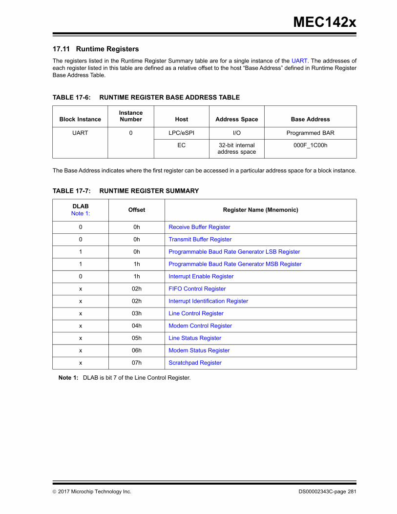
MEC142x
17.11 Runtime Registers
The registers listed in the Runtime Register Summary table are for a single instance of the UART. The addresses ofeach register listed in this table are defined as a relative offset to the host “Base Address” defined in Runtime RegisterBase Address Table.
The Base Address indicates where the first register can be accessed in a particular address space for a block instance.
Note 1: DLAB is bit 7 of the Line Control Register.
TABLE 17-6: RUNTIME REGISTER BASE ADDRESS TABLE
Block InstanceInstance Number Host Address Space Base Address
UART 0 LPC/eSPI I/O Programmed BAR
EC 32-bit internal address space
000F_1C00h
TABLE 17-7: RUNTIME REGISTER SUMMARY
DLABNote 1:
Offset Register Name (Mnemonic)
0 0h Receive Buffer Register
0 0h Transmit Buffer Register
1 0h Programmable Baud Rate Generator LSB Register
1 1h Programmable Baud Rate Generator MSB Register
0 1h Interrupt Enable Register
x 02h FIFO Control Register
x 02h Interrupt Identification Register
x 03h Line Control Register
x 04h Modem Control Register
x 05h Line Status Register
x 06h Modem Status Register
x 07h Scratchpad Register
2017 Microchip Technology Inc. DS00002343C-page 281

MEC142x
17.11.1 RECEIVE BUFFER REGISTER
17.11.2 TRANSMIT BUFFER REGISTER
17.11.3 PROGRAMMABLE BAUD RATE GENERATOR LSB REGISTER
Offset 0h (DLAB=0)
Bits Description Type DefaultReset Event
7:0 RECEIVED_DATAThis register holds the received incoming data byte. Bit 0 is the least significant bit, which is transmitted and received first. Received data is double buffered; this uses an additional shift reg-ister to receive the serial data stream and convert it to a parallel 8 bit word which is transferred to the Receive Buffer register. The shift register is not accessible.
R 0h RESET
Offset 0h (DLAB=0)
Bits Description Type DefaultReset Event
7:0 TRANSMIT_DATAThis register contains the data byte to be transmitted. The trans-mit buffer is double buffered, utilizing an additional shift register (not accessible) to convert the 8 bit data word to a serial format. This shift register is loaded from the Transmit Buffer when the transmission of the previous byte is complete.
W 0h RESET
Offset 00h (DLAB=1)
Bits Description Type DefaultReset Event
7:0 BAUD_RATE_DIVISOR_LSB
See Section 17.9.1, "Programmable Baud Rate".
R/W 0h RESET
DS00002343C-page 282 2017 Microchip Technology Inc.

MEC142x
17.11.4 PROGRAMMABLE BAUD RATE GENERATOR MSB REGISTER
17.11.5 INTERRUPT ENABLE REGISTER
The lower four bits of this register control the enables of the five interrupt sources of the Serial Port interrupt. It is possibleto totally disable the interrupt system by resetting bits 0 through 3 of this register. Similarly, setting the appropriate bitsof this register to a high, selected interrupts can be enabled. Disabling the interrupt system inhibits the Interrupt Identi-fication Register and disables any Serial Port interrupt out of the MEC142x. All other system functions operate in theirnormal manner, including the Line Status and MODEM Status Registers. The contents of the Interrupt Enable Registerare described below.
Offset 01h (DLAB=1)
Bits Description Type DefaultReset Event
7 BAUD_CLK_SEL0=If CLK_SRC is ‘0’, the baud clock is derived from the
1.8432MHz_Clk. If CLK_SRC is ‘1’, this bit has no effect1=If CLK_SRC is ‘0’, the baud clock is derived from the 24MHz_Clk.
If CLK_SRC is ‘1’, this bit has no effect
R/W 0h RESET
6:0 BAUD_RATE_DIVISOR_MSB
See Section 17.9.1, "Programmable Baud Rate".
R/W 0h RESET
Offset 01h (DLAB=0)
Bits Description Type DefaultReset Event
7:4 Reserved R - -
3 EMSI
This bit enables the MODEM Status Interrupt when set to logic “1”. This is caused when one of the Modem Status Register bits changes state.
R/W 0h RESET
2 ELSI
This bit enables the Received Line Status Interrupt when set to logic “1”. The error sources causing the interrupt are Overrun, Par-ity, Framing and Break. The Line Status Register must be read to determine the source.
R/W 0h RESET
1 ETHREI
This bit enables the Transmitter Holding Register Empty Interrupt when set to logic “1”.
R/W 0h RESET
0 ERDAI
This bit enables the Received Data Available Interrupt (and timeout interrupts in the FIFO mode) when set to logic “1”.
R/W 0h RESET
2017 Microchip Technology Inc. DS00002343C-page 283
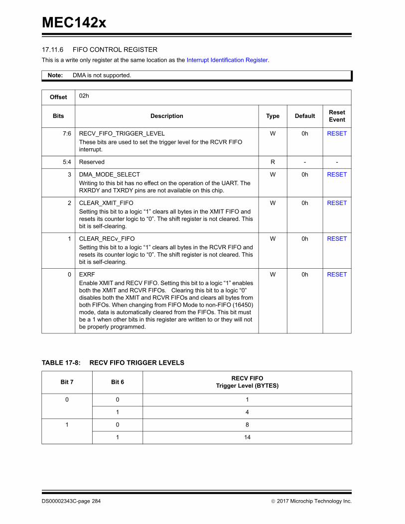
MEC142x
17.11.6 FIFO CONTROL REGISTER
This is a write only register at the same location as the Interrupt Identification Register.
Note: DMA is not supported.
Offset 02h
Bits Description Type DefaultReset Event
7:6 RECV_FIFO_TRIGGER_LEVEL
These bits are used to set the trigger level for the RCVR FIFO interrupt.
W 0h RESET
5:4 Reserved R - -
3 DMA_MODE_SELECT
Writing to this bit has no effect on the operation of the UART. The RXRDY and TXRDY pins are not available on this chip.
W 0h RESET
2 CLEAR_XMIT_FIFO
Setting this bit to a logic “1” clears all bytes in the XMIT FIFO and resets its counter logic to “0”. The shift register is not cleared. This bit is self-clearing.
W 0h RESET
1 CLEAR_RECv_FIFO
Setting this bit to a logic “1” clears all bytes in the RCVR FIFO and resets its counter logic to “0”. The shift register is not cleared. This bit is self-clearing.
W 0h RESET
0 EXRF
Enable XMIT and RECV FIFO. Setting this bit to a logic “1” enables both the XMIT and RCVR FIFOs. Clearing this bit to a logic “0” disables both the XMIT and RCVR FIFOs and clears all bytes from both FIFOs. When changing from FIFO Mode to non-FIFO (16450) mode, data is automatically cleared from the FIFOs. This bit must be a 1 when other bits in this register are written to or they will not be properly programmed.
W 0h RESET
TABLE 17-8: RECV FIFO TRIGGER LEVELS
Bit 7 Bit 6RECV FIFO
Trigger Level (BYTES)
0 0 1
1 4
1 0 8
1 14
DS00002343C-page 284 2017 Microchip Technology Inc.
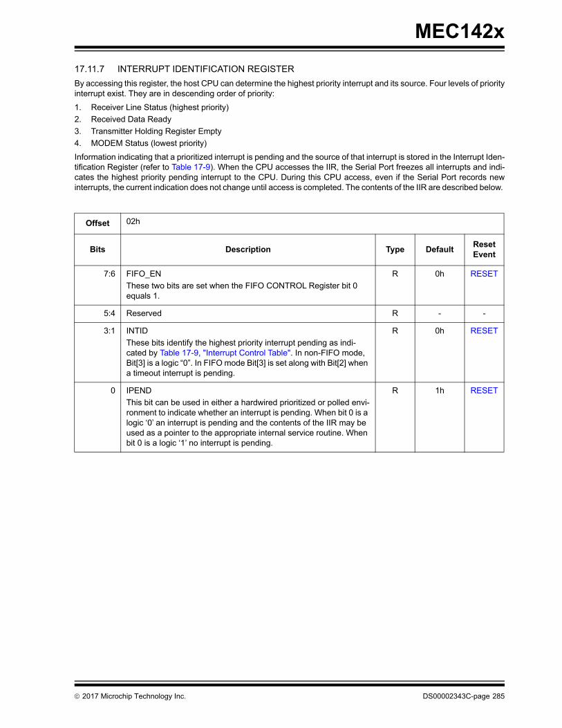
MEC142x
17.11.7 INTERRUPT IDENTIFICATION REGISTER
By accessing this register, the host CPU can determine the highest priority interrupt and its source. Four levels of priorityinterrupt exist. They are in descending order of priority:
1. Receiver Line Status (highest priority)
2. Received Data Ready
3. Transmitter Holding Register Empty
4. MODEM Status (lowest priority)
Information indicating that a prioritized interrupt is pending and the source of that interrupt is stored in the Interrupt Iden-tification Register (refer to Table 17-9). When the CPU accesses the IIR, the Serial Port freezes all interrupts and indi-cates the highest priority pending interrupt to the CPU. During this CPU access, even if the Serial Port records newinterrupts, the current indication does not change until access is completed. The contents of the IIR are described below.
Offset 02h
Bits Description Type DefaultReset Event
7:6 FIFO_EN
These two bits are set when the FIFO CONTROL Register bit 0 equals 1.
R 0h RESET
5:4 Reserved R - -
3:1 INTID
These bits identify the highest priority interrupt pending as indi-cated by Table 17-9, "Interrupt Control Table". In non-FIFO mode, Bit[3] is a logic “0”. In FIFO mode Bit[3] is set along with Bit[2] when a timeout interrupt is pending.
R 0h RESET
0 IPEND
This bit can be used in either a hardwired prioritized or polled envi-ronment to indicate whether an interrupt is pending. When bit 0 is a logic ‘0’ an interrupt is pending and the contents of the IIR may be used as a pointer to the appropriate internal service routine. When bit 0 is a logic ‘1’ no interrupt is pending.
R 1h RESET
2017 Microchip Technology Inc. DS00002343C-page 285

MEC142x
TABLE 17-9: INTERRUPT CONTROL TABLE
FIFO Mode Only
Interrupt Identification Register
Interrupt SET and RESET Functions
Bit 3 Bit 2 Bit 1 Bit 0Priority Level
Interrupt Type Interrupt SourceInterrupt Reset
Control
0 0 0 1 - None None -
1 1 0 Highest Receiver Line Status
Overrun Error, Parity Error, Framing Error or Break Interrupt
Reading the Line Status Register
0 Second Received Data Available
Receiver Data Available
Read Receiver Buffer or the FIFO drops below the trigger level.
1 Character Time-out Indication
No Characters Have Been Removed From or Input to the RCVR FIFO during the last 4 Char times and there is at least 1 char in it during this time
Reading the Receiver Buffer Register
0 0 1 Third Transmitter Hold-ing Register Empty
Transmitter Hold-ing Register Empty
Reading the IIR Register (if Source of Inter-rupt) or Writing the Transmitter Holding Register
0 0 Fourth MODEM Status Clear to Send or Data Set Ready or Ring Indicator or Data Carrier Detect
Reading the MODEM Status Register
DS00002343C-page 286 2017 Microchip Technology Inc.

MEC142x
17.11.8 LINE CONTROL REGISTER
Offset 03h
BitsDescription Type Default
Reset Event
7 DLAB
Divisor Latch Access Bit (DLAB). It must be set high (logic “1”) to access the Divisor Latches of the Baud Rate Generator during read or write operations. It must be set low (logic “0”) to access the Receiver Buffer Register, the Transmitter Holding Register, or the Interrupt Enable Register.
R/W 0h RESET
6 BREAK_CONTROL
Set Break Control bit. When bit 6 is a logic “1”, the transmit data output (TXD) is forced to the Spacing or logic “0” state and remains there (until reset by a low level bit 6) regardless of other transmitter activity. This feature enables the Serial Port to alert a terminal in a communications system.
R/W 0h RESET
5 STICK_PARITY
Stick Parity bit. When parity is enabled it is used in conjunction with bit 4 to select Mark or Space Parity. When LCR bits 3, 4 and 5 are 1 the Parity bit is transmitted and checked as a 0 (Space Parity). If bits 3 and 5 are 1 and bit 4 is a 0, then the Parity bit is transmitted and checked as 1 (Mark Parity). If bit 5 is 0 Stick Parity is disabled. Bit 3 is a logic “1” and bit 5 is a logic “1”, the parity bit is transmitted and then detected by the receiver in the opposite state indicated by bit 4.
R/W 0h RESET
4 PARITY_SELECT
Even Parity Select bit. When bit 3 is a logic “1” and bit 4 is a logic “0”, an odd number of logic “1”'s is transmitted or checked in the data word bits and the parity bit. When bit 3 is a logic “1” and bit 4 is a logic “1” an even number of bits is transmitted and checked.
R/W 0h RESET
3 ENABLE_PARITY
Parity Enable bit. When bit 3 is a logic “1”, a parity bit is gener-ated (transmit data) or checked (receive data) between the last data word bit and the first stop bit of the serial data. (The parity bit is used to generate an even or odd number of 1s when the data word bits and the parity bit are summed).
R/W 0h RESET
2 STOP_BITS
This bit specifies the number of stop bits in each transmitted or received serial character. Table 17-10 summarizes the information.
R/W 0h RESET
1:0 WORD_LENGTH
These two bits specify the number of bits in each transmitted or received serial character. The encoding of bits 0 and 1 is as fol-lows:
R/W 0h RESET
2017 Microchip Technology Inc. DS00002343C-page 287

MEC142x
Note 17-1 The receiver will ignore all stop bits beyond the first, regardless of the number used in transmitting.
The Start, Stop and Parity bits are not included in the word length.
TABLE 17-10: STOP BITS
Bit 2 Word Length Number of Stop Bits
0 -- 1
1 5 bits 1.5
6 bits 2
7 bits
8 bits
TABLE 17-11: SERIAL CHARACTER
Bit 1 Bit 0 Word Length
0011
0101
5 Bits6 Bits7 Bits8 Bits
DS00002343C-page 288 2017 Microchip Technology Inc.
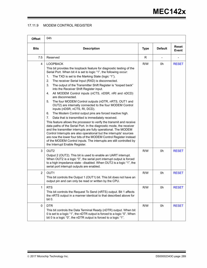
MEC142x
17.11.9 MODEM CONTROL REGISTER
Offset 04h
Bits Description Type DefaultReset Event
7:5 Reserved R - -
4 LOOPBACK
This bit provides the loopback feature for diagnostic testing of the Serial Port. When bit 4 is set to logic “1”, the following occur:
1. The TXD is set to the Marking State (logic “1”).
2. The receiver Serial Input (RXD) is disconnected.
3. The output of the Transmitter Shift Register is “looped back”into the Receiver Shift Register input.
4. All MODEM Control inputs (nCTS, nDSR, nRI and nDCD)are disconnected.
5. The four MODEM Control outputs (nDTR, nRTS, OUT1 andOUT2) are internally connected to the four MODEM Controlinputs (nDSR, nCTS, RI, DCD).
6. The Modem Control output pins are forced inactive high.
7. Data that is transmitted is immediately received.
This feature allows the processor to verify the transmit and receive data paths of the Serial Port. In the diagnostic mode, the receiver and the transmitter interrupts are fully operational. The MODEM Control Interrupts are also operational but the interrupts' sources are now the lower four bits of the MODEM Control Register instead of the MODEM Control inputs. The interrupts are still controlled by the Interrupt Enable Register.
R/W 0h RESET
3 OUT2
Output 2 (OUT2). This bit is used to enable an UART interrupt. When OUT2 is a logic “0”, the serial port interrupt output is forced to a high impedance state - disabled. When OUT2 is a logic “1”, the serial port interrupt outputs are enabled.
R/W 0h RESET
2 OUT1
This bit controls the Output 1 (OUT1) bit. This bit does not have an output pin and can only be read or written by the CPU.
R/W 0h RESET
1 RTS
This bit controls the Request To Send (nRTS) output. Bit 1 affects the nRTS output in a manner identical to that described above for bit 0.
R/W 0h RESET
0 DTR
This bit controls the Data Terminal Ready (nDTR) output. When bit 0 is set to a logic “1”, the nDTR output is forced to a logic “0”. When bit 0 is a logic “0”, the nDTR output is forced to a logic “1”.
R/W 0h RESET
2017 Microchip Technology Inc. DS00002343C-page 289

MEC142x
17.11.10 LINE STATUS REGISTER
Offset 05h
Bits Description Type DefaultReset Event
7 FIFO_ERROR
This bit is permanently set to logic “0” in the 450 mode. In the FIFO mode, this bit is set to a logic “1” when there is at least one parity error, framing error or break indication in the FIFO. This bit is cleared when the LSR is read if there are no subsequent errors in the FIFO.
R 0h RESET
6 TRANSMIT_ERROR
Transmitter Empty. Bit 6 is set to a logic “1” whenever the Trans-mitter Holding Register (THR) and Transmitter Shift Register (TSR) are both empty. It is reset to logic “0” whenever either the THR or TSR contains a data character. Bit 6 is a read only bit. In the FIFO mode this bit is set whenever the THR and TSR are both empty,
R 0h RESET
5 TRANSMIT_EMPTY
Transmitter Holding Register Empty Bit 5 indicates that the Serial Port is ready to accept a new character for transmission. In addition, this bit causes the Serial Port to issue an interrupt when the Transmitter Holding Register interrupt enable is set high. The THRE bit is set to a logic “1” when a character is trans-ferred from the Transmitter Holding Register into the Transmitter Shift Register. The bit is reset to logic “0” whenever the CPU loads the Transmitter Holding Register. In the FIFO mode this bit is set when the XMIT FIFO is empty, it is cleared when at least 1 byte is written to the XMIT FIFO. Bit 5 is a read only bit.
R 0h RESET
4 BREAK_INTERRUPT
Break Interrupt. Bit 4 is set to a logic “1” whenever the received data input is held in the Spacing state (logic “0”) for longer than a full word transmission time (that is, the total time of the start bit + data bits + parity bits + stop bits). The BI is reset after the CPU reads the contents of the Line Status Register. In the FIFO mode this error is associated with the particular character in the FIFO it applies to. This error is indicated when the associated character is at the top of the FIFO. When break occurs only one zero char-acter is loaded into the FIFO. Restarting after a break is received, requires the serial data (RXD) to be logic “1” for at least 1/2 bit time. Bits 1 through 4 are the error conditions that produce a Receiver Line Status Interrupt BIT 3 whenever any of the corresponding conditions are detected and the interrupt is enabled
R 0h RESET
DS00002343C-page 290 2017 Microchip Technology Inc.
MEC142x
3 FRAME_ERROR
Framing Error. Bit 3 indicates that the received character did not have a valid stop bit. Bit 3 is set to a logic “1” whenever the stop bit following the last data bit or parity bit is detected as a zero bit (Spacing level). This bit is reset to a logic “0” whenever the Line Status Register is read. In the FIFO mode this error is associated with the particular character in the FIFO it applies to. This error is indicated when the associated character is at the top of the FIFO. The Serial Port will try to resynchronize after a framing error. To do this, it assumes that the framing error was due to the next start bit, so it samples this 'start' bit twice and then takes in the 'data'.
R 0h RESET
2 PARITY ERRORParity Error. Bit 2 indicates that the received data character does not have the correct even or odd parity, as selected by the even parity select bit. This bit is set to a logic “1” upon detection of a parity error and is reset to a logic “0” whenever the Line Status Register is read. In the FIFO mode this error is associated with the particular character in the FIFO it applies to. This error is indicated when the associated character is at the top of the FIFO.
R 0h RESET
1 OVERRUN_ERROR
Overrun Error. Bit 1 indicates that data in the Receiver Buffer Register was not read before the next character was transferred into the register, thereby destroying the previous character. In FIFO mode, an overrun error will occur only when the FIFO is full and the next character has been completely received in the shift register, the character in the shift register is overwritten but not transferred to the FIFO. This bit is set to a logic “1” immediately upon detection of an overrun condition, and reset whenever the Line Status Register is read.
R 0h RESET
0 DATA_READY
Data Ready. It is set to a logic ‘1’ whenever a complete incoming character has been received and transferred into the Receiver Buffer Register or the FIFO. Bit 0 is reset to a logic ‘0’ by reading all of the data in the Receive Buffer Register or the FIFO.
R 0h RESET
Offset 05h
Bits Description Type DefaultReset Event
2017 Microchip Technology Inc. DS00002343C-page 291

MEC142x
17.11.11 MODEM STATUS REGISTER
Offset 06h
Bits Description Type DefaultReset Event
7 DCD
This bit is the complement of the Data Carrier Detect (nDCD) input. If bit 4 of the MCR is set to logic ‘1’, this bit is equivalent to OUT2 in the MCR.
R 0h RESET
6 RI#
This bit is the complement of the Ring Indicator (nRI) input. If bit 4 of the MCR is set to logic ‘1’, this bit is equivalent to OUT1 in the MCR.
R 0h RESET
5 DSR
This bit is the complement of the Data Set Ready (nDSR) input. If bit 4 of the MCR is set to logic ‘1’, this bit is equivalent to DTR in the MCR.
R 0h RESET
4 CTS
This bit is the complement of the Clear To Send (nCTS) input. If bit 4 of the MCR is set to logic ‘1’, this bit is equivalent to nRTS in the MCR.
R 0h RESET
3 DCD
Delta Data Carrier Detect (DDCD). Bit 3 indicates that the nDCD input to the chip has changed state. NOTE: Whenever bit 0, 1, 2, or 3 is set to a logic ‘1’, a MODEM Status Interrupt is generated.
R 0h RESET
2 RI
Trailing Edge of Ring Indicator (TERI). Bit 2 indicates that the nRI input has changed from logic ‘0’ to logic ‘1’.
R 0h RESET
1 DSR
Delta Data Set Ready (DDSR). Bit 1 indicates that the nDSR input has changed state since the last time the MSR was read.
R 0h RESET
0 CTS
Delta Clear To Send (DCTS). Bit 0 indicates that the nCTS input to the chip has changed state since the last time the MSR was read.
R 0h RESET
Note: The Modem Status Register (MSR) only provides the current state of the UART MODEM control lines inLoopback Mode. The MEC142x does not support external connections for the MODEM Control inputs(nCTS, nDSR, nRI and nDCD) or for the four MODEM Control outputs (nDTR, nRTS, OUT1 and OUT2).
DS00002343C-page 292 2017 Microchip Technology Inc.
MEC142x
17.11.12 SCRATCHPAD REGISTER
Offset 07h
Bits Description Type DefaultReset Event
7:0 SCRATCH
This 8 bit read/write register has no effect on the operation of the Serial Port. It is intended as a scratchpad register to be used by the programmer to hold data temporarily.
R/W 0h RESET
2017 Microchip Technology Inc. DS00002343C-page 293
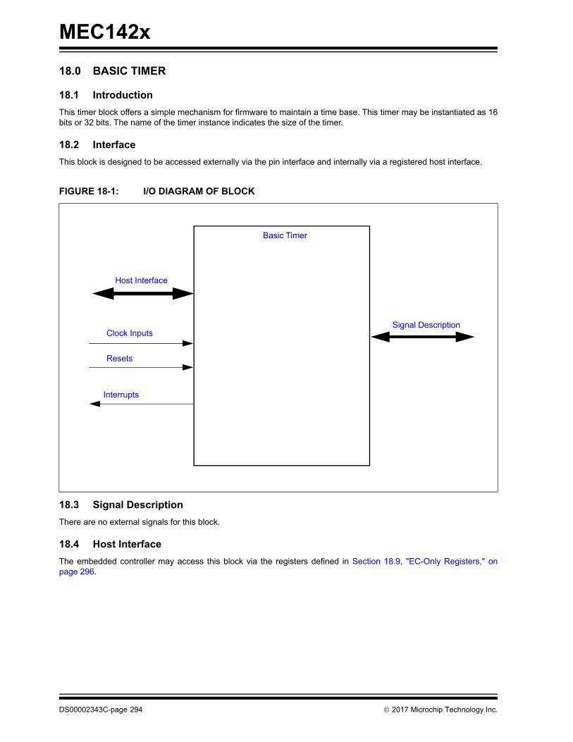
MEC142x
18.0 BASIC TIMER
18.1 Introduction
This timer block offers a simple mechanism for firmware to maintain a time base. This timer may be instantiated as 16bits or 32 bits. The name of the timer instance indicates the size of the timer.
18.2 Interface
This block is designed to be accessed externally via the pin interface and internally via a registered host interface.
18.3 Signal Description
There are no external signals for this block.
18.4 Host Interface
The embedded controller may access this block via the registers defined in Section 18.9, "EC-Only Registers," onpage 296.
FIGURE 18-1: I/O DIAGRAM OF BLOCK
Basic Timer
Signal Description
Interrupts
Host Interface
Clock Inputs
Resets
DS00002343C-page 294 2017 Microchip Technology Inc.

MEC142x
18.5 Power, Clocks and Reset
This section defines the Power, Clock, and Reset parameters of the block.
18.5.1 POWER DOMAINS
18.5.2 CLOCK INPUTS
18.5.3 RESETS
18.6 Interrupts
18.7 Low Power Modes
The Basic Timer may be put into a low power state by the chip’s Power, Clocks, and Reset (PCR) circuitry. This blockis only be permitted to enter low power modes when the block is not active.
The sleep state of this timer is as follows:
• Asleep while the block is not Enabled
• Asleep while the block is not running (start inactive).
• Asleep while the block is halted (even if running).
The block is active while start is active.
Name Description
VTR The timer control logic and registers are all implemented on this single power domain.
Name Description
48 MHz Ring Oscillator This is the clock source to the timer logic. The Pre-scaler may be used to adjust the minimum resolution per bit of the counter.
Name Description
nSYSRST This reset signal, which is an input to this block, resets all the logic and registers to their initial default state.
Soft Reset This reset signal, which is created by this block, resets all the logic and registers to their initial default state. This reset is generated by the block when the SOFT_RESET bit is set in the Timer Control Register register.
Timer_Reset This reset signal, which is created by this block, is asserted when either the nSYSRST or the Soft Reset signal is asserted. The nSYSRST and Soft Reset signals are OR’d together to create this signal.
Source Description
Timer_Event This interrupt event fires when a 16-bit timer x reaches its limit. This event is sourced by the EVENT_INTERRUPT status bit if enabled.
2017 Microchip Technology Inc. DS00002343C-page 295
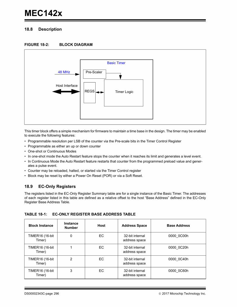
MEC142x
18.8 Description
This timer block offers a simple mechanism for firmware to maintain a time base in the design. The timer may be enabledto execute the following features:
• Programmable resolution per LSB of the counter via the Pre-scale bits in the Timer Control Register
• Programmable as either an up or down counter
• One-shot or Continuous Modes
• In one-shot mode the Auto Restart feature stops the counter when it reaches its limit and generates a level event.
• In Continuous Mode the Auto Restart feature restarts that counter from the programmed preload value and gener-ates a pulse event.
• Counter may be reloaded, halted, or started via the Timer Control register
• Block may be reset by either a Power On Reset (POR) or via a Soft Reset.
18.9 EC-Only Registers
The registers listed in the EC-Only Register Summary table are for a single instance of the Basic Timer. The addressesof each register listed in this table are defined as a relative offset to the host “Base Address” defined in the EC-OnlyRegister Base Address Table.
FIGURE 18-2: BLOCK DIAGRAM
TABLE 18-1: EC-ONLY REGISTER BASE ADDRESS TABLE
Block InstanceInstance Number
Host Address Space Base Address
TIMER16 (16-bit Timer)
0 EC 32-bit internal address space
0000_0C00h
TIMER16 (16-bit Timer)
1 EC 32-bit internal address space
0000_0C20h
TIMER16 (16-bit Timer)
2 EC 32-bit internal address space
0000_0C40h
TIMER16 (16-bit Timer)
3 EC 32-bit internal address space
0000_0C60h
Host Interface
Basic Timer
REGS Timer Logic
Pre-Scaler48 MHz
DS00002343C-page 296 2017 Microchip Technology Inc.
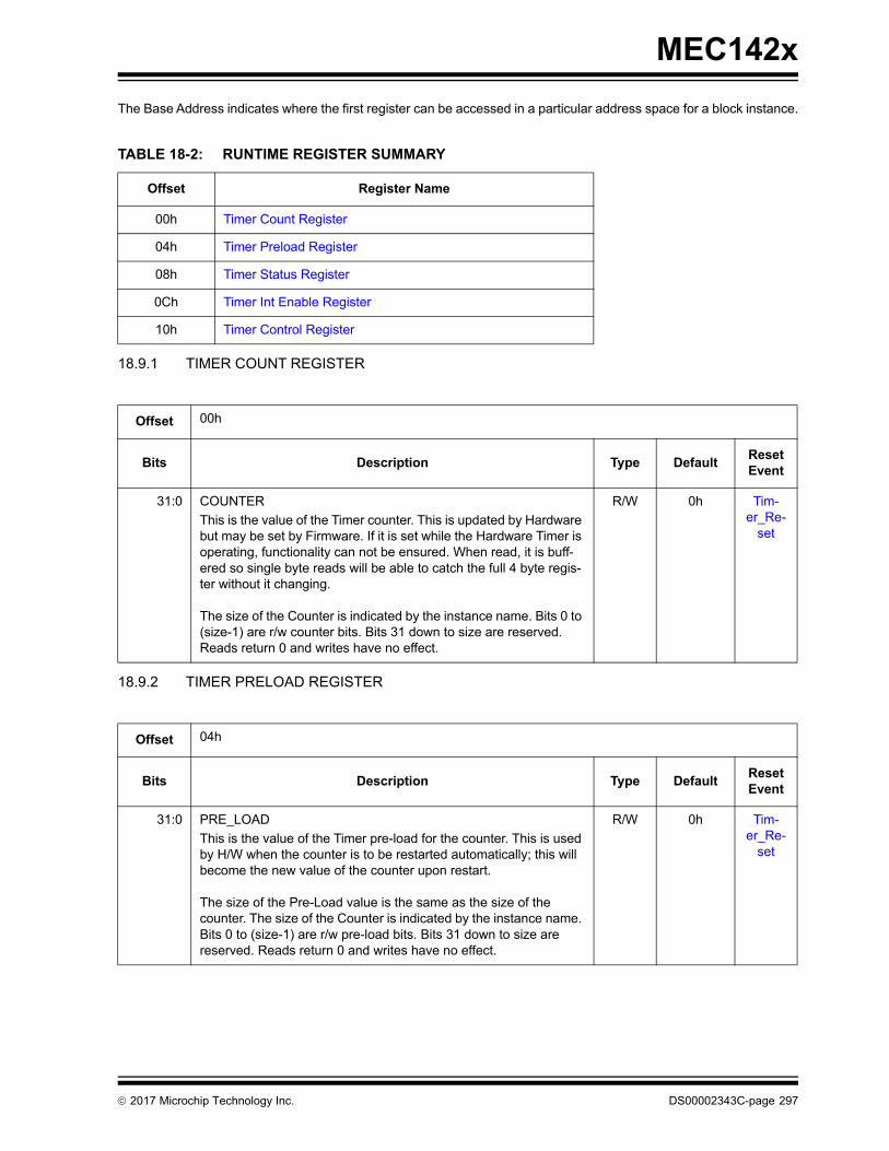
MEC142x
The Base Address indicates where the first register can be accessed in a particular address space for a block instance.
18.9.1 TIMER COUNT REGISTER
18.9.2 TIMER PRELOAD REGISTER
TABLE 18-2: RUNTIME REGISTER SUMMARY
Offset Register Name
00h Timer Count Register
04h Timer Preload Register
08h Timer Status Register
0Ch Timer Int Enable Register
10h Timer Control Register
Offset 00h
Bits Description Type DefaultReset Event
31:0 COUNTER
This is the value of the Timer counter. This is updated by Hardware but may be set by Firmware. If it is set while the Hardware Timer is operating, functionality can not be ensured. When read, it is buff-ered so single byte reads will be able to catch the full 4 byte regis-ter without it changing.
The size of the Counter is indicated by the instance name. Bits 0 to (size-1) are r/w counter bits. Bits 31 down to size are reserved. Reads return 0 and writes have no effect.
R/W 0h Tim-er_Re-
set
Offset 04h
Bits Description Type DefaultReset Event
31:0 PRE_LOAD
This is the value of the Timer pre-load for the counter. This is used by H/W when the counter is to be restarted automatically; this will become the new value of the counter upon restart.
The size of the Pre-Load value is the same as the size of the counter. The size of the Counter is indicated by the instance name. Bits 0 to (size-1) are r/w pre-load bits. Bits 31 down to size are reserved. Reads return 0 and writes have no effect.
R/W 0h Tim-er_Re-
set
2017 Microchip Technology Inc. DS00002343C-page 297

MEC142x
18.9.3 TIMER STATUS REGISTER
18.9.4 TIMER INT ENABLE REGISTER
18.9.5 TIMER CONTROL REGISTER
Offset 08h
Bits Description Type DefaultReset Event
31:0 Reserved R - -
0 EVENT_INTERRUPT
This is the interrupt status that fires when the timer reaches its limit. This may be level or a self clearing signal cycle pulse, based on the AUTO_RESTART bit in the Timer Control Register. If the timer is set to automatically restart, it will provide a pulse, otherwise a level is provided.
R/WC 0h Tim-er_Re-
set
Offset 0Ch
Bits Description Type DefaultReset Event
31:0 Reserved R - -
0 EVENT_INTERRUPT_ENABLE
This is the interrupt enable for the status EVENT_INTERRUPT bit in the Timer Status Register
R/W 0h Tim-er_Re-
set
Offset 10h
Bits Description Type DefaultReset Event
31:16 PRE_SCALE
This is used to divide down the system clock through clock enables to lower the power consumption of the block and allow slow timers.Updating this value during operation may result in erroneous clock enable pulses until the clock divider restarts.The number of clocks per clock enable pulse is (Value + 1); a setting of 0 runs at the full clock speed, while a setting of 1 runs at half speed.
R/W 0h Tim-er_Reset
15:8 Reserved R - -
7 HALT
This is a halt bit. This will halt the timer as long as it is active. Once the halt is inactive, the timer will start from where it left off.
1=Timer is halted. It stops counting. The clock divider will also be reset.
0=Timer runs normally
R/W 0h Tim-er_Reset
DS00002343C-page 298 2017 Microchip Technology Inc.

MEC142x
6 RELOAD
This bit reloads the counter without interrupting it operation. This will not function if the timer has already completed (when the START bit in this register is ‘0’). This is used to periodically prevent the timer from firing when an event occurs. Usage while the timer is off may result in erroneous behavior.
R/W 0h Tim-er_Reset
5 START
This bit triggers the timer counter. The counter will operate until it hits its terminating condition. This will clear this bit. It should be noted that when operating in restart mode, there is no terminating condition for the counter, so this bit will never clear. Clearing this bit will halt the timer counter.
Setting this bit will:
• Reset the clock divider counter.
• Enable the clock divider counter.
• Start the timer counter.
• Clear all interrupts.
Clearing this bit will:
• Disable the clock divider counter.
• Stop the timer counter.
R/W 0h Tim-er_Reset
4 SOFT_RESET
This is a soft reset.This is self clearing 1 cycle after it is written.
WO 0h Tim-er_Reset
3 AUTO_RESTART
This will select the action taken upon completing a count.
1=The counter will automatically restart the count, using the contentsof the Timer Preload Register to load the Timer Count RegisterThe interrupt will be set in edge mode
0=The counter will simply enter a done state and wait for further con-trol inputs. The interrupt will be set in level mode.
R/W 0h Tim-er_Reset
2 COUNT_UP
This selects the counter direction.
When the counter in incrementing the counter will saturate and trig-ger the event when it reaches all F’s. When the counter is decre-menting the counter will saturate when it reaches 0h.
1=The counter will increment0=The counter will decrement
R/W 0h Tim-er_Reset
1 Reserved R - -
0 ENABLE
This enables the block for operation.
1=This block will function normally0=This block will gate its clock and go into its lowest power state
R/W 0h Tim-er_Reset
Offset 10h
Bits Description Type DefaultReset Event
2017 Microchip Technology Inc. DS00002343C-page 299

MEC142x
19.0 RTOS TIMER
19.1 Introduction
The RTOS Timer is a low-power, 32-bit timer designed to operate on the 32kHz oscillator which is available during allchip sleep states. This allows firmware the option to sleep the processor, enter heavy or deep chip sleep states, andwake after a programmed amount of time. The timer may be used as a one-shot timer or a continuous timer. When thetimer transitions to 0 it is capable of generating a wake-capable interrupt to the embedded controller. This timer may behalted during debug by hardware or via a software control bit.
19.2 References
No references have been cited for this chapter
19.3 Terminology
No terms have been cited for this chapter.
19.4 Interface
This block is an IP block designed to be incorporated into a chip. It is designed to be accessed internally via a registeredhost interface. The following diagram illustrates the various interfaces to the block.
19.4.1 HOST INTERFACE
The registers defined in Section 19.9, "RTOS Timer Registers," on page 304 are accessible by the Host Interfacesdefined in Table 19-6, “RTOS Timer Registers Base Address Table,” on page 304.
FIGURE 19-1: RTOS TIMER INTERFACE DIAGRAM
RTOS Timer
Clocking and Resets
Interrupt Interface
Host Interface
INT
ER
NA
L I
NT
ER
FA
CE
S
EX
TE
RN
AL
IN
TE
RF
AC
ES
Sleep Interface
Sideband Signals
DS00002343C-page 300 2017 Microchip Technology Inc.
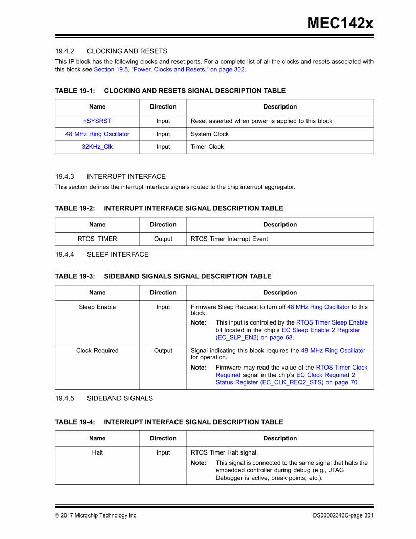
MEC142x
19.4.2 CLOCKING AND RESETS
This IP block has the following clocks and reset ports. For a complete list of all the clocks and resets associated withthis block see Section 19.5, "Power, Clocks and Resets," on page 302.
19.4.3 INTERRUPT INTERFACE
This section defines the interrupt Interface signals routed to the chip interrupt aggregator.
19.4.4 SLEEP INTERFACE
19.4.5 SIDEBAND SIGNALS
TABLE 19-1: CLOCKING AND RESETS SIGNAL DESCRIPTION TABLE
Name Direction Description
nSYSRST Input Reset asserted when power is applied to this block
48 MHz Ring Oscillator Input System Clock
32KHz_Clk Input Timer Clock
TABLE 19-2: INTERRUPT INTERFACE SIGNAL DESCRIPTION TABLE
Name Direction Description
RTOS_TIMER Output RTOS Timer Interrupt Event
TABLE 19-3: SIDEBAND SIGNALS SIGNAL DESCRIPTION TABLE
Name Direction Description
Sleep Enable Input Firmware Sleep Request to turn off 48 MHz Ring Oscillator to this block.
Note: This input is controlled by the RTOS Timer Sleep Enable bit located in the chip’s EC Sleep Enable 2 Register (EC_SLP_EN2) on page 68.
Clock Required Output Signal indicating this block requires the 48 MHz Ring Oscillator for operation.
Note: Firmware may read the value of the RTOS Timer Clock Required signal in the chip’s EC Clock Required 2 Status Register (EC_CLK_REQ2_STS) on page 70.
TABLE 19-4: INTERRUPT INTERFACE SIGNAL DESCRIPTION TABLE
Name Direction Description
Halt Input RTOS Timer Halt signal.
Note: This signal is connected to the same signal that halts the embedded controller during debug (e.g., JTAG Debugger is active, break points, etc.).
2017 Microchip Technology Inc. DS00002343C-page 301
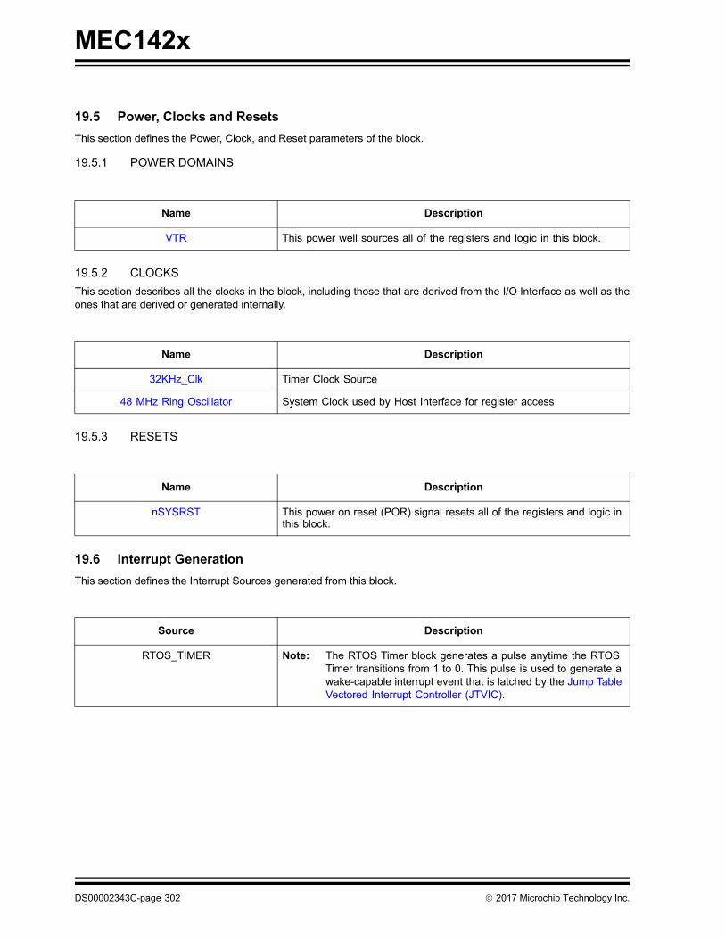
MEC142x
19.5 Power, Clocks and Resets
This section defines the Power, Clock, and Reset parameters of the block.
19.5.1 POWER DOMAINS
19.5.2 CLOCKS
This section describes all the clocks in the block, including those that are derived from the I/O Interface as well as theones that are derived or generated internally.
19.5.3 RESETS
19.6 Interrupt Generation
This section defines the Interrupt Sources generated from this block.
Name Description
VTR This power well sources all of the registers and logic in this block.
Name Description
32KHz_Clk Timer Clock Source
48 MHz Ring Oscillator System Clock used by Host Interface for register access
Name Description
nSYSRST This power on reset (POR) signal resets all of the registers and logic in this block.
Source Description
RTOS_TIMER Note: The RTOS Timer block generates a pulse anytime the RTOS Timer transitions from 1 to 0. This pulse is used to generate a wake-capable interrupt event that is latched by the Jump Table Vectored Interrupt Controller (JTVIC).
DS00002343C-page 302 2017 Microchip Technology Inc.

MEC142x
19.7 Low Power Modes
The RTOS Timer may be put into a low power state by the chip Power, Clocks, and Reset (PCR) circuitry.
The timer operates off of the 32KHz_Clk, and therefore will operate normally when 48 MHz Ring Oscillator is stopped.The sleep enable input has no effect on the RTOS Timer and the clock required output is only asserted during registerread/write cycles for as long as necessary to propagate updates to the block core.
19.7.1 SLEEP INTERFACE - SYSTEM CLOCK
The RTOS Timer is designed to always operate in its lowest functional power consumption state. In addition, it can becommanded to enter a lower power state via the Sleep Enable signal. The block notifies the chip’s power managementcircuitry when it is in its low power state by driving the Clock Required signal low. The following table defines all theblocks Power States associated with the System Clock.
19.7.2 WAKING FROM LOW POWER STATES
The chip Power, Clocks, and Resets logic is responsible for monitoring wake events that turn on 48 MHz Ring Oscillator.The RTOS_TIMER interrupt event is a wake-capable event that may be used to turn on 48 MHz Ring Oscillator.
19.8 Description
The RTOS Timer is a very basic timer with simple down counter functionality with auto-reload and halt features. Thetimer counts with Timer Clock when the timer is programmed with pre-load value.
The counter can be configured as one-shot timer by not setting the Auto Reload bit. The timer will load the value of thepre-load register and start to count down when the Timer Start bit is asserted by the firmware. The timer will generateinterrupt when the counter transitions from count = 1 to count = 0 as defined in the Interrupt Generation section.
If the timer is needed again with same pre-load value, firmware has to only set the Timer Start bit. This will restart thetimer again.
The counter can also be programmed as continuous running mode by enabling the Auto Reload bit. In this mode counterreloads itself every time timer equals 0. The timer also generates interrupt as defined in the interrupt section.
If the RTOS Timer Pre-Load register is written when the counter is counting, the new preload value will take effect onlywhen the counter reaches 0 if the auto-reload bit has been set.
Note: The logic clocked by the system clock is considered to be in the idle state when the host is not accessingthe register interface.
TABLE 19-5: RTOS Timer - SYSTEM CLOCK POWER STATES
Power StateBlock
Enable BitSleep
EnableClock
RequiredDescription
Idle x x 0 Block is idle and operating in its lowest power consumption state. The 48 MHz Ring Oscillator is not used in this state. The block automatically enters this state anytime it is not performing a function requiring this clock source (e.g., Register accesses).
Operating x x 1 Block is not idle. This block will assert Clock Required signal only during register access and when it needs to generate interrupt. The sleep_en signal has no effect on this clock requirement.
Note: The RTOS Timer Registers are readable and writable in all defined Power States.
2017 Microchip Technology Inc. DS00002343C-page 303
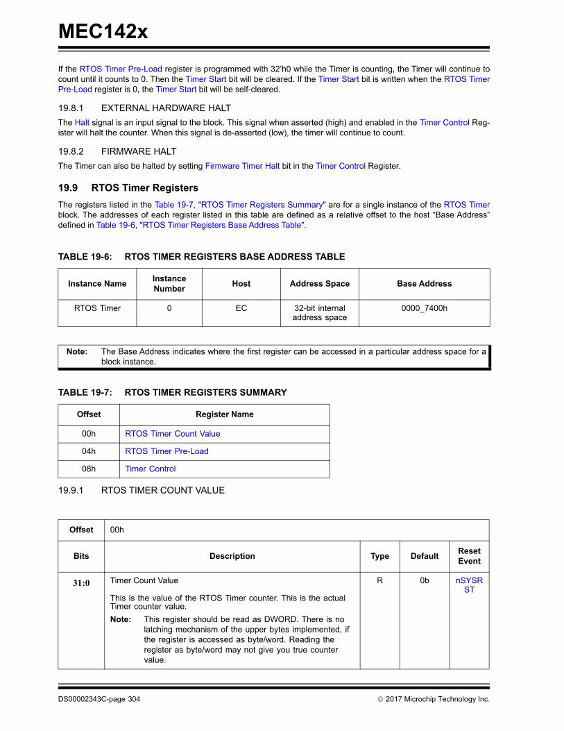
MEC142x
If the RTOS Timer Pre-Load register is programmed with 32’h0 while the Timer is counting, the Timer will continue tocount until it counts to 0. Then the Timer Start bit will be cleared. If the Timer Start bit is written when the RTOS TimerPre-Load register is 0, the Timer Start bit will be self-cleared.
19.8.1 EXTERNAL HARDWARE HALT
The Halt signal is an input signal to the block. This signal when asserted (high) and enabled in the Timer Control Reg-ister will halt the counter. When this signal is de-asserted (low), the timer will continue to count.
19.8.2 FIRMWARE HALT
The Timer can also be halted by setting Firmware Timer Halt bit in the Timer Control Register.
19.9 RTOS Timer Registers
The registers listed in the Table 19-7, "RTOS Timer Registers Summary" are for a single instance of the RTOS Timerblock. The addresses of each register listed in this table are defined as a relative offset to the host “Base Address”defined in Table 19-6, "RTOS Timer Registers Base Address Table".
19.9.1 RTOS TIMER COUNT VALUE
TABLE 19-6: RTOS TIMER REGISTERS BASE ADDRESS TABLE
Instance NameInstance Number
Host Address Space Base Address
RTOS Timer 0 EC 32-bit internal address space
0000_7400h
Note: The Base Address indicates where the first register can be accessed in a particular address space for ablock instance.
TABLE 19-7: RTOS TIMER REGISTERS SUMMARY
Offset Register Name
00h RTOS Timer Count Value
04h RTOS Timer Pre-Load
08h Timer Control
Offset 00h
Bits Description Type DefaultReset Event
31:0 Timer Count Value
This is the value of the RTOS Timer counter. This is the actual Timer counter value.
Note: This register should be read as DWORD. There is no latching mechanism of the upper bytes implemented, if the register is accessed as byte/word. Reading the register as byte/word may not give you true counter value.
R 0b nSYSRST
DS00002343C-page 304 2017 Microchip Technology Inc.

MEC142x
19.9.2 RTOS TIMER PRE-LOAD
19.9.3 TIMER CONTROL
Offset 04h
Bits Description Type DefaultReset Event
31:0 Timer Pre-Load Count Value
This is the pre load value for the counter.
This value is loaded in the timer counter after setting the Timer Start bit or when the counter reloads if the Auto Reload bit is set.
Note: This register must be programmed with new Pre-Load count value before Timer Start bit is enabled. If this sequence is not followed, the new Pre-Load count value will only take effect when the counter expires if the Auto Reload bit is set.
Note: Programming this register with 0’s will disable the counter and clear the “start” bit if set.
R/W 0h nSYSRST
Offset 08h
Bits Description Type Default Reset
31:5 RESERVED RES - -
4 Firmware Timer Halt
This bit gives the firmware the ability to halt the counter without the use of the hardware Halt signal.
0: Do not halt the counter1: Halt the counter
R/W 0h nSYSRST
3 Ext Hardware Halt Enable
0: Do not allow hardware Halt signal to stop the counter.1: Allow hardware Halt signal to stop the counter.
R/W 0h nSYSRST
2017 Microchip Technology Inc. DS00002343C-page 305
MEC142x
2 Timer Start
This bit triggers the timer counter. The counter will operate until it hits its terminating condition. This will clear this bit. It should be noted that while operating in Auto Reload mode; there is no terminating condition for the counter, so this bit will never clear. Clearing this bit by firmware will reset the timer counter.
Setting this bit will:Load the Pre-Load value into the counter.Start the timer counter.
Clearing this bit will:Reset the counter to 0. Will not generate the interrupt.
The hardware will clear this bit for following conditions:When One-Shot mode expires.When TimerPreLoad = TimerCountValue=0
R/W 0h nSYSRST
1 Auto Reload
This will select the action taken upon completing a count.0: The counter will simply enter a done state and wait for further control inputs. One-Shot mode.
1: The counter will automatically restart the count using the RTOS Timer Pre-load value. Continuous mode.
R/W 0h nSYSRST
0 Block Enable
This bit enables the block for operation.
0: This bit will gate Timer clock and go into its lowest power state. Falling edge of this bit will clear all the timer logic and register bits to default state.
1: This block will function normally.
Note: Registers are always accessible regardless of the state of this bit.
R/W 0h nSYSRST
Offset 08h
Bits Description Type Default Reset
DS00002343C-page 306 2017 Microchip Technology Inc.

MEC142x
20.0 HIBERNATION TIMER
20.1 Introduction
The Hibernation Timer can generate a wake event to the Embedded Controller (EC) when it is in a hibernation mode.This block supports wake events up to 2 hours in duration. The timer is a 16-bit binary count-down timer that can beprogrammed in 30.5µs and 0.125 second increments for period ranges of 30.5µs to 2s or 0.125s to 136.5 minutes,respectively. Writing a non-zero value to this register starts the counter from that value. A wake-up interrupt is generatedwhen the count reaches zero.
20.2 References
No references have been cited for this chapter
20.3 Terminology
No terms have been cited for this chapter.
20.4 Interface
This block is an IP block designed to be incorporated into a chip. It is designed to be accessed externally via the pininterface and internally via a registered host interface. The following diagram illustrates the various interfaces to theblock.
FIGURE 20-1: HIBERNATION TIMER INTERFACE DIAGRAM
Hibernation Timer
Signal DescriptionClock Inputs
Interrupts
Resets
Host Interface
2017 Microchip Technology Inc. DS00002343C-page 307

MEC142x
20.5 Signal Description
There are no external signals for this block.
20.6 Host Interface
The registers defined for the Hibernation Timer are accessible by the various hosts as indicated in Section 20.10, "EC-Only Registers".
20.7 Power, Clocks and Reset
This section defines the Power, Clock, and Reset parameters of the block.
20.7.1 POWER DOMAINS
20.7.2 CLOCK INPUTS
20.7.3 RESETS
20.8 Interrupts
This section defines the interrupt Interface signals routed to the chip interrupt aggregator.
Each instance of the Hibernation Timer in the MEC142x can be used to generate interrupts and wake-up events whenthe timer decrements to zero.
Name Description
VTR The timer control logic and registers are all implemented on this single power domain.
Name Description
5Hz_Clk This is the clock source to the timer logic. The Pre-scaler may be used to adjust the minimum resolution per bit of the counter.
if the main oscillator is stopped then an external 32.768kHz clock sourcemust be active for the Hibernation Timer to continue to operate.
Name Description
nSYSRST This reset signal, which is an input to this block, resets all the logic and registers to their initial default state.
TABLE 20-1: INTERRUPT INTERFACE SIGNAL DESCRIPTION TABLE
Name Direction Description
HTIMER Output Signal indicating that the timer is enabled and decrements to 0. This signal is used to generate an Hibernation Timer interrupt event.
DS00002343C-page 308 2017 Microchip Technology Inc.
MEC142x
20.9 Low Power Modes
The Hibernation Timer may be put into a low power state by the chip Power, Clocks, and Reset (PCR) circuitry.
The timer operates off of the 5Hz_Clk, and therefore will operate normally when 48 MHz Ring Oscillator is stopped.
The sleep enable inputs have no effect on the Hibernation Timer and the clock required outputs are only asserted duringregister read/write cycles for as long as necessary to propagate updates to the block core.
20.10 EC-Only Registers
The registers listed in the EC-Only Register Summary table are for a single instance of the Hibernation Timer. Theaddresses of each register listed in this table are defined as a relative offset to the host “Base Address” defined in theEC-Only Register Base Address Table.
The Base Address indicates where the first register can be accessed in a particular address space for a block instance.
20.10.1 HTIMER PRELOAD REGISTER
TABLE 20-2: EC-ONLY REGISTER BASE ADDRESS TABLE
Block InstanceInstance Number
Host Address Space Base Address
Hibernation Timer 0 EC 32-bit internal address space
0000_9800h
TABLE 20-3: HIBERNATION TIMER SUMMARY
Offset Register Name
00h HTimer Preload Register
04h HTimer Control Register
08h HTimer Count Register
Offset 00h
Bits Description Type DefaultReset Event
15:0 HT_PRELOAD
This register is used to set the Hibernation Timer Preload value. Writing this register to a non-zero value resets the down counter to start counting down from this programmed value. Writing this regis-ter to 0000h disables the hibernation counter. The resolution of this timer is determined by the CTRL bit in the HTimer Control Register.Writes to the HTimer Control Register are completed with an EC bus cycle.
R/W 000h nSYSRST
2017 Microchip Technology Inc. DS00002343C-page 309
MEC142x
20.10.2 HTIMER CONTROL REGISTER
20.10.3 HTIMER COUNT REGISTER
Offset 04h
Bits Description Type DefaultReset Event
15:1 Reserved R - -
0 CTRL
1= The Hibernation Timer has a resolution of 0.125s per LSB, whichyields a maximum time in excess of 2 hours.
0= The Hibernation Timer has a resolution of 30.5µs per LSB, whichyields a maximum time of ~2seconds.
R 0000h nSYSRST
Offset 08h
Bits Description Type DefaultReset Event
15:0 COUNT
The current state of the Hibernation Timer.
R 0000h nSYSRST
DS00002343C-page 310 2017 Microchip Technology Inc.
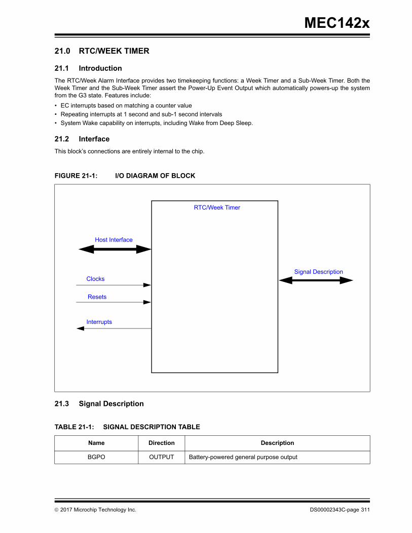
MEC142x
21.0 RTC/WEEK TIMER
21.1 Introduction
The RTC/Week Alarm Interface provides two timekeeping functions: a Week Timer and a Sub-Week Timer. Both theWeek Timer and the Sub-Week Timer assert the Power-Up Event Output which automatically powers-up the systemfrom the G3 state. Features include:
• EC interrupts based on matching a counter value
• Repeating interrupts at 1 second and sub-1 second intervals
• System Wake capability on interrupts, including Wake from Deep Sleep.
21.2 Interface
This block’s connections are entirely internal to the chip.
21.3 Signal Description
FIGURE 21-1: I/O DIAGRAM OF BLOCK
TABLE 21-1: SIGNAL DESCRIPTION TABLE
Name Direction Description
BGPO OUTPUT Battery-powered general purpose output
RTC/Week Timer
Signal DescriptionClocks
Interrupts
Host Interface
Resets
2017 Microchip Technology Inc. DS00002343C-page 311

MEC142x
21.4 Host Interface
The registers defined for the RTC/Week Timer are accessible only by the EC.
21.5 Power, Clocks and Resets
This section defines the Power, Clock, and Reset parameters of the block.
21.5.1 POWER DOMAINS
21.5.2 CLOCKS
21.5.3 RESETS
TABLE 21-2: INTERNAL SIGNAL DESCRIPTION TABLE
Name Direction Description
POWER_UP_EVENT OUTPUT Signal to the VBAT-Powered Control Interface. When this signal is asserted, the VCI output signal asserts. See Section 21.8, "Power-Up Events".
TABLE 21-3: POWER SOURCES
Name Description
VBAT This power well sources all of the internal registers and logic in this block.
VTR This power well sources only bus communication. The block continues to operate internally while this rail is down.
TABLE 21-4: CLOCKS
Name Description
32KHz_Clk This 32KHz clock input drives all internal logic, and will be present at all times that the VBAT well is powered.
TABLE 21-5: RESET SIGNALS
Name Description
VBAT_POR This reset signal is used reset all of the registers and logic in this block.
VTR_RESET# This reset signal is used to inhibit the bus communication logic, and iso-lates this block from VTR powered circuitry on-chip. Otherwise it has no effect on the internal state.
DS00002343C-page 312 2017 Microchip Technology Inc.
MEC142x
21.6 Interrupts
21.7 Low Power Modes
The RTC/Week Alarm has no low-power modes. It runs continuously while the VBAT well is powered.
21.8 Power-Up Events
The RTC/Week Timer POWER_UP_EVENT can be used to power up the system after a timed interval. The POW-ER_UP_EVENT is routed to the VBAT-Powered Control Interface. The VCI_OUT pin that is part of the VCI is assertedif the POWER_UP_EVENT is asserted.
The POWER_UP_EVENT can be asserted under the following two conditions:
1. The Week Alarm Counter Register is greater than or equal to the Week Timer Compare Register
2. The Sub-Week Alarm Counter Register decrements from ‘1’ to ‘0’
The assertion of the POWER_UP_EVENT is inhibited by the following two conditions:
1. The POWERUP_EN field in the Control Register is ‘0’
2. The SYSPWR_PRES_ENABLE field in the Sub-Week Control Register is ‘1’ and the SYSPWR_PRES input pinis ‘0’. This option permits inhibiting a timeout causing a system wake during a deep sleep and draining the batteryif AC Power is not present.
Once a POWER_UP_EVENT is asserted the POWERUP_EN bit must be cleared to reset the output. ClearingPOWERUP_EN is necessary to avoid unintended power-up cycles.
TABLE 21-6: EC INTERRUPTS
Source Description
WEEK_ALARM_INT This interrupt is signaled to the Interrupt Aggregator when the Week Alarm Counter Register is greater than or equal to the Week Timer Com-pare Register. The interrupt signal is always generated by the RTC/Week Timer if the block is enabled; the interrupt is enabled or disabled in the Interrupt Aggregator.
SUB_WEEK_ALARM_INT This interrupt is signaled to the Interrupt Aggregator when the Sub-Week Alarm Counter Register decrements from ‘1’ to ‘0’. The interrupt signal is always generated by the RTC/Week Timer if the block is enabled; the interrupt is enabled or disabled in the Interrupt Aggregator.
ONE_SECOND This interrupt is signaled to the Interrupt Aggregator at an isochronous rate of once per second. The interrupt signal is always generated by the RTC/Week Timer if the block is enabled; the interrupt is enabled or dis-abled in the Interrupt Aggregator.
SUB_SECOND This interrupt is signaled to the Interrupt Aggregator at an isochronous rate programmable between 0.5Hz and 32.768KHz. The rate interrupts are signaled is determined by the SPISR field in the Sub-Second Pro-grammable Interrupt Select Register. See Table 21-10, "SPISR Encod-ing". The interrupt signal is always generated by the RTC/Week Timer if the block is enabled; the interrupt is enabled or disabled in the Interrupt Aggregator.
SYSPWR_PRES This wake interrupt is signaled to the Interrupt Aggregator when an Alarm event occurs. The associated GPIO pin Control Register must be pro-grammed in order to configure the interrupt condition.
2017 Microchip Technology Inc. DS00002343C-page 313

MEC142x
21.9 Description
The RTC/Week Alarm block provides battery-powered timekeeping functions, derived from a low-power 32KHz clock,that operate even when the device’s main power is off. The block contains a set of counters that can be used to generateone-shot and periodic interrupts to the EC for periods ranging from about 30 microseconds to over 8 years. TheRTC/Week Alarm can be used in conjunction with the VBAT-Powered Control Interface to power up a sleeping systemafter a configurable period.
In addition to basic timekeeping, the RTC/Week Alarm block can be used to control the battery-powered general pur-pose BGPO outputs.
21.9.1 INTERNAL COUNTERS
The RTC/Week Timer includes 3 counters:
21.9.1.1 28-bit Week Alarm Counter
This counter is 28 bits wide. The clock for this counter is the overflow of the Clock Divider, and as long as the RTC/WeekTimer is enabled, it is incremented at a 1 Hz rate.
Both an interrupt and a power-up event can be generated when the contents of this counter matches the contents of theWeek Timer Compare Register.
21.9.1.2 9-bit Sub-Week Alarm Counter
This counter is 9 bits wide. It is decremented by 1 at each tick of its selected clock. It can be configured either as a one-shot or repeating event generator.
Both an interrupt and a power-up event can be generated when this counter decrements from 1 to 0.
The Sub-Week Alarm Counter can be configured with a number of different clock sources for its time base, derived fromeither the Week Alarm Counter or the Clock Divider, by setting the SUBWEEK_TICK field of the Sub-Week Control Reg-ister.
TABLE 21-7: SUB-WEEK ALARM COUNTER CLOCK
SUBWEEK_TICK
Source SPISR FrequencyMinimumDuration
MaximumDuration
0 Counter Disabled
1 Sub-Second
0 Counter Disabled
1 2 Hz 500 ms 255.5 sec
2 4 Hz 250 ms 127.8 sec
3 8 Hz 125 ms 63.9 sec
4 16 Hz 62.5 31.9 sec
5 32 Hz 31.25 ms 16.0 sec
6 64 Hz 15.6 ms 8 sec
7 128 Hz 7.8 ms 4 sec
8 256 Hz 3.9 ms 2 sec
9 512 Hz 1.95 ms 1 sec
10 1024 Hz 977 µS 499 ms
11 2048 Hz 488 µS 249.5 ms
12 4096 Hz 244 µS 124.8 ms
13 8192 Hz 122 µS 62.4 ms
14 16.384 Khz 61.1 µS 31.2 ms
15 32.768 KHz 30.5 µS 15.6 ms
2 Second n/a 1 Hz 1 sec 511 sec
3 Reserved
4 Week Counterbit 3
n/a 125 Hz 8 sec 68.1 min
DS00002343C-page 314 2017 Microchip Technology Inc.
MEC142x
21.9.1.3 15-bit Clock Divider
This counter is 15 bits wide. The clock for this counter is 32KHz_Clk, and as long as the RTC/Week Timer is enabled,it is incremented at 32.768KHz rate. The Clock Divider automatically The Clock Divider generates a clock out of 1 Hzwhen the counter wraps from 7FFFh to 0h.
By selecting one of the 15 bits of the counter, using the Sub-Second Programmable Interrupt Select Register, the ClockDivider can be used either to generate a time base for the Sub-Week Alarm Counter or as an isochronous interrupt tothe EC, the SUB_SECOND interrupt. See Table 21-10, "SPISR Encoding" for a list of available frequencies.
21.9.2 TIMER VALID STATUS
If power on reset occurs on the VBAT power rail while the main device power is off, the counters in the RTC/Week Alarmare invalid. If firmware detects a POR on the VBAT power rail after a system boot, by checking the status bits in thePower, Clocks and Resets registers, the RTC/Week Alarm block must be reinitialized.
21.9.3 APPLICATION NOTE: REGISTER TIMING
Register writes in the RTC/Week Alarm complete within two cycles of the 32KHz_Clk clock.The write completes evenif the main system clock is stopped before the two cycles of the 32K clock complete. Register reads complete in onecycle of the internal bus clock.
All RTC/Week Alarm interrupts that are asserted within the same cycle of the 32KHz_Clk clock are synchronouslyasserted to the EC.
21.9.4 APPLICATION NOTE: USE OF THE WEEK TIMER AS A 43-BIT COUNTER
The Week Timer cannot be directly used as a 42-bit counter that is incremented directly by the 32.768KHz clock domain.The upper 28 bits (28-bit Week Alarm Counter) are incremented at a 1Hz rate and the lower 16 bits (15-bit Clock Divider)are incremented at a 32.768KHz rate, but the increments are not performed in parallel. In particular, the upper 28 bitsare incremented when the lower 15 bits increment from 0 to 1, so as long as the Clock Divider Register is 0 the tworegisters together, treated as a single value, have a smaller value then before the lower register rolled over from 7FFFhto 0h.
The following code can be used to treat the two registers as a single large counter. This example extracts a 32-bit valuefrom the middle of the 43-bit counter:
dword TIME_STAMP(void) AHB_dword wct_value; AHB_dword cd_value1; AHB_dword cd_value2; dword irqEnableSave;
5 Week Counterbit 5
n/a 31.25 Hz 32 sec 272.5 min
6 Week Counterbit 7
n/a 7.8125 Hz 128 sec 18.17 hour
7 Week Counterbit 9
n/a 1.95 Hz 512 sec 72.68 hour
Note 1: The Week Alarm Counter must not be modified by firmware if Sub-Week Alarm Counter is using the WeekAlarm Counter as its clock source (i.e., the SUBWEEK_TICK field is set to any of the values 4, 5, 6 or 7).The Sub-Week Alarm Counter must be disabled before changing the Week Alarm Counter. For example,the following sequence may be used:
1. Write 0h to the Sub-Week Alarm Counter Register (disabling the Sub-Week Counter)
2. Write the Week Alarm Counter Register
3. Write a new value to the Sub-Week Alarm Counter Register, restarting the Sub-Week Counter
TABLE 21-7: SUB-WEEK ALARM COUNTER CLOCK (CONTINUED)
SUBWEEK_TICK
Source SPISR FrequencyMinimumDuration
MaximumDuration
2017 Microchip Technology Inc. DS00002343C-page 315

MEC142x
//Disable interrupts irqEnableSave = IRQ_ENABLE; IRQ_ENABLE = 0; //Read 15-bit clk divider reading register, save result in A cd_value1 = WTIMER->CLOCK_DIVIDER; //Read 28 bit up-counter timer register, save result in B wct_value = WTIMER->WEEK_COUNTER_TIMER; //Read 15-bit clk divider reading register, save result in C cd_value2 = WTIMER->CLOCK_DIVIDER; if (0 == cd_value2) wct_value = wct_value + 1; else if ( (cd_value2 < cd_value1) || (0 == cd_value1)) wct_value = WTIMER->WEEK_COUNTER_TIMER; //Enable interrupts IRQ_ENABLE = irqEnableSave; return (WTIMER_BASE + ((wct_value << 10) | (cd_value2>>5)));
21.10 Runtime Registers
The addresses of each register listed in this table are defined as a relative offset to the host “Base Address” defined inRuntime Register Base Address Table.
The Base Address indicates where the first register can be accessed in a particular address space for a block instance.Add the register’s Offset to this value to obtain the direct address of the register.
TABLE 21-8: RUNTIME REGISTER BASE ADDRESS TABLE
Block InstanceInstance Number
Host Address Space Base Address
Week Alarm 0 EC 32-bit internal Address Space
0000_CC80h
TABLE 21-9: RUNTIME REGISTER SUMMARY
Offset Register Name (Mnemonic)
00h Control Register
04h Week Alarm Counter Register
08h Week Timer Compare Register
0Ch Clock Divider Register
10h Sub-Second Programmable Interrupt Select Register
14h Sub-Week Control Register
18h Sub-Week Alarm Counter Register
DS00002343C-page 316 2017 Microchip Technology Inc.
MEC142x
21.10.1 CONTROL REGISTER
21.10.2 WEEK ALARM COUNTER REGISTER
Offset 00h
Bits Description Type DefaultReset Event
31:7 Reserved R - -
6 POWERUP_EN
This bit controls the state of the Power-Up Event Output and enables Week POWER-UP Event decoding in the VBAT-Powered Control Interface on page 462. See Section 2.5.8, "Power-Up Event Output," on page 307 for a functional description of the POWER-UP_EN bit.
1=Power-Up Event Output Enabled0=Power-Up Event Output Disabled and Reset
R/W 00h VBAT_POR
5 BGPO
VBAT-powered General Purpose Output Control that is used as part of the VBAT-Powered Control Interface.
1=Output high0=Output low
R/W 00h VBAT_POR
4:1 Reserved R - -
0 WT_ENABlLE
The WT_ENABLE bit is used to start and stop the Week Alarm Counter Register and the Clock Divider Register.
The value in the Counter Register is held when the WT_ENABLE bit is not asserted (‘0’) and the count is resumed from the last value when the bit is asserted (‘1’).
The 15-Bit Clock Divider is reset to 00h and the RTC/Week Alarm Interface is in its lowest power consumption state when the WT_EN-ABLE bit is not asserted.
R/W 00h VBAT_POR
Offset 04h
Bits Description Type DefaultReset Event
31:28 Reserved R - -
27:0 WEEK_COUNTER
While the WT_ENABLE bit is ‘1’, this register is incremented at a 1 Hz rate. Writes of this register may require one second to take effect. Reads return the current state of the register. Reads and writes complete independently of the state of WT_ENABLE.
R/W 00h VBAT_POR
2017 Microchip Technology Inc. DS00002343C-page 317

MEC142x
21.10.3 WEEK TIMER COMPARE REGISTER
21.10.4 CLOCK DIVIDER REGISTER
21.10.5 SUB-SECOND PROGRAMMABLE INTERRUPT SELECT REGISTER
Offset 08h
Bits Description Type DefaultReset Event
31:28 Reserved R - -
27:0 WEEK_COMPARE
A Week Alarm Interrupt and a Week Alarm Power-Up Event are asserted when the Week Alarm Counter Register is greater than or equal to the contents of this register. Reads and writes complete independently of the state of WT_ENABLE.
R/W FFFFFFFh VBAT_POR
Offset 0Ch
Bits Description Type DefaultReset Event
31:15 Reserved R - -
14:0 CLOCK_DIVIDER
Reads of this register return the current state of the Week Timer 15-bit clock divider.
R - VBAT_POR
Offset 10h
Bits Description Type DefaultReset Event
31:15 Reserved R - -
3:0 SPISR
This field determines the rate at which Sub-Second interrupt events are generated. Table 21-10, "SPISR Encoding" shows the relation between the SPISR encoding and Sub-Second interrupt rate.
R/W 00h VBAT_POR
DS00002343C-page 318 2017 Microchip Technology Inc.

MEC142x
21.10.6 SUB-WEEK CONTROL REGISTER
TABLE 21-10: SPISR ENCODING
SPISR Value Sub-Second Interrupt Rate, Hz Interrupt Period
0 Interrupts disabled
1 2 500 ms
2 4 250 ms
3 8 125 ms
4 16 62.5 ms
5 32 31.25 ms
6 64 15.63 ms
7 128 7.813 ms
8 256 3.906 ms
9 512 1.953 ms
10 1024 977 µS
11 2048 488 µS
12 4096 244 µS
13 8192 122 µS
14 16384 61 µS
15 32768 30.5 µS
Offset 14h
Bits Description Type DefaultReset Event
31:10 Reserved R - -
9:7
SUBWEEK_TICK
This field selects the clock source for the Sub-Week Counter. See Table 21-7, "Sub-Week Alarm Counter Clock" for the description of the options for this field. See also Note 1.
R/W 0 VBAT_POR
6
AUTO_RELOAD
1= No reload occurs when the Sub-Week Counter expires0= Reloads the SUBWEEK_COUNTER_LOAD field into the Sub-
Week Counter when the counter expires.
R/W 0 VBAT_POR
5
SYSPWR_PRES_ENABLE
Enables SYSPWR_PRES Pin to disable Week the Week timer and Sub-Week Timer Power-Up Events from driving VCI_OUT high
1=The SYSPWR_PRES Pin input low disables both the Week timerand Sub-Week Timer Power-Up Events from driving VCI_OUThigh
0=The SYSPWR_PRES Pin input has no effect on the Week timerand Sub-Week Timer Power-Up Events driving VCI_OUT high
R/W 0 VBAT_POR
2017 Microchip Technology Inc. DS00002343C-page 319

MEC142x
21.10.7 SUB-WEEK ALARM COUNTER REGISTER
4SYSPWR_PRES_STATUS
Current status of the SYSPWR_PRES pin.
R - VBAT_POR
3:2 Reserved R - -
1
WEEK_TIMER_POWERUP_EVENT_STATUS
This bit is set to ‘1’ when the Week Alarm Counter Register is greater than or equal the contents of the Week Timer Compare Register and the POWERUP_EN is ‘1’.
Writes of ‘1’ clear this bit. Writes of ‘0’ have no effect.
Note: This bit does not have to be cleared to remove a WeekTimer Power-Up Event.
R/WC 0 VBAT_POR
0
SUBWEEK_TIMER_POWERUP_EVENT_STATUS
This bit is set to ‘1’ when the Sub-Week Alarm Counter Register decrements from ‘1’ to ‘0’ and the POWERUP_EN is ‘1’.
Writes of ‘1’ clear this bit. Writes of ‘0’ have no effect.
Note: This bit MUST be cleared to remove a Sub-Week TimerPower-Up Event.
R/WC 0 VBAT_POR
Offset 18h
Bits Description Type DefaultReset Event
31:25 Reserved R - -
24:16 SUBWEEK_COUNTER_STATUS
Reads of this register return the current state of the 9-bit Sub-Week Alarm counter.
R 00h VBAT_POR
15:9 Reserved R - -
8:0 SUBWEEK_COUNTER_LOAD
Writes with a non-zero value to this field reload the 9-bit Sub-Week Alarm counter. Writes of 0 disable the counter.
If the Sub-Week Alarm counter decrements to 0 and the AUTO_RE-LOAD bit is set, the value in this field is automatically loaded into the Sub-Week Alarm counter.
R/W 00h VBAT_POR
Offset 14h
Bits Description Type DefaultReset Event
DS00002343C-page 320 2017 Microchip Technology Inc.
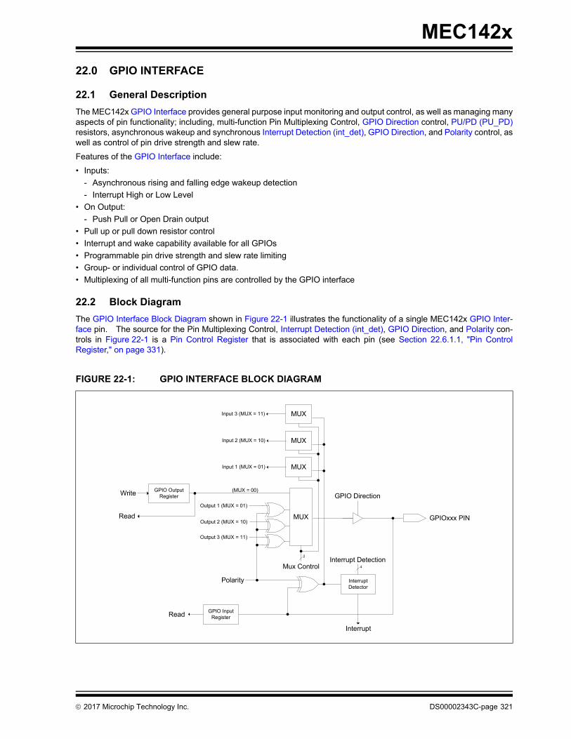
MEC142x
22.0 GPIO INTERFACE
22.1 General Description
The MEC142x GPIO Interface provides general purpose input monitoring and output control, as well as managing manyaspects of pin functionality; including, multi-function Pin Multiplexing Control, GPIO Direction control, PU/PD (PU_PD)resistors, asynchronous wakeup and synchronous Interrupt Detection (int_det), GPIO Direction, and Polarity control, aswell as control of pin drive strength and slew rate.
Features of the GPIO Interface include:
• Inputs:
- Asynchronous rising and falling edge wakeup detection
- Interrupt High or Low Level
• On Output:
- Push Pull or Open Drain output
• Pull up or pull down resistor control
• Interrupt and wake capability available for all GPIOs
• Programmable pin drive strength and slew rate limiting
• Group- or individual control of GPIO data.
• Multiplexing of all multi-function pins are controlled by the GPIO interface
22.2 Block Diagram
The GPIO Interface Block Diagram shown in Figure 22-1 illustrates the functionality of a single MEC142x GPIO Inter-face pin. The source for the Pin Multiplexing Control, Interrupt Detection (int_det), GPIO Direction, and Polarity con-trols in Figure 22-1 is a Pin Control Register that is associated with each pin (see Section 22.6.1.1, "Pin ControlRegister," on page 331).
FIGURE 22-1: GPIO INTERFACE BLOCK DIAGRAM
GPIOxxx PIN
GPIO Input RegisterRead
MUX
(MUX = 00)
Read
Polarity
MUXInput 3 (MUX = 11)
MUX
MUX
GPIO Direction
Input 2 (MUX = 10)
Input 1 (MUX = 01)
Interrupt Detector
Output 1 (MUX = 01)
Output 2 (MUX = 10)
Output 3 (MUX = 11)
GPIO Output RegisterWrite
Mux Control
2Interrupt Detection
4
Interrupt
2017 Microchip Technology Inc. DS00002343C-page 321

MEC142x
22.3 Power, Clocks and Reset
This section defines the Power, Clock, and Reset parameters of the block.
22.3.1 POWER DOMAINS
22.3.2 CLOCK INPUTS
22.3.3 RESETS
22.4 Interrupts
This section defines the Interrupt Sources generated from this block.
22.5 Description
The GPIO Interface refers to all the GPIOxxx pins implemented in the design. GPIO stands for General Purpose I/O.
The GPIO signals may be used by firmware to both monitor and control a pin in “bit-banged” mode. The GPIOs may beindividually controlled via their Pin Control Register or group controlled via the Output and Input GPIO registers. TheGPIO Output Control Select
The GPIO Pin control registers are used to select the alternate functions on GPIO pins (unless otherwise specified), tocontrol the buffer direction, strength, and polarity, to control the internal pull-ups and pull-downs, for VCC emulation, andfor selecting the event type that causes a GPIO interrupt.
The GPIO input is always live, even when an alternate function is selected. Firmware may read the GPIO input anytimeto see the value on the pin. In addition, the GPIO interrupt is always functional, and may be used for either the GPIOitself or to support the alternate functions on the pin. See FIGURE 22-1: GPIO Interface Block Diagram on page 321.
Name Description
VTR The registers and logic in this block are powered by VTR.
Name Description
48 MHz Ring Oscillator The 48 MHz Ring Oscillator is used for synchronizing the GPIO inputs.
Name Description
nSYSRST This reset is asserted when VTR is applied.
nSIO_RESET This is an alternate reset condition, typically asserted when the main power rail is asserted. This reset is used for VCC Power Well Emulation.
Source Description
GPIO_Event Each pin in the GPIO Interface has the ability to generate an interrupt event. This event may be used as a wake event.
The GPIO Interface can generate an interrupt source event on a high level, low level, rising edge and falling edge, as configured by the Interrupt Detection (int_det) bits in the Pin Control Register associated with the GPIO signal function.
Note: The minimum pulse width required to generate an inter-rupt/wakeup event is 5ns.
DS00002343C-page 322 2017 Microchip Technology Inc.

MEC142x
22.5.1 ACCESSING GPIOS
There are two ways to access GPIO output data. Bit [10] is used to determine which GPIO output data bit affects theGPIO output pin.
• Grouped Output GPIO Data
- Outputs to individual GPIO ports are grouped into 32-bit GPIO Output Registers.
• Individual GPIO output data
- Alternatively, each GPIO output port is individually accessible via Bit [16] in the port’s Pin Control Register. On reads, Bit [16] returns the programmed value, not the value on the pin.
There are two ways to access GPIO input data.
• Input GPIO Data
- Inputs from individual GPIO ports are grouped into 32-bit GPIO Input Registers and always reflect the current state of the GPIO input from the pad.
• GPIO input from pad
- Alternatively, each GPIO input port is individually accessible via Bit [24] in the port’s Pin Control Register. Bit [24] always reflects the current state of GPIO input from the pad.
22.5.2 GPIO INDEXING
Each GPIO signal function name consists of a 4-character prefix (“GPIO”) followed by a 3-digit octal-encoded indexnumber. In the MEC142x GPIO indexing is done sequentially starting from ‘GPIO000.’
22.5.3 GPIO MULTIPLEXING
The GPIO Mux Control bits located in the Pin Control Register are used to support up to three alternate functions onany GPIO pin. The following tables define all the GPIO Multiplexing Options implemented for each of the MEC142xproducts.
22.5.3.1 GPIO Multiplexing Options
MEC142x
GPIO Name (Octal) Mux Control = 00 Mux Control = 01 Mux Control = 10 Mux Control = 11
GPIO001 GPIO001 KSO05 32KHZ_OUT Reserved
GPIO002 GPIO002 PWM7 Reserved Reserved
GPIO003 GPIO003 SYSPWR_PRES Reserved Reserved
GPIO004 GPIO004 BGPO Reserved Reserved
GPIO005 GPIO005 SMB00_DATA SMB00_DATA18 KSI2
GPIO006 GPIO006 SMB00_CLK SMB00_CLK18 KSI3
GPIO007 GPIO007 SMB01_DATA SMB01_DATA18 Reserved
GPIO010 GPIO010 SMB01_CLK SMB01_CLK18 Reserved
GPIO011 GPIO011 nSMI nEMI_INT PWM4
GPIO012 GPIO012 SMB02_DATA SMB02_DATA18 Reserved
GPIO013 GPIO013 SMB02_CLK SMB02_CLK18 Reserved
GPIO014 GPIO014 nRESET_IN Reserved Reserved
GPIO015 GPIO015 KSO01 PVT_CS# Reserved
GPIO016 GPIO016 KSO02 PVT_SCLK Reserved
GPIO017 GPIO017 KSO03 PVT_IO0 Reserved
GPIO020 GPIO020 CMP_VIN0 Reserved Reserved
GPIO021 GPIO021 CMP_VIN1 Reserved Reserved
GPIO022 GPIO022 ADC5 PWM1 Reserved
GPIO023 GPIO023 ADC6 A20M TACH1
GPIO024 GPIO024 ADC7 Reserved Reserved
2017 Microchip Technology Inc. DS00002343C-page 323

MEC142x
GPIO025 GPIO025 KSO07 Reserved Reserved
GPIO026 GPIO026 PS2_CLK1B Reserved Reserved
GPIO027 GPIO027 KSO00 PVT_IO1 Reserved
GPIO030 GPIO030 Reserved PWM4 Reserved
GPIO031 GPIO031 SPI_CS# PWM5 Reserved
GPIO032 GPIO032 SPI_CLK PWM6 Reserved
GPIO033 GPIO033 PECI_DAT SB_TSI_DAT Reserved
GPIO034 GPIO034 PCI_CLK ESPI_CLK Reserved
GPIO035 GPIO035 Reserved SB-TSI_CLK PWM3
GPIO036 GPIO036 VCI_OUT Reserved Reserved
GPIO040 GPIO040 LAD0 ESPI_IO0 Reserved
GPIO041 GPIO041 LAD1 ESPI_IO1 Reserved
GPIO042 GPIO042 LAD2 ESPI_IO2 Reserved
GPIO043 GPIO043 LAD3 ESPI_IO3 Reserved
GPIO044 GPIO044 LFRAME# ESPI_CS# Reserved
GPIO045 GPIO045 SMB05_DATA KSO04 Reserved
GPIO046 GPIO046 SMB05_CLK KSO05 Reserved
GPIO047 GPIO047 SHD_CS1# KSO06 Reserved
GPIO050 GPIO050 TACH0 Reserved Reserved
GPIO051 GPIO051 TACH1 Reserved Reserved
GPIO052 GPIO052 SPI_IO2 Reserved Reserved
GPIO053 GPIO053 PWM0 SPI_IO0 Reserved
GPIO054 GPIO054 PWM1 SPI_IO1 Reserved
GPIO055 GPIO055 PWM2 KSO08 Reserved
GPIO056 GPIO056 PWM3 Reserved Reserved
GPIO057 GPIO057 VCC_PWRGD Reserved Reserved
GPIO060 GPIO060 KBRST Reserved Reserved
GPIO061 GPIO061 LPCPD# ESPI_RESET# Reserved
GPIO062 GPIO062 SPI_IO3 Reserved Reserved
GPIO063 GPIO063 SER_IRQ ESPI_ALERT# Reserved
GPIO064 GPIO064 LRESET# Reserved Reserved
(GPIO065) Reserved ADC_VREF Reserved Reserved
GPIO066 GPIO066 KSO06 Reserved Reserved
GPIO067 GPIO067 CLKRUN# Reserved Reserved
GPIO100 GPIO100 nEC_SCI Reserved Reserved
GPIO101 GPIO101 KSO04 Reserved Reserved
GPIO102 GPIO102 KSO09 Reserved Reserved
GPIO103 GPIO103 VCC_PWRGD Reserved Reserved
GPIO104 GPIO104 LED2 Reserved Reserved
GPIO105 GPIO105 PS2_CLK1B PWM0 Reserved
GPIO106 GPIO106 KSO10 PCIRST_OUT0# Reserved
GPIO107 GPIO107 nRESET_OUT Reserved Reserved
GPIO110 GPIO110 KSO11 TACH2 Reserved
MEC142x
GPIO Name (Octal) Mux Control = 00 Mux Control = 01 Mux Control = 10 Mux Control = 11
DS00002343C-page 324 2017 Microchip Technology Inc.
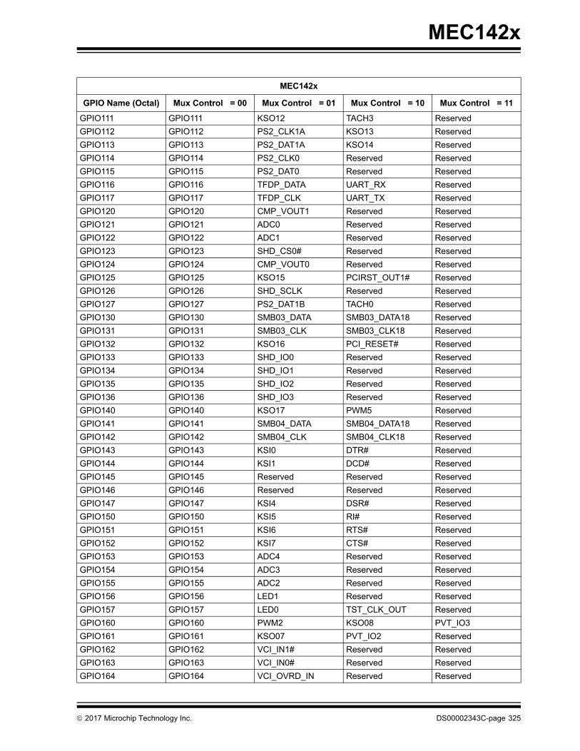
MEC142x
GPIO111 GPIO111 KSO12 TACH3 Reserved
GPIO112 GPIO112 PS2_CLK1A KSO13 Reserved
GPIO113 GPIO113 PS2_DAT1A KSO14 Reserved
GPIO114 GPIO114 PS2_CLK0 Reserved Reserved
GPIO115 GPIO115 PS2_DAT0 Reserved Reserved
GPIO116 GPIO116 TFDP_DATA UART_RX Reserved
GPIO117 GPIO117 TFDP_CLK UART_TX Reserved
GPIO120 GPIO120 CMP_VOUT1 Reserved Reserved
GPIO121 GPIO121 ADC0 Reserved Reserved
GPIO122 GPIO122 ADC1 Reserved Reserved
GPIO123 GPIO123 SHD_CS0# Reserved Reserved
GPIO124 GPIO124 CMP_VOUT0 Reserved Reserved
GPIO125 GPIO125 KSO15 PCIRST_OUT1# Reserved
GPIO126 GPIO126 SHD_SCLK Reserved Reserved
GPIO127 GPIO127 PS2_DAT1B TACH0 Reserved
GPIO130 GPIO130 SMB03_DATA SMB03_DATA18 Reserved
GPIO131 GPIO131 SMB03_CLK SMB03_CLK18 Reserved
GPIO132 GPIO132 KSO16 PCI_RESET# Reserved
GPIO133 GPIO133 SHD_IO0 Reserved Reserved
GPIO134 GPIO134 SHD_IO1 Reserved Reserved
GPIO135 GPIO135 SHD_IO2 Reserved Reserved
GPIO136 GPIO136 SHD_IO3 Reserved Reserved
GPIO140 GPIO140 KSO17 PWM5 Reserved
GPIO141 GPIO141 SMB04_DATA SMB04_DATA18 Reserved
GPIO142 GPIO142 SMB04_CLK SMB04_CLK18 Reserved
GPIO143 GPIO143 KSI0 DTR# Reserved
GPIO144 GPIO144 KSI1 DCD# Reserved
GPIO145 GPIO145 Reserved Reserved Reserved
GPIO146 GPIO146 Reserved Reserved Reserved
GPIO147 GPIO147 KSI4 DSR# Reserved
GPIO150 GPIO150 KSI5 RI# Reserved
GPIO151 GPIO151 KSI6 RTS# Reserved
GPIO152 GPIO152 KSI7 CTS# Reserved
GPIO153 GPIO153 ADC4 Reserved Reserved
GPIO154 GPIO154 ADC3 Reserved Reserved
GPIO155 GPIO155 ADC2 Reserved Reserved
GPIO156 GPIO156 LED1 Reserved Reserved
GPIO157 GPIO157 LED0 TST_CLK_OUT Reserved
GPIO160 GPIO160 PWM2 KSO08 PVT_IO3
GPIO161 GPIO161 KSO07 PVT_IO2 Reserved
GPIO162 GPIO162 VCI_IN1# Reserved Reserved
GPIO163 GPIO163 VCI_IN0# Reserved Reserved
GPIO164 GPIO164 VCI_OVRD_IN Reserved Reserved
MEC142x
GPIO Name (Octal) Mux Control = 00 Mux Control = 01 Mux Control = 10 Mux Control = 11
2017 Microchip Technology Inc. DS00002343C-page 325
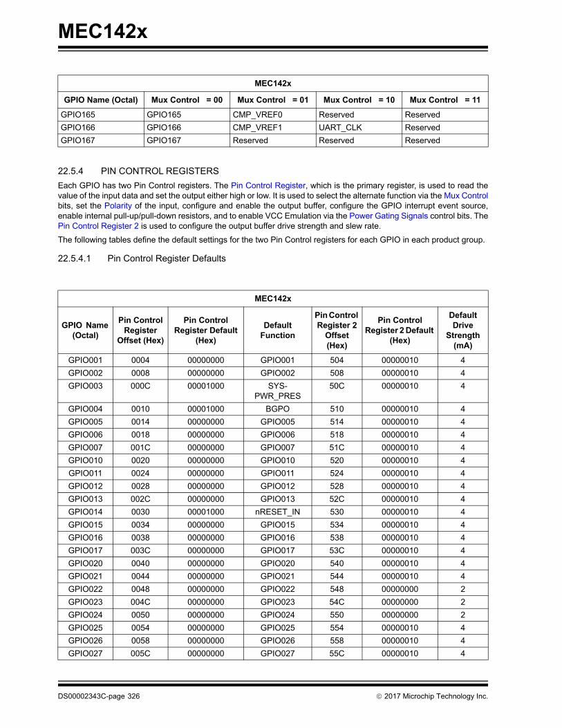
MEC142x
22.5.4 PIN CONTROL REGISTERS
Each GPIO has two Pin Control registers. The Pin Control Register, which is the primary register, is used to read thevalue of the input data and set the output either high or low. It is used to select the alternate function via the Mux Controlbits, set the Polarity of the input, configure and enable the output buffer, configure the GPIO interrupt event source,enable internal pull-up/pull-down resistors, and to enable VCC Emulation via the Power Gating Signals control bits. ThePin Control Register 2 is used to configure the output buffer drive strength and slew rate.
The following tables define the default settings for the two Pin Control registers for each GPIO in each product group.
22.5.4.1 Pin Control Register Defaults
GPIO165 GPIO165 CMP_VREF0 Reserved Reserved
GPIO166 GPIO166 CMP_VREF1 UART_CLK Reserved
GPIO167 GPIO167 Reserved Reserved Reserved
MEC142x
GPIO Name (Octal)
Pin Control Register
Offset (Hex)
Pin Control Register Default
(Hex)
Default Function
Pin Control Register 2
Offset (Hex)
Pin Control Register 2 Default
(Hex)
Default Drive
Strength (mA)
GPIO001 0004 00000000 GPIO001 504 00000010 4
GPIO002 0008 00000000 GPIO002 508 00000010 4
GPIO003 000C 00001000 SYS-PWR_PRES
50C 00000010 4
GPIO004 0010 00001000 BGPO 510 00000010 4
GPIO005 0014 00000000 GPIO005 514 00000010 4
GPIO006 0018 00000000 GPIO006 518 00000010 4
GPIO007 001C 00000000 GPIO007 51C 00000010 4
GPIO010 0020 00000000 GPIO010 520 00000010 4
GPIO011 0024 00000000 GPIO011 524 00000010 4
GPIO012 0028 00000000 GPIO012 528 00000010 4
GPIO013 002C 00000000 GPIO013 52C 00000010 4
GPIO014 0030 00001000 nRESET_IN 530 00000010 4
GPIO015 0034 00000000 GPIO015 534 00000010 4
GPIO016 0038 00000000 GPIO016 538 00000010 4
GPIO017 003C 00000000 GPIO017 53C 00000010 4
GPIO020 0040 00000000 GPIO020 540 00000010 4
GPIO021 0044 00000000 GPIO021 544 00000010 4
GPIO022 0048 00000000 GPIO022 548 00000000 2
GPIO023 004C 00000000 GPIO023 54C 00000000 2
GPIO024 0050 00000000 GPIO024 550 00000000 2
GPIO025 0054 00000000 GPIO025 554 00000010 4
GPIO026 0058 00000000 GPIO026 558 00000010 4
GPIO027 005C 00000000 GPIO027 55C 00000010 4
MEC142x
GPIO Name (Octal) Mux Control = 00 Mux Control = 01 Mux Control = 10 Mux Control = 11
DS00002343C-page 326 2017 Microchip Technology Inc.
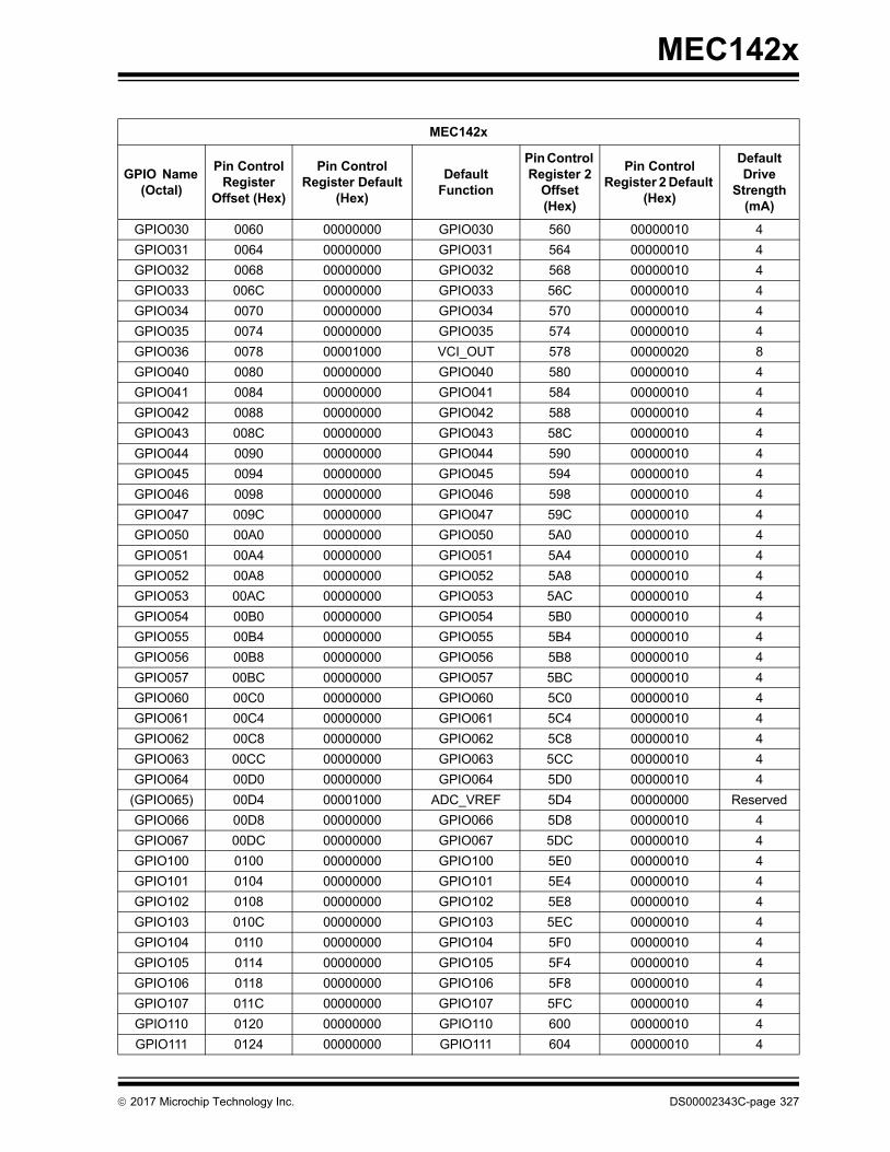
MEC142x
GPIO030 0060 00000000 GPIO030 560 00000010 4
GPIO031 0064 00000000 GPIO031 564 00000010 4
GPIO032 0068 00000000 GPIO032 568 00000010 4
GPIO033 006C 00000000 GPIO033 56C 00000010 4
GPIO034 0070 00000000 GPIO034 570 00000010 4
GPIO035 0074 00000000 GPIO035 574 00000010 4
GPIO036 0078 00001000 VCI_OUT 578 00000020 8
GPIO040 0080 00000000 GPIO040 580 00000010 4
GPIO041 0084 00000000 GPIO041 584 00000010 4
GPIO042 0088 00000000 GPIO042 588 00000010 4
GPIO043 008C 00000000 GPIO043 58C 00000010 4
GPIO044 0090 00000000 GPIO044 590 00000010 4
GPIO045 0094 00000000 GPIO045 594 00000010 4
GPIO046 0098 00000000 GPIO046 598 00000010 4
GPIO047 009C 00000000 GPIO047 59C 00000010 4
GPIO050 00A0 00000000 GPIO050 5A0 00000010 4
GPIO051 00A4 00000000 GPIO051 5A4 00000010 4
GPIO052 00A8 00000000 GPIO052 5A8 00000010 4
GPIO053 00AC 00000000 GPIO053 5AC 00000010 4
GPIO054 00B0 00000000 GPIO054 5B0 00000010 4
GPIO055 00B4 00000000 GPIO055 5B4 00000010 4
GPIO056 00B8 00000000 GPIO056 5B8 00000010 4
GPIO057 00BC 00000000 GPIO057 5BC 00000010 4
GPIO060 00C0 00000000 GPIO060 5C0 00000010 4
GPIO061 00C4 00000000 GPIO061 5C4 00000010 4
GPIO062 00C8 00000000 GPIO062 5C8 00000010 4
GPIO063 00CC 00000000 GPIO063 5CC 00000010 4
GPIO064 00D0 00000000 GPIO064 5D0 00000010 4
(GPIO065) 00D4 00001000 ADC_VREF 5D4 00000000 Reserved
GPIO066 00D8 00000000 GPIO066 5D8 00000010 4
GPIO067 00DC 00000000 GPIO067 5DC 00000010 4
GPIO100 0100 00000000 GPIO100 5E0 00000010 4
GPIO101 0104 00000000 GPIO101 5E4 00000010 4
GPIO102 0108 00000000 GPIO102 5E8 00000010 4
GPIO103 010C 00000000 GPIO103 5EC 00000010 4
GPIO104 0110 00000000 GPIO104 5F0 00000010 4
GPIO105 0114 00000000 GPIO105 5F4 00000010 4
GPIO106 0118 00000000 GPIO106 5F8 00000010 4
GPIO107 011C 00000000 GPIO107 5FC 00000010 4
GPIO110 0120 00000000 GPIO110 600 00000010 4
GPIO111 0124 00000000 GPIO111 604 00000010 4
MEC142x
GPIO Name (Octal)
Pin Control Register
Offset (Hex)
Pin Control Register Default
(Hex)
Default Function
Pin Control Register 2
Offset (Hex)
Pin Control Register 2 Default
(Hex)
Default Drive
Strength (mA)
2017 Microchip Technology Inc. DS00002343C-page 327

MEC142x
GPIO112 0128 00000000 GPIO112 608 00000010 4
GPIO113 012C 00000000 GPIO113 60C 00000010 4
GPIO114 0130 00000000 GPIO114 610 00000010 4
GPIO115 0134 00000000 GPIO115 614 00000010 4
GPIO116 0138 00000000 GPIO116 618 00000010 4
GPIO117 013C 00000000 GPIO117 61C 00000010 4
GPIO120 0140 00000000 GPIO120 620 00000010 4
GPIO121 0144 00000000 GPIO121 624 00000000 2
GPIO122 0148 00000000 GPIO122 628 00000000 2
GPIO123 014C 00000000 GPIO123 62C 00000010 4
GPIO124 0150 00000000 GPIO124 630 00000010 4
GPIO125 0154 00000000 GPIO125 634 00000010 4
GPIO126 0158 00000000 GPIO126 638 00000010 4
GPIO127 015C 00000000 GPIO127 63C 00000010 4
GPIO130 0160 00000000 GPIO130 640 00000010 4
GPIO131 0164 00000000 GPIO131 644 00000010 4
GPIO132 0168 00000000 GPIO132 648 00000010 4
GPIO133 016C 00000000 GPIO133 64C 00000010 4
GPIO134 0170 00000000 GPIO134 650 00000010 4
GPIO135 0174 00000000 GPIO135 654 00000010 4
GPIO136 0178 00000000 GPIO136 658 00000010 4
GPIO140 0180 00000000 GPIO140 660 00000010 4
GPIO141 0184 00000000 GPIO141 664 00000010 4
GPIO142 0188 00000000 GPIO142 668 00000010 4
GPIO143 018C 00000000 GPIO143 66C 00000010 4
GPIO144 0190 00000000 GPIO144 670 00000010 4
GPIO145 0194 00000000 GPIO145 674 00000010 4
GPIO146 0198 00000000 GPIO146 678 00000010 4
GPIO147 019C 00000000 GPIO147 67C 00000010 4
GPIO150 01A0 00000000 GPIO150 680 00000010 4
GPIO151 01A4 00000000 GPIO151 684 00000010 4
GPIO152 01A8 00000000 GPIO152 688 00000010 4
GPIO153 01AC 00000000 GPIO153 68C 00000000 2
GPIO154 01B0 00000000 GPIO154 690 00000000 2
GPIO155 01B4 00000000 GPIO155 694 00000000 2
GPIO156 01B8 00000000 GPIO156 698 00000010 4
GPIO157 01BC 00000000 GPIO157 69C 00000010 4
GPIO160 01C0 00000000 GPIO160 6A0 00000010 4
GPIO161 01C4 00000000 GPIO161 6A4 00000010 4
GPIO162 01C8 00001000 VCI_IN1# 6A8 00000010 4
GPIO163 01CC 00001000 VCI_IN0# 6AC 00000010 4
MEC142x
GPIO Name (Octal)
Pin Control Register
Offset (Hex)
Pin Control Register Default
(Hex)
Default Function
Pin Control Register 2
Offset (Hex)
Pin Control Register 2 Default
(Hex)
Default Drive
Strength (mA)
DS00002343C-page 328 2017 Microchip Technology Inc.

MEC142x
22.6 GPIO Registers
The registers listed in the Register Summary table are for a single instance of the MEC142x. The addresses of eachregister listed in this table are defined as a relative offset to the host “Base Address” defined in the Register BaseAddress Table.
Note 22-1 The Base Address indicates where the first register can be accessed in a particular address spacefor a block instance.
Note 22-2 The GPIO registers may be accessed by the LPC Host via the EMI block via GPIO commands or bydirect access if enabled by firmware. See the firmware documentation for a description of this accessmethod.
GPIO164 01D0 00001000 VCI_OVRD_IN 6B0 00000010 4
GPIO165 01D4 00000000 GPIO165 6B4 00000010 4
GPIO166 01D8 00000000 GPIO166 6B8 00000010 4
GPIO167 01DC 00000000 GPIO167 6BC 00000010 4
TABLE 22-1: REGISTER BASE ADDRESS TABLE
Instance NameInstance Number
Host Address Space Base Address
GPIO 0 LPC/eSPI I/O Note 22-2
0 EC 32-bit internal address space
0008_1000h
TABLE 22-2: REGISTER SUMMARY
Offset Register Name
000h Reserved (GPIO000 not implemented)
004h - 01Ch GPIO001-GPIO007 Pin Control Register
020h - 03Ch GPIO010-GPIO017 Pin Control Register
040h - 05Ch GPIO020-GPIO027 Pin Control Register
060h - 078h GPIO030-GPIO036 Pin Control Register
080h - 09Ch GPIO040-GPIO047 Pin Control Register
0A0h - 0BCh GPIO050-GPIO057 Pin Control Register
0C0h - 0DCh GPIO060-GPIO067 Pin Control Register
0E0h - 0F8h Reserved (GPIO070-GPIO076 not implemented)
MEC142x
GPIO Name (Octal)
Pin Control Register
Offset (Hex)
Pin Control Register Default
(Hex)
Default Function
Pin Control Register 2
Offset (Hex)
Pin Control Register 2 Default
(Hex)
Default Drive
Strength (mA)
2017 Microchip Technology Inc. DS00002343C-page 329

MEC142x
100h - 11Ch GPIO100-GPIO107 Pin Control Register
120h - 13Ch GPIO110-GPIO117 Pin Control Register
140h - 15Ch GPIO120-GPIO127 Pin Control Register
160h - 178h GPIO130-GPIO136 Pin Control Register
180h - 19Ch GPIO140-GPIO147 Pin Control Register
1A0h - 1BCh GPIO150-GPIO157 Pin Control Register
1C0h - 1DCh GPIO160-GPIO167 Pin Control Register
280h(Note 22-3)
Output GPIO[000:036]
284h(Note 22-3)
Output GPIO[040:076]
288h(Note 22-3)
Output GPIO[100:127]
28Ch(Note 22-3)
Output GPIO[140:176]
300h(Note 22-3)
Input GPIO[000:036]
304h(Note 22-3)
Input GPIO[040:076]
308h(Note 22-3)
Input GPIO[100:127]
30Ch(Note 22-3)
Input GPIO[140:176]
504h - 51Ch GPIO001-GPIO007 Pin Control Register 2
520h - 53Ch GPIO010-GPIO017 Pin Control Register 2
540h - 55Ch GPIO020-GPIO027 Pin Control Register 2
560h - 578h GPIO030-GPIO036 Pin Control Register 2 (see Note 22-5 for limitations)
580h - 59Ch GPIO040-GPIO047 Pin Control Register 2 (see Note 22-5 for limitations)
5A0h - 5BCh GPIO050-GPIO057 Pin Control Register 2
5C0h - 5CCh GPIO060-GPIO063 Pin Control Register 2 (see Note 22-5 for limitations)
5D0h Reserved (GPIO064 not implemented - see Note 22-4)
5D4h - 5D8h GPIO065-GPIO066 Pin Control Register 2
5DCh Reserved (GPIO067 not implemented - see Note 22-4)
TABLE 22-2: REGISTER SUMMARY (CONTINUED)
Offset Register Name
DS00002343C-page 330 2017 Microchip Technology Inc.

MEC142x
Note 22-3 The GPIO input and output registers are LPC I/O accessible via Region 0 of the EMI block. Thisaccess is defined in the EMI Protocols chapter of the firmware specification.
Note 22-4 There is no Pin Control Register 2 for GPIO064 and GPIO067, which are PCI_PIO buffer type pins.The drive strength and slew rate are not configurable on these pins.
Note 22-5 The drive strength and slew rate are not configurable for the LPC functions on GPIO034, GPIO061,GPIO063, and GPIO40 - GPIO044 since they are controlled by the PCI_PIO type buffers.
22.6.1 PIN CONTROL REGISTERS
Two Pin Control Registers are implemented for each GPIO. The Pin Control Register format is described in Section22.6.1.1, "Pin Control Register," on page 331. The Pin Control Register 2 format is described in Section 22.6.1.2, "PinControl Register 2," on page 335. Pin Control Register address offsets and defaults for each product are defined inSection 22.5.4.1, "Pin Control Register Defaults," on page 326.
22.6.1.1 Pin Control Register
5E0h - 5F8h Reserved (GPIO070-GPIO076 not implemented)
5E0h - 5FCh GPIO100-GPIO107 Pin Control Register 2
600h - 61Ch GPIO110-GPIO117 Pin Control Register 2
620h - 63Ch GPIO120-GPIO127 Pin Control Register 2
640h - 658h GPIO130-GPIO136 Pin Control Register 2
660h - 67Ch GPIO140-GPIO147 Pin Control Register 2
680h - 69Ch GPIO150-GPIO157 Pin Control Register 2
6A0h - 6BCh GPIO160-GPIO167 Pin Control Register 2
Offset See Table 22-2, "Register Summary"
Bits Description Type DefaultReset Event
31:25 RESERVED RES - -
24 GPIO input from pad
On reads, Bit [24] reflects the state of GPIO input from the pad regardless of setting of Bit [10].
Note: This bit is forced high when the selected power well is offas selected by the Power Gating Signal bits. Seebits[3:2].
R Note 22-6 nSYSRST
23:17 RESERVED RES - -
TABLE 22-2: REGISTER SUMMARY (CONTINUED)
Offset Register Name
2017 Microchip Technology Inc. DS00002343C-page 331

MEC142x
16 GPIO output data
If enabled by the GPIO Output Control Select bit, the GPIO output data bit determines the level on the GPIO pin when the pin is config-ured for the GPIO output function.
On writes:If enabled via the GPIO Output Control Select0: GPIO[x] out = ‘0’1: GPIO[x] out = ‘1’
Note: If disabled via the GPIO Output Control Select then theGPIO[x] out pin is unaffected by writing this bit.
On reads:Bit [16] returns the last programmed value, not the value on the pin.
R/W(GPIO Output Control Select =
0)
R(GPIO Output Control
Select=1)
Note 22-6 nSYSRST
15 RESERVED RES - -
14 GPIO input disableThis bit can be used to support undervoltage functionality.1=disable input0=do not disable input
R/W Note 22-6 nSYSRST
13:12 Mux Control
The Mux Control field determines the active signal function for a pin.
00 = GPIO Function Selected01 = Signal Function 1 Selected10 = Signal Function 2 Selected11 = Signal Function 3 Selected
R/W Note 22-6 nSYSRST
11 Polarity
0 = Non-inverted1 = Inverted
When the Polarity bit is set to ‘1’ and the Mux Control bits are greater than ‘00,’ the selected signal function outputs are inverted and Inter-rupt Detection (int_det) sense defined in Table 22-3, "Edge Enable and Interrupt Detection Bits Definition" is inverted. When the Mux Control field selects the GPIO signal function (Mux = ‘00’), the Polar-ity bit does not effect the output. Regardless of the state of the Mux Control field and the Polarity bit, the state of the pin is always reported without inversion in the GPIO input register.
R/W Note 22-6 nSYSRST
Offset See Table 22-2, "Register Summary"
Bits Description Type DefaultReset Event
DS00002343C-page 332 2017 Microchip Technology Inc.
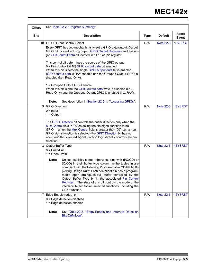
MEC142x
10 GPIO Output Control Select
Every GPIO has two mechanisms to set a GPIO data output: Output GPIO Bit located in the grouped GPIO Output Registers and the sin-gle GPIO output data bit located in bit 16 of this register.
This control bit determines the source of the GPIO output.0 = Pin Control Bit[16] GPIO output data bit enabledWhen this bit is zero the single GPIO output data bit is enabled. (GPIO output data is R/W capable and the Grouped Output GPIO is disabled (i.e., Read-Only).
1 = Grouped Output GPIO enableWhen this bit is one the GPIO output data write is disabled (i.e., Read-Only) and the Grouped Output GPIO is enabled (i.e., R/W).
Note: See description in Section 22.5.1, "Accessing GPIOs".
R/W Note 22-6 nSYSRST
9 GPIO Direction
0 = Input1 = Output
The GPIO Direction bit controls the buffer direction only when the Mux Control field is ‘00’ selecting the pin signal function to be GPIO. When the Mux Control field is greater than ‘00’ (i.e., a non-GPIO signal function is selected) the GPIO Direction bit has no affect and the selected signal function logic directly controls the pin direction.
R/W Note 22-6 nSYSRST
8 Output Buffer Type
0 = Push-Pull1 = Open Drain
Note: Unless explicitly stated otherwise, pins with (I/O/OD) or(O/OD) in their buffer type column in the tables in arecompliant with the following Programmable OD/PP Multi-plexing Design Rule: Each compliant pin has a program-mable open drain/push-pull buffer controlled by theOutput Buffer Type bit in the associated Pin ControlRegister. The state of this bit controls the mode of theinterface buffer for all selected functions, including theGPIO function.
R/W Note 22-6 nSYSRST
7 Edge Enable (edge_en)
0 = Edge detection disabled1 = Edge detection enabled
Note: See Table 22-3, "Edge Enable and Interrupt DetectionBits Definition".
R/W Note 22-6 nSYSRST
Offset See Table 22-2, "Register Summary"
Bits Description Type DefaultReset Event
2017 Microchip Technology Inc. DS00002343C-page 333
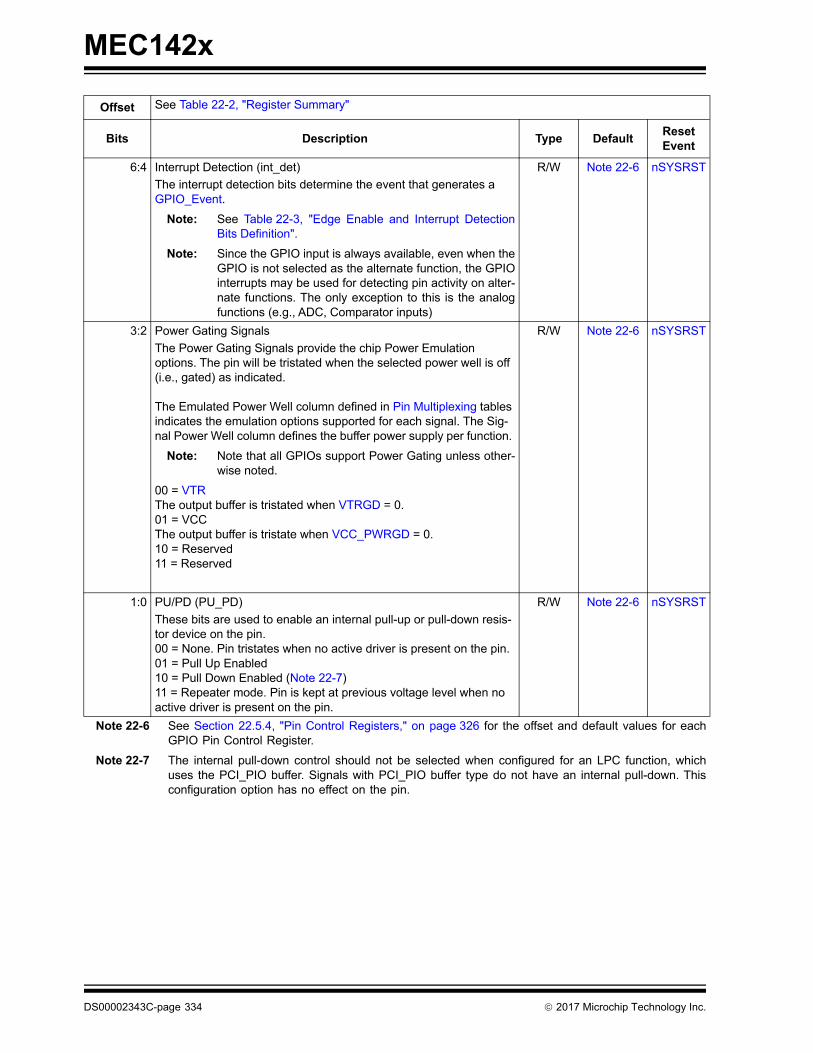
MEC142x
Note 22-6 See Section 22.5.4, "Pin Control Registers," on page 326 for the offset and default values for eachGPIO Pin Control Register.
Note 22-7 The internal pull-down control should not be selected when configured for an LPC function, whichuses the PCI_PIO buffer. Signals with PCI_PIO buffer type do not have an internal pull-down. Thisconfiguration option has no effect on the pin.
6:4 Interrupt Detection (int_det)
The interrupt detection bits determine the event that generates a GPIO_Event.
Note: See Table 22-3, "Edge Enable and Interrupt DetectionBits Definition".
Note: Since the GPIO input is always available, even when theGPIO is not selected as the alternate function, the GPIOinterrupts may be used for detecting pin activity on alter-nate functions. The only exception to this is the analogfunctions (e.g., ADC, Comparator inputs)
R/W Note 22-6 nSYSRST
3:2 Power Gating Signals
The Power Gating Signals provide the chip Power Emulation options. The pin will be tristated when the selected power well is off (i.e., gated) as indicated.
The Emulated Power Well column defined in Pin Multiplexing tables indicates the emulation options supported for each signal. The Sig-nal Power Well column defines the buffer power supply per function.
Note: Note that all GPIOs support Power Gating unless other-wise noted.
00 = VTR The output buffer is tristated when VTRGD = 0.01 = VCC The output buffer is tristate when VCC_PWRGD = 0.10 = Reserved 11 = Reserved
R/W Note 22-6 nSYSRST
1:0 PU/PD (PU_PD)
These bits are used to enable an internal pull-up or pull-down resis-tor device on the pin.00 = None. Pin tristates when no active driver is present on the pin.01 = Pull Up Enabled10 = Pull Down Enabled (Note 22-7)11 = Repeater mode. Pin is kept at previous voltage level when no active driver is present on the pin.
R/W Note 22-6 nSYSRST
Offset See Table 22-2, "Register Summary"
Bits Description Type DefaultReset Event
DS00002343C-page 334 2017 Microchip Technology Inc.

MEC142x
APPLICATION NOTE:
1. All GPIO interrupt detection configurations default to '0000', which is low level interrupt. Having interrupt detectionenabled will un-gated the clock to the GPIO module whenever the interrupt is active, which increases power con-sumption. Interrupt detection should be disabled when not required to save power; this is especially true for pininterfaces (i.e., LPC).
2. Changing the configuration of the Interrupt edge and detection bits may generate an interrupt if it is enabled. TheGPIO should be configured and associated status bits should be cleared before enabling the Interrupt.
22.6.1.2 Pin Control Register 2
TABLE 22-3: EDGE ENABLE AND INTERRUPT DETECTION BITS DEFINITION
Edge Enable
Interrupt Detection BitsSelected Function
D7 D6 D5 D4
0 0 0 0 Low Level Sensitive
0 0 0 1 High Level Sensitive
0 0 1 0 Reserved
0 0 1 1 Reserved
0 1 0 0 Interrupt events are disabled
0 1 0 1 Reserved
0 1 1 0 Reserved
0 1 1 1 Reserved
1 1 0 1 Rising Edge Triggered
1 1 1 0 Falling Edge Triggered
1 1 1 1 Either Edge Triggered
Note: Only edge triggered interrupts can wake up the main ring oscillator. The GPIO must be enabled for edge-triggered interrupts and the GPIO interrupt must be enabled in the interrupt aggregator in order to wake upthe ring when the ring is shut down.
Offset See Note 22-6
Bits Description Type DefaultReset Event
31:6 RESERVED RES - -
5:4 Drive Strength
These bits are used to select the drive strength on the pin.00 = 2mA01 = 4mA10 = 8mA11 = 12mA
R/W 00 nSYSRST
2017 Microchip Technology Inc. DS00002343C-page 335

MEC142x
22.6.2 GPIO OUTPUT REGISTERS
If enabled by the GPIO Output Control Select bit, the grouped GPIO Output bits determine the level on the GPIO pinwhen the pin is configured for the GPIO output function.
On writes:
If enabled via the GPIO Output Control Select
0: GPIO[x] out = ‘0’
1: GPIO[x] out = ‘1’
If disabled via the GPIO Output Control Select then the GPIO[x] out pin is unaffected by writing the corresponding GPIObit in the grouped Output GPIO[xxx:yyy] register.
On reads:
The GPIO output bit in the grouped Output GPIO[xxx:yyy] register returns the last programmed value, not the value onthe pin.
22.6.2.1 Output GPIO[000:036]
3:1 RESERVED RES - -
0 Slew Rate
This bit is used to select the slew rate on the pin.0 = slow (half frequency)1 = fast
R/W 0 nSYSRST
Note: Bits associated with GPIOs not implemented are Reserved.
Offset 280h (Note 22-3)
Bits Description Type DefaultReset Event
31 RESERVED RES - -
30:24 GPIO[036:030] Output R/W 00h nSYSRST
23:16 GPIO[027:020] Output R/W 00h nSYSRST
15:8 GPIO[017:010] Output R/W 00h nSYSRST
7:0 GPIO[007:000] Output R/W 00h nSYSRST
Offset See Note 22-6
Bits Description Type DefaultReset Event
DS00002343C-page 336 2017 Microchip Technology Inc.
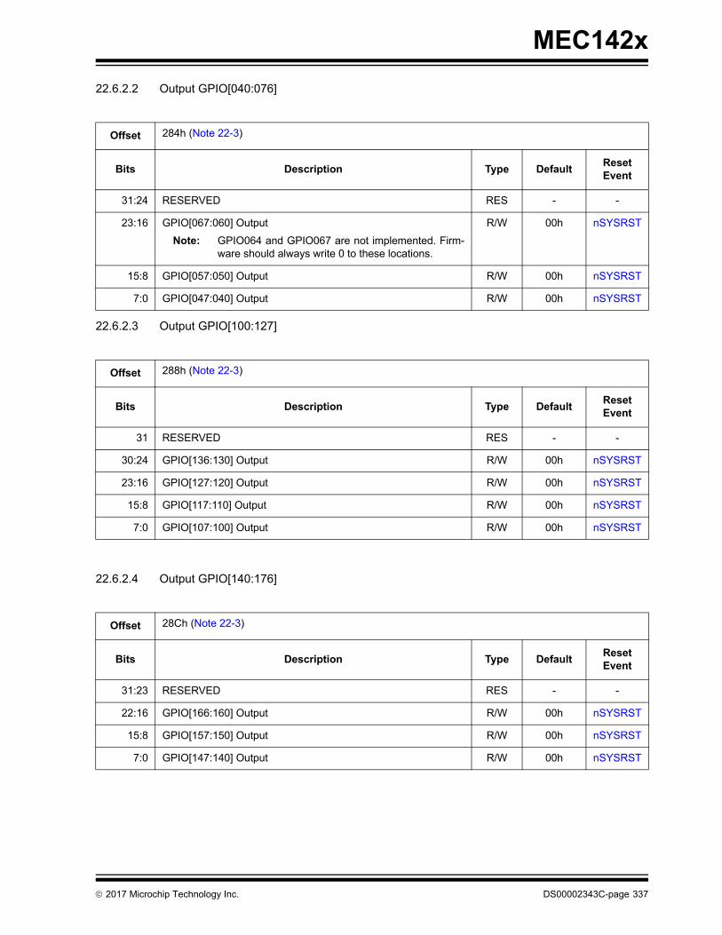
MEC142x
22.6.2.2 Output GPIO[040:076]
22.6.2.3 Output GPIO[100:127]
22.6.2.4 Output GPIO[140:176]
Offset 284h (Note 22-3)
Bits Description Type DefaultReset Event
31:24 RESERVED RES - -
23:16 GPIO[067:060] Output
Note: GPIO064 and GPIO067 are not implemented. Firm-ware should always write 0 to these locations.
R/W 00h nSYSRST
15:8 GPIO[057:050] Output R/W 00h nSYSRST
7:0 GPIO[047:040] Output R/W 00h nSYSRST
Offset 288h (Note 22-3)
Bits Description Type DefaultReset Event
31 RESERVED RES - -
30:24 GPIO[136:130] Output R/W 00h nSYSRST
23:16 GPIO[127:120] Output R/W 00h nSYSRST
15:8 GPIO[117:110] Output R/W 00h nSYSRST
7:0 GPIO[107:100] Output R/W 00h nSYSRST
Offset 28Ch (Note 22-3)
Bits Description Type DefaultReset Event
31:23 RESERVED RES - -
22:16 GPIO[166:160] Output R/W 00h nSYSRST
15:8 GPIO[157:150] Output R/W 00h nSYSRST
7:0 GPIO[147:140] Output R/W 00h nSYSRST
2017 Microchip Technology Inc. DS00002343C-page 337

MEC142x
22.6.3 GPIO INPUT REGISTERS
The GPIO Input Registers can always be used to read the state of a pin, even when the pin is in an output mode and/orwhen a signal function other than the GPIO signal function is selected; i.e., the Pin Control Register Mux Control bitsare not equal to ‘00.’
The MSbit of the Input GPIO registers have been implemented as a read/write scratch pad bit to support processor spe-cific instructions.
22.6.3.1 Input GPIO[000:036]
22.6.3.2 Input GPIO[040:076]
Note: Bits associated with GPIOs that are not implemented are shown as Reserved.
Offset 300h (Note 22-3)
Bits Description Type DefaultReset Event
31 Scratchpad Bit R/W 0b nSYSRST
30:24 GPIO[036:030] Input R 00h nSYSRST
23:16 GPIO[027:020] Input R 00h nSYSRST
15:8 GPIO[017:010] Input R 00h nSYSRST
7:0 GPIO[007:000] Input R 00h nSYSRST
Offset 304h (Note 22-3)
Bits Description Type DefaultReset Event
31 Scratchpad Bit R/W 0b nSYSRST
30:24 RESERVED R - -
23:16 GPIO[067:060] Input
Note: GPIO064 and GPIO067 are not implemented.
R 00h nSYSRST
15:8 GPIO[057:050] Input R 00h nSYSRST
7:0 GPIO[047:040] Input R 00h nSYSRST
DS00002343C-page 338 2017 Microchip Technology Inc.
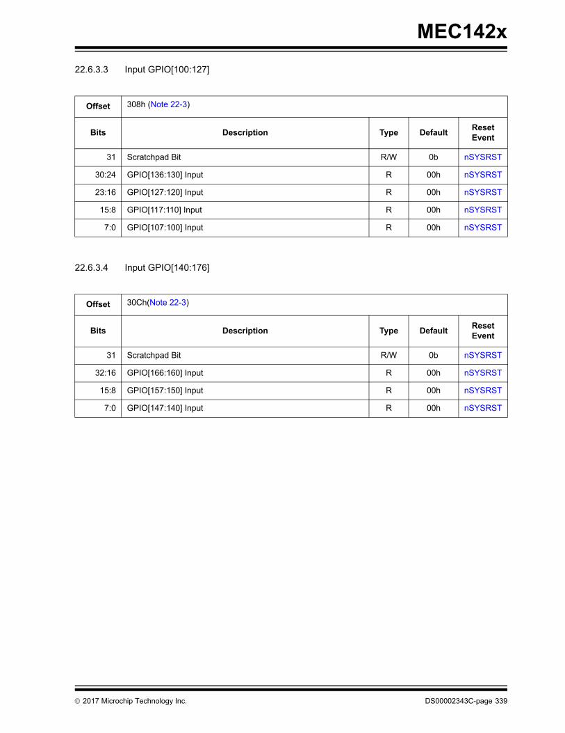
MEC142x
22.6.3.3 Input GPIO[100:127]
22.6.3.4 Input GPIO[140:176]
Offset 308h (Note 22-3)
Bits Description Type DefaultReset Event
31 Scratchpad Bit R/W 0b nSYSRST
30:24 GPIO[136:130] Input R 00h nSYSRST
23:16 GPIO[127:120] Input R 00h nSYSRST
15:8 GPIO[117:110] Input R 00h nSYSRST
7:0 GPIO[107:100] Input R 00h nSYSRST
Offset 30Ch(Note 22-3)
Bits Description Type DefaultReset Event
31 Scratchpad Bit R/W 0b nSYSRST
32:16 GPIO[166:160] Input R 00h nSYSRST
15:8 GPIO[157:150] Input R 00h nSYSRST
7:0 GPIO[147:140] Input R 00h nSYSRST
2017 Microchip Technology Inc. DS00002343C-page 339

MEC142x
23.0 SMBUS INTERFACE
23.1 Introduction
The MEC142x SMBus Interface includes five instances of the SMBus controller core. This chapter describes aspectsof the SMBus Interface that are unique to the MEC142x instantiations of this core; including, Power Domain, Resets,Clocks, Interrupts, Registers and the Physical Interface. For a General Description, Features, Block Diagram, Func-tional Description, Registers Interface and other core-specific details, see Ref [1] (note: in this chapter, italicized texttypically refers to SMBus controller core interface elements as described in Ref [1]).
23.2 References
1. SMBus Controller Core with Network Layer Support (SMB2) - 16MHz I2C Baud Clock“, Revision 3.52, Core-LevelArchitecture Specification, MCHP, 10/25/13
23.3 Terminology
There is no terminology defined for this chapter.
23.4 Interface
This block is designed to be accessed externally via the pin interface and internally via a registered host interface. Inaddition, this block is equipped with
23.5 Signal Description
The pin signals are defined in Section 2.0, "Pin Configuration," on page 12.
23.6 Host Interface
The registers defined for the SMBus Interface are accessible as indicated in Section 23.12, "SMBus Registers".
FIGURE 23-1: I/O DIAGRAM OF BLOCK
Signal Description
SMBus Interface
Interrupts
Power, Clocks and Reset
Host Interface
DMA Interface
DS00002343C-page 340 2017 Microchip Technology Inc.
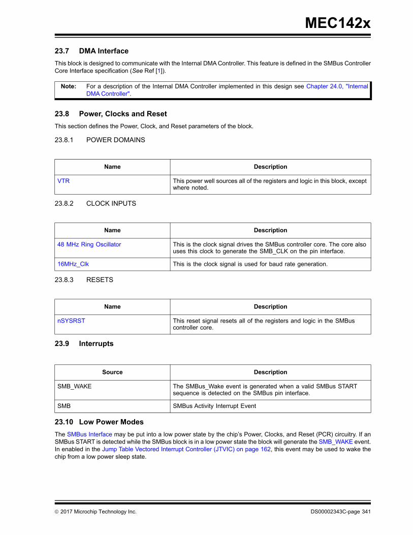
MEC142x
23.7 DMA Interface
This block is designed to communicate with the Internal DMA Controller. This feature is defined in the SMBus ControllerCore Interface specification (See Ref [1]).
23.8 Power, Clocks and Reset
This section defines the Power, Clock, and Reset parameters of the block.
23.8.1 POWER DOMAINS
23.8.2 CLOCK INPUTS
23.8.3 RESETS
23.9 Interrupts
23.10 Low Power Modes
The SMBus Interface may be put into a low power state by the chip’s Power, Clocks, and Reset (PCR) circuitry. If anSMBus START is detected while the SMBus block is in a low power state the block will generate the SMB_WAKE event.In enabled in the Jump Table Vectored Interrupt Controller (JTVIC) on page 162, this event may be used to wake thechip from a low power sleep state.
Note: For a description of the Internal DMA Controller implemented in this design see Chapter 24.0, "InternalDMA Controller".
Name Description
VTR This power well sources all of the registers and logic in this block, except where noted.
Name Description
48 MHz Ring Oscillator This is the clock signal drives the SMBus controller core. The core also uses this clock to generate the SMB_CLK on the pin interface.
16MHz_Clk This is the clock signal is used for baud rate generation.
Name Description
nSYSRST This reset signal resets all of the registers and logic in the SMBus controller core.
Source Description
SMB_WAKE The SMBus_Wake event is generated when a valid SMBus START sequence is detected on the SMBus pin interface.
SMB SMBus Activity Interrupt Event
2017 Microchip Technology Inc. DS00002343C-page 341

MEC142x
23.11 Description
23.11.1 SMBUS CONTROLLER CORE
The MEC142x SMBus Interface behavior is defined in the SMBus Controller Core Interface specification (See Ref [1]).
23.11.2 PHYSICAL INTERFACE
23.11.2.1 Overview
The Physical Interface for the SMBus controller core is configurable for up to 15 ports as defined below in SMBus PortSelection.
Each of the 3 SMBus controllers can be connected to any of the ports defined in the table. The PORT SEL [3:0] bits ineach controller will appear the same (Table 23-1). The default for each field is Fh, Reserved, which means that the SMBcontroller is not connected to a port.
An SMB port should be connected to a single controller. An attempt to configure the PORT SEL [3:0] bits in one con-troller to a value already assigned to another controller may result in unexpected results.
The port signal-function names and pin numbers are defined in the Pin Configuration chapter. The SMBus port selec-tion is made using the PORT SEL [3:0] bits in the Configuration Register as described in Ref [1] and in the subsectionsthat follow.
For SMBus port signal functions that are alternate functions of GPIO pins, the buffer type for these pins must be con-figured as open-drain outputs when the port is selected as defined in SMBus Port Selection. For more informationregarding the SMBus controller core see Section 2.2, “Physical Interface” in Ref[1].
23.11.2.2 SMBus Port Selection
Note 1: See Pin Configuration chapter for a description of the SMBus pin configuration.
2: The SMB00 to SMB04 Ports have the option to be configured for either 3.3V or 1.8V signaling. This selec-tion is determined by the GPIO alternate function mux. SMBxx_DATA/SMBxx_CLK are 3.3V I/O signaling. SMBxx_DATA18/SMBxx_CLK18 are 1.8V I/O signaling.
3: The SMB05 Port operates at the voltage of the power region it is in. It does not have the option to be config-ured for either 3.3V or 1.8V signaling through the GPIO alternate function mux.
TABLE 23-1: SMBUS PORT SELECTION
PORT SEL [3:0]PORT (Note 1)
3 2 1 0
0 0 0 0 SMB00 (3.3V or 1.8V, Note 2)
0 0 0 1 SMB01 (3.3V or 1.8V, Note 2)
0 0 1 0 SMB02 (3.3V or 1.8V, Note 2)
0 0 1 1 SMB03 (3.3V or 1.8V, Note 2)
0 1 0 0 SMB04 (3.3V or 1.8V, Note 2)
0 1 0 1 SB-TSI
0 1 1 0 SMB05 (3.3V or 1.8V, Note 3)
0111b - 1111b Reserved
DS00002343C-page 342 2017 Microchip Technology Inc.

MEC142x
23.12 SMBus Registers
The registers listed in the SMBus Core Register Summary table in the SMBus Controller Core Interface specification(Ref [1]) are for a single instance of the SMBus Controller Core. The addresses of each register listed in this table aredefined as a relative offset to the host “Base Address” defined in the following table:
TABLE 23-2: EC-ONLY REGISTER BASE ADDRESS TABLE
Block InstanceInstance Number
Host Address Space Base Address
SMBus Controller 0 EC 32-bit internal address space
0000_1800h
SMBus Controller 1 EC 32-bit internal address space
0000_AC00h
SMBus Controller 2 EC 32-bit internal address space
0000_B000h
SMBus Controller 3 EC 32-bit internal address space
0000_B400h
SMBus Controller 4 EC 32-bit internal address space
0000_C000h
Note: The Base Address indicates where the first register can be accessed in a particular address space for ablock instance.
2017 Microchip Technology Inc. DS00002343C-page 343
MEC142x
24.0 INTERNAL DMA CONTROLLER
24.1 Features
• Supports Memory-to-Memory BYTE, WORD, and DWORD transfers
• Used to Perform DMA transactions for DMA capable hardware IP blocks
• Supports 11 DMA Channels that may be configured for any Hardware Device or Memory transfer
• Channel 0 Supports CRC-32 generation
24.2 Introduction
The Internal DMA Controller transfers data to/from the source from/to the destination. The firmware is responsible forsetting up each channel. Afterwards either the firmware or the hardware may perform the flow control. The hardwareflow control exists entirely inside the source device. Each transfer may be 1, 2, or 4 bytes in size, so long as the devicesupports a transfer of that size. Every device must be on the internal 32-bit address space.
24.3 References
No references have been cited for this chapter
24.4 Terminology
TABLE 24-1: TERMINOLOGY
Term Definition
DMA Transfer This is a complete DMA Transfer which is done after the Master Device terminates the transfer, the Firmware Aborts the transfer or the DMA reaches its transfer limit.A DMA Transfer may consist of one or more data packets.
Data Packet Each data packet may be composed of 1, 2, or 4 bytes. The size of the data packet is limited by the max size supported by both the source and the destination. Both source and destination will transfer the same num-ber of bytes per packet.
Channel The Channel is responsible for end-to-end (source-to-destination) Data Packet delivery.
Device A Device may refer to a Master or Slave connected to the DMA Channel. Each DMA Channel may be assigned one or more devices.
Master Device This is the master of the DMA, which determines when it is active.The Firmware is the master while operating in Firmware Flow Control.The Hardware is the master while operating in Hardware Flow Control.
The Master Device in Hardware Mode is selected by DMA Channel Con-trol:Hardware Flow Control Device. It is the index of the Flow Control Port.
Slave Device The Slave Device is defined as the device associated with the targeted Memory Address.
DS00002343C-page 344 2017 Microchip Technology Inc.
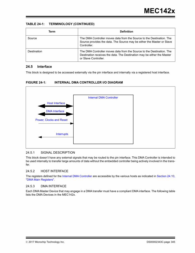
MEC142x
24.5 Interface
This block is designed to be accessed externally via the pin interface and internally via a registered host interface.
24.5.1 SIGNAL DESCRIPTION
This block doesn’t have any external signals that may be routed to the pin interface. This DMA Controller is intended tobe used internally to transfer large amounts of data without the embedded controller being actively involved in the trans-fer.
24.5.2 HOST INTERFACE
The registers defined for the Internal DMA Controller are accessible by the various hosts as indicated in Section 24.10,"DMA Main Registers".
24.5.3 DMA INTERFACE
Each DMA Master Device that may engage in a DMA transfer must have a compliant DMA interface. The following tablelists the DMA Devices in the MEC142x.
Source The DMA Controller moves data from the Source to the Destination. The Source provides the data. The Source may be either the Master or Slave Controller.
Destination The DMA Controller moves data from the Source to the Destination. The Destination receives the data. The Destination may be either the Master or Slave Controller.
FIGURE 24-1: INTERNAL DMA CONTROLLER I/O DIAGRAM
TABLE 24-1: TERMINOLOGY (CONTINUED)
Term Definition
Internal DMA Controller
Power, Clocks and Reset
Interrupts
DMA Interface
Host Interface
2017 Microchip Technology Inc. DS00002343C-page 345
MEC142x
Note 1: The Device Number is programmed into field HARDWARE_FLOW_CONTROL_DEVICE of the DMA Chan-nel N Control Register register.
24.6 Power, Clocks and Reset
This section defines the Power, Clock, and Reset parameters of the block.
24.6.1 POWER DOMAINS
24.6.2 CLOCK INPUTS
TABLE 24-2: DMA CONTROLLER DEVICE SELECTION
Device NameDevice Number
(Note 1)Controller Source
SMBus 0 Controller 0 Slave
1 Master
SMBus 1 Controller 2 Slave
3 Master
SMBus 2 Controller 4 Slave
5 Master
QuadSPI Master Controller 6 Transmit
7 Receive
SMBus 3 Controller 8 Slave
9 Master
SMBus 4 Controller 10 Slave
11 Master
SMBus 5 Controller 12 Slave
13 Master
Name Description
VTR This power well sources all of the registers and logic in this block, except where noted.
Name Description
48 MHz Ring Oscillator This clock signal drives selected logic (e.g., counters).
DS00002343C-page 346 2017 Microchip Technology Inc.
MEC142x
24.6.3 RESETS
24.7 Interrupts
This section defines the Interrupt Sources generated from this block.
24.8 Low Power Modes
The Internal DMA Controller may be put into a low power state by the chip’s Power, Clocks, and Reset (PCR) circuitry.
When the block is commanded to go to sleep it will place the DMA block into sleep mode only after all transactions onthe DMA have been completed. For Firmware Flow Controlled transactions, the DMA will wait until it hits its terminalcount and clears the Go control bit. For Hardware Flow Control, the DMA will go to sleep after either the terminal countis hit, or the Master device flags the terminate signal.
Name Description
nSYSRST This reset signal resets all of the registers and logic in this block.
DMA_RESET This reset is generated if either the nSYSRST is asserted or the SOFT_RESET is asserted.
Source Description
DMA0 Direct Memory Access Channel 0This signal is generated by the STATUS_DONE bit.
DMA1 Direct Memory Access Channel 1This signal is generated by the STATUS_DONE bit.
DMA2 Direct Memory Access Channel 2This signal is generated by the STATUS_DONE bit.
DMA3 Direct Memory Access Channel 3This signal is generated by the STATUS_DONE bit.
DMA4 Direct Memory Access Channel 4This signal is generated by the STATUS_DONE bit.
DMA5 Direct Memory Access Channel 5This signal is generated by the STATUS_DONE bit.
DMA6 Direct Memory Access Channel 6This signal is generated by the STATUS_DONE bit.
DMA7 Direct Memory Access Channel 7This signal is generated by the STATUS_DONE bit.
DMA8 Direct Memory Access Channel 8This signal is generated by the STATUS_DONE bit.
DMA9 Direct Memory Access Channel 9This signal is generated by the STATUS_DONE bit.
DMA10 Direct Memory Access Channel 10This signal is generated by the STATUS_DONE bit.
2017 Microchip Technology Inc. DS00002343C-page 347

MEC142x
24.9 Description
The MEC142x features a multi-channel DMA controller. The DMA controller can autonomously move data from/to anyDMA capable master device to/from any populated memory location. This mechanism allows hardware IP blocks totransfer large amounts of data into or out of memory without EC intervention.
The DMA has the following characteristics:
• Data is only moved 1 Data Packet at a time
• Data only moves between devices on the accessible via the internal 32-bit address space
• Each DMA Channel may be configured to communicate with any DMA capable device on the 32-bit internal address space. Each device has been assigned a device number. See Section 24.5.3, "DMA Interface," on page 345.
The controller will accesses SRAM buffers only with incrementing addresses (that is, it cannot start at the top of a buffer,nor does it handle circular buffers automatically). The controller does not handle chaining (that is, automatically startinga new DMA transfer when one finishes).
A DMA Channel can optionally generate a CRC-32 on the data transfered by the Channel.
24.9.1 CONFIGURATION
The DMA Controller is enabled via the ACTIVATE bit in DMA Main Control Register register.
Each DMA Channel must also be individually enabled via the CHANNEL_ACTIVATE bit in the DMA Channel N ActivateRegister to be operational.
Before starting a DMA transaction on a DMA Channel the host must assign a DMA Master to the channel via bits[15:9]HARDWARE_FLOW_CONTROL_DEVICE. The host must not configure two different channels to the same DMA Mas-ter at the same time.
Data will be transfered between the DMA Master, starting at the programmed DEVICE_ADDRESS, and the targetedmemory location, starting at the MEMORY_START_ADDRESS. The address for either the DMA Master or the targetedmemory location may remain static or it may increment. To enable the DMA Master to increment its address set theINCREMENT_DEVICE_ADDRESS bit. To enable the targeted memory location to increment its addresses set theINCREMENT_MEMORY_ADDRESS. The DMA transfer will continue as long as the target memory address beingaccessed is less than the MEMORY_END_ADDRESS. If the DMA Controller detects that the memory location it isattempting to access on the Target is equal to the MEMORY_END_ADDRESS it will notify the DMA Master that thetransaction is done. Otherwise the Data will be transferred in packets. The size of the packet is determined by theTRANSFER_SIZE.
24.9.2 OPERATION
The DMA Controller is designed to move data from one memory location to another.
24.9.2.1 Establishing a Connection
A DMA Master will initiate a DMA Transaction by requesting access to a channel. The DMA arbiter, which evaluateseach channel request using a basic round robin algorithm, will grant access to the DMA master. Once granted, the chan-nel will hold the grant until it decides to release it, by notifying the DMA Controller that it is done.
24.9.2.2 Initiating a Transfer
Once a connection is established the DMA Master will issue a DMA request to start a DMA transfer.
Firmware can initiate a transaction by setting the TRANSFER_GO bit. The DMA transfer will remain active until eitherthe Master issues a Terminate or the DMA Controller signals that the transfer is DONE. Firmware may terminate a trans-action by setting the TRANSFER_ABORT bit.
Data may be moved from the DMA Master to the targeted Memory address or from the targeted Memory Address to theDMA Master. The direction of the transfer is determined by the TRANSFER_DIRECTION bit.
Note: If Firmware wants to prevent any other channels from being granted while it is active it can set theLOCK_CHANNEL bit.
Note: Before initiating a DMA transaction via firmware the hardware flow control must be disabled via the DIS-ABLE_HARDWARE_FLOW_CONTROL bit.
DS00002343C-page 348 2017 Microchip Technology Inc.

MEC142x
Once a transaction has been initiated firmware can use the STATUS_DONE bit to determine when the transaction iscompleted. This status bit is routed to the interrupt interface. In the same register there are additional status bits thatindicate if the transaction completed successfully or with errors. This bits are OR’d together with the STATUS_DONEbit to generate the interrupt event. Each status be may be individually enabled/disabled from generating this event.
24.9.2.3 CRC Generation
A CRC generator can be attached to a DMA channel in order to generate a CRC on the data as it is transfered from thesource to the destination. The CRC used is the CRC-32 algorithm used in IEEE 802.3 and many other protocols, usingthe polynomial x32 + x26 + x23 + x22 + x16 + x12 + x11 + x10 + x8 + x7 + x5 + x4 + x2 + x + 1. The CRC generation takesplace in parallel with the data transfer; enabling CRC will not increase the time to complete a DMA transaction. The CRCgenerator has the optional ability to automatically transfer the generated CRC to the destination after the data transferhas completed.
CRC generation is subject to a number of restrictions:
• The CRC is only generated on channels that have the CRC hardware. See Table 24-6, "DMA Channel N Register Summary" for a definition of which channels have the ability to generate a CRC.
• The DMA transfer must be 32-bits.
• If CRC is enabled, DMA interrupts are inhibited until the CRC is completed, including the optional post-transfer copy of it is enabled.
• The CRC must be initialized by firmware. The value FFFFFFFFh must be written to the Data Register in order to initialize the generator for the standard CRC-32-IEEE algorithm.
24.9.3 DMA REGISTERS
The DMA Controller consists of a single Main Block of registers that applies to all channels and channel specific regis-ters. Table 24-4, "DMA Main Register Summary" lists the registers in the Main Block and Table 24-6, "DMA Channel NRegister Summary" lists the registers in each channel.
24.10 DMA Main Registers
The addresses of each register listed in these tables are defined as a relative offset to the “Base Address” defined inthe DMA Main Register Base Address Table. The Base Address indicates where the first register can be accessed in aparticular bank of registers.
TABLE 24-3: DMA MAIN REGISTER BASE ADDRESS TABLE
Instance NameChannel Number
Host Address Space Base Address
DMA Controller Main Block EC 32-bit internal address space
0000_2400h
TABLE 24-4: DMA MAIN REGISTER SUMMARY
Offset Register Name (Mnemonic)
00h DMA Main Control Register
04h DMA Data Packet Register
2017 Microchip Technology Inc. DS00002343C-page 349

MEC142x
24.10.1 DMA MAIN CONTROL REGISTER
24.10.2 DMA DATA PACKET REGISTER
24.11 DMA Channel Registers
The addresses of each register listed in these tables are defined as a relative offset to the “Base Address” defined inthe DMA Channel N Register Base Address Table. The Base Address indicates where the first register can be accessedin a particular bank of registers.
Offset 00h
Bits Description Type DefaultReset Event
7:2 Reserved R - -
1 SOFT_RESET
Soft reset the entire module.
This bit is self-clearing.
W 0b -
0 ACTIVATE
Enable the blocks operation.
1=Enable block. Each individual channel must be enabled sepa-rately.
0=Disable all channels.
R/WS 0b DMA_RESET
Offset 04h
Bits Description Type DefaultReset Event
31:0 DATA_PACKET
Debug register that has the data that is stored in the Data Packet. This data is read data from the currently active transfer source.
R 0000h -
TABLE 24-5: DMA CHANNEL N REGISTER BASE ADDRESS TABLE
Instance NameChannel
Number (N)Host Address Space Base Address
DMA Controller 0(Note 1)
EC 32-bit internal address space
0000_2440h
DMA Controller 1 EC 32-bit internal address space
0000_2480h
DMA Controller 2 EC 32-bit internal address space
0000_24C0h
DMA Controller 3 EC 32-bit internal address space
0000_2500h
DS00002343C-page 350 2017 Microchip Technology Inc.

MEC142x
Note 1: Only DMA Channel 0 has CRC-32 generation support, which can be used with the Quad SPI Master Con-troller or for Memory-to-Memory DMA transfers.
DMA Controller 4 EC 32-bit internal address space
0000_2540h
DMA Controller 5 EC 32-bit internal address space
0000_2580h
DMA Controller 6 EC 32-bit internal address space
0000_25C0h
DMA Controller 7 EC 32-bit internal address space
0000_2600h
DMA Controller 8 EC 32-bit internal address space
0000_2640h
DMA Controller 9 EC 32-bit internal address space
0000_2680h
DMA Controller 10 EC 32-bit internal address space
0000_26C0h
TABLE 24-6: DMA CHANNEL N REGISTER SUMMARY
OffsetRegister Name (Mnemonic)
(Note 2)
00h DMA Channel N Activate Register
04h DMA Channel N Memory Start Address Register
08h DMA Channel N Memory End Address Register
0Ch DMA Channel N Device Address Register
10h DMA Channel N Control Register
14h DMA Channel N Interrupt Status Register
18h DMA Channel N Interrupt Enable Register
1Ch Test
20h(Note 3)
DMA Channel N CRC Enable Register
24h(Note 3)
DMA Channel N CRC Data Register
28h(Note 3)
DMA Channel N CRC Post Status Register
2Ch(Note 3)
DMA Channel N CRC Test Register
TABLE 24-5: DMA CHANNEL N REGISTER BASE ADDRESS TABLE (CONTINUED)
Instance NameChannel
Number (N)Host Address Space Base Address
2017 Microchip Technology Inc. DS00002343C-page 351

MEC142x
2: The letter ‘N’ following DMA Channel indicates the Channel Number. Each Channel implemented will havethese registers to determine that channel’s operation.
3: These registers are only present in DMA Channel 0. Offsets 20h to 2Ch are reserved in all the other chan-nels.
24.11.1 DMA CHANNEL N ACTIVATE REGISTER
24.11.2 DMA CHANNEL N MEMORY START ADDRESS REGISTER
Offset 00h
Bits Description Type DefaultReset Event
7:1 Reserved R - -
0 CHANNEL_ACTIVATE
Enable this channel for operation.The DMA Main Control:Activate must also be enabled for this channel to be operational.
R/W 0h DMA_RESET
Offset 04h
Bits Description Type DefaultReset Event
31:0 MEMORY_START_ADDRESS
This is the starting address for the Memory device.
This field is updated by Hardware after every packet transfer by the size of the transfer, as defined by DMA Channel Control:Channel Transfer Size while the DMA Channel Control:Increment Memory Address is Enabled.
The Memory device is defined as the device that is the slave device in the transfer.
ex. With Hardware Flow Control, the Memory device is the device that is not connected to the Hardware Flow Controlling device.
Note: This field is only as large as the maximum allowed AHBAddress Size in the system. If the HADDR size is 24Bits, then Bits [31:24] will be RESERVED.
R/W 0000h DMA_RESET
DS00002343C-page 352 2017 Microchip Technology Inc.

MEC142x
24.11.3 DMA CHANNEL N MEMORY END ADDRESS REGISTER
24.11.4 DMA CHANNEL N DEVICE ADDRESS REGISTER
Offset 08h
Bits Description Type DefaultReset Event
31:0 MEMORY_END_ADDRESS
This is the ending address for the Memory device.
This will define the limit of the transfer, so long as DMA Channel Control:Increment Memory Address is Enabled. When the Memory Start Address is equal to this value, the DMA will terminate the transfer and flag the status DMA Channel Interrupt:Status Done.
Note: This field is only as large as the maximum allowed AHBAddress Size in the system. If the HADDR size is 24Bits, then Bits [31:24] will be RESERVED.
R/W 0000h DMA_RESET
Offset 0Ch
Bits Description Type DefaultReset Event
31:0 DEVICE_ADDRESS
This is the Master Device address.
This is used as the address that will access the Device on the DMA. The Device is defined as the Master of the DMA transfer; as in the device that is controlling the Hardware Flow Control.
APPLICATION NOTE: Only Channel 0 has CRC function whichmay be utilized only by the Quad SPIMaster Controller and for Memory-to-Memory transfers. It is recommended touse Channels 1-6 for the SMBusControllers.
This field is updated by Hardware after every Data Packet transfer by the size of the transfer, as defined by DMA Channel Con-trol:Transfer Size while the DMA Channel Control:Increment Device Address is Enabled.
Note: This field is only as large as the maximum allowed AHBAddress Size in the system. If the HADDR size is 24Bits, then Bits [31:24] will be RESERVED.
R/W 0000h DMA_RESET
2017 Microchip Technology Inc. DS00002343C-page 353

MEC142x
24.11.5 DMA CHANNEL N CONTROL REGISTER
Offset 10h
Bits Description Type DefaultReset Event
31:26 Reserved R - -
25 TRANSFER_ABORT
This is used to abort the current transfer on this DMA Channel. The aborted transfer will be forced to terminate immediately.
R/W 0h DMA_RESET
24 TRANSFER_GO
This is used for the Firmware Flow Control DMA transfer.
This is used to start a transfer under the Firmware Flow Control. Do not use this in conjunction with the Hardware Flow Control; DMA Channel Control:Disable Hardware Flow Control must be set in order for this field to function correctly.
R/W 0h DMA_RESET
23 Reserved R - -
22:20 TRANSFER_SIZE
This is the transfer size in Bytes of each Data Packet transfer.
Note: The transfer size must be a legal transfer size. Validsizes are 1, 2 and 4 Bytes.
R/W 0h DMA_RESET
19 DISABLE_HARDWARE_FLOW_CONTROL
This will Disable the Hardware Flow Control. When disabled, any DMA Master device attempting to communicate to the DMA over the DMA Flow Control Interface (Ports: dma_req, dma_term, and dma_done) will be ignored.This should be set before using the DMA channel in Firmware Flow Control mode.
RW 0h DMA_RESET
18 LOCK_CHANNEL
This is used to lock the arbitration of the Channel Arbiter on this channel once this channel is granted.Once this is locked, it will remain on the arbiter until it has completed it transfer (either the Transfer Aborted, Transfer Done or Transfer Terminated conditions).
Note: This setting may starve other channels if the locked chan-nel takes an excessive period of time to complete.
RW 0h DMA_RESET
17 INCREMENT_DEVICE_ADDRESS
This will enable an auto-increment to the DMA Channel Device Address.
1: Increment the DMA Channel Device Address by DMA ChannelControl:Transfer Size after every Data Packet transfer
0: Do nothing
RW 0h DMA_RESET
DS00002343C-page 354 2017 Microchip Technology Inc.

MEC142x
16 INCREMENT_MEMORY_ADDRESS
This will enable an auto-increment to the DMA Channel Memory Address.
1=Increment the DMA Channel Memory Address by DMA ChannelControl:Transfer Size after every Data Packet transfer
0=Do nothing
Note: If this is not set, the DMA will never terminate the transferon its own. It will have to be terminated through the Hard-ware Flow Control or through a DMA Channel Con-trol:Transfer Abort.
RW 0h DMA_RESET
15:9 HARDWARE_FLOW_CONTROL_DEVICE
This is the device that is connected to this channel as its Hardware Flow Control master.The Flow Control Interface is a bus with each master concatenated onto it. This selects which bus index of the concatenated Flow Con-trol Interface bus is targeted towards this channel.The Flow Control Interface Port list is dma_req, dma_term, and dma_done.
RW 0h DMA_RESET
8 TRANSFER_DIRECTION
This determines the direction of the DMA Transfer.
1=Data Packet Read from Memory Start Address followed by DataPacket Write to Device Address
0=Data Packet Read from Device Address followed by Data PacketWrite to Memory Start Address
RW 0h DMA_RESET
7:6 Reserved R - -
5 BUSY
This is a status signal.
1=The DMA Channel is busy (FSM is not IDLE)0=The DMA Channel is not busy (FSM is IDLE)
RO 0h DMA_RESET
Offset 10h
Bits Description Type DefaultReset Event
2017 Microchip Technology Inc. DS00002343C-page 355

MEC142x
4:3 STATUS
This is a status signal. The status decode is listed in priority order with the highest priority first.
3: Error detected by the DMA2: The DMA Channel is externally done, in that the Device has termi-
nated the transfer over the Hardware Flow Control through thePort dma_term
1: The DMA Channel is locally done, in that Memory Start Addressequals Memory End Address
0: DMA Channel Control:Run is Disabled (0x0)
Note: This functionality has been replaced by the Interrupt field,and as such should never be used.
The field will not flag back appropriately timed status, andif used may cause the firmware to become out-of-syncwith the hardware.
This field has multiple non-exclusive statuses, but mayonly display a single status. As such, multiple statusesmay be TRUE, but this will appear as though only a singlestatus has been triggered.
R 0h DMA_RESET
2 DONE
This is a status signal. It is only valid while DMA Channel Con-trol:Run is Enabled. This is the inverse of the DMA Channel Con-trol:Busy field, except this is qualified with the DMA Channel Control:Run field.
1=Channel is done0=Channel is not done or it is OFF
RO 0h DMA_RESET
1 REQUEST
This is a status field.
1: There is a transfer request from the Master Device0: There is no transfer request from the Master Device
RO 0h DMA_RESET
0 RUN
This is a control field.
Note: This bit only applies to Hardware Flow Control mode.Do not use this bit in conjunction with the Firmware FlowControl.
1: This channel is enabled and will service transfer requests0=This channel is disabled. All transfer requests are ignored
RW 0h DMA_RESET
Offset 10h
Bits Description Type DefaultReset Event
DS00002343C-page 356 2017 Microchip Technology Inc.
MEC142x
24.11.6 DMA CHANNEL N INTERRUPT STATUS REGISTER
24.11.7 DMA CHANNEL N INTERRUPT ENABLE REGISTER
Offset 14h
Bits Description Type DefaultReset Event
7:3 Reserved R - -
2 STATUS_DONE
This is an interrupt source register.This flags when the DMA Channel has completed a transfer suc-cessfully on its side.A completed transfer is defined as when the DMA Channel reaches its limit; Memory Start Address equals Memory End Address.A completion due to a Hardware Flow Control Terminate will not flag this interrupt.
1=Memory Start Address equals Memory End Address1=Memory Start Address does not equal Memory End Address
R/WC 0h DMA_RESET
1 STATUS_FLOW_CONTROL
This is an interrupt source register.This flags when the DMA Channel has encountered a Hardware Flow Control Request after the DMA Channel has completed the transfer. This means the Master Device is attempting to overflow the DMA.
1=Hardware Flow Control is requesting after the transfer has com-pleted
0=No Hardware Flow Control event
0h DMA_RESET
0 STATUS_BUS_ERROR
This is an interrupt source register.This flags when there is an Error detected over the internal 32-bit Bus.
1: Error detected.
R/WC 0h DMA_RESET
Offset 18h
Bits Description Type DefaultReset Event
7:3 Reserved R - -
2 STATUS_ENABLE_DONE
This is an interrupt enable for DMA Channel Interrupt:Status Done.
1=Enable Interrupt0=Disable Interrupt
R/W 0h DMA_RESET
2017 Microchip Technology Inc. DS00002343C-page 357
MEC142x
24.11.8 DMA CHANNEL N CRC ENABLE REGISTER
1 STATUS_ENABLE_FLOW_CONTROL_ERROR
This is an interrupt enable for DMA Channel Interrupt:Status Flow Control Error.
1=Enable Interrupt0=Disable Interrupt
R/W 0h DMA_RESET
0 STATUS_ENABLE_BUS_ERROR
This is an interrupt enable for DMA Channel Interrupt:Status Bus Error.
1=Enable Interrupt0=Disable Interrupt
R/W 0h DMA_RESET
Offset 20h
Bits Description Type DefaultReset Event
31:2 Reserved R - -
1 CRC_POST_TRANSFER_ENABLE
The bit enables the transfer of the calculated CRC-32 after the completion of the DMA transaction. If the DMA transaction is aborted by either firmware or an internal bus error, the transfer will not occur. If the target of the DMA transfer is a device and the device signaled the termination of the DMA transaction, the CRC post transfer will not occur.
1=Enable the transfer of CRC-32 for DMA Channel N after the DMAtransaction completes
0=Disable the automatic transfer of the CRC
R/W 0h DMA_RESET
0 CRC_ENABLE
1=Enable the calculation of CRC-32 for DMA Channel N0=Disable the calculation of CRC-32 for DMA Channel N
R/W 0h DMA_RESET
Offset 18h
Bits Description Type DefaultReset Event
DS00002343C-page 358 2017 Microchip Technology Inc.
MEC142x
24.11.9 DMA CHANNEL N CRC DATA REGISTER
24.11.10 DMA CHANNEL N CRC POST STATUS REGISTER
Offset 24h
Bits Description Type DefaultReset Event
31:0 CRC
Writes to this register initialize the CRC generator. Reads from this register return the output of the CRC that is calculated from the data transfered by DMA Channel N. The output of the CRC gener-ator is bit-reversed and inverted on reads, as required by the CRC-32-IEEE definition.
A CRC can be accumulated across multiple DMA transactions on Channel N. If it is necessary to save the intermediate CRC value, the result of the read of this register must be bit-reversed and inverted before being written back to this register.
R/W 0h DMA_RESET
Offset 28h
Bits Description Type DefaultReset Event
31:4 Reserved R - -
3 CRC_POST_TEST2
This is a test bit. Read back data is unpredictable.
R 0h DMA_RESET
2 CRC_POST_TRANSFER
This bit is cleared to ‘0’ when a DMA transaction starts. If Post Transfer is enabled, and the CRC is successfully transferred fol-lowing the completion of the DMA transaction, this bit is set to ‘1’. If the post transfer of the CRC is inhibited, because either firmware or the device terminated the transaction, this bit remains ‘0’.
R 0h DMA_RESET
1 CRC_POST_TEST1
This is a test bit. Read back data is unpredictable.
R 0h DMA_RESET
0 CRC_POST_TEST0
This is a test bit. Read back data is unpredictable.
R 0h DMA_RESET
2017 Microchip Technology Inc. DS00002343C-page 359

MEC142x
24.11.11 DMA CHANNEL N CRC TEST REGISTER
Offset 2Ch
Bits Description Type DefaultReset Event
31:0 Reserved R - -
DS00002343C-page 360 2017 Microchip Technology Inc.

MEC142x
25.0 PECI INTERFACE
25.1 Overview
The MEC142x includes a PECI Interface to allow the EC to retrieve temperature readings from PECI-compliantdevices. The PECI Interface implements the PHY and Link Layer of a PECI host controller as defined in References[1]and includes hardware support for the PECI 2.0 command set.
This chapter focuses on MEC142x specific PECI Interface configuration information such as Power Domains, ClockInputs, Resets, Interrupts, and other chip specific information. For a functional description of the MEC142x PECI Inter-face refer to References [1].
25.2 References
1. PECI Interface Core, Rev. 1.31, Core-Level Architecture Specification, SMSC Confidential, 4/15/11
25.3 Terminology
No terminology has been defined for this chapter.
25.4 Interface
This block is designed to be accessed externally via the pin interface and internally via a registered host interface.
25.5 Signal Description
The Signal Description Table lists the signals that are typically routed to the pin interface.
FIGURE 25-1: PECI INTERFACE I/O DIAGRAM
TABLE 25-1: SIGNAL DESCRIPTION TABLE
Name Direction Description
PECI_READY Input PECI Ready input pin
Note: This signal is optional. If this signal is not on the pininterface it is pulled high internally.
PECI_DAT Input/Output PECI Data signal pin
PECI_READY
PECI_DAT
PECI Interface
Power, Clocks and Reset
Interrupts
Host Interface
2017 Microchip Technology Inc. DS00002343C-page 361

MEC142x
25.6 Host Interface
The registers defined for the PECI Interface are accessible by the various hosts as indicated in Section 25.11, "PECIInterface Registers".
25.7 Power, Clocks and Reset
This section defines the Power, Clock, and Reset parameters of the block.
25.7.1 POWER DOMAINS
25.7.2 CLOCK INPUTS
25.7.3 RESETS
25.8 Interrupts
This section defines the Interrupt Sources generated from this block.
25.9 Low Power Modes
The PECI Interface may be put into a low power state by the chip’s Power, Clocks, and Reset (PCR) circuitry.
Note: Routing guidelines for the PECI_DAT pin is provided in Intel Platform design guides. Refer to the appropri-ate Intel document for current information. See Table 25-2.
TABLE 25-2: PECI ROUTING GUIDELINES
Trace Impedance 50 Ohms +/- 15%
Spacing 10 mils
Routing Layer Microstrip
Trace Width Calculate to match impedance
Length 1” - 15”
Name Description
VTR The PECI Interface logic and registers are powered by VTR.
Name Description
48 MHz Ring Oscillator PECI Module Input Clock
Name Description
nSYSRST PECI Core Reset Input
Source Description
PECIHOST PECI Host
DS00002343C-page 362 2017 Microchip Technology Inc.

MEC142x
25.10 Instance Description
There is one instance of the PECI Core implemented in the PECI Interface in the MEC142x. See PECI Interface Core,Rev. 1.31, Core-Level Architecture Specification, SMSC Confidential, 4/15/11 for a description of the PECI Core.
25.11 PECI Interface Registers
The registers listed in the PECI Interface Register Summary table are for a single instance of the PECI Interface. Theaddresses of each register listed in this table are defined as a relative offset to the host “Base Address” defined in thePECI Interface Register Base Address Table.
TABLE 25-3: EC-ONLY REGISTER BASE ADDRESS TABLE
Block InstanceInstance Number
Host Address Space Base Address
PECI Interface 0 EC 32-bit Internal Address Space
0000_6400h
Note: The Base Address indicates where the first register can be accessed in a particular address space for ablock instance.
TABLE 25-4: PECI INTERFACE REGISTER SUMMARY
Offset Register Name (Mnemonic)
00h Write Data Register
04h Read Data Register
08h Control Register
0Ch Status Register 1
10h Status Register 2
14h Error Register
18h Interrupt Enable 1 Register
1Ch Interrupt Enable 2 Register
20h Optimal Bit Time Register (Low Byte)
24h Optimal Bit Time Register (High Byte)
28h Test
2Ch Test
30h-3Ch Reserved
40h Block ID Register
44h Revision Register
48h - 7Ch Test
2017 Microchip Technology Inc. DS00002343C-page 363

MEC142x
For register details see References [1].
Note: Test registers are reserved for Microchip use only. Reading and writing Test registers may cause undesir-able results
DS00002343C-page 364 2017 Microchip Technology Inc.
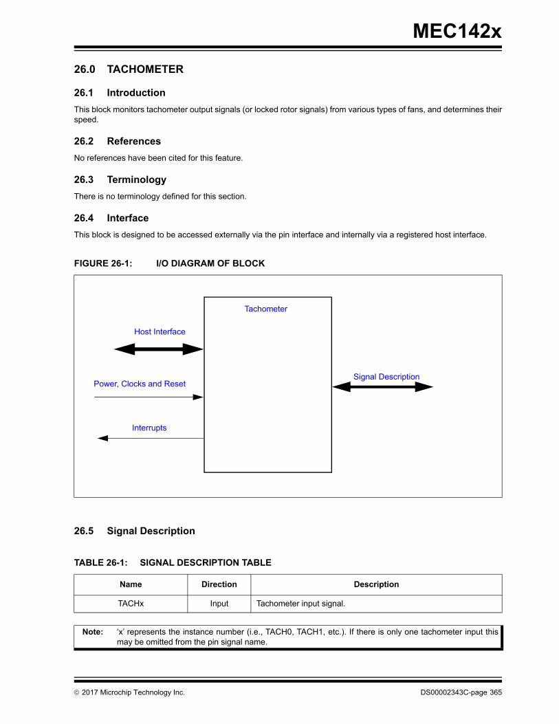
MEC142x
26.0 TACHOMETER
26.1 Introduction
This block monitors tachometer output signals (or locked rotor signals) from various types of fans, and determines theirspeed.
26.2 References
No references have been cited for this feature.
26.3 Terminology
There is no terminology defined for this section.
26.4 Interface
This block is designed to be accessed externally via the pin interface and internally via a registered host interface.
26.5 Signal Description
FIGURE 26-1: I/O DIAGRAM OF BLOCK
TABLE 26-1: SIGNAL DESCRIPTION TABLE
Name Direction Description
TACHx Input Tachometer input signal.
Note: ‘x’ represents the instance number (i.e., TACH0, TACH1, etc.). If there is only one tachometer input thismay be omitted from the pin signal name.
Signal Description
Tachometer
Interrupts
Power, Clocks and Reset
Host Interface
2017 Microchip Technology Inc. DS00002343C-page 365
MEC142x
26.6 Host Interface
The registers defined for the Tachometer are accessible by the various hosts as indicated in Section 26.11, "EC-OnlyRegisters".
26.7 Power, Clocks and Reset
This section defines the Power, Clock, and Reset parameters of the block.
26.7.1 POWER DOMAINS
26.7.2 CLOCK INPUTS
26.7.3 RESETS
26.8 Interrupts
This section defines the Interrupt Sources generated from this block.
26.9 Low Power Modes
The Tachometer may be put into a low power state by the chip’s Power, Clocks, and Reset (PCR) circuitry.
26.10 Description
The Tachometer block monitors tachometer output signals (also referred to as TACH signals) or locked rotor signalsgenerated by various types of fans. These signals can be used to determine the speed of the attached fan. This blockis designed to monitor fans at fan speeds from 100 RPMs to 30,000 RPMs.
Typically, these are DC brushless fans that generate (with each revolution) a 50% duty cycle, two-period square wave,as shown in Figure 26-2 below.
Name Description
VTR The logic and registers implemented in this block are powered by this power well.
Name Description
100kHz_Clk This is the clock input to the tachometer monitor logic. In Mode 1, the TACHx input is measured in the number of these clocks.
Name Description
nSYSRST This signal resets all the registers and logic in this block to their default state.
Source Description
TACH This internal signal is generated from the OR’d result of the status events, as defined in the TACHx Status Register.
DS00002343C-page 366 2017 Microchip Technology Inc.

MEC142x
In typical systems, the fans are powered by the main power supply. Firmware may disable this block when it detects thatthe main power rail has been turned off by either clearing the <enable> TACH_ENABLE bit or putting the block to sleepvia the supported Low Power Mode interface (see Low Power Modes).
26.10.1 MODES OF OPERATION
The Tachometer block supports two modes of operation. The mode of operation is selected via the TACH_READING_-MODE_SELECT bit.
26.10.1.1 Free Running Counter
In Mode 0, the Tachometer block uses the TACHx input as the clock source for the internal TACH pulse counter (seeTACHX_COUNTER). The counter is incremented when it detects a rising edge on the TACH input. In this mode, thefirmware may periodically poll the TACHX_COUNTER field to determine the average speed over a period of time. Thefirmware must store the previous reading and the current reading to compute the number of pulses detected over aperiod of time. In this mode, the counter continuously increments until it reaches FFFFh. It then wraps back to 0000hand continues counting. The firmware must ensure that the sample rate is greater than the time it takes for the counterto wrap back to the starting point.
26.10.1.2 Mode 1 -- Number of Clock Pulses per Revolution
In Mode 1, the Tachometer block uses its 100kHz_Clk clock input to measure the programmable number of TACHxpulses. In this mode, the internal TACH pulse counter (TACHX_COUNTER) returns the value in number of 100kHz_Clkpulses per programmed number of TACH_EDGES. For fans that generate two square waves per revolution, these bitsshould be configured to five edges.
When the number of edges is detected, the counter is latched and the COUNT_READY_STATUS bit is asserted. If theCOUNT_READY_INT_EN bit is set a TACH interrupt event will be generated.
26.10.2 OUT-OF-LIMIT EVENTS
The Tachometer Block has a pair of limit registers that may be configured to generate an event if the Tachometer indi-cates that the fan is operating too slow or too fast. If the TACHX_COUNTER exceeds one of the programmed limits, theTACHx High Limit Register and the TACHx Low Limit Register, the bit TACH_OUT_OF_LIMIT_STATUS will be set. Ifthe TACH_OUT_OF_LIMIT_STATUS bit is set, the Tachometer block will generate an interrupt event.
FIGURE 26-2: FAN GENERATED 50%DUTY CYCLE WAVEFORM
Note: Tach interrupts should be disabled in Mode 0.
one revolution
2017 Microchip Technology Inc. DS00002343C-page 367

MEC142x
26.11 EC-Only Registers
The registers listed in the EC-Only Register Summary table are for a single instance of the Tachometer. The addressesof each register listed in this table are defined as a relative offset to the host “Base Address” defined in the EC-OnlyRegister Base Address Table.
The Base Address indicates where the first register can be accessed in a particular address space for a block instance.
TABLE 26-2: EC-ONLY REGISTER BASE ADDRESS TABLE
Block InstanceInstance Number Host Address Space Base Address
TACH 0 EC 32-bit internal address space
0000_6000h
TACH 1 EC 32-bit internal address space
0000_6010h
TACH 2 EC 32-bit internal address space
0000_6020h
TACH 3 EC 32-bit internal address space
0000_6030h
TABLE 26-3: TACHOMETER REGISTER SUMMARY
Offset Register Name (Mnemonic)
00h TACHx Control Register
04h TACHx Status Register
08h TACHx High Limit Register
0Ch TACHx Low Limit Register
DS00002343C-page 368 2017 Microchip Technology Inc.
MEC142x
26.11.1 TACHX CONTROL REGISTER
Offset 00h
Bits Description Type DefaultReset Event
31:16 TACHX_COUNTER
This 16-bit field contains the latched value of the internal Tach pulse counter, which may be configured by the Tach Reading Mode Select field to operate as a free-running counter or to be gated by the TACHx input signal.
If the counter is free-running (Mode 0), the internal Tach counter increments (if enabled) on transitions of the raw TACHx input signal and is latched into this field every time it is incremented. The act of reading this field will not reset the counter, which rolls over to 0000h after FFFFh. The firmware will compute the delta between the current count reading and the previous count reading, to determine the num-ber of pulses detected over a programmed period.
If the counter is gated by the TACHx input and clocked by 100kHz_-Clk (Mode 1), the internal counter will be latched into the reading reg-ister when the programmed number of edges is detected or when the counter reaches FFFFh. The internal counter is reset to zero after it is copied into this register.
Note: In Mode 1, a counter value of FFFFh means that theTachometer logic did not detect the programmed numberof edges in 655ms. A stuck fan can be detected by settingthe TACHx High Limit Register to a number less thanFFFFh. If the internal counter then reaches FFFFh, thereading register will be set to FFFFh and an out-of-limitinterrupt can be sent to the EC.
R 00h nSYSRST
15 TACH_INPUT_INT_EN
1=Enable TACHx Input toggle interrupt from Tachometer block0=Disable TACHx Input toggle interrupt from Tachometer block
R/W 0b nSYSRST
14 COUNT_READY_INT_EN
1=Enable Count Ready interrupt from Tachometer block0=Disable Count Ready interrupt from Tachometer block
R/W 0b nSYSRST
13 Reserved R - -
12:11 TACH_EDGES
A tachometer signal is a square wave with a 50% duty cycle. Typi-cally, two tachometer periods represents one revolution of the fan. A tachometer period consists of three edges.
This programmed value represents the number of tachometer edges that will be used to determine the interval for which the number of 100kHz_Clk pulses will be counted
11b=9 Tach edges (4 Tach periods)10b=5 Tach edges (2 Tach periods)01b=3 Tach edges (1 Tach period)00b=2 Tach edges (1/2 Tach period)
R/W 00b nSYSRST
2017 Microchip Technology Inc. DS00002343C-page 369

MEC142x
10 TACH_READING_MODE_SELECT
1=Counter is incremented on the rising edge of the 100kHz_Clk input.The counter is latched into the TACHX_COUNTER field andreset when the programmed number of edges is detected.
0=Counter is incremented when TACHx Input transitions from low-to-high state (default)
R/W 0b nSYSRST
9 Reserved R - -
8 FILTER_ENABLE
This filter is used to remove high frequency glitches from TACHx Input. When this filter is enabled, TACHx input pulses less than two 100kHz_Clk periods wide get filtered.
1= Filter enabled0= Filter disabled (default)
It is recommended that the TACHx input filter always be enabled.
R/W 0b nSYSRST
7:2 Reserved R - -
1 TACH_ENABLE
This bit gates the clocks into the block. When clocks are gated, the TACHx pin is tristated. When re-enabled, the internal counters will continue from the last known state and stale status events may still be pending. Firmware should discard any status or reading values until the reading value has been updated at least one time after the enable bit is set.
1= TACH Monitoring enabled, clocks enabled.0= TACH Idle, clocks gated
R/W 0b nSYSRST
0 TACH_OUT_OF_LIMIT_ENABLE
This bit is used to enable the TACH_OUT_OF_LIMIT_STATUS bit in the TACHx Status Register to generate an interrupt event.
1=Enable interrupt output from Tachometer block0=Disable interrupt output from Tachometer block (default)
R/W 0b nSYSRST
Offset 00h
Bits Description Type DefaultReset Event
DS00002343C-page 370 2017 Microchip Technology Inc.
MEC142x
26.11.2 TACHX STATUS REGISTER
Offset 04h
Bits Description Type DefaultReset Event
31:4 Reserved R - -
3 COUNT_READY_STATUS
This status bit is asserted when the TACHx input changes state and when the counter value is latched. This bit remains cleared to '0' when the TACH_READING_MODE_SELECT bit in the TACHx Con-trol Register is '0'.When the TACH_READING_MODE_SELECT bit in the TACHx Con-trol Register is set to '1', this bit is set to ‘1’ when the counter value is latched by the hardware. It is cleared when written with a ‘1’. If COUNT_READY_INT_EN in the TACHx Control Register is set to 1, this status bit will assert the Tach Interrupt signal.
1=Reading ready0=Reading not ready
R/WC 0b nSYSRST
2 TOGGLE_STATUS
This bit is set when TACHx Input changes state. It is cleared when written with a ’1’. If TACH_INPUT_INT_EN in the TACHx Control Register is set to ’1’, this status bit will assert the Tach Interrupt sig-nal.
1=TACHx Input changed state (this bit is set on a low-to-high or high-to-low transition)
0=TACHx stable
R/WC 0b nSYSRST
1 TACH_PIN_STATUS
This bit reflects the state of TACHx Input. This bit is a read only bit that may be polled by the embedded controller.
1= TACHx Input is high0= TACHx Input is low
R 0b nSYSRST
0 TACH_OUT_OF_LIMIT_STATUS
This bit is set when the Tach Count value is greater than the high limit or less than the low limit. It is cleared when written with a ’1’. To disable this status event set the limits to their extreme values. If TACH_OUT_OF_LIMIT_ENABLE in the TACHx Control Register is set to 1’, this status bit will assert the Tach Interrupt signal.
1=Tach is outside of limits0=Tach is within limits
R/WC 0b nSYSRST
Note:
• Some fans offer a Locked Rotor output pin that generates a level event if a locked rotor is detected. This bit may be used in combination with the Tach pin status bit to detect a locked rotor signal event from a fan.
• Tach Input may come up as active for Locked Rotor events. This would not cause an interrupt event because the pin would not toggle. Firmware must read the status events as part of the initialization process, if polling is not implemented.
2017 Microchip Technology Inc. DS00002343C-page 371
MEC142x
26.11.3 TACHX HIGH LIMIT REGISTER
26.11.4 TACHX LOW LIMIT REGISTER
Offset 08h
Bits Description Type DefaultReset Event
31:16 Reserved - - -
15:0 TACH_HIGH_LIMIT
This value is compared with the value in the TACHX_COUNTER field. If the value in the counter is greater than the value programmed in this register, the TACH_OUT_OF_LIMIT_STATUS bit will be set. The TACH_OUT_OF_LIMIT_STATUS status event may be enabled to generate an interrupt to the embedded controller via the TACH_OUT_OF_LIMIT_ENABLE bit in the TACHx Control Register.
R/W FFFFh nSYSRST
Offset 0Ch
Bits Description Type DefaultReset Event
31:16 Reserved R - -
15:0 TACHX_LOW_LIMIT
This value is compared with the value in the TACHX_COUNTER field of the TACHx Control Register. If the value in the counter is less than the value programmed in this register, the TACH_OUT_OF_LIM-IT_STATUS bit will be set. The TACH_OUT_OF_LIMIT_STATUS sta-tus event may be enabled to generate an interrupt to the embedded controller via the TACH_OUT_OF_LIMIT_ENABLE bit in the TACHx Control Register
To disable the TACH_OUT_OF_LIMIT_STATUS low event, program 0000h into this register.
R/W 0000h nSYSRST
DS00002343C-page 372 2017 Microchip Technology Inc.

MEC142x
27.0 PWM
27.1 Introduction
This block generates a PWM output that can be used to control 4-wire fans, blinking LEDs, and other similar devices.Each PWM can generate an arbitrary duty cycle output at frequencies from less than 0.1 Hz to 24 MHz. The PWM con-troller can also used to generate the PROCHOT output and Speaker output.
The PWMx Counter ON Time registers and PWMx Counter OFF Time registers determine the operation of thePWM_OUTPUT signals. See Section 27.11.1, "PWMx Counter ON Time Register," on page 377 and Section 27.11.2,"PWMx Counter OFF Time Register," on page 377 for a description of the PWM_OUTPUT signals.
27.2 References
There are no standards referenced in this chapter.
27.3 Terminology
There is no terminology defined for this section.
27.4 Interface
This block is designed to be accessed externally via the pin interface and internally via a registered host interface.
There are no external signals for this block.
FIGURE 27-1: I/O DIAGRAM OF BLOCK
PWM
Interrupts
Power, Clocks and Reset
Host Interface
Signal Description
2017 Microchip Technology Inc. DS00002343C-page 373
MEC142x
27.5 Signal Description
27.6 Host Interface
The registers defined for the PWM Interface are accessible by the various hosts as indicated in Section 27.11, "EC-OnlyRegisters".
27.7 Power, Clocks and Reset
This section defines the Power, Clock, and Reset parameters of the block.
27.7.1 POWER DOMAINS
27.7.2 CLOCK INPUTS
27.7.3 RESETS
27.8 Interrupts
The PWM block does not generate any interrupt events.
27.9 Low Power Modes
The PWM may be put into a low power state by the chip’s Power, Clocks, and Reset (PCR) circuitry. When the PWM isin the sleep state, the internal counters reset to 0 and the internal state of the PWM and the PWM_OUTPUT signal setto the OFF state.
27.10 Description
The PWM_OUTPUT signal is used to generate a duty cycle of specified frequency. This block can be programmed sothat the PWM signal toggles the PWM_OUTPUT, holds it high, or holds it low. When the PWM is configured to toggle,the PWM_OUTPUT alternates from high to low at the rate specified in the PWMx Counter ON Time Register and PWMxCounter OFF Time Register.
TABLE 27-1: SIGNAL DESCRIPTION TABLE
Name Direction Description
PWM_OUTPUT OUTPUT Pulse Width Modulated signal to PWMx pin.
Name Description
VTR The PWM logic and registers are powered by this single power source.
Name Description
100kHz_Clk 100kHz_Clk clock input for generating low PWM frequencies, such as 10 Hz to 100 Hz.
48 MHz Ring Oscillator 48 MHz Ring Oscillator clock input for generating high PWM frequencies, such as 15 kHz to 30 kHz.
Name Description
nSYSRST This reset signal resets all the logic in this block to its initial state including the registers, which are set to their defined default state.
DS00002343C-page 374 2017 Microchip Technology Inc.

MEC142x
The following diagram illustrates how the clock inputs and registers are routed to the PWM Duty Cycle & FrequencyControl logic to generate the PWM output.
The PWM clock source to the PWM Down Counter, used to generate a duty cycle and frequency on the PWM, is deter-mined through the Clock select[1] and Clock Pre-Divider[6:3] bits in the PWMx Configuration Register register.
The PWMx Counter ON/OFF Time registers determine both the frequency and duty cycle of the signal generated onPWM_OUTPUT as described below.
The PWM frequency is determined by the selected clock source and the total on and off time programmed in the PWMxCounter ON Time Register and PWMx Counter OFF Time Register registers. The frequency is the time it takes (at thatclock rate) to count down to 0 from the total on and off time.
The PWM duty cycle is determined by the relative values programmed in the PWMx Counter ON Time Register andPWMx Counter OFF Time Register registers.
Note that Setting the PWMX_COUNTER_ON_TIME field in the PWMx Counter ON Time Register to a value of n will cause the On time of the PWM to be n+1 cycles of the PWM Clock Source. Setting the PWMX_COUNTER_OFF_TIME field in the PWMx Counter OFF Time Register to a value of n will cause the Off time of the PWM to be n+1 cycles of the PWM Clock Source.
FIGURE 27-2: BLOCK DIAGRAM OF PWM CONTROLLER
Note: In Figure 27-2, the 48 MHz Ring Oscillator is represented as CLOCK_HIGH and 100kHz_Clk is repre-sented as CLOCK_LOW.
PWM BLOCK
PWM Duty Cycle & Frequency Control
PWM_ OUTPUT
PWM Registers
CLOCK_HIGH
CLOCK_LOW Invert_PWM
Clock Select
16-bit down counterEC I/F
Clock Pre-
Divider(15:0)
2017 Microchip Technology Inc. DS00002343C-page 375

MEC142x
The PWM Frequency Equation and PWM Duty Cycle Equation are shown below.
FIGURE 27-3: PWM FREQUENCY EQUATION
In Figure 27-3, the ClockSourceFrequency variable is the frequency of the clock source selected by the Clock Selectbit in the PWMx Configuration Register, and PreDivisor is a field in the PWMx Configuration Register. The PWMCoun-terOnTime, PWMCounterOffTime are registers that are defined in Section 27.11, "EC-Only Registers".
FIGURE 27-4: PWM DUTY CYCLE EQUATION
The PWMx Counter ON Time Register and PWMx Counter OFF Time Register registers should be accessed as 16-bitvalues.
27.11 EC-Only Registers
The registers listed in the EC-Only Register Summary table are for a single instance of the PWM. The addresses ofeach register listed in this table are defined as a relative offset to the host “Base Address” defined in the EC-Only Reg-ister Base Address Table.
The Base Address indicates where the first register can be accessed in a particular address space for a block instance.
TABLE 27-2: EC-ONLY REGISTER BASE ADDRESS TABLE
Block InstanceInstance Number Host Address Space Base Address
PWM 0 EC 32-bit internal address space
0000_5800h
PWM 1 EC 32-bit internal address space
0000_5810h
PWM 2 EC 32-bit internal address space
0000_5820h
PWM 3 EC 32-bit internal address space
0000_5830h
PWM 4 EC 32-bit internal address space
0000_5840h
PWM 5 EC 32-bit internal address space
0000_5850h
PWM 6 EC 32-bit internal address space
0000_5860h
PWM 7 EC 32-bit internal address space
0000_5870h
PWM Frequency1
PreDivisor 1+ -------------------------------------------- ClockSourceFrequency
PWMCounterOnTime 1+ PWMCounterOffTime 1+ + --------------------------------------------------------------------------------------------------------------------------------------------------------------=
PWM Duty CyclePWMCounterOnTime
PWMCounterOnTime 1+ PWMCounterOffTime 1+ + ------------------------------------------------------------------------------------------------------------------------------------------------------------=
DS00002343C-page 376 2017 Microchip Technology Inc.

MEC142x
27.11.1 PWMX COUNTER ON TIME REGISTER
27.11.2 PWMX COUNTER OFF TIME REGISTER
27.11.3 PWMX CONFIGURATION REGISTER
TABLE 27-3: EC-ONLY REGISTER SUMMARY
Offset Register Name (Mnemonic)
00h PWMx Counter ON Time Register
04h PWMx Counter OFF Time Register
08h PWMx Configuration Register
Offset 00h
Bits Description Type DefaultReset Event
31:16 Reserved R - -
15:0 PWMX_COUNTER_ON_TIME
This field determine both the frequency and duty cycle of the PWM signal.When this field is set to zero and the PWMX_COUNTER_OFF_-TIME is not set to zero, the PWM_OUTPUT is held low (Full Off).
R/W 0000h nSYSRST
Offset 04h
Bits Description Type DefaultReset Event
31:16 Reserved R - -
15:0 PWMX_COUNTER_OFF_TIME
This field determine both the frequency and duty cycle of the PWM signal.When this field is set to zero, the PWM_OUTPUT is held high (Full On).
R/W FFFFh nSYSRST
Offset 08h
Bits Description Type DefaultReset Event
31:7 Reserved R - -
6:3 CLOCK_PRE_DIVIDERThe Clock source for the 16-bit down counter (see PWMx Counter ON Time Register and PWMx Counter OFF Time Register) is deter-mined by bit D1 of this register. The Clock source is then divided by the value of Pre-Divider+1 and the resulting signal determines the rate at which the down counter will be decremented. For example, a Pre-Divider value of 1 divides the input clock by 2 and a value of 2 divides the input clock by 3. A Pre-Divider of 0 will disable the Pre-Divider option.
R/W 0000b nSYSRST
2017 Microchip Technology Inc. DS00002343C-page 377
MEC142x
2 INVERT
1= PWM_OUTPUT ON State is active low0=PWM_OUTPUT ON State is active high
R/W 0b nSYSRST
1 CLOCK_SELECTThis bit determines the clock source used by the PWM duty cycle and frequency control logic.
1=CLOCK_LOW0=CLOCK_HIGH
R/W 0b nSYSRST
0 PWM_ENABLE
1=Enabled (default)0=Disabled (gates clocks to save power)
Note: When the PWM enable bit is set to 0 the internal countersare reset and the internal state machine is set to the OFFstate. In addition, the PWM_OUTPUT signal is set to theinactive state as determined by the Invert bit. The PWMxCounter ON Time Register and PWMx Counter OFFTime Register are not affected by the PWM enable bitand may be read and written while the PWM enable bit is0.
R/W 0b nSYSRST
Offset 08h
Bits Description Type DefaultReset Event
DS00002343C-page 378 2017 Microchip Technology Inc.

MEC142x
28.0 BLINKING/BREATHING PWM
28.1 Introduction
LEDs are used in computer applications to communicate internal state information to a user through a minimal interface.Typical applications will cause an LED to blink at different rates to convey different state information. For example, anLED could be full on, full off, blinking at a rate of once a second, or blinking at a rate of once every four seconds, in orderto communicate four different states.
As an alternative to blinking, an LED can “breathe”, that is, oscillate between a bright state and a dim state in a contin-uous, or apparently continuous manner. The rate of breathing, or the level of brightness at the extremes of the oscillationperiod, can be used to convey state information to the user that may be more informative, or at least more novel, thantraditional blinking.
The blinking/breathing hardware is implemented using a PWM. The PWM can be driven either by the 48 MHz clock orby a 32.768 KHz clock input. When driven by the 48 MHz clock, the PWM can be used as a standard 8-bit PWM in orderto control a fan. When used to drive blinking or breathing LEDs, the 32.768 KHz clock source is used.
Features:
• Each PWM independently configurable
• Each PWM configurable for LED blinking and breathing output
• Highly configurable breathing rate from 60ms to 1min
• Non-linear brightness curves approximated with 8 piece wise-linear segments
• All LED PWMs can be synchronized
• Each PWM configurable for 8-bit PWM support
• Multiple clock rates
• Configurable Watchdog Timer
2017 Microchip Technology Inc. DS00002343C-page 379
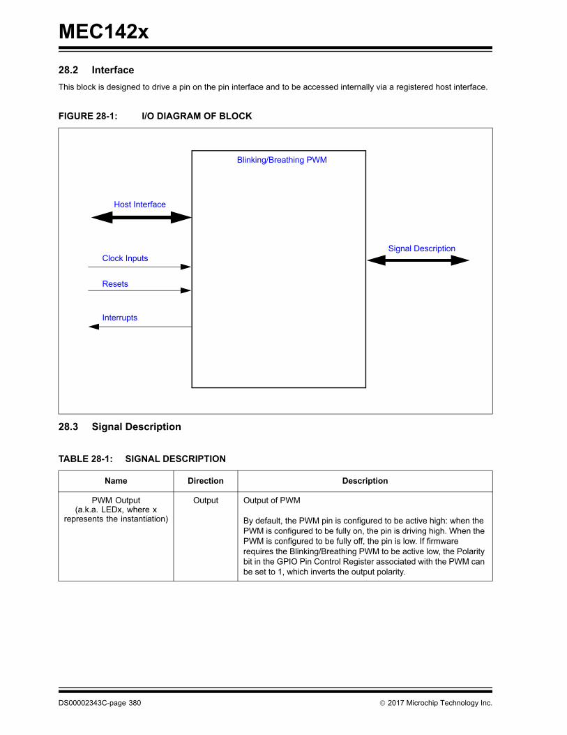
MEC142x
28.2 Interface
This block is designed to drive a pin on the pin interface and to be accessed internally via a registered host interface.
28.3 Signal Description
FIGURE 28-1: I/O DIAGRAM OF BLOCK
TABLE 28-1: SIGNAL DESCRIPTION
Name Direction Description
PWM Output(a.k.a. LEDx, where x
represents the instantiation)
Output Output of PWM
By default, the PWM pin is configured to be active high: when the PWM is configured to be fully on, the pin is driving high. When the PWM is configured to be fully off, the pin is low. If firmware requires the Blinking/Breathing PWM to be active low, the Polarity bit in the GPIO Pin Control Register associated with the PWM can be set to 1, which inverts the output polarity.
Blinking/Breathing PWM
Signal DescriptionClock Inputs
Interrupts
Resets
Host Interface
DS00002343C-page 380 2017 Microchip Technology Inc.
MEC142x
28.4 Host Interface
The blinking/breathing PWM block is accessed by a controller over the standard register interface.
28.5 Power, Clocks and Reset
This section defines the Power, Clock, and Reset parameters of the block.
28.5.1 POWER DOMAINS
28.5.2 CLOCK INPUTS
28.5.3 RESETS
28.6 Interrupts
Each PWM can generate an interrupt. The interrupt is asserted for one 48 MHz clock period whenever the PWM WDTtimes out. The PWM WDT is described in Section 28.8.3.1, "PWM WDT," on page 386.
Name Description
VTR Main power. The source of main power for the device is system dependent.
Name Description
5Hz_Clk 32.768 KHz clock
48 MHz Ring Oscillator 48 MHz clock
Name Description
nSYSRST Block reset
Source Description
PWM_WDT PWM watchdog time out
2017 Microchip Technology Inc. DS00002343C-page 381
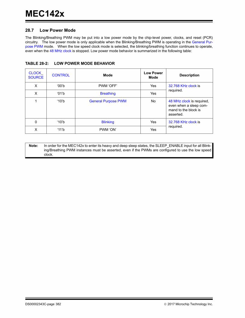
MEC142x
28.7 Low Power Mode
The Blinking/Breathing PWM may be put into a low power mode by the chip-level power, clocks, and reset (PCR)circuitry. The low power mode is only applicable when the Blinking/Breathing PWM is operating in the General Pur-pose PWM mode. When the low speed clock mode is selected, the blinking/breathing function continues to operate,even when the 48 MHz clock is stopped. Low power mode behavior is summarized in the following table:
TABLE 28-2: LOW POWER MODE BEHAVIOR
CLOCK_SOURCE
CONTROL ModeLow Power
ModeDescription
X ‘00’b PWM ‘OFF’ Yes 32.768 KHz clock is required.
X ‘01’b Breathing Yes
1 ‘10’b General Purpose PWM No 48 MHz clock is required, even when a sleep com-mand to the block is asserted.
0 ‘10’b Blinking Yes 32.768 KHz clock is required.
X ‘11’b PWM ‘ON’ Yes
Note: In order for the MEC142x to enter its heavy and deep sleep states, the SLEEP_ENABLE input for all Blink-ing/Breathing PWM instances must be asserted, even if the PWMs are configured to use the low speedclock.
DS00002343C-page 382 2017 Microchip Technology Inc.

MEC142x
28.8 Description
28.8.1 BREATHING
If an LED blinks rapidly enough, the eye will interpret the light as reduced brightness, rather than a blinking pattern.Therefore, if the blinking period is short enough, modifying the duty cycle will set the apparent brightness, rather than ablinking rate. At a blinking rate of 128Hz or greater, almost all people will perceive a continuous light source rather thanan intermittent pattern.
Because making an LED appear to breathe is an aesthetic effect, the breathing mechanism must be adjustable or cus-tomers may find the breathing effect unattractive. There are several variables that can affect breathing appearance, asdescribed below.
The following figure illustrates some of the variables in breathing:
The breathing range of and LED can range between full on and full off, or in a range that falls within the full-on/full-offrange, as shown in this figure. The ramp time can be different in different applications. For example, if the ramp timewas 1 second, the LED would appear to breathe quickly. A time of 2 seconds would make the LED appear to breathemore leisurely.
FIGURE 28-2: BREATHING LED EXAMPLE
Full off
Full on
RISING RAMP TIME FALLING RAMP TIME
Min Duty Cycle
Max Duty Cycle
2017 Microchip Technology Inc. DS00002343C-page 383
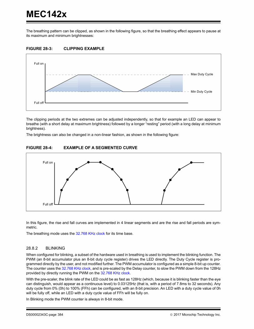
MEC142x
The breathing pattern can be clipped, as shown in the following figure, so that the breathing effect appears to pause atits maximum and minimum brightnesses:
The clipping periods at the two extremes can be adjusted independently, so that for example an LED can appear tobreathe (with a short delay at maximum brightness) followed by a longer “resting” period (with a long delay at minimumbrightness).
The brightness can also be changed in a non-linear fashion, as shown in the following figure:
In this figure, the rise and fall curves are implemented in 4 linear segments and are the rise and fall periods are sym-metric.
The breathing mode uses the 32.768 KHz clock for its time base.
28.8.2 BLINKING
When configured for blinking, a subset of the hardware used in breathing is used to implement the blinking function. ThePWM (an 8-bit accumulator plus an 8-bit duty cycle register) drives the LED directly. The Duty Cycle register is pro-grammed directly by the user, and not modified further. The PWM accumulator is configured as a simple 8-bit up counter.The counter uses the 32.768 KHz clock, and is pre-scaled by the Delay counter, to slow the PWM down from the 128Hzprovided by directly running the PWM on the 32.768 KHz clock.
With the pre-scaler, the blink rate of the LED could be as fast as 128Hz (which, because it is blinking faster than the eyecan distinguish, would appear as a continuous level) to 0.03125Hz (that is, with a period of 7.8ms to 32 seconds). Anyduty cycle from 0% (0h) to 100% (FFh) can be configured, with an 8-bit precision. An LED with a duty cycle value of 0hwill be fully off, while an LED with a duty cycle value of FFh will be fully on.
In Blinking mode the PWM counter is always in 8-bit mode.
FIGURE 28-3: CLIPPING EXAMPLE
FIGURE 28-4: EXAMPLE OF A SEGMENTED CURVE
Full off
Full on
Min Duty Cycle
Max Duty Cycle
Full off
Full on
DS00002343C-page 384 2017 Microchip Technology Inc.
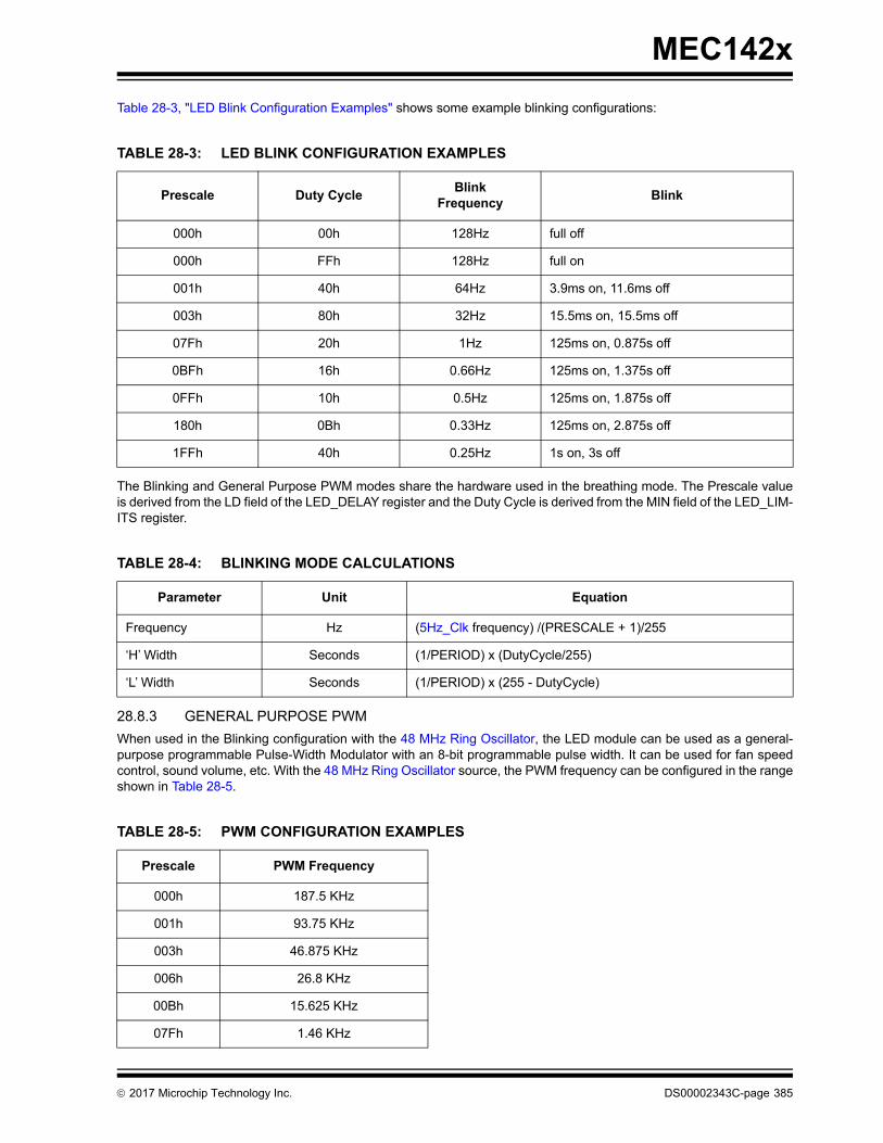
MEC142x
Table 28-3, "LED Blink Configuration Examples" shows some example blinking configurations:
The Blinking and General Purpose PWM modes share the hardware used in the breathing mode. The Prescale valueis derived from the LD field of the LED_DELAY register and the Duty Cycle is derived from the MIN field of the LED_LIM-ITS register.
28.8.3 GENERAL PURPOSE PWM
When used in the Blinking configuration with the 48 MHz Ring Oscillator, the LED module can be used as a general-purpose programmable Pulse-Width Modulator with an 8-bit programmable pulse width. It can be used for fan speedcontrol, sound volume, etc. With the 48 MHz Ring Oscillator source, the PWM frequency can be configured in the rangeshown in Table 28-5.
TABLE 28-3: LED BLINK CONFIGURATION EXAMPLES
Prescale Duty CycleBlink
FrequencyBlink
000h 00h 128Hz full off
000h FFh 128Hz full on
001h 40h 64Hz 3.9ms on, 11.6ms off
003h 80h 32Hz 15.5ms on, 15.5ms off
07Fh 20h 1Hz 125ms on, 0.875s off
0BFh 16h 0.66Hz 125ms on, 1.375s off
0FFh 10h 0.5Hz 125ms on, 1.875s off
180h 0Bh 0.33Hz 125ms on, 2.875s off
1FFh 40h 0.25Hz 1s on, 3s off
TABLE 28-4: BLINKING MODE CALCULATIONS
Parameter Unit Equation
Frequency Hz (5Hz_Clk frequency) /(PRESCALE + 1)/255
‘H’ Width Seconds (1/PERIOD) x (DutyCycle/255)
‘L’ Width Seconds (1/PERIOD) x (255 - DutyCycle)
TABLE 28-5: PWM CONFIGURATION EXAMPLES
Prescale PWM Frequency
000h 187.5 KHz
001h 93.75 KHz
003h 46.875 KHz
006h 26.8 KHz
00Bh 15.625 KHz
07Fh 1.46 KHz
2017 Microchip Technology Inc. DS00002343C-page 385

MEC142x
28.8.3.1 PWM WDT
When the PWM is configured as a general-purpose PWM (in the Blinking configuration with the 48 MHz clock), the PWMincludes a Watch Dog Timer (WDT). The WDT consists of an internal 8-bit counter and an 8-bit reload value (the fieldWDTLD in LED Configuration Register register). The internal counter is loaded with the reset value of WDTLD (14h, or4 seconds) on system nSYSRST and loaded with the contents of WDTLD whenever either the LED Configuration Reg-ister register is written or the MIN byte in the LED Limits Register register is written (the MIN byte controls the duty cycleof the PWM).
Whenever the internal counter is non-zero, it is decremented by 1 for every tick of the 5 Hz clock. If the counter decre-ments from 1 to 0, a WDT Terminal Count causes an interrupt to be generated and reset sets the CONTROL bit in theLED Configuration Register to 3h, which forces the PWM to be full on. No other PWM registers or fields are affected.
If the 5 Hz clock halts, the watchdog timer stops decrementing but retains its value, provided the device continues to bepowered. When the 5 Hz clock restarts, the watchdog counter will continue decrementing where it left off.
Setting the WDTLD bits to 0 disables the PWM WDT. Other sample values for WDTLD are:
01h = 200 ms
02h = 400 ms
03h = 600 ms
04h = 800 ms
…14h = 4seconds
FFh = 51 seconds
28.9 Implementation
In addition to the registers described in Section 28.10, "EC-Only Registers", the PWM is implemented using a numberof components that are interconnected differently when configured for breathing operation and when configured forblinking/PWM operation.
28.9.1 BREATHING CONFIGURATION
The PSIZE parameter can configure the PWM to one of three modes: 8-bit, 7-bit and 6-bit. The PERIOD CTR countsticks of its input clock. In 8-bit mode, it counts from 0 to 255 (that is, 256 steps), then repeats continuously. In this mode,a full cycle takes 7.8ms (128Hz). In 7-bit mode it counts from 0 to 127 (128 steps), and a full cycle takes 3.9ms (256Hz).In 6-bit mode it counts from 0 to 63 (64 steps) and a full cycle takes 1.95ms (512Hz).
The output of the LED circuit is asserted whenever the PERIOD CTR is less than the contents of the DUTY CYCLEregister. The appearance of breathing is created by modifying the contents of the DUTY CYCLE register in a continuousmanner. When the LED control is off the internal counters and registers are all reset to 0 (i.e. after a write setting theRESET bit in the LED Configuration Register Register.) Once enabled, the DUTY CYCLE register is increased by an
1FFh 366 Hz
FFFh 46 Hz
TABLE 28-6: GENERAL PURPOSE PWM MODE CALCULATIONS
Parameter Unit Equation
Frequency Hz (48 MHz Ring Oscillator frequency) / (PRESCALE + 1) / 255
‘H’ Width Seconds (1/PERIOD) x (DutyCycle/255)
‘L’ Width Seconds (1/PERIOD) x (255 - DutyCycle)
TABLE 28-5: PWM CONFIGURATION EXAMPLES (CONTINUED)
Prescale PWM Frequency
DS00002343C-page 386 2017 Microchip Technology Inc.

MEC142x
amount determined by the LED_STEP register and at a rate determined by the DELAY counter. Once the duty cyclereaches its maximum value (determined by the field MAX), the duty cycle is held constant for a period determined bythe field HD. Once the hold time is complete, the DUTY CYCLE register is decreased, again by an amount determinedby the LED_STEP register and at a rate determined by the DELAY counter. When the duty cycle then falls at or belowthe minimum value (determined by the field MIN), the duty cycle is held constant for a period determined by the fieldHD. Once the hold time is complete, the cycle repeats, with the duty cycle oscillating between MIN and MAX.
The rising and falling ramp times as shown in FIGURE 28-2: Breathing LED Example on page 383 can be either sym-metric or asymmetric depending on the setting of the SYMMETRY bit in the LED Configuration Register Register. InSymmetric mode the rising and falling ramp rates have mirror symmetry; both rising and falling ramp rates use the same(all) 8 segments fields in each of the following registers (see Table 28-7): the LED Update Stepsize Register registerand the LED Update Interval Register register. In Asymmetric mode the rising ramp rate uses 4 of the 8 segments fieldsand the falling ramp rate uses the remaining 4 of the 8 segments fields (see Table 28-7).
The parameters MIN, MAX, HD, LD and the 8 fields in LED_STEP and LED_INT determine the brightness range of theLED and the rate at which its brightness changes. See the descriptions of the fields in Section 28.10, "EC-Only Regis-ters", as well as the examples in Section 28.9.3, "Breathing Examples" for information on how to set these fields.
TABLE 28-7: SYMMETRIC BREATHING MODE REGISTER USAGE
Rising/ Falling Ramp Times
in Figure 28-3, "Clipping Example"
Duty CycleSegment
IndexSymmetric Mode Register Fields Utilized
X 000xxxxxb 000b STEP[0]/INT[0] Bits[3:0]
X 001xxxxxb 001b STEP[1]/INT[1] Bits[7:4]
X 010xxxxxb 010b STEP[2]/INT[2] Bits[11:8]
X 011xxxxxb 011b STEP[3]/INT[3] Bits[15:12]
X 100xxxxxb 100b STEP[4]/INT[4] Bits[19:16]
X 101xxxxxb 101b STEP[5]/INT[5] Bits[23:20]
X 110xxxxxb 110b STEP[6]/INT[6] Bits[27:24]
X 111xxxxxb 111b STEP[7]/INT[7] Bits[31:28]
Note: In Symmetric Mode the Segment_Index[2:0] = Duty Cycle Bits[7:5]
TABLE 28-8: ASYMMETRIC BREATHING MODE REGISTER USAGE
Rising/ Falling Ramp Times
in Figure 28-3, "Clipping Example"
Duty CycleSegment
IndexAsymmetric Mode Register Fields Utilized
Rising 00xxxxxxb 000b STEP[0]/INT[0] Bits[3:0]
Rising 01xxxxxxb 001b STEP[1]/INT[1] Bits[7:4]
Rising 10xxxxxxb 010b STEP[2]/INT[2] Bits[11:8]
Rising 11xxxxxxb 011b STEP[3]/INT[3] Bits[15:12]
falling 00xxxxxxb 100b STEP[4]/INT[4] Bits[19:16]
falling 01xxxxxxb 101b STEP[5]/INT[5] Bits[23:20]
2017 Microchip Technology Inc. DS00002343C-page 387
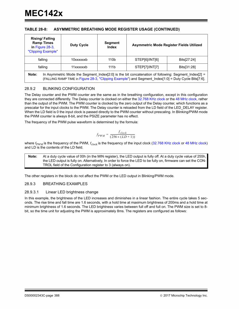
MEC142x
28.9.2 BLINKING CONFIGURATION
The Delay counter and the PWM counter are the same as in the breathing configuration, except in this configurationthey are connected differently. The Delay counter is clocked on either the 32.768 KHz clock or the 48 MHz clock, ratherthan the output of the PWM. The PWM counter is clocked by the zero output of the Delay counter, which functions as aprescalar for the input clocks to the PWM. The Delay counter is reloaded from the LD field of the LED_DELAY register.When the LD field is 0 the input clock is passed directly to the PWM counter without prescaling. In Blinking/PWM modethe PWM counter is always 8-bit, and the PSIZE parameter has no effect.
The frequency of the PWM pulse waveform is determined by the formula:
where fPWM is the frequency of the PWM, fclock is the frequency of the input clock (32.768 KHz clock or 48 MHz clock)and LD is the contents of the LD field.
The other registers in the block do not affect the PWM or the LED output in Blinking/PWM mode.
28.9.3 BREATHING EXAMPLES
28.9.3.1 Linear LED brightness change
In this example, the brightness of the LED increases and diminishes in a linear fashion. The entire cycle takes 5 sec-onds. The rise time and fall time are 1.6 seconds, with a hold time at maximum brightness of 200ms and a hold time atminimum brightness of 1.6 seconds. The LED brightness varies between full off and full on. The PWM size is set to 8-bit, so the time unit for adjusting the PWM is approximately 8ms. The registers are configured as follows:
falling 10xxxxxxb 110b STEP[6]/INT[6] Bits[27:24]
falling 11xxxxxxb 111b STEP[7]/INT[7] Bits[31:28]
Note: In Asymmetric Mode the Segment_Index[2:0] is the bit concatenation of following: Segment_Index[2] =(FALLING RAMP TIME in Figure 28-3, "Clipping Example") and Segment_Index[1:0] = Duty Cycle Bits[7:6].
Note: At a duty cycle value of 00h (in the MIN register), the LED output is fully off. At a duty cycle value of 255h,the LED output is fully on. Alternatively, In order to force the LED to be fully on, firmware can set the CON-TROL field of the Configuration register to 3 (always on).
TABLE 28-8: ASYMMETRIC BREATHING MODE REGISTER USAGE (CONTINUED)
Rising/ Falling Ramp Times
in Figure 28-3, "Clipping Example"
Duty CycleSegment
IndexAsymmetric Mode Register Fields Utilized
fPWMfclock
256 LD 1+ ------------------------------------------=
DS00002343C-page 388 2017 Microchip Technology Inc.
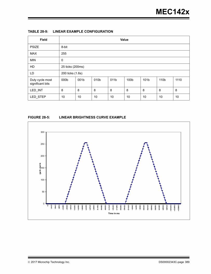
MEC142x
TABLE 28-9: LINEAR EXAMPLE CONFIGURATION
Field Value
PSIZE 8-bit
MAX 255
MIN 0
HD 25 ticks (200ms)
LD 200 ticks (1.6s)
Duty cycle mostsignificant bits
000b 001b 010b 011b 100b 101b 110b 1110
LED_INT 8 8 8 8 8 8 8 8
LED_STEP 10 10 10 10 10 10 10 10
FIGURE 28-5: LINEAR BRIGHTNESS CURVE EXAMPLE
0
50
100
150
200
250
300
0320
640
960
1280
1600
1920
2240
2560
2880
3200
3520
3840
4160
4480
4800
5120
5440
5760
6080
6400
6720
7040
7360
7680
8000
8320
8640
8960
9280
9600
9920
10240
10560
10880
Duty Cycle
Time in ms
2017 Microchip Technology Inc. DS00002343C-page 389
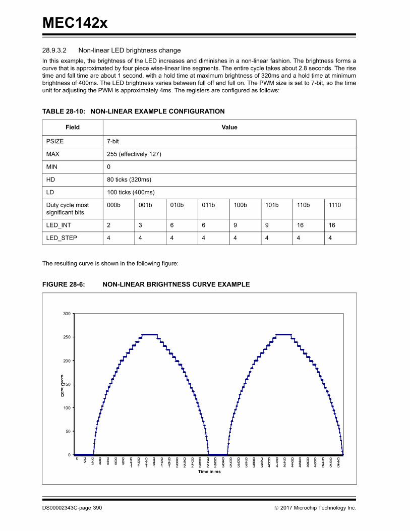
MEC142x
28.9.3.2 Non-linear LED brightness change
In this example, the brightness of the LED increases and diminishes in a non-linear fashion. The brightness forms acurve that is approximated by four piece wise-linear line segments. The entire cycle takes about 2.8 seconds. The risetime and fall time are about 1 second, with a hold time at maximum brightness of 320ms and a hold time at minimumbrightness of 400ms. The LED brightness varies between full off and full on. The PWM size is set to 7-bit, so the timeunit for adjusting the PWM is approximately 4ms. The registers are configured as follows:
The resulting curve is shown in the following figure:
TABLE 28-10: NON-LINEAR EXAMPLE CONFIGURATION
Field Value
PSIZE 7-bit
MAX 255 (effectively 127)
MIN 0
HD 80 ticks (320ms)
LD 100 ticks (400ms)
Duty cycle mostsignificant bits
000b 001b 010b 011b 100b 101b 110b 1110
LED_INT 2 3 6 6 9 9 16 16
LED_STEP 4 4 4 4 4 4 4 4
FIGURE 28-6: NON-LINEAR BRIGHTNESS CURVE EXAMPLE
0
50
100
150
200
250
300
0160
320
480
640
800
960
1120
1280
1440
1600
1760
1920
2080
2240
2400
2560
2720
2880
3040
3200
3360
3520
3680
3840
4000
4160
4320
4480
4640
4800
4960
5120
5280
5440
Duty Cycle
Time in ms
DS00002343C-page 390 2017 Microchip Technology Inc.

MEC142x
28.10 EC-Only Registers
The registers listed in the EC-Only Register Summary table are for a single instance of the Blinking/Breathing PWM.The addresses of each register listed in this table are defined as a relative offset to the host “Base Address” defined inthe EC-Only Register Base Address Table.
The Base Address indicates where the first register can be accessed in a particular address space for a block instance.
In the following register definitions, a “PWM period” is defined by time the PWM counter goes from 000h to its maximumvalue (FFh in 8-bit mode, FEh in 7-bit mode and FCh in 6-bit mode, as defined by the PSCALE field in registerLED_CFG). The end of a PWM period occurs when the PWM counter wraps from its maximum value to 0.
The registers in this block can be written 32-bits, 16-bits or 8-bits at a time. Writes to LED Configuration Register takeeffect immediately. Writes to LED Limits Register are held in a holding register and only take effect only at the end of aPWM period. The update takes place at the end of every period, even if only one byte of the register was updated. Thismeans that in blink/PWM mode, software can change the duty cycle with a single 8-bit write to the MIN field in theLED_LIMIT register. Writes to LED Delay Register, LED Update Stepsize Register and LED Update Interval Registeralso go initially into a holding register. The holding registers are copied to the operating registers at the end of a PWMperiod only if the Enable Update bit in the LED Configuration Register is set to 1. If LED_CFG is 0, data in the holdingregisters is retained but not copied to the operating registers when the PWM period expires. To change an LED breath-ing configuration, software should write these three registers with the desired values and then set LED_CFG to 1. Thismechanism ensures that all parameters affecting LED breathing will be updated consistently, even if the registers areonly written 8 bits at a time.
TABLE 28-11: EC-ONLY REGISTER BASE ADDRESS TABLE
Block InstanceInstance Number
Host Address Space Base Address
Blinking/Breath-ing PWM
0 EC 32-bit internal address space
0000_B800h
Blinking/Breath-ing PWM
1 EC 32-bit internal address space
0000_B900h
Blinking/Breath-ing PWM
2 EC 32-bit internal address space
0000_BA00h
TABLE 28-12: EC-ONLY REGISTER SUMMARY
Offset Register Name (Mnemonic)
00h LED Configuration Register
04h LED Limits Register
08h LED Delay Register
0Ch LED Update Stepsize Register
10h LED Update Interval Register
2017 Microchip Technology Inc. DS00002343C-page 391
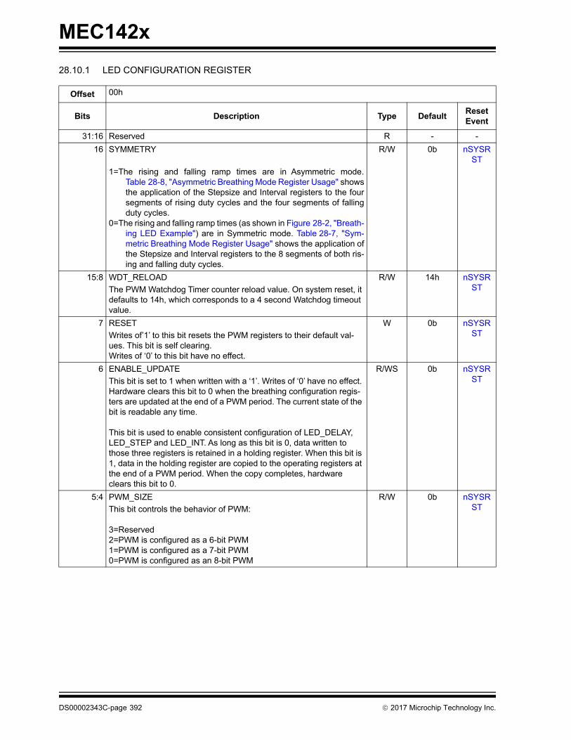
MEC142x
28.10.1 LED CONFIGURATION REGISTER
Offset 00h
Bits Description Type DefaultReset Event
31:16 Reserved R - -
16 SYMMETRY
1=The rising and falling ramp times are in Asymmetric mode.Table 28-8, "Asymmetric Breathing Mode Register Usage" showsthe application of the Stepsize and Interval registers to the foursegments of rising duty cycles and the four segments of fallingduty cycles.
0=The rising and falling ramp times (as shown in Figure 28-2, "Breath-ing LED Example") are in Symmetric mode. Table 28-7, "Sym-metric Breathing Mode Register Usage" shows the application ofthe Stepsize and Interval registers to the 8 segments of both ris-ing and falling duty cycles.
R/W 0b nSYSRST
15:8 WDT_RELOAD
The PWM Watchdog Timer counter reload value. On system reset, it defaults to 14h, which corresponds to a 4 second Watchdog timeout value.
R/W 14h nSYSRST
7 RESET
Writes of’1’ to this bit resets the PWM registers to their default val-ues. This bit is self clearing. Writes of ‘0’ to this bit have no effect.
W 0b nSYSRST
6 ENABLE_UPDATE
This bit is set to 1 when written with a ‘1’. Writes of ‘0’ have no effect. Hardware clears this bit to 0 when the breathing configuration regis-ters are updated at the end of a PWM period. The current state of the bit is readable any time.
This bit is used to enable consistent configuration of LED_DELAY, LED_STEP and LED_INT. As long as this bit is 0, data written to those three registers is retained in a holding register. When this bit is 1, data in the holding register are copied to the operating registers at the end of a PWM period. When the copy completes, hardware clears this bit to 0.
R/WS 0b nSYSRST
5:4 PWM_SIZE
This bit controls the behavior of PWM:
3=Reserved2=PWM is configured as a 6-bit PWM1=PWM is configured as a 7-bit PWM0=PWM is configured as an 8-bit PWM
R/W 0b nSYSRST
DS00002343C-page 392 2017 Microchip Technology Inc.
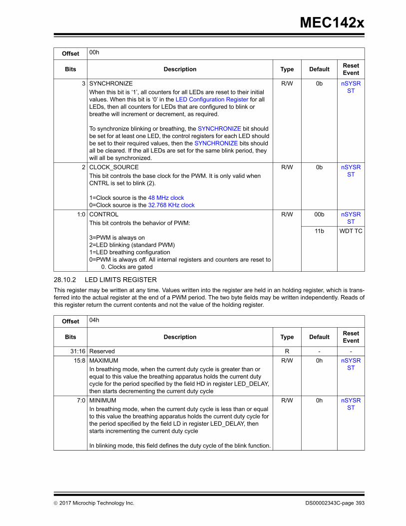
MEC142x
28.10.2 LED LIMITS REGISTER
This register may be written at any time. Values written into the register are held in an holding register, which is trans-ferred into the actual register at the end of a PWM period. The two byte fields may be written independently. Reads ofthis register return the current contents and not the value of the holding register.
3 SYNCHRONIZE
When this bit is ‘1’, all counters for all LEDs are reset to their initial values. When this bit is ‘0’ in the LED Configuration Register for all LEDs, then all counters for LEDs that are configured to blink or breathe will increment or decrement, as required.
To synchronize blinking or breathing, the SYNCHRONIZE bit should be set for at least one LED, the control registers for each LED should be set to their required values, then the SYNCHRONIZE bits should all be cleared. If the all LEDs are set for the same blink period, they will all be synchronized.
R/W 0b nSYSRST
2 CLOCK_SOURCE
This bit controls the base clock for the PWM. It is only valid when CNTRL is set to blink (2).
1=Clock source is the 48 MHz clock0=Clock source is the 32.768 KHz clock
R/W 0b nSYSRST
1:0 CONTROL
This bit controls the behavior of PWM:
3=PWM is always on2=LED blinking (standard PWM)1=LED breathing configuration0=PWM is always off. All internal registers and counters are reset to
0. Clocks are gated
R/W 00b nSYSRST
11b WDT TC
Offset 04h
Bits Description Type DefaultReset Event
31:16 Reserved R - -
15:8 MAXIMUM
In breathing mode, when the current duty cycle is greater than or equal to this value the breathing apparatus holds the current duty cycle for the period specified by the field HD in register LED_DELAY, then starts decrementing the current duty cycle
R/W 0h nSYSRST
7:0 MINIMUM
In breathing mode, when the current duty cycle is less than or equal to this value the breathing apparatus holds the current duty cycle for the period specified by the field LD in register LED_DELAY, then starts incrementing the current duty cycle
In blinking mode, this field defines the duty cycle of the blink function.
R/W 0h nSYSRST
Offset 00h
Bits Description Type DefaultReset Event
2017 Microchip Technology Inc. DS00002343C-page 393

MEC142x
28.10.3 LED DELAY REGISTER
This register may be written at any time. Values written into the register are held in an holding register, which is trans-ferred into the actual register at the end of a PWM period if the Enable Update bit in the LED Configuration register isset to 1. Reads of this register return the current contents and not the value of the holding register.
28.10.4 LED UPDATE STEPSIZE REGISTER
This register has eight segment fields which provide the amount the current duty cycle is adjusted at the end of everyPWM period. Segment field selection is decoded based on the segment index. The segment index equation utilizeddepends on the SYMMETRY bit in the LED Configuration Register Register).
• In Symmetric Mode the Segment_Index[2:0] = Duty Cycle Bits[7:5]
• In Asymmetric Mode the Segment_Index[2:0] is the bit concatenation of following: Segment_Index[2] = (FALLING RAMP TIME in Figure 28-3, "Clipping Example") and Segment_Index[1:0] = Duty Cycle Bits[7:6].
This register may be written at any time. Values written into the register are held in an holding register, which is trans-ferred into the actual register at the end of a PWM period if the Enable Update bit in the LED Configuration register isset to 1. Reads of this register return the current contents and not the value of the holding register.
In 8-bit mode, each 4-bit STEPSIZE field represents 16 possible duty cycle modifications, from 1 to 16 as the duty cycleis modified between 0 and 255:
15: Modify the duty cycle by 16
...
1: Modify the duty cycle by 2
0: Modify the duty cycle by 1
In 7-bit mode, the least significant bit of the 4-bit field is ignored, so each field represents 8 possible duty cycle modifi-cations, from 1 to 8, as the duty cycle is modified between 0 and 127:
14, 15: Modify the duty cycle by 8
...
2, 3: Modify the duty cycle by 2
Offset 08h
Bits Description Type DefaultReset Event
31:24 Reserved R - -
23:12 HIGH_DELAY
In breathing mode, the number of PWM periods to wait before updat-ing the current duty cycle when the current duty cycle is greater than or equal to the value MAX in register LED_LIMIT.
4095=The current duty cycle is decremented after 4096 PWM periods…1=The delay counter is bypassed and the current duty cycle is decre-
mented after two PWM period0=The delay counter is bypassed and the current duty cycle is decre-
mented after one PWM period
R/W 000h nSYSRST
11:0 LOW_DELAY
The number of PWM periods to wait before updating the current duty cycle when the current duty cycle is greater than or equal to the value MIN in register LED_LIMIT.
4095=The current duty cycle is incremented after 4096 PWM periods…0=The delay counter is bypassed and the current duty cycle is incre-
mented after one PWM period
In blinking mode, this field defines the prescalar for the PWM clock
R/W 000h nSYSRST
DS00002343C-page 394 2017 Microchip Technology Inc.
MEC142x
0, 1: Modify the duty cycle by 1
In 6-bit mode, the two least significant bits of the 4-bit field is ignored, so each field represents 4 possible duty cyclemodifications, from 1 to 4 as the duty cycle is modified between 0 and 63:
12, 13, 14, 15: Modify the duty cycle by 4
8, 9, 10, 11: Modify the duty cycle by 3
4, 5, 6, 7: Modify the duty cycle by 2
0, 1, 2, 3: Modify the duty cycle by 1
28.10.5 LED UPDATE INTERVAL REGISTER
This register has eight segment fields which provide the number of PWM periods between updates to current duty cycle.Segment field selection is decoded based on the segment index. The segment index equation utilized depends on theSYMMETRY bit in the LED Configuration Register Register)
• In Symmetric Mode the Segment_Index[2:0] = Duty Cycle Bits[7:5]
• In Asymmetric Mode the Segment_Index[2:0] is the bit concatenation of following: Segment_Index[2] = (FALLING RAMP TIME in Figure 28-3, "Clipping Example") and Segment_Index[1:0] = Duty Cycle Bits[7:6].
This register may be written at any time. Values written into the register are held in an holding register, which is trans-ferred into the actual register at the end of a PWM period if the Enable Update bit in the LED Configuration register isset to 1. Reads of this register return the current contents and not the value of the holding register.
Offset 0Ch
Bits Description Type DefaultReset Event
31:28 UPDATE_STEP7
Amount the current duty cycle is adjusted at the end of every PWM period when the segment index is equal to 111.
R/W 0h nSYSRST
27:24 UPDATE_STEP6
Amount the current duty cycle is adjusted at the end of every PWM period when the segment index is equal to 110.
R/W 0h nSYSRST
23:20 UPDATE_STEP5
Amount the current duty cycle is adjusted at the end of every PWM period when the segment index is equal to 101
R/W 0h nSYSRST
19:16 UPDATE_STEP4
Amount the current duty cycle is adjusted at the end of every PWM period when the segment index is equal to 100.
R/W 0h nSYSRST
15:12 UPDATE_STEP3
Amount the current duty cycle is adjusted at the end of every PWM period when the segment index is equal to 011.
R/W 0h nSYSRST
11:8 UPDATE_STEP2
Amount the current duty cycle is adjusted at the end of every PWM period when the segment index is equal to 010.
R/W 0h nSYSRST
7:4 UPDATE_STEP1
Amount the current duty cycle is adjusted at the end of every PWM period when the segment index is equal to 001.
R/W 0h nSYSRST
3:0 UPDATE_STEP0
Amount the current duty cycle is adjusted at the end of every PWM period when the segment index is equal to 000.
R/W 0h nSYSRST
2017 Microchip Technology Inc. DS00002343C-page 395

MEC142x
Offset 10h
Bits Description Type DefaultReset Event
31:28 UPDATE_INTERVAL7
The number of PWM periods between updates to current duty cycle when the segment index is equal to 111b.
15=Wait 16 PWM periods…0=Wait 1 PWM period
R/W 0h nSYSRST
27:24 UPDATE_INTERVAL6
The number of PWM periods between updates to current duty cycle when the segment index is equal to 110b.
15=Wait 16 PWM periods…0=Wait 1 PWM period
R/W 0h nSYSRST
23:20 UPDATE_INTERVAL5
The number of PWM periods between updates to current duty cycle when the segment index is equal to 101b.
15=Wait 16 PWM periods…0=Wait 1 PWM period
R/W 0h nSYSRST
19:16 UPDATE_INTERVAL4
The number of PWM periods between updates to current duty cycle when the segment index is equal to 100b.
15=Wait 16 PWM periods…0=Wait 1 PWM period
R/W 0h nSYSRST
15:12 UPDATE_INTERVAL3
The number of PWM periods between updates to current duty cycle when the segment index is equal to 011b.
15=Wait 16 PWM periods…0=Wait 1 PWM period
R/W 0h nSYSRST
11:8 UPDATE_INTERVAL2
The number of PWM periods between updates to current duty cycle when the segment index is equal to 010b.
15=Wait 16 PWM periods…0=Wait 1 PWM period
R/W 0h nSYSRST
DS00002343C-page 396 2017 Microchip Technology Inc.
MEC142x
7:4 UPDATE_INTERVAL1
The number of PWM periods between updates to current duty cycle when the segment index is equal to 001b.
15=Wait 16 PWM periods…0=Wait 1 PWM period
R/W 0h nSYSRST
3:0 UPDATE_INTERVAL0
The number of PWM periods between updates to current duty cycle when the segment index is equal to 000b.
15=Wait 16 PWM periods…0=Wait 1 PWM period
R/W 0h nSYSRST
Offset 10h
Bits Description Type DefaultReset Event
2017 Microchip Technology Inc. DS00002343C-page 397
MEC142x
29.0 PS/2 INTERFACE
29.1 Introduction
The PS/2 Interface may be used to communicate with a PS/2 keyboard or a PS/2 mouse. The physical interface pro-vides the clock and data signaling for PS/2 data transfers. The PS/2 Controllers are directly controlled by the EC. Thehardware implementation eliminates the need to bit bang I/O ports to generate PS/2 traffic, however bit banging is avail-able via the associated GPIO pins.
29.2 References
No references have been cited for this feature.
29.3 Terminology
There is no terminology defined for this section.
29.4 Interface
This block is designed to be accessed externally via the pin interface and internally via a registered host interface.
FIGURE 29-1: I/O DIAGRAM OF BLOCK
PS/2 Interface
Interrupts
Power, Clocks and Reset
Host Interface
Signal Description
DS00002343C-page 398 2017 Microchip Technology Inc.
MEC142x
29.5 Signal Description
29.6 Host Interface
The registers defined for the Keyboard Scan Interface are accessible by the various hosts as indicated in Section 29.15,"EC-Only Registers".
29.7 Power, Clocks and Reset
This section defines the Power, Clock, and Reset parameters of the block.
29.7.1 POWER DOMAINS
29.7.2 CLOCK INPUTS
29.7.3 RESETS
TABLE 29-1: SIGNAL DESCRIPTION TABLE
Name Direction Description
PS2_DAT INPUT/OUTPUT
Data from the PS/2 device
PS2_CLK INPUT/OUTPUT
Clock from the PS/2 device
Name Description
VTR The logic and registers implemented in this block are powered by this power well.
Name Description
48 MHz Ring Oscillator This is the clock source for PS/2 Interface logic.
2 MHz Clock The PS/2 state machine is clocked using the 2 MHz clock.
Name Description
nSYSRST This signal resets all the registers and logic in this block to their default state.
2017 Microchip Technology Inc. DS00002343C-page 399
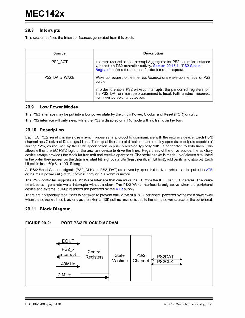
MEC142x
29.8 Interrupts
This section defines the Interrupt Sources generated from this block.
29.9 Low Power Modes
The PS/2 Interface may be put into a low power state by the chip’s Power, Clocks, and Reset (PCR) circuitry.
The PS2 interface will only sleep while the PS2 is disabled or in Rx mode with no traffic on the bus.
29.10 Description
Each EC PS/2 serial channels use a synchronous serial protocol to communicate with the auxiliary device. Each PS/2channel has Clock and Data signal lines. The signal lines are bi-directional and employ open drain outputs capable ofsinking 12m, as required by the PS/2 specification. A pull-up resistor, typically 10K, is connected to both lines. Thisallows either the EC PS/2 logic or the auxiliary device to drive the lines. Regardless of the drive source, the auxiliarydevice always provides the clock for transmit and receive operations. The serial packet is made up of eleven bits, listedin the order they appear on the data line: start bit, eight data bits (least significant bit first), odd parity, and stop bit. Eachbit cell is from 60S to 100S long.
All PS/2 Serial Channel signals (PS2_CLK and PS2_DAT) are driven by open drain drivers which can be pulled to VTRor the main power rail (+3.3V nominal) through 10K-ohm resistors.
The PS/2 controller supports a PS/2 Wake Interface that can wake the EC from the IDLE or SLEEP states. The WakeInterface can generate wake interrupts without a clock. The PS/2 Wake Interface is only active when the peripheraldevice and external pull-up resisters are powered by the VTR supply.
There are no special precautions to be taken to prevent back drive of a PS/2 peripheral powered by the main power wellwhen the power well is off, as long as the external 10K pull-up resistor is tied to the same power source as the peripheral.
29.11 Block Diagram
Source Description
PS2_ACT Interrupt request to the Interrupt Aggregator for PS2 controller instance x, based on PS2 controller activity. Section 29.15.4, "PS2 Status Register" defines the sources for the interrupt request.
PS2_DATx_WAKE Wake-up request to the Interrupt Aggregator’s wake-up interface for PS2 port x.
In order to enable PS2 wakeup interrupts, the pin control registers for the PS2_DAT pin must be programmed to Input, Falling Edge Triggered, non-inverted polarity detection.
FIGURE 29-2: PORT PS/2 BLOCK DIAGRAM
Control Registers PS2DAT
PS2CLK
PS/2 Channel
State Machine
EC I/F
PS2_xinterrupt
48MHz
2 MHz
DS00002343C-page 400 2017 Microchip Technology Inc.
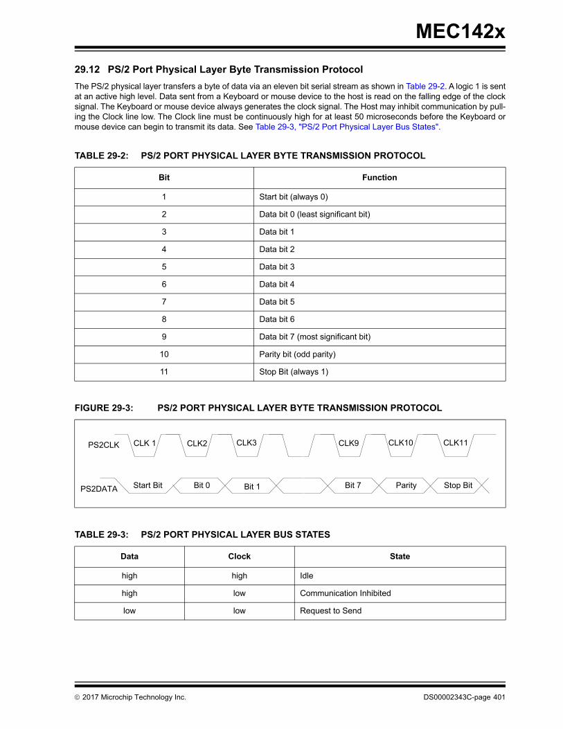
MEC142x
29.12 PS/2 Port Physical Layer Byte Transmission Protocol
The PS/2 physical layer transfers a byte of data via an eleven bit serial stream as shown in Table 29-2. A logic 1 is sentat an active high level. Data sent from a Keyboard or mouse device to the host is read on the falling edge of the clocksignal. The Keyboard or mouse device always generates the clock signal. The Host may inhibit communication by pull-ing the Clock line low. The Clock line must be continuously high for at least 50 microseconds before the Keyboard ormouse device can begin to transmit its data. See Table 29-3, "PS/2 Port Physical Layer Bus States".
TABLE 29-2: PS/2 PORT PHYSICAL LAYER BYTE TRANSMISSION PROTOCOL
Bit Function
1 Start bit (always 0)
2 Data bit 0 (least significant bit)
3 Data bit 1
4 Data bit 2
5 Data bit 3
6 Data bit 4
7 Data bit 5
8 Data bit 6
9 Data bit 7 (most significant bit)
10 Parity bit (odd parity)
11 Stop Bit (always 1)
FIGURE 29-3: PS/2 PORT PHYSICAL LAYER BYTE TRANSMISSION PROTOCOL
TABLE 29-3: PS/2 PORT PHYSICAL LAYER BUS STATES
Data Clock State
high high Idle
high low Communication Inhibited
low low Request to Send
Start Bit Bit 0 ParityBit 7Bit 1 Stop Bit
CLK 1 CLK2 CLK9 CLK10 CLK11CLK3PS2CLK
PS2DATA
2017 Microchip Technology Inc. DS00002343C-page 401
MEC142x
29.13 Controlling PS/2 Transactions
PS/2 transfers are controlled by fields in the PS2 Control Register.
The interface is enabled by the PS2_EN bit. Transfers are enabled when PS2_EN is ‘1’ and disabled when PS2_EN is‘0’. If the PS2_EN bit is cleared to ‘0’ while a transfer is in progress but prior to the leading edge (falling edge) of the10th (parity bit) clock edge, the receive data is discarded (RDATA_RDY remains low). If the PS2_EN bit is cleared fol-lowing the leading edge of the 10th clock signal, then the receive data is saved in the Receive Register (RDATA_RDYgoes high) assuming no parity error.
The direction of a PS/2 transfer is controlled by the PS2_T/R bit.
29.13.1 RECEIVE
If PS2_T/R is ‘0’ while the PS2 Interface is enabled, the interface is configured to receive data. If while PS2_T/R is ‘0’RDATA_RDY is ‘0’, the channel’s PS2_CLK and PS2_DAT will float waiting for the external PS/2 device to signal thestart of a transmission. If RDATA_RDY is ‘1’, the channel’s PS2_DAT line will float but its PS2_CLK line will be held low,holding off the peripheral, until the Receive Register is read.
The peripheral initiates a reception by sending a start bit followed by the data bits). After a successful reception, dataare placed in the PS2 Receive Buffer Register, the RDATA_RDY bit in the PS2 Status Register is set and the PS2_CLKline is forced low. Further receive transfers are inhibited until the EC reads the data in the PS2 Receive Buffer Register.RDATA_RDY is cleared and the PS2_CLK line is tri-stated following a read of the PS2 Receive Buffer Register.
The Receive Buffer Register is initialized to FFh after a read or after a Time-out has occurred.
29.13.2 TRANSMIT
If PS2_T/R is ‘1’ while the PS2 Interface is enabled, the interface is configured to transmit data. When the PS2_T/R bitis written to ‘1’ while the state machine is idle, the channel prepares for a transmission: the interface will drive the PS2_-CLK line low and then float the PS2_DAT line, holding this state until a write occurs to the Transmit Register or until thePS2_T/R bit is cleared. A transmission is started by writing the PS2 Transmit Buffer Register. Writes to the TransmitBuffer Register are blocked when PS2_EN is ‘0’, PS2_T/R is ‘0’ or when the transmit state machine is active (theXMIT_IDLE bit in the PS/2 Status Register is ‘0’). The transmission of data will not start if there is valid data in theReceive Data Register (when the status bit RDATA_RDY is ‘1’). When a transmission is started, the transmission statemachine becomes active (the XMIT_IDLE bit is set to ‘1’ by hardware), the PS2_DAT line is driven low and within 80nsthe PS2_CLK line floats (externally pulled high by the pull-up resistor).
The transmission terminates either on the 11th clock edge of the transmission or if a Transmit Time-Out error conditionoccurs. When the transmission terminates, the PS2_T/R bit is cleared to ‘0’and the state machine becomes idle, settingXMIT_IDLE to ‘1’.
The PS2_T/R bit must be written to a ‘1’ before initiating another transmission to the remote device. If the PS2_T/R bitis set to ‘1’ while the channel is actively receiving data (that is, while the status bit RDATA_RDYis ‘1’) prior to the leadingedge of the 10th (parity bit) clock edge, the receive data is discarded. If the bit is set after the 10th edge, the receivedata is saved in the Receive Register.
DS00002343C-page 402 2017 Microchip Technology Inc.

MEC142x
29.14 Instance Description
29.15 EC-Only Registers
The registers listed in the EC-Only Register Summary table are for a single instance of the PS/2 Interface. Theaddresses of each register listed in this table are defined as a relative offset to the host “Base Address” defined in theEC-Only Register Base Address Table.
The Base Address indicates where the first register can be accessed in a particular address space for a block instance.
29.15.1 PS2 TRANSMIT BUFFER REGISTER
TABLE 29-4: EC-ONLY REGISTER BASE ADDRESS TABLE
Block Instance Instance Number
Host Address Space Base Address
PS/2 Interface 0 EC 32-bit internal address space
0000_9000h
1 EC 32-bit internal address space
0000_9040h
TABLE 29-5: EC-ONLY REGISTER SUMMARY
Offset Register Name
0h PS2 Transmit Buffer Register
0h PS2 Receive Buffer Register
4h PS2 Control Register
8h PS2 Status Register
Offset 00h
Bits Description Type DefaultReset Event
31:8 Reserved R - -
7:0 TRANSMIT_DATA
Writes to this register start a transmission of the data in this register to the peripheral.
W 0h nSYSRST
2017 Microchip Technology Inc. DS00002343C-page 403

MEC142x
29.15.2 PS2 RECEIVE BUFFER REGISTER
29.15.3 PS2 CONTROL REGISTER
Offset 00h
Bits Description Type DefaultReset Event
31:8 Reserved R - -
7:0 RECEIVE_DATA
Data received from a peripheral are recorded in this register.
A transmission initiated by writing the PS2 Transmit Buffer Register will not start until valid data in this register have been read and RDATA_RDY has been cleared by hardware.
The Receive Buffer Register is initialized to FFh after a read or after a Time-out has occurred.
R FFh nSYSRST
Offset 00h
Bits Description Type DefaultReset Event
31:6 Reserved R - -
5:4 STOP
These bits are used to set the level of the stop bit expected by the PS/2 channel state machine. These bits are therefore only valid when PS2_EN is set.
00b=Receiver expects an active high stop bit.01b=Receiver expects an active low stop bit.10b=Receiver ignores the level of the Stop bit (11th bit is not inter-
preted as a stop bit).11b=Reserved.
R/W 0h nSYSRST
3:2 PARITY
These bits are used to set the parity expected by the PS/2 channel state machine. These bits are therefore only valid when PS2_EN is set.
00b=Receiver expects Odd Parity (default).01b=Receiver expects Even Parity.10b=Receiver ignores level of the parity bit (10th bit is not inter-
preted as a parity bit).11b=Reserved
R/W 0h nSYSRST
DS00002343C-page 404 2017 Microchip Technology Inc.

MEC142x
Changing values in the PS2 CONTROL REGISTER at a rate faster than 2 MHz, may result in unpredictable behavior.
1 PS2_EN
PS/2 Enable.
0=The PS/2 state machine is disabled. The CLK pin is driven lowand the DATA pin is tri-stated.
1=The PS/2 state machine is enabled, allowing the channel to per-form automatic reception or transmission, depending on thestate of PS2_T/R.
R/W 0h nSYSRST
0 PS2_T/R
PS/2 Transmit/Receive
0=The P2/2 channel is enabled to receive data. 1=The PS2 channel is enabled to transmit data.
R/W 0h nSYSRST
Offset 00h
Bits Description Type DefaultReset Event
2017 Microchip Technology Inc. DS00002343C-page 405

MEC142x
29.15.4 PS2 STATUS REGISTER
Offset 08h
Bits Description Type DefaultReset Event
31:8 Reserved R - -
7 XMIT_START_TIMEOUT
Transmit Start Timeout.
0=No transmit start timeout detected1=A start bit was not received within 25 ms following the transmit
start event. The transmit start bit time-out condition is also indi-cated by the XMIT_TIMEOUT bit.
R/WC 0h nSYSRST
6 RX_BUSY
Receive Channel Busy.
0=The channel is actively receiving PS/2 data1=The channel is idle
R 0h nSYSRST
5 XMIT_TIME_OUT
Transmitter Idle.
When the XMIT_TIMEOUT bit is set, the PS2_T/R bit is held clear, the PS/2 channel’s CLK line is pulled low for a minimum of 300μs until the PS/2 Status register is read. The XMIT_TIMEOUT bit is set on one of three transmit conditions: when the transmitter bit time (the time between falling edges) exceeds 300μs, when the transmitter start bit is not received within 25ms from signaling a transmit start event or if the time from the first bit (start) to the 10th bit (parity) exceeds 2ms
R/WC 0h nSYSRST
4 XMIT_IDLE
Transmitter Idle.
0=The channel is actively transmitting PS/2 data. Writing the PS2Transmit Buffer Register will cause the XMIT_IDLE bit to clear
1=The channel is not transmitting. This bit transitions from ‘0’ to ‘1’in the following cases:
• The falling edge of the 11th CLK• XMIT_TIMEOUT is set• The PS2_T/R bit is cleared• The PS2_EN bit is cleared.
A low to high transition on this bit generates a PS2 Activity inter-rupt.
R 0h nSYSRST
3 FE
Framing Error
When receiving data, the stop bit is clocked in on the falling edge of the 11th CLK edge. If the channel is configured to expect either a high or low stop bit and the 11th bit is contrary to the expected stop polarity, then the FE and REC_TIMEOUT bits are set following the falling edge of the 11th CLK edge and an interrupt is generated.
R/WC 0h nSYSRST
DS00002343C-page 406 2017 Microchip Technology Inc.

MEC142x
2 PE
Parity Error
When receiving data, the parity bit is clocked in on the falling edge of the 10th CLK edge. If the channel is configured to expect either even or odd parity and the 10th bit is contrary to the expected par-ity, then the PE and REC_TIMEOUT bits are set following the fall-ing edge of the 10th CLK edge and an interrupt is generated.
R/WC 0h nSYSRST
1 REC_TIMEOUT
Receive Timeout
Following assertion of the REC_TIMEOUT bit, the channel’s CLK line is automatically pulled low for a minimum of 300us until the PS/2 status register is read. Under PS2 automatic operation, PS2_EN is set, this bit is set on one of three receive error condi-tions:• When the receiver bit time (the time between falling edges)
exceeds 300μs.• If the time from the first bit (start) to the 10th bit (parity)
exceeds 2ms.• On a receive parity error along with the Parity Error (PE) bit.• On a receive framing error due to an incorrect STOP bit along
with the framing error (FE) bit.
A low to high transition on this bit generates a PS2 Activity inter-rupt.
R/WC 0h nSYSRST
0 RDATA_RDY
Receive Data Ready
Under normal operating conditions, this bit is set following the fall-ing edge of the 11th clock given successful reception of a data byte from the PS/2 peripheral (i.e., no parity, framing, or receive time-out errors) and indicates that the received data byte is available to be read from the Receive Register. This bit may also be set in the event that the PS2_EN bit is cleared following the 10th CLK edge.
Reading the Receive Register clears this bit.
A low to high transition on this bit generates a PS2 Activity inter-rupt.
R 0h nSYSRST
Offset 08h
Bits Description Type DefaultReset Event
2017 Microchip Technology Inc. DS00002343C-page 407

MEC142x
30.0 KEYBOARD MATRIX SCAN INTERFACE
30.1 Overview
The Keyboard Matrix Scan Interface block provides a register interface to the EC to directly scan an external keyboardmatrix of size up to 18x8.
The maximum configuration of the Keyboard Matrix Scan Interface is 18 outputs by 8 inputs. For a smaller matrix size,firmware should configure unused KSO pins as GPIOs or another alternate function, and it should mask out unusedKSIs and associated interrupts.
30.2 References
No references have been cited for this feature.
30.3 Terminology
There is no terminology defined for this section.
30.4 Interface
This block is designed to be accessed externally via the pin interface and internally via a registered host interface.
30.5 Signal Description
FIGURE 30-1: I/O DIAGRAM OF BLOCK
TABLE 30-1: SIGNAL DESCRIPTION TABLE
Name Direction Description
KSI[7:0] Input Column inputs from external keyboard matrix.
KSO[17:0] Output Row outputs to external keyboard matrix.
Signal Description
Keyboard Matrix Scan Inter-
Interrupts
Power, Clocks and Reset
Host Interface
DS00002343C-page 408 2017 Microchip Technology Inc.
MEC142x
30.6 Host Interface
The registers defined for the Keyboard Scan Interface are accessible by the various hosts as indicated in Section 30.11,"EC-Only Registers".
30.7 Power, Clocks and Reset
This section defines the Power, Clock, and Reset parameters of the block.
30.7.1 POWER DOMAINS
30.7.2 CLOCK INPUTS
30.7.3 RESETS
30.8 Interrupts
This section defines the Interrupt Sources generated from this block.
30.9 Low Power Modes
The Keyboard Scan Interface automatically enters a low power mode whenever it is not actively scanning the keyboardmatrix. The block is also placed in a low-power state when it is disabled by the KSEN bit. When the interface is in a low-power mode it will not prevent the chip from entering a sleep state. When the interface is active it will inhibit the chipsleep state until the interface has re-entered its low power mode.
Note: Pull-up resistors are required on both the KSI and KSO pins. Either external 10k ohm resistors or the inter-nal resistors may be used. However, if the internal pull-ups are used then the PreDrive Mode must also beenabled.
Name Description
VTR The logic and registers implemented in this block are powered by this power well.
Name Description
48 MHz Ring Oscillator This is the clock source for Keyboard Scan Interface logic.
Name Description
nSYSRST This signal resets all the registers and logic in this block to their default state.
Source Description
KSC_INT Interrupt request to the Interrupt Aggregator.
KSC_INT_WAKE Wake-up request to the Interrupt Aggregator’s wake-up interface.
2017 Microchip Technology Inc. DS00002343C-page 409

MEC142x
30.10 Description
During scanning the firmware sequentially drives low one of the rows (KSO[17:0]) and then reads the column data line(KSI[7:0]). A key press is detected as a zero in the corresponding position in the matrix. Keys that are pressed aredebounced by firmware. Once confirmed, the corresponding keycode is loaded into host data read buffer in the 8042Host Interface module. Firmware may need to buffer keycodes in memory in case this interface is stalled or the hostrequests a Resend.
30.10.1 INITIALIZATION OF KSO PINS
If the Keyboard Scan Interface is not configured for PREDRIVE Mode, KSO pins should be configured as open-drainoutputs. Internal or external pull-ups should be used so that the GPIO functions that share the pins do not have a floatinginput when the KSO pins are tri-stated.
If the Keyboard Scan Interface is configured for PREDRIVE Mode, KSO pins must be configured as push-pull outputs.Internal or external pull-ups should be used to protect the GPIO inputs associated with the KSO pins from floating inputs.
30.10.2 PREDRIVE MODE
There is an optional Predrive Mode that can be enabled to actively drive the KSO pins high before switching to open-drain operation. The PREDRIVE ENABLE bit in the Keyscan Extended Control Register is used to enable the PRE-DRIVE option. Timing for the Predive mode is shown in Section 43.14, Keyboard Scan Matrix Timing.
30.10.2.1 Predrive Mode Programming
The following precautions should be taken to prevent output pad damage during Predrive Mode Programming.
FIGURE 30-2: Keyboard Matrix Scan Interface Block Diagram
KSO Select
Register
KSI Input and
Status Registers
KSI[7:0]
KSI Interrupt Interface
Output Decoder
KSC_INT
KSC_INT_WAKE
48MHz
SPBI/F
EC Bus
DS00002343C-page 410 2017 Microchip Technology Inc.

MEC142x
30.10.2.2 Asserting PREDRIVE_ENABLE
1. Disable Key Scan Interface (KSEN = '1')
2. Enable Predrive function (PREDRIVE_ENABLE = '1')
3. Program buffer type for all KSO pins to "push-pull”
4. Enable Keyscan Interface (KSEN ='0')
30.10.2.3 De-asserting PREDRIVE_ENABLE
1. Disable Key Scan Interface (KSEN = '1')
2. Program buffer type for all KSO pins to "open-drain”
3. Disable Predrive function (PREDRIVE_ENABLE = '0')
4. Enable Keyscan Interface (KSEN ='0')
30.10.3 INTERRUPT GENERATION
To support interrupt-based processing, an interrupt can optionally be generated on the high-to-low transition on any ofthe KSI inputs. A running clock is not required to generate interrupts.
30.10.3.1 Runtime interrupt
KSC_INT is the block’s runtime active-high level interrupt. It is connected to the interrupt interface of the Interrupt Aggre-gator, which then relays interrupts to the EC.
Associated with each KSI input is a status register bit and an interrupt enable register bit. A status bit is set when theassociated KSI input goes from high to low. If the interrupt enable bit for that input is set, an interrupt is generated. AnInterrupt is de-asserted when the status bit and/or interrupt enable bit is clear. A status bit cleared when written to a ‘1’.
Interrupts from individual KSIs are logically ORed together to drive the KSC_INT output port. Once asserted, an interruptis not asserted again until either all KSI[7:0] inputs have returned high or the has changed.
30.10.3.2 Wake-up interrupt
KSC_INT_WAKE is the block’s wakeup interrupt. It is routed to the Interrupt Aggregator.
During sleep mode, i.e., when the bus clock is stopped, a high-to-low transition on any KSI whose interrupt enable bitis set causes the KSC_INT_WAKE to be asserted. Also set is the associated status bit in the EC Clock Required 2 StatusRegister (EC_CLK_REQ2_STS). KSC_WAKEUP_INT remains active until the bus clock is started.
The aforementioned transition on KSI also sets the corresponding status bit in the KSI STATUS Register. If enabled, aruntime interrupt is also asserted on KSC_INT when the bus clock resumes running.
30.10.4 WAKE PROGRAMMING
Using the Keyboard Scan Interface to ‘wake’ the MEC142x can be accomplished using either the Keyboard Scan Inter-face wake interrupt, or using the wake capabilities of the GPIO Interface pins that are multiplexed with the KeyboardScan Interface pins. Enabling the Keyboard Scan Interface wake interrupt requires only a single interrupt enable accessand is recommended over using the GPIO Interface for this purpose.
30.11 EC-Only Registers
The registers listed in the EC-Only Register Summary table are for a single instance of the Keyboard Scan Interface.The addresses of each register listed in this table are defined as a relative offset to the host “Base Address” defined inthe EC-Only Register Base Address Table.
The Base Address indicates where the first register can be accessed in a particular address space for a block instance.
TABLE 30-2: EC-ONLY REGISTER BASE ADDRESS TABLE
Block InstanceInstance Number
Host Address Space Base Address
Keyboard ScanInterface
0 EC 32-bit internal address space
0000_9C00h
2017 Microchip Technology Inc. DS00002343C-page 411

MEC142x
30.11.1 KSO SELECT REGISTER
TABLE 30-3: EC-ONLY REGISTER SUMMARY
Offset Register Name
4h KSO Select Register
8h KSI INPUT Register
Ch KSI STATUS Register
10h KSI INTERRUPT ENABLE Register
14h Keyscan Extended Control Register
Offset 04h
Bits Description Type DefaultReset Event
31:4 Reserved R - -
7 KSO_INVERT
This bit controls the output level of KSO pins when selected.
If all KSO pins are active by programming KSO_SELECT to a value greater than 11h the KSO_INVERT controls the state of the pins as follows:1= All KSOs driven low when selected0= All KSOs driven high when selected.
Otherwise, if a single KSO line is selected via the KSO_SELECT bit field or all KSO lines are selected via the KSO_ALL bit then the KSO_INVERT controls the state of the pins as follows:0= KSO[x] driven low when selected1= KSO[x] driven high when selected.
Note: The active state of the KSO pins is determined by theKSO_INVERT bit as is shown in Table 30-5, "KeyboardScan Out Control Summary"
R/W 0b nSYSRST
6 KSEN
This field enables and disables keyboard scan
0= Keyboard scan enabled1= Keyboard scan disabled. All KSO output buffers disabled.
R/W 1h nSYSRST
DS00002343C-page 412 2017 Microchip Technology Inc.
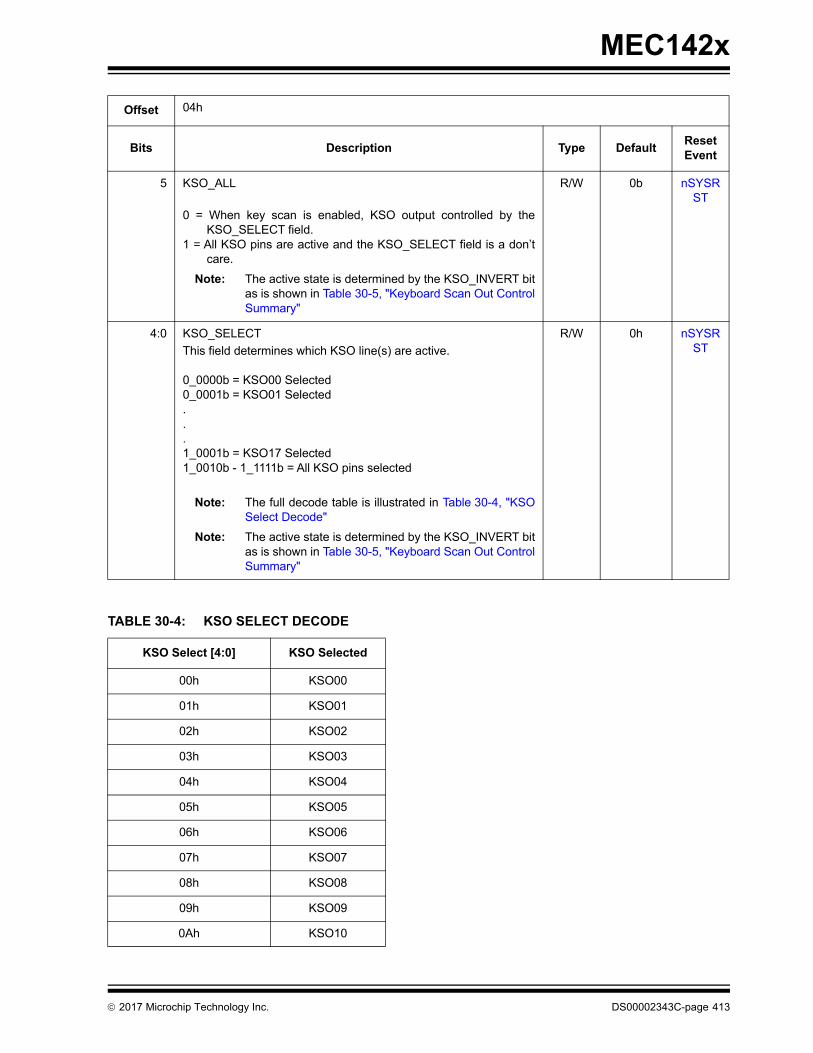
MEC142x
5 KSO_ALL
0 = When key scan is enabled, KSO output controlled by theKSO_SELECT field.
1 = All KSO pins are active and the KSO_SELECT field is a don’tcare.
Note: The active state is determined by the KSO_INVERT bitas is shown in Table 30-5, "Keyboard Scan Out ControlSummary"
R/W 0b nSYSRST
4:0 KSO_SELECT
This field determines which KSO line(s) are active.
0_0000b = KSO00 Selected0_0001b = KSO01 Selected...1_0001b = KSO17 Selected1_0010b - 1_1111b = All KSO pins selected
Note: The full decode table is illustrated in Table 30-4, "KSOSelect Decode"
Note: The active state is determined by the KSO_INVERT bitas is shown in Table 30-5, "Keyboard Scan Out ControlSummary"
R/W 0h nSYSRST
TABLE 30-4: KSO SELECT DECODE
KSO Select [4:0] KSO Selected
00h KSO00
01h KSO01
02h KSO02
03h KSO03
04h KSO04
05h KSO05
06h KSO06
07h KSO07
08h KSO08
09h KSO09
0Ah KSO10
Offset 04h
Bits Description Type DefaultReset Event
2017 Microchip Technology Inc. DS00002343C-page 413
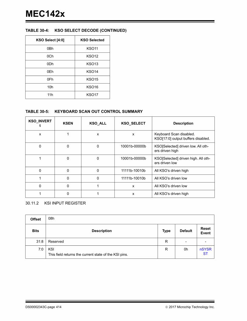
MEC142x
30.11.2 KSI INPUT REGISTER
0Bh KSO11
0Ch KSO12
0Dh KSO13
0Eh KSO14
0Fh KSO15
10h KSO16
11h KSO17
TABLE 30-5: KEYBOARD SCAN OUT CONTROL SUMMARY
KSO_INVERTt
KSEN KSO_ALL KSO_SELECT Description
x 1 x x Keyboard Scan disabled. KSO[17:0] output buffers disabled.
0 0 0 10001b-00000b KSO[Selected] driven low. All oth-ers driven high
1 0 0 10001b-00000b KSO[Selected] driven high. All oth-ers driven low
0 0 0 11111b-10010b All KSO’s driven high
1 0 0 11111b-10010b All KSO’s driven low
0 0 1 x All KSO’s driven low
1 0 1 x All KSO’s driven high
Offset 08h
Bits Description Type DefaultReset Event
31:8 Reserved R - -
7:0 KSI
This field returns the current state of the KSI pins.
R 0h nSYSRST
TABLE 30-4: KSO SELECT DECODE (CONTINUED)
KSO Select [4:0] KSO Selected
DS00002343C-page 414 2017 Microchip Technology Inc.

MEC142x
30.11.3 KSI STATUS REGISTER
30.11.4 KSI INTERRUPT ENABLE REGISTER
30.11.5 KEYSCAN EXTENDED CONTROL REGISTER
Offset 0Ch
Bits Description Type DefaultReset Event
31:8 Reserved R - -
7:0 KSI_STATUS
Each bit in this field is set on the falling edge of the corresponding KSI input pin.
A KSI interrupt is generated when its corresponding status bit and interrupt enable bit are both set. KSI interrupts are logically ORed together to produce KSC_INT and KSC_INT_WAKE.
Writing a ‘1’ to a bit will clear it. Writing a ‘0’ to a bit has no effect.
R/WC 0h nSYSRST
Offset 10h
Bits Description Type DefaultReset Event
31:8 Reserved R - -
7:0 KSI_INT_EN
Each bit in KSI_INT_EN enables interrupt generation due to high-to-low transition on a KSI input. An interrupt is generated when the corresponding bits in KSI_STATUS and KSI_INT_EN are both set.
R/W 0h nSYSRST
Offset 14h
Bits Description Type Default Reset Event
32:1 Reserved R - -
0 PREDRIVE_ENABLE
PREDRIVE_ENABLE enables the PREDRIVE mode to actively drive the KSO pins high for approximately 100 ns before switching to open-drain operation.
0=Disable predrive on KSO pins1=Enable predrive on KSO pins.
RW 0 nSYSRST
2017 Microchip Technology Inc. DS00002343C-page 415

MEC142x
31.0 TRACE FIFO DEBUG PORT (TFDP)
31.1 Introduction
The TFDP serially transmits Embedded Controller (EC)-originated diagnostic vectors to an external debug trace system.
31.2 References
No references have been cited for this chapter.
31.3 Terminology
There is no terminology defined for this chapter.
31.4 Interface
This block is designed to be accessed externally via the pin interface and internally via a registered host interface.
31.5 Signal Description
The Signal Description Table lists the signals that are typically routed to the pin interface.
FIGURE 31-1: I/O DIAGRAM OF BLOCK
TABLE 31-1: SIGNAL DESCRIPTION TABLE
Name Direction Description
TFDP Clk Output Derived from EC Bus Clock.
TFDP Data Output Serialized data shifted out by TFDP Clk.
Signal Description
Trace FIFO Debug Port (TFDP)
Interrupts
Power, Clocks and Reset
Host Interface
DS00002343C-page 416 2017 Microchip Technology Inc.
MEC142x
31.6 Host Interface
The registers defined for the Trace FIFO Debug Port (TFDP) are accessible by the various hosts as indicated in Section31.11, "EC-Only Registers".
31.7 Power, Clocks and Reset
This section defines the Power, Clock, and Reset parameters of the block.
31.7.1 POWER DOMAINS
31.7.2 CLOCK INPUTS
31.7.3 RESETS
31.8 Interrupts
There are no interrupts generated from this block.
31.9 Low Power Modes
The Trace FIFO Debug Port (TFDP) may be put into a low power state by the chip’s Power, Clocks, and Reset (PCR)circuitry.
31.10 Description
The TFDP is a unidirectional (from processor to external world) two-wire serial, byte-oriented debug interface for useby processor firmware to transmit diagnostic information.
The TFDP consists of the Debug Data Register, Debug Control Register, a Parallel-to-Serial Converter, a Clock/ControlInterface and a two-pin external interface (TFDP Clk, TFDP Data).
Name Description
VTR This power well sources all of the registers and logic in this block.
Name Description
48 MHz Ring Oscillator This clock input is used to derive the TFDP Clk.
Name Description
nSYSRST This reset signal resets all of the registers and logic in this block.
2017 Microchip Technology Inc. DS00002343C-page 417

MEC142x
The firmware executing on the embedded controller writes to the Debug Data Register to initiate a transfer cycle (Sec-tion 31.11, "EC-Only Registers"). At first, data from the Debug Data Register is shifted into the LSB. Afterwards, it istransmitted at the rate of one byte per transfer cycle.
Data is transferred in one direction only from the Debug Data Register to the external interface. The data is shifted outat the clock edge. The clock edge is selected by the EDGE_SEL bit in the Debug Control Register. After being shiftedout, valid data is provided at the opposite edge of the TFDP_CLK. For example, when the EDGE_SEL bit is ‘0’ (default),valid data is provided at the falling edge of TFDP_CLK. The Setup Time (to the falling edge of TFDP_CLK) is 10 ns,minimum. The Hold Time is 1 ns, minimum.
When the Serial Debug Port is inactive, the TFDP_CLK and TFDP_DAT outputs are ‘1.’ The EC Bus Clock clock inputis the transfer clock.
FIGURE 31-2: BLOCK DIAGRAM OF TFDP DEBUG PORT
FIGURE 31-3: DATA TRANSFER
Data Register
PARALLEL-TO-SERIAL CONVERTER
CLOCK/CONTROL INTERFACE
WRITE_COMPLETE
MC
LK
TFDP_DAT
TFDP_CLK
TFDP_CLK
TFDP_DAT
CPU_CLOCK
D0 D1 D2 D3 D4 D5 D6 D7
DS00002343C-page 418 2017 Microchip Technology Inc.

MEC142x
31.11 EC-Only Registers
The registers listed in the EC-Only Register Summary table are for a single instance of the Trace FIFO Debug Port(TFDP). The addresses of each register listed in this table are defined as a relative offset to the host “Base Address”defined in the EC-Only Register Base Address Table.
The Base Address indicates where the first register can be accessed in a particular address space for a block instance.
31.11.1 DEBUG DATA REGISTER
The Debut Data Register is Read/Write. It always returns the last data written by the TFDP or the power-on default ‘00h’.
31.11.2 DEBUG CONTROL REGISTER
TABLE 31-2: EC-ONLY REGISTER BASE ADDRESS TABLE
Block Instance Instance Number Host Address Space Base Address
TFDP Debug Port 0 EC 32-bit internal address space
0000_8C00h
TABLE 31-3: EC-ONLY REGISTER SUMMARY
Offset Register Name (Mnemonic)
00h Debug Data Register
04h Debug Control Register
Offset 00h
Bits Description Type DefaultReset Event
7:0 DATA
Debug data to be shifted out on the TFDP Debug port. While data is being shifted out, the Host Interface will ‘hold-off’ additional writes to the data register until the transfer is complete.
R/W 00h nSYSRST
Offset 04h
Bits Description Type DefaultReset Event
7 Reserved R - -
6:4 IP_DELAY
Inter-packet Delay. The delay is in terms of TFDP Debug output clocks. A value of 0 provides a 1 clock inter-packet period, while a value of 7 provides 8 clocks between packets:
R/W 000b nSYSRST
2017 Microchip Technology Inc. DS00002343C-page 419
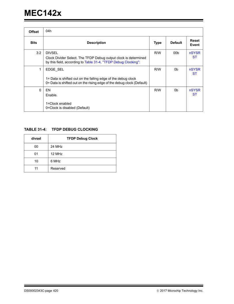
MEC142x
3:2 DIVSEL
Clock Divider Select. The TFDP Debug output clock is determined by this field, according to Table 31-4, "TFDP Debug Clocking":
R/W 00b nSYSRST
1 EDGE_SEL
1= Data is shifted out on the falling edge of the debug clock0= Data is shifted out on the rising edge of the debug clock (Default)
R/W 0b nSYSRST
0 EN
Enable.
1=Clock enabled0=Clock is disabled (Default)
R/W 0b nSYSRST
TABLE 31-4: TFDP DEBUG CLOCKING
divsel TFDP Debug Clock
00 24 MHz
01 12 MHz
10 6 MHz
11 Reserved
Offset 04h
Bits Description Type DefaultReset Event
DS00002343C-page 420 2017 Microchip Technology Inc.

MEC142x
32.0 PORT 80 BIOS DEBUG PORT
32.1 Overview
The Port 80 BIOS Debug Port emulates the functionality of a “Port 80” ISA plug-in card. In addition, a timestamp for thedebug data can be optionally added.
Diagnostic data is written by the Host Interface to the Port 80 BIOS Debug Port, which is located in the Host I/O addressspace. The Port 80 BIOS Debug Port generates an interrupt to the EC when host data is available. The EC reads thisdata along with the timestamp, if enabled.
32.2 References
There are no references for this block.
32.3 Interface
This block is designed to be accessed externally via the pin interface and internally via a registered host interface.
32.4 Signal Description
There are no external signals for this block.
32.5 Host Interface
The Port 80 block is accessed by host software via a registered interface, as defined in Section 32.11, "Runtime Reg-isters".
FIGURE 32-1: I/O DIAGRAM OF BLOCK
Port 80 BIOS Debug Port
Signal DescriptionClock Inputs
Interrupts
Resets
Host Interface
2017 Microchip Technology Inc. DS00002343C-page 421

MEC142x
32.6 Power, Clocks and Reset
This section defines the Power, Clock, and Reset parameters of the block.
32.6.1 POWER DOMAINS
32.6.2 CLOCK INPUTS
32.6.3 RESETS
32.7 Interrupts
This section defines the Interrupt Sources generated from this block.
32.8 Low Power Modes
The Port 80 block may be put into a low power state by the chip’s Power, Clocks, and Reset (PCR) circuitry.
Name Description
VTR This Power Well is used to power the registers and logic in this block.
Name Description
48 MHz Ring Oscillator This is the clock source for Port 80 block logic.
Name Description
nSYSRST This signal is asserted when VTR is low, PWRGD is low, or Host Inter-face is reset.
Source Description
BDP_INT The Port 80 BIOS Debug Port generates an EC interrupt when the amount of data in the Port 80 FIFO equals or exceeds the FIFO Thresh-old defined in the Configuration Register.
The interrupt signal is always generated by the Port 80 block if the block is enabled; the interrupt is enabled or disabled in the Interrupt Aggrega-tor.
DS00002343C-page 422 2017 Microchip Technology Inc.

MEC142x
32.9 Description
32.9.1 BLOCK DIAGRAM
The Port 80 BIOS Debug Port consists of a 32-bit wide x 16 deep FIFO and a 24-bit free running timer. Host and ECaccess to the Port 80 device is through a set of registers. The Host can write the FIFO via the Runtime Registers andthe EC can read the FIFO can control the device via the EC-Only Registers.
Writes to the Host Data Register are concatenated with the 24-bit timestamp and written to the FIFO. Reads of theHost Data Register return zero. If writes to the Host Data Register overrun the FIFO, the oldest data are discarded andthe OVERRUN status bit in the Status Register is asserted.
Only the EC can read data from the FIFO, using the EC Data Register. The use of this data is determined by EC Firm-ware alone.
FIGURE 32-2: Port 80 BIOS Debug Port BLOCK DIAGRAM
Note: In eSPI mode, the Port 80 BIOS Debug Port only operates in byte mode. Word and double word writes toPort 80 are not supported.
FIFO
32-bit x 16
24-bit Timer
Host Interface EC Interface
POWER
MGMTClock RequiredSleep Enable
BDP_INT48 MHz Ring Oscillator
nSYSRST
2017 Microchip Technology Inc. DS00002343C-page 423

MEC142x
32.10 Configuration Registers
The registers listed in the Configuration Register Summary table are for a single instance of the Port 80 BIOS DebugPort. The addresses of each register listed in this table are defined as a relative offset to the host “Base Address” definedin the Configuration Register Base Address Table.
Each Configuration register access through the Host Access Port is via its LDN and its Host Access Port Index. ECaccess is a relative offset to the EC Base Address.
32.10.1 ACTIVATE REGISTER
FIGURE 32-3: CONFIGURATION REGISTER BASE ADDRESS TABLE
Block InstanceInstance Number
HostAddress Space Base Address
Port 80 BIOS Debug Port
0 LPC/eSPI Configuration Port INDEX = 00h
0 EC 32-bit internal address space
000F_5400h
1 LPC/eSPI Configuration Port INDEX = 00h
EC 32-bit internal address space
000F_5800h
TABLE 32-1: CONFIGURATION REGISTER SUMMARY
EC Offset Host Index Register Name (Mnemonic)
330h 30h Activate Register
Offset 330h
Bits Description Type DefaultReset Event
7:1 Reserved R - -
0 ACTIVATE
When this bit is asserted ‘1’, the block is enabled. When this bit is ‘0’, writes by the Host interface to the Host Data Register are not claimed, the FIFO is flushed, the 24-bit Timer is reset, and the timer clock is stopped. Control bits in the Configuration Register are not affected by the state of ACTIVATE.
R/W 0h nSYSRST
DS00002343C-page 424 2017 Microchip Technology Inc.

MEC142x
32.11 Runtime Registers
The registers listed in the Runtime Register Summary table are for two instances of the Port 80 BIOS Debug Port. Theaddresses of each register listed in this table are defined as a relative offset to the host “Base Address” defined in theRuntime Register Base Address Table.
The Base Address indicates where the first register can be accessed in a particular address space for a block instance.
32.11.1 HOST DATA REGISTER
Note: The Runtime registers may be accessed by the EC but typically the Host will access the Runtime Registersand the EC will access just the EC-Only registers.
TABLE 32-2: RUNTIME REGISTER BASE ADDRESS TABLE
Block InstanceInstance Number
Host Address Space Base Address
Port 80 BIOS Debug Port
0 LPC/eSPI I/O Programmed BAR
EC 32-bit internal address space
000F_5400h
1 LPC/eSPI I/O Programmed BAR
EC 32-bit internal address space
000F_5800h
TABLE 32-3: RUNTIME REGISTER SUMMARY
Offset Register Name (Mnemonic)
00h Host Data Register
Offset 00h
Bits Description Type DefaultReset Event
31:8 Reserved R - -
7:0 HOST_DATA W 0h nSYSRST
2017 Microchip Technology Inc. DS00002343C-page 425
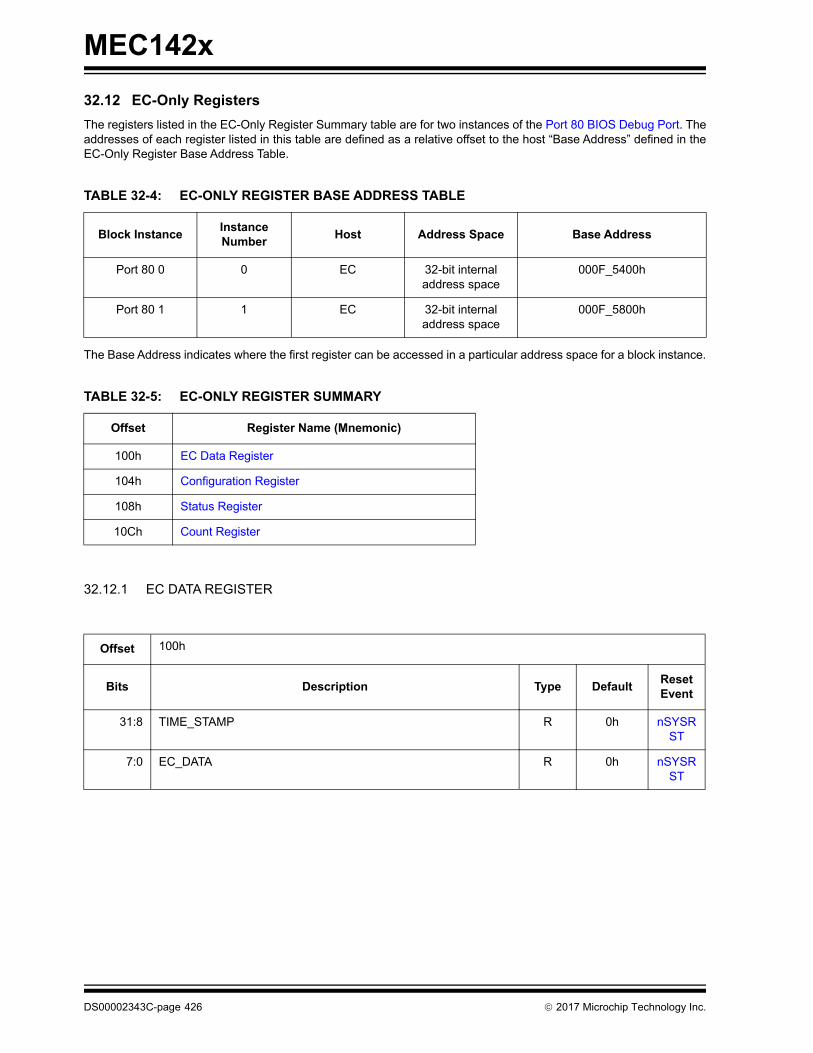
MEC142x
32.12 EC-Only Registers
The registers listed in the EC-Only Register Summary table are for two instances of the Port 80 BIOS Debug Port. Theaddresses of each register listed in this table are defined as a relative offset to the host “Base Address” defined in theEC-Only Register Base Address Table.
The Base Address indicates where the first register can be accessed in a particular address space for a block instance.
32.12.1 EC DATA REGISTER
TABLE 32-4: EC-ONLY REGISTER BASE ADDRESS TABLE
Block InstanceInstance Number
Host Address Space Base Address
Port 80 0 0 EC 32-bit internal address space
000F_5400h
Port 80 1 1 EC 32-bit internal address space
000F_5800h
TABLE 32-5: EC-ONLY REGISTER SUMMARY
Offset Register Name (Mnemonic)
100h EC Data Register
104h Configuration Register
108h Status Register
10Ch Count Register
Offset 100h
Bits Description Type DefaultReset Event
31:8 TIME_STAMP R 0h nSYSRST
7:0 EC_DATA R 0h nSYSRST
DS00002343C-page 426 2017 Microchip Technology Inc.

MEC142x
32.12.2 CONFIGURATION REGISTER
Offset 104h
Bits Description Type DefaultReset Event
31:8 Reserved R - -
7:6 FIFO_THRESHOLD
This field determines the threshold for the Port 80 BIOS Debug Port Interrupts.
3=14 entry threshold2=8 entry threshold1=4 entry threshold0=1 entry threshold
R/W 0h nSYSRST
5 TIMER_ENABLE
When the TIMER_ENABLE bit is ‘1’, the 24-bit Timer is actively counting at a rate determined by the TIMEBASE_SELECT bits. When the TIMER ENABLE bit is ‘0’, counting is stopped.
R/W 0h nSYSRST
4:3 TIMEBASE_SELECT
The TIMEBASE SELECT bits determine the clock for the 24-bit Timer.
3=48 MHz Ring Oscillator/642=48 MHz Ring Oscillator/321=48 MHz Ring Oscillator/160=48 MHz Ring Oscillator/8
R/W 0h nSYSRST
2 RESET_TIMESTAMP
When this field is written with a ‘1’, the 24-bit Timer is reset to ‘0’. Writing zero to the Count Register has the same effect.
Writes of a ‘0’ to this field have no effect. Reads always return ‘0’.
W - nSYSRST
1 FLUSH
When this field is written with a ‘1’, the FIFO is flushed. Writes of a ‘0’ to this field have no effect. Reads always return ‘0’.
W - nSYSRST
0 Reserved R - -
2017 Microchip Technology Inc. DS00002343C-page 427

MEC142x
32.12.3 STATUS REGISTER
32.12.4 COUNT REGISTER
Offset 108h
Bits Description Type DefaultReset Event
31:2 Reserved R - -
1 OVERRUN
The OVERRUN bit is ‘1’ when the host writes the Host Data Regis-ter when the FIFO is full.
R 0h nSYSRST
0 NOT_EMPTY
The NOT EMPTY bit is ‘1’ when there is data in the FIFO. The NOT EMPTY bit is ‘0’ when the FIFO is empty.
R 0h nSYSRST
Offset 10Ch
Bits Description Type DefaultReset Event
32:8 COUNT
Writes load data into the 24-bit Timer. Reads return the 24-bit Timer current value.
R/W 0h –
7:0 Reserved R - -
DS00002343C-page 428 2017 Microchip Technology Inc.
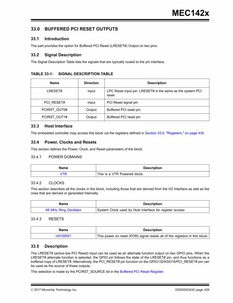
MEC142x
33.0 BUFFERED PCI RESET OUTPUTS
33.1 Introduction
The part provides the option for Buffered PCI Reset (LRESET#) Output on two pins.
33.2 Signal Description
The Signal Description Table lists the signals that are typically routed to the pin interface.
33.3 Host Interface
The embedded controller may access this block via the registers defined in Section 33.6, "Registers," on page 430.
33.4 Power, Clocks and Resets
This section defines the Power, Clock, and Reset parameters of the block.
33.4.1 POWER DOMAINS
33.4.2 CLOCKS
This section describes all the clocks in the block, including those that are derived from the I/O Interface as well as theones that are derived or generated internally.
33.4.3 RESETS
33.5 Description
The LRESET# (active-low PCI Reset) input can be used as an alternate function output on two GPIO pins. When theLRESET# alternate function is selected, the GPIO pin follows the state of the LRESET# pin, and thus functions as abuffered copy of LRESET#. Alternatively, the PCI_RESET# pin function on the GPIO132/KSO16/PCI_RESET# pin canbe used as the source of these outputs.
This selection is made by the PCIRST_SOURCE bit in the Buffered PCI Reset Register.
TABLE 33-1: SIGNAL DESCRIPTION TABLE
Name Direction Description
LRESET# Input LPC Reset input pin. LRESET# is the same as the system PCI reset
PCI_RESET# Input PCI Reset signal pin
PCIRST_OUT0# Output Buffered PCI reset pin
PCIRST_OUT1# Output Buffered PCI reset pin
Name Description
VTR This is a VTR Powered block.
Name Description
48 MHz Ring Oscillator System Clock used by Host Interface for register access
Name Description
nSYSRST This power on reset (POR) signal resets all of the registers in this block.
2017 Microchip Technology Inc. DS00002343C-page 429

MEC142x
The PCIRST_OUT0# and PCIRST_OUT1# functions are each associated with an enable bit in the PCI Reset Register.The bits are VTR powered, and default to enabled (‘1’) on VTR POR. The bits operate as follows when the pins areconfigured for the PCIRST_OUTx# buffer function:
• When the associated enable bit is set to ‘1’, the pins will operate as in Table below.
• When the associated enable bit is cleared to ‘0’, the pins will be low (‘0’).
See Table 33-1, "Buffered PCI Reset Truth Table" below.
33.6 Registers
The PCI Reset Register is an EC Subsystem register at offset 58h. See Section 34.8.7, "Buffered PCI Reset Register,"on page 435.
Note: The alternate function must be selected on the associated GPIO064/LRESET# orGPIO132/KSO16/PCI_RESET# pin for the PCIRST_OUTX# functions to operate. If the alternate functionis not selected, then the associated PCI reset signal is gated low (active).
Note: The GPIO064/LRESET# pin is either a 3.3V or 1.8V signal as controlled by the VTR_LPC_ESPI pin. TheGPIO132/KSO16/PCI_RESET# pin is a 3.3V signal.
TABLE 33-1: BUFFERED PCI RESET TRUTH TABLE
Input Enable Output
One of the following:LRESET#, PCI_RESET#
PCIRST_OUT0_EN PCIRST_OUT1_EN
PCIRST_OUT0#PCIRST_OUT1#
X 0 0
0 1 0
1 1 1
Note: The GPIOs associated with the PCIRST_OUTx# pins default to the GPIO input function. In order to ensurethat they are low immediately following a VTR reset, these pins require external pull-downs.
Note: This register is not directly host accessible, so the host will have to use the EMI interface or another mailboxto control these PCI Reset outputs with a command to the firmware.
DS00002343C-page 430 2017 Microchip Technology Inc.
MEC142x
34.0 EC SUBSYSTEM REGISTERS
34.1 Introduction
This chapter defines a bank of registers associated with the EC Subsystem.
34.2 References
None
34.3 Interface
This block is designed to be accessed internally by the EC via the register interface.
34.4 Power, Clocks and Reset
This section defines the Power, Clock, and Reset parameters of the block.
34.4.1 POWER DOMAINS
34.4.2 CLOCK INPUTS
This block does not require any special clock inputs. All register accesses are synchronized to the host clock.
34.4.3 RESETS
34.5 Interrupts
This block does not generate any interrupt events.
34.6 Low Power Modes
The EC Subsystem Registers may be put into a low power state by the chip’s Power, Clocks, and Reset (PCR) circuitry.When this block is commanded to sleep it will still allow read/write access to the registers.
34.7 Description
The EC Subsystem Registers block is a block implemented for aggregating miscellaneous registers required by theEmbedded Controller (EC) Subsystem that are not unique to a block implemented in the EC subsystem.
Name Description
VTR The EC Subsystem Registers are all implemented on this single power domain.
Name Description
VTR_RESET# This reset signal, which is an input to this block, resets registers to their initial default state on a power-on-reset event only.
nSYSRST This reset signal, which is an input to this block, resets registers to their initial default state any time the embedded controller is reset.
2017 Microchip Technology Inc. DS00002343C-page 431

MEC142x
34.8 EC-Only Registers
Note 34-1 The Base Address indicates where the first register can be accessed in a particular address spacefor a block instance.
TABLE 34-1: EC-ONLY REGISTER BASE ADDRESS TABLE
Block InstanceInstance Number
Host Address Space Base Address
EC_REG_BANK 0 EC 32-bit internal address space
0000_FC00h
TABLE 34-2: EC-ONLY REGISTER SUMMARY
Offset Register Name
00h Test
04h Test
08h Test
0Ch Test
10h Test
14h AHB Error Control
18h Comparator Control
1Ch Test
20h JTAG Enable
24h Test
28h WDT Event Count
2Ch Reserved
30h Reserved
34h Test
38h Reserved
3Ch Test
40h VREF_CPU DISABLE
44h Test
48h Power Regions Voltage Control
4Ch Test
50h Test
54h Test
58h Buffered PCI Reset Register
DS00002343C-page 432 2017 Microchip Technology Inc.

MEC142x
34.8.1 AHB ERROR CONTROL
34.8.2 COMPARATOR CONTROL
Note 1: These bits become Read-Only by writing bit 2 Comparator 0 Configuration Locked bit.
5Ch Test
80h Test
90h Test
Offset 14h
Bits Description Type DefaultReset Event
7:1 Reserved R - -
0 AHB_ERROR_DISABLE
0: EC memory exceptions are enabled.1: EC memory exceptions are disabled.
RW 0h nSYSRST
Offset 18h
Bits Description Type DefaultReset Event
7:5 Reserved R - -
4 Comparator 1 Enable
0: Disable Comparator 1 for operation1: Enable Comparator 1 operation.
RW 0h nSYSRST
3 Reserved R - -
2 Comparator 0 Configuration Locked
0: Configuration Not Locked. Bits[2,0] are Read-Write1: Configuration Locked. Bits[2,0] are Read-Only
R/W1X 0h nSYSRST
1 Reserved R - -
0 Comparator 0 Enable
0: Disable Comparator 0 for operation1: Enable Comparator 0 operation.
RW or RO
(Note 1)
0h nSYSRST
TABLE 34-2: EC-ONLY REGISTER SUMMARY (CONTINUED)
Offset Register Name
2017 Microchip Technology Inc. DS00002343C-page 433

MEC142x
34.8.3 JTAG ENABLE
34.8.4 WDT EVENT COUNT
34.8.5 VREF_CPU DISABLE
Offset 20h
Bits Description Type DefaultReset Event
31:2 Reserved R - -
1 Boot ROM Configuration Ready
This bit indicates to the ICSP debugger when the Boot ROM has finished its configuration sequence. The state of this bit is reflected in the MCHP_CMD <0x07> Read Status register.0 = Boot ROM has not finished configuration sequence
1 = Boot ROM has finished configuration sequence.
R/W 0b nSYSRST
0 JTAG_EN
This bit enables the JTAG/ICSP debug port. 0 = JTAG/ICSP port disabled. JTAG/ICSP cannot be enabled (i.e., the TRST#/ICSP_MCLR pin is ignored and the JTAG/ICSP signals remain in their non-JTAG/ICSP state).1= JTAG/ICSP port enabled. A high on TRST#/ICSP_MCLR enables JTAG/ICSP
R/W 0b nSYSRST
Offset 28h
Bits Description Type DefaultReset Event
31:4 Reserved R - -
3:0 WDT_COUNT
These EC R/W bits are cleared to 0 on VTR POR, but not on a WDT.
Note: This field is written by Boot ROM firmware to indicate thenumber of times a WDT fired before loading a good ECcode image.
R/W 0b VTR_RE-SET#
Offset 40h
Bits Description Type DefaultReset Event
31:7 Reserved R - -
6:2 Test R/W 0b nSYSRST
1 VREF_CPU Disable
0: Enable1: Disable
Note: In order to achieve the lowest leakage current when bothPECI and SB TSI are not used, set the VREF_CPU Dis-able bit to 1.
R/W 0b nSYSRST
0 Test R 0b nSYSRST
DS00002343C-page 434 2017 Microchip Technology Inc.

MEC142x
34.8.6 POWER REGIONS VOLTAGE CONTROL
34.8.7 BUFFERED PCI RESET REGISTER
Note 1: The alternate function must be selected on the associated GPIO064/LRESET# orGPIO132/KSO16/PCI_RESET# pin for the PCIRST_OUTX# functions to operate. If the alternate functionis not selected, then the associated PCI reset signal is gated low (active).
Offset 48h
Bits Description Type DefaultReset Event
31:5 Reserved R - -
4 VTR_33_18_SEL18This is used for the 3.3/1.8V region. See Section 2.6, "1.8V or 3.3V I/O Pins," on page 18.
0 = 3.3V Operation. Note: The VTR_33_18 pin must be con-nected to a 3.3V supply.
1 = 1.8V Operation. Note: The VTR_33_18 pin must be con-nected to a 1.8V supply.
R/W 0b nSYSRST
3 VTR_LPC_ESPI_SEL180 = 3.3V Operation (use for LPC interface). Note: The
VTR_33_18 pin must be connected to a 3.3V supply.1 = 1.8V Operation (use for eSPI Interface). Note: The
VTR_33_18 pin must be connected to a 1.8V supply.
Note: If the I2C interface is used as the host interface, theGPIOs on the LPC and eSPI interface may be config-ured to operate as either 1.8V or 3.3V GPIOs.
R/W 0b nSYSRST
2 Test
Note: Writing this register bit to a different value may causeunwanted results. This bit must always be set to 0.
R/W 0b nSYSRST
1 Test
Note: Writing this register bit to a different value may causeunwanted results. This bit must always be set to 0.
R/W 0b nSYSRST
0 Reserved R - -
Offset 58h
Bits Description Type DefaultReset Event
7:3 Reserved R - nSYSRST
2 PCIRST_OUT1#0= The PCIRST_OUT1# pin is forced low1= The PCIRST_OUT1# pin is a buffered copy of LRESET# or the GPIO132/KSO16/PCI_RESET# pin as selected by bit 0 (default)
R/W 1h nSYSRST
1 PCIRST_OUT0#0= The PCIRST_OUT0# pin is forced low1= The PCIRST_OUT0# pin is a buffered copy of LRESET# or the GPIO132/KSO16/PCI_RESET# pin as selected by bit 0 (default)
R/W 1h nSYSRST
0 PCIRST_SOURCEThis bit determines the source of the PCIRST_OUT0# and PCIRST_OUT1# pins.0=LRESET# on the GPIO064/LRESET# pin (Note 1)1=PCI_RESET# on the GPIO132/KSO16/PCI_RESET# (Note 1)
R/W 0h nSYSRST
2017 Microchip Technology Inc. DS00002343C-page 435
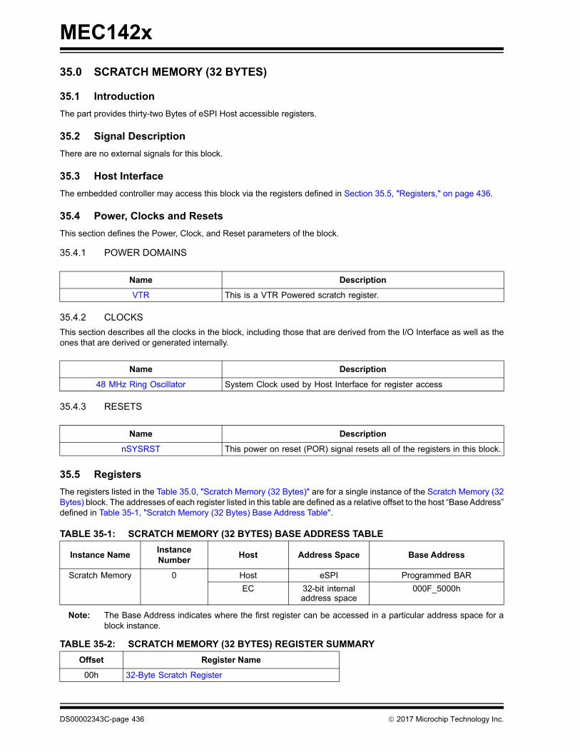
MEC142x
35.0 SCRATCH MEMORY (32 BYTES)
35.1 Introduction
The part provides thirty-two Bytes of eSPI Host accessible registers.
35.2 Signal Description
There are no external signals for this block.
35.3 Host Interface
The embedded controller may access this block via the registers defined in Section 35.5, "Registers," on page 436.
35.4 Power, Clocks and Resets
This section defines the Power, Clock, and Reset parameters of the block.
35.4.1 POWER DOMAINS
35.4.2 CLOCKS
This section describes all the clocks in the block, including those that are derived from the I/O Interface as well as theones that are derived or generated internally.
35.4.3 RESETS
35.5 Registers
The registers listed in the Table 35.0, "Scratch Memory (32 Bytes)" are for a single instance of the Scratch Memory (32Bytes) block. The addresses of each register listed in this table are defined as a relative offset to the host “Base Address”defined in Table 35-1, "Scratch Memory (32 Bytes) Base Address Table".
Note: The Base Address indicates where the first register can be accessed in a particular address space for ablock instance.
Name Description
VTR This is a VTR Powered scratch register.
Name Description
48 MHz Ring Oscillator System Clock used by Host Interface for register access
Name Description
nSYSRST This power on reset (POR) signal resets all of the registers in this block.
TABLE 35-1: SCRATCH MEMORY (32 BYTES) BASE ADDRESS TABLE
Instance NameInstance Number
Host Address Space Base Address
Scratch Memory 0 Host eSPI Programmed BAR
EC 32-bit internal address space
000F_5000h
TABLE 35-2: SCRATCH MEMORY (32 BYTES) REGISTER SUMMARY
Offset Register Name
00h 32-Byte Scratch Register
DS00002343C-page 436 2017 Microchip Technology Inc.
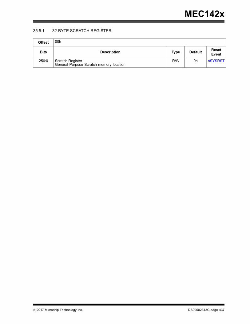
MEC142x
35.5.1 32-BYTE SCRATCH REGISTER
Offset 00h
Bits Description Type DefaultReset Event
256:0 Scratch RegisterGeneral Purpose Scratch memory location
R/W 0h nSYSRST
2017 Microchip Technology Inc. DS00002343C-page 437

MEC142x
36.0 VBAT REGISTER BANK
36.1 Introduction
This chapter defines a bank of registers powered by VBAT.
36.2 Interface
This block is designed to be accessed internally by the EC via the register interface.
36.3 Power, Clocks and Reset
This section defines the Power, Clock, and Reset parameters of the block.
36.3.1 POWER DOMAINS
36.3.2 CLOCK INPUTS
This block does not require any special clock inputs. All register accesses are synchronized to the host clock.
36.3.3 RESETS
36.4 Interrupts
36.5 Low Power Modes
The VBAT Register Bank is designed to always operate in the lowest power consumption state.
36.6 Description
The VBAT Register Bank block is a block implemented for aggregating miscellaneous battery-backed registers requiredthe host and by the Embedded Controller (EC) Subsystem that are not unique to a block implemented in the EC sub-system.
Name Description
VBAT The VBAT Register Bank are all implemented on this single power domain.
Name Description
VBAT_POR This reset signal, which is an input to this block, resets all the logic and registers to their initial default state.
Name Description
PFR_Status This interrupt signal from the Power-Fail and Reset Status Register indicates VBAT RST and WDT events.
DS00002343C-page 438 2017 Microchip Technology Inc.
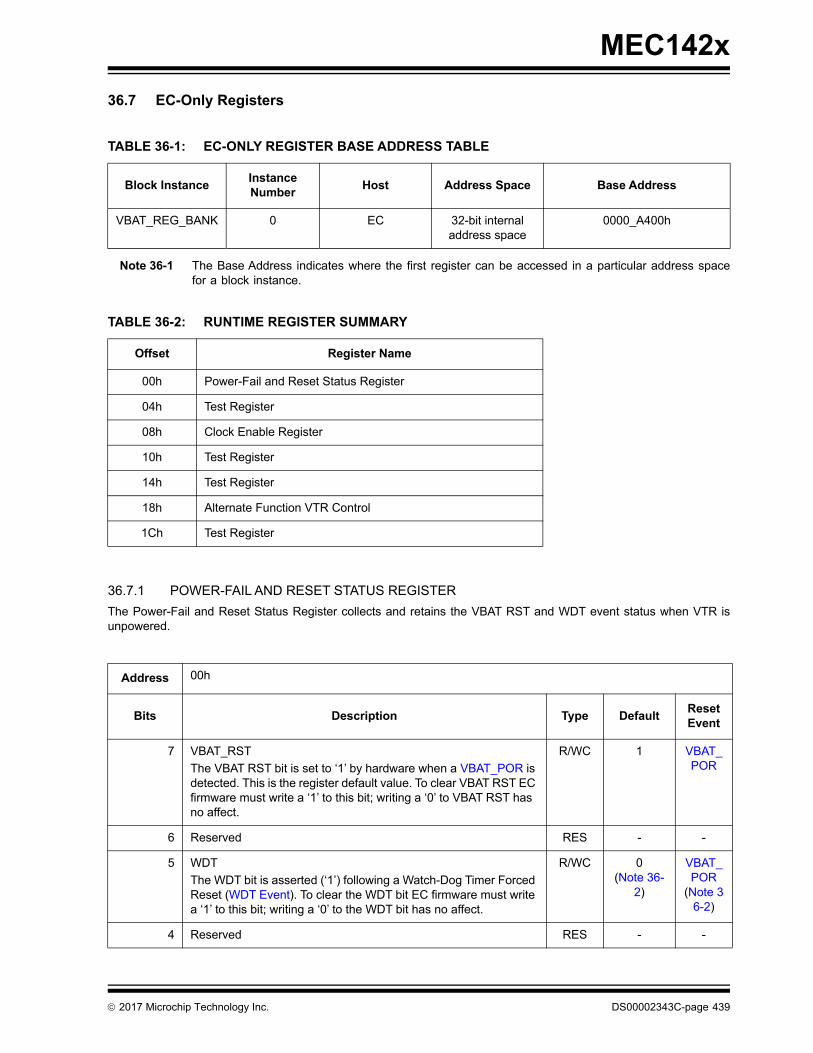
MEC142x
36.7 EC-Only Registers
Note 36-1 The Base Address indicates where the first register can be accessed in a particular address spacefor a block instance.
36.7.1 POWER-FAIL AND RESET STATUS REGISTER
The Power-Fail and Reset Status Register collects and retains the VBAT RST and WDT event status when VTR isunpowered.
TABLE 36-1: EC-ONLY REGISTER BASE ADDRESS TABLE
Block InstanceInstance Number
Host Address Space Base Address
VBAT_REG_BANK 0 EC 32-bit internal address space
0000_A400h
TABLE 36-2: RUNTIME REGISTER SUMMARY
Offset Register Name
00h Power-Fail and Reset Status Register
04h Test Register
08h Clock Enable Register
10h Test Register
14h Test Register
18h Alternate Function VTR Control
1Ch Test Register
Address 00h
Bits Description Type DefaultReset Event
7 VBAT_RST
The VBAT RST bit is set to ‘1’ by hardware when a VBAT_POR is detected. This is the register default value. To clear VBAT RST EC firmware must write a ‘1’ to this bit; writing a ‘0’ to VBAT RST has no affect.
R/WC 1 VBAT_POR
6 Reserved RES - -
5 WDT
The WDT bit is asserted (‘1’) following a Watch-Dog Timer Forced Reset (WDT Event). To clear the WDT bit EC firmware must write a ‘1’ to this bit; writing a ‘0’ to the WDT bit has no affect.
R/WC 0(Note 36-
2)
VBAT_POR
(Note 36-2)
4 Reserved RES - -
2017 Microchip Technology Inc. DS00002343C-page 439

MEC142x
Note 36-2 In the MEC142x devices the WDT defaults to disabled, however the Boot ROM Exception Handleruses the WDT to generate a nSYSRST. The Boot ROM only touches the WDT if the BEV exceptionfires. In this case 0x5 is written to the EC Subsystem WDT_COUNT bit field. The WDT Status bit,located in the WDT EC-Only Register bank, and the WDT status bit located in the Power-Fail andReset Status Register register are cleared before the WDT is enabled.
36.7.2 CLOCK ENABLE REGISTER
3 Test, must write 0. RWC 0 VBAT_POR
2 SOFT
This bit is set to ‘1b’ if an nSYSRST was triggered by an assertion of the SOFT_SYS_RESET bit in the System Reset Control (SYS-_RST_CTRL) Register (PCR at offset 50h).This bit is cleared to ‘0b’ when written with a ‘1b’; writes of a ‘0b’have no effect.
RWC 0 VBAT_POR
1 Reserved RES - -
0 DET32K_IN
0 = No clock detected on the XTAL[1:2] pins.1= Clock detected on the XTAL[1:2] pins.
R X VBAT_POR
Address 08h
Bits Description Type DefaultReset Event
31:6 Reserved RES - -
5 48MHz Oscillator Reference Select
0 = External 32KHz clock source is the 48MHz clock reference(default)
1 = Switched Clock Source (i.e., either internal 32kHz or external32kHz clock) is the 48MHz clock reference
Note: The external 32KHz clock source may be either the crys-tal or external single-ended 32kHz clock as selected bythe XOSEL bit.
R/W 0b VBAT_POR
Address 00h
Bits Description Type DefaultReset Event
DS00002343C-page 440 2017 Microchip Technology Inc.
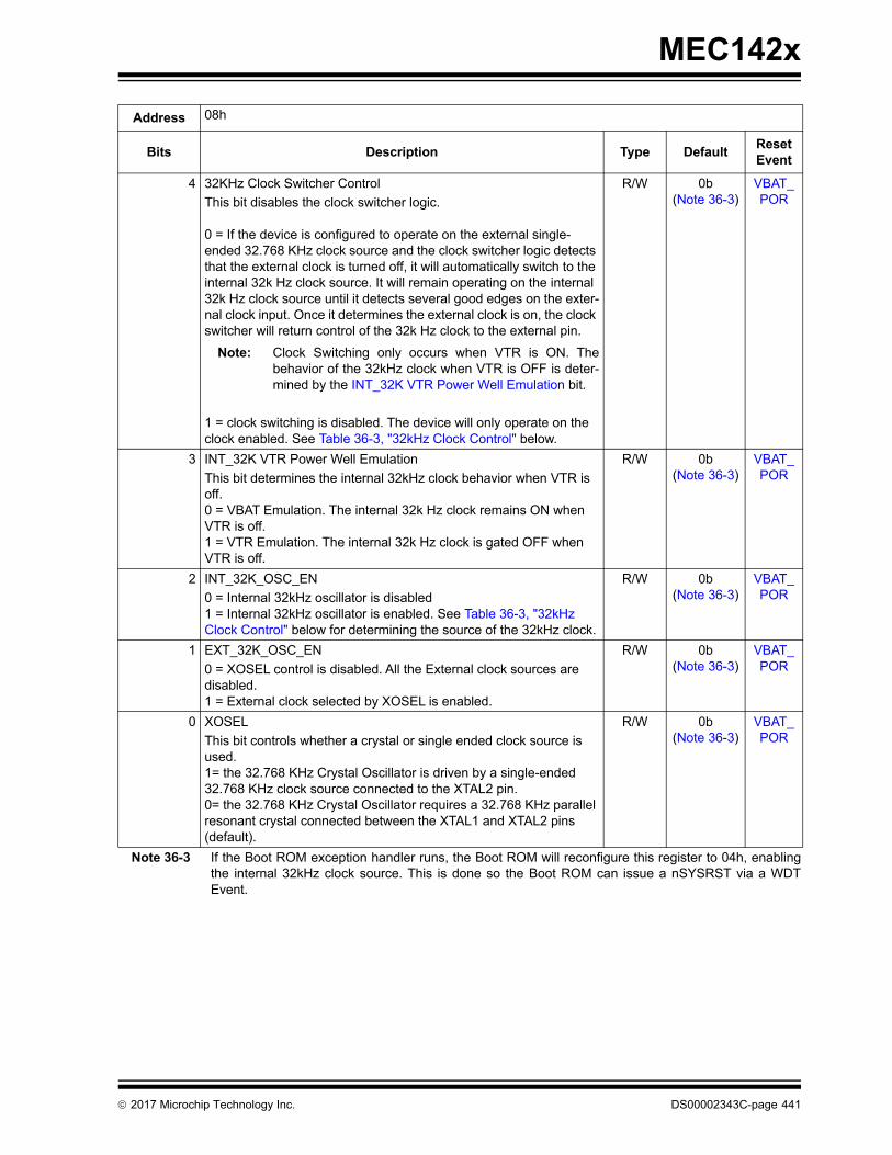
MEC142x
Note 36-3 If the Boot ROM exception handler runs, the Boot ROM will reconfigure this register to 04h, enablingthe internal 32kHz clock source. This is done so the Boot ROM can issue a nSYSRST via a WDTEvent.
4 32KHz Clock Switcher Control
This bit disables the clock switcher logic.
0 = If the device is configured to operate on the external single-ended 32.768 KHz clock source and the clock switcher logic detects that the external clock is turned off, it will automatically switch to the internal 32k Hz clock source. It will remain operating on the internal 32k Hz clock source until it detects several good edges on the exter-nal clock input. Once it determines the external clock is on, the clock switcher will return control of the 32k Hz clock to the external pin.
Note: Clock Switching only occurs when VTR is ON. Thebehavior of the 32kHz clock when VTR is OFF is deter-mined by the INT_32K VTR Power Well Emulation bit.
1 = clock switching is disabled. The device will only operate on the clock enabled. See Table 36-3, "32kHz Clock Control" below.
R/W 0b(Note 36-3)
VBAT_POR
3 INT_32K VTR Power Well Emulation
This bit determines the internal 32kHz clock behavior when VTR is off.0 = VBAT Emulation. The internal 32k Hz clock remains ON when VTR is off.1 = VTR Emulation. The internal 32k Hz clock is gated OFF when VTR is off.
R/W 0b(Note 36-3)
VBAT_POR
2 INT_32K_OSC_EN
0 = Internal 32kHz oscillator is disabled1 = Internal 32kHz oscillator is enabled. See Table 36-3, "32kHz Clock Control" below for determining the source of the 32kHz clock.
R/W 0b(Note 36-3)
VBAT_POR
1 EXT_32K_OSC_EN
0 = XOSEL control is disabled. All the External clock sources are disabled.1 = External clock selected by XOSEL is enabled.
R/W 0b(Note 36-3)
VBAT_POR
0 XOSEL
This bit controls whether a crystal or single ended clock source is used.1= the 32.768 KHz Crystal Oscillator is driven by a single-ended 32.768 KHz clock source connected to the XTAL2 pin.0= the 32.768 KHz Crystal Oscillator requires a 32.768 KHz parallel resonant crystal connected between the XTAL1 and XTAL2 pins (default).
R/W 0b(Note 36-3)
VBAT_POR
Address 08h
Bits Description Type DefaultReset Event
2017 Microchip Technology Inc. DS00002343C-page 441
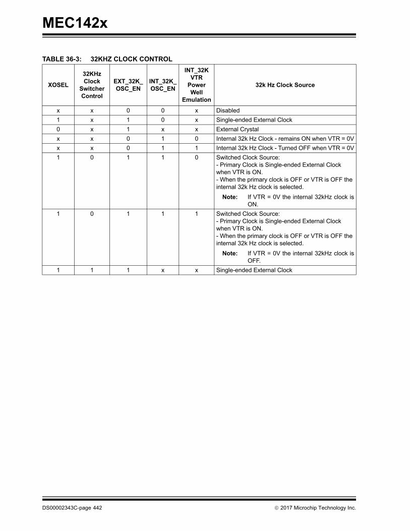
MEC142x
TABLE 36-3: 32KHZ CLOCK CONTROL
XOSEL
32KHz Clock
Switcher Control
EXT_32K_OSC_EN
INT_32K_OSC_EN
INT_32K VTR
Power Well
Emulation
32k Hz Clock Source
x x 0 0 x Disabled
1 x 1 0 x Single-ended External Clock
0 x 1 x x External Crystal
x x 0 1 0 Internal 32k Hz Clock - remains ON when VTR = 0V
x x 0 1 1 Internal 32k Hz Clock - Turned OFF when VTR = 0V
1 0 1 1 0 Switched Clock Source:- Primary Clock is Single-ended External Clock when VTR is ON.- When the primary clock is OFF or VTR is OFF the internal 32k Hz clock is selected.
Note: If VTR = 0V the internal 32kHz clock isON.
1 0 1 1 1 Switched Clock Source:- Primary Clock is Single-ended External Clock when VTR is ON.- When the primary clock is OFF or VTR is OFF the internal 32k Hz clock is selected.
Note: If VTR = 0V the internal 32kHz clock isOFF.
1 1 1 x x Single-ended External Clock
DS00002343C-page 442 2017 Microchip Technology Inc.
MEC142x
36.7.3 ALTERNATE FUNCTION VTR CONTROL
Address 18h
Bits Description Type DefaultReset Event
31:2 Reserved RES - -
1 BGPO
0 = VTR PoweredIf VTR = ON, then the output is driven according to GPIO output control registerIf VTR = OFF, then the output pin is tristated
1 = VBAT PoweredOutput driven according to the BGPO bit located in
R/W 1b VBAT_POR
0 VCI_OUT
0 = VTR PoweredIf VTR = ON, then the output is driven according to GPIO output control registerIf VTR = OFF, then the output pin is tristated
1 = VBAT PoweredOutput driven according to the VCI_OUT logic defined in Section 38.0, "VBAT-Powered Control Interface," on page 447
R/W 1b VBAT_POR
2017 Microchip Technology Inc. DS00002343C-page 443
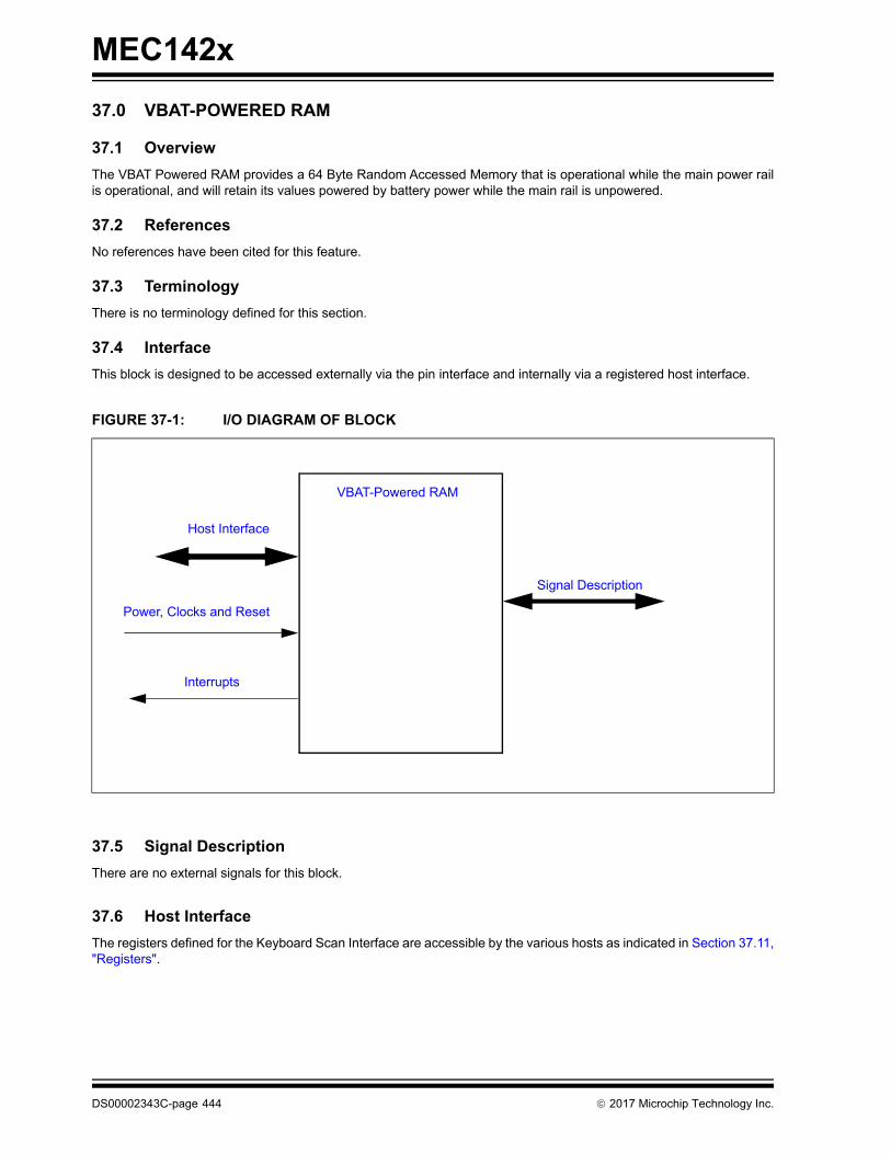
MEC142x
37.0 VBAT-POWERED RAM
37.1 Overview
The VBAT Powered RAM provides a 64 Byte Random Accessed Memory that is operational while the main power railis operational, and will retain its values powered by battery power while the main rail is unpowered.
37.2 References
No references have been cited for this feature.
37.3 Terminology
There is no terminology defined for this section.
37.4 Interface
This block is designed to be accessed externally via the pin interface and internally via a registered host interface.
37.5 Signal Description
There are no external signals for this block.
37.6 Host Interface
The registers defined for the Keyboard Scan Interface are accessible by the various hosts as indicated in Section 37.11,"Registers".
FIGURE 37-1: I/O DIAGRAM OF BLOCK
VBAT-Powered RAM
Interrupts
Power, Clocks and Reset
Host Interface
Signal Description
DS00002343C-page 444 2017 Microchip Technology Inc.
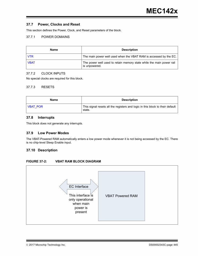
MEC142x
37.7 Power, Clocks and Reset
This section defines the Power, Clock, and Reset parameters of the block.
37.7.1 POWER DOMAINS
37.7.2 CLOCK INPUTS
No special clocks are required for this block.
37.7.3 RESETS
37.8 Interrupts
This block does not generate any interrupts.
37.9 Low Power Modes
The VBAT-Powered RAM automatically enters a low power mode whenever it is not being accessed by the EC. Thereis no chip-level Sleep Enable input.
37.10 Description
Name Description
VTR The main power well used when the VBAT RAM is accessed by the EC.
VBAT The power well used to retain memory state while the main power rail is unpowered.
Name Description
VBAT_POR This signal resets all the registers and logic in this block to their default state.
FIGURE 37-2: VBAT RAM BLOCK DIAGRAM
VBAT Powered RAM
EC Interface
This interface is only operational
when main power is present
2017 Microchip Technology Inc. DS00002343C-page 445

MEC142x
The VBAT Powered RAM provides a 64 Byte Random Accessed Memory that is operational while VTR is powered, andwill retain its values powered by VBAT while VTR is unpowered. The RAM is organized as a 16 words x 32-bit wide fora total of 64 bytes.
37.11 Registers
37.11.1 REGISTERS SUMMARY
The registers listed in the Table 37-1, "EC-Only Register Base Address Table" are for a single instance of the KeyboardScan Interface block. Each 32-bit RAM location is an offset from the EC base address.
TABLE 37-1: EC-ONLY REGISTER BASE ADDRESS TABLE
Block InstanceInstance Number
Host Address Space Base Address
VBAT-Powered RAM 0 EC 32-bit internal address space
0000_A800h
Note: The Base Address indicates where the first register can be accessed in a particular address space for ablock instance.
DS00002343C-page 446 2017 Microchip Technology Inc.

MEC142x
38.0 VBAT-POWERED CONTROL INTERFACE
38.1 General Description
The VBAT-Powered Control Interface has VBAT powered combinational logic and input and output signal pins. TheVBAT-Powered Control Interface block interfaces with the RTC/Week Timer on page 311.
38.2 Interface
This block’s connections are entirely internal to the chip.
38.3 Signal Description
FIGURE 38-1: I/O DIAGRAM OF BLOCK
TABLE 38-1: EXTERNAL SIGNAL DESCRIPTION TABLE
Name Direction Description
VCI_OUT OUTPUT Output status driven by this block.
VCI_IN0# INPUT Input, active low
VCI_IN1# INPUT Input, active low
VCI_OVRD_IN INPUT Input, active high
VBAT-Powered Control Interface
Signal DescriptionClocks
Interrupts
Host Interface
Resets
2017 Microchip Technology Inc. DS00002343C-page 447

MEC142x
38.4 Host Interface
The registers defined for the VBAT-Powered Control Interface are accessible only by the EC.
38.5 Power, Clocks and Resets
This section defines the Power, Clock, and Reset parameters of the block.
38.5.1 POWER DOMAINS
38.5.2 CLOCKS
This block does not require clocks.
38.5.3 RESETS
TABLE 38-2: INTERNAL SIGNAL DESCRIPTION TABLE
Name Direction Description
POWER_UP_EVENT INPUT Signal from the RTC/Week Timer block. The POW-ER_UP_EVENT is asserted by the timer when either the Week_Alarm or the Sub-Week Alarm is asserted. The POW-ER_UP_EVENT can be suppressed if the SYSPWR_PRES pin indicates that system power is not available.
VTRGD INPUT Status signal for the state of the VTR power rail. This signal is high if the power rail is on, and low if the power rail is off.
TABLE 38-3: POWER SOURCES
Name Description
VBAT This power well sources all of the internal registers and logic in this block.
VTR This power well sources only bus communication. The block continues to operate internally while this rail is down.
TABLE 38-4: RESET SIGNALS
Name Description
VBAT_POR This reset signal is used reset all of the registers and logic in this block.
nSYSRST This reset signal is used to inhibit the bus communication logic, and iso-lates this block from VTR powered circuitry on-chip. Otherwise it has no effect on the internal state.
DS00002343C-page 448 2017 Microchip Technology Inc.
MEC142x
38.6 Interrupts
38.7 Low Power Modes
The VBAT-powered Control Interface has no low-power modes. It runs continuously while the VBAT well is powered.
38.8 General Description
The VBAT-Powered Control Interface (VCI) is used to drive the VCI_OUT pin. The output pin can be controlled eitherby VBAT-powered inputs, or by firmware when the VTR is active and the EC is powered and running. When theVCI_OUT pin is controlled by hardware, either because VTR is inactive or because the VCI block is configured for hard-ware control, the VCI_OUT pin can be asserted by a number of inputs:
• When either the VCI_IN0# pin or the VCI_IN1# is asserted. By default, the VCI_IN# pins are active low, but firm-ware can switch each input individually to an active-high input. See Section 38.8.1, "Input Polarity".
• Wen the VCI_OVRD_IN pin is asserted. The VCI_OVRD_IN pin is always active high
• When the POWER_UP_EVENT from the RTC/Week Timer is asserted
Firmware can configure which of the hardware pin inputs contribute to the VCI_OUT output by setting the enable bits inthe VCI Input Enable Register. Even if the input pins are not configured to affect VCI_OUT, firmware can monitor theircurrent state through the status bits in the VCI Register. Firmware can also enable EC interrupts from the state of theinput pins.
Each of the VCI_IN# pins can be configured for additional properties.
• By default, each of the VCI_IN# pins have an input glitch filter. All glitch filters can be disabled by the FIL-TERS_BYPASS bit in the VCI Register
• Assertions of each of the VCI_IN# pins can optionally be latched, so hardware can maintain the assertion of a VCI_IN# even after the physical pin is de-asserted, or so that firmware can determine which of the VCI_IN# inputs contributed to VCI_OUT assertion. See the Latch Enable Register and the Latch Resets Register.
• Rising edges and falling edges on the VCI_IN# pins are latched, so firmware can detect transitions on the VCI_IN# pins even if the transitions occurred while EC power was not available. See Section 38.8.2, "Edge Event Status".
When VTR power is present and the EC is operating, firmware can figure the VCI_OUT pin to operate as a general-purpose output pin. The VCI_OUT pin is firmware-controlled when the FW_EXT bit in the VCI Register is ‘1’. When firm-ware is controlling the output, the state of VCI_OUT is defined by the VCI_FW_CNTRL bit in the same register. WhenVTR is not present (the VTRGD input is low), the VCI_OUT pin is also determined by the hardware circuit.
TABLE 38-5: EC INTERRUPTS
Source Description
VCI_IN0 This interrupt is routed to the Interrupt Controller It is only asserted when both VBAT and VTR are powered. Edge detection and assertion level for the interrupt are configured in the GPIO Pin Control Register for the GPIO that shares the pin with VCI_IN# input. This interrupt is equivalent to the GPIO interrupt for the GPIO that shares the pin, but appears on a differ-ent register in the Interrupt Aggregator.
VCI_IN1 This interrupt is routed to the Interrupt Controller It is only asserted when both VBAT and VTR are powered. Edge detection and assertion level for the interrupt are configured in the GPIO Pin Control Register for the GPIO that shares the pin with VCI_IN# input. This interrupt is equivalent to the GPIO interrupt for the GPIO that shares the pin, but appears on a differ-ent register in the Interrupt Aggregator.
VCI_OVRD_IN This interrupt is routed to the Interrupt Controller It is only asserted when both VBAT and VTR are powered. Edge detection and assertion level for the interrupt are configured in the GPIO Pin Control Register for the GPIO that shares the pin with VCI_OVRD_IN input. This interrupt is equivalent to the GPIO interrupt for the GPIO that shares the pin, but appears on a different register in the Interrupt Aggregator.
2017 Microchip Technology Inc. DS00002343C-page 449
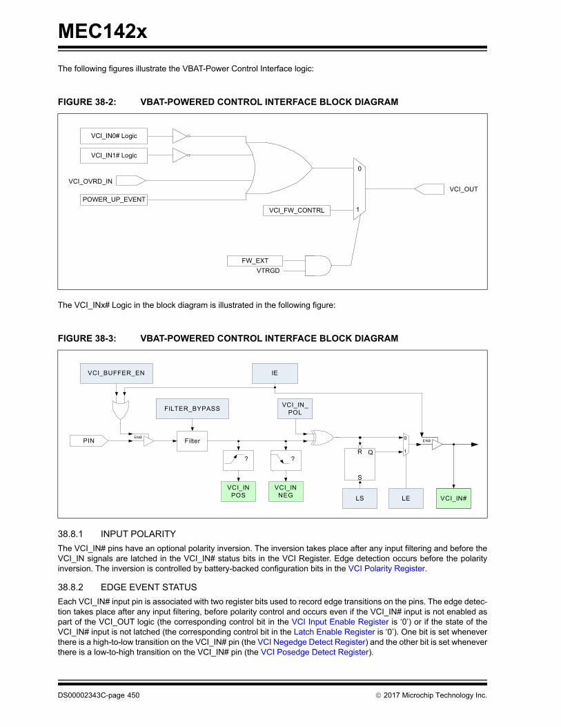
MEC142x
The following figures illustrate the VBAT-Power Control Interface logic:
The VCI_INx# Logic in the block diagram is illustrated in the following figure:
38.8.1 INPUT POLARITY
The VCI_IN# pins have an optional polarity inversion. The inversion takes place after any input filtering and before theVCI_IN signals are latched in the VCI_IN# status bits in the VCI Register. Edge detection occurs before the polarityinversion. The inversion is controlled by battery-backed configuration bits in the VCI Polarity Register.
38.8.2 EDGE EVENT STATUS
Each VCI_IN# input pin is associated with two register bits used to record edge transitions on the pins. The edge detec-tion takes place after any input filtering, before polarity control and occurs even if the VCI_IN# input is not enabled aspart of the VCI_OUT logic (the corresponding control bit in the VCI Input Enable Register is ‘0’) or if the state of theVCI_IN# input is not latched (the corresponding control bit in the Latch Enable Register is ‘0’). One bit is set wheneverthere is a high-to-low transition on the VCI_IN# pin (the VCI Negedge Detect Register) and the other bit is set wheneverthere is a low-to-high transition on the VCI_IN# pin (the VCI Posedge Detect Register).
FIGURE 38-2: VBAT-POWERED CONTROL INTERFACE BLOCK DIAGRAM
FIGURE 38-3: VBAT-POWERED CONTROL INTERFACE BLOCK DIAGRAM
VCI_IN0# Logic
VCI_IN1# Logic
POWER_UP_EVENT
VCI_OVRD_IN
VCI_FW_CONTRL
0
1
FW_EXT
VTRGD
VCI_OUT
PIN Filter
VCI_BUFFER_EN
FILTER_BYPASSVCI_IN_
POL
VCI_INPOS
VCI_INNEG
? ?
VCI_IN#
IE
ENB
LE
Q
S
LS
ENB0
1R
DS00002343C-page 450 2017 Microchip Technology Inc.

MEC142x
In order to minimize power drain on the VBAT circuit, the edge detection logic operates only when the input buffer for aVCI_IN# pin is enabled. The input buffer is enabled either when the VCI_IN# pin is configured to determine theVCI_OUT pin, as controlled by the VCI_IN[1:0]# field of the VCI Register, or when the input buffer is explicitly enabledin the VCI Input Enable Register. When the pins are not enabled transitions on the pins are ignored.
The VCI_OVRD input also has an Input Buffer Enable and an Input Enable bit associated with VCI_OUT. However, theVCI_OVRD input does not have any filtering, latching, input edge detection or polarity control.
38.8.3 VCI PIN MULTIPLEXING
Each of the VCI inputs, as well as VCI_OUT, are multiplexed with standard VTR-powered GPIOs. When VTR power isoff, the mux control is disabled and the pin always reverts to the VCI function. The VCI_IN# function should be disabledin the VCI Input Enable Register for any pin that is intended to be used as a GPIO rather than a VCI_IN#, so thatVCI_OUT is not affected by the state of the pin. The VCI_OVRD_IN function should similarly be disabled if the pin is tobe used as a GPIO.
38.8.4 APPLICATION EXAMPLE
For this example, a mobile platform configures the VBAT-Powered Control Interface as follows:
• VCI_IN0# is wired to a power button on the mobile platform
• VCI_IN1# is wired to a power button on a dock
• VCI_OVRD_IN is wired so that it is asserted whenever AC power is present
• The VCI_OUT pin is connected to the regulator that sources the VTR power rail, the rail which powers the EC
The VBAT-Powered Control Interface can be used in a system as follows:
1. In the initial condition, there is no power on either the VTR or VBAT power rails. All registers in the VBAT-PoweredControl Interface are in an indeterminate state
2. A coin cell battery is installed, causing a VBAT_POR. All registers in the interface are forced to their default con-ditions. The VCI_OUT pin is driven by hardware, input filters on the VCI_IN# pins are enabled, the VCI_IN# pinsare all active low, all VCI inputs are enabled and all edge and status latches are in their non-asserted state
3. The power button on VCI_IN0# is pushed. This causes VCI_OUT to be asserted, powering the VTR rail. Thiscauses the EC to boot and start executing EC firmware
4. The EC changes the VCI configuration so that firmware controls the VCI_OUT pin, and sets the output controlso that VCI_OUT is driven high. With this change, the power button can be released without removing the ECpower rail.
5. EC firmware re-configures the VCI logic so that the VCI_IN# input latches are enabled. This means that subse-quent presses of the power button do not have to be held until EC firmware switches the VCI logic to firmwarecontrol
6. During this phase the VCI_OUT pin is driven by the firmware-controlled state bit and the VCI input pins areignored. However, the EC can monitor the state of the pins, or generate inputs when their state changes
7. At some later point, EC firmware must enter a long-term power-down state.
- Firmware configures the Week Timer for a Sub-Week Alarm once every 8 hours. This will turn on the EC power rail three times a day and enable the EC to perform low frequency housekeeping tasks even in its low-est-power state
- Firmware de-asserts VCI_OUT. This action kills power to the EC and automatically returns control of the VCI_OUT pin to hardware.
- The EC will remain in its lowest-power state until a power pin is pushed, AC power is connected, or the Sub-Week Alarm is active
2017 Microchip Technology Inc. DS00002343C-page 451
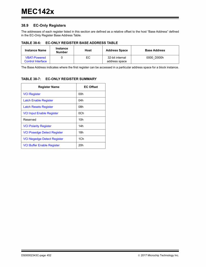
MEC142x
38.9 EC-Only Registers
The addresses of each register listed in this section are defined as a relative offset to the host “Base Address” definedin the EC-Only Register Base Address Table.
The Base Address indicates where the first register can be accessed in a particular address space for a block instance.
TABLE 38-6: EC-ONLY REGISTER BASE ADDRESS TABLE
Instance NameInstance Number
Host Address Space Base Address
VBAT-Powered Control Interface
0 EC 32-bit internal address space
0000_D000h
TABLE 38-7: EC-ONLY REGISTER SUMMARY
Register Name EC Offset
VCI Register 00h
Latch Enable Register 04h
Latch Resets Register 08h
VCI Input Enable Register 0Ch
Reserved 10h
VCI Polarity Register 14h
VCI Posedge Detect Register 18h
VCI Negedge Detect Register 1Ch
VCI Buffer Enable Register 20h
DS00002343C-page 452 2017 Microchip Technology Inc.
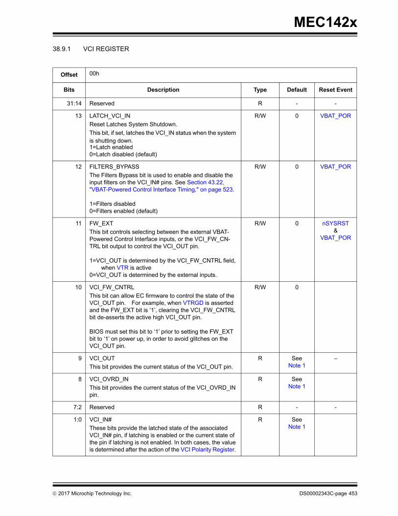
MEC142x
38.9.1 VCI REGISTER
Offset 00h
Bits Description Type Default Reset Event
31:14 Reserved R - -
13 LATCH_VCI_IN
Reset Latches System Shutdown.
This bit, if set, latches the VCI_IN status when the system is shutting down.1=Latch enabled0=Latch disabled (default)
R/W 0 VBAT_POR
12 FILTERS_BYPASS
The Filters Bypass bit is used to enable and disable the input filters on the VCI_IN# pins. See Section 43.22, "VBAT-Powered Control Interface Timing," on page 523.
1=Filters disabled0=Filters enabled (default)
R/W 0 VBAT_POR
11 FW_EXT
This bit controls selecting between the external VBAT-Powered Control Interface inputs, or the VCI_FW_CN-TRL bit output to control the VCI_OUT pin.
1=VCI_OUT is determined by the VCI_FW_CNTRL field, when VTR is active
0=VCI_OUT is determined by the external inputs.
R/W 0 nSYSRST&
VBAT_POR
10 VCI_FW_CNTRL
This bit can allow EC firmware to control the state of the VCI_OUT pin. For example, when VTRGD is asserted and the FW_EXT bit is ‘1’, clearing the VCI_FW_CNTRL bit de-asserts the active high VCI_OUT pin.
BIOS must set this bit to ‘1’ prior to setting the FW_EXT bit to ‘1’ on power up, in order to avoid glitches on the VCI_OUT pin.
R/W 0
9 VCI_OUT
This bit provides the current status of the VCI_OUT pin.
R See Note 1
–
8 VCI_OVRD_IN
This bit provides the current status of the VCI_OVRD_IN pin.
R See Note 1
7:2 Reserved R - -
1:0 VCI_IN#
These bits provide the latched state of the associated VCI_IN# pin, if latching is enabled or the current state of the pin if latching is not enabled. In both cases, the value is determined after the action of the VCI Polarity Register.
R See Note 1
2017 Microchip Technology Inc. DS00002343C-page 453
MEC142x
Note 1: The VCI_IN[1:0]# and VCI_OVRD_IN bits default to the state of their respective input pins. The VCI_OUTbit is determined by the VCI hardware circuit.
38.9.2 LATCH ENABLE REGISTER
38.9.3 LATCH RESETS REGISTER
Offset 04h
Bits DESCRIPTION TYPE DEFAULT RESET EVENT
31:2 Reserved R - -
1:0 LE
Latching Enables. Latching occurs after the Polarity con-figuration, so a VCI_IN# pin is asserted when it is ‘0’ if VCI_IN_POL is ‘0’, and asserted when it is ‘1 ‘if VCI_IN_POL is ‘1’.
For each bit in the field:1=Enabled. Assertions of the VCI_IN# pin are held until
the latch is reset by writing the corresponding LS bit0=Not Enabled. The VCI_IN# signal is not latched but
passed directly to the VCI_OUT logic
R/W 00h VBAT_POR
Offset 08h
Bits DESCRIPTION TYPE DEFAULT RESET EVENT
31:2 Reserved R - -
1:0 LS
Latch Resets. When a Latch Resets bit is written with a ‘1’, the corresponding VCI_IN# latch is de-asserted (‘1’).
The VCI_IN# input to the latch has priority over the Latch Reset input, so firmware cannot reset the latch while the VCI_IN# pin is asserted. Firmware should sample the state of the pin in the VCI Register before attempting to reset the latch. As noted in the Latch Enable Register, the assertion level is determined by the VCI_IN_POL bit.
Reads of this register are undefined.
W – –
DS00002343C-page 454 2017 Microchip Technology Inc.

MEC142x
38.9.4 VCI INPUT ENABLE REGISTER
Offset 0Ch
Bits DESCRIPTION TYPE DEFAULT RESET EVENT
31:9 Reserved R - -
8 VCI_OVRD_INPUT_ENABLE
After changing the input enable, firmware should clear any potential interrupt that may have been triggered by the input, as changing the enable may cause the internal sta-tus to change.
1=Enabled. This signal is not gated and toggling the pin will affect the VCI_OUT pin
0=Not Enabled. This signal is gated low and has no effect on the VCI_OUT pin
R/W 1h VBAT_POR
7:2 Reserved R - -
1:0 IE
Input Enables for VCI_IN# signals.
After changing the input enable for a VCI input, firmware should reset the input latch and clear any potential inter-rupt that may have been triggered by the input, as chang-ing the enable may cause the internal status to change.
For each bit in the field:1=Enabled. The corresponding VCI_IN# input is not gated
and toggling the pin will affect the VCI_OUT pin0=Not Enabled. the corresponding VCI_IN# input does not
affect the input status registers or the VCI_OUT pin, even if the input is ‘0.’ Latches are not asserted, even if the VCI_IN# pin is low, during a VBAT power transi-tion
R/W 3h VBAT_POR
2017 Microchip Technology Inc. DS00002343C-page 455
MEC142x
38.9.5 VCI POLARITY REGISTER
38.9.6 VCI POSEDGE DETECT REGISTER
38.9.7 VCI NEGEDGE DETECT REGISTER
Offset 14h
Bits DESCRIPTION TYPE DEFAULT RESET EVENT
31:2 Reserved R - -
1:0 VCI_IN_POL
These bits determine the polarity of the VCI_IN input sig-nals:
For each bit in the field:1=Active High. The value on the pins is inverted before
use0=Active Low (default)
RW 0 VBAT_POR
Offset 18h
Bits DESCRIPTION TYPE DEFAULT RESET EVENT
31:1 Reserved R - -
1:0 VCI_IN_POS
These bits record a low to high transition on the VCI_IN# pins. A “1” indicates a transition occurred.
For each bit in the field:1=Positive Edge Detected0=No edge detected
RWC 0 VBAT_POR
Offset 1Ch
Bits DESCRIPTION TYPE DEFAULT RESET EVENT
31:2 Reserved R - -
1:0 VCI_IN_NEG
These bits record a high to low transition on the VCI_IN# pins. A “1” indicates a transition occurred.
For each bit in the field:1=Negative Edge Detected0=No edge detected
RWC 0 VBAT_POR
DS00002343C-page 456 2017 Microchip Technology Inc.
MEC142x
38.9.8 VCI BUFFER ENABLE REGISTER
Offset 20h
Bits DESCRIPTION TYPE DEFAULT RESET EVENT
31:9 Reserved R - -
8 VCI_OVRD_EN
VCI_OVRD_IN Input Buffer Enable.
After changing the buffer enable, firmware should clear any potential interrupt that may have been triggered by the input, as changing the buffer may cause the internal status to change.
1=VCI_OVRD_IN input buffer enabled independent of the VCI_OVRD_INPUT_ENABLE bit
0=VCI_OVRD_IN input buffer enabled by the VCI_OVRD_INPUT_ENABLE bit (default)
RW 0 VBAT_POR
7:2 Reserved R - -
1:0 VCI_BUFFER_EN
Input Buffer enable.
After changing the buffer enable for a VCI input, firmware should reset the input latch and clear any potential inter-rupt that may have been triggered by the input, as chang-ing the buffer may cause the internal status to change.
For each bit in the field:1=VCI_IN# input buffer enabled independent of the IE bit.
The edge detection latches for this input are always enabled
0=VCI_IN# input buffer enabled by the IE bit. The edge detection latches are only enabled when the IE bit is ‘1’ (default)
RW 0 VBAT_POR
2017 Microchip Technology Inc. DS00002343C-page 457

MEC142x
39.0 ANALOG TO DIGITAL CONVERTER
39.1 Introduction
This block is designed to convert external analog voltage readings into digital values. It consists of a single successive-approximation Analog-Digital Converter that can be shared with up to sixteen inputs.
Note: Transitions on ADC GPIOs are not permitted when Analog to Digital Converter readings are being taken.
39.2 References
No references have been cited for this chapter
39.3 Terminology
No terminology is defined for this chapter
39.4 Interface
This block is designed to be accessed externally via the pin interface and internally via a registered host interface.
39.5 Signal Description
The Signal Description Table lists the signals that are typically routed to the pin interface.
FIGURE 39-1: I/O DIAGRAM OF BLOCK
TABLE 39-1: SIGNAL DESCRIPTION TABLE
Name Direction Description
ADC_VREF Input ADC Reference Voltage. This pin must either be connected to a very accurate 3.0V reference or connected to the same VTR power supply that is powering the ADC logic.
ADC 16:0 Input ADC Analog Voltage Input 16:0 from pinsUnused ports are connected to ground.
Signal Description
Analog to Digital Converter
Interrupts
Power, Clocks and Reset
Host Interface
DS00002343C-page 458 2017 Microchip Technology Inc.

MEC142x
39.6 Host Interface
The registers defined for the Trace FIFO Debug Port are accessible by the various hosts as indicated in Section 39.11,"EC-Only Registers".
39.7 Power, Clocks and Reset
This section defines the Power, Clock, and Reset parameters of the block.
39.7.1 POWER DOMAINS
39.7.2 CLOCK INPUTS
39.7.3 RESETS
39.8 Interrupts
39.9 Low Power Modes
The ADC may be put into a low power state by the chip’s Power, Clocks, and Reset (PCR) circuitry.
The ADC is designed to conserve power when it is either sleeping or disabled. It is disabled via the Activate Bit andsleeps when the ADC_SLEEP_EN signal is asserted. The sleeping state only controls clocking in the ADC and doesnot power down the analog circuitry. For lowest power consumption, the ADC Activate bit must be set to ‘0.’
Name Description
VTR This power well sources the registers in this block.
VTR This power well sources of the logic in this block, except where noted.
AVSS This is the ground signal for the block.
Name Description
1.2MHz This derived clock signal drives selected logic (1.2 MHz clock with a 50% duty cycle).
Name Description
nSYSRST This reset signal resets all of the registers and logic in this block.
Source Description
ADC_Single_Int Interrupt signal from ADC controller to EC for Single-Sample ADC con-version.
ADC_Repeat_Int Interrupt signal from ADC controller to EC for Repeated ADC conversion.
2017 Microchip Technology Inc. DS00002343C-page 459
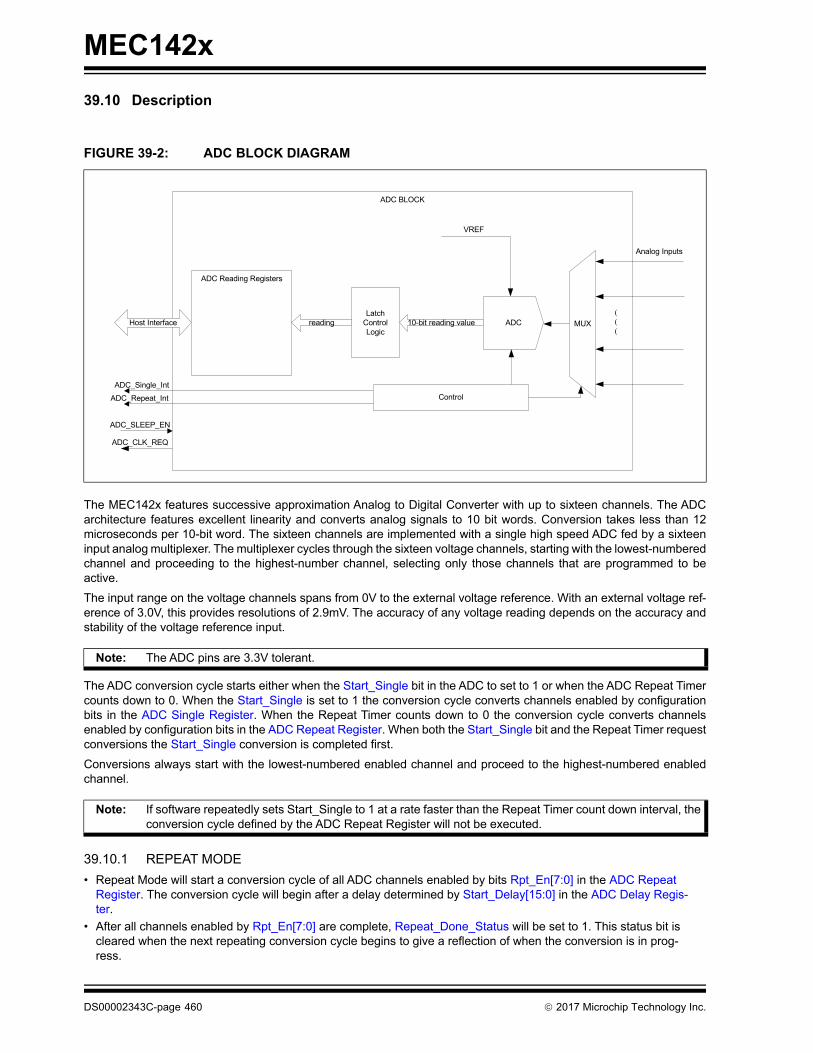
MEC142x
39.10 Description
The MEC142x features successive approximation Analog to Digital Converter with up to sixteen channels. The ADCarchitecture features excellent linearity and converts analog signals to 10 bit words. Conversion takes less than 12microseconds per 10-bit word. The sixteen channels are implemented with a single high speed ADC fed by a sixteeninput analog multiplexer. The multiplexer cycles through the sixteen voltage channels, starting with the lowest-numberedchannel and proceeding to the highest-number channel, selecting only those channels that are programmed to beactive.
The input range on the voltage channels spans from 0V to the external voltage reference. With an external voltage ref-erence of 3.0V, this provides resolutions of 2.9mV. The accuracy of any voltage reading depends on the accuracy andstability of the voltage reference input.
The ADC conversion cycle starts either when the Start_Single bit in the ADC to set to 1 or when the ADC Repeat Timercounts down to 0. When the Start_Single is set to 1 the conversion cycle converts channels enabled by configurationbits in the ADC Single Register. When the Repeat Timer counts down to 0 the conversion cycle converts channelsenabled by configuration bits in the ADC Repeat Register. When both the Start_Single bit and the Repeat Timer requestconversions the Start_Single conversion is completed first.
Conversions always start with the lowest-numbered enabled channel and proceed to the highest-numbered enabledchannel.
39.10.1 REPEAT MODE
• Repeat Mode will start a conversion cycle of all ADC channels enabled by bits Rpt_En[7:0] in the ADC Repeat Register. The conversion cycle will begin after a delay determined by Start_Delay[15:0] in the ADC Delay Regis-ter.
• After all channels enabled by Rpt_En[7:0] are complete, Repeat_Done_Status will be set to 1. This status bit is cleared when the next repeating conversion cycle begins to give a reflection of when the conversion is in prog-ress.
FIGURE 39-2: ADC BLOCK DIAGRAM
Note: The ADC pins are 3.3V tolerant.
Note: If software repeatedly sets Start_Single to 1 at a rate faster than the Repeat Timer count down interval, theconversion cycle defined by the ADC Repeat Register will not be executed.
ADC BLOCK
ADC Reading Registers
ADC_Single_Int
Latch Control Logic
10-bit reading valuereadingHost Interface MUXADC
Control
Analog Inputs
VREF
ADC_Repeat_Int
ADC_SLEEP_EN
ADC_CLK_REQ
DS00002343C-page 460 2017 Microchip Technology Inc.

MEC142x
• As long as Start_Repeat is 1 the ADC will repeatedly begin conversion cycles with a period defined by Repeat_Delay[15:0].
• If the delay period expires and a conversion cycle is already in progress because Start_Single was written with a 1, the cycle in progress will complete, followed immediately by a conversion cycle using Rpt_En[7:0] to control the channel conversions.
39.10.2 SINGLE MODE
• The Single Mode conversion cycle will begin without a delay. After all channels enabled by Single_En[7:0] are complete, Single_Done_Status will be set to 1. When the next conversion cycle begins the bit is cleared.
• If Start_Single is written with a 1 while a conversion cycle is in progress because Start_Repeat is set, the conver-sion cycle will complete, followed immediately by a conversion cycle using Single_En[7:0] to control the channel conversions.
39.11 EC-Only Registers
The registers listed in the Table 39-3, "Analog to Digital Converter Register Summary" are for a single instance of theAnalog to Digital Converter block. The addresses of each register listed in this table are defined as a relative offset tothe host “Base Address” defined in Table 39-2, "Analog to Digital Converter Base Address Table".
Note 39-1 The Base Address indicates where the first register can be accessed in a particular address spacefor a block instance.
TABLE 39-2: ANALOG TO DIGITAL CONVERTER BASE ADDRESS TABLE
Instance NameInstance Number
Host Address Space Base Address
ADC 0 EC 32-bit internal address space
0000_7C00h
TABLE 39-3: ANALOG TO DIGITAL CONVERTER REGISTER SUMMARY
Offset Register Name (Mnemonic)
00h ADC Control Register
04h ADC Delay Register
08h ADC Status Register
0Ch ADC Single Register
10h ADC Repeat Register
14h ADC Channel 0 Reading Register
18h ADC Channel 1 Reading Register
1Ch ADC Channel 2 Reading Register
20h ADC Channel 3 Reading Register
24h ADC Channel 4 Reading Register
28h ADC Channel 5 Reading Register
2Ch ADC Channel 6 Reading Register
2017 Microchip Technology Inc. DS00002343C-page 461

MEC142x
Note: The unused channel reading registers are reserved.
39.11.1 ADC CONTROL REGISTER
The ADC Control Register is used to control the behavior of the Analog to Digital Converter.
30h ADC Channel 7 Reading Register
34h ADC Channel 8 Reading Register
Offset 00h
Bits Description Type DefaultReset Event
31:8 RESERVED RES
7 Single_Done_Status
This bit is cleared when it is written with a 1. Writing a 0 to this bit has no effect.This bit can be used to generate an EC interrupt.
0: ADC single-sample conversion is not complete. This bit is cleared whenever an ADC conversion cycle begins for a single conversion cycle.1: ADC single-sample conversion is completed. This bit is set to 1 when all enabled channels in the single conversion cycle.
R/WC 0h nSYSRST
6 Repeat_Done_Status
This bit is cleared when it is written with a 1. Writing a 0 to this bit has no effect.This bit can be used to generate an EC interrupt.
0: ADC repeat-sample conversion is not complete. This bit is cleared whenever an ADC conversion cycle begins for a repeating conversion cycle.1: ADC repeat-sample conversion is completed. This bit is set to 1 when all enabled channels in a repeating conversion cycle com-plete.
R/WC 0h nSYSRST
5 RESERVED RES
4 Soft Reset
1: writing one causes a reset of the ADC block hardware (not the registers)0: writing zero takes the ADC block out of reset
R/W 0h nSYSRST
3 Power_Saver_Dis
0: Power saving feature is enabled. The Analog to Digital Con-verter controller powers down the ADC between conversion sequences.1: Power saving feature is disabled.
R/W 0h nSYSRST
TABLE 39-3: ANALOG TO DIGITAL CONVERTER REGISTER SUMMARY (CONTINUED)
Offset Register Name (Mnemonic)
DS00002343C-page 462 2017 Microchip Technology Inc.

MEC142x
39.11.2 ADC DELAY REGISTER
The ADC Delay register determines the delay from setting Start_Repeat in the ADC Control Register and the start of aconversion cycle. This register also controls the interval between conversion cycles in repeat mode.
2 Start_Repeat
0: The ADC Repeat Mode is disabled. Note: This setting will not terminate any conversion cycle in process, but will inhibit any fur-ther periodic conversions.1: The ADC Repeat Mode is enabled. This setting will start a con-version cycle of all ADC channels enabled by bits Rpt_En[7:0] in the ADC Repeat Register.
R/W 0h nSYSRST
1 Start_Single
0: The ADC Single Mode is disabled.1: The ADC Single Mode is enabled. This setting starts a single conversion cycle of all ADC channels enabled by bits Sin-gle_En[7:0] in the ADC Single Register.
Note: This bit is self-clearing
R/W 0h nSYSRST
0 Activate
0: The ADC is disabled and placed in its lowest power state. Note: Any conversion cycle in process will complete before the block is shut down, so that the reading registers will contain valid data but no new conversion cycles will begin.1: ADC block is enabled for operation. Start_Single or Start_Re-peat can begin data conversions by the ADC. Note: A reset pulse is sent to the ADC core when this bit changes from 0 to 1.
R/W 0h nSYSRST
Offset 00h
Bits Description Type DefaultReset Event
2017 Microchip Technology Inc. DS00002343C-page 463
MEC142x
39.11.3 ADC STATUS REGISTER
The ADC Status Register indicates whether the ADC has completed a conversion cycle.
Note 39-2 Bits that correspond to the unused channels are reserved.
39.11.4 ADC SINGLE REGISTER
The ADC Single Register is used to control which ADC channel is captured during a Single-Sample conversion cycleinitiated by the Start_Single bit in the ADC Control Register.
APPLICATION NOTE: Do not change the bits in this register in the middle of a conversion cycle to insure properoperation.
Offset 04h
Bits Description Type DefaultReset Event
31:16 Repeat_Delay[15:0]
This field determines the interval between conversion cycles when Start_Repeat is 1. The delay is in units of 40s. A value of 0 means no delay between conversion cycles, and a value of 0xFFFF means a delay of 2.6 seconds.This field has no effect when Start_Single is written with a 1.
R/W 0000h nSYSRST
15:0 Start_Delay[15:0]
This field determines the starting delay before a conversion cycle is begun when Start_Repeat is written with a 1. The delay is in units of 40s. A value of 0 means no delay before the start of a conver-sion cycle, and a value of 0xFFFF means a delay of 2.6 seconds.This field has no effect when Start_Single is written with a 1.
R/W 0000h nSYSRST
Offset 08h
Bits Description Type DefaultReset Event
31:8 RESERVED RES
7:0 ADC_Ch_Status[7:0]
All bits are cleared by being written with a ‘1’.0: conversion of the corresponding ADC channel is not complete1: conversion of the corresponding ADC channel is completeNote: for enabled single cycles, the Single_Done_Status bit in the ADC Control Register is also set after all enabled channel conver-sion are done; for enabled repeat cycles, the Repeat_Done_Status in the ADC Control Register is also set after all enabled channel conversion are done. See Note 39-2.
R/WC 00h nSYSRST
DS00002343C-page 464 2017 Microchip Technology Inc.

MEC142x
39.11.5 ADC REPEAT REGISTER
The ADC Repeat Register is used to control which ADC channels are captured during a repeat conversion cycle initiatedby the Start_Repeat bit in the ADC Control Register.
39.11.6 ADC CHANNEL READING REGISTERS
All 8 ADC channels return their results into a 32-bit reading register. In each case the low 10 bits of the reading registerreturn the result of the Analog to Digital conversion and the upper 22 bits return 0. Table 39-3, “Analog to Digital Con-verter Register Summary,” on page 461 shows the addresses of all the reading registers.
Note 39-3 The ADC Channel Reading Registers access require single 16, or 32 bit reads; i.e., two 8 bit readscannot ensure data coherency.
Offset 0Ch
Bits Description Type DefaultReset Event
31:8 RESERVED RES
7:0 Single_En[7:0]
0: single cycle conversions for this channel are disabled1: single cycle conversions for this channel are enabledEach bit in this field enables the corresponding ADC channel when a single cycle of conversions is started when the Start_Single bit in the ADC Control Register is written with a 1. See Note 39-2.
R/W 00h nSYSRST
Offset 10h
Bits Description Type DefaultReset Event
31:8 RESERVED RES
7:0 Rpt_En[7:0]
0: repeat conversions for this channel are disabled1: repeat conversions for this channel are enabledEach bit in this field enables the corresponding ADC channel for each pass of the Repeated ADC Conversion that is controlled by bit Start_Repeat in the ADC Control Register. See Note 39-2.
R/W 00h nSYSRST
2017 Microchip Technology Inc. DS00002343C-page 465
MEC142x
Offset See Table 39-3, "Analog to Digital Converter Register Summary"
Bits Description Type DefaultReset Event
31:10 RESERVED RES
9:0 ADCx_[9:0]
This read-only field reports the 10-bit output reading of the Input ADCx.
R/W 000h nSYSRST
DS00002343C-page 466 2017 Microchip Technology Inc.

MEC142x
40.0 ANALOG COMPARATOR
40.1 Overview
The Analog Comparator compares the analog voltage on an input pin to a reference voltage and generates an outputthat indicates the result of the comparison.
40.2 References
No references have been cited for this feature.
40.3 Terminology
There is no terminology defined for this section.
40.4 Interface
This block is designed to be accessed externally via the pin interface and internally via a registered host interface.
40.5 Comparator Pin Interface
FIGURE 40-1: I/O DIAGRAM OF BLOCK
TABLE 40-1: SIGNAL DESCRIPTION TABLE
Name Direction Description
CMP_VREF0 Input Negative voltage input for Comparator 0
CMP_VREF1 Input Negative voltage input for Comparator 1
CMP_VIN0 Input Positive voltage input for Comparator 0
CMP_VIN1 Input Positive voltage input for Comparator 1
CMP_VOUT0 Output Comparator 0 output
CMP_VOUT1 Output Comparator 1 output
Comparator Pin Interface
Analog Comparator
Interrupts
Power, Clocks and Reset
Host Interface
2017 Microchip Technology Inc. DS00002343C-page 467

MEC142x
40.6 Host Interface
The registers defined for the Comparator Interface are only accessible by the embedded controller. The ComparatorRegisters for both comparators are located in one register in the EC Subsystem register bank. See Section 34.8.2,"Comparator Control," on page 433.
40.7 Power, Clocks and Reset
This section defines the Power, Clock, and Reset parameters of the block.
40.7.1 POWER DOMAINS
40.7.2 CLOCK INPUTS
This component does not require a clock input.
40.7.3 RESETS
40.8 Interrupts
The comparators do not have a dedicated interrupt output event. An interrupt can be generated by the GPIO whichshares the pin with the comparator output signal.
• GPIO124/CMP_VOUT0
• GPIO120/CMP_VOUT1
The GPIO interrupt is configurable, thereby allowing CMP_VOUTx signal to generate an event when the CMP_VINxinput is greater than the CMP_VREFx input or when it is less than the CMP_VREFx input. See the definition of Bits[7:4]of the Pin Control Registers on page 326.
40.9 Low Power Modes
Each comparator is in its lowest powered state when its ENABLE bit is ‘0’.
Name Description
VTR The logic implemented in this block are powered by this power well.
Name Description
VTR_RESET# This signal resets all the register in the EC Subsystem that interact with the comparators.
DS00002343C-page 468 2017 Microchip Technology Inc.
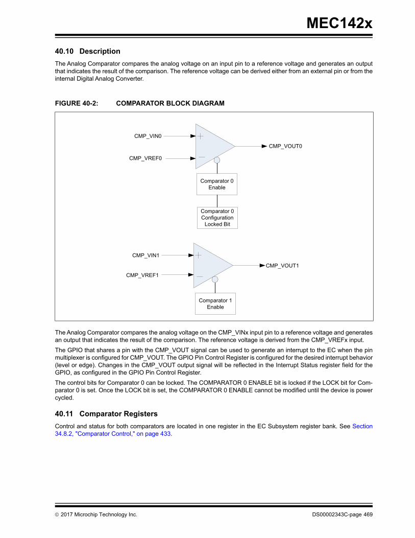
MEC142x
40.10 Description
The Analog Comparator compares the analog voltage on an input pin to a reference voltage and generates an outputthat indicates the result of the comparison. The reference voltage can be derived either from an external pin or from theinternal Digital Analog Converter.
The Analog Comparator compares the analog voltage on the CMP_VINx input pin to a reference voltage and generatesan output that indicates the result of the comparison. The reference voltage is derived from the CMP_VREFx input.
The GPIO that shares a pin with the CMP_VOUT signal can be used to generate an interrupt to the EC when the pinmultiplexer is configured for CMP_VOUT. The GPIO Pin Control Register is configured for the desired interrupt behavior(level or edge). Changes in the CMP_VOUT output signal will be reflected in the Interrupt Status register field for theGPIO, as configured in the GPIO Pin Control Register.
The control bits for Comparator 0 can be locked. The COMPARATOR 0 ENABLE bit is locked if the LOCK bit for Com-parator 0 is set. Once the LOCK bit is set, the COMPARATOR 0 ENABLE cannot be modified until the device is powercycled.
40.11 Comparator Registers
Control and status for both comparators are located in one register in the EC Subsystem register bank. See Section34.8.2, "Comparator Control," on page 433.
FIGURE 40-2: COMPARATOR BLOCK DIAGRAM
CMP_VOUT0
CMP_VIN0
CMP_VREF0
CMP_VOUT1
CMP_VIN1
CMP_VREF1
Comparator 0 Enable
Comparator 1 Enable
Comparator 0 Configuration
Locked Bit
2017 Microchip Technology Inc. DS00002343C-page 469
MEC142x
41.0 TEST MECHANISMS
41.1 Introduction
This device has the following test mechanisms:
• 2-pin processor debug port (ICSP)
• 2-pin UART debug port
• 2-pin Trace FIFO port
• XNOR Chain for board connectivity test
This section defines the ICSP Controller and XNOR Chain for board test.
The UART is defined in Section 17.0, "UART," on page 275 and the Trace FIFO is defined in Section 31.0, "Trace FIFODebug Port (TFDP)," on page 416.
41.2 References
No references have been cited for this chapter.
41.3 Terminology
41.4 ICSP Controller
The ICSP Controller is the pin interface to the MIPs M14K EJTAG port.
41.4.1 INTERFACE
Note 41-1 The ICSP_MCLR input provides the Reset. Note that the reset state of the ICSP port is only local tothe port: its effect is to keep the port in an idle state and to disengage it from the rest of the system,so that it does not affect other on-chip logic in this state.
41.4.2 POWER, CLOCKS, AND RESET
41.4.2.1 Power Domains
Term Definition
ICSP In-Circuit Serial Programmer™
TABLE 41-1: ICSP 2-PIN PORT LIST
Signal Name Direction Description
ICSP_CLK Input Test Clock
ICSP_DATA I/O Bi-directional Test Data
ICSP_MCLR Input Test Reset, low active (Note 41-1). Also referred to as MCLR#
Note: This signal has an internal pull-up.
Name Description
VTR The ICSP Controller logic and registers are implemented on this single power domain.
DS00002343C-page 470 2017 Microchip Technology Inc.

MEC142x
41.4.2.2 Clocks
The ICSP port runs internally from the externally-provided ICSP_CLK clock pulses only. There is no requirement forICSP_CLK to be constantly running.
41.4.2.3 Reset
41.4.3 ICSP TEST MODES
The ICSP block supports TMOD0 .
• TMOD0 supports 2-wire ICSP JTAG
TMOD0 converts 2-wire ICSP signaling (Clock and Data) to standard 4-wire JTAG signaling (TCK, TMS, TDI and TDO).Doing this conversion has a cost of four clocks, therefore four ICSP_CLK pulses is equivalent to one JTAG clock (i.e.,4x slowdown).
Name Description
nSYSRST Power On Reset for ICSP controller and registers
JTAG_RST# Active-Low Test Reset Signal. Generated by toggling ICSP_MCLR low.
FIGURE 41-1: ICSP-TO-JTAG CONVERSION TIMING (4 CLOCKS)
ICSP Clock
ICSP Data
Description
TDI TMS TDO
ICSP Data is undriven at this time to turn around the bus.
TCK
TMS/TDI
TDO
TDI
TDO
The ICSP will resume driving on the next clock cycle.
2017 Microchip Technology Inc. DS00002343C-page 471

MEC142x
41.4.4 INSTRUCTION REGISTERS
41.4.4.1 IDCODE
The MTAP JTAG ID Code is 0214_2445h.
41.4.4.2 SAMPLE/PRELOAD <0x02>
Not implemented, but reserved as required by JTAG standard.
41.4.4.3 SWTAP_CHIP <0x04>
Turn the Chip TAP (MTAP) back on and disable MIPS eJTAG.
41.4.4.4 SWTAP <0x05>
Turn off the Chip TAP (MTAP) and enable MIPS eJTAG.
41.4.4.5 EXTEST <0x06>
Not implemented, but reserved as required by JTAG standard.
TABLE 41-2: PUBLIC INSTRUCTIONS
Instruction Description
IDCODE <0x01> JTAG Standard IDCODE Register
SAMPLE/PRELOAD <0x02> Not implemented, but reserved as required by JTAG standard.
SWTAP_CHIP <0x04> Turn the Chip TAP (MTAP) back on and disable MIPS eJTAG.
SWTAP <0x05> Turn off the Chip TAP (MTAP) and enable MIPS eJTAG.
EXTEST <0x06> Not implemented, but reserved as required by JTAG standard.
MCHP_CMD <0x07> Chip Status interrogation and manual reset control.
BYPASS <0x1F> Standard JTAG Bypass.
Offset 01h
Bits Description Type DefaultReset Event
31:28 VERSION R 0h nSYSRST
27:12 PartNumber R 2142h nSYSRST
11:1 ManufID R 222h nSYSRST
0 RESERVED
Hard-coded to 1h.
R 1h nSYSRST
DS00002343C-page 472 2017 Microchip Technology Inc.

MEC142x
41.4.4.6 MCHP_CMD <0x07>
Offset 01h
Bits Description Type DefaultReset Event
7:0 MCHP_CMD
Microchip Command Register supports the following commands.
Command 0x00: Read Status
Bit [7] Boot Into User Code Status (read-only)
0=Boot ROM will boot normally following a AssertDeviceRe-set command
1=Boot ROM will stall after setting the Boot Ready status bitallowing the ICSP debugger to load code into SRAM follow-ing a AssertDeviceReset command.
Bit [6] BRDY; Boot Ready (read-only)
0 = eJTAG access is not enabled.
1 = Boot ROM is done initializing the device and has enabledeJTAG interface. This bit is cleared by H/W on nSYSRST.
Bit [5:4] RESERVEDBit [3] CFGRDY; Configuration Ready (read-only)
0 = MTAP Device ID Not Valid
1 = MTAP Device ID Valid.
Bit [2] RESERVEDBit [1] SLEEPING
0 = 48 MHz Ring Oscillator is running
1 = The device is sleeping. 48 MHz Ring Oscillator is not run-ning
Bit [0] DEVRST; Device Reset Status (read-only)
0 = MTAP Device Reset is deasserted
1 = MTAP Device Reset is asserted
The MTAP Device Reset is equivalent to a VTR POR, except theMTAP registers are not reset.
Command 0x08: DeviceID
Bit [31:16] Device IDBit [15:8] Sub IDBit [7:0] Revision IDThe Device ID, Sub Id, and Revision ID are a reflection of the value in the same registers defined in Table 7-2, “Chip-Level (Global) Control/Configuration Registers,” on page 153 starting at offset 1Ch.
Note: This command only executes while ConfigurationReady (CFGRDY) is set.
R/W 0h JTAG_RST#
2017 Microchip Technology Inc. DS00002343C-page 473
MEC142x
41.4.4.7 BYPASS <0x1F>
Standard JTAG BYPASS. TDI connected to TDO via a 1-bit Bypass register.
41.4.5 TEST MODE ENTRY
The MCLR pin is used as MCLR for the ICSP interface. The device pulls this signal high internally. The debug connectormust drive this signal correctly to enter ICSP modes.
41.4.5.1 Entry Sequence
To Enter ICSP:
1. Drive MCLR# High.
2. Drive ICSP_CLK and ICSP_DAT Low.
3. Drive MCLR# Low.
4. Send down 32 ICSP Clocks with the Test Mode Entry Code.
5. Drive MCLR# High
41.4.5.2 Test Mode Entry Codes
41.4.5.3 Enabling EJTAG Interface
By default the EJTAG interface is disabled. It is gated by the MTAP (MCHP_TAP) controller. MTAP gates all other TAPcontrollers TDI so they always operate in BYPASS mode. There are two ISCP commands used to enable/disable theMTAP gating.
• IR SWTAP_CHIP (5'h04).
- Enables the MTAP and gates the EJTAG interface behind it.
• IR SWTAP (5'h05).
- Disables the MTAP and enables the EJTAG interface behind it.
Offset 01h (continued)
Bits Description Type DefaultReset Event
7:0 Command 0x09: SetBootIntoUserCode
Sets the MTAP Boot into User Code status bit.
Note: This function only works while the Boot Ready status isset.
Command 0x0A: ClrBootIntoUserCode
Clears the MTAP Boot into User Code status bit.
Note: This function only works while the Boot Ready status isset.
Command 0xD1: AssertDeviceReset
Causes a VTR POR. Test functions remain uneffected.
Note: DEVRST, Device Reset Status, reflects the state of thereset event.
Command 0xD0: DeassertDeviceReset
Clears the AssertDeviceReset.
R/W 0h JTAG_RST#
Test Mode Test Mode Entry Code Description
TMOD0 4D43 4850“MCHP”
2-wire ICSP
DS00002343C-page 474 2017 Microchip Technology Inc.
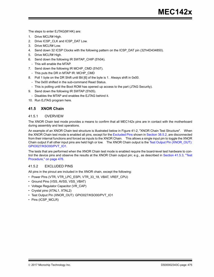
MEC142x
The steps to enter EJTAG(M14K) are:
1. Drive MCLR# High.
2. Drive ICSP_CLK and ICSP_DAT Low.
3. Drive MCLR# Low.
4. Send down 32 ICSP Clocks with the following pattern on the ICSP_DAT pin (32'h4D434850).
5. Drive MCLR# High.
6. Send down the following IR SWTAP_CHIP (5'h04).
- This will enable the MTAP.
7. Send down the following IR MCHP_CMD (5'h07).
- This puts the DR in MTAP IR: MCHP_CMD
8. Poll 1 byte on the DR Shift until Bit [6] of the byte is 1. Always shift in 0x00.
- The 0x00 shifted in the sub-command Read Status.
- This is polling until the Boot ROM has opened up access to the part (JTAG Security).
9. Send down the following IR SWTAP (5'h05).
- Disables the MTAP and enables the EJTAG behind it.
10. Run EJTAG program here.
41.5 XNOR Chain
41.5.1 OVERVIEW
The XNOR Chain test mode provides a means to confirm that all MEC142x pins are in contact with the motherboardduring assembly and test operations.
An example of an XNOR Chain test structure is illustrated below in Figure 41-2, "XNOR Chain Test Structure". Whenthe XNOR Chain test mode is enabled all pins, except for the Excluded Pins shown in Section 38.5.2, are disconnectedfrom their internal functions and forced as inputs to the XNOR Chain. This allows a single input pin to toggle the XNORChain output if all other input pins are held high or low. The XNOR Chain output is the Test Output Pin (XNOR_OUT):GPIO027/KSO00/PVT_IO1.
The tests that are performed when the XNOR Chain test mode is enabled require the board-level test hardware to con-trol the device pins and observe the results at the XNOR Chain output pin; e.g., as described in Section 41.5.3, "TestProcedure," on page 476.
41.5.2 EXCLUDED PINS
All pins in the pinout are included in the XNOR chain, except the following:
• Power Pins (VTR, VTR_LPC_ESPI, VTR_33_18, VBAT, VREF_CPU)
• Ground Pins (VSS, AVSS, VSS_VBAT)
• Voltage Regulator Capacitor (VR_CAP)
• Crystal pins (XTAL1, XTAL2)
• Test Output Pin (XNOR_OUT): GPIO027/KSO00/PVT_IO1
• Pins (ICSP_MCLR)
2017 Microchip Technology Inc. DS00002343C-page 475
MEC142x
41.5.3 TEST PROCEDURE
41.5.3.1 Setup
Warning: Ensure power supply is off during Setup.1. Connect ICSP_MCLR to ground.
2. Connect the VSS, AVSS, VSS_VBAT pins to ground.
3. Connect the VTR, VTR_LPC_ESPI, VTR_33_18, VBAT pins to an unpowered 3.3V power source.
4. Connect the VREF_CPU pin to an unpowered 1.8V power source.
5. Connect an oscilloscope or voltmeter to the Test Output pin.
6. All other pins should be tied to ground.
41.5.3.2 Testing
1. Turn on the 3.3V power source.
2. Enable the XNOR Chain as defined in Section 38.5.3.3, "Procedure to Enable the XNOR Chain".
3. Bring one pin in the chain high. The output on the Test Output Pin (XNOR_OUT): GPIO027/KSO00/PVT_IO1pin should toggle. Then individually toggle each of the remaining pins in the chain. Each time an input pin is tog-gled either high or low the Test Output Pin (XNOR_OUT): GPIO027/KSO00/PVT_IO1 pin should toggle.
4. Once the XNOR test is completed, exit the XNOR Chain Test Mode by cycling VTR power.
41.5.3.3 Procedure to Enable the XNOR Chain
FIGURE 41-2: XNOR CHAIN TEST STRUCTURE
Note: There are 107 pins in the XNOR Chain in the 128-pin package.
Note: Note that at this point all inputs to the XNOR Chain are low, except for the ICSP_MCLR pin, and the outputon the Test Output pin is non-inverted from its initial state, which is dependent on the number of pins in thechain. If the number of input pins in the chain is an even number, the initial state of the Test Output Pin(XNOR_OUT): GPIO027/KSO00/PVT_IO1 is low. If the number of input pins in the chain is an odd number,the initial state of the Test Output Pin (XNOR_OUT): GPIO027/KSO00/PVT_IO1 is high.
Note: The GPIO145(ICSP_CLOCK) pin is used as a clock in this test mode. This pin must never be toggled at arate greater than 20Mhz.
I/O#1 I/O#2 I/O#3 I/O#n XNOROut
DS00002343C-page 476 2017 Microchip Technology Inc.

MEC142x
//BEGIN PROCEDURE TO ENTER XNOR CHAIN
///////////////////////////////////
// Initialize IF
///////////////////////////////////
force ICSP_MCLR = 1;
force GPIO145(ICSP_CLOCK) = 0; //TCLK
force GPIO146(ICSP_DATA) = 0; //TDI
force GPIO130/SMB03_DATA/SMB03_DATA18 = 1; //TMS
Wait 100 ns
///////////////////////////////////
// ICSP Reset
///////////////////////////////////
force ICSP_MCLR = 1;
Wait 1000 ns;
force ICSP_MCLR = 0;
///////////////////////////////////
// ICSP Bypass
///////////////////////////////////
force ICSP_MCLR = 0;
force GPIO146(ICSP_DATA) = 0; //TDI
force GPIO130/SMB03_DATA/SMB03_DATA18 = 1; //TMS
repeat (40)
begin
force ICSP_MCLR = 1;
force ICSP_MCLR = 0;
end
Wait 1000 ns
///////////////////////////////////
// Come out of reset
///////////////////////////////////
force ICSP_MCLR = 1; //P 1
force ICSP_MCLR = 0;
force ICSP_MCLR = 1; //P 2
force ICSP_MCLR = 0;
Wait 100 ns
2017 Microchip Technology Inc. DS00002343C-page 477

MEC142x
///////////////////////////////////
// Write IR with 0xD
///////////////////////////////////
force ICSP_MCLR = 1; //P 3 (TEST_LOGIC_RESET)
force ICSP_MCLR = 0; //1N
force GPIO146(ICSP_DATA) = 0; //TDI
force GPIO130/SMB03_DATA/SMB03_DATA18 = 0; //TMS
force ICSP_MCLR = 1; //P 4 (RUN_TEST_IDLE)
force ICSP_MCLR = 0; //2N
force GPIO146(ICSP_DATA) = 0; //TDI
force GPIO130/SMB03_DATA/SMB03_DATA18 = 1; //TMS
force ICSP_MCLR = 1; //P 5 (SEL_DR)
force ICSP_MCLR = 0; //3N
force GPIO146(ICSP_DATA) = 0; //TDI
force GPIO130/SMB03_DATA/SMB03_DATA18 = 1; //TMS
force ICSP_MCLR = 1; //P 6 (SEL_IR)
force ICSP_MCLR = 0; //4N
force GPIO146(ICSP_DATA) = 0; //TDI
force GPIO130/SMB03_DATA/SMB03_DATA18 = 0; //TMS
force ICSP_MCLR = 1; //P 7 (CAP_IR)
force ICSP_MCLR = 0; //5N
force GPIO146(ICSP_DATA) = 0; //TDI
force GPIO130/SMB03_DATA/SMB03_DATA18 = 0; //TMS
///////////////////////////////////
//SHIFT IR 0xD
///////////////////////////////////
force ICSP_MCLR = 1; //P 8 (SHIFT_IR)
force ICSP_MCLR = 0; //6N
force GPIO146(ICSP_DATA) = 1; //TDI;
force GPIO130/SMB03_DATA/SMB03_DATA18 = 0; //TMS
force ICSP_MCLR = 1; //P 9
force ICSP_MCLR = 0; //7N
force GPIO146(ICSP_DATA) = 0; //TDI;
force GPIO130/SMB03_DATA/SMB03_DATA18 = 0; //TMS
force ICSP_MCLR= 1; //P 10
force ICSP_MCLR = 0; //8N
force GPIO146(ICSP_DATA) = 1; //TDI;
force GPIO130/SMB03_DATA/SMB03_DATA18 = 0; //TMS
force ICSP_MCLR = 1; //P 11
DS00002343C-page 478 2017 Microchip Technology Inc.

MEC142x
force ICSP_MCLR = 0; //9N
force GPIO146(ICSP_DATA) = 1; //TDI;
force GPIO130/SMB03_DATA/SMB03_DATA18 = 1; //TMS //Next will be EXIT1_IR
force ICSP_MCLR = 1; //P 12 (EXIT1_IR)
force ICSP_MCLR 0; //10N
force GPIO146(ICSP_DATA) = 0; //TDI;
force GPIO130/SMB03_DATA/SMB03_DATA18 = 1; //TMS //Next will be UPDATE_IR
force ICSP_MCLR = 1; //P 13 (UPDATE_IR)
force ICSP_MCLR = 0; //11N
force GPIO146(ICSP_DATA) = 0; //TDI;
force GPIO130/SMB03_DATA/SMB03_DATA18 = 0; //TMS //Next will be IDLE
force ICSP_MCLR = 1; //P 14 (IDLE)
force ICSP_MCLR = 0; //12N
force GPIO146(ICSP_DATA) = 0; //TDI;
force GPIO130/SMB03_DATA/SMB03_DATA18 = 0; //TMS //Next will be IDLE
Wait 1000 ns
///////////////////////////////////
// DIR=0, CMD[2:0]=1, DATA[7:0]=01\h, ADDR[7:0]=88\h
///////////////////////////////////
force ICSP_MCLR = 1; //P 15
force ICSP_MCLR = 0; //1N
force GPIO146(ICSP_DATA) = 0; //TDI;
force GPIO130/SMB03_DATA/SMB03_DATA18 = 1; //TMS
force ICSP_MCLR = 1; //P 16
force ICSP_MCLR = 0; //2N
force GPIO146(ICSP_DATA) = 0; //TDI;
force GPIO130/SMB03_DATA/SMB03_DATA18 = 0; //TMS
force ICSP_MCLR = 1; //P 17
force ICSP_MCLR = 0; //3N
force GPIO146(ICSP_DATA) = 0; //TDI;
force GPIO130/SMB03_DATA/SMB03_DATA18 = 0; //TMS
///////////////////////////////////
//DIR 0 - Write
///////////////////////////////////
force ICSP_MCLR = 1; //P 18
force ICSP_MCLR = 0; //N (DR1)
force GPIO146(ICSP_DATA) = 0; //TDI;
force GPIO130/SMB03_DATA/SMB03_DATA18 = 0; //TMS
2017 Microchip Technology Inc. DS00002343C-page 479
MEC142x
///////////////////////////////////
//CMD 1 - Test
///////////////////////////////////
force ICSP_MCLR = 1; //P 19
**Verify JTAG_TDO = 1
force ICSP_MCLR = 0;//N (DR2)
force GPIO146(ICSP_DATA) = 1; //TDI;
force GPIO130/SMB03_DATA/SMB03_DATA18 = 0; //TMS
force `ICSP_MCLR = 1; //P 20
**Verify JTAG_TDO = 1
force ICSP_MCLR = 0; //N (DR3)
force GPIO146(ICSP_DATA) = 0; //TDI;
force GPIO130/SMB03_DATA/SMB03_DATA18 = 0; //TMS
force ICSP_MCLR = 1; //P 21
**Verify JTAG_TDO = 1
force ICSP_MCLR = 0; //N (DR4)
force GPIO146(ICSP_DATA) = 0; //TDI;
force GPIO130/SMB03_DATA/SMB03_DATA18 = 0; //TMS
///////////////////////////////////
//DATA 0x01 - XNOR_EN
///////////////////////////////////
force ICSP_MCLR = 1; //P 22
**Verify JTAG_TDO = 1
force ICSP_MCLR = 0; //N (DR5)
force GPIO146(ICSP_DATA) = 1; //TDI;
force GPIO130/SMB03_DATA/SMB03_DATA18 = 0; //TMS
force ICSP_MCLR = 1; //P23
**Verify JTAG_TDO = 1
force ICSP_MCLR = 0; //N (DR6)
force GPIO146(ICSP_DATA) = 0; //TDI;
force GPIO130/SMB03_DATA/SMB03_DATA18 = 0; //TMS
force ICSP_MCLR = 1; //P 24
**Verify JTAG_TDO = 0
force ICSP_MCLR = 0; //N (DR7)
force GPIO146(ICSP_DATA) = 0; //TDI;
force GPIO130/SMB03_DATA/SMB03_DATA18 = 0; //TMS
force ICSP_MCLR = 1; //P 25
**Verify JTAG_TDO = 0
force ICSP_MCLR = 0; //N (DR8)
force GPIO146(ICSP_DATA) = 0; //TDI;
force GPIO130/SMB03_DATA/SMB03_DATA18 = 0; //TMS
force ICSP_MCLR = 1; //P 26
DS00002343C-page 480 2017 Microchip Technology Inc.
MEC142x
**Verify JTAG_TDO = 0
force ICSP_MCLR = 0; //N (DR9)
force GPIO146(ICSP_DATA) = 0; //TDI;
force GPIO130/SMB03_DATA/SMB03_DATA18 = 0; //TMS
force ICSP_MCLR = 1; //P 27
**Verify JTAG_TDO = 1
force ICSP_MCLR = 0; //N (DR10)
force GPIO146(ICSP_DATA) = 0; //TDI;
force GPIO130/SMB03_DATA/SMB03_DATA18 = 0; //TMS
force `ICSP_MCLR = 1; //P 28
**Verify JTAG_TDO = 0
force ICSP_MCLR = 0; //N (DR11)
force GPIO146(ICSP_DATA) = 0; //TDI;
force GPIO130/SMB03_DATA/SMB03_DATA18 = 0; //TMS
force ICSP_MCLR = 1; //P 29
**Verify JTAG_TDO = 0
force ICSP_MCLR = 0; //N (DR12)
force GPIO146(ICSP_DATA) = 0; //TDI;
force GPIO130/SMB03_DATA/SMB03_DATA18 = 0; //TMS
///////////////////////////////////
//ADDRESS 0x88 - Customer Control
///////////////////////////////////
force ICSP_MCLR = 1; //P 30
**Verify JTAG_TDO = 0
force ICSP_MCLR = 0; //N (DR13)
force GPIO146(ICSP_DATA) = 0; //TDI;
force GPIO130/SMB03_DATA/SMB03_DATA18 = 0; //TMS
force ICSP_MCLR = 1; //P 31
**Verify JTAG_TDO = 1
force ICSP_MCLR = 0; //N (DR14)
force GPIO146(ICSP_DATA) = 0; //TDI;
force GPIO130/SMB03_DATA/SMB03_DATA18 = 0; //TMS
force ICSP_MCLR = 1; //P 32
**Verify JTAG_TDO = 0
force ICSP_MCLR = 0; //N (DR15)
force GPIO146(ICSP_DATA) = 0; //TDI;
force GPIO130/SMB03_DATA/SMB03_DATA18 = 0; //TMS
force ICSP_MCLR = 1; //P 33
**Verify JTAG_TDO = 0
force ICSP_MCLR = 0; //N (DR16)
force GPIO146(ICSP_DATA) = 1; //TDI;
force GPIO130/SMB03_DATA/SMB03_DATA18 = 0; //TMS
force ICSP_MCLR = 1; //P 34
2017 Microchip Technology Inc. DS00002343C-page 481
MEC142x
**Verify JTAG_TDO = 0
force ICSP_MCLR = 0; //N (DR17)
force GPIO146(ICSP_DATA) = 0; //TDI;
force GPIO130/SMB03_DATA/SMB03_DATA18 = 0; //TMS
force ICSP_MCLR = 1; //P 35
**Verify JTAG_TDO = 1
force ICSP_MCLR = 0; //N (DR18)
force GPIO146(ICSP_DATA) = 0; //TDI;
force GPIO130/SMB03_DATA/SMB03_DATA18 = 0; //TMS
force ICSP_MCLR = 1; //P 36
**Verify JTAG_TDO = 0
force ICSP_MCLR = 0; //N (DR19)
force GPIO146(ICSP_DATA) = 0; //TDI;
force GPIO130/SMB03_DATA/SMB03_DATA18 = 0; //TMS
force ICSP_MCLR = 1; //P 37
**Verify JTAG_TDO = 0
force ICSP_MCLR = 0; //N (DR20)
force GPIO146(ICSP_DATA) = 1; //TDI;
force GPIO130/SMB03_DATA/SMB03_DATA18 = 1; //TMS
force ICSP_MCLR= 1; //P 38
**Verify JTAG_TDO = 0
force ICSP_MCLR = 0; //N (E1_DR)
force GPIO146(ICSP_DATA) = 0; //TDI;
force GPIO130/SMB03_DATA/SMB03_DATA18 = 1; //TMS
force ICSP_MCLR = 1; //P 39
force ICSP_MCLR = 0; //N (UP_DR)
force GPIO146(ICSP_DATA) = 0; //TDI;
force GPIO130/SMB03_DATA/SMB03_DATA18 = 0; //TMS
force ICSP_MCLR = 1; //P 40
force ICSP_MCLR = 0; //N (EXTRA CLK)
force GPIO146(ICSP_DATA) = 0; //TDI;
force GPIO130/SMB03_DATA/SMB03_DATA18 = 0; //TMS
force ICSP_MCLR = 1; //P 41
force ICSP_MCLR= 0; //N (EXTRA CLK)
force GPIO146(ICSP_DATA) = 0; //TDI;
force GPIO130/SMB03_DATA/SMB03_DATA18 = 0; //TMS
Wait 1000 ns
////////////////////////////////////////////////////////////////////////////
//FINISHED PROCEDURE TO ENTER XNOR
///////////////////////////////////////////////////////////////////////////
DS00002343C-page 482 2017 Microchip Technology Inc.

MEC142x
42.0 ELECTRICAL SPECIFICATIONS
42.1 Maximum Ratings*
*Stresses exceeding those listed could cause permanent damage to the device. This is a stress rating only and func-tional operation of the device at any other condition above those indicated in the operation sections of this specificationis not implied.
42.1.1 ABSOLUTE MAXIMUM THERMAL RATINGS
42.1.2 ABSOLUTE MAXIMUM SUPPLY VOLTAGE RATINGS
42.1.3 ABSOLUTE MAXIMUM I/O VOLTAGE RATINGS
Note 42-1 The Power Supply used to power the buffer is shown in the Signal Power Well column of the PinMultiplexing Tables in Section 2.0 “Pin Configuration”.
Note: When powering this device from laboratory or system power supplies, it is important that the Absolute Max-imum Ratings not be exceeded or device failure can result. Some power supplies exhibit voltage spikes ontheir outputs when the AC power is switched on or off. In addition, voltage transients on the AC power linemay appear on the DC output. If this possibility exists, it is suggested that a clamp circuit be used.
TABLE 42-1: ABSOLUTE MAXIMUM THERMAL RATINGS
Parameter Maximum Limits
Operating Temperature Range 0oC to +70oC Commercial-40oC to +85oC Industrial
Storage Temperature Range -55o to +150oC
Lead Temperature Range Refer to JEDEC Spec J-STD-020B
TABLE 42-2: ABSOLUTE POWER SUPPLY RATINGS
Symbol Parameter Maximum Limits
VBAT 3.0V Battery Backup Power Supply with respect to ground -0.3V to +3.63V
VTR 3.3V Suspend Power Supply with respect to ground -0.3V to +3.63V
VTR_33_18 3.3V or 1.8V Power Supply with respect to ground -0.3V to +3.63V
VTR_LPC_ESPI 3.3V or 1.8V Power Supply with respect to ground -0.3V to +3.63V
VCC 3.3V Main Power Supply with respect to ground (Con-nected to VCC_PWRGD pin)
-0.3V to +3.63V
Parameter Maximum Limits
Voltage with respect to ground on any pin without back-drive protection
-0.3V to (Power Supply used to power the buffer) + 0.3V (Note 42-1)
2017 Microchip Technology Inc. DS00002343C-page 483

MEC142x
42.2 Operational Specifications
42.2.1 POWER SUPPLY OPERATIONAL CHARACTERISTICS
42.2.2 AC ELECTRICAL SPECIFICATIONS
The AC Electrical Specifications for the clock input time are defined in Section 43.2, "Clocking AC Timing Characteris-tics," on page 497. The clock rise and fall times use the standard input thresholds of 0.8V and 2.0V unless otherwisespecified and the capacitive values listed in Section 42.2.2, "AC Electrical Specifications," on page 484.
42.2.3 CAPACITIVE LOADING SPECIFICATIONS
The following table defines the maximum capacitive load validated for the buffer characteristics listed in Table 42-5, “DCElectrical Characteristics,” on page 485.
CAPACITANCE TA = 25°C; fc = 1MHz; Vcc = 3.3 VDC
TABLE 42-3: POWER SUPPLY OPERATING CONDITIONS
Symbol Parameter MIN TYP MAX Units
VBAT Battery Backup Power Supply 2.0 3.0 3.6 V
VTR Suspend Power Supply 3.135 3.3 3.465 V
VTR_33_18 3.3V Power Supply 3.135 3.3 3.465 V
1.8V Power Supply 1.71 1.80 1.89 V
VTR_LPC_ESPI 3.3V Power Supply 3.135 3.3 3.465 V
1.8V Power Supply 1.71 1.80 1.89 V
Note: The specification for the VTR, VTR_33_18 and VTR_LPC_ESPI supplies are +/- 5%.
Note: All output pins, except pin under test, tied to AC ground.
TABLE 42-4: MAXIMUM CAPACITIVE LOADING
Parameter SymbolLimits
Unit NotesMIN TYP MAX
Input Capacitance of PCI_I and PCI_IO pins
CIN Note 42-2
pF
Input Capacitance of PCI_CLK pin CIN Note 42-2
pF
Output Load Capacitance supported by PCI_IO, PCI_O, and PCI_OD
COUT Note 42-2
pF
SUSCLK Input Capacitance CIN 10 pF
Input Capacitance of PECI_I and PECI_IO
CIN 10 pF
Output Load Capacitance supported by PECI_IO and OD_PH
COUT 10 pF
DS00002343C-page 484 2017 Microchip Technology Inc.
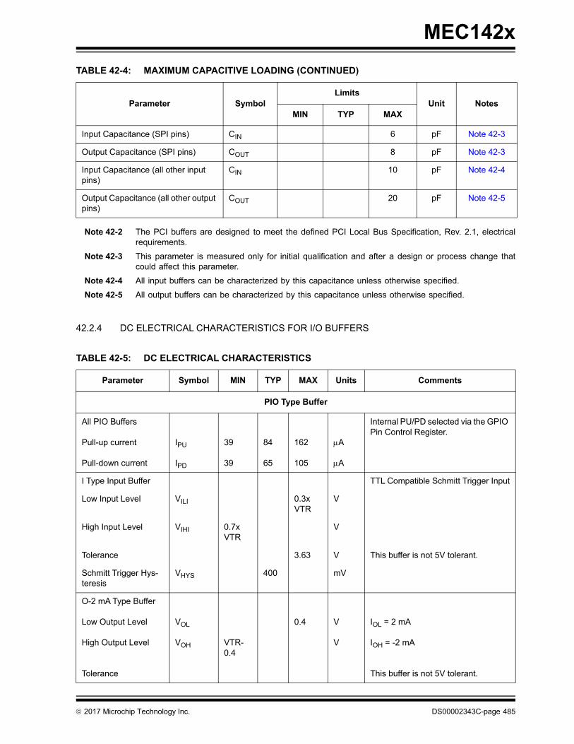
MEC142x
Note 42-2 The PCI buffers are designed to meet the defined PCI Local Bus Specification, Rev. 2.1, electricalrequirements.
Note 42-3 This parameter is measured only for initial qualification and after a design or process change thatcould affect this parameter.
Note 42-4 All input buffers can be characterized by this capacitance unless otherwise specified.
Note 42-5 All output buffers can be characterized by this capacitance unless otherwise specified.
42.2.4 DC ELECTRICAL CHARACTERISTICS FOR I/O BUFFERS
Input Capacitance (SPI pins) CIN 6 pF Note 42-3
Output Capacitance (SPI pins) COUT 8 pF Note 42-3
Input Capacitance (all other input pins)
CIN 10 pF Note 42-4
Output Capacitance (all other output pins)
COUT 20 pF Note 42-5
TABLE 42-5: DC ELECTRICAL CHARACTERISTICS
Parameter Symbol MIN TYP MAX Units Comments
PIO Type Buffer
All PIO Buffers
Pull-up current
Pull-down current
IPU
IPD
39
39
84
65
162
105
A
A
Internal PU/PD selected via the GPIO Pin Control Register.
I Type Input Buffer TTL Compatible Schmitt Trigger Input
Low Input Level VILI 0.3x VTR
V
High Input Level VIHI 0.7x VTR
V
Tolerance 3.63 V This buffer is not 5V tolerant.
Schmitt Trigger Hys-teresis
VHYS 400 mV
O-2 mA Type Buffer
Low Output Level
High Output Level
Tolerance
VOL
VOH VTR-0.4
0.4 V
V
IOL = 2 mA
IOH = -2 mA
This buffer is not 5V tolerant.
TABLE 42-4: MAXIMUM CAPACITIVE LOADING (CONTINUED)
Parameter SymbolLimits
Unit NotesMIN TYP MAX
2017 Microchip Technology Inc. DS00002343C-page 485

MEC142x
IO-2 mA Type Buffer _ _ _ _ _ Same characteristics as an I and an O-2mA.
OD-2 mA Type Buffer
Low Output Level
Tolerance
VOL 0.4 V VOL = 2 mA
This buffer is not 5V tolerant.
IOD-2 mA Type Buf-fer
_ _ _ _ _ Same characteristics as an I and an OD-2mA.
O-4 mA Type Buffer
Low Output Level
High Output Level
Tolerance
VOL
VOH VTR-0.4
0.4 V
V
IOL = 4 mA
IOH = -4 mA
This buffer is not 5V tolerant.
IO-4 mA Type Buffer _ _ _ _ _ Same characteristics as an I and an O-4mA.
OD-4 mA Type Buffer
Low Output Level
Tolerance
VOL 0.4 V VOL = 4 mA
This buffer is not 5V tolerant.
IOD-4 mA Type Buf-fer
_ _ _ _ _ Same characteristics as an I and an OD-4mA.
O-8 mA Type Buffer
Low Output Level
High Output Level
Tolerance
VOL
VOH VTR-0.4
0.4 V
V
IOL = 8 mA
IOH = -8 mA
This buffer is not 5V tolerant.
IO-8 mA Type Buffer _ _ _ _ _ Same characteristics as an I and an O-8mA.
OD-8 mA Type Buffer
Low Output Level
Tolerance
VOL 0.4 V VOL = 8 mA
This buffer is not 5V tolerant.
IOD-8 mA Type Buf-fer
_ _ _ _ _ Same characteristics as an I and an OD-8mA.
TABLE 42-5: DC ELECTRICAL CHARACTERISTICS (CONTINUED)
Parameter Symbol MIN TYP MAX Units Comments
DS00002343C-page 486 2017 Microchip Technology Inc.

MEC142x
O-12 mA Type Buffer
Low Output Level
High Output Level
Tolerance
VOL
VOH VTR-0.4
0.4 V
V
IOL = 12mA
IOH = -12mA
This buffer is not 5V tolerant.
IO-12 mA Type Buffer _ _ _ _ _ Same characteristics as an I and an O-12mA.
OD-12 mA Type Buf-fer
Low Output Level
Tolerance
VOL 0.4 V IOL = 12mA
This buffer is not 5V tolerant.
IOD-12 mA Type Buf-fer
_ _ _ _ _ Same characteristics as an I and an OD-12mA.
ILLKLow Leakage Input Buffer
TTL Levels
Low Input Level VILI 0.8 V
High Input Level VIH 2.0 V
Input Leakage IIL -500 +500 nA VIN = 0n, VBAT = 3.0 VDC & VTR = 0 VDC
I_AN Type Buffer
I_AN Type Buffer(Analog Input Buffer)
I_AN Voltage range on pins:-0.3V to +3.63V
These buffers are not 5V tolerant buf-fers and they are not backdrive pro-tected
PCI_PIO Type Buffer
All PCI_PIO Buffers
Pull-up current IPU 0.6 1 1.5 mA
Internal PU is selected via the GPIO Pin Control Register.
PCI_CLK Type Buffer
PCI_IO Type Buffers
PCI_OD Type Buffer
PCI_ICLK
PCI_IOPCI_OPCI_I
PCI_OD
See PCI Local Bus Specification Rev. 2.1
These buffers are not 5V tolerant buf-fers and they are not backdrive pro-tected.
TABLE 42-5: DC ELECTRICAL CHARACTERISTICS (CONTINUED)
Parameter Symbol MIN TYP MAX Units Comments
2017 Microchip Technology Inc. DS00002343C-page 487

MEC142x
PECI Type Buffer
VREF_CPU Connects to CPU Voltage pin(Processor dependent)
PECI Bus Voltage VBUS 0.95 1.26 V
SBTSI Bus Voltage VBUS 1.28 1.9 V
Input current IDC 100 µA
Input Low Current ILEAK -10 +10 µA This buffer is not 5V tolerant This buffer is not backdrive protected.
PECI_I Buffer All input and output voltages are a function of Vref, which is connected to CPU_VREF input.
Input voltage range VIn -0.3 +Vref0.3
V
Low Input Level VIL 0.275Vref
V
High Input Level VIH 0.725Vref
V This buffer is not 5V tolerant This buffer is not backdrive protected.
PECI_IO All input and output voltages are a function of Vref, which is connected to CPU_VREF input.
See PECI Specification.
Input voltage range VIn -0.3 +Vref0.3
V
Hysteresis VHYS 0.1 Vref
0.2Vref
V
Low Input Level VIL 0.275Vref
V
High Input Level VIH 0.725Vref
V
Low Output Level VOL 0.25Vref
V 0.5mA < IOL < 1mA
High Output Level VOH 0.75 Vref
V IOH = -6mA
Tolerance 3.63 V This buffer is not 5V tolerantThis buffer is not backdrive protected.
TABLE 42-5: DC ELECTRICAL CHARACTERISTICS (CONTINUED)
Parameter Symbol MIN TYP MAX Units Comments
DS00002343C-page 488 2017 Microchip Technology Inc.
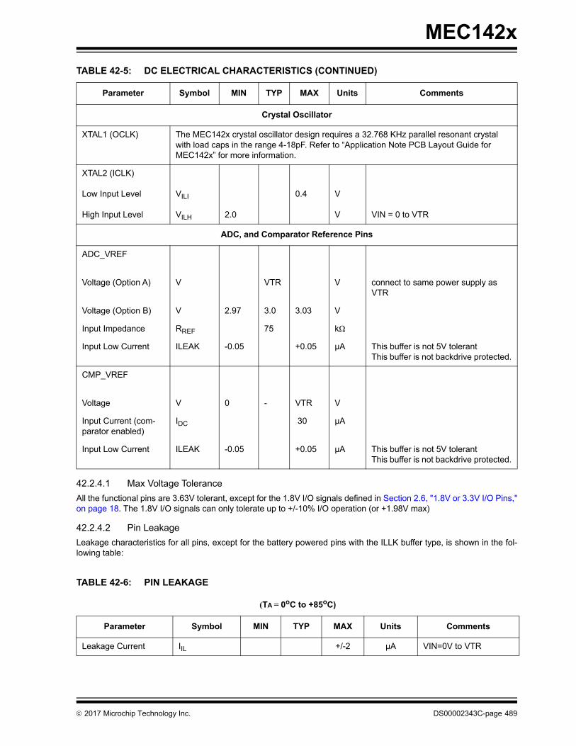
MEC142x
42.2.4.1 Max Voltage Tolerance
All the functional pins are 3.63V tolerant, except for the 1.8V I/O signals defined in Section 2.6, "1.8V or 3.3V I/O Pins,"on page 18. The 1.8V I/O signals can only tolerate up to +/-10% I/O operation (or +1.98V max)
42.2.4.2 Pin Leakage
Leakage characteristics for all pins, except for the battery powered pins with the ILLK buffer type, is shown in the fol-lowing table:
Crystal Oscillator
XTAL1 (OCLK) The MEC142x crystal oscillator design requires a 32.768 KHz parallel resonant crystal with load caps in the range 4-18pF. Refer to “Application Note PCB Layout Guide for MEC142x” for more information.
XTAL2 (ICLK)
Low Input Level
High Input Level
VILI
VILH 2.0
0.4 V
V VIN = 0 to VTR
ADC, and Comparator Reference Pins
ADC_VREF
Voltage (Option A) V VTR V connect to same power supply as VTR
Voltage (Option B) V 2.97 3.0 3.03 V
Input Impedance RREF 75 kΩ
Input Low Current ILEAK -0.05 +0.05 µA This buffer is not 5V tolerant This buffer is not backdrive protected.
CMP_VREF
Voltage V 0 - VTR V
Input Current (com-parator enabled)
IDC 30 µA
Input Low Current ILEAK -0.05 +0.05 µA This buffer is not 5V tolerant This buffer is not backdrive protected.
TABLE 42-6: PIN LEAKAGE
(TA = 0oC to +85oC)
Parameter Symbol MIN TYP MAX Units Comments
Leakage Current IIL +/-2 µA VIN=0V to VTR
TABLE 42-5: DC ELECTRICAL CHARACTERISTICS (CONTINUED)
Parameter Symbol MIN TYP MAX Units Comments
2017 Microchip Technology Inc. DS00002343C-page 489

MEC142x
42.2.4.3 Backdrive Protection
All signal pins are Backdrive Protected except those listed in the Pin Configuration chapter as non-backdrive protected.
42.2.5 ADC ELECTRICAL CHARACTERISTICS
42.2.6 COMPARATOR ELECTRICAL CHARACTERISTICS
TABLE 42-7: BACKDRIVE PROTECTION
(TA = 0oC to +85oC)
Parameter Symbol MIN TYP MAX Units Comments
Input Leakage IIL -2 +2 µA VIN=3.47V@VTR=0V
TABLE 42-8: ADC CHARACTERISTICS
Parameter MIN TYP MAX Units
Analog Supply Voltage (powered by VTR)
3.135 3.3 3.465 V
Resolution – – 10 Bits
Accuracy – 2 4 LSB
Differential Non Linearity, DNL -1 – +1 LSB
Integral Non Linearity, INL -1.5 – +1.5 LSB
Gain Error, EGAIN -2 – 2 LSB
Offset Error, EOFFSET -2 – 2 LSB
Conversion Time – – 12 s/channel
Input Impedance 4 4.5 5.3 M
VREF Input Impedance 630 750 830 k
TABLE 42-9: AC AND DC CHARACTERISTICS: COMPARATOR
CHARACTERISTICS Standard Operating Conditions (unless otherwise noted)
Symbol Characteristic Min Typ Max Units Comments
VIN Input Voltage Range 0 - VTR V
VHYST Input Hysteresis Voltage 15 30 45 mV
CMRR Common mode rejection ratio 44 - - dB
TRESP Large signal response time — 100 160 ns VCM = VDD/2100 mV step
DS00002343C-page 490 2017 Microchip Technology Inc.

MEC142x
Note 42-6 To prevent getting glitches on the comparator output, it is recommended to enable the comparatorand wait for the output to be valid and stable before configuring the pin for the CMP_VOUTx function.
42.2.7 THERMAL CHARACTERISTICS
TSRESP Small signal response time — 160 320 ns VCM = VDD/2100 mV step
TON Comparator Enable to Valid Output
— — 0.1 µS Note 42-6
TABLE 42-10: THERMAL OPERATING CONDITIONS
Rating Symbol Min. Typical Max. Unit
Consumer Temperature Devices
Operating Junction Temperature Range TJ — — +125 (Note 1)
°C
Operating Ambient Temperature Range - Commercial TA 0 — +70 °C
Operating Ambient Temperature Range - Industrial TA -40 — +85 °C
Power Dissipation:Internal Chip Power Dissipation:
PINT = VTR x IVTR from Table 42-12 and Table 42-13(e.g., 3.45V x 12.50mA = 43mW) PD PINT + PI/O W
I/O Pin Power Dissipation:I/O = S ((VTR– VOH x IOH) + S (VOL x IOL))
Maximum Allowed Power Dissipation PDMAX (TJ – TA)/JA W
Note 1: TJ Max value is at ambient of 70°C
TABLE 42-11: THERMAL PACKAGING CHARACTERISTICS
Characteristics Symbol Typical Max. Unit Notes
Package Thermal Resistance, 128-pin VTQFP JA 51.0 — °C/W 1
JC 25.0 — °C/W 1
Package Thermal Resistance, 128-pin WFBGA JA 77.2 — °C/W 1
JC 22.8 — °C/W 1
Package Thermal Resistance, 144-pin WFBGA JA 76.8 — °C/W 1
JC 20.5 — °C/W 1
Note 1: Junction to ambient thermal resistance, Theta-JA (JA) and Junction to case thermal resistance, Theta-JC (JC) numbers are achieved by package simulations.
TABLE 42-9: AC AND DC CHARACTERISTICS: COMPARATOR (CONTINUED)
CHARACTERISTICS Standard Operating Conditions (unless otherwise noted)
Symbol Characteristic Min Typ Max Units Comments
2017 Microchip Technology Inc. DS00002343C-page 491

MEC142x
42.3 Power Consumption
TABLE 42-12: VTR SUPPLY CURRENT, I_VTR
VCC VTRLPC
Clock
48 MHz Ring
Oscillator Frequency
Typical (3.3V, 25o C)
Max(3.45V,70o C)
Max(3.45V,85o C)
Units Comments
On On On 48MHz 10.50 12.00 13.00 mA FULL ON HIGH
On On On 48MHz 10.00 11.50 12.50 mA FULL ON
On On On 1MHz 3.25 4.25 4.75 mA FULL ON LOW
On On On 1MHz 2.75 3.75 4.50 mA Heavy Sleep 1
On On On Gated 1.00 2.10 2.75 mA Heavy Sleep 2
On On On Off 0.65 1.75 2.25 mA Heavy Sleep 3
On On On Off 0.55 1.60 2.20 mA Deepest Sleep
Off On Off 48MHz 10.00 11.50 12.50 mA FULL ON HIGH
Off On Off 48MHz 9.50 11.00 12.00 mA FULL ON
Off On Off 1MHz 2.50 3.75 4.25 mA FULL ON LOW
Off On Off 1MHz 2.25 3.25 4.00 mA Heavy Sleep 1
Off On Off Gated 0.80 1.90 2.55 mA Heavy Sleep 2
Off On Off Off 0.45 1.65 2.05 mA Heavy Sleep 3
Off On Off Off 0.35 1.40 2.00 mA Deepest Sleep
Note 1: FULL ON HIGH is defined as follows: The processor is not sleeping, the Core regulator and the Ring Oscillator remain powered and the following blocks are Active: LPC, EMI, ADC, EC Subsystem, Hiber-nation Timer, Interrupt Controller, PWM 0-6, TFDP, Basic Timers 0-3, JTAG, RTC. The following block is Idle: PECI.
2: FULL ON is defined as follows: The processor is not sleeping, the Core regulator and the Ring Oscillator remain powered, and at least one block is not sleeping.
3: FULL ON LOW is defined as follows: The processor is not sleeping, the Core regulator and the Ring Oscillator remain powered and the following blocks are Active: EC Subsystem, Interrupt Controller, Basic Timer 0, JTAG. The following blocks are Idle: LPC, EMI, PECI.
4: The sleep states are defined in the System Sleep Control Register in the Power, Clocks and Resets Chapter. See Table 3-12, “System Sleep Control Bit Encoding,” on page 68.
5: In order to achieve the lowest leakage current when both PECI and SB TSI are not used, set the VREF_CPU Disable bit to 1. This bit is defined in Section 34.8.5, VREF_CPU DISABLE.
6: All values are taken with Comparator 0, Comparator 1 and ADC disabled. See Table 42-13 for additional IVTR with these blocks enabled.
DS00002343C-page 492 2017 Microchip Technology Inc.
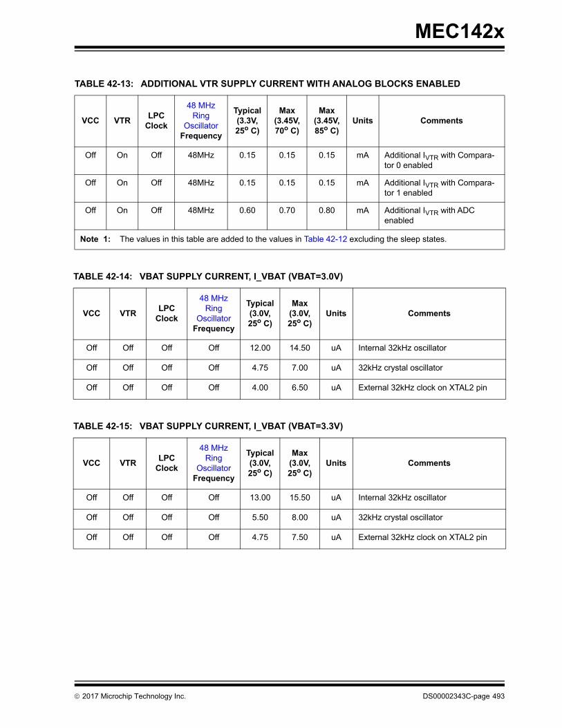
MEC142x
TABLE 42-13: ADDITIONAL VTR SUPPLY CURRENT WITH ANALOG BLOCKS ENABLED
VCC VTRLPC
Clock
48 MHz Ring
Oscillator Frequency
Typical (3.3V, 25o C)
Max(3.45V,70o C)
Max(3.45V,85o C)
Units Comments
Off On Off 48MHz 0.15 0.15 0.15 mA Additional IVTR with Compara-tor 0 enabled
Off On Off 48MHz 0.15 0.15 0.15 mA Additional IVTR with Compara-tor 1 enabled
Off On Off 48MHz 0.60 0.70 0.80 mA Additional IVTR with ADC enabled
Note 1: The values in this table are added to the values in Table 42-12 excluding the sleep states.
TABLE 42-14: VBAT SUPPLY CURRENT, I_VBAT (VBAT=3.0V)
VCC VTRLPC
Clock
48 MHz Ring
Oscillator Frequency
Typical (3.0V, 25o C)
Max(3.0V,25o C)
Units Comments
Off Off Off Off 12.00 14.50 uA Internal 32kHz oscillator
Off Off Off Off 4.75 7.00 uA 32kHz crystal oscillator
Off Off Off Off 4.00 6.50 uA External 32kHz clock on XTAL2 pin
TABLE 42-15: VBAT SUPPLY CURRENT, I_VBAT (VBAT=3.3V)
VCC VTRLPC
Clock
48 MHz Ring
Oscillator Frequency
Typical (3.0V, 25o C)
Max(3.0V,25o C)
Units Comments
Off Off Off Off 13.00 15.50 uA Internal 32kHz oscillator
Off Off Off Off 5.50 8.00 uA 32kHz crystal oscillator
Off Off Off Off 4.75 7.50 uA External 32kHz clock on XTAL2 pin
2017 Microchip Technology Inc. DS00002343C-page 493
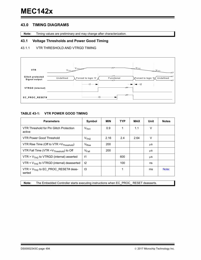
MEC142x
43.0 TIMING DIAGRAMS
43.1 Voltage Thresholds and Power Good Timing
43.1.1 VTR THRESHOLD AND VTRGD TIMING
Note: Timing values are preliminary and may change after characterization.
TABLE 43-1: VTR POWER GOOD TIMING
Parameters Symbol MIN TYP MAX Unit Notes
VTR Threshold for Pin Glitch Protection active
VTH1 0.9 1 1.1 V
VTR Power Good Threshold VTH2 2.16 2.4 2.64 V
VTR Rise Time (Off to VTR =VThreshold) VRise 200 s
VTR Fall Time (VTR =VThreshold) to Off VFall 200 s
VTR > VTH2 to VTRGD (internal) asserted t1 600 s
VTR < VTH2 to VTRGD (internal) deasserted t2 100 ns
VTR > VTH2 to EC_PROC_RESET# deas-serted
t3 1 ms Note:
Note: The Embedded Controller starts executing instructions when EC_PROC_ RESET deasserts.
U nde fined Functiona l
t1
Forced to log ic ‘0 ’Forced to log ic ‘0 ’
VTR G D (in terna l)
G litch protected S ignal outpu t
VTR
U ndefined
t2
V T H 2V TH 2V T H 1 V T H 1
t3E C _P R O C _R E SE T#
DS00002343C-page 494 2017 Microchip Technology Inc.
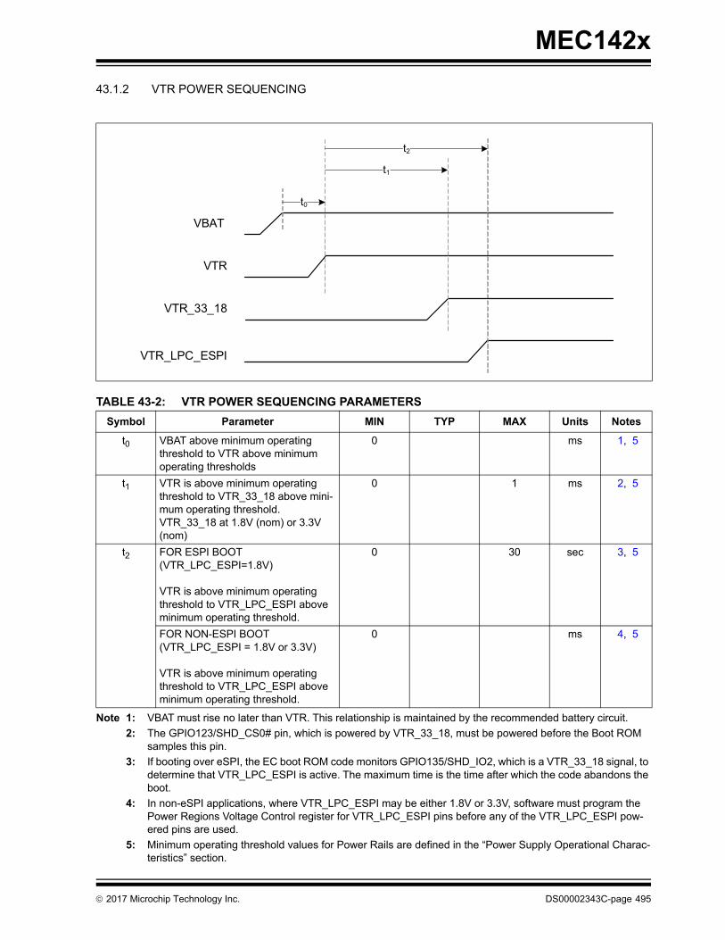
MEC142x
43.1.2 VTR POWER SEQUENCING
Note 1: VBAT must rise no later than VTR. This relationship is maintained by the recommended battery circuit.
2: The GPIO123/SHD_CS0# pin, which is powered by VTR_33_18, must be powered before the Boot ROM samples this pin.
3: If booting over eSPI, the EC boot ROM code monitors GPIO135/SHD_IO2, which is a VTR_33_18 signal, to determine that VTR_LPC_ESPI is active. The maximum time is the time after which the code abandons the boot.
4: In non-eSPI applications, where VTR_LPC_ESPI may be either 1.8V or 3.3V, software must program the Power Regions Voltage Control register for VTR_LPC_ESPI pins before any of the VTR_LPC_ESPI pow-ered pins are used.
5: Minimum operating threshold values for Power Rails are defined in the “Power Supply Operational Charac-teristics” section.
TABLE 43-2: VTR POWER SEQUENCING PARAMETERS
Symbol Parameter MIN TYP MAX Units Notes
t0 VBAT above minimum operating threshold to VTR above minimum operating thresholds
0 ms 1, 5
t1 VTR is above minimum operating threshold to VTR_33_18 above mini-mum operating threshold.VTR_33_18 at 1.8V (nom) or 3.3V (nom)
0 1 ms 2, 5
t2 FOR ESPI BOOT (VTR_LPC_ESPI=1.8V)
VTR is above minimum operating threshold to VTR_LPC_ESPI above minimum operating threshold.
0 30 sec 3, 5
FOR NON-ESPI BOOT(VTR_LPC_ESPI = 1.8V or 3.3V)
VTR is above minimum operating threshold to VTR_LPC_ESPI above minimum operating threshold.
0 ms 4, 5
VTR_33_18
VBAT
VTR
VTR_LPC_ESPI
t0
t1
t2
2017 Microchip Technology Inc. DS00002343C-page 495
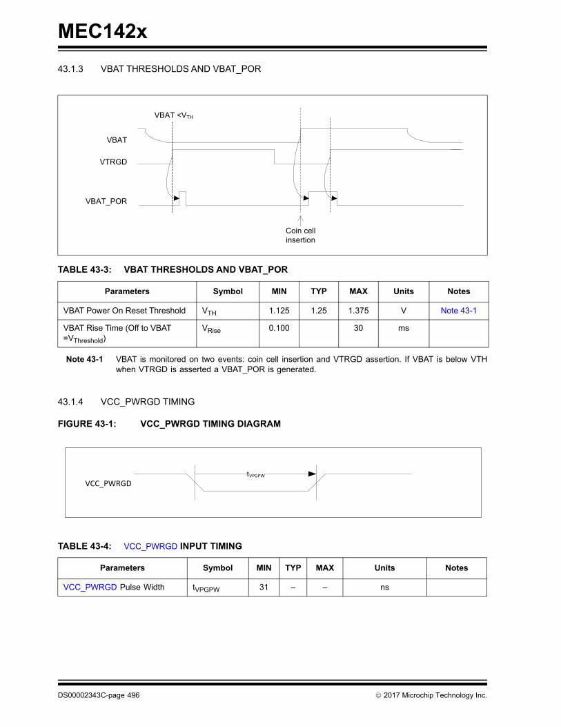
MEC142x
43.1.3 VBAT THRESHOLDS AND VBAT_POR
Note 43-1 VBAT is monitored on two events: coin cell insertion and VTRGD assertion. If VBAT is below VTHwhen VTRGD is asserted a VBAT_POR is generated.
43.1.4 VCC_PWRGD TIMING
FIGURE 43-1: VCC_PWRGD TIMING DIAGRAM
TABLE 43-3: VBAT THRESHOLDS AND VBAT_POR
Parameters Symbol MIN TYP MAX Units Notes
VBAT Power On Reset Threshold VTH 1.125 1.25 1.375 V Note 43-1
VBAT Rise Time (Off to VBAT =VThreshold)
VRise 0.100 30 ms
TABLE 43-4: VCC_PWRGD INPUT TIMING
Parameters Symbol MIN TYP MAX Units Notes
VCC_PWRGD Pulse Width tVPGPW 31 – – ns
VBAT
VTRGD
VBAT_POR
Coin cell insertion
VBAT <VTH
VCC_PWRGDtVPGPW
DS00002343C-page 496 2017 Microchip Technology Inc.

MEC142x
43.2 Clocking AC Timing Characteristics
FIGURE 43-2: CLOCK TIMING DIAGRAM
TABLE 43-5: CLOCK TIMING PARAMETERS
Clock Parameters Symbol MIN TYP MAX Units
48 MHz Ring Oscillator
Start-up accuracy (without 32 kHz present)
fSU 22 - 53 MHz
Start-up delay from 0 MHz to Start-up accuracy
tSU - - 6 µs
Operating Frequency (with exter-nal 32kHz clock source present after frequency lock to 48 MHz)
fOP 47.04 48 48.95 MHz
Operating Frequency (with inter-nal 32 kHz oscillator present after frequency lock to 48 MHz) Note 43-3
fOP 46.08 48 49.92 MHz
Adjustment Delay from Start-up accuracy to Operating accuracy (time to attain frequency lock - with 32 kHz present)
tADJ 0.03 - 4(Note 43-3)
ms
Adjustment Delay when resuming from Heavy Sleep 3 and System Deepest Sleep state.(time to re-attain frequency lock - with external 32 kHz present)
tADJ - 0.60 1 (Note 43-3)
ms
Operating Frequency (with exter-nal 32 kHz removed after fre-quency locked to 48 MHz)
fOP 43.2(Note 43-5)
- 52.8(Note 43-5)
MHz
tSU tADJ
High Time
Low Time
Fall Time Rise Time
2017 Microchip Technology Inc. DS00002343C-page 497

MEC142x
Note 43-2 Without the external clock, the 48MHz clock will vary up to +/-4% which may affect the timingparameters of certain blocks. In particular it may not be accurate enough to ensure that the UARTwill work, depending on the accuracy of the clock of the external device.
Note 43-3 This time applies if the external 32KHz clock input is available or if the Internal Oscillator clock sourceis enabled via the Clock Enable Register on page 440.
Note 43-4 SUSCLK is required to have an accuracy of +/- 100 ppm.
Note 43-5 The drift in frequency after frequency lock if the 32kHz clock is removed is determined by varyingtemperature while voltage is held constant.
Note 43-6 Firmware can use the INT_32K_RDY status bit listed in the Section 10.0, "Jump Table VectoredInterrupt Controller (JTVIC)" to indicate when the internal 32k Hz clock has reach operatingfrequency.
Note 43-7 This timing assumes the oscillator was powered and reach oscillator-lock prior to entering a sleepstate. See also Table 3-12, “System Sleep Control Bit Encoding,” on page 68.
SUSCLK Operating Frequency - - 32.768 - kHz
Period - (Note 43-4) 30.52 (Note 43-4) µs
High Time - 10 us
Low Time - 10 us
Fall Time - - - 1 us
Rise Time - - - 1 us
32kHz_INT_OSC
Operating Frequency - 32.112 32.768 33.424 kHz
Start-up delay from 0k Hz to Oper-ating Frequency
- 150 us
TABLE 43-5: CLOCK TIMING PARAMETERS (CONTINUED)
Clock Parameters Symbol MIN TYP MAX Units
DS00002343C-page 498 2017 Microchip Technology Inc.

MEC142x
43.3 Generic Strap Option Sampling Timing
43.4 Pin Reset Timing
43.4.1 RESET_IN# TIMING
Note 43-8 The RESET_IN# input can tolerate glitches of no more than 50ns.
43.4.2 RESET_OUT# TIMING
The minimum reset output time is determined by the RESET_IN# pin.
TABLE 43-6: GENERIC STRAP OPTION SAMPLING TIMING
Parameters Symbol MIN TYP MAX Units Notes
EC_PROC_RESET# deasserted to Strap Sampled
tSAMPLE – 500 600 µs
Note: The GPIO pins will float after the RESET_IN# pin is asserted low in less than 9 usec (max).
FIGURE 43-3: RESET_IN# TIMING
TABLE 43-7: RESETI# TIMING PARAMETERS
Symbol ParameterLimits
Units CommentsMIN MAX
tF RESET_IN# Fall time 0 10 s
tR RESET_IN# Rise time 0 10 s
tRESET Minimum Reset Time 1 s Note 43-8
tRtF
VSS
tRESET
0.8V
2017 Microchip Technology Inc. DS00002343C-page 499
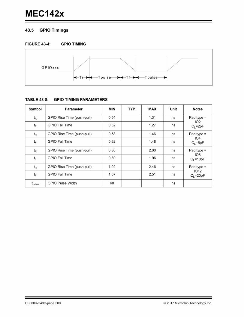
MEC142x
43.5 GPIO Timings
FIGURE 43-4: GPIO TIMING
TABLE 43-8: GPIO TIMING PARAMETERS
Symbol Parameter MIN TYP MAX Unit Notes
tR GPIO Rise Time (push-pull) 0.54 1.31 ns Pad type = IO2
CL=2pFtF GPIO Fall Time 0.52 1.27 ns
tR GPIO Rise Time (push-pull) 0.58 1.46 ns Pad type = IO4
CL=5pFtF GPIO Fall Time 0.62 1.48 ns
tR GPIO Rise Time (push-pull) 0.80 2.00 ns Pad type = IO8
CL=10pFtF GPIO Fall Time 0.80 1.96 ns
tR GPIO Rise Time (push-pull) 1.02 2.46 ns Pad type = IO12
CL=20pFtF GPIO Fall Time 1.07 2.51 ns
tpulse GPIO Pulse Width 60 ns
G PIO xxx
Tr T fTpu lse Tpu lse
DS00002343C-page 500 2017 Microchip Technology Inc.

MEC142x
43.6 eSPI Boot Timing
Note 1: Intel Primary Rails are defined as VCC_Prim 1.8, VCC_Prim 3.3, VCCPRIM_CORE and VCC_Prim 1.0V.
2: This is an Intel system requirement. This time is not monitored directly.
FIGURE 43-5: ESPI FLASH CHANNEL BOOT TIMING
TABLE 43-9: ESPI FLASH CHANNEL BOOT TIMING
Symbol Parameter MIN TYP MAX Unit Notes
t0 Time from Power On to sample Strap options (CR_STRAP and BSS_STRAP)
4 ms
t1a Time BSS_STRAP is low following a power-on-reset (POR) or WDT event
5 ms
t1b Time DSW_PWROK pin is low follow-ing a POR event
20 ms
Time DSW_PWROK pin is low follow-ing a WDT event
120 ms
t2 Time from BSS_STRAP detected high to PRG_STRAP high (i.e., at least one Primary Rail active)
30 sec 1
t3 Time from PRG_STRAP high until all Primary Rails are active including VTR_LPC_ESPI
20 ms 2
t4 Time from PRG_STRAP high to RSMRST# driven high
35 ms
GPIO102/KSO09[CR_STRAP]
t1a
VTR
t0
`
GPIO123/SHD_CS0#[BSS_STRAP] (RSMRST#)
VTR_LPC_ESPI Don’t Care
Don’t Care
Don’t Care
GPIO135/SHD_IO2[PRG_STRAP]
t2
All System Primary Rails Good
t3
t4
GPIO136/SHD_IO3 (DSW_PWROK) Don’t Care
t1b
Don’t Care
2017 Microchip Technology Inc. DS00002343C-page 501

MEC142x
43.7 A20M Timing
Same timing as GPIO signals. See Section 43.5, "GPIO Timings," on page 500.
DS00002343C-page 502 2017 Microchip Technology Inc.

2017 Microchip Technology Inc. DS00002343C-page 503
MEC142x
43.8 8042 Emulation CPU_Reset Timing
Note 43-1 Figure 43-6 and Table 43-10 refer to in which CPU_RESET is the inverse of ALT_RST# & KRESET.
Note 43-2 The KBRST pin function is the output of CPU_RESET described in Section 16.11.2, "CPU_RESETHardware Speed-Up," on page 262.
FIGURE 43-6: CPU_RESET TIMING
TABLE 43-10: CPU_RESET TIMING PARAMETERS
Name Description MIN TYP MAX Units
tdelay Delay prior to active pulse 14 15 15.5 s
tactive Active pulse width 6 8 8.5 s
td e la y ta c t iv e
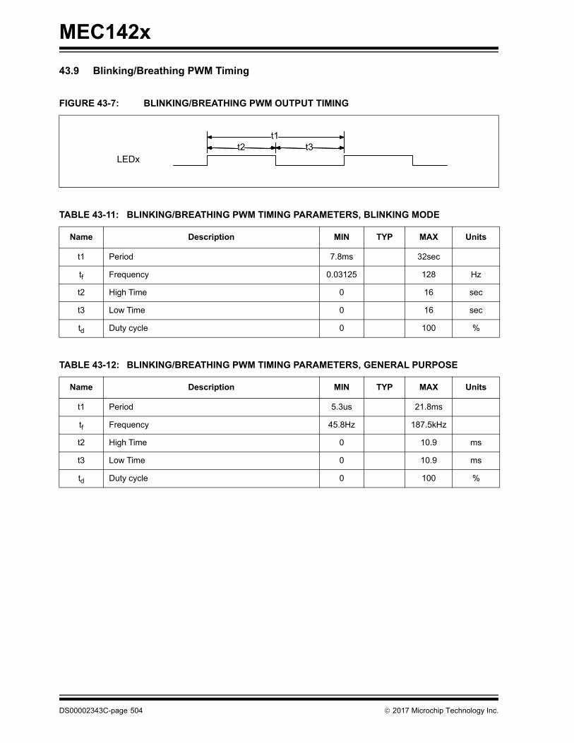
MEC142x
DS00002343C-page 504 2017 Microchip Technology Inc.
43.9 Blinking/Breathing PWM Timing
FIGURE 43-7: BLINKING/BREATHING PWM OUTPUT TIMING
TABLE 43-11: BLINKING/BREATHING PWM TIMING PARAMETERS, BLINKING MODE
Name Description MIN TYP MAX Units
t1 Period 7.8ms 32sec
tf Frequency 0.03125 128 Hz
t2 High Time 0 16 sec
t3 Low Time 0 16 sec
td Duty cycle 0 100 %
TABLE 43-12: BLINKING/BREATHING PWM TIMING PARAMETERS, GENERAL PURPOSE
Name Description MIN TYP MAX Units
t1 Period 5.3us 21.8ms
tf Frequency 45.8Hz 187.5kHz
t2 High Time 0 10.9 ms
t3 Low Time 0 10.9 ms
td Duty cycle 0 100 %
t3t1
t2LEDx
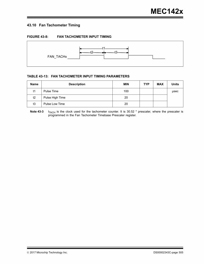
2017 Microchip Technology Inc. DS00002343C-page 505
MEC142x
43.10 Fan Tachometer Timing
Note 43-3 tTACH is the clock used for the tachometer counter. It is 30.52 * prescaler, where the prescaler isprogrammed in the Fan Tachometer Timebase Prescaler register.
FIGURE 43-8: FAN TACHOMETER INPUT TIMING
TABLE 43-13: FAN TACHOMETER INPUT TIMING PARAMETERS
Name Description MIN TYP MAX Units
t1 Pulse Time 100 µsec
t2 Pulse High Time 20
t3 Pulse Low Time 20
t3t1
t2FAN_TACHx
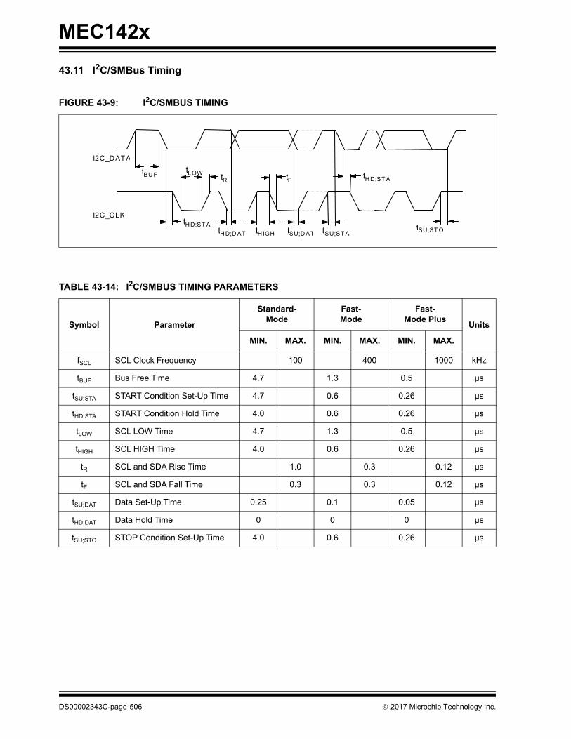
MEC142x
DS00002343C-page 506 2017 Microchip Technology Inc.
43.11 I2C/SMBus Timing
FIGURE 43-9: I2C/SMBUS TIMING
TABLE 43-14: I2C/SMBUS TIMING PARAMETERS
Symbol Parameter
Standard-Mode
Fast-Mode
Fast-Mode Plus
Units
MIN. MAX. MIN. MAX. MIN. MAX.
fSCL SCL Clock Frequency 100 400 1000 kHz
tBUF Bus Free Time 4.7 1.3 0.5 µs
tSU;STA START Condition Set-Up Time 4.7 0.6 0.26 µs
tHD;STA START Condition Hold Time 4.0 0.6 0.26 µs
tLOW SCL LOW Time 4.7 1.3 0.5 µs
tHIGH SCL HIGH Time 4.0 0.6 0.26 µs
tR SCL and SDA Rise Time 1.0 0.3 0.12 µs
tF SCL and SDA Fall Time 0.3 0.3 0.12 µs
tSU;DAT Data Set-Up Time 0.25 0.1 0.05 µs
tHD;DAT Data Hold Time 0 0 0 µs
tSU;STO STOP Condition Set-Up Time 4.0 0.6 0.26 µs
tH D;ST A
tSU;ST OtSU;ST AtSU;D ATtH IGH
tFtRtLOW
tH D;D AT
tH D;ST A
tBU F
I2C_DATA
I2C_CLK
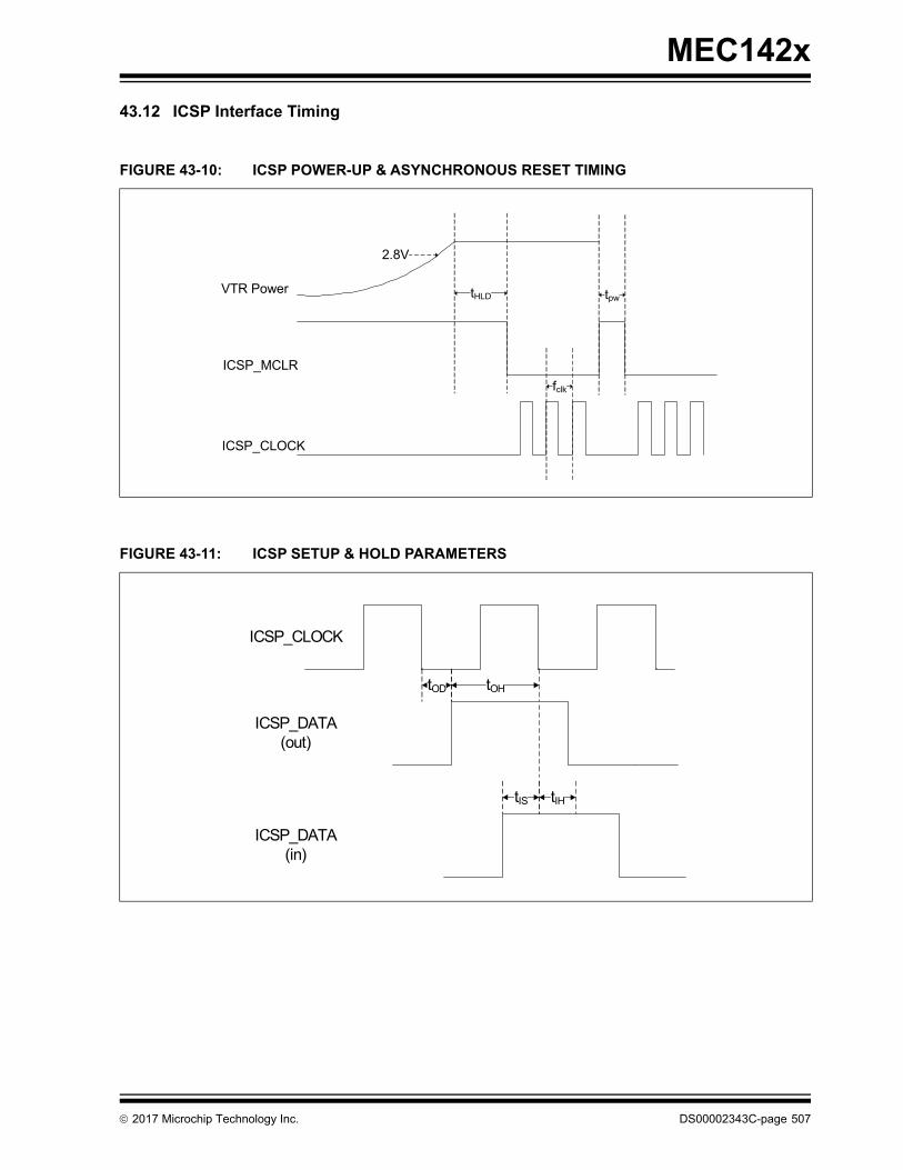
MEC142x
43.12 ICSP Interface Timing
FIGURE 43-10: ICSP POWER-UP & ASYNCHRONOUS RESET TIMING
FIGURE 43-11: ICSP SETUP & HOLD PARAMETERS
VTR Power
ICSP_MCLR
tpw
fclk
tHLD
2.8V
ICSP_CLOCK
tOD
tIHtIS
tOH
ICSP_DATA (out)
ICSP_DATA (in)
ICSP_CLOCK
2017 Microchip Technology Inc. DS00002343C-page 507

MEC142x
43.13 Test Port - XNOR
See Test Procedure in Section 41.5, "XNOR Chain".
TABLE 43-15: ICSP INTERFACE TIMING PARAMETERS
Name Description MIN TYP MAX Units
tHLD ICSP_MCLR de-assertion after VTR power is applied
5 ms
tpw ICSP_MCLR assertion pulse width 500 nsec
fclk ICSP_CLOCK frequency (see note) 48 MHz
tOD ICSP_DATA output delay after falling edge of TCLK.
5 10 nsec
tOH ICSP_DATA hold time after falling edge of TCLK 1 TCLK - tOD nsec
tIS ICSP_DATA input setup time before falling edge of TCLK.
5 nsec
tIH ICSP_DATA hold time after falling edge of TCLK. 5 nsec
Note: fclk is the maximum frequency to access ICSP accessible test registers.
DS00002343C-page 508 2017 Microchip Technology Inc.
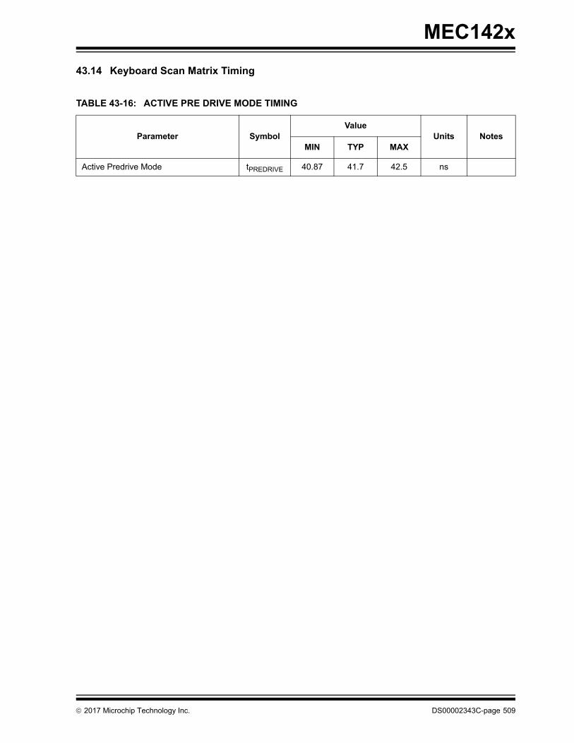
2017 Microchip Technology Inc. DS00002343C-page 509
MEC142x
43.14 Keyboard Scan Matrix Timing
TABLE 43-16: ACTIVE PRE DRIVE MODE TIMING
Parameter SymbolValue
Units NotesMIN TYP MAX
Active Predrive Mode tPREDRIVE 40.87 41.7 42.5 ns
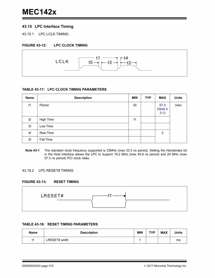
MEC142x
43.15 LPC Interface Timing
43.15.1 LPC LCLK TIMING
Note 43-1 The standard clock frequency supported is 33MHz (max 33.3 ns period). Setting the Handshake bitin the Host Interface allows the LPC to support 19.2 MHz (max 45.8 ns period) and 24 MHz (max57.3 ns period) PCI clock rates.
43.15.2 LPC RESET# TIMING
FIGURE 43-12: LPC CLOCK TIMING
TABLE 43-17: LPC CLOCK TIMING PARAMETERS
Name Description MIN TYP MAX Units
t1 Period 30 57.3(Note 4
3-1)
nsec
t2 High Time 11
t3 Low Time
t4 Rise Time 3
t5 Fall Time
FIGURE 43-13: RESET TIMING
TABLE 43-18: RESET TIMING PARAMETERS
Name Description MIN TYP MAX Units
t1 LRESET# width 1 ms
t1t3 t2LC LK t5
t4
t1 LRESET#
DS00002343C-page 510 2017 Microchip Technology Inc.
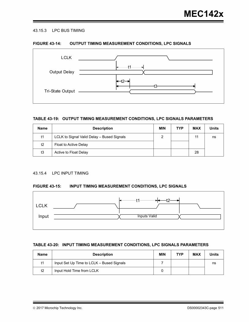
MEC142x
43.15.3 LPC BUS TIMING
43.15.4 LPC INPUT TIMING
FIGURE 43-14: OUTPUT TIMING MEASUREMENT CONDITIONS, LPC SIGNALS
TABLE 43-19: OUTPUT TIMING MEASUREMENT CONDITIONS, LPC SIGNALS PARAMETERS
Name Description MIN TYP MAX Units
t1 LCLK to Signal Valid Delay – Bused Signals 2 11 ns
t2 Float to Active Delay
t3 Active to Float Delay 28
FIGURE 43-15: INPUT TIMING MEASUREMENT CONDITIONS, LPC SIGNALS
TABLE 43-20: INPUT TIMING MEASUREMENT CONDITIONS, LPC SIGNALS PARAMETERS
Name Description MIN TYP MAX Units
t1 Input Set Up Time to LCLK – Bused Signals 7 ns
t2 Input Hold Time from LCLK 0
t3 t2
t1
LCLK
Output Delay
Tri-State Output
Inputs Valid
t2 t1 LCLK
Input
2017 Microchip Technology Inc. DS00002343C-page 511

MEC142x
43.15.5 LPC I/O TIMING
43.15.6 SERIAL IRQ TIMING
43.15.7 NEC_SCI TIMING
nEC_SCI pin has the same minimum timing requirements as GPIO signals. See Section 43.5, "GPIO Timings," onpage 500.
FIGURE 43-16: I/O WRITE
Note: L1=Start; L2=CYCTYP+DIR; L3=Sync of 0000
FIGURE 43-17: I/O READ
Note: L1=Start; L2=CYCTYP+DIR; L3=Sync of 0000
FIGURE 43-18: SETUP AND HOLD TIME
TABLE 43-21: SETUP AND HOLD TIME
Name Description MIN TYP MAX Units
t1 SER_IRQ Setup Time to LCLK Rising 7 nsec
t2 SER_IRQ Hold Time to LCLK Rising 0
L1 L2 Address Data TAR Sync=0110 L3 TAR
LCLK
LFRAME#
LAD[3:0]#
L1 L2 Address TAR Sync=0110 L3 Data TAR
LCLK
LFRAME#
LAD[3:0]#
t2 t1
LCLK
SER_IRQ
DS00002343C-page 512 2017 Microchip Technology Inc.
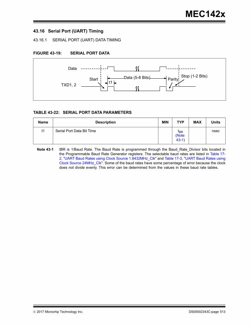
MEC142x
43.16 Serial Port (UART) Timing
43.16.1 SERIAL PORT (UART) DATA TIMING
Note 43-1 tBR is 1/Baud Rate. The Baud Rate is programmed through the Baud_Rate_Divisor bits located inthe Programmable Baud Rate Generator registers. The selectable baud rates are listed in Table 17-2, "UART Baud Rates using Clock Source 1.8432MHz_Clk" and Table 17-3, "UART Baud Rates usingClock Source 24MHz_Clk". Some of the baud rates have some percentage of error because the clockdoes not divide evenly. This error can be determined from the values in these baud rate tables.
FIGURE 43-19: SERIAL PORT DATA
TABLE 43-22: SERIAL PORT DATA PARAMETERS
Name Description MIN TYP MAX Units
t1 Serial Port Data Bit Time tBR(Note 43-1)
nsec
Data (5-8 Bits)t1
Data
TXD1, 2Start Parity
Stop (1-2 Bits)
2017 Microchip Technology Inc. DS00002343C-page 513
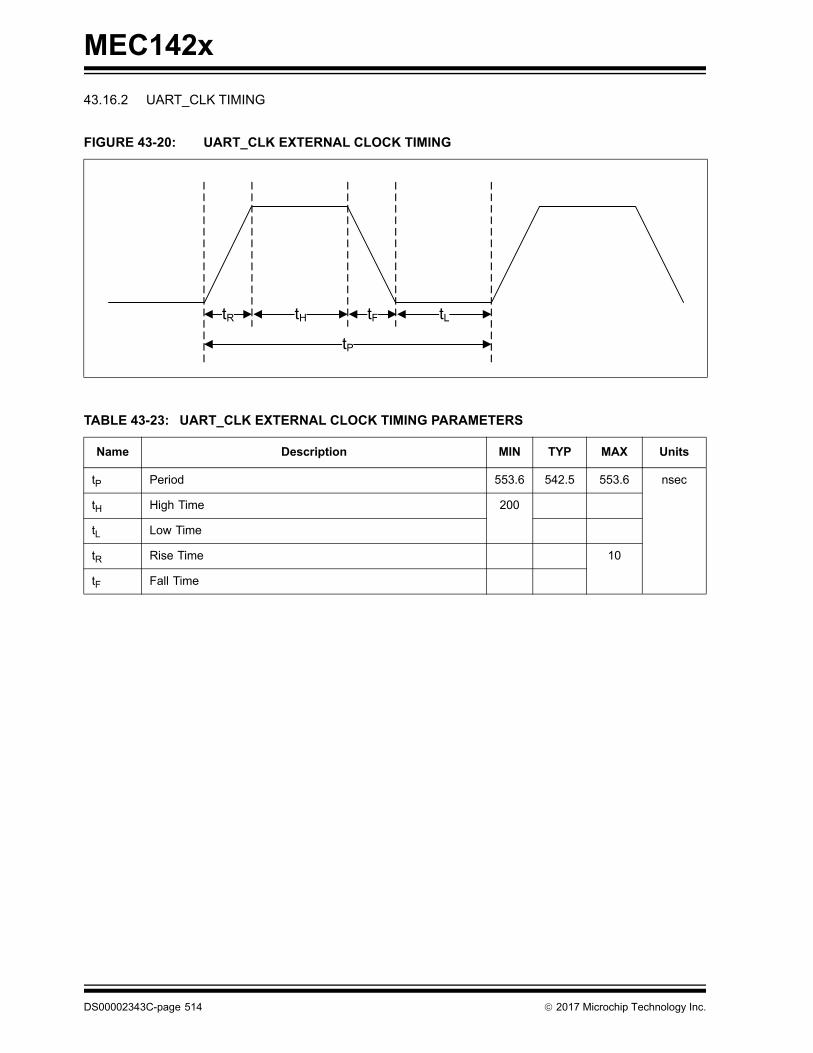
MEC142x
43.16.2 UART_CLK TIMING
FIGURE 43-20: UART_CLK EXTERNAL CLOCK TIMING
TABLE 43-23: UART_CLK EXTERNAL CLOCK TIMING PARAMETERS
Name Description MIN TYP MAX Units
tP Period 553.6 542.5 553.6 nsec
tH High Time 200
tL Low Time
tR Rise Time 10
tF Fall Time
tP
tR tH tF tL
DS00002343C-page 514 2017 Microchip Technology Inc.

2017 Microchip Technology Inc. DS00002343C-page 515
MEC142x
43.17 PECI Interface
Note 43-1 The originator must drive a more restrictive time to allow for quantized sampling errors by a clientyet still attain the minimum time less than 500 µsec. tBIT limits apply equally to tBIT-A and tBIT-M . TheMEC142x is designed to support 500kHz, or a 2us bit time. See the PECI 3.0 specification from IntelCorp. for further details.
Note 43-2 The minimum and maximum bit times are relative to tBIT defined in the Timing Negotiation pulse. Seethe PECI 3.0 specification from Intel Corp. for further details.
Note 43-3 “#nodes” is the number of nodes on the PECI bus; host and client nodes are counted as one each.Extended trace lengths may appear as extra nodes. Refer also to Table 25-2, "PECI RoutingGuidelines". See the PECI 3.0 specification from Intel Corp. for further details.
Name Description MIN MAX Units Notes
tBIT Bit time (overall time evident on PECI pin) Bit time driven by an originator
22
500250
µsecµsec
43-1
tBIT,jitter Bit time jitter between adjacent bits in a PECI message header or data bytes after timing has been negotiated
- - %
tBIT,drift Change in bit time across a PECI address or PECI message bits as driven by the originator. This limit only applies across tBIT-A bit drift and tBIT-M drift.
- - %
tH1 High level time for logic 1 0.6 0.8 tBIT 43-2
tH0 High level time for logic 0 0.2 0.4 tBIT
tPECIR Rise time (measured from VOL to VIH,min , Vtt(nom)5%)
- 30 + (5 x #nodes)
ns 43-3
tPECIF Fall time (measured from VOH to VIL,max , Vtt(nom)+5%)
- (30 x #nodes) ns 43-3
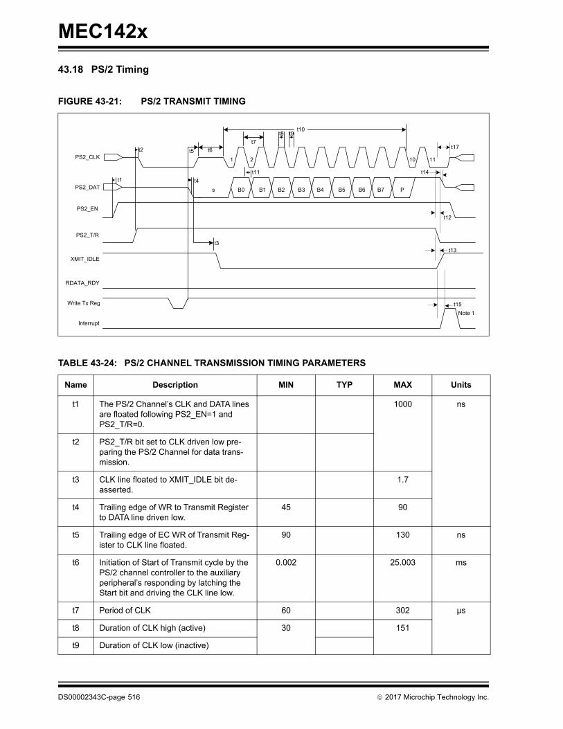
MEC142x
43.18 PS/2 Timing
FIGURE 43-21: PS/2 TRANSMIT TIMING
TABLE 43-24: PS/2 CHANNEL TRANSMISSION TIMING PARAMETERS
Name Description MIN TYP MAX Units
t1 The PS/2 Channel’s CLK and DATA lines are floated following PS2_EN=1 and PS2_T/R=0.
1000 ns
t2 PS2_T/R bit set to CLK driven low pre-paring the PS/2 Channel for data trans-mission.
t3 CLK line floated to XMIT_IDLE bit de-asserted.
1.7
t4 Trailing edge of WR to Transmit Register to DATA line driven low.
45 90
t5 Trailing edge of EC WR of Transmit Reg-ister to CLK line floated.
90 130 ns
t6 Initiation of Start of Transmit cycle by the PS/2 channel controller to the auxiliary peripheral’s responding by latching the Start bit and driving the CLK line low.
0.002 25.003 ms
t7 Period of CLK 60 302 µs
t8 Duration of CLK high (active) 30 151
t9 Duration of CLK low (inactive)
1 2 10 11
B0 B1 B2 B3 B4 B5 B6 B7 Ps
PS2_CLK
PS2_DAT
PS2_EN
PS2_T/R
XMIT_IDLE
RDATA_RDY
Write Tx Reg
Interrupt
t1
t2
t4
t3
t5 t6
t7
t9t8t10
t11
t12
t13
t14
t15
Note 1
t17
DS00002343C-page 516 2017 Microchip Technology Inc.
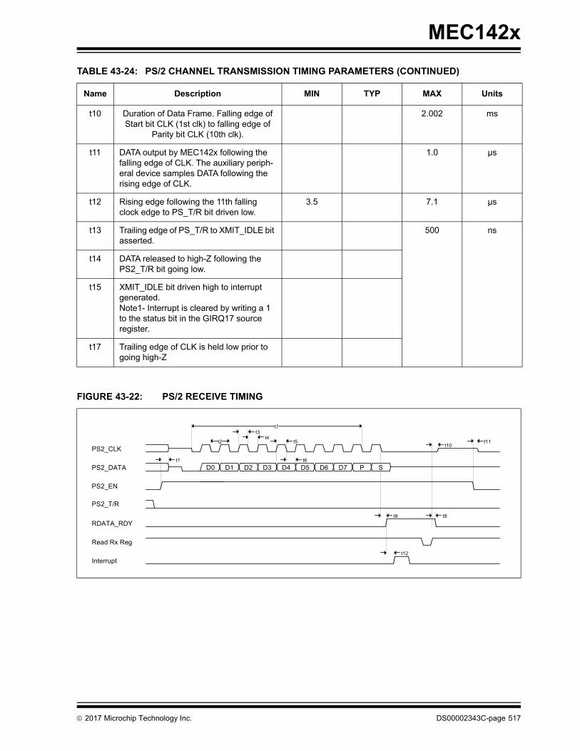
MEC142x
t10 Duration of Data Frame. Falling edge of Start bit CLK (1st clk) to falling edge of
Parity bit CLK (10th clk).
2.002 ms
t11 DATA output by MEC142x following the falling edge of CLK. The auxiliary periph-eral device samples DATA following the rising edge of CLK.
1.0 µs
t12 Rising edge following the 11th falling clock edge to PS_T/R bit driven low.
3.5 7.1 µs
t13 Trailing edge of PS_T/R to XMIT_IDLE bit asserted.
500 ns
t14 DATA released to high-Z following the PS2_T/R bit going low.
t15 XMIT_IDLE bit driven high to interrupt generated. Note1- Interrupt is cleared by writing a 1 to the status bit in the GIRQ17 source register.
t17 Trailing edge of CLK is held low prior to going high-Z
FIGURE 43-22: PS/2 RECEIVE TIMING
TABLE 43-24: PS/2 CHANNEL TRANSMISSION TIMING PARAMETERS (CONTINUED)
Name Description MIN TYP MAX Units
t6
t5t4
t3
t2
t7
t1
t8 t9
t10
t12
t11
RDATA_RDY
Interrupt
PS2_EN
Read Rx Reg
D3D0 D2 D5D4 D6 D7 P SD1PS2_DATA
PS2_CLK
PS2_T/R
2017 Microchip Technology Inc. DS00002343C-page 517
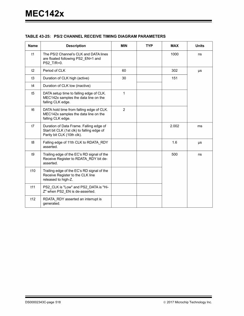
MEC142x
TABLE 43-25: PS/2 CHANNEL RECEIVE TIMING DIAGRAM PARAMETERS
Name Description MIN TYP MAX Units
t1 The PS/2 Channel’s CLK and DATA lines are floated following PS2_EN=1 and PS2_T/R=0.
1000 ns
t2 Period of CLK 60 302 µs
t3 Duration of CLK high (active) 30 151
t4 Duration of CLK low (inactive)
t5 DATA setup time to falling edge of CLK. MEC142x samples the data line on the falling CLK edge.
1
t6 DATA hold time from falling edge of CLK. MEC142x samples the data line on the falling CLK edge.
2
t7 Duration of Data Frame. Falling edge of Start bit CLK (1st clk) to falling edge of Parity bit CLK (10th clk).
2.002 ms
t8 Falling edge of 11th CLK to RDATA_RDY asserted.
1.6 µs
t9 Trailing edge of the EC’s RD signal of the Receive Register to RDATA_RDY bit de-asserted.
500 ns
t10 Trailing edge of the EC’s RD signal of the Receive Register to the CLK line released to high-Z.
t11 PS2_CLK is "Low" and PS2_DATA is "Hi-Z" when PS2_EN is de-asserted.
t12 RDATA_RDY asserted an interrupt is generated.
DS00002343C-page 518 2017 Microchip Technology Inc.
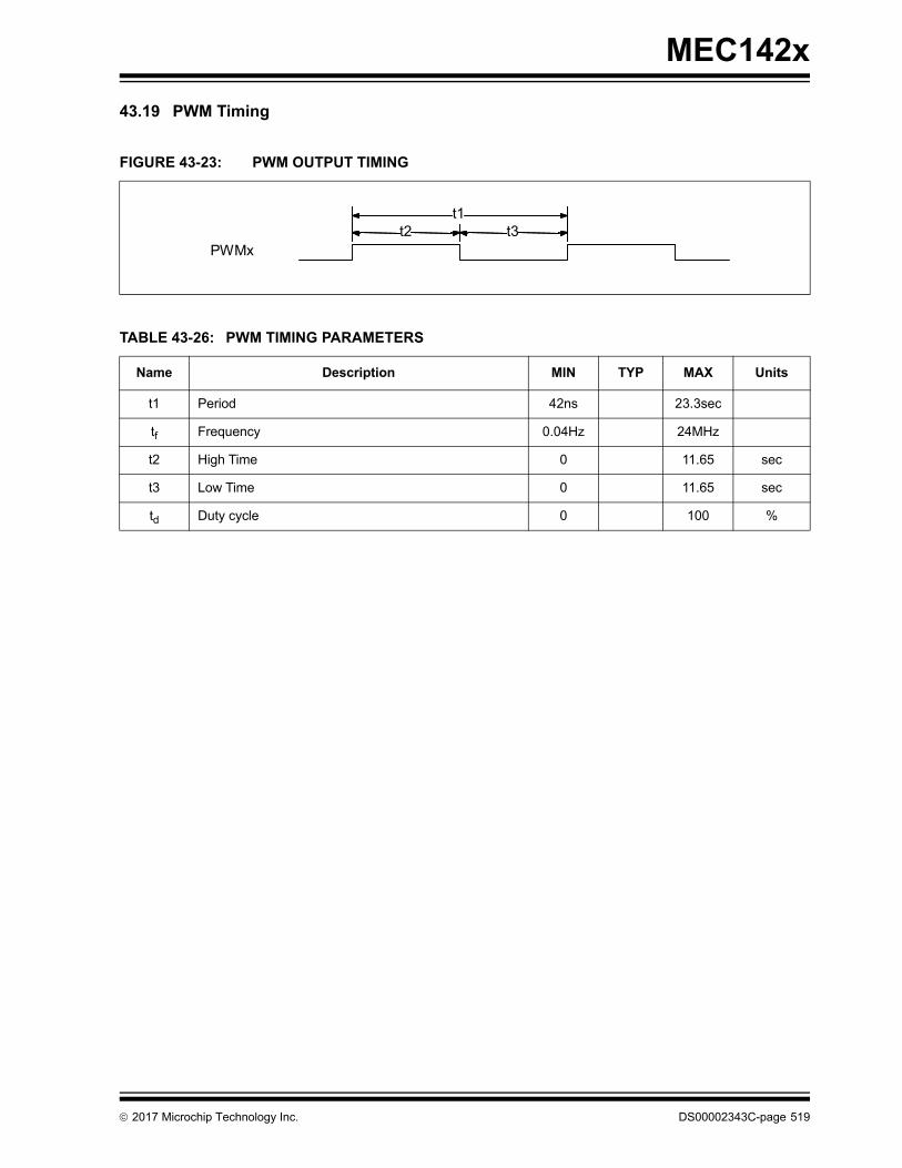
2017 Microchip Technology Inc. DS00002343C-page 519
MEC142x
43.19 PWM Timing
FIGURE 43-23: PWM OUTPUT TIMING
TABLE 43-26: PWM TIMING PARAMETERS
Name Description MIN TYP MAX Units
t1 Period 42ns 23.3sec
tf Frequency 0.04Hz 24MHz
t2 High Time 0 11.65 sec
t3 Low Time 0 11.65 sec
td Duty cycle 0 100 %
t3t1
t2PWMx
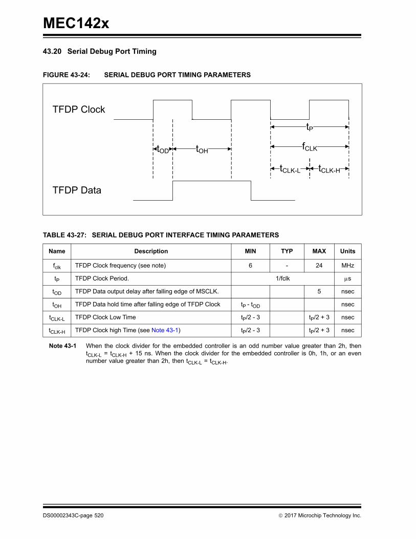
MEC142x
DS00002343C-page 520 2017 Microchip Technology Inc.
43.20 Serial Debug Port Timing
Note 43-1 When the clock divider for the embedded controller is an odd number value greater than 2h, thentCLK-L = tCLK-H + 15 ns. When the clock divider for the embedded controller is 0h, 1h, or an evennumber value greater than 2h, then tCLK-L = tCLK-H.
FIGURE 43-24: SERIAL DEBUG PORT TIMING PARAMETERS
TABLE 43-27: SERIAL DEBUG PORT INTERFACE TIMING PARAMETERS
Name Description MIN TYP MAX Units
fclk TFDP Clock frequency (see note) 6 - 24 MHz
tP TFDP Clock Period. 1/fclk s
tOD TFDP Data output delay after falling edge of MSCLK. 5 nsec
tOH TFDP Data hold time after falling edge of TFDP Clock tP - tOD nsec
tCLK-L TFDP Clock Low Time tP/2 - 3 tP/2 + 3 nsec
tCLK-H TFDP Clock high Time (see Note 43-1) tP/2 - 3 tP/2 + 3 nsec
tOD tOH
tP
tCLK-L tCLK-H
fCLK
TFDP Clock
TFDP Data
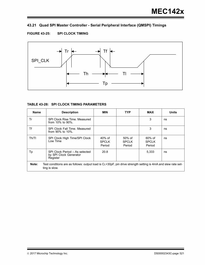
MEC142x
43.21 Quad SPI Master Controller - Serial Peripheral Interface (QMSPI) Timings
FIGURE 43-25: SPI CLOCK TIMING
TABLE 43-28: SPI CLOCK TIMING PARAMETERS
Name Description MIN TYP MAX Units
Tr SPI Clock Rise Time. Measured from 10% to 90%.
3 ns
Tf SPI Clock Fall Time. Measured from 90% to 10%.
3 ns
Th/Tl SPI Clock High Time/SPI Clock Low Time
40% of SPCLK Period
50% of SPCLK Period
60% of SPCLK Period
ns
Tp SPI Clock Period – As selected by SPI Clock Generator Register
20.8 5,333 ns
Note: Test conditions are as follows: output load is CL=30pF, pin drive strength setting is 4mA and slew rate set-ting is slow.
Tr Tf
Th Tl
Tp
SPI_CLK
2017 Microchip Technology Inc. DS00002343C-page 521
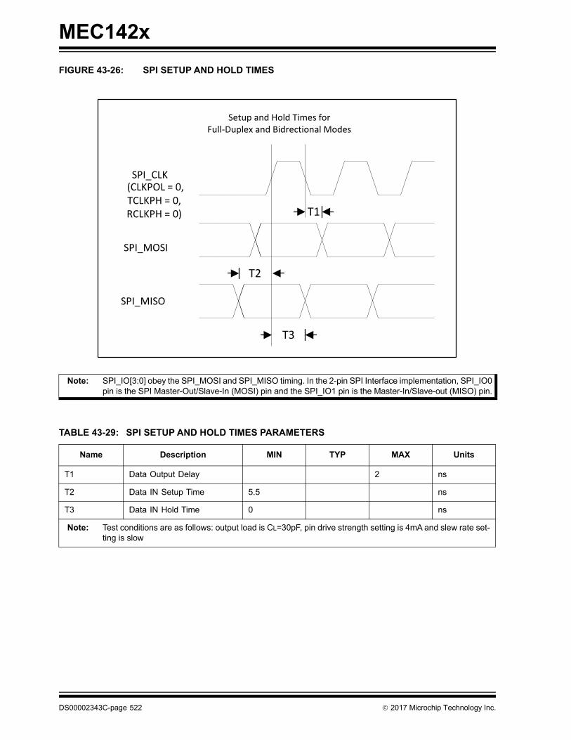
MEC142x
FIGURE 43-26: SPI SETUP AND HOLD TIMES
Note: SPI_IO[3:0] obey the SPI_MOSI and SPI_MISO timing. In the 2-pin SPI Interface implementation, SPI_IO0pin is the SPI Master-Out/Slave-In (MOSI) pin and the SPI_IO1 pin is the Master-In/Slave-out (MISO) pin.
TABLE 43-29: SPI SETUP AND HOLD TIMES PARAMETERS
Name Description MIN TYP MAX Units
T1 Data Output Delay 2 ns
T2 Data IN Setup Time 5.5 ns
T3 Data IN Hold Time 0 ns
Note: Test conditions are as follows: output load is CL=30pF, pin drive strength setting is 4mA and slew rate set-ting is slow
SPI_MISO
SPI_MOSI
T1
T2
T3
SPI_CLK(CLKPOL = 0, TCLKPH = 0, RCLKPH = 0)
Setup and Hold Times for Full‐Duplex and Bidrectional Modes
DS00002343C-page 522 2017 Microchip Technology Inc.
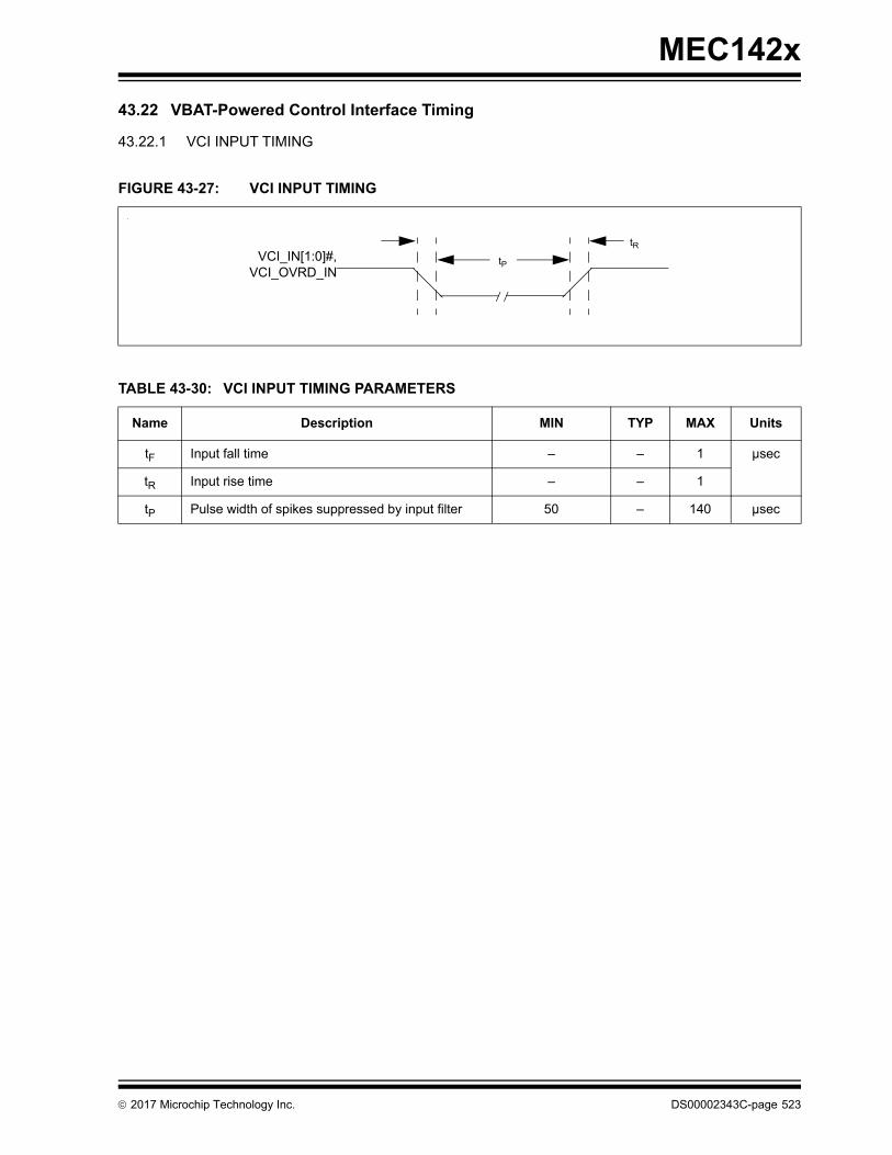
2017 Microchip Technology Inc. DS00002343C-page 523
MEC142x
43.22 VBAT-Powered Control Interface Timing
43.22.1 VCI INPUT TIMING
FIGURE 43-27: VCI INPUT TIMING
.
TABLE 43-30: VCI INPUT TIMING PARAMETERS
Name Description MIN TYP MAX Units
tF Input fall time – – 1 µsec
tR Input rise time – – 1
tP Pulse width of spikes suppressed by input filter 50 – 140 µsec
tP
tRVCI_IN[1:0]#,
VCI_OVRD_IN
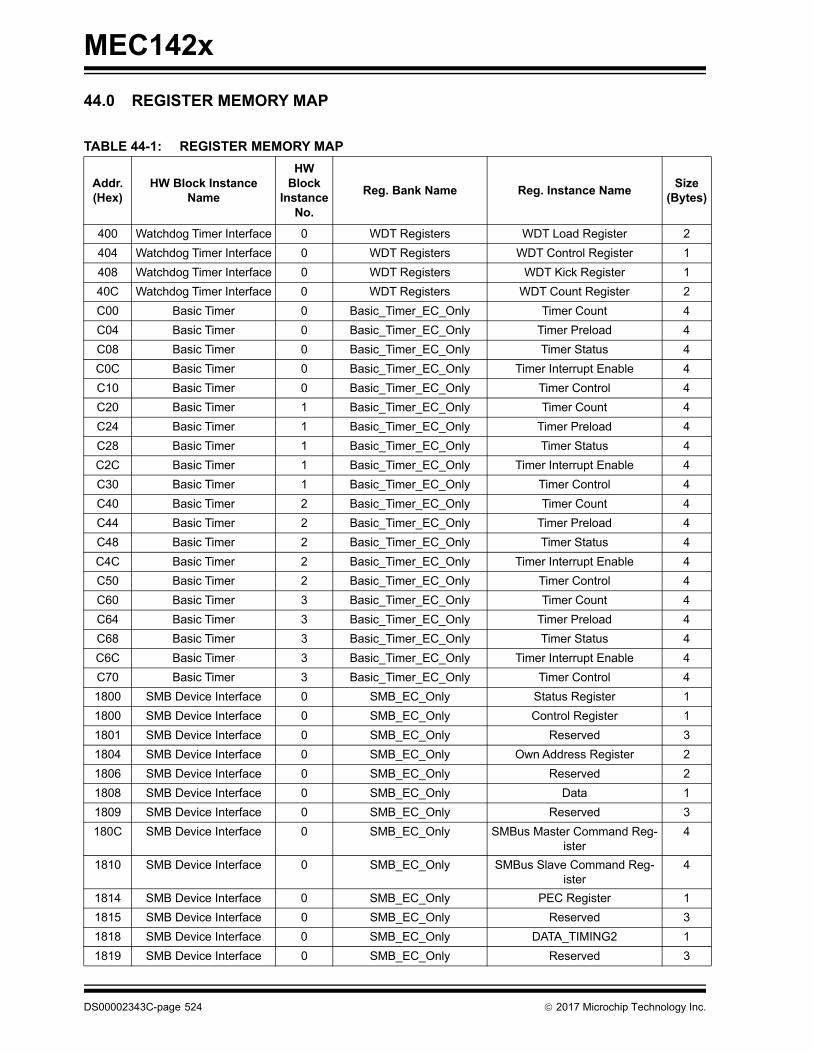
MEC142x
44.0 REGISTER MEMORY MAP
TABLE 44-1: REGISTER MEMORY MAP
Addr. (Hex)
HW Block Instance Name
HWBlock
InstanceNo.
Reg. Bank Name Reg. Instance NameSize
(Bytes)
400 Watchdog Timer Interface 0 WDT Registers WDT Load Register 2
404 Watchdog Timer Interface 0 WDT Registers WDT Control Register 1
408 Watchdog Timer Interface 0 WDT Registers WDT Kick Register 1
40C Watchdog Timer Interface 0 WDT Registers WDT Count Register 2
C00 Basic Timer 0 Basic_Timer_EC_Only Timer Count 4
C04 Basic Timer 0 Basic_Timer_EC_Only Timer Preload 4
C08 Basic Timer 0 Basic_Timer_EC_Only Timer Status 4
C0C Basic Timer 0 Basic_Timer_EC_Only Timer Interrupt Enable 4
C10 Basic Timer 0 Basic_Timer_EC_Only Timer Control 4
C20 Basic Timer 1 Basic_Timer_EC_Only Timer Count 4
C24 Basic Timer 1 Basic_Timer_EC_Only Timer Preload 4
C28 Basic Timer 1 Basic_Timer_EC_Only Timer Status 4
C2C Basic Timer 1 Basic_Timer_EC_Only Timer Interrupt Enable 4
C30 Basic Timer 1 Basic_Timer_EC_Only Timer Control 4
C40 Basic Timer 2 Basic_Timer_EC_Only Timer Count 4
C44 Basic Timer 2 Basic_Timer_EC_Only Timer Preload 4
C48 Basic Timer 2 Basic_Timer_EC_Only Timer Status 4
C4C Basic Timer 2 Basic_Timer_EC_Only Timer Interrupt Enable 4
C50 Basic Timer 2 Basic_Timer_EC_Only Timer Control 4
C60 Basic Timer 3 Basic_Timer_EC_Only Timer Count 4
C64 Basic Timer 3 Basic_Timer_EC_Only Timer Preload 4
C68 Basic Timer 3 Basic_Timer_EC_Only Timer Status 4
C6C Basic Timer 3 Basic_Timer_EC_Only Timer Interrupt Enable 4
C70 Basic Timer 3 Basic_Timer_EC_Only Timer Control 4
1800 SMB Device Interface 0 SMB_EC_Only Status Register 1
1800 SMB Device Interface 0 SMB_EC_Only Control Register 1
1801 SMB Device Interface 0 SMB_EC_Only Reserved 3
1804 SMB Device Interface 0 SMB_EC_Only Own Address Register 2
1806 SMB Device Interface 0 SMB_EC_Only Reserved 2
1808 SMB Device Interface 0 SMB_EC_Only Data 1
1809 SMB Device Interface 0 SMB_EC_Only Reserved 3
180C SMB Device Interface 0 SMB_EC_Only SMBus Master Command Reg-ister
4
1810 SMB Device Interface 0 SMB_EC_Only SMBus Slave Command Reg-ister
4
1814 SMB Device Interface 0 SMB_EC_Only PEC Register 1
1815 SMB Device Interface 0 SMB_EC_Only Reserved 3
1818 SMB Device Interface 0 SMB_EC_Only DATA_TIMING2 1
1819 SMB Device Interface 0 SMB_EC_Only Reserved 3
DS00002343C-page 524 2017 Microchip Technology Inc.

MEC142x
1820 SMB Device Interface 0 SMB_EC_Only Completion Register 4
1824 SMB Device Interface 0 SMB_EC_Only Idle Scaling Register 4
1828 SMB Device Interface 0 SMB_EC_Only Configuration Register 4
182C SMB Device Interface 0 SMB_EC_Only Bus Clock Register 2
182E SMB Device Interface 0 SMB_EC_Only Reserved 2
1830 SMB Device Interface 0 SMB_EC_Only Block ID Register 1
1831 SMB Device Interface 0 SMB_EC_Only Reserved 3
1834 SMB Device Interface 0 SMB_EC_Only Revision Register 1
1835 SMB Device Interface 0 SMB_EC_Only Reserved 3
1838 SMB Device Interface 0 SMB_EC_Only Bit-Bang Control Register 1
1839 SMB Device Interface 0 SMB_EC_Only Reserved 3
1840 SMB Device Interface 0 SMB_EC_Only Data Timing Register 4
1844 SMB Device Interface 0 SMB_EC_Only Time-Out Scaling Register 4
1848 SMB Device Interface 0 SMB_EC_Only SMBus Slave Transmit Buffer Register
1
1849 SMB Device Interface 0 SMB_EC_Only Reserved 3
184C SMB Device Interface 0 SMB_EC_Only SMBus Slave Receive Buffer Register
1
184D SMB Device Interface 0 SMB_EC_Only Reserved 3
1850 SMB Device Interface 0 SMB_EC_Only SMBus Master Transmit Bufer Register
1
1851 SMB Device Interface 0 SMB_EC_Only Reserved 3
1854 SMB Device Interface 0 SMB_EC_Only SMBus Master Receive Buffer Register
1
1855 SMB Device Interface 0 SMB_EC_Only Reserved 3
1860 SMB Device Interface 0 SMB_EC_Only Wake Status register 4
1864 SMB Device Interface 0 SMB_EC_Only Wake Enable register 4
2400 DMA 0 DMA Main DMA Main Control Register 1
2401 DMA 0 DMA Main DMA Reserved 3
2404 DMA 0 DMA Main DMA AFIFO Data Register 4
2440 DMA 0 DMA_CH0 DMA Activate Register 4
2444 DMA 0 DMA_CH0 DMA Memory Start Address Register
4
2448 DMA 0 DMA_CH0 DMA Memory End Address Register
4
244C DMA 0 DMA_CH0 AHB Address Register 4
2450 DMA 0 DMA_CH0 DMA Control Register 4
2454 DMA 0 DMA_CH0 DMA Channel Interrupt Status 4
2458 DMA 0 DMA_CH0 DMA Channel Interrupt Enable 4
245C DMA 0 DMA_CH0 DMA Test 4
2460 DMA 0 DMA_CH0_CRC DMA Channel 0 CRC Enable Register
4
TABLE 44-1: REGISTER MEMORY MAP (CONTINUED)
Addr. (Hex)
HW Block Instance Name
HWBlock
InstanceNo.
Reg. Bank Name Reg. Instance NameSize
(Bytes)
2017 Microchip Technology Inc. DS00002343C-page 525

MEC142x
2464 DMA 0 DMA_CH0_CRC DMA Channel 0 CRC Data Register
4
2468 DMA 0 DMA_CH0_CRC DMA Channel 0 CRC Post Sta-tus Register
4
2480 DMA 0 DMA_CH1 DMA Activate Register 4
2484 DMA 0 DMA_CH1 DMA Memory Start Address Register
4
2488 DMA 0 DMA_CH1 DMA Memory End Address Register
4
248C DMA 0 DMA_CH1 AHB Address Register 4
2490 DMA 0 DMA_CH1 DMA Control Register 4
2494 DMA 0 DMA_CH1 DMA Channel Interrupt Status 4
2498 DMA 0 DMA_CH1 DMA Channel Interrupt Enable 4
249C DMA 0 DMA_CH1 DMA Test 4
24A0 DMA 0 DMA_CH1_NOCRC Reserved 22
24C0 DMA 0 DMA_CH2 DMA Activate Register 4
24C4 DMA 0 DMA_CH2 DMA Memory Start Address Register
4
24C8 DMA 0 DMA_CH2 DMA Memory End Address Register
4
24CC DMA 0 DMA_CH2 AHB Address Register 4
24D0 DMA 0 DMA_CH2 DMA Control Register 4
24D4 DMA 0 DMA_CH2 DMA Channel Interrupt Status 4
24D8 DMA 0 DMA_CH2 DMA Channel Interrupt Enable 4
24DC DMA 0 DMA_CH2 DMA Test 4
24E0 DMA 0 DMA_CH2_NOCRC Reserved 22
2500 DMA 0 DMA_CH3 DMA Activate Register 4
2504 DMA 0 DMA_CH3 DMA Memory Start Address Register
4
2508 DMA 0 DMA_CH3 DMA Memory End Address Register
4
250C DMA 0 DMA_CH3 AHB Address Register 4
2510 DMA 0 DMA_CH3 DMA Control Register 4
2514 DMA 0 DMA_CH3 DMA Channel Interrupt Status 4
2518 DMA 0 DMA_CH3 DMA Channel Interrupt Enable 4
251C DMA 0 DMA_CH3 DMA Test 4
2520 DMA 0 DMA_CH3_NOCRC Reserved 22
2540 DMA 0 DMA_CH4 DMA Activate Register 4
2544 DMA 0 DMA_CH4 DMA Memory Start Address Register
4
2548 DMA 0 DMA_CH4 DMA Memory End Address Register
4
254C DMA 0 DMA_CH4 AHB Address Register 4
TABLE 44-1: REGISTER MEMORY MAP (CONTINUED)
Addr. (Hex)
HW Block Instance Name
HWBlock
InstanceNo.
Reg. Bank Name Reg. Instance NameSize
(Bytes)
DS00002343C-page 526 2017 Microchip Technology Inc.
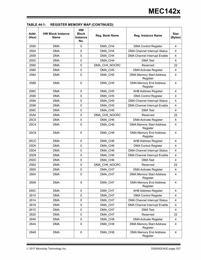
MEC142x
2550 DMA 0 DMA_CH4 DMA Control Register 4
2554 DMA 0 DMA_CH4 DMA Channel Interrupt Status 4
2558 DMA 0 DMA_CH4 DMA Channel Interrupt Enable 4
255C DMA 0 DMA_CH4 DMA Test 4
2560 DMA 0 DMA_CH4_NOCRC Reserved 22
2580 DMA 0 DMA_CH5 DMA Activate Register 4
2584 DMA 0 DMA_CH5 DMA Memory Start Address Register
4
2588 DMA 0 DMA_CH5 DMA Memory End Address Register
4
258C DMA 0 DMA_CH5 AHB Address Register 4
2590 DMA 0 DMA_CH5 DMA Control Register 4
2594 DMA 0 DMA_CH5 DMA Channel Interrupt Status 4
2598 DMA 0 DMA_CH5 DMA Channel Interrupt Enable 4
259C DMA 0 DMA_CH5 DMA Test 4
25A0 DMA 0 DMA_CH5_NOCRC Reserved 22
25C0 DMA 0 DMA_CH6 DMA Activate Register 4
25C4 DMA 0 DMA_CH6 DMA Memory Start Address Register
4
25C8 DMA 0 DMA_CH6 DMA Memory End Address Register
4
25CC DMA 0 DMA_CH6 AHB Address Register 4
25D0 DMA 0 DMA_CH6 DMA Control Register 4
25D4 DMA 0 DMA_CH6 DMA Channel Interrupt Status 4
25D8 DMA 0 DMA_CH6 DMA Channel Interrupt Enable 4
25DC DMA 0 DMA_CH6 DMA Test 4
25E0 DMA 0 DMA_CH6_NOCRC Reserved 22
2600 DMA 0 DMA_CH7 DMA Activate Register 4
2604 DMA 0 DMA_CH7 DMA Memory Start Address Register
4
2608 DMA 0 DMA_CH7 DMA Memory End Address Register
4
260C DMA 0 DMA_CH7 AHB Address Register 4
2610 DMA 0 DMA_CH7 DMA Control Register 4
2614 DMA 0 DMA_CH7 DMA Channel Interrupt Status 4
2618 DMA 0 DMA_CH7 DMA Channel Interrupt Enable 4
261C DMA 0 DMA_CH7 DMA Test 4
2620 DMA 0 DMA_CH7 Reserved 22
2640 DMA 0 DMA_CH8 DMA Activate Register 4
2644 DMA 0 DMA_CH8 DMA Memory Start Address Register
4
2648 DMA 0 DMA_CH8 DMA Memory End Address Register
4
TABLE 44-1: REGISTER MEMORY MAP (CONTINUED)
Addr. (Hex)
HW Block Instance Name
HWBlock
InstanceNo.
Reg. Bank Name Reg. Instance NameSize
(Bytes)
2017 Microchip Technology Inc. DS00002343C-page 527
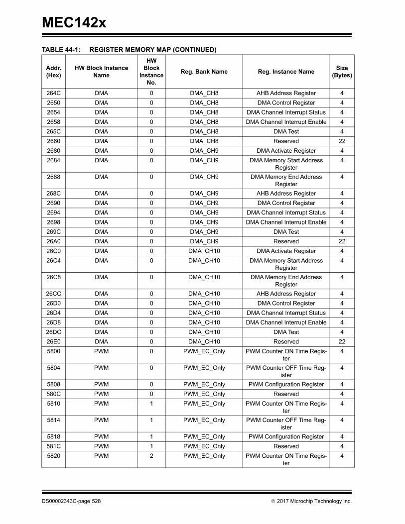
MEC142x
264C DMA 0 DMA_CH8 AHB Address Register 4
2650 DMA 0 DMA_CH8 DMA Control Register 4
2654 DMA 0 DMA_CH8 DMA Channel Interrupt Status 4
2658 DMA 0 DMA_CH8 DMA Channel Interrupt Enable 4
265C DMA 0 DMA_CH8 DMA Test 4
2660 DMA 0 DMA_CH8 Reserved 22
2680 DMA 0 DMA_CH9 DMA Activate Register 4
2684 DMA 0 DMA_CH9 DMA Memory Start Address Register
4
2688 DMA 0 DMA_CH9 DMA Memory End Address Register
4
268C DMA 0 DMA_CH9 AHB Address Register 4
2690 DMA 0 DMA_CH9 DMA Control Register 4
2694 DMA 0 DMA_CH9 DMA Channel Interrupt Status 4
2698 DMA 0 DMA_CH9 DMA Channel Interrupt Enable 4
269C DMA 0 DMA_CH9 DMA Test 4
26A0 DMA 0 DMA_CH9 Reserved 22
26C0 DMA 0 DMA_CH10 DMA Activate Register 4
26C4 DMA 0 DMA_CH10 DMA Memory Start Address Register
4
26C8 DMA 0 DMA_CH10 DMA Memory End Address Register
4
26CC DMA 0 DMA_CH10 AHB Address Register 4
26D0 DMA 0 DMA_CH10 DMA Control Register 4
26D4 DMA 0 DMA_CH10 DMA Channel Interrupt Status 4
26D8 DMA 0 DMA_CH10 DMA Channel Interrupt Enable 4
26DC DMA 0 DMA_CH10 DMA Test 4
26E0 DMA 0 DMA_CH10 Reserved 22
5800 PWM 0 PWM_EC_Only PWM Counter ON Time Regis-ter
4
5804 PWM 0 PWM_EC_Only PWM Counter OFF Time Reg-ister
4
5808 PWM 0 PWM_EC_Only PWM Configuration Register 4
580C PWM 0 PWM_EC_Only Reserved 4
5810 PWM 1 PWM_EC_Only PWM Counter ON Time Regis-ter
4
5814 PWM 1 PWM_EC_Only PWM Counter OFF Time Reg-ister
4
5818 PWM 1 PWM_EC_Only PWM Configuration Register 4
581C PWM 1 PWM_EC_Only Reserved 4
5820 PWM 2 PWM_EC_Only PWM Counter ON Time Regis-ter
4
TABLE 44-1: REGISTER MEMORY MAP (CONTINUED)
Addr. (Hex)
HW Block Instance Name
HWBlock
InstanceNo.
Reg. Bank Name Reg. Instance NameSize
(Bytes)
DS00002343C-page 528 2017 Microchip Technology Inc.

MEC142x
5824 PWM 2 PWM_EC_Only PWM Counter OFF Time Reg-ister
4
5828 PWM 2 PWM_EC_Only PWM Configuration Register 4
582C PWM 2 PWM_EC_Only Reserved 4
5830 PWM 3 PWM_EC_Only PWM Counter ON Time Regis-ter
4
5834 PWM 3 PWM_EC_Only PWM Counter OFF Time Reg-ister
4
5838 PWM 3 PWM_EC_Only PWM Configuration Register 4
583C PWM 3 PWM_EC_Only Reserved 4
5840 PWM 4 PWM_EC_Only PWM Counter ON Time Regis-ter
4
5844 PWM 4 PWM_EC_Only PWM Counter OFF Time Reg-ister
4
5848 PWM 4 PWM_EC_Only PWM Configuration Register 4
584C PWM 4 PWM_EC_Only Reserved 4
5850 PWM 5 PWM_EC_Only PWM Counter ON Time Regis-ter
4
5854 PWM 5 PWM_EC_Only PWM Counter OFF Time Reg-ister
4
5858 PWM 5 PWM_EC_Only PWM Configuration Register 4
585C PWM 5 PWM_EC_Only Reserved 4
5860 PWM 6 PWM_EC_Only PWM Counter ON Time Regis-ter
4
5864 PWM 6 PWM_EC_Only PWM Counter OFF Time Reg-ister
4
5868 PWM 6 PWM_EC_Only PWM Configuration Register 4
586C PWM 6 PWM_EC_Only Reserved 4
5870 PWM 7 PWM_EC_Only PWM Counter ON Time Regis-ter
4
5874 PWM 7 PWM_EC_Only PWM Counter OFF Time Reg-ister
4
5878 PWM 7 PWM_EC_Only PWM Configuration Register 4
587C PWM 7 PWM_EC_Only Reserved 4
6000 TACH 0 TACH_EC_ONLY TACH Control Register 4
6004 TACH 0 TACH_EC_ONLY TACH Status Register 4
6008 TACH 0 TACH_EC_ONLY TACH High Limit Register 4
600C TACH 0 TACH_EC_ONLY TACH Low Limit Register 4
6010 TACH 1 TACH_EC_ONLY TACH Control Register 4
6014 TACH 1 TACH_EC_ONLY TACH Status Register 4
6018 TACH 1 TACH_EC_ONLY TACH High Limit Register 4
601C TACH 1 TACH_EC_ONLY TACH Low Limit Register 4
6020 TACH 2 TACH_EC_ONLY TACH Control Register 4
6024 TACH 2 TACH_EC_ONLY TACH Status Register 4
TABLE 44-1: REGISTER MEMORY MAP (CONTINUED)
Addr. (Hex)
HW Block Instance Name
HWBlock
InstanceNo.
Reg. Bank Name Reg. Instance NameSize
(Bytes)
2017 Microchip Technology Inc. DS00002343C-page 529

MEC142x
6028 TACH 2 TACH_EC_ONLY TACH High Limit Register 4
602C TACH 2 TACH_EC_ONLY TACH Low Limit Register 4
6030 TACH 3 TACH_EC_ONLY TACH Control Register 4
6034 TACH 3 TACH_EC_ONLY TACH Status Register 4
6038 TACH 3 TACH_EC_ONLY TACH High Limit Register 4
603C TACH 3 TACH_EC_ONLY TACH Low Limit Register 4
6400 PECI 0 PECI_EC_Only PECI Write Data Register 4
6404 PECI 0 PECI_EC_Only PECI Read Data Register 4
6408 PECI 0 PECI_EC_Only PECI Control Register 4
640C PECI 0 PECI_EC_Only PECI Status 1 Register 4
6410 PECI 0 PECI_EC_Only PECI Status 2 Register 4
6414 PECI 0 PECI_EC_Only PECI Error Register 4
6418 PECI 0 PECI_EC_Only PECI Interrupt Enable 1 Regis-ter
4
641C PECI 0 PECI_EC_Only PECI Interrupt Enable 2 Regis-ter
4
6420 PECI 0 PECI_EC_Only PECI Optimal Bit Time (Low Byte) Register
4
6424 PECI 0 PECI_EC_Only PECI Optimal Bit Time (High Byte) Register
4
6430 PECI 0 PECI_EC_Only PECI Reserved 16
6440 PECI 0 PECI_EC_Only PECI Block ID Register 4
6444 PECI 0 PECI_EC_Only Block Revision 4
7400 RTOS Timer 0 RTOS Registers RTOS Timer Count Value 4
7404 RTOS Timer 0 RTOS Registers RTOS Timer Pre-Load 4
7408 RTOS Timer 0 RTOS Registers Timer Control 4
7C00 ADC 0 ADC Registers ADC Control Register 4
7C04 ADC 0 ADC Registers ADC Delay Register 4
7C08 ADC 0 ADC Registers ADC Status Register 4
7C0C ADC 0 ADC Registers ADC Single Register 4
7C10 ADC 0 ADC Registers ADC Repeat Register 4
7C14 ADC 0 ADC Registers ADC Channel 0 Reading Reg-isters
4
7C18 ADC 0 ADC Registers ADC Channel 1 Reading Reg-isters
4
7C1C ADC 0 ADC Registers ADC Channel 2 Reading Reg-isters
4
7C20 ADC 0 ADC Registers ADC Channel 3 Reading Reg-isters
4
7C24 ADC 0 ADC Registers ADC Channel 4 Reading Reg-isters
4
7C28 ADC 0 ADC Registers ADC Channel 5 Reading Reg-isters
4
TABLE 44-1: REGISTER MEMORY MAP (CONTINUED)
Addr. (Hex)
HW Block Instance Name
HWBlock
InstanceNo.
Reg. Bank Name Reg. Instance NameSize
(Bytes)
DS00002343C-page 530 2017 Microchip Technology Inc.
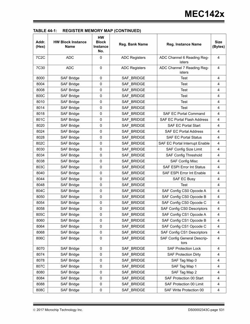
MEC142x
7C2C ADC 0 ADC Registers ADC Channel 6 Reading Reg-isters
4
7C30 ADC 0 ADC Registers ADC Channel 7 Reading Reg-isters
4
8000 SAF Bridge 0 SAF_BRIDGE Test 4
8004 SAF Bridge 0 SAF_BRIDGE Test 4
8008 SAF Bridge 0 SAF_BRIDGE Test 4
800C SAF Bridge 0 SAF_BRIDGE Test 4
8010 SAF Bridge 0 SAF_BRIDGE Test 4
8014 SAF Bridge 0 SAF_BRIDGE Test 4
8018 SAF Bridge 0 SAF_BRIDGE SAF EC Portal Command 4
801C SAF Bridge 0 SAF_BRIDGE SAF EC Portal Flash Address 4
8020 SAF Bridge 0 SAF_BRIDGE SAF EC Portal Start 4
8024 SAF Bridge 0 SAF_BRIDGE SAF EC Portal Address 4
8028 SAF Bridge 0 SAF_BRIDGE SAF EC Portal Status 4
802C SAF Bridge 0 SAF_BRIDGE SAF EC Portal Interrupt Enable 4
8030 SAF Bridge 0 SAF_BRIDGE SAF Config Size Limit 4
8034 SAF Bridge 0 SAF_BRIDGE SAF Config Threshold 4
8038 SAF Bridge 0 SAF_BRIDGE SAF Config Misc 4
803C SAF Bridge 0 SAF_BRIDGE SAF ESPI Error Int Status 4
8040 SAF Bridge 0 SAF_BRIDGE SAF ESPI Error Int Enable 4
8044 SAF Bridge 0 SAF_BRIDGE SAF EC Busy 4
8048 SAF Bridge 0 SAF_BRIDGE Test 4
804C SAF Bridge 0 SAF_BRIDGE SAF Config CS0 Opcode A 4
8050 SAF Bridge 0 SAF_BRIDGE SAF Config CS0 Opcode B 4
8054 SAF Bridge 0 SAF_BRIDGE SAF Config CS0 Opcode C 4
8058 SAF Bridge 0 SAF_BRIDGE SAF Config CS0 Descriptors 4
805C SAF Bridge 0 SAF_BRIDGE SAF Config CS1 Opcode A 4
8060 SAF Bridge 0 SAF_BRIDGE SAF Config CS1 Opcode B 4
8064 SAF Bridge 0 SAF_BRIDGE SAF Config CS1 Opcode C 4
8068 SAF Bridge 0 SAF_BRIDGE SAF Config CS1 Descriptors 4
806C SAF Bridge 0 SAF_BRIDGE SAF Config General Descrip-tors
4
8070 SAF Bridge 0 SAF_BRIDGE SAF Protection Lock 4
8074 SAF Bridge 0 SAF_BRIDGE SAF Protection Dirty 4
8078 SAF Bridge 0 SAF_BRIDGE SAF Tag Map 0 4
807C SAF Bridge 0 SAF_BRIDGE SAF Tag Map 1 4
8080 SAF Bridge 0 SAF_BRIDGE SAF Tag Map 2 4
8084 SAF Bridge 0 SAF_BRIDGE SAF Protection 00 Start 4
8088 SAF Bridge 0 SAF_BRIDGE SAF Protection 00 Limit 4
808C SAF Bridge 0 SAF_BRIDGE SAF Write Protection 00 4
TABLE 44-1: REGISTER MEMORY MAP (CONTINUED)
Addr. (Hex)
HW Block Instance Name
HWBlock
InstanceNo.
Reg. Bank Name Reg. Instance NameSize
(Bytes)
2017 Microchip Technology Inc. DS00002343C-page 531

MEC142x
8090 SAF Bridge 0 SAF_BRIDGE SAF Read Protection 00 4
8094 SAF Bridge 0 SAF_BRIDGE SAF Protection 01 Start 4
8098 SAF Bridge 0 SAF_BRIDGE SAF Protection 01 Limit 4
809C SAF Bridge 0 SAF_BRIDGE SAF Write Protection 01 4
80A0 SAF Bridge 0 SAF_BRIDGE SAF Read Protection 01 4
80A4 SAF Bridge 0 SAF_BRIDGE SAF Protection 02 Start 4
80A8 SAF Bridge 0 SAF_BRIDGE SAF Protection 02 Limit 4
80AC SAF Bridge 0 SAF_BRIDGE SAF Write Protection 02 4
80B0 SAF Bridge 0 SAF_BRIDGE SAF Read Protection 02 4
80B4 SAF Bridge 0 SAF_BRIDGE SAF Protection 03 Start 4
80B8 SAF Bridge 0 SAF_BRIDGE SAF Protection 03 Limit 4
80BC SAF Bridge 0 SAF_BRIDGE SAF Write Protection 03 4
80C0 SAF Bridge 0 SAF_BRIDGE SAF Read Protection 03 4
80C4 SAF Bridge 0 SAF_BRIDGE SAF Protection 04 Start 4
80C8 SAF Bridge 0 SAF_BRIDGE SAF Protection 04 Limit 4
80CC SAF Bridge 0 SAF_BRIDGE SAF Write Protection 04 4
80D0 SAF Bridge 0 SAF_BRIDGE SAF Read Protection 04 4
80D4 SAF Bridge 0 SAF_BRIDGE SAF Protection 05 Start 4
80D8 SAF Bridge 0 SAF_BRIDGE SAF Protection 05 Limit 4
80DC SAF Bridge 0 SAF_BRIDGE SAF Write Protection 05 4
80E0 SAF Bridge 0 SAF_BRIDGE SAF Read Protection 05 4
80E4 SAF Bridge 0 SAF_BRIDGE SAF Protection 06 Start 4
80E8 SAF Bridge 0 SAF_BRIDGE SAF Protection 06 Limit 4
80EC SAF Bridge 0 SAF_BRIDGE SAF Write Protection 06 4
80F0 SAF Bridge 0 SAF_BRIDGE SAF Read Protection 06 4
80F4 SAF Bridge 0 SAF_BRIDGE SAF Protection 07 Start 4
80F8 SAF Bridge 0 SAF_BRIDGE SAF Protection 07 Limit 4
80FC SAF Bridge 0 SAF_BRIDGE SAF Write Protection 07 4
8100 SAF Bridge 0 SAF_BRIDGE SAF Read Protection 07 4
8104 SAF Bridge 0 SAF_BRIDGE SAF Protection 08 Start 4
8108 SAF Bridge 0 SAF_BRIDGE SAF Protection 08 Limit 4
810C SAF Bridge 0 SAF_BRIDGE SAF Write Protection 08 4
8110 SAF Bridge 0 SAF_BRIDGE SAF Read Protection 08 4
8114 SAF Bridge 0 SAF_BRIDGE SAF Protection 09 Start 4
8118 SAF Bridge 0 SAF_BRIDGE SAF Protection 09 Limit 4
811C SAF Bridge 0 SAF_BRIDGE SAF Write Protection 09 4
8120 SAF Bridge 0 SAF_BRIDGE SAF Read Protection 09 4
8124 SAF Bridge 0 SAF_BRIDGE SAF Protection 10 Start 4
8128 SAF Bridge 0 SAF_BRIDGE SAF Protection 10 Limit 4
812C SAF Bridge 0 SAF_BRIDGE SAF Write Protection 10 4
8130 SAF Bridge 0 SAF_BRIDGE SAF Read Protection 10 4
TABLE 44-1: REGISTER MEMORY MAP (CONTINUED)
Addr. (Hex)
HW Block Instance Name
HWBlock
InstanceNo.
Reg. Bank Name Reg. Instance NameSize
(Bytes)
DS00002343C-page 532 2017 Microchip Technology Inc.

MEC142x
8134 SAF Bridge 0 SAF_BRIDGE SAF Protection 11 Start 4
8138 SAF Bridge 0 SAF_BRIDGE SAF Protection 11 Limit 4
813C SAF Bridge 0 SAF_BRIDGE SAF Write Protection 11 4
8140 SAF Bridge 0 SAF_BRIDGE SAF Read Protection 11 4
8144 SAF Bridge 0 SAF_BRIDGE SAF Protection 12 Start 4
8148 SAF Bridge 0 SAF_BRIDGE SAF Protection 12 Limit 4
814C SAF Bridge 0 SAF_BRIDGE SAF Write Protection 12 4
8150 SAF Bridge 0 SAF_BRIDGE SAF Read Protection 12 4
8154 SAF Bridge 0 SAF_BRIDGE SAF Protection 13 Start 4
8158 SAF Bridge 0 SAF_BRIDGE SAF Protection 13 Limit 4
815C SAF Bridge 0 SAF_BRIDGE SAF Write Protection 13 4
8160 SAF Bridge 0 SAF_BRIDGE SAF Read Protection 13 4
8164 SAF Bridge 0 SAF_BRIDGE SAF Protection 14 Start 4
8168 SAF Bridge 0 SAF_BRIDGE SAF Protection 14 Limit 4
816C SAF Bridge 0 SAF_BRIDGE SAF Write Protection 14 4
8170 SAF Bridge 0 SAF_BRIDGE SAF Read Protection 14 4
8174 SAF Bridge 0 SAF_BRIDGE SAF Protection 15 Start 4
8178 SAF Bridge 0 SAF_BRIDGE SAF Protection 15 Limit 4
817C SAF Bridge 0 SAF_BRIDGE SAF Write Protection 15 4
8180 SAF Bridge 0 SAF_BRIDGE SAF Read Protection 15 4
8184 SAF Bridge 0 SAF_BRIDGE SAF Protection 16 Start 4
8188 SAF Bridge 0 SAF_BRIDGE SAF Protection 16 Limit 4
818C SAF Bridge 0 SAF_BRIDGE SAF Write Protection 16 4
8190 SAF Bridge 0 SAF_BRIDGE SAF Read Protection 16 4
8194 SAF Bridge 0 SAF_BRIDGE SAF Poll Timeout 4
8198 SAF Bridge 0 SAF_BRIDGE SAF Poll Interval 4
819C SAF Bridge 0 SAF_BRIDGE SAF Suspend/Resume Interval 4
81A0 SAF Bridge 0 SAF_BRIDGE SAF Consecutive Read Time-out
4
81A4 SAF Bridge 0 SAF_BRIDGE SAF Config Poll2 Mask 4
81A8 SAF Bridge 0 SAF_BRIDGE Test 4
81AC SAF Bridge 0 SAF_BRIDGE SAF Suspend Check Delay 4
81B0 SAF Bridge 0 SAF_BRIDGE SAF Continuous Mode Prefix 4
8C00 Trace FIFO Debug Port 0 TFDP Data 4
8C04 Trace FIFO Debug Port 0 TFDP Control 4
9000 PS/2 0 Registers PS/2 Transmit Buffer Register 1
9000 PS/2 0 Registers PS/2 Receive Buffer Register 1
9004 PS/2 0 Registers PS/2 Control Register 1
9008 PS/2 0 Registers PS/2 Status Register 1
9040 PS/2 1 Registers PS/2 Transmit Buffer Register 1
9040 PS/2 1 Registers PS/2 Receive Buffer Register 1
TABLE 44-1: REGISTER MEMORY MAP (CONTINUED)
Addr. (Hex)
HW Block Instance Name
HWBlock
InstanceNo.
Reg. Bank Name Reg. Instance NameSize
(Bytes)
2017 Microchip Technology Inc. DS00002343C-page 533

MEC142x
9044 PS/2 1 Registers PS/2 Control Register 1
9048 PS/2 1 Registers PS/2 Status Register 1
9800 Hibernation Timer 0 Registers HTimer x Preload Register 2
9804 Hibernation Timer 0 Registers Hibernation Timer x Control Register
2
9808 Hibernation Timer 0 Registers Hibernation Timer x Count Reg-ister
2
9C04 Keyboard Matrix Scan Support
0 Registers KSO Select Register 4
9C08 Keyboard Matrix Scan Support
0 Registers KSI Input Register 4
9C0C Keyboard Matrix Scan Support
0 Registers KSI Status Register 4
9C10 Keyboard Matrix Scan Support
0 Registers KSI Interrupt Enable Register 4
9C14 Keyboard Matrix Scan Support
0 Registers Keyscan Extended Control Register
4
A400 VBAT Registers 0 VBAT_REG_BANK Power-Fail and Reset Status Register
1
A408 VBAT Registers 0 VBAT_REG_BANK Clock Enable Register 1
A418 VBAT Registers 0 VBAT_REG_BANK Alternate Function VTR Control 4
A800 VBAT Powered RAM 0 Registers VBAT Backed Memory 64
AC00 SMB Device Interface 1 SMB_EC_Only Status Register 1
AC00 SMB Device Interface 1 SMB_EC_Only Control Register 1
AC01 SMB Device Interface 1 SMB_EC_Only Reserved 3
AC04 SMB Device Interface 1 SMB_EC_Only Own Address Register 2
AC06 SMB Device Interface 1 SMB_EC_Only Reserved 2
AC08 SMB Device Interface 1 SMB_EC_Only Data 1
AC09 SMB Device Interface 1 SMB_EC_Only Reserved 3
AC0C SMB Device Interface 1 SMB_EC_Only SMBus Master Command Reg-ister
4
AC10 SMB Device Interface 1 SMB_EC_Only SMBus Slave Command Reg-ister
4
AC14 SMB Device Interface 1 SMB_EC_Only PEC Register 1
AC15 SMB Device Interface 1 SMB_EC_Only Reserved 3
AC18 SMB Device Interface 1 SMB_EC_Only DATA_TIMING2 1
AC19 SMB Device Interface 1 SMB_EC_Only Reserved 3
AC20 SMB Device Interface 1 SMB_EC_Only Completion Register 4
AC24 SMB Device Interface 1 SMB_EC_Only Idle Scaling Register 4
AC28 SMB Device Interface 1 SMB_EC_Only Configuration Register 4
AC2C SMB Device Interface 1 SMB_EC_Only Bus Clock Register 2
AC2E SMB Device Interface 1 SMB_EC_Only Reserved 2
AC30 SMB Device Interface 1 SMB_EC_Only Block ID Register 1
TABLE 44-1: REGISTER MEMORY MAP (CONTINUED)
Addr. (Hex)
HW Block Instance Name
HWBlock
InstanceNo.
Reg. Bank Name Reg. Instance NameSize
(Bytes)
DS00002343C-page 534 2017 Microchip Technology Inc.

MEC142x
AC31 SMB Device Interface 1 SMB_EC_Only Reserved 3
AC34 SMB Device Interface 1 SMB_EC_Only Revision Register 1
AC35 SMB Device Interface 1 SMB_EC_Only Reserved 3
AC38 SMB Device Interface 1 SMB_EC_Only Bit-Bang Control Register 1
AC39 SMB Device Interface 1 SMB_EC_Only Reserved 3
AC40 SMB Device Interface 1 SMB_EC_Only Data Timing Register 4
AC44 SMB Device Interface 1 SMB_EC_Only Time-Out Scaling Register 4
AC48 SMB Device Interface 1 SMB_EC_Only SMBus Slave Transmit Buffer Register
1
AC49 SMB Device Interface 1 SMB_EC_Only Reserved 3
AC4C SMB Device Interface 1 SMB_EC_Only SMBus Slave Receive Buffer Register
1
AC4D SMB Device Interface 1 SMB_EC_Only Reserved 3
AC50 SMB Device Interface 1 SMB_EC_Only SMBus Master Transmit Bufer Register
1
AC51 SMB Device Interface 1 SMB_EC_Only Reserved 3
AC54 SMB Device Interface 1 SMB_EC_Only SMBus Master Receive Buffer Register
1
AC55 SMB Device Interface 1 SMB_EC_Only Reserved 3
AC60 SMB Device Interface 1 SMB_EC_Only Wake Status register 4
AC64 SMB Device Interface 1 SMB_EC_Only Wake Enable register 4
B000 SMB Device Interface 2 SMB_EC_Only Control Register 1
B000 SMB Device Interface 2 SMB_EC_Only Status Register 1
B001 SMB Device Interface 2 SMB_EC_Only Reserved 3
B004 SMB Device Interface 2 SMB_EC_Only Own Address Register 2
B006 SMB Device Interface 2 SMB_EC_Only Reserved 2
B008 SMB Device Interface 2 SMB_EC_Only Data 1
B009 SMB Device Interface 2 SMB_EC_Only Reserved 3
B00C SMB Device Interface 2 SMB_EC_Only SMBus Master Command Reg-ister
4
B010 SMB Device Interface 2 SMB_EC_Only SMBus Slave Command Reg-ister
4
B014 SMB Device Interface 2 SMB_EC_Only PEC Register 1
B015 SMB Device Interface 2 SMB_EC_Only Reserved 3
B018 SMB Device Interface 2 SMB_EC_Only DATA_TIMING2 1
B019 SMB Device Interface 2 SMB_EC_Only Reserved 3
B020 SMB Device Interface 2 SMB_EC_Only Completion Register 4
B024 SMB Device Interface 2 SMB_EC_Only Idle Scaling Register 4
B028 SMB Device Interface 2 SMB_EC_Only Configuration Register 4
B02C SMB Device Interface 2 SMB_EC_Only Bus Clock Register 2
B02E SMB Device Interface 2 SMB_EC_Only Reserved 2
B030 SMB Device Interface 2 SMB_EC_Only Block ID Register 1
TABLE 44-1: REGISTER MEMORY MAP (CONTINUED)
Addr. (Hex)
HW Block Instance Name
HWBlock
InstanceNo.
Reg. Bank Name Reg. Instance NameSize
(Bytes)
2017 Microchip Technology Inc. DS00002343C-page 535
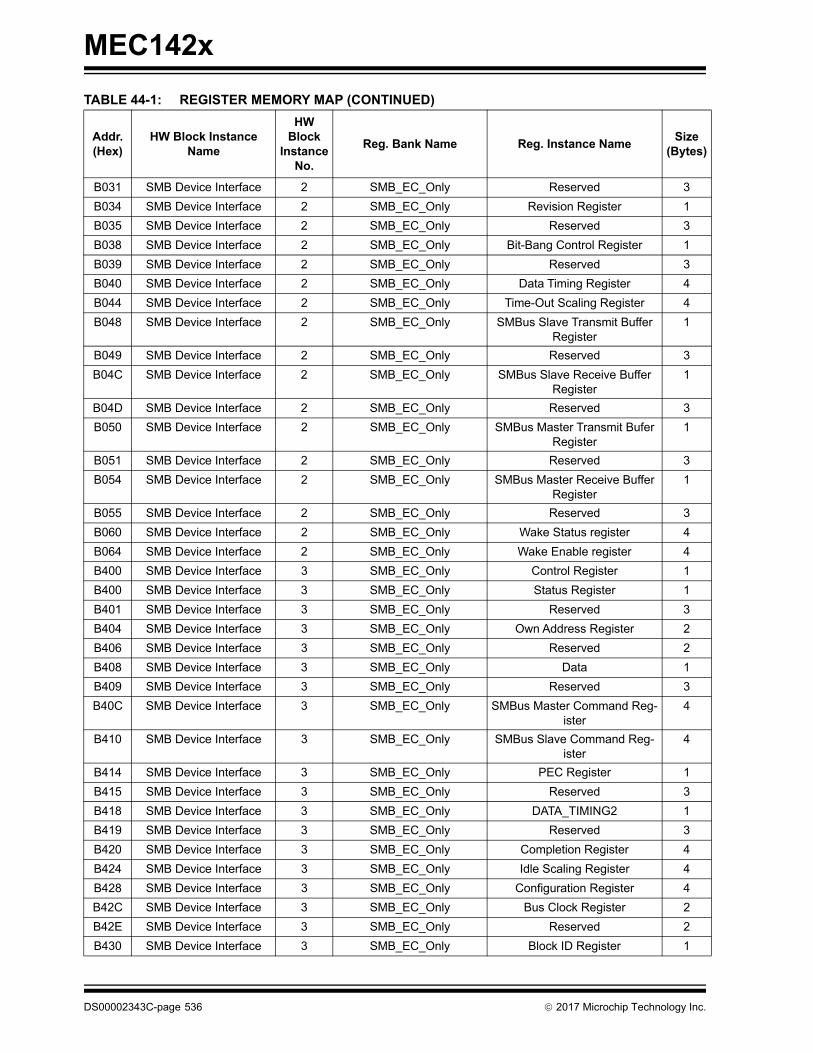
MEC142x
B031 SMB Device Interface 2 SMB_EC_Only Reserved 3
B034 SMB Device Interface 2 SMB_EC_Only Revision Register 1
B035 SMB Device Interface 2 SMB_EC_Only Reserved 3
B038 SMB Device Interface 2 SMB_EC_Only Bit-Bang Control Register 1
B039 SMB Device Interface 2 SMB_EC_Only Reserved 3
B040 SMB Device Interface 2 SMB_EC_Only Data Timing Register 4
B044 SMB Device Interface 2 SMB_EC_Only Time-Out Scaling Register 4
B048 SMB Device Interface 2 SMB_EC_Only SMBus Slave Transmit Buffer Register
1
B049 SMB Device Interface 2 SMB_EC_Only Reserved 3
B04C SMB Device Interface 2 SMB_EC_Only SMBus Slave Receive Buffer Register
1
B04D SMB Device Interface 2 SMB_EC_Only Reserved 3
B050 SMB Device Interface 2 SMB_EC_Only SMBus Master Transmit Bufer Register
1
B051 SMB Device Interface 2 SMB_EC_Only Reserved 3
B054 SMB Device Interface 2 SMB_EC_Only SMBus Master Receive Buffer Register
1
B055 SMB Device Interface 2 SMB_EC_Only Reserved 3
B060 SMB Device Interface 2 SMB_EC_Only Wake Status register 4
B064 SMB Device Interface 2 SMB_EC_Only Wake Enable register 4
B400 SMB Device Interface 3 SMB_EC_Only Control Register 1
B400 SMB Device Interface 3 SMB_EC_Only Status Register 1
B401 SMB Device Interface 3 SMB_EC_Only Reserved 3
B404 SMB Device Interface 3 SMB_EC_Only Own Address Register 2
B406 SMB Device Interface 3 SMB_EC_Only Reserved 2
B408 SMB Device Interface 3 SMB_EC_Only Data 1
B409 SMB Device Interface 3 SMB_EC_Only Reserved 3
B40C SMB Device Interface 3 SMB_EC_Only SMBus Master Command Reg-ister
4
B410 SMB Device Interface 3 SMB_EC_Only SMBus Slave Command Reg-ister
4
B414 SMB Device Interface 3 SMB_EC_Only PEC Register 1
B415 SMB Device Interface 3 SMB_EC_Only Reserved 3
B418 SMB Device Interface 3 SMB_EC_Only DATA_TIMING2 1
B419 SMB Device Interface 3 SMB_EC_Only Reserved 3
B420 SMB Device Interface 3 SMB_EC_Only Completion Register 4
B424 SMB Device Interface 3 SMB_EC_Only Idle Scaling Register 4
B428 SMB Device Interface 3 SMB_EC_Only Configuration Register 4
B42C SMB Device Interface 3 SMB_EC_Only Bus Clock Register 2
B42E SMB Device Interface 3 SMB_EC_Only Reserved 2
B430 SMB Device Interface 3 SMB_EC_Only Block ID Register 1
TABLE 44-1: REGISTER MEMORY MAP (CONTINUED)
Addr. (Hex)
HW Block Instance Name
HWBlock
InstanceNo.
Reg. Bank Name Reg. Instance NameSize
(Bytes)
DS00002343C-page 536 2017 Microchip Technology Inc.
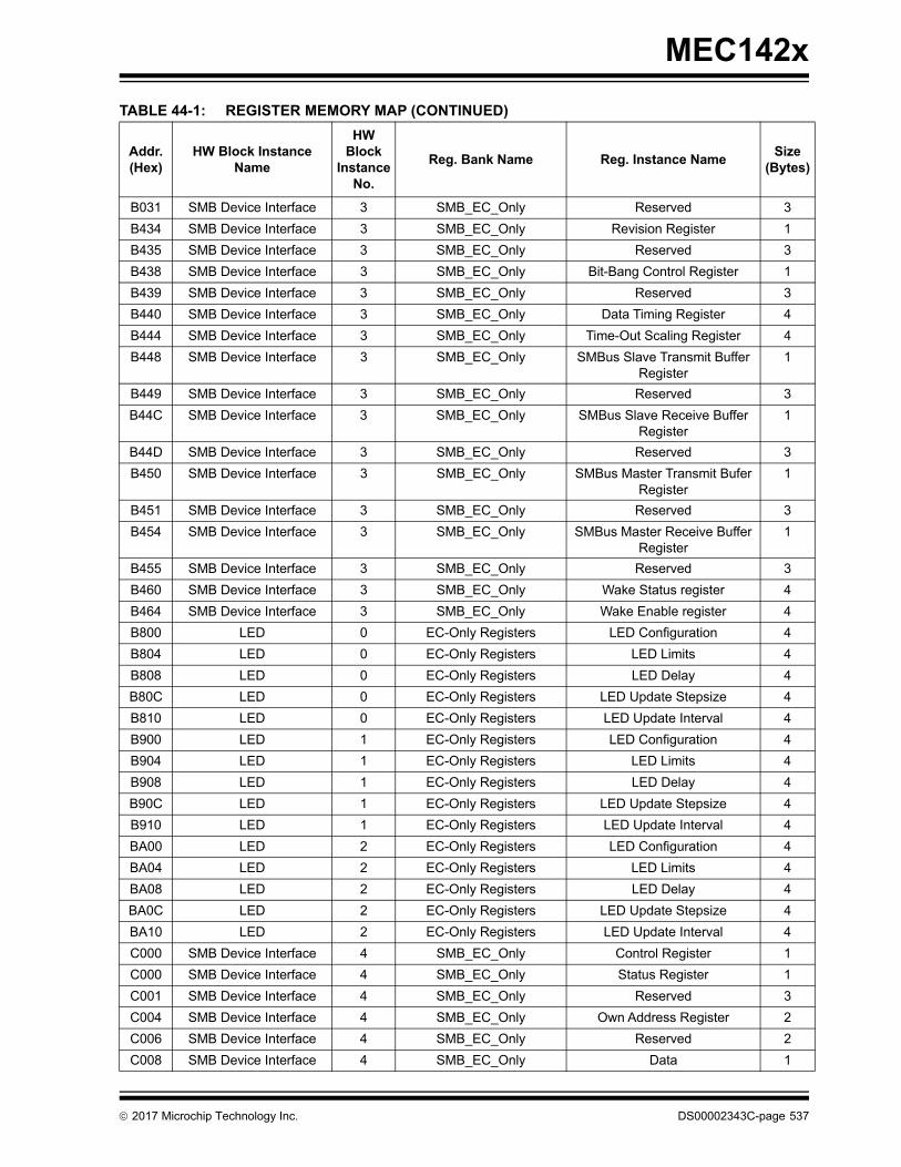
MEC142x
B031 SMB Device Interface 3 SMB_EC_Only Reserved 3
B434 SMB Device Interface 3 SMB_EC_Only Revision Register 1
B435 SMB Device Interface 3 SMB_EC_Only Reserved 3
B438 SMB Device Interface 3 SMB_EC_Only Bit-Bang Control Register 1
B439 SMB Device Interface 3 SMB_EC_Only Reserved 3
B440 SMB Device Interface 3 SMB_EC_Only Data Timing Register 4
B444 SMB Device Interface 3 SMB_EC_Only Time-Out Scaling Register 4
B448 SMB Device Interface 3 SMB_EC_Only SMBus Slave Transmit Buffer Register
1
B449 SMB Device Interface 3 SMB_EC_Only Reserved 3
B44C SMB Device Interface 3 SMB_EC_Only SMBus Slave Receive Buffer Register
1
B44D SMB Device Interface 3 SMB_EC_Only Reserved 3
B450 SMB Device Interface 3 SMB_EC_Only SMBus Master Transmit Bufer Register
1
B451 SMB Device Interface 3 SMB_EC_Only Reserved 3
B454 SMB Device Interface 3 SMB_EC_Only SMBus Master Receive Buffer Register
1
B455 SMB Device Interface 3 SMB_EC_Only Reserved 3
B460 SMB Device Interface 3 SMB_EC_Only Wake Status register 4
B464 SMB Device Interface 3 SMB_EC_Only Wake Enable register 4
B800 LED 0 EC-Only Registers LED Configuration 4
B804 LED 0 EC-Only Registers LED Limits 4
B808 LED 0 EC-Only Registers LED Delay 4
B80C LED 0 EC-Only Registers LED Update Stepsize 4
B810 LED 0 EC-Only Registers LED Update Interval 4
B900 LED 1 EC-Only Registers LED Configuration 4
B904 LED 1 EC-Only Registers LED Limits 4
B908 LED 1 EC-Only Registers LED Delay 4
B90C LED 1 EC-Only Registers LED Update Stepsize 4
B910 LED 1 EC-Only Registers LED Update Interval 4
BA00 LED 2 EC-Only Registers LED Configuration 4
BA04 LED 2 EC-Only Registers LED Limits 4
BA08 LED 2 EC-Only Registers LED Delay 4
BA0C LED 2 EC-Only Registers LED Update Stepsize 4
BA10 LED 2 EC-Only Registers LED Update Interval 4
C000 SMB Device Interface 4 SMB_EC_Only Control Register 1
C000 SMB Device Interface 4 SMB_EC_Only Status Register 1
C001 SMB Device Interface 4 SMB_EC_Only Reserved 3
C004 SMB Device Interface 4 SMB_EC_Only Own Address Register 2
C006 SMB Device Interface 4 SMB_EC_Only Reserved 2
C008 SMB Device Interface 4 SMB_EC_Only Data 1
TABLE 44-1: REGISTER MEMORY MAP (CONTINUED)
Addr. (Hex)
HW Block Instance Name
HWBlock
InstanceNo.
Reg. Bank Name Reg. Instance NameSize
(Bytes)
2017 Microchip Technology Inc. DS00002343C-page 537

MEC142x
C009 SMB Device Interface 4 SMB_EC_Only Reserved 3
C00C SMB Device Interface 4 SMB_EC_Only SMBus Master Command Reg-ister
4
C010 SMB Device Interface 4 SMB_EC_Only SMBus Slave Command Reg-ister
4
C014 SMB Device Interface 4 SMB_EC_Only PEC Register 1
C015 SMB Device Interface 4 SMB_EC_Only Reserved 3
C018 SMB Device Interface 4 SMB_EC_Only DATA_TIMING2 1
C019 SMB Device Interface 4 SMB_EC_Only Reserved 3
C020 SMB Device Interface 4 SMB_EC_Only Completion Register 4
C024 SMB Device Interface 4 SMB_EC_Only Idle Scaling Register 4
C028 SMB Device Interface 4 SMB_EC_Only Configuration Register 4
C02C SMB Device Interface 4 SMB_EC_Only Bus Clock Register 2
C02E SMB Device Interface 4 SMB_EC_Only Reserved 2
C030 SMB Device Interface 4 SMB_EC_Only Block ID Register 1
C031 SMB Device Interface 4 SMB_EC_Only Reserved 3
C034 SMB Device Interface 2 SMB_EC_Only Revision Register 1
C035 SMB Device Interface 4 SMB_EC_Only Reserved 3
C038 SMB Device Interface 4 SMB_EC_Only Bit-Bang Control Register 1
C039 SMB Device Interface 4 SMB_EC_Only Reserved 3
C040 SMB Device Interface 4 SMB_EC_Only Data Timing Register 4
C044 SMB Device Interface 4 SMB_EC_Only Time-Out Scaling Register 4
C048 SMB Device Interface 4 SMB_EC_Only SMBus Slave Transmit Buffer Register
1
C049 SMB Device Interface 4 SMB_EC_Only Reserved 3
C04C SMB Device Interface 4 SMB_EC_Only SMBus Slave Receive Buffer Register
1
C04D SMB Device Interface 4 SMB_EC_Only Reserved 3
C050 SMB Device Interface 4 SMB_EC_Only SMBus Master Transmit Bufer Register
1
C051 SMB Device Interface 4 SMB_EC_Only Reserved 3
C054 SMB Device Interface 4 SMB_EC_Only SMBus Master Receive Buffer Register
1
C055 SMB Device Interface 4 SMB_EC_Only Reserved 3
C060 SMB Device Interface 4 SMB_EC_Only Wake Status register 4
C064 SMB Device Interface 4 SMB_EC_Only Wake Enable register 4
CC80 Week Timer 0 Registers Control Register 1
CC84 Week Timer 0 Registers 28-bit Up-Counter Timer Regis-ter
4
CC88 Week Timer 0 Registers 28-bit Comparator Register 4
CC8C Week Timer 0 Registers 15-Bit Clock Divider Reading Register
2
TABLE 44-1: REGISTER MEMORY MAP (CONTINUED)
Addr. (Hex)
HW Block Instance Name
HWBlock
InstanceNo.
Reg. Bank Name Reg. Instance NameSize
(Bytes)
DS00002343C-page 538 2017 Microchip Technology Inc.
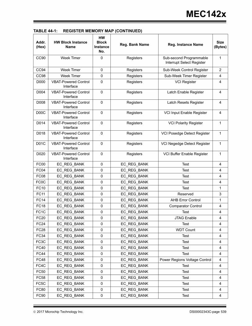
MEC142x
CC90 Week Timer 0 Registers Sub-second Programmable Interrupt Select Register
1
CC94 Week Timer 0 Registers Sub-Week Control Register 2
CC98 Week Timer 0 Registers Sub-Week Timer Register 4
D000 VBAT-Powered Control Interface
0 Registers VCI Register 4
D004 VBAT-Powered Control Interface
0 Registers Latch Enable Register 4
D008 VBAT-Powered Control Interface
0 Registers Latch Resets Register 4
D00C VBAT-Powered Control Interface
0 Registers VCI Input Enable Register 4
D014 VBAT-Powered Control Interface
0 Registers VCI Polarity Register 1
D018 VBAT-Powered Control Interface
0 Registers VCI Posedge Detect Register 1
D01C VBAT-Powered Control Interface
0 Registers VCI Negedge Detect Register 1
D020 VBAT-Powered Control Interface
0 Registers VCI Buffer Enable Register 1
FC00 EC_REG_BANK 0 EC_REG_BANK Test 4
FC04 EC_REG_BANK 0 EC_REG_BANK Test 4
FC08 EC_REG_BANK 0 EC_REG_BANK Test 4
FC0C EC_REG_BANK 0 EC_REG_BANK Test 4
FC10 EC_REG_BANK 0 EC_REG_BANK Test 1
FC11 EC_REG_BANK 0 EC_REG_BANK Reserved 3
FC14 EC_REG_BANK 0 EC_REG_BANK AHB Error Control 1
FC18 EC_REG_BANK 0 EC_REG_BANK Comparator Control 4
FC1C EC_REG_BANK 0 EC_REG_BANK Test 4
FC20 EC_REG_BANK 0 EC_REG_BANK JTAG Enable 4
FC24 EC_REG_BANK 0 EC_REG_BANK Test 4
FC28 EC_REG_BANK 0 EC_REG_BANK WDT Count 4
FC34 EC_REG_BANK 0 EC_REG_BANK Test 4
FC3C EC_REG_BANK 0 EC_REG_BANK Test 4
FC40 EC_REG_BANK 0 EC_REG_BANK Test 4
FC44 EC_REG_BANK 0 EC_REG_BANK Test 4
FC48 EC_REG_BANK 0 EC_REG_BANK Power Regions Voltage Control 4
FC4C EC_REG_BANK 0 EC_REG_BANK Test 4
FC50 EC_REG_BANK 0 EC_REG_BANK Test 4
FC58 EC_REG_BANK 0 EC_REG_BANK Test 4
FC5C EC_REG_BANK 0 EC_REG_BANK Test 4
FC80 EC_REG_BANK 0 EC_REG_BANK Test 4
FC90 EC_REG_BANK 0 EC_REG_BANK Test 4
TABLE 44-1: REGISTER MEMORY MAP (CONTINUED)
Addr. (Hex)
HW Block Instance Name
HWBlock
InstanceNo.
Reg. Bank Name Reg. Instance NameSize
(Bytes)
2017 Microchip Technology Inc. DS00002343C-page 539
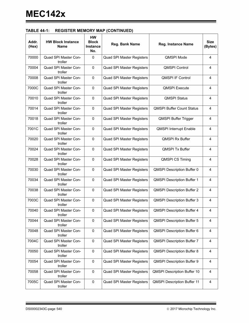
MEC142x
70000 Quad SPI Master Con-troller
0 Quad SPI Master Registers QMSPI Mode 4
70004 Quad SPI Master Con-troller
0 Quad SPI Master Registers QMSPI Control 4
70008 Quad SPI Master Con-troller
0 Quad SPI Master Registers QMSPI IF Control 4
7000C Quad SPI Master Con-troller
0 Quad SPI Master Registers QMSPI Execute 4
70010 Quad SPI Master Con-troller
0 Quad SPI Master Registers QMSPI Status 4
70014 Quad SPI Master Con-troller
0 Quad SPI Master Registers QMSPI Buffer Count Status 4
70018 Quad SPI Master Con-troller
0 Quad SPI Master Registers QMSPI Buffer Trigger 4
7001C Quad SPI Master Con-troller
0 Quad SPI Master Registers QMSPI Interrupt Enable 4
70020 Quad SPI Master Con-troller
0 Quad SPI Master Registers QMSPI Rx Buffer 4
70024 Quad SPI Master Con-troller
0 Quad SPI Master Registers QMSPI Tx Buffer 4
70028 Quad SPI Master Con-troller
0 Quad SPI Master Registers QMSPI CS Timing 4
70030 Quad SPI Master Con-troller
0 Quad SPI Master Registers QMSPI Description Buffer 0 4
70034 Quad SPI Master Con-troller
0 Quad SPI Master Registers QMSPI Description Buffer 1 4
70038 Quad SPI Master Con-troller
0 Quad SPI Master Registers QMSPI Description Buffer 2 4
7003C Quad SPI Master Con-troller
0 Quad SPI Master Registers QMSPI Description Buffer 3 4
70040 Quad SPI Master Con-troller
0 Quad SPI Master Registers QMSPI Description Buffer 4 4
70044 Quad SPI Master Con-troller
0 Quad SPI Master Registers QMSPI Description Buffer 5 4
70048 Quad SPI Master Con-troller
0 Quad SPI Master Registers QMSPI Description Buffer 6 4
7004C Quad SPI Master Con-troller
0 Quad SPI Master Registers QMSPI Description Buffer 7 4
70050 Quad SPI Master Con-troller
0 Quad SPI Master Registers QMSPI Description Buffer 8 4
70054 Quad SPI Master Con-troller
0 Quad SPI Master Registers QMSPI Description Buffer 9 4
70058 Quad SPI Master Con-troller
0 Quad SPI Master Registers QMSPI Description Buffer 10 4
7005C Quad SPI Master Con-troller
0 Quad SPI Master Registers QMSPI Description Buffer 11 4
TABLE 44-1: REGISTER MEMORY MAP (CONTINUED)
Addr. (Hex)
HW Block Instance Name
HWBlock
InstanceNo.
Reg. Bank Name Reg. Instance NameSize
(Bytes)
DS00002343C-page 540 2017 Microchip Technology Inc.

MEC142x
70060 Quad SPI Master Con-troller
0 Quad SPI Master Registers QMSPI Description Buffer 12 4
70064 Quad SPI Master Con-troller
0 Quad SPI Master Registers QMSPI Description Buffer 13 4
70068 Quad SPI Master Con-troller
0 Quad SPI Master Registers QMSPI Description Buffer 14 4
7006C Quad SPI Master Con-troller
0 Quad SPI Master Registers QMSPI Description Buffer 15 4
71000-7101B
SAF Comm 0 SAF Comm Registers Test 4
712B8 SAF Comm 0 SAF Comm Registers SAF Comm Mode 4
712BC SAF Comm 0 SAF Comm Registers Test 8
80100 PCR 0 EC-Only Registers Chip Sleep Enable Register 4
80104 PCR 0 EC-Only Registers Chip Clock Required Register 4
80108 PCR 0 EC-Only Registers Test 4
8010C PCR 0 EC-Only Registers Test 4
80110 PCR 0 EC-Only Registers Host Sleep Enables Register 4
80114 PCR 0 EC-Only Registers Host Clock Required Status Register
4
80118 PCR 0 EC-Only Registers System Sleep Control 4
80120 PCR 0 EC-Only Registers Processor Clock Control 4
80124 PCR 0 EC-Only Registers EC Sleep Enable 2 Register 4
80128 PCR 0 EC-Only Registers EC Clock Required 2 Status Register
4
8012C PCR 0 EC-Only Registers Slow Clock Control 4
80130 PCR 0 EC-Only Registers Oscillator ID 4
80134 PCR 0 EC-Only Registers CHIP_PWR_RST_STS 4
80138 PCR 0 EC-Only Registers Test 4
8013C PCR 0 EC-Only Registers Host Reset Enable 4
80140 PCR 0 EC-Only Registers EC Reset Enable 4
80144 PCR 0 EC-Only Registers EC Reset Enable 2 4
80148 PCR 0 EC-Only Registers Power Reset Control 4
8014C PCR 0 EC-Only Registers Test 4
80150 PCR 0 EC-Only Registers System Reset 4
81004 GPIO 0 GPIO Registers GPIO001 Pin Control 4
81008 GPIO 0 GPIO Registers GPIO002 Pin Control 4
8100C GPIO 0 GPIO Registers GPIO003 Pin Control 4
81010 GPIO 0 GPIO Registers GPIO004 Pin Control 4
81014 GPIO 0 GPIO Registers GPIO005 Pin Control 4
81018 GPIO 0 GPIO Registers GPIO006 Pin Control 4
8101C GPIO 0 GPIO Registers GPIO007 Pin Control 4
81020 GPIO 0 GPIO Registers GPIO010 Pin Control 4
TABLE 44-1: REGISTER MEMORY MAP (CONTINUED)
Addr. (Hex)
HW Block Instance Name
HWBlock
InstanceNo.
Reg. Bank Name Reg. Instance NameSize
(Bytes)
2017 Microchip Technology Inc. DS00002343C-page 541

MEC142x
81024 GPIO 0 GPIO Registers GPIO011 Pin Control 4
81028 GPIO 0 GPIO Registers GPIO012 Pin Control 4
8102C GPIO 0 GPIO Registers GPIO013 Pin Control 4
81030 GPIO 0 GPIO Registers GPIO014 Pin Control 4
81034 GPIO 0 GPIO Registers GPIO015 Pin Control 4
81038 GPIO 0 GPIO Registers GPIO016 Pin Control 4
8103C GPIO 0 GPIO Registers GPIO017 Pin Control 4
81040 GPIO 0 GPIO Registers GPIO020 Pin Control 4
81044 GPIO 0 GPIO Registers GPIO021 Pin Control 4
81048 GPIO 0 GPIO Registers GPIO022 Pin Control 4
8104C GPIO 0 GPIO Registers GPIO023 Pin Control 4
81050 GPIO 0 GPIO Registers GPIO024 Pin Control 4
81054 GPIO 0 GPIO Registers GPIO025 Pin Control 4
81058 GPIO 0 GPIO Registers GPIO026 Pin Control 4
8105C GPIO 0 GPIO Registers GPIO027 Pin Control 4
81060 GPIO 0 GPIO Registers GPIO030 Pin Control 4
81064 GPIO 0 GPIO Registers GPIO031 Pin Control 4
81068 GPIO 0 GPIO Registers GPIO032 Pin Control 4
8106C GPIO 0 GPIO Registers GPIO033 Pin Control 4
81070 GPIO 0 GPIO Registers GPIO034 Pin Control 4
81074 GPIO 0 GPIO Registers GPIO035 Pin Control 4
81078 GPIO 0 GPIO Registers GPIO036 Pin Control 4
81080 GPIO 0 GPIO Registers GPIO040 Pin Control 4
81084 GPIO 0 GPIO Registers GPIO041 Pin Control 4
81088 GPIO 0 GPIO Registers GPIO042 Pin Control 4
8108C GPIO 0 GPIO Registers GPIO043 Pin Control 4
81090 GPIO 0 GPIO Registers GPIO044 Pin Control 4
81094 GPIO 0 GPIO Registers GPIO045 Pin Control 4
81098 GPIO 0 GPIO Registers GPIO046 Pin Control 4
8109C GPIO 0 GPIO Registers GPIO047 Pin Control 4
810A0 GPIO 0 GPIO Registers GPIO050 Pin Control 4
810A4 GPIO 0 GPIO Registers GPIO051 Pin Control 4
810A8 GPIO 0 GPIO Registers GPIO052 Pin Control 4
810AC GPIO 0 GPIO Registers GPIO053 Pin Control 4
810B0 GPIO 0 GPIO Registers GPIO054 Pin Control 4
810B4 GPIO 0 GPIO Registers GPIO055 Pin Control 4
810B8 GPIO 0 GPIO Registers GPIO056 Pin Control 4
810BC GPIO 0 GPIO Registers GPIO057 Pin Control 4
810C0 GPIO 0 GPIO Registers GPIO060 Pin Control 4
810C4 GPIO 0 GPIO Registers GPIO061 Pin Control 4
810C8 GPIO 0 GPIO Registers GPIO062 Pin Control 4
TABLE 44-1: REGISTER MEMORY MAP (CONTINUED)
Addr. (Hex)
HW Block Instance Name
HWBlock
InstanceNo.
Reg. Bank Name Reg. Instance NameSize
(Bytes)
DS00002343C-page 542 2017 Microchip Technology Inc.
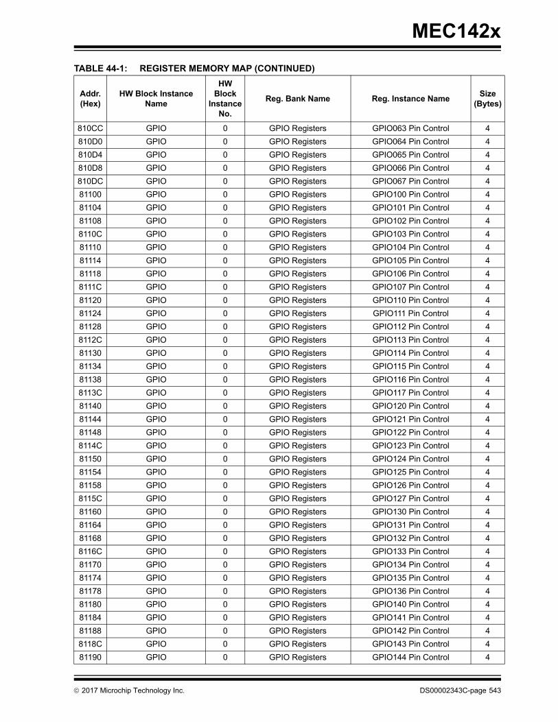
MEC142x
810CC GPIO 0 GPIO Registers GPIO063 Pin Control 4
810D0 GPIO 0 GPIO Registers GPIO064 Pin Control 4
810D4 GPIO 0 GPIO Registers GPIO065 Pin Control 4
810D8 GPIO 0 GPIO Registers GPIO066 Pin Control 4
810DC GPIO 0 GPIO Registers GPIO067 Pin Control 4
81100 GPIO 0 GPIO Registers GPIO100 Pin Control 4
81104 GPIO 0 GPIO Registers GPIO101 Pin Control 4
81108 GPIO 0 GPIO Registers GPIO102 Pin Control 4
8110C GPIO 0 GPIO Registers GPIO103 Pin Control 4
81110 GPIO 0 GPIO Registers GPIO104 Pin Control 4
81114 GPIO 0 GPIO Registers GPIO105 Pin Control 4
81118 GPIO 0 GPIO Registers GPIO106 Pin Control 4
8111C GPIO 0 GPIO Registers GPIO107 Pin Control 4
81120 GPIO 0 GPIO Registers GPIO110 Pin Control 4
81124 GPIO 0 GPIO Registers GPIO111 Pin Control 4
81128 GPIO 0 GPIO Registers GPIO112 Pin Control 4
8112C GPIO 0 GPIO Registers GPIO113 Pin Control 4
81130 GPIO 0 GPIO Registers GPIO114 Pin Control 4
81134 GPIO 0 GPIO Registers GPIO115 Pin Control 4
81138 GPIO 0 GPIO Registers GPIO116 Pin Control 4
8113C GPIO 0 GPIO Registers GPIO117 Pin Control 4
81140 GPIO 0 GPIO Registers GPIO120 Pin Control 4
81144 GPIO 0 GPIO Registers GPIO121 Pin Control 4
81148 GPIO 0 GPIO Registers GPIO122 Pin Control 4
8114C GPIO 0 GPIO Registers GPIO123 Pin Control 4
81150 GPIO 0 GPIO Registers GPIO124 Pin Control 4
81154 GPIO 0 GPIO Registers GPIO125 Pin Control 4
81158 GPIO 0 GPIO Registers GPIO126 Pin Control 4
8115C GPIO 0 GPIO Registers GPIO127 Pin Control 4
81160 GPIO 0 GPIO Registers GPIO130 Pin Control 4
81164 GPIO 0 GPIO Registers GPIO131 Pin Control 4
81168 GPIO 0 GPIO Registers GPIO132 Pin Control 4
8116C GPIO 0 GPIO Registers GPIO133 Pin Control 4
81170 GPIO 0 GPIO Registers GPIO134 Pin Control 4
81174 GPIO 0 GPIO Registers GPIO135 Pin Control 4
81178 GPIO 0 GPIO Registers GPIO136 Pin Control 4
81180 GPIO 0 GPIO Registers GPIO140 Pin Control 4
81184 GPIO 0 GPIO Registers GPIO141 Pin Control 4
81188 GPIO 0 GPIO Registers GPIO142 Pin Control 4
8118C GPIO 0 GPIO Registers GPIO143 Pin Control 4
81190 GPIO 0 GPIO Registers GPIO144 Pin Control 4
TABLE 44-1: REGISTER MEMORY MAP (CONTINUED)
Addr. (Hex)
HW Block Instance Name
HWBlock
InstanceNo.
Reg. Bank Name Reg. Instance NameSize
(Bytes)
2017 Microchip Technology Inc. DS00002343C-page 543
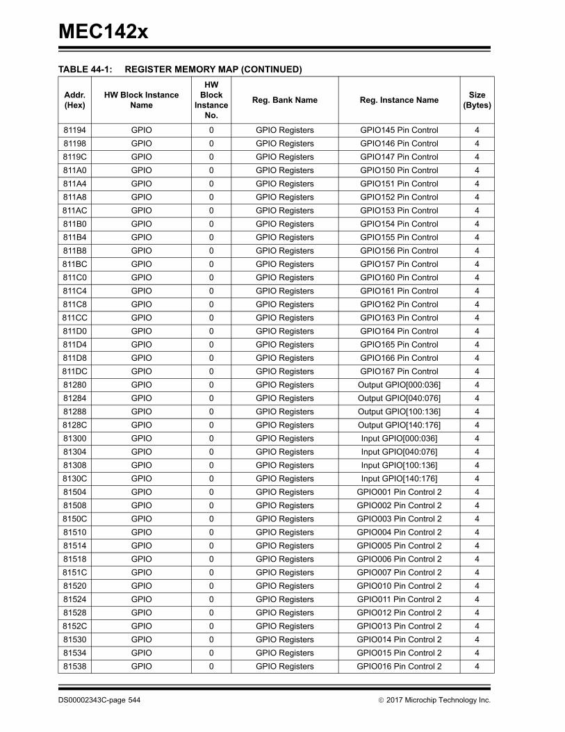
MEC142x
81194 GPIO 0 GPIO Registers GPIO145 Pin Control 4
81198 GPIO 0 GPIO Registers GPIO146 Pin Control 4
8119C GPIO 0 GPIO Registers GPIO147 Pin Control 4
811A0 GPIO 0 GPIO Registers GPIO150 Pin Control 4
811A4 GPIO 0 GPIO Registers GPIO151 Pin Control 4
811A8 GPIO 0 GPIO Registers GPIO152 Pin Control 4
811AC GPIO 0 GPIO Registers GPIO153 Pin Control 4
811B0 GPIO 0 GPIO Registers GPIO154 Pin Control 4
811B4 GPIO 0 GPIO Registers GPIO155 Pin Control 4
811B8 GPIO 0 GPIO Registers GPIO156 Pin Control 4
811BC GPIO 0 GPIO Registers GPIO157 Pin Control 4
811C0 GPIO 0 GPIO Registers GPIO160 Pin Control 4
811C4 GPIO 0 GPIO Registers GPIO161 Pin Control 4
811C8 GPIO 0 GPIO Registers GPIO162 Pin Control 4
811CC GPIO 0 GPIO Registers GPIO163 Pin Control 4
811D0 GPIO 0 GPIO Registers GPIO164 Pin Control 4
811D4 GPIO 0 GPIO Registers GPIO165 Pin Control 4
811D8 GPIO 0 GPIO Registers GPIO166 Pin Control 4
811DC GPIO 0 GPIO Registers GPIO167 Pin Control 4
81280 GPIO 0 GPIO Registers Output GPIO[000:036] 4
81284 GPIO 0 GPIO Registers Output GPIO[040:076] 4
81288 GPIO 0 GPIO Registers Output GPIO[100:136] 4
8128C GPIO 0 GPIO Registers Output GPIO[140:176] 4
81300 GPIO 0 GPIO Registers Input GPIO[000:036] 4
81304 GPIO 0 GPIO Registers Input GPIO[040:076] 4
81308 GPIO 0 GPIO Registers Input GPIO[100:136] 4
8130C GPIO 0 GPIO Registers Input GPIO[140:176] 4
81504 GPIO 0 GPIO Registers GPIO001 Pin Control 2 4
81508 GPIO 0 GPIO Registers GPIO002 Pin Control 2 4
8150C GPIO 0 GPIO Registers GPIO003 Pin Control 2 4
81510 GPIO 0 GPIO Registers GPIO004 Pin Control 2 4
81514 GPIO 0 GPIO Registers GPIO005 Pin Control 2 4
81518 GPIO 0 GPIO Registers GPIO006 Pin Control 2 4
8151C GPIO 0 GPIO Registers GPIO007 Pin Control 2 4
81520 GPIO 0 GPIO Registers GPIO010 Pin Control 2 4
81524 GPIO 0 GPIO Registers GPIO011 Pin Control 2 4
81528 GPIO 0 GPIO Registers GPIO012 Pin Control 2 4
8152C GPIO 0 GPIO Registers GPIO013 Pin Control 2 4
81530 GPIO 0 GPIO Registers GPIO014 Pin Control 2 4
81534 GPIO 0 GPIO Registers GPIO015 Pin Control 2 4
81538 GPIO 0 GPIO Registers GPIO016 Pin Control 2 4
TABLE 44-1: REGISTER MEMORY MAP (CONTINUED)
Addr. (Hex)
HW Block Instance Name
HWBlock
InstanceNo.
Reg. Bank Name Reg. Instance NameSize
(Bytes)
DS00002343C-page 544 2017 Microchip Technology Inc.

MEC142x
8153C GPIO 0 GPIO Registers GPIO017 Pin Control 2 4
81540 GPIO 0 GPIO Registers GPIO020 Pin Control 2 4
81544 GPIO 0 GPIO Registers GPIO021 Pin Control 2 4
81548 GPIO 0 GPIO Registers GPIO022 Pin Control 2 4
8154C GPIO 0 GPIO Registers GPIO023 Pin Control 2 4
81550 GPIO 0 GPIO Registers GPIO024 Pin Control 2 4
81554 GPIO 0 GPIO Registers GPIO025 Pin Control 2 4
81558 GPIO 0 GPIO Registers GPIO026 Pin Control 2 4
8155C GPIO 0 GPIO Registers GPIO027 Pin Control 2 4
81560 GPIO 0 GPIO Registers GPIO030 Pin Control 2 4
81564 GPIO 0 GPIO Registers GPIO031 Pin Control 2 4
81568 GPIO 0 GPIO Registers GPIO032 Pin Control 2 4
8156C GPIO 0 GPIO Registers GPIO033 Pin Control 2 4
81570 GPIO 0 GPIO Registers GPIO034 Pin Control 2 4
81574 GPIO 0 GPIO Registers GPIO035 Pin Control 2 4
81578 GPIO 0 GPIO Registers GPIO036 Pin Control 2 4
81580 GPIO 0 GPIO Registers GPIO040 Pin Control 2 4
81584 GPIO 0 GPIO Registers GPIO041 Pin Control 2 4
81588 GPIO 0 GPIO Registers GPIO042 Pin Control 2 4
8158C GPIO 0 GPIO Registers GPIO043 Pin Control 2 4
81590 GPIO 0 GPIO Registers GPIO044 Pin Control 2 4
81594 GPIO 0 GPIO Registers GPIO045 Pin Control 2 4
81598 GPIO 0 GPIO Registers GPIO046 Pin Control 2 4
8159C GPIO 0 GPIO Registers GPIO047 Pin Control 2 4
815A0 GPIO 0 GPIO Registers GPIO050 Pin Control 2 4
815A4 GPIO 0 GPIO Registers GPIO051 Pin Control 2 4
815A8 GPIO 0 GPIO Registers GPIO052 Pin Control 2 4
815AC GPIO 0 GPIO Registers GPIO053 Pin Control 2 4
815B0 GPIO 0 GPIO Registers GPIO054 Pin Control 2 4
815B4 GPIO 0 GPIO Registers GPIO055 Pin Control 2 4
815B8 GPIO 0 GPIO Registers GPIO056 Pin Control 2 4
815BC GPIO 0 GPIO Registers GPIO057 Pin Control 2 4
815C0 GPIO 0 GPIO Registers GPIO060 Pin Control 2 4
815C4 GPIO 0 GPIO Registers GPIO061 Pin Control 2 4
815C8 GPIO 0 GPIO Registers GPIO062 Pin Control 2 4
815CC GPIO 0 GPIO Registers GPIO063 Pin Control 2 4
815D0 GPIO 0 GPIO Registers GPIO064 Pin Control 2 4
815D4 GPIO 0 GPIO Registers GPIO065 Pin Control 2 4
815D8 GPIO 0 GPIO Registers GPIO066 Pin Control 2 4
815DC GPIO 0 GPIO Registers GPIO067 Pin Control 2 4
815E0 GPIO 0 GPIO Registers GPIO100 Pin Control 2 4
TABLE 44-1: REGISTER MEMORY MAP (CONTINUED)
Addr. (Hex)
HW Block Instance Name
HWBlock
InstanceNo.
Reg. Bank Name Reg. Instance NameSize
(Bytes)
2017 Microchip Technology Inc. DS00002343C-page 545

MEC142x
815E4 GPIO 0 GPIO Registers GPIO101 Pin Control 2 4
815E8 GPIO 0 GPIO Registers GPIO102 Pin Control 2 4
815EC GPIO 0 GPIO Registers GPIO103 Pin Control 2 4
815F0 GPIO 0 GPIO Registers GPIO104 Pin Control 2 4
815F4 GPIO 0 GPIO Registers GPIO105 Pin Control 2 4
815F8 GPIO 0 GPIO Registers GPIO106 Pin Control 2 4
815FC GPIO 0 GPIO Registers GPIO107 Pin Control 2 4
81600 GPIO 0 GPIO Registers GPIO110 Pin Control 2 4
81604 GPIO 0 GPIO Registers GPIO111 Pin Control 2 4
81608 GPIO 0 GPIO Registers GPIO112 Pin Control 2 4
8160C GPIO 0 GPIO Registers GPIO113 Pin Control 2 4
81610 GPIO 0 GPIO Registers GPIO114 Pin Control 2 4
81614 GPIO 0 GPIO Registers GPIO115 Pin Control 2 4
81618 GPIO 0 GPIO Registers GPIO116 Pin Control 2 4
8161C GPIO 0 GPIO Registers GPIO117 Pin Control 2 4
81620 GPIO 0 GPIO Registers GPIO120 Pin Control 2 4
81624 GPIO 0 GPIO Registers GPIO121 Pin Control 2 4
81628 GPIO 0 GPIO Registers GPIO122 Pin Control 2 4
8162C GPIO 0 GPIO Registers GPIO123 Pin Control 2 4
81630 GPIO 0 GPIO Registers GPIO124 Pin Control 2 4
81634 GPIO 0 GPIO Registers GPIO125 Pin Control 2 4
81638 GPIO 0 GPIO Registers GPIO126 Pin Control 2 4
8163C GPIO 0 GPIO Registers GPIO127 Pin Control 2 4
81640 GPIO 0 GPIO Registers GPIO130 Pin Control 2 4
81644 GPIO 0 GPIO Registers GPIO131 Pin Control 2 4
81648 GPIO 0 GPIO Registers GPIO132 Pin Control 2 4
8164C GPIO 0 GPIO Registers GPIO133 Pin Control 2 4
81650 GPIO 0 GPIO Registers GPIO134 Pin Control 2 4
81654 GPIO 0 GPIO Registers GPIO135 Pin Control 2 4
81658 GPIO 0 GPIO Registers GPIO136 Pin Control 2 4
81660 GPIO 0 GPIO Registers GPIO140 Pin Control 2 4
81664 GPIO 0 GPIO Registers GPIO141 Pin Control 2 4
81668 GPIO 0 GPIO Registers GPIO142 Pin Control 2 4
8166C GPIO 0 GPIO Registers GPIO143 Pin Control 2 4
81670 GPIO 0 GPIO Registers GPIO144 Pin Control 2 4
81674 GPIO 0 GPIO Registers GPIO145 Pin Control 2 4
81678 GPIO 0 GPIO Registers GPIO146 Pin Control 2 4
8167C GPIO 0 GPIO Registers GPIO147 Pin Control 2 4
81680 GPIO 0 GPIO Registers GPIO150 Pin Control 2 4
81684 GPIO 0 GPIO Registers GPIO151 Pin Control 2 4
81688 GPIO 0 GPIO Registers GPIO152 Pin Control 2 4
TABLE 44-1: REGISTER MEMORY MAP (CONTINUED)
Addr. (Hex)
HW Block Instance Name
HWBlock
InstanceNo.
Reg. Bank Name Reg. Instance NameSize
(Bytes)
DS00002343C-page 546 2017 Microchip Technology Inc.
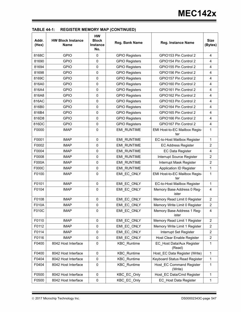
MEC142x
8168C GPIO 0 GPIO Registers GPIO153 Pin Control 2 4
81690 GPIO 0 GPIO Registers GPIO154 Pin Control 2 4
81694 GPIO 0 GPIO Registers GPIO155 Pin Control 2 4
81698 GPIO 0 GPIO Registers GPIO156 Pin Control 2 4
8169C GPIO 0 GPIO Registers GPIO157 Pin Control 2 4
816A0 GPIO 0 GPIO Registers GPIO160 Pin Control 2 4
816A4 GPIO 0 GPIO Registers GPIO161 Pin Control 2 4
816A8 GPIO 0 GPIO Registers GPIO162 Pin Control 2 4
816AC GPIO 0 GPIO Registers GPIO163 Pin Control 2 4
816B0 GPIO 0 GPIO Registers GPIO164 Pin Control 2 4
816B4 GPIO 0 GPIO Registers GPIO165 Pin Control 2 4
816D8 GPIO 0 GPIO Registers GPIO166 Pin Control 2 4
816DC GPIO 0 GPIO Registers GPIO167 Pin Control 2 4
F0000 IMAP 0 EMI_RUNTIME EMI Host-to-EC Mailbox Regis-ter
1
F0001 IMAP 0 EMI_RUNTIME EC-to-Host Mailbox Register 1
F0002 IMAP 0 EMI_RUNTIME EC Address Register 2
F0004 IMAP 0 EMI_RUNTIME EC Data Register 4
F0008 IMAP 0 EMI_RUNTIME Interrupt Source Register 2
F000A IMAP 0 EMI_RUNTIME Interrupt Mask Register 2
F000C IMAP 0 EMI_RUNTIME Application ID Register 1
F0100 IMAP 0 EMI_EC_ONLY EMI Host-to-EC Mailbox Regis-ter
1
F0101 IMAP 0 EMI_EC_ONLY EC-to-Host Mailbox Register 1
F0104 IMAP 0 EMI_EC_ONLY Memory Base Address 0 Reg-ister
4
F0108 IMAP 0 EMI_EC_ONLY Memory Read Limit 0 Register 2
F010A IMAP 0 EMI_EC_ONLY Memory Write Limit 0 Register 2
F010C IMAP 0 EMI_EC_ONLY Memory Base Address 1 Reg-ister
4
F0110 IMAP 0 EMI_EC_ONLY Memory Read Limit 1 Register 2
F0112 IMAP 0 EMI_EC_ONLY Memory Write Limit 1 Register 2
F0114 IMAP 0 EMI_EC_ONLY Interrupt Set Register 2
F0116 IMAP 0 EMI_EC_ONLY Host Clear Enable Register 2
F0400 8042 Host Interface 0 KBC_Runtime EC_Host Data/Aux Register (Read)
1
F0400 8042 Host Interface 0 KBC_Runtime Host_EC Data Register (Write) 1
F0404 8042 Host Interface 0 KBC_Runtime Keyboard Status Read Register 1
F0404 8042 Host Interface 0 KBC_Runtime Host_EC Command Register (Write)
1
F0500 8042 Host Interface 0 KBC_EC_Only Host_EC Data/Cmd Register 1
F0500 8042 Host Interface 0 KBC_EC_Only EC_Host Data Register 1
TABLE 44-1: REGISTER MEMORY MAP (CONTINUED)
Addr. (Hex)
HW Block Instance Name
HWBlock
InstanceNo.
Reg. Bank Name Reg. Instance NameSize
(Bytes)
2017 Microchip Technology Inc. DS00002343C-page 547

MEC142x
F0504 8042 Host Interface 0 KBC_EC_Only Keyboard Status Read Register 1
F0508 8042 Host Interface 0 KBC_EC_Only Keyboard Control Register 1
F050C 8042 Host Interface 0 KBC_EC_Only EC_Host Aux Register 1
F0514 8042 Host Interface 0 KBC_EC_Only PCOBF Register 1
F0730 8042 Host Interface 0 KBC_Configuration Activate Register 1
F0C00 ACPI EC Interface 0 ACPI_Runtime ACPI OS Data Register Byte 0 - Read
1
F0C00 ACPI EC Interface 0 ACPI_Runtime ACPI OS Data Register Byte 0 - Write
1
F0C01 ACPI EC Interface 0 ACPI_Runtime ACPI OS Data Register Byte 1 - Read
1
F0C01 ACPI EC Interface 0 ACPI_Runtime ACPI OS Data Register Byte 1 - Write
1
F0C02 ACPI EC Interface 0 ACPI_Runtime ACPI OS Data Register Byte 2 - Read
1
F0C02 ACPI EC Interface 0 ACPI_Runtime ACPI OS Data Register Byte 2 - Write
1
F0C03 ACPI EC Interface 0 ACPI_Runtime ACPI OS Data Register Byte 3 - Read
1
F0C03 ACPI EC Interface 0 ACPI_Runtime ACPI OS Data Register Byte 3 - Write
1
F0C04 ACPI EC Interface 0 ACPI_Runtime ACPI OS Command Register 1
F0C04 ACPI EC Interface 0 ACPI_Runtime STATUS OS-Register 1
F0C05 ACPI EC Interface 0 ACPI_Runtime Byte Control OS-Register 1
F0D00 ACPI EC Interface 0 ACPI_EC_Only EC2OS Data EC-Register Byte 0
1
F0D01 ACPI EC Interface 0 ACPI_EC_Only EC2OS Data EC-Register Byte 1
1
F0D02 ACPI EC Interface 0 ACPI_EC_Only EC2OS Data EC-Register Byte 2
1
F0D03 ACPI EC Interface 0 ACPI_EC_Only EC2OS Data EC-Register Byte 3
1
F0D04 ACPI EC Interface 0 ACPI_EC_Only STATUS EC-Register 1
F0D05 ACPI EC Interface 0 ACPI_EC_Only Byte Control EC-Register 1
F0D08 ACPI EC Interface 0 ACPI_EC_Only OS2EC Data EC-Register Byte 0 - CMD
1
F0D08 ACPI EC Interface 0 ACPI_EC_Only OS2EC Data EC-Register Byte 0 - DATA
1
F0D09 ACPI EC Interface 0 ACPI_EC_Only OS2EC Data EC-Register Byte 1
1
F0D0A ACPI EC Interface 0 ACPI_EC_Only OS2EC Data EC-Register Byte 2
1
F0D0B ACPI EC Interface 0 ACPI_EC_Only OS2EC Data EC-Register Byte 3
1
F1000 ACPI EC Interface 1 ACPI_Runtime ACPI OS Data Register Byte 0 - Read
1
TABLE 44-1: REGISTER MEMORY MAP (CONTINUED)
Addr. (Hex)
HW Block Instance Name
HWBlock
InstanceNo.
Reg. Bank Name Reg. Instance NameSize
(Bytes)
DS00002343C-page 548 2017 Microchip Technology Inc.

MEC142x
F1000 ACPI EC Interface 1 ACPI_Runtime ACPI OS Data Register Byte 0 - Write
1
F1001 ACPI EC Interface 1 ACPI_Runtime ACPI OS Data Register Byte 1 - Read
1
F1001 ACPI EC Interface 1 ACPI_Runtime ACPI OS Data Register Byte 1 - Write
1
F1002 ACPI EC Interface 1 ACPI_Runtime ACPI OS Data Register Byte 2 - Read
1
F1002 ACPI EC Interface 1 ACPI_Runtime ACPI OS Data Register Byte 2 - Write
1
F1003 ACPI EC Interface 1 ACPI_Runtime ACPI OS Data Register Byte 3 - Read
1
F1003 ACPI EC Interface 1 ACPI_Runtime ACPI OS Data Register Byte 3 - Write
1
F1004 ACPI EC Interface 1 ACPI_Runtime ACPI OS Command Register 1
F1004 ACPI EC Interface 1 ACPI_Runtime STATUS OS-Register 1
F1005 ACPI EC Interface 1 ACPI_Runtime Byte Control OS-Register 1
F1100 ACPI EC Interface 1 ACPI_EC_Only EC2OS Data EC-Register Byte 0
1
F1101 ACPI EC Interface 1 ACPI_EC_Only EC2OS Data EC-Register Byte 1
1
F1102 ACPI EC Interface 1 ACPI_EC_Only EC2OS Data EC-Register Byte 2
1
F1103 ACPI EC Interface 1 ACPI_EC_Only EC2OS Data EC-Register Byte 3
1
F1104 ACPI EC Interface 1 ACPI_EC_Only STATUS EC-Register 1
F1105 ACPI EC Interface 1 ACPI_EC_Only Byte Control EC-Register 1
F1108 ACPI EC Interface 1 ACPI_EC_Only OS2EC Data EC-Register Byte 0 - CMD
1
F1108 ACPI EC Interface 1 ACPI_EC_Only OS2EC Data EC-Register Byte 0 - DATA
1
F1109 ACPI EC Interface 1 ACPI_EC_Only OS2EC Data EC-Register Byte 1
1
F110A ACPI EC Interface 1 ACPI_EC_Only OS2EC Data EC-Register Byte 2
1
F110B ACPI EC Interface 1 ACPI_EC_Only OS2EC Data EC-Register Byte 3
1
F1400 ACPI PM1 0 PM1_Runtime PM1 Status 1 1
F1401 ACPI PM1 0 PM1_Runtime PM1 Status 2 1
F1402 ACPI PM1 0 PM1_Runtime PM1 Enable 1 1
F1403 ACPI PM1 0 PM1_Runtime PM1 Enable 2 1
F1404 ACPI PM1 0 PM1_Runtime PM1 Control 1 1
F1405 ACPI PM1 0 PM1_Runtime PM1 Control 2 1
F1406 ACPI PM1 0 PM1_Runtime PM2 Control 1 1
F1407 ACPI PM1 0 PM1_Runtime PM2 Control 2 1
TABLE 44-1: REGISTER MEMORY MAP (CONTINUED)
Addr. (Hex)
HW Block Instance Name
HWBlock
InstanceNo.
Reg. Bank Name Reg. Instance NameSize
(Bytes)
2017 Microchip Technology Inc. DS00002343C-page 549
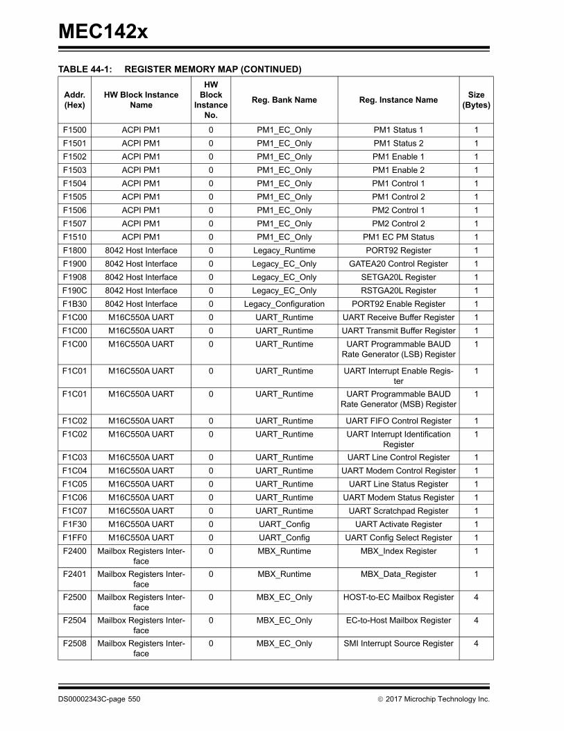
MEC142x
F1500 ACPI PM1 0 PM1_EC_Only PM1 Status 1 1
F1501 ACPI PM1 0 PM1_EC_Only PM1 Status 2 1
F1502 ACPI PM1 0 PM1_EC_Only PM1 Enable 1 1
F1503 ACPI PM1 0 PM1_EC_Only PM1 Enable 2 1
F1504 ACPI PM1 0 PM1_EC_Only PM1 Control 1 1
F1505 ACPI PM1 0 PM1_EC_Only PM1 Control 2 1
F1506 ACPI PM1 0 PM1_EC_Only PM2 Control 1 1
F1507 ACPI PM1 0 PM1_EC_Only PM2 Control 2 1
F1510 ACPI PM1 0 PM1_EC_Only PM1 EC PM Status 1
F1800 8042 Host Interface 0 Legacy_Runtime PORT92 Register 1
F1900 8042 Host Interface 0 Legacy_EC_Only GATEA20 Control Register 1
F1908 8042 Host Interface 0 Legacy_EC_Only SETGA20L Register 1
F190C 8042 Host Interface 0 Legacy_EC_Only RSTGA20L Register 1
F1B30 8042 Host Interface 0 Legacy_Configuration PORT92 Enable Register 1
F1C00 M16C550A UART 0 UART_Runtime UART Receive Buffer Register 1
F1C00 M16C550A UART 0 UART_Runtime UART Transmit Buffer Register 1
F1C00 M16C550A UART 0 UART_Runtime UART Programmable BAUD Rate Generator (LSB) Register
1
F1C01 M16C550A UART 0 UART_Runtime UART Interrupt Enable Regis-ter
1
F1C01 M16C550A UART 0 UART_Runtime UART Programmable BAUD Rate Generator (MSB) Register
1
F1C02 M16C550A UART 0 UART_Runtime UART FIFO Control Register 1
F1C02 M16C550A UART 0 UART_Runtime UART Interrupt Identification Register
1
F1C03 M16C550A UART 0 UART_Runtime UART Line Control Register 1
F1C04 M16C550A UART 0 UART_Runtime UART Modem Control Register 1
F1C05 M16C550A UART 0 UART_Runtime UART Line Status Register 1
F1C06 M16C550A UART 0 UART_Runtime UART Modem Status Register 1
F1C07 M16C550A UART 0 UART_Runtime UART Scratchpad Register 1
F1F30 M16C550A UART 0 UART_Config UART Activate Register 1
F1FF0 M16C550A UART 0 UART_Config UART Config Select Register 1
F2400 Mailbox Registers Inter-face
0 MBX_Runtime MBX_Index Register 1
F2401 Mailbox Registers Inter-face
0 MBX_Runtime MBX_Data_Register 1
F2500 Mailbox Registers Inter-face
0 MBX_EC_Only HOST-to-EC Mailbox Register 4
F2504 Mailbox Registers Inter-face
0 MBX_EC_Only EC-to-Host Mailbox Register 4
F2508 Mailbox Registers Inter-face
0 MBX_EC_Only SMI Interrupt Source Register 4
TABLE 44-1: REGISTER MEMORY MAP (CONTINUED)
Addr. (Hex)
HW Block Instance Name
HWBlock
InstanceNo.
Reg. Bank Name Reg. Instance NameSize
(Bytes)
DS00002343C-page 550 2017 Microchip Technology Inc.

MEC142x
F250C Mailbox Registers Inter-face
0 MBX_EC_Only SMI Interrupt Mask Register 4
F2510 Mailbox Registers Inter-face
0 MBX_EC_Only Mailbox Register [3:0] 4
F2514 Mailbox Registers Inter-face
0 MBX_EC_Only Mailbox Register [7:4] 4
F2518 Mailbox Registers Inter-face
0 MBX_EC_Only Mailbox Register [B:8] 4
F251C Mailbox Registers Inter-face
0 MBX_EC_Only Mailbox Register [F:C] 4
F2520 Mailbox Registers Inter-face
0 MBX_EC_Only Mailbox Register [13:10] 4
F2524 Mailbox Registers Inter-face
0 MBX_EC_Only Mailbox Register [17:14] 4
F2528 Mailbox Registers Inter-face
0 MBX_EC_Only Mailbox Register [1B:18] 4
F252C Mailbox Registers Inter-face
0 MBX_EC_Only Mailbox Register [1F:1C] 4
F2800 ACPI EC Interface 2 ACPI_Runtime ACPI OS Data Register Byte 0 - Read
1
F2800 ACPI EC Interface 2 ACPI_Runtime ACPI OS Data Register Byte 0 - Write
1
F2801 ACPI EC Interface 2 ACPI_Runtime ACPI OS Data Register Byte 1 - Read
1
F2801 ACPI EC Interface 2 ACPI_Runtime ACPI OS Data Register Byte 1 - Write
1
F2802 ACPI EC Interface 2 ACPI_Runtime ACPI OS Data Register Byte 2 - Read
1
F2802 ACPI EC Interface 2 ACPI_Runtime ACPI OS Data Register Byte 2 - Write
1
F2803 ACPI EC Interface 2 ACPI_Runtime ACPI OS Data Register Byte 3 - Read
1
F2803 ACPI EC Interface 2 ACPI_Runtime ACPI OS Data Register Byte 3 - Write
1
F2804 ACPI EC Interface 2 ACPI_Runtime ACPI OS Command Register 1
F2804 ACPI EC Interface 2 ACPI_Runtime STATUS OS-Register 1
F2805 ACPI EC Interface 2 ACPI_Runtime Byte Control OS-Register 1
F2900 ACPI EC Interface 2 ACPI_EC_Only EC2OS Data EC-Register Byte 0
1
F2901 ACPI EC Interface 2 ACPI_EC_Only EC2OS Data EC-Register Byte 1
1
F2902 ACPI EC Interface 2 ACPI_EC_Only EC2OS Data EC-Register Byte 2
1
F2903 ACPI EC Interface 2 ACPI_EC_Only EC2OS Data EC-Register Byte 3
1
F2904 ACPI EC Interface 2 ACPI_EC_Only STATUS EC-Register 1
TABLE 44-1: REGISTER MEMORY MAP (CONTINUED)
Addr. (Hex)
HW Block Instance Name
HWBlock
InstanceNo.
Reg. Bank Name Reg. Instance NameSize
(Bytes)
2017 Microchip Technology Inc. DS00002343C-page 551
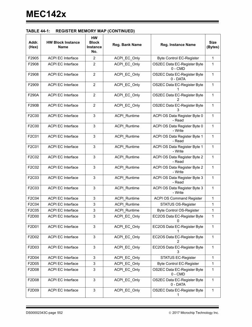
MEC142x
F2905 ACPI EC Interface 2 ACPI_EC_Only Byte Control EC-Register 1
F2908 ACPI EC Interface 2 ACPI_EC_Only OS2EC Data EC-Register Byte 0 - CMD
1
F2908 ACPI EC Interface 2 ACPI_EC_Only OS2EC Data EC-Register Byte 0 - DATA
1
F2909 ACPI EC Interface 2 ACPI_EC_Only OS2EC Data EC-Register Byte 1
1
F290A ACPI EC Interface 2 ACPI_EC_Only OS2EC Data EC-Register Byte 2
1
F290B ACPI EC Interface 2 ACPI_EC_Only OS2EC Data EC-Register Byte 3
1
F2C00 ACPI EC Interface 3 ACPI_Runtime ACPI OS Data Register Byte 0 - Read
1
F2C00 ACPI EC Interface 3 ACPI_Runtime ACPI OS Data Register Byte 0 - Write
1
F2C01 ACPI EC Interface 3 ACPI_Runtime ACPI OS Data Register Byte 1 - Read
1
F2C01 ACPI EC Interface 3 ACPI_Runtime ACPI OS Data Register Byte 1 - Write
1
F2C02 ACPI EC Interface 3 ACPI_Runtime ACPI OS Data Register Byte 2 - Read
1
F2C02 ACPI EC Interface 3 ACPI_Runtime ACPI OS Data Register Byte 2 - Write
1
F2C03 ACPI EC Interface 3 ACPI_Runtime ACPI OS Data Register Byte 3 - Read
1
F2C03 ACPI EC Interface 3 ACPI_Runtime ACPI OS Data Register Byte 3 - Write
1
F2C04 ACPI EC Interface 3 ACPI_Runtime ACPI OS Command Register 1
F2C04 ACPI EC Interface 3 ACPI_Runtime STATUS OS-Register 1
F2C05 ACPI EC Interface 3 ACPI_Runtime Byte Control OS-Register 1
F2D00 ACPI EC Interface 3 ACPI_EC_Only EC2OS Data EC-Register Byte 0
1
F2D01 ACPI EC Interface 3 ACPI_EC_Only EC2OS Data EC-Register Byte 1
1
F2D02 ACPI EC Interface 3 ACPI_EC_Only EC2OS Data EC-Register Byte 2
1
F2D03 ACPI EC Interface 3 ACPI_EC_Only EC2OS Data EC-Register Byte 3
1
F2D04 ACPI EC Interface 3 ACPI_EC_Only STATUS EC-Register 1
F2D05 ACPI EC Interface 3 ACPI_EC_Only Byte Control EC-Register 1
F2D08 ACPI EC Interface 3 ACPI_EC_Only OS2EC Data EC-Register Byte 0 - CMD
1
F2D08 ACPI EC Interface 3 ACPI_EC_Only OS2EC Data EC-Register Byte 0 - DATA
1
F2D09 ACPI EC Interface 3 ACPI_EC_Only OS2EC Data EC-Register Byte 1
1
TABLE 44-1: REGISTER MEMORY MAP (CONTINUED)
Addr. (Hex)
HW Block Instance Name
HWBlock
InstanceNo.
Reg. Bank Name Reg. Instance NameSize
(Bytes)
DS00002343C-page 552 2017 Microchip Technology Inc.
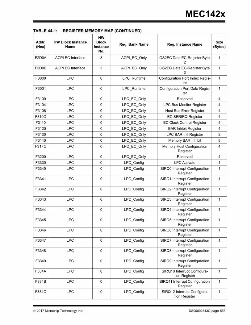
MEC142x
F2D0A ACPI EC Interface 3 ACPI_EC_Only OS2EC Data EC-Register Byte 2
1
F2D0B ACPI EC Interface 3 ACPI_EC_Only OS2EC Data EC-Register Byte 3
1
F3000 LPC 0 LPC_Runtime Configuration Port Index Regis-ter
1
F3001 LPC 0 LPC_Runtime Configuration Port Data Regis-ter
1
F3100 LPC 0 LPC_EC_Only Reserved 4
F3104 LPC 0 LPC_EC_Only LPC Bus Monitor Register 4
F3108 LPC 0 LPC_EC_Only Host Bus Error Register 4
F310C LPC 0 LPC_EC_Only EC SERIRQ Register 4
F3110 LPC 0 LPC_EC_Only EC Clock Control Register 4
F3120 LPC 0 LPC_EC_Only BAR Inhibit Register 4
F3130 LPC 0 LPC_EC_Only LPC BAR Init Register 2
F3140 LPC 0 LPC_EC_Only Memory BAR Inhibit 8
F31FC LPC 0 LPC_EC_Only Memory Host Configuration Register
4
F3200 LPC 0 LPC_EC_Only Reserved 4
F3330 LPC 0 LPC_Config LPC Activate 1
F3340 LPC 0 LPC_Config SIRQ0 Interrupt Configuration Register
1
F3341 LPC 0 LPC_Config SIRQ1 Interrupt Configuration Register
1
F3342 LPC 0 LPC_Config SIRQ2 Interrupt Configuration Register
1
F3343 LPC 0 LPC_Config SIRQ3 Interrupt Configuration Register
1
F3344 LPC 0 LPC_Config SIRQ4 Interrupt Configuration Register
1
F3345 LPC 0 LPC_Config SIRQ5 Interrupt Configuration Register
1
F3346 LPC 0 LPC_Config SIRQ6 Interrupt Configuration Register
1
F3347 LPC 0 LPC_Config SIRQ7 Interrupt Configuration Register
1
F3348 LPC 0 LPC_Config SIRQ8 Interrupt Configuration Register
1
F3349 LPC 0 LPC_Config SIRQ9 Interrupt Configuration Register
1
F334A LPC 0 LPC_Config SIRQ10 Interrupt Configura-tion Register
1
F334B LPC 0 LPC_Config SIRQ11 Interrupt Configuration Register
1
F334C LPC 0 LPC_Config SIRQ12 Interrupt Configura-tion Register
1
TABLE 44-1: REGISTER MEMORY MAP (CONTINUED)
Addr. (Hex)
HW Block Instance Name
HWBlock
InstanceNo.
Reg. Bank Name Reg. Instance NameSize
(Bytes)
2017 Microchip Technology Inc. DS00002343C-page 553

MEC142x
F334D LPC 0 LPC_Config SIRQ13 Interrupt Configura-tion Register
1
F334E LPC 0 LPC_Config SIRQ14 Interrupt Configura-tion Register
1
F334F LPC 0 LPC_Config SIRQ15 Interrupt Configura-tion Register
1
F3350 LPC 0 LPC_Config Reserved 16
F3360 LPC 0 LPC_Config LPC Interface BAR Register 4
F3364 LPC 0 LPC_Config EM Interface 0 BAR 4
F3368 LPC 0 LPC_Config Keyboard Controller BAR 4
F336C LPC 0 LPC_Config ACPI EC Interface 0 BAR 4
F3370 LPC 0 LPC_Config ACPI EC Interface 1 BAR 4
F3374 LPC 0 LPC_Config ACPI PM1 Interface BAR 4
F3378 LPC 0 LPC_Config Legacy (GATEA20) Interface BAR
4
F337C LPC 0 LPC_Config UART 0 BAR Register 4
F3380 LPC 0 LPC_Config Mailbox Registers Interface BAR
4
F3384 LPC 0 LPC_Config ACPI EC Interface 2 BAR 4
F3388 LPC 0 LPC_Config ACPI EC Interface 3 BAR 4
F338C LPC 0 LPC_Config Port 80 BIOS Debug Port 0 CONFIG BAR
4
F3390 LPC 0 LPC_Config Port 80 BIOS Debug Port 1 CONFIG BAR
4
F33A0 LPC 0 LPC_Config SRAM Memory BAR 4
F33A4 LPC 0 LPC_Config SRAM Memory BAR Configu-ration
4
F33C0 LPC 0 LPC_Config EM Interface 0 Memory BAR 6
F33C6 LPC 0 LPC_Config ACPI EC Interface 0 Memory BAR
6
F33CC LPC 0 LPC_Config ACPI EC Interface 1 Memory BAR
6
F33D2 LPC 0 LPC_Config Mailbox Registers I/F Memory BAR
6
F33D8 LPC 0 LPC_Config ACPI EC2 Memory BAR (Inter-nal Component)
6
F33DE LPC 0 LPC_Config ACPI EC3 Memory BAR (Inter-nal Component)
6
F4000 eSPI Interface 0 IO_Component INDEX Register 1
F4001 eSPI Interface 0 IO_Component Data Register 1
F4100 eSPI Interface 0 IO_Component Peripheral Channel Last Cycle Register
12
F410C eSPI Interface 0 IO_Component Peripheral Channel Error Address Register
8
TABLE 44-1: REGISTER MEMORY MAP (CONTINUED)
Addr. (Hex)
HW Block Instance Name
HWBlock
InstanceNo.
Reg. Bank Name Reg. Instance NameSize
(Bytes)
DS00002343C-page 554 2017 Microchip Technology Inc.
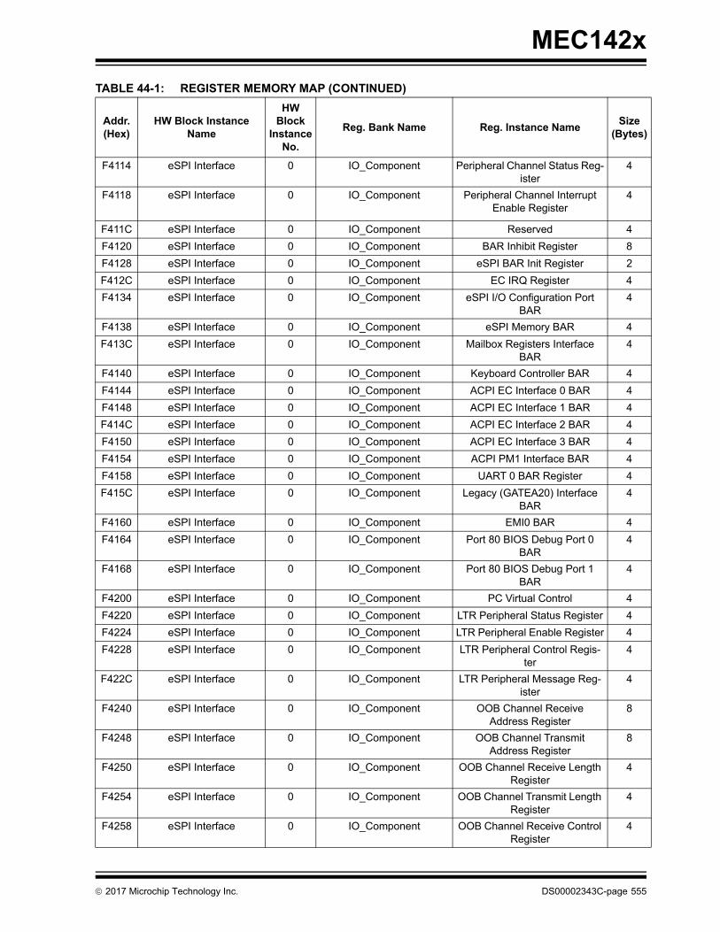
MEC142x
F4114 eSPI Interface 0 IO_Component Peripheral Channel Status Reg-ister
4
F4118 eSPI Interface 0 IO_Component Peripheral Channel Interrupt Enable Register
4
F411C eSPI Interface 0 IO_Component Reserved 4
F4120 eSPI Interface 0 IO_Component BAR Inhibit Register 8
F4128 eSPI Interface 0 IO_Component eSPI BAR Init Register 2
F412C eSPI Interface 0 IO_Component EC IRQ Register 4
F4134 eSPI Interface 0 IO_Component eSPI I/O Configuration Port BAR
4
F4138 eSPI Interface 0 IO_Component eSPI Memory BAR 4
F413C eSPI Interface 0 IO_Component Mailbox Registers Interface BAR
4
F4140 eSPI Interface 0 IO_Component Keyboard Controller BAR 4
F4144 eSPI Interface 0 IO_Component ACPI EC Interface 0 BAR 4
F4148 eSPI Interface 0 IO_Component ACPI EC Interface 1 BAR 4
F414C eSPI Interface 0 IO_Component ACPI EC Interface 2 BAR 4
F4150 eSPI Interface 0 IO_Component ACPI EC Interface 3 BAR 4
F4154 eSPI Interface 0 IO_Component ACPI PM1 Interface BAR 4
F4158 eSPI Interface 0 IO_Component UART 0 BAR Register 4
F415C eSPI Interface 0 IO_Component Legacy (GATEA20) Interface BAR
4
F4160 eSPI Interface 0 IO_Component EMI0 BAR 4
F4164 eSPI Interface 0 IO_Component Port 80 BIOS Debug Port 0 BAR
4
F4168 eSPI Interface 0 IO_Component Port 80 BIOS Debug Port 1 BAR
4
F4200 eSPI Interface 0 IO_Component PC Virtual Control 4
F4220 eSPI Interface 0 IO_Component LTR Peripheral Status Register 4
F4224 eSPI Interface 0 IO_Component LTR Peripheral Enable Register 4
F4228 eSPI Interface 0 IO_Component LTR Peripheral Control Regis-ter
4
F422C eSPI Interface 0 IO_Component LTR Peripheral Message Reg-ister
4
F4240 eSPI Interface 0 IO_Component OOB Channel Receive Address Register
8
F4248 eSPI Interface 0 IO_Component OOB Channel Transmit Address Register
8
F4250 eSPI Interface 0 IO_Component OOB Channel Receive Length Register
4
F4254 eSPI Interface 0 IO_Component OOB Channel Transmit Length Register
4
F4258 eSPI Interface 0 IO_Component OOB Channel Receive Control Register
4
TABLE 44-1: REGISTER MEMORY MAP (CONTINUED)
Addr. (Hex)
HW Block Instance Name
HWBlock
InstanceNo.
Reg. Bank Name Reg. Instance NameSize
(Bytes)
2017 Microchip Technology Inc. DS00002343C-page 555
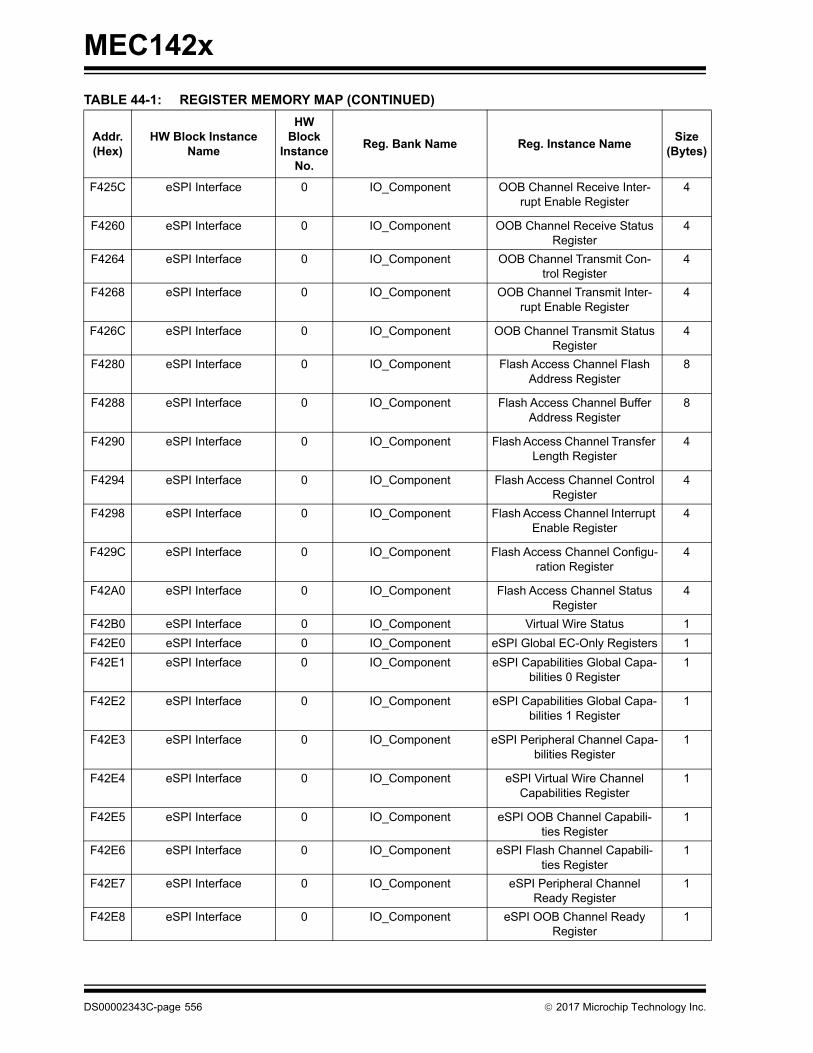
MEC142x
F425C eSPI Interface 0 IO_Component OOB Channel Receive Inter-rupt Enable Register
4
F4260 eSPI Interface 0 IO_Component OOB Channel Receive Status Register
4
F4264 eSPI Interface 0 IO_Component OOB Channel Transmit Con-trol Register
4
F4268 eSPI Interface 0 IO_Component OOB Channel Transmit Inter-rupt Enable Register
4
F426C eSPI Interface 0 IO_Component OOB Channel Transmit Status Register
4
F4280 eSPI Interface 0 IO_Component Flash Access Channel Flash Address Register
8
F4288 eSPI Interface 0 IO_Component Flash Access Channel Buffer Address Register
8
F4290 eSPI Interface 0 IO_Component Flash Access Channel Transfer Length Register
4
F4294 eSPI Interface 0 IO_Component Flash Access Channel Control Register
4
F4298 eSPI Interface 0 IO_Component Flash Access Channel Interrupt Enable Register
4
F429C eSPI Interface 0 IO_Component Flash Access Channel Configu-ration Register
4
F42A0 eSPI Interface 0 IO_Component Flash Access Channel Status Register
4
F42B0 eSPI Interface 0 IO_Component Virtual Wire Status 1
F42E0 eSPI Interface 0 IO_Component eSPI Global EC-Only Registers 1
F42E1 eSPI Interface 0 IO_Component eSPI Capabilities Global Capa-bilities 0 Register
1
F42E2 eSPI Interface 0 IO_Component eSPI Capabilities Global Capa-bilities 1 Register
1
F42E3 eSPI Interface 0 IO_Component eSPI Peripheral Channel Capa-bilities Register
1
F42E4 eSPI Interface 0 IO_Component eSPI Virtual Wire Channel Capabilities Register
1
F42E5 eSPI Interface 0 IO_Component eSPI OOB Channel Capabili-ties Register
1
F42E6 eSPI Interface 0 IO_Component eSPI Flash Channel Capabili-ties Register
1
F42E7 eSPI Interface 0 IO_Component eSPI Peripheral Channel Ready Register
1
F42E8 eSPI Interface 0 IO_Component eSPI OOB Channel Ready Register
1
TABLE 44-1: REGISTER MEMORY MAP (CONTINUED)
Addr. (Hex)
HW Block Instance Name
HWBlock
InstanceNo.
Reg. Bank Name Reg. Instance NameSize
(Bytes)
DS00002343C-page 556 2017 Microchip Technology Inc.
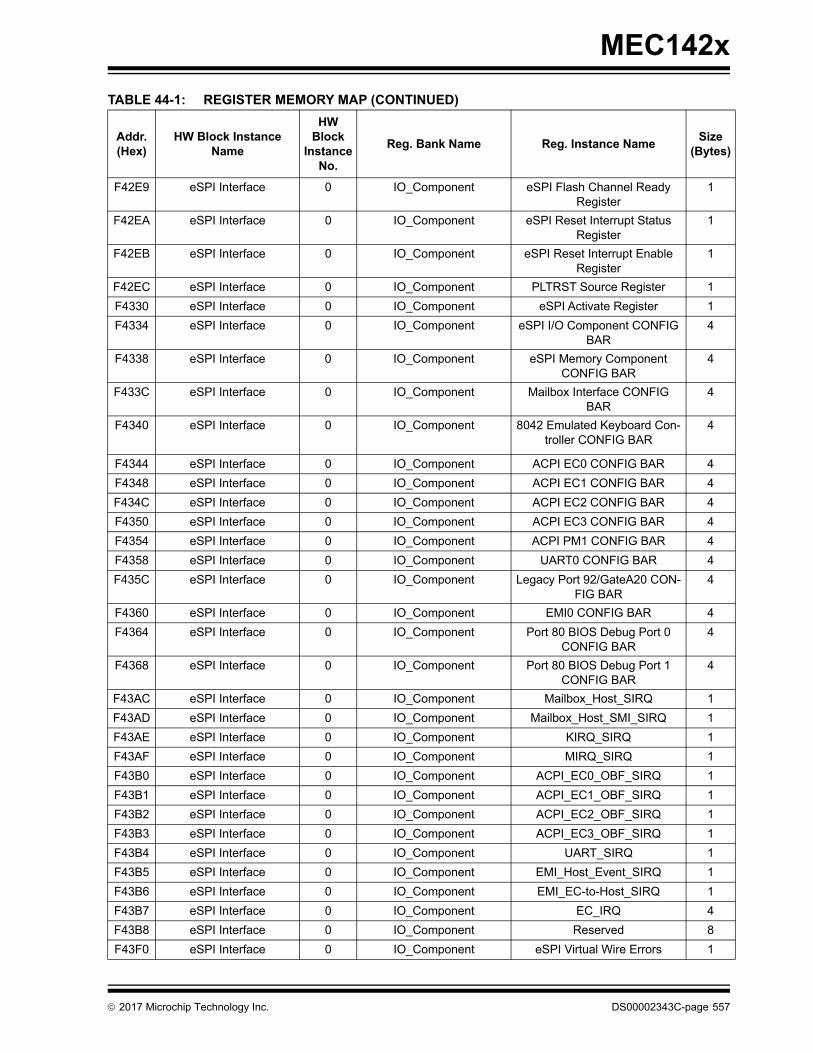
MEC142x
F42E9 eSPI Interface 0 IO_Component eSPI Flash Channel Ready Register
1
F42EA eSPI Interface 0 IO_Component eSPI Reset Interrupt Status Register
1
F42EB eSPI Interface 0 IO_Component eSPI Reset Interrupt Enable Register
1
F42EC eSPI Interface 0 IO_Component PLTRST Source Register 1
F4330 eSPI Interface 0 IO_Component eSPI Activate Register 1
F4334 eSPI Interface 0 IO_Component eSPI I/O Component CONFIG BAR
4
F4338 eSPI Interface 0 IO_Component eSPI Memory Component CONFIG BAR
4
F433C eSPI Interface 0 IO_Component Mailbox Interface CONFIG BAR
4
F4340 eSPI Interface 0 IO_Component 8042 Emulated Keyboard Con-troller CONFIG BAR
4
F4344 eSPI Interface 0 IO_Component ACPI EC0 CONFIG BAR 4
F4348 eSPI Interface 0 IO_Component ACPI EC1 CONFIG BAR 4
F434C eSPI Interface 0 IO_Component ACPI EC2 CONFIG BAR 4
F4350 eSPI Interface 0 IO_Component ACPI EC3 CONFIG BAR 4
F4354 eSPI Interface 0 IO_Component ACPI PM1 CONFIG BAR 4
F4358 eSPI Interface 0 IO_Component UART0 CONFIG BAR 4
F435C eSPI Interface 0 IO_Component Legacy Port 92/GateA20 CON-FIG BAR
4
F4360 eSPI Interface 0 IO_Component EMI0 CONFIG BAR 4
F4364 eSPI Interface 0 IO_Component Port 80 BIOS Debug Port 0 CONFIG BAR
4
F4368 eSPI Interface 0 IO_Component Port 80 BIOS Debug Port 1 CONFIG BAR
4
F43AC eSPI Interface 0 IO_Component Mailbox_Host_SIRQ 1
F43AD eSPI Interface 0 IO_Component Mailbox_Host_SMI_SIRQ 1
F43AE eSPI Interface 0 IO_Component KIRQ_SIRQ 1
F43AF eSPI Interface 0 IO_Component MIRQ_SIRQ 1
F43B0 eSPI Interface 0 IO_Component ACPI_EC0_OBF_SIRQ 1
F43B1 eSPI Interface 0 IO_Component ACPI_EC1_OBF_SIRQ 1
F43B2 eSPI Interface 0 IO_Component ACPI_EC2_OBF_SIRQ 1
F43B3 eSPI Interface 0 IO_Component ACPI_EC3_OBF_SIRQ 1
F43B4 eSPI Interface 0 IO_Component UART_SIRQ 1
F43B5 eSPI Interface 0 IO_Component EMI_Host_Event_SIRQ 1
F43B6 eSPI Interface 0 IO_Component EMI_EC-to-Host_SIRQ 1
F43B7 eSPI Interface 0 IO_Component EC_IRQ 4
F43B8 eSPI Interface 0 IO_Component Reserved 8
F43F0 eSPI Interface 0 IO_Component eSPI Virtual Wire Errors 1
TABLE 44-1: REGISTER MEMORY MAP (CONTINUED)
Addr. (Hex)
HW Block Instance Name
HWBlock
InstanceNo.
Reg. Bank Name Reg. Instance NameSize
(Bytes)
2017 Microchip Technology Inc. DS00002343C-page 557
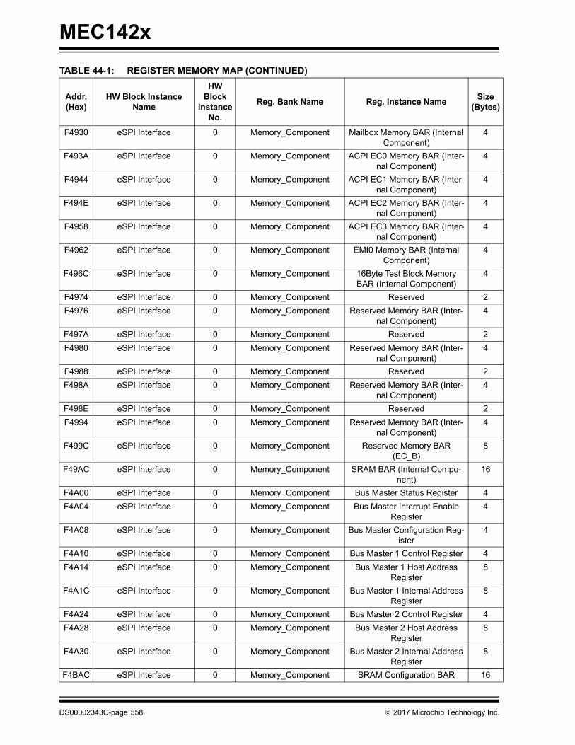
MEC142x
F4930 eSPI Interface 0 Memory_Component Mailbox Memory BAR (Internal Component)
4
F493A eSPI Interface 0 Memory_Component ACPI EC0 Memory BAR (Inter-nal Component)
4
F4944 eSPI Interface 0 Memory_Component ACPI EC1 Memory BAR (Inter-nal Component)
4
F494E eSPI Interface 0 Memory_Component ACPI EC2 Memory BAR (Inter-nal Component)
4
F4958 eSPI Interface 0 Memory_Component ACPI EC3 Memory BAR (Inter-nal Component)
4
F4962 eSPI Interface 0 Memory_Component EMI0 Memory BAR (Internal Component)
4
F496C eSPI Interface 0 Memory_Component 16Byte Test Block Memory BAR (Internal Component)
4
F4974 eSPI Interface 0 Memory_Component Reserved 2
F4976 eSPI Interface 0 Memory_Component Reserved Memory BAR (Inter-nal Component)
4
F497A eSPI Interface 0 Memory_Component Reserved 2
F4980 eSPI Interface 0 Memory_Component Reserved Memory BAR (Inter-nal Component)
4
F4988 eSPI Interface 0 Memory_Component Reserved 2
F498A eSPI Interface 0 Memory_Component Reserved Memory BAR (Inter-nal Component)
4
F498E eSPI Interface 0 Memory_Component Reserved 2
F4994 eSPI Interface 0 Memory_Component Reserved Memory BAR (Inter-nal Component)
4
F499C eSPI Interface 0 Memory_Component Reserved Memory BAR (EC_B)
8
F49AC eSPI Interface 0 Memory_Component SRAM BAR (Internal Compo-nent)
16
F4A00 eSPI Interface 0 Memory_Component Bus Master Status Register 4
F4A04 eSPI Interface 0 Memory_Component Bus Master Interrupt Enable Register
4
F4A08 eSPI Interface 0 Memory_Component Bus Master Configuration Reg-ister
4
F4A10 eSPI Interface 0 Memory_Component Bus Master 1 Control Register 4
F4A14 eSPI Interface 0 Memory_Component Bus Master 1 Host Address Register
8
F4A1C eSPI Interface 0 Memory_Component Bus Master 1 Internal Address Register
8
F4A24 eSPI Interface 0 Memory_Component Bus Master 2 Control Register 4
F4A28 eSPI Interface 0 Memory_Component Bus Master 2 Host Address Register
8
F4A30 eSPI Interface 0 Memory_Component Bus Master 2 Internal Address Register
8
F4BAC eSPI Interface 0 Memory_Component SRAM Configuration BAR 16
TABLE 44-1: REGISTER MEMORY MAP (CONTINUED)
Addr. (Hex)
HW Block Instance Name
HWBlock
InstanceNo.
Reg. Bank Name Reg. Instance NameSize
(Bytes)
DS00002343C-page 558 2017 Microchip Technology Inc.

MEC142x
F4BBC eSPI Interface 0 Memory_Component Reserved 16
F4BCC eSPI Interface 0 Memory_Component Reserved 16
F4BDC eSPI Interface 0 Memory_Component Reserved 16
F4BEC eSPI Interface 0 Memory_Component Reserved 16
F4C00 eSPI Interface 0 Virtual Wire Component MSVW00 12
F4C0C eSPI Interface 0 Virtual Wire Component MSVW01 12
F4C18 eSPI Interface 0 Virtual Wire Component MSVW02 12
F4C24 eSPI Interface 0 Virtual Wire Component MSVW03 12
F4C30 eSPI Interface 0 Virtual Wire Component MSVW04 12
F4C3C eSPI Interface 0 Virtual Wire Component MSVW05 12
F4C48 eSPI Interface 0 Virtual Wire Component MSVW06 12
F4C54 eSPI Interface 0 Virtual Wire Component MSVW07 12
F4C60 eSPI Interface 0 Virtual Wire Component MSVW08 12
F4C6C eSPI Interface 0 Virtual Wire Component MSVW09 12
F4C78 eSPI Interface 0 Virtual Wire Component MSVW10 12
F4C84 eSPI Interface 0 Virtual Wire Component Reserved for MSVW11 12
F4E00 eSPI Interface 0 Virtual Wire Component SMVW00 8
F4E08 eSPI Interface 0 Virtual Wire Component SMVW01 8
F4E10 eSPI Interface 0 Virtual Wire Component SMVW02 8
F4E18 eSPI Interface 0 Virtual Wire Component SMVW03 8
F4E20 eSPI Interface 0 Virtual Wire Component SMVW04 8
F4E28 eSPI Interface 0 Virtual Wire Component SMVW05 8
F4E30 eSPI Interface 0 Virtual Wire Component SMVW06 8
F4E38 eSPI Interface 0 Virtual Wire Component SMVW07 8
F4E40 eSPI Interface 0 Virtual Wire Component SMVW08 8
F4E48 eSPI Interface 0 Virtual Wire Component SMVW09 8
F4E50 eSPI Interface 0 Virtual Wire Component SMVW10 8
F4E58 eSPI Interface 0 Virtual Wire Component Reserved for SMVW11 8
F5000 32 Byte Scratch 0 32 Byte Scratch 32-Byte Scratch Register 32
F5400 BIOS Debug Port 0 BDP_Runtime Host Data Register 1
F5500 BIOS Debug Port 0 BDP_EC_Only EC Data Register 1
F5504 BIOS Debug Port 0 BDP_EC_Only Configuration Register 4
F5508 BIOS Debug Port 0 BDP_EC_Only Status Register 4
F550C BIOS Debug Port 0 BDP_EC_Only Count Register 4
F5730 BIOS Debug Port 0 BDP_Configuration Activate Register 1
F5800 BIOS Debug Port 1 BDP_Runtime Host Data Register 1
F5900 BIOS Debug Port 1 BDP_EC_Only EC Data Register 1
F5904 BIOS Debug Port 1 BDP_EC_Only Configuration Register 4
F5908 BIOS Debug Port 1 BDP_EC_Only Status Register 4
F590C BIOS Debug Port 1 BDP_EC_Only Count Register 4
F5B30 BIOS Debug Port 1 BDP_Configuration Activate Register 1
TABLE 44-1: REGISTER MEMORY MAP (CONTINUED)
Addr. (Hex)
HW Block Instance Name
HWBlock
InstanceNo.
Reg. Bank Name Reg. Instance NameSize
(Bytes)
2017 Microchip Technology Inc. DS00002343C-page 559

MEC142x
FFF00 Global Configuration Registers
0 GCR GCR Reserved Registers 7
FFF07 Global Configuration Registers
0 GCR Logical Device Number Regis-ter
1
FFF1C Global Configuration Registers
0 GCR Device Revision 1
FFF1D Global Configuration Registers
0 GCR Device Sub ID 1
FFF1E Global Configuration Registers
0 GCR Device ID[7:0] 1
FFF1F Global Configuration Registers
0 GCR Device ID[15:8] 1
FFF22 Global Configuration Registers
0 GCR GCR Reserved 2
FFF24 Global Configuration Registers
0 GCR Device Mode 1
FFF25 Global Configuration Registers
0 GCR GCR Test 3
FFF2A Global Configuration Registers
0 GCR GCR Reserved Registers 2
FFF2C Global Configuration Registers
0 GCR GCR Test 4
1FFFC000
JTVIC 0 JTVIC Registers GIRQ8 Source Register 4
1FFFC004
JTVIC 0 JTVIC Registers GIRQ8 Enable Set Register 4
1FFFC008
JTVIC 0 JTVIC Registers GIRQ8 Enable Clear Register 4
1FFFC00C
JTVIC 0 JTVIC Registers GIRQ8 Result Register 4
1FFFC010
JTVIC 0 JTVIC Registers GIRQ9 Source Register 4
1FFFC014
JTVIC 0 JTVIC Registers GIRQ9 Enable Set Register 4
1FFFC018
JTVIC 0 JTVIC Registers GIRQ9 Enable Clear Register 4
1FFFC01C
JTVIC 0 JTVIC Registers GIRQ9 Result Register 4
1FFFC020
JTVIC 0 JTVIC Registers GIRQ10 Source Register 4
1FFFC024
JTVIC 0 JTVIC Registers GIRQ10 Enable Set Register 4
1FFFC028
JTVIC 0 JTVIC Registers GIRQ10 Enable Clear Register 4
1FFFC02C
JTVIC 0 JTVIC Registers GIRQ10 Result Register 4
TABLE 44-1: REGISTER MEMORY MAP (CONTINUED)
Addr. (Hex)
HW Block Instance Name
HWBlock
InstanceNo.
Reg. Bank Name Reg. Instance NameSize
(Bytes)
DS00002343C-page 560 2017 Microchip Technology Inc.
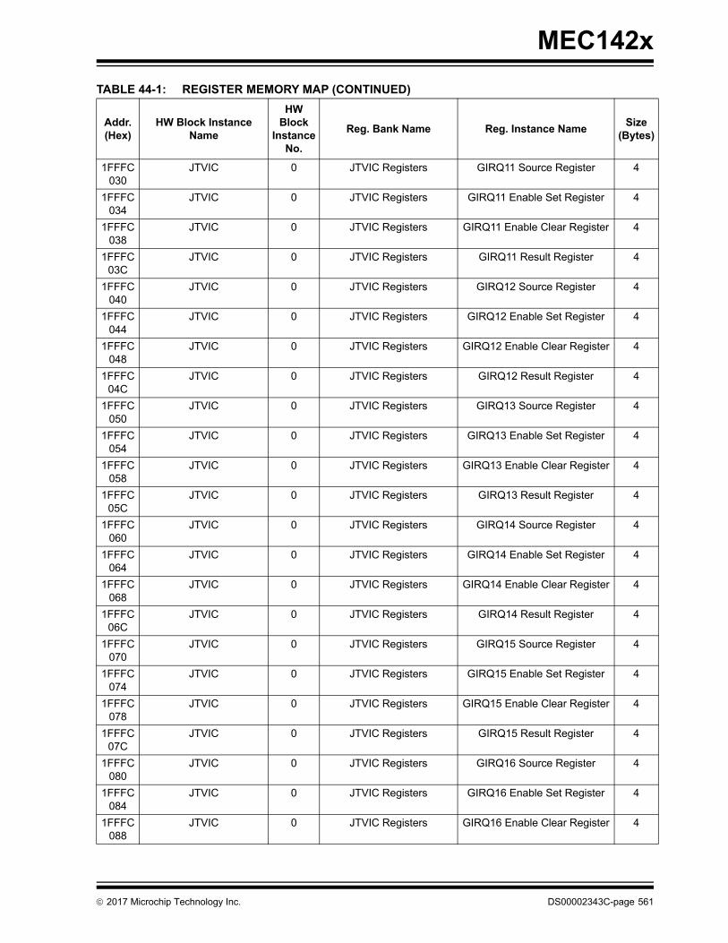
MEC142x
1FFFC030
JTVIC 0 JTVIC Registers GIRQ11 Source Register 4
1FFFC034
JTVIC 0 JTVIC Registers GIRQ11 Enable Set Register 4
1FFFC038
JTVIC 0 JTVIC Registers GIRQ11 Enable Clear Register 4
1FFFC03C
JTVIC 0 JTVIC Registers GIRQ11 Result Register 4
1FFFC040
JTVIC 0 JTVIC Registers GIRQ12 Source Register 4
1FFFC044
JTVIC 0 JTVIC Registers GIRQ12 Enable Set Register 4
1FFFC048
JTVIC 0 JTVIC Registers GIRQ12 Enable Clear Register 4
1FFFC04C
JTVIC 0 JTVIC Registers GIRQ12 Result Register 4
1FFFC050
JTVIC 0 JTVIC Registers GIRQ13 Source Register 4
1FFFC054
JTVIC 0 JTVIC Registers GIRQ13 Enable Set Register 4
1FFFC058
JTVIC 0 JTVIC Registers GIRQ13 Enable Clear Register 4
1FFFC05C
JTVIC 0 JTVIC Registers GIRQ13 Result Register 4
1FFFC060
JTVIC 0 JTVIC Registers GIRQ14 Source Register 4
1FFFC064
JTVIC 0 JTVIC Registers GIRQ14 Enable Set Register 4
1FFFC068
JTVIC 0 JTVIC Registers GIRQ14 Enable Clear Register 4
1FFFC06C
JTVIC 0 JTVIC Registers GIRQ14 Result Register 4
1FFFC070
JTVIC 0 JTVIC Registers GIRQ15 Source Register 4
1FFFC074
JTVIC 0 JTVIC Registers GIRQ15 Enable Set Register 4
1FFFC078
JTVIC 0 JTVIC Registers GIRQ15 Enable Clear Register 4
1FFFC07C
JTVIC 0 JTVIC Registers GIRQ15 Result Register 4
1FFFC080
JTVIC 0 JTVIC Registers GIRQ16 Source Register 4
1FFFC084
JTVIC 0 JTVIC Registers GIRQ16 Enable Set Register 4
1FFFC088
JTVIC 0 JTVIC Registers GIRQ16 Enable Clear Register 4
TABLE 44-1: REGISTER MEMORY MAP (CONTINUED)
Addr. (Hex)
HW Block Instance Name
HWBlock
InstanceNo.
Reg. Bank Name Reg. Instance NameSize
(Bytes)
2017 Microchip Technology Inc. DS00002343C-page 561

MEC142x
1FFFC08C
JTVIC 0 JTVIC Registers GIRQ16 Result Register 4
1FFFC090
JTVIC 0 JTVIC Registers GIRQ17 Source Register 4
1FFFC094
JTVIC 0 JTVIC Registers GIRQ17 Enable Set Register 4
1FFFC098
JTVIC 0 JTVIC Registers GIRQ17 Enable Clear Register 4
1FFFC09C
JTVIC 0 JTVIC Registers GIRQ17 Result Register 4
1FFFC0A0
JTVIC 0 JTVIC Registers GIRQ18 Source Register 4
1FFFC0A4
JTVIC 0 JTVIC Registers GIRQ18 Enable Set Register 4
1FFFC0A8
JTVIC 0 JTVIC Registers GIRQ18 Enable Clear Register 4
1FFFC0AC
JTVIC 0 JTVIC Registers GIRQ18 Result Register 4
1FFFC0B0
JTVIC 0 JTVIC Registers GIRQ19 Source Register 4
1FFFC0B4
JTVIC 0 JTVIC Registers GIRQ19 Enable Set Register 4
1FFFC0B8
JTVIC 0 JTVIC Registers GIRQ19 Enable Clear Register 4
1FFFC0BC
JTVIC 0 JTVIC Registers GIRQ19 Result Register 4
1FFFC0C0
JTVIC 0 JTVIC Registers GIRQ20 Source Register 4
1FFFC0C4
JTVIC 0 JTVIC Registers GIRQ20 Enable Set Register 4
1FFFC0C8
JTVIC 0 JTVIC Registers GIRQ20 Enable Clear Register 4
1FFFC0CC
JTVIC 0 JTVIC Registers GIRQ20 Result Register 4
1FFFC0D0
JTVIC 0 JTVIC Registers GIRQ21 Source Register 4
1FFFC0D4
JTVIC 0 JTVIC Registers GIRQ21 Enable Set Register 4
1FFFC0D8
JTVIC 0 JTVIC Registers GIRQ21 Enable Clear Register 4
1FFFC0DC
JTVIC 0 JTVIC Registers GIRQ21 Result Register 4
1FFFC0E0
JTVIC 0 JTVIC Registers GIRQ22 Source Register 4
1FFFC0E4
JTVIC 0 JTVIC Registers GIRQ22 Enable Set Register 4
TABLE 44-1: REGISTER MEMORY MAP (CONTINUED)
Addr. (Hex)
HW Block Instance Name
HWBlock
InstanceNo.
Reg. Bank Name Reg. Instance NameSize
(Bytes)
DS00002343C-page 562 2017 Microchip Technology Inc.

MEC142x
1FFFC0E8
JTVIC 0 JTVIC Registers GIRQ22 Enable Clear Register 4
1FFFC0EC
JTVIC 0 JTVIC Registers GIRQ22 Result Register 4
1FFFC0F0
JTVIC 0 JTVIC Registers GIRQ23 Source Register 4
1FFFC0F4
JTVIC 0 JTVIC Registers GIRQ23 Enable Set Register 4
1FFFC0F8
JTVIC 0 JTVIC Registers GIRQ23 Enable Clear Register 4
1FFFC0FC
JTVIC 0 JTVIC Registers GIRQ23 Result Register 4
1FFFC100
JTVIC 0 JTVIC Registers GIRQ24 Source Register 4
1FFFC104
JTVIC 0 JTVIC Registers GIRQ24 Enable Set Register 4
1FFFC108
JTVIC 0 JTVIC Registers GIRQ24 Enable Clear Register 4
1FFFC10C
JTVIC 0 JTVIC Registers GIRQ24 Result Register 4
1FFFC110
JTVIC 0 JTVIC Registers GIRQ25 Source Register 4
1FFFC114
JTVIC 0 JTVIC Registers GIRQ25 Enable Set Register 4
1FFFC118
JTVIC 0 JTVIC Registers GIRQ25 Enable Clear Register 4
1FFFC11C
JTVIC 0 JTVIC Registers GIRQ25 Result Register 4
1FFFC120
JTVIC 0 JTVIC Registers GIRQ26 Source Register 4
1FFFC124
JTVIC 0 JTVIC Registers GIRQ26 Enable Set Register 4
1FFFC128
JTVIC 0 JTVIC Registers GIRQ26 Enable Clear Register 4
1FFFC12C
JTVIC 0 JTVIC Registers GIRQ26 Result Register 4
1FFFC130
JTVIC 0 JTVIC Registers Reserved 208
1FFFC200
JTVIC 0 JTVIC Registers GIRQ8 Aggregator Control Register
4
1FFFC204
JTVIC 0 JTVIC Registers GIRQ9 Aggregator Control Register
4
1FFFC208
JTVIC 0 JTVIC Registers GIRQ10 Aggregator Control Register
4
1FFFC20C
JTVIC 0 JTVIC Registers GIRQ11 Aggregator Control Register
4
TABLE 44-1: REGISTER MEMORY MAP (CONTINUED)
Addr. (Hex)
HW Block Instance Name
HWBlock
InstanceNo.
Reg. Bank Name Reg. Instance NameSize
(Bytes)
2017 Microchip Technology Inc. DS00002343C-page 563
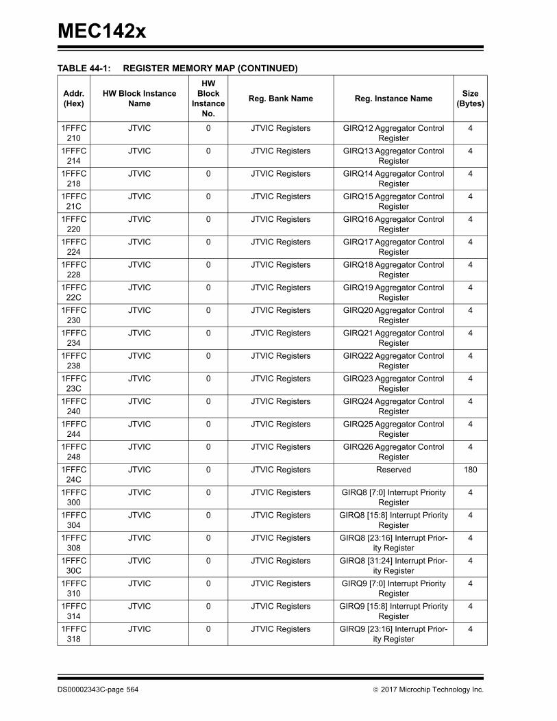
MEC142x
1FFFC210
JTVIC 0 JTVIC Registers GIRQ12 Aggregator Control Register
4
1FFFC214
JTVIC 0 JTVIC Registers GIRQ13 Aggregator Control Register
4
1FFFC218
JTVIC 0 JTVIC Registers GIRQ14 Aggregator Control Register
4
1FFFC21C
JTVIC 0 JTVIC Registers GIRQ15 Aggregator Control Register
4
1FFFC220
JTVIC 0 JTVIC Registers GIRQ16 Aggregator Control Register
4
1FFFC224
JTVIC 0 JTVIC Registers GIRQ17 Aggregator Control Register
4
1FFFC228
JTVIC 0 JTVIC Registers GIRQ18 Aggregator Control Register
4
1FFFC22C
JTVIC 0 JTVIC Registers GIRQ19 Aggregator Control Register
4
1FFFC230
JTVIC 0 JTVIC Registers GIRQ20 Aggregator Control Register
4
1FFFC234
JTVIC 0 JTVIC Registers GIRQ21 Aggregator Control Register
4
1FFFC238
JTVIC 0 JTVIC Registers GIRQ22 Aggregator Control Register
4
1FFFC23C
JTVIC 0 JTVIC Registers GIRQ23 Aggregator Control Register
4
1FFFC240
JTVIC 0 JTVIC Registers GIRQ24 Aggregator Control Register
4
1FFFC244
JTVIC 0 JTVIC Registers GIRQ25 Aggregator Control Register
4
1FFFC248
JTVIC 0 JTVIC Registers GIRQ26 Aggregator Control Register
4
1FFFC24C
JTVIC 0 JTVIC Registers Reserved 180
1FFFC300
JTVIC 0 JTVIC Registers GIRQ8 [7:0] Interrupt Priority Register
4
1FFFC304
JTVIC 0 JTVIC Registers GIRQ8 [15:8] Interrupt Priority Register
4
1FFFC308
JTVIC 0 JTVIC Registers GIRQ8 [23:16] Interrupt Prior-ity Register
4
1FFFC30C
JTVIC 0 JTVIC Registers GIRQ8 [31:24] Interrupt Prior-ity Register
4
1FFFC310
JTVIC 0 JTVIC Registers GIRQ9 [7:0] Interrupt Priority Register
4
1FFFC314
JTVIC 0 JTVIC Registers GIRQ9 [15:8] Interrupt Priority Register
4
1FFFC318
JTVIC 0 JTVIC Registers GIRQ9 [23:16] Interrupt Prior-ity Register
4
TABLE 44-1: REGISTER MEMORY MAP (CONTINUED)
Addr. (Hex)
HW Block Instance Name
HWBlock
InstanceNo.
Reg. Bank Name Reg. Instance NameSize
(Bytes)
DS00002343C-page 564 2017 Microchip Technology Inc.

MEC142x
1FFFC31C
JTVIC 0 JTVIC Registers GIRQ9 [31:24] Interrupt Prior-ity Register
4
1FFFC320
JTVIC 0 JTVIC Registers GIRQ10 [7:0] Interrupt Priority Register
4
1FFFC324
JTVIC 0 JTVIC Registers GIRQ10 [15:8] Interrupt Prior-ity Register
4
1FFFC328
JTVIC 0 JTVIC Registers GIRQ10 [23:16] Interrupt Prior-ity Register
4
1FFFC32C
JTVIC 0 JTVIC Registers GIRQ10 [31:24] Interrupt Prior-ity Register
4
1FFFC330
JTVIC 0 JTVIC Registers GIRQ11 [7:0] Interrupt Priority Register
4
1FFFC334
JTVIC 0 JTVIC Registers GIRQ11 [15:8] Interrupt Priority Register
4
1FFFC338
JTVIC 0 JTVIC Registers GIRQ11 [23:16] Interrupt Prior-ity Register
4
1FFFC33C
JTVIC 0 JTVIC Registers GIRQ11 [31:24] Interrupt Prior-ity Register
4
1FFFC340
JTVIC 0 JTVIC Registers GIRQ12 [7:0] Interrupt Priority Register
4
1FFFC344
JTVIC 0 JTVIC Registers GIRQ12 [15:8] Interrupt Prior-ity Register
4
1FFFC348
JTVIC 0 JTVIC Registers GIRQ12 [23:16] Interrupt Prior-ity Register
4
1FFFC34C
JTVIC 0 JTVIC Registers GIRQ12 [31:24] Interrupt Prior-ity Register
4
1FFFC350
JTVIC 0 JTVIC Registers GIRQ13 [7:0] Interrupt Priority Register
4
1FFFC354
JTVIC 0 JTVIC Registers GIRQ13 [15:8] Interrupt Prior-ity Register
4
1FFFC358
JTVIC 0 JTVIC Registers GIRQ13 [23:16] Interrupt Prior-ity Register
4
1FFFC35C
JTVIC 0 JTVIC Registers GIRQ13 [31:24] Interrupt Prior-ity Register
4
1FFFC360
JTVIC 0 JTVIC Registers GIRQ14 [7:0] Interrupt Priority Register
4
1FFFC364
JTVIC 0 JTVIC Registers GIRQ14 [15:8] Interrupt Prior-ity Register
4
1FFFC368
JTVIC 0 JTVIC Registers GIRQ14 [23:16] Interrupt Prior-ity Register
4
1FFFC36C
JTVIC 0 JTVIC Registers GIRQ14 [31:24] Interrupt Prior-ity Register
4
1FFFC370
JTVIC 0 JTVIC Registers GIRQ15 [7:0] Interrupt Priority Register
4
1FFFC374
JTVIC 0 JTVIC Registers GIRQ15 [15:8] Interrupt Prior-ity Register
4
TABLE 44-1: REGISTER MEMORY MAP (CONTINUED)
Addr. (Hex)
HW Block Instance Name
HWBlock
InstanceNo.
Reg. Bank Name Reg. Instance NameSize
(Bytes)
2017 Microchip Technology Inc. DS00002343C-page 565

MEC142x
1FFFC378
JTVIC 0 JTVIC Registers GIRQ15 [23:16] Interrupt Prior-ity Register
4
1FFFC37C
JTVIC 0 JTVIC Registers GIRQ15 [31:24] Interrupt Prior-ity Register
4
1FFFC380
JTVIC 0 JTVIC Registers GIRQ16 [7:0] Interrupt Priority Register
4
1FFFC384
JTVIC 0 JTVIC Registers GIRQ16 [15:8] Interrupt Prior-ity Register
4
1FFFC388
JTVIC 0 JTVIC Registers GIRQ16 [23:16] Interrupt Prior-ity Register
4
1FFFC38C
JTVIC 0 JTVIC Registers GIRQ16 [31:24] Interrupt Prior-ity Register
4
1FFFC390
JTVIC 0 JTVIC Registers GIRQ17 [7:0] Interrupt Priority Register
4
1FFFC394
JTVIC 0 JTVIC Registers GIRQ17 [15:8] Interrupt Prior-ity Register
4
1FFFC398
JTVIC 0 JTVIC Registers GIRQ17 [23:16] Interrupt Prior-ity Register
4
1FFFC39C
JTVIC 0 JTVIC Registers GIRQ17 [31:24] Interrupt Prior-ity Register
4
1FFFC3A0
JTVIC 0 JTVIC Registers GIRQ18 [7:0] Interrupt Priority Register
4
1FFFC3A4
JTVIC 0 JTVIC Registers GIRQ18 [15:8] Interrupt Prior-ity Register
4
1FFFC3A8
JTVIC 0 JTVIC Registers GIRQ18 [23:16] Interrupt Prior-ity Register
4
1FFFC3AC
JTVIC 0 JTVIC Registers GIRQ18 [31:24] Interrupt Prior-ity Register
4
1FFFC3B0
JTVIC 0 JTVIC Registers GIRQ19 [7:0] Interrupt Priority Register
4
1FFFC3B4
JTVIC 0 JTVIC Registers GIRQ19 [15:8] Interrupt Prior-ity Register
4
1FFFC3B8
JTVIC 0 JTVIC Registers GIRQ19 [23:16] Interrupt Prior-ity Register
4
1FFFC3BC
JTVIC 0 JTVIC Registers GIRQ19 [31:24] Interrupt Prior-ity Register
4
1FFFC3C0
JTVIC 0 JTVIC Registers GIRQ20 [7:0] Interrupt Priority Register
4
1FFFC3C4
JTVIC 0 JTVIC Registers GIRQ20 [15:8] Interrupt Prior-ity Register
4
1FFFC3C8
JTVIC 0 JTVIC Registers GIRQ20 [23:16] Interrupt Prior-ity Register
4
1FFFC3CC
JTVIC 0 JTVIC Registers GIRQ20 [31:24] Interrupt Prior-ity Register
4
1FFFC3D0
JTVIC 0 JTVIC Registers GIRQ21 [7:0] Interrupt Priority Register
4
TABLE 44-1: REGISTER MEMORY MAP (CONTINUED)
Addr. (Hex)
HW Block Instance Name
HWBlock
InstanceNo.
Reg. Bank Name Reg. Instance NameSize
(Bytes)
DS00002343C-page 566 2017 Microchip Technology Inc.
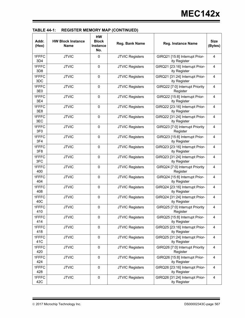
MEC142x
1FFFC3D4
JTVIC 0 JTVIC Registers GIRQ21 [15:8] Interrupt Prior-ity Register
4
1FFFC3D8
JTVIC 0 JTVIC Registers GIRQ21 [23:16] Interrupt Prior-ity Register
4
1FFFC3DC
JTVIC 0 JTVIC Registers GIRQ21 [31:24] Interrupt Prior-ity Register
4
1FFFC3E0
JTVIC 0 JTVIC Registers GIRQ22 [7:0] Interrupt Priority Register
4
1FFFC3E4
JTVIC 0 JTVIC Registers GIRQ22 [15:8] Interrupt Prior-ity Register
4
1FFFC3E8
JTVIC 0 JTVIC Registers GIRQ22 [23:16] Interrupt Prior-ity Register
4
1FFFC3EC
JTVIC 0 JTVIC Registers GIRQ22 [31:24] Interrupt Prior-ity Register
4
1FFFC3F0
JTVIC 0 JTVIC Registers GIRQ23 [7:0] Interrupt Priority Register
4
1FFFC3F4
JTVIC 0 JTVIC Registers GIRQ23 [15:8] Interrupt Prior-ity Register
4
1FFFC3F8
JTVIC 0 JTVIC Registers GIRQ23 [23:16] Interrupt Prior-ity Register
4
1FFFC3FC
JTVIC 0 JTVIC Registers GIRQ23 [31:24] Interrupt Prior-ity Register
4
1FFFC400
JTVIC 0 JTVIC Registers GIRQ24 [7:0] Interrupt Priority Register
4
1FFFC404
JTVIC 0 JTVIC Registers GIRQ24 [15:8] Interrupt Prior-ity Register
4
1FFFC408
JTVIC 0 JTVIC Registers GIRQ24 [23:16] Interrupt Prior-ity Register
4
1FFFC40C
JTVIC 0 JTVIC Registers GIRQ24 [31:24] Interrupt Prior-ity Register
4
1FFFC410
JTVIC 0 JTVIC Registers GIRQ25 [7:0] Interrupt Priority Register
4
1FFFC414
JTVIC 0 JTVIC Registers GIRQ25 [15:8] Interrupt Prior-ity Register
4
1FFFC418
JTVIC 0 JTVIC Registers GIRQ25 [23:16] Interrupt Prior-ity Register
4
1FFFC41C
JTVIC 0 JTVIC Registers GIRQ25 [31:24] Interrupt Prior-ity Register
4
1FFFC420
JTVIC 0 JTVIC Registers GIRQ26 [7:0] Interrupt Priority Register
4
1FFFC424
JTVIC 0 JTVIC Registers GIRQ26 [15:8] Interrupt Prior-ity Register
4
1FFFC428
JTVIC 0 JTVIC Registers GIRQ26 [23:16] Interrupt Prior-ity Register
4
1FFFC42C
JTVIC 0 JTVIC Registers GIRQ26 [31:24] Interrupt Prior-ity Register
4
TABLE 44-1: REGISTER MEMORY MAP (CONTINUED)
Addr. (Hex)
HW Block Instance Name
HWBlock
InstanceNo.
Reg. Bank Name Reg. Instance NameSize
(Bytes)
2017 Microchip Technology Inc. DS00002343C-page 567
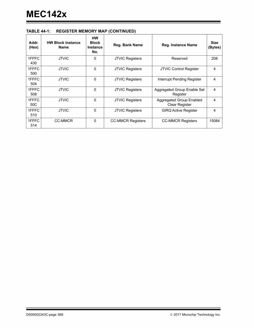
MEC142x
1FFFC430
JTVIC 0 JTVIC Registers Reserved 208
1FFFC500
JTVIC 0 JTVIC Registers JTVIC Control Register 4
1FFFC504
JTVIC 0 JTVIC Registers Interrupt Pending Register 4
1FFFC508
JTVIC 0 JTVIC Registers Aggregated Group Enable Set Register
4
1FFFC50C
JTVIC 0 JTVIC Registers Aggregated Group Enabled Clear Register
4
1FFFC510
JTVIC 0 JTVIC Registers GIRQ Active Register 4
1FFFC514
CC-MMCR 0 CC-MMCR Registers CC-MMCR Registers 15084
TABLE 44-1: REGISTER MEMORY MAP (CONTINUED)
Addr. (Hex)
HW Block Instance Name
HWBlock
InstanceNo.
Reg. Bank Name Reg. Instance NameSize
(Bytes)
DS00002343C-page 568 2017 Microchip Technology Inc.

2017 Microchip Technology Inc. DS00002343C-page 569
MEC142x
APPENDIX A: DATA SHEET REVISION HISTORY
TABLE A-1: REVISION HISTORY
Revision Level Section/Figure/Entry Correction
DS00002343C (10-20-17) Public Release
DS00002343B (09-07-17) Section , "Common Features," on page 1
Updated Programmable 16-bit Timer description.
Section 2.3, "Notes for Tables in this Chapter," on page 13,Table 2-1, “Non-POR Glitch Protected Pins,” on page 19
Updated Note 2. Added Note 19.
Added table.
Section 3.9.11, "PCR chip sub-system power reset status (CHIP_P-WR_RST_STS)," on page 72
Removed VBAT_LOW and VBAT reset status bits. These are shown as TEST bits.
Section 5.6.3, "System Interface, SAFS," on page 120Section TABLE 5-8:, "I/O Logical Device BARs," on page 127
Added APPLICATION NOTE:
Updated EC only reset value of eSPI I/O Component.
Table 22-3, “Edge Enable and Inter-rupt Detection Bits Definition,” on page 335
Added APPLICATION NOTE: 2.
Table 42-2, “Absolute Power Supply Ratings,” on page 483,Table 42-11, “Thermal Packaging Characteristics,” on page 491Table 42-12, “VTR Supply Current, I_VTR,” on page 492,Table 42-13, “Additional VTR Supply Current with Analog blocks enabled,” on page 493,Table 42-14, “VBAT Supply Current, I_VBAT (VBAT=3.0V),” on page 493,Table 42-15, “VBAT Supply Current, I_VBAT (VBAT=3.3V),” on page 493
Changed Maximum Limits to 3.63V.
Added thermal values.
Added supply current values.
Added supply current values.
Added supply current values.
Added supply current values.
DS00002343A (01-19-17) Initial Release

MEC142x
DS00002343C-page 570 2017 Microchip Technology Inc.
THE MICROCHIP WEB SITE
Microchip provides online support via our WWW site at www.microchip.com. This web site is used as a means to makefiles and information easily available to customers. Accessible by using your favorite Internet browser, the web site con-tains the following information:
• Product Support – Data sheets and errata, application notes and sample programs, design resources, user’s guides and hardware support documents, latest software releases and archived software
• General Technical Support – Frequently Asked Questions (FAQ), technical support requests, online discussion groups, Microchip consultant program member listing
• Business of Microchip – Product selector and ordering guides, latest Microchip press releases, listing of semi-nars and events, listings of Microchip sales offices, distributors and factory representatives
CUSTOMER CHANGE NOTIFICATION SERVICE
Microchip’s customer notification service helps keep customers current on Microchip products. Subscribers will receivee-mail notification whenever there are changes, updates, revisions or errata related to a specified product family ordevelopment tool of interest.
To register, access the Microchip web site at www.microchip.com. Under “Support”, click on “Customer Change Notifi-cation” and follow the registration instructions.
CUSTOMER SUPPORT
Users of Microchip products can receive assistance through several channels:
• Distributor or Representative
• Local Sales Office
• Field Application Engineer (FAE)
• Technical Support
Customers should contact their distributor, representative or field application engineer (FAE) for support. Local salesoffices are also available to help customers. A listing of sales offices and locations is included in the back of this docu-ment.
Technical support is available through the web site at: http://microchip.com/support

2017 Microchip Technology Inc. DS00002343C-page 571
MEC142x
PRODUCT IDENTIFICATION SYSTEM
Not all of the product variants defined by the Product Identification System may be offered for sale or released toproduction. To order or obtain information on availability, pricing or delivery, please visit MicrochipDirect.com or contactyour Microchip sales representative or authorized distributor.
PART NO.(1) XXX(2)
PackageDevice
Devices: MEC1424(1) = 128KB SRAMMEC1426(1) = 160KB SRAMMEC1428(1) = 192KB SRAM
Temperature Range Option:
Blank = 0oC to +70oC (Commercial)I/ = -40oC to +85oC (Industrial)
Package: NU = 128 pin VTQFP(2)
SZ = 144 pin WFBGA(2)
TF = 128 pin WFBGA(2)
SX = 84 pin WFBGA(2)
Version/Revision: C# = Standard Version, # = Version Revision Number
Tape and Reel Option:
Blank = Tray packagingTR = Tape and Reel(3)
XX
Version/
-
Note 1: These products meet the halogen maxi-mum concentration values per IEC61249-2-21.
2: All package options are RoHS compliant. For RoHS compliance and environmental information, please visit http://www.microchip.com/pagehandler/en-us/aboutus/ehs.html.
3: Tape and Reel identifier only appears in the catalog part number description. This identifier is used for ordering purposes and is not printed on the device package. Check with your Microchip Sales Office for package availability with the Tape and Reel option.
[X](3)
Tape and ReelOption
- Examples:
a) MEC1424-NU-C0 = 128KB SRAM, Commercialtemperature, 128 VTQFP, Standard version, Ver-sion Revision 0, Tray packaging
b) MEC1428-I/NU-C0 = 192KB SRAM, Industrialtemperature, 128 VTQFP, Standard version, Ver-sion Revision 0, Tray packaging
c) MEC1428-SZ-C0-TR = 192KB SRAM, Commer-cial temperature, 144 WFBGA Standard version,Version Revision 0, Tape and Reel packaging
- [X/]
TemperatureRange
Note: [ ] indicate designators that have blank options
Revision
MEC142x
DS
Note the following details of the code protection feature on Microchip devices:
• Microchip products meet the specification contained in their particular Microchip Data Sheet.
• Microchip believes that its family of products is one of the most secure families of its kind on the market today, when used in the intended manner and under normal conditions.
• There are dishonest and possibly illegal methods used to breach the code protection feature. All of these methods, to our knowledge, require using the Microchip products in a manner outside the operating specifications contained in Microchip’s Data Sheets. Most likely, the person doing so is engaged in theft of intellectual property.
• Microchip is willing to work with the customer who is concerned about the integrity of their code.
• Neither Microchip nor any other semiconductor manufacturer can guarantee the security of their code. Code protection does not mean that we are guaranteeing the product as “unbreakable.”
Code protection is constantly evolving. We at Microchip are committed to continuously improving the code protection features of ourproducts. Attempts to break Microchip’s code protection feature may be a violation of the Digital Millennium Copyright Act. If such actsallow unauthorized access to your software or other copyrighted work, you may have a right to sue for relief under that Act.
Information contained in this publication regarding device applications and the like is provided only for your convenience and may besuperseded by updates. It is your responsibility to ensure that your application meets with your specifications. MICROCHIP MAKES NOREPRESENTATIONS OR WARRANTIES OF ANY KIND WHETHER EXPRESS OR IMPLIED, WRITTEN OR ORAL, STATUTORY OROTHERWISE, RELATED TO THE INFORMATION, INCLUDING BUT NOT LIMITED TO ITS CONDITION, QUALITY, PERFORMANCE,MERCHANTABILITY OR FITNESS FOR PURPOSE. Microchip disclaims all liability arising from this information and its use. Use of Micro-chip devices in life support and/or safety applications is entirely at the buyer’s risk, and the buyer agrees to defend, indemnify and holdharmless Microchip from any and all damages, claims, suits, or expenses resulting from such use. No licenses are conveyed, implicitly orotherwise, under any Microchip intellectual property rights unless otherwise stated.
Trademarks
The Microchip name and logo, the Microchip logo, AnyRate, AVR, AVR logo, AVR Freaks, BeaconThings, BitCloud, CryptoMemory, CryptoRF, dsPIC, FlashFlex, flexPWR, Heldo, JukeBlox, KEELOQ, KEELOQ logo, Kleer, LANCheck, LINK MD, maXStylus, maXTouch, MediaLB, megaAVR, MOST, MOST logo, MPLAB, OptoLyzer, PIC, picoPower, PICSTART, PIC32 logo, Prochip Designer, QTouch, RightTouch, SAM-BA, SpyNIC, SST, SST Logo, SuperFlash, tinyAVR, UNI/O, and XMEGA are registered trademarks of Microchip Technology Incorporated in the U.S.A. and other countries.
ClockWorks, The Embedded Control Solutions Company, EtherSynch, Hyper Speed Control, HyperLight Load, IntelliMOS, mTouch, Precision Edge, and Quiet-Wire are registered trademarks of Microchip Technology Incorporated in the U.S.A.
Adjacent Key Suppression, AKS, Analog-for-the-Digital Age, Any Capacitor, AnyIn, AnyOut, BodyCom, chipKIT, chipKIT logo, CodeGuard, CryptoAuthentication, CryptoCompanion, CryptoController, dsPICDEM, dsPICDEM.net, Dynamic Average Matching, DAM, ECAN, EtherGREEN, In-Circuit Serial Programming, ICSP, Inter-Chip Connectivity, JitterBlocker, KleerNet, KleerNet logo, Mindi, MiWi, motorBench, MPASM, MPF, MPLAB Certified logo, MPLIB, MPLINK, MultiTRAK, NetDetach, Omniscient Code Generation, PICDEM, PICDEM.net, PICkit, PICtail, PureSilicon, QMatrix, RightTouch logo, REAL ICE, Ripple Blocker, SAM-ICE, Serial Quad I/O, SMART-I.S., SQI, SuperSwitcher, SuperSwitcher II, Total Endurance, TSHARC, USBCheck, VariSense, ViewSpan, WiperLock, Wireless DNA, and ZENA are trademarks of Microchip Technology Incorporated in the U.S.A. and other countries.
SQTP is a service mark of Microchip Technology Incorporated in the U.S.A.
Silicon Storage Technology is a registered trademark of Microchip Technology Inc. in other countries.
GestIC is a registered trademark of Microchip Technology Germany II GmbH & Co. KG, a subsidiary of Microchip Technology Inc., in other countries.
All other trademarks mentioned herein are property of their respective companies.
© 2017, Microchip Technology Incorporated, All Rights Reserved.
ISBN: 9781522422747
00002343C-page 572 2017 Microchip Technology Inc.
Microchip received ISO/TS-16949:2009 certification for its worldwide headquarters, design and wafer fabrication facilities in Chandler and Tempe, Arizona; Gresham, Oregon and design centers in California and India. The Company’s quality system processes and procedures are for its PIC® MCUs and dsPIC® DSCs, KEELOQ® code hopping devices, Serial EEPROMs, microperipherals, nonvolatile memory and analog products. In addition, Microchip’s quality system for the design and manufacture of development systems is ISO 9001:2000 certified.
QUALITYMANAGEMENTSYSTEMCERTIFIEDBYDNV
== ISO/TS16949==

DS00002343C-page 573 2017 Microchip Technology Inc.
AMERICASCorporate Office2355 West Chandler Blvd.Chandler, AZ 85224-6199Tel: 480-792-7200 Fax: 480-792-7277Technical Support: http://www.microchip.com/supportWeb Address: www.microchip.com
AtlantaDuluth, GA Tel: 678-957-9614 Fax: 678-957-1455
Austin, TXTel: 512-257-3370
BostonWestborough, MA Tel: 774-760-0087 Fax: 774-760-0088
ChicagoItasca, IL Tel: 630-285-0071 Fax: 630-285-0075
DallasAddison, TX Tel: 972-818-7423 Fax: 972-818-2924
DetroitNovi, MI Tel: 248-848-4000
Houston, TX Tel: 281-894-5983
IndianapolisNoblesville, IN Tel: 317-773-8323Fax: 317-773-5453Tel: 317-536-2380
Los AngelesMission Viejo, CA Tel: 949-462-9523Fax: 949-462-9608Tel: 951-273-7800
Raleigh, NC Tel: 919-844-7510
New York, NY Tel: 631-435-6000
San Jose, CA Tel: 408-735-9110Tel: 408-436-4270
Canada - TorontoTel: 905-695-1980 Fax: 905-695-2078
ASIA/PACIFICAsia Pacific OfficeSuites 3707-14, 37th FloorTower 6, The GatewayHarbour City, Kowloon
Hong KongTel: 852-2943-5100Fax: 852-2401-3431
Australia - SydneyTel: 61-2-9868-6733Fax: 61-2-9868-6755
China - BeijingTel: 86-10-8569-7000 Fax: 86-10-8528-2104
China - ChengduTel: 86-28-8665-5511Fax: 86-28-8665-7889
China - ChongqingTel: 86-23-8980-9588Fax: 86-23-8980-9500
China - DongguanTel: 86-769-8702-9880
China - GuangzhouTel: 86-20-8755-8029
China - HangzhouTel: 86-571-8792-8115 Fax: 86-571-8792-8116
China - Hong Kong SARTel: 852-2943-5100 Fax: 852-2401-3431
China - NanjingTel: 86-25-8473-2460Fax: 86-25-8473-2470
China - QingdaoTel: 86-532-8502-7355Fax: 86-532-8502-7205
China - ShanghaiTel: 86-21-3326-8000 Fax: 86-21-3326-8021
China - ShenyangTel: 86-24-2334-2829Fax: 86-24-2334-2393
China - ShenzhenTel: 86-755-8864-2200 Fax: 86-755-8203-1760
China - WuhanTel: 86-27-5980-5300Fax: 86-27-5980-5118
China - XianTel: 86-29-8833-7252Fax: 86-29-8833-7256
ASIA/PACIFICChina - XiamenTel: 86-592-2388138 Fax: 86-592-2388130
China - ZhuhaiTel: 86-756-3210040 Fax: 86-756-3210049
India - BangaloreTel: 91-80-3090-4444 Fax: 91-80-3090-4123
India - New DelhiTel: 91-11-4160-8631Fax: 91-11-4160-8632
India - PuneTel: 91-20-3019-1500
Japan - OsakaTel: 81-6-6152-7160 Fax: 81-6-6152-9310
Japan - TokyoTel: 81-3-6880- 3770 Fax: 81-3-6880-3771
Korea - DaeguTel: 82-53-744-4301Fax: 82-53-744-4302
Korea - SeoulTel: 82-2-554-7200Fax: 82-2-558-5932 or 82-2-558-5934
Malaysia - Kuala LumpurTel: 60-3-6201-9857Fax: 60-3-6201-9859
Malaysia - PenangTel: 60-4-227-8870Fax: 60-4-227-4068
Philippines - ManilaTel: 63-2-634-9065Fax: 63-2-634-9069
SingaporeTel: 65-6334-8870Fax: 65-6334-8850
Taiwan - Hsin ChuTel: 886-3-5778-366Fax: 886-3-5770-955
Taiwan - KaohsiungTel: 886-7-213-7830
Taiwan - TaipeiTel: 886-2-2508-8600 Fax: 886-2-2508-0102
Thailand - BangkokTel: 66-2-694-1351Fax: 66-2-694-1350
EUROPEAustria - WelsTel: 43-7242-2244-39Fax: 43-7242-2244-393
Denmark - CopenhagenTel: 45-4450-2828 Fax: 45-4485-2829
Finland - EspooTel: 358-9-4520-820
France - ParisTel: 33-1-69-53-63-20 Fax: 33-1-69-30-90-79
Germany - GarchingTel: 49-8931-9700Germany - HaanTel: 49-2129-3766400
Germany - HeilbronnTel: 49-7131-67-3636
Germany - KarlsruheTel: 49-721-625370
Germany - MunichTel: 49-89-627-144-0 Fax: 49-89-627-144-44
Germany - RosenheimTel: 49-8031-354-560
Israel - Ra’anana Tel: 972-9-744-7705
Italy - Milan Tel: 39-0331-742611 Fax: 39-0331-466781
Italy - PadovaTel: 39-049-7625286
Netherlands - DrunenTel: 31-416-690399 Fax: 31-416-690340
Norway - TrondheimTel: 47-7289-7561
Poland - WarsawTel: 48-22-3325737
Romania - BucharestTel: 40-21-407-87-50
Spain - MadridTel: 34-91-708-08-90Fax: 34-91-708-08-91
Sweden - GothenbergTel: 46-31-704-60-40
Sweden - StockholmTel: 46-8-5090-4654
UK - WokinghamTel: 44-118-921-5800Fax: 44-118-921-5820
Worldwide Sales and Service
10/10/17


![Waggon-Gattungen [WG GATT] - BHT 19.06 FS FS-Z 485 476 490 G ... HBCHS 165 128 HBCKK 165 128 HBCKS 165 128 HBCKSS 165 128 HBCS 165 128 HBCS-UV ... Waggon-Gattungen [WG_GATT] - BHT](https://img.pdfslide.us/doc/110x75/5b77e3ce7f8b9a8f698dd790/waggon-gattungen-wg-gatt-bht-1906-fs-fs-z-485-476-490-g-hbchs-165-128-hbckk.jpg)