Embed Size (px)
Citation preview

MCP3550/1/3Low-Power, Single-Channel 22-Bit Delta-Sigma ADCs
Features:
• 22-Bit ADC in Small 8-pin MSOP Package with Automatic Internal Offset and Gain Calibration
• Low-Output Noise of 2.5 µVRMS with Effective Resolution of 21.9 Bits (MCP3550/1)
• 3 µV Typical Offset Error
• 2 ppm Typical Full Scale Error
• 6 ppm Maximum INL Error
• Total Unadjusted Error Less Than 10 ppm
• No Digital Filter Settling Time, Single-Command Conversions through 3-wire SPI Interface
• Ultra-Low Conversion Current (MCP3550/1):
- 100 µA Typical (VDD = 2.7V)
- 120 µA Typical (VDD = 5.0V)
• Differential Input with VSS to VDD Common Mode Range
• 2.7V to 5.5V Single-Supply Operation
• Extended Temperature Range:
- -40°C to +125°C
Applications:
• Weigh Scales
• Direct Temperature Measurement
• 6-digit DVMs
• Instrumentation
• Data Acquisition
• Strain Gauge Measurement
Block Diagram
Description:
The Microchip Technology Inc. MCP3550/1/3 devicesare 2.7V to 5.5V low-power, 22-bit Delta-SigmaAnalog-to-Digital Converters ADCs). The devices offeroutput noise as low as 2.5 µVRMS, with a totalunadjusted error of 10 ppm. The family exhibits 6 ppmIntegral Non-Linearity (INL) error, 3 µV offset error andless than 2 ppm full scale error. The MCP3550/1/3devices provide high accuracy and low noiseperformance for applications where sensormeasurements (such as pressure, temperature andhumidity) are performed. With the internal oscillatorand high oversampling rate, minimal externalcomponents are required for high-accuracyapplications.
This product line has fully differential analog inputs,making it compatible with a wide variety of sensor,industrial control or process control applications.
The MCP3550/1/3 devices operate from -40°C to+125°C and are available in the space-saving 8-pinMSOP and SOIC packages.
Package Types
VSS
VIN+
VIN-
SCK
VDD
SDO
CS
SIN
C 4
Internal
Se
ria
l In
terf
ace
VREF
POROscillator
3rd-OrderDS ADC Modulatorw/ Internal Calibration
VDD
RDY
VIN–
VIN+
MCP3550/1/3
VSS
CS
SDO/RDY
1
2
3
4
8
7
6
5 SCK
VDDVREF
MSOP, SOIC
2005-2014 Microchip Technology Inc. DS20001950F-page 1

MCP3550/1/3
NOTES:
DS20001950F-page 2 2005-2014 Microchip Technology Inc.

MCP3550/1/3
1.0 ELECTRICAL CHARACTERISTICS
Absolute Maximum Ratings †
VDD...................................................................................7.0V
All inputs and outputs w.r.t VSS .... .......... -0.3V to VDD+ 0.3V
Difference Input Voltage ....................................... |VDD - VSS|
Output Short Circuit Current ................................Continuous
Current at Input Pins ....................................................±2 mA
Current at Output and Supply Pins ............................±10 mA
Storage Temperature ....................................-65°C to +150°C
Ambient temp. with power applied ................-55°C to +125°C
ESD protection on all pins (HBM, MM) 6 kV, 400V
Maximum Junction Temperature (TJ) . .........................+150°C
† Notice: Stresses above those listed under "AbsoluteMaximum Ratings" may cause permanent damage to thedevice. This is a stress rating only and functional operation ofthe device at those or any other conditions above those indi-cated in the operation listings of this specification is notimplied. Exposure to maximum rating conditions for extendedperiods may affect device reliability.
DC CHARACTERISTICSElectrical Specifications: Unless otherwise indicated, all parameters apply at -40°C TA +85°C, VDD = 2.7V or 5.0V. VREF = 2.5V. VIN+ = VIN- = VCM = VREF/2. All ppm units use 2*VREF as full scale range. Unless otherwise noted, specification applies to entire MCP3550/1/3 family.
Parameters Sym. Min. Typ. Max. Units Conditions
Noise Performance (MCP3550/1)
No Missing Codes NMC 22 — — bits At DC (Note 5)
Output Noise eN — 2.5 — µVRMS
Effective Resolution ER — 21.9 — bits RMS VREF = 5V
Noise Performance (MCP3553)
No Missing Codes NMC 20 — — bits At DC (Note 5)
Output Noise eN — 6 — µVRMS
Effective Resolution ER — 20.6 — bits RMS VREF = 5V
Conversion Times
MCP3550-50 tCONV -2.0% 80 +2.0% ms
MCP3550-60 tCONV -2.0% 66.67 +2.0% ms
MCP3551 tCONV -2.0% 73.1 +2.0% ms
MCP3553 tCONV -2.0% 16.67 +2.0% ms
Accuracy
Integral Non-Linearity INL — ±2 6 ppm TA = +25°C only (Note 2)
Offset Error VOS -12 ±3 +12 µV TA = +25°C
— ±4 — µV TA = +85°C
— ±6 — µV TA = +125°C
Positive Full-Scale Error VFS,P -10 ±2 +10 ppm TA = +25°C only
Negative Full-Scale Error VFS,N -10 ±2 +10 ppm TA = +25°C only
Offset Drift — 0.040 — ppm/°C
Positive/Negative Full-Scale Error Drift
— 0.028 — ppm/°C
Note 1: This parameter is established by characterization and not 100% tested.2: INL is the difference between the endpoint’s line and the measured code at the center of the quantization band.3: This current is due to the leakage current and the current due to the offset voltage between VIN+ and VIN-.4: Input impedance is inversely proportional to clock frequency; typical values are for the MCP3550/1 device. VREF = 5V.5: Characterized by design, but not tested.6: Rejection performance depends on internal oscillator accuracy; see Section 4.0 “Device Overview” for more informa-
tion on oscillator and digital filter design. MCP3550/1 device rejection specifications characterized from 49 to 61 Hz.
2005-2014 Microchip Technology Inc. DS20001950F-page 3
MCP3550/1/3
Rejection Performance(1,6)
Common Mode DC Rejection — -135 — dB VCM range from 0 to VDD
Power Supply DC Rejection — -115 — dB
Common Mode 50/60 Hz Rejection CMRR — -135 — dB VCM varies from 0V to VDD
Power Supply 50/60 Hz Rejection PSRR — -85 — dB MCP3551 only, VDD varies from 4.5V to 5.5V
Power Supply 50/60 Hz Rejection PSRR — -120 — dB MCP3550-50 or MCP3550-60 only at 50 or 60 Hz respectively, VDD varies from 4.5V to 5.5V
Normal Mode 50 and 60 Hz Rejection
NMRR — -85 — dB MCP3551 only, 0 < VCM < VDD,-VREF < VIN = (VIN + -VIN-) < +VREF
Normal Mode 50 or 60 Hz Rejection
NMRR — -120 — dB MCP3550-50 or MCP3550-60 only at 50 or 60 Hz respectively, 0 < VCM < VDD,-VREF < VIN = (VIN + -VIN-) < +VREF
Analog Inputs
Differential Input Range VIN+ VIN- -VREF — +VREF V
Absolute/Common Mode Voltages VSS - 0.3 — VDD + 0.3 V
Analog Input Sampling Capacitor — 10 — pF Note 5
Differential Input Impedance — 2.4 — MΩ
Shutdown Mode Leakage Current — 1 — nA VIN+ = VIN- = VDD; CS = VDD (Note 3)
Reference Input
Voltage Range 0.1 — VDD V
Reference Input Sampling Capacitor
— 15 — pF Note 5
Reference Input Impedance — 2.4 — MΩ Note 4
Shutdown Mode Reference Leakage Current
— 1 — nA VIN+ = VIN- = VSS; CS = VDD
Power Requirements
Power Supply Voltage Range VDD 2.7 — 5.5 V
MCP3550-50, MCP3551 Supply Current
IDD — 120 170 µA VDD = 5V
— 100 — µA VDD = 2.7V
MCP3550-60, MCP3553 Supply Current
IDD — 140 185 µA VDD = 5V
— 120 — µA VDD = 2.7V
Supply Current, Sleep Mode IDDSL — 10 µA
Supply Current, Shutdown Mode IDDS — — 1 µA CS = SCK = VDD
Serial Interface
Voltage Input High (CS, SCK) VIH 0.7 VDD — — V
Voltage Input Low (CS, SCK) VIL — — 0.4 V
Voltage Output High (SDO/RDY) VOH VDD - 0.5 — — V VOH = 1 mA, VDD = 5.0V
DC CHARACTERISTICS (CONTINUED)Electrical Specifications: Unless otherwise indicated, all parameters apply at -40°C TA +85°C, VDD = 2.7V or 5.0V. VREF = 2.5V. VIN+ = VIN- = VCM = VREF/2. All ppm units use 2*VREF as full scale range. Unless otherwise noted, specification applies to entire MCP3550/1/3 family.
Parameters Sym. Min. Typ. Max. Units Conditions
Note 1: This parameter is established by characterization and not 100% tested.2: INL is the difference between the endpoint’s line and the measured code at the center of the quantization band.3: This current is due to the leakage current and the current due to the offset voltage between VIN+ and VIN-.4: Input impedance is inversely proportional to clock frequency; typical values are for the MCP3550/1 device. VREF = 5V.5: Characterized by design, but not tested.6: Rejection performance depends on internal oscillator accuracy; see Section 4.0 “Device Overview” for more informa-
tion on oscillator and digital filter design. MCP3550/1 device rejection specifications characterized from 49 to 61 Hz.
DS20001950F-page 4 2005-2014 Microchip Technology Inc.

MCP3550/1/3
Voltage Output Low (SDO/RDY) VOL — — 0.4 V VOH = -1 mA, VDD = 5.0V
Input leakage Current(CS, SCK)
ILI -1 — 1 µA
Internal Pin Capacitance(CS, SCK, SDO/RDY)
CINT — 5 — pF Note 1
DC CHARACTERISTICS (CONTINUED)Electrical Specifications: Unless otherwise indicated, all parameters apply at -40°C TA +85°C, VDD = 2.7V or 5.0V. VREF = 2.5V. VIN+ = VIN- = VCM = VREF/2. All ppm units use 2*VREF as full scale range. Unless otherwise noted, specification applies to entire MCP3550/1/3 family.
Parameters Sym. Min. Typ. Max. Units Conditions
Note 1: This parameter is established by characterization and not 100% tested.2: INL is the difference between the endpoint’s line and the measured code at the center of the quantization band.3: This current is due to the leakage current and the current due to the offset voltage between VIN+ and VIN-.4: Input impedance is inversely proportional to clock frequency; typical values are for the MCP3550/1 device. VREF = 5V.5: Characterized by design, but not tested.6: Rejection performance depends on internal oscillator accuracy; see Section 4.0 “Device Overview” for more informa-
tion on oscillator and digital filter design. MCP3550/1 device rejection specifications characterized from 49 to 61 Hz.
TEMPERATURE CHARACTERISTICSElectrical Specifications: Unless otherwise indicated
Parameters Sym. Min. Typ. Max. Units Conditions
Temperature Ranges
Specified Temperature Range TA -40 — +85 °C
Operating Temperature Range TA -40 — +125 °C
Thermal Package Resistances
Thermal Resistance, 8L-MSOP JA — 211 — °C/W
Thermal Resistance, 8L-SOIC JA — 149.5 — °C/W
SERIAL TIMINGSElectrical Specifications: Unless otherwise indicated, all parameters apply at -40°C TA +85°C,VDD = 3.3V or 5.0V, SDO load = 50 pF.
Parameters Sym. Min. Typ. Max. Units Conditions
CLK Frequency fSCK — — 5 MHz
CLK High tHI 90 — — ns
CLK Low tLO 90 — — ns
CLK fall to output data valid tDO 0 — 90 ns
CS low to indicate RDY state tRDY 0 — 50 ns
CS minimum low time tCSL 8 — — µs Note
RDY flag setup time tSU 20 — — ns
CS rise to output disable tDIS 20 — — ns
CS disable time tCSD 90 — — ns
Power-up to CS LOW tPUCSL — 10 — µs
CS High to Shutdown Mode tCSHSD — 10 — µs
Note: This parameter is established by characterization and not 100% tested.
2005-2014 Microchip Technology Inc. DS20001950F-page 5

MCP3550/1/3
FIGURE 1-1: Serial Timing.
FIGURE 1-2: Power-Up Timing.
tRDY
tCSL
tDO
tSU
fSCK
tHI tLO
tDISCS
SDO
SCK
tCSD
tCSHSD
/RDY
VDD
CS
tPUCSL
DS20001950F-page 6 2005-2014 Microchip Technology Inc.

MCP3550/1/3
2.0 TYPICAL PERFORMANCE CURVES
Note: Unless otherwise specified, TA = +25°C, VDD = 5V, VREF = 2.5V, VSS = 0V, VCM = VREF/2, VIN+ = VIN-. All ppm units use 2*VREF as full scale range. Unless otherwise noted, graphs apply to entire MCP3550/1/3 family.
FIGURE 2-1: INL Error vs. Input Voltage (VDD = 2.7V).
FIGURE 2-2: INL Error vs. Input Voltage (VDD = 5.0V).
FIGURE 2-3: INL Error vs. Input Voltage (VDD = 5.0V, VREF = 5V).
FIGURE 2-4: Maximum INL Error vs. VREF.
FIGURE 2-5: Maximum INL Error vs. Temperature.
FIGURE 2-6: Output Noise vs. Input Voltage (VDD = 2.7V).
Note: The graphs and tables provided following this note are a statistical summary based on a limited number ofsamples and are provided for informational purposes only. The performance characteristics listed hereinare not tested or guaranteed. In some graphs or tables, the data presented may be outside the specifiedoperating range (e.g., outside specified power supply range) and therefore outside the warranted range.
-5-4-3-2-1012345
-2.5 -1.5 -0.5 0.5 1.5 2.5
VIN (V)
INL
(p
pm
)
+125 C
+85 C
-40 C
+25 C
-5-4-3-2-1012345
-2.5 -1.5 -0.5 0.5 1.5 2.5
VIN (V)
INL
(p
pm
)
+125 C
+85 C
+25 C
- 40 C
-10-8-6-4-202468
10
-5 -4 -3 -2 -1 0 1 2 3 4 5
VIN (V)
INL
(p
pm
)
+125 C+85 C
+25 C
-40 C
0
2
4
6
8
10
0 0.5 1 1.5 2 2.5 3 3.5 4 4.5 5
VREF (V)
INL
Err
or
(pp
m)
0123456789
10
-50 -25 0 25 50 75 100 125
Temperature (°C)
Max
IN
L (
pp
m)
0123456789
10
-2.5 -1.5 -0.5 0.5 1.5 2.5
VIN (Volts)
Ou
tpu
t N
ois
e (µ
VR
MS)
MCP3553
MCP3550/1
2005-2014 Microchip Technology Inc. DS20001950F-page 7

MCP3550/1/3
Note: Unless otherwise specified, TA = +25°C, VDD = 5V, VREF = 2.5V, VSS = 0V, VCM = VREF/2, VIN+ = VIN-.All ppm units use 2*VREF as full scale range. Unless otherwise noted, graphs apply to entire MCP3550/1/3 family.
FIGURE 2-7: Output Noise vs. Input Voltage (VDD = 5.0V).u
FIGURE 2-8: Output Noise vs. VREF.
FIGURE 2-9: Output Noise vs.VDD.
FIGURE 2-10: Output Noise vs. Temperature.
FIGURE 2-11: Offset Error vs VDD (VCM = 0V).
FIGURE 2-12: Offset Error vs. Temperature (VREF = 5.0V).
0
5
10
15
-2.5 -1.5 -0.5 0.5 1.5 2.5
VIN (V)
Ou
tpu
t N
ois
e (µ
VR
MS)
MCP3553
MCP3550/1
0.01.0
2.03.0
4.05.06.07.0
8.09.0
10.0
0.0 1.0 2.0 3.0 4.0 5.0
VREF (V)
Ou
tpu
t N
ois
e (
µV
RM
S)
MCP3550/1
MCP3553
0123456789
10
2.5 3 3.5 4 4.5 5 5.5VDD (V)
Ou
tpu
t N
ois
e (
µV
RM
S)
MCP3550/1
MCP3553
0
12
34
56
78
910
-50 -25 0 25 50 75 100 125Temperature (°C)
Ou
tpu
t N
ois
e (µ
VR
MS)
MCP3550/1
MCP3553
0
1
2
3
4
5
2.5 3 3.5 4 4.5 5 5.5
VDD (V)
Off
set
(µV
)
0
1
2
3
4
5
6
7
-50 -25 0 25 50 75 100 125
Temperature (°C)
Off
set
(µV
)
DS20001950F-page 8 2005-2014 Microchip Technology Inc.

MCP3550/1/3
Note: Unless otherwise specified, TA = +25°C, VDD = 5V, VREF = 2.5V, VSS = 0V, VCM = VREF/2, VIN+ = VIN-.All ppm units are ratioed against 2*VREF . Unless otherwise noted, graphs apply to entire MCP3550/1/3 family.
FIGURE 2-13: Full Scale Error vs. VDD .
FIGURE 2-14: Full Scale Error vs. Temperature.
FIGURE 2-15: Full Scale Error vs. Temperature (VREF = 5.0V).
FIGURE 2-16: MCP3550/1 Output Noise Histogram.
FIGURE 2-17: MCP3553 Output Noise Histogram.
FIGURE 2-18: Total Unadjusted Error (TUE) vs. Input Voltage (VDD = 2.7V).
-5-4-3-2-1012345
2.5 3 3.5 4 4.5 5 5.5
VDD (V)
Fu
ll S
ca
le E
rro
r (p
pm
)
Positive Full Scale
Negative Full Scale
-10-8-6-4-202468
10
-50 -25 0 25 50 75 100 125
Temperature (°C)
Fu
ll S
ca
le E
rro
r (p
pm
)
Positive Full Scale
Negative Full Scale
-10-8-6-4-202468
10
-50 -25 0 25 50 75 100 125
Temperature (°C)
Fu
ll S
ca
le E
rro
r (p
pm
)
Positive Full Scale
Negative Full Scale
0500
1000150020002500300035004000
-15 -10 -5 0 5 10 15
Num
ber o
f Occ
urre
nces
Output Code (LSB)
VDD = 5VVREF = 2.5VVCM = 1.25VVIN = 0VTA = 25C16384consecutive readings
0
200
400
600
800
1000
1200
1400
1600
1800
-15 -10 -5 0 5 10 15Output Code (LSB)
Nu
mb
er o
f O
ccu
rre
nc
es
VDD = 5VVREF = 2.5VVCM = 1.25VVIN = 0VTA = 25°C16384 consecutive readings
-5.0
-4.0
-3.0
-2.0
-1.0
0.0
1.0
2.0
3.0
4.0
5.0
-2.5 -2.0 -1.5 -1.0 -0.5 0.0 0.5 1.0 1.5 2.0 2.5
VIN (V)
TU
E (
pp
m)
2005-2014 Microchip Technology Inc. DS20001950F-page 9

MCP3550/1/3
Note: Unless otherwise specified, TA = +25°C, VDD = 5V, VREF = 2.5V, VSS = 0V, VCM = VREF/2, VIN+ = VIN-. All ppm units use 2*VREF as full scale range. Unless otherwise noted, graphs apply to entire MCP3550/1/3 family.
FIGURE 2-19: Total Unadjusted Error (TUE) vs. Input Voltage.
FIGURE 2-20: Total Unadjusted Error (TUE) vs. Input Voltage (VREF = 5.0V).
FIGURE 2-21: Maximum TUE vs. VREF.
FIGURE 2-22: Maximum TUE vs. Temperature.
FIGURE 2-23: Maximum TUE vs. VDD.
FIGURE 2-24: IDDS vs. Temperature.
-5
-4
-3
-2
-1
0
1
2
3
4
5
-2.5 -2 -1.5 -1 -0.5 0 0.5 1 1.5 2 2.5
VIN (V)
TU
E (
pp
m)
-10-8-6-4
-202
4
68
10
-5 -4 -3 -2 -1 0 1 2 3 4 5
VIN (V)
TU
E (
pp
m)
0
1
2
3
4
5
6
7
89
10
0 1 2 3 4 5
VREF (V)
Ma
xim
um
TU
E (
pp
m)
0
1
2
3
4
5
6
-50 -25 0 25 50 75 100 125
Temperature (°C)
Ma
xim
um
TU
E (
pp
m)
0
0.5
1
1.5
2
2.5
3
3.5
4
4.5
5
2.5 2.7 3 3.3 4 5 5.5
VDD (V)
TU
E (
pp
m)
-0.1
0
0.1
0.2
0.3
0.4
0.5
0.6
-50 -25 0 25 50 75 100 125
Temperature (°C)
I DD
S (
µA
)
MCP3550/1
MCP3553
DS20001950F-page 10 2005-2014 Microchip Technology Inc.
MCP3550/1/3
Note: Unless otherwise specified, TA = +25°C, VDD = 5V, VREF = 2.5V, VSS = 0V, VCM = VREF/2, VIN+ = VIN-.All ppm units use 2*VREF as full scale range. Unless otherwise noted, graphs apply to entire MCP3550/1/3 family.
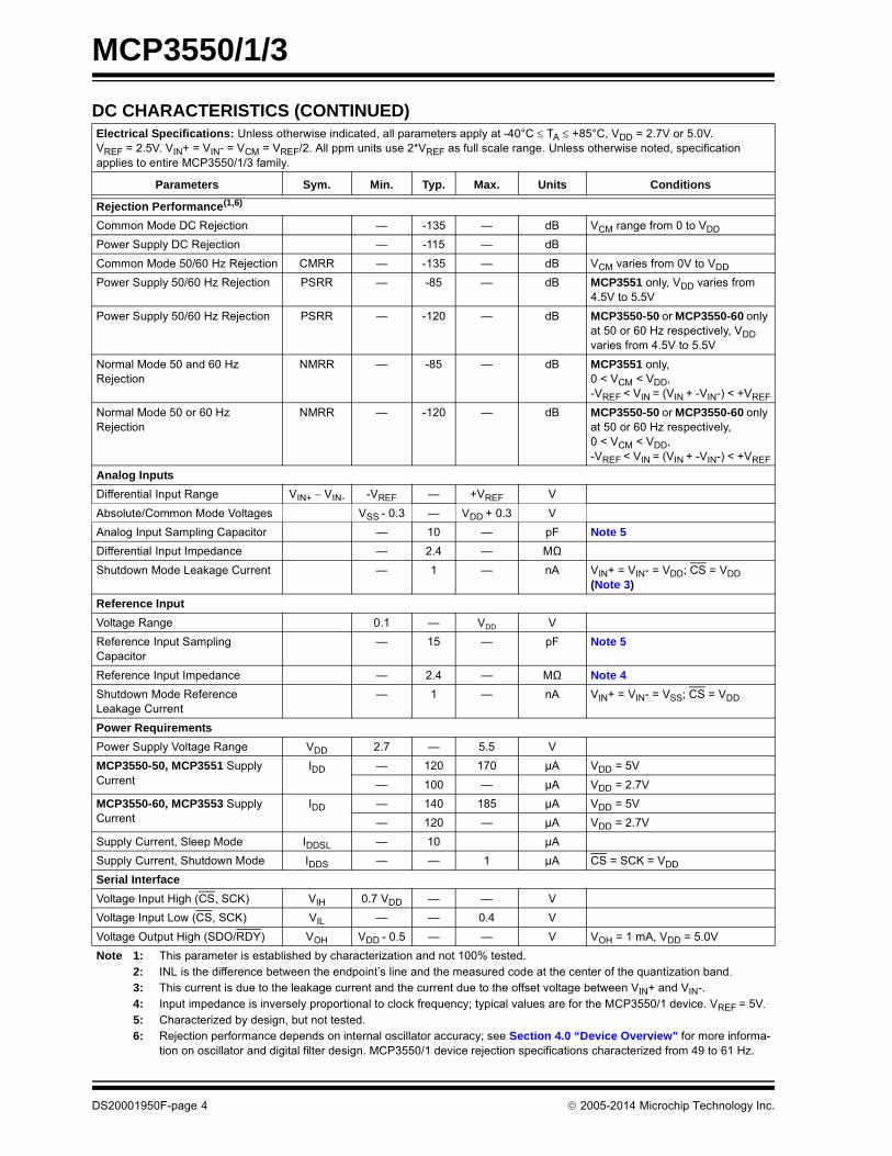
FIGURE 2-25: IDD vs. VDD. FIGURE 2-26: IDD vs. Temperature.
0
20
40
60
80
100
120
140
160
180200
2.5 3 3.5 4 4.5 5 5.5
VDD (V)
I DD (
µA
)
MCP3550-60, MCP3553
MCP3550-50, MCP3550/1
0
20
40
60
80
100
120
140
160
-50 -25 0 25 50 75 100 125
Temperature (°C)
I DD (
µA
)
MCP3550-60, MCP3553
MCP3550-50, MCP3550/1
2005-2014 Microchip Technology Inc. DS20001950F-page 11

MCP3550/1/3
NOTES:
DS20001950F-page 12 2005-2014 Microchip Technology Inc.
MCP3550/1/3
3.0 PIN DESCRIPTIONS
The descriptions of the pins are listed in Table 3-1.
TABLE 3-1: PIN FUNCTION TABLE
3.1 Voltage Reference (VREF)
The MCP3550/1/3 devices accept single-endedreference voltages from 0.1V to VDD. Since theconverter output noise is dominated by thermal noise,which is independent of the reference voltage, theoutput noise is not significantly improved bydiminishing the reference voltage at the VREF input pin.A reduced voltage reference will significantly improvethe INL performance (see Figure 2-4); the INL maxerror is proportional to VREF
2.
3.2 Analog Inputs (VIN+, VIN-)
The MCP3550/1/3 devices accept a fully differentialanalog input voltage to be connected on the VIN+ andVIN- input pins. The differential voltage that isconverted is defined by VIN = VIN+ – VIN-. Thedifferential voltage range specified for ensuredaccuracy is from -VREF to +VREF. However, theconverter will still output valid and usable codes withthe inputs overranged by up to 12% (see Section 5.0“Serial Interface”) at room temperature. Thisoverrange is clearly specified by two overload bits inthe output code.
The absolute voltage range on these input pins extendsfrom VSS – 0.3V to VDD + 0.3V. Any voltage above orbelow this range will create leakage currents throughthe Electrostatic Discharge (ESD) diodes. This currentwill increase exponentially, degrading the accuracy andnoise performance of the device. The common mode ofthe analog inputs should be chosen such that both thedifferential analog input range and the absolute voltagerange on each pin are within the specified operatingrange defined in Section 1.0 “ElectricalCharacteristics”.
3.3 Supply Voltage (VDD, VSS)
VDD is the power supply pin for the analog and digitalcircuitry within the MCP3550/1/3. This pin requires anappropriate bypass capacitor of 0.1 µF. The voltage onthis pin should be maintained in the 2.7V to 5.5V rangefor specified operation. VSS is the ground pin and thecurrent return path for both analog and digital circuitryof the MCP3550/1/3. If an analog ground plane isavailable, it is recommended that this device be tied tothe analog ground plane of the Printed Circuit Board(PCB).
3.4 Serial Clock (SCK)
SCK synchronizes data communication with thedevice. The device operates in both SPI mode 1,1 andSPI mode 0,0. Data is shifted out of the device on thefalling edge of SCK. Data is latched in on the risingedge of SCK. During CS high times, the SCK pin canidle either high or low.
3.5 Data Output (SDO/RDY)
SDO/RDY is the output data pin for the device. Once aconversion is complete, this pin will go active-low,acting as a ready flag. Subsequent falling clock edgeswill then place the 24-bit data word (two overflow bitsand 22 bits of data, see Section 5.0 “SerialInterface”) on the SPI bus through the SDO pin. Datais clocked out on the falling edge of SCK.
MCP3550/1/3Symbol I/O/P Description
MSOP, SOIC
1 VREF I Reference Voltage Analog Input pin
2 VIN+ I Non-inverting Analog Input pin
3 VIN- I Inverting Analog Input pin
4 VSS P Ground pin
5 SCK I Serial Clock Digital Input pin
6 SDO/RDY O Data/Ready Digital Output pin
7 CS I Chip Select Digital Input pin
8 VDD P Positive Supply Voltage pin
Type Identification: I = Input; O = Output; P = Power
2005-2014 Microchip Technology Inc. DS20001950F-page 13

MCP3550/1/3
3.6 Chip Select (CS)
CS gates all communication to the device and can beused to select multiple devices that share the sameSCK and SDO/RDY pins. This pin is also used tocontrol the internal conversions, which begin on thefalling edge of CS. Raising CS before the first internalconversion is complete places the device in SingleConversion mode. Leaving CS low will place thedevice in Continuous Conversion mode (i.e., additionalinternal conversions will automatically occur). CS maybe tied permanently low for two-wire ContinuousConversion mode operation. SDO/RDY enters a high-impedance state with CS high.
DS20001950F-page 14 2005-2014 Microchip Technology Inc.

MCP3550/1/3
4.0 DEVICE OVERVIEW
The MCP3550/1/3 devices are 22-bit delta-sigmaADCs that include fully differential analog inputs, athird-order delta-sigma modulator, a fourth-ordermodified SINC decimation filter, an on-chip, low-noiseinternal oscillator, a power supply monitoring circuit andan SPI 3-wire digital interface. These devices can beeasily used to measure low-frequency, low-levelsignals such as those found in pressure transducers,temperature, strain gauge, industrial control or processcontrol applications. The power supply range for thisproduct family is 2.7V to 5.5V; the temperature range is-40°C to +125°C. The functional block diagram for theMCP3550/1/3 devices is shown in Figure 4-1.
A Power-On Reset (POR) monitoring circuit is includedto ensure proper power supply voltages during theconversion process. The clock source for the part isinternally generated to ±0.5% over the full-powersupply voltage range and industrial temperature range.This stable clock source allows for superior conversionrepeatability and minimal drift across conversions.
The MCP3550/1/3 devices employ a delta-sigmaconversion technique to realize up to 22 bits of nomissing code performance with 21.9 Effective Numberof Bits (ENOB). These devices provide single-cycleconversions with no digital filter settling time. Everyconversion includes an internal offset and gain auto-calibration to reduce device error. These calibrationsare transparent to the user and are done in real-timeduring the conversion. Therefore, these devices do notrequire any additional time or conversion to proceed,allowing easy usage of the devices for multiplexedapplications. The MCP3550/1/3 devices incorporate afourth-order digital decimation filter in order to allowsuperior averaging performance, as well as excellentline frequency rejection capabilities. The oversamplingfrequency also reduces any external anti-aliasing filterrequirements.
The MCP3550/1/3 devices communicate with a simple3-wire SPI interface. The interface controls theconversion start event, with an added feature of anauto-conversion at system power-up by tying the CSpin to logic-low. The device can communicate with busspeeds of up to 5 MHz, with 50 pF capacitive loading.The interface offers two conversion modes: SingleConversion mode for multiplexed applications and aContinuous Conversion mode for multiple conversionsin series. Every conversion is independent of eachother. That is, all internal registers are flushed betweenconversions. When the device is not converting, it auto-matically goes into Shutdown mode and, while in thismode, consumes less than 1 µA.
FIGURE 4-1: MCP3550/1/3 Functional Block Diagram.
InternalOscillator
Third-Order∆Σ
Modulator
DigitalDecimation
Filter (SINC4)
SPI 3-wireInterface
Gain andOffset
Calibration
DifferentialAnalog Input
Bit ConversionCode
OutputCode
Clock
ChargeTransfer
ReferenceInput
Stream
2005-2014 Microchip Technology Inc. DS20001950F-page 15
MCP3550/1/3
4.1 MCP3550/1/3 Delta-SigmaModulator with Internal Offset and Gain Calibration
The converter core of the MCP3550/1/3 devices is athird-order delta-sigma modulator with automatic gainand offset error calibrations. The modulator uses a 1-bitDAC structure. The delta-sigma modulator processesthe sampled charges through switched capacitorstructures controlled by a very low drift oscillator forreduced clock jitter.
During the conversion process, the modulator outputsa bit stream with the bit frequency equivalent to thefOSC/4 (see Table 4-1). The high oversamplingimplemented in the modulator ensures very highresolution and high averaging factor to achieve low-noise specifications. The bit stream output of themodulator is then processed by the digital decimationfilter in order to provide a 22-bit output code at a datarate of 12.5 Hz for the MCP3550-50, 15 Hz for theMCP3550-60, 13.75 Hz for the MCP3551 and 60 Hzfor the MCP3553. Since the oversampling ratio is lowerwith the MCP3553 device, a much higher output datarate is achieved while still achieving 20 bits No MissingCodes (NMC) and 20.6 ENOB.
A self-calibration of offset and gain occurs at the onsetof every conversion. The conversion data available atthe output of the device is always calibrated for offsetand gain through this process. This offset and gainauto-calibration is performed internally and has noimpact on the speed of the converter since the offsetand gain errors are calibrated in real-time during theconversion. The real-time offset and gain calibrationschemes do not affect the conversion process.
4.2 Digital Filter
The MCP3550/1/3 devices include a digital decimationfilter, which is a fourth-order modified SINC filter. Thisfilter averages the incoming bit stream from themodulator and outputs a 22-bit conversion word inbinary two's complement. When all bits have beenprocessed by the filter, the output code is ready for SPIcommunication, the RDY flag is set on the SDO/RDYpin and all the internal registers are reset in order toprocess the next conversion.
Like the commonly used SINC filter, the modified SINCfilter in the MCP3550/1/3 family has the main notchfrequency located at fS/(OSR*L), where fS is the bitstream sample frequency. OSR is the OversamplingRatio and L is the order of the filter.
The MCP3550-50 device has the main filter notchlocated at 50 Hz. For the MCP3550-60 device, thenotch is located at 60 Hz. The MCP3551 device has itsnotch located at 55 Hz, and for the MCP3553 device,the main notch is located at 240 Hz, with an OSR of128. (see Table 4-1 for rejection performance).
The digital decimation SINC filter has been modified inorder to offer staggered zeros in its transfer function.This modification is intended to widen the main notch inorder to be less sensitive to oscillator deviation or line-frequency drift. The MCP3551 filter has staggeredzeros spread in order to reject both 50 Hz and 60 Hzline frequencies simultaneously (see Figure 4-2).
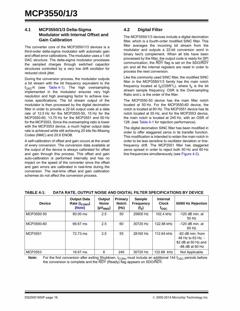
TABLE 4-1: DATA RATE, OUTPUT NOISE AND DIGITAL FILTER SPECIFICATIONS BY DEVICE
DeviceOutput Data Rate (tCONV)
(Note)
Output Noise
(µVRMS)
Primary Notch(Hz)
Sample Frequency
(fS)
Internal Clock fOSC
50/60 Hz Rejection
MCP3550-50 80.00 ms 2.5 50 25600 Hz 102.4 kHz -120 dB min. at 50 Hz
MCP3550-60 66.67 ms 2.5 60 30720 Hz 122.88 kHz -120 dB min. at 60 Hz
MCP3551 72.73 ms 2.5 55 28160 Hz 112.64 kHz -82 dB min. from 48 Hz to 63 Hz. -
82 dB at 50 Hz and -88 dB at 60 Hz
MCP3553 16.67 ms 6 240 30720 Hz 122.88 kHz Not Applicable
Note: For the first conversion after exiting Shutdown, tCONV must include an additional 144 fOSC periods beforethe conversion is complete and the RDY (Ready) flag appears on SDO/RDY.
DS20001950F-page 16 2005-2014 Microchip Technology Inc.

MCP3550/1/3
:
FIGURE 4-2: SINC Filter Response, MCP3550-50 Device.:
FIGURE 4-3: SINC Filter Response, MCP3550-60 Device.:
FIGURE 4-4: SINC Filter Response, MCP3551 Device, Simultaneous 50/60 Hz Rejection.
FIGURE 4-5: SINC Filter Response at Integer Multiples of the Sampling Frequency (fs).
4.3 Internal Oscillator
The MCP3550/1/3 devices include a highly stable andaccurate internal oscillator that provides clock signalsto the delta-sigma ADC with minimum jitter. Theoscillator is a specialized structure with a lowtemperature coefficient across the full range ofspecified operation. See Table 4-1 for oscillatorfrequencies.
The conversion time is an integer multiple of theinternal clock period and, therefore, has the sameaccuracy as the internal clock frequency. The internaloscillator frequency is 102.4 kHz ±1% for theMCP3550-50, 112.64 kHz ±1% for the MCP3551, and122.88 kHz ±1% for the MCP3550-60 and MCP3553devices, across the full power supply voltage andspecified temperature ranges.
The notch of the digital filter is proportional to theinternal oscillator frequency, with the exact notchfrequency equivalent to the oscillator accuracy(< 1% deviation). This high accuracy, combined withwide notches, will ensure that the MCP3551 will havesimultaneous 50 Hz and 60 Hz line frequency rejectionand the MCP3550-50 or MCP3550-60 devices willhave greater than 120 dB rejection (at either 50 or60 Hz) by the digital filtering, even when jitter ispresent.
The internal oscillator is held in the reset conditionwhen the part is in Shutdown mode to ensure very lowpower consumption (< 1 µA in Shutdown mode). Theinternal oscillator is independent of all serial digitalinterface edges (i.e., state machine processing thedigital SPI interface is asynchronous with respect to theinternal clock edges).
-120
-100
-80
-60
-40
-20
0
0 50 100 150 200
Frequency (Hz)
Att
en
ua
tio
n (
dB
)
-120
-100
-80
-60
-40
-20
0
0 60 120 180 240
Frequency (Hz)
Att
enu
atio
n (
dB
)
-120-110-100-90-80-70-60-50-40-30-20-10
0
0 10 20 30 40 50 60 70 80 90 100 110
Frequency (Hz)
Att
enu
atio
n (
dB
)
-140
-120
-100
-80
-60
-40
-20
0
0 28160 56320 84480 112640 140800 168960 197120 225280 253440
Frequency (Hz)
No
rma
l M
od
e R
eje
cti
on
(d
B)
2005-2014 Microchip Technology Inc. DS20001950F-page 17

MCP3550/1/3
4.4 Differential Analog Inputs
The MCP3550/1/3 devices accept a fully differentialanalog input voltage to be connected to the VIN+ andVIN- input pins. The differential voltage that is convertedis defined by VIN = VIN+ – VIN-. The differential voltagerange specified for ensured accuracy is from -VREF to+VREF.
The converter will output valid and usable codes from-112% to 112% of output range (see Section 5.0“Serial Interface”) at room temperature. The ±12%overrange is clearly specified by two overload bits inthe output code: OVH and OVL. This feature allows forsystem calibration of a positive gain error.
The absolute voltage range on these input pins extendsfrom VSS - 0.3V to VDD + 0.3V. If the input voltages areabove or below this range, the leakage currents of theESD diodes will increase exponentially, degrading theaccuracy and noise performance of the converter. Thecommon mode of the analog inputs should be chosensuch that both the differential analog input range andabsolute voltage range on each pin are within thespecified operating range defined in Section 1.0“Electrical Characteristics”.
Both the analog differential inputs and the referenceinput have switched-capacitor input structures. Theinput capacitors are charged and dischargedalternatively with the input and the reference in order toprocess a conversion. The charge and discharge of theinput capacitors create dynamic input currents at theVIN+ and VIN- input pins inversely proportional to thesampling capacitor. This current is a function of thedifferential input voltages and their respective commonmodes. The typical value of the differential inputimpedance is 2.4 MΩ, with VCM = 2.5V, VDD = VREF =5V. The DC leakage current caused by the ESD inputdiodes, even though on the order of 1 nA, can causeadditional offset errors proportional to the sourceresistance at the VIN+ and VIN- input pins.
From a transient response standpoint and as a first-order approximation, these input structures form asimple RC filtering circuit with the source impedance inseries with the RON (switched resistance when closed)of the input switch and the sampling capacitor. In orderto ensure the accuracy of the sampled charge, propersettling time of the input circuit has to be considered.Slow settling of the input circuit will create additionalgain error. As a rule of thumb, in order to obtain 1 ppmabsolute measurement accuracy, the sampling periodmust be 14 times greater than the input circuit RC timeconstant.
4.5 Voltage Reference Input Pin
The MCP3550/1/3 devices accept a single-endedexternal reference voltage, to be connected on theVREF input pin. Internally, the reference voltage for theADC is a differential voltage with the non-inverting inputconnected to the VREF pin and the inverting inputconnected to the VSS pin. The value of the referencevoltage is VREF - VSS and the common mode of thereference is always (VREF - VSS)/2.
The MCP3550/1/3 devices accept a single-endedreference voltage from 0.1V to VDD. The converteroutput noise is dominated by thermal noise that isindependent of the reference voltage. Therefore, theoutput noise is not significantly improved by loweringthe reference voltage at the VREF input pin. However, areduced reference voltage will significantly improve theINL performance since the INL max error isproportional to VREF
2 (see Figure 2-4).
The charge and discharge of the input capacitor createdynamic input currents at the VREF input pin inverselyproportional to the sampling capacitor, which is a func-tion of the input reference voltage. The typical value ofthe single-ended input impedance is 2.4 MΩ, withVDD = VREF = 5V. The DC leakage current caused bythe ESD input diodes, though on the order of 1 nAtypically, can cause additional gain error proportional tothe source resistance at the VREF pin.
4.6 Power-On Reset (POR)
The MCP3550/1/3 devices contain an internal Power-On Reset (POR) circuit that monitors power supplyvoltage VDD during operation. This circuit ensurescorrect device start-up at system power-up and power-down events. The POR has built-in hysteresis and atimer to give a high degree of immunity to potentialripple and noise on the power supplies, as well as toallow proper settling of the power supply during power-up. A 0.1 µF decoupling capacitor should be mountedas close as possible to the VDD pin, providing additionaltransient immunity.
The threshold voltage is set at 2.2V, with a tolerance ofapproximately ±5%. If the supply voltage falls belowthis threshold, the MCP3550/1/3 devices will be held ina reset condition or in Shutdown mode. When the partis in Shutdown mode, the power consumption is lessthan 1 µA. The typical hysteresis value is around200 mV in order to prevent reset during brown-out orother glitches on the power supply.
DS20001950F-page 18 2005-2014 Microchip Technology Inc.

MCP3550/1/3
Once a power-up event has occurred, the device mustrequire additional time before a conversion can takeplace. During this time, all internal analog circuitry mustsettle before the first conversion can occur. An internaltimer counts 32 internal clock periods before theinternal oscillator can provide clock to the conversionprocess. This allows all internal analog circuitry tosettle to their proper operating point. This timing istypically less than 300 µs, which is negligible comparedto one conversion time (e.g. 72.7 ms for theMCP3551). Figure 4-6 illustrates the conditions for apower-up and power-down event under typical start-upconditions.
FIGURE 4-6: Power-On Reset Operation.
4.7 Shutdown Mode
When not internally converting, the two modes ofoperation for the MCP3550/1/3 devices are theShutdown and Sleep modes. During Shutdown mode,all internal analog circuitry, including the POR, is turnedoff and the device consumes less than 1 µA. Whenexiting Shutdown mode, the device must requireadditional time before a conversion can take place.During this time, all internal analog circuitry must settlebefore the first conversion can occur. An internal timercounts 32 internal clock periods before the internaloscillator can provide clock to the conversion process.This allows all internal analog circuitry to settle to theirproper operating point. This timing is typically less than300 µs, which is negligible compared to one conversiontime (72.7 ms for MCP3551).
4.8 Sleep Mode
During Sleep mode, the device is not converting and isawaiting data retrieval; the internal analog circuitry isstill running and the device typically consumes 10 µA.In order to restart a conversion while in Sleep mode,toggling CS to a logic-high (placing the part in Shut-down mode) and then back to a logic-low will restart theconversion. Sleep can only be entered in SingleConversion mode. Once a conversion is complete inSingle Conversion mode, the device automaticallyenters Sleep mode.
VDD
2.2V2.0V
0V
ResetNormal
OperationResetStart-up
Time
300 µs
2005-2014 Microchip Technology Inc. DS20001950F-page 19

MCP3550/1/3
NOTES:
DS20001950F-page 20 2005-2014 Microchip Technology Inc.

MCP3550/1/3
5.0 SERIAL INTERFACE
5.1 Overview
Serial communication between the microcontroller andthe MCP3550/1/3 devices is achieved using CS, SCKand SDO/RDY. There are two modes of operation:Single Conversion and Continuous Conversion. CScontrols the conversion start. There are 24 bits in thedata word: 22 bits of conversion data and two overflowbits. The conversion process takes place via theinternal oscillator and the status of this conversionmust be detected. The typical method ofcommunication is shown in Figure 5-1. The status ofthe internal conversion is the SDO/RDY pin and isavailable with CS low. A High state on SDO/RDYmeans the device is busy converting, while a Lowstate means the conversion is finished and data isready for transfer using SCK. SDO/RDY remains in ahigh-impedance state when CS is held high. CS mustbe low when clocking out the data using SCK andSDO/RDY.
Bit 22 is Overflow High (OVH) when VIN > VREF – 1 LSB,OVH toggles to logic ‘1’, detecting an overflow high inthe analog input voltage.
Bit 23 is Overflow Low (OVL) when VIN < -VREF, OVLtoggles to logic ‘1’, detecting an overflow low in theanalog input voltage. The state OVH = OVL = ‘1’ is notdefined and should be considered as an interrupt forthe SPI interface meaning erroneous communication.
Bit 21 to bit 0 represents the output code in 22-bitbinary two's complement. Bit 21 is the sign bit and islogic ‘0’ when the differential analog input is positiveand logic ‘1’ when the differential analog input isnegative. From Bit 20 to bit 0, the output code is givenMSb first (MSb is bit 20 and LSB is Bit 0). When theanalog input value is comprised between -VREF andVREF – 1 LSB, the two overflow bits are set to logic ‘0’.The relationship between input voltage and outputcode is shown in Figure 5-1.
The delta-sigma modulator saturation point for thedifferential analog input is located at around ±112% ofVREF (at room temperature), meaning that themodulator will still give accurate output codes with anoverrange of 12% below or above the referencevoltage. Unlike the usual 22-bit device, the 22-bit out-put code will not lock at 0x1FFFFF for positive signinputs or 0x200000 for negative sign inputs in order totake advantage of the overrange capabilities of thedevice. This can be practical for closed-loopoperations, for instance. In case of an overflow, theoutput code becomes a 23-bit two's complement outputcode, where the sign bit will be the OVL bit. If anoverflow high or low is detected, OVL (bit 23) becomesthe sign bit (instead of bit 21), the MSb is then bit 21and the converter can be used as a 23-bit two'scomplement code converter, with output code from bitsB21 to B0, and OVL as the sign bit. Figure 5-1summarizes the output coding data format with orwithout overflow high and low.
FIGURE 5-1: Typical Serial Device Communication and Example Digital Output Codes for Specific Analog Input Voltages.
CS
SCK
D O O21 20 19 18 17 16 15 14 13 12 11 10 9 8 7 6 5 4 3 2 1 0
READY HLR
High ZSDO/RDY
2005-2014 Microchip Technology Inc. DS20001950F-page 21

MCP3550/1/3
5.2 Controlling Internal Conversions and the Internal Oscillator
During Shutdown mode, on the falling edge of CS, theconversion process begins. During this process, theinternal oscillator clocks the delta-sigma modulator andthe SINC filter until a conversion is complete. Thisconversion time is tCONV and the timing is shown inFigure 5-2. At the end of tCONV, the digital filter hassettled completely and there is no latency involved withthe digital SINC filter of the MCP3550/1/3.
The two modes of conversion for the MCP3550/1/3devices are Single Conversion and ContinuousConversion. In Single Conversion mode, a consecutiveconversion will not automatically begin. Instead, after asingle conversion is complete and the SINC filter havesettled, the device puts the data into the output registerand enters shutdown.
In Continuous Conversion mode, a consecutiveconversion will be automatic. In this mode, the deviceis continuously converting, independent of the serialinterface. The most recent conversion data will alwaysbe available in the Output register.
When the device exits Shutdown, there is an internalpower-up delay that must be observed.
FIGURE 5-2: Single Conversion Mode.
FIGURE 5-3: Continuous Conversion Mode.
CS
Int. Osc
tCONV Sleep Shutdown
SCK (opt)
SDO/RDYHigh Z High Z
x24
CS
Int. Osc
tCONV
Shutdown
SCK (opt)
tCONV tCONV
SDO/RDY High Z
x24
DS20001950F-page 22 2005-2014 Microchip Technology Inc.
MCP3550/1/3
5.3 Single Conversion Mode
If a rising edge of Chip Select (CS) occurs during tCONV,a subsequent conversion will not take place and thedevice will enter low-power Shutdown mode aftertCONV completes. This is referred to as SingleConversion mode. This operation is demonstrated inFigure 5-2. Note that a falling edge of CS during thesame conversion that detected a rising edge, as inFigure 5-2, will not initiate a new conversion. The datamust be read during sleep mode, with CSN low, and willbe lost as soon as the part enters in shutdown mode(with a rising edge of CSN). After the final data bit hasbeen clocked out on the 25th clock, the SDO/RDY pinwill go active-high.
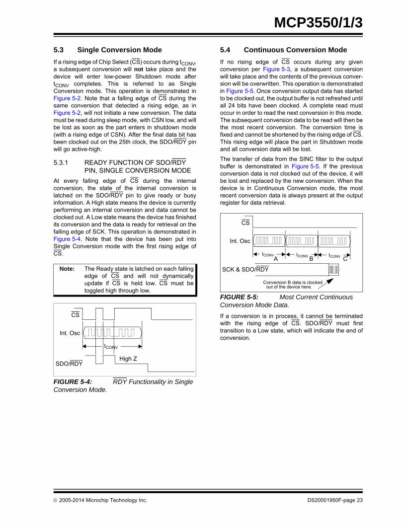
5.3.1 READY FUNCTION OF SDO/RDY PIN, SINGLE CONVERSION MODE
At every falling edge of CS during the internalconversion, the state of the internal conversion islatched on the SDO/RDY pin to give ready or busyinformation. A High state means the device is currentlyperforming an internal conversion and data cannot beclocked out. A Low state means the device has finishedits conversion and the data is ready for retrieval on thefalling edge of SCK. This operation is demonstrated inFigure 5-4. Note that the device has been put intoSingle Conversion mode with the first rising edge ofCS.
FIGURE 5-4: RDY Functionality in Single Conversion Mode.
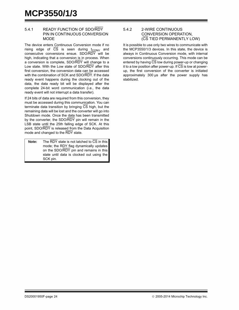
5.4 Continuous Conversion Mode
If no rising edge of CS occurs during any givenconversion per Figure 5-3, a subsequent conversionwill take place and the contents of the previous conver-sion will be overwritten. This operation is demonstratedin Figure 5-5. Once conversion output data has startedto be clocked out, the output buffer is not refreshed untilall 24 bits have been clocked. A complete read mustoccur in order to read the next conversion in this mode.The subsequent conversion data to be read will then bethe most recent conversion. The conversion time isfixed and cannot be shortened by the rising edge of CS.This rising edge will place the part in Shutdown modeand all conversion data will be lost.
The transfer of data from the SINC filter to the outputbuffer is demonstrated in Figure 5-5. If the previousconversion data is not clocked out of the device, it willbe lost and replaced by the new conversion. When thedevice is in Continuous Conversion mode, the mostrecent conversion data is always present at the outputregister for data retrieval.
FIGURE 5-5: Most Current Continuous Conversion Mode Data.
If a conversion is in process, it cannot be terminatedwith the rising edge of CS. SDO/RDY must firsttransition to a Low state, which will indicate the end ofconversion.
Note: The Ready state is latched on each fallingedge of CS and will not dynamicallyupdate if CS is held low. CS must betoggled high through low.
tCONV
CS
Int. Osc
SDO/RDYHigh Z
tCONVtCONV tCONV
CS
Int. Osc
SCK & SDO/RDY
A B C
Conversion B data is clockedout of the device here.
2005-2014 Microchip Technology Inc. DS20001950F-page 23
MCP3550/1/3
5.4.1 READY FUNCTION OF SDO/RDY PIN IN CONTINUOUS CONVERSION MODE
The device enters Continuous Conversion mode if norising edge of CS is seen during tCONV andconsecutive conversions ensue. SDO/RDY will behigh, indicating that a conversion is in process. Whena conversion is complete, SDO/RDY will change to aLow state. With the Low state of SDO/RDY after thisfirst conversion, the conversion data can be accessedwith the combination of SCK and SDO/RDY. If the dataready event happens during the clocking out of thedata, the data ready bit will be displayed after thecomplete 24-bit word communication (i.e., the dataready event will not interrupt a data transfer).
If 24 bits of data are required from this conversion, theymust be accessed during this communication. You canterminate data transition by bringing CS high, but theremaining data will be lost and the converter will go intoShutdown mode. Once the data has been transmittedby the converter, the SDO/RDY pin will remain in theLSB state until the 25th falling edge of SCK. At thispoint, SDO/RDY is released from the Data Acquisitionmode and changed to the RDY state.
5.4.2 2-WIRE CONTINUOUS CONVERSION OPERATION, (CS TIED PERMANENTLY LOW)
It is possible to use only two wires to communicate withthe MCP3550/1/3 devices. In this state, the device isalways in Continuous Conversion mode, with internalconversions continuously occurring. This mode can beentered by having CS low during power-up or changingit to a low position after power-up. If CS is low at power-up, the first conversion of the converter is initiatedapproximately 300 µs after the power supply hasstabilized.
Note: The RDY state is not latched to CS in thismode; the RDY flag dynamically updateson the SDO/RDY pin and remains in thisstate until data is clocked out using theSCK pin.
DS20001950F-page 24 2005-2014 Microchip Technology Inc.

MCP3550/1/3
5.5 Using The MCP3550/1/3 with Microcontroller (MCU) SPI Ports
It is required that the microcontroller SPI port beconfigured to clock out data on the falling edge of clockand latch data in on the rising edge. Figure 5-6 depictsthe operation shown in SPI mode 1,1, which requiresthat the SCK from the MCU idles in the High state,while Figure 5-7 shows the similar case of SPI Mode0,0, where the clock idles in the Low state. Thewaveforms in the figures are examples of an MCUoperating the SPI port in 8-bit mode, and theMCP3550/1/3 devices do not require data in 8-bitgroups.
In SPI mode 1,1, data is read using only 24 clocks orthree byte transfers. The data ready bit must be readby testing the SDO/RDY line prior to a falling edge ofthe clock.
In SPI mode 0,0, data is read using 25 clocks or fourbyte transfers. Please note that the data ready bit isincluded in the transfer as the first bit in this mode.
FIGURE 5-6: SPI Communication – Mode 1,1.
FIGURE 5-7: SPI Communication – Mode 0,0.
CS
SCK
SDO/RDY
MCU
Data stored into MCUreceive register aftertransmission of first byte
Receive Buffer
Data stored into MCUreceive register aftertransmission of second byte
Data stored into MCUreceive register aftertransmission of third byte
D O O 21 20 19 18 17 16 15 14 13 12 11 10 9 8 7 6 5 4 3 2 1 0
OL OH 21 20 19 18 17 16 15 14 13 12 11 10 9 8 7 6 5 4 3 2 1 0
R H L
CS
SCK
SDO/RDY
MCU
Data stored into MCUreceive register aftertransmission of first byte
Receive Buffer
Data stored into MCUreceive register aftertransmission of second byte
Data stored into MCUreceive register aftertransmission of third byte
Data stored into MCUreceive register aftertransmission of fourth byte
DR O O21 20 19 18 17 16 14 13 12 11 10 9 6 5 4 3 2 0
OH OL 21 20 19 18 17 15 14 13 12 11 10 9 7 6 5 4 3 2 1 0DR
8
16
15 7
8
1H L
2005-2014 Microchip Technology Inc. DS20001950F-page 25

MCP3550/1/3
NOTES:
DS20001950F-page 26 2005-2014 Microchip Technology Inc.

MCP3550/1/3
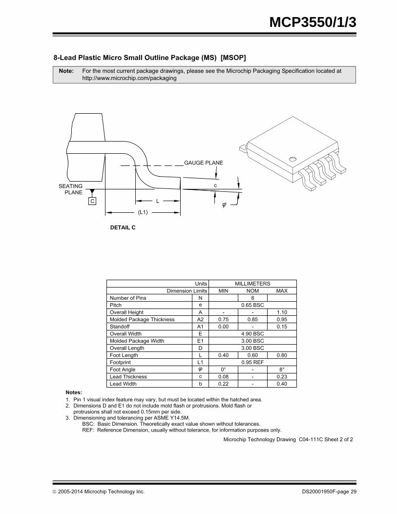
6.0 PACKAGING INFORMATION
6.1 Package Marking Information
Legend: XX...X Customer-specific informationY Year code (last digit of calendar year)YY Year code (last 2 digits of calendar year)WW Week code (week of January 1 is week ‘01’)NNN Alphanumeric traceability code Pb-free JEDEC® designator for Matte Tin (Sn)* This package is Pb-free. The Pb-free JEDEC designator ( )
can be found on the outer packaging for this package.
Note: In the event the full Microchip part number cannot be marked on one line, it willbe carried over to the next line, thus limiting the number of availablecharacters for customer-specific information.
3e
3e
8-Lead MSOP (3x3 mm) Example
3553E
425256
8-Lead SOIC (3.90 mm) Example (MCP3550)
NNN
3550-50ESN^^ 1425
256
3e
MCP3551ESN^^ 1425
256
3e
Example (MCP3551)
2005-2014 Microchip Technology Inc. DS20001950F-page 27

MCP3550/1/3
Note: For the most current package drawings, please see the Microchip Packaging Specification located at http://www.microchip.com/packaging
DS20001950F-page 28 2005-2014 Microchip Technology Inc.
MCP3550/1/3
Note: For the most current package drawings, please see the Microchip Packaging Specification located at http://www.microchip.com/packaging
2005-2014 Microchip Technology Inc. DS20001950F-page 29

MCP3550/1/3
Note: For the most current package drawings, please see the Microchip Packaging Specification located at http://www.microchip.com/packaging
DS20001950F-page 30 2005-2014 Microchip Technology Inc.

MCP3550/1/3
Note: For the most current package drawings, please see the Microchip Packaging Specification located at http://www.microchip.com/packaging
2005-2014 Microchip Technology Inc. DS20001950F-page 31

MCP3550/1/3
Note: For the most current package drawings, please see the Microchip Packaging Specification located at http://www.microchip.com/packaging
DS20001950F-page 32 2005-2014 Microchip Technology Inc.

MCP3550/1/3
!"#$%
& !"#$%&"'""($)%*++&&&!!+$
2005-2014 Microchip Technology Inc. DS20001950F-page 33

MCP3550/1/3
NOTES:
DS20001950F-page 34 2005-2014 Microchip Technology Inc.

MCP3550/1/3
APPENDIX A: REVISION HISTORY
Revision F (July 2014)
The following is the list of modifications:
1. Updated the Serial Timings table.
Revision E (April 2009)
The following is the list of modifications:
1. DC Characteristics Table, Conversion Times:Changed all minimums from -1.0% to -2.0%.Changed typical for MCP3551 from 72.73 to73.1. Changed all maximums from +1.0% to+2.0%.
2. Packaging Outline drawings updated.
Revision D (January 2007)
The following is the list of modifications:
• This update includes revisions to the packaging diagrams.
Revision C (December 2005)
The following is the list of modifications:
• Added MCP3550-50, MCP3550-60 references throughout this document.
Revision B (October 2005)
The following is the list of modifications:
• Changed LSb refefences to LSB.
Revision A (September 2005)
• Original Release of this Document.
2005-2014 Microchip Technology Inc. DS20001950F-page 35

MCP3550/1/3
NOTES:
DS20001950F-page 36 2005-2014 Microchip Technology Inc.

MCP3550/1/3
PRODUCT IDENTIFICATION SYSTEM
To order or obtain information, e.g., on pricing or delivery, refer to the factory or the listed sales office.
Device: MCP3550-50: Single-Channel 22-Bit Delta-Sigma ADCMCP3550T-50: Single-Channel 22-Bit Delta-Sigma ADC
(Tape and Reel)MCP3550-60: Single-Channel 22-Bit Delta-Sigma ADCMCP3550T-60: Single-Channel 22-Bit Delta-Sigma ADC
(Tape and Reel)MCP3551: Single-Channel 22-Bit Delta-Sigma ADCMCP3551T: Single-Channel 22-Bit Delta-Sigma ADC
(Tape and Reel)MCP3553: Single-Channel 22-Bit Delta-Sigma ADCMCP3553T: Single-Channel 22-Bit Delta-Sigma ADC
(Tape and Reel)
Temperature Range: E = -40°C to +125°C
Package: MS = Plastic MSOP, 8-leadSN = Plastic SOIC (150 mil Body), 8-lead
Examples:
a) MCP3550-50E/MS: Extended Temp., 8LD MSOP
b) MCP3550T-50E/MS: Tape and Reel,Extended Temp.,8LD MSOP
c) MCP3550-60E/SN: Extended Temp.,8LD SOIC
d) MCP3550T-60E/SN: Tape and Reel,Extended Temp.,8LD SOIC
a) MCP3551-E/MS: Extended Temp., 8LD MSOP
b) MCP3551T-E/MS: Tape and Reel,Extended Temp.,8LD MSOP
a) MCP3553-E/SN: Extended Temp.,8LD SOIC
b) MCP3553T-E/SN: Tape and Reel,Extended Temp.,8LD SOIC
PART NO. –X /XX
PackageTemperatureRange
Device
2005-2014 Microchip Technology Inc. DS20001950F-page 37
MCP3550/1/3
NOTES:
DS20001950F-page 38 2005-2014 Microchip Technology Inc.

Note the following details of the code protection feature on Microchip devices:
• Microchip products meet the specification contained in their particular Microchip Data Sheet.
• Microchip believes that its family of products is one of the most secure families of its kind on the market today, when used in the intended manner and under normal conditions.
• There are dishonest and possibly illegal methods used to breach the code protection feature. All of these methods, to our knowledge, require using the Microchip products in a manner outside the operating specifications contained in Microchip’s Data Sheets. Most likely, the person doing so is engaged in theft of intellectual property.
• Microchip is willing to work with the customer who is concerned about the integrity of their code.
• Neither Microchip nor any other semiconductor manufacturer can guarantee the security of their code. Code protection does not mean that we are guaranteeing the product as “unbreakable.”
Code protection is constantly evolving. We at Microchip are committed to continuously improving the code protection features of ourproducts. Attempts to break Microchip’s code protection feature may be a violation of the Digital Millennium Copyright Act. If such actsallow unauthorized access to your software or other copyrighted work, you may have a right to sue for relief under that Act.
Information contained in this publication regarding deviceapplications and the like is provided only for your convenienceand may be superseded by updates. It is your responsibility toensure that your application meets with your specifications.MICROCHIP MAKES NO REPRESENTATIONS ORWARRANTIES OF ANY KIND WHETHER EXPRESS ORIMPLIED, WRITTEN OR ORAL, STATUTORY OROTHERWISE, RELATED TO THE INFORMATION,INCLUDING BUT NOT LIMITED TO ITS CONDITION,QUALITY, PERFORMANCE, MERCHANTABILITY ORFITNESS FOR PURPOSE. Microchip disclaims all liabilityarising from this information and its use. Use of Microchipdevices in life support and/or safety applications is entirely atthe buyer’s risk, and the buyer agrees to defend, indemnify andhold harmless Microchip from any and all damages, claims,suits, or expenses resulting from such use. No licenses areconveyed, implicitly or otherwise, under any Microchipintellectual property rights.
2005-2014 Microchip Technology Inc.
QUALITY MANAGEMENT SYSTEM CERTIFIED BY DNV
== ISO/TS 16949 ==
Trademarks
The Microchip name and logo, the Microchip logo, dsPIC, FlashFlex, flexPWR, JukeBlox, KEELOQ, KEELOQ logo, Kleer, LANCheck, MediaLB, MOST, MOST logo, MPLAB, OptoLyzer, PIC, PICSTART, PIC32 logo, RightTouch, SpyNIC, SST, SST Logo, SuperFlash and UNI/O are registered trademarks of Microchip Technology Incorporated in the U.S.A. and other countries.
The Embedded Control Solutions Company and mTouch are registered trademarks of Microchip Technology Incorporated in the U.S.A.
Analog-for-the-Digital Age, BodyCom, chipKIT, chipKIT logo, CodeGuard, dsPICDEM, dsPICDEM.net, ECAN, In-Circuit Serial Programming, ICSP, Inter-Chip Connectivity, KleerNet, KleerNet logo, MiWi, MPASM, MPF, MPLAB Certified logo, MPLIB, MPLINK, MultiTRAK, NetDetach, Omniscient Code Generation, PICDEM, PICDEM.net, PICkit, PICtail, RightTouch logo, REAL ICE, SQI, Serial Quad I/O, Total Endurance, TSHARC, USBCheck, VariSense, ViewSpan, WiperLock, Wireless DNA, and ZENA are trademarks of Microchip Technology Incorporated in the U.S.A. and other countries.
SQTP is a service mark of Microchip Technology Incorporated in the U.S.A.
Silicon Storage Technology is a registered trademark of Microchip Technology Inc. in other countries.
GestIC is a registered trademarks of Microchip Technology Germany II GmbH & Co. KG, a subsidiary of Microchip Technology Inc., in other countries.
All other trademarks mentioned herein are property of their respective companies.
© 2005-2014, Microchip Technology Incorporated, Printed in the U.S.A., All Rights Reserved.
ISBN: 978-1-63276-389-1
Microchip received ISO/TS-16949:2009 certification for its worldwide
DS20001950F-page 39
headquarters, design and wafer fabrication facilities in Chandler and Tempe, Arizona; Gresham, Oregon and design centers in California and India. The Company’s quality system processes and procedures are for its PIC® MCUs and dsPIC® DSCs, KEELOQ® code hopping devices, Serial EEPROMs, microperipherals, nonvolatile memory and analog products. In addition, Microchip’s quality system for the design and manufacture of development systems is ISO 9001:2000 certified.

DS20001950F-page 40 2005-2014 Microchip Technology Inc.
AMERICASCorporate Office2355 West Chandler Blvd.Chandler, AZ 85224-6199Tel: 480-792-7200 Fax: 480-792-7277Technical Support: http://www.microchip.com/supportWeb Address: www.microchip.com
AtlantaDuluth, GA Tel: 678-957-9614 Fax: 678-957-1455
Austin, TXTel: 512-257-3370
BostonWestborough, MA Tel: 774-760-0087 Fax: 774-760-0088
ChicagoItasca, IL Tel: 630-285-0071 Fax: 630-285-0075
ClevelandIndependence, OH Tel: 216-447-0464 Fax: 216-447-0643
DallasAddison, TX Tel: 972-818-7423 Fax: 972-818-2924
DetroitNovi, MI Tel: 248-848-4000
Houston, TX Tel: 281-894-5983
IndianapolisNoblesville, IN Tel: 317-773-8323Fax: 317-773-5453
Los AngelesMission Viejo, CA Tel: 949-462-9523 Fax: 949-462-9608
New York, NY Tel: 631-435-6000
San Jose, CA Tel: 408-735-9110
Canada - TorontoTel: 905-673-0699 Fax: 905-673-6509
ASIA/PACIFICAsia Pacific OfficeSuites 3707-14, 37th FloorTower 6, The GatewayHarbour City, KowloonHong KongTel: 852-2943-5100Fax: 852-2401-3431
Australia - SydneyTel: 61-2-9868-6733Fax: 61-2-9868-6755
China - BeijingTel: 86-10-8569-7000 Fax: 86-10-8528-2104
China - ChengduTel: 86-28-8665-5511Fax: 86-28-8665-7889
China - ChongqingTel: 86-23-8980-9588Fax: 86-23-8980-9500
China - HangzhouTel: 86-571-8792-8115 Fax: 86-571-8792-8116
China - Hong Kong SARTel: 852-2943-5100 Fax: 852-2401-3431
China - NanjingTel: 86-25-8473-2460Fax: 86-25-8473-2470
China - QingdaoTel: 86-532-8502-7355Fax: 86-532-8502-7205
China - ShanghaiTel: 86-21-5407-5533 Fax: 86-21-5407-5066
China - ShenyangTel: 86-24-2334-2829Fax: 86-24-2334-2393
China - ShenzhenTel: 86-755-8864-2200 Fax: 86-755-8203-1760
China - WuhanTel: 86-27-5980-5300Fax: 86-27-5980-5118
China - XianTel: 86-29-8833-7252Fax: 86-29-8833-7256
China - XiamenTel: 86-592-2388138 Fax: 86-592-2388130
China - ZhuhaiTel: 86-756-3210040 Fax: 86-756-3210049
ASIA/PACIFICIndia - BangaloreTel: 91-80-3090-4444 Fax: 91-80-3090-4123
India - New DelhiTel: 91-11-4160-8631Fax: 91-11-4160-8632
India - PuneTel: 91-20-3019-1500
Japan - OsakaTel: 81-6-6152-7160 Fax: 81-6-6152-9310
Japan - TokyoTel: 81-3-6880- 3770 Fax: 81-3-6880-3771
Korea - DaeguTel: 82-53-744-4301Fax: 82-53-744-4302
Korea - SeoulTel: 82-2-554-7200Fax: 82-2-558-5932 or 82-2-558-5934
Malaysia - Kuala LumpurTel: 60-3-6201-9857Fax: 60-3-6201-9859
Malaysia - PenangTel: 60-4-227-8870Fax: 60-4-227-4068
Philippines - ManilaTel: 63-2-634-9065Fax: 63-2-634-9069
SingaporeTel: 65-6334-8870Fax: 65-6334-8850
Taiwan - Hsin ChuTel: 886-3-5778-366Fax: 886-3-5770-955
Taiwan - KaohsiungTel: 886-7-213-7830
Taiwan - TaipeiTel: 886-2-2508-8600 Fax: 886-2-2508-0102
Thailand - BangkokTel: 66-2-694-1351Fax: 66-2-694-1350
EUROPEAustria - WelsTel: 43-7242-2244-39Fax: 43-7242-2244-393Denmark - CopenhagenTel: 45-4450-2828 Fax: 45-4485-2829
France - ParisTel: 33-1-69-53-63-20 Fax: 33-1-69-30-90-79
Germany - DusseldorfTel: 49-2129-3766400
Germany - MunichTel: 49-89-627-144-0 Fax: 49-89-627-144-44
Germany - PforzheimTel: 49-7231-424750
Italy - Milan Tel: 39-0331-742611 Fax: 39-0331-466781
Italy - VeniceTel: 39-049-7625286
Netherlands - DrunenTel: 31-416-690399 Fax: 31-416-690340
Poland - WarsawTel: 48-22-3325737
Spain - MadridTel: 34-91-708-08-90Fax: 34-91-708-08-91
Sweden - StockholmTel: 46-8-5090-4654
UK - WokinghamTel: 44-118-921-5800Fax: 44-118-921-5820
Worldwide Sales and Service
03/25/14