Embed Size (px)
Citation preview

MCP1826/MCP1826S1000 mA, Low Voltage, Low Quiescent Current
LDO Regulator
Features• 1000 mA Output Current Capability• Input Operating Voltage Range: 2.3V to 6.0V• Adjustable Output Voltage Range: 0.8V to 5.0V
(MCP1826 only)• Standard Fixed Output Voltages:
- 0.8V, 1.2V, 1.8V, 2.5V, 3.0V, 3.3V, 5.0V• Other Fixed Output Voltage Options Available
Upon Request• Low Dropout Voltage: 250 mV Typical at 1000 mA• Typical Output Voltage Tolerance: 0.5%• Stable with 1.0 µF Ceramic Output Capacitor• Fast response to Load Transients• Low Supply Current: 120 µA (typ)• Low Shutdown Supply Current: 0.1 µA (typ)
(MCP1826 only)• Fixed Delay on Power Good Output
(MCP1826 only)• Short Circuit Current Limiting and
Overtemperature Protection• TO-263-5 (DDPAK-5), TO-220-5, SOT-223-5
Package Options (MCP1826).• TO-263-3 (DDPAK-3), TO-220-3, SOT-223-3
Package Options (MCP1826S).
Applications• High-Speed Driver Chipset Power• Networking Backplane Cards• Notebook Computers• Network Interface Cards• Palmtop Computers• 2.5V to 1.XV Regulators
DescriptionThe MCP1826/MCP1826S is a 1000 mA Low Dropout(LDO) linear regulator that provides high current andlow output voltages. The MCP1826 comes in a fixed oradjustable output voltage version, with an outputvoltage range of 0.8V to 5.0V. The 1000 mA output cur-rent capability, combined with the low output voltagecapability, make the MCP1826 a good choice for newsub-1.8V output voltage LDO applications that havehigh current demands. The MCP1826S is a 3-pin fixedvoltage version.
The MCP1826/MCP1826S is stable using ceramicoutput capacitors that inherently provide lower outputnoise and reduce the size and cost of the entireregulator solution. Only 1 µF of output capacitance isneeded to stabilize the LDO.
Using CMOS construction, the quiescent currentconsumed by the MCP1826/MCP1826S is typicallyless than 120 µA over the entire input voltage range,making it attractive for portable computing applicationsthat demand high output current. The MCP1826versions have a Shutdown (SHDN) pin. When shutdown, the quiescent current is reduced to less than0.1 µA.
On the MCP1826 fixed output versions the scaled-down output voltage is internally monitored and apower good (PWRGD) output is provided when theoutput is within 92% of regulation (typical). ThePWRGD delay is internally fixed at 200 µs (typical).
The overtemperature and short circuit current-limitingprovide additional protection for the LDO during systemfault conditions.
© 2007 Microchip Technology Inc. DS22057A-page 1

MCP1826/MCP1826S
Package TypesMCP1826
1 2 3 4 5
6
SOT-223-5
Pin Fixed Adjustable
1 SHDN SHDN
2 VIN VIN
3 GND (TAB) GND (TAB)
4 VOUT VOUT
5 PWRGD ADJ
6 GND (TAB) GND (TAB)
1 2 3
SOT-223-34
MCP1826S
Pin
1 VIN2 GND (TAB)3 VOUT4 GND (TAB)
Fixed/AdjustableDDPAK-3DDPAK-5 TO-220-3TO-220-5
1 2 3 4 51 2 3 4 5
1 2 3
1 2 3
DS22057A-page 2 © 2007 Microchip Technology Inc.
MCP1826/MCP1826S
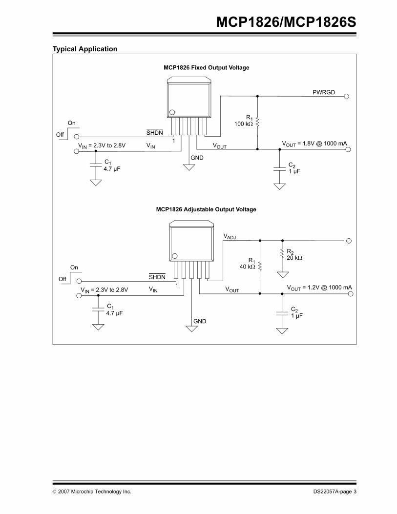
Typical ApplicationMCP1826 Adjustable Output Voltage
MCP1826 Fixed Output Voltage
VOUT = 1.8V @ 1000 mAVIN = 2.3V to 2.8V
On
Off
1 µF
100 kΩ
4.7 µFC1 C2
R1
SHDN
VIN
GND
VOUT
PWRGD
20 kΩR2
VOUT = 1.2V @ 1000 mAVIN = 2.3V to 2.8V
On
Off
1 µF
40 kΩ
4.7 µFC1 C2
R1
SHDN
VIN
GND
VOUT
VADJ
1
1
© 2007 Microchip Technology Inc. DS22057A-page 3

MCP1826/MCP1826S
Functional Block Diagram - Adjustable OutputEA+
–
VOUT
PMOS
RfCfISNS
Overtemperature
VREF
Comp
92% of VREF
TDELAY
VIN
Driver w/limitand SHDN
GND
Soft-Start
ADJ/SENSE
Undervoltage Lock Out
VINReference
SHDN
SHDN
SHDNSensing
(UVLO)
DS22057A-page 4 © 2007 Microchip Technology Inc.

MCP1826/MCP1826S
Functional Block Diagram - Fixed Output (3-Pin)EA+
–
VOUT
PMOS
RfCfISNS
Overtemperature
VREF
Comp
92% of VREF
TDELAY
VIN
Driver w/limitand SHDN
GND
Soft-Start
SenseUndervoltage Lock Out
VINReference
SHDN
SHDN
SHDNSensing
(UVLO)
© 2007 Microchip Technology Inc. DS22057A-page 5

MCP1826/MCP1826S
Functional Block Diagram - Fixed Output (5-Pin)EA+
–
VOUT
PMOS
RfCfISNS
Overtemperature
VREF
Comp
92% of VREF
VIN
Driver w/limitand SHDN
GND
Soft-Start
SenseUndervoltage Lock Out
VINReference
SHDN
SHDN
SHDNSensing
(UVLO)
PWRGDTDELAY
DS22057A-page 6 © 2007 Microchip Technology Inc.

MCP1826/MCP1826S
1.0 ELECTRICAL CHARACTERISTICS
Absolute Maximum Ratings †VIN....................................................................................6.5V
Maximum Voltage on Any Pin .. (GND – 0.3V) to (VDD + 0.3)VMaximum Power Dissipation......... Internally-Limited (Note 6)Output Short Circuit Duration................................ContinuousStorage temperature .....................................-65°C to +150°CMaximum Junction Temperature, TJ ........................... +150°CESD protection on all pins (HBM/MM) ........... ≥ 4 kV; ≥ 300V
† Notice: Stresses above those listed under “Maximum Rat-ings” may cause permanent damage to the device. This is astress rating only and functional operation of the device atthose or any other conditions above those indicated in theoperational listings of this specification is not implied. Expo-sure to maximum rating conditions for extended periods mayaffect device reliability.
AC/DC CHARACTERISTICSElectrical Specifications: Unless otherwise noted, VIN = VOUT(MAX) + VDROPOUT(MAX), Note 1, VR=1.8V for Adjustable Output, IOUT = 1 mA, CIN = COUT = 4.7 µF (X7R Ceramic), TA = +25°C.Boldface type applies for junction temperatures, TJ (Note 7) of -40°C to +125°C
Parameters Sym Min Typ Max Units Conditions
Input Operating Voltage VIN 2.3 6.0 V Note 1
Input Quiescent Current Iq — 120 220 µA IL = 0 mA, VOUT = 0.8V to 5.0V
Input Quiescent Current for SHDN Mode
ISHDN — 0.1 3 µA SHDN = GND
Maximum Output Current IOUT 1000 — — mA VIN = 2.3V to 6.0VVR = 0.8V to 5.0V, Note 1
Line Regulation ΔVOUT/(VOUT x ΔVIN)
— ±0.05 ±0.20 %/V (Note 1) ≤ VIN ≤ 6V
Load Regulation ΔVOUT/VOUT -1.0 ±0.5 1.0 % IOUT = 1 mA to 1000 mA, (Note 4)
Output Short Circuit Current IOUT_SC — 2.2 — A RLOAD < 0.1Ω, Peak Current
Adjust Pin Characteristics (Adjustable Output Only)
Adjust Pin Reference Voltage VADJ 0.402 0.410 0.418 V VIN = 2.3V to VIN = 6.0V,IOUT = 1 mA
Adjust Pin Leakage Current IADJ -10 ±0.01 +10 nA VIN = 6.0V, VADJ = 0V to 6V
Adjust Temperature Coefficient TCVOUT — 40 — ppm/°C Note 3
Fixed-Output Characteristics (Fixed Output Only)
Voltage Regulation VOUT VR - 2.5% VR ±0.5% VR + 2.5% V Note 2
Note 1: The minimum VIN must meet two conditions: VIN ≥ 2.3V and VIN ≥ VOUT(MAX) + VDROPOUT(MAX).2: VR is the nominal regulator output voltage for the fixed cases. VR = 1.2V, 1.8V, etc. VR is the desired set point output
voltage for the adjustable cases. VR = VADJ * ((R1/R2)+1). Figure 4-1.3: TCVOUT = (VOUT-HIGH – VOUT-LOW) *106 / (VR * ΔTemperature). VOUT-HIGH is the highest voltage measured over the
temperature range. VOUT-LOW is the lowest voltage measured over the temperature range.4: Load regulation is measured at a constant junction temperature using low duty-cycle pulse testing. Load regulation is
tested over a load range from 1 mA to the maximum specified output current.5: Dropout voltage is defined as the input-to-output voltage differential at which the output voltage drops 2% below its
nominal value that was measured with an input voltage of VIN = VOUT(MAX) + VDROPOUT(MAX).6: The maximum allowable power dissipation is a function of ambient temperature, the maximum allowable junction
temperature and the thermal resistance from junction to air. (i.e., TA, TJ, θJA). Exceeding the maximum allowable power dissipation will cause the device operating junction temperature to exceed the maximum +150°C rating. Sustained junction temperatures above 150°C can impact device reliability.
7: The junction temperature is approximated by soaking the device under test at an ambient temperature equal to the desired junction temperature. The test time is small enough such that the rise in the junction temperature over the ambient temperature is not significant.
© 2007 Microchip Technology Inc. DS22057A-page 7

MCP1826/MCP1826S
Dropout Characteristics
Dropout Voltage VDROPOUT — 250 400 mV Note 5, IOUT = 1000 mA, VIN(MIN) = 2.3V
Power Good Characteristics
PWRGD Input Voltage Operat-ing Range
VPWRGD_VIN 1.0 — 6.0 V TA = +25°C
1.2 — 6.0 TA = -40°C to +125°C
For VIN < 2.3V, ISINK = 100 µA
PWRGD Threshold Voltage(Referenced to VOUT)
VPWRGD_TH %VOUT Falling Edge
89 92 95 VOUT < 2.5V Fixed,VOUT = Adj.
90 92 94 VOUT >= 2.5V Fixed
PWRGD Threshold Hysteresis VPWRGD_HYS 1.0 2.0 3.0 %VOUT
PWRGD Output Voltage Low VPWRGD_L — 0.2 0.4 V IPWRGD SINK = 1.2 mA,ADJ = 0V
PWRGD Leakage PWRGD_LK — 1 — nA VPWRGD = VIN = 6.0V
PWRGD Time Delay TPG — 125 — µs Rising EdgeRPULLUP = 10 kΩ
Detect Threshold to PWRGD Active Time Delay
TVDET-PWRGD — 200 — µs VOUT = VPWRGD_TH + 20 mV to VPWRGD_TH - 20 mV
Shutdown Input
Logic High Input VSHDN-HIGH 45 — — %VIN VIN = 2.3V to 6.0V
Logic Low Input VSHDN-LOW — — 15 %VIN VIN = 2.3V to 6.0V
SHDN Input Leakage Current SHDNILK -0.1 ±0.001 +0.1 µA VIN = 6V, SHDN =VIN,SHDN = GND
AC Performance
Output Delay From SHDN TOR — 100 — µs SHDN = GND to VIN VOUT = GND to 95% VR
Output Noise eN — 2.0 — µV/√Hz IOUT = 200 mA, f = 1 kHz, COUT = 10 µF (X7R Ceramic), VOUT = 2.5V
AC/DC CHARACTERISTICS (CONTINUED)Electrical Specifications: Unless otherwise noted, VIN = VOUT(MAX) + VDROPOUT(MAX), Note 1, VR=1.8V for Adjustable Output, IOUT = 1 mA, CIN = COUT = 4.7 µF (X7R Ceramic), TA = +25°C.Boldface type applies for junction temperatures, TJ (Note 7) of -40°C to +125°C
Parameters Sym Min Typ Max Units Conditions
Note 1: The minimum VIN must meet two conditions: VIN ≥ 2.3V and VIN ≥ VOUT(MAX) + VDROPOUT(MAX).2: VR is the nominal regulator output voltage for the fixed cases. VR = 1.2V, 1.8V, etc. VR is the desired set point output
voltage for the adjustable cases. VR = VADJ * ((R1/R2)+1). Figure 4-1.3: TCVOUT = (VOUT-HIGH – VOUT-LOW) *106 / (VR * ΔTemperature). VOUT-HIGH is the highest voltage measured over the
temperature range. VOUT-LOW is the lowest voltage measured over the temperature range.4: Load regulation is measured at a constant junction temperature using low duty-cycle pulse testing. Load regulation is
tested over a load range from 1 mA to the maximum specified output current.5: Dropout voltage is defined as the input-to-output voltage differential at which the output voltage drops 2% below its
nominal value that was measured with an input voltage of VIN = VOUT(MAX) + VDROPOUT(MAX).6: The maximum allowable power dissipation is a function of ambient temperature, the maximum allowable junction
temperature and the thermal resistance from junction to air. (i.e., TA, TJ, θJA). Exceeding the maximum allowable power dissipation will cause the device operating junction temperature to exceed the maximum +150°C rating. Sustained junction temperatures above 150°C can impact device reliability.
7: The junction temperature is approximated by soaking the device under test at an ambient temperature equal to the desired junction temperature. The test time is small enough such that the rise in the junction temperature over the ambient temperature is not significant.
DS22057A-page 8 © 2007 Microchip Technology Inc.

MCP1826/MCP1826S
TEMPERATURE SPECIFICATIONS
Power Supply Ripple Rejection Ratio
PSRR — 60 — dB f = 100 Hz, COUT = 4.7 µF,IOUT = 100 µA, VINAC = 100 mV pk-pk,CIN = 0 µF
Thermal Shutdown Temperature TSD — 150 — °C IOUT = 100 µA, VOUT = 1.8V, VIN = 2.8V
Thermal Shutdown Hysteresis ΔTSD — 10 — °C IOUT = 100 µA, VOUT = 1.8V, VIN = 2.8V
Parameters Sym Min Typ Max Units Conditions
Temperature RangesOperating Junction Temperature Range TJ -40 — +125 °C Steady StateMaximum Junction Temperature TJ — — +150 °C TransientStorage Temperature Range TA -65 — +150 °CThermal Package ResistancesThermal Resistance, 3L-DDPAK θJA — 31.4 — °C/W 4-Layer JC51 Standard
BoardθJC — 3.0 — °C/WThermal Resistance, 3L-TO-220 θJA — 29.4 — °C/W 4-Layer JC51 Standard
BoardθJC — 2.0 — °C/WThermal Resistance, 3L-SOT-223 θJA — 62 — °C/W EIA/JEDEC JESD51-751-7
4 Layer BoardθJC — 15.0 — °C/WThermal Resistance, 5L-DDPAK θJA — 31.2 — °C/W 4-Layer JC51 Standard
BoardθJC — 3.0 — °C/WThermal Resistance, 5L-TO-220 θJA — 29.3 — °C/W 4-Layer JC51 Standard
BoardθJC — 2.0 — °C/WThermal Resistance, 5L-SOT-223 θJA — 62 — °C/W EIA/JEDEC JESD51-751-7
4 Layer BoardθJC — 15.0 — °C/W
AC/DC CHARACTERISTICS (CONTINUED)Electrical Specifications: Unless otherwise noted, VIN = VOUT(MAX) + VDROPOUT(MAX), Note 1, VR=1.8V for Adjustable Output, IOUT = 1 mA, CIN = COUT = 4.7 µF (X7R Ceramic), TA = +25°C.Boldface type applies for junction temperatures, TJ (Note 7) of -40°C to +125°C
Parameters Sym Min Typ Max Units Conditions
Note 1: The minimum VIN must meet two conditions: VIN ≥ 2.3V and VIN ≥ VOUT(MAX) + VDROPOUT(MAX).2: VR is the nominal regulator output voltage for the fixed cases. VR = 1.2V, 1.8V, etc. VR is the desired set point output
voltage for the adjustable cases. VR = VADJ * ((R1/R2)+1). Figure 4-1.3: TCVOUT = (VOUT-HIGH – VOUT-LOW) *106 / (VR * ΔTemperature). VOUT-HIGH is the highest voltage measured over the
temperature range. VOUT-LOW is the lowest voltage measured over the temperature range.4: Load regulation is measured at a constant junction temperature using low duty-cycle pulse testing. Load regulation is
tested over a load range from 1 mA to the maximum specified output current.5: Dropout voltage is defined as the input-to-output voltage differential at which the output voltage drops 2% below its
nominal value that was measured with an input voltage of VIN = VOUT(MAX) + VDROPOUT(MAX).6: The maximum allowable power dissipation is a function of ambient temperature, the maximum allowable junction
temperature and the thermal resistance from junction to air. (i.e., TA, TJ, θJA). Exceeding the maximum allowable power dissipation will cause the device operating junction temperature to exceed the maximum +150°C rating. Sustained junction temperatures above 150°C can impact device reliability.
7: The junction temperature is approximated by soaking the device under test at an ambient temperature equal to the desired junction temperature. The test time is small enough such that the rise in the junction temperature over the ambient temperature is not significant.
© 2007 Microchip Technology Inc. DS22057A-page 9
MCP1826/MCP1826S
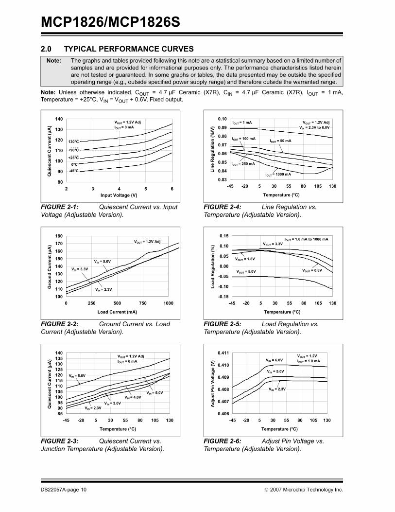
2.0 TYPICAL PERFORMANCE CURVES
Note: Unless otherwise indicated, COUT = 4.7 µF Ceramic (X7R), CIN = 4.7 µF Ceramic (X7R), IOUT = 1 mA,Temperature = +25°C, VIN = VOUT + 0.6V, Fixed output.
FIGURE 2-1: Quiescent Current vs. Input Voltage (Adjustable Version).
FIGURE 2-2: Ground Current vs. Load Current (Adjustable Version).
FIGURE 2-3: Quiescent Current vs. Junction Temperature (Adjustable Version).
FIGURE 2-4: Line Regulation vs. Temperature (Adjustable Version).
FIGURE 2-5: Load Regulation vs. Temperature (Adjustable Version).
FIGURE 2-6: Adjust Pin Voltage vs. Temperature (Adjustable Version).
Note: The graphs and tables provided following this note are a statistical summary based on a limited number ofsamples and are provided for informational purposes only. The performance characteristics listed hereinare not tested or guaranteed. In some graphs or tables, the data presented may be outside the specifiedoperating range (e.g., outside specified power supply range) and therefore outside the warranted range.
80
90
100
110
120
130
140
2 3 4 5 6Input Voltage (V)
Qui
esce
nt C
urre
nt (μ
A)
130°C
-45°C
+25°C
+90°C
VOUT = 1.2V AdjIOUT = 0 mA
130°C
+25°C
+90°C
0°C
100110120130140150160170180
0 250 500 750 1000
Load Current (mA)
Gro
und
Cur
rent
(μA
)
VIN = 3.3V
VOUT = 1.2V Adj
VIN = 5.0V
VIN = 2.3V
859095
100105110115120125130135140
-45 -20 5 30 55 80 105 130
Temperature (°C)
Qui
esce
nt C
urre
nt (μ
A)
VIN = 5.0V
VIN = 2.3V
VIN = 4.0V
VOUT = 1.2V AdjIOUT = 0 mA
VIN = 5.0V
VIN = 3.0V
0.03
0.04
0.05
0.06
0.07
0.08
0.09
0.10
-45 -20 5 30 55 80 105 130
Temperature (°C)
Line
Reg
ulat
ion
(%/V
)
VOUT = 1.2V AdjVIN = 2.3V to 6.0V
IOUT = 1 mA
IOUT = 1000 mA
IOUT = 100 mA
IOUT = 250 mA
IOUT = 50 mA
-0.15
-0.10
-0.05
0.00
0.05
0.10
0.15
-45 -20 5 30 55 80 105 130
Temperature (°C)
Load
Reg
ulat
ion
(%)
IOUT = 1.0 mA to 1000 mA
VOUT = 5.0V
VOUT = 3.3V
VOUT = 0.8V
VOUT = 1.8V
0.406
0.407
0.408
0.409
0.410
0.411
-45 -20 5 30 55 80 105 130
Temperature (°C)
Adj
ust P
in V
olta
ge (V
)
VOUT = 1.2VIOUT = 1.0 mAVIN = 6.0V
VIN = 2.3V
VIN = 5.0V
DS22057A-page 10 © 2007 Microchip Technology Inc.

MCP1826/MCP1826S
Note: Unless otherwise indicated, COUT = 4.7 µF Ceramic (X7R), CIN = 4.7 µF Ceramic (X7R), IOUT = 1 mA,Temperature = +25°C, VIN = VOUT + 0.6V, Fixed output.FIGURE 2-7: Dropout Voltage vs. Load Current (Adjustable Version).
FIGURE 2-8: Dropout Voltage vs. Temperature (Adjustable Version).
FIGURE 2-9: Power Good (PWRGD) Time Delay vs. Temperature.
FIGURE 2-10: Quiescent Current vs. Input Voltage.
FIGURE 2-11: Quiescent Current vs. Input Voltage.
FIGURE 2-12: Ground Current vs. Load Current.
0.00
0.05
0.10
0.15
0.20
0.25
0.30
0 200 400 600 800 1000
Load Current (mA)
Dro
pout
Vol
tage
(V)
VOUT = 2.5V Adj
VOUT = 5.0V Adj
0.19
0.22
0.25
0.28
0.31
0.34
-45 -20 5 30 55 80 105 130
Temperature (°C)
Dro
pout
Vol
tage
(V)
VOUT = 5.0V Adj
VOUT = 2.5V Adj
IOUT = 1.0A
100.0000
110.0000
120.0000
130.0000
140.0000
150.0000
160.0000
170.0000
-45 -20 5 30 55 80 105 130Temperature (°C)
Pow
er G
ood
Tim
e D
elay
(µS) VOUT = 2.5V
IOUT= 0 mA
VIN = 3.9V
VIN = 6.0V
VIN = 5.0V
VIN = 3.1V
90
100
110
120
130
140
150
2 3 4 5 6Input Voltage (V)
Qui
esce
nt C
urre
nt (μ
A)
+130°C
VOUT = 0.8VIOUT = 0 mA
-45°C
+90°C
+25°C
0°C
80
90
100
110
120
130
140
150
3 3.5 4 4.5 5 5.5 6
Input Voltage (V)
Qui
esce
nt C
urre
nt (μ
A) VOUT = 2.5V
IOUT = 0 mA
+130°C
-45°C
+25°C
+90°C
0°C
60
80
100
120
140
160
180
200
0 250 500 750 1000
Load Current (mA)
Gro
und
Cur
rent
(μA
)
VIN = 2.3V for VR=0.8VVIN = 3.9V for VR=3.3V
VOUT=0.8V
VOUT=3.3V
© 2007 Microchip Technology Inc. DS22057A-page 11

MCP1826/MCP1826S
Note: Unless otherwise indicated, COUT = 4.7 µF Ceramic (X7R), CIN = 4.7 µF Ceramic (X7R), IOUT = 1 mA,Temperature = +25°C, VIN = VOUT + 0.6V, Fixed output.FIGURE 2-13: Quiescent Current vs. Temperature.
FIGURE 2-14: ISHDN vs. Temperature.
FIGURE 2-15: Line Regulation vs. Temperature.
FIGURE 2-16: Line Regulation vs. Temperature.
FIGURE 2-17: Load Regulation vs. Temperature (VOUT < 2.5V Fixed).
FIGURE 2-18: Load Regulation vs. Temperature (VOUT ≥ 2.5V Fixed).
9095
100105110115120125130
-45 -20 5 30 55 80 105 130
Temperature (°C)
Qui
esce
nt C
urre
nt (μ
A)
VOUT = 0.8V
VOUT = 2.5V
IOUT = 0 mA
0.00
0.10
0.20
0.30
0.40
0.50
-45 -20 5 30 55 80 105 130
Temperature (°C)
I SH
DN (μ
A)
VIN = 2.3V
VIN = 3.0V
VIN = 4.0V
VR = 0.8V
VIN = 6.0V
VIN = 5.0V
0.00
0.02
0.04
0.06
0.08
0.10
-45 -20 5 30 55 80 105 130
Temperature (°C)
Line
Reg
ulat
ion
(%/V
)
VOUT = 0.8VVIN = 2.3V to 6.0V
IOUT = 1 mA
IOUT = 100 mA
IOUT = 500mAIOUT = 1A
IOUT = 50 mA
0.015
0.020
0.025
0.030
0.035
0.040
-45 -20 5 30 55 80 105 130
Temperature (°C)
Line
Reg
ulat
ion
(%/V
)
IOUT = 1000 mA
IOUT = 1 mA
IOUT = 50 mA
IOUT = 250 mA
IOUT = 500 mA
VR = 2.5VVIN = 3.1 to 6.0V
-0.30
-0.20
-0.10
0.00
0.10
0.20
0.30
-45 -20 5 30 55 80 105 130
Temperature (°C)
Load
Reg
ulat
ion
(%)
VOUT = 0.8VVIN = 2.3V
IOUT = 1 mA to 1000 mA
-0.40-0.35-0.30-0.25-0.20-0.15-0.10-0.050.00
-45 -20 5 30 55 80 105 130
Temperature (°C)
Load
Reg
ulat
ion
(%) VOUT = 2.5V
VOUT = 5.0V
IOUT = 1 mA to 1000 mA
DS22057A-page 12 © 2007 Microchip Technology Inc.

MCP1826/MCP1826S
Note: Unless otherwise indicated, COUT = 4.7 µF Ceramic (X7R), CIN = 4.7 µF Ceramic (X7R), IOUT = 1 mA,Temperature = +25°C, VIN = VOUT + 0.6V, Fixed output.FIGURE 2-19: Dropout Voltage vs. Load Current.
FIGURE 2-20: Dropout Voltage vs. Temperature.
FIGURE 2-21: Short Circuit Current vs. Input Voltage.
FIGURE 2-22: Output Noise Voltage Density vs. Frequency.
FIGURE 2-23: Power Supply Ripple Rejection (PSRR) vs. Frequency (Adjustable).
FIGURE 2-24: Power Supply Ripple Rejection (PSRR) vs. Frequency.
0.00
0.05
0.10
0.15
0.20
0.25
0.30
0 200 400 600 800 1000Load Current (mA)
Dro
pout
Vol
tage
(V)
VOUT = 5.0V
VOUT = 2.5V
0.20
0.22
0.24
0.26
0.28
0.30
0.32
0.34
-45 -20 5 30 55 80 105 130
Temperature (°C)
Dro
pout
Vol
tage
(V)
IOUT = 1000 mA
VOUT = 2.5V
VOUT = 5.0V
0.000.200.400.600.801.001.201.401.601.802.00
0 1 2 3 4 5 6Input Voltage (V)
Shor
t Circ
uit C
urre
nt (A
) VOUT = 0.8V
0.010
0.100
1.000
10.000
0.01 0.1 1 10 100 1000Frequency (kHz)
Noi
se (m
V/√H
z)
VR=0.8V, VIN=2.3V
VR=3.3V, VIN=4.1V
COUT=1 μF ceramic X7RCIN=10 μF ceramic
IOUT=200 mA
-80-70-60-50-40-30-20-10
0
0.01 0.1 1 10 100 1000Frequency (kHz)
PSR
R (d
B)
VR=1.2V AdjCOUT=10 μF ceramic X7RVIN=3.1VCIN=0 μFIOUT=10 mA
-80-70-60-50-40-30-20-10
0
0.01 0.1 1 10 100 1000Frequency (kHz)
PSR
R (d
B)
VR=3.3V FixedCOUT=22 μF ceramic X7RVIN=3.9VCIN=0 μFIOUT=10 mA
© 2007 Microchip Technology Inc. DS22057A-page 13

MCP1826/MCP1826S
.Note: Unless otherwise indicated, COUT = 4.7 µF Ceramic (X7R), CIN = 4.7 µF Ceramic (X7R), IOUT = 1 mA,Temperature = +25°C, VIN = VOUT + 0.6V, Fixed output.FIGURE 2-25: 2.5V (Adj.) Startup from VIN.
FIGURE 2-26: 2.5V (Adj.) Startup from Shutdown.
FIGURE 2-27: Power Good (PWRGD) Timing.
FIGURE 2-28: Dynamic Line Response.
FIGURE 2-29: Dynamic Load Response (10 mA to 1000 mA).
FIGURE 2-30: Dynamic Load Response (100 mA to 1000 mA).
DS22057A-page 14 © 2007 Microchip Technology Inc.

MCP1826/MCP1826S
3.0 PIN DESCRIPTIONThe descriptions of the pins are listed in Table 3-1.
TABLE 3-1: PIN FUNCTION TABLE
3.1 Shutdown Control Input (SHDN)The SHDN input is used to turn the LDO output voltageon and off. When the SHDN input is at a logic-highlevel, the LDO output voltage is enabled. When theSHDN input is pulled to a logic-low level, the LDOoutput voltage is disabled. When the SHDN input ispulled low, the PWRGD output also goes low and theLDO enters a low quiescent current shutdown statewhere the typical quiescent current is 0.1 µA.
3.2 Input Voltage Supply (VIN)Connect the unregulated or regulated input voltagesource to VIN. If the input voltage source is locatedseveral inches away from the LDO, or the input sourceis a battery, it is recommended that an input capacitorbe used. A typical input capacitance value of 1 µF to10 µF should be sufficient for most applications.
3.3 Ground (GND)Connect the GND pin of the LDO to a quiet circuitground. This will help the LDO power supply rejectionratio and noise performance. The ground pin of theLDO only conducts the quiescent current of the LDO(typically 120 µA), so a heavy trace is not required.For applications have switching or noisy inputs tie theGND pin to the return of the output capacitor. Groundplanes help lower inductance and voltage spikescaused by fast transient load currents and arerecommended for applications that are subjected tofast load transients.
3.4 Regulated Output Voltage (VOUT)The VOUT pin is the regulated output voltage of theLDO. A minimum output capacitance of 1.0 µF isrequired for LDO stability. The MCP1826/MCP1826S isstable with ceramic, tantalum and aluminum-electro-lytic capacitors. See Section 4.3 “Output Capacitor”for output capacitor selection guidance.
3.5 Power Good Output (PWRGD)The PWRGD output is an open-drain output used toindicate when the LDO output voltage is within 92%(typically) of its nominal regulation value. The PWRGDthreshold has a typical hysteresis value of 2%. ThePWRGD output is delayed by 200 µs (typical) from thetime the LDO output is within 92% + 3% (max hystere-sis) of the regulated output value on power-up. Thisdelay time is internally fixed.
3.6 Output Voltage Adjust Input (ADJ)For adjustable applications, the output voltage isconnected to the ADJ input through a resistor dividerthat sets the output voltage regulation value. Thisprovides the user the capability to set the outputvoltage to any value they desire within the 0.8V to 5.0Vrange of the device.
3.7 Exposed Pad (EP)The DDPAK and TO-220 package have an exposed tabon the package. A heat sink may may be mount to thetab to aid in the removal of heat from the packageduring operation. The exposed tab is at the groundpotential of the LDO.
3-Pin Fixed Output
5-Pin Fixed Output
Adjustable Output Name Description
— 1 1 SHDN Shutdown Control Input (active-low)
1 2 2 VIN Input Voltage Supply
2 3 3 GND Ground
3 4 4 VOUT Regulated Output Voltage— 5 — PWRGD Power Good Output— — 5 ADJ Voltage Adjust/Sense Input
Exposed Pad Exposed Pad Exposed Pad EP Exposed Pad of the Package (ground potential)
© 2007 Microchip Technology Inc. DS22057A-page 15

MCP1826/MCP1826S
4.0 DEVICE OVERVIEWThe MCP1826/MCP1826S is a high output current,Low Dropout (LDO) voltage regulator. The low dropoutvoltage of 300 mV typical at 1000 mA of current makesit ideal for battery-powered applications. Unlike otherhigh output current LDOs, the MCP1826/MCP1826Sonly draws a maximum of 220 µA of quiescent current.The MCP1826 has a shutdown control input and apower good output.
4.1 LDO Output VoltageThe 5-pin MCP1826 LDO is available with either a fixedoutput voltage or an adjustable output voltage. Theoutput voltage range is 0.8V to 5.0V for both versions.The 3-pin MCP1826S LDO is available as a fixedvoltage device.
4.1.1 ADJUST INPUTThe adjustable version of the MCP1826 uses the ADJpin (pin 5) to get the output voltage feedback for outputvoltage regulation. This allows the user to set theoutput voltage of the device with two external resistors.The nominal voltage for ADJ is 0.41V.
Figure 4-1 shows the adjustable version of theMCP1826. Resistors R1 and R2 form the resistordivider network necessary to set the output voltage.With this configuration, the equation for setting VOUT is:
EQUATION 4-1:
FIGURE 4-1: Typical adjustable output voltage application circuit.
The allowable resistance value range for resistor R2 isfrom 10 kΩ to 200 kΩ. Solving the equation for R1yields the following equation:
EQUATION 4-2:
4.2 Output Current and Current Limiting
The MCP1826/MCP1826S LDO is tested and ensuredto supply a minimum of 1000 mA of output current. TheMCP1826/MCP1826S has no minimum output load, sothe output load current can go to 0 mA and the LDO willcontinue to regulate the output voltage to withintolerance.
The MCP1826/MCP1826S also incorporates an outputcurrent limit. If the output voltage falls below 0.7V dueto an overload condition (usually represents a shortedload condition), the output current is limited to 2.2A(typical). If the overload condition is a soft overload, theMCP1826/MCP1826S will supply higher load currentsof up to 2.5A. The MCP1826/MCP1826S should not beoperated in this condition continuously as it may resultin failure of the device. However, this does allow fordevice usage in applications that have higher pulsedload currents having an average output current value of1000 mA or less.
Output overload conditions may also result in an over-temperature shutdown of the device. If the junctiontemperature rises above 150°C, the LDO will shutdown the output voltage. See Section 4.8 “Overtem-perature Protection” for more information onovertemperature shutdown.
4.3 Output CapacitorThe MCP1826/MCP1826S requires a minimum outputcapacitance of 1 µF for output voltage stability. Ceramiccapacitors are recommended because of their size,cost and environmental robustness qualities.
Aluminum-electrolytic and tantalum capacitors can beused on the LDO output as well. The Equivalent SeriesResistance (ESR) of the electrolytic output capacitormust be no greater than 1 ohm. The output capacitorshould be located as close to the LDO output as ispractical. Ceramic materials X7R and X5R have lowtemperature coefficients and are well within theacceptable ESR range required. A typical 1 µF X7R0805 capacitor has an ESR of 50 milli-ohms.
Larger LDO output capacitors can be used with theMCP1826/MCP1826S to improve dynamicperformance and power supply ripple rejectionperformance. A maximum of 22 µF is recommended.Aluminum-electrolytic capacitors are not recom-mended for low-temperature applications of ≤ 25°C.
VOUT VADJR1 R2+R2
------------------⎝ ⎠⎛ ⎞=
Where:
VOUT = LDO Output VoltageVADJ = ADJ Pin Voltage
(typically 0.41V)
SHDN
GND
ADJ2
1 µF
VOUT
4.7 µF
VIN
OnOff
R1
R2C1
C2
MCP1826-ADJ
1 3 4 5
R1 R2VOUT VADJ–
VADJ--------------------------------⎝ ⎠
⎛ ⎞=
Where:
VOUT = LDO Output VoltageVADJ = ADJ Pin Voltage
(typically 0.41V)
DS22057A-page 16 © 2007 Microchip Technology Inc.
MCP1826/MCP1826S
4.4 Input CapacitorLow input source impedance is necessary for the LDOoutput to operate properly. When operating frombatteries, or in applications with long lead length(> 10 inches) between the input source and the LDO,some input capacitance is recommended. A minimumof 1.0 µF to 4.7 µF is recommended for mostapplications.For applications that have output step loadrequirements, the input capacitance of the LDO is veryimportant. The input capacitance provides the LDOwith a good local low-impedance source to pull thetransient currents from in order to respond quickly tothe output load step. For good step responseperformance, the input capacitor should be ofequivalent (or higher) value than the output capacitor.The capacitor should be placed as close to the input ofthe LDO, as is practical. Larger input capacitors willalso help reduce any high-frequency noise on the inputand output of the LDO and reduce the effects of anyinductance that exists between the input sourcevoltage and the input capacitance of the LDO.
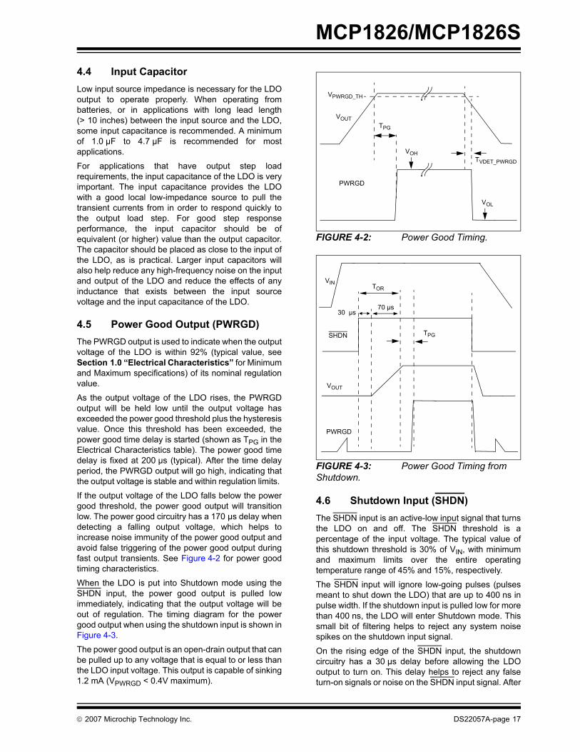
4.5 Power Good Output (PWRGD)The PWRGD output is used to indicate when the outputvoltage of the LDO is within 92% (typical value, seeSection 1.0 “Electrical Characteristics” for Minimumand Maximum specifications) of its nominal regulationvalue.
As the output voltage of the LDO rises, the PWRGDoutput will be held low until the output voltage hasexceeded the power good threshold plus the hysteresisvalue. Once this threshold has been exceeded, thepower good time delay is started (shown as TPG in theElectrical Characteristics table). The power good timedelay is fixed at 200 µs (typical). After the time delayperiod, the PWRGD output will go high, indicating thatthe output voltage is stable and within regulation limits.
If the output voltage of the LDO falls below the powergood threshold, the power good output will transitionlow. The power good circuitry has a 170 µs delay whendetecting a falling output voltage, which helps toincrease noise immunity of the power good output andavoid false triggering of the power good output duringfast output transients. See Figure 4-2 for power goodtiming characteristics.
When the LDO is put into Shutdown mode using theSHDN input, the power good output is pulled lowimmediately, indicating that the output voltage will beout of regulation. The timing diagram for the powergood output when using the shutdown input is shown inFigure 4-3.
The power good output is an open-drain output that canbe pulled up to any voltage that is equal to or less thanthe LDO input voltage. This output is capable of sinking1.2 mA (VPWRGD < 0.4V maximum).
FIGURE 4-2: Power Good Timing.
FIGURE 4-3: Power Good Timing from Shutdown.
4.6 Shutdown Input (SHDN)The SHDN input is an active-low input signal that turnsthe LDO on and off. The SHDN threshold is apercentage of the input voltage. The typical value ofthis shutdown threshold is 30% of VIN, with minimumand maximum limits over the entire operatingtemperature range of 45% and 15%, respectively.
The SHDN input will ignore low-going pulses (pulsesmeant to shut down the LDO) that are up to 400 ns inpulse width. If the shutdown input is pulled low for morethan 400 ns, the LDO will enter Shutdown mode. Thissmall bit of filtering helps to reject any system noisespikes on the shutdown input signal.
On the rising edge of the SHDN input, the shutdowncircuitry has a 30 µs delay before allowing the LDOoutput to turn on. This delay helps to reject any falseturn-on signals or noise on the SHDN input signal. After
TPG
TVDET_PWRGD
VPWRGD_TH
VOUT
PWRGD
VOL
VOH
VIN
SHDN
VOUT
30 µs70 µs
TOR
PWRGD
TPG
© 2007 Microchip Technology Inc. DS22057A-page 17

MCP1826/MCP1826S
the 30 µs delay, the LDO output enters its soft-startperiod as it rises from 0V to its final regulation value. Ifthe SHDN input signal is pulled low during the 30 µsdelay period, the timer will be reset and the delay timewill start over again on the next rising edge of theSHDN input. The total time from the SHDN input goinghigh (turn-on) to the LDO output being in regulation istypically 100 µs. See Figure 4-4 for a timing diagram ofthe SHDN input.FIGURE 4-4: Shutdown Input Timing Diagram.
4.7 Dropout Voltage and Undervoltage Lockout
Dropout voltage is defined as the input-to-outputvoltage differential at which the output voltage drops2% below the nominal value that was measured with aVR + 0.5V differential applied. The MCP1826/MCP1826S LDO has a very low dropout voltagespecification of 300 mV (typical) at 1000 mA of outputcurrent. See Section 1.0 “Electrical Characteristics”for maximum dropout voltage specifications.
The MCP1826/MCP1826S LDO operates across aninput voltage range of 2.3V to 6.0V and incorporatesinput Undervoltage Lockout (UVLO) circuitry that keepsthe LDO output voltage off until the input voltagereaches a minimum of 2.00V (typical) on the risingedge of the input voltage. As the input voltage falls, theLDO output will remain on until the input voltage levelreaches 1.82V (typical).
Since the MCP1826/MCP1826S LDO undervoltagelockout activates at 1.82V as the input voltage is falling,the dropout voltage specification does not apply foroutput voltages that are less than 1.8V.
For high-current applications, voltage drops across thePCB traces must be taken into account. The traceresistances can cause significant voltage dropsbetween the input voltage source and the LDO. Forapplications with input voltages near 2.3V, these PCBtrace voltage drops can sometimes lower the inputvoltage enough to trigger a shutdown due toundervoltage lockout.
4.8 Overtemperature ProtectionThe MCP1826/MCP1826S LDO has temperature-sensing circuitry to prevent the junction temperaturefrom exceeding approximately 150°C. If the LDOjunction temperature does reach 150°C, the LDOoutput will be turned off until the junction temperaturecools to approximately 140°C, at which point the LDOoutput will automatically resume normal operation. Ifthe internal power dissipation continues to beexcessive, the device will again shut off. The junctiontemperature of the die is a function of power dissipa-tion, ambient temperature and package thermalresistance. See Section 5.0 “Application Circuits/Issues” for more information on LDO powerdissipation and junction temperature.
SHDN
VOUT
30 µs70 µs
TOR400 ns (typ)
DS22057A-page 18 © 2007 Microchip Technology Inc.

MCP1826/MCP1826S
5.0 APPLICATION CIRCUITS/ISSUES
5.1 Typical ApplicationThe MCP1826/MCP1826S is used for applications thatrequire high LDO output current and a power goodoutput.
FIGURE 5-1: Typical Application Circuit.
5.1.1 APPLICATION CONDITIONS
5.2 Power Calculations
5.2.1 POWER DISSIPATIONThe internal power dissipation within the MCP1826/MCP1826S is a function of input voltage, outputvoltage, output current and quiescent current.Equation 5-1 can be used to calculate the internalpower dissipation for the LDO.
EQUATION 5-1:
In addition to the LDO pass element power dissipation,there is power dissipation within the MCP1826/MCP1826S as a result of quiescent or ground current.The power dissipation as a result of the ground currentcan be calculated using the following equation:
EQUATION 5-2:
The total power dissipated within the MCP1826/MCP1826S is the sum of the power dissipated in theLDO pass device and the P(IGND) term. Because of theCMOS construction, the typical IGND for the MCP1826/MCP1826S is 120 µA. Operating at a maximum VIN of3.465V results in a power dissipation of 0.12 milli-Wattsfor a 2.5V output. For most applications, this is smallcompared to the LDO pass device power dissipationand can be neglected.
The maximum continuous operating junctiontemperature specified for the MCP1826/MCP1826S is+125°C. To estimate the internal junction temperatureof the MCP1826/MCP1826S, the total internal powerdissipation is multiplied by the thermal resistance fromjunction to ambient (RθJA) of the device. The thermalresistance from junction to ambient for the TO-220-5package is estimated at 29.3°C/W.
EQUATION 5-3:
Package Type = TO-220-5Input Voltage Range = 3.3V ± 5%
VIN maximum = 3.465VVIN minimum = 3.135V
VDROPOUT (max) = 0.350VVOUT (typical) = 2.5V
IOUT = 1000 mA maximumPDISS (typical) = 0.965W
Temperature Rise = 28.27°C
10 µF
VOUT = 2.5V @ 1000 mA
R1C210 kΩ
PWRGD
SHDN
GND
2
4.7 µF
OnOff
C1
MCP1826-2.5
1 3 4 5
3.3V VIN
PLDO VIN MAX )( ) VOUT MIN( )–( ) IOUT MAX )( )×=
Where:
PLDO = LDO Pass device internal power dissipation
VIN(MAX) = Maximum input voltageVOUT(MIN) = LDO minimum output voltage
PI GND( ) VIN MAX( ) IVIN×=Where:
PI(GND = Power dissipation due to the quiescent current of the LDO
VIN(MAX) = Maximum input voltageIVIN = Current flowing in the VIN pin
with no LDO output current (LDO quiescent current)
TJ MAX( ) PTOTAL RθJA× TAMAX+=
TJ(MAX) = Maximum continuous junctiontemperature
PTOTAL = Total device power dissipationRθJA = Thermal resistance from junction to
ambientTAMAX = Maximum ambient temperature
© 2007 Microchip Technology Inc. DS22057A-page 19

MCP1826/MCP1826S
The maximum power dissipation capability for apackage can be calculated given the junction-to-ambient thermal resistance and the maximum ambienttemperature for the application. Equation 5-4 can beused to determine the package maximum internalpower dissipation.EQUATION 5-4:
EQUATION 5-5:
EQUATION 5-6:
5.3 Typical ApplicationInternal power dissipation, junction temperature rise,junction temperature and maximum power dissipationis calculated in the following example. The powerdissipation as a result of ground current is smallenough to be neglected.
5.3.1 POWER DISSIPATION EXAMPLE
5.3.1.1 Device Junction Temperature RiseThe internal junction temperature rise is a function ofinternal power dissipation and the thermal resistancefrom junction-to-ambient for the application. Thethermal resistance from junction-to-ambient (RθJA) isderived from EIA/JEDEC standards for measuringthermal resistance. The EIA/JEDEC specification isJESD51. The standard describes the test method andboard specifications for measuring the thermalresistance from junction to ambient. The actual thermalresistance for a particular application can varydepending on many factors such as copper area andthickness. Refer to AN792, “A Method to DetermineHow Much Power a SOT23 Can Dissipate in an Appli-cation” (DS00792), for more information regarding thissubject.
PD MAX( )TJ MAX( ) TA MAX( )–( )
RθJA---------------------------------------------------=
PD(MAX) = Maximum device power dissipationTJ(MAX) = maximum continuous junction
temperatureTA(MAX) = maximum ambient temperature
RθJA = Thermal resistance from junction-to-ambient
TJ RISE( ) PD MAX( ) RθJA×=
TJ(RISE) = Rise in device junction temperature over the ambient temperature
PD(MAX) = Maximum device power dissipationRθJA = Thermal resistance from junction-to-
ambient
TJ TJ RISE( ) TA+=
TJ = Junction temperatureTJ(RISE) = Rise in device junction temperature
over the ambient temperatureTA = Ambient temperature
PackagePackage Type = TO-220-5Input Voltage
VIN = 3.3V ± 5%LDO Output Voltage and Current
VOUT = 2.5VIOUT = 1000 mA
Maximum Ambient TemperatureTA(MAX) = 60°C
Internal Power DissipationPLDO(MAX) = (VIN(MAX) – VOUT(MIN)) x IOUT(MAX)
PLDO = ((3.3V x 1.05) – (2.5V x 0.975)) x 1000 mA
PLDO = 1.028 Watts
TJ(RISE) = PTOTAL x RθJATJRISE = 1.028 W x 29.3°C/WTJRISE = 30.12°C
DS22057A-page 20 © 2007 Microchip Technology Inc.

MCP1826/MCP1826S
5.3.1.2 Junction Temperature EstimateTo estimate the internal junction temperature, thecalculated temperature rise is added to the ambient oroffset temperature. For this example, the worst-casejunction temperature is estimated below:5.3.1.3 Maximum Package Power Dissipation at 60°C Ambient Temperature
From this table, you can see the difference in maximumallowable power dissipation between the TO-220-5package and the DDPAK-5 package.
TJ = TJRISE + TA(MAX)TJ = 30.12°C + 60.0°CTJ = 90.12°C
TO-220-5 (29.3° C/W RθJA):PD(MAX) = (125°C – 60°C) / 29.3°C/WPD(MAX) = 2.218W
DDPAK-5 (31.2°C/Watt RθJA):PD(MAX) = (125°C – 60°C)/ 31.2°C/WPD(MAX) = 2.083W
© 2007 Microchip Technology Inc. DS22057A-page 21

MCP1826/MCP1826S
6.0 PACKAGING INFORMATION
6.1 Package Marking InformationExample:
Legend: XX...X Customer-specific informationY Year code (last digit of calendar year)YY Year code (last 2 digits of calendar year)WW Week code (week of January 1 is week ‘01’)NNN Alphanumeric traceability code Pb-free JEDEC designator for Matte Tin (Sn)* This package is Pb-free. The Pb-free JEDEC designator ( )
can be found on the outer packaging for this package.
Note: In the event the full Microchip part number cannot be marked on one line, it willbe carried over to the next line, thus limiting the number of availablecharacters for customer-specific information.
3e
3e
3-Lead DDPAK (MCP1826S)
3-Lead TO-220 (MCP1826S)
1 2 3
1 2 3
XXXXXXXXXXXXXXXXXXYYWWNNN
XXXXXXXXXXXXXXXXXXYYWWNNN
1 2 3
MCP1826S0.8EEB^^0730256
1 2 3
MCP1826S12EAB^^0730256
Example:
3e
3e
3-Lead SOT-223 (MCP1826S)
XXXXXXXXXXYYWW
NNN
Example:
1826S08EDB0730
256
DS22057A-page 22 © 2007 Microchip Technology Inc.

MCP1826/MCP1826S
Package Marking Information (Continued)Legend: XX...X Customer-specific informationY Year code (last digit of calendar year)YY Year code (last 2 digits of calendar year)WW Week code (week of January 1 is week ‘01’)NNN Alphanumeric traceability code Pb-free JEDEC designator for Matte Tin (Sn)* This package is Pb-free. The Pb-free JEDEC designator ( )
can be found on the outer packaging for this package.
Note: In the event the full Microchip part number cannot be marked on one line, it willbe carried over to the next line, thus limiting the number of availablecharacters for customer-specific information.
3e
3e
5-Lead DDPAK (MCP1826)
5-Lead TO-220 (MCP1826)
1 2 3 4 5
1 2 3 4 5
XXXXXXXXXXXXXXXXXXYYWWNNN
XXXXXXXXXXXXXXXXXXYYWWNNN
1 2 3 4 5
MCP18261.0EET^^0730256
1 2 3 4 5
MCP182608EAT^^0730256
Example:
Example:
3e
3e
5-Lead SOT-223 (MCP1826)
XXXXXXXXXXYYWW
NNN
Example:
1826-08EDC0730
256
© 2007 Microchip Technology Inc. DS22057A-page 23
MCP1826/MCP1826S
DS22057A-page 24 © 2007 Microchip Technology Inc.

MCP1826/MCP1826S
© 2007 Microchip Technology Inc. DS22057A-page 25

MCP1826/MCP1826S
DS22057A-page 26 © 2007 Microchip Technology Inc.

MCP1826/MCP1826S
© 2007 Microchip Technology Inc. DS22057A-page 27

MCP1826/MCP1826S
DS22057A-page 28 © 2007 Microchip Technology Inc.

MCP1826/MCP1826S
© 2007 Microchip Technology Inc. DS22057A-page 29
MCP1826/MCP1826S
NOTES:DS22057A-page 30 © 2007 Microchip Technology Inc.

MCP1826/MCP1826S
APPENDIX A: REVISION HISTORY
Revision A (August 2007)• Original Release of this Document.
© 2007 Microchip Technology Inc. DS22057A-page 31

MCP1826/MCP1826S
NOTES:DS22057A-page 32 © 2007 Microchip Technology Inc.

MCP1826/MCP1826S
PRODUCT IDENTIFICATION SYSTEMTo order or obtain information, e.g., on pricing or delivery, refer to the factory or the listed sales office.
Device: MCP1826: 1000 mA Low Dropout Regulator
MCP1826T: 1000 mA Low Dropout RegulatorTape and Reel
MCP1826S: 1000 mA Low Dropout RegulatorMCP1826ST: 1000 mA Low Dropout Regulator
Tape and Reel
Output Voltage *: 08 = 0.8V “Standard”12 = 1.2V “Standard”18 = 1.8V “Standard”25 = 2.5V “Standard”30 = 3.0V “Standard”33 = 3.3V “Standard”50 = 5.0V “Standard”ADJ = Adjustable Output Voltage ** (MCP1826 only)
*Contact factory for other output voltage options** When ADJ is used, the “extra feature code” and “tolerance” columns do not apply. Refer to examples.
Extra Feature Code: 0 = Fixed
Tolerance: 2 = 2.0% (Standard)
Temperature: E = -40°C to +125°C
Package Type: AB = Plastic Transistor Outline, TO-220, 3-leadAT = Plastic Transistor Outline, TO-220, 5-leadDB = Plastic Transistor Outline, SOT-223, 3-leadDC = Plastic Transistor Outline, SOT-223, 5-leadEB = Plastic, DDPAK, 3-leadET = Plastic, DDPAK, 5-lead
Note: ADJ (Adjustable) only available in 5-lead version.
PART NO. XXX
Output FeatureCode
DeviceVoltage
X
Tolerance
X/
Temp.
XX
Package
Examples:a) MCP1826-0802E/XX: 0.8V LDO Regulatorb) MCP1826-1002E/XX: 1.0V LDO Regulatorc) MCP1826-1202E/XX: 1.2V LDO Regulatord) MCP1826-1802E/XX 1.8V LDO Regulatore) MCP1826-2502EXX: 25V LDO Regulatorf) MCP1826-3002E/XX: 3.0V LDO Regulatorg) MCP1826-3302E/XX 3.3V LDO Regulatorh) MCP1826-5002E/XX: 5.0V LDO Regulatori) MCP1826-ADJE/XX: ADJ LDO Regulator
a) MCP1826S-0802E/XX:0.8V LDO Regulatorb) MCP1826S-1002E/XX:1.0V LDO Regulatorc) MCP1826S-1202E/XX 1.2V LDO Regulatord) MCP1826S-1802E/XX 1.8V LDO Regulatore) MCP1826S-2502E/XX 2.5V LDO Regulatorf) MCP1826S-2502E/XX 3.0V LDO Regulatorg) MCP1826S-3302E/XX 3.3V LDO Regulatorh) MCP1826S-5002E/XX 5.0V LDO Regulator
XX = AB for 3LD TO-220 package= AT for 5LD TO-220 package= DB for 3LD SOT-223 package= DC for 5LD SOT-223 package= EB for 3LD DDPAK package= ET for 5LD DDPAK package
© 2007 Microchip Technology Inc. DS22057A-page 33

MCP1826/MCP1826S
NOTES:DS22057A-page 34 © 2007 Microchip Technology Inc.

Note the following details of the code protection feature on Microchip devices:• Microchip products meet the specification contained in their particular Microchip Data Sheet.
• Microchip believes that its family of products is one of the most secure families of its kind on the market today, when used in the intended manner and under normal conditions.
• There are dishonest and possibly illegal methods used to breach the code protection feature. All of these methods, to our knowledge, require using the Microchip products in a manner outside the operating specifications contained in Microchip’s Data Sheets. Most likely, the person doing so is engaged in theft of intellectual property.
• Microchip is willing to work with the customer who is concerned about the integrity of their code.
• Neither Microchip nor any other semiconductor manufacturer can guarantee the security of their code. Code protection does not mean that we are guaranteeing the product as “unbreakable.”
Code protection is constantly evolving. We at Microchip are committed to continuously improving the code protection features of ourproducts. Attempts to break Microchip’s code protection feature may be a violation of the Digital Millennium Copyright Act. If such actsallow unauthorized access to your software or other copyrighted work, you may have a right to sue for relief under that Act.
Information contained in this publication regarding deviceapplications and the like is provided only for your convenienceand may be superseded by updates. It is your responsibility toensure that your application meets with your specifications.MICROCHIP MAKES NO REPRESENTATIONS ORWARRANTIES OF ANY KIND WHETHER EXPRESS ORIMPLIED, WRITTEN OR ORAL, STATUTORY OROTHERWISE, RELATED TO THE INFORMATION,INCLUDING BUT NOT LIMITED TO ITS CONDITION,QUALITY, PERFORMANCE, MERCHANTABILITY ORFITNESS FOR PURPOSE. Microchip disclaims all liabilityarising from this information and its use. Use of Microchipdevices in life support and/or safety applications is entirely atthe buyer’s risk, and the buyer agrees to defend, indemnify andhold harmless Microchip from any and all damages, claims,suits, or expenses resulting from such use. No licenses areconveyed, implicitly or otherwise, under any Microchipintellectual property rights.
© 2007 Microchip Technology Inc.
Trademarks
The Microchip name and logo, the Microchip logo, Accuron, dsPIC, KEELOQ, KEELOQ logo, microID, MPLAB, PIC, PICmicro, PICSTART, PRO MATE, rfPIC and SmartShunt are registered trademarks of Microchip Technology Incorporated in the U.S.A. and other countries.
AmpLab, FilterLab, Linear Active Thermistor, Migratable Memory, MXDEV, MXLAB, SEEVAL, SmartSensor and The Embedded Control Solutions Company are registered trademarks of Microchip Technology Incorporated in the U.S.A.
Analog-for-the-Digital Age, Application Maestro, CodeGuard, dsPICDEM, dsPICDEM.net, dsPICworks, dsSPEAK, ECAN, ECONOMONITOR, FanSense, FlexROM, fuzzyLAB, In-Circuit Serial Programming, ICSP, ICEPIC, Mindi, MiWi, MPASM, MPLAB Certified logo, MPLIB, MPLINK, PICkit, PICDEM, PICDEM.net, PICLAB, PICtail, PowerCal, PowerInfo, PowerMate, PowerTool, REAL ICE, rfLAB, Select Mode, Smart Serial, SmartTel, Total Endurance, UNI/O, WiperLock and ZENA are trademarks of Microchip Technology Incorporated in the U.S.A. and other countries.
SQTP is a service mark of Microchip Technology Incorporated in the U.S.A.
All other trademarks mentioned herein are property of their respective companies.
© 2007, Microchip Technology Incorporated, Printed in the U.S.A., All Rights Reserved.
Printed on recycled paper.
DS22057A-page 35
Microchip received ISO/TS-16949:2002 certification for its worldwide headquarters, design and wafer fabrication facilities in Chandler and Tempe, Arizona; Gresham, Oregon and design centers in California and India. The Company’s quality system processes and procedures are for its PIC® MCUs and dsPIC® DSCs, KEELOQ® code hopping devices, Serial EEPROMs, microperipherals, nonvolatile memory and analog products. In addition, Microchip’s quality system for the design and manufacture of development systems is ISO 9001:2000 certified.
DS22057A-page 36 © 2007 Microchip Technology Inc.
AMERICASCorporate Office2355 West Chandler Blvd.Chandler, AZ 85224-6199Tel: 480-792-7200 Fax: 480-792-7277Technical Support: http://support.microchip.comWeb Address: www.microchip.comAtlantaDuluth, GA Tel: 678-957-9614 Fax: 678-957-1455BostonWestborough, MA Tel: 774-760-0087 Fax: 774-760-0088ChicagoItasca, IL Tel: 630-285-0071 Fax: 630-285-0075DallasAddison, TX Tel: 972-818-7423 Fax: 972-818-2924DetroitFarmington Hills, MI Tel: 248-538-2250Fax: 248-538-2260KokomoKokomo, IN Tel: 765-864-8360Fax: 765-864-8387Los AngelesMission Viejo, CA Tel: 949-462-9523 Fax: 949-462-9608Santa ClaraSanta Clara, CA Tel: 408-961-6444Fax: 408-961-6445TorontoMississauga, Ontario, CanadaTel: 905-673-0699 Fax: 905-673-6509
ASIA/PACIFICAsia Pacific OfficeSuites 3707-14, 37th FloorTower 6, The GatewayHarbour City, KowloonHong KongTel: 852-2401-1200Fax: 852-2401-3431Australia - SydneyTel: 61-2-9868-6733Fax: 61-2-9868-6755China - BeijingTel: 86-10-8528-2100 Fax: 86-10-8528-2104China - ChengduTel: 86-28-8665-5511Fax: 86-28-8665-7889China - FuzhouTel: 86-591-8750-3506 Fax: 86-591-8750-3521China - Hong Kong SARTel: 852-2401-1200 Fax: 852-2401-3431China - QingdaoTel: 86-532-8502-7355Fax: 86-532-8502-7205China - ShanghaiTel: 86-21-5407-5533 Fax: 86-21-5407-5066China - ShenyangTel: 86-24-2334-2829Fax: 86-24-2334-2393China - ShenzhenTel: 86-755-8203-2660 Fax: 86-755-8203-1760China - ShundeTel: 86-757-2839-5507 Fax: 86-757-2839-5571China - WuhanTel: 86-27-5980-5300Fax: 86-27-5980-5118China - XianTel: 86-29-8833-7252Fax: 86-29-8833-7256
ASIA/PACIFICIndia - BangaloreTel: 91-80-4182-8400 Fax: 91-80-4182-8422India - New DelhiTel: 91-11-4160-8631Fax: 91-11-4160-8632India - PuneTel: 91-20-2566-1512Fax: 91-20-2566-1513Japan - YokohamaTel: 81-45-471- 6166 Fax: 81-45-471-6122Korea - DaeguTel: 82-53-744-4301Fax: 82-53-744-4302Korea - SeoulTel: 82-2-554-7200Fax: 82-2-558-5932 or 82-2-558-5934Malaysia - PenangTel: 60-4-646-8870Fax: 60-4-646-5086Philippines - ManilaTel: 63-2-634-9065Fax: 63-2-634-9069SingaporeTel: 65-6334-8870Fax: 65-6334-8850Taiwan - Hsin ChuTel: 886-3-572-9526Fax: 886-3-572-6459Taiwan - KaohsiungTel: 886-7-536-4818Fax: 886-7-536-4803Taiwan - TaipeiTel: 886-2-2500-6610 Fax: 886-2-2508-0102Thailand - BangkokTel: 66-2-694-1351Fax: 66-2-694-1350
EUROPEAustria - WelsTel: 43-7242-2244-39Fax: 43-7242-2244-393Denmark - CopenhagenTel: 45-4450-2828 Fax: 45-4485-2829France - ParisTel: 33-1-69-53-63-20 Fax: 33-1-69-30-90-79Germany - MunichTel: 49-89-627-144-0 Fax: 49-89-627-144-44Italy - Milan Tel: 39-0331-742611 Fax: 39-0331-466781Netherlands - DrunenTel: 31-416-690399 Fax: 31-416-690340Spain - MadridTel: 34-91-708-08-90Fax: 34-91-708-08-91UK - WokinghamTel: 44-118-921-5869Fax: 44-118-921-5820
WORLDWIDE SALES AND SERVICE
06/25/07