Embed Size (px)
Citation preview

Number 3, Autumn 2013
McKinsey on Semiconductors
McK
insey on Semiconductors
Num
ber 3, Autum
n 2013
When software meets hardware: Excellence in embedded-software development
The hunt for revenue: A case for further granularity
Bringing energy efficiency to the fab
Exploring SynBio’s potential for semiconductor players
42 46 52 56Winning share in automotive semiconductors
34
Value creation remains a challenge
16Moore’s law: Repeal or renewal?
4The potential shake-up in semiconductor manufacturing business models
What happens when chip-design complexity outpaces development productivity?
19 24

McKinsey on Semiconductors is
written by experts and practitioners
in McKinsey & Company’s
semiconductors practice along with
other McKinsey colleagues.
To send comments or request copies,
e-mail us: McKinsey_on_
Editorial Board: Harald Bauer, Mark
Patel, Nick Santhanam, Florian Weig,
and Bill Wiseman
Editor: Brendan Hasenstab
Art Direction and Design: Cary Shoda
Managing Editors: Michael T. Borruso,
Venetia Simcock
Editorial Production:
Elizabeth Brown, Heather Byer, Torea
Frey, Shahnaz Islam, Ashwati Michael,
John C. Sanchez, Sneha Vats
Cover illustration by Harry Campbell
McKinsey Practice Publications
Editor-in-Chief: Lucia Rahilly
Executive Editors: Allan Gold,
Mark Staples
Copyright © 2013 McKinsey &
Company. All rights reserved.
This publication is not intended
to be used as the basis for trading in
the shares of any company or
for undertaking any other complex or
significant financial transaction
without consulting with appropriate
professional advisers.
No part of this publication may be
copied or redistributed in any
form without the prior written consent
of McKinsey & Company.

1
McKinsey on SemiconductorsNumber 3, Autumn 2013
4Moore’s law:
Repeal or renewal?
Economic conditions could invalidate Moore’s law after decades as the semiconductor industry’s innova- tion touchstone. The impact on chip makers and others could be dramatic.
19The potential shake-
up in semiconductor
manufacturing
business models
The mobile revolution gave a lift to global semiconductor sales, partially enabled by the fabless-foundry model, which allowed designers and manufacturers to bring powerful and inno- vative mobile chips to market rapidly. But the model is facing new pressures.
2Introduction
16Value creation
remains a challenge
New research offers insights into what creates value—and what doesn’t—in the semi-conductor business.
24What happens when
chip-design
complexity outpaces
development
productivity?
Among the forces reshap-ing the semiconductor industry, few are more important than R&D productivity’s inability to keep pace with the challenges of product development. However, there are steps com-panies can take to close the gap.
46The hunt for revenue:
A case for further
granularity
Uncovering additional market opportunities can be a critical driver of growth in today’s semi-conductor markets. But how should executive and managers broach the exercise? Three approaches can help ensure that mar- kets are assessed at the appropriate level of granularity.
56Exploring SynBio’s
potential for
semiconductor
players
Synthetic biology has the potential to disrupt trillion-dollar industries, and semiconductor players could help make it happen.
34Winning share in
automotive
semiconductors
From self-parking cars to anticipatory braking, semiconductors have been important to automo- tive innovations in the past decade. And automotive-semiconductor revenues expanded quicker than those of both the automotive and broader semiconductor industries—but will this continue? Where will innovation come from?
42When software
meets hardware:
Excellence in embedded-
software development
Embedded software has become essential to the success of most types of new semiconductors. Yet some semiconductor companies still resist the idea that they are selling not just hardware but also, increasingly, software. A blueprint can help in better integrating them in your organization.
52Bringing energy
efficiency to the fab
Large semiconductor fabs use as much as 100 megawatt-hours of power each hour, which is more than many auto-motive plants or oil refineries do. In some markets, electricity can account for up to 30 percent of fab operating costs, so there is significant opportunity in rethinking power usage and management.

2
Welcome to the third edition of McKinsey on
Semiconductors. The articles in this publication
reflect an industry in transition—one that
continues to evolve in response to challenges
faced in technology, business models,
and operations.
We kick off the issue with one of the industry’s
biggest challenges: planning for the uncertainties
surrounding the future of Moore’s law, a
principle that has guided semiconductor players
for five decades. From there, we move on to
a discussion of value creation in a sector where
consistent returns to shareholders have
been elusive, and then to mobile’s impact on
the industry and the pressures the fabless-
foundry model is currently facing.
The next article focuses on the challenges and
opportunities in design, as complexity increases
IntroductionHarald Bauer,
Mark Patel,
Nick Santhanam,
Florian Weig, and
Bill Wiseman
© Christian Carroll/Getty Images

3
and the need for effective design methodol-
ogies becomes paramount. The authors suggest
some solutions that can help close this gap.
The second half of the publication points
to some of the possible paths forward. What
opportunities lie ahead for semiconductor
companies in the automotive market? How can
players better coordinate the development
and integration of embedded software? Where
can the industry find hidden pockets of
revenue, and what new approaches can be taken
to address the rising cost of energy? We
conclude with a perspective on adjacent-market
opportunities in the field of synthetic biology as
this potentially disruptive field matures.
McKinsey on Semiconductors is written,
first and foremost, for industry executives who
are passionate about their organizations’
development and success. We hope that you
find these perspectives helpful as you chart your
own course.
Florian Weig
Director
Harald Bauer
Director
Mark Patel
Principal
Bill Wiseman
Principal
Nick Santhanam
Director

4
Harald Bauer,
Jan Veira, and
Florian Weig
Moore’s law: Repeal or renewal?
The global semiconductor industry has recorded impressive achievements since 1965, when Intel cofounder Gordon Moore published the observation that would become the industry’s touchstone. Moore’s law states that the number of transistors on integrated circuits doubles every two years, and for the past four decades it has set the pace for progress in the semiconductor industry. The positive by-products of the constant scaling down that Moore’s law predicts include simultaneous cost declines, made possible by fitting more transistors per area onto silicon chips, and performance increases with regard to speed, compactness, and power consumption. As a result, semiconductor-enabled products today
Economic conditions could invalidate Moore’s law after decades as the
semiconductor industry’s innovation touchstone. The impact on chip makers
and others could be dramatic.
play integral roles in virtually every aspect of modern life.
In this article, we will examine the technologies that aim to extend the life of Moore’s law and model their impact on four likely future scenarios for the industry. Obviously, there are many factors in play, but we believe the economics of continued advances in performance could eventually disrupt the companies competing in the business today.
How Moore’s law drives
the global economy
Adherence to Moore’s law has led to continuously falling semiconductor prices. Per-bit prices of
Harry Campbell

5
dynamic random-access memory chips, for example, have fallen by as much as 30 to 35 percent a year for several decades.
As a result, Moore’s law has swept much of the modern world along with it. Some estimates ascribe up to 40 percent of the global productivity growth achieved during the last two decades to the expansion of information and communication technologies made possible by semiconductor performance and cost improvements.
Enabled by constant technological innovation
The law retains its predictive power because of constant improvements in production technology, which are driven by the industry’s “global semiconductor road maps.” These describe the progress required for the continuation of Moore’s law. This cycle of innovation began with the production of the first semiconductor circuits, then continued unabated with the intro- duction of clean-room technology in the 1970s, and it is sustained by today’s fabrication
Exhibit 1 Four kinds of innovation should drive growth in semiconductors.
MoSemiconductors 2013Moore’s LawExhibit 1 of 5
Description Examples Expected timeline Key challenges
• Short to midterm• Extreme-ultraviolet (EUV) lithography
• Multicore system-on-a-chip (SOC) architectures
• Large financial investment needed (eg, EUV)
• Some technologies are not yet available or are close to physical limits
Further development of CMOS1 technologies (silicon based) to increase performance and reduce costs via geometrical and design scaling
1 More Moore (scaling)
• Ongoing for 300mm• Midterm for 450mm
• Shift of analog and power products to 300mm
• Large financial investment necessary
Increase productivity by introducing larger wafer size: 450 millimeters (mm) for leading edge, 300mm for lagging edge
2 Wafer-size increases (maximize productivity)
• Short to midterm• Integration of power management and wireless baseband in application processor
• Development of new technologies needed
• New capabilities and skills needed
Added functionality (eg, interfaces, nondigital components) in package (SIP2) or chip (SOC), not scaling with Moore’s law
3 More than Moore (functional diversification)
• Mid- to long term• Spintronics• Carbon nanotubes• Quantum computing
• Technologies are in early stages of development
• Commercial scalability of technologies pending
Use of new technologies and materials for information processing and switching
4 Beyond CMOS (new technologies)
1 Complementary metal-oxide semiconductor.2System in a package.
Source: International Technology Roadmap for Semiconductors; ObservatoryNANO; McKinsey analysis

6 McKinsey on Semiconductors Autumn 2013
plants, or fabs, often considered the most advanced production facilities ever built.
Whether Moore’s law will apply in the future depends on technological developments, with one of the most critical areas of innovation involving lithography tools, especially extreme-ultraviolet (EUV) lithography technology. EUV uses short-wavelength light sources to scale feature sizes below 10 nanometers (nm). (See deep dive, “Innovations in lithography and EUV.”)
However, lithography is not the only potential source of productivity improvements in semiconductor manufacturing; other cost-saving and performance-improvement methods are also in play. Companies are working toward larger semiconductor wafer sizes (see deep dive, “Transitioning to 450mm wafers”) and will likely introduce new materials into chip designs. In fact, we see four types of innovation with the potential to propel semiconductor industry growth and performance improvements (Exhibit 1).
From a technological perspective, these innovations make progress based on Moore’s law—smaller feature sizes and improved performance—a viable assumption for at least the next five to ten years. Our analysis of leading-edge chip technologies also supports
a continuation of Moore’s law from a demand perspective. While McKinsey research suggests that the number of leading-edge market segments will decline, those remaining, such as in mobile applications, should grow strongly, providing sufficient demand for high-end technologies.
Will economics doom Moore’s law?
While the trends appear positive for the continued applicability of Moore’s law from a techno- logical perspective, economics could prove its undoing. Recent developments indicate that the economics of continued miniaturization could break down as cost-per-transistor reductions flatten for nodes with feature sizes below 28nm.
The culprits are the rapidly rising costs associated with technology development and the capital equipment needed to produce next-generation nodes. These cost increases are largely driven by the extreme investments required for leading-edge lithography technologies and the process complexity inherent in the double-patterning and multipatterning approaches used for nodes at 32nm and 28nm and below.
A McKinsey analysis shows that moving from 32nm to 22nm nodes on 300-millimeter (mm) wafers causes typical fabrication costs to grow by roughly 40 percent. It also boosts the
While the trends appear positive for the continued applicability of Moore’s law from a technological perspective, economics could prove its undoing.

7
costs associated with process development by about 45 percent and with chip design by up to 50 percent. These dramatic increases will lead to process-development costs that exceed $1 billion for nodes below 20nm. In addition, the state-of-the art fabs needed to produce them will likely cost $10 billion or more. As a result, the number of companies capable of financing next-generation nodes and fabs will likely dwindle.
Exploring four potential scenarios
When assessing the industry’s future, leaders may find it helpful to consider four scenarios reflecting uncertainties about the viability of tomorrow’s semiconductor cost and performance improvements (Exhibit 2).
Each scenario reflects different assumptions regarding the sources of differentiating innovation, the potential for commoditization, and shifts
Exhibit 2 Several scenarios offer snapshots of the industry’s potential evolution.
MoSemiconductors 2013Moore’s LawExhibit 2 of 5
Cost improvements through node scaling1
Performance2 increases through node scaling3
I Moore’s law continues
• Node scaling continues • Leading-edge segments continue to consolidate to absorb capital expenditure • End-market demand is stable
III Cost improvements end but performance increases continue4
• Node scaling continues for segments that value performance5
• Leading-edge segments continue to consolidate to absorb capital expenditure • Demand is at risk due to a lack of continuous cost decreases
Continue
Continue
Stop
Stop
II Performance increases end but cost improvements continue4
• Node scaling continues • Leading-edge segments continue to consolidate to absorb capital expenditure • Demand is at risk due to a lack of continuous performance increases
IV Moore’s law ends
• Industry becomes commoditized • Lagging-edge players have a chance to catch up • Demand is disrupted due to negligible improvements in cost and performance
1 Additional cost improvements (eg, due to wafer-size increases, yield improvements, and equipment effectiveness) are independent of this.
2Increase of absolute or relative performance (ie, performance per power consumption).3Additional performance increases (eg, due to “more than Moore” effects and software) are independent of this.
4These scenarios can only be transition stages for the industry; in the long term, they do not offer a stable equilibrium from an economic perspective.
5Examples include central processing units or wireless.
Moore’s law: Repeal or renewal?

8 McKinsey on Semiconductors Autumn 2013
in customer demand; each also takes into account the industry’s dynamics, return on invested capital (ROIC), and ability to capture value (Exhibit 3). Take, for example, the scenario in which cost improvements
end but performance increases continue. Node scaling would continue, but only for players that seek higher performance and are willing to pay for it. Industry participants would see little increased risk of commoditization, but
Exhibit 3 Different assumptions underlie each scenario.
MoSemiconductors 2013Moore’s LawExhibit 3 of 5
I Moore’s law continues
II Performance increases end
III Cost improvements end
IV Moore’s law ends
• Node scaling for cost and performance
• No, node scaling differentiates via performance
• Improved because of market power of a few players and stable demand
• No
• Node scaling for cost
• Other innovations1 for performance
• Large players aim to dominate commodity market via scale effects
• Lagging-edge players have the ability to catch up
• Improving because there is no need for capital expenditure/R&D spending for new nodes
• Highly at risk given commoditization and demand disruption
• Node scaling for performance
• Other innovations1 for cost
Source for differentiating innovation
Increased commoditization risk
Industry dynamics
Increased risk for end-customer demand2
Return on invested capital in industry
Industry ability to capture value
• Yes, lack of “automatic” performance differentiation
• No, node scaling differentiates via performance
• Yes, given lack of continuous performance increases
• Yes, given lack of cost declines
• Other innovations1 for cost and performance
• Yes, lack of “automatic” performance differentiation
• Yes, given lack of cost and performance improvements
Oligopoly, with few remaining leading-edge players with their own fabs and consolidation of fabless players given exploding capital costs
Declining because of exploding capital required for smaller nodes
At risk from demand disruption
1 Examples include innovative chip design and software.2Does not consider end-customer demand disruptions happening independent of a semiconductor-related “trigger” (eg, lack of end-customer demand for better smartphone performance).

9Moore’s law: Repeal or renewal?
Lithography has enabled the semiconductor
industry to achieve continually smaller nodes for
the past 25 years. As argon fluoride (ArF)
immersion lithography reached its critical limit, the
industry introduced double and multipatterning,
which made scaling to 32 nanometers (nm) and
below possible. Double and multipatterning
enables further node scaling by overlaying several
lithography steps to enhance feature density.
Multipatterning was first used for 32nm and 28nm
nodes and could enable the industry to scale
nodes down to 14nm and even smaller.
However, complex lithography approaches
like multipatterning carry a high price. As a result,
the percentage of corporate capital spending
allocated to lithography will rise to an estimated
24 percent for 2010–15 from an average of
less than 20 percent in 2000–05. What’s more,
per-layer costs and accompanying complexity
levels are exploding for double and multipatterning.
For instance, moving to 22nm with double
patterning, from 32nm ArF immersion without it,
could double the number of process steps
per layer, depending on the product, and raise
costs per layer by 50 percent. This trend
could lead to a breakdown of Moore’s law as the
cost advantages that traditionally come with
scaling disappear.
There is, however, a technological innovation that
could overcome these challenges, extreme-
ultraviolet (EUV) lithography. This technology uses
new light sources with a wavelength of 13.5nm.
The industry expects EUV to reduce per-layer costs
because fewer steps will be needed compared
with double or multipatterning. Double patterning,
for example, can require more than 30 pattern-
ing steps per layer, but EUV will likely need just 10,
with resulting cost-per-layer advantages
estimated to be as high as 35 percent. In addition,
EUV promises to deliver node sizes of 10nm
and below because of the smaller wavelength of
the lithography tools.
EUV is not production ready because of unsolved
technical issues, including the lack of a light
source with sufficient power and stability. However,
recent developments suggest the industry is
moving to make EUV commercially feasible. For
instance, ASML, an EUV tool producer,
acquired Cymer, which is working on the light-
source issue. Additionally, Intel, Samsung,
and Taiwan Semiconductor Manufacturing
Company have coinvested in ASML to
fund EUV development.
A McKinsey survey on the semiconductor business
climate index conducted in the fourth quarter
of 2012 found that industry experts expect at-scale
EUV production to become possible by 2015
or 2016.1 1 McKinsey’s survey is a quarterly survey of semiconductor-industry executives to measure the business climate and inquire about selected topics. Results are available only to survey participants.
DEEPDIVEInnovations in lithography and EUV

10 McKinsey on Semiconductors Autumn 2013
Exhibit 4 Implications vary depending on a player’s place in the value chain.
MoSemiconductors 2013Moore’s LawExhibit 4 of 5
I Moore’s law continues
II Performance increases end
III Cost improvements end
IV Moore’s law ends
• Consolidation to secure scale effects
• Lagging-edge players can catch up
• Niche players can succeed via cost/performance innovations1
• Extreme cost pressure
• Lagging-edge players can catch up
• Consolidation to secure scale effects
• Lagging-edge players can catch up
• Niche players can succeed with cost/performance innovations1
• Extreme cost pressure
• Equipment becomes a commodity
• Consolidation to secure scale effects
Integrated device manufacturers (IDMs)
Foundry
Equipment manufacturers
Fabless
• Niche players can succeed with performance innovations1
• Niche players can succeed with performance innovations1
• Memory exits leading edge and becomes commoditized
• Niche players can succeed with cost innovations1
• Niche players can succeed with cost innovations1
• Niche players can succeed with cost innovations1
Significant consolidation: oligopoly of a few remaining players; the rest exit or go fabless
1 Other than scaling; examples include chip design or software.2As an “industry foundation,” for instance.
Remaining players broaden portfolio to spread capital expenditure over broader revenue base
Further consolidation, with few remaining players
Consolidation of players to enable required funding for leading-edge technologies
Cooperation with foundries (“virtual IDMs”) and intellectual-property/electronic-design-automation players increases to manage rising complexity
Certain customers integrate downstream into a fabless business model to control complexity and ensure success of critical components
Support from remaining IDMs/foundries increases (up to shared ownership2) for suppliers of critical equipment
Select IDMs/foundries could integrate vertically for critical equipment and develop proprietary solutions
Some remaining IDMs start to offer foundry services to fill capacities

11
customer demand probably would shift in important markets such as consumer electronics because end-customer cost declines will cease. The industry itself would remain highly concentrated, and ROIC performance of these companies would drop because of rising capital-spending levels. Finally, the industry’s ability to capture value would be at risk because of the disruption of demand.
Each scenario will have different implications for industry players depending on their positions in the semiconductor value chain (Exhibit 4). And if Moore’s law does in some way break down, the implications for semiconductor end users will also be significant. One reason for the success of Apple and Samsung has been their ability to provide major increases in performance for the same or lower prices with each new genera- tion of handsets they sell. Were that to end, these players would be forced to seek innovation elsewhere to stimulate demand, such as in addi- tional component technologies or software.
A close review of the technologies in development and our scenarios can help to clarify the implications for different players along the value chain.
Moore’s law continues. Under this scenario, both performance and costs would continue to improve through node scaling. The industry would consolidate further, effectively turning into
an oligopoly consisting of the few remaining leading-edge players. Only a handful of companies would own leading-edge chip fabs. Some integrated device manufacturers (IDMs) would offer foundry services (meaning they would fabricate the designs of other companies), while others would exit the industry or go fabless. The most advanced IDMs and foundries would probably collaborate closely with equipment manufacturers or might even verti-cally integrate and develop in-house competence for critical production steps like specific cleaning tools or even lithography equipment. The semiconductor industry would gain increasing market power over its customers, which in turn would lead to greater economic value creation in the sector.
Performance increases end but cost improvements continue. Currently, there is no indication that performance increases will end, but such a state is possible, for example, because of quantum effects as transistors approach atomic scale. In principle, industry dynamics would mimic those under the scenario in which Moore’s law continues, but there would be two differences. First, companies would step up their efforts to achieve performance increases through methods other than scaling (for example, by introducing new chip designs and architectures). IDMs and fabless players that would be forced to exit the market if Moore’s law continues could
A close review of the technologies in development and our scenarios can help to clarify the implications for different players along the value chain.
Moore’s law: Repeal or renewal?

12 McKinsey on Semiconductors Autumn 2013
Semiconductor companies seek continuous pro-
ductivity improvements to pay for the increasingly
expensive tools and equipment needed to
achieve the node-scaling progression underlying
Moore’s law. Through the years, the industry
has made productivity improvements by transition-
ing to larger wafer sizes; these grew to 300
millimeters (mm) by 2000 from 150mm in the early
1980s. Today, all leading-edge production occurs
on 300mm wafers.
The industry’s next step could be a switch to
450mm wafers. These would provide a 125 percent
increase in area compared with the current
300mm wafer and would lower labor costs,
increase the number of dies per wafer, and provide
better yields. On the other hand, the cost
of equipment will be markedly higher. Analysts
estimate that a full-scale 450mm production
fabrication plant would run $10 billion to $15 billion.
Only a handful of industry players have the
financial wherewithal to afford such investments.
Signs of the industry’s interest in supporting
this advance have become apparent. The Global
450 Consortium, for example, is building a test
facility in New York, and Intel has recently invested
in 450mm development by ASML.
It is unclear when a 450mm wafer might hit the
market. The most recent industry road maps
suggest that 450mm volume production will not be
available before 2018 or 2020, with the main
stumbling block involving lithography processes.
If 450mm wafers become a reality, the advance will
have dramatic implications for the industry.
Perhaps the most important is the potential for
overcapacity. McKinsey analysis indicates
that one or two 450mm fabs alone would be
sufficient to meet the demand of entire
industry segments making products such as central
processing units or application processors.
This added production volume could drive players
unable to invest in 450mm fabs from the market.
These players would have an estimated 30 percent
cost disadvantage relative to companies
with 450mm fabs. In turn, a switch of leading-edge
volume from 300mm to 450mm fabs would free
up the 300mm facilities to cannibalize 200mm fabs.
As a result, we expect significant overcapacity
at the 300mm and 200mm levels if 450mm wafers
enter production.
Transitioning to 450mm wafers
DEEPDIVE

13
continues, with two differences. First, to reduce costs, there would be a strong focus on differ-entiating innovation through means other than scaling, and second, end-product markets would be disrupted because chip prices would stop their continual declines.
Moore’s law ends. This is the worst-case scenario, in which both performance and cost improvements would cease. While the overall industry would experience technological commoditization, new elements such as software or design could become differentiating factors. A few large-scale commodity players would dominate, and some niche firms would succeed by offering differentiated products. This scenario would open the door to today’s lagging-edge players (or even new entrants), allowing them to catch up to technology leaders on node scaling and to compete successfully using innovations other than scaling. Under this scenario, the equipment employed in semi-conductor fabrication would become commodi-
survive in this environment based on such innovations. Second, semiconductor customer industries such as consumer electronics and telecommunications would have to adjust their end-product life cycles because the constant inflow of higher-performing chips would end.
Cost improvements end but performance increases continue. While the cost-related benefits of moving to the next-generation node cease, companies seeking increased perfor-mance for its own sake could still gain advantages from further investments. This scenario would likely separate today’s leading-edge industry into two parts: the first, consisting of micropro- cessor units, high-end field-programmable gate arrays, and graphics and wireless chips, would remain on the leading edge. Memory chips, on the other hand, would become commodities.
The dynamics for segments that remain on the leading edge would be similar to those described under the scenario in which Moore’s law
Moore’s law: Repeal or renewal?

14 McKinsey on Semiconductors Autumn 2013
Exhibit 5 The industry is moving toward the third scenario, but this won’t be stable in the long term.
MoSemiconductors 2013Moore’s LawExhibit 5 of 5
The world as we know itPast 3–4 decades through today
The cost for scaling to smaller nodes cannot indefinitely be pushed toward the end customer, leading to an inability to fund new nodes
Short- to midterm futureToday through 2020
EUV1 and 450mm2 realized
EUV and 450mm not realized
Mid- to long-term future2015–20 and beyond
Long-term stable equilibrium
Long-term unstable equilibrium
Long-term stable equilibrium
IMoore’s law continues
IIICost improvements end
IIPerformance increases end
IVMoore’s law ends
IMoore’s law continues
IIICost improvements end
IIPerformance increases end
IVMoore’s law ends
IMoore’s law continues
IIICost improvements end
IIPerformance increases end
IVMoore’s law ends
IMoore’s law continues
IIICost improvements end
IIPerformance increases end
IVMoore’s law ends
1 Extreme-ultraviolet lithography.2450-millimeter wafers.
Prevailing scenarios
tized, and the industry that produces it would consolidate. Stabilized chip prices and changes in innovation cycles would significantly disrupt many end-customer markets. The semiconductor industry itself would struggle to create signifi-cant economic value because of commoditization. One bright spot: the industry’s ROIC should
improve because capital and R&D spending requirements would slow.
Which scenarios, in what order?
Industry leaders should understand that each of these scenarios could unleash different industry dynamics and that they need to be

15
The authors wish to thank André Korn and Kai Steinbock for their contributions to this article.
Harald Bauer ([email protected]) is a director in McKinsey’s Frankfurt office; Jan Veira
([email protected]) is a consultant in the Munich office, where Florian Weig ([email protected])
is a director. Copyright © 2013 McKinsey & Company, Inc. All rights reserved.
prepared for each possibility. We believe that the industry is moving toward the third scenario—under which cost improvements end—because of the cost-advantage lag now seen in nodes below the 28nm to 20nm range (Exhibit 5).
In the mid- to long term, however, this scenario would not create a stable industry equilibrium; as a result, two other outcomes become possible. If EUV lithography and 450mm wafer sizes are successful, manufacturers could overcome the cost disadvantages caused by multipatterning, and the industry would likely move back to the first scenario, in which Moore’s law continues. Semiconductor road maps currently suggest that the required tools and technologies for EUV will be available by 2015 and for 450mm wafers by 2018. The failure to commercialize these tech-
nologies might, over the mid- to long term, result in the end of Moore’s law (our fourth scenario).
Moore’s law has guided the global semiconductor industry for nearly five decades, but pressing economic challenges could undercut its impact for at least part of the industry over the short to midterm. The major challenge ahead involves mitigating the potentially negative impli- cations of a missing cost advantage in the near term, while also carefully watching how competitors prepare for the long term. We believe that interesting years lay ahead for the semiconductor industry because the steady evolution the industry historically counted on might be coming to an end.
Moore’s law: Repeal or renewal?

16
Kai Steinbock,
Jan Veira, and
Florian Weig
Value creation remains a challenge
As an industry, the semiconductor business is known for destroying shareholder value. However, there are a few companies that build both shareholder value and economic profit (exhibit).1 To better understand what factors affect value creation in semiconductors, we updated and expanded a proprietary database2 to include all financial-performance metrics for 182 semiconductor companies between 1996 and 2011.
Our research confirms that size matters in the capital-intensive segments of the market: foundries, microprocessors, and memory. In the latter two segments, our research shows that between 1996 and 2012, the critical threshold to
New research offers insights into what creates value—and what doesn’t—in
the semiconductor business.
fund R&D and compete in the marketplace was about $6 billion in average annual revenue. The point for foundries falls between $3 billion to $6 billion in average annual revenue.
When one looks past pure size, companies that have a crisply defined portfolio of product segments are more successful generating economic profit than those with a diffuse array. Within the diversified integrated-device-manufacturer (IDM) category, companies that used the recent downturns to focus their portfolios have been better able to generate economic profits than their competitors have, preliminary research shows; those IDMs that focused their portfolio between 2001
1 Economic profit reflects the total opportunity costs (both explicit and implicit) of a venture to an investor. We focus our analysis there because economic profits act as a good proxy for share-holder value creation.
2 Our database of financial metrics for semiconductor companies was con- structed in 2011, and its initial findings were discussed in “Creating value in the semicon- ductor industry,” McKinsey on Semiconductors, Autumn 2011.
Celia Johnson

17
and 2011 were able to improve the economic-profit-to-sales margin by more than 20 percent, while those who diversified their portfolio over the same period only saw a 5 percent improvement in the ratio.
Why is this the case? A focused portfolio correlates more closely with higher market share, and that higher share drives cash flow, thereby financing investment. With a larger R&D budget, these players can be faster to market with new nodes, and that builds additional market
power. And this is not just true for IDMs; earlier time to market with new nodes (meaning the smallest feature size of a chip) and market share both correlate with value creation across all segments of the semiconductor industry.
Given the cost and the presence of established leaders in each segment, it can be difficult for new entrants to elbow their way into the business. Our research shows that semiconductor compa-nies that do not fabricate chips, or fabless companies, are the only segment with new market
Exhibit Shareholder value creation and economic profit are strongly correlated.
MoSemiconductors 2013Value creationExhibit 1 of 1
1 Economic profit equals net operating profit less adjusted taxes minus capital charge.2Total companies considered: 182.
Source: Bloomberg; Compustat; McKinsey analysis
Companies ranked by shareholder value creation (SVC) and economic profit (EP),1 1996–2011
Fraction of companies in category,2 %
SVC
EP creation
Lowest EP (bottom 25%)
Lower EP (3rd quartile)
Higher EP (2nd quartile)
Highest SVC(top 25%)
For more than 80% of companies, there is a strong correlation between SVC and EP
1 28
14
Higher SVC (2nd quartile) 3
10 93
Lower SVC (3rd quartile)
6 105 4
Lowest SVC (bottom 25%)
15
3 3 4
Highest EP (top 25%)

18 McKinsey on Semiconductors Autumn 2013
entrants that have managed to generate economic profits in the years between 1996 and 2012. New players in all other segments destroyed their economic profits after entering the industry.
In our survey population, 48 of the companies in operation today have destroyed a combined $500 million in economic profits since 1996. Among diversified IDMs, many of the largest companies in the segment have destroyed value year after year for periods as long as 16 years in a row.
With a focus on the right segments and on significant market share, semiconductor companies can make the types of investments in R&D necessary to power them to market leadership. While competition within the indus- try is likely to remain fierce, a focus on value creation is an important trait of successful companies.
The authors wish to thank Harald Bauer and Stefan Müller for their contributions to this article.
Kai Steinbock ([email protected]) is a consultant in McKinsey’s Frankfurt office, and Jan Veira
([email protected]) is a consultant in the Munich office, where Florian Weig ([email protected]) is
a director. Copyright © 2013 McKinsey & Company, Inc. All rights reserved.

19
Abhijit Mahindroo,
Nick Santhanam, and
Dmitry Skurt
The potential shake-up in semiconductor manufacturing business models
The rise of mobile phones has been one of the semiconductor industry’s main growth drivers over the past 15 years. In 1997, wireless-communications chips accounted for about 10 percent of the overall semiconductor market; by 2012, they were at 24 percent, and they are forecast to rise to 32 percent of the market by 2017, according to the market-research firm iSuppli.
The fabless-foundry model1 has been a critical enabler of this growth and has benefited from it. We estimate that about 60 percent of leading-edge-foundry output in 2012 served the mobile segment, far outstripping micropro-cessors, graphics-processing units, and field-programmable gate arrays (exhibit).
The mobile revolution gave a lift to global semiconductor sales, partially enabled
by the fabless-foundry model, which allowed designers and manufacturers
to bring powerful and innovative mobile chips to market rapidly. But the model is
facing new pressures.
However, foundries are facing increasing challenges upstream and downstream:
• The mobile-device market has become more concentrated. In 2011, Apple and Samsung had about 44 percent of handset revenues and made virtually the entire operating profit in the segment. By the second quarter of 2013, their share of handset revenues had increased to about 62 percent. Two years later, the market-share figures are strikingly similar. This evolution has led to concentration among mobile- chip makers (foundry customers) and has shifted bargaining power away from foundries.
1 The partnership between fabless design companies– those that do not fabricate the physical chips–and the foundry partners that manu-facture the chips.
© Fotosearch/Getty Images

20 McKinsey on Semiconductors Autumn 2013
• The semiconductor-equipment industry (foundry suppliers) has continued to consolidate, increasing their bargaining power in most cases.
• The Atom system-on-a-chip (SOC) represents a determined effort by Intel to emerge as a serious player in the mobile segment while retaining an integrated-device-manufacturer (IDM) business model.
• Disruptive architectures and manufacturing technologies impose additional pressures on foundries. Intel’s tri-gate architecture forced several foundries to accelerate their FinFET
device road map. Also, there are open ques- tions about the number of players that could afford the transition to 450-millimeter (mm) manufacturing.
• Announcements by various foundry players regarding the introduction of sub-20-nanometer (nm) nodes over the next two to three years raise questions about the ability of the industry to recoup planned investments.
Under pressure from these challenges, what does the future hold for foundries and fabless design firms? Our work suggests that there are
Exhibit Mobile is emerging as a key growth driver.
MoSemiconductors 2013Future of manufacturingExhibit 1 of 1
Mobile’s share of semiconductor sales is growing
Total semiconductor revenues by application, 2012, % CAGR,1
2012–17, %
Mobile forms the largest share of leading edge3
Leading-edge foundry volumes by application, 2012 (estimated), %
CPU4
Mobile7
GPU5
FPGA66211
9
18
1 Compound annual growth rate.2Others include data processing, wired communications, consumer electronics, automotive electronics, and industrial electronics.
3Leading edge refers to chips produced at a 45 nanometer or lower node width.4Central processing unit; includes only CPUs manufactured in foundry environments (such as AMD).5Graphics-processing unit.6Field-programmable gate array.7Mobile includes application processors, baseband processors, and combination chips for smartphones and tablets.
Source: iSuppli; McKinsey analysis
Others2
Wireless communications
1997
10
$146 billion100% =
90
2012
24
$304 billion
76
2017
32
$380 billion 4.6
68
10.9
2.2

21
four scenarios that embody the different paths on which the industry could evolve in the years ahead. We offer a reflection on these paths in order to test the implications of each.
Four scenarios for the future
The balance among leading players in the mobile ecosystem is delicate. Almost all of the leading players both compete and cooperate with one another, and each has a plan to take more share from the other. This fragile equilibrium could easily be disrupted and result in new alignments and relationships. So what could change to cause this disruption? We examine four possible scenarios.
Scenario 1: Intel wins in mobile
The first scenario involves a significant market shift in favor of Intel. For such a scenario to play out, Intel’s Atom processor would increasingly provide significant advantage to the x86 device architecture versus ARM, with the result being a shift in key design wins in mobile.
Indicators of such a scenario becoming reality would include foundry players facing increased challenges in ramping up new process technologies and device architectures, in addition to significantly higher investment by Intel in leading-edge manufacturing capacity. Over three to four years, such a scenario could shift
Although we have modeled four paths along which
the landscape might evolve, they are by no
means exhaustive or mutually exclusive. Given
the breadth and sweep of potential changes,
semiconductor executives should ask themselves
several questions to assess the range of
possible outcomes:
• Which potential disruptions can be a source of
competitive advantage? What are the leading
indicators to look out for to determine whether a
favorable or unfavorable scenario is likely
to play out?
• What is the optimal manufacturing strategy to
follow? What is the right set of partners?
What are the best ways to increase your leverage
or importance with your partners?
• How are partners and competitors likely to react
to your strategic moves? Is it possible to
develop a competitive advantage that is privileged
and sustainable?
• What are the other sources of value creation
to pursue? Are there opportunities to
increase R&D productivity, conduct targeted
acquisitions, or capture more value by
integrating software with the underlying hardware
in products and solutions?
How might the manufacturing landscape evolve?
The potential shake-up in semiconductor manufacturing business models

22 McKinsey on Semiconductors Autumn 2013
$10 billion to $15 billion in mobile-chip revenues to Intel and $3 billion to $5 billion in annual leading-edge-wafer revenues away from foundries.
Scenario 2: Intel successfully becomes a foundry
In this scenario, Intel’s push into foundry takes flight and opens the door for leading fabless players such as Apple, Broadcom, and Qualcomm to consider using Intel as a foundry partner, thus reshaping the broader ecosystem. Fabless companies would gain an additional, credible foundry option for leading-edge chips. Foundries, especially those with less credible leading- edge technology and manufacturing capacity, could face significant financial pressure.
Although Intel has publicly announced its intention of taking on some foundry business, the leading indicators preceding such a scenario would be Intel enhancing its electronic-design-automation tools and developing standard cell libraries before the actual migration of leading-edge business to its fabs. Also, the company might begin to build its management team and bench strength in foundry services. Intel’s announcement in February 2013 that it would manufacture field-programmable gate arrays for Altera using its 14nm FinFET process tech- nology lends further credence to this scenario.
Scenario 3: Fabless players invest in
manufacturing capacity
This scenario would revive one of the oldest battles in the industry: the tug-of-war between
fabless design companies and vertically integrated IDMs. In this scenario, we posit that ARM’s architecture wins out over x86, and the large fabless companies make strategic investments—either stand-alone or with foundries—in manufacturing capacity.
For this to occur, we would see one or more of the major fabless players decide it would be better off controlling its own destiny and acquiring manufacturing capacity. Whether literal or virtual, this vertical integration would likely accelerate design and go-to-market cycles among the larger players given the closer integration of design and capacity.
This scenario has a silver lining for the foundries that would likely be the recipient of the fab- less players’ investment to secure manufacturing capacity. Rather than build new capacity, most fabless leaders would instead look to partner with a foundry and fund capacity.
Scenario 4: Cooperation rises
The last scenario posits little change in device architecture or business model, but the level of cooperation among major players could change significantly. In this scenario, current foundry players would struggle to get the right process technology implemented (for example, suffering delays with 14nm FinFET process technology) and struggle to establish fab capacity to fulfill customer demands. Under such a scenario foundry players might be forced to ask for help
Rather than build new capacity, most fabless leaders would instead look to partner with a foundry and fund capacity.

23The potential shake-up in semiconductor manufacturing business models
from customers and to seek coinvestment in tools, technologies, and process development. Whether the challenge is maintaining the pace of Moore’s law, making the transition to 450mm production, or simply having better leverage in pricing, a number of factors could push unwilling participants into a broader coalition.
The indicators for this scenario will be delayed delivery of subsequent technology nodes and/or challenges in ramping up to target yields in new-product introductions.
In summary, the scenarios provided in this article are neither exhaustive nor mutually exclusive but are intended to provide an exploration of the possible shifts in the coming years and the impact on companies in the mobile ecosystem. In three of four scenarios, the fabless-foundry model has the potential to be weakened and chal- lenged. If nothing else, this should be a rallying call for both fabless companies and foundries to carefully assess the implications for their respective strategies.
The authors wish to thank Nicholas Sergeant and Bryant Shao for their contributions to this article.
Abhijit Mahindroo ([email protected]) is an associate principal in McKinsey’s Silicon Valley
office, where Nick Santhanam ([email protected]) is a director and Dmitry Skurt
([email protected]) is a consultant. Copyright © 2013 McKinsey & Company, Inc. All rights reserved.

24
Ron Collett and
Dorian Pyle
What happens when chip-design complexity outpaces development productivity?
Driven by the market’s huge demand for more functionality, performance, and bandwidth, semiconductor-development organizations race to pack as much capability as possible into their integrated-circuit designs. As a result, product development in the semiconductor industry has become a game of leapfrog, whereby competi-tors do everything possible to raise the bar on time-to-market and product functionality and performance.
Many companies mask problems of design complexity and time-to-market pressures by adding more engineers to project teams. This raises R&D expenditures until they bump up against the constraints of the company’s
Among the forces reshaping the semiconductor industry, few are more important than
R&D productivity’s inability to keep pace with the challenges of product development.
However, there are steps companies can take to close the gap.
business model. Ramping up head count in lieu of necessary productivity improvements increasingly puts chip makers in a corner; they literally cannot afford to compete in certain chip categories, given the R&D cost.
The good news is that the destructive cycle of productivity chasing the complexity demanded by a hungry market can be broken. To do so requires world-class product-development capa- bilities. Elements of a successful program go beyond traditional performance-improvement techniques. They include the creation of a robust R&D analytics environment that boosts productivity by ensuring project plans are optimized given the project’s complexity, time-to-
Harry Campbell

25
market requirements, and budget constraints; improved embedded-software-development capa- bilities; and a strategic approach to intellectual-property (IP) licensing. Companies that master this set of competencies will have what it takes to survive and prosper in the years ahead.
A shifting landscape
Competitive advantage in the semiconductor industry is increasingly achieved more through product-development capabilities than through manufacturing. The reason is simple. Many chip makers that traditionally were vertically integrated are shedding their fabrication plants, or fabs, and outsourcing chip fabrica- tion. Furthermore, some companies that never
owned fabs, such as Broadcom and Qualcomm, have become industry leaders. In the absence of manufacturing differentiation, semiconductor players that design the most functionality and performance into their products in the shortest amount of time wield distinct competitive advantage. That puts product-development productivity at center stage.
The problem, however, is that productivity is not keeping pace with the growth in logic and circuit-design complexity. Designing, verifying, and validating chip designs has become enormously complex, especially system-on-a- chip (SOC) devices that integrate processors, analog circuits, memory, and logic and
Exhibit 1 Venture-capital funding is declining for semiconductor start-ups.
MoSemiconductors 2013Chip design complexityExhibit 1 of 5
Fewer deals are being done
Venture-capital deals in semiconductor start-ups, number of deals
Source: Capital IQ; National Venture Capital Association; interviews; McKinsey analysis
Series A funding of semiconductor start-ups, number of start-ups
New funding for semiconductor start-ups is also on the decline
137
2010
256
2000
–6% p.a.
222
2005
–18% p.a.
15
2010
115
2000
40
2005

26 McKinsey on Semiconductors Autumn 2013
increasingly demand enormous amounts of software.
Indeed, chip development requires very careful evaluation of the investment given the costs involved. Creating a complex SOC from start to finish1 while meeting tight market windows demands significant investment and focus on timelines. Complex integrated-chip designs now exceed $100 million, with designs of $20 million to $50 million becoming common- place among more standard or basic components. Naturally, these rising costs have far-ranging implications for the industry’s structure, partici-pants, and value chain.
Consider a $100 million development investment. Its business case typically demands at least a $500 million return. If it is assumed that first- mover advantage yields a maximum of 25 to 50 percent market share, then the total market size must be at least $1 billion to $2 billion. Few market segments are that big. Economic considerations such as this are among the reasons players need to thoroughly analyze where to invest.
The same holds true for professional investors. The risk-adjusted return of semiconductor investments no longer meets the threshold most venture capitalists demand. Exhibit 1 shows the decline in venture-capital investment in semiconductor companies during the past ten years.
Product development: The dominant
battlefield
Soaring fab costs have made product-development capabilities an important differentiator in the semiconductor industry. As the cost of building and equipping a leading-edge fab climbs above $5 billion, few companies can afford the investment. Not surprisingly, many traditional integrated device manufacturers are now leveraging third-party foundries. Likewise, many are joining—or have already joined—the ranks of the “fab lite” or fabless.
For all semiconductor companies, but especially for fab-lite and fabless players, achieving R&D excellence is no longer a luxury but rather a necessity. Establishing product-development superiority demands harnessing the full
Exhibit 2 Several elements are characteristic of R&D excellence.
MoSemiconductors 2013Chip design complexityExhibit 2 of 5
• Projects must finish on time, within budget, and to specifications
• Companies must achieve best-in-class levels on product-development key performance indicators– Highest development productivity and throughput– Shortest project duration (time to market)– Highest schedule predictability– Lowest product-development cost, including lowest cost per unit of development output– Maximum number of products released per year that meet revenue/margin targets
• The product-development road map must be rationalized given the R&D organization’s development capacity
1 The definition of start is “start of concept investigation,” and finish means “release to production.”

27
power of the R&D organization—and time is of the essence. Only with world-class product-development capabilities can semiconductor companies hope to survive the industry’s continuing shakeout. Exhibit 2 summarizes the enablers of R&D excellence.
Product-development productivity is the founda-tion of R&D excellence. It translates into fast time to market, competitive development cost, on-time schedule performance, and high schedule predictability. Yet a serious problem exists: productivity is not keeping up with rising development and design complexity. Average complexity in the semiconductor industry is increasing 4.6 percent faster annually than average development productivity. This is observed
by measuring the increase in complexity relative to the increase in productivity during a prior ten-year window. Exhibit 3 shows the relative change. The impact will be significant and disruptive.
Productivity: Rising but falling
Productivity is rising year over year, but not relative to complexity, which is outpacing it (see sidebar, “The difference between absolute and relative productivity”). We define (and rigorously quantify) design complexity as the level of difficulty, or challenge, in developing a semi-conductor product from start to finish. That means from the start-of-concept investigation to a product’s release to production manu-facturing. It encompasses the entire develop-
What happens when chip-design complexity outpaces development productivity?
Exhibit 3 Average complexity is growing faster than productivity.
MoSemiconductors 2013Chip design complexityExhibit 3 of 5
% change in trend, 2003 = 100%
Project effort
Peak staffing of project
Project duration
Development productivity
Design/development complexity
500
400
300
200
100
2004 2005 2007 2009 20112003 2006 2008 2010 2012 20130

28 McKinsey on Semiconductors Autumn 2013
ment life cycle, including the so-called fuzzy front end,2 logic and circuit-design creation and verification, physical design, validation, debug, respins, and qualification. Thus, our complexity metric, which applies to both hardware and embedded software, captures not just the design- creation and implementation challenge but also the full product-development challenge.
Complexity is measured using a production-proven,3 proprietary set of models that calculate the amount of effort the average development team in the semiconductor industry would expend on developing the particular chip product— from start to finish—given the design’s technical characteristics.4 This is then transformed into a unit of measure called the complexity unit (CU). A calculation of effort underpins the computation, which makes interpretation straightforward. For instance, a two-million-CU design requires, on average, twice as much (total) project effort as a one-million-CU design. Similarly, a six-million-CU design would require three times as much effort as a two-million-CU design, and so on. By calculating the “industry norm effort” for each project, the models yield a statistically defensible and reliable method for determining the relative difference in development complexity, or difficulty, among different chip designs, as seen through the lens of the average development team in the industry.
When the average number of CUs created per person-week (productivity) is compared with the number of CUs that must be created to finish a project in the allotted time (to satisfy the time-to-market requirement), a fundamental and persistent mismatch can be observed. Again, complexity is outpacing productivity.
As a secondary check on the analysis, one can examine the average amount of effort expended per integrated-circuit-development project in the past ten years. As Exhibit 3 shows, effort has increased at an annual rate of 17 percent. This offers conclusive evidence that productivity is not keeping pace with complexity (combined with inexorable time-to-market mandates). If productivity were moving in lockstep with rising complexity,5 team size would remain constant. There would be no reason to increase team size, because teams of constant size would be fully capable of finishing projects in the allotted time. Likewise, if productivity were outpacing complexity, project effort would be falling. Project effort is neither declining nor remaining constant. It is rising, because development organizations have had no choice but to increase team size to ensure competitive cycle times.
Only by increasing team size have semiconductor companies been able to offset the expanding gap between productivity and complexity. At first, the gap was hardly noticeable. However, a persistent 4.6 percent difference compounded annually manifests itself dramatically over time with respect to the need for increasingly larger teams and therefore development cost. Allocating increasing numbers of engineers to projects is an “escape valve” that offsets most of the growing gap between productivity and complexity. Unfortunately, it’s becoming an expensive route. During the past ten years, effort for hardware design alone has increased nearly fivefold.
The ballooning cost of product development is a root cause of disruptive change in the industry. A full SOC product family, including platform
2 The “fuzzy front end” of the product-development process is the period in which the development team formulates a product concept and includes all activities up to the point when the decision is made to invest the resources needed to begin formal development of the product.
3 The models have been applied successfully to several thousand integrated-circuit projects in the semiconductor and electronics industry.
4 Examples of technical char-acteristics include process technology and node, clock speeds/domains, circuit types such as analog/radio frequency, processor cores and memory, functionality of blocks, power consumption, input/output, and amount of reuse per block—hard, soft, test bench, and so on. In short, our model con-templates all parameters that have been shown to have a statistically significant impact on project effort.
5 Complexity reflects the combined challenge of captur- ing and implementing the market’s requirements within a specified period of time. Thus, the complexity metric reflects not only the design’s logic/circuit com-plexity but also the project’s schedule, which is dictated by the level of competition (that is, time to market, time to first tape- out, time to samples, time to money, and so on).

29What happens when chip-design complexity outpaces development productivity?
One important element to note is the distinction of
relative productivity from absolute productivity.
Relative productivity is the change in productivity
compared with, or relative to, the change in
complexity over a given period of time. Absolute
productivity, on the other hand, is the change
in productivity measured year on year. Absolute
productivity is unmistakably increasing.
Consider the effort required to design a million-
transistor SOC ten years ago versus what
it takes today. There is no comparison—teams
expend far less effort now than they did then—
which means absolute productivity is rising.
However, relative productivity is declining—even
in the face of more design reuse, which has
steadily increased during the past ten years, as the
exhibit illustrates. Neither the amount of reuse
nor reuse-integration efficiency is advancing fast
enough to offset the need for larger teams.
Once thought of as a potential “silver bullet,” reuse
has not reduced design complexity enough to
close the productivity gap.
The difference between absolute and relative productivity
Exhibit Even as design reuse increases, relative productivity has fallen.
MoSemiconductors 2013Chip design complexitySidebar exhibit
Amount of average chip design implemented from preexisting logic/circuitry, % of logical and layout data reused
Project start date
110.0
88.2
66.4
44.6
22.8
2004 2006 20072003 2005 2008 2009 2010 2011 20121.0

30 McKinsey on Semiconductors Autumn 2013
and derivatives, can cost $150 million or more to develop. A declining number of companies can afford that level of investment.
Justifying large development investments demands an appropriate risk-adjusted return. As development cost has risen, the return has been increasingly difficult to find. There is evidence of this throughout the industry. Many semi-conductor organizations that once touted SOC development as their future have significantly scaled back development or withdrawn altogether. Many companies and business units still developing these complex chips are either being absorbed by competitors or selling off their IP and exiting the business. When combined with the shift to outsourced manufacturing, the impact of skyrocketing product-development costs will be a complete restructuring of the economics of the semiconductor industry.
The complexity, productivity,
and cost treadmill
Complexity is outpacing productivity as a result of two forces acting in concert. First, the semiconductor market, which is increasingly driven by the consumer, wants more func-tionality, performance, and bandwidth. It wants more capability in its mobile devices, auto-mobiles, entertainment systems, computers, and peripheral devices. Its thirst for more capability and therefore complexity—at the right price point—is virtually insatiable and spans myriad application segments.
Second, semiconductor competitors aggressively pursuing the global market opportunity recognize they must achieve first-mover advan-tage with products boasting the most value and differentiation, which invariably demands high complexity. To do this, companies are
deploying ever-larger teams to increase develop-ment throughput, or rate of output, with the goal of leapfrogging or at least staying even with rivals. The goal, of course, is to introduce winning products faster than competitors. Thus it is the companies themselves causing complexity to outpace productivity by deploying increasingly larger teams to implement more functionality and higher performance chips. Why do they do it? In short, it is because those possessing the financial means can afford to do it. Inevitably, as team sizes continue to grow, less well-heeled competitors will drop out of the race. Even financially strong companies are increasingly concluding there are better places to allocate capital. This self-selection process will drive consolidation in each subsegment of the semiconductor industry.
Attacking the gap
Successful semiconductor companies can develop specific capabilities that will allow them to narrow the gap between R&D productivity and product complexity without necessarily making dramatic increases to team size. Such capabilities should provide insights to assess new and road-map projects in a concrete way to rationalize the broader project portfolio. As we noted in last year’s issue of McKinsey on Semiconductors, aligning product-portfolio and development road maps with market oppor-tunities is a critical enabler.
Cornerstones of a program that narrows the gap include the creation of a robust analytics environment tracking key performance indicators across all dimensions of each design project, especially productivity and throughput6; a renewed focus on excellence in embedded-software development; and a robust approach to IP licensing to help deliver silicon on time and on budget.
6 At key milestones, recalculat-ing the R&D productivity and throughput necessary for the project to finish on time can provide an early indicator of whether the project schedule is likely to slip. For example, if specifications change or engineering resources do not ramp up as planned, the team may be forced to achieve much higher productivity than is realistically possible. Thus, it is quite useful to recal-culate at regular intervals the productivity target the team must achieve, especially if major changes to the project occur.

31
Best-in-class organizations are raising the stakes by taking bold steps to improve R&D productivity dramatically, including leveraging predictive analytics for resource planning and schedule esti- mation. In so doing, they more reliably match team size to complexity—and in many cases can deploy smaller teams than competitors. On average, companies must improve productivity by 4.6 percent annually to offset the “subsidized” staffing advantage of rivals. The use of advanced analytics and processes that systematically identify product-development bottlenecks is key to making this possible.
Loss of productivity, budget overruns, and missed schedules frequently stem from a mismatch between the organization’s R&D capacity and product-development road map. In short, the R&D organization’s resources are often heavily oversubscribed—not enough engineers are available to finish all the projects on time within
the road map’s target time horizon. Imbalances between R&D capacity and the product-development portfolio are among the most common failure mechanisms from which semiconductor companies suffer.
Underestimating the number of engineering resources to implement the road map is the root cause. Projects are not staffed commensurately with their logic and circuit-design complexity and development-schedule constraints. The lack of a reliable R&D productivity measurement is one reason for this disconnect. A baseline measurement of productivity is therefore the first and most important step in ensuring the product-development road map aligns with the R&D organization’s capacity.
Any significant mismatch between capacity and demand must immediately trigger portfolio rationalization. Without robust analytics, getting
What happens when chip-design complexity outpaces development productivity?
32 McKinsey on Semiconductors Autumn 2013
the vehicle for implementing functionality and creating value given the following advantages:
• Requirements and specifications changes are far less costly and more easily implemented in software than in hardware.
• Product enhancements and upgrades can be implemented more frequently and far less expensively in software.
• Software developers are more readily avail- able globally and typically have lower costs than integrated-circuit engineers.
• Software interfaces enable customers to more easily integrate products into their environments, making them more attractive to customers.
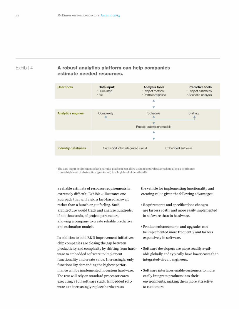
a reliable estimate of resource requirements is extremely difficult. Exhibit 4 illustrates one approach that will yield a fact-based answer, rather than a hunch or gut feeling. Such architecture would track and analyze hundreds, if not thousands, of project parameters, allowing a company to create reliable predictive and estimation models.
In addition to bold R&D improvement initiatives, chip companies are closing the gap between productivity and complexity by shifting from hard- ware to embedded software to implement functionality and create value. Increasingly, only functionality demanding the highest perfor-mance will be implemented in custom hardware. The rest will rely on standard processor cores executing a full software stack. Embedded soft- ware can increasingly replace hardware as
Exhibit 4 A robust analytics platform can help companies estimate needed resources.
MoSemiconductors 2013Chip design complexityExhibit 4 of 5
User tools
Analytics engines Complexity Schedule
Project-estimation models
Industry databases Semiconductor integrated circuit Embedded software
Staffing
Data input1
• Quickstart• Full
Analysis tools• Project metrics• Portfolio/pipeline
Predictive tools• Project estimates• Scenario analysis
1 The data-input environment of an analytics platform can allow users to enter data anywhere along a continuum from a high level of abstraction (quickstart) to a high level of detail (full).

33What happens when chip-design complexity outpaces development productivity?
However, despite its many advantages, embedded software is no panacea. Overall performance characteristics will still be determined by hard- ware. Innovation in chip design remains the foundation of ever-increasing efficiency, speed, and power performance.
A further step semiconductor companies might take to fill the complexity-and-productivity gap is to expand their use of third-party logic and circuit blocks and processor cores, also known as IP. Successful R&D organizations will shift their mind-sets from the historical “let’s make it ourselves” to “let’s see if can we buy or license it” (at a price point that makes sense).
For many years, IP licensing has been a frag-mented industry comprising myriad small, independent suppliers. However, large electronic-design-automation (EDA) vendors are aggressively pursuing the business opportunity, acquiring numerous companies to accelerate their entry. The success of ARM Holdings is not lost on its EDA brethren. ARM demonstrates that it is quite possible to become a large, profitable “silicon-less” semiconductor company.
EDA companies’ aggressive pursuit of the IP business is a boon for semiconductor companies, as it enables integrated device manufacturers
and fabless suppliers to focus their R&D resources on creating more value-added IP. On the other hand, as the breadth and depth of their IP portfolios expand, EDA vendors themselves become suppliers of added value, which once belonged to semiconductor companies. During this transition, EDA vendors invariably become competitors of the chip companies’ internal R&D organizations, much as they did 20 years ago when they displaced the internal computer-aided-design groups of semiconductor companies. This has already begun, and successful semiconductor companies will aggres-sively restructure their R&D organizations to take advantage of the shift.
R&D productivity’s inability to keep pace with the challenges of product development will be one of the major issues for the industry in the years ahead. The insatiable demand for more functionality, performance, and bandwidth puts heavy pressure on R&D teams. Only compa-nies with world-class product-development capabilities are likely to stay ahead of competitors and market demands.
Ron Collett is an alumnus of McKinsey’s Silicon Valley office, where Dorian Pyle ([email protected]) is
a consultant. Copyright © 2013 McKinsey & Company, Inc. All rights reserved.

34
Doug Parker and
Christopher Thomas
Winning share in automotive semiconductors
Automotive semiconductors, a $24 billion business, have experienced one of the fastest growth rates of any large segment in the $300 billion worldwide chip market, averaging 8 percent annually between 2002 and 2012. An increasing number of powered systems requiring microcontrollers, sensors, and analog devices have led this growth (Exhibit 1). But there are signs of a slowdown. For example, the number of microcontrollers has leveled off in luxury cars at about 100 per automobile, and prices for those microcontrollers have dropped rapidly. Where will the next wave of growth come from for automotive semiconductors? We see three likely sources: further electrification of the drivetrain, “consumerization” of auto electronics,
From self-parking cars to anticipatory braking, semiconductors have been important
to automotive innovations in the past decade. And automotive-semiconductor
revenues expanded quicker than those of both the automotive and broader semicon-
ductor industries—but will this continue? Where will innovation come from?
and vehicle intelligence (including active safety innovations and connectivity-enhanced driving).
Winning share in any automotive application is challenging, given carmakers’ rigorous qualification process and strong risk aversion (for quality reasons), as well as the industry’s need for long-term supply agreements and lengthy product cycles. However, we believe these sources of growth create opportunities for semi- conductor companies, even those that are not traditional suppliers of automakers.
Further electrification of drivetrains
The electrification of the drivetrain, due to the rise of hybrid and full electric vehicles,
© Getty Images

35
may lead to the largest expansion of semiconductor usage in automobiles over the next ten years. The drivetrain now accounts for 30 percent of all semiconductor content in an automobile, or a market of about $7 billion a year. While the average internal-combustion drivetrain uses less than $100 of semiconductor content, hybrid drivetrains contain more than $1,000 of electronics, much of which is in power circuits. Such circuits route power from batteries to the motor; in this case, semiconductor content comprises isolated-gate bipolar transistors (IGBT) and power metal oxide semiconductor field-effect transistors (MOSFETs). Toyota has highlighted the efficiency and fast switching rates of the IGBT in the Prius’s drivetrain as
a distinct advantage, “tuned at the level of the crystal” (Exhibit 2).
Automakers rarely change suppliers of the electronics controlling the power and drivetrains of their vehicles. There are four reasons for this: the complexity of installed systems makes consistency valuable; strong relationships exist between semiconductor companies and automakers in various regions; the installed base of designers using proprietary tools and programming languages favors consistency; and high risk exists in making significant changes in established platforms. As such, the costs and risks of switching would be high.
Exhibit 1 The average automobile has about $350 of semiconductor content, with nearly 80% of that in microcontroller units, analog, and power.
MoSemiconductors 2013Automotive semiconductorsExhibit 1 of 2
Semiconductor content per car by car type, $ The average car has ~$350 of semiconductor content, with 2/3 of that MCUs1 and analog
Type of semiconductor content in average car, ~$350 total, %
~1,000
Luxury
Sensors~600
Hybrid electric
~350
Midrange in developed market
~100
Compact in developed market
~50
Compact in emerging market
Discrete power devices
Application processors (MCUs)
Analog ICs2
33
33
17
17
1 Microcontroller units.2Integrated circuits.
Source: Auto Semiconductors Report, Sanford C. Bernstein, September 2012; iSuppli

36 McKinsey on Semiconductors Autumn 2013
Hybrids and full electric vehicles present a unique opportunity for semiconductor companies to win share in the next generation of the automobile engine. Electric drivetrains change substantially in each vehicle generation. The
basic design of the drivetrain itself is still evolving, with pure electric vehicles (EVs), EVs with internal-combustion-engine charging, and EVs with internal-combustion-engine assistance (hybrid electric vehicles, or HEVs) competing for
Exhibit 2
Infotainment• Dashboard• Car audio• Connectivity audio• Entertainment• ITS/GPS2
• Car navigation display
Semiconductors are used pervasively in modern automobiles.
MoSemiconductors 2013Automotive semiconductorsExhibit 2 of 2
1 Hybrid electric vehicle/electric vehicle.2Intelligent transportation system/global positioning system.3Controller area network.4Local interconnect network.5Media-oriented systems transport.6Electric power steering.7Antilock brake system.8Tire-pressure monitoring system.
Chassis• Steering/EPS6
• Brake/ABS7
• Traction control• Suspension• Chassis control
Safety and control• Airbag• TPMS8
• Collision warning• Parking assistant• Back monitor• Night vision
Comfort and control• Power door• Power window• Climate control• Seat controls• Mirror and wiper control
Electronic system• Alternator, battery,
and starter• Lighting• Diagnostics• In-car data bus
Networking• CAN3
• LIN4
• FlexRay• SAFE-BY-WIRE• MOST5
• Bluetooth
Power train• Engine control – Engine – Fuel injection – Knock control• HEV/EV1 motor• Transmission

37
market share and the option to be the next dominant engine type.
The innovation cycle for electronic components in electric vehicles is much faster than it is in internal combustion engines. For example, the bipolar transistors, sensors, and microcontrollers serving one generation of vehicles may be deemed insufficient for the next one. In fact, automobile executives tell us that designs for these elements are leapfrogging previous generations, not just offering incremental improvement.
While the pace of innovation is fast, automakers and their tier-one suppliers have been conservative in choosing vendors for the core electronic functions such as powertrain and drivetrain management. These functions favor large incumbents, as established companies usually have both financial stability and a reputa- tion for quality. A number of winners have emerged as this landscape evolves, just one example of which is Mitsubishi Electric. When the company spun off its semiconductor business to Renesas, it notably retained its IGBT business, which now captures roughly a third of that market. Given the rate of development in IGBTs and in high-voltage gallium nitride MOSFETs,
we expect to see semiconductor players that don’t currently serve the auto industry supplying chips to hybrid makers, especially auto manufacturers that have not released a successful hybrid offering yet. These players must be strong financially, meet high quality standards, and most important, offer significant perfor-mance improvements over current offerings while understanding vehicle usage or specific systems-usage patterns very well. Developing a less expensive alternative to IGBTs would be one way to accomplish this; another would be to offer kits of sensors and microcontrollers that could be used to extend the range of the car through better assisted-driving technology or more effi- cient power management, for example. A third opportunity for semiconductor companies would be to offer products to improve the driving experience, covering the wider field of driving dynamics and handling—for example, con-tinuous tuning technology, which aims to reduce engine vibration in the types of smaller engines used in hybrids.
Consumerization of auto electronics
Infotainment—a market of about $6 billion—accounts for almost a quarter of the semiconductor content in automobiles, up from 20 percent ten years ago. Consumers’ tastes
Winning share in automotive semiconductors
The innovation cycle for electronic components in electric vehicles is much faster than it is in internal combustion engines.

38 McKinsey on Semiconductors Autumn 2013
have changed considerably in that period; they now enter cars with smartphones in hand and expect a similar user experience from auto- motive electronics. If the car’s electronics are not up to their expectations, they could simply use smartphones for communi- cation, entertainment, navigation, and other information-access services.
Automakers have tried to improve the user experience, for example, by shortening the software-development cycle to keep graphical user interfaces fresher and more intuitively user-friendly. However, it is hard to compete with leading consumer-electronics players. Apple and Samsung release updated products on a 9- to 12-month cycle, while automakers are making purchase decisions now for their electronics on a four- to five-year cycle with a potential midcycle upgrade option. In fact, some automakers have just announced user interfaces with the familiar tile layout of Apple’s products—six years after the first iPhone was released. This puts pressure on a critical high-margin product for automakers: the in-dash infotainment system. They charge up to $3,000 for infotainment and navigation packages, while a new smartphone can be pur- chased for less than $200 with a service plan.
Car manufacturers have made efforts to integrate consumer electronics into vehicles. Premium carmakers, for example, have incorporated a search function into navigation systems and have developed apps that allow users to control parts of their infotainment systems with their smartphones.
To keep pace with consumer-electronics devel-opment, automakers must find a way to accelerate their product development and allow
a broader range and more frequent upgrade of application installations in the infotainment system while maintaining control over the in-dash offering. On the one hand, if they cannot keep up with the consumer experience, there is a risk that auto buyers will not opt for their navigation systems (or for a lower-end offering at best) and will instead rely on smart-phones and other devices. But if they give up too much access to their onboard systems— for example, adding an in-dash iPad docking station—there is a risk that profits could erode as their own infotainment systems become commoditized. One important aspect to note is safety while using the infotainment features in order to minimize driver distraction: this could ultimately lead to a continued preference for embedded solutions in the infotainment system.
One way automakers can compete is to create a limited connection between a user’s smartphone and their car’s in-dash navigation system. MirrorLink is a standard system established to help automakers and smartphone makers connect their devices. It mirrors the driver’s smartphone screen on the navigation system. To keep the customer experience current, automakers could push operating-system and user-interface updates to vehicles through Wi-Fi or other device-based upgrades.
Another way to maintain competitiveness is for automakers to allow for easier upgrades of their infotainment features or capabilities. They could do this in a number of ways, including focusing their upgrade efforts more on software (either operating-system or feature-based software), installing sufficient memory and microprocessor capabilities, or creating easily exchangeable hardware elements to enable these new capabilities (for example, memory

39Winning share in automotive semiconductors
chips). Maintaining high reliability standards is critical while pursuing these opportunities.
Infotainment is also the most likely place for ARM-based products to penetrate the auto market. ARM-based processors have been gaining share rapidly in the broader microcontroller market but have not made significant inroads in automobiles because of concerns about reliability, the large installed base of proprietary products and instruction sets already in use, and long product cycles. Entering into the smart- phone ecosystem would have many benefits. Automakers could tap software and hardware designers from consumer applications. They could also benefit from the R&D being invested in semiconductors and in user experience for cell phones, which operates at a different order of magnitude. While Toyota sold almost ten million cars in 2012, only a fraction had infotainment systems. In that same year, Apple sold about 200 million iPhones and other devices using its A-series processors. It will likely take years for ARM chips to penetrate deeply into auto powertrains, but the shift in infotainment could happen if reliability can be proved to match the very high quality
standards of both auto manufacturers and buyers. Ultimately, to make this happen, it would be important that automotive, consumer-electronics, and semiconductor players collaborate to tackle these issues and develop high-quality and user-friendly product solutions.
Vehicle intelligence and connectivity-
enhanced driving
Perhaps no other trends offer greater growth opportunities than vehicle intelligence (including active safety) and connectivity. Many of the most impressive innovations in automobiles in the last few years have been collision-avoidance braking, lane-change sensors, and automatic- parking functions. This has driven the market for sensors in automobiles to grow at a 14 percent annual rate over the last decade. Last year it was a $3 billion market. We expect there to be significant additional growth in this market as features in luxury cars migrate to midrange cars and new connectivity-enhanced driving features enter the marketplace.
While fully autonomous driving may be ten or more years away, we expect to see a continuous increase in driving assistance and related

40 McKinsey on Semiconductors Autumn 2013
semiconductor content. Tires embedded with microelectromechanical systems can monitor road traction and adjust braking. Enhanced night vision is another intriguing area. With the increase in these types of driver support and assistance comes a spike in the amount of data sensed, processed, and collected.
The new generation of premium automobiles collects not only physical data (for example, road resistance, temperature, and speed data) but also visual data (posted speed limits in assisted-driving modes) and even audio data (the sound of the road to sense ice and other hazardous conditions). While automakers use this to create a smoother, safer ride for their customers, the data collected by automobiles create opportunities of potentially significant value. Cameras in automobiles could continuously feed road condi- tions to navigational-software programs that will learn to not only report current traffic but also accurately predict traffic levels and suggest better routing. Highway operators could tap these data to predict likely accident spots and to automatically drop speed limits in that area and position safety crews. High-tech traffic lights could feed timing information to driving-assistance systems (and vice versa) to help reduce congestion and improve gas mileage. In the future, road-maintenance crews could know the size of every pothole in their city with a precise GPS position—before any citizen called to complain. Of course, the collection and
use of such data must be balanced against privacy concerns, but many benefits are readily apparent.
In the short run, connectivity-enhanced driving innovations will likely be led by various players in the existing auto value chain such as original-equipment manufacturers and suppliers. (Most premium automakers already have self- driving and assisted-driving prototypes.) New entrants to the auto value chain are cur- rently exploring their role within it, as well (such as big-data players like Google).
Efforts to monetize the data stream collected by automobiles may be driven by automobile makers or by big-data players and tech start-ups. The payback on innovations tapping these data streams likely will take longer, and all players in the auto value chain still need to develop business models to address how to use the vast trove of data they could create and tap. The real question is how to develop scalable business models.
Deployment outside the automobile (for example, in the systems that power traffic lights or parking-space locators at parking garages) is also attractive and will likely appeal to a larger set of systems providers and start-ups. However, it will be important for players to understand end-consumer preferences and willingness to pay, as well as the required technical infrastructure. In the parking-space-locator arena alone there are
Efforts to monetize the data stream collected by automobiles may be driven by automobile makers or by big-data players and tech start-ups.

41
numerous start-ups, with a few notable players including Parking Panda, SpotHero, Parking Spotter, and Parker. These systems will prompt increased semiconductor demand for sensors, basebands, and microcontrollers, to assess the area and communicate with users, alerting them to conveniences like open parking spaces. Still, consumers will likely use their handsets to gain access to these improvements, rather than the onboard systems in their dashboards. Therefore the biggest challenge for broader use will be defining system standards to make efficient large-scale systems work (the types of systems that could work with traffic lights across multiple municipalities, cellular providers, and automaker systems) and take advantage of embedded systems with regard to safety and user-friendly, intuitive interfaces.
Given the rapid pace of change, automakers, current suppliers, and newcomers to the space need to move quickly and further adapt their
business models to capture these ideas, including potential alliances and collaborations. Whoever develops a good understanding of end consumers’ true preferences and willingness to pay, together with a viable plan for developing scalable solutions, may gain competitive advantage.
The recent growth in automotive semiconductors has made the segment one of the most attractive spaces for designers and manufacturers to target. However, companies should care- fully assess application areas, including the three discussed in this article, before investing in development.
Winning share in automotive semiconductors
Doug Parker ([email protected]) is a consultant in McKinsey’s Seattle office, and Christopher Thomas
([email protected]) is an associate principal in the Beijing office. Copyright © 2013 McKinsey &
Company, Inc. All rights reserved.
42
Harald Bauer and
Ondrej Burkacky
When software meets hardware: Excellence in embedded-software development
For many years, software was an afterthought for semiconductor companies. When software did get attention, it was limited mostly to basic firmware operating the integrated circuits (ICs) that the companies produced. But in the last five years, as hardware has become increasingly commoditized and customers demand shorter time to market, the importance of embedded software has grown.
At one time, hardware designers were the dominant class of engineers in most semiconductor R&D organizations. Now, given the rise of mobile devices, most IC designers employ more software developers than hardware engineers. In consumer-facing markets, that evolution has
Embedded software has become essential to the success of most types of new
semiconductors. Yet some semiconductor companies still resist the idea that they are
selling not just hardware but also, increasingly, software. A blueprint can help in
better integrating them in your organization.
come quickly. Through work in the wireless-handset sector, it was observed that more than 60 percent of engineers are engaged in software development or testing, compared with roughly 40 percent three years ago and less than 20 percent in 2008.
Companies undergoing the transformation from hardware- to software-centric business models typically find that several aspects of their existing processes lead to productivity losses, quality problems, rework due to late defect detection, and budget overruns. These include lack of modularization, manual testing regimens, and hardware-led development processes that do not fit the agile-development model required
Harry Campbell

43
for software. Several ways to overcome these chal- lenges have been identified, but the three discussed below usually have the most impact.
Giving software its own driver’s seat
Because their historical operations were hardware-centric, semiconductor companies’ supporting structures remain that way. Hardware timelines drive both overall company planning cycles and the operations of embedded-software divisions. This approach is not well matched to the agile-development methodology common in software development. (Software releases tend to be in ranges of hours or days, whereas new hardware typically takes months to develop.) Instead of software development coming along for the ride with hardware develop-ment, these activities should be placed on separate but coordinated tracks, with frequent release cycles. To achieve this, project clocks should be aligned to an overarching system plan, featuring smooth integration and timely definition of requirements on both the hardware and software sides of the development team. Parallel development, with frequent release cycles, should be the desired end state.
Overcoming practical obstacles
From a system-architecture standpoint, it may seem difficult to place embedded software on a different development track than hardware. Certain portions of the software, such as
firmware, should be closely linked to the hardware. The use of abstraction layers, however, can help to decouple software stacks and allow for internal optimization of these modules’ interfaces and communications protocols. This decoupling approach can also make it easier to migrate software stacks to new hardware, thereby fostering reuse and cutting down on the need for rework.
Release cycles can be automated using a software-development tool chain1 that handles automatic release management with multiple modules and ideally includes the “virtual prototype” of the target hardware for verification purposes. Several players in the embedded-software field have shown that variable release cycles of as little as three hours to one week are feasible, gaining significant flexibility, reducing bug-fixing effort, and shortening the overall project timeline.
Integrating verification processes
The verification process should transition from a rigid hardware focus to one that has an integrated development tool chain with a fully automated verification work flow. Testing should be continu-ous, and a priority should be finding bugs early and fixing them before they get integrated on the system level. Continuous testing can be made possible by virtualizing the entire system stack (for example, in wireless, including the base station, “air” interface, mobile antenna, mobile-software stack, and baseband chip) and then
Software and hardware development should be placed on separate but coordinated tracks, with frequent release cycles.
1 In this article, software tool chains are referred to in their purest sense—that is, a set of programming tools with logical, sequential relationships—rather than the common usage that refers to any collection of programming tools.

44 McKinsey on Semiconductors Autumn 2013
conducting automated testing of the virtual stack at “precommit” (when the developer submits a final change request to be included in the system). A reduction of the defect density by more than 50 percent is feasible with this approach.
Seeing the impact
Programs employing these levers can generate significant impact. Several companies have improved time to market by 30 to 40 percent,
while product-quality scores rose by up to 50 percent and overall productivity increased by roughly 30 percent (exhibit).
Such a transformation can take more than 18 months, but initial results from some initiatives can deliver measurable improvement in a much shorter time. Companies can use a subset of development projects as pilots to implement and refine the new methodologies.
Exhibit Excellence in embedded systems is a key performance lever.
MoSemiconductors 2013Software toolchainExhibit 1 of 1
Development time
Reduced cycle time by parallelization of feature development and stabilization
Mobile-phone-platform development, months Product-development effort, person-months, comparable complexity
Reduced overall project budget by improved hardware/software synchronization
Lower defect density due to strict quality gates
Mean time between failures, hours Average release-schedule adherence, %
Significantly better predictability and quality of releases with “precommit” verification
Defect density
33
–42%
50%
Previous approach Current approach
19
3,500
Previous approach Current approach
2,000
450
Before With quality gates
300 60
Previous approach Current approach
100
–43%

45When software meets hardware: Excellence in embedded-software development
Companies should initially aim for a 10 to 20 percent decrease in project timelines and a significant productivity increase within the first six months. An example of a quick win would then be delivered by using a stringent requirements-definition process to ensure effective use of resources, as it drastically cuts down on rework and unnecessary develop- ment efforts.
Tighter integration of hardware and software could deliver significant benefits to many semiconductor companies. Furthermore, the measures described above have delivered significant time-to-market improvements while maintaining a high level of quality in real- world situations.
Harald Bauer ([email protected]) is a director in McKinsey’s Frankfurt office, and Ondrej Burkacky
([email protected]) is an associate principal in the Munich office. Copyright © 2013 McKinsey &
Company, Inc. All rights reserved.

46
André Andonian,
Rajat Mishra, and
Nick Santhanam
The hunt for revenue: A case for further granularity
As semiconductor players consolidate, the opportunities for growth through M&A have dimin- ished. Now well documented, the supply of semiconductor start-ups has dropped at a 13 per- cent compound annual rate over the past decade, and the number of new companies formed has slipped to under 50 a year, compared with 144 in 2001 (the year the Internet bubble burst). In the face of these conditions, semiconductor players that seek to grow beyond their core business are increasingly challenged in identifying markets and building sufficient confidence in the attrac-tiveness of those markets.
Based on the observation of these trends across a number of maturing markets, McKinsey has
Uncovering additional market opportunities can be a critical driver of growth
in today’s semiconductor markets. But how should executives and managers broach
the exercise? Three approaches can help ensure that markets are assessed at
the appropriate level of granularity.
developed an approach called the “granularity of growth,” which focuses on finding opportuni- ties in emerging businesses while defending and extending core businesses.1 We believe that certain elements of this approach have high appli- cability to semiconductor companies and move beyond what companies typically do when trying to identify market-growth opportunities. Specifically, semiconductor companies could benefit from assessing micromarkets rather than broad categories, looking around corners to consider the impact of disruptive trends, and getting closer to their customers and end users. Such a granular approach to assessing mar- kets is more likely to identify pockets or niches that could be attractive as a result of subtle
Harry Campbell
1 Mehrdad Baghai, Sven Smit, and Patrick Viguerie, The Granularity of Growth: How to Identify the Sources of Growth and Drive Enduring Company Performance, Hoboken, NJ: John Wiley & Sons, 2008. For additional details, see mckinsey.com.

47
Exhibit 1 Companies must go beyond high-level end markets and analyze micromarkets.
MoSemiconductors 2013Revenue HuntExhibit 1 of 2
1 Dynamic random-access memory.2Universal serial bus.
Wired communication
• Broadcast and studio • Cable modems• Digital loop access• Enterprise voice
networks• Fiber to the home• Local-access-network
switches and hubs• Legacy access• Long-haul equipment• Metro equipment• Routers, high end• Routers, low to mid
Automotive• Body electronics • Dashboard instrument
clusters• GPS, fixed navigation
system• Infotainment• Power train• Safety and control
Military and aviation• Aeronautics• Aerospace radar
and imaging• Military
communication• Wearable computing
Medical• Electronic medical
records • Genetic engineering• Imaging• Implantable devices• Monitoring and test
equipment• Portable devices• Surgical tools
Industrial controls• Automation • Building and
home control• Energy generation
and distribution• Smart grid• Solar cell• Weather imaging • Test and measurement
Wireless communication
• Bluetooth• Femtocells• Fixed wireless
broadband access• Mobile handsets,
1G–2G+• Mobile handsets, 3G+• Mobile handsets, 4G+• Mobile wireless
broadband access
Consumer electronics• Camcorders• Consumer appliances• Digital picture frames• Digital set-top boxes• Digital still cameras• DVD and Blu-ray
video players• E-book readers• Handheld-video-
game players• Home-theater
projectors• Motion detection• Personal and
portable stereos• Pachinko• Portable-media/
MP3 players• Rear-projection TV• Tablets• Video-game consoles
Data processing• Bare-bones
deskbound PCs• DRAM1 upgrade
modules• Enterprise servers• Flash storage cards• Flat-panel monitors• Fully configured
deskbound PC adders• Fully configured mobile
PC adders• Graphic cards• Information analysis• Mainframe and
supercomputers• Multifunction printers• Optical disk drives
for computers• Rigid disk drives
for computers• Smart cards• Solid-state drives• USB2 flash drives
Example micromarkets
>120 micromarkets

48 McKinsey on Semiconductors Autumn 2013
shifts in customer needs or disruptive technologies specific to a certain submarket or application.
Pockets of opportunity
As a first step to achieving this additional level of granularity, companies should build their planning and market intelligence around an analysis of micromarkets. As an example, the medical-device market is significant for many semiconductor companies, but is it helpful to assess that market’s overall growth rate?
That may work for overall portfolio decisions, but it is not as useful as breaking the market down into application subcategories that would include electronic medical records, genetic-engineering technologies, imaging technologies, implantable devices, monitoring and test equipment, portable devices, and surgical tools. By examining these specific markets in this granular fashion, we have consistently seen untapped opportunities appear (Exhibit 1). The discipline that this calls for is a shift from
Exhibit 2 Companies should try to anticipate disruptive trends.
MoSemiconductors 2013Revenue HuntExhibit 2 of 2
1 Growth rate: 2010–15 compound annual growth rate.
Source: ABI Research; expert interviews; McKinsey analysis
Example, data-converter sales in smart-meter application
Smart transformers replacing smart meters
Are you “product ready” for the smart-transformer market?
Trends affecting smart-meter serviceable addressable market
Market’s estimated growth Estimate using our approach
China smart-meter growth 2x 12% average
12% vs. 13%Are your China sales commensurate with a 2x average growth rate?
Number of units of application
0% vs. –3%High-end application-specific standard products replacing stand-alone analog-to-digital converters
How aligned is your product portfolio to integration trends?
Semiconductor content per application
×
×
Serviceable addressable market
–3% vs. –4%Supplier pressure, die shrinkage, and analog-to-digital conversion
Have you considered worst-case scenarios of average selling prices on product lines?
Average selling price
Implications for analog players
Market growth estimate1 vs. adjusted growth
Impact on growth
9%vs.
6%
=

49
planning at the broad product-category level and instead developing medium- and long-term plans based on micro-assessments of applications (rather than products).
Two additional lenses might then be applied to this more granular approach. The first is to make geographic comparisons (at the granular level of countries rather than the broader level of continents) and the second is to assess opportunities in applications adjacent to the current chip portfolio. As an example, in the industrial-automation submarket, semiconductor companies could explore programmable logic controllers (PLC) or the operator-interface market specific to different applications (such as process manufacturing in Brazil, which is a particularly high-growth opportunity). Analysis shows these niches may be smaller than the overall automation market, but they are growing slightly faster, at more than 9 percent per year, significantly higher than the automation market as a whole.
Looking around corners
How do you know a disruption is coming? Looking around corners means taking the time and actions to provide insight beyond the latest market research or analyst report. A disruption seen at the level of the overall market is often an
evolution when analyzed at the level of the system and value chain. The effort involved to find these disruptions is in a detailed approach to application and system-level design evolution.
As an example, let’s examine the opportunity in analog-to-digital converters (ADCs) in smart meters (Exhibit 2). Viewed at a normal component-market level, the overall revenue in the addressable market for analog-to-digital converters in smart meters is expected to grow by 9 percent a year. In addition, the consensus estimate for unit growth is forecast at 13 percent annually over the next two years. That would seem to be a robust opportu-nity. However, a thoughtful evaluation of the system level and value chain indicates that a change in technology elsewhere in the value chain could have a significant disruption: the transition to smart transformers on power poles could reduce the need for stand-alone ADCs on meters. That evolution might make the opportunity for analog semicon- ductor companies in the ADC market a lot less attractive.
In this example, the impact is a significantly weaker outlook for the smart-meter data-converter market (making it likely to grow by 6 percent a year over the next three years
The hunt for revenue: A case for further granularity
How do you know a disruption is coming? Looking around corners means taking the time and actions to provide insight beyond the latest market research or analyst report.

50 McKinsey on Semiconductors Autumn 2013
rather than by the 9 percent that the analyst and market-research consensus expects).
Getting closer with customers
and end users
Most semiconductor companies that perform well already know their customers and the main decision makers within those companies. However, a handful of activities can help in gaining further insight into the customers’ needs and their own markets. One such activity is to develop customer intelligence through an advisory board, a strategy now used by most companies.
A less traditional activity to gain intelligence is to create lead-user groups, where major customers have the chance to comment on products in development. There is a real benefit to be realized because this effort allows companies to gather feedback on the product pipeline and gain insight
into customer needs. These interactions, which can be supplemented by follow-up conversations, can help build stronger relationships with participants. Companies must decide what functional groups to involve in this process. Broadening the group to include technology, product marketing, and sales can provide valuable customer insight to multiple parts of the com-pany early on in the process.
We noted that it is essential to know a lot about your customers, but frequently they have different needs than their own customers do. And the ability to gain insights into these end users’ needs is often obfuscated when the products are sold through a distributor or third-party assem-bler. Why should this matter now more than it did in years past? Because the anticipated growth in embedded, connected devices in the physi- cal world (the Internet of Things) and forecasted

51
increased need for semiconductor players to understand the application requirement, partic-ularly in the embedded world.
In sum, semiconductor companies stand to benefit from taking a more granular approach to sizing markets and upgrading their approach to market-potential analyses. By assessing micromarkets, employing approaches to look at system and value- chain trends, and by getting closer to customers and applications, companies stand to find opportunities for growth where market research and analysts fail. With these inputs in place, the revenue engine could be further revved up, helping semiconductor companies grow more robustly in the years ahead.
growth in wearable and mobile devices beyond the smartphone mean that more specific knowledge of application requirements will become increasingly important for semiconductor companies. For example, say a semiconductor company wants to sell data converters in the indus- trial market. However, its industrial customers may use the chip in a PLC, which is then sold to an oil refinery. Let’s examine the needs of these different players: the industrial company wants the chip to integrate easily into the PLC, and it wants a low price on the component. The refinery’s primary concerns are uptime and reliability. In the past, the system-level designer typically took care of making the chip rugged, but as the market opportunity grows and pressure on system costs intensifies, the chip designer would do well to develop a higher-reliability product that can help reduce overall system cost. The example, though simple, reinforces the
The hunt for revenue: A case for further granularity
The authors wish to thank Wendy Lee for her contributions to this article.
André Andonian ([email protected]) is a director in McKinsey’s Stamford office, Rajat Mishra
([email protected]) is an associate principal in the San Francisco office, and Nick Santhanam
([email protected]) is a director in the Silicon Valley office. Copyright © 2013 McKinsey & Company, Inc.
All rights reserved.

52
Steve Chen,
Apoorv Gautam, and
Florian Weig
Bringing energy efficiency to the fab
A typical semiconductor fabrication plant, or fab, will use as much power in a year as about 50,000 homes. In fact, the larger “megafabs” can consume more electricity than auto plants and refineries. Some facilities have even built their own captive power plants.
While the power consumed by semiconductor chips has been reduced significantly in the past decade, improvements in the energy used during the chip-production process have lagged behind. Energy costs can account for 5 to 30 percent of fab operating expenses, depending on local electricity prices. High-tariff markets include semiconductor hot spots like Japan and Singapore.
Large semiconductor fabs use as much as 100 megawatt-hours of power each
hour, which is more than many automotive plants or oil refineries do. In some markets,
electricity can account for up to 30 percent of fab operating costs, so there is
significant opportunity in rethinking power usage and management.
Given the competitive intensity of the industry, it is not surprising that integrated device manufac- turers and foundries have invested to achieve energy-efficient solutions (sometimes in collab-oration with “green” nongovernmental organizations). We often find, however, that less work has been put into ensuring that the company’s infrastructure is run in the most efficient manner. Instead, reliability is frequently the primary, and sometimes the only, consideration when it comes to utility requirements. Few measurements are taken, and at many fabs, there is only one power meter for the entire clean room, despite the dozens of power-intensive tools contained therein. About $20 million to $30 million in electricity
© Amit Basu Photography/Getty Images

53
flows through that meter each year, but engineers, plant managers, and even fab execu-tives often treat it as a free commodity. Our experience shows that most fab engineers focus on process technology, and the few facility engineers on staff are asked to maintain the status quo. As a result, compressors and exhaust fans run above specification, and chillers often overcool water for the air-conditioning systems.
In boom times, many companies treat energy conservation as a low priority. But the issue becomes more critical when chip volumes fall. Despite reduced production, energy costs remain relatively stable since the plant environ-ment must be maintained regardless of the number of chips made. This puts upward pressure
on the ratio of energy costs per wafer and can quickly eat into profit margins. In addition, governments worldwide are putting increasing pressure on energy-intensive businesses to reduce consumption. So semiconductor companies are facing both financial and political pressure to rationalize their energy use.
We have analyzed the energy usage of leading-edge and lagging-edge fabs of several companies in different regions. We consistently found that by applying energy-efficiency lessons from other power-hungry industries, fab energy costs could be cut 20 to 30 percent, half of which can come from changes in plant-management processes. A few modest investments would be required to capture the rest of the savings (exhibit).
Exhibit A 300-millimeter fab could cut up to 30% of its energy costs.
MoSemiconductors 2013Fab energy efficiencyExhibit 1 of 1
Specific management processes
Breakdown of potential savings, %
Tool Subfab
15
Etch
12
Implant
10
Lithography
8
Polish
31
Thin film10Bulk gas
6Others
21Air-conditioning system
8Process-cooling water
5Ultrapure water
5
Clean tech
Diffusion
19
50Plant management
26 24

54 McKinsey on Semiconductors Autumn 2013
Realizing significant efficiency potential
Our approach draws on methodologies and tools used for other power-intensive industries, such as in steel and paper plants and oil refineries. We also apply insights from other McKinsey work to identify the types of equipment and processes that consume the most power in a fab. In most cases, we found potential energy savings of 25 to 30 percent with no loss of quality or worker-safety compromises and little new investment.
How is this possible? Most facilities we inspected are overengineered. Consider the thousands of exhaust pipes circulating scrubbed air and removing hazardous fumes from a modern fab to provide a safe, clean environment. Manufacturers of these exhaust systems recom-mend certain airflow specifications for this equipment. Our analysis showed that most exhaust volumes were running 20 to 50 percent higher than the equipment specifications called for. This was because most semiconductor companies focus on maintaining a certain level of air pressure in the ventilation system, rather than focusing on a manufacturer’s recommended airflow volume, which is the more relevant metric. (It is possible to achieve correct pressure with either a low flow or a high flow.)
By reducing the volume of air pushed through the network of exhaust pipes and sent through the scrubber to the manufacturer’s recommended volume, a fab could save 20 to 30 percent of air- conditioning costs, or 4 to 9 percent of total electricity expense. Of course, there is potential to reduce volumes further, because there are minimum and maximum specifications. To reach beyond the initial improvements would take several months of additional testing, but the first
steps could yield significant improvement in just weeks.
Another area we found that is always able to generate quick wins is the process-cooling water system. Pressure, flow, and temperature are three critical parameters and cost drivers of the system, and our analysis and experience shows that the efficiency of each could be improved significantly. Take pressure: most tools require pressure of less than 4 bar (for context, normal home water pressure is 1 to 2 bar). Most fab systems, however, supply process-cooling water at 5 to 7 bar for perceived reliability or because one or two tools call for extra-high pressure. But there is another way to provision cooling water. Some 15 to 30 percent of the power used to pump water could be saved by reducing pressure from, say, 6 bar to 4.5 bar. And small-boost pumps could be added for specific tools that require higher pressure.
Putting a new approach in place
While process-cooling water systems and air-conditioning are two big users of electricity, semiconductor companies should consider carrying out a comprehensive review of fab opera- tions and an analysis of energy consumption at the tool level. This may lead to a change in metering. Most fabs would benefit from installing meters, if not for every tool then at least at the module level, thereby creating more visibility and accountability. While it could cost $200,000 to install 200 meters, the transparency created can produce rapid savings. In our work, we have found the payback for installing new meters comes in one or two months. The visibility into which modules are using how much power changes behavior faster than any policy memo could.

55Bringing energy efficiency to the fab
From there, the challenge shifts to ensuring that functions such as the exhaust system are running within the specified parameters and then to see if additional improvement potential exists. This often requires the creation of a dedi- cated, professional energy-management team. Many fabs have only one part-time engineer assigned to the energy-management role, even though they might spend tens of millions of dollars each year on electricity. We suggest building an energy-management organization comprising at least one manager, three to five system experts, and additional part- time specialists. Their goal would be to find, implement, and sustain gains in energy efficiency.
Several months into the program, with all processes adhering to specifications and all quick wins either implemented or close to being implemented, managers should undertake a more comprehensive review and develop an energy-efficiency road map across the entire fab network. System experts and specialists should investi- gate the theoretical limit of power consumption by each tool type and major piece of equipment. From that point, they can develop a list of new efficiency ideas and evaluate each based on a formal business case.
For example, there may be an opportunity to install an additional loop of “high temperature” process-cooling water (77 degrees Fahrenheit
versus the 55- to 65-degree water that is commonly used). This water could be produced by ambient air flowing through a cooling tower—a process that is essentially free—compared with traditional (and expensive) chill-generated cooling water. Assuming electricity costs 18 cents a kilowatt-hour (not unusual for Japan or Singapore), a fab could reduce makeup system costs by 50 percent, with a positive return on investment in less than one year. A fab could also install idle-time controllers to reduce tool power consumption by 30 percent. Even this technology investment would generate a positive return on invest- ment in less than two years.
Energy efficiency is not a common topic within the fab community, but with the fierce competition in many segments of the industry, ratcheting up efficiency efforts and taking a 20 to 30 percent bite out of annual energy costs can offer a competitive advantage and also improve profit margins. As such, semiconductor companies have a big incentive to analyze the opportunity and look for ways to economize across their fab networks.
The authors wish to thank Abhyuadaya Shrivastava and Karen Sim for their contributions to this article.
Steve Chen ([email protected]) is a consultant in McKinsey’s Shanghai office, Apoorv Gautam
([email protected]) is a consultant in the Delhi office, and Florian Weig ([email protected])
is a director in the Munich office. Copyright © 2013 McKinsey & Company, Inc. All rights reserved.

56
Mark Patel, Nick
Santhanam, and
Sid Tandon
Exploring SynBio’s potential for semiconductor players
The disruptive potential of synthetic biology (SynBio) is as compelling today as the transfor-mative effect of the first transistor in the era of vacuum tubes. Both technologies appear to share similar growth trajectories, beginning with rapid innovations in basic sciences and mov- ing quickly through process development to commercial reality. We also see signs that the semiconductor industry could play an enabling role for SynBio and in the process capture a portion of the value that this technology generates.
SynBio is poised to disrupt several trillion-dollar industries. The businesses emerging from this technology have the potential to revolutionize end
Synthetic biology has the potential to disrupt trillion-dollar industries, and
semiconductor players could help make it happen.
markets in the agriculture, chemical, energy, and health-care sectors. And semiconductor players, if they capitalize on this momentum, might help usher in the era of SynBio-enabled cellular computing and capture adjacent market opportunities as the industry matures.
What is synthetic biology?
SynBio is the science of “programming” organ-isms (typically simple cells or microbes) with synthetic or artificial DNA that biologists develop by conducting metabolic engineering or otherwise modifying bacteria to deliver a specific function, system, or product. Scientists can, for example, program bacteria to convert biological feedstock into specific chemicals or biofuels.
© Adam Gault/Getty Images

57
Similarly, biotech companies can program bacteria or yeast with synthetic DNA to generate specific proteins that the industry can then use in the production of biologic remedies. SynBio entrepreneurs have begun to envision innovative new applications for the technology. One start-up, for example, used the peer-to-peer funding site Kickstarter to raise capital to produce a syn- thetically engineered light-emitting plant that it says could lead to a new source of lighting.
A 2013 McKinsey Global Institute (MGI) analysis of disruptive technologies identified SynBio as one of the top technologies that could cause massive economic disruptions between now and 2025. MGI expects next-generation genomics, including SynBio, to generate between $700 billion and $1.6 trillion of combined economic impact in 2025, disrupting major indus- tries such as agriculture, energy production, and health care.1
Scientists focused first-generation SynBio research on the basic evolution of cells as they attempted to find the most productive appli-cations. The second generation—currently under way—concerns designing these cells to make a more productive biological factory. For example, in the energy industry, first-generation appli-cations concentrated on evolving existing yeast strains for more efficient ethanol production. Second-generation research focuses on designing and engineering the yeast to produce long-chain hydrocarbons that offer much higher performance and value than ethanol as fuel (for example, high-purity diesel or jet fuel) or to create advanced polymers.
A number of sectors have already adopted SynBio, but the industry remains vertically integrated and depends on the so-called scale-up model to
organize the SynBio ecosystem and value chain. Specifically, organizations that use this model undertake each step on the path individually, from lab-based research to demon-stration to piloting and scale-up, and, ultimately, to commercial production. The challenge with the scale-up model is that companies need to make significant investments in process engineering and development for this approach to work, and both capital and operating expenses can be crippling for relatively small and early-stage companies. These themes recall the early days of Silicon Valley, when companies dealt with the challenge of both designing and making semiconductors at scale.
We believe that SynBio will achieve its true potential only if the industry can develop a scale- out model that enables companies to use a set of standardized tools and technologies across industries to develop innovative new applica- tions. The semiconductor industry advanced using a similar approach, ultimately evolving into a scale-out value chain that allows systems compa-nies to innovate using standardized components.
If perfected, the scale-out model could make the process of modifying organisms as simple as writing computer code, and evidence already exists for applications in science and business. For example, a research team at Ginkgo BioWorks in Boston is developing the biological equivalent of a high-level programming language with the goal of enabling large-scale production of synthetically engineered organisms. On the manufacturing side, Gen9, a company founded by scientists from Harvard University, the Massachusetts Institute of Technology (MIT), and Stanford University, has developed a biological fabrication facility designed to produce synthetic DNA at scale.
1 Disruptive Technologies: Advances That Will Transform Life, Business, and the Global Economy, McKinsey Global Institute, mckinsey.com, May 2013.

58 McKinsey on Semiconductors Autumn 2013
Just as in the semiconductor industry, SynBio needs an ecosystem that includes process-development experts, designers (biologists), process designers, engineers skilled at scaling up processes, and intellectual-property designers (such as Ginkgo BioWorks). They also need tool developers to create the applications required to design and build cells—companies not unlike the electronic-design-automation players in the semi- conductor industry.
Based on the growing involvement of leading SynBio players and the emergence of a critical mass of start-ups, this evolution is starting to gather steam. A number of companies are beginning to invest in synthetic-biology capabilities. Algenol Biofuels and Joule Unlimited, for example, have created demonstration plants that can produce high-value substances using synthetically engineered organisms—ethanol in the case of Algenol Biofuels and diesel fuel at Joule Unlimited.
Exhibit Bio-based chemicals is a ~$260 billion market and growing rapidly.
MoSemiconductors 2013Synthetic biologyExhibit 2 of 4
17
Bio-based chemicals in 2012, $ billionGlobal chemical industry, $ billion1
Biofuels 76
Plant extracts 65
Natural rubber 45
Oleochemicals 19
Polyols 5
Enzymes 4
Bioplastics 4
Others 6
Total 262
Food/feed ingredients
22
Pharmaceutical ingredients
1 Figures may not sum, because of rounding.2Compound annual growth rate.
Source: American Chemistry Council; IHS Global Insight; McKinsey analysis
2012
262
2,924
2,663
2008
204
2,620
2,413
8%
4%
CAGR,2 2012–17
Nonbio
Bio

59
The impact of SynBio is already apparent in the chemical and health-care industries, where its first generation of processes now collectively supports roughly $360 billion in business. The next sections examine these two industries and identify parallels to the evolution of the semiconductor industry. It also explores opportunities for semiconductor players to apply their knowledge of the process and equipment technologies used in chip making to drive SynBio scale improvements.
Biologics in the chemical industry
The $2.9 trillion chemical industry depends heavily on petroleum-based feedstock as its primary input. This reliance, however, has subjected it to price increases and shocks as petroleum prices have risen and fallen. As a result, in the past ten years, the chemical industry has begun turning to synthetic biology to produce biological feedstocks in place of petroleum-based ones (exhibit).
Companies such as Amyris, DuPont, and Solazyme are employing SynBio to develop tech- nically engineered biological organisms such as bacteria and algae to convert bio-based feed- stocks into chemicals. A number of leading manufacturers are using these chemicals to develop products ranging from tires to fuels to fragrances. What’s more, the chemical industry’s use of synthetic biology is a good example of an application of cellular com-
puting. Biologists are using organisms they have programmed to shift the chemical industry’s input materials away from a petroleum base toward one that uses biologics. In fact, bio-based chemicals now make up roughly 9 percent of chemical-industry revenues, generating about $260 billion in annual sales.
Although significant progress has been made, most SynBio initiatives remain under scale. The critical processes to achieve the size required for cost-effective operations involve yield and process improvements, and the semiconductor industry’s knowledge in these areas could help drive SynBio to its next growth level. Another factor contributing to the current lack of scale is the vertically integrated nature of the biochemical industry. Moving from the current vertical scale-up approach to a horizontal scale-out plan could alter the economics and structure of the industry in a positive way—eliminating the investment redundancies across players in areas such as plant and equipment, basic process engineering, and development talent. Here, too, the semiconductor industry’s experience in enabling and navigating this shift could become a vital element of unlocking the value of synthetic biology in chemicals.
Biologics in the health-care industry
To develop new drugs, the health-care industry has historically relied mainly on artificial “small molecule” compounds. Recently, companies
Exploring SynBio’s potential for semiconductor players
Moving from the current vertical scale-up approach to a horizontal scale-out plan could alter the economics and structure of the industry in a positive way.

60 McKinsey on Semiconductors Autumn 2013
have begun to employ synthetic biology in their quest to develop increasingly complex drugs using organisms like yeast and bacteria for production. Known as biologics, this biotech field has already evolved into a $100 billion market. Leading industry players such as Amgen and Roche are vying with new entrants such as Samsung BioLogics that are trying to capture a piece of this pie, which is expected to experience strong future growth.
The opportunity to shift from the scale-up model to a horizontal scale-out approach is equally applicable and important here. A scale-out model
could dramatically lower the cost of developing these medicines and reduce the timelines needed (see sidebar, “Adapting the scale-out model for the SynBio ecosystem”). Moving from today’s vertically integrated model to a scale-out approach will create opportunities for new and existing players alike. And the semiconductor industry, with its experience in developing such models, is well situated to participate in this growth. In fact, several firms have already entered the arena. Companies like Autodesk are creating design tools for this industry, while Agilent recently invested about $21 million in Gen9.
The genomics-driven SynBio industry is
primarily vertically integrated: the pharmaceutical
players building biologics and the chemical
companies developing bio-based products
establish most of their value chains internally. That
includes development tools, synthetic DNA,
organism development, and testing procedures.
Some in the SynBio community are attempting
to convert this vertically integrated model
of development to a scale-out model where com-
panies develop best-of-breed components
for each part of the value chain and in the process
unleash new bio-application innovations.
The parallels between the semiconductor
and SynBio industries are strong in certain cases.
In fact, the scale-out attempt in SynBio is
similar to the experience of the vertically integrated
systems companies that once developed
semiconductors largely in-house using the scale-
up model. More recently, however, the model
has evolved into a thriving scale-out semiconductor
industry that develops specific chip sets for
specific use cases. In this model, a tool-and-design
industry provides the development tools and
a fabrication industry manufactures the chips.
The big opportunity here is for semiconductor
companies to make use of their experience with
the scale-out model and bring their business
expertise to the SynBio industry. To understand
why this approach can work in SynBio, chip
players need to examine the SynBio ecosystem
and value chain and appreciate how they
are beginning to look very similar to those of the
semiconductor industry. The exhibit describes
the parallels between the SynBio and
semiconductor ecosystems.
Adapting the scale-out model for the SynBio ecosystem

61Exploring SynBio’s potential for semiconductor players
Exhibit The ecosystem for synthetic biology is nascent, but emerging segments are parallel to the semiconductor industry.
MoSemiconductors 2013Synthetic biologyExhibit 4 of 4
1 Defense Advanced Research Projects Agency.
Synthetic-biology segment Semiconductor equivalent
1 Players that create artificially or synthesized DNA and building blocks, or “BioBricks” (eg, Agilent, DARPA,1 Gen9)
Integrated-circuit firms and foundries
2 Players creating design tools to help develop BioBricks and building systems (eg, Autodesk, BioJADE, DARPA)
Electronic-design automation/computer-aided design
3 Players developing systems that use building blocks designed to do specific tasks (eg, Amyris, Solazyme)
Semiconductor end-use markets
4 Government bodies developing policies to provide incentives and regulate the industry (eg, DARPA’s Living Foundries grants, Organisation for Economic Co-operation and Development, the United Kingdom’s Synthetic Biology Roadmap Coordination Group, and several US federal departments under the National Bioeconomy Blueprint)
Semiconductor-specific government regulations
Is computing the next SynBio frontier?
Computing as we generally know it—its funda-mental logic and memory building blocks—is silicon based. SynBio challenges this fundamental computing assumption by making cell-based computing, or cellular computing, a reality. In the past 12 months, scientists at MIT and Stanford have successfully created computing’s two fundamental building blocks—logic and memory—using synthetically engineered organisms.
SynBio can help the industry expand its funda-mental view of computing from silicon to a cell base, dramatically changing expectations
regarding what computing can do and which industries it can affect. It also poses an important question: what kind of ecosystem will the industry need to make biological comput- ing a reality?
One vision of the future sees SynBio evolve into a thriving scale-out ecosystem of design, software, and manufacturing companies that create economic disruptions across multiple trillion-dollar industries. This ecosystem would play an important role in creating the models and tools to develop biological circuits and computing.

62 McKinsey on Semiconductors Autumn 2013
While the promise of commercial-scale bio- based computing may still be years if not decades away, the SynBio-driven cellular-computing industry will need the business expertise of the semiconductor industry to build these capa-bilities and support a large number of applications across multiple industries. What’s more, computer-chip players could take the lead in building a SynBio ecosystem of process and tool designers and developers, based on the many similarities the two industries share.
The advances in synthetic biology over the last decade have moved the industry from the basic manipulation of organisms to the design and manufacture of commercial-scale biological factories. Successful use cases and proven industry applications suggest that SynBio will play an increasingly significant role in consumers’ lives and in the chemicals, food, fuels, and phar-maceuticals they use. Moreover, the technology offers the potential to create a new approach to building biological circuits and, ultimately, cellular computing.
However, SynBio must meet challenging process-engineering and development requirements, not to mention high capital thresholds, to achieve economical scale. For stalwarts of the semi-conductor industry, these are familiar themes, and the sector’s hard-won expertise in productively dealing with them could accelerate SynBio development. Furthermore, the growth of SynBio creates a number of exciting opportunities for the development of tools and processes, as well as the application of proven yield-acceleration approaches and services. Collectively, these openings could translate into real business opportunities for players in the semiconductor industry. As a consequence, we believe that semiconductor players with expertise in equipment and processes, as well as experience in manufacturing at scale, could play a disruptive role in the unfolding SynBio space.
Mark Patel ([email protected]) is a principal in McKinsey’s San Francisco office, and Nick Santhanam
([email protected]) is a director in the Silicon Valley office, where Sid Tandon ([email protected])
is a consultant. Copyright © 2013 McKinsey & Company, Inc. All rights reserved.

63

64


October 2013
Designed by Global Editorial Services
Copyright © McKinsey & Company
McKinsey Practice Publications meet the Forest Stewardship
Council (FSC) chain-of-custody standards.
The paper used in this publication is certified as being
produced in an environmentally responsible, socially beneficial,
and economically viable way.
Printed in the United States of America.


![MCK- China Mobile Phone Retail Market[1]](https://img.pdfslide.us/doc/110x75/544962fab1af9f4f618b511e/mck-china-mobile-phone-retail-market1.jpg)