Embed Size (px)
Citation preview

Performance Motion Devices, Inc.80 Central Street
Boxborough, MA 01719
Revision 1.5, March 2007
MC73110Advanced 3-Phase Motor Control IC
Developer’s Kit Manual
MC73110 Developer’s Kit Manual

NOTICEThis document contains proprietary and confidential information of Performance Motion Devices, Inc., and is pro-tected by federal copyright law. The contents of this document may not be disclosed to third parties, translated, copied,or duplicated in any form, in whole or in part, without the express written permission of PMD.
The information contained in this document is subject to change without notice. No part of this document may bereproduced or transmitted in any form, by any means, electronic or mechanical, for any purpose, without the expresswritten permission of PMD.
Copyright 1998–2007 by Performance Motion Devices, Inc.
Magellan, ION, Magellan/ION, Pro-Motion, Pro-Motor, C-Motion, and VB-Motion are trademarks of PerformanceMotion Devices, Inc.
ii MC73110 Developer’s Kit Manual

WarrantyPMD warrants performance of its products to the specifications applicable at the time of sale in accordance withPMD’s standard warranty. Testing and other quality control techniques are utilized to the extent PMD deems necessaryto support this warranty. Specific testing of all parameters of each device is not necessarily performed, except thosemandated by government requirements.
Performance Motion Devices, Inc. (PMD) reserves the right to make changes to its products or to discontinue anyproduct or service without notice, and advises customers to obtain the latest version of relevant information to verify,before placing orders, that information being relied on is current and complete. All products are sold subject to theterms and conditions of sale supplied at the time of order acknowledgement, including those pertaining to warranty,patent infringement, and limitation of liability.
Safety NoticeCertain applications using semiconductor products may involve potential risks of death, personal injury, or severeproperty or environmental damage. Products are not designed, authorized, or warranted to be suitable for use in lifesupport devices or systems or other critical applications. Inclusion of PMD products in such applications is under-stood to be fully at the customer's risk.
In order to minimize risks associated with the customer’s applications, adequate design and operating safeguards mustbe provided by the customer to minimize inherent procedural hazards.
DisclaimerPMD assumes no liability for applications assistance or customer product design. PMD does not warrant or representthat any license, either express or implied, is granted under any patent right, copyright, mask work right, or other in-tellectual property right of PMD covering or relating to any combination, machine, or process in which such productsor services might be or are used. PMD’s publication of information regarding any third party’s products or servicesdoes not constitute PMD’s approval, warranty or endorsement thereof.
MC73110 Developer’s Kit Manual iii

Related DocumentsMC73110 Advanced 3-Phase Motor Control IC Product Manual
Electrical Specifications, Theory of Operations, and Command Reference for MC73110 IC.
iv MC73110 Developer’s Kit Manual

MC73110 Developer’s Kit Manual
Table of Contents
List of Figures . . . . . . . . . . . . . . . . . . . . . . . . . . . . . . . . . . . . . . . . . . . . . . . . . . . vii
1. Product Overview . . . . . . . . . . . . . . . . . . . . . . . . . . . . . . . . . . . . . . . . . . . . . . 9
2. Installation . . . . . . . . . . . . . . . . . . . . . . . . . . . . . . . . . . . . . . . . . . . . . . . . . . . 112.1 Software . . . . . . . . . . . . . . . . . . . . . . . . . . . . . . . . . . . . . . . . . . . . . . . . . . . . . . . . . . . . . 132.2 Documentation . . . . . . . . . . . . . . . . . . . . . . . . . . . . . . . . . . . . . . . . . . . . . . . . . . . . . . 132.3 Connection Configurations . . . . . . . . . . . . . . . . . . . . . . . . . . . . . . . . . . . . . . . . . . . 132.4 Installation Sequence . . . . . . . . . . . . . . . . . . . . . . . . . . . . . . . . . . . . . . . . . . . . . . . . . 142.5 Required Hardware . . . . . . . . . . . . . . . . . . . . . . . . . . . . . . . . . . . . . . . . . . . . . . . . . . . 152.6 Preparing the Card for Installation . . . . . . . . . . . . . . . . . . . . . . . . . . . . . . . . . . . . 152.7 Connecting to the Card . . . . . . . . . . . . . . . . . . . . . . . . . . . . . . . . . . . . . . . . . . . . . . . 162.8 Applying Power . . . . . . . . . . . . . . . . . . . . . . . . . . . . . . . . . . . . . . . . . . . . . . . . . . . . . . 202.9 Software Installation . . . . . . . . . . . . . . . . . . . . . . . . . . . . . . . . . . . . . . . . . . . . . . . . . . 202.10 First Time System Verification . . . . . . . . . . . . . . . . . . . . . . . . . . . . . . . . . . . . . . . . . 21
3. Using Pro-Motor . . . . . . . . . . . . . . . . . . . . . . . . . . . . . . . . . . . . . . . . . . . . . . 233.1 Communication . . . . . . . . . . . . . . . . . . . . . . . . . . . . . . . . . . . . . . . . . . . . . . . . . . . . . . 243.2 Axis Setup Wizard . . . . . . . . . . . . . . . . . . . . . . . . . . . . . . . . . . . . . . . . . . . . . . . . . . . . 253.3 Main Window . . . . . . . . . . . . . . . . . . . . . . . . . . . . . . . . . . . . . . . . . . . . . . . . . . . . . . . . 303.4 Storing Commands to Flash Memory . . . . . . . . . . . . . . . . . . . . . . . . . . . . . . . . . . 323.5 Creating an EEPROM File . . . . . . . . . . . . . . . . . . . . . . . . . . . . . . . . . . . . . . . . . . . . . 33
4. Developing Applications with C-Motion . . . . . . . . . . . . . . . . . . . . . . . . 354.1 Theory of Use . . . . . . . . . . . . . . . . . . . . . . . . . . . . . . . . . . . . . . . . . . . . . . . . . . . . . . . . 35
5. MC73110 Electrical Reference . . . . . . . . . . . . . . . . . . . . . . . . . . . . . . . . . 375.1 User-Settable Jumper Options . . . . . . . . . . . . . . . . . . . . . . . . . . . . . . . . . . . . . . . . 375.2 Connecting to the Card . . . . . . . . . . . . . . . . . . . . . . . . . . . . . . . . . . . . . . . . . . . . . . . 38
6. Schematics . . . . . . . . . . . . . . . . . . . . . . . . . . . . . . . . . . . . . . . . . . . . . . . . . . . 436.1 Introduction . . . . . . . . . . . . . . . . . . . . . . . . . . . . . . . . . . . . . . . . . . . . . . . . . . . . . . . . . 436.2 Detailed Schematic Descriptions . . . . . . . . . . . . . . . . . . . . . . . . . . . . . . . . . . . . . . 446.3 System Design Using the MC73110 . . . . . . . . . . . . . . . . . . . . . . . . . . . . . . . . . . . 64
MC73110 Developer’s Kit Manual v

Table of Contents
This page intentionally left blank.
vi MC73110 Developer’s Kit Manual

MC73110 Developer’s Kit Manual vii
List of Figures
2-1 MC73110 functional diagram . . . . . . . . . . . . . . . . . . . . . . . . . . . . . . . . . . . . . . . . . . . . . . .122-2 Internal switcher configuration . . . . . . . . . . . . . . . . . . . . . . . . . . . . . . . . . . . . . . . . . . . . . .142-3 Remote switcher configuration . . . . . . . . . . . . . . . . . . . . . . . . . . . . . . . . . . . . . . . . . . . . . .142-4 Location of MC73110 board components . . . . . . . . . . . . . . . . . . . . . . . . . . . . . . . . . . . . .163-1 Main window . . . . . . . . . . . . . . . . . . . . . . . . . . . . . . . . . . . . . . . . . . . . . . . . . . . . . . . . . . . .233-2 Interface, COM port . . . . . . . . . . . . . . . . . . . . . . . . . . . . . . . . . . . . . . . . . . . . . . . . . . . . . .243-3 Interface, serial port . . . . . . . . . . . . . . . . . . . . . . . . . . . . . . . . . . . . . . . . . . . . . . . . . . . . . .243-4 Axis Properties dialog . . . . . . . . . . . . . . . . . . . . . . . . . . . . . . . . . . . . . . . . . . . . . . . . . . . . .253-5 Axis Setup Wizard opener . . . . . . . . . . . . . . . . . . . . . . . . . . . . . . . . . . . . . . . . . . . . . . . . .253-6 Signal Output Settings . . . . . . . . . . . . . . . . . . . . . . . . . . . . . . . . . . . . . . . . . . . . . . . . . . . . .263-7 Signal Status Registers . . . . . . . . . . . . . . . . . . . . . . . . . . . . . . . . . . . . . . . . . . . . . . . . . . . . .263-8 Safety Settings . . . . . . . . . . . . . . . . . . . . . . . . . . . . . . . . . . . . . . . . . . . . . . . . . . . . . . . . . . .273-9 Commutation Settings . . . . . . . . . . . . . . . . . . . . . . . . . . . . . . . . . . . . . . . . . . . . . . . . . . . . .273-10 Velocity Integrator Loop . . . . . . . . . . . . . . . . . . . . . . . . . . . . . . . . . . . . . . . . . . . . . . . . . . .283-11 Velocity Loop . . . . . . . . . . . . . . . . . . . . . . . . . . . . . . . . . . . . . . . . . . . . . . . . . . . . . . . . . . .283-12 Current Loop Settings . . . . . . . . . . . . . . . . . . . . . . . . . . . . . . . . . . . . . . . . . . . . . . . . . . . . .293-13 Motion Dynamics Settings . . . . . . . . . . . . . . . . . . . . . . . . . . . . . . . . . . . . . . . . . . . . . . . . . .293-14 Project window . . . . . . . . . . . . . . . . . . . . . . . . . . . . . . . . . . . . . . . . . . . . . . . . . . . . . . . . . .303-15 Axis item properties dialog . . . . . . . . . . . . . . . . . . . . . . . . . . . . . . . . . . . . . . . . . . . . . . . . .303-16 Command window . . . . . . . . . . . . . . . . . . . . . . . . . . . . . . . . . . . . . . . . . . . . . . . . . . . . . . .313-17 Select a Command window . . . . . . . . . . . . . . . . . . . . . . . . . . . . . . . . . . . . . . . . . . . . . . . .323-18 Output window . . . . . . . . . . . . . . . . . . . . . . . . . . . . . . . . . . . . . . . . . . . . . . . . . . . . . . . . . .323-19 EStop–Safety window . . . . . . . . . . . . . . . . . . . . . . . . . . . . . . . . . . . . . . . . . . . . . . . . . . . . .333-20 EStop–Signals window . . . . . . . . . . . . . . . . . . . . . . . . . . . . . . . . . . . . . . . . . . . . . . . . . . . . .335-1 Location of MC73110 board components . . . . . . . . . . . . . . . . . . . . . . . . . . . . . . . . . . . . .386-1 Function blocks . . . . . . . . . . . . . . . . . . . . . . . . . . . . . . . . . . . . . . . . . . . . . . . . . . . . . . . . . .436-2 Basic connection . . . . . . . . . . . . . . . . . . . . . . . . . . . . . . . . . . . . . . . . . . . . . . . . . . . . . . . . .456-3 Conditioning circuitry . . . . . . . . . . . . . . . . . . . . . . . . . . . . . . . . . . . . . . . . . . . . . . . . . . . . .476-4 Connectors . . . . . . . . . . . . . . . . . . . . . . . . . . . . . . . . . . . . . . . . . . . . . . . . . . . . . . . . . . . . .496-5 Jumpers . . . . . . . . . . . . . . . . . . . . . . . . . . . . . . . . . . . . . . . . . . . . . . . . . . . . . . . . . . . . . . . .516-6 Communication ports . . . . . . . . . . . . . . . . . . . . . . . . . . . . . . . . . . . . . . . . . . . . . . . . . . . . .536-7 Power train . . . . . . . . . . . . . . . . . . . . . . . . . . . . . . . . . . . . . . . . . . . . . . . . . . . . . . . . . . . . .556-8 Current-sensing circuits . . . . . . . . . . . . . . . . . . . . . . . . . . . . . . . . . . . . . . . . . . . . . . . . . . .576-9 On-board power supply . . . . . . . . . . . . . . . . . . . . . . . . . . . . . . . . . . . . . . . . . . . . . . . . . . .596-10 Analog power supply . . . . . . . . . . . . . . . . . . . . . . . . . . . . . . . . . . . . . . . . . . . . . . . . . . . . . .616-11 Auxiliary circuits . . . . . . . . . . . . . . . . . . . . . . . . . . . . . . . . . . . . . . . . . . . . . . . . . . . . . . . . .636-12 Alternate signal conditioning circuit . . . . . . . . . . . . . . . . . . . . . . . . . . . . . . . . . . . . . . . . . .65
MC73110 Developer’s Kit Manual

viii MC73110 Developer’s Kit Manual
This page intentionally left blank.

1
MC73110 Developer’s Kit Manual
1. Product Overview
The MC73110 Motor Control IC is a single-chip, single-axis device ideal for use in intelligent three-phase brushlessmotor amplifiers. It provides sophisticated programmable digital current control with direct analog input of feedbacksignals. It can be operated in voltage, torque, or velocity modes. The MC73110 also supports standalone operation foruse with PMD’s motion processors, other off-the-shelf servo controllers, or via a serial port.
Navigator/Pilot-family Motion Processors provide programmable chip-based positioning control for DC brush,brushless DC, microstepping, and pulse & direction motors. They are available in 1-, 2-, and 4-axis configurations, andin both single-chip and dual-IC chipset configurations. These parts operate at 5V.
Magellan-family Motion Processors are state-of-the-art programmable chip-based positioning controllers for DC brush, brushless DC, microstepping, and pulse & direction motors. They are similar to the Navigator Motion Pro-cessors, but provide increased capabilities including faster loop rate, CANBus communications, software-selectable mo-tor type, and direct SPI bus output for serial DACs. They are available in 1, 2, 3, and 4-axis configurations, and in bothsingle-chip and dual-IC chipset configurations. These parts operate at 3.3V.
PMD’s PCI and PC/104-bus motion cards are high performance general purpose motion cards for controlling DC brush, brushless DC, microstepping, and pulse & direction motors. Utilizing PMD’s Magellan Motion Processors,these products are available in 1, 2, 3, and 4 axis configurations and have advanced features such as 16-bit D/A analogoutput, and on-board high-speed performance tracing.
MC73110Motor Control IC Navigator/Pilot Magellan Motion Cards
Number of axes 1 1, 2, 4 1, 2, 3, 4 1, 2, 3, 4
Package 64-pin TQFP 132-pin PQFP100-pin PQFP
144-pin TQFP100-pin TQFP
PCIPC/104
Voltage 3.3 V 5 V 3.3 V 3 V
Function Velocity controlTorque controlCommutationEncoder input
Position controlEncoder inputProfile generationCommutation
Position controlEncoder inputProfile generationCommutationNetwork communicationsMulti-motor
Position controlEncoder inputProfile generationCommutationSignal conditioningAnalog outputTrace buffer
Motor types Brushless DC DC brushBrushless DCPulse & direction
DC brushBrushless DCPulse & direction
DC brushBrushless DC Pulse & direction
Communication
StandaloneSerial
ParallelSerial point-to-pointSerial multi-drop
ParallelSerial point-to-pointSerial multi-dropCANbus
PCI, PC104
Loop rate 20 kHz 100 -150 µSec/axis 50 -75 µSec/axis 50 -75 µSec/axis
MC73110 Developer’s Kit Manual 9

Product Overview1
This page intentionally left blank.
10 MC73110 Developer’s Kit Manual

2
MC73110 Developer’s Kit Manual
2. Installation
In This Chapter Software Documentation Connection Configurations Installation Sequence Required Hardware Preparing the Card for Installation Connecting to the Card Applying Power Software Installation First Time System VerificationThe PMD MC73110 developer’s kit is an integrated board and software package which serves as an electrical and soft-ware design tool for MC73110-based systems. The major components of the kit are:
Standalone MC73110-based card with 10 Amp three-phase brushless motor amplifier Serial cable to communicate with PC CD-ROM containing C-Motion and Pro-Motor software programs MC73110 product manual MC73110 developer’s kit manual.
The developer’s kit is a self-standing card supported by aluminum standoffs. The card measures 4.093" x 6.800" in size.The PCB board is FR-4 four-layer with 2-oz. copper, and a thickness of 62 mil. It accepts a single power connectionranging from 18V to 48V, from which the card derives all required voltages via an on-board DC to DC converter device.
During initial setup and operation, a serial cable connects the card to a PC, which runs PMD’s Pro-Motor exerciser pro-gram. The serial port can be operated in point-to-point or multi-drop mode. The card may also be operated in standal-one mode, without a serial port connection. In this mode, the card receives a command from an external motioncontroller via analog or digital hardware signals. When operated in standalone mode, MC73110 parameters are loadedinto the MC73110 at power up via an on-board serial EEPROM which is installed in an 8-pin DIP socket located onthe developer’s kit card.
The card drives a 3-phase brushless DC motor at up to 10 amps continuous current; 15 amps peak. A wide range ofmotor inductances are supported. An on-card temperature sensor may be used to alert the user of an over-temperaturecondition on the amplifier.
MC73110 Developer’s Kit Manual 11

Installation2
The following diagram provides an overview of the signal paths and functionality of the MC73110 Developer’s Kitcard.
The MC73110 Developer’s Kit may be used for a number of purposes. For example:
a “ready-to-go” system for exercising the MC73110 a reference design for an MC73110-based amplifier/drive a pre-production system with which the user’s application may be developed,
and motors may be tested a test system from which various switching power block sections may be tested.
Serial port(RS232
or RS485)
AnalogCmd
SPI ClkSPI Data
Estop
QuadA, B, Index
Hall sensors(A, B, C)
Tachometer
To coilsA, B, C
MC73110
DC DC converter
Serialconditioning
Analog conditioning
Digitalconditioning
Quadconditioning
Digitalconditioning
Analogconditioning
Analogconditioning
MOSFETs( 6 )Pre-driver
LEDsgreen - power
red - amplifier enabled
Serial EEPROM(optional)
Reset(button)
Temperaturesense
V+
AmplifierDisable
A, B, C
(Hi, Lo)
A, B, C
(Hi, Lo)
Current feedback A, B
V+
12V
5V
3.3V
Figure 2-1: MC73110 functional diagram
12 MC73110 Developer’s Kit Manual

Installation 2
2.1 SoftwareTwo major software packages are provided with the MC73110 developer’s kit cards: Pro-Motor, an interactive Win-dows-based exerciser program, and C-Motion, a C-language library which simplifies the development of motion ap-plications for MC73110 developer’s kit cards.
Pro-Motor is a sophisticated, easy-to-use exerciser program which allows for the setting, viewing, and exercising of allcard parameters and card features. Pro-Motor features include:
A project window for accessing card parameters The ability to save and load current settings A motor-specific parameter setup A command window for direct text command entry A communications monitor which echoes all commands sent by Pro-Motor to the card.
C-Motion provides a convenient set of callable routines comprising all code required for controlling the MC73110developer's kit card. C-Motion includes the following features:
Axis virtualization The ability to communicate to multiple MC73110 developer’s kit cards Can be easily linked to any “C/C++” application.
Pro-Motor is described in Chapter 3, “Using Pro-Motor.” C-Motion is described in detail in Chapter 4, “DevelopingApplications with C-Motion.”
2.2 DocumentationThere are two manuals associated with the MC73110 card. A brief description of each is listed below.
To download these documents, or request that they be sent to you, visit the PMD website at www.pmdcorp.com orcontact your PMD representative.
2.3 Connection ConfigurationsThere are two major connection configurations of the MC73110 developer’s kit. The first is internal switcher, and thesecond is remote switcher.
Internal switcher: the developer’s kit uses its internal 10 Amp continuous (15 Amp peak) on-board MOSFET switch-ers and current sense circuitry to form a complete standalone intelligent amplifier card. This is the normal operatingstate of the system, and the most convenient to use when working with the MC73110 developer’s kit.
Remote switcher: an external switching triple half-bridge and associated current sense and conditioning circuitry isinstalled. Section 5, Electrical Reference, page 33, provides complete details on the signals required to connect to an externalamplifier. This configuration is useful for prototyping with a custom-designed amplifier for the purpose of verifyingcustomized amplifier designs, or driving motors with a larger current capacity than 10 Amps continuous.
Component Name Description
MC73110 Product Manual This is the complete description of the MC73110 IC. It includes electrical specifica-tions, theory of operations, and a programmer’s command reference.
MC73110 Developer’s Kit Manual This document guides you through installation and operation developer’s kit manual of the MC73110 developer’s kit. It describes the developer’s kit card and software, and provides complete schematics for the card.
MC73110 Developer’s Kit Manual 13

Installation2
The following diagrams illustrate these two configurations.
2.4 Installation SequenceFor a normal installation of a MC73110 developer’s kit card, the card will need to be configured for the connectionconfiguration which will be used (internal or remote). Configuration of the MC73110 developer’s kit card is describedin detail in Section 2.6, “Preparing the Card for Installation.”
The first step is to connect the system’s motors, encoders, amplifiers, and sensors as desired to operate the motionhardware. A description of available connections for the MC73110 developer’s kit card is found in Section 2.7, “Con-necting to the Card.”
Once this hardware configuration is complete, the software must be installed. Installation of the software is describedin Section 2.9, “Software Installation.”
MC73110Pre-driver
and switcher
J7
J3
J6
J1
J2
Serial
Host interface
signals
Motor feedback
To motor
or
CurrentA, B
J4
Power J1
Serial
Host interface
signalsMotor
feedback
Power J1
MC73110 Pre-driver Switches(6)
J1
J5J7
J3
J6 J2
Remote switcher power
or
Figure 2-2: Internal switcher configuration
Figure 2-3: Remote switcher configuration
14 MC73110 Developer’s Kit Manual

Installation 2
The final step of the installation is to perform a functional test of the finished system. This is described in Section2.10, “First Time System Verification.”
Once these steps have been performed, installation is complete, and the card is ready for operation.
2.5 Required HardwareTo operate the MC73110 developer’s kit card with Pro-Motor, the Windows-based exerciser program, you will needthe following hardware:
1 The recommended platform is an Intel (or compatible) processor, Pentium or better, 5 MB of available diskspace, 32 MB of available RAM, and a CD-ROM drive. Supported PC operating systems are Windows 9X/ME/NT/2000/XP.
2 A 3-phase Brushless DC Motor with Hall sensors and optional quadrature encoder feedback with index.
3 Cables as required to connect to the MC73110 developer’s kit card to your motor, encoder, card powerinput, and to the analog or digital command signals. Additionally, you will connect the PC to the card via anincluded DB-9 cable. For complete descriptions of these connections see Section 2.7, “Connecting to theCard.”
2.6 Preparing the Card for InstallationThe following table shows the user-settable jumper options for the MC73110 developer’s kit card. For jumper loca-tions, see Figure 2-4.
In addition, the resistor pack should be installed; depending on whether single or differential quadrature encoders areused.
JumperJumper Setting Description
JP1, JP2 1-2 Selects RS-232 communication using on-board transceiver. This is the default position of this jumper.
2-3 Selects RS-485 communication using user-provided daughtercard. For a complete description of the electrical requirements of this daughtercard, see Section 5.2.3, “RS485 Connector (J3).”
3-4 Reserved.
JP3–JP5 1-2 Reserved. Must be set to 1-2.
JP6, JP7 1-2 Selects use of on board amplifier/switcher. This is the default setting.
2-3 Selects use of remote amplifier/switcher. This setting is useful to verify custom ampli-fier design, or to connect to more powerful switching blocks.
JP9, JP10 1-2 Reserved. Must be set to 1-2.
Resistor Pack Setting Description
J8 Installed; this is the default setting.
If differential connections are being used, leave the resistor pack installed.
Removed If single-ended encoder connections are being used, remove the resistor pack.
MC73110 Developer’s Kit Manual 15

Installation2
2.7 Connecting to the CardThere are a total of seven connectors whch may be used with the MC73110 developer’s kit card as follows.
Connector Name Function
J1 Power Provides operating power to the developer’s kit card.
J2 Motor feedback Inputs various motor-related signals.
J3 RS-485 Provides communication to/from the card when a multi-drop RS485 is used.
J4 Motor Provides high-voltage, high-current connections to the motor from the ampli-fier output.
J5 Remote switcher Inputs and outputs various signals for use with a remote switching block.
J6 Host Inputs and outputs various non-motor command and feedback signals to/from the developer’s kit card.
J7 Serial port Provides RS-232 communication to/from the card using an on-card transceiver driver chip. This connector is designed to interface without null-modem or other changes to a DB-9 PC serial port.
MC73110
J6
J2
U12 U11 U10
U9 U8 U7
J4Motor
J7RS232 Reset
JP7
J9
J5
J3
JP2 JP1
J8
JP9
JP10
Motorfeedback
Host
JP6
JP4
JP5
JP3
J1DC in
Figure 2-4: Location of MC73110 board components
16 MC73110 Developer’s Kit Manual

Installation 2
Here is a summary of the connector types expected for these seven connectors.
2.7.1 Initial SetupTo initially set up the developer’s kit card for checkout and verification, four connectors must be used—J1 (power), J2(motor feedback), J4 (motor), and J7 (serial port). In addition, the host connector (J6) is frequently used during testingafter initial setup, in which case the serial port becomes optional. The signal connections for these connectors are de-scribed in the following sections. For a complete description of all connectors, see Chapter 5, “MC73110 ElectricalReference.”
2.7.2 Power Connector (J1)The power connector provides power to the card. All other voltages used by the card are derived from this centralsupply using an on-card DC-DC converter. The voltage provided at these connections matches the voltage at whichthe motor will be driven. The DK board is operable using a DC voltage source. If it is a regulated DC voltage source,sometimes a barrier diode is needed between the voltage source and DK board, or the voltage source could go intoprotection mode. If it is an unregulated DC voltage source, ensure that the output voltage of the unregulated DC volt-age source meets the input voltage specifications of the DK board’s operating range.
Connector Signal Type # Pins Type
J1 High power 2 Through-hole terminal block (screw connection).
J2 Low-powerdigital & analog
14 Right-angle single-row shrouded header (0.100” pitch friction lock header).
J3 Low-power digital 5 1-in-line 0.100” pitch header.
J4 High power 3 Through-hole terminal block (screw connection).
J5 Low-powerdigital & analog
16 8 x 2 vertical header (2mm pitch).
J6 Low-power digital & analog
12 Right-angle single-row shrouded header(0.100” pitch friction lock header).
J7 Low-power digital 9 Side-facing D-sub 9 (female).
Pin # Signal Description
1 V+ 18–48V. Current capacity specification should be maximum motor drive + lamp (to power the card).
2 PowerGnd Ground return for V+.
MC73110 Developer’s Kit Manual 17

Installation2
2.7.3 Motor Feedback Connector (J2)The motor feedback connector inputs various motor-related signals to the developer’s kit card. All these signals arelow-power, low-voltage digital or analog signals. Note: on-board Hall signal buffers (see U3A/B/C) invert the signal sense of the input signals. That is, if the Hall signalis asserted logic high, the MC73110 will sense a logic low due to the inverter, U3. Therefore, the signal sense for theHall signals should be reversed by software when using the DK board.
Pin # Signal Description
1 +5V This signal provides 5V. This is often useful for powering the encoder circuitry.
2 GND This signal provides the digital return.
3 QuadA+ This input signal provides the high side of the differential quadrature input for encoder phase A. For more information on connecting encoders see Section 2.6, “Preparing the Card for Installation.” If unused, this signal may remain unconnected.
4 QuadA- This input signal provides the low side of the differential quadrature input for encoder phase A. When using a single-ended encoder, this pin should remain unconnected. For more information on connecting encoders see section 2.6, Preparing the Card for Installa-tion, page 14. If unused, this signal may remain unconnected.
5 QuadB+ This input signal provides the high side of the differential quadrature input for encoder phase B. For more information on connecting encoders see Section 2.6, “Preparing the Card for Installation. If unused, this signal may remain unconnected.
6 QuadB- This input signal provides the low side of the differential quadrature input for encoder phase B. When using a single-ended encoder, this pin should remain unconnected. For more information on connecting encoders see Section 2.6, “Preparing the Card for Installa-tion.” If unused, this signal may remain unconnected.
7 Index+ This input signal provides the high side of the differential quadrature input for the Index signal. For more information on connecting encoders see Section 2.6, “Preparing the Card for Installation.” If unused, this signal may remain unconnected.
8 Index- This input signal provides the low side of the differential quadrature input for the Index signal. When using a single-ended encoder, this pin should remain unconnected. For more information on connecting encoders see Section 2.6, “Preparing the Card for Installation.” If unused, this signal may remain unconnected.
9 GND This signal provides the digital return.
101112
HallAHallBHallC
These signals are the Hall sensor inputs. For logic “0,” the signal should be lower than 0.5V; for logic “1,” the signal should be greater than 1.5V.
13 TachIn+ This is the positive input signal for the analog tachometer signal. This signal represents the instantaneous speed of the motor. The input range is +/– 60V. If unused, this signal may remain unconnected.
14 TachIn-(GND) This is the negative input for the analog tachometer signal. The input range is +/– 60V. If unused, this signal may remain unconnected.
18 MC73110 Developer’s Kit Manual

Installation 2
2.7.4 Motor Connector (J4)The motor connector provides the high-voltage three-phase outputs from the amplifier/switcher to the motor. Thecoil current into the motor is defined as positive.
2.7.5 Host Connector (J6)The host connector inputs and outputs various non-motor related signals to/from the developer’s kit card.
Pin # Signal Description
1 MotorC Leg 3 of 3 motor coil connections.
2 MotorB Leg 2 of 3 motor coil connections.
3 MotorA Leg 1 of 3 motor coil connections.
Pin # Signal Description
1 Estop This digital input provides an emergency stop signal to the developer’s kit card. Although its function and interpretation are programmable, normally a high signal (greater than 1.5V) indicates an emergency stop is not active; and a low signal (less than .5V) indicates that it is active. If unused, this signal may remain unconnected.
2 AmplifierDisable This digital output signal provides a programmable output signal which indicates the internal state of the MC73110. Normally, a low output indicates an error, while a high signal indicates no error. In addition to being an output at this connector, this signal is also used internally by the MC73110 developer’s kit card to shut down the amplifier’s switchers when the amplifier operates in “internal switcher” mode. NOTE: This output signal is 3.3V CMOS.
3 GND This signal provides a digital ground return.
4 DigitalCmdClk This digital input signal provides the SPI datastream “clock” signal. NOTE: The max-imum input voltage is 3.3V.
5 DigitalCmdData This digital input signal provides the SPI datastream “data” signal. NOTE: The maxi-mum input voltage is 3.3V.
6 GND This signal provides a digital ground return.
7 +5V This signal provides a 5V output to external circuitry.
89
n.c. —
10 AnalogCmd+ This analog input signal provides the positive input of the analog command. Depending on how the MC73110’s control loop has been programmed, this signal represents the desired voltage, torque, or velocity. The input range is ±10V. The reference input can be differential or single-ended.
11 AnalogCmd- This analog input signal provides the negative input of the analog command. Depending on how the MC73110’s control loop has been programmed, this signal represents the desired voltage, torque, or velocity. The input range is ±10V. The reference input can be differential or single-ended. When it is single-ended, AnalogCmd- must be con-nected to AGND, pin 12.
12 AGND This signal provides an analog ground return.
MC73110 Developer’s Kit Manual 19
Installation2
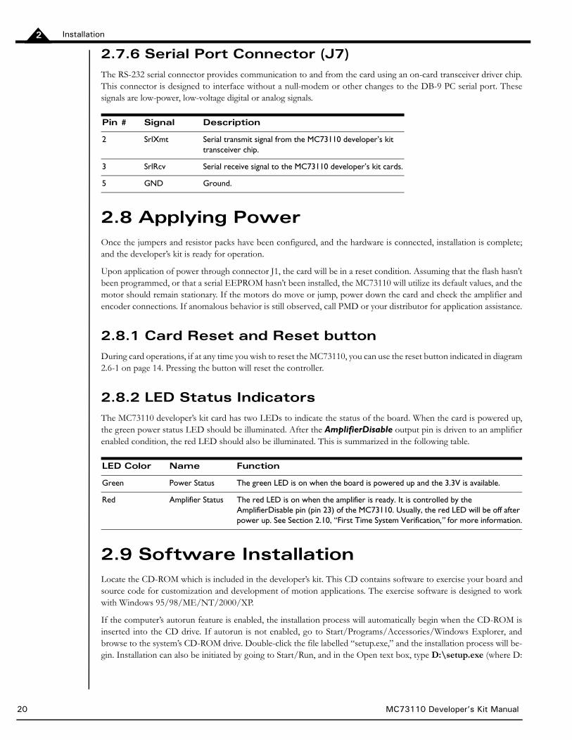
2.7.6 Serial Port Connector (J7)The RS-232 serial connector provides communication to and from the card using an on-card transceiver driver chip.This connector is designed to interface without a null-modem or other changes to the DB-9 PC serial port. Thesesignals are low-power, low-voltage digital or analog signals.
2.8 Applying PowerOnce the jumpers and resistor packs have been configured, and the hardware is connected, installation is complete;and the developer’s kit is ready for operation.
Upon application of power through connector J1, the card will be in a reset condition. Assuming that the flash hasn’tbeen programmed, or that a serial EEPROM hasn’t been installed, the MC73110 will utilize its default values, and themotor should remain stationary. If the motors do move or jump, power down the card and check the amplifier andencoder connections. If anomalous behavior is still observed, call PMD or your distributor for application assistance.
2.8.1 Card Reset and Reset buttonDuring card operations, if at any time you wish to reset the MC73110, you can use the reset button indicated in diagram2.6-1 on page 14. Pressing the button will reset the controller.
2.8.2 LED Status IndicatorsThe MC73110 developer’s kit card has two LEDs to indicate the status of the board. When the card is powered up,the green power status LED should be illuminated. After the AmplifierDisable output pin is driven to an amplifierenabled condition, the red LED should also be illuminated. This is summarized in the following table.
2.9 Software InstallationLocate the CD-ROM which is included in the developer’s kit. This CD contains software to exercise your board andsource code for customization and development of motion applications. The exercise software is designed to workwith Windows 95/98/ME/NT/2000/XP.
If the computer’s autorun feature is enabled, the installation process will automatically begin when the CD-ROM isinserted into the CD drive. If autorun is not enabled, go to Start/Programs/Accessories/Windows Explorer, andbrowse to the system’s CD-ROM drive. Double-click the file labelled “setup.exe,” and the installation process will be-gin. Installation can also be initiated by going to Start/Run, and in the Open text box, type D:\setup.exe (where D:
Pin # Signal Description
2 SrlXmt Serial transmit signal from the MC73110 developer’s kit transceiver chip.
3 SrlRcv Serial receive signal to the MC73110 developer’s kit cards.
5 GND Ground.
LED Color Name Function
Green Power Status The green LED is on when the board is powered up and the 3.3V is available.
Red Amplifier Status The red LED is on when the amplifier is ready. It is controlled by the AmplifierDisable pin (pin 23) of the MC73110. Usually, the red LED will be off after power up. See Section 2.10, “First Time System Verification,” for more information.
20 MC73110 Developer’s Kit Manual

Installation 2
is the drive letter of the CD-ROM drive), and click OK. The installation program will guide you through installing thesoftware. Upon completion of the installation process, the following components will be installed:
Pro-Motor—an application for communicating to and exercising the installed developer’s kit. Refer to Chapter 3, “Using Pro-Motor,” for operating instructions.
C-Motion—source code that can be used for developing customized motion applications based on the MC73110. Refer to Chapter 4, “Developing Applications with C-Motion,” for further information. These files are installed in the “C-Motion” folder, a subfolder of the installation folder.
PDF versions of the developer’s kit manual, programmer’s reference and user’s guide. Adobe Reader is re-quired for viewing and printing these files. If Adobe Reader is not installed, it may be downloaded at no charge from http://www.adobe.com.
2.10 First Time System VerificationAfter the card hardware has been installed, the appropriate motor connections have been made, and software instal-lation is complete, it’s time to perform a simple test which will verify that all connections are correct. The followingprocedure should work for the majority of brushless motors, even if the gain parameters may not be optimized foryour particular motor. Note that at any time the Pause/Break key can be pressed to disable the servo loops and motoroutput in case the motor begins to move erratically or uncontrollably.
1 Run Pro-Motor by double-clicking the Pro-Motor icon on the desktop.
2 If Pro-Motor cannot find the DK board, re-check the serial port connections, select the appropriate COMport in the Interface dialog, and click OK. Accept the default serial port settings by clicking OK. Refer tosection 3.1 Communication for more information.
3 The Axis Wizard should start automatically to lead you through the setup and initialization step. SeeChapter 3, “Using Pro-Motor,” for more information on using the Axis Wizard.
If unexpected motion occurs, the Pause/Break key can be hit to reset the MC73110 and disable the motor.
MC73110 Developer’s Kit Manual 21

Installation2
This page intentionally left blank.
22 MC73110 Developer’s Kit Manual

3
MC73110 Developer’s Kit Manual
3. Using Pro-Motor
In This Chapter Communication Axis Wizard Main Window Storing Commands to Flash Memory Creating an EEPROM FileThe Pro-Motor program facilitates the exercising of the MC73110. All chip parameters can be viewed and modified viastandard Windows controls.
Pro-Motor features:
Project window for accessing MC73110 parameters via properties dialog boxes. Command window for direct text command entry. Communications monitor that echoes all commands sent by Pro-Motor to the MC73110.
Figure 3-1: Main window
MC73110 Developer’s Kit Manual 23
Using Pro-Motor3
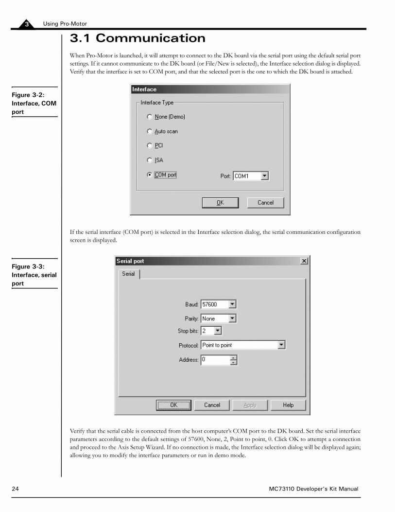
3.1 CommunicationWhen Pro-Motor is launched, it will attempt to connect to the DK board via the serial port using the default serial portsettings. If it cannot communicate to the DK board (or File/New is selected), the Interface selection dialog is displayed.Verify that the interface is set to COM port, and that the selected port is the one to which the DK board is attached.
If the serial interface (COM port) is selected in the Interface selection dialog, the serial communication configurationscreen is displayed.
Verify that the serial cable is connected from the host computer’s COM port to the DK board. Set the serial interfaceparameters according to the default settings of 57600, None, 2, Point to point, 0. Click OK to attempt a connectionand proceed to the Axis Setup Wizard. If no connection is made, the Interface selection dialog will be displayed again;allowing you to modify the interface parameters or run in demo mode.
Figure 3-2: Interface, COM port
Figure 3-3: Interface, serial port
24 MC73110 Developer’s Kit Manual

Using Pro-Motor 3
3.2 Axis Setup WizardOnce communication has been established with the DK board, the connected motors may be put in motion by settingthe appropriate Axis parameters.
When Pro-Motor is run for the first time, the Axis Setup Wizard will automatically start to configure the axis. TheAxis Wizard can also be selected from the View menu at any time. To continue through the configuration process forall of the axis’ parameters, click “Next.” To accept the default values, click “Cancel.”
Individual Axis settings may be modified at any time via Pro-Motor’s Axis Properties dialog box, which is accessedby right-clicking an Axis icon in the Project window and selecting “Properties.”
The Axis Setup Wizard may be re-run at any time by selecting “Axis Wizard” from Pro-Motor’s View menu.
Figure 3-4: Axis Properties dialog
Figure 3-5: Axis Setup Wizard opener
MC73110 Developer’s Kit Manual 25
Using Pro-Motor3
26 MC73110 Developer’s Kit Manual
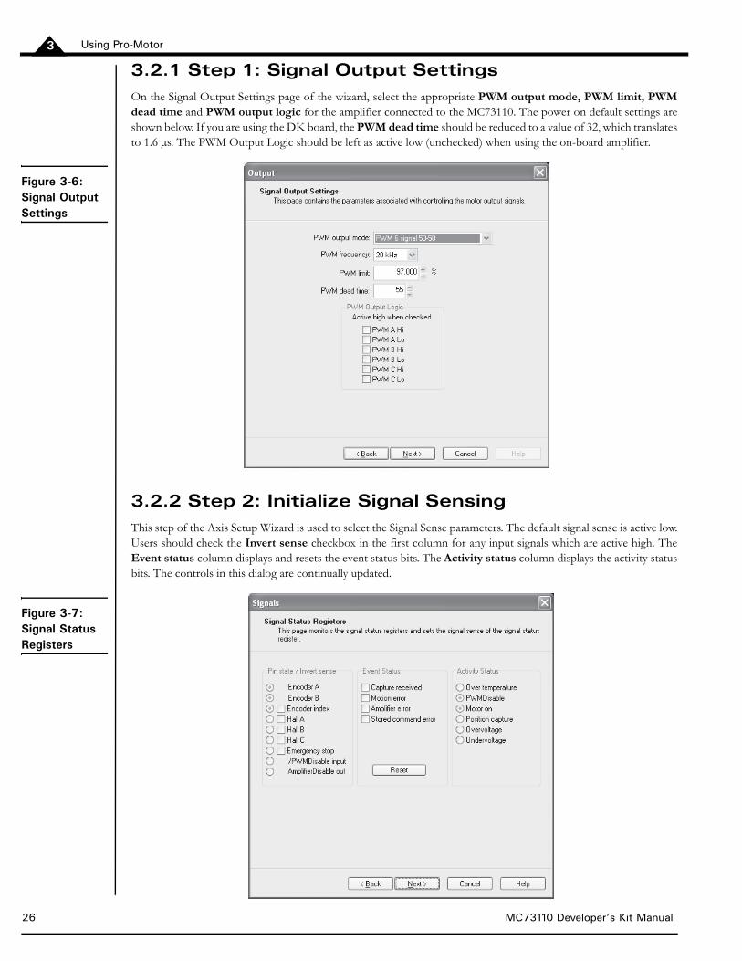
3.2.1 Step 1: Signal Output SettingsOn the Signal Output Settings page of the wizard, select the appropriate PWM output mode, PWM limit, PWMdead time and PWM output logic for the amplifier connected to the MC73110. The power on default settings areshown below. If you are using the DK board, the PWM dead time should be reduced to a value of 32, which translatesto 1.6 µs. The PWM Output Logic should be left as active low (unchecked) when using the on-board amplifier.
3.2.2 Step 2: Initialize Signal SensingThis step of the Axis Setup Wizard is used to select the Signal Sense parameters. The default signal sense is active low.Users should check the Invert sense checkbox in the first column for any input signals which are active high. TheEvent status column displays and resets the event status bits. The Activity status column displays the activity statusbits. The controls in this dialog are continually updated.
Figure 3-6: Signal Output Settings
Figure 3-7: Signal Status Registers

Using Pro-Motor 3
MC73110 Developer’s Kit Manual 27
3.2.3 Step 3: Safety SettingsThis step of the Axis Setup Wizard is used to set the Safety parameters. The settings as shown in Figure 3-8 will:
1. Disable the amplifier if the temperature exceeds 60°C or the Emergency stop signal is set. This particular configuration will latch the amplifier as disabled, because the Amplifier Disable
Source is set to Amplifier error, which is latched in the Event Status register (see Section 3.2.2, “Step 2: Initialize Signal Sensing”).
2. Disable the servo loop if the Motion error exceeds 100000.
Refer to the MC73110 Product Manual for further information on these settings.
3.2.4 Step 4: CommutationThis step of the Axis Setup Wizard is used to set the Commutation parameters. If the Commutation mode is set toSinusoidal, the motor will commutate in hall-based mode until a hall signal transition occurs. The phase angle pa-rameter is read-only and cannot be set in the dialog box. However, it can be set in the command window using theSetPhaseAngle command. Please see the MC73110 Product Manual for further information on phase initialization.
Figure 3-8: Safety Settings
Figure 3-9: Commutation Settings

Using Pro-Motor3
28 MC73110 Developer’s Kit Manual
3.2.4.1 Step 4a: Check CommutationThe commutation may be verified by running the motor in open loop mode. Set the motor command parameter to alow value between 1% and 15%; bearing in mind that the motor may start to move at a rate proportional to the motorcommand setting. Click the Open loop start button. If the motor is commutating properly, a smooth, continuousmotion should occur in a single direction. Click the Stop button to stop motion. If the motor does not move or motionis erratic, verify that Phase counts and signal sense is set correctly. The signal sense can be accessed by going backto the Signals page.
3.2.5 Step 5: Velocity Integrator Loop ParametersThis step of the Axis Setup Wizard is used to select the Velocity Integrator Loop parameters.
3.2.6 Step 6: Velocity Loop ParametersThis step of the Axis Setup Wizard is used to select the Velocity Loop parameters.
Figure 3-10: Velocity Integrator Loop
Figure 3-11: Velocity Loop

Using Pro-Motor 3
MC73110 Developer’s Kit Manual 29
3.2.7 Step 7: Current Loop ParametersThis step of the Axis Setup Wizard is used to select the Current Loop parameters.
3.2.8 Step 8: Miscellaneous SettingsThe Miscellaneous Settings page contains the parameters for controlling the servo loops and motor dynamics. Thepower-on default settings are shown in the following figure. When Motor Mode is off, all the loops are disabled (openloop mode) and Motor command controls the motor speed. The dynamics settings have no effect in this mode.
When the command source is set to Analog, the command for the velocity or current loops originates from the an-alog input signal. When set to SPI, the command for the velocity or current loops is a 16-bit value read from the in-coming SPI data stream. When set to Profile Generator, the command is generated internally based on the Velocityand Acceleration parameters.
Click the Finish button to update the motion processor parameters.
Figure 3-12: Current Loop Settings
Figure 3-13: Motion Dynamics Settings

Using Pro-Motor3
3.3 Main WindowThe main window is comprised of three subwindows: the project window, the command window and the output win-dow. The workspace and output windows are control bars which can be docked and resized at any location in the mainwindow, or undocked and moved anywhere on the desktop. They can be closed by clicking the X. To re-display them,select the appropriate View menu item.
The following keyboard shortcuts can be used at any time.
the Pause/Break key will disable the servo loops and motor output by setting MotorMode to 0 and Motor-Command to 0.
the Scroll Lock key will start and stop the output window from displaying communication activity.
3.3.1 Project Window
The Project window displays the available DK boards and axes in a tree format. Double-clicking a board or axis iconwill display the properties dialog for that item.
Figure 3-14: Project window
Figure 3-15: Axis item properties dialog
30 MC73110 Developer’s Kit Manual

Using Pro-Motor 3
3.3.2 Command Window
The Command window in Pro-Motor allows commands to be issued directly to the MC73110. The window has a com-mand line style interface which accepts all of the MC73110 commands. The MC73110 Programmer’s Reference containsa full list of commands, along with their required parameters. The command window presents you with the commandprompt “>’. The following sequence shows a typical command session.
> ResetProcessor reset> SetSignalSense 0x380> SetPWMDeadTime 36> SetPhaseCounts 2000> SetLoopGain 0x0 50> SetLoopGain 0x10 300> SetLoopGain 0x20 30000> SetVelocityScalar 2000
The Command window is not case-sensitive, so commands may be entered in any combination of upper- and lower-case characters. As shown in the preceding example, commands are entered as a sequence of command name followedby up to two numeric parameters. Parameters can represent a single 16-bit word of data, or a 32-bit double word ofdata; depending on the requirements of the particular command.
> SetLoopGain 1 300
In this example, the first parameter represents a 16-bit word containing the selected loop gain, and the second param-eter represents a 32-bit word that contains the loop gain value.
All of the “Get” commands display the value returned by the chipset.
> GetEventStatus0x0309
Some commands require a parameter for selecting the desired value.
> GetLoopGain 163000
In this example, 16 selects the loop gain number for which the value is retrieved. The Command window accepts nu-meric parameters in either decimal or hexadecimal format. Prefixing a numeric parameter with “0x” enters that num-ber using hexadecimal format.
> GetLoopGain 0x103000
Figure 3-16: Command window
MC73110 Developer’s Kit Manual 31

Using Pro-Motor3
Pressing the Tab key at any time will display a list of available commands, based upon what is already typed in thecommand window. If nothing is typed in the command window, then all of the available commands are displayed. Forexample, typing “geta” in the command window will invoke a list containing all the commands beginning with “geta.”
The command window also supports two useful keyboard shortcuts—the UP and DOWN arrows can be used toscroll through previously executed commands. CTRL-R will repeat the last executed command.
3.3.3 Output Window
The Output window displays the stream of commands sent to the MC73110. Any communication errors will also bedisplayed in this window.
3.4 Storing Commands to Flash MemoryAs mentioned in the MC73110 Product Manual, the AmpDisable condition mask must be active when storing com-mands to flash. If the red LED on the DK board is on, then the AmpDisable condition mask is inactive and must bechanged. The simplest way to achieve this is to force the AmpDisable condition mask to look at the Emergency Stopinput. Make sure to press the APPLY button.
Figure 3-17: Select a Command window
Figure 3-18: Output window
32 MC73110 Developer’s Kit Manual

Using Pro-Motor 3
Next, the interpretation (active high vs. active low) of the Emergency Stop input can be changed. With nothing con-nected to the Emergency Stop input, the input will be high, which by default is inactive. Selecting the Emergency Stopcheckbox in the Signals tab will cause the Emergency Stop input to be interpreted as active high. After doing so theAmpDisable condition mask should now be active, and the red LED should be off.
In the File menu is a “Store Commands in Flash” item that can now be selected. This will cause all parameter valuescurrently in Pro-Motor to be stored in the user Flash space on the MC73110. When complete, a reset will occur. Thevalues in Flash will be read and will become the active configuration.
3.5 Creating an EEPROM FileThe Pro-Motor File menu has a “Create EEPROM File” item. This will create an EEPROM file on your PC that con-tains all parameter values currently active in Pro-Motor. This file can be loaded into standard EEPROM programmingsoftware.
Figure 3-19: EStop–Safety window
Figure 3-20: EStop–Signals window
MC73110 Developer’s Kit Manual 33

Using Pro-Motor3
This page intentionally left blank.
34 MC73110 Developer’s Kit Manual

4
MC73110 Developer’s Kit Manual
4. Developing Applications with C-Motion
In This Chapter Theory of UseC-Motion is a “C” source code library containing all the code required for communicating with the motion control pro-cessor using the serial interface.
C-Motion includes the following features:
Axis virtualization The ability to communicate to multiple PMD motion processors Can be easily linked to any “C/C++” application Supports serial communication.
The following files comprise the C-Motion distribution.
C-Motion may be linked to your application code by including the above “C” source files in your application. Then, forany application source file requiring access to the motion processor, #include “C-Motion.h.”
4.1 Theory of UseC-Motion is a set of functions encapsulating the motion processor command set. Every command has as its first param-eter an “axis handle.” The axis handle is a structure containing information about the interface to the motion processor,and the axis number that the handle represents. Before communicating to the motion processor, the axis handle mustbe initialized using the following sequence of commands.
// the axis handlePMDAxisHandle handle;// open serial interface to PMD processor and initialize handle to axis onePMDSetupAxisInterface_Serial( &handle, PMDAxis1, 1 ); // COM1
Once the axis handle has been initialized, any of the motion processor commands may be executed. C-Motion.h includesthe prototypes for all motion processor commands as implemented in C-Motion. Refer to this file for the required pa-rameters for each command. The MC73110 Product Manual is the primary source for information about the operationand purpose of each command.
C-Motion.h/C-Motion.c Definition/declaration of the processor command set.
PMDw32ser.h/PMDw32ser.c Windows serial communication interface functions.
PMDtrans.h/PMDtrans.c Generic transport (interface) functions.
PMDecode.h Defines the processor and C-Motion error codes.
PMDocode.h Defines the control codes for processor commands.
PMDtypes.h Defines the basic types required by C-Motion.
PMDDiag.h/PMDdiag.c Diagnostic utility functions
PMDconio.h/PMDconio.c Console I/O wrapper functions
MC73110 Developer’s Kit Manual 35

Developing Applications with C-Motion4
Every C-Motion processor command returns a status code of type PMDresult. The return code for every commandexecuted should be checked before attempting to execute more commands.
PMDresult result,status;
result = PMDSetVelocity(&handle, 100000);
if (result != PMD_ERR_OK){
printf(“Error: %s\n”, PMDGetErrorMessage(result));return;
}
Many commands require additional parameters. Some standard values are defined by C-Motion and can be used withthe appropriate commands. Refer to PMDtypes.h for a complete list of defined types. A C-Motion function call withthe pre-defined types is shown in the following example.
PMDSetConditionMask(&handle, PMDConditionMaskAmpDisable, PMDConditionOverTemp);
In addition to the processor commands, C-Motion provides several support functions. A subset of these are:
void PMDCloseAxisInterface(PMDAxisHandle* axis_handle);
This should be called to terminate an interface connection.
char *PMDGetErrorMessage(PMDresult errorCode);
This returns a character string representation of the corresponding PMD chip or C-Motion error code.
void GetCMotionVersion(PMDuint8* MajorVersion, PMDuint8* MinorVersion);
This returns the major and minor version number of C-Motion.
36 MC73110 Developer’s Kit Manual

5
MC73110 Developer’s Kit Manual
5. MC73110 Electrical Reference
InThis Chapter User-Settable Jumper Options Connecting to the Card5.1 User-Settable Jumper OptionsThe following table shows the user-settable jumper options for the MC73110 developer’s kit card. For jumper locations,see Figure 5-1.
In addition, the following resistor pack should be installed; dependant upon the use of single or differential quadrature encoders.
JumperJumper Setting Description
JP1, JP2 1-2 Selects RS-232 communication using the on-board transceiver. This is the default position of this jumper.
2-3 Selects RS-485 communication using a user-provided daughtercard. For a complete description of the electrical requirements of this daughtercard, see Section 5.2.3, “RS485 Connector (J3).”
3-4 Reserved.
JP3-JP5 1-2 Reserved; must be set to 1-2.
JP6, JP7 1-2 Selects the use of the on board amplifier/switcher. This is the default setting.
2-3 Selects the use of a remote amplifier/switcher. This setting is useful to verify custom amplifier design, or to connect to more powerful switching blocks.
JP9, JP10 1-2 Reserved; must be set to 1-2.
Resistor Pack How to Set Description
J8 Installed this is the default setting
If you are using differential connections, leave the resistor pack installed.
Removed If you are using single-ended encoder connections, remove the resistor pack.
MC73110 Developer’s Kit Manual 37

MC73110 Electrical Reference5
5.2 Connecting to the CardThere are a total of seven connectors which may be used with the MC73110 Developer’s Kit card . See Section 2.6, “Preparing the Card for Installation,” for addtional information regarding card component details.
Connector Name Function
J1 Power Provides operating power to the developer’s kit card.
J2 Motor feedback Inputs various motor-related signals.
J3 RS-485 Provides communication to and from the card when a multi-drop RS485 is used.
J4 Motor Provides high voltage, high current connections to the motor from the amplifier output.
J5 Remote switcher Inputs and outputs various signals for use with a remote switching block.
J6 Host Inputs and outputs various non-motor commands and feedback signals to and from the developer’s kit card.
J7 Serial port Provides RS-232 communication to and from the card using an on-card transceiver driver chip. This connector is designed to interface directly to the DB9 serial port of a host computer.
Figure 5-1: Location of MC73110 board components
MC73110
J6
J2
U12 U11 U10
U9 U8 U7
J4Motor
J7RS232 Reset
JP7
J9
J5
J3
JP2 JP1
J8
JP9
JP10
Motorfeedback
Host
JP6
JP4
JP5
JP3
J1DC in
38 MC73110 Developer’s Kit Manual

MC73110 Electrical Reference 5
The following is a summary of the required connector types.
5.2.1 Power Connector (J1)The power connector provides power to the card. All other voltages used by the card are derived from this centralsupply using an on-card DC-DC converter. The voltage provided at these connections matches the voltage at whichthe motor will be driven.
5.2.2 Motor Feedback Connector (J2)The motor feedback connector inputs various motor-related signals to the developer’s kit card. All these signals are low-power, low-voltage digital, or analog signals. The mating connector is Tyco/Amp MTA100 series, part # 1-640620-4.
Connector Signal Type # Pins Type
J1 High power 2 Through-hole terminal block (screw connection).
J2 Low-powerdigital & analog
14 Right-angle single-row shrouded header (0.100” pitch friction lock header).
J3 Low-power digital 5 1-in-line 0.100” pitch header.
J4 High power 3 Through-hole terminal block (screw connection).
J5 Low-powerdigital & analog
16 8 x 2 vertical header (2mm pitch).
J6 Low-power digital & analog
12 Right-angle single-row shrouded header(0.100” pitch friction lock header).
J7 Low-power digital 9 Side-facing D-sub 9 (female).
Pin #Signal Name Description
1 V+ 18v–48V. Current capacity specification should be maximum motor drive + 1 Amp (to power the card).
2 PowerGnd Ground return for V+.
Pin # Signal Description
1 +5V This signal provides 5V. This is often useful to power the encoder circuitry.
2 GND This signal provides the digital return.
3 QuadA+ This input signal provides the high side of the differential quadrature input for encoder phase A. For more information on connecting encoders, see Section 2.6, “Preparing the Card for Installation.” If unused, this signal may remain uncon-nected.
4 QuadA- This input signal provides the low side of the differential quadrature input for encoder phase A. When using a single-ended encoder, this pin should remain unconnected. For more information on connecting encoders, see Section 2.6, “Preparing the Card for Installation.” If unused, this signal may remain uncon-nected.
5 QuadB+ This input signal provides the high side of the differential quadrature input for encoder phase B. For more information on connecting encoders, see Section 2.6, “Preparing the Card for Installation.” If unused, this signal may remain uncon-nected.
MC73110 Developer’s Kit Manual 39

MC73110 Electrical Reference5
5.2.3 RS485 Connector (J3)This connector provides communication to/from the card when an external 3.3V RS485 transceiver is being used.The communication signals are low-power, 3.3V. A 3.3V transceiver must be used.
5.2.4 Motor Connector (J4)The motor connector provides the high voltage three-phase outputs from the amplifier/switcher to the motor.
6 QuadB- This input signal provides the low side of the differential quadrature input for encoder phase B. When using a single-ended encoder, this pin should remain unconnected. For more information on connecting encoders, see Section 2.6, “Preparing the Card for Installation.” If unused, this signal may remain uncon-nected.
7 Index+ This input signal provides the high side of the differential quadrature input for the Index signal. For more information on connecting encoders, see Section 2.6, “Pre-paring the Card for Installation.” If unused, this signal may remain unconnected.
8 Index- This input signal provides the low side of the differential quadrature input for the Index signal. When using a single-ended encoder, this pin should be left uncon-nected. For more information on connecting encoders see Section 2.6, “Preparing the Card for Installation.” If unused, this signal may remain unconnected.
9 GND This signal provides the digital return.
101112
HallAHallBHallC
These signals are the Hall sensor inputs. For logic “0,” the signal should be lower than 0.5V; for logic “1,” the signal should be greater than 1.5V.
13 TachIn+ This is the positive input signal for the analog tachometer signal. This signal repre-sents the instantaneous speed of the motor. The input range is +/– 60V. If unused, this signal may remain unconnected.
14 TachIn- (GND) This is the negative input for the analog tachometer signal. The input range is±60V. If unused, this signal may remain unconnected.
Pin # Signal Description
1 SrlXmt This signal provides a serial transmit connection for RS485 communications.
2 SrlRcv This signal provides a serial receive connection for RS485 communications.
3 SrlEnable This signal provides a serial enable connection for RS485 communications.
4 GND Ground.
5 Vcc +5V Vcc provided by card.
Pin # Signal Description
1 MotorC Leg 3 of 3 motor coil connections.
2 MotorB Leg 2 of 3 motor coil connections.
3 MotorA Leg 1 of 3 motor coil connections.
Pin # Signal Description
40 MC73110 Developer’s Kit Manual

MC73110 Electrical Reference 5
5.2.5 Remote Switcher Connector (J5)The remote switcher connector inputs and outputs various signals that make it possible for the user to develop a sep-arate switching block, while still using the digital logic of the DK card to power the motor control IC. All digital signalsare 3.3V maximum.
5.2.6 Host Connector (J6)The host connector inputs and outputs various non-motor related signals to and from the developer’s kit card. Themating connector is Tyco/Amp MTA100 series, part # 1-640620-2.
Pin # Signal Description
1 AmplifierDisable This signal is connected to the AmplifierDisable signal from MC73110. It can be programmed to go inactive under certain erroneous MCP conditions.
2 PWMOutputDisable This signal provides a digital input connected to the MC73110 pin of the same name. A high level on this signal indicates that PWMOutputDisable is not active; a low indicates it is active.
3 I2CClk This signal connects to the remote switcher’s temperature sensor I2C clock connection.
4 I2Cdata This signal connects to the remote switcher’s temperature sensor I2C data connection.
5678910
PWMCHigh/PWMCPWMLowCPWMBHigh/PWMBPWMBLowBPWMAHigh/PWMAPWMALowA
These signals connect to the PWM drive signals of the same name at the MC73110.
11 +3.3V +3.3V power for digital logic.
12 GND Digital return.
1314
AGND Analog returns.
1516
CurrentACurrentB
These analog input signals hold the instantaneous current through phase A and phase B of the motor coils. The input voltage range is 0V to 3.3V; referenced at 1.65V.
Pin # Signal Description
1 Estop This digital input provides an emergency stop signal to the developer’s kit card. Although its function and interpretation are programmable, normally a high signal (greater than 1.5V) indicates an emergency stop is not active; and a low signal (less than .5V) indicates that it is active. If unused, this signal may remain unconnected.
2 AmplifierDisable This digital output signal provides a programmable output signal which indicates the internal state of the MC73110. Normally, a high output indicates an error, while a low signal indicates no error. In addition to being an output at this connector, this signal is also used internally by the MC73110 developer’s kit card to shut down the amplifier’s switchers when the amplifier operates in “internal switcher” mode.NOTE: This output signal is 3.3V CMOS.
3 GND This signal provides a digital ground return.
4 DigitalCmdClk This digital input accepts the SPI datastream “clock” signal. NOTE: The maxi-mum input voltage is 3.3V.
MC73110 Developer’s Kit Manual 41

MC73110 Electrical Reference5
5.2.7 Serial Port Connector (J7)The RS-232 serial connector provides communication to and from the card using an on-card transceiver driver chip.This connector is designed to interface without a null-modem or other changes to the DB-9 PC serial port. Thesesignals are low-power, low voltage digital or analog signals.
5 DigitalCmdData This digital input accepts the SPI datastream “data” signal. NOTE: The maximum input voltage is 3.3V.
6 GND This signal provides a digital ground return.
7 +5V This signal provides 5V for external circuitry.
89
n.c. —
10 AnalogCmd+ This analog input signal provides the positive input of the analog command. Depend-ing on how the MC73110’s control loop has been programmed, this signal repre-sents the desired voltage, torque or velocity. The input range is +/–10V. The reference input can be differential or single-ended.
11 AnalogCmd- This analog input signal provides the negative input of the analog command. Depend-ing on how the MC73110’s control loop has been programmed, this signal repre-sents the desired voltage, torque or velocity. The input range is +/–10V. The reference input can be differential or single-ended. When it is single-ended, AnalogCmd- must be connected to AGND, pin 12.
12 AGND This signal provides an analog ground return.
Pin # Signal Description
2 SrlXmt Serial transmit signal from the MC73110 developer’s kit transceiver chip.
3 SrlRcv Serial receive signal to the MC73110 developer’s kit card.
5 GND Ground.
Pin # Signal Description
42 MC73110 Developer’s Kit Manual

6
MC73110 Developer’s Kit Manual
6. Schematics
In This Chapter Introduction Detailed Schematic Descriptions System Design Using the MC731106.1 IntroductionThe wide-ranging functionality of the DK board includes circuits for motor sensor signal conditioning, host communication,a serial communication port, current sensing, power output for driving brushless DC motors, and housekeeping power.
The usage of the board has been explained in Chapters 2 and 5 of this manual. This section focuses on the details forsystem implementation of the MC73110. For information and details regarding specific components and circuitry, seethe reference schematics, which are included in this section.
The design of the MC73110 DK is detailed in a series of 10 schematic pages. The basic connections of the MC73110 The conditioning circuits of both digital and analog signal, from the host and the motor sensors All connectors on the DK board All jumpers on the DK board An on-board temperature sensor and an optional EEPROM, which communicate with MC73110 via the I2C
bus; it also includes a RS-232 line driver/receiver The power train, which consists of the pre-driver circuitry and a three-phase MOSFET inverter The motor coil current sensing circuits; it includes isolation amplifiers and signal conditioning circuitry The housekeeping power supply; it provides regulated output voltages of +12V, +5V, +3V, and two floating
+5V outputs, and also includes the reset circuitry The analog power supply for the analog circuits Auxiliary circuits currently reserved by PMD; it includes the positive-rail current monitoring circuit, and the
input voltage monitoring circuitFigure 6-1 summarizes the functions of the MC73110 Developer Kit.
Figure 6-1: Function blocks
MC73110 Developer’s Kit Manual 43

Schematics6
6.2 Detailed Schematic Descriptions
Figure 6-2This page shows the basic connection of MC73110.
The MC73110 has multiple Vcc and GND pins. The supply voltage (+3.3V) has a nominal value of 3.3V, and it powersthe digital portion of MC73110. See Figure 6-9 for details of the digital power supply.
Pin 60, Vccp, is the user data voltage pin. By providing a 5V current to this pin, users can store the startup configura-tions in MC73110’s internal memory. When used, Vccp must be directly connected to 5V without any current limitingresistors. When unused, it is connected to GND. Never leave this pin floating.
U18 is a 10MHz clock. Its supply voltage is derived from the 3.3V digital power supply (+3.3V). The ferrite bead, L3,is in a series with the power trace in order to isolate U18 from the rest of the power plane, since U18 supplies thehighest continuous frequency on the board. Similarly, the ferrite bead, L1, is located between pin 39, PLLVcc, and the3.3V digital power supply (+3.3V), because PLLVcc powers the MC73110’s internal PLL module.
R75 is located between the output of U18 and pin 24, ClockIn, of MC73110. This resistor slows the rise/fall time ofthe clock signal, thus improving the EMI performance.
R76, C38, and C39 are MC73110’s external PLL (phase lock loop) filter. C38 and C39 must be non-polarizedcapacitors.
A separate 3.3V analog voltage supply (Ref_3.3) powers the MC73110’s internal analog circuitry. The analog powerand the digital power are AC isolated on the DK board in order to improve the noise immunity and to ensure ADCaccuracy. See Figure 6-10 for details on the analog power supply.
Pins 11 through 22 of the MC73110 are related to its analog circuit, and use the analog ground as the reference.
Pin 21, AnalogVcc, is the analog power supply. The nominal supply voltage is 3.3V.
Pin 20, AnalogRefHigh, is the analog high voltage reference. It is connected to the analog power Ref_3.3 on the DKboard.
Pin 19, AnalogRefLow, is the analog low voltage reference. It is connected to the analog ground.
The 3.3V analog voltage Ref_3.3 acts as both the ADC voltage reference and the voltage supply of MC73110’s analogcircuitry. In order to ensure the ADC accuracy, the mutual coupling between the analog power supply pin pairs(AnalogRefHigh, AnalogRefLow) and reference pin pairs (AnalogVcc, AnalogGND) must be minimized. The DKboard meets this requirement by placing two ceramic capacitors, C40 and C41, close to the two pin pairs, respectively.Furthermore, C40 is on the top of the board, and C41 is on the bottom of the board.
Pins 11 through 14 are reserved, and should be connected to analog ground in customer designs.
Resistors R101 and R102 are for test purposes, and are not required in customer designs.
44 MC73110 Developer’s Kit Manual

Schematics 6
Figure 6-2: Basic connection
5 5
4 4
3 3
2 2
1 1
DD
CC
BB
AA
+3.3
V
Hal
l1H
all2
Hal
l3
Qua
dAQ
uadB
Inde
x
Em
ergS
top
I2C
Clk
I2C
Dat
a
SrlE
nabl
e
Dig
italC
mdC
lkD
igita
lCm
dDat
a
Ser
ialR
cvS
eria
lXm
t
Com
mM
ode
Cur
rent
AC
urre
ntB
Tach
omet
erA
nalo
gCm
d
PW
MO
utpu
tDis
able
Ref
_3.3
Pos
Rai
lCur
rent
+5V
TST8
+3.3
V
TST0
TST1
TST3
TST4
TST5
TST6
TST2
TST7
+3.3
V
Bus
Vol
tage
PW
MA
Hi/P
WM
AP
WM
ALo
PW
MB
Hi/P
WM
BP
WM
BLo
PW
MC
Hi/P
WM
CP
WM
CLo
Am
pDis
able
Res
et
+3.3
V
+3.3
V
Title
Siz
eD
ocum
ent N
umbe
rR
ev
Dat
e:S
heet
of
0401
1620
2D
MC
7311
0 D
K
B
110
Tues
day,
Mar
ch 2
7, 2
007
Title
Siz
eD
ocum
ent N
umbe
rR
ev
Dat
e:S
heet
of
0401
1620
2D
MC
7311
0 D
K
B
110
Tues
day,
Mar
ch 2
7, 2
007
Title
Siz
eD
ocum
ent N
umbe
rR
ev
Dat
e:S
heet
of
0401
1620
2D
MC
7311
0 D
K
B
110
Tues
day,
Mar
ch 2
7, 2
007
Perf
orm
ance
Mot
ion
Dev
ices
, Inc
.
L3L3
C39
0.01
5uC
390.
015u
U18
CB
3LV
U18
CB
3LV
EN
1
GN
D2
Out
put
3
Vcc
4
U37 MC
7311
0
U37 MC
7311
0
I2C
Dat
a63
I2C
Clk
64
SrlX
mt
43S
rlRcv
44
Com
mun
icat
ionM
ode
1
SrlE
nabl
e46
PW
MA
Hig
h/P
WM
A59
PW
MA
Low
58P
WM
BH
igh/
PW
MB
57P
WM
BLo
w54
PW
MC
Hig
h/P
WM
C53
PW
MC
Low
50
Hal
l 140
Hal
l 241
Hal
l 349
Ana
logR
efH
igh
20A
nalo
gRef
Low
19A
nalo
gVcc
21A
nalo
gGN
D22
Cur
rent
A18
Cur
rent
B17
Qua
dA4
Qua
dB3
Inde
x2
Tach
omet
er16
Ana
logC
md
15A
nalo
gGN
D14
Bus
Vol
tage
13A
nalo
gGN
D12
Ana
logG
ND
11
Am
plife
rDis
able
23
PW
MO
utpu
tDis
able
36
Osc
filte
r 238
Osc
filte
r 137
Res
erve
d61
Res
erve
d62
Res
et28
Vccp60
Clo
ckIn
24
GND 5GND 26GND 55
GND 9GND 34GND 51
Vcc6Vcc27Vcc56
Vcc10Vcc35Vcc52
PLL
Vcc
39
Dig
italC
mdC
lk47
Dig
italC
mdD
ata
45
Res
erve
d25
Res
erve
d7
Res
erve
d8
Res
erve
d29
Res
erve
d30
Res
erve
d31
Res
erve
d32
Res
erve
d48
Res
erve
d33
Est
op42
C41
0.1u
C41
0.1u
C63 0.
1uC
63 0.1u
R75
22R
7522
L1L1
C38
0.68
uC
380.
68u
R10
1
10.0
k
R10
1
10.0
k
R76
11R
7611
R10
2
10.0
k
R10
2
10.0
k
C40 0.
1uC
40 0.1u
C66 0.
1uC
66 0.1u
MC73110 Developer’s Kit Manual 45

Schematics6
Figure 6-3This page details the conditioning circuitry for the digital and analog signals from the host and the motor sensors.
U1, DS26LV32AT, is a RS-422 line receiver. With the use of a 120~150 resistor pack (located at J8 in Figure 6-4), theDK board may be configured for differential encoder inputs. The resistors at inputs (R1~R4, R6~R9, R10~R13) con-figure fail-safe connections. When the encoder connection is broken or shorted, the corresponding output of U1 islogic high.
D1, MMBZ5221B, is a Zener diode with nominal voltage of 2.4V. It sets a bias voltage at the negative inputs of U1.Therefore, the DK board can also be configured for single-ended encoder input. Without the resistor pack at J8,connect the single-ended encoder signal to the positive input, and leave the negative input floating.
U3(A/B/C), 74HC14, is a Hex-inverting Schmitt trigger. It conditions Hall signals from either a commutation encoderor from magnetic sensors. The resistor/capacitor pairs (R21/C6, R25/C7, R27/C8) are low-pass filters used to rejectnoise on the input signals, and the Schmitt input further improves the noise immunity. The pull-up resistors (R16, R24,R26) are used when the Hall signal type is open-collector. The input resistors (R21, R25, R27) are used to limit theinput current into the 3.3V Schritt trigger buffers.
U2, TLV2474, is a quad rail-to-rail op amp. It is referenced to the analog ground and powered by a 3.3V analog supply(Analog_3.3). See Figure 6-10 for details on the analog power supply.
U2B/C/D is the conditioning circuit for analog command (AnalogCmd+, AnalogCmd-) with differential inputs.
U2B is configured as a difference amplifier with R32=R35 and R29=R36. Its balanced input impedance rejects thecommon-mode noise on the analog command. The tolerance of the resistors is 1% in order to ensure the differenceamplifier’s performance.
U2C is a voltage follower with output voltage 1.65V, which is from Ref_0shift in Figure 6-10. It sets a 1.65V DC biasat the output of U2B, which corresponds to zero output of the internal ADC of the MC73110.
The analog command (AnalogCmd+/–) is between -10V and +10V, and the output of U2B is determined using thefollowing formula.
(AnalogCmd + –AnalogCmd -)*R29/R32+1.65=0.14(AnalogCmd + –AnalogCmd -)+1.65 V
Therefore, a +10V command corresponds to 3.05V output, and a -10V command corresponds to 0.25V output. A0.25V safety margin remains between U2’s maximum output range and the monotonic conversion range of theMC73110’s internal ADC.
U2D is a Butterworth second-order low-pass filter with unity gain and a cutoff frequency of 5KHz. It attenuates highfrequency noise on the command signal and acts as an anti-aliasing filter for the internal ADC of the MC73110.
U2A is a first-order low-pass filter for conditioning the tachometer signal TachIn+. Its output has a DC bias of 1.65Vand the cutoff frequency is 1/(2*pi*R14*C4)= 4.4 KHz. When the tachometer signal is much lower than 4.4KHz, thislower-pass filter only scales and shifts the tachometer signal. For example, when the tachometer input signal is lowerthan 400Hz, the output of U2A is determined using the following formula.
R14/(R17+R18)*(TachIn+)+1.65=0.0221(TachIn+) + 1.65 V
C5 is optional, and may be installed to configure the U2A as a second-order filter.
46 MC73110 Developer’s Kit Manual

Schematics 6
Figure 6-3: Conditioning circuitry
5 5
4 4
3 3
2 2
1 1
DD
CC
BB
AA
+3.3
V
Qua
dA
Inde
x
Qua
dA+
Qua
dA-
Qua
dB+
Qua
dB-
Inde
x+In
dex-
+5V
2.4V
_bia
s
2.4V
_bia
s
2.4V
_bia
s
2.4V
_bia
s
+5V
+5V
+5V
Tach
In+
Tach
omet
er
Ref
_gro
up1
Qua
dB
Hal
lA
Hal
lB
Hal
lC
+3.3
V
Hal
l1
Hal
l2
Hal
l3
+5V +5
V
+5V
Ana
log_
3.3
+3.3
V
Em
ergS
top
+3.3
V
ES
top
+3.3
V
Am
pDis
able
Am
plifi
erD
isab
le
+3.3
V
Ref
_0sh
ift
Ana
logC
md+
Ana
logC
md-
Ana
logC
md
Ref
_gro
up1
Title
Siz
eD
ocum
ent N
umbe
rR
ev
Dat
e:S
heet
of
0401
1620
2D
MC
7311
0 D
K
B
210
Tues
day,
Mar
ch 2
7, 2
007
Title
Siz
eD
ocum
ent N
umbe
rR
ev
Dat
e:S
heet
of
0401
1620
2D
MC
7311
0 D
K
B
210
Tues
day,
Mar
ch 2
7, 2
007
Title
Siz
eD
ocum
ent N
umbe
rR
ev
Dat
e:S
heet
of
0401
1620
2D
MC
7311
0 D
K
B
210
Tues
day,
Mar
ch 2
7, 2
007
Perf
orm
ance
Mot
ion
Dev
ices
, Inc
.No
te:
C11
is a
res
isto
r.
Motor Feedback Signals
Host Signals
R6
4.7k
R6
4.7k
R27
10k
R27
10k
R28
5.1k
R28
5.1k
U3A
74H
C14
U3A
74H
C14
12
14 7
U1
DS
26LV
32A
TU
1D
S26
LV32
AT
RI1
-1
RI1
+2
RO
13
EN
4
RO
25
GND 8
RO
311
EN
12
RO
413
Vcc16
RI4
+14
RI4
-15
RI2
+6
RI2
-7
RI3
+10
RI3
-9
C15
0.1uC15
0.1u
U4B
MM
74H
C12
5U
4BM
M74
HC
125
56
144
7
C3
0.1uC
30.
1u
R10
4.7k
R10
4.7k
R30
45.0
kR
3045
.0k
R9
4.7k
R9
4.7k
C6
10nC6
10n
R37
10k
R37
10k
U3B
74H
C14
U3B
74H
C14
34
14 7
R33
29.4
kR
3329
.4k
R1
4.7k
R1
4.7k
R35
36.5
kR
3536
.5k
C11
39.2
kC
1139
.2k
C7
10nC7
10n
R19
60.4
KR
1960
.4K
R13
4.7k
R13
4.7k
R38
10k
R38
10k
R34
15.8
kR
3415
.8k
R32
36.5
kR
3236
.5kU3F
74H
C14
U3F
74H
C14
1312
14 7
R26
4.7k
R26
4.7k
R2
470
R2
470
R7
470
R7
470
D1
MM
BZ5
221B
D1
MM
BZ5
221B
13
2
- +
U2D
TLV
2474
- +
U2D
TLV
2474
121314
411
C10
2.2n
C10
2.2n
R29
5.11
kR
295.
11k
C8
10nC8
10n
- +
U2A
TLV
2474
- +
U2A
TLV
2474
321
411
R31
15.8
kR
3115
.8k
U3C
74H
C14
U3C
74H
C14
56
14 7
R16
4.7k
R16
4.7k
R17
60.4
KR
1760
.4K
R11
470
R11
470
R20
30.1
KR
2030
.1K
R8
470
R8
470
R21
10k
R21
10k
R5
130
R5
130
R36
5.11
k
R36
5.11
k
- +
U2B
TLV
2474
- +
U2B
TLV
2474
567
411
C12
1nC12
1n
C4
18n
C4
18n
R23
2kR23
2k
R3
470
R3
470
R14
2kR
142k
C5
NU
C5
NU
R4
4.7k
R4
4.7k
R24
4.7k
R24
4.7k
R25
10k
R25
10k
R18
30.1
KR
1830
.1K
R12
470
R12
470
- +
U2C
TLV
2474
- +
U2C
TLV
2474
1098
411
MC73110 Developer’s Kit Manual 47

Schematics6
Figure 6-4This page shows all connectors on the DK board. Please refer to Section 2.7, "Connecting to the Card,” for the com-ponent definitions and functionality.
48 MC73110 Developer’s Kit Manual

Schematics 6
Figure 6-4: Connectors
5 5
4 4
3 3
2 2
1 1
DD
CC
BB
AA
Mot
orB
Hal
lAH
allB
Hal
lCTa
chIn
+
Est
op
Dig
italC
mdC
lkD
igita
lCm
dDat
a
Am
plifi
erD
isab
le
SrlX
mt
SrlR
cvS
rlEna
ble
+5V
PW
MC
Lo
+5V
Pow
er_R
ail+
SrlX
mtB
uffe
red
SrlR
cvB
uffe
red
TST8
TST7
+5V
TST0
TST1
TST3
TST4
TST5
TST6
TST2
Mot
orA
Mot
orC
Ana
logC
md-
Ana
logC
md+
Cur
rent
AC
urre
ntB
I2C
Clk
I2C
Dat
aA
mpl
ifier
Dis
able
PW
MC
Hi/P
WM
CP
WM
BH
i/PW
MB
PW
MA
Hi/P
WM
AP
WM
BLo
PW
MA
Lo
+5V
Inde
x-In
dex+
Qua
dB-
Qua
dB+
Qua
dA-
Qua
dA+
+3.3
V
Inde
x+In
dex-
Qua
dB-
Qua
dB+
Qua
dA+
Qua
dA-
PW
MO
utpu
tDis
able
Title
Siz
eD
ocum
ent N
umbe
rR
ev
Dat
e:S
heet
of
0401
1620
2D
MC
7311
0 D
K
B
310
Tues
day,
Mar
ch 2
7, 2
007
Title
Siz
eD
ocum
ent N
umbe
rR
ev
Dat
e:S
heet
of
0401
1620
2D
MC
7311
0 D
K
B
310
Tues
day,
Mar
ch 2
7, 2
007
Title
Siz
eD
ocum
ent N
umbe
rR
ev
Dat
e:S
heet
of
0401
1620
2D
MC
7311
0 D
K
B
310
Tues
day,
Mar
ch 2
7, 2
007
Motor Feedback
Motor
Serial Port
RS-485
Host
Power
Perf
orm
ance
Mot
ion
Dev
ices
, Inc
.
(Tac
hIN-
)
Terminal Resistor Pack
Test
Por
t (R
eser
ved)
Powe
rGND
Remote Switcher
J5J5
12
34
56
78
910
1112
1314
1516
J4J4 1 2 3J1J1 1 2
J3J3
1 2 3 4 5
J6J6
1 2 3 4 5 6 7 8 9 10 11 12
J8J8
1 2 3 4 5 6
J9J9
1 2 3 4 5 6 7 8 9
J7J7
59
48
37
26
1
J2J2
1 2 3 4 5 6 7 8 9 10 11 12 13 14
MC73110 Developer’s Kit Manual 49

Schematics6
Figure 6-5This page shows all jumpers on the DK board. Please refer to Section 2.6, "Preparing the Card for Installation,” forthe component definitions and functionality.
50 MC73110 Developer’s Kit Manual

Schematics 6
Figure 6-5: Jumpers
5 5
4 4
3 3
2 2
1 1
DD
CC
BB
AA
Ser
ialX
mt_
1S
eria
lXm
t
I2C
Clk
SrlX
mt
I2C
Clk
_MC
I2C
Dat
a_M
CS
eria
lXm
t
I2C
Clk
Ser
ialR
cv
I2C
Dat
a
+3.3
V
Com
mM
ode
+3.3
Vre
mot
e_cu
rren
t
I2C
Dat
a
Ser
ialR
cv_1
Ser
ialR
cvS
rlRcv
rem
ote_
switc
her
Am
pEna
ble
+3.3
V+3
.3V D
igita
lCm
dDat
a
Ana
log_
3.3
Title
Siz
eD
ocum
ent N
umbe
rR
ev
Dat
e:S
heet
of
0401
1620
2D
MC
7311
0 D
K
B
410
Tues
day,
Mar
ch 2
7, 2
007
Title
Siz
eD
ocum
ent N
umbe
rR
ev
Dat
e:S
heet
of
0401
1620
2D
MC
7311
0 D
K
B
410
Tues
day,
Mar
ch 2
7, 2
007
Title
Siz
eD
ocum
ent N
umbe
rR
ev
Dat
e:S
heet
of
0401
1620
2D
MC
7311
0 D
K
B
410
Tues
day,
Mar
ch 2
7, 2
007
JP1 and JP2 set the transmission mode:
2-3 RS 422/485 communication using user-provided daugher-card
3-4 Reserved
JP3, JP4, JP5: Reserved, must be set 1-2
JP6 and JP7 select on-board or remote amplifier/switcher
1-2 On-board amplifier/switcher (default)
2-3 Remote amplifier/switcher
1-2 RS-232 communication using on-board transceiver (default)
Perf
orm
ance
Mot
ion
Dev
ices
, Inc
.JP9, JP10: Reserved, must be set to 1-2
Jumpers
JP7
JP7
11
22
33
R10
610
kR
106
10k
R10
510
kR
105
10k
JP9
JP9
11
22
33
JP1
JP1 1
12
23
34
4
JP6
JP6
11
22
33
JP4
JP4
11
22
33
R71
10k
R71
10k
JP5
JP5
11
22
33
JP10
JP10
11
22
33
JP2
JP2
11
22
33
44
JP3
JP3
11
22
33
MC73110 Developer’s Kit Manual 51

Schematics6
Figure 6-6This schematic includes an on-board temperature sensor and an optional EEPROM. The MC73110 communicateswith both parts via the I2C bus. This schematic also includes an on-board RS-232 line driver/receiver.
U5, TMP 100, is a digital temperature sensor with an I2C bus interface. It is located on the bottom of the DK board,and is near the three-phase inverter. Thus, the MC73110 can monitor the temperature of the power train by commu-nicating with TMP 100.
U6, 24LC256, is an EEPROM with an I2C bus interface. It is optional, and only an 8-pin DIP socket is provided onthe DK board. The EEPROM is plugged into the socket when used.
The I2C bus address of U5 and U6 have been hardwired as 1001000 and 1010000, respectively.
R41~R46 are protection resistors against voltage spikes on the I2C bus. R39 and R40 are pull-up resistors. The resis-tance of the series resistors has an upper limit, while the resistance of the pull-up resistors has a lower limit. The se-lection of these resistors depends on the supply voltage, load capacitance, and specific components. Please refer to I2Cbus specifications for the components you are using.
If additional I2C bus devices are attached to the DK board through the remote switcher connectors, then the followingconditions apply.
1 The additional I2C bus devices cannot use addresses 1001000 and 1010000.
2 The attached I2C bus should not have pull-up resistors. However, should additional resistors be used, theirimpedance must be higher than 4K.
3 The load capacitance must be confirmed if there are more than two additional I2C bus devices attached.
4 The I2C bus voltage is 3.3V on the DK board. If devices utilizing different voltages are attached, voltageshift circuit may be necessary.
U34, MAX3232, is a RS-232 line driver/receiver. It is powered by 3.3V
52 MC73110 Developer’s Kit Manual
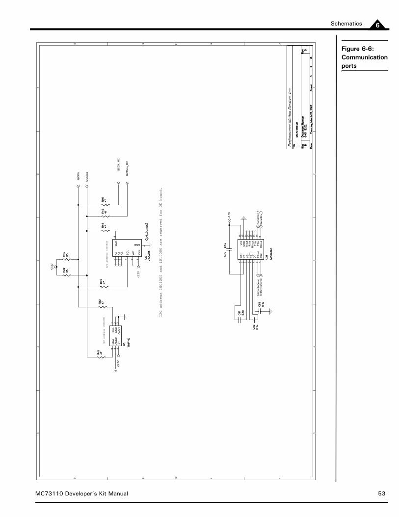
Schematics 6
Figure 6-6: Communication ports
5 5
4 4
3 3
2 2
1 1
DD
CC
BB
AA
+3.3
V
I2C
Clk
I2C
Dat
a
I2C
Clk
_MC
I2C
Dat
a_M
C
+3.3
V
+3.3
V
+3.3
V
SrlX
mtB
uffe
red
Ser
ialX
mt_
1S
eria
lRcv
_1S
rlRcv
Buf
fere
d
Title
Siz
eD
ocum
ent N
umbe
rR
ev
Dat
e:S
heet
of
0401
1620
2D
MC
7311
0 D
K
B
510
Tues
day,
Mar
ch 2
7, 2
007
Title
Siz
eD
ocum
ent N
umbe
rR
ev
Dat
e:S
heet
of
0401
1620
2D
MC
7311
0 D
K
B
510
Tues
day,
Mar
ch 2
7, 2
007
Title
Siz
eD
ocum
ent N
umbe
rR
ev
Dat
e:S
heet
of
0401
1620
2D
MC
7311
0 D
K
B
510
Tues
day,
Mar
ch 2
7, 2
007
I2C
addr
ess
1001
000
I2C
addr
ess
1010
000
I2C address 1001000 and 1010000 are reserved for DK board.
Perf
orm
ance
Mot
ion
Dev
ices
, Inc
.
Optional
C81
0.1u
C81
0.1u
R40
8KR40
8K
U5
TMP
100
U5
TMP
100
SC
L1
GN
D2
AD
D1
3V
+4
AD
D0
5S
DA
6
R45
47R45
47R
4447R
4447
C82
0.1u
C82
0.1u
R41
47R41
47R
4647R
4647
R43
47R43
47
U6
24LC
256
U6
24LC
256
GND 4
VC
C8
SD
A5
SC
L6
A0
1A
12
A2
3
WP
7
C83
0.1u
C83
0.1u
U34
MA
X32
32
U34
MA
X32
32
C1+
1V
+2
C1-
3C
2+4
C2-
5V
-6
T2ou
t7
R2i
n8
R2o
ut9
T2in
10T1
in11
R1o
ut12
R1i
n13
T1ou
t14
GN
D15
Vcc
16
R42
47R42
47
R39
8KR39
8K
C79
0.1u
C79
0.1u
MC73110 Developer’s Kit Manual 53

Schematics6
Figure 6-7This schematic shows the power train, which includes the pre-driver and a three-phase inverter.
U7~U12, IRF540, are N-channel MOSFETs with a voltage rating of 100V. They are configured as a three-phaseinverter. The MOSFETs switch on and off, based on PWM commands of the MC73110.
Switching the MOSFETs requires that the gate driving signals have enough current sourcing and sinking capacity. Inmany cases, a pre-driver is needed as a buffer between the MC73110 and the three-phase inverter.
U13, IR2133S, is an integrated pre-driver. It accepts logic PWM signals directly from the MC73110. The pre-driver isconfigured as a six-signal mode, and its MOSFET drive outputs have high current sourcing and sinking capacity.
C20~C22 are bootstrap capacitors, which are used by the pre-driver to turn on U7~U9. The value of the bootstrapcapacitors depends on the gate charge of the MOSFET/IGBT and the PWM frequency. Please refer to the manu-facturer’s datasheet of the pre-driver for design guidelines. R62 is used to limit the charging current to the bootstrapcapacitors.
R48~R50 and R55~R57 are used to limit the gate driving currents, and to damp the gate driving signals. The MC73110provides a dead-time option on the PWM commands to prevent shooting-through. Therefore, no hardware dead-timecircuit is used on the DK board.
D3~D5 are not used on the DK board. These diodes, together with R54, R58, and R60, are optional to improve theimmunity to ground spikes. Ground spikes are due to parasitic parameters on the three-phase inverter, and can be ef-fectively limited by proper layout.
R61 is a current sensing resistor, and the voltage drop on R61 is proportional to the low-side current of the power rail.R67, R68, and C26 are low-pass filters and voltage dividers. Therefore, the current trip pin of U13 (ITRIP) monitorslow-side current. Too high a current (~55 Amps) will trigger the protection circuit in U13 and then shut down theinverter. When this happens, /Fault of U13 is asserted logic low.
R61 can detect current fault conditions such as shoot-through, and line-to-line short. However, it cannot detectground fault, since the motor coil is shorted directly to the ground.
R47 is the high-side current sensing resistor. It can detect current faults, including ground fault. However, the voltagesignals on both sides of R47 have large common-mode components, and the signal conditioning circuit must havegood common-mode rejection performance. For additional details, see Figure 6-11.
R52 and R53 are motor coil current sensing resistors and have four-wire connections. A two-end current sensingresistor may also be used. The voltage signal on both sides of the current sensing resistors have large and fast changingcommon-mode components, and special attention should be given to designing signal conditioning circuits. Examplesof these circuits are shown in Figure 6-8.
C19 is a bulk capacitor which is used to attenuate the voltage ripple on the power bus. The user may need additionalexternal capacitors to meet his or her specific requirements on voltage ripple or regenerated power absorption on thepower rail.
54 MC73110 Developer’s Kit Manual

Schematics 6
Figure 6-7: Power train
5 5
4 4
3 3
2 2
1 1
DD
CC
BB
AA
I_A
-I_
A+
I_B
+I_
B-
Rai
l_P
os-
Pow
er_R
ail+
Rai
l_N
eg+
PW
MB
Hi/P
WM
B
+12V
PW
MB
Lo
Rai
l_N
eg+
Am
pDis
able
+3.3
V
Mot
orA
Mot
orB
rem
ote_
switc
her
rem
ote_
switc
her
+12V
AH
_O
CH
_O
AL
CL
AH
_S
CH
_S
BH
_O BL
BL
BH
_S
BH
_S
AH
_OA
L
AH
_S
Mot
orC
CH
_O CL
CH
_S
BH
_O
PW
MC
Hi/P
WM
C
PW
MA
Hi/P
WM
A
PW
MC
Lo
PW
MA
Lo
AH
_SB
H_S
Rai
l_N
eg+
+12V
CH
_SP
WM
Out
putD
isab
le
+3.3
V
Title
Siz
eD
ocum
ent N
umbe
rR
ev
Dat
e:S
heet
of
D
MC
7311
0 D
K
B
610
Tues
day,
Mar
ch 2
7, 2
007
0401
1620
2
Title
Siz
eD
ocum
ent N
umbe
rR
ev
Dat
e:S
heet
of
D
MC
7311
0 D
K
B
610
Tues
day,
Mar
ch 2
7, 2
007
0401
1620
2
Title
Siz
eD
ocum
ent N
umbe
rR
ev
Dat
e:S
heet
of
D
MC
7311
0 D
K
B
610
Tues
day,
Mar
ch 2
7, 2
007
0401
1620
2
Perf
orm
ance
Mot
ion
Dev
ices
, Inc
.
NU:
not
used
D4
NU
D4
NU
13
2
D3
NU
D3
NU
13
2
C20
0.56
uC
200.
56u
C21
0.56
uC
210.
56u
R50
75R
5075
R65
10.0
KR
6510
.0K
R67
1.00
KR
671.
00K
R64
1.00
KR
641.
00K
U9
IRF5
40U
9IR
F540
2
1
3
U13
IR21
33S
U13
IR21
33S
ITR
IP1
FLT-
CLR
2C
AO
3C
A-
4C
A+
5S
D6
VS
S7
CO
M8
LO3
9LO
210
LO1
11V
S3
12H
O3
13V
B3
14V
S2
15H
O2
16V
B2
17V
S1
18H
O1
19V
B1
20V
CC
21H
IN1
22H
IN2
23H
IN3
24LI
N1
25LI
N2
26LI
N3
27FA
ULT
28
R53
CS
R2
R53
CS
R2
41
2
3
C22
0.56
uC
220.
56u
D2
BA
S19
D2
BA
S19
13
2
R56
75R
5675
R48
75R
4875
U4D
MM
74H
C12
5
U4D
MM
74H
C12
5
1211
1413
7
U12
IRF5
40U
12IR
F540
2
1
3
R52
CS
R2
R52
CS
R2
41
2
3
R68
10.0
K
R68
10.0
K
R66
10.0
KR
6610
.0K
R69
10.0
KR
6910
.0K
C26
1nC26
1n
R61
10m
R61
10m
R55
75R
5575
D5
NU
D5
NU
13
2
U4A
MM
74H
C12
5U
4AM
M74
HC
125
23
141
7
R60
0R
600
D6
BA
S19
D6
BA
S19
13
2
R54
0R
540
R58
0R
580
C23
1uC
231u
R63
1.00
KR
631.
00K
R62
2.0
R62
2.0
C19
330u
C19
330u
U10
IRF5
40U
10IR
F540
2
1
3
R49
75R
4975
U7
IRF5
40U
7IR
F540
2
1
3D
7B
AS
19D
7B
AS
19
13
2
U11
IRF5
40U
11IR
F540
2
1
3
U8
IRF5
40U
8IR
F540
2
1
3
R47
10m
R47
10m
R57
75R
5775
MC73110 Developer’s Kit Manual 55

Schematics6
Figure 6-8This schematic shows the motor coil current sensing circuits. It includes isolation amplifiers and low-pass active filters.
The DK board uses series resistors (R52 and R53 in Figure 6-7) to sense coil current. The instantaneous coil currentsare proportional to the voltage drop on the resistors. However, the voltage on both ends of the resistor have large andfast-changing common-mode components, which is several orders larger than the useful voltage drop signal. Isolationamplifiers are used on the DK board to reject the common-mode signal.
U20, U21, and U22A act as the signal conditioning circuit for current signal of motor coil A.
U20, HCPL 7800, is an isolation amplifier. Its high side is powered by a 5V floating voltage (5_f_1+, 5_f_1-), and itslow side is power by a 5V analog voltage. R78 and C50 is an anti-aliasing filter of the on-chip sampling circuit. U20has differential output, which is suitable for noisy industrial environments.
U21, AD623, is an instrumentation amplifier. It converts and scales the differential signals from U20 to a single-endedsignal. R81 is the gain resistor. The output has a DC bias of 1.65V, which corresponds to the zero output of theMC73110’s internal ADC.
Therefore, the output of U21 is determined as:
R52*Gain(U20)*Gain(U21)*I+1.65=10m*8*1.75*I+1.65=0.14*I+1.65 V
where I is the current in motor coil A, which is positive when input to the motor.
U22, TLV2473, is a dual rail-to-rail op amp. It is referenced to the analog ground, and powered by a 3.3V analog supply(Analog_3.3). Details on the analog power supply are in Figure 6-10.
U22A, TLV2473, is a second-order low-pass filter with unity gain and a cutoff frequency of 7.5 KHz. It is configuredas a Bessel filter due to the advantages on group delay. U22 can be shut off by remote_current (see JP7 in Figure 6-5)when a remote switcher is used. The output of U22A is high-impedance when remote_current is pulled down to theground.
U24, U25, and U22B act as the signal conditioning circuit for motor coil B current sensing, and it is symmetric to thatof the coil A current sensing.
56 MC73110 Developer’s Kit Manual

Schematics 6
Figure 6-8: Current-sensingcircuits
5 5
4 4
3 3
2 2
1 1
DD
CC
BB
AA
Cur
rent
AI_
A+
I_A
-
bias
_1.6
5V
bias
_1.6
5V
I_B
+
I_B
-
Cur
rent
B
bias
_1.6
5V
rem
ote_
curr
ent
rem
ote_
curr
ent
Ref
_0sh
ift
+5V
_A
+5V
_A
+5V
_A
+5V
_A
Ana
log_
3.3
Ana
log_
3.3
5_f_
2+
5_f_
2-
5_f_
1+
5_f_
1-
Title
Siz
eD
ocum
ent N
umbe
rR
ev
Dat
e:S
heet
of
0401
1620
2D
MC
7311
0 D
K
B
710
Tues
day,
Mar
ch 2
7, 2
007
Title
Siz
eD
ocum
ent N
umbe
rR
ev
Dat
e:S
heet
of
0401
1620
2D
MC
7311
0 D
K
B
710
Tues
day,
Mar
ch 2
7, 2
007
Title
Siz
eD
ocum
ent N
umbe
rR
ev
Dat
e:S
heet
of
0401
1620
2D
MC
7311
0 D
K
B
710
Tues
day,
Mar
ch 2
7, 2
007
Perf
orm
ance
Mot
ion
Dev
ices
, Inc
.
(Res
erve
d fo
r te
st p
urpo
se)
-+
U21
AD
623
-+
U21
AD
623
RG
-1
IN-
2IN
+3
VE
E4
RG
+8
VC
C7
OU
T6
RE
F5
U20
HC
PL
7800
U20
HC
PL
7800
VD
D1
1
Vin
+2
Vin
-3
GN
D1
4
VD
D2
8
GN
D2
5V
out-
6
Vou
t+7
C56
2.2n
NP
O
C56
2.2n
NP
O- +
U26
CTL
V24
74
- +
U26
CTL
V24
74
1098
411
-+
U25
AD
623
-+
U25
AD
623
RG
-1
IN-
2IN
+3
VE
E4
RG
+8
VC
C7
OU
T6
RE
F5
R80
36.5
KR
8036
.5K
C62
10n
C62
10n
C59
10n
C59
10n
U24
HC
PL
7800
U24
HC
PL
7800
VD
D1
1
Vin
+2
Vin
-3
GN
D1
4
VD
D2
8
GN
D2
5V
out-
6
Vou
t+7
R86
36.5
KR
8636
.5K
-+
U22
ATL
V24
73
-+
U22
ATL
V24
73 3 21
14 46
5
7
R82
42.2
KR
8242
.2K
R84
47.5
R84
47.5
C51 68
0pC
51 680p
R89
10k
R89
10k
R87
133K
R87
133K
-+
U26
BTL
V24
74
-+
U26
BTL
V24
74
5 67
4 11R79
5.11
KR
795.
11K
C47
2.2n
C47
2.2n
R90
10.0
KR
9010
.0K
C50
10n
C50
10n
-+
U22
BTL
V24
73 -+
U22
BTL
V24
73
11 1213
14 49
10
8
R85
5.11
KR
855.
11K
R78
47.5
R78
47.5
R81
133K
R81
133K
R88
42.2
KR
8842
.2K
C60 68
0pN
PO
C60 68
0pN
PO
MC73110 Developer’s Kit Manual 57

Schematics6
Figure 6-9This schematic shows the on-board digital power supply. It provides regulated outputs of +12V, +5V, +3.3V, and twofloating +5V outputs. This schematic also includes the reset circuitry.
U29, PK5611SI, is an isolated DC-DC converter with input range of 18V~72V and output voltage of 5V. It convertsthe bus voltage (J1 inFigure 6-4) to 5V, and in turn, powers the components on the DK board. The input ground andoutput ground are electrically connected. However, the input ground is the power ground and the output ground isthe signal ground. During layout, they should be connected at one point in order to ensure the highest signal quality.
U27, TPS76833S, is a low-dropout voltage regulator with an output voltage of 3.3V. It is the digital power supply forMC73110. TPS76833S has a power good output (PG), which can be used for under-voltage protection.
U31, DCP010515B, is an unregulated isolated DC-DC converter with 5V input and 15V nominal output. Its outputis passed through the linear regulator (U32) to obtain a regulated 12V. The regulated 12V is used to drive the MOSFETpre-driver.
U28, DCP010512B, is an unregulated isolated DC-DC converter with 5V input and 12V nominal output. The linearregulator (U19, 78L05), uses the isolated voltage to generate a regulated floating 5V. The floating voltage(5_f_1+,5_f_1-) is used to power the high side of the isolation amplifier U20 in Figure 6-8. R77 is a small resistor inorder to improve the noise performance of the output voltage.
Similarly, U23 and U30 generate the 5V floating voltage (5_f_2+, 5_f_2-), which powers the high side of the isolationamplifier (U24) in Figure 6-8.
D11 and D12 are the on-board indicator LEDs. R91 and R92 are their current limit resistors.
SW1 is a reset button. The DK board has two reset sources. Pushing SW1 will pull the reset signal to ground, and thenreset the MC73110.
Another reset signal is from power good (PG) of the 3.3V voltage regulator (U27). U27 monitors its own outputvoltage. PG will pull down to ground, and then reset the MC73110 when the output voltage falls below a pre-specifiedrange.
58 MC73110 Developer’s Kit Manual

Schematics 6
Figure 6-9: On-board power supply
5 5
4 4
3 3
2 2
1 1
DD
CC
BB
AA
Pow
er_R
ail+
+5V
+3.3
V
+3.3
V
Am
pEna
ble
+3.3
V
+5V
+5V
+3.3
V
5_f_
2+
5_f_
2-
5_f_
1+
5_f_
1-+5
V
+12V
+3.3
V
Res
et
Title
Siz
eD
ocum
ent N
umbe
rR
ev
Dat
e:S
heet
of
0401
1620
2D
MC
7311
0 D
K
B
810
Tues
day,
Mar
ch 2
7, 2
007
Title
Siz
eD
ocum
ent N
umbe
rR
ev
Dat
e:S
heet
of
0401
1620
2D
MC
7311
0 D
K
B
810
Tues
day,
Mar
ch 2
7, 2
007
Title
Siz
eD
ocum
ent N
umbe
rR
ev
Dat
e:S
heet
of
0401
1620
2D
MC
7311
0 D
K
B
810
Tues
day,
Mar
ch 2
7, 2
007
Perf
orm
ance
Mot
ion
Dev
ices
, Inc
.
R83
22R
8322
SW
1S
W1
U19
78L0
5U
1978
L05
VIN
3V
OU
T1
GND 2
C35
0.1uC
350.
1u
C45
0.1u
C45
0.1u
U4C
MM
74H
C12
5U
4CM
M74
HC
125
98
1410
7
C57
0.1u
C57
0.1u
C92
1uC
921u
U29
PK
F561
1SI
U29
PK
F561
1SI
Out
11
RTN
2N
C3
NC
4N
C5
NC
6S
ync
7V
adj
8N
OR
9A
ux10
RC
11N
C12
NC
13N
C14
NC
15N
C16
-In17
+In
18
C37
0.1uC
370.
1u
U32
TL78
0-12
U32
TL78
0-12
VIN
3V
OU
T1
GND 2
C68 10
uC
68 10u
C64 10
uC
64 10u
C58
0.1u
C58
0.1u
D9
MM
BD
4148
D9
MM
BD
4148
13
2
TP
C13
0.1uC13
0.1u
R92
1.3k
R92
1.3k
C9
0.1uC
90.
1uC
10.
1uC1
0.1u
U28
DC
P01
0512
B
U28
DC
P01
0512
B
Vs
10V
2
0v5
+Vou
t6
NC
7S
YN
Cou
t8
SY
NC
in14
C70
4.7u
C70
4.7u
R72
20.0
kR
7220
.0k
TP
C44
0.1u
C44
0.1u
C17
0.1u
C17
0.1u
D10
MM
BD
4148
D10
MM
BD
4148
13
2
C67
4.7u
C67
4.7u
C88
0.1u
C88
0.1u
C25
0.1u
C25
0.1u
U3E
74H
C14
U3E
74H
C14
1110
14 7
C65
1uC65
1u
C69 68
uC
69 68u
C43 4.7u
C43 4.7u
C24
10u
C24
10u
C18
0.1u
C18
0.1u
C54
0.1u
C54
0.1u
C72
1uC72
1u
U3D
74H
C14
U3D
74H
C14
98
14 7
C73
1uC73
1u
R77
22R
7722
C89
0.1u
C89
0.1u
C53 4.7u
C53 4.7u
R91
1.3k
R91
1.3k
C71
4.7u
C71
4.7u
U23
78L0
5U
2378
L05
VIN
3V
OU
T1
GND 2
U27
TPS
7683
3Q
U27
TPS
7683
3Q
IN6
IN7
Out
13O
ut14
PG
16
EN
5
GN
D/H
SIN
K1
GN
D/H
SIN
K2
GN
D3
GN
C/H
SIN
K9
GN
C/H
SIN
K10
GN
C/H
SIN
K11
GN
C/H
SIN
K12
GN
C/H
SIN
K19
GN
C/H
SIN
K20
NC
4N
C8
NC
15N
C17
NC
18
C93
0.1uC93
0.1u
C2
0.1uC
20.
1uC
360.
1uC36
0.1u
C16
0.1u
C16
0.1u
C87
0.1uC
870.
1u
C80
0.1u
C80
0.1u
D11
LED
_red
D11
LED
_red
D12
LED
_gre
enD
12LE
D_g
reen
C84
0.1u
C84
0.1u
C49
0.1u
C49
0.1u
D13
MM
BD
4148
D13
MM
BD
4148 1
3
2
R73
47R
7347
U31
DC
P01
0515
B
U31
DC
P01
0515
B
Vs
10V
2
0v5
+Vou
t6
NC
7S
YN
Cou
t8
SY
NC
in14
U30
DC
P01
0512
BU
30D
CP
0105
12B
Vs
10V
2
0v5
+Vou
t6
NC
7S
YN
Cou
t8
SY
NC
in14
MC73110 Developer’s Kit Manual 59

Schematics6
Figure 6-10This schematic shows the on-board analog power supply. It provides regulated outputs of +12V, +5V, and two +3.3Voutputs.
The analog power is derived from the digital power supply (see Figure 6-9). The analog power ground and the digitalpower ground are AC isolated by an inductor (L4) in order to provide a low noise floor for the analog circuits.
L5, with C28, is a LC filter to keep the noise on 5V digital voltage (+5V) from the 5V analog voltage (+5V_A).Similarly, L6 and C75 are a LC filter, and derive +12V analog voltage (+12V_A) from the digital voltage (+12V).
U14 with Q1 provides a 3.3V supply with tight tolerance and high current driving capacity. U14 sets the output voltagepoint, and output current mainly goes through Q1. C29 is optional and is not used.
U16 provides another 3.3V analog voltage to the analog components on the DK board.
NOTE: In order to obtain the highest performance, it is recommended that a separated analog power and ground plane is used in customerdesign. However, this separate analog power supply can be implemented in different ways, each of which will involve different costs andperformance tradeoffs. This page provides three options. The scheme with U14 and Q1 provides the best accuracy, but carries the highestcost. Alternatively, analog 3.3V may also be derived from the digital 3.3V with an LC filter, in order to derive analog 5V and 12V. Itis a low-cost option with some compromises in accuracy. The scheme with U16 involves both moderate cost and accuracy.
U15, INA132, is a difference amplifier. It is configured as a voltage divider, and generates DC 1.65V. This correspondsto the zero output of the MC73110’s internal ADC.
60 MC73110 Developer’s Kit Manual

Schematics 6
Figure 6-10: Analog power supply
5 5
4 4
3 3
2 2
1 1
DD
CC
BB
AA
Ana
log_
3.3
Ref
_3.3
Ref
_0sh
ift
+5V
_A
+12V
_A+1
2V
+5V
Title
Siz
eD
ocum
ent N
umbe
rR
ev
Dat
e:S
heet
of
0401
1620
2D
MC
7311
0 D
K
B
910
Tues
day,
Mar
ch 2
7, 2
007
Title
Siz
eD
ocum
ent N
umbe
rR
ev
Dat
e:S
heet
of
0401
1620
2D
MC
7311
0 D
K
B
910
Tues
day,
Mar
ch 2
7, 2
007
Title
Siz
eD
ocum
ent N
umbe
rR
ev
Dat
e:S
heet
of
0401
1620
2D
MC
7311
0 D
K
B
910
Tues
day,
Mar
ch 2
7, 2
007
Ref_
0shi
ft i
s ha
lf o
f th
e 3.
3V r
efer
ence
Perf
orm
ance
Mot
ion
Dev
ices
, Inc
.
C61
0.1u
C61
0.1u
C29 N
UC
29 NU
C28 10
uC
28 10u
L4L4
C34
10n
C34
10n
C32
0.1u
C32
0.1u
C14
0.1uC14
0.1u
C27
4.7u
C27
4.7u
C55
0.1u
C55
0.1u
C30
0.1uC30
0.1u
U16
TPS
7913
3
U16
TPS
7913
3
IN1
GND 2
EN
3B
YP
AS
S4
OU
T5
C48
0.1u
C48
0.1u
C75
1uC75
1u
C33
0.1u
C33
0.1u
C90
0.1u
C90
0.1u
U14
RE
F303
3U
14R
EF3
033
IN1
OUT2
GND 3
C31 10
uC
31 10u
L6L6
C52
0.1u
C52
0.1u
R70
2kR
702k
C46
0.1u
C46
0.1u
C76
0.1u
C76
0.1u
L5L5
Q1
MM
BT4
403
Q1
MM
BT4
403 3
2
1
U15
INA
132
U15
INA
132
Ref
1-In
2+I
n3
V-
4S
ense
5O
utpu
t6
V+
7N
C8
MC73110 Developer’s Kit Manual 61

Schematics6
Figure 6-11This schematic shows some auxiliary circuits. It includes high-side current monitoring and input voltage monitoringconditioning circuitry.
High-side current monitoring
R47 in Figure 6-7 is the high-side current sensing resistors. Its voltage drop may be used to monitor input current andto detect current fault, including ground fault. However, the voltage on both ends of R47 is large and includes largecommon-mode components, which is much larger than the useful voltage drop.
U33 and U26A are the high-side current monitoring circuits, and are capable of rejecting the large common-modesignals.
U33, INA148, is a difference amplifier with high common-mode voltage rating. Its output is proportional to thevoltage difference between its inputs (+In, -In), which is the voltage drop on the current sensing resistor R47.
U26, TLV2474, is a quad rail-to-rail op amp. It is powered by the 3.3V analog power supply, and is referenced to theanalog ground.
U26A is a first-order low-pass filter with a gain of 10 and a cutoff frequency of 16 KHz.
U26D is a voltage follower with an output of 1.65V. This corresponds to zero output of MC73110’s internal ADC.
Input voltage monitoring
Motor drivers sometimes need to monitor the bus voltage. The pre-set protection scheme, such as auto shutdown, isexecuted when an over-voltage or under-voltage condition occurs.
Resistor R51 and R59 scale the bus voltage to the MC73110’s internal ADC input range, which is 0~3.3V on the DKboard. C42, in conjunction with the resistors, works as a low-pass filter and rejects noise and voltage spikes to preventfake detection.
D8 is a protection diode against over-voltage: if the BusVoltage signal is much higher than 3.3V, D8 will conduct andhold the signal around 3.3V.
62 MC73110 Developer’s Kit Manual

Schematics 6
Figure 6-11: Auxiliary circuits
5 5
4 4
3 3
2 2
1 1
DD
CC
BB
AA
Rai
l_P
os-
Pos
Rai
lCur
rent
Ana
log_
3.3
Ref
_0sh
ift
+12V
_A
Ana
log_
3.3
Bus
Vol
tage
Pow
er_R
ail+
Pow
er_R
ail+
Title
Siz
eD
ocum
ent N
umbe
rR
ev
Dat
e:S
heet
of
0401
1620
2D
MC
7311
0 D
K
B
1010
Tues
day,
Mar
ch 2
7, 2
007
Title
Siz
eD
ocum
ent N
umbe
rR
ev
Dat
e:S
heet
of
0401
1620
2D
MC
7311
0 D
K
B
1010
Tues
day,
Mar
ch 2
7, 2
007
Title
Siz
eD
ocum
ent N
umbe
rR
ev
Dat
e:S
heet
of
0401
1620
2D
MC
7311
0 D
K
B
1010
Tues
day,
Mar
ch 2
7, 2
007
Perf
orm
ance
Mot
ion
Dev
ices
, Inc
.
Postive-rail current sensing
Input voltage sensing
R95
1kR
951k
C78
10n
C78
10n
D8
MM
BD
4148
D8
MM
BD
4148
13
2
R96
NU
R96
NU
R51
47k
R51
47k
- +
U26
A
TLV
2474
- +
U26
A
TLV
2474
321
411
R98
10k
R98
10k
- +
U26
D
TLV
2474
- +
U26
D
TLV
2474
121314
411
R93
10k
R93
10k
C74
1nC
741n
C77
1nC77
1n
U33
INA
148
U33
INA
148
Ref
1-In
2+I
n3
V-
4N
C5
Out
6V
+7
NC
8
R59
2.2k
R59
2.2k
C42
0.1uC
420.
1u
R97
10k
R97
10k
R94
1kR
941k
MC73110 Developer’s Kit Manual 63

Schematics6
6.3 System Design Using the MC73110The MC73110 is a mixed-signal microcontroller, including both digital signals and analog signals. Furthermore, theMC73110 is used to control motors, and such a system usually involves high voltage and/or current power. Therefore,the designers should be careful in system design in order to achieve MC73110’s specified performance.
This section will present some basic design considerations.
There are at least three ground references on the system design: digital ground, analog ground, and power ground forthe power train. These three grounds must be connected at one point during layout. In some instances, the groundsmay be AC isolated. For example, the DK board also uses inductor L4 (Figure 6-10) to isolate the digital ground andanalog ground.
Meanwhile, ensure that there is enough capacitance between Vcc and GND of the MC73110 to maintain nominal sup-ply voltage, and to reject perturbations. It is recommended that six 0.01uF~0.1uF ceramic capacitors be used. Oneend of these decoupling capacitors should be placed close to the Vcc pins, and the other end should be connected tothe digital ground plane.
The following suggestions should be observed in order to reduce EMI generation.
1 Place R75 close to pin 24, ClockIn.
2 Place clock U18 close to the MC73110.
3 Place the series ferrite beads for OscVcc and PLLVcc close to their respective pin.
4 Place the three parts of PLL filter (R76, C38, and C39) close to each other, close to pins 37 and 38 of theMC73110, and keep the traces between them as short as possible.
The MC73110 features internal analog circuitry and 10-bit ADC. The reference high voltage may range between 2.0Vto AnalogVcc; in other words, between 2.0V and 3.3V. However, as the reference voltage decreases, the analog voltagecorresponding to the LSB of the ADC also diminishes. As a result, the noise on the ADC might approach 1 LSB, whichcould distort the result as the reference voltage decreases. Therefore, noise issues such as ground bounce should betaken into account when choosing the design’s high voltage reference.
The nominal value of the reference high voltage is 3.3V, and the difference between Vcc and AnalogVcc must be lowerthan 0.3V.
Please note that the ADC has single-ended inputs and that output 0 (zero) corresponds to the middle of the referencevoltages. The designer has to shift and scale the raw signal to fit the ADC. For example, the DK board uses 3.3V asreference high voltage, 0V as reference low voltage, and then 1.65V as the DC shift. Meanwhile, when scaling the rawsignals, the designer should include enough upper and lower safety margins for the signal swing.
The maximum output impedance of the analog input is 700 ohms. In order to obtain the specified performance, thesignal conditioning circuits, usually op-amps, should have an output impedance less than 700 ohms.
64 MC73110 Developer’s Kit Manual

Schematics 6
If the signal conditioning circuit cannot meet the design requirements, the circuit in the following example may be aneffective solution.
This circuit features a small resistor (R99), and a small capacitor (C85) between the signal paths. The R-C should beplaced close to the input pin of the ADC, which improves the effective impedance seen by the ADC. Additionally, italso works as an anti-aliasing filter.
3
21
144 65
7
-
+
U22ATLV2473R80 36.5K
R82 42.2K
Analog_3.3
R99
C85
CurrentA
remote_current
C51680p
C47 2.2nFigure 6-12: Alternate signal conditioning circuit
MC73110 Developer’s Kit Manual 65

Schematics6
This page intentionally left blank.
66 MC73110 Developer’s Kit Manual

MC73110 Developer’s Kit Manual 67
For additional information, or for technical assistance,please contact PMD at (978) 266-1210.
You may also e-mail your request to [email protected]
Visit our website at http://www.pmdcorp.com
Performance Motion Devices80 Central Street
Boxborough, MA 01719