Embed Size (px)
Citation preview
MC33772CBattery cell controller ICRev. 3 — 4 June 2021 Product brief
1 General description
The MC33772C is a SMARTMOS lithium-ion battery cell controller IC designed forautomotive applications, such as hybrid electric (HEV) and electric vehicles (EV) alongwith industrial applications, such as energy storage systems (ESS) and uninterruptiblepower supply (UPS) systems.
The device performs ADC conversions of the differential cell voltages and current, as wellas battery coulomb counting and battery temperature measurements. The information istransmitted to MCU using one of the microcontroller interfaces: serial peripheral interface(SPI) or isolated daisy chain communication interface [also referred as transformerphysical layer (TPL)] which supports both capacitive and inductive isolation betweennodes of the IC. The product is AEC-Q100 qualified and operates up to 125 °C ambienttemperature.
2 Features
• 5.0 V ≤ VPWR ≤ 30 V operation, 40 V transient• 3 to 6 cells management• Isolated 2.0 Mbit/s differential communication or 4.0 Mbit/s SPI• Addressable on initialization• Bi-directional transceiver to support up to 63 nodes in daisy chain• 0.8 mV total voltage measurement error• Synchronized cell voltage/current measurement with coulomb count• Averaging of cell voltage measurements• Total stack voltage measurement• Seven GPIO/temperature sensor inputs• 5.0 V at 5.0 mA reference supply output• Automatic over/undervoltage and temperature detection routable to fault pin• Integrated sleep mode over/undervoltage and temperature monitoring• Onboard 300 mA passive cell balancing with diagnostics• Hot plug capable• Detection of internal and external faults, as open lines, shorts, and leakage• Designed to support ISO 26262, up to ASIL D safety system• Fully compatible with the MC33771C and the MC33664• Qualified in compliance with AEC-Q100

NXP Semiconductors MC33772CBattery cell controller IC
3 Simplified application diagram
Figure 1. Simplified application diagram, SPI use case
MC33772C All information provided in this document is subject to legal disclaimers. © NXP B.V. 2021. All rights reserved.
Product brief Rev. 3 — 4 June 20212 / 27
NXP Semiconductors MC33772CBattery cell controller IC
MC33772C
VCOM
VCOM cluster # 2
VCOM cluster # 2
cluster # 2reference
cluster # 2reference
cluster # 2reference
cluster # 2reference
CGND
VPWR1
VPWR2CT6
CB6
CB6:5_C
CT5
CT1
CB1
CTREF
GNDSUB
GNDFLG
ISENSE+
ISENSE-
CB2:1_C
CTn
CBnFAULT
DGND
AGND
VANA
SDAEEPROM
(OPTIONAL)SCL
SO
CSB
RESET
GPIO0GPIO1GPIO2GPIO3GPIO4GPIO5GPIO6
+
+
6 cellvoltage
measure
cluster # 2reference
VPRE
SPI_COM_EN
cluster # 2reference
VCPGNDCP
SI/RDTX_IN+
SCLK/RDTX_IN-
T1
aaa-037592
MC33664
MCU
RDTX_OUT+
RDTX_OUT-
SPI1
SPI2
MC33772C
VCOM
VCOM cluster # 1
VCOM cluster # 1
cluster # 1reference
cluster # 1reference
cluster # 1reference
cluster # 1reference
CGND
VPWR1
VPWR2CT6
CB6
CB6:5_C
CT5
CT1
CB1
CTREF
GNDSUB
GNDFLG
ISENSE+
ISENSE-
CB2:1_C
CTn
CBnFAULT
DGND
AGND
VANA
SDAEEPROM
(OPTIONAL)SCL
SO
CSB
RESET
GPIO0GPIO1GPIO2GPIO3GPIO4GPIO5GPIO6
+
+
6 cellvoltage
measure
cluster # 1reference
VPRE
SPI_COM_EN
cluster # 1reference
VCPGNDCP
SI/RDTX_IN+
SCLK/RDTX_IN-
T1
currentmeasure
T1
BATTERY PACKCONTROLLER
RDTX_OUT+
RDTX_OUT-
VDDIO
VCOM
VDDIO
VCOM
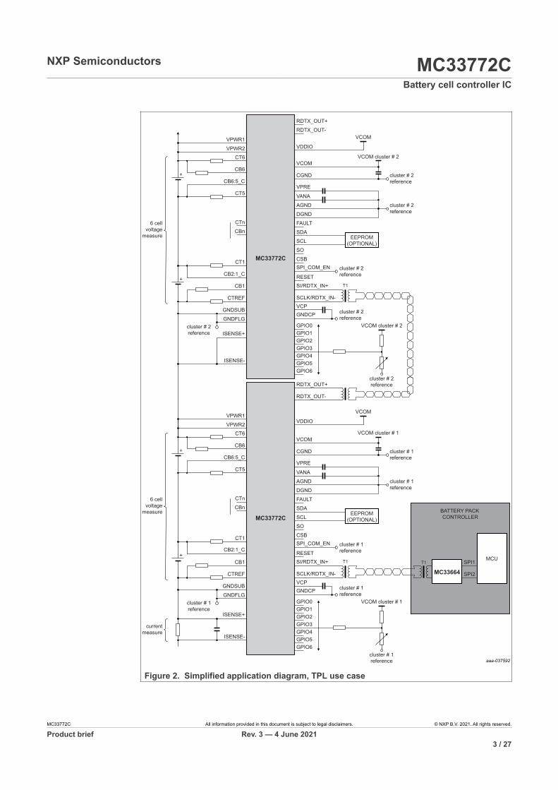
Figure 2. Simplified application diagram, TPL use case
MC33772C All information provided in this document is subject to legal disclaimers. © NXP B.V. 2021. All rights reserved.
Product brief Rev. 3 — 4 June 20213 / 27
NXP Semiconductors MC33772CBattery cell controller IC
4 Applications
• Automotive: 12 V and high-voltage battery packs• E-bikes, e-scooters, drones• Energy storage systems• Uninterruptible power supply (UPS)• Battery junction box
5 Ordering information
5.1 Part numbers definition
MC33772C x y z AE/R2
Code Option Description
x T x = T (TPL communication type)
A y = A (Advanced)
C y = C (Current)y
P y = P (Premium)
0 z = 0 (0 channels)
1 z = 1 (3 to 6 channels)z
2 z = 2 (3 to 4 channels)
AE Package suffix
R2 Tape and reel indicator
Table 1. Part number breakdown
MC33772C All information provided in this document is subject to legal disclaimers. © NXP B.V. 2021. All rights reserved.
Product brief Rev. 3 — 4 June 20214 / 27
NXP Semiconductors MC33772CBattery cell controller IC
5.2 Part numbers listThis section describes the part numbers available to be purchased along with theirdifferences. Valid orderable part numbers are provided on the web. To determine theorderable part numbers for this device, go to http://www.nxp.com.
Package type is 48-pin LQFP-EP
Orderable part Number ofchannels
OV/UV Precision GPIO as temperaturechannels and OT/UT
Current channel orcoulomb count
TPL differential communication protocol
MC33772CTA1AE 3 to 6 Yes Yes No
MC33772CTA2AE 3 to 4 Yes Yes No
Table 2. Advanced orderable part table
Package type is 48-pin LQFP-EP
Orderable part Number ofchannels
OV/UV Precision GPIO as temperaturechannels and OT/UT
Current channel orcoulomb count
TPL differential communication protocol with current measurement option
MC33772CTP1AE 3 to 6 Yes Yes Yes
MC33772CTP2AE 3 to 4 Yes Yes Yes
Table 3. Premium orderable part table
Package type is 48-pin LQFP-EP
Orderable part Number ofchannels
OV/UV Precision GPIO as temperaturechannels and OT/UT
Current channel orcoulomb count
TPL differential communication protocol
MC33772CTC0AE 0 No Yes Yes
MC33772CTC1AE 1 No Yes Yes
Table 4. Current orderable part table
Note: To order parts in tape and reel, add an R2 suffix to the part number.
MC33772C All information provided in this document is subject to legal disclaimers. © NXP B.V. 2021. All rights reserved.
Product brief Rev. 3 — 4 June 20215 / 27
NXP Semiconductors MC33772CBattery cell controller IC
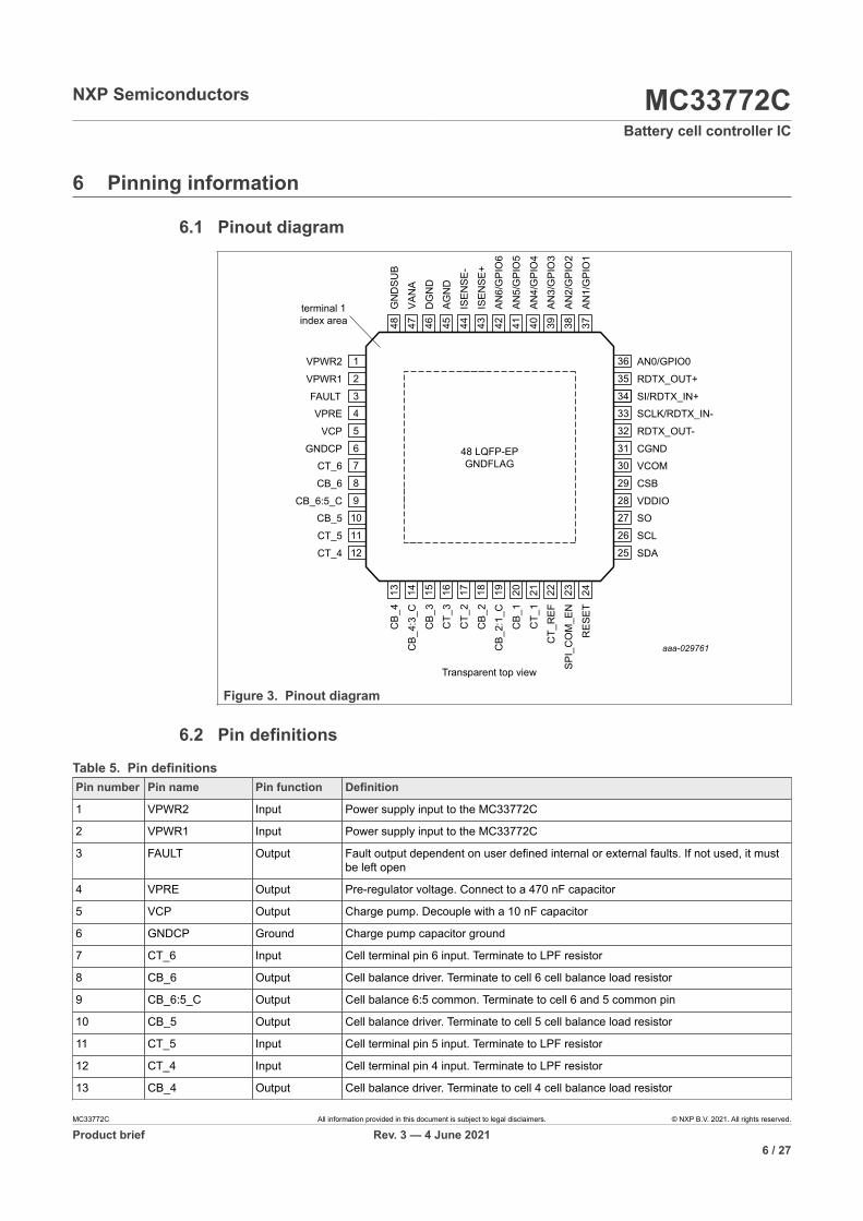
6 Pinning information
6.1 Pinout diagram
VPWR2 AN0/GPIO0
VPWR1
SI/RDTX_IN+FAULTSCLK/RDTX_IN-VPRE
RDTX_OUT-VCP
CGNDGNDCPVCOMCT_6
CSBCB_6
VDDIOCB_6:5_CSOCB_5
SCLCT_5
SDACT_4
CB_
4
VAN
AC
B_4:
3_C
DG
ND
CB_
3AG
ND
CT_
3
ISEN
SE-
CT_
2
ISEN
SE+
CB_
2AN
6/G
PIO
6C
B_2:
1_C
AN5/
GPI
O5
CB_
1
AN4/
GPI
O4
CT_
1AN
3/G
PIO
3C
T_R
EF
AN2/
GPI
O2
SPI_
CO
M_E
N
AN1/
GPI
O1
RES
ET
aaa-029761
1
2
34
5
67
8
910
11
12
RDTX_OUT+
36
35
34
48 LQFP-EPGNDFLAG
33
32
3130
29
2827
26
25
13 14 15 16 17 18 19 20 21 22 23 24
48 47G
ND
SUB
46 45 44 43 42 41 40 39 38 37
Transparent top view
terminal 1index area
Figure 3. Pinout diagram
6.2 Pin definitions
Pin number Pin name Pin function Definition
1 VPWR2 Input Power supply input to the MC33772C
2 VPWR1 Input Power supply input to the MC33772C
3 FAULT Output Fault output dependent on user defined internal or external faults. If not used, it mustbe left open
4 VPRE Output Pre-regulator voltage. Connect to a 470 nF capacitor
5 VCP Output Charge pump. Decouple with a 10 nF capacitor
6 GNDCP Ground Charge pump capacitor ground
7 CT_6 Input Cell terminal pin 6 input. Terminate to LPF resistor
8 CB_6 Output Cell balance driver. Terminate to cell 6 cell balance load resistor
9 CB_6:5_C Output Cell balance 6:5 common. Terminate to cell 6 and 5 common pin
10 CB_5 Output Cell balance driver. Terminate to cell 5 cell balance load resistor
11 CT_5 Input Cell terminal pin 5 input. Terminate to LPF resistor
12 CT_4 Input Cell terminal pin 4 input. Terminate to LPF resistor
13 CB_4 Output Cell balance driver. Terminate to cell 4 cell balance load resistor
Table 5. Pin definitions
MC33772C All information provided in this document is subject to legal disclaimers. © NXP B.V. 2021. All rights reserved.
Product brief Rev. 3 — 4 June 20216 / 27
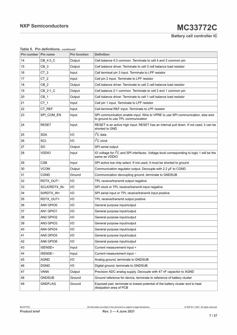
NXP Semiconductors MC33772CBattery cell controller IC
Pin number Pin name Pin function Definition
14 CB_4:3_C Output Cell balance 4:3 common. Terminate to cell 4 and 3 common pin
15 CB_3 Output Cell balance driver. Terminate to cell 3 cell balance load resistor
16 CT_3 Input Cell terminal pin 3 input. Terminate to LPF resistor
17 CT_2 Input Cell pin 2 input. Terminate to LPF resistor
18 CB_2 Output Cell balance driver. Terminate to cell 2 cell balance load resistor
19 CB_2:1_C Output Cell balance 2:1 common. Terminate to cell 2 and 1 common pin
20 CB_1 Output Cell balance driver. Terminate to cell 1 cell balance load resistor
21 CT_1 Input Cell pin 1 input. Terminate to LPF resistor
22 CT_REF Input Cell terminal REF input. Terminate to LPF resistor
23 SPI_COM_EN Input SPI communication enable input. Wire to VPRE to use SPI communication, else wireto ground to use TPL communication
24 RESET Input RESET is an active high input. RESET has an internal pull down. If not used, it can beshorted to GND
25 SDA I/O I2C data
26 SCL I/O I2C clock
27 SO Output SPI serial output
28 VDDIO Input IO voltage for I2C and SPI interfaces. Voltage level corresponding to logic 1 will be thesame as VDDIO
29 CSB Input SPI active low chip select. If not used, it must be shorted to ground
30 VCOM Output Communication regulator output. Decouple with 2.2 μF to CGND
31 CGND Ground Communication decoupling ground, terminate to GNDSUB
32 RDTX_OUT− I/O TPL receive/transmit output negative
33 SCLK/RDTX_IN- I/O SPI clock or TPL receive/transmit input negative
34 SI/RDTX_IN+ I/O SPI serial input or TPL receive/transmit input positive
35 RDTX_OUT+ I/O TPL receive/transmit output positive
36 AN0 GPIO0 I/O General purpose input/output
37 AN1 GPIO1 I/O General purpose input/output
38 AN2 GPIO2 I/O General purpose input/output
39 AN3 GPIO3 I/O General purpose input/output
40 AN4 GPIO4 I/O General purpose input/output
41 AN5 GPIO5 I/O General purpose input/output
42 AN6 GPIO6 I/O General purpose input/output
43 ISENSE+ Input Current measurement input +
44 ISENSE− Input Current measurement input −
45 AGND I/O Analog ground, terminate to GNDSUB
46 DGND I/O Digital ground, terminate to GNDSUB
47 VANA Output Precision ADC analog supply. Decouple with 47 nF capacitor to AGND
48 GNDSUB Ground Ground reference for device, terminate to reference of battery cluster
49 GNDFLAG Ground Exposed pad, terminate to lowest potential of the battery cluster and to heatdissipation area of PCB
Table 5. Pin definitions...continued
MC33772C All information provided in this document is subject to legal disclaimers. © NXP B.V. 2021. All rights reserved.
Product brief Rev. 3 — 4 June 20217 / 27
NXP Semiconductors MC33772CBattery cell controller IC
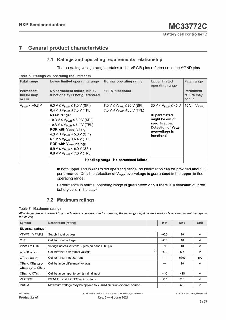
7 General product characteristics
7.1 Ratings and operating requirements relationshipThe operating voltage range pertains to the VPWR pins referenced to the AGND pins.
Fatal range Permanentfailure mayoccur
Lower limited operating range No permanent failure, but ICfunctionality is not guaranteed
Normal operating range 100 % functional
Upper limitedoperating range
Fatal range Permanentfailure mayoccur
5.0 V ≤ VPWR ≤ 6.0 V (SPI)6.4 V ≤ VPWR ≤ 7.0 V (TPL)Reset range:–0.3 V ≤ VPWR ≤ 5.0 V (SPI)–0.3 V ≤ VPWR ≤ 6.4 V (TPL)POR with VPWR falling:4.8 V ≤ VPWR < 5.0 V (SPI)6.1 V ≤ VPWR < 6.4 V (TPL)POR with VPWR rising:5.6 V ≤ VPWR < 6.0 V (SPI)6.6 V ≤ VPWR < 7.0 V (TPL)
6.0 V ≤ VPWR ≤ 30 V (SPI)7.0 V ≤ VPWR ≤ 30 V (TPL)
30 V < VPWR ≤ 40 V IC parametersmight be out ofspecification.Detection of VPWRovervoltage isfunctional
VPWR < −0.3 V
Handling range - No permanent failure
40 V < VPWR
Table 6. Ratings vs. operating requirements
In both upper and lower limited operating range, no information can be provided about ICperformance. Only the detection of VPWR overvoltage is guaranteed in the upper limitedoperating range.
Performance in normal operating range is guaranteed only if there is a minimum of threebattery cells in the stack.
7.2 Maximum ratings
All voltages are with respect to ground unless otherwise noted. Exceeding these ratings might cause a malfunction or permanent damage tothe device.
Symbol Description (rating) Min Max Unit
Electrical ratings
VPWR1, VPWR2 Supply input voltage –0.3 40 V
CT6 Cell terminal voltage −0.3 40 V
VPWR to CT6 Voltage across VPWR1,2 pins pair and CT6 pin −10 10 V
CTN to CTN-1 Cell terminal differential voltage [1] −0.3 6.7 V
CTN(CURRENT) Cell terminal input current — ±500 µA
CBN to CBN:N-1_CCBN:N-1_C to CBN-1
Cell balance differential voltage — 10 V
CBN-1 to CTN-1 Cell balance input to cell terminal input −10 +10 V
VISENSE ISENSE+ and ISENSE– pin voltage −0.5 2.5 V
VCOM Maximum voltage may be applied to VCOM pin from external source — 5.8 V
Table 7. Maximum ratings
MC33772C All information provided in this document is subject to legal disclaimers. © NXP B.V. 2021. All rights reserved.
Product brief Rev. 3 — 4 June 20218 / 27
NXP Semiconductors MC33772CBattery cell controller IC
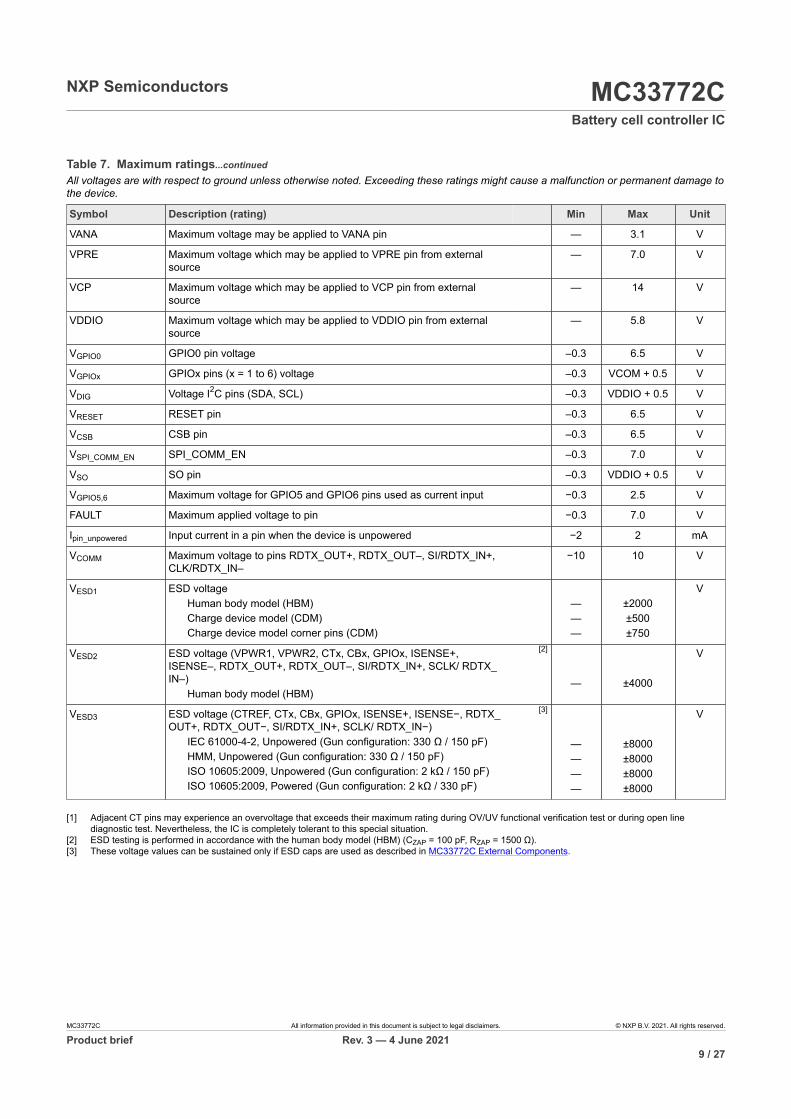
All voltages are with respect to ground unless otherwise noted. Exceeding these ratings might cause a malfunction or permanent damage tothe device.
Symbol Description (rating) Min Max Unit
VANA Maximum voltage may be applied to VANA pin — 3.1 V
VPRE Maximum voltage which may be applied to VPRE pin from externalsource
— 7.0 V
VCP Maximum voltage which may be applied to VCP pin from externalsource
— 14 V
VDDIO Maximum voltage which may be applied to VDDIO pin from externalsource
— 5.8 V
VGPIO0 GPIO0 pin voltage –0.3 6.5 V
VGPIOx GPIOx pins (x = 1 to 6) voltage –0.3 VCOM + 0.5 V
VDIG Voltage I2C pins (SDA, SCL) –0.3 VDDIO + 0.5 V
VRESET RESET pin –0.3 6.5 V
VCSB CSB pin –0.3 6.5 V
VSPI_COMM_EN SPI_COMM_EN –0.3 7.0 V
VSO SO pin –0.3 VDDIO + 0.5 V
VGPIO5,6 Maximum voltage for GPIO5 and GPIO6 pins used as current input −0.3 2.5 V
FAULT Maximum applied voltage to pin −0.3 7.0 V
Ipin_unpowered Input current in a pin when the device is unpowered −2 2 mA
VCOMM Maximum voltage to pins RDTX_OUT+, RDTX_OUT–, SI/RDTX_IN+,CLK/RDTX_IN–
−10 10 V
VESD1 ESD voltageHuman body model (HBM)Charge device model (CDM)Charge device model corner pins (CDM)
———
±2000±500±750
V
VESD2 ESD voltage (VPWR1, VPWR2, CTx, CBx, GPIOx, ISENSE+,ISENSE–, RDTX_OUT+, RDTX_OUT–, SI/RDTX_IN+, SCLK/ RDTX_IN–)
Human body model (HBM)
[2]
—
±4000
V
VESD3 ESD voltage (CTREF, CTx, CBx, GPIOx, ISENSE+, ISENSE−, RDTX_OUT+, RDTX_OUT−, SI/RDTX_IN+, SCLK/ RDTX_IN−)
IEC 61000-4-2, Unpowered (Gun configuration: 330 Ω / 150 pF)HMM, Unpowered (Gun configuration: 330 Ω / 150 pF)ISO 10605:2009, Unpowered (Gun configuration: 2 kΩ / 150 pF)ISO 10605:2009, Powered (Gun configuration: 2 kΩ / 330 pF)
[3]
————
±8000±8000±8000±8000
V
Table 7. Maximum ratings...continued
[1] Adjacent CT pins may experience an overvoltage that exceeds their maximum rating during OV/UV functional verification test or during open linediagnostic test. Nevertheless, the IC is completely tolerant to this special situation.
[2] ESD testing is performed in accordance with the human body model (HBM) (CZAP = 100 pF, RZAP = 1500 Ω).[3] These voltage values can be sustained only if ESD caps are used as described in MC33772C External Components.
MC33772C All information provided in this document is subject to legal disclaimers. © NXP B.V. 2021. All rights reserved.
Product brief Rev. 3 — 4 June 20219 / 27

NXP Semiconductors MC33772CBattery cell controller IC
7.3 Thermal characteristics
All voltages are with respect to ground unless otherwise noted. Exceeding these ratings might cause a malfunction or permanent damage tothe device.
Symbol Description (rating) Min Max Unit
Thermal ratings
TATATJ
Operating temperatureAmbient (SPI application)Ambient (TPL application)Junction[1]
–40–40–40
+125+105+150
°C
TSTG Storage temperature −55 +150 °C
TPPRT Peak package reflow temperature [2] [3] — 260 °C
Thermal resistance and package dissipation ratings
RΘJB Junction-to-board (bottom exposed pad soldered to board) 48 LQFP EP [4] — 11 °C/W
RΘJA Junction-to-ambient, natural convection, single-layer board (1s) 48 LQFP EP [5] [6] — 72 °C/W
RΘJA Junction-to-ambient, natural convection, four-layer board (2s2p) 48 LQFP EP [5] [6] — 30 °C/W
RΘJCTOP Junction-to-case top (exposed pad) 48 LQFP EP [7] — 24 °C/W
RΘJCBOTTOM Junction-to-case bottom (exposed pad) 48 LQFP EP [8] — 0.98 °C/W
ΨJT Junction to package top, natural convection [9] — 4 °C/W
Table 8. Thermal ratings
[1] The user must ensure that the average maximum operating junction temperature (Tj) is not exceeded.[2] Pin soldering temperature limit is for 10 seconds maximum duration. Not designed for immersion soldering. Exceeding these limits may cause a
malfunction or permanent damage to the device.[3] NXP’s Package Reflow capability meets Pb-free requirements for JEDEC standard J-STD-020C. For Peak Package Reflow Temperature and Moisture
Sensitivity Levels (MSL), go to www.nxp.com, search by part number (remove prefixes/suffixes) and enter the core ID to view all orderable parts, andreview parametrics.
[4] Thermal resistance between the die and the printed circuit board per JEDEC JESD51-8. Board temperature is measured on the top surface of the boardnear the package.
[5] Junction temperature is a function of die size, on-chip power dissipation, package thermal resistance, mounting site (board) temperature, ambienttemperature, air flow, power dissipation of other components on the board, and board thermal resistance.
[6] Per JEDEC JESD51-6 with the board (JESD51-7) horizontal.[7] Thermal resistance between the die and the case top surface as measured by the cold plate method (MIL SPEC-883 Method 1012.1), with the cold plate
temperature used for the case temperature.[8] Thermal resistance between the die and the solder pad on the bottom of the package based on simulation without any interface resistance.[9] Thermal characterization parameter indicating the temperature difference between the package top and the junction temperature per JEDEC JESD51-2.
MC33772C All information provided in this document is subject to legal disclaimers. © NXP B.V. 2021. All rights reserved.
Product brief Rev. 3 — 4 June 202110 / 27
NXP Semiconductors MC33772CBattery cell controller IC
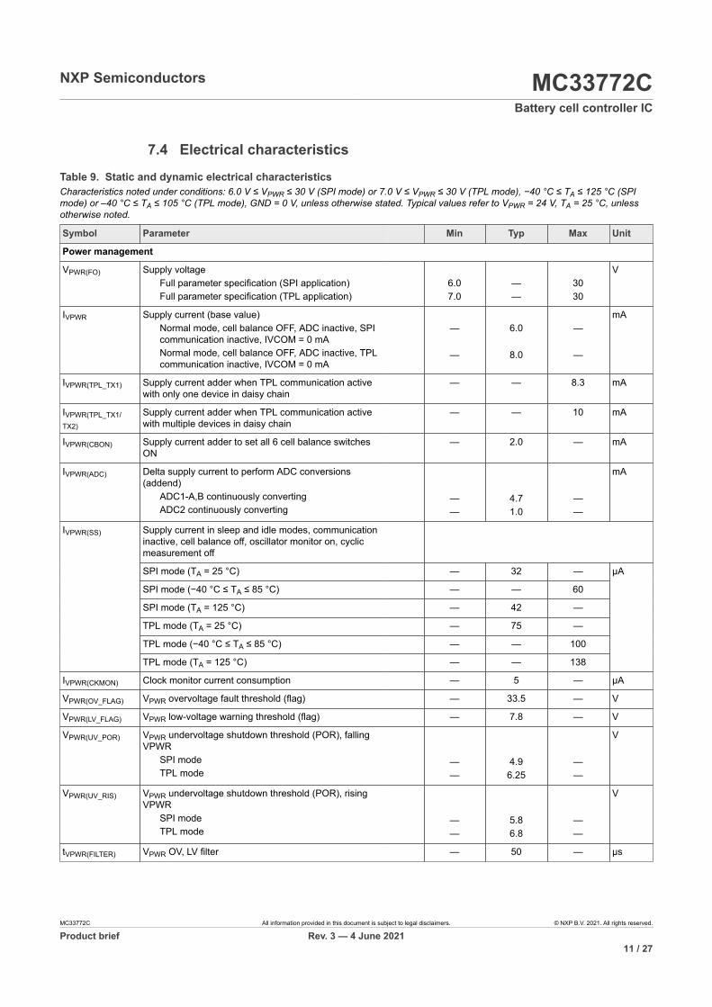
7.4 Electrical characteristics
Characteristics noted under conditions: 6.0 V ≤ VPWR ≤ 30 V (SPI mode) or 7.0 V ≤ VPWR ≤ 30 V (TPL mode), −40 °C ≤ TA ≤ 125 °C (SPImode) or –40 °C ≤ TA ≤ 105 °C (TPL mode), GND = 0 V, unless otherwise stated. Typical values refer to VPWR = 24 V, TA = 25 °C, unlessotherwise noted.
Symbol Parameter Min Typ Max Unit
Power management
VPWR(FO) Supply voltageFull parameter specification (SPI application)Full parameter specification (TPL application)
6.07.0
——
3030
V
IVPWR Supply current (base value)Normal mode, cell balance OFF, ADC inactive, SPIcommunication inactive, IVCOM = 0 mANormal mode, cell balance OFF, ADC inactive, TPLcommunication inactive, IVCOM = 0 mA
—
—
6.0
8.0
—
—
mA
IVPWR(TPL_TX1) Supply current adder when TPL communication activewith only one device in daisy chain
— — 8.3 mA
IVPWR(TPL_TX1/TX2)
Supply current adder when TPL communication activewith multiple devices in daisy chain
— — 10 mA
IVPWR(CBON) Supply current adder to set all 6 cell balance switchesON
— 2.0 — mA
IVPWR(ADC) Delta supply current to perform ADC conversions(addend)
ADC1-A,B continuously convertingADC2 continuously converting
——
4.71.0
——
mA
Supply current in sleep and idle modes, communicationinactive, cell balance off, oscillator monitor on, cyclicmeasurement off
SPI mode (TA = 25 °C) — 32 —
SPI mode (−40 °C ≤ TA ≤ 85 °C) — — 60
SPI mode (TA = 125 °C) — 42 —
TPL mode (TA = 25 °C) — 75 —
TPL mode (−40 °C ≤ TA ≤ 85 °C) — — 100
IVPWR(SS)
TPL mode (TA = 125 °C) — — 138
µA
IVPWR(CKMON) Clock monitor current consumption — 5 — µA
VPWR(OV_FLAG) VPWR overvoltage fault threshold (flag) — 33.5 — V
VPWR(LV_FLAG) VPWR low-voltage warning threshold (flag) — 7.8 — V
VPWR(UV_POR) VPWR undervoltage shutdown threshold (POR), fallingVPWR
SPI modeTPL mode
——
4.96.25
——
V
VPWR(UV_RIS) VPWR undervoltage shutdown threshold (POR), risingVPWR
SPI modeTPL mode
——
5.86.8
——
V
tVPWR(FILTER) VPWR OV, LV filter — 50 — µs
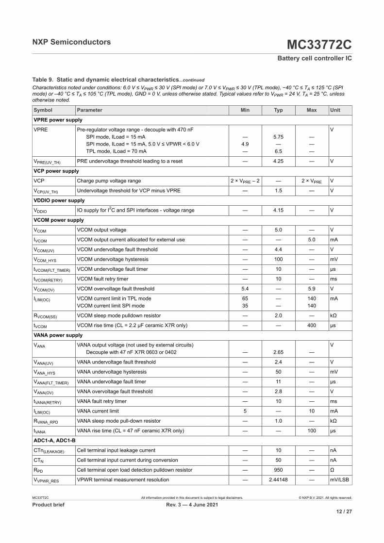
Table 9. Static and dynamic electrical characteristics
MC33772C All information provided in this document is subject to legal disclaimers. © NXP B.V. 2021. All rights reserved.
Product brief Rev. 3 — 4 June 202111 / 27
NXP Semiconductors MC33772CBattery cell controller IC
Characteristics noted under conditions: 6.0 V ≤ VPWR ≤ 30 V (SPI mode) or 7.0 V ≤ VPWR ≤ 30 V (TPL mode), −40 °C ≤ TA ≤ 125 °C (SPImode) or –40 °C ≤ TA ≤ 105 °C (TPL mode), GND = 0 V, unless otherwise stated. Typical values refer to VPWR = 24 V, TA = 25 °C, unlessotherwise noted.
Symbol Parameter Min Typ Max Unit
VPRE power supply
VPRE Pre-regulator voltage range - decouple with 470 nFSPI mode, ILoad = 15 mASPI mode, ILoad = 15 mA, 5.0 V ≤ VPWR < 6.0 VTPL mode, ILoad = 70 mA
—4.9—
5.75—6.5
———
V
VPRE(UV_TH) PRE undervoltage threshold leading to a reset — 4.25 — V
VCP power supply
VCP Charge pump voltage range 2 × VPRE – 2 — 2 × VPRE V
VCP(UV_TH) Undervoltage threshold for VCP minus VPRE — 1.5 — V
VDDIO power supply
VDDIO IO supply for I2C and SPI interfaces - voltage range — 4.15 — V
VCOM power supply
VCOM VCOM output voltage — 5.0 — V
IVCOM VCOM output current allocated for external use — — 5.0 mA
VCOM(UV) VCOM undervoltage fault threshold — 4.4 — V
VCOM_HYS VCOM undervoltage hysteresis — 100 — mV
tVCOM(FLT_TIMER) VCOM undervoltage fault timer — 10 — µs
tVCOM(RETRY) VCOM fault retry timer — 10 — ms
VCOM(OV) VCOM overvoltage fault threshold 5.4 — 5.9 V
ILIM(OC) VCOM current limit in TPL modeVCOM current limit SPI mode
6535
——
140140
mA
RVCOM(SS) VCOM sleep mode pulldown resistor — 2.0 — kΩ
tVCOM VCOM rise time (CL = 2.2 µF ceramic X7R only) — — 400 µs
VANA power supply
VANA VANA output voltage (not used by external circuits)Decouple with 47 nF X7R 0603 or 0402
—
2.65
—
V
VANA(UV) VANA undervoltage fault threshold — 2.4 — V
VANA_HYS VANA undervoltage hysteresis — 50 — mV
VANA(FLT_TIMER) VANA undervoltage fault timer — 11 — µs
VANA(OV) VANA overvoltage fault threshold — 2.8 — V
tVANA(RETRY) VANA fault retry timer — 10 — ms
ILIM(OC) VANA current limit 5 — 10 mA
RVANA_RPD VANA sleep mode pull-down resistor — 1.0 — kΩ
tVANA VANA rise time (CL = 47 nF ceramic X7R only) — — 100 µs
ADC1-A, ADC1-B
CTn(LEAKAGE) Cell terminal input leakage current — 10 — nA
CTN Cell terminal input current during conversion — 50 — nA
RPD Cell terminal open load detection pulldown resistor — 950 — Ω
VVPWR_RES VPWR terminal measurement resolution — 2.44148 — mV/LSB
Table 9. Static and dynamic electrical characteristics...continued
MC33772C All information provided in this document is subject to legal disclaimers. © NXP B.V. 2021. All rights reserved.
Product brief Rev. 3 — 4 June 202112 / 27
NXP Semiconductors MC33772CBattery cell controller IC
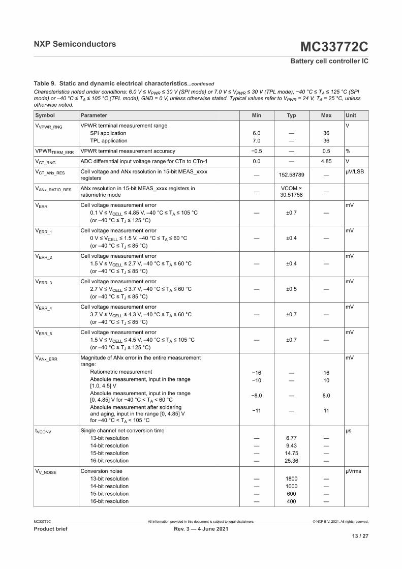
Characteristics noted under conditions: 6.0 V ≤ VPWR ≤ 30 V (SPI mode) or 7.0 V ≤ VPWR ≤ 30 V (TPL mode), −40 °C ≤ TA ≤ 125 °C (SPImode) or –40 °C ≤ TA ≤ 105 °C (TPL mode), GND = 0 V, unless otherwise stated. Typical values refer to VPWR = 24 V, TA = 25 °C, unlessotherwise noted.
Symbol Parameter Min Typ Max Unit
VVPWR_RNG VPWR terminal measurement rangeSPI applicationTPL application
6.07.0
——
3636
V
VPWRTERM_ERR VPWR terminal measurement accuracy −0.5 — 0.5 %
VCT_RNG ADC differential input voltage range for CTn to CTn-1 0.0 — 4.85 V
VCT_ANx_RES Cell voltage and ANx resolution in 15-bit MEAS_xxxxregisters — 152.58789 — µV/LSB
VANx_RATIO_RES ANx resolution in 15-bit MEAS_xxxx registers inratiometric mode — VCOM ×
30.51758 —
VERR Cell voltage measurement error0.1 V ≤ VCELL ≤ 4.85 V, –40 °C ≤ TA ≤ 105 °C(or –40 °C ≤ TJ ≤ 125 °C)
—
±0.7
—
mV
VERR_1 Cell voltage measurement error0 V ≤ VCELL ≤ 1.5 V, –40 °C ≤ TA ≤ 60 °C(or –40 °C ≤ TJ ≤ 85 °C)
—
±0.4
—
mV
VERR_2 Cell voltage measurement error1.5 V ≤ VCELL ≤ 2.7 V, –40 °C ≤ TA ≤ 60 °C(or –40 °C ≤ TJ ≤ 85 °C)
—
±0.4
—
mV
VERR_3 Cell voltage measurement error2.7 V ≤ VCELL ≤ 3.7 V, –40 °C ≤ TA ≤ 60 °C(or –40 °C ≤ TJ ≤ 85 °C)
—
±0.5
—
mV
VERR_4 Cell voltage measurement error3.7 V ≤ VCELL ≤ 4.3 V, –40 °C ≤ TA ≤ 60 °C(or –40 °C ≤ TJ ≤ 85 °C)
—
±0.7
—
mV
VERR_5 Cell voltage measurement error1.5 V ≤ VCELL ≤ 4.5 V, –40 °C ≤ TA ≤ 105 °C(or –40 °C ≤ TJ ≤ 125 °C)
—
±0.7
—
mV
VANx_ERR Magnitude of ANx error in the entire measurementrange:
Ratiometric measurementAbsolute measurement, input in the range[1.0, 4.5] VAbsolute measurement, input in the range[0, 4.85] V for −40 °C < TA < 60 °CAbsolute measurement after solderingand aging, input in the range [0, 4.85] Vfor −40 °C < TA < 105 °C
−16−10
−8.0
−11
——
—
—
1610
8.0
11
mV
tVCONV Single channel net conversion time13-bit resolution14-bit resolution15-bit resolution16-bit resolution
————
6.779.43
14.7525.36
————
µs
VV_NOISE Conversion noise13-bit resolution14-bit resolution15-bit resolution16-bit resolution
————
18001000600400
————
µVrms
Table 9. Static and dynamic electrical characteristics...continued
MC33772C All information provided in this document is subject to legal disclaimers. © NXP B.V. 2021. All rights reserved.
Product brief Rev. 3 — 4 June 202113 / 27
NXP Semiconductors MC33772CBattery cell controller IC
Characteristics noted under conditions: 6.0 V ≤ VPWR ≤ 30 V (SPI mode) or 7.0 V ≤ VPWR ≤ 30 V (TPL mode), −40 °C ≤ TA ≤ 125 °C (SPImode) or –40 °C ≤ TA ≤ 105 °C (TPL mode), GND = 0 V, unless otherwise stated. Typical values refer to VPWR = 24 V, TA = 25 °C, unlessotherwise noted.
Symbol Parameter Min Typ Max Unit
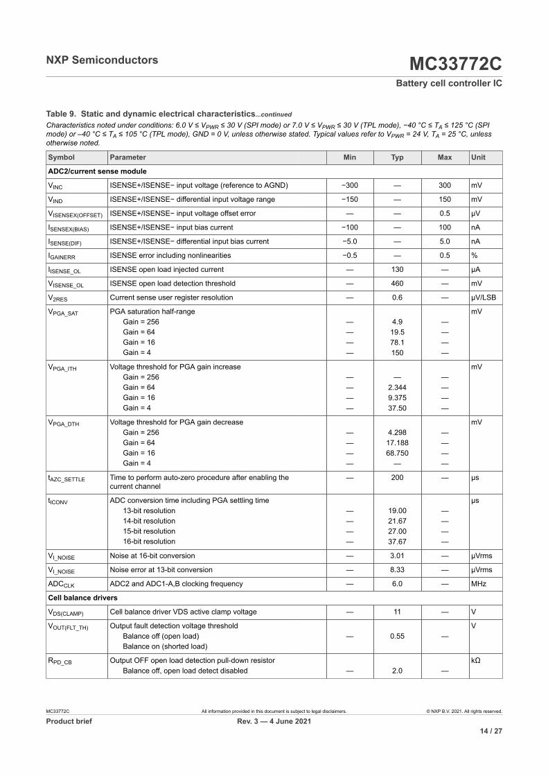
ADC2/current sense module
VINC ISENSE+/ISENSE− input voltage (reference to AGND) −300 — 300 mV
VIND ISENSE+/ISENSE− differential input voltage range −150 — 150 mV
VISENSEX(OFFSET) ISENSE+/ISENSE− input voltage offset error — — 0.5 µV
ISENSEX(BIAS) ISENSE+/ISENSE− input bias current −100 — 100 nA
ISENSE(DIF) ISENSE+/ISENSE− differential input bias current −5.0 — 5.0 nA
IGAINERR ISENSE error including nonlinearities −0.5 — 0.5 %
IISENSE_OL ISENSE open load injected current — 130 — µA
VISENSE_OL ISENSE open load detection threshold — 460 — mV
V2RES Current sense user register resolution — 0.6 — µV/LSB
VPGA_SAT PGA saturation half-rangeGain = 256Gain = 64Gain = 16Gain = 4
————
4.9
19.578.1150
————
mV
VPGA_ITH Voltage threshold for PGA gain increaseGain = 256Gain = 64Gain = 16Gain = 4
————
—
2.3449.37537.50
————
mV
VPGA_DTH Voltage threshold for PGA gain decreaseGain = 256Gain = 64Gain = 16Gain = 4
————
4.298
17.18868.750
—
————
mV
tAZC_SETTLE Time to perform auto-zero procedure after enabling thecurrent channel
— 200 — µs
tICONV ADC conversion time including PGA settling time13-bit resolution14-bit resolution15-bit resolution16-bit resolution
————
19.0021.6727.0037.67
————
µs
VI_NOISE Noise at 16-bit conversion — 3.01 — µVrms
VI_NOISE Noise error at 13-bit conversion — 8.33 — µVrms
ADCCLK ADC2 and ADC1-A,B clocking frequency — 6.0 — MHz
Cell balance drivers
VDS(CLAMP) Cell balance driver VDS active clamp voltage — 11 — V
VOUT(FLT_TH) Output fault detection voltage thresholdBalance off (open load)Balance on (shorted load)
—
0.55
—
V
RPD_CB Output OFF open load detection pull-down resistorBalance off, open load detect disabled
—
2.0
—
kΩ
Table 9. Static and dynamic electrical characteristics...continued
MC33772C All information provided in this document is subject to legal disclaimers. © NXP B.V. 2021. All rights reserved.
Product brief Rev. 3 — 4 June 202114 / 27

NXP Semiconductors MC33772CBattery cell controller IC
Characteristics noted under conditions: 6.0 V ≤ VPWR ≤ 30 V (SPI mode) or 7.0 V ≤ VPWR ≤ 30 V (TPL mode), −40 °C ≤ TA ≤ 125 °C (SPImode) or –40 °C ≤ TA ≤ 105 °C (TPL mode), GND = 0 V, unless otherwise stated. Typical values refer to VPWR = 24 V, TA = 25 °C, unlessotherwise noted.
Symbol Parameter Min Typ Max Unit
IOUT(LKG) Output leakage currentBalance off, open load detect disabled atVDS = 4.0 V
—
—
1.0
µA
RDS(on) Drain-to-source on resistanceIOUT = 300 mA, TJ = 125 °CIOUT = 300 mA, TJ = 25 °CIOUT = 300 mA, TJ = −40 °C
———
—0.50.4
0.80——
Ω
ILIM_CB Driver current limitation (shorted resistor) 310 — 950 mA
tON Cell balance driver turn onRL = 15 Ω
—
350
—
µs
tOFF Cell balance driver turn offRL = 15 Ω
—
200
—
µs
tBAL_DEGLICTH Short/open detect filter time — 20 — µs
Internal temperature measurement
IC_TEMP1_ERR IC temperature measurement error −3.0 — 3.0 K
IC_TEMP1_RES IC temperature resolution — 0.032 — K/LSB
TSD_TH Thermal shutdown — 170 — °C
TSD_HYS Thermal shutdown hysteresis — 10 — °C
Default operational parameters
VCTOV(TH) Cell overvoltage threshold (8 bits) 0.0 4.2 5.0 V
VCTOV(RES) Cell overvoltage threshold resolution — 19.53125 — mV/LSB
VCTUV(TH) Cell undervoltage threshold (8 bits) 0.0 2.5 5.0 V
VCTUV(RES) Cell undervoltage threshold resolution — 19.53125 — mV/LSB
VGPIO_OT(TH) GPIOx configured as ANx input overtemperaturethreshold from POR
— 1.16 — V
VGPIO_OT(RES) Overtemperature voltage threshold resolution — 4.8828125 — mV/LSB
VGPIO_UT(TH) GPIOx configured as ANx input undertemperaturethreshold from POR
— 3.82 — V
VGPIO_UT(RES) Undertemperature voltage threshold resolution — 4.8828125 — mV/LSB
General purpose input/output GPIOx
VIH Input high-voltage (3.3 V compatible) 2.0 — — V
VIL Input low-voltage (3.3 V compatible) — — 1.0 V
VHYS Input hysteresis — 100 — mV
IIL Input leakage currentPins 3-state, VIN = VCOM or AGND
−100
—
100
nA
IIDL Differential input leakage current GPIO 5,6GPIO 5,6 configured as digital inputs for currentmeasurement
−30
—
30
nA
VOH Output high-voltage IOH = −0.5 mA VCOM − 0.8 — — V
VOL Output low-voltage IOL = +0.5 mA — — 0.8 V
VADC Analog ADC input voltage range for ratiometricmeasurements
AGND — VCOM V
Table 9. Static and dynamic electrical characteristics...continued
MC33772C All information provided in this document is subject to legal disclaimers. © NXP B.V. 2021. All rights reserved.
Product brief Rev. 3 — 4 June 202115 / 27
NXP Semiconductors MC33772CBattery cell controller IC
Characteristics noted under conditions: 6.0 V ≤ VPWR ≤ 30 V (SPI mode) or 7.0 V ≤ VPWR ≤ 30 V (TPL mode), −40 °C ≤ TA ≤ 125 °C (SPImode) or –40 °C ≤ TA ≤ 105 °C (TPL mode), GND = 0 V, unless otherwise stated. Typical values refer to VPWR = 24 V, TA = 25 °C, unlessotherwise noted.
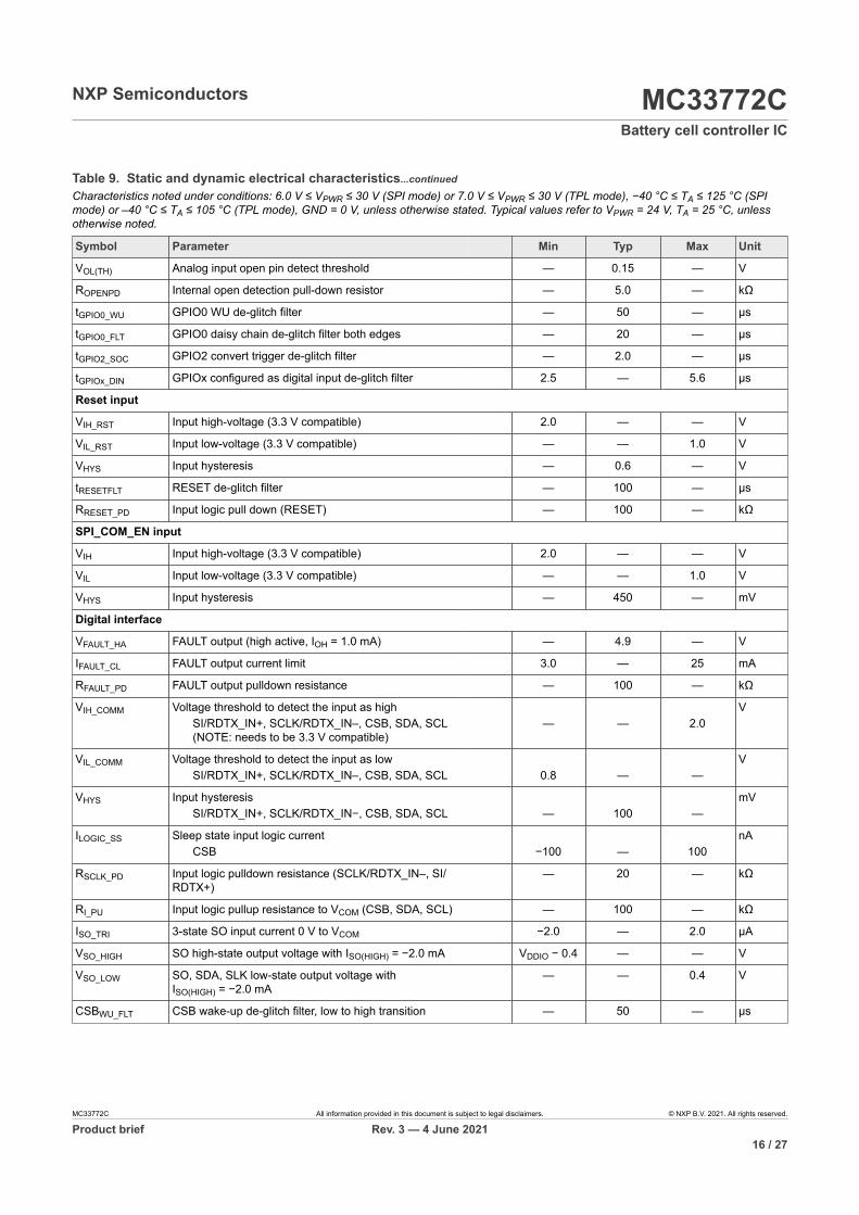
Symbol Parameter Min Typ Max Unit
VOL(TH) Analog input open pin detect threshold — 0.15 — V
ROPENPD Internal open detection pull-down resistor — 5.0 — kΩ
tGPIO0_WU GPIO0 WU de-glitch filter — 50 — µs
tGPIO0_FLT GPIO0 daisy chain de-glitch filter both edges — 20 — µs
tGPIO2_SOC GPIO2 convert trigger de-glitch filter — 2.0 — µs
tGPIOx_DIN GPIOx configured as digital input de-glitch filter 2.5 — 5.6 µs
Reset input
VIH_RST Input high-voltage (3.3 V compatible) 2.0 — — V
VIL_RST Input low-voltage (3.3 V compatible) — — 1.0 V
VHYS Input hysteresis — 0.6 — V
tRESETFLT RESET de-glitch filter — 100 — µs
RRESET_PD Input logic pull down (RESET) — 100 — kΩ
SPI_COM_EN input
VIH Input high-voltage (3.3 V compatible) 2.0 — — V
VIL Input low-voltage (3.3 V compatible) — — 1.0 V
VHYS Input hysteresis — 450 — mV
Digital interface
VFAULT_HA FAULT output (high active, IOH = 1.0 mA) — 4.9 — V
IFAULT_CL FAULT output current limit 3.0 — 25 mA
RFAULT_PD FAULT output pulldown resistance — 100 — kΩ
VIH_COMM Voltage threshold to detect the input as highSI/RDTX_IN+, SCLK/RDTX_IN–, CSB, SDA, SCL(NOTE: needs to be 3.3 V compatible)
—
—
2.0
V
VIL_COMM Voltage threshold to detect the input as lowSI/RDTX_IN+, SCLK/RDTX_IN–, CSB, SDA, SCL
0.8
—
—
V
VHYS Input hysteresisSI/RDTX_IN+, SCLK/RDTX_IN−, CSB, SDA, SCL
—
100
—
mV
ILOGIC_SS Sleep state input logic currentCSB
−100
—
100
nA
RSCLK_PD Input logic pulldown resistance (SCLK/RDTX_IN–, SI/RDTX+)
— 20 — kΩ
RI_PU Input logic pullup resistance to VCOM (CSB, SDA, SCL) — 100 — kΩ
ISO_TRI 3-state SO input current 0 V to VCOM −2.0 — 2.0 µA
VSO_HIGH SO high-state output voltage with ISO(HIGH) = −2.0 mA VDDIO − 0.4 — — V
VSO_LOW SO, SDA, SLK low-state output voltage withISO(HIGH) = −2.0 mA
— — 0.4 V
CSBWU_FLT CSB wake-up de-glitch filter, low to high transition — 50 — µs
Table 9. Static and dynamic electrical characteristics...continued
MC33772C All information provided in this document is subject to legal disclaimers. © NXP B.V. 2021. All rights reserved.
Product brief Rev. 3 — 4 June 202116 / 27
NXP Semiconductors MC33772CBattery cell controller IC
Characteristics noted under conditions: 6.0 V ≤ VPWR ≤ 30 V (SPI mode) or 7.0 V ≤ VPWR ≤ 30 V (TPL mode), −40 °C ≤ TA ≤ 125 °C (SPImode) or –40 °C ≤ TA ≤ 105 °C (TPL mode), GND = 0 V, unless otherwise stated. Typical values refer to VPWR = 24 V, TA = 25 °C, unlessotherwise noted.
Symbol Parameter Min Typ Max Unit
System timing
tCELL_CONV Time needed to acquire all 6 cell voltages and thecurrent after an on demand conversion
13-bit resolution14-bit resolution15-bit resolution16-bit resolution
————
415789
152
————
µs
tSYNC V/I synchronization timeADC1-A,B at 13 bit, ADC2 at 13 bitADC1-A,B at 14 bit, ADC2 at 13 bitADC1-A,B at 15 bit, ADC2 at 13 bitADC1-A,B at 16 bit, ADC2 at 13 bit
————
41.3942.7147.3795.14
————
µs
tSYNC V/I synchronization timeADC1-A,B at 13 bit, ADC2 at 14 bitADC1-A,B at 14 bit, ADC2 at 14 bitADC1-A,B at 15 bit, ADC2 at 14 bitADC1-A,B at 16 bit, ADC2 at 14 bit
————
46.7348.0550.7192.47
————
µs
tSYNC V/I synchronization timeADC1-A,B at 13 bit, ADC2 at 15 bitADC1-A,B at 14 bit, ADC2 at 15 bitADC1-A,B at 15 bit, ADC2 at 15 bitADC1-A,B at 16 bit, ADC2 at 15 bit
————
57.3958.7161.3787.14
————
µs
tSYNC V/I synchronization timeADC1-A,B at 13 bit, ADC2 at 16 bitADC1-A,B at 14 bit, ADC2 at 16 bitADC1-A,B at 15 bit, ADC2 at 16 bitADC1-A,B at 16 bit, ADC2 at 16 bit
————
78.7380.0582.7188.02
————
µs
tVPWR(READY) Time after VPWR connection for the IC to be ready forinitialization
— — 5.0 ms
tWAKE-UP Power up duration — — 440 µs
tWAKE_DELAY Time between wake pulses — 600 — µs
tNOWUP Time, starting from the first SOM received, to go back toSleep/Idle mode time after receiving incomplete TPL buswake-up sequence
— — 1.3 ms
tIDLE Idle timeout after POR — 60 — s
tBALANCE Cell balance timer range 0.5 — 511 min
tCYCLE Cyclic acquisition timer range 0.0 — 8.5 s
tFAULT Fault detection to activation of fault pinNormal mode
—
—
56
µs
tDIAG Diagnostic mode timeout 0.047 1.0 8.5 s
tEOC SOC to data ready (includes post processing of data)13-bit resolution14-bit resolution15-bit resolution16-bit resolution
————
148201307520
————
µs
tSETTLE Time after SOC to begin converting with ADC1-A,B — 12.28 — µs
Table 9. Static and dynamic electrical characteristics...continued
MC33772C All information provided in this document is subject to legal disclaimers. © NXP B.V. 2021. All rights reserved.
Product brief Rev. 3 — 4 June 202117 / 27
NXP Semiconductors MC33772CBattery cell controller IC
Characteristics noted under conditions: 6.0 V ≤ VPWR ≤ 30 V (SPI mode) or 7.0 V ≤ VPWR ≤ 30 V (TPL mode), −40 °C ≤ TA ≤ 125 °C (SPImode) or –40 °C ≤ TA ≤ 105 °C (TPL mode), GND = 0 V, unless otherwise stated. Typical values refer to VPWR = 24 V, TA = 25 °C, unlessotherwise noted.
Symbol Parameter Min Typ Max Unit
tCLST_TPL Time needed to send an SOC command and readback 6 cell voltages, 7 temperatures, 1 current, and1 coulomb counter with TPL communication working at2.0 Mbit/s and ADC1-A,B configured as follows (with ADC_CFG[AVG] = 0):
13-bit resolution14-bit resolution15-bit resolution16-bit resolution
————
0.790.850.951.16
————
ms
tCLST_SPI Time needed to send an SOC command and readback 6 cell voltages, 7 temperatures, 1 current, and1 coulomb counter with SPI communication working at4.0 Mbit/s and ADC1-A,B configured as follows (with ADC_CFG[AVG] = 0):
13-bit resolution14-bit resolution15-bit resolution16-bit resolution
————
0.480.540.640.86
————
ms
tI2C_DOWNLOAD Time to download EEPROM calibration after POR — — 1.0 ms
tI2C_ACCESS EEPROM access time, EEPROM write (depends ondevice selection)
— 5.0 — ms
tWAVE_DC_BITx Daisy chain duty cycle off timetWAVE_DC_BITx = 00
—
500
—
µs
tWAVE_DC_BITx Daisy chain duty cycle off timetWAVE_DC_BITx = 01
—
1.0
—
ms
tWAVE_DC_BITx Daisy chain duty cycle off timetWAVE_DC_BITx = 10
—
10
—
ms
tWAVE_DC_BITx Daisy chain duty cycle off timetWAVE_DC_BITx = 11
—
100
—
ms
tWAVE_DC_ON Daisy chain duty cycle on time — 500 — µs
tCOM_LOSS Time out to reset the IC in the absence ofcommunication
— 1024 — ms
SPI interface
tTD Sequential data transfer delay in SPI mode (N) 1.0 — — µs
FSCK SCLK frequency — — 4.0 MHz
tSCK _H SCLK high time (A) 125 — — ns
tSCK _L SCLK high time (B) 125 — — ns
tSCK SCLK period (A+B) 250 — — ns
tFALL SCLK falling time — — 15 ns
tRISE SCLK rising time — — 15 ns
tSET SCLK setup time (O) 20 — — ns
tHOLD SCLK hold time (P) 20 — — ns
tSI_SETUP SI setup time (F) 40 — — ns
tSI_HOLD SI hold time (G) 40 — — ns
tSO_VALID SO data valid, rising edge of SCLK to SO data valid (I) — — 40 ns
Table 9. Static and dynamic electrical characteristics...continued
MC33772C All information provided in this document is subject to legal disclaimers. © NXP B.V. 2021. All rights reserved.
Product brief Rev. 3 — 4 June 202118 / 27
NXP Semiconductors MC33772CBattery cell controller IC
Characteristics noted under conditions: 6.0 V ≤ VPWR ≤ 30 V (SPI mode) or 7.0 V ≤ VPWR ≤ 30 V (TPL mode), −40 °C ≤ TA ≤ 125 °C (SPImode) or –40 °C ≤ TA ≤ 105 °C (TPL mode), GND = 0 V, unless otherwise stated. Typical values refer to VPWR = 24 V, TA = 25 °C, unlessotherwise noted.
Symbol Parameter Min Typ Max Unit
tSO_EN SO enable time (H) — — 40 ns
tSO_DISABLE SO disable time (K) — — 40 ns
tCSB_LEAD CSB lead time (L) 100 — — ns
tCSB_LAG CSB lag time (M) 100 — — ns
TPL interface (MCU)
tMCU_RES Time between two consecutive message requesttransmitted by MCU
4.0 — — µs
tWU_Wait Time the MCU shall wait after sending first wake-upmessage per MC33772C IC
0.75 — — ms
TPL interface (MC33772C)
tTPL_TD Sequential data transfer delay in TPL mode — 4.0 — µs
tTPL Transmit pulse duration — 208 — ns
tport_delay Port delay introduced by each repeater in MC33772C — — 0.95 µs
tRES Slave response after read command — 5.0 — µs
VRDTX INTH Differential receiver threshold — 580 — mV
tEOM Message timeout duration — 250 — µs
Table 9. Static and dynamic electrical characteristics...continued
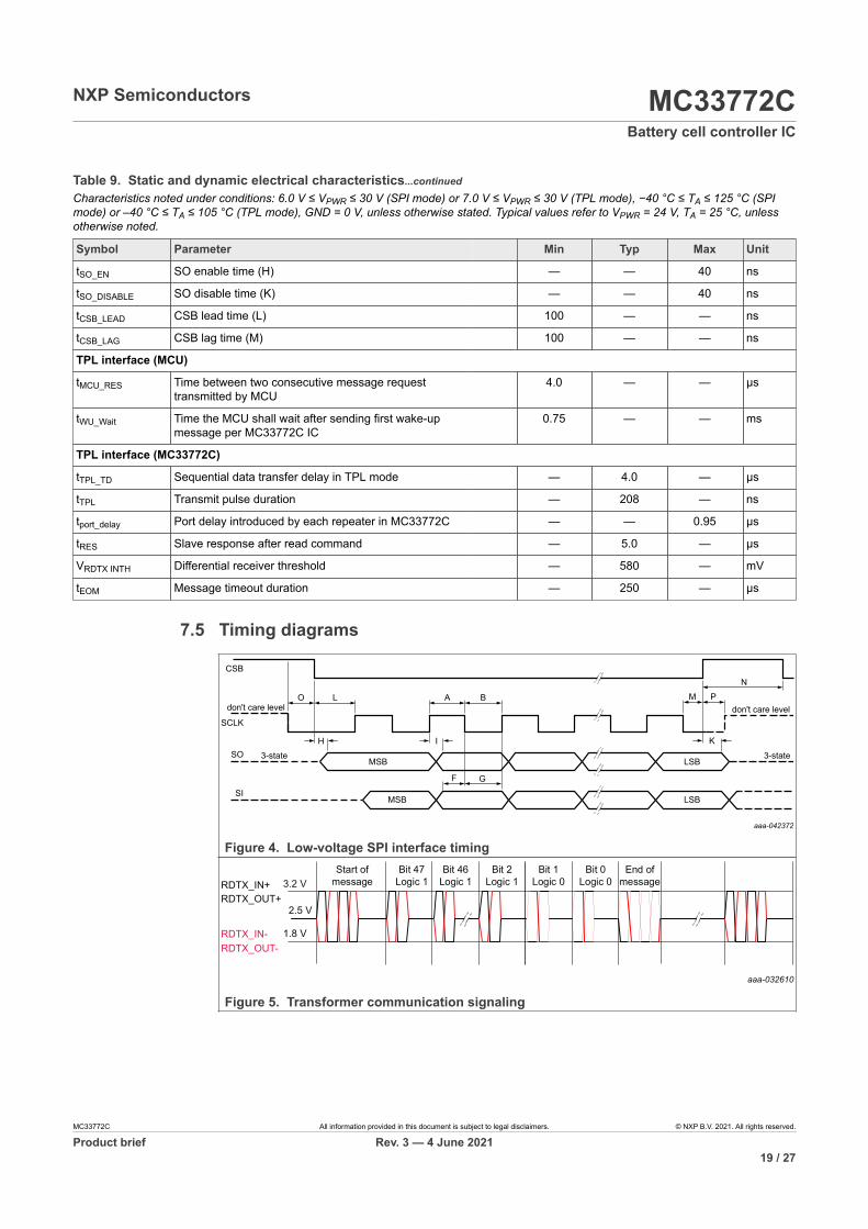
7.5 Timing diagrams
aaa-042372
CSB
MSB
MSB
LSB
LSB
SCLK
SO
SI
don't care level
3-state 3-state
don't care levelO L A
GF
B
NM P
KH I
Figure 4. Low-voltage SPI interface timing
RDTX_OUT+RDTX_IN+
RDTX_IN-RDTX_OUT-
3.2 V
1.8 V
2.5 V
End ofmessage
Start ofmessage
Bit 0Logic 0
Bit 1Logic 0
Bit 2Logic 1
Bit 46Logic 1
Bit 47Logic 1
aaa-032610
Figure 5. Transformer communication signaling
MC33772C All information provided in this document is subject to legal disclaimers. © NXP B.V. 2021. All rights reserved.
Product brief Rev. 3 — 4 June 202119 / 27
NXP Semiconductors MC33772CBattery cell controller IC
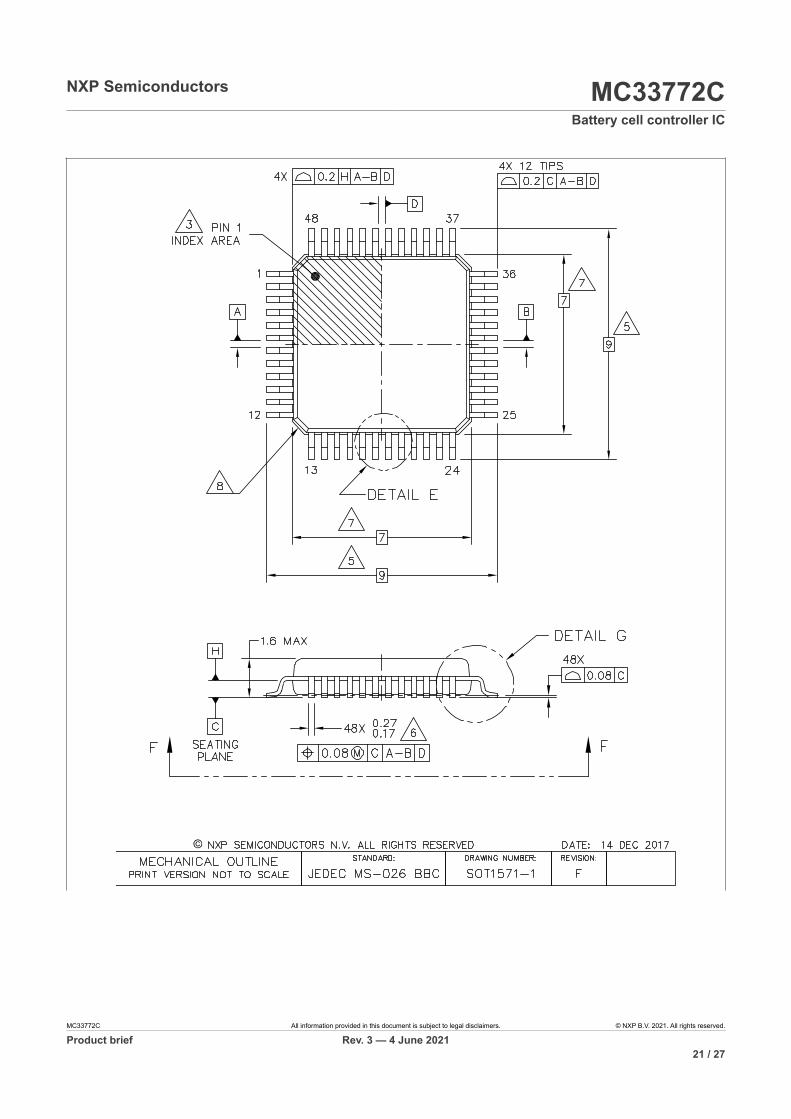
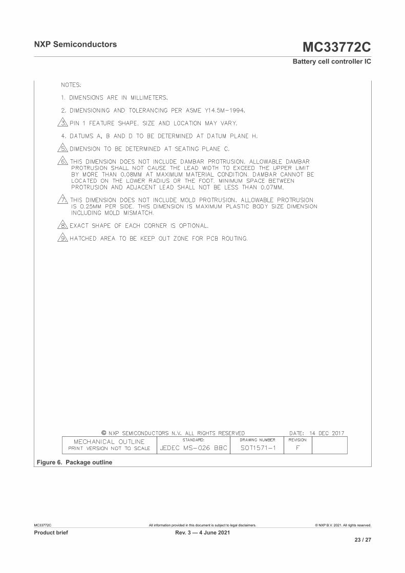
8 Packaging
8.1 Package mechanical dimensionsPackage dimensions are provided in package drawings. To find the most current packageoutline drawing, go to www.nxp.com and perform a keyword search for the documentnumber of the drawings.
Package Suffix Package outline drawing number
48-pin LQFP-EP AE SOT1571-1
Table 10. Package Outline
MC33772C All information provided in this document is subject to legal disclaimers. © NXP B.V. 2021. All rights reserved.
Product brief Rev. 3 — 4 June 202120 / 27
NXP Semiconductors MC33772CBattery cell controller IC
MC33772C All information provided in this document is subject to legal disclaimers. © NXP B.V. 2021. All rights reserved.
Product brief Rev. 3 — 4 June 202121 / 27

NXP Semiconductors MC33772CBattery cell controller IC
MC33772C All information provided in this document is subject to legal disclaimers. © NXP B.V. 2021. All rights reserved.
Product brief Rev. 3 — 4 June 202122 / 27
NXP Semiconductors MC33772CBattery cell controller IC
Figure 6. Package outline
MC33772C All information provided in this document is subject to legal disclaimers. © NXP B.V. 2021. All rights reserved.
Product brief Rev. 3 — 4 June 202123 / 27
NXP Semiconductors MC33772CBattery cell controller IC
9 Revision history
Revision Date Description
v.3 20210604 update to align with data sheet MC33772C v.3
v.2 20210310 update to align with preliminary data sheet
v.1 20200324 initial version
Revision history
MC33772C All information provided in this document is subject to legal disclaimers. © NXP B.V. 2021. All rights reserved.
Product brief Rev. 3 — 4 June 202124 / 27

NXP Semiconductors MC33772CBattery cell controller IC
10 Legal information
10.1 DefinitionsDraft — A draft status on a document indicates that the content is stillunder internal review and subject to formal approval, which may resultin modifications or additions. NXP Semiconductors does not give anyrepresentations or warranties as to the accuracy or completeness ofinformation included in a draft version of a document and shall have noliability for the consequences of use of such information.
10.2 DisclaimersLimited warranty and liability — Information in this document is believedto be accurate and reliable. However, NXP Semiconductors does notgive any representations or warranties, expressed or implied, as to theaccuracy or completeness of such information and shall have no liabilityfor the consequences of use of such information. NXP Semiconductorstakes no responsibility for the content in this document if provided by aninformation source outside of NXP Semiconductors. In no event shall NXPSemiconductors be liable for any indirect, incidental, punitive, special orconsequential damages (including - without limitation - lost profits, lostsavings, business interruption, costs related to the removal or replacementof any products or rework charges) whether or not such damages are basedon tort (including negligence), warranty, breach of contract or any otherlegal theory. Notwithstanding any damages that customer might incur forany reason whatsoever, NXP Semiconductors’ aggregate and cumulativeliability towards customer for the products described herein shall be limitedin accordance with the Terms and conditions of commercial sale of NXPSemiconductors.
Right to make changes — NXP Semiconductors reserves the right tomake changes to information published in this document, including withoutlimitation specifications and product descriptions, at any time and withoutnotice. This document supersedes and replaces all information supplied priorto the publication hereof.
Applications — Applications that are described herein for any of theseproducts are for illustrative purposes only. NXP Semiconductors makesno representation or warranty that such applications will be suitablefor the specified use without further testing or modification. Customersare responsible for the design and operation of their applications andproducts using NXP Semiconductors products, and NXP Semiconductorsaccepts no liability for any assistance with applications or customer productdesign. It is customer’s sole responsibility to determine whether the NXPSemiconductors product is suitable and fit for the customer’s applicationsand products planned, as well as for the planned application and use ofcustomer’s third party customer(s). Customers should provide appropriatedesign and operating safeguards to minimize the risks associated withtheir applications and products. NXP Semiconductors does not accept anyliability related to any default, damage, costs or problem which is basedon any weakness or default in the customer’s applications or products, orthe application or use by customer’s third party customer(s). Customer isresponsible for doing all necessary testing for the customer’s applicationsand products using NXP Semiconductors products in order to avoid adefault of the applications and the products or of the application or use bycustomer’s third party customer(s). NXP does not accept any liability in thisrespect.
Limiting values — Stress above one or more limiting values (as defined inthe Absolute Maximum Ratings System of IEC 60134) will cause permanentdamage to the device. Limiting values are stress ratings only and (proper)operation of the device at these or any other conditions above thosegiven in the Recommended operating conditions section (if present) or theCharacteristics sections of this document is not warranted. Constant orrepeated exposure to limiting values will permanently and irreversibly affectthe quality and reliability of the device.
Terms and conditions of commercial sale — NXP Semiconductorsproducts are sold subject to the general terms and conditions of commercialsale, as published at http://www.nxp.com/profile/terms, unless otherwiseagreed in a valid written individual agreement. In case an individualagreement is concluded only the terms and conditions of the respectiveagreement shall apply. NXP Semiconductors hereby expressly objects toapplying the customer’s general terms and conditions with regard to thepurchase of NXP Semiconductors products by customer.
No offer to sell or license — Nothing in this document may be interpretedor construed as an offer to sell products that is open for acceptance orthe grant, conveyance or implication of any license under any copyrights,patents or other industrial or intellectual property rights.
Suitability for use in automotive applications — This NXP product hasbeen qualified for use in automotive applications. If this product is usedby customer in the development of, or for incorporation into, products orservices (a) used in safety critical applications or (b) in which failure couldlead to death, personal injury, or severe physical or environmental damage(such products and services hereinafter referred to as “Critical Applications”),then customer makes the ultimate design decisions regarding its productsand is solely responsible for compliance with all legal, regulatory, safety,and security related requirements concerning its products, regardless ofany information or support that may be provided by NXP. As such, customerassumes all risk related to use of any products in Critical Applications andNXP and its suppliers shall not be liable for any such use by customer.Accordingly, customer will indemnify and hold NXP harmless from anyclaims, liabilities, damages and associated costs and expenses (includingattorneys’ fees) that NXP may incur related to customer’s incorporation ofany product in a Critical Application.
Quick reference data — The Quick reference data is an extract of theproduct data given in the Limiting values and Characteristics sections of thisdocument, and as such is not complete, exhaustive or legally binding.
Export control — This document as well as the item(s) described hereinmay be subject to export control regulations. Export might require a priorauthorization from competent authorities.
Translations — A non-English (translated) version of a document is forreference only. The English version shall prevail in case of any discrepancybetween the translated and English versions.
Security — Customer understands that all NXP products may be subjectto unidentified or documented vulnerabilities. Customer is responsiblefor the design and operation of its applications and products throughouttheir lifecycles to reduce the effect of these vulnerabilities on customer’sapplications and products. Customer’s responsibility also extends to otheropen and/or proprietary technologies supported by NXP products for usein customer’s applications. NXP accepts no liability for any vulnerability.Customer should regularly check security updates from NXP and follow upappropriately. Customer shall select products with security features that bestmeet rules, regulations, and standards of the intended application and makethe ultimate design decisions regarding its products and is solely responsiblefor compliance with all legal, regulatory, and security related requirementsconcerning its products, regardless of any information or support that maybe provided by NXP. NXP has a Product Security Incident Response Team(PSIRT) (reachable at [email protected]) that manages the investigation,reporting, and solution release to security vulnerabilities of NXP products.
10.3 TrademarksNotice: All referenced brands, product names, service names andtrademarks are the property of their respective owners.
NXP — wordmark and logo are trademarks of NXP B.V.
MC33772C All information provided in this document is subject to legal disclaimers. © NXP B.V. 2021. All rights reserved.
Product brief Rev. 3 — 4 June 202125 / 27
NXP Semiconductors MC33772CBattery cell controller IC
TablesTab. 1. Part number breakdown ....................................4Tab. 2. Advanced orderable part table .......................... 5Tab. 3. Premium orderable part table ............................5Tab. 4. Current orderable part table ..............................5Tab. 5. Pin definitions ....................................................6Tab. 6. Ratings vs. operating requirements ...................8
Tab. 7. Maximum ratings ...............................................8Tab. 8. Thermal ratings ............................................... 10Tab. 9. Static and dynamic electrical
characteristics ..................................................11Tab. 10. Package Outline ..............................................20
FiguresFig. 1. Simplified application diagram, SPI use
case ...................................................................2Fig. 2. Simplified application diagram, TPL use
case ...................................................................3
Fig. 3. Pinout diagram .................................................. 6Fig. 4. Low-voltage SPI interface timing .....................19Fig. 5. Transformer communication signaling .............19Fig. 6. Package outline ...............................................21
MC33772C All information provided in this document is subject to legal disclaimers. © NXP B.V. 2021. All rights reserved.
Product brief Rev. 3 — 4 June 202126 / 27
NXP Semiconductors MC33772CBattery cell controller IC
Contents1 General description ............................................ 12 Features ............................................................... 13 Simplified application diagram .......................... 24 Applications .........................................................45 Ordering information .......................................... 45.1 Part numbers definition ......................................45.2 Part numbers list ............................................... 56 Pinning information ............................................ 66.1 Pinout diagram .................................................. 66.2 Pin definitions .................................................... 67 General product characteristics ........................ 87.1 Ratings and operating requirements
relationship .........................................................87.2 Maximum ratings ............................................... 87.3 Thermal characteristics ....................................107.4 Electrical characteristics .................................. 117.5 Timing diagrams .............................................. 198 Packaging .......................................................... 208.1 Package mechanical dimensions .................... 209 Revision history ................................................ 2410 Legal information ..............................................25
Please be aware that important notices concerning this document and the product(s)described herein, have been included in section 'Legal information'.
© NXP B.V. 2021. All rights reserved.For more information, please visit: http://www.nxp.comFor sales office addresses, please send an email to: [email protected]
Date of release: 4 June 2021Document identifier: MC33772C