Embed Size (px)
Citation preview

PB_MC33771CBattery cell controller ICRev. 1.0 — 20 January 2020 Product brief
1 General description
The MC33771C is a SMARTMOS lithium-ion battery cell controller IC designed forautomotive applications, such as hybrid electric (HEV) and electric vehicles (EV) alongwith industrial applications, such as energy storage systems (ESS) and uninterruptiblepower supply (UPS) systems.
The device performs ADC conversions of the differential cell voltages and current, as wellas battery coulomb counting and battery temperature measurements. The informationis transmitted to MCU using one of the microcontroller interfaces (Serial PeripheralInterface (SPI) or Transformer physical layer (TPL)) of the IC.
2 Features
• 9.6 V ≤ VPWR ≤ 61.6 V operation, 75 V transient• 7 to 14 cells management• Isolated 2.0 Mbps differential communication or 4.0 Mbps SPI• Addressable on initialization• Bi-directional transceiver to support up to 63 nodes in daisy chain• 0.8 mV maximum total voltage measurement error• Synchronized cell voltage/current measurement with coulomb count• Averaging of cell voltage measurements• Total stack voltage measurement• Seven GPIO/temperature sensor inputs• 5.0 V at 5.0 mA reference supply output• Automatic over/undervoltage and temperature detection routable to fault pin• Integrated sleep mode over/undervoltage and temperature monitoring• Onboard 300 mA passive cell balancing with diagnostics• Hot plug capable• Detection of internal and external faults, as open lines, shorts, and leakages• Designed to support ISO 26262, up to ASIL D safety system.• Qualified in compliance with AECQ-100

NXP Semiconductors PB_MC33771CBattery cell controller IC
PB_MC33771C All information provided in this document is subject to legal disclaimers. © NXP B.V. 2020. All rights reserved.
Product brief Rev. 1.0 — 20 January 20202 / 30
3 Simplified application diagram
14 cellvoltage
measure
current measure
VPWR1VPWR2
CT14
CB14
CB14:13_C
CT13
CTn
CBn
CT1
CB2:1_C
CB1
CTREF
battery reference GNDREF
GNDFLG
ISENSE+
ISENSE-
MC33771C MCU
RDTX_OUT+
RDTX_OUT-
VCOM
VCOM
CGND
VANA
AGND
DGND
FAULTSDA
SCL
SPI_COM_EN
FAULT
RESET
CSBSO
SI/RDTX_IN+
SCLK/RDTX_IN-
GPIO0GPIO1GPIO2
GPIO3GPIO4GPIO5GPIO6
VCOM
batteryreference
batteryreference
EEPROM(OPTIONAL)
GPIOy
GPIOx
CSBMISO
MOSISCLK
VCOM
batteryreference
Figure 1. Simplified application diagram, SPI use case

NXP Semiconductors PB_MC33771CBattery cell controller IC
PB_MC33771C All information provided in this document is subject to legal disclaimers. © NXP B.V. 2020. All rights reserved.
Product brief Rev. 1.0 — 20 January 20203 / 30
MC33771C
RDTX_OUT+
RDTX_OUT-
VCOM
VCOM cluster # 2
VCOM cluster # 1
VCOM cluster # 1
VCOM cluster # 2
cluster # 2reference
cluster # 2reference
cluster # 2reference
cluster # 2reference
CGND
VPWR1
VPWR2CT14
CB14
CB14:13_C
CT13
CT1
CB1
CTREF
GNDREF
GNDFLG
ISENSE+
ISENSE-
CB2:1_C
CTn
CBn
FAULT
DGND
AGND
VANA
SDAEEPROM
(OPTIONAL)
EEPROM(OPTIONAL)
SCL
SO
CSB
RESET
GPIO0
GPIO1
GPIO2
GPIO3
GPIO4
GPIO5
GPIO6
+
+
14 cellvoltage
measure
cluster # 2reference
SPI_COM_EN
SI/RDTX_IN+
SCLK/RDTX_IN-
T1
aaa-034555
MC33771C
MC33664
MCU
RDTX_OUT+
RDTX_OUT-
VCOM
cluster # 1reference
cluster # 1reference
cluster # 1reference
cluster # 1reference
CGND
FAULT
DGND
AGND
VANA
SDA
SCL
SO
CSB
SPI1
SPI2
RESET
GPIO0
GPIO1
GPIO2
GPIO3
GPIO4
GPIO5
GPIO6
SPI_COM_EN
SI/RDTX_IN+
SCLK/RDTX_IN-
T1
VPWR1
VPWR2
CT14
CB14
CB14:13_C
CT13
CT1
CB1
CTREF
GNDREF
GNDFLG
ISENSE+
ISENSE-
CB2:1_C
CTn
CBn
+
+
14 cellvoltage
measure
currentmeasure
cluster # 1 reference
T1
BATTERY PACKCONTROLLER
= twisted pair
Figure 2. Simplified application diagram, TPL use case
4 Applications
• Automotive: 48 V and high-voltage battery packs• E-bikes, e-scooters• Energy storage systems• Uninterruptible power supply (UPS)
NXP Semiconductors PB_MC33771CBattery cell controller IC
PB_MC33771C All information provided in this document is subject to legal disclaimers. © NXP B.V. 2020. All rights reserved.
Product brief Rev. 1.0 — 20 January 20204 / 30
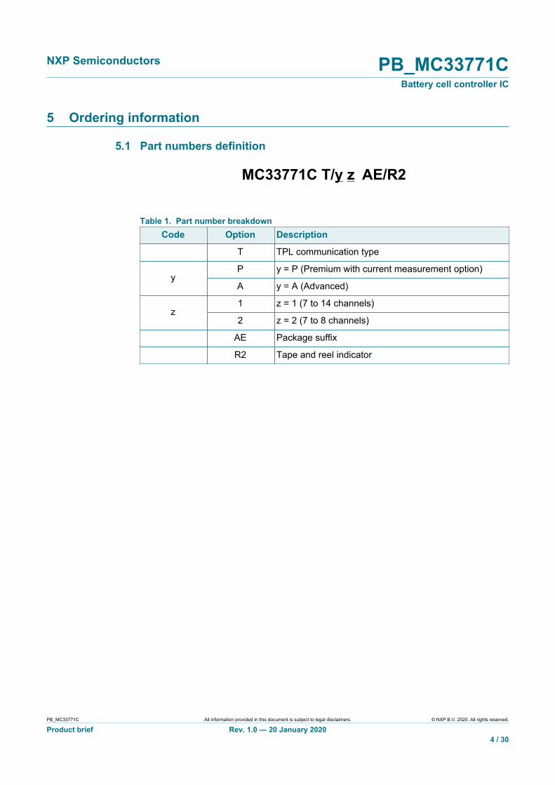
5 Ordering information
5.1 Part numbers definition
MC33771C T/y z AE/R2
Table 1. Part number breakdownCode Option Description
T TPL communication type
P y = P (Premium with current measurement option)y
A y = A (Advanced)
1 z = 1 (7 to 14 channels)z
2 z = 2 (7 to 8 channels)
AE Package suffix
R2 Tape and reel indicator

NXP Semiconductors PB_MC33771CBattery cell controller IC
PB_MC33771C All information provided in this document is subject to legal disclaimers. © NXP B.V. 2020. All rights reserved.
Product brief Rev. 1.0 — 20 January 20205 / 30
5.2 Part numbers listThis section describes the part numbers available to be purchased along with theirdifferences. Valid orderable part numbers are provided on the web. To determine theorderable part numbers for this device, go to http://www.nxp.com.
Table 2. Advanced orderable part tableTemperature range is −40 to 105 °CPackage type is 64-pin LQFP-EP
Orderable part Number ofchannels
OV/UV Precision GPIO as temperaturechannels and OT/UT
Current channel orcoulomb count
TPL differential communication protocol
MC33771CTA1AE 7 to 14 Yes Yes No
MC33771CTA2AE 7 to 8 Yes Yes No
Table 3. Premium orderable part tableTemperature range is −40 to 105 °CPackage type is 64-pin LQFP-EP
Orderable part Number ofchannels
OV/UV Precision GPIO as temperaturechannels and OT/UT
Current channel orcoulomb count
TPL differential communication protocol with current measurement option
MC33771CTP1AE 7 to 14 Yes Yes Yes
MC33771CTP2AE 7 to 8 Yes Yes Yes

NXP Semiconductors PB_MC33771CBattery cell controller IC
PB_MC33771C All information provided in this document is subject to legal disclaimers. © NXP B.V. 2020. All rights reserved.
Product brief Rev. 1.0 — 20 January 20206 / 30
6 Pinning information
6.1 Pinout diagram
VPWR2 RDTX_OUT+VPWR1 SI/RDTX_IN+
CT_14 SCLK/RDXT_IN-
CB_14 RDTX_OUT-CB_14:13C CGND
CB_13 VCOM
CT_13 SOCT_12 CSB
CB_12 FAULT
CB_12:11_C SPI_COM_ENCB_11 CT_REF
CT_11 CT_1
CT_10 CB_1CB_10 CB_2:1_C
CB_10:9_C CB_2
CB_9 CT_2
CT_
9G
ND
REF
CT_
8R
ESET
CB_
8SD
A
CB_
8:7_
CSC
LC
B_7
VAN
A
CT_
7D
GN
DC
T_6
AGN
D
CB_
6IS
ENSE
-
CB_
6:5_
CIS
ENSE
+C
B_5
GPI
O6
CT_
5G
PIO
5
CT_
4G
PIO
4C
B_4
GPI
O3
CB_
4:3_
CG
PIO
2
CB_
3G
PIO
1
CT_
3G
PIO
0
aaa-027847
12
3
45
6
78
9
1011
12
1314
15
16
4847
46
65GNDFLAG
4544
43
4241
40
3938
37
3635
34
33
17 18 19 20 21 22 23 24 25 26 27 28 29 30 31 32
64 63 62 61 60 59 58 57 56 55 54 53 52 51 50 49
Transparent top view
terminal 1index area
Figure 3. Pinout diagram
6.2 Pin definitions
Table 4. Pin definitionsNumber Name Function Definition
1 VPWR2 Input Power input to the MC33771C
2 VPWR1 Input Power input to the MC33771C
3 CT_14 Input Cell pin 14 input. Terminate to LPF resistor.
4 CB_14 Output Cell balance driver. Terminate to cell 14 cellbalance load resistor.
5 CB_14:13_C Output Cell balance 14:13 common. Terminate toCB_14:13_C balance load resistor.
6 CB_13 Output Cell balance driver. Terminate to cell 13 cellbalance load resistor.
7 CT_13 Input Cell pin 13 input. Terminate to LPF resistor.
8 CT_12 Input Cell pin 12 input. Terminate to LPF resistor.

NXP Semiconductors PB_MC33771CBattery cell controller IC
PB_MC33771C All information provided in this document is subject to legal disclaimers. © NXP B.V. 2020. All rights reserved.
Product brief Rev. 1.0 — 20 January 20207 / 30
Number Name Function Definition
9 CB_12 Output Cell balance driver. Terminate to cell 12 cellbalance load resistor.
10 CB_12:11_C Output Cell balance 12:11 common. Terminate toCB_12:11_C balance load resistor.
11 CB_11 Output Cell balance driver. Terminate to cell 11 cellbalance load resistor.
12 CT_11 Input Cell pin 11 input. Terminate to LPF resistor.
13 CT_10 Input Cell pin 10 input. Terminate to LPF resistor.
14 CB_10 Output Cell balance driver. Terminate to cell 10 cellbalance load resistor.
15 CB_10:9_C Output Cell balance 10:9 common. Terminate to CB_10:9_C balance load resistor.
16 CB_9 Output Cell balance driver. Terminate to cell 9 cellbalance load resistor.
17 CT_9 Input Cell pin 9 input. Terminate to LPF resistor.
18 CT_8 Input Cell pin 8 input. Terminate to LPF resistor.
19 CB_8 Output Cell balance driver. Terminate to cell 8 cellbalance load resistor.
20 CB_8:7_C Output Cell balance 8:7 common. Terminate to CB_8:7_C balance load resistor.
21 CB_7 Output Cell balance driver. Terminate to cell 7 cellbalance load resistor.
22 CT_7 Input Cell pin 7 input. Terminate to LPF resistor.
23 CT_6 Input Cell pin 6 input. Terminate to LPF resistor.
24 CB_6 Output Cell balance driver. Terminate to cell 6 cellbalance load resistor.
25 CB_6:5_C Output Cell balance 6:5 common. Terminate to CB_6:5_C balance load resistor.
26 CB_5 Output Cell balance driver. Terminate to cell 5 cellbalance load resistor.
27 CT_5 Input Cell pin 5 input. Terminate to LPF resistor.
28 CT_4 Input Cell pin 4 input. Terminate to LPF resistor.
29 CB_4 Output Cell balance driver. Terminate to cell 4 cellbalance load resistor.
30 CB_4:3_C Output Cell balance 4:3 common. Terminate to CB_4:3_C balance load resistor.
31 CB_3 Output Cell balance driver. Terminate to cell 3 cellbalance load resistor.
32 CT_3 Input Cell pin 3 input. Terminate to LPF resistor.
33 CT_2 Input Cell pin 2 input. Terminate to LPF resistor.
34 CB_2 Output Cell balance driver. Terminate to cell 2 cellbalance load resistor.

NXP Semiconductors PB_MC33771CBattery cell controller IC
PB_MC33771C All information provided in this document is subject to legal disclaimers. © NXP B.V. 2020. All rights reserved.
Product brief Rev. 1.0 — 20 January 20208 / 30
Number Name Function Definition
35 CB_2:1_C Output Cell Balance 2:1 common. Terminate to CB_2:1_C balance load resistor.
36 CB_1 Output Cell balance driver. Terminate to cell 1 cellbalance load resistor.
37 CT_1 Input Cell pin 1 input. Terminate to LPF resistor.
38 CT_REF Input Cell pin REF input. Terminate to LPF resistor.
39 SPI_COM_EN Input SPI communication enable. Pin must be highfor the SPI to be active.
40 FAULT Output Fault output dependent on user definedinternal or external faults. If not used, it mustbe left open.
41 CSB Input SPI chip select
42 SO Output SPI serial output
43 VCOM Output Communication regulator output
44 CGND Ground Communication decoupling ground.Terminate to GNDREF.
45 RDTX_OUT- I/O Receive/transmit output negative
46 SCLK/RDTX_IN- I/O SPI clock or receive/transmit input negative
47 SI/RDTX_IN+ I/O SPI serial input or receive/transmit inputpositive
48 RDTX_OUT+ I/O Receive/transmit output positive
49 GPIO0 I/O General purpose analog input or GPIO orwake-up or fault daisy chain
50 GPIO1 I/O General purpose analog input or GPIO
51 GPIO2 I/O General purpose analog input or GPIO orconversion trigger
52 GPIO3 I/O General purpose analog input or GPIO
53 GPIO4 I/O General purpose analog input or GPIO
54 GPIO5 I/O General purpose analog input or GPIO
55 GPIO6 I/O General purpose analog input or GPIO
56 ISENSE+ Input Current measurement input+
57 ISENSE- Input Current measurement input−
58 AGND Ground Analog ground, terminate to GNDREF
59 DGND Ground Digital ground, terminate to GNDREF
60 VANA Output Precision ADC analog supply
61 SCL I/O I2C clock
62 SDA I/O I2C data
63 RESET Input RESET is an active high input. RESET hasan internal pull down. If not used, it can betied to GND.

NXP Semiconductors PB_MC33771CBattery cell controller IC
PB_MC33771C All information provided in this document is subject to legal disclaimers. © NXP B.V. 2020. All rights reserved.
Product brief Rev. 1.0 — 20 January 20209 / 30
Number Name Function Definition
64 GNDREF Ground Ground reference for device. Terminate toreference of battery cluster.
65 GNDFLAG Ground Device flag. Terminate to lowest potential ofbattery cluster.
7 General product characteristics
7.1 Ratings and operating requirements relationshipThe operating voltage range pertains to the VPWR pins referenced to the AGND pins.
Table 5. Ratings vs. operating requirementsHandling range – no permanent failureFatal range
• Permanentfailure mightoccur
Lower limited operating range• No permanent failure,
but IC functionality is notguaranteed
Normal operating range• 100 % functional
Upper limited operating range• IC parameters might be out
of specification• Detection of VPWR
overvoltage is functional
Fatal range• Permanent
failure mightoccur
VPWR < −0.3 V 7.6 V ≤ VPWR < 9.6 VReset range:–0.3 V ≤ VPWR < 7.6 V
9.6 V ≤ VPWR ≤ 61.6 V 61.6 V < VPWR ≤ 75 V 75 V < VPWR
In both upper and lower limited operating range, no information can be provided about ICperformance. Only the detection of VPWR overvoltage is guaranteed in the upper limitedoperating range.
Performance in normal operating range is guaranteed only if there is a minimum of sevenbattery cells in the stack.
7.2 Maximum ratings
Table 6. Maximum ratingsAll voltages are with respect to ground unless otherwise noted. Exceeding these ratings may cause a malfunction orpermanent damage to the device.
Symbol Description (rating) Min Max Unit
Electrical ratings
VPWR1, VPWR2 Supply input voltage −0.3 75 V
CT14 Cell terminal voltage −0.3 75 V
VPWR to CT14 Voltage across VPWR1,2 pins pair and CT14 pin −10 10.5 V
CTN to CTN-1 Cell terminal differential voltage [1] −0.3 6.0 V
CTREF to GND Cell terminal reference to ground — 5 V
Cell terminal voltage to ground (N=1 to 4 or N=6 to 14) — (N+1) . 5 VCTN to GND
Cell terminal voltage to ground (N=5) — 27.5 V
CTN(CURRENT) Cell terminal input current — ±500 µA
CBN to CBN:N-1_CCBN:N-1_C to CBN-1
Cell balance differential voltage — 10 V

NXP Semiconductors PB_MC33771CBattery cell controller IC
PB_MC33771C All information provided in this document is subject to legal disclaimers. © NXP B.V. 2020. All rights reserved.
Product brief Rev. 1.0 — 20 January 202010 / 30
Symbol Description (rating) Min Max Unit
CB2n to GND Cell balance voltage to GND (n=1 to 7) — (2n+1) . 5 V
CB2n+1 to GND Cell balance voltage to GND (n=0 to 6) — (2n+1) . 5 V
CB2n:2n-1_C to GND Cell balance voltage to GND (n=1 to 6) — 2n . 5 V
CBN:N-1_C to CTn-1 Cell balance input to cell terminal input −10 10 V
VISENSE ISENSE+ and ISENSE– pin voltage −0.3 2.5 V
VCOM Maximum voltage may be applied to VCOM pin from externalsource
— 5.8 V
VANA Maximum voltage may be applied to VANA pin — 3.1 V
VGPIO0 GPIO0 pin voltage –0.3 6.5 V
VGPIOx GPIOx pins (x = 1 to 6) voltage –0.3 VCOM +0.5
V
VDIG Voltage I2C pins (SDA, SCL) –0.3 VCOM +0.5
V
VRESET RESET pin –0.3 6.5 V
VCSB CSB pin –0.3 6.5 V
VSPI_COMM_EN SPI_COMM_EN –0.3 6.5 V
VSO SO pin –0.3 VCOM +0.5
V
VGPIO5,6 Maximum voltage for GPIO5 and GPIO6 pins used as current input −0.3 2.5 V
FAULT Maximum applied voltage to pin −0.3 7.0 V
Ipin_unpowered Input current in a pin when the device is unpowered –2 2 mA
VCOMM Maximum voltage to pins RDTX_OUT+, RDTX_OUT–,SI/RDTX_IN+, SCLK/RDTX_IN-
−10.0 10.0 V
VESD1 ESD voltageHuman body model (HBM)Charge device model (CDM)Charge device model corner pins (CDM)
———
±2000±500 [2]
±750
V
VESD2 ESD voltage (VPWR1, VPWR2, CTx, CBx, GPIOx, ISENSE+,ISENSE−, RDTX_OUT+, RDTX_OUT−, SI/RDTX_IN+, SCLK/RDTX_IN−) versus all ground pins
Human body model (HBM)
[3] —
±4000
V
VESD3 ESD voltage (CTREF, CTx, CBx, GPIOx, ISENSE+, ISENSE−,RDTX_OUT+, RDTX_OUT−, SI/RDTX_IN+, SCLK/ RDTX_IN−)IEC 61000-4-2, Unpowered (Gun configuration: 330Ω / 150pF)HMM, Unpowered (Gun configuration: 330Ω / 150pF)ISO 10605:2009, Unpowered (Gun configuration: 2 kΩ / 150pF)ISO 10605:2009, Powered (Gun configuration: 2 kΩ / 150pF)
[4] ————
±8000±8000±8000±8000
V
[1] Adjacent CT pins may experience an overvoltage that exceeds their maximum rating during OV/UV functional verification test or during open linediagnostic test. Nevertheless, the IC is completely tolerant to this special situation.
[2] For CT_REF pin applicable limit is ±450 V.[3] ESD testing is performed in accordance with the human body model (HBM) (CZAP = 100 pF, RZAP = 1500 Ω), and the charge device model (CDM) (CZAP =
4.0 pF).[4] These voltage values can be sustained only if ESD caps are used as described in MC33771C External Components

NXP Semiconductors PB_MC33771CBattery cell controller IC
PB_MC33771C All information provided in this document is subject to legal disclaimers. © NXP B.V. 2020. All rights reserved.
Product brief Rev. 1.0 — 20 January 202011 / 30
7.3 Thermal characteristics
Table 7. Thermal ratingsAll voltages are with respect to ground unless otherwise noted. Exceeding these ratings may cause a malfunction orpermanent damage to the device.
Symbol Description (rating) Min Max Unit
Thermal ratings
TATJ
Operating temperatureAmbientJunction[1]
−40−40
+105+150
°C
TSTG Storage temperature −55 +150 °C
TPPRT Peak package reflow temperature [2][3]
— 260 °C
Thermal resistance and package dissipation ratings
RΘJB Junction-to-board (bottom exposed pad soldered to board) 64LQFP EP
[4] — 10 °C/W
RΘJA Junction-to-ambient, natural convection, single-layer board (1s) 64LQFP EP
[5][6]
— 59 °C/W
RΘJA Junction-to-ambient, natural convection, four-layer board (2s2p) 64LQFP EP
[5][6]
— 27 °C/W
RΘJCTOP Junction-to-case top (exposed pad) 64 LQFP EP [7] — 14 °C/W
RΘJCBOTTOM Junction-to-case bottom (exposed pad) 64 LQFP EP [8] — 0.97 °C/W
ΨJT Junction to package top, natural convection [9] — 3 °C/W
[1] The user must ensure that the average maximum operating junction temperature (TJ) is not exceeded.[2] Pin soldering temperature limit is for 10 seconds maximum duration. Not designed for immersion soldering. Exceeding these limits may cause a
malfunction or permanent damage to the device.[3] NXP’s Package Reflow capability meets Pb-free requirements for JEDEC standard J-STD-020C. For Peak Package Reflow Temperature and Moisture
Sensitivity Levels (MSL), go to www.nxp.com, search by part number (remove prefixes/suffixes) and enter the core ID to view all orderable parts andreview parametrics.
[4] Thermal resistance between the die and the printed circuit board per JEDEC JESD51-8. Board temperature is measured on the top surface of the boardnear the package.
[5] Junction temperature is a function of die size, on-chip power dissipation, package thermal resistance, mounting site (board) temperature, ambienttemperature, air flow, power dissipation of other components on the board, and board thermal resistance.
[6] Per JEDEC JESD51-6 with the board (JESD51-7) horizontal.[7] Thermal resistance between the die and the case top surface as measured by the cold plate method (MIL SPEC-883 Method 1012.1), with the cold plate
temperature used for the case temperature.[8] Thermal resistance between the die and the solder pad on the bottom of the package based on simulation without any interface resistance.[9] Thermal characterization parameter indicating the temperature difference between the package top and the junction temperature per JEDEC JESD51-2.
7.4 Electrical characteristics
Table 8. Static and dynamic electrical characteristicsCharacteristics noted under conditions 9.6 V ≤ VPWR ≤ 61.6V, −40 °C ≤ TA ≤ 105 °C, GND = 0 V, unless otherwise stated.Typical values refer to VPWR = 56 V, TA = 25 °C, unless otherwise noted.
Symbol Parameter Min Typ Max Unit
Power management
VPWR(FO) Supply voltageFull parameter specification
9.6
—
61.6
V

NXP Semiconductors PB_MC33771CBattery cell controller IC
PB_MC33771C All information provided in this document is subject to legal disclaimers. © NXP B.V. 2020. All rights reserved.
Product brief Rev. 1.0 — 20 January 202012 / 30
Symbol Parameter Min Typ Max Unit
IVPWR Supply current (base value)Normal mode, cell balance OFF, ADC inactive, SPIcommunication inactive, IVCOM = 0 mANormal mode, cell balance OFF, ADC inactive, TPLcommunication inactive, IVCOM = 0 mA
—
5.4 8.0
— —
mA
IVPWR(TPL_TX) Supply current adder when TPL communication active — — 16 mA
IVPWR(CBON) Supply current adder to set all 14 cell balance switches ON — 0.97 — mA
IVPWR(ADC) Delta supply current to perform ADC conversions (addend)ADC1-A,B continuously convertingADC2 continuously converting
——
3.01.4
——
mA
IVPWR(SS) Supply current in sleep mode and in idle mode, communicationinactive, cell balance off, cyclic measurement off, oscillator monitoron
SPI mode (25 °C)
TPL mode (TA = 25 °C)
— 64
40 —
— 108
µA
IVPWR(CKMON) Clock monitor current consumption — 5 — µA
VPWR(OV_FLAG) VPWR overvoltage fault threshold (flag) — 65 — V
VPWR(LV_FLAG) VPWR low-voltage warning threshold (flag) — 12 — V
VPWR(UV_POR) VPWR undervoltage shutdown threshold (POR) — 8.5 — V
VPWR(HYS) VPWR UV hysteresis voltage — 200 — mV
tVPWR(FILTER) VPWR OV, LV filter — 50 — µs
VCOM power supply
VCOM VCOM output voltage — 5.0 — V
IVCOM VCOM output current allocated for external use — — 5.0 mA
VCOM(UV) VCOM undervoltage fault threshold — 4.4 — V
VCOM_HYS VCOM undervoltage hysteresis — 100 — mV
tVCOM(FLT_TIMER) VCOM undervoltage fault timer — 10 — µs
tVCOM(RETRY) VCOM fault retry timer — 10 — ms
VCOM(OV) VCOM overvoltage fault threshold 5.4 — 5.9 V
ILIM_VCOM(OC) VCOM current limit 65 — 140 mA
RVCOM(SS) VCOM sleep mode pull-down resistor — 2.0 — kΩ
tVCOM VCOM rise time (for VPWR > 10V and CL = 2.2 µF (ceramic X7Ronly) in parallel with 220 pF)
— — 440 µs
VANA power supply
VANA VANA output voltage (not used by external circuits)Decouple with 47 nF X7R 0603 or 0402
—
2.65
—
V
VANA(UV) VANA undervoltage fault threshold — 2.4 — V
VANA_HYS VANA undervoltage hysteresis — 50 — mV
VANA(FLT_TIMER) VANA undervoltage fault timer — 11 — µs
VANA(OV) VANA overvoltage fault threshold — 2.8 — V
tVANA(RETRY) VANA fault retry timer — 10 — ms
ILIM_VANA(OC) VANA current limit 5.0 — 10 mA
RVANA_RPD VANA sleep mode pull-down resistor — 1.0 — kΩ

NXP Semiconductors PB_MC33771CBattery cell controller IC
PB_MC33771C All information provided in this document is subject to legal disclaimers. © NXP B.V. 2020. All rights reserved.
Product brief Rev. 1.0 — 20 January 202013 / 30
Symbol Parameter Min Typ Max Unit
tVANA VANA rise time (CL = 47 nF ceramic X7R only) — — 400 µs
ADC1-A, ADC1-B
CTn(LEAKAGE) Cell terminal input leakage current (except in SLEEP mode when cellbalancing is ON)
— 10 — nA
CTn(FV) Cell terminal input current - functional verification — 0.365 — mA
CTN Cell terminal input current during conversion — 50 — nA
RPD Cell terminal open load detection pull-down resistor — 950 — Ω
VVPWR_RES VPWR terminal measurement resolution — 2.44141 — mV/LSB
VVPWR_RNG VPWR terminal measurement range 9.6 — 75 V
VPWRTERM_ERR VPWR terminal measurement accuracy −0.5 — 0.5 %
VCT_RNG ADC differential input voltage range for CTn to CTn-1 0.0 — 4.85 V
VCT_ANx_RES Cell voltage and ANx resolution in 15-bit MEAS_xxxx registers — 152.58789 — µV/LSB
VANx_RATIO_RES ANx resolution in 15-bit MEAS_xxxx registers in ratiometric mode — VCOM.(30.51851)
— µV/LSB
VERR33RT Cell voltage measurement error VCELL = 3.3 V, TA = 25 °C −0.8 ±0.4 0.8 mV
VERR Cell voltage measurement error0.1 V ≤ VCELL ≤ 4.8 V, −40 °C ≤ TA ≤ 105 °C (or −40 °C ≤ TJ ≤125 °C)
—
±0.7
—
mV
VERR_1 Cell voltage measurement error0 V ≤ VCELL ≤ 1.5 V, −40 °C ≤ TA ≤ 60 °C (or −40 °C ≤ TJ ≤85 °C)
—
±0.4
—
mV
VERR_2 Cell voltage measurement error1.5 V ≤ VCELL ≤ 2.7 V, −40 °C ≤ TA ≤ 60 °C (or −40 °C ≤ TJ ≤85 °C)
—
±0.4
—
mV
VERR_3 Cell voltage measurement error2.7 V ≤ VCELL ≤ 3.7 V, −40 °C ≤ TA ≤ 60 °C (or −40 °C ≤ TJ ≤85 °C)
—
±0.5
—
mV
VERR_4 Cell voltage measurement error3.7 V ≤ VCELL ≤ 4.3 V, −40 °C ≤ TA ≤ 60 °C (or −40 °C ≤ TJ ≤85 °C)
—
±0.7
—
mV
VERR_5 Cell voltage measurement error1.5 V ≤ VCELL ≤ 4.5 V, −40 °C ≤ TA ≤ 105 °C (or −40 °C ≤ TJ ≤125 °C)
—
±0.7
—
mV
VANx_ERR Magnitude of ANx error in the entire measurement range:Ratiometric measurementAbsolute measurement after soldering and aging, input in therange [1.0, 4.5] VAbsolute measurement after soldering and aging, input in therange [0, 4.85] V, for −40 °C < TA < 60 °C)Absolute measurement after soldering and aging, input in therange [0, 4.85] V, for −40 °C < TA < 105 °C)
—— −8.0 −11
—— — —
1610 8.0 11
mV
tVCONV Single channel net conversion time13-bit resolution14-bit resolution15-bit resolution16-bit resolution
————
6.779.4314.7525.36
————
µs

NXP Semiconductors PB_MC33771CBattery cell controller IC
PB_MC33771C All information provided in this document is subject to legal disclaimers. © NXP B.V. 2020. All rights reserved.
Product brief Rev. 1.0 — 20 January 202014 / 30
Symbol Parameter Min Typ Max Unit
VV_NOISE Conversion noise13-bit resolution14-bit resolution15-bit resolution16-bit resolution
————
18001000600400
————
µVrms
ADC2/current sense module
VINC ISENSE+/ISENSE− input voltage (reference to AGND) −300 — 300 mV
VIND ISENSE+/ISENSE− differential input voltage range −150 — 150 mV
VISENSEX(OFFSET) ISENSE+/ISENSE− input voltage offset error — — 0.5 µV
ISENSEX(BIAS) ISENSE+/ISENSE− input bias current −100 — 100 nA
ISENSE(DIF) ISENSE+/ISENSE− differential input bias current −5.0 — 5.0 nA
IGAINERR ISENSE error including nonlinearities −0.5 — 0.5 %
IISENSE_OL ISENSE open load injected current — 130 — µA
VISENSE_OL ISENSE open load detection threshold — 460 — mV
V2RES Current sense user register resolution — 0.6 — µV/LSB
VPGA_SAT PGA saturation half-rangeGain = 256Gain = 64Gain = 16Gain = 4
————
4.919.578.1150.0
————
mV
VPGA_ITH Voltage threshold for PGA gain increaseGain = 256Gain = 64Gain = 16Gain = 4
————
—2.3449.37537.50
————
mV
VPGA_DTH Voltage threshold for PGA gain decreaseGain = 256Gain = 64Gain = 16Gain = 4
————
4.29817.18868.750—
————
mV
tAZC_SETTLE Time to perform auto-zero procedure after enabling the currentchannel
— 200 — µs
tICONV ADC conversion time including PGA settling time13 bit resolution14 bit resolution15 bit resolution16 bit resolution
————
19.0021.6727.0037.67
————
µs
VI_NOISE Noise error at 16-bit conversion — 3.01 — µVrms
VI_NOISE Noise error at 13-bit conversion — 8.33 — µVrms
ADCCLK ADC2 and ADC1-A,B clocking frequency — 6.0 — MHz
Cell balance drivers
VDS(CLAMP) Cell balance driver VDS active clamp voltage — 11 — V
VOUT(FLT_TH) Output fault detection voltage thresholdBalance off (open load)Balance on (shorted load)
—
0.55
—
V
RPD_CB Output OFF open load detection pull-down resistorBalance off, open load detect disabled
—
2.0
—
kΩ

NXP Semiconductors PB_MC33771CBattery cell controller IC
PB_MC33771C All information provided in this document is subject to legal disclaimers. © NXP B.V. 2020. All rights reserved.
Product brief Rev. 1.0 — 20 January 202015 / 30
Symbol Parameter Min Typ Max Unit
IOUT(LKG) Output leakage currentBalance off, open load detect disabled at VDS = 4.0 V
—
—
1.0
µA
RDS(on) Drain-to-source on resistanceIOUT = 300 mA, TJ = 105 °CIOUT = 300 mA, TJ = 25 °CIOUT = 300 mA, TJ = −40 °C
———
—0.50.4
0.80——
Ω
ILIM_CB Driver current limitation 310 — 950 mA
tON Cell balance driver turn onRL = 15 Ω
—
350
—
µs
tOFF Cell balance driver turn offRL = 15 Ω
—
200
—
µs
tBAL_DEGLICTH Short/open detect filter time — 20 — µs
Internal temperature measurement
IC_TEMP1_ERR IC temperature measurement error −3.0 — 3.0 K
IC_TEMP1_RES IC temperature resolution — 0.032 — K/LSB
TSD_TH Thermal shutdown — 170 — °C
TSD_HYS Thermal shutdown hysteresis — 10 — °C
Default operational parameters
VCTOV(TH) Cell overvoltage threshold (8 bits), typical value is default value afterRESET
0.0 4.2 5.0 V
VCTOV(RES) Cell overvoltage threshold resolution — 19.53125 — mV/LSB
VCTUV(TH) Cell undervoltage threshold (8 bits), typical value is default valueafter RESET
0.0 2.5 5.0 V
VCTUV(RES) Cell undervoltage threshold resolution — 19.53125 — mV/LSB
VGPIO_OT(TH) GPIOx configured as ANx input overtemperature threshold afterRESET
— 1.16 — V
VGPIO_OT(RES) Temperature voltage threshold resolution — 4.8828125 — mV/LSB
VGPIO_UT(TH) GPIOx configured as ANx input undertemperature threshold afterRESET
— 3.82 — V
VGPIO_UT(RES) Temperature voltage threshold resolution — 4.8828125 — mV/LSB
General purpose input/output GPIOx
VIH Input high-voltage (3.3 V compatible) 2.0 — — V
VIL Input low-voltage (3.3 V compatible) — — 1.0 V
VHYS Input hysteresis — 100 — mV
IIL Input leakage currentPins tristate, VIN = VCOM or AGND
−100
—
100
nA
IIDL Differential Input Leakage Current GPIO 5,6GPIO 5,6 configured as digital inputs for current measurement
−30
—
30
nA
VOH Output high-voltage IOH = −0.5 mA VCOM −0.8
— — V
VOL Output low-voltage IOL = +0.5 mA — — 0.8 V
VADC Analog ADC input voltage range for ratiometric measurements AGND — VCOM V
VOL(TH) Analog input open pin detect threshold — 0.15 — V
ROPENPD Internal open detection pull-down resistor — 5.0 — kΩ
tGPIO0_WU GPIO0 WU de-glitch filter — 50 — µs

NXP Semiconductors PB_MC33771CBattery cell controller IC
PB_MC33771C All information provided in this document is subject to legal disclaimers. © NXP B.V. 2020. All rights reserved.
Product brief Rev. 1.0 — 20 January 202016 / 30
Symbol Parameter Min Typ Max Unit
tGPIO0_FLT GPIO0 daisy chain de-glitch filter both edges — 20 — µs
tGPIO2_SOC GPIO2 convert trigger de-glitch filter — 2.0 — µs
tGPIOx_DIN GPIOx configured as digital input de-glitch filter 2.5 — 5.6 µs
Reset input
VIH_RST Input high-voltage (3.3 V compatible) 2.0 — — V
VIL_RST Input low-voltage (3.3 V compatible) — — 1.0 V
VHYS Input hysteresis — 0.6 — V
tRESETFLT RESET de-glitch filter — 100 — µs
RRESET_PD Input logic pull down (RESET) — 100 — kΩ
SPI_COM_EN input
VIH Input high-voltage (3.3 V compatible) 2.0 — — V
VIL Input low-voltage (3.3 V compatible) — — 1.0 V
VHYS Input hysteresis — 450 — mV
RSPI_COM_EN_PD Input pull-down resistor (SPI_COM_EN) — 100 — kΩ
Digital interface
VFAULT_HA FAULT output (high active, IOH = 1.0 mA) — 4.9 — V
IFAULT_CL FAULT output current limit 3.0 — 40 mA
RFAULT_PD FAULT output pull-down resistance — 100 — kΩ
VIH_COMM Voltage threshold to detect the input as highSI/RDTX_IN+, SCLK/RDTX_IN–, CSB, SDA, SCL (NOTE: needsto be 3.3 V compatible)
—
—
2.0
V
VIL_COMM Voltage threshold to detect the input as lowSI/RDTX_IN+, SCLK/RDTX_IN–, CSB, SDA, SCL
0.8
—
—
V
VHYS Input hysteresisSI/RDTX_IN+, SCLK/RDTX_IN−, CSB, SDA, SCL
—
80
—
mV
ILOGIC_SS Sleep state input logic currentCSB
−100
—
100
nA
RSCLK_PD Input logic pull-down resistance (SCLK/RDTX_IN–, SI/RDTX_IN+) — 20 — kΩ
RI_PU Input logic pull-up resistance to VCOM (CSB, SDA, SCL) — 100 — kΩ
ISO_TRI Tristate SO input current 0 V to VCOM −2.0 — 2.0 µA
VSO_HIGH SO high-state output voltage with ISO(HIGH) = −2.0 mA VCOM −0.4
— — V
VSO_LOW SO, SDA, SLK low-state output voltage with ISO(HIGH) = −2.0 mA — — 0.4 V
CSBWU_FLT CSB wake-up de-glitch filter, low to high transition — — 80 µs
System timing
tCELL_CONV Time needed to acquire all 14 cell voltages and the current after anon-demand conversion
13-bit resolution14-bit resolution15-bit resolution16-bit resolution
————
5980123208
————
µs

NXP Semiconductors PB_MC33771CBattery cell controller IC
PB_MC33771C All information provided in this document is subject to legal disclaimers. © NXP B.V. 2020. All rights reserved.
Product brief Rev. 1.0 — 20 January 202017 / 30
Symbol Parameter Min Typ Max Unit
tSYNC V/I synchronization timeADC1-A,B at 13 bit, ADC2 at 13 bitADC1-A,B at 14 bit, ADC2 at 13 bitADC1-A,B at 15 bit, ADC2 at 13 bitADC1-A,B at 16 bit, ADC2 at 13 bit
————
48.1653.5064.1685.50
————
µs
tSYNC V/I synchronization timeADC1-A,B at 13 bit, ADC2 at 14 bitADC1-A,B at 14 bit, ADC2 at 14 bitADC1-A,B at 15 bit, ADC2 at 14 bitADC1-A,B at 16 bit, ADC2 at 14 bit
————
52.1457.4868.1489.48
————
µs
tSYNC V/I synchronization timeADC1-A,B at 13 bit, ADC2 at 15 bitADC1-A,B at 14 bit, ADC2 at 15 bitADC1-A,B at 15 bit, ADC2 at 15 bitADC1-A,B at 16 bit, ADC2 at 15 bit
————
62.1265.4676.1297.46
————
µs
tSYNC V/I synchronization timeADC1-A,B at 13 bit, ADC2 at 16 bitADC1-A,B at 14 bit, ADC2 at 16 bitADC1-A,B at 15 bit, ADC2 at 16 bitADC1-A,B at 16 bit, ADC2 at 16 bit
————
120.51117.84112.51113.39
————
µs
tVPWR(READY) Time after VPWR connection for the IC to be ready for initialization — — 5.0 ms
tWAKE-UP Power up duration — — 440 µs
tWAKE_DELAY Time between wake pulses — 600 — µs
tIDLE Idle timeout after POR — 60 — s
tBALANCE Cell balance timer range 0.5 — 511 min
tCYCLE Cyclic acquisition timer range 0.0 — 8.5 s
tFAULT Fault detection to activation of fault pinNormal mode
—
—
56
µs
tEOC SOC to data ready (includes post processing of data, ADC_CFG[AVG]=0)
13-bit resolution14-bit resolution15-bit resolution16-bit resolution
————
148201307520
————
µs
tSETTLE Time after SOC to begin converting with ADC1-A,B — 12.28 — µs
tSYS_MEAS1 Time needed to send an SOC command and read back 96 cellvoltages, 48 temperatures, 1 current, and 1 coulomb counter, andADC1-A,B configured as follows (with ADC_CFG[AVG]=0):
13-bit resolution14-bit resolution15-bit resolution16-bit resolution
————
4.674.734.835.05
————
ms
tSYS_MEAS2 Time needed to send an SOC command and read back 96cell voltages, 1 current, and 1 coulomb counter and ADC1-A,Bconfigured as follows (with ADC_CFG[AVG]=0):
13-bit resolution14-bit resolution15-bit resolution16-bit resolution
————
3.243.393.403.61
————
ms

NXP Semiconductors PB_MC33771CBattery cell controller IC
PB_MC33771C All information provided in this document is subject to legal disclaimers. © NXP B.V. 2020. All rights reserved.
Product brief Rev. 1.0 — 20 January 202018 / 30
Symbol Parameter Min Typ Max Unit
tCLST_TPL Time needed to send an SOC command and read back 14 cellvoltages, 7 temperatures, 1 current, and 1 coulomb counter with TPLcommunication working at 2.0 Mbps and ADC1-A,B configured asfollows (with ADC_CFG[AVG]=0):
13-bit resolution14-bit resolution15-bit resolution16-bit resolution
————
0.850.901.1011.22
————
ms
tCLST_SPI Time needed to send an SOC command and read back 14 cellvoltages, 7 temperatures, 1 current, and 1 coulomb counter with SPIcommunication working at 4.0 Mbps and ADC1-A,B configured asfollows (with ADC_CFG[AVG]=0):
13-bit resolution14-bit resolution15-bit resolution16-bit resolution
————
0.570.640.761.03
————
ms
tI2C_DOWNLOAD Time to download EEPROM calibration after POR — — 1.0 ms
tI2C_ACCESS EEPROM access time, EEPROM write (depends on deviceselection)
— 5.0 — ms
tWAVE_DC_BITx Daisy chain duty cycle off timetWAVE_DC_BITx = 00
—
500
—
µs
tWAVE_DC_BITx Daisy chain duty cycle off timetWAVE_DC_BITx = 01
—
1.0
—
ms
tWAVE_DC_BITx Daisy chain duty cycle off timetWAVE_DC_BITx = 10
—
10
—
ms
tWAVE_DC_BITx Daisy chain duty cycle off timetWAVE_DC_BITx = 11
—
100
—
ms
tWAVE_DC_ON Daisy chain duty cycle on time — 500 — µs
tCOM_LOSS Time out to reset the IC in the absence of communication — 1024 — ms
SPI interface
tSPI_TD Sequential data transfer delay in SPI mode (N) 1.0 — — µs
FSCK SCLK/RDTX_IN– frequency — — 4.0 MHz
tSCK _H SCLK/RDTX_IN– high time (A) 125 — — ns
tSCK _L SCLK/RDTX_IN– high time (B) 125 — — ns
tSCK SCLK/RDTX_IN− period (A+B) 250 — — ns
tFALL SCLK/RDTX_IN− falling time — — 15 ns
tRISE SCLK/RDTX_IN− rising time — — 15 ns
tSET SCLK/RDTX_IN− setup time (O) 20 — — ns
tHOLD SCLK/RDTX_IN– hold time (P) 20 — — ns
tSI_SETUP SI/RDTX_IN+ setup time (F) 40 — — ns
tSI_HOLD SI/RDTX_IN+ hold time (G) 40 — — ns
tSO_VALID SO data valid, rising edge of SCLK/RDTX_IN− to SO data valid (I) — — 40 ns
tSO_EN SO enable time (H) — — 40 ns
tSO_DISABLE SO disable time (K) — — 40 ns
tCSB_LEAD CSB lead time (L) 100 — — ns
tCSB_LAG CSB lag time (M) 100 — — ns

NXP Semiconductors PB_MC33771CBattery cell controller IC
PB_MC33771C All information provided in this document is subject to legal disclaimers. © NXP B.V. 2020. All rights reserved.
Product brief Rev. 1.0 — 20 January 202019 / 30
Symbol Parameter Min Typ Max Unit
TPL interface (MCU)
tMCU_RES Time between two consecutive message request transmitted byMCU
4.0 — — µs
tWU_Wait Time the MCU shall wait after sending first wake-up message per33771 IC
0.75 — — ms
TPL interface (33771)
tTPL_TD Sequential data transfer delay in TPL mode 4.0 — — µs
tTPL Transmit pulse duration — 210 — ns
tport_delay Port delay introduced by each repeater in 33771 — — 0.95 µs
tRES Slave response after read command — 5.0 — µs
VRDTX INTH Differential receiver threshold — 580 — mV
tEOM Message timeout duration — 250 — µs
7.5 Timing diagrams
aaa-027848
CSB
MSB
MSB
LSB
LSB
SCLK
SO
SI
Don't care level
Tri-state Tri-state
Don't care levelO L A
GF
B
NM P
KH I
Figure 4. Low-voltage SPI interface timing
RDTX_OUT+RDTX_IN+
RDTX_IN-RDTX_OUT-
3.2 V
1.8 V
2.5 V
End ofmessage
Start ofmessage
Bit 0Logic 0
Bit 1Logic 0
Bit 2Logic 1
Bit 46Logic 1
Bit 47Logic 1
aaa-032610
Figure 5. Transformer communication signaling
8 Packaging
8.1 Package mechanical dimensionsPackage dimensions are provided in package drawings. To find the most currentpackage outline drawing, go to www.nxp.com and perform a keyword search for thedrawing’s document number.
Table 9. Package outlinePackage Suffix Package outline drawing number
64-pin LQFP-EP AE 98ASA10763D

NXP Semiconductors PB_MC33771CBattery cell controller IC
PB_MC33771C All information provided in this document is subject to legal disclaimers. © NXP B.V. 2020. All rights reserved.
Product brief Rev. 1.0 — 20 January 202020 / 30
Figure 6. Package outline

NXP Semiconductors PB_MC33771CBattery cell controller IC
PB_MC33771C All information provided in this document is subject to legal disclaimers. © NXP B.V. 2020. All rights reserved.
Product brief Rev. 1.0 — 20 January 202021 / 30
Figure 7. Package outline

NXP Semiconductors PB_MC33771CBattery cell controller IC
PB_MC33771C All information provided in this document is subject to legal disclaimers. © NXP B.V. 2020. All rights reserved.
Product brief Rev. 1.0 — 20 January 202022 / 30
Figure 8. Package outline

NXP Semiconductors PB_MC33771CBattery cell controller IC
PB_MC33771C All information provided in this document is subject to legal disclaimers. © NXP B.V. 2020. All rights reserved.
Product brief Rev. 1.0 — 20 January 202023 / 30
Figure 9. Package outline

NXP Semiconductors PB_MC33771CBattery cell controller IC
PB_MC33771C All information provided in this document is subject to legal disclaimers. © NXP B.V. 2020. All rights reserved.
Product brief Rev. 1.0 — 20 January 202024 / 30
Figure 10. Package outline

NXP Semiconductors PB_MC33771CBattery cell controller IC
PB_MC33771C All information provided in this document is subject to legal disclaimers. © NXP B.V. 2020. All rights reserved.
Product brief Rev. 1.0 — 20 January 202025 / 30
Figure 11. Package outline

NXP Semiconductors PB_MC33771CBattery cell controller IC
PB_MC33771C All information provided in this document is subject to legal disclaimers. © NXP B.V. 2020. All rights reserved.
Product brief Rev. 1.0 — 20 January 202026 / 30
Figure 12. Package outline

NXP Semiconductors PB_MC33771CBattery cell controller IC
PB_MC33771C All information provided in this document is subject to legal disclaimers. © NXP B.V. 2020. All rights reserved.
Product brief Rev. 1.0 — 20 January 202027 / 30
9 References
Following are URLs where you can obtain information on related NXP products andapplication solutions:
[1] Product summary page for RD33771CNTREVM: HV Battery management system reference design — http://www.nxp.com/products/RD33771CNTREVM
[2] Product summary page for MC33664: Isolated Network High-Speed Transceiver — http://www.nxp.com/products/MC33664
[3] Product summary page for MC33771: 14-Channel Li-ion Battery Cell Controller IC — http://www.nxp.com/products/MC33771C
[4] Product summary page for UJA1169: Mini high-speed CAN companion system basis chip — https://www.nxp.com/products/power-management/system-basis-chips/mini-system-basis-chips-sbcs/mini-high-speed-can-companion-system-basis-chip:UJA1169LTK
[5] Product summary page for S32K144: 32-bit Automotive General Purpose Microcontroller — https://www.nxp.com/products/processors-and-microcontrollers/arm-microcontrollers/s32k-32-bit-automotive-general-purpose-microcontrollers:S32K
[6] Support page for S32DS-PA: S32DS-ARM: S32 Design Studio for Arm — https://www.nxp.com/design/software/development-software/s32-design-studio-ide/s32-design-studio-for-arm:S32DS-ARM
[7] NXP DocStore — docstore.nxp.com

NXP Semiconductors PB_MC33771CBattery cell controller IC
PB_MC33771C All information provided in this document is subject to legal disclaimers. © NXP B.V. 2020. All rights reserved.
Product brief Rev. 1.0 — 20 January 202028 / 30
10 Legal information
10.1 DefinitionsDraft — The document is a draft version only. The content is still underinternal review and subject to formal approval, which may result inmodifications or additions. NXP Semiconductors does not give anyrepresentations or warranties as to the accuracy or completeness ofinformation included herein and shall have no liability for the consequencesof use of such information.
10.2 DisclaimersLimited warranty and liability — Information in this document is believedto be accurate and reliable. However, NXP Semiconductors does notgive any representations or warranties, expressed or implied, as to theaccuracy or completeness of such information and shall have no liabilityfor the consequences of use of such information. NXP Semiconductorstakes no responsibility for the content in this document if provided by aninformation source outside of NXP Semiconductors. In no event shall NXPSemiconductors be liable for any indirect, incidental, punitive, special orconsequential damages (including - without limitation - lost profits, lostsavings, business interruption, costs related to the removal or replacementof any products or rework charges) whether or not such damages are basedon tort (including negligence), warranty, breach of contract or any otherlegal theory. Notwithstanding any damages that customer might incur forany reason whatsoever, NXP Semiconductors’ aggregate and cumulativeliability towards customer for the products described herein shall be limitedin accordance with the Terms and conditions of commercial sale of NXPSemiconductors.
Right to make changes — NXP Semiconductors reserves the right tomake changes to information published in this document, including withoutlimitation specifications and product descriptions, at any time and withoutnotice. This document supersedes and replaces all information supplied priorto the publication hereof.
Applications — Applications that are described herein for any of theseproducts are for illustrative purposes only. NXP Semiconductors makesno representation or warranty that such applications will be suitablefor the specified use without further testing or modification. Customersare responsible for the design and operation of their applications andproducts using NXP Semiconductors products, and NXP Semiconductorsaccepts no liability for any assistance with applications or customer productdesign. It is customer’s sole responsibility to determine whether the NXPSemiconductors product is suitable and fit for the customer’s applicationsand products planned, as well as for the planned application and use ofcustomer’s third party customer(s). Customers should provide appropriatedesign and operating safeguards to minimize the risks associated withtheir applications and products. NXP Semiconductors does not accept anyliability related to any default, damage, costs or problem which is basedon any weakness or default in the customer’s applications or products, or
the application or use by customer’s third party customer(s). Customer isresponsible for doing all necessary testing for the customer’s applicationsand products using NXP Semiconductors products in order to avoid adefault of the applications and the products or of the application or use bycustomer’s third party customer(s). NXP does not accept any liability in thisrespect.
Limiting values — Stress above one or more limiting values (as defined inthe Absolute Maximum Ratings System of IEC 60134) will cause permanentdamage to the device. Limiting values are stress ratings only and (proper)operation of the device at these or any other conditions above thosegiven in the Recommended operating conditions section (if present) or theCharacteristics sections of this document is not warranted. Constant orrepeated exposure to limiting values will permanently and irreversibly affectthe quality and reliability of the device.
Terms and conditions of commercial sale — NXP Semiconductorsproducts are sold subject to the general terms and conditions of commercialsale, as published at http://www.nxp.com/profile/terms, unless otherwiseagreed in a valid written individual agreement. In case an individualagreement is concluded only the terms and conditions of the respectiveagreement shall apply. NXP Semiconductors hereby expressly objects toapplying the customer’s general terms and conditions with regard to thepurchase of NXP Semiconductors products by customer.
Suitability for use in automotive applications — This NXPSemiconductors product has been qualified for use in automotiveapplications. Unless otherwise agreed in writing, the product is not designed,authorized or warranted to be suitable for use in life support, life-critical orsafety-critical systems or equipment, nor in applications where failure ormalfunction of an NXP Semiconductors product can reasonably be expectedto result in personal injury, death or severe property or environmentaldamage. NXP Semiconductors and its suppliers accept no liability forinclusion and/or use of NXP Semiconductors products in such equipment orapplications and therefore such inclusion and/or use is at the customer's ownrisk.
Export control — This document as well as the item(s) described hereinmay be subject to export control regulations. Export might require a priorauthorization from competent authorities.
Translations — A non-English (translated) version of a document is forreference only. The English version shall prevail in case of any discrepancybetween the translated and English versions.
10.3 TrademarksNotice: All referenced brands, product names, service names andtrademarks are the property of their respective owners.
NXP — is a trademark of NXP B.V.SMARTMOS — is a trademark of NXP B.V.

NXP Semiconductors PB_MC33771CBattery cell controller IC
PB_MC33771C All information provided in this document is subject to legal disclaimers. © NXP B.V. 2020. All rights reserved.
Product brief Rev. 1.0 — 20 January 202029 / 30
TablesTab. 1. Part number breakdown ....................................4Tab. 2. Advanced orderable part table .......................... 5Tab. 3. Premium orderable part table ............................5Tab. 4. Pin definitions ....................................................6Tab. 5. Ratings vs. operating requirements ...................9
Tab. 6. Maximum ratings ...............................................9Tab. 7. Thermal ratings ............................................... 11Tab. 8. Static and dynamic electrical characteristics ... 11Tab. 9. Package outline ...............................................19
FiguresFig. 1. Simplified application diagram, SPI use case ....2Fig. 2. Simplified application diagram, TPL use
case ...................................................................3Fig. 3. Pinout diagram .................................................. 6Fig. 4. Low-voltage SPI interface timing .....................19Fig. 5. Transformer communication signaling .............19Fig. 6. Package outline ...............................................20
Fig. 7. Package outline ...............................................21Fig. 8. Package outline ...............................................22Fig. 9. Package outline ...............................................23Fig. 10. Package outline ...............................................24Fig. 11. Package outline ...............................................25Fig. 12. Package outline ...............................................26

NXP Semiconductors PB_MC33771CBattery cell controller IC
Please be aware that important notices concerning this document and the product(s)described herein, have been included in section 'Legal information'.
© NXP B.V. 2020. All rights reserved.For more information, please visit: http://www.nxp.comFor sales office addresses, please send an email to: [email protected]
Date of release: 20 January 2020Document identifier: PB_MC33771C
Contents1 General description ............................................ 12 Features ............................................................... 13 Simplified application diagram .......................... 24 Applications .........................................................35 Ordering information .......................................... 45.1 Part numbers definition ......................................45.2 Part numbers list ............................................... 56 Pinning information ............................................ 66.1 Pinout diagram .................................................. 66.2 Pin definitions .................................................... 67 General product characteristics ........................ 97.1 Ratings and operating requirements
relationship .........................................................97.2 Maximum ratings ............................................... 97.3 Thermal characteristics ....................................117.4 Electrical characteristics .................................. 117.5 Timing diagrams .............................................. 198 Packaging .......................................................... 198.1 Package mechanical dimensions .................... 199 References ......................................................... 2710 Legal information ..............................................28


![MFRC523 Contactless reader IC - NXP Semiconductors · 115233 3 of 98 NXP Semiconductors MFRC523 Contactless reader IC [1] Supply voltages below 3 V reduce the performance in, for](https://img.pdfslide.us/doc/110x75/60d572e79758d0137c43f5f8/mfrc523-contactless-reader-ic-nxp-semiconductors-115233-3-of-98-nxp-semiconductors.jpg)