Embed Size (px)
Citation preview
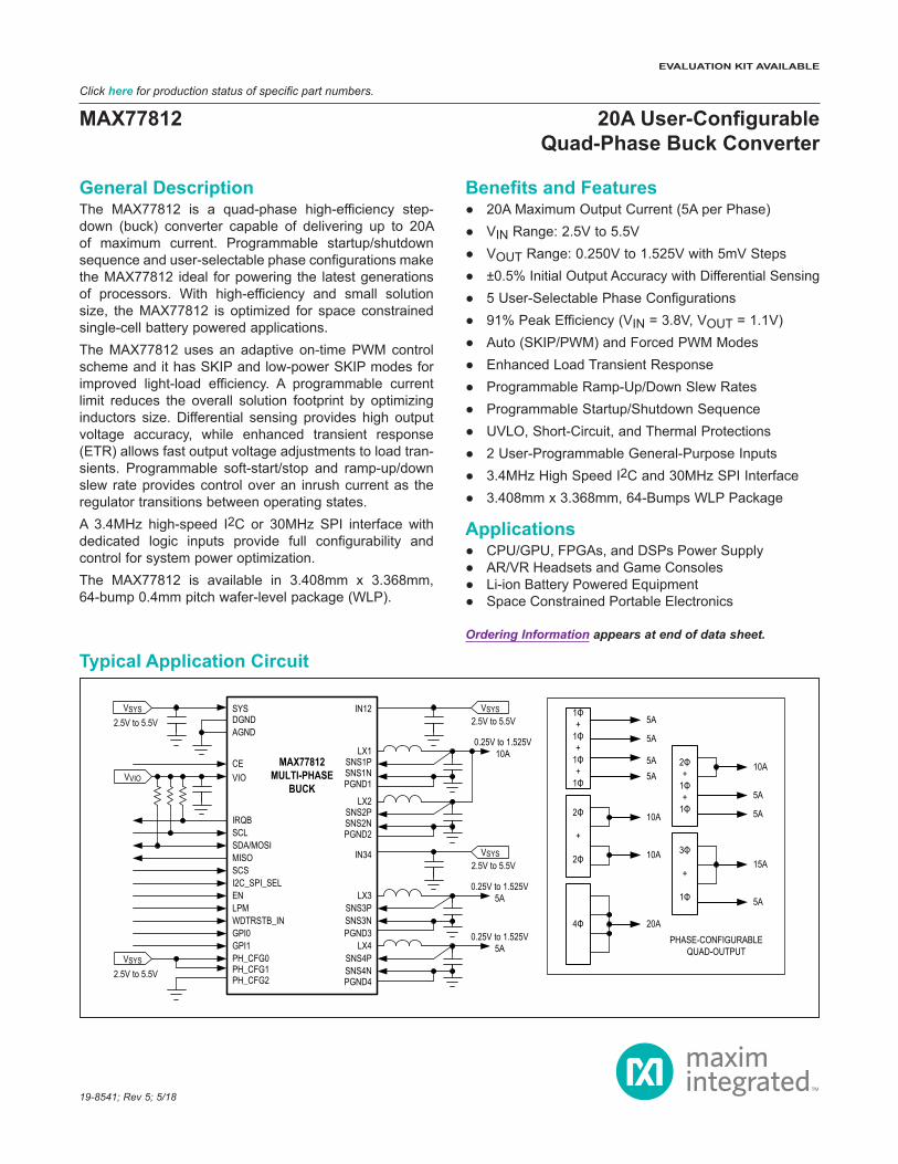
General DescriptionThe MAX77812 is a quad-phase high-efficiency step-down (buck) converter capable of delivering up to 20A of maximum current. Programmable startup/shutdown sequence and user-selectable phase configurations make the MAX77812 ideal for powering the latest generations of processors. With high-efficiency and small solution size, the MAX77812 is optimized for space constrained single-cell battery powered applications.The MAX77812 uses an adaptive on-time PWM control scheme and it has SKIP and low-power SKIP modes for improved light-load efficiency. A programmable current limit reduces the overall solution footprint by optimizing inductors size. Differential sensing provides high output voltage accuracy, while enhanced transient response (ETR) allows fast output voltage adjustments to load tran-sients. Programmable soft-start/stop and ramp-up/down slew rate provides control over an inrush current as the regulator transitions between operating states.A 3.4MHz high-speed I2C or 30MHz SPI interface with dedicated logic inputs provide full configurability and control for system power optimization.The MAX77812 is available in 3.408mm x 3.368mm, 64-bump 0.4mm pitch wafer-level package (WLP).
Benefits and Features 20A Maximum Output Current (5A per Phase) VIN Range: 2.5V to 5.5V VOUT Range: 0.250V to 1.525V with 5mV Steps ±0.5% Initial Output Accuracy with Differential Sensing 5 User-Selectable Phase Configurations 91% Peak Efficiency (VIN = 3.8V, VOUT = 1.1V) Auto (SKIP/PWM) and Forced PWM Modes Enhanced Load Transient Response Programmable Ramp-Up/Down Slew Rates Programmable Startup/Shutdown Sequence UVLO, Short-Circuit, and Thermal Protections 2 User-Programmable General-Purpose Inputs 3.4MHz High Speed I2C and 30MHz SPI Interface 3.408mm x 3.368mm, 64-Bumps WLP Package
Applications CPU/GPU, FPGAs, and DSPs Power Supply AR/VR Headsets and Game Consoles Li-ion Battery Powered Equipment Space Constrained Portable Electronics
Ordering Information appears at end of data sheet.
19-8541; Rev 5; 5/18
2.5V to 5.5V
0.25V to 1.525V 10A
PGND1
IN12
LX1
PGND2
LX2
PGND3
IN34
LX3
PGND4
LX4
SNS1PSNS1N
SNS2PSNS2N
SNS3PSNS3N
SNS4PSNS4N
SYS
VIO
IRQBSCL
MISO
AGND
CE
VSYSDGND
PH_CFG0PH_CFG1
GPI0GPI1
SDA/MOSI
SCS
PH_CFG2
I2C_SPI_SELEN
WDTRSTB_INLPM
0.25V to 1.525V5A
0.25V to 1.525V5A
1Φ+
1Φ+
1Φ+
1Φ
5A
PHASE-CONFIGURABLEQUAD-OUTPUT
MAX77812MULTI-PHASE
BUCKVVIO
VSYS
VSYS
5A
5A5A
2Φ
+
2Φ
10A
10A
2.5V to 5.5V
2.5V to 5.5V
2.5V to 5.5V
4Φ 20A
2Φ+
1Φ+
1Φ
10A
5A
5A
3Φ
+
1Φ
15A
5A
VSYS
MAX77812 20A User-Configurable Quad-Phase Buck Converter
Typical Application Circuit
Click here for production status of specific part numbers.
EVALUATION KIT AVAILABLE
SYS, VIO to AGND ...............................................-0.3V to +6.0VDGND to AGND ....................................................-0.3V to +0.3VSCL, SDA/MOSI, MISO, SCS, IRQB, CE, EN, LPM, GPI0, GPI1,
WDTRSTB_IN to DGND...................... -0.3V to (VVIO + 0.3V)PH_CFG0, PH_CFG1, PH_CFG2,
I2C_SPI_SEL to AGND ...................... -0.3V to (VSYS + 0.3V)IN12, IN34 to PGNDx .............................-0.3V to (VSYS + 0.3V)LX1/2/3/4 to PGNDx ................................ -0.3V to (VIN_ + 0.3V)LX1/2/3/4 to PGNDx (Pulsed <10ns Voltage) ......-3.0V to +7.0VPGND1/2/3/4 to AGND .........................................-0.3V to +0.3V
SNS1P, SNS2P, SNS3P, SNS4P to AGND ..-0.3V to (VIN_ + 0.3V)SNS1N, SNS2N, SNS3N, SNS4N to AGND ........-0.3V to +0.3VLX1/2/3/4 RMS Current (Note 1) ..........................................7.2AContinuous Power Dissipation at TA = +70°C
(derate 26.17mW/°C above +70°C) ..........................2094mWOperating Temperature Range ........................... -40°C to +85°CJunction Temperature ..................................................... +150°CStorage Temperature Range ............................ -65°C to +150°CSoldering Temperature (reflow) .......................................+260°C
WLP Junction-to-Ambient Thermal Resistance (θJA) .......33.2°C/W
(Note 2)
(VSYS = VINx = +3.8V, VVIO = +1.8V, TA = -40°C to +85°C, typical values are at TA = +25°C, unless otherwise noted.) (Note 3)
PARAMETER SYMBOL CONDITIONS MIN TYP MAX UNITSGLOBAL INPUT SUPPLYOperating Voltage Range VSYS 2.5 5.5 VShutdown Supply Current ISHDN CE = low, TA = +25°C 2 5 µA
Standby Current ISTBYCE = high and all outputs are off, TA = +25°C 25 µA
No Load Supply Current in Low Power Skip Mode
ILP_SKIP14-phase configuration (no switching) 120
µA
ILP_SKIP23 + 1-phase configuration (no switching) 190
ILP_SKIP32 + 2-phase configuration (no switching) 190
ILP_SKIP42 + 1 + 1-phase configuration (no switching) 265
ILP_SKIP51 + 1 + 1 + 1-phase configuration (no switching) 340 510
MAX77812 20A User-Configurable Quad-Phase Buck Converter
www.maximintegrated.com Maxim Integrated 2
Note 2: Package thermal resistances were obtained using the method described in JEDEC specification JESD51-7, using a four-layer board. For detailed information on package thermal considerations, refer to www.maximintegrated.com/thermal-tutorial.
Note 1: LXx node has internal clamp diodes to PGNDx and INx. Applications that give forward bias to these diodes should ensure that the total power loss does not exceed the power dissipation limit of IC package.
Absolute Maximum Ratings
Stresses beyond those listed under “Absolute Maximum Ratings” may cause permanent damage to the device. These are stress ratings only, and functional operation of the device at these or any other conditions beyond those indicated in the operational sections of the specifications is not implied. Exposure to absolute maximum rating conditions for extended periods may affect device reliability.
Package Thermal Characteristics
Electrical CharacteristicsTop-Level Electrical Characteristics
(VSYS = VINx = +3.8V, VVIO = +1.8V, TA = -40°C to +85°C, typical values are at TA = +25°C, unless otherwise noted.) (Note 3)
PARAMETER SYMBOL CONDITIONS MIN TYP MAX UNITS
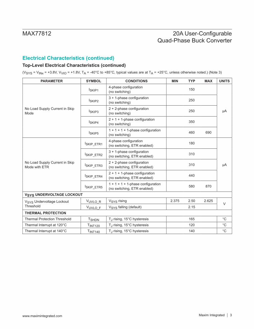
No Load Supply Current in Skip Mode
ISKIP14-phase configuration (no switching) 150
µA
ISKIP23 + 1-phase configuration (no switching) 250
ISKIP32 + 2-phase configuration (no switching) 250
ISKIP42 + 1 + 1-phase configuration (no switching) 350
ISKIP51 + 1 + 1 + 1-phase configuration (no switching) 460 690
No Load Supply Current in Skip Mode with ETR
ISKIP_ETR14-phase configuration (no switching, ETR enabled) 180
µA
ISKIP_ETR23 + 1-phase configuration (no switching, ETR enabled) 310
ISKIP_ETR32 + 2-phase configuration (no switching, ETR enabled) 310
ISKIP_ETR42 + 1 + 1-phase configuration (no switching, ETR enabled) 440
ISKIP_ETR51 + 1 + 1 + 1-phase configuration (no switching, ETR enabled) 580 870
VSYS UNDERVOLTAGE LOCKOUT
VSYS Undervoltage Lockout Threshold
VUVLO_R VSYS rising 2.375 2.50 2.625V
VUVLO_F VSYS falling (default) 2.15THERMAL PROTECTIONThermal Protection Threshold TSHDN TJ rising, 15°C hysteresis 165 °CThermal Interrupt at 120°C TINT120 TJ rising, 15°C hysteresis 120 °CThermal Interrupt at 140°C TINT140 TJ rising, 15°C hysteresis 140 °C
MAX77812 20A User-Configurable Quad-Phase Buck Converter
www.maximintegrated.com Maxim Integrated 3
Electrical Characteristics (continued)Top-Level Electrical Characteristics (continued)
(VSYS = VINx = +3.8V, VVIO = +1.8V, TA = -40°C to +85°C, typical values are at TA = +25°C, unless otherwise noted.) (Note 3)
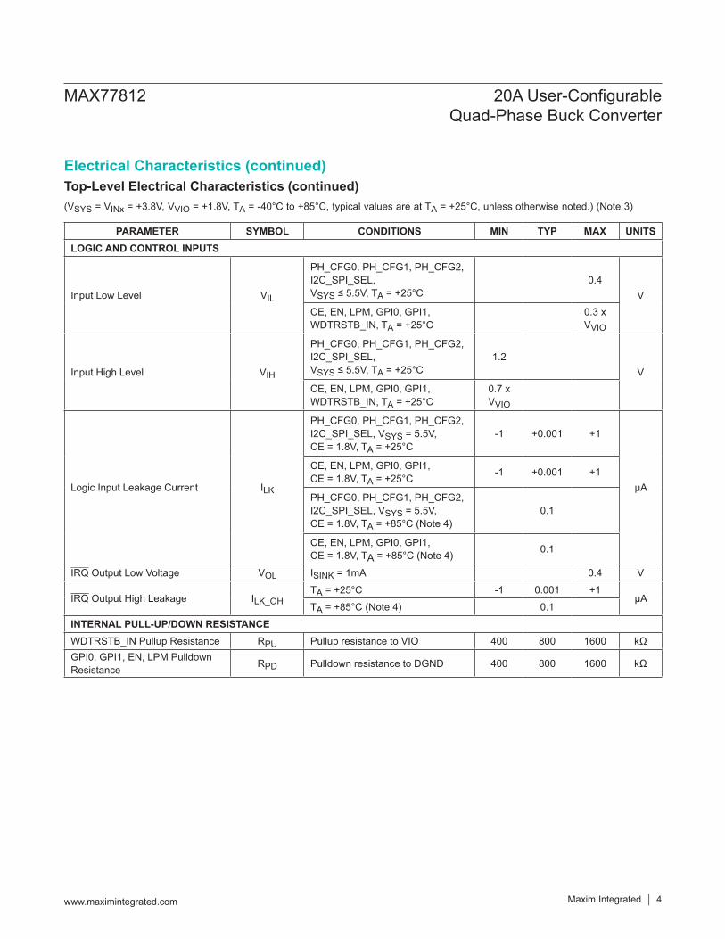
PARAMETER SYMBOL CONDITIONS MIN TYP MAX UNITSLOGIC AND CONTROL INPUTS
Input Low Level VIL
PH_CFG0, PH_CFG1, PH_CFG2, I2C_SPI_SEL,VSYS ≤ 5.5V, TA = +25°C
0.4V
CE, EN, LPM, GPI0, GPI1, WDTRSTB_IN, TA = +25°C
0.3 x VVIO
Input High Level VIH
PH_CFG0, PH_CFG1, PH_CFG2, I2C_SPI_SEL,VSYS ≤ 5.5V, TA = +25°C
1.2V
CE, EN, LPM, GPI0, GPI1, WDTRSTB_IN, TA = +25°C
0.7 x VVIO
Logic Input Leakage Current ILK
PH_CFG0, PH_CFG1, PH_CFG2, I2C_SPI_SEL, VSYS = 5.5V, CE = 1.8V, TA = +25°C
-1 +0.001 +1
µA
CE, EN, LPM, GPI0, GPI1, CE = 1.8V, TA = +25°C -1 +0.001 +1
PH_CFG0, PH_CFG1, PH_CFG2, I2C_SPI_SEL, VSYS = 5.5V, CE = 1.8V, TA = +85°C (Note 4)
0.1
CE, EN, LPM, GPI0, GPI1, CE = 1.8V, TA = +85°C (Note 4) 0.1
IRQ Output Low Voltage VOL ISINK = 1mA 0.4 V
IRQ Output High Leakage ILK_OHTA = +25°C -1 0.001 +1
µATA = +85°C (Note 4) 0.1
INTERNAL PULL-UP/DOWN RESISTANCEWDTRSTB_IN Pullup Resistance RPU Pullup resistance to VIO 400 800 1600 kΩGPI0, GPI1, EN, LPM Pulldown Resistance RPD Pulldown resistance to DGND 400 800 1600 kΩ
MAX77812 20A User-Configurable Quad-Phase Buck Converter
www.maximintegrated.com Maxim Integrated 4
Electrical Characteristics (continued)Top-Level Electrical Characteristics (continued)
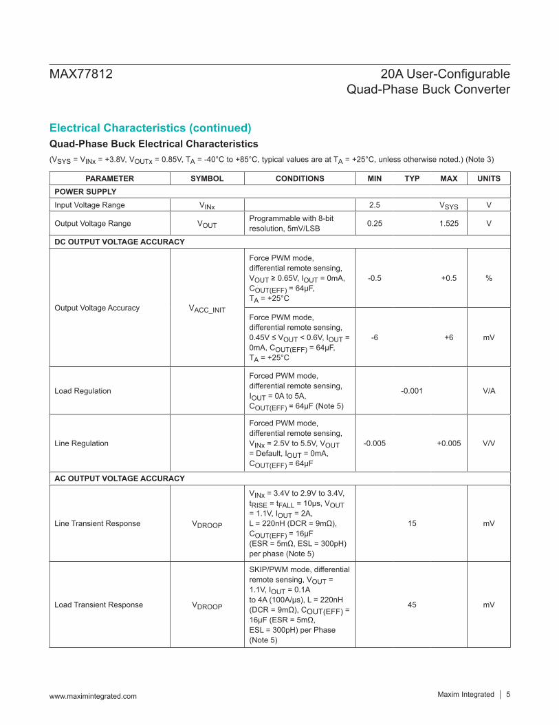
(VSYS = VINx = +3.8V, VOUTx = 0.85V, TA = -40°C to +85°C, typical values are at TA = +25°C, unless otherwise noted.) (Note 3)
PARAMETER SYMBOL CONDITIONS MIN TYP MAX UNITSPOWER SUPPLYInput Voltage Range VINx 2.5 VSYS V
Output Voltage Range VOUTProgrammable with 8-bit resolution, 5mV/LSB 0.25 1.525 V
DC OUTPUT VOLTAGE ACCURACY
Output Voltage Accuracy VACC_INIT
Force PWM mode, differential remote sensing, VOUT ≥ 0.65V, IOUT = 0mA, COUT(EFF) = 64µF, TA = +25°C
-0.5 +0.5 %
Force PWM mode, differential remote sensing, 0.45V ≤ VOUT < 0.6V, IOUT = 0mA, COUT(EFF) = 64µF, TA = +25°C
-6 +6 mV
Load Regulation
Forced PWM mode, differential remote sensing, IOUT = 0A to 5A, COUT(EFF) = 64µF (Note 5)
-0.001 V/A
Line Regulation
Forced PWM mode, differential remote sensing, VINx = 2.5V to 5.5V, VOUT = Default, IOUT = 0mA, COUT(EFF) = 64µF
-0.005 +0.005 V/V
AC OUTPUT VOLTAGE ACCURACY
Line Transient Response VDROOP
VINx = 3.4V to 2.9V to 3.4V, tRISE = tFALL = 10µs, VOUT = 1.1V, IOUT = 2A, L = 220nH (DCR = 9mΩ), COUT(EFF) = 16µF (ESR = 5mΩ, ESL = 300pH) per phase (Note 5)
15 mV
Load Transient Response VDROOP
SKIP/PWM mode, differential remote sensing, VOUT = 1.1V, IOUT = 0.1A to 4A (100A/µs), L = 220nH (DCR = 9mΩ), COUT(EFF) = 16µF (ESR = 5mΩ, ESL = 300pH) per Phase (Note 5)
45 mV
MAX77812 20A User-Configurable Quad-Phase Buck Converter
www.maximintegrated.com Maxim Integrated 5
Electrical Characteristics (continued)Quad-Phase Buck Electrical Characteristics
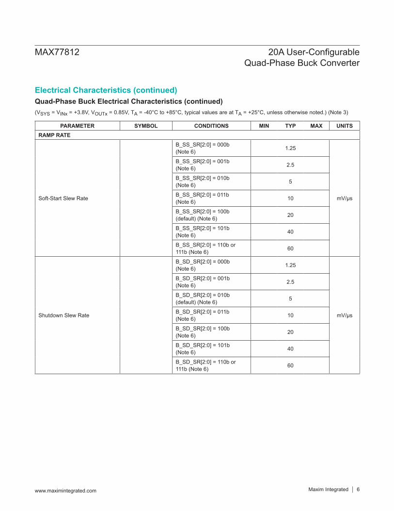
(VSYS = VINx = +3.8V, VOUTx = 0.85V, TA = -40°C to +85°C, typical values are at TA = +25°C, unless otherwise noted.) (Note 3)
PARAMETER SYMBOL CONDITIONS MIN TYP MAX UNITSRAMP RATE
Soft-Start Slew Rate
B_SS_SR[2:0] = 000b (Note 6) 1.25
mV/µs
B_SS_SR[2:0] = 001b (Note 6) 2.5
B_SS_SR[2:0] = 010b (Note 6) 5
B_SS_SR[2:0] = 011b (Note 6) 10
B_SS_SR[2:0] = 100b (default) (Note 6) 20
B_SS_SR[2:0] = 101b (Note 6) 40
B_SS_SR[2:0] = 110b or 111b (Note 6) 60
Shutdown Slew Rate
B_SD_SR[2:0] = 000b (Note 6) 1.25
mV/µs
B_SD_SR[2:0] = 001b (Note 6) 2.5
B_SD_SR[2:0] = 010b (default) (Note 6) 5
B_SD_SR[2:0] = 011b (Note 6) 10
B_SD_SR[2:0] = 100b (Note 6) 20
B_SD_SR[2:0] = 101b (Note 6) 40
B_SD_SR[2:0] = 110b or 111b (Note 6) 60
MAX77812 20A User-Configurable Quad-Phase Buck Converter
www.maximintegrated.com Maxim Integrated 6
Electrical Characteristics (continued)Quad-Phase Buck Electrical Characteristics (continued)
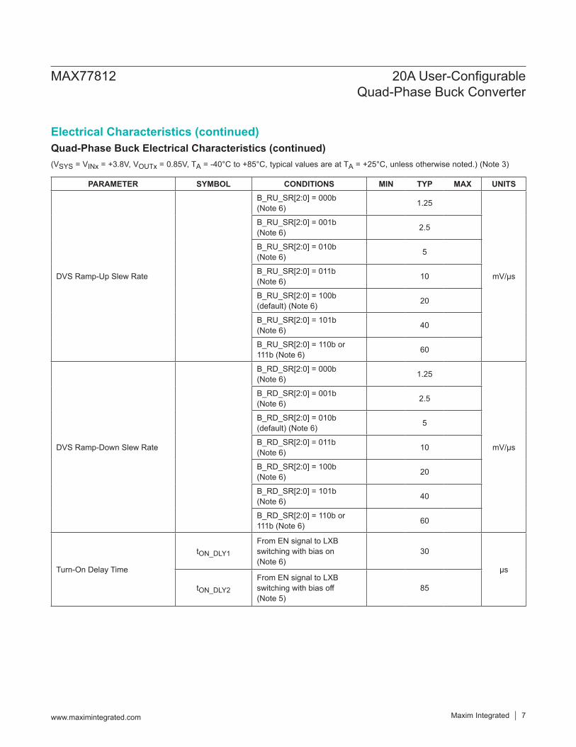
(VSYS = VINx = +3.8V, VOUTx = 0.85V, TA = -40°C to +85°C, typical values are at TA = +25°C, unless otherwise noted.) (Note 3)
PARAMETER SYMBOL CONDITIONS MIN TYP MAX UNITS
DVS Ramp-Up Slew Rate
B_RU_SR[2:0] = 000b (Note 6) 1.25
mV/µs
B_RU_SR[2:0] = 001b (Note 6) 2.5
B_RU_SR[2:0] = 010b (Note 6) 5
B_RU_SR[2:0] = 011b (Note 6) 10
B_RU_SR[2:0] = 100b (default) (Note 6) 20
B_RU_SR[2:0] = 101b (Note 6) 40
B_RU_SR[2:0] = 110b or 111b (Note 6) 60
DVS Ramp-Down Slew Rate
B_RD_SR[2:0] = 000b (Note 6) 1.25
mV/µs
B_RD_SR[2:0] = 001b (Note 6) 2.5
B_RD_SR[2:0] = 010b (default) (Note 6) 5
B_RD_SR[2:0] = 011b (Note 6) 10
B_RD_SR[2:0] = 100b (Note 6) 20
B_RD_SR[2:0] = 101b (Note 6) 40
B_RD_SR[2:0] = 110b or 111b (Note 6) 60
Turn-On Delay Time
tON_DLY1
From EN signal to LXB switching with bias on (Note 6)
30
µs
tON_DLY2
From EN signal to LXB switching with bias off (Note 5)
85
MAX77812 20A User-Configurable Quad-Phase Buck Converter
www.maximintegrated.com Maxim Integrated 7
Electrical Characteristics (continued)Quad-Phase Buck Electrical Characteristics (continued)
(VSYS = VINx = +3.8V, VOUTx = 0.85V, TA = -40°C to +85°C, typical values are at TA = +25°C, unless otherwise noted.) (Note 3)
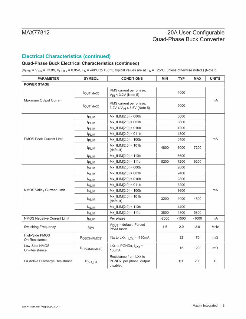
PARAMETER SYMBOL CONDITIONS MIN TYP MAX UNITSPOWER STAGE
Maximum Output Current
IOUT(MAX)RMS current per phase, VIN < 3.2V (Note 5) 4000
mAIOUT(MAX)
RMS current per phase, 3.2V ≤ VIN ≤ 5.5V (Note 5) 5000
PMOS Peak Current Limit
IPLIM Mx_ILIM[2:0] = 000b 3000
mA
IPLIM Mx_ILIM[2:0] = 001b 3600IPLIM Mx_ILIM[2:0] = 010b 4200IPLIM Mx_ILIM[2:0] = 011b 4800IPLIM Mx_ILIM[2:0] = 100b 5400
IPLIMMx_ILIM[2:0] = 101b (default) 4800 6000 7200
IPLIM Mx_ILIM[2:0] = 110b 6600IPLIM Mx_ILIM[2:0] = 111b 5200 7200 9200
NMOS Valley Current Limit
IVLIM Mx_ILIM[2:0] = 000b 2000
mA
IVLIM Mx_ILIM[2:0] = 001b 2400IVLIM Mx_ILIM[2:0] = 010b 2800IVLIM Mx_ILIM[2:0] = 011b 3200IVLIM Mx_ILIM[2:0] = 100b 3600
IVLIMMx_ILIM[2:0] = 101b (default) 3200 4000 4800
IVLIM Mx_ILIM[2:0] = 110b 4400IVLIM Mx_ILIM[2:0] = 111b 3800 4800 5800
NMOS Negative Current Limit INLIM Per phase -2000 -1500 -1000 mA
Switching Frequency fSWVOUT = default, Forced PWM mode 1.6 2.0 2.8 MHz
High-Side PMOS On-Resistance RDSON(PMOS) INx to LXx, ILXx = -150mA 32 70 mΩ
Low-Side NMOS On-Resistance RDSON(NMOS)
LXx to PGNDx, ILXx = 150mA 15 29 mΩ
LX Active Discharge Resistance RAD_LX
Resistance from LXx to PGNDx, per phase, output disabled
100 200 Ω
MAX77812 20A User-Configurable Quad-Phase Buck Converter
www.maximintegrated.com Maxim Integrated 8
Electrical Characteristics (continued)Quad-Phase Buck Electrical Characteristics (continued)
(VSYS = VINx = +3.8V, VOUTx = 0.85V, TA = -40°C to +85°C, typical values are at TA = +25°C, unless otherwise noted.) (Note 3)
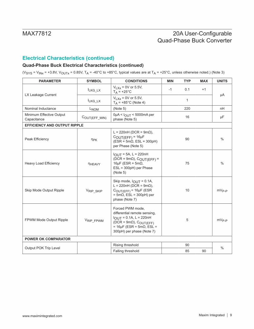
PARAMETER SYMBOL CONDITIONS MIN TYP MAX UNITS
LX Leakage CurrentILKG_LX
VLXx = 0V or 5.5V, TA = +25°C -1 0.1 +1
µAILKG_LX
VLXx = 0V or 5.5V, TA = +85°C (Note 4) 1
Nominal Inductance LNOM (Note 5) 220 nH
Minimum Effective Output Capacitance COUT(EFF_MIN)
0µA < IOUT < 5000mA per phase (Note 5) 16 µF
EFFICIENCY AND OUTPUT RIPPLE
Peak Efficiency ηPK
L = 220nH (DCR = 9mΩ), COUT(EFF) = 16µF (ESR = 5mΩ, ESL = 300pH) per Phase (Note 5)
90 %
Heavy Load Efficiency ηHEAVY
IOUT = 5A, L = 220nH (DCR = 9mΩ), COUT(EFF) = 16µF (ESR = 5mΩ, ESL = 300pH) per Phase (Note 5)
75 %
Skip Mode Output Ripple VRIP_SKIP
Skip mode, IOUT = 0.1A, L = 220nH (DCR = 9mΩ), COUT(EFF) = 16µF (ESR = 5mΩ, ESL = 300pH) per phase (Note 7)
10 mVP-P
FPWM Mode Output Ripple VRIP_FPWM
Forced PWM mode, differential remote sensing, IOUT = 0.1A, L = 220nH (DCR = 9mΩ), COUT(EFF) = 16µF (ESR = 5mΩ, ESL = 300pH) per phase (Note 7)
5 mVP-P
POWER OK COMPARATOR
Output POK Trip LevelRising threshold 90
%Falling threshold 85 90
MAX77812 20A User-Configurable Quad-Phase Buck Converter
www.maximintegrated.com Maxim Integrated 9
Electrical Characteristics (continued)Quad-Phase Buck Electrical Characteristics (continued)
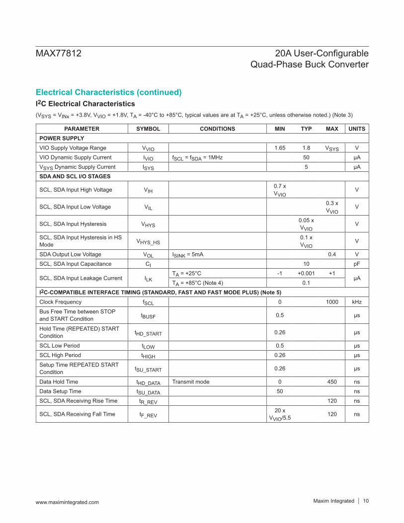
(VSYS = VINx = +3.8V, VVIO = +1.8V, TA = -40°C to +85°C, typical values are at TA = +25°C, unless otherwise noted.) (Note 3)
PARAMETER SYMBOL CONDITIONS MIN TYP MAX UNITSPOWER SUPPLYVIO Supply Voltage Range VVIO 1.65 1.8 VSYS VVIO Dynamic Supply Current IVIO fSCL = fSDA = 1MHz 50 µAVSYS Dynamic Supply Current ISYS 5 µASDA AND SCL I/O STAGES
SCL, SDA Input High Voltage VIH0.7 x VVIO
V
SCL, SDA Input Low Voltage VIL0.3 x VVIO
V
SCL, SDA Input Hysteresis VHYS0.05 xVVIO
V
SCL, SDA Input Hysteresis in HS Mode VHYS_HS
0.1 xVVIO
V
SDA Output Low Voltage VOL ISINK = 5mA 0.4 VSCL, SDA Input Capacitance CI 10 pF
SCL, SDA Input Leakage Current ILKTA = +25°C -1 +0.001 +1
µATA = +85°C (Note 4) 0.1
I2C-COMPATIBLE INTERFACE TIMING (STANDARD, FAST AND FAST MODE PLUS) (Note 5)Clock Frequency fSCL 0 1000 kHz
Bus Free Time between STOP and START Condition tBUSF 0.5 µs
Hold Time (REPEATED) START Condition tHD_START 0.26 µs
SCL Low Period tLOW 0.5 µsSCL High Period tHIGH 0.26 µs
Setup Time REPEATED START Condition tSU_START 0.26 µs
Data Hold Time tHD_DATA Transmit mode 0 450 nsData Setup Time tSU_DATA 50 nsSCL, SDA Receiving Rise Time tR_REV 120 ns
SCL, SDA Receiving Fall Time tF_REV20 x
VVIO/5.5 120 ns
MAX77812 20A User-Configurable Quad-Phase Buck Converter
www.maximintegrated.com Maxim Integrated 10
Electrical Characteristics (continued)I2C Electrical Characteristics
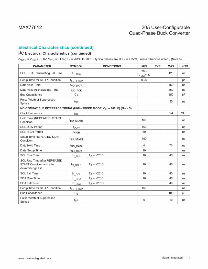
(VSYS = VINx = +3.8V, VVIO = +1.8V, TA = -40°C to +85°C, typical values are at TA = +25°C, unless otherwise noted.) (Note 3)
PARAMETER SYMBOL CONDITIONS MIN TYP MAX UNITS
SCL, SDA Transmitting Fall Time tF_TRA20 x
VVIO/5.5 120 ns
Setup Time for STOP Condition tSU_STOP 0.26 µsData Valid Time tVD_DATA 450 nsData Valid Acknowledge Time tVD_ACK 450 nsBus Capacitance CB 550 pF
Pulse Width of Suppressed Spikes tSP 50 ns
I2C-COMPATIBLE INTERFACE TIMING (HIGH-SPEED MODE, CB = 100pF) (Note 5)Clock Frequency fSCL 3.4 MHz
Hold Time (REPEATED) START Condition tHD_START 160 ns
SCL LOW Period tLOW 160 nsSCL HIGH Period tHIGH 60 ns
Setup Time REPEATED START Condition tSU_START 160 ns
Data Hold Time tHD_DATA 0 70 nsData Setup Time tSU_DATA 10 nsSCL Rise Time tR_SCL TA = +25°C 10 40 ns
SCL Rise Time after REPEATED START Condition and after Acknowledge Bit
tR_SCL1 TA = +25°C 10 40 ns
SCL Fall Time tF_SCL TA = +25°C 10 40 nsSDA Rise Time tR_SDA TA = +25°C 10 40 nsSDA Fall Time tF_SDA TA = +25°C 40 nsSetup Time for STOP Condition tSU_STOP 160 nsBus Capacitance CB 100 pF
Pulse Width of Suppressed Spikes tSP 0 10 ns
MAX77812 20A User-Configurable Quad-Phase Buck Converter
www.maximintegrated.com Maxim Integrated 11
Electrical Characteristics (continued)I2C Electrical Characteristics (continued)
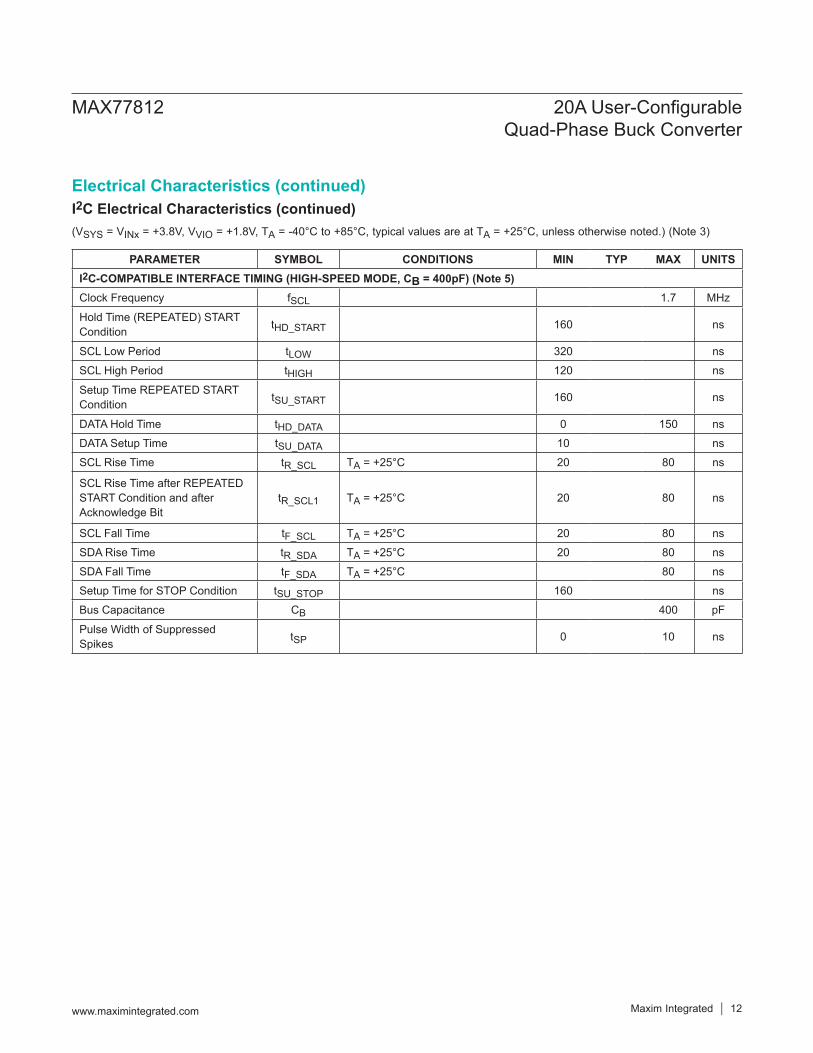
(VSYS = VINx = +3.8V, VVIO = +1.8V, TA = -40°C to +85°C, typical values are at TA = +25°C, unless otherwise noted.) (Note 3)
PARAMETER SYMBOL CONDITIONS MIN TYP MAX UNITSI2C-COMPATIBLE INTERFACE TIMING (HIGH-SPEED MODE, CB = 400pF) (Note 5)Clock Frequency fSCL 1.7 MHz
Hold Time (REPEATED) START Condition tHD_START 160 ns
SCL Low Period tLOW 320 nsSCL High Period tHIGH 120 ns
Setup Time REPEATED START Condition tSU_START 160 ns
DATA Hold Time tHD_DATA 0 150 nsDATA Setup Time tSU_DATA 10 nsSCL Rise Time tR_SCL TA = +25°C 20 80 ns
SCL Rise Time after REPEATED START Condition and after Acknowledge Bit
tR_SCL1 TA = +25°C 20 80 ns
SCL Fall Time tF_SCL TA = +25°C 20 80 nsSDA Rise Time tR_SDA TA = +25°C 20 80 nsSDA Fall Time tF_SDA TA = +25°C 80 nsSetup Time for STOP Condition tSU_STOP 160 nsBus Capacitance CB 400 pF
Pulse Width of Suppressed Spikes tSP 0 10 ns
MAX77812 20A User-Configurable Quad-Phase Buck Converter
www.maximintegrated.com Maxim Integrated 12
Electrical Characteristics (continued)I2C Electrical Characteristics (continued)
(VSYS = VINx = +3.8V, VVIO = +1.8V, TA = -40°C to +85°C, typical values are at TA = +25°C, unless otherwise noted.) (Note 3)
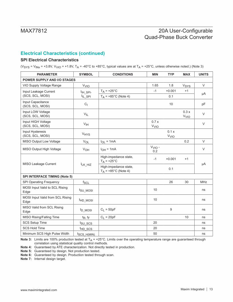
Note 3: Limits are 100% production tested at TA = +25°C. Limits over the operating temperature range are guaranteed through correlation using statistical quality control methods.
Note 4: Guaranteed by ATE characterization. Not directly tested in production.Note 5: Guaranteed by design. Not production tested.Note 6: Guaranteed by design. Production tested through scan.Note 7: Internal design target.
PARAMETER SYMBOL CONDITIONS MIN TYP MAX UNITSPOWER SUPPLY AND I/O STAGESVIO Supply Voltage Range VVIO 1.65 1.8 VSYS V
Input Leakage Current (SCS, SCL, MOSI)
IIH_SPI, IIL_SPI
TA = +25°C -1 +0.001 +1µA
TA = +85°C (Note 4) 0.1
Input Capacitance (SCS, SCL, MOSI) CI 10 pF
Input LOW Voltage (SCS, SCL, MOSI) VIL
0.3 x VVIO
V
Input HIGH Voltage (SCS, SCL, MOSI) VIH
0.7 x VVIO
V
Input Hysteresis (SCS, SCL, MOSI) VHYS
0.1 x VVIO
MISO Output Low Voltage VOL IOL = 1mA 0.2 V
MISO Output High Voltage VOH IOH = 1mA VVIO - 0.2 V
MISO Leakage Current ILK_HIZ
High-impedance state, TA = +25°C -1 +0.001 +1
µAHigh-impedance state, TA = +85°C (Note 4) 0.1
SPI INTERFACE TIMING (Note 5)SPI Operating Frequency fSCL 26 30 MHz
MOSI Input Valid to SCL Rising Edge tSU_MOSI 10 ns
MOSI Input Valid from SCL Rising Edge tHD_MOSI 10 ns
MISO Valid from SCL Rising Edge tD_MOSI CL = 50pF 9 ns
MISO Rising/Falling Time tR, tF CL = 20pF 10 nsSCS Setup Time tSU_SCS 20 nsSCS Hold Time tHD_SCS 20 nsMinimum SCS High Pulse Width tSCS_H(MIN) 50 ns
MAX77812 20A User-Configurable Quad-Phase Buck Converter
www.maximintegrated.com Maxim Integrated 13
Electrical Characteristics (continued)SPI Electrical Characteristics
(VSYS = 3.8V, VOUT = 0.85V, IOUT = 0A, CE = high, 4-Phase (1 Output), FPWM = 0, LPM = 0, ETR = 0, ALPS 220nH, TA = +25°C, unless otherwise noted.)
0
100
200
300
400
500
600
700
800
2.5 3.0 3.5 4.0 4.5 5.0 5.5
SUPP
LY C
URRE
NT (μ
A)
INPUT VOLTAGE (V)
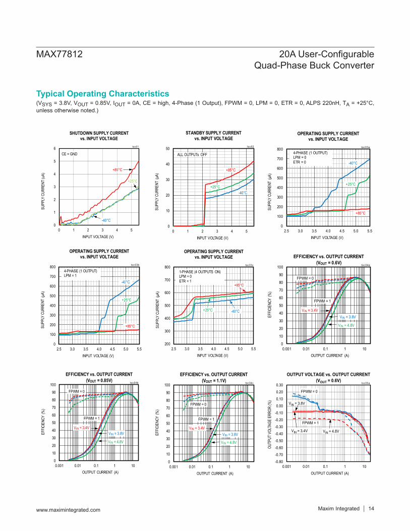
OPERATING SUPPLY CURRENTvs. INPUT VOLTAGE
+85°C
toc 03b
4-PHASE (1 OUTPUT)LPM = 1
+25°C
-40°C
0
1
2
3
4
5
6
0 1 2 3 4 5
SUPP
LY C
URRE
NT (u
A)
INPUT VOLTAGE (V)
SHUTDOWN SUPPLY CURRENTvs. INPUT VOLTAGE
+85°C
toc01
CE = GND
+25°C
-40°C
0
10
20
30
40
50
60
70
80
90
100
0.001 0.01 0.1 1 10
EFFIC
IENC
Y (%
)
OUTPUT CURRENT (A)
FPWM = 0
EFFICIENCY vs. OUTPUT CURRENT(VOUT = 0.85V) toc 04b
FPWM = 1
VIN = 3.4VVIN = 3.8V
VIN = 4.8V
0
10
20
30
40
50
0 1 2 3 4 5
SUPP
LY C
URRE
NT (μ
A)
INPUT VOLTAGE (V)
STANDBY SUPPLY CURRENTvs. INPUT VOLTAGE
+85°C
toc 02
ALL OUTPUTs OFF
+25°C-40°C
0
10
20
30
40
50
60
70
80
90
100
0.001 0.01 0.1 1 10
EFFIC
IENC
Y (%
)
OUTPUT CURRENT (A)
FPWM = 0
EFFICIENCY vs. OUTPUT CURRENT(VOUT = 1.1V) toc 04c
FPWM = 1
VIN = 3.4VVIN = 3.8V
VIN = 4.8V
0
100
200
300
400
500
600
700
800
2.5 3.0 3.5 4.0 4.5 5.0 5.5
SUPP
LY C
URRE
NT (μ
A)
INPUT VOLTAGE (V)
OPERATING SUPPLY CURRENTvs. INPUT VOLTAGE
+85°C
toc 03a
+25°C
-40°C
4-PHASE (1 OUTPUT)LPM = 0ETR = 0
-0.80-0.70-0.60-0.50-0.40-0.30-0.20-0.100.000.100.200.30
0.001 0.01 0.1 1 10
OUTP
UT V
OLTA
GE E
RROR
(%)
OUTPUT CURRENT (A)
FPWM = 1
OUTPUT VOLTAGE vs. OUTPUT CURRENT(VOUT = 0.6V)
toc05a
FPWM = 0
VIN = 3.4V
VIN = 3.8V
VIN = 4.8V
200
300
400
500
600
700
800
2.5 3.0 3.5 4.0 4.5 5.0 5.5
SUPP
LY C
URRE
NT (μ
A)
INPUT VOLTAGE (V)
OPERATING SUPPLY CURRENTvs. INPUT VOLTAGE
+85°C
toc 03c
1-PHASE (4 OUTPUTS ON)LPM = 0ETR = 1
+25°C -40°C
0
10
20
30
40
50
60
70
80
90
100
0.001 0.01 0.1 1 10
EFFIC
IENC
Y (%
)
OUTPUT CURRENT (A)
FPWM = 0
EFFICIENCY vs. OUTPUT CURRENT(VOUT = 0.6V) toc 04a
FPWM = 1
VIN = 3.4VVIN = 3.8V
VIN = 4.8V
Maxim Integrated 14www.maximintegrated.com
MAX77812 20A User-Configurable Quad-Phase Buck Converter
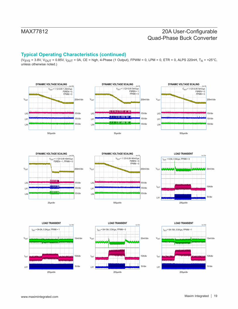
Typical Operating Characteristics
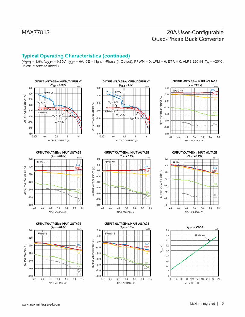
(VSYS = 3.8V, VOUT = 0.85V, IOUT = 0A, CE = high, 4-Phase (1 Output), FPWM = 0, LPM = 0, ETR = 0, ALPS 220nH, TA = +25°C, unless otherwise noted.)
-0.80
-0.60
-0.40
-0.20
0.00
0.20
0.40
2.5 3.0 3.5 4.0 4.5 5.0 5.5
OUTP
UT V
OLTA
GE E
RROR
(%)
INPUT VOLTAGE (V)
OUTPUT VOLTAGE vs. INPUT VOLTAGE(VOUT = 0.85V)
2mA
toc 06b
FPWM = 0
10mA
1A
10A
20A
-0.50
-0.40
-0.30
-0.20
-0.10
0.00
0.10
0.20
0.30
0.001 0.01 0.1 1 10
OUTP
UT V
OLTA
GE E
RROR
(%)
OUTPUT CURRENT (A)
FPWM = 0
OUTPUT VOLTAGE vs. OUTPUT CURRENT(VOUT = 0.85V)
toc05b
FPWM = 1VIN = 3.8V
VIN = 3.4V
VIN = 4.8V
-0.80
-0.60
-0.40
-0.20
0.00
0.20
0.40
2.5 3.0 3.5 4.0 4.5 5.0 5.5
OUTP
UT V
OLTA
GE (V
)
INPUT VOLTAGE (V)
OUTPUT VOLTAGE vs. INPUT VOLTAGE(VOUT = 0.85V)
2mA
toc 06e
FPWM = 1
10mA
1A
10A
20A
-0.30
-0.20
-0.10
0.00
0.10
0.20
0.30
0.001 0.01 0.1 1 10
OUTP
UT V
OLTA
GE E
RROR
(%)
OUTPUT CURRENT (A)
FPWM = 1
OUTPUT VOLTAGE vs. OUTPUT CURRENT(VOUT = 1.1V)
toc05c
FPWM = 0
VIN = 3.8V
VIN = 3.4V
VIN = 4.8V
-0.60
-0.50
-0.40
-0.30
-0.20
-0.10
0.00
0.10
0.20
2.5 3.0 3.5 4.0 4.5 5.0 5.5
OUTP
UT V
OLTA
GE E
RROR
(%)
INPUT VOLTAGE (V)
OUTPUT VOLTAGE vs. INPUT VOLTAGE(VOUT = 1.1V)
2mA
toc 06f
FPWM = 1
10mA
1A
10A
20A
-1.00
-0.80
-0.60
-0.40
-0.20
0.00
0.20
0.40
2.5 3.0 3.5 4.0 4.5 5.0 5.5
OUTP
UT V
OLTA
GE E
RROR
(%)
INPUT VOLTAGE (V)
OUTPUT VOLTAGE vs. INPUT VOLTAGE(VOUT = 0.6V)
2mAtoc 06a
FPWM = 010mA
1A
10A
20A
0.0
0.2
0.4
0.6
0.8
1.0
1.2
1.4
1.6
1.8
0 30 60 90 120 150 180 210 240 270
V OUT
(V)
M1_VOUT CODE
VOUT vs. CODE
FPWM = 0
toc 07
-0.60
-0.50
-0.40
-0.30
-0.20
-0.10
0.00
0.10
0.20
2.5 3.0 3.5 4.0 4.5 5.0 5.5
OUTP
UT V
OLTA
GE E
RROR
(%)
INPUT VOLTAGE (V)
OUTPUT VOLTAGE vs. INPUT VOLTAGE(VOUT = 1.1V)
2mA
toc 06c
FPWM = 0
10mA
1A
10A
20A
-1.00
-0.80
-0.60
-0.40
-0.20
0.00
0.20
0.40
2.5 3.0 3.5 4.0 4.5 5.0 5.5
OUTP
UT V
OLTA
GE E
RROR
(%)
INPUT VOLTAGE (V)
OUTPUT VOLTAGE vs. INPUT VOLTAGE(VOUT = 0.6V)
2mA
toc 06d
FPWM = 1
10mA
1A
10A
20A
Maxim Integrated 15www.maximintegrated.com
MAX77812 20A User-Configurable Quad-Phase Buck Converter
Typical Operating Characteristics (continued)
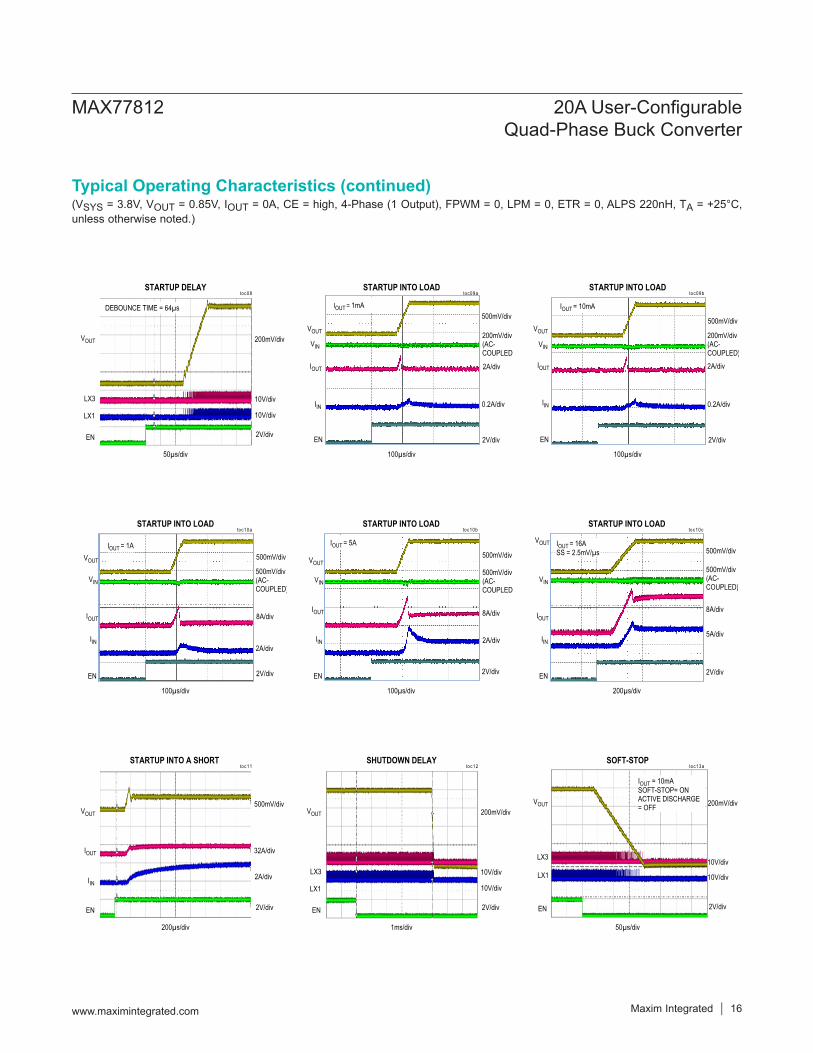
(VSYS = 3.8V, VOUT = 0.85V, IOUT = 0A, CE = high, 4-Phase (1 Output), FPWM = 0, LPM = 0, ETR = 0, ALPS 220nH, TA = +25°C, unless otherwise noted.)
500mV/div
2A/div
toc10a
100µs/div
VOUT
STARTUP INTO LOAD
IIN
IOUT 8A/div
EN 2V/div
VIN500mV/div (AC-COUPLED)
IOUT = 1A
200mV/div
10V/div
2V/div
toc08
50µs/div
VOUT
LX3
STARTUP DELAY
EN
LX1
10V/div
DEBOUNCE TIME = 64µs
500mV/div
2A/div
2V/div
toc11
200µs/div
VOUT
IOUT
STARTUP INTO A SHORT
EN
32A/div
IIN
500mV/div
0.2A/div
toc09a
100µs/div
VOUT
STARTUP INTO LOAD
IIN
IOUT 2A/div
EN 2V/div
VIN
200mV/div (AC-COUPLED)
IOUT = 1mA
200mV/div
10V/div
2V/div
toc12
1ms/div
VOUT
LX3
SHUTDOWN DELAY
EN
LX1
10V/div
500mV/div
0.2A/div
toc09b
100µs/div
VOUT
STARTUP INTO LOAD
IIN
IOUT 2A/div
EN 2V/div
VIN
200mV/div (AC-COUPLED)
IOUT = 10mA
200mV/div
10V/div
toc13a
50µs/div
VOUT
SOFT-STOP
LX1
LX3 10V/div
EN 2V/div
IOUT = 10mASOFT-STOP= ONACTIVE DISCHARGE = OFF
500mV/div
2A/div
toc10b
100µs/div
VOUT
STARTUP INTO LOAD
IIN
IOUT 8A/div
EN 2V/div
VIN500mV/div (AC-COUPLED)
IOUT = 5A500mV/div
5A/div
toc10c
200µs/div
VOUT
STARTUP INTO LOAD
IIN
IOUT8A/div
EN 2V/div
VIN
500mV/div (AC-COUPLED)
IOUT = 16A SS = 2.5mV/µs
Maxim Integrated 16www.maximintegrated.com
MAX77812 20A User-Configurable Quad-Phase Buck Converter
Typical Operating Characteristics (continued)
(VSYS = 3.8V, VOUT = 0.85V, IOUT = 0A, CE = high, 4-Phase (1 Output), FPWM = 0, LPM = 0, ETR = 0, ALPS 220nH, TA = +25°C, unless otherwise noted.)
20mV/div
5V/div
toc14a
100µs/div
VOUT
OUTPUT RIPPLE
LX1
LX3 5V/div
IOUT = 1mAFPWM = 0
200mV/div
10V/div
toc13b
50µs/div
VOUT
SOFT-STOP
LX1
LX3 10V/div
EN 2V/div
IOUT = 10mASOFT-STOP = ONACTIVE DISCHARGE = ON
10mV/div
5V/div
toc14d
2µs/div
VOUT
OUTPUT RIPPLE
LX1
LX3 5V/div
IOUT = 5AFPWM = 0 or 1
200mV/div
10V/div
toc13c
1s/div
VOUT
SOFT-STOP
LX1
LX3 10V/div
EN 2V/div
IOUT = 10mASOFT-STOP = OFFACTIVE DISCHARGE = OFF
10mV/div
5V/div
toc14e
2µs/div
VOUT
OUTPUT RIPPLE
LX1
LX3 5V/div
IOUT = 10AFPWM = 0 or 1
200mV/div
10V/div
toc13d
1ms/div
VOUT
SOFT-STOP
LX1
LX3 10V/div
EN 2V/div
IOUT = 10mASOFT-STOP = OFFACTIVE DISCHARGE = ON
20mV/div
5V/div
toc14f
2µs/div
VOUT
OUTPUT RIPPLE
LX1
LX3 5V/div
IOUT = 1mAFPWM = 1
20mV/div
5V/div
toc14b
50µs/div
VOUT
OUTPUT RIPPLE
LX1
LX3 5V/div
IOUT = 10mAFPWM = 0
20mV/div
5V/div
toc14c
5µs/div
VOUT
OUTPUT RIPPLE
LX1
LX3 5V/div
IOUT =1AFPWM = 0
Maxim Integrated 17www.maximintegrated.com
MAX77812 20A User-Configurable Quad-Phase Buck Converter
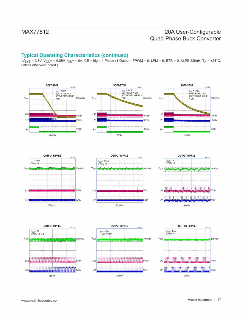
Typical Operating Characteristics (continued)
(VSYS = 3.8V, VOUT = 0.85V, IOUT = 0A, CE = high, 4-Phase (1 Output), FPWM = 0, LPM = 0, ETR = 0, ALPS 220nH, TA = +25°C, unless otherwise noted.)
200mV/div
10V/div
toc15b
10µs/div
VOUT
DYNAMIC VOLTAGE SCALING
LX4
LX3
LX1 10V/div
10V/div
VOUT = 0.8-1.12V 10mV/µsFPWM = 0
20mV/div
5V/div
toc14g
2µs/div
VOUT
OUTPUT RIPPLE
LX1
LX3 5V/div
IOUT = 10mAFPWM = 1
200mV/div
10V/div
toc15e
10µs/div
VOUT
DYNAMIC VOLTAGE SCALING
LX4
LX3
LX1 10V/div
10V/div
VOUT = 0.8-1.12V 10mV/µsFPWM = 1
10mV/div
5V/div
toc14h
2µs/div
VOUT
OUTPUT RIPPLE
LX1
LX3 5V/div
IOUT = 1AFPWM = 1
200mV/div
10V/div
toc15f
10µs/div
VOUT
DYNAMIC VOLTAGE SCALING
LX4
LX3
LX1 10V/div
10V/div
VOUT = 0.8V-1.12V 40mV/µsFPWM = 1
200mV/div
10V/div
toc15a
50µs/div
VOUT
DYNAMIC VOLTAGE SCALING
LX4
LX3
LX1 10V/div
10V/div
VOUT = 0.8-1.12V 1.25mV/µsFPWM = 0
200mV/div
10V/div
toc15g
50µs/div
VOUT
DYNAMIC VOLTAGE SCALING
LX4
LX3
LX1 10V/div
10V/div
VOUT = 1.12-0.8V 1.25mV/µsFSREN = 1FPWM = 0
200mV/div
10V/div
toc15c
10µs/div
VOUT
DYNAMIC VOLTAGE SCALING
LX4
LX3
LX1 10V/div
10V/div
VOUT = 0.8-1.12V 40mV/µsFPWM = 0
200mV/div
10V/div
toc15d
50µs/div
VOUT
DYNAMIC VOLTAGE SCALING
LX4
LX3
LX1 10V/div
10V/div
VOUT = 0.8-1.12V 1.25mV/µsFPWM = 1
Maxim Integrated 18www.maximintegrated.com
MAX77812 20A User-Configurable Quad-Phase Buck Converter
Typical Operating Characteristics (continued)
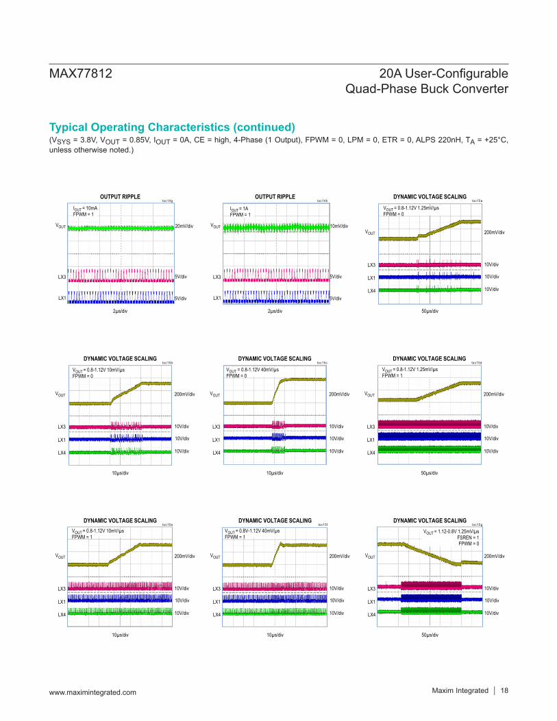
(VSYS = 3.8V, VOUT = 0.85V, IOUT = 0A, CE = high, 4-Phase (1 Output), FPWM = 0, LPM = 0, ETR = 0, ALPS 220nH, TA = +25°C, unless otherwise noted.)
200mV/div
10V/div
toc15k
20µs/div
VOUT
DYNAMIC VOLTAGE SCALING
LX4
LX3
LX1 10V/div
10V/div
VOUT = 1.12V-0.8V 40mV/µsFSREN = 1, FPWM = 0
200mV/div
10V/div
toc15h
500µs/div
VOUT
DYNAMIC VOLTAGE SCALING
LX4
LX3
LX1 10V/div
10V/div
VOUT = 1.12-0.8V 1.25mV/µsFSREN = 0FPWM = 0
10mV/div
5V/div
toc16b
200µs/div
VOUT
IOUT
LOAD TRANSIENT
LX1
10A/div
IOUT = 0A-5A, 0.5A/µs, FPWM = 1
200mV/div
10V/div
toc15 i
50µs/div
VOUT
DYNAMIC VOLTAGE SCALING
LX4
LX3
LX1 10V/div
10V/div
VOUT = 1.12V-0.8V 5mV/µsFSREN = 1FPWM = 0
20mV/div
5V/div
toc16c
200µs/div
VOUT
IOUT
LOAD TRANSIENT
LX1
10A/div
IOUT = 0A-10A, 0.5A/µs, FPWM = 0
200mV/div
10V/div
toc15 j
500µs/div
VOUT
DYNAMIC VOLTAGE SCALING
LX4
LX3
LX1 10V/div
10V/div
VOUT = 1.12V-0.8V 5mV/µsFSREN = 0FPWM = 0
10mV/div
5V/div
toc16d
200µs/div
VOUT
IOUT
LOAD TRANSIENT
LX1
10A/div
IOUT = 0A-10A, 0.5A/µs, FPWM = 1
200mV/div
10V/div
toc15 l
500µs/div
VOUT
DYNAMIC VOLTAGE SCALING
LX4
LX3
LX1 10V/div
10V/div
VOUT = 1.12V-0.8V 40mV/µsFSREN = 0FPWM = 0
20mV/div
5V/div
toc16a
200µs/div
VOUT
IOUT
LOAD TRANSIENT
LX1
10A/div
IOUT = 0-5A, 0.5A/µs, FPWM = 0
Maxim Integrated 19www.maximintegrated.com
MAX77812 20A User-Configurable Quad-Phase Buck Converter
Typical Operating Characteristics (continued)
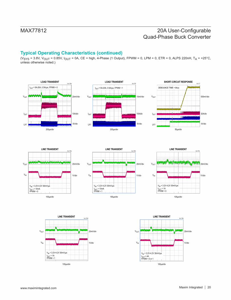
(VSYS = 3.8V, VOUT = 0.85V, IOUT = 0A, CE = high, 4-Phase (1 Output), FPWM = 0, LPM = 0, ETR = 0, ALPS 220nH, TA = +25°C, unless otherwise noted.)
20mV/div
toc18a
100µs/div
VOUT
VIN
LINE TRANSIENT
1V/div
VIN = 3.2V-4.2V 30mV/µsIOU T = 10mAFPWM = 0
20mV/div
5V/div
toc16e
200µs/div
VOUT
IOUT
LOAD TRANSIENT
LX1
10A/div
IOUT = 0A-20A, 0.5A/µs, FPWM = 0
20mV/div
toc18d
100µs/div
VOUT
VIN
LINE TRANSIENT
1V/div
VIN = 3.2V-4.2V 30mV/µsIOUT = 1AFPWM = 1
10mV/div
5V/div
toc16f
200µs/div
VOUT
IOUT
LOAD TRANSIENT
LX1
10A/div
IOUT = 0A-20A, 0.5A/µs, FPWM = 1
500mV/div
5V/div
toc17
50µs/div
VOUT
IOUT
SHORT-CIRCUIT RESPONSE
LX1
20A/div
DEBOUNCE TIME = 64us
20mV/div
toc18e
100µs/div
VOUT
VIN
LINE TRANSIENT
1V/div
VIN = 3.2V-4.2V 30mV/µsIOUT = 4AFPWM = 0 or 1
20mV/div
toc18b
100µs/div
VOUT
VIN
LINE TRANSIENT
1V/div
VIN = 3.2V-4.2V 30mV/µsIOUT = 10mAFPWM = 1
20mV/div
toc18c
100µs/div
VOUT
VIN
LINE TRANSIENT
1V/div
VIN = 3.2V-4.2V 30mV/µs IOUT = 1AFPWM = 0
Maxim Integrated 20www.maximintegrated.com
MAX77812 20A User-Configurable Quad-Phase Buck Converter
Typical Operating Characteristics (continued)
BUCK BIAS DIGITAL
40 9 15
SCL
IRQB
VIO SYS
MISO
CE
IN12LX1PGND
1
SNS1P
PGND1
LX3
PGND3
PGND3
LX1
LX3
PGND1
PGND3
SNS1N
LX2 PGND2
PGND2
LX4PGND4
IN34
LX2 PGND2
LX4PGND4
IN12
IN12
IN34
IN34
SNS3N
SNS3P
PH_CFG0 AGND
PH_CFG1
A
B
C
D
E
F
G
LX1 LX2
LX4
LX3
DGNDGPI0
IN12
IN34
PGND4
GPI1
WDTRSTB_IN
SDA/MOSI
1 2 3 4 5 6 7 8
H
SNS4P
SNS4N
SNS2N
SNS2P
SCS
AGND
I2C_SPI_SEL
PH_CFG2
EN
LPM
AGND
AGND AGND
AGND
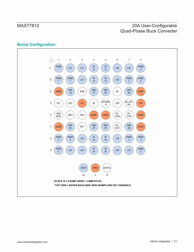
64 WLP (8 x 8 BUMP ARRAY, 0.4MM PITCH)
*TOP VIEW = WAFER BACK-SIDE VIEW (BUMPS ARE NOT VIEWABLE)
MAX77812 20A User-Configurable Quad-Phase Buck Converter
www.maximintegrated.com Maxim Integrated 21
Bump Configuration
BUMP NAME FUNCTIONA1, B1, B2 PGND1 Phase1 Power GroundA2, A3, B3 LX1 Phase1 Switch Node
A4, A5, B4, B5 IN12 Phase1/2 Input. Bypass to PGND1/2 with a 10µF capacitor.A6, A7, B6 LX2 Phase2 Switch NodeA8, B7, B8 PGND2 Phase2 Power Ground
C1, C8, E5, E8, F1, F8 AGND Analog Ground
C2 SNS1N Phase1 Differential Negative Remote Sense Input
C3 IRQ Interrupt Output. A 100kΩ external pullup resistor to VIO is required. High impedance when CE = low.
C4 SNS1P Phase 1 Differential Positive Remote Sense InputC5 SNS2P Phase 2 Differential Positive Remote Sense Input
C6 EN Global Enable Input (Active-High, Logically ORed with GLB_EN Function of GPIs). An 800kΩ internal pulldown resistance to DGND. If this pin is not used, leave it unconnected.
C7 SNS2N Phase 2 Differential Negative Remote Sense Input
D1 SCL I2C Clock Input. High impedance in off state. A 1.5kΩ~2.2kΩ of pullup resistor to VIO is required.
D2 SCS Active-Low SPI Chip SelectD3 VIO IO Supply Voltage Input. Bypass to DGND with a 0.1µF capacitor.
D4 CE
Active-High Chip Enable Input.CE = High (standby), I2C interface is enabled and regulators are ready to be turned on.CE = Low (shutdown), all regulators are turned off and all Type-O registers are reset to their POR default values.
D5 WDTRSTB_IN Active-Low Watchdog Timer Reset Input. An 800kΩ internal pullup resistance to VIO. If this pin is not used, leave it unconnected.
D6 LPMGlobal Low Power Mode Input (Active-High, Logically ORed with GLB_LPM Function of GPIs). An 800kΩ internal pulldown resistance to DGND. If this pin is not used, leave it unconnected.
D7 I2C_SPI_SELSerial Interface Selection Input. Latches at POR.I2C_SPI_SEL = Low: I2CI2C_SPI_SEL = High: SPI
D8 SYS System (Battery) Voltage Input. Bypass to AGND with a 1µF capacitor.
E1 SDA/MOSI I2C Data I/O. High Impedance in Off State. A 1.5kΩ~2.2kΩ of pullup resistor to VIO is required. Configured as MOSI when SPI mode is selected.
E2 MISO SPI Data Output. High impedance in off state.
E3 GPI0 Active-High, General-Purpose Input. An 800kΩ internal pulldown resistance to DGND. If this pin is not used, leave it unconnected.
E4 DGND Digital Ground
MAX77812 20A User-Configurable Quad-Phase Buck Converter
www.maximintegrated.com Maxim Integrated 22
Bump Description
BUMP NAME FUNCTION
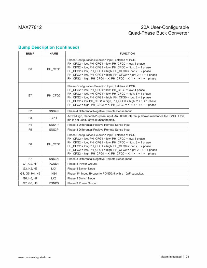
E6 PH_CFG0
Phase Configuration Selection Input. Latches at POR.PH_CFG2 = low, PH_CFG1 = low, PH_CFG0 = low: 4 phasePH_CFG2 = low, PH_CFG1 = low, PH_CFG0 = high: 3 + 1 phasePH_CFG2 = low, PH_CFG1 = high, PH_CFG0 = low: 2 + 2 phasePH_CFG2 = low, PH_CFG1 = high, PH_CFG0 = high: 2 + 1 + 1 phasePH_CFG2 = high, PH_CFG1 = X, PH_CFG0 = X: 1 + 1 + 1 + 1 phase
E7 PH_CFG2
Phase Configuration Selection Input. Latches at POR.PH_CFG2 = low, PH_CFG1 = low, PH_CFG0 = low: 4 phasePH_CFG2 = low, PH_CFG1 = low, PH_CFG0 = high: 3 + 1 phasePH_CFG2 = low, PH_CFG1 = high, PH_CFG0 = low: 2 + 2 phasePH_CFG2 = low PH_CFG1 = high, PH_CFG0 = high: 2 + 1 + 1 phasePH_CFG2 = high, PH_CFG1 = X, PH_CFG0 = X: 1 + 1 + 1 + 1 phase
F2 SNS4N Phase 4 Differential Negative Remote Sense Input
F3 GPI1 Active-High, General-Purpose Input. An 800kΩ internal pulldown resistance to DGND. If this pin is not used, leave it unconnected.
F4 SNS4P Phase 4 Differential Positive Remote Sense InputF5 SNS3P Phase 3 Differential Positive Remote Sense Input
F6 PH_CFG1
Phase Configuration Selection Input. Latches at POR.PH_CFG2 = low, PH_CFG1 = low, PH_CFG0 = low: 4 phasePH_CFG2 = low, PH_CFG1 = low, PH_CFG0 = high: 3 + 1 phasePH_CFG2 = low, PH_CFG1 = high, PH_CFG0 = low: 2 + 2 phasePH_CFG2 = low, PH_CFG1 = high, PH_CFG0 = high: 2 + 1 + 1 phasePH_CFG2 = high, PH_CFG1 = X, PH_CFG0 = X: 1 + 1 + 1 + 1 phase
F7 SNS3N Phase 3 Differential Negative Remote Sense InputG1, G2, H1 PGND4 Phase 4 Power GroundG3, H2, H3 LX4 Phase 4 Switch Node
G4, G5, H4, H5 IN34 Phase 3/4 Input. Bypass to PGND3/4 with a 10µF capacitor.G6, H6, H7 LX3 Phase 3 Switch NodeG7, G8, H8 PGND3 Phase 3 Power Ground
MAX77812 20A User-Configurable Quad-Phase Buck Converter
www.maximintegrated.com Maxim Integrated 23
Bump Description (continued)
Detailed DescriptionTop-Level System ManagementSystem FaultsThe MAX77812 monitors the system for the following faults:
Undervoltage lockout VIO fault
Undervoltage LockoutWhen the VSYS voltage falls below VUVLO_F (2.15V typ), the MAX77812 enters into a shutdown state and UVLO forces the MAX77812 to a dormant state until VSYS voltage rises above the UVLO rising threshold (typically 2.5V). Once the VSYS voltage is higher than the UVLO rising threshold, the MAX77812 comes out of shutdown mode to be securely functional. The UVLO falling thresh-old is programmable through I2C, but it must be set lower than UVLO rising threshold to avoid unexpected behav-iors.
VIO FaultWhen the VIO supply falls below VTH_VIO_OK (1.0V typ), the MAX77812 immediately goes into a shutdown state and stays in this mode until IO supply rises beyond VTH_VIO_OK threshold.
Thermal ProtectionThe MAX77812 has a centralized thermal protection circuit which monitors temperature on the die. If the die temperature exceeds +165°C (TSHDN), the MAX77812 initiates a soft-stop for all the output(s) and all Type-O registers are reset to their POR default values. However, the MAX77812 should be able to communicate with the host processor through the serial interface as long as VSYS and VVIO supplies are within the operating range.In case the die temperature drops by 15°C after the thermal protection occurs, the MAX77812 recovers to the normal state and the output(s) can be turned on again.In addition to +165°C threshold, there are two additional comparators which trip at +120°C and +140°C. Interrupts are generated in the event the die temperature reaches +120°C or +140°C.
Reset Conditions Power-On Reset (POR)When a valid system supply voltage is applied to the device, the MAX77812 goes into Shutdown mode and
stay there until CE goes high. As the VSYS voltage rises above POR threshold (≈ 1.60V), the internal reference and the integrated supply are enabled and the MAX77812 starts loading the default register values from the OTPs.
System ResetWhen VSYS voltage drops below its POR threshold (≈ 1.50V), all Type-S1 registers are reset to their POR default values.
Off ResetOff reset occurs by any power-off or shutdown events. This condition resets all Type-O registers to their POR default values.
Software ResetAll Type-O registers can be reset by writing ‘1’ to SW_RST bit in REG_RESET register. This bit clears to ‘0’ upon reset.
Watchdog Timeout Reset (WDTRSTB_IN)In case the host processor fails to reset its watchdog timer for any system issues, WDTRSTB_IN signal goes low for about 100ms. When the MAX77812 detects that WDTRSTB_IN is low longer than its debounce timer (programmable by WDT_DEB[2:0]), the output voltage setting registers of all phases (Mx_VOUT[7:0]) resets to their POR default values and the output voltages return to their POR default values with given ramp-up/down slew rates.
Chip Enable (CE)When VSYS and VVIO supplies are valid, a logic-high on CE pin puts the MAX77812 into standby mode (enabled). In standby mode, all user registers are accessible through I2C/SPI so that the host processor can overwrite the default output voltages of regulators and each regulator can be enabled by either I2C/SPI or GPI input if applicable.When CE pin goes high, the MAX77812 turns on the internal bias circuitry which takes typically 50µs to be settled. As soon as the bias is ready, all the regulators are allowed to be turned on via I2C/SPI or EN pins. In case the regulators are enabled before the bias circuitry is ready, the regulators require longer time to startup.When the CE pin is pulled low, the MAX77812 goes into shutdown mode (disabled) and turns off all the regulators regardless of EN pins. This event also resets all Type-O registers to their POR default values.
MAX77812 20A User-Configurable Quad-Phase Buck Converter
www.maximintegrated.com Maxim Integrated 24
Enable ControlEach master phase of the MAX77812 can be enabled and disabled by a corresponding enable register bit (EN_Mx), EN input and multifunction GPIs. The enable logic is an ‘OR’ logic of active enable logic signals. For example, the Master1 is enabled when EN_M1 bit, GLB_EN or M1_EN logic signal is set to ‘1’. When all active signals are ‘0’, then the corresponding master phase is turned off.
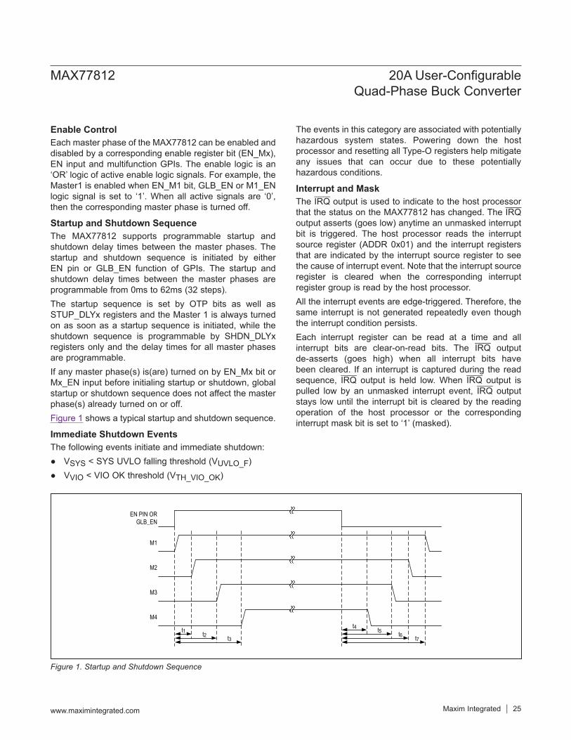
Startup and Shutdown SequenceThe MAX77812 supports programmable startup and shutdown delay times between the master phases. The startup and shutdown sequence is initiated by either EN pin or GLB_EN function of GPIs. The startup and shutdown delay times between the master phases are programmable from 0ms to 62ms (32 steps).The startup sequence is set by OTP bits as well as STUP_DLYx registers and the Master 1 is always turned on as soon as a startup sequence is initiated, while the shutdown sequence is programmable by SHDN_DLYx registers only and the delay times for all master phases are programmable.If any master phase(s) is(are) turned on by EN_Mx bit or Mx_EN input before initialing startup or shutdown, global startup or shutdown sequence does not affect the master phase(s) already turned on or off.Figure 1 shows a typical startup and shutdown sequence.
Immediate Shutdown EventsThe following events initiate and immediate shutdown:
VSYS < SYS UVLO falling threshold (VUVLO_F) VVIO < VIO OK threshold (VTH_VIO_OK)
The events in this category are associated with potentially hazardous system states. Powering down the host processor and resetting all Type-O registers help mitigate any issues that can occur due to these potentially hazardous conditions.
Interrupt and MaskThe IRQ output is used to indicate to the host processor that the status on the MAX77812 has changed. The IRQ output asserts (goes low) anytime an unmasked interrupt bit is triggered. The host processor reads the interrupt source register (ADDR 0x01) and the interrupt registers that are indicated by the interrupt source register to see the cause of interrupt event. Note that the interrupt source register is cleared when the corresponding interrupt register group is read by the host processor.All the interrupt events are edge-triggered. Therefore, the same interrupt is not generated repeatedly even though the interrupt condition persists.Each interrupt register can be read at a time and all interrupt bits are clear-on-read bits. The IRQ output de-asserts (goes high) when all interrupt bits have been cleared. If an interrupt is captured during the read sequence, IRQ output is held low. When IRQ output is pulled low by an unmasked interrupt event, IRQ output stays low until the interrupt bit is cleared by the reading operation of the host processor or the corresponding interrupt mask bit is set to ‘1’ (masked).
Figure 1. Startup and Shutdown Sequence
M2
M3
EN PIN OR GLB_EN
M1
M4
t1 t2 t3t6
t4 t5t7
MAX77812 20A User-Configurable Quad-Phase Buck Converter
www.maximintegrated.com Maxim Integrated 25
Each interrupt can be masked (disabled) by setting the corresponding interrupt mask register bit.When the corresponding mask bit is set (masked), an interrupt bit is not set for an interrupt event. As a result, the IRQ output stays high. When the mask bit is cleared, an active interrupt event at the time of clearing the mask bit is captured, which results in pulling the IRQ output low.Interrupt mask bits are set to ‘1’ by default and are reset to the default values at power-off events.
StatusIn addition to interrupt bits, the MAX77812 has read-only STATUS bits. Those bits always represent the current status of the device. It is highly recommended that the host processor read STATUS bits whenever the MAX77812 is initialized by the host processor. These STATUS bits do not directly affect the state of interrupt bits.
Quad-Phase Buck RegulatorThe MAX77812 uses Maxim’s proprietary Quick-PWM™ adaptive on-time control scheme. Adaptive on-time control provides fast response to load transients, inherent compensation to input voltage variation, and stable performance at low duty cycles. On-times (high-side MOSFET on) are controlled by the on-time generator circuit. This circuit calculates an on-time based on the input voltage (VINx), the output voltage (VOUTx), and the target switching frequency (FSW). The on-time is modified (slightly shortened or lengthened) by the phase current balancing control circuit. Off-times (low-side MOSFET on)
begin when the on-time ends. Shoot-through current from INx to PGNDx is avoided by introducing a brief period of dead-time between switching events when neither MOSFET is on. During the dead-time, the inductor current conducts through the intrinsic body diode of the low-side MOSFET.The PWM comparator regulates VOUTx by modulating off-time. A compensation ramp is fed to the positive input of the PWM comparator and the negative input is a voltage proportional to the actual output voltage error added to the replicated AC current in the inductor. The PWM comparator begins an on-time (and resets the compensation ramp) when the error voltage plus replicated AC inductor current becomes greater than the ramp. When the calculated on-time expires, the off-time automatically begins. One PWM comparator is used to control all phases in multiphase configuration. The output is demultiplexed by a phase scheduler which controls the phase spacing of each switching stage (e.g., 2Φ is spaced 180º apart, 3Φ is spaced 120º, 4Φ is spaced 90°). Multiphase configurations permanently have all phases activated and always switches in sequence during steady-state operation (phases do not add or shed).The switching frequency (FSW) of the adaptive on-time BUCK is variable and heavily influenced by the instantaneous load. More on-time pulses in a given time (higher FSW) is observed as load increases. Fewer on-times in a given time (lower FSW) is observed as load decreases.
MAX77812 20A User-Configurable Quad-Phase Buck Converter
www.maximintegrated.com Maxim Integrated 26
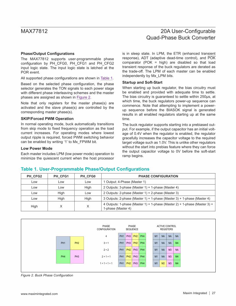
Phase/Output ConfigurationsThe MAX77812 supports user-programmable phase configuration by PH_CFG0, PH_CFG1 and PH_CFG2 input logic state. The input logic state is latched at the POR event.All supported phase configurations are shown in Table 1.Based on the selected phase configuration, the phase selector generates the TON signals to each power stage with different phase interleaving schemes and the master phases are assigned as shown in Figure 2.Note that only registers for the master phase(s) are activated and the slave phase(s) are controlled by the corresponding master phase(s).
SKIP/Forced PWM OperationIn normal operating mode, buck automatically transitions from skip mode to fixed frequency operation as the load current increases. For operating modes where lowest output ripple is required, forced PWM switching behavior can be enabled by writing ‘1’ to Mx_FPWM bit.
Low Power ModeEach master includes LPM (low power mode) operation to minimize the quiescent current when the host processor
is in sleep state. In LPM, the ETR (enhanced transient response), ADT (adaptive dead-time control), and POK comparator (POK = high) are disabled so that load transient response of the buck regulators are derated as the trade-off. The LPM of each master can be enabled independently by Mx_LPM bits.
Startup and Soft-StartWhen starting up buck regulator, the bias circuitry must be enabled and provided with adequate time to settle. The bias circuitry is guaranteed to settle within 250µs, at which time, the buck regulators power-up sequence can commence. Note that attempting to implement a power-up sequence before the BIASOK signal is generated results in all enabled regulators starting up at the same time.The buck regulator supports starting into a prebiased out-put. For example, if the output capacitor has an initial volt-age of 0.4V when the regulator is enabled, the regulator gracefully increases the capacitor voltage to the required target voltage such as 1.0V. This is unlike other regulators without the start into prebias feature where they can force the output capacitor voltage to 0V before the soft-start ramp begins.
Table 1. User-Programmable Phase/Output Configurations
Figure 2. Buck Phase Configuration
PH_CFG2 PH_CFG1 PH_CFG0 PHASE CONFIGURATIONLow Low Low 1 Output: 4-Phase (Master 1)Low Low High 2 Outputs: 3-phase (Master 1) + 1-phase (Master 4)Low High Low 2 Outputs: 2-phase (Master 1) + 2-phase (Master 3)Low High High 3 Outputs: 2-phase (Master 1) + 1-phase (Master 3) + 1-phase (Master 4)
High X X 4 Outputs: 1-phase (Master 1) + 1-phase (Master 2) + 1-phase (Master 3) + 1-phase (Master 4)
PH2
PH4 PH3
PH1
PH1 PH3 PH2 PH44
PH1 PH3 PH2 PH43 + 1
PH1 PH3PH2 PH42 + 2
PH1 PH3PH2 PH42 + 1 + 1
PH1 PH3PH2 PH41 + 1 + 1 + 1
ACTIVE CONTROL REGISTERS
PHASE SEQUENCE
PHASE CONFIGURATION
M4
M3
M3 M4
M3M2 M4
NA NA NA
NANA
NA NA
NA
M1
M1
M1
M1
M1
MAX77812 20A User-Configurable Quad-Phase Buck Converter
www.maximintegrated.com Maxim Integrated 27
The buck regulator supports programmable soft-start rate from 1.25mV/µs to 60mV/µs. The controlled soft-start rate and buck regulator current limit (ILIM_PEAK) limit the input inrush current to the output capacitor (IINRUSH). IINRUSH = min (ILIM_PEAK & COUT x dv/dt). Note that the input current of the buck regulator is lower than the inrush current to the output capacitor by the ratio of output to input voltage.
Output Voltage SettingThe output voltage is programmable from 0.25V to 1.525V in 5mV steps to allow fine adjustment to the processor supply voltage under light load conditions to minimize power loss within the processor. Each master phase have three output voltage control registers. Mx_VOUT[7:0] register is for normal operation and Mx_VOUT_D[7:0] and Mx_VOUT_S[7:0] are used for voltage selection function by GPIx. See the *Multifunction GPIs* section. The default output voltages are set by an OTP option at the factory. The default output voltages can be overwritten by changing the contents in Mx_VOUT[7:0] register prior to enabling the regulator.
Changing Output Voltage During OperationIn a typical smartphone or tablet application, there are several power domains in which the operating frequency of the processor is increased or decreased (DVFS). When the operating frequency needs to be changed, it is expected that the buck regulator responds to a command to change the output voltages to new target values quickly. The high peak current limit, coupled with low inductance and small output capacitance, allows the buck regulator to respond to a positive step change in output voltage and settle to the new target value quickly. The buck regulator provides programmable ramp-up slew rates to accommodate different requirements.For a negative step change in output voltage, the settling time is not critical. In Forced PWM mode (either Mx_
FPWM bit or Mx_FSREN bit is enabled), the negative inductor current through NMOS discharges energy from the output capacitor, which helps the output voltage to decrease to the new target value faster. In skip mode, the negative inductor current is not allowed so that the output voltage settling time is dependent on the load current and the output capacitance.
Output Voltage Slew Rate ControlThe buck regulator supports programmable slew rate control feature when increasing and decreasing the output voltage. The ramp-up slew rate can be set to 1.25mV/µs, 2.5mV/µs, 5mV/µs, 10mV/µs, 20mV/µs 40mV/µs or 60mV/µs independently via B_RU_SR[2:0] bits, while the ramp-down slew rate is programmable to 1.25mV/µs, 2.5mV/µs, 5mV/µs, 10mV/µs, 20mV/µs 40mV/µs or 60mV/µs through B_RD_SR[2:0].
Remote Output Voltage SensingAll phases support differential remote output voltage sensing feature for improving point of load regulation. Differential feedback (SNSxP and SNSxN) enables voltage sensing directly at the point of load, ensuring best voltage regulation at the load, regardless of power plane impedances.
Output Active DischargeBUCK provides an internal 100Ω resistor for output active discharge function. If the active discharge function is enabled (Mx_AD = 1), the internal resistor discharges the energy stored in the output capacitor to PGNDx whenever the regulator is disabled.Either the regulator remains enabled or the active discharge function is disabled (Mx_AD = 0), the internal resistor is disconnected from the output. If the active discharge function is disabled, the output voltage decays at a rate that is determined by the output capacitance and the load current when the regulator is turned off.
MAX77812 20A User-Configurable Quad-Phase Buck Converter
www.maximintegrated.com Maxim Integrated 28
Inductor SelectionThe buck regulator is optimized for 110nH to 470nH inductors. The lower the inductor DCR, the higher the buck efficiency is. Users need to trade off inductor size with DCR value and choose a suitable inductor for the buck.
Input and Output Capacitor SelectionThe input capacitor, CIN, reduces the current peaks drawn from the battery or input power source and reduces switching noise in the device. The impedance of CIN at the switching frequency should be kept very low. Ceramic capacitors with X5R or X7R dielectrics are highly recommended due to their small size, low ESR, and small temperature coefficients. For most applications a 10µF capacitor is sufficient.The output capacitor, COUT, is required to keep the out-put voltage ripple small and to ensure regulation loop stability. COUT must have low impedance at the switching frequency. Ceramic capacitors with X5R or X7R dielectric
are highly recommended due to their small size, low ESR, and small temperature coefficients. Due to the unique feedback network, the output capacitance can be very low. The recommended minimum output capacitance per phase is 22µF.
PCB Trace ResistanceThe evaluation kit (and the typical PCB on which the MAX77812 is expected to be designed in) utilize 1/3oz. Cu, which is plated up to 0.5oz. 0.5oz. Cu has a typical resistance of 1mΩ per square.
Multifunction GPIsGeneral DescriptionThe MAX77812 has two general purpose inputs (GPI0 and GPI1) that can be configured as the enable of regulators, the output voltage selection, the low power mode control and no function. The function of these two inputs is programmable through I2C/SPI (GPI_FUNC register) on the fly.
Table 2. Suggested Inductors
Table 3. Suggested Capacitors
MFGR. SERIESNOMINAL
INDUCTANCE (nH)
TYPICAL DCRESISTANCE
(mΩ)
CURRENT RATING (A)-30% (∆L/L)
CURRENT RATING [A]
∆T = +40°C RISE
DIMENSIONSL x W x H
(mm)
Cyntec HMLE20161B-R22MDR 220 13 5.8 5.3 2.0 x 1.6 x 1.2TOKO DFE201610-E-R24N 240 16 7.0 5.5 2.0 x 1.6 x 1.0ALPS GLULMR2201A 220 9 6.5 7.0 2.5 X 2.0 X 1.2
MFGR. SERIESNOMINAL
INDUCTANCE (µF)
RATED VOLTAGE
(V)
TEMPERATURE CHARACTERISTICS
CASE SIZE (inch)
DIMENSIONSL x W x H
(mm)
Murata GRM188R60J106ME84 10 ±20% 6.3 X5R 0603 1.6 x 0.8 x 0.8Murata GRM188R60J226MEA0 22 ±20% 6.3 X5R 0603 1.6 x 0.8 x 0.8
MAX77812 20A User-Configurable Quad-Phase Buck Converter
www.maximintegrated.com Maxim Integrated 29
Enable Control by GPIWhen the GPIx are configured as output enable pins, the enable logic of a specific regulator is an ‘OR’ logic of the GPIx and the corresponding enable register bit (Mx_EN). For example, if GPI0_FUNC[3:0] = 0001b, the buck Master 1 enable is controlled by GPI0 and M1_EN bit.In case the two GPIs are configured as the same enable function (i.e., GPI0_FUNC[3:0] = GPI1_FUNC[3:0] = 0010b), those inputs are ORed with M2_EN bit. GLB_EN function (GPI0_FUNC[3:0] = 0000b) allows the host processor to enable all the masters in sequence based on STUP_DLYx registers. Note that M1 thru M4 are defined by PH_CFG0, PH_CFG1 and PH_CFG2 inputs.
Voltage Selection by GPIThe buck has two additional output voltage control registers (Mx_VOUT_D[7:0] and Mx_VOUT_S[7:0]) besides one (Mx_VOUT[7:0]) for normal operation. Those two additional registers are for storing the default output voltage and the system sleep mode output voltage for a specific host processor.
When GPIx are configured as voltage selection pins, the output voltage of a specific regulator is set by Mx_VOUT_D[7:0] and Mx_VOUT_S[7:0] registers based on the input logic. For example, if GPI0_FUNC[3:0] = 0101b, the output voltages of all the masters are set by Mx_VOUT_D[7:0] and Mx_VOUT_S[7:0] when GPI0 = high and GPI0 = low, respectively. In case the two GPIs are configured as the same voltage selection function, those inputs are ORed. During the output voltage transition, the ramp-up/down slew rate is controlled by B_RU_SR[2:0] and B_RD_SR[2:0]. Note that M1 thru M4 are defined by PH_CFG0, PH_CFG1 and PH_CFG2 inputs.
Low Power Mode by GPIWhen GPIx are configured as low power mode enable pins, the low power mode enable logic of a specific regulator is an ‘OR’ logic of GPIx and the corresponding enable register bit (Mx_LPM). For example, if GPI0_FUNC[3:0] = 1011b, the buck Master 1 low power mode enable is controlled by GPI0 and M1_LPM bit.
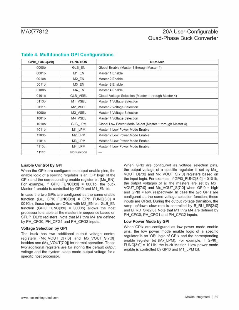
Table 4. Multifunction GPI ConfigurationsGPIx_FUNC[3:0] FUNCTION REMARK
0000b GLB_EN Global Enable (Master 1 through Master 4)0001b M1_EN Master 1 Enable0010b M2_EN Master 2 Enable0011b M3_EN Master 3 Enable0100b M4_EN Master 4 Enable0101b GLB_VSEL Global Voltage Selection (Master 1 through Master 4)0110b M1_VSEL Master 1 Voltage Selection0111b M2_VSEL Master 2 Voltage Selection1000b M3_VSEL Master 3 Voltage Selection1001b M4_VSEL Master 4 Voltage Selection1010b GLB_LPM Global Low Power Mode Select (Master 1 through Master 4)1011b M1_LPM Master 1 Low Power Mode Enable1100b M2_LPM Master 2 Low Power Mode Enable1101b M3_LPM Master 3 Low Power Mode Enable1110b M4_LPM Master 4 Low Power Mode Enable1111b No function —
MAX77812 20A User-Configurable Quad-Phase Buck Converter
www.maximintegrated.com Maxim Integrated 30
In case the two GPIs are configured as the same enable function (i.e., GPI0_FUNC[3:0] = GPI0_FUNC[3:0] = 1100b), those inputs are ORed with M2_LPM bit. GLB_LPM function (GPI0_FUNC[3:0] = 1010b) allows the host processor to enable low power mode of all the masters at the same time. Note that M1 thru M4 are defined by PH_CFG0, PH_CFG1, and PH_CFG2 inputs.
I2C Serial Interface General DescriptionThe I2C-compatible 2-wire serial interface is used for regulator on/off control, setting output voltages, and other functions. See the Register Map section for details.The I2C serial bus consists of a bidirectional serial-data line (SDA) and a serial clock (SCL). I2C is an open-drain bus. SDA and SCL require pullup resistors (500Ω or greater). Optional 24Ω resistors in series with SDA and SCL help to protect the device inputs from high voltage spikes on the bus lines. Series resistors also minimize crosstalk and undershoot on bus lines.
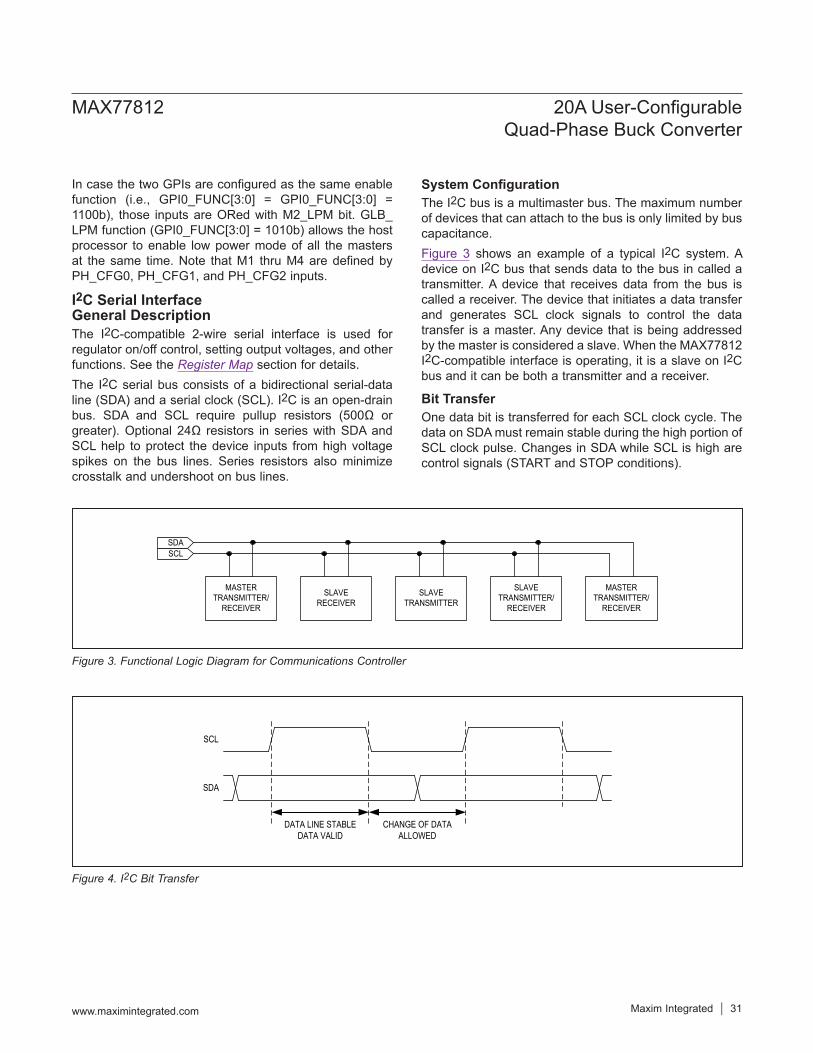
System ConfigurationThe I2C bus is a multimaster bus. The maximum number of devices that can attach to the bus is only limited by bus capacitance.Figure 3 shows an example of a typical I2C system. A device on I2C bus that sends data to the bus in called a transmitter. A device that receives data from the bus is called a receiver. The device that initiates a data transfer and generates SCL clock signals to control the data transfer is a master. Any device that is being addressed by the master is considered a slave. When the MAX77812 I2C-compatible interface is operating, it is a slave on I2C bus and it can be both a transmitter and a receiver.
Bit TransferOne data bit is transferred for each SCL clock cycle. The data on SDA must remain stable during the high portion of SCL clock pulse. Changes in SDA while SCL is high are control signals (START and STOP conditions).
Figure 3. Functional Logic Diagram for Communications Controller
Figure 4. I2C Bit Transfer
MASTER TRANSMITTER/
RECEIVER
SDASCL
SLAVE RECEIVER
SLAVE TRANSMITTER
SLAVE TRANSMITTER/
RECEIVER
MASTER TRANSMITTER/
RECEIVER
SDA
SCL
CHANGE OF DATA ALLOWED
DATA LINE STABLEDATA VALID
MAX77812 20A User-Configurable Quad-Phase Buck Converter
www.maximintegrated.com Maxim Integrated 31
START and STOP ConditionsWhen I2C serial interface is inactive, SDA and SCL idle high. A master device initiates communication by issuing a START condition. A START condition is a high-to-low transition on SDA with SCL high. A STOP condition is a low-to-high transition on SDA, while SCL is high.A START condition from the master signals the beginning of a transmission to the MAX77812. The master terminates transmission by issuing a NOT ACKNOWLEDGE followed by a STOP condition.A STOP condition frees the bus. To issue a series of commands to the slave, the master can issue REPEATED START (Sr) commands instead of a STOP command in order to maintain control of the bus. In general, a REPEATED START command is functionally equivalent to a regular START command.When a STOP condition or incorrect address is detected, the MAX77812 internally disconnects SCL from I2C serial interface until the next START condition, minimizing digital noise and feedthrough.
AcknowledgeBoth the I2C bus master and the MAX77812 (slave) generate acknowledge bits when receiving data. The acknowledge bit is the last bit of each nine bit data packet. To generate an ACKNOWLEDGE (A), the receiving device must pull SDA low before the rising edge of the acknowledge-related clock pulse (ninth pulse) and keep it low during the high period of the clock pulse. To generate a NOT ACKNOWLEDGE (nA), the receiving device allows SDA to be pulled high before the rising edge of the acknowledge-related clock pulse and leaves it high during the high period of the clock pulse.Monitoring the acknowledge bits allows for detection of unsuccessful data transfers. An unsuccessful data transfer occurs if a receiving device is busy or if a system fault has occurred. In the event of an unsuccessful data transfer, the bus master should reattempt communication at a later time.
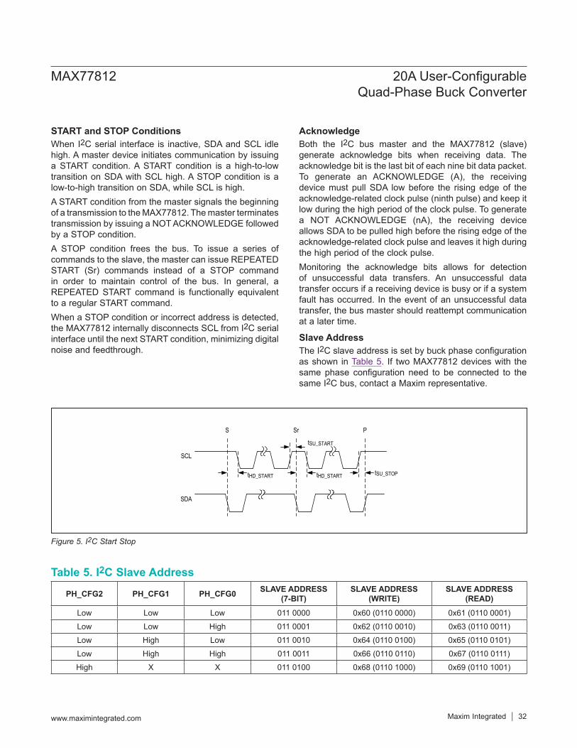
Slave AddressThe I2C slave address is set by buck phase configuration as shown in Table 5. If two MAX77812 devices with the same phase configuration need to be connected to the same I2C bus, contact a Maxim representative.
Figure 5. I2C Start Stop
Table 5. I2C Slave Address
PH_CFG2 PH_CFG1 PH_CFG0 SLAVE ADDRESS (7-BIT)
SLAVE ADDRESS (WRITE)
SLAVE ADDRESS (READ)
Low Low Low 011 0000 0x60 (0110 0000) 0x61 (0110 0001)Low Low High 011 0001 0x62 (0110 0010) 0x63 (0110 0011)Low High Low 011 0010 0x64 (0110 0100) 0x65 (0110 0101)Low High High 011 0011 0x66 (0110 0110) 0x67 (0110 0111)High X X 011 0100 0x68 (0110 1000) 0x69 (0110 1001)
S PSr
SCL
SDA
tHD_START
tSU_START
tSU_STOPtHD_START
MAX77812 20A User-Configurable Quad-Phase Buck Converter
www.maximintegrated.com Maxim Integrated 32
Clock StretchingIn general, the clock signal generation for I2C bus is the responsibility of the master device. I2C specification allows slow slave devices to alter the clock signal by holding down the clock line. The process in which a slave device holds down the clock line is typically called clock stretching. The MAX77812 does not use any form of clock stretching to hold down the clock line.
General Call AddressThe MAX77812 does not implement the I2C specification general call address. If the MAX77812 sees general call address (00000000b), it does not issue an ACKNOWLEDGE (A).
Communication SpeedThe MAX77812 provides an I2C 3.0-compatible (3.4MHz) serial interface.
I2C Revision 3 Compatible Serial Communications Channel• 0Hz to 100kHz (Standard Mode)• 0Hz to 400kHz (Fast Mode)• 0Hz to 1MHz (Fast Mode Plus)• 0Hz to 3.4MHz (High-speed Mode)
Does not utilize I2C Clock StretchingOperating in standard mode, fast mode and fast mode plus does not require any special protocols. The main consideration when changing the bus speed through this range is the combination of the bus capacitance and pullup resistors. Higher time constants created by the
bus capacitance and pullup resistance (C x R) slow the bus operation. Therefore, when increasing bus speeds the pullup resistance must be decreased to maintain a reasonable time constant. See the Pullup Resistor Sizing section of the I2C revision 3.0 specification for detailed guidance on the pullup resistor selection. In general, for bus capacitance of 200pF, a 100kHz bus needs 5.6kΩ pullup resistors, a 400kHz bus needs about a 1.5kΩ pullup resistors, and a 1MHz bus needs 680Ω pullup resistors. Note that the pullup resistor is dissipating power when the open-drain bus is low. The lower the value of the pullup resistor, the higher the power dissipation (V2/R).Operating in high-speed mode requires some special con-siderations. For the full list of considerations, see the I2C 3.0 specification. The major considerations with respect to the MAX77812 are:
I2C bus master use current source pullups to shorten the signal rise times.
I2C slave must use a different set of input filters on its SDA and SCL lines to accommodate for the higher bus speed.
The communication protocols need to utilize the high-speed master code.
At power-up and after each STOP condition, the MAX77812 inputs filters are set for standard mode, fast mode, or fast mode plus (i.e., 0Hz to 1MHz). To switch the input filters for high-speed mode, use the high-speed master code protocols that are described in the Protocols section.
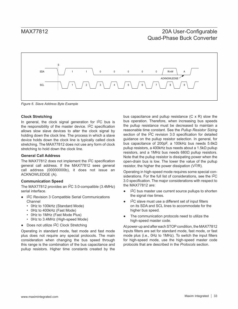
Figure 6. Slave Address Byte Example
S
SCL
SDA
1 2 3
011
8 94 5 6 7
0 0 0 R/nW A0
ACKNOWLEDGE
MAX77812 20A User-Configurable Quad-Phase Buck Converter
www.maximintegrated.com Maxim Integrated 33
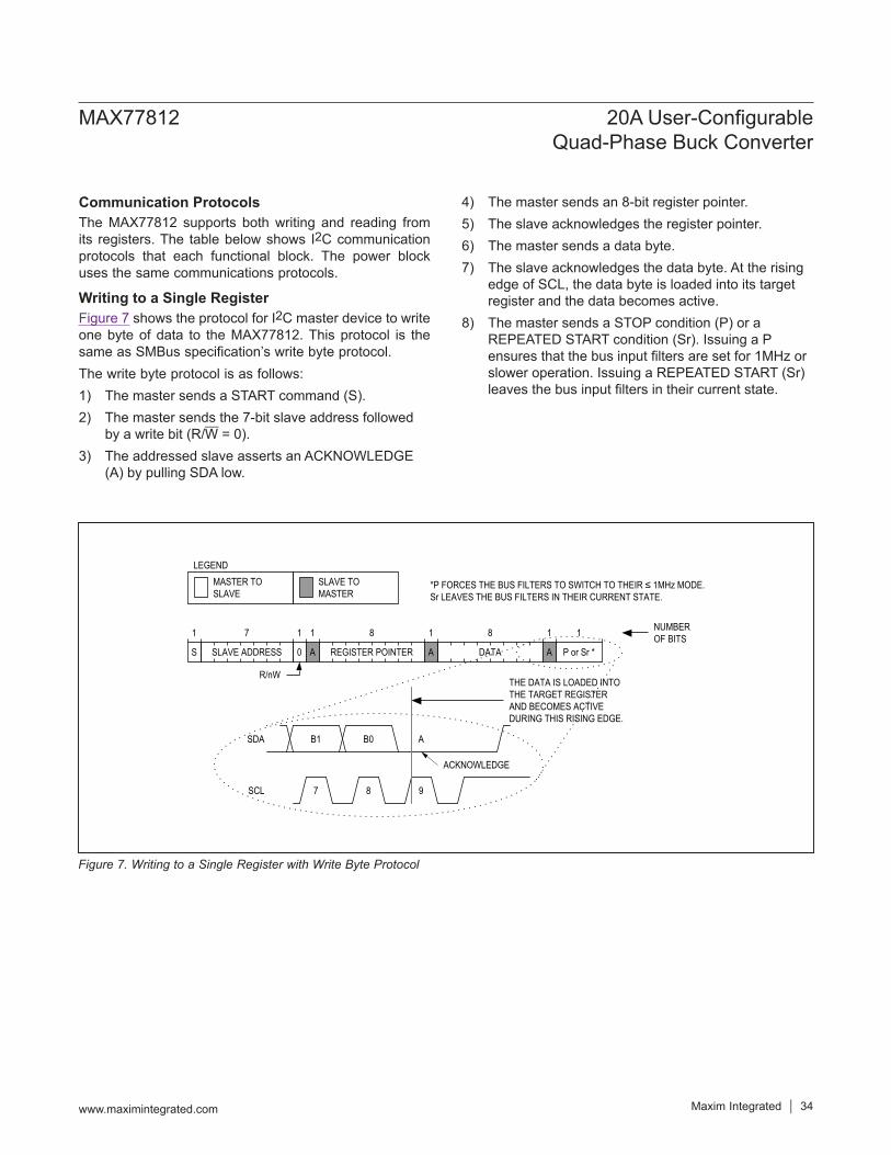
Communication ProtocolsThe MAX77812 supports both writing and reading from its registers. The table below shows I2C communication protocols that each functional block. The power block uses the same communications protocols.
Writing to a Single RegisterFigure 7 shows the protocol for I2C master device to write one byte of data to the MAX77812. This protocol is the same as SMBus specification’s write byte protocol.The write byte protocol is as follows:1) The master sends a START command (S).2) The master sends the 7-bit slave address followed
by a write bit (R/W = 0).3) The addressed slave asserts an ACKNOWLEDGE
(A) by pulling SDA low.
4) The master sends an 8-bit register pointer.5) The slave acknowledges the register pointer.6) The master sends a data byte.7) The slave acknowledges the data byte. At the rising
edge of SCL, the data byte is loaded into its target register and the data becomes active.
8) The master sends a STOP condition (P) or a REPEATED START condition (Sr). Issuing a P ensures that the bus input filters are set for 1MHz or slower operation. Issuing a REPEATED START (Sr) leaves the bus input filters in their current state.
Figure 7. Writing to a Single Register with Write Byte Protocol
1
S
NUMBER OF BITS
R/nW
SLAVE ADDRESS
7
0
1 8
REGISTER POINTERA
1
A
1 8
DATA
1
P or Sr *
*P FORCES THE BUS FILTERS TO SWITCH TO THEIR ≤ 1MHz MODE.Sr LEAVES THE BUS FILTERS IN THEIR CURRENT STATE.
SLAVE TO MASTER
MASTER TO SLAVE
LEGEND
8 97
B0 AB1
THE DATA IS LOADED INTO THE TARGET REGISTER AND BECOMES ACTIVE DURING THIS RISING EDGE.
SDA
SCL
ACKNOWLEDGE
A
1
MAX77812 20A User-Configurable Quad-Phase Buck Converter
www.maximintegrated.com Maxim Integrated 34
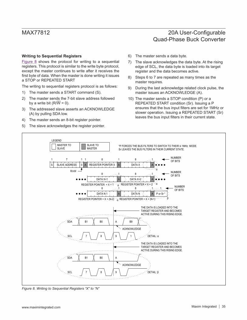
Writing to Sequential RegistersFigure 8 shows the protocol for writing to a sequential registers. This protocol is similar to the write byte protocol, except the master continues to write after it receives the first byte of data. When the master is done writing it issues a STOP or REPEATED STARTThe writing to sequential registers protocol is as follows:1) The master sends a START command (S).2) The master sends the 7-bit slave address followed
by a write bit (R/W = 0).3) The addressed slave asserts an ACKNOWLEDGE
(A) by pulling SDA low.4) The master sends an 8-bit register pointer.5) The slave acknowledges the register pointer.
6) The master sends a data byte.7) The slave acknowledges the data byte. At the rising
edge of SCL, the data byte is loaded into its target register and the data becomes active.
8) Steps 6 to 7 are repeated as many times as the master requires.
9) During the last acknowledge related clock pulse, the master issues an ACKNOWLEDGE (A).
10) The master sends a STOP condition (P) or a REPEATED START condition (Sr). Issuing a P ensures that the bus input filters are set for 1MHz or slower operation. Issuing a REPEATED START (Sr) leaves the bus input filters in their current state.
Figure 8. Writing to Sequential Registers “X” to “N”
1
S
NUMBER OF BITS
R/nW
SLAVE ADDRESS
7
0
1 8
REGISTER POINTER XA
1
A
1 8
DATA X A
1
NUMBER OF BITS8
DATA X+1 A
1 8
DATA X+2 A
1
NUMBER OF BITS8
DATA N-1
1 8
DATA N
α
αα
α β
1
P or Sr *
*P FORCES THE BUS FILTERS TO SWITCH TO THEIR ≤ 1MHz MODE. Sr LEAVES THE BUS FILTERS IN THEIR CURRENT STATE.
REGISTER POINTER = X + 1 REGISTER POINTER = X + 2
REGISTER POINTER = X + (N-2) REGISTER POINTER = X + (N-1)
SLAVE TO MASTER
MASTER TO SLAVE
LEGEND
8 97
B0 AB1
THE DATA IS LOADED INTO THE TARGET REGISTER AND BECOMES ACTIVE DURING THIS RISING EDGE.
SDA
SCL DETAIL: α
DETAIL: β
1
B9
8 97
B0 AB1
THE DATA IS LOADED INTO THE TARGET REGISTER AND BECOMES ACTIVE DURING THIS RISING EDGE.
SDA
SCL
ACKNOWLEDGE
ACKNOWLEDGE
A
1
A
MAX77812 20A User-Configurable Quad-Phase Buck Converter
www.maximintegrated.com Maxim Integrated 35
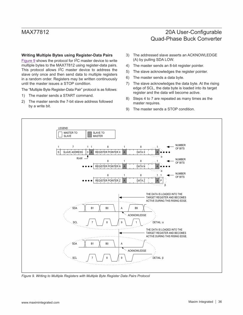
Writing Multiple Bytes using Register-Data PairsFigure 9 shows the protocol for I2C master device to write multiple bytes to the MAX77812 using register-data pairs. This protocol allows I2C master device to address the slave only once and then send data to multiple registers in a random order. Registers may be written continuously until the master issues a STOP condition.The “Multiple Byte Register-Data Pair” protocol is as follows:1) The master sends a START command.2) The master sends the 7-bit slave address followed
by a write bit.
3) The addressed slave asserts an ACKNOWLEDGE (A) by pulling SDA LOW.
4) The master sends an 8-bit register pointer.5) The slave acknowledges the register pointer.6) The master sends a data byte.7) The slave acknowledges the data byte. At the rising
edge of SCL, the data byte is loaded into its target register and the data will become active.
8) Steps 4 to 7 are repeated as many times as the master requires.
9) The master sends a STOP condition.
Figure 9. Writing to Multiple Registers with Multiple Byte Register Data Pairs Protocol
1
S
NUMBER OF BITS
R/nW
SLAVE ADDRESS
7 1 8
REGISTER POINTER XA
1
A
1 8
DATA X A
1
P
1
NUMBER OF BITS8
REGISTER POINTER N A
1 8
DATA N A
1
NUMBER OF BITS8
REGISTER POINTER Z A
1 8
DATA Z A
1
α
α
β
SLAVE TO MASTER
MASTER TO SLAVE
LEGEND
8 97
B0 AB1
THE DATA IS LOADED INTO THE TARGET REGISTER AND BECOMES ACTIVE DURING THIS RISING EDGE.
SDA
SCL DETAIL: α
DETAIL: β
1
B9
8 97
B0 AB1
THE DATA IS LOADED INTO THE TARGET REGISTER AND BECOMES ACTIVE DURING THIS RISING EDGE.
SDA
SCL
ACKNOWLEDGE
ACKNOWLEDGE
0
MAX77812 20A User-Configurable Quad-Phase Buck Converter
www.maximintegrated.com Maxim Integrated 36
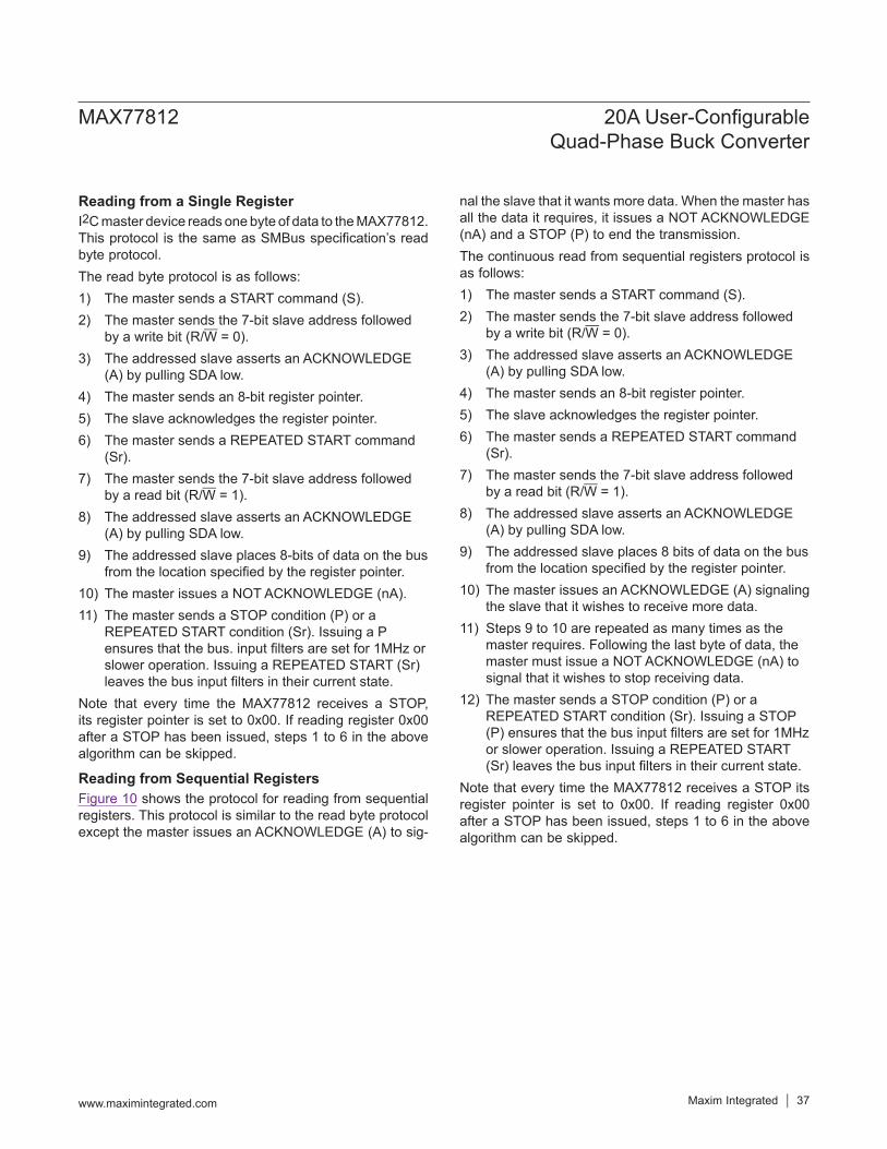
Reading from a Single RegisterI2C master device reads one byte of data to the MAX77812. This protocol is the same as SMBus specification’s read byte protocol.The read byte protocol is as follows:1) The master sends a START command (S).2) The master sends the 7-bit slave address followed
by a write bit (R/W = 0).3) The addressed slave asserts an ACKNOWLEDGE
(A) by pulling SDA low.4) The master sends an 8-bit register pointer.5) The slave acknowledges the register pointer.6) The master sends a REPEATED START command
(Sr).7) The master sends the 7-bit slave address followed
by a read bit (R/W = 1).8) The addressed slave asserts an ACKNOWLEDGE
(A) by pulling SDA low.9) The addressed slave places 8-bits of data on the bus
from the location specified by the register pointer.10) The master issues a NOT ACKNOWLEDGE (nA).11) The master sends a STOP condition (P) or a
REPEATED START condition (Sr). Issuing a P ensures that the bus. input filters are set for 1MHz or slower operation. Issuing a REPEATED START (Sr) leaves the bus input filters in their current state.
Note that every time the MAX77812 receives a STOP, its register pointer is set to 0x00. If reading register 0x00 after a STOP has been issued, steps 1 to 6 in the above algorithm can be skipped.
Reading from Sequential RegistersFigure 10 shows the protocol for reading from sequential registers. This protocol is similar to the read byte protocol except the master issues an ACKNOWLEDGE (A) to sig-
nal the slave that it wants more data. When the master has all the data it requires, it issues a NOT ACKNOWLEDGE (nA) and a STOP (P) to end the transmission.The continuous read from sequential registers protocol is as follows:1) The master sends a START command (S).2) The master sends the 7-bit slave address followed
by a write bit (R/W = 0).3) The addressed slave asserts an ACKNOWLEDGE
(A) by pulling SDA low.4) The master sends an 8-bit register pointer.5) The slave acknowledges the register pointer.6) The master sends a REPEATED START command
(Sr).7) The master sends the 7-bit slave address followed
by a read bit (R/W = 1).8) The addressed slave asserts an ACKNOWLEDGE
(A) by pulling SDA low.9) The addressed slave places 8 bits of data on the bus
from the location specified by the register pointer.10) The master issues an ACKNOWLEDGE (A) signaling
the slave that it wishes to receive more data.11) Steps 9 to 10 are repeated as many times as the
master requires. Following the last byte of data, the master must issue a NOT ACKNOWLEDGE (nA) to signal that it wishes to stop receiving data.
12) The master sends a STOP condition (P) or a REPEATED START condition (Sr). Issuing a STOP (P) ensures that the bus input filters are set for 1MHz or slower operation. Issuing a REPEATED START (Sr) leaves the bus input filters in their current state.
Note that every time the MAX77812 receives a STOP its register pointer is set to 0x00. If reading register 0x00 after a STOP has been issued, steps 1 to 6 in the above algorithm can be skipped.
MAX77812 20A User-Configurable Quad-Phase Buck Converter
www.maximintegrated.com Maxim Integrated 37
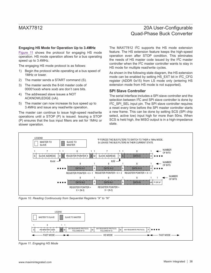
Engaging HS Mode for Operation Up to 3.4MHzFigure 11 shows the protocol for engaging HS mode operation. HS mode operation allows for a bus operating speed up to 3.4MHz.The engaging HS mode protocol is as follows:1) Begin the protocol while operating at a bus speed of
1MHz or lower.2) The master sends a START command (S).3) The master sends the 8-bit master code of
00001xxxb where xxxb are don’t care bits.4) The addressed slave issues a NOT
ACKNOWLEDGE (nA).5) The master can now increase its bus speed up to
3.4MHz and issue any read/write operation.The master can continue to issue high-speed read/write operations until a STOP (P) is issued. Issuing a STOP (P) ensures that the bus input filters are set for 1MHz or slower operation.
The MAX77812 I2C supports the HS mode extension feature. The HS extension feature keeps the high-speed operation even after STOP condition. This eliminates the needs of HS master code issued by the I2C master controller when the I2C master controller wants to stay in HS mode for multiple read/write cycles.As shown in the following state diagram, the HS extension mode can be enabled by setting HS_EXT bit in I2C_CFG register (ADDR 0x15) from LS mode only (entering HS extension mode from HS mode is not supported).
SPI Slave ControllerThe serial interface includes a SPI slave controller and the selection between I2C and SPI slave controller is done by I2C_SPI_SEL input pin. The SPI slave controller requires a reset every time before the SPI master controller starts a new frame. This can be done by setting SCS (SPI chip select, active low) input high for more than 50ns. When SCS is held high, the MISO output is in a high-impedance state.
Figure 10. Reading Continuously from Sequential Registers “X” to “N”
Figure 11. Engaging HS Mode
R/nW
SLAVE ADDRESS
7 1 8
REGISTER POINTER X Sr SLAVE ADDRESS
7 8
DATA X A
NUMBER OF BITS
R/W8
DATA X+3 A
NUMBER OF BITS8
DATA X+2 ADATA X+1 A
8
8
DATA N nA
8
DATA N-1 ADATA N-2 A
8
SLAVE TO MASTER
MASTER TO SLAVE
LEGEND
NUMBER OF BITS1
P OR Sr*
*P FORCES THE BUS FILTERS TO SWITCH TO THEIR ≤ 1MHz MODE. Sr LEAVES THE BUS FILTERS IN THEIR CURRENT STATE.
REGISTER POINTER = X + 1 REGISTER POINTER = X + 2 REGISTER POINTER = X + 3
REGISTER POINTER = X + (N-3)
REGISTER POINTER = X + (N-2)
A A AS 0 1
11 1 1 1 1 1
1 1 1
1 1 1
1
S HS MASTER CODE
8
nA
1 1
Sr
SLAVE TO MASTERMASTER TO SLAVE
LEGEND
FAST MODE HS MODE
ANY READ/WRITE PROTOCOL FOLLOWED BY Sr Sr ANY READ/WRITE PROTOCOL
FOLLOWED BY Sr Sr ANY READ/WRITE PROTOCOL P
FAST MODE
MAX77812 20A User-Configurable Quad-Phase Buck Converter
www.maximintegrated.com Maxim Integrated 38
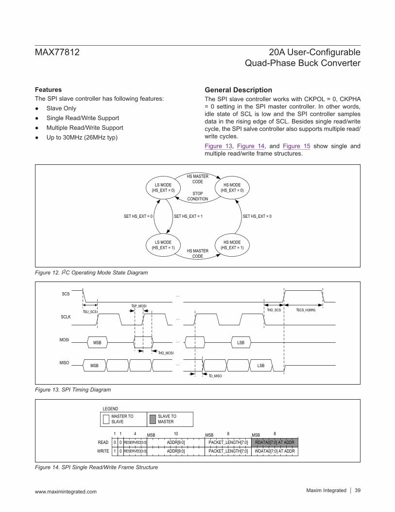
FeaturesThe SPI slave controller has following features:
Slave Only Single Read/Write Support Multiple Read/Write Support Up to 30MHz (26MHz typ)
General DescriptionThe SPI slave controller works with CKPOL = 0, CKPHA = 0 setting in the SPI master controller. In other words, idle state of SCL is low and the SPI controller samples data in the rising edge of SCL. Besides single read/write cycle, the SPI salve controller also supports multiple read/write cycles.Figure 13, Figure 14, and Figure 15 show single and multiple read/write frame structures.
Figure 13. SPI Timing Diagram
Figure 14. SPI Single Read/Write Frame Structure
Figure 12. I2C Operating Mode State Diagram
LS MODE (HS_EXT = 0)
LS MODE (HS_EXT = 1)
HS MODE(HS_EXT = 0)
HS MODE(HS_EXT = 1)
HS MASTER CODE
STOP CONDITION
HS MASTER CODE
SET HS_EXT = 1 SET HS_EXT = 0SET HS_EXT = 0
SCS
SCLK
MOSI
MISO
tSP_MOSI
tHD_MOSI
···
tD_MISO
tSU_SCS tHD_SCS tSCS_H(MIN)
MSB
···
···
··· LSB
MSB LSB
1
0
ADDR[9:0]
4
RDATA0[7:0] AT ADDR
SLAVE TO MASTER
MASTER TO SLAVE
LEGEND
1
ADDR[9:0]
8
WDATA0[7:0] AT ADDR
10
READ
WRITE
0
0
1
PACKET_LENGTH[7:0]
PACKET_LENGTH[7:0]
8MSB MSB MSB
RESERVED[3:0]
RESERVED[3:0]
MAX77812 20A User-Configurable Quad-Phase Buck Converter
www.maximintegrated.com Maxim Integrated 39
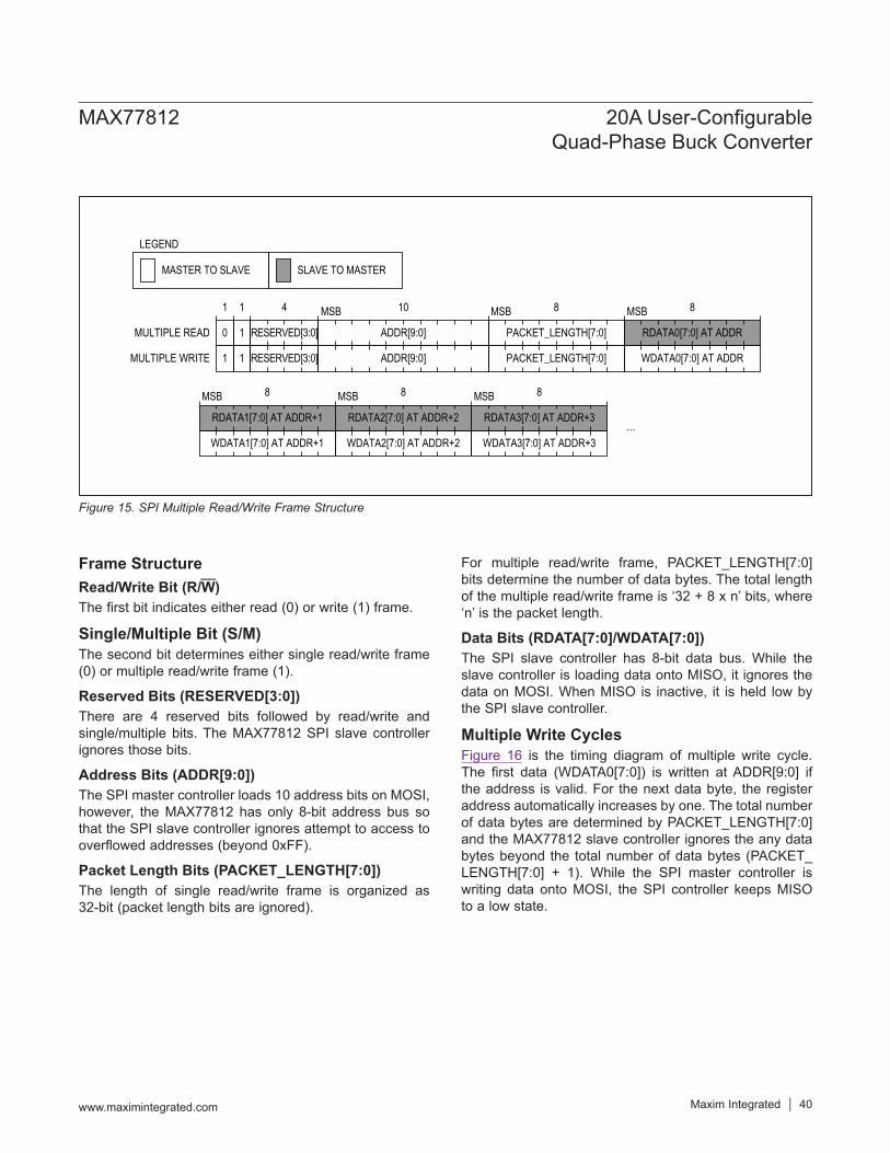
Frame StructureRead/Write Bit (R/W)The first bit indicates either read (0) or write (1) frame.
Single/Multiple Bit (S/M)The second bit determines either single read/write frame (0) or multiple read/write frame (1).
Reserved Bits (RESERVED[3:0])There are 4 reserved bits followed by read/write and single/multiple bits. The MAX77812 SPI slave controller ignores those bits.
Address Bits (ADDR[9:0])The SPI master controller loads 10 address bits on MOSI, however, the MAX77812 has only 8-bit address bus so that the SPI slave controller ignores attempt to access to overflowed addresses (beyond 0xFF).
Packet Length Bits (PACKET_LENGTH[7:0])The length of single read/write frame is organized as 32-bit (packet length bits are ignored).
For multiple read/write frame, PACKET_LENGTH[7:0] bits determine the number of data bytes. The total length of the multiple read/write frame is ‘32 + 8 x n’ bits, where ‘n’ is the packet length.
Data Bits (RDATA[7:0]/WDATA[7:0])The SPI slave controller has 8-bit data bus. While the slave controller is loading data onto MISO, it ignores the data on MOSI. When MISO is inactive, it is held low by the SPI slave controller.
Multiple Write CyclesFigure 16 is the timing diagram of multiple write cycle. The first data (WDATA0[7:0]) is written at ADDR[9:0] if the address is valid. For the next data byte, the register address automatically increases by one. The total number of data bytes are determined by PACKET_LENGTH[7:0] and the MAX77812 slave controller ignores the any data bytes beyond the total number of data bytes (PACKET_LENGTH[7:0] + 1). While the SPI master controller is writing data onto MOSI, the SPI controller keeps MISO to a low state.
Figure 15. SPI Multiple Read/Write Frame Structure
1
0
ADDR[9:0]
RDATA0[7:0] AT ADDR
1
ADDR[9:0]
8
WDATA0[7:0] AT ADDR
10
MULTIPLE READ
MULTIPLE WRITE
1
1
1
PACKET_LENGTH[7:0]
PACKET_LENGTH[7:0]
8
RDATA1[7:0] AT ADDR+1
WDATA1[7:0] AT ADDR+1
8
RDATA2[7:0] AT ADDR+2
WDATA2[7:0] AT ADDR+2
RDATA3[7:0] AT ADDR+3
WDATA3[7:0] AT ADDR+3
8 8
···
MSB MSB MSB
MSB MSB MSB
4
RESERVED[3:0]
RESERVED[3:0]
SLAVE TO MASTERMASTER TO SLAVE
LEGEND
MAX77812 20A User-Configurable Quad-Phase Buck Converter
www.maximintegrated.com Maxim Integrated 40
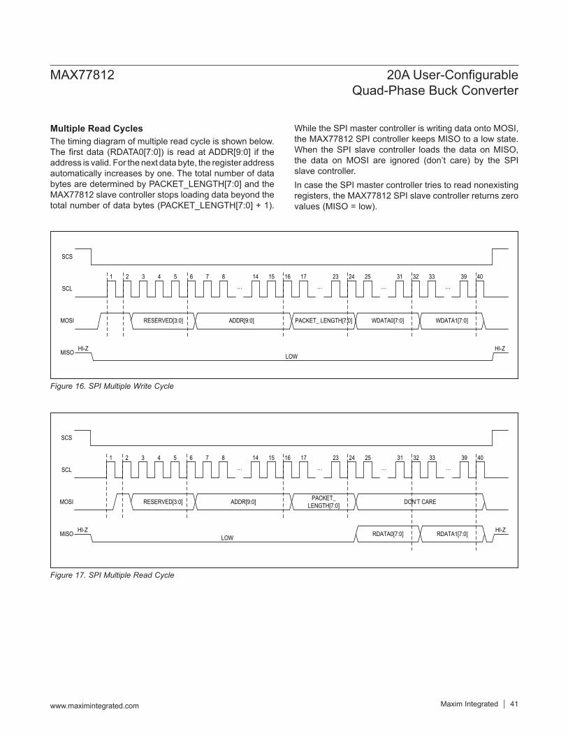
Multiple Read CyclesThe timing diagram of multiple read cycle is shown below. The first data (RDATA0[7:0]) is read at ADDR[9:0] if the address is valid. For the next data byte, the register address automatically increases by one. The total number of data bytes are determined by PACKET_LENGTH[7:0] and the MAX77812 slave controller stops loading data beyond the total number of data bytes (PACKET_LENGTH[7:0] + 1).
While the SPI master controller is writing data onto MOSI, the MAX77812 SPI controller keeps MISO to a low state. When the SPI slave controller loads the data on MISO, the data on MOSI are ignored (don’t care) by the SPI slave controller.In case the SPI master controller tries to read nonexisting registers, the MAX77812 SPI slave controller returns zero values (MISO = low).
Figure 16. SPI Multiple Write Cycle
Figure 17. SPI Multiple Read Cycle
MOSI
SCL
MISO
SCS
1 2 3 4 5 6 7 8 14 15 16 17 23 24 25 31 32 33 39 40
HI-Z
ADDR[9:0]RESERVED[3:0]
··· ···
LOW
PACKET_ LENGTH[7:0] WDATA0[7:0] WDATA1[7:0]
··· ···
HI-Z
MOSI
SCL
MISO
SCS
1 2 3 4 5 6 7 8 14 15 16 17 23 24 25 31 32 33 39 40
HI-Z
ADDR[9:0]RESERVED[3:0]
··· ···
LOW
PACKET_LENGTH[7:0]
··· ···
HI-ZRDATA0[7:0] RDATA1[7:0]
DON’T CARE
MAX77812 20A User-Configurable Quad-Phase Buck Converter
www.maximintegrated.com Maxim Integrated 41
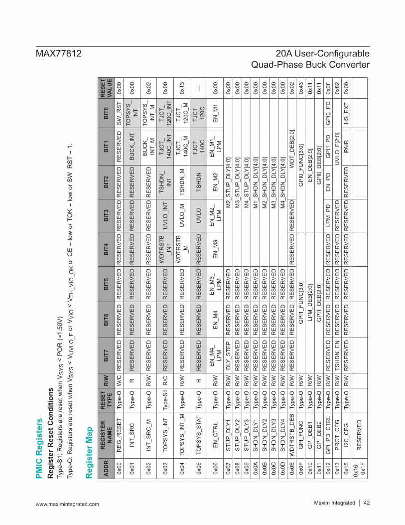
AD
DR
REG
ISTE
R
NA
ME
RES
ET
TYPE
R/W
BIT
7B
IT6
BIT
5B
IT4
BIT
3B
IT2
BIT
1B
IT0
RES
ET
VALU
E0x
00R
EG_R
ESET
Type
-OW
/CR
ESER
VED
RES
ERVE
DR
ESER
VED
RES
ERVE
DR
ESER
VED
RES
ERVE
DR
ESER
VED
SW_R
ST0x
00
0x01
INT_
SRC
Type
-OR
RES
ERVE
DR
ESER
VED
RES
ERVE
DR
ESER
VED
RES
ERVE
DR
ESER
VED
BUC
K_IN
TTO
PSYS
_ IN
T0x
00
0x02
INT_
SRC
_MTy
pe-O
R/W
RES
ERVE
DR
ESER
VED
RES
ERVE
DR
ESER
VED
RES
ERVE
DR
ESER
VED
BUC
K_
INT_
MTO
PSYS
_ IN
T_M
0x02
0x03
TOPS
YS_I
NT
Type
-S1
R/C
RES
ERVE
DR
ESER
VED
RES
ERVE
DW
DTR
STB
_IN
TU
VLO
_IN
TTS
HD
N_
INT
TJC
T_
140C
_IN
TTJ
CT_
12
0C_I
NT
0x00
0x04
TOPS
YS_I
NT_
MTy
pe-O
R/W
RES
ERVE
DR
ESER
VED
RES
ERVE
DW
DTR
STB
_MU
VLO
_MTS
HD
N_M
TJC
T_
140C
_MTJ
CT_
12
0C_M
0x13
0x05
TOPS
YS_S
TAT
Type
-OR
RES
ERVE
DR
ESER
VED
RES
ERVE
DR
ESER
VED
UVL
OTS
HD
NTJ
CT_
14
0CTJ
CT_
12
0C—
0x06
EN_C
TRL
Type
-OR
/WEN
_M4_
LP
MEN
_M4
EN_M
3_
LPM
EN_M
3EN
_M2_
LP
MEN
_M2
EN_M
1_
LPM
EN_M
10x
00
0x07
STU
P_D
LY1
Type
-OR
/WD
LY_S
TEP
RES
ERVE
DR
ESER
VED
M2_
STU
P_D
LY[4
:0]
0x00
0x08
STU
P_D
LY2
Type
-OR
/WR
ESER
VED
RES
ERVE
DR
ESER
VED
M3_
STU
P_D
LY[4
:0]
0x00
0x09
STU
P_D
LY3
Type
-OR
/WR
ESER
VED
RES
ERVE
DR
ESER
VED
M4_
STU
P_D
LY[4
:0]
0x00
0x0A
SHD
N_D
LY1
Type
-OR
/WR
ESER
VED
RES
ERVE
DR
ESER
VED
M1_
SHD
N_D
LY[4
:0]
0x00
0x0B
SHD
N_D
LY2
Type
-OR
/WR
ESER
VED
RES
ERVE
DR
ESER
VED
M2_
SHD
N_D
LY[4
:0]
0x00
0x0C
SHD
N_D
LY3
Type
-OR
/WR
ESER
VED
RES
ERVE
DR
ESER
VED
M3_
SHD
N_D
LY[4
:0]
0x00
0x0D
SHD
N_D
LY4
Type
-OR
/WR
ESER
VED
RES
ERVE
DR
ESER
VED
M4_
SHD
N_D
LY[4
:0]
0x00
0x0E
WD
TRST
B_D
EBTy
pe-O
R/W
RES
ERVE
DR
ESER
VED
RES
ERVE
DR
ESER
VED
RES
ERVE
DW
DT_
DEB
[2:0
]0x
020x
0FG
PI_F
UN
CTy
pe-O
R/W
GPI
1_FU
NC
[3:0
]G
PI0_
FUN
C[3
:0]
0x43
0x10
GPI
_DEB
1Ty
pe-O
R/W
LPM
_DEB
[2:0
]EN
_DEB
[2:0
]0x
110x
11G
PI_D
EB2
Type
-OR
/WG
PI1_
DEB
[2:0
]G
PI0_
DEB
[2:0
]0x
110x
12G
PI_P
D_C
TRL
Type
-OR
/WR
ESER
VED
RES
ERVE
DR
ESER
VED
RES
ERVE
DLP
M_P
DEN
_PD
GPI
1_PD
GPI
0_PD
0x0F
0x13
PRO
T_C
FGTy
pe-O
R/W
TSH
DN
_EN
RES
ERVE
DR
ESER
VED
RES
ERVE
DR
ESER
VED
UVL
O_F
[2:0
]0x
820x
15I2
C_C
FGTy
pe-O
R/W
RES
ERVE
DR
ESER
VED
RES
ERVE
DR
ESER
VED
RES
ERVE
DR
ESER
VED
PAIR
HS_
EXT
0x00
0x16
–
0x1F
RES
ERVE
D
MAX77812 20A User-Configurable Quad-Phase Buck Converter
www.maximintegrated.com Maxim Integrated 42
PMIC
Reg
iste
rs
Reg
iste
r Map
Reg
iste
r Res
et C
ondi
tions
Type
-S1:
Reg
iste
rs a
re re
set w
hen
V SYS
< P
OR
(≈1.
50V)
Type
-O: R
egis
ters
are
rese
t whe
n V S
YS <
VU
VLO
_F o
r VVI
O <
VTH
_VIO
_OK
or C
E =
low
or T
OK
= lo
w o
r SW
_RST
= 1
.
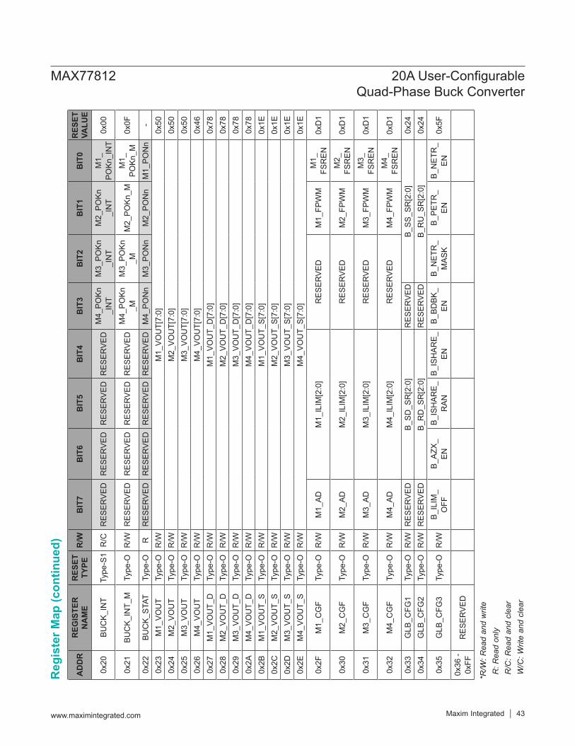
*R/W
: Rea
d an
d w
rite
R: R
ead
only
R/C
: Rea
d an
d cl
ear
W/C
: Writ
e an
d cl
ear
AD
DR
REG
ISTE
R
NA
ME
RES
ET
TYPE
R/W
BIT
7B
IT6
BIT
5B
IT4
BIT
3B
IT2
BIT
1B
IT0
RES
ET
VALU
E
0x20
BUC
K_IN
TTy
pe-S
1R
/CR
ESER
VED
RES
ERVE
DR
ESER
VED
RES
ERVE
DM
4_PO
Kn
_IN
TM
3_PO
Kn
_IN
TM
2_PO
Kn
_IN
TM
1_PO
Kn_I
NT
0x00
0x21
BUC
K_IN
T_M
Type
-OR
/WR
ESER
VED
RES
ERVE
DR
ESER
VED
RES
ERVE
DM
4_PO
Kn
_MM
3_PO
Kn
_MM
2_PO
Kn_M
M1_
PO
Kn_M
0x0F
0x22
BUC
K_ST
ATTy
pe-O
RR
ESER
VED
RES
ERVE
DR
ESER
VED
RES
ERVE
DM
4_PO
Nn
M3_
PON
nM
2_PO
Nn
M1_
PON
n-
0x23
M1_
VOU
TTy
pe-O
R/W
M1_
VOU
T[7:
0]0x
500x
24M
2_VO
UT
Type
-OR
/WM
2_VO
UT[
7:0]
0x50
0x25
M3_
VOU
TTy
pe-O
R/W
M3_
VOU
T[7:
0]0x
500x
26M
4_VO
UT
Type
-OR
/WM
4_VO
UT[
7:0]
0x46
0x27
M1_
VOU
T_D
Type
-OR
/WM
1_VO
UT_
D[7
:0]
0x78
0x28
M2_
VOU
T_D
Type
-OR
/WM
2_VO
UT_
D[7
:0]
0x78
0x29
M3_
VOU
T_D
Type
-OR
/WM
3_VO
UT_
D[7
:0]
0x78
0x2A
M4_
VOU
T_D
Type
-OR
/WM
4_VO
UT_
D[7
:0]
0x78
0x2B
M1_
VOU
T_S
Type
-OR
/WM
1_VO
UT_
S[7:
0]0x
1E0x
2CM
2_VO
UT_
STy
pe-O
R/W
M2_
VOU
T_S[
7:0]
0x1E
0x2D
M3_
VOU
T_S
Type
-OR
/WM
3_VO
UT_
S[7:
0]0x
1E0x
2EM
4_VO
UT_
STy
pe-O
R/W
M4_
VOU
T_S[
7:0]
0x1E
0x2F
M1_
CG
FTy
pe-O
R/W
M1_
ADM
1_IL
IM[2
:0]
RES
ERVE
DM
1_FP
WM
M1_
FS
REN
0xD
1
0x30
M2_
CG
FTy
pe-O
R/W
M2_
ADM
2_IL
IM[2
:0]
RES
ERVE
DM
2_FP
WM
M2_
FS
REN
0xD
1
0x31
M3_
CG
FTy
pe-O
R/W
M3_
ADM
3_IL
IM[2
:0]
RES
ERVE
DM
3_FP
WM
M3_
FS
REN
0xD
1
0x32
M4_
CG
FTy
pe-O
R/W
M4_
ADM
4_IL
IM[2
:0]
RES
ERVE
DM
4_FP
WM
M4_
FS
REN
0xD
1
0x33
GLB
_CFG
1Ty
pe-O
R/W
RES
ERVE
DB_
SD_S
R[2
:0]
RES
ERVE
DB_
SS_S
R[2
:0]
0x24
0x34
GLB
_CFG
2Ty
pe-O
R/W
RES
ERVE
DB_
RD
_SR
[2:0
]R
ESER
VED
B_R
U_S
R[2
:0]
0x24
0x35
GLB
_CFG
3Ty
pe-O
R/W
B_IL
IM_
OFF
B_AZ
X_
ENB_
ISH
ARE_
RAN
B_IS
HAR
E_EN
B_BD
BK_
ENB_
NET
R_
MAS
KB_
PETR
_ EN
B_N
ETR
_EN
0x5F
0x36
- 0x
FFR
ESER
VED
MAX77812 20A User-Configurable Quad-Phase Buck Converter
www.maximintegrated.com Maxim Integrated 43
Reg
iste
r Map
(con
tinue
d)
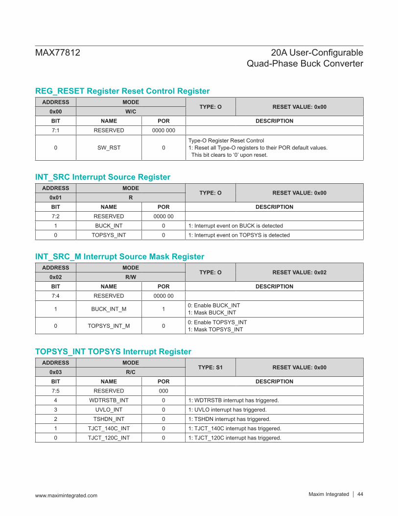
ADDRESS MODETYPE: O RESET VALUE: 0x00
0x00 W/CBIT NAME POR DESCRIPTION7:1 RESERVED 0000 000
0 SW_RST 0Type-O Register Reset Control1: Reset all Type-O registers to their POR default values. This bit clears to ‘0’ upon reset.
ADDRESS MODETYPE: O RESET VALUE: 0x00
0x01 RBIT NAME POR DESCRIPTION7:2 RESERVED 0000 001 BUCK_INT 0 1: Interrupt event on BUCK is detected0 TOPSYS_INT 0 1: Interrupt event on TOPSYS is detected
ADDRESS MODETYPE: O RESET VALUE: 0x02
0x02 R/WBIT NAME POR DESCRIPTION7:4 RESERVED 0000 00
1 BUCK_INT_M 1 0: Enable BUCK_INT1: Mask BUCK_INT
0 TOPSYS_INT_M 0 0: Enable TOPSYS_INT1: Mask TOPSYS_INT
ADDRESS MODETYPE: S1 RESET VALUE: 0x00
0x03 R/CBIT NAME POR DESCRIPTION7:5 RESERVED 0004 WDTRSTB_INT 0 1: WDTRSTB interrupt has triggered.3 UVLO_INT 0 1: UVLO interrupt has triggered.2 TSHDN_INT 0 1: TSHDN interrupt has triggered.1 TJCT_140C_INT 0 1: TJCT_140C interrupt has triggered.0 TJCT_120C_INT 0 1: TJCT_120C interrupt has triggered.
MAX77812 20A User-Configurable Quad-Phase Buck Converter
www.maximintegrated.com Maxim Integrated 44
REG_RESET Register Reset Control Register
INT_SRC Interrupt Source Register
INT_SRC_M Interrupt Source Mask Register
TOPSYS_INT TOPSYS Interrupt Register
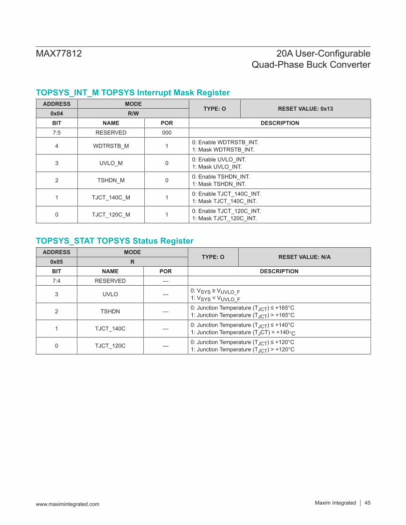
ADDRESS MODETYPE: O RESET VALUE: 0x13
0x04 R/WBIT NAME POR DESCRIPTION7:5 RESERVED 000
4 WDTRSTB_M 1 0: Enable WDTRSTB_INT.1: Mask WDTRSTB_INT.
3 UVLO_M 0 0: Enable UVLO_INT.1: Mask UVLO_INT.
2 TSHDN_M 0 0: Enable TSHDN_INT.1: Mask TSHDN_INT.
1 TJCT_140C_M 1 0: Enable TJCT_140C_INT.1: Mask TJCT_140C_INT.
0 TJCT_120C_M 1 0: Enable TJCT_120C_INT.1: Mask TJCT_120C_INT.
ADDRESS MODETYPE: O RESET VALUE: N/A
0x05 RBIT NAME POR DESCRIPTION7:4 RESERVED —
3 UVLO — 0: VSYS ≥ VUVLO_F1: VSYS < VUVLO_F
2 TSHDN — 0: Junction Temperature (TJCT) ≤ +165°C1: Junction Temperature (TJCT) > +165°C
1 TJCT_140C — 0: Junction Temperature (TJCT) ≤ +140°C1: Junction Temperature (TJCT) > +140°C
0 TJCT_120C — 0: Junction Temperature (TJCT) ≤ +120°C1: Junction Temperature (TJCT) > +120°C
MAX77812 20A User-Configurable Quad-Phase Buck Converter
www.maximintegrated.com Maxim Integrated 45
TOPSYS_INT_M TOPSYS Interrupt Mask Register
TOPSYS_STAT TOPSYS Status Register
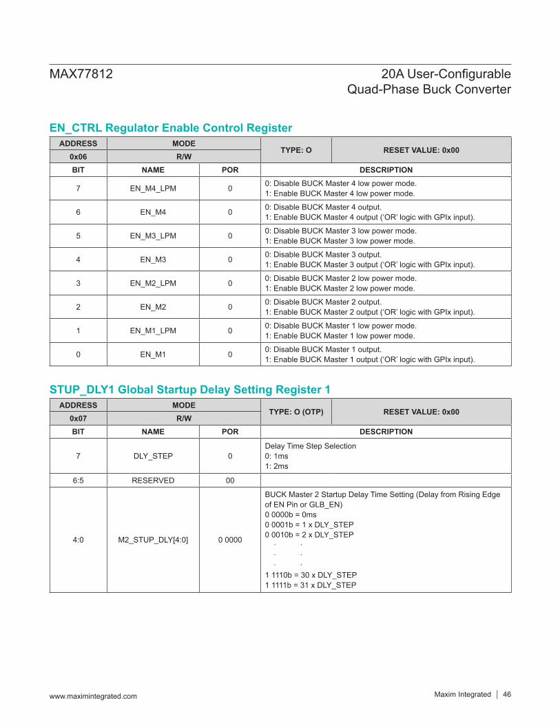
ADDRESS MODETYPE: O RESET VALUE: 0x00
0x06 R/WBIT NAME POR DESCRIPTION
7 EN_M4_LPM 0 0: Disable BUCK Master 4 low power mode.1: Enable BUCK Master 4 low power mode.
6 EN_M4 0 0: Disable BUCK Master 4 output.1: Enable BUCK Master 4 output (‘OR’ logic with GPIx input).
5 EN_M3_LPM 0 0: Disable BUCK Master 3 low power mode.1: Enable BUCK Master 3 low power mode.
4 EN_M3 0 0: Disable BUCK Master 3 output.1: Enable BUCK Master 3 output (‘OR’ logic with GPIx input).
3 EN_M2_LPM 0 0: Disable BUCK Master 2 low power mode.1: Enable BUCK Master 2 low power mode.
2 EN_M2 0 0: Disable BUCK Master 2 output.1: Enable BUCK Master 2 output (‘OR’ logic with GPIx input).
1 EN_M1_LPM 0 0: Disable BUCK Master 1 low power mode.1: Enable BUCK Master 1 low power mode.
0 EN_M1 0 0: Disable BUCK Master 1 output.1: Enable BUCK Master 1 output (‘OR’ logic with GPIx input).
ADDRESS MODETYPE: O (OTP) RESET VALUE: 0x00
0x07 R/WBIT NAME POR DESCRIPTION
7 DLY_STEP 0Delay Time Step Selection0: 1ms1: 2ms
6:5 RESERVED 00
4:0 M2_STUP_DLY[4:0] 0 0000
BUCK Master 2 Startup Delay Time Setting (Delay from Rising Edge of EN Pin or GLB_EN)0 0000b = 0ms0 0001b = 1 x DLY_STEP0 0010b = 2 x DLY_STEP · · · · · ·1 1110b = 30 x DLY_STEP1 1111b = 31 x DLY_STEP
MAX77812 20A User-Configurable Quad-Phase Buck Converter
www.maximintegrated.com Maxim Integrated 46
EN_CTRL Regulator Enable Control Register
STUP_DLY1 Global Startup Delay Setting Register 1
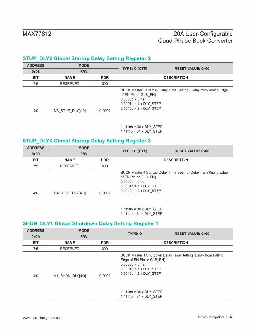
ADDRESS MODETYPE: O (OTP) RESET VALUE: 0x00
0x08 R/WBIT NAME POR DESCRIPTION7:5 RESERVED 000
4:0 M3_STUP_DLY[4:0] 0 0000
BUCK Master 3 Startup Delay Time Setting (Delay from Rising Edge of EN Pin or GLB_EN)0 0000b = 0ms0 0001b = 1 x DLY_STEP0 0010b = 2 x DLY_STEP · · · · · ·1 1110b = 30 x DLY_STEP1 1111b = 31 x DLY_STEP
ADDRESS MODETYPE: O (OTP) RESET VALUE: 0x00
0x09 R/WBIT NAME POR DESCRIPTION7:5 RESERVED 000
4:0 M4_STUP_DLY[4:0] 0 0000
BUCK Master 4 Startup Delay Time Setting (Delay from Rising Edge of EN Pin or GLB_EN)0 0000b = 0ms0 0001b = 1 x DLY_STEP0 0010b = 2 x DLY_STEP · · · · · ·1 1110b = 30 x DLY_STEP1 1111b = 31 x DLY_STEP
ADDRESS MODETYPE: O RESET VALUE: 0x00
0x0A R/WBIT NAME POR DESCRIPTION7:5 RESERVED 000
4:0 M1_SHDN_DLY[4:0] 0 0000
BUCK Master 1 Shutdown Delay Time Setting (Delay from Falling Edge of EN Pin or GLB_EN)0 0000b = 0ms0 0001b = 1 x DLY_STEP0 0010b = 2 x DLY_STEP · · · · · ·1 1110b = 30 x DLY_STEP1 1111b = 31 x DLY_STEP
MAX77812 20A User-Configurable Quad-Phase Buck Converter
www.maximintegrated.com Maxim Integrated 47
STUP_DLY2 Global Startup Delay Setting Register 2
STUP_DLY3 Global Startup Delay Setting Register 3
SHDN_DLY1 Global Shutdown Delay Setting Register 1
ADDRESS MODETYPE: O RESET VALUE: 0x00
0x0B R/WBIT NAME POR DESCRIPTION7:5 RESERVED 000
4:0 M2_SHDN_DLY[4:0] 0 0000
BUCK Master 2 Shutdown Delay Time Setting (Delay from Falling Edge of EN Pin or GLB_EN)0 0000b = 0ms0 0001b = 1 x DLY_STEP0 0010b = 2 x DLY_STEP · · · · · ·1 1110b = 30 x DLY_STEP1 1111b = 31 x DLY_STEP
ADDRESS MODETYPE: O RESET VALUE: 0x00
0x0C R/WBIT NAME POR DESCRIPTION7:5 RESERVED 000
4:0 M3_SHDN_DLY[4:0] 0 0000
BUCK Master 3 Shutdown Delay Time Setting (Delay from Falling Edge of EN Pin or GLB_EN)0 0000b = 0ms0 0001b = 1 x DLY_STEP0 0010b = 2 x DLY_STEP · · · · · ·1 1110b = 30 x DLY_STEP1 1111b = 31 x DLY_STEP
ADDRESS MODETYPE: O RESET VALUE: 0x00
0x0D R/WBIT NAME POR DESCRIPTION7:5 RESERVED 000
4:0 M4_SHDN_DLY[4:0] 0 0000
BUCK Master 4 Shutdown Delay Time Setting (Delay from Falling Edge of EN Pin or GLB_EN)0 0000b = 0ms0 0001b = 1 x DLY_STEP0 0010b = 2 x DLY_STEP · · · · · ·1 1110b = 30 x DLY_STEP1 1111b = 31 x DLY_STEP
MAX77812 20A User-Configurable Quad-Phase Buck Converter
www.maximintegrated.com Maxim Integrated 48
SHDN_DLY2 Global Shutdown Delay Setting Register 2
SHDN_DLY3 Global Shutdown Delay Setting Register 3
SHDN_DLY4 Global Shutdown Delay Setting Register 4
ADDRESS MODETYPE: O RESET VALUE: 0x02
0x0E R/WBIT NAME POR DESCRIPTION7:3 RESERVED 0000 0
2:0 WDT_DEB[2:0] 010
WDTRSTB_IN Debounce Time Setting000b = 0ms001b = 0.8ms010b = 1.6ms011b = 3.2ms100b = 6.4ms101b = 12.8ms111b = 51.2ms
ADDRESS MODETYPE: O RESET VALUE: 0x43
0x0F R/WBIT NAME POR DESCRIPTION
7:4 GPI1_FUNC[3:0] 0100
GPI1 Function Selection0000b: GLB_EN 1000b: M3_VSEL0001b: M1_EN 1001b: M4_VSEL0010b: M2_EN 1010b: GLB_LPM0011b: M3_EN 1011b: M1_LPM0100b: M4_EN 1100b: M2_LPM0101b: GLB_VSEL 1101b: M3_LPM0110b: M1_VSEL 1110b: M4_LPM0111b: M2_VSEL 1111b: No Function
3:0 GPI0_FUNC[3:0] 0011
GPI0 Function Selection0000b: GLB_EN 1000b: M3_VSEL0001b: M1_EN 1001b: M4_VSEL0010b: M2_EN 1010b: GLB_LPM0011b: M3_EN 1011b: M1_LPM0100b: M4_EN 1100b: M2_LPM0101b: GLB_VSEL 1101b: M3_LPM0110b: M1_VSEL 1110b: M4_LPM0111b: M2_VSEL 1111b: No Function
MAX77812 20A User-Configurable Quad-Phase Buck Converter
www.maximintegrated.com Maxim Integrated 49
WDTRSTB_DEB WDTRSTB_IN Input Debounce Time Setting Register
GPI_FUNC GPI Function Selection Register
ADDRESS MODETYPE: O RESET VALUE: 0x11
0x10 R/WBIT NAME POR DESCRIPTION
7:4 LPM_DEB[3:0] 0001
LPM Debounce Time Setting0000b = 0µs 1000b = 512µs0001b = 64µs 1001b = 576µs0010b = 128µs 1010b = 640µs0011b = 192µs 1011b = 704µs0100b = 256µs 1100b = 768µs0101b = 320µs 1101b = 832µs0110b = 384µs 1110b = 896µs0111b = 448µs 1111b = 960µs
3:0 EN_DEB[3:0] 0001
EN Debounce Time Setting0000b = 0µs 1000b = 512µs0001b = 64µs 1001b = 576µs0010b = 128µs 1010b = 640µs0011b = 192µs 1011b = 704µs0100b = 256µs 1100b = 768µs0101b = 320µs 1101b = 832µs0110b = 384µs 1110b = 896µs0111b = 448µs 1111b = 960µs
ADDRESS MODETYPE: O RESET VALUE: 0x11
0x11 R/WBIT NAME POR DESCRIPTION
7:4 GPI1_DEB[3:0] 0001
GPI1 Debounce Time Setting0000b = 0µs 1000b = 512µs0001b = 64µs 1001b = 576µs0010b = 128µs 1010b = 640µs0011b = 192µs 1011b = 704µs0100b = 256µs 1100b = 768µs0101b = 320µs 1101b = 832µs0110b = 384µs 1110b = 896µs0111b = 448µs 1111b = 960µs
3:0 GPI0_DEB[3:0] 0001
GPI0 Debounce Time Setting0000b = 0µs 1000b = 512µs0001b = 64µs 1001b = 576µs0010b = 128µs 1010b = 640µs0011b = 192µs 1011b = 704µs0100b = 256µs 1100b = 768µs0101b = 320µs 1101b = 832µs0110b = 384µs 1110b = 896µs0111b = 448µs 1111b = 960µs
MAX77812 20A User-Configurable Quad-Phase Buck Converter
www.maximintegrated.com Maxim Integrated 50
GPI_DEB1 GPI Debounce Time Setting Register 1
GPI_DEB2 GPI Debounce Time Setting Register 2
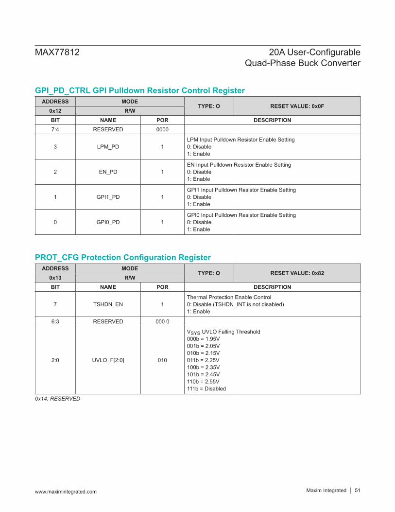
0x14: RESERVED
ADDRESS MODETYPE: O RESET VALUE: 0x0F
0x12 R/WBIT NAME POR DESCRIPTION7:4 RESERVED 0000
3 LPM_PD 1LPM Input Pulldown Resistor Enable Setting0: Disable1: Enable
2 EN_PD 1EN Input Pulldown Resistor Enable Setting0: Disable1: Enable
1 GPI1_PD 1GPI1 Input Pulldown Resistor Enable Setting0: Disable1: Enable
0 GPI0_PD 1GPI0 Input Pulldown Resistor Enable Setting0: Disable1: Enable
ADDRESS MODETYPE: O RESET VALUE: 0x82
0x13 R/WBIT NAME POR DESCRIPTION
7 TSHDN_EN 1Thermal Protection Enable Control0: Disable (TSHDN_INT is not disabled)1: Enable
6:3 RESERVED 000 0
2:0 UVLO_F[2:0] 010
VSYS UVLO Falling Threshold000b = 1.95V001b = 2.05V010b = 2.15V011b = 2.25V100b = 2.35V101b = 2.45V110b = 2.55V111b = Disabled
MAX77812 20A User-Configurable Quad-Phase Buck Converter
www.maximintegrated.com Maxim Integrated 51
GPI_PD_CTRL GPI Pulldown Resistor Control Register
PROT_CFG Protection Configuration Register
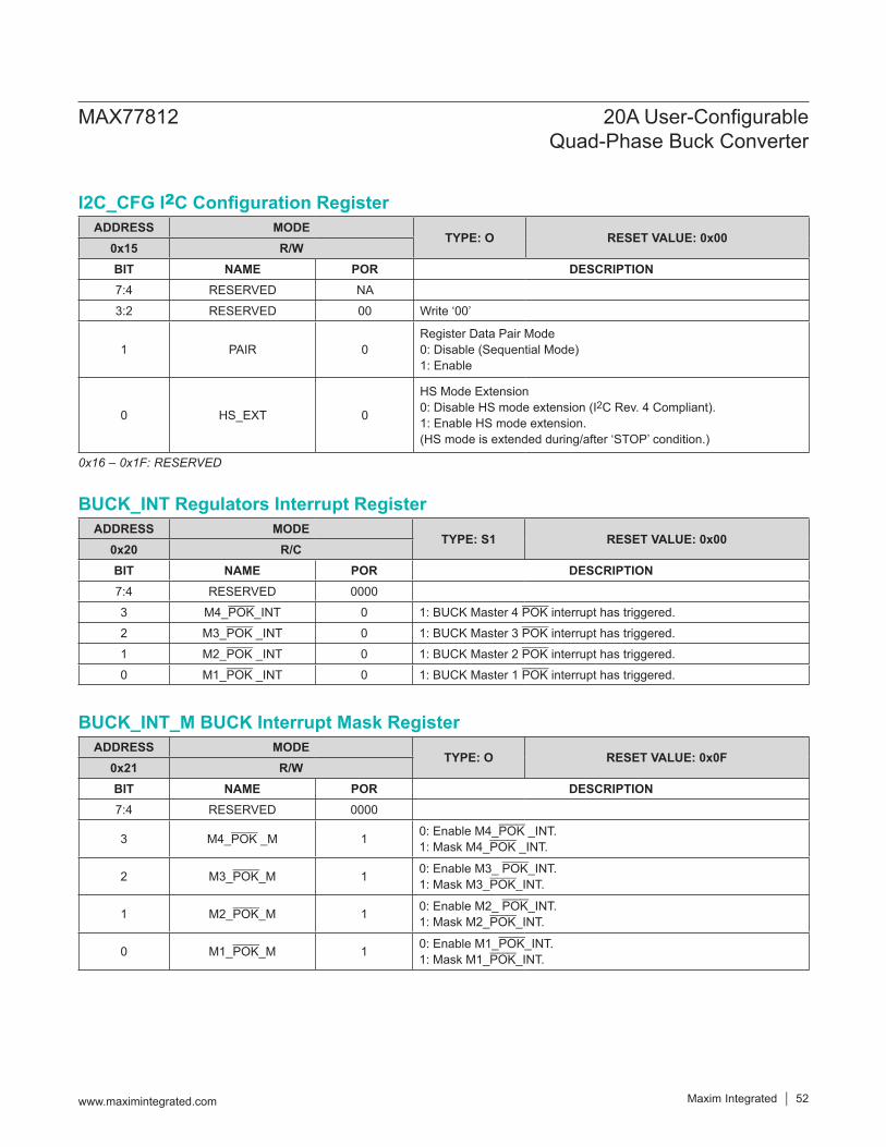
0x16 – 0x1F: RESERVED
ADDRESS MODETYPE: O RESET VALUE: 0x00
0x15 R/WBIT NAME POR DESCRIPTION7:4 RESERVED NA3:2 RESERVED 00 Write ‘00’
1 PAIR 0Register Data Pair Mode0: Disable (Sequential Mode)1: Enable
0 HS_EXT 0
HS Mode Extension0: Disable HS mode extension (I2C Rev. 4 Compliant).1: Enable HS mode extension.(HS mode is extended during/after ‘STOP’ condition.)
ADDRESS MODETYPE: S1 RESET VALUE: 0x00
0x20 R/CBIT NAME POR DESCRIPTION7:4 RESERVED 00003 M4_POK_INT 0 1: BUCK Master 4 POK interrupt has triggered.2 M3_POK _INT 0 1: BUCK Master 3 POK interrupt has triggered.1 M2_POK _INT 0 1: BUCK Master 2 POK interrupt has triggered.0 M1_POK _INT 0 1: BUCK Master 1 POK interrupt has triggered.
ADDRESS MODETYPE: O RESET VALUE: 0x0F
0x21 R/WBIT NAME POR DESCRIPTION7:4 RESERVED 0000
3 M4_POK _M 1 0: Enable M4_POK _INT.1: Mask M4_POK _INT.
2 M3_POK_M 1 0: Enable M3_ POK_INT.1: Mask M3_POK_INT.
1 M2_POK_M 1 0: Enable M2_ POK_INT.1: Mask M2_POK_INT.
0 M1_POK_M 1 0: Enable M1_POK_INT.1: Mask M1_POK_INT.
MAX77812 20A User-Configurable Quad-Phase Buck Converter
www.maximintegrated.com Maxim Integrated 52
I2C_CFG I2C Configuration Register
BUCK_INT Regulators Interrupt Register
BUCK_INT_M BUCK Interrupt Mask Register
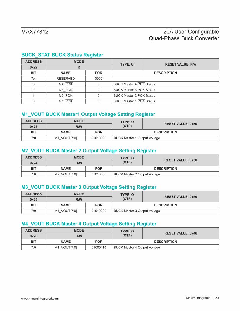
ADDRESS MODETYPE: O RESET VALUE: N/A
0x22 RBIT NAME POR DESCRIPTION7:4 RESERVED 00003 M4_POK 0 BUCK Master 4 POK Status2 M3_POK 0 BUCK Master 3 POK Status1 M2_POK 0 BUCK Master 2 POK Status0 M1_POK 0 BUCK Master 1 POK Status
ADDRESS MODE TYPE: O(OTP) RESET VALUE: 0x50
0x23 R/WBIT NAME POR DESCRIPTION7:0 M1_VOUT[7:0] 01010000 BUCK Master 1 Output Voltage
ADDRESS MODE TYPE: O(OTP) RESET VALUE: 0x50
0x24 R/WBIT NAME POR DESCRIPTION7:0 M2_VOUT[7:0] 01010000 BUCK Master 2 Output Voltage
ADDRESS MODE TYPE: O(OTP) RESET VALUE: 0x50
0x25 R/WBIT NAME POR DESCRIPTION7:0 M3_VOUT[7:0] 01010000 BUCK Master 3 Output Voltage
ADDRESS MODE TYPE: O(OTP) RESET VALUE: 0x46
0x26 R/WBIT NAME POR DESCRIPTION7:0 M4_VOUT[7:0] 01000110 BUCK Master 4 Output Voltage
MAX77812 20A User-Configurable Quad-Phase Buck Converter
www.maximintegrated.com Maxim Integrated 53
BUCK_STAT BUCK Status Register
M1_VOUT BUCK Master1 Output Voltage Setting Register
M2_VOUT BUCK Master 2 Output Voltage Setting Register
M3_VOUT BUCK Master 3 Output Voltage Setting Register
M4_VOUT BUCK Master 4 Output Voltage Setting Register
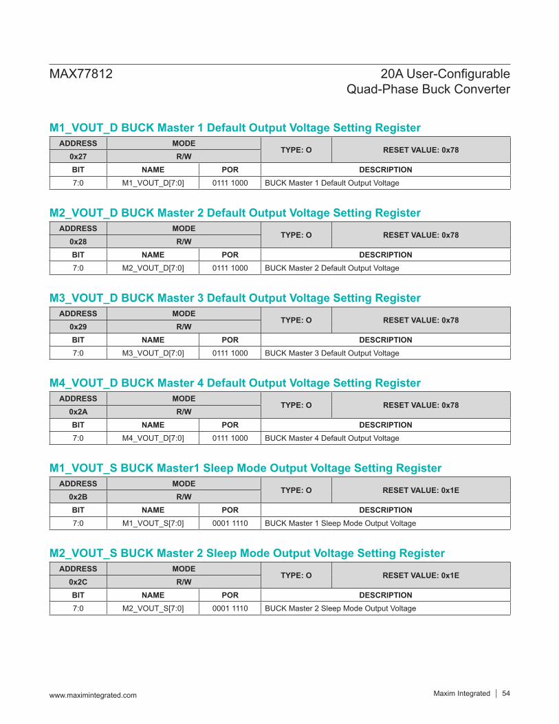
ADDRESS MODETYPE: O RESET VALUE: 0x78
0x27 R/WBIT NAME POR DESCRIPTION7:0 M1_VOUT_D[7:0] 0111 1000 BUCK Master 1 Default Output Voltage
ADDRESS MODETYPE: O RESET VALUE: 0x78
0x28 R/WBIT NAME POR DESCRIPTION7:0 M2_VOUT_D[7:0] 0111 1000 BUCK Master 2 Default Output Voltage
ADDRESS MODETYPE: O RESET VALUE: 0x78
0x29 R/WBIT NAME POR DESCRIPTION7:0 M3_VOUT_D[7:0] 0111 1000 BUCK Master 3 Default Output Voltage
ADDRESS MODETYPE: O RESET VALUE: 0x78
0x2A R/WBIT NAME POR DESCRIPTION7:0 M4_VOUT_D[7:0] 0111 1000 BUCK Master 4 Default Output Voltage
ADDRESS MODETYPE: O RESET VALUE: 0x1E
0x2B R/WBIT NAME POR DESCRIPTION7:0 M1_VOUT_S[7:0] 0001 1110 BUCK Master 1 Sleep Mode Output Voltage
ADDRESS MODETYPE: O RESET VALUE: 0x1E
0x2C R/WBIT NAME POR DESCRIPTION7:0 M2_VOUT_S[7:0] 0001 1110 BUCK Master 2 Sleep Mode Output Voltage
MAX77812 20A User-Configurable Quad-Phase Buck Converter
www.maximintegrated.com Maxim Integrated 54
M1_VOUT_D BUCK Master 1 Default Output Voltage Setting Register
M2_VOUT_D BUCK Master 2 Default Output Voltage Setting Register
M3_VOUT_D BUCK Master 3 Default Output Voltage Setting Register
M4_VOUT_D BUCK Master 4 Default Output Voltage Setting Register
M1_VOUT_S BUCK Master1 Sleep Mode Output Voltage Setting Register
M2_VOUT_S BUCK Master 2 Sleep Mode Output Voltage Setting Register
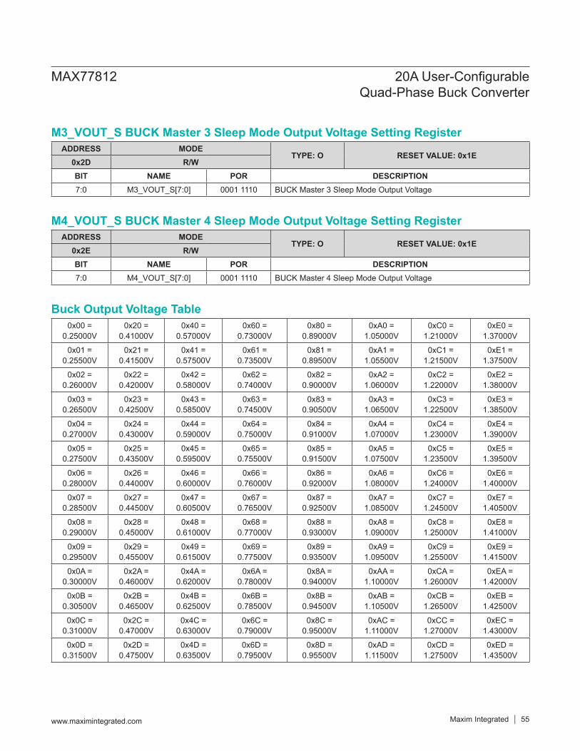
ADDRESS MODETYPE: O RESET VALUE: 0x1E
0x2D R/WBIT NAME POR DESCRIPTION7:0 M3_VOUT_S[7:0] 0001 1110 BUCK Master 3 Sleep Mode Output Voltage
ADDRESS MODETYPE: O RESET VALUE: 0x1E
0x2E R/WBIT NAME POR DESCRIPTION7:0 M4_VOUT_S[7:0] 0001 1110 BUCK Master 4 Sleep Mode Output Voltage
0x00 = 0.25000V
0x20 = 0.41000V
0x40 = 0.57000V
0x60 = 0.73000V
0x80 = 0.89000V
0xA0 = 1.05000V
0xC0 = 1.21000V
0xE0 = 1.37000V
0x01 = 0.25500V
0x21 = 0.41500V
0x41 = 0.57500V
0x61 = 0.73500V
0x81 = 0.89500V
0xA1 = 1.05500V
0xC1 = 1.21500V
0xE1 = 1.37500V
0x02 = 0.26000V
0x22 = 0.42000V
0x42 = 0.58000V
0x62 = 0.74000V
0x82 = 0.90000V
0xA2 = 1.06000V
0xC2 = 1.22000V
0xE2 = 1.38000V
0x03 = 0.26500V
0x23 = 0.42500V
0x43 = 0.58500V
0x63 = 0.74500V
0x83 = 0.90500V
0xA3 = 1.06500V
0xC3 = 1.22500V
0xE3 = 1.38500V
0x04 = 0.27000V
0x24 = 0.43000V
0x44 = 0.59000V
0x64 = 0.75000V
0x84 = 0.91000V
0xA4 = 1.07000V
0xC4 = 1.23000V
0xE4 = 1.39000V
0x05 = 0.27500V
0x25 = 0.43500V
0x45 = 0.59500V
0x65 = 0.75500V
0x85 = 0.91500V
0xA5 = 1.07500V
0xC5 = 1.23500V
0xE5 = 1.39500V
0x06 = 0.28000V
0x26 = 0.44000V
0x46 = 0.60000V
0x66 = 0.76000V
0x86 = 0.92000V
0xA6 = 1.08000V
0xC6 = 1.24000V
0xE6 = 1.40000V
0x07 = 0.28500V
0x27 = 0.44500V
0x47 = 0.60500V
0x67 = 0.76500V
0x87 = 0.92500V
0xA7 = 1.08500V
0xC7 = 1.24500V
0xE7 = 1.40500V
0x08 = 0.29000V
0x28 = 0.45000V
0x48 = 0.61000V
0x68 = 0.77000V
0x88 = 0.93000V
0xA8 = 1.09000V
0xC8 = 1.25000V
0xE8 = 1.41000V
0x09 = 0.29500V
0x29 = 0.45500V
0x49 = 0.61500V
0x69 = 0.77500V
0x89 = 0.93500V
0xA9 = 1.09500V
0xC9 = 1.25500V
0xE9 = 1.41500V
0x0A = 0.30000V
0x2A = 0.46000V
0x4A = 0.62000V
0x6A = 0.78000V
0x8A = 0.94000V
0xAA = 1.10000V
0xCA = 1.26000V
0xEA = 1.42000V
0x0B = 0.30500V
0x2B = 0.46500V
0x4B = 0.62500V
0x6B = 0.78500V
0x8B = 0.94500V
0xAB = 1.10500V
0xCB = 1.26500V
0xEB = 1.42500V
0x0C = 0.31000V
0x2C = 0.47000V
0x4C = 0.63000V
0x6C = 0.79000V
0x8C = 0.95000V
0xAC = 1.11000V
0xCC = 1.27000V
0xEC = 1.43000V
0x0D = 0.31500V
0x2D = 0.47500V
0x4D = 0.63500V
0x6D = 0.79500V
0x8D = 0.95500V
0xAD = 1.11500V
0xCD = 1.27500V
0xED = 1.43500V
MAX77812 20A User-Configurable Quad-Phase Buck Converter
www.maximintegrated.com Maxim Integrated 55
M3_VOUT_S BUCK Master 3 Sleep Mode Output Voltage Setting Register
M4_VOUT_S BUCK Master 4 Sleep Mode Output Voltage Setting Register
Buck Output Voltage Table
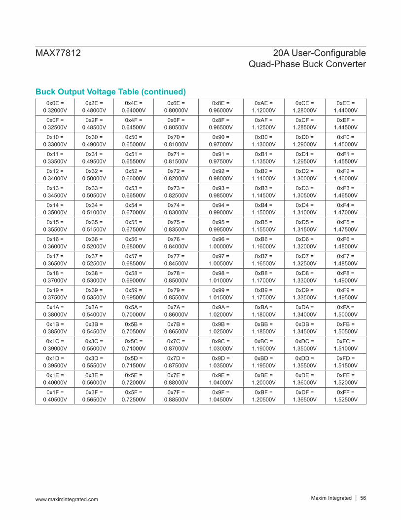
0x0E = 0.32000V
0x2E = 0.48000V
0x4E = 0.64000V
0x6E = 0.80000V
0x8E = 0.96000V
0xAE = 1.12000V
0xCE = 1.28000V
0xEE = 1.44000V
0x0F = 0.32500V
0x2F = 0.48500V
0x4F = 0.64500V
0x6F = 0.80500V
0x8F = 0.96500V
0xAF = 1.12500V
0xCF = 1.28500V
0xEF = 1.44500V
0x10 = 0.33000V
0x30 = 0.49000V
0x50 = 0.65000V
0x70 = 0.81000V
0x90 = 0.97000V
0xB0 = 1.13000V
0xD0 = 1.29000V
0xF0 = 1.45000V
0x11 = 0.33500V
0x31 = 0.49500V
0x51 = 0.65500V
0x71 = 0.81500V
0x91 = 0.97500V
0xB1 = 1.13500V
0xD1 = 1.29500V
0xF1 = 1.45500V
0x12 = 0.34000V
0x32 = 0.50000V
0x52 = 0.66000V
0x72 = 0.82000V
0x92 = 0.98000V
0xB2 = 1.14000V
0xD2 = 1.30000V
0xF2 = 1.46000V
0x13 = 0.34500V
0x33 = 0.50500V
0x53 = 0.66500V
0x73 = 0.82500V
0x93 = 0.98500V
0xB3 = 1.14500V
0xD3 = 1.30500V
0xF3 = 1.46500V
0x14 = 0.35000V
0x34 = 0.51000V
0x54 = 0.67000V
0x74 = 0.83000V
0x94 = 0.99000V
0xB4 = 1.15000V
0xD4 = 1.31000V
0xF4 = 1.47000V
0x15 = 0.35500V
0x35 = 0.51500V
0x55 = 0.67500V
0x75 = 0.83500V
0x95 = 0.99500V
0xB5 = 1.15500V
0xD5 = 1.31500V
0xF5 = 1.47500V
0x16 = 0.36000V
0x36 = 0.52000V
0x56 = 0.68000V
0x76 = 0.84000V
0x96 = 1.00000V
0xB6 = 1.16000V
0xD6 = 1.32000V
0xF6 = 1.48000V
0x17 = 0.36500V
0x37 = 0.52500V
0x57 = 0.68500V
0x77 = 0.84500V
0x97 = 1.00500V
0xB7 = 1.16500V
0xD7 = 1.32500V
0xF7 = 1.48500V
0x18 = 0.37000V
0x38 = 0.53000V
0x58 = 0.69000V
0x78 = 0.85000V
0x98 = 1.01000V
0xB8 = 1.17000V
0xD8 = 1.33000V
0xF8 = 1.49000V
0x19 = 0.37500V
0x39 = 0.53500V
0x59 = 0.69500V
0x79 = 0.85500V
0x99 = 1.01500V
0xB9 = 1.17500V
0xD9 = 1.33500V
0xF9 = 1.49500V
0x1A = 0.38000V
0x3A = 0.54000V
0x5A = 0.70000V
0x7A = 0.86000V
0x9A = 1.02000V
0xBA = 1.18000V
0xDA = 1.34000V
0xFA = 1.50000V
0x1B = 0.38500V
0x3B = 0.54500V
0x5B = 0.70500V
0x7B = 0.86500V
0x9B = 1.02500V
0xBB = 1.18500V
0xDB = 1.34500V
0xFB = 1.50500V
0x1C = 0.39000V
0x3C = 0.55000V
0x5C = 0.71000V
0x7C = 0.87000V
0x9C = 1.03000V
0xBC = 1.19000V
0xDC = 1.35000V
0xFC = 1.51000V
0x1D = 0.39500V
0x3D = 0.55500V
0x5D = 0.71500V
0x7D = 0.87500V
0x9D = 1.03500V
0xBD = 1.19500V
0xDD = 1.35500V
0xFD = 1.51500V
0x1E = 0.40000V
0x3E = 0.56000V
0x5E = 0.72000V
0x7E = 0.88000V
0x9E = 1.04000V
0xBE = 1.20000V
0xDE = 1.36000V
0xFE = 1.52000V
0x1F = 0.40500V
0x3F = 0.56500V
0x5F = 0.72500V
0x7F = 0.88500V
0x9F = 1.04500V
0xBF = 1.20500V
0xDF = 1.36500V
0xFF = 1.52500V
MAX77812 20A User-Configurable Quad-Phase Buck Converter
www.maximintegrated.com Maxim Integrated 56
Buck Output Voltage Table (continued)

ADDRESS MODETYPE: O RESET VALUE: 0xD1
0x2F R/WBIT NAME POR DESCRIPTION
7 M1_AD 1BUCK Master 1 Output Active Discharge0: Disable1: Enable
6:4 M1_ILIM[2:0] 101
BUCK Master 1 PMOS Peak/NMOS Valley Current Limit Setting000b: 3.0A/2.0A001b: 3.6A/2.4A010b: 4.2A/2.8A011b: 4.8A/3.2A100b: 5.4A/3.6A101b: 6.0A/4.0A110b: 6.6A/4.4A111b: 7.2A/4.8A
2:3 RESERVED 00 Write ‘00’
1 M1_FPWM 0
BUCK Master 1 Forced PWM0: Turn off Forced PWM(Automatic skip mode operation under light load)1: Turn on Forced PWM mode
0 M1_FSREN 1
BUCK Master 1 Falling Slew Rate Control0: DisableBUCK Master 1 operates in skip mode during the output voltage ramp-down (only if M1_FPWM = 0). In skip mode, negative current through the low-side FET is not allowed so that the output voltage falling slew rate is a function of the output capacitance and the external load under light load condition. If the load is heavy, the output voltage falling slew rate is limited to the ramp-down slew rate set by B_RD_SR[1:0]. Note that the internal feedback string always imposes a 2µA load on the output.1: EnableBUCK Master 1 operates in Forced PWM mode during the output voltage ramp-down. In Forced PWM mode, BUCK Master 1 can sink current from the output capacitor to ensure that the output voltage decreases at the ramp-down slew rate set by B_RD_SR[1:0]. To ensure a smooth output voltage ramp-down, Forced PMW mode remains engaged for 50µs after the output voltage decreases to its target voltage.
MAX77812 20A User-Configurable Quad-Phase Buck Converter
www.maximintegrated.com Maxim Integrated 57
M1_CFG BUCK Master 1 Configuration Register
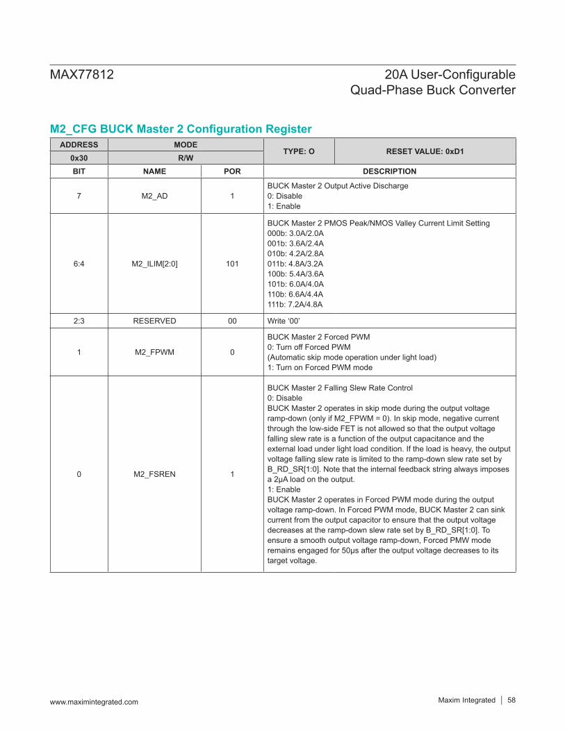
ADDRESS MODETYPE: O RESET VALUE: 0xD1
0x30 R/WBIT NAME POR DESCRIPTION
7 M2_AD 1BUCK Master 2 Output Active Discharge0: Disable1: Enable
6:4 M2_ILIM[2:0] 101
BUCK Master 2 PMOS Peak/NMOS Valley Current Limit Setting000b: 3.0A/2.0A001b: 3.6A/2.4A010b: 4.2A/2.8A011b: 4.8A/3.2A100b: 5.4A/3.6A101b: 6.0A/4.0A110b: 6.6A/4.4A111b: 7.2A/4.8A
2:3 RESERVED 00 Write ‘00’
1 M2_FPWM 0
BUCK Master 2 Forced PWM0: Turn off Forced PWM(Automatic skip mode operation under light load)1: Turn on Forced PWM mode
0 M2_FSREN 1
BUCK Master 2 Falling Slew Rate Control0: DisableBUCK Master 2 operates in skip mode during the output voltage ramp-down (only if M2_FPWM = 0). In skip mode, negative current through the low-side FET is not allowed so that the output voltage falling slew rate is a function of the output capacitance and the external load under light load condition. If the load is heavy, the output voltage falling slew rate is limited to the ramp-down slew rate set by B_RD_SR[1:0]. Note that the internal feedback string always imposes a 2µA load on the output.1: EnableBUCK Master 2 operates in Forced PWM mode during the output voltage ramp-down. In Forced PWM mode, BUCK Master 2 can sink current from the output capacitor to ensure that the output voltage decreases at the ramp-down slew rate set by B_RD_SR[1:0]. To ensure a smooth output voltage ramp-down, Forced PMW mode remains engaged for 50µs after the output voltage decreases to its target voltage.
MAX77812 20A User-Configurable Quad-Phase Buck Converter
www.maximintegrated.com Maxim Integrated 58
M2_CFG BUCK Master 2 Configuration Register
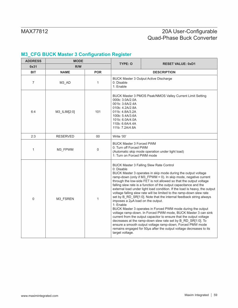
ADDRESS MODETYPE: O RESET VALUE: 0xD1
0x31 R/WBIT NAME POR DESCRIPTION
7 M3_AD 1BUCK Master 3 Output Active Discharge0: Disable1: Enable
6:4 M3_ILIM[2:0] 101
BUCK Master 3 PMOS Peak/NMOS Valley Current Limit Setting000b: 3.0A/2.0A001b: 3.6A/2.4A010b: 4.2A/2.8A011b: 4.8A/3.2A100b: 5.4A/3.6A101b: 6.0A/4.0A110b: 6.6A/4.4A111b: 7.2A/4.8A
2:3 RESERVED 00 Write ‘00’
1 M3_FPWM 0
BUCK Master 3 Forced PWM0: Turn off Forced PWM(Automatic skip mode operation under light load)1: Turn on Forced PWM mode
0 M3_FSREN 1
BUCK Master 3 Falling Slew Rate Control0: DisableBUCK Master 3 operates in skip mode during the output voltage ramp-down (only if M3_FPWM = 0). In skip mode, negative current through the low-side FET is not allowed so that the output voltage falling slew rate is a function of the output capacitance and the external load under light load condition. If the load is heavy, the output voltage falling slew rate will be limited to the ramp-down slew rate set by B_RD_SR[1:0]. Note that the internal feedback string always imposes a 2µA load on the output.1: EnableBUCK Master 3 operates in Forced PWM mode during the output voltage ramp-down. In Forced PWM mode, BUCK Master 3 can sink current from the output capacitor to ensure that the output voltage decreases at the ramp-down slew rate set by B_RD_SR[1:0]. To ensure a smooth output voltage ramp-down, Forced PMW mode remains engaged for 50µs after the output voltage decreases to its target voltage.
MAX77812 20A User-Configurable Quad-Phase Buck Converter
www.maximintegrated.com Maxim Integrated 59
M3_CFG BUCK Master 3 Configuration Register
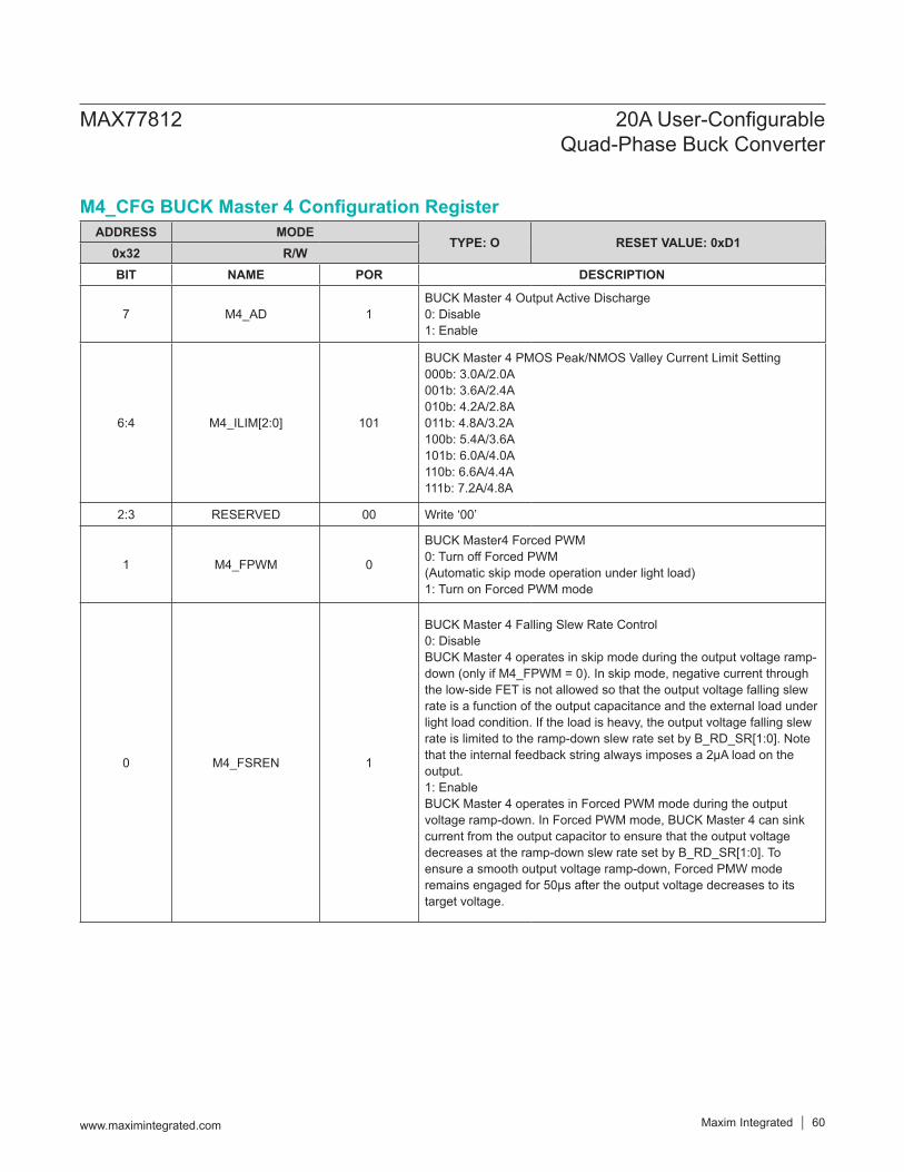
ADDRESS MODETYPE: O RESET VALUE: 0xD1
0x32 R/WBIT NAME POR DESCRIPTION
7 M4_AD 1BUCK Master 4 Output Active Discharge0: Disable1: Enable
6:4 M4_ILIM[2:0] 101
BUCK Master 4 PMOS Peak/NMOS Valley Current Limit Setting000b: 3.0A/2.0A001b: 3.6A/2.4A010b: 4.2A/2.8A011b: 4.8A/3.2A100b: 5.4A/3.6A101b: 6.0A/4.0A110b: 6.6A/4.4A111b: 7.2A/4.8A
2:3 RESERVED 00 Write ‘00’
1 M4_FPWM 0
BUCK Master4 Forced PWM0: Turn off Forced PWM(Automatic skip mode operation under light load)1: Turn on Forced PWM mode
0 M4_FSREN 1
BUCK Master 4 Falling Slew Rate Control0: DisableBUCK Master 4 operates in skip mode during the output voltage ramp-down (only if M4_FPWM = 0). In skip mode, negative current through the low-side FET is not allowed so that the output voltage falling slew rate is a function of the output capacitance and the external load under light load condition. If the load is heavy, the output voltage falling slew rate is limited to the ramp-down slew rate set by B_RD_SR[1:0]. Note that the internal feedback string always imposes a 2µA load on the output.1: EnableBUCK Master 4 operates in Forced PWM mode during the output voltage ramp-down. In Forced PWM mode, BUCK Master 4 can sink current from the output capacitor to ensure that the output voltage decreases at the ramp-down slew rate set by B_RD_SR[1:0]. To ensure a smooth output voltage ramp-down, Forced PMW mode remains engaged for 50µs after the output voltage decreases to its target voltage.
MAX77812 20A User-Configurable Quad-Phase Buck Converter
www.maximintegrated.com Maxim Integrated 60
M4_CFG BUCK Master 4 Configuration Register
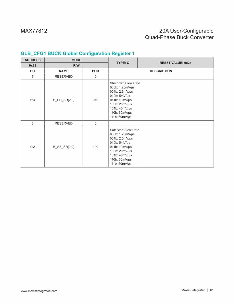
ADDRESS MODETYPE: O RESET VALUE: 0x24
0x33 R/WBIT NAME POR DESCRIPTION7 RESERVED 0
6:4 B_SD_SR[2:0] 010
Shutdown Slew Rate000b: 1.25mV/µs001b: 2.5mV/µs010b: 5mV/µs011b: 10mV/µs100b: 20mV/µs101b: 40mV/µs110b: 60mV/µs111b: 60mV/µs
3 RESERVED 0
0:2 B_SS_SR[2:0] 100
Soft Start Slew Rate000b: 1.25mV/µs001b: 2.5mV/µs010b: 5mV/µs011b: 10mV/µs100b: 20mV/µs101b: 40mV/µs110b: 60mV/µs111b: 60mV/µs
MAX77812 20A User-Configurable Quad-Phase Buck Converter
www.maximintegrated.com Maxim Integrated 61
GLB_CFG1 BUCK Global Configuration Register 1

ADDRESS MODETYPE: O RESET VALUE: 0x24
0x34 R/WBIT NAME POR DESCRIPTION7 RESERVED 0
6:4 B_RD_SR[2:0] 010
Ramp-Down Slew Rate000b: 1.25mV/µs001b: 2.5mV/µs010b: 5mV/µs011b: 10mV/µs100b: 20mV/µs101b: 40mV/µs110b: 60mV/µs111b: 60mV/µs
3 RESERVED 0
0:2 B_RU_SR[2:0] 100
Ramp-Up Slew Rate000b: 1.25mV/µs001b: 2.5mV/µs010b: 5mV/µs011b: 10mV/µs100b: 20mV/µs101b: 40mV/µs110b: 60mV/µs111b: 60mV/µs
MAX77812 20A User-Configurable Quad-Phase Buck Converter
www.maximintegrated.com Maxim Integrated 62
GLB_CFG2 BUCK Global Configuration Register 2
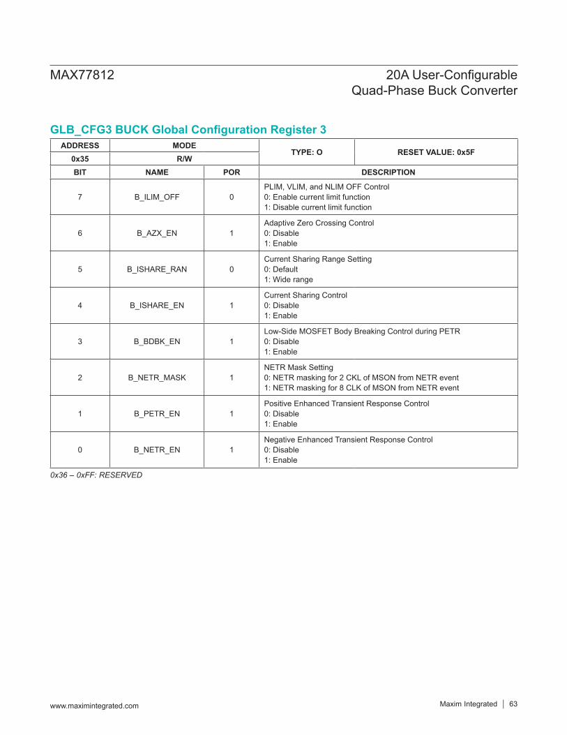
0x36 – 0xFF: RESERVED
ADDRESS MODE TYPE: O RESET VALUE: 0x5F
0x35 R/WBIT NAME POR DESCRIPTION
7 B_ILIM_OFF 0PLIM, VLIM, and NLIM OFF Control 0: Enable current limit function 1: Disable current limit function
6 B_AZX_EN 1Adaptive Zero Crossing Control 0: Disable1: Enable
5 B_ISHARE_RAN 0Current Sharing Range Setting 0: Default 1: Wide range
4 B_ISHARE_EN 1Current Sharing Control 0: Disable 1: Enable
3 B_BDBK_EN 1Low-Side MOSFET Body Breaking Control during PETR 0: Disable 1: Enable
2 B_NETR_MASK 1NETR Mask Setting 0: NETR masking for 2 CKL of MSON from NETR event 1: NETR masking for 8 CLK of MSON from NETR event
1 B_PETR_EN 1Positive Enhanced Transient Response Control 0: Disable 1: Enable
0 B_NETR_EN 1Negative Enhanced Transient Response Control 0: Disable 1: Enable
MAX77812 20A User-Configurable Quad-Phase Buck Converter
www.maximintegrated.com Maxim Integrated 63
GLB_CFG3 BUCK Global Configuration Register 3
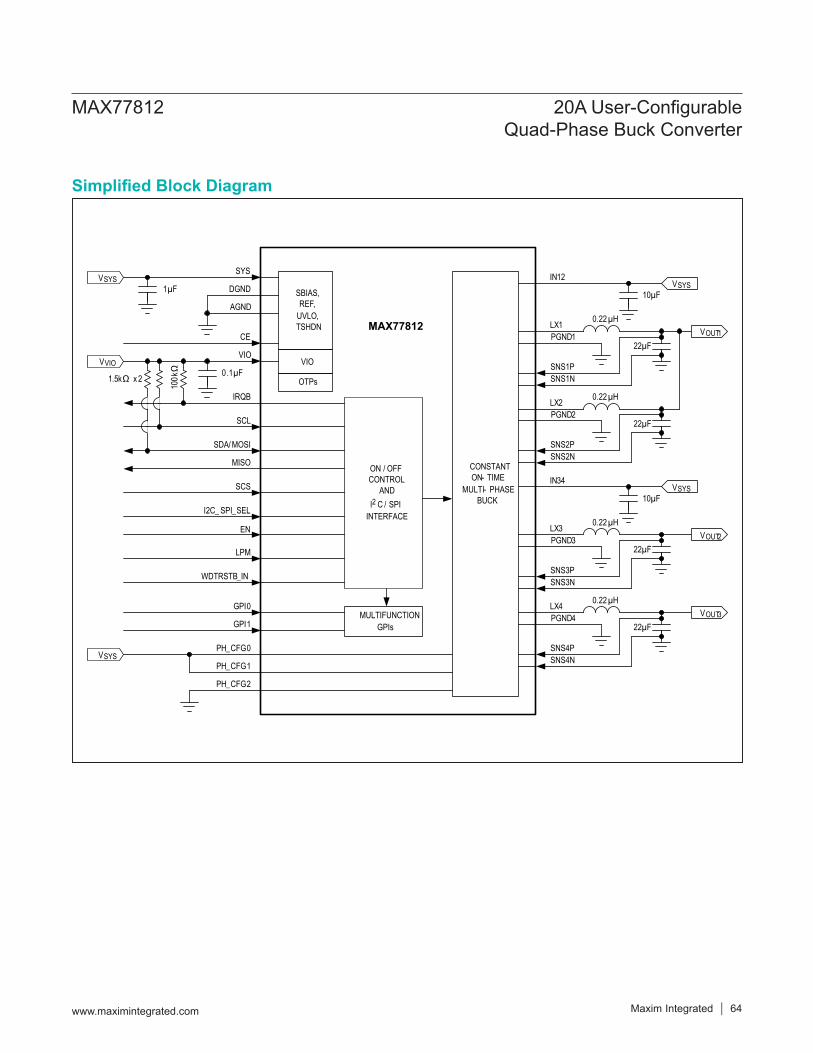
SYS
ON / OFFCONTROL
AND I2 C / SPI
INTERFACE
VIOVIO
IRQB
SCL
MISO
MAX77812
AGND
CE
VSYSDGND
OTPs
GPI0
SDA/ MOSI
SCS
EN
WDTRSTB_IN
LPM
1.5kΩ x 2
1µF
VVIO0.1µF
I2C_ SPI_SEL
100k
Ω
GPI1MULTIFUNCTION
GPIs
PH_CFG0
PH_CFG1
PH_CFG2
VSYS
SBIAS,REF,
UVLO,TSHDN
CONSTANT ON- TIME
MULTI- PHASE BUCK
VSYS
0.22µH
IN12
LX1PGND1
SNS1PSNS1N
10µF
22µF
0.22µHLX2PGND2
SNS2PSNS2N
22µF
VSYS
0.22µH
IN34
LX3PGND3
SNS3PSNS3N
10µF
22µF
0.22µHLX4PGND4
SNS4PSNS4N
22µF
VOUT1
VOUT2
VOUT3
MAX77812 20A User-Configurable Quad-Phase Buck Converter
www.maximintegrated.com Maxim Integrated 64
Simplified Block Diagram
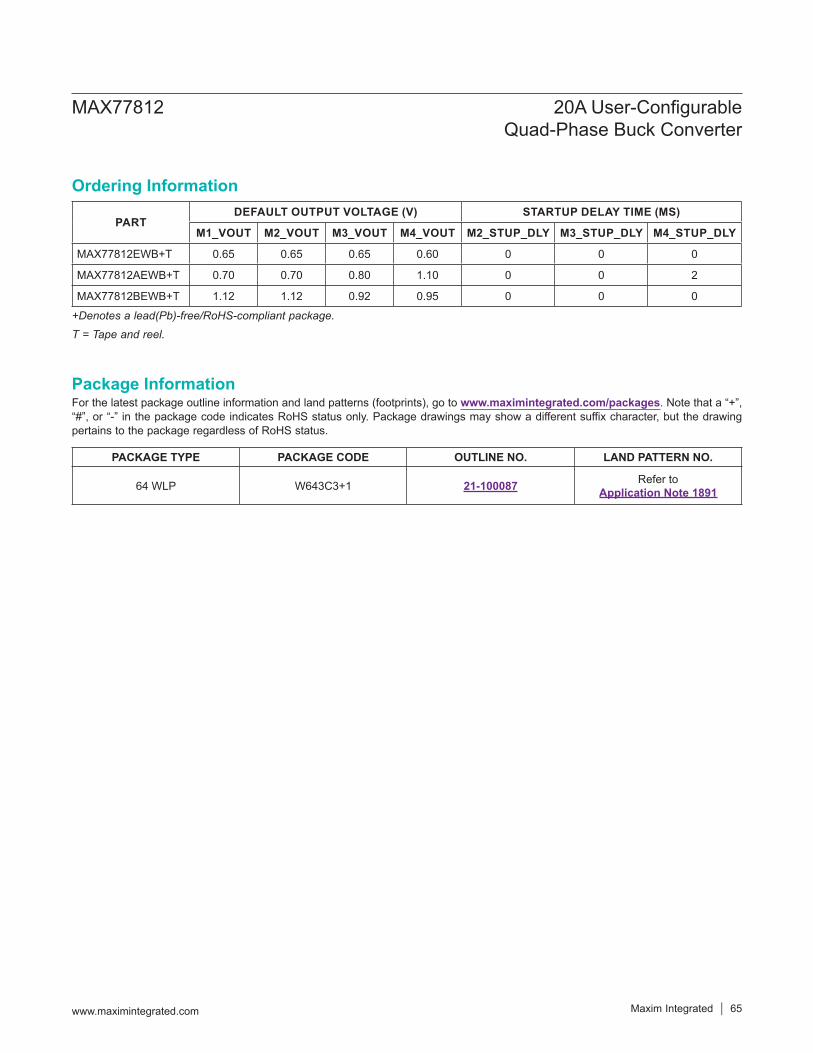
+Denotes a lead(Pb)-free/RoHS-compliant package.
T = Tape and reel.
PACKAGE TYPE PACKAGE CODE OUTLINE NO. LAND PATTERN NO.
64 WLP W643C3+1 21-100087 Refer to Application Note 1891
PARTDEFAULT OUTPUT VOLTAGE (V) STARTUP DELAY TIME (MS)
M1_VOUT M2_VOUT M3_VOUT M4_VOUT M2_STUP_DLY M3_STUP_DLY M4_STUP_DLY
MAX77812EWB+T 0.65 0.65 0.65 0.60 0 0 0
MAX77812AEWB+T 0.70 0.70 0.80 1.10 0 0 2
MAX77812BEWB+T 1.12 1.12 0.92 0.95 0 0 0
MAX77812 20A User-Configurable Quad-Phase Buck Converter
www.maximintegrated.com Maxim Integrated 65
Package InformationFor the latest package outline information and land patterns (footprints), go to www.maximintegrated.com/packages. Note that a “+”, “#”, or “-” in the package code indicates RoHS status only. Package drawings may show a different suffix character, but the drawing pertains to the package regardless of RoHS status.
Ordering Information
REVISIONNUMBER
REVISIONDATE DESCRIPTION PAGES
CHANGED0 6/16 Initial release —
1 3/17
Updated Applications section, updated Benefits and Features section, updated MIN/TYP/MAX values in the Electrical Characteristics section and changed inductor to 220nH, DCR = 16mΩ, added Cyntec information to Table 2, added I2C slave addresses for OTP = 1 to Table 5, updated Figures 69 and communication protocols description, updated GPI_FUNC, M1_CFG, M2_CFG, M3_CFG, M4_CFG, GLB_CFG1, GLB_CFG2 registers in the Register Map table, updated Typical Application Circuit
1–14, 29, 32–36, 42, 43, 49, 56, 60–66
2 6/17 Updated Benefits and Features section and Register Map table, fixed various typos
1, 2, 4–6, 8, 11, 12, 14, 15, 23, 25, 26, 31, 33-38, 42, 43,
46-48, 62–64
3 8/17
Updated title, Benefits and Features section, and Electrical Characteristics table, corrected label error to Output Voltage Error (%) in Typical Operating Characteristics, corrected errors to register name and removed error statement in HS mode in Detailed Description section, removed inductor from Table 2, corrected error in POR bits in the GPI_PD_CTRL GPI Pulldown Resistor Control Register table
1, 10, 14, 16, 26, 29, 30, 38, 51
4 1/18
Updated Applications and Benefits and Features sections, added Simplified Block Diagram, added LX1/2/3/4 pulsed ratings, updated Electrical Characteristics tables, updated Detailed Description section, added ALPS 220nH, removed process information
1–4, 11, 15, 26–29, 30, 31, 38,
67
5 5/18
Updated General Description, Benefits and Features, and Applications sections, renamed Typical Application Circuit and moved to page 1, updated Absolute Maximum Ratings for LXx RMS current, updated Electrical Characteristics tables, updated Typical Operating Characteristics global conditions and TOCs, updated Detailed Description sections, Table 1, Figure 2, Table 5, corrected errors in Registers information, renamed Simplified Block Diagram and updated to 2+1+1 configuration, updated Ordering Information table
1–3, 14, 16, 17, 26, 28–30, 32, 34, 35, 47–50, 59–62,
66, 67
Maxim Integrated cannot assume responsibility for use of any circuitry other than circuitry entirely embodied in a Maxim Integrated product. No circuit patent licenses are implied. Maxim Integrated reserves the right to change the circuitry and specifications without notice at any time. The parametric values (min and max limits) shown in the Electrical Characteristics table are guaranteed. Other parametric values quoted in this data sheet are provided for guidance.
Maxim Integrated and the Maxim Integrated logo are trademarks of Maxim Integrated Products, Inc. © 2018 Maxim Integrated Products, Inc. 66
MAX77812 20A User-Configurable Quad-Phase Buck Converter
Revision History
For pricing, delivery, and ordering information, please contact Maxim Direct at 1-888-629-4642, or visit Maxim Integrated’s website at www.maximintegrated.com.


![Superior adhesive performance acrylic foam Double-coated adhesive tape HYPERJOINT ... · 2021. 4. 12. · H9004 [Tape thickness:0.4mm] H9008 [Tape thickness:0.8mm] H9012 [Tape](https://img.pdfslide.us/doc/110x75/612dd5e11ecc515869426f9b/superior-adhesive-performance-acrylic-foam-double-coated-adhesive-tape-hyperjoint.jpg)