Embed Size (px)
Citation preview
General DescriptionThe MAX5556 stereo audio sigma-delta digital-to-analog converter (DAC) offers a simple and complete stereo dig-ital-to-analog solution for media servers, set-top boxes, video-game hardware, and other general consumer audio applications. This DAC features built-in digital interpo-lation/filtering, sigma-delta digital-to-analog conversion, and analog output filtering. Control logic and mute cir-cuitry minimize audible pops and clicks during power-up, power-down, clock changes, or when invalid clock condi-tions occur.The MAX5556 receives input data over a 3-wire I2S-compatible interface with left-justified audio data. Data can be clocked by either an external or internal serial clock. The internal serial clock frequency is pro- grammable by selection of a master clock (MCLK) and sample clock (LRCLK) ratio. Sampling rates from 2kHz to 50kHz are supported.The MAX5556 operates from a single +4.75V to +5.5V analog supply with total harmonic distortion plus noise below -87dB. This device is available in an 8-pin SO pack-age and is specified over the -40°C to +85°C industrial temperature range.
Applications Digital Video Recorders and Media Servers Set-Top Boxes Video-Game Hardware
Features Simple and Complete Stereo Audio DAC Solutions,
No Controls to Set Sigma-Delta Stereo DACs with Built-In Interpolation
and Analog Output Filters I2S-Compatible Digital Audio Interface Clickless/Popless Operation 3.5VP-P Output Voltage Swing -87dB THD+N +87dB Dynamic Range Sample Frequencies (fS) from 2kHz to 50kHz Master Clock (MCLK) up to 25MHz Automatic Detection of Clock Ratio (MCLK/ LRCLK)
+Denotes a lead(Pb)-free/RoHS-compliant package. For leaded version, contact factory.*Contact factory for availability.
PART TEMP RANGE
PIN- PACKAGE DATA FORMAT
MAX5556ESA+ -40°C to +85°C 8 SO Left-justified I2S
data
GND
OUTRMCLK
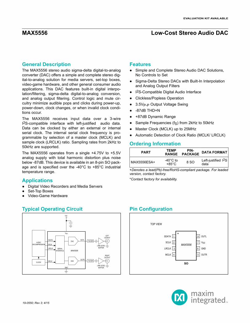
1+
2
8
7
OUTL
VDDSCLK
LRCLK
SDATA
SO
TOP VIEW
3
4
6
5
MAX5556
MCLK
LRCLK
SCLK
SDATA
GND
VDD
OUTR
OUTL
CLOCK
FILTER
FILTERDAC
DAC
+5V
LEFTOUTPUT
RIGHTOUTPUT
LINE-LEVELBUFFER
LINE-LEVELBUFFER
AUDIODECOMPRESSION
MAX5556SERIAL
INTERFACE
MAX5556 Low-Cost Stereo Audio DAC
19-0550; Rev 3; 4/15
Pin Configuration
Ordering Information
Typical Operating Circuit
EVALUATION KIT AVAILABLE
VDD to GND .........................................................-0.3V to +6.0VOUTL, OUTR, SDATA to GND ................ -0.3V to (VDD + 0.3V)Current Any Pin (excluding VDD and GND) .....................±10mA
OUTL, OUTR Shorted to GND ..............................ContinuousSCLK, LRCLK, MCLK to GND .............................-0.3V to +6.0VContinuous Power Dissipation (TA = +70°C) 8-Pin SO (derate 5.88mW/°C above +70°C) ...............471mW
Package Thermal Resistance (θJA) ..............................170°C/WOperating Temperature Range ........................... -40°C to +85°CJunction Temperature ......................................................+150°CStorage Temperature Range ............................ -65°C to +150°CLead Temperature (soldering, 10s) .................................+300°CSoldering Temperature (reflow) .......................................+260°C
(VDD = +4.75V to +5.5V, VGND = 0V, ROUT_ = 10kΩ, COUT_ = 10pF, 0dBFS sine-wave signal at 997Hz, fLRCLK (fS) = 48kHz, fMCLK = 12.288MHz, measurement bandwidth 10Hz to 20kHz, TA = -40°C to +85°C, outputs are unloaded, unless otherwise noted. Typical values at VDD = +5V, TA = +25°C.) (Note 1)
PARAMETER SYMBOL CONDITIONS MIN TYP MAX UNITSPOWER SUPPLYSupply Voltage VDD 4.75 5.0 5.50 V
Supply Current IDDUp to 48ksps 13 15
mAStatic digital 6 8.5
Power DissipationUp to 48ksps 65 82.5
mWStatic digital 30 44
DYNAMIC PERFORMANCE (Note 2)
Dynamic Range, 16-BitUnweighted 84 86
dBA-weighted 86 90
Dynamic Range, 18-Bit to 24-BitUnweighted 87
dBA-weighted 91
Total Harmonic Distortion PlusNoise, 16-Bit
THD+N0dBFS -86 -81
dB-20dBFS -67-60dBFS -26 -24
Total Harmonic Distortion PlusNoise, 18-Bit to 24-Bit
THD+N0dBFS -87
dB-20dBFS -68-60dBFS -27
Interchannel Isolation 1kHz full-scale output (crosstalk) 94 dBCOMBINED DIGITAL AND INTEGRATED ANALOG FILTER FREQUENCY RESPONSE (Note 3)
Passband-0.5dB corner 0.46
fS-3dB corner 0.49-6dB corner 0.50
Frequency Response/PassbandRipple
10Hz to 20kHz (fS = 48kHz) -0.025 +0.08dB10Hz to 20kHz (fS = 44.1kHz) -0.025 +0.08
10Hz to 16kHz (fS = 32kHz) -6.000 +0.073Stopband 0.5465 fSStopband Attenuation 52 dBGroup Delay tgd 20/fS sPassband Group-Delay Variation ∆tgd 20Hz to 20kHz ±0.4/fS s
www.maximintegrated.com Maxim Integrated 2
MAX5556 Low-Cost Stereo Audio DAC
Electrical Characteristics
Stresses beyond those listed under “Absolute Maximum Ratings” may cause permanent damage to the device. These are stress ratings only, and functional operation of the device at these or any other conditions beyond those indicated in the operational sections of the specifications is not implied. Exposure to absolute maximum rating conditions for extended periods may affect device reliability.
Absolute Maximum Ratings
(VDD = +4.75V to +5.5V, VGND = 0V, ROUT_ = 10kΩ, COUT_ = 10pF, 0dBFS sine-wave signal at 997Hz, fLRCLK (fS) = 48kHz, fMCLK = 12.288MHz, measurement bandwidth 10Hz to 20kHz, TA = -40°C to +85°C, outputs are unloaded, unless otherwise noted. Typical values at VDD = +5V, TA = +25°C.) (Note 1)
PARAMETER SYMBOL CONDITIONS MIN TYP MAX UNITSDC CHARACTERISTICSInterchannel Gain Mismatch 0.1 0.4 dBGain Error -5 +5 %Gain Drift 100 ppm/°CANALOG OUTPUTS
Full-Scale Output Voltage VOUTR, VOUTLVOUTL 3.25 3.5 3.75 VP-P
DC Quiescent Output Voltage VQ Input code = 0 2.4 VMinimum Load Resistance RL 3 kΩMaximum Load Capacitance CL 100 pF
Power-Supply Rejection Ratio PSRRVRIPPLE = 100mVP-P, frequency = 1kHz(Note 4)
66 dB
POP AND CLICK SUPPRESSIONMute Attenuation 100 dBPower-Up Until Bias Established Figure 11 360 msValid Clock to Normal Operation Soft-start ramp time, Figure 12 (Note 5) 20 msDIGITAL AUDIO INTERFACE (SCLK, SDATA, MCLK, LRCLK)Input-Voltage High VIH 2.0 VInput-Voltage Low VIL 0.8 VInput Leakage Current IIN -10 +10 µAInput Capacitance 8 pFTIMING CHARACTERISTICSInput Sample Rate fS 2 50 kHz
MCLK Pulse-Width Low tMCLKL
MCLK/LRCLK = 512 10nsMCLK/LRCLK = 384 20
MCLK/LRCLK = 256 20
MCLK Pulse-Width High tMCLKH
MCLK/LRCLK = 512 10nsMCLK/LRCLK = 384 20
MCLK/LRCLK = 256 20EXTERNAL SCLK MODELRCLK Duty Cycle (Note 6) 25 75 %SCLK Pulse-Width Low tSCLKL 20 nsSCLK Pulse-Width High tSCLKH 20 ns
SCLK Period tSCLK 1/(128x fS) ns
LRCLK Edge to SCLK RisingSetup Time tSLRS 20 ns
LRCLK Edge to SCLK RisingHold Time tSLRH 20 ns
SDATA Valid to SCLK RisingSetup Time tSDS 20 ns
SCLK Rising to SDATA Hold Time tSDH 20 ns
www.maximintegrated.com Maxim Integrated 3
MAX5556 Low-Cost Stereo Audio DAC
Electrical Characteristics (continued)

Note 1: 100% production tested at TA = +85°C. Limits to -40°C are guaranteed by design. Note 2: 0.5 LSB of triangular PDF dither added to data.Note 3: Guaranteed by design, not production tested.Note 4: PSRR test block diagram shown in Figure 1 denotes the test setup used to measure PSRR.Note 5: Volume ramping interval starts from establishment of a valid MCLK to LRCLK ratio. Total time is proportional to the sample
rate (fS). 20ms based on 48ksps operation.Note 6: In external SCLK mode, LRCLK duty cycles are not limited, provided all data formatting requirements are met. See Figure 4.Note 7: The LRCLK duty cycle must be 50% ±1/2 MCLK period in internal SCLK mode.Note 8: The SCLK/LRCLK ratio can be set to 32, 48, or 64, depending on the MCLK/LRCLK ratio selected. See Figure 4.
(VDD = +4.75V to +5.5V, VGND = 0V, ROUT_ = 10kΩ, COUT_ = 10pF, 0dBFS sine-wave signal at 997Hz, fLRCLK (fS) = 48kHz, fMCLK = 12.288MHz, measurement bandwidth 10Hz to 20kHz, TA = -40°C to +85°C, outputs are unloaded, unless otherwise noted. Typical values at VDD = +5V, TA = +25°C.) (Note 1)
Figure 1. PSRR Test Block Diagram
PARAMETER SYMBOL CONDITIONS MIN TYP MAX UNITSINTERNAL SCLK MODELRCLK Duty Cycle (Note 7) 50 %
Internal SCLK Period tISCLK (Note 8) 1/fSCLK ns
LRCLK Edge to Internal SCLKRising Delay Time tISCLKR tISCLK/2 ns
SDATA Valid to Internal SCLKRising Setup Time
tISDSMCLK period = tMCLK
tMCLK + 10ns
tISDH tMCLK
MCLK
SDATA
LRCLK
SCLK
ACTI
VE C
LOCK
S
GND
VDD
SPECTRUM ANALYZER
LOUT, ROUTZGAUDIO SIGNALGENERATOR
(100mVP-P AT 1kHz)
DC POWER SUPPLY(5VDC)
MAX5556
+
-
www.maximintegrated.com Maxim Integrated 4
MAX5556 Low-Cost Stereo Audio DAC
Electrical Characteristics (continued)
(VDD = +5V, VGND = 0V, ROUT_ = 10kΩ, COUT_ = 10pF, TA = +25°C, unless otherwise noted.)
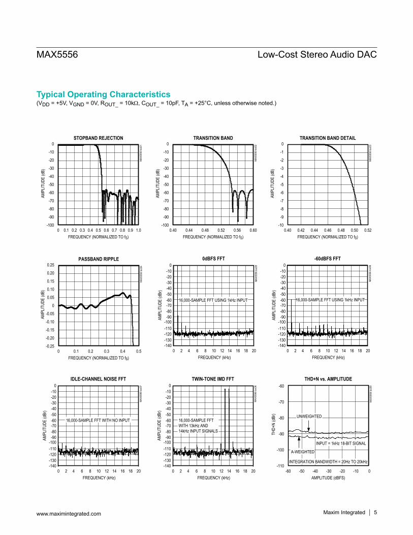
-110
-100
-80
-90
-70
-60
-60 -40-50 -30 -20 -10 0
THD+N vs. AMPLITUDE
MAX
5556
toc0
9
AMPLITUDE (dBFS)
THD+
N (d
Br) UNWEIGHTED
A-WEIGHTED
INPUT = 1kHz 18-BIT SIGNAL
INTEGRATION BANDWIDTH = 20Hz TO 20kHz
-100-110
0-10-20-30-40-50-60-70-80-90
-130-120
-1400 2 4 6 8 10 12 14 16 18 20
FREQUENCY (kHz)
AMPL
ITUD
E (d
Br)
TWIN-TONE IMD FFT
MAX
5556
toc0
8
16,000-SAMPLE FFT WITH 13kHz AND 14kHz INPUT SIGNALS
-100-110
0-10-20-30-40-50-60-70-80-90
-130-120
-1400 2 4 6 8 10 12 14 16 18 20
FREQUENCY (kHz)
AMPL
ITUD
E (d
Br)
IDLE-CHANNEL NOISE FFT
MAX
5556
toc0
7
16,000-SAMPLE FFT WITH NO INPUT
-100-110
0-10-20-30-40-50-60-70-80-90
-130-120
-1400 2 4 6 8 10 12 14 16 18 20
FREQUENCY (kHz)
AMPL
ITUD
E (d
Br)
-60dBFS FFT
MAX
5556
toc0
6
16,000-SAMPLE FFT USING 1kHz INPUT
-100-110
0-10-20-30-40-50-60-70-80-90
-130-120
-1400 2 4 6 8 10 12 14 16 18 20
FREQUENCY (kHz)
AMPL
ITUD
E (d
Br)
0dBFS FFTM
AX55
56 to
c05
16,000-SAMPLE FFT USING 1kHz INPUT
-0.25
-0.15
-0.20
-0.05
-0.10
0.05
0
0.10
0.20
0.15
0.25
0 0.1 0.2 0.3 0.4 0.5
PASSBAND RIPPLE
MAX
5556
toc0
4
FREQUENCY (NORMALIZED TO fS)
AMPL
ITUD
E (d
B)
-10
-7
-8
-9
-6
-5
-4
-3
-2
-1
0
0.40 0.440.42 0.46 0.48 0.50 0.52
TRANSITION BAND DETAIL
MAX
5556
toc0
3
FREQUENCY (NORMALIZED TO fS)
AMPL
ITUD
E (d
B)
-100
-80
-90
-60
-70
-40
-50
-30
-10
-20
0
0.40 0.44 0.48 0.52 0.56 0.60
TRANSITION BAND
MAX
5556
toc0
2
FREQUENCY (NORMALIZED TO fS)
AMPL
ITUD
E (d
B)
-100
-80
-90
-60
-70
-40
-50
-30
-10
-20
0
0 0.2 0.3 0.40.1 0.5 0.6 0.7 0.90.8 1.0
STOPBAND REJECTIONM
AX55
56 to
c01
FREQUENCY (NORMALIZED TO fS)
AMPL
ITUD
E (d
B)
Maxim Integrated 5www.maximintegrated.com
MAX5556 Low-Cost Stereo Audio DAC
Typical Operating Characteristics

(VDD = +5V, VGND = 0V, ROUT_ = 10kΩ, COUT_ = 10pF, TA = +25°C, unless otherwise noted.)
100ms/div
POWER-UP RESPONSE
VOUT1V/div
0V
MAX5556 toc15
5ms/div
CLOCK-LOSS MUTE RECOVERY
VOUT1V/div2.4V
MAX5556 toc14
CLOCKRESTORED
LOSSOF CLOCK
5
7
6
10
9
8
11
12
14
13
15
0 1.0 1.50.5 2.0 2.5 3.0 3.5 4.0 4.5 5.0 5.5
SUPPLY CURRENT vs. DIGITAL INPUT VOLTAGE (VDIG)
MAX
5556
toc1
3
DIGITAL INPUT VOLTAGE (VDIG) (V)
SUPP
LY C
URRE
NT (m
A)
VIH
VDIG < VIHMUTE ENGAGED
VDD = +5.5VDC OUTPUT
VDIG < VIHNORMAL OPERATION
5
8
7
6
9
10
11
12
13
14
15
4.75 5.054.90 5.20 5.35 5.50
SUPPLY CURRENT vs. SUPPLY VOLTAGE
MAX
5556
toc1
2
SUPPLY VOLTAGE (V)
SUPP
LY C
URRE
NT (m
A)
INPUT = 1kHz, 0dBFS SIGNALNORMAL OPERATION
STATIC DIGITAL INPUTMUTE OPERATION
0
20
10
40
30
60
50
70
0 2010 30 40 50
POWER DISSIPATIONvs. SAMPLE FREQUENCY
MAX
5556
toc1
1
SAMPLE FREQUENCY (kHz)
POW
ER D
ISSI
PATI
ON (m
W)
VDD = +5VINPUT = 1kHz, 0dBFS SIGNAL
-110
-100
-90
-80
-70
-60
0 8 104 62 12 14 16 18 20
UNWEIGHTED THD+Nvs. FREQUENCY
MAX
5556
toc1
0
FREQUENCY (kHz)
THD+
N (d
Br)
INPUT = 1kHz 18-BIT SIGNAL,INTEGRATION BANDWIDTH = 20Hz TO 20kHz
Maxim Integrated 6www.maximintegrated.com
MAX5556 Low-Cost Stereo Audio DAC
Typical Operating Characteristics

Detailed DescriptionThe MAX5556 stereo audio sigma-delta DAC offers a complete stereo digital-to-analog system for consumer audio applications. The MAX5556 features built-in digital interpolation/filtering, sigma-delta digital-to-analog con-version and analog output filters (Figure 2). Control logic and mute circuitry minimize audible pops and clicks dur- ing power-up, power-down, and whenever invalid clock conditions occur.This stereo audio DAC receives input data over a 3-wire I2S-compatible interface. The MAX5556 accepts left- justified I2S data of 16 or 24 bits. This DAC also sup-ports a wide range of sample rates from 2kHz to 50kHz. Direct analog output data is routed to the right or left output by driving LRCLK high or low. See the Clock and Data Interface section.The MAX5556 supports MCLK/LRCLK ratios of 256, 384, or 512. This device allows a change to the clock speed ratio without causing glitches on the analog out-puts by internally muting the audio during invalid clock conditions. The internal mute function ramps down the audio amplitude and forces the analog outputs to a 2.4V quiescent voltage immediately upon clock loss or
change of ratio. A soft-start routine is then engaged when a valid clock ratio is re-established, producing clickless and popless continuous operation.The MAX5556 operates from a +4.75V to +5.5V analog supply and features +87dB dynamic range with total har-monic distortion typically below -87dB.
InterpolatorThe digital interpolation filter eliminates images of the baseband audio signal that exist at multiples of the input sample rate (fS). The resulting upsampled frequency spectrum has images of the input signal at multiples of 8 x fS. An additional upsampling sinc filter further reduces upsampling images up to 64 x fS. These images are ulti-mately removed through the internal analog lowpass filter and the external analog output filter.
Sigma-Delta Modulator/DACThe MAX5556 uses a multibit sigma-delta DAC with an oversampling ratio (OSR) of 64 to achieve a wide dynamic range. The sigma-delta modulator accepts a 3-bit data stream from the interpolation filter at a rate of 64 x fS (fS = LRCLK frequency) and provides an analog voltage repre-sentation of that data stream.
PIN NAME FUNCTION
1 SDATASerial Audio Data Input. Data is clocked into the MAX5556 on the rising edge of the internal or external SCLK. Data is input in two’s complement format, MSB first. The state of LRCLK determines whether data is directed to OUTL or OUTR.
2 SCLK External Serial-Clock Input. Data is strobed on the rising edge of SCLK.
3 LRCLK Left-/Right-Channel Select Clock. Drive LRCLK low to direct data to OUTL or LRCLK high to direct data to OUTR.
4 MCLK Master Clock Input. The MCLK/LRCLK ratio must equal to 256, 384, or 512.
5 OUTR Right-Channel Analog Output
6 GND Ground
7 VDDPower-Supply Input. Bypass VDD to GND with a 0.1µF capacitor in parallel with a 4.7µF capacitor as close to VDD as possible. Place the 0.1µF capacitor closest to VDD.
8 OUTL Left-Channel Analog Output
www.maximintegrated.com Maxim Integrated 7
MAX5556 Low-Cost Stereo Audio DAC
Pin Description

Integrated Analog Lowpass FilterThe DAC output of the sigma-delta modulator is followed by an analog smoothing filter that attenuates high-frequency quantization noise. The corner frequency of the filter is approximately 2 x fS.
Integrated Analog Output BufferFollowing the analog lowpass filter, the analog signal is routed through internal buffers to OUTR and OUTL. The buffer can directly drive load resistances larger than 3kΩ and load capacitances up to 100pF (Figure 3).
Figure 3. Load-Impedance Operating Region
Figure 2. Functional Diagram
LOAD RESISTANCE RL (k)
3
5 10 15 20
125
100
75
50
25
SAFE OPERATING REGION
25
LOAD
CAP
ACITA
NCE
C L (p
F)
INTERPOLATOR SIGMA-DELTAMODULATOR
SIGMA-DELTAMODULATOR
ANALOGLOWPASS
FILTER
ANALOGLOWPASS
FILTER
SDATA
MCLK
LRCLK
SCLK
OUTL
OUTR
VDD
GND
DAC
DAC
BUFFER
INTERNALREFERENCE
INTERPOLATOR
BUFFER
MAX5556
SERIALINTERFACE
www.maximintegrated.com Maxim Integrated 8
MAX5556 Low-Cost Stereo Audio DAC
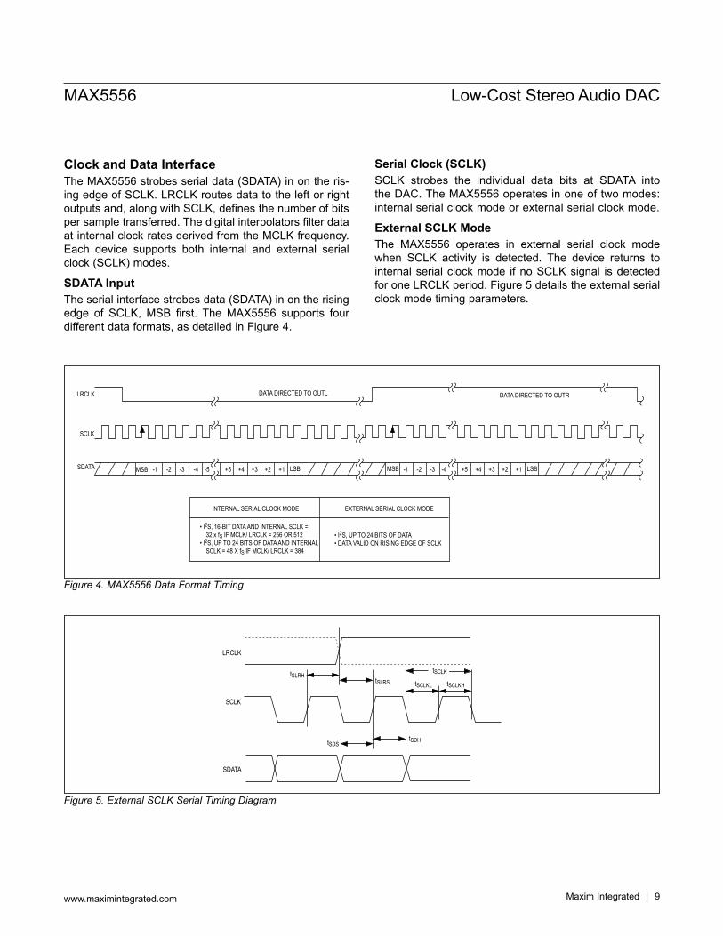
Clock and Data InterfaceThe MAX5556 strobes serial data (SDATA) in on the ris-ing edge of SCLK. LRCLK routes data to the left or right outputs and, along with SCLK, defines the number of bits per sample transferred. The digital interpolators filter data at internal clock rates derived from the MCLK frequency. Each device supports both internal and external serial clock (SCLK) modes.
SDATA InputThe serial interface strobes data (SDATA) in on the rising edge of SCLK, MSB first. The MAX5556 supports four different data formats, as detailed in Figure 4.
Serial Clock (SCLK)SCLK strobes the individual data bits at SDATA into the DAC. The MAX5556 operates in one of two modes: internal serial clock mode or external serial clock mode.
External SCLK ModeThe MAX5556 operates in external serial clock mode when SCLK activity is detected. The device returns to internal serial clock mode if no SCLK signal is detected for one LRCLK period. Figure 5 details the external serial clock mode timing parameters.
Figure 5. External SCLK Serial Timing Diagram
Figure 4. MAX5556 Data Format Timing
tSLRHtSLRS
tSDH
SDATA
SCLK
LRCLK
tSDS
tSCLKL tSCLKH
tSCLK
MSB MSBLSB LSB-2 -3 -4 -5 +5 +4 +3 +2 +1 -1 -2 -3 -4 +5 +4 +3 +2 +1
LRCLK
SCLK
SDATA
DATA DIRECTED TO OUTL
-1
INTERNAL SERIAL CLOCK MODE EXTERNAL SERIAL CLOCK MODE
• I2S, 16-BIT DATA AND INTERNAL SCLK = 32 x fS IF MCLK/ LRCLK = 256 OR 512• I2S, UP TO 24 BITS OF DATA AND INTERNAL SCLK = 48 X fS IF MCLK/ LRCLK = 384
• I2S, UP TO 24 BITS OF DATA• DATA VALID ON RISING EDGE OF SCLK
DATA DIRECTED TO OUTR
www.maximintegrated.com Maxim Integrated 9
MAX5556 Low-Cost Stereo Audio DAC
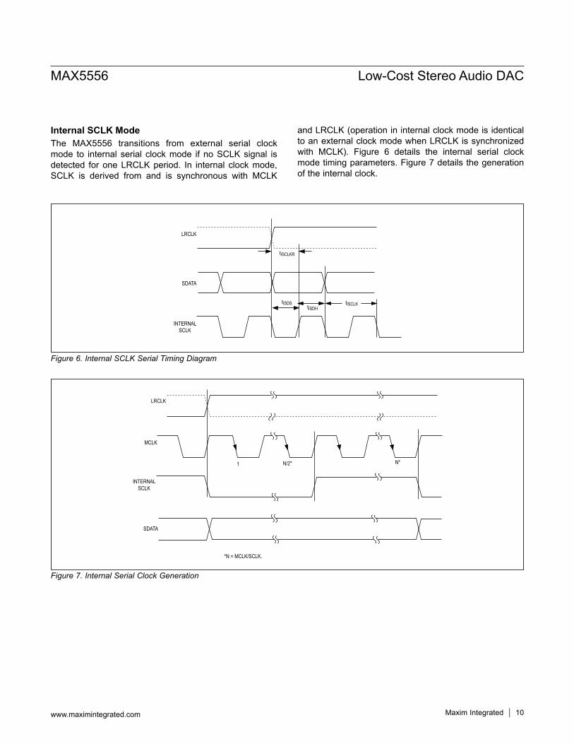
Internal SCLK ModeThe MAX5556 transitions from external serial clock mode to internal serial clock mode if no SCLK signal is detected for one LRCLK period. In internal clock mode, SCLK is derived from and is synchronous with MCLK
and LRCLK (operation in internal clock mode is identical to an external clock mode when LRCLK is synchronized with MCLK). Figure 6 details the internal serial clock mode timing parameters. Figure 7 details the generation of the internal clock.
Figure 7. Internal Serial Clock Generation
Figure 6. Internal SCLK Serial Timing Diagram
INTERNALSCLK
MCLK
LRCLK
SDATA
1 N/2* N*
*N = MCLK/SCLK.
SDATA
INTERNALSCLK
LRCLK
tISCLKR
tISDStISDH
tISCLK
www.maximintegrated.com Maxim Integrated 10
MAX5556 Low-Cost Stereo Audio DAC
Left/Right Clock Input (LRCLK)LRCLK is the left/right clock input signal for the 3-wire interface and sets the sample frequency (fS). On the MAX5556, drive LRCLK low to direct data to OUTL or LRCLK high to direct data to OUTR (Figure 4). The MAX5556 accepts data at LRCLK audio sample rates from 2kHz to 50kHz.
Master Clock (MCLK)MCLK accepts the master clock signal from an external clocking device and is used to derive internal clock fre-quencies. Set the MCLK/LRCLK ratio to 256, 384, or 512 to achieve the internal serial clock frequencies listed in Table 1. Table 2 details the MCLK/LRCLK ratios for three sample audio rates.The MAX5556 detects the MCLK/LRCLK ratio during the initialization sequence by counting the number of MCLK transitions during a single LRCLK period. MCLK, SCLK, and LRCLK must be synchronous signals.
Data FormatsMAX5556 I2S Left-Justified Data FormatThe MAX5556 accepts data with an I2S left-justified data format, accepting 16 or 24 bits of data. SDATA accepts data in two’s complement format with the MSB first. The MSB is valid on the second SCLK rising edge after LRCLK transitions low to high or high to low (Figure 4). Drive LRCLK low to direct data to OUTL. Drive LRCLK high to direct data to OUTR. The number of SCLK pulses with LRCLK high or low determines the number of bits transferred per sample. If fewer than 24 bits of data are written, the remaining LSBs are set to 0. If more than 24 bits are written, any bits after the LSB are ignored.The MAX5556 accepts up to 24 bits of data in external serial clock mode or when the MCLK/LRCLK ratio is 384 (internal serial clock = 48 x fS) in internal serial clock mode. The DAC also accepts 16 bits of data in internal serial clock mode when the MCLK/LRCLK ratio is 256 or 512 (internal serial clock = 32 x fS).
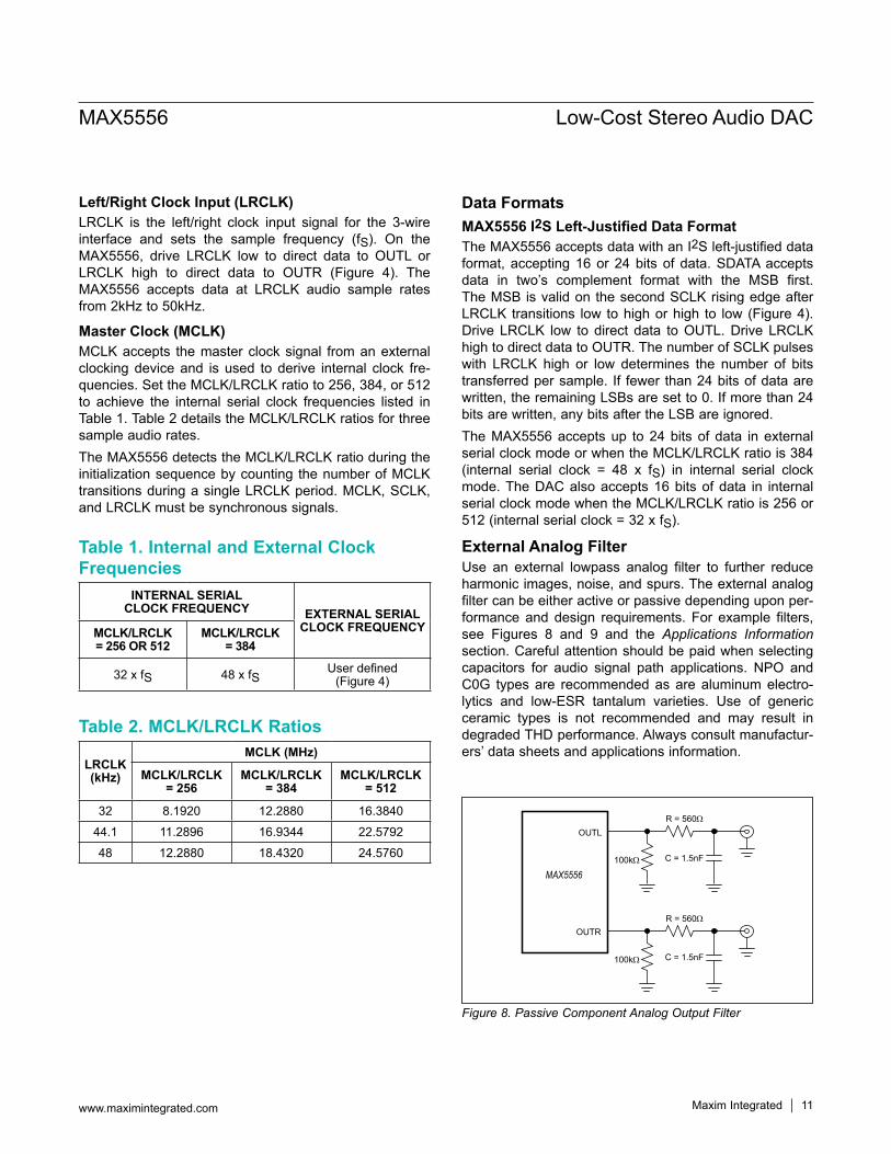
External Analog FilterUse an external lowpass analog filter to further reduce harmonic images, noise, and spurs. The external analog filter can be either active or passive depending upon per-formance and design requirements. For example filters, see Figures 8 and 9 and the Applications Information section. Careful attention should be paid when selecting capacitors for audio signal path applications. NPO and C0G types are recommended as are aluminum electro-lytics and low-ESR tantalum varieties. Use of generic ceramic types is not recommended and may result in degraded THD performance. Always consult manufactur-ers’ data sheets and applications information.
Figure 8. Passive Component Analog Output Filter
Table 2. MCLK/LRCLK Ratios
Table 1. Internal and External Clock Frequencies
LRCLK (kHz)
MCLK (MHz)
MCLK/LRCLK = 256
MCLK/LRCLK = 384
MCLK/LRCLK = 512
32 8.1920 12.2880 16.3840
44.1 11.2896 16.9344 22.5792
48 12.2880 18.4320 24.5760
INTERNAL SERIAL CLOCK FREQUENCY EXTERNAL SERIAL
CLOCK FREQUENCYMCLK/LRCLK = 256 OR 512
MCLK/LRCLK = 384
32 x fS 48 x fSUser defined
(Figure 4)
MAX5556
OUTR
OUTL
100kΩ
100kΩ
R = 560Ω
R = 560Ω
C = 1.5nF
C = 1.5nF
www.maximintegrated.com Maxim Integrated 11
MAX5556 Low-Cost Stereo Audio DAC

Figure 9. Active Component Analog Output Filter
OUTR
33pF
OUTL
+5V
33pF
+5V
56pF
56pF
24.3kΩ5.23kΩ
10kΩ 59kΩ
10kΩ 59kΩ
5.23kΩ 24.3kΩ
VBIAS2.4V
VBIAS2.4V
MAX5556
www.maximintegrated.com Maxim Integrated 12
MAX5556 Low-Cost Stereo Audio DAC
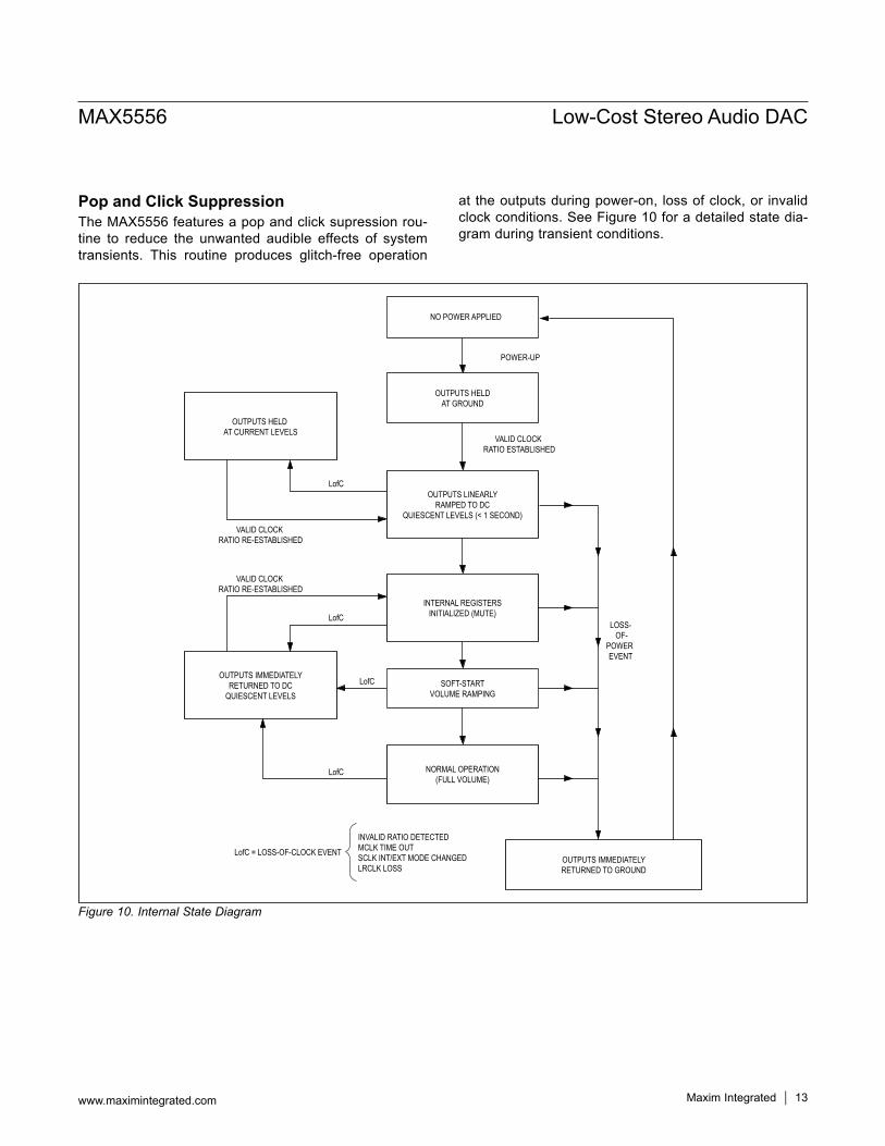
Pop and Click SuppressionThe MAX5556 features a pop and click supression rou-tine to reduce the unwanted audible effects of system transients. This routine produces glitch-free operation
at the outputs during power-on, loss of clock, or invalid clock conditions. See Figure 10 for a detailed state dia-gram during transient conditions.
Figure 10. Internal State Diagram
NO POWER APPLIED
OUTPUTS HELDAT GROUND
OUTPUTS LINEARLYRAMPED TO DC
QUIESCENT LEVELS (< 1 SECOND)
INTERNAL REGISTERSINITIALIZED (MUTE)
SOFT-STARTVOLUME RAMPING
OUTPUTS IMMEDIATELYRETURNED TO DC
QUIESCENT LEVELS
INVALID RATIO DETECTEDMCLK TIME OUTSCLK INT/EXT MODE CHANGEDLRCLK LOSS
OUTPUTS HELD AT CURRENT LEVELS
VALID CLOCK RATIO RE-ESTABLISHED
VALID CLOCK RATIO RE-ESTABLISHED
VALID CLOCK RATIO ESTABLISHED
POWER-UP
LOSS- OF-
POWER EVENT
NORMAL OPERATION(FULL VOLUME)
LofC
LofC
LofC
LofC = LOSS-OF-CLOCK EVENT
LofC
OUTPUTS IMMEDIATELYRETURNED TO GROUND
www.maximintegrated.com Maxim Integrated 13
MAX5556 Low-Cost Stereo Audio DAC
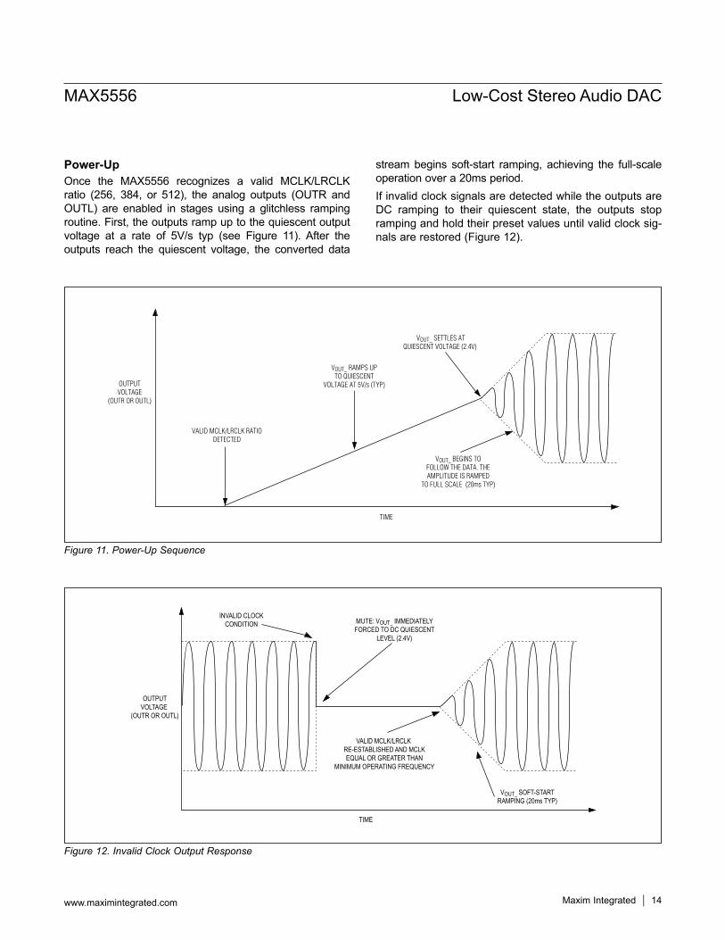
Power-UpOnce the MAX5556 recognizes a valid MCLK/LRCLK ratio (256, 384, or 512), the analog outputs (OUTR and OUTL) are enabled in stages using a glitchless ramping routine. First, the outputs ramp up to the quiescent output voltage at a rate of 5V/s typ (see Figure 11). After the outputs reach the quiescent voltage, the converted data
stream begins soft-start ramping, achieving the full-scale operation over a 20ms period.If invalid clock signals are detected while the outputs are DC ramping to their quiescent state, the outputs stop ramping and hold their preset values until valid clock sig-nals are restored (Figure 12).
Figure 12. Invalid Clock Output Response
Figure 11. Power-Up Sequence
TIME
OUTPUTVOLTAGE
(OUTR OR OUTL)
INVALID CLOCKCONDITION MUTE: VOUT_ IMMEDIATELY
FORCED TO DC QUIESCENTLEVEL (2.4V)
VALID MCLK/LRCLK RE-ESTABLISHED AND MCLKEQUAL OR GREATER THAN
MINIMUM OPERATING FREQUENCY
VOUT_ SOFT-STARTRAMPING (20ms TYP)
TIME
OUTPUTVOLTAGE
(OUTR OR OUTL)
VOUT_ RAMPS UPTO QUIESCENT
VOLTAGE AT 5V/s (TYP)
VOUT_ BEGINS TOFOLLOW THE DATA. THEAMPLITUDE IS RAMPED
TO FULL SCALE (20ms TYP)
VALID MCLK/LRCLK RATIODETECTED
VOUT_ SETTLES ATQUIESCENT VOLTAGE (2.4V)
www.maximintegrated.com Maxim Integrated 14
MAX5556 Low-Cost Stereo Audio DAC

Loss of Clock and Invalid Clock ConditionsThe MAX5556 mutes both outputs after detecting one of four invalid clock conditions. The device mutes its output to prevent propagation of pops, clicks, or cor-rupted data through the signal path. The MAX5556 forces the outputs to the quiescent DC voltage (2.4V) to prevent clicks in capacitive-coupled systems. Invalid clock conditions include:
1) MCLK/LRCLK ratio changes between 256, 384, and 512
2) Transition between internal and external serial- clock mode
3) Invalid MCLK/LRCLK ratio4) MCLK falls below the minimum operating
frequency 2kHzWhen the MCLK/LRCLK ratio returns to 256, 384, or 512 and MCLK is equal or greater than its minimum operating frequency, the MAX5556 output returns to its full-scale setting over a soft-start mute time of 20ms (Figure 12).
Power-DownWhen the positive supply is removed from the MAX5556, the output discharges to ground. When power is restored, the power-up ramp routine engages once a valid clock ratio is established (see the Power-Up section).Avoid violating absolute maximum conditions by supply-ing digital inputs to the part or forcing voltages on the analog outputs during a loss-of-power event.
Applications InformationLow-Cost Line-Level SolutionConnect the MAX5556 output through a passive output filter as detailed in Figure 8 for a low-cost solution. This lowpass filter yields single-pole (20dB/decade) roll-off at a corner frequency (fC) determined by:
C1f
2 RC=
π
In the case of Figure 8, fC is approximately 190kHz.
High-Performance Line-Level SolutionFor enhanced performance, connect the MAX5556 output to an active filter by using an operational amplifier as shown in Figure 9. The use of an active filter allows for steeper roll-off, more efficient filtering, and also adds the capability of a programmable output gain.
Power-Supply SequencingFor correct power-up sequencing, apply VDD and then connect the input digital signals. Do not apply digital sig-nals before VDD is applied.Do not violate any of the absolute maximum ratings by removing power with the digital inputs still connected. To correctly power down the device, first disconnect the digital input signals, and then remove VDD.
Power-Supply Connections and Ground ManagementProper layout and grounding are essential for optimum performance. Use large traces for the power-supply inputs and analog outputs to minimize losses due to para-sitic trace resistance. Large traces also aid in moving heat away from the package. Proper grounding improves audio performance, minimizes crosstalk between channels, and prevents any switching noise from coupling into the audio signal. Route the analog paths (GND, VDD, OUTL, and OUTR) away from the digital signals. Connect a 0.1µF capacitor in parallel with a 4.7µF capacitor as close to VDD as possible. Low ESR-type capacitors are recom-mended for supply decoupling applications. A small value C0G-type bypass capacitor located as close to the device as possible is recommended in parallel with larger values.
www.maximintegrated.com Maxim Integrated 15
MAX5556 Low-Cost Stereo Audio DAC
PACKAGE TYPE
PACKAGE CODE OUTLINE NO. LAND
PATTERN NO.
8 SO S8+5 21-0041 90-0096
www.maximintegrated.com Maxim Integrated 16
MAX5556 Low-Cost Stereo Audio DAC
Package InformationFor the latest package outline information and land patterns (footprints), go to www.maximintegrated.com/packages. Note that a “+”, “#”, or “-” in the package code indicates RoHS status only. Package drawings may show a different suffix character, but the drawing pertains to the package regardless of RoHS status.
Chip InformationPROCESS: BiCMOS
REVISION NUMBER
REVISION DATE DESCRIPTION PAGES
CHANGED
0 5/06 Initial release —
1 2/11Added lead-free and automotive information, updated the Absolute Maximum Ratings, removed all references to unreleased products MAX5557/MAX5558/MAX5559, updated the Typical Operating Circuit
1–4, 7–19
2 8/13 Updated Ordering Information 1
3 4/15 Removed automotive reference from data sheet 1
Maxim Integrated cannot assume responsibility for use of any circuitry other than circuitry entirely embodied in a Maxim Integrated product. No circuit patent licenses are implied. Maxim Integrated reserves the right to change the circuitry and specifications without notice at any time. The parametric values (min and max limits) shown in the Electrical Characteristics table are guaranteed. Other parametric values quoted in this data sheet are provided for guidance.
Maxim Integrated and the Maxim Integrated logo are trademarks of Maxim Integrated Products, Inc. © 2015 Maxim Integrated Products, Inc. 17
MAX5556 Low-Cost Stereo Audio DAC
Revision History
For pricing, delivery, and ordering information, please contact Maxim Direct at 1-888-629-4642, or visit Maxim Integrated’s website at www.maximintegrated.com.
![108dB 192kHz 32bit 2-Channel Audio DAC - AKM - … · [AK4432] 015002029-E-00 2015/02 - 1 - 1. General Description The AK4432 is a 32-bit Stereo DAC which corresponds to digital audio](https://img.pdfslide.us/doc/110x75/5b5d00497f8b9ac8618d5e3e/108db-192khz-32bit-2-channel-audio-dac-akm-ak4432-015002029-e-00-201502.jpg)