Embed Size (px)
Citation preview

General DescriptionThe MAX306/MAX307 precision, monolithic, CMOS analog multiplexers (muxes) offer low on-resistance (less than 100Ω), which is matched to within 5Ω between channels and remains flat over the specified analog signal range (7Ω, max). They also offer low leakage over temperature (INO(OFF) less than 2.5nA at +85°C) and fast switching speeds (tTRANS less than 250ns). The MAX306 is a single-ended 1-of-16 device, and the MAX307 is a differential 2-of-8 device.The MAX306/MAX307 are fabricated with Maxim’s improved 44V silicon-gate process. Design improvements yield extremely low charge injection (less than 10pC) and guarantee electrostatic discharge (ESD) protection greater than 2000V.These muxes operate with a single +5V to +30V supply, or bipolar ±4.5V to ±20V supplies, while retaining TTL/CMOS-logic input compatibility and fast switching. CMOS inputs provide reduced input loading. These improved parts are plug-in upgrades for the industrystandard DG406, DG407, DG506A, and DG507A.Applications
Benefits and Features Guaranteed On-Resistance Match Between
Channels, < 5Ω Max Low On-Resistance, < 100Ω Max Guaranteed Flat On-Resistance Over Specified
Signal Range, 7Ω Max Guaranteed Charge Injection, < 10pC INO(OFF) Leakage < 2.5nA at +85°C ICOM(OFF) Leakage < 20nA at +85°C ESD Protection > 2000V Plug-In Upgrade for Industry-Standard
DG406/DG407/DG506A/DG507A Single-Supply Operation (+5V to +30V)
Bipolar-Supply Operation (±4.5V to ±20V) Low Power Consumption, < 1.25mW Rail-to-Rail Signal Handling TTL/CMOS-Logic Compatible
Ordering Information continued at end of data sheet. *Contact factory for dice specifications.
19-0270; Rev 5; 3/16
Sample-and-Hold Circuits Test Equipment Heads-Up Displays Guidance and Control Systems
Military Radios Communications Systems Battery-Operated Systems PBX, PABX
Audio Signal Routing
PART TEMP RANGE PIN-PACKAGEMAX306CPI 0°C to +70°C 28 PDIPMAX306CWI 0°C to +70°C 28 Wide SOMAX306C/D 0°C to +70°C Dice*MAX306EPI -40°C to +85°C 28 PDIPMAX306EWI -40°C to +85°C 28 Wide SOMAX306EQI -40°C to +85°C 28 PLCCMAX306EUI -40°C to +85°C 28 TSSOPMAX306MJI -55°C to +125°C 28 CERDIP
28
27
26
25
24
23
22
21
1
2
3
4
5
6
7
8
COM
V-
NO8
NO7NO16
N.C.
N.C.
V+TOP VIEW
NO6
NO5
NO4
NO3NO12
NO13
NO14
NO15
20
19
18
17
9
10
11
12
NO2
NO1
EN
A0GND
NO9
NO10
NO11
PDIP/SO/TSSOP
MAX306
16
15
13
14
A1
A2Pin Configurations/Functional Diagrams/Truth Tablescontinued at end of data sheet.
A3
N.C.
A2 A1 A0 EN
X0000111100001111
X0011001100110011
X0101010101010101
01111111111111111
None12345678910111213141516
MAX306LOGIC “0” VAL ≤ 0.8V, LOGIC “1” = VAH ≥ 2.4V
A3
X0000000011111111
MAX306/MAX307 Precision, 16-Channel/Dual 8-Channel, High-Performance, CMOS Analog Multiplexers
Pin Configurations/Functional Diagrams/Truth Tables
Ordering Information

(Voltage Referenced to V-) V+ ......................................................................... -0.3V, +44V GND ...................................................................... -0.3V, +25VDigital Inputs, NO, COM (Note 1) ........ (V- - 2V) to (V+ + 2V) or
30mA (whichever occurs first)Continuous Current (any terminal) .....................................30mAPeak Current, NO or COM (pulsed at 1ms, 10% duty cycle max) ..........................100mAContinuous Power Dissipation (TA = +70°C) Plastic DIP (derate 9.09mW/°C above +70°C) ............727mW Wide SO (derate 12.50mW/°C above +70°C) ...........1000mW PLCC (derate 10.53mW/°C above +70°C) ..................842mW CERDIP (derate 16.67mW/°C above +70°C) ............1333mW TSSOP (derate 12.8mW/°C above +70°C) ...............1025mW
Operating Temperature Ranges MAX30_C_ _ ......................................................0°C to +70°C MAX30_E_ _ .................................................. -40°C to +85°C MAX30_MJI .................................................. -55°C to +125°CStorage Temperature Range ............................ -65°C to +150°CLead Temperature (soldering, 10s) .................................+300°CSoldering Temperature (reflow) PDIP, Wide SO, TSSOP lead(Pb)-free ........................+260°C PDIP, Wide SO, TSSOP containing lead(Pb) ..............+240°C PLCC lead(Pb)-free .....................................................+245°C PLCC containing lead(Pb) ...........................................+225°C CERDIP .......................................................................+240°C
(V+ = +15V, V- = -15V, GND = 0V, VAH = +2.4V, VAL = +0.8V, TA = TMIN to TMAX, unless otherwise noted.)
PARAMETER SYMBOL CONDITIONS MIN TYP (Note 2) MAX UNITS
SWITCH
Analog Signal Range VNO,VCOM
(Note 3) -15 +15 V
On-Resistance RONINO = -1.0mA,VCOM = ±10V
TA = +25°C 60 100Ω
TA = TMIN to TMAX 125
On-Resistance Matching Between Channels ΔRON
INO = -1.0mA,VCOM = ±10V (Note 4)
TA = +25°C 1.5 5Ω
TA = TMIN to TMAX 8
On-Resistance Flatness RFLATINO = -1.0mA,VCOM = ±5V or 0V
TA = +25°C 1.8 7Ω
TA = TMIN to TMAX 10
NO Off-Leakage Current (Note 5) INO(OFF)
VCOM = +10V,VNO = ±10V,VEN = 0V
TA = +25°C -0.5 +0.01 +0.5
nATA = TMIN to TMAX
C, E -2.5 +2.5
M -5.0 +5.0
COM Off-Leakage Current(Note 5) ICOM(OFF)
VNO = ±10V,VCOM = +10V,VEN = 0V
MAX306
TA = +25°C -0.75 +0.02 +0.75
nA
TA = TMIN to TMAX
C, E -20 +20
M -40 +40
VNO = +10V,VCOM = ±10V,VEN = 0V
MAX307
TA = +25°C -0.75 +0.02 +0.75
TA = TMIN to TMAX
C, E -10 +10
M -20 +20
MAX306/MAX307 Precision, 16-Channel/Dual 8-Channel, High-Performance, CMOS Analog Multiplexers
www.maximintegrated.com Maxim Integrated 2
Note 1: Signals on NO, COM, A0, A1, A2, A3, or EN exceeding V+ or V- are clamped by internal diodes. Limit forward current to maximum current ratings.
Absolute Maximum Ratings
Stresses beyond those listed under “Absolute Maximum Ratings” may cause permanent damage to the device. These are stress ratings only, and functional operation of the device at these or any other conditions beyond those indicated in the operational sections of the specifications is not implied. Exposure to absolute maximum rating conditions for extended periods may affect device reliability.
Electrical Characteristics—Dual Supplies

(V+ = +15V, V- = -15V, GND = 0V, VAH = +2.4V, VAL = +0.8V, TA = TMIN to TMAX, unless otherwise noted.)
PARAMETER SYMBOL CONDITIONS MIN TYP (Note 2) MAX UNITS
COM On-Leakage Current(Note 5) ICOM(ON)
VCOM = ±10V,VNO = ±10V,Sequence each switch on
MAX306
TA = +25°C -0.75 +0.02 +0.75
nA
TA = TMIN to TMAX
C, E -25 +25
M -50 +50
MAX307
TA = +25°C -0.75 +0.02 +0.75
TA = TMIN to TMAX
C, E -12.5 +12.5
M -25 +25
INPUTInput Current withInput Voltage High IAH VA = 2.4V or 15V -1.0 +1.0 µA
Input Current withInput Voltage Low IAL VEN = 0V or 2.4V, VA = 0V -1.0 +1.0 µA
SUPPLYPower-Supply Range ±4.5 ±20 V
Positive Supply Current I+VEN = VA = 0V or 5.0V
TA = +25°C 16 30µA
TA = TMIN to TMAX 75
VEN = 2.4V,VA(ALL) = 0V
TA = +25°C 0.075 0.5mA
TA = TMIN to TMAX 1
Negative Supply Current I- VEN = 2.4V,VA(ALL) = 0V
TA = +25°C -1 +1µA
TA = TMIN to TMAX -10 +10DYNAMIC
Transition Time (Note 3) tTRANS Figure 2TA = +25°C 110 300
nsTA = TMIN to TMAX 400
Break-Before-Make Interval tOPEN Figure 4 TA = +25°C 10 40 ns
Enable Turn-On Time (Note 3) tON(EN) Figure 3
TA = +25°C 130 200ns
TA = TMIN to TMAX 400
Enable Turn-Off Time (Note 3) tOFF(EN) Figure 3
TA = +25°C 55 150ns
TA = TMIN to TMAX 300
Charge Injection(Note 3) Q
CL = 1.0nF,VNO = 0V,RS = 0Ω, Figure 5
TA = +25°C 2 10 pC
Off-Isolation(Note 6) VISO
VEN = 0V,RL = 1kΩ,fSW = 100kHz, Figure 6
TA = +25°C -69 dB
Crosstalk Between Channels VCT
VEN = 2.4V,fSW = 100kHz,VGEN = 1VP-P,RL = 1kΩ, Figure 7
TA = +25°C -92 dB
Logic Input Capacitance CIN fSW = 1MHz TA = +25°C 8 pF
MAX306/MAX307 Precision, 16-Channel/Dual 8-Channel, High-Performance, CMOS Analog Multiplexers
www.maximintegrated.com Maxim Integrated 3
Electrical Characteristics—Dual Supplies (continued)

(V+ = +12V, V- = 0V, GND = 0V, VAH = +2.4V, VAL = +0.8V, TA = TMIN to TMAX, unless otherwise noted.)
Note 2: The algebraic convention where the most negative value is a minimum and the most positive value a maximum is used in this data sheet.
Note 3: Guaranteed by design.Note 4: ΔRON = RON(MAX) - RON(MIN). On-resistance match between channels and flatness are guaranteed only with specified
voltages. Flatness is defined as the difference between the maximum and minimum value of on-resistance as measured at the extremes of the specified analog signal range.
Note 5: Leakage parameters are 100% tested at the maximum-rated hot temperature and guaranteed by correlation at +25°C.Note 6: Off-isolation = 20log VCOM/VNO, where VCOM = output and VNO = input to off switch.
PARAMETER SYMBOL CONDITIONS MIN TYP (Note 2) MAX UNITS
NO Off-Capacitance CNO(OFF)
fSW = 1MHz,VEN = VNO = 0V,Figure 8
TA = +25°C 8 pF
COM Off-Capacitance CCOM(OFF)
fSW = 1MHz,VEN = 0.8V,VCOM = 0V,Figure 8
MAX306TA = +25°C
130pF
MAX307 65
COM On-Capacitance CCOM(ON)
fSW = 1MHz,VEN = 2.4V,VCOM = 0V,Figure 8
MAX306TA = +25°C
140pF
MAX307 70
SWITCH
Analog Signal Range VNO,VCOM
(Note 3) 0 12 V
On-Resistance RONINO = -1.0mAVCOM = 3V or 10V TA = +25°C 120 175 Ω
DYNAMIC
Transition Time(Note 3) tTRANS
VNO1 = 8V,VNO8 = 0V,VIN = 2.4V,Figure 2
TA = +25°C 130 450 ns
Enable Turn-On Time(Note 3) tON(EN)
VINH = 2.4V,VINL = 0V,VNO1 = 5V,Figure 3
TA = +25°C 105 600 ns
Enable Turn-Off Time(Note 3) tOFF(EN)
VINH = 2.4V,VINL = 0V,VNO1 = 5V,Figure 3
TA = +25°C 80 300 ns
Charge Injection(Note 3) Q
CL = 1.0nF,VNO = 0V,RS = 0Ω
TA = +25°C 2 10 pC
MAX306/MAX307 Precision, 16-Channel/Dual 8-Channel, High-Performance, CMOS Analog Multiplexers
www.maximintegrated.com Maxim Integrated 4
Electrical Characteristics—Single Supply

(TA = +25°C, unless otherwise noted.)
120
ON-RESISTANCE vs. VCOM ANDTEMPERATURE (DUAL SUPPLIES)
100 MAX3
06/7
TOC-
02
0
20
40
60
-15 15-10 10-5 50
80
VCOM (V)
+125°C+85°C
+25°C
-55°C
R ON
(Ω)
V+ = +15VV- = -15V
280
320
360
400
ON-RESISTANCE vs. VCOM(SINGLE SUPPLY)
240
MAX3
06/7
TOC-
03
40
80
120
160
15 201050
200
VCOM (V)
R ON
(Ω) 5V
10V
15V20V
120
140
160
ON-RESISTANCE vs. VCOM ANDTEMPERATURE (SINGLE SUPPLY)
100
MAX3
06/7
TOC-
04
0
20
40
60
151050
80
VCOM (V)
R ON
(Ω)
+125°C
+85°C
+25°C
-55°C
V+ = +15VV- = 0V
10
0.0001-55 125
OFF-LEAKAGE vs. TEMPERATURE
1
MAX3
06/7
TOC-
05
TEMPERATURE (°C)
OFF-
LEAK
AGE
(nA)
25
0.01
0.001
-35 -15 65
0.1
100
1000
45 85 1055
INO (OFF)
ICOM (ON)
V+ = +15VV- = -15V
10
0.0001-55 125
ON-LEAKAGE vs. TEMPERATURE
1
MAX3
06/7
TOC-
06
TEMPERATURE (°C)
ON-L
EAKA
GE (n
A)
25
0.01
0.001
-35 -15 65
0.1
100
1000
45 85 1055
ICOM (ON)
V+ = +15VV- = -15V
120
140
160
ON-RESISTANCE vs. VCOM(DUAL SUPPLIES)
100
MAX3
06/7
TOC-
01
0
20
40
60
-20 20-15 15-10 10-5 50
80
VCOM (V)
±5V
±10V
±15V
±20V
R ON
(Ω)
30CHARGE INJECTION vs. VCOM
20 MAX3
06/7
TOC-
07
-30
-20
-10
0
-15 15-10 10-5 50
10
VCOM (V)
Q j (p
C)
V+ = 12VV- = 0V
V+ = +15VV- = -15V
100
0.001-55 125
SUPPLY CURRENT vs. TEMPERATURE
10 MAX3
06/7
TOC-
08
TEMPERATURE (°C)
I+, I-
(mA)
25
0.1
0.01
-35 -15 65
1
45 85 1055
I+
I- V+ = +15V V- = -15V VEN = VA = 0V, 4.5V
MAX306/MAX307 Precision, 16-Channel/Dual 8-Channel, High-Performance, CMOS Analog Multiplexers
Maxim Integrated 5www.maximintegrated.com
Typical Operating Characteristics

Applications InformationOperation with Supply Voltages Other than ±15VUsing supply voltages other than ±15V will reduce the analog signal range. The MAX306/MAX307 switches operate with ±4.5V to ±20V bipolar supplies or with a +5V to +30V single supply; connect V- to GND when operating with a single supply. Also, both device types can operate with unbalanced supplies such as +24V and -5V. The Typical Operating Characteristics graphs show typical on-resistance with 20V, 15V, 10V, and 5V supplies. (Switching times increase for 5V operation, up to a maximum of 10µs.)
Overvoltage ProtectionProper power-supply sequencing is recommended for all CMOS devices. Do not exceed the absolute maximum ratings because stresses beyond the listed ratings may cause permanent damage to the devices. Always sequence V+ on first, then V-, followed by either the logic inputs, NO or COM. If power-supply sequencing is not possible, add two small-signal diodes in series with supply pins for overvoltage protection (Figure 1). Adding diodes reduces the analog signal range to 1V above
V+ and 1V below V-, but low switch resistance and low leakage characteristics are unaffected. Device operation is unchanged, and the difference between V+ and V- should not exceed +44V.
Figure 1. Overvoltage Protection Using External Blocking Diodes
MAX306PIN NAME FUNCTION
1 V+ Positive Supply Voltage Input
2, 3, 13 N.C. No Connection. Not internally connected.
4–11 NO16–NO9 Analog Inputs–bidirectional
12 GND Ground
14–17 A3–A0 Address Inputs
18 EN Enable Inputs
19–26 NO1–NO8 Analog Inputs–bidirectional
27 V- Negative Supply Voltage Input
28 COM Output–bidirectional
MAX307PIN NAME FUNCTION
1 V+ Positive Supply Voltage Input
2 COMB Output B–bidirectional
3, 13, 14 N.C. No Connection. Not internally connected.
4–11 NO8B–NO1B Analog Inputs–bidirectional
12 GND Ground
15, 16, 17 A2, A1, A0 Address Inputs
18 EN Enable Input
19–26 NO1A–NO8A Analog Inputs–bidirectional
27 V- Negative Supply Voltage Input
28 COMA Output A–bidirectional
Vg
NOCOM
MAX306
V-
V+
MAX306/MAX307 Precision, 16-Channel/Dual 8-Channel, High-Performance, CMOS Analog Multiplexers
www.maximintegrated.com Maxim Integrated 6
Pin Description
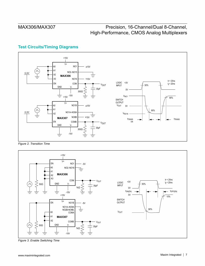
Figure 2. Transition Time
Figure 3. Enable Switching Time
50%
tTRANS
tr < 20nstf < 20ns
VOUT
+3V
0V
VNO1
0V
VNO16
LOGICINPUT
SWITCHOUTPUT
+15V
VOUT
-15V
GND
V+
A1
V-
A0
A2
A3
EN
NO1
NO2–NO15
NO16
COM
±10V
+10VMAX306
300Ω35pF
+15V
VOUT
-15V
GND
V+
A1
V-
A0
A2
EN
NO1B
NO1A–NO8A
NO8B
COMB
±10V
MAX307
300Ω 35pF
90%
90%
tTRANSON
+10V
+2.4V
+2.4V
50%
tOFF(EN)
tr < 20nstf < 20ns
VOUT
+3V
0V
0V
LOGICINPUT
SWITCHOUTPUT
+15V
VOUT
-15V
GND
V+
A1
V-
A0
A2A3
EN NO1
NO2–NO16
COM
-5V
50Ω
MAX306
1kΩ35pF
90%
10%
tON(EN)
+15V
VOUT
-15V
GND
V+
A1
V-
A0
A2
EN NO1B
NO1A–NO8ANO2B-NO8B,
COMA
COMB
-5V
50Ω
MAX307
1kΩ35pF
MAX306/MAX307 Precision, 16-Channel/Dual 8-Channel, High-Performance, CMOS Analog Multiplexers
www.maximintegrated.com Maxim Integrated 7
Test Circuits/Timing Diagrams

Figure 4. Break-Before-Make Interval
Figure 5. Charge Injection
50%
tOPEN
tr < 20nstf < 20ns
VOUT
+3V
0V
LOGICINPUT
SWITCHOUTPUT
+15V
VOUT
-15V
GND
V+
A1
V-
A0
A2
A3
EN
NO1–NO16
COM
+5V
50Ω
MAX306
300Ω35pF
80%
+2.4V
0V
∆VOUT
+3V
0V
LOGICINPUT
+15V
VOUT
-15V
GND
V+
A1
V-
A0
A2A3
EN
COMMAX306
CL = 1000nFVOUT
NO1–NO16
CHANNELSELECT
RS
VS
ONOFF OFF
∆VOUT IS THE MEASURED VOLTAGE DUE TO CHARGE TRANSFERERROR Q WHEN THE CHANNEL TURNS OFF.
Q = CL = ∆VOUT
MAX306/MAX307 Precision, 16-Channel/Dual 8-Channel, High-Performance, CMOS Analog Multiplexers
www.maximintegrated.com Maxim Integrated 8
Test Circuits/Timing Diagrams (continued)
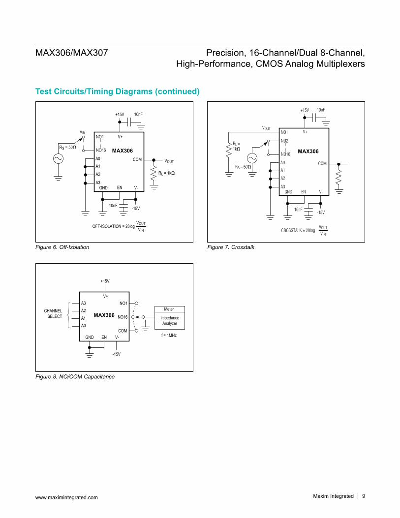
Figure 6. Off-Isolation
Figure 8. NO/COM Capacitance
Figure 7. Crosstalk
+15V
VOUT
-15V
GND
V+
A1
V-
A0
A2
A3
NO16
COM
MAX306
NO1
RS = 50Ω
VIN
EN
10nF
RL = 1kΩ
OFF-ISOLATION = 20logVOUTVIN
10nF
+15V
-15V
GND
V+
A2
V-
A3
A1A0
NO16MAX306CHANNEL
SELECT
NO1
COMEN
Meter
ImpedanceAnalyzer
f = 1MHz
+15V
-15V
GND
V+
A1
V-
A0
A2
A3
NO16
COM
MAX306
NO2
RS = 50Ω
VOUT
EN
10nF
RL = 1kΩ
CROSSTALK = 20logVOUT
VIN
10nF
NO1
MAX306/MAX307 Precision, 16-Channel/Dual 8-Channel, High-Performance, CMOS Analog Multiplexers
www.maximintegrated.com Maxim Integrated 9
Test Circuits/Timing Diagrams (continued)

28
27
26
25
24
23
22
21
1
2
3
4
5
6
7
8
COMA
V-
NO8A
NO7ANO8B
N.C.
COMB
V+TOP VIEW
NO6A
NO5A
NO4A
NO3ANO4B
NO5B
NO6B
NO7B
20
19
18
17
9
10
11
12
NO2A
NO1A
EN
A0GND
NO1B
NO2B
NO3B
PDIP/SO
MAX307
16
15
13
14
A1
A2N.C.
N.C.
A2 A1 A0 EN
X00001111
X00110011
X01010101
011111111
None12345678
MAX307
LOGIC “0” VAL ≤ 0.8V, LOGIC “1” = VAH ≥ 2.4V
NO15
NO14
NO13
NO12
NO11
NO10
NO9
NO7
NO6
NO5
NO4
N03
N02
N01
NO16
N.C.
N.C.
V+ COM
V- NO8
GND N.C. A3 A2 A1 A0 EN
TOP VIEW
PLCC
12 13 14 15 16 17 18
1234 262728
19
20
21
22
23
24
255
6
7
8
9
10
11
MAX306
N.C. = NO INTERNAL CONNECTION
CMOS DECODERS/DRIVERS
A0 A1 A2 A3 EN
MAX306 16-CHANNEL SINGLE-ENDED MULTIPLEXER
NO16NO15NO14NO13NO12NO11NO10NO9NO8NO7NO6NO5NO4NO3NO2NO1
COM
V+ V- GND
MAX306/MAX307 Precision, 16-Channel/Dual 8-Channel, High-Performance, CMOS Analog Multiplexers
www.maximintegrated.com Maxim Integrated 10
Pin Configurations/Functional Diagrams/Truth Tables (continued)

*Contact factory for dice specifications.
PART TEMP RANGE PIN-PACKAGEMAX307CPI 0°C to +70°C 28 PDIPMAX307CWI 0°C to +70°C 28 Wide SOMAX307C/D 0°C to +70°C Dice*MAX307EPI -40°C to +85°C 28 PDIPMAX307EWI -40°C to +85°C 28 Wide SOMAX307EQI -40°C to +85°C 28 PLCCMAX307EUI -40°C to +85°C 28 TSSOPMAX307MJI -55°C to +125°C 28 CERDIPMAX307MWI/PR -55°C to +125°C 28 Wide SOMAX307MWI/PR-T -55°C to +125°C 28 Wide SO
PACKAGE TYPE
PACKAGE CODE
OUTLINE NO.
LAND PATTERN NO.
28 PDIP P28+3 21-0044 —
28 Wide SO W28+6 21-0042 90-0109
28 PLCC Q28+4 21-0049 90-0235
28 CDIP J28-2 21-0046 —
28 TSSOP U28+2 21-0066 90-0171
NO7B
NO6B
NO5B
NO4B
NO3B
NO2B
NO1B
NO7A
NO6A
NO5A
NO4A
N03A
N02A
N01A
NO8B
N.C.
COM
B
V+ COM
A
V- NO8A
GND N.C.
N.C. A2 A1 A0 EN
TOP VIEW
PLCC
12 13 14 15 16 17 18
1234 262728
19
20
21
22
23
24
255
6
7
8
9
10
11
MAX307
N.C. = NO INTERNAL CONNECTION
CMOS DECODERS/DRIVERS
A0 A1 A2 EN
NO8BNO7BNO6BNO5BNO4BNO3BNO2BNO1BNO8ANO7ANO6ANO5ANO4ANO3ANO2ANO1A
COMA
V+ V- GND
COMB
MAX307 8-CHANNEL DIFFERENTIAL MULTIPLEXER
MAX306/MAX307 Precision, 16-Channel/Dual 8-Channel, High-Performance, CMOS Analog Multiplexers
www.maximintegrated.com Maxim Integrated 11
Pin Configurations/Functional Diagrams/Truth Tables (continued)
Ordering Information (continued) Package InformationFor the latest package outline information and land patterns (footprints), go to www.maximintegrated.com/packages. Note that a “+”, “#”, or “-” in the package code indicates RoHS status only. Package drawings may show a different suffix character, but the drawing pertains to the package regardless of RoHS status.

REVISION NUMBER
REVISIONDATE DESCRIPTION PAGES
CHANGED
3 3/10
Changed the single-supply operating voltage minimum from +4.5V to +5V in the General Description, Features, and Applications Information sections. 1, 6
Added the soldering temperatures for all packages to the Absolute Maximum Ratings section. 2
4 5/14 Added MAX307MWI/PR and MAX307MWI/PR-T to the Ordering Information table. 11
5 3/16 Updated Electrical Characteristics table and Figure 2 3, 4, 6, 7
Maxim Integrated cannot assume responsibility for use of any circuitry other than circuitry entirely embodied in a Maxim Integrated product. No circuit patent licenses are implied. Maxim Integrated reserves the right to change the circuitry and specifications without notice at any time. The parametric values (min and max limits) shown in the Electrical Characteristics table are guaranteed. Other parametric values quoted in this data sheet are provided for guidance.
Maxim Integrated and the Maxim Integrated logo are trademarks of Maxim Integrated Products, Inc.
MAX306/MAX307 Precision, 16-Channel/Dual 8-Channel, High-Performance, CMOS Analog Multiplexers
© 2016 Maxim Integrated Products, Inc. 12
Revision History
For pricing, delivery, and ordering information, please contact Maxim Direct at 1-888-629-4642, or visit Maxim Integrated’s website at www.maximintegrated.com.