Embed Size (px)
Citation preview
19-4323; Rev 17; 1/15
MAX220–MAX249 +5V-Powered, MultichannelRS-232 Drivers/Receivers
General DescriptionThe MAX220–MAX249 family of line drivers/receivers isintended for all EIA/TIA-232E and V.28/V.24 communica-tions interfaces, particularly applications where ±12V isnot available.The MAX225, MAX233, MAX235, and MAX245/MAX246/MAX247 use no external components and arerecommended for applications where printed circuitboard space is critical.The MAX220-MAX249 are offered in 26 different pack-ages with temperatures from 0 to +70°C up to -55°C to+125°C. See ordering information table at the end of thedata sheet for all package and temperature options.
Applications• Interface Translation• Multidrop RS-232 Networks• Portable Diagnostics Equipment
Benefits and Features
Saves Board Space
• Integrated Charge Pump Circuitry• Eliminates the Need for a Bipolar ±12V Supply• Enables Single Supply Operation from +5V Supply
• Integrated Capacitors (MAX223, MAX233, MAX235,
MAX245-MAX247)Saves Power for Reduced Power Requirements
• 5µW Shutdown Mode
AutoShutdown and UCSP are trademarks of Maxim IntegratedProducts, Inc.
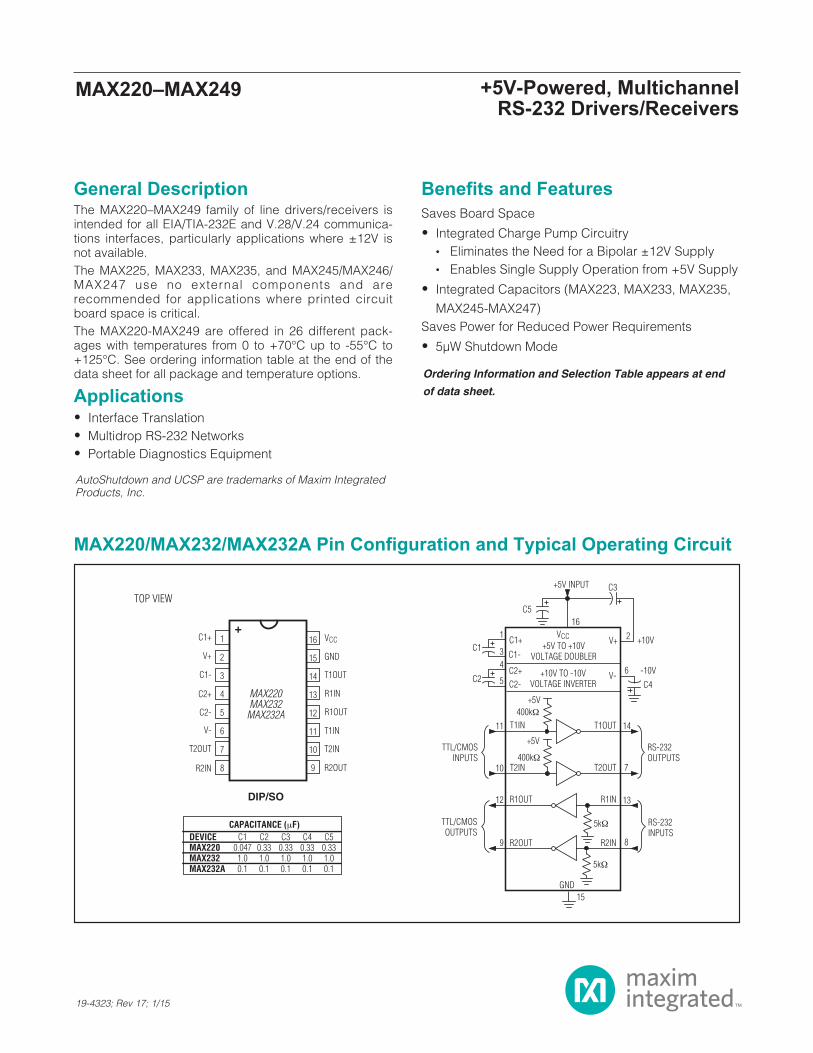
TOP VIEW
16
15
14
13
12
11
10
9
1
2
3
4
5
6
7
8
VCC
GND
T1OUT
R1INC2+
C1-
V+
C1++
MAX220MAX232
MAX232A R1OUT
T1IN
T2IN
R2OUTR2IN
T2OUT
V-
C2-
DIP/SO
V+
V-
2 +10VC1+C1
C2
1
34
5
11
10
12
9
6
14
7
13
8
T1IN
R1OUT
T2IN
R2OUT
T1OUT
R1IN
T2OUT
R2IN
+5V INPUT
C2+ -10V
C4
RS-232OUTPUTS
RS-232INPUTS
TTL/CMOSINPUTS
TTL/CMOSOUTPUTS
GND15
5kΩ
5kΩ
400kΩ
400kΩ+5V
+5V
+10V TO -10VVOLTAGE INVERTER
+5V TO +10VVOLTAGE DOUBLER
16
C3
C5
CAPACITANCE (μF)DEVICEMAX220MAX232MAX232A
C10.0471.00.1
C20.331.00.1
C30.331.00.1
C40.331.00.1
C50.331.00.1
C2-
C1-
VCC
Ordering Information and Selection Table appears at end
of data sheet.
MAX220/MAX232/MAX232A Pin Configuration and Typical Operating Circuit
Maxim Integrated | 2www.maximintegrated.com
MAX220–MAX249 +5V-Powered, MultichannelRS-232 Drivers/Receivers
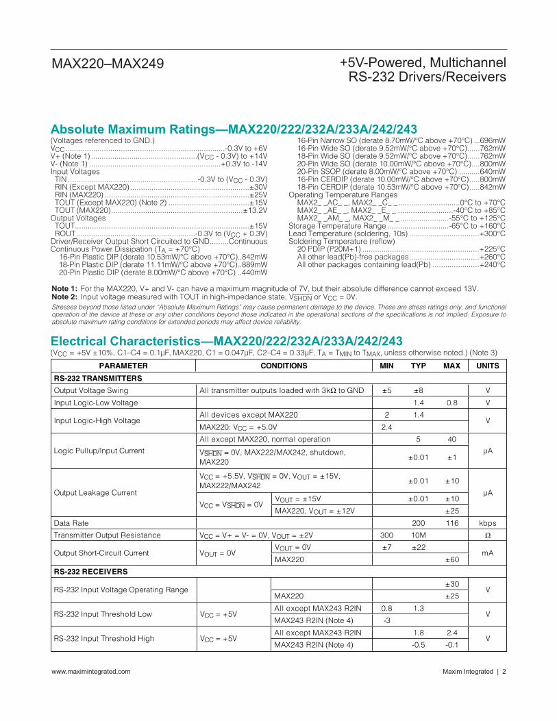
Absolute Maximum Ratings—MAX220/222/232A/233A/242/243
Electrical Characteristics—MAX220/222/232A/233A/242/243(VCC = +5V ±10%, C1–C4 = 0.1µF‚ MAX220, C1 = 0.047µF, C2–C4 = 0.33µF, TA = TMIN to TMAX‚ unless otherwise noted.) (Note 3)
Note 1: For the MAX220, V+ and V- can have a maximum magnitude of 7V, but their absolute difference cannot exceed 13V.Note 2: Input voltage measured with TOUT in high-impedance state, VSHDN or VCC = 0V.Stresses beyond those listed under “Absolute Maximum Ratings” may cause permanent damage to the device. These are stress ratings only, and functionaloperation of the device at these or any other conditions beyond those indicated in the operational sections of the specifications is not implied. Exposure toabsolute maximum rating conditions for extended periods may affect device reliability.
(Voltages referenced to GND.)VCC...........................................................................-0.3V to +6VV+ (Note 1) ..................................................(VCC - 0.3V) to +14VV- (Note 1) ..............................................................+0.3V to -14VInput Voltages
TIN .............................................................-0.3V to (VCC - 0.3V)RIN (Except MAX220) ........................................................±30VRIN (MAX220) ....................................................................±25VTOUT (Except MAX220) (Note 2) ......................................±15VTOUT (MAX220)..............................................................±13.2V
Output VoltagesTOUT..................................................................................±15VROUT........................................................-0.3V to (VCC + 0.3V)
Driver/Receiver Output Short Circuited to GND.........ContinuousContinuous Power Dissipation (TA = +70°C)
16-Pin Plastic DIP (derate 10.53mW/°C above +70°C)..842mW18-Pin Plastic DIP (derate 11.11mW/°C above +70°C)..889mW20-Pin Plastic DIP (derate 8.00mW/°C above +70°C) ..440mW
16-Pin Narrow SO (derate 8.70mW/°C above +70°C) ...696mW16-Pin Wide SO (derate 9.52mW/°C above +70°C)......762mW18-Pin Wide SO (derate 9.52mW/°C above +70°C)......762mW20-Pin Wide SO (derate 10.00mW/°C above +70°C)....800mW20-Pin SSOP (derate 8.00mW/°C above +70°C) ..........640mW16-Pin CERDIP (derate 10.00mW/°C above +70°C).....800mW18-Pin CERDIP (derate 10.53mW/°C above +70°C).....842mW
Operating Temperature RangesMAX2_ _AC_ _, MAX2_ _C_ _.............................0°C to +70°CMAX2_ _AE_ _, MAX2_ _E_ _ ..........................-40°C to +85°CMAX2_ _AM_ _, MAX2_ _M_ _.......................-55°C to +125°C
Storage Temperature Range .............................-65°C to +160°CLead Temperature (soldering, 10s) .................................+300°CSoldering Temperature (reflow)
20 PDIP (P20M+1) .......................................................+225°CAll other lead(Pb)-free packages.................................+260°CAll other packages containing lead(Pb) ......................+240°C
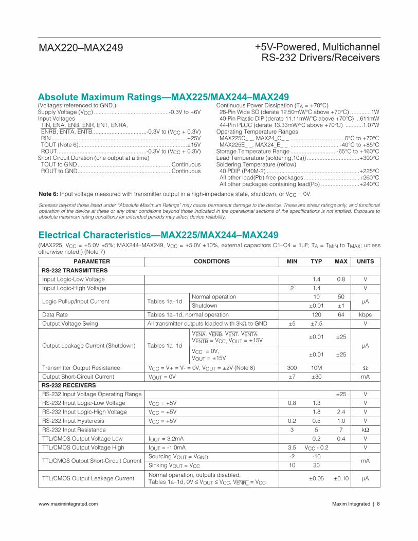
PARAMETER CONDITIONS MIN TYP MAX UNITS
RS-232 TRANSMITTERS
Output Voltage Swing All transmitter outputs loaded with 3k to GND ±5 ±8 V
Input Logic-Low Voltage 1.4 0.8 V
All devices except MAX220 2 1.4 Input Logic-High Voltage
MAX220: VCC = +5.0V 2.4 V
All except MAX220, normal operation 5 40
Logic Pullup/lnput Current VSHDN = 0V, MAX222/MAX242, shutdown, MAX220
±0.01 ±1 μA
VCC = +5.5V, VSHDN = 0V, VOUT = ±15V, MAX222/MAX242
±0.01 ±10
VOUT = ±15V ±0.01 ±10 Output Leakage Current
VCC = VSHDN = 0V MAX220, VOUT = ±12V ±25
μA
Data Rate 200 116 kbps
Transmitter Output Resistance VCC = V+ = V- = 0V, VOUT = ±2V 300 10M
VOUT = 0V ±7 ±22 Output Short-Circuit Current VOUT = 0V
MAX220 ±60 mA
RS-232 RECEIVERS
±30 RS-232 Input Voltage Operating Range
MAX220 ±25 V
All except MAX243 R2IN 0.8 1.3 RS-232 Input Threshold Low VCC = +5V
MAX243 R2IN (Note 4) -3 V
All except MAX243 R2IN 1.8 2.4 RS-232 Input Threshold High VCC = +5V
MAX243 R2IN (Note 4) -0.5 -0.1 V
MAX220–MAX249 +5V-Powered, MultichannelRS-232 Drivers/Receivers
Maxim Integrated | 3www.maximintegrated.com
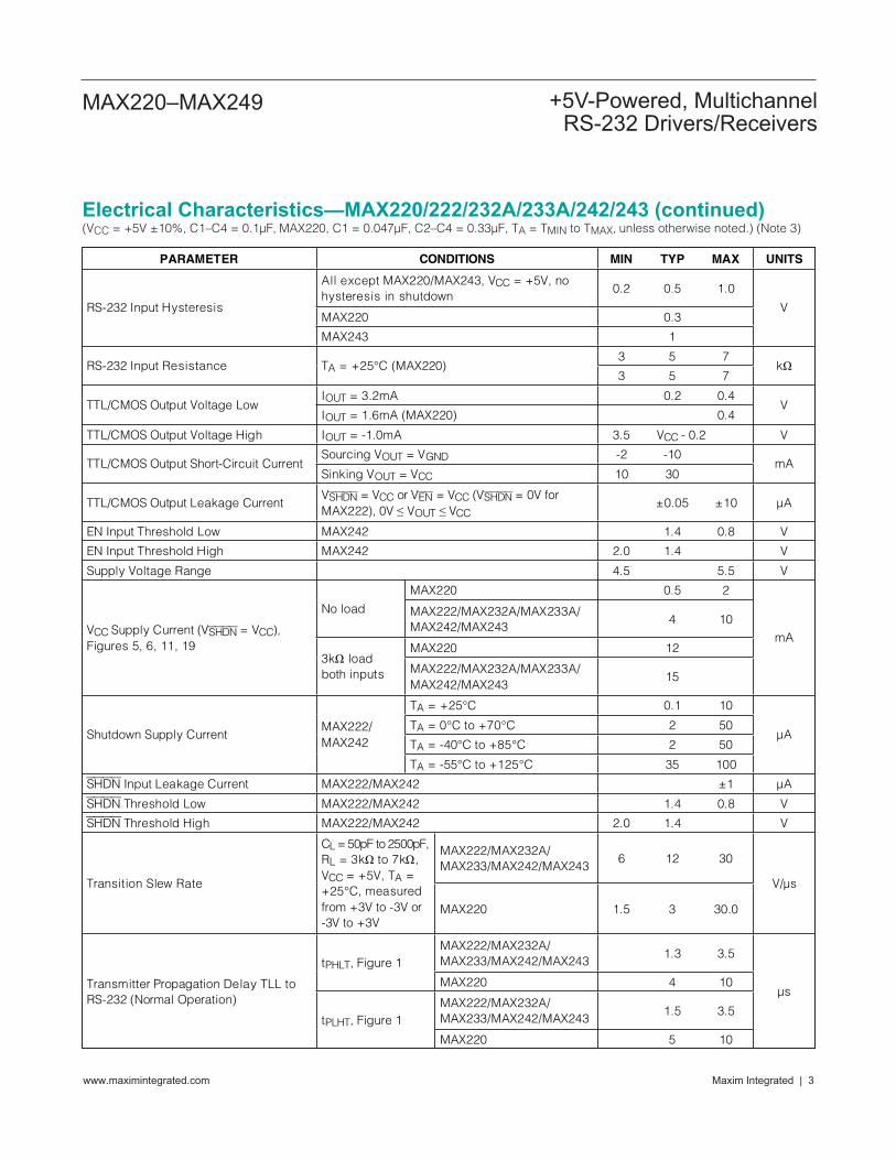
Electrical Characteristics—MAX220/222/232A/233A/242/243 (continued)(VCC = +5V ±10%, C1–C4 = 0.1µF‚ MAX220, C1 = 0.047µF, C2–C4 = 0.33µF, TA = TMIN to TMAX‚ unless otherwise noted.) (Note 3)
PARAMETER CONDITIONS MIN TYP MAX UNITS
All except MAX220/MAX243, VCC = +5V, no hysteresis in shutdown
0.2 0.5 1.0
MAX220 0.3 RS-232 Input Hysteresis
MAX243 1
V
3 5 7 RS-232 Input Resistance TA = +25°C (MAX220)
3 5 7 k
IOUT = 3.2mA 0.2 0.4 TTL/CMOS Output Voltage Low
IOUT = 1.6mA (MAX220) 0.4 V
TTL/CMOS Output Voltage High IOUT = -1.0mA 3.5 VCC - 0.2 V
Sourcing VOUT = VGND -2 -10 TTL/CMOS Output Short-Circuit Current
Sinking VOUT = VCC 10 30 mA
TTL/CMOS Output Leakage Current VSHDN = VCC or VEN = VCC (VSHDN = 0V for MAX222), 0V VOUT VCC
±0.05 ±10 μA
EN Input Threshold Low MAX242 1.4 0.8 V
EN Input Threshold High MAX242 2.0 1.4 V
Supply Voltage Range 4.5 5.5 V
MAX220 0.5 2
No load MAX222/MAX232A/MAX233A/ MAX242/MAX243
4 10
MAX220 12 VCC Supply Current (VSHDN = VCC), Figures 5, 6, 11, 19
3k load both inputs MAX222/MAX232A/MAX233A/
MAX242/MAX243 15
mA
TA = +25°C 0.1 10
TA = 0°C to +70°C 2 50
TA = -40°C to +85°C 2 50 Shutdown Supply Current
MAX222/ MAX242
TA = -55°C to +125°C 35 100
μA
SHDN Input Leakage Current MAX222/MAX242 ±1 μA
SHDN Threshold Low MAX222/MAX242 1.4 0.8 V
SHDN Threshold High MAX222/MAX242 2.0 1.4 V
MAX222/MAX232A/ MAX233/MAX242/MAX243
6 12 30
Transition Slew Rate
CL = 50pF to 2500pF, RL = 3k to 7k ,VCC = +5V, TA = +25°C, measured from +3V to -3V or -3V to +3V
MAX220 1.5 3 30.0
V/μs
MAX222/MAX232A/ MAX233/MAX242/MAX243
1.3 3.5 tPHLT, Figure 1
MAX220 4 10
MAX222/MAX232A/ MAX233/MAX242/MAX243
1.5 3.5
Transmitter Propagation Delay TLL to RS-232 (Normal Operation)
tPLHT, Figure 1
MAX220 5 10
μs
Maxim Integrated | 4www.maximintegrated.com
MAX220–MAX249 +5V-Powered, MultichannelRS-232 Drivers/Receivers
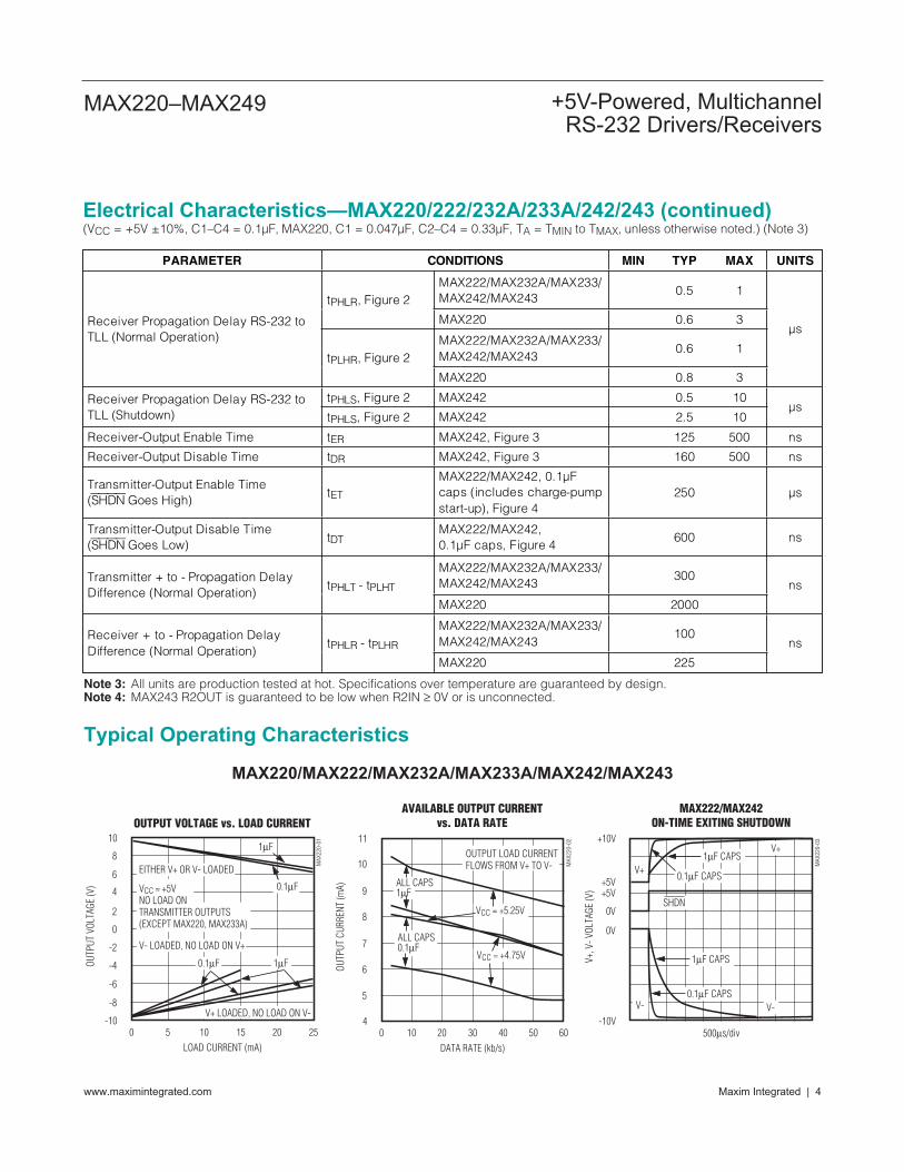
Typical Operating Characteristics
MAX220/MAX222/MAX232A/MAX233A/MAX242/MAX243
10
8
-100 5 15 25
OUTPUT VOLTAGE vs. LOAD CURRENT
-4
-6
-8
-2
6
4
2
MAX
220-
01
LOAD CURRENT (mA)
OUTP
UT V
OLTA
GE (V
)
10
0
20
0.1μF
EITHER V+ OR V- LOADED
VCC = +5VNO LOAD ONTRANSMITTER OUTPUTS(EXCEPT MAX220, MAX233A)
V- LOADED, NO LOAD ON V+
V+ LOADED, NO LOAD ON V-
1μF
1μF0.1μF
11
10
40 10 40 60
AVAILABLE OUTPUT CURRENTvs. DATA RATE
6
5
7
9
8
MAX
220-
02
DATA RATE (kb/s)
OUTP
UT C
URRE
NT (m
A)
20 30 50
OUTPUT LOAD CURRENTFLOWS FROM V+ TO V-
VCC = +5.25V
ALL CAPS1μF
ALL CAPS0.1μF
VCC = +4.75V
+10V
-10V
MAX222/MAX242ON-TIME EXITING SHUTDOWN
+5V+5V
0V
0V
MAX
220-
03
500μs/div
V+, V
- VOL
TAGE
(V)
1μF CAPSV+
V+
V-V-
SHDN
0.1μF CAPS
1μF CAPS
0.1μF CAPS
Electrical Characteristics—MAX220/222/232A/233A/242/243 (continued)(VCC = +5V ±10%, C1–C4 = 0.1µF‚ MAX220, C1 = 0.047µF, C2–C4 = 0.33µF, TA = TMIN to TMAX‚ unless otherwise noted.) (Note 3)
PARAMETER CONDITIONS MIN TYP MAX UNITS
MAX222/MAX232A/MAX233/MAX242/MAX243
0.5 1 tPHLR, Figure 2
MAX220 0.6 3
MAX222/MAX232A/MAX233/MAX242/MAX243
0.6 1
Receiver Propagation Delay RS-232 to TLL (Normal Operation)
tPLHR, Figure 2
MAX220 0.8 3
μs
tPHLS, Figure 2 MAX242 0.5 10 Receiver Propagation Delay RS-232 to TLL (Shutdown) tPHLS, Figure 2 MAX242 2.5 10
μs
Receiver-Output Enable Time tER MAX242, Figure 3 125 500 ns
Receiver-Output Disable Time tDR MAX242, Figure 3 160 500 ns
Transmitter-Output Enable Time (SHDN Goes High)
tET
MAX222/MAX242, 0.1μF caps (includes charge-pump start-up), Figure 4
250 μs
Transmitter-Output Disable Time (SHDN Goes Low)
tDTMAX222/MAX242, 0.1μF caps, Figure 4
600 ns
MAX222/MAX232A/MAX233/MAX242/MAX243
300 Transmitter + to - Propagation Delay Difference (Normal Operation)
tPHLT - tPLHT
MAX220 2000
ns
MAX222/MAX232A/MAX233/MAX242/MAX243
100 Receiver + to - Propagation Delay Difference (Normal Operation)
tPHLR - tPLHR
MAX220 225
ns
Note 3: All units are production tested at hot. Specifications over temperature are guaranteed by design.Note 4: MAX243 R2OUT is guaranteed to be low when R2IN ≥ 0V or is unconnected.
(Voltages referenced to GND.)VCC...........................................................................-0.3V to +6VV+................................................................(VCC - 0.3V) to +14VV- ............................................................................+0.3V to -14VInput VoltagesTIN............................................................-0.3V to (VCC + 0.3V)RIN .....................................................................................±30V
Output VoltagesTOUT ..................................................(V+ + 0.3V) to (V- - 0.3V)ROUT........................................................-0.3V to (VCC + 0.3V)
Short-Circuit Duration, TOUT to GND ........................ContinuousContinuous Power Dissipation (TA = +70°C)
14-Pin Plastic DIP (derate 10.00mW/°C above +70°C)....800mW16-Pin Plastic DIP (derate 10.53mW/°C above +70°C)....842mW20-Pin Plastic DIP (derate 11.11mW/°C above +70°C)....889mW24-Pin Narrow Plastic DIP
(derate 13.33mW/°C above +70°C) ..........1.07W24-Pin Plastic DIP (derate 9.09mW/°C above +70°C)......500mW16-Pin Wide SO (derate 9.52mW/°C above +70°C).........762mW20-Pin Wide SO (derate 10.00mW/°C above +70°C).......800mW24-Pin Wide SO (derate 11.76mW/°C above +70°C).......941mW
28-Pin Wide SO (derate 12.50mW/°C above +70°C) .............1W44-Pin Plastic FP (derate 11.11mW/°C above +70°C) .....889mW14-Pin CERDIP (derate 9.09mW/°C above +70°C) ..........727mW16-Pin CERDIP (derate 10.00mW/°C above +70°C) ........800mW20-Pin CERDIP (derate 11.11mW/°C above +70°C) ........889mW24-Pin Narrow CERDIP
(derate 12.50mW/°C above +70°C) ..............1W24-Pin Sidebraze (derate 20.0mW/°C above +70°C)..........1.6W28-Pin SSOP (derate 9.52mW/°C above +70°C).............762mW
Operating Temperature RangesMAX2 _ _ C _ _......................................................0°C to +70°CMAX2 _ _ E _ _ ...................................................-40°C to +85°CMAX2 _ _ M _ _......................................................-55°C to +125°C
Storage Temperature Range .............................-65°C to +160°CLead Temperature (soldering, 10s) .................................+300°CSoldering Temperature (reflow)20 PDIP (P20M+1) .........................................................+225°C24 PDIP (P24M-1) ..........................................................+225°CAll other lead(Pb)-free packages...................................+260°CAll other packages containing lead(Pb) ...........................+240°C
MAX220–MAX249 +5V-Powered, MultichannelRS-232 Drivers/Receivers
Maxim Integrated | 5www.maximintegrated.com
Absolute Maximum Ratings—MAX223/MAX230–MAX241
Electrical Characteristics—MAX223/MAX230–MAX241(MAX223/230/232/234/236/237/238/240/241, VCC = +5V ±10%; MAX233/MAX235, VCC = +5V ±5%‚ C1–C4 = 1.0µF;MAX231/MAX239, VCC = +5V ±10%; V+ = +7.5V to +13.2V; TA = TMIN to TMAX; unless otherwise noted.) (Note 5)
Stresses beyond those listed under “Absolute Maximum Ratings” may cause permanent damage to the device. These are stress ratings only, and functionaloperation of the device at these or any other conditions beyond those indicated in the operational sections of the specifications is not implied. Exposure toabsolute maximum rating conditions for extended periods may affect device reliability.
CONDITIONS MIN TYP MAX UNITS
Output Voltage Swing All transmitter outputs loaded with 3kΩ to ground ±5.0 ±7.3 V
VCC Supply CurrentNo load,TA = +25°C
5 10
mA7 15
0.4 1
V+ Supply Current1.8 5
mA5 15
Shutdown Supply Current TA = +25°C15 50
VInput Logic-High Voltage
TIN 2.0
EN, SHDN (MAX223);EN, SHDN (MAX230/235/236/240/241)
2.4
Logic Pullup Current VTIN = 0V 1.5 200
Receiver Input VoltageOperating Range
-30 +30 V
µA
µA1 10
VInput Logic-Low Voltage TIN, EN, SHDN (MAX233); EN, SHDN (MAX230/235–241) 0.8
MAX231/239
MAX223/230/234–238/240/241
MAX232/233
PARAMETER
MAX239
MAX230/235/236/240/241
MAX231
MAX223
Maxim Integrated | 6www.maximintegrated.com
MAX220–MAX249 +5V-Powered, MultichannelRS-232 Drivers/Receivers
mA
V
0.8 1.2
PARAMETER MIN TYP MAX UNITSCONDITIONS
Normal operationVSHDN = 5V (MAX223)VSHDN = 0V (MAX235/236/240/241)
1.7 2.4
RS-232 Input Logic-Low VoltageTA = +25°C, VCC = +5V
0.6 1.5
VRS-232 Input Logic-High VoltageTA = +25°C,VCC = +5V Shutdown (MAX223)
VSHDN = 0V,VEN = +5V (R4IN‚ R5IN)
1.5 2.4
Electrical Characteristics—MAX223/MAX230–MAX241 (continued)(MAX223/230/232/234/236/237/238/240/241, VCC = +5V ±10%; MAX233/MAX235, VCC = +5V ±5%‚ C1–C4 = 1.0µF;MAX231/MAX239, VCC = +5V ±10%; V+ = +7.5V to +13.2V; TA = TMIN to TMAX; unless otherwise noted.) (Note 5)
Shutdown (MAX223)VSHDN = 0V,VEN = +5V (R4IN, R5IN)
Normal operationVSHDN = +5V (MAX223)VSHDN = 0V (MAX235/236/240/241)
RS-232 Input Hysteresis VCC = +5V, no hysteresis in shutdown 0.2 0.5 1.0 V
RS-232 Input Resistance TA = +25°C, VCC = +5V 3 5 7 kΩ
TTL/CMOS Output Voltage Low IOUT = 1.6mA (MAX231/232/233, IOUT = 3.2mA) 0.4 V
TTL/CMOS Output Voltage High IOUT = -1mA 3.5 VCC - 0.4 V
TTL/CMOS Output Leakage Current0V ≤ ROUT ≤ VCC; VEN = 0V (MAX223); VEN = VCC (MAX235–241)
±0.05 ±10 µA
MAX223 600nsReceiver Output Enable Time
Normal operation MAX235/236/239/240/241 400
MAX223 900nsReceiver Output Disable Time
Normal operation MAX235/236/239/240/241 250
Normal operation 0.5 10
µsVSHDN = 0V(MAX223)
4 40Propagation DelayRS-232 IN toTTL/CMOS OUT,CL = 150pF 6 40
3 5.1 30
V/µsMAX231/MAX232/MAX233, TA = +25°C, VCC = +5V,RL = 3kΩ to 7kΩ, CL = 50pF to 2500pF, measured from+3V to -3V or -3V to +3V
4 30
Transmitter Output Resistance VCC = V+ = V- = 0V, VOUT = ±2V 300 Ω
Transmitter Output Short-CircuitCurrent
±10 mA
tPHLS
tPLHS
Transition Region Slew Rate
MAX223/MAX230/MAX234–241, TA = +25°C, VCC = +5V,RL = 3kΩ to 7kΩ‚ CL = 50pF to 2500pF, measured from+3V to -3V or -3V to +3V
Note 5: All units are production tested at hot except for the MAX240, which is production tested at TA = +25°C. Specifications overtemperature are guaranteed by design.
Maxim Integrated | 7www.maximintegrated.com
MAX220–MAX249 +5V-Powered, MultichannelRS-232 Drivers/Receivers
8.5
6.54.5 5.5
TRANSMITTER OUTPUTVOLTAGE (VOH) vs. VCC
7.0
8.0
MAX
220-
04
VCC (V)
V OH
(V)
5.0
7.5
1 TRANSMITTERLOADED
3 TRANS-MITTERSLOADED
4 TRANSMITTERSLOADED
2 TRANSMITTERSLOADED
TA = +25°CC1–C4 = 1μFTRANSMITTERLOADS =3kΩ || 2500pF
7.4
6.00 2500
TRANSMITTER OUTPUT VOLTAGE (VOH)vs. LOAD CAPACITANCE AT
DIFFERENT DATA RATES
6.4
6.2
7.2
7.0
MAX
220-
05
LOAD CAPACITANCE (pF)
V OH
(V)
15001000500 2000
6.8
6.6
160kb/s80kb/s20kb/s
TA = +25°CVCC = +5V3 TRANSMITTERS LOADEDRL = 3kΩC1–C4 = 1μF
12.0
4.00 2500
TRANSMITTER SLEW RATEvs. LOAD CAPACITANCE
6.0
5.0
11.0
9.0
10.0
MAX
220-
06
LOAD CAPACITANCE (pF)
SLEW
RAT
E (V
/μs)
15001000500 2000
8.0
7.0
TA = +25°CVCC = +5VLOADED, RL = 3kΩC1–C4 = 1μF
1 TRANSMITTER LOADED
2 TRANSMITTERS LOADED
3 TRANSMITTERS LOADED
4 TRANSMITTERS LOADED
-6.0
-9.04.5 5.5
TRANSMITTER OUTPUTVOLTAGE (VOL) vs. VCC
-8.0
-8.5
-6.5
-7.0
MAX
220-
07
VCC (V)
V OL (
V)
5.0
-7.5
4 TRANS-MITTERSLOADED
TA = +25°CC1–C4 = 1μFTRANSMITTERLOADS =3kΩ || 2500pF
1 TRANS-MITTERLOADED
2 TRANS-MITTERSLOADED
3 TRANS-MITTERSLOADED
-6.0
-7.60 2500
TRANSMITTER OUTPUT VOLTAGE (VOL) vs. LOAD CAPACITANCE AT
DIFFERENT DATA RATES
-7.0
-7.2
-7.4
-6.2
-6.4
MAX
220-
08
LOAD CAPACITANCE (pF)
V OL (
V)
15001000500 2000
-6.6
-6.8 160kb/s80kb/s20kb/s
TA = +25°CVCC = +5V3 TRANSMITTERS LOADEDRL = 3kΩC1–C4 = 1μF
10
-100 5 10 15 20 25 30 35 40 45 50
TRANSMITTER OUTPUT VOLTAGE (V+, V-)vs. LOAD CURRENT
-2
-6
-4
-8
8
6
MAX
220-
09
CURRENT (mA)
V+, V
- (V)
4
2
0V+ AND V-EQUALLYLOADED
V- LOADED,NO LOADON V+
TA = +25°CVCC = +5VC1–C4 = 1μF
ALL TRANSMITTERS UNLOADED
V+ LOADED,NO LOADON V-
Typical Operating Characteristics
MAX223/MAX230–MAX241
*SHUTDOWN POLARITY IS REVERSED FOR NON MAX241 PARTS
V+, V- WHEN EXITING SHUTDOWN(1μF CAPACITORS)
MAX220-13
VSHDN*
V-
O
V+
500ms/div
Maxim Integrated | 8www.maximintegrated.com
MAX220–MAX249 +5V-Powered, MultichannelRS-232 Drivers/Receivers
Input Logic-Low Voltage
Absolute Maximum Ratings—MAX225/MAX244–MAX249
Electrical Characteristics—MAX225/MAX244–MAX249(MAX225, VCC = +5.0V ±5%; MAX244–MAX249, VCC = +5.0V ±10%, external capacitors C1–C4 = 1µF; TA = TMIN to TMAX; unlessotherwise noted.) (Note 7)
Stresses beyond those listed under “Absolute Maximum Ratings” may cause permanent damage to the device. These are stress ratings only, and functionaloperation of the device at these or any other conditions beyond those indicated in the operational sections of the specifications is not implied. Exposure toabsolute maximum rating conditions for extended periods may affect device reliability.
(Voltages referenced to GND.)Supply Voltage (VCC) ...............................................-0.3V to +6VInput Voltages
TIN‚ ENA, ENB, ENR, ENT, ENRA,ENRB, ENTA, ENTB..................................-0.3V to (VCC + 0.3V)RIN .....................................................................................±25VTOUT (Note 6)....................................................................±15VROUT........................................................-0.3V to (VCC + 0.3V)
Short Circuit Duration (one output at a time)TOUT to GND...........................................................ContinuousROUT to GND...........................................................Continuous
Continuous Power Dissipation (TA = +70°C)28-Pin Wide SO (derate 12.50mW/°C above +70°C) .............1W40-Pin Plastic DIP (derate 11.11mW/°C above +70°C) ...611mW44-Pin PLCC (derate 13.33mW/°C above +70°C) ...........1.07W
Operating Temperature RangesMAX225C_ _, MAX24_C_ _ ..................................0°C to +70°CMAX225E_ _, MAX24_E_ _ ...............................-40°C to +85°C
Storage Temperature Range .............................-65°C to +160°CLead Temperature (soldering,10s)) .................................+300°CSoldering Temperature (reflow)
40 PDIP (P40M-2) ..........................................................+225°CAll other lead(Pb)-free packages...................................+260°CAll other packages containing lead(Pb) ........................+240°C
VCC = 0V, VOUT = ±15V
µATables 1a–1d
±0.01 ±25
Normal operation
Shutdown
Tables 1a–1d, normal operation
All transmitter outputs loaded with 3kΩ to GND
VENA, VENB, VENT, VENTA, VENTB = VCC, VOUT = ±15V
VRS-232 Input Hysteresis
RS-232 Input Logic-Low Voltage V
V±5 ±7.5Output Voltage Swing
Output Leakage Current (Shutdown)
±0.01 ±25
Ω300 10MVCC = V+ = V- = 0V, VOUT = ±2V (Note 8)Transmitter Output Resistance
µA
PARAMETER
±0.05 ±0.10
MIN TYP MAX UNITS
Normal operation, outputs disabled,Tables 1a–1d, 0V ≤ VOUT ≤ VCC, VENR_ = VCC
TTL/CMOS Output Leakage Current
10 30Sinking VOUT = VCCmA
-2 -10Sourcing VOUT = VGND
V3.5 VCC - 0.2IOUT = -1.0mATTL/CMOS Output Voltage High
V0.2 0.4IOUT = 3.2mATTL/CMOS Output Voltage Low
kΩ3 5 7
0.2 0.5 1.0VCC = +5V
1.4 0.8 V
TTL/CMOS Output Short-Circuit Current
V1.8 2.4
0.8 1.3VCC = +5V
RS-232 Input Resistance
V±25RS-232 Input Voltage Operating Range
mA±7 ±30VOUT = 0VOutput Short-Circuit Current
kbps120 64Data Rate
CONDITIONS
VCC = +5V
µA±0.01 ±1
Logic Pullup/lnput Current10 50
Tables 1a–1d
RS-232 Input Logic-High Voltage
V2 1.4Input Logic-High Voltage
RS-232 TRANSMITTERS
RS-232 RECEIVERS
Note 6: Input voltage measured with transmitter output in a high-impedance state, shutdown, or VCC = 0V.

MAX220–MAX249 +5V-Powered, MultichannelRS-232 Drivers/Receivers
Maxim Integrated | 9www.maximintegrated.com
Supply Voltage Range4.75 5.25
V
Transmitter Enable Time
MAX225 10 20
tET
No loadMAX244–MAX249 11 30
5 10 30
MAX225 40VCC Supply Current (Normal Operation) 3kΩ loads on
all outputs MAX244–MAX249 57
mA
Transition Slew Rate
8 25
CL = 50pF to 2500pF, RL = 3kΩ to 7kΩ, VCC = +5V,TA = +25°C, measured from +3V to -3V or -3V to +3V
TA = TMIN to TMAX
CONDITIONS
50
V/µs
MAX246–MAX249 (excludes charge-pump startup)
Shutdown Supply Current µA
5
tPHLT, Figure 1 1.3 3.5
µs
tPLHT, Figure 1 1.5 3.5
Transmitter Disable Time
Transmitter Propagation DelayTLL to RS-232 (Normal Operation)
µs
tDT, Figure 4 100 ns
Transmitter + to - Propagation Delay Difference (Normal Operation)
tPHLT - tPLHT
UNITSMIN TYP MAX
350
PARAMETER
ns
Receiver + to - Propagation Delay Difference (Normal Operation)
tPHLR - tPLHR 350 ns
4.5 5.5MAX244–MAX249
MAX225
Leakage current ±1
Logic-low voltage 1.4 0.8Control Input
Logic-high voltage 2.4 1.4V
µA
TA = +25°C
tPHLR, Figure 2 0.6 1.5
tPLHR, Figure 2 0.6 1.5
Receiver Propagation DelayTLL to RS-232 (Normal Operation)
µs
tPHLS, Figure 2 0.6 10
tPLHS, Figure 2 3.0 10
Receiver Propagation Delay TLL to RS-232 (Low-Power Mode)
µs
Receiver-Output Enable Time tER, Figure 3 100 500 ns
Receiver-Output Disable Time tDR, Figure 3 100 500 ns
MAX225/MAX245–MAX249(includes charge-pump startup)
10 ms
POWER SUPPLY AND CONTROL LOGIC
AC CHARACTERISTICS
Note 7: All units production tested at hot. Specifications over temperature are guaranteed by design.Note 8: The 300Ω minimum specification complies with EIA/TIA-232E, but the actual resistance when in shutdown mode or VCC =
0V is 10MΩ as is implied by the leakage specification.
Electrical Characteristics—MAX225/MAX244–MAX249 (continued)(MAX225, VCC = +5.0V ±5%; MAX244–MAX249, VCC = +5.0V ±10%, external capacitors C1–C4 = 1µF; TA = TMIN to TMAX; unlessotherwise noted.) (Note 7)
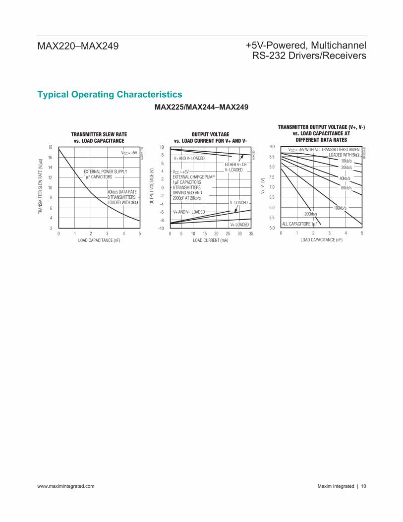
Typical Operating Characteristics
MAX225/MAX244–MAX249
18
20 1 2 3 4 5
TRANSMITTER SLEW RATEvs. LOAD CAPACITANCE
8
6
4
16 MAX
220-
10
LOAD CAPACITANCE (nF)
TRAN
SMIT
TER
SLEW
RAT
E (V
/μs)
14
12
10
VCC = +5V
EXTERNAL POWER SUPPLY1μF CAPACITORS
40kb/s DATA RATE 8 TRANSMITTERSLOADED WITH 3kΩ
10
-100 5 10 15 20 25 30 35
OUTPUT VOLTAGEvs. LOAD CURRENT FOR V+ AND V-
-2
-4
-6
-8
8
MAX
220-
11
LOAD CURRENT (mA)
OUTP
UT V
OLTA
GE (V
)
6
4
2
0
V+ AND V- LOADEDEITHER V+ OR V- LOADED
V+ AND V- LOADED
VCC = +5VEXTERNAL CHARGE PUMP1μF CAPACITORS 8 TRANSMITTERSDRIVING 5kΩ AND2000pF AT 20kb/s
V- LOADED
V+ LOADED
9.0
5.00 1 2 3 4 5
TRANSMITTER OUTPUT VOLTAGE (V+, V-)vs. LOAD CAPACITANCE AT
DIFFERENT DATA RATES
6.0
5.5
8.5 MAX
220-
12
LOAD CAPACITANCE (nF)
V+, V
- (V)
8.0
7.5
7.0
6.5
VCC = +5V WITH ALL TRANSMITTERS DRIVENLOADED WITH 5kΩ
40kb/s
60kb/s
100kb/s200kb/s
ALL CAPACITIORS 1μF
10kb/s20kb/s
Maxim Integrated | 10www.maximintegrated.com
MAX220–MAX249 +5V-Powered, MultichannelRS-232 Drivers/Receivers
MAX220–MAX249 +5V-Powered, MultichannelRS-232 Drivers/Receivers
Maxim Integrated | 11www.maximintegrated.com
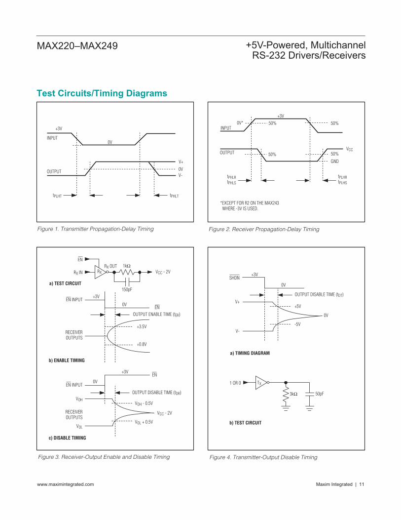
INPUT
OUTPUT
+3V
V+
0VV-
0V
tPLHT tPHLT
tPHLRtPHLS
tPLHRtPLHS
50%VCC
50%+3V
50%INPUT
OUTPUT
*EXCEPT FOR R2 ON THE MAX243 WHERE -3V IS USED.
0V*
50%GND
Figure 1. Transmitter Propagation-Delay Timing Figure 2. Receiver Propagation-Delay Timing
EN
RX IN
a) TEST CIRCUIT
b) ENABLE TIMING
c) DISABLE TIMING
EN INPUT
RECEIVEROUTPUTS
RX OUTRX
1kΩ
0V
+3V
EN
EN
+0.8V
+3.5V
OUTPUT ENABLE TIME (tER)
VCC - 2V
VOL + 0.5V
VOH - 0.5V
OUTPUT DISABLE TIME (tDR)
VCC - 2V
+3V
0V
150pF
EN INPUT
VOH
RECEIVEROUTPUTS
VOL
1 OR 0 TX
3kΩ 50pF
-5V
+5V
OUTPUT DISABLE TIME (tDT)V+
SHDN+3V
0V
V-
0V
a) TIMING DIAGRAM
b) TEST CIRCUIT
Figure 3. Receiver-Output Enable and Disable Timing Figure 4. Transmitter-Output Disable Timing
Test Circuits/Timing Diagrams
Maxim Integrated | 12www.maximintegrated.com
MAX220–MAX249 +5V-Powered, MultichannelRS-232 Drivers/Receivers
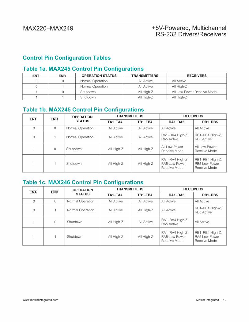
ENT ENR OPERATION STATUS TRANSMITTERS RECEIVERS
0 0 Normal Operation All Active All Active
0 1 Normal Operation All Active All High-Z
1 0 Shutdown All High-Z All Low-Power Receive Mode
1 1 Shutdown All High-Z All High-Z
Table 1a. MAX245 Control Pin Configurations
ENT ENROPERATION
STATUSTRANSMITTERS RECEIVERS
TA1–TA4 TB1–TB4 RA1–RA5 RB1–RB5
0 0 Normal Operation All Active All Active All Active All Active
0 1 Normal Operation All Active All ActiveRA1–RA4 High-Z,RA5 Active
RB1–RB4 High-Z,RB5 Active
1 0 Shutdown All High-Z All High-ZAll Low-PowerReceive Mode
All Low-PowerReceive Mode
1 1 Shutdown All High-Z All High-ZRA1–RA4 High-Z,RA5 Low-PowerReceive Mode
RB1–RB4 High-Z,RB5 Low-PowerReceive Mode
Table 1b. MAX245 Control Pin Configurations
Table 1c. MAX246 Control Pin Configurations
ENA ENBOPERATION
STATUSTRANSMITTERS RECEIVERS
TA1–TA4 TB1–TB4 RA1–RA5 RB1–RB5
0 0 Normal Operation All Active All Active All Active All Active
0 1 Normal Operation All Active All High-Z All ActiveRB1–RB4 High-Z,RB5 Active
1 0 Shutdown All High-Z All ActiveRA1–RA4 High-Z,RA5 Active
All Active
1 1 Shutdown All High-Z All High-ZRA1–RA4 High-Z,RA5 Low-PowerReceive Mode
RB1–RB4 High-Z,RA5 Low-PowerReceive Mode
Control Pin Configuration Tables
MAX220–MAX249 +5V-Powered, MultichannelRS-232 Drivers/Receivers
Maxim Integrated | 13www.maximintegrated.com
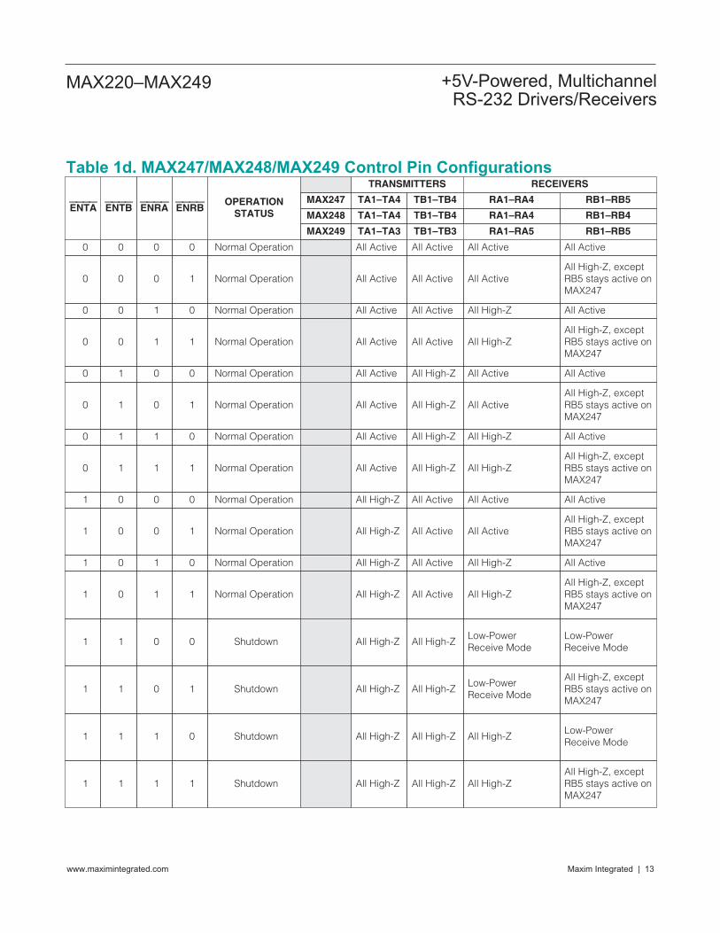
TA1–TA4 TB1–TB4 RA1–RA4 RB1–RB4
0 0 0 0 Normal Operation All Active All Active All Active All Active
0 0 0 1 Normal Operation All Active All Active All ActiveAll High-Z, exceptRB5 stays active onMAX247
0 0 1 0 Normal Operation All Active All Active All High-Z All Active
0 0 1 1 Normal Operation All Active All Active All High-ZAll High-Z, exceptRB5 stays active onMAX247
0 1 0 0 Normal Operation All Active All High-Z All Active All Active
0 1 0 1 Normal Operation All Active All High-Z All ActiveAll High-Z, exceptRB5 stays active onMAX247
0 1 1 0 Normal Operation All Active All High-Z All High-Z All Active
0 1 1 1 Normal Operation All Active All High-Z All High-ZAll High-Z, exceptRB5 stays active onMAX247
1 0 0 0 Normal Operation All High-Z All Active All Active All Active
1 0 0 1 Normal Operation All High-Z All Active All ActiveAll High-Z, exceptRB5 stays active onMAX247
1 0 1 0 Normal Operation All High-Z All Active All High-Z All Active
1 0 1 1 Normal Operation All High-Z All Active All High-ZAll High-Z, exceptRB5 stays active onMAX247
1 1 0 0 Shutdown All High-Z All High-ZLow-PowerReceive Mode
Low-PowerReceive Mode
1 1 0 1 Shutdown All High-Z All High-ZLow-PowerReceive Mode
All High-Z, exceptRB5 stays active onMAX247
1 1 1 0 Shutdown All High-Z All High-Z All High-ZLow-PowerReceive Mode
1 1 1 1 Shutdown All High-Z All High-Z All High-ZAll High-Z, exceptRB5 stays active onMAX247
Table 1d. MAX247/MAX248/MAX249 Control Pin Configurations
MAX248OPERATION
STATUSENRBMAX247 TA1–TA4 TB1–TB4 RA1–RA4 RB1–RB5
TRANSMITTERS
ENRAENTBENTA
MAX249 TA1–TA3 TB1–TB3 RA1–RA5 RB1–RB5
RECEIVERS
Maxim Integrated | 14www.maximintegrated.com
MAX220–MAX249 +5V-Powered, MultichannelRS-232 Drivers/Receivers
Detailed DescriptionThe MAX220–MAX249 contain four sections: dualcharge-pump DC-DC voltage converters, RS-232 dri-vers, RS-232 receivers, and receiver and transmitterenable control inputs.
Dual Charge-Pump Voltage ConverterThe MAX220–MAX249 have two internal charge-pumpsthat convert +5V to ±10V (unloaded) for RS-232 driveroperation. The first converter uses capacitor C1 to dou-ble the +5V input to +10V on C3 at the V+ output. Thesecond converter uses capacitor C2 to invert +10V to -10V on C4 at the V- output.
A small amount of power may be drawn from the +10V(V+) and -10V (V-) outputs to power external circuitry(see the Typical Operating Characteristics section),except on the MAX225 and MAX245–MAX247, wherethese pins are not available. V+ and V- are not regulated,so the output voltage drops with increasing load current.Do not load V+ and V- to a point that violates the mini-mum ±5V EIA/TIA-232E driver output voltage whensourcing current from V+ and V- to external circuitry.
When using the shutdown feature in the MAX222,MAX225, MAX230, MAX235, MAX236, MAX240,MAX241, and MAX245–MAX249, avoid using V+ and V-to power external circuitry. When these parts are shutdown, V- falls to 0V, and V+ falls to +5V. For applica-tions where a +10V external supply is applied to the V+pin (instead of using the internal charge pump to gen-erate +10V), the C1 capacitor must not be installed andthe SHDN pin must be connected to VCC. This isbecause V+ is internally connected to VCC in shutdownmode.
RS-232 DriversThe typical driver output voltage swing is ±8V whenloaded with a nominal 5kΩ RS-232 receiver and VCC =+5V. Output swing is guaranteed to meet the EIA/TIA-232E and V.28 specification, which calls for ±5V mini-mum driver output levels under worst-case conditions.These include a minimum 3kΩ load, VCC = +4.5V, andmaximum operating temperature. Unloaded driver out-put voltage ranges from (V+ -1.3V) to (V- +0.5V).
Input thresholds are both TTL and CMOS compatible.The inputs of unused drivers can be left unconnectedsince 400kΩ input pullup resistors to VCC are built in(except for the MAX220). The pullup resistors force theoutputs of unused drivers low because all drivers invert.The internal input pullup resistors typically source 12µA,except in shutdown mode where the pullups are dis-abled. Driver outputs turn off and enter a high-imped-ance state—where leakage current is typicallymicroamperes (maximum 25µA)—when in shutdown
mode, in three-state mode, or when device power isremoved. Outputs can be driven to ±15V. The power-supply current typically drops to 8µA in shutdown mode.The MAX220 does not have pullup resistors to force theoutputs of the unused drivers low. Connect unusedinputs to GND or VCC.
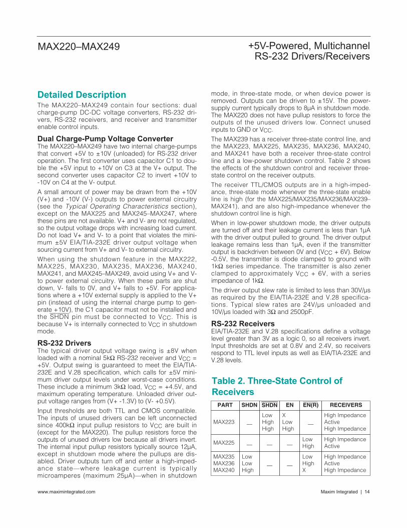
The MAX239 has a receiver three-state control line, andthe MAX223, MAX225, MAX235, MAX236, MAX240,and MAX241 have both a receiver three-state controlline and a low-power shutdown control. Table 2 showsthe effects of the shutdown control and receiver three-state control on the receiver outputs.
The receiver TTL/CMOS outputs are in a high-imped-ance, three-state mode whenever the three-state enableline is high (for the MAX225/MAX235/MAX236/MAX239–MAX241), and are also high-impedance whenever theshutdown control line is high.
When in low-power shutdown mode, the driver outputsare turned off and their leakage current is less than 1µAwith the driver output pulled to ground. The driver outputleakage remains less than 1µA, even if the transmitteroutput is backdriven between 0V and (VCC + 6V). Below-0.5V, the transmitter is diode clamped to ground with1kΩ series impedance. The transmitter is also zenerclamped to approximately VCC + 6V, with a seriesimpedance of 1kΩ.
The driver output slew rate is limited to less than 30V/µsas required by the EIA/TIA-232E and V.28 specifica-tions. Typical slew rates are 24V/µs unloaded and10V/µs loaded with 3Ω and 2500pF.
RS-232 ReceiversEIA/TIA-232E and V.28 specifications define a voltagelevel greater than 3V as a logic 0, so all receivers invert.Input thresholds are set at 0.8V and 2.4V, so receiversrespond to TTL level inputs as well as EIA/TIA-232E andV.28 levels.
PART SHDN EN EN(R) RECEIVERS
MAX223 __LowHighHigh
XLowHigh
High ImpedanceActiveHigh Impedance
MAX225 __ __High ImpedanceActive
__
MAX235MAX236MAX240
LowLowHigh
__ __LowHighX
High ImpedanceActiveHigh Impedance
Table 2. Three-State Control of
Receivers
LowHigh
SHDN
__
MAX220–MAX249 +5V-Powered, MultichannelRS-232 Drivers/Receivers
Maxim Integrated | 15www.maximintegrated.com
The receiver inputs withstand an input overvoltage upto ±25V and provide input terminating resistors withnominal 5kΩ values. The receivers implement Type 1interpretation of the fault conditions of V.28 andEIA/TIA-232E.
The receiver input hysteresis is typically 0.5V with aguaranteed minimum of 0.2V. This produces clear out-put transitions with slow-moving input signals, evenwith moderate amounts of noise and ringing. Thereceiver propagation delay is typically 600ns and isindependent of input swing direction.
Low-Power Receive ModeThe low-power receive mode feature of the MAX223,MAX242, and MAX245–MAX249 puts the IC into shut-down mode but still allows it to receive information. Thisis important for applications where systems are periodi-cally awakened to look for activity. Using low-powerreceive mode, the system can still receive a signal thatwill activate it on command and prepare it for communi-cation at faster data rates. This operation conservessystem power.
Negative Threshold—MAX243The MAX243 is pin compatible with the MAX232A, differ-ing only in that RS-232 cable fault protection is removedon one of the two receiver inputs. This means that controllines such as CTS and RTS can either be driven or leftunconnected without interrupting communication.Different cables are not needed to interface with differentpieces of equipment.
The input threshold of the receiver without cable faultprotection is -0.8V rather than +1.4V. Its output goespositive only if the input is connected to a control linethat is actively driven negative. If not driven, it defaultsto the 0 or “OK to send” state. Normally‚ the MAX243’sother receiver (+1.4V threshold) is used for the data line(TD or RD)‚ while the negative threshold receiver is con-nected to the control line (DTR‚ DTS‚ CTS‚ RTS, etc.).
Other members of the RS-232 family implement theoptional cable fault protection as specified by EIA/TIA-232E specifications. This means a receiver output goeshigh whenever its input is driven negative‚ left uncon-nected‚ or shorted to ground. The high output tells theserial communications IC to stop sending data. Toavoid this‚ the control lines must either be driven orconnected with jumpers to an appropriate positive volt-age level.
Shutdown—MAX222–MAX242 On the MAX222‚ MAX235‚ MAX236‚ MAX240‚ andMAX241‚ all receivers are disabled during shutdown.On the MAX223 and MAX242‚ two receivers continue tooperate in a reduced power mode when the chip is inshutdown. Under these conditions‚ the propagationdelay increases to about 2.5µs for a high-to-low inputtransition. When in shutdown, the receiver acts as aCMOS inverter with no hysteresis. The MAX223 andMAX242 also have a receiver output enable input (ENfor the MAX242 and EN for the MAX223) that allowsreceiver output control independent of SHDN (SHDNfor MAX241). With all other devices‚ SHDN (SHDN forMAX241) also disables the receiver outputs.
The MAX225 provides five transmitters and fivereceivers‚ while the MAX245 provides ten receivers andeight transmitters. Both devices have separate receiverand transmitter-enable controls. The charge pumpsturn off and the devices shut down when a logic high isapplied to the ENT input. In this state, the supply cur-rent drops to less than 25µA and the receivers continueto operate in a low-power receive mode. Driver outputsenter a high-impedance state (three-state mode). Onthe MAX225‚ all five receivers are controlled by theENR input. On the MAX245‚ eight of the receiver out-puts are controlled by the ENR input‚ while the remain-ing two receivers (RA5 and RB5) are always active.RA1–RA4 and RB1–RB4 are put in a three-state modewhen ENR is a logic high.
Receiver and Transmitter Enable Control Inputs The MAX225 and MAX245–MAX249 feature transmitterand receiver enable controls.
The receivers have three modes of operation: full-speedreceive (normal active)‚ three-state (disabled)‚ and low-power receive (enabled receivers continue to functionat lower data rates). The receiver enable inputs controlthe full-speed receive and three-state modes. Thetransmitters have two modes of operation: full-speedtransmit (normal active) and three-state (disabled). Thetransmitter enable inputs also control the shutdownmode. The device enters shutdown mode when alltransmitters are disabled. Enabled receivers function inthe low-power receive mode when in shutdown.
Maxim Integrated | 16www.maximintegrated.com
MAX220–MAX249 +5V-Powered, MultichannelRS-232 Drivers/Receivers
Tables 1a–1d define the control states. The MAX244has no control pins and is not included in these tables.
The MAX246 has ten receivers and eight drivers withtwo control pins, each controlling one side of thedevice. A logic high at the A-side control input (ENA)causes the four A-side receivers and drivers to go intoa three-state mode. Similarly, the B-side control input(ENB) causes the four B-side drivers and receivers togo into a three-state mode. As in the MAX245, one A-side and one B-side receiver (RA5 and RB5) remainactive at all times. The entire device is put into shut-down mode when both the A and B sides are disabled(ENA = ENB = +5V).
The MAX247 provides nine receivers and eight driverswith four control pins. The ENRA and ENRB receiverenable inputs each control four receiver outputs. TheENTA and ENTB transmitter enable inputs each controlfour drivers. The ninth receiver (RB5) is always active.The device enters shutdown mode with a logic high onboth ENTA and ENTB.
The MAX248 provides eight receivers and eight driverswith four control pins. The ENRA and ENRB receiverenable inputs each control four receiver outputs. TheENTA and ENTB transmitter enable inputs control fourdrivers each. This part does not have an always-activereceiver. The device enters shutdown mode and trans-mitters go into a three-state mode with a logic high onboth ENTA and ENTB.
The MAX249 provides ten receivers and six drivers withfour control pins. The ENRA and ENRB receiver enableinputs each control five receiver outputs. The ENTAand ENTB transmitter enable inputs control three dri-vers each. There is no always-active receiver. Thedevice enters shutdown mode and transmitters go intoa three-state mode with a logic high on both ENTA andENTB. In shutdown mode, active receivers operate in alow-power receive mode at data rates up to 20kb/s.
Applications InformationFigures 5 through 25 show pin configurations and typi-cal operating circuits. In applications that are sensitiveto power-supply noise, VCC should be decoupled toground with a capacitor of the same value as C1 andC2 connected as close as possible to the device.
MAX220–MAX249 +5V-Powered, MultichannelRS-232 Drivers/Receivers
Maxim Integrated | 17www.maximintegrated.com
TOP VIEW
16
15
14
13
12
11
10
9
1
2
3
4
5
6
7
8
VCC
GND
T1OUT
R1INC2+
C1-
V+
C1++
MAX220MAX232
MAX232A R1OUT
T1IN
T2IN
R2OUTR2IN
T2OUT
V-
C2-
DIP/SO
V+
V-
2 +10VC1+C1
C2
1
34
5
11
10
12
9
6
14
7
13
8
T1IN
R1OUT
T2IN
R2OUT
T1OUT
R1IN
T2OUT
R2IN
+5V INPUT
C2+ -10V
C4
RS-232OUTPUTS
RS-232INPUTS
TTL/CMOSINPUTS
TTL/CMOSOUTPUTS
GND15
5kΩ
5kΩ
400kΩ
400kΩ+5V
+5V
+10V TO -10VVOLTAGE INVERTER
+5V TO +10VVOLTAGE DOUBLER
16
C3
C5
CAPACITANCE (μF)DEVICEMAX220MAX232MAX232A
C10.0471.00.1
C20.331.00.1
C30.331.00.1
C40.331.00.1
C50.331.00.1
C2-
C1-
VCC
5kΩ
DIP/SO
18
17
16
15
14
13
12
11
1
2
3
4
5
6
7
8
SHDN
VCC
GND
T1OUTC1-
V+
C1+
(N.C.) EN
R1IN
R1OUT
T1IN
T2INT2OUT
V-
C2-
C2+
109 R2OUTR2IN
MAX222MAX242
20
19
18
17
16
15
14
13
1
2
3
4
5
6
7
8
SHDN
VCC
GND
T1OUTC1-
V+
C1+
(N.C.) EN
N.C.
R1IN
R1OUT
N.C.T2OUT
V-
C2-
C2+
12
11
9
10
T1IN
T2INR2OUT
R2IN
MAX222MAX242
SSOP
( ) ARE FOR MAX222 ONLY.PIN NUMBERS IN TYPICAL OPERATING CIRCUIT ARE FOR DIP/SO PACKAGES ONLY.
V+
V-
3 +10VC1
C2
2
45
6
12
11
13
7
15
8
14
9
T1IN
R1OUT
T2IN
R2OUT
T1OUT
(EXCEPT MAX220)
(EXCEPT MAX220)
R1IN
T2OUT
R2IN
+5V INPUT
C2+ -10V
C4
RS-232OUTPUTS
RS-232INPUTS
TTL/CMOSINPUTS
TTL/CMOSOUTPUTS
GND16
5kΩ
400kΩ
400kΩ+5V
+5V
+10V TO -10VVOLTAGE INVERTER
VCC+5V TO +10V
VOLTAGE DOUBLER
17
C3
C5
1
10
18SHDN
EN(N.C.)
ALL CAPACITORS = 0.1μF
C2-
C1+C1-
+
+
TOP VIEW
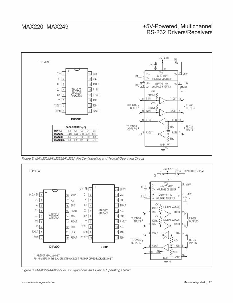
Figure 5. MAX220/MAX232/MAX232A Pin Configuration and Typical Operating Circuit
Figure 6. MAX222/MAX242 Pin Configurations and Typical Operating Circuit
Maxim Integrated | 18www.maximintegrated.com
MAX220–MAX249 +5V-Powered, MultichannelRS-232 Drivers/Receivers
13
14
28
27
26
25
24
23
22
21
1
2
3
4
5
6
7
8
VCC
VCC VCC
400kΩ
400kΩ
400kΩ
400kΩ
400kΩ
T1OUT+5V
+5V
0.1μF
+5V
3
28 27
4
25
24
23
26
5
6
7
22
GNDENRENR
GND
21
+5V
+5V
+5V
T2OUT
T3OUT
T4OUT
5kΩ
5kΩ
5kΩ
5kΩ
5kΩ
1413
21
T5OUT
T5OUT
R1IN
R2IN
R3IN
R4IN
R5IN
T1IN11
12
18
17
16
15
10
9
8
19
20
T2IN
T3IN
T4IN
T5IN
ENT
R2OUT
R3OUT
R4OUT
PINS (ENR, GND, VCC, T5OUT) ARE INTERNALLY CONNECTED.CONNECT EITHER OR BOTH EXTERNALLY. T5OUT IS A SINGLE DRIVER.
R5OUT
R1OUT
VCC
ENT
T3INT2IN
T1IN
ENR
ENR
T4IN
T5IN
R4OUT
R5OUTR3IN
R3OUT
R2OUT
R1OUT
20
19
18
17
9
10
11
12
R5IN
R4IN
T3OUT
T4OUTT2OUT
T1OUT
R1IN
R2IN
SO
MAX225
16
15
T5OUT
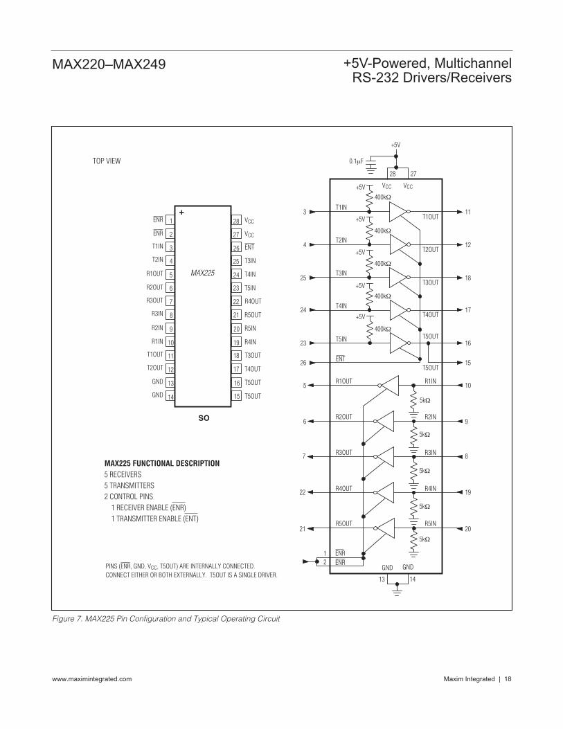
MAX225 FUNCTIONAL DESCRIPTION5 RECEIVERS5 TRANSMITTERS2 CONTROL PINS 1 RECEIVER ENABLE (ENR) 1 TRANSMITTER ENABLE (ENT)
T5OUTGND
GND
TOP VIEW
+
Figure 7. MAX225 Pin Configuration and Typical Operating Circuit

MAX220–MAX249 +5V-Powered, MultichannelRS-232 Drivers/Receivers
Maxim Integrated | 19www.maximintegrated.com
GND
10
27R3OUT
23R4OUT
R3IN
R4IN
5kΩ
5kΩ
5 4R2OUT R2IN
5kΩ
RS-232INPUTS
LOGICOUTPUTS
RS-232OUTPUTS
TTL/CMOSINPUTS
R2
8 9R1OUT R1IN
5kΩ
R1
R3
R4
19 18R5OUT R5IN
5kΩR5
27 T1IN T1OUT
+5V400kΩ
+5V
6 3T2IN T2OUTT2
400kΩ
20 T3OUT 1T3IN
+5V
T3
400kΩ
C1+
C1-
1.0μF
12VCC
+5V INPUT
11
17
1.0μF
131.0μF
+5V TO +10VVOLTAGE DOUBLER
26
1.0μF
T1
2821 T4IN T4OUT
+5V
400kΩ
T4
14
C2+
C2-
15
1.0μF 16+10V TO -10V
VOLTAGE INVERTER
V+
22
EN (EN)24 25
28
27
26
25
24
23
22
21
20
19
18
17
16
15
1
2
3
4
5
6
7
8
9
10
11
12
13
14
T4OUT
R3IN
R3OUT
SHDN (SHDN)
R4IN*
C2+
R4OUT*
T4IN
T3IN
R5OUT*
R5IN*
V-
C2-
C1-
V+
C1+
VCC
GND
R1IN
R1OUT
T1IN
T2IN
R2OUT
R2IN
T2OUT
T1OUT
T3OUT
Wide SO/SSOP
MAX223MAX241
EN (EN)
SHDN(SHDN)
*R4 AND R5 IN MAX223 REMAIN ACTIVE IN SHUTDOWN.
NOTE: PIN LABELS IN ( ) ARE FOR MAX241.
V-
+
TOP VIEW
Figure 8. MAX223/MAX241 Pin Configuration and Typical Operating Circuit
Maxim Integrated | 20www.maximintegrated.com
MAX220–MAX249 +5V-Powered, MultichannelRS-232 Drivers/Receivers
20
19
18
17
16
15
14
13
1
2
3
4
5
6
7
8
T5IN
N.C.
SHDNT2IN
T2OUT
T1OUT
T5OUT
T4IN
T3IN
V-C1+
VCC
GND
T1IN
12
11
9
10
C2-
C2+C1-
V+
DIP/SO
MAX230
V+
V-
9C1+C1-
810
1112
5
4
14
13
2
3
1
20
T3IN
T4IN
T2IN
T5IN
T1OUT
T2OUT
+5V INPUT
C2+C2-
RS-232OUTPUTS
TTL/CMOSINPUTS
GND6
400kΩ+5V
400kΩ+5V
400kΩ+5V
400kΩ+5V
400kΩ+5V
+10V TO -10VVOLTAGE INVERTER
VCC+5V TO +10V
VOLTAGE DOUBLER
7
1.0μF
1.0μF
1.0μF
1.0μF
19
15
16
T3OUT T4OUT
18x
T1IN
T3OUT
T4OUT
T5OUT
17
1.0μF
T2
T3
T4
T5
N.C. SHDN
T1
+
TOP VIEW
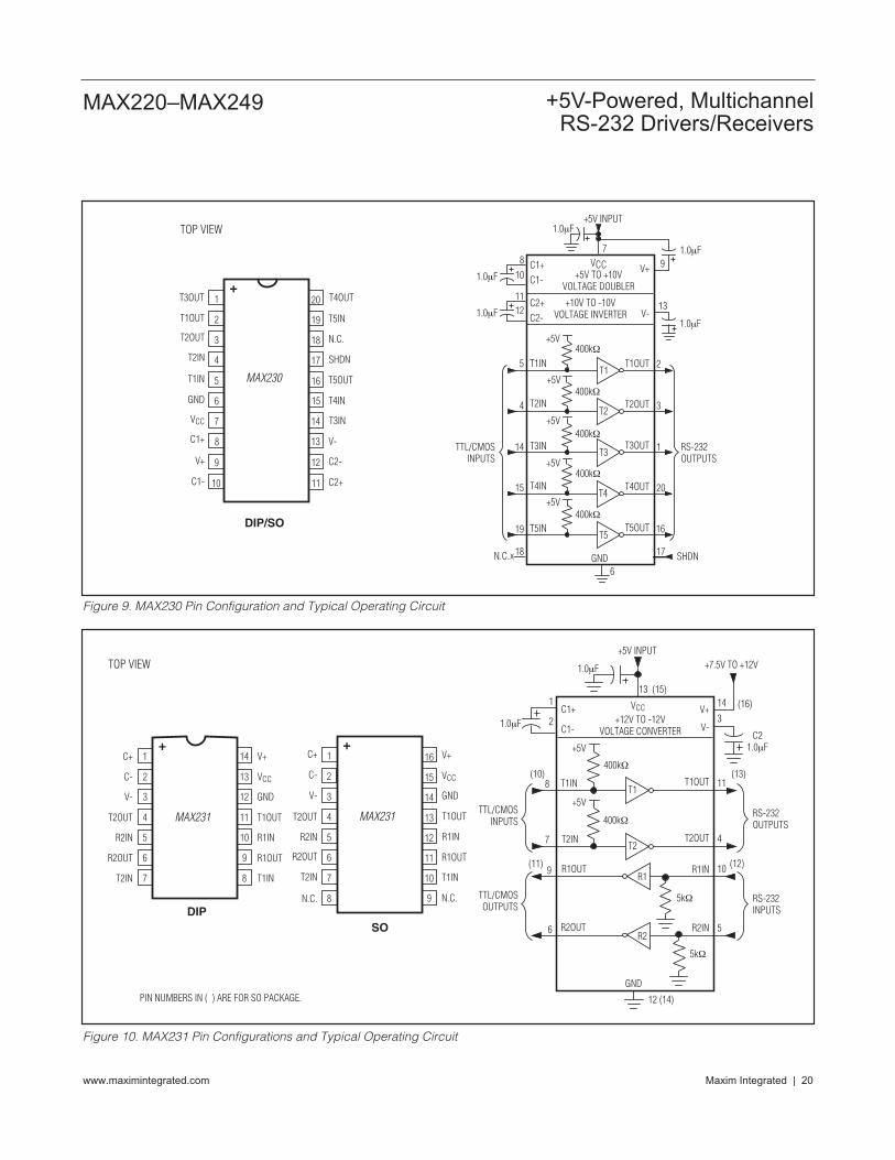
Figure 9. MAX230 Pin Configuration and Typical Operating Circuit
V+
V-
14C1+
C1-
1
2
8
7
3
11
4T2IN
T1IN T1OUT
T2OUT
+5V INPUT
RS-232INPUTS
TTL/CMOSOUTPUTS
GND
12 (14)
5kΩ
5kΩ
+12V TO -12VVOLTAGE CONVERTER
13 (15)
1.0μF
1.0μFC2
1.0μF
400kΩ
+5V
400kΩ
+5V
6
9 10R1IN
R2INR2OUT
R1OUT
5
16
15
14
13
12
11
10
9
1
2
3
4
5
6
7
8
V+
VCC
GND
T1OUTT2OUT
V-
C-
C+
MAX231
R1IN
R1OUT
T1IN
N.C.N.C.
T2IN
R2OUT
R2IN
SO
(12)
RS-232OUTPUTS
TTL/CMOSINPUTS
(11)
(13)(10)
VCC
PIN NUMBERS IN ( ) ARE FOR SO PACKAGE.
14
13
12
11
10
9
8
1
2
3
4
5
6
7
V+
VCC
GND
T1OUTT2OUT
V-
C-
C+
MAX231
R1IN
R1OUT
T1INT2IN
R2OUT
R2IN
DIP
+7.5V TO +12V
(16)
T1
T2
R1
R2
+ +
TOP VIEW
Figure 10. MAX231 Pin Configurations and Typical Operating Circuit
MAX220–MAX249 +5V-Powered, MultichannelRS-232 Drivers/Receivers
Maxim Integrated | 21www.maximintegrated.com
2
1
5
18T2IN
T1IN T1OUT
T2OUT
+5V INPUT
RS-232INPUTS
TTL/CMOSOUTPUTS
GND GND6 9
400kΩ
+5V
400kΩ
+5V
5kΩ
5kΩ
7
20
3 4R1IN
R2INR2OUT
R1OUT
19
RS-232OUTPUTS
TTL/CMOSINPUTS
VCC
PIN NAMES IN ( ) ARE FOR SO PACKAGE.
20
19
18
17
16
15
14
13
1
2
3
4
5
6
7
8
R2IN
T2OUT
V-R1IN
R1OUT
T1IN
C2-
C2+
V+ (C1-)
C1- (C1+)(V+) C1+
VCC
GND
T1OUT
12
11
9
10
V- (C2+)
C2+ (C2-)(V-) CS-
GND
DIP/SO
MAX233MAX233A
T2IN R2OUT
C1+
C1-
V-
V-
V+
C2+
C2-
CS-
C2+
8 (13)
13 (14)
12 (10)
17
14 (8)
11 (12)
15
16
10 (11)
DO NOT MAKECONNECTIONS TO
THESE PINS
INTERNAL -10VPOWER SUPPLY
INTERNAL +10VPOWER SUPPLY
1.0μFTOP VIEW
+
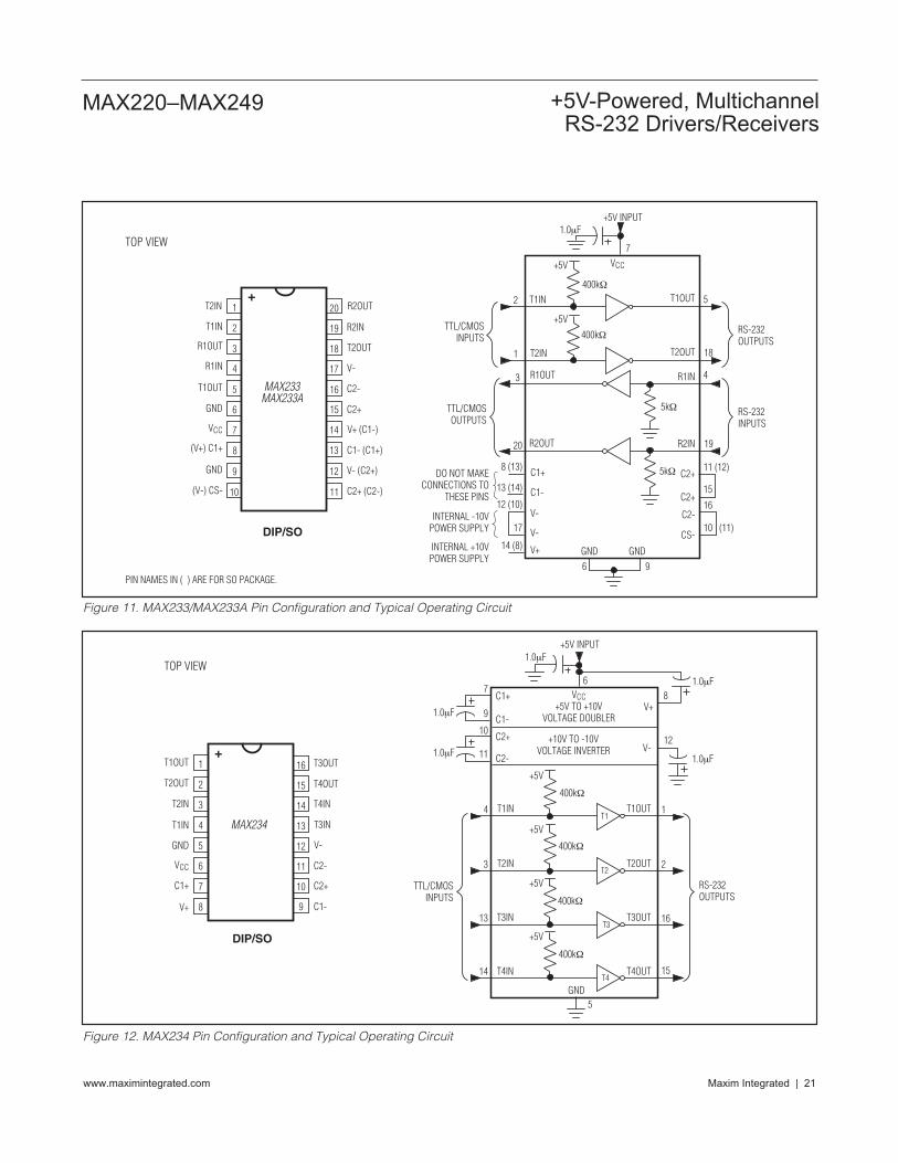
Figure 11. MAX233/MAX233A Pin Configuration and Typical Operating Circuit
16
15
14
13
12
11
10
9
1
2
3
4
5
6
7
8
T3OUT
T4OUT
T4IN
T3INT1IN
T2IN
T2OUT
T1OUT
MAX234
V-
C2-
C2+
C1-V+
C1+
VCC
GND
DIP/SO
V+
V-
8C1+
C1-
1.0μF
1.0μF
1.0μF
7
9
10
11
4
3
13
14
12
1
2
16
15
T1IN
T3IN
T2IN
T4IN
T1OUT
T3OUT
T2OUT
T4OUT
+5V INPUT
C2-
C2+
RS-232OUTPUTS
TTL/CMOSINPUTS
GND5
+5V
+5V
+10V TO -10VVOLTAGE INVERTER
VCC+5V TO +10V
VOLTAGE DOUBLER
6
+5V
+5V
400kΩ
400kΩ
400kΩ
400kΩ
1.0μF
1.0μF
T1
T2
T4
T3
+
TOP VIEW
Figure 12. MAX234 Pin Configuration and Typical Operating Circuit
Maxim Integrated | 22www.maximintegrated.com
MAX220–MAX249 +5V-Powered, MultichannelRS-232 Drivers/Receivers
1.0μF+5V INPUT
GND
11
6
23
5R2OUT
RS-232INPUTS
TTL/CMOSOUTPUTS
14 13
21
R5OUT
5kΩ
17 18R4OUT
5kΩ
24R3OUT
5kΩ
24
23
22
21
20
19
18
17
1
2
3
4
5
6
7
8
R3IN
R3OUT
T5IN
SHDNT2OUT
T1OUT
T3OUT
T4OUT
EN
T5OUT
R4IN
R4OUTT1IN
T2IN
R2OUT
R2IN
16
15
14
13
9
10
11
12
T4IN
T3IN
R5OUT
R5INVCC
GND
R1IN
R1OUT
DIP
MAX235
5kΩ
9 10R1OUT R1IN
R2IN
R3IN
R4IN
R5IN
5kΩ
7
15
3
4T2IN
T3OUT RS-232OUTPUTS
TTL/CMOSINPUTS
22 19T5IN T5OUT
+5V
16 1T4IN T4OUT
+5V
2T3IN
+5V
+5V
8 T1IN T1OUT
+5V
T2OUT
T1
T1
R2
R3
R4
R5
T2
T3
T5
T4
400kΩ
400kΩ
400kΩ
400kΩ
400kΩ
SHDNEN20
12
VCC
+
TOP VIEW
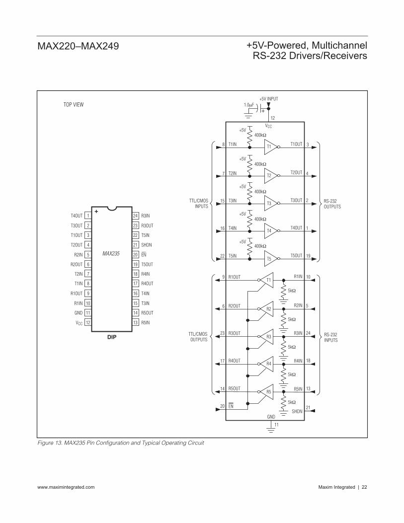
Figure 13. MAX235 Pin Configuration and Typical Operating Circuit
MAX220–MAX249 +5V-Powered, MultichannelRS-232 Drivers/Receivers
Maxim Integrated | 23www.maximintegrated.com
GND
8
23R2OUT RS-232INPUTS
TTL/CMOSOUTPUTS
17 16
21
R3OUT
R2IN
R3IN
5kΩ
5kΩ
5 4R1OUT R1IN
5kΩ
RS-232OUTPUTS
TTL/CMOSINPUTS
R1
R2
R3
27 T1IN T1OUT
+5V
T1
400kΩ
6 3T2IN
+5V
T2OUTT2
400kΩ
18 T3OUT 1T3IN
+5V
T3
400kΩ
19 24T4IN T4OUT
+5V
T4
400kΩ
SHDNEN20
11C1+
C1-
1.0μF
10
12
13
14
15
+5V INPUT
C2+
C2-
VCC+5V TO +10V
VOLTAGE DOUBLER
9 1.0μF
1.0μF+10V TO -10VVOLTAGE INVERTER
22
24
23
22
21
20
19
18
17
1
2
3
4
5
6
7
8
T4OUT
R2IN
R2OUT
SHDNR1IN
T2OUT
T1OUT
T3OUT
T4IN
T3IN
R3OUTGND
T1IN
T2IN
R1OUT
16
15
14
13
9
10
11
12
R3IN
V-
C2-
C2+C1-
V+
C1+
VCC
DIP/SO
MAX236 EN
1.0μF
1.0μF
TOP VIEW
V+
V-
+
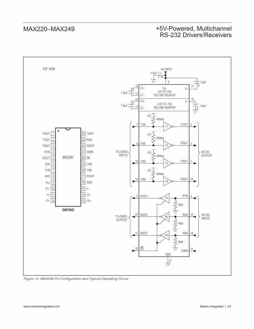
Figure 14. MAX236 Pin Configuration and Typical Operating Circuit
Maxim Integrated | 24www.maximintegrated.com
MAX220–MAX249 +5V-Powered, MultichannelRS-232 Drivers/Receivers
GND
8
23R2OUT RS-232INPUTS
TTL/CMOSOUTPUTS
17 16R3OUT
R2IN
R3IN
5kΩ
5kΩ
5 4R1OUT R1IN
5kΩ
RS-232OUTPUTS
TTL/CMOSINPUTS
R1
R2
R3
27 T1IN T1OUT
+5V
T1
400kΩ
6 3T2IN
+5V
T2OUTT2
400kΩ
18 T3OUT 1T3IN
+5V
T3
400kΩ
21 20T5IN T5OUT
+5V
T5
400kΩ
11C1+
C1-
1.0μF
10
12
13
14
15
+5V INPUT
C2+
C2-
VCC+5V TO +10V
VOLTAGE DOUBLER
9 1.0μF
1.0μF+10V TO -10V
VOLTAGE INVERTER
22
24
23
22
21
20
19
18
17
1
2
3
4
5
6
7
8
T4OUT
R2IN
R2OUT
T5INR1IN
T2OUT
T1OUT
T3OUT
T4IN
T3IN
R3OUTGND
T1IN
T2IN
R1OUT
16
15
14
13
9
10
11
12
R3IN
V-
C2-
C2+C1-
V+
C1+
VCC
DIP/SO
MAX237 T5OUT
1.0μF
1.0μF
19 24T4IN T4OUT
+5V
T4
400kΩ
V+
V-
+
TOP VIEW
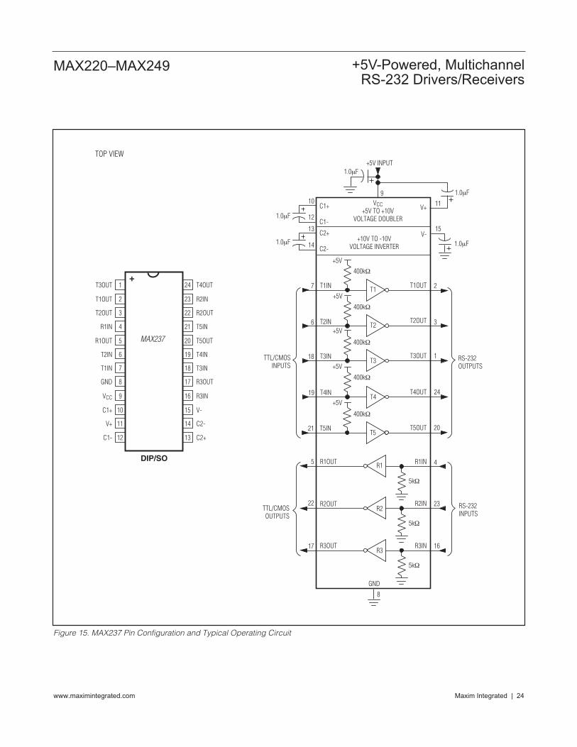
Figure 15. MAX237 Pin Configuration and Typical Operating Circuit

MAX220–MAX249 +5V-Powered, MultichannelRS-232 Drivers/Receivers
Maxim Integrated | 25www.maximintegrated.com
GND
8
3R2OUT
22 23R3OUT
R2IN
R3IN
5kΩ
5kΩ
6 7R1OUT R1IN
5kΩ
RS-232OUTPUTS
TTL/CMOSINPUTS
RS-232INPUTS
TTL/CMOSOUTPUTS
R1
R2
R3
17 16R4OUT R4IN
5kΩ
R4
25 T1IN T1OUT
+5V400kΩ
+5V
18 1T2IN T2OUTT2
400kΩ
19 T3OUT 24T3IN
+5V
T3
400kΩ
11C1+
C1-
1.0μF
10
12
13
1415
+5V INPUT
C2+
C2-
VCC+5V TO +10V
VOLTAGE DOUBLER
9 1.0μF
1.0μF+10V TO -10V
VOLTAGE INVERTER
4
1.0μF
1.0μF
21 20T4IN T4OUT
+5V
T4
400kΩ
T124
23
22
21
20
19
18
17
1
2
3
4
5
6
7
8
T3OUT
R3IN
R3OUT
T4INR2OUT
R2IN
T1OUT
T2OUT
TOP VIEW
T3IN
T2IN
R4OUTGND
R1IN
R1OUT
T1IN
16
15
14
13
9
10
11
12
R4IN
V-
C2-
C2+C1-
V+
C1+
VCC
DIP/SO
MAX238 T4OUT
+
V+
V-
Figure 16. MAX238 Pin Configuration and Typical Operating Circuit

Maxim Integrated | 26www.maximintegrated.com
MAX220–MAX249 +5V-Powered, MultichannelRS-232 Drivers/Receivers
GND
3
18R3OUT
12R4OUT
R3IN
R4IN
5kΩ
5kΩ
22 21R2OUT R2IN
5kΩ
RS-232OUTPUTS
TTL/CMOSINPUTS
RS-232INPUTS
TTL/CMOSOUTPUTS
R2
1 2R1OUT R1IN
5kΩ
R1
R3
R4
10 9R5OUT R5IN
5kΩ
R5
1924 T1IN T1OUT
+5V400kΩ
+5V
23 20T2IN T2OUTT2
400kΩ
16 T3OUT 13T3IN
+5V
T3
400kΩ
C1+
C1-
1.0μF
6 VCC 8
+5V INPUT
4 5
1.0μF+10V TO -10V
VOLTAGE INVERTER
17
1.0μF
T1
24
23
22
21
20
19
18
17
1
2
3
4
5
6
7
8
T1IN
T2IN
R2OUT
R2INVCC
GND
R1IN
R1OUT
T1OUT
R3IN
R3OUTV-
C-
C+
V+
16
15
14
13
9
10
11
12
T3IN
N.C.
EN
T3OUTR4IN
R4OUT
R5OUT
R5IN
DIP/SO
MAX239 T2OUT
+7.5V TO +13.2VINPUT
7
V+
11
EN14 15N.C.
V-
+
TOP VIEW
Figure 17. MAX239 Pin Configuration and Typical Operating Circuit
MAX220–MAX249 +5V-Powered, MultichannelRS-232 Drivers/Receivers
Maxim Integrated | 27www.maximintegrated.com
GND
18
4R3OUT
40R4OUT
R3IN
R4IN
5kΩ
5kΩ
13 10R2OUT R2IN
5kΩ
RS-232INPUTS
TTL/CMOSOUTPUTS
RS-232OUTPUTS
TTL/CMOSINPUTS
R2
16 17R1OUT R1IN
5kΩR1
R3
R4
36 35R5OUT R5IN
5kΩ
R5
715 T1IN T1OUT
+5V400kΩ
+5V
14 8T2IN T2OUTT2
400kΩ
37 T3OUT 6T3IN
+5V
T3
400kΩ
C1+
C1-
1.0μF
25VCC
+5V INPUT
19
30
1.0μF
261.0μF
+5V TO +10VVOLTAGE DOUBLER
3
1.0μF
T1
+5V
2 41T5IN T5OUTT5
400kΩ
538 T4IN T4OUT
+5V400kΩ
T4
27
C2+
C2-
28
1.0μF 29+5V TO -10V
VOLTAGE INVERTER
V+
39
EN42 43
Plastic FP
MAX240
SHDNENT5OUTR4INR4OUT
R5OUTR5INN.C.
N.C.
T3INT4IN
R2OUTT2INT1IN
R1OUTR1IN
N.C.N.C.N.C.
N.C.
VCC
GND
R2IN
N.C.
T4OU
T
T2OU
TT1
OUT
T3OU
T
N.C.
R3IN
R3OU
T
N.C.
T5IN
N.C.
C1+ C2V+ C1-
C2+
N.C. V-
N.C.
N.C.
N.C.
3332313029282726252423
3435363738394041424344
1234567891011
2221201918171615141312
SHDN
TOP VIEW
V-
+
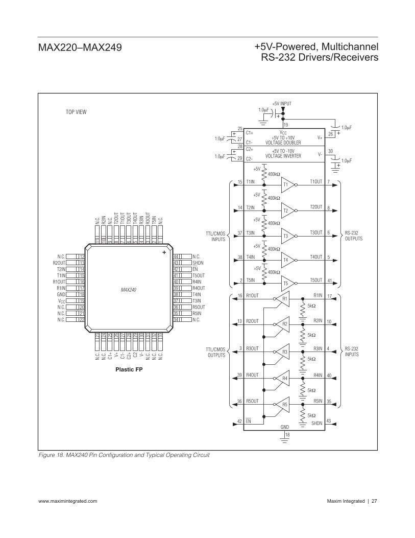
Figure 18. MAX240 Pin Configuration and Typical Operating Circuit

Maxim Integrated | 28www.maximintegrated.com
MAX220–MAX249 +5V-Powered, MultichannelRS-232 Drivers/Receivers
V+
V-
2 +10VC1+
C1-
1
3
4
5
11
10
12
9
6
14
7
13
8
T1IN
R1OUT
T2IN
R2OUT
T1OUT
R1IN
T2OUT
R2IN
+5V INPUT
C2+
C2--10V
RS-232OUTPUTS
RS-232INPUTS
TTL/CMOSINPUTS
TTL/CMOSOUTPUTS
GND
15
5kΩ
5kΩ
400kΩ
400kΩ
+5V
+5V
+10V TO -10VVOLTAGE INVERTER
+5V TO +10VVOLTAGE DOUBLER
16
16
15
14
13
12
11
10
9
1
2
3
4
5
6
7
8
C1+ VCC
GND
T1OUT
R1IN
R1OUT
T1IN
T2IN
R2OUT
MAX243
DIP/SO
V+
C1-
V-
C2+
C2-
T2OUT
R2IN
0.1μF
0.1μF
0.1μF
0.1μF
0.1μF
RECEIVER INPUT≤ -3VOPEN≥ +3V
R1 OUTPUTHIGHHIGHLOW
R2 OUTPUTHIGHLOWLOW
TOP VIEW
VCC
+
Figure 19. MAX243 Pin Configuration and Typical Operating Circuit
MAX220–MAX249 +5V-Powered, MultichannelRS-232 Drivers/Receivers
Maxim Integrated | 29www.maximintegrated.com
400kΩ
+10V TO -10V VOLTAGE INVERTER
+5V TO +10V VOLTAGE DOUBLERVCC
400kΩ
400kΩ
GND
+5V +5V
+5V +5V
+5V
25
2423
2120
2
1μF
1μF
1μF 1μF
1μF
16
3
17
4
18
5kΩ
5kΩ
5kΩ
5kΩ
5kΩ
5kΩ
5kΩ
5kΩ
5kΩ
5kΩ
C2-C2+
C1-C1+
TA2OUT
TA2IN
TA3OUT
TA3IN
TA4OUT
TA4IN
9 RA1IN
10 RA1OUT
8 RA2IN
11 RA2OUT
7 RA3IN
12 RA3OUT
6 RA4IN
13 RA4OUT
5 RA5IN
14
19
RA5OUT
26
22
43
29
42
28
41
27
36
35
37
34
38
33
39
32
40
31
V-
V+
TB2OUT
TB2IN
400kΩ
2
15
TA1OUT
TA1IN
44
30
TB1OUT
TB1IN
TB3OUT
TB3IN
TB4OUT
TB4IN
RB1IN
RB1OUT
RB2IN
RB2OUT
RB3IN
RB3OUT
RB4IN
RB4OUT
RB5IN
RB5OUT
MAX249 FUNCTIONAL DESCRIPTION10 RECEIVERS 5 A-SIDE RECEIVERS 5 B-SIDE RECEIVERS8 TRANSMITTERS 4 A-SIDE TRANSMITTERS 4 B-SIDE TRANSMITTERSNO CONTROL PINS
441234 404142435
21 24 2625 27 2822 2319 20
8
9
10
11
12
13
14
15
16
17 29
30
31
32
33
34
35
36
37
38
TA3IN
V CC
RA5I
N
MAX244
PLCC
TOP VIEWTA
4OUT
TA3O
UT
TA2O
UT
TA1O
UT
TB1O
UT
TB2O
UT
TB3O
UT
TB4O
UT
RB5I
N
GND V+C1+
C2+
C1- V-C2-
TB3I
N
TB4I
N
RB3IN
RB2IN
RB1IN
RB1OUT
RB2OUT
RB3OUT
RB4OUT
RB5OUT
TB1IN
TB2IN
TA2IN
TA1IN
RA5OUT
RA4OUT
RA3OUT
RA2OUT
RA1OUT
RA1IN
RA2IN
7 39 RB4INRA3IN
6
18
RA4I
NTA
4IN
+5V +5V
+5V +5V+
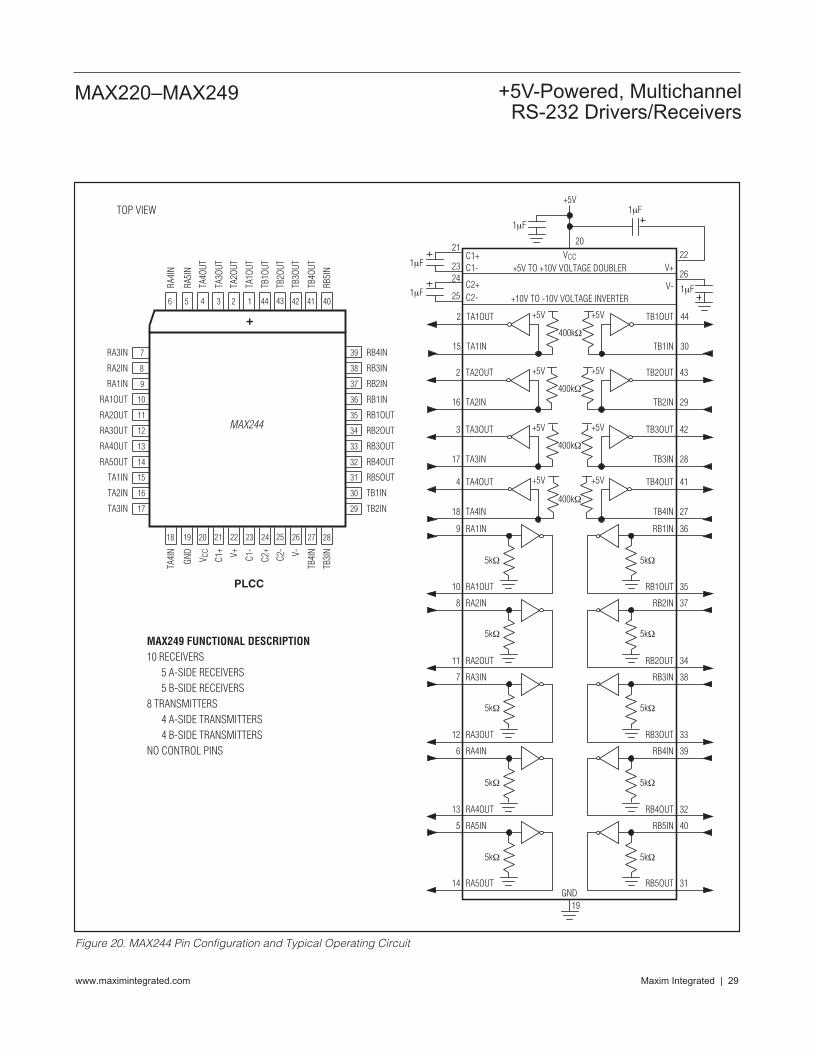
Figure 20. MAX244 Pin Configuration and Typical Operating Circuit
Maxim Integrated | 30www.maximintegrated.com
MAX220–MAX249 +5V-Powered, MultichannelRS-232 Drivers/Receivers
400kΩ
VCC
400kΩ
400kΩ
GND
+5V +5V
+5V +5V
+5V
40
17
1μF
3
18
4
19
5
5kΩ
5kΩ
5kΩ
5kΩ
5kΩ
5kΩ
5kΩ
5kΩ
5kΩ
5kΩ
TA2OUT
TA2IN
TA3OUT
TA3IN
TA4OUT
TA4IN
1
11 RA1IN
10 RA1OUT
12 RA2IN
9 RA2OUT
13 RA3IN
8 RA3OUT
14 RA4IN
7 RA4OUT
15 RA5IN
6
20
RA5OUT
23
37
22
36
21
35
29
30
28
31
27
32
26
33
25
34
TB2OUT
TB2IN
TB3OUT
TB3IN
TB4OUT
TB4IN
RB1IN
RB1OUT
RB2IN
RB2OUT
RB3IN
RB3OUT
RB4IN
RB4OUT
RB5IN
RB5OUT
+5V +5V
400kΩ
16
2
TA1OUT
TA1IN
24
38
TB1OUT
TB1IN
+5V +5V40 VCC
ENT
TB1IN
TB2IN
TB3IN
TB4IN
RB5OUT
RB4OUT
RB3OUT
RB2OUT
RB1OUT
RB1IN
RB2IN
RB3IN
RB4IN
RB5IN
TB1OUT
TB2OUT
TB3OUT
TB4OUT
39
38
37
36
35
34
33
32
31
1
2
3
4
5
6
7
8
9
10
ENR
TA1IN
TA2IN
TA3IN
TA4IN
RA5OUT
RA4OUT
RA3OUT
RA2OUT
RA1OUT
RA1IN
RA2IN
RA3IN
RA4IN
RA5IN
TA1OUT
TA2OUT
TA3OUT
TA4OUT
GND
TOP VIEW
MAX245
30
29
28
27
26
25
24
23
22
21
11
12
13
14
15
16
17
18
19
DIP
20
MAX245 FUNCTIONAL DESCRIPTION10 RECEIVERS 5 A-SIDE RECEIVERS (RA5 ALWAYS ACTIVE) 5 B-SIDE RECEIVERS (RB5 ALWAYS ACTIVE)8 TRANSMITTTERS 4 A-SIDE TRANSMITTERS2 CONTROL PINS 1 RECEIVER ENABLE (ENR) 1 TRANSMITTER ENABLE (ENT)
39
+
ENR ENT
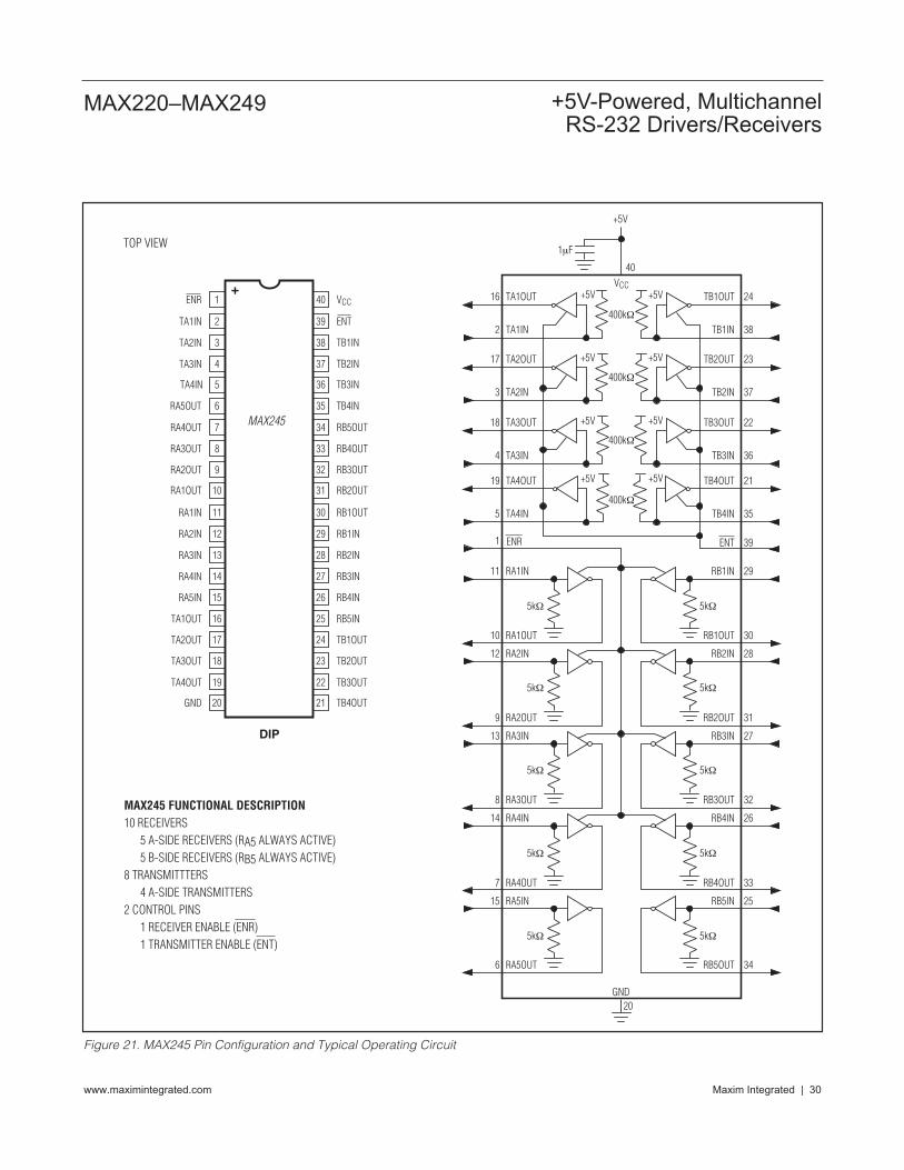
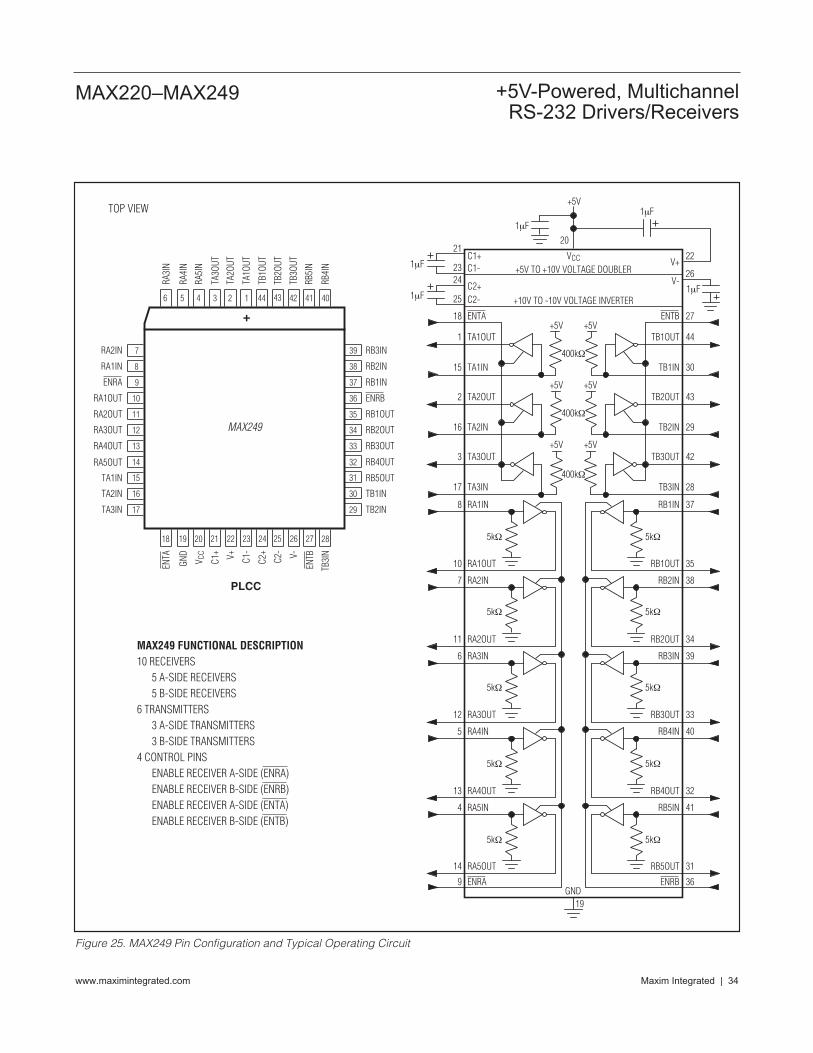
Figure 21. MAX245 Pin Configuration and Typical Operating Circuit
MAX220–MAX249 +5V-Powered, MultichannelRS-232 Drivers/Receivers
Maxim Integrated | 31www.maximintegrated.com
400kΩ
VCC
400kΩ
GND
+5V
+5V
+5V
+5V
+5V
40
16
1μF
2
18
4
TA1OUT
TA1IN
TA3OUT
TA3IN
20
24
38
22
36
1 39
TB1OUT
TB1IN
TB3OUT
TB3IN
400kΩ
+5V17
3
TA2OUT
TA2IN
+5V23
37
TB2OUT
TB2IN
400kΩ
+5V19
5
TA4OUT
TA4IN
+5V21
35
TB4OUT
TB4IN
5kΩ
5kΩ
5kΩ
5kΩ
5kΩ
5kΩ
5kΩ
5kΩ
5kΩ
5kΩ
11 RA1IN
10 RA1OUT
12 RA2IN
9 RA2OUT
13 RA3IN
8 RA3OUT
14 RA4IN
7 RA4OUT
15 RA5IN
6 RA5OUT
29
30
28
31
27
32
26
33
25
34
RB1IN
RB1OUT
RB2IN
RB2OUT
RB3IN
RB3OUT
RB4IN
RB4OUT
RB5IN
RB5OUT
40 VCC
ENB
TB1IN
TB2IN
TB3IN
TB4IN
RB5OUT
RB4OUT
RB3OUT
RB2OUT
RB1OUT
RB1IN
RB2IN
RB3IN
RB4IN
RB5IN
TB1OUT
TB2OUT
TB3OUT
TB4OUT
39
38
37
36
35
34
33
32
31
1
2
3
4
5
6
7
8
9
10
ENA
TA1IN
TA2IN
TA3IN
TA4IN
RA5OUT
RA4OUT
RA3OUT
RA2OUT
RA1OUT
RA1IN
RA2IN
RA3IN
RA4IN
RA5IN
TA1OUT
TA2OUT
TA3OUT
TA4OUT
GND
TOP VIEW
MAX246
30
29
28
27
26
25
24
23
22
21
11
12
13
14
15
16
17
18
19
DIP
20
MAX246 FUNCTIONAL DESCRIPTION10 RECEIVERS 5 A-SIDE RECEIVERS (RA5 ALWAYS ACTIVE) 5 B-SIDE RECEIVERS (RB5 ALWAYS ACTIVE)8 TRANSMITTERS 4 A-SIDE TRANSMITTERS 4 B-SIDE TRANSMITTERS2 CONTROL PINS ENABLE A-SIDE (ENA) ENABLE B-SIDE (ENB)
ENA ENB
+
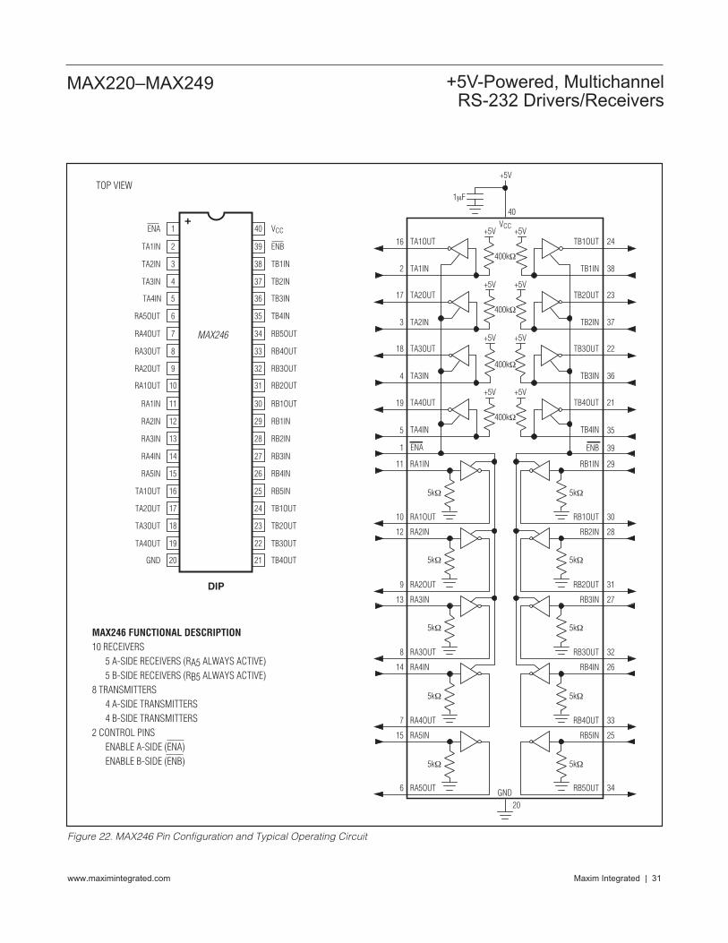
Figure 22. MAX246 Pin Configuration and Typical Operating Circuit
Maxim Integrated | 32www.maximintegrated.com
MAX220–MAX249 +5V-Powered, MultichannelRS-232 Drivers/Receivers
400kΩ
VCC
400kΩ
GND
+5V
+5V
+5V
+5V
+5V
1
40
16
1μF
2
18
4
5kΩ
5kΩ
5kΩ
5kΩ
5kΩ
5kΩ
5kΩ
5kΩ
ENTA
TA1OUT
TA1IN
TA3OUT
TA3IN
6 RB5OUT
12 RA1IN
10 RA1OUT
13 RA2IN
9 RA2OUT
14 RA3IN
8 RA3OUT
15 RA4IN
7
20
RA4OUT
11
39
24
38
22
36
29
31
28
32
27
33
26
34
30ENRA
ENTB
TB1OUT
TB1IN
TB3OUT
TB3IN
RB1IN
5kΩ
25RB5IN
RB1OUT
RB2IN
RB2OUT
RB3IN
RB3OUT
RB4IN
RB4OUT
ENRB
400kΩ
+5V17
3
TA2OUT
TA2IN
+5V23
37
TB2OUT
TB2IN
400kΩ
+5V19
5
TA4OUT
TA4IN
+5V21
35
TB4OUT
TB4IN
40 VCC
ENTB
TB1IN
TB2IN
TB3IN
TB4IN
RB4OUT
RB3OUT
RB2OUT
RB1OUT
RB1IN
RB2IN
RB3IN
RB4IN
RB5IN
TB1OUT
TB2OUT
TB3OUT
TB4OUT
39
38
37
36
35
34
33
32
31
1
2
3
4
5
6
7
8
9
10
ENTA
TA1IN
TA2IN
TA3IN
TA4IN
RB5OUT
RA4OUT
RA3OUT
RA2OUT
RA1OUT
RA1IN
RA2IN
RA3IN
RA4IN
TA1OUT
TA2OUT
TA3OUT
TA4OUT
GND
TOP VIEW
MAX247
30
29
28
27
26
25
24
23
22
21
11
12
13
14
15
16
17
18
19
DIP
20
ENRA ENRB
MAX247 FUNCTIONAL DESCRIPTION9 RECEIVERS 4 A-SIDE RECEIVERS 5 B-SIDE RECEIVERS (RB5 ALWAYS ACTIVE)8 TRANSMITTERS 4 A-SIDE TRANSMITTERS 4 B-SIDE TRANSMITTERS4 CONTROL PINS ENABLE RECEIVER A-SIDE (ENRA) ENABLE RECEIVER B-SIDE (ENRB) ENABLE RECEIVER A-SIDE (ENTA) ENABLE RECEIVER B-SIDE (ENTB)
+
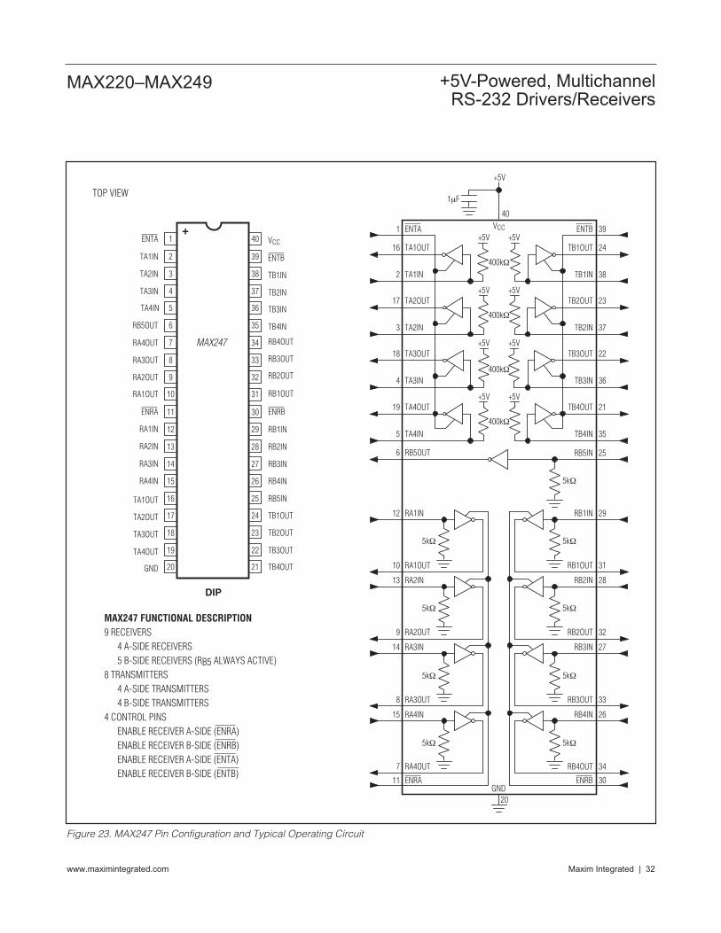
Figure 23. MAX247 Pin Configuration and Typical Operating Circuit
MAX220–MAX249 +5V-Powered, MultichannelRS-232 Drivers/Receivers
Maxim Integrated | 33www.maximintegrated.com
400kΩ
+10V TO -10V VOLTAGE INVERTER
+5V TO +10V VOLTAGE DOUBLERVCC
400kΩ
GND
+5V
+5V
+5V
+5V
+5V
18
25
2423
2120
1
1μF
1μF
1μF1μF
1μF
14
3
16
5kΩ
5kΩ
5kΩ
5kΩ
5kΩ
5kΩ
5kΩ
5kΩ
ENTA
C2-C2+
C1-C1+
TA1OUT
TA1IN
TA3OUT
TA3IN
8 RA1IN
10 RA1OUT
7 RA2IN
11 RA2OUT
6 RA3IN
12 RA3OUT
5 RA4IN
13
19
RA4OUT
9
27
26
22
44
31
42
29
37
35
38
34
39
33
40
32
36ENRA
ENTB
V-
V+
TB1OUT
TB1IN
TB3OUT
TB3IN
RB1IN
RB1OUT
RB2IN
RB2OUT
RB3IN
RB3OUT
RB4IN
RB4OUT
ENRB
400kΩ
+5V2
15
TA2OUT
TA2IN
+5V43
30
TB2OUT
TB2IN
400kΩ
+5V4
17
TA4OUT
TA4IN
+5V41
28
TB4OUT
TB4IN
441234 404142435
21 24 2625 27 2822 2319 20
8
9
10
11
12
13
14
15
16
17 29
30
31
32
33
34
35
36
37
38
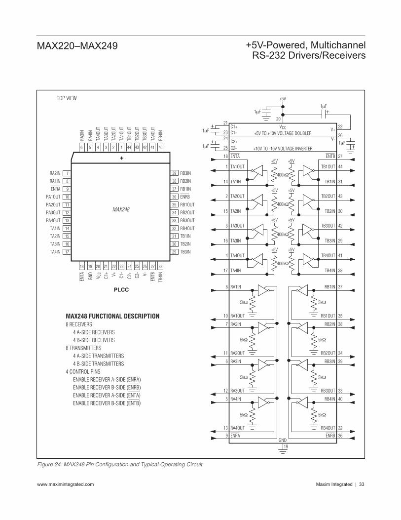
TA4IN
V CC
RA4I
N
MAX248
PLCC
TOP VIEWTA
4OUT
TA3O
UT
TA2O
UT
TA1O
UT
TB1O
UT
TB2O
UT
TB3O
UT
TA4O
UT
RB4I
N
GND V+C1+
C2+
C1- V-C2-
TB4I
N
ENTB
RB2IN
RB1IN
RB1OUT
RB2OUT
RB3OUT
RB4OUT
TB1IN
TB2IN
TB3IN
TA3IN
TA2IN
TA1IN
RA4OUT
RA3OUT
RA2OUT
RA1OUT
ENRA
RA1IN
7 39 RB3INRA2IN
6
18
RA3I
N
ENRB
ENTA
MAX248 FUNCTIONAL DESCRIPTION8 RECEIVERS 4 A-SIDE RECEIVERS 4 B-SIDE RECEIVERS8 TRANSMITTERS 4 A-SIDE TRANSMITTERS 4 B-SIDE TRANSMITTERS4 CONTROL PINS ENABLE RECEIVER A-SIDE (ENRA) ENABLE RECEIVER B-SIDE (ENRB) ENABLE RECEIVER A-SIDE (ENTA) ENABLE RECEIVER B-SIDE (ENTB)
+
Figure 24. MAX248 Pin Configuration and Typical Operating Circuit
Maxim Integrated | 34www.maximintegrated.com
MAX220–MAX249 +5V-Powered, MultichannelRS-232 Drivers/Receivers
400kΩ
+10V TO -10V VOLTAGE INVERTER
+5V TO +10V VOLTAGE DOUBLERVCC
400kΩ
400kΩ
GND
+5V
+5V
+5V
+5V
+5V
+5V
+5V
18
25
2423
2120
1
1μF
1μF
1μF1μF
15
2
16
3
17
5kΩ
5kΩ
5kΩ
5kΩ
5kΩ
5kΩ
5kΩ
5kΩ
5kΩ
5kΩ
ENTA
C2-C2+
C1-C1+
TA1OUT
TA1IN
TA2OUT
TA2IN
TA3OUT
TA3IN
8 RA1IN
10 RA1OUT
7 RA2IN
11 RA2OUT
6 RA3IN
12 RA3OUT
5 RA4IN
13 RA4OUT
4 RA5IN
14
19
RA5OUT
9
27
26
22
44
30
43
29
42
28
37
35
38
34
39
33
40
32
41
31
36ENRA
ENTB
V-
V+
TB1OUT
TB1IN
TB2OUT
TB2IN
TB3OUT
TB3IN
RB1IN
RB1OUT
RB2IN
RB2OUT
RB3IN
RB3OUT
RB4IN
RB4OUT
RB5IN
RB5OUT
ENRB
441234 404142435
21 24 2625 27 2822 2319 20
8
9
10
11
12
13
14
15
16
17 29
30
31
32
33
34
35
36
37
38
V CC
RA4I
N
RA5I
N
MAX249
PLCC
TOP VIEWTA
3OUT
TA2O
UT
TA1O
UT
TB1O
UT
TB2O
UT
TB3O
UT
RB4I
N
RB5I
N
GND V+C1+
C2+
C1- V-C2-
TB3I
N
ENTB
RB2IN
RB1IN
RB1OUT
MAX249 FUNCTIONAL DESCRIPTION10 RECEIVERS 5 A-SIDE RECEIVERS 5 B-SIDE RECEIVERS6 TRANSMITTERS 3 A-SIDE TRANSMITTERS 3 B-SIDE TRANSMITTERS4 CONTROL PINS ENABLE RECEIVER A-SIDE (ENRA) ENABLE RECEIVER B-SIDE (ENRB) ENABLE RECEIVER A-SIDE (ENTA) ENABLE RECEIVER B-SIDE (ENTB)
RB2OUT
RB3OUT
RB4OUT
RB5OUT
TB1IN
TB2INTA3IN
TA2IN
TA1IN
RA4OUT
RA5OUT
RA3OUT
RA2OUT
RA1OUT
ENRA
RA1IN
7 39 RB3INRA2IN
6
18
RA3I
N
ENRB
ENTA
1μF
+
Figure 25. MAX249 Pin Configuration and Typical Operating Circuit
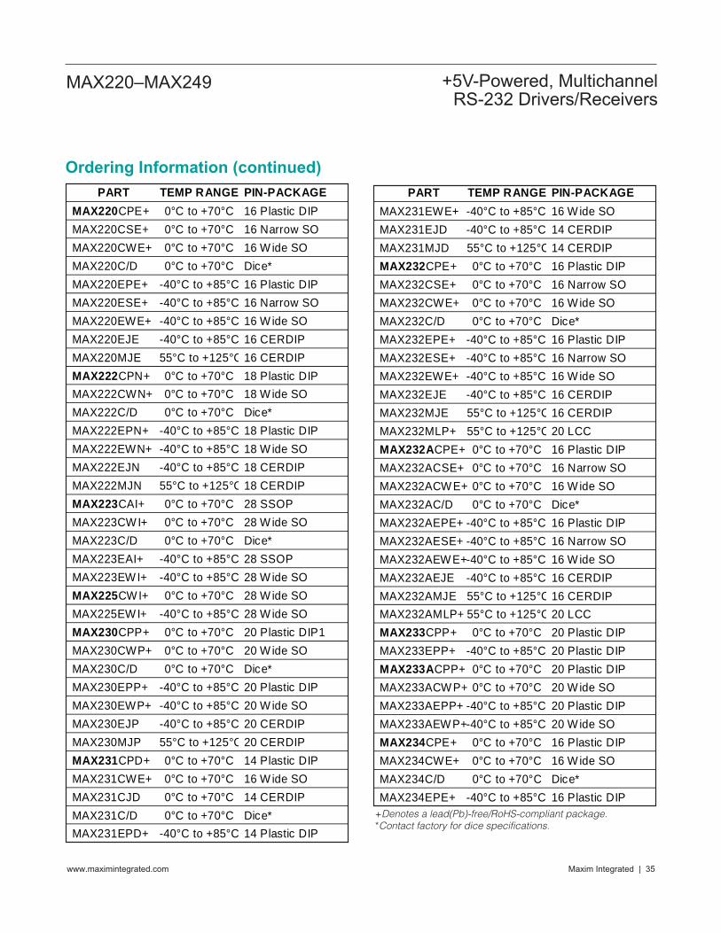
MAX220–MAX249 +5V-Powered, MultichannelRS-232 Drivers/Receivers
Maxim Integrated | 35www.maximintegrated.com
Ordering Information (continued)
+Denotes a lead(Pb)-free/RoHS-compliant package.*Contact factory for dice specifications.
PART TEMP RANGE PIN-PACKAGE MAX220CPE+ 0°C to +70°C 16 Plastic DIP MAX220CSE+ 0°C to +70°C 16 Narrow SO MAX220CWE+ 0°C to +70°C 16 W ide SO MAX220C/D 0°C to +70°C Dice* MAX220EPE+ -40°C to +85°C 16 Plastic DIP MAX220ESE+ -40°C to +85°C 16 Narrow SO MAX220EWE+ -40°C to +85°C 16 W ide SO MAX220EJE -40°C to +85°C 16 CERDIP MAX220MJE 55°C to +125°C 16 CERDIP MAX222CPN+ 0°C to +70°C 18 Plastic DIP MAX222CWN+ 0°C to +70°C 18 W ide SO MAX222C/D 0°C to +70°C Dice* MAX222EPN+ -40°C to +85°C 18 Plastic DIP MAX222EWN+ -40°C to +85°C 18 W ide SO MAX222EJN -40°C to +85°C 18 CERDIP MAX222MJN 55°C to +125°C 18 CERDIP MAX223CAI+ 0°C to +70°C 28 SSOP MAX223CW I+ 0°C to +70°C 28 W ide SO MAX223C/D 0°C to +70°C Dice* MAX223EAI+ -40°C to +85°C 28 SSOP MAX223EW I+ -40°C to +85°C 28 W ide SO MAX225CW I+ 0°C to +70°C 28 W ide SO MAX225EW I+ -40°C to +85°C 28 W ide SO MAX230CPP+ 0°C to +70°C 20 Plastic DIP1 MAX230CWP+ 0°C to +70°C 20 W ide SO MAX230C/D 0°C to +70°C Dice* MAX230EPP+ -40°C to +85°C 20 Plastic DIP MAX230EWP+ -40°C to +85°C 20 W ide SO MAX230EJP -40°C to +85°C 20 CERDIP MAX230MJP 55°C to +125°C 20 CERDIP MAX231CPD+ 0°C to +70°C 14 Plastic DIP MAX231CWE+ 0°C to +70°C 16 W ide SO MAX231CJD 0°C to +70°C 14 CERDIP MAX231C/D 0°C to +70°C Dice* MAX231EPD+ -40°C to +85°C 14 Plastic DIP
PART TEMP RANGE PIN-PACKAGE MAX231EWE+ -40°C to +85°C 16 W ide SO MAX231EJD -40°C to +85°C 14 CERDIP MAX231MJD 55°C to +125°C 14 CERDIP MAX232CPE+ 0°C to +70°C 16 Plastic DIP MAX232CSE+ 0°C to +70°C 16 Narrow SO MAX232CWE+ 0°C to +70°C 16 W ide SO MAX232C/D 0°C to +70°C Dice* MAX232EPE+ -40°C to +85°C 16 Plastic DIP MAX232ESE+ -40°C to +85°C 16 Narrow SO MAX232EWE+ -40°C to +85°C 16 W ide SO MAX232EJE -40°C to +85°C 16 CERDIP MAX232MJE 55°C to +125°C 16 CERDIP MAX232MLP+ 55°C to +125°C 20 LCC MAX232ACPE+ 0°C to +70°C 16 Plastic DIP MAX232ACSE+ 0°C to +70°C 16 Narrow SO MAX232ACW E+ 0°C to +70°C 16 W ide SO MAX232AC/D 0°C to +70°C Dice* MAX232AEPE+ -40°C to +85°C 16 Plastic DIP MAX232AESE+ -40°C to +85°C 16 Narrow SO MAX232AEW E+-40°C to +85°C 16 W ide SO MAX232AEJE -40°C to +85°C 16 CERDIP MAX232AMJE 55°C to +125°C 16 CERDIP MAX232AMLP+ 55°C to +125°C 20 LCC MAX233CPP+ 0°C to +70°C 20 Plastic DIP MAX233EPP+ -40°C to +85°C 20 Plastic DIP MAX233ACPP+ 0°C to +70°C 20 Plastic DIP MAX233ACW P+ 0°C to +70°C 20 W ide SO MAX233AEPP+ -40°C to +85°C 20 Plastic DIP MAX233AEW P+-40°C to +85°C 20 W ide SO MAX234CPE+ 0°C to +70°C 16 Plastic DIP MAX234CWE+ 0°C to +70°C 16 W ide SO MAX234C/D 0°C to +70°C Dice* MAX234EPE+ -40°C to +85°C 16 Plastic DIP
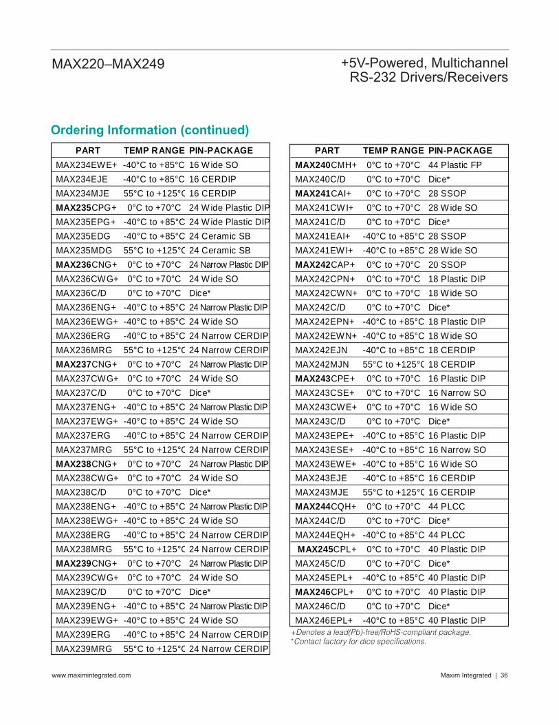
Maxim Integrated | 36www.maximintegrated.com
MAX220–MAX249 +5V-Powered, MultichannelRS-232 Drivers/Receivers
Ordering Information (continued)
+Denotes a lead(Pb)-free/RoHS-compliant package.*Contact factory for dice specifications.
PART TEMP RANGE PIN-PACKAGE MAX234EWE+ -40°C to +85°C 16 W ide SO MAX234EJE -40°C to +85°C 16 CERDIP MAX234MJE 55°C to +125°C 16 CERDIP MAX235CPG+ 0°C to +70°C 24 W ide Plastic DIPMAX235EPG+ -40°C to +85°C 24 W ide Plastic DIPMAX235EDG -40°C to +85°C 24 Ceramic SB MAX235MDG 55°C to +125°C 24 Ceramic SB MAX236CNG+ 0°C to +70°C 24 Narrow Plastic DIPMAX236CWG+ 0°C to +70°C 24 W ide SO MAX236C/D 0°C to +70°C Dice* MAX236ENG+ -40°C to +85°C 24 Narrow Plastic DIP MAX236EWG+ -40°C to +85°C 24 W ide SO MAX236ERG -40°C to +85°C 24 Narrow CERDIPMAX236MRG 55°C to +125°C 24 Narrow CERDIPMAX237CNG+ 0°C to +70°C 24 Narrow Plastic DIP MAX237CWG+ 0°C to +70°C 24 W ide SO MAX237C/D 0°C to +70°C Dice* MAX237ENG+ -40°C to +85°C 24 Narrow Plastic DIP MAX237EWG+ -40°C to +85°C 24 W ide SO MAX237ERG -40°C to +85°C 24 Narrow CERDIPMAX237MRG 55°C to +125°C 24 Narrow CERDIPMAX238CNG+ 0°C to +70°C 24 Narrow Plastic DIPMAX238CWG+ 0°C to +70°C 24 W ide SO MAX238C/D 0°C to +70°C Dice* MAX238ENG+ -40°C to +85°C 24 Narrow Plastic DIP MAX238EWG+ -40°C to +85°C 24 W ide SO MAX238ERG -40°C to +85°C 24 Narrow CERDIPMAX238MRG 55°C to +125°C 24 Narrow CERDIPMAX239CNG+ 0°C to +70°C 24 Narrow Plastic DIP MAX239CWG+ 0°C to +70°C 24 W ide SO MAX239C/D 0°C to +70°C Dice* MAX239ENG+ -40°C to +85°C 24 Narrow Plastic DIP MAX239EWG+ -40°C to +85°C 24 W ide SO MAX239ERG -40°C to +85°C 24 Narrow CERDIPMAX239MRG 55°C to +125°C 24 Narrow CERDIP
PART TEMP RANGE PIN-PACKAGE MAX240CMH+ 0°C to +70°C 44 Plastic FP MAX240C/D 0°C to +70°C Dice* MAX241CAI+ 0°C to +70°C 28 SSOP MAX241CW I+ 0°C to +70°C 28 W ide SO MAX241C/D 0°C to +70°C Dice* MAX241EAI+ -40°C to +85°C 28 SSOP MAX241EW I+ -40°C to +85°C 28 W ide SO MAX242CAP+ 0°C to +70°C 20 SSOP MAX242CPN+ 0°C to +70°C 18 Plastic DIP MAX242CWN+ 0°C to +70°C 18 W ide SO MAX242C/D 0°C to +70°C Dice* MAX242EPN+ -40°C to +85°C 18 Plastic DIP MAX242EWN+ -40°C to +85°C 18 W ide SO MAX242EJN -40°C to +85°C 18 CERDIP MAX242MJN 55°C to +125°C 18 CERDIP MAX243CPE+ 0°C to +70°C 16 Plastic DIP MAX243CSE+ 0°C to +70°C 16 Narrow SO MAX243CWE+ 0°C to +70°C 16 W ide SO MAX243C/D 0°C to +70°C Dice* MAX243EPE+ -40°C to +85°C 16 Plastic DIP MAX243ESE+ -40°C to +85°C 16 Narrow SO MAX243EWE+ -40°C to +85°C 16 W ide SO MAX243EJE -40°C to +85°C 16 CERDIP MAX243MJE 55°C to +125°C 16 CERDIP MAX244CQH+ 0°C to +70°C 44 PLCC MAX244C/D 0°C to +70°C Dice* MAX244EQH+ -40°C to +85°C 44 PLCC MAX245CPL+ 0°C to +70°C 40 Plastic DIP MAX245C/D 0°C to +70°C Dice* MAX245EPL+ -40°C to +85°C 40 Plastic DIP MAX246CPL+ 0°C to +70°C 40 Plastic DIP MAX246C/D 0°C to +70°C Dice* MAX246EPL+ -40°C to +85°C 40 Plastic DIP
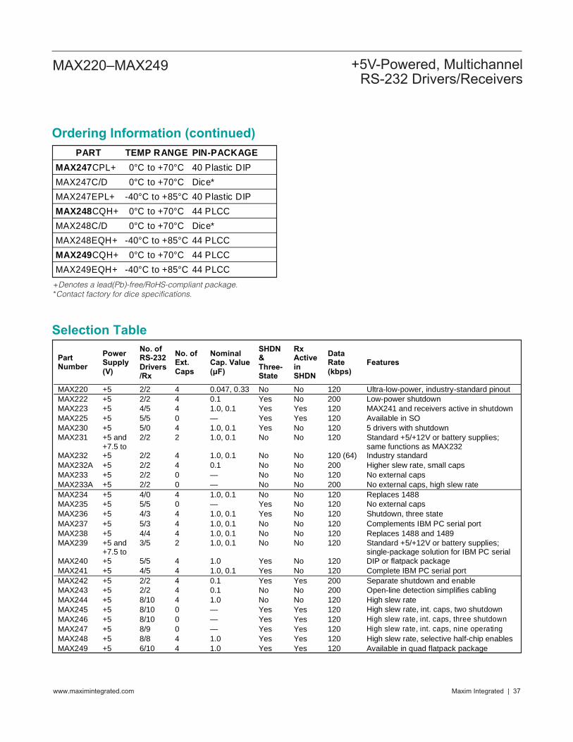
MAX220–MAX249 +5V-Powered, MultichannelRS-232 Drivers/Receivers
Maxim Integrated | 37www.maximintegrated.com
Selection Table
Ordering Information (continued)
PART TEMP RANGE PIN-PACKAGE MAX247CPL+ 0°C to +70°C 40 Plastic DIP MAX247C/D 0°C to +70°C Dice* MAX247EPL+ -40°C to +85°C 40 Plastic DIP MAX248CQH+ 0°C to +70°C 44 PLCC MAX248C/D 0°C to +70°C Dice* MAX248EQH+ -40°C to +85°C 44 PLCC MAX249CQH+ 0°C to +70°C 44 PLCC MAX249EQH+ -40°C to +85°C 44 PLCC
+Denotes a lead(Pb)-free/RoHS-compliant package.*Contact factory for dice specifications.
Part Number
Power Supply (V)
No. of RS-232 Drivers/Rx
No. of Ext. Caps
Nominal Cap. Value ( F)
SHDN & Three- State
Rx Active in SHDN
Data Rate (kbps)
Features
MAX220 +5 2/2 4 0.047, 0.33 No No 120 Ultra-low-power, industry-standard pinout MAX222 +5 2/2 4 0.1 Yes No 200 Low-power shutdown MAX223 +5 4/5 4 1.0, 0.1 Yes Yes 120 MAX241 and receivers active in shutdown MAX225 +5 5/5 0 — Yes Yes 120 Available in SO MAX230 +5 5/0 4 1.0, 0.1 Yes No 120 5 drivers with shutdown MAX231 +5 and
+7.5 to2/2 2 1.0, 0.1 No No 120 Standard +5/+12V or battery supplies;
same functions as MAX232MAX232 +5 2/2 4 1.0, 0.1 No No 120 (64) Industry standard MAX232A +5 2/2 4 0.1 No No 200 Higher slew rate, small caps MAX233 +5 2/2 0 — No No 120 No external caps MAX233A +5 2/2 0 — No No 200 No external caps, high slew rate MAX234 +5 4/0 4 1.0, 0.1 No No 120 Replaces 1488 MAX235 +5 5/5 0 — Yes No 120 No external caps MAX236 +5 4/3 4 1.0, 0.1 Yes No 120 Shutdown, three state MAX237 +5 5/3 4 1.0, 0.1 No No 120 Complements IBM PC serial port MAX238 +5 4/4 4 1.0, 0.1 No No 120 Replaces 1488 and 1489 MAX239 +5 and
+7.5 to3/5 2 1.0, 0.1 No No 120 Standard +5/+12V or battery supplies;
single-package solution for IBM PC serialMAX240 +5 5/5 4 1.0 Yes No 120 DIP or flatpack package MAX241 +5 4/5 4 1.0, 0.1 Yes No 120 Complete IBM PC serial port MAX242 +5 2/2 4 0.1 Yes Yes 200 Separate shutdown and enable MAX243 +5 2/2 4 0.1 No No 200 Open-line detection simplifies cabling MAX244 +5 8/10 4 1.0 No No 120 High slew rate MAX245 +5 8/10 0 — Yes Yes 120 High slew rate, int. caps, two shutdown MAX246 +5 8/10 0 — Yes Yes 120 High slew rate, int. caps, three shutdown MAX247 +5 8/9 0 — Yes Yes 120 High slew rate, int. caps, nine operating MAX248 +5 8/8 4 1.0 Yes Yes 120 High slew rate, selective half-chip enables MAX249 +5 6/10 4 1.0 Yes Yes 120 Available in quad flatpack package
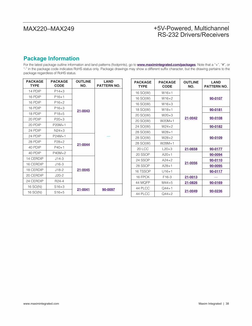
Maxim Integrated | 38www.maximintegrated.com
MAX220–MAX249 +5V-Powered, MultichannelRS-232 Drivers/Receivers
PACKAGETYPE
PACKAGECODE
OUTLINENO.
LANDPATTERN NO.
14 PDIP P14+3
21-0043
—
16 PDIP P16+1
16 PDIP P16+2
16 PDIP P16+3
18 PDIP P18+5
20 PDIP P20+3
20 PDIP P20M+1
24 PDIP N24+3
24 PDIP P24M+1
21-004428 PDIP P28+2
40 PDIP P40+1
40 PDIP P40M+2
14 CERDIP J14-3
21-0045
16 CERDIP J16-3
18 CERDIP J18-2
20 CERDIP J20-2
24 CERDIP R24-4
16 SO(N) S16+321-0041 90-0097
16 SO(N) S16+5
Package Information For the latest package outline information and land patterns (footprints), go to www.maximintegrated.com/packages. Note that a “+”, “#”, or“-” in the package code indicates RoHS status only. Package drawings may show a different suffix character, but the drawing pertains to thepackage regardless of RoHS status.
PACKAGETYPE
PACKAGECODE
OUTLINENO.
LANDPATTERN NO.
16 SO(W) W16+1
21-0042
90-010716 SO(W) W16+2
16 SO(W) W16+3
18 SO(W) W18+1 90-0181
20 SO(W) W20+390-0108
20 SO(W) W20M+1
24 SO(W) W24+2 90-0182
28 SO(W) W28+1
90-010928 SO(W) W28+2
28 SO(W) W28M+1
20 LCC L20+3 21-0658 90-0177
20 SSOP A20+1
21-0056
90-0094
24 SSOP A24+2 90-0110
28 SSOP A28+1 90-0095
16 TSSOP U16+1 90-0117
16 FPCK F16-3 21-0013 —
44 MQFP M44+5 21-0826 90-0169
44 PLCC Q44+121-0049 90-0236
44 PLCC Q44+2
Maxim Integrated cannot assume responsibility for use of any circuitry other than circuitry entirely embodied in a Maxim Integrated product. No circuit patentlicenses are implied. Maxim Integrated reserves the right to change the circuitry and specifications without notice at any time. The parametric values (min andmax limits) shown in the Electrical Characteristics table are guaranteed. Other parametric values quoted in this data sheet are provided for guidance.
Maxim Integrated and the Maxim Integrated logo are trademarks of Maxim Integrated Products, Inc. © 2015 Maxim Integrated Products, Inc. | 39
For pricing, delivery, and ordering information, please contact Maxim Direct at 1-888-629-4642, or visit Maxim Integrated’s website at www.maximintegrated.com.
MAX220–MAX249 +5V-Powered, MultichannelRS-232 Drivers/Receivers
Revision History
REVISIONNUMBER
REVISIONDATE
DESCRIPTIONPAGES
CHANGED
15 1/06Added part information to the lead temperature in the Absolute Maximum Ratingssections
2, 5, 8
16 7/10Changed multiple packages to lead-free versions; updated/added notes 3, 4, 5, 7, and8 to the Electrical Characteristics table; removed incorrect subscripting from all pinnames in the Electrical Characteristics table and Pin Configurations
1, 2–9, 17–36
17 1/15 Updated General Description and Benefits and Features sections 1