Embed Size (px)
Citation preview

General DescriptionThe MAX14871 DC motor driver provides a low-power and simple solution for driving and controlling brushed motors with voltages between 4.5V and 36V. Very low driver on resistance reduces power during dissipation. The MAX14871 features a charge-pump-less design for reduced external components and low supply current. Integrated current regulation allows user-defined peak startup motor currents and requires minimal external components. The MAX14871 includes 3 modes of current regulation: fast decay, slow decay, and 25% current ripple modes. Current regulation based on 25% ripple simplifies the design and enables regulation independent of motor characteristics. A separate voltage sense input (SNS) reduc-es current-sensing errors due to parasitic trace resistance.The MAX14871 features shoot-through protection and internal free-wheeling diodes that absorb inductive motor currents. Driver outputs are short-circuit-protected from shorts to ground, to the supply, and between M1 and M2. An active-low FAULT output signals thermal overload and overcurrents during fault conditions. The MAX14871 is available in a 16-pin TSSOP-EP package and operates over the -40°C to +85°C temperature range.
Applications Printers and Scanners Industrial Automation Vending and Gaming Machines
Benefits and Features Drive More Power and Reduce Footprint
• Up to 2.8A Peak Motor-Current Package• Flexible 4.5V–36V Supply Enables Longer Runtime
Low Power Consumption Runs Cooler and Longer• 334mΩ (typ) Total Bridge On-Resistance• 1mA (typ) Supply Current at 30kHz/24V• 10µA (max) Standby Current at 12V
Simplified Designs Reduces Time to Market• Charge-Pump-Less Architecture• Current Regulation Only Requires a Sense Resistor• Current-Sense Input Simplifies PCB Layout• Internal/External VREF for Current Regulation• Fast/Slow/25% Ripple Current Regulation Modes
Integrated Protection Provides Robust Driving Solutions• Short-Circuit-Protected Drivers• Thermal Shutdown Undervoltage Lockout• Diagnostic FAULT Output• -40°C to +85°C Temperature Range
Ordering Information appears at end of data sheet.
19-7063; Rev 0; 9/14
DRIVER
VDD
SNS
PWM
DIR
MAX14871
GNDCOM
M1 M2
EN
FAULT
DRIVER
VDD VDD
CURRENT REGULATION
RSENSE
MODE
VREF
TCOFF
µC
IRQ
PWM
GPO
24V
3.3V3.3V
M
3.3V
COFF
Typical Application Circuit
MAX14871 4.5V to 36V Full-Bridge DC Motor Driver
EVALUATION KIT AVAILABLE

(All voltages referenced to GND)VDD ........................................................................-0.3V to +40VM1, M2 ....................................................... -0.3V to (VDD+0.3V)PWM, DIR, FAULT, EN, SNS, VREF, MODE, TCOFF ............................................................... -0.3V to +6.0VCOM .....................................................................-0.3V to +0.3VCurrent Into M1, M2 .............................................................±3AContinuous Power Dissipation (TA = +70°C)
Single-Layer Board (derate at 21.3mW/°C above +70°C) ............................................................1702mWMultiple-Layer Board (derate at 26.1mW/°C above +70°C) ............................................................2088mWOperating Temperature Range ........................... -40°C to +85°CJunction Temperature ...................................................... +150ºCStorage Temperature Range .............................-65ºC to +150°CLead Temperature (Soldering, 10s) ................................+300°CSolder Temperature (Reflow) .........................................+260°C
Junction-to-Case Thermal Resistance (θJC) TSSOP-EP (Single-Layer Board) ..................................3°C/W TSSOP-EP (Multiple-Layer Board) ................................3°C/W
Junction-to-Ambient Thermal Resistance (θJA) TSSOP-EP (Single-Layer Board) ................................47°C/W TSSOP-EP (Multiple-Layer Board) ...........................38.3°C/W
(Note 1)
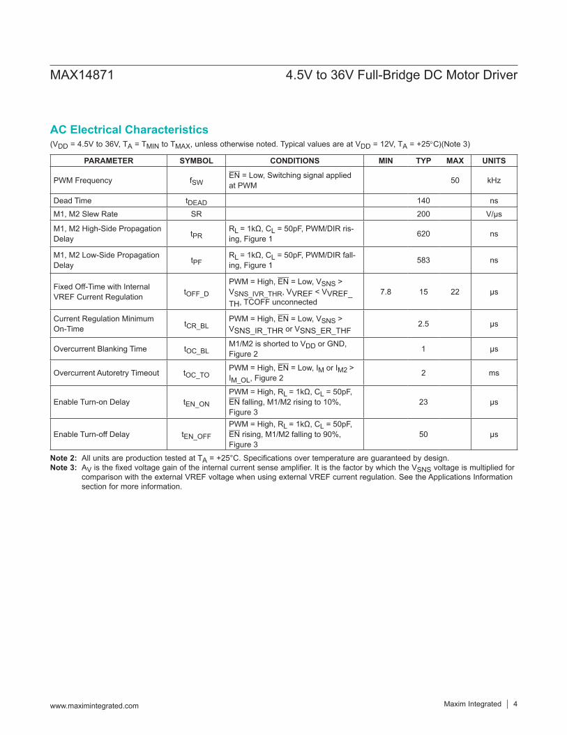
(VDD = 4.5V to 36V, TA = TMIN to TMAX, unless otherwise noted. Typical values are at VDD = 12V, TA = +25°C)(Note 3)
Note 2: Package thermal resistances were obtained using the method described in JEDEC specification JESD51-7, using a four-layer board. For detailed information on package thermal considerations, refer to www.maximintegrated.com/thermal-tutorial.
PARAMETER SYMBOL CONDITIONS MIN TYP MAX UNITSPOWER SUPPLYSupply Voltage VDD 4.5 36 V
Supply Current IDDEN = low, M1/M2 not connected
fPWM = 50kHz 1mA
No switching 0.5 1.2
Shutdown Supply Current ISHDNEN = high, Driver is in shutdown
VDD = 12V 3.7 10μA
VDD = 36V 10 20
Undervoltage Lockout Threshold VUVLO VDD rising 3.3 3.8 4.3 V
Undervoltage Lockout Threshold Hysteresis VUVLO_HYST 400 mV
DRIVER (M1, M2)Driver Output Resistance (High-Side + Low-Side) RON IM_ = 2.8A
TJ = 25°C 334 435mΩ
TJ = 125°C 465 620
Driver Overload Current Limit IM_OL 3 A
M1, M2 Leakage Current IM_LKG EN = High, VM1 = VM2 = 0V or VDD -1 +1 μA
M1, M2 Body Diode Forward-Voltage VBF
Low-side diode, EN = High, IF = 2.8A 1.5V
High-side diode, EN = High, IF = 2.8A 1.5
MAX14871 4.5V to 36V Full-Bridge DC Motor Driver
www.maximintegrated.com Maxim Integrated 2
Absolute Maximum Ratings
Stresses beyond those listed under “Absolute Maximum Ratings” may cause permanent damage to the device. These are stress ratings only, and functional operation of the device at these or any other conditions beyond those indicated in the operational sections of the specifications is not implied. Exposure to absolute maximum rating conditions for extended periods may affect device reliability.
Package Thermal Characteristics
Electrical Characteristics
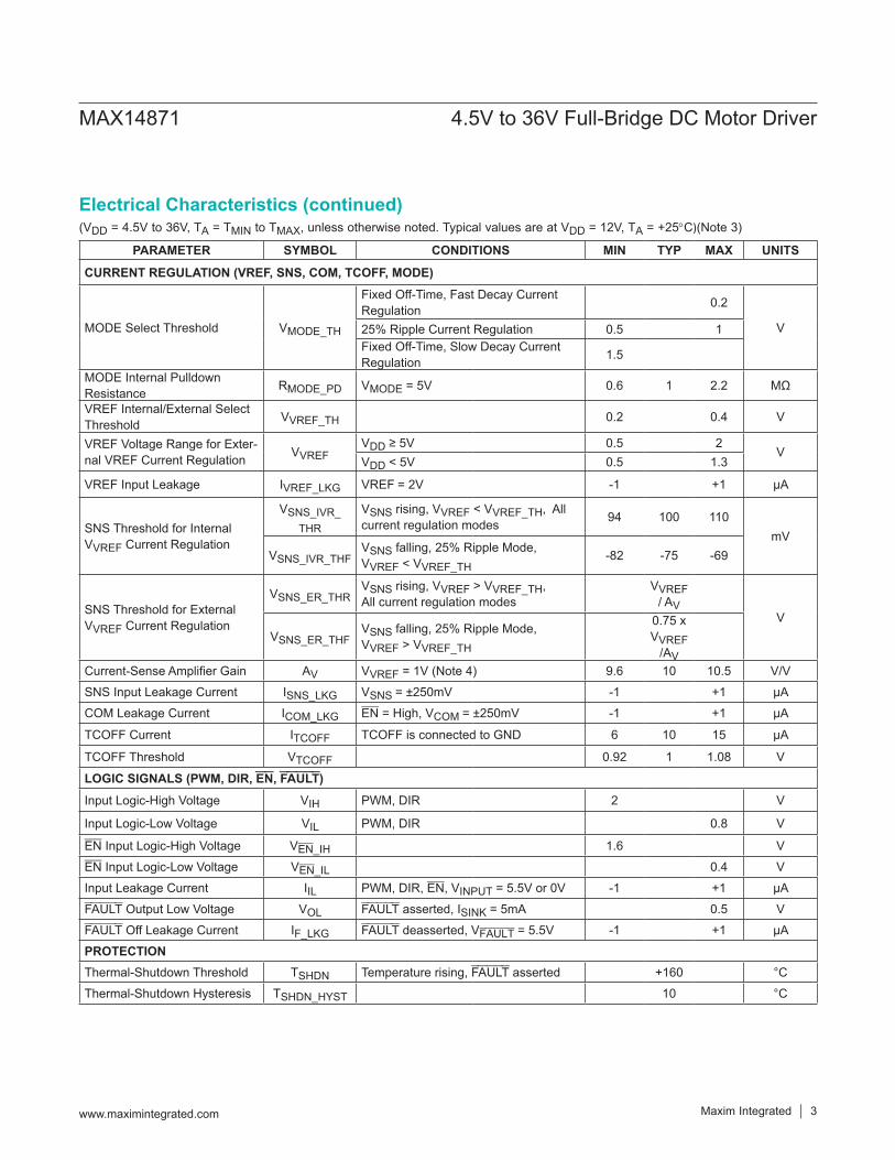
(VDD = 4.5V to 36V, TA = TMIN to TMAX, unless otherwise noted. Typical values are at VDD = 12V, TA = +25°C)(Note 3)
PARAMETER SYMBOL CONDITIONS MIN TYP MAX UNITS
CURRENT REGULATION (VREF, SNS, COM, TCOFF, MODE)
MODE Select Threshold VMODE_TH
Fixed Off-Time, Fast Decay Current Regulation 0.2
V25% Ripple Current Regulation 0.5 1Fixed Off-Time, Slow Decay Current Regulation 1.5
MODE Internal Pulldown Resistance RMODE_PD VMODE = 5V 0.6 1 2.2 MΩ
VREF Internal/External Select Threshold VVREF_TH 0.2 0.4 V
VREF Voltage Range for Exter-nal VREF Current Regulation VVREF
VDD ≥ 5V 0.5 2V
VDD < 5V 0.5 1.3
VREF Input Leakage IVREF_LKG VREF = 2V -1 +1 μA
SNS Threshold for Internal VVREF Current Regulation
VSNS_IVR_THR
VSNS rising, VVREF < VVREF_TH, All current regulation modes 94 100 110
mVVSNS_IVR_THF
VSNS falling, 25% Ripple Mode, VVREF < VVREF_TH
-82 -75 -69
SNS Threshold for External VVREF Current Regulation
VSNS_ER_THRVSNS rising, VVREF > VVREF_TH, All current regulation modes
VVREF / AV
VVSNS_ER_THF
VSNS falling, 25% Ripple Mode, VVREF > VVREF_TH
0.75 x VVREF
/AVCurrent-Sense Amplifier Gain AV VVREF = 1V (Note 4) 9.6 10 10.5 V/V
SNS Input Leakage Current ISNS_LKG VSNS = ±250mV -1 +1 μA
COM Leakage Current ICOM_LKG EN = High, VCOM = ±250mV -1 +1 μA
TCOFF Current ITCOFF TCOFF is connected to GND 6 10 15 μA
TCOFF Threshold VTCOFF 0.92 1 1.08 V
LOGIC SIGNALS (PWM, DIR, EN, FAULT)
Input Logic-High Voltage VIH PWM, DIR 2 V
Input Logic-Low Voltage VIL PWM, DIR 0.8 V
EN Input Logic-High Voltage VEN_IH 1.6 V
EN Input Logic-Low Voltage VEN_IL 0.4 V
Input Leakage Current IIL PWM, DIR, EN, VINPUT = 5.5V or 0V -1 +1 μA
FAULT Output Low Voltage VOL FAULT asserted, ISINK = 5mA 0.5 V
FAULT Off Leakage Current IF_LKG FAULT deasserted, VFAULT = 5.5V -1 +1 μA
PROTECTIONThermal-Shutdown Threshold TSHDN Temperature rising, FAULT asserted +160 °C
Thermal-Shutdown Hysteresis TSHDN_HYST 10 °C
MAX14871 4.5V to 36V Full-Bridge DC Motor Driver
www.maximintegrated.com Maxim Integrated 3
Electrical Characteristics (continued)
(VDD = 4.5V to 36V, TA = TMIN to TMAX, unless otherwise noted. Typical values are at VDD = 12V, TA = +25°C)(Note 3)
Note 2: All units are production tested at TA = +25°C. Specifications over temperature are guaranteed by design.Note 3: AV is the fixed voltage gain of the internal current sense amplifier. It is the factor by which the VSNS voltage is multiplied for
comparison with the external VREF voltage when using external VREF current regulation. See the Applications Information section for more information.
PARAMETER SYMBOL CONDITIONS MIN TYP MAX UNITS
PWM Frequency fSWEN = Low, Switching signal applied at PWM 50 kHz
Dead Time tDEAD 140 ns
M1, M2 Slew Rate SR 200 V/μs
M1, M2 High-Side Propagation Delay tPR
RL = 1kΩ, CL = 50pF, PWM/DIR ris-ing, Figure 1 620 ns
M1, M2 Low-Side Propagation Delay tPF
RL = 1kΩ, CL = 50pF, PWM/DIR fall-ing, Figure 1 583 ns
Fixed Off-Time with Internal VREF Current Regulation tOFF_D
PWM = High, EN = Low, VSNS > VSNS_IVR_THR, VVREF < VVREF_TH, TCOFF unconnected
7.8 15 22 μs
Current Regulation Minimum On-Time tCR_BL
PWM = High, EN = Low, VSNS > VSNS_IR_THR or VSNS_ER_THF 2.5 μs
Overcurrent Blanking Time tOC_BLM1/M2 is shorted to VDD or GND, Figure 2 1 μs
Overcurrent Autoretry Timeout tOC_TOPWM = High, EN = Low, IM or IM2 > IM_OL, Figure 2 2 ms
Enable Turn-on Delay tEN_ON
PWM = High, RL = 1kΩ, CL = 50pF, EN falling, M1/M2 rising to 10%, Figure 3
23 μs
Enable Turn-off Delay tEN_OFF
PWM = High, RL = 1kΩ, CL = 50pF, EN rising, M1/M2 falling to 90%, Figure 3
50 μs
MAX14871 4.5V to 36V Full-Bridge DC Motor Driver
www.maximintegrated.com Maxim Integrated 4
AC Electrical Characteristics
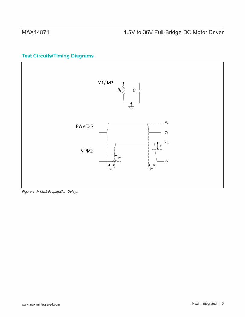
Figure 1. M1/M2 Propagation Delays
RL CL
M1/ M2
tPR tPF
0V
VL
VDD
0V
PWM/DIR
M1/M21V
1V
MAX14871 4.5V to 36V Full-Bridge DC Motor Driver
www.maximintegrated.com Maxim Integrated 5
Test Circuits/Timing Diagrams
Figure 2. Overcurrent Autoretry Timeout
Figure 3. Enable/Disable Delays
FAULT
tOC_BL
VL
0V
IM1 or IM2
tOC_TO
IM_OL
0A
RL CL
M1/ M2
tEN_ON tEN_OFF
0V
VL
VDD
0V
EN
M1/M2
1.5V 1.5V
10%
90%
MAX14871 4.5V to 36V Full-Bridge DC Motor Driver
www.maximintegrated.com Maxim Integrated 6
Test Circuits/Timing Diagrams (continued)
(VDD = 24V, TA = +25°C, unless otherwise noted.)
0
2
4
6
8
10
12
-45 -30 -15 0 15 30 45 60 75 90
I SHDN
(µA)
TEMPERATURE (oC)
SHUTDOWN SUPPLY CURRENTvs. TEMPERATURE
toc04
VDD = 4.5V
VDD = 36V
VDD = 24V
0.00
0.05
0.10
0.15
0.20
0.25
0.30
0 1000 2000 3000
ON-R
ESIS
TANC
E(Ω
)
LOAD CURRENT (mA)
HIGH-SIDE ON RESISTANCEvs. LOAD CURRENT
toc01
VDD = 4.5V
VDD = 36V
0.0
0.2
0.4
0.6
0.8
1.0
1.2
0 1 2 3
V BF
(V)
LOAD CURRENT (A)
HIGH-SIDE M1/M2 BODY DIODEFORWARD-VOLTAGE vs. LOAD
toc07
TA = 25°CTA = 85°CTA = -40°C
0.00
0.02
0.04
0.06
0.08
0.10
0.12
0.14
0.16
0.18
0.20
0 1000 2000 3000
ON-R
ESIS
TANC
E (Ω
)
LOAD CURRENT (mA)
LOW-SIDE ON RESISTANCEvs. LOAD CURRENT
toc02
VDD = 4.5V
VDD = 36V
0
5
10
15
20
25
30
35
40
45
50
55
100 150 200 250 300 350 400 450 500
t OFF
(µs)
COFF (pF)
OFF-TIME vs COFF CAPACITANCEtoc08
0.00
0.05
0.10
0.15
0.20
0.25
0.30
0.35
0.40
-45 -20 5 30 55 80 105 130
ON-R
ESIS
TANC
E(Ω
)
TEMPERATURE (oC)
ON-RESISTANCEvs. TEMPERATURE toc03
LOW-SIDE
HIGH-SIDE
ILOAD = 1A
0.0
0.2
0.4
0.6
0.8
1.0
1.2
1.4
1.6
0 5 10 15 20 25 30 35 40 45 50
I CC(m
A)
DATA RATE (kHz)
SUPPLY CURRENT vs. SWITCHING RATE
toc05
VDD = 5V
VDD = 36V
CL = 10pF on M1/M2
VDD = 24V
VDD = 12V
0.0
0.2
0.4
0.6
0.8
1.0
1.2
0 1 2 3
V BF
(V)
LOAD CURRENT (A)
LOW-SIDE M1/M2 BODY DIODEFORWARD-VOLTAGE vs. LOAD toc06
TA = 25°CTA = 85°CTA = -40°C
MAX14871 4.5V to 36V Full-Bridge DC Motor Driver
Maxim Integrated 7www.maximintegrated.com
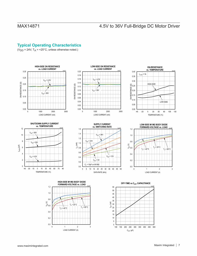
Typical Operating Characteristics
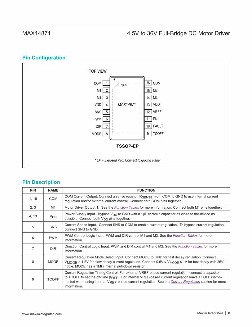
PIN NAME FUNCTION
1, 16 COM COM Current Output. Connect a sense resistor, RSENSE, from COM to GND to use internal current regulation and/or external current control. Connect both COM pins together.
2, 3 M1 Motor Driver Output 1. See the Function Tables for more information. Connect both M1 pins together.
4, 13 VDDPower Supply Input. Bypass VDD to GND with a 1μF ceramic capacitor as close to the device as possible. Connect both VDD pins together.
5 SNS Current Sense Input. Connect SNS to COM to enable current regulation. To bypass current regulation, connect SNS to GND.
6 PWM PWM Control Logic Input. PWM and DIR control M1 and M2. See the Function Tables for more information.
7 DIR Direction Control Logic Input. PWM and DIR control M1 and M2. See the Function Tables for more information.
8 MODECurrent Regulation Mode Select Input. Connect MODE to GND for fast decay regulation. Connect VMODE > 1.5V for slow decay current regulation. Connect 0.5V ≤ VMODE ≤ 1V for fast decay with 25% ripple. MODE has a 1MΩ internal pull-down resistor.
9 TCOFF
Current Regulation Timing Control. For external VREF-based current regulation, connect a capacitor to TCOFF to set the off-time (tOFF). For internal VREF-based current regulation leave TCOFF uncon-nected when using internal VREF-based current regulation. See the Current Regulation section for more information.
TOP VIEW
* EP = Exposed Pad. Connect to ground plane.
16
15
14
13
12
11
9
1
2
3
4
5
6
8
COM+
M2
M2
VDDVDD
M1
M1
COM
MAX14871VREF
EN
TCOFFMODE
PWM
107 FAULTDIR
SNS
TSSOP-EP
*EP
MAX14871 4.5V to 36V Full-Bridge DC Motor Driver
www.maximintegrated.com Maxim Integrated 8
Pin Configuration
Pin Description
PIN NAME FUNCTION
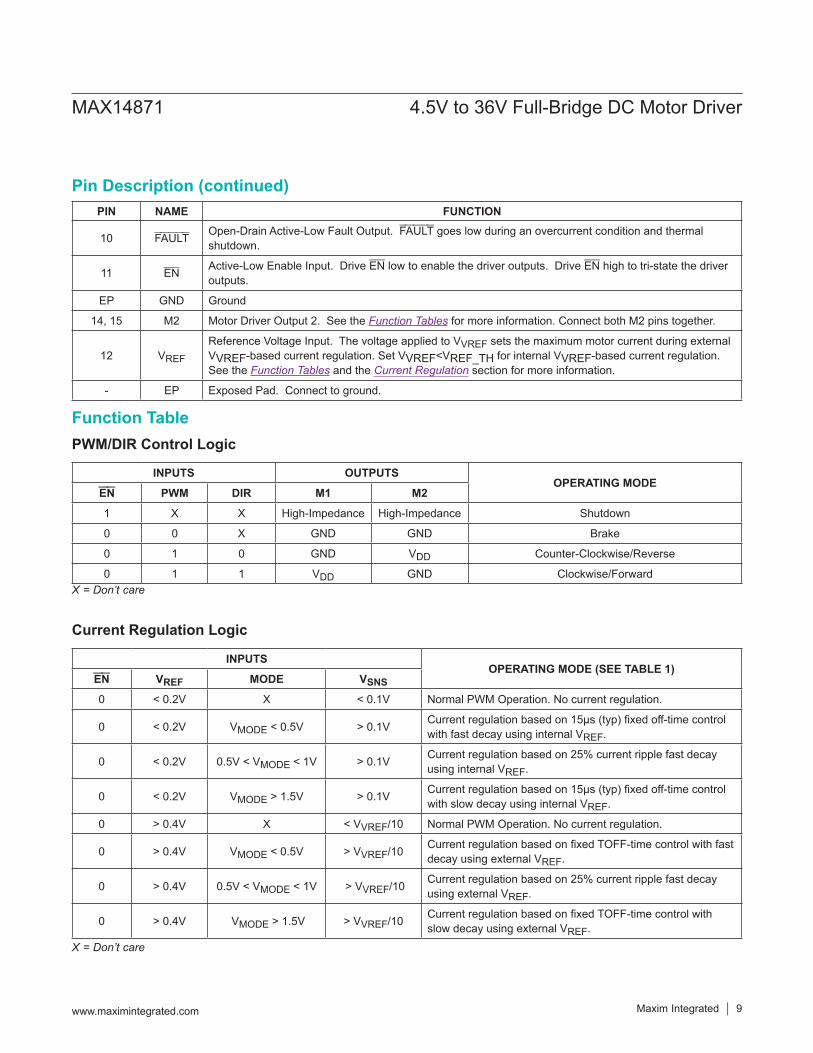
10 FAULT Open-Drain Active-Low Fault Output. FAULT goes low during an overcurrent condition and thermal shutdown.
11 EN Active-Low Enable Input. Drive EN low to enable the driver outputs. Drive EN high to tri-state the driver outputs.
EP GND Ground
14, 15 M2 Motor Driver Output 2. See the Function Tables for more information. Connect both M2 pins together.
12 VREF
Reference Voltage Input. The voltage applied to VVREF sets the maximum motor current during external VVREF-based current regulation. Set VVREF<VREF_TH for internal VVREF-based current regulation. See the Function Tables and the Current Regulation section for more information.
- EP Exposed Pad. Connect to ground.
INPUTS OUTPUTSOPERATING MODE
EN PWM DIR M1 M2
1 X X High-Impedance High-Impedance Shutdown
0 0 X GND GND Brake
0 1 0 GND VDD Counter-Clockwise/Reverse
0 1 1 VDD GND Clockwise/Forward
INPUTSOPERATING MODE (SEE TABLE 1)
EN VREF MODE VSNS
0 < 0.2V X < 0.1V Normal PWM Operation. No current regulation.
0 < 0.2V VMODE < 0.5V > 0.1V Current regulation based on 15μs (typ) fixed off-time control with fast decay using internal VREF.
0 < 0.2V 0.5V < VMODE < 1V > 0.1V Current regulation based on 25% current ripple fast decay using internal VREF.
0 < 0.2V VMODE > 1.5V > 0.1V Current regulation based on 15μs (typ) fixed off-time control with slow decay using internal VREF.
0 > 0.4V X < VVREF/10 Normal PWM Operation. No current regulation.
0 > 0.4V VMODE < 0.5V > VVREF/10 Current regulation based on fixed TOFF-time control with fast decay using external VREF.
0 > 0.4V 0.5V < VMODE < 1V > VVREF/10 Current regulation based on 25% current ripple fast decay using external VREF.
0 > 0.4V VMODE > 1.5V > VVREF/10 Current regulation based on fixed TOFF-time control with slow decay using external VREF.
Current Regulation Logic
PWM/DIR Control Logic
MAX14871 4.5V to 36V Full-Bridge DC Motor Driver
www.maximintegrated.com Maxim Integrated 9
Pin Description (continued)
Function Table
X = Don’t care
X = Don’t care
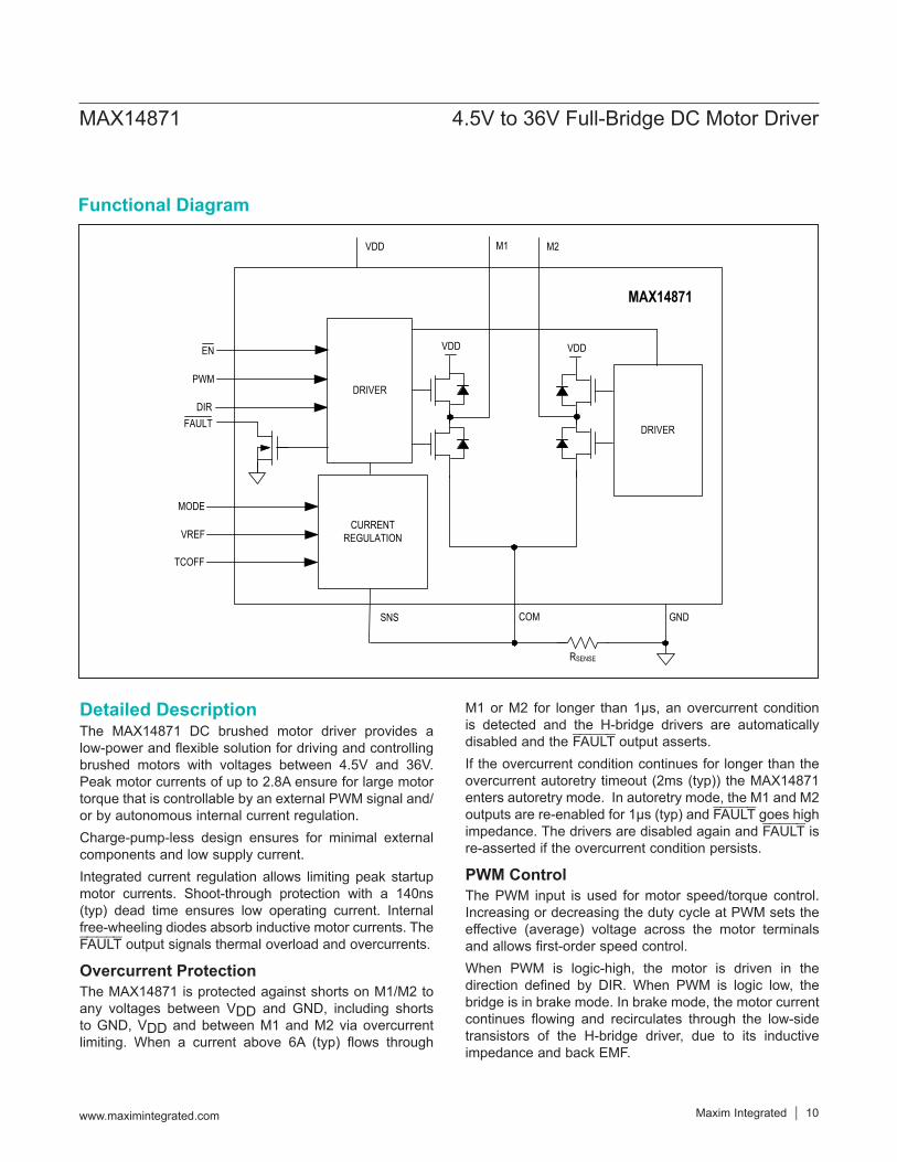
Detailed DescriptionThe MAX14871 DC brushed motor driver provides a low-power and flexible solution for driving and controlling brushed motors with voltages between 4.5V and 36V. Peak motor currents of up to 2.8A ensure for large motor torque that is controllable by an external PWM signal and/or by autonomous internal current regulation.Charge-pump-less design ensures for minimal external components and low supply current. Integrated current regulation allows limiting peak startup motor currents. Shoot-through protection with a 140ns (typ) dead time ensures low operating current. Internal free-wheeling diodes absorb inductive motor currents. The FAULT output signals thermal overload and overcurrents.
Overcurrent ProtectionThe MAX14871 is protected against shorts on M1/M2 to any voltages between VDD and GND, including shorts to GND, VDD and between M1 and M2 via overcurrent limiting. When a current above 6A (typ) flows through
M1 or M2 for longer than 1µs, an overcurrent condition is detected and the H-bridge drivers are automatically disabled and the FAULT output asserts.If the overcurrent condition continues for longer than the overcurrent autoretry timeout (2ms (typ)) the MAX14871 enters autoretry mode. In autoretry mode, the M1 and M2 outputs are re-enabled for 1µs (typ) and FAULT goes high impedance. The drivers are disabled again and FAULT is re-asserted if the overcurrent condition persists.
PWM ControlThe PWM input is used for motor speed/torque control. Increasing or decreasing the duty cycle at PWM sets the effective (average) voltage across the motor terminals and allows first-order speed control.When PWM is logic-high, the motor is driven in the direction defined by DIR. When PWM is logic low, the bridge is in brake mode. In brake mode, the motor current continues flowing and recirculates through the low-side transistors of the H-bridge driver, due to its inductive impedance and back EMF.
DRIVER
VDD
SNS
PWM
DIR
MAX14871
GNDCOM
M1 M2
EN
FAULT DRIVER
VDD VDD
CURRENT REGULATION
RSENSE
MODE
VREF
TCOFF
MAX14871 4.5V to 36V Full-Bridge DC Motor Driver
www.maximintegrated.com Maxim Integrated 10
Functional Diagram
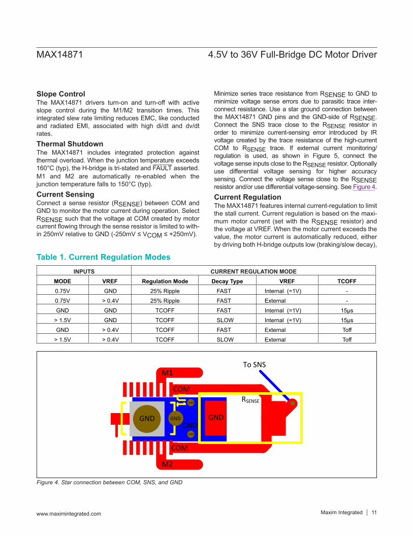
Slope ControlThe MAX14871 drivers turn-on and turn-off with active slope control during the M1/M2 transition times. This integrated slew rate limiting reduces EMC, like conducted and radiated EMI, associated with high di/dt and dv/dt rates.Thermal ShutdownThe MAX14871 includes integrated protection against thermal overload. When the junction temperature exceeds 160°C (typ), the H-bridge is tri-stated and FAULT asserted.M1 and M2 are automatically re-enabled when the junction temperature falls to 150°C (typ).Current SensingConnect a sense resistor (RSENSE) between COM and GND to monitor the motor current during operation. Select RSENSE such that the voltage at COM created by motor current flowing through the sense resistor is limited to with-in 250mV relative to GND (-250mV ≤ VCOM ≤ +250mV).
Minimize series trace resistance from RSENSE to GND to minimize voltage sense errors due to parasitic trace inter-connect resistance. Use a star ground connection between the MAX14871 GND pins and the GND-side of RSENSE. Connect the SNS trace close to the RSENSE resistor in order to minimize current-sensing error introduced by IR voltage created by the trace resistance of the high-current COM to RSENSE trace. If external current monitoring/ regulation is used, as shown in Figure 5, connect the voltage sense inputs close to the RSENSE resistor. Optionally use differential voltage sensing for higher accuracy sensing. Connect the voltage sense close to the RSENSE resistor and/or use differential voltage-sensing. See Figure 4.Current RegulationThe MAX14871 features internal current-regulation to limit the stall current. Current regulation is based on the maxi-mum motor current (set with the RSENSE resistor) and the voltage at VREF. When the motor current exceeds the value, the motor current is automatically reduced, either by driving both H-bridge outputs low (braking/slow decay),
Table 1. Current Regulation ModesINPUTS CURRENT REGULATION MODE
MODE VREF Regulation Mode Decay Type VREF TCOFF0.75V GND 25% Ripple FAST Internal (=1V) -
0.75V > 0.4V 25% Ripple FAST External -
GND GND TCOFF FAST Internal (=1V) 15µs
> 1.5V GND TCOFF SLOW Internal (=1V) 15µs
GND > 0.4V TCOFF FAST External Toff
> 1.5V > 0.4V TCOFF SLOW External Toff
Figure 4. Star connection between COM, SNS, and GND
EP
M1
M2
To SNS
COM
COM
RSENSE
GNDGNDGND
GND
GND
GND
MAX14871 4.5V to 36V Full-Bridge DC Motor Driver
www.maximintegrated.com Maxim Integrated 11
or by reversing the H-bridge direction (fast decay). The H-bridge is turned back to normal polarity after a defined delay time (TOFF mode) or after the motor current has reduced by 25% (25% ripple mode). See Table 1. The MAX14871 Function Tables show how to set the regula-tion mode.
Regulation ModesThe MAX14871 offers two internal current regulation modes: Constant off-time (TOFF) and 25% current ripple regulation. For both modes, regulation is set when the motor current (IM) exceeds the current limit defined by the VREF voltage and the sense resistor:
IM_MAX = VVREF/(AV x RSENSE)
VREFEither the internal VVREF voltage or an external voltage on VREF can be used for current regulation. Select inter-nal VREF-based regulation by setting VVREF < VREF_TH. The internal VVREF is 1V (typ). When an external voltage is used, the range of VREF is defined by VVREF.
Fixed Off-Time (TOFF-time) RegulationFixed off-time regulation turns the H-bridge driver off for a fixed time (tOFF time), as defined by the value of the COFF capacitor connected between TCOFF and GND:
tOFF (µs)= COFF(pF)/10. If VVREF < VVREF_TH and TCOFF is left unconnected, then tOFF is 15µs (typ).During the fixed TOFF-time regulation, the H-bridge can operate in either slow or fast decay mode. See Table 1.
Slow Decay ModeSlow decay, also called brake mode, is selected by set-ting VMODE > 1.5V. In slow decay, both H-bridge low-side drivers are turned on so that the inductive motor current recirculates through the low-side transistors and the motor’s terminals see a differential voltage near zero (VDIFF = 2 x IM x RON_LS). During the slow-decay TOFF period (tOFF) motor current does not flow through the external VDD/GND supply and the voltage across RSENSE is zero. The current decay during tOFF is a first-order exponential decay with a time constant equal to the motor’s electrical time constant (L/R). The rate of current decay during tOFF is proportional to the motor’s back EMF/rotational speed.
Fast Decay ModeFast decay mode can be used as an alternative to slow decay during fixed off-time regulation. Fast decay is enabled by setting VMODE < 0.2V. In fast decay, the H-bridge polarity is reversed during the tOFF period, which results in faster motor current decay, since –VDD is applied across the motor’s terminals. The motor current decrease is first order with an L/R time constant and proportional to (VDD + VEMF). Note that if tOFF is larger than the motor’s L/R electrical time constant, the inductive current can reverse direction, causing the motor not to start-up. If fixed off-time regula-tion with fast decay is used, select TOFF carefully, based on the motor’s electrical characteristics.During fast decay, the motor’s inductive current recircu-lates through the external VDD supply, which charges up the VDD bypass capacitor. Thus the voltage seen across RSENSE is negative during the tOFF delay.
25% Ripple Regulation25% ripple regulation is based on the H-bridge switching to fast decay period until the motor current falls by 25%. When IM reaches the regulation limit, the bridge enters fast decay until the IM falls to 75% of the current limit. The H-bridge polarity is then turned back to normal drive. Thus the motor current ramps up and down between 75% and 100% of the set-point current. 25% ripple regulation eliminates tOFF time tuning and the TCOFF capacitor, allowing motors to be exchanged without redesign.Since 25% ripple regulation uses fast decay, the voltage seen across RSENSE is negative during the time period that the H-bridge polarity is reversed.Select 25% ripple regulation mode by setting 0.5V < VMODE < 1.0V. Leave TCOFF unconnected when 25% ripple is used.
Applications InformationLayout ConsiderationsConnect duplicate pins (COM pins and VDD pins) togeth-er with low-resistance traces. See the Current Sensing section for further layout recommendations.
Power ConsiderationsThe MAX14871 driver can generate more power than the package for the device can safely dissipate. Total power dissipation for the device is calculated using the following equation:
PTOTAL = PDRIVER + PSW + PD
MAX14871 4.5V to 36V Full-Bridge DC Motor Driver
www.maximintegrated.com Maxim Integrated 12
The power dissipated inside of the driver is calculated as:PDRIVER = IM_LOAD2 x RON
where IM_LOAD is the motor current and RON is the on-resistance of the high and low-side FETs.PSW is the power generated by the driver during the rise/fall times in switching, and includes both arms of the bridge. Calculate PSW using the following equation: PSW = IM_LOAD x 2 x VDS = IM_LOAD x 2 x (1/2 x VDD x fSW x tR)where IM_LOAD is the motor current, tR is the 200ns (typ) rise or fall time of the driver output, and fSW is the switching frequency.The internal diodes dissipate power during switching, as well. Calculate the power dissipated in the diodes as:
PD = IM_LOAD x 2 x VBF x tDEAD x fSW
Operation Without Internal Current RegulationTo operate the MAX14871 without internal or external current regulation, connect SNS directly to GND. No sense resistor is required for this configuration. See Figure 4.
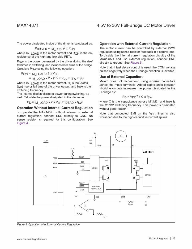
Operation with External Current RegulationThe motor current can be controlled by external PWM regulation using sense-resistor feedback in a control loop. To disable the internal current regulation circuitry of the MAX14871 and use external regulation, connect SNS directly to ground. See Figure 5.Note that, if fast decay control is used, the COM voltage pulses negatively when the H-bridge direction is inverted.
Use of External CapacitorsMaxim does not recommend using external capacitors across the motor terminals. Added capacitance between H-bridge outputs increases the power dissipated in the H-bridge by:
PD = VDD2 x C x fSW where C is the capacitance across M1/M2 and fSW is the M1/M2 switching frequency. This power is dissipated without good reason. Note that conducted EMI on the VDD lines is also worsened due to the high-capacitive current spikes.
Figure 5. Operation with External Current Regulation
DRIVER
VDD
SNS
PWM
DIR
MAX14871
GNDCOM
M1 M2
EN
FAULT
DRIVER
VDD VDD
CURRENT REGULATION
RSENSE
MODE
VREF
TCOFF
µC
IRQ
PWM
GPO
ADC
9V
3.3V
3.3V
M
A
MAX14871 4.5V to 36V Full-Bridge DC Motor Driver
www.maximintegrated.com Maxim Integrated 13
Package InformationFor the latest package outline information and land patterns (foot-prints), go to www.maximintegrated.com/packages. Note that a “+”, “#”, or “-” in the package code indicates RoHS status only. Package drawings may show a different suffix character, but the drawing pertains to the package regardless of RoHS status.
PACKAGE TYPE
PACKAGE CODE
OUTLINE NO.
LAND PATTERN NO.
16 TSSOP-EP U16E+3 21-0108 90-0120
Ordering InformationPART TEMP RANGE PIN-PACKAGE
MAX14871EUE+ -40°C to +85°C 16 TSSOP-EP
+Denotes a lead(Pb)-free/RoHS-compliant package.*EP = Exposed pad
MAX14871 4.5V to 36V Full-Bridge DC Motor Driver
www.maximintegrated.com Maxim Integrated 14
Chip InformationPROCESS: BiCMOS
Revision HistoryREVISIONNUMBER
REVISIONDATE DESCRIPTION PAGES
CHANGED0 9/14 Initial release —
Maxim Integrated cannot assume responsibility for use of any circuitry other than circuitry entirely embodied in a Maxim Integrated product. No circuit patent licenses are implied. Maxim Integrated reserves the right to change the circuitry and specifications without notice at any time. The parametric values (min and max limits) shown in the Electrical Characteristics table are guaranteed. Other parametric values quoted in this data sheet are provided for guidance.
Maxim Integrated and the Maxim Integrated logo are trademarks of Maxim Integrated Products, Inc.
MAX14871 4.5V to 36V Full-Bridge DC Motor Driver
© 2014 Maxim Integrated Products, Inc. 15
For pricing, delivery, and ordering information, please contact Maxim Direct at 1-888-629-4642, or visit Maxim Integrated’s website at www.maximintegrated.com.


![AC/DC Geared Motor and Gearhead - raveo.czkatalog]_DKM_A... · DKM Products Overview Induction Motor 2 Pole Motor Reversible Motor E.M. Brake Motor Clutch & Brake Motor Torque Motor](https://img.pdfslide.us/doc/110x75/5ca5afa988c9930a6e8c9362/acdc-geared-motor-and-gearhead-raveocz-katalogdkma-dkm-products-overview.jpg)
![How to Use Bitcoin to Play Decentralized Poker › ~iddo › poker02.pdfFairness with penalties Secure cash distribution End Claim-or-Refund for two parties Ps,Pr (implicit in [Max11],[BBSU12])](https://img.pdfslide.us/doc/110x75/60e09ab64a39df492a73ab9b/how-to-use-bitcoin-to-play-decentralized-a-iddo-a-poker02pdf-fairness-with.jpg)