Embed Size (px)
DESCRIPTION
datasheet
Citation preview

General DescriptionThe MAX2057 general-purpose, high-performance vari-able-gain amplifier (VGA) is designed to operate in the1300MHz to 2700MHz frequency range*. This devicefeatures 15.5dB of gain, 6dB of noise figure, and an out-put 1dB compression point of 23.8dBm. The MAX2057also provides an exceptionally high OIP3 level of37dBm, which is maintained over the entire attenuationrange. In addition, the on-chip analog attenuators yieldinfinite control and high attenuation accuracy overselectable 21dB or 42dB control ranges. Each of thesefeatures makes the MAX2057 an ideal VGA forDCS/PCS, cdma2000™, W-CDMA, and PHS/PAS trans-mitter and power amplifier AGC circuits.
The MAX2057 is pin compatible with the MAX2056800MHz to 1000MHz VGA, making this family of ampli-fiers ideal for applications where a common PC boardlayout is used for both frequency bands.
The MAX2057 operates from a single +5V supply and isavailable in a compact 36-pin thin QFN package (6mmx 6mm x 0.8mm) with an exposed pad. Electrical per-formance is guaranteed over the extended -40°C to+85°C temperature range.
ApplicationsDCS 1800/PCS 1900 2G and 2.5G EDGE Base-Station Transmitters and Power Amplifiers
cdmaOne™, cdma2000, Base-StationTransmitters and Power Amplifiers
WCDMA, LTE, TD-SCDMA, and TD-LTETransmitters and Power Amplifiers
PHS/PAS Base-Station Transmitters and PowerAmplifiers
Transmitter Gain Control
Receiver Gain Control
Broadband Systems
Automatic Test Equipment
Digital and Spread-Spectrum CommunicationSystems
Microwave Terrestrial Links
cdmaOne is a trademark of CDMA Development Group.cdma2000 is a registered trademark of TelecommunicationsIndustry Association.
Features 1300MHz to 2700MHz RF Frequency Range*
37dBm Constant OIP3 (Over All Gain Settings)
23.8dBm Output 1dB Compression Point
15.5dB Typical Gain at Maximum Gain Setting
0.5dB Gain Flatness Over 100MHz Bandwidth
6dB Noise Figure at Maximum Gain Setting (Using1 Attenuator)
Two Gain-Control Ranges: 21dB and 42dB
Analog Gain Control
Single +5V Supply Voltage
Pin Compatible with MAX2056, 800MHz to1000MHz RF VGA
External Current-Setting Resistors Provide Optionfor Operating VGA in Reduced-Power/Reduced-Performance Mode
Lead-Free Package Available*Note: Operation beyond this range is possible, but has not beencharacterized.
MA
X2
05
7
1300MHz to 2700MHz Variable-GainAmplifier with Analog Gain Control
________________________________________________________________ Maxim Integrated Products 1
Ordering Information
19-3510; Rev 1; 12/10
For pricing, delivery, and ordering information, please contact Maxim Direct at 1-888-629-4642,or visit Maxim’s website at www.maxim-ic.com.
EVALUATION KIT
AVAILABLE
PART TEMP RANGE PIN-PACKAGE
MAX2057ETX+ -40°C to +85°C36 Thin QFN-EP** 6mm x 6mm
MAX2057ETX+T -40°C to +85°C36 Thin QFN-EP** 6mm x 6mm
**EP = Exposed pad.+Denotes a lead(Pb)-free/RoHS-compliant package.T = Tape-and-reel package.
Pin Configuration/Functional Diagram appear at end of datasheet.

MA
X2
05
7
1300MHz to 2700MHz Variable-GainAmplifier with Analog Gain Control
2 _______________________________________________________________________________________
ABSOLUTE MAXIMUM RATINGS
Stresses beyond those listed under “Absolute Maximum Ratings” may cause permanent damage to the device. These are stress ratings only, and functionaloperation of the device at these or any other conditions beyond those indicated in the operational sections of the specifications is not implied. Exposure toabsolute maximum rating conditions for extended periods may affect device reliability.
VCC to GND...........................................................-0.3V to +5.5VVCNTL to GND (with VCC applied) .............................0V to 4.75VCurrent into VCNTL pin (VCC grounded) .............................40mAAll Other Pins to GND.................................-0.3V to (VCC + 0.3V)RF Input Power (IN, IN_A, ATTN_OUT, OUT_A) ...........+20dBmRF Input Power (AMP_IN)...............................................+12dBmθJA (natural convection)...................................................35°C/WθJA (1m/s airflow) .............................................................31°C/W
θJA (2.5m/s airflow) ..........................................................29°C/WθJC (junction to exposed pad) .........................................10°C/WOperating Temperature Range ...........................-40°C to +85°CStorage Temperature Range .............................-65°C to +150°CJunction Temperature ......................................................+150°CLead Temperature (soldering, 10s) .................................+300°CSoldering Temperature (reflow) .......................................+260°C
DC ELECTRICAL CHARACTERISTICS(VCC = +4.75V to +5.25V, no RF signals applied, all input and output ports terminated with 50Ω, TA = -40°C to +85°C, unless other-wise noted. Typical values are at VCC = +5.0V, TA = +25°C, unless otherwise noted.)
PARAMETER CONDITIONS MIN TYP MAX UNITS
Supply Voltage 4.75 5 5.25 V
Supply Current R1 = 1.2k , R2 = 2k (Note 1) 180 230 mA
RSET1 Current R1 = 1.2k (Note 1) 1 mA
RSET2 Current R1 = 2k (Note 1) 0.6 mA
Gain-Control Voltage Range (Note 2) 1.0 4.5 V
Gain-Control Pin Input Resistance VCNTL = 1V to 4.5V 50 k
RECOMMENDED AC OPERATING CONDITIONSPARAMETER CONDITIONS MIN TYP MAX UNITS
Frequency Range (Note 3) 1300 2700 MHz
AC ELECTRICAL CHARACTERISTICS(Typical Operating Circuit with one attenuator connected, VCC = +4.75V to +5.25V, TA = -40°C to +85°C, fIN = 1700MHz to2500MHz, unless otherwise noted. Typical values are at VCC = +5.0V, R1 = 1.2kΩ, R2 = 2kΩ, POUT = +5dBm, fIN = 2100MHz,VCNTL = 1V, 50Ω system impedance, second attenuator is not connected, TA = +25°C, unless otherwise noted.) (Note 4)
PARAMETER CONDITIONS MIN TYP MAX UNITS
TA = +25°C, VCC = 5.0V, fIN = 2100MHz 13.5 15.5 17.5
TA = +25°C, VCC = 5.0V, fIN = 1560MHz 11.5 14.5 16.5
TA = +25°C, VCC = 5.0V, fIN = 1500MHz 11.5 14.3 16.5 Gain
TA = +25°C, VCC = 5.0V, fIN = 1450MHz 11.5 14 16.5
dB
VCNTL = 1V +0.9
VCNTL = 1.8V +0.41
VCNTL = 2.6V +0.09 TA = +25°C to -40°C
VCNTL = 3.5V -0.16
VCNTL = 1V -1
VCNTL = 1.8V -0.56
VCNTL = 2.6V -0.32
Maximum Gain Variation
TA = +25°C to +85°C
VCNTL = 3.5V +0.1
dB

MA
X2
05
7
1300MHz to 2700MHz Variable-GainAmplifier with Analog Gain Control
_______________________________________________________________________________________ 3
AC ELECTRICAL CHARACTERISTICS (continued)(Typical Operating Circuit with one attenuator connected, VCC = +4.75V to +5.25V, TA = -40°C to +85°C, fIN = 1700MHz to2500MHz, unless otherwise noted. Typical values are at VCC = +5.0V, R1 = 1.2kΩ, R2 = 2kΩ, POUT = +5dBm, fIN = 2100MHz,VCNTL = 1V, 50Ω system impedance, second attenuator is not connected, TA = +25°C, unless otherwise noted.) (Note 3)
Note 1: Total supply current reduces as R1 and R2 are increased.Note 2: Operating outside this range for extended periods may affect device reliability. Limit pin input current to 40mA when VCC
is not present.Note 3: Operation outside this range is possible, but with degraded performance of some parameters.Note 4: All limits include external component losses, unless otherwise noted.Note 5: Noise figure increases by approximately 1dB for every 1dB of gain reduction.Note 6: f1 = 2100MHz, f2 = 2101MHz, +5dBm/tone at OUT.Note 7: Switching time is measured from 50% of the control signal to when the RF output settles to ±1dB.
PARAMETER CONDITIONS MIN TYP MAX UNITS
Reverse Isolation 37 dB
Noise Figure (Note 5) 6 dB
Output 1dB Compression Point +23.8 dBm
Output 2nd-Order Intercept Point From maximum gain to 15dB attenuation, measured at f1 + f2 (Note 6)
+64 dBm
Output 3rd-Order Intercept Point From maximum gain to 15dB attenuation (Note 5) +37 dBm
TA = +25°C to +85°C -0.83 Output 3rd-Order Intercept Point Variation Over Temperature TA = +25°C to -40°C -0.6
dB
2nd Harmonic From maximum gain to 15dB attenuation, POUT = +5dBm -65 dBc
3rd Harmonic From maximum gain to 15dB attenuation, POUT = +5dBm -83 dBc
One attenuator 17 20.7 fIN = 1700MHz to 2200MHz, VCNTL = 1V to 4V Two attenuators 34 42.4
One attenuator 17 22 RF Gain-Control Range
fIN = 1450MHz to 1560MHz, VCNTL = 1V to 4V Two attenuators 34 44
dB
RF Gain-Control Slope VCNTL = 1.8V to 3.5V -10 dB/V
Maximum RF Gain-Control Slope Maximum slope vs. gain-control voltage -15.2 dB/V
Gain Flatness Over 100MHz Bandwidth
Peak-to-peak for all settings 0.5 dB
Attenuator Switching Time 15dB attenuation change (Note 7) 500 ns
Attenuator Insertion Loss Second attenuator (IN_A, OUT_A) 2.2 dB
Input Return Loss Entire band, all gain settings 18 dB
Output Return Loss Entire band, all gain settings 15 dB
Group Delay Input/output 50 lines de-embedded 300 ps
Group Delay Flatness Over 100MHz Bandwidth
Peak to peak 20 ps
Group Delay Change vs. Gain Control
VCNTL = 1V to 4V -70 ps
Insertion Phase Change vs. Gain Control
VCNTL = 1V to 4V 50 degrees

MA
X2
05
7
1300MHz to 2700MHz Variable-GainAmplifier with Analog Gain Control
4 _______________________________________________________________________________________
Typical Operating CharacteristicsOne Attenuator Configuration
(Typical Application Circuit with one attenuator connected, VCC = +5.0V, R1 = 1.2kΩ, R2 = 2kΩ, fIN = 2100MHz, maximum gainsetting, POUT = +5dBm, linearity measured at POUT = +5dBm/tone, TA = +25°C, unless otherwise noted.)
SUPPLY CURRENTvs. SUPPLY VOLTAGE
MAX
2057
toc0
1
SUPPLY VOLTAGE (V)
SUPP
LY C
URRE
NT (m
A)
5.1255.0004.875
160
170
180
190
200
1504.750 5.250
TA = +85°C
TA = +25°C
TA = -40°C
INPUT RETURN LOSSvs. RF FREQUENCY
MAX
2057
toc0
2
RF FREQUENCY (MHz)
INPU
T RE
TURN
LOS
S (d
B)
230021001700 1900
35
30
25
20
15
10
5
0
401500 2500
TA = +85°C
TA = +25°C
TA = -40°C
OUTPUT RETURN LOSSvs. RF FREQUENCY
MAX
2057
toc0
3
RF FREQUENCY (MHz)
OUTP
UT R
ETUR
N LO
SS (d
B)
230021001700 1900
35
30
25
20
15
10
5
0
401500 2500
TA = +25°C
TA = -40°C
TA = +85°C
GAIN vs. GAIN-CONTROL VOLTAGE
MAX
2057
toc0
4
VCNTL (V)
GAIN
(dB)
3.53.02.52.01.5
-5
0
5
10
15
20
-101.0 4.0
TA = +25°C
TA = -40°C
TA = +85°C
GAIN vs. RF FREQUENCYM
AX20
57 to
c05
RF FREQUENCY (MHz)
GAIN
(dB)
2300210019001700
11
13
15
17
19
91500 2500
TA = -40°C
TA = +25°C
TA = +85°C
REVERSE ISOLATIONvs. RF FREQUENCY
MAX
2057
toc0
6
RF FREQUENCY (MHz)
REVE
RSE
ISOL
ATIO
N (d
B)
2300210019001700
30
35
40
251500 2500
TA = +25°C
TA = +85°C
TA = -40°C
INPUT RETURN LOSSvs. RF FREQUENCY
MAX
2057
toc0
7
RF FREQUENCY (MHz)
INPU
T RE
TURN
LOS
S (d
B)
230021001700 1900
35
30
25
20
15
10
5
0
401500 2500
MAX GAIN
3dB GAIN REDUCTION6dB GAIN REDUCTION
9dB, 12dB, 15dB, 18dBGAIN REDUCTION
OUTPUT RETURN LOSSvs. RF FREQUENCY
MAX
2057
toc0
8
RF FREQUENCY (MHz)
OUTP
UT R
ETUR
N LO
SS (d
B)
230021001700 1900
35
30
25
20
15
10
5
0
401500 2500
MAX GAIN, 3dB, 6dB, 9dB, 12dB, 15dB, AND 18dB GAIN REDUCTION
GAIN vs. RF FREQUENCY
MAX
2057
toc0
9
RF FREQUENCY (MHz)
GAIN
(dB)
2300210019001700
-5
0
5
10
15
20
-101500 2500
MAXIMUM GAIN
18dB GAIN REDUCTION

MA
X2
05
7
1300MHz to 2700MHz Variable-GainAmplifier with Analog Gain Control
_______________________________________________________________________________________ 5
Typical Operating Characteristics (continued)One Attenuator Configuration
(Typical Application Circuit with one attenuator connected, VCC = +5.0V, R1 = 1.2kΩ, R2 = 2kΩ, fIN = 2100MHz, maximum gainsetting, POUT = +5dBm, linearity measured at POUT = +5dBm/tone, TA = +25°C, unless otherwise noted.)
REVERSE ISOLATIONvs. RF FREQUENCY
MAX
2057
toc1
0
RF FREQUENCY (MHz)
REVE
RSE
ISOL
ATIO
N (d
B)
230021001700 1900
25
30
35
40
45
50
55
60
201500 2500
MAXIMUM GAIN
18dB GAIN REDUCTION
NOISE FIGURE vs. RF FREQUENCY
MAX
2057
toc1
1
RF FREQUENCY (MHz)
NOIS
E FI
GURE
(dB)
230021001700 1900
4.5
5.0
5.5
6.0
6.5
7.0
7.5
8.0
4.01500 2500
TA = +85°C
TA = +25°C
TA = -40°C
NOISE FIGURE vs. RF FREQUENCY
MAX
2057
toc1
2
RF FREQUENCY (MHz)
NOIS
E FI
GURE
(dB)
230021001700 1900
4.5
5.0
5.5
6.0
6.5
7.0
7.5
8.0
4.01500 2500
VCC = 4.75V
VCC = 5.25V
VCC = 5.00V
OUTPUT IP3 vs. RF FREQUENCY
MAX
2057
toc1
3
RF FREQUENCY (MHz)
OUTP
UT IP
3 (d
Bm)
2300210019001700
32
34
36
38
40
301500 2500
TA = +85°C
TA = +25°C
TA = -40°C
OUTPUT IP3 vs. RF FREQUENCYM
AX20
57 to
c14
RF FREQUENCY (MHz)
OUTP
UT IP
3 (d
Bm)
2300210019001700
32
34
36
38
40
301500 2500
VCC = 4.75V
VCC = 5.25V
VCC = 5.00V
INPUT IP3 vs. ATTENUATION
MAX
2057
toc1
5
ATTENUATION (dB)
INPU
T IP
3 (d
Bm)
15105
23
26
29
32
35
38
41
200 20
TA = +25°C
TA = +85°C
TA = -40°C
30
32
36
34
38
40OUTPUT IP3 vs. ATTENUATION
MAX
2057
toc1
6
ATTENUATION (dB)
OUTP
UT IP
3 (d
Bm)
0 105 15 20
TA = +25°C
TA = -40°CTA = +85°C
32
34
33
36
35
37
38
-6 0 3-3 6 9 12
OUTPUT IP3 vs. OUTPUT POWER
MAX
2057
toc1
7
OUTPUT POWER PER TONE (dBm)
OUTP
UT IP
3 (d
Bm)
OUTPUT IP2 vs. RF FREQUENCYM
AX20
57 to
c18
RF FREQUENCY (MHz)
OUTP
UT IP
2 (d
Bm)
2300210019001700
50
55
60
65
70
75
451500 2500
TA = +25°C
TA = -40°C
TA = +85°C

MA
X2
05
7
1300MHz to 2700MHz Variable-GainAmplifier with Analog Gain Control
6 _______________________________________________________________________________________
OUTPUT P1dB vs. RF FREQUENCY
MAX
2057
toc2
2
RF FREQUENCY (MHz)
OUTP
UT P
1dB
(dBm
)
2300210019001700
21
22
23
24
25
26
201500 2500
TA = +25°CTA = -40°C
TA = +85°C
OUTPUT P1dB vs. RF FREQUENCY
MAX
2057
toc2
3
RF FREQUENCY (MHz)
OUTP
UT P
1dB
(dBm
)
2300210019001700
21
22
23
24
25
26
201500 2500
VCC = 4.75V
VCC = 5.25V
VCC = 5.00V
OUTPUT IP2 vs. RF FREQUENCYM
AX20
57 to
c19
RF FREQUENCY (MHz)
OUTP
UT IP
2 (d
Bm)
2300210019001700
50
55
60
65
70
75
451500 2500
VCC = 4.75V
VCC = 5.25V
VCC = 5.00V
INPUT IP2 vs. ATTENUATION
MAX
2057
toc2
0
ATTENUATION (dB)
INPU
T IP
2 (d
Bm)
15105
45
50
55
60
65
70
400 20
TA = +25°C
TA = -40°C
TA = +85°C
55
60
65
70
0 5 10 15 20
OUTPUT IP2 vs. ATTENUATION
MAX
2057
toc2
1
ATTENUATION (dB)
OUTP
UT IP
2 (d
Bm)
TA = +25°C
TA = -40°C
TA = +85°C
Typical Operating Characteristics (continued)One Attenuator Configuration
(Typical Application Circuit with one attenuator connected, VCC = +5.0V, R1 = 1.2kΩ, R2 = 2kΩ, fIN = 2100MHz, maximum gainsetting, POUT = +5dBm, linearity measured at POUT = +5dBm/tone, TA = +25°C, unless otherwise noted.)
MA
X2
05
7
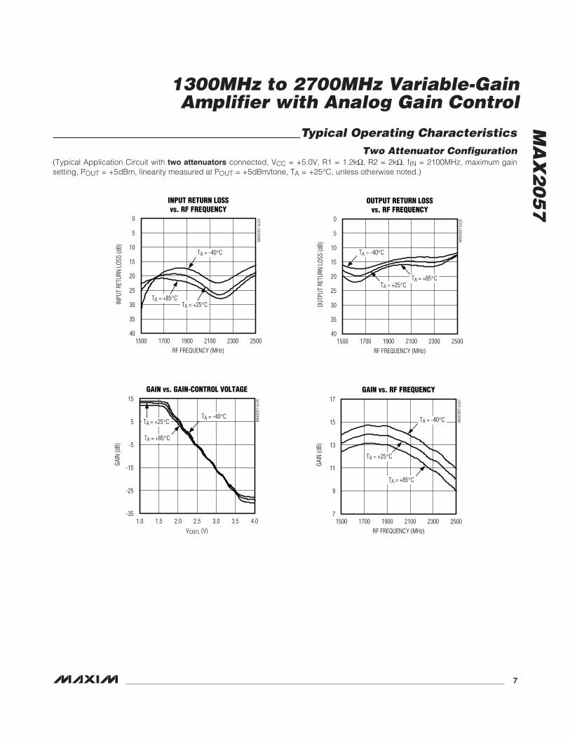
Typical Operating CharacteristicsTwo Attenuator Configuration
(Typical Application Circuit with two attenuators connected, VCC = +5.0V, R1 = 1.2kΩ, R2 = 2kΩ, fIN = 2100MHz, maximum gainsetting, POUT = +5dBm, linearity measured at POUT = +5dBm/tone, TA = +25°C, unless otherwise noted.)
INPUT RETURN LOSSvs. RF FREQUENCY
MAX
2057
toc2
4
RF FREQUENCY (MHz)
INPU
T RE
TURN
LOS
S (d
B)
230021001700 1900
35
30
25
20
15
10
5
0
401500 2500
TA = +25°C
TA = -40°C
TA = +85°C
OUTPUT RETURN LOSSvs. RF FREQUENCY
MAX
2057
toc2
5
RF FREQUENCY (MHz)
OUTP
UT R
ETUR
N LO
SS (d
B)
230021001700 1900
35
30
25
20
15
10
5
0
401500 2500
TA = -40°C
TA = +25°CTA = +85°C
GAIN vs. GAIN-CONTROL VOLTAGE
MAX
2057
toc2
6
VCNTL (V)
GAIN
(dB)
3.53.02.52.01.5
-25
-15
-5
5
15
-351.0 4.0
TA = -40°CTA = +25°C
TA = +85°C
GAIN vs. RF FREQUENCY
MAX
2057
toc2
7
RF FREQUENCY (MHz)
GAIN
(dB)
2300210019001700
9
11
13
15
17
71500 2500
TA = -40°C
TA = +25°C
TA = +85°C
1300MHz to 2700MHz Variable-GainAmplifier with Analog Gain Control
_______________________________________________________________________________________ 7

MA
X2
05
7
1300MHz to 2700MHz Variable-GainAmplifier with Analog Gain Control
8 _______________________________________________________________________________________
OUTPUT IP3 vs. RF FREQUENCY
MAX
2057
toc3
4
RF FREQUENCY (MHz)
OUTP
UT IP
3 (d
Bm)
2300210019001700
32
34
36
38
40
301500 2500
TA = +85°C
TA = +25°C
TA = -40°C
OUTPUT IP2 vs. RF FREQUENCY
MAX
2057
toc3
5
RF FREQUENCY (MHz)
OUTP
UT IP
2 (d
Bm)
2300210019001700
50
55
60
65
70
75
451500 2500
TA = +85°C
TA = +25°C
TA = -40°C
Typical Operating Characteristics (continued)Two Attenuator Configuration
(Typical Application Circuit with two attenuators connected, VCC = +5.0V, R1 = 1.2kΩ, R2 = 2kΩ, fIN = 2100MHz, maximum gainsetting, POUT = +5dBm, linearity measured at POUT = +5dBm/tone, TA = +25°C, unless otherwise noted.)
REVERSE ISOLATIONvs. RF FREQUENCY
MAX
2057
toc2
8
RF FREQUENCY (MHz)
REVE
RSE
ISOL
ATIO
N (d
B)
2300210019001700
35
40
45
301500 2500
TA = +25°C
TA = +85°C
TA = -40°C
INPUT RETURN LOSSvs. RF FREQUENCY
MAX
2057
toc2
9
RF FREQUENCY (MHz)
INPU
T RE
TURN
LOS
S (d
B)
230021001700 1900
35
30
25
20
15
10
5
0
401500 2500
MAXIMUM GAIN6dB GAIN REDUCTION
12dB, 18dB, 24dB, 30dBGAIN REDUCTION
OUTPUT RETURN LOSSvs. RF FREQUENCY
MAX
2057
toc3
0
RF FREQUENCY (MHz)
OUTP
UT R
ETUR
N LO
SS (d
B)
230021001700 1900
35
30
25
20
15
10
5
0
401500 2500
6dB, 12dB, 18dB, 24dB,30dB GAIN REDUCTION
MAXIMUM GAIN
GAIN vs. RF FREQUENCY
MAX
2057
toc3
1
RF FREQUENCY (MHz)
GAIN
(dB)
2300210019001700
-20
-15
-5
-10
0
5
10
15
20
-251500 2500
MAXIMUM GAIN
30dB GAIN REDUCTION
REVERSE ISOLATIONvs. RF FREQUENCY
MAX
2057
toc3
2
RF FREQUENCY (MHz)
REVE
RSE
ISOL
ATIO
N (d
B)
230021001700 1900
30
40
50
60
70
80
201500 2500
30dB GAIN REDUCTION
MAXIMUM GAIN
NOISE FIGURE vs. RF FREQUENCY
MAX
2057
toc3
3
RF FREQUENCY (MHz)
NOIS
E FI
GURE
(dB)
230021001700 1900
7.0
7.5
6.5
8.0
8.5
9.0
9.5
10.0
10.5
11.0
6.01500 2500
TA = +85°C
TA = +25°C
TA = -40°C
MA
X2
05
7
1300MHz to 2700MHz Variable-GainAmplifier with Analog Gain Control
_______________________________________________________________________________________ 9
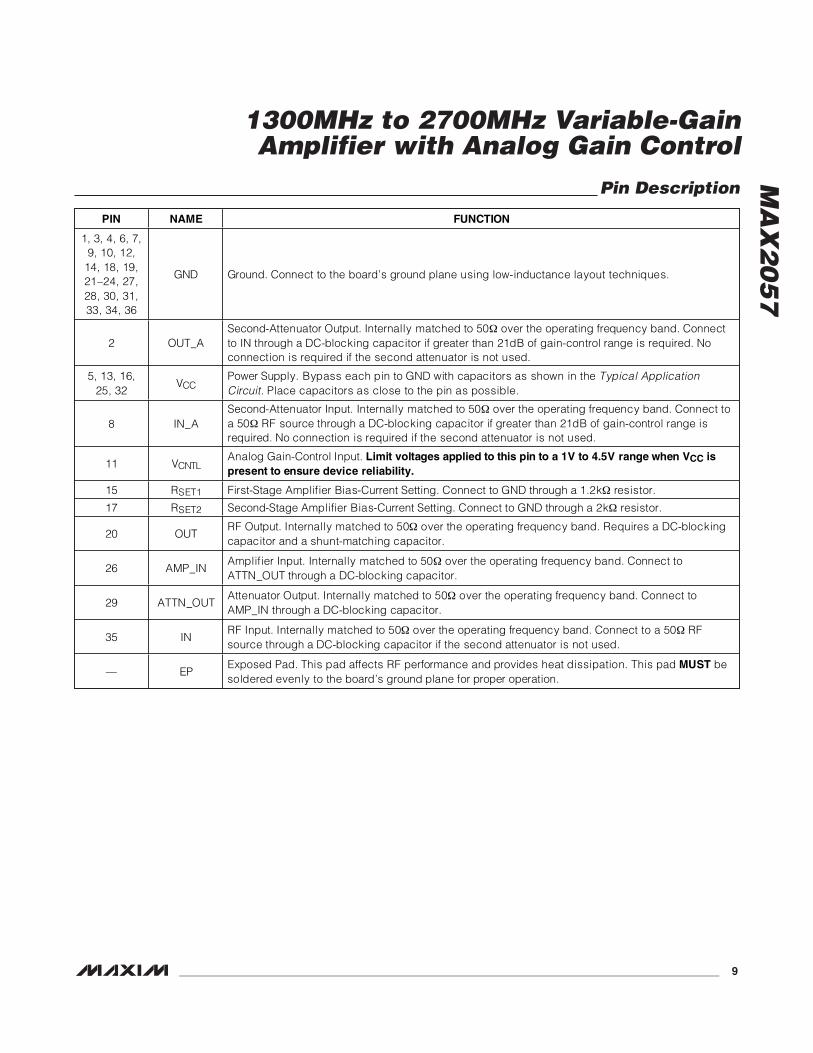
Pin Description
PIN NAME FUNCTION
1, 3, 4, 6, 7, 9, 10, 12,
14, 18, 19, 21–24, 27, 28, 30, 31, 33, 34, 36
GND Ground. Connect to the board’s ground plane using low-inductance layout techniques.
2 OUT_A Second-Attenuator Output. Internally matched to 50 over the operating frequency band. Connect to IN through a DC-blocking capacitor if greater than 21dB of gain-control range is required. No connection is required if the second attenuator is not used.
5, 13, 16, 25, 32
VCCPower Supply. Bypass each pin to GND with capacitors as shown in the Typical Application Circuit. Place capacitors as close to the pin as possible.
8 IN_A Second-Attenuator Input. Internally matched to 50 over the operating frequency band. Connect to a 50 RF source through a DC-blocking capacitor if greater than 21dB of gain-control range is required. No connection is required if the second attenuator is not used.
11 VCNTLAnalog Gain-Control Input. Limit voltages applied to this pin to a 1V to 4.5V range when VCC is present to ensure device reliability.
15 RSET1 First-Stage Amplifier Bias-Current Setting. Connect to GND through a 1.2k resistor.
17 RSET2 Second-Stage Amplifier Bias-Current Setting. Connect to GND through a 2k resistor.
20 OUT RF Output. Internally matched to 50 over the operating frequency band. Requires a DC-blocking capacitor and a shunt-matching capacitor.
26 AMP_IN Amplifier Input. Internally matched to 50 over the operating frequency band. Connect to ATTN_OUT through a DC-blocking capacitor.
29 ATTN_OUT Attenuator Output. Internally matched to 50 over the operating frequency band. Connect to AMP_IN through a DC-blocking capacitor.
35 IN RF Input. Internally matched to 50 over the operating frequency band. Connect to a 50 RF source through a DC-blocking capacitor if the second attenuator is not used.
— EP Exposed Pad. This pad affects RF performance and provides heat dissipation. This pad MUST be soldered evenly to the board’s ground plane for proper operation.

MA
X2
05
7
1300MHz to 2700MHz Variable-GainAmplifier with Analog Gain Control
10 ______________________________________________________________________________________
Detailed DescriptionThe MAX2057 general-purpose, high-performance VGAwith analog gain control is designed to interface with50Ω systems operating in the 1300MHz to 2700MHzfrequency range.
The MAX2057 integrates two attenuators to provide21dB or 42dB of precision analog gain control, as well
as a two-stage amplifier that has been optimized toprovide high gain, high IP3, low noise figure, and lowpower consumption. The bias current of each amplifierstage can be adjusted by individual external resistorsto further reduce power consumption for applicationsthat do not require high linearity.
MAX2057
27
26
25
24
23
32 31 30 29 28
GND
VGC
GND
GND
GND
OUT
GND
GND
GND
GND
GND
GND
GND
OUT_A
GND
IN_A
C4
C6
C10
C13
C5
RFOUTPUT
R1
R2
C2
C1
C15 C9
C3
VCC
VCC
VCC
C14C8
VCC
RF INPUT*
*NOTE: CONNECT THE INPUT ACCORDING TO THE SOLID BOLD LINE IF ONE ATTENUATORIS USED. CONNECT THE INPUT ACCORDING TO THE BROKEN LINE IF TWO ATTENUATORS ARE USED.
VCC
VCC
GND
GND
IN GND
GND
V CC
GND
GND
ATTN
_OUT
AMP_IN
GND
36 35 34 33
14 15 16 17 1810 11 12 13
22
20
21
19
5
4
3
2
9
8
7
6
1
+-
ATTENUATIONCONTROLCIRCUITRY
VCC
V CNT
L
GND
V CC
GND
R SET
1
V CC
R SET
2
GND
C170.06in LONG FR4 50Ω TRANSMISSION LINE
EP
C7
Figure 1. Typical Application Circuit

MA
X2
05
7
1300MHz to 2700MHz Variable-GainAmplifier with Analog Gain Control
______________________________________________________________________________________ 11
Applications InformationAnalog Attenuation Control
A single input voltage at the VCNTL pin adjusts the gainof the MAX2057. Up to 21dB of gain-control range isprovided through a single attenuator. At the maximumgain setting, each attenuator’s insertion loss is approxi-mately 2.2dB. With the single attenuator at the maximumgain setting, the device provides a nominal 15.5dB ofcascaded gain and 6dB of cascaded noise figure.
If a larger gain-control range is desired, a second on-chip attenuator can be connected in the signal path toprovide an additional 21dB of gain-control range. Withthe second attenuator connected at the maximum gainsetting, the device typically exhibits 13.3dB of cascad-ed gain. Note that the VCNTL pin simultaneously adjustsboth on-chip attenuators.
The VCNTL input voltage drives a high-impedance load(> 50kΩ). It is suggested that a current-limiting resistorbe included in series with this connection to limit theinput current to less than 40mA should the control volt-age be applied when VCC is not present. A series resis-tor of greater than 200Ω will provide completeprotection for 5V control voltage ranges. Limit VCNTLinput voltages to a 1.0V to 4.5V range when VCC ispresent to ensure the reliability of the device.
Amplifier Bias CurrentThe MAX2057 integrates a two-stage amplifier to simul-taneously provide high gain and high IP3. Optimal per-formance is obtained when R1 and R2 are equal to1.2kΩ and 2kΩ, respectively. The typical supply currentis 180mA and the typical output IP3 is 37dBm underthese conditions.
Increasing R1 and R2 from the nominal values of 1.2kΩand 2kΩ reduces the bias current of each amplifierstage, which reduces the total power consumption andIP3 of the device. This feature can be utilized to furtherdecrease power consumption for applications that donot require high IP3.
Layout ConsiderationsA properly designed PC board is an essential part ofany RF/microwave circuit. Keep RF signal lines as shortas possible to reduce losses, radiation, and induc-tance. For best performance, route the ground-pintraces directly to the exposed pad underneath thepackage. This pad MUST be connected to the groundplane of the board by using multiple vias under thedevice to provide the best RF and thermal conductionpath. Solder the exposed pad on the bottom of thedevice package to a PC board exposed pad.
Power-Supply BypassingProper voltage-supply bypassing is essential for high-frequency circuit stability. Bypass each VCC pin withcapacitors placed as close to the device as possible.Place the smallest capacitor closest to the device. Referto the MAX2057 evaluation kit data sheet for more details.
Exposed Pad RF and ThermalConsiderations
The EP of the MAX2057’s 36-pin thin QFN-EP packageprovides a low-thermal-resistance path to the die. It isimportant that the PC board on which the IC is mountedbe designed to conduct heat from this contact. In addi-tion, the EP provides a low-inductance RF ground pathfor the device.
The EP MUST be soldered to a ground plane on the PCboard either directly or through an array of plated viaholes. Soldering the pad to ground is also critical forefficient heat transfer. Use a solid ground plane wher-ever possible.
DESIGNATION VALUE TYPE
C1, C3, C5, C7, C10 22pFMicrowave capacitors(0402)
C2, C4, C6, C8, C9 1000pFMicrowave capacitors(0402)
C13, C14, C15 0.1µFMicrowave capacitors(0603)
C17 0.75pFMicrowave capacitor(0402)
R1 1.2kΩ ±1% resistor (0402)
R2 2kΩ ±1% resistor (0402)
Table 1. Typical Application CircuitComponent Values

Pin Configuration/Functional Diagram
MAX2057
27
26
25
24
23
32 31 30 29 28
GND
GND
GND
GND
OUT
GND
GND
GND
GND
GND
GND
OUT_A
GND
GND
IN_A
VCC
VCC
GND
GND
IN GND
GND
V CC
GND
GND
ATTN
_OUT
AMP_IN
GND
V CNT
L
GND
V CC
GND
R SET
1
V CC
R SET
2
GND
36 35 34 33
14 15 16 17 1810 11 12 13
22
20
21
19
5
4
3
2
9
8
7
6
1
ATTENUATIONCONTROL
CIRCUITRY
EP
Chip InformationPROCESS: BiCMOS
Package InformationFor the latest package outline information and land patterns,go to www.maxim-ic.com/packages. Note that a “+”, “#”, or“-” in the package code indicates RoHS status only. Packagedrawings may show a different suffix character, but the drawingpertains to the package regardless of RoHS status.
PACKAGETYPE
PACKAGECODE
OUTLINENO.
LANDPATTERN NO.
36 TQFN-EP T3666+2 21-0141 90-0049
MA
X2
05
7
1300MHz to 2700MHz Variable-GainAmplifier with Analog Gain Control
12 ______________________________________________________________________________________

MA
X2
05
7
1300MHz to 2700MHz Variable-GainAmplifier with Analog Gain Control
Maxim cannot assume responsibility for use of any circuitry other than circuitry entirely embodied in a Maxim product. No circuit patent licenses areimplied. Maxim reserves the right to change the circuitry and specifications without notice at any time.
Maxim Integrated Products, 120 San Gabriel Drive, Sunnyvale, CA 94086 408-737-7600 ____________________ 13
© 2010 Maxim Integrated Products Maxim is a registered trademark of Maxim Integrated Products, Inc.
Revision History
REVISION NUMBER
REVISION DATE
DESCRIPTION PAGES
CHANGED
0 1/05 Initial release —
1 12/10
Updated General Description, Features, Applications, Ordering Information, DC Electrical Characteristics, AC Electrical Characteristics, Detailed Description, and Analog Attenuation Control sections, and added Recommended AC Operating Conditions section
1, 2, 3, 10, 11


![[XLS] · Web view7500 17934 12/20/2013 12/20/2013 2057 1500 17935 12/20/2013 12/20/2013 2057 412.8 17935 12/20/2013 12/20/2013 1502 185.78 17936 12/20/2013 12/20/2013 458 1079.82](https://img.pdfslide.us/doc/110x75/5ac391bf7f8b9aae1b8c8925/xls-view7500-17934-12202013-12202013-2057-1500-17935-12202013-12202013.jpg)