Embed Size (px)
Citation preview

MAX 10 FPGA Device Architecture2016.08.11
M10-ARCHITECTURE Subscribe Send Feedback
The MAX® 10 devices consist of the following:
• Logic array blocks (LABs)• Analog-to-digital converter (ADC)• User flash memory (UFM)• Embedded multiplier blocks• Embedded memory blocks (M9K)• Clocks and phase-locked loops (PLL)• General purpose I/O• High-speed LVDS I/O• External memory interfaces• Configuration flash memory (CFM)
© 2016 Altera Corporation. All rights reserved. ALTERA, ARRIA, CYCLONE, ENPIRION, MAX, MEGACORE, NIOS, QUARTUS and STRATIX words and logos aretrademarks of Altera Corporation and registered in the U.S. Patent and Trademark Office and in other countries. All other words and logos identified astrademarks or service marks are the property of their respective holders as described at www.altera.com/common/legal.html. Altera warrants performanceof its semiconductor products to current specifications in accordance with Altera's standard warranty, but reserves the right to make changes to anyproducts and services at any time without notice. Altera assumes no responsibility or liability arising out of the application or use of any information,product, or service described herein except as expressly agreed to in writing by Altera. Altera customers are advised to obtain the latest version of devicespecifications before relying on any published information and before placing orders for products or services.
ISO9001:2008Registered
www.altera.com101 Innovation Drive, San Jose, CA 95134
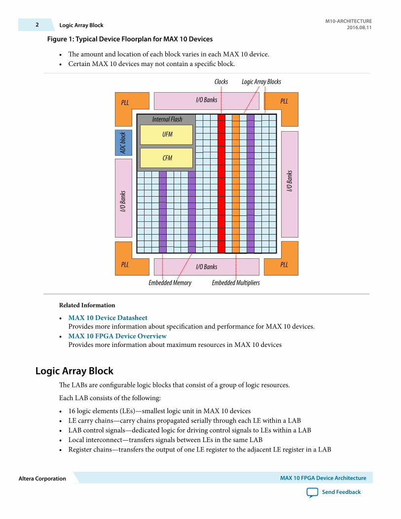
Figure 1: Typical Device Floorplan for MAX 10 Devices
• The amount and location of each block varies in each MAX 10 device.• Certain MAX 10 devices may not contain a specific block.
Embedded MultipliersEmbedded Memory
PLL
Logic Array Blocks
I/O BanksPLL
PLL PLL
I/O Ba
nks
I/O Banks
I/O Ba
nks
Internal Flash
CFM
Clocks
UFM
ADC b
lock
Related Information
• MAX 10 Device DatasheetProvides more information about specification and performance for MAX 10 devices.
• MAX 10 FPGA Device OverviewProvides more information about maximum resources in MAX 10 devices
Logic Array BlockThe LABs are configurable logic blocks that consist of a group of logic resources.
Each LAB consists of the following:
• 16 logic elements (LEs)—smallest logic unit in MAX 10 devices• LE carry chains—carry chains propagated serially through each LE within a LAB• LAB control signals—dedicated logic for driving control signals to LEs within a LAB• Local interconnect—transfers signals between LEs in the same LAB• Register chains—transfers the output of one LE register to the adjacent LE register in a LAB
2 Logic Array BlockM10-ARCHITECTURE
2016.08.11
Altera Corporation MAX 10 FPGA Device Architecture
Send Feedback
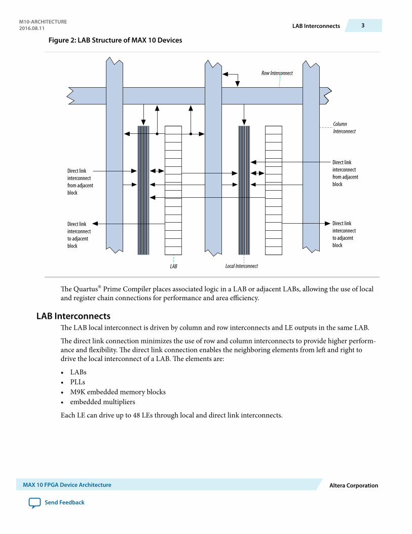
Figure 2: LAB Structure of MAX 10 Devices
Direct linkinterconnectfrom adjacentblock
Direct linkinterconnectto adjacentblock
Row Interconnect
Column Interconnect
Local InterconnectLAB
Direct linkinterconnectfrom adjacentblock
Direct linkinterconnectto adjacentblock
The Quartus® Prime Compiler places associated logic in a LAB or adjacent LABs, allowing the use of localand register chain connections for performance and area efficiency.
LAB InterconnectsThe LAB local interconnect is driven by column and row interconnects and LE outputs in the same LAB.
The direct link connection minimizes the use of row and column interconnects to provide higher perform‐ance and flexibility. The direct link connection enables the neighboring elements from left and right todrive the local interconnect of a LAB. The elements are:
• LABs• PLLs• M9K embedded memory blocks• embedded multipliers
Each LE can drive up to 48 LEs through local and direct link interconnects.
M10-ARCHITECTURE2016.08.11 LAB Interconnects 3
MAX 10 FPGA Device Architecture Altera Corporation
Send Feedback
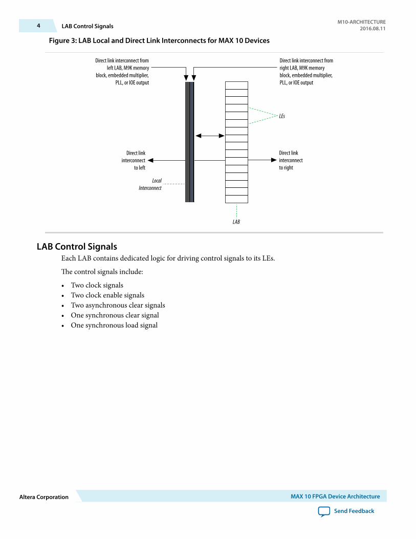
Figure 3: LAB Local and Direct Link Interconnects for MAX 10 Devices
LAB
Direct linkinterconnectto right
Direct link interconnect fromright LAB, M9K memoryblock, embedded multiplier,PLL, or IOE output
Direct link interconnect fromleft LAB, M9K memory
block, embedded multiplier,PLL, or IOE output
LocalInterconnect
Direct linkinterconnect
to left
LEs
LAB Control SignalsEach LAB contains dedicated logic for driving control signals to its LEs.
The control signals include:
• Two clock signals• Two clock enable signals• Two asynchronous clear signals• One synchronous clear signal• One synchronous load signal
4 LAB Control SignalsM10-ARCHITECTURE
2016.08.11
Altera Corporation MAX 10 FPGA Device Architecture
Send Feedback
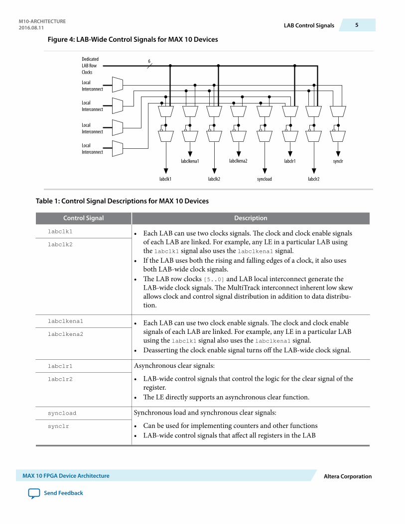
Figure 4: LAB-Wide Control Signals for MAX 10 Devices
labclkena1
labclk2labclk1
labclkena2 labclr1
DedicatedLAB RowClocks
LocalInterconnect
LocalInterconnect
LocalInterconnect
LocalInterconnect
syncload
synclr
labclr2
6
Table 1: Control Signal Descriptions for MAX 10 Devices
Control Signal Description
labclk1 • Each LAB can use two clocks signals. The clock and clock enable signalsof each LAB are linked. For example, any LE in a particular LAB usingthe labclk1 signal also uses the labclkena1 signal.
• If the LAB uses both the rising and falling edges of a clock, it also usesboth LAB-wide clock signals.
• The LAB row clocks [5..0] and LAB local interconnect generate theLAB-wide clock signals. The MultiTrack interconnect inherent low skewallows clock and control signal distribution in addition to data distribu‐tion.
labclk2
labclkena1 • Each LAB can use two clock enable signals. The clock and clock enablesignals of each LAB are linked. For example, any LE in a particular LABusing the labclk1 signal also uses the labclkena1 signal.
• Deasserting the clock enable signal turns off the LAB-wide clock signal.
labclkena2
labclr1 Asynchronous clear signals:
• LAB-wide control signals that control the logic for the clear signal of theregister.
• The LE directly supports an asynchronous clear function.
labclr2
syncload Synchronous load and synchronous clear signals:
• Can be used for implementing counters and other functions• LAB-wide control signals that affect all registers in the LAB
synclr
M10-ARCHITECTURE2016.08.11 LAB Control Signals 5
MAX 10 FPGA Device Architecture Altera Corporation
Send Feedback
You can use up to eight control signals at a time. Register packing and synchronous load cannot be usedsimultaneously.
Each LAB can have up to four non-global control signals. You can use additional LAB control signals aslong as they are global signals.
A LAB-wide asynchronous load signal to control the logic for the preset signal of the register is notavailable. The register preset is achieved with a NOT gate push-back technique. MAX 10 devices onlysupport either a preset or asynchronous clear signal.
In addition to the clear port, MAX 10 devices provide a chip-wide reset pin (DEV_CLRn) to reset allregisters in the device. An option set before compilation in the Quartus Prime software controls this pin.This chip-wide reset overrides all other control signals.
Logic ElementsLE is the smallest unit of logic in the MAX 10 device family architecture. LEs are compact and provideadvanced features with efficient logic usage.
Each LE has the following features:
• A four-input look-up table (LUT), which can implement any function of four variables• A programmable register• A carry chain connection• A register chain connection• The ability to drive the following interconnects:
• local• row• column• register chain• direct link
• Register packing support• Register feedback support
LE FeaturesLEs contain inputs, outputs and registers to enable several features.
6 Logic ElementsM10-ARCHITECTURE
2016.08.11
Altera Corporation MAX 10 FPGA Device Architecture
Send Feedback
Figure 5: LE High-Level Block Diagram for MAX 10 Devices.
Row, Column,And Direct Link Routing
data 1data 2data 3
data 4
labclr1labclr2
Chip-WideReset
(DEV_CLRn)
labclk1
labclk2
labclkena1
labclkena2
LE Carry-In
LAB-WideSynchronous
LoadLAB-Wide
Synchronous Clear
Row, Column,And Direct Link Routing
Local Routing
Register ChainOutput
Register Bypass
ProgrammableRegister
Register ChainRouting from
previous LE
LE Carry-Out
Register Feedback
SynchronousLoad and
Clear Logic
CarryChain
Look-Up Table(LUT)
Asynchronous Clear Logic
Clock &Clock Enable
Select
D Q
ENACLRN
LE Inputs
There are six available inputs to the LE in both mode LE operating modes, Normal Mode and ArithmeticMode. Each input is directed to different destinations to implement the desired logic function. The LEinputs are:
• four data inputs from the LAB local interconnect• an LE carry-in from the previous LE carry-chain• a register chain connection
LE Outputs
Each LE has three outputs which are:
• Two LE outputs drive the column or row and direct link routing connections• One LE output drives the local interconnect resources
The register packing feature is supported in MAX 10 devices. With register packing, the LUT or registeroutput drives the three outputs independently. This feature improves device utilization by using theregister and the LUT for unrelated functions.
The LAB-wide synchronous load control signal is not available when using register packing.
M10-ARCHITECTURE2016.08.11 LE Features 7
MAX 10 FPGA Device Architecture Altera Corporation
Send Feedback
Register Chain Output
Each LE has a register chain output which allows registers in the same LAB to cascade together. Thisfeature speed up connections between LABs and optimize local interconnect resources by allowing thefollowing:
• LUTs to be used for combinational functions• registers to be used for an unrelated shift register implementation
Programmable Register
You can configure the programmable register of each LE for D, T, JK, or SR flipflop operation. Eachregister has the following inputs:
• clock—can be driven by signals that use the global clock network, general-purpose I/O pins or theinternal logic
• clear—can be driven by signals that use the global clock network, general-purpose I/O pins or theinternal logic
• clock enable—can be driven by general-purpose I/O pins or the internal logic
For combinational functions, the LUT output bypasses the register and drives directly to the LE outputs.
Register Feedback
The register feedback mode allows the register output to feed back into the LUT of the same LE. This is toensure that the register is packed with its own fan-out LUT which provides another mechanism forimproved fitting. The LE can also drive out registered and unregistered versions of the LUT output.
LE Operating ModesThe LEs in MAX 10 devices operate in two modes.
• Normal mode• Arithmetic mode
These operating modes use LE resources differently. Both LE modes have six available inputs and LAB-wide signals.
The Quartus Prime software automatically chooses the appropriate mode for common functions, such ascounters, adders, subtractors, and arithmetic functions, in conjunction with parameterized functions suchas the library of parameterized modules (LPM) functions.
You can also create special-purpose functions that specify which LE operating mode to use for optimalperformance.
Normal ModeNormal mode is suitable for general logic applications and combinational functions.
In normal mode, four data inputs from the LAB local interconnect are inputs to a four-input LUT. TheQuartus Prime Compiler automatically selects the carry-in (cin) or the data3 signal as one of the inputs tothe LUT. LEs in normal mode support packed registers and register feedback.
8 LE Operating ModesM10-ARCHITECTURE
2016.08.11
Altera Corporation MAX 10 FPGA Device Architecture
Send Feedback
Figure 6: LE Operating in Normal Mode for MAX 10 devices
data1
Four-InputLUT
data2data3cin (from cout of previous LE)
data4clock (LAB Wide)
ena (LAB Wide)aclr (LAB Wide)
CLRN
DQ
ENA
sclear(LAB Wide)
sload(LAB Wide)
Register ChainConnection
RegisterChain Output
Row, Column, andDirect Link Routing
Row, Column, andDirect Link Routing
Local Routing
Register Bypass
Packed Register Input
Register Feedback
Arithmetic ModeArithmetic mode is ideal for implementing adders, counters, accumulators, and comparators.
The LE in arithmetic mode implements a 2-bit full adder and basic carry chain. LEs in arithmetic modecan drive out registered and unregistered versions of the LUT output. Register feedback and registerpacking are supported when LEs are used in arithmetic mode.
M10-ARCHITECTURE2016.08.11 Arithmetic Mode 9
MAX 10 FPGA Device Architecture Altera Corporation
Send Feedback
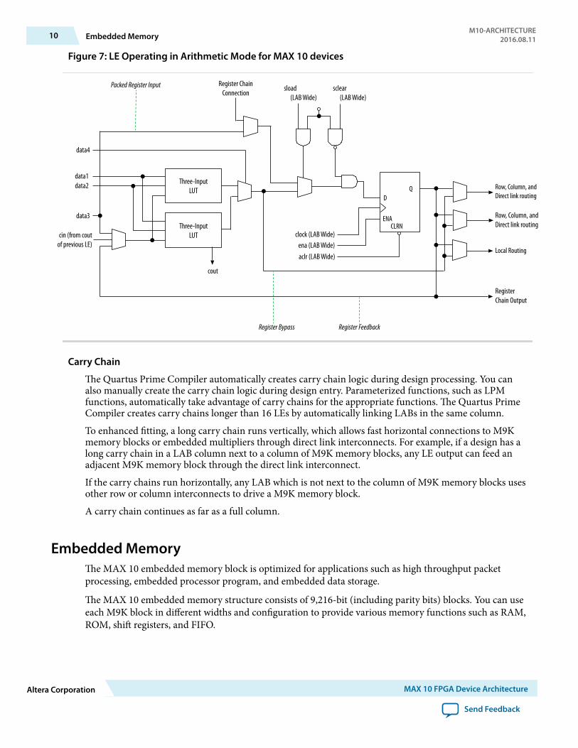
Figure 7: LE Operating in Arithmetic Mode for MAX 10 devices
clock (LAB Wide)ena (LAB Wide)aclr (LAB Wide)
CLRN
DQ
ENA
sclear(LAB Wide)
sload(LAB Wide)
RegisterChain Output
Row, Column, andDirect link routing
Row, Column, andDirect link routing
Local Routing
Register Feedback
Three-InputLUT
Three-InputLUTcin (from cout
of previous LE)
data2data1
cout
Register Bypass
data4
data3
Register ChainConnection
Packed Register Input
Carry Chain
The Quartus Prime Compiler automatically creates carry chain logic during design processing. You canalso manually create the carry chain logic during design entry. Parameterized functions, such as LPMfunctions, automatically take advantage of carry chains for the appropriate functions. The Quartus PrimeCompiler creates carry chains longer than 16 LEs by automatically linking LABs in the same column.
To enhanced fitting, a long carry chain runs vertically, which allows fast horizontal connections to M9Kmemory blocks or embedded multipliers through direct link interconnects. For example, if a design has along carry chain in a LAB column next to a column of M9K memory blocks, any LE output can feed anadjacent M9K memory block through the direct link interconnect.
If the carry chains run horizontally, any LAB which is not next to the column of M9K memory blocks usesother row or column interconnects to drive a M9K memory block.
A carry chain continues as far as a full column.
Embedded MemoryThe MAX 10 embedded memory block is optimized for applications such as high throughput packetprocessing, embedded processor program, and embedded data storage.
The MAX 10 embedded memory structure consists of 9,216-bit (including parity bits) blocks. You can useeach M9K block in different widths and configuration to provide various memory functions such as RAM,ROM, shift registers, and FIFO.
10 Embedded MemoryM10-ARCHITECTURE
2016.08.11
Altera Corporation MAX 10 FPGA Device Architecture
Send Feedback
MAX 10 embedded memory supports the following general features:
• 8,192 memory bits per block (9,216 bits per block including parity).• Independent read-enable (rden) and write-enable (wren) signals for each port.• Packed mode in which the M9K memory block is split into two 4.5 K single-port RAMs.• Variable port configurations.• Single-port and simple dual-port modes support for all port widths.• True dual-port (one read and one write, two reads, or two writes) operation.• Byte enables for data input masking during writes.• Two clock-enable control signals for each port (port A and port B).• Initialization file to preload memory content in RAM and ROM modes.
Related InformationMAX 10 Embedded Memory User Guide
Embedded MultiplierYou can use an embedded multiplier block in one of two operational modes, depending on the applicationneeds:
• One 18-bit x 18-bit multiplier• Up to two 9-bit x 9-bit independent multipliers
You can also use embedded multipliers of the MAX 10 devices to implement multiplier adder andmultiplier accumulator functions. The multiplier portion of the function is implemented using embeddedmultipliers. The adder or accumulator function is implemented in logic elements (LEs).
Related InformationMAX 10 Embedded Multiplier User Guide
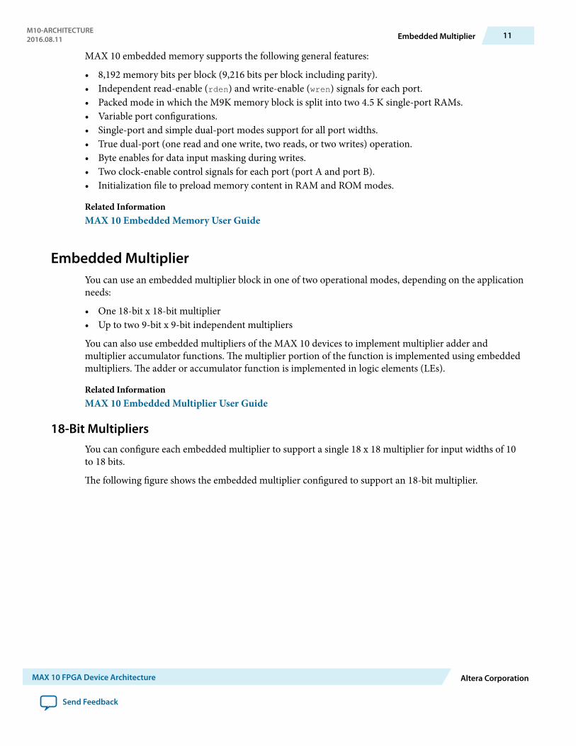
18-Bit MultipliersYou can configure each embedded multiplier to support a single 18 x 18 multiplier for input widths of 10to 18 bits.
The following figure shows the embedded multiplier configured to support an 18-bit multiplier.
M10-ARCHITECTURE2016.08.11 Embedded Multiplier 11
MAX 10 FPGA Device Architecture Altera Corporation
Send Feedback
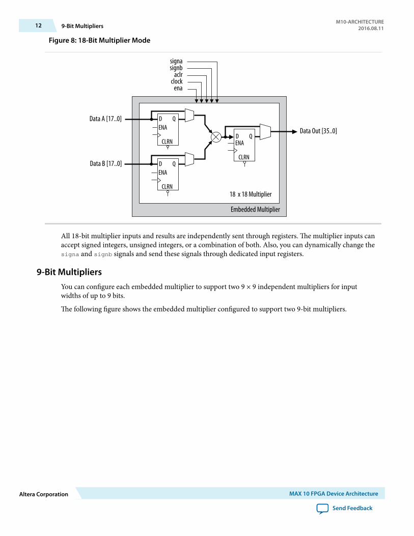
Figure 8: 18-Bit Multiplier Mode
CLRN
D QENA
Data A [17..0]
Data B [17..0]
aclrclock
ena
signasignb
CLRN
D QENA
CLRN
D QENA Data Out [35..0]
18 x 18 Multiplier
Embedded Multiplier
All 18-bit multiplier inputs and results are independently sent through registers. The multiplier inputs canaccept signed integers, unsigned integers, or a combination of both. Also, you can dynamically change thesigna and signb signals and send these signals through dedicated input registers.
9-Bit MultipliersYou can configure each embedded multiplier to support two 9 × 9 independent multipliers for inputwidths of up to 9 bits.
The following figure shows the embedded multiplier configured to support two 9-bit multipliers.
12 9-Bit MultipliersM10-ARCHITECTURE
2016.08.11
Altera Corporation MAX 10 FPGA Device Architecture
Send Feedback
Figure 9: 9-Bit Multiplier Mode
CLRN
D QENA
Data A 0 [8..0]
Data B 0 [8..0]
aclrclock
ena
signasignb
CLRN
D QENA
CLRN
D QENA Data Out 0 [17..0]
9 x 9 Multiplier
Embedded Multiplier
CLRN
D QENA
Data A 1 [8..0]
Data B 1 [8..0]
CLRN
D QENA
CLRN
D QENA Data Out 1 [17..0]
9 x 9 Multiplier
All 9-bit multiplier inputs and results are independently sent through registers. The multiplier inputs canaccept signed integers, unsigned integers, or a combination of both.
Each embedded multiplier block has only one signa and one signb signal to control the sign representa‐tion of the input data to the block. If the embedded multiplier block has two 9 × 9 multipliers the followingapplies:
• The Data A input of both multipliers share the same signa signal• The Data B input of both multipliers share the same signb signal
Clocking and PLLMAX 10 devices support global clock network (GCLK) and phase-locked loop (PLL).
M10-ARCHITECTURE2016.08.11 Clocking and PLL 13
MAX 10 FPGA Device Architecture Altera Corporation
Send Feedback
Clock networks provide clock sources for the core. You can use clock networks in high fan out globalsignal network such as reset and clear.
PLLs provide robust clock management and synthesis for device clock management, external system clockmanagement, and I/O interface clocking.
Related InformationMAX 10 Clock Networks and PLLs User Guide
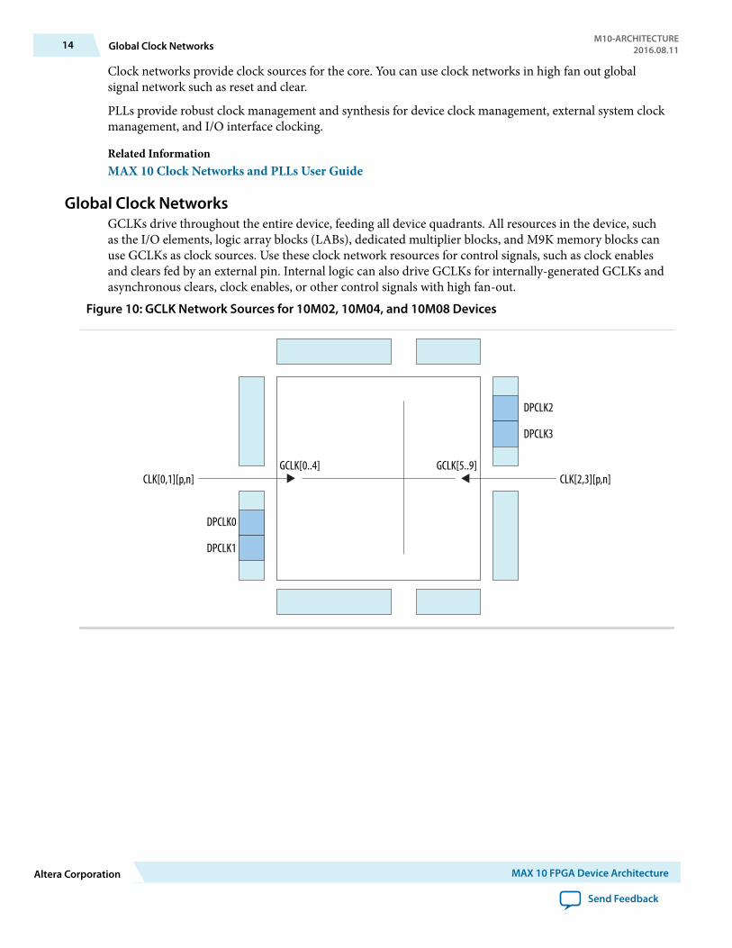
Global Clock NetworksGCLKs drive throughout the entire device, feeding all device quadrants. All resources in the device, suchas the I/O elements, logic array blocks (LABs), dedicated multiplier blocks, and M9K memory blocks canuse GCLKs as clock sources. Use these clock network resources for control signals, such as clock enablesand clears fed by an external pin. Internal logic can also drive GCLKs for internally-generated GCLKs andasynchronous clears, clock enables, or other control signals with high fan-out.
Figure 10: GCLK Network Sources for 10M02, 10M04, and 10M08 Devices
DPCLK2
DPCLK3
DPCLK0
DPCLK1
CLK[0,1][p,n] CLK[2,3][p,n]GCLK[0..4] GCLK[5..9]
14 Global Clock NetworksM10-ARCHITECTURE
2016.08.11
Altera Corporation MAX 10 FPGA Device Architecture
Send Feedback
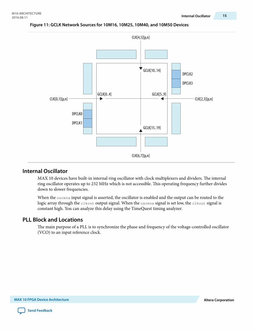
Figure 11: GCLK Network Sources for 10M16, 10M25, 10M40, and 10M50 Devices
DPCLK2
DPCLK3
DPCLK0
DPCLK1
CLK[0,1][p,n] CLK[2,3][p,n]GCLK[0..4] GCLK[5..9]
CLK[4,5][p,n]
CLK[6,7][p,n]
GCLK[15..19]
GCLK[10..14]
Internal OscillatorMAX 10 devices have built-in internal ring oscillator with clock multiplexers and dividers. The internalring oscillator operates up to 232 MHz which is not accessible. This operating frequency further dividesdown to slower frequencies.
When the oscena input signal is asserted, the oscillator is enabled and the output can be routed to thelogic array through the clkout output signal. When the oscena signal is set low, the clkout signal isconstant high. You can analyze this delay using the TimeQuest timing analyzer.
PLL Block and LocationsThe main purpose of a PLL is to synchronize the phase and frequency of the voltage-controlled oscillator(VCO) to an input reference clock.
M10-ARCHITECTURE2016.08.11 Internal Oscillator 15
MAX 10 FPGA Device Architecture Altera Corporation
Send Feedback
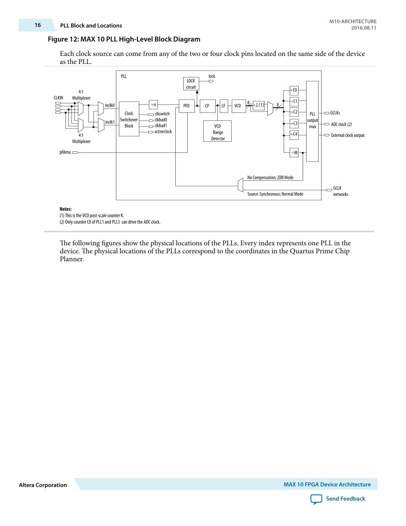
Figure 12: MAX 10 PLL High-Level Block Diagram
Each clock source can come from any of the two or four clock pins located on the same side of the deviceas the PLL.
ClockSwitchover
Block
inclk0
inclk1
pfdena
clkswitchclkbad0clkbad1activeclock
PFD
LOCKcircuit
lock
÷n CP LF VCO ÷2 (1)
÷C0
÷C1
÷C2
÷C3
÷C4
÷M
PLL output
mux
GCLKs
ADC clock (2)
8 8
GCLK networks
No Compensation; ZDB Mode
Source-Synchronous; Normal Mode
VCO Range
Detector
Notes:(1) This is the VCO post-scale counter K.(2) Only counter C0 of PLL1 and PLL3 can drive the ADC clock.
PLL
External clock output
4:1 Multiplexer
4:1 Multiplexer
CLKIN
The following figures show the physical locations of the PLLs. Every index represents one PLL in thedevice. The physical locations of the PLLs correspond to the coordinates in the Quartus Prime ChipPlanner.
16 PLL Block and LocationsM10-ARCHITECTURE
2016.08.11
Altera Corporation MAX 10 FPGA Device Architecture
Send Feedback
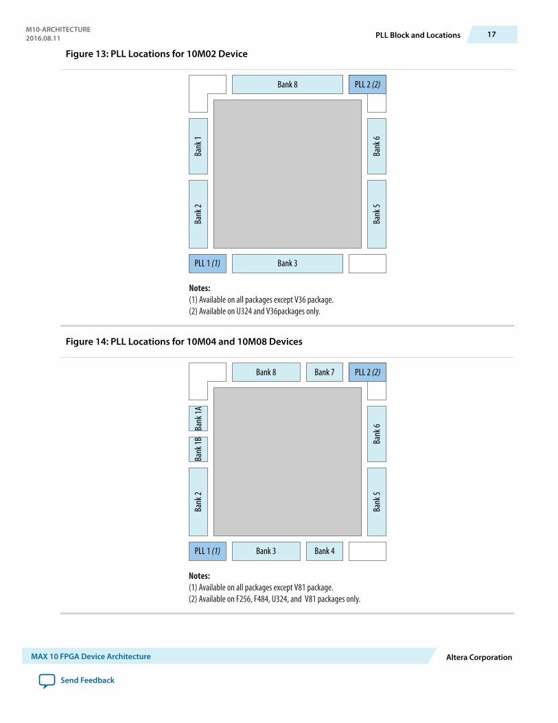
Figure 13: PLL Locations for 10M02 Device
Bank 8
Bank 3
Bank
1Ba
nk 2
Bank
6Ba
nk 5
PLL 1 (1)
PLL 2 (2)
Notes:(1) Available on all packages except V36 package.(2) Available on U324 and V36packages only.
Figure 14: PLL Locations for 10M04 and 10M08 Devices
Bank 8
Bank
1ABa
nk 2
Bank
6Ba
nk 5
PLL 1 (1)
PLL 2 (2)Bank 7
Bank 3 Bank 4
Bank
1B
Notes:(1) Available on all packages except V81 package.(2) Available on F256, F484, U324, and V81 packages only.
M10-ARCHITECTURE2016.08.11 PLL Block and Locations 17
MAX 10 FPGA Device Architecture Altera Corporation
Send Feedback
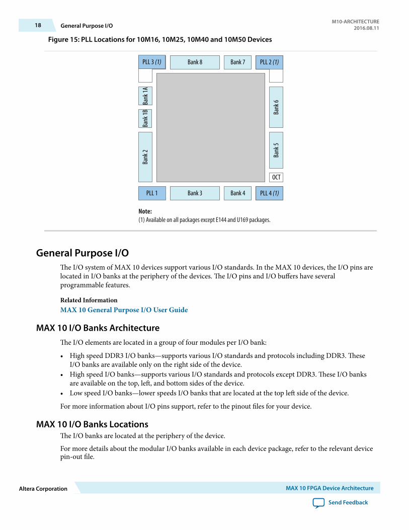
Figure 15: PLL Locations for 10M16, 10M25, 10M40 and 10M50 Devices
Bank 8
Bank
1ABa
nk 2
Bank
6Ba
nk 5
PLL 1
PLL 2 (1)Bank 7
Bank 3 Bank 4
Bank
1B
PLL 3 (1)
PLL 4 (1)
OCT
Note:(1) Available on all packages except E144 and U169 packages.
General Purpose I/OThe I/O system of MAX 10 devices support various I/O standards. In the MAX 10 devices, the I/O pins arelocated in I/O banks at the periphery of the devices. The I/O pins and I/O buffers have severalprogrammable features.
Related InformationMAX 10 General Purpose I/O User Guide
MAX 10 I/O Banks ArchitectureThe I/O elements are located in a group of four modules per I/O bank:
• High speed DDR3 I/O banks—supports various I/O standards and protocols including DDR3. TheseI/O banks are available only on the right side of the device.
• High speed I/O banks—supports various I/O standards and protocols except DDR3. These I/O banksare available on the top, left, and bottom sides of the device.
• Low speed I/O banks—lower speeds I/O banks that are located at the top left side of the device.
For more information about I/O pins support, refer to the pinout files for your device.
MAX 10 I/O Banks LocationsThe I/O banks are located at the periphery of the device.
For more details about the modular I/O banks available in each device package, refer to the relevant devicepin-out file.
18 General Purpose I/OM10-ARCHITECTURE
2016.08.11
Altera Corporation MAX 10 FPGA Device Architecture
Send Feedback
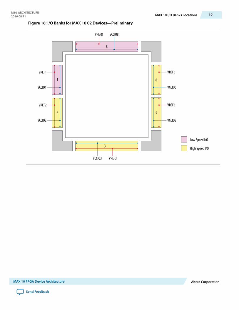
Figure 16: I/O Banks for MAX 10 02 Devices—Preliminary
1
2 5
6
3
8
VREF1
VCCIO8VREF8
VCCIO1
VCCIO5VCCIO2
VCCIO3 VREF3
VCCIO6
VREF6
VREF2 VREF5
Low Speed I/O
High Speed I/O
M10-ARCHITECTURE2016.08.11 MAX 10 I/O Banks Locations 19
MAX 10 FPGA Device Architecture Altera Corporation
Send Feedback
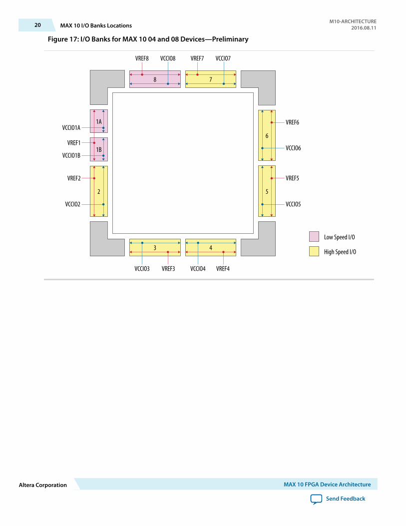
Figure 17: I/O Banks for MAX 10 04 and 08 Devices—Preliminary
1A
1B
2 5
6
3 4
8 7
VCCIO5VCCIO2
VCCIO3 VREF3 VREF4VCCIO4
VCCIO7VCCIO8
VCCIO1B
VCCIO1A
VCCIO6
VREF6
VREF1
VREF2
VREF8 VREF7
VREF5
Low Speed I/O
High Speed I/O
20 MAX 10 I/O Banks LocationsM10-ARCHITECTURE
2016.08.11
Altera Corporation MAX 10 FPGA Device Architecture
Send Feedback
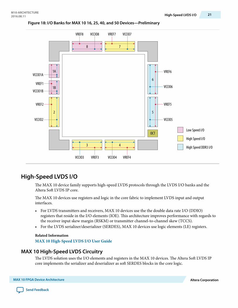
Figure 18: I/O Banks for MAX 10 16, 25, 40, and 50 Devices—Preliminary
1A
1B
2 5
6
3 4
8 7
VCCIO5VCCIO2
VCCIO3 VREF3 VREF4VCCIO4
VCCIO7VCCIO8
VCCIO1B
VCCIO1A
VCCIO6
VREF6
VREF1
VREF2
VREF8 VREF7
VREF5
Low Speed I/O
High Speed I/O
High Speed DDR3 I/O
OCT
High-Speed LVDS I/OThe MAX 10 device family supports high-speed LVDS protocols through the LVDS I/O banks and theAltera Soft LVDS IP core.
The MAX 10 devices use registers and logic in the core fabric to implement LVDS input and outputinterfaces.
• For LVDS transmitters and receivers, MAX 10 devices use the the double data rate I/O (DDIO)registers that reside in the I/O elements (IOE). This architecture improves performance with regards tothe receiver input skew margin (RSKM) or transmitter channel-to-channel skew (TCCS).
• For the LVDS serializer/deserializer (SERDES), MAX 10 devices use logic elements (LE) registers.
Related InformationMAX 10 High-Speed LVDS I/O User Guide
MAX 10 High-Speed LVDS CircuitryThe LVDS solution uses the I/O elements and registers in the MAX 10 devices. The Altera Soft LVDS IPcore implements the serializer and deserializer as soft SERDES blocks in the core logic.
M10-ARCHITECTURE2016.08.11 High-Speed LVDS I/O 21
MAX 10 FPGA Device Architecture Altera Corporation
Send Feedback
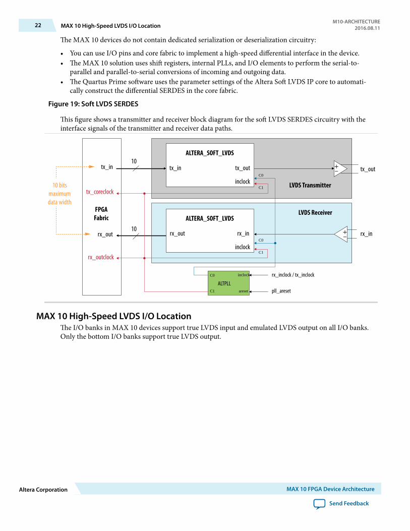
The MAX 10 devices do not contain dedicated serialization or deserialization circuitry:
• You can use I/O pins and core fabric to implement a high-speed differential interface in the device.• The MAX 10 solution uses shift registers, internal PLLs, and I/O elements to perform the serial-to-
parallel and parallel-to-serial conversions of incoming and outgoing data.• The Quartus Prime software uses the parameter settings of the Altera Soft LVDS IP core to automati‐
cally construct the differential SERDES in the core fabric.
Figure 19: Soft LVDS SERDES
This figure shows a transmitter and receiver block diagram for the soft LVDS SERDES circuitry with theinterface signals of the transmitter and receiver data paths.
FPGAFabric
rx_out
tx_in
rx_outclock
tx_coreclock10 bits
maximumdata width
+–
+–
tx_out
rx_in
10
10
pll_areset
rx_inclock / tx_inclockC0
C0
C0
C1
C1
C1
inclock
areset
ALTPLL
ALTERA_SOFT_LVDS
tx_in tx_out
inclock
ALTERA_SOFT_LVDS
rx_out rx_in
inclock
LVDS Transmitter
LVDS Receiver
MAX 10 High-Speed LVDS I/O LocationThe I/O banks in MAX 10 devices support true LVDS input and emulated LVDS output on all I/O banks.Only the bottom I/O banks support true LVDS output.
22 MAX 10 High-Speed LVDS I/O LocationM10-ARCHITECTURE
2016.08.11
Altera Corporation MAX 10 FPGA Device Architecture
Send Feedback
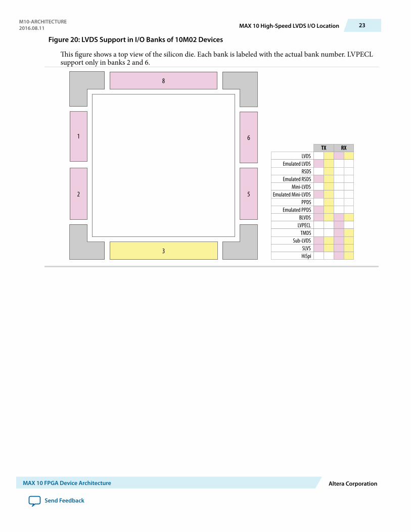
Figure 20: LVDS Support in I/O Banks of 10M02 Devices
This figure shows a top view of the silicon die. Each bank is labeled with the actual bank number. LVPECLsupport only in banks 2 and 6.
1
2 5
6
3
8
LVDSEmulated LVDS
RSDSEmulated RSDS
Mini-LVDSEmulated Mini-LVDS
PPDSEmulated PPDS
BLVDSLVPECL
TMDSSub-LVDS
SLVSHiSpi
TX RX
M10-ARCHITECTURE2016.08.11 MAX 10 High-Speed LVDS I/O Location 23
MAX 10 FPGA Device Architecture Altera Corporation
Send Feedback
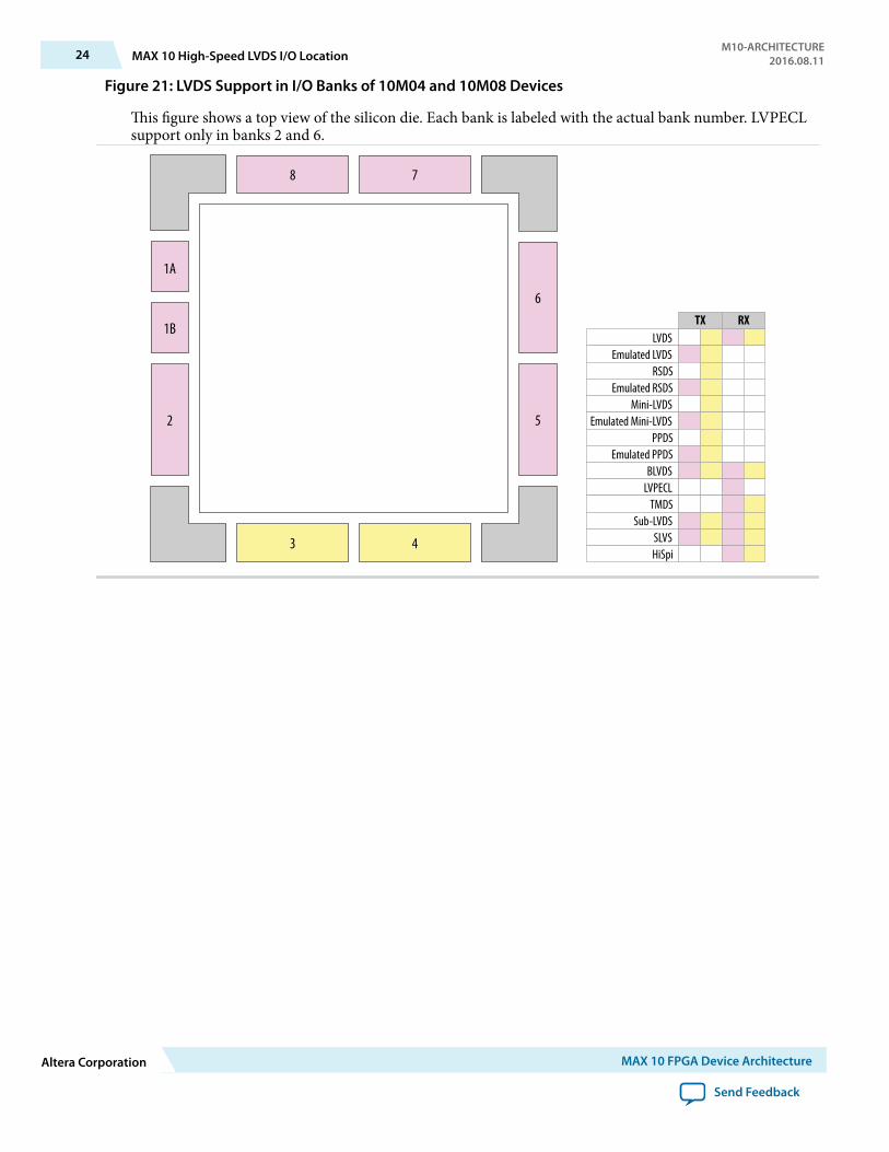
Figure 21: LVDS Support in I/O Banks of 10M04 and 10M08 Devices
This figure shows a top view of the silicon die. Each bank is labeled with the actual bank number. LVPECLsupport only in banks 2 and 6.
1B
1A
2 5
6
3 4
8 7
LVDSEmulated LVDS
RSDSEmulated RSDS
Mini-LVDSEmulated Mini-LVDS
PPDSEmulated PPDS
BLVDSLVPECL
TMDSSub-LVDS
SLVSHiSpi
TX RX
24 MAX 10 High-Speed LVDS I/O LocationM10-ARCHITECTURE
2016.08.11
Altera Corporation MAX 10 FPGA Device Architecture
Send Feedback
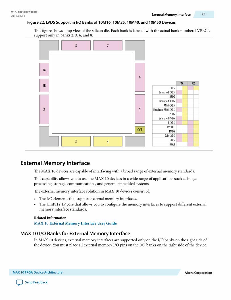
Figure 22: LVDS Support in I/O Banks of 10M16, 10M25, 10M40, and 10M50 Devices
This figure shows a top view of the silicon die. Each bank is labeled with the actual bank number. LVPECLsupport only in banks 2, 3, 6, and 8.
1B
1A
2
3 4
8 7
OCT
5
6
LVDSEmulated LVDS
RSDSEmulated RSDS
Mini-LVDSEmulated Mini-LVDS
PPDSEmulated PPDS
BLVDSLVPECL
TMDSSub-LVDS
SLVSHiSpi
TX RX
External Memory InterfaceThe MAX 10 devices are capable of interfacing with a broad range of external memory standards.
This capability allows you to use the MAX 10 devices in a wide range of applications such as imageprocessing, storage, communications, and general embedded systems.
The external memory interface solution in MAX 10 devices consist of:
• The I/O elements that support external memory interfaces.• The UniPHY IP core that allows you to configure the memory interfaces to support different external
memory interface standards.
Related InformationMAX 10 External Memory Interface User Guide
MAX 10 I/O Banks for External Memory InterfaceIn MAX 10 devices, external memory interfaces are supported only on the I/O banks on the right side ofthe device. You must place all external memory I/O pins on the I/O banks on the right side of the device.
M10-ARCHITECTURE2016.08.11 External Memory Interface 25
MAX 10 FPGA Device Architecture Altera Corporation
Send Feedback
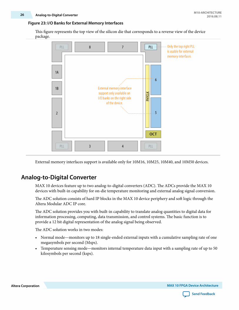
Figure 23: I/O Banks for External Memory Interfaces
This figure represents the top view of the silicon die that corresponds to a reverse view of the devicepackage.
1B
1A
2
3 4
8 7
External memory interfacesupport only available on I/O banks on the right side
of the device.
Only the top right PLLis usable for externalmemory interfaces
PHYC
LKPLLPLL
PLL PLL
OCT
5
6
External memory interfaces support is available only for 10M16, 10M25, 10M40, and 10M50 devices.
Analog-to-Digital ConverterMAX 10 devices feature up to two analog-to-digital converters (ADC). The ADCs provide the MAX 10devices with built-in capability for on-die temperature monitoring and external analog signal conversion.
The ADC solution consists of hard IP blocks in the MAX 10 device periphery and soft logic through theAltera Modular ADC IP core.
The ADC solution provides you with built-in capability to translate analog quantities to digital data forinformation processing, computing, data transmission, and control systems. The basic function is toprovide a 12 bit digital representation of the analog signal being observed.
The ADC solution works in two modes:
• Normal mode—monitors up to 18 single-ended external inputs with a cumulative sampling rate of onemegasymbols per second (Msps).
• Temperature sensing mode—monitors internal temperature data input with a sampling rate of up to 50kilosymbols per second (ksps).
26 Analog-to-Digital ConverterM10-ARCHITECTURE
2016.08.11
Altera Corporation MAX 10 FPGA Device Architecture
Send Feedback
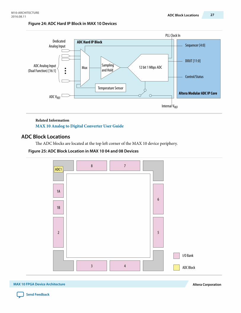
Figure 24: ADC Hard IP Block in MAX 10 Devices
Samplingand Hold
Mux 12 bit 1 Mbps ADC
Altera Modular ADC IP Core
Sequencer [4:0]
DOUT [11:0]
Control/Status
DedicatedAnalog Input
ADC Analog Input(Dual Function) [16:1]
ADC VREF
Internal VREF
PLL Clock In
Temperature Sensor
ADC Hard IP Block
Related InformationMAX 10 Analog to Digital Converter User Guide
ADC Block LocationsThe ADC blocks are located at the top left corner of the MAX 10 device periphery.
Figure 25: ADC Block Location in MAX 10 04 and 08 Devices
1B
1A
2 5
6
3 4
8 7
I/O Bank
ADC Block
ADC1
M10-ARCHITECTURE2016.08.11 ADC Block Locations 27
MAX 10 FPGA Device Architecture Altera Corporation
Send Feedback
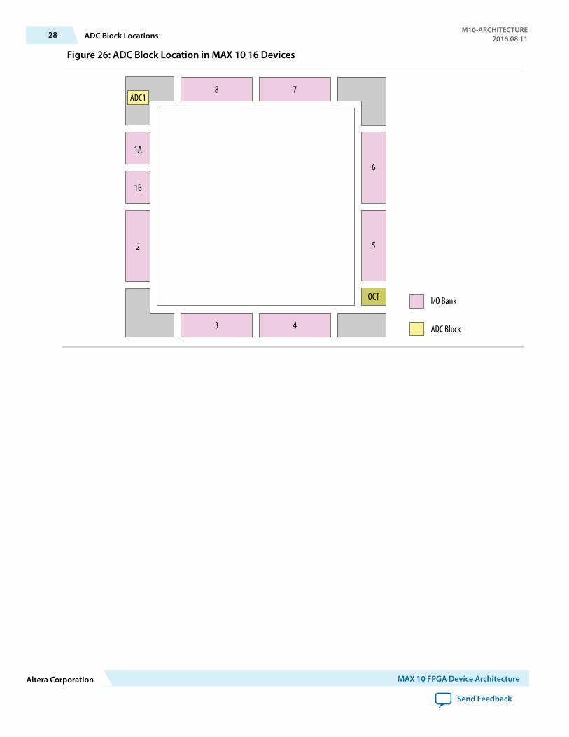
Figure 26: ADC Block Location in MAX 10 16 Devices
1B
1A
2
3 4
8 7
OCT
5
6
I/O Bank
ADC Block
ADC1
28 ADC Block LocationsM10-ARCHITECTURE
2016.08.11
Altera Corporation MAX 10 FPGA Device Architecture
Send Feedback
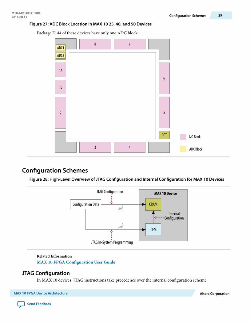
Figure 27: ADC Block Location in MAX 10 25, 40, and 50 Devices
Package E144 of these devices have only one ADC block.
1B
1A
2
3 4
8 7
OCT
5
6
I/O Bank
ADC Block
ADC2
ADC1
Configuration SchemesFigure 28: High-Level Overview of JTAG Configuration and Internal Configuration for MAX 10 Devices
CRAM
MAX 10 Device
JTAG In-System Programming
CFM
Configuration Data
InternalConfiguration
JTAG Configuration
.sof
.pof
Related InformationMAX 10 FPGA Configuration User Guide
JTAG ConfigurationIn MAX 10 devices, JTAG instructions take precedence over the internal configuration scheme.
M10-ARCHITECTURE2016.08.11 Configuration Schemes 29
MAX 10 FPGA Device Architecture Altera Corporation
Send Feedback
Using the JTAG configuration scheme, you can directly configure the device CRAM through the JTAGinterface—TDI, TDO, TMS, and TCK pins. The Quartus Prime software automatically generates an SRAMObject File (.sof). You can program the .sof using a download cable with the Quartus Prime softwareprogrammer.
Internal ConfigurationYou need to program the configuration data into the configuration flash memory (CFM) before internalconfiguration can take place. The configuration data to be written to CFM will be part of the programmerobject file (.pof). Using JTAG In-System Programming (ISP), you can program the .pof into the internalflash.
During internal configuration, MAX 10 devices load the CRAM with configuration data from the CFM.
User Flash MemoryAltera MAX 10 devices feature a user flash memory (UFM) block that stores non-volatile information.
The UFM is part of the internal flash available in MAX 10 devices.
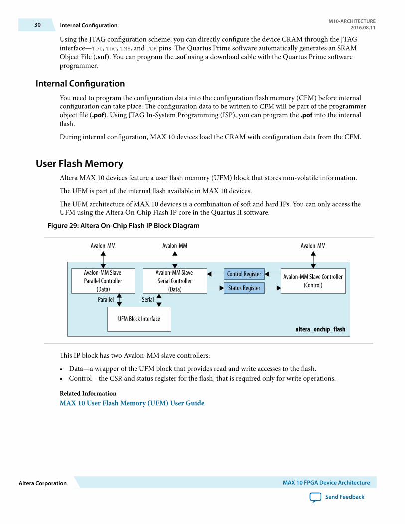
The UFM architecture of MAX 10 devices is a combination of soft and hard IPs. You can only access theUFM using the Altera On-Chip Flash IP core in the Quartus II software.
Figure 29: Altera On-Chip Flash IP Block Diagram
UFM Block Interface
Avalon-MM Slave Controller(Control)
Control Register
Status Register
altera_onchip_flash
Avalon-MM Slave Serial Controller
(Data)SerialParallel
Avalon-MM
Avalon-MM Slave Parallel Controller
(Data)
Avalon-MM Avalon-MM
This IP block has two Avalon-MM slave controllers:
• Data—a wrapper of the UFM block that provides read and write accesses to the flash.• Control—the CSR and status register for the flash, that is required only for write operations.
Related InformationMAX 10 User Flash Memory (UFM) User Guide
30 Internal ConfigurationM10-ARCHITECTURE
2016.08.11
Altera Corporation MAX 10 FPGA Device Architecture
Send Feedback
Power ManagementMAX 10 power optimization features are as follows:
• Single-supply or dual-supply device options• Power-on reset (POR) circuitry• Power management controller scheme• Hot socketing
Related InformationPower Management User Guide
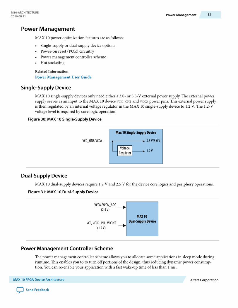
Single-Supply DeviceMAX 10 single-supply devices only need either a 3.0- or 3.3-V external power supply. The external powersupply serves as an input to the MAX 10 device VCC_ONE and VCCA power pins. This external power supplyis then regulated by an internal voltage regulator in the MAX 10 single-supply device to 1.2 V. The 1.2-Vvoltage level is required by core logic operation.
Figure 30: MAX 10 Single-Supply Device
VCC_ONE/VCCA
VoltageRegulator
3.3 V/3.0 V
1.2 V
Max 10 Single-Supply Device
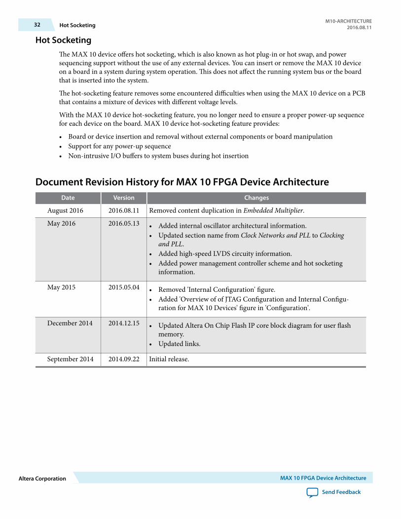
Dual-Supply DeviceMAX 10 dual-supply devices require 1.2 V and 2.5 V for the device core logics and periphery operations.
Figure 31: MAX 10 Dual-Supply Device
MAX 10 Dual-Supply DeviceVCC, VCCD_PLL, VCCINT
(1.2 V)
VCCA, VCCA_ADC(2.5 V)
Power Management Controller SchemeThe power management controller scheme allows you to allocate some applications in sleep mode duringruntime. This enables you to to turn off portions of the design, thus reducing dynamic power consump‐tion. You can re-enable your application with a fast wake-up time of less than 1 ms.
M10-ARCHITECTURE2016.08.11 Power Management 31
MAX 10 FPGA Device Architecture Altera Corporation
Send Feedback
Hot SocketingThe MAX 10 device offers hot socketing, which is also known as hot plug-in or hot swap, and powersequencing support without the use of any external devices. You can insert or remove the MAX 10 deviceon a board in a system during system operation. This does not affect the running system bus or the boardthat is inserted into the system.
The hot-socketing feature removes some encountered difficulties when using the MAX 10 device on a PCBthat contains a mixture of devices with different voltage levels.
With the MAX 10 device hot-socketing feature, you no longer need to ensure a proper power-up sequencefor each device on the board. MAX 10 device hot-socketing feature provides:
• Board or device insertion and removal without external components or board manipulation• Support for any power-up sequence• Non-intrusive I/O buffers to system buses during hot insertion
Document Revision History for MAX 10 FPGA Device ArchitectureDate Version Changes
August 2016 2016.08.11 Removed content duplication in Embedded Multiplier.
May 2016 2016.05.13 • Added internal oscillator architectural information.• Updated section name from Clock Networks and PLL to Clocking
and PLL.• Added high-speed LVDS circuity information.• Added power management controller scheme and hot socketing
information.
May 2015 2015.05.04 • Removed 'Internal Configuration' figure.• Added 'Overview of of JTAG Configuration and Internal Configu‐
ration for MAX 10 Devices' figure in 'Configuration'.
December 2014 2014.12.15 • Updated Altera On Chip Flash IP core block diagram for user flashmemory.
• Updated links.
September 2014 2014.09.22 Initial release.
32 Hot SocketingM10-ARCHITECTURE
2016.08.11
Altera Corporation MAX 10 FPGA Device Architecture
Send Feedback

MAX 10 Embedded Memory User Guide
Subscribe
Send Feedback
UG-M10MEMORY2016.10.31
101 Innovation DriveSan Jose, CA 95134www.altera.com
Contents
MAX 10 Embedded Memory Overview..............................................................1-1
MAX 10 Embedded Memory Architecture and Features................................... 2-1MAX 10 Embedded Memory General Features.......................................................................................2-1
Control Signals................................................................................................................................. 2-1Parity Bit............................................................................................................................................ 2-2Read Enable.......................................................................................................................................2-2Read-During-Write..........................................................................................................................2-3Byte Enable........................................................................................................................................2-3Packed Mode Support......................................................................................................................2-5Address Clock Enable Support.......................................................................................................2-5Asynchronous Clear.........................................................................................................................2-6
MAX 10 Embedded Memory Operation Modes..................................................................................... 2-7Supported Memory Operation Modes..........................................................................................2-8
MAX 10 Embedded Memory Clock Modes...........................................................................................2-10Asynchronous Clear in Clock Modes..........................................................................................2-10Output Read Data in Simultaneous Read and Write.................................................................2-11Independent Clock Enables in Clock Modes............................................................................. 2-11
MAX 10 Embedded Memory Configurations........................................................................................2-11Port Width Configurations........................................................................................................... 2-11Memory Configurations for Dual-Port Modes..........................................................................2-12Maximum Block Depth Configuration.......................................................................................2-13
MAX 10 Embedded Memory Design Consideration..........................................3-1Implement External Conflict Resolution.................................................................................................. 3-1Customize Read-During-Write Behavior................................................................................................. 3-1
Same-Port Read-During-Write Mode........................................................................................... 3-2Mixed-Port Read-During-Write Mode......................................................................................... 3-3
Consider Power-Up State and Memory Initialization.............................................................................3-5Control Clocking to Reduce Power Consumption..................................................................................3-5Selecting Read-During-Write Output Choices........................................................................................ 3-6
RAM: 1-Port IP Core References........................................................................ 4-1RAM: 1-Port IP Core Signals For MAX 10 Devices................................................................................4-2RAM: 1-Port IP Core Parameters For MAX 10 Devices.........................................................................4-3
RAM: 2-PORT IP Core References..................................................................... 5-1RAM: 2-Ports IP Core Signals (Simple Dual-Port RAM) For MAX 10 Devices.................................5-5RAM: 2-Port IP Core Signals (True Dual-Port RAM) for MAX 10 Devices....................................... 5-7
TOC-2
Altera Corporation
RAM: 2-Port IP Core Parameters for MAX 10 Devices....................................................................... 5-10
ROM: 1-PORT IP Core References..................................................................... 6-1ROM: 1-PORT IP Core Signals For MAX 10 Devices............................................................................ 6-2ROM: 1-PORT IP Core Parameters for MAX 10 Devices......................................................................6-4
ROM: 2-PORT IP Core References..................................................................... 7-1ROM: 2-PORT IP Core Signals for MAX 10 Devices............................................................................. 7-3ROM:2-Port IP Core Parameters For MAX 10 Devices......................................................................... 7-5
Shift Register (RAM-based) IP Core References................................................ 8-1Shift Register (RAM-based) IP Core Signals for MAX 10 Devices....................................................... 8-1Shift Register (RAM-based) IP Core Parameters for MAX 10 Devices................................................8-2
FIFO IP Core References.....................................................................................9-1FIFO IP Core Signals for MAX 10 Devices.............................................................................................. 9-2FIFO IP Core Parameters for MAX 10 Devices.......................................................................................9-4
ALTMEMMULT IP Core References.................................................................10-1ALTMEMMULT IP Core Signals for MAX 10 Devices........................................................................10-1ALTMEMMULT IP Core Parameters for MAX 10 Devices................................................................ 10-2
Additional Information for MAX 10 Embedded Memory User Guide.............A-1Document Revision History for MAX 10 Embedded Memory User Guide....................................... A-1
TOC-3
Altera Corporation

MAX 10 Embedded Memory Overview 12016.10.31
UG-M10MEMORY Subscribe Send Feedback
MAX® 10 embedded memory block is optimized for applications such as high throughput packetprocessing, embedded processor program, and embedded data storage.
© 2016 Intel Corporation. All rights reserved. Intel, the Intel logo, Altera, Arria, Cyclone, Enpirion, MAX, Megacore, NIOS, Quartus and Stratix words and logosare trademarks of Intel Corporation in the US and/or other countries. Other marks and brands may be claimed as the property of others. Intel warrantsperformance of its FPGA and semiconductor products to current specifications in accordance with Intel's standard warranty, but reserves the right to makechanges to any products and services at any time without notice. Intel assumes no responsibility or liability arising out of the application or use of anyinformation, product, or service described herein except as expressly agreed to in writing by Intel. Intel customers are advised to obtain the latest version ofdevice specifications before relying on any published information and before placing orders for products or services.
ISO9001:2008Registered
www.altera.com101 Innovation Drive, San Jose, CA 95134
MAX 10 Embedded Memory Architecture andFeatures 2
2016.10.31
UG-M10MEMORY Subscribe Send Feedback
The MAX 10 embedded memory structure consists of 9,216-bit (including parity bits) blocks. You can useeach M9K block in different widths and configuration to provide various memory functions such as RAM,ROM, shift registers, and FIFO.
The following list summarizes the MAX 10 embedded memory features:
• Embedded memory general features• Embedded memory operation modes• Embedded memory clock modes
Related InformationMAX 10 Device OverviewFor information about MAX 10 devices embedded memory capacity and distribution
MAX 10 Embedded Memory General FeaturesMAX 10 embedded memory supports the following general features:
• 8,192 memory bits per block (9,216 bits per block including parity).• Independent read-enable (rden) and write-enable (wren) signals for each port.• Packed mode in which the M9K memory block is split into two 4.5 K single-port RAMs.• Variable port configurations.• Single-port and simple dual-port modes support for all port widths.• True dual-port (one read and one write, two reads, or two writes) operation.• Byte enables for data input masking during writes.• Two clock-enable control signals for each port (port A and port B).• Initialization file to preload memory content in RAM and ROM modes.
Control SignalsThe clock-enable control signal controls the clock entering the input and output registers and the entireM9K memory block. This signal disables the clock so that the M9K memory block does not see any clockedges and does not perform any operations.
© 2016 Intel Corporation. All rights reserved. Intel, the Intel logo, Altera, Arria, Cyclone, Enpirion, MAX, Megacore, NIOS, Quartus and Stratix words and logosare trademarks of Intel Corporation in the US and/or other countries. Other marks and brands may be claimed as the property of others. Intel warrantsperformance of its FPGA and semiconductor products to current specifications in accordance with Intel's standard warranty, but reserves the right to makechanges to any products and services at any time without notice. Intel assumes no responsibility or liability arising out of the application or use of anyinformation, product, or service described herein except as expressly agreed to in writing by Intel. Intel customers are advised to obtain the latest version ofdevice specifications before relying on any published information and before placing orders for products or services.
ISO9001:2008Registered
www.altera.com101 Innovation Drive, San Jose, CA 95134
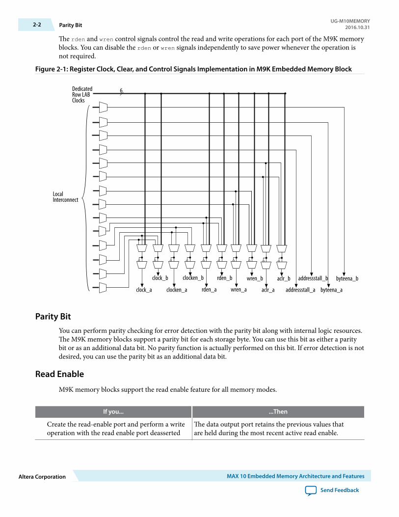
The rden and wren control signals control the read and write operations for each port of the M9K memoryblocks. You can disable the rden or wren signals independently to save power whenever the operation isnot required.
Figure 2-1: Register Clock, Clear, and Control Signals Implementation in M9K Embedded Memory Block
clock_b
clocken_aclock_a
clocken_b aclr_b
aclr_a
DedicatedRow LABClocks
rden_b
rden_a
6
LocalInterconnect
byteena_b
byteena_a
addressstall_b
addressstall_awren_a
wren_b
Parity BitYou can perform parity checking for error detection with the parity bit along with internal logic resources.The M9K memory blocks support a parity bit for each storage byte. You can use this bit as either a paritybit or as an additional data bit. No parity function is actually performed on this bit. If error detection is notdesired, you can use the parity bit as an additional data bit.
Read Enable
M9K memory blocks support the read enable feature for all memory modes.
If you... ...Then
Create the read-enable port and perform a writeoperation with the read enable port deasserted
The data output port retains the previous values thatare held during the most recent active read enable.
2-2 Parity BitUG-M10MEMORY
2016.10.31
Altera Corporation MAX 10 Embedded Memory Architecture and Features
Send Feedback
If you... ...Then
• Activate the read enable during a writeoperation, or
• Do not create a read-enable signal
The output port shows:
• the new data being written,• the old data at that address, or• a “Don't Care” value when read-during-write
occurs at the same address location.
Read-During-Write
The read-during-write operation occurs when a read operation and a write operation target the samememory location at the same time.
The read-during-write operation operates in the following ways:
• Same-port• Mixed-port
Related InformationCustomize Read-During-Write Behavior on page 3-1
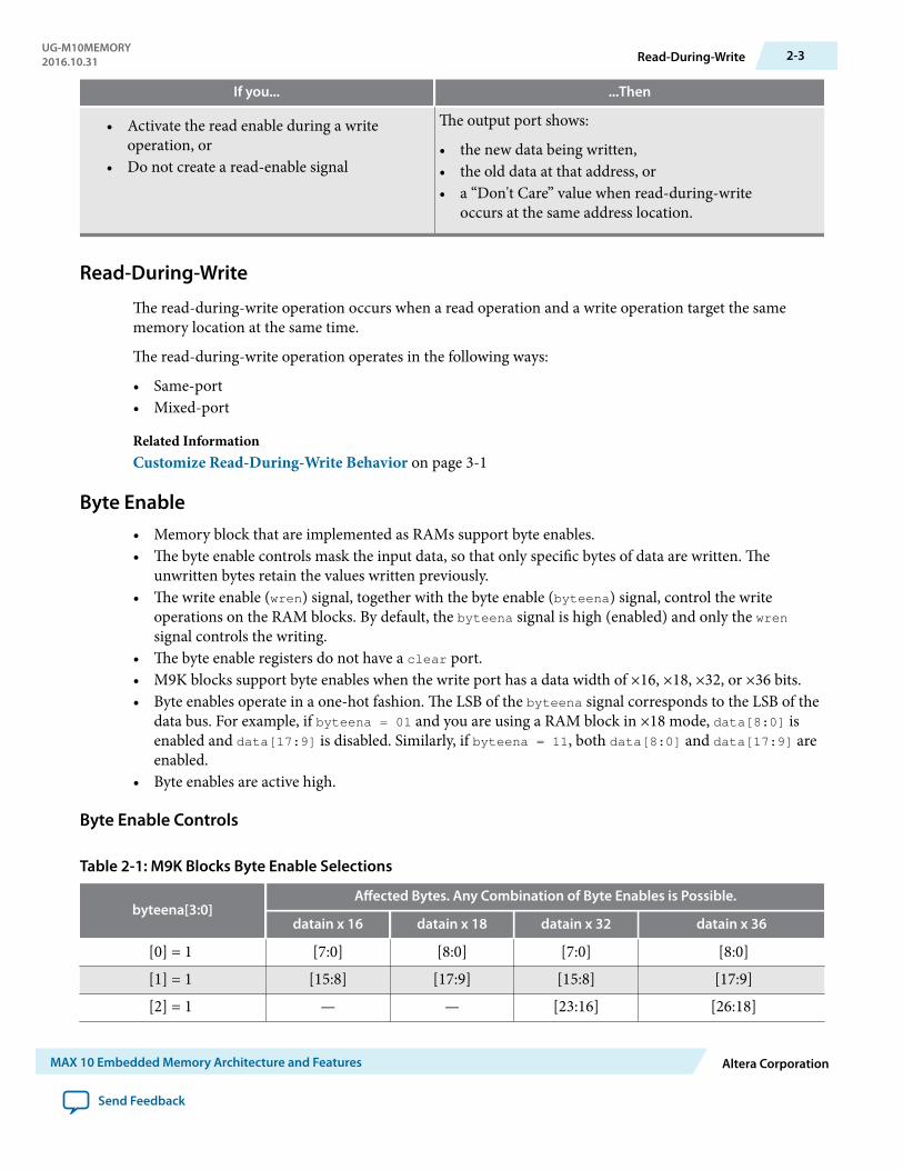
Byte Enable• Memory block that are implemented as RAMs support byte enables.• The byte enable controls mask the input data, so that only specific bytes of data are written. The
unwritten bytes retain the values written previously.• The write enable (wren) signal, together with the byte enable (byteena) signal, control the write
operations on the RAM blocks. By default, the byteena signal is high (enabled) and only the wrensignal controls the writing.
• The byte enable registers do not have a clear port.• M9K blocks support byte enables when the write port has a data width of ×16, ×18, ×32, or ×36 bits.• Byte enables operate in a one-hot fashion. The LSB of the byteena signal corresponds to the LSB of the
data bus. For example, if byteena = 01 and you are using a RAM block in ×18 mode, data[8:0] isenabled and data[17:9] is disabled. Similarly, if byteena = 11, both data[8:0] and data[17:9] areenabled.
• Byte enables are active high.
Byte Enable Controls
Table 2-1: M9K Blocks Byte Enable Selections
byteena[3:0]Affected Bytes. Any Combination of Byte Enables is Possible.
datain x 16 datain x 18 datain x 32 datain x 36
[0] = 1 [7:0] [8:0] [7:0] [8:0][1] = 1 [15:8] [17:9] [15:8] [17:9][2] = 1 — — [23:16] [26:18]
UG-M10MEMORY2016.10.31 Read-During-Write 2-3
MAX 10 Embedded Memory Architecture and Features Altera Corporation
Send Feedback
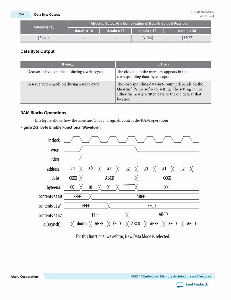
byteena[3:0]Affected Bytes. Any Combination of Byte Enables is Possible.
datain x 16 datain x 18 datain x 32 datain x 36
[3] = 1 — — [31:24] [35:27]
Data Byte Output
If you... ...Then
Deassert a byte-enable bit during a write cycle The old data in the memory appears in thecorresponding data-byte output.
Assert a byte-enable bit during a write cycle The corresponding data-byte output depends on theQuartus® Prime software setting. The setting can beeither the newly written data or the old data at thatlocation.
RAM Blocks Operations
This figure shows how the wren and byteena signals control the RAM operations.
Figure 2-2: Byte Enable Functional Waveform
inclock
wren
address
data
q (asynch)
an
XXXX
a0 a1 a2 a0 a1 a2
doutn ABFF FFCD ABCD ABFF FFCD
ABCD
byteena XX 10 01 11
XXXX
XX
ABCD
ABCDFFFF
FFFF
FFFF
ABFF
FFCD
contents at a0
contents at a1
contents at a2
rden
For this functional waveform, New Data Mode is selected.
2-4 Data Byte OutputUG-M10MEMORY
2016.10.31
Altera Corporation MAX 10 Embedded Memory Architecture and Features
Send Feedback
Packed Mode SupportYou can implement two single-port memory blocks in a single block under the following conditions:
• Each of the two independent block sizes is less than or equal to half of the M9K block size. Themaximum data width for each independent block is 18 bits wide.
• Each of the single-port memory blocks is configured in single-clock mode.
Related InformationMAX 10 Embedded Memory Clock Modes on page 2-10
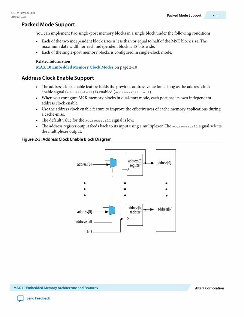
Address Clock Enable Support• The address clock enable feature holds the previous address value for as long as the address clock
enable signal (addressstall) is enabled (addressstall = 1).• When you configure M9K memory blocks in dual-port mode, each port has its own independent
address clock enable.• Use the address clock enable feature to improve the effectiveness of cache memory applications during
a cache-miss.• The default value for the addressstall signal is low.• The address register output feeds back to its input using a multiplexer. The addressstall signal selects
the multiplexer output.
Figure 2-3: Address Clock Enable Block Diagram
address[0]
address[N]
addressstall
clock
address[0]register
address[N]register
address[N]
address[0]
UG-M10MEMORY2016.10.31 Packed Mode Support 2-5
MAX 10 Embedded Memory Architecture and Features Altera Corporation
Send Feedback
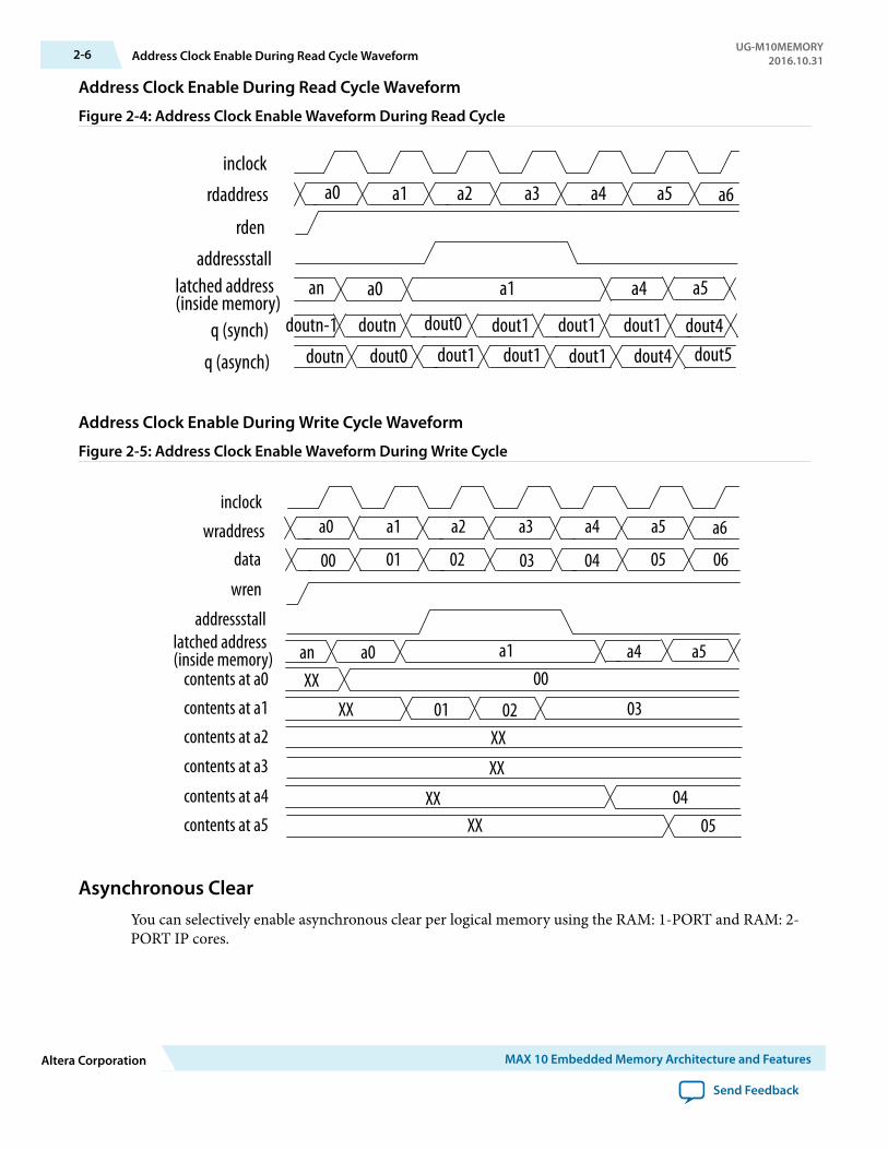
Address Clock Enable During Read Cycle Waveform
Figure 2-4: Address Clock Enable Waveform During Read Cycle
inclock
rden
rdaddress
q (synch)
a0 a1 a2 a3 a4 a5 a6
q (asynch)
an a0 a4 a5latched address(inside memory)
dout0 dout1 dout1 dout4dout1 dout4 dout5
addressstalla1
doutn-1 dout1doutn
doutn dout1dout0 dout1
Address Clock Enable During Write Cycle Waveform
Figure 2-5: Address Clock Enable Waveform During Write Cycle
inclock
wren
wraddress a0 a1 a2 a3 a4 a5 a6
an a0 a4 a5latched address(inside memory)
addressstall
a1
data 00 01 02 03 04 05 06
contents at a0contents at a1contents at a2
contents at a3
contents at a4contents at a5
XX
04XX
00
0301XX 02XX
XX
XX 05
Asynchronous ClearYou can selectively enable asynchronous clear per logical memory using the RAM: 1-PORT and RAM: 2-PORT IP cores.
2-6 Address Clock Enable During Read Cycle WaveformUG-M10MEMORY
2016.10.31
Altera Corporation MAX 10 Embedded Memory Architecture and Features
Send Feedback
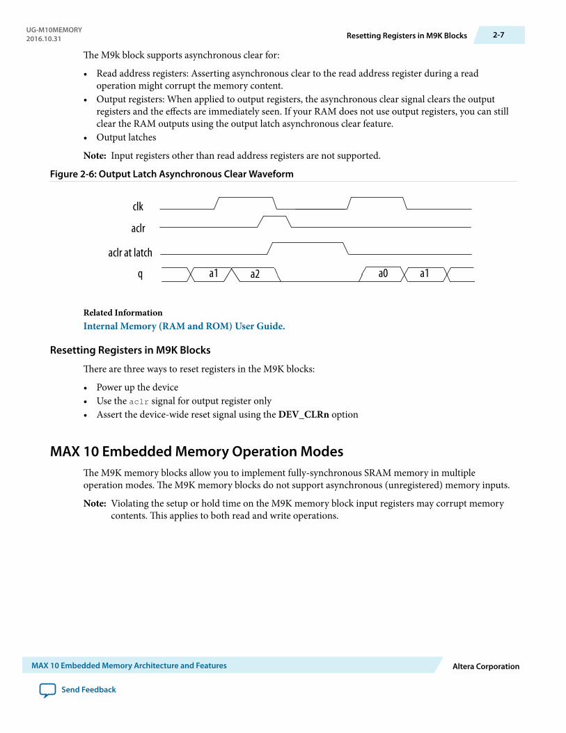
The M9k block supports asynchronous clear for:
• Read address registers: Asserting asynchronous clear to the read address register during a readoperation might corrupt the memory content.
• Output registers: When applied to output registers, the asynchronous clear signal clears the outputregisters and the effects are immediately seen. If your RAM does not use output registers, you can stillclear the RAM outputs using the output latch asynchronous clear feature.
• Output latches
Note: Input registers other than read address registers are not supported.
Figure 2-6: Output Latch Asynchronous Clear Waveform
aclr
aclr at latch
clk
q a1 a0 a1a2
Related InformationInternal Memory (RAM and ROM) User Guide.
Resetting Registers in M9K Blocks
There are three ways to reset registers in the M9K blocks:
• Power up the device• Use the aclr signal for output register only• Assert the device-wide reset signal using the DEV_CLRn option
MAX 10 Embedded Memory Operation ModesThe M9K memory blocks allow you to implement fully-synchronous SRAM memory in multipleoperation modes. The M9K memory blocks do not support asynchronous (unregistered) memory inputs.
Note: Violating the setup or hold time on the M9K memory block input registers may corrupt memorycontents. This applies to both read and write operations.
UG-M10MEMORY2016.10.31 Resetting Registers in M9K Blocks 2-7
MAX 10 Embedded Memory Architecture and Features Altera Corporation
Send Feedback
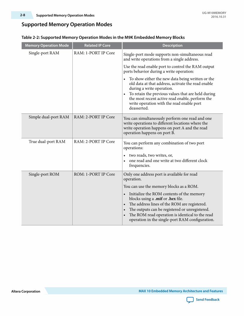
Supported Memory Operation Modes
Table 2-2: Supported Memory Operation Modes in the M9K Embedded Memory Blocks
Memory Operation Mode Related IP Core Description
Single-port RAM RAM: 1-PORT IP Core Single-port mode supports non-simultaneous readand write operations from a single address.
Use the read enable port to control the RAM outputports behavior during a write operation:
• To show either the new data being written or theold data at that address, activate the read enableduring a write operation.
• To retain the previous values that are held duringthe most recent active read enable, perform thewrite operation with the read enable portdeasserted.
Simple dual-port RAM RAM: 2-PORT IP Core You can simultaneously perform one read and onewrite operations to different locations where thewrite operation happens on port A and the readoperation happens on port B.
True dual-port RAM RAM: 2-PORT IP Core You can perform any combination of two portoperations:
• two reads, two writes, or,• one read and one write at two different clock
frequencies.
Single-port ROM ROM: 1-PORT IP Core Only one address port is available for readoperation.
You can use the memory blocks as a ROM.
• Initialize the ROM contents of the memoryblocks using a .mif or .hex file.
• The address lines of the ROM are registered.• The outputs can be registered or unregistered.• The ROM read operation is identical to the read
operation in the single-port RAM configuration.
2-8 Supported Memory Operation ModesUG-M10MEMORY
2016.10.31
Altera Corporation MAX 10 Embedded Memory Architecture and Features
Send Feedback
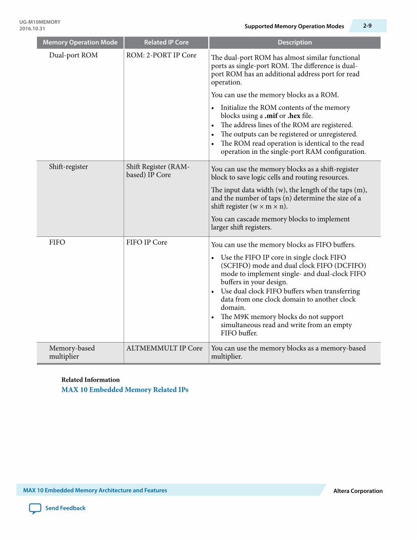
Memory Operation Mode Related IP Core Description
Dual-port ROM ROM: 2-PORT IP Core The dual-port ROM has almost similar functionalports as single-port ROM. The difference is dual-port ROM has an additional address port for readoperation.
You can use the memory blocks as a ROM.
• Initialize the ROM contents of the memoryblocks using a .mif or .hex file.
• The address lines of the ROM are registered.• The outputs can be registered or unregistered.• The ROM read operation is identical to the read
operation in the single-port RAM configuration.
Shift-register Shift Register (RAM-based) IP Core
You can use the memory blocks as a shift-registerblock to save logic cells and routing resources.
The input data width (w), the length of the taps (m),and the number of taps (n) determine the size of ashift register (w × m × n).
You can cascade memory blocks to implementlarger shift registers.
FIFO FIFO IP Core You can use the memory blocks as FIFO buffers.
• Use the FIFO IP core in single clock FIFO(SCFIFO) mode and dual clock FIFO (DCFIFO)mode to implement single- and dual-clock FIFObuffers in your design.
• Use dual clock FIFO buffers when transferringdata from one clock domain to another clockdomain.
• The M9K memory blocks do not supportsimultaneous read and write from an emptyFIFO buffer.
Memory-basedmultiplier
ALTMEMMULT IP Core You can use the memory blocks as a memory-basedmultiplier.
Related InformationMAX 10 Embedded Memory Related IPs
UG-M10MEMORY2016.10.31 Supported Memory Operation Modes 2-9
MAX 10 Embedded Memory Architecture and Features Altera Corporation
Send Feedback
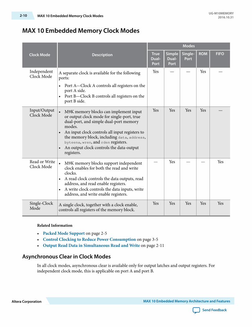
MAX 10 Embedded Memory Clock Modes
Clock Mode Description
Modes
TrueDual-Port
SimpleDual-Port
Single-Port
ROM FIFO
IndependentClock Mode
A separate clock is available for the followingports:
• Port A—Clock A controls all registers on theport A side.
• Port B—Clock B controls all registers on theport B side.
Yes — — Yes —
Input/OutputClock Mode
• M9K memory blocks can implement inputor output clock mode for single-port, truedual-port, and simple dual-port memorymodes.
• An input clock controls all input registers tothe memory block, including data, address,byteena, wren, and rden registers.
• An output clock controls the data-outputregisters.
Yes Yes Yes Yes —
Read or WriteClock Mode
• M9K memory blocks support independentclock enables for both the read and writeclocks.
• A read clock controls the data outputs, readaddress, and read enable registers.
• A write clock controls the data inputs, writeaddress, and write enable registers.
— Yes — — Yes
Single-ClockMode
A single clock, together with a clock enable,controls all registers of the memory block.
Yes Yes Yes Yes Yes
Related Information
• Packed Mode Support on page 2-5• Control Clocking to Reduce Power Consumption on page 3-5• Output Read Data in Simultaneous Read and Write on page 2-11
Asynchronous Clear in Clock ModesIn all clock modes, asynchronous clear is available only for output latches and output registers. Forindependent clock mode, this is applicable on port A and port B.
2-10 MAX 10 Embedded Memory Clock ModesUG-M10MEMORY
2016.10.31
Altera Corporation MAX 10 Embedded Memory Architecture and Features
Send Feedback
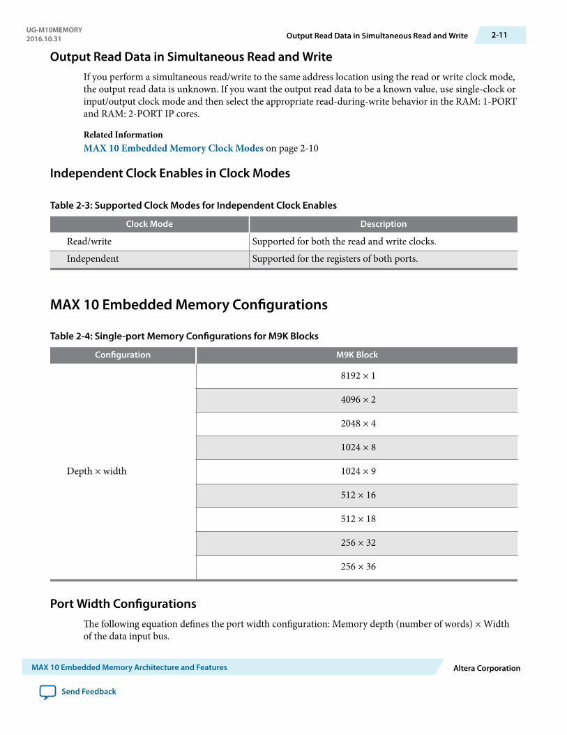
Output Read Data in Simultaneous Read and WriteIf you perform a simultaneous read/write to the same address location using the read or write clock mode,the output read data is unknown. If you want the output read data to be a known value, use single-clock orinput/output clock mode and then select the appropriate read-during-write behavior in the RAM: 1-PORTand RAM: 2-PORT IP cores.
Related InformationMAX 10 Embedded Memory Clock Modes on page 2-10
Independent Clock Enables in Clock Modes
Table 2-3: Supported Clock Modes for Independent Clock Enables
Clock Mode Description
Read/write Supported for both the read and write clocks.Independent Supported for the registers of both ports.
MAX 10 Embedded Memory Configurations
Table 2-4: Single-port Memory Configurations for M9K Blocks
Configuration M9K Block
Depth × width
8192 × 1
4096 × 2
2048 × 4
1024 × 8
1024 × 9
512 × 16
512 × 18
256 × 32
256 × 36
Port Width ConfigurationsThe following equation defines the port width configuration: Memory depth (number of words) × Widthof the data input bus.
UG-M10MEMORY2016.10.31 Output Read Data in Simultaneous Read and Write 2-11
MAX 10 Embedded Memory Architecture and Features Altera Corporation
Send Feedback
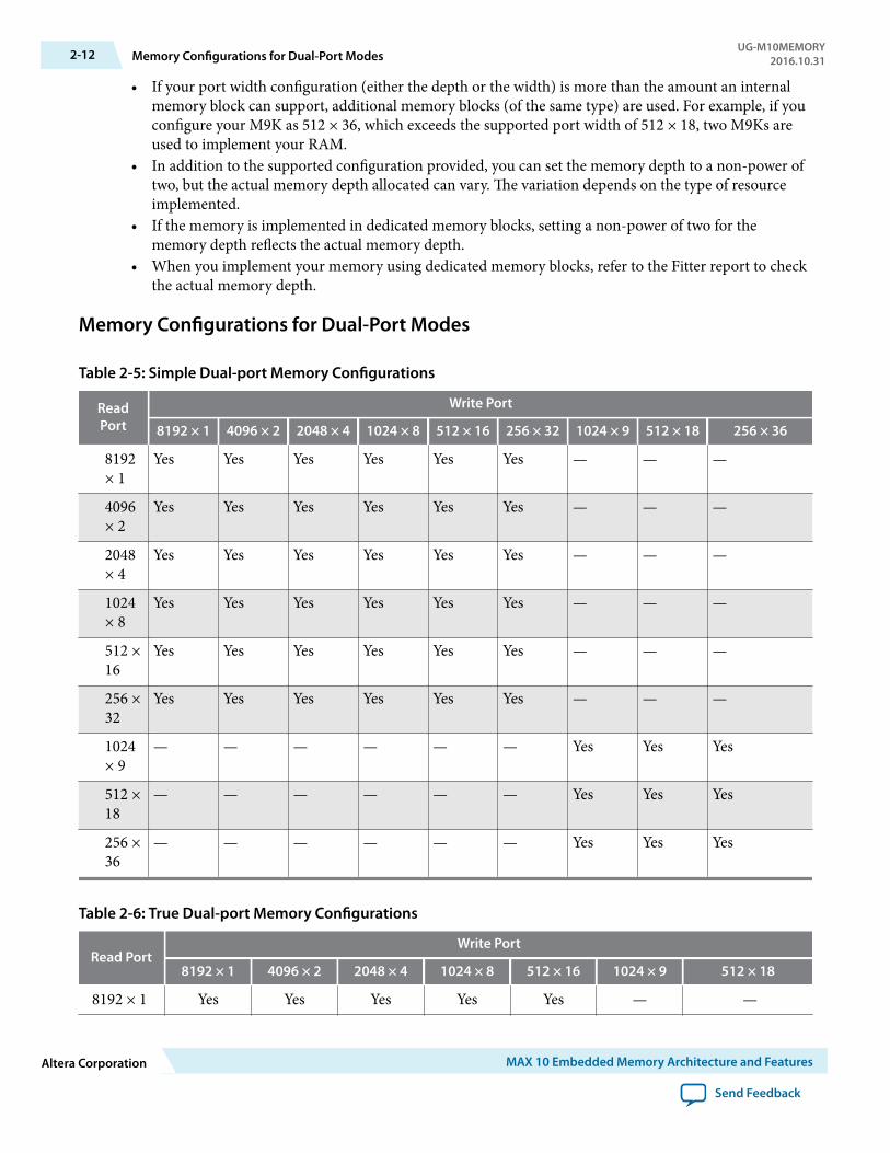
• If your port width configuration (either the depth or the width) is more than the amount an internalmemory block can support, additional memory blocks (of the same type) are used. For example, if youconfigure your M9K as 512 × 36, which exceeds the supported port width of 512 × 18, two M9Ks areused to implement your RAM.
• In addition to the supported configuration provided, you can set the memory depth to a non-power oftwo, but the actual memory depth allocated can vary. The variation depends on the type of resourceimplemented.
• If the memory is implemented in dedicated memory blocks, setting a non-power of two for thememory depth reflects the actual memory depth.
• When you implement your memory using dedicated memory blocks, refer to the Fitter report to checkthe actual memory depth.
Memory Configurations for Dual-Port Modes
Table 2-5: Simple Dual-port Memory Configurations
ReadPort
Write Port
8192 × 1 4096 × 2 2048 × 4 1024 × 8 512 × 16 256 × 32 1024 × 9 512 × 18 256 × 36
8192× 1
Yes Yes Yes Yes Yes Yes — — —
4096× 2
Yes Yes Yes Yes Yes Yes — — —
2048× 4
Yes Yes Yes Yes Yes Yes — — —
1024× 8
Yes Yes Yes Yes Yes Yes — — —
512 ×16
Yes Yes Yes Yes Yes Yes — — —
256 ×32
Yes Yes Yes Yes Yes Yes — — —
1024× 9
— — — — — — Yes Yes Yes
512 ×18
— — — — — — Yes Yes Yes
256 ×36
— — — — — — Yes Yes Yes
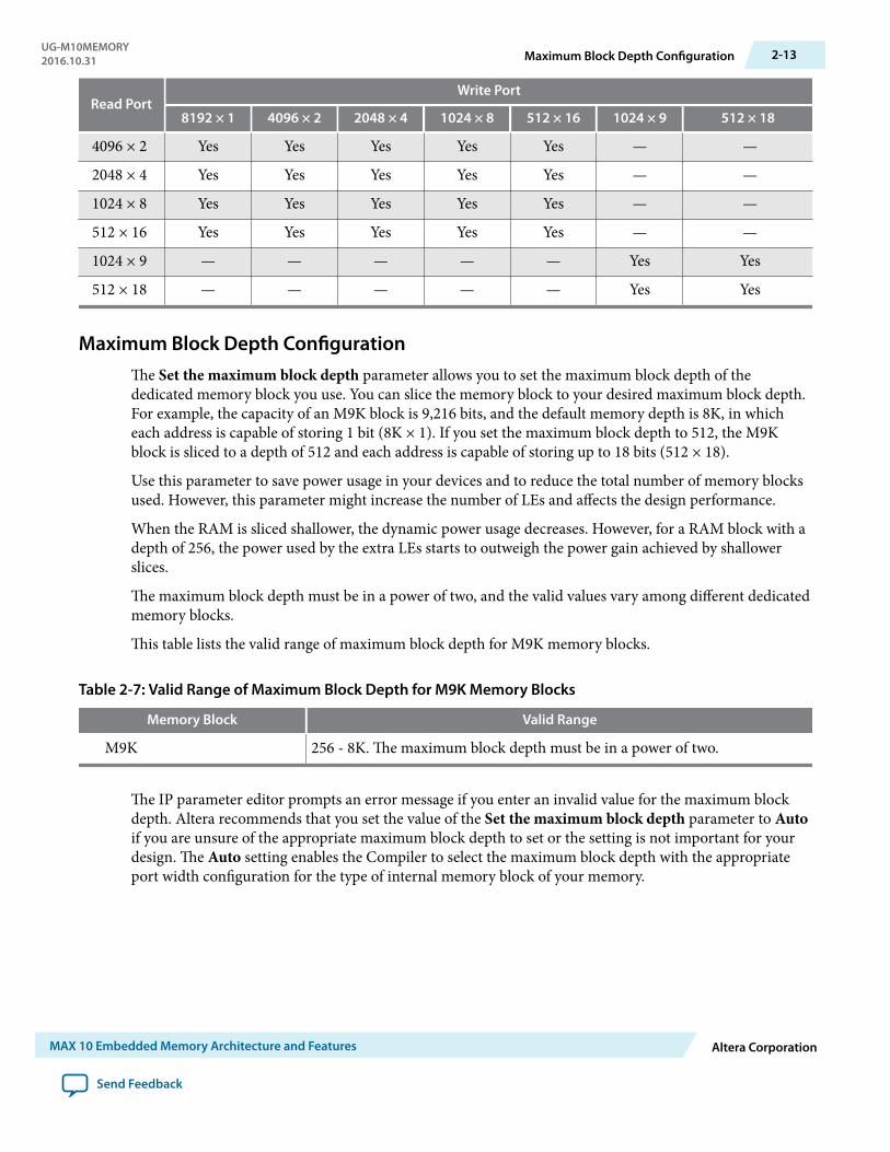
Table 2-6: True Dual-port Memory Configurations
Read PortWrite Port
8192 × 1 4096 × 2 2048 × 4 1024 × 8 512 × 16 1024 × 9 512 × 18
8192 × 1 Yes Yes Yes Yes Yes — —
2-12 Memory Configurations for Dual-Port ModesUG-M10MEMORY
2016.10.31
Altera Corporation MAX 10 Embedded Memory Architecture and Features
Send Feedback
Read PortWrite Port
8192 × 1 4096 × 2 2048 × 4 1024 × 8 512 × 16 1024 × 9 512 × 18
4096 × 2 Yes Yes Yes Yes Yes — —
2048 × 4 Yes Yes Yes Yes Yes — —
1024 × 8 Yes Yes Yes Yes Yes — —
512 × 16 Yes Yes Yes Yes Yes — —
1024 × 9 — — — — — Yes Yes
512 × 18 — — — — — Yes Yes
Maximum Block Depth ConfigurationThe Set the maximum block depth parameter allows you to set the maximum block depth of thededicated memory block you use. You can slice the memory block to your desired maximum block depth.For example, the capacity of an M9K block is 9,216 bits, and the default memory depth is 8K, in whicheach address is capable of storing 1 bit (8K × 1). If you set the maximum block depth to 512, the M9Kblock is sliced to a depth of 512 and each address is capable of storing up to 18 bits (512 × 18).
Use this parameter to save power usage in your devices and to reduce the total number of memory blocksused. However, this parameter might increase the number of LEs and affects the design performance.
When the RAM is sliced shallower, the dynamic power usage decreases. However, for a RAM block with adepth of 256, the power used by the extra LEs starts to outweigh the power gain achieved by shallowerslices.
The maximum block depth must be in a power of two, and the valid values vary among different dedicatedmemory blocks.
This table lists the valid range of maximum block depth for M9K memory blocks.
Table 2-7: Valid Range of Maximum Block Depth for M9K Memory Blocks
Memory Block Valid Range
M9K 256 - 8K. The maximum block depth must be in a power of two.
The IP parameter editor prompts an error message if you enter an invalid value for the maximum blockdepth. Altera recommends that you set the value of the Set the maximum block depth parameter to Autoif you are unsure of the appropriate maximum block depth to set or the setting is not important for yourdesign. The Auto setting enables the Compiler to select the maximum block depth with the appropriateport width configuration for the type of internal memory block of your memory.
UG-M10MEMORY2016.10.31 Maximum Block Depth Configuration 2-13
MAX 10 Embedded Memory Architecture and Features Altera Corporation
Send Feedback
MAX 10 Embedded Memory DesignConsideration 3
2016.10.31
UG-M10MEMORY Subscribe Send Feedback
There are several considerations that require your attention to ensure the success of your designs.
Implement External Conflict ResolutionIn the true dual-port RAM mode, you can perform two write operations to the same memory location.However, the memory blocks do not have internal conflict resolution circuitry.
To avoid unknown data being written to the address, implement external conflict resolution logic to thememory block.
Customize Read-During-Write BehaviorCustomize the read-during-write behavior of the memory blocks to suit your design requirements.
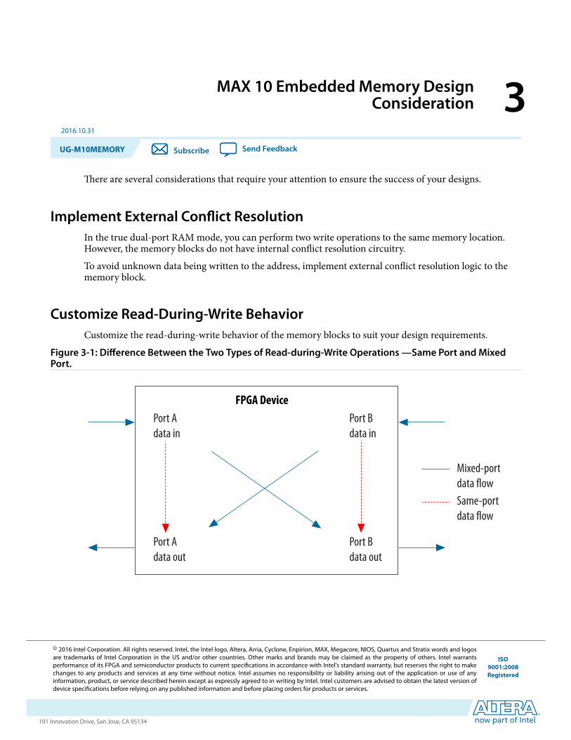
Figure 3-1: Difference Between the Two Types of Read-during-Write Operations —Same Port and MixedPort.
Port Adata in
Port Bdata in
Port Adata out
Port Bdata out
Mixed-portdata flowSame-portdata flow
FPGA Device
© 2016 Intel Corporation. All rights reserved. Intel, the Intel logo, Altera, Arria, Cyclone, Enpirion, MAX, Megacore, NIOS, Quartus and Stratix words and logosare trademarks of Intel Corporation in the US and/or other countries. Other marks and brands may be claimed as the property of others. Intel warrantsperformance of its FPGA and semiconductor products to current specifications in accordance with Intel's standard warranty, but reserves the right to makechanges to any products and services at any time without notice. Intel assumes no responsibility or liability arising out of the application or use of anyinformation, product, or service described herein except as expressly agreed to in writing by Intel. Intel customers are advised to obtain the latest version ofdevice specifications before relying on any published information and before placing orders for products or services.
ISO9001:2008Registered
www.altera.com101 Innovation Drive, San Jose, CA 95134
Related InformationRead-During-Write on page 2-3
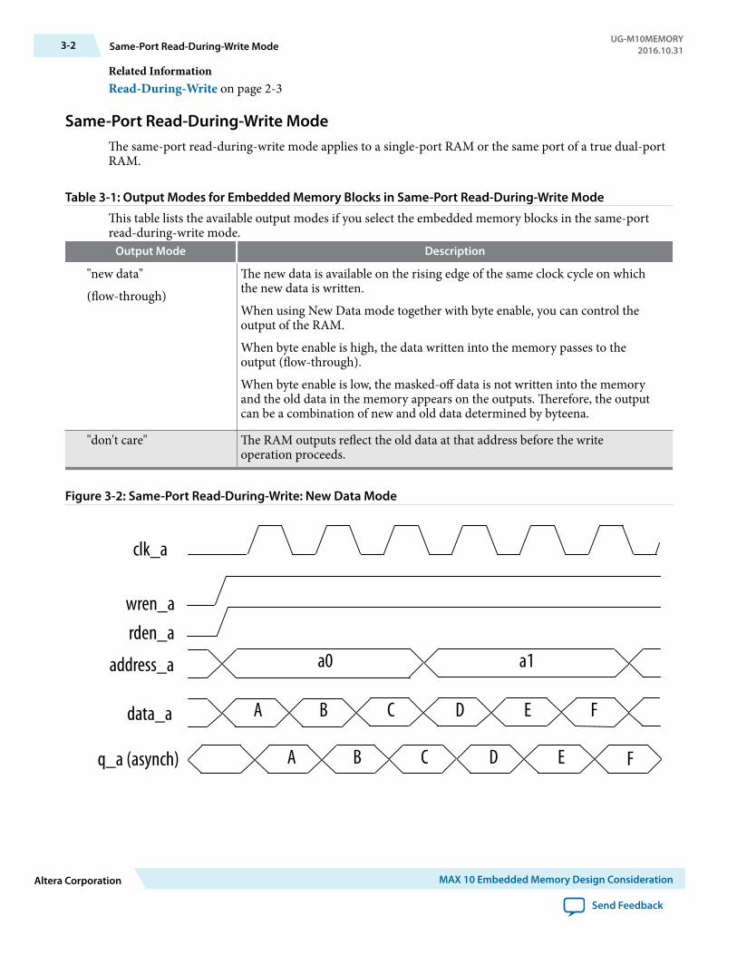
Same-Port Read-During-Write ModeThe same-port read-during-write mode applies to a single-port RAM or the same port of a true dual-portRAM.
Table 3-1: Output Modes for Embedded Memory Blocks in Same-Port Read-During-Write Mode
This table lists the available output modes if you select the embedded memory blocks in the same-portread-during-write mode.
Output Mode Description
"new data"
(flow-through)
The new data is available on the rising edge of the same clock cycle on whichthe new data is written.
When using New Data mode together with byte enable, you can control theoutput of the RAM.
When byte enable is high, the data written into the memory passes to theoutput (flow-through).
When byte enable is low, the masked-off data is not written into the memoryand the old data in the memory appears on the outputs. Therefore, the outputcan be a combination of new and old data determined by byteena.
"don't care" The RAM outputs reflect the old data at that address before the writeoperation proceeds.
Figure 3-2: Same-Port Read-During-Write: New Data Mode
clk_a
wren_a
address_a
data_a
rden_a
q_a (asynch)
a0 a1
A B C D E F
A B C D E F
3-2 Same-Port Read-During-Write ModeUG-M10MEMORY
2016.10.31
Altera Corporation MAX 10 Embedded Memory Design Consideration
Send Feedback
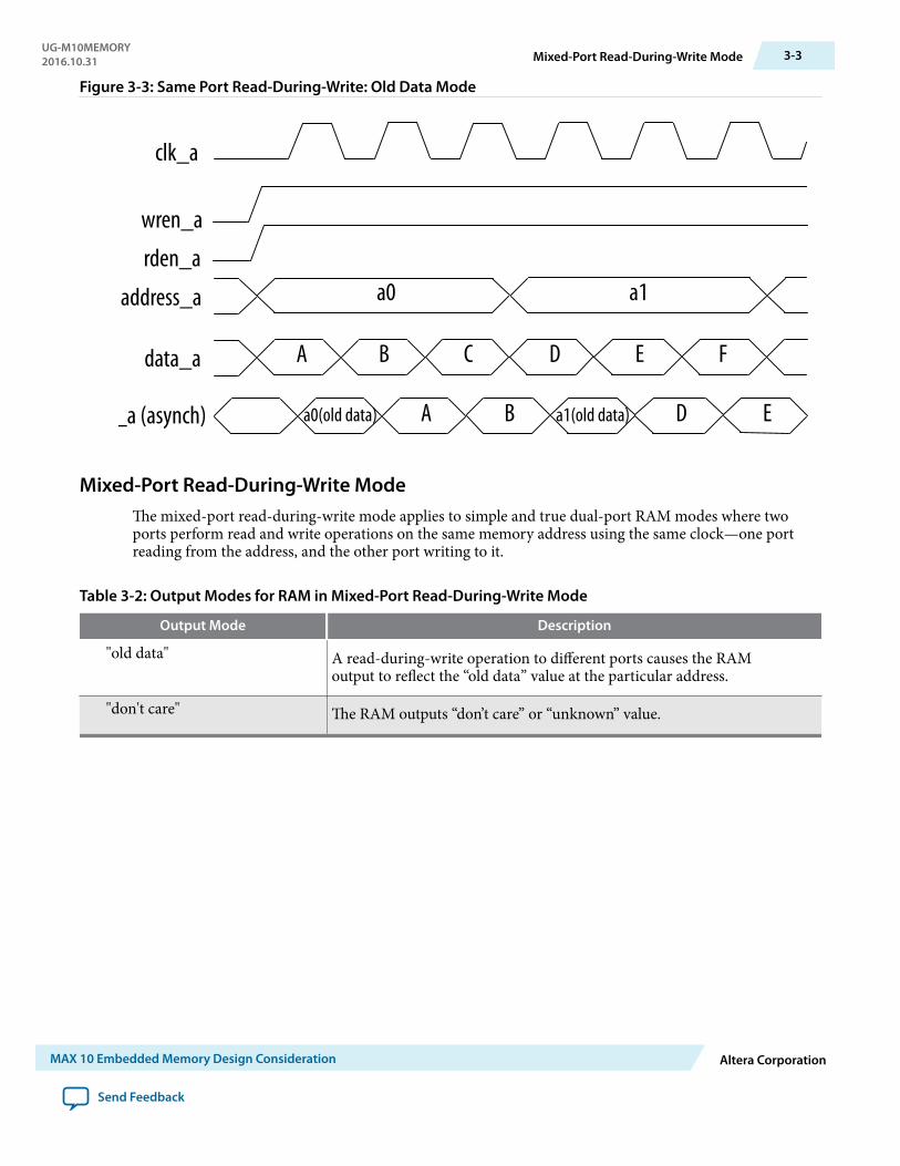
Figure 3-3: Same Port Read-During-Write: Old Data Mode
clk_a
wren_a
address_a
data_a
rden_a
q_a (asynch)
a0 a1
A B C D E F
a0(old data) a1(old data)A B D E
Mixed-Port Read-During-Write ModeThe mixed-port read-during-write mode applies to simple and true dual-port RAM modes where twoports perform read and write operations on the same memory address using the same clock—one portreading from the address, and the other port writing to it.
Table 3-2: Output Modes for RAM in Mixed-Port Read-During-Write Mode
Output Mode Description
"old data" A read-during-write operation to different ports causes the RAMoutput to reflect the “old data” value at the particular address.
"don't care" The RAM outputs “don’t care” or “unknown” value.
UG-M10MEMORY2016.10.31 Mixed-Port Read-During-Write Mode 3-3
MAX 10 Embedded Memory Design Consideration Altera Corporation
Send Feedback
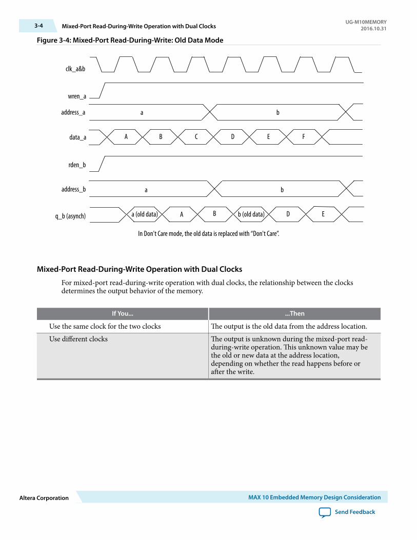
Figure 3-4: Mixed-Port Read-During-Write: Old Data Mode
a b
a (old data) b (old data)
clk_a&b
wren_a
address_a
q_b (asynch)
rden_b
a baddress_b
data_a A B C D E F
A B D E
In Don't Care mode, the old data is replaced with “Don't Care”.
Mixed-Port Read-During-Write Operation with Dual Clocks
For mixed-port read-during-write operation with dual clocks, the relationship between the clocksdetermines the output behavior of the memory.
If You... ...Then
Use the same clock for the two clocks The output is the old data from the address location.Use different clocks The output is unknown during the mixed-port read-
during-write operation. This unknown value may bethe old or new data at the address location,depending on whether the read happens before orafter the write.
3-4 Mixed-Port Read-During-Write Operation with Dual ClocksUG-M10MEMORY
2016.10.31
Altera Corporation MAX 10 Embedded Memory Design Consideration
Send Feedback
Consider Power-Up State and Memory InitializationConsider the power-up state of the different types of memory blocks if you are designing logic thatevaluates the initial power-up values, as listed in the following table:
Table 3-3: Initial Power-Up Values of Embedded Memory Blocks
Memory Type Output Registers Power Up Value
M9KUsed Zero (cleared)
Bypassed Zero (cleared)
By default, the Quartus Prime software initializes the RAM cells to zero unless you specify a .mif.All memory blocks support initialization with a .mif. You can create .mif files in the Quartus Primesoftware and specify their use with the RAM IP when you instantiate a memory in your design. Even if amemory is preinitialized (for example, using a .mif), it still powers up with its output cleared. Only thesubsequent read after power up outputs the preinitialized values.
Only the following MAX 10 configuration modes support memory initialization:
• Single Compressed Image with Memory Initialization• Single Uncompressed Image with Memory Initialization
Note: The memory initialization feature is supported in MAX 10 Flash and Analog feature options only
Related Information
• Selecting Internal Configuration modes.Provides more information about selecting MAX 10 internal configuration modes.
• MAX 10 Device Feature OptionsProvides information on devices that support memory initialization.
Control Clocking to Reduce Power ConsumptionReduce AC power consumption in your design by controlling the clocking of each memory block:
• Use the read-enable signal to ensure that read operations occur only when necessary. If your designdoes not require read-during-write, you can reduce your power consumption by deasserting the read-enable signal during write operations, or during the period when no memory operations occur.
• Use the Quartus Prime software to automatically place any unused memory blocks in low-power modeto reduce static power.
• Create independent clock enable for different input and output registers to control the shut down of aparticular register for power saving purposes. From the parameter editor, click More Options (besidethe clock enable option) to set the available independent clock enable that you prefer.
Related InformationMAX 10 Embedded Memory Clock Modes on page 2-10
UG-M10MEMORY2016.10.31 Consider Power-Up State and Memory Initialization 3-5
MAX 10 Embedded Memory Design Consideration Altera Corporation
Send Feedback
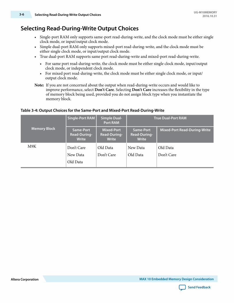
Selecting Read-During-Write Output Choices• Single-port RAM only supports same-port read-during-write, and the clock mode must be either single
clock mode, or input/output clock mode.• Simple dual-port RAM only supports mixed-port read-during-write, and the clock mode must be
either single clock mode, or input/output clock mode.• True dual-port RAM supports same port read-during-write and mixed-port read-during-write.
• For same port read-during-write, the clock mode must be either single clock mode, input/outputclock mode, or independent clock mode.
• For mixed port read-during-write, the clock mode must be either single clock mode, or input/output clock mode.
Note: If you are not concerned about the output when read-during-write occurs and would like toimprove performance, select Don't Care. Selecting Don't Care increases the flexibility in the typeof memory block being used, provided you do not assign block type when you instantiate thememory block.
Table 3-4: Output Choices for the Same-Port and Mixed-Port Read-During-Write
Memory Block
Single-Port RAM Simple Dual-Port RAM
True Dual-Port RAM
Same-PortRead-During-
Write
Mixed-PortRead-During-
Write
Same-PortRead-During-
Write
Mixed-Port Read-During-Write
M9K Don’t Care
New Data
Old Data
Old Data
Don’t Care
New Data
Old Data
Old Data
Don’t Care
3-6 Selecting Read-During-Write Output ChoicesUG-M10MEMORY
2016.10.31
Altera Corporation MAX 10 Embedded Memory Design Consideration
Send Feedback
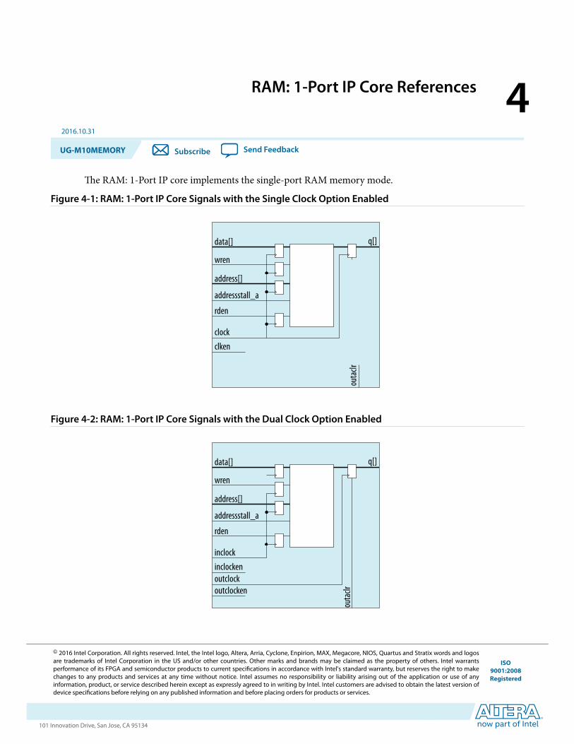
RAM: 1-Port IP Core References 42016.10.31
UG-M10MEMORY Subscribe Send Feedback
The RAM: 1-Port IP core implements the single-port RAM memory mode.
Figure 4-1: RAM: 1-Port IP Core Signals with the Single Clock Option Enabled
data[]
wren
address[]
rden
addressstall_a
clockclken
q[]
outa
clr
Figure 4-2: RAM: 1-Port IP Core Signals with the Dual Clock Option Enabled
data[]
wren
address[]
rden
addressstall_a
inclockinclockenoutclockoutclocken
q[]
outa
clr
© 2016 Intel Corporation. All rights reserved. Intel, the Intel logo, Altera, Arria, Cyclone, Enpirion, MAX, Megacore, NIOS, Quartus and Stratix words and logosare trademarks of Intel Corporation in the US and/or other countries. Other marks and brands may be claimed as the property of others. Intel warrantsperformance of its FPGA and semiconductor products to current specifications in accordance with Intel's standard warranty, but reserves the right to makechanges to any products and services at any time without notice. Intel assumes no responsibility or liability arising out of the application or use of anyinformation, product, or service described herein except as expressly agreed to in writing by Intel. Intel customers are advised to obtain the latest version ofdevice specifications before relying on any published information and before placing orders for products or services.
ISO9001:2008Registered
www.altera.com101 Innovation Drive, San Jose, CA 95134
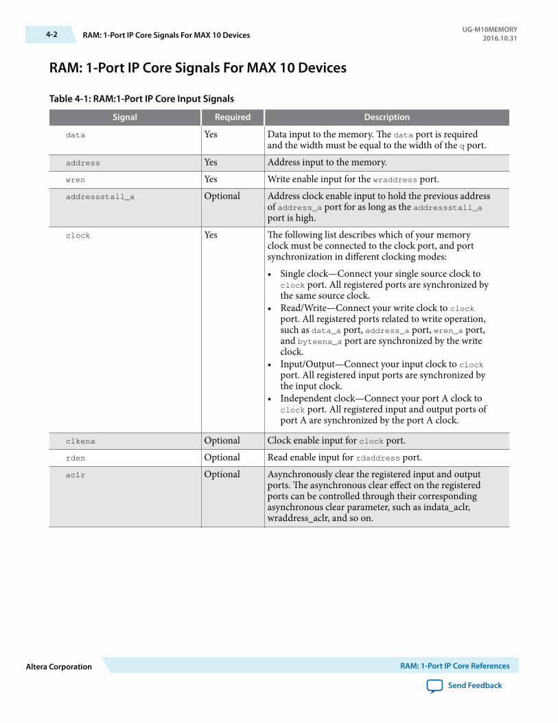
RAM: 1-Port IP Core Signals For MAX 10 Devices
Table 4-1: RAM:1-Port IP Core Input Signals
Signal Required Description
data Yes Data input to the memory. The data port is requiredand the width must be equal to the width of the q port.
address Yes Address input to the memory.wren Yes Write enable input for the wraddress port.addressstall_a Optional Address clock enable input to hold the previous address
of address_a port for as long as the addressstall_aport is high.
clock Yes The following list describes which of your memoryclock must be connected to the clock port, and portsynchronization in different clocking modes:
• Single clock—Connect your single source clock toclock port. All registered ports are synchronized bythe same source clock.
• Read/Write—Connect your write clock to clockport. All registered ports related to write operation,such as data_a port, address_a port, wren_a port,and byteena_a port are synchronized by the writeclock.
• Input/Output—Connect your input clock to clockport. All registered input ports are synchronized bythe input clock.
• Independent clock—Connect your port A clock toclock port. All registered input and output ports ofport A are synchronized by the port A clock.
clkena Optional Clock enable input for clock port.rden Optional Read enable input for rdaddress port.aclr Optional Asynchronously clear the registered input and output
ports. The asynchronous clear effect on the registeredports can be controlled through their correspondingasynchronous clear parameter, such as indata_aclr,wraddress_aclr, and so on.
4-2 RAM: 1-Port IP Core Signals For MAX 10 DevicesUG-M10MEMORY
2016.10.31
Altera Corporation RAM: 1-Port IP Core References
Send Feedback
Signal Required Description
inclock Optional The following list describes which of your memoryclock must be connected to the inclock port, and portsynchronization in different clock modes:
• Single clock—Connect your single source clock toinclock port and outclock port. All registeredports are synchronized by the same source clock.
• Read/Write—Connect your write clock to inclockport. All registered ports related to write operation,such as data port, wraddress port, wren port, andbyteena port are synchronized by the write clock.
• Input/Output—Connect your input clock toinclock port. All registered input ports aresynchronized by the input clock.
inclocken Optional Clock enable input for inclock port.outclock Optional The following list describes which of your memory
clock must be connected to the outclock port, and portsynchronization in different clock modes:
• Single clock—Connect your single source clock toinclock port and outclock port. All registeredports are synchronized by the same source clock.
• Read/Write—Connect your read clock to outclockport. All registered ports related to read operation,such as rdaddress port, rdren port, and q port aresynchronized by the read clock.
• Input/Output—Connect your output clock tooutclock port. The registered q port is synchronizedby the output clock.
outclocken Optional Clock enable input for outclock port.
Table 4-2: RAM:1-Port IP Core Output Ports
Signal Required Description
q Yes Data output from the memory. The q port must be equalto the width data port.
RAM: 1-Port IP Core Parameters For MAX 10 Devices
Table 4-3: RAM: 1-Port IP Core Parameters for MAX 10 Devices
This table lists the IP core parameters applicable to MAX 10 devices.Parameter Values Description
Parameter Settings: Widths/Blk Type/Clks
UG-M10MEMORY2016.10.31 RAM: 1-Port IP Core Parameters For MAX 10 Devices 4-3
RAM: 1-Port IP Core References Altera Corporation
Send Feedback
Parameter Values Description
How wide should the 'q' output bus be? 1, 2, 3, 4, 5, 6, 7, 8, 9,10, 11, 12, 13, 14, 15,16, 17, 18, 19, 20, 21,22, 23, 24, 25, 26, 27,28, 29, 30, 31, 32, 36,40, 48, 64, 72, 108,128, 144, and 256.
Specifies the width of the 'q' output busin bits.
How many <X>-bit words of memory? 32, 64, 128, 256, 512,1024, 2048, 4096,8192, 16384, 32768,and 65536.
Specifies the number of <X>-bit words.
What should the memory block type be?Auto On/Off Specifies the memory block type. The
types of memory block that areavailable for selection depends on yourtarget device.
M9K On/OffLC On/Off
Options
Use defaultlogic cell style
On/Off
Specifies the logic cell implementationoptions. This option is enabled onlywhen you choose LCs memory type.
Use StratixM512emulation logiccell style
On/Off
Set the maximum block depth to Auto, 32, 64, 128,256, 512, 1024, 2048,4096, and 8192
Specifies the maximum block depth inwords. This option is disabled onlywhen you choose LCs memory type.
What clocking method would you like to use?Single clock On/Off A single clock and a clock enable
controls all registers of the memoryblock.
Dual clock: use separate ‘input’ and‘output’ clocks
On/Off An input and an output clock controlsall registers related to the data inputand output to/from the memory blockincluding data, address, byte enables,read enables, and write enables.
Parameter Settings: Regs/Clkens/Byte Enable/AclrsWhich ports should be registered?'data' and 'wren' input ports — This option is automatically enabled.
Specifies whether to register the reador write input and output ports.
'address' input port — This option is automatically enabled.Specifies whether to register the reador write input and output ports.
'q' output port On/Off Specifies whether to register the reador write input and output ports.
4-4 RAM: 1-Port IP Core Parameters For MAX 10 DevicesUG-M10MEMORY
2016.10.31
Altera Corporation RAM: 1-Port IP Core References
Send Feedback
Parameter Values Description
Create one clock enable signal for eachclock signal.
On/Off Specifies whether to turn on the optionto create one clock enable signal foreach clock signal.
More Options
Use clock enablefor port A inputregisters
On/Off Specify whether to use clock enable forport A input and output registers.
Use clock enablefor port Aoutput registers
On/Off Specify whether to use clock enable forport A input and output registers.
Create an'addressstall_a'input port
On/Off Specifies whether to create clockenables for address registers. You cancreate these ports to act as an extraactive low clock enable input for theaddress registers.
Create an ‘aclr’ asynchronous clear for theregistered ports.
On/Off Specifies whether to create anasynchronous clear port for theregistered ports.
More Options 'q' port On/Off Specifies whether the q port is clearedby the aclr port.
Create a 'rden' read enable signal On/Off Specifies whether to create a rden readenable signal.
Parameter Settings: Read During Write OptionSingle Port Read During Write OptionWhat should the q output be whenreading from a memory location beingwritten to?
• Don't Care• New Data• Old Data
Specifies the output behavior whenread-during-write occurs.
• Don't Care—The RAM outputs"don't care" or "unknown" valuesfor read-during-write operation.
• New Data—New data is availableon the rising edge of the same clockcycle on which it was written.
• Old Data— The RAM outputsreflect the old data at that addressbefore the write operation proceeds.
Get x's for write masked bytes instead ofold data when byte enable is used
On/Off Turn on this option to obtain 'X' on themasked byte.
Parameter Settings: Mem InitDo you want to specify the initial content of the memory?No, leave it blank On/Off Specifies the initial content of the
memory. Initialize the memory to zero.Initialize memory content data to XX..Xon power-up in simulation
On/Off
UG-M10MEMORY2016.10.31 RAM: 1-Port IP Core Parameters For MAX 10 Devices 4-5
RAM: 1-Port IP Core References Altera Corporation
Send Feedback

Parameter Values Description
Yes, use this file for the memory contentdata
On/Off Allows you to specify a memoryinitialization file (.mif) or a hexadec‐imal (Intel-format) file (.hex).
Note: The configuration schemeof your device is InternalConfiguration. In order touse memory initialization,you must select a singleimage configuration modewith memory initialization,for example the SingleCompressed Image withMemory Initializationoption. You can set theconfiguration mode on theConfiguration page of theDevice and Pin Optionsdialog box.
Allow In-System Memory Content Editorto capture and update content independ‐ently of the system clock
On/Off Specifies whether to allow In-SystemMemory Content Editor to capture andupdate content independently of thesystem clock.
The 'Instance ID' of this RAM is — Specifies the RAM ID.
4-6 RAM: 1-Port IP Core Parameters For MAX 10 DevicesUG-M10MEMORY
2016.10.31
Altera Corporation RAM: 1-Port IP Core References
Send Feedback
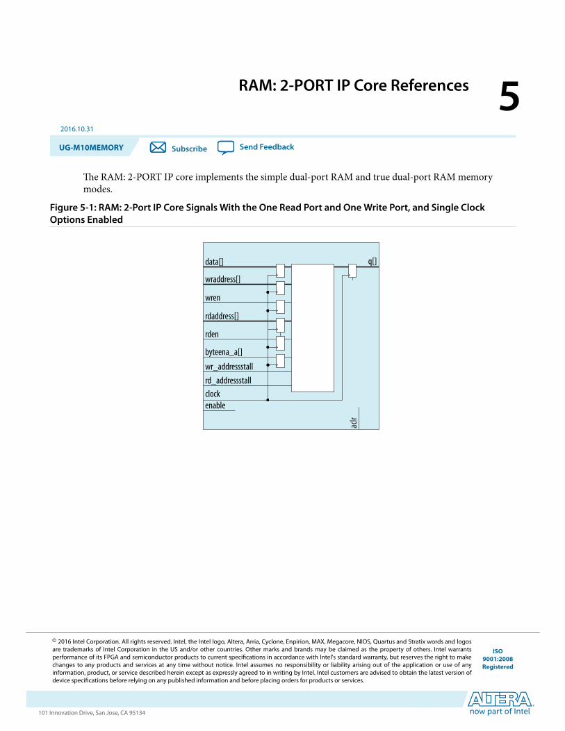
RAM: 2-PORT IP Core References 52016.10.31
UG-M10MEMORY Subscribe Send Feedback
The RAM: 2-PORT IP core implements the simple dual-port RAM and true dual-port RAM memorymodes.
Figure 5-1: RAM: 2-Port IP Core Signals With the One Read Port and One Write Port, and Single ClockOptions Enabled
data[]
wren
rdaddress[]
rden
wr_addressstall
clockenable
q[]
aclr
wraddress[]
byteena_a[]
rd_addressstall
© 2016 Intel Corporation. All rights reserved. Intel, the Intel logo, Altera, Arria, Cyclone, Enpirion, MAX, Megacore, NIOS, Quartus and Stratix words and logosare trademarks of Intel Corporation in the US and/or other countries. Other marks and brands may be claimed as the property of others. Intel warrantsperformance of its FPGA and semiconductor products to current specifications in accordance with Intel's standard warranty, but reserves the right to makechanges to any products and services at any time without notice. Intel assumes no responsibility or liability arising out of the application or use of anyinformation, product, or service described herein except as expressly agreed to in writing by Intel. Intel customers are advised to obtain the latest version ofdevice specifications before relying on any published information and before placing orders for products or services.
ISO9001:2008Registered
www.altera.com101 Innovation Drive, San Jose, CA 95134
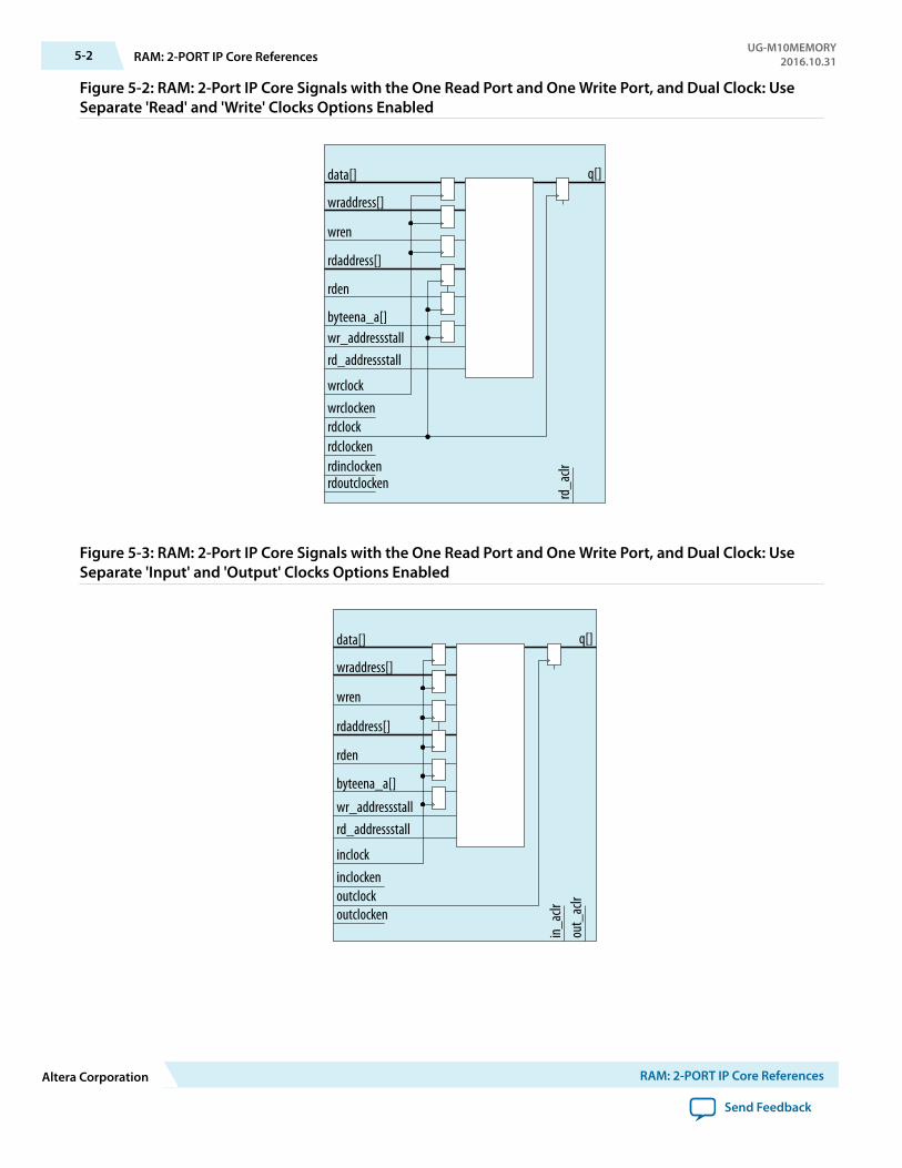
Figure 5-2: RAM: 2-Port IP Core Signals with the One Read Port and One Write Port, and Dual Clock: UseSeparate 'Read' and 'Write' Clocks Options Enabled
data[]
wren
rdaddress[]
wr_addressstall
wrclockwrclockenrdclock
rdinclocken
q[]
rd_a
clr
wraddress[]
rden
rd_addressstall
rdoutclocken
byteena_a[]
rdclocken
Figure 5-3: RAM: 2-Port IP Core Signals with the One Read Port and One Write Port, and Dual Clock: UseSeparate 'Input' and 'Output' Clocks Options Enabled
data[]
wren
rdaddress[]
rden
wr_addressstall
inclockinclockenoutclockoutclocken
q[]
in_ac
lrou
t_ac
lr
wraddress[]
byteena_a[]
rd_addressstall
5-2 RAM: 2-PORT IP Core ReferencesUG-M10MEMORY
2016.10.31
Altera Corporation RAM: 2-PORT IP Core References
Send Feedback
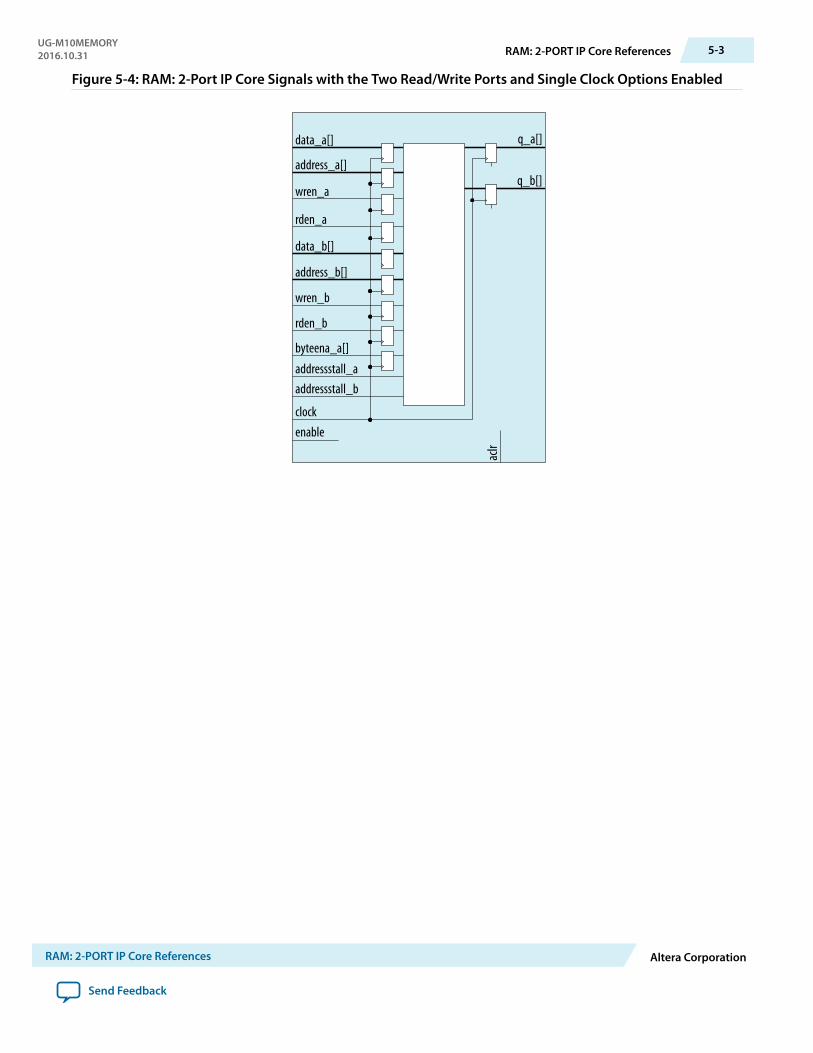
Figure 5-4: RAM: 2-Port IP Core Signals with the Two Read/Write Ports and Single Clock Options Enabled
data_a[]
wren_a
data_b[]
address_b[]
addressstall_a
clockenable
q_a[]
aclr
address_a[]
wren_b
addressstall_b
rden_a
rden_b
byteena_a[]
q_b[]
UG-M10MEMORY2016.10.31 RAM: 2-PORT IP Core References 5-3
RAM: 2-PORT IP Core References Altera Corporation
Send Feedback
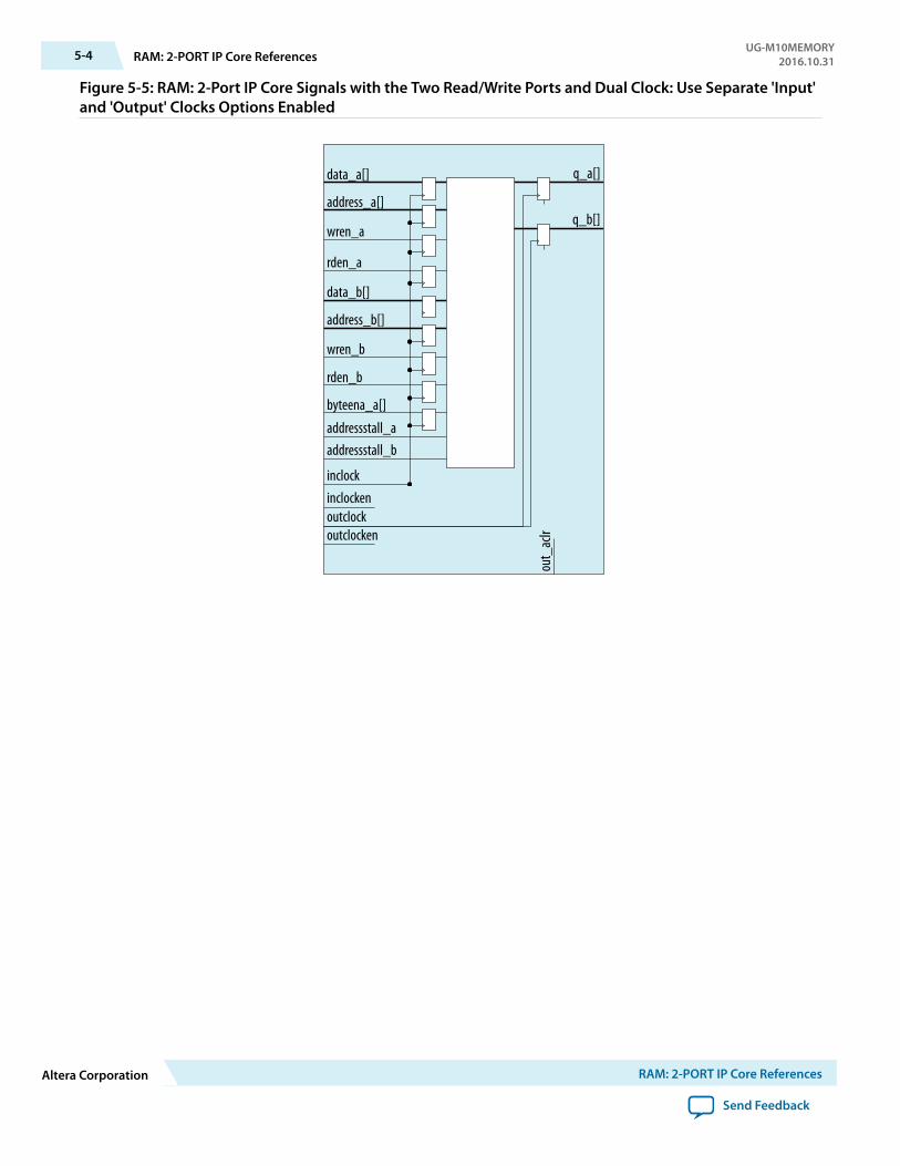
Figure 5-5: RAM: 2-Port IP Core Signals with the Two Read/Write Ports and Dual Clock: Use Separate 'Input'and 'Output' Clocks Options Enabled
data_a[]
wren_a
data_b[]
address_b[]
addressstall_a
inclockinclockenoutclockoutclocken
q_a[]
out_
aclr
address_a[]
wren_b
addressstall_b
rden_a
rden_b
byteena_a[]
q_b[]
5-4 RAM: 2-PORT IP Core ReferencesUG-M10MEMORY
2016.10.31
Altera Corporation RAM: 2-PORT IP Core References
Send Feedback
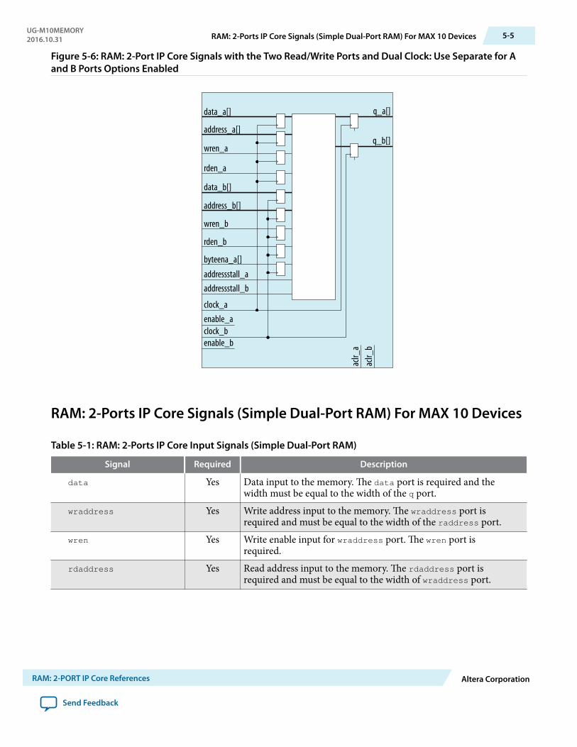
Figure 5-6: RAM: 2-Port IP Core Signals with the Two Read/Write Ports and Dual Clock: Use Separate for Aand B Ports Options Enabled
data_a[]
wren_a
data_b[]
address_b[]
addressstall_a
clock_aenable_aclock_benable_b
q_a[]
aclr_
a
address_a[]
wren_b
addressstall_b
rden_a
rden_b
byteena_a[]
aclr_
b
q_b[]
RAM: 2-Ports IP Core Signals (Simple Dual-Port RAM) For MAX 10 Devices
Table 5-1: RAM: 2-Ports IP Core Input Signals (Simple Dual-Port RAM)
Signal Required Description
data Yes Data input to the memory. The data port is required and thewidth must be equal to the width of the q port.
wraddress Yes Write address input to the memory. The wraddress port isrequired and must be equal to the width of the raddress port.
wren Yes Write enable input for wraddress port. The wren port isrequired.
rdaddress Yes Read address input to the memory. The rdaddress port isrequired and must be equal to the width of wraddress port.
UG-M10MEMORY2016.10.31 RAM: 2-Ports IP Core Signals (Simple Dual-Port RAM) For MAX 10 Devices 5-5
RAM: 2-PORT IP Core References Altera Corporation
Send Feedback
Signal Required Description
clock Yes The following list describes which of your memory clock mustbe connected to the clock port, and port synchronization indifferent clock modes:
• Single clock—Connect your single source clock to clockport. All registered ports are synchronized by the samesource clock.
• Read/Write—Connect your write clock to clock port. Allregistered ports related to write operation, such as data_aport, address_a port, wren_a port, and byteena_a port aresynchronized by the write clock.
• Input/Output—Connect your input clock to clock port. Allregistered input ports are synchronized by the input clock.
• Independent clock—Connect your port A clock to clockport. All registered input and output ports of port A aresynchronized by the port A clock.
inclock Yes The following list describes which of your memory clock mustbe connected to the inclock port, and port synchronization indifferent clock modes:
• Single clock—Connect your single source clock to inclockport and outclock port. All registered ports are synchron‐ized by the same source clock.
• Read/Write—Connect your write clock to inclock port. Allregistered ports related to write operation, such as data port,wraddress port, wren port, and byteena port are synchron‐ized by the write clock.
• Input/Output—Connect your input clock to inclock port.All registered input ports are synchronized by the inputclock.
outclock Yes The following list describes which of your memory clock mustbe connected to the outclock port, and port synchronization indifferent clock modes:
• Single clock—Connect your single source clock to inclockport and outclock port. All registered ports are synchron‐ized by the same source clock.
• Read/Write—Connect your read clock to outclock port. Allregistered ports related to read operation, such as rdaddressport, rdren port, and q port are synchronized by the readclock.
• Input/Output—Connect your output clock to outclockport. The registered q port is synchronized by the outputclock.
rden Optional Read enable input for rdaddress port. The rden port issupported when the use_eab parameter is set to OFF. Instantiatethe IP core if you want to use read enable feature with othermemory blocks.
5-6 RAM: 2-Ports IP Core Signals (Simple Dual-Port RAM) For MAX 10 DevicesUG-M10MEMORY
2016.10.31
Altera Corporation RAM: 2-PORT IP Core References
Send Feedback
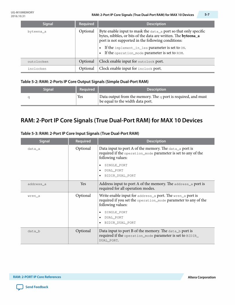
Signal Required Description
byteena_a Optional Byte enable input to mask the data_a port so that only specificbytes, nibbles, or bits of the data are written. The byteena_aport is not supported in the following conditions:
• If the implement_in_les parameter is set to ON.• If the operation_mode parameter is set to ROM.
outclocken Optional Clock enable input for outclock port.inclocken Optional Clock enable input for inclock port.
Table 5-2: RAM: 2-Ports IP Core Output Signals (Simple Dual-Port RAM)
Signal Required Description
q Yes Data output from the memory. The q port is required, and mustbe equal to the width data port.
RAM: 2-Port IP Core Signals (True Dual-Port RAM) for MAX 10 Devices
Table 5-3: RAM: 2-Port IP Core Input Signals (True Dual-Port RAM)
Signal Required Description
data_a Optional Data input to port A of the memory. The data_a port isrequired if the operation_mode parameter is set to any of thefollowing values:
• SINGLE_PORT
• DUAL_PORT
• BIDIR_DUAL_PORT
address_a Yes Address input to port A of the memory. The address_a port isrequired for all operation modes.
wren_a Optional Write enable input for address_a port. The wren_a port isrequired if you set the operation_mode parameter to any of thefollowing values:
• SINGLE_PORT
• DUAL_PORT
• BIDIR_DUAL_PORT
data_b Optional Data input to port B of the memory. The data_b port isrequired if the operation_mode parameter is set to BIDIR_DUAL_PORT.
UG-M10MEMORY2016.10.31 RAM: 2-Port IP Core Signals (True Dual-Port RAM) for MAX 10 Devices 5-7
RAM: 2-PORT IP Core References Altera Corporation
Send Feedback
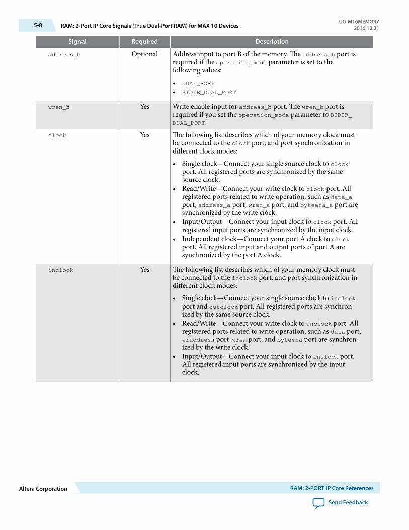
Signal Required Description
address_b Optional Address input to port B of the memory. The address_b port isrequired if the operation_mode parameter is set to thefollowing values:
• DUAL_PORT
• BIDIR_DUAL_PORT
wren_b Yes Write enable input for address_b port. The wren_b port isrequired if you set the operation_mode parameter to BIDIR_DUAL_PORT.
clock Yes The following list describes which of your memory clock mustbe connected to the clock port, and port synchronization indifferent clock modes:
• Single clock—Connect your single source clock to clockport. All registered ports are synchronized by the samesource clock.
• Read/Write—Connect your write clock to clock port. Allregistered ports related to write operation, such as data_aport, address_a port, wren_a port, and byteena_a port aresynchronized by the write clock.
• Input/Output—Connect your input clock to clock port. Allregistered input ports are synchronized by the input clock.
• Independent clock—Connect your port A clock to clockport. All registered input and output ports of port A aresynchronized by the port A clock.
inclock Yes The following list describes which of your memory clock mustbe connected to the inclock port, and port synchronization indifferent clock modes:
• Single clock—Connect your single source clock to inclockport and outclock port. All registered ports are synchron‐ized by the same source clock.
• Read/Write—Connect your write clock to inclock port. Allregistered ports related to write operation, such as data port,wraddress port, wren port, and byteena port are synchron‐ized by the write clock.
• Input/Output—Connect your input clock to inclock port.All registered input ports are synchronized by the inputclock.
5-8 RAM: 2-Port IP Core Signals (True Dual-Port RAM) for MAX 10 DevicesUG-M10MEMORY
2016.10.31
Altera Corporation RAM: 2-PORT IP Core References
Send Feedback
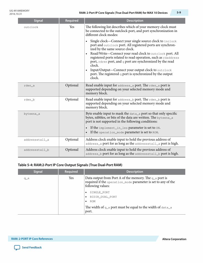
Signal Required Description
outclock Yes The following list describes which of your memory clock mustbe connected to the outclock port, and port synchronization indifferent clock modes:
• Single clock—Connect your single source clock to inclockport and outclock port. All registered ports are synchron‐ized by the same source clock.
• Read/Write—Connect your read clock to outclock port. Allregistered ports related to read operation, such as rdaddressport, rdren port, and q port are synchronized by the readclock.
• Input/Output—Connect your output clock to outclockport. The registered q port is synchronized by the outputclock.
rden_a Optional Read enable input for address_a port. The rden_a port issupported depending on your selected memory mode andmemory block.
rden_b Optional Read enable input for address_b port. The rden_b port issupported depending on your selected memory mode andmemory block.
byteena_a Byte enable input to mask the data_a port so that only specificbytes, nibbles, or bits of the data are written. The byteena_aport is not supported in the following conditions:
• If the implement_in_les parameter is set to ON.• If the operation_mode parameter is set to ROM.
addressstall_a Optional Address clock enable input to hold the previous address ofaddress_a port for as long as the addressstall_a port is high.
addressstall_b Optional Address clock enable input to hold the previous address ofaddress_b port for as long as the addressstall_b port is high.
Table 5-4: RAM:2-Port IP Core Output Signals (True Dual-Port RAM)
Signal Required Description
q_a Yes Data output from Port A of the memory. The q_a port isrequired if the operation_mode parameter is set to any of thefollowing values:
• SINGLE_PORT
• BIDIR_DUAL_PORT
• ROM
The width of q_a port must be equal to the width of data_aport.
UG-M10MEMORY2016.10.31 RAM: 2-Port IP Core Signals (True Dual-Port RAM) for MAX 10 Devices 5-9
RAM: 2-PORT IP Core References Altera Corporation
Send Feedback
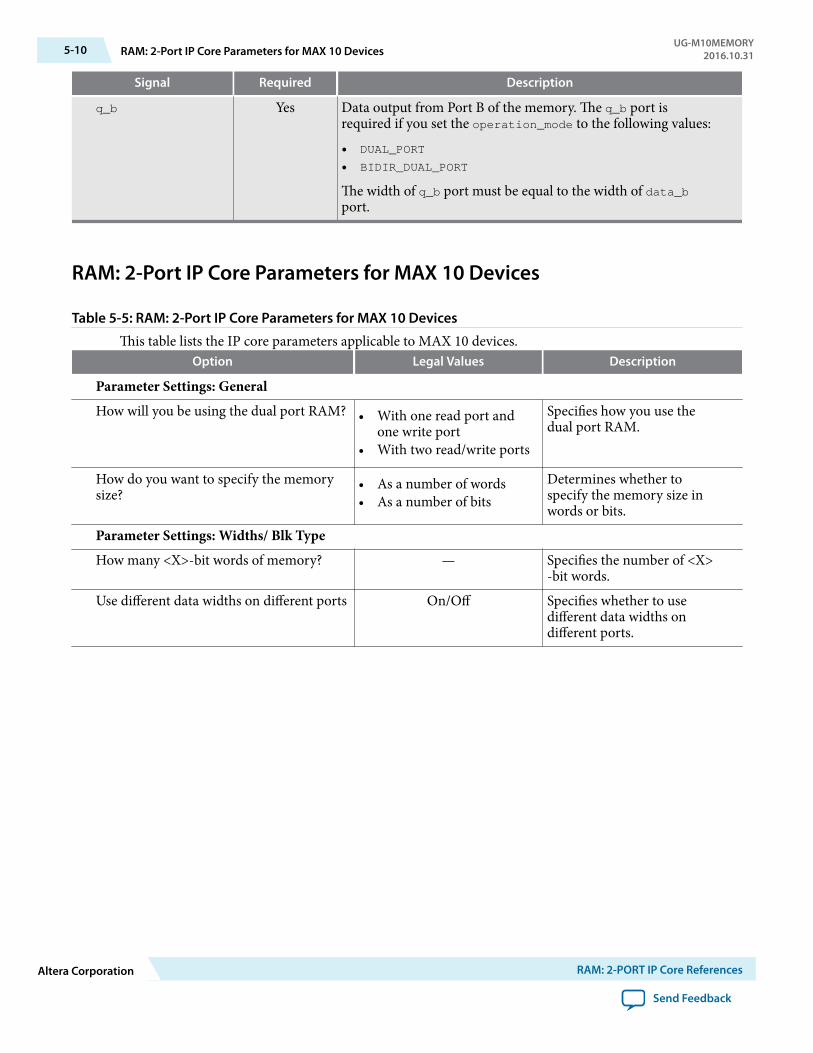
Signal Required Description
q_b Yes Data output from Port B of the memory. The q_b port isrequired if you set the operation_mode to the following values:
• DUAL_PORT
• BIDIR_DUAL_PORT
The width of q_b port must be equal to the width of data_bport.
RAM: 2-Port IP Core Parameters for MAX 10 Devices
Table 5-5: RAM: 2-Port IP Core Parameters for MAX 10 Devices
This table lists the IP core parameters applicable to MAX 10 devices.Option Legal Values Description
Parameter Settings: GeneralHow will you be using the dual port RAM? • With one read port and
one write port• With two read/write ports
Specifies how you use thedual port RAM.
How do you want to specify the memorysize?
• As a number of words• As a number of bits
Determines whether tospecify the memory size inwords or bits.
Parameter Settings: Widths/ Blk TypeHow many <X>-bit words of memory? — Specifies the number of <X>
-bit words.Use different data widths on different ports On/Off Specifies whether to use
different data widths ondifferent ports.
5-10 RAM: 2-Port IP Core Parameters for MAX 10 DevicesUG-M10MEMORY
2016.10.31
Altera Corporation RAM: 2-PORT IP Core References
Send Feedback
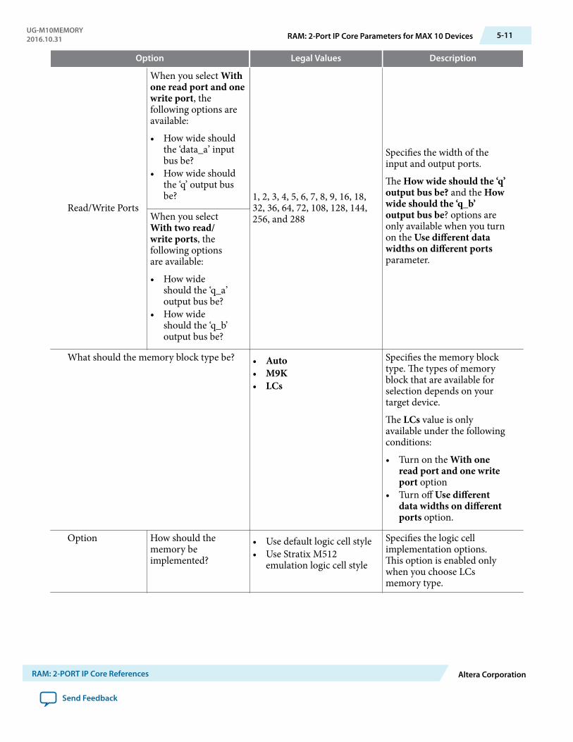
Option Legal Values Description
Read/Write Ports
When you select Withone read port and onewrite port, thefollowing options areavailable:
• How wide shouldthe ‘data_a’ inputbus be?
• How wide shouldthe ‘q’ output busbe? 1, 2, 3, 4, 5, 6, 7, 8, 9, 16, 18,
32, 36, 64, 72, 108, 128, 144,256, and 288
Specifies the width of theinput and output ports.
The How wide should the ‘q’output bus be? and the Howwide should the ‘q_b’output bus be? options areonly available when you turnon the Use different datawidths on different portsparameter.
When you selectWith two read/write ports, thefollowing optionsare available:
• How wideshould the ‘q_a’output bus be?
• How wideshould the ‘q_b’output bus be?
What should the memory block type be? • Auto• M9K• LCs
Specifies the memory blocktype. The types of memoryblock that are available forselection depends on yourtarget device.
The LCs value is onlyavailable under the followingconditions:
• Turn on the With oneread port and one writeport option
• Turn off Use differentdata widths on differentports option.
Option How should thememory beimplemented?
• Use default logic cell style• Use Stratix M512
emulation logic cell style
Specifies the logic cellimplementation options.This option is enabled onlywhen you choose LCsmemory type.
UG-M10MEMORY2016.10.31 RAM: 2-Port IP Core Parameters for MAX 10 Devices 5-11
RAM: 2-PORT IP Core References Altera Corporation
Send Feedback
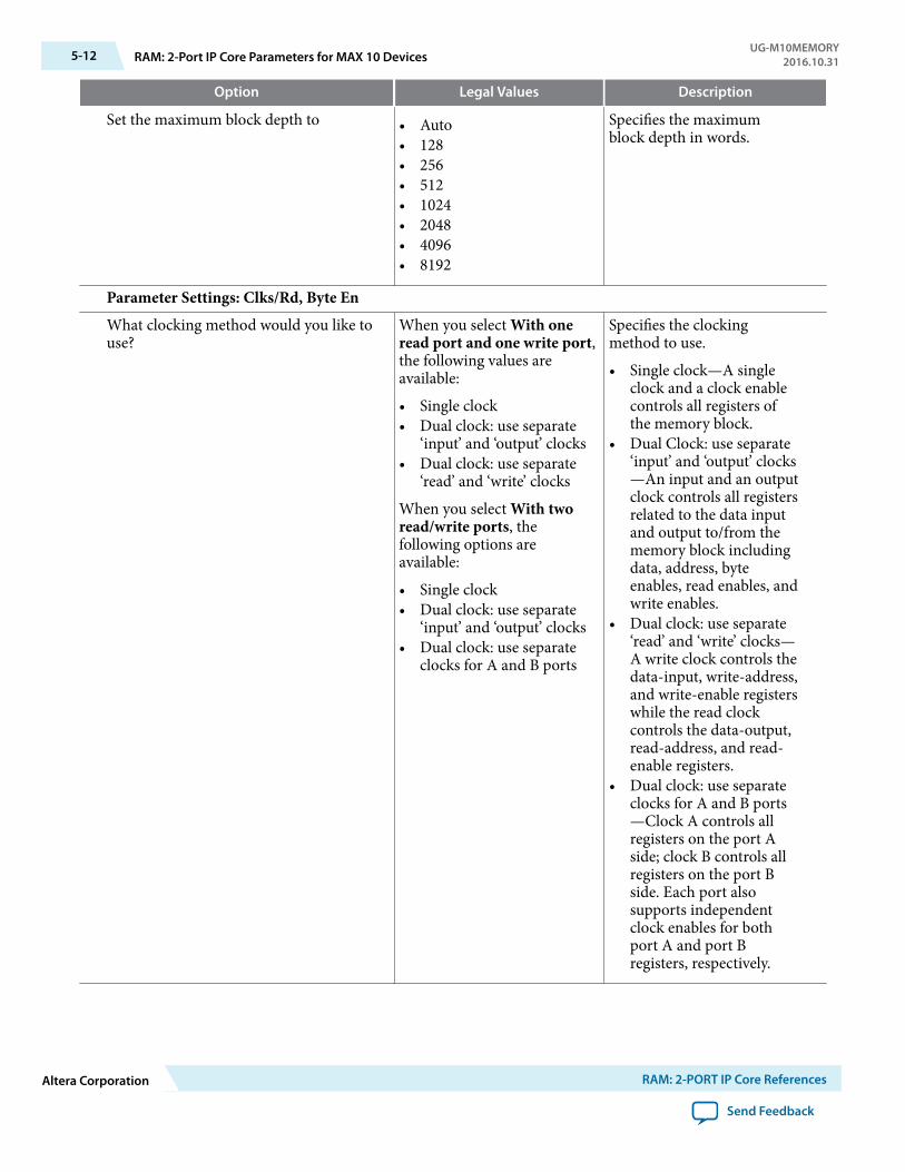
Option Legal Values Description
Set the maximum block depth to • Auto• 128• 256• 512• 1024• 2048• 4096• 8192
Specifies the maximumblock depth in words.
Parameter Settings: Clks/Rd, Byte EnWhat clocking method would you like touse?
When you select With oneread port and one write port,the following values areavailable:
• Single clock• Dual clock: use separate
‘input’ and ‘output’ clocks• Dual clock: use separate
‘read’ and ‘write’ clocks
When you select With tworead/write ports, thefollowing options areavailable:
• Single clock• Dual clock: use separate
‘input’ and ‘output’ clocks• Dual clock: use separate
clocks for A and B ports
Specifies the clockingmethod to use.
• Single clock—A singleclock and a clock enablecontrols all registers ofthe memory block.
• Dual Clock: use separate‘input’ and ‘output’ clocks—An input and an outputclock controls all registersrelated to the data inputand output to/from thememory block includingdata, address, byteenables, read enables, andwrite enables.
• Dual clock: use separate‘read’ and ‘write’ clocks—A write clock controls thedata-input, write-address,and write-enable registerswhile the read clockcontrols the data-output,read-address, and read-enable registers.
• Dual clock: use separateclocks for A and B ports—Clock A controls allregisters on the port Aside; clock B controls allregisters on the port Bside. Each port alsosupports independentclock enables for bothport A and port Bregisters, respectively.
5-12 RAM: 2-Port IP Core Parameters for MAX 10 DevicesUG-M10MEMORY
2016.10.31
Altera Corporation RAM: 2-PORT IP Core References
Send Feedback
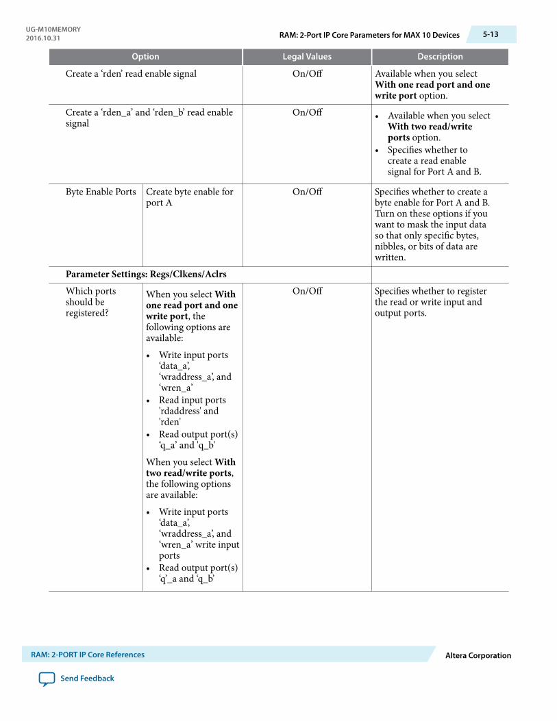
Option Legal Values Description
Create a ‘rden’ read enable signal On/Off Available when you selectWith one read port and onewrite port option.
Create a ‘rden_a’ and ‘rden_b’ read enablesignal
On/Off • Available when you selectWith two read/writeports option.
• Specifies whether tocreate a read enablesignal for Port A and B.
Byte Enable Ports Create byte enable forport A
On/Off Specifies whether to create abyte enable for Port A and B.Turn on these options if youwant to mask the input dataso that only specific bytes,nibbles, or bits of data arewritten.
Parameter Settings: Regs/Clkens/AclrsWhich portsshould beregistered?
When you select Withone read port and onewrite port, thefollowing options areavailable:
• Write input ports‘data_a’,‘wraddress_a’, and‘wren_a’
• Read input ports'rdaddress' and'rden'
• Read output port(s)‘q_a’ and 'q_b'
When you select Withtwo read/write ports,the following optionsare available:
• Write input ports‘data_a’,‘wraddress_a’, and‘wren_a’ write inputports
• Read output port(s)‘q’_a and ‘q_b’
On/Off Specifies whether to registerthe read or write input andoutput ports.
UG-M10MEMORY2016.10.31 RAM: 2-Port IP Core Parameters for MAX 10 Devices 5-13
RAM: 2-PORT IP Core References Altera Corporation
Send Feedback
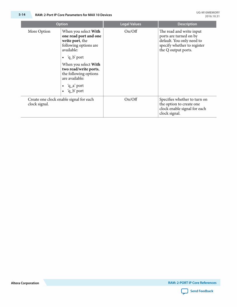
Option Legal Values Description
More Option When you select Withone read port and onewrite port, thefollowing options areavailable:
• ‘q_b’ port
When you select Withtwo read/write ports,the following optionsare available:
• ‘q_a’ port• ‘q_b’ port
On/Off The read and write inputports are turned on bydefault. You only need tospecify whether to registerthe Q output ports.
Create one clock enable signal for eachclock signal.
On/Off Specifies whether to turn onthe option to create oneclock enable signal for eachclock signal.
5-14 RAM: 2-Port IP Core Parameters for MAX 10 DevicesUG-M10MEMORY
2016.10.31
Altera Corporation RAM: 2-PORT IP Core References
Send Feedback
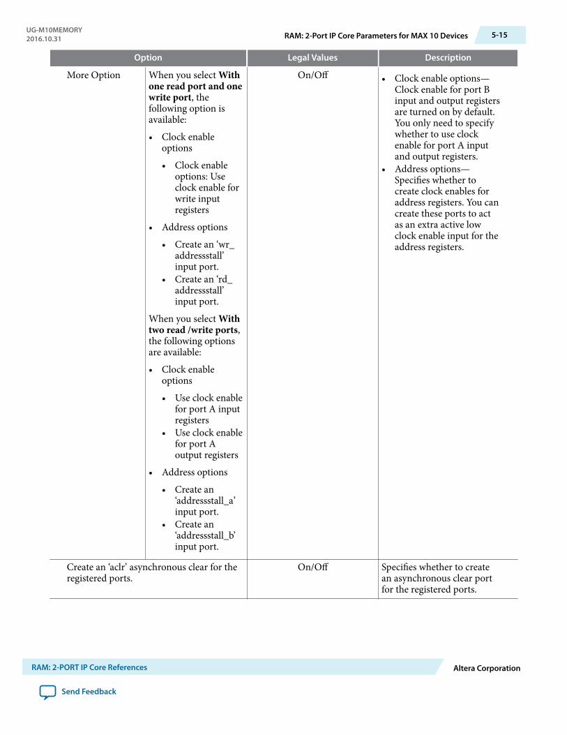
Option Legal Values Description
More Option When you select Withone read port and onewrite port, thefollowing option isavailable:
• Clock enableoptions
• Clock enableoptions: Useclock enable forwrite inputregisters
• Address options
• Create an ‘wr_addressstall’input port.
• Create an ‘rd_addressstall’input port.
When you select Withtwo read /write ports,the following optionsare available:
• Clock enableoptions
• Use clock enablefor port A inputregisters
• Use clock enablefor port Aoutput registers
• Address options
• Create an‘addressstall_a’input port.
• Create an‘addressstall_b’input port.
On/Off • Clock enable options—Clock enable for port Binput and output registersare turned on by default.You only need to specifywhether to use clockenable for port A inputand output registers.
• Address options—Specifies whether tocreate clock enables foraddress registers. You cancreate these ports to actas an extra active lowclock enable input for theaddress registers.
Create an ‘aclr’ asynchronous clear for theregistered ports.
On/Off Specifies whether to createan asynchronous clear portfor the registered ports.
UG-M10MEMORY2016.10.31 RAM: 2-Port IP Core Parameters for MAX 10 Devices 5-15
RAM: 2-PORT IP Core References Altera Corporation
Send Feedback
Option Legal Values Description
More Option When you select Withone read port and onewrite port, thefollowing options areavailable:
• ‘rdaddress’ port• ‘q_b’ port
When you select Withtwo read /write ports,the following optionsare available:
• ‘q_a’ port• ‘q_b’ port
On/Off Specifies whether theraddress, q_a, and q_bports are cleared by the aclrport.
Parameter Settings: Output 1Mixed Port Read-During-Write forSingle Input ClockRAM
When you select Withone read port and onewrite port, thefollowing option isavailable:
• How should the qoutput behavewhen reading amemory locationthat is being writtenfrom the otherport?
When you select Withtwo read /write ports,the following option isavailable:
• How should the q_aand q_b outputsbehave whenreading a memorylocation that isbeing written fromthe other port?
• Old memory contentsappear
• I do not care (the outputswill be undefined)
Specifies the output behaviorwhen read-during-writeoccurs.
• Old memory contentsappear— The RAMoutputs reflect the olddata at that addressbefore the write operationproceeds.
• I do not care—Thisoption functionsdifferently when you turnit on depending on thefollowing memory blocktype you select:
• When you set thememory block type toAuto, or M9K, theRAM outputs ‘don'tcare’ or “unknown”values for read-during-writeoperation withoutanalyzing the timingpath.
5-16 RAM: 2-Port IP Core Parameters for MAX 10 DevicesUG-M10MEMORY
2016.10.31
Altera Corporation RAM: 2-PORT IP Core References
Send Feedback
Option Legal Values Description
Do not analyze the timing between writeand read operation. Metastability issues areprevented by never writing and reading atthe same address at the same time.
On/Off This option is automaticallyturned on when you turn onthe I do not care (Theoutputs will be undefined)option. This option enablesthe RAM to output ‘don’tcare’ or 'unknown' values forread-during-write operationwithout analyzing the timingpath.
Parameter Settings: Output 2 (This tab is only available when you select two read/write ports)Port A Read-During-WriteOption
What should the ‘q_a’output be whenreading from amemory locationbeing written to?
• New data• Old Data
Specifies the output behaviorwhen read-during-writeoccurs.
• New Data—New data isavailable on the risingedge of the same clockcycle on which it waswritten.
• Old Data—The RAMoutputs reflect the olddata at that addressbefore the write operationproceeds.
Port B Read-During-WriteOption
What should the‘q_b’ output bewhen reading froma memory locationbeing written to?
Get x’s for write masked bytes instead ofold data when byte enable is used
On/Off This option is automaticallyturned on when you selectthe New Data value. Thisoption obtains ‘X’ on themasked byte.
Parameter Settings: Mem Init
UG-M10MEMORY2016.10.31 RAM: 2-Port IP Core Parameters for MAX 10 Devices 5-17
RAM: 2-PORT IP Core References Altera Corporation
Send Feedback
Option Legal Values Description
Do you want to specify the initial contentof the memory?
• No, leave it blank• Yes, use this file for the
memory content data
Specifies the initial contentof the memory.
• To initialize the memoryto zero, select No, leave itblank.
• To use a Memory Initiali‐zation File (.mif) or aHexadecimal (Intel-format) File (.hex), selectYes, use this file for thememory content data.
Note: The configurationscheme of yourdevice is InternalConfiguration. Inorder to usememory initiali‐zation, you mustselect a singleimage configura‐tion mode withmemory initiali‐zation, forexample theSingleCompressedImage withMemory Initiali‐zation option. Youcan set theconfigurationmode on theConfigurationpage of theDevice and PinOptions dialogbox.
The initial content file should conform towhich port's dimension?
• PORT_A• PORT_B
Specifies which port'sdimension that the initialcontent file should conformto.
5-18 RAM: 2-Port IP Core Parameters for MAX 10 DevicesUG-M10MEMORY
2016.10.31
Altera Corporation RAM: 2-PORT IP Core References
Send Feedback
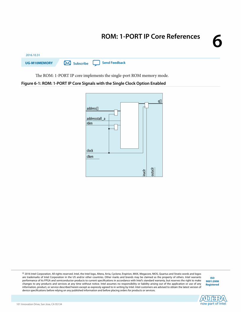
ROM: 1-PORT IP Core References 62016.10.31
UG-M10MEMORY Subscribe Send Feedback
The ROM: 1-PORT IP core implements the single-port ROM memory mode.
Figure 6-1: ROM: 1-PORT IP Core Signals with the Single Clock Option Enabled
addressstall_a
clockclken
q[]
inaclr
address[]
rden
outa
clr
© 2016 Intel Corporation. All rights reserved. Intel, the Intel logo, Altera, Arria, Cyclone, Enpirion, MAX, Megacore, NIOS, Quartus and Stratix words and logosare trademarks of Intel Corporation in the US and/or other countries. Other marks and brands may be claimed as the property of others. Intel warrantsperformance of its FPGA and semiconductor products to current specifications in accordance with Intel's standard warranty, but reserves the right to makechanges to any products and services at any time without notice. Intel assumes no responsibility or liability arising out of the application or use of anyinformation, product, or service described herein except as expressly agreed to in writing by Intel. Intel customers are advised to obtain the latest version ofdevice specifications before relying on any published information and before placing orders for products or services.
ISO9001:2008Registered
www.altera.com101 Innovation Drive, San Jose, CA 95134
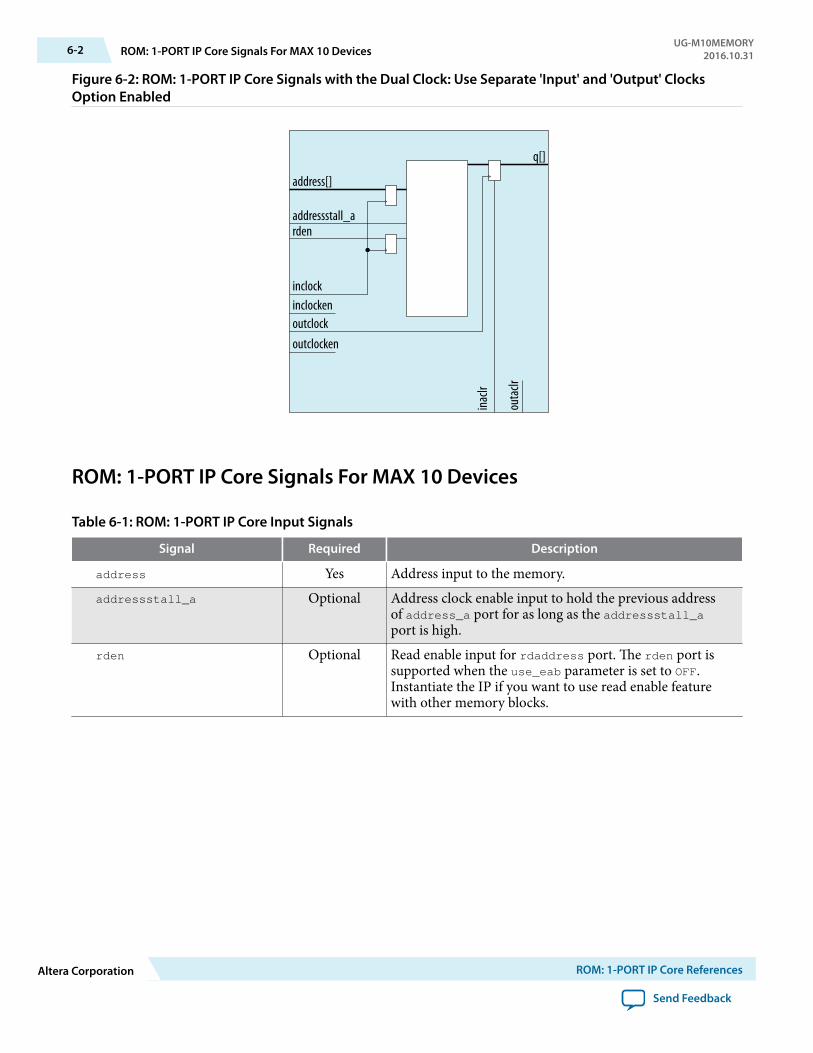
Figure 6-2: ROM: 1-PORT IP Core Signals with the Dual Clock: Use Separate 'Input' and 'Output' ClocksOption Enabled
addressstall_a
outclockoutclocken
q[]
inaclr
address[]
rden
inclockeninclock
outa
clr
ROM: 1-PORT IP Core Signals For MAX 10 Devices
Table 6-1: ROM: 1-PORT IP Core Input Signals
Signal Required Description
address Yes Address input to the memory.addressstall_a Optional Address clock enable input to hold the previous address
of address_a port for as long as the addressstall_aport is high.
rden Optional Read enable input for rdaddress port. The rden port issupported when the use_eab parameter is set to OFF.Instantiate the IP if you want to use read enable featurewith other memory blocks.
6-2 ROM: 1-PORT IP Core Signals For MAX 10 DevicesUG-M10MEMORY
2016.10.31
Altera Corporation ROM: 1-PORT IP Core References
Send Feedback
Signal Required Description
clock Yes The following list describes which of your memoryclock must be connected to the clock port, and portsynchronization in different clock modes:
• Single clock—Connect your single source clock toclock port. All registered ports are synchronized bythe same source clock.
• Read/Write—Connect your write clock to clockport. All registered ports related to write operation,such as data_a port, address_a port, wren_a port,and byteena_a port are synchronized by the writeclock.
• Input/Output—Connect your input clock to clockport. All registered input ports are synchronized bythe input clock.
• Independent clock—Connect your port A clock toclock port. All registered input and output ports ofport A are synchronized by the port A clock.
clken Optional Clock enable input for clock port.inclock Yes The following list describes which of your memory
clock must be connected to the inclock port, and portsynchronization in different clock modes:
• Single clock—Connect your single source clock toinclock port and outclock port. All registeredports are synchronized by the same source clock.
• Read/Write—Connect your write clock to inclockport. All registered ports related to write operation,such as data port, wraddress port, wren port, andbyteena port are synchronized by the write clock.
• Input/Output—Connect your input clock toinclock port. All registered input ports aresynchronized by the input clock.
inclocken Optional Clock enable input for inclock port.outclock Yes The following list describes which of your memory
clock must be connected to the outclock port, andport synchronization in different clock modes:
• Single clock—Connect your single source clock toinclock port and outclock port. All registeredports are synchronized by the same source clock.
• Read/Write—Connect your read clock to outclockport. All registered ports related to read operation,such as rdaddress port, rdren port, and q port aresynchronized by the read clock.
• Input/Output—Connect your output clock tooutclock port. The registered q port is synchronizedby the output clock.
UG-M10MEMORY2016.10.31 ROM: 1-PORT IP Core Signals For MAX 10 Devices 6-3
ROM: 1-PORT IP Core References Altera Corporation
Send Feedback
Signal Required Description
outclocken Optional Clock enable input for outclock port.
Table 6-2: ROM: 1-PORT IP Core Output Signals
Signal Required Description
q Yes Data output from the memory. The q port is required,and must be equal to the width data port.
ROM: 1-PORT IP Core Parameters for MAX 10 Devices
Table 6-3: ROM: 1-Port IP Core Parameters for MAX 10 Devices
This table lists the IP core parameters applicable to MAX 10 devices.Option Legal Values Description
Parameter Settings: GeneralHow wide should the 'q' output bus be? 1, 2, 3, 4, 5, 6, 7, 8, 9, 10, 11,
12, 13, 14, 15, 16, 17, 18, 19,20, 21, 22, 23, 24, 25, 26, 27,28, 29, 30, 31, 32, 36, 40, 48,64, 72, 108, 128, 144, and 256.
Specifies the width of the 'q'output bus in bits.
How many <X>-bit words of memory? 32, 64, 128, 256, 512, 1024,2048, 4096, 8192, 16384,32768, and 65536.
Specifies the number of <X>-bit words.
What should the memory block type be? • Auto• M9K
Specifies the memory blocktype. The types of memoryblock that are available forselection depends on yourtarget device.
Set the maximum block depth to • Auto• 32• 64• 128• 256• 512• 1024• 2048• 4096• 8192
Specifies the maximumblock depth in words.
6-4 ROM: 1-PORT IP Core Parameters for MAX 10 DevicesUG-M10MEMORY
2016.10.31
Altera Corporation ROM: 1-PORT IP Core References
Send Feedback
Option Legal Values Description
What clocking method would you like touse?
• Single clock• Dual clock: use separate
‘input’ and ‘output’ clocks
Specifies the clockingmethod to use.
• Single clock—A singleclock and a clock enablecontrols all registers ofthe memory block.
• Dual clock: use separate‘input’ and ‘output’ clocks—An input and an outputclock controls all registersrelated to the data inputand output to/from thememory block includingdata, address, byteenables, read enables, andwrite enables.
Parameter Settings: Regs/Clkens/AclrsWhich portsshould beregistered?
• 'address' input port• 'q' output port
On/Off Specifies whether to registerthe read or write input andoutput ports.
Create one clock enable signal for eachclock signal.
On/Off Specifies whether to turn onthe option to create oneclock enable signal for eachclock signal.
More Options • Clock enable options
• Use clock enable forport A inputregisters
• Use clock enable forport A outputregisters
• Address options
• Create an 'address‐stall_a' input port
On/Off • Clock enable options—Clock enable for port Binput and output registersare turned on by default.You only need to specifywhether to use clockenable for port A inputand output registers.
• Address options—Specifies whether tocreate clock enables foraddress registers. You cancreate these ports to actas an extra active lowclock enable input for theaddress registers.
Create an ‘aclr’ asynchronous clear for theregistered ports.
On/Off Specifies whether to createan asynchronous clear portfor the registered ports.
More Options • 'address' port• 'q' port
On/Off Specifies whether theaddress and q ports arecleared by the aclr port.
UG-M10MEMORY2016.10.31 ROM: 1-PORT IP Core Parameters for MAX 10 Devices 6-5
ROM: 1-PORT IP Core References Altera Corporation
Send Feedback
Option Legal Values Description
Create a 'rden' read enable signal On/Off Specifies whether to create arden read enable signal.
Parameter Settings: Mem InitDo you want to specify the initial contentof the memory?
Yes, use this file for thememory content data.
Specifies the initial contentof the memory. In ROMmode you must specify aMemory Initialization File(.mif) or a Hexadecimal(Intel-format) File (.hex).The configuration scheme ofyour device is InternalConfiguration. In order touse memory initialization,you must select a singleimage configuration modewith memory initialization,for example the SingleCompressed Image withMemory Initializationoption. You can set theconfiguration mode on theConfiguration page of theDevice and Pin Optionsdialog box.
Allow In-System Memory Content Editorto capture and update content independ‐ently of the system clock
On/Off Specifies whether to allowIn-System Memory ContentEditor to capture and updatecontent independently of thesystem clock.
The 'Instance ID' of this RAM is — Specifies the RAM ID.
6-6 ROM: 1-PORT IP Core Parameters for MAX 10 DevicesUG-M10MEMORY
2016.10.31
Altera Corporation ROM: 1-PORT IP Core References
Send Feedback
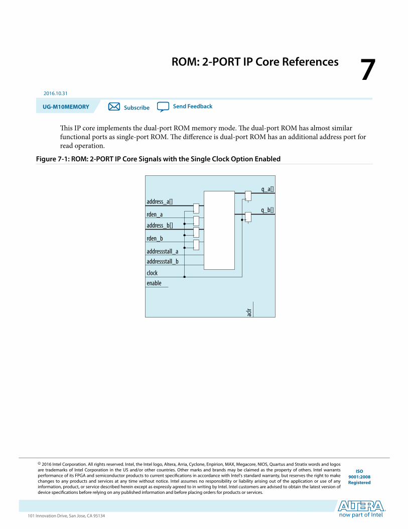
ROM: 2-PORT IP Core References 72016.10.31
UG-M10MEMORY Subscribe Send Feedback
This IP core implements the dual-port ROM memory mode. The dual-port ROM has almost similarfunctional ports as single-port ROM. The difference is dual-port ROM has an additional address port forread operation.
Figure 7-1: ROM: 2-PORT IP Core Signals with the Single Clock Option Enabled
address_b[]
addressstall_a
clockenable
q_a[]
aclr
address_a[]
addressstall_b
rden_a
rden_b
q_b[]
© 2016 Intel Corporation. All rights reserved. Intel, the Intel logo, Altera, Arria, Cyclone, Enpirion, MAX, Megacore, NIOS, Quartus and Stratix words and logosare trademarks of Intel Corporation in the US and/or other countries. Other marks and brands may be claimed as the property of others. Intel warrantsperformance of its FPGA and semiconductor products to current specifications in accordance with Intel's standard warranty, but reserves the right to makechanges to any products and services at any time without notice. Intel assumes no responsibility or liability arising out of the application or use of anyinformation, product, or service described herein except as expressly agreed to in writing by Intel. Intel customers are advised to obtain the latest version ofdevice specifications before relying on any published information and before placing orders for products or services.
ISO9001:2008Registered
www.altera.com101 Innovation Drive, San Jose, CA 95134
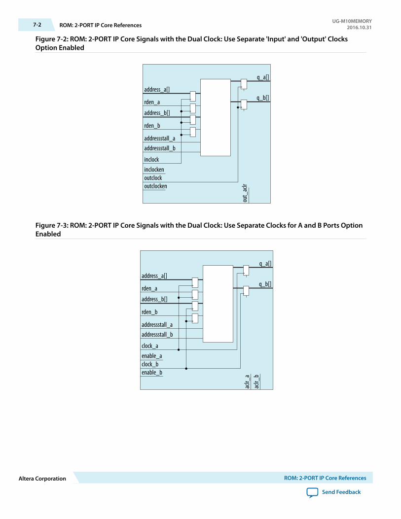
Figure 7-2: ROM: 2-PORT IP Core Signals with the Dual Clock: Use Separate 'Input' and 'Output' ClocksOption Enabled
address_b[]
addressstall_a
inclockinclockenoutclockoutclocken
q_a[]
out_
aclr
address_a[]
addressstall_b
rden_a
rden_b
q_b[]
Figure 7-3: ROM: 2-PORT IP Core Signals with the Dual Clock: Use Separate Clocks for A and B Ports OptionEnabled
address_b[]
addressstall_a
clock_aenable_aclock_benable_b
q_a[]
aclr_
a
address_a[]
addressstall_b
rden_a
rden_b
aclr_
b
q_b[]
7-2 ROM: 2-PORT IP Core ReferencesUG-M10MEMORY
2016.10.31
Altera Corporation ROM: 2-PORT IP Core References
Send Feedback
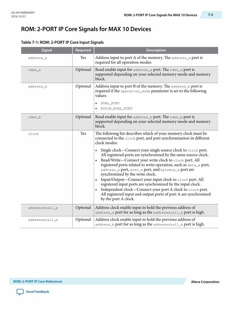
ROM: 2-PORT IP Core Signals for MAX 10 Devices
Table 7-1: ROM: 2-PORT IP Core Input Signals
Signal Required Description
address_a Yes Address input to port A of the memory. The address_a port isrequired for all operation modes.
rden_a Optional Read enable input for address_a port. The rden_a port issupported depending on your selected memory mode and memoryblock.
address_b Optional Address input to port B of the memory. The address_b port isrequired if the operation_mode parameter is set to the followingvalues:
• DUAL_PORT
• BIDIR_DUAL_PORT
rden_b Optional Read enable input for address_b port. The rden_b port issupported depending on your selected memory mode and memoryblock.
clock Yes The following list describes which of your memory clock must beconnected to the clock port, and port synchronization in differentclock modes:
• Single clock—Connect your single source clock to clock port.All registered ports are synchronized by the same source clock.
• Read/Write—Connect your write clock to clock port. Allregistered ports related to write operation, such as data_a port,address_a port, wren_a port, and byteena_a port aresynchronized by the write clock.
• Input/Output—Connect your input clock to clock port. Allregistered input ports are synchronized by the input clock.
• Independent clock—Connect your port A clock to clock port.All registered input and output ports of port A are synchronizedby the port A clock.
addressstall_a Optional Address clock enable input to hold the previous address ofaddress_a port for as long as the addressstall_a port is high.
addressstall_b Optional Address clock enable input to hold the previous address ofaddress_b port for as long as the addressstall_b port is high.
UG-M10MEMORY2016.10.31 ROM: 2-PORT IP Core Signals for MAX 10 Devices 7-3
ROM: 2-PORT IP Core References Altera Corporation
Send Feedback
Signal Required Description
inclock Yes The following list describes which of your memory clock must beconnected to the inclock port, and port synchronization indifferent clock modes:
• Single clock—Connect your single source clock to inclock portand outclock port. All registered ports are synchronized by thesame source clock.
• Read/Write—Connect your write clock to inclock port. Thewrite clock synchronizes all registered ports related to writeoperation, such as data port, wraddress port, wren port, andbyteena port.
• Input/Output—Connect your input clock to inclock port. Theinput clock synchronizes all registered input ports.
outclock Yes The following list describes which of your memory clock must beconnected to the outclock port, and port synchronization indifferent clock modes:
• Single clock—Connect your single source clock to inclock portand outclock port. All registered ports are synchronized by thesame source clock.
• Read/Write—Connect your read clock to outclock port. Theread clock synchronizes all registered ports related to readoperation, such as rdaddress port, rdren port, and q port.
• Input/Output—Connect your output clock to outclock port.The output clock synchronizes the registered q port.
inclocken Optional Clock enable input for inclock port.outclocken Optional Clock enable input for outclock port.aclr Optional Asynchronously clear the registered input and output ports. The
asynchronous clear effect on the registered ports can be controlledthrough their corresponding asynchronous clear parameter, suchas indata_aclr and wraddress_aclr.
Table 7-2: ROM: 2-PORT IP Core Output Signals
Signal Required Description
q_a Yes Data output from port A of the memory. The q_a port is required ifyou set the operation_mode parameter to any of the followingvalues:
• SINGLE_PORT
• BIDIR_DUAL_PORT
• ROM
The width of the q_a port must be equal to the width of the data_aport.
7-4 ROM: 2-PORT IP Core Signals for MAX 10 DevicesUG-M10MEMORY
2016.10.31
Altera Corporation ROM: 2-PORT IP Core References
Send Feedback
Signal Required Description
q_b Yes Data output from port B of the memory. The q_b port is required ifyou set the operation_mode parameter to the following values:
• DUAL_PORT
• BIDIR_DUAL_PORT
The width of q_b port must be equal to the width of data_b port.
ROM:2-Port IP Core Parameters For MAX 10 Devices
Table 7-3: ROM:2-Port IP Core Parameters for MAX 10 Devices
This table lists the IP core parameters applicable to MAX 10 devices.Option Legal Values Description
Parameter Settings: Widths/Blk TypeHow do you want to specify the memorysize?
• As a number ofwords
• As a number of bits
Determines whether to specify thememory size in words or bits.
How many <X>-bit words of memory? — Specifies the number of <X>-bitwords.
Use different data widths on different ports On/Off Specifies whether to use differentdata widths on different ports.
Read Ports
How wide should the‘q_a’ output bus be?
1, 2, 3, 4, 5, 6, 7, 8, 9,16, 18, 32, 36, 64, 72,108, 128, 144, 256, and288
Specifies the width of the input andoutput ports.
The How wide should the ‘q_b’output bus be? option is onlyavailable when you turn on the Usedifferent data widths on differentports parameter.
How wide shouldthe ‘q_b’ output busbe?
What should the memory block type be? Auto, M9K Specifies the memory block type.The types of memory block that areavailable for selection depends onyour target device.
Set the maximum block depth to Auto, 128, 256, 512,1024, 2048, 4096, 8192
Specifies the maximum block depthin words.
Parameter Settings: Clks/Rd, Byte En
UG-M10MEMORY2016.10.31 ROM:2-Port IP Core Parameters For MAX 10 Devices 7-5
ROM: 2-PORT IP Core References Altera Corporation
Send Feedback
Option Legal Values Description
What clocking method would you like touse?
• Single clock• Dual clock: use
separate ‘input’ and‘output’ clocks
• Dual clock: useseparate clocks forA and B ports
Specifies the clocking method to use.
• Single clock—A single clock anda clock enable controls allregisters of the memory block.
• Dual Clock: use separate ‘input’and ‘output’ clocks—An inputand an output clock controls allregisters related to the data inputand output to/from the memoryblock including data, address,byte enables, read enables, andwrite enables.
• Dual clock: use separate clocksfor A and B ports—Clock Acontrols all registers on the portA side; clock B controls allregisters on the port B side. Eachport also supports independentclock enables for both port A andport B registers, respectively.
Create a ‘rden_a’ and 'rden_b' read enablesignal
On/Off Specifies whether to create readenable signals.
Parameter Settings: Regs/Clkens/AclrsWhich portsshould beregistered?
• Write input ports• Read output port(s)
On/Off Specifies whether to register the reador write input and output ports.
More Options • Input ports
• 'address_a' port• 'address_b' port
• Q output ports
• ‘q_a’ port• 'q_b' port
On/Off The read and write input ports areturned on by default. You only needto specify whether to register the Qoutput ports.
Create one clock enable signal for eachclock signal.
On/Off Specifies whether to turn on theoption to create one clock enablesignal for each clock signal.
7-6 ROM:2-Port IP Core Parameters For MAX 10 DevicesUG-M10MEMORY
2016.10.31
Altera Corporation ROM: 2-PORT IP Core References
Send Feedback
Option Legal Values Description
More Options • Clock enable options
• Use clock enablefor port A inputregisters
• Use clock enablefor port A outputregisters
• Address options
• Create an‘addressstall_a’input port.
• Create an‘addressstall_b’input port.
•
On/Off • Clock enable options—Clockenable for port B input andoutput registers are turned on bydefault. You only need to specifywhether to use clock enable forport A input and output registers.
• Address options—Specifieswhether to create clock enablesfor address registers. You cancreate these ports to act as anextra active low clock enableinput for the address registers.
Create an ‘aclr’ asynchronous clear for theregistered ports.
On/Off Specifies whether to create anasynchronous clear port for theregistered ports.
More Options • ‘q_a’ port• ‘q_b’ port
On/Off Specifies whether the ‘q_a’, and ‘q_b’ports are cleared by the aclr port.
Parameter Settings: Mem Init
UG-M10MEMORY2016.10.31 ROM:2-Port IP Core Parameters For MAX 10 Devices 7-7
ROM: 2-PORT IP Core References Altera Corporation
Send Feedback
Option Legal Values Description
Do you want to specify the initial contentof the memory?
Yes, use this file for thememory content data
Specifies the initial content of thememory.
• To initialize the memory to zero,select No, leave it blank.
• To use a Memory InitializationFile (.mif) or a Hexadecimal(Intel-format) File (.hex), selectYes, use this file for the memorycontent data.
Note: The configuration schemeof your device is InternalConfiguration. In orderto use memory initializa‐tion, you must select asingle image configura‐tion mode with memoryinitialization, for examplethe Single CompressedImage with MemoryInitialization option. Youcan set the configurationmode on the Configura‐tion page of the Deviceand Pin Options dialogbox.
The initial content file should conform towhich port's dimension?
• PORT_A• PORT_B
Specifies which port's dimensionthat the initial content file shouldconform to.
7-8 ROM:2-Port IP Core Parameters For MAX 10 DevicesUG-M10MEMORY
2016.10.31
Altera Corporation ROM: 2-PORT IP Core References
Send Feedback
Shift Register (RAM-based) IP Core References 82016.10.31
UG-M10MEMORY Subscribe Send Feedback
The Shift Register (RAM-based) IP core contains additional features not found in a conventional shiftregister. You can use the memory blocks as a shift-register block to save logic cells and routing resources.You can cascade memory blocks to implement larger shift registers.
Figure 8-1: Shift Register (RAM-based) IP Core Signals
shift_in[]clockclkenaclr
shiftout[]taps[]
Shift Register (RAM-based) IP Core Signals for MAX 10 Devices
Table 8-1: Shift Register (RAM-based) IP Core Input Signals
Signal Required Description
shiftin[] Yes Data input to the shifter. Input port WIDTH bits wide.clock Yes Positive-edge triggered clock.clken No Clock enable for the clock port. clken defaults to VCC.aclr No Asynchronously clears the contents of the shift register chain. The shiftout
outputs are cleared immediately upon the assertion of the aclr signal.
Table 8-2: Shift Register (RAM-based) IP Core Output Signals
Signal Required Description
shiftout[] Yes Output from the end of the shift register. Output port WIDTH bits wide.
© 2016 Intel Corporation. All rights reserved. Intel, the Intel logo, Altera, Arria, Cyclone, Enpirion, MAX, Megacore, NIOS, Quartus and Stratix words and logosare trademarks of Intel Corporation in the US and/or other countries. Other marks and brands may be claimed as the property of others. Intel warrantsperformance of its FPGA and semiconductor products to current specifications in accordance with Intel's standard warranty, but reserves the right to makechanges to any products and services at any time without notice. Intel assumes no responsibility or liability arising out of the application or use of anyinformation, product, or service described herein except as expressly agreed to in writing by Intel. Intel customers are advised to obtain the latest version ofdevice specifications before relying on any published information and before placing orders for products or services.
ISO9001:2008Registered
www.altera.com101 Innovation Drive, San Jose, CA 95134
Signal Required Description
taps[] Yes Output from the regularly spaced taps along the shift register. Output portWIDTH * NUMBER_OF_TAPS wide. This port is an aggregate of all theregularly spaced taps (each WIDTH bits) along the shift register.
Shift Register (RAM-based) IP Core Parameters for MAX 10 Devices
Table 8-3: Shift Register (RAM-based) IP Core Parameters for MAX 10 Devices
This table lists the IP core parameters applicable to MAX 10 devices.Option Values Description
How wide should the "shiftin" input andthe "shiftout" output buses be?
1, 2, 3, 4, 5, 6, 7, 8, 12, 16, 24,32, 48, 64, 96, 128, 192, and
256.
Specifies the width of theinput pattern.
How many taps would you like? 1, 2, 3, 4, 5, 6, 7, 8, 12, 16, 24,32, 48, 64, 96, and 128.
Specifies the number ofregularly spaced taps alongthe shift register.
Create groups for each tap output On/Off Creates groups for each tapoutput.
How wide should the distance betweentaps be?
3, 4, 5, 6, 7, 8, 16, 32, 64, and128
Specifies the distancebetween the regularly spacedtaps in clock cycles. Thisnumber translates to thenumber of RAM words thatwill be used. The value mustbe at least 3.
Create a clock enable port On/Off Creates the clken portCreate an asynchronous clear port On/Off Creates the aclr port.What should the RAM block type be? Auto, M9K Specifies the RAM block
type.
8-2 Shift Register (RAM-based) IP Core Parameters for MAX 10 DevicesUG-M10MEMORY
2016.10.31
Altera Corporation Shift Register (RAM-based) IP Core References
Send Feedback
FIFO IP Core References 92016.10.31
UG-M10MEMORY Subscribe Send Feedback
The FIFO IP core implements the FIFO mode, enabling you to use the memory blocks as FIFO buffers.
• Use the FIFO IP core in single clock FIFO (SCFIFO) and dual clock FIFO (DCFIFO) modes toimplement single- and dual-clock FIFO buffers in your design.
• Dual clock FIFO buffers are useful when transferring data from one clock domain to another clockdomain.
• The M9K memory blocks do not support simultaneous read and write from an empty FIFO buffer.
Figure 9-1: FIFO IP Core: SCFIFO Mode Signals
data[]wrreqrdreq
q[]full
almost_fullclock empty
almost_empty
usedw[]
sclraclr
© 2016 Intel Corporation. All rights reserved. Intel, the Intel logo, Altera, Arria, Cyclone, Enpirion, MAX, Megacore, NIOS, Quartus and Stratix words and logosare trademarks of Intel Corporation in the US and/or other countries. Other marks and brands may be claimed as the property of others. Intel warrantsperformance of its FPGA and semiconductor products to current specifications in accordance with Intel's standard warranty, but reserves the right to makechanges to any products and services at any time without notice. Intel assumes no responsibility or liability arising out of the application or use of anyinformation, product, or service described herein except as expressly agreed to in writing by Intel. Intel customers are advised to obtain the latest version ofdevice specifications before relying on any published information and before placing orders for products or services.
ISO9001:2008Registered
www.altera.com101 Innovation Drive, San Jose, CA 95134
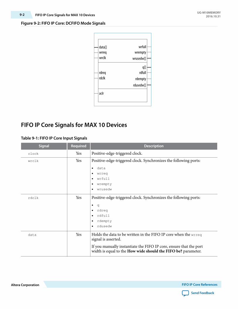
Figure 9-2: FIFO IP Core: DCFIFO Mode Signals
data[]wrreqwrclk
wrfullwrempty
wrusedw[]
rdreqrdclk
q[]rdfull
rdempty
rdusedw[]
aclr
FIFO IP Core Signals for MAX 10 Devices
Table 9-1: FIFO IP Core Input Signals
Signal Required Description
clock Yes Positive-edge-triggered clock.wrclk Yes Positive-edge-triggered clock. Synchronizes the following ports:
• data
• wrreq
• wrfull
• wrempty
• wrusedw
rdclk Yes Positive-edge-triggered clock. Synchronizes the following ports:
• q
• rdreq
• rdfull
• rdempty
• rdusedw
data Yes Holds the data to be written in the FIFO IP core when the wrreqsignal is asserted.
If you manually instantiate the FIFO IP core, ensure that the portwidth is equal to the How wide should the FIFO be? parameter.
9-2 FIFO IP Core Signals for MAX 10 DevicesUG-M10MEMORY
2016.10.31
Altera Corporation FIFO IP Core References
Send Feedback
Signal Required Description
wrreq Yes Assert this signal to request for a write operation.
Ensure that the following conditions are met:
• Do not assert the wrreq signal when the full (for the FIFO IPcore in SCFIFO mode) or wrfull (for the FIFO IP core inDCFIFO mode) port is high. Enable the overflow protectioncircuitry or turn on the Disable overflow checking. Writing to afull FIFO will corrupt contents parameter so that the FIFO IPcore can automatically disable the wrreq signal when it is full.
• The wrreq signal must meet the functional timing requirementbased on the full or wrfull signal.
• Do not assert the wrreq signal during the deassertion of the aclrsignal. Violating this requirement creates a race conditionbetween the falling edge of the aclr signal and the rising edge ofthe write clock if the wrreq port is set to high.
rdreq Yes Assert this signal to request for a read operation. The rdreq signalacts differently in normal synchronous FIFO mode and show-aheadmode synchronous FIFO modes.
Ensure that the following conditions are met:
• Do not assert the rdreq signal when the empty (for the FIFO IPcore in SCFIFO mode) or rdempty (for the FIFO IP core inDCFIFO mode) port is high. Enable the underflow protectioncircuitry or turn on the Disable underflow checking. Readingfrom an empty FIFO will corrupt contents parameter so that theFIFO IP core can automatically disable the rdreq signal when it isempty.
The rdreq signal must meet the functional timing requirement basedon the empty or rdempty signal.
sclr No Assert this signal to clear all the output status ports, but the effect onthe q output may vary for different FIFO configurations. There are nominimum number of clock cycles for aclr signals that must remainactive.
aclr No
Table 9-2: FIFO IP Core Output Signals
Signal Required Description
q Shows the data read from the read request operation. In SCFIFO andDCFIFO modes, the width of the q port must be equal to the width ofthe data port. If you manually instantiate the IPs, ensure that theport width is equal to the How wide should the FIFO be? parameter.In DCFIFO_MIXED_WIDTHS mode, the width of the q port can bedifferent from the width of the data port. If you manually instantiatethe IP, ensure that the width of the q port is equal to the Use adifferent output width parameter. The IP supports a wide write portwith a narrow read port, and vice versa. However, the width ratio isrestricted by the type of RAM block, and in general, are in the powerof 2.
UG-M10MEMORY2016.10.31 FIFO IP Core Signals for MAX 10 Devices 9-3
FIFO IP Core References Altera Corporation
Send Feedback
Signal Required Description
full
No
When asserted, the FIFO IP core is considered full. Do not performwrite request operation when the FIFO IP core is full. In general, the signal is a delayed version of the wrfull signal. However, the rdfullsignal functions as a combinational output instead of a derivedversion of the wrfull signal. Therefore, you must always refer to thewrfull port to ensure whether or not a valid write request operationcan be performed, regardless of the target device.
wrfull
rdfull
empty
No
When asserted, the FIFO IP core is considered empty. Do notperform read request operation when the FIFO IP core is empty. Ingeneral, the wrempty signal is a delayed version of the rdempty signal.However, the wrempty signal functions as a combinational outputinstead of a derived version of the rdempty signal. Therefore, youmust always refer to the rdempty port to ensure whether or not avalid read request operation can be performed, regardless of thetarget device.
wrempty
rdempty
almost_full No Asserted when the usedw signal is greater than or equal to theAlmost full parameter. It is used as an early indication of the fullsignal.
almost_empty No Asserted when the usedw signal is less than the Almost emptyparameter. It is used as an early indication of the empty signal.
usedw
No
Show the number of words stored in the FIFO. Ensure that the portwidth is equal to the usedw[] parameter if you manually instantiatethe FIFO IP core in SCFIFO or DCFIFO modes. In DCFIFO_MIXED_WIDTH mode, the width of the wrusedw and rdusedw portsmust be equal to the usedw[] and Use a different output widthparameters respectively.
wrusedw
rdusedw
FIFO IP Core Parameters for MAX 10 Devices
Table 9-3: FIFO IP Core Parameters for MAX 10 Devices
This table lists the IP core parameters applicable to MAX 10 devices.Parameter HDL Parameter Description
How wide should theFIFO be?
lpm_width Specifies the width of the data and q ports for the FIFO IPcore in SCFIFO mode and DCFIFO mode. For the FIFO IPcore in DCFIFO_MIXED_WIDTHS mode, this parameterspecifies only the width of the data port.
Use a different outputwidth(1)
lpm_width_r Specifies the width of the q port for the FIFO IP core inDCFIFO_MIXED_WIDTHS mode.
(1) Applicable in DCFIFO_MIXED_WIDTHS mode only.
9-4 FIFO IP Core Parameters for MAX 10 DevicesUG-M10MEMORY
2016.10.31
Altera Corporation FIFO IP Core References
Send Feedback
Parameter HDL Parameter Description
Usedw[] lpm_widthu Specifies the width of the usedw port for the FIFO IP corein SCFIFO mode, or the width of the rdusedw andwrusedw ports for the FIFO IP core in DCFIFO mode. Forthe FIFO IP core in DCFIFO_MIXED_WIDTHS mode, itonly represents the width of the wrusedw port.
How deep should theFIFO be?
lpm_numwords Specifies the depths of the FIFO you require. The valuemust be at least 4. The value assigned must comply with the2LPM_WIDTHU equation.
Which kind of readaccess do you want withthe rdreq signal?
lpm_showahead Specifies whether the FIFO is in normal synchronous FIFOmode or show-ahead mode synchronous FIFO mode.Fornormal synchronous FIFO mode, the FIFO IP coretreats the rdreq port as a normal read request that onlyperforms read operation when the port is asserted. Forshow-ahead mode synchronous FIFO mode, the FIFO IPcore treats the rdreq port as a read-acknowledge thatautomatically outputs the first word of valid data in theFIFO IP core (when the empty or rdempty port is low)without asserting the rdreq signal. Asserting the rdreqsignal causes the FIFO IP core to output the next dataword, if available. If you turn on this parameter, you mayreduce performance.
Do you want a commonclock for reading andwriting the FIFO?
lpm_type Identifies the library of parameterized modules (LPM)entity name. The values are SCFIFO and DCFIFO.
Disable overflowchecking. Writing to afull FIFO will corruptcontents
overflow_
checking
Specifies whether or not to enable the protection circuitryfor overflow checking that disables the wrreq port whenthe FIFO IP core is full. This parameter is enabled bydefault.
Disable underflowchecking. Reading froman empty FIFO willcorrupt contents.
underflow_
checking
Specifies whether or not to enable the protection circuitryfor underflow checking that disables the rdreq port whenthe FIFO IP core is empty. This parameter is enabled bydefault. Note that reading from an empty SCFIFO modegives unpredictable results.
Add an extra MSB tousedw (2)
add_usedw_msb_
bit
Increases the width of the rdusedw and wrusedw ports byone bit. By increasing the width, it prevents the FIFO IPcore from rolling over to zero when it is full. Thisparameter is disabled by default.
(2) Applicable in DCFIFO mode only.
UG-M10MEMORY2016.10.31 FIFO IP Core Parameters for MAX 10 Devices 9-5
FIFO IP Core References Altera Corporation
Send Feedback
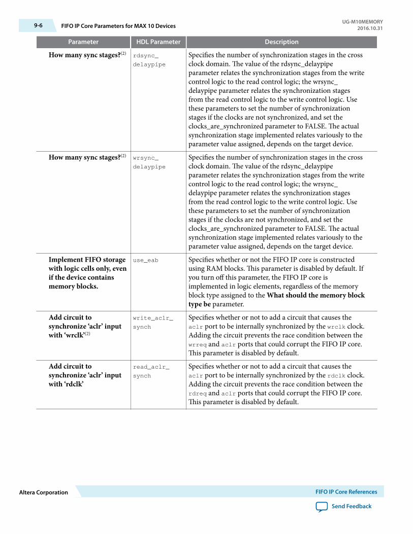
Parameter HDL Parameter Description
How many sync stages?(2) rdsync_
delaypipe
Specifies the number of synchronization stages in the crossclock domain. The value of the rdsync_delaypipeparameter relates the synchronization stages from the writecontrol logic to the read control logic; the wrsync_delaypipe parameter relates the synchronization stagesfrom the read control logic to the write control logic. Usethese parameters to set the number of synchronizationstages if the clocks are not synchronized, and set theclocks_are_synchronized parameter to FALSE. The actualsynchronization stage implemented relates variously to theparameter value assigned, depends on the target device.
How many sync stages?(2) wrsync_
delaypipe
Specifies the number of synchronization stages in the crossclock domain. The value of the rdsync_delaypipeparameter relates the synchronization stages from the writecontrol logic to the read control logic; the wrsync_delaypipe parameter relates the synchronization stagesfrom the read control logic to the write control logic. Usethese parameters to set the number of synchronizationstages if the clocks are not synchronized, and set theclocks_are_synchronized parameter to FALSE. The actualsynchronization stage implemented relates variously to theparameter value assigned, depends on the target device.
Implement FIFO storagewith logic cells only, evenif the device containsmemory blocks.
use_eab Specifies whether or not the FIFO IP core is constructedusing RAM blocks. This parameter is disabled by default. Ifyou turn off this parameter, the FIFO IP core isimplemented in logic elements, regardless of the memoryblock type assigned to the What should the memory blocktype be parameter.
Add circuit tosynchronize ‘aclr’ inputwith ‘wrclk’(2)
write_aclr_
synch
Specifies whether or not to add a circuit that causes theaclr port to be internally synchronized by the wrclk clock.Adding the circuit prevents the race condition between thewrreq and aclr ports that could corrupt the FIFO IP core.This parameter is disabled by default.
Add circuit tosynchronize ‘aclr’ inputwith ‘rdclk’
read_aclr_
synch
Specifies whether or not to add a circuit that causes theaclr port to be internally synchronized by the rdclk clock.Adding the circuit prevents the race condition between therdreq and aclr ports that could corrupt the FIFO IP core.This parameter is disabled by default.
9-6 FIFO IP Core Parameters for MAX 10 DevicesUG-M10MEMORY
2016.10.31
Altera Corporation FIFO IP Core References
Send Feedback
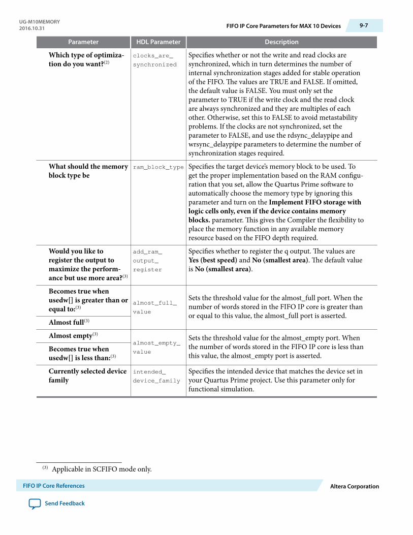
Parameter HDL Parameter Description
Which type of optimiza‐tion do you want?(2)
clocks_are_
synchronized
Specifies whether or not the write and read clocks aresynchronized, which in turn determines the number ofinternal synchronization stages added for stable operationof the FIFO. The values are TRUE and FALSE. If omitted,the default value is FALSE. You must only set theparameter to TRUE if the write clock and the read clockare always synchronized and they are multiples of eachother. Otherwise, set this to FALSE to avoid metastabilityproblems. If the clocks are not synchronized, set theparameter to FALSE, and use the rdsync_delaypipe andwrsync_delaypipe parameters to determine the number ofsynchronization stages required.
What should the memoryblock type be
ram_block_type Specifies the target device’s memory block to be used. Toget the proper implementation based on the RAM configu‐ration that you set, allow the Quartus Prime software toautomatically choose the memory type by ignoring thisparameter and turn on the Implement FIFO storage withlogic cells only, even if the device contains memoryblocks. parameter. This gives the Compiler the flexibility toplace the memory function in any available memoryresource based on the FIFO depth required.
Would you like toregister the output tomaximize the perform‐ance but use more area?(3)
add_ram_
output_
register
Specifies whether to register the q output. The values areYes (best speed) and No (smallest area). The default valueis No (smallest area).
Becomes true whenusedw[] is greater than orequal to:(3)
almost_full_
value
Sets the threshold value for the almost_full port. When thenumber of words stored in the FIFO IP core is greater thanor equal to this value, the almost_full port is asserted.
Almost full(3)
Almost empty(3)
almost_empty_
value
Sets the threshold value for the almost_empty port. Whenthe number of words stored in the FIFO IP core is less thanthis value, the almost_empty port is asserted.
Becomes true whenusedw[] is less than:(3)
Currently selected devicefamily
intended_
device_family
Specifies the intended device that matches the device set inyour Quartus Prime project. Use this parameter only forfunctional simulation.
(3) Applicable in SCFIFO mode only.
UG-M10MEMORY2016.10.31 FIFO IP Core Parameters for MAX 10 Devices 9-7
FIFO IP Core References Altera Corporation
Send Feedback
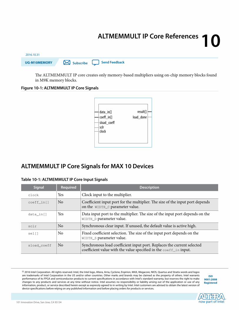
ALTMEMMULT IP Core References 102016.10.31
UG-M10MEMORY Subscribe Send Feedback
The ALTMEMMULT IP core creates only memory-based multipliers using on-chip memory blocks foundin M9K memory blocks.
Figure 10-1: ALTMEMMULT IP Core Signals
data_in[]coeff_in[]sload_coeff
clocksclr
result[]load_done
ALTMEMMULT IP Core Signals for MAX 10 Devices
Table 10-1: ALTMEMMULT IP Core Input Signals
Signal Required Description
clock Yes Clock input to the multiplier.coeff_in[] No Coefficient input port for the multiplier. The size of the input port depends
on the WIDTH_C parameter value.data_in[] Yes Data input port to the multiplier. The size of the input port depends on the
WIDTH_D parameter value.sclr No Synchronous clear input. If unused, the default value is active high.sel[] No Fixed coefficient selection. The size of the input port depends on the
WIDTH_S parameter value.sload_coeff No Synchronous load coefficient input port. Replaces the current selected
coefficient value with the value specified in the coeff_in input.
© 2016 Intel Corporation. All rights reserved. Intel, the Intel logo, Altera, Arria, Cyclone, Enpirion, MAX, Megacore, NIOS, Quartus and Stratix words and logosare trademarks of Intel Corporation in the US and/or other countries. Other marks and brands may be claimed as the property of others. Intel warrantsperformance of its FPGA and semiconductor products to current specifications in accordance with Intel's standard warranty, but reserves the right to makechanges to any products and services at any time without notice. Intel assumes no responsibility or liability arising out of the application or use of anyinformation, product, or service described herein except as expressly agreed to in writing by Intel. Intel customers are advised to obtain the latest version ofdevice specifications before relying on any published information and before placing orders for products or services.
ISO9001:2008Registered
www.altera.com101 Innovation Drive, San Jose, CA 95134
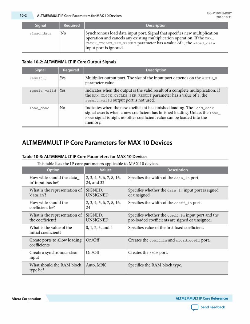
Signal Required Description
sload_data No Synchronous load data input port. Signal that specifies new multiplicationoperation and cancels any existing multiplication operation. If the MAX_CLOCK_CYCLES_PER_RESULT parameter has a value of 1, the sload_datainput port is ignored.
Table 10-2: ALTMEMMULT IP Core Output Signals
Signal Required Description
result[] Yes Multiplier output port. The size of the input port depends on the WIDTH_Rparameter value.
result_valid Yes Indicates when the output is the valid result of a complete multiplication. Ifthe MAX_CLOCK_CYCLES_PER_RESULT parameter has a value of 1, theresult_valid output port is not used.
load_done No Indicates when the new coefficient has finished loading. The load_donesignal asserts when a new coefficient has finished loading. Unless the load_done signal is high, no other coefficient value can be loaded into thememory.
ALTMEMMULT IP Core Parameters for MAX 10 Devices
Table 10-3: ALTMEMMULT IP Core Parameters for MAX 10 Devices
This table lists the IP core parameters applicable to MAX 10 devices.Option Values Description
How wide should the 'data_in' input bus be?
2, 3, 4, 5, 6, 7, 8, 16,24, and 32
Specifies the width of the data_in port.
What is the representation of'data_in'?
SIGNED,UNSIGNED
Specifies whether the data_in input port is signedor unsigned.
How wide should thecoefficient be?
2, 3, 4, 5, 6, 7, 8, 16,24
Specifies the width of the coeff_in port.
What is the representation ofthe coefficient?
SIGNED,UNSIGNED
Specifies whether the coeff_in input port and thepre-loaded coefficients are signed or unsigned.
What is the value of theinitial coefficient?
0, 1, 2, 3, and 4 Specifies value of the first fixed coefficient.
Create ports to allow loadingcoefficients
On/Off Creates the coeff_in and sload_coeff port.
Create a synchronous clearinput
On/Off Creates the sclr port.
What should the RAM blocktype be?
Auto, M9K Specifies the RAM block type.
10-2 ALTMEMMULT IP Core Parameters for MAX 10 DevicesUG-M10MEMORY
2016.10.31
Altera Corporation ALTMEMMULT IP Core References
Send Feedback
Additional Information for MAX 10 EmbeddedMemory User Guide A
2016.10.31
UG-M10MEMORY Subscribe Send Feedback
Document Revision History for MAX 10 Embedded Memory User Guide
Date Version Changes
October 2016 2016.10.31 • Added note stating that the memory initialization feature issupported in MAX 10 Analog and Flash feature options only.
November 2015 2015.11.02 • Revised the title for the tables in the Embedded Memory Configu‐ration topic.
• Added a link to the MAX 10 FPGA Device Overview in theConsider Power-Up State and Memory Initialization topic.
• Changes instances of Quartus II to Quartus Prime.
May 2015 2015.05.04 • Updated 'Yes, use this file for the memory content data' parameternote for RAM:1-Port, RAM:2-Port, ROM:1-Port, and ROM:2-Port.
• Added information about the internal configuration mode thatsupports memory initialization in 'Consider Power-Up State andMemory Initialization'
September 2014 2014.09.22 Initial release.
© 2016 Intel Corporation. All rights reserved. Intel, the Intel logo, Altera, Arria, Cyclone, Enpirion, MAX, Megacore, NIOS, Quartus and Stratix words and logosare trademarks of Intel Corporation in the US and/or other countries. Other marks and brands may be claimed as the property of others. Intel warrantsperformance of its FPGA and semiconductor products to current specifications in accordance with Intel's standard warranty, but reserves the right to makechanges to any products and services at any time without notice. Intel assumes no responsibility or liability arising out of the application or use of anyinformation, product, or service described herein except as expressly agreed to in writing by Intel. Intel customers are advised to obtain the latest version ofdevice specifications before relying on any published information and before placing orders for products or services.
ISO9001:2008Registered
www.altera.com101 Innovation Drive, San Jose, CA 95134

MAX 10 Embedded Multipliers UserGuide
Subscribe
Send Feedback
UG-M10DSP2015.11.02
101 Innovation DriveSan Jose, CA 95134www.altera.com
Contents
Embedded Multiplier Block Overview................................................................1-1
Embedded Multipliers Features and Architecture............................................. 2-1Embedded Multipliers Architecture..........................................................................................................2-1
Input Register................................................................................................................................... 2-1Multiplier Stage................................................................................................................................ 2-2Output Register................................................................................................................................ 2-2
Embedded Multipliers Operational Modes..............................................................................................2-318-Bit Multipliers............................................................................................................................. 2-39-Bit Multipliers............................................................................................................................... 2-4
Embedded Multipliers Implementation Guides.................................................3-1Files Generated by IP Cores........................................................................................................................3-1
Verilog HDL Prototype Location.................................................................................................. 3-1VHDL Component Declaration Location....................................................................................3-2
LPM_MULT (Multiplier) IP Core References.................................................... 4-1LPM_MULT Parameter Settings............................................................................................................... 4-1Ports............................................................................................................................................................... 4-3
ALTMULT_ACCUM (Multiply-Accumulate) IP Core References....................5-1ALTMULT_ACCUM Parameter Settings................................................................................................5-1ALTMULT_ACCUM Ports........................................................................................................................5-8
ALTMULT_ADD (Multiply-Adder) IP Core References...................................6-1ALTMULT_ADD Parameter Settings...................................................................................................... 6-1ALTMULT_ADD Ports.............................................................................................................................. 6-8
ALTMULT_COMPLEX (Complex Multiplier) IP Core References.................. 7-1ALTMULT_COMPLEX Parameter Settings............................................................................................7-1Ports............................................................................................................................................................... 7-2
Additional Information for MAX 10 Embedded Multipliers User Guide........A-1Document Revision History for MAX 10 Embedded Multipliers User Guide ................................. A-1
TOC-2
Altera Corporation
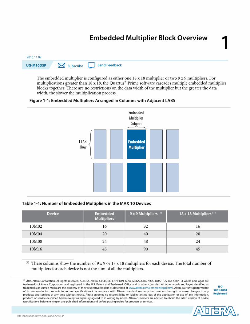
Embedded Multiplier Block Overview 12015.11.02
UG-M10DSP Subscribe Send Feedback
The embedded multiplier is configured as either one 18 x 18 multiplier or two 9 x 9 multipliers. Formultiplications greater than 18 x 18, the Quartus® Prime software cascades multiple embedded multiplierblocks together. There are no restrictions on the data width of the multiplier but the greater the datawidth, the slower the multiplication process.
Figure 1-1: Embedded Multipliers Arranged in Columns with Adjacent LABS
EmbeddedMultiplier
EmbeddedMultiplier
Column
1 LABRow
Table 1-1: Number of Embedded Multipliers in the MAX 10 Devices
Device EmbeddedMultipliers
9 x 9 Multipliers (1) 18 x 18 Multipliers (1)
10M02 16 32 1610M04 20 40 2010M08 24 48 2410M16 45 90 45
(1) These columns show the number of 9 x 9 or 18 x 18 multipliers for each device. The total number ofmultipliers for each device is not the sum of all the multipliers.
© 2015 Altera Corporation. All rights reserved. ALTERA, ARRIA, CYCLONE, ENPIRION, MAX, MEGACORE, NIOS, QUARTUS and STRATIX words and logos aretrademarks of Altera Corporation and registered in the U.S. Patent and Trademark Office and in other countries. All other words and logos identified astrademarks or service marks are the property of their respective holders as described at www.altera.com/common/legal.html. Altera warrants performanceof its semiconductor products to current specifications in accordance with Altera's standard warranty, but reserves the right to make changes to anyproducts and services at any time without notice. Altera assumes no responsibility or liability arising out of the application or use of any information,product, or service described herein except as expressly agreed to in writing by Altera. Altera customers are advised to obtain the latest version of devicespecifications before relying on any published information and before placing orders for products or services.
ISO9001:2008Registered
www.altera.com101 Innovation Drive, San Jose, CA 95134
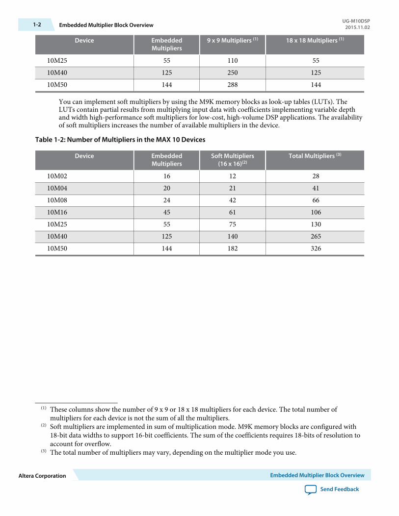
Device EmbeddedMultipliers
9 x 9 Multipliers (1) 18 x 18 Multipliers (1)
10M25 55 110 5510M40 125 250 12510M50 144 288 144
You can implement soft multipliers by using the M9K memory blocks as look-up tables (LUTs). TheLUTs contain partial results from multiplying input data with coefficients implementing variable depthand width high-performance soft multipliers for low-cost, high-volume DSP applications. The availabilityof soft multipliers increases the number of available multipliers in the device.
Table 1-2: Number of Multipliers in the MAX 10 Devices
Device EmbeddedMultipliers
Soft Multipliers(16 x 16)(2)
Total Multipliers (3)
10M02 16 12 2810M04 20 21 4110M08 24 42 6610M16 45 61 10610M25 55 75 13010M40 125 140 26510M50 144 182 326
(1) These columns show the number of 9 x 9 or 18 x 18 multipliers for each device. The total number ofmultipliers for each device is not the sum of all the multipliers.
(2) Soft multipliers are implemented in sum of multiplication mode. M9K memory blocks are configured with18-bit data widths to support 16-bit coefficients. The sum of the coefficients requires 18-bits of resolution toaccount for overflow.
(3) The total number of multipliers may vary, depending on the multiplier mode you use.
1-2 Embedded Multiplier Block OverviewUG-M10DSP
2015.11.02
Altera Corporation Embedded Multiplier Block Overview
Send Feedback
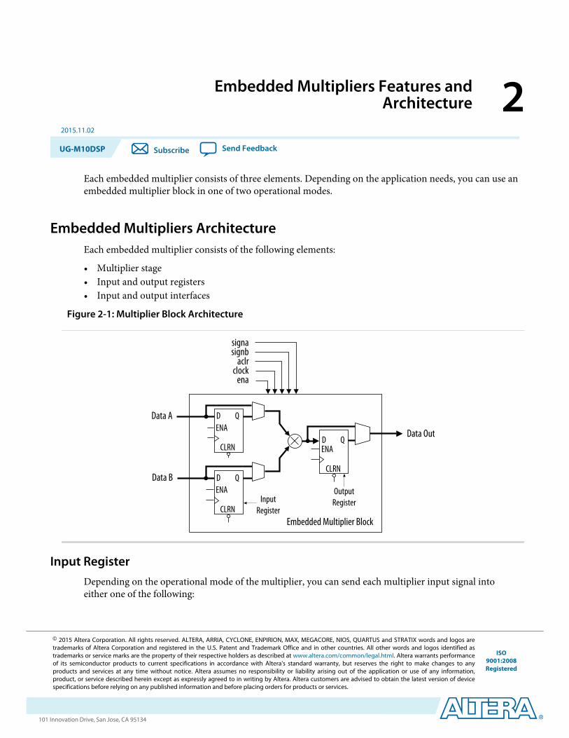
Embedded Multipliers Features andArchitecture 2
2015.11.02
UG-M10DSP Subscribe Send Feedback
Each embedded multiplier consists of three elements. Depending on the application needs, you can use anembedded multiplier block in one of two operational modes.
Embedded Multipliers ArchitectureEach embedded multiplier consists of the following elements:
• Multiplier stage• Input and output registers• Input and output interfaces
Figure 2-1: Multiplier Block Architecture
CLRN
D QENA
Data A
Data B
aclrclock
ena
signasignb
CLRN
D QENA
CLRN
D QENA Data Out
Embedded Multiplier Block
OutputRegisterInput
Register
Input RegisterDepending on the operational mode of the multiplier, you can send each multiplier input signal intoeither one of the following:
© 2015 Altera Corporation. All rights reserved. ALTERA, ARRIA, CYCLONE, ENPIRION, MAX, MEGACORE, NIOS, QUARTUS and STRATIX words and logos aretrademarks of Altera Corporation and registered in the U.S. Patent and Trademark Office and in other countries. All other words and logos identified astrademarks or service marks are the property of their respective holders as described at www.altera.com/common/legal.html. Altera warrants performanceof its semiconductor products to current specifications in accordance with Altera's standard warranty, but reserves the right to make changes to anyproducts and services at any time without notice. Altera assumes no responsibility or liability arising out of the application or use of any information,product, or service described herein except as expressly agreed to in writing by Altera. Altera customers are advised to obtain the latest version of devicespecifications before relying on any published information and before placing orders for products or services.
ISO9001:2008Registered
www.altera.com101 Innovation Drive, San Jose, CA 95134
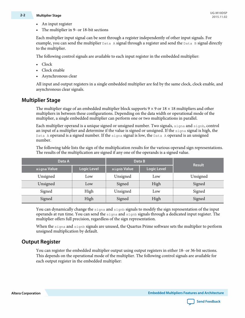
• An input register• The multiplier in 9- or 18-bit sections
Each multiplier input signal can be sent through a register independently of other input signals. Forexample, you can send the multiplier Data A signal through a register and send the Data B signal directlyto the multiplier.
The following control signals are available to each input register in the embedded multiplier:
• Clock• Clock enable• Asynchronous clear
All input and output registers in a single embedded multiplier are fed by the same clock, clock enable, andasynchronous clear signals.
Multiplier StageThe multiplier stage of an embedded multiplier block supports 9 × 9 or 18 × 18 multipliers and othermultipliers in between these configurations. Depending on the data width or operational mode of themultiplier, a single embedded multiplier can perform one or two multiplications in parallel.
Each multiplier operand is a unique signed or unsigned number. Two signals, signa and signb, controlan input of a multiplier and determine if the value is signed or unsigned. If the signa signal is high, theData A operand is a signed number. If the signa signal is low, the Data A operand is an unsignednumber.
The following table lists the sign of the multiplication results for the various operand sign representations.The results of the multiplication are signed if any one of the operands is a signed value.
Data A Data BResult
signa Value Logic Level signb Value Logic Level
Unsigned Low Unsigned Low UnsignedUnsigned Low Signed High Signed
Signed High Unsigned Low SignedSigned High Signed High Signed
You can dynamically change the signa and signb signals to modify the sign representation of the inputoperands at run time. You can send the signa and signb signals through a dedicated input register. Themultiplier offers full precision, regardless of the sign representation.
When the signa and signb signals are unused, the Quartus Prime software sets the multiplier to performunsigned multiplication by default.
Output RegisterYou can register the embedded multiplier output using output registers in either 18- or 36-bit sections.This depends on the operational mode of the multiplier. The following control signals are available foreach output register in the embedded multiplier:
2-2 Multiplier StageUG-M10DSP
2015.11.02
Altera Corporation Embedded Multipliers Features and Architecture
Send Feedback
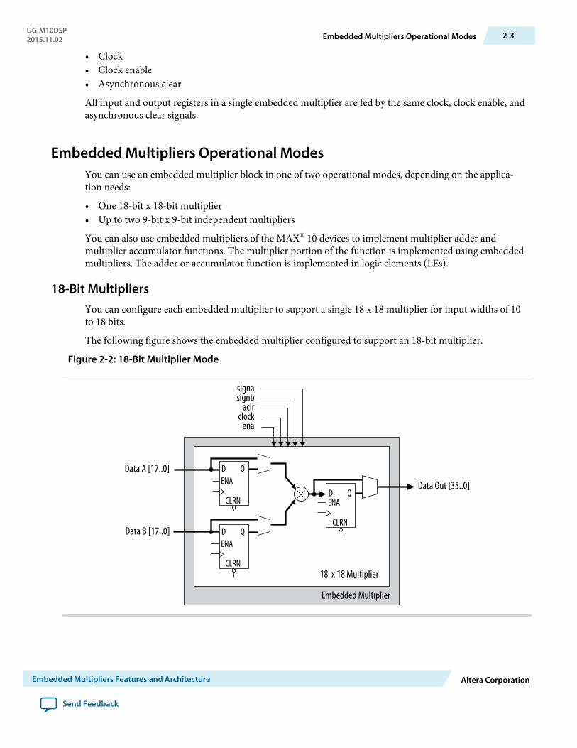
• Clock• Clock enable• Asynchronous clear
All input and output registers in a single embedded multiplier are fed by the same clock, clock enable, andasynchronous clear signals.
Embedded Multipliers Operational ModesYou can use an embedded multiplier block in one of two operational modes, depending on the applica‐tion needs:
• One 18-bit x 18-bit multiplier• Up to two 9-bit x 9-bit independent multipliers
You can also use embedded multipliers of the MAX® 10 devices to implement multiplier adder andmultiplier accumulator functions. The multiplier portion of the function is implemented using embeddedmultipliers. The adder or accumulator function is implemented in logic elements (LEs).
18-Bit MultipliersYou can configure each embedded multiplier to support a single 18 x 18 multiplier for input widths of 10to 18 bits.
The following figure shows the embedded multiplier configured to support an 18-bit multiplier.
Figure 2-2: 18-Bit Multiplier Mode
CLRN
D QENA
Data A [17..0]
Data B [17..0]
aclrclock
ena
signasignb
CLRN
D QENA
CLRN
D QENA Data Out [35..0]
18 x 18 Multiplier
Embedded Multiplier
UG-M10DSP2015.11.02 Embedded Multipliers Operational Modes 2-3
Embedded Multipliers Features and Architecture Altera Corporation
Send Feedback
All 18-bit multiplier inputs and results are independently sent through registers. The multiplier inputs canaccept signed integers, unsigned integers, or a combination of both. Also, you can dynamically change thesigna and signb signals and send these signals through dedicated input registers.
9-Bit MultipliersYou can configure each embedded multiplier to support two 9 × 9 independent multipliers for inputwidths of up to 9 bits.
The following figure shows the embedded multiplier configured to support two 9-bit multipliers.
Figure 2-3: 9-Bit Multiplier Mode
CLRN
D QENA
Data A 0 [8..0]
Data B 0 [8..0]
aclrclock
ena
signasignb
CLRN
D QENA
CLRN
D QENA Data Out 0 [17..0]
9 x 9 Multiplier
Embedded Multiplier
CLRN
D QENA
Data A 1 [8..0]
Data B 1 [8..0]
CLRN
D QENA
CLRN
D QENA Data Out 1 [17..0]
9 x 9 Multiplier
All 9-bit multiplier inputs and results are independently sent through registers. The multiplier inputs canaccept signed integers, unsigned integers, or a combination of both.
2-4 9-Bit MultipliersUG-M10DSP
2015.11.02
Altera Corporation Embedded Multipliers Features and Architecture
Send Feedback

Each embedded multiplier block has only one signa and one signb signal to control the sign representa‐tion of the input data to the block. If the embedded multiplier block has two 9 × 9 multipliers thefollowing applies:
• The Data A input of both multipliers share the same signa signal• The Data B input of both multipliers share the same signb signal
UG-M10DSP2015.11.02 9-Bit Multipliers 2-5
Embedded Multipliers Features and Architecture Altera Corporation
Send Feedback
Embedded Multipliers Implementation Guides 32015.11.02
UG-M10DSP Subscribe Send Feedback
The Quartus Prime software contains tools for you to create and compile your design, and configure yourdevice.
You can prepare for device migration, set pin assignments, define placement restrictions, setup timingconstraints, and customize IP cores using the Quartus Prime software.
Related Information
• Introduction to Altera IP CoresProvides general information about all Altera IP cores, including parameterizing, generating,upgrading, and simulating IP.
• Creating Version-Independent IP and Qsys Simulation ScriptsCreate simulation scripts that do not require manual updates for software or IP version upgrades.
• Project Management Best PracticesGuidelines for efficient management and portability of your project and IP files.
Files Generated by IP CoresThe following integer arithmetic IP cores use the MAX 10 device embedded multipliers block:
• LPM_MULT• ALTMULT_ACCUM (MAC)• ALTMULT_ADD• ALTMULT_COMPLEX
Verilog HDL Prototype LocationYou can view the Verilog HDL prototype for the IP cores in the following Verilog Design Files (.v):
Table 3-1: Verilog HDL Prototype Location
Integer Arithmetic Megafunctions Directory Verilog Design File (.v)
LPM_MULT <Quartus Prime installationdirectory>\eda\synthesis
lpm.v
© 2015 Altera Corporation. All rights reserved. ALTERA, ARRIA, CYCLONE, ENPIRION, MAX, MEGACORE, NIOS, QUARTUS and STRATIX words and logos aretrademarks of Altera Corporation and registered in the U.S. Patent and Trademark Office and in other countries. All other words and logos identified astrademarks or service marks are the property of their respective holders as described at www.altera.com/common/legal.html. Altera warrants performanceof its semiconductor products to current specifications in accordance with Altera's standard warranty, but reserves the right to make changes to anyproducts and services at any time without notice. Altera assumes no responsibility or liability arising out of the application or use of any information,product, or service described herein except as expressly agreed to in writing by Altera. Altera customers are advised to obtain the latest version of devicespecifications before relying on any published information and before placing orders for products or services.
ISO9001:2008Registered
www.altera.com101 Innovation Drive, San Jose, CA 95134
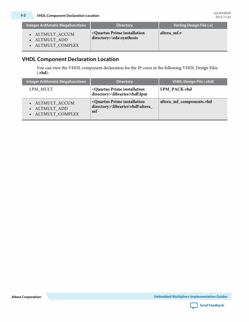
Integer Arithmetic Megafunctions Directory Verilog Design File (.v)
• ALTMULT_ACCUM• ALTMULT_ADD• ALTMULT_COMPLEX
<Quartus Prime installationdirectory>\eda\synthesis
altera_mf.v
VHDL Component Declaration LocationYou can view the VHDL component declaration for the IP cores in the following VHDL Design Files(.vhd):
Integer Arithmetic Megafunctions Directory VHDL Design File (.vhd)
LPM_MULT <Quartus Prime installationdirectory>\libraries\vhdl\lpm
LPM_PACK.vhd
• ALTMULT_ACCUM• ALTMULT_ADD• ALTMULT_COMPLEX
<Quartus Prime installationdirectory>\libraries\vhdl\altera_mf
altera_mf_components.vhd
3-2 VHDL Component Declaration LocationUG-M10DSP
2015.11.02
Altera Corporation Embedded Multipliers Implementation Guides
Send Feedback
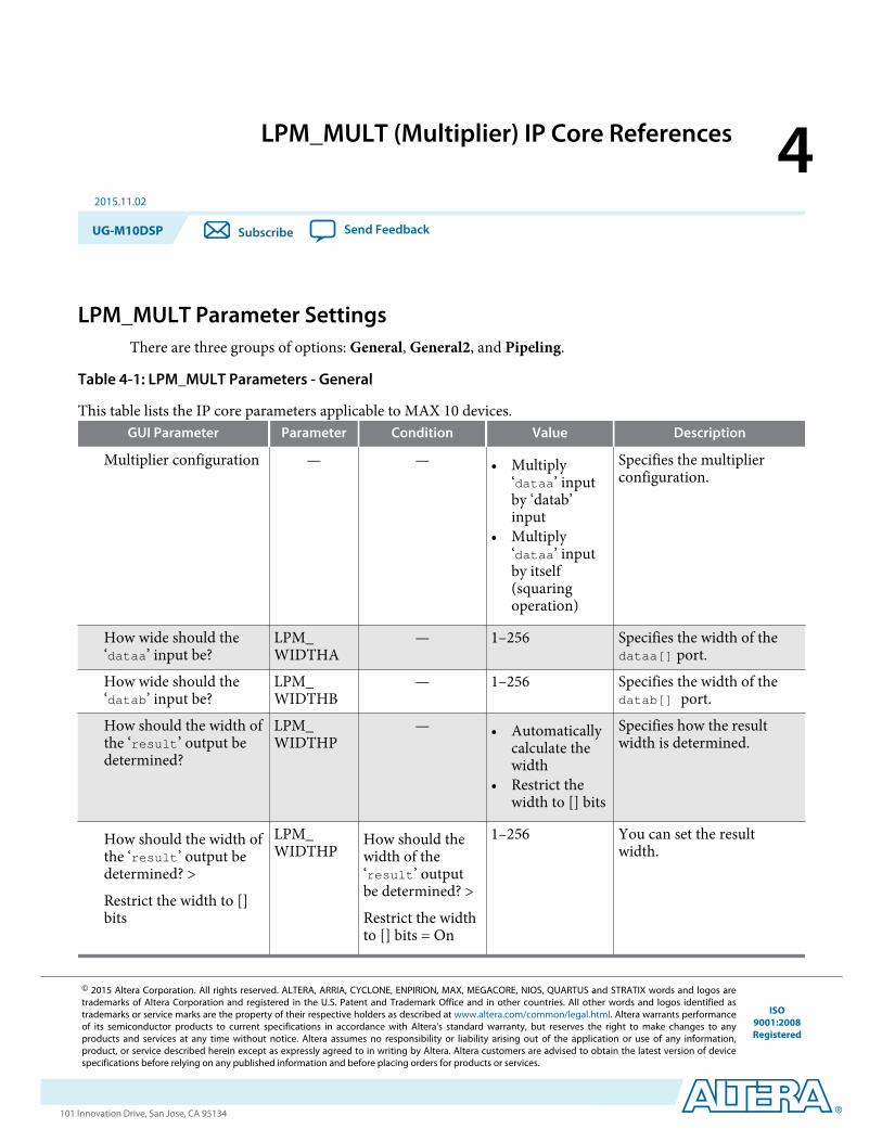
LPM_MULT (Multiplier) IP Core References 42015.11.02
UG-M10DSP Subscribe Send Feedback
LPM_MULT Parameter SettingsThere are three groups of options: General, General2, and Pipeling.
Table 4-1: LPM_MULT Parameters - General
This table lists the IP core parameters applicable to MAX 10 devices.GUI Parameter Parameter Condition Value Description
Multiplier configuration — — • Multiply‘dataa’ inputby ‘datab’input
• Multiply‘dataa’ inputby itself(squaringoperation)
Specifies the multiplierconfiguration.
How wide should the‘dataa’ input be?
LPM_WIDTHA
— 1–256 Specifies the width of thedataa[] port.
How wide should the‘datab’ input be?
LPM_WIDTHB
— 1–256 Specifies the width of thedatab[] port.
How should the width ofthe ‘result’ output bedetermined?
LPM_WIDTHP
— • Automaticallycalculate thewidth
• Restrict thewidth to [] bits
Specifies how the resultwidth is determined.
How should the width ofthe ‘result’ output bedetermined? >
Restrict the width to []bits
LPM_WIDTHP
How should thewidth of the‘result’ outputbe determined? >
Restrict the widthto [] bits = On
1–256 You can set the resultwidth.
© 2015 Altera Corporation. All rights reserved. ALTERA, ARRIA, CYCLONE, ENPIRION, MAX, MEGACORE, NIOS, QUARTUS and STRATIX words and logos aretrademarks of Altera Corporation and registered in the U.S. Patent and Trademark Office and in other countries. All other words and logos identified astrademarks or service marks are the property of their respective holders as described at www.altera.com/common/legal.html. Altera warrants performanceof its semiconductor products to current specifications in accordance with Altera's standard warranty, but reserves the right to make changes to anyproducts and services at any time without notice. Altera assumes no responsibility or liability arising out of the application or use of any information,product, or service described herein except as expressly agreed to in writing by Altera. Altera customers are advised to obtain the latest version of devicespecifications before relying on any published information and before placing orders for products or services.
ISO9001:2008Registered
www.altera.com101 Innovation Drive, San Jose, CA 95134
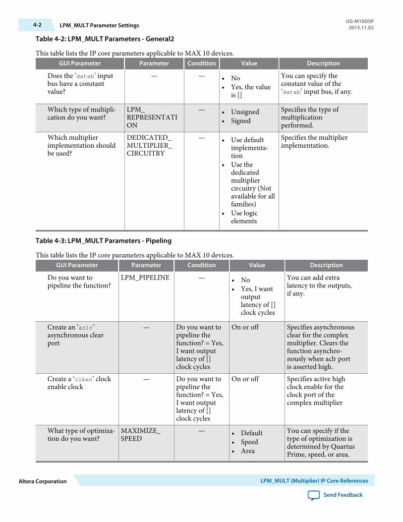
Table 4-2: LPM_MULT Parameters - General2
This table lists the IP core parameters applicable to MAX 10 devices.GUI Parameter Parameter Condition Value Description
Does the ‘datab’ inputbus have a constantvalue?
— — • No• Yes, the value
is []
You can specify theconstant value of the‘datab’ input bus, if any.
Which type of multipli‐cation do you want?
LPM_REPRESENTATION
— • Unsigned• Signed
Specifies the type ofmultiplicationperformed.
Which multiplierimplementation shouldbe used?
DEDICATED_MULTIPLIER_CIRCUITRY
— • Use defaultimplementa‐tion
• Use thededicatedmultipliercircuitry (Notavailable for allfamilies)
• Use logicelements
Specifies the multiplierimplementation.
Table 4-3: LPM_MULT Parameters - Pipeling
This table lists the IP core parameters applicable to MAX 10 devices.GUI Parameter Parameter Condition Value Description
Do you want topipeline the function?
LPM_PIPELINE — • No• Yes, I want
outputlatency of []clock cycles
You can add extralatency to the outputs,if any.
Create an ‘aclr’asynchronous clearport
— Do you want topipeline thefunction? = Yes,I want outputlatency of []clock cycles
On or off Specifies asynchronousclear for the complexmultiplier. Clears thefunction asynchro‐nously when aclr portis asserted high.
Create a ‘clken’ clockenable clock
— Do you want topipeline thefunction? = Yes,I want outputlatency of []clock cycles
On or off Specifies active highclock enable for theclock port of thecomplex multiplier
What type of optimiza‐tion do you want?
MAXIMIZE_SPEED
— • Default• Speed• Area
You can specify if thetype of optimization isdetermined by QuartusPrime, speed, or area.
4-2 LPM_MULT Parameter SettingsUG-M10DSP
2015.11.02
Altera Corporation LPM_MULT (Multiplier) IP Core References
Send Feedback
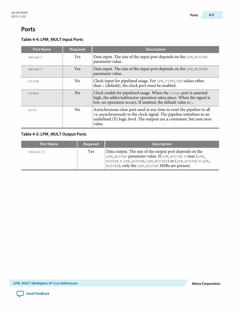
PortsTable 4-4: LPM_MULT Input Ports
Port Name Required Description
dataa[] Yes Data input. The size of the input port depends on the LPM_WIDTHAparameter value.
datab[] Yes Data input. The size of the input port depends on the LPM_WIDTHBparameter value.
clock No Clock input for pipelined usage. For LPM_PIPELINE values otherthan 0 (default), the clock port must be enabled.
clken No Clock enable for pipelined usage. When the clken port is assertedhigh, the adder/subtractor operation takes place. When the signal islow, no operation occurs. If omitted, the default value is 1.
aclr No Asynchronous clear port used at any time to reset the pipeline to all0s, asynchronously to the clock signal. The pipeline initializes to anundefined (X) logic level. The outputs are a consistent, but non-zerovalue.
Table 4-5: LPM_MULT Output Ports
Port Name Required Description
result[] Yes Data output. The size of the output port depends on theLPM_WIDTHP parameter value. If LPM_WIDTHP < max (LPM_WIDTHA + LPM_WIDTHB, LPM_WIDTHS) or (LPM_WIDTHA + LPM_WIDTHS), only the LPM_WIDTHP MSBs are present.
UG-M10DSP2015.11.02 Ports 4-3
LPM_MULT (Multiplier) IP Core References Altera Corporation
Send Feedback
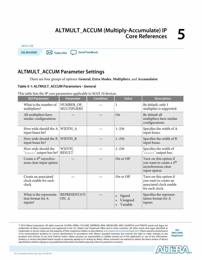
ALTMULT_ACCUM (Multiply-Accumulate) IPCore References 5
2015.11.02
UG-M10DSP Subscribe Send Feedback
ALTMULT_ACCUM Parameter SettingsThere are four groups of options: General, Extra Modes, Multipliers, and Accumulator.
Table 5-1: ALTMULT_ACCUM Parameters - General
This table lists the IP core parameters applicable to MAX 10 devices.GUI Parameter Parameter Condition Value Description
What is the number ofmultipliers?
NUMBER_OF_MULTIPLIERS
— 1 By default, only 1multiplier is supported.
All multipliers havesimilar configurations
— — On By default allmultipliers have similarconfigurations
How wide should the Ainput buses be?
WIDTH_A — 1–256 Specifies the width of Ainput buses.
How wide should the Binput buses be?
WIDTH_B — 1–256 Specifies the width of Binput buses.
How wide should the‘result’ output bus be?
WIDTH_RESULT
— 1–256 Specifies the width of‘result’ output bus.
Create a 4th asynchro‐nous clear input option
— — On or Off Turn on this option ifyou want to create a 4th
asynchronous clearinput option.
Create an associatedclock enable for eachclock
— — On or Off Turn on this option ifyou want to create anassociated clock enablefor each clock.
What is the representa‐tion format for Ainputs?
REPRESENTATION_A
— • Signed• Unsigned• Variable
Specifies the represen‐tation format for Ainputs.
© 2015 Altera Corporation. All rights reserved. ALTERA, ARRIA, CYCLONE, ENPIRION, MAX, MEGACORE, NIOS, QUARTUS and STRATIX words and logos aretrademarks of Altera Corporation and registered in the U.S. Patent and Trademark Office and in other countries. All other words and logos identified astrademarks or service marks are the property of their respective holders as described at www.altera.com/common/legal.html. Altera warrants performanceof its semiconductor products to current specifications in accordance with Altera's standard warranty, but reserves the right to make changes to anyproducts and services at any time without notice. Altera assumes no responsibility or liability arising out of the application or use of any information,product, or service described herein except as expressly agreed to in writing by Altera. Altera customers are advised to obtain the latest version of devicespecifications before relying on any published information and before placing orders for products or services.
ISO9001:2008Registered
www.altera.com101 Innovation Drive, San Jose, CA 95134
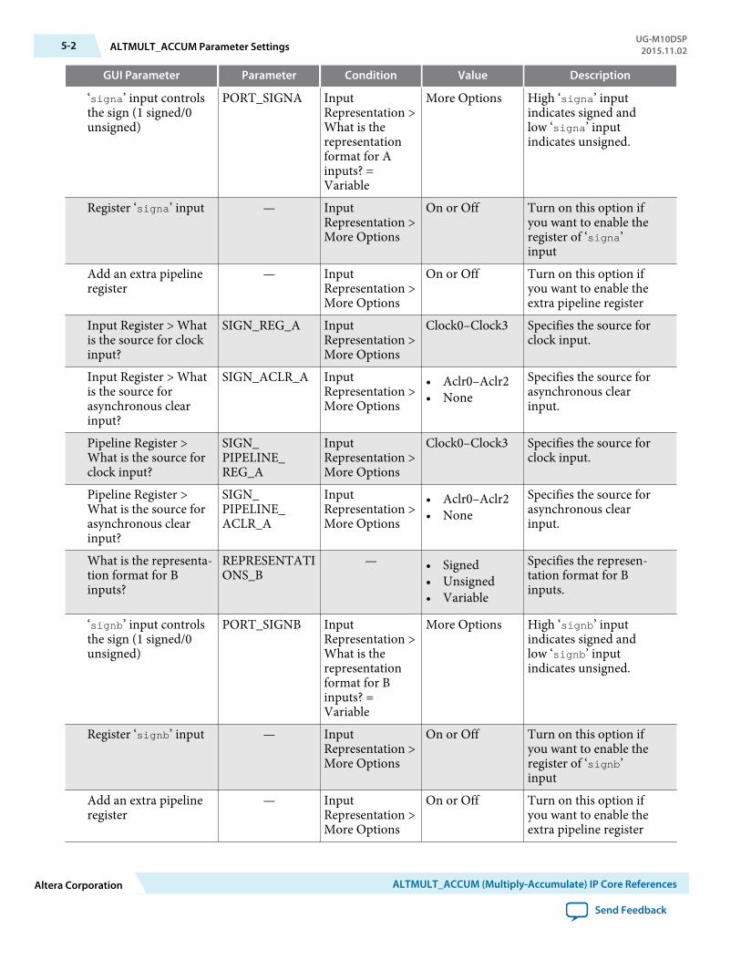
GUI Parameter Parameter Condition Value Description
‘signa’ input controlsthe sign (1 signed/0unsigned)
PORT_SIGNA InputRepresentation >What is therepresentationformat for Ainputs? =Variable
More Options High ‘signa’ inputindicates signed andlow ‘signa’ inputindicates unsigned.
Register ‘signa’ input — InputRepresentation >More Options
On or Off Turn on this option ifyou want to enable theregister of ‘signa’input
Add an extra pipelineregister
— InputRepresentation >More Options
On or Off Turn on this option ifyou want to enable theextra pipeline register
Input Register > Whatis the source for clockinput?
SIGN_REG_A InputRepresentation >More Options
Clock0–Clock3 Specifies the source forclock input.
Input Register > Whatis the source forasynchronous clearinput?
SIGN_ACLR_A InputRepresentation >More Options
• Aclr0–Aclr2• None
Specifies the source forasynchronous clearinput.
Pipeline Register >What is the source forclock input?
SIGN_PIPELINE_REG_A
InputRepresentation >More Options
Clock0–Clock3 Specifies the source forclock input.
Pipeline Register >What is the source forasynchronous clearinput?
SIGN_PIPELINE_ACLR_A
InputRepresentation >More Options
• Aclr0–Aclr2• None
Specifies the source forasynchronous clearinput.
What is the representa‐tion format for Binputs?
REPRESENTATIONS_B
— • Signed• Unsigned• Variable
Specifies the represen‐tation format for Binputs.
‘signb’ input controlsthe sign (1 signed/0unsigned)
PORT_SIGNB InputRepresentation >What is therepresentationformat for Binputs? =Variable
More Options High ‘signb’ inputindicates signed andlow ‘signb’ inputindicates unsigned.
Register ‘signb’ input — InputRepresentation >More Options
On or Off Turn on this option ifyou want to enable theregister of ‘signb’input
Add an extra pipelineregister
— InputRepresentation >More Options
On or Off Turn on this option ifyou want to enable theextra pipeline register
5-2 ALTMULT_ACCUM Parameter SettingsUG-M10DSP
2015.11.02
Altera Corporation ALTMULT_ACCUM (Multiply-Accumulate) IP Core References
Send Feedback
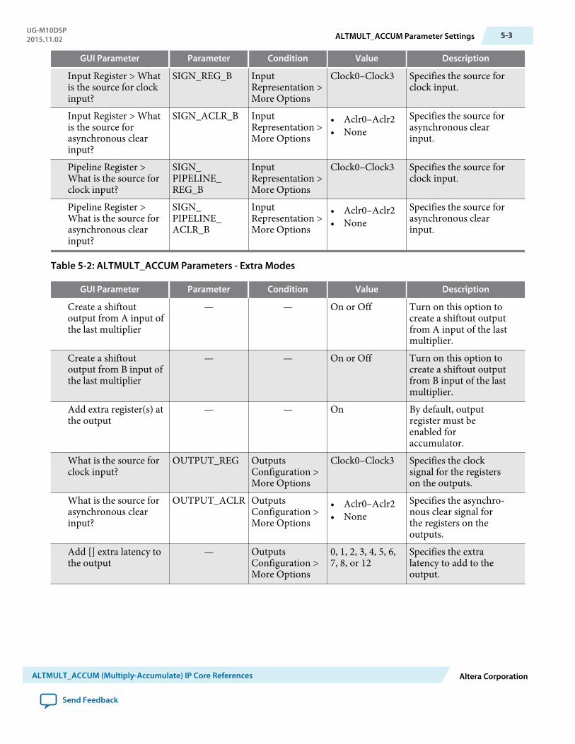
GUI Parameter Parameter Condition Value Description
Input Register > Whatis the source for clockinput?
SIGN_REG_B InputRepresentation >More Options
Clock0–Clock3 Specifies the source forclock input.
Input Register > Whatis the source forasynchronous clearinput?
SIGN_ACLR_B InputRepresentation >More Options
• Aclr0–Aclr2• None
Specifies the source forasynchronous clearinput.
Pipeline Register >What is the source forclock input?
SIGN_PIPELINE_REG_B
InputRepresentation >More Options
Clock0–Clock3 Specifies the source forclock input.
Pipeline Register >What is the source forasynchronous clearinput?
SIGN_PIPELINE_ACLR_B
InputRepresentation >More Options
• Aclr0–Aclr2• None
Specifies the source forasynchronous clearinput.
Table 5-2: ALTMULT_ACCUM Parameters - Extra Modes
GUI Parameter Parameter Condition Value Description
Create a shiftoutoutput from A input ofthe last multiplier
— — On or Off Turn on this option tocreate a shiftout outputfrom A input of the lastmultiplier.
Create a shiftoutoutput from B input ofthe last multiplier
— — On or Off Turn on this option tocreate a shiftout outputfrom B input of the lastmultiplier.
Add extra register(s) atthe output
— — On By default, outputregister must beenabled foraccumulator.
What is the source forclock input?
OUTPUT_REG OutputsConfiguration >More Options
Clock0–Clock3 Specifies the clocksignal for the registerson the outputs.
What is the source forasynchronous clearinput?
OUTPUT_ACLR OutputsConfiguration >More Options
• Aclr0–Aclr2• None
Specifies the asynchro‐nous clear signal forthe registers on theoutputs.
Add [] extra latency tothe output
— OutputsConfiguration >More Options
0, 1, 2, 3, 4, 5, 6,7, 8, or 12
Specifies the extralatency to add to theoutput.
UG-M10DSP2015.11.02 ALTMULT_ACCUM Parameter Settings 5-3
ALTMULT_ACCUM (Multiply-Accumulate) IP Core References Altera Corporation
Send Feedback
GUI Parameter Parameter Condition Value Description
Which multiplier-adder implementationshould be used?
DEDICATED_MULTIPLIER_CIRCUITRY
— • Use thedefaultimplementa‐tion
• Use dedicatedmultipliercircuitry (Notavailable forall families)
• Use logicelements
Specifies themultiplier-adderimplementation.
Table 5-3: ALTMULT_ACCUM Parameters - Multipliers
This table lists the IP core parameters applicable to MAX 10 devices.GUI Parameter Parameter Condition Value Description
Register input A of themultiplier
— — On or Off Turn on to enableregister input A of themultiplier.
What is the source forclock input?
INPUT_REG_A • InputConfiguration> Registerinput A of themultiplier =On
• InputConfiguration> MoreOptions
Clock0–Clock3 Specifies the clock portfor the dataa[] port.
What is the source forasynchronous clearinput?
INPUT_ACLR_A
• InputConfiguration> Registerinput A of themultiplier =On
• InputConfiguration> MoreOptions
• Aclr0–Aclr2• None
Specifies the asynchro‐nous clear port for thedataa[] port.
Register input B of themultiplier
— — On or Off Turn on to enableregister input B of themultiplier.
5-4 ALTMULT_ACCUM Parameter SettingsUG-M10DSP
2015.11.02
Altera Corporation ALTMULT_ACCUM (Multiply-Accumulate) IP Core References
Send Feedback
GUI Parameter Parameter Condition Value Description
What is the source forclock input?
INPUT_REG_B • InputConfiguration> Registerinput B of themultiplier =On
• InputConfiguration> MoreOptions
Clock0–Clock3 Specifies the clock portfor the datab[] port.
What is the source forasynchronous clearinput?
INPUT_ACLR_B
• InputConfiguration> Registerinput B of themultiplier =On
• InputConfiguration> MoreOptions
• Aclr0–Aclr2• None
Specifies the asynchro‐nous clear port for thedatab[] port.
What is the input A ofthe multiplierconnected to?
— — Multiplier input By default, input A ofthe multiplier is alwaysconnected to themultiplier’s input.
What is the input B ofthe multiplierconnected to?
— — Multiplier input By default, input B ofthe multiplier is alwaysconnected to themultiplier’s input.
Register output of themultiplier
— — On or Off Turn on to enableregister output of themultiplier.
What is the source forclock input?
MULTIPLIER_REG
• OutputConfiguration> Registeroutput of themultiplier =On
• OutputConfiguration> MoreOptions
Clock0–Clock3 Specifies the clocksignal for the registerthat immediatelyfollows the multiplier.
UG-M10DSP2015.11.02 ALTMULT_ACCUM Parameter Settings 5-5
ALTMULT_ACCUM (Multiply-Accumulate) IP Core References Altera Corporation
Send Feedback
GUI Parameter Parameter Condition Value Description
What is the source forasynchronous clearinput?
MULTIPLIER_ACLR
• OutputConfiguration> Registeroutput of themultiplier =On
• OutputConfiguration> MoreOptions
• Aclr0–Aclr2• None
Specifies the asynchro‐nous clear signal of theregister that follows thecorrespondingmultiplier.
Table 5-4: ALTMULT_ACCUM Parameters - Accumulator
This table lists the IP core parameters applicable to MAX 10 devices.GUI Parameter Parameter Condition Value Description
Create an ‘accum_sload’ input port
— — On or off Dynamically specifieswhether theaccumulator value isconstant. If the accum_sload port is high,then the multiplieroutput is loaded intothe accumulator.
Register ‘accum_sload’input
— • Accumulator> Create an‘accum_sload’input port =On
• Accumulator> MoreOptions
On or off Turn on to enableregister ‘accum_sload’input.
Add an extra pipelineregister
— • Accumulator> Create an‘accum_sload’ inputport = On
• Accumulator> MoreOptions
On or off Turn on this option ifyou want to enable theextra pipeline register
5-6 ALTMULT_ACCUM Parameter SettingsUG-M10DSP
2015.11.02
Altera Corporation ALTMULT_ACCUM (Multiply-Accumulate) IP Core References
Send Feedback
GUI Parameter Parameter Condition Value Description
Input Register > Whatis the source for clockinput?
ACCUM_SLOAD_REG
• Accumulator> Create an‘accum_sload’input port =On
• Accumulator> MoreOptions
Clock0–Clock3 Specifies the clocksignal for the accum_sload port.
Input Register > Whatis the source forasynchronous clearinput?
ACCUM_SLOAD_ACLR
• Accumulator> Create an‘accum_sload’ inputport = On
• Accumulator> MoreOptions
• Aclr0–Aclr2• None
Specifies the asynchro‐nous clear source forthe first register on theaccum_sload input.
Pipeline Register >What is the source forclock input?
ACCUM_SLOAD_PIPELINE_REG
• •Accumulator> Create an‘accum_sload’ inputport = On
• Accumulator> MoreOptions
Clock0–Clock3 Specifies the source forclock input.
Pipeline Register >What is the source forasynchronous clearinput?
ACCUM_SLOAD_PIPELINE_ACLR
• Accumulator> Create an‘accum_soad’input port =On
• Accumulator> MoreOptions
• Aclr0–Aclr2• None
Specifies the source forasynchronous clearinput.
Create an ‘overflow’output port
— — On or Off Overflow port for theaccumulator
Add [] extra latency tothe multiplier output
EXTRA_MULTIPLIER_LATENCY
— 0, 1, 2, 3, 4, 5, 6,7, 8, or 12
Specifies the number ofclock cycles of latencyfor the multiplierportion of the DSPblock. If theMULTIPLIER_REGparameter is specified,then the specified clockport is used to add thelatency.
UG-M10DSP2015.11.02 ALTMULT_ACCUM Parameter Settings 5-7
ALTMULT_ACCUM (Multiply-Accumulate) IP Core References Altera Corporation
Send Feedback
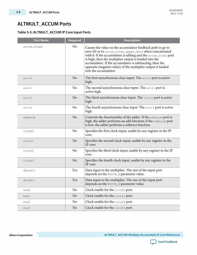
ALTMULT_ACCUM PortsTable 5-5: ALTMULT_ACCUM IP Core Input Ports
Port Name Required Description
accum_sload No Causes the value on the accumulator feedback path to go tozero (0) or to accum_sload_upper_data when concatenatedwith 0. If the accumulator is adding and the accum_sload portis high, then the multiplier output is loaded into theaccumulator. If the accumulator is subtracting, then theopposite (negative value) of the multiplier output is loadedinto the accumulator.
aclr0 No The first asynchronous clear input. The aclr0 port is activehigh.
aclr1 No The second asynchronous clear input. The aclr1 port isactive high.
aclr2 No The third asynchronous clear input. The aclr2 port is activehigh.
aclr3 No The fourth asynchronous clear input. The aclr3 port is activehigh.
addnsub No Controls the functionality of the adder. If the addnsub port ishigh, the adder performs an add function; if the addnsub portis low, the adder performs a subtract function.
clock0 No Specifies the first clock input, usable by any register in the IPcore.
clock1 No Specifies the second clock input, usable by any register in theIP core.
clock2 No Specifies the third clock input, usable by any register in the IPcore.
clock3 No Specifies the fourth clock input, usable by any register in theIP core.
dataa[] Yes Data input to the multiplier. The size of the input portdepends on the WIDTH_A parameter value.
datab[] Yes Data input to the multiplier. The size of the input portdepends on the WIDTH_B parameter value.
ena0 No Clock enable for the clock0 port.ena1 No Clock enable for the clock1 port.ena2 No Clock enable for the clock2 port.ena3 No Clock enable for the clock3 port.
5-8 ALTMULT_ACCUM PortsUG-M10DSP
2015.11.02
Altera Corporation ALTMULT_ACCUM (Multiply-Accumulate) IP Core References
Send Feedback
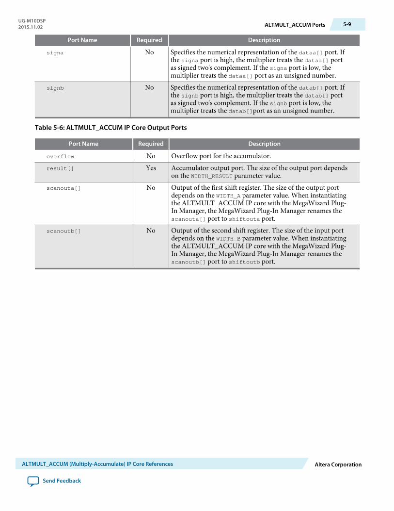
Port Name Required Description
signa No Specifies the numerical representation of the dataa[] port. Ifthe signa port is high, the multiplier treats the dataa[] portas signed two's complement. If the signa port is low, themultiplier treats the dataa[] port as an unsigned number.
signb No Specifies the numerical representation of the datab[] port. Ifthe signb port is high, the multiplier treats the datab[] portas signed two's complement. If the signb port is low, themultiplier treats the datab[]port as an unsigned number.
Table 5-6: ALTMULT_ACCUM IP Core Output Ports
Port Name Required Description
overflow No Overflow port for the accumulator.result[] Yes Accumulator output port. The size of the output port depends
on the WIDTH_RESULT parameter value.scanouta[] No Output of the first shift register. The size of the output port
depends on the WIDTH_A parameter value. When instantiatingthe ALTMULT_ACCUM IP core with the MegaWizard Plug-In Manager, the MegaWizard Plug-In Manager renames thescanouta[] port to shiftouta port.
scanoutb[] No Output of the second shift register. The size of the input portdepends on the WIDTH_B parameter value. When instantiatingthe ALTMULT_ACCUM IP core with the MegaWizard Plug-In Manager, the MegaWizard Plug-In Manager renames thescanoutb[] port to shiftoutb port.
UG-M10DSP2015.11.02 ALTMULT_ACCUM Ports 5-9
ALTMULT_ACCUM (Multiply-Accumulate) IP Core References Altera Corporation
Send Feedback
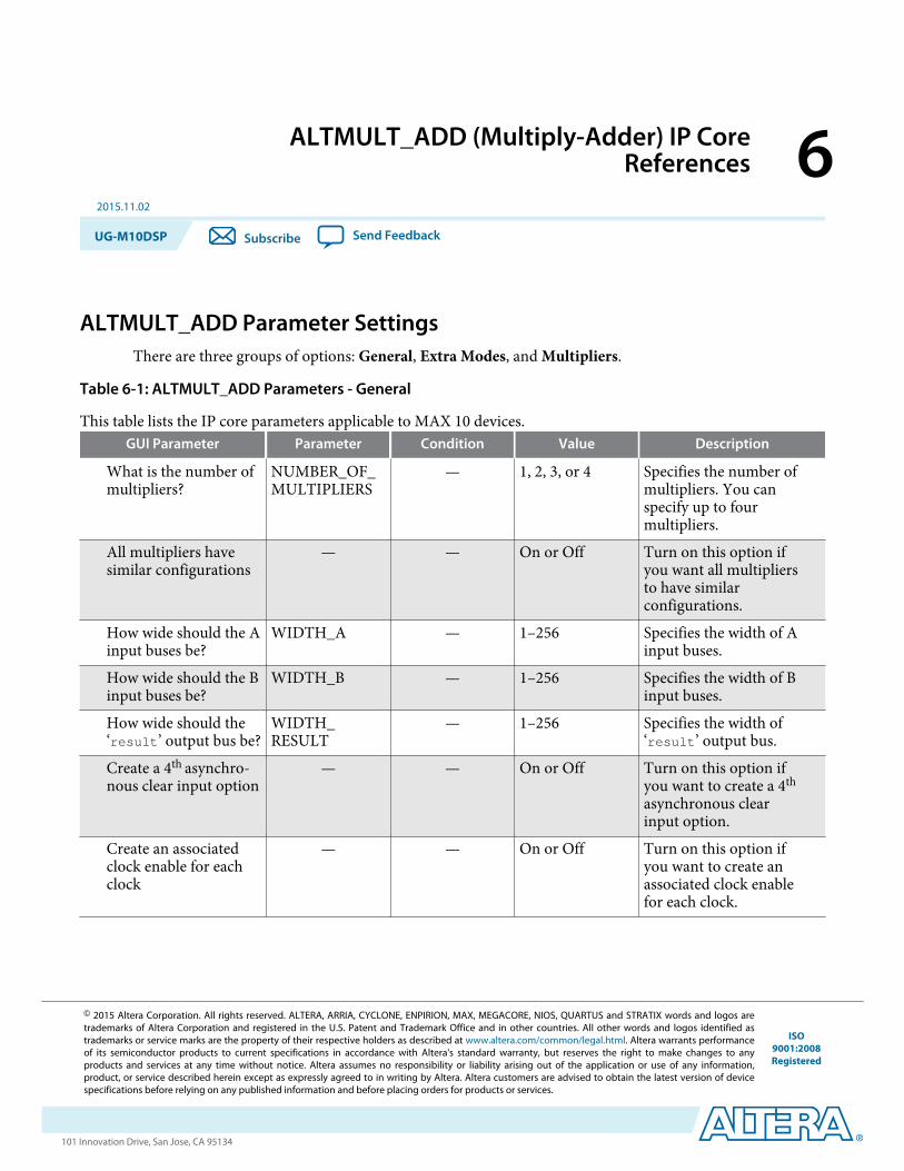
ALTMULT_ADD (Multiply-Adder) IP CoreReferences 6
2015.11.02
UG-M10DSP Subscribe Send Feedback
ALTMULT_ADD Parameter SettingsThere are three groups of options: General, Extra Modes, and Multipliers.
Table 6-1: ALTMULT_ADD Parameters - General
This table lists the IP core parameters applicable to MAX 10 devices.GUI Parameter Parameter Condition Value Description
What is the number ofmultipliers?
NUMBER_OF_MULTIPLIERS
— 1, 2, 3, or 4 Specifies the number ofmultipliers. You canspecify up to fourmultipliers.
All multipliers havesimilar configurations
— — On or Off Turn on this option ifyou want all multipliersto have similarconfigurations.
How wide should the Ainput buses be?
WIDTH_A — 1–256 Specifies the width of Ainput buses.
How wide should the Binput buses be?
WIDTH_B — 1–256 Specifies the width of Binput buses.
How wide should the‘result’ output bus be?
WIDTH_RESULT
— 1–256 Specifies the width of‘result’ output bus.
Create a 4th asynchro‐nous clear input option
— — On or Off Turn on this option ifyou want to create a 4th
asynchronous clearinput option.
Create an associatedclock enable for eachclock
— — On or Off Turn on this option ifyou want to create anassociated clock enablefor each clock.
© 2015 Altera Corporation. All rights reserved. ALTERA, ARRIA, CYCLONE, ENPIRION, MAX, MEGACORE, NIOS, QUARTUS and STRATIX words and logos aretrademarks of Altera Corporation and registered in the U.S. Patent and Trademark Office and in other countries. All other words and logos identified astrademarks or service marks are the property of their respective holders as described at www.altera.com/common/legal.html. Altera warrants performanceof its semiconductor products to current specifications in accordance with Altera's standard warranty, but reserves the right to make changes to anyproducts and services at any time without notice. Altera assumes no responsibility or liability arising out of the application or use of any information,product, or service described herein except as expressly agreed to in writing by Altera. Altera customers are advised to obtain the latest version of devicespecifications before relying on any published information and before placing orders for products or services.
ISO9001:2008Registered
www.altera.com101 Innovation Drive, San Jose, CA 95134
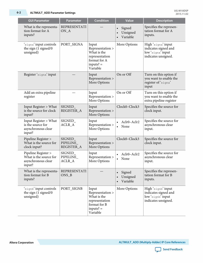
GUI Parameter Parameter Condition Value Description
What is the representa‐tion format for Ainputs?
REPRESENTATION_A
— • Signed• Unsigned• Variable
Specifies the represen‐tation format for Ainputs.
‘signa’ input controlsthe sign (1 signed/0unsigned)
PORT_SIGNA InputRepresentation >What is therepresentationformat for Ainputs? =Variable
More Options High ‘signa’ inputindicates signed andlow ‘signa’ inputindicates unsigned.
Register ‘signa’ input — InputRepresentation >More Options
On or Off Turn on this option ifyou want to enable theregister of ‘signa’input
Add an extra pipelineregister
— InputRepresentation >More Options
On or Off Turn on this option ifyou want to enable theextra pipeline register
Input Register > Whatis the source for clockinput?
SIGNED_REGISTER_A
InputRepresentation >More Options
Clock0–Clock3 Specifies the source forclock input.
Input Register > Whatis the source forasynchronous clearinput?
SIGNED_ACLR_A
InputRepresentation >More Options
• Aclr0–Aclr2• None
Specifies the source forasynchronous clearinput.
Pipeline Register >What is the source forclock input?
SIGNED_PIPELINE_REGISTER_A
InputRepresentation >More Options
Clock0–Clock3 Specifies the source forclock input.
Pipeline Register >What is the source forasynchronous clearinput?
SIGNED_PIPELINE_ACLR_A
InputRepresentation >More Options
• Aclr0–Aclr2• None
Specifies the source forasynchronous clearinput.
What is the representa‐tion format for Binputs?
REPRESENTATIONS_B
— • Signed• Unsigned• Variable
Specifies the represen‐tation format for Binputs.
‘signb’ input controlsthe sign (1 signed/0unsigned)
PORT_SIGNB InputRepresentation >What is therepresentationformat for Binputs? =Variable
More Options High ‘signb’ inputindicates signed andlow ‘signb’ inputindicates unsigned.
6-2 ALTMULT_ADD Parameter SettingsUG-M10DSP
2015.11.02
Altera Corporation ALTMULT_ADD (Multiply-Adder) IP Core References
Send Feedback
GUI Parameter Parameter Condition Value Description
Register ‘signb’ input — InputRepresentation >More Options
On or Off Turn on this option ifyou want to enable theregister of ‘signb’input
Add an extra pipelineregister
— InputRepresentation >More Options
On or Off Turn on this option ifyou want to enable theextra pipeline register
Input Register > Whatis the source for clockinput?
SIGNED_REGISTER_B
InputRepresentation >More Options
Clock0–Clock3 Specifies the source forclock input.
Input Register > Whatis the source forasynchronous clearinput?
SIGNED_ACLR_B
InputRepresentation >More Options
• Aclr0–Aclr2• None
Specifies the source forasynchronous clearinput.
Pipeline Register >What is the source forclock input?
SIGNED_PIPELINE_REGISTER_B
InputRepresentation >More Options
Clock0–Clock3 Specifies the source forclock input.
Pipeline Register >What is the source forasynchronous clearinput?
SIGNED_PIPELINE_ACLR_B
InputRepresentation >More Options
• Aclr0–Aclr2• None
Specifies the source forasynchronous clearinput.
Table 6-2: ALTMULT_ADD Parameters - Extra Modes
This table lists the IP core parameters applicable to MAX 10 devices.GUI Parameter Parameter Condition Value Description
Create a shiftoutoutput from A input ofthe last multiplier
— — On or Off Turn on to create asignal from A input.
Create a shiftoutoutput from B input ofthe last multiplier
— — On or Off Turn on to create asignal from B input.
Register output of theadder unit
— — On or Off Turn on to create aregister output of theadder unit.
What is the source forclock input?
OUTPUT_REGISTER
• OutputsConfiguration> Registeroutput of theadder unit =On
• OutputsConfiguration> MoreOptions
Clock0–Clock3 Specifies the clocksignal for the outputregister.
UG-M10DSP2015.11.02 ALTMULT_ADD Parameter Settings 6-3
ALTMULT_ADD (Multiply-Adder) IP Core References Altera Corporation
Send Feedback
GUI Parameter Parameter Condition Value Description
What is the source forasynchronous clearinput?
OUTPUT_ACLR • OutputsConfiguration> Registeroutput of theadder unit =On
• OutputsConfiguration> MoreOptions
• Aclr0–Aclr2• None
Specifies the source forasynchronous clearinput.
What operation shouldbe performed onoutputs of the first pairof multipliers?
MUTIPLIER1_DIRECTION
General > Whatis the number ofmultipliers? = 2,3, or 4
• Add• Subtract• Variable
Specifies whether thesecond multiplier addsor subtracts its valuefrom the sum. Valuesare add and subtract. IfVariable is selected theaddnsub1 port is used.
‘addnsub1’ inputcontrols the operation(1 add/0 sub)
— Adder Operation> Whatoperation shouldbe performed onoutputs of thefirst pair ofmultipliers? =Variable
More Options High ‘addnsub1’ inputindicates add and low‘addnsub1’ inputindicates subtract.
Register ‘addnsub1'input
— — On or Off Turn on this option ifyou want to enable theregister of ‘addnsub1’input
Add an extra pipelineregister
— — On or Off Turn on this option ifyou want to enable theextra pipeline register
Input Register > Whatis the source for clockinput?
ADDNSUB_MULTIPLIER_REGISTER[1]
Adder Operation> More Options
Clock0–Clock3 Specifies the source forclock input.
Input Register > Whatis the source forasynchronous clearinput?
ADDSUB_MULTIPLIER_ACLR[1]
Adder Operation> More Options
• Aclr0–Aclr2• None
Specifies the source forasynchronous clearinput.
Pipeline Register >What is the source forclock input?
ADDNSUB_MULTIPLIER_PIPELINE_REGISTER[1]
Adder Operation> More Options
Clock0–Clock3 Specifies the source forclock input.
6-4 ALTMULT_ADD Parameter SettingsUG-M10DSP
2015.11.02
Altera Corporation ALTMULT_ADD (Multiply-Adder) IP Core References
Send Feedback
GUI Parameter Parameter Condition Value Description
Pipeline Register >What is the source forasynchronous clearinput?
ADDNSUB_MULTIPLIER_PIPELINE_ACLR[1]
Adder Operation> More Options
• Aclr0–Aclr2• None
Specifies the source forasynchronous clearinput.
What operation shouldbe performed onoutputs of the secondpair of multipliers?
MUTIPLIER3_DIRECTION
General > Whatis the number ofmultipliers? = 4
— Specifies whether thefourth and allsubsequent odd-numbered multipliersadd or subtract theirresults from the total.Values are add andsubtract. If Variable isselected, the addnsub3port is used.
‘addnsub3’ inputcontrols the sign (1add/0 sub) - MoreOptions
— — — High ‘addnsub3’ inputindicates add and low‘addnsub3’ inputindicates subtract.
Register ‘addnsub3’input
— — On or Off Turn on this option ifyou want to enable theregister of ‘addnsub3’input.
Add an extra pipelineregister
— — On or Off Turn on this option ifyou want to enable theextra pipeline register.
Input Register > Whatis the source for clockinput?
ADDNSUB_MULTIPLIER_REGISTER[3]
Adder Operation> More Options
Clock0–Clock3 Specifies the source forclock input.
Input Register > Whatis the source forasynchronous clearinput?
ADDSUB_MULTIPLIER_ACLR[3]
Adder Operation> More Options
• Aclr0–Aclr2• None
Specifies the source forasynchronous clearinput.
Pipeline Register >What is the source forclock input?
ADDNSUB_MULTIPLIER_PIPELINE_REGISTER[3]
Adder Operation> More Options
Clock0–Clock3 Specifies the source forclock input.
Pipeline Register >What is the source forasynchronous clearinput?
ADDNSUB_MULTIPLIER_PIPELINE_ACLR[3]
Adder Operation> More Options
• Aclr0–Aclr2• None
Specifies the source forasynchronous clearinput.
UG-M10DSP2015.11.02 ALTMULT_ADD Parameter Settings 6-5
ALTMULT_ADD (Multiply-Adder) IP Core References Altera Corporation
Send Feedback
GUI Parameter Parameter Condition Value Description
Which multiplier-adder implementationshould be used?
DEDICATED_MULTIPLIER_CIRCUITRY
— • Use thedefaultimplementa‐tion
• Use dedicatedmultipliercircuitry (Notavailable forall families)
• Use logicelements
Specifies themultiplier-adderimplementation.
Table 6-3: ALTMULT_ADD Parameters - Multipliers
This table lists the IP core parameters applicable to MAX 10 devices.GUI Parameter Parameter Condition Value Description
Register input A of themultiplier
— — On or Off Turn on to enableregister input A of themultiplier.
What is the source forclock input?
INPUT_REGISTER_A[0..3]
• InputConfiguration> Registerinput A of themultiplier =On
• • InputConfiguration> MoreOptions
Clock0–Clock3 Specifies the source forclock input.
What is the source forasynchronous clearinput?
INPUT_ACLR_A[0..3]
• InputConfiguration> Registerinput A of themultiplier =On
• InputConfiguration> MoreOptions
• Aclr0–Aclr2• None
Specifies the source forasynchronous clearinput.
Register input B of themultiplier
— — On or Off Turn on to enableregister input B of themultiplier.
6-6 ALTMULT_ADD Parameter SettingsUG-M10DSP
2015.11.02
Altera Corporation ALTMULT_ADD (Multiply-Adder) IP Core References
Send Feedback
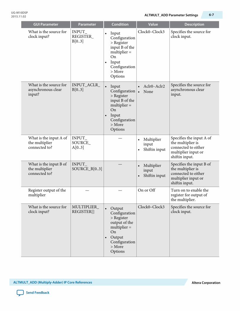
GUI Parameter Parameter Condition Value Description
What is the source forclock input?
INPUT_REGISTER_B[0..3]
• InputConfiguration> Registerinput B of themultiplier =On
• InputConfiguration> MoreOptions
Clock0–Clock3 Specifies the source forclock input.
What is the source forasynchronous clearinput?
INPUT_ACLR_B[0..3]
• InputConfiguration> Registerinput B of themultiplier =On
• InputConfiguration> MoreOptions
• Aclr0–Aclr2• None
Specifies the source forasynchronous clearinput.
What is the input A ofthe multiplierconnected to?
INPUT_SOURCE_A[0..3]
— • Multiplierinput
• Shiftin input
Specifies the input A ofthe multiplier isconnected to eithermultiplier input orshiftin input.
What is the input B ofthe multiplierconnected to?
INPUT_SOURCE_B[0..3]
— • Multiplierinput
• Shiftin input
Specifies the input B ofthe multiplier isconnected to eithermultiplier input orshiftin input.
Register output of themultiplier
— — On or Off Turn on to enable theregister for output ofthe multiplier.
What is the source forclock input?
MULTIPLIER_REGISTER[]
• OutputConfiguration> Registeroutput of themultiplier =On
• OutputConfiguration> MoreOptions
Clock0–Clock3 Specifies the source forclock input.
UG-M10DSP2015.11.02 ALTMULT_ADD Parameter Settings 6-7
ALTMULT_ADD (Multiply-Adder) IP Core References Altera Corporation
Send Feedback
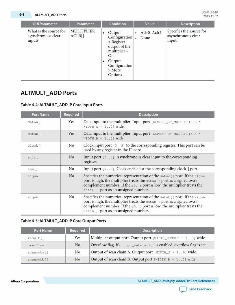
GUI Parameter Parameter Condition Value Description
What is the source forasynchronous clearinput?
MULTIPLIER_ACLR[]
• OutputConfiguration> Registeroutput of themultiplier =On
• OutputConfiguration> MoreOptions
• Aclr0–Aclr2• None
Specifies the source forasynchronous clearinput.
ALTMULT_ADD Ports
Table 6-4: ALTMULT_ADD IP Core Input Ports
Port Name Required Description
dataa[] Yes Data input to the multiplier. Input port [NUMBER_OF_MULTIPLIERS *WIDTH_A - 1..0] wide.
datab[] Yes Data input to the multiplier. Input port [NUMBER_OF_MULTIPLIERS *WIDTH_B - 1..0] wide.
clock[] No Clock input port [0..3] to the corresponding register. This port can beused by any register in the IP core.
aclr[] No Input port [0..3]. Asynchronous clear input to the correspondingregister.
ena[] No Input port [0..3]. Clock enable for the corresponding clock[] port.signa No Specifies the numerical representation of the dataa[] port. If the signa
port is high, the multiplier treats the dataa[] port as a signed two'scomplement number. If the signa port is low, the multiplier treats thedataa[] port as an unsigned number.
signb No Specifies the numerical representation of the datab[] port. If the signbport is high, the multiplier treats the datab[] port as a signed two'scomplement number. If the signb port is low, the multiplier treats thedatab[] port as an unsigned number.
Table 6-5: ALTMULT_ADD IP Core Output Ports
Port Name Required Description
result[] Yes Multiplier output port. Output port [WIDTH_RESULT - 1..0] wide.overflow No Overflow flag. If output_saturation is enabled, overflow flag is set.scanouta[] No Output of scan chain A. Output port [WIDTH_A - 1..0] wide.scanoutb[] No Output of scan chain B. Output port [WIDTH_B - 1..0] wide.
6-8 ALTMULT_ADD PortsUG-M10DSP
2015.11.02
Altera Corporation ALTMULT_ADD (Multiply-Adder) IP Core References
Send Feedback
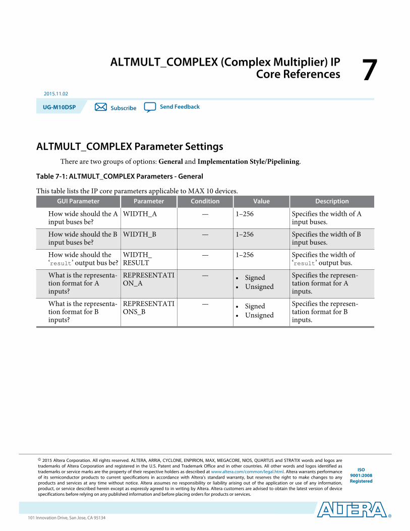
ALTMULT_COMPLEX (Complex Multiplier) IPCore References 7
2015.11.02
UG-M10DSP Subscribe Send Feedback
ALTMULT_COMPLEX Parameter SettingsThere are two groups of options: General and Implementation Style/Pipelining.
Table 7-1: ALTMULT_COMPLEX Parameters - General
This table lists the IP core parameters applicable to MAX 10 devices.GUI Parameter Parameter Condition Value Description
How wide should the Ainput buses be?
WIDTH_A — 1–256 Specifies the width of Ainput buses.
How wide should the Binput buses be?
WIDTH_B — 1–256 Specifies the width of Binput buses.
How wide should the‘result’ output bus be?
WIDTH_RESULT
— 1–256 Specifies the width of‘result’ output bus.
What is the representa‐tion format for Ainputs?
REPRESENTATION_A
— • Signed• Unsigned
Specifies the represen‐tation format for Ainputs.
What is the representa‐tion format for Binputs?
REPRESENTATIONS_B
— • Signed• Unsigned
Specifies the represen‐tation format for Binputs.
© 2015 Altera Corporation. All rights reserved. ALTERA, ARRIA, CYCLONE, ENPIRION, MAX, MEGACORE, NIOS, QUARTUS and STRATIX words and logos aretrademarks of Altera Corporation and registered in the U.S. Patent and Trademark Office and in other countries. All other words and logos identified astrademarks or service marks are the property of their respective holders as described at www.altera.com/common/legal.html. Altera warrants performanceof its semiconductor products to current specifications in accordance with Altera's standard warranty, but reserves the right to make changes to anyproducts and services at any time without notice. Altera assumes no responsibility or liability arising out of the application or use of any information,product, or service described herein except as expressly agreed to in writing by Altera. Altera customers are advised to obtain the latest version of devicespecifications before relying on any published information and before placing orders for products or services.
ISO9001:2008Registered
www.altera.com101 Innovation Drive, San Jose, CA 95134
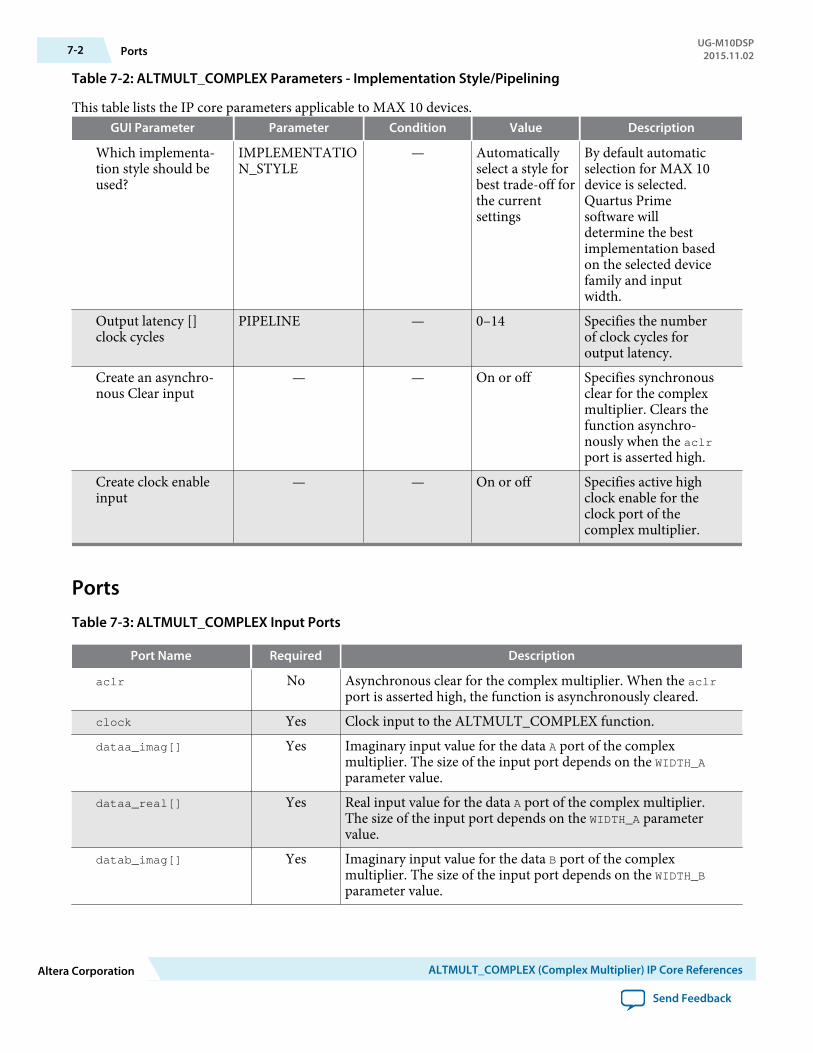
Table 7-2: ALTMULT_COMPLEX Parameters - Implementation Style/Pipelining
This table lists the IP core parameters applicable to MAX 10 devices.GUI Parameter Parameter Condition Value Description
Which implementa‐tion style should beused?
IMPLEMENTATION_STYLE
— Automaticallyselect a style forbest trade-off forthe currentsettings
By default automaticselection for MAX 10device is selected.Quartus Primesoftware willdetermine the bestimplementation basedon the selected devicefamily and inputwidth.
Output latency []clock cycles
PIPELINE — 0–14 Specifies the numberof clock cycles foroutput latency.
Create an asynchro‐nous Clear input
— — On or off Specifies synchronousclear for the complexmultiplier. Clears thefunction asynchro‐nously when the aclrport is asserted high.
Create clock enableinput
— — On or off Specifies active highclock enable for theclock port of thecomplex multiplier.
PortsTable 7-3: ALTMULT_COMPLEX Input Ports
Port Name Required Description
aclr No Asynchronous clear for the complex multiplier. When the aclrport is asserted high, the function is asynchronously cleared.
clock Yes Clock input to the ALTMULT_COMPLEX function.dataa_imag[] Yes Imaginary input value for the data A port of the complex
multiplier. The size of the input port depends on the WIDTH_Aparameter value.
dataa_real[] Yes Real input value for the data A port of the complex multiplier.The size of the input port depends on the WIDTH_A parametervalue.
datab_imag[] Yes Imaginary input value for the data B port of the complexmultiplier. The size of the input port depends on the WIDTH_Bparameter value.
7-2 PortsUG-M10DSP
2015.11.02
Altera Corporation ALTMULT_COMPLEX (Complex Multiplier) IP Core References
Send Feedback
Port Name Required Description
datab_real[] Yes Real input value for the data B port of the complex multiplier.The size of the input port depends on the WIDTH_B parametervalue.
ena No Active high clock enable for the clock port of the complexmultiplier.
Table 7-4: ALTMULT_COMPLEX Output Ports
Port Name Required Description
result_imag Yes Imaginary output value of the multiplier. The size of the output portdepends on the WIDTH_RESULT parameter value.
result_real Yes Real output value of the multiplier. The size of the output port dependson the WIDTH_RESULT parameter value.
UG-M10DSP2015.11.02 Ports 7-3
ALTMULT_COMPLEX (Complex Multiplier) IP Core References Altera Corporation
Send Feedback
Additional Information for MAX 10 EmbeddedMultipliers User Guide A
2015.11.02
UG-M10DSP Subscribe Send Feedback
Document Revision History for MAX 10 Embedded Multipliers User GuideDate Version Changes
November2015
2015.11.02 • Changed instances of Quartus II to Quartus Prime.• Removed topics on generating IP cores and added links to Introduc‐
tion to Altera IP Cores, Creating Version-Independent IP and QsysSimulation Scripts, and Project Management Best Practices.
September2014
2014.09.22 Initial release.
© 2015 Altera Corporation. All rights reserved. ALTERA, ARRIA, CYCLONE, ENPIRION, MAX, MEGACORE, NIOS, QUARTUS and STRATIX words and logos aretrademarks of Altera Corporation and registered in the U.S. Patent and Trademark Office and in other countries. All other words and logos identified astrademarks or service marks are the property of their respective holders as described at www.altera.com/common/legal.html. Altera warrants performanceof its semiconductor products to current specifications in accordance with Altera's standard warranty, but reserves the right to make changes to anyproducts and services at any time without notice. Altera assumes no responsibility or liability arising out of the application or use of any information,product, or service described herein except as expressly agreed to in writing by Altera. Altera customers are advised to obtain the latest version of devicespecifications before relying on any published information and before placing orders for products or services.
ISO9001:2008Registered
www.altera.com101 Innovation Drive, San Jose, CA 95134

MAX 10 Clocking and PLL User Guide
Subscribe
Send Feedback
UG-M10CLKPLL2015.11.02
101 Innovation DriveSan Jose, CA 95134www.altera.com
Contents
MAX 10 Clocking and PLL Overview................................................................. 1-1Clock Networks Overview.......................................................................................................................... 1-1Internal Oscillator Overview...................................................................................................................... 1-1PLLs Overview..............................................................................................................................................1-1
MAX 10 Clocking and PLL Architecture and Features...................................... 2-1Clock Networks Architecture and Features............................................................................................. 2-1
Global Clock Networks................................................................................................................... 2-1Clock Pins Introduction..................................................................................................................2-1Clock Resources............................................................................................................................... 2-2Global Clock Network Sources...................................................................................................... 2-2Global Clock Control Block............................................................................................................2-4Global Clock Network Power Down.............................................................................................2-6Clock Enable Signals........................................................................................................................2-7
Internal Oscillator Architecture and Features......................................................................................... 2-8PLLs Architecture and Features.................................................................................................................2-8
PLL Architecture.............................................................................................................................. 2-8PLL Features................................................................................................................................... 2-10PLL Locations................................................................................................................................. 2-10Clock Pin to PLL Connections.....................................................................................................2-12PLL Counter to GCLK Connections........................................................................................... 2-12PLL Control Signals.......................................................................................................................2-13Clock Feedback Modes..................................................................................................................2-14PLL External Clock Output.......................................................................................................... 2-17ADC Clock Input from PLL......................................................................................................... 2-19Spread-Spectrum Clocking...........................................................................................................2-19PLL Programmable Parameters................................................................................................... 2-19Clock Switchover........................................................................................................................... 2-22PLL Cascading................................................................................................................................2-26PLL Reconfiguration..................................................................................................................... 2-26
MAX 10 Clocking and PLL Design Considerations........................................... 3-1Clock Networks Design Considerations...................................................................................................3-1
Guideline: Clock Enable Signals.................................................................................................... 3-1Guideline: Connectivity Restrictions............................................................................................ 3-1
Internal Oscillator Design Considerations...............................................................................................3-2Guideline: Connectivity Restrictions............................................................................................ 3-2
PLLs Design Considerations...................................................................................................................... 3-2Guideline: PLL Control Signals......................................................................................................3-2Guideline: Connectivity Restrictions............................................................................................ 3-2Guideline: Self-Reset........................................................................................................................3-2
TOC-2
Altera Corporation
Guideline: Output Clocks............................................................................................................... 3-3Guideline: PLL Cascading...............................................................................................................3-3Guideline: Clock Switchover.......................................................................................................... 3-4Guideline: .mif Streaming in PLL Reconfiguration.....................................................................3-5Guideline: scandone Signal for PLL Reconfiguration.................................................................3-5
MAX 10 Clocking and PLL Implementation Guides......................................... 4-1ALTCLKCTRL IP Core...............................................................................................................................4-1ALTPLL IP Core.......................................................................................................................................... 4-1
Expanding the PLL Lock Range..................................................................................................... 4-2Programmable Bandwidth with Advanced Parameters............................................................. 4-3PLL Dynamic Reconfiguration Implementation.........................................................................4-4Dynamic Phase Configuration Implementation......................................................................... 4-8
ALTPLL_RECONFIG IP Core.................................................................................................................4-10Obtaining the Resource Utilization Report................................................................................4-11
Internal Oscillator IP Core....................................................................................................................... 4-11
ALTCLKCTRL IP Core References.....................................................................5-1ALTCLKCTRL Parameters.........................................................................................................................5-1ALTCLKCTRL Ports and Signals.............................................................................................................. 5-2
ALTPLL IP Core References............................................................................... 6-1ALTPLL Parameters.................................................................................................................................... 6-1
Operation Modes Parameter Settings........................................................................................... 6-1PLL Control Signals Parameter Settings.......................................................................................6-2Programmable Bandwidth Parameter Settings............................................................................6-2Clock Switchover Parameter Settings........................................................................................... 6-3PLL Dynamic Reconfiguration Parameter Settings.................................................................... 6-4Dynamic Phase Configuration Parameter Settings.....................................................................6-4Output Clocks Parameter Settings.................................................................................................6-5
ALTPLL Ports and Signals..........................................................................................................................6-6
ALTPLL_RECONFIG IP Core References......................................................... 7-1ALTPLL_RECONFIG Parameters............................................................................................................ 7-1ALTPLL_RECONFIG Ports and Signals.................................................................................................. 7-2ALTPLL_RECONFIG Counter Settings...................................................................................................7-7
Internal Oscillator IP Core References...............................................................8-1Internal Oscillator Parameters................................................................................................................... 8-1Internal Oscillator Ports and Signals.........................................................................................................8-1
Additional Information for MAX 10 Clocking and PLL User Guide............... A-1Document Revision History for MAX 10 Clocking and PLL User Guide..........................................A-1
TOC-3
Altera Corporation
MAX 10 Clocking and PLL Overview 12015.11.02
UG-M10CLKPLL Subscribe Send Feedback
Clock Networks OverviewMAX® 10 devices support global clock (GCLK) networks.
Clock networks provide clock sources for the core. You can use clock networks in high fan-out globalsignal network such as reset and clear.
Internal Oscillator OverviewMAX 10 devices offer built-in internal oscillator up to 116 MHz.
You can enable or disable the internal oscillator.
PLLs OverviewPhase-locked loops (PLLs) provide robust clock management and synthesis for device clock management,external system clock management, and I/O interface clocking.
You can use the PLLs as follows:
• Zero-delay buffer• Jitter attenuator• Low-skew fan-out buffer• Frequency synthesizer• Reduce the number of oscillators required on the board• Reduce the clock pins used in the device by synthesizing multiple clock frequencies from a single
reference clock source• On-chip clock de-skew• Dynamic phase shift• Counters reconfiguration• Bandwidth reconfiguration• Programmable output duty cycle
© 2015 Altera Corporation. All rights reserved. ALTERA, ARRIA, CYCLONE, ENPIRION, MAX, MEGACORE, NIOS, QUARTUS and STRATIX words and logos aretrademarks of Altera Corporation and registered in the U.S. Patent and Trademark Office and in other countries. All other words and logos identified astrademarks or service marks are the property of their respective holders as described at www.altera.com/common/legal.html. Altera warrants performanceof its semiconductor products to current specifications in accordance with Altera's standard warranty, but reserves the right to make changes to anyproducts and services at any time without notice. Altera assumes no responsibility or liability arising out of the application or use of any information,product, or service described herein except as expressly agreed to in writing by Altera. Altera customers are advised to obtain the latest version of devicespecifications before relying on any published information and before placing orders for products or services.
ISO9001:2008Registered
www.altera.com101 Innovation Drive, San Jose, CA 95134

• PLL cascading• Reference clock switchover• Drive the analog-to-digital converter (ADC) clock
1-2 PLLs OverviewUG-M10CLKPLL
2015.11.02
Altera Corporation MAX 10 Clocking and PLL Overview
Send Feedback
MAX 10 Clocking and PLL Architecture andFeatures 2
2015.11.02
UG-M10CLKPLL Subscribe Send Feedback
Clock Networks Architecture and Features
Global Clock NetworksGCLKs drive throughout the entire device, feeding all device quadrants. All resources in the device, suchas the I/O elements, logic array blocks (LABs), dedicated multiplier blocks, and M9K memory blocks canuse GCLKs as clock sources. Use these clock network resources for control signals, such as clock enablesand clears fed by an external pin. Internal logic can also drive GCLKs for internally-generated GCLKs andasynchronous clears, clock enables, or other control signals with high fan-out.
Clock Pins IntroductionThere are two types of external clock pins that can drive the GCLK networks.
Dedicated Clock Input Pins
You can use the dedicated clock input pins (CLK<#>[p,n]) to drive clock and global signals, such asasynchronous clears, presets, and clock enables for GCLK networks.
If you do not use the dedicated clock input pins for clock input, you can also use them as general-purposeinput or output pins.
The CLK pins can be single-ended or differential inputs. When you use the CLK pins as single-ended clockinputs, both the CLK<#>p and CLK<#>n pins have dedicated connection to the GCLK networks. When youuse the CLK pins as differential inputs, pair two clock pins of the same number to receive differentialsignaling.
Dual-Purpose Clock Pins
You can use the dual-purpose clock (DPCLK) pins for high fan-out control signals, such as protocol signals,TRDY and IRDY signals for PCI via GCLK networks.
The DPCLK pins are only available on the left and right of the I/O banks.
© 2015 Altera Corporation. All rights reserved. ALTERA, ARRIA, CYCLONE, ENPIRION, MAX, MEGACORE, NIOS, QUARTUS and STRATIX words and logos aretrademarks of Altera Corporation and registered in the U.S. Patent and Trademark Office and in other countries. All other words and logos identified astrademarks or service marks are the property of their respective holders as described at www.altera.com/common/legal.html. Altera warrants performanceof its semiconductor products to current specifications in accordance with Altera's standard warranty, but reserves the right to make changes to anyproducts and services at any time without notice. Altera assumes no responsibility or liability arising out of the application or use of any information,product, or service described herein except as expressly agreed to in writing by Altera. Altera customers are advised to obtain the latest version of devicespecifications before relying on any published information and before placing orders for products or services.
ISO9001:2008Registered
www.altera.com101 Innovation Drive, San Jose, CA 95134
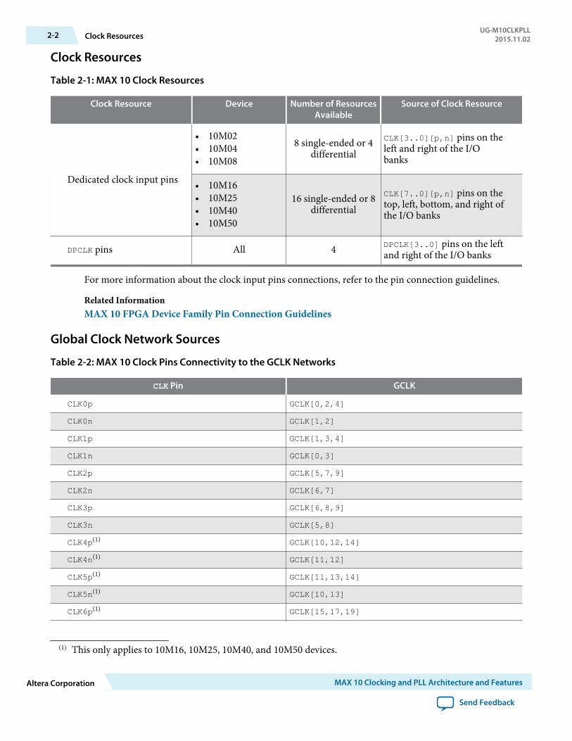
Clock Resources
Table 2-1: MAX 10 Clock Resources
Clock Resource Device Number of ResourcesAvailable
Source of Clock Resource
Dedicated clock input pins
• 10M02• 10M04• 10M08
8 single-ended or 4differential
CLK[3..0][p,n] pins on theleft and right of the I/Obanks
• 10M16• 10M25• 10M40• 10M50
16 single-ended or 8differential
CLK[7..0][p,n] pins on thetop, left, bottom, and right ofthe I/O banks
DPCLK pins All 4 DPCLK[3..0] pins on the leftand right of the I/O banks
For more information about the clock input pins connections, refer to the pin connection guidelines.
Related InformationMAX 10 FPGA Device Family Pin Connection Guidelines
Global Clock Network Sources
Table 2-2: MAX 10 Clock Pins Connectivity to the GCLK Networks
CLK Pin GCLK
CLK0p GCLK[0,2,4]
CLK0n GCLK[1,2]
CLK1p GCLK[1,3,4]
CLK1n GCLK[0,3]
CLK2p GCLK[5,7,9]
CLK2n GCLK[6,7]
CLK3p GCLK[6,8,9]
CLK3n GCLK[5,8]
CLK4p(1) GCLK[10,12,14]
CLK4n(1) GCLK[11,12]
CLK5p(1) GCLK[11,13,14]
CLK5n(1) GCLK[10,13]
CLK6p(1) GCLK[15,17,19]
(1) This only applies to 10M16, 10M25, 10M40, and 10M50 devices.
2-2 Clock ResourcesUG-M10CLKPLL
2015.11.02
Altera Corporation MAX 10 Clocking and PLL Architecture and Features
Send Feedback
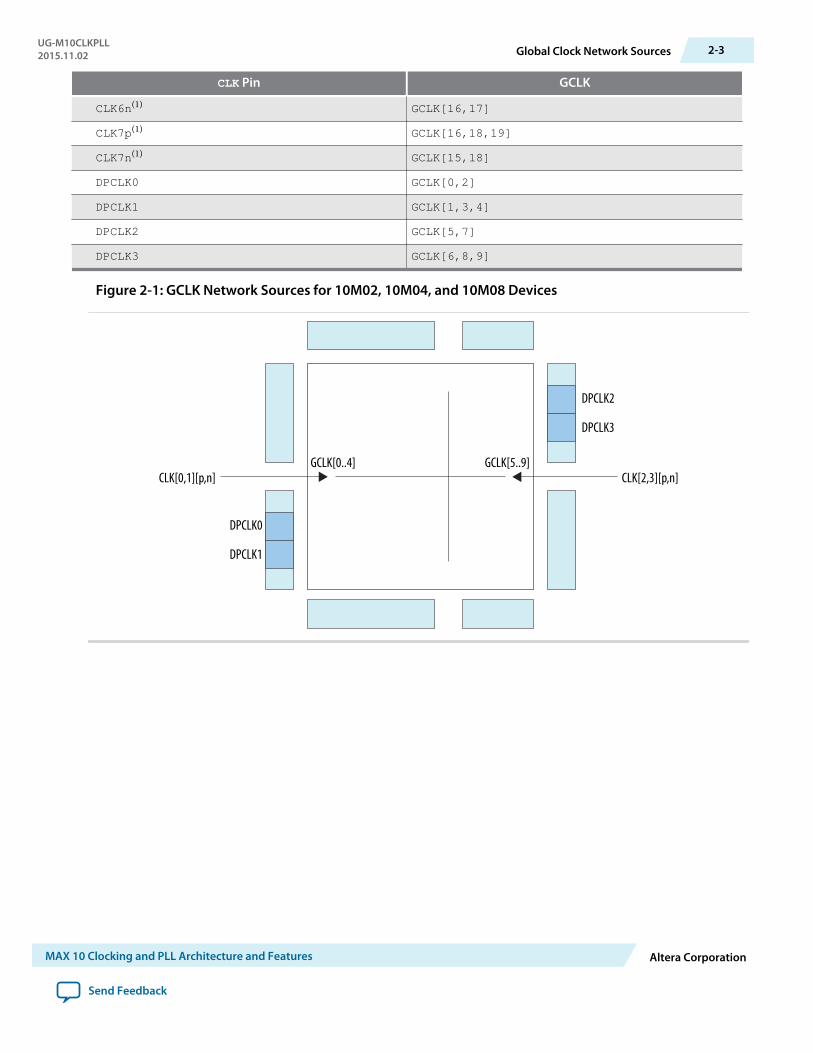
CLK Pin GCLK
CLK6n(1) GCLK[16,17]
CLK7p(1) GCLK[16,18,19]
CLK7n(1) GCLK[15,18]
DPCLK0 GCLK[0,2]
DPCLK1 GCLK[1,3,4]
DPCLK2 GCLK[5,7]
DPCLK3 GCLK[6,8,9]
Figure 2-1: GCLK Network Sources for 10M02, 10M04, and 10M08 Devices
DPCLK2
DPCLK3
DPCLK0
DPCLK1
CLK[0,1][p,n] CLK[2,3][p,n]GCLK[0..4] GCLK[5..9]
UG-M10CLKPLL2015.11.02 Global Clock Network Sources 2-3
MAX 10 Clocking and PLL Architecture and Features Altera Corporation
Send Feedback
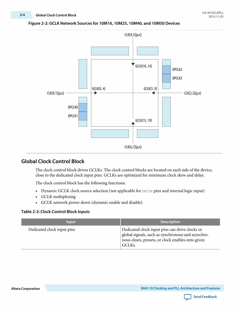
Figure 2-2: GCLK Network Sources for 10M16, 10M25, 10M40, and 10M50 Devices
DPCLK2
DPCLK3
DPCLK0
DPCLK1
CLK[0,1][p,n] CLK[2,3][p,n]GCLK[0..4] GCLK[5..9]
CLK[4,5][p,n]
CLK[6,7][p,n]
GCLK[15..19]
GCLK[10..14]
Global Clock Control BlockThe clock control block drives GCLKs. The clock control blocks are located on each side of the device,close to the dedicated clock input pins. GCLKs are optimized for minimum clock skew and delay.
The clock control block has the following functions:
• Dynamic GCLK clock source selection (not applicable for DPCLK pins and internal logic input)• GCLK multiplexing• GCLK network power down (dynamic enable and disable)
Table 2-3: Clock Control Block Inputs
Input Description
Dedicated clock input pins Dedicated clock input pins can drive clocks orglobal signals, such as synchronous and asynchro‐nous clears, presets, or clock enables onto givenGCLKs.
2-4 Global Clock Control BlockUG-M10CLKPLL
2015.11.02
Altera Corporation MAX 10 Clocking and PLL Architecture and Features
Send Feedback
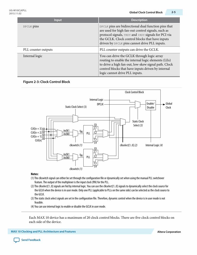
Input Description
DPCLK pins DPCLK pins are bidirectional dual function pins thatare used for high fan-out control signals, such asprotocol signals, TRDY and IRDY signals for PCI viathe GCLK. Clock control blocks that have inputsdriven by DPCLK pins cannot drive PLL inputs.
PLL counter outputs PLL counter outputs can drive the GCLK.
Internal logic You can drive the GCLK through logic arrayrouting to enable the internal logic elements (LEs)to drive a high fan-out, low-skew signal path. Clockcontrol blocks that have inputs driven by internallogic cannot drive PLL inputs.
Figure 2-3: Clock Control Block
clkswitch (1)
Static Clock Select (3)
Static ClockSelect (3)
Internal Logic
Clock Control Block
DPCLK
clkselect[1..0] (2) Internal Logic (4)
inclk1inclk0
CLK[n + 3]CLK[n + 2]CLK[n + 1]
CLK[n]
fIN
C0C1C2PLL
GlobalClock
Enable/Disable
C3C4
Notes:(1) The clkswitch signal can either be set through the configuration file or dynamically set when using the manual PLL switchover feature. The output of the multiplexer is the input clock (fIN) for the PLL.(2) The clkselect[1..0] signals are fed by internal logic. You can use the clkselect[1..0] signals to dynamically select the clock source for the GCLK when the device is in user mode. Only one PLL (applicable to PLLs on the same side) can be selected as the clock source to the GCLK.(3) The static clock select signals are set in the configuration file. Therefore, dynamic control when the device is in user mode is not feasible.(4) You can use internal logic to enable or disable the GCLK in user mode.
clkswitch (1)
inclk1inclk0
fIN
C0C1C2PLL
C3C4
Each MAX 10 device has a maximum of 20 clock control blocks. There are five clock control blocks oneach side of the device.
UG-M10CLKPLL2015.11.02 Global Clock Control Block 2-5
MAX 10 Clocking and PLL Architecture and Features Altera Corporation
Send Feedback
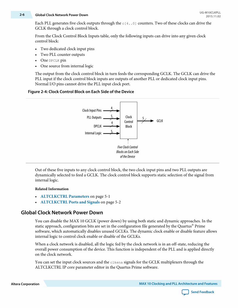
Each PLL generates five clock outputs through the c[4..0] counters. Two of these clocks can drive theGCLK through a clock control block.
From the Clock Control Block Inputs table, only the following inputs can drive into any given clockcontrol block:
• Two dedicated clock input pins• Two PLL counter outputs• One DPCLK pin• One source from internal logic
The output from the clock control block in turn feeds the corresponding GCLK. The GCLK can drive thePLL input if the clock control block inputs are outputs of another PLL or dedicated clock input pins.Normal I/O pins cannot drive the PLL input clock port.
Figure 2-4: Clock Control Block on Each Side of the Device
5GCLK
Clock Input Pins4
DPCLK
Internal Logic
ClockControlBlock
5PLL Outputs
5
4
Five Clock ControlBlocks on Each Side
of the Device
Out of these five inputs to any clock control block, the two clock input pins and two PLL outputs aredynamically selected to feed a GCLK. The clock control block supports static selection of the signal frominternal logic.
Related Information
• ALTCLKCTRL Parameters on page 5-1• ALTCLKCTRL Ports and Signals on page 5-2
Global Clock Network Power DownYou can disable the MAX 10 GCLK (power down) by using both static and dynamic approaches. In thestatic approach, configuration bits are set in the configuration file generated by the Quartus® Primesoftware, which automatically disables unused GCLKs. The dynamic clock enable or disable feature allowsinternal logic to control clock enable or disable of the GCLKs.
When a clock network is disabled, all the logic fed by the clock network is in an off-state, reducing theoverall power consumption of the device. This function is independent of the PLL and is applied directlyon the clock network.
You can set the input clock sources and the clkena signals for the GCLK multiplexers through theALTCLKCTRL IP core parameter editor in the Quartus Prime software.
2-6 Global Clock Network Power DownUG-M10CLKPLL
2015.11.02
Altera Corporation MAX 10 Clocking and PLL Architecture and Features
Send Feedback
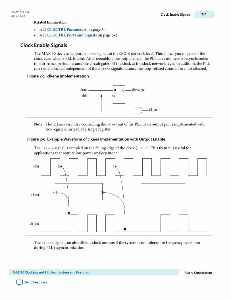
Related Information
• ALTCLKCTRL Parameters on page 5-1• ALTCLKCTRL Ports and Signals on page 5-2
Clock Enable SignalsThe MAX 10 devices support clkena signals at the GCLK network level. This allows you to gate off theclock even when a PLL is used. After reenabling the output clock, the PLL does not need a resynchroniza‐tion or relock period because the circuit gates off the clock at the clock network level. In addition, the PLLcan remain locked independent of the clkena signals because the loop-related counters are not affected.
Figure 2-5: clkena Implementation
clkena clkena_out
clk_out
clkinD Q
Note: The clkena circuitry controlling the C0 output of the PLL to an output pin is implemented withtwo registers instead of a single register.
Figure 2-6: Example Waveform of clkena Implementation with Output Enable
The clkena signal is sampled on the falling edge of the clock (clkin). This feature is useful forapplications that require low power or sleep mode.
clkin
clkena
clk_out
The clkena signal can also disable clock outputs if the system is not tolerant to frequency overshootduring PLL resynchronization.
UG-M10CLKPLL2015.11.02 Clock Enable Signals 2-7
MAX 10 Clocking and PLL Architecture and Features Altera Corporation
Send Feedback
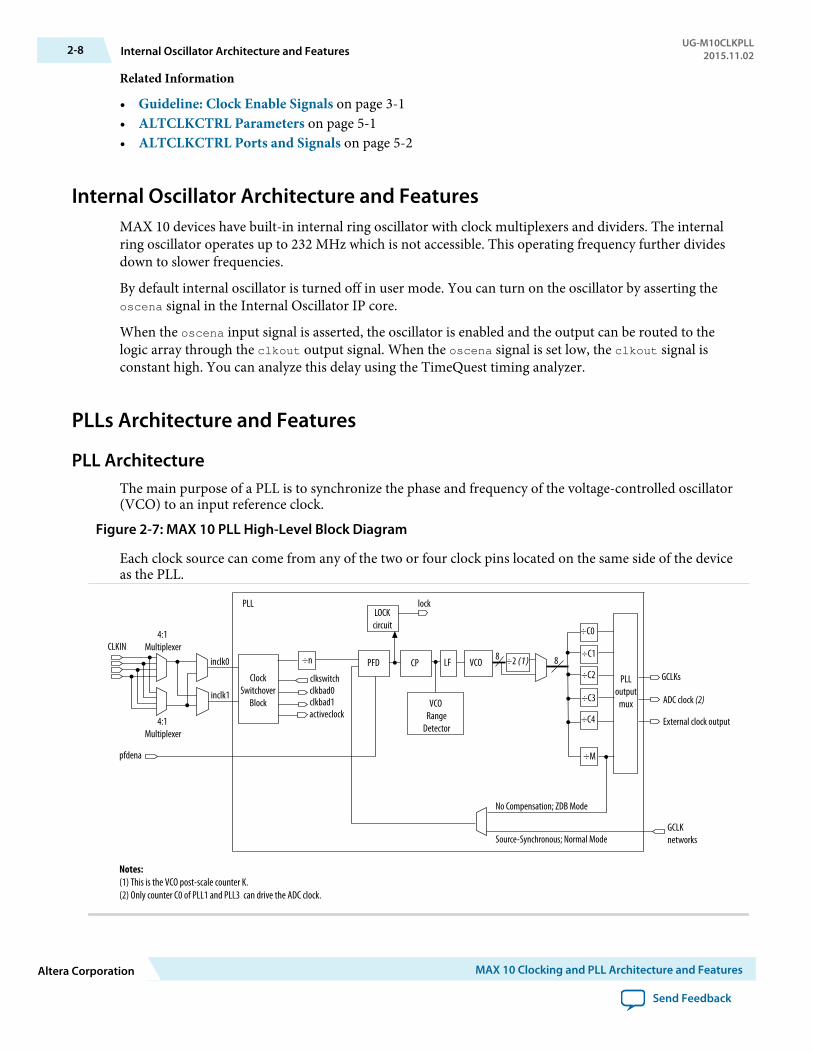
Related Information
• Guideline: Clock Enable Signals on page 3-1• ALTCLKCTRL Parameters on page 5-1• ALTCLKCTRL Ports and Signals on page 5-2
Internal Oscillator Architecture and FeaturesMAX 10 devices have built-in internal ring oscillator with clock multiplexers and dividers. The internalring oscillator operates up to 232 MHz which is not accessible. This operating frequency further dividesdown to slower frequencies.
By default internal oscillator is turned off in user mode. You can turn on the oscillator by asserting theoscena signal in the Internal Oscillator IP core.
When the oscena input signal is asserted, the oscillator is enabled and the output can be routed to thelogic array through the clkout output signal. When the oscena signal is set low, the clkout signal isconstant high. You can analyze this delay using the TimeQuest timing analyzer.
PLLs Architecture and Features
PLL ArchitectureThe main purpose of a PLL is to synchronize the phase and frequency of the voltage-controlled oscillator(VCO) to an input reference clock.
Figure 2-7: MAX 10 PLL High-Level Block Diagram
Each clock source can come from any of the two or four clock pins located on the same side of the deviceas the PLL.
ClockSwitchover
Block
inclk0
inclk1
pfdena
clkswitchclkbad0clkbad1activeclock
PFD
LOCKcircuit
lock
÷n CP LF VCO ÷2 (1)
÷C0
÷C1
÷C2
÷C3
÷C4
÷M
PLL output
mux
GCLKs
ADC clock (2)
8 8
GCLK networks
No Compensation; ZDB Mode
Source-Synchronous; Normal Mode
VCO Range
Detector
Notes:(1) This is the VCO post-scale counter K.(2) Only counter C0 of PLL1 and PLL3 can drive the ADC clock.
PLL
External clock output
4:1 Multiplexer
4:1 Multiplexer
CLKIN
2-8 Internal Oscillator Architecture and FeaturesUG-M10CLKPLL
2015.11.02
Altera Corporation MAX 10 Clocking and PLL Architecture and Features
Send Feedback
Phase-Frequency Detector (PFD)
The PFD has inputs from the feedback clock, fFB, and the input reference clock, fREF. The PLL comparesthe rising edge of the input reference clock to a feedback clock using a PFD. The PFD produces an up ordown signal that determines whether the VCO needs to operate at a higher or lower frequency.
Charge Pump (CP)
If the charge pump receives a logic high on the up signal, current is driven into the loop filter. If thecharge pump receives a logic high on the down signal, current is drawn from the loop filter.
Loop Filter (LF)
The loop filter converts the up and down signals from the PFD to a voltage that is used to bias the VCO.The loop filter filters out glitches from the charge pump and prevents voltage overshoot, which minimizesjitter on the VCO.
Voltage-Controlled Oscillator (VCO)
The voltage from the charge pump determines how fast the VCO operates. The VCO is implemented as afour-stage differential ring oscillator. A divide counter, M, is inserted in the feedback loop to increase theVCO frequency, fVCO, above the input reference frequency, fREF.
The VCO frequency is determined using the following equation:
fVCO = fREF × M = fIN × M/N ,
where fIN is the input clock frequency to the PLL and N is the pre-scale counter.
The VCO frequency is a critical parameter that must be between 600 and 1,300 MHz to ensure properoperation of the PLL. The Quartus Prime software automatically sets the VCO frequency within therecommended range based on the clock output and phase shift requirements in your design.
Post-Scale Counters (C)
The VCO output can feed up to five post-scale counters (C0, C1, C2, C3, and C4). These post-scale countersallow the PLL to produce a number of harmonically-related frequencies.
Internal Delay Elements
The MAX 10 PLLs have internal delay elements to compensate for routing on the GCLK networks andI/O buffers. These internal delays are fixed.
PLL Outputs
The MAX 10 PLL supports up to 5 GCLK outputs and 1 dedicated external clock output. The outputfrequency, fOUT, to the GCLK network or dedicated external clock output is determined using thefollowing equation:
fREF = fIN/N and
fOUT = fVCO/C = (fREF × M)/C = (fIN × M)/(N × C),
where C is the setting on the C0, C1, C2, C3, or C4 counter.
UG-M10CLKPLL2015.11.02 PLL Architecture 2-9
MAX 10 Clocking and PLL Architecture and Features Altera Corporation
Send Feedback
PLL Features
Table 2-4: MAX 10 PLL Features
Feature Support
C output counters 5M, N, C counter sizes 1 to 512 (2)
Dedicated clock outputs 1 single-ended or 1 differentialDedicated clock input pins 4 single-ended or 2 differentialSpread-spectrum input clock tracking Yes (3)
PLL cascading Through GCLKSource synchronous compensation YesNo compensation mode YesNormal compensation YesZero-delay buffer compensation YesPhase shift resolution Down to 96 ps increments (4)
Programmable duty cycle YesOutput counter cascading YesInput clock switchover YesUser mode reconfiguration YesLoss of lock detection Yes4:1 multiplexer CLK input selection Yes
PLL LocationsThe following figures show the physical locations of the PLLs. Every index represents one PLL in thedevice. The physical locations of the PLLs correspond to the coordinates in the Quartus Prime ChipPlanner.
(2) C counters range from 1 through 512 if the output clock uses a 50% duty cycle. For any output clocks using anon-50% duty cycle, the post-scale counters range from 1 through 256.
(3) Only applicable if the input clock jitter is in the input jitter tolerance specifications.(4) The smallest phase shift is determined by the VCO period divided by eight. For degree increments, the
MAX 10 device family can shift all output frequencies in increments of at least 45°. Smaller degreeincrements are possible depending on the frequency and divide parameters.
2-10 PLL FeaturesUG-M10CLKPLL
2015.11.02
Altera Corporation MAX 10 Clocking and PLL Architecture and Features
Send Feedback
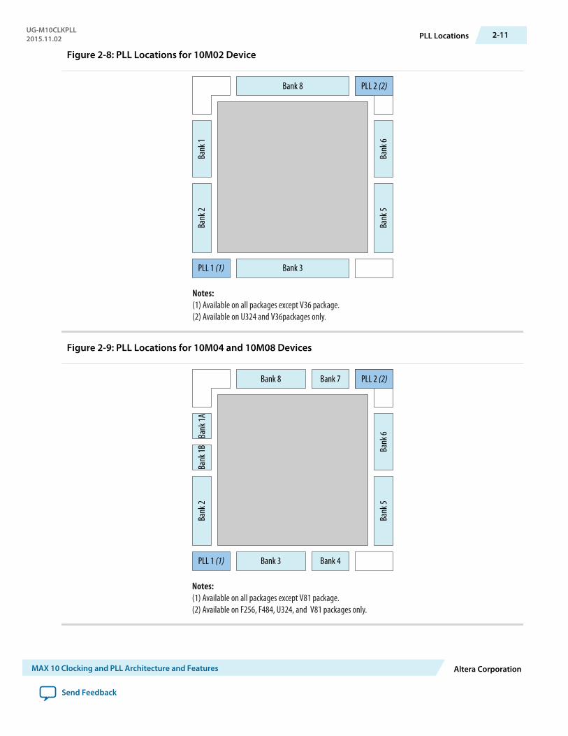
Figure 2-8: PLL Locations for 10M02 Device
Bank 8
Bank 3
Bank
1Ba
nk 2
Bank
6Ba
nk 5
PLL 1 (1)
PLL 2 (2)
Notes:(1) Available on all packages except V36 package.(2) Available on U324 and V36packages only.
Figure 2-9: PLL Locations for 10M04 and 10M08 Devices
Bank 8
Bank
1ABa
nk 2
Bank
6Ba
nk 5
PLL 1 (1)
PLL 2 (2)Bank 7
Bank 3 Bank 4
Bank
1B
Notes:(1) Available on all packages except V81 package.(2) Available on F256, F484, U324, and V81 packages only.
UG-M10CLKPLL2015.11.02 PLL Locations 2-11
MAX 10 Clocking and PLL Architecture and Features Altera Corporation
Send Feedback
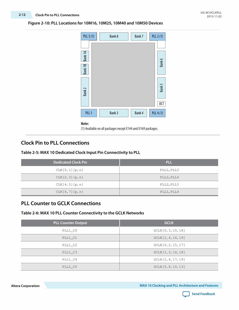
Figure 2-10: PLL Locations for 10M16, 10M25, 10M40 and 10M50 Devices
Bank 8
Bank
1ABa
nk 2
Bank
6Ba
nk 5
PLL 1
PLL 2 (1)Bank 7
Bank 3 Bank 4
Bank
1B
PLL 3 (1)
PLL 4 (1)
OCT
Note:(1) Available on all packages except E144 and U169 packages.
Clock Pin to PLL Connections
Table 2-5: MAX 10 Dedicated Clock Input Pin Connectivity to PLL
Dedicated Clock Pin PLL
CLK[0,1][p,n] PLL1, PLL3CLK[2,3][p,n] PLL2, PLL4CLK[4,5][p,n] PLL2, PLL3CLK[6,7][p,n] PLL1, PLL4
PLL Counter to GCLK Connections
Table 2-6: MAX 10 PLL Counter Connectivity to the GCLK Networks
PLL Counter Output GCLK
PLL1_C0 GCLK[0,3,15,18]
PLL1_C1 GCLK[1,4,16,19]
PLL1_C2 GCLK[0,2,15,17]
PLL1_C3 GCLK[1,3,16,18]
PLL1_C4 GCLK[2,4,17,19]
PLL2_C0 GCLK[5,8,10,13]
2-12 Clock Pin to PLL ConnectionsUG-M10CLKPLL
2015.11.02
Altera Corporation MAX 10 Clocking and PLL Architecture and Features
Send Feedback
PLL Counter Output GCLK
PLL2_C1 GCLK[6,9,11,14]
PLL2_C2 GCLK[5,7,10,12]
PLL2_C3 GCLK[6,8,11,13]
PLL2_C4 GCLK[7,9,12,14]
PLL3_C0(5) GCLK[0,3,10,13]
PLL3_C1(5) GCLK[1,4,11,14]
PLL3_C2(5) GCLK[0,2,10,12]
PLL3_C3(5) GCLK[1,3,11,13]
PLL3_C4(5) GCLK[2,4,12,14]
PLL4_C0(5) GCLK[5,8,15,18]
PLL4_C1(5) GCLK[6,9,16,19]
PLL4_C2(5) GCLK[5,7,15,17]
PLL4_C3(5) GCLK[6,8,16,18]
PLL4_C4(5) GCLK[7,9,17,19]
PLL Control SignalsYou can use the following three signals to observe and control the PLL operation and resynchronization.
pfdena
Use the pfdena signal to maintain the last locked frequency so that your system has time to store itscurrent settings before shutting down.
The pfdena signal controls the PFD output with a programmable gate. The PFD circuit is enabled bydefault. When the PFD circuit is disabled, the PLL output does not depend on the input clock, and tendsto drift outside of the lock window.
areset
The areset signal is the reset or resynchronization input for each PLL. The device input pins or internallogic can drive these input signals.
When you assert the areset signal, the PLL counters reset, clearing the PLL output and placing the PLLout of lock. The VCO is then set back to its nominal setting. When the areset signal is deasserted, thePLL resynchronizes to its input as it relocks.
The assertion of the areset signal does not disable the VCO, but instead resets the VCO to its nominalvalue. The only time that the VCO is completely disabled is when you do not have a PLL instantiated inyour design.
(5) This only applies to 10M16, 10M25, 10M40, and 10M50 devices.
UG-M10CLKPLL2015.11.02 PLL Control Signals 2-13
MAX 10 Clocking and PLL Architecture and Features Altera Corporation
Send Feedback
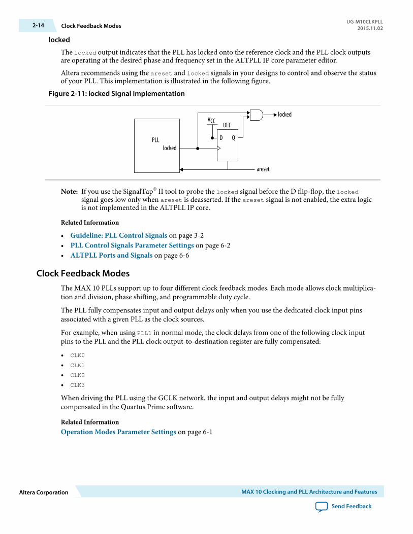
locked
The locked output indicates that the PLL has locked onto the reference clock and the PLL clock outputsare operating at the desired phase and frequency set in the ALTPLL IP core parameter editor.
Altera recommends using the areset and locked signals in your designs to control and observe the statusof your PLL. This implementation is illustrated in the following figure.
Figure 2-11: locked Signal Implementation
DFF
D QPLL
locked
locked
areset
VCC
Note: If you use the SignalTap® II tool to probe the locked signal before the D flip-flop, the lockedsignal goes low only when areset is deasserted. If the areset signal is not enabled, the extra logicis not implemented in the ALTPLL IP core.
Related Information
• Guideline: PLL Control Signals on page 3-2• PLL Control Signals Parameter Settings on page 6-2• ALTPLL Ports and Signals on page 6-6
Clock Feedback ModesThe MAX 10 PLLs support up to four different clock feedback modes. Each mode allows clock multiplica‐tion and division, phase shifting, and programmable duty cycle.
The PLL fully compensates input and output delays only when you use the dedicated clock input pinsassociated with a given PLL as the clock sources.
For example, when using PLL1 in normal mode, the clock delays from one of the following clock inputpins to the PLL and the PLL clock output-to-destination register are fully compensated:
• CLK0
• CLK1
• CLK2
• CLK3
When driving the PLL using the GCLK network, the input and output delays might not be fullycompensated in the Quartus Prime software.
Related InformationOperation Modes Parameter Settings on page 6-1
2-14 Clock Feedback ModesUG-M10CLKPLL
2015.11.02
Altera Corporation MAX 10 Clocking and PLL Architecture and Features
Send Feedback
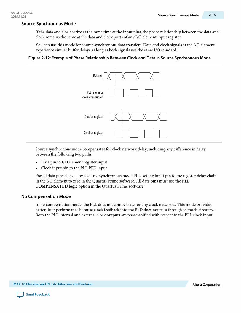
Source Synchronous Mode
If the data and clock arrive at the same time at the input pins, the phase relationship between the data andclock remains the same at the data and clock ports of any I/O element input register.
You can use this mode for source synchronous data transfers. Data and clock signals at the I/O elementexperience similar buffer delays as long as both signals use the same I/O standard.
Figure 2-12: Example of Phase Relationship Between Clock and Data in Source Synchronous Mode
Data pin
PLL reference clock at input pin
Data at register
Clock at register
Source synchronous mode compensates for clock network delay, including any difference in delaybetween the following two paths:
• Data pin to I/O element register input• Clock input pin to the PLL PFD input
For all data pins clocked by a source synchronous mode PLL, set the input pin to the register delay chainin the I/O element to zero in the Quartus Prime software. All data pins must use the PLLCOMPENSATED logic option in the Quartus Prime software.
No Compensation Mode
In no compensation mode, the PLL does not compensate for any clock networks. This mode providesbetter jitter performance because clock feedback into the PFD does not pass through as much circuitry.Both the PLL internal and external clock outputs are phase-shifted with respect to the PLL clock input.
UG-M10CLKPLL2015.11.02 Source Synchronous Mode 2-15
MAX 10 Clocking and PLL Architecture and Features Altera Corporation
Send Feedback
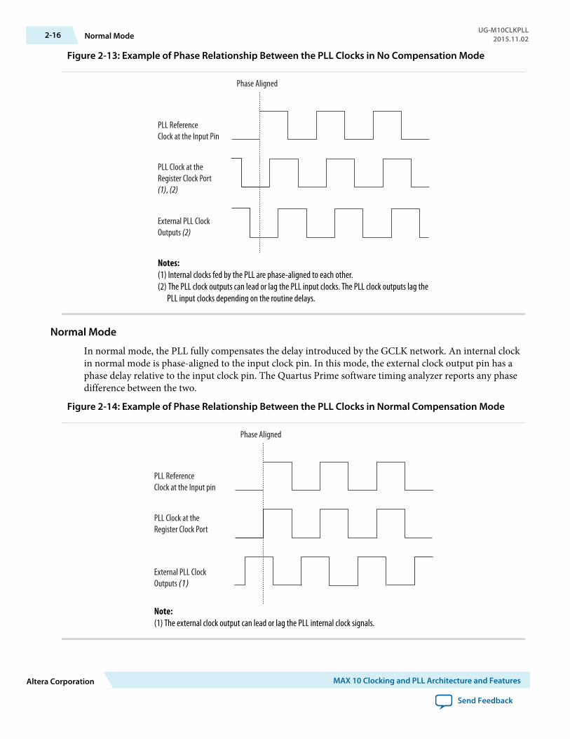
Figure 2-13: Example of Phase Relationship Between the PLL Clocks in No Compensation Mode
PLL ReferenceClock at the Input Pin
PLL Clock at theRegister Clock Port(1), (2)
External PLL Clock Outputs (2)
Phase Aligned
Notes:(1) Internal clocks fed by the PLL are phase-aligned to each other.(2) The PLL clock outputs can lead or lag the PLL input clocks. The PLL clock outputs lag the PLL input clocks depending on the routine delays.
Normal Mode
In normal mode, the PLL fully compensates the delay introduced by the GCLK network. An internal clockin normal mode is phase-aligned to the input clock pin. In this mode, the external clock output pin has aphase delay relative to the input clock pin. The Quartus Prime software timing analyzer reports any phasedifference between the two.
Figure 2-14: Example of Phase Relationship Between the PLL Clocks in Normal Compensation Mode
PLL ReferenceClock at the Input pin
PLL Clock at theRegister Clock Port
External PLL Clock Outputs (1)
Phase Aligned
Note:(1) The external clock output can lead or lag the PLL internal clock signals.
2-16 Normal ModeUG-M10CLKPLL
2015.11.02
Altera Corporation MAX 10 Clocking and PLL Architecture and Features
Send Feedback
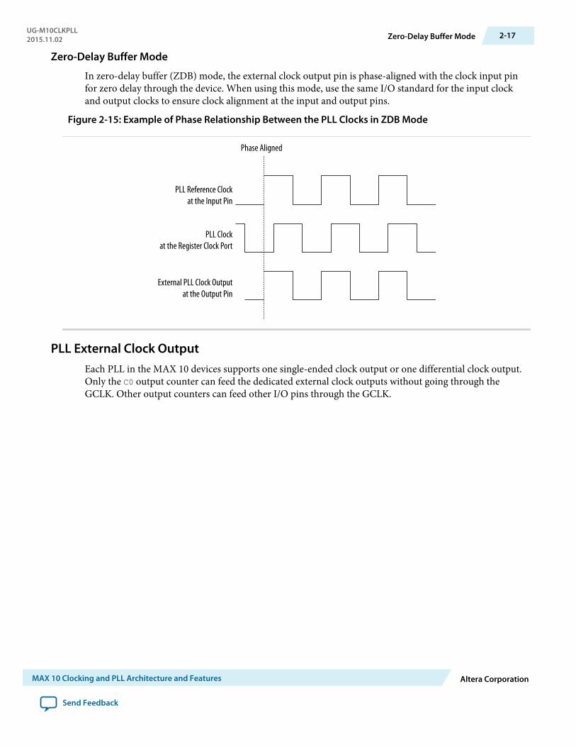
Zero-Delay Buffer Mode
In zero-delay buffer (ZDB) mode, the external clock output pin is phase-aligned with the clock input pinfor zero delay through the device. When using this mode, use the same I/O standard for the input clockand output clocks to ensure clock alignment at the input and output pins.
Figure 2-15: Example of Phase Relationship Between the PLL Clocks in ZDB Mode
PLL Reference Clock at the Input Pin
PLL Clockat the Register Clock Port
External PLL Clock Outputat the Output Pin
Phase Aligned
PLL External Clock OutputEach PLL in the MAX 10 devices supports one single-ended clock output or one differential clock output.Only the C0 output counter can feed the dedicated external clock outputs without going through theGCLK. Other output counters can feed other I/O pins through the GCLK.
UG-M10CLKPLL2015.11.02 Zero-Delay Buffer Mode 2-17
MAX 10 Clocking and PLL Architecture and Features Altera Corporation
Send Feedback
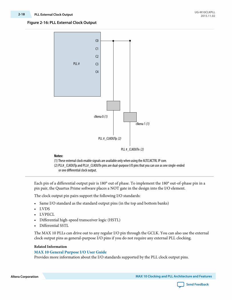
Figure 2-16: PLL External Clock Output
C0
C1
C2
C4
C3PLL #
clkena 1 (1)
clkena 0 (1)
PLL #_CLKOUTp (2)
PLL #_CLKOUTn (2)
Notes:(1) These external clock enable signals are available only when using the ALTCLKCTRL IP core.(2) PLL#_CLKOUTp and PLL#_CLKOUTn pins are dual-purpose I/O pins that you can use as one single-ended or one differential clock output.
Each pin of a differential output pair is 180° out of phase. To implement the 180° out-of-phase pin in apin pair, the Quartus Prime software places a NOT gate in the design into the I/O element.
The clock output pin pairs support the following I/O standards:
• Same I/O standard as the standard output pins (in the top and bottom banks)• LVDS• LVPECL• Differential high-speed transceiver logic (HSTL)• Differential SSTL
The MAX 10 PLLs can drive out to any regular I/O pin through the GCLK. You can also use the externalclock output pins as general-purpose I/O pins if you do not require any external PLL clocking.
Related InformationMAX 10 General Purpose I/O User GuideProvides more information about the I/O standards supported by the PLL clock output pins.
2-18 PLL External Clock OutputUG-M10CLKPLL
2015.11.02
Altera Corporation MAX 10 Clocking and PLL Architecture and Features
Send Feedback
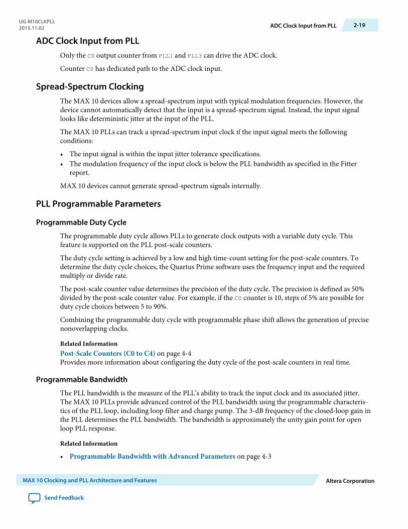
ADC Clock Input from PLLOnly the C0 output counter from PLL1 and PLL3 can drive the ADC clock.
Counter C0 has dedicated path to the ADC clock input.
Spread-Spectrum ClockingThe MAX 10 devices allow a spread-spectrum input with typical modulation frequencies. However, thedevice cannot automatically detect that the input is a spread-spectrum signal. Instead, the input signallooks like deterministic jitter at the input of the PLL.
The MAX 10 PLLs can track a spread-spectrum input clock if the input signal meets the followingconditions:
• The input signal is within the input jitter tolerance specifications.• The modulation frequency of the input clock is below the PLL bandwidth as specified in the Fitter
report.
MAX 10 devices cannot generate spread-spectrum signals internally.
PLL Programmable Parameters
Programmable Duty Cycle
The programmable duty cycle allows PLLs to generate clock outputs with a variable duty cycle. Thisfeature is supported on the PLL post-scale counters.
The duty cycle setting is achieved by a low and high time-count setting for the post-scale counters. Todetermine the duty cycle choices, the Quartus Prime software uses the frequency input and the requiredmultiply or divide rate.
The post-scale counter value determines the precision of the duty cycle. The precision is defined as 50%divided by the post-scale counter value. For example, if the C0 counter is 10, steps of 5% are possible forduty cycle choices between 5 to 90%.
Combining the programmable duty cycle with programmable phase shift allows the generation of precisenonoverlapping clocks.
Related InformationPost-Scale Counters (C0 to C4) on page 4-4Provides more information about configuring the duty cycle of the post-scale counters in real time.
Programmable Bandwidth
The PLL bandwidth is the measure of the PLL’s ability to track the input clock and its associated jitter.The MAX 10 PLLs provide advanced control of the PLL bandwidth using the programmable characteris‐tics of the PLL loop, including loop filter and charge pump. The 3-dB frequency of the closed-loop gain inthe PLL determines the PLL bandwidth. The bandwidth is approximately the unity gain point for openloop PLL response.
Related Information
• Programmable Bandwidth with Advanced Parameters on page 4-3
UG-M10CLKPLL2015.11.02 ADC Clock Input from PLL 2-19
MAX 10 Clocking and PLL Architecture and Features Altera Corporation
Send Feedback
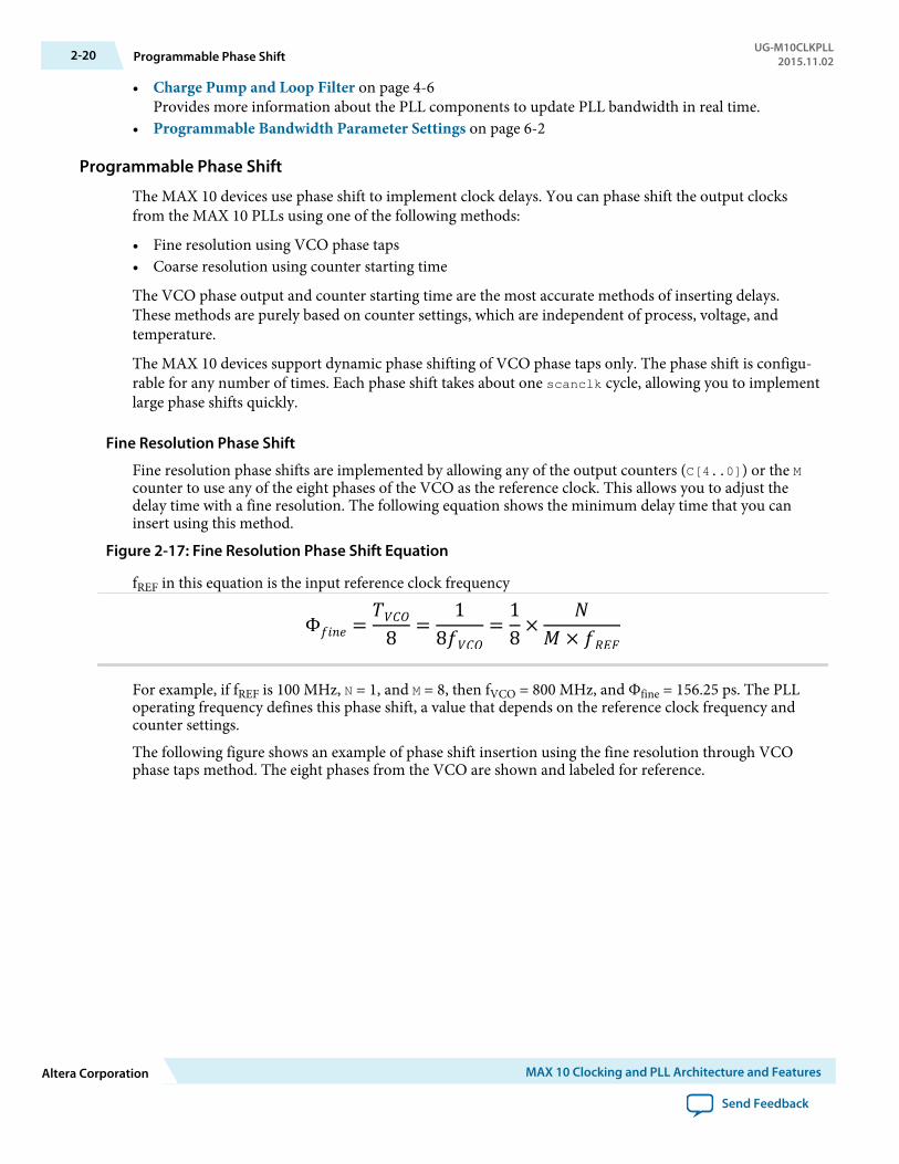
• Charge Pump and Loop Filter on page 4-6Provides more information about the PLL components to update PLL bandwidth in real time.
• Programmable Bandwidth Parameter Settings on page 6-2
Programmable Phase Shift
The MAX 10 devices use phase shift to implement clock delays. You can phase shift the output clocksfrom the MAX 10 PLLs using one of the following methods:
• Fine resolution using VCO phase taps• Coarse resolution using counter starting time
The VCO phase output and counter starting time are the most accurate methods of inserting delays.These methods are purely based on counter settings, which are independent of process, voltage, andtemperature.
The MAX 10 devices support dynamic phase shifting of VCO phase taps only. The phase shift is configu‐rable for any number of times. Each phase shift takes about one scanclk cycle, allowing you to implementlarge phase shifts quickly.
Fine Resolution Phase Shift
Fine resolution phase shifts are implemented by allowing any of the output counters (C[4..0]) or the Mcounter to use any of the eight phases of the VCO as the reference clock. This allows you to adjust thedelay time with a fine resolution. The following equation shows the minimum delay time that you caninsert using this method.
Figure 2-17: Fine Resolution Phase Shift Equation
fREF in this equation is the input reference clock frequency
For example, if fREF is 100 MHz, N = 1, and M = 8, then fVCO = 800 MHz, and Φfine = 156.25 ps. The PLLoperating frequency defines this phase shift, a value that depends on the reference clock frequency andcounter settings.
The following figure shows an example of phase shift insertion using the fine resolution through VCOphase taps method. The eight phases from the VCO are shown and labeled for reference.
2-20 Programmable Phase ShiftUG-M10CLKPLL
2015.11.02
Altera Corporation MAX 10 Clocking and PLL Architecture and Features
Send Feedback
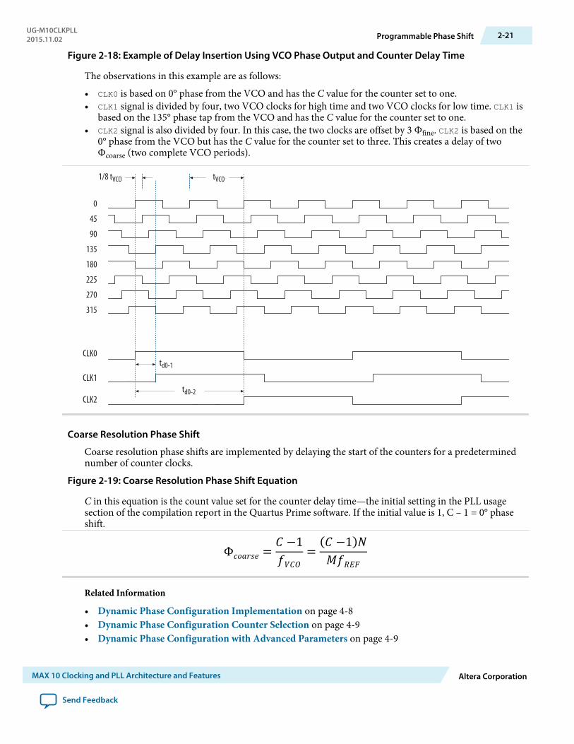
Figure 2-18: Example of Delay Insertion Using VCO Phase Output and Counter Delay Time
The observations in this example are as follows:
• CLK0 is based on 0° phase from the VCO and has the C value for the counter set to one.• CLK1 signal is divided by four, two VCO clocks for high time and two VCO clocks for low time. CLK1 is
based on the 135° phase tap from the VCO and has the C value for the counter set to one.• CLK2 signal is also divided by four. In this case, the two clocks are offset by 3 Φfine. CLK2 is based on the
0° phase from the VCO but has the C value for the counter set to three. This creates a delay of twoΦcoarse (two complete VCO periods).
td0-1
td0-2
1/8 tVCO tVCO
0
90
135
180
225
270
315
CLK0
CLK1
CLK2
45
Coarse Resolution Phase Shift
Coarse resolution phase shifts are implemented by delaying the start of the counters for a predeterminednumber of counter clocks.
Figure 2-19: Coarse Resolution Phase Shift Equation
C in this equation is the count value set for the counter delay time—the initial setting in the PLL usagesection of the compilation report in the Quartus Prime software. If the initial value is 1, C – 1 = 0° phaseshift.
Related Information
• Dynamic Phase Configuration Implementation on page 4-8• Dynamic Phase Configuration Counter Selection on page 4-9• Dynamic Phase Configuration with Advanced Parameters on page 4-9
UG-M10CLKPLL2015.11.02 Programmable Phase Shift 2-21
MAX 10 Clocking and PLL Architecture and Features Altera Corporation
Send Feedback
• Dynamic Phase Configuration Parameter Settings on page 6-4Provides more information about the ALTPLL IP core parameter settings in the Quartus Primesoftware.
• ALTPLL_RECONFIG Parameters on page 7-1Provides more information about the ALTPLL_RECONFIG IP core parameter settings in the QuartusPrime software.
Clock SwitchoverThe clock switchover feature allows the PLL to switch between two reference input clocks. Use this featurefor clock redundancy or for a dual-clock domain application where a system turns on the redundant clockif the previous clock stops running. The design can perform clock switchover automatically when theclock is no longer toggling or based on a user-controlled signal, clkswitch.
The following clock switchover modes are supported in MAX 10 PLLs:
• Automatic switchover—The clock sense circuit monitors the current reference clock. If the currentreference clock stops toggling, the reference clock automatically switches to inclk0 or inclk1 clock.
• Manual clock switchover—The clkswitch signal controls the clock switchover. When the clkswitchsignal goes from logic low to high, and stays high for at least three clock cycles, the reference clock tothe PLL switches from inclk0 to inclk1, or vice-versa.
• Automatic switchover with manual override—This mode combines automatic switchover and manualclock switchover. When the clkswitch signal goes high, it overrides the automatic clock switchoverfunction. As long as the clkswitch signal is high, any further switchover action is blocked.
Related Information
• Guideline: Clock Switchover on page 3-4• Clock Switchover Parameter Settings on page 6-3
Automatic Clock Switchover
The MAX 10 PLLs support a fully configurable clock switchover capability.
2-22 Clock SwitchoverUG-M10CLKPLL
2015.11.02
Altera Corporation MAX 10 Clocking and PLL Architecture and Features
Send Feedback
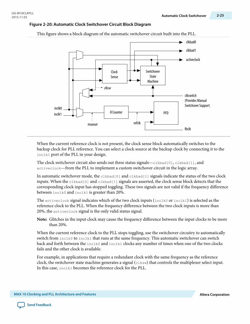
Figure 2-20: Automatic Clock Switchover Circuit Block Diagram
This figure shows a block diagram of the automatic switchover circuit built into the PLL.
SwitchoverState
Machine
ClockSense
N Counter PFD
clkswitch (Provides Manual Switchover Support)
activeclock
clkbad1
clkbad0
muxout
inclk0inclk1
refclkfbclk
clksw
When the current reference clock is not present, the clock sense block automatically switches to thebackup clock for PLL reference. You can select a clock source at the backup clock by connecting it to theinclk1 port of the PLL in your design.
The clock switchover circuit also sends out three status signals—clkbad[0], clkbad[1], andactiveclock—from the PLL to implement a custom switchover circuit in the logic array.
In automatic switchover mode, the clkbad[0] and clkbad[1] signals indicate the status of the two clockinputs. When the clkbad[0] and clkbad[1] signals are asserted, the clock sense block detects that thecorresponding clock input has stopped toggling. These two signals are not valid if the frequency differencebetween inclk0 and inclk1 is greater than 20%.
The activeclock signal indicates which of the two clock inputs (inclk0 or inclk1) is selected as thereference clock to the PLL. When the frequency difference between the two clock inputs is more than20%, the activeclock signal is the only valid status signal.
Note: Glitches in the input clock may cause the frequency difference between the input clocks to be morethan 20%.
When the current reference clock to the PLL stops toggling, use the switchover circuitry to automaticallyswitch from inclk0 to inclk1 that runs at the same frequency. This automatic switchover can switchback and forth between the inclk0 and inclk1 clocks any number of times when one of the two clocksfails and the other clock is available.
For example, in applications that require a redundant clock with the same frequency as the referenceclock, the switchover state machine generates a signal (clksw) that controls the multiplexer select input.In this case, inclk1 becomes the reference clock for the PLL.
UG-M10CLKPLL2015.11.02 Automatic Clock Switchover 2-23
MAX 10 Clocking and PLL Architecture and Features Altera Corporation
Send Feedback
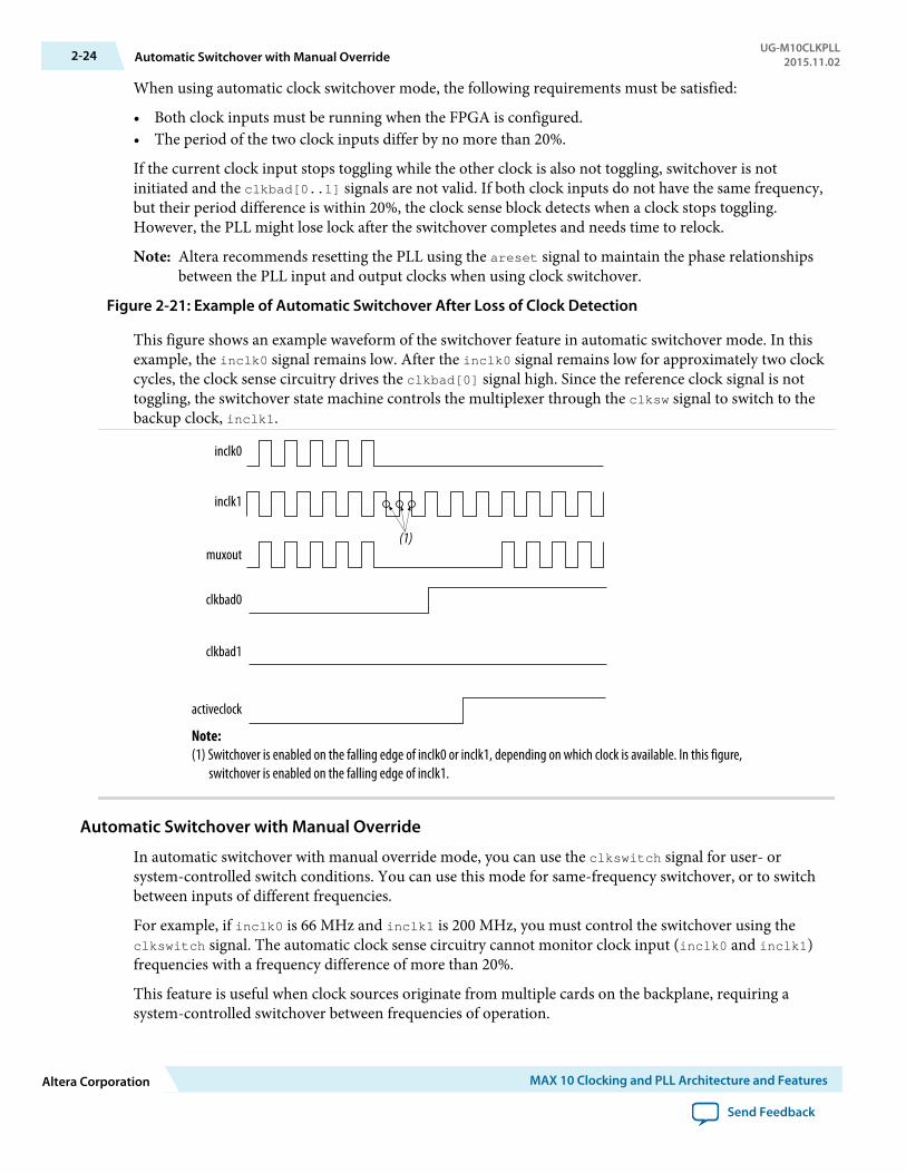
When using automatic clock switchover mode, the following requirements must be satisfied:
• Both clock inputs must be running when the FPGA is configured.• The period of the two clock inputs differ by no more than 20%.
If the current clock input stops toggling while the other clock is also not toggling, switchover is notinitiated and the clkbad[0..1] signals are not valid. If both clock inputs do not have the same frequency,but their period difference is within 20%, the clock sense block detects when a clock stops toggling.However, the PLL might lose lock after the switchover completes and needs time to relock.
Note: Altera recommends resetting the PLL using the areset signal to maintain the phase relationshipsbetween the PLL input and output clocks when using clock switchover.
Figure 2-21: Example of Automatic Switchover After Loss of Clock Detection
This figure shows an example waveform of the switchover feature in automatic switchover mode. In thisexample, the inclk0 signal remains low. After the inclk0 signal remains low for approximately two clockcycles, the clock sense circuitry drives the clkbad[0] signal high. Since the reference clock signal is nottoggling, the switchover state machine controls the multiplexer through the clksw signal to switch to thebackup clock, inclk1.
inclk0
inclk1
muxout
clkbad0
clkbad1
(1)
activeclock
Note:(1) Switchover is enabled on the falling edge of inclk0 or inclk1, depending on which clock is available. In this figure, switchover is enabled on the falling edge of inclk1.
Automatic Switchover with Manual Override
In automatic switchover with manual override mode, you can use the clkswitch signal for user- orsystem-controlled switch conditions. You can use this mode for same-frequency switchover, or to switchbetween inputs of different frequencies.
For example, if inclk0 is 66 MHz and inclk1 is 200 MHz, you must control the switchover using theclkswitch signal. The automatic clock sense circuitry cannot monitor clock input (inclk0 and inclk1)frequencies with a frequency difference of more than 20%.
This feature is useful when clock sources originate from multiple cards on the backplane, requiring asystem-controlled switchover between frequencies of operation.
2-24 Automatic Switchover with Manual OverrideUG-M10CLKPLL
2015.11.02
Altera Corporation MAX 10 Clocking and PLL Architecture and Features
Send Feedback
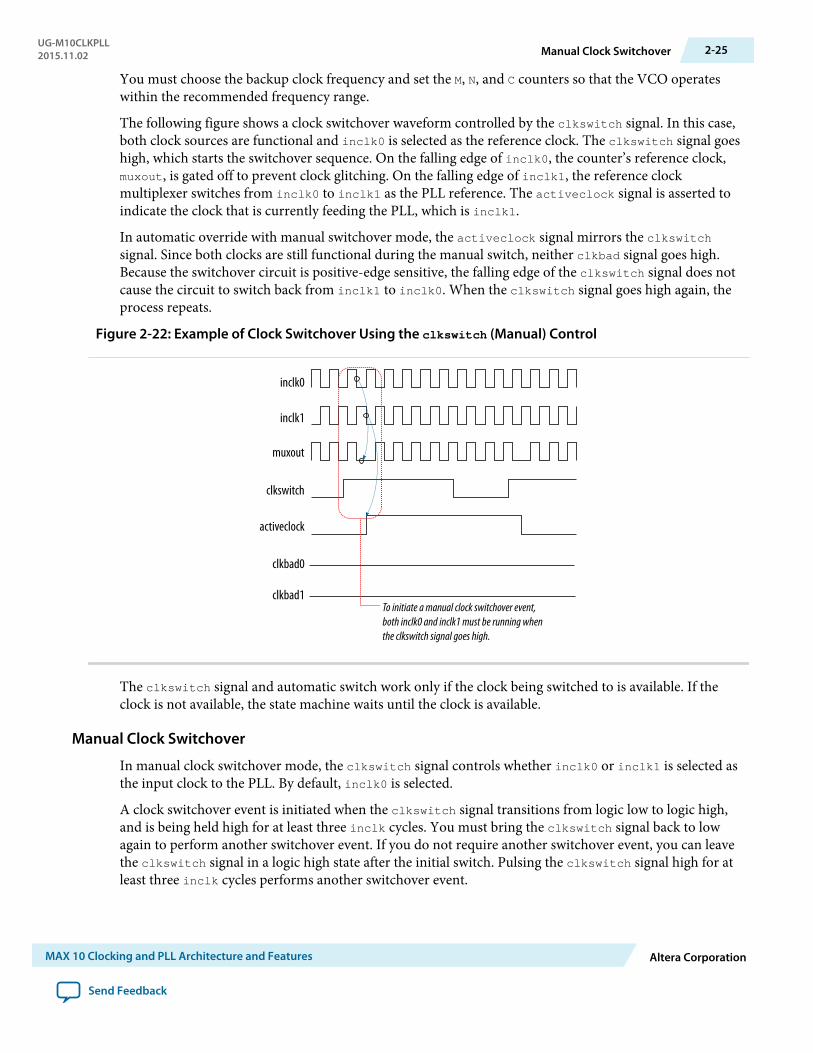
You must choose the backup clock frequency and set the M, N, and C counters so that the VCO operateswithin the recommended frequency range.
The following figure shows a clock switchover waveform controlled by the clkswitch signal. In this case,both clock sources are functional and inclk0 is selected as the reference clock. The clkswitch signal goeshigh, which starts the switchover sequence. On the falling edge of inclk0, the counter’s reference clock,muxout, is gated off to prevent clock glitching. On the falling edge of inclk1, the reference clockmultiplexer switches from inclk0 to inclk1 as the PLL reference. The activeclock signal is asserted toindicate the clock that is currently feeding the PLL, which is inclk1.
In automatic override with manual switchover mode, the activeclock signal mirrors the clkswitchsignal. Since both clocks are still functional during the manual switch, neither clkbad signal goes high.Because the switchover circuit is positive-edge sensitive, the falling edge of the clkswitch signal does notcause the circuit to switch back from inclk1 to inclk0. When the clkswitch signal goes high again, theprocess repeats.
Figure 2-22: Example of Clock Switchover Using the clkswitch (Manual) Control
inclk0
inclk1
muxout
clkswitch
activeclock
clkbad0
clkbad1To initiate a manual clock switchover event, both inclk0 and inclk1 must be running when the clkswitch signal goes high.
The clkswitch signal and automatic switch work only if the clock being switched to is available. If theclock is not available, the state machine waits until the clock is available.
Manual Clock Switchover
In manual clock switchover mode, the clkswitch signal controls whether inclk0 or inclk1 is selected asthe input clock to the PLL. By default, inclk0 is selected.
A clock switchover event is initiated when the clkswitch signal transitions from logic low to logic high,and is being held high for at least three inclk cycles. You must bring the clkswitch signal back to lowagain to perform another switchover event. If you do not require another switchover event, you can leavethe clkswitch signal in a logic high state after the initial switch. Pulsing the clkswitch signal high for atleast three inclk cycles performs another switchover event.
UG-M10CLKPLL2015.11.02 Manual Clock Switchover 2-25
MAX 10 Clocking and PLL Architecture and Features Altera Corporation
Send Feedback
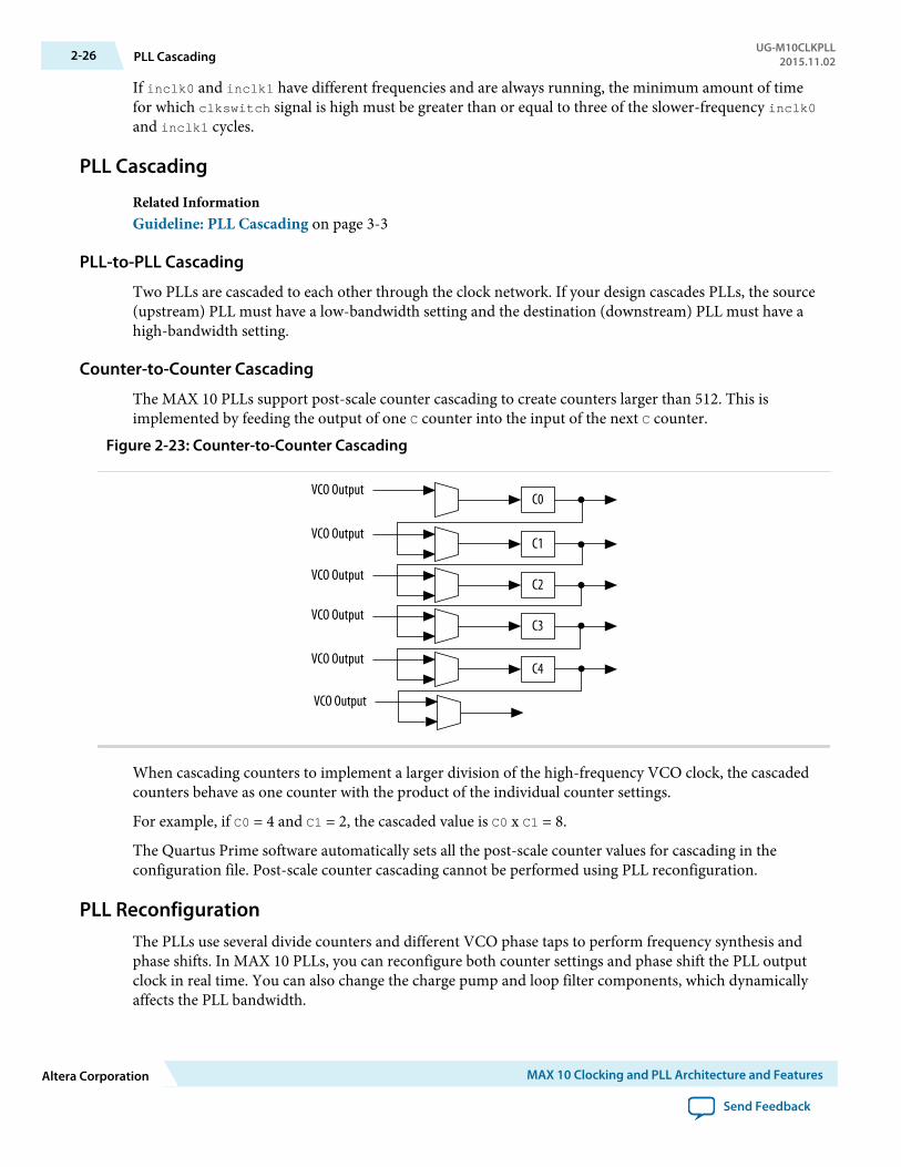
If inclk0 and inclk1 have different frequencies and are always running, the minimum amount of timefor which clkswitch signal is high must be greater than or equal to three of the slower-frequency inclk0and inclk1 cycles.
PLL Cascading
Related InformationGuideline: PLL Cascading on page 3-3
PLL-to-PLL Cascading
Two PLLs are cascaded to each other through the clock network. If your design cascades PLLs, the source(upstream) PLL must have a low-bandwidth setting and the destination (downstream) PLL must have ahigh-bandwidth setting.
Counter-to-Counter Cascading
The MAX 10 PLLs support post-scale counter cascading to create counters larger than 512. This isimplemented by feeding the output of one C counter into the input of the next C counter.
Figure 2-23: Counter-to-Counter Cascading
C0
C1
C2
C3
C4
VCO Output
VCO Output
VCO Output
VCO Output
VCO Output
VCO Output
When cascading counters to implement a larger division of the high-frequency VCO clock, the cascadedcounters behave as one counter with the product of the individual counter settings.
For example, if C0 = 4 and C1 = 2, the cascaded value is C0 x C1 = 8.
The Quartus Prime software automatically sets all the post-scale counter values for cascading in theconfiguration file. Post-scale counter cascading cannot be performed using PLL reconfiguration.
PLL ReconfigurationThe PLLs use several divide counters and different VCO phase taps to perform frequency synthesis andphase shifts. In MAX 10 PLLs, you can reconfigure both counter settings and phase shift the PLL outputclock in real time. You can also change the charge pump and loop filter components, which dynamicallyaffects the PLL bandwidth.
2-26 PLL CascadingUG-M10CLKPLL
2015.11.02
Altera Corporation MAX 10 Clocking and PLL Architecture and Features
Send Feedback
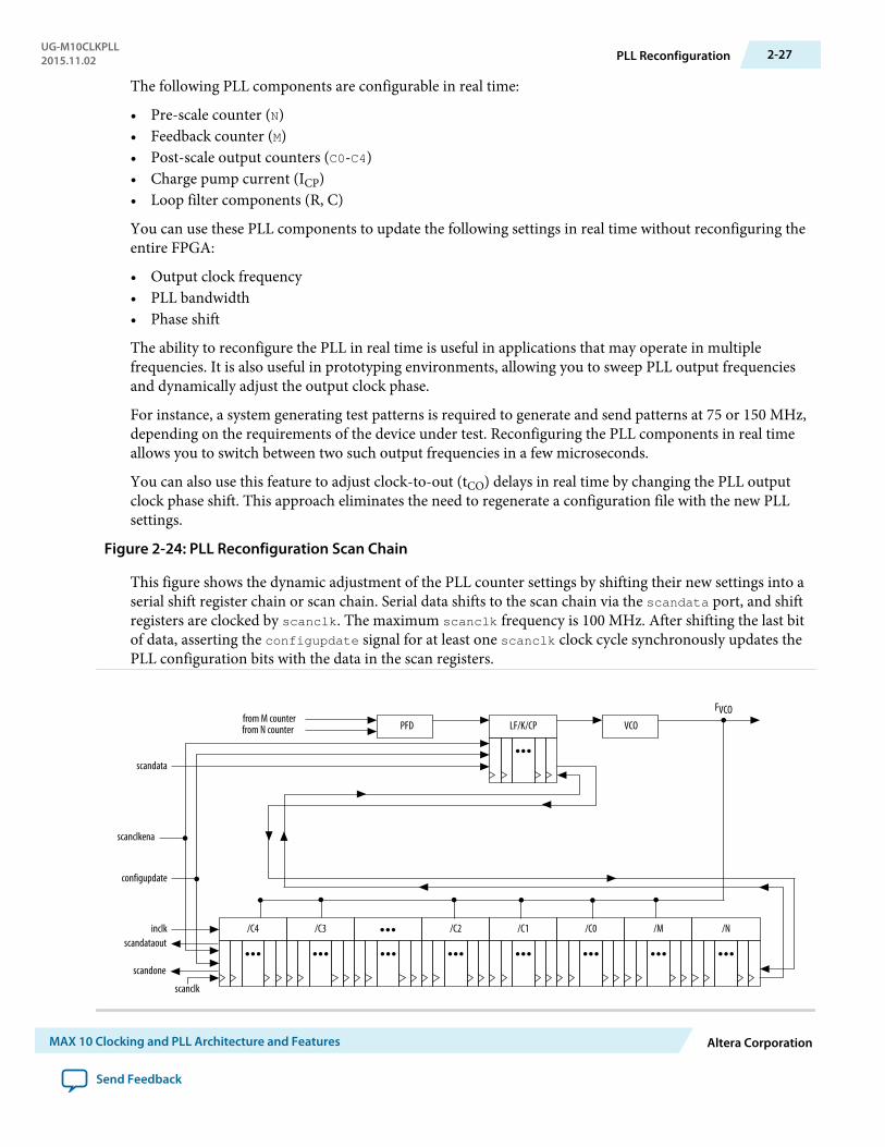
The following PLL components are configurable in real time:
• Pre-scale counter (N)• Feedback counter (M)• Post-scale output counters (C0-C4)• Charge pump current (ICP)• Loop filter components (R, C)
You can use these PLL components to update the following settings in real time without reconfiguring theentire FPGA:
• Output clock frequency• PLL bandwidth• Phase shift
The ability to reconfigure the PLL in real time is useful in applications that may operate in multiplefrequencies. It is also useful in prototyping environments, allowing you to sweep PLL output frequenciesand dynamically adjust the output clock phase.
For instance, a system generating test patterns is required to generate and send patterns at 75 or 150 MHz,depending on the requirements of the device under test. Reconfiguring the PLL components in real timeallows you to switch between two such output frequencies in a few microseconds.
You can also use this feature to adjust clock-to-out (tCO) delays in real time by changing the PLL outputclock phase shift. This approach eliminates the need to regenerate a configuration file with the new PLLsettings.
Figure 2-24: PLL Reconfiguration Scan Chain
This figure shows the dynamic adjustment of the PLL counter settings by shifting their new settings into aserial shift register chain or scan chain. Serial data shifts to the scan chain via the scandata port, and shiftregisters are clocked by scanclk. The maximum scanclk frequency is 100 MHz. After shifting the last bitof data, asserting the configupdate signal for at least one scanclk clock cycle synchronously updates thePLL configuration bits with the data in the scan registers.
/C4 /C3 /C2 /C1 /C0 /M /N
scanclk
scandone
scandata
LF/K/CP
configupdate
inclk
PFD VCO
FVCO
scanclkena
scandataout
from M counterfrom N counter
UG-M10CLKPLL2015.11.02 PLL Reconfiguration 2-27
MAX 10 Clocking and PLL Architecture and Features Altera Corporation
Send Feedback
The counter settings are updated synchronously to the clock frequency of the individual counters.Therefore, not all counters update simultaneously.
The dynamic reconfiguration scheme uses configuration files, such as the Hexadecimal-format file (.hex)or the Memory Initialization file (.mif). These files are used together with the ALTPLL_RECONFIG IPcore to perform the dynamic reconfiguration.
Related Information
• Guideline: .mif Streaming in PLL Reconfiguration on page 3-5• PLL Dynamic Reconfiguration Implementation on page 4-4• PLL Dynamic Reconfiguration Parameter Settings on page 6-4
Provides more information about the ALTPLL IP core parameter settings in the Quartus Primesoftware.
• ALTPLL_RECONFIG Parameters on page 7-1Provides more information about the ALTPLL_RECONFIG IP core parameter settings in the QuartusPrime software.
2-28 PLL ReconfigurationUG-M10CLKPLL
2015.11.02
Altera Corporation MAX 10 Clocking and PLL Architecture and Features
Send Feedback
MAX 10 Clocking and PLL DesignConsiderations 3
2015.11.02
UG-M10CLKPLL Subscribe Send Feedback
Clock Networks Design Considerations
Guideline: Clock Enable SignalsAltera recommends using the clkena signals when switching the clock source to the PLLs or GCLK. Therecommended sequence is as follows:
1. Disable the primary output clock by deasserting the clkena signal.2. Switch to the secondary clock using the dynamic select signals of the clock control block.3. Allow some clock cycles of the secondary clock to pass before reasserting the clkena signal. The exact
number of clock cycles to wait before enabling the secondary clock depends on your design. You canbuild a custom logic to ensure a glitch-free transition when switching between different clock sources.
Related Information
• Clock Enable Signals on page 2-7• ALTCLKCTRL Parameters on page 5-1• ALTCLKCTRL Ports and Signals on page 5-2
Guideline: Connectivity RestrictionsThe following guidelines describe the restrictions associated with the signal sources that can drive theinclk input:
• You must use the inclk ports that are consistent with the clkselect ports.• When you are using multiple input sources, the inclk ports can only be driven by the dedicated clock
input pins and the PLL clock outputs.• If the clock control block feeds any inclk port of another clock control block, both clock control
blocks must be able to be reduced to a single clock control block of equivalent functionality.• When you are using the glitch-free switchover feature, the clock you are switching from must be active.
If the clock is not active, the switchover circuit cannot transition from the clock you originally selected.
© 2015 Altera Corporation. All rights reserved. ALTERA, ARRIA, CYCLONE, ENPIRION, MAX, MEGACORE, NIOS, QUARTUS and STRATIX words and logos aretrademarks of Altera Corporation and registered in the U.S. Patent and Trademark Office and in other countries. All other words and logos identified astrademarks or service marks are the property of their respective holders as described at www.altera.com/common/legal.html. Altera warrants performanceof its semiconductor products to current specifications in accordance with Altera's standard warranty, but reserves the right to make changes to anyproducts and services at any time without notice. Altera assumes no responsibility or liability arising out of the application or use of any information,product, or service described herein except as expressly agreed to in writing by Altera. Altera customers are advised to obtain the latest version of devicespecifications before relying on any published information and before placing orders for products or services.
ISO9001:2008Registered
www.altera.com101 Innovation Drive, San Jose, CA 95134
Internal Oscillator Design Considerations
Guideline: Connectivity RestrictionsYou cannot drive the PLLs with internal oscillator.
PLLs Design Considerations
Guideline: PLL Control SignalsYou must include the areset signal in your designs if one of the following conditions is true:
• PLL reconfiguration or clock switchover is enabled in your design.• Phase relationships between the PLL input clock and output clocks must be maintained after a loss-of-
lock condition.• The input clock to the PLL is toggling or unstable at power-up.• The areset signal is asserted after the input clock is stable and within specifications.
Related InformationPLL Control Signals on page 2-13
Guideline: Connectivity RestrictionsTo comply with simultaneous switching noise (SSN) design guideline, Altera recommends that you donot use unterminated I/O in the same bank as the input clock signal to the PLL.
Related InformationGuidelines: Clock and Asynchronous Control Input SignalProvides more information about using I/O connectivity restrictions.
Guideline: Self-ResetThe lock time of a PLL is the amount of time required by the PLL to attain the target frequency and phaserelationship after device power-up, after a change in the PLL output frequency, or after resetting the PLL.
A PLL might lose lock for a number of reasons, such as the following causes:
• Excessive jitter on the input clock.• Excessive switching noise on the clock inputs of the PLL.• Excessive noise from the power supply, causing high output jitter and possible loss of lock.• A glitch or stopping of the input clock to the PLL.• Resetting the PLL by asserting the areset port of the PLL.• An attempt to reconfigure the PLL might cause the M counter, N counter, or phase shift to change,
causing the PLL to lose lock. However, changes to the post-scale counters do not affect the PLL lockedsignal.
• PLL input clock frequency drifts outside the lock range specification.• The PFD is disabled using the pfdena port. When this happens, the PLL output phase and frequency
tend to drift outside of the lock window.
3-2 Internal Oscillator Design ConsiderationsUG-M10CLKPLL
2015.11.02
Altera Corporation MAX 10 Clocking and PLL Design Considerations
Send Feedback
The ALTPLL IP core allows you to monitor the PLL locking process using a lock signal named lockedand also allows you to set the PLL to self-reset on loss of lock.
Guideline: Output ClocksEach MAX 10 PLL supports up to five output clocks. You can use the output clock port as a core outputclock or an external output clock port. The core output clock feeds the FPGA core and the external outputclock feeds the dedicated pins on the FPGA.
The ALTPLL IP core does not have a dedicated output enable port. You can disable the PLL output usingthe areset signal to disable the PLL output counters.
Guideline: PLL CascadingConsider the following guidelines when cascading PLLs:
• Set the primary PLL to low bandwidth to help filter jitter. Set the secondary PLL to high bandwidth totrack the jitter from the primary PLL. You can view the Quartus Prime software compilation report fileto ensure the PLL bandwidth ranges do not overlap. If the bandwidth ranges overlap, jitter peaking canoccur in the cascaded PLL scheme.
Note: You can get an estimate of the PLL deterministic jitter and static phase error (SPE) by using theTimeQuest Timing Analyzer in the Quartus Prime software. Use the SDC commandderive_clock_uncertainty to generate a report titled PLLJ_PLLSPE_INFO.txt in yourproject directory. Then, use set_clock_uncertainty command to add jitter and SPEvalues to your clock constraints.
• Keep the secondary PLL in a reset state until the primary PLL has locked to ensure the phase settingsare correct on the secondary PLL.
• You cannot connect any of the inclk ports of any PLLs in a cascaded scheme to the clock outputsfrom PLLs in the cascaded scheme.
Related InformationPLL Cascading on page 2-26
UG-M10CLKPLL2015.11.02 Guideline: Output Clocks 3-3
MAX 10 Clocking and PLL Design Considerations Altera Corporation
Send Feedback
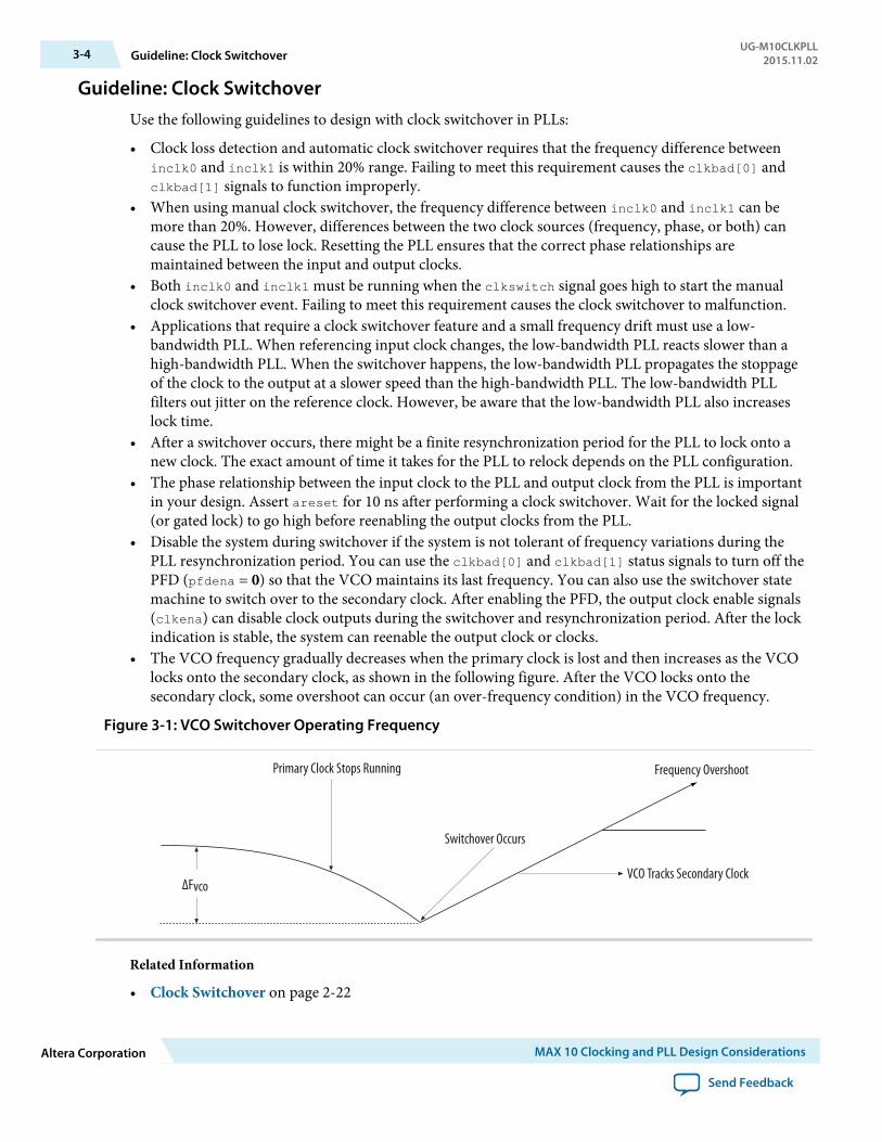
Guideline: Clock SwitchoverUse the following guidelines to design with clock switchover in PLLs:
• Clock loss detection and automatic clock switchover requires that the frequency difference betweeninclk0 and inclk1 is within 20% range. Failing to meet this requirement causes the clkbad[0] andclkbad[1] signals to function improperly.
• When using manual clock switchover, the frequency difference between inclk0 and inclk1 can bemore than 20%. However, differences between the two clock sources (frequency, phase, or both) cancause the PLL to lose lock. Resetting the PLL ensures that the correct phase relationships aremaintained between the input and output clocks.
• Both inclk0 and inclk1 must be running when the clkswitch signal goes high to start the manualclock switchover event. Failing to meet this requirement causes the clock switchover to malfunction.
• Applications that require a clock switchover feature and a small frequency drift must use a low-bandwidth PLL. When referencing input clock changes, the low-bandwidth PLL reacts slower than ahigh-bandwidth PLL. When the switchover happens, the low-bandwidth PLL propagates the stoppageof the clock to the output at a slower speed than the high-bandwidth PLL. The low-bandwidth PLLfilters out jitter on the reference clock. However, be aware that the low-bandwidth PLL also increaseslock time.
• After a switchover occurs, there might be a finite resynchronization period for the PLL to lock onto anew clock. The exact amount of time it takes for the PLL to relock depends on the PLL configuration.
• The phase relationship between the input clock to the PLL and output clock from the PLL is importantin your design. Assert areset for 10 ns after performing a clock switchover. Wait for the locked signal(or gated lock) to go high before reenabling the output clocks from the PLL.
• Disable the system during switchover if the system is not tolerant of frequency variations during thePLL resynchronization period. You can use the clkbad[0] and clkbad[1] status signals to turn off thePFD (pfdena = 0) so that the VCO maintains its last frequency. You can also use the switchover statemachine to switch over to the secondary clock. After enabling the PFD, the output clock enable signals(clkena) can disable clock outputs during the switchover and resynchronization period. After the lockindication is stable, the system can reenable the output clock or clocks.
• The VCO frequency gradually decreases when the primary clock is lost and then increases as the VCOlocks onto the secondary clock, as shown in the following figure. After the VCO locks onto thesecondary clock, some overshoot can occur (an over-frequency condition) in the VCO frequency.
Figure 3-1: VCO Switchover Operating Frequency
ΔFvco
Primary Clock Stops Running
Switchover Occurs
VCO Tracks Secondary Clock
Frequency Overshoot
Related Information
• Clock Switchover on page 2-22
3-4 Guideline: Clock SwitchoverUG-M10CLKPLL
2015.11.02
Altera Corporation MAX 10 Clocking and PLL Design Considerations
Send Feedback
• Clock Switchover Parameter Settings on page 6-3
Guideline: .mif Streaming in PLL ReconfigurationConsider the following guidelines when using .mif streaming in PLL reconfiguration:
• 10M02 devices do not support .mif streaming in PLL reconfiguration due to flash size limitation. Alterarecommends using an external flash.
• 10M04, 10M08, 10M16, 10M25, 10M40, and 10M50 devices only support .mif streaming in singleimage mode. Altera recommends using an external flash for dual image mode. The MAX 10 devices donot support using both dual image mode and PLL reconfiguration with .mif simultaneously.
Related InformationPLL Reconfiguration on page 2-26
Guideline: scandone Signal for PLL Reconfigurationscandone signal must be low before the second PLL reconfiguration. For scandone signal to go low, PLLareset signal must be asserted.
UG-M10CLKPLL2015.11.02 Guideline: .mif Streaming in PLL Reconfiguration 3-5
MAX 10 Clocking and PLL Design Considerations Altera Corporation
Send Feedback
MAX 10 Clocking and PLL ImplementationGuides 4
2015.11.02
UG-M10CLKPLL Subscribe Send Feedback
ALTCLKCTRL IP CoreThe clock control block (ALTCLKCTRL) IP core is a clock control function for configuring the clockcontrol block.
The common applications of the ALTCLKCTRL IP core are as follows:
• Dynamic clock source selection—When using the clock control block, you can select the dynamicclock source that drives the global clock network.
• Dynamic power-down of a clock network—The dynamic clock enable or disable feature allowsinternal logic to power down the clock network. When a clock network is powered down, all the logicfed by that clock network is not toggling, thus reducing the overall power consumption of the device.
The ALTCLKCTRL IP core provides the following features:
• Supports clock control block operation mode specifications• Supports specification of the number of input clock sources• Provides an active high clock enable control input
Related Information
• Introduction to Altera IP CoresProvides general information about all Altera IP cores, including parameterizing, generating,upgrading, and simulating IP.
• Creating Version-Independent IP and Qsys Simulation ScriptsCreate simulation scripts that do not require manual updates for software or IP version upgrades.
• Project Management Best PracticesGuidelines for efficient management and portability of your project and IP files.
ALTPLL IP CoreThe ALTPLL IP core specifies the PLL circuitry. You can use this IP core to configure the PLL types,operation modes, and advanced features of the PLL.
© 2015 Altera Corporation. All rights reserved. ALTERA, ARRIA, CYCLONE, ENPIRION, MAX, MEGACORE, NIOS, QUARTUS and STRATIX words and logos aretrademarks of Altera Corporation and registered in the U.S. Patent and Trademark Office and in other countries. All other words and logos identified astrademarks or service marks are the property of their respective holders as described at www.altera.com/common/legal.html. Altera warrants performanceof its semiconductor products to current specifications in accordance with Altera's standard warranty, but reserves the right to make changes to anyproducts and services at any time without notice. Altera assumes no responsibility or liability arising out of the application or use of any information,product, or service described herein except as expressly agreed to in writing by Altera. Altera customers are advised to obtain the latest version of devicespecifications before relying on any published information and before placing orders for products or services.
ISO9001:2008Registered
www.altera.com101 Innovation Drive, San Jose, CA 95134
Related Information
• Introduction to Altera IP CoresProvides general information about all Altera IP cores, including parameterizing, generating,upgrading, and simulating IP.
• Creating Version-Independent IP and Qsys Simulation ScriptsCreate simulation scripts that do not require manual updates for software or IP version upgrades.
• Project Management Best PracticesGuidelines for efficient management and portability of your project and IP files.
Expanding the PLL Lock RangeThe PLL lock range is between the minimum (Freq min lock parameter) and maximum (Freq min lockparameter) input frequency values for which the PLL can achieve lock. Changing the input frequencymight cause the PLL to lose lock, but if the input clock remains within the minimum and maximumfrequency specifications, the PLL is able to achieve lock. The Quartus Prime software shows these inputfrequency values in the PLL Summary report located under the Resource Section of the Fitter folder in theCompilation Report.
The Quartus Prime software does not necessarily pick values for the PLL parameters to maximize the lockrange. For example, when you specify a 75 MHz input clock in the ALTPLL parameter editor, the actualPLL lock range might be between 70 MHz to 90 MHz. If your application requires a lock range of 50 MHzto 100 MHz, the default lock range of this PLL is insufficient.
For devices that support clock switchover in PLLs, you can use the ALTPLL IP core parameter editor tomaximize the lock range.
To extract valid parameter values to maximize your PLL lock range, perform the following steps:
1. In the schematic editor, double-click the ALTPLL instance in your design to open the ALTPLLparameter editor.
2. On the General/Modes page, for What is the frequency of the inclk0 input?, type the value of the lowend of your desired PLL lock range.For example, if your application requires a lock range of 50 MHz to 100 MHz, type 50 MHz.
3. On the Inputs/Lock page, turn on Create output file(s) using the 'Advanced' PLL parameters.4. On the Clock switchover page, turn on Create an 'inclk1' input for a second input clock and enter
the high end of your lock range as the frequency for inclk1.For example, if your application requires a lock range of 50 MHz to 100 MHz, type 100 MHz.
5. Set the rest of the parameters in the remaining pages of the ALTPLL IP core parameter editor.6. Compile your project and note the lock range shown in the PLL Summary report. If it is satisfactory,
note all of the values for the PLL from this report, such as the M value, N value, charge pump current,loop filter resistance, and loop filter capacitance.
7. In the schematic editor, double-click the ALTPLL instance in your design to open the ALTPLLparameter editor.
8. On the Clock switchover page, turn off Create an 'inclk1' input for a second input clock.9. Click Finish to update the PLL wrapper file.10.In a text editor, open the PLL wrapper file. Modify all of the values for the parameters listed in step 6.
Save the changes.
4-2 Expanding the PLL Lock RangeUG-M10CLKPLL
2015.11.02
Altera Corporation MAX 10 Clocking and PLL Implementation Guides
Send Feedback
• If the wrapper file is in Verilog format, go to the defparam section.• If the wrapper file is in VHDL HDL, go to the Generic Map section.
11.Compile your project.12.Check the PLL Summary report to confirm that the PLL lock range meets your requirements. The
modified PLL should have the desired lock range.
If your input clock frequency is too close to the end of the desired PLL lock range—for example the lowend of the desired lock range is 50 MHz and the input clock frequency is 50 MHz, the PLL might notmaintain lock when the input clock has jitter or the frequency drifts below 50 MHz. You may choose toexpand your PLL lock range to ensure your expected input clock frequency is further from the end of therange. For this example, you can enter 45 MHz and 105 MHz to ensure that your target lock range of50 MHz to 100 MHz is within the PLL lock range.
The Quartus Prime software prompts an error message if it is unable to implement your preferred lockrange using this procedure. Therefore, you have to look into other options, such as PLL reconfiguration tosupport your input frequency range.
Programmable Bandwidth with Advanced ParametersAn advanced level of control is also possible for precise control of the PLL loop filter characteristics. Thislevel allows you to explicitly select the following advanced parameters:
• Charge pump current (charge_pump_current)• Loop filter resistance (loop_filter_r)• Loop filter capacitance(loop_filter_c)
This option is intended for advanced users who know the exact details of their PLL configuration. Youcan use this option if you understand the parameters well enough to set them optimally. The filesgenerated are not intended to be reused by the ALTPLL IP core parameter editor. After the ALTPLL IPcore output files are specified using the advanced parameters, the Quartus Prime compiler cannot changethem. For example, the compiler cannot perform optimization. Thus, your design cannot benefit fromimproved algorithms of the compiler. The Quartus Prime compiler cannot select better settings or changesome settings that the ALTPLL IP core parameter editor finds to be incompatible with your design.
The parameter settings to generate output files using advanced PLL parameters are located on the Inputs/Lock page of the ALTPLL IP core parameter editor.
Turn on Create output file(s) using the 'Advanced' PLL parameters to enable the feature.
When you turn on this option, the generated output files contain all of the initial counter values used inthe PLL. You can use these values for functional simulation in a third-party simulator.
These parameter settings create no additional top-level ports.
Related Information
• Programmable Bandwidth on page 2-19• Charge Pump and Loop Filter on page 4-6
Provides more information about the PLL components to update PLL bandwidth in real time.• Programmable Bandwidth Parameter Settings on page 6-2
UG-M10CLKPLL2015.11.02 Programmable Bandwidth with Advanced Parameters 4-3
MAX 10 Clocking and PLL Implementation Guides Altera Corporation
Send Feedback
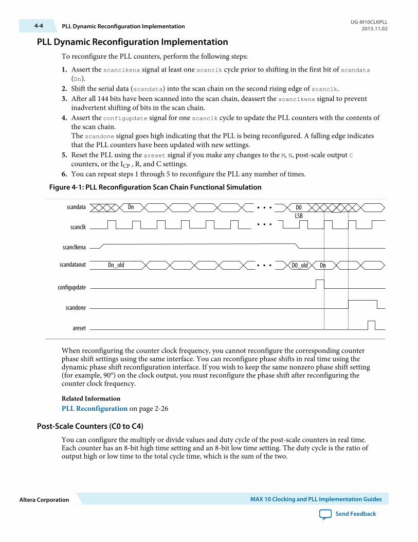
PLL Dynamic Reconfiguration ImplementationTo reconfigure the PLL counters, perform the following steps:
1. Assert the scanclkena signal at least one scanclk cycle prior to shifting in the first bit of scandata(Dn).
2. Shift the serial data (scandata) into the scan chain on the second rising edge of scanclk.3. After all 144 bits have been scanned into the scan chain, deassert the scanclkena signal to prevent
inadvertent shifting of bits in the scan chain.4. Assert the configupdate signal for one scanclk cycle to update the PLL counters with the contents of
the scan chain.The scandone signal goes high indicating that the PLL is being reconfigured. A falling edge indicatesthat the PLL counters have been updated with new settings.
5. Reset the PLL using the areset signal if you make any changes to the M, N, post-scale output Ccounters, or the ICP , R, and C settings.
6. You can repeat steps 1 through 5 to reconfigure the PLL any number of times.
Figure 4-1: PLL Reconfiguration Scan Chain Functional Simulation
scandata
scanclk
scanclkena
scandataout
configupdate
scandone
areset
Dn_old D0_old Dn
D0DnLSB
When reconfiguring the counter clock frequency, you cannot reconfigure the corresponding counterphase shift settings using the same interface. You can reconfigure phase shifts in real time using thedynamic phase shift reconfiguration interface. If you wish to keep the same nonzero phase shift setting(for example, 90°) on the clock output, you must reconfigure the phase shift after reconfiguring thecounter clock frequency.
Related InformationPLL Reconfiguration on page 2-26
Post-Scale Counters (C0 to C4)
You can configure the multiply or divide values and duty cycle of the post-scale counters in real time.Each counter has an 8-bit high time setting and an 8-bit low time setting. The duty cycle is the ratio ofoutput high or low time to the total cycle time, which is the sum of the two.
4-4 PLL Dynamic Reconfiguration ImplementationUG-M10CLKPLL
2015.11.02
Altera Corporation MAX 10 Clocking and PLL Implementation Guides
Send Feedback
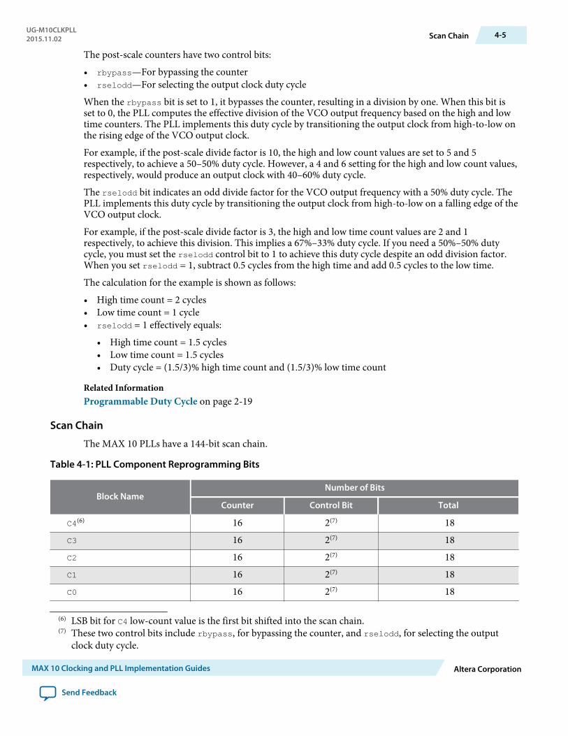
The post-scale counters have two control bits:
• rbypass—For bypassing the counter• rselodd—For selecting the output clock duty cycle
When the rbypass bit is set to 1, it bypasses the counter, resulting in a division by one. When this bit isset to 0, the PLL computes the effective division of the VCO output frequency based on the high and lowtime counters. The PLL implements this duty cycle by transitioning the output clock from high-to-low onthe rising edge of the VCO output clock.
For example, if the post-scale divide factor is 10, the high and low count values are set to 5 and 5respectively, to achieve a 50–50% duty cycle. However, a 4 and 6 setting for the high and low count values,respectively, would produce an output clock with 40–60% duty cycle.
The rselodd bit indicates an odd divide factor for the VCO output frequency with a 50% duty cycle. ThePLL implements this duty cycle by transitioning the output clock from high-to-low on a falling edge of theVCO output clock.
For example, if the post-scale divide factor is 3, the high and low time count values are 2 and 1respectively, to achieve this division. This implies a 67%–33% duty cycle. If you need a 50%–50% dutycycle, you must set the rselodd control bit to 1 to achieve this duty cycle despite an odd division factor.When you set rselodd = 1, subtract 0.5 cycles from the high time and add 0.5 cycles to the low time.
The calculation for the example is shown as follows:
• High time count = 2 cycles• Low time count = 1 cycle• rselodd = 1 effectively equals:
• High time count = 1.5 cycles• Low time count = 1.5 cycles• Duty cycle = (1.5/3)% high time count and (1.5/3)% low time count
Related InformationProgrammable Duty Cycle on page 2-19
Scan Chain
The MAX 10 PLLs have a 144-bit scan chain.
Table 4-1: PLL Component Reprogramming Bits
Block NameNumber of Bits
Counter Control Bit Total
C4(6) 16 2(7) 18C3 16 2(7) 18C2 16 2(7) 18C1 16 2(7) 18C0 16 2(7) 18
(6) LSB bit for C4 low-count value is the first bit shifted into the scan chain.(7) These two control bits include rbypass, for bypassing the counter, and rselodd, for selecting the output
clock duty cycle.
UG-M10CLKPLL2015.11.02 Scan Chain 4-5
MAX 10 Clocking and PLL Implementation Guides Altera Corporation
Send Feedback
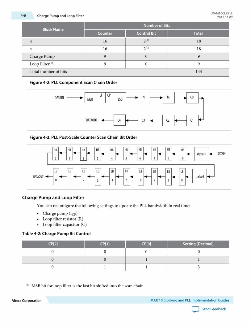
Block NameNumber of Bits
Counter Control Bit Total
M 16 2(7) 18N 16 2(7) 18Charge Pump 9 0 9Loop Filter(8) 9 0 9Total number of bits 144
Figure 4-2: PLL Component Scan Chain Order
DATAIN
C1C2C3C4DATAOUT
MSBLF CP
LSB N M C0
Figure 4-3: PLL Post-Scale Counter Scan Chain Bit Order
DATAINrbypassHB
7
HB
6
HB
5
HB
4
HB
3
HB
2
HB
1
HB
0
rseloddLB
7
LB
6
LB
5
LB
4
LB
3
LB
2
LB
1
LB
0DATAOUT
HB
9
HB
8
LB
9
LB
8
Charge Pump and Loop Filter
You can reconfigure the following settings to update the PLL bandwidth in real time:
• Charge pump (ICP)• Loop filter resistor (R)• Loop filter capacitor (C)
Table 4-2: Charge Pump Bit Control
CP[2] CP[1] CP[0] Setting (Decimal)
0 0 0 00 0 1 10 1 1 3
(8) MSB bit for loop filter is the last bit shifted into the scan chain.
4-6 Charge Pump and Loop FilterUG-M10CLKPLL
2015.11.02
Altera Corporation MAX 10 Clocking and PLL Implementation Guides
Send Feedback
CP[2] CP[1] CP[0] Setting (Decimal)
1 1 1 7
Table 4-3: Loop Filter Resistor Value Control
LFR[4] LFR[3] LFR[2] LFR[1] LFR[0] Setting (Decimal)
0 0 0 0 0 00 0 0 1 1 30 0 1 0 0 40 1 0 0 0 81 0 0 0 0 161 0 0 1 1 191 0 1 0 0 201 1 0 0 0 241 1 0 1 1 271 1 1 0 0 281 1 1 1 0 30
Table 4-4: Loop Filter High Frequency Capacitor Control
LFC[1] LFC[0] Setting (Decimal)
0 0 00 1 11 1 3
Related Information
• Programmable Bandwidth on page 2-19• Programmable Bandwidth with Advanced Parameters on page 4-3• Programmable Bandwidth Parameter Settings on page 6-2
Bypassing PLL Counter
Bypassing a PLL counter results in a multiplification (M counter) or a division (N, C0 to C4 counters) factorof one.
UG-M10CLKPLL2015.11.02 Bypassing PLL Counter 4-7
MAX 10 Clocking and PLL Implementation Guides Altera Corporation
Send Feedback
Table 4-5: PLL Counter Settings
DescriptionPLL Scan Chain Bits [0..8] Settings
LSB MSB
PLL counterbypassed
X X X X X X X X 1(9)
PLL counter notbypassed
X X X X X X X X 0(9)
To bypass any of the PLL counters, set the bypass bit to 1. The values on the other bits are ignored.
Dynamic Phase Configuration ImplementationTo perform one dynamic phase shift step, perform the following steps:
1. Set PHASEUPDOWN and PHASECOUNTERSELECT as required.2. Assert PHASESTEP for at least two SCANCLK cycles. Each PHASESTEP pulse allows one phase shift.3. Deassert PHASESTEP after PHASEDONE goes low.4. Wait for PHASEDONE to go high.5. Repeat steps 1 through 4 as many times as required to perform multiple phase shifts.
PHASEUPDOWN and PHASECOUNTERSELECT signals are synchronous to SCANCLK and must meet the tsu and threquirements with respect to the SCANCLK edges.
You can repeat dynamic phase-shifting indefinitely. For example, in a design where the VCO frequency isset to 1,000 MHz and the output clock frequency is set to 100 MHz, performing 40 dynamic phase shifts(each one yields 125 ps phase shift) results in shifting the output clock by 180º, which is a phase shift of 5ns.
Figure 4-4: Dynamic Phase Shift Timing Diagram
PHASEDONE goes low synchronous with SCANCLK
SCANCLK
PHASESTEP
PHASEUPDOWN
PHASECOUNTERSELECT
PHASEDONE
a b c d
The PHASESTEP signal is latched on the negative edge of SCANCLK (a,c) and must remain asserted for atleast two SCANCLK cycles. Deassert PHASESTEP after PHASEDONE goes low.
(9) Bypass bit
4-8 Dynamic Phase Configuration ImplementationUG-M10CLKPLL
2015.11.02
Altera Corporation MAX 10 Clocking and PLL Implementation Guides
Send Feedback
On the second SCANCLK rising edge (b,d) after PHASESTEP is latched, the values of PHASEUPDOWN andPHASECOUNTERSELECT are latched. The PLL starts dynamic phase-shifting for the specified counters and inthe indicated direction.
The PHASEDONE signal is deasserted synchronous to SCANCLK at the second rising edge (b,d) and remainslow until the PLL finishes dynamic phase-shifting. Depending on the VCO and SCANCLK frequencies,PHASEDONE low time may be greater than or less than one SCANCLK cycle.
You can perform another dynamic phase-shift after the PHASEDONE signal goes from low to high. EachPHASESTEP pulse enables one phase shift. The PHASESTEP pulses must be at least one SCANCLK cycle apart.
Related Information
• Programmable Phase Shift on page 2-20• Dynamic Phase Configuration Parameter Settings on page 6-4
Provides more information about the ALTPLL IP core parameter settings in the Quartus Primesoftware.
• ALTPLL_RECONFIG Parameters on page 7-1Provides more information about the ALTPLL_RECONFIG IP core parameter settings in the QuartusPrime software.
• PLL Dynamic Reconfiguration Parameter Settings on page 6-4Provides more information about the ALTPLL IP core parameter settings in the Quartus Primesoftware.
• ALTPLL_RECONFIG Parameters on page 7-1Provides more information about the ALTPLL_RECONFIG IP core parameter settings in the QuartusPrime software.
Dynamic Phase Configuration Counter Selection
Table 4-6: Phase Counter Select Mapping
PLL Counter Selection PHASECOUNTERSELECT [2] [1] [0]
All output counters 0 0 0M counter 0 0 1C0 counter 0 1 0C1 counter 0 1 1C2 counter 1 0 0C3 counter 1 0 1C4 counter 1 1 0
Related InformationProgrammable Phase Shift on page 2-20
Dynamic Phase Configuration with Advanced Parameters
The finest phase shift step resolution you can get in the ALTPLL IP core is 1/8 of the VCO period. If theVCO frequency is at the lower end of the supported VCO range, the phase shift step resolution might belarger than preferred for your design.
UG-M10CLKPLL2015.11.02 Dynamic Phase Configuration Counter Selection 4-9
MAX 10 Clocking and PLL Implementation Guides Altera Corporation
Send Feedback
You can modify your phase shift resolution using the dynamic phase reconfiguration feature of the PLL. Ifyou want to modify the phase shift resolution without the dynamic phase reconfiguration feature enabled,perform the following steps:
1. Create an ALTPLL instance. Make sure you specify the speed grade of your target device and the PLLtype.
2. On the PLL Reconfiguration page, turn on Create optional inputs for dynamic phase reconfigura‐tion and Enable phase shift step resolution.
3. On the Output Clocks page, set your desired phase shift for each required output clock. Note all theinternal PLL settings shown.
4. On the Bandwidth/SS page, click More Details to see the internal PLL settings. Note all of the settingsshown.
5. On the Inputs/Lock page, turn on Create output file(s) using the ‘Advanced’ PLL Parameters.6. Return to the PLL Reconfiguration page and turn off Create Optional Inputs for Dynamic Phase
Reconfiguration.7. Click Finish to generate the PLL instantiation file(s).
When using Advanced Parameters, the PLL wrapper file (<ALTPLL_instantiation_name>.v or<ALTPLL_instantiation_name>.vhd) is written in a format that allows you to identify the PLLparameters. The parameters are listed in the Generic Map section of the VHDL file, or in thedefparam section of the Verilog file.
8. Open your PLL instantiation wrapper file and locate either the Generic Map or the defparam section.9. Modify the settings to match the settings that you noted in steps 3 and 4.10.Save the PLL instantiation wrapper file and compile your design.11.Verify that the output clock frequencies and phases are correct in the PLL Usage report located under
the Resource section of the Fitter folder in the Compilation Report.
By using this technique, you can apply valid PLL parameters as provided by the ALTPLL IP coreparameter editor to optimize the settings for your design.
Alternatively, you can leave the dynamic phase reconfiguration option enabled and tie the relevant inputports—phasecounterselect[3..0], phaseupdown, phasestep, and scanclk—to constants, if you prefernot to manually edit the PLL wrapper file using the Advanced PLL Parameters option.
Related InformationProgrammable Phase Shift on page 2-20
ALTPLL_RECONFIG IP CoreThe ALTPLL_RECONFIG IP core implements reconfiguration logic to facilitate dynamic real-timereconfiguration of PLLs. You can use the IP core to update the output clock frequency, PLL bandwidth,and phase shifts in real time, without reconfiguring the entire FPGA.
Use the ALTPLL_RECONFIG IP core in designs that must support dynamic changes in the frequency andphase shift of clocks and other frequency signals. The IP core is also useful in prototyping environmentsbecause it allows you to sweep PLL output frequencies and dynamically adjust the output clock phase.You can also adjust the clock-to-output (tCO) delays in real-time by changing the output clock phase shift.This approach eliminates the need to regenerate a configuration file with the new PLL settings. Thisoperation requires dynamic phase-shifting.
4-10 ALTPLL_RECONFIG IP CoreUG-M10CLKPLL
2015.11.02
Altera Corporation MAX 10 Clocking and PLL Implementation Guides
Send Feedback
Related Information
• Introduction to Altera IP CoresProvides general information about all Altera IP cores, including parameterizing, generating,upgrading, and simulating IP.
• Creating Version-Independent IP and Qsys Simulation ScriptsCreate simulation scripts that do not require manual updates for software or IP version upgrades.
• Project Management Best PracticesGuidelines for efficient management and portability of your project and IP files.
Obtaining the Resource Utilization ReportFor details about the resource usage and performance of the ALTPLL_RECONFIG IP core, refer to thecompilation reports in the Quartus Prime software.
To view the compilation reports for the ALTPLL_RECONFIG IP core in the Quartus Prime software,follow these steps:
1. On the Processing menu, click Start Compilation to run a full compilation.2. After compiling the design, on the Processing menu, click Compilation Report.3. In the Table of Contents browser, expand the Fitter folder by clicking the “+” icon.4. Under Fitter, expand Resource section, and select Resource Usage Summary to view the resource
usage information.5. Under Fitter, expand Resource section, and select Resource Utilization by Entity to view the
resource utilization information.
Internal Oscillator IP CoreThe Internal Oscillator IP core specifies the internal oscillator frequencies for the devices.
Related Information
• Introduction to Altera IP CoresProvides general information about all Altera IP cores, including parameterizing, generating,upgrading, and simulating IP.
• Creating Version-Independent IP and Qsys Simulation ScriptsCreate simulation scripts that do not require manual updates for software or IP version upgrades.
• Project Management Best PracticesGuidelines for efficient management and portability of your project and IP files.
UG-M10CLKPLL2015.11.02 Obtaining the Resource Utilization Report 4-11
MAX 10 Clocking and PLL Implementation Guides Altera Corporation
Send Feedback
ALTCLKCTRL IP Core References 52015.11.02
UG-M10CLKPLL Subscribe Send Feedback
ALTCLKCTRL ParametersTable 5-1: ALTCLKCTRL IP Core Parameters for MAX 10 Devices
This table lists the IP core parameters applicable to MAX 10 devices.Parameter Value Decription
How do you want to usethe ALTCLKCTRL
For global clock, orFor external path
Specify the ALTCLKCTRL buffering mode. You canselect from the following modes:
• For global clock—Allows a clock signal to reach allparts of the chip with the same amount of skew; youcan select input port clkselect to switch betweenthe four clock inputs.
• For external path—Represents the clock path fromthe outputs of the PLL to the dedicated clock outputpins; only one clock output is accepted.
How many clock inputswould you like?
1, 2, 3, or 4 Specify the number of input clock sources for the clockcontrol block. You can specify up to four clock inputs.
You can change the number of clock inputs only if youchoose For global clock option.
Create ‘ena’ port toenable or disable theclock network driven bythis buffer
On or Off Turn on this option if you want to create an active highclock enable signal to enable or disable the clocknetwork.
© 2015 Altera Corporation. All rights reserved. ALTERA, ARRIA, CYCLONE, ENPIRION, MAX, MEGACORE, NIOS, QUARTUS and STRATIX words and logos aretrademarks of Altera Corporation and registered in the U.S. Patent and Trademark Office and in other countries. All other words and logos identified astrademarks or service marks are the property of their respective holders as described at www.altera.com/common/legal.html. Altera warrants performanceof its semiconductor products to current specifications in accordance with Altera's standard warranty, but reserves the right to make changes to anyproducts and services at any time without notice. Altera assumes no responsibility or liability arising out of the application or use of any information,product, or service described herein except as expressly agreed to in writing by Altera. Altera customers are advised to obtain the latest version of devicespecifications before relying on any published information and before placing orders for products or services.
ISO9001:2008Registered
www.altera.com101 Innovation Drive, San Jose, CA 95134
Parameter Value Decription
Ensure glitch-freeswitchover implementa‐tion
On or Off Turn on this option to implement a glitch-freeswitchover when you use multiple clock inputs.
You must ensure the currently selected clock is runningbefore switching to another source. If the selected clockis not running, the glitch-free switchover implementa‐tion will not be able to switch to the new clock source.
By default, the clkselect port is set to 00. A clockmust be applied to inclk0x for the values on theclkselect ports to be read.
Related Information
• Global Clock Control Block on page 2-4• Global Clock Network Power Down on page 2-6• Clock Enable Signals on page 2-7• Guideline: Clock Enable Signals on page 3-1
ALTCLKCTRL Ports and SignalsTable 5-2: ALTCLKCTRL Input Ports for MAX 10 Devices
Port Name Condition Description
clkselect[] Optional Input that dynamically selects the clock source to drive theclock network that is driven by the clock buffer.
Input port [1 DOWNTO 0] wide.
If omitted, the default is GND.
If this signal is connected, only the global clock network canbe driven by this clock control block.
The following list shows the signal selection for the binaryvalue:
• 00—inclk[0]
• 01—inclk[1]
ena Optional Clock enable of the clock buffer.
If omitted, the default value is VCC.
5-2 ALTCLKCTRL Ports and SignalsUG-M10CLKPLL
2015.11.02
Altera Corporation ALTCLKCTRL IP Core References
Send Feedback
Port Name Condition Description
inclk[] Required Clock input of the clock buffer.
Input port [1 DOWNTO 0] wide.
You can specify up to two clock inputs, inclk[1..0].
Clock pins, clock outputs from the PLL, and core signals candrive the inclk[] port.
Multiple clock inputs are only supported for the global clocknetworks.
Table 5-3: ALTCLKCTRL Output Ports for MAX 10 Devices
Port Name Condition Description
outclk Required Output of the clock buffer.
Related Information
• Global Clock Control Block on page 2-4• Global Clock Network Power Down on page 2-6• Clock Enable Signals on page 2-7• Guideline: Clock Enable Signals on page 3-1
UG-M10CLKPLL2015.11.02 ALTCLKCTRL Ports and Signals 5-3
ALTCLKCTRL IP Core References Altera Corporation
Send Feedback
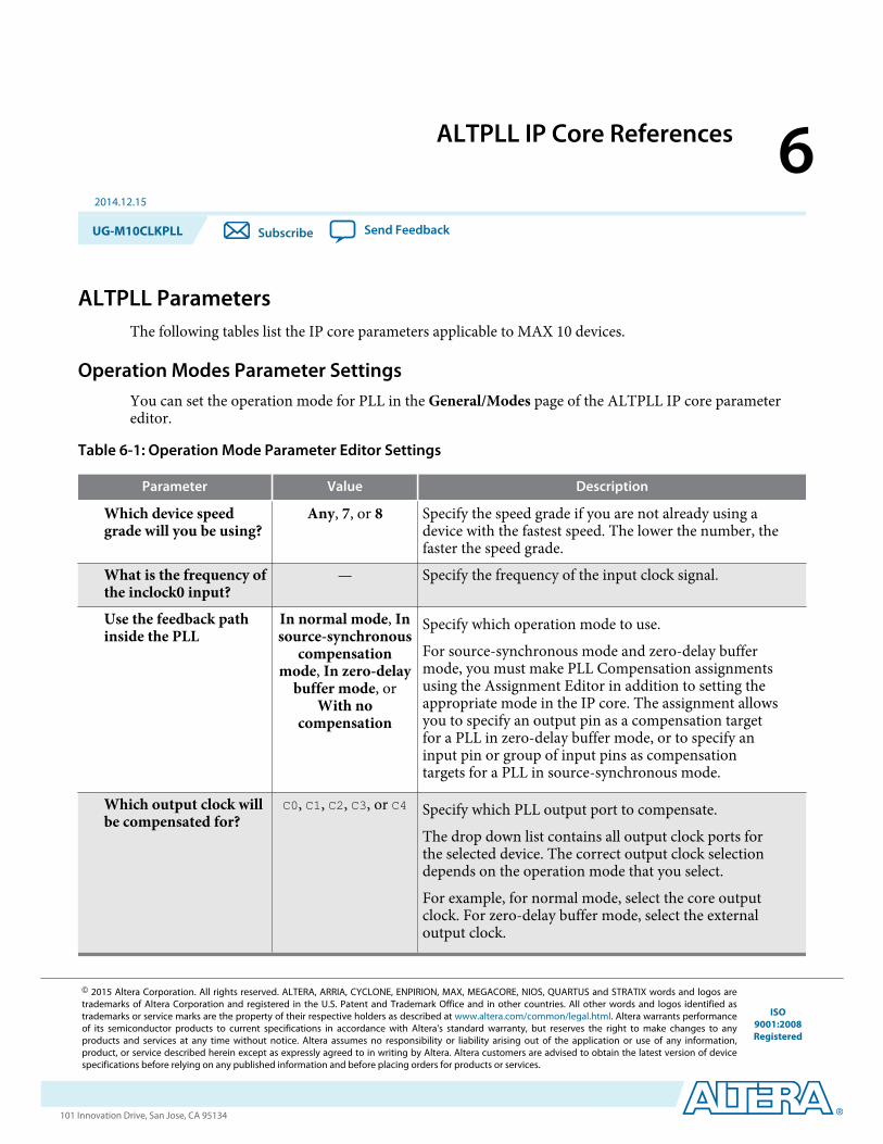
ALTPLL IP Core References 62014.12.15
UG-M10CLKPLL Subscribe Send Feedback
ALTPLL ParametersThe following tables list the IP core parameters applicable to MAX 10 devices.
Operation Modes Parameter SettingsYou can set the operation mode for PLL in the General/Modes page of the ALTPLL IP core parametereditor.
Table 6-1: Operation Mode Parameter Editor Settings
Parameter Value Description
Which device speedgrade will you be using?
Any, 7, or 8 Specify the speed grade if you are not already using adevice with the fastest speed. The lower the number, thefaster the speed grade.
What is the frequency ofthe inclock0 input?
— Specify the frequency of the input clock signal.
Use the feedback pathinside the PLL
In normal mode, Insource-synchronous
compensationmode, In zero-delay
buffer mode, orWith no
compensation
Specify which operation mode to use.
For source-synchronous mode and zero-delay buffermode, you must make PLL Compensation assignmentsusing the Assignment Editor in addition to setting theappropriate mode in the IP core. The assignment allowsyou to specify an output pin as a compensation targetfor a PLL in zero-delay buffer mode, or to specify aninput pin or group of input pins as compensationtargets for a PLL in source-synchronous mode.
Which output clock willbe compensated for?
C0, C1, C2, C3, or C4 Specify which PLL output port to compensate.
The drop down list contains all output clock ports forthe selected device. The correct output clock selectiondepends on the operation mode that you select.
For example, for normal mode, select the core outputclock. For zero-delay buffer mode, select the externaloutput clock.
© 2015 Altera Corporation. All rights reserved. ALTERA, ARRIA, CYCLONE, ENPIRION, MAX, MEGACORE, NIOS, QUARTUS and STRATIX words and logos aretrademarks of Altera Corporation and registered in the U.S. Patent and Trademark Office and in other countries. All other words and logos identified astrademarks or service marks are the property of their respective holders as described at www.altera.com/common/legal.html. Altera warrants performanceof its semiconductor products to current specifications in accordance with Altera's standard warranty, but reserves the right to make changes to anyproducts and services at any time without notice. Altera assumes no responsibility or liability arising out of the application or use of any information,product, or service described herein except as expressly agreed to in writing by Altera. Altera customers are advised to obtain the latest version of devicespecifications before relying on any published information and before placing orders for products or services.
ISO9001:2008Registered
www.altera.com101 Innovation Drive, San Jose, CA 95134
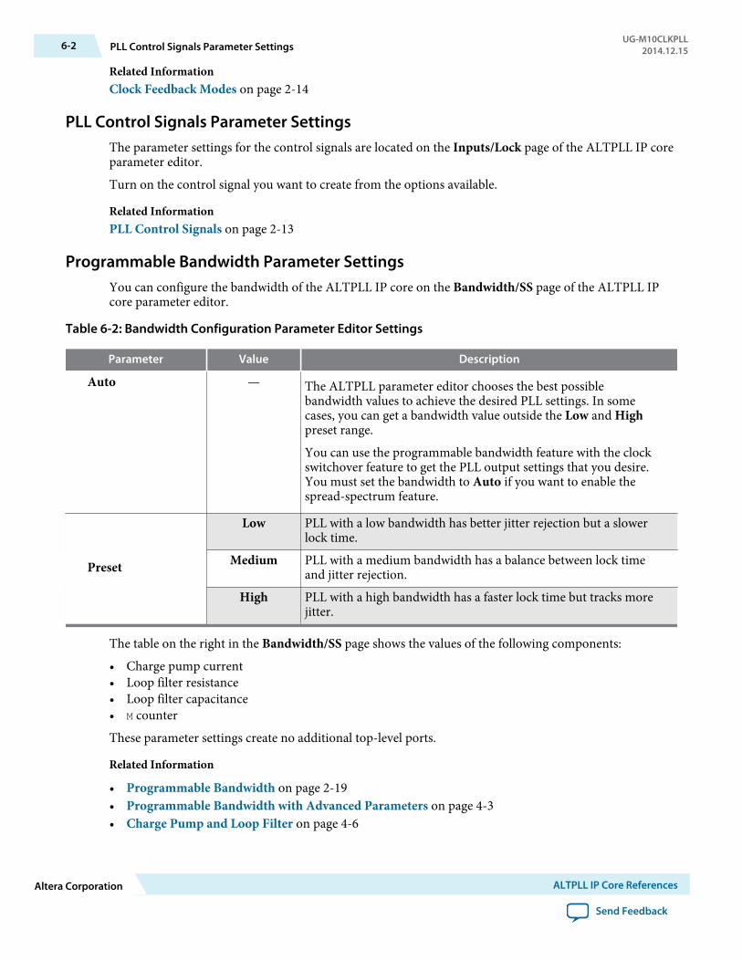
Related InformationClock Feedback Modes on page 2-14
PLL Control Signals Parameter SettingsThe parameter settings for the control signals are located on the Inputs/Lock page of the ALTPLL IP coreparameter editor.
Turn on the control signal you want to create from the options available.
Related InformationPLL Control Signals on page 2-13
Programmable Bandwidth Parameter SettingsYou can configure the bandwidth of the ALTPLL IP core on the Bandwidth/SS page of the ALTPLL IPcore parameter editor.
Table 6-2: Bandwidth Configuration Parameter Editor Settings
Parameter Value Description
Auto — The ALTPLL parameter editor chooses the best possiblebandwidth values to achieve the desired PLL settings. In somecases, you can get a bandwidth value outside the Low and Highpreset range.
You can use the programmable bandwidth feature with the clockswitchover feature to get the PLL output settings that you desire.You must set the bandwidth to Auto if you want to enable thespread-spectrum feature.
Preset
Low PLL with a low bandwidth has better jitter rejection but a slowerlock time.
Medium PLL with a medium bandwidth has a balance between lock timeand jitter rejection.
High PLL with a high bandwidth has a faster lock time but tracks morejitter.
The table on the right in the Bandwidth/SS page shows the values of the following components:
• Charge pump current• Loop filter resistance• Loop filter capacitance• M counter
These parameter settings create no additional top-level ports.
Related Information
• Programmable Bandwidth on page 2-19• Programmable Bandwidth with Advanced Parameters on page 4-3• Charge Pump and Loop Filter on page 4-6
6-2 PLL Control Signals Parameter SettingsUG-M10CLKPLL
2014.12.15
Altera Corporation ALTPLL IP Core References
Send Feedback
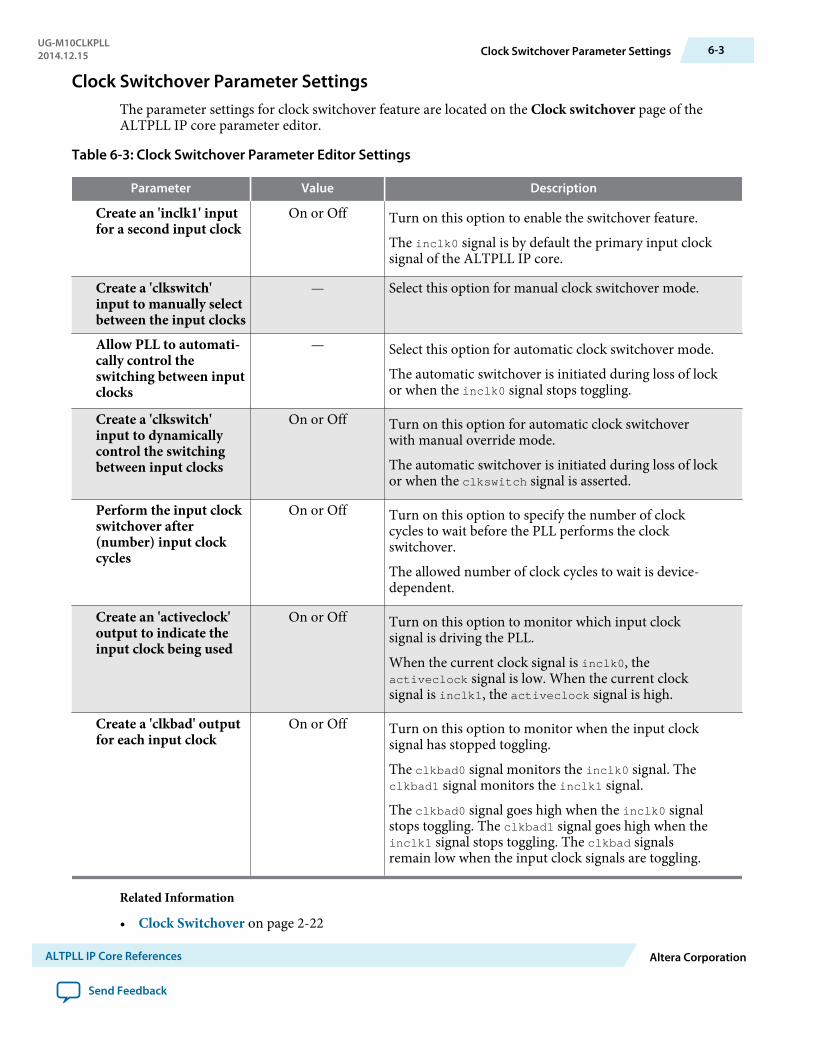
Clock Switchover Parameter SettingsThe parameter settings for clock switchover feature are located on the Clock switchover page of theALTPLL IP core parameter editor.
Table 6-3: Clock Switchover Parameter Editor Settings
Parameter Value Description
Create an 'inclk1' inputfor a second input clock
On or Off Turn on this option to enable the switchover feature.
The inclk0 signal is by default the primary input clocksignal of the ALTPLL IP core.
Create a 'clkswitch'input to manually selectbetween the input clocks
— Select this option for manual clock switchover mode.
Allow PLL to automati‐cally control theswitching between inputclocks
— Select this option for automatic clock switchover mode.
The automatic switchover is initiated during loss of lockor when the inclk0 signal stops toggling.
Create a 'clkswitch'input to dynamicallycontrol the switchingbetween input clocks
On or Off Turn on this option for automatic clock switchoverwith manual override mode.
The automatic switchover is initiated during loss of lockor when the clkswitch signal is asserted.
Perform the input clockswitchover after(number) input clockcycles
On or Off Turn on this option to specify the number of clockcycles to wait before the PLL performs the clockswitchover.
The allowed number of clock cycles to wait is device-dependent.
Create an 'activeclock'output to indicate theinput clock being used
On or Off Turn on this option to monitor which input clocksignal is driving the PLL.
When the current clock signal is inclk0, theactiveclock signal is low. When the current clocksignal is inclk1, the activeclock signal is high.
Create a 'clkbad' outputfor each input clock
On or Off Turn on this option to monitor when the input clocksignal has stopped toggling.
The clkbad0 signal monitors the inclk0 signal. Theclkbad1 signal monitors the inclk1 signal.
The clkbad0 signal goes high when the inclk0 signalstops toggling. The clkbad1 signal goes high when theinclk1 signal stops toggling. The clkbad signalsremain low when the input clock signals are toggling.
Related Information
• Clock Switchover on page 2-22
UG-M10CLKPLL2014.12.15 Clock Switchover Parameter Settings 6-3
ALTPLL IP Core References Altera Corporation
Send Feedback
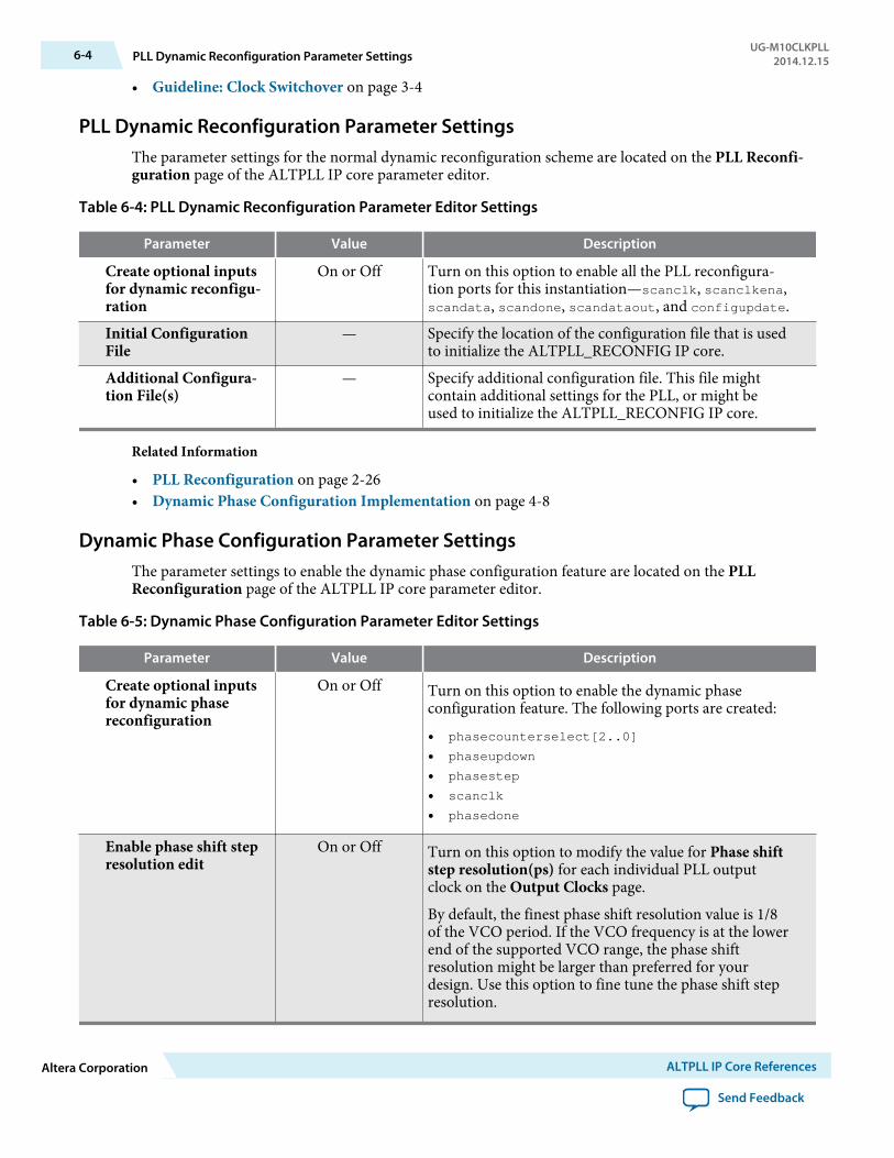
• Guideline: Clock Switchover on page 3-4
PLL Dynamic Reconfiguration Parameter SettingsThe parameter settings for the normal dynamic reconfiguration scheme are located on the PLL Reconfi‐guration page of the ALTPLL IP core parameter editor.
Table 6-4: PLL Dynamic Reconfiguration Parameter Editor Settings
Parameter Value Description
Create optional inputsfor dynamic reconfigu‐ration
On or Off Turn on this option to enable all the PLL reconfigura‐tion ports for this instantiation—scanclk, scanclkena,scandata, scandone, scandataout, and configupdate.
Initial ConfigurationFile
— Specify the location of the configuration file that is usedto initialize the ALTPLL_RECONFIG IP core.
Additional Configura‐tion File(s)
— Specify additional configuration file. This file mightcontain additional settings for the PLL, or might beused to initialize the ALTPLL_RECONFIG IP core.
Related Information
• PLL Reconfiguration on page 2-26• Dynamic Phase Configuration Implementation on page 4-8
Dynamic Phase Configuration Parameter SettingsThe parameter settings to enable the dynamic phase configuration feature are located on the PLLReconfiguration page of the ALTPLL IP core parameter editor.
Table 6-5: Dynamic Phase Configuration Parameter Editor Settings
Parameter Value Description
Create optional inputsfor dynamic phasereconfiguration
On or Off Turn on this option to enable the dynamic phaseconfiguration feature. The following ports are created:
• phasecounterselect[2..0]
• phaseupdown
• phasestep
• scanclk
• phasedone
Enable phase shift stepresolution edit
On or Off Turn on this option to modify the value for Phase shiftstep resolution(ps) for each individual PLL outputclock on the Output Clocks page.
By default, the finest phase shift resolution value is 1/8of the VCO period. If the VCO frequency is at the lowerend of the supported VCO range, the phase shiftresolution might be larger than preferred for yourdesign. Use this option to fine tune the phase shift stepresolution.
6-4 PLL Dynamic Reconfiguration Parameter SettingsUG-M10CLKPLL
2014.12.15
Altera Corporation ALTPLL IP Core References
Send Feedback
Related Information
• Programmable Phase Shift on page 2-20• Dynamic Phase Configuration Implementation on page 4-8
Output Clocks Parameter SettingsThe Output Clocks page of the ALTPLL parameter editor contains the parameter settings of the clockoutput signals. You can configure the c0, c1, c2, c3, and c4 clock output signals of the ALTPLL IP core.
Each option has the following two columns:
• Requested settings—The settings that you want to implement.• Actual settings—The settings closest values that can be implemented in the PLL circuit to best approxi‐
mate the requested settings.
Use the values in the actual settings column as a guide to adjust the requested settings. If the requestedsettings for one of the output clocks cannot be approximated, the ALTPLL IP core parameter editorproduces a warning message at the top of every page.
Table 6-6: Output Clocks Parameter Editor Settings
Parameter Value Description
Use this clock On or Off Turn on this option to generate an output clock port inyour ALTPLL instance.
The output clock port that is to be compensated for isenabled by default. It cannot be disabled, unless youselect a different output clock port to be compensatedfor.
Enter output clockfrequency
— Specify the frequency of the output clock signal.
Enter output clockparameters
— Specify the the output clock parameters instead of thefrequency.
Clock multiplicationfactor
— Specify the clock multiplication factor of the signal.
Clock division factor — Specify the clock division factor of the signal.Clock phase shift — Set the programmable phase shift for an output clock
signals.
The smallest phase shift is 1/8 of VCO period. Fordegree increments, the maximum step size is 45degrees. You can set smaller steps using the Clockmultiplication factor and Clock division factoroptions.
For example, if the post-scale counter is 32, the smallestphase shift step is 0.1°. The up and down buttons letyou cycle through phase shift values. Alternatively, youcan enter a number in the phase shift field manuallyinstead of using the buttons.
UG-M10CLKPLL2014.12.15 Output Clocks Parameter Settings 6-5
ALTPLL IP Core References Altera Corporation
Send Feedback
Parameter Value Description
Clock duty cycle (%) — Set the duty cycle of the output clock signal.Per Clock FeasibilityIndicators
— Indicate output clocks that contain unachievablesettings.
The output clock name in red is the name of the clockwith unachievable settings. The clock listed in green hasno settings issues, and the grayed-out names are theunselected output clocks. You must adjust the requestedsettings for the affected output clocks to resolve thewarning messages.
The ALTPLL IP core parameter editor calculates the simplest fraction, and displays it in the actual settingscolumn. You can use the copy button to copy values from the actual settings to the requested settings.
Figure 6-1: PLL Output Clock Frequency
For example, if the input clock frequency is 100 MHz, and the requested multiplication and divisionfactors are 205 and 1025 respectively, the output clock frequency is calculated as 100 × 205/1025=20 MHz.The actual settings reflect the simplest fraction—the actual multiplication factor is 1, and the actualdivision factor is 5.
ALTPLL Ports and SignalsTable 6-7: ALTPLL Input Ports for MAX 10 Devices
Port Name(10) Condition Description
areset Optional Resets all counters to initial values, including theGATE_LOCK_COUNTER parameter.
clkswitch Optional The control input port to dynamically togglebetween clock input ports (inclk0 and inclk1ports), or to manually override the automatic clockswitchover.
You should create the clkswitch port if only theinclk1 port is created.
configupdate Optional Dynamic full PLL reconfiguration.
(10) Replace brackets, [], in the port name with integer to get the exact name. For example, inclk0 and inclk1.
6-6 ALTPLL Ports and SignalsUG-M10CLKPLL
2014.12.15
Altera Corporation ALTPLL IP Core References
Send Feedback
Port Name(10) Condition Description
inclk[] Required The clock inputs that drive the clock network.
If more than one inclk[] port is created, you mustuse the clkselect port to specify which clock isused. The inclk0 port must always be connected;connect other clock inputs if switching is necessary.
A dedicated clock pin or PLL output clock can drivethis port.
pfdena Optional Enables the phase frequency detector (PFD).
When the PFD is disabled, the PLL continues tooperate regardless of the input clock. Because thePLL output clock frequency does not change forsome time, you can use the pfdena port as ashutdown or cleanup function when a reliable inputclock is no longer available.
phasecounterselect[] Optional Specifies counter select. You can use thephasecounterselect[2..0] bits to select either theM or one of the C counters for phase adjustment.One address map to select all C counters. This signalis registered in the PLL on the rising edge ofSCANCLK.
phasestep Optional Specifies dynamic phase shifting. Logic high enablesdynamic phase shifting.
phaseupdown Optional Specifies dynamic phase shift direction. 1= UP, 0 =DOWN. Signal is registered in the PLL on the risingedge of SCANCLK.
scanclk Optional Input clock port for the serial scan chain.
Free-running clock from core used in combinationwith PHASESTEP to enable or disable dynamic phaseshifting. Shared with SCANCLK for dynamic reconfi‐guration.
scanclkena Optional Clock enable port for the serial scan chain.
scandata Optional Contains the data for the serial scan chain.
(10) Replace brackets, [], in the port name with integer to get the exact name. For example, inclk0 and inclk1.
UG-M10CLKPLL2014.12.15 ALTPLL Ports and Signals 6-7
ALTPLL IP Core References Altera Corporation
Send Feedback
Table 6-8: ALTPLL Output Ports for MAX 10 Devices
Port Name(11) Condition Description
activeclock Optional Specifies which clock is the primary reference clockwhen the clock switchover circuit initiates.
If the inclk0 is in use, the activeclock port goeslow. If the inclk1 is in use, the activeclock portgoes high.
You can set the PLL to automatically initiate theclock switchover when the primary reference clockis not toggling correctly, or you can manuallyinitiate the clock switchover using the clkswitchinput port.
c[] Required The clock output of the PLL.
clkbad[] Optional clkbad1 and clkbad0 ports check for input clocktoggling.
If the inclk0 port stops toggling, the clkbad0 portgoes high. If the inclk1 port stops toggling, theclkbad1 port goes high.
(11) Replace the brackets, [], in the port name with an integer to get the exact name (for example, c0 and c1).
6-8 ALTPLL Ports and SignalsUG-M10CLKPLL
2014.12.15
Altera Corporation ALTPLL IP Core References
Send Feedback
Port Name(11) Condition Description
locked Optional This output port acts as an indicator when the PLLhas reached phase-locked. The locked port stayshigh as long as the PLL is locked, and stays lowwhen the PLL is out-of-lock.
The number of cycles needed to gate the lockedsignal is based on the PLL input clock. The gated-lock circuitry is clocked by the PLL input clock. Themaximum lock time for the PLL is provided in theMAX 10 Device Datasheet.Take the maximum lock time of the PLL and divideit by the period of the PLL input clock. The result isthe number of clock cycles needed to gate thelocked signal.
The lock signal is an asynchronous output of thePLL. The PLL lock signal is derived from thereference clock and feedback clock feeding thephase frequency detector (PFD) as follows:
• Reference clock = Input Clock/N• Feedback clock = VCO/M
The PLL asserts the locked port when the phasesand frequencies of the reference clock and feedbackclock are the same or within the lock circuittolerance. When the difference between the twoclock signals goes beyond the lock circuit tolerance,the PLL loses lock.
phasedone Optional This output port indicates that dynamic phasereconfiguration is completed.
When phasedone signal is asserted, it indicates tocore logic that the phase adjustment is complete andPLL is ready to act on a possible second adjustmentpulse. This signal asserts based on internal PLLtiming and deasserts on rising edge of SCANCLK.
scandataout Optional The data output for the serial scan chain.
You can use the scandataout port to determinewhen PLL reconfiguration completes. The lastoutput is cleared when reconfiguration completes.
scandone Optional This output port indicates that the scan chain writeoperation is initiated.
The scandone port goes high when the scan chainwrite operation initiates, and goes low when thescan chain write operation completes.
(11) Replace the brackets, [], in the port name with an integer to get the exact name (for example, c0 and c1).
UG-M10CLKPLL2014.12.15 ALTPLL Ports and Signals 6-9
ALTPLL IP Core References Altera Corporation
Send Feedback

Related InformationPLL Control Signals on page 2-13
6-10 ALTPLL Ports and SignalsUG-M10CLKPLL
2014.12.15
Altera Corporation ALTPLL IP Core References
Send Feedback
ALTPLL_RECONFIG IP Core References 72015.11.02
UG-M10CLKPLL Subscribe Send Feedback
ALTPLL_RECONFIG ParametersTable 7-1: ALTPLL_RECONFIG IP Core Parameters for MAX 10 Devices
This table lists the IP core parameters applicable to MAX 10 devices.Page Parameter Value Description
ParameterSettings
Currently SelectedDevice Family
— Specifies the chosen device family.
Which scan chain typewill you be using?
— The scan chain is a serial shift register chainthat is used to store settings. It acts like acache. When you assert the reconfig signal,the PLL is reconfigured with the values in thecache. The type of scan chain must follow thetype of PLL to be reconfigured. The scanchain type has a default value of Top/Bottom.
Do you want to specifythe initial value of thescan chain?
No, leave itblank,
Yes, use this filefor the content
data
Specifies the initial value of the scan chain.Select No, leave it blank to not specify a fileor select Yes, use this file for the contentdata to browse for a .hex or .mif file.
The option to initialize from a ROM is notavailable. However, you can choose to addports to write to the scan chain from anexternal ROM during runtime by turning onAdd ports to write to the scan chain fromexternal ROM during run time.
Add ports to write tothe scan chain fromexternal ROM duringrun time
On, Off Turn on this option to take advantage ofcycling multiple configuration files, which arestored in external ROMs during user mode.
© 2015 Altera Corporation. All rights reserved. ALTERA, ARRIA, CYCLONE, ENPIRION, MAX, MEGACORE, NIOS, QUARTUS and STRATIX words and logos aretrademarks of Altera Corporation and registered in the U.S. Patent and Trademark Office and in other countries. All other words and logos identified astrademarks or service marks are the property of their respective holders as described at www.altera.com/common/legal.html. Altera warrants performanceof its semiconductor products to current specifications in accordance with Altera's standard warranty, but reserves the right to make changes to anyproducts and services at any time without notice. Altera assumes no responsibility or liability arising out of the application or use of any information,product, or service described herein except as expressly agreed to in writing by Altera. Altera customers are advised to obtain the latest version of devicespecifications before relying on any published information and before placing orders for products or services.
ISO9001:2008Registered
www.altera.com101 Innovation Drive, San Jose, CA 95134
Page Parameter Value Description
EDA
Simulation Libraries — Specifies the libraries for functionalsimulation.
Generate netlist On, Off Turn on this option to generate synthesis areaand timing estimation netlist.
Summary — — Specifies the types of files to be generated. Agray checkmark indicates a file that isautomatically generated; an unchecked checkbox indicates an optional file. Choose fromthe following types of files:
• AHDL Include file (<function name>.inc)• VHDL component declaration file
(<function name>.cmp)• Quartus Prime symbol file (<function
name>.bsf)• Instantiation template file (<function
name>_inst.v or <function name>_inst.vhd)
• Verilog HDL black box file (<functionname>_bb.v)
If the Generate netlist option is turned on,the file for that netlist is also available(<function name>_syn.v).
Related Information
• Programmable Phase Shift on page 2-20• Dynamic Phase Configuration Implementation on page 4-8• PLL Reconfiguration on page 2-26• Dynamic Phase Configuration Implementation on page 4-8
ALTPLL_RECONFIG Ports and SignalsTable 7-2: ALTPLL_RECONFIG Input Ports for MAX 10 Devices
Port Name Condition Description
clock Required Clock input for loading individual parameters. This signalalso clocks the PLL during reconfiguration.
The clock input port must be connected to a valid clock.
Refer to the MAX 10 Device Datasheet for the clock fMAX.
7-2 ALTPLL_RECONFIG Ports and SignalsUG-M10CLKPLL
2015.11.02
Altera Corporation ALTPLL_RECONFIG IP Core References
Send Feedback
Port Name Condition Description
reset Required Asynchronous reset input to the IP core.
Altera recommends that you reset this IP core before firstuse to guarantee that it is in a valid state. However, it doespower up in the reset state. This port must be connected.
data_in[] Optional Data input that provides parameter value when writingparameters.
This 9-bit input port provides the data to be written to thescan cache during a write operation. The bit width of thecounter parameter to be written determines the numberof bits of data_in[] that are read into the cache.
For example, the low bit count of the C0 counter is 8-bitwide, so data_in[7..0] is read to the correct cachelocation. The bypass mode for the C0 counter is 1-bitwide, so data_in[0] is read for the value of thisparameter.
If omitted, the default value is 0.
counter_type[] Optional Specifies the counter type.
An input port in the form of a 4-bit bus that selects whichcounter type should be selected for the correspondingoperation (read, write, or reconfig).
Refer to the counter_type[3..0] settings table for themapping between the counter_type value and thephysical counter to be set.
counter_param[] Optional Specifies the parameter for the value specified in thecounter_type port.
An input port in the form of a 3-bit bus that selects whichparameter for the given counter type should be updated.The mapping to each parameter type and thecorresponding parameter bit-width are defined in thecounter_param[3..0] settings table.
UG-M10CLKPLL2015.11.02 ALTPLL_RECONFIG Ports and Signals 7-3
ALTPLL_RECONFIG IP Core References Altera Corporation
Send Feedback
Port Name Condition Description
read_param Optional Reads the parameter specified with the counter_type andcounter_param ports from cache and fed to the data_out[] port.
When asserted, the read_param signal indicates that thescan cache should be read and fed to data_out[]. The bitlocation of the scan cache and the number of bits readand sent to data_out[] depend on the counter_typeand counter_param values. The read_param signal issampled at the rising clock edge. If the read_param signalis asserted, the parameter value is read from the cache.Assert the read_param signal for 1 clock cycle only toprevent the parameter from being read twice.
The busy signal is asserted on the rising clock edgefollowing the assertion of the read_param signal. Whilethe parameter is read, the busy signal remains asserted.After the busy signal is deasserted, the value on data_out[] is valid and the next parameter can be loaded.While the busy signal is asserted, the value on data_out[] is not valid.
When the read_param signal is asserted, the busy signal isonly asserted on the following rising edge of the clock andnot on the same clock cycle as the read_param signal.
write_param Optional Writes the parameter specified with the counter_typeand counter_param ports to the cache with the valuespecified on the data_in[] port.
When asserted, the write_param signal indicates that thevalue on data_in[] should be written to the parameterspecified by counter_type[] and counter_param[]. Thenumber of bits read from the data_in[] port depends onthe parameter. The write_param signal is sampled at therising clock edge. If the write_param signal is asserted,the parameter value is written to the cache. Assert thewrite_param signal for 1 clock cycle only to prevent theparameter from being written twice.
The busy signal is asserted on the rising clock edgefollowing the assertion of the write_param signal. Whilethe parameter is being written, the busy signal remainsasserted and input to data_in[] is ignored. After thebusy signal is deasserted, the next parameter can bewritten.
When the write_param signal is asserted, the busy signalis only asserted on the following rising edge of the clock.The busy signal is not asserted on the same clock cycle asthe write_param signal.
7-4 ALTPLL_RECONFIG Ports and SignalsUG-M10CLKPLL
2015.11.02
Altera Corporation ALTPLL_RECONFIG IP Core References
Send Feedback
Port Name Condition Description
reconfig Required Specifies that the PLL should be reconfigured with thePLL settings specified in the current cache.
When asserted, the reconfig signal indicates that the PLLshould be reconfigured with the values in the cache. Thereconfig signal is sampled at the rising clock edge. If thereconfig signal is asserted, the cached settings are loadedin the PLL. Assert the reconfig signal for 1 clock cycleonly to prevent reloading the PLL configuration. Thebusy signal is asserted on the rising clock edge followingthe assertion of the reconfig signal. While the PLL isbeing loaded, the busy signal remains asserted. After thebusy signal is deasserted, the parameter values can bemodified again.
During and after reconfiguration, the scan chain datacache remains unchanged. This allows you to easily createa new set of reconfiguration settings using only oneparameter.
If write_param has not been asserted since the previousassertion of reconfig, the entire scan chain is shifted into the PLL again.
When the reconfig signal is asserted, the busy signal isonly asserted on the following rising edge of the clock.The busy signal is not asserted on the same clock cycle asthe reconfig signal.
pll_areset_in Optional Input signal indicating that the PLL should be reset.
When asserted, the pll_areset_in signal indicates thePLL IP core should be reset. This port defaults to 0 if leftunconnected. When using the ALTPLL_RECONFIG IPcore in a design, you cannot reset the PLL in any otherway. You must use this IP core port to manually reset thePLL.
pll_scandone Optional Input port for the ALTPLL_RECONFIG IP core. Thisport is driven by the PLL's scandone output signal anddetermines when the PLL is reconfigured.
pll_scandataout Required Input port driven by the scandataout signal from theALTPLL IP core. Use this port to read the currentconfiguration of the ALTPLL IP core. This input portholds the ALTPLL scan data output from the dynamicallyreconfigurable bits. The pll_scandataout port must beconnected to the scandataout port of the PLL. Theactivity on this port can only be observed when thereconfig signal is asserted.
UG-M10CLKPLL2015.11.02 ALTPLL_RECONFIG Ports and Signals 7-5
ALTPLL_RECONFIG IP Core References Altera Corporation
Send Feedback
Table 7-3: ALTPLL_RECONFIG Output Ports for MAX 10 Devices
Port Name Condition Description
data_out[] Optional Data read from the cache when read_param is asserted.
This 9-bit output bus provides the parameter data to theuser. When the read_param signal is asserted, the valueson counter_type[] and counter_param[] determine theparameter value that is loaded from cache and driven onthe data_out[] bus. When the IP core deasserts the busysignal, the appropriate bits of the bus (for example,[0] or[3..0]) hold a valid value.
busy Optional Indicates that the PLL is reading or writing a parameter tothe cache, or is configuring the PLL.
While the busy signal is asserted, no parameters can beread or written, and no reconfiguration can be initiated.Changes to the IP core can be made only when the busysignal is not asserted. The signal goes high when theread_param, write_param, or reconfig input port isasserted, and remains high until the specified operation iscomplete. In the case of a reconfiguration operation, thebusy signal remains high until the pll_areset signal isasserted and then deasserted.
pll_areset Required Drives the areset port on the PLL to be reconfigured.
The pll_areset port must be connected to the aresetport of the ALTPLL IP core for the reconfiguration tofunction correctly. This signal is active high. The pll_areset is asserted when pll_areset_in is asserted, or,after reconfiguration, at the next rising clock edge afterthe scandone signal goes high. If you use the ALTPLL_RECONFIG IP core, use the pll_areset output port todrive the PLL areset port.
pll_configupdate Optional Drives the configupdate port on the PLL to be reconfig‐ured. When asserted, the pll_configupdate port loadsselected data to PLL configuration latches. The signal isasserted after the final data bit is sent out.
pll_scanclk Required Drives the scanclk port on the PLL to be reconfigured.For information about the maximum scanclk frequencyfor the various devices, refer to the respective devicehandbook.
7-6 ALTPLL_RECONFIG Ports and SignalsUG-M10CLKPLL
2015.11.02
Altera Corporation ALTPLL_RECONFIG IP Core References
Send Feedback
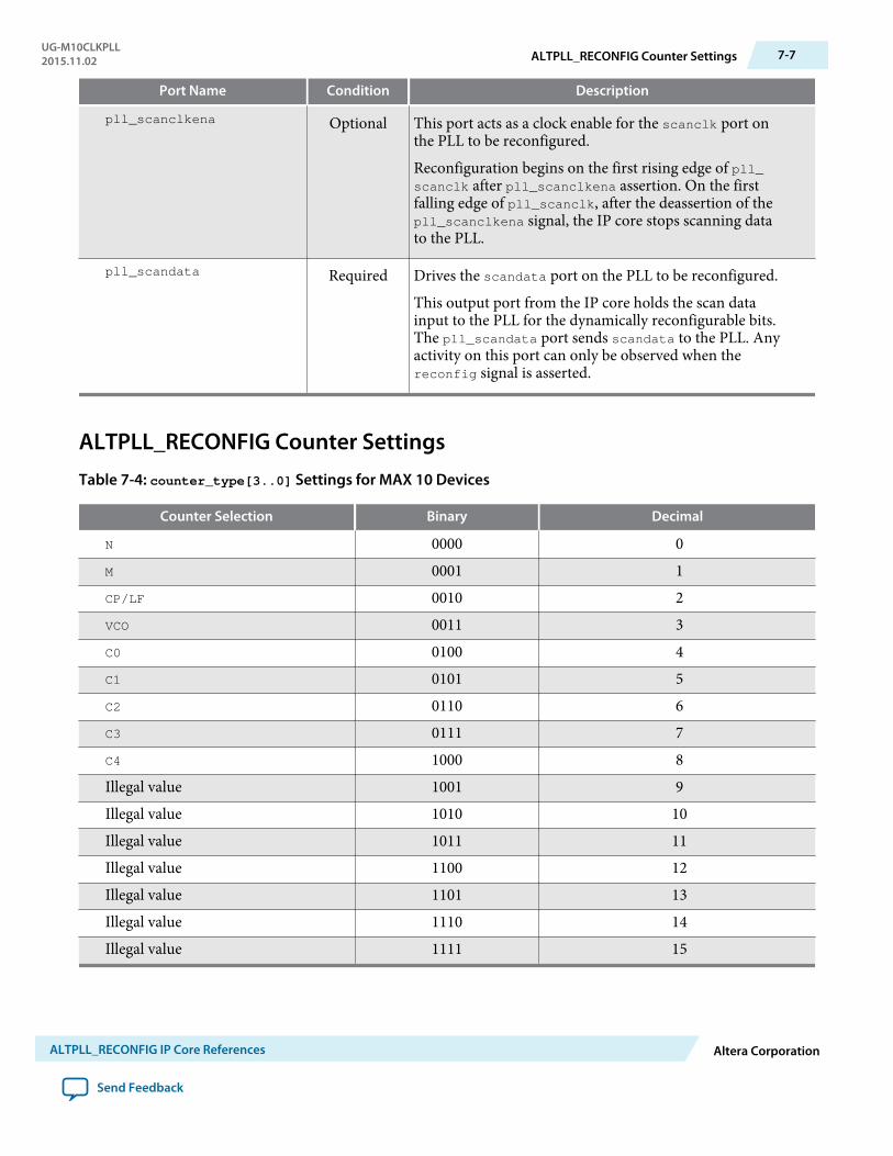
Port Name Condition Description
pll_scanclkena Optional This port acts as a clock enable for the scanclk port onthe PLL to be reconfigured.
Reconfiguration begins on the first rising edge of pll_scanclk after pll_scanclkena assertion. On the firstfalling edge of pll_scanclk, after the deassertion of thepll_scanclkena signal, the IP core stops scanning datato the PLL.
pll_scandata Required Drives the scandata port on the PLL to be reconfigured.
This output port from the IP core holds the scan datainput to the PLL for the dynamically reconfigurable bits.The pll_scandata port sends scandata to the PLL. Anyactivity on this port can only be observed when thereconfig signal is asserted.
ALTPLL_RECONFIG Counter SettingsTable 7-4: counter_type[3..0] Settings for MAX 10 Devices
Counter Selection Binary Decimal
N 0000 0M 0001 1CP/LF 0010 2VCO 0011 3C0 0100 4C1 0101 5C2 0110 6C3 0111 7C4 1000 8Illegal value 1001 9Illegal value 1010 10Illegal value 1011 11Illegal value 1100 12Illegal value 1101 13Illegal value 1110 14Illegal value 1111 15
UG-M10CLKPLL2015.11.02 ALTPLL_RECONFIG Counter Settings 7-7
ALTPLL_RECONFIG IP Core References Altera Corporation
Send Feedback
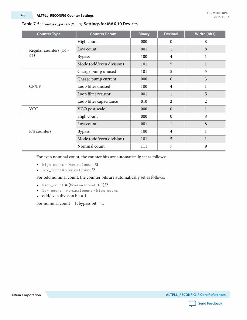
Table 7-5: counter_param[2..0] Settings for MAX 10 Devices
Counter Type Counter Param Binary Decimal Width (bits)
Regular counters (C0 -C4)
High count 000 0 8Low count 001 1 8Bypass 100 4 1Mode (odd/even division) 101 5 1
CP/LF
Charge pump unused 101 5 5Charge pump current 000 0 3Loop filter unused 100 4 1Loop filter resistor 001 1 5Loop filter capacitance 010 2 2
VCO VCO post scale 000 0 1
M/N counters
High count 000 0 8Low count 001 1 8Bypass 100 4 1Mode (odd/even division) 101 5 1Nominal count 111 7 9
For even nominal count, the counter bits are automatically set as follows:
• high_count = Nominalcount/2• low_count= Nominalcount/2
For odd nominal count, the counter bits are automatically set as follows:
• high_count = (Nominalcount + 1)/2• low_count = Nominalcount - high_count• odd/even division bit = 1
For nominal count = 1, bypass bit = 1.
7-8 ALTPLL_RECONFIG Counter SettingsUG-M10CLKPLL
2015.11.02
Altera Corporation ALTPLL_RECONFIG IP Core References
Send Feedback
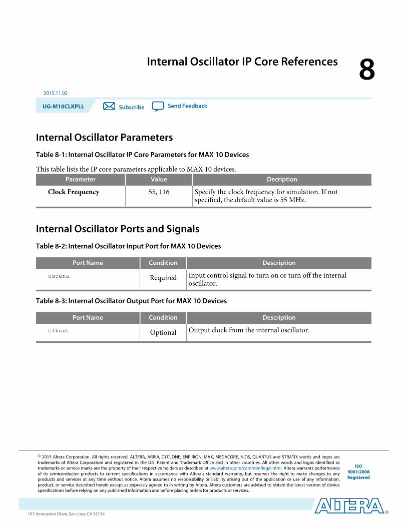
Internal Oscillator IP Core References 82015.11.02
UG-M10CLKPLL Subscribe Send Feedback
Internal Oscillator ParametersTable 8-1: Internal Oscillator IP Core Parameters for MAX 10 Devices
This table lists the IP core parameters applicable to MAX 10 devices.Parameter Value Decription
Clock Frequency 55, 116 Specify the clock frequency for simulation. If notspecified, the default value is 55 MHz.
Internal Oscillator Ports and SignalsTable 8-2: Internal Oscillator Input Port for MAX 10 Devices
Port Name Condition Description
oscena Required Input control signal to turn on or turn off the internaloscillator.
Table 8-3: Internal Oscillator Output Port for MAX 10 Devices
Port Name Condition Description
clkout Optional Output clock from the internal oscillator.
© 2015 Altera Corporation. All rights reserved. ALTERA, ARRIA, CYCLONE, ENPIRION, MAX, MEGACORE, NIOS, QUARTUS and STRATIX words and logos aretrademarks of Altera Corporation and registered in the U.S. Patent and Trademark Office and in other countries. All other words and logos identified astrademarks or service marks are the property of their respective holders as described at www.altera.com/common/legal.html. Altera warrants performanceof its semiconductor products to current specifications in accordance with Altera's standard warranty, but reserves the right to make changes to anyproducts and services at any time without notice. Altera assumes no responsibility or liability arising out of the application or use of any information,product, or service described herein except as expressly agreed to in writing by Altera. Altera customers are advised to obtain the latest version of devicespecifications before relying on any published information and before placing orders for products or services.
ISO9001:2008Registered
www.altera.com101 Innovation Drive, San Jose, CA 95134
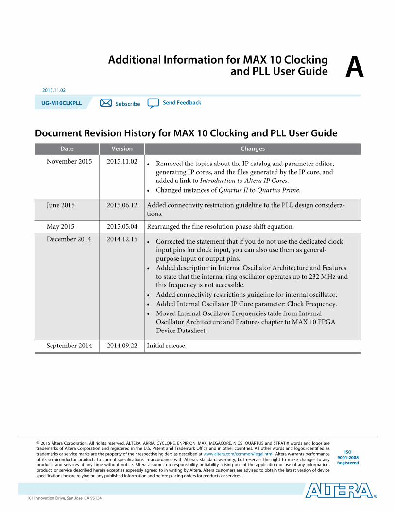
Additional Information for MAX 10 Clockingand PLL User Guide A
2015.11.02
UG-M10CLKPLL Subscribe Send Feedback
Document Revision History for MAX 10 Clocking and PLL User GuideDate Version Changes
November 2015 2015.11.02 • Removed the topics about the IP catalog and parameter editor,generating IP cores, and the files generated by the IP core, andadded a link to Introduction to Altera IP Cores.
• Changed instances of Quartus II to Quartus Prime.
June 2015 2015.06.12 Added connectivity restriction guideline to the PLL design considera‐tions.
May 2015 2015.05.04 Rearranged the fine resolution phase shift equation.
December 2014 2014.12.15 • Corrected the statement that if you do not use the dedicated clockinput pins for clock input, you can also use them as general-purpose input or output pins.
• Added description in Internal Oscillator Architecture and Featuresto state that the internal ring oscillator operates up to 232 MHz andthis frequency is not accessible.
• Added connectivity restrictions guideline for internal oscillator.• Added Internal Oscillator IP Core parameter: Clock Frequency.• Moved Internal Oscillator Frequencies table from Internal
Oscillator Architecture and Features chapter to MAX 10 FPGADevice Datasheet.
September 2014 2014.09.22 Initial release.
© 2015 Altera Corporation. All rights reserved. ALTERA, ARRIA, CYCLONE, ENPIRION, MAX, MEGACORE, NIOS, QUARTUS and STRATIX words and logos aretrademarks of Altera Corporation and registered in the U.S. Patent and Trademark Office and in other countries. All other words and logos identified astrademarks or service marks are the property of their respective holders as described at www.altera.com/common/legal.html. Altera warrants performanceof its semiconductor products to current specifications in accordance with Altera's standard warranty, but reserves the right to make changes to anyproducts and services at any time without notice. Altera assumes no responsibility or liability arising out of the application or use of any information,product, or service described herein except as expressly agreed to in writing by Altera. Altera customers are advised to obtain the latest version of devicespecifications before relying on any published information and before placing orders for products or services.
ISO9001:2008Registered
www.altera.com101 Innovation Drive, San Jose, CA 95134

MAX 10 General Purpose I/O User Guide
Last updated for Quartus Prime Design Suite: 16.0
Subscribe
Send Feedback
UG-M10GPIO2016.05.02
101 Innovation DriveSan Jose, CA 95134www.altera.com
Contents
MAX 10 I/O Overview......................................................................................... 1-1MAX 10 Devices I/O Resources Per Package ..........................................................................................1-1MAX 10 I/O Vertical Migration Support................................................................................................. 1-3
MAX 10 I/O Architecture and Features..............................................................2-1MAX 10 I/O Standards Support................................................................................................................ 2-1
MAX 10 I/O Standards Voltage and Pin Support....................................................................... 2-5MAX 10 I/O Elements.................................................................................................................................2-8
MAX 10 I/O Banks Architecture................................................................................................... 2-9MAX 10 I/O Banks Locations...................................................................................................... 2-10
MAX 10 I/O Buffers.................................................................................................................................. 2-13Schmitt-Trigger Input Buffer....................................................................................................... 2-13Programmable I/O Buffer Features............................................................................................. 2-13
I/O Standards Termination...................................................................................................................... 2-21Voltage-Referenced I/O Standards Termination...................................................................... 2-21Differential I/O Standards Termination.....................................................................................2-22MAX 10 On-Chip I/O Termination............................................................................................2-23
MAX 10 I/O Design Considerations...................................................................3-1Guidelines: VCCIO Range Considerations.................................................................................................3-1Guidelines: Voltage-Referenced I/O Standards Restriction.................................................................. 3-1Guidelines: Enable Clamp Diode for LVTTL/LVCMOS Input Buffers...............................................3-2Guidelines: Adhere to the LVDS I/O Restrictions Rules........................................................................3-3Guidelines: I/O Restriction Rules.............................................................................................................. 3-3Guidelines: Analog-to-Digital Converter I/O Restriction..................................................................... 3-3Guidelines: External Memory Interface I/O Restrictions.......................................................................3-7Guidelines: Dual-Purpose Configuration Pin..........................................................................................3-8Guidelines: Clock and Data Input Signal for MAX 10 E144 Package.................................................. 3-9
MAX 10 I/O Implementation Guides................................................................. 4-1Altera GPIO Lite IP Core............................................................................................................................4-1
Altera GPIO Lite IP Core Data Paths............................................................................................4-2Verifying Pin Migration Compatibility.................................................................................................... 4-4
Altera GPIO Lite IP Core References................................................................. 5-1Altera GPIO Lite Parameter Settings........................................................................................................ 5-1Altera GPIO Lite Interface Signals............................................................................................................ 5-5
MAX 10 General Purpose I/O User Guide Archives......................................... A-1
TOC-2
Altera Corporation

Document Revision History for MAX 10 General Purpose I/O User Guide...B-1
TOC-3
Altera Corporation
MAX 10 I/O Overview 12016.05.02
UG-M10GPIO Subscribe Send Feedback
The MAX® 10 general purpose I/O (GPIO) system consists of the I/O elements (IOE) and the AlteraGPIO Lite IP core.
• The IOEs contain bidirectional I/O buffers and I/O registers located in I/O banks around the peripheryof the device.
• The Altera GPIO Lite IP core supports the GPIO components and features, including double data rateI/O (DDIO), delay chains, I/O buffers, control signals, and clocking.
Related Information
• MAX 10 I/O Architecture and Features on page 2-1Provides information about the architecture and features of the I/Os in MAX 10 devices.
• MAX 10 I/O Design Considerations on page 3-1Provides I/O design guidelines for MAX 10 Devices.
• MAX 10 I/O Implementation Guides on page 4-1Provides guides to implement I/Os in MAX 10 Devices.
• Altera GPIO Lite IP Core References on page 5-1Lists the parameters and signals of Altera GPIO Lite IP core for MAX 10 Devices.
• MAX 10 General Purpose I/O User Guide Archives on page 6-1Provides a list of user guides for previous versions of the Altera GPIO Lite IP core.
MAX 10 Devices I/O Resources Per PackageTable 1-1: Package Plan for MAX 10 Single Power Supply Devices
Device
Package
Type M153
153-pin MBGA
U169
169-pin UBGA
E144
144-pin EQFP
Size 8 mm × 8 mm 11 mm × 11 mm 22 mm × 22 mm
Ball Pitch 0.5 mm 0.8 mm 0.5 mm
10M02 112 130 10110M04 112 130 101
© 2016 Altera Corporation. All rights reserved. ALTERA, ARRIA, CYCLONE, ENPIRION, MAX, MEGACORE, NIOS, QUARTUS and STRATIX words and logos aretrademarks of Altera Corporation and registered in the U.S. Patent and Trademark Office and in other countries. All other words and logos identified astrademarks or service marks are the property of their respective holders as described at www.altera.com/common/legal.html. Altera warrants performanceof its semiconductor products to current specifications in accordance with Altera's standard warranty, but reserves the right to make changes to anyproducts and services at any time without notice. Altera assumes no responsibility or liability arising out of the application or use of any information,product, or service described herein except as expressly agreed to in writing by Altera. Altera customers are advised to obtain the latest version of devicespecifications before relying on any published information and before placing orders for products or services.
ISO9001:2008Registered
www.altera.com101 Innovation Drive, San Jose, CA 95134
Device
Package
Type M153
153-pin MBGA
U169
169-pin UBGA
E144
144-pin EQFP
Size 8 mm × 8 mm 11 mm × 11 mm 22 mm × 22 mm
Ball Pitch 0.5 mm 0.8 mm 0.5 mm
10M08 112 130 10110M16 — 130 10110M25 — — 10110M40 — — 10110M50 — — 101
Table 1-2: Package Plan for MAX 10 Dual Power Supply Devices—Preliminary
Device
Package
Type V36
36-pinWLCSP
V81
81-pinWLCSP
U324
324-pinUBGA
F256
256-pinFBGA
F484
484-pinFBGA
F672
672-pin FBGA
Size 3 mm × 3mm
4 mm × 4mm
15 mm × 15mm
17 mm × 17mm
23 mm × 23mm
27 mm × 27 mm
BallPitch
0.4 mm 0.4 mm 0.8 mm 1.0 mm 1.0 mm 1.0 mm
10M02 27 — 160 — — —10M04 — — 246 178 — —10M08 — 56 246 178 250 —10M16 — — 246 178 320 —10M25 — — — 178 360 —10M40 — — — 178 360 50010M50 — — — 178 360 500
1-2 MAX 10 Devices I/O Resources Per PackageUG-M10GPIO
2016.05.02
Altera Corporation MAX 10 I/O Overview
Send Feedback

MAX 10 I/O Vertical Migration SupportFigure 1-1: Migration Capability Across MAX 10 Devices
• The arrows indicate the migration paths. The devices included in each vertical migration path areshaded. Some packages have several migration paths. Devices with lesser I/O resources in the samepath have lighter shades.
• To achieve the full I/O migration across product lines in the same migration path, restrict I/Os usageto match the product line with the lowest I/O count.
DevicePackage
V36 V81 M153 U169 U324 F256 E144 F484 F672
10M02
10M04
10M08
10M16
10M25
10M40
10M50
Note: To verify the pin migration compatibility, use the Pin Migration View window in the Quartus®
Prime software Pin Planner.
Related InformationVerifying Pin Migration Compatibility on page 4-4
UG-M10GPIO2016.05.02 MAX 10 I/O Vertical Migration Support 1-3
MAX 10 I/O Overview Altera Corporation
Send Feedback
MAX 10 I/O Architecture and Features 22016.05.02
UG-M10GPIO Subscribe Send Feedback
The I/O system of MAX 10 devices support various I/O standards. In the MAX 10 devices, the I/O pinsare located in I/O banks at the periphery of the devices. The I/O pins and I/O buffers have severalprogrammable features.
Related InformationMAX 10 I/O Overview on page 1-1
MAX 10 I/O Standards SupportMAX 10 devices support a wide range of I/O standards, including single-ended, voltage-referenced single-ended, and differential I/O standards.
Table 2-1: Supported I/O Standards in MAX 10 Devices
The voltage-referenced I/O standards are not supported in the following I/O banks of these device packages:
• All I/O banks of V36 package of 10M02.• All I/O banks of V81 package of 10M08.• Banks 1A and 1B of E144 package of 10M50.
I/O Standard Type DeviceSupport
DirectionApplication Standard Support
Input Output
3.3 V LVTTL/3.3 VLVCMOS
Single-ended
All Yes Yes General purpose JESD8-B
3.0 V LVTTL/3.0 VLVCMOS
Single-ended
All Yes Yes General purpose JESD8-B
2.5 V LVCMOS Single-ended
All Yes Yes General purpose JESD8-5
1.8 V LVCMOS Single-ended
All Yes Yes General purpose JESD8-7
1.5 V LVCMOS Single-ended
All Yes Yes General purpose JESD8-11
© 2016 Altera Corporation. All rights reserved. ALTERA, ARRIA, CYCLONE, ENPIRION, MAX, MEGACORE, NIOS, QUARTUS and STRATIX words and logos aretrademarks of Altera Corporation and registered in the U.S. Patent and Trademark Office and in other countries. All other words and logos identified astrademarks or service marks are the property of their respective holders as described at www.altera.com/common/legal.html. Altera warrants performanceof its semiconductor products to current specifications in accordance with Altera's standard warranty, but reserves the right to make changes to anyproducts and services at any time without notice. Altera assumes no responsibility or liability arising out of the application or use of any information,product, or service described herein except as expressly agreed to in writing by Altera. Altera customers are advised to obtain the latest version of devicespecifications before relying on any published information and before placing orders for products or services.
ISO9001:2008Registered
www.altera.com101 Innovation Drive, San Jose, CA 95134
I/O Standard Type DeviceSupport
DirectionApplication Standard Support
Input Output
1.2 V LVCMOS Single-ended
All Yes Yes General purpose JESD8-12
3.0 V PCI Single-ended
All Yes Yes General purpose PCI Rev. 2.2
3.3 V SchmittTrigger
Single-ended
All Yes — General purpose —
2.5 V SchmittTrigger
Single-ended
All Yes — General purpose —
1.8 V SchmittTrigger
Single-ended
All Yes — General purpose —
1.5 V SchmittTrigger
Single-ended
All Yes — General purpose —
SSTL-2 Class I Voltage-referenced
All Yes Yes DDR1 JESD8-9B
SSTL-2 Class II Voltage-referenced
All Yes Yes DDR1 JESD8-9B
SSTL-18 Class I Voltage-referenced
All Yes Yes DDR2 JESD8-15
SSTL-18 Class II Voltage-referenced
All Yes Yes DDR2 JESD8-15
SSTL-15 Class I Voltage-referenced
All Yes Yes DDR3 —
SSTL-15 Class II Voltage-referenced
All Yes Yes DDR3 —
SSTL-15(1) Voltage-referenced
All Yes Yes DDR3 JESD79-3D
SSTL-135(1) Voltage-referenced
All Yes Yes DDR3L —
1.8 V HSTL Class I Voltage-referenced
All Yes Yes DDR II+, QDR II+,and RLDRAM 2
JESD8-6
1.8 V HSTL Class II Voltage-referenced
All Yes Yes DDR II+, QDR II+,and RLDRAM 2
JESD8-6
1.5 V HSTL Class I Voltage-referenced
All Yes Yes DDR II+, QDR II+,QDR II, andRLDRAM 2
JESD8-6
(1) Available in MAX 10 16, 25, 40, and 50 devices only.
2-2 MAX 10 I/O Standards SupportUG-M10GPIO
2016.05.02
Altera Corporation MAX 10 I/O Architecture and Features
Send Feedback
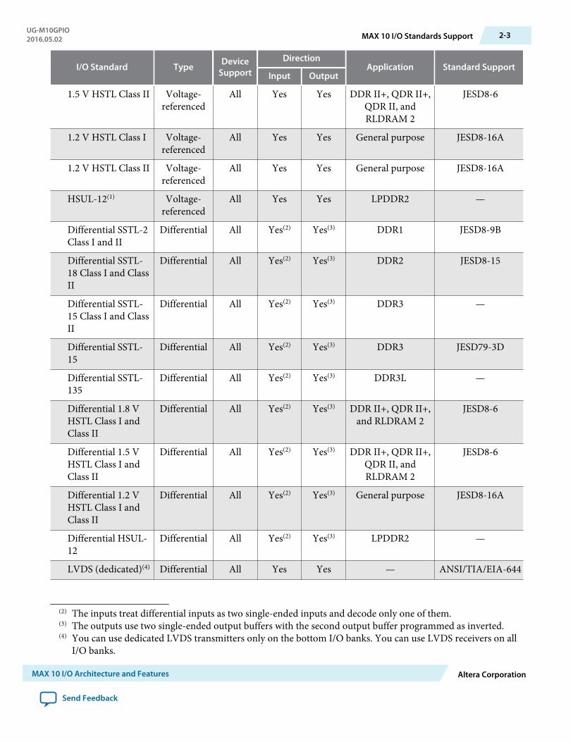
I/O Standard Type DeviceSupport
DirectionApplication Standard Support
Input Output
1.5 V HSTL Class II Voltage-referenced
All Yes Yes DDR II+, QDR II+,QDR II, andRLDRAM 2
JESD8-6
1.2 V HSTL Class I Voltage-referenced
All Yes Yes General purpose JESD8-16A
1.2 V HSTL Class II Voltage-referenced
All Yes Yes General purpose JESD8-16A
HSUL-12(1) Voltage-referenced
All Yes Yes LPDDR2 —
Differential SSTL-2Class I and II
Differential All Yes(2) Yes(3) DDR1 JESD8-9B
Differential SSTL-18 Class I and ClassII
Differential All Yes(2) Yes(3) DDR2 JESD8-15
Differential SSTL-15 Class I and ClassII
Differential All Yes(2) Yes(3) DDR3 —
Differential SSTL-15
Differential All Yes(2) Yes(3) DDR3 JESD79-3D
Differential SSTL-135
Differential All Yes(2) Yes(3) DDR3L —
Differential 1.8 VHSTL Class I andClass II
Differential All Yes(2) Yes(3) DDR II+, QDR II+,and RLDRAM 2
JESD8-6
Differential 1.5 VHSTL Class I andClass II
Differential All Yes(2) Yes(3) DDR II+, QDR II+,QDR II, andRLDRAM 2
JESD8-6
Differential 1.2 VHSTL Class I andClass II
Differential All Yes(2) Yes(3) General purpose JESD8-16A
Differential HSUL-12
Differential All Yes(2) Yes(3) LPDDR2 —
LVDS (dedicated)(4) Differential All Yes Yes — ANSI/TIA/EIA-644
(2) The inputs treat differential inputs as two single-ended inputs and decode only one of them.(3) The outputs use two single-ended output buffers with the second output buffer programmed as inverted.(4) You can use dedicated LVDS transmitters only on the bottom I/O banks. You can use LVDS receivers on all
I/O banks.
UG-M10GPIO2016.05.02 MAX 10 I/O Standards Support 2-3
MAX 10 I/O Architecture and Features Altera Corporation
Send Feedback
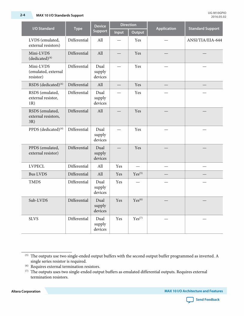
I/O Standard Type DeviceSupport
DirectionApplication Standard Support
Input Output
LVDS (emulated,external resistors)
Differential All — Yes — ANSI/TIA/EIA-644
Mini-LVDS(dedicated)(4)
Differential All — Yes — —
Mini-LVDS(emulated, externalresistor)
Differential Dualsupplydevices
— Yes — —
RSDS (dedicated)(4) Differential All — Yes — —
RSDS (emulated,external resistor,1R)
Differential Dualsupplydevices
— Yes — —
RSDS (emulated,external resistors,3R)
Differential All — Yes — —
PPDS (dedicated)(4) Differential Dualsupplydevices
— Yes — —
PPDS (emulated,external resistor)
Differential Dualsupplydevices
— Yes — —
LVPECL Differential All Yes — — —
Bus LVDS Differential All Yes Yes(5) — —
TMDS Differential Dualsupplydevices
Yes — — —
Sub-LVDS Differential Dualsupplydevices
Yes Yes(6) — —
SLVS Differential Dualsupplydevices
Yes Yes(7) — —
(5) The outputs use two single-ended output buffers with the second output buffer programmed as inverted. Asingle series resistor is required.
(6) Requires external termination resistors.(7) The outputs uses two single-ended output buffers as emulated differential outputs. Requires external
termination resistors.
2-4 MAX 10 I/O Standards SupportUG-M10GPIO
2016.05.02
Altera Corporation MAX 10 I/O Architecture and Features
Send Feedback
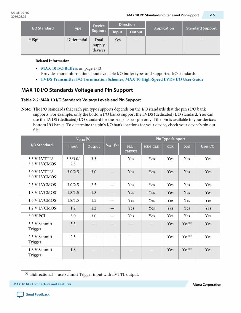
I/O Standard Type DeviceSupport
DirectionApplication Standard Support
Input Output
HiSpi Differential Dualsupplydevices
Yes — — —
Related Information
• MAX 10 I/O Buffers on page 2-13Provides more information about available I/O buffer types and supported I/O standards.
• LVDS Transmitter I/O Termination Schemes, MAX 10 High-Speed LVDS I/O User Guide
MAX 10 I/O Standards Voltage and Pin Support
Table 2-2: MAX 10 I/O Standards Voltage Levels and Pin Support
Note: The I/O standards that each pin type supports depends on the I/O standards that the pin's I/O banksupports. For example, only the bottom I/O banks support the LVDS (dedicated) I/O standard. You canuse the LVDS (dedicated) I/O standard for the PLL_CLKOUT pin only if the pin is available in your device'sbottom I/O banks. To determine the pin's I/O bank locations for your device, check your device's pin outfile.
I/O Standard
VCCIO (V)
VREF (V)
Pin Type Support
Input Output PLL_
CLKOUT
MEM_CLK CLK DQS User I/O
3.3 V LVTTL/3.3 V LVCMOS
3.3/3.0/2.5
3.3 — Yes Yes Yes Yes Yes
3.0 V LVTTL/3.0 V LVCMOS
3.0/2.5 3.0 — Yes Yes Yes Yes Yes
2.5 V LVCMOS 3.0/2.5 2.5 — Yes Yes Yes Yes Yes
1.8 V LVCMOS 1.8/1.5 1.8 — Yes Yes Yes Yes Yes
1.5 V LVCMOS 1.8/1.5 1.5 — Yes Yes Yes Yes Yes
1.2 V LVCMOS 1.2 1.2 — Yes Yes Yes Yes Yes
3.0 V PCI 3.0 3.0 — Yes Yes Yes Yes Yes
3.3 V SchmittTrigger
3.3 — — — — Yes Yes(8) Yes
2.5 V SchmittTrigger
2.5 — — — — Yes Yes(8) Yes
1.8 V SchmittTrigger
1.8 — — — — Yes Yes(8) Yes
(8) Bidirectional— use Schmitt Trigger input with LVTTL output.
UG-M10GPIO2016.05.02 MAX 10 I/O Standards Voltage and Pin Support 2-5
MAX 10 I/O Architecture and Features Altera Corporation
Send Feedback
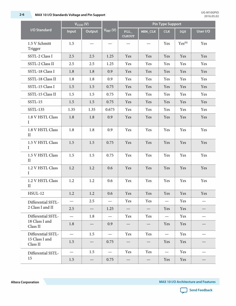
I/O Standard
VCCIO (V)
VREF (V)
Pin Type Support
Input Output PLL_
CLKOUT
MEM_CLK CLK DQS User I/O
1.5 V SchmittTrigger
1.5 — — — — Yes Yes(8) Yes
SSTL-2 Class I 2.5 2.5 1.25 Yes Yes Yes Yes Yes
SSTL-2 Class II 2.5 2.5 1.25 Yes Yes Yes Yes Yes
SSTL-18 Class I 1.8 1.8 0.9 Yes Yes Yes Yes Yes
SSTL-18 Class II 1.8 1.8 0.9 Yes Yes Yes Yes Yes
SSTL-15 Class I 1.5 1.5 0.75 Yes Yes Yes Yes Yes
SSTL-15 Class II 1.5 1.5 0.75 Yes Yes Yes Yes Yes
SSTL-15 1.5 1.5 0.75 Yes Yes Yes Yes Yes
SSTL-135 1.35 1.35 0.675 Yes Yes Yes Yes Yes
1.8 V HSTL ClassI
1.8 1.8 0.9 Yes Yes Yes Yes Yes
1.8 V HSTL ClassII
1.8 1.8 0.9 Yes Yes Yes Yes Yes
1.5 V HSTL ClassI
1.5 1.5 0.75 Yes Yes Yes Yes Yes
1.5 V HSTL ClassII
1.5 1.5 0.75 Yes Yes Yes Yes Yes
1.2 V HSTL ClassI
1.2 1.2 0.6 Yes Yes Yes Yes Yes
1.2 V HSTL ClassII
1.2 1.2 0.6 Yes Yes Yes Yes Yes
HSUL-12 1.2 1.2 0.6 Yes Yes Yes Yes Yes
Differential SSTL-2 Class I and II
— 2.5 — Yes Yes — Yes —
2.5 — 1.25 — — Yes Yes —
Differential SSTL-18 Class I andClass II
— 1.8 — Yes Yes — Yes —
1.8 — 0.9 — — Yes Yes —
Differential SSTL-15 Class I andClass II
— 1.5 — Yes Yes — Yes —
1.5 — 0.75 — — Yes Yes —
Differential SSTL-15
— 1.5 — Yes Yes — Yes —
1.5 — 0.75 — — Yes Yes —
2-6 MAX 10 I/O Standards Voltage and Pin SupportUG-M10GPIO
2016.05.02
Altera Corporation MAX 10 I/O Architecture and Features
Send Feedback
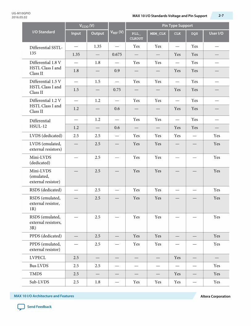
I/O Standard
VCCIO (V)
VREF (V)
Pin Type Support
Input Output PLL_
CLKOUT
MEM_CLK CLK DQS User I/O
Differential SSTL-135
— 1.35 — Yes Yes — Yes —
1.35 — 0.675 — — Yes Yes —
Differential 1.8 VHSTL Class I andClass II
— 1.8 — Yes Yes — Yes —
1.8 — 0.9 — — Yes Yes —
Differential 1.5 VHSTL Class I andClass II
— 1.5 — Yes Yes — Yes —
1.5 — 0.75 — — Yes Yes —
Differential 1.2 VHSTL Class I andClass II
— 1.2 — Yes Yes — Yes —
1.2 — 0.6 — — Yes Yes —
DifferentialHSUL-12
— 1.2 — Yes Yes — Yes —
1.2 — 0.6 — — Yes Yes —
LVDS (dedicated) 2.5 2.5 — Yes Yes Yes — Yes
LVDS (emulated,external resistors)
— 2.5 — Yes Yes — — Yes
Mini-LVDS(dedicated)
— 2.5 — Yes Yes — — Yes
Mini-LVDS(emulated,external resistor)
— 2.5 — Yes Yes — — Yes
RSDS (dedicated) — 2.5 — Yes Yes — — Yes
RSDS (emulated,external resistor,1R)
— 2.5 — Yes Yes — — Yes
RSDS (emulated,external resistors,3R)
— 2.5 — Yes Yes — — Yes
PPDS (dedicated) — 2.5 — Yes Yes — — Yes
PPDS (emulated,external resistor)
— 2.5 — Yes Yes — — Yes
LVPECL 2.5 — — — — Yes — —
Bus LVDS 2.5 2.5 — — — — — Yes
TMDS 2.5 — — — — Yes — Yes
Sub-LVDS 2.5 1.8 — Yes Yes Yes — Yes
UG-M10GPIO2016.05.02 MAX 10 I/O Standards Voltage and Pin Support 2-7
MAX 10 I/O Architecture and Features Altera Corporation
Send Feedback
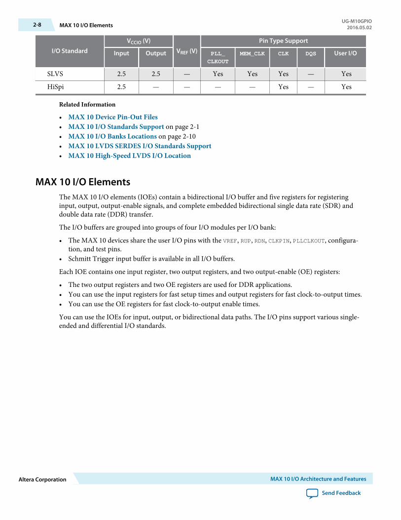
I/O Standard
VCCIO (V)
VREF (V)
Pin Type Support
Input Output PLL_
CLKOUT
MEM_CLK CLK DQS User I/O
SLVS 2.5 2.5 — Yes Yes Yes — Yes
HiSpi 2.5 — — — — Yes — Yes
Related Information
• MAX 10 Device Pin-Out Files• MAX 10 I/O Standards Support on page 2-1• MAX 10 I/O Banks Locations on page 2-10• MAX 10 LVDS SERDES I/O Standards Support• MAX 10 High-Speed LVDS I/O Location
MAX 10 I/O ElementsThe MAX 10 I/O elements (IOEs) contain a bidirectional I/O buffer and five registers for registeringinput, output, output-enable signals, and complete embedded bidirectional single data rate (SDR) anddouble data rate (DDR) transfer.
The I/O buffers are grouped into groups of four I/O modules per I/O bank:
• The MAX 10 devices share the user I/O pins with the VREF, RUP, RDN, CLKPIN, PLLCLKOUT, configura‐tion, and test pins.
• Schmitt Trigger input buffer is available in all I/O buffers.
Each IOE contains one input register, two output registers, and two output-enable (OE) registers:
• The two output registers and two OE registers are used for DDR applications.• You can use the input registers for fast setup times and output registers for fast clock-to-output times.• You can use the OE registers for fast clock-to-output enable times.
You can use the IOEs for input, output, or bidirectional data paths. The I/O pins support various single-ended and differential I/O standards.
2-8 MAX 10 I/O ElementsUG-M10GPIO
2016.05.02
Altera Corporation MAX 10 I/O Architecture and Features
Send Feedback
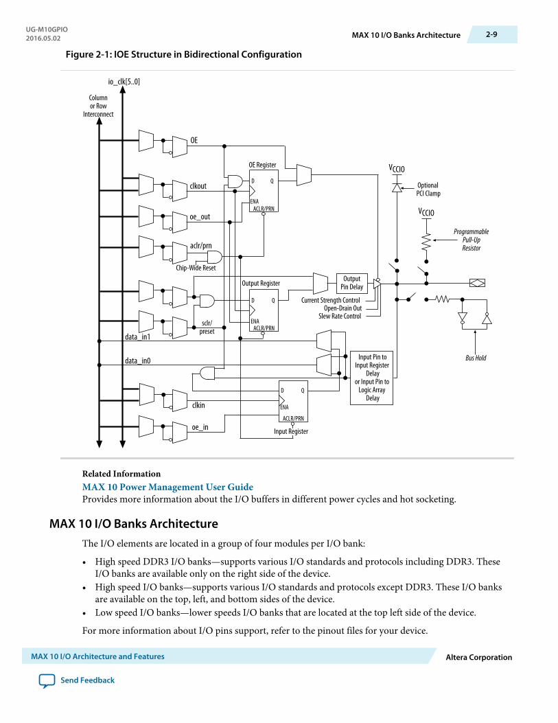
Figure 2-1: IOE Structure in Bidirectional Configuration
D Q
ENA
D Q
ENA
VCCIO
VCCIO
Optional PCI Clamp
ProgrammablePull-UpResistor
Bus HoldInput Pin toInput Register
Delayor Input Pin to
Logic Array Delay
OutputPin Delay
clkin
oe_in
data_in0
data_in1
sclr/preset
Chip-Wide Reset
aclr/prn
oe_out
clkout
OE
OE Register
Current Strength ControlOpen-Drain Out
Columnor Row
Interconnect
io_clk[5..0]
Slew Rate Control
ACLR/PRN
ACLR/PRN
Output Register
D Q
ENA
ACLR/PRN
Input Register
Related InformationMAX 10 Power Management User GuideProvides more information about the I/O buffers in different power cycles and hot socketing.
MAX 10 I/O Banks ArchitectureThe I/O elements are located in a group of four modules per I/O bank:
• High speed DDR3 I/O banks—supports various I/O standards and protocols including DDR3. TheseI/O banks are available only on the right side of the device.
• High speed I/O banks—supports various I/O standards and protocols except DDR3. These I/O banksare available on the top, left, and bottom sides of the device.
• Low speed I/O banks—lower speeds I/O banks that are located at the top left side of the device.
For more information about I/O pins support, refer to the pinout files for your device.
UG-M10GPIO2016.05.02 MAX 10 I/O Banks Architecture 2-9
MAX 10 I/O Architecture and Features Altera Corporation
Send Feedback
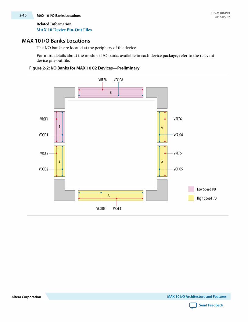
Related InformationMAX 10 Device Pin-Out Files
MAX 10 I/O Banks LocationsThe I/O banks are located at the periphery of the device.
For more details about the modular I/O banks available in each device package, refer to the relevantdevice pin-out file.
Figure 2-2: I/O Banks for MAX 10 02 Devices—Preliminary
1
2 5
6
3
8
VREF1
VCCIO8VREF8
VCCIO1
VCCIO5VCCIO2
VCCIO3 VREF3
VCCIO6
VREF6
VREF2 VREF5
Low Speed I/O
High Speed I/O
2-10 MAX 10 I/O Banks LocationsUG-M10GPIO
2016.05.02
Altera Corporation MAX 10 I/O Architecture and Features
Send Feedback
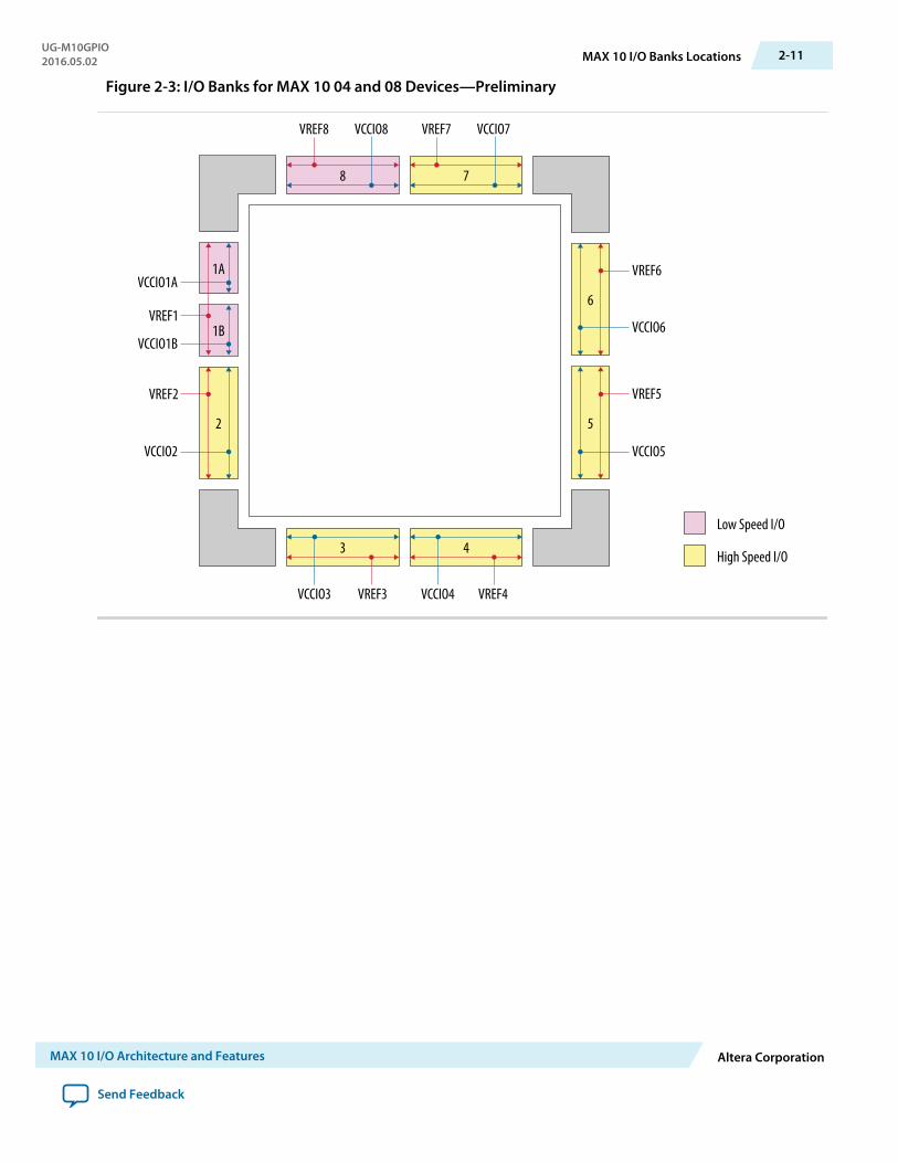
Figure 2-3: I/O Banks for MAX 10 04 and 08 Devices—Preliminary
1A
1B
2 5
6
3 4
8 7
VCCIO5VCCIO2
VCCIO3 VREF3 VREF4VCCIO4
VCCIO7VCCIO8
VCCIO1B
VCCIO1A
VCCIO6
VREF6
VREF1
VREF2
VREF8 VREF7
VREF5
Low Speed I/O
High Speed I/O
UG-M10GPIO2016.05.02 MAX 10 I/O Banks Locations 2-11
MAX 10 I/O Architecture and Features Altera Corporation
Send Feedback
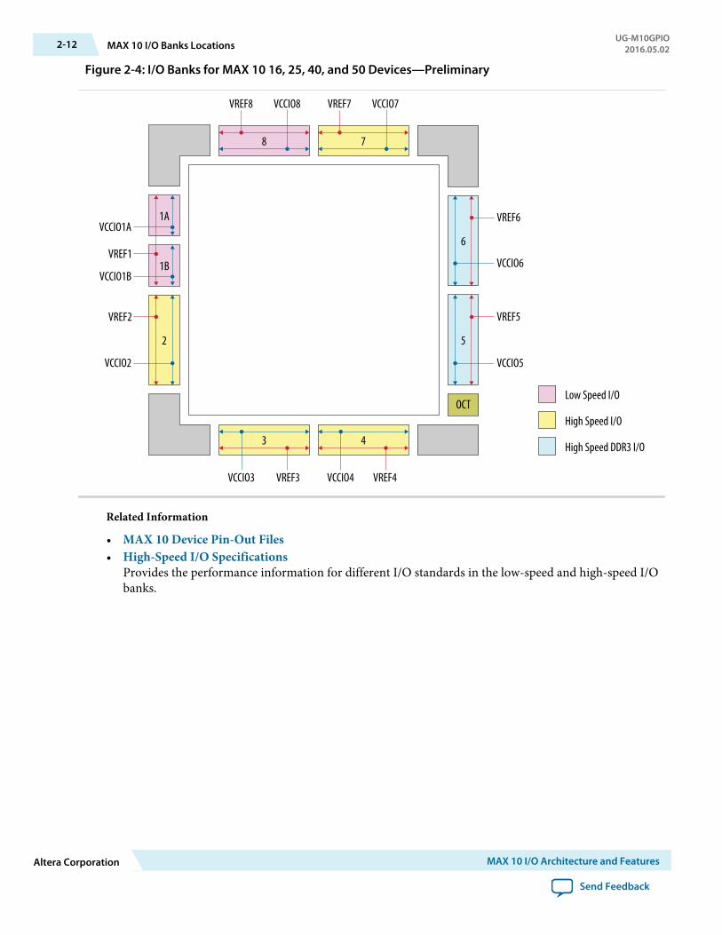
Figure 2-4: I/O Banks for MAX 10 16, 25, 40, and 50 Devices—Preliminary
1A
1B
2 5
6
3 4
8 7
VCCIO5VCCIO2
VCCIO3 VREF3 VREF4VCCIO4
VCCIO7VCCIO8
VCCIO1B
VCCIO1A
VCCIO6
VREF6
VREF1
VREF2
VREF8 VREF7
VREF5
Low Speed I/O
High Speed I/O
High Speed DDR3 I/O
OCT
Related Information
• MAX 10 Device Pin-Out Files• High-Speed I/O Specifications
Provides the performance information for different I/O standards in the low-speed and high-speed I/Obanks.
2-12 MAX 10 I/O Banks LocationsUG-M10GPIO
2016.05.02
Altera Corporation MAX 10 I/O Architecture and Features
Send Feedback
MAX 10 I/O BuffersThe general purpose I/Os (GPIOs) in MAX 10 devices consist of LVDS I/O and DDR I/O buffers.
Table 2-3: Types of GPIO Buffers in MAX 10 Devices
LVDS I/O Buffers DDR I/O Buffers
• Support differential and single-ended I/Ostandards.
• Available only on I/O banks at the bottom sideof the device.
• For LVDS, the bottom I/O banks support LVDStransmitter, emulated LVDS transmitter, andLVDS receiver buffers.
• Support differential and single-ended I/Ostandards.
• Available on I/O banks at the left, right, and topsides of the device.
• For LVDS, the DDR I/O buffers support onlyLVDS receiver and emulated LVDS transmitterbuffers.
• For DDR, only the DDR I/O buffers on the rightside of the device supports DDR3 externalmemory interfaces. DDR3 support is onlyavailable for MAX 10 16, 25, 40, and 50 devices.
Related Information
• MAX 10 I/O Standards Support on page 2-1• LVDS Transmitter I/O Termination Schemes, MAX 10 High-Speed LVDS I/O User Guide
Schmitt-Trigger Input BufferThe MAX 10 devices feature selectable Schmitt trigger input buffer on all I/O banks.
The Schmitt trigger input buffer has similar VIL and VIH as the LVTTL I/O standard but with better noiseimmunity. The Schmitt trigger input buffers are used as default input buffers during configuration mode.
Related InformationMAX 10 Device Datasheet
Programmable I/O Buffer FeaturesThe MAX 10 I/O buffers support a range of programmable features. These features increase the flexibilityof I/O utilization and provide an alternative to reduce the usage of external discrete components such as apull-up resistor and a diode.
UG-M10GPIO2016.05.02 MAX 10 I/O Buffers 2-13
MAX 10 I/O Architecture and Features Altera Corporation
Send Feedback
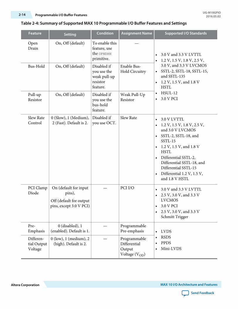
Table 2-4: Summary of Supported MAX 10 Programmable I/O Buffer Features and Settings
Feature Setting Condition Assignment Name Supported I/O Standards
OpenDrain
On, Off (default) To enable thisfeature, usethe OPNDRNprimitive.
—
• 3.0 V and 3.3 V LVTTL• 1.2 V, 1.5 V, 1.8 V, 2.5 V,
3.0 V, and 3.3 V LVCMOS• SSTL-2, SSTL-18, SSTL-15,
and SSTL-135• 1.2 V, 1.5 V, and 1.8 V
HSTL• HSUL-12• 3.0 V PCI
Bus-Hold On, Off (default) Disabled ifyou use theweak pull-upresistorfeature.
Enable Bus-Hold Circuitry
Pull-upResistor
On, Off (default) Disabled ifyou use thebus-holdfeature.
Weak Pull-UpResistor
Slew RateControl
0 (Slow), 1 (Medium),2 (Fast). Default is 2.
Disabled ifyou use OCT.
Slew Rate • 3.0 V LVTTL• 1.2 V, 1.5 V, 1.8 V, 2.5 V,
and 3.0 V LVCMOS• SSTL-2, SSTL-18, and
SSTL-15• 1.2 V, 1.5 V, and 1.8 V
HSTL• Differential SSTL-2,
Differential SSTL-18, andDifferential SSTL-15
• Differential 1.2 V, 1.5 V,and 1.8 V HSTL
PCI ClampDiode
On (default for inputpins),
Off (default for outputpins, except 3.0 V PCI)
— PCI I/O • 3.0 V and 3.3 V LVTTL• 2.5 V, 3.0 V, and 3.3 V
LVCMOS• 3.0 V PCI• 2.5 V, 3.0 V, and 3.3 V
Schmitt Trigger
Pre-Emphasis
0 (disabled), 1(enabled). Default is 1.
— ProgrammablePre-emphasis • LVDS
• RSDS• PPDS• Mini-LVDS
Differen‐tial OutputVoltage
0 (low), 1 (medium), 2(high). Default is 2.
— ProgrammableDifferentialOutputVoltage (VOD)
2-14 Programmable I/O Buffer FeaturesUG-M10GPIO
2016.05.02
Altera Corporation MAX 10 I/O Architecture and Features
Send Feedback
Programmable Open DrainThe optional open-drain output for each I/O pin is equivalent to an open collector output. If it isconfigured as an open drain, the logic value of the output is either high-Z or logic low.
Use an external resistor to pull the signal to a logic high.
Programmable Bus HoldEach I/O pin provides an optional bus-hold feature that is active only after configuration. When thedevice enters user mode, the bus-hold circuit captures the value that is present on the pin by the end ofthe configuration.
The bus-hold circuitry holds this pin state until the next input signal is present. Because of this, you donot require an external pull-up or pull-down resistor to hold a signal level when the bus is tri-stated.
For each I/O pin, you can individually specify that the bus-hold circuitry pulls non-driven pins away fromthe input threshold voltage—where noise can cause unintended high-frequency switching. To preventover-driving signals, the bus-hold circuitry drives the voltage level of the I/O pin lower than the VCCIOlevel.
If you enable the bus-hold feature, you cannot use the programmable pull-up option. To configure theI/O pin for differential signals, disable the bus-hold feature.
Programmable Pull-Up ResistorEach I/O pin provides an optional programmable pull-up resistor during user mode. The pull-up resistorweakly holds the I/O to the VCCIO level.
If you enable the weak pull-up resistor, you cannot use the bus-hold feature.
Programmable Current StrengthYou can use the programmable current strength to mitigate the effects of high signal attenuation that iscaused by a long transmission line or a legacy backplane.
Table 2-5: Programmable Current Strength Settings for MAX 10 Devices
The output buffer for each MAX 10 device I/O pin has a programmable current strength control for the I/Ostandards listed in this table.
I/O Standard IOH / IOL Current Strength Setting (mA)
(Default setting in bold)
3.3 V LVCMOS 23.3 V LVTTL 8, 43.0 V LVTTL/3.0 V LVCMOS 16, 12, 8, 42.5 V LVTTL/2.5 V LVCMOS 16, 12, 8, 41.8 V LVTTL/1.8 V LVCMOS 16, 12, 10, 8, 6, 4, 21.5 V LVCMOS 16, 12, 10, 8, 6, 4, 21.2 V LVCMOS 12, 10, 8, 6, 4, 2SSTL-2 Class I 12, 8SSTL-2 Class II 16
UG-M10GPIO2016.05.02 Programmable Open Drain 2-15
MAX 10 I/O Architecture and Features Altera Corporation
Send Feedback
I/O Standard IOH / IOL Current Strength Setting (mA)
(Default setting in bold)
SSTL-18 Class I 12, 10, 8SSTL-18 Class II 16, 12SSTL-15 Class I 12, 10, 8SSTL-15 Class II 161.8 V HSTL Class I 12, 10, 81.8 V HSTL Class II 161.5 V HSTL Class I 12, 10, 81.5 V HSTL Class II 161.2 V HSTL Class I 12, 10, 81.2 V HSTL Class II 14BLVDS 16, 12, 8SLVS 16, 12, 8Sub-LVDS 12, 8, 4
Note: Altera recommends that you perform IBIS or SPICE simulations to determine the best currentstrength setting for your specific application.
Programmable Output Slew Rate ControlYou have the option of three settings for programmable slew rate control—0, 1, and 2 with 2 as the defaultsetting. Setting 0 is the slow slew rate and 2 is the fast slew rate.
• Fast slew rate—provides high-speed transitions for high-performance systems.• Slow slew rate—reduces system noise and crosstalk but adds a nominal delay to the rising and falling
edges.
Table 2-6: Programmable Output Slew Rate Control for MAX 10 Devices
This table lists the single-ended I/O standards and current strength settings that support programmable outputslew rate control. For I/O standards and current strength settings that do not support programmable slew ratecontrol, the default slew rate setting is 2 (fast slew rate).
I/O Standard IOH / IOL Current Strength Supporting Slew Rate Control
3.0 V LVTTL/3.0 V LVCMOS 16, 12, 8
2.5 V LVTTL/2.5 V LVCMOS 16, 12, 8
1.8 V LVTTL/1.8 V LVCMOS 16, 12, 8
1.5 V LVCMOS 16, 12, 10, 8
1.2 V LVCMOS 12, 10, 8
SSTL-2 Class I 12, 8
2-16 Programmable Output Slew Rate ControlUG-M10GPIO
2016.05.02
Altera Corporation MAX 10 I/O Architecture and Features
Send Feedback
I/O Standard IOH / IOL Current Strength Supporting Slew Rate Control
SSTL-2 Class II 16
SSTL-18 Class I 12, 10, 8
SSTL-18 Class II 16, 12
SSTL-15 Class I 12, 10, 8
SSTL-15 Class II 16
1.8 V HSTL Class I 12, 10, 8
1.8 V HSTL Class II 16
1.5 V HSTL Class I 12, 10, 8
1.5 V HSTL Class II 16
1.2 V HSTL Class I 12, 10, 8
1.2 V HSTL Class II 14
You can specify the slew rate on a pin-by-pin basis because each I/O pin contains a slew rate control. Theslew rate control affects both the rising and falling edges.
Note: Altera recommends that you perform IBIS or SPICE simulations to determine the best slew ratesetting for your specific application.
Programmable IOE DelayYou can activate the programmable IOE delays to ensure zero hold times, minimize setup times, increaseclock-to-output times, or delay the clock input signal. This feature helps read and write timing marginsbecause it minimizes the uncertainties between signals in the bus.
Each pin can have a different input delay from pin-to-input register or a delay from outputregister-to-output pin values to ensure that the signals within a bus have the same delay going into or outof the device.
Table 2-7: Programmable Delay Chain
Programmable Delays Quartus Prime Logic Option
Input pin-to-logic array delay Input delay from pin to internal cells
Input pin-to-input register delay Input delay from pin to input register
Output pin delay Delay from output register to output pin
Dual-purpose clock input pin delay Input delay from dual-purpose clock pin to fan-out destina‐tions
There are two paths in the IOE for an input to reach the logic array. Each of the two paths can have adifferent delay. This allows you to adjust delays from the pin to the internal logic element (LE) registersthat reside in two different areas of the device. You must set the two combinational input delays with theinput delay from pin to internal cells logic option in the Quartus Prime software for each path. If the pin
UG-M10GPIO2016.05.02 Programmable IOE Delay 2-17
MAX 10 I/O Architecture and Features Altera Corporation
Send Feedback
uses the input register, one of the delays is disregarded and the delay is set with the input delay from pinto input register logic option in the Quartus Prime software.
The IOE registers in each I/O block share the same source for the preset or clear features. You canprogram preset or clear for each individual IOE, but you cannot use both features simultaneously. Youcan also program the registers to power-up high or low after configuration is complete. If programmed topower-up low, an asynchronous clear can control the registers. If programmed to power-up high, anasynchronous preset can control the registers. This feature prevents the inadvertent activation of theactive-low input of another device upon power up. If one register in an IOE uses a preset or clear signal,all registers in the IOE must use that same signal if they require preset or clear. Additionally, a synchro‐nous reset signal is available for the IOE registers.
Related Information
• MAX 10 Device Datasheet• Timing Closure and Optimization chapter, Volume 2: Design Implementation and Optimization,
Quartus Prime HandbookProvides more information about the input and output pin delay settings.
PCI Clamp DiodeThe MAX 10 devices are equipped with optional PCI clamp diode that you can enable for the input andoutput of each I/O pin.
The PCI clamp diode is available in the Quartus Prime software for the following I/O standards:
• 3.3 V LVTTL/3.3 V LVCMOS• 3.0 V LVTTL/3.0 V LVCMOS• 2.5 V LVTTL/2.5 V LVCMOS• 3.0 V PCI• 3.3 V Schmitt Trigger• 2.5 V Schmitt Trigger
Programmable Pre-EmphasisThe differential output voltage (VOD) setting and the output impedance of the driver set the outputcurrent limit of a high-speed transmission signal. At a high frequency, the slew rate may not be fastenough to reach the full VOD level before the next edge, producing pattern-dependent jitter. Pre-emphasismomentarily boosts the output current during switching to increase the output slew rate.
Pre-emphasis increases the amplitude of the high-frequency component of the output signal. Thisincrease compensates for the frequency-dependent attenuation along the transmission line.
The overshoot introduced by the extra current occurs only during change of state switching. Thisovershoot increases the output slew rate but does not ring, unlike the overshoot caused by signalreflection. The amount of pre-emphasis required depends on the attenuation of the high-frequencycomponent along the transmission line.
2-18 PCI Clamp DiodeUG-M10GPIO
2016.05.02
Altera Corporation MAX 10 I/O Architecture and Features
Send Feedback
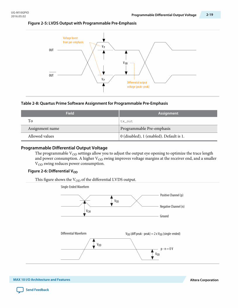
Figure 2-5: LVDS Output with Programmable Pre-Emphasis
OUT
OUT
V OD
V P
V P
Voltage boostfrom pre-emphasis
Differential outputvoltage (peak–peak)
Table 2-8: Quartus Prime Software Assignment for Programmable Pre-Emphasis
Field Assignment
To tx_out
Assignment name Programmable Pre-emphasis
Allowed values 0 (disabled), 1 (enabled). Default is 1.
Programmable Differential Output VoltageThe programmable VOD settings allow you to adjust the output eye opening to optimize the trace lengthand power consumption. A higher VOD swing improves voltage margins at the receiver end, and a smallerVOD swing reduces power consumption.
Figure 2-6: Differential VOD
This figure shows the VOD of the differential LVDS output.Single-Ended Waveform
Positive Channel (p)
Negative Channel (n)
Ground
Differential Waveform
p - n = 0 V
VCM
VOD
VOD
VOD
VOD (diff peak - peak) = 2 x VOD (single-ended)
UG-M10GPIO2016.05.02 Programmable Differential Output Voltage 2-19
MAX 10 I/O Architecture and Features Altera Corporation
Send Feedback
You can statically adjust the VOD of the differential signal by changing the VOD settings in the QuartusPrime software Assignment Editor.
Table 2-9: Quartus Prime Software Assignment Editor—Programmable VOD
Field Assignment
To tx_out
Assignment name Programmable Differential Output Voltage (VOD)Allowed values 0 (low), 1 (medium), 2 (high). Default is 2.
Programmable Emulated Differential OutputThe MAX 10 devices support emulated differential output where a pair of IOEs drives bidirectional I/Opins.
The emulated differential output feature is supported for the following I/O standards:
• Differential SSTL-2 Class I and II• Differential SSTL-18 Class I and II• Differential SSTL-15 Class I and II• Differential SSTL-15• Differential SSTL-135• Differential 1.8 V HSTL Class I and II• Differential 1.5 V HSTL Class I and II• Differential 1.2 V HSTL Class I and II• Differential HSUL-12• LVDS 3R• Mini-LVDS 3R• PPDS 3R• RSDS 1R and 3R• BLVDS• SLVS• Sub-LVDS
Programmable Dynamic Power DownThe MAX 10 16, 25, 40, and 50 devices feature programmable dynamic power down for several I/Ostandards to reduce the static power consumption.
In these devices, you can apply the programmable dynamic power down feature to the I/O buffers for thefollowing I/O standards:
• Input buffer—SSTL, HSTL, HSUL, LVDS• Output buffer—LVDS
Related InformationMAX 10 Power Management User GuideProvides more information about using the programmable dynamic power down feature.
2-20 Programmable Emulated Differential OutputUG-M10GPIO
2016.05.02
Altera Corporation MAX 10 I/O Architecture and Features
Send Feedback
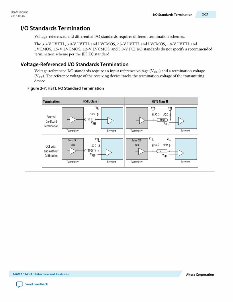
I/O Standards TerminationVoltage-referenced and differential I/O standards requires different termination schemes.
The 3.3-V LVTTL, 3.0-V LVTTL and LVCMOS, 2.5-V LVTTL and LVCMOS, 1.8-V LVTTL andLVCMOS, 1.5-V LVCMOS, 1.2-V LVCMOS, and 3.0-V PCI I/O standards do not specify a recommendedtermination scheme per the JEDEC standard.
Voltage-Referenced I/O Standards TerminationVoltage-referenced I/O standards require an input reference voltage (VREF) and a termination voltage(VTT). The reference voltage of the receiving device tracks the termination voltage of the transmittingdevice.
Figure 2-7: HSTL I/O Standard Termination
HSTL Class I HSTL Class II
ExternalOn-Board
Termination
OCT with and withoutCalibration
VTT
50 Ω
50 Ω
VTT
50 Ω
VTT
50 Ω
Transmitter TransmitterReceiver Receiver
VTT
50 Ω
Transmitter Receiver
VTT
50 Ω
VTT
50 Ω
Transmitter Receiver
Series OCT
50 Ω
Series OCT25 Ω
VREFVREF
VREFVREF
Termination
50 Ω
50 Ω
50 Ω
UG-M10GPIO2016.05.02 I/O Standards Termination 2-21
MAX 10 I/O Architecture and Features Altera Corporation
Send Feedback
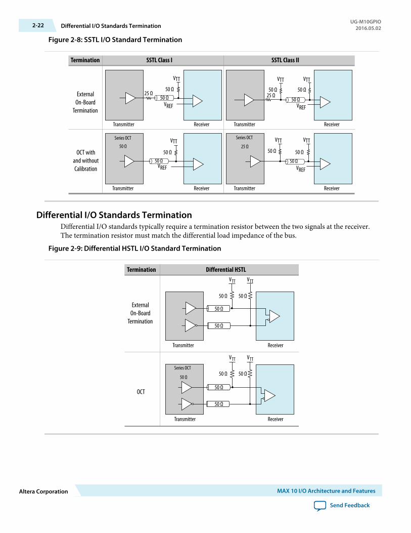
Figure 2-8: SSTL I/O Standard Termination
SSTL Class I SSTL Class II
ExternalOn-Board
Termination
OCT withand withoutCalibration
VTT
50 Ω25 Ω
VTT
50 Ω25 Ω
VTT
50 Ω
Transmitter TransmitterReceiver Receiver
VTT
50 Ω50 Ω
Transmitter Receiver
Series OCT
50 ΩVTT
50 Ω25 Ω
50 Ω
VTT
50 Ω
Transmitter Receiver
Series OCT
VREF VREF
VREFVREF
Termination
50 Ω 50 Ω
Differential I/O Standards TerminationDifferential I/O standards typically require a termination resistor between the two signals at the receiver.The termination resistor must match the differential load impedance of the bus.
Figure 2-9: Differential HSTL I/O Standard Termination
ExternalOn-Board
Termination
OCT
Series OCT
50 Ω
Differential HSTLTermination
Receiver
Receiver
50 Ω
50 Ω 50 Ω
50 Ω 50 Ω
50 Ω
50 Ω
50 Ω
Transmitter
Transmitter
VTT VTT
VTT VTT
2-22 Differential I/O Standards TerminationUG-M10GPIO
2016.05.02
Altera Corporation MAX 10 I/O Architecture and Features
Send Feedback
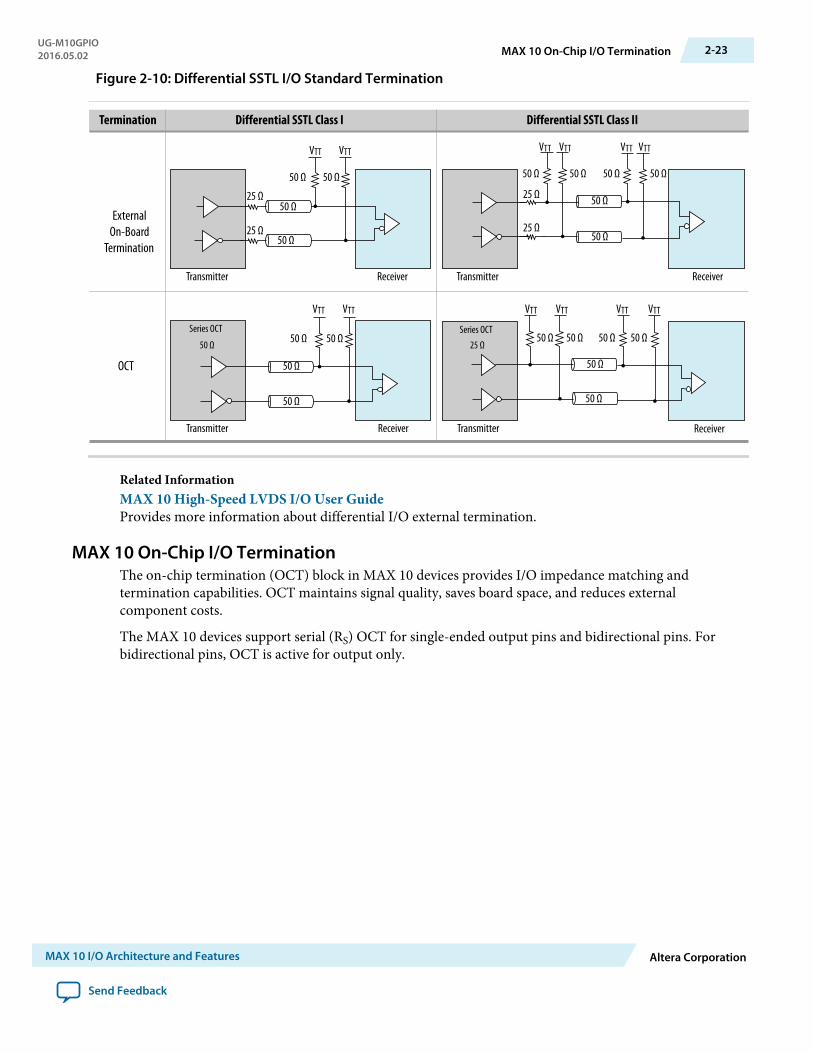
Figure 2-10: Differential SSTL I/O Standard Termination
Differential SSTL Class I Differential SSTL Class II
ExternalOn-Board
Termination
OCT
Transmitter Receiver
50 Ω
50 Ω 50 Ω
50 Ω
VTT VTT
25 Ω
25 Ω
Transmitter Receiver
50 Ω
50 Ω 50 Ω
50 Ω
VTT VTT
25 Ω
25 Ω
50 Ω 50 Ω
VTT VTT
Transmitter Receiver
50 Ω
50 Ω 50 Ω
50 Ω
VTT VTT
50 Ω 50 Ω
VTT VTT
Series OCT25 Ω
Transmitter Receiver
50 Ω
50 Ω 50 Ω
50 Ω
VTT VTT
50 Ω
Series OCT
Termination
Related InformationMAX 10 High-Speed LVDS I/O User GuideProvides more information about differential I/O external termination.
MAX 10 On-Chip I/O TerminationThe on-chip termination (OCT) block in MAX 10 devices provides I/O impedance matching andtermination capabilities. OCT maintains signal quality, saves board space, and reduces externalcomponent costs.
The MAX 10 devices support serial (RS) OCT for single-ended output pins and bidirectional pins. Forbidirectional pins, OCT is active for output only.
UG-M10GPIO2016.05.02 MAX 10 On-Chip I/O Termination 2-23
MAX 10 I/O Architecture and Features Altera Corporation
Send Feedback
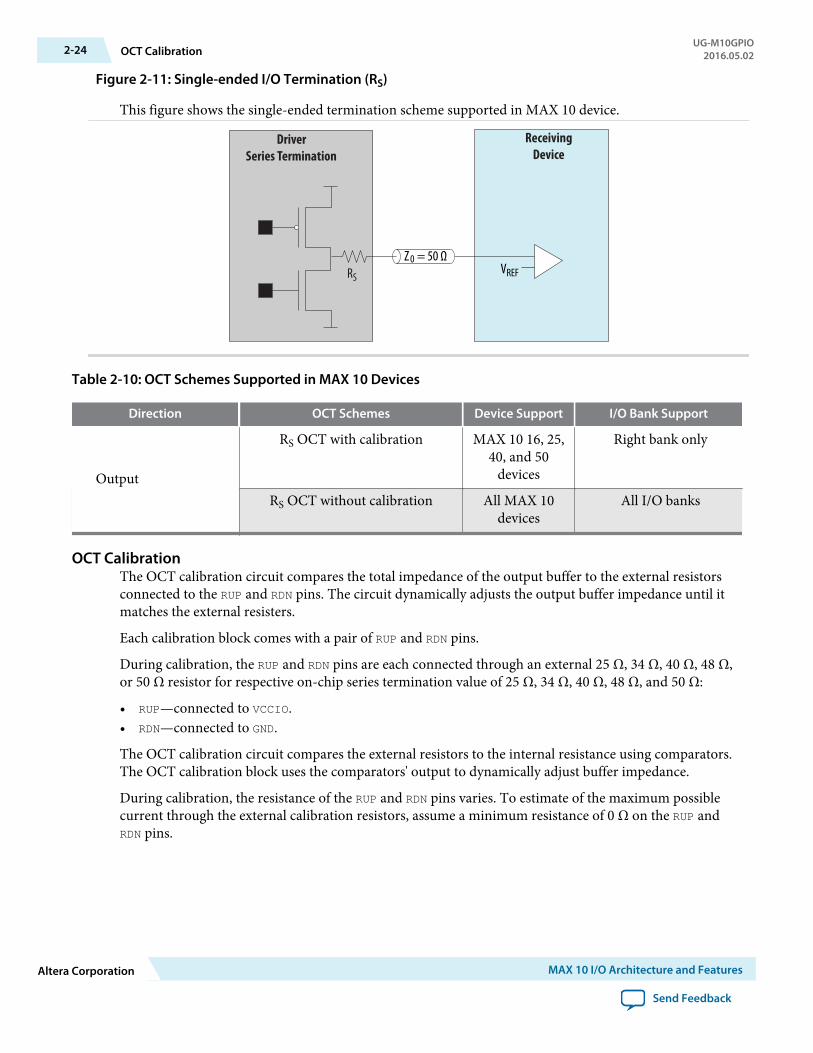
Figure 2-11: Single-ended I/O Termination (RS)
This figure shows the single-ended termination scheme supported in MAX 10 device.
RS
Z 0 = 50 Ω
DriverSeries Termination
ReceivingDevice
VREF
Table 2-10: OCT Schemes Supported in MAX 10 Devices
Direction OCT Schemes Device Support I/O Bank Support
Output
RS OCT with calibration MAX 10 16, 25,40, and 50
devices
Right bank only
RS OCT without calibration All MAX 10devices
All I/O banks
OCT CalibrationThe OCT calibration circuit compares the total impedance of the output buffer to the external resistorsconnected to the RUP and RDN pins. The circuit dynamically adjusts the output buffer impedance until itmatches the external resisters.
Each calibration block comes with a pair of RUP and RDN pins.
During calibration, the RUP and RDN pins are each connected through an external 25 Ω, 34 Ω, 40 Ω, 48 Ω,or 50 Ω resistor for respective on-chip series termination value of 25 Ω, 34 Ω, 40 Ω, 48 Ω, and 50 Ω:
• RUP—connected to VCCIO.• RDN—connected to GND.
The OCT calibration circuit compares the external resistors to the internal resistance using comparators.The OCT calibration block uses the comparators' output to dynamically adjust buffer impedance.
During calibration, the resistance of the RUP and RDN pins varies. To estimate of the maximum possiblecurrent through the external calibration resistors, assume a minimum resistance of 0 Ω on the RUP andRDN pins.
2-24 OCT CalibrationUG-M10GPIO
2016.05.02
Altera Corporation MAX 10 I/O Architecture and Features
Send Feedback
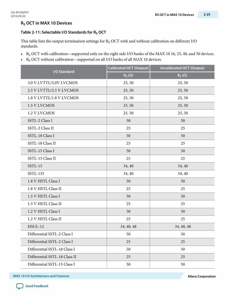
RS OCT in MAX 10 Devices
Table 2-11: Selectable I/O Standards for RS OCT
This table lists the output termination settings for RS OCT with and without calibration on different I/Ostandards.
• RS OCT with calibration—supported only on the right side I/O banks of the MAX 10 16, 25, 40, and 50 devices.• RS OCT without calibration—supported on all I/O banks of all MAX 10 devices.
I/O StandardCalibrated OCT (Output) Uncalibrated OCT (Output)
RS (Ω) RS (Ω)
3.0 V LVTTL/3.0V LVCMOS 25, 50 25, 50
2.5 V LVTTL/2.5 V LVCMOS 25, 50 25, 50
1.8 V LVTTL/1.8 V LVCMOS 25, 50 25, 50
1.5 V LVCMOS 25, 50 25, 50
1.2 V LVCMOS 25, 50 25, 50
SSTL-2 Class I 50 50
SSTL-2 Class II 25 25
SSTL-18 Class I 50 50
SSTL-18 Class II 25 25
SSTL-15 Class I 50 50
SSTL-15 Class II 25 25
SSTL-15 34, 40 34, 40
SSTL-135 34, 40 34, 40
1.8 V HSTL Class I 50 50
1.8 V HSTL Class II 25 25
1.5 V HSTL Class I 50 50
1.5 V HSTL Class II 25 25
1.2 V HSTL Class I 50 50
1.2 V HSTL Class II 25 25
HSUL-12 34, 40, 48 34, 40, 48
Differential SSTL-2 Class I 50 50
Differential SSTL-2 Class I 25 25
Differential SSTL-18 Class I 50 50
Differential SSTL-18 Class II 25 25
Differential SSTL-15 Class I 50 50
UG-M10GPIO2016.05.02 RS OCT in MAX 10 Devices 2-25
MAX 10 I/O Architecture and Features Altera Corporation
Send Feedback
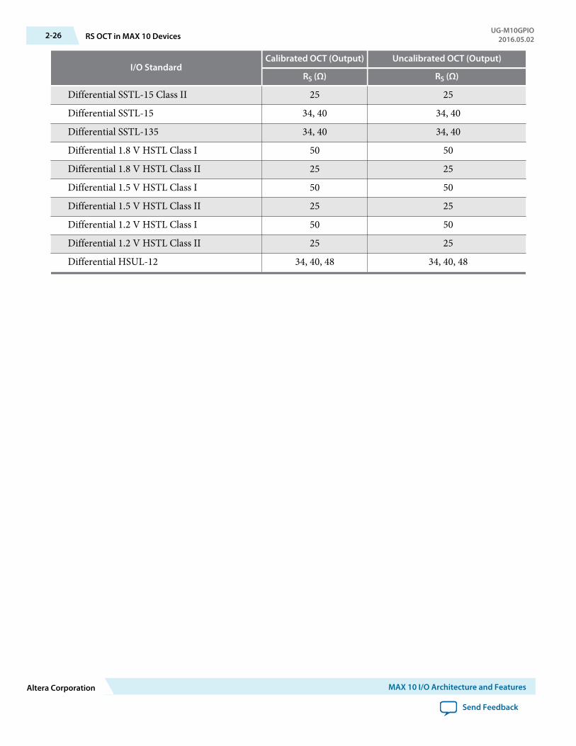
I/O StandardCalibrated OCT (Output) Uncalibrated OCT (Output)
RS (Ω) RS (Ω)
Differential SSTL-15 Class II 25 25
Differential SSTL-15 34, 40 34, 40
Differential SSTL-135 34, 40 34, 40
Differential 1.8 V HSTL Class I 50 50
Differential 1.8 V HSTL Class II 25 25
Differential 1.5 V HSTL Class I 50 50
Differential 1.5 V HSTL Class II 25 25
Differential 1.2 V HSTL Class I 50 50
Differential 1.2 V HSTL Class II 25 25
Differential HSUL-12 34, 40, 48 34, 40, 48
2-26 RS OCT in MAX 10 DevicesUG-M10GPIO
2016.05.02
Altera Corporation MAX 10 I/O Architecture and Features
Send Feedback
MAX 10 I/O Design Considerations 32016.05.02
UG-M10GPIO Subscribe Send Feedback
There are several considerations that require your attention to ensure the success of your designs. Unlessnoted otherwise, these design guidelines apply to all variants of this device family.
Related InformationMAX 10 I/O Overview on page 1-1
Guidelines: VCCIO Range ConsiderationsThere are several VCCIO range considerations because of I/O pin configuration function and I/O banklocation.
• The shared I/O pins can only support a VCCIO range of 1.5 V to 3.3 V when you access the configura‐tion function in user mode. The configuration function of the I/O pins can only support 1.5 V to 3.3 V.If you need to access, for example, JTAG pins during user mode, the bank where the pin resides will beconstrained by this VCCIO range. If you want to use I/O standards within the 1.2 V to 1.35 V range, youmust not use the configuration function of any of the I/O pins during user mode. This only affectsbank 1 and bank 8 because only these banks have I/O pins with configuration function.
• For devices with banks 1A and 1B:
• If you use the VREF pin or the ADC, you must supply a common VCCIO voltage to banks 1A and 1B.• If you do not use the VREF pin or the ADC, you can supply separate VCCIO voltages to banks 1A and
1B.• If you plan to migrate from devices that has banks 1A and 1B to devices that has only bank 1, ensure
that the VCCIO of bank 1A and 1B are the same.• For the V36 package of the 10M02 device, the VCCIO of these groups of I/O banks must be the same:
• Group 1—banks 1, 2 and 8• Group 2—banks 3, 5, and 6
• For the V81 package of the 10M08 device, the VCCIO of these groups of I/O banks must be the same:
• Group 1—banks 1A, 1B, and 2• Group 2—banks 5 and 6
Guidelines: Voltage-Referenced I/O Standards RestrictionThese restrictions apply if you use the VREF pin.
© 2016 Altera Corporation. All rights reserved. ALTERA, ARRIA, CYCLONE, ENPIRION, MAX, MEGACORE, NIOS, QUARTUS and STRATIX words and logos aretrademarks of Altera Corporation and registered in the U.S. Patent and Trademark Office and in other countries. All other words and logos identified astrademarks or service marks are the property of their respective holders as described at www.altera.com/common/legal.html. Altera warrants performanceof its semiconductor products to current specifications in accordance with Altera's standard warranty, but reserves the right to make changes to anyproducts and services at any time without notice. Altera assumes no responsibility or liability arising out of the application or use of any information,product, or service described herein except as expressly agreed to in writing by Altera. Altera customers are advised to obtain the latest version of devicespecifications before relying on any published information and before placing orders for products or services.
ISO9001:2008Registered
www.altera.com101 Innovation Drive, San Jose, CA 95134
• If you use a shared VREF pin as an I/O, all voltage-reference input buffers (SSTL, HSTL, and HSUL) aredisabled.
• If you use a shared VREF pin as a voltage reference, you must enable the input buffer of specific I/O pinto use the voltage-reference I/O standards.
• The voltage-referenced I/O standards are not supported in the following I/O banks of these devicepackages:
• All I/O banks of V36 package of 10M02.• All I/O banks of V81 package of 10M08.• Banks 1A and 1B of E144 package of 10M50.
• For devices with banks 1A and 1B, if you use the VREF pin, you must supply a common VCCIO to banks1A and 1B.
• Maximum number of voltage-referenced inputs for each VREF pin is 75% of total number of I/O pads.The Quartus Prime software will provide a warning if you exceed the maximum number.
• Except for I/O pins that you used for static signals, all non-voltage-referenced output must be placedtwo pads away from a VREF pin. The Quartus Prime software will output an error message if this rule isviolated.
Related InformationMAX 10 I/O Standards Support on page 2-1
Guidelines: Enable Clamp Diode for LVTTL/LVCMOS Input BuffersIf the VCCIO of the I/O bank is lower than the voltage of the LVTTL/LVCMOS input buffers, Alterarecommends that you enable the clamp diode.
• 3.3 V LVCMOS/LVTTL input buffers—enable clamp diode if VCCIO of the I/O bank is 3.0 V.• 3.3 V or 3.0 V LVCMOS/LVTTL input buffers—enable clamp diode if VCCIO of the I/O bank is 2.5 V.
By enabling the clamp diode under these conditions, you will be able to limit overshoot or undershoot.However, this does not comply with hot socket current specification.
If you do not enable the clamp diode under these conditions, the signal integrity for the I/O pin will beimpacted and there will be overshoot or undershoot problem. In this situation, you must ensure that yourboard design conforms to the overshoot/undershoot specifications.
Table 3-1: Voltage Tolerance Maximum Ratings for 3.3 V or 3.0 V
This table lists the voltage tolerance specifications. Ensure that your board design conforms to these specificationsif you do not want to follow the clamp diode recommendation.
Voltage Minimum (V) Maximum (V)
VCCIO = 3.3 V 3.135 3.45
VCCIO = 3.0 V 2.85 3.15
VIH (AC) — 4.1
VIH (DC) — 3.6
VIL (DC) –0.3 0.8
3-2 Guidelines: Enable Clamp Diode for LVTTL/LVCMOS Input BuffersUG-M10GPIO
2016.05.02
Altera Corporation MAX 10 I/O Design Considerations
Send Feedback
Guidelines: Adhere to the LVDS I/O Restrictions RulesFor LVDS applications, adhere to the I/O restriction pin connection guidelines to avoid excessive jitter onthe LVDS transmitter output pins. The Quartus Prime software generates a critical warning if these rulesare violated.
Related InformationMAX 10 FPGA Device Family Pin Connection Guidelines
Guidelines: I/O Restriction RulesFor different I/O standards and conditions, you must limit the number of I/O pins. This I/O restrictionrule is applicable if you use LVDS transmitters or receivers.
Table 3-2: Maximum Percentage of I/O Pins Allowed for Specific I/O Standards in an I/O Bank
This table lists the maximum number of general purpose output pins recommended in a bank in terms ofpercentage to the total number of I/O pins available in an I/O bank if you use these combinations of I/O standardsand conditions.
I/O Standard Condition Max Pins Per Bank (%)
2.5 V LVTTL/LVCMOS
16 mA current strength and 25 Ω OCT (fast and slowslew rate)
25
12 mA current strength (fast and slow slew rate) 30
8 mA current strength (fast and slow slew rate) and 50Ω OCT (fast slew rate)
45
4 mA current strength (fast and slow slew rate) 65
2.5 V SSTL — 100
Guidelines: Analog-to-Digital Converter I/O RestrictionThese restrictions are applicable if you use the analog-to-digital converter (ADC) block.
The Quartus Prime software uses physics-based rules to define the number of I/Os allowed in a particularbank based on the I/O's drive strength. These rules are based on noise calculation to analyze accurately theimpact of I/O placement on the ADC performance.
The physics-based rules are available for the following devices starting from these Quartus Prime softwareversions:
• From Quartus Prime version 14.1—MAX 10 10M04, 10M08, 10M40, and 10M50 devices.• From Quartus Prime version 15.0.1—MAX 10 10M02, 10M16, and 10M25 devices.
Altera highly recommends that you adhere to these guidelines to ensure ADC performance. Furthermore,following these guidelines prevents additional critical warning from future versions of the Quartus Primesoftware when the physics-based rules are implemented.
UG-M10GPIO2016.05.02 Guidelines: Adhere to the LVDS I/O Restrictions Rules 3-3
MAX 10 I/O Design Considerations Altera Corporation
Send Feedback
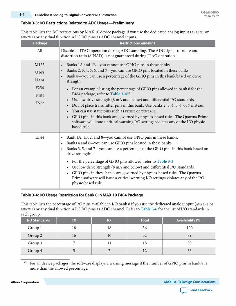
Table 3-3: I/O Restrictions Related to ADC Usage—Preliminary
This table lists the I/O restrictions by MAX 10 device package if you use the dedicated analog input (ANAIN1 orANAIN2) or any dual function ADC I/O pins as ADC channel inputs.
Package Restriction/Guideline
All Disable all JTAG operation during ADC sampling. The ADC signal-to-noise anddistortion ratio (SINAD) is not guaranteed during JTAG operation.
M153
U169
U324
F256
F484
F672
• Banks 1A and 1B—you cannot use GPIO pins in these banks.• Banks 2, 3, 4, 5, 6, and 7—you can use GPIO pins located in these banks.• Bank 8—you can use a percentage of the GPIO pins in this bank based on drive
strength:
• For an example listing the percentage of GPIO pins allowed in bank 8 for theF484 package, refer to Table 3-4(9).
• Use low drive strength (8 mA and below) and differential I/O standards.• Do not place transmitter pins in this bank. Use banks 2, 3, 4, 5, 6, or 7 instead.• You can use static pins such as RESET or CONTROL.• GPIO pins in this bank are governed by physics-based rules. The Quartus Prime
software will issue a critical warning I/O settings violates any of the I/O physic-based rule.
E144 • Bank 1A, 1B, 2, and 8—you cannot use GPIO pins in these banks.• Banks 4 and 6—you can use GPIO pins located in these banks.• Banks 3, 5, and 7—you can use a percentage of the GPIO pins in this bank based on
drive strength:
• For the percentage of GPIO pins allowed, refer to Table 3-5.• Use low drive strength (8 mA and below) and differential I/O standards.• GPIO pins in these banks are governed by physics-based rules. The Quartus
Prime software will issue a critical warning I/O settings violates any of the I/Ophysic-based rule.
Table 3-4: I/O Usage Restriction for Bank 8 in MAX 10 F484 Package
This table lists the percentage of I/O pins available in I/O bank 8 if you use the dedicated analog input (ANAIN1 orANAIN2) or any dual function ADC I/O pins as ADC channel. Refer to Table 3-6 for the list of I/O standards ineach group.
I/O Standards TX RX Total Availability (%)
Group 1 18 18 36 100
Group 2 16 16 32 89
Group 3 7 11 18 50
Group 4 5 7 12 33
(9) For all device packages, the software displays a warning message if the number of GPIO pins in bank 8 ismore than the allowed percentage.
3-4 Guidelines: Analog-to-Digital Converter I/O RestrictionUG-M10GPIO
2016.05.02
Altera Corporation MAX 10 I/O Design Considerations
Send Feedback
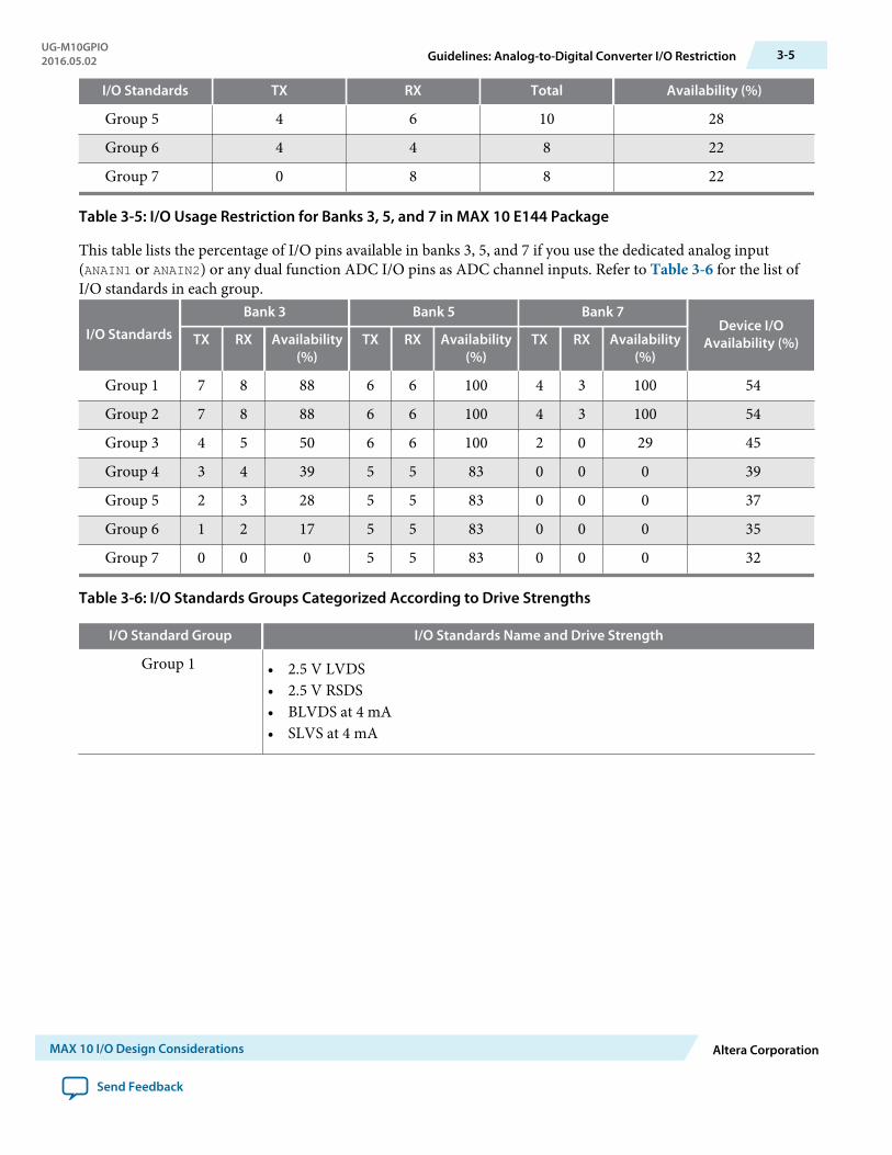
I/O Standards TX RX Total Availability (%)
Group 5 4 6 10 28
Group 6 4 4 8 22
Group 7 0 8 8 22
Table 3-5: I/O Usage Restriction for Banks 3, 5, and 7 in MAX 10 E144 Package
This table lists the percentage of I/O pins available in banks 3, 5, and 7 if you use the dedicated analog input(ANAIN1 or ANAIN2) or any dual function ADC I/O pins as ADC channel inputs. Refer to Table 3-6 for the list ofI/O standards in each group.
I/O Standards
Bank 3 Bank 5 Bank 7Device I/O
Availability (%)TX RX Availability(%)
TX RX Availability(%)
TX RX Availability(%)
Group 1 7 8 88 6 6 100 4 3 100 54
Group 2 7 8 88 6 6 100 4 3 100 54
Group 3 4 5 50 6 6 100 2 0 29 45
Group 4 3 4 39 5 5 83 0 0 0 39
Group 5 2 3 28 5 5 83 0 0 0 37
Group 6 1 2 17 5 5 83 0 0 0 35
Group 7 0 0 0 5 5 83 0 0 0 32
Table 3-6: I/O Standards Groups Categorized According to Drive Strengths
I/O Standard Group I/O Standards Name and Drive Strength
Group 1 • 2.5 V LVDS• 2.5 V RSDS• BLVDS at 4 mA• SLVS at 4 mA
UG-M10GPIO2016.05.02 Guidelines: Analog-to-Digital Converter I/O Restriction 3-5
MAX 10 I/O Design Considerations Altera Corporation
Send Feedback
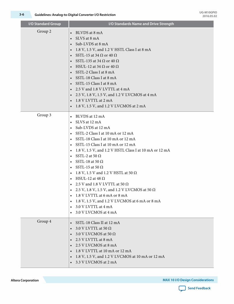
I/O Standard Group I/O Standards Name and Drive Strength
Group 2 • BLVDS at 8 mA• SLVS at 8 mA• Sub-LVDS at 8 mA• 1.8 V, 1.5 V, and 1.2 V HSTL Class I at 8 mA• SSTL-15 at 34 Ω or 40 Ω• SSTL-135 at 34 Ω or 40 Ω• HSUL-12 at 34 Ω or 40 Ω• SSTL-2 Class I at 8 mA• SSTL-18 Class I at 8 mA• SSTL-15 Class I at 8 mA• 2.5 V and 1.8 V LVTTL at 4 mA• 2.5 V, 1.8 V, 1.5 V, and 1.2 V LVCMOS at 4 mA• 1.8 V LVTTL at 2 mA• 1.8 V, 1.5 V, and 1.2 V LVCMOS at 2 mA
Group 3 • BLVDS at 12 mA• SLVS at 12 mA• Sub-LVDS at 12 mA• SSTL-2 Class I at 10 mA or 12 mA• SSTL-18 Class I at 10 mA or 12 mA• SSTL-15 Class I at 10 mA or 12 mA• 1.8 V, 1.5 V, and 1.2 V HSTL Class I at 10 mA or 12 mA• SSTL-2 at 50 Ω• SSTL-18 at 50 Ω• SSTL-15 at 50 Ω• 1.8 V, 1.5 V and 1.2 V HSTL at 50 Ω• HSUL-12 at 48 Ω• 2.5 V and 1.8 V LVTTL at 50 Ω• 2.5 V, 1.8 V, 1.5 V, and 1.2 V LVCMOS at 50 Ω• 1.8 V LVTTL at 6 mA or 8 mA• 1.8 V, 1.5 V, and 1.2 V LVCMOS at 6 mA or 8 mA• 3.0 V LVTTL at 4 mA• 3.0 V LVCMOS at 4 mA
Group 4 • SSTL-18 Class II at 12 mA• 3.0 V LVTTL at 50 Ω• 3.0 V LVCMOS at 50 Ω• 2.5 V LVTTL at 8 mA• 2.5 V LVCMOS at 8 mA• 1.8 V LVTTL at 10 mA or 12 mA• 1.8 V, 1.5 V, and 1.2 V LVCMOS at 10 mA or 12 mA• 3.3 V LVCMOS at 2 mA
3-6 Guidelines: Analog-to-Digital Converter I/O RestrictionUG-M10GPIO
2016.05.02
Altera Corporation MAX 10 I/O Design Considerations
Send Feedback
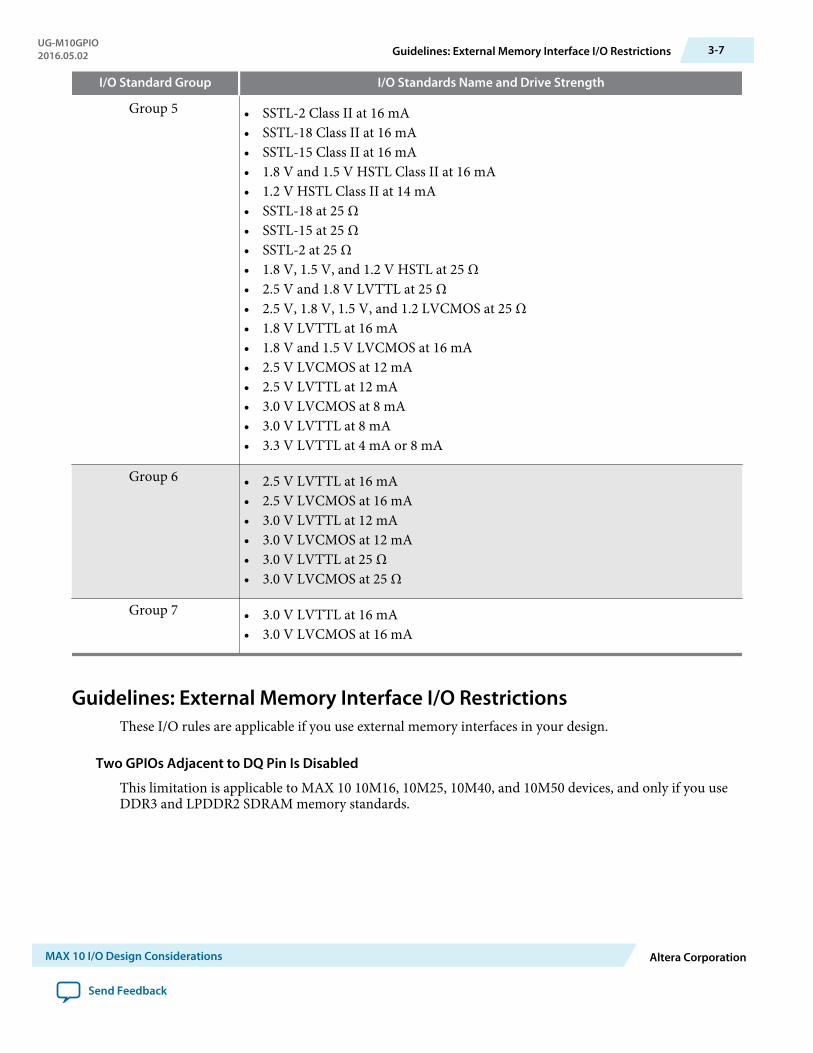
I/O Standard Group I/O Standards Name and Drive Strength
Group 5 • SSTL-2 Class II at 16 mA• SSTL-18 Class II at 16 mA• SSTL-15 Class II at 16 mA• 1.8 V and 1.5 V HSTL Class II at 16 mA• 1.2 V HSTL Class II at 14 mA• SSTL-18 at 25 Ω• SSTL-15 at 25 Ω• SSTL-2 at 25 Ω• 1.8 V, 1.5 V, and 1.2 V HSTL at 25 Ω• 2.5 V and 1.8 V LVTTL at 25 Ω• 2.5 V, 1.8 V, 1.5 V, and 1.2 LVCMOS at 25 Ω• 1.8 V LVTTL at 16 mA• 1.8 V and 1.5 V LVCMOS at 16 mA• 2.5 V LVCMOS at 12 mA• 2.5 V LVTTL at 12 mA• 3.0 V LVCMOS at 8 mA• 3.0 V LVTTL at 8 mA• 3.3 V LVTTL at 4 mA or 8 mA
Group 6 • 2.5 V LVTTL at 16 mA• 2.5 V LVCMOS at 16 mA• 3.0 V LVTTL at 12 mA• 3.0 V LVCMOS at 12 mA• 3.0 V LVTTL at 25 Ω• 3.0 V LVCMOS at 25 Ω
Group 7 • 3.0 V LVTTL at 16 mA• 3.0 V LVCMOS at 16 mA
Guidelines: External Memory Interface I/O RestrictionsThese I/O rules are applicable if you use external memory interfaces in your design.
Two GPIOs Adjacent to DQ Pin Is Disabled
This limitation is applicable to MAX 10 10M16, 10M25, 10M40, and 10M50 devices, and only if you useDDR3 and LPDDR2 SDRAM memory standards.
UG-M10GPIO2016.05.02 Guidelines: External Memory Interface I/O Restrictions 3-7
MAX 10 I/O Design Considerations Altera Corporation
Send Feedback
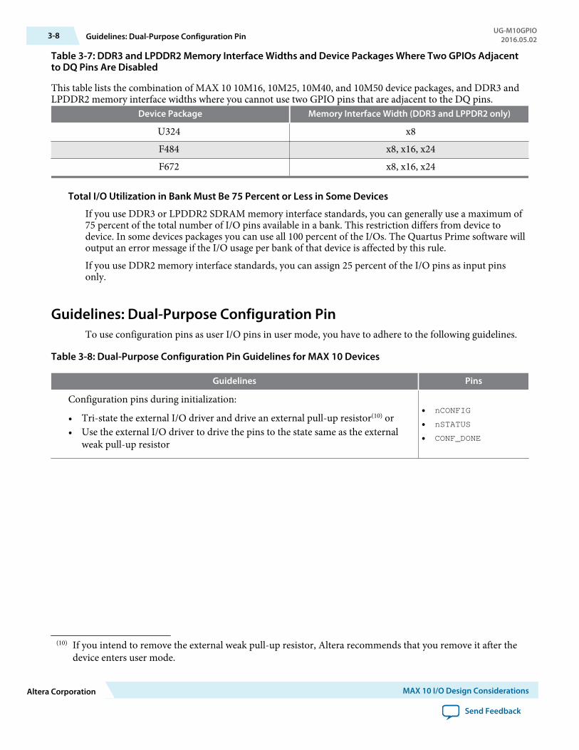
Table 3-7: DDR3 and LPDDR2 Memory Interface Widths and Device Packages Where Two GPIOs Adjacentto DQ Pins Are Disabled
This table lists the combination of MAX 10 10M16, 10M25, 10M40, and 10M50 device packages, and DDR3 andLPDDR2 memory interface widths where you cannot use two GPIO pins that are adjacent to the DQ pins.
Device Package Memory Interface Width (DDR3 and LPPDR2 only)
U324 x8F484 x8, x16, x24F672 x8, x16, x24
Total I/O Utilization in Bank Must Be 75 Percent or Less in Some Devices
If you use DDR3 or LPDDR2 SDRAM memory interface standards, you can generally use a maximum of75 percent of the total number of I/O pins available in a bank. This restriction differs from device todevice. In some devices packages you can use all 100 percent of the I/Os. The Quartus Prime software willoutput an error message if the I/O usage per bank of that device is affected by this rule.
If you use DDR2 memory interface standards, you can assign 25 percent of the I/O pins as input pinsonly.
Guidelines: Dual-Purpose Configuration PinTo use configuration pins as user I/O pins in user mode, you have to adhere to the following guidelines.
Table 3-8: Dual-Purpose Configuration Pin Guidelines for MAX 10 Devices
Guidelines Pins
Configuration pins during initialization:
• Tri-state the external I/O driver and drive an external pull-up resistor(10) or• Use the external I/O driver to drive the pins to the state same as the external
weak pull-up resistor
• nCONFIG
• nSTATUS
• CONF_DONE
(10) If you intend to remove the external weak pull-up resistor, Altera recommends that you remove it after thedevice enters user mode.
3-8 Guidelines: Dual-Purpose Configuration PinUG-M10GPIO
2016.05.02
Altera Corporation MAX 10 I/O Design Considerations
Send Feedback
Guidelines Pins
JTAG pins:
• If you intend to switch back and forth between user I/O pins and JTAG pinfunctions using the JTAGEN pin, all JTAG pins must be assigned as single-endedI/O pins or voltage-referenced I/O pins. Schmitt trigger input is therecommended input buffer.
• JTAG pins cannot perform as JTAG pins in user mode if you assign any of theJTAG pin as a differential I/O pin.
• You must use the JTAG pins as dedicated pins and not as user I/O pins duringJTAG programming.
• Do not toggle JTAG pin during the initialization stage.• Put the test access port (TAP) controller in reset state by driving the TDI and
TMS pins high and TCK pin low for at least 5 clock cycles before the initialization.
• TDO
• TMS
• TCK
• TDI
Attention: Assign all JTAG pins as single-ended I/O pins or voltage-referenced I/O pins if you enableJTAG pin sharing feature.
Related InformationMAX 10 FPGA Configuration User GuideProvides more information about the dual-purpose I/O pins in configuration and user modes.
Guidelines: Clock and Data Input Signal for MAX 10 E144 PackageThere is strong inductive coupling on the MAX 10 E144 lead frame package. Glitch may occur on aninput pin when an aggressor pin with strong drive strength toggles directly adjacent to it.
PLL Clock Input Pins
The PLL clock input pins are sensitive to SSN jitter. To avoid the PLL from losing lock, do not use theoutput pins directly on the left and right of the PLL clock input pins.
Data Input Pins
Potential glitch on the data input pin, leading to input read signal failure, can occur in the followingconditions:
• The output pin directly adjacent to the data input pin is assigned an unterminated I/O standard, suchas LVTTL and LVCMOS, with drive strength of 8 mA or higher.
• The output pin directly adjacent to the data input pin is assigned a terminated I/O standard, such asSSTL, with drive strength of 8 mA or higher.
UG-M10GPIO2016.05.02 Guidelines: Clock and Data Input Signal for MAX 10 E144 Package 3-9
MAX 10 I/O Design Considerations Altera Corporation
Send Feedback

To reduce jitter on data input pin, Altera recommends the following guidelines:
• Reduce the drive strength of the directly adjacent output pin for the different unterminated I/Ostandards as follows:
• 4 mA or below—2.5 V, 3.0 V, and 3.3 V unterminated I/O standards• 6 mA or below—1.2 V, 1.5 V, and 1.8 V unterminated I/O standards
• For unterminated I/O standard, assign the pins directly on the left and right of the data input pin to anon-toggling signal.
• For terminated I/O standard, you can use only one pin directly on the left or right of the data input pinas toggling signal, provided that you set the slew rate setting of this pin to “0” (slow slew rate).Otherwise, assign the pins directly on the left and right of the data input pin to a non-toggling signal.
• Change the unterminated I/O standard data input pin to a Schmitt Trigger input buffer for better noiseimmunity. If you are using Schmitt Trigger input buffer on the data input pin, you can use the directlyadjacent output pin with unterminated I/O standard at a maximum drive strength of 8 mA.
3-10 Guidelines: Clock and Data Input Signal for MAX 10 E144 PackageUG-M10GPIO
2016.05.02
Altera Corporation MAX 10 I/O Design Considerations
Send Feedback
MAX 10 I/O Implementation Guides 42016.05.02
UG-M10GPIO Subscribe Send Feedback
You can implement your I/O design in the Quartus Prime software. The software contains tools for you tocreate and compile your design, and configure your device.
The Quartus Prime software allows you to prepare for device migration, set pin assignments, defineplacement restrictions, setup timing constraints, and customize IP cores. For more information aboutusing the Quartus Prime software, refer to the related information.
Related InformationMAX 10 I/O Overview on page 1-1
Altera GPIO Lite IP CoreThe Altera GPIO Lite IP core supports the MAX 10 GPIO components. To implement the GPIOs in yourdesign, you can customize the Altera GPIO Lite IP core to suit your requirements and instantiate it inyour design.
GPIOs are I/Os used in general applications not specific to transceivers, memory-like interfaces or LVDS.The Altera GPIO Lite IP core features the following components:
• Double data rate input/output (DDIO)—A digital component that doubles the data-rate of acommunication channel.
• I/O buffers—connect the pads to the FPGA.
Figure 4-1: High Level View of Single-Ended GPIO
Buffer
OEIN[1:0]
DATAIN[3:0] OutputPath
GPIOOE
Path
InputPathDATAOUT[3:0]
Core
© 2016 Altera Corporation. All rights reserved. ALTERA, ARRIA, CYCLONE, ENPIRION, MAX, MEGACORE, NIOS, QUARTUS and STRATIX words and logos aretrademarks of Altera Corporation and registered in the U.S. Patent and Trademark Office and in other countries. All other words and logos identified astrademarks or service marks are the property of their respective holders as described at www.altera.com/common/legal.html. Altera warrants performanceof its semiconductor products to current specifications in accordance with Altera's standard warranty, but reserves the right to make changes to anyproducts and services at any time without notice. Altera assumes no responsibility or liability arising out of the application or use of any information,product, or service described herein except as expressly agreed to in writing by Altera. Altera customers are advised to obtain the latest version of devicespecifications before relying on any published information and before placing orders for products or services.
ISO9001:2008Registered
www.altera.com101 Innovation Drive, San Jose, CA 95134
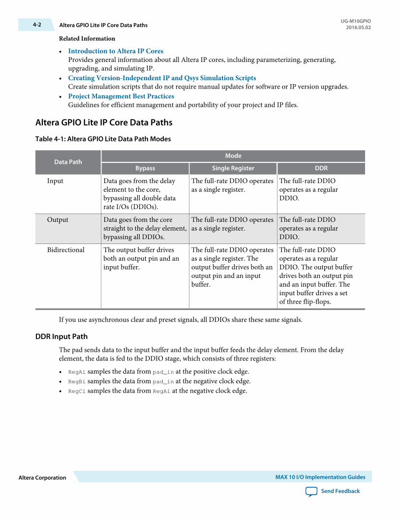
Related Information
• Introduction to Altera IP CoresProvides general information about all Altera IP cores, including parameterizing, generating,upgrading, and simulating IP.
• Creating Version-Independent IP and Qsys Simulation ScriptsCreate simulation scripts that do not require manual updates for software or IP version upgrades.
• Project Management Best PracticesGuidelines for efficient management and portability of your project and IP files.
Altera GPIO Lite IP Core Data Paths
Table 4-1: Altera GPIO Lite Data Path Modes
Data PathMode
Bypass Single Register DDR
Input Data goes from the delayelement to the core,bypassing all double datarate I/Os (DDIOs).
The full-rate DDIO operatesas a single register.
The full-rate DDIOoperates as a regularDDIO.
Output Data goes from the corestraight to the delay element,bypassing all DDIOs.
The full-rate DDIO operatesas a single register.
The full-rate DDIOoperates as a regularDDIO.
Bidirectional The output buffer drivesboth an output pin and aninput buffer.
The full-rate DDIO operatesas a single register. Theoutput buffer drives both anoutput pin and an inputbuffer.
The full-rate DDIOoperates as a regularDDIO. The output bufferdrives both an output pinand an input buffer. Theinput buffer drives a setof three flip-flops.
If you use asynchronous clear and preset signals, all DDIOs share these same signals.
DDR Input Path
The pad sends data to the input buffer and the input buffer feeds the delay element. From the delayelement, the data is fed to the DDIO stage, which consists of three registers:
• RegAi samples the data from pad_in at the positive clock edge.• RegBi samples the data from pad_in at the negative clock edge.• RegCi samples the data from RegAi at the negative clock edge.
4-2 Altera GPIO Lite IP Core Data PathsUG-M10GPIO
2016.05.02
Altera Corporation MAX 10 I/O Implementation Guides
Send Feedback
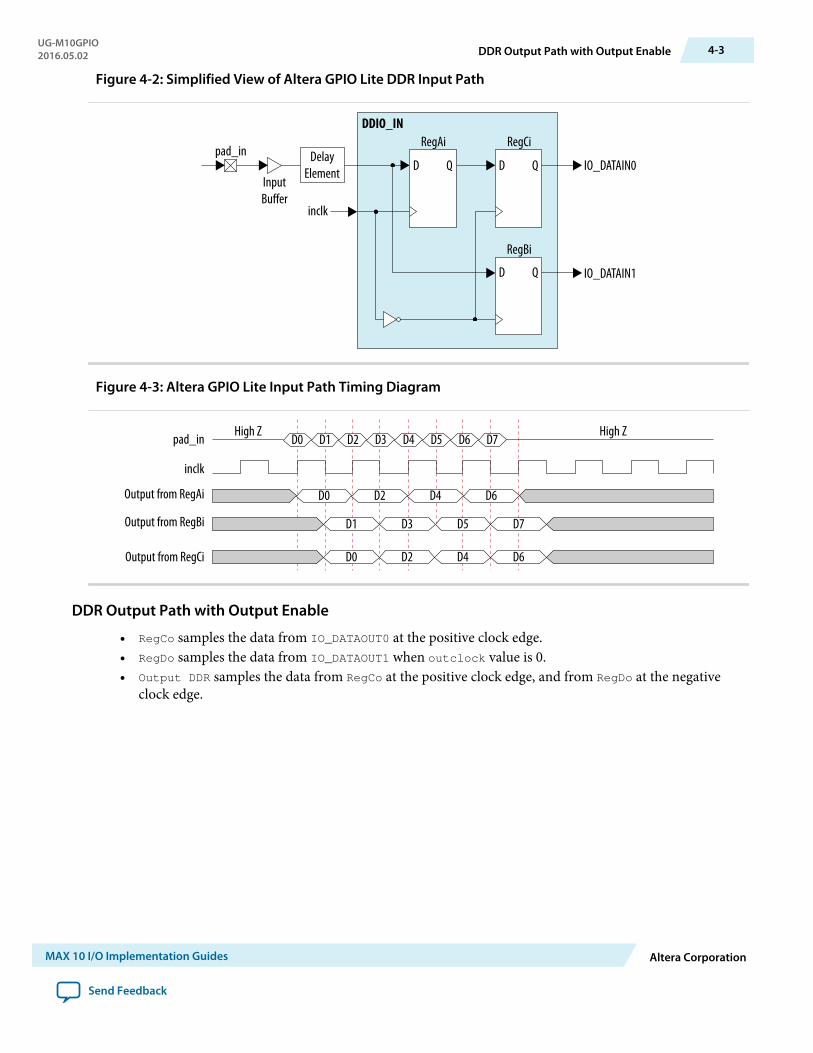
Figure 4-2: Simplified View of Altera GPIO Lite DDR Input Path
DelayElement
pad_in
InputBuffer
RegAi RegCi
RegBi
inclk
IO_DATAIN0
IO_DATAIN1
DDIO_IN
D Q D Q
D Q
Figure 4-3: Altera GPIO Lite Input Path Timing Diagram
D0 D1 D2 D3 D4 D5 D6 D7
D0 D2 D4 D6
D1 D3 D5 D7
D0 D2 D4 D6
pad_in
inclk
Output from RegAi
Output from RegBi
Output from RegCi
High Z High Z
DDR Output Path with Output Enable
• RegCo samples the data from IO_DATAOUT0 at the positive clock edge.• RegDo samples the data from IO_DATAOUT1 when outclock value is 0.• Output DDR samples the data from RegCo at the positive clock edge, and from RegDo at the negative
clock edge.
UG-M10GPIO2016.05.02 DDR Output Path with Output Enable 4-3
MAX 10 I/O Implementation Guides Altera Corporation
Send Feedback
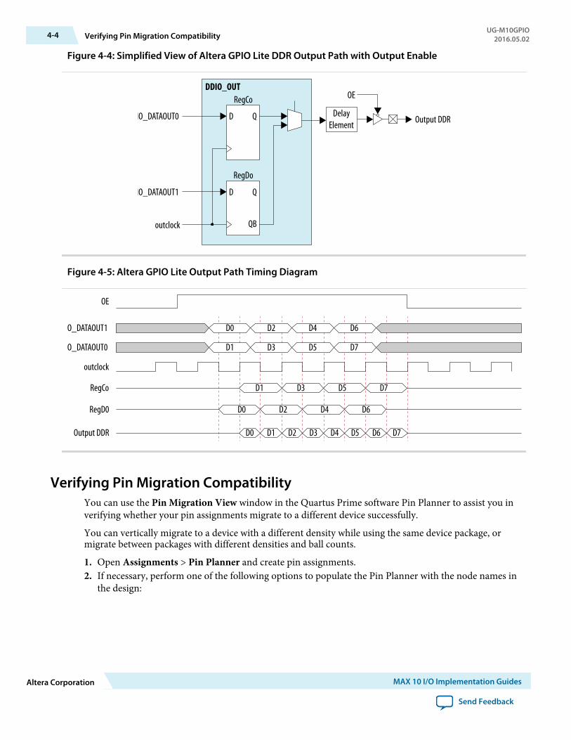
Figure 4-4: Simplified View of Altera GPIO Lite DDR Output Path with Output Enable
DelayElement Output DDR
RegCo
RegDo
IO_DATAOUT0
IO_DATAOUT1
DDIO_OUTOE
outclock
D Q
D Q
QB
Figure 4-5: Altera GPIO Lite Output Path Timing Diagram
D0IO_DATAOUT1
IO_DATAOUT0
outclock
RegD0
Output DDR
D2 D4 D6
D1 D3 D5 D7
D1 D3 D5 D7
D0 D2 D4 D6
D0 D1 D2 D3 D4 D5 D6 D7
RegCo
OE
Verifying Pin Migration CompatibilityYou can use the Pin Migration View window in the Quartus Prime software Pin Planner to assist you inverifying whether your pin assignments migrate to a different device successfully.
You can vertically migrate to a device with a different density while using the same device package, ormigrate between packages with different densities and ball counts.
1. Open Assignments > Pin Planner and create pin assignments.2. If necessary, perform one of the following options to populate the Pin Planner with the node names in
the design:
4-4 Verifying Pin Migration CompatibilityUG-M10GPIO
2016.05.02
Altera Corporation MAX 10 I/O Implementation Guides
Send Feedback

• Analysis & Elaboration• Analysis & Synthesis• Fully compile the design
3. Then, on the menu, click View > Pin Migration View.4. To select or change migration devices:
a. Click Device to open the Device dialog box.b. Under Migration compatibility click Migration Devices.
5. To show more information about the pins:a. Right-click anywhere in the Pin Migration View window and select Show Columns.b. Then, click the pin feature you want to display.
6. If you want to view only the pins, in at least one migration device, that have a different feature than thecorresponding pin in the migration result, turn on Show migration differences.
7. Click Pin Finder to open the Pin Finder dialog box and find and highlight pins with specific function‐ality.If you want to view only the pins found and highlighted by the most recent query in the Pin Finderdialog box, turn on Show only highlighted pins.
8. To export the pin migration information to a Comma-Separated Value File (.csv), click Export.
Related InformationMAX 10 I/O Vertical Migration Support on page 1-3
UG-M10GPIO2016.05.02 Verifying Pin Migration Compatibility 4-5
MAX 10 I/O Implementation Guides Altera Corporation
Send Feedback
Altera GPIO Lite IP Core References 52016.05.02
UG-M10GPIO Subscribe Send Feedback
You can set various parameter settings for the Altera GPIO Lite IP core to customize its behaviors, ports,and signals.
The Quartus Prime software generates your customized Altera GPIO Lite IP core according to theparameter options that you set in the parameter editor.
Related InformationMAX 10 I/O Overview on page 1-1
Altera GPIO Lite Parameter SettingsYou can set the parameter settings for the Altera GPIO Lite IP core in the Quartus Prime software. Thereare three groups of options: General, Buffer, and Registers.
Table 5-1: Altera GPIO Lite Parameters - General
Parameter Condition AllowedValues
Description
Data direction — • input• output• bidir
Specifies the data direction for theGPIO.
Data width — 1 to 128 Specifies the data width.
Table 5-2: Altera GPIO Lite Parameters - Buffer
Parameter Condition AllowedValues
Description
Use true differential buffer Data direction =input or output
• On• Off
If turned on, enables truedifferential I/O buffers anddisables pseudo differential I/Obuffers.
© 2016 Altera Corporation. All rights reserved. ALTERA, ARRIA, CYCLONE, ENPIRION, MAX, MEGACORE, NIOS, QUARTUS and STRATIX words and logos aretrademarks of Altera Corporation and registered in the U.S. Patent and Trademark Office and in other countries. All other words and logos identified astrademarks or service marks are the property of their respective holders as described at www.altera.com/common/legal.html. Altera warrants performanceof its semiconductor products to current specifications in accordance with Altera's standard warranty, but reserves the right to make changes to anyproducts and services at any time without notice. Altera assumes no responsibility or liability arising out of the application or use of any information,product, or service described herein except as expressly agreed to in writing by Altera. Altera customers are advised to obtain the latest version of devicespecifications before relying on any published information and before placing orders for products or services.
ISO9001:2008Registered
www.altera.com101 Innovation Drive, San Jose, CA 95134
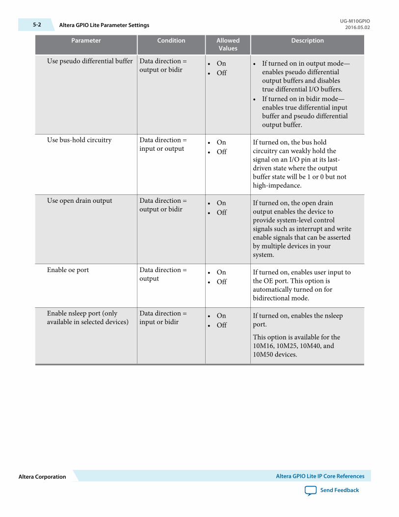
Parameter Condition AllowedValues
Description
Use pseudo differential buffer Data direction =output or bidir
• On• Off
• If turned on in output mode—enables pseudo differentialoutput buffers and disablestrue differential I/O buffers.
• If turned on in bidir mode—enables true differential inputbuffer and pseudo differentialoutput buffer.
Use bus-hold circuitry Data direction =input or output
• On• Off
If turned on, the bus holdcircuitry can weakly hold thesignal on an I/O pin at its last-driven state where the outputbuffer state will be 1 or 0 but nothigh-impedance.
Use open drain output Data direction =output or bidir
• On• Off
If turned on, the open drainoutput enables the device toprovide system-level controlsignals such as interrupt and writeenable signals that can be assertedby multiple devices in yoursystem.
Enable oe port Data direction =output
• On• Off
If turned on, enables user input tothe OE port. This option isautomatically turned on forbidirectional mode.
Enable nsleep port (onlyavailable in selected devices)
Data direction =input or bidir
• On• Off
If turned on, enables the nsleepport.
This option is available for the10M16, 10M25, 10M40, and10M50 devices.
5-2 Altera GPIO Lite Parameter SettingsUG-M10GPIO
2016.05.02
Altera Corporation Altera GPIO Lite IP Core References
Send Feedback
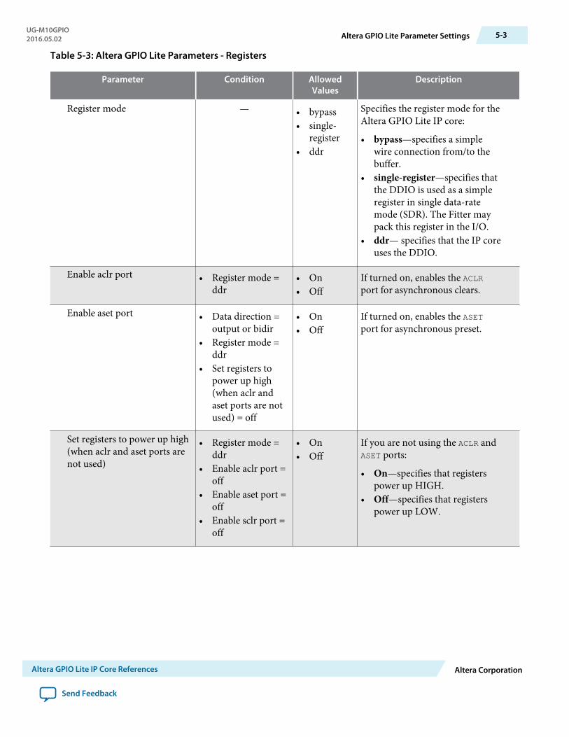
Table 5-3: Altera GPIO Lite Parameters - Registers
Parameter Condition AllowedValues
Description
Register mode — • bypass• single-
register• ddr
Specifies the register mode for theAltera GPIO Lite IP core:
• bypass—specifies a simplewire connection from/to thebuffer.
• single-register—specifies thatthe DDIO is used as a simpleregister in single data-ratemode (SDR). The Fitter maypack this register in the I/O.
• ddr— specifies that the IP coreuses the DDIO.
Enable aclr port • Register mode =ddr
• On• Off
If turned on, enables the ACLRport for asynchronous clears.
Enable aset port • Data direction =output or bidir
• Register mode =ddr
• Set registers topower up high(when aclr andaset ports are notused) = off
• On• Off
If turned on, enables the ASETport for asynchronous preset.
Set registers to power up high(when aclr and aset ports arenot used)
• Register mode =ddr
• Enable aclr port =off
• Enable aset port =off
• Enable sclr port =off
• On• Off
If you are not using the ACLR andASET ports:
• On—specifies that registerspower up HIGH.
• Off—specifies that registerspower up LOW.
UG-M10GPIO2016.05.02 Altera GPIO Lite Parameter Settings 5-3
Altera GPIO Lite IP Core References Altera Corporation
Send Feedback
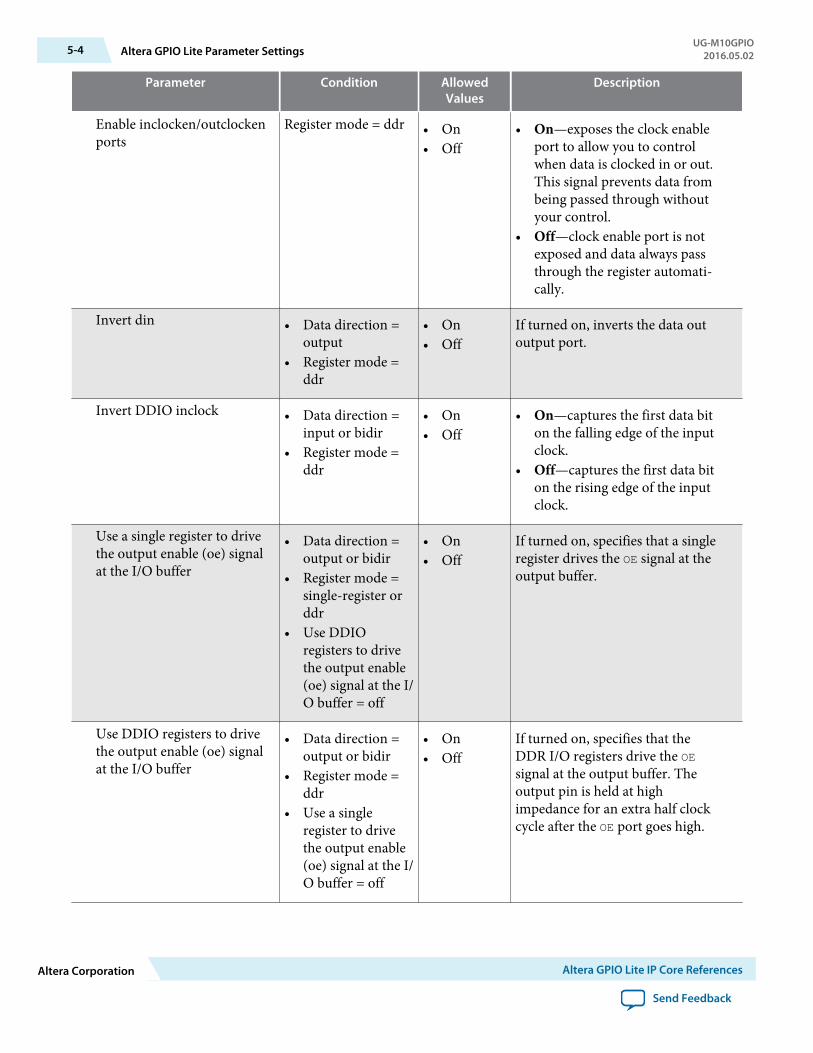
Parameter Condition AllowedValues
Description
Enable inclocken/outclockenports
Register mode = ddr • On• Off
• On—exposes the clock enableport to allow you to controlwhen data is clocked in or out.This signal prevents data frombeing passed through withoutyour control.
• Off—clock enable port is notexposed and data always passthrough the register automati‐cally.
Invert din • Data direction =output
• Register mode =ddr
• On• Off
If turned on, inverts the data outoutput port.
Invert DDIO inclock • Data direction =input or bidir
• Register mode =ddr
• On• Off
• On—captures the first data biton the falling edge of the inputclock.
• Off—captures the first data biton the rising edge of the inputclock.
Use a single register to drivethe output enable (oe) signalat the I/O buffer
• Data direction =output or bidir
• Register mode =single-register orddr
• Use DDIOregisters to drivethe output enable(oe) signal at the I/O buffer = off
• On• Off
If turned on, specifies that a singleregister drives the OE signal at theoutput buffer.
Use DDIO registers to drivethe output enable (oe) signalat the I/O buffer
• Data direction =output or bidir
• Register mode =ddr
• Use a singleregister to drivethe output enable(oe) signal at the I/O buffer = off
• On• Off
If turned on, specifies that theDDR I/O registers drive the OEsignal at the output buffer. Theoutput pin is held at highimpedance for an extra half clockcycle after the OE port goes high.
5-4 Altera GPIO Lite Parameter SettingsUG-M10GPIO
2016.05.02
Altera Corporation Altera GPIO Lite IP Core References
Send Feedback
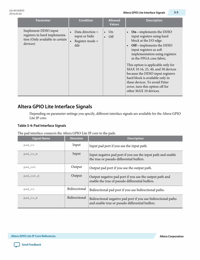
Parameter Condition AllowedValues
Description
Implement DDIO inputregisters in hard implementa‐tion (Only available in certaindevices)
• Data direction =input or bidir
• Register mode =ddr
• On• Off
• On—implements the DDIOinput registers using hardblock at the I/O edge.
• Off—implements the DDIOinput registers as softimplementation using registersin the FPGA core fabric.
This option is applicable only forMAX 10 16, 25, 40, and 50 devicesbecause the DDIO input registershard block is available only inthese devices. To avoid Fittererror, turn this option off forother MAX 10 devices.
Altera GPIO Lite Interface SignalsDepending on parameter settings you specify, different interface signals are available for the Altera GPIOLite IP core.
Table 5-4: Pad Interface Signals
The pad interface connects the Altera GPIO Lite IP core to the pads.Signal Name Direction Description
pad_in Input Input pad port if you use the input path.
pad_in_b Input Input negative pad port if you use the input path and enablethe true or pseudo differential buffers.
pad_out Output Output pad port if you use the output path.
pad_out_b Output Output negative pad port if you use the output path andenable the true of pseudo differential buffers.
pad_io Bidirectional Bidirectional pad port if you use bidirectional paths.
pad_io_b Bidirectional Bidirectional negative pad port if you use bidirectional pathsand enable true or pseudo differential buffers.
UG-M10GPIO2016.05.02 Altera GPIO Lite Interface Signals 5-5
Altera GPIO Lite IP Core References Altera Corporation
Send Feedback
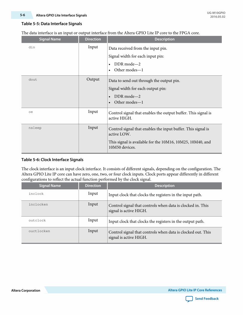
Table 5-5: Data Interface Signals
The data interface is an input or output interface from the Altera GPIO Lite IP core to the FPGA core.Signal Name Direction Description
din Input Data received from the input pin.
Signal width for each input pin:
• DDR mode—2• Other modes—1
dout Output Data to send out through the output pin.
Signal width for each output pin:
• DDR mode—2• Other modes—1
oe Input Control signal that enables the output buffer. This signal isactive HIGH.
nsleep Input Control signal that enables the input buffer. This signal isactive LOW.
This signal is available for the 10M16, 10M25, 10M40, and10M50 devices.
Table 5-6: Clock Interface Signals
The clock interface is an input clock interface. It consists of different signals, depending on the configuration. TheAltera GPIO Lite IP core can have zero, one, two, or four clock inputs. Clock ports appear differently in differentconfigurations to reflect the actual function performed by the clock signal.
Signal Name Direction Description
inclock Input Input clock that clocks the registers in the input path.
inclocken Input Control signal that controls when data is clocked in. Thissignal is active HIGH.
outclock Input Input clock that clocks the registers in the output path.
ouctlocken Input Control signal that controls when data is clocked out. Thissignal is active HIGH.
5-6 Altera GPIO Lite Interface SignalsUG-M10GPIO
2016.05.02
Altera Corporation Altera GPIO Lite IP Core References
Send Feedback
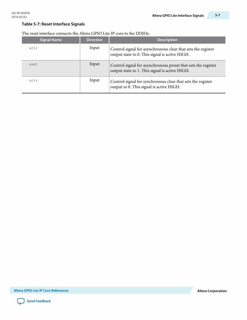
Table 5-7: Reset Interface Signals
The reset interface connects the Altera GPIO Lite IP core to the DDIOs.Signal Name Direction Description
aclr Input Control signal for asynchronous clear that sets the registeroutput state to 0. This signal is active HIGH.
aset Input Control signal for asynchronous preset that sets the registeroutput state to 1. This signal is active HIGH.
sclr Input Control signal for synchronous clear that sets the registeroutput to 0. This signal is active HIGH.
UG-M10GPIO2016.05.02 Altera GPIO Lite Interface Signals 5-7
Altera GPIO Lite IP Core References Altera Corporation
Send Feedback
MAX 10 General Purpose I/O User GuideArchives A
2016.05.02
UG-M10GPIO Subscribe Send Feedback
If an IP core version is not listed, the user guide for the previous IP core version applies.IP Core Version User Guide
15.1 MAX 10 General Purpose I/O User Guide
15.0 MAX 10 General Purpose I/O User Guide
14.1 MAX 10 General Purpose I/O User Guide
© 2016 Altera Corporation. All rights reserved. ALTERA, ARRIA, CYCLONE, ENPIRION, MAX, MEGACORE, NIOS, QUARTUS and STRATIX words and logos aretrademarks of Altera Corporation and registered in the U.S. Patent and Trademark Office and in other countries. All other words and logos identified astrademarks or service marks are the property of their respective holders as described at www.altera.com/common/legal.html. Altera warrants performanceof its semiconductor products to current specifications in accordance with Altera's standard warranty, but reserves the right to make changes to anyproducts and services at any time without notice. Altera assumes no responsibility or liability arising out of the application or use of any information,product, or service described herein except as expressly agreed to in writing by Altera. Altera customers are advised to obtain the latest version of devicespecifications before relying on any published information and before placing orders for products or services.
ISO9001:2008Registered
www.altera.com101 Innovation Drive, San Jose, CA 95134
Document Revision History for MAX 10 GeneralPurpose I/O User Guide B
2016.05.02
UG-M10GPIO Subscribe Send Feedback
Date Version Changes
May 2016 2016.05.02 • Updated the list of supported I/O standards to specify I/Ostandards that are supported only in dual power supply MAX 10devices.
• Updated the names of emulated differential I/O standards toimprove clarity.
• Updated the topic about the I/O standards voltage and pin supportto clarify that the I/O standards that a pin type supports dependson pin's I/O bank.
• Updated the setting information for PCI clamp diode:
• On by default for input pins for all supported I/O standards• Off by default for output pins for all supported I/O standards,
except 3.0 V PCI• Updated the topic about the ADC I/O restriction:
• Added the list of devices with physics-based rules support fromQuartus Prime version 15.0.1.
• Clarified that the table listing the percentage of GPIOs allowedin bank 8 is an example for the F484 package. For all packages,the Quartus Prime software displays a warning message if youexceed the allowed GPIO percentage.
© 2016 Altera Corporation. All rights reserved. ALTERA, ARRIA, CYCLONE, ENPIRION, MAX, MEGACORE, NIOS, QUARTUS and STRATIX words and logos aretrademarks of Altera Corporation and registered in the U.S. Patent and Trademark Office and in other countries. All other words and logos identified astrademarks or service marks are the property of their respective holders as described at www.altera.com/common/legal.html. Altera warrants performanceof its semiconductor products to current specifications in accordance with Altera's standard warranty, but reserves the right to make changes to anyproducts and services at any time without notice. Altera assumes no responsibility or liability arising out of the application or use of any information,product, or service described herein except as expressly agreed to in writing by Altera. Altera customers are advised to obtain the latest version of devicespecifications before relying on any published information and before placing orders for products or services.
ISO9001:2008Registered
www.altera.com101 Innovation Drive, San Jose, CA 95134
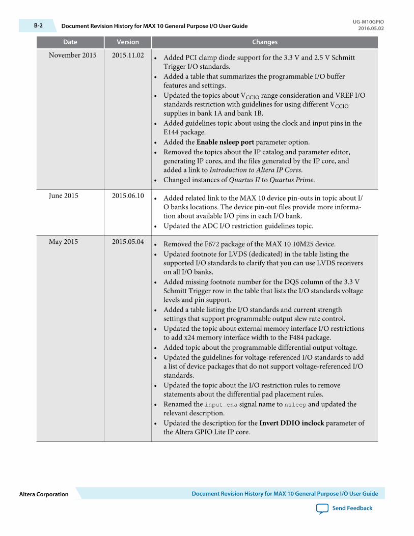
Date Version Changes
November 2015 2015.11.02 • Added PCI clamp diode support for the 3.3 V and 2.5 V SchmittTrigger I/O standards.
• Added a table that summarizes the programmable I/O bufferfeatures and settings.
• Updated the topics about VCCIO range consideration and VREF I/Ostandards restriction with guidelines for using different VCCIOsupplies in bank 1A and bank 1B.
• Added guidelines topic about using the clock and input pins in theE144 package.
• Added the Enable nsleep port parameter option.• Removed the topics about the IP catalog and parameter editor,
generating IP cores, and the files generated by the IP core, andadded a link to Introduction to Altera IP Cores.
• Changed instances of Quartus II to Quartus Prime.
June 2015 2015.06.10 • Added related link to the MAX 10 device pin-outs in topic about I/O banks locations. The device pin-out files provide more informa‐tion about available I/O pins in each I/O bank.
• Updated the ADC I/O restriction guidelines topic.
May 2015 2015.05.04 • Removed the F672 package of the MAX 10 10M25 device.• Updated footnote for LVDS (dedicated) in the table listing the
supported I/O standards to clarify that you can use LVDS receiverson all I/O banks.
• Added missing footnote number for the DQS column of the 3.3 VSchmitt Trigger row in the table that lists the I/O standards voltagelevels and pin support.
• Added a table listing the I/O standards and current strengthsettings that support programmable output slew rate control.
• Updated the topic about external memory interface I/O restrictionsto add x24 memory interface width to the F484 package.
• Added topic about the programmable differential output voltage.• Updated the guidelines for voltage-referenced I/O standards to add
a list of device packages that do not support voltage-referenced I/Ostandards.
• Updated the topic about the I/O restriction rules to removestatements about the differential pad placement rules.
• Renamed the input_ena signal name to nsleep and updated therelevant description.
• Updated the description for the Invert DDIO inclock parameter ofthe Altera GPIO Lite IP core.
B-2 Document Revision History for MAX 10 General Purpose I/O User GuideUG-M10GPIO
2016.05.02
Altera Corporation Document Revision History for MAX 10 General Purpose I/O User Guide
Send Feedback

Date Version Changes
December 2014 2014.12.15 Updated the topic about the ADC I/O restriction:
• Added information about implementation of physics-based rules inthe Quartus Prime software.
• Updated the list of I/O standards groups for the ADC I/O restric‐tion.
September 2014 2014.09.22 Initial release.
UG-M10GPIO2016.05.02 Document Revision History for MAX 10 General Purpose I/O User Guide B-3
Document Revision History for MAX 10 General Purpose I/O User Guide Altera Corporation
Send Feedback

MAX 10 High-Speed LVDS I/O User Guide
Subscribe
Send Feedback
UG-M10LVDS2016.10.31
101 Innovation DriveSan Jose, CA 95134www.altera.com
Contents
MAX 10 High-Speed LVDS I/O Overview..........................................................1-1Altera Soft LVDS Implementation Overview...........................................................................................1-2
MAX 10 High-Speed LVDS Architecture and Features......................................2-1MAX 10 LVDS Channels Support ............................................................................................................ 2-1MAX 10 LVDS SERDES I/O Standards Support..................................................................................... 2-7MAX 10 High-Speed LVDS Circuitry.....................................................................................................2-10MAX 10 High-Speed LVDS I/O Location.............................................................................................. 2-11Differential I/O Pins in Low Speed Region............................................................................................ 2-14
MAX 10 LVDS Transmitter Design.....................................................................3-1High-Speed I/O Transmitter Circuitry..................................................................................................... 3-1LVDS Transmitter Programmable I/O Features...................................................................................... 3-1
Programmable Pre-Emphasis.........................................................................................................3-1Programmable Differential Output Voltage................................................................................. 3-2
LVDS Transmitter I/O Termination Schemes..........................................................................................3-3Emulated LVDS External Termination......................................................................................... 3-3Sub-LVDS Transmitter External Termination............................................................................. 3-3SLVS Transmitter External Termination.......................................................................................3-4Emulated RSDS, Emulated Mini-LVDS, and Emulated PPDS Transmitter External
Termination.................................................................................................................................3-4LVDS Transmitter FPGA Design Implementation..................................................................................3-5
Altera Soft LVDS IP Core in Transmitter Mode.......................................................................... 3-6High-Speed I/O Timing Budget.....................................................................................................3-8Guidelines: LVDS Transmitter Channels Placement...................................................................3-9Guidelines: LVDS Channels PLL Placement................................................................................ 3-9Guidelines: LVDS Transmitter Logic Placement......................................................................... 3-9Guidelines: Enable LVDS Pre-Emphasis for E144 Package......................................................3-10
LVDS Transmitter Debug and Troubleshooting.................................................................................... 3-10Perform RTL Simulation Before Hardware Debug................................................................... 3-10Geometry-Based and Physics-Based I/O Rules......................................................................... 3-10
MAX 10 LVDS Receiver Design.......................................................................... 4-1High-Speed I/O Receiver Circuitry........................................................................................................... 4-1
Soft Deserializer................................................................................................................................4-1Data Realignment Block (Bit Slip)................................................................................................. 4-2
LVDS Receiver I/O Termination Schemes................................................................................................4-2LVDS, Mini-LVDS, and RSDS Receiver External Termination................................................. 4-3SLVS Receiver External Termination.............................................................................................4-3Sub-LVDS Receiver External Termination................................................................................... 4-3
TOC-2
Altera Corporation
TMDS Receiver External Termination..........................................................................................4-4HiSpi Receiver External Termination............................................................................................4-4LVPECL External Termination...................................................................................................... 4-5
LVDS Receiver FPGA Design Implementation....................................................................................... 4-6Altera Soft LVDS IP Core in Receiver Mode................................................................................ 4-6High-Speed I/O Timing Budget.....................................................................................................4-9Guidelines: Floating LVDS Input Pins........................................................................................ 4-13Guidelines: LVDS Receiver Channels Placement...................................................................... 4-13Guidelines: LVDS Channels PLL Placement.............................................................................. 4-13Guidelines: LVDS Receiver Logic Placement............................................................................. 4-14Guidelines: LVDS Receiver Timing Constraints........................................................................4-14
LVDS Receiver Debug and Troubleshooting..........................................................................................4-14Perform RTL Simulation Before Hardware Debug................................................................... 4-14Geometry-Based and Physics-Based I/O Rules......................................................................... 4-14
MAX 10 LVDS Transmitter and Receiver Design...............................................5-1Transmitter–Receiver Interfacing.............................................................................................................. 5-1LVDS Transmitter and Receiver FPGA Design Implementation.......................................................... 5-2
LVDS Transmitter and Receiver PLL Sharing Implementation.................................................5-2Initializing the Altera Soft LVDS IP Core..................................................................................... 5-3
LVDS Transmitter and Receiver Debug and Troubleshooting...............................................................5-3Perform RTL Simulation Before Hardware Debug......................................................................5-3Geometry-Based and Physics-Based I/O Rules........................................................................... 5-3
MAX 10 High-Speed LVDS Board Design Considerations................................6-1Guidelines: Improve Signal Quality...........................................................................................................6-1Guidelines: Control Channel-to-Channel Skew...................................................................................... 6-1Guidelines: Determine Board Design Constraints.................................................................................. 6-2Guidelines: Perform Board Level Simulations......................................................................................... 6-2
Altera Soft LVDS IP Core References................................................................. 7-1Altera Soft LVDS Parameter Settings ....................................................................................................... 7-1Altera Soft LVDS Interface Signals............................................................................................................ 7-7
MAX 10 High-Speed LVDS I/O User Guide Archives....................................... A-1
Document Revision History for MAX 10 High-Speed LVDS I/O User Guide..B-1
TOC-3
Altera Corporation
MAX 10 High-Speed LVDS I/O Overview 12016.10.31
UG-M10LVDS Subscribe Send Feedback
The MAX® 10 device family supports high-speed LVDS protocols through the LVDS I/O banks and theAltera Soft LVDS IP core.
Table 1-1: Summary of LVDS I/O Buffers Support in MAX 10 I/O Banks
I/O Buffer Type I/O Bank Support
True LVDS input buffer All I/O banks
True LVDS output buffer Only bottom I/O banks
Emulated LVDS output buffer All I/O banks
The LVDS I/O standards support differs between MAX 10 D and S variants. Refer to related informationfor more details.
Related Information
• MAX 10 High-Speed LVDS Architecture and Features on page 2-1Provides information about the high-speed LVDS architecture and the features supported by thedevice.
• MAX 10 LVDS Transmitter Design on page 3-1Provides information and guidelines for implementing LVDS transmitter in MAX 10 devices using theAltera Soft LVDS IP core.
• MAX 10 LVDS Receiver Design on page 4-1Provides information and guidelines for implementing LVDS receiver in MAX 10 devices using theAltera Soft LVDS IP core.
• MAX 10 LVDS Transmitter and Receiver Design on page 5-1Provides design guidelines for implementing both LVDS transmitters and receivers in the same MAX10 device.
• Altera Soft LVDS IP Core References on page 7-1Lists the parameters and signals of Altera Soft LVDS IP core for MAX 10 devices.
• MAX 10 LVDS SERDES I/O Standards Support on page 2-7Lists the supported LVDS I/O standards and the support in different MAX 10 device variants.
• MAX 10 High-Speed LVDS I/O User Guide Archives on page 8-1Provides a list of user guides for previous versions of the Altera Soft LVDS IP core.
© 2016 Intel Corporation. All rights reserved. Intel, the Intel logo, Altera, Arria, Cyclone, Enpirion, MAX, Megacore, NIOS, Quartus and Stratix words and logosare trademarks of Intel Corporation in the US and/or other countries. Other marks and brands may be claimed as the property of others. Intel warrantsperformance of its FPGA and semiconductor products to current specifications in accordance with Intel's standard warranty, but reserves the right to makechanges to any products and services at any time without notice. Intel assumes no responsibility or liability arising out of the application or use of anyinformation, product, or service described herein except as expressly agreed to in writing by Intel. Intel customers are advised to obtain the latest version ofdevice specifications before relying on any published information and before placing orders for products or services.
ISO9001:2008Registered
www.altera.com101 Innovation Drive, San Jose, CA 95134
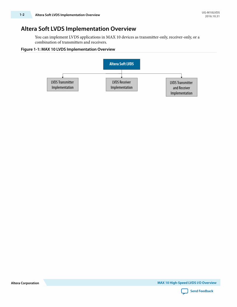
Altera Soft LVDS Implementation OverviewYou can implement LVDS applications in MAX 10 devices as transmitter-only, receiver-only, or acombination of transmitters and receivers.
Figure 1-1: MAX 10 LVDS Implementation Overview
Altera Soft LVDS
LVDS TransmitterImplementation
LVDS Transmitterand Receiver
Implementation
LVDS ReceiverImplementation
1-2 Altera Soft LVDS Implementation OverviewUG-M10LVDS
2016.10.31
Altera Corporation MAX 10 High-Speed LVDS I/O Overview
Send Feedback
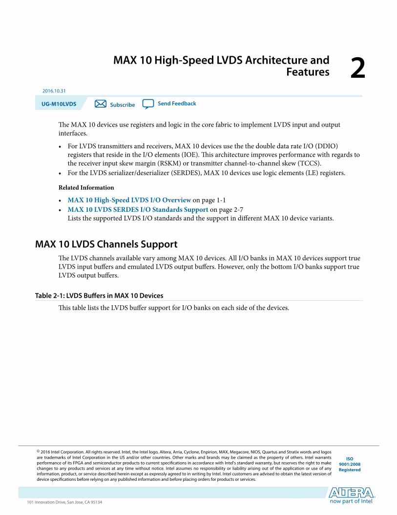
MAX 10 High-Speed LVDS Architecture andFeatures 2
2016.10.31
UG-M10LVDS Subscribe Send Feedback
The MAX 10 devices use registers and logic in the core fabric to implement LVDS input and outputinterfaces.
• For LVDS transmitters and receivers, MAX 10 devices use the the double data rate I/O (DDIO)registers that reside in the I/O elements (IOE). This architecture improves performance with regards tothe receiver input skew margin (RSKM) or transmitter channel-to-channel skew (TCCS).
• For the LVDS serializer/deserializer (SERDES), MAX 10 devices use logic elements (LE) registers.
Related Information
• MAX 10 High-Speed LVDS I/O Overview on page 1-1• MAX 10 LVDS SERDES I/O Standards Support on page 2-7
Lists the supported LVDS I/O standards and the support in different MAX 10 device variants.
MAX 10 LVDS Channels SupportThe LVDS channels available vary among MAX 10 devices. All I/O banks in MAX 10 devices support trueLVDS input buffers and emulated LVDS output buffers. However, only the bottom I/O banks support trueLVDS output buffers.
Table 2-1: LVDS Buffers in MAX 10 Devices
This table lists the LVDS buffer support for I/O banks on each side of the devices.
© 2016 Intel Corporation. All rights reserved. Intel, the Intel logo, Altera, Arria, Cyclone, Enpirion, MAX, Megacore, NIOS, Quartus and Stratix words and logosare trademarks of Intel Corporation in the US and/or other countries. Other marks and brands may be claimed as the property of others. Intel warrantsperformance of its FPGA and semiconductor products to current specifications in accordance with Intel's standard warranty, but reserves the right to makechanges to any products and services at any time without notice. Intel assumes no responsibility or liability arising out of the application or use of anyinformation, product, or service described herein except as expressly agreed to in writing by Intel. Intel customers are advised to obtain the latest version ofdevice specifications before relying on any published information and before placing orders for products or services.
ISO9001:2008Registered
www.altera.com101 Innovation Drive, San Jose, CA 95134
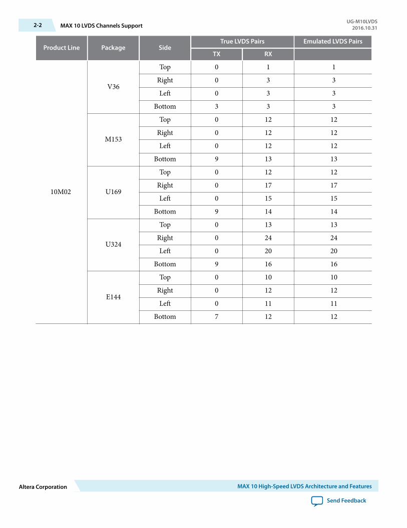
Product Line Package SideTrue LVDS Pairs Emulated LVDS Pairs
TX RX
10M02
V36
Top 0 1 1
Right 0 3 3
Left 0 3 3
Bottom 3 3 3
M153
Top 0 12 12
Right 0 12 12
Left 0 12 12
Bottom 9 13 13
U169
Top 0 12 12
Right 0 17 17
Left 0 15 15
Bottom 9 14 14
U324
Top 0 13 13
Right 0 24 24
Left 0 20 20
Bottom 9 16 16
E144
Top 0 10 10
Right 0 12 12
Left 0 11 11
Bottom 7 12 12
2-2 MAX 10 LVDS Channels SupportUG-M10LVDS
2016.10.31
Altera Corporation MAX 10 High-Speed LVDS Architecture and Features
Send Feedback
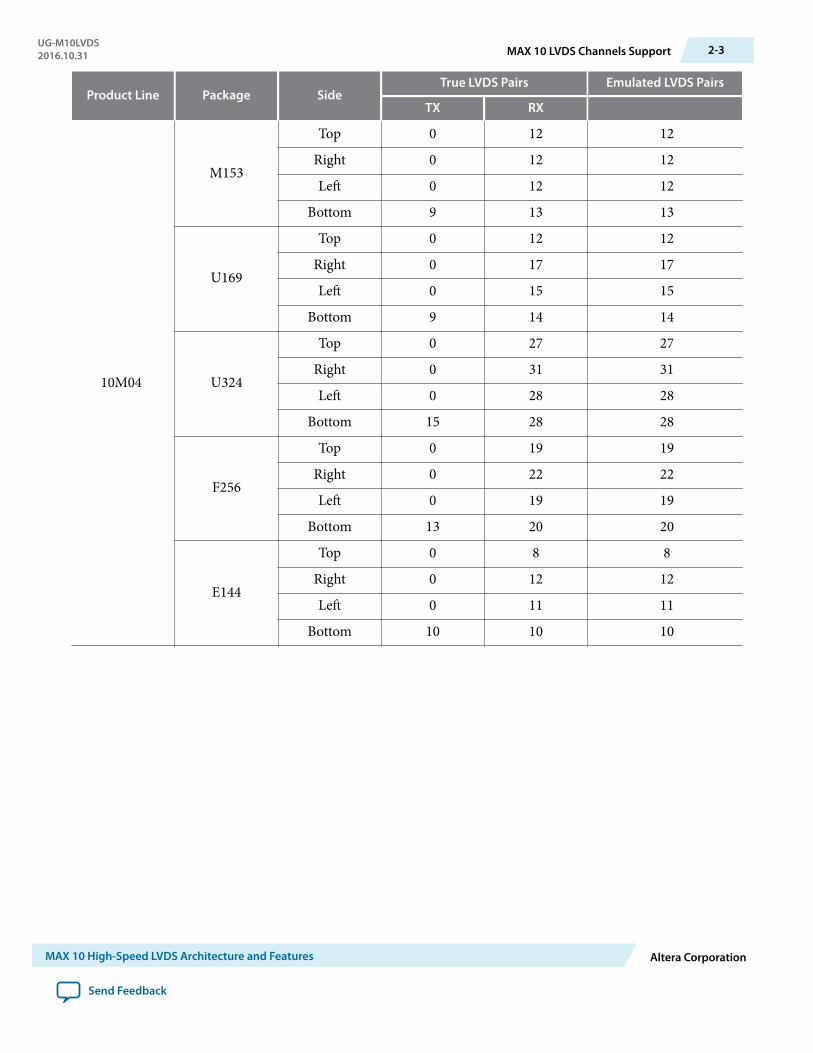
Product Line Package SideTrue LVDS Pairs Emulated LVDS Pairs
TX RX
10M04
M153
Top 0 12 12
Right 0 12 12
Left 0 12 12
Bottom 9 13 13
U169
Top 0 12 12
Right 0 17 17
Left 0 15 15
Bottom 9 14 14
U324
Top 0 27 27
Right 0 31 31
Left 0 28 28
Bottom 15 28 28
F256
Top 0 19 19
Right 0 22 22
Left 0 19 19
Bottom 13 20 20
E144
Top 0 8 8
Right 0 12 12
Left 0 11 11
Bottom 10 10 10
UG-M10LVDS2016.10.31 MAX 10 LVDS Channels Support 2-3
MAX 10 High-Speed LVDS Architecture and Features Altera Corporation
Send Feedback
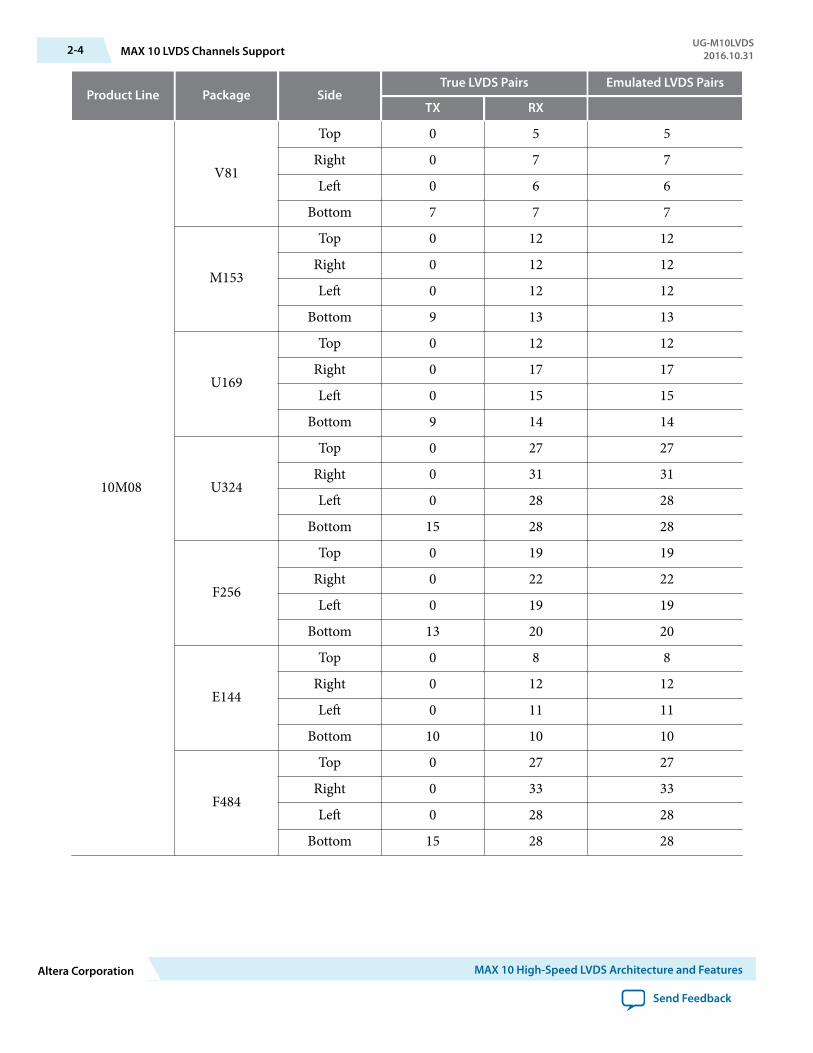
Product Line Package SideTrue LVDS Pairs Emulated LVDS Pairs
TX RX
10M08
V81
Top 0 5 5
Right 0 7 7
Left 0 6 6
Bottom 7 7 7
M153
Top 0 12 12
Right 0 12 12
Left 0 12 12
Bottom 9 13 13
U169
Top 0 12 12
Right 0 17 17
Left 0 15 15
Bottom 9 14 14
U324
Top 0 27 27
Right 0 31 31
Left 0 28 28
Bottom 15 28 28
F256
Top 0 19 19
Right 0 22 22
Left 0 19 19
Bottom 13 20 20
E144
Top 0 8 8
Right 0 12 12
Left 0 11 11
Bottom 10 10 10
F484
Top 0 27 27
Right 0 33 33
Left 0 28 28
Bottom 15 28 28
2-4 MAX 10 LVDS Channels SupportUG-M10LVDS
2016.10.31
Altera Corporation MAX 10 High-Speed LVDS Architecture and Features
Send Feedback
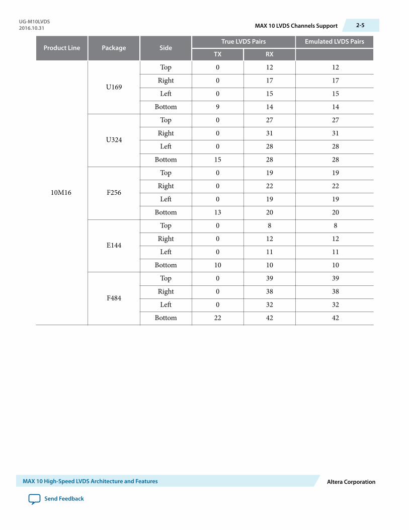
Product Line Package SideTrue LVDS Pairs Emulated LVDS Pairs
TX RX
10M16
U169
Top 0 12 12
Right 0 17 17
Left 0 15 15
Bottom 9 14 14
U324
Top 0 27 27
Right 0 31 31
Left 0 28 28
Bottom 15 28 28
F256
Top 0 19 19
Right 0 22 22
Left 0 19 19
Bottom 13 20 20
E144
Top 0 8 8
Right 0 12 12
Left 0 11 11
Bottom 10 10 10
F484
Top 0 39 39
Right 0 38 38
Left 0 32 32
Bottom 22 42 42
UG-M10LVDS2016.10.31 MAX 10 LVDS Channels Support 2-5
MAX 10 High-Speed LVDS Architecture and Features Altera Corporation
Send Feedback
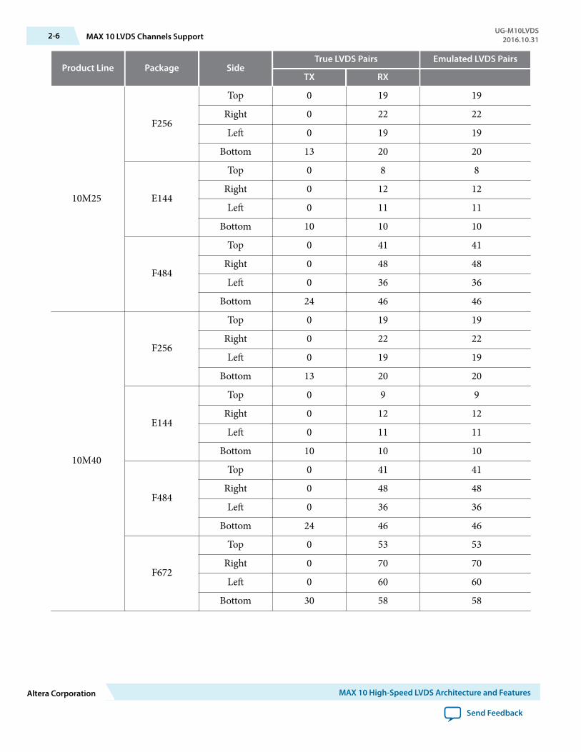
Product Line Package SideTrue LVDS Pairs Emulated LVDS Pairs
TX RX
10M25
F256
Top 0 19 19
Right 0 22 22
Left 0 19 19
Bottom 13 20 20
E144
Top 0 8 8
Right 0 12 12
Left 0 11 11
Bottom 10 10 10
F484
Top 0 41 41
Right 0 48 48
Left 0 36 36
Bottom 24 46 46
10M40
F256
Top 0 19 19
Right 0 22 22
Left 0 19 19
Bottom 13 20 20
E144
Top 0 9 9
Right 0 12 12
Left 0 11 11
Bottom 10 10 10
F484
Top 0 41 41
Right 0 48 48
Left 0 36 36
Bottom 24 46 46
F672
Top 0 53 53
Right 0 70 70
Left 0 60 60
Bottom 30 58 58
2-6 MAX 10 LVDS Channels SupportUG-M10LVDS
2016.10.31
Altera Corporation MAX 10 High-Speed LVDS Architecture and Features
Send Feedback
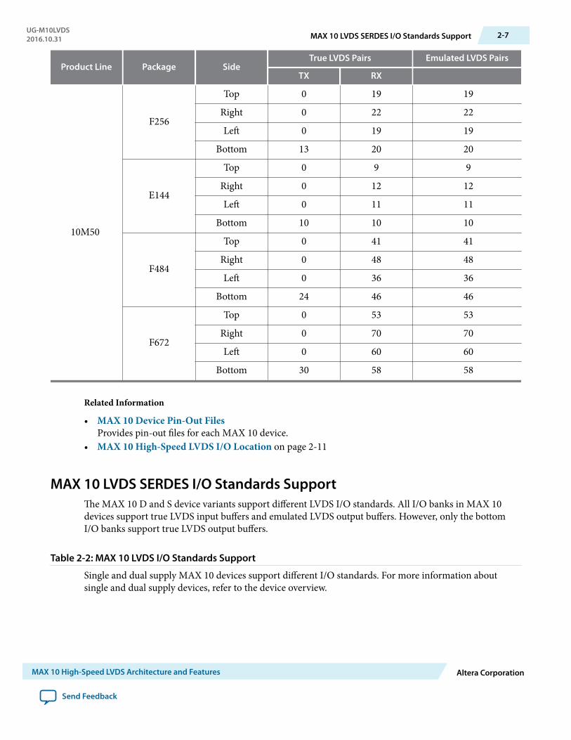
Product Line Package SideTrue LVDS Pairs Emulated LVDS Pairs
TX RX
10M50
F256
Top 0 19 19
Right 0 22 22
Left 0 19 19
Bottom 13 20 20
E144
Top 0 9 9
Right 0 12 12
Left 0 11 11
Bottom 10 10 10
F484
Top 0 41 41
Right 0 48 48
Left 0 36 36
Bottom 24 46 46
F672
Top 0 53 53
Right 0 70 70
Left 0 60 60
Bottom 30 58 58
Related Information
• MAX 10 Device Pin-Out FilesProvides pin-out files for each MAX 10 device.
• MAX 10 High-Speed LVDS I/O Location on page 2-11
MAX 10 LVDS SERDES I/O Standards SupportThe MAX 10 D and S device variants support different LVDS I/O standards. All I/O banks in MAX 10devices support true LVDS input buffers and emulated LVDS output buffers. However, only the bottomI/O banks support true LVDS output buffers.
Table 2-2: MAX 10 LVDS I/O Standards Support
Single and dual supply MAX 10 devices support different I/O standards. For more information aboutsingle and dual supply devices, refer to the device overview.
UG-M10LVDS2016.10.31 MAX 10 LVDS SERDES I/O Standards Support 2-7
MAX 10 High-Speed LVDS Architecture and Features Altera Corporation
Send Feedback
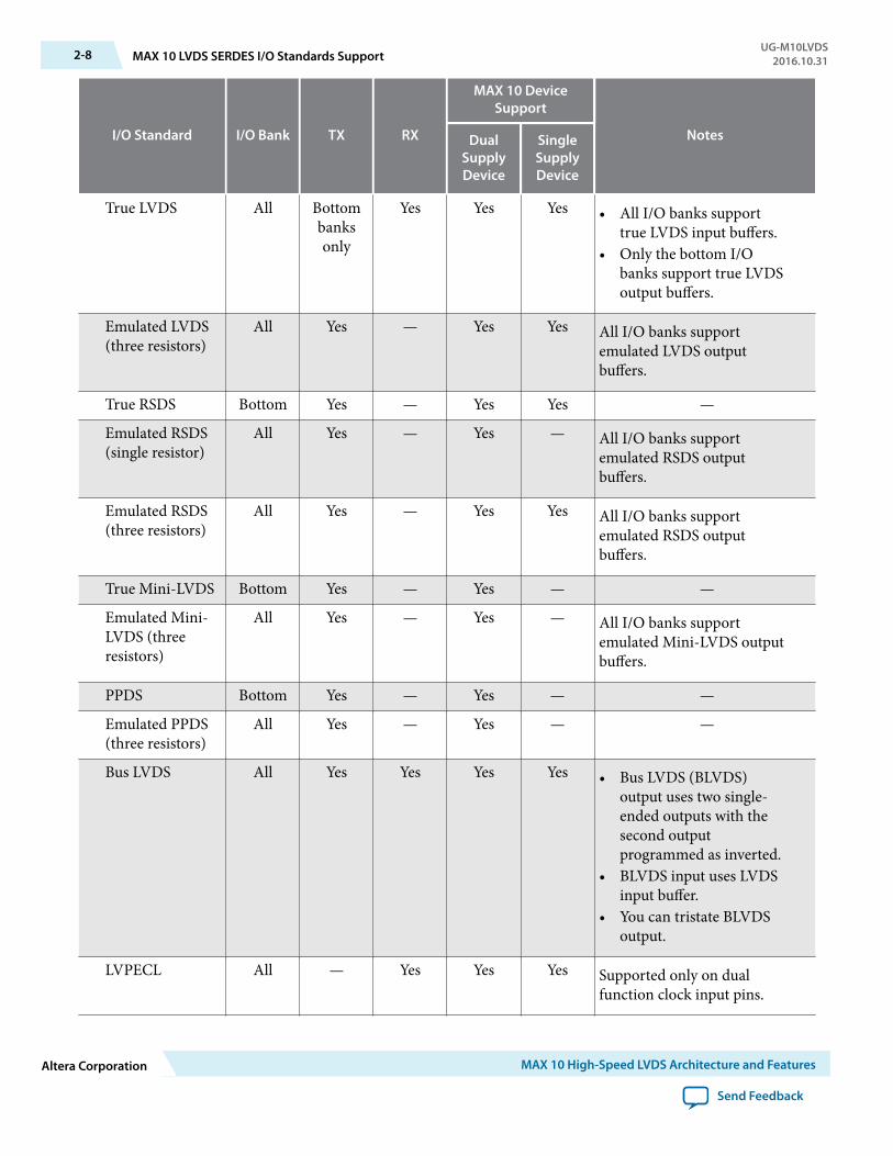
I/O Standard I/O Bank TX RX
MAX 10 DeviceSupport
NotesDualSupplyDevice
SingleSupplyDevice
True LVDS All Bottombanksonly
Yes Yes Yes • All I/O banks supporttrue LVDS input buffers.
• Only the bottom I/Obanks support true LVDSoutput buffers.
Emulated LVDS(three resistors)
All Yes — Yes Yes All I/O banks supportemulated LVDS outputbuffers.
True RSDS Bottom Yes — Yes Yes —
Emulated RSDS(single resistor)
All Yes — Yes — All I/O banks supportemulated RSDS outputbuffers.
Emulated RSDS(three resistors)
All Yes — Yes Yes All I/O banks supportemulated RSDS outputbuffers.
True Mini-LVDS Bottom Yes — Yes — —
Emulated Mini-LVDS (threeresistors)
All Yes — Yes — All I/O banks supportemulated Mini-LVDS outputbuffers.
PPDS Bottom Yes — Yes — —
Emulated PPDS(three resistors)
All Yes — Yes — —
Bus LVDS All Yes Yes Yes Yes • Bus LVDS (BLVDS)output uses two single-ended outputs with thesecond outputprogrammed as inverted.
• BLVDS input uses LVDSinput buffer.
• You can tristate BLVDSoutput.
LVPECL All — Yes Yes Yes Supported only on dualfunction clock input pins.
2-8 MAX 10 LVDS SERDES I/O Standards SupportUG-M10LVDS
2016.10.31
Altera Corporation MAX 10 High-Speed LVDS Architecture and Features
Send Feedback
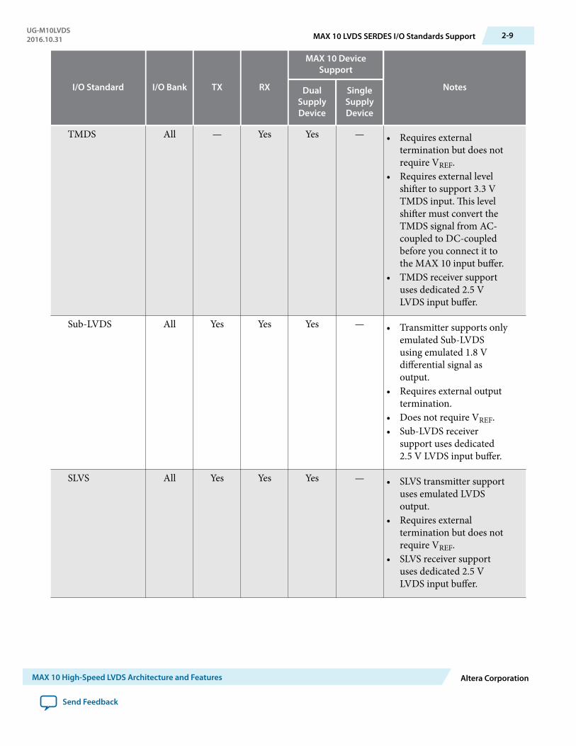
I/O Standard I/O Bank TX RX
MAX 10 DeviceSupport
NotesDualSupplyDevice
SingleSupplyDevice
TMDS All — Yes Yes — • Requires externaltermination but does notrequire VREF.
• Requires external levelshifter to support 3.3 VTMDS input. This levelshifter must convert theTMDS signal from AC-coupled to DC-coupledbefore you connect it tothe MAX 10 input buffer.
• TMDS receiver supportuses dedicated 2.5 VLVDS input buffer.
Sub-LVDS All Yes Yes Yes — • Transmitter supports onlyemulated Sub-LVDSusing emulated 1.8 Vdifferential signal asoutput.
• Requires external outputtermination.
• Does not require VREF.• Sub-LVDS receiver
support uses dedicated2.5 V LVDS input buffer.
SLVS All Yes Yes Yes — • SLVS transmitter supportuses emulated LVDSoutput.
• Requires externaltermination but does notrequire VREF.
• SLVS receiver supportuses dedicated 2.5 VLVDS input buffer.
UG-M10LVDS2016.10.31 MAX 10 LVDS SERDES I/O Standards Support 2-9
MAX 10 High-Speed LVDS Architecture and Features Altera Corporation
Send Feedback
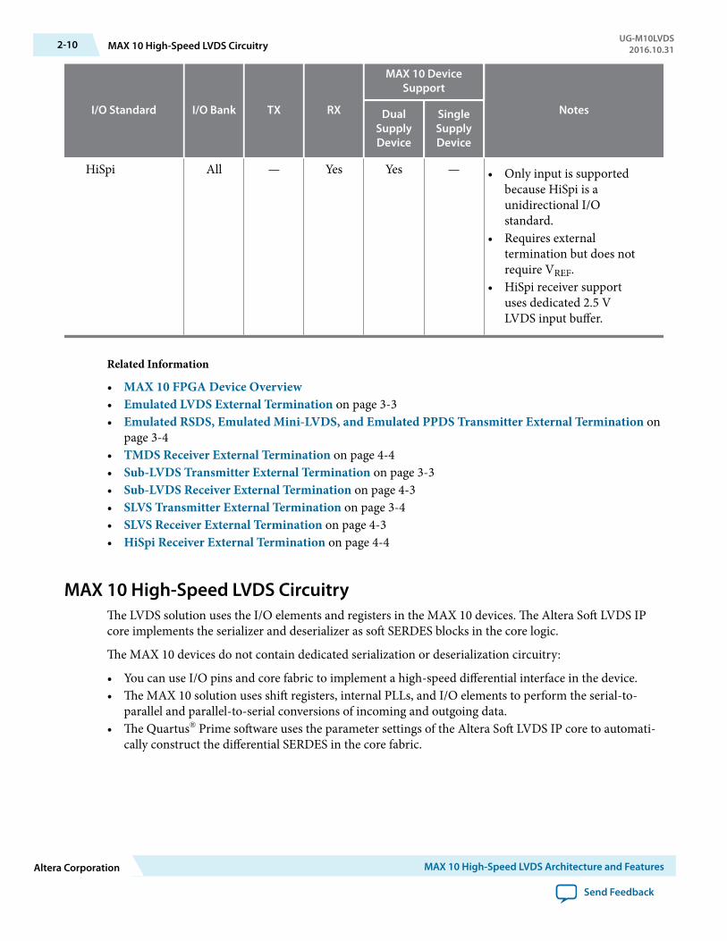
I/O Standard I/O Bank TX RX
MAX 10 DeviceSupport
NotesDualSupplyDevice
SingleSupplyDevice
HiSpi All — Yes Yes — • Only input is supportedbecause HiSpi is aunidirectional I/Ostandard.
• Requires externaltermination but does notrequire VREF.
• HiSpi receiver supportuses dedicated 2.5 VLVDS input buffer.
Related Information
• MAX 10 FPGA Device Overview• Emulated LVDS External Termination on page 3-3• Emulated RSDS, Emulated Mini-LVDS, and Emulated PPDS Transmitter External Termination on
page 3-4• TMDS Receiver External Termination on page 4-4• Sub-LVDS Transmitter External Termination on page 3-3• Sub-LVDS Receiver External Termination on page 4-3• SLVS Transmitter External Termination on page 3-4• SLVS Receiver External Termination on page 4-3• HiSpi Receiver External Termination on page 4-4
MAX 10 High-Speed LVDS CircuitryThe LVDS solution uses the I/O elements and registers in the MAX 10 devices. The Altera Soft LVDS IPcore implements the serializer and deserializer as soft SERDES blocks in the core logic.
The MAX 10 devices do not contain dedicated serialization or deserialization circuitry:
• You can use I/O pins and core fabric to implement a high-speed differential interface in the device.• The MAX 10 solution uses shift registers, internal PLLs, and I/O elements to perform the serial-to-
parallel and parallel-to-serial conversions of incoming and outgoing data.• The Quartus® Prime software uses the parameter settings of the Altera Soft LVDS IP core to automati‐
cally construct the differential SERDES in the core fabric.
2-10 MAX 10 High-Speed LVDS CircuitryUG-M10LVDS
2016.10.31
Altera Corporation MAX 10 High-Speed LVDS Architecture and Features
Send Feedback
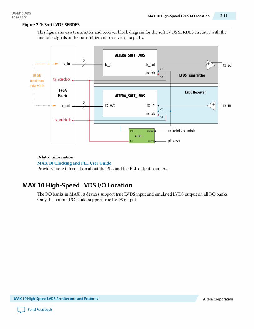
Figure 2-1: Soft LVDS SERDES
This figure shows a transmitter and receiver block diagram for the soft LVDS SERDES circuitry with theinterface signals of the transmitter and receiver data paths.
FPGAFabric
rx_out
tx_in
rx_outclock
tx_coreclock10 bits
maximumdata width
+–
+–
tx_out
rx_in
10
10
pll_areset
rx_inclock / tx_inclockC0
C0
C0
C1
C1
C1
inclock
areset
ALTPLL
ALTERA_SOFT_LVDS
tx_in tx_out
inclock
ALTERA_SOFT_LVDS
rx_out rx_in
inclock
LVDS Transmitter
LVDS Receiver
Related InformationMAX 10 Clocking and PLL User GuideProvides more information about the PLL and the PLL output counters.
MAX 10 High-Speed LVDS I/O LocationThe I/O banks in MAX 10 devices support true LVDS input and emulated LVDS output on all I/O banks.Only the bottom I/O banks support true LVDS output.
UG-M10LVDS2016.10.31 MAX 10 High-Speed LVDS I/O Location 2-11
MAX 10 High-Speed LVDS Architecture and Features Altera Corporation
Send Feedback
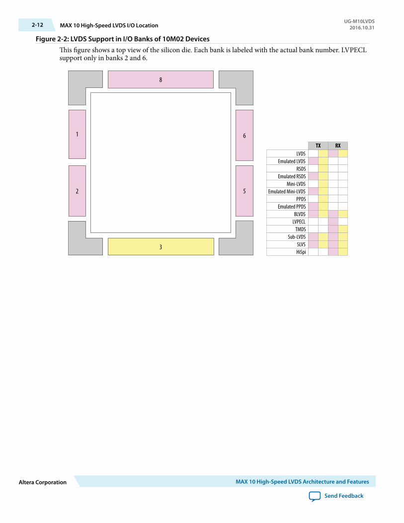
Figure 2-2: LVDS Support in I/O Banks of 10M02 DevicesThis figure shows a top view of the silicon die. Each bank is labeled with the actual bank number. LVPECLsupport only in banks 2 and 6.
1
2 5
6
3
8
LVDSEmulated LVDS
RSDSEmulated RSDS
Mini-LVDSEmulated Mini-LVDS
PPDSEmulated PPDS
BLVDSLVPECL
TMDSSub-LVDS
SLVSHiSpi
TX RX
2-12 MAX 10 High-Speed LVDS I/O LocationUG-M10LVDS
2016.10.31
Altera Corporation MAX 10 High-Speed LVDS Architecture and Features
Send Feedback
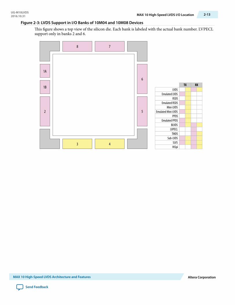
Figure 2-3: LVDS Support in I/O Banks of 10M04 and 10M08 DevicesThis figure shows a top view of the silicon die. Each bank is labeled with the actual bank number. LVPECLsupport only in banks 2 and 6.
1B
1A
2 5
6
3 4
8 7
LVDSEmulated LVDS
RSDSEmulated RSDS
Mini-LVDSEmulated Mini-LVDS
PPDSEmulated PPDS
BLVDSLVPECL
TMDSSub-LVDS
SLVSHiSpi
TX RX
UG-M10LVDS2016.10.31 MAX 10 High-Speed LVDS I/O Location 2-13
MAX 10 High-Speed LVDS Architecture and Features Altera Corporation
Send Feedback
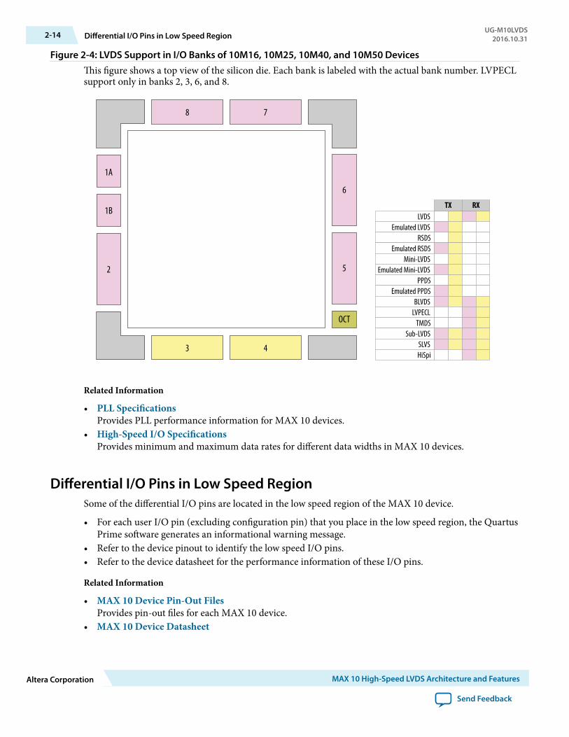
Figure 2-4: LVDS Support in I/O Banks of 10M16, 10M25, 10M40, and 10M50 DevicesThis figure shows a top view of the silicon die. Each bank is labeled with the actual bank number. LVPECLsupport only in banks 2, 3, 6, and 8.
1B
1A
2
3 4
8 7
OCT
5
6
LVDSEmulated LVDS
RSDSEmulated RSDS
Mini-LVDSEmulated Mini-LVDS
PPDSEmulated PPDS
BLVDSLVPECL
TMDSSub-LVDS
SLVSHiSpi
TX RX
Related Information
• PLL SpecificationsProvides PLL performance information for MAX 10 devices.
• High-Speed I/O SpecificationsProvides minimum and maximum data rates for different data widths in MAX 10 devices.
Differential I/O Pins in Low Speed RegionSome of the differential I/O pins are located in the low speed region of the MAX 10 device.
• For each user I/O pin (excluding configuration pin) that you place in the low speed region, the QuartusPrime software generates an informational warning message.
• Refer to the device pinout to identify the low speed I/O pins.• Refer to the device datasheet for the performance information of these I/O pins.
Related Information
• MAX 10 Device Pin-Out FilesProvides pin-out files for each MAX 10 device.
• MAX 10 Device Datasheet
2-14 Differential I/O Pins in Low Speed RegionUG-M10LVDS
2016.10.31
Altera Corporation MAX 10 High-Speed LVDS Architecture and Features
Send Feedback

• MAX 10 I/O Banks Locations, MAX 10 General Purpose I/O User GuideShows the locations of the high speed and low speed I/O banks.
UG-M10LVDS2016.10.31 Differential I/O Pins in Low Speed Region 2-15
MAX 10 High-Speed LVDS Architecture and Features Altera Corporation
Send Feedback
MAX 10 LVDS Transmitter Design 32016.10.31
UG-M10LVDS Subscribe Send Feedback
You can implement transmitter-only applications using the MAX 10 LVDS solution. You can use theAltera Soft LVDS IP core to instantiate soft SERDES circuitry. The soft SERDES circuitry works with theclocks and differential I/O pins to create a high-speed differential transmitter circuit.
Related Information
• MAX 10 High-Speed LVDS I/O Overview on page 1-1• MAX 10 LVDS SERDES I/O Standards Support on page 2-7
Lists the supported LVDS I/O standards and the support in different MAX 10 device variants.
High-Speed I/O Transmitter CircuitryThe LVDS transmitter circuitry uses the I/O elements and registers in the MAX 10 devices. The Altera SoftLVDS IP core implements the serializer as a soft SERDES block in the core logic.
Related InformationMAX 10 High-Speed LVDS Circuitry on page 2-10
LVDS Transmitter Programmable I/O FeaturesYou can program some features of the I/O buffers and pins in MAX 10 devices according to your designrequirements. For high-speed LVDS transmitter applications, you can program the pre-emphasis setting.
Programmable Pre-EmphasisThe differential output voltage (VOD) setting and the output impedance of the driver set the output currentlimit of a high-speed transmission signal. At a high frequency, the slew rate may not be fast enough toreach the full VOD level before the next edge, producing pattern-dependent jitter. Pre-emphasismomentarily boosts the output current during switching to increase the output slew rate.
Pre-emphasis increases the amplitude of the high-frequency component of the output signal. This increasecompensates for the frequency-dependent attenuation along the transmission line.
The overshoot introduced by the extra current occurs only during change of state switching. Thisovershoot increases the output slew rate but does not ring, unlike the overshoot caused by signalreflection. The amount of pre-emphasis required depends on the attenuation of the high-frequencycomponent along the transmission line.
© 2016 Intel Corporation. All rights reserved. Intel, the Intel logo, Altera, Arria, Cyclone, Enpirion, MAX, Megacore, NIOS, Quartus and Stratix words and logosare trademarks of Intel Corporation in the US and/or other countries. Other marks and brands may be claimed as the property of others. Intel warrantsperformance of its FPGA and semiconductor products to current specifications in accordance with Intel's standard warranty, but reserves the right to makechanges to any products and services at any time without notice. Intel assumes no responsibility or liability arising out of the application or use of anyinformation, product, or service described herein except as expressly agreed to in writing by Intel. Intel customers are advised to obtain the latest version ofdevice specifications before relying on any published information and before placing orders for products or services.
ISO9001:2008Registered
www.altera.com101 Innovation Drive, San Jose, CA 95134
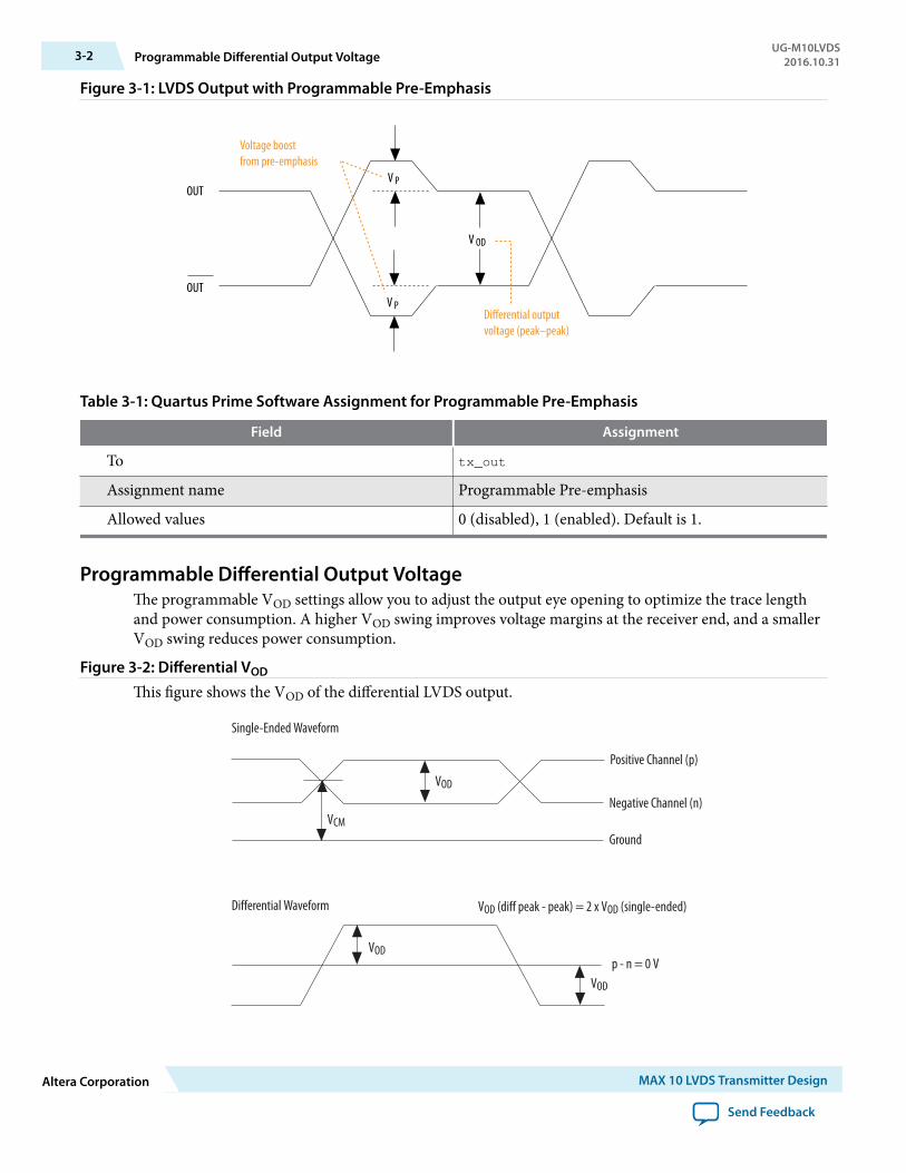
Figure 3-1: LVDS Output with Programmable Pre-Emphasis
OUT
OUT
V OD
V P
V P
Voltage boostfrom pre-emphasis
Differential outputvoltage (peak–peak)
Table 3-1: Quartus Prime Software Assignment for Programmable Pre-Emphasis
Field Assignment
To tx_out
Assignment name Programmable Pre-emphasis
Allowed values 0 (disabled), 1 (enabled). Default is 1.
Programmable Differential Output VoltageThe programmable VOD settings allow you to adjust the output eye opening to optimize the trace lengthand power consumption. A higher VOD swing improves voltage margins at the receiver end, and a smallerVOD swing reduces power consumption.
Figure 3-2: Differential VOD
This figure shows the VOD of the differential LVDS output.
Single-Ended Waveform
Positive Channel (p)
Negative Channel (n)
Ground
Differential Waveform
p - n = 0 V
VCM
VOD
VOD
VOD
VOD (diff peak - peak) = 2 x VOD (single-ended)
3-2 Programmable Differential Output VoltageUG-M10LVDS
2016.10.31
Altera Corporation MAX 10 LVDS Transmitter Design
Send Feedback
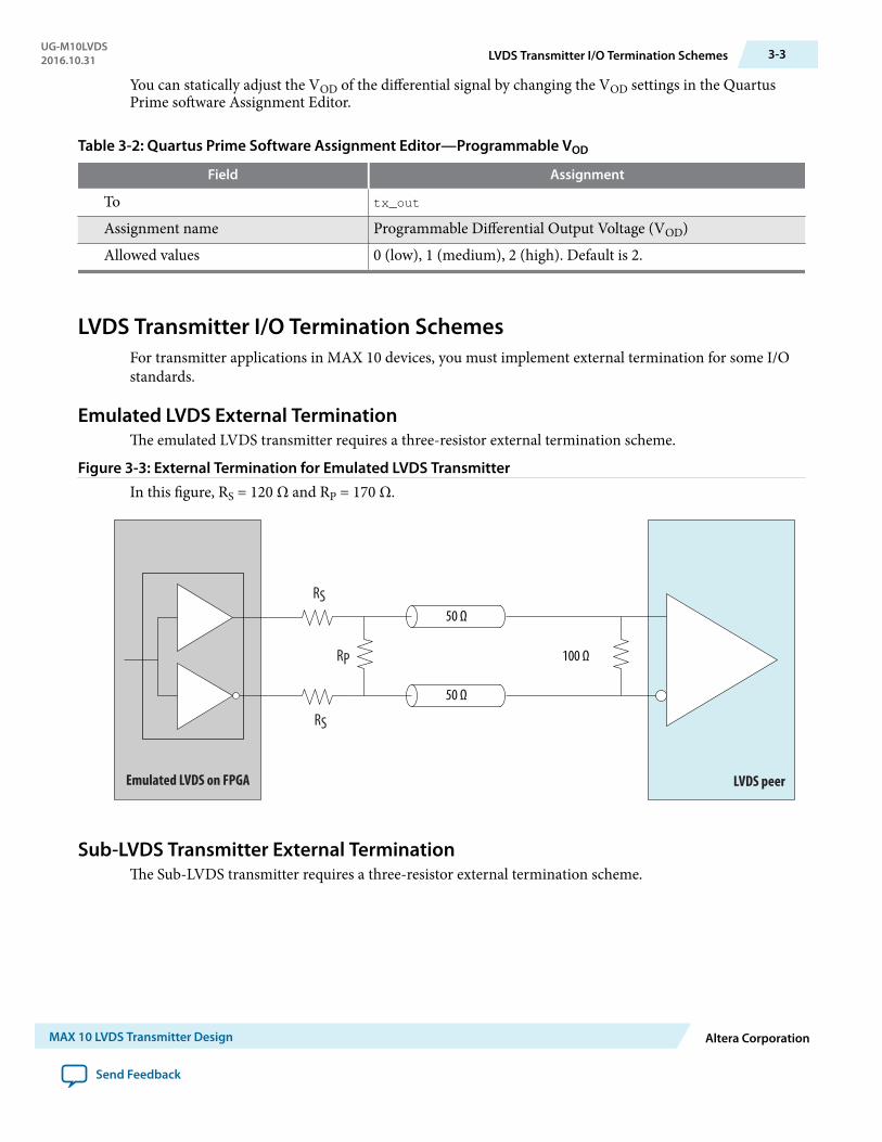
You can statically adjust the VOD of the differential signal by changing the VOD settings in the QuartusPrime software Assignment Editor.
Table 3-2: Quartus Prime Software Assignment Editor—Programmable VOD
Field Assignment
To tx_out
Assignment name Programmable Differential Output Voltage (VOD)Allowed values 0 (low), 1 (medium), 2 (high). Default is 2.
LVDS Transmitter I/O Termination SchemesFor transmitter applications in MAX 10 devices, you must implement external termination for some I/Ostandards.
Emulated LVDS External TerminationThe emulated LVDS transmitter requires a three-resistor external termination scheme.
Figure 3-3: External Termination for Emulated LVDS TransmitterIn this figure, RS = 120 Ω and RP = 170 Ω.
RS
RP
RS
LVDS peer
50 Ω
50 Ω
100 Ω
Emulated LVDS on FPGA
Sub-LVDS Transmitter External TerminationThe Sub-LVDS transmitter requires a three-resistor external termination scheme.
UG-M10LVDS2016.10.31 LVDS Transmitter I/O Termination Schemes 3-3
MAX 10 LVDS Transmitter Design Altera Corporation
Send Feedback
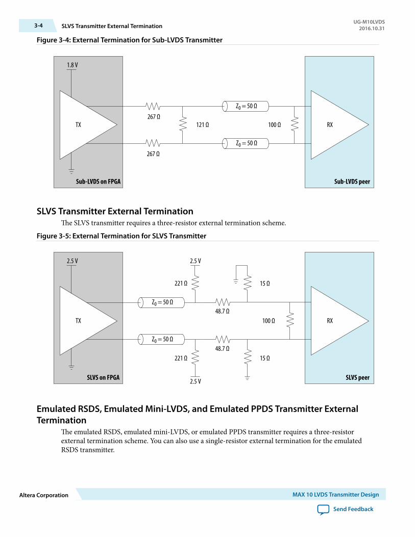
Figure 3-4: External Termination for Sub-LVDS Transmitter
TX RX
Sub-LVDS on FPGA
1.8 V
Sub-LVDS peer
Z0 = 50 Ω
Z0 = 50 Ω
267 Ω
267 Ω100 Ω121 Ω
SLVS Transmitter External TerminationThe SLVS transmitter requires a three-resistor external termination scheme.
Figure 3-5: External Termination for SLVS Transmitter
TX RX
SLVS on FPGA
2.5 V2.5 V
2.5 V SLVS peer
Z0 = 50 Ω
Z0 = 50 Ω48.7 Ω
48.7 Ω
221 Ω
221 Ω 15 Ω
100 Ω
15 Ω
Emulated RSDS, Emulated Mini-LVDS, and Emulated PPDS Transmitter ExternalTermination
The emulated RSDS, emulated mini-LVDS, or emulated PPDS transmitter requires a three-resistorexternal termination scheme. You can also use a single-resistor external termination for the emulatedRSDS transmitter.
3-4 SLVS Transmitter External TerminationUG-M10LVDS
2016.10.31
Altera Corporation MAX 10 LVDS Transmitter Design
Send Feedback
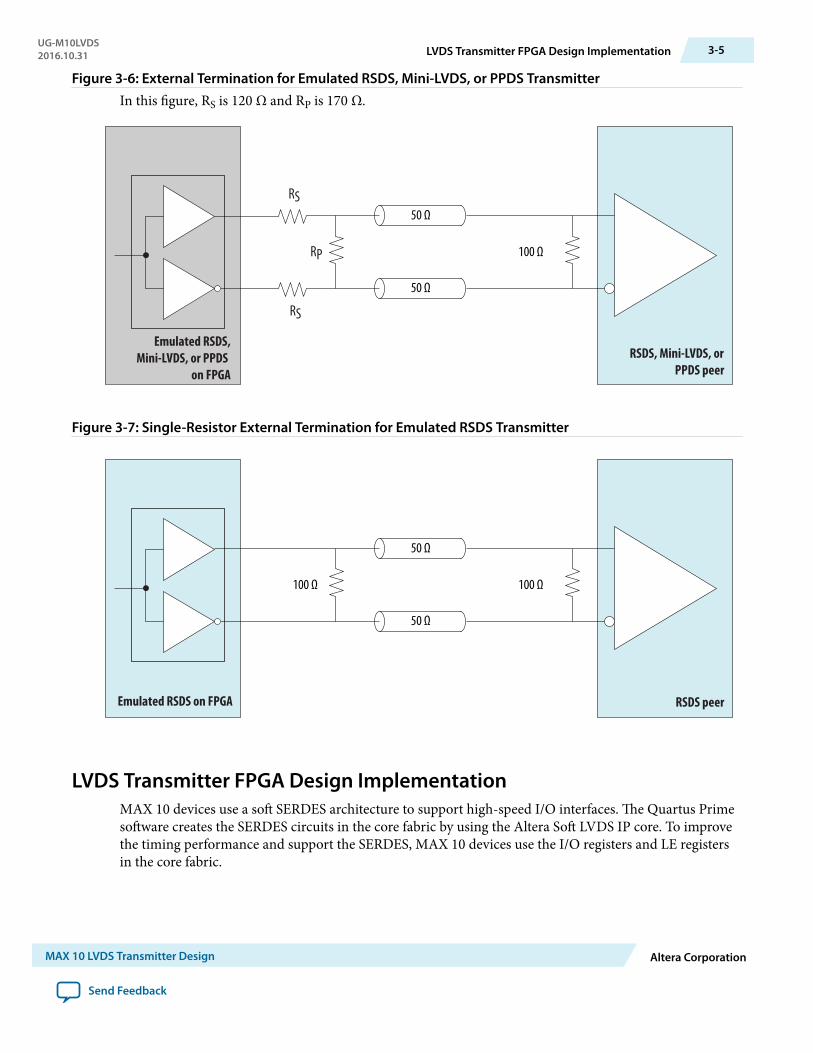
Figure 3-6: External Termination for Emulated RSDS, Mini-LVDS, or PPDS TransmitterIn this figure, RS is 120 Ω and RP is 170 Ω.
RS
RP
RS
RSDS, Mini-LVDS, orPPDS peer
50 Ω
50 Ω
100 Ω
Emulated RSDS,Mini-LVDS, or PPDS
on FPGA
Figure 3-7: Single-Resistor External Termination for Emulated RSDS Transmitter
RSDS peer
50 Ω
50 Ω
100 Ω100 Ω
Emulated RSDS on FPGA
LVDS Transmitter FPGA Design ImplementationMAX 10 devices use a soft SERDES architecture to support high-speed I/O interfaces. The Quartus Primesoftware creates the SERDES circuits in the core fabric by using the Altera Soft LVDS IP core. To improvethe timing performance and support the SERDES, MAX 10 devices use the I/O registers and LE registersin the core fabric.
UG-M10LVDS2016.10.31 LVDS Transmitter FPGA Design Implementation 3-5
MAX 10 LVDS Transmitter Design Altera Corporation
Send Feedback
Altera Soft LVDS IP Core in Transmitter ModeIn the Quartus Prime software, you can design your high-speed transmitter interfaces using the Altera SoftLVDS IP core. This IP core uses the resources optimally in the MAX 10 devices to create the high-speedI/O interfaces.
• You can use the Altera Soft LVDS parameter editor to customize your serializer based on your designrequirements.
• The high-speed I/O interface created using the Altera Soft LVDS IP core always sends the most signifi‐cant bit (MSB) of your parallel data first.
Related Information
• Altera Soft LVDS Parameter Settings on page 7-1• Introduction to Altera IP Cores
Provides general information about all Altera FPGA IP cores, including parameterizing, generating,upgrading, and simulating IP cores.
• Creating Version-Independent IP and Qsys Simulation ScriptsCreate simulation scripts that do not require manual updates for software or IP version upgrades.
• Project Management Best PracticesGuidelines for efficient management and portability of your project and IP files.
PLL Source Selection for Altera Soft LVDS IP CoreYou can create the LVDS interface components by instantiating the Altera Soft LVDS IP core with aninternal or external PLL.
Instantiate Altera Soft LVDS IP Core with Internal PLLYou can set the Altera Soft LVDS IP core to build the SERDES components and instantiate the PLLinternally.
• To use this method, turn off the Use external PLL option in the PLL Settings tab and set the necessarysettings in the PLL Settings and Transmitter Settings tab.
• The Altera Soft LVDS IP core integrates the PLL into the LVDS block.• The drawback of this method is that you can use the PLL only for the particular LVDS instance.
Instantiate Altera Soft LVDS IP Core with External PLLYou can set the Altera Soft LVDS IP core to build only the SERDES components but use an external PLLsource.
• To use this method, turn on the Use external PLL option in the PLL Settings tab.• Follow the required clock setting to the input ports as listed in the notification panel.• You can create your own clocking source using the ALTPLL IP core.• Use this method to optimize PLL usage with other functions in the core.
Related Information
• MAX 10 Clocking and PLL User GuideProvides more information about the PLL and the PLL output counters.
• MAX 10 Clocking and PLL User GuideProvides more information about the PLL and the PLL output counters.
3-6 Altera Soft LVDS IP Core in Transmitter ModeUG-M10LVDS
2016.10.31
Altera Corporation MAX 10 LVDS Transmitter Design
Send Feedback
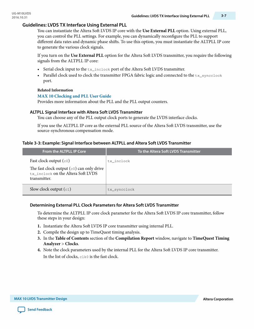
Guidelines: LVDS TX Interface Using External PLLYou can instantiate the Altera Soft LVDS IP core with the Use External PLL option. Using external PLL,you can control the PLL settings. For example, you can dynamically reconfigure the PLL to supportdifferent data rates and dynamic phase shifts. To use this option, you must instantiate the ALTPLL IP coreto generate the various clock signals.
If you turn on the Use External PLL option for the Altera Soft LVDS transmitter, you require the followingsignals from the ALTPLL IP core:
• Serial clock input to the tx_inclock port of the Altera Soft LVDS transmitter.• Parallel clock used to clock the transmitter FPGA fabric logic and connected to the tx_syncclock
port.
Related InformationMAX 10 Clocking and PLL User GuideProvides more information about the PLL and the PLL output counters.
ALTPLL Signal Interface with Altera Soft LVDS TransmitterYou can choose any of the PLL output clock ports to generate the LVDS interface clocks.
If you use the ALTPLL IP core as the external PLL source of the Altera Soft LVDS transmitter, use thesource-synchronous compensation mode.
Table 3-3: Example: Signal Interface between ALTPLL and Altera Soft LVDS Transmitter
From the ALTPLL IP Core To the Altera Soft LVDS Transmitter
Fast clock output (c0)
The fast clock output (c0) can only drivetx_inclock on the Altera Soft LVDStransmitter.
tx_inclock
Slow clock output (c1) tx_syncclock
Determining External PLL Clock Parameters for Altera Soft LVDS Transmitter
To determine the ALTPLL IP core clock parameter for the Altera Soft LVDS IP core transmitter, followthese steps in your design:
1. Instantiate the Altera Soft LVDS IP core transmitter using internal PLL.2. Compile the design up to TimeQuest timing analysis.3. In the Table of Contents section of the Compilation Report window, navigate to TimeQuest Timing
Analyzer > Clocks.4. Note the clock parameters used by the internal PLL for the Altera Soft LVDS IP core transmitter.
In the list of clocks, clk0 is the fast clock.
UG-M10LVDS2016.10.31 Guidelines: LVDS TX Interface Using External PLL 3-7
MAX 10 LVDS Transmitter Design Altera Corporation
Send Feedback
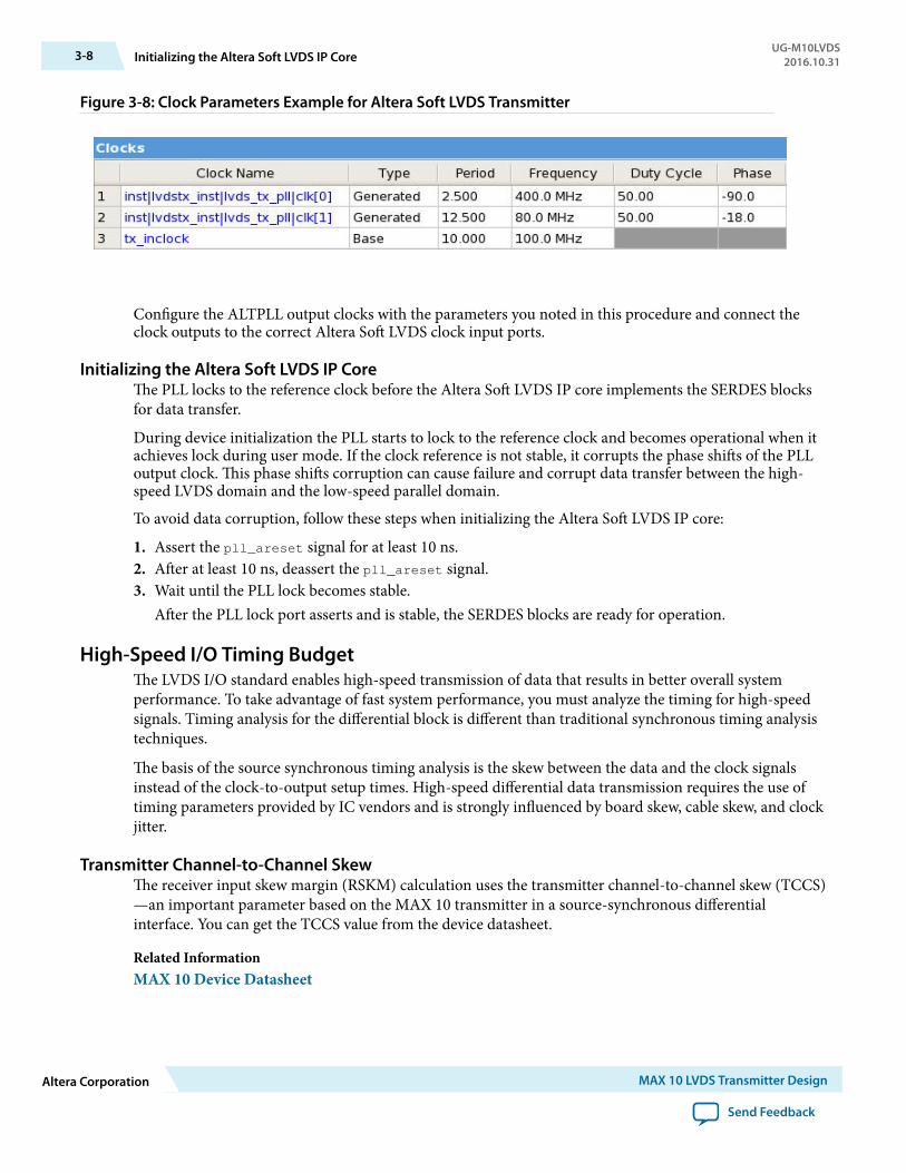
Figure 3-8: Clock Parameters Example for Altera Soft LVDS Transmitter
Configure the ALTPLL output clocks with the parameters you noted in this procedure and connect theclock outputs to the correct Altera Soft LVDS clock input ports.
Initializing the Altera Soft LVDS IP CoreThe PLL locks to the reference clock before the Altera Soft LVDS IP core implements the SERDES blocksfor data transfer.
During device initialization the PLL starts to lock to the reference clock and becomes operational when itachieves lock during user mode. If the clock reference is not stable, it corrupts the phase shifts of the PLLoutput clock. This phase shifts corruption can cause failure and corrupt data transfer between the high-speed LVDS domain and the low-speed parallel domain.
To avoid data corruption, follow these steps when initializing the Altera Soft LVDS IP core:
1. Assert the pll_areset signal for at least 10 ns.2. After at least 10 ns, deassert the pll_areset signal.3. Wait until the PLL lock becomes stable.
After the PLL lock port asserts and is stable, the SERDES blocks are ready for operation.
High-Speed I/O Timing BudgetThe LVDS I/O standard enables high-speed transmission of data that results in better overall systemperformance. To take advantage of fast system performance, you must analyze the timing for high-speedsignals. Timing analysis for the differential block is different than traditional synchronous timing analysistechniques.
The basis of the source synchronous timing analysis is the skew between the data and the clock signalsinstead of the clock-to-output setup times. High-speed differential data transmission requires the use oftiming parameters provided by IC vendors and is strongly influenced by board skew, cable skew, and clockjitter.
Transmitter Channel-to-Channel SkewThe receiver input skew margin (RSKM) calculation uses the transmitter channel-to-channel skew (TCCS)—an important parameter based on the MAX 10 transmitter in a source-synchronous differentialinterface. You can get the TCCS value from the device datasheet.
Related InformationMAX 10 Device Datasheet
3-8 Initializing the Altera Soft LVDS IP CoreUG-M10LVDS
2016.10.31
Altera Corporation MAX 10 LVDS Transmitter Design
Send Feedback
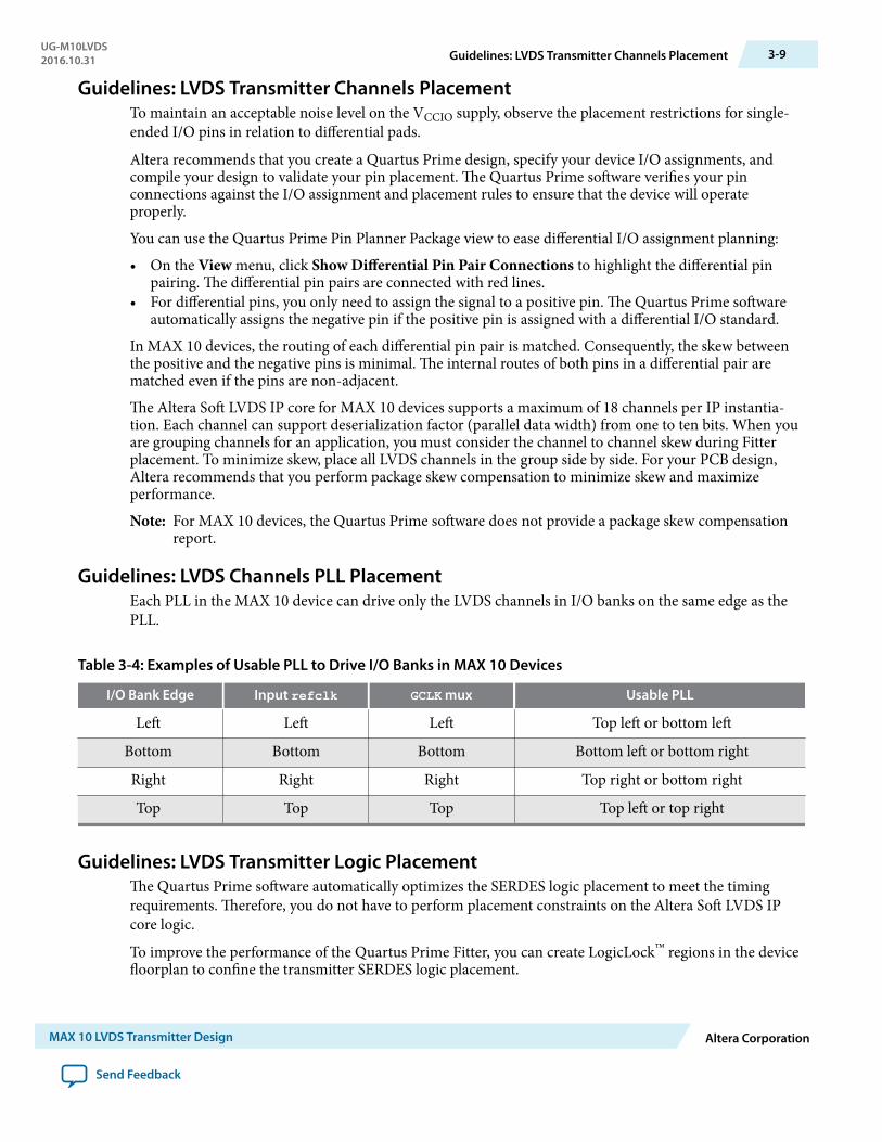
Guidelines: LVDS Transmitter Channels PlacementTo maintain an acceptable noise level on the VCCIO supply, observe the placement restrictions for single-ended I/O pins in relation to differential pads.
Altera recommends that you create a Quartus Prime design, specify your device I/O assignments, andcompile your design to validate your pin placement. The Quartus Prime software verifies your pinconnections against the I/O assignment and placement rules to ensure that the device will operateproperly.
You can use the Quartus Prime Pin Planner Package view to ease differential I/O assignment planning:
• On the View menu, click Show Differential Pin Pair Connections to highlight the differential pinpairing. The differential pin pairs are connected with red lines.
• For differential pins, you only need to assign the signal to a positive pin. The Quartus Prime softwareautomatically assigns the negative pin if the positive pin is assigned with a differential I/O standard.
In MAX 10 devices, the routing of each differential pin pair is matched. Consequently, the skew betweenthe positive and the negative pins is minimal. The internal routes of both pins in a differential pair arematched even if the pins are non-adjacent.
The Altera Soft LVDS IP core for MAX 10 devices supports a maximum of 18 channels per IP instantia‐tion. Each channel can support deserialization factor (parallel data width) from one to ten bits. When youare grouping channels for an application, you must consider the channel to channel skew during Fitterplacement. To minimize skew, place all LVDS channels in the group side by side. For your PCB design,Altera recommends that you perform package skew compensation to minimize skew and maximizeperformance.
Note: For MAX 10 devices, the Quartus Prime software does not provide a package skew compensationreport.
Guidelines: LVDS Channels PLL PlacementEach PLL in the MAX 10 device can drive only the LVDS channels in I/O banks on the same edge as thePLL.
Table 3-4: Examples of Usable PLL to Drive I/O Banks in MAX 10 Devices
I/O Bank Edge Input refclk GCLK mux Usable PLL
Left Left Left Top left or bottom left
Bottom Bottom Bottom Bottom left or bottom right
Right Right Right Top right or bottom right
Top Top Top Top left or top right
Guidelines: LVDS Transmitter Logic PlacementThe Quartus Prime software automatically optimizes the SERDES logic placement to meet the timingrequirements. Therefore, you do not have to perform placement constraints on the Altera Soft LVDS IPcore logic.
To improve the performance of the Quartus Prime Fitter, you can create LogicLock™ regions in the devicefloorplan to confine the transmitter SERDES logic placement.
UG-M10LVDS2016.10.31 Guidelines: LVDS Transmitter Channels Placement 3-9
MAX 10 LVDS Transmitter Design Altera Corporation
Send Feedback
• The TCCS parameter is guaranteed per datasheet specification to the entire bank of differential I/Osthat are located in the same side. This guarantee applies if the transmitter SERDES logic is placedwithin the LAB adjacent to the output pins.
• Constrain the transmitter SERDES logic to the LAB adjacent to the data output pins and clock outputpins to improve the TCCS performance.
Related InformationQuartus Prime Incremental Compilation for Hierarchical and Team-Based Design chapter, Volume 1:Design and Synthesis, Quartus Prime HandbookProvides step by step instructions about creating a design floorplan with LogicLock location assignments.
Guidelines: Enable LVDS Pre-Emphasis for E144 PackageFor MAX 10 devices in the E144 package, Altera recommends that you enable LVDS pre-emphasis toachieve optimum signal integrity (SI) performance. If you do not enable pre-emphasis, undesirable SIcondition may be induced in the device resulting in LVDS eye height sensitivity.
LVDS Transmitter Debug and TroubleshootingYou can obtain useful information about the LVDS interface performance with board-level verificationusing the FPGA prototype.
Although the focus of the board-level verification is to verify the FPGA functionality in your end system,you can take additional steps to examine the margins. Using oscilloscopes, you can examine the marginsto verify the predicted size of the data-valid window, and the setup and hold margins at the I/O interface.
You can also use the Altera SignalTap® II Logic Analyzer to perform system level verification to correlatethe system against your design targets.
Related InformationIn-System Debugging Using External Logic Analyzers chapter, Volume 3: Verification, Quartus PrimeHandbook
Perform RTL Simulation Before Hardware DebugBefore you debug on hardware, Altera recommends that you perform an RTL simulation. Using the RTLsimulation, you can check the code functionality before testing in real hardware.
For example, you can use the RTL simulation to verify that when you send a training pattern from aremote transmitter, the bitslipping mechanism in your LVDS receiver works.
Geometry-Based and Physics-Based I/O RulesYou need to consider the I/O placement rules related to LVDS. The Quartus Prime software generatescritical warning or error messages if the I/O placements rules are violated.
For more information, refer to the related information.
Related InformationMAX 10 General Purpose I/O User Guide
3-10 Guidelines: Enable LVDS Pre-Emphasis for E144 PackageUG-M10LVDS
2016.10.31
Altera Corporation MAX 10 LVDS Transmitter Design
Send Feedback
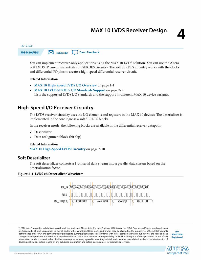
MAX 10 LVDS Receiver Design 42016.10.31
UG-M10LVDS Subscribe Send Feedback
You can implement receiver-only applications using the MAX 10 LVDS solution. You can use the AlteraSoft LVDS IP core to instantiate soft SERDES circuitry. The soft SERDES circuitry works with the clocksand differential I/O pins to create a high-speed differential receiver circuit.
Related Information
• MAX 10 High-Speed LVDS I/O Overview on page 1-1• MAX 10 LVDS SERDES I/O Standards Support on page 2-7
Lists the supported LVDS I/O standards and the support in different MAX 10 device variants.
High-Speed I/O Receiver CircuitryThe LVDS receiver circuitry uses the I/O elements and registers in the MAX 10 devices. The deserializer isimplemented in the core logic as a soft SERDES blocks.
In the receiver mode, the following blocks are available in the differential receiver datapath:
• Deserializer• Data realignment block (bit slip)
Related InformationMAX 10 High-Speed LVDS Circuitry on page 2-10
Soft DeserializerThe soft deserializer converts a 1-bit serial data stream into a parallel data stream based on thedeserialization factor.
Figure 4-1: LVDS x8 Deserializer Waveform
7 6 5 4 3 2 1 0 a b c d e f g h A B C D E F G H X X X X X X X X
ABCDEFGHabcdefgh76543210XXXXXXXX
RX_IN
FCLK
RX_OUT[9:0]
© 2016 Intel Corporation. All rights reserved. Intel, the Intel logo, Altera, Arria, Cyclone, Enpirion, MAX, Megacore, NIOS, Quartus and Stratix words and logosare trademarks of Intel Corporation in the US and/or other countries. Other marks and brands may be claimed as the property of others. Intel warrantsperformance of its FPGA and semiconductor products to current specifications in accordance with Intel's standard warranty, but reserves the right to makechanges to any products and services at any time without notice. Intel assumes no responsibility or liability arising out of the application or use of anyinformation, product, or service described herein except as expressly agreed to in writing by Intel. Intel customers are advised to obtain the latest version ofdevice specifications before relying on any published information and before placing orders for products or services.
ISO9001:2008Registered
www.altera.com101 Innovation Drive, San Jose, CA 95134
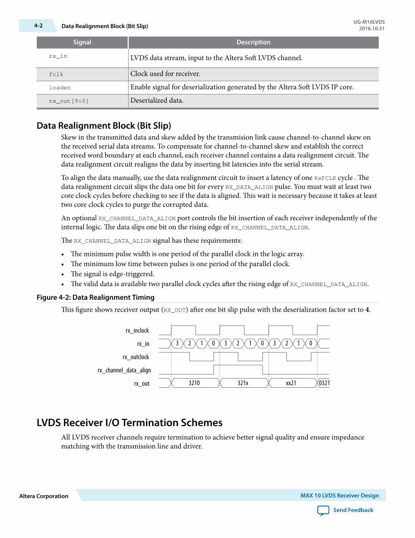
Signal Description
rx_in LVDS data stream, input to the Altera Soft LVDS channel.
fclk Clock used for receiver.
loaden Enable signal for deserialization generated by the Altera Soft LVDS IP core.
rx_out[9:0] Deserialized data.
Data Realignment Block (Bit Slip)Skew in the transmitted data and skew added by the transmision link cause channel-to-channel skew onthe received serial data streams. To compensate for channel-to-channel skew and establish the correctreceived word boundary at each channel, each receiver channel contains a data realignment circuit. Thedata realignment circuit realigns the data by inserting bit latencies into the serial stream.
To align the data manually, use the data realignment circuit to insert a latency of one RxFCLK cycle . Thedata realignment circuit slips the data one bit for every RX_DATA_ALIGN pulse. You must wait at least twocore clock cycles before checking to see if the data is aligned. This wait is necessary because it takes at leasttwo core clock cycles to purge the corrupted data.
An optional RX_CHANNEL_DATA_ALIGN port controls the bit insertion of each receiver independently of theinternal logic. The data slips one bit on the rising edge of RX_CHANNEL_DATA_ALIGN.
The RX_CHANNEL_DATA_ALIGN signal has these requirements:
• The minimum pulse width is one period of the parallel clock in the logic array.• The minimum low time between pulses is one period of the parallel clock.• The signal is edge-triggered.• The valid data is available two parallel clock cycles after the rising edge of RX_CHANNEL_DATA_ALIGN.
Figure 4-2: Data Realignment Timing
This figure shows receiver output (RX_OUT) after one bit slip pulse with the deserialization factor set to 4.
rx_inclock
rx_in
rx_outclock
rx_channel_data_align
rx_out
3 2 1 0 3 2 1 0 3 2 1 0
3210 321x xx21 0321
LVDS Receiver I/O Termination SchemesAll LVDS receiver channels require termination to achieve better signal quality and ensure impedancematching with the transmission line and driver.
4-2 Data Realignment Block (Bit Slip)UG-M10LVDS
2016.10.31
Altera Corporation MAX 10 LVDS Receiver Design
Send Feedback
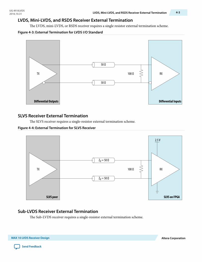
LVDS, Mini-LVDS, and RSDS Receiver External TerminationThe LVDS, mini-LVDS, or RSDS receiver requires a single resistor external termination scheme.
Figure 4-3: External Termination for LVDS I/O Standard
TX RX
Differential InputsDifferential Outputs
50 Ω
50 Ω
100 Ω
SLVS Receiver External TerminationThe SLVS receiver requires a single-resistor external termination scheme.
Figure 4-4: External Termination for SLVS Receiver
TX RX
SLVS on FPGA
2.5 V
SLVS peer
Z0 = 50 Ω
Z0 = 50 Ω
100 Ω
Sub-LVDS Receiver External TerminationThe Sub-LVDS receiver requires a single-resistor external termination scheme.
UG-M10LVDS2016.10.31 LVDS, Mini-LVDS, and RSDS Receiver External Termination 4-3
MAX 10 LVDS Receiver Design Altera Corporation
Send Feedback
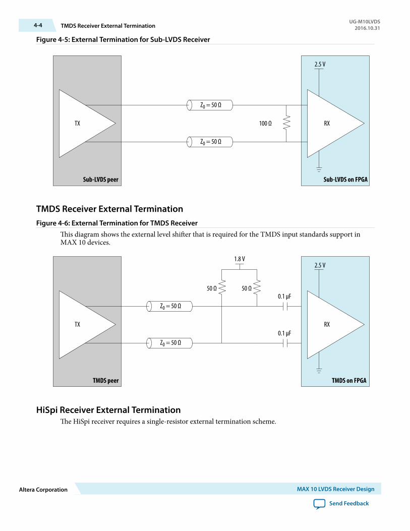
Figure 4-5: External Termination for Sub-LVDS Receiver
TX RX
Sub-LVDS on FPGA
2.5 V
Sub-LVDS peer
Z0 = 50 Ω
Z0 = 50 Ω
100 Ω
TMDS Receiver External TerminationFigure 4-6: External Termination for TMDS Receiver
This diagram shows the external level shifter that is required for the TMDS input standards support inMAX 10 devices.
TX RX
TMDS on FPGA
2.5 V1.8 V
TMDS peer
Z0 = 50 Ω
Z0 = 50 Ω
50 Ω50 Ω0.1 µF
0.1 µF
HiSpi Receiver External TerminationThe HiSpi receiver requires a single-resistor external termination scheme.
4-4 TMDS Receiver External TerminationUG-M10LVDS
2016.10.31
Altera Corporation MAX 10 LVDS Receiver Design
Send Feedback
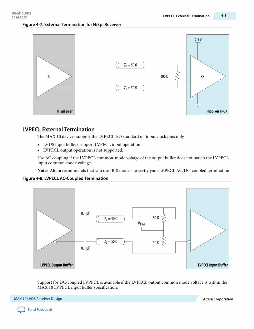
Figure 4-7: External Termination for HiSpi Receiver
TX RX
HiSpi on FPGA
2.5 V
HiSpi peer
Z0 = 50 Ω
Z0 = 50 Ω
100 Ω
LVPECL External TerminationThe MAX 10 devices support the LVPECL I/O standard on input clock pins only.
• LVDS input buffers support LVPECL input operation.• LVPECL output operation is not supported.
Use AC coupling if the LVPECL common-mode voltage of the output buffer does not match the LVPECLinput common-mode voltage.
Note: Altera recommends that you use IBIS models to verify your LVPECL AC/DC-coupled termination.
Figure 4-8: LVPECL AC-Coupled Termination
LVPECL Input BufferLVPECL Output Buffer
0.1 µF
0.1 µFZ0 = 50 Ω
Z0 = 50 ΩVICM
50 Ω
50 Ω
Support for DC-coupled LVPECL is available if the LVPECL output common mode voltage is within theMAX 10 LVPECL input buffer specification.
UG-M10LVDS2016.10.31 LVPECL External Termination 4-5
MAX 10 LVDS Receiver Design Altera Corporation
Send Feedback
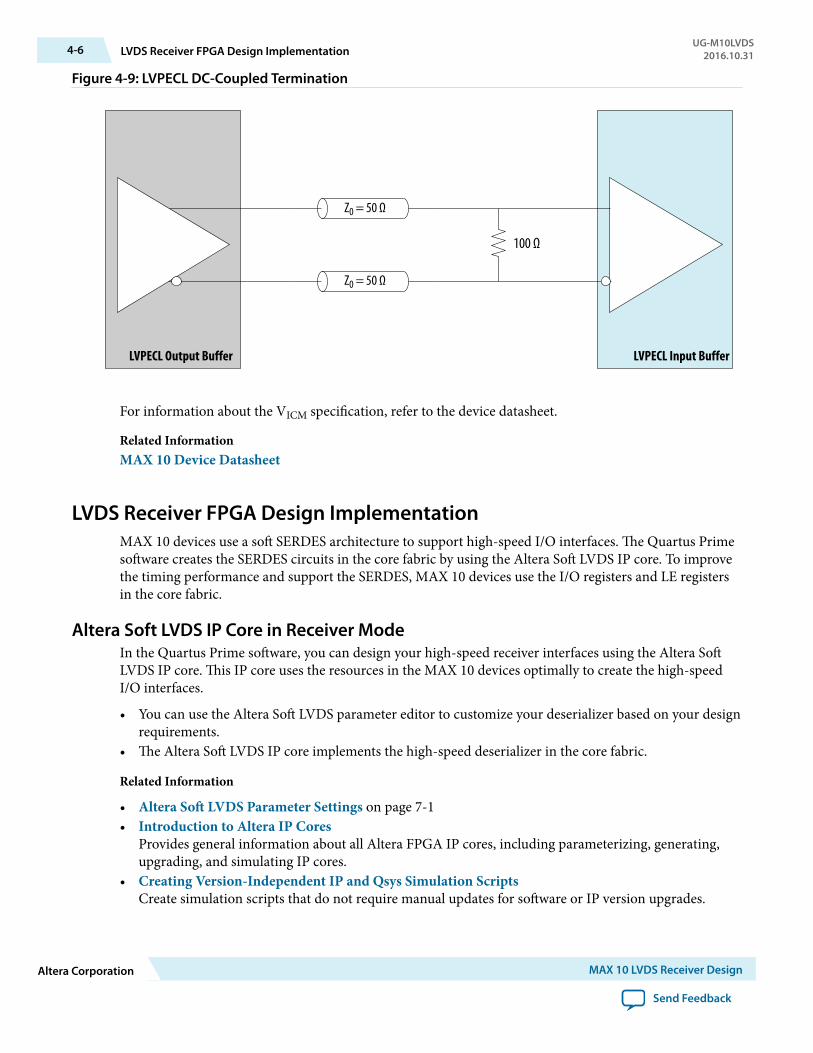
Figure 4-9: LVPECL DC-Coupled Termination
LVPECL Input BufferLVPECL Output Buffer
Z0 = 50 Ω
Z0 = 50 Ω
100 Ω
For information about the VICM specification, refer to the device datasheet.
Related InformationMAX 10 Device Datasheet
LVDS Receiver FPGA Design ImplementationMAX 10 devices use a soft SERDES architecture to support high-speed I/O interfaces. The Quartus Primesoftware creates the SERDES circuits in the core fabric by using the Altera Soft LVDS IP core. To improvethe timing performance and support the SERDES, MAX 10 devices use the I/O registers and LE registersin the core fabric.
Altera Soft LVDS IP Core in Receiver ModeIn the Quartus Prime software, you can design your high-speed receiver interfaces using the Altera SoftLVDS IP core. This IP core uses the resources in the MAX 10 devices optimally to create the high-speedI/O interfaces.
• You can use the Altera Soft LVDS parameter editor to customize your deserializer based on your designrequirements.
• The Altera Soft LVDS IP core implements the high-speed deserializer in the core fabric.
Related Information
• Altera Soft LVDS Parameter Settings on page 7-1• Introduction to Altera IP Cores
Provides general information about all Altera FPGA IP cores, including parameterizing, generating,upgrading, and simulating IP cores.
• Creating Version-Independent IP and Qsys Simulation ScriptsCreate simulation scripts that do not require manual updates for software or IP version upgrades.
4-6 LVDS Receiver FPGA Design ImplementationUG-M10LVDS
2016.10.31
Altera Corporation MAX 10 LVDS Receiver Design
Send Feedback
• Project Management Best PracticesGuidelines for efficient management and portability of your project and IP files.
PLL Source Selection for Altera Soft LVDS IP CoreYou can create the LVDS interface components by instantiating the Altera Soft LVDS IP core with aninternal or external PLL.
Instantiate Altera Soft LVDS IP Core with Internal PLLYou can set the Altera Soft LVDS IP core to build the SERDES components and instantiate the PLLinternally.
• To use this method, turn off the Use external PLL option in the PLL Settings tab.• The Altera Soft LVDS IP core integrates the PLL into the LVDS block.• The drawback of this method is that you can use the PLL only for the particular LVDS instance.
Instantiate Altera Soft LVDS IP Core with External PLLYou can set the Altera Soft LVDS IP core to build only the SERDES components but use an external PLLsource.
• To use this method, turn on the Use external PLL option in the PLL Settings tab.• Follow the required clock setting to the input ports as listed in the notification panel.• You can create your own clocking source using the ALTPLL IP core.• Use this method to optimize PLL usage with other functions in the core.
Related Information
• MAX 10 Clocking and PLL User GuideProvides more information about the PLL and the PLL output counters.
• MAX 10 Clocking and PLL User GuideProvides more information about the PLL and the PLL output counters.
Guidelines: LVDS RX Interface Using External PLLYou can instantiate the Altera Soft LVDS IP core with the Use External PLL option. Using external PLL,you can control the PLL settings. For example, you can dynamically reconfigure the PLL to supportdifferent data rates and dynamic phase shifts. To use this option, you must instantiate the ALTPLL IP coreto generate the various clock signals.
If you turn on the Use External PLL option for the Altera Soft LVDS receiver, you require the followingsignals from the ALTPLL IP core:
• Serial clock input to the rx_inclock port of the Altera Soft LVDS receiver.• Parallel clock used to clock the receiver FPGA fabric logic.• The locked signal for Altera Soft LVDS PLL reset port.
Related InformationMAX 10 Clocking and PLL User GuideProvides more information about the PLL and the PLL output counters.
ALTPLL Signal Interface with Altera Soft LVDS ReceiverYou can choose any of the PLL output clock ports to generate the LVDS interface clocks.
UG-M10LVDS2016.10.31 PLL Source Selection for Altera Soft LVDS IP Core 4-7
MAX 10 LVDS Receiver Design Altera Corporation
Send Feedback
If you use the ALTPLL IP core as the external PLL source of the Altera Soft LVDS receiver, use the source-synchronous compensation mode.
Table 4-1: Example: Signal Interface Between ALTPLL and Altera Soft LVDS Receiver with EvenDeserialization Factor
From the ALTPLL IP Core To the Altera Soft LVDS Receiver
Fast clock output (c0)
The serial clock output (c0) can onlydrive rx_inclock on the Altera SoftLVDS receiver.
rx_inclock
Slow clock output (c1) rx_syncclock
Table 4-2: Example: Signal Interface Between ALTPLL and Altera Soft LVDS Receiver with OddDeserialization Factor
From the ALTPLL IP Core To the Altera Soft LVDS Receiver
Fast clock output (c0)
The serial clock output (c0) can onlydrive rx_inclock on the Altera SoftLVDS receiver.
rx_inclock
Slow clock output (c1) rx_syncclock
Read clock (c2) output from the PLL rx_readclock
(clock input port for reading operation from RAM buffer and readcounter)
Determining External PLL Clock Parameters for Altera Soft LVDS Receiver
To determine the ALTPLL IP core clock parameter for the Altera Soft LVDS IP core receiver, follow thesesteps in your design:
1. Instantiate the Altera Soft LVDS IP core receiver using internal PLL.2. Compile the design up to TimeQuest timing analysis.3. In the Table of Contents section of the Compilation Report window, navigate to TimeQuest Timing
Analyzer > Clocks.4. Note the clock parameters used by the internal PLL for the Altera Soft LVDS IP core receiver.
In the list of clocks, clk[0] is the fast clock, clk[1] is the slow clock, and clk[2] is the read clock.
4-8 Determining External PLL Clock Parameters for Altera Soft LVDS ReceiverUG-M10LVDS
2016.10.31
Altera Corporation MAX 10 LVDS Receiver Design
Send Feedback
Figure 4-10: Clock Parameters Example for Altera Soft LVDS Receiver
Configure the ALTPLL output clocks with the parameters you noted in this procedure and connect theclock outputs to the correct Altera Soft LVDS clock input ports.
Initializing the Altera Soft LVDS IP CoreThe PLL locks to the reference clock before the Altera Soft LVDS IP core implements the SERDES blocksfor data transfer.
During device initialization the PLL starts to lock to the reference clock and becomes operational when itachieves lock during user mode. If the clock reference is not stable, it corrupts the phase shifts of the PLLoutput clock. This phase shifts corruption can cause failure and corrupt data transfer between the high-speed LVDS domain and the low-speed parallel domain.
To avoid data corruption, follow these steps when initializing the Altera Soft LVDS IP core:
1. Assert the pll_areset signal for at least 10 ns.2. After at least 10 ns, deassert the pll_areset signal.3. Wait until the PLL lock becomes stable.
After the PLL lock port asserts and is stable, the SERDES blocks are ready for operation.
High-Speed I/O Timing BudgetThe LVDS I/O standard enables high-speed transmission of data that results in better overall systemperformance. To take advantage of fast system performance, you must analyze the timing for high-speedsignals. Timing analysis for the differential block is different than traditional synchronous timing analysistechniques.
The basis of the source synchronous timing analysis is the skew between the data and the clock signalsinstead of the clock-to-output setup times. High-speed differential data transmission requires the use oftiming parameters provided by IC vendors and is strongly influenced by board skew, cable skew, and clockjitter.
Receiver Input Skew MarginUse RSKM, TCCS, and sampling window (SW) specifications for high-speed source-synchronousdifferential signals in the receiver data path.
Related InformationGuidelines: Control Channel-to-Channel Skew on page 6-1
UG-M10LVDS2016.10.31 Initializing the Altera Soft LVDS IP Core 4-9
MAX 10 LVDS Receiver Design Altera Corporation
Send Feedback
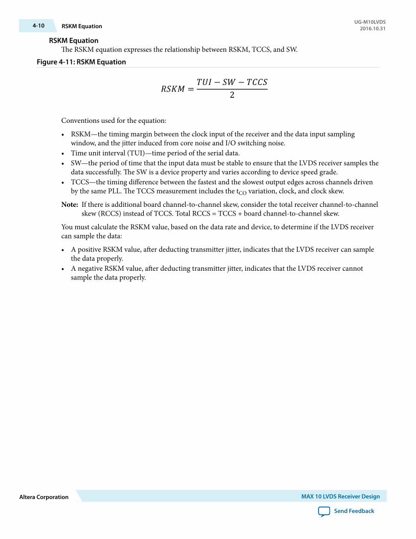
RSKM EquationThe RSKM equation expresses the relationship between RSKM, TCCS, and SW.
Figure 4-11: RSKM Equation
Conventions used for the equation:
• RSKM—the timing margin between the clock input of the receiver and the data input samplingwindow, and the jitter induced from core noise and I/O switching noise.
• Time unit interval (TUI)—time period of the serial data.• SW—the period of time that the input data must be stable to ensure that the LVDS receiver samples the
data successfully. The SW is a device property and varies according to device speed grade.• TCCS—the timing difference between the fastest and the slowest output edges across channels driven
by the same PLL. The TCCS measurement includes the tCO variation, clock, and clock skew.
Note: If there is additional board channel-to-channel skew, consider the total receiver channel-to-channelskew (RCCS) instead of TCCS. Total RCCS = TCCS + board channel-to-channel skew.
You must calculate the RSKM value, based on the data rate and device, to determine if the LVDS receivercan sample the data:
• A positive RSKM value, after deducting transmitter jitter, indicates that the LVDS receiver can samplethe data properly.
• A negative RSKM value, after deducting transmitter jitter, indicates that the LVDS receiver cannotsample the data properly.
4-10 RSKM EquationUG-M10LVDS
2016.10.31
Altera Corporation MAX 10 LVDS Receiver Design
Send Feedback
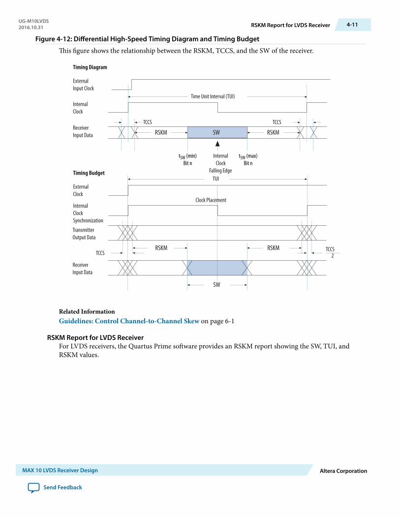
Figure 4-12: Differential High-Speed Timing Diagram and Timing Budget
This figure shows the relationship between the RSKM, TCCS, and the SW of the receiver.
TUI
Time Unit Interval (TUI)
TCCS
InternalClock
Falling Edge
tSW (min)Bit n
tSW (max)Bit n
TCCSTCCS
2
ReceiverInput Data
TransmitterOutput Data
InternalClockSynchronization
ExternalClock
ReceiverInput Data
InternalClock
ExternalInput Clock
Timing Budget
Timing Diagram
Clock Placement
SW
TCCS
RSKM RSKM
SW
RSKM RSKM
Related InformationGuidelines: Control Channel-to-Channel Skew on page 6-1
RSKM Report for LVDS ReceiverFor LVDS receivers, the Quartus Prime software provides an RSKM report showing the SW, TUI, andRSKM values.
UG-M10LVDS2016.10.31 RSKM Report for LVDS Receiver 4-11
MAX 10 LVDS Receiver Design Altera Corporation
Send Feedback
• To generate the RSKM report, run the report_RSKM command in the TimeQuest Timing Analyzer.The RSKM report is available in the TimeQuest Timing Analyzer section of the Quartus Primecompilation report.
• To obtain a more realistic RSKM value, assign the input delay to the LVDS receiver through theconstraints menu of the TimeQuest Timing Analyzer. The input delay is determined according to thedata arrival time at the LVDS receiver port, with respect to the reference clock.
• If you set the input delay in the settings parameters for the Set Input Delay option, set the clock nameto the clock that references the source-synchronous clock that feeds the LVDS receiver.
• If you do not set any input delay in the TimeQuest Timing Analyzer, the receiver channel-to-channelskew defaults to zero.
• You can also directly set the input delay in a Synopsys Design Constraint file (.sdc) by using theset_input_delay command.
Related InformationGuidelines: Control Channel-to-Channel Skew on page 6-1
Assigning Input Delay to LVDS Receiver Using TimeQuest Timing Analyzer
To obtain the RSKM value, assign an appropriate input delay to the LVDS receiver from the TimeQuestTiming Analyzer constraints menu.
1. On the menu in the TimeQuest Timing Analyzer, select Constraints > Set Input Delay.2. In the Set Input Delay window, select the desired clock using the pull-down menu. The clock name
must reference the source synchronous clock that feeds the LVDS receiver.3. Click the Browse button (next to the Targets field).4. In the Name Finder window, click List to view a list of all available ports. Select the LVDS receiver
serial input ports according to the input delay you set, and click OK.5. In the Set Input Delay window, set the appropriate values in the Input delay options and Delay value
fields.6. Click Run to incorporate these values in the TimeQuest Timing Analyzer.7. Repeat from step 1 to assign the appropriate delay for all the LVDS receiver input ports. If you have
already assigned Input Delay and you need to add more delay to that input port, turn on the AddDelay option.
Related InformationGuidelines: Control Channel-to-Channel Skew on page 6-1
Example: RSKM CalculationThis example shows the RSKM calculation for FPGA devices at 1 Gbps data rate with a 200 ps boardchannel-to-channel skew.
• TCCS = 100 ps• SW = 300 ps• TUI = 1000 ps• Total RCCS = TCCS + Board channel-to-channel skew = 100 ps + 200 ps = 300 ps• RSKM = (TUI – SW – RCCS) / 2 = (1000 ps – 300 ps – 300 ps) / 2 = 200 ps
If the RSKM is greater than 0 ps after deducting transmitter jitter, the receiver will work correctly.
4-12 Assigning Input Delay to LVDS Receiver Using TimeQuest Timing AnalyzerUG-M10LVDS
2016.10.31
Altera Corporation MAX 10 LVDS Receiver Design
Send Feedback
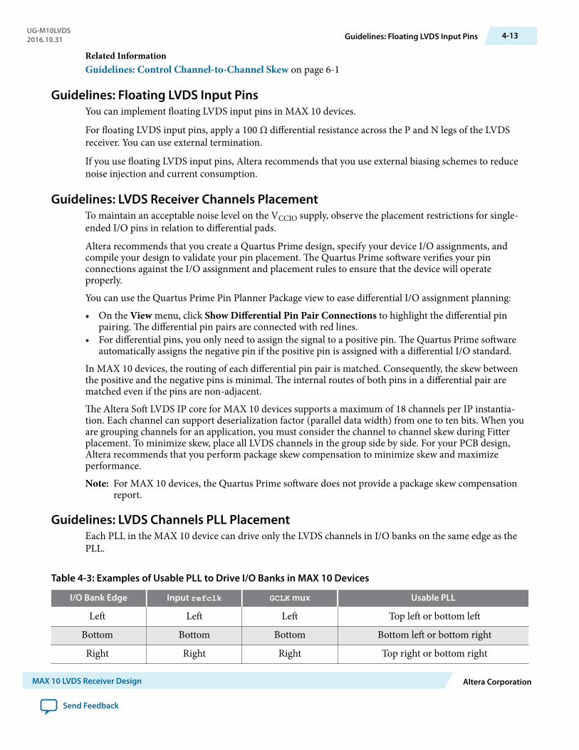
Related InformationGuidelines: Control Channel-to-Channel Skew on page 6-1
Guidelines: Floating LVDS Input PinsYou can implement floating LVDS input pins in MAX 10 devices.
For floating LVDS input pins, apply a 100 Ω differential resistance across the P and N legs of the LVDSreceiver. You can use external termination.
If you use floating LVDS input pins, Altera recommends that you use external biasing schemes to reducenoise injection and current consumption.
Guidelines: LVDS Receiver Channels PlacementTo maintain an acceptable noise level on the VCCIO supply, observe the placement restrictions for single-ended I/O pins in relation to differential pads.
Altera recommends that you create a Quartus Prime design, specify your device I/O assignments, andcompile your design to validate your pin placement. The Quartus Prime software verifies your pinconnections against the I/O assignment and placement rules to ensure that the device will operateproperly.
You can use the Quartus Prime Pin Planner Package view to ease differential I/O assignment planning:
• On the View menu, click Show Differential Pin Pair Connections to highlight the differential pinpairing. The differential pin pairs are connected with red lines.
• For differential pins, you only need to assign the signal to a positive pin. The Quartus Prime softwareautomatically assigns the negative pin if the positive pin is assigned with a differential I/O standard.
In MAX 10 devices, the routing of each differential pin pair is matched. Consequently, the skew betweenthe positive and the negative pins is minimal. The internal routes of both pins in a differential pair arematched even if the pins are non-adjacent.
The Altera Soft LVDS IP core for MAX 10 devices supports a maximum of 18 channels per IP instantia‐tion. Each channel can support deserialization factor (parallel data width) from one to ten bits. When youare grouping channels for an application, you must consider the channel to channel skew during Fitterplacement. To minimize skew, place all LVDS channels in the group side by side. For your PCB design,Altera recommends that you perform package skew compensation to minimize skew and maximizeperformance.
Note: For MAX 10 devices, the Quartus Prime software does not provide a package skew compensationreport.
Guidelines: LVDS Channels PLL PlacementEach PLL in the MAX 10 device can drive only the LVDS channels in I/O banks on the same edge as thePLL.
Table 4-3: Examples of Usable PLL to Drive I/O Banks in MAX 10 Devices
I/O Bank Edge Input refclk GCLK mux Usable PLL
Left Left Left Top left or bottom left
Bottom Bottom Bottom Bottom left or bottom right
Right Right Right Top right or bottom right
UG-M10LVDS2016.10.31 Guidelines: Floating LVDS Input Pins 4-13
MAX 10 LVDS Receiver Design Altera Corporation
Send Feedback
I/O Bank Edge Input refclk GCLK mux Usable PLL
Top Top Top Top left or top right
Guidelines: LVDS Receiver Logic PlacementThe Quartus Prime software automatically optimizes the SERDES logic placement to meet the timingrequirements. Therefore, you do not have to perform placement constraints on the Altera Soft LVDS IPcore logic.
To improve the performance of the Quartus Prime Fitter, you can create LogicLock regions in the devicefloorplan to confine the transmitter SERDES logic placement.
• The TCCS parameter is guaranteed per datasheet specification to the entire bank of differential I/Osthat are located in the same side. This guarantee applies if the transmitter SERDES logic is placedwithin the LAB adjacent to the output pins.
• Constrain the transmitter SERDES logic to the LAB adjacent to the data output pins and clock outputpins to improve the TCCS performance.
Guidelines: LVDS Receiver Timing ConstraintsFor receiver designs that uses the core logic to implement the SERDES circuits, you must set proper timingconstraints.
For LVDS receiver data paths where the PLL operation is in source-synchronous compensation mode, theQuartus Prime compiler automatically ensures that the associated delay chain settings are set correctly.
However, if the input clock and data at the receiver are not edge- or center-aligned, it may be necessary foryou to set the timing constraints in the Quartus Prime TimeQuest Timing Analyzer. The timingconstraints specify the timing requirements necessary to ensure reliable data capture.
LVDS Receiver Debug and TroubleshootingYou can obtain useful information about the LVDS interface performance with board-level verificationusing the FPGA prototype.
Although the focus of the board-level verification is to verify the FPGA functionality in your end system,you can take additional steps to examine the margins. Using oscilloscopes, you can examine the marginsto verify the predicted size of the data-valid window, and the setup and hold margins at the I/O interface.
You can also use the Altera SignalTap II Logic Analyzer to perform system level verification to correlatethe system against your design targets.
Perform RTL Simulation Before Hardware DebugBefore you debug on hardware, Altera recommends that you perform an RTL simulation. Using the RTLsimulation, you can check the code functionality before testing in real hardware.
For example, you can use the RTL simulation to verify that when you send a training pattern from aremote transmitter, the bitslipping mechanism in your LVDS receiver works.
Geometry-Based and Physics-Based I/O RulesYou need to consider the I/O placement rules related to LVDS. The Quartus Prime software generatescritical warning or error messages if the I/O placements rules are violated.
4-14 Guidelines: LVDS Receiver Logic PlacementUG-M10LVDS
2016.10.31
Altera Corporation MAX 10 LVDS Receiver Design
Send Feedback

For more information, refer to the related information.
Related InformationMAX 10 General Purpose I/O User Guide
UG-M10LVDS2016.10.31 Geometry-Based and Physics-Based I/O Rules 4-15
MAX 10 LVDS Receiver Design Altera Corporation
Send Feedback
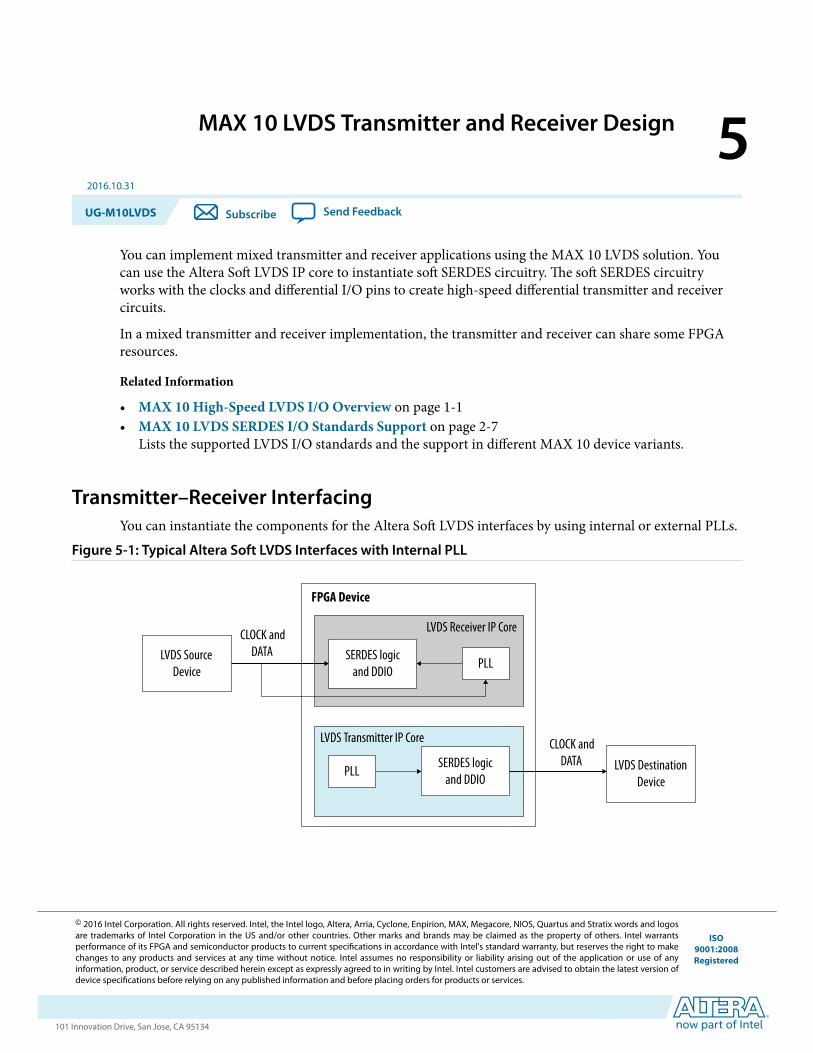
MAX 10 LVDS Transmitter and Receiver Design 52016.10.31
UG-M10LVDS Subscribe Send Feedback
You can implement mixed transmitter and receiver applications using the MAX 10 LVDS solution. Youcan use the Altera Soft LVDS IP core to instantiate soft SERDES circuitry. The soft SERDES circuitryworks with the clocks and differential I/O pins to create high-speed differential transmitter and receivercircuits.
In a mixed transmitter and receiver implementation, the transmitter and receiver can share some FPGAresources.
Related Information
• MAX 10 High-Speed LVDS I/O Overview on page 1-1• MAX 10 LVDS SERDES I/O Standards Support on page 2-7
Lists the supported LVDS I/O standards and the support in different MAX 10 device variants.
Transmitter–Receiver InterfacingYou can instantiate the components for the Altera Soft LVDS interfaces by using internal or external PLLs.
Figure 5-1: Typical Altera Soft LVDS Interfaces with Internal PLL
SERDES logicand DDIO
SERDES logicand DDIO
PLL
PLL
LVDS DestinationDevice
LVDS SourceDevice
LVDS Receiver IP Core
LVDS Transmitter IP Core
FPGA Device
CLOCK andDATA
CLOCK andDATA
© 2016 Intel Corporation. All rights reserved. Intel, the Intel logo, Altera, Arria, Cyclone, Enpirion, MAX, Megacore, NIOS, Quartus and Stratix words and logosare trademarks of Intel Corporation in the US and/or other countries. Other marks and brands may be claimed as the property of others. Intel warrantsperformance of its FPGA and semiconductor products to current specifications in accordance with Intel's standard warranty, but reserves the right to makechanges to any products and services at any time without notice. Intel assumes no responsibility or liability arising out of the application or use of anyinformation, product, or service described herein except as expressly agreed to in writing by Intel. Intel customers are advised to obtain the latest version ofdevice specifications before relying on any published information and before placing orders for products or services.
ISO9001:2008Registered
www.altera.com101 Innovation Drive, San Jose, CA 95134
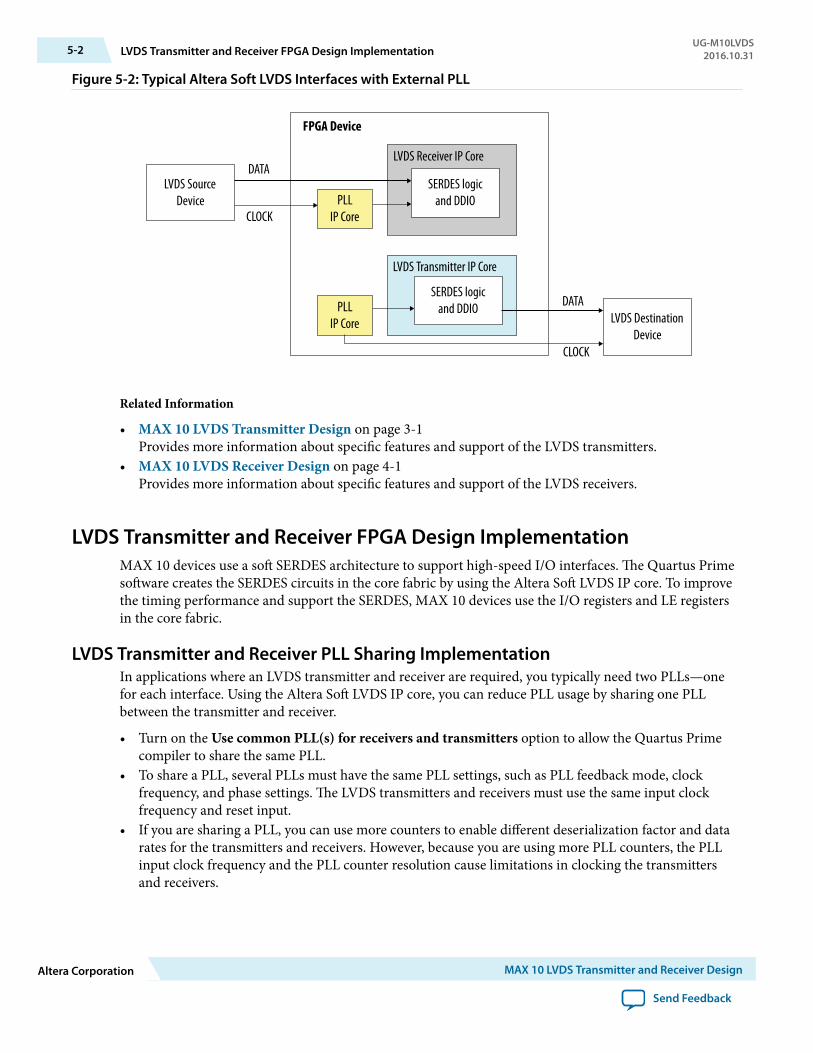
Figure 5-2: Typical Altera Soft LVDS Interfaces with External PLL
SERDES logicand DDIO
SERDES logicand DDIO
LVDS DestinationDevice
LVDS SourceDevice
LVDS Receiver IP Core
LVDS Transmitter IP Core
FPGA Device
DATA
DATAPLLIP Core
PLLIP CoreCLOCK
CLOCK
Related Information
• MAX 10 LVDS Transmitter Design on page 3-1Provides more information about specific features and support of the LVDS transmitters.
• MAX 10 LVDS Receiver Design on page 4-1Provides more information about specific features and support of the LVDS receivers.
LVDS Transmitter and Receiver FPGA Design ImplementationMAX 10 devices use a soft SERDES architecture to support high-speed I/O interfaces. The Quartus Primesoftware creates the SERDES circuits in the core fabric by using the Altera Soft LVDS IP core. To improvethe timing performance and support the SERDES, MAX 10 devices use the I/O registers and LE registersin the core fabric.
LVDS Transmitter and Receiver PLL Sharing ImplementationIn applications where an LVDS transmitter and receiver are required, you typically need two PLLs—onefor each interface. Using the Altera Soft LVDS IP core, you can reduce PLL usage by sharing one PLLbetween the transmitter and receiver.
• Turn on the Use common PLL(s) for receivers and transmitters option to allow the Quartus Primecompiler to share the same PLL.
• To share a PLL, several PLLs must have the same PLL settings, such as PLL feedback mode, clockfrequency, and phase settings. The LVDS transmitters and receivers must use the same input clockfrequency and reset input.
• If you are sharing a PLL, you can use more counters to enable different deserialization factor and datarates for the transmitters and receivers. However, because you are using more PLL counters, the PLLinput clock frequency and the PLL counter resolution cause limitations in clocking the transmittersand receivers.
5-2 LVDS Transmitter and Receiver FPGA Design ImplementationUG-M10LVDS
2016.10.31
Altera Corporation MAX 10 LVDS Transmitter and Receiver Design
Send Feedback
Note: The number of PLLs available differs among MAX 10 packages. Altera recommends that you selecta MAX 10 device package that provides sufficient number of PLL clockouts for your design.
Initializing the Altera Soft LVDS IP CoreThe PLL locks to the reference clock before the Altera Soft LVDS IP core implements the SERDES blocksfor data transfer.
During device initialization the PLL starts to lock to the reference clock and becomes operational when itachieves lock during user mode. If the clock reference is not stable, it corrupts the phase shifts of the PLLoutput clock. This phase shifts corruption can cause failure and corrupt data transfer between the high-speed LVDS domain and the low-speed parallel domain.
To avoid data corruption, follow these steps when initializing the Altera Soft LVDS IP core:
1. Assert the pll_areset signal for at least 10 ns.2. After at least 10 ns, deassert the pll_areset signal.3. Wait until the PLL lock becomes stable.
After the PLL lock port asserts and is stable, the SERDES blocks are ready for operation.
LVDS Transmitter and Receiver Debug and TroubleshootingYou can obtain useful information about the LVDS interface performance with board-level verificationusing the FPGA prototype.
Although the focus of the board-level verification is to verify the FPGA functionality in your end system,you can take additional steps to examine the margins. Using oscilloscopes, you can examine the marginsto verify the predicted size of the data-valid window, and the setup and hold margins at the I/O interface.
You can also use the Altera SignalTap II Logic Analyzer to perform system level verification to correlatethe system against your design targets.
Perform RTL Simulation Before Hardware DebugBefore you debug on hardware, Altera recommends that you perform an RTL simulation. Using the RTLsimulation, you can check the code functionality before testing in real hardware.
For example, you can use the RTL simulation to verify that when you send a training pattern from aremote transmitter, the bitslipping mechanism in your LVDS receiver works.
Geometry-Based and Physics-Based I/O RulesYou need to consider the I/O placement rules related to LVDS. The Quartus Prime software generatescritical warning or error messages if the I/O placements rules are violated.
For more information, refer to the related information.
Related InformationMAX 10 General Purpose I/O User Guide
UG-M10LVDS2016.10.31 Initializing the Altera Soft LVDS IP Core 5-3
MAX 10 LVDS Transmitter and Receiver Design Altera Corporation
Send Feedback
MAX 10 High-Speed LVDS Board DesignConsiderations 6
2016.10.31
UG-M10LVDS Subscribe Send Feedback
To achieve optimal performance from the MAX 10 device, you must consider critical issues such asimpedance of traces and connectors, differential routing, and termination techniques.
Guidelines: Improve Signal QualityTo improve signal quality, follow these board design guidelines:
• Base your board designs on controlled differential impedance. Calculate and compare all parameterssuch as trace width, trace thickness, and the distance between two differential traces.
• Maintain equal distance between traces in differential I/O standard pairs as much as possible. Routingthe pair of traces close to each other maximizes the common-mode rejection ratio (CMRR).
• Keep the traces as short as possible to limit signal integrity issues. Longer traces have more inductanceand capacitance.
• Place termination resistors as close to receiver input pins as possible.• Use surface mount components.• Avoid 90° corners on board traces.• Use high-performance connectors.• Design backplane and card traces so that trace impedance matches the impedance of the connector and
termination.• Keep an equal number of vias for both signal traces.• Create equal trace lengths to avoid skew between signals. Unequal trace lengths result in misplaced
crossing points and decrease system margins as the transmitter-channel-to-channel skew (TCCS) valueincreases.
• Limit vias because they cause discontinuities.• Keep toggling single-ended I/O signals away from differential signals to avoid possible noise coupling.• Do not route single-ended I/O clock signals to layers adjacent to differential signals.• Analyze system-level signals.
Guidelines: Control Channel-to-Channel SkewFor the MAX 10 devices, perform PCB trace compensation to adjust the trace length of each LVDSchannel. Adjusting the trace length improves the channel-to-channel skew when interfacing withreceivers.
© 2016 Intel Corporation. All rights reserved. Intel, the Intel logo, Altera, Arria, Cyclone, Enpirion, MAX, Megacore, NIOS, Quartus and Stratix words and logosare trademarks of Intel Corporation in the US and/or other countries. Other marks and brands may be claimed as the property of others. Intel warrantsperformance of its FPGA and semiconductor products to current specifications in accordance with Intel's standard warranty, but reserves the right to makechanges to any products and services at any time without notice. Intel assumes no responsibility or liability arising out of the application or use of anyinformation, product, or service described herein except as expressly agreed to in writing by Intel. Intel customers are advised to obtain the latest version ofdevice specifications before relying on any published information and before placing orders for products or services.
ISO9001:2008Registered
www.altera.com101 Innovation Drive, San Jose, CA 95134
At the package level, you must control the LVDS I/O skew for each I/O bank and each side of the device. Ifyou plan to vertically migrate from one device to another using the same board design, you must controlthe package migration skew for each migratable LVDS I/O pin.
For information about controlling the LVDS I/O and package skew, refer to the related information.
Related Information
• Receiver Input Skew Margin on page 4-9• RSKM Equation on page 4-10
Explains the relationship between the RSKM, TCCS, and SW.• RSKM Report for LVDS Receiver on page 4-11
Provides guidelines to generate RSKM report with realistic RSKM value.• Assigning Input Delay to LVDS Receiver Using TimeQuest Timing Analyzer on page 4-12
Provides the procedure to assign input delay in TimeQuest Timing Analyzer to obtain RSKM value.• Example: RSKM Calculation on page 4-12
Guidelines: Determine Board Design ConstraintsAfter you have closed timing for your FPGA design, examine your board design to determine the differentfactors that can impact signal integrity. These factors affect overall timing at the receiving device in theLVDS interface.
The time margin for the LVDS receiver (indicated by the RSKM value) is the timing budget allocation forboard level effects such as:
• Skew—these factors cause board-level skew:
• Board trace lengths• Connectors usage• Parasitic circuits variations
• Jitter—jitter effects are derived from factors such as crosstalk.• Noise—on board resources with imperfect power supplies and reference planes may also cause noise.
To ensure successful operation of the Altera Soft LVDS IP core receiver, do not exceed the timing budget.
Related InformationBoard Design Guidelines Solution CenterProvides resources related to board design for Altera devices.
Guidelines: Perform Board Level SimulationsAfter you determined the system requirements and finalized the board design constraints, use anelectronic design automation (EDA) simulation tool to perform board-level simulations. Use the IBIS orHSPICE models of the FPGA and the target LVDS device for the simulation.
The board-level simulation ensures optimum board setup where you can determine if the data windowconforms to the input specification (electrical and timing) of the LVDS receiver.
6-2 Guidelines: Determine Board Design ConstraintsUG-M10LVDS
2016.10.31
Altera Corporation MAX 10 High-Speed LVDS Board Design Considerations
Send Feedback

You can use the programmable pre-emphasis feature on the true LVDS output buffers, for example, tocompensate for the frequency-dependent attenuation of the transmission line. With this feature, you canmaximize the data eye opening at the far end receiver especially on long transmission lines.
Related Information
• Altera IBIS ModelsProvides IBIS models of Altera devices for download.
• Altera HSPICE ModelsProvides SPICE models of Altera devices for download.
• IBIS Model GenerationProvides video that demonstrates how to generate IBIS file using the Quartus Prime software.
UG-M10LVDS2016.10.31 Guidelines: Perform Board Level Simulations 6-3
MAX 10 High-Speed LVDS Board Design Considerations Altera Corporation
Send Feedback
Altera Soft LVDS IP Core References 72016.10.31
UG-M10LVDS Subscribe Send Feedback
You can set various parameter settings for the Altera Soft LVDS IP core to customize its behaviors, ports,and signals.
The Quartus Prime software generates your customized Altera Soft LVDS IP core according to theparameter options that you set in the parameter editor.
Related Information
• MAX 10 High-Speed LVDS I/O Overview on page 1-1• MAX 10 LVDS SERDES I/O Standards Support on page 2-7
Lists the supported LVDS I/O standards and the support in different MAX 10 device variants.
Altera Soft LVDS Parameter SettingsThere are four groups of options: General , PLL Settings , Receiver Settings , and Transmitter Settings
Table 7-1: Altera Soft LVDS Parameters - General
Parameter Condition AllowedValues
Description
Power SupplyMode
— • DualSupply
• SingleSupply
Specifies whether the target device is asingle or dual supply device.
Functional mode — • RX• TX
Specifies the functional mode for the AlteraSoft LVDS IP core:
• RX—specifies the IP is an LVDSreceiver.
• TX—specifies the IP is an LVDStransmitter.
Number ofchannels
— 1–18 Specifies the number of LVDS channels.
© 2016 Intel Corporation. All rights reserved. Intel, the Intel logo, Altera, Arria, Cyclone, Enpirion, MAX, Megacore, NIOS, Quartus and Stratix words and logosare trademarks of Intel Corporation in the US and/or other countries. Other marks and brands may be claimed as the property of others. Intel warrantsperformance of its FPGA and semiconductor products to current specifications in accordance with Intel's standard warranty, but reserves the right to makechanges to any products and services at any time without notice. Intel assumes no responsibility or liability arising out of the application or use of anyinformation, product, or service described herein except as expressly agreed to in writing by Intel. Intel customers are advised to obtain the latest version ofdevice specifications before relying on any published information and before placing orders for products or services.
ISO9001:2008Registered
www.altera.com101 Innovation Drive, San Jose, CA 95134
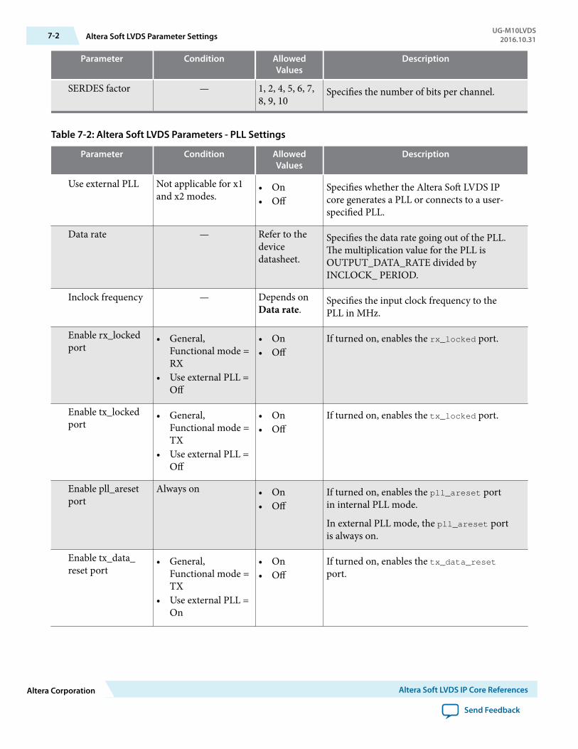
Parameter Condition AllowedValues
Description
SERDES factor — 1, 2, 4, 5, 6, 7,8, 9, 10
Specifies the number of bits per channel.
Table 7-2: Altera Soft LVDS Parameters - PLL Settings
Parameter Condition AllowedValues
Description
Use external PLL Not applicable for x1and x2 modes.
• On• Off
Specifies whether the Altera Soft LVDS IPcore generates a PLL or connects to a user-specified PLL.
Data rate — Refer to thedevicedatasheet.
Specifies the data rate going out of the PLL.The multiplication value for the PLL isOUTPUT_DATA_RATE divided byINCLOCK_ PERIOD.
Inclock frequency — Depends onData rate.
Specifies the input clock frequency to thePLL in MHz.
Enable rx_lockedport
• General,Functional mode =RX
• Use external PLL =Off
• On• Off
If turned on, enables the rx_locked port.
Enable tx_lockedport
• General,Functional mode =TX
• Use external PLL =Off
• On• Off
If turned on, enables the tx_locked port.
Enable pll_aresetport
Always on • On• Off
If turned on, enables the pll_areset portin internal PLL mode.
In external PLL mode, the pll_areset portis always on.
Enable tx_data_reset port
• General,Functional mode =TX
• Use external PLL =On
• On• Off
If turned on, enables the tx_data_resetport.
7-2 Altera Soft LVDS Parameter SettingsUG-M10LVDS
2016.10.31
Altera Corporation Altera Soft LVDS IP Core References
Send Feedback
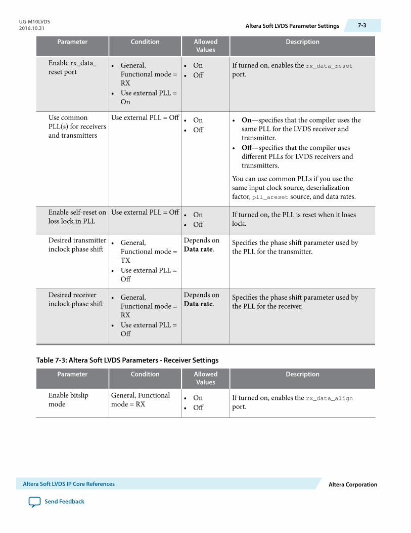
Parameter Condition AllowedValues
Description
Enable rx_data_reset port
• General,Functional mode =RX
• Use external PLL =On
• On• Off
If turned on, enables the rx_data_resetport.
Use commonPLL(s) for receiversand transmitters
Use external PLL = Off • On• Off
• On—specifies that the compiler uses thesame PLL for the LVDS receiver andtransmitter.
• Off—specifies that the compiler usesdifferent PLLs for LVDS receivers andtransmitters.
You can use common PLLs if you use thesame input clock source, deserializationfactor, pll_areset source, and data rates.
Enable self-reset onloss lock in PLL
Use external PLL = Off • On• Off
If turned on, the PLL is reset when it loseslock.
Desired transmitterinclock phase shift
• General,Functional mode =TX
• Use external PLL =Off
Depends onData rate.
Specifies the phase shift parameter used bythe PLL for the transmitter.
Desired receiverinclock phase shift
• General,Functional mode =RX
• Use external PLL =Off
Depends onData rate.
Specifies the phase shift parameter used bythe PLL for the receiver.
Table 7-3: Altera Soft LVDS Parameters - Receiver Settings
Parameter Condition AllowedValues
Description
Enable bitslipmode
General, Functionalmode = RX
• On• Off
If turned on, enables the rx_data_alignport.
UG-M10LVDS2016.10.31 Altera Soft LVDS Parameter Settings 7-3
Altera Soft LVDS IP Core References Altera Corporation
Send Feedback
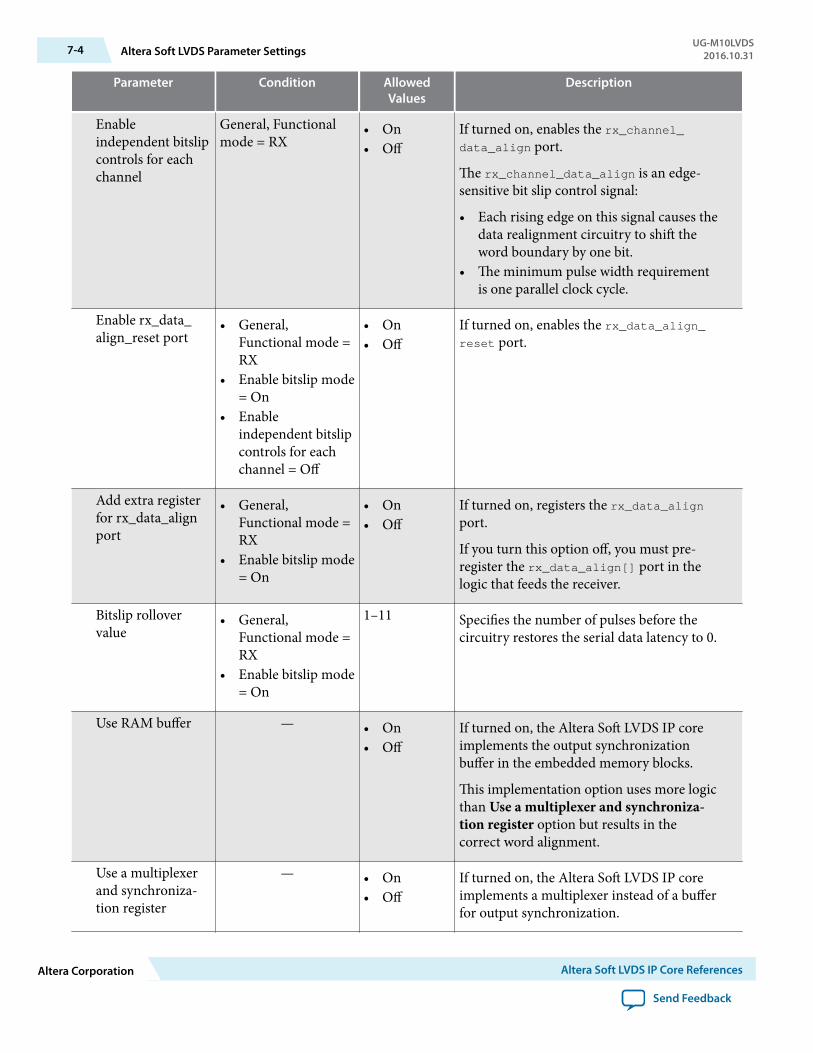
Parameter Condition AllowedValues
Description
Enableindependent bitslipcontrols for eachchannel
General, Functionalmode = RX
• On• Off
If turned on, enables the rx_channel_data_align port.
The rx_channel_data_align is an edge-sensitive bit slip control signal:
• Each rising edge on this signal causes thedata realignment circuitry to shift theword boundary by one bit.
• The minimum pulse width requirementis one parallel clock cycle.
Enable rx_data_align_reset port
• General,Functional mode =RX
• Enable bitslip mode= On
• Enableindependent bitslipcontrols for eachchannel = Off
• On• Off
If turned on, enables the rx_data_align_reset port.
Add extra registerfor rx_data_alignport
• General,Functional mode =RX
• Enable bitslip mode= On
• On• Off
If turned on, registers the rx_data_alignport.
If you turn this option off, you must pre-register the rx_data_align[] port in thelogic that feeds the receiver.
Bitslip rollovervalue
• General,Functional mode =RX
• Enable bitslip mode= On
1–11 Specifies the number of pulses before thecircuitry restores the serial data latency to 0.
Use RAM buffer — • On• Off
If turned on, the Altera Soft LVDS IP coreimplements the output synchronizationbuffer in the embedded memory blocks.
This implementation option uses more logicthan Use a multiplexer and synchroniza‐tion register option but results in thecorrect word alignment.
Use a multiplexerand synchroniza‐tion register
— • On• Off
If turned on, the Altera Soft LVDS IP coreimplements a multiplexer instead of a bufferfor output synchronization.
7-4 Altera Soft LVDS Parameter SettingsUG-M10LVDS
2016.10.31
Altera Corporation Altera Soft LVDS IP Core References
Send Feedback
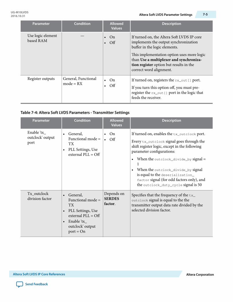
Parameter Condition AllowedValues
Description
Use logic elementbased RAM
— • On• Off
If turned on, the Altera Soft LVDS IP coreimplements the output synchronizationbuffer in the logic elements.
This implementation option uses more logicthan Use a multiplexer and synchroniza‐tion register option but results in thecorrect word alignment.
Register outputs General, Functionalmode = RX
• On• Off
If turned on, registers the rx_out[] port.
If you turn this option off, you must pre-register the rx_out[] port in the logic thatfeeds the receiver.
Table 7-4: Altera Soft LVDS Parameters - Transmitter Settings
Parameter Condition AllowedValues
Description
Enable 'tx_outclock' outputport
• General,Functional mode =TX
• PLL Settings, Useexternal PLL = Off
• On• Off
If turned on, enables the tx_outclock port.
Every tx_outclock signal goes through theshift register logic, except in the followingparameter configurations:
• When the outclock_divide_by signal =1
• When the outclock_divide_by signalis equal to the deserialization_factor signal (for odd factors only), andthe outclock_duty_cycle signal is 50
Tx_outclockdivision factor
• General,Functional mode =TX
• PLL Settings, Useexternal PLL = Off
• Enable 'tx_outclock' outputport = On
Depends onSERDESfactor.
Specifies that the frequency of the tx_outclock signal is equal to the thetransmitter output data rate divided by theselected division factor.
UG-M10LVDS2016.10.31 Altera Soft LVDS Parameter Settings 7-5
Altera Soft LVDS IP Core References Altera Corporation
Send Feedback
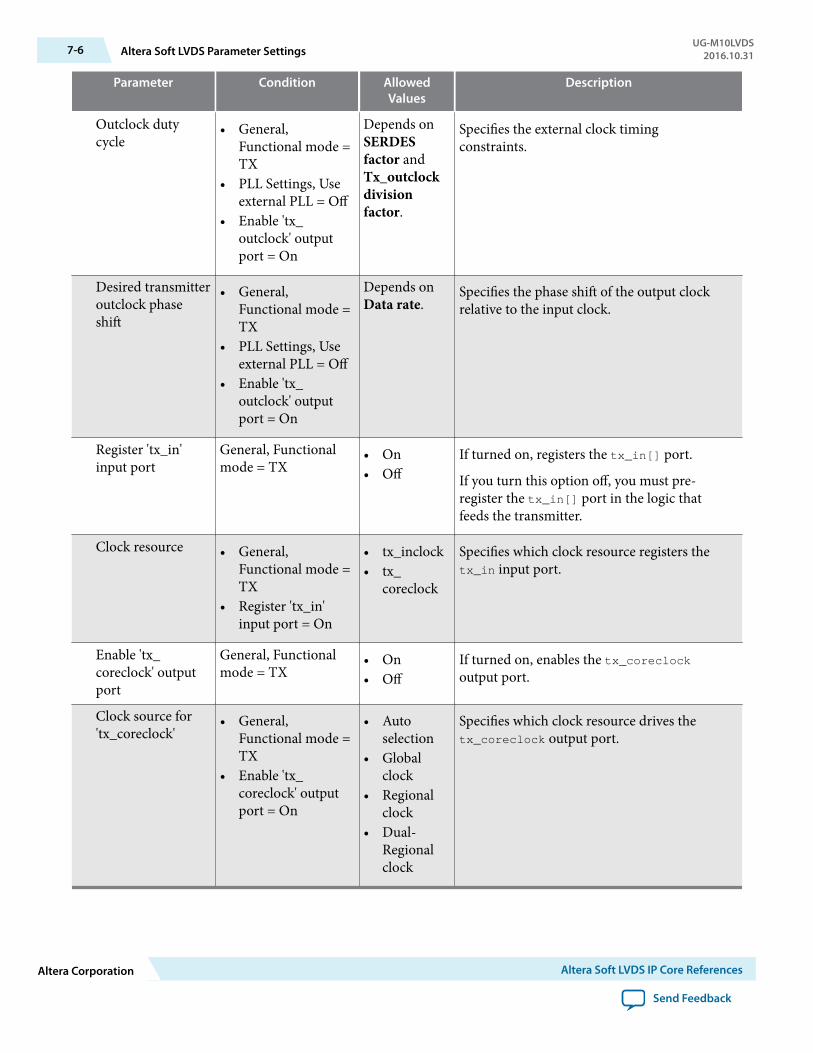
Parameter Condition AllowedValues
Description
Outclock dutycycle
• General,Functional mode =TX
• PLL Settings, Useexternal PLL = Off
• Enable 'tx_outclock' outputport = On
Depends onSERDESfactor andTx_outclockdivisionfactor.
Specifies the external clock timingconstraints.
Desired transmitteroutclock phaseshift
• General,Functional mode =TX
• PLL Settings, Useexternal PLL = Off
• Enable 'tx_outclock' outputport = On
Depends onData rate.
Specifies the phase shift of the output clockrelative to the input clock.
Register 'tx_in'input port
General, Functionalmode = TX
• On• Off
If turned on, registers the tx_in[] port.
If you turn this option off, you must pre-register the tx_in[] port in the logic thatfeeds the transmitter.
Clock resource • General,Functional mode =TX
• Register 'tx_in'input port = On
• tx_inclock• tx_
coreclock
Specifies which clock resource registers thetx_in input port.
Enable 'tx_coreclock' outputport
General, Functionalmode = TX
• On• Off
If turned on, enables the tx_coreclockoutput port.
Clock source for'tx_coreclock'
• General,Functional mode =TX
• Enable 'tx_coreclock' outputport = On
• Autoselection
• Globalclock
• Regionalclock
• Dual-Regionalclock
Specifies which clock resource drives thetx_coreclock output port.
7-6 Altera Soft LVDS Parameter SettingsUG-M10LVDS
2016.10.31
Altera Corporation Altera Soft LVDS IP Core References
Send Feedback
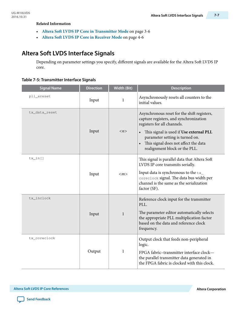
Related Information
• Altera Soft LVDS IP Core in Transmitter Mode on page 3-6• Altera Soft LVDS IP Core in Receiver Mode on page 4-6
Altera Soft LVDS Interface SignalsDepending on parameter settings you specify, different signals are available for the Altera Soft LVDS IPcore.
Table 7-5: Transmitter Interface Signals
Signal Name Direction Width (Bit) Description
pll_aresetInput 1 Asynchronously resets all counters to the
initial values.
tx_data_reset
Input <n>
Asynchronous reset for the shift registers,capture registers, and synchronizationregisters for all channels.
• This signal is used if Use external PLLparameter setting is turned on.
• This signal does not affect the datarealignment block or the PLL.
tx_in[]
Input <m>
This signal is parallel data that Altera SoftLVDS IP core transmits serially.
Input data is synchronous to the tx_coreclock signal. The data bus width perchannel is the same as the serializationfactor (SF).
tx_inclock
Input 1
Reference clock input for the transmitterPLL.
The parameter editor automatically selectsthe appropriate PLL multiplication factorbased on the data and reference clockfrequency.
tx_coreclock
Output 1
Output clock that feeds non-peripherallogic.
FPGA fabric–transmitter interface clock—the parallel transmitter data generated inthe FPGA fabric is clocked with this clock.
UG-M10LVDS2016.10.31 Altera Soft LVDS Interface Signals 7-7
Altera Soft LVDS IP Core References Altera Corporation
Send Feedback
Signal Name Direction Width (Bit) Description
tx_locked
Output 1
Provides the LVDS PLL status:
• Remains high when the PLL is locked tothe input reference clock.
• Remains low when the PLL fails to lock.
tx_out[]
Output <n>
Serialized LVDS data output signal of <n>channels.
tx_out[(<n>-1)..0] drives parallel datafrom tx_in[(<J> × <n>)-1 ..0] where<J> is the serialization factor and <n> is thenumber of channels. tx_out[0] drives datafrom tx_in[(<J>-1)..0]. tx_out[1]drives data from the next <J> number ofbits on tx_in.
tx_outclock
Output 1External reference clock.
The frequency of this clock is program‐mable to be the same as the data rate.
Table 7-6: Receiver Interface Signals
signal Name Direction Width (Bit) Description
rx_data_reset Input <n> Asynchronous reset for all channels,excluding the PLL.
• This signal is available if Use externalPLL parameter setting is turned on.
• You must externally synchronize thissignal with the fast clock.
rx_in[] Input <n> LVDS serial data input signal of <n>channels.
rx_in[(<n>-1)..0] is deserialized anddriven on rx_out[(<J> × <n>)-1 ..0]where <J> is the deserialization factor and<n> is the number of channels. rx_in[0]drives data to rx_out[(<J>-1)..0]. rx_in[1] drives data to the next <J> numberof bits on rx_out.
7-8 Altera Soft LVDS Interface SignalsUG-M10LVDS
2016.10.31
Altera Corporation Altera Soft LVDS IP Core References
Send Feedback
signal Name Direction Width (Bit) Description
rx_inclock Input 1 LVDS reference input clock.
The parameter editor automatically selectsthe appropriate PLL multiplication factorbased on the data rate and reference clockfrequency selection.
rx_coreclk Input <n> LVDS reference input clock.
• Replaces the non-peripheral clock fromthe PLL.
• One clock for each channel.
rx_locked Output 1 Provides the LVDS PLL status:
• Stays high when the PLL is locked to theinput reference clock.
• Stays low when the PLL fails to lock.
rx_out Output <m> Receiver parallel data output.
The data bus width per channel is the sameas the deserialization factor (DF).
rx_outclock Output 1 Parallel output clock from the receiver PLL.
• This signal is not available if you turn onthe Use external PLL parameter setting.
• The FPGA fabric–receiver interfaceclock must be driven by the PLLinstantiated through the ALTPLLparameter editor.
rx_data_align Input 1 Controls the byte alignment circuitry.
You can register this signal using the rx_outclock signal.
rx_data_align_reset Input 1 Resets the byte alignment circuitry.
Use the rx_data_align_reset input signalif:
• You need to reset the PLL during deviceoperation.
• You need to re-establish the wordalignment.
rx_channel_data_align Input <n> Controls byte alignment circuitry.
UG-M10LVDS2016.10.31 Altera Soft LVDS Interface Signals 7-9
Altera Soft LVDS IP Core References Altera Corporation
Send Feedback

signal Name Direction Width (Bit) Description
rx_cda_reset Input <n> Asynchronous reset to the data realignmentcircuitry. This signal resets the data realign‐ment block.
The minimum pulse width requirement forthis reset is one parallel clock cycle.
7-10 Altera Soft LVDS Interface SignalsUG-M10LVDS
2016.10.31
Altera Corporation Altera Soft LVDS IP Core References
Send Feedback
MAX 10 High-Speed LVDS I/O User GuideArchives A
2016.10.31
UG-M10LVDS Subscribe Send Feedback
If an IP core version is not listed, the user guide for the previous IP core version applies.IP Core Version User Guide
16.0 MAX 10 High-Speed LVDS I/O User Guide
15.1 MAX 10 High-Speed LVDS I/O User Guide
15.0 MAX 10 High-Speed LVDS I/O User Guide
14.1 MAX 10 High-Speed LVDS I/O User Guide
© 2016 Intel Corporation. All rights reserved. Intel, the Intel logo, Altera, Arria, Cyclone, Enpirion, MAX, Megacore, NIOS, Quartus and Stratix words and logosare trademarks of Intel Corporation in the US and/or other countries. Other marks and brands may be claimed as the property of others. Intel warrantsperformance of its FPGA and semiconductor products to current specifications in accordance with Intel's standard warranty, but reserves the right to makechanges to any products and services at any time without notice. Intel assumes no responsibility or liability arising out of the application or use of anyinformation, product, or service described herein except as expressly agreed to in writing by Intel. Intel customers are advised to obtain the latest version ofdevice specifications before relying on any published information and before placing orders for products or services.
ISO9001:2008Registered
www.altera.com101 Innovation Drive, San Jose, CA 95134
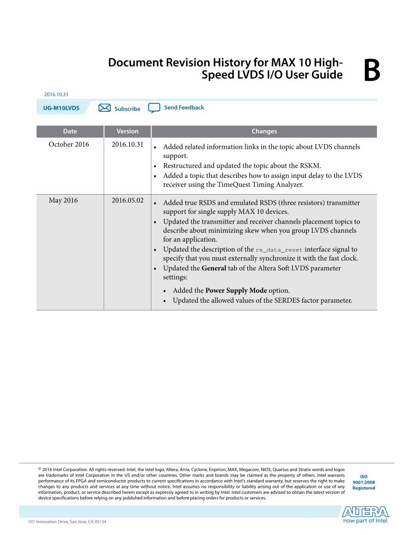
Document Revision History for MAX 10 High-Speed LVDS I/O User Guide B
2016.10.31
UG-M10LVDS Subscribe Send Feedback
Date Version Changes
October 2016 2016.10.31 • Added related information links in the topic about LVDS channelssupport.
• Restructured and updated the topic about the RSKM.• Added a topic that describes how to assign input delay to the LVDS
receiver using the TimeQuest Timing Analyzer.
May 2016 2016.05.02 • Added true RSDS and emulated RSDS (three resistors) transmittersupport for single supply MAX 10 devices.
• Updated the transmitter and receiver channels placement topics todescribe about minimizing skew when you group LVDS channelsfor an application.
• Updated the description of the rx_data_reset interface signal tospecify that you must externally synchronize it with the fast clock.
• Updated the General tab of the Altera Soft LVDS parametersettings:
• Added the Power Supply Mode option.• Updated the allowed values of the SERDES factor parameter.
© 2016 Intel Corporation. All rights reserved. Intel, the Intel logo, Altera, Arria, Cyclone, Enpirion, MAX, Megacore, NIOS, Quartus and Stratix words and logosare trademarks of Intel Corporation in the US and/or other countries. Other marks and brands may be claimed as the property of others. Intel warrantsperformance of its FPGA and semiconductor products to current specifications in accordance with Intel's standard warranty, but reserves the right to makechanges to any products and services at any time without notice. Intel assumes no responsibility or liability arising out of the application or use of anyinformation, product, or service described herein except as expressly agreed to in writing by Intel. Intel customers are advised to obtain the latest version ofdevice specifications before relying on any published information and before placing orders for products or services.
ISO9001:2008Registered
www.altera.com101 Innovation Drive, San Jose, CA 95134
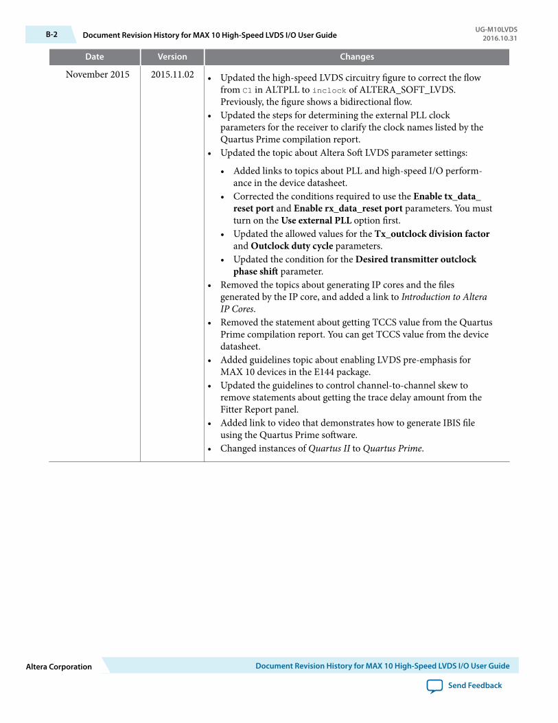
Date Version Changes
November 2015 2015.11.02 • Updated the high-speed LVDS circuitry figure to correct the flowfrom C1 in ALTPLL to inclock of ALTERA_SOFT_LVDS.Previously, the figure shows a bidirectional flow.
• Updated the steps for determining the external PLL clockparameters for the receiver to clarify the clock names listed by theQuartus Prime compilation report.
• Updated the topic about Altera Soft LVDS parameter settings:
• Added links to topics about PLL and high-speed I/O perform‐ance in the device datasheet.
• Corrected the conditions required to use the Enable tx_data_reset port and Enable rx_data_reset port parameters. You mustturn on the Use external PLL option first.
• Updated the allowed values for the Tx_outclock division factorand Outclock duty cycle parameters.
• Updated the condition for the Desired transmitter outclockphase shift parameter.
• Removed the topics about generating IP cores and the filesgenerated by the IP core, and added a link to Introduction to AlteraIP Cores.
• Removed the statement about getting TCCS value from the QuartusPrime compilation report. You can get TCCS value from the devicedatasheet.
• Added guidelines topic about enabling LVDS pre-emphasis forMAX 10 devices in the E144 package.
• Updated the guidelines to control channel-to-channel skew toremove statements about getting the trace delay amount from theFitter Report panel.
• Added link to video that demonstrates how to generate IBIS fileusing the Quartus Prime software.
• Changed instances of Quartus II to Quartus Prime.
B-2 Document Revision History for MAX 10 High-Speed LVDS I/O User GuideUG-M10LVDS
2016.10.31
Altera Corporation Document Revision History for MAX 10 High-Speed LVDS I/O User Guide
Send Feedback
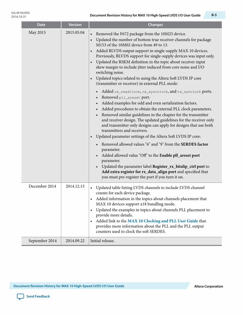
Date Version Changes
May 2015 2015.05.04 • Removed the F672 package from the 10M25 device.• Updated the number of bottom true receiver channels for package
M153 of the 10M02 device from 49 to 13.• Added BLVDS output support in single-supply MAX 10 devices.
Previously, BLVDS support for single-supply devices was input only.• Updated the RSKM definition in the topic about receiver input
skew margin to include jitter induced from core noise and I/Oswitching noise.
• Updated topics related to using the Altera Soft LVDS IP core(transmitter or receiver) in external PLL mode:
• Added rx_readclock, rx_syncclock, and tx_synclock ports.• Removed pll_areset port.• Added examples for odd and even serialization factors.• Added procedures to obtain the external PLL clock parameters.• Removed similar guidelines in the chapter for the transmitter
and receiver design. The updated guidelines for the receiver onlyand transmitter only designs can apply for designs that use bothtransmitters and receivers.
• Updated parameter settings of the Altera Soft LVDS IP core:
• Removed allowed values "6" and "9" from the SERDES factorparameter.
• Added allowed value "Off" to the Enable pll_areset portparameter.
• Updated the parameter label Register_rx_bitslip_ctrl port toAdd extra register for rx_data_align port and specified thatyou must pre-register the port if you turn it on.
December 2014 2014.12.15 • Updated table listing LVDS channels to include LVDS channelcounts for each device package.
• Added information in the topics about channels placement thatMAX 10 devices support x18 bundling mode.
• Updated the examples in topics about channels PLL placement toprovide more details.
• Added link to the MAX 10 Clocking and PLL User Guide thatprovides more information about the PLL and the PLL outputcounters used to clock the soft SERDES.
September 2014 2014.09.22 Initial release.
UG-M10LVDS2016.10.31 Document Revision History for MAX 10 High-Speed LVDS I/O User Guide B-3
Document Revision History for MAX 10 High-Speed LVDS I/O User Guide Altera Corporation
Send Feedback

MAX 10 External Memory Interface UserGuide
Last updated for Quartus Prime Design Suite: 16.1
Subscribe
Send Feedback
UG-M10EMI2016.10.28
101 Innovation DriveSan Jose, CA 95134www.altera.com
Contents
MAX 10 External Memory Interface Overview.................................................. 1-1MAX 10 External Memory Interface Support and Performance...........................................................1-2
MAX 10 External Memory Interface Architecture and Features....................... 2-1MAX 10 I/O Banks for External Memory Interface................................................................................2-1MAX 10 DQ/DQS Groups..........................................................................................................................2-2MAX 10 External Memory Interfaces Maximum Width........................................................................2-3MAX 10 Memory Controller......................................................................................................................2-5MAX 10 External Memory Read Datapath.............................................................................................. 2-6
DDR Input Registers........................................................................................................................2-7MAX 10 External Memory Write Datapath............................................................................................. 2-8
DDR Output Registers.....................................................................................................................2-8MAX 10 Address/Command Path...........................................................................................................2-10MAX 10 PHY Clock (PHYCLK) Network............................................................................................. 2-11Phase Detector for VT Tracking.............................................................................................................. 2-12On-Chip Termination............................................................................................................................... 2-12Phase-Locked Loop................................................................................................................................... 2-13MAX 10 Low Power Feature.....................................................................................................................2-13
MAX 10 External Memory Interface Design Considerations............................ 3-1MAX 10 DDR2 and DDR3 Design Considerations................................................................................ 3-1
DDR2/DDR3 External Memory Interface Pins........................................................................... 3-1DDR2/DDR3 Recommended Termination Schemes for MAX 10 Devices............................. 3-3
LPDDR2 Design Considerations............................................................................................................... 3-4LPDDR2 External Memory Interface Pins................................................................................... 3-4LPPDDR2 Power Supply Variation Constraint............................................................................3-5LPDDR2 Recommended Termination Schemes for MAX 10 Devices.....................................3-6
Guidelines: MAX 10 DDR3, DDR2, and LPDDR2 External Memory Interface I/O Limitation...... 3-6Guidelines: MAX 10 Board Design Requirement for DDR2, DDR3, and LPDDR2.......................... 3-8Guidelines: Reading the MAX 10 Pin-Out Files......................................................................................3-8
MAX 10 External Memory Interface Implementation Guides...........................4-1UniPHY IP Core...........................................................................................................................................4-1LPDDR2 External Memory Interface Implementation...........................................................................4-3
Supported LPDDR2 Topology........................................................................................................4-3DDR2 and DDR3 External Memory Interface Implementation............................................................4-4
MAX 10 Supported DDR2 or DDR3 Topology........................................................................... 4-4
UniPHY IP Core References for MAX 10........................................................... 5-1
TOC-2
Altera Corporation
UniPHY Parameter Settings for MAX 10................................................................................................. 5-1UniPHY Parameters—PHY Settings............................................................................................. 5-1UniPHY Parameters—Memory Parameters.................................................................................5-3UniPHY Parameters—Memory Timing....................................................................................... 5-7UniPHY Parameters—Board Settings...........................................................................................5-9UniPHY Parameters—Controller Settings................................................................................. 5-15UniPHY Parameters—Diagnostics..............................................................................................5-18
MAX 10 External Memory Interface User Guide Archives................................A-1
Additional Information for MAX 10 External Memory Interface User Guide......................................................................................................................... B-1
Document Revision History for MAX 10 External Memory Interface User Guide........................... B-1
TOC-3
Altera Corporation
MAX 10 External Memory Interface Overview 12016.10.28
UG-M10EMI Subscribe Send Feedback
The MAX® 10 devices are capable of interfacing with a broad range of external memory standards. Withthis capability, you can utilize MAX 10 devices in a wide range of applications such as image processing,storage, communications, and general embedded systems.
The external memory interface solution in MAX 10 devices consist of:
• The I/O elements that support external memory interfaces.• The UniPHY IP core that allows you to configure the memory interfaces to support different external
memory interface standards.
Note: Altera recommends that you construct all DDR2, DDR3, and LPDDR2 SDRAM external memoryinterfaces using the UniPHY IP core.(1)
Related Information
• MAX 10 External Memory Interface Architecture and Features on page 2-1• MAX 10 External Memory Interface Design Considerations on page 3-1• MAX 10 External Memory Interface Implementation Guides on page 4-1• UniPHY IP Core References for MAX 10 on page 5-1• Documentation: External Memory Interfaces
Provides more information about external memory system performance specification, board designguidelines, timing analysis, simulation, and debugging.
• External Memory Interface Handbook Volume 1: Altera Memory Solution Overview and DesignFlowProvides more information about using Altera devices for external memory interfaces including Alteramemory solution and design flow.
• External Memory Interface Handbook Volume 2: Design GuidelinesProvides more information about using Altera devices for external memory interfaces includingmemory selection, board design, implementing memory IP cores, timing, optimization, anddebugging.
• Functional Description—MAX 10 EMIFProvides more information about implementing memory IP cores for MAX 10 devices.
• MAX 10 DDR3 Reference DesignProvides DDR3 UniPHY IP core reference design for MAX 10 devices.
(1) Licensing terms and costs for UniPHY IP core apply.
© 2016 Intel Corporation. All rights reserved. Intel, the Intel logo, Altera, Arria, Cyclone, Enpirion, MAX, Megacore, NIOS, Quartus and Stratix words and logosare trademarks of Intel Corporation in the US and/or other countries. Other marks and brands may be claimed as the property of others. Intel warrantsperformance of its FPGA and semiconductor products to current specifications in accordance with Intel's standard warranty, but reserves the right to makechanges to any products and services at any time without notice. Intel assumes no responsibility or liability arising out of the application or use of anyinformation, product, or service described herein except as expressly agreed to in writing by Intel. Intel customers are advised to obtain the latest version ofdevice specifications before relying on any published information and before placing orders for products or services.
ISO9001:2008Registered
www.altera.com101 Innovation Drive, San Jose, CA 95134
• MAX 10 External Memory Interface User Guide Archives on page 6-1Provides a list of user guides for previous versions of the UniPHY IP core.
MAX 10 External Memory Interface Support and PerformanceThe MAX 10 devices contain circuitry that supports several external memory interface standards.
Table 1-1: Memory Standards Supported by the Soft Memory Controller for MAX 10 Devices
Contact your local sales representatives for access to the -I6 or -A6 speed grade devices in the QuartusPrime Software.
External MemoryInterface Standard
Rate Support Speed Grade Voltage (V) Max Frequency (MHz)
DDR3 SDRAM Half -I6 1.5 303DDR3L SDRAM Half -I6 1.35 303
DDR2 SDRAM Half-I6
1.8200
-I7 and -C7 167LPDDR2(2) Half -I6 1.2 200(3)
Related Information
• External Memory Interface Spec EstimatorProvides a parametric tool that allows you to find and compare the performance of the supportedexternal memory interfaces in Altera devices.
• Planning Pin and FPGA Resources chapter, External Memory Interface HandbookProvides the maximum number of interfaces supported by MAX 10 devices for each memorystandards, pin counts for various external memory interface implementation examples, and informa‐tion about the clock, address/command, data, data strobe, DM, and optional ECC signals.
• MAX 10 Device Datasheet
(2) MAX 10 devices support only single-die LPDDR2.(3) To achieve the specified performance, constrain the memory device I/O and core power supply variation to
within ±3%. By default, the frequency is 167 MHz.
1-2 MAX 10 External Memory Interface Support and PerformanceUG-M10EMI2016.10.28
Altera Corporation MAX 10 External Memory Interface Overview
Send Feedback
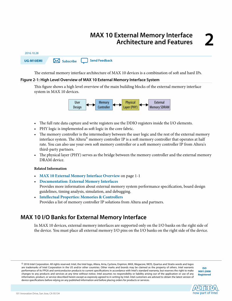
MAX 10 External Memory InterfaceArchitecture and Features 2
2016.10.28
UG-M10EMI Subscribe Send Feedback
The external memory interface architecture of MAX 10 devices is a combination of soft and hard IPs.Figure 2-1: High Level Overview of MAX 10 External Memory Interface System
This figure shows a high level overview of the main building blocks of the external memory interfacesystem in MAX 10 devices.
UserDesign
MemoryController
PhysicalLayer (PHY)
ExternalMemory SDRAM
• The full rate data capture and write registers use the DDIO registers inside the I/O elements.• PHY logic is implemented as soft logic in the core fabric.• The memory controller is the intermediary between the user logic and the rest of the external memory
interface system. The Altera® memory controller IP is a soft memory controller that operates at halfrate. You can also use your own soft memory controller or a soft memory controller IP from Altera'sthird-party partners.
• The physical layer (PHY) serves as the bridge between the memory controller and the external memoryDRAM device.
Related Information
• MAX 10 External Memory Interface Overview on page 1-1• Documentation: External Memory Interfaces
Provides more information about external memory system performance specification, board designguidelines, timing analysis, simulation, and debugging.
• Intellectual Properties: Memories & ControllersProvides a list of memory controller IP solutions from Altera and partners.
MAX 10 I/O Banks for External Memory InterfaceIn MAX 10 devices, external memory interfaces are supported only on the I/O banks on the right side ofthe device. You must place all external memory I/O pins on the I/O banks on the right side of the device.
© 2016 Intel Corporation. All rights reserved. Intel, the Intel logo, Altera, Arria, Cyclone, Enpirion, MAX, Megacore, NIOS, Quartus and Stratix words and logosare trademarks of Intel Corporation in the US and/or other countries. Other marks and brands may be claimed as the property of others. Intel warrantsperformance of its FPGA and semiconductor products to current specifications in accordance with Intel's standard warranty, but reserves the right to makechanges to any products and services at any time without notice. Intel assumes no responsibility or liability arising out of the application or use of anyinformation, product, or service described herein except as expressly agreed to in writing by Intel. Intel customers are advised to obtain the latest version ofdevice specifications before relying on any published information and before placing orders for products or services.
ISO9001:2008Registered
www.altera.com101 Innovation Drive, San Jose, CA 95134
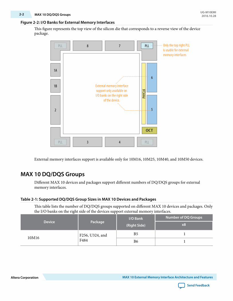
Figure 2-2: I/O Banks for External Memory InterfacesThis figure represents the top view of the silicon die that corresponds to a reverse view of the devicepackage.
1B
1A
2
3 4
8 7
External memory interfacesupport only available on I/O banks on the right side
of the device.
Only the top right PLLis usable for externalmemory interfaces
PHYC
LKPLLPLL
PLL PLL
OCT
5
6
External memory interfaces support is available only for 10M16, 10M25, 10M40, and 10M50 devices.
MAX 10 DQ/DQS GroupsDifferent MAX 10 devices and packages support different numbers of DQ/DQS groups for externalmemory interfaces.
Table 2-1: Supported DQ/DQS Group Sizes in MAX 10 Devices and Packages
This table lists the number of DQ/DQS groups supported on different MAX 10 devices and packages. Onlythe I/O banks on the right side of the devices support external memory interfaces.
Device PackageI/O Bank
(Right Side)
Number of DQ Groups
x8
10M16 F256, U324, andF484
B5 1
B6 1
2-2 MAX 10 DQ/DQS GroupsUG-M10EMI2016.10.28
Altera Corporation MAX 10 External Memory Interface Architecture and Features
Send Feedback
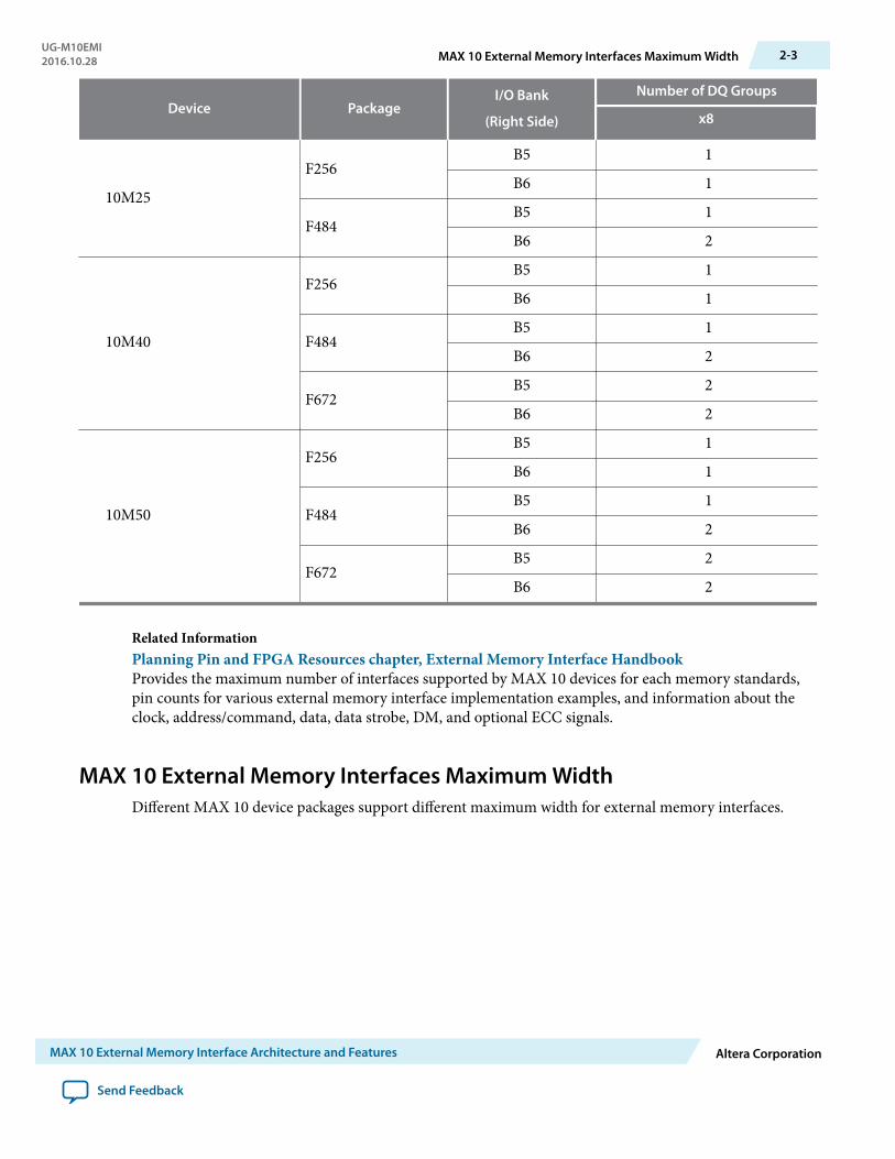
Device PackageI/O Bank
(Right Side)
Number of DQ Groups
x8
10M25
F256B5 1
B6 1
F484B5 1
B6 2
10M40
F256B5 1
B6 1
F484B5 1
B6 2
F672B5 2
B6 2
10M50
F256B5 1
B6 1
F484B5 1
B6 2
F672B5 2
B6 2
Related InformationPlanning Pin and FPGA Resources chapter, External Memory Interface HandbookProvides the maximum number of interfaces supported by MAX 10 devices for each memory standards,pin counts for various external memory interface implementation examples, and information about theclock, address/command, data, data strobe, DM, and optional ECC signals.
MAX 10 External Memory Interfaces Maximum WidthDifferent MAX 10 device packages support different maximum width for external memory interfaces.
UG-M10EMI2016.10.28 MAX 10 External Memory Interfaces Maximum Width 2-3
MAX 10 External Memory Interface Architecture and Features Altera Corporation
Send Feedback
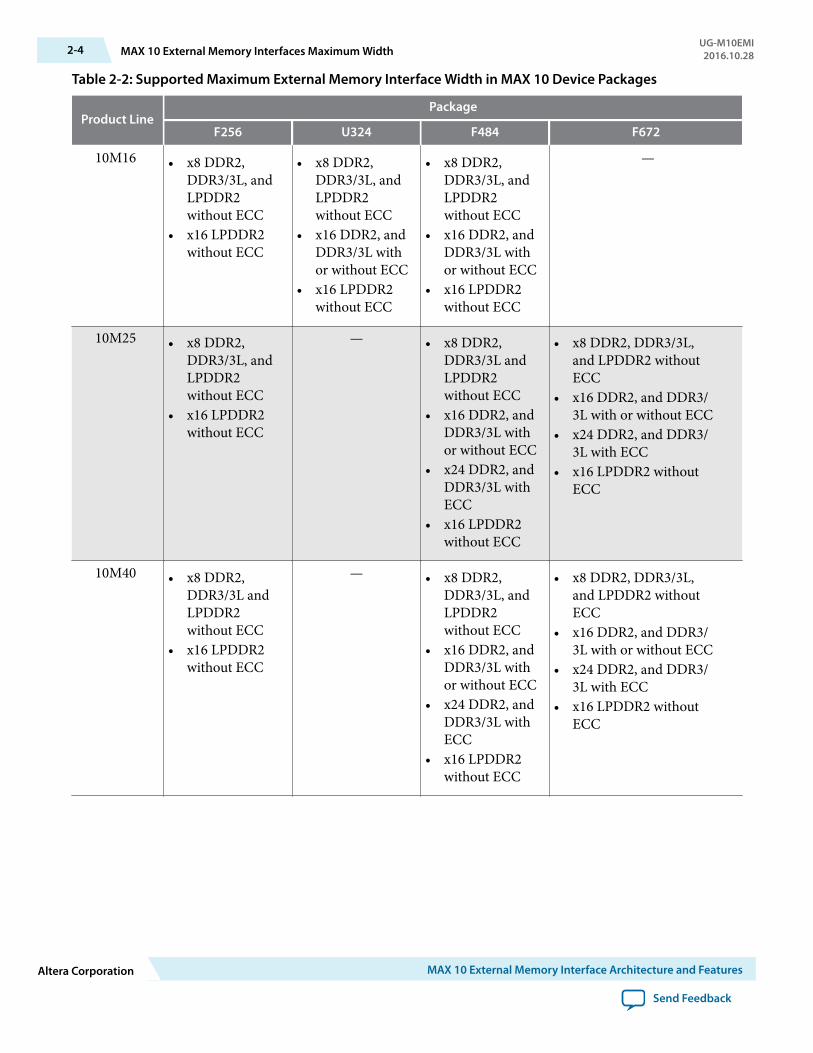
Table 2-2: Supported Maximum External Memory Interface Width in MAX 10 Device Packages
Product LinePackage
F256 U324 F484 F672
10M16 • x8 DDR2,DDR3/3L, andLPDDR2without ECC
• x16 LPDDR2without ECC
• x8 DDR2,DDR3/3L, andLPDDR2without ECC
• x16 DDR2, andDDR3/3L withor without ECC
• x16 LPDDR2without ECC
• x8 DDR2,DDR3/3L, andLPDDR2without ECC
• x16 DDR2, andDDR3/3L withor without ECC
• x16 LPDDR2without ECC
—
10M25 • x8 DDR2,DDR3/3L, andLPDDR2without ECC
• x16 LPDDR2without ECC
— • x8 DDR2,DDR3/3L andLPDDR2without ECC
• x16 DDR2, andDDR3/3L withor without ECC
• x24 DDR2, andDDR3/3L withECC
• x16 LPDDR2without ECC
• x8 DDR2, DDR3/3L,and LPDDR2 withoutECC
• x16 DDR2, and DDR3/3L with or without ECC
• x24 DDR2, and DDR3/3L with ECC
• x16 LPDDR2 withoutECC
10M40 • x8 DDR2,DDR3/3L andLPDDR2without ECC
• x16 LPDDR2without ECC
— • x8 DDR2,DDR3/3L, andLPDDR2without ECC
• x16 DDR2, andDDR3/3L withor without ECC
• x24 DDR2, andDDR3/3L withECC
• x16 LPDDR2without ECC
• x8 DDR2, DDR3/3L,and LPDDR2 withoutECC
• x16 DDR2, and DDR3/3L with or without ECC
• x24 DDR2, and DDR3/3L with ECC
• x16 LPDDR2 withoutECC
2-4 MAX 10 External Memory Interfaces Maximum WidthUG-M10EMI2016.10.28
Altera Corporation MAX 10 External Memory Interface Architecture and Features
Send Feedback
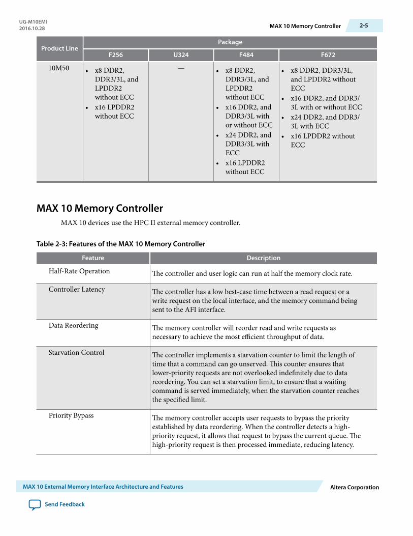
Product LinePackage
F256 U324 F484 F672
10M50 • x8 DDR2,DDR3/3L, andLPDDR2without ECC
• x16 LPDDR2without ECC
— • x8 DDR2,DDR3/3L, andLPDDR2without ECC
• x16 DDR2, andDDR3/3L withor without ECC
• x24 DDR2, andDDR3/3L withECC
• x16 LPDDR2without ECC
• x8 DDR2, DDR3/3L,and LPDDR2 withoutECC
• x16 DDR2, and DDR3/3L with or without ECC
• x24 DDR2, and DDR3/3L with ECC
• x16 LPDDR2 withoutECC
MAX 10 Memory ControllerMAX 10 devices use the HPC II external memory controller.
Table 2-3: Features of the MAX 10 Memory Controller
Feature Description
Half-Rate Operation The controller and user logic can run at half the memory clock rate.
Controller Latency The controller has a low best-case time between a read request or awrite request on the local interface, and the memory command beingsent to the AFI interface.
Data Reordering The memory controller will reorder read and write requests asnecessary to achieve the most efficient throughput of data.
Starvation Control The controller implements a starvation counter to limit the length oftime that a command can go unserved. This counter ensures thatlower-priority requests are not overlooked indefinitely due to datareordering. You can set a starvation limit, to ensure that a waitingcommand is served immediately, when the starvation counter reachesthe specified limit.
Priority Bypass The memory controller accepts user requests to bypass the priorityestablished by data reordering. When the controller detects a high-priority request, it allows that request to bypass the current queue. Thehigh-priority request is then processed immediate, reducing latency.
UG-M10EMI2016.10.28 MAX 10 Memory Controller 2-5
MAX 10 External Memory Interface Architecture and Features Altera Corporation
Send Feedback
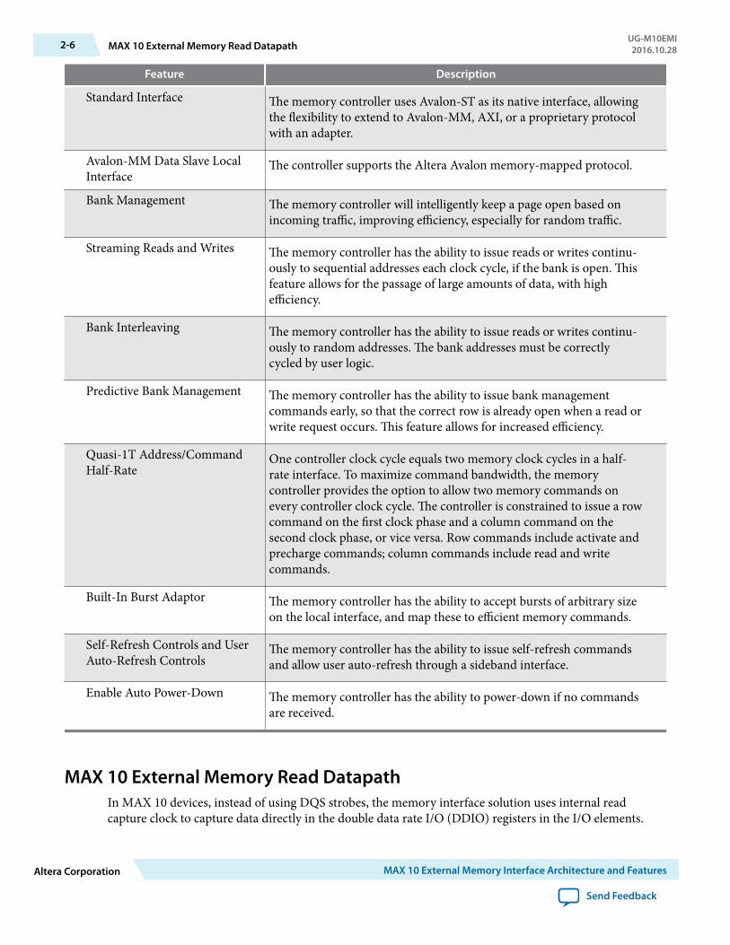
Feature Description
Standard Interface The memory controller uses Avalon-ST as its native interface, allowingthe flexibility to extend to Avalon-MM, AXI, or a proprietary protocolwith an adapter.
Avalon-MM Data Slave LocalInterface
The controller supports the Altera Avalon memory-mapped protocol.
Bank Management The memory controller will intelligently keep a page open based onincoming traffic, improving efficiency, especially for random traffic.
Streaming Reads and Writes The memory controller has the ability to issue reads or writes continu‐ously to sequential addresses each clock cycle, if the bank is open. Thisfeature allows for the passage of large amounts of data, with highefficiency.
Bank Interleaving The memory controller has the ability to issue reads or writes continu‐ously to random addresses. The bank addresses must be correctlycycled by user logic.
Predictive Bank Management The memory controller has the ability to issue bank managementcommands early, so that the correct row is already open when a read orwrite request occurs. This feature allows for increased efficiency.
Quasi-1T Address/CommandHalf-Rate
One controller clock cycle equals two memory clock cycles in a half-rate interface. To maximize command bandwidth, the memorycontroller provides the option to allow two memory commands onevery controller clock cycle. The controller is constrained to issue a rowcommand on the first clock phase and a column command on thesecond clock phase, or vice versa. Row commands include activate andprecharge commands; column commands include read and writecommands.
Built-In Burst Adaptor The memory controller has the ability to accept bursts of arbitrary sizeon the local interface, and map these to efficient memory commands.
Self-Refresh Controls and UserAuto-Refresh Controls
The memory controller has the ability to issue self-refresh commandsand allow user auto-refresh through a sideband interface.
Enable Auto Power-Down The memory controller has the ability to power-down if no commandsare received.
MAX 10 External Memory Read DatapathIn MAX 10 devices, instead of using DQS strobes, the memory interface solution uses internal readcapture clock to capture data directly in the double data rate I/O (DDIO) registers in the I/O elements.
2-6 MAX 10 External Memory Read DatapathUG-M10EMI2016.10.28
Altera Corporation MAX 10 External Memory Interface Architecture and Features
Send Feedback
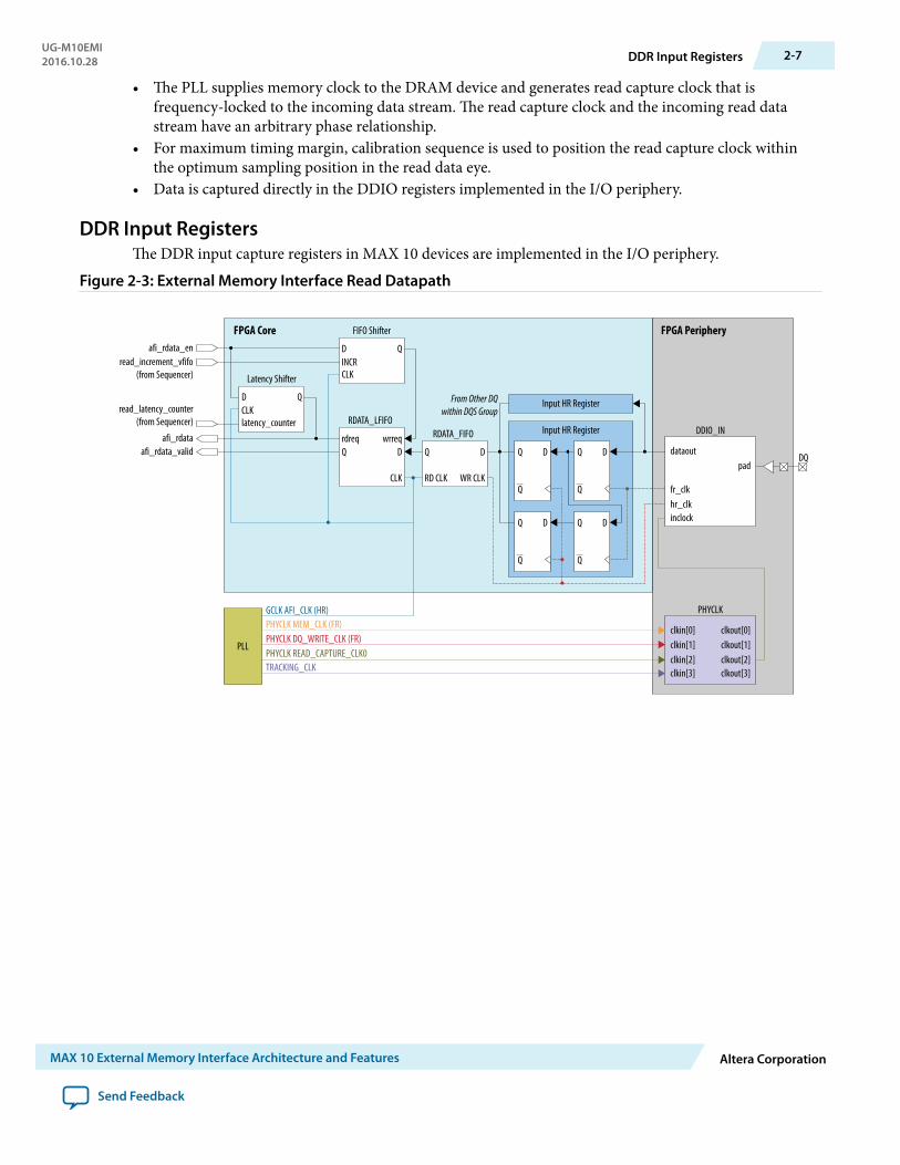
• The PLL supplies memory clock to the DRAM device and generates read capture clock that isfrequency-locked to the incoming data stream. The read capture clock and the incoming read datastream have an arbitrary phase relationship.
• For maximum timing margin, calibration sequence is used to position the read capture clock withinthe optimum sampling position in the read data eye.
• Data is captured directly in the DDIO registers implemented in the I/O periphery.
DDR Input RegistersThe DDR input capture registers in MAX 10 devices are implemented in the I/O periphery.
Figure 2-3: External Memory Interface Read Datapath
DQ
Latency Shifter
D Q
FPGA Core FPGA Periphery
PLL
clkin[0]clkin[1]clkin[2]clkin[3]
clkout[0]clkout[1]clkout[2]clkout[3]
PHYCLKGCLK AFI_CLK (HR)PHYCLK MEM_CLK (FR)PHYCLK DQ_WRITE_CLK (FR)PHYCLK READ_CAPTURE_CLK0TRACKING_CLK
CLKlatency_counter
FIFO Shifter
D QINCRCLK
RDATA_LFIFO
rdreq wrreqQ D
CLK
RDATA_FIFO
Q D
RD CLK WR CLK
Q D
Q
Q D
Q
Q D
Q
Input HR Register
Input HR Register
afi_rdata_enread_increment_vfifo
(from Sequencer)
read_latency_counter(from Sequencer)
afi_rdataafi_rdata_valid Q D
Q
dataout
fr_clkhr_clkinclock
pad
DDIO_IN
From Other DQwithin DQS Group
UG-M10EMI2016.10.28 DDR Input Registers 2-7
MAX 10 External Memory Interface Architecture and Features Altera Corporation
Send Feedback
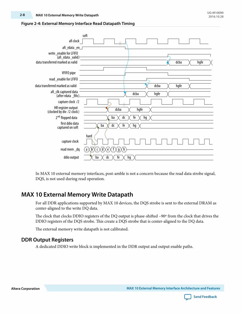
Figure 2-4: External Memory Interface Read Datapath Timing
a b c d e f g h
dcba hgfe
soft
hard
afi clock
afi_rdata _en
capture clock
ba dc fe hg
ba dc fe hg
ba dc fe hg
capture clock /2
dcba hgfe
read mem _dq
ddio output
first ddio data captured on soft
HR register output(clocked by div /2 clock )
data transferred marked as valid
read _enable for LFIFO
VFIFO pipe
dcba hgfeafi_clk captured data(after rdata _fifo)
2nd flopped data
write _enable for LFIFO(afi_rdata _valid)
dcba hgfedata transferred marked as valid
In MAX 10 external memory interfaces, post-amble is not a concern because the read data strobe signal,DQS, is not used during read operation.
MAX 10 External Memory Write DatapathFor all DDR applications supported by MAX 10 devices, the DQS strobe is sent to the external DRAM ascenter-aligned to the write DQ data.
The clock that clocks DDIO registers of the DQ output is phase-shifted –90º from the clock that drives theDDIO registers of the DQS strobe. This create a DQS strobe that is center-aligned to the DQ data.
The external memory write datapath is not calibrated.
DDR Output RegistersA dedicated DDIO write block is implemented in the DDR output and output enable paths.
2-8 MAX 10 External Memory Write DatapathUG-M10EMI2016.10.28
Altera Corporation MAX 10 External Memory Interface Architecture and Features
Send Feedback
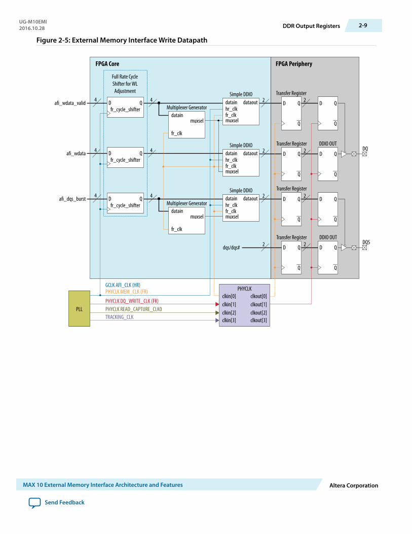
Figure 2-5: External Memory Interface Write Datapath
DQ
DQS
DDIO OUT
DDIO OUT
Transfer Register
Transfer Register
Transfer Register
Transfer Register
4
4
4
4 2 2
D Q
Q
2 2 D Q
Q
D Q
Q
2 2 D Q
Q
dqs/dqs#
D Q
Q
afi_wdata_valid
fr_cycle_shifterD Qafi_wdata
datain
fr_clk
muxsel
Simple DDIOdatainhr_clkfr_clkmuxsel
dataout
D Q
Q
fr_cycle_shifterD Q D Q
Q
afi_dqs_burst 4 4 2 2Simple DDIO
datainhr_clkfr_clkmuxsel
datain
fr_clk
muxsel
D Q
Q
dataout
fr_cycle_shifterD Q
Full Rate CycleShifter for WLAdjustment Simple DDIO
datainhr_clkfr_clkmuxsel
dataout
FPGA Core FPGA Periphery
Multiplexer Generator
Multiplexer Generator
PLL
clkin[0]clkin[1]clkin[2]clkin[3]
clkout[0]clkout[1]clkout[2]clkout[3]
PHYCLKGCLK AFI_CLK (HR)PHYCLK MEM_CLK (FR)
PHYCLK DQ_WRITE_CLK (FR)PHYCLK READ_CAPTURE_CLK0TRACKING_CLK
UG-M10EMI2016.10.28 DDR Output Registers 2-9
MAX 10 External Memory Interface Architecture and Features Altera Corporation
Send Feedback
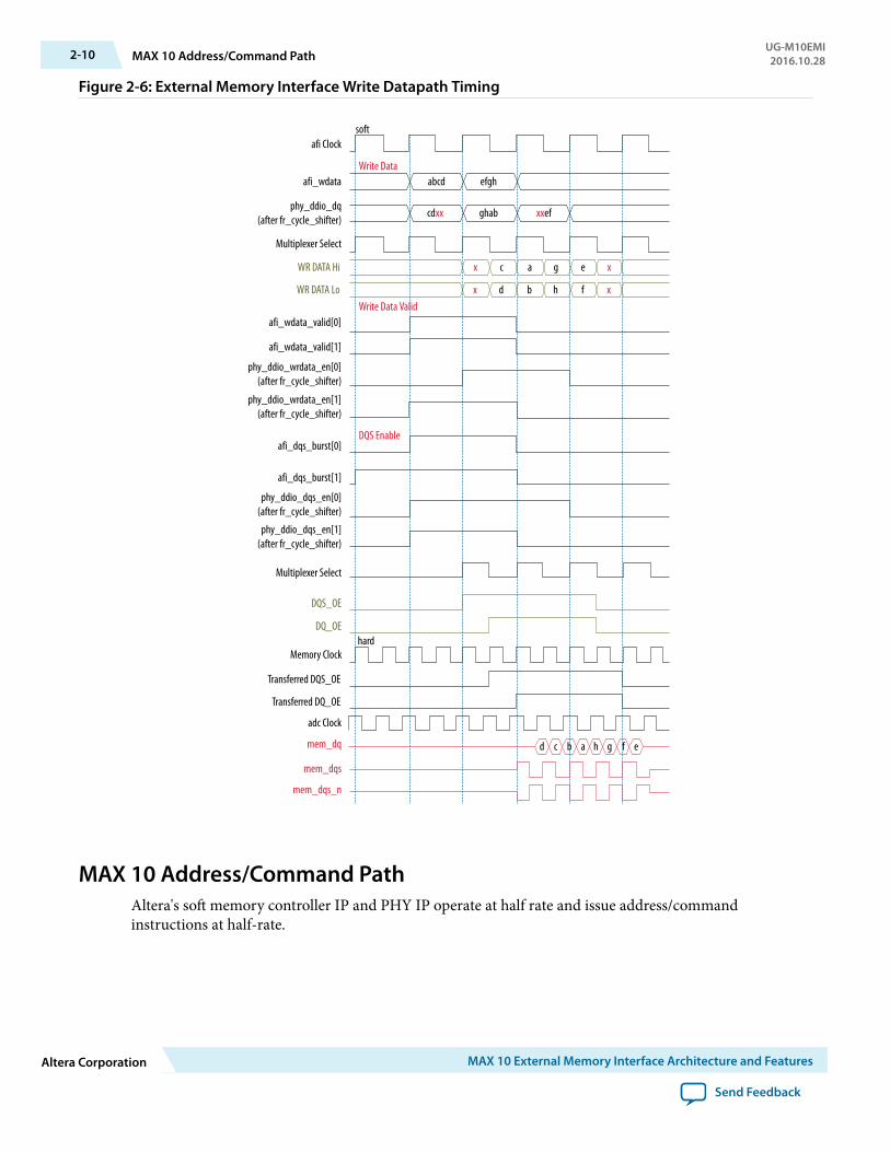
Figure 2-6: External Memory Interface Write Datapath Timing
d c b a h g f e
x c a g e x
x d b h f x
soft
Write Dataabcd efgh
cdxx ghab xxef
Write Data Valid
DQS Enable
hard
afi Clock
afi_wdata
phy_ddio_dq(after fr_cycle_shifter)
Multiplexer Select
WR DATA Hi
WR DATA Lo
afi_wdata_valid[0]
afi_wdata_valid[1]
phy_ddio_wrdata_en[0](after fr_cycle_shifter)
phy_ddio_wrdata_en[1](after fr_cycle_shifter)
afi_dqs_burst[0]
afi_dqs_burst[1]
phy_ddio_dqs_en[0](after fr_cycle_shifter)
phy_ddio_dqs_en[1](after fr_cycle_shifter)
Multiplexer Select
DQS_OE
DQ_OE
Memory Clock
Transferred DQS_OE
Transferred DQ_OE
adc Clock
mem_dq
mem_dqs
mem_dqs_n
MAX 10 Address/Command PathAltera's soft memory controller IP and PHY IP operate at half rate and issue address/commandinstructions at half-rate.
2-10 MAX 10 Address/Command PathUG-M10EMI2016.10.28
Altera Corporation MAX 10 External Memory Interface Architecture and Features
Send Feedback
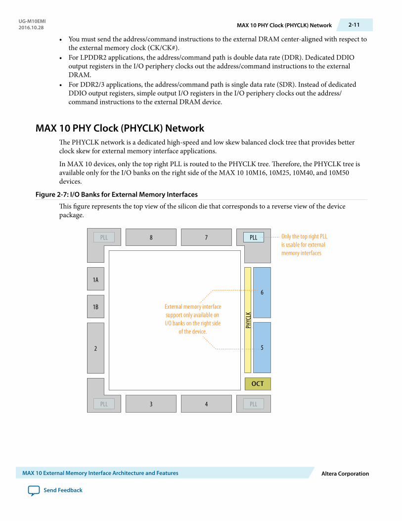
• You must send the address/command instructions to the external DRAM center-aligned with respect tothe external memory clock (CK/CK#).
• For LPDDR2 applications, the address/command path is double data rate (DDR). Dedicated DDIOoutput registers in the I/O periphery clocks out the address/command instructions to the externalDRAM.
• For DDR2/3 applications, the address/command path is single data rate (SDR). Instead of dedicatedDDIO output registers, simple output I/O registers in the I/O periphery clocks out the address/command instructions to the external DRAM device.
MAX 10 PHY Clock (PHYCLK) NetworkThe PHYCLK network is a dedicated high-speed and low skew balanced clock tree that provides betterclock skew for external memory interface applications.
In MAX 10 devices, only the top right PLL is routed to the PHYCLK tree. Therefore, the PHYCLK tree isavailable only for the I/O banks on the right side of the MAX 10 10M16, 10M25, 10M40, and 10M50devices.
Figure 2-7: I/O Banks for External Memory Interfaces
This figure represents the top view of the silicon die that corresponds to a reverse view of the devicepackage.
1B
1A
2
3 4
8 7
External memory interfacesupport only available on I/O banks on the right side
of the device.
Only the top right PLLis usable for externalmemory interfaces
PHYC
LK
PLLPLL
PLL PLL
OCT
5
6
UG-M10EMI2016.10.28 MAX 10 PHY Clock (PHYCLK) Network 2-11
MAX 10 External Memory Interface Architecture and Features Altera Corporation
Send Feedback
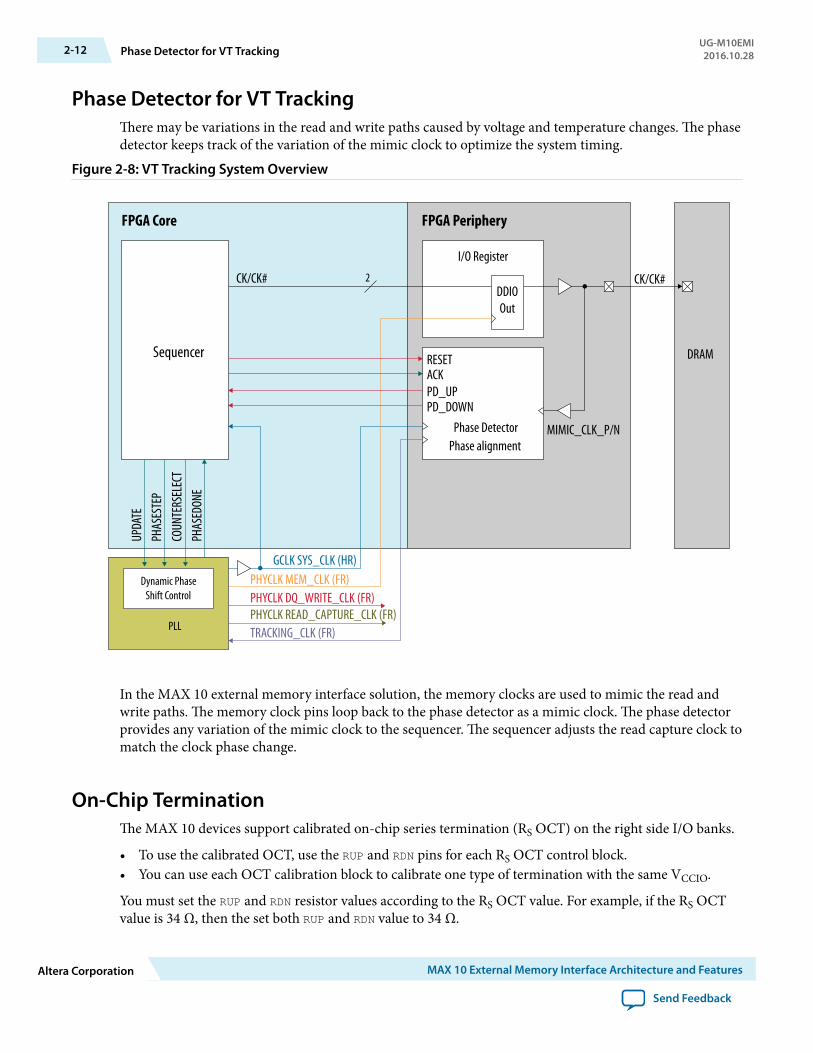
Phase Detector for VT TrackingThere may be variations in the read and write paths caused by voltage and temperature changes. The phasedetector keeps track of the variation of the mimic clock to optimize the system timing.
Figure 2-8: VT Tracking System Overview
I/O Register
Phase DetectorPhase alignment
MIMIC_CLK_P/N
RESETACKPD_UPPD_DOWN
CK/CK# 2
PLL
Dynamic PhaseShift Control
FPGA Core FPGA Periphery
CK/CK#
Sequencer
DDIOOut
UPDA
TEPH
ASES
TEP
PHAS
EDON
ECO
UNTE
RSEL
ECT
GCLK SYS_CLK (HR)
PHYCLK DQ_WRITE_CLK (FR)PHYCLK MEM_CLK (FR)
PHYCLK READ_CAPTURE_CLK (FR)TRACKING_CLK (FR)
DRAM
In the MAX 10 external memory interface solution, the memory clocks are used to mimic the read andwrite paths. The memory clock pins loop back to the phase detector as a mimic clock. The phase detectorprovides any variation of the mimic clock to the sequencer. The sequencer adjusts the read capture clock tomatch the clock phase change.
On-Chip TerminationThe MAX 10 devices support calibrated on-chip series termination (RS OCT) on the right side I/O banks.
• To use the calibrated OCT, use the RUP and RDN pins for each RS OCT control block.• You can use each OCT calibration block to calibrate one type of termination with the same VCCIO.
You must set the RUP and RDN resistor values according to the RS OCT value. For example, if the RS OCTvalue is 34 Ω, then the set both RUP and RDN value to 34 Ω.
2-12 Phase Detector for VT TrackingUG-M10EMI2016.10.28
Altera Corporation MAX 10 External Memory Interface Architecture and Features
Send Feedback
Related InformationMAX 10 On-Chip I/O TerminationProvides more information about OCT.
Phase-Locked LoopFor the external memory interface, the PLL generates the memory clock, write clock, capture clock, andthe logic–core clock.
• The memory clock provides clock for DQS write strobe, and address and command signals.• The write clock that is shifted –90° from the memory clock provides clock for DQ signals during
memory writes.
You can use the PLL reconfiguration feature to calibrate the read–capture phase shift to balance the setupand hold margins. At startup, the sequencer calibrates the capture clock.
For external memory interfaces in MAX 10 devices, you must use the top right PLL (PLL 2).
Related InformationPLL LocationsProvides more information about PLL location and availability in different MAX 10 packages.
MAX 10 Low Power FeatureThe MAX 10 low power feature is automatically activated when the self refresh or low power down modesare activated. The low power feature sends the afi_mem_clk_disable signal to stop the clock used by thecontroller.
To conserve power, the MAX 10 UniPHY IP core performs the following functions:
• Tri-states the address and command signals except CKE and RESET_N signals• Disables the input buffer of DDR input
Note: The MAX 10 low power feature is available from version 15.0 of the Quartus® Prime software. Toenable this feature, regenerate your MAX 10 UniPHY IP core using the Quartus Prime softwareversion 15.0 or later.
UG-M10EMI2016.10.28 Phase-Locked Loop 2-13
MAX 10 External Memory Interface Architecture and Features Altera Corporation
Send Feedback
MAX 10 External Memory Interface DesignConsiderations 3
2016.10.28
UG-M10EMI Subscribe Send Feedback
There are several considerations that require your attention to ensure the success of your designs. Unlessnoted otherwise, these design guidelines apply to all variants of this device family.
Related Information
• MAX 10 External Memory Interface Overview on page 1-1• Planning Pin and FPGA Resources chapter, External Memory Interface Handbook
Provides pin planning guidelines for implementing external memory interfaces with Altera devices.
MAX 10 DDR2 and DDR3 Design Considerations
DDR2/DDR3 External Memory Interface PinsIn DDR2/DDR3 interfaces, the MAX 10 devices use data (DQ), data strobe (DQS), clock, address, andcommand pins to interface with external memory devices. The devices also use the data mask (DM) pinsto enable data masking.
Related InformationDDR2/DDR3 Recommended Termination Schemes for MAX 10 Devices on page 3-3
MAX 10 Data and Data Clock (Data Strobe) PinsFor the MAX 10 external memory interfaces, the DQ pins are the data pins for bidirectional read andwrite, and the DQS pins are the data strobe pins used only during write operations.
The MAX 10 devices support bidirectional data strobes. Connect the bidirectional DQ data signals to thesame MAX 10 device DQ pins. The DQS pin is used only during write mode. In read mode, the MAX 10PHY generates the read capture clock internally and ignores the DQS signal. However, you must stillconnect DQS signal to the MAX 10 DQS pin.
Related InformationGuidelines: Reading the MAX 10 Pin-Out Files on page 3-8
MAX 10 I/O Bank DQ/DQS Support for DDR2/DDR3For DDR2/DDR3 SDRAM, I/O banks 5 and 6 in MAX 10 devices can support DQ and DQS signals withDQ-bus widths of 8, 16 and 24 bits.
© 2016 Intel Corporation. All rights reserved. Intel, the Intel logo, Altera, Arria, Cyclone, Enpirion, MAX, Megacore, NIOS, Quartus and Stratix words and logosare trademarks of Intel Corporation in the US and/or other countries. Other marks and brands may be claimed as the property of others. Intel warrantsperformance of its FPGA and semiconductor products to current specifications in accordance with Intel's standard warranty, but reserves the right to makechanges to any products and services at any time without notice. Intel assumes no responsibility or liability arising out of the application or use of anyinformation, product, or service described herein except as expressly agreed to in writing by Intel. Intel customers are advised to obtain the latest version ofdevice specifications before relying on any published information and before placing orders for products or services.
ISO9001:2008Registered
www.altera.com101 Innovation Drive, San Jose, CA 95134
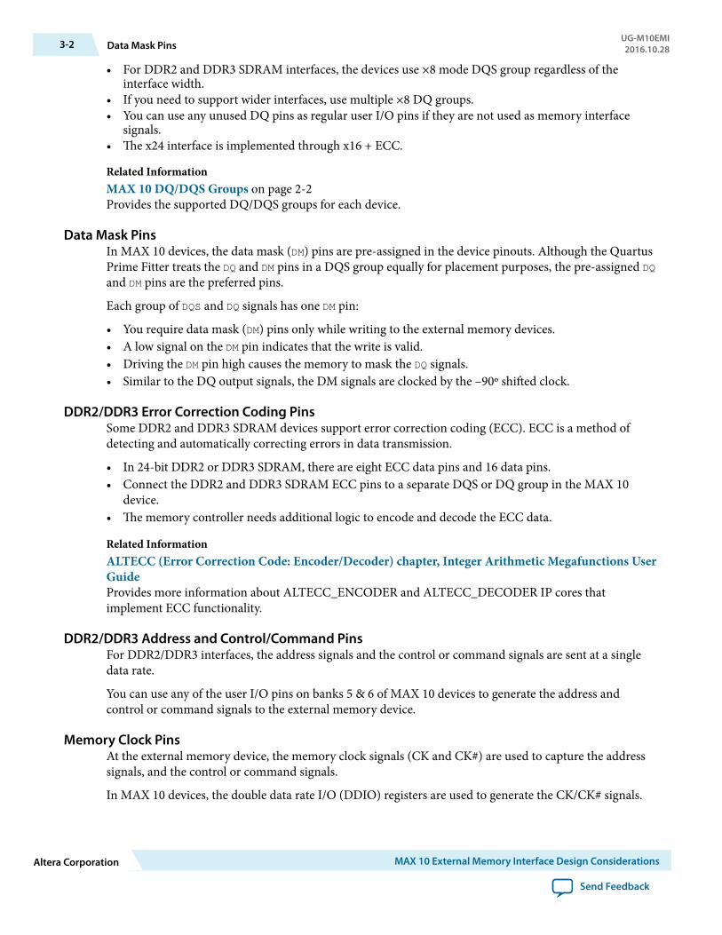
• For DDR2 and DDR3 SDRAM interfaces, the devices use ×8 mode DQS group regardless of theinterface width.
• If you need to support wider interfaces, use multiple ×8 DQ groups.• You can use any unused DQ pins as regular user I/O pins if they are not used as memory interface
signals.• The x24 interface is implemented through x16 + ECC.
Related InformationMAX 10 DQ/DQS Groups on page 2-2Provides the supported DQ/DQS groups for each device.
Data Mask PinsIn MAX 10 devices, the data mask (DM) pins are pre-assigned in the device pinouts. Although the QuartusPrime Fitter treats the DQ and DM pins in a DQS group equally for placement purposes, the pre-assigned DQand DM pins are the preferred pins.
Each group of DQS and DQ signals has one DM pin:
• You require data mask (DM) pins only while writing to the external memory devices.• A low signal on the DM pin indicates that the write is valid.• Driving the DM pin high causes the memory to mask the DQ signals.• Similar to the DQ output signals, the DM signals are clocked by the –90º shifted clock.
DDR2/DDR3 Error Correction Coding PinsSome DDR2 and DDR3 SDRAM devices support error correction coding (ECC). ECC is a method ofdetecting and automatically correcting errors in data transmission.
• In 24-bit DDR2 or DDR3 SDRAM, there are eight ECC data pins and 16 data pins.• Connect the DDR2 and DDR3 SDRAM ECC pins to a separate DQS or DQ group in the MAX 10
device.• The memory controller needs additional logic to encode and decode the ECC data.
Related InformationALTECC (Error Correction Code: Encoder/Decoder) chapter, Integer Arithmetic Megafunctions UserGuideProvides more information about ALTECC_ENCODER and ALTECC_DECODER IP cores thatimplement ECC functionality.
DDR2/DDR3 Address and Control/Command PinsFor DDR2/DDR3 interfaces, the address signals and the control or command signals are sent at a singledata rate.
You can use any of the user I/O pins on banks 5 & 6 of MAX 10 devices to generate the address andcontrol or command signals to the external memory device.
Memory Clock PinsAt the external memory device, the memory clock signals (CK and CK#) are used to capture the addresssignals, and the control or command signals.
In MAX 10 devices, the double data rate I/O (DDIO) registers are used to generate the CK/CK# signals.
3-2 Data Mask PinsUG-M10EMI2016.10.28
Altera Corporation MAX 10 External Memory Interface Design Considerations
Send Feedback
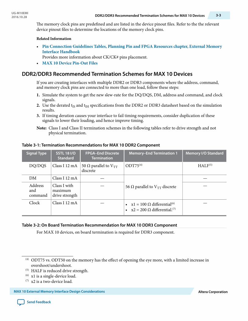
The memory clock pins are predefined and are listed in the device pinout files. Refer to the the relevantdevice pinout files to determine the locations of the memory clock pins.
Related Information
• Pin Connection Guidelines Tables, Planning Pin and FPGA Resources chapter, External MemoryInterface HandbookProvides more information about CK/CK# pins placement.
• MAX 10 Device Pin-Out Files
DDR2/DDR3 Recommended Termination Schemes for MAX 10 DevicesIf you are creating interfaces with multiple DDR2 or DDR3 components where the address, command,and memory clock pins are connected to more than one load, follow these steps:
1. Simulate the system to get the new slew-rate for the DQ/DQS, DM, address and command, and clocksignals.
2. Use the derated tIS and tIH specifications from the DDR2 or DDR3 datasheet based on the simulationresults.
3. If timing deration causes your interface to fail timing requirements, consider duplication of thesesignals to lower their loading, and hence improve timing.
Note: Class I and Class II termination schemes in the following tables refer to drive strength and notphysical termination.
Table 3-1: Termination Recommendations for MAX 10 DDR2 Component
Signal Type SSTL 18 I/OStandard
FPGA–End DiscreteTermination
Memory–End Termination 1 Memory I/O Standard
DQ/DQS Class I 12 mA 50 Ω parallel to VTTdiscrete
ODT75(4) HALF(5)
DM Class I 12 mA —
56 Ω parallel to VTT discrete
—Addressandcommand
Class I withmaximumdrive strength
— —
Clock Class I 12 mA — • x1 = 100 Ω differential(6)
• x2 = 200 Ω differential.(7)
—
Table 3-2: On Board Termination Recommendation for MAX 10 DDR3 Component
For MAX 10 devices, on board termination is required for DDR3 component.
(4) ODT75 vs. ODT50 on the memory has the effect of opening the eye more, with a limited increase inovershoot/undershoot.
(5) HALF is reduced drive strength.(6) x1 is a single-device load.(7) x2 is a two-device load.
UG-M10EMI2016.10.28 DDR2/DDR3 Recommended Termination Schemes for MAX 10 Devices 3-3
MAX 10 External Memory Interface Design Considerations Altera Corporation
Send Feedback
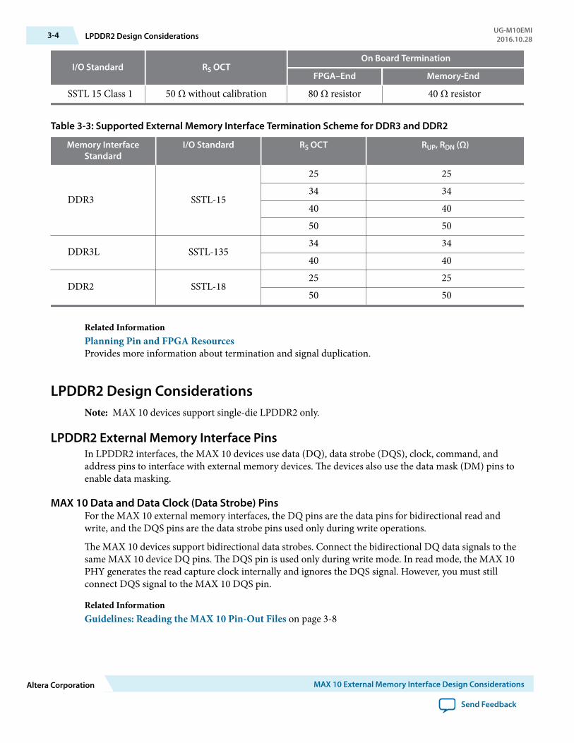
I/O Standard RS OCTOn Board Termination
FPGA–End Memory-End
SSTL 15 Class 1 50 Ω without calibration 80 Ω resistor 40 Ω resistor
Table 3-3: Supported External Memory Interface Termination Scheme for DDR3 and DDR2
Memory InterfaceStandard
I/O Standard RS OCT RUP, RDN (Ω)
DDR3 SSTL-15
25 2534 3440 4050 50
DDR3L SSTL-13534 3440 40
DDR2 SSTL-1825 2550 50
Related InformationPlanning Pin and FPGA ResourcesProvides more information about termination and signal duplication.
LPDDR2 Design ConsiderationsNote: MAX 10 devices support single-die LPDDR2 only.
LPDDR2 External Memory Interface PinsIn LPDDR2 interfaces, the MAX 10 devices use data (DQ), data strobe (DQS), clock, command, andaddress pins to interface with external memory devices. The devices also use the data mask (DM) pins toenable data masking.
MAX 10 Data and Data Clock (Data Strobe) PinsFor the MAX 10 external memory interfaces, the DQ pins are the data pins for bidirectional read andwrite, and the DQS pins are the data strobe pins used only during write operations.
The MAX 10 devices support bidirectional data strobes. Connect the bidirectional DQ data signals to thesame MAX 10 device DQ pins. The DQS pin is used only during write mode. In read mode, the MAX 10PHY generates the read capture clock internally and ignores the DQS signal. However, you must stillconnect DQS signal to the MAX 10 DQS pin.
Related InformationGuidelines: Reading the MAX 10 Pin-Out Files on page 3-8
3-4 LPDDR2 Design ConsiderationsUG-M10EMI2016.10.28
Altera Corporation MAX 10 External Memory Interface Design Considerations
Send Feedback
MAX 10 I/O Bank DQ/DQS Support for LPDDR2For LPDDR2 SDRAM, I/O banks 5 and 6 in MAX 10 devices can support DQ and DQS signals with DQ-bus widths of 8 and 16 bits.
• For LPDDR2 SDRAM interfaces, the devices use ×8 mode DQS group regardless of the interface width.• If you need to support wider interfaces, use multiple ×8 DQ groups.• You can use any unused DQ pins as regular user I/O pins if they are not used as memory interface
signal.
Related InformationMAX 10 DQ/DQS Groups on page 2-2Provides the supported DQ/DQS groups for each device.
Data Mask PinsIn MAX 10 devices, the data mask (DM) pins are pre-assigned in the device pinouts. Although the QuartusPrime Fitter treats the DQ and DM pins in a DQS group equally for placement purposes, the pre-assigned DQand DM pins are the preferred pins.
Each group of DQS and DQ signals has one DM pin:
• You require data mask (DM) pins only while writing to the external memory devices.• A low signal on the DM pin indicates that the write is valid.• Driving the DM pin high causes the memory to mask the DQ signals.• Similar to the DQ output signals, the DM signals are clocked by the –90º shifted clock.
LPDDR2 Address and Control/Command PinsFor LPDDR2 interfaces, the address signals and the control or command signals are sent at double datarate.
You can use any of the user I/O pins on banks 5 & 6 of MAX 10 devices to generate the address andcontrol or command signals to the external memory device.
Memory Clock PinsAt the external memory device, the memory clock signals (CK and CK#) are used to capture the addresssignals, and the control or command signals.
In MAX 10 devices, the double data rate I/O (DDIO) registers are used to generate the CK/CK# signals.
The memory clock pins are predefined and are listed in the device pinout files. Refer to the the relevantdevice pinout files to determine the locations of the memory clock pins.
Related Information
• Pin Connection Guidelines Tables, Planning Pin and FPGA Resources chapter, External MemoryInterface HandbookProvides more information about CK/CK# pins placement.
• MAX 10 Device Pin-Out Files
LPPDDR2 Power Supply Variation ConstraintFor an LPDDR2 interface that targets 200 MHz, constrain the memory device I/O and core power supplyvariation to within ±3%.
UG-M10EMI2016.10.28 MAX 10 I/O Bank DQ/DQS Support for LPDDR2 3-5
MAX 10 External Memory Interface Design Considerations Altera Corporation
Send Feedback
• Memory I/O power supply pin is VDDQ• Memory core power supply pin is VDD
Related InformationMAX 10 Power Management User Guide
LPDDR2 Recommended Termination Schemes for MAX 10 Devices
Table 3-4: Supported External Memory Interface Termination Scheme for LPDDR2
Memory InterfaceStandard
I/O Standard RS OCT RUP, RDN (Ω)
LPDDR2 HSUL-12 34, 40, 48 34, 40, 48
Guidelines: MAX 10 DDR3, DDR2, and LPDDR2 External Memory InterfaceI/O Limitation
While implementing certain external memory interface standards, the number of I/O pins available islimited.
• While implementing DDR2—for 25 percent of the remaining I/O pins available in I/O banks 5 and 6,you can assign them only as input pins.
• While implementing DDR3 or LPDDR2—the I/O pins listed in the following table are not available foruse. Of the remaining I/O pins, you can assign only 75 percent of the available I/O pins in I/O banks 5and 6 for normal I/O operation.
Table 3-5: Unavailable I/O Pins While Implementing DDR3 or LPDDR2 External Memory Interfaces inCertain Device Packages—Preliminary
DevicePackage
F256 U324 F484 F672
10M16 N16
P16
R15
P15
R18
P18
E16
D16
U21
U22
M21
L22
F21
F20
E19
F18
—
3-6 LPDDR2 Recommended Termination Schemes for MAX 10 DevicesUG-M10EMI2016.10.28
Altera Corporation MAX 10 External Memory Interface Design Considerations
Send Feedback
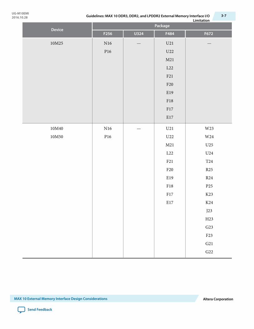
DevicePackage
F256 U324 F484 F672
10M25 N16
P16
— U21
U22
M21
L22
F21
F20
E19
F18
F17
E17
—
10M40
10M50
N16
P16
— U21
U22
M21
L22
F21
F20
E19
F18
F17
E17
W23
W24
U25
U24
T24
R25
R24
P25
K23
K24
J23
H23
G23
F23
G21
G22
UG-M10EMI2016.10.28 Guidelines: MAX 10 DDR3, DDR2, and LPDDR2 External Memory Interface I/O
Limitation3-7
MAX 10 External Memory Interface Design Considerations Altera Corporation
Send Feedback
Guidelines: MAX 10 Board Design Requirement for DDR2, DDR3, andLPDDR2
• For DDR2, DDR3, and LPDDR2 interfaces, the maximum board skew between pins must be lowerthan 40 ps. This guideline applies to all pins (address, command, clock, and data).
• To minimize unwanted inductance from the board via, Altera recommends that you keep the PCB viadepth for VCCIO banks below 49.5 mil.
• For devices with DDR3 interface implementation, onboard termination is required for the DQ, DQS,and address signals. Altera recommends that you use termination resistor value of 80 Ω to VTT.
• For the DQ, address, and command pins, keep the PCB trace routing length less than six inches forDDR3, or less than three inches for LPDDR2.
Related Information
• External Memory Interface Handbook Volume 1: Altera Memory Solution Overview and DesignFlowProvides more information about using Altera devices for external memory interfaces including Alteramemory solution and design flow.
• External Memory Interface Handbook Volume 2: Design GuidelinesProvides more information about using Altera devices for external memory interfaces includingmemory selection, board design, implementing memory IP cores, timing, optimization, anddebugging.
• Functional Description—MAX 10 EMIFProvides more information about implementing memory IP cores for MAX 10 devices.
• MAX 10 FPGA Signal Integrity Design GuidelinesProvides design guidelines related to signal integrity for MAX 10 devices.
Guidelines: Reading the MAX 10 Pin-Out FilesFor the maximum number of DQ pins and the exact number per group for a particular MAX 10 device,refer to the relevant device pin-out files.
In the pin-out files, the DQS and DQSn pins denote the differential data strobe/clock pin pairs. The DQS andDQSn pins are listed in the MAX 10 pin-out files as DQSXR and DQSnXR:
• X indicates the DQ/DQS grouping number.• R indicates the location of the group which is always on the right side of the device.
3-8 Guidelines: MAX 10 Board Design Requirement for DDR2, DDR3, and LPDDR2UG-M10EMI2016.10.28
Altera Corporation MAX 10 External Memory Interface Design Considerations
Send Feedback
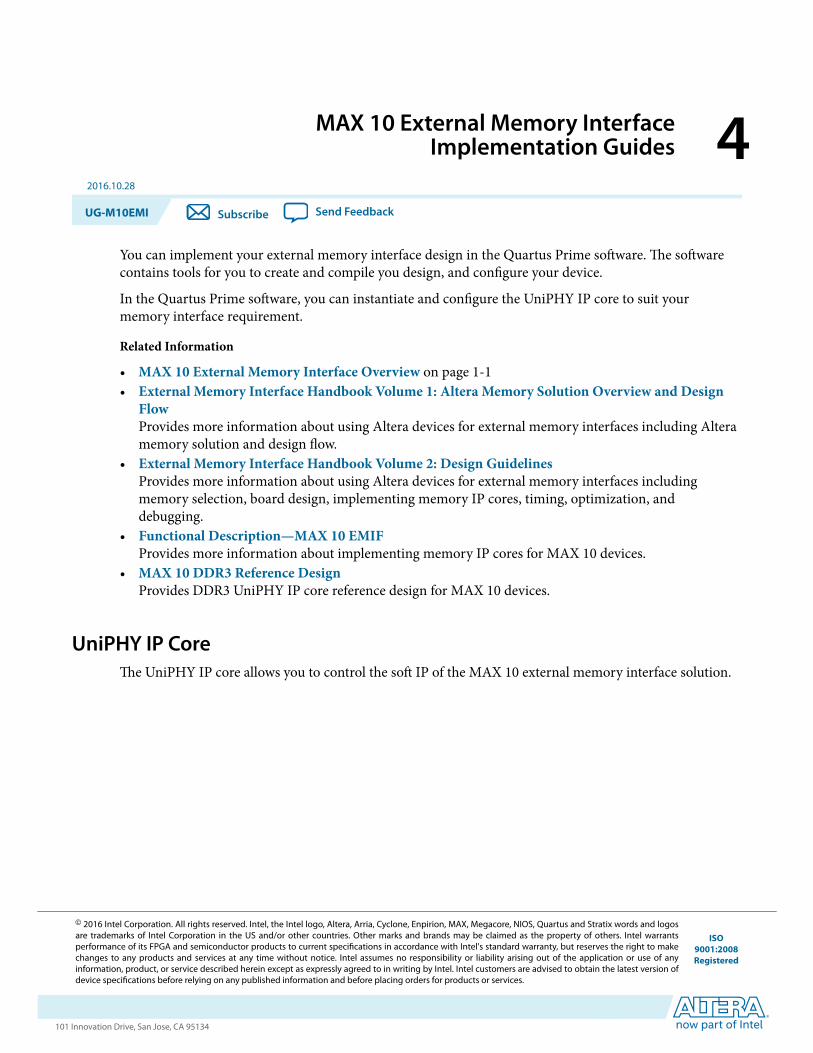
MAX 10 External Memory InterfaceImplementation Guides 4
2016.10.28
UG-M10EMI Subscribe Send Feedback
You can implement your external memory interface design in the Quartus Prime software. The softwarecontains tools for you to create and compile you design, and configure your device.
In the Quartus Prime software, you can instantiate and configure the UniPHY IP core to suit yourmemory interface requirement.
Related Information
• MAX 10 External Memory Interface Overview on page 1-1• External Memory Interface Handbook Volume 1: Altera Memory Solution Overview and Design
FlowProvides more information about using Altera devices for external memory interfaces including Alteramemory solution and design flow.
• External Memory Interface Handbook Volume 2: Design GuidelinesProvides more information about using Altera devices for external memory interfaces includingmemory selection, board design, implementing memory IP cores, timing, optimization, anddebugging.
• Functional Description—MAX 10 EMIFProvides more information about implementing memory IP cores for MAX 10 devices.
• MAX 10 DDR3 Reference DesignProvides DDR3 UniPHY IP core reference design for MAX 10 devices.
UniPHY IP CoreThe UniPHY IP core allows you to control the soft IP of the MAX 10 external memory interface solution.
© 2016 Intel Corporation. All rights reserved. Intel, the Intel logo, Altera, Arria, Cyclone, Enpirion, MAX, Megacore, NIOS, Quartus and Stratix words and logosare trademarks of Intel Corporation in the US and/or other countries. Other marks and brands may be claimed as the property of others. Intel warrantsperformance of its FPGA and semiconductor products to current specifications in accordance with Intel's standard warranty, but reserves the right to makechanges to any products and services at any time without notice. Intel assumes no responsibility or liability arising out of the application or use of anyinformation, product, or service described herein except as expressly agreed to in writing by Intel. Intel customers are advised to obtain the latest version ofdevice specifications before relying on any published information and before placing orders for products or services.
ISO9001:2008Registered
www.altera.com101 Innovation Drive, San Jose, CA 95134
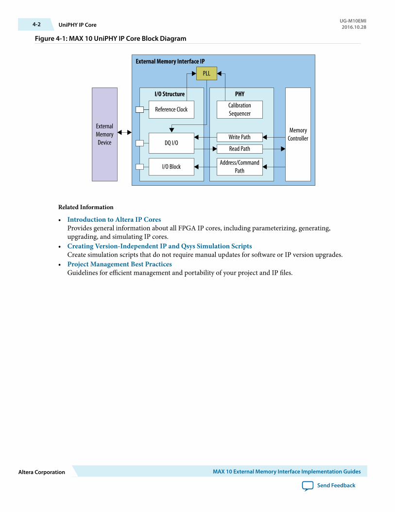
Figure 4-1: MAX 10 UniPHY IP Core Block Diagram
I/O Structure
Reference Clock
DQ I/O
I/O Block
Write Path
Read Path
Address/CommandPath
CalibrationSequencer
PLL
MemoryController
PHY
ExternalMemoryDevice
External Memory Interface IP
Related Information
• Introduction to Altera IP CoresProvides general information about all FPGA IP cores, including parameterizing, generating,upgrading, and simulating IP cores.
• Creating Version-Independent IP and Qsys Simulation ScriptsCreate simulation scripts that do not require manual updates for software or IP version upgrades.
• Project Management Best PracticesGuidelines for efficient management and portability of your project and IP files.
4-2 UniPHY IP CoreUG-M10EMI2016.10.28
Altera Corporation MAX 10 External Memory Interface Implementation Guides
Send Feedback
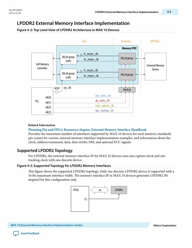
LPDDR2 External Memory Interface ImplementationFigure 4-2: Top Level View of LPDDR2 Architecture in MAX 10 Devices
DQ x8 group(soft)
DQ x8 group(soft)
DQ x8 group
DQ x8 group
PHYCLK
PLL
External MemoryDevice
Soft MemoryController
clk[0]
clk[1]clk[2]
clk[3]
phy_mem_clk
sys_clk
dq_write_clk
read_capture_clk
dqs_tracking_clk
fr_resync_clk8
hr_resync_clk
fr_resync_clk8
hr_resync_clk
Memory PHY
Off FPGAPeripheryCore
GCLK
Related InformationPlanning Pin and FPGA Resources chapter, External Memory Interface HandbookProvides the maximum number of interfaces supported by MAX 10 devices for each memory standards,pin counts for various external memory interface implementation examples, and information about theclock, address/command, data, data strobe, DM, and optional ECC signals.
Supported LPDDR2 TopologyFor LPDDR2, the external memory interface IP for MAX 10 devices uses one capture clock and onetracking clock with one discrete device.
Figure 4-3: Supported Topology for LPDDR2 Memory Interfaces
This figure shows the supported LPDDR2 topology. Only one discrete LPDDR2 device is supported with a16 bit maximum interface width. The memory interface IP in MAX 10 devices generates LPDDR2 IPstargeted for this configuration only.
FPGA
CS
LPDDR216
UG-M10EMI2016.10.28 LPDDR2 External Memory Interface Implementation 4-3
MAX 10 External Memory Interface Implementation Guides Altera Corporation
Send Feedback
DDR2 and DDR3 External Memory Interface ImplementationFigure 4-4: Top Level View of DDR2, DDR3, or DDR3L Architecture in MAX 10 Devices
DQ x8 group(soft)
DQ x8 group(soft)
DQ x8 group(soft)
DQ x8 group
DQ x8 group
DQ x8 group
PHYCLK
PLL
External MemoryDevice
Soft MemoryController
External MemoryDevice
clk[0]
clk[1]clk[2]
clk[3]
phy_mem_clk
sys_clk
dq_write_clk
read_capture_clk
read_capture_ecc_clk
fr_resync_clk8
hr_resync_clk
fr_resync_clk8
hr_resync_clk
fr_resync_clk8
hr_resync_clk
Memory PHY
Off FPGAPeripheryCore
GCLK
Related InformationPlanning Pin and FPGA Resources chapter, External Memory Interface HandbookProvides the maximum number of interfaces supported by MAX 10 devices for each memory standards,pin counts for various external memory interface implementation examples, and information about theclock, address/command, data, data strobe, DM, and optional ECC signals.
MAX 10 Supported DDR2 or DDR3 TopologyFor DDR2 or DDR3/DDR3L, the external memory interface IP for MAX 10 devices uses two captureclocks with two discrete devices.
4-4 DDR2 and DDR3 External Memory Interface ImplementationUG-M10EMI2016.10.28
Altera Corporation MAX 10 External Memory Interface Implementation Guides
Send Feedback
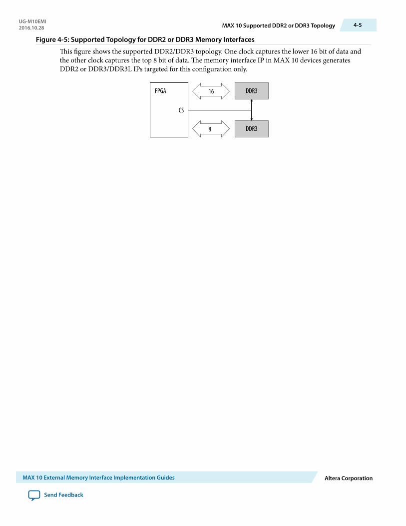
Figure 4-5: Supported Topology for DDR2 or DDR3 Memory Interfaces
This figure shows the supported DDR2/DDR3 topology. One clock captures the lower 16 bit of data andthe other clock captures the top 8 bit of data. The memory interface IP in MAX 10 devices generatesDDR2 or DDR3/DDR3L IPs targeted for this configuration only.
FPGA
CS
DDR3
DDR3
8
16
UG-M10EMI2016.10.28 MAX 10 Supported DDR2 or DDR3 Topology 4-5
MAX 10 External Memory Interface Implementation Guides Altera Corporation
Send Feedback
UniPHY IP Core References for MAX 10 52016.10.28
UG-M10EMI Subscribe Send Feedback
For MAX 10 devices, there are three variations of the UniPHY IP core:
• DDR2 SDRAM Controller• DDR3 SDRAM Controller• LPDDR2 SDRAM Controller
Related Information
• MAX 10 External Memory Interface Overview on page 1-1• External Memory Interface Handbook Volume 1: Altera Memory Solution Overview and Design
FlowProvides more information about using Altera devices for external memory interfaces including Alteramemory solution and design flow.
• External Memory Interface Handbook Volume 2: Design GuidelinesProvides more information about using Altera devices for external memory interfaces includingmemory selection, board design, implementing memory IP cores, timing, optimization, anddebugging.
• Functional Description—MAX 10 EMIFProvides more information about implementing memory IP cores for MAX 10 devices.
UniPHY Parameter Settings for MAX 10You can set the parameter settings for the UniPHY IP core in the Quartus Prime software. There are sixgroups of options: PHY Settings, Memory Parameters, Memory Timing, Board Settings, ControllerSettings, and Diagnostics.
Note: MAX 10 devices are not supported in the EMIF Debug Toolkit.
UniPHY Parameters—PHY SettingsThere are three groups of options: General Settings, Clocks, and Advanced PHY Settings.
© 2016 Intel Corporation. All rights reserved. Intel, the Intel logo, Altera, Arria, Cyclone, Enpirion, MAX, Megacore, NIOS, Quartus and Stratix words and logosare trademarks of Intel Corporation in the US and/or other countries. Other marks and brands may be claimed as the property of others. Intel warrantsperformance of its FPGA and semiconductor products to current specifications in accordance with Intel's standard warranty, but reserves the right to makechanges to any products and services at any time without notice. Intel assumes no responsibility or liability arising out of the application or use of anyinformation, product, or service described herein except as expressly agreed to in writing by Intel. Intel customers are advised to obtain the latest version ofdevice specifications before relying on any published information and before placing orders for products or services.
ISO9001:2008Registered
www.altera.com101 Innovation Drive, San Jose, CA 95134
Table 5-1: PHY Settings - General Settings
Parameter Description
Speed Grade Specifies the speed grade of the targeted FPGA device that affects thegenerated timing constraints and timing reporting.
Note: For MAX 10 devices, DDR3 and LPDDR2 is supported onlyfor speed grade –6, and DDR2 for speed grades –6 and –7.
Generate PHY only Turn on this option to generate the UniPHY IP core without a memorycontroller.
When you turn on this option, the AFI interface is exported so that youcan easily connect your own memory controller.
Table 5-2: PHY Settings - Clocks
Parameter Description
Memory clock frequency The frequency of the clock that drives the memory device. Use up to 4decimal places of precision.
To obtain the maximum supported frequency for your target memoryconfiguration, refer to the External Memory Spec Estimator page onthe Altera website.
Achieved memory clockfrequency
The actual frequency the PLL generates to drive the external memoryinterface (memory clock).
PLL reference clock frequency The frequency of the input clock that feeds the PLL. Use up to 4decimal places of precision.
Rate on Avalon-MM interface The width of data bus on the Avalon-MM interface.
The MAX 10 supports only Half rate, which results in a width of 4× thememory data width.
Achieved local clock frequency The actual frequency the PLL generates to drive the local interface forthe memory controller (AFI clock).
Table 5-3: DDR3 SDRAM PHY Settings - Advanced PHY Settings
Parameter Description
Supply voltage The supply voltage and sub-family type of memory.
This option is available for DDR3 SDRAM only.
I/O standard The I/O standard voltage.
Set the I/O standard according to your design’s memory standard.
5-2 UniPHY Parameters—PHY SettingsUG-M10EMI2016.10.28
Altera Corporation UniPHY IP Core References for MAX 10
Send Feedback
Parameter Description
Reconfigurable PLL location If you set the PLL used in the UniPHY IP core memory interface to bereconfigurable at run time, you must specify the location of the PLL.
This assignment generates a PLL that can only be placed in the givensides.
Related InformationExternal Memory Interface Spec EstimatorProvides a parametric tool that allows you to find and compare the performance of the supported externalmemory interfaces in Altera devices.
UniPHY Parameters—Memory ParametersThere are three groups of options: Memory Parameters, Memory Topology, and Memory InitializationOptions.
Table 5-4: Memory Parameters
Use the Memory Parameters options group to apply the memory parameters from your memorymanufacturer’s data sheet.
Parameter Description
Memory vendor The vendor of the memory device. Select the memory vendor according to thememory vendor you use. For memory vendors that are not listed in the setting,select JEDEC with the nearest memory parameters and edit the parameter valuesaccording to the values of the memory vendor that you use. However, if youselect a configuration from the list of memory presets, the default memoryvendor for that preset setting is automatically selected.
Memory format The format of the memory device.
This parameter is automatically set to Discrete Device.
Memory device speedgrade
The maximum frequency at which the memory device can run.
Total interface width The total number of DQ pins of the memory device. Limited to 8 to 24 bits.
DQ/DQS group size The number of DQ bits per DQS group.
Number of DQSgroups
The number of DQS groups is calculated automatically from the Total interfacewidth and the DQ/DQS group size parameters.
Number of chip selects The number of chip-selects the IP core uses for the current device configuration.
Specify the total number of chip-selects according to the number of memorydevice.
Number of clocks The width of the clock bus on the memory interface.
UG-M10EMI2016.10.28 UniPHY Parameters—Memory Parameters 5-3
UniPHY IP Core References for MAX 10 Altera Corporation
Send Feedback
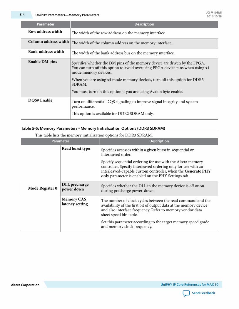
Parameter Description
Row address width The width of the row address on the memory interface.
Column address width The width of the column address on the memory interface.
Bank-address width The width of the bank address bus on the memory interface.
Enable DM pins Specifies whether the DM pins of the memory device are driven by the FPGA.You can turn off this option to avoid overusing FPGA device pins when using x4mode memory devices.
When you are using x4 mode memory devices, turn off this option for DDR3SDRAM.
You must turn on this option if you are using Avalon byte enable.
DQS# Enable Turn on differential DQS signaling to improve signal integrity and systemperformance.
This option is available for DDR2 SDRAM only.
Table 5-5: Memory Parameters - Memory Initialization Options (DDR3 SDRAM)
This table lists the memory initialization options for DDR3 SDRAM.Parameter Description
Mode Register 0
Read burst type Specifies accesses within a given burst in sequential orinterleaved order.
Specify sequential ordering for use with the Altera memorycontroller. Specify interleaved ordering only for use with aninterleaved-capable custom controller, when the Generate PHYonly parameter is enabled on the PHY Settings tab.
DLL prechargepower down
Specifies whether the DLL in the memory device is off or onduring precharge power-down.
Memory CASlatency setting
The number of clock cycles between the read command and theavailability of the first bit of output data at the memory deviceand also interface frequency. Refer to memory vendor datasheet speed bin table.
Set this parameter according to the target memory speed gradeand memory clock frequency.
5-4 UniPHY Parameters—Memory ParametersUG-M10EMI2016.10.28
Altera Corporation UniPHY IP Core References for MAX 10
Send Feedback
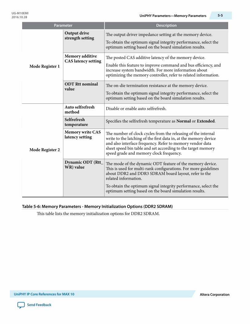
Parameter Description
Mode Register 1
Output drivestrength setting
The output driver impedance setting at the memory device.
To obtain the optimum signal integrity performance, select theoptimum setting based on the board simulation results.
Memory additiveCAS latency setting
The posted CAS additive latency of the memory device.
Enable this feature to improve command and bus efficiency, andincrease system bandwidth. For more information aboutoptimizing the memory controller, refer to related information.
ODT Rtt nominalvalue
The on-die termination resistance at the memory device.
To obtain the optimum signal integrity performance, select theoptimum setting based on the board simulation results.
Mode Register 2
Auto selfrefreshmethod
Disable or enable auto selfrefresh.
Selfrefreshtemperature
Specifies the selfrefresh temperature as Normal or Extended.
Memory write CASlatency setting
The number of clock cycles from the releasing of the internalwrite to the latching of the first data in, at the memory deviceand also interface frequency. Refer to memory vendor datasheet speed bin table and set according to the target memoryspeed grade and memory clock frequency.
Dynamic ODT (Rtt_WR) value
The mode of the dynamic ODT feature of the memory device.This is used for multi-rank configurations. For more guidelinesabout DDR2 and DDR3 SDRAM board layout, refer to therelated information.
To obtain the optimum signal integrity performance, select theoptimum setting based on the board simulation results.
Table 5-6: Memory Parameters - Memory Initialization Options (DDR2 SDRAM)
This table lists the memory initialization options for DDR2 SDRAM.
UG-M10EMI2016.10.28 UniPHY Parameters—Memory Parameters 5-5
UniPHY IP Core References for MAX 10 Altera Corporation
Send Feedback
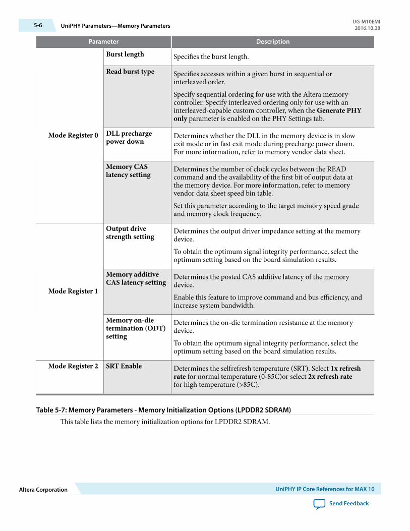
Parameter Description
Mode Register 0
Burst length Specifies the burst length.
Read burst type Specifies accesses within a given burst in sequential orinterleaved order.
Specify sequential ordering for use with the Altera memorycontroller. Specify interleaved ordering only for use with aninterleaved-capable custom controller, when the Generate PHYonly parameter is enabled on the PHY Settings tab.
DLL prechargepower down
Determines whether the DLL in the memory device is in slowexit mode or in fast exit mode during precharge power down.For more information, refer to memory vendor data sheet.
Memory CASlatency setting
Determines the number of clock cycles between the READcommand and the availability of the first bit of output data atthe memory device. For more information, refer to memoryvendor data sheet speed bin table.
Set this parameter according to the target memory speed gradeand memory clock frequency.
Mode Register 1
Output drivestrength setting
Determines the output driver impedance setting at the memorydevice.
To obtain the optimum signal integrity performance, select theoptimum setting based on the board simulation results.
Memory additiveCAS latency setting
Determines the posted CAS additive latency of the memorydevice.
Enable this feature to improve command and bus efficiency, andincrease system bandwidth.
Memory on-dietermination (ODT)setting
Determines the on-die termination resistance at the memorydevice.
To obtain the optimum signal integrity performance, select theoptimum setting based on the board simulation results.
Mode Register 2 SRT Enable Determines the selfrefresh temperature (SRT). Select 1x refreshrate for normal temperature (0-85C)or select 2x refresh ratefor high temperature (>85C).
Table 5-7: Memory Parameters - Memory Initialization Options (LPDDR2 SDRAM)
This table lists the memory initialization options for LPDDR2 SDRAM.
5-6 UniPHY Parameters—Memory ParametersUG-M10EMI2016.10.28
Altera Corporation UniPHY IP Core References for MAX 10
Send Feedback
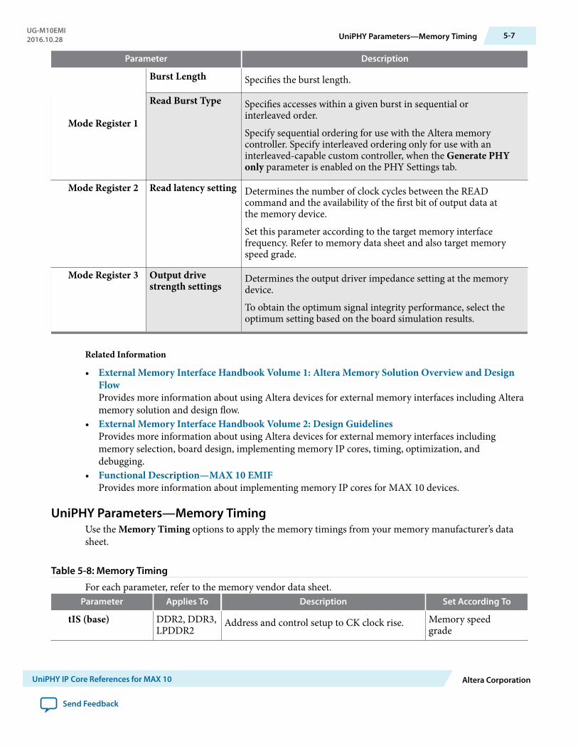
Parameter Description
Mode Register 1
Burst Length Specifies the burst length.
Read Burst Type Specifies accesses within a given burst in sequential orinterleaved order.
Specify sequential ordering for use with the Altera memorycontroller. Specify interleaved ordering only for use with aninterleaved-capable custom controller, when the Generate PHYonly parameter is enabled on the PHY Settings tab.
Mode Register 2 Read latency setting Determines the number of clock cycles between the READcommand and the availability of the first bit of output data atthe memory device.
Set this parameter according to the target memory interfacefrequency. Refer to memory data sheet and also target memoryspeed grade.
Mode Register 3 Output drivestrength settings
Determines the output driver impedance setting at the memorydevice.
To obtain the optimum signal integrity performance, select theoptimum setting based on the board simulation results.
Related Information
• External Memory Interface Handbook Volume 1: Altera Memory Solution Overview and DesignFlowProvides more information about using Altera devices for external memory interfaces including Alteramemory solution and design flow.
• External Memory Interface Handbook Volume 2: Design GuidelinesProvides more information about using Altera devices for external memory interfaces includingmemory selection, board design, implementing memory IP cores, timing, optimization, anddebugging.
• Functional Description—MAX 10 EMIFProvides more information about implementing memory IP cores for MAX 10 devices.
UniPHY Parameters—Memory TimingUse the Memory Timing options to apply the memory timings from your memory manufacturer’s datasheet.
Table 5-8: Memory Timing
For each parameter, refer to the memory vendor data sheet.Parameter Applies To Description Set According To
tIS (base) DDR2, DDR3,LPDDR2
Address and control setup to CK clock rise. Memory speedgrade
UG-M10EMI2016.10.28 UniPHY Parameters—Memory Timing 5-7
UniPHY IP Core References for MAX 10 Altera Corporation
Send Feedback
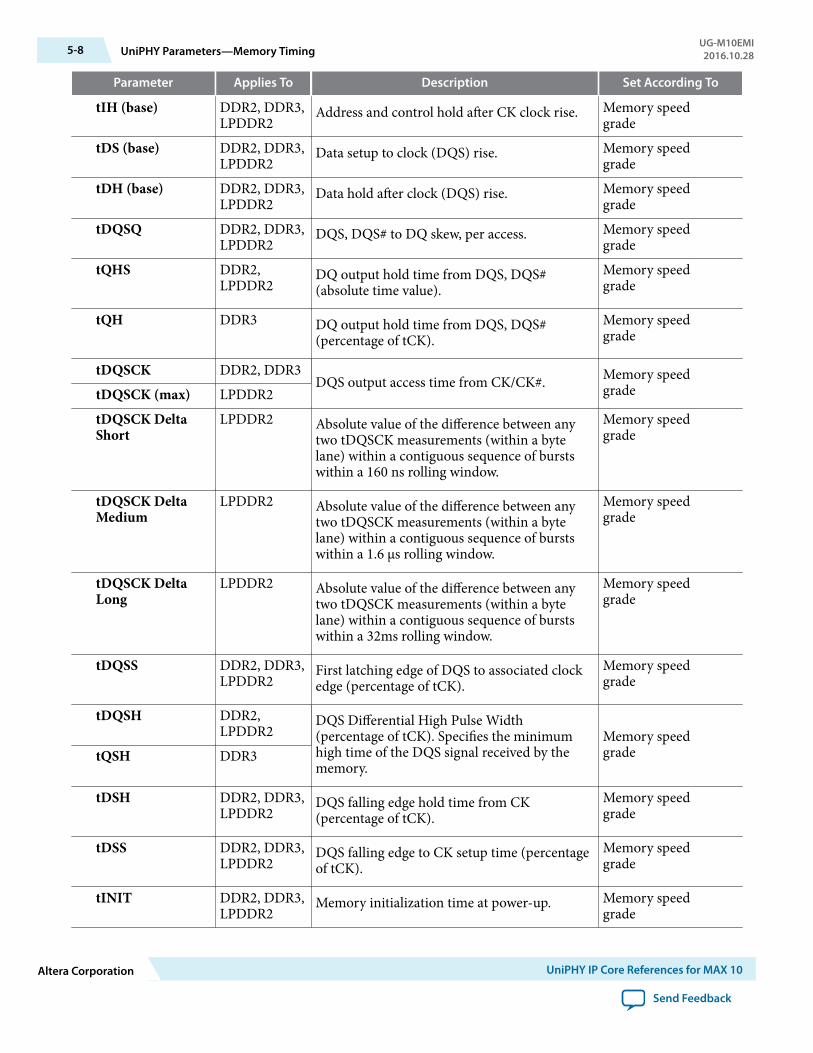
Parameter Applies To Description Set According To
tIH (base) DDR2, DDR3,LPDDR2
Address and control hold after CK clock rise. Memory speedgrade
tDS (base) DDR2, DDR3,LPDDR2
Data setup to clock (DQS) rise. Memory speedgrade
tDH (base) DDR2, DDR3,LPDDR2
Data hold after clock (DQS) rise. Memory speedgrade
tDQSQ DDR2, DDR3,LPDDR2
DQS, DQS# to DQ skew, per access. Memory speedgrade
tQHS DDR2,LPDDR2
DQ output hold time from DQS, DQS#(absolute time value).
Memory speedgrade
tQH DDR3 DQ output hold time from DQS, DQS#(percentage of tCK).
Memory speedgrade
tDQSCK DDR2, DDR3DQS output access time from CK/CK#. Memory speed
gradetDQSCK (max) LPDDR2tDQSCK DeltaShort
LPDDR2 Absolute value of the difference between anytwo tDQSCK measurements (within a bytelane) within a contiguous sequence of burstswithin a 160 ns rolling window.
Memory speedgrade
tDQSCK DeltaMedium
LPDDR2 Absolute value of the difference between anytwo tDQSCK measurements (within a bytelane) within a contiguous sequence of burstswithin a 1.6 µs rolling window.
Memory speedgrade
tDQSCK DeltaLong
LPDDR2 Absolute value of the difference between anytwo tDQSCK measurements (within a bytelane) within a contiguous sequence of burstswithin a 32ms rolling window.
Memory speedgrade
tDQSS DDR2, DDR3,LPDDR2
First latching edge of DQS to associated clockedge (percentage of tCK).
Memory speedgrade
tDQSH DDR2,LPDDR2
DQS Differential High Pulse Width(percentage of tCK). Specifies the minimumhigh time of the DQS signal received by thememory.
Memory speedgradetQSH DDR3
tDSH DDR2, DDR3,LPDDR2
DQS falling edge hold time from CK(percentage of tCK).
Memory speedgrade
tDSS DDR2, DDR3,LPDDR2
DQS falling edge to CK setup time (percentageof tCK).
Memory speedgrade
tINIT DDR2, DDR3,LPDDR2
Memory initialization time at power-up. Memory speedgrade
5-8 UniPHY Parameters—Memory TimingUG-M10EMI2016.10.28
Altera Corporation UniPHY IP Core References for MAX 10
Send Feedback
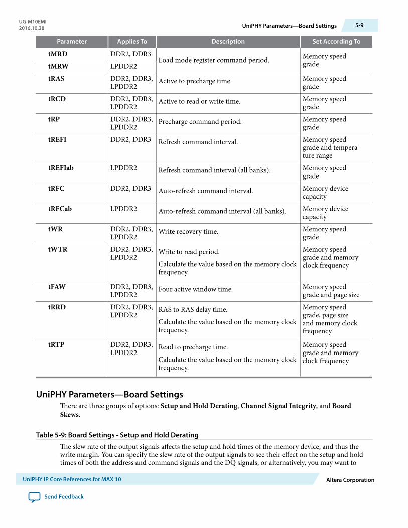
Parameter Applies To Description Set According To
tMRD DDR2, DDR3Load mode register command period. Memory speed
gradetMRW LPDDR2tRAS DDR2, DDR3,
LPDDR2Active to precharge time. Memory speed
gradetRCD DDR2, DDR3,
LPDDR2Active to read or write time. Memory speed
gradetRP DDR2, DDR3,
LPDDR2Precharge command period. Memory speed
gradetREFI DDR2, DDR3 Refresh command interval. Memory speed
grade and tempera‐ture range
tREFIab LPDDR2 Refresh command interval (all banks). Memory speedgrade
tRFC DDR2, DDR3 Auto-refresh command interval. Memory devicecapacity
tRFCab LPDDR2 Auto-refresh command interval (all banks). Memory devicecapacity
tWR DDR2, DDR3,LPDDR2
Write recovery time. Memory speedgrade
tWTR DDR2, DDR3,LPDDR2
Write to read period.
Calculate the value based on the memory clockfrequency.
Memory speedgrade and memoryclock frequency
tFAW DDR2, DDR3,LPDDR2
Four active window time. Memory speedgrade and page size
tRRD DDR2, DDR3,LPDDR2
RAS to RAS delay time.
Calculate the value based on the memory clockfrequency.
Memory speedgrade, page sizeand memory clockfrequency
tRTP DDR2, DDR3,LPDDR2
Read to precharge time.
Calculate the value based on the memory clockfrequency.
Memory speedgrade and memoryclock frequency
UniPHY Parameters—Board SettingsThere are three groups of options: Setup and Hold Derating, Channel Signal Integrity, and BoardSkews.
Table 5-9: Board Settings - Setup and Hold Derating
The slew rate of the output signals affects the setup and hold times of the memory device, and thus thewrite margin. You can specify the slew rate of the output signals to see their effect on the setup and holdtimes of both the address and command signals and the DQ signals, or alternatively, you may want to
UG-M10EMI2016.10.28 UniPHY Parameters—Board Settings 5-9
UniPHY IP Core References for MAX 10 Altera Corporation
Send Feedback
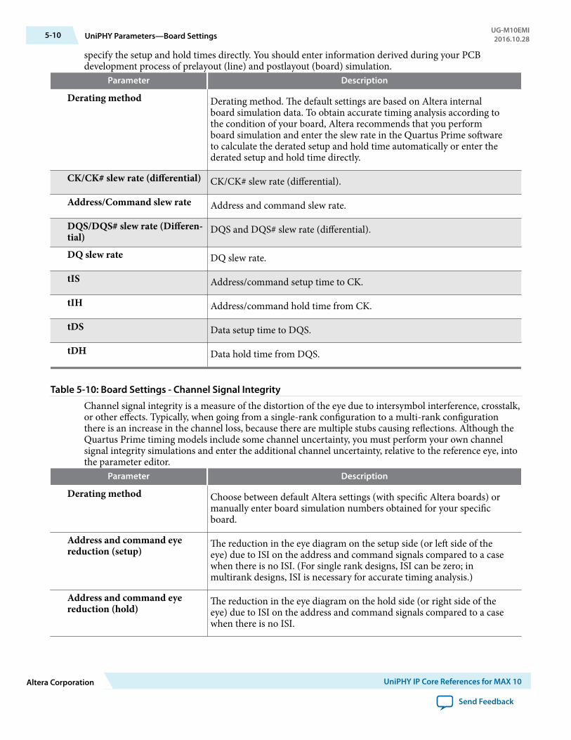
specify the setup and hold times directly. You should enter information derived during your PCBdevelopment process of prelayout (line) and postlayout (board) simulation.
Parameter Description
Derating method Derating method. The default settings are based on Altera internalboard simulation data. To obtain accurate timing analysis according tothe condition of your board, Altera recommends that you performboard simulation and enter the slew rate in the Quartus Prime softwareto calculate the derated setup and hold time automatically or enter thederated setup and hold time directly.
CK/CK# slew rate (differential) CK/CK# slew rate (differential).
Address/Command slew rate Address and command slew rate.
DQS/DQS# slew rate (Differen‐tial)
DQS and DQS# slew rate (differential).
DQ slew rate DQ slew rate.
tIS Address/command setup time to CK.
tIH Address/command hold time from CK.
tDS Data setup time to DQS.
tDH Data hold time from DQS.
Table 5-10: Board Settings - Channel Signal Integrity
Channel signal integrity is a measure of the distortion of the eye due to intersymbol interference, crosstalk,or other effects. Typically, when going from a single-rank configuration to a multi-rank configurationthere is an increase in the channel loss, because there are multiple stubs causing reflections. Although theQuartus Prime timing models include some channel uncertainty, you must perform your own channelsignal integrity simulations and enter the additional channel uncertainty, relative to the reference eye, intothe parameter editor.
Parameter Description
Derating method Choose between default Altera settings (with specific Altera boards) ormanually enter board simulation numbers obtained for your specificboard.
Address and command eyereduction (setup)
The reduction in the eye diagram on the setup side (or left side of theeye) due to ISI on the address and command signals compared to a casewhen there is no ISI. (For single rank designs, ISI can be zero; inmultirank designs, ISI is necessary for accurate timing analysis.)
Address and command eyereduction (hold)
The reduction in the eye diagram on the hold side (or right side of theeye) due to ISI on the address and command signals compared to a casewhen there is no ISI.
5-10 UniPHY Parameters—Board SettingsUG-M10EMI2016.10.28
Altera Corporation UniPHY IP Core References for MAX 10
Send Feedback
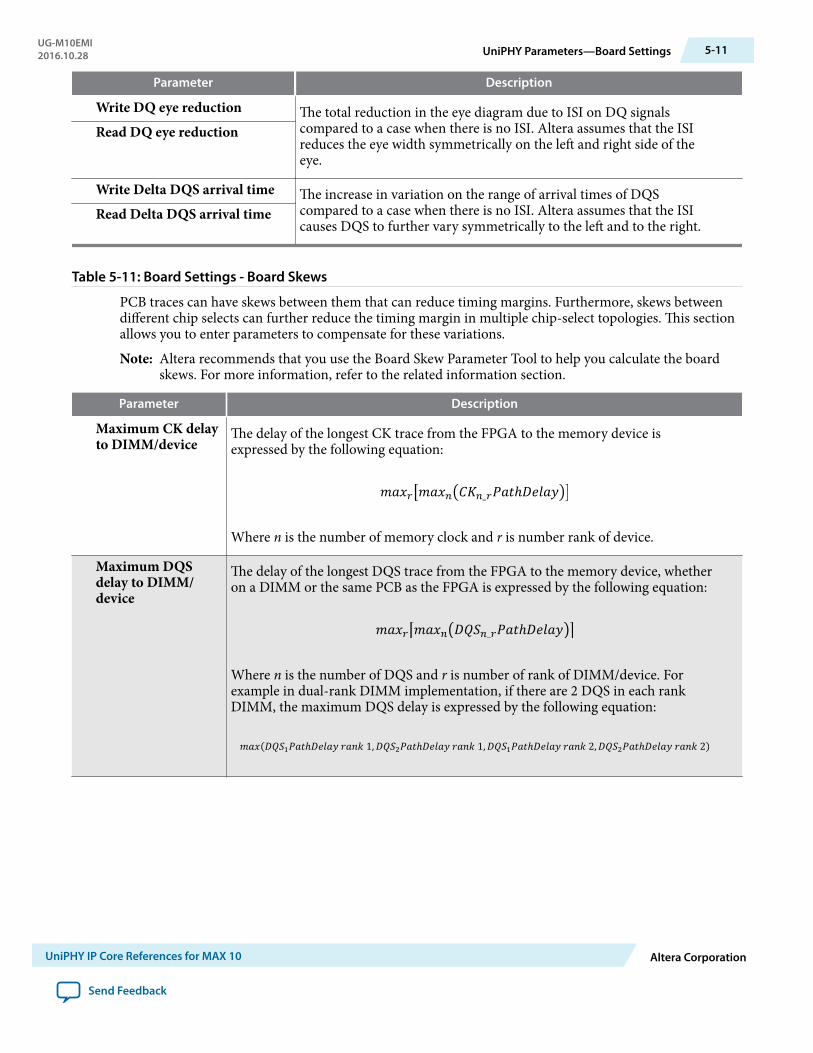
Parameter Description
Write DQ eye reduction The total reduction in the eye diagram due to ISI on DQ signalscompared to a case when there is no ISI. Altera assumes that the ISIreduces the eye width symmetrically on the left and right side of theeye.
Read DQ eye reduction
Write Delta DQS arrival time The increase in variation on the range of arrival times of DQScompared to a case when there is no ISI. Altera assumes that the ISIcauses DQS to further vary symmetrically to the left and to the right.
Read Delta DQS arrival time
Table 5-11: Board Settings - Board Skews
PCB traces can have skews between them that can reduce timing margins. Furthermore, skews betweendifferent chip selects can further reduce the timing margin in multiple chip-select topologies. This sectionallows you to enter parameters to compensate for these variations.
Note: Altera recommends that you use the Board Skew Parameter Tool to help you calculate the boardskews. For more information, refer to the related information section.
Parameter Description
Maximum CK delayto DIMM/device
The delay of the longest CK trace from the FPGA to the memory device isexpressed by the following equation:
Where n is the number of memory clock and r is number rank of device.
Maximum DQSdelay to DIMM/device
The delay of the longest DQS trace from the FPGA to the memory device, whetheron a DIMM or the same PCB as the FPGA is expressed by the following equation:
Where n is the number of DQS and r is number of rank of DIMM/device. Forexample in dual-rank DIMM implementation, if there are 2 DQS in each rankDIMM, the maximum DQS delay is expressed by the following equation:
UG-M10EMI2016.10.28 UniPHY Parameters—Board Settings 5-11
UniPHY IP Core References for MAX 10 Altera Corporation
Send Feedback
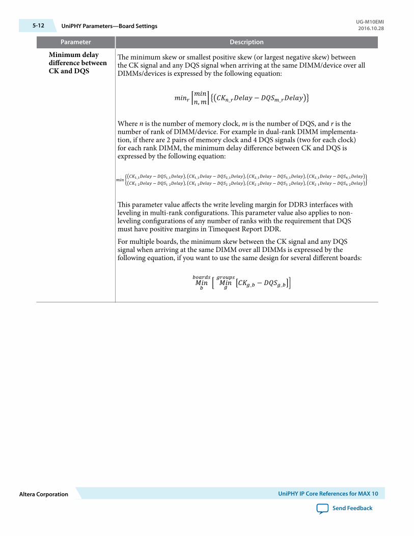
Parameter Description
Minimum delaydifference betweenCK and DQS
The minimum skew or smallest positive skew (or largest negative skew) betweenthe CK signal and any DQS signal when arriving at the same DIMM/device over allDIMMs/devices is expressed by the following equation:
Where n is the number of memory clock, m is the number of DQS, and r is thenumber of rank of DIMM/device. For example in dual-rank DIMM implementa‐tion, if there are 2 pairs of memory clock and 4 DQS signals (two for each clock)for each rank DIMM, the minimum delay difference between CK and DQS isexpressed by the following equation:
This parameter value affects the write leveling margin for DDR3 interfaces withleveling in multi-rank configurations. This parameter value also applies to non-leveling configurations of any number of ranks with the requirement that DQSmust have positive margins in Timequest Report DDR.
For multiple boards, the minimum skew between the CK signal and any DQSsignal when arriving at the same DIMM over all DIMMs is expressed by thefollowing equation, if you want to use the same design for several different boards:
5-12 UniPHY Parameters—Board SettingsUG-M10EMI2016.10.28
Altera Corporation UniPHY IP Core References for MAX 10
Send Feedback
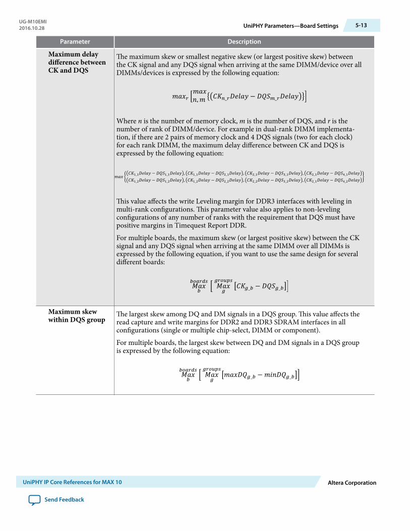
Parameter Description
Maximum delaydifference betweenCK and DQS
The maximum skew or smallest negative skew (or largest positive skew) betweenthe CK signal and any DQS signal when arriving at the same DIMM/device over allDIMMs/devices is expressed by the following equation:
Where n is the number of memory clock, m is the number of DQS, and r is thenumber of rank of DIMM/device. For example in dual-rank DIMM implementa‐tion, if there are 2 pairs of memory clock and 4 DQS signals (two for each clock)for each rank DIMM, the maximum delay difference between CK and DQS isexpressed by the following equation:
This value affects the write Leveling margin for DDR3 interfaces with leveling inmulti-rank configurations. This parameter value also applies to non-levelingconfigurations of any number of ranks with the requirement that DQS must havepositive margins in Timequest Report DDR.
For multiple boards, the maximum skew (or largest positive skew) between the CKsignal and any DQS signal when arriving at the same DIMM over all DIMMs isexpressed by the following equation, if you want to use the same design for severaldifferent boards:
Maximum skewwithin DQS group
The largest skew among DQ and DM signals in a DQS group. This value affects theread capture and write margins for DDR2 and DDR3 SDRAM interfaces in allconfigurations (single or multiple chip-select, DIMM or component).
For multiple boards, the largest skew between DQ and DM signals in a DQS groupis expressed by the following equation:
UG-M10EMI2016.10.28 UniPHY Parameters—Board Settings 5-13
UniPHY IP Core References for MAX 10 Altera Corporation
Send Feedback
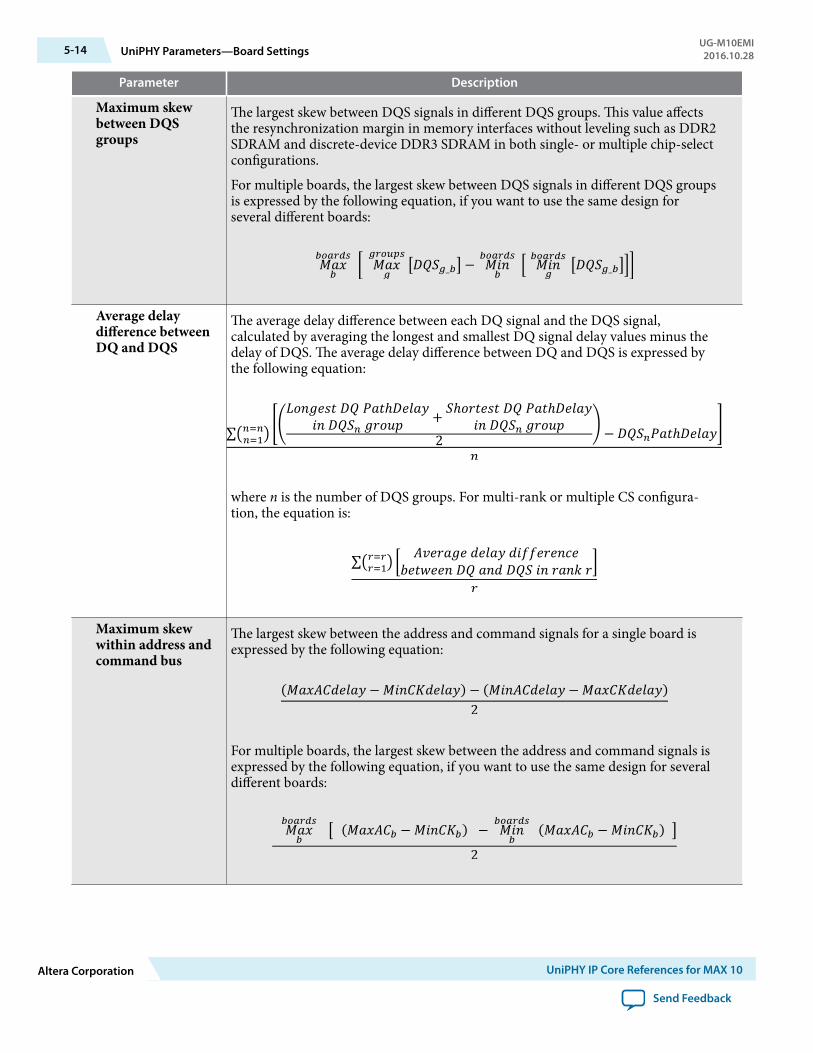
Parameter Description
Maximum skewbetween DQSgroups
The largest skew between DQS signals in different DQS groups. This value affectsthe resynchronization margin in memory interfaces without leveling such as DDR2SDRAM and discrete-device DDR3 SDRAM in both single- or multiple chip-selectconfigurations.
For multiple boards, the largest skew between DQS signals in different DQS groupsis expressed by the following equation, if you want to use the same design forseveral different boards:
Average delaydifference betweenDQ and DQS
The average delay difference between each DQ signal and the DQS signal,calculated by averaging the longest and smallest DQ signal delay values minus thedelay of DQS. The average delay difference between DQ and DQS is expressed bythe following equation:
where n is the number of DQS groups. For multi-rank or multiple CS configura‐tion, the equation is:
Maximum skewwithin address andcommand bus
The largest skew between the address and command signals for a single board isexpressed by the following equation:
For multiple boards, the largest skew between the address and command signals isexpressed by the following equation, if you want to use the same design for severaldifferent boards:
5-14 UniPHY Parameters—Board SettingsUG-M10EMI2016.10.28
Altera Corporation UniPHY IP Core References for MAX 10
Send Feedback
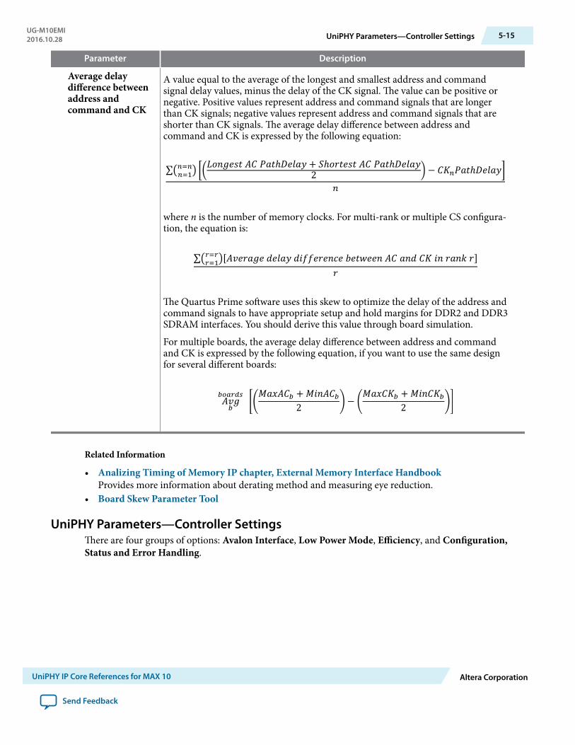
Parameter Description
Average delaydifference betweenaddress andcommand and CK
A value equal to the average of the longest and smallest address and commandsignal delay values, minus the delay of the CK signal. The value can be positive ornegative. Positive values represent address and command signals that are longerthan CK signals; negative values represent address and command signals that areshorter than CK signals. The average delay difference between address andcommand and CK is expressed by the following equation:
where n is the number of memory clocks. For multi-rank or multiple CS configura‐tion, the equation is:
The Quartus Prime software uses this skew to optimize the delay of the address andcommand signals to have appropriate setup and hold margins for DDR2 and DDR3SDRAM interfaces. You should derive this value through board simulation.
For multiple boards, the average delay difference between address and commandand CK is expressed by the following equation, if you want to use the same designfor several different boards:
Related Information
• Analizing Timing of Memory IP chapter, External Memory Interface HandbookProvides more information about derating method and measuring eye reduction.
• Board Skew Parameter Tool
UniPHY Parameters—Controller SettingsThere are four groups of options: Avalon Interface, Low Power Mode, Efficiency, and Configuration,Status and Error Handling.
UG-M10EMI2016.10.28 UniPHY Parameters—Controller Settings 5-15
UniPHY IP Core References for MAX 10 Altera Corporation
Send Feedback
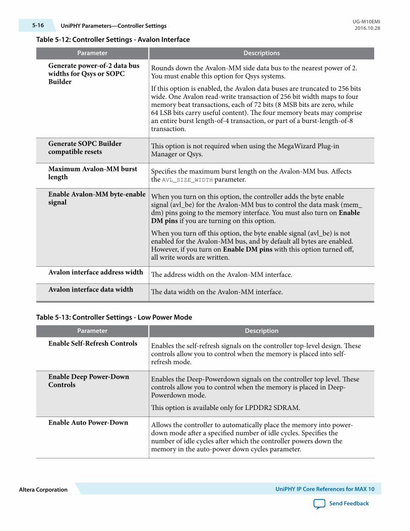
Table 5-12: Controller Settings - Avalon Interface
Parameter Descriptions
Generate power-of-2 data buswidths for Qsys or SOPCBuilder
Rounds down the Avalon-MM side data bus to the nearest power of 2.You must enable this option for Qsys systems.
If this option is enabled, the Avalon data buses are truncated to 256 bitswide. One Avalon read-write transaction of 256 bit width maps to fourmemory beat transactions, each of 72 bits (8 MSB bits are zero, while64 LSB bits carry useful content). The four memory beats may comprisean entire burst length-of-4 transaction, or part of a burst-length-of-8transaction.
Generate SOPC Buildercompatible resets
This option is not required when using the MegaWizard Plug-inManager or Qsys.
Maximum Avalon-MM burstlength
Specifies the maximum burst length on the Avalon-MM bus. Affectsthe AVL_SIZE_WIDTH parameter.
Enable Avalon-MM byte-enablesignal
When you turn on this option, the controller adds the byte enablesignal (avl_be) for the Avalon-MM bus to control the data mask (mem_dm) pins going to the memory interface. You must also turn on EnableDM pins if you are turning on this option.
When you turn off this option, the byte enable signal (avl_be) is notenabled for the Avalon-MM bus, and by default all bytes are enabled.However, if you turn on Enable DM pins with this option turned off,all write words are written.
Avalon interface address width The address width on the Avalon-MM interface.
Avalon interface data width The data width on the Avalon-MM interface.
Table 5-13: Controller Settings - Low Power Mode
Parameter Description
Enable Self-Refresh Controls Enables the self-refresh signals on the controller top-level design. Thesecontrols allow you to control when the memory is placed into self-refresh mode.
Enable Deep Power-DownControls
Enables the Deep-Powerdown signals on the controller top level. Thesecontrols allow you to control when the memory is placed in Deep-Powerdown mode.
This option is available only for LPDDR2 SDRAM.
Enable Auto Power-Down Allows the controller to automatically place the memory into power-down mode after a specified number of idle cycles. Specifies thenumber of idle cycles after which the controller powers down thememory in the auto-power down cycles parameter.
5-16 UniPHY Parameters—Controller SettingsUG-M10EMI2016.10.28
Altera Corporation UniPHY IP Core References for MAX 10
Send Feedback
Parameter Description
Auto Power-Down Cycles The number of idle controller clock cycles after which the controllerautomatically powers down the memory. The legal range is from 1 to65,535 controller clock cycles.
Table 5-14: Controller Settings - Efficiency
Parameter Description
Enable User Auto-RefreshControls
Enables the user auto-refresh control signals on the controller top level.These controller signals allow you to control when the controller issuesmemory autorefresh commands.
Enable Auto-Precharge Control Enables the autoprecharge control on the controller top level. Assertingthe autoprecharge control signal while requesting a read or write burstallows you to specify whether the controller should close (autopre‐charge) the currently open page at the end of the read or write burst.
Local-to-Memory AddressMapping
Allows you to control the mapping between the address bits on theAvalon-MM interface and the chip, row, bank, and column bits on thememory:
• Chip-Row-Bank-Col—improves efficiency with sequential traffic.• Chip-Bank-Row-Col—improves efficiency with random traffic.• Row-Chip-Bank-Col—improves efficiency with multiple chip select
and sequential traffic.
Command Queue Look-AheadDepth
Selects a look-ahead depth value to control how many read or writesrequests the look-ahead bank management logic examines. Largernumbers are likely to increase the efficiency of the bank management,but at the cost of higher resource usage. Smaller values may be lessefficient, but also use fewer resources. The valid range is from 1 to 16.
Enable Reordering Allows the controller to perform command and data reordering thatreduces bus turnaround time and row/bank switching time to improvecontroller efficiency.
Starvation limit for eachcommand
Specifies the number of commands that can be served before a waitingcommand is served. The valid range is from 1 to 63.
UG-M10EMI2016.10.28 UniPHY Parameters—Controller Settings 5-17
UniPHY IP Core References for MAX 10 Altera Corporation
Send Feedback
Table 5-15: Controller Settings - Configuration, Status and Error Handling
Parameter Description
Enable Configuration andStatus Register Interface
Enables run-time configuration and status interface for the memorycontroller. This option adds an additional Avalon-MM slave port to thememory controller top level, which you can use to change or read outthe memory timing parameters, memory address sizes, mode registersettings and controller status. If Error Detection and Correction Logicis enabled, the same slave port also allows you to control and retrievethe status of this logic.
CSR port host interface Specifies the type of connection to the CSR port. The port can beexported, internally connected to a JTAG Avalon Master, or both:
• Internal (JTAG)—connects the CSR port to a JTAG Avalon Master.• Avalon-MM Slave —exports the CSR port.• Shared—exports and connects the CSR port to a JTAG Avalon
Master.
Enable Error Detection andCorrection Logic
Enables ECC for single-bit error correction and double-bit errordetection. MAX 10 devices supports ECC only for 16 bits + 8 bits ECCmemory configuration.
Enable Auto Error Correction Allows the controller to perform auto correction when a single-biterror is detected by the ECC logic.
To turn this on, you must first turn on Enable Error Detection andCorrection Logic.
UniPHY Parameters—DiagnosticsThere is one option group supported for MAX 10 devices: Simulation Options.
Table 5-16: Diagnostics - Simulation Options
Parameter Description
Enable verbose memory model output Turn on this option to display more detailed information abouteach memory access during simulation.
5-18 UniPHY Parameters—DiagnosticsUG-M10EMI2016.10.28
Altera Corporation UniPHY IP Core References for MAX 10
Send Feedback

MAX 10 External Memory Interface User GuideArchives A
2016.10.28
UG-M10EMI Subscribe Send Feedback
If an IP core version is not listed, the user guide for the previous IP core version applies.IP Core Version User Guide
16.0 MAX 10 Exteral Memory Interface User Guide
15.1 MAX 10 Exteral Memory Interface User Guide
15.0 MAX 10 Exteral Memory Interface User Guide
14.1 MAX 10 Exteral Memory Interface User Guide
© 2016 Intel Corporation. All rights reserved. Intel, the Intel logo, Altera, Arria, Cyclone, Enpirion, MAX, Megacore, NIOS, Quartus and Stratix words and logosare trademarks of Intel Corporation in the US and/or other countries. Other marks and brands may be claimed as the property of others. Intel warrantsperformance of its FPGA and semiconductor products to current specifications in accordance with Intel's standard warranty, but reserves the right to makechanges to any products and services at any time without notice. Intel assumes no responsibility or liability arising out of the application or use of anyinformation, product, or service described herein except as expressly agreed to in writing by Intel. Intel customers are advised to obtain the latest version ofdevice specifications before relying on any published information and before placing orders for products or services.
ISO9001:2008Registered
www.altera.com101 Innovation Drive, San Jose, CA 95134
Additional Information for MAX 10 ExternalMemory Interface User Guide B
2016.10.28
UG-M10EMI Subscribe Send Feedback
Document Revision History for MAX 10 External Memory Interface UserGuide
Date Version Changes
October 2016 2016.10.28 • Updated Memory Standards Supported by the SoftMemory Controller for MAX 10 devices table.
May 2016 2016.05.02 • Updated UniPHY IP core parameter settings forLPDDR2, DDR2 and DDR3.
• Updated Supported Maximum External MemoryInterface Width in MAX 10 Device Packages table.
• Added MAX 10 External Memory Interface UserGuide Archives table.
• Updated DDR2, DDR3 and LPDDR2 can use onlyuser I/O pins from banks 5 and 6 of MAX 10devices to generate address and control orcommand signals..
November 2015 2015.11.02 • Added links to MAX 10 DDR3 UniPHY IP corereference design.
• Added topic that lists the maximum externalmemory interface widths supported for differentMAX 10 device packages.
• Removed the topics about the IP catalog andparameter editor, generating IP cores, and the filesgenerated by the IP core, and added a link toIntroduction to Altera IP Cores.
• Changed instances of Quartus II to Quartus Prime.
May 2015 2015.05.11 Added on board termination recommendation forDDR3 component.
© 2016 Intel Corporation. All rights reserved. Intel, the Intel logo, Altera, Arria, Cyclone, Enpirion, MAX, Megacore, NIOS, Quartus and Stratix words and logosare trademarks of Intel Corporation in the US and/or other countries. Other marks and brands may be claimed as the property of others. Intel warrantsperformance of its FPGA and semiconductor products to current specifications in accordance with Intel's standard warranty, but reserves the right to makechanges to any products and services at any time without notice. Intel assumes no responsibility or liability arising out of the application or use of anyinformation, product, or service described herein except as expressly agreed to in writing by Intel. Intel customers are advised to obtain the latest version ofdevice specifications before relying on any published information and before placing orders for products or services.
ISO9001:2008Registered
www.altera.com101 Innovation Drive, San Jose, CA 95134
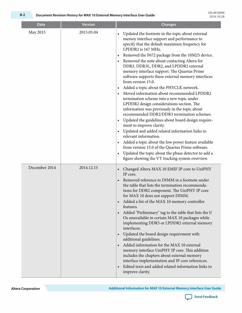
Date Version Changes
May 2015 2015.05.04 • Updated the footnote in the topic about externalmemoy interface support and performance tospecify that the default maximum frequency forLPDDR2 is 167 MHz.
• Removed the F672 package from the 10M25 device.• Removed the note about contacting Altera for
DDR3, DDR3L, DDR2, and LPDDR2 externalmemory interface support. The Quartus Primesoftware supports these external memory interfacesfrom version 15.0.
• Added a topic about the PHYCLK network.• Moved information about recommended LPDDR2
termination scheme into a new topic underLPDDR2 design considerations section. Theinformation was previously in the topic aboutrecommended DDR2/DDR3 termination schemes.
• Updated the guidelines about board design require‐ment to improve clarity.
• Updated and added related information links torelevant information.
• Added a topic about the low power feature availablefrom version 15.0 of the Quartus Prime software.
• Updated the topic about the phase detector to add afigure showing the VT tracking system overview.
December 2014 2014.12.15 • Changed Altera MAX 10 EMIF IP core to UniPHYIP core.
• Removed reference to DIMM in a footnote underthe table that lists the termination recommenda‐tions for DDR2 component. The UniPHY IP corefor MAX 10 does not support DIMM.
• Added a list of the MAX 10 memory controllerfeatures.
• Added "Preliminary" tag to the table that lists the I/Os unavailable in certain MAX 10 packages whileimplementing DDR3 or LPDDR2 external memoryinterfaces.
• Updated the board design requirement withadditional guidelines.
• Added information for the MAX 10 externalmemory interface UniPHY IP core. This additionincludes the chapters about external memoryinterface implementation and IP core references.
• Edited texts and added related information links toimprove clarity.
B-2 Document Revision History for MAX 10 External Memory Interface User GuideUG-M10EMI2016.10.28
Altera Corporation Additional Information for MAX 10 External Memory Interface User Guide
Send Feedback

Date Version Changes
September 2014 2014.09.22 Initial release.
UG-M10EMI2016.10.28 Document Revision History for MAX 10 External Memory Interface User Guide B-3
Additional Information for MAX 10 External Memory Interface User Guide Altera Corporation
Send Feedback

MAX 10 Analog to Digital Converter UserGuide
Last updated for Quartus Prime Design Suite: 16.1
Subscribe
Send Feedback
UG-M10ADC2016.10.31
101 Innovation DriveSan Jose, CA 95134www.altera.com
Contents
MAX 10 Analog to Digital Converter Overview................................................ 1-1ADC Block Counts in MAX 10 Devices................................................................................................... 1-2ADC Channel Counts in MAX 10 Devices.............................................................................................. 1-3MAX 10 ADC Vertical Migration Support...............................................................................................1-4MAX 10 Single or Dual Supply Devices....................................................................................................1-5MAX 10 ADC Conversion..........................................................................................................................1-5
MAX 10 ADC Architecture and Features........................................................... 2-1MAX 10 ADC Hard IP Block..................................................................................................................... 2-1
ADC Block Locations...................................................................................................................... 2-2Single or Dual ADC Devices.......................................................................................................... 2-5ADC Analog Input Pins.................................................................................................................. 2-6ADC Prescaler.................................................................................................................................. 2-6ADC Clock Sources......................................................................................................................... 2-6ADC Voltage Reference...................................................................................................................2-7ADC Temperature Sensing Diode................................................................................................. 2-7ADC Sequencer..............................................................................................................................2-10ADC Timing................................................................................................................................... 2-11
Altera Modular ADC and Altera Modular Dual ADC IP Cores......................................................... 2-11Altera Modular ADC IP Core Configuration Variants.............................................................2-12Altera Modular ADC and Altera Modular Dual ADC IP Cores Architecture...................... 2-17
Altera ADC HAL Driver........................................................................................................................... 2-22ADC Toolkit for Testing ADC Performance..........................................................................................2-23ADC Logic Simulation Output................................................................................................................ 2-23
Fixed ADC Logic Simulation Output..........................................................................................2-23User-Specified ADC Logic Simulation Output..........................................................................2-24
MAX 10 ADC Design Considerations................................................................ 3-1Guidelines: ADC Ground Plane Connection...........................................................................................3-1Guidelines: Board Design for Power Supply Pin and ADC Ground (REFGND)....................................3-1Guidelines: Board Design for Analog Input............................................................................................. 3-2Guidelines: Board Design for ADC Reference Voltage Pin....................................................................3-4
MAX 10 ADC Implementation Guides...............................................................4-1Creating MAX 10 ADC Design................................................................................................................. 4-2Customizing and Generating Altera Modular ADC IP Core.................................................................4-3Parameters Settings for Generating ALTPLL IP Core............................................................................ 4-4Parameters Settings for Generating Altera Modular ADC or Altera Modular Dual ADC IP
Core.......................................................................................................................................................... 4-5Completing ADC Design............................................................................................................................4-8
TOC-2
Altera Corporation
Altera Modular ADC and Altera Modular Dual ADC IP Cores References..... 5-1Altera Modular ADC Parameters Settings............................................................................................... 5-2
Altera Modular ADC IP Core Channel Name to MAX 10 Device Pin Name Mapping........ 5-6Altera Modular Dual ADC Parameters Settings......................................................................................5-8
Altera Modular Dual ADC IP Core Channel Name to MAX 10 Device Pin NameMapping.....................................................................................................................................5-12
Valid ADC Sample Rate and Input Clock Combination...................................................................... 5-13Altera Modular ADC and Altera Modular Dual ADC Interface Signals........................................... 5-13
Command Interface of Altera Modular ADC and Altera Modular Dual ADC.................... 5-13Response Interface of Altera Modular ADC and Altera Modular Dual ADC.......................5-14Threshold Interface of Altera Modular ADC and Altera Modular Dual ADC......................5-15CSR Interface of Altera Modular ADC and Altera Modular Dual ADC................................5-16IRQ Interface of Altera Modular ADC and Altera Modular Dual ADC................................5-16Peripheral Clock Interface of Altera Modular ADC and Altera Modular Dual ADC..........5-17Peripheral Reset Interface of Altera Modular ADC and Altera Modular Dual ADC...........5-17ADC PLL Clock Interface of Altera Modular ADC and Altera Modular Dual ADC.......... 5-17ADC PLL Locked Interface of Altera Modular ADC and Altera Modular Dual ADC........ 5-18
Altera Modular ADC Register Definitions.............................................................................................5-18Sequencer Core Registers..............................................................................................................5-18Sample Storage Core Registers..................................................................................................... 5-19
ADC HAL Device Driver for Nios II Gen 2........................................................................................... 5-20
MAX 10 Analog to Digital Converter User Guide Archives.............................. A-1
Document Revision History for MAX 10 Analog to Digital Converter UserGuide............................................................................................................... B-1
TOC-3
Altera Corporation
MAX 10 Analog to Digital Converter Overview 12016.10.31
UG-M10ADC Subscribe Send Feedback
MAX® 10 devices feature up to two analog-to-digital converters (ADC). The ADCs provide the MAX 10devices with built-in capability for on-die temperature monitoring and external analog signal conversion.
The ADC solution consists of hard IP blocks in the MAX 10 device periphery and soft logic through theAltera Modular ADC IP core.
The ADC solution provides you with built-in capability to translate analog quantities to digital data forinformation processing, computing, data transmission, and control systems. The basic function is toprovide a 12 bit digital representation of the analog signal being observed.
The ADC solution works in two modes:
• Normal mode—monitors single-ended external inputs with a cumulative sampling rate of up to 1million samples per second (MSPS):
• Single ADC devices—up to 17 single-ended external inputs (one dedicated analog and 16 dualfunction input pins)
• Dual ADC devices—up to 18 single-ended external inputs (one dedicated analog and eight dualfunction input pins in each ADC block)
• Temperature sensing mode—monitors external temperature data input with a sampling rate of up to 50kilosamples per second. In dual ADC devices, only the first ADC block supports this mode.
Related Information
• MAX 10 ADC Architecture and Features on page 2-1• MAX 10 ADC Design Considerations on page 3-1• MAX 10 ADC Implementation Guides on page 4-1• Altera Modular ADC and Altera Modular Dual ADC IP Cores References on page 5-1• MAX 10 Getting Started• MAX 10 Online Training• MAX 10 How-to Videos• How to Create ADC Design in MAX 10 Device Using Qsys Tool
Provides video instruction that demonstrates how to create the ADC design in MAX 10 devices usingthe Qsys system integration tool within the Quartus® Prime software and how to use the ADC toolkitto view the measured analog signal.
© 2016 Intel Corporation. All rights reserved. Intel, the Intel logo, Altera, Arria, Cyclone, Enpirion, MAX, Megacore, NIOS, Quartus and Stratix words and logosare trademarks of Intel Corporation in the US and/or other countries. Other marks and brands may be claimed as the property of others. Intel warrantsperformance of its FPGA and semiconductor products to current specifications in accordance with Intel's standard warranty, but reserves the right to makechanges to any products and services at any time without notice. Intel assumes no responsibility or liability arising out of the application or use of anyinformation, product, or service described herein except as expressly agreed to in writing by Intel. Intel customers are advised to obtain the latest version ofdevice specifications before relying on any published information and before placing orders for products or services.
ISO9001:2008Registered
www.altera.com101 Innovation Drive, San Jose, CA 95134
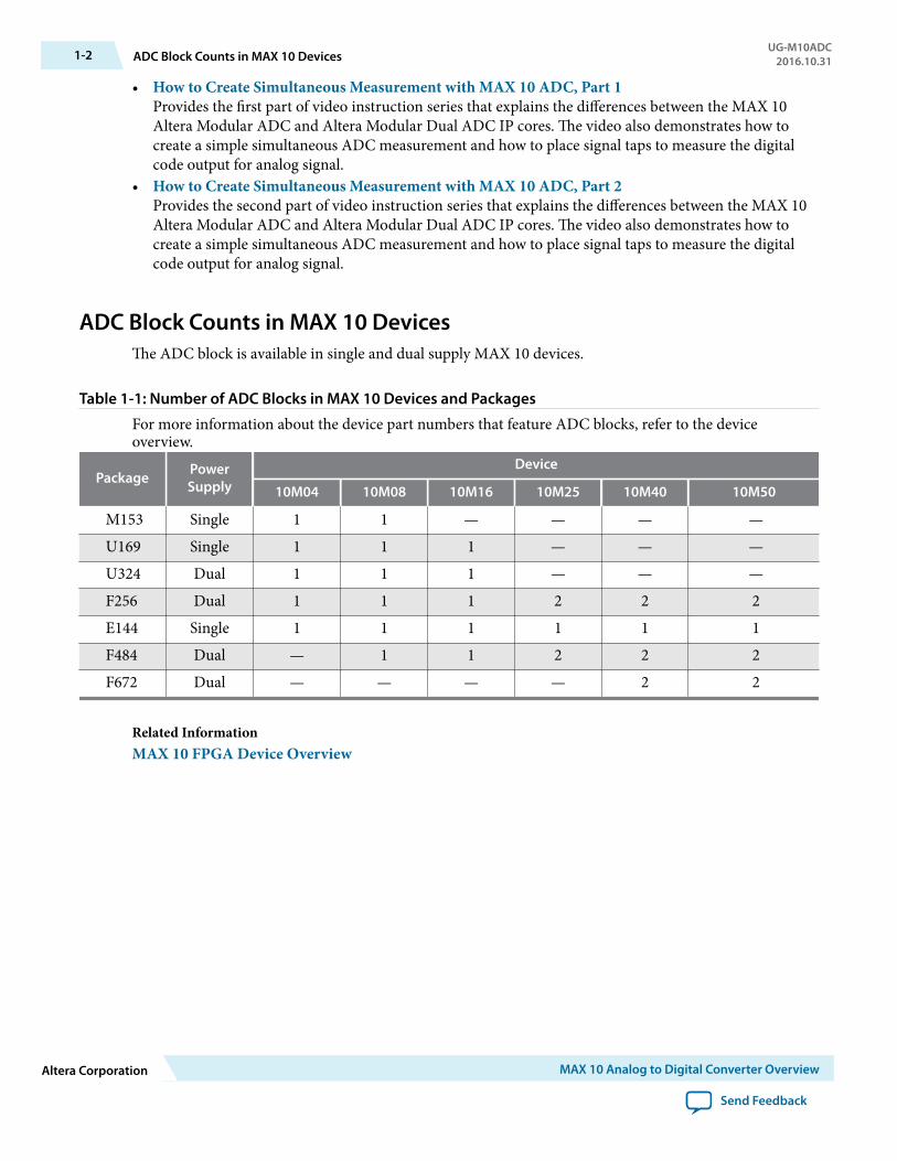
• How to Create Simultaneous Measurement with MAX 10 ADC, Part 1Provides the first part of video instruction series that explains the differences between the MAX 10Altera Modular ADC and Altera Modular Dual ADC IP cores. The video also demonstrates how tocreate a simple simultaneous ADC measurement and how to place signal taps to measure the digitalcode output for analog signal.
• How to Create Simultaneous Measurement with MAX 10 ADC, Part 2Provides the second part of video instruction series that explains the differences between the MAX 10Altera Modular ADC and Altera Modular Dual ADC IP cores. The video also demonstrates how tocreate a simple simultaneous ADC measurement and how to place signal taps to measure the digitalcode output for analog signal.
ADC Block Counts in MAX 10 DevicesThe ADC block is available in single and dual supply MAX 10 devices.
Table 1-1: Number of ADC Blocks in MAX 10 Devices and Packages
For more information about the device part numbers that feature ADC blocks, refer to the deviceoverview.
Package PowerSupply
Device
10M04 10M08 10M16 10M25 10M40 10M50
M153 Single 1 1 — — — —U169 Single 1 1 1 — — —U324 Dual 1 1 1 — — —F256 Dual 1 1 1 2 2 2E144 Single 1 1 1 1 1 1F484 Dual — 1 1 2 2 2F672 Dual — — — — 2 2
Related InformationMAX 10 FPGA Device Overview
1-2 ADC Block Counts in MAX 10 DevicesUG-M10ADC
2016.10.31
Altera Corporation MAX 10 Analog to Digital Converter Overview
Send Feedback
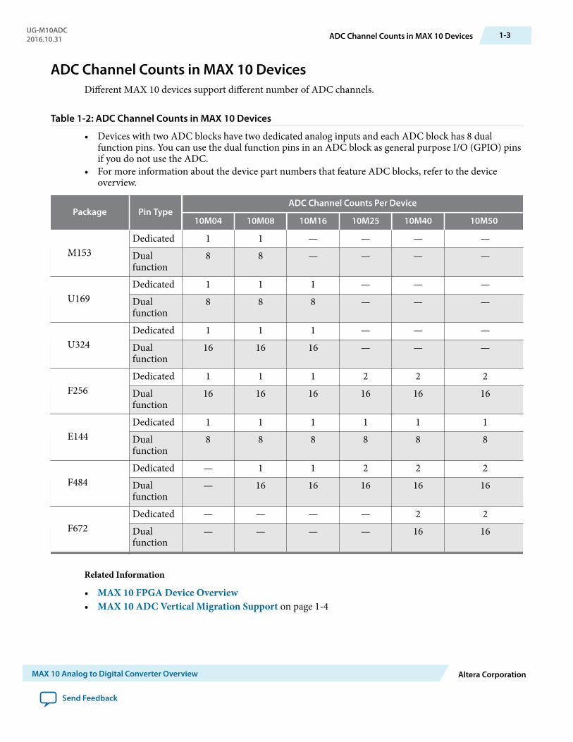
ADC Channel Counts in MAX 10 DevicesDifferent MAX 10 devices support different number of ADC channels.
Table 1-2: ADC Channel Counts in MAX 10 Devices
• Devices with two ADC blocks have two dedicated analog inputs and each ADC block has 8 dualfunction pins. You can use the dual function pins in an ADC block as general purpose I/O (GPIO) pinsif you do not use the ADC.
• For more information about the device part numbers that feature ADC blocks, refer to the deviceoverview.
Package Pin TypeADC Channel Counts Per Device
10M04 10M08 10M16 10M25 10M40 10M50
M153Dedicated 1 1 — — — —Dualfunction
8 8 — — — —
U169Dedicated 1 1 1 — — —Dualfunction
8 8 8 — — —
U324Dedicated 1 1 1 — — —Dualfunction
16 16 16 — — —
F256Dedicated 1 1 1 2 2 2Dualfunction
16 16 16 16 16 16
E144Dedicated 1 1 1 1 1 1Dualfunction
8 8 8 8 8 8
F484Dedicated — 1 1 2 2 2Dualfunction
— 16 16 16 16 16
F672Dedicated — — — — 2 2Dualfunction
— — — — 16 16
Related Information
• MAX 10 FPGA Device Overview• MAX 10 ADC Vertical Migration Support on page 1-4
UG-M10ADC2016.10.31 ADC Channel Counts in MAX 10 Devices 1-3
MAX 10 Analog to Digital Converter Overview Altera Corporation
Send Feedback
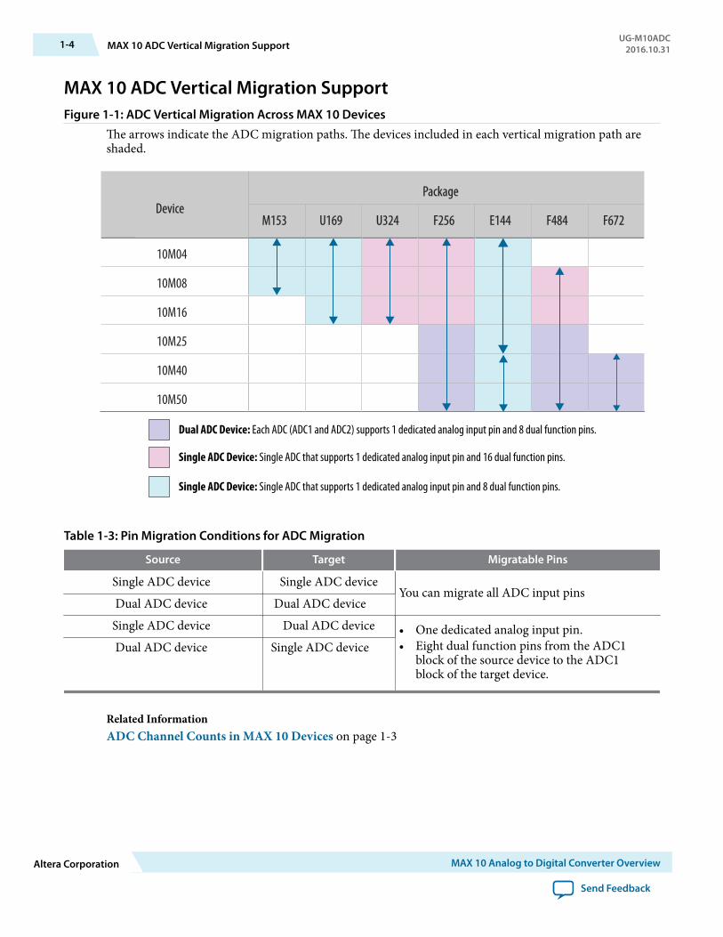
MAX 10 ADC Vertical Migration SupportFigure 1-1: ADC Vertical Migration Across MAX 10 Devices
The arrows indicate the ADC migration paths. The devices included in each vertical migration path areshaded.
DevicePackage
M153 U169 U324 F256 E144 F484 F672
10M04
10M08
10M16
10M25
10M40
10M50
Dual ADC Device: Each ADC (ADC1 and ADC2) supports 1 dedicated analog input pin and 8 dual function pins.
Single ADC Device: Single ADC that supports 1 dedicated analog input pin and 16 dual function pins.
Single ADC Device: Single ADC that supports 1 dedicated analog input pin and 8 dual function pins.
Table 1-3: Pin Migration Conditions for ADC Migration
Source Target Migratable Pins
Single ADC device Single ADC deviceYou can migrate all ADC input pins
Dual ADC device Dual ADC deviceSingle ADC device Dual ADC device • One dedicated analog input pin.
• Eight dual function pins from the ADC1block of the source device to the ADC1block of the target device.
Dual ADC device Single ADC device
Related InformationADC Channel Counts in MAX 10 Devices on page 1-3
1-4 MAX 10 ADC Vertical Migration SupportUG-M10ADC
2016.10.31
Altera Corporation MAX 10 Analog to Digital Converter Overview
Send Feedback
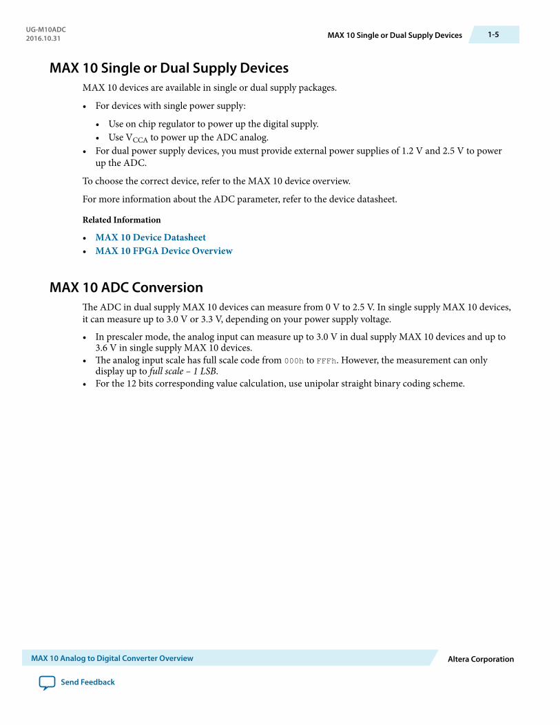
MAX 10 Single or Dual Supply DevicesMAX 10 devices are available in single or dual supply packages.
• For devices with single power supply:
• Use on chip regulator to power up the digital supply.• Use VCCA to power up the ADC analog.
• For dual power supply devices, you must provide external power supplies of 1.2 V and 2.5 V to powerup the ADC.
To choose the correct device, refer to the MAX 10 device overview.
For more information about the ADC parameter, refer to the device datasheet.
Related Information
• MAX 10 Device Datasheet• MAX 10 FPGA Device Overview
MAX 10 ADC ConversionThe ADC in dual supply MAX 10 devices can measure from 0 V to 2.5 V. In single supply MAX 10 devices,it can measure up to 3.0 V or 3.3 V, depending on your power supply voltage.
• In prescaler mode, the analog input can measure up to 3.0 V in dual supply MAX 10 devices and up to3.6 V in single supply MAX 10 devices.
• The analog input scale has full scale code from 000h to FFFh. However, the measurement can onlydisplay up to full scale – 1 LSB.
• For the 12 bits corresponding value calculation, use unipolar straight binary coding scheme.
UG-M10ADC2016.10.31 MAX 10 Single or Dual Supply Devices 1-5
MAX 10 Analog to Digital Converter Overview Altera Corporation
Send Feedback
Figure 1-2: ADC Measurement Display for 2.5 V
FFF
FFE
FFD
003
002
000
001
12 bi
t Out
put C
ode (
Hex)
Input Voltage (V)
610.35µ 1220.70µ 2.4993896
Full scale input = 2.5 VResolution = 212 = 40961 LSB = 2.5V / 4096 = 610.35µ V
Full ScaleTransition
Output Code
The MAX 10 ADC is a 1 MHz successive approximation register (SAR) ADC. If you set up the PLL andAltera Modular ADC IP core correctly, the ADC operates at up to 1 MHz during normal sampling and 50kHz during temperature sensing.
Note: The analog value represented by the all-ones code is not full scale but full scale – 1 LSB. This is acommon convention in data conversion notation and applies to ADCs.
Related Information
• Creating MAX 10 ADC Design on page 4-2• Altera Modular ADC Parameters Settings on page 5-2• Altera Modular Dual ADC Parameters Settings on page 5-8
1-6 MAX 10 ADC ConversionUG-M10ADC
2016.10.31
Altera Corporation MAX 10 Analog to Digital Converter Overview
Send Feedback
MAX 10 ADC Architecture and Features 22016.10.31
UG-M10ADC Subscribe Send Feedback
In MAX 10 devices, the ADC is a 12-bit SAR ADC that provides the following features:
• Sampling rate of up to 1 MSPS• Up to 18 channels for analog measurement: 16 dual function channels and two dedicated analog input
channels in dual ADC devices• Single-ended measurement capability• Simultaneous measurement capability at the dedicated analog input pins for dual ADC devices• Soft logic sequencer• On-chip temperature sensor with sampling rate of 50 kilosamples per second• Internal or external voltage references usage. The source of the internal voltage reference is the ADC
analog supply; the ADC conversion result is ratiometric.
Related Information
• MAX 10 Analog to Digital Converter Overview on page 1-1• MAX 10 Analog to Digital Converter User Guide Archives on page 6-1
Provides a list of user guides for previous versions of the Altera Modular ADC and Altera ModularDual ADC IP cores.
MAX 10 ADC Hard IP BlockThe MAX 10 ADC is a successive approximation register (SAR) ADC that converts one analog sample inone clock cycle.
Each ADC block supports one dedicated analog input pin and up to 16 channels of dual function pins.
You can use the built-in temperature sensing diode (TSD) to perform on-chip temperature measurement.
© 2016 Intel Corporation. All rights reserved. Intel, the Intel logo, Altera, Arria, Cyclone, Enpirion, MAX, Megacore, NIOS, Quartus and Stratix words and logosare trademarks of Intel Corporation in the US and/or other countries. Other marks and brands may be claimed as the property of others. Intel warrantsperformance of its FPGA and semiconductor products to current specifications in accordance with Intel's standard warranty, but reserves the right to makechanges to any products and services at any time without notice. Intel assumes no responsibility or liability arising out of the application or use of anyinformation, product, or service described herein except as expressly agreed to in writing by Intel. Intel customers are advised to obtain the latest version ofdevice specifications before relying on any published information and before placing orders for products or services.
ISO9001:2008Registered
www.altera.com101 Innovation Drive, San Jose, CA 95134
Figure 2-1: ADC Hard IP Block in MAX 10 Devices
Note: In dual ADC devices, the temperature sensor is available only in ADC1.
Samplingand Hold
Mux 12 bit 1 Mbps ADC
Altera Modular ADC IP Core
Sequencer [4:0]
DOUT [11:0]
Control/Status
DedicatedAnalog Input
ADC Analog Input(Dual Function) [16:1]
ADC VREF
Internal VREF
PLL Clock In
Temperature Sensor
ADC Hard IP Block
Related InformationSequencer Core on page 2-19Provides mode information about the sequencer conversion modes.
ADC Block LocationsThe ADC blocks are located at the top left corner of the MAX 10 device periphery.
2-2 ADC Block LocationsUG-M10ADC
2016.10.31
Altera Corporation MAX 10 ADC Architecture and Features
Send Feedback
Figure 2-2: ADC Block Location in MAX 10 04 and 08 Devices
1B
1A
2 5
6
3 4
8 7
I/O Bank
ADC Block
ADC1
UG-M10ADC2016.10.31 ADC Block Locations 2-3
MAX 10 ADC Architecture and Features Altera Corporation
Send Feedback
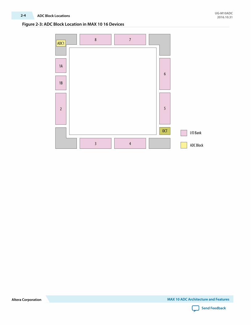
Figure 2-3: ADC Block Location in MAX 10 16 Devices
1B
1A
2
3 4
8 7
OCT
5
6
I/O Bank
ADC Block
ADC1
2-4 ADC Block LocationsUG-M10ADC
2016.10.31
Altera Corporation MAX 10 ADC Architecture and Features
Send Feedback
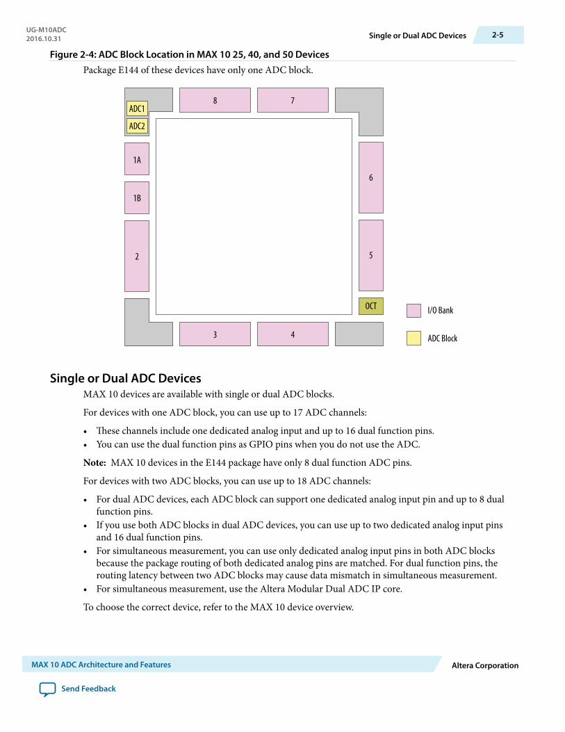
Figure 2-4: ADC Block Location in MAX 10 25, 40, and 50 DevicesPackage E144 of these devices have only one ADC block.
1B
1A
2
3 4
8 7
OCT
5
6
I/O Bank
ADC Block
ADC2
ADC1
Single or Dual ADC DevicesMAX 10 devices are available with single or dual ADC blocks.
For devices with one ADC block, you can use up to 17 ADC channels:
• These channels include one dedicated analog input and up to 16 dual function pins.• You can use the dual function pins as GPIO pins when you do not use the ADC.
Note: MAX 10 devices in the E144 package have only 8 dual function ADC pins.
For devices with two ADC blocks, you can use up to 18 ADC channels:
• For dual ADC devices, each ADC block can support one dedicated analog input pin and up to 8 dualfunction pins.
• If you use both ADC blocks in dual ADC devices, you can use up to two dedicated analog input pinsand 16 dual function pins.
• For simultaneous measurement, you can use only dedicated analog input pins in both ADC blocksbecause the package routing of both dedicated analog pins are matched. For dual function pins, therouting latency between two ADC blocks may cause data mismatch in simultaneous measurement.
• For simultaneous measurement, use the Altera Modular Dual ADC IP core.
To choose the correct device, refer to the MAX 10 device overview.
UG-M10ADC2016.10.31 Single or Dual ADC Devices 2-5
MAX 10 ADC Architecture and Features Altera Corporation
Send Feedback
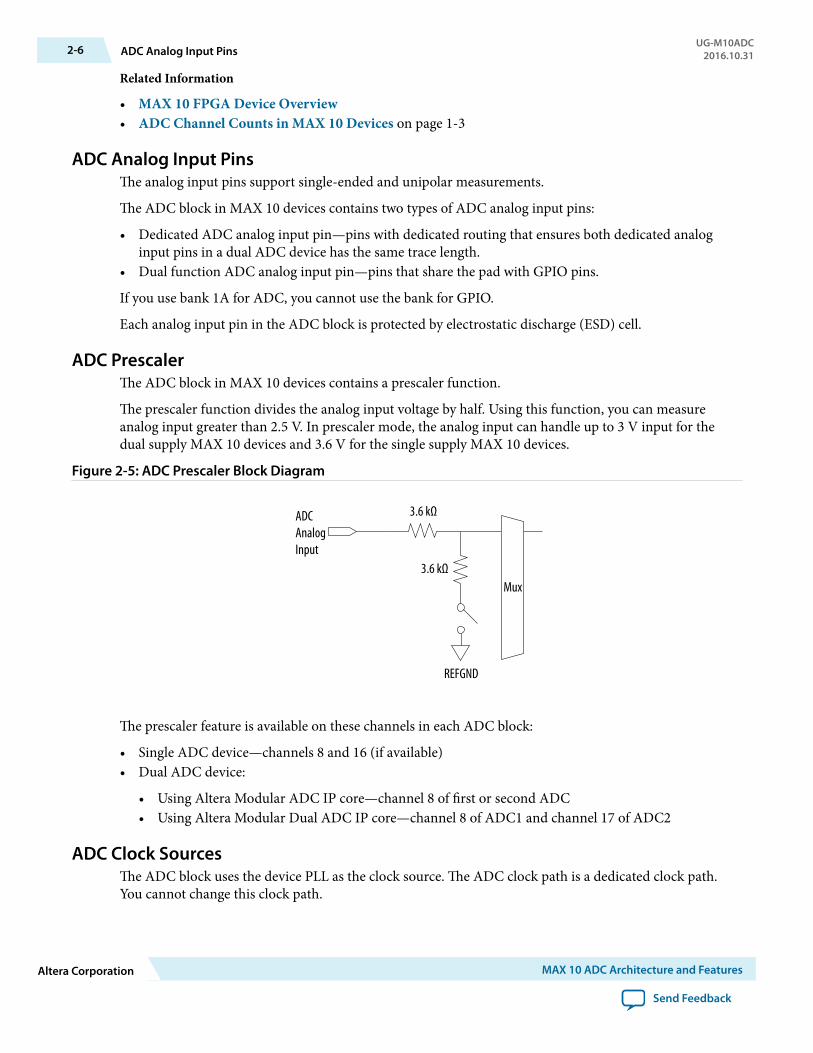
Related Information
• MAX 10 FPGA Device Overview• ADC Channel Counts in MAX 10 Devices on page 1-3
ADC Analog Input PinsThe analog input pins support single-ended and unipolar measurements.
The ADC block in MAX 10 devices contains two types of ADC analog input pins:
• Dedicated ADC analog input pin—pins with dedicated routing that ensures both dedicated analoginput pins in a dual ADC device has the same trace length.
• Dual function ADC analog input pin—pins that share the pad with GPIO pins.
If you use bank 1A for ADC, you cannot use the bank for GPIO.
Each analog input pin in the ADC block is protected by electrostatic discharge (ESD) cell.
ADC PrescalerThe ADC block in MAX 10 devices contains a prescaler function.
The prescaler function divides the analog input voltage by half. Using this function, you can measureanalog input greater than 2.5 V. In prescaler mode, the analog input can handle up to 3 V input for thedual supply MAX 10 devices and 3.6 V for the single supply MAX 10 devices.
Figure 2-5: ADC Prescaler Block Diagram
Mux
REFGND
3.6 kΩ
3.6 kΩADCAnalogInput
The prescaler feature is available on these channels in each ADC block:
• Single ADC device—channels 8 and 16 (if available)• Dual ADC device:
• Using Altera Modular ADC IP core—channel 8 of first or second ADC• Using Altera Modular Dual ADC IP core—channel 8 of ADC1 and channel 17 of ADC2
ADC Clock SourcesThe ADC block uses the device PLL as the clock source. The ADC clock path is a dedicated clock path.You cannot change this clock path.
2-6 ADC Analog Input PinsUG-M10ADC
2016.10.31
Altera Corporation MAX 10 ADC Architecture and Features
Send Feedback
Depending on the device package, the MAX 10 devices support one or two PLLs—PLL1 only, or PLL1 andPLL3.
For devices that support two PLLs, you can select which PLL to connect to the ADC. You can configurethe ADC blocks with one of the following schemes:
• Both ADC blocks share the same clock source for synchronization.• Both ADC blocks use different PLLs for redundancy.
If each ADC block in your design uses its own PLL, the Quartus® Prime Fitter automatically selects theclock source scheme based on the PLL clock input source:
• If each PLL that clocks its respective ADC block uses different PLL input clock source, the QuartusPrime Fitter follows your design (two PLLs).
• If both PLLs that clock their respective ADC block uses the same PLL input clock source, the QuartusPrime Fitter merges both PLLs as one.
In dual ADC mode, both ADC instance must share the same ADC clock setting.
Related InformationPLL Locations, MAX 10 Clocking and PLL User GuideProvides more information about the availability of PLL3 in different MAX 10 devices and packages.
ADC Voltage ReferenceEach ADC block in MAX 10 devices can independently use an internal or external voltage reference. Indual ADC devices, you can assign an internal voltage reference to one ADC block and an external voltagereference to the other ADC block.
There is only one external VREF pin in each MAX 10 device. Therefore, if you want to assign externalvoltage reference for both ADC blocks in dual ADC devices, share the same external voltage reference forboth ADC blocks.
Altera recommends that you use a clean external voltage reference with a maximum resistance of 100 Ωfor the ADC blocks. If the ADC block uses an internal voltage reference, the ADC block is tied to itsanalog voltage and the conversion result is ratiometric.
ADC Temperature Sensing DiodeThe ADC block in MAX 10 devices has built-in TSD. You can use the built-in TSD to monitor the internaltemperature of the MAX 10 device.
UG-M10ADC2016.10.31 ADC Voltage Reference 2-7
MAX 10 ADC Architecture and Features Altera Corporation
Send Feedback

• While using the temperature sensing mode, the ADC sampling rate is 50 kilosamples per secondduring temperature measurement.
• After the temperature measurement completes, if the next conversion in the sequence is normalsampling mode, the Altera Modular ADC IP core automatically switches the ADC back to normalsampling mode. The maximum cumulative sampling rate in normal sampling mode is 1 MSPS.
• When the ADC switches from normal sensing mode to temperature sensing mode, and vice versa,calibration is run automatically for the changed clock frequency. The calibration incurs at least sixclock calibration cycles from the new sampling rate.
• The ADC TSD measurement uses a 64-samples running average method. For example:
• The first measured temperature value is the average of samples 1 to 64.• The second measured temperature value is the average of samples 2 to 65.• The third measured temperature value is the average of samples 3 to 66.• The subsequent temperature measurements follow the same method.
For dual ADC devices, the temperature sensor is available in ADC1 only.
2-8 ADC Temperature Sensing DiodeUG-M10ADC
2016.10.31
Altera Corporation MAX 10 ADC Architecture and Features
Send Feedback
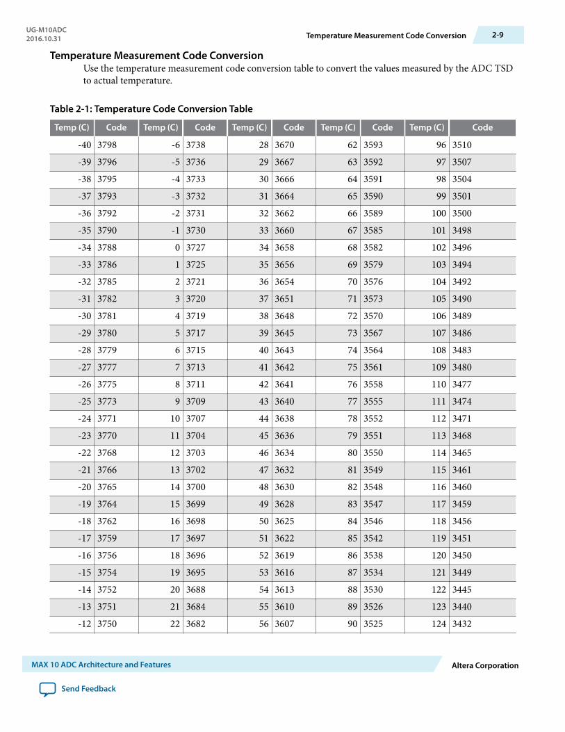
Temperature Measurement Code ConversionUse the temperature measurement code conversion table to convert the values measured by the ADC TSDto actual temperature.
Table 2-1: Temperature Code Conversion Table
Temp (C) Code Temp (C) Code Temp (C) Code Temp (C) Code Temp (C) Code
-40 3798 -6 3738 28 3670 62 3593 96 3510-39 3796 -5 3736 29 3667 63 3592 97 3507-38 3795 -4 3733 30 3666 64 3591 98 3504-37 3793 -3 3732 31 3664 65 3590 99 3501-36 3792 -2 3731 32 3662 66 3589 100 3500-35 3790 -1 3730 33 3660 67 3585 101 3498-34 3788 0 3727 34 3658 68 3582 102 3496-33 3786 1 3725 35 3656 69 3579 103 3494-32 3785 2 3721 36 3654 70 3576 104 3492-31 3782 3 3720 37 3651 71 3573 105 3490-30 3781 4 3719 38 3648 72 3570 106 3489-29 3780 5 3717 39 3645 73 3567 107 3486-28 3779 6 3715 40 3643 74 3564 108 3483-27 3777 7 3713 41 3642 75 3561 109 3480-26 3775 8 3711 42 3641 76 3558 110 3477-25 3773 9 3709 43 3640 77 3555 111 3474-24 3771 10 3707 44 3638 78 3552 112 3471-23 3770 11 3704 45 3636 79 3551 113 3468-22 3768 12 3703 46 3634 80 3550 114 3465-21 3766 13 3702 47 3632 81 3549 115 3461-20 3765 14 3700 48 3630 82 3548 116 3460-19 3764 15 3699 49 3628 83 3547 117 3459-18 3762 16 3698 50 3625 84 3546 118 3456-17 3759 17 3697 51 3622 85 3542 119 3451-16 3756 18 3696 52 3619 86 3538 120 3450-15 3754 19 3695 53 3616 87 3534 121 3449-14 3752 20 3688 54 3613 88 3530 122 3445-13 3751 21 3684 55 3610 89 3526 123 3440-12 3750 22 3682 56 3607 90 3525 124 3432
UG-M10ADC2016.10.31 Temperature Measurement Code Conversion 2-9
MAX 10 ADC Architecture and Features Altera Corporation
Send Feedback
Temp (C) Code Temp (C) Code Temp (C) Code Temp (C) Code Temp (C) Code
-11 3748 23 3680 57 3604 91 3524 125 3431-10 3746 24 3678 58 3601 92 3522 — —
-9 3744 25 3677 59 3598 93 3519 — —-8 3742 26 3676 60 3595 94 3516 — —-7 3740 27 3673 61 3594 95 3513 — —
ADC SequencerThe Altera Modular ADC and Altera Modular Dual ADC IP cores implement the sequencer. Use theAltera Modular ADC or Altera Modular Dual ADC parameter editor to define the ADC channelacquisition sequence and generate the HDL code.
The sequencer can support sequences of up to 64 ADC measurement slots. While configuring the AlteraModular ADC or Altera Modular Dual ADC IP core, you can select which channel, including the TSDchannel, to sample in each sequencer slot. During runtime, you cannot change the channel sequence butyou can configure the sequencer conversion mode using the Nios® II HAL driver API.
You can specify up to 64 slots and assign the channel for each slot. You can repeat the same channelnumber several times if required.
Related InformationGuidelines: ADC Sequencer in Altera Modular Dual ADC IP Core on page 2-10
Guidelines: ADC Sequencer in Altera Modular Dual ADC IP CoreFollow these sequencer guidelines if you use dual ADC blocks with the Altera Modular Dual ADC IP core.
• The conversion sequence length of both ADC blocks must be the same.• You can configure independent patterns for the conversion sequence of each ADC blocks.• You can set a sequencer slot in ADC2 to NULL. If you set the slot to NULL, ADC2 will perform a
dummy conversion for the slot with output of "0". The NULL option is available only for ADC2.• The temperature sensor is available only in ADC1. If you configure a sequencer slot in ADC1 for
temperature sensing, you must set the same sequencer slot number in ADC2 to NULL.
Related InformationADC Sequencer on page 2-10
2-10 ADC SequencerUG-M10ADC
2016.10.31
Altera Corporation MAX 10 ADC Architecture and Features
Send Feedback
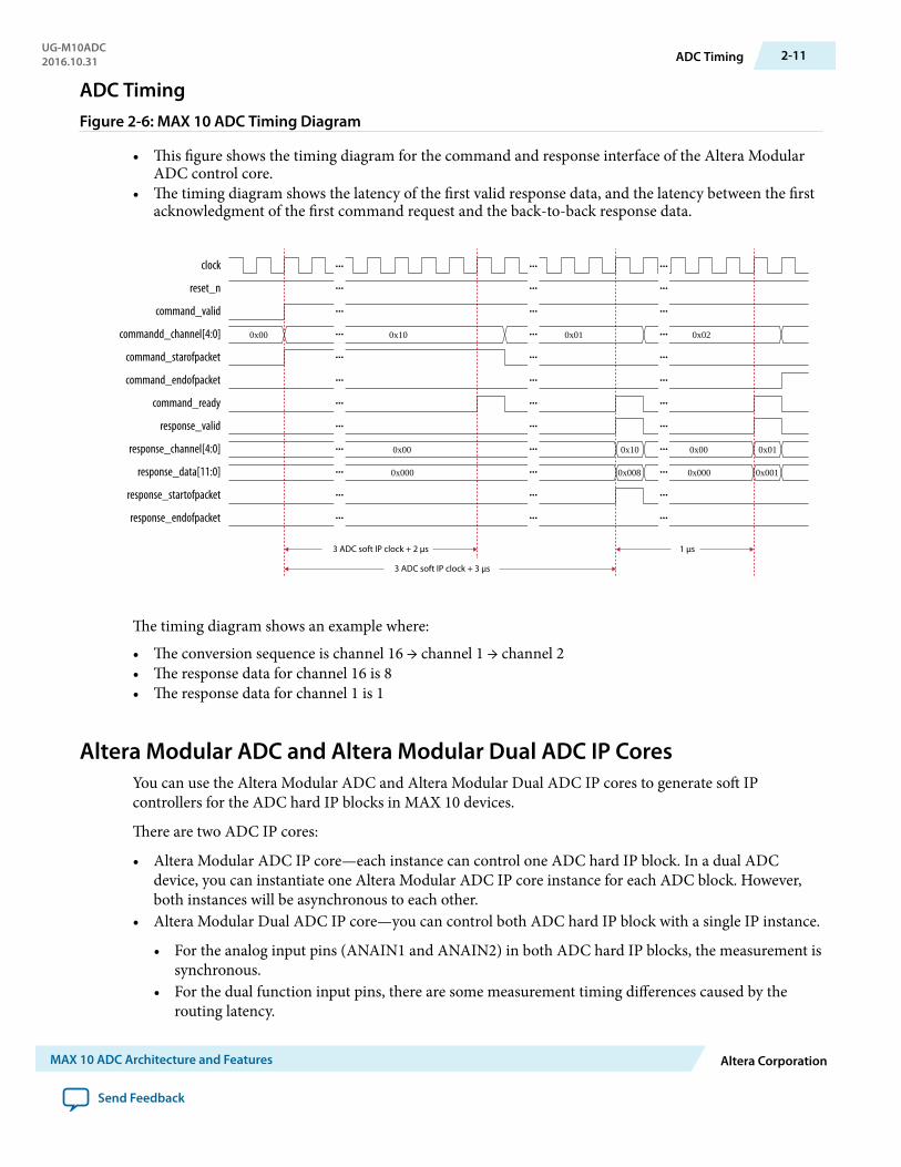
ADC TimingFigure 2-6: MAX 10 ADC Timing Diagram
• This figure shows the timing diagram for the command and response interface of the Altera ModularADC control core.
• The timing diagram shows the latency of the first valid response data, and the latency between the firstacknowledgment of the first command request and the back-to-back response data.
clock
reset_n
command_valid
commandd_channel[4:0]
command_starofpacket
command_endofpacket
command_ready
response_valid
response_channel[4:0]
response_data[11:0]
response_startofpacket
response_endofpacket
0x00 0x10 0x01 0x02
0x00 0x10 0x00 0x01
0x000 0x008 0x000 0x001
3 ADC soft IP clock + 3 μs
3 ADC soft IP clock + 2 μs 1 μs
The timing diagram shows an example where:
• The conversion sequence is channel 16 → channel 1 → channel 2• The response data for channel 16 is 8• The response data for channel 1 is 1
Altera Modular ADC and Altera Modular Dual ADC IP CoresYou can use the Altera Modular ADC and Altera Modular Dual ADC IP cores to generate soft IPcontrollers for the ADC hard IP blocks in MAX 10 devices.
There are two ADC IP cores:
• Altera Modular ADC IP core—each instance can control one ADC hard IP block. In a dual ADCdevice, you can instantiate one Altera Modular ADC IP core instance for each ADC block. However,both instances will be asynchronous to each other.
• Altera Modular Dual ADC IP core—you can control both ADC hard IP block with a single IP instance.
• For the analog input pins (ANAIN1 and ANAIN2) in both ADC hard IP blocks, the measurement issynchronous.
• For the dual function input pins, there are some measurement timing differences caused by therouting latency.
UG-M10ADC2016.10.31 ADC Timing 2-11
MAX 10 ADC Architecture and Features Altera Corporation
Send Feedback
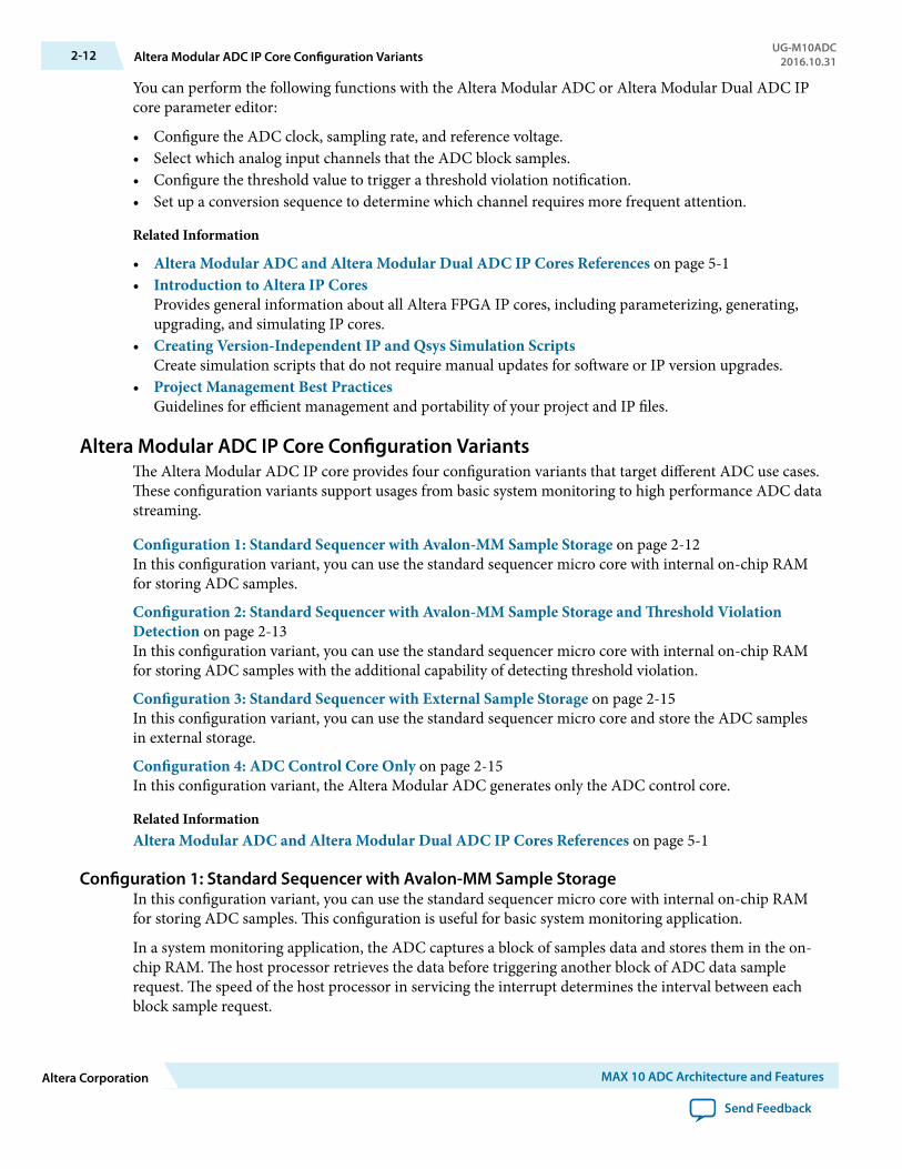
You can perform the following functions with the Altera Modular ADC or Altera Modular Dual ADC IPcore parameter editor:
• Configure the ADC clock, sampling rate, and reference voltage.• Select which analog input channels that the ADC block samples.• Configure the threshold value to trigger a threshold violation notification.• Set up a conversion sequence to determine which channel requires more frequent attention.
Related Information
• Altera Modular ADC and Altera Modular Dual ADC IP Cores References on page 5-1• Introduction to Altera IP Cores
Provides general information about all Altera FPGA IP cores, including parameterizing, generating,upgrading, and simulating IP cores.
• Creating Version-Independent IP and Qsys Simulation ScriptsCreate simulation scripts that do not require manual updates for software or IP version upgrades.
• Project Management Best PracticesGuidelines for efficient management and portability of your project and IP files.
Altera Modular ADC IP Core Configuration VariantsThe Altera Modular ADC IP core provides four configuration variants that target different ADC use cases.These configuration variants support usages from basic system monitoring to high performance ADC datastreaming.
Configuration 1: Standard Sequencer with Avalon-MM Sample Storage on page 2-12In this configuration variant, you can use the standard sequencer micro core with internal on-chip RAMfor storing ADC samples.
Configuration 2: Standard Sequencer with Avalon-MM Sample Storage and Threshold ViolationDetection on page 2-13In this configuration variant, you can use the standard sequencer micro core with internal on-chip RAMfor storing ADC samples with the additional capability of detecting threshold violation.
Configuration 3: Standard Sequencer with External Sample Storage on page 2-15In this configuration variant, you can use the standard sequencer micro core and store the ADC samplesin external storage.
Configuration 4: ADC Control Core Only on page 2-15In this configuration variant, the Altera Modular ADC generates only the ADC control core.
Related InformationAltera Modular ADC and Altera Modular Dual ADC IP Cores References on page 5-1
Configuration 1: Standard Sequencer with Avalon-MM Sample StorageIn this configuration variant, you can use the standard sequencer micro core with internal on-chip RAMfor storing ADC samples. This configuration is useful for basic system monitoring application.
In a system monitoring application, the ADC captures a block of samples data and stores them in the on-chip RAM. The host processor retrieves the data before triggering another block of ADC data samplerequest. The speed of the host processor in servicing the interrupt determines the interval between eachblock sample request.
2-12 Altera Modular ADC IP Core Configuration VariantsUG-M10ADC
2016.10.31
Altera Corporation MAX 10 ADC Architecture and Features
Send Feedback
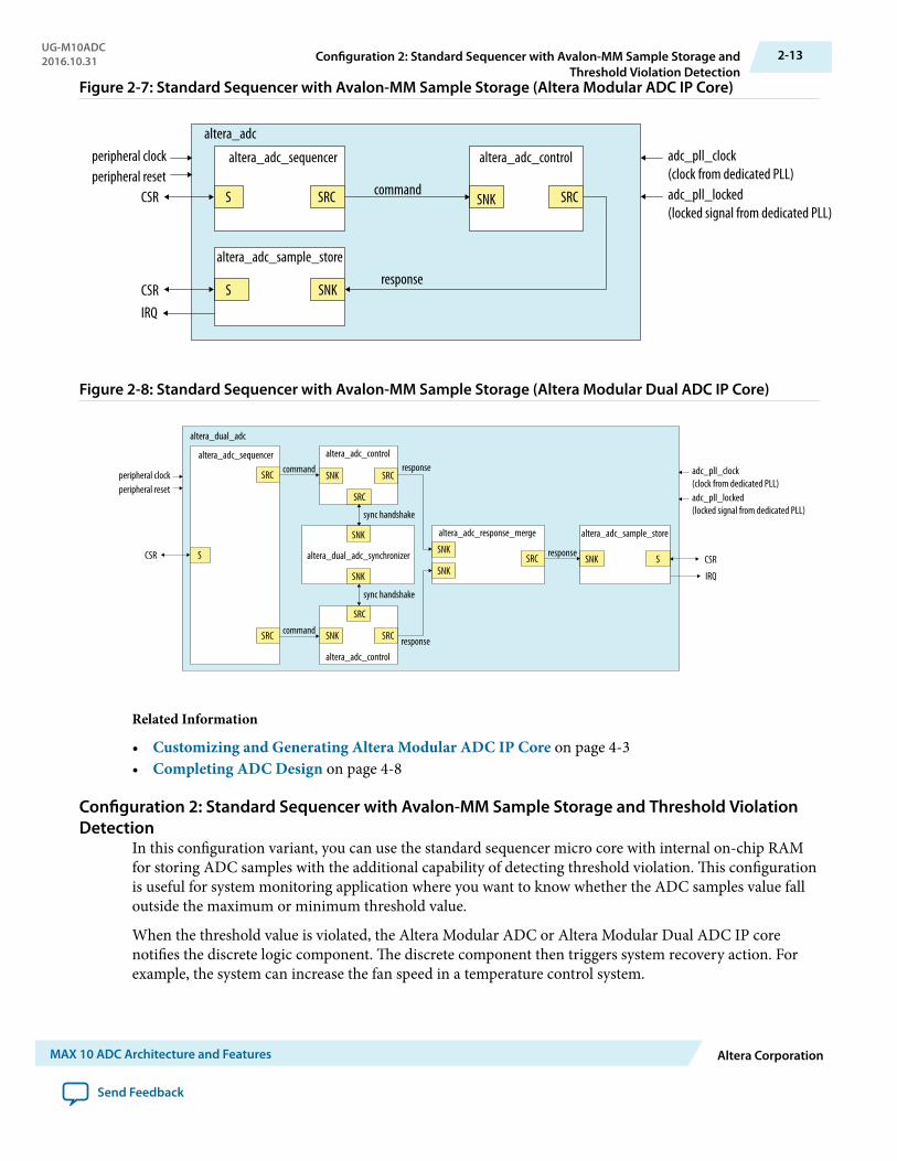
Figure 2-7: Standard Sequencer with Avalon-MM Sample Storage (Altera Modular ADC IP Core)
adc_pll_clock(clock from dedicated PLL)adc_pll_locked(locked signal from dedicated PLL)
altera_adc
altera_adc_sequencer altera_adc_control
SNK
SNK
SRC SRCS
S
altera_adc_sample_store
CSR
CSR
IRQ
peripheral clockperipheral reset
command
response
Figure 2-8: Standard Sequencer with Avalon-MM Sample Storage (Altera Modular Dual ADC IP Core)
adc_pll_clock(clock from dedicated PLL)adc_pll_locked(locked signal from dedicated PLL)
altera_dual_adc
altera_adc_sequencer
S
SRC
SRC
altera_adc_control
SNK SRC
SRC
altera_dual_adc_synchronizer
altera_adc_response_mergeSNK
SNK SNK
SNKS SNK
altera_adc_sample_store
CSRCSR
IRQ
peripheral clockperipheral reset
altera_adc_control
SNK SRC
SRC
sync handshake
sync handshake
command
command
SRC
response
response
response
Related Information
• Customizing and Generating Altera Modular ADC IP Core on page 4-3• Completing ADC Design on page 4-8
Configuration 2: Standard Sequencer with Avalon-MM Sample Storage and Threshold ViolationDetection
In this configuration variant, you can use the standard sequencer micro core with internal on-chip RAMfor storing ADC samples with the additional capability of detecting threshold violation. This configurationis useful for system monitoring application where you want to know whether the ADC samples value falloutside the maximum or minimum threshold value.
When the threshold value is violated, the Altera Modular ADC or Altera Modular Dual ADC IP corenotifies the discrete logic component. The discrete component then triggers system recovery action. Forexample, the system can increase the fan speed in a temperature control system.
UG-M10ADC2016.10.31 Configuration 2: Standard Sequencer with Avalon-MM Sample Storage and
Threshold Violation Detection2-13
MAX 10 ADC Architecture and Features Altera Corporation
Send Feedback
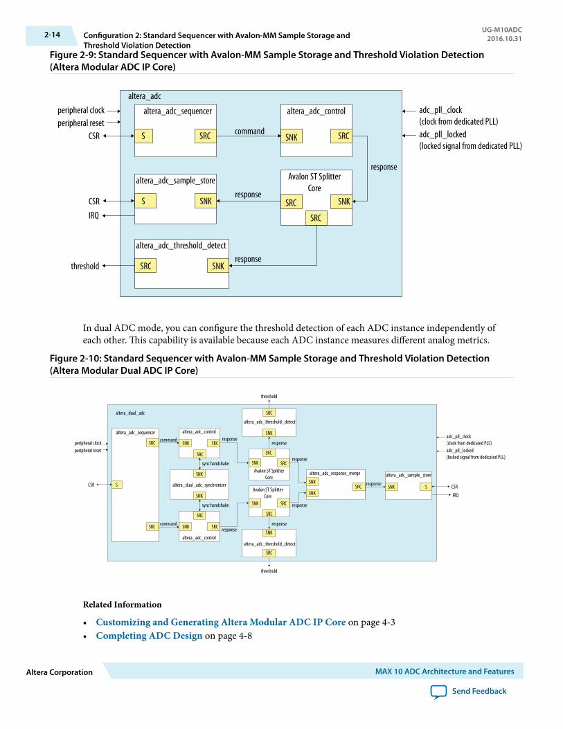
Figure 2-9: Standard Sequencer with Avalon-MM Sample Storage and Threshold Violation Detection(Altera Modular ADC IP Core)
adc_pll_clock(clock from dedicated PLL)adc_pll_locked(locked signal from dedicated PLL)
altera_adc
altera_adc_sequencer altera_adc_control
SNK
SNK
SRC SRC
Avalon ST SplitterCore
SRC SNK
S
S
altera_adc_sample_store
SNKSRC
altera_adc_threshold_detect
CSR
CSR
IRQ
peripheral clockperipheral reset
command
response
response
response
SRC
threshold
In dual ADC mode, you can configure the threshold detection of each ADC instance independently ofeach other. This capability is available because each ADC instance measures different analog metrics.
Figure 2-10: Standard Sequencer with Avalon-MM Sample Storage and Threshold Violation Detection(Altera Modular Dual ADC IP Core)
adc_pll_clock(clock from dedicated PLL)adc_pll_locked(locked signal from dedicated PLL)
SSNK
altera_adc_sample_store
SNK
SRC
altera_adc_threshold_detect
SNK
SRC
altera_adc_threshold_detect
CSR
IRQ
Avalon ST SplitterCore
SRCSNK
SRC
Avalon ST SplitterCore
SRCSNK
SRC
threshold
threshold
altera_dual_adc
altera_adc_sequencer
SRC
SRC
altera_adc_control
SNK SRC
SRC
altera_dual_adc_synchronizer
SNK
SNK
SCSR
peripheral clockperipheral reset
altera_adc_control
SNK SRC
SRC
sync handshake
sync handshake
command
commandresponse
response
response
response
response
response
response
altera_adc_response_merge
SNK
SNKSRC
Related Information
• Customizing and Generating Altera Modular ADC IP Core on page 4-3• Completing ADC Design on page 4-8
2-14 Configuration 2: Standard Sequencer with Avalon-MM Sample Storage andThreshold Violation Detection
UG-M10ADC2016.10.31
Altera Corporation MAX 10 ADC Architecture and Features
Send Feedback
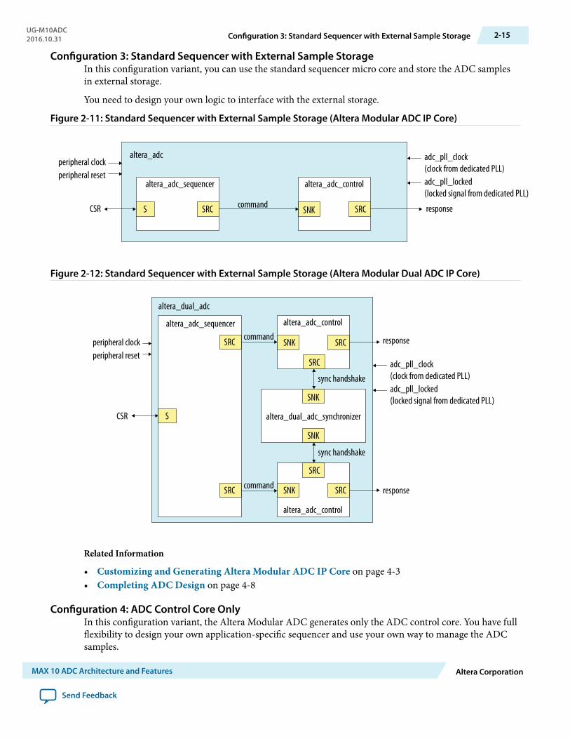
Configuration 3: Standard Sequencer with External Sample StorageIn this configuration variant, you can use the standard sequencer micro core and store the ADC samplesin external storage.
You need to design your own logic to interface with the external storage.
Figure 2-11: Standard Sequencer with External Sample Storage (Altera Modular ADC IP Core)
adc_pll_clock(clock from dedicated PLL)adc_pll_locked(locked signal from dedicated PLL)
altera_adc
altera_adc_sequencer altera_adc_control
SNKSRC SRCSCSR
peripheral clockperipheral reset
command response
Figure 2-12: Standard Sequencer with External Sample Storage (Altera Modular Dual ADC IP Core)
adc_pll_clock(clock from dedicated PLL)adc_pll_locked(locked signal from dedicated PLL)
altera_dual_adc
altera_adc_sequencer
SRC
SRC
altera_adc_control
SNK SRC
SRC
altera_dual_adc_synchronizer
SNK
SNK
SCSR
peripheral clockperipheral reset
altera_adc_control
SNK SRC
SRC
sync handshake
sync handshake
command
command response
response
Related Information
• Customizing and Generating Altera Modular ADC IP Core on page 4-3• Completing ADC Design on page 4-8
Configuration 4: ADC Control Core OnlyIn this configuration variant, the Altera Modular ADC generates only the ADC control core. You have fullflexibility to design your own application-specific sequencer and use your own way to manage the ADCsamples.
UG-M10ADC2016.10.31 Configuration 3: Standard Sequencer with External Sample Storage 2-15
MAX 10 ADC Architecture and Features Altera Corporation
Send Feedback
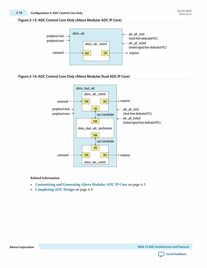
Figure 2-13: ADC Control Core Only (Altera Modular ADC IP Core)
adc_pll_clock(clock from dedicated PLL)adc_pll_locked(locked signal from dedicated PLL)
altera_adc
altera_adc_control
SNK SRC
peripheral clockperipheral reset
command response
Figure 2-14: ADC Control Core Only (Altera Modular Dual ADC IP Core)
adc_pll_clock(clock from dedicated PLL)adc_pll_locked(locked signal from dedicated PLL)
altera_dual_adc
altera_adc_control
SNK SRC
SRC
altera_dual_adc_synchronizer
SNK
SNK
peripheral clockperipheral reset
altera_adc_control
SNK SRC
SRC
sync handshake
sync handshake
command
command response
response
Related Information
• Customizing and Generating Altera Modular ADC IP Core on page 4-3• Completing ADC Design on page 4-8
2-16 Configuration 4: ADC Control Core OnlyUG-M10ADC
2016.10.31
Altera Corporation MAX 10 ADC Architecture and Features
Send Feedback
Altera Modular ADC and Altera Modular Dual ADC IP Cores ArchitectureThe Altera Modular ADC IP core consists of six micro cores.
Table 2-2: Altera Modular ADC Micro Cores
Micro Core Description
ADC control This core interacts with the ADC hard IP block. The ADC control core usesAvalon ST interface to receive commands from upstream cores, decodes, anddrives the ADC hard IP block accordingly.
Sequencer This core contains command register and static conversion sequence data. Thesequencer core issues commands for downstream cores to execute.
• You can use the command register to configure the intended conversionmode.
• You can configure the length and content of the conversion sequence dataonly when generating the IP core.
• You can access the register of the sequencer core through the Avalon-MMslave interface.
• The command information to the downstream core goes through theAvalon ST interface.
Sample storage This core stores the ADC samples that are received through the Avalon STinterface.
• The samples are stored in the on-chip RAM. You can retrieve the samplesthrough the Avalon-MM slave interface.
• With this core, you have the option to generate interrupt when the ADCreceives a block of ADC samples (one full round of conversion sequence).
Response merge This core merges simultaneous responses from two ADC control cores into asingle response packet to send to the sample storage core. This core is availableonly if you use the Altera Modular Dual ADC IP core in the followingconfigurations:
• Standard Sequencer with Avalon-MM Sample Storage• Standard Sequencer with Avalon-MM Sample Storage and Threshold
Violation Detection
Dual ADC synchronizercore
This core performs synchronization handshakes between two ADC controlcores. This core is available only if you use the Altera Modular Dual ADC IPcore.
UG-M10ADC2016.10.31 Altera Modular ADC and Altera Modular Dual ADC IP Cores Architecture 2-17
MAX 10 ADC Architecture and Features Altera Corporation
Send Feedback
Micro Core Description
Threshold detection • This core supports fault detection. The threshold detection core receivesADC samples through the Avalon ST interface and checks whether thesamples value exceeds the maximum or falls below the minimum thresholdvalue.
• The threshold detection core conveys threshold value violation informationthrough the Avalon ST interface.
• You can configure which channel to enable for maximum and minimumthreshold detection and the threshold values only during IP coregeneration.
ADC Control CoreThe ADC control core drives the ADC hard IP according to the command it receives. The control core alsomaps the channels from the Altera Modular ADC IP core to the channels in the ADC hard IP block.
The ADC control core of the Altera Modular ADC IP core implements only the functions that are relatedto ADC hard IP block operations. For example:
• Power up• Power down• Analog to digital conversion on analog pins• Analog to digital conversion on on-chip temperature sensor
The ADC control core has two clock domains:
• One clock domain for clocking the ADC control core soft logic• Another clock domain for the ADC hard IP block
The ADC control core does not have run-time configurable options.
Figure 2-15: ADC Control Core High-Level Block Diagram
adc_pll_clock(clock from dedicated PLL)adc_pll_locked(locked signal from dedicated PLL)
altera_adc_control
SNK SRC
SRC
peripheral clockperipheral reset
command response
sync handshake (dual ADC only)
ADCController
FSM
ADCHard IP
Wrapper
2-18 ADC Control CoreUG-M10ADC
2016.10.31
Altera Corporation MAX 10 ADC Architecture and Features
Send Feedback
Table 2-3: ADC Control Core Backpressure Behavior
Interface Backpressure Behavior
Command The ADC control core asserts ready when it is ready to perform a sample conversion.
The ADC control core only accepts one command at a time. The control core releasesready when it completes processing current command and prepares to perform thenext command.
Once the ADC control core asserts "cmd_ready=1" to acknowledge the currentcommand, the Sequencer core provides the next valid request within two clock cycles.If the next valid request comes after two clock cycles, the ADC control core performnon-continuous sampling.
Response The ADC control core does not support backpressure in the response interface. Thefastest back-to-back assertion of valid request is 1 µs.
Sequencer CoreThe sequencer core controls the type of conversion sequence performed by the ADC hard IP. You canconfigure the conversion mode during run time using the sequencer core registers.
During Altera Modular ADC or Altera Modular Dual ADC IP core configuration, the sequencer coreprovides up to 64 configurable slots. You can define the sequence that the ADC channels are sampled byselecting the ADC channel for each sequencer slot.
The sequencer core has a single clock domain.
Figure 2-16: Sequencer Core High-Level Block Diagram
altera_adc_sequencer
S
SRC
peripheral clockperipheral reset
CSR
command
SRC command(dual ADC only)
SequencerController
SequencerController
Command Register
Static ConversionSequence Data Array
(up to 64 slots)
Table 2-4: Sequencer Core Conversion Modes
Conversion Mode Description
Single cycle ADCconversion
• In this mode, when the run bit is set, ADC conversion starts from the channel thatyou specify in the first slot.
• The conversion continues onwards with the channel that you specify in eachsequencer slot.
• Once the conversion finishes with the last sequencer slot, the conversion cycle stopsand the ADC hard IP block clears the run bit.
UG-M10ADC2016.10.31 Sequencer Core 2-19
MAX 10 ADC Architecture and Features Altera Corporation
Send Feedback
Conversion Mode Description
Continuous ADCconversion
• In this mode, when the run bit is set, ADC conversion starts from the channel thatyou specify in the first slot.
• The conversion continues onwards with the channel that you specify in eachsequencer slot.
• Once the conversion finishes with the last sequencer slot, the conversion beginsagain from the first slot of the sequence.
• To stop the continuous conversion, clear the run bit. The sequencer core continuesthe conversion sequence until it reaches the last slot and then stops the conversioncycle.
Related Information
• Altera Modular ADC Parameters Settings on page 5-2Lists the parameters available during Altera Modular ADC IP core configuration.
• Altera Modular Dual ADC Parameters Settings on page 5-8Lists the parameters available during Altera Modular Dual ADC IP core configuration.
• Sequencer Core Registers on page 5-18Lists the registers for run-time control of the sequencer core.
Sample Storage CoreThe sample storage core stores the ADC sampling data in the on-chip RAM. The sample storage corestores the ADC samples data based on conversion sequence slots instead of ADC channels.
For example, if you sample a sequence of CH1, CH2, CH1, CH3, CH1, and then CH4, the ADC samplestorage core stores the channel sample data in the same RAM entry sequence. This means that CH1sample data will be in the first, third, and fifth RAM entries; one for each sequence slot.
The sample storage core asserts IRQ when it completes receipt of a sample block. You can disable the IRQassertion during run time using the interrupt enable register (IER) of the sample storage core. If youdisable IRQ assertion, you must create polling methods in your design to determine the complete receiptof a sample block.
The sample storage core has a single clock domain.
Figure 2-17: Sample Storage Core High-Level Block Diagram
altera_adc_sample_store
S SNK
peripheral clockperipheral reset
CSR
IRQ
64 RAM Entries forADC Sample Storage
IER RegisterISR Register
RAMControl
InterruptControl
response
2-20 Sample Storage CoreUG-M10ADC
2016.10.31
Altera Corporation MAX 10 ADC Architecture and Features
Send Feedback
Related InformationSample Storage Core Registers on page 5-19
Response Merge CoreThe response merge core merges simultaneous responses from two ADC control cores in the AlteraModular Dual ADC IP core.
The Altera Modular Dual ADC IP core uses the response merge core if you use the following configura‐tions:
• Standard Sequencer with Avalon-MM Sample Storage• Standard Sequencer with Avalon-MM Sample Storage and Threshold Violation Detection
Figure 2-18: Response Merge Core High-Level Block Diagram
altera_adc_response_merge
SNK
SNKSRC
peripheral clockperipheral reset
response
responseresponseResponse merge
logic
Dual ADC Synchronizer CoreThe dual ADC synchronizer core performs synchronization handshakes between two ADC control coresin the Altera Modular Dual ADC IP core.
The peripheral clock domain is asynchronous to the ADC PLL clock domain in the ADC control core.Control event from the ADC hard IP block can appear at the peripheral clock domain at the same time, orby a difference of one peripheral clock between ADC1 and ADC2 control cores. Both ADC hard IP corescommunicate with the dual ADC synchronizer core through the Avalon-ST interface.
For example, although a new command valid event from the sequencer arrives at both ADC control coresat the same peripheral clock cycle, the end of conversion signals arrive at one peripheral clock cycledifference between ADC1 and ADC2. To avoid the condition where ADC1 begins conversion earlier orlater than ADC2, the ADC control core performs synchronization handshake using the dual ADCsynchronizer core.
An ADC control core asserts a sync_valid signal when it detects an ADC PLL clock domain event. Thedual ADC synchronizer core asserts the sync_ready signal after it receives sync_valid signals from bothADC control cores. After the sync_ready signal is asserted, both ADC control cores proceed to their nextinternal state.
UG-M10ADC2016.10.31 Response Merge Core 2-21
MAX 10 ADC Architecture and Features Altera Corporation
Send Feedback
Figure 2-19: Dual ADC Synchronizer Core High-Level Block Diagram
altera_dual_adc_synchronizer
SNK
SNK
peripheral clockperipheral reset
sync handshake
sync handshake
Synchronizerlogic
Threshold Detection CoreThe threshold detection core compares the sample value that the ADC block receives to the thresholdvalue that you define during Altera Modular ADC IP core configuration. This core does not have run-timeconfigurable options.
If the ADC sample value is beyond the maximum or minimum threshold limit, the threshold detectioncore issues a violation notification through the Avalon-ST interface.
The threshold detection core has a single clock domain.
Figure 2-20: Threshold Detection Core High-Level Block Diagram
altera_adc_threshold_detect
SRC SNK
peripheral clockperipheral reset
threshold responseComparator
Logic
Altera ADC HAL DriverThe Altera ADC HAL driver supports the following features:
• Read ADC channel data.• Enable maximum or minimum threshold and return a user callback when the interrupt is triggered.• Command the control of the ADC (run, stop, and recalibrate).
Related Information
• HAL API Reference, Nios II Gen 2 Software Developer's HandbookProvides more information about the HAL API.
• ADC HAL Device Driver for Nios II Gen 2 on page 5-20
2-22 Threshold Detection CoreUG-M10ADC
2016.10.31
Altera Corporation MAX 10 ADC Architecture and Features
Send Feedback
ADC Toolkit for Testing ADC PerformanceYou can use the ADC Toolkit provided with the Quartus Prime software to understand the performance ofthe analog signal chain as seen by the MAX 10 ADC blocks.
The ADC Toolkit supports monitoring the ADC whether you use the Altera Modular ADC or AlteraModular Dual ADC IP core. However, the ADC Toolkit can only monitor one ADC block at a time. If youare using the Altera Modular Dual ADC IP core, configure the Debug Path parameter in the IP core toselect which ADC block you want to hook up to the ADC Toolkit.
Related InformationADC ToolkitProvides more information about the ADC Toolkit.
ADC Logic Simulation OutputBy default, the ADC logic simulation outputs a fixed unique value for each ADC channel. However, youcan enable an option to specify your own output values for each ADC channel other than the TSD.
The ADC simulation model for MAX 10 devices supports the standard digital logic simulators that theQuartus Prime software supports.
Related InformationQuartus Prime Simulator Support
Fixed ADC Logic Simulation OutputBy default, the Enable user created expected output file option in the Altera Modular ADC or AlteraModular Dual ADC IP core is disabled. The ADC simulation always output a fixed value for each ADCchannel, including the analog and TSD channels. The values are different for single and dual ADC devices.
Table 2-5: Fixed Expected Output Data for Single ADC Device Simulation
Channel Expected Output Data (Decimal Value)
CH0 0
CH1 1
CH2 2
CH3 3
CH4 4
CH5 5
CH6 6
CH7 7
CH8 8
CH9 9
UG-M10ADC2016.10.31 ADC Toolkit for Testing ADC Performance 2-23
MAX 10 ADC Architecture and Features Altera Corporation
Send Feedback
Channel Expected Output Data (Decimal Value)
CH10 10
CH11 11
CH12 12
CH13 13
CH14 14
CH15 15
CH16 16
TSD 3615
Table 2-6: Fixed Expected Output Data for Dual ADC Device Simulation
ChannelExpected Output Data (Decimal Value)
ADC1 ADC2
CH0 10 20
CH1 11 21
CH2 12 22
CH3 13 23
CH4 14 24
CH5 15 25
CH6 16 26
CH7 17 27
CH8 18 28
TSD 3615 —
(No TSD in ADC2)
User-Specified ADC Logic Simulation OutputYou can configure the Altera Modular ADC or Altera Modular Dual ADC IP core to output user-specifiedvalues in the logic simulation for each ADC channel except the TSD channel.
If you enable this feature, you must provide a simulation stimulus input file for each ADC channel thatyou enable. The logic simulation reads the input file for each channel and outputs the value of the currentsequence. Once the simulation reaches the end of the file, it repeats from the beginning of the sequence.
The stimulus input file is a plain text file that contains two columns of numbers:
• The first column of numbers is ignored by the simulation model. You can use any values that you wantsuch as time or sequence. The actual data sequencing is based on the text rows.
• The second column contains the voltage values.
2-24 User-Specified ADC Logic Simulation OutputUG-M10ADC
2016.10.31
Altera Corporation MAX 10 ADC Architecture and Features
Send Feedback
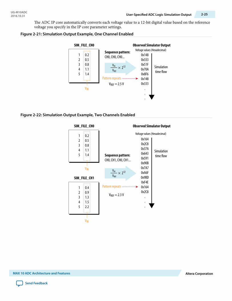
The ADC IP core automatically converts each voltage value to a 12-bit digital value based on the referencevoltage you specify in the IP core parameter settings.
Figure 2-21: Simulation Output Example, One Channel Enabled
1 0.22 0.53 0.84 1.15 1.4
SIM_FILE_CH0 Observed Simulator Output
0x1480x3330x51F0x70A0x8F60x1480x333
.
.
.
Simulationtime flow
Pattern repeats
Voltage values (Hexadecimal)
VIN
VREF× 212
VREF = 2.5 VVIN
Sequence pattern:CH0, CH0, CH0...
Figure 2-22: Simulation Output Example, Two Channels Enabled
1 0.22 0.53 0.84 1.15 1.4
SIM_FILE_CH0
1 0.42 0.93 1.34 1.55 2.2
SIM_FILE_CH1
Observed Simulator Output
0x1640x2C80x37A0x6430x5910x90B0x7A70xA6F0x9BD0xF4E0x1640x2C8
.
.
.
Simulationtime flow
Pattern repeats
VREF = 2.3 V
Sequence pattern:CH0, CH1, CH0, CH1...
Voltage values (Hexadecimal)
VIN
VREF× 212
VIN
VIN
UG-M10ADC2016.10.31 User-Specified ADC Logic Simulation Output 2-25
MAX 10 ADC Architecture and Features Altera Corporation
Send Feedback

MAX 10 ADC Design Considerations 32016.10.31
UG-M10ADC Subscribe Send Feedback
There are several considerations that require your attention to ensure the success of your designs. Unlessnoted otherwise, these design guidelines apply to all variants of this device family.
Related InformationMAX 10 Analog to Digital Converter Overview on page 1-1
Guidelines: ADC Ground Plane ConnectionFor the ADC and VREF pins, use the REFGND pin as the analog ground plane connection.
Related InformationMAX 10 FPGA Device Family Pin Connection GuidelinesProvides more information about pin connections including pin names and connection guidelines.
Guidelines: Board Design for Power Supply Pin and ADC Ground (REFGND)The crosstalk requirement for analog to digital signal is -100 dB up to 2 GHz. There must be no parallelrouting between power, ground, and surrounding general purpose I/O traces. If a power plane is notpossible, route the power and ground traces as wide as possible.
• To reduce IR drop and switching noise, keep the impedance as low as possible for the ADC power andground. The maximum DC resistance for power is 1.5 Ω.
• The power supplies connected to the ADC should have ferrite beads in series followed by a 10 µFcapacitor to the ground. This setup ensures that no external noise goes into the device power supplypins.
• Decouple each of the device power supply pin with a 0.1 µF capacitor. Place the capacitor as close aspossible to the device pin.
© 2016 Intel Corporation. All rights reserved. Intel, the Intel logo, Altera, Arria, Cyclone, Enpirion, MAX, Megacore, NIOS, Quartus and Stratix words and logosare trademarks of Intel Corporation in the US and/or other countries. Other marks and brands may be claimed as the property of others. Intel warrantsperformance of its FPGA and semiconductor products to current specifications in accordance with Intel's standard warranty, but reserves the right to makechanges to any products and services at any time without notice. Intel assumes no responsibility or liability arising out of the application or use of anyinformation, product, or service described herein except as expressly agreed to in writing by Intel. Intel customers are advised to obtain the latest version ofdevice specifications before relying on any published information and before placing orders for products or services.
ISO9001:2008Registered
www.altera.com101 Innovation Drive, San Jose, CA 95134
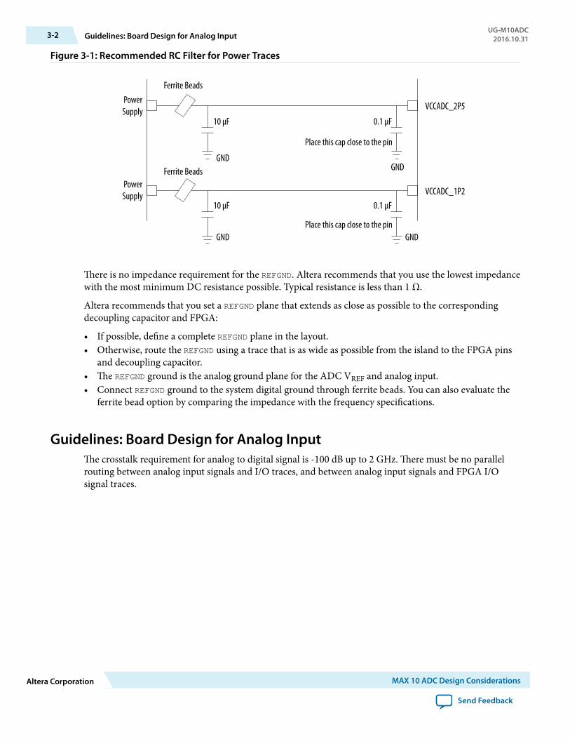
Figure 3-1: Recommended RC Filter for Power Traces
Place this cap close to the pin
Place this cap close to the pin
0.1 µF
0.1 µF
10 µF
10 µF
Ferrite Beads
Ferrite BeadsPowerSupply
PowerSupply
VCCADC_2P5
VCCADC_1P2
GND
GND
GND
GND
There is no impedance requirement for the REFGND. Altera recommends that you use the lowest impedancewith the most minimum DC resistance possible. Typical resistance is less than 1 Ω.
Altera recommends that you set a REFGND plane that extends as close as possible to the correspondingdecoupling capacitor and FPGA:
• If possible, define a complete REFGND plane in the layout.• Otherwise, route the REFGND using a trace that is as wide as possible from the island to the FPGA pins
and decoupling capacitor.• The REFGND ground is the analog ground plane for the ADC VREF and analog input.• Connect REFGND ground to the system digital ground through ferrite beads. You can also evaluate the
ferrite bead option by comparing the impedance with the frequency specifications.
Guidelines: Board Design for Analog InputThe crosstalk requirement for analog to digital signal is -100 dB up to 2 GHz. There must be no parallelrouting between analog input signals and I/O traces, and between analog input signals and FPGA I/Osignal traces.
3-2 Guidelines: Board Design for Analog InputUG-M10ADC
2016.10.31
Altera Corporation MAX 10 ADC Design Considerations
Send Feedback
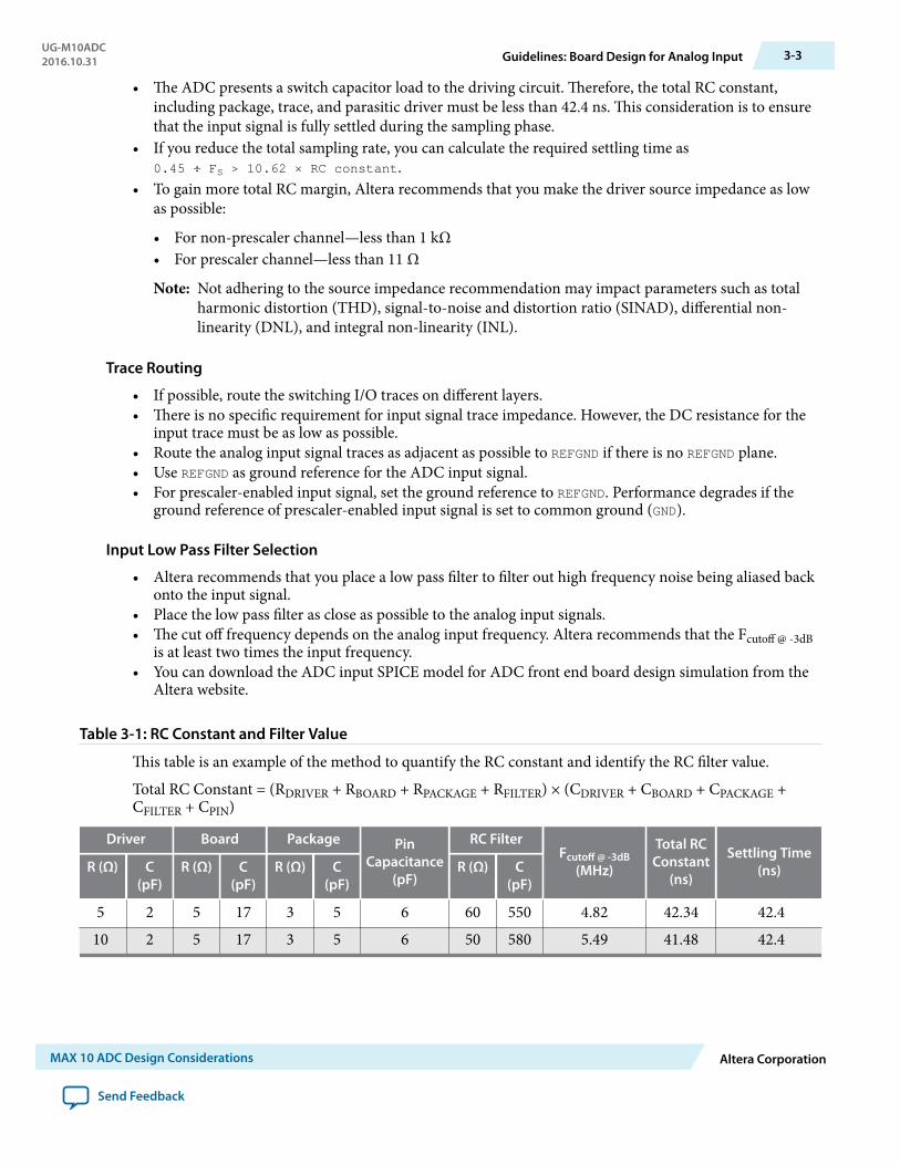
• The ADC presents a switch capacitor load to the driving circuit. Therefore, the total RC constant,including package, trace, and parasitic driver must be less than 42.4 ns. This consideration is to ensurethat the input signal is fully settled during the sampling phase.
• If you reduce the total sampling rate, you can calculate the required settling time as0.45 ÷ FS > 10.62 × RC constant.
• To gain more total RC margin, Altera recommends that you make the driver source impedance as lowas possible:
• For non-prescaler channel—less than 1 kΩ• For prescaler channel—less than 11 Ω
Note: Not adhering to the source impedance recommendation may impact parameters such as totalharmonic distortion (THD), signal-to-noise and distortion ratio (SINAD), differential non-linearity (DNL), and integral non-linearity (INL).
Trace Routing
• If possible, route the switching I/O traces on different layers.• There is no specific requirement for input signal trace impedance. However, the DC resistance for the
input trace must be as low as possible.• Route the analog input signal traces as adjacent as possible to REFGND if there is no REFGND plane.• Use REFGND as ground reference for the ADC input signal.• For prescaler-enabled input signal, set the ground reference to REFGND. Performance degrades if the
ground reference of prescaler-enabled input signal is set to common ground (GND).
Input Low Pass Filter Selection
• Altera recommends that you place a low pass filter to filter out high frequency noise being aliased backonto the input signal.
• Place the low pass filter as close as possible to the analog input signals.• The cut off frequency depends on the analog input frequency. Altera recommends that the Fcutoff @ -3dB
is at least two times the input frequency.• You can download the ADC input SPICE model for ADC front end board design simulation from the
Altera website.
Table 3-1: RC Constant and Filter Value
This table is an example of the method to quantify the RC constant and identify the RC filter value.
Total RC Constant = (RDRIVER + RBOARD + RPACKAGE + RFILTER) × (CDRIVER + CBOARD + CPACKAGE +CFILTER + CPIN)
Driver Board Package PinCapacitance
(pF)
RC FilterFcutoff @ -3dB
(MHz)
Total RCConstant
(ns)
Settling Time(ns)R (Ω) C
(pF)R (Ω) C
(pF)R (Ω) C
(pF)R (Ω) C
(pF)
5 2 5 17 3 5 6 60 550 4.82 42.34 42.410 2 5 17 3 5 6 50 580 5.49 41.48 42.4
UG-M10ADC2016.10.31 Guidelines: Board Design for Analog Input 3-3
MAX 10 ADC Design Considerations Altera Corporation
Send Feedback
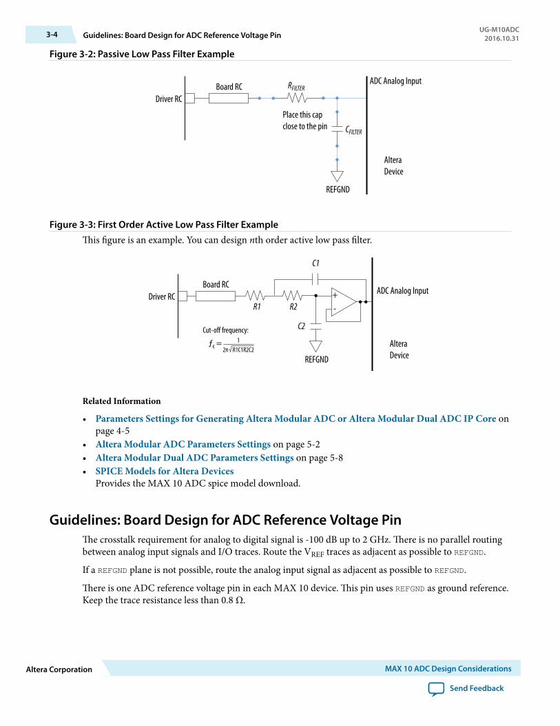
Figure 3-2: Passive Low Pass Filter Example
ADC Analog InputBoard RC
Driver RCRFILTER
CFILTER
Place this cap close to the pin
REFGND
AlteraDevice
Figure 3-3: First Order Active Low Pass Filter ExampleThis figure is an example. You can design nth order active low pass filter.
+-
ADC Analog InputBoard RC
Driver RCR1 R2
C2
C1
ƒc =1
2π R1C1R2C2
Cut-off frequency:
REFGND
AlteraDevice
Related Information
• Parameters Settings for Generating Altera Modular ADC or Altera Modular Dual ADC IP Core onpage 4-5
• Altera Modular ADC Parameters Settings on page 5-2• Altera Modular Dual ADC Parameters Settings on page 5-8• SPICE Models for Altera Devices
Provides the MAX 10 ADC spice model download.
Guidelines: Board Design for ADC Reference Voltage PinThe crosstalk requirement for analog to digital signal is -100 dB up to 2 GHz. There is no parallel routingbetween analog input signals and I/O traces. Route the VREF traces as adjacent as possible to REFGND.
If a REFGND plane is not possible, route the analog input signal as adjacent as possible to REFGND.
There is one ADC reference voltage pin in each MAX 10 device. This pin uses REFGND as ground reference.Keep the trace resistance less than 0.8 Ω.
3-4 Guidelines: Board Design for ADC Reference Voltage PinUG-M10ADC
2016.10.31
Altera Corporation MAX 10 ADC Design Considerations
Send Feedback
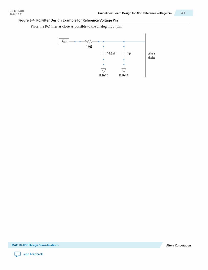
Figure 3-4: RC Filter Design Example for Reference Voltage Pin
Place the RC filter as close as possible to the analog input pin.
VREF
1.0 Ω
10.0 µF 1 µF
REFGND REFGND
Alteradevice
UG-M10ADC2016.10.31 Guidelines: Board Design for ADC Reference Voltage Pin 3-5
MAX 10 ADC Design Considerations Altera Corporation
Send Feedback
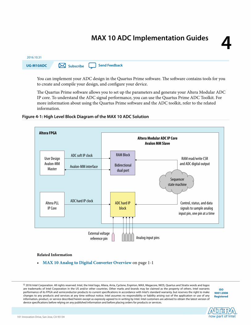
MAX 10 ADC Implementation Guides 42016.10.31
UG-M10ADC Subscribe Send Feedback
You can implement your ADC design in the Quartus Prime software. The software contains tools for youto create and compile your design, and configure your device.
The Quartus Prime software allows you to set up the parameters and generate your Altera Modular ADCIP core. To understand the ADC signal performance, you can use the Quartus Prime ADC Toolkit. Formore information about using the Quartus Prime software and the ADC toolkit, refer to the relatedinformation.
Figure 4-1: High Level Block Diagram of the MAX 10 ADC Solution
Altera FPGA
User DesignAvalon-MM
Master
ADC soft IP clock
Avalon-MM interface
Altera PLLIP Core
ADC hard IP clock ADC hard IPblock
External voltagereference pin Analog input pins
Control, status, and datasignals to sample analog
input pin, one pin at a time
Sequencerstate machine
RAM read/write CSRand ADC digital output
Altera Modular ADC IP CoreAvalon MM Slave
RAM Block
Bidirectionaldual port
Related Information
• MAX 10 Analog to Digital Converter Overview on page 1-1
© 2016 Intel Corporation. All rights reserved. Intel, the Intel logo, Altera, Arria, Cyclone, Enpirion, MAX, Megacore, NIOS, Quartus and Stratix words and logosare trademarks of Intel Corporation in the US and/or other countries. Other marks and brands may be claimed as the property of others. Intel warrantsperformance of its FPGA and semiconductor products to current specifications in accordance with Intel's standard warranty, but reserves the right to makechanges to any products and services at any time without notice. Intel assumes no responsibility or liability arising out of the application or use of anyinformation, product, or service described herein except as expressly agreed to in writing by Intel. Intel customers are advised to obtain the latest version ofdevice specifications before relying on any published information and before placing orders for products or services.
ISO9001:2008Registered
www.altera.com101 Innovation Drive, San Jose, CA 95134
• Quartus II Handbook, Volume 1: Design and SynthesisProvides more information about using IP cores in the Quartus II software.
• Introduction to Altera IP CoresProvides general information about all Altera FPGA IP cores, including parameterizing, generating,upgrading, and simulating IP cores.
• Creating Version-Independent IP and Qsys Simulation ScriptsCreate simulation scripts that do not require manual updates for software or IP version upgrades.
• Project Management Best PracticesGuidelines for efficient management and portability of your project and IP files.
• ADC ToolkitProvides more information about the ADC Toolkit.
• ADC Toolkit for Testing ADC Performance on page 2-23
Creating MAX 10 ADC DesignTo create your ADC design, you must customize and generate the ALTPLL and Altera Modular ADC IPcores.
The ALTPLL IP core provides the clock for the Altera Modular ADC IP core.
1. Customize and generate the ALTPLL IP core.2. Customize and generate the Altera Modular ADC IP core.3. Connect the ALTPLL IP core to the Altera Modular ADC IP core.4. Create ADC Avalon slave interface to start the ADC.
Related Information
• Customizing and Generating Altera Modular ADC IP Core on page 4-3• Parameters Settings for Generating Altera Modular ADC or Altera Modular Dual ADC IP Core on
page 4-5• Parameters Settings for Generating ALTPLL IP Core on page 4-4• Completing ADC Design on page 4-8• MAX 10 Getting Started• MAX 10 Online Training• MAX 10 How-to Videos• How to Create ADC Design in MAX 10 Device Using Qsys Tool
Provides video instruction that demonstrates how to create the ADC design in MAX 10 devices usingthe Qsys system integration tool within the Quartus Prime software and how to use the ADC toolkit toview the measured analog signal.
• How to Create Simultaneous Measurement with MAX 10 ADC, Part 1Provides the first part of video instruction series that explains the differences between the MAX 10Altera Modular ADC and Altera Modular Dual ADC IP cores. The video also demonstrates how tocreate a simple simultaneous ADC measurement and how to place signal taps to measure the digitalcode output for analog signal.
4-2 Creating MAX 10 ADC DesignUG-M10ADC
2016.10.31
Altera Corporation MAX 10 ADC Implementation Guides
Send Feedback
• How to Create Simultaneous Measurement with MAX 10 ADC, Part 2Provides the second part of video instruction series that explains the differences between the MAX 10Altera Modular ADC and Altera Modular Dual ADC IP cores. The video also demonstrates how tocreate a simple simultaneous ADC measurement and how to place signal taps to measure the digitalcode output for analog signal.
Customizing and Generating Altera Modular ADC IP CoreAltera recommends that you use the Altera Modular ADC IP core with a Nios II processor, whichsupports the ADC HAL driver.
1. Create a new project in the Quartus Prime software.While creating the project, select a device that has one or two ADC blocks.
2. In the Quartus Prime software, select Tools > Qsys.3. In the Qsys window, select File > New System.
A clock source block is automatically added under the System Contents tab.4. In the System Contents tab, double click the clock name.5. In the Parameters tab for the clock source, set the Clock frequency.6. In the IP Catalog tab in the Qsys window, double click Processors and Peripherals > Peripherals >
Altera Modular ADC.The Altera Modular ADC appears in the System Contents tab and the Altera Modular ADC parametereditor opens.
7. In the Altera Modular ADC parameter editor, specify the parameter settings and channel samplingsequence for your application.
8. In the System Contents tab in the Qsys window, double click the Export column of theadc_pll_clock and adc_pll_locked interfaces to export them.
9. Connect the clock, reset_sink, sample_store_csr, and sample_store_irq signals. Optionally, youcan use the Nios II Processor, On-Chip Memory, and JTAG UART IP cores to form a working ADCsystem that uses the Altera ADC HAL drivers.
10.In the Qsys window, select File > Save.
You can copy an example HDL code to declare an instance of your ADC system. In the Qsys window,select Generate > HDL Example.
Related Information
• Creating MAX 10 ADC Design on page 4-2• Parameters Settings for Generating ALTPLL IP Core on page 4-4• Parameters Settings for Generating Altera Modular ADC or Altera Modular Dual ADC IP Core on
page 4-5• Configuration 1: Standard Sequencer with Avalon-MM Sample Storage on page 2-12• Configuration 2: Standard Sequencer with Avalon-MM Sample Storage and Threshold Violation
Detection on page 2-13• Configuration 3: Standard Sequencer with External Sample Storage on page 2-15• Configuration 4: ADC Control Core Only on page 2-15• ADC PLL Clock Interface of Altera Modular ADC and Altera Modular Dual ADC on page 5-17• ADC PLL Locked Interface of Altera Modular ADC and Altera Modular Dual ADC on page 5-18
UG-M10ADC2016.10.31 Customizing and Generating Altera Modular ADC IP Core 4-3
MAX 10 ADC Implementation Guides Altera Corporation
Send Feedback
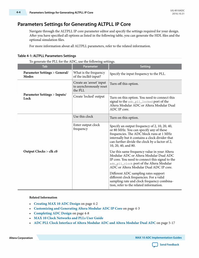
Parameters Settings for Generating ALTPLL IP CoreNavigate through the ALTPLL IP core parameter editor and specify the settings required for your design.After you have specified all options as listed in the following table, you can generate the HDL files and theoptional simulation files.
For more information about all ALTPLL parameters, refer to the related information.
Table 4-1: ALTPLL Parameters Settings
To generate the PLL for the ADC, use the following settings.Tab Parameter Setting
Parameter Settings > General/Modes
What is the frequencyof the inclk0 input?
Specify the input frequency to the PLL.
Parameter Settings > Inputs/Lock
Create an 'areset' inputto asynchronously resetthe PLL
Turn off this option.
Create 'locked' output Turn on this option. You need to connect thissignal to the adc_pll_locked port of theAltera Modular ADC or Altera Modular DualADC IP core.
Output Clocks > clk c0
Use this clock Turn on this option.
Enter output clockfrequency
Specify an output frequency of 2, 10, 20, 40,or 80 MHz. You can specify any of thesefrequencies. The ADC block runs at 1 MHzinternally but it contains a clock divider thatcan further divide the clock by a factor of 2,10, 20, 40, and 80.
Use this same frequency value in your AlteraModular ADC or Altera Modular Dual ADCIP core. You need to connect this signal to theadc_pll_clock port of the Altera ModularADC or Altera Modular Dual ADC IP core.
Different ADC sampling rates supportdifferent clock frequencies. For a validsampling rate and clock frequency combina‐tion, refer to the related information.
Related Information
• Creating MAX 10 ADC Design on page 4-2• Customizing and Generating Altera Modular ADC IP Core on page 4-3• Completing ADC Design on page 4-8• MAX 10 Clock Networks and PLLs User Guide• ADC PLL Clock Interface of Altera Modular ADC and Altera Modular Dual ADC on page 5-17
4-4 Parameters Settings for Generating ALTPLL IP CoreUG-M10ADC
2016.10.31
Altera Corporation MAX 10 ADC Implementation Guides
Send Feedback
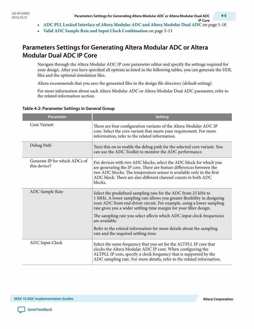
• ADC PLL Locked Interface of Altera Modular ADC and Altera Modular Dual ADC on page 5-18• Valid ADC Sample Rate and Input Clock Combination on page 5-13
Parameters Settings for Generating Altera Modular ADC or AlteraModular Dual ADC IP Core
Navigate through the Altera Modular ADC IP core parameter editor and specify the settings required foryour design. After you have specified all options as listed in the following tables, you can generate the HDLfiles and the optional simulation files.
Altera recommends that you save the generated files in the design file directory (default setting).
For more information about each Altera Modular ADC or Altera Modular Dual ADC parameter, refer tothe related information section.
Table 4-2: Parameter Settings in General Group
Parameter Setting
Core Variant There are four configuration variants of the Altera Modular ADC IPcore. Select the core variant that meets your requirement. For moreinformation, refer to the related information.
Debug Path Turn this on to enable the debug path for the selected core variant. Youcan use the ADC Toolkit to monitor the ADC performance.
Generate IP for which ADCs ofthis device?
For devices with two ADC blocks, select the ADC block for which youare generating the IP core. There are feature differences between thetwo ADC blocks. The temperature sensor is available only in the firstADC block. There are also different channel counts in both ADCblocks.
ADC Sample Rate Select the predefined sampling rate for the ADC from 25 kHz to1 MHz. A lower sampling rate allows you greater flexibility in designingyour ADC front end driver circuit. For example, using a lower samplingrate gives you a wider settling time margin for your filter design.
The sampling rate you select affects which ADC input clock frequenciesare available.
Refer to the related information for more details about the samplingrate and the required settling time.
ADC Input Clock Select the same frequency that you set for the ALTPLL IP core thatclocks the Altera Modular ADC IP core. When configuring theALTPLL IP core, specify a clock frequency that is supported by theADC sampling rate. For more details, refer to the related information.
UG-M10ADC2016.10.31 Parameters Settings for Generating Altera Modular ADC or Altera Modular Dual ADC
IP Core4-5
MAX 10 ADC Implementation Guides Altera Corporation
Send Feedback
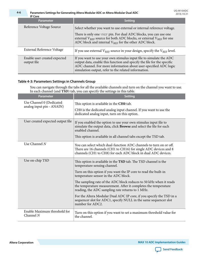
Parameter Setting
Reference Voltage Source Select whether you want to use external or internal reference voltage.
There is only one VREF pin. For dual ADC blocks, you can use oneexternal VREF source for both ADC blocks, or external VREF for oneADC block and internal VREF for the other ADC block.
External Reference Voltage If you use external VREF source in your design, specify the VREF level.
Enable user created expectedoutput file
If you want to use your own stimulus input file to simulate the ADCoutput data, enable this function and specify the file for the specificADC channel. For more information about user-specified ADC logicsimulation output, refer to the related information.
Table 4-3: Parameters Settings in Channels Group
You can navigate through the tabs for all the available channels and turn on the channel you want to use.In each channel (and TSD) tab, you can specify the settings in this table.
Parameter Setting
Use Channel 0 (Dedicatedanalog input pin - ANAIN)
This option is available in the CH0 tab.
CH0 is the dedicated analog input channel. If you want to use thededicated analog input, turn on this option.
User created expected output file If you enabled the option to use your own stimulus input file tosimulate the output data, click Browse and select the file for eachenabled channel.
This option is available in all channel tabs except the TSD tab.
Use Channel N You can select which dual-function ADC channels to turn on or off.There are 16 channels (CH1 to CH16) for single ADC devices and 8channels (CH1 to CH8) for each ADC block in dual ADC devices.
Use on-chip TSD This option is available in the TSD tab. The TSD channel is thetemperature sensing channel.
Turn on this option if you want the IP core to read the built-intemperature sensor in the ADC block.
The sampling rate of the ADC block reduces to 50 kHz when it readsthe temperature measurement. After it completes the temperaturereading, the ADC sampling rate returns to 1 MHz.
For the Altera Modular Dual ADC IP core, if you specify the TSD in asequencer slot for ADC1, specify NULL in the same sequencer slotnumber for ADC2.
Enable Maximum threshold forChannel N
Turn on this option if you want to set a maximum threshold value forthe channel.
4-6 Parameters Settings for Generating Altera Modular ADC or Altera Modular Dual ADCIP Core
UG-M10ADC2016.10.31
Altera Corporation MAX 10 ADC Implementation Guides
Send Feedback
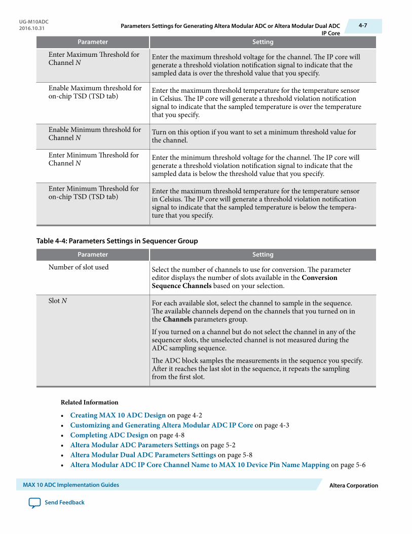
Parameter Setting
Enter Maximum Threshold forChannel N
Enter the maximum threshold voltage for the channel. The IP core willgenerate a threshold violation notification signal to indicate that thesampled data is over the threshold value that you specify.
Enable Maximum threshold foron-chip TSD (TSD tab)
Enter the maximum threshold temperature for the temperature sensorin Celsius. The IP core will generate a threshold violation notificationsignal to indicate that the sampled temperature is over the temperaturethat you specify.
Enable Minimum threshold forChannel N
Turn on this option if you want to set a minimum threshold value forthe channel.
Enter Minimum Threshold forChannel N
Enter the minimum threshold voltage for the channel. The IP core willgenerate a threshold violation notification signal to indicate that thesampled data is below the threshold value that you specify.
Enter Minimum Threshold foron-chip TSD (TSD tab)
Enter the maximum threshold temperature for the temperature sensorin Celsius. The IP core will generate a threshold violation notificationsignal to indicate that the sampled temperature is below the tempera‐ture that you specify.
Table 4-4: Parameters Settings in Sequencer Group
Parameter Setting
Number of slot used Select the number of channels to use for conversion. The parametereditor displays the number of slots available in the ConversionSequence Channels based on your selection.
Slot N For each available slot, select the channel to sample in the sequence.The available channels depend on the channels that you turned on inthe Channels parameters group.
If you turned on a channel but do not select the channel in any of thesequencer slots, the unselected channel is not measured during theADC sampling sequence.
The ADC block samples the measurements in the sequence you specify.After it reaches the last slot in the sequence, it repeats the samplingfrom the first slot.
Related Information
• Creating MAX 10 ADC Design on page 4-2• Customizing and Generating Altera Modular ADC IP Core on page 4-3• Completing ADC Design on page 4-8• Altera Modular ADC Parameters Settings on page 5-2• Altera Modular Dual ADC Parameters Settings on page 5-8• Altera Modular ADC IP Core Channel Name to MAX 10 Device Pin Name Mapping on page 5-6
UG-M10ADC2016.10.31 Parameters Settings for Generating Altera Modular ADC or Altera Modular Dual ADC
IP Core4-7
MAX 10 ADC Implementation Guides Altera Corporation
Send Feedback
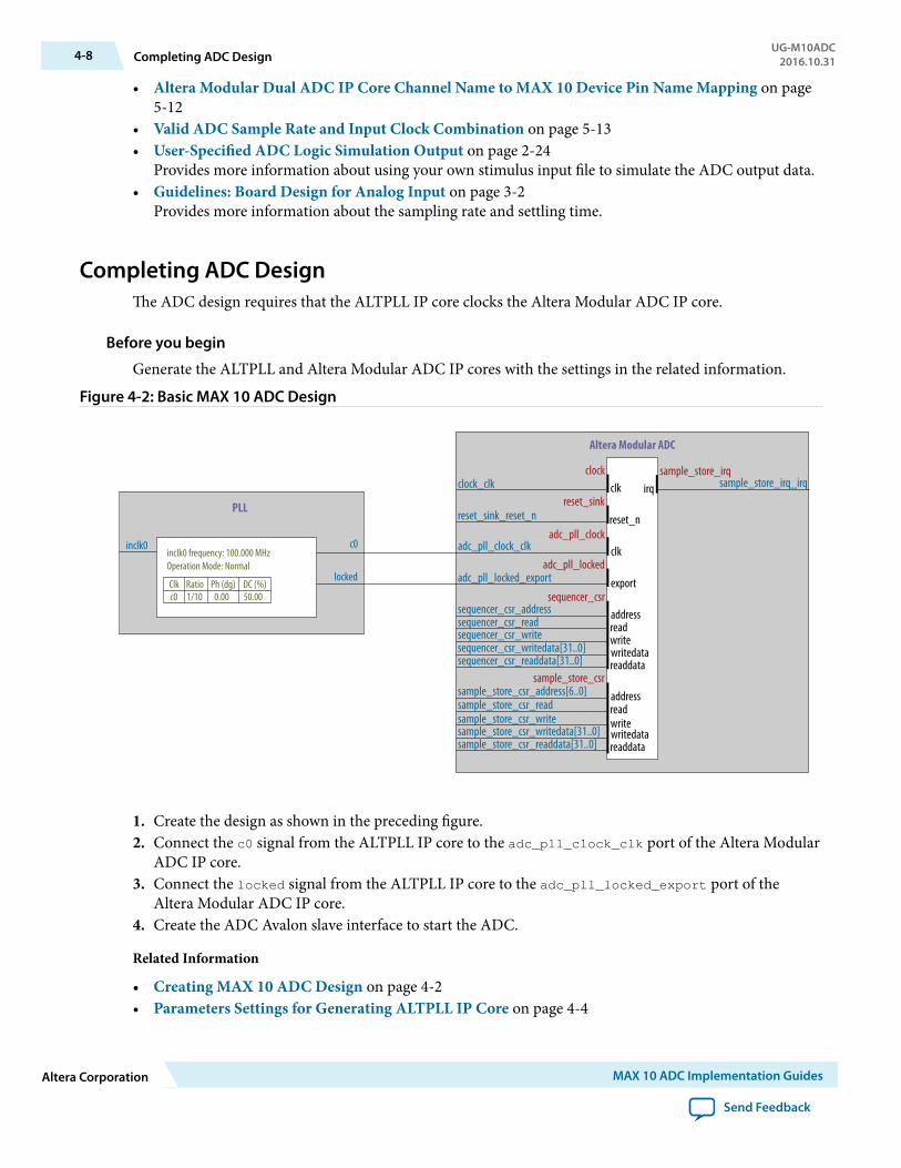
• Altera Modular Dual ADC IP Core Channel Name to MAX 10 Device Pin Name Mapping on page5-12
• Valid ADC Sample Rate and Input Clock Combination on page 5-13• User-Specified ADC Logic Simulation Output on page 2-24
Provides more information about using your own stimulus input file to simulate the ADC output data.• Guidelines: Board Design for Analog Input on page 3-2
Provides more information about the sampling rate and settling time.
Completing ADC DesignThe ADC design requires that the ALTPLL IP core clocks the Altera Modular ADC IP core.
Before you begin
Generate the ALTPLL and Altera Modular ADC IP cores with the settings in the related information.
Figure 4-2: Basic MAX 10 ADC Design
Altera Modular ADC
PLL
inclk0 c0
locked
inclk0 frequency: 100.000 MHzOperation Mode: Normal
Clk Ratio Ph (dg) DC (%)c0 1/10 0.00 50.00
clock
reset_sink
adc_pll_clock
adc_pll_locked
sequencer_csr
sample_store_csr
clock_clk
reset_sink_reset_n
adc_pll_clock_clk
adc_pll_locked_export
sequencer_csr_addresssequencer_csr_readsequencer_csr_writesequencer_csr_writedata[31..0]sequencer_csr_readdata[31..0]
sample_store_csr_address[6..0]sample_store_csr_readsample_store_csr_writesample_store_csr_writedata[31..0]sample_store_csr_readdata[31..0]
clk
reset_n
clk
export
addressreadwritewritedatareaddata
addressreadwritewritedatareaddata
irqsample_store_irq
sample_store_irq_irq
1. Create the design as shown in the preceding figure.2. Connect the c0 signal from the ALTPLL IP core to the adc_pll_clock_clk port of the Altera Modular
ADC IP core.3. Connect the locked signal from the ALTPLL IP core to the adc_pll_locked_export port of the
Altera Modular ADC IP core.4. Create the ADC Avalon slave interface to start the ADC.
Related Information
• Creating MAX 10 ADC Design on page 4-2• Parameters Settings for Generating ALTPLL IP Core on page 4-4
4-8 Completing ADC DesignUG-M10ADC
2016.10.31
Altera Corporation MAX 10 ADC Implementation Guides
Send Feedback
• Parameters Settings for Generating Altera Modular ADC or Altera Modular Dual ADC IP Core onpage 4-5
• Configuration 1: Standard Sequencer with Avalon-MM Sample Storage on page 2-12• Configuration 2: Standard Sequencer with Avalon-MM Sample Storage and Threshold Violation
Detection on page 2-13• Configuration 3: Standard Sequencer with External Sample Storage on page 2-15• Configuration 4: ADC Control Core Only on page 2-15
UG-M10ADC2016.10.31 Completing ADC Design 4-9
MAX 10 ADC Implementation Guides Altera Corporation
Send Feedback
Altera Modular ADC and Altera Modular DualADC IP Cores References 5
2016.10.31
UG-M10ADC Subscribe Send Feedback
The Altera Modular ADC or Altera Modular Dual ADC IP core is a soft controller for the ADC hard IPblocks. You can generate soft IPs to instantiate the on-chip ADC blocks. With this IP core, you canconfigure the ADCs and abstract the low level handshake with the ADC hard IP blocks.
The Quartus Prime software generates your customized Altera Modular ADC or Altera Modular DualADC IP core according to the parameter options that you set in the parameter editor.
Related Information
• MAX 10 Analog to Digital Converter Overview on page 1-1• Altera Modular ADC and Altera Modular Dual ADC IP Cores on page 2-11• Altera Modular ADC IP Core Configuration Variants on page 2-12
© 2016 Intel Corporation. All rights reserved. Intel, the Intel logo, Altera, Arria, Cyclone, Enpirion, MAX, Megacore, NIOS, Quartus and Stratix words and logosare trademarks of Intel Corporation in the US and/or other countries. Other marks and brands may be claimed as the property of others. Intel warrantsperformance of its FPGA and semiconductor products to current specifications in accordance with Intel's standard warranty, but reserves the right to makechanges to any products and services at any time without notice. Intel assumes no responsibility or liability arising out of the application or use of anyinformation, product, or service described herein except as expressly agreed to in writing by Intel. Intel customers are advised to obtain the latest version ofdevice specifications before relying on any published information and before placing orders for products or services.
ISO9001:2008Registered
www.altera.com101 Innovation Drive, San Jose, CA 95134
Altera Modular ADC Parameters SettingsThere are three groups of options: General, Channels, and Sequencer.
Table 5-1: Altera Modular ADC Parameters - General
Parameter Allowed Values Description
Core Variant • Standardsequencer withAvalon-MMsample storage
• Standardsequencer withAvalon-MMsample storageand thresholdviolationdetection
• Standardsequencer withexternal samplestorage
• ADC controlcore only
Selects the core configuration for the Altera ModularADC IP core.
Debug Path • Disabled• Enabled
Enables the debug path.
Generate IP for whichADCs of this device?
• 1st ADC• 2nd ADC
For devices that have two ADC blocks, specifies whichADC block you want to instantiate using the IP core.
ADC Sample Rate 25 kHz, 50 kHz,100 kHz, 200 kHz,250 kHz, 500 kHz,and 1 MHz
Specifies the ADC sampling rate. The sampling rate youselect affects which ADC input clock frequencies areavailable.
Refer to the related information for more details aboutthe sampling rate and the required settling time.
5-2 Altera Modular ADC Parameters SettingsUG-M10ADC
2016.10.31
Altera Corporation Altera Modular ADC and Altera Modular Dual ADC IP Cores References
Send Feedback
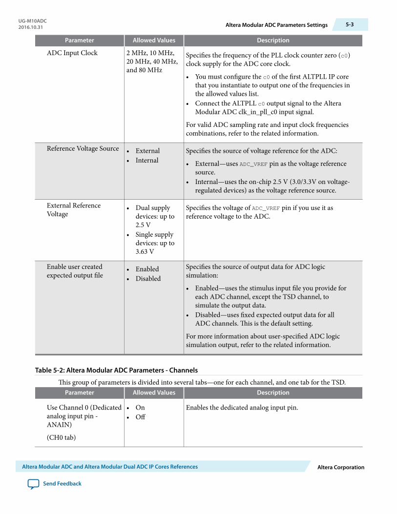
Parameter Allowed Values Description
ADC Input Clock 2 MHz, 10 MHz,20 MHz, 40 MHz,and 80 MHz
Specifies the frequency of the PLL clock counter zero (c0)clock supply for the ADC core clock.
• You must configure the c0 of the first ALTPLL IP corethat you instantiate to output one of the frequencies inthe allowed values list.
• Connect the ALTPLL c0 output signal to the AlteraModular ADC clk_in_pll_c0 input signal.
For valid ADC sampling rate and input clock frequenciescombinations, refer to the related information.
Reference Voltage Source • External• Internal
Specifies the source of voltage reference for the ADC:
• External—uses ADC_VREF pin as the voltage referencesource.
• Internal—uses the on-chip 2.5 V (3.0/3.3V on voltage-regulated devices) as the voltage reference source.
External ReferenceVoltage
• Dual supplydevices: up to2.5 V
• Single supplydevices: up to3.63 V
Specifies the voltage of ADC_VREF pin if you use it asreference voltage to the ADC.
Enable user createdexpected output file
• Enabled• Disabled
Specifies the source of output data for ADC logicsimulation:
• Enabled—uses the stimulus input file you provide foreach ADC channel, except the TSD channel, tosimulate the output data.
• Disabled—uses fixed expected output data for allADC channels. This is the default setting.
For more information about user-specified ADC logicsimulation output, refer to the related information.
Table 5-2: Altera Modular ADC Parameters - Channels
This group of parameters is divided into several tabs—one for each channel, and one tab for the TSD.Parameter Allowed Values Description
Use Channel 0 (Dedicatedanalog input pin -ANAIN)
(CH0 tab)
• On• Off
Enables the dedicated analog input pin.
UG-M10ADC2016.10.31 Altera Modular ADC Parameters Settings 5-3
Altera Modular ADC and Altera Modular Dual ADC IP Cores References Altera Corporation
Send Feedback
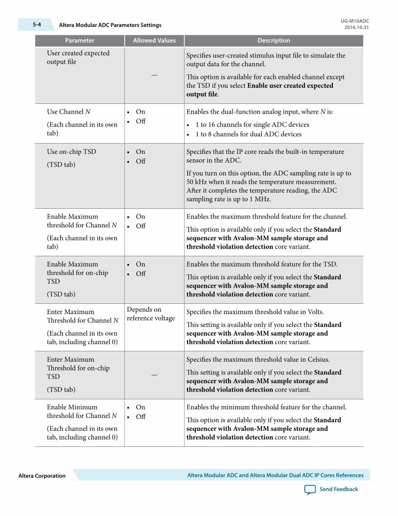
Parameter Allowed Values Description
User created expectedoutput file
—
Specifies user-created stimulus input file to simulate theoutput data for the channel.
This option is available for each enabled channel exceptthe TSD if you select Enable user created expectedoutput file.
Use Channel N
(Each channel in its owntab)
• On• Off
Enables the dual-function analog input, where N is:
• 1 to 16 channels for single ADC devices• 1 to 8 channels for dual ADC devices
Use on-chip TSD
(TSD tab)
• On• Off
Specifies that the IP core reads the built-in temperaturesensor in the ADC.
If you turn on this option, the ADC sampling rate is up to50 kHz when it reads the temperature measurement.After it completes the temperature reading, the ADCsampling rate is up to 1 MHz.
Enable Maximumthreshold for Channel N
(Each channel in its owntab)
• On• Off
Enables the maximum threshold feature for the channel.
This option is available only if you select the Standardsequencer with Avalon-MM sample storage andthreshold violation detection core variant.
Enable Maximumthreshold for on-chipTSD
(TSD tab)
• On• Off
Enables the maximum threshold feature for the TSD.
This option is available only if you select the Standardsequencer with Avalon-MM sample storage andthreshold violation detection core variant.
Enter MaximumThreshold for Channel N
(Each channel in its owntab, including channel 0)
Depends onreference voltage
Specifies the maximum threshold value in Volts.
This setting is available only if you select the Standardsequencer with Avalon-MM sample storage andthreshold violation detection core variant.
Enter MaximumThreshold for on-chipTSD
(TSD tab)
—
Specifies the maximum threshold value in Celsius.
This setting is available only if you select the Standardsequencer with Avalon-MM sample storage andthreshold violation detection core variant.
Enable Minimumthreshold for Channel N
(Each channel in its owntab, including channel 0)
• On• Off
Enables the minimum threshold feature for the channel.
This option is available only if you select the Standardsequencer with Avalon-MM sample storage andthreshold violation detection core variant.
5-4 Altera Modular ADC Parameters SettingsUG-M10ADC
2016.10.31
Altera Corporation Altera Modular ADC and Altera Modular Dual ADC IP Cores References
Send Feedback
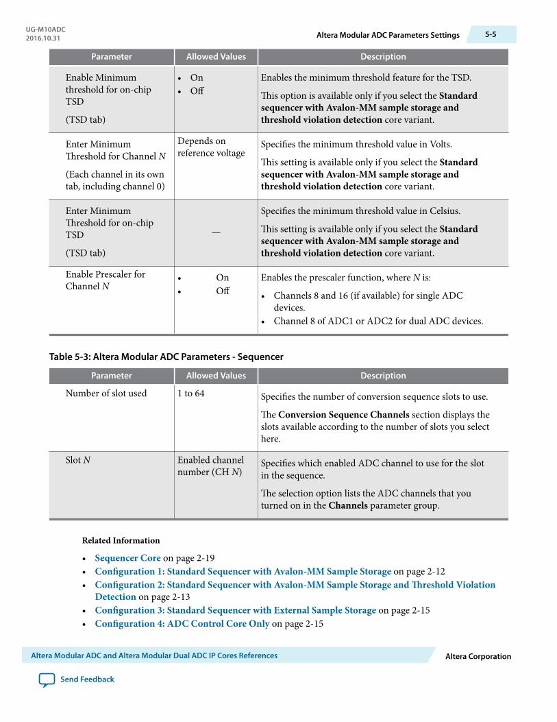
Parameter Allowed Values Description
Enable Minimumthreshold for on-chipTSD
(TSD tab)
• On• Off
Enables the minimum threshold feature for the TSD.
This option is available only if you select the Standardsequencer with Avalon-MM sample storage andthreshold violation detection core variant.
Enter MinimumThreshold for Channel N
(Each channel in its owntab, including channel 0)
Depends onreference voltage
Specifies the minimum threshold value in Volts.
This setting is available only if you select the Standardsequencer with Avalon-MM sample storage andthreshold violation detection core variant.
Enter MinimumThreshold for on-chipTSD
(TSD tab)
—
Specifies the minimum threshold value in Celsius.
This setting is available only if you select the Standardsequencer with Avalon-MM sample storage andthreshold violation detection core variant.
Enable Prescaler forChannel N
• On• Off
Enables the prescaler function, where N is:
• Channels 8 and 16 (if available) for single ADCdevices.
• Channel 8 of ADC1 or ADC2 for dual ADC devices.
Table 5-3: Altera Modular ADC Parameters - Sequencer
Parameter Allowed Values Description
Number of slot used 1 to 64 Specifies the number of conversion sequence slots to use.
The Conversion Sequence Channels section displays theslots available according to the number of slots you selecthere.
Slot N Enabled channelnumber (CH N)
Specifies which enabled ADC channel to use for the slotin the sequence.
The selection option lists the ADC channels that youturned on in the Channels parameter group.
Related Information
• Sequencer Core on page 2-19• Configuration 1: Standard Sequencer with Avalon-MM Sample Storage on page 2-12• Configuration 2: Standard Sequencer with Avalon-MM Sample Storage and Threshold Violation
Detection on page 2-13• Configuration 3: Standard Sequencer with External Sample Storage on page 2-15• Configuration 4: ADC Control Core Only on page 2-15
UG-M10ADC2016.10.31 Altera Modular ADC Parameters Settings 5-5
Altera Modular ADC and Altera Modular Dual ADC IP Cores References Altera Corporation
Send Feedback
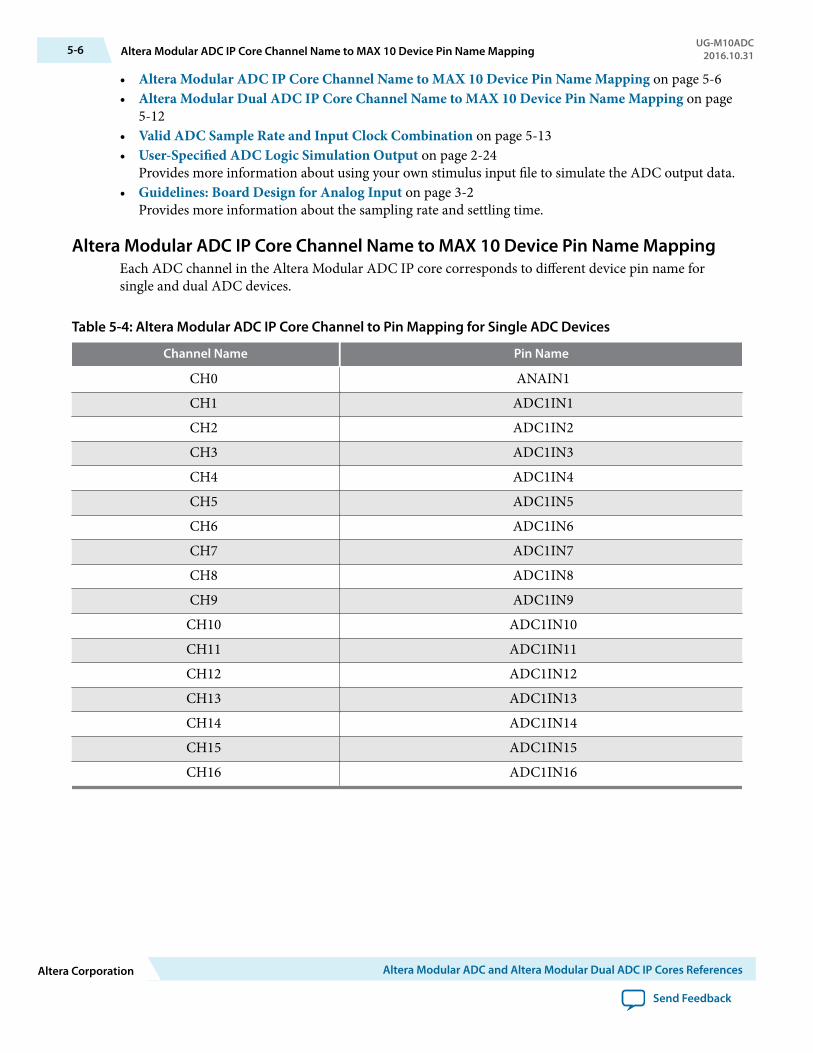
• Altera Modular ADC IP Core Channel Name to MAX 10 Device Pin Name Mapping on page 5-6• Altera Modular Dual ADC IP Core Channel Name to MAX 10 Device Pin Name Mapping on page
5-12• Valid ADC Sample Rate and Input Clock Combination on page 5-13• User-Specified ADC Logic Simulation Output on page 2-24
Provides more information about using your own stimulus input file to simulate the ADC output data.• Guidelines: Board Design for Analog Input on page 3-2
Provides more information about the sampling rate and settling time.
Altera Modular ADC IP Core Channel Name to MAX 10 Device Pin Name MappingEach ADC channel in the Altera Modular ADC IP core corresponds to different device pin name forsingle and dual ADC devices.
Table 5-4: Altera Modular ADC IP Core Channel to Pin Mapping for Single ADC Devices
Channel Name Pin Name
CH0 ANAIN1CH1 ADC1IN1CH2 ADC1IN2CH3 ADC1IN3CH4 ADC1IN4CH5 ADC1IN5CH6 ADC1IN6CH7 ADC1IN7CH8 ADC1IN8CH9 ADC1IN9
CH10 ADC1IN10CH11 ADC1IN11CH12 ADC1IN12CH13 ADC1IN13CH14 ADC1IN14CH15 ADC1IN15CH16 ADC1IN16
5-6 Altera Modular ADC IP Core Channel Name to MAX 10 Device Pin Name MappingUG-M10ADC
2016.10.31
Altera Corporation Altera Modular ADC and Altera Modular Dual ADC IP Cores References
Send Feedback
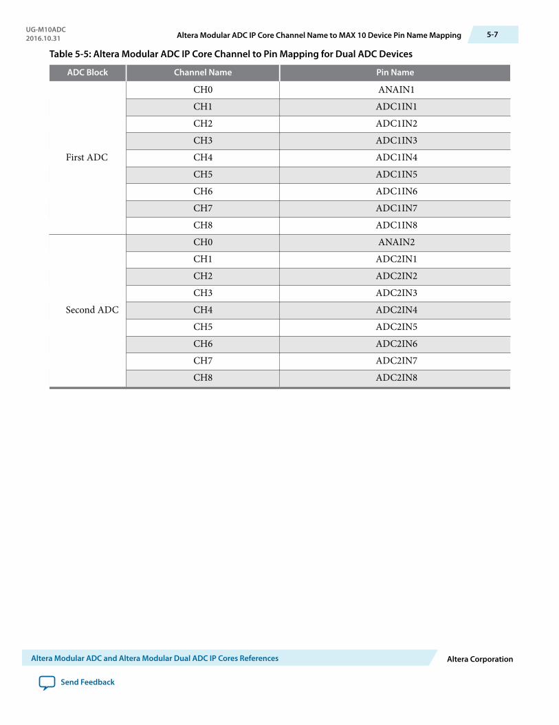
Table 5-5: Altera Modular ADC IP Core Channel to Pin Mapping for Dual ADC Devices
ADC Block Channel Name Pin Name
First ADC
CH0 ANAIN1CH1 ADC1IN1CH2 ADC1IN2CH3 ADC1IN3CH4 ADC1IN4CH5 ADC1IN5CH6 ADC1IN6CH7 ADC1IN7CH8 ADC1IN8
Second ADC
CH0 ANAIN2CH1 ADC2IN1CH2 ADC2IN2CH3 ADC2IN3CH4 ADC2IN4CH5 ADC2IN5CH6 ADC2IN6CH7 ADC2IN7CH8 ADC2IN8
UG-M10ADC2016.10.31 Altera Modular ADC IP Core Channel Name to MAX 10 Device Pin Name Mapping 5-7
Altera Modular ADC and Altera Modular Dual ADC IP Cores References Altera Corporation
Send Feedback
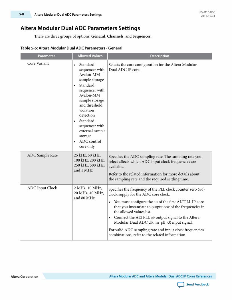
Altera Modular Dual ADC Parameters SettingsThere are three groups of options: General, Channels, and Sequencer.
Table 5-6: Altera Modular Dual ADC Parameters - General
Parameter Allowed Values Description
Core Variant • Standardsequencer withAvalon-MMsample storage
• Standardsequencer withAvalon-MMsample storageand thresholdviolationdetection
• Standardsequencer withexternal samplestorage
• ADC controlcore only
Selects the core configuration for the Altera ModularDual ADC IP core.
ADC Sample Rate 25 kHz, 50 kHz,100 kHz, 200 kHz,250 kHz, 500 kHz,and 1 MHz
Specifies the ADC sampling rate. The sampling rate youselect affects which ADC input clock frequencies areavailable.
Refer to the related information for more details aboutthe sampling rate and the required settling time.
ADC Input Clock 2 MHz, 10 MHz,20 MHz, 40 MHz,and 80 MHz
Specifies the frequency of the PLL clock counter zero (c0)clock supply for the ADC core clock.
• You must configure the c0 of the first ALTPLL IP corethat you instantiate to output one of the frequencies inthe allowed values list.
• Connect the ALTPLL c0 output signal to the AlteraModular Dual ADC clk_in_pll_c0 input signal.
For valid ADC sampling rate and input clock frequenciescombinations, refer to the related information.
5-8 Altera Modular Dual ADC Parameters SettingsUG-M10ADC
2016.10.31
Altera Corporation Altera Modular ADC and Altera Modular Dual ADC IP Cores References
Send Feedback
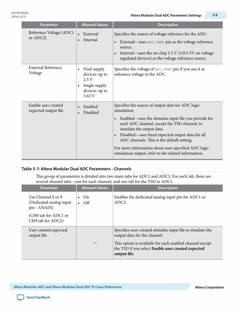
Parameter Allowed Values Description
Reference Voltage (ADC1or ADC2)
• External• Internal
Specifies the source of voltage reference for the ADC:
• External—uses ADC_VREF pin as the voltage referencesource.
• Internal—uses the on-chip 2.5 V (3.0/3.3V on voltage-regulated devices) as the voltage reference source.
External ReferenceVoltage
• Dual supplydevices: up to2.5 V
• Single supplydevices: up to3.63 V
Specifies the voltage of ADC_VREF pin if you use it asreference voltage to the ADC.
Enable user createdexpected output file
• Enabled• Disabled
Specifies the source of output data for ADC logicsimulation:
• Enabled—uses the stimulus input file you provide foreach ADC channel, except the TSD channel, tosimulate the output data.
• Disabled—uses fixed expected output data for allADC channels. This is the default setting.
For more information about user-specified ADC logicsimulation output, refer to the related information.
Table 5-7: Altera Modular Dual ADC Parameters - Channels
This group of parameters is divided into two main tabs for ADC1 and ADC2. For each tab, there areseveral channel tabs—one for each channel, and one tab for the TSD in ADC1.
Parameter Allowed Values Description
Use Channel 0 or 9(Dedicated analog inputpin - ANAIN)
(CH0 tab for ADC1 orCH9 tab for ADC2)
• On• Off
Enables the dedicated analog input pin for ADC1 orADC2.
User created expectedoutput file
—
Specifies user-created stimulus input file to simulate theoutput data for the channel.
This option is available for each enabled channel exceptthe TSD if you select Enable user created expectedoutput file.
UG-M10ADC2016.10.31 Altera Modular Dual ADC Parameters Settings 5-9
Altera Modular ADC and Altera Modular Dual ADC IP Cores References Altera Corporation
Send Feedback
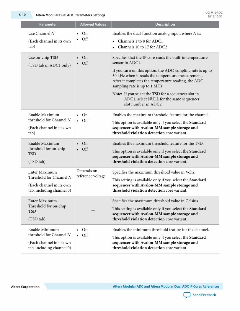
Parameter Allowed Values Description
Use Channel N
(Each channel in its owntab)
• On• Off
Enables the dual-function analog input, where N is:
• Channels 1 to 8 for ADC1• Channels 10 to 17 for ADC2
Use on-chip TSD
(TSD tab in ADC1 only)
• On• Off
Specifies that the IP core reads the built-in temperaturesensor in ADC1.
If you turn on this option, the ADC sampling rate is up to50 kHz when it reads the temperature measurement.After it completes the temperature reading, the ADCsampling rate is up to 1 MHz.
Note: If you select the TSD for a sequencer slot inADC1, select NULL for the same sequencerslot number in ADC2.
Enable Maximumthreshold for Channel N
(Each channel in its owntab)
• On• Off
Enables the maximum threshold feature for the channel.
This option is available only if you select the Standardsequencer with Avalon-MM sample storage andthreshold violation detection core variant.
Enable Maximumthreshold for on-chipTSD
(TSD tab)
• On• Off
Enables the maximum threshold feature for the TSD.
This option is available only if you select the Standardsequencer with Avalon-MM sample storage andthreshold violation detection core variant.
Enter MaximumThreshold for Channel N
(Each channel in its owntab, including channel 0)
Depends onreference voltage
Specifies the maximum threshold value in Volts.
This setting is available only if you select the Standardsequencer with Avalon-MM sample storage andthreshold violation detection core variant.
Enter MaximumThreshold for on-chipTSD
(TSD tab)
—
Specifies the maximum threshold value in Celsius.
This setting is available only if you select the Standardsequencer with Avalon-MM sample storage andthreshold violation detection core variant.
Enable Minimumthreshold for Channel N
(Each channel in its owntab, including channel 0)
• On• Off
Enables the minimum threshold feature for the channel.
This option is available only if you select the Standardsequencer with Avalon-MM sample storage andthreshold violation detection core variant.
5-10 Altera Modular Dual ADC Parameters SettingsUG-M10ADC
2016.10.31
Altera Corporation Altera Modular ADC and Altera Modular Dual ADC IP Cores References
Send Feedback
Parameter Allowed Values Description
Enable Minimumthreshold for on-chipTSD
(TSD tab)
• On• Off
Enables the minimum threshold feature for the TSD.
This option is available only if you select the Standardsequencer with Avalon-MM sample storage andthreshold violation detection core variant.
Enter MinimumThreshold for Channel N
(Each channel in its owntab, including channel 0)
Depends onreference voltage
Specifies the minimum threshold value in Volts.
This setting is available only if you select the Standardsequencer with Avalon-MM sample storage andthreshold violation detection core variant.
Enter MinimumThreshold for on-chipTSD
(TSD tab)
—
Specifies the minimum threshold value in Celsius.
This setting is available only if you select the Standardsequencer with Avalon-MM sample storage andthreshold violation detection core variant.
Enable Prescaler forChannel N
• On• Off
Enables the prescaler function, where N is:
• Channel 8 in ADC1• Channel 17 in ADC2
Table 5-8: Altera Modular Dual ADC Parameters - Sequencer
Parameter Allowed Values Description
Number of slot used 1 to 64 Specifies the number of conversion sequence slots to usefor both ADC1 and ADC2.
The Conversion Sequence Channels section displays theslots available for ADC1 and ADC2 according to thenumber of slots you select here.
Slot N Enabled channelnumber (CH N)
Specifies which enabled ADC channel to use for the slotin the sequence.
The selection option lists the ADC channels that youturned on in the Channels parameter group for ADC1and ADC2.
Note: If you select the TSD for a sequencer slot inADC1, select NULL for the same sequencerslot number in ADC2.
Related Information
• Sequencer Core on page 2-19• Configuration 1: Standard Sequencer with Avalon-MM Sample Storage on page 2-12
UG-M10ADC2016.10.31 Altera Modular Dual ADC Parameters Settings 5-11
Altera Modular ADC and Altera Modular Dual ADC IP Cores References Altera Corporation
Send Feedback
• Configuration 2: Standard Sequencer with Avalon-MM Sample Storage and Threshold ViolationDetection on page 2-13
• Configuration 3: Standard Sequencer with External Sample Storage on page 2-15• Configuration 4: ADC Control Core Only on page 2-15• Altera Modular ADC IP Core Channel Name to MAX 10 Device Pin Name Mapping on page 5-6• Altera Modular Dual ADC IP Core Channel Name to MAX 10 Device Pin Name Mapping on page
5-12• Valid ADC Sample Rate and Input Clock Combination on page 5-13• User-Specified ADC Logic Simulation Output on page 2-24
Provides more information about using your own stimulus input file to simulate the ADC output data.• Guidelines: Board Design for Analog Input on page 3-2
Provides more information about the sampling rate and settling time.
Altera Modular Dual ADC IP Core Channel Name to MAX 10 Device Pin NameMapping
Each ADC channel in the Altera Modular Dual ADC IP core corresponds to different device pin name.
Table 5-9: Altera Modular Dual ADC IP Core Channel to Pin Mapping
ADC Block Channel Name Pin Name
ADC1
CH0 ANAIN1CH1 ADC1IN1CH2 ADC1IN2CH3 ADC1IN3CH4 ADC1IN4CH5 ADC1IN5CH6 ADC1IN6CH7 ADC1IN7CH8 ADC1IN8
ADC2
CH9 ANAIN2CH10 ADC2IN1CH11 ADC2IN2CH12 ADC2IN3CH13 ADC2IN4CH14 ADC2IN5CH15 ADC2IN6CH16 ADC2IN7CH17 ADC2IN8
5-12 Altera Modular Dual ADC IP Core Channel Name to MAX 10 Device Pin NameMapping
UG-M10ADC2016.10.31
Altera Corporation Altera Modular ADC and Altera Modular Dual ADC IP Cores References
Send Feedback
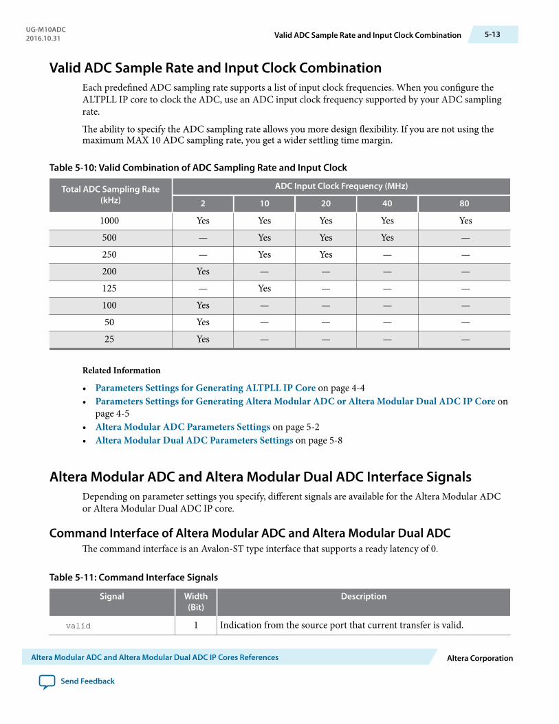
Valid ADC Sample Rate and Input Clock CombinationEach predefined ADC sampling rate supports a list of input clock frequencies. When you configure theALTPLL IP core to clock the ADC, use an ADC input clock frequency supported by your ADC samplingrate.
The ability to specify the ADC sampling rate allows you more design flexibility. If you are not using themaximum MAX 10 ADC sampling rate, you get a wider settling time margin.
Table 5-10: Valid Combination of ADC Sampling Rate and Input Clock
Total ADC Sampling Rate(kHz)
ADC Input Clock Frequency (MHz)
2 10 20 40 80
1000 Yes Yes Yes Yes Yes500 — Yes Yes Yes —250 — Yes Yes — —200 Yes — — — —125 — Yes — — —100 Yes — — — —50 Yes — — — —25 Yes — — — —
Related Information
• Parameters Settings for Generating ALTPLL IP Core on page 4-4• Parameters Settings for Generating Altera Modular ADC or Altera Modular Dual ADC IP Core on
page 4-5• Altera Modular ADC Parameters Settings on page 5-2• Altera Modular Dual ADC Parameters Settings on page 5-8
Altera Modular ADC and Altera Modular Dual ADC Interface SignalsDepending on parameter settings you specify, different signals are available for the Altera Modular ADCor Altera Modular Dual ADC IP core.
Command Interface of Altera Modular ADC and Altera Modular Dual ADCThe command interface is an Avalon-ST type interface that supports a ready latency of 0.
Table 5-11: Command Interface Signals
Signal Width(Bit)
Description
valid 1 Indication from the source port that current transfer is valid.
UG-M10ADC2016.10.31 Valid ADC Sample Rate and Input Clock Combination 5-13
Altera Modular ADC and Altera Modular Dual ADC IP Cores References Altera Corporation
Send Feedback
Signal Width(Bit)
Description
ready 1 Indication from the sink port that it is ready for current transfer.
channel 5 Indicates the channel that the ADC hard block samples from forcurrent command.
• 31—recalibration request• 30:18—not used• 17—temperature sensor• 16:0—channels 16 to 0; where channel 0 is the dedicated analog
input pin and channels 1 to 16 are the dual purpose analog inputpins
startofpacket 1 Indication from the source port that current transfer is the start ofpacket.
• For altera_adc_sequencer core implementation, the IP coreasserts this signal during the first slot of conversion sequencedata array.
• For altera_adc_control core implementation, this signal isignored. The IP core just passes the received information back tothe corresponding response interface.
endofpacket 1 Indication from the source port that current transfer is the end ofpacket.
• For altera_adc_sequencer core implementation, IP core assertsthis signal during the final slot of conversion sequence dataarray.
• For altera_adc_control core implementation, this signal isignored. The IP core just passes the received information back tothe corresponding response interface.
Related Information
• Altera Modular ADC IP Core Channel Name to MAX 10 Device Pin Name Mapping on page 5-6• Altera Modular Dual ADC IP Core Channel Name to MAX 10 Device Pin Name Mapping on page
5-12
Response Interface of Altera Modular ADC and Altera Modular Dual ADCThe response interface is an Avalon-ST type interface that does not support backpressure. To avoidoverflow condition at the source port, implement sink ports with response data process time that is fastenough, or with enough buffers storage.
5-14 Response Interface of Altera Modular ADC and Altera Modular Dual ADCUG-M10ADC
2016.10.31
Altera Corporation Altera Modular ADC and Altera Modular Dual ADC IP Cores References
Send Feedback
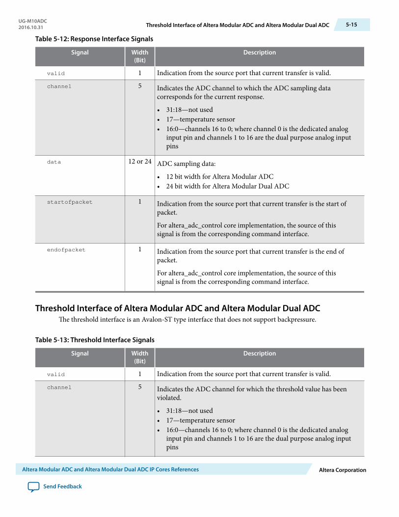
Table 5-12: Response Interface Signals
Signal Width(Bit)
Description
valid 1 Indication from the source port that current transfer is valid.
channel 5 Indicates the ADC channel to which the ADC sampling datacorresponds for the current response.
• 31:18—not used• 17—temperature sensor• 16:0—channels 16 to 0; where channel 0 is the dedicated analog
input pin and channels 1 to 16 are the dual purpose analog inputpins
data 12 or 24 ADC sampling data:
• 12 bit width for Altera Modular ADC• 24 bit width for Altera Modular Dual ADC
startofpacket 1 Indication from the source port that current transfer is the start ofpacket.
For altera_adc_control core implementation, the source of thissignal is from the corresponding command interface.
endofpacket 1 Indication from the source port that current transfer is the end ofpacket.
For altera_adc_control core implementation, the source of thissignal is from the corresponding command interface.
Threshold Interface of Altera Modular ADC and Altera Modular Dual ADCThe threshold interface is an Avalon-ST type interface that does not support backpressure.
Table 5-13: Threshold Interface Signals
Signal Width(Bit)
Description
valid 1 Indication from the source port that current transfer is valid.
channel 5 Indicates the ADC channel for which the threshold value has beenviolated.
• 31:18—not used• 17—temperature sensor• 16:0—channels 16 to 0; where channel 0 is the dedicated analog
input pin and channels 1 to 16 are the dual purpose analog inputpins
UG-M10ADC2016.10.31 Threshold Interface of Altera Modular ADC and Altera Modular Dual ADC 5-15
Altera Modular ADC and Altera Modular Dual ADC IP Cores References Altera Corporation
Send Feedback
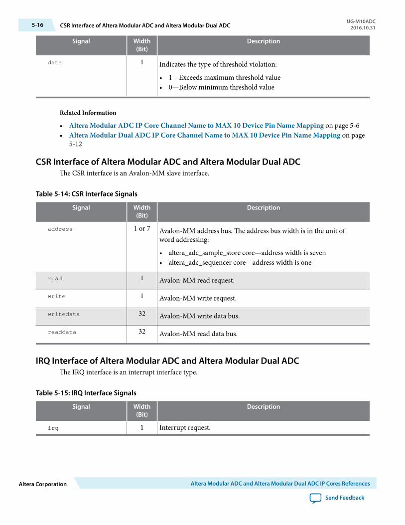
Signal Width(Bit)
Description
data 1 Indicates the type of threshold violation:
• 1—Exceeds maximum threshold value• 0—Below minimum threshold value
Related Information
• Altera Modular ADC IP Core Channel Name to MAX 10 Device Pin Name Mapping on page 5-6• Altera Modular Dual ADC IP Core Channel Name to MAX 10 Device Pin Name Mapping on page
5-12
CSR Interface of Altera Modular ADC and Altera Modular Dual ADCThe CSR interface is an Avalon-MM slave interface.
Table 5-14: CSR Interface Signals
Signal Width(Bit)
Description
address 1 or 7 Avalon-MM address bus. The address bus width is in the unit ofword addressing:
• altera_adc_sample_store core—address width is seven• altera_adc_sequencer core—address width is one
read 1 Avalon-MM read request.
write 1 Avalon-MM write request.
writedata 32 Avalon-MM write data bus.
readdata 32 Avalon-MM read data bus.
IRQ Interface of Altera Modular ADC and Altera Modular Dual ADCThe IRQ interface is an interrupt interface type.
Table 5-15: IRQ Interface Signals
Signal Width(Bit)
Description
irq 1 Interrupt request.
5-16 CSR Interface of Altera Modular ADC and Altera Modular Dual ADCUG-M10ADC
2016.10.31
Altera Corporation Altera Modular ADC and Altera Modular Dual ADC IP Cores References
Send Feedback
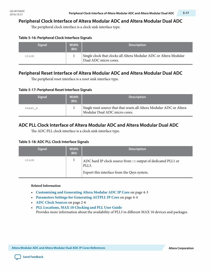
Peripheral Clock Interface of Altera Modular ADC and Altera Modular Dual ADCThe peripheral clock interface is a clock sink interface type.
Table 5-16: Peripheral Clock Interface Signals
Signal Width(Bit)
Description
clock 1 Single clock that clocks all Altera Modular ADC or Altera ModularDual ADC micro cores.
Peripheral Reset Interface of Altera Modular ADC and Altera Modular Dual ADCThe peripheral reset interface is a reset sink interface type.
Table 5-17: Peripheral Reset Interface Signals
Signal Width(Bit)
Description
reset_n 1 Single reset source that that resets all Altera Modular ADC or AlteraModular Dual ADC micro cores.
ADC PLL Clock Interface of Altera Modular ADC and Altera Modular Dual ADCThe ADC PLL clock interface is a clock sink interface type.
Table 5-18: ADC PLL Clock Interface Signals
Signal Width(Bit)
Description
clock 1 ADC hard IP clock source from C0 output of dedicated PLL1 orPLL3.
Export this interface from the Qsys system.
Related Information
• Customizing and Generating Altera Modular ADC IP Core on page 4-3• Parameters Settings for Generating ALTPLL IP Core on page 4-4• ADC Clock Sources on page 2-6• PLL Locations, MAX 10 Clocking and PLL User Guide
Provides more information about the availability of PLL3 in different MAX 10 devices and packages.
UG-M10ADC2016.10.31 Peripheral Clock Interface of Altera Modular ADC and Altera Modular Dual ADC 5-17
Altera Modular ADC and Altera Modular Dual ADC IP Cores References Altera Corporation
Send Feedback
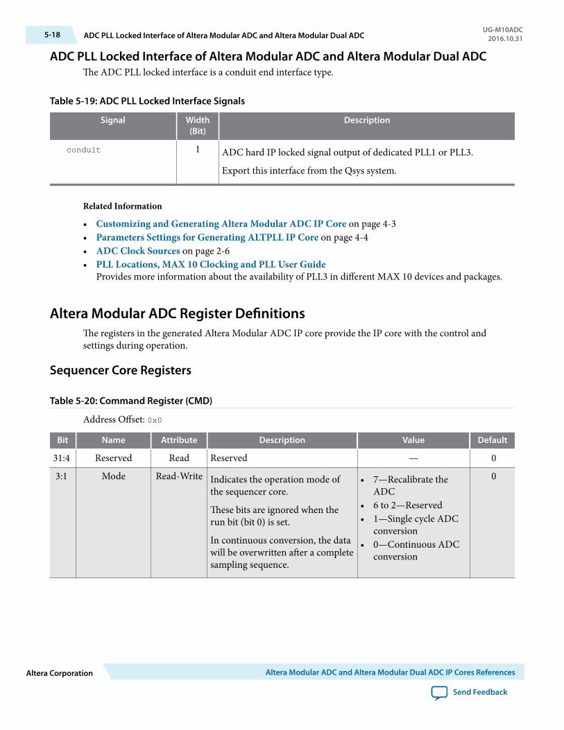
ADC PLL Locked Interface of Altera Modular ADC and Altera Modular Dual ADCThe ADC PLL locked interface is a conduit end interface type.
Table 5-19: ADC PLL Locked Interface Signals
Signal Width(Bit)
Description
conduit 1 ADC hard IP locked signal output of dedicated PLL1 or PLL3.
Export this interface from the Qsys system.
Related Information
• Customizing and Generating Altera Modular ADC IP Core on page 4-3• Parameters Settings for Generating ALTPLL IP Core on page 4-4• ADC Clock Sources on page 2-6• PLL Locations, MAX 10 Clocking and PLL User Guide
Provides more information about the availability of PLL3 in different MAX 10 devices and packages.
Altera Modular ADC Register DefinitionsThe registers in the generated Altera Modular ADC IP core provide the IP core with the control andsettings during operation.
Sequencer Core Registers
Table 5-20: Command Register (CMD)
Address Offset: 0x0
Bit Name Attribute Description Value Default
31:4 Reserved Read Reserved — 0
3:1 Mode Read-Write Indicates the operation mode ofthe sequencer core.
These bits are ignored when therun bit (bit 0) is set.
In continuous conversion, the datawill be overwritten after a completesampling sequence.
• 7—Recalibrate theADC
• 6 to 2—Reserved• 1—Single cycle ADC
conversion• 0—Continuous ADC
conversion
0
5-18 ADC PLL Locked Interface of Altera Modular ADC and Altera Modular Dual ADCUG-M10ADC
2016.10.31
Altera Corporation Altera Modular ADC and Altera Modular Dual ADC IP Cores References
Send Feedback
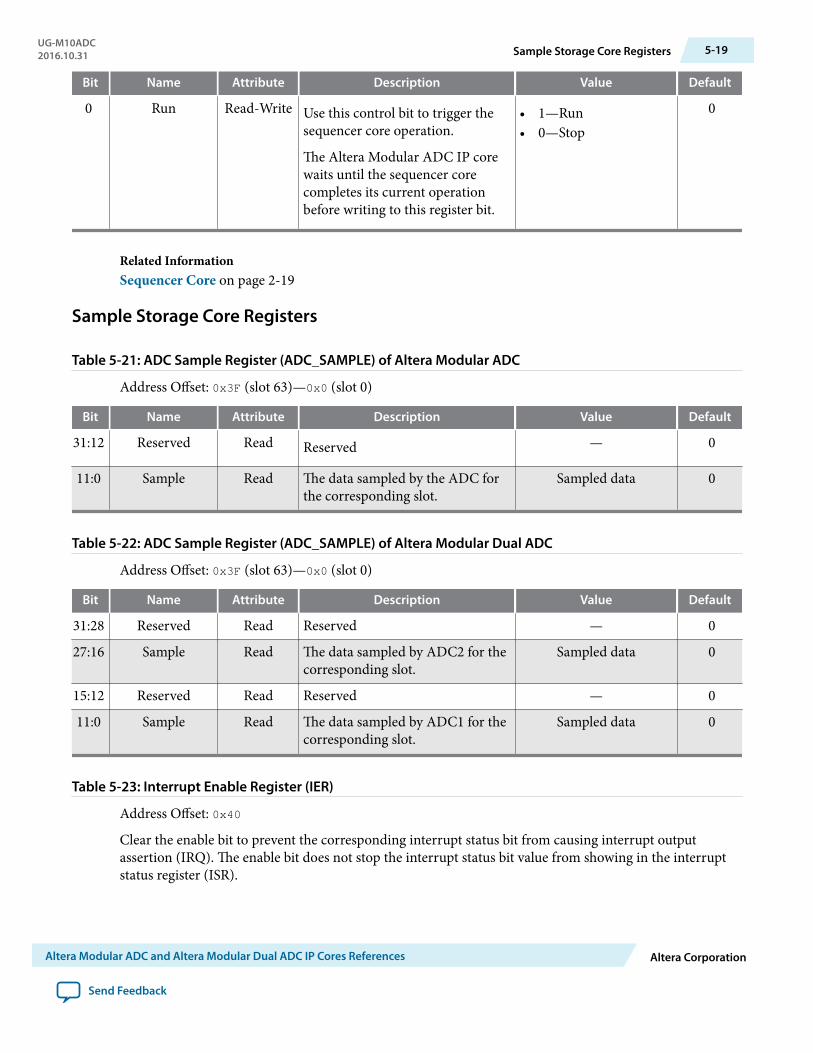
Bit Name Attribute Description Value Default
0 Run Read-Write Use this control bit to trigger thesequencer core operation.
The Altera Modular ADC IP corewaits until the sequencer corecompletes its current operationbefore writing to this register bit.
• 1—Run• 0—Stop
0
Related InformationSequencer Core on page 2-19
Sample Storage Core Registers
Table 5-21: ADC Sample Register (ADC_SAMPLE) of Altera Modular ADC
Address Offset: 0x3F (slot 63)—0x0 (slot 0)
Bit Name Attribute Description Value Default
31:12 Reserved Read Reserved — 0
11:0 Sample Read The data sampled by the ADC forthe corresponding slot.
Sampled data 0
Table 5-22: ADC Sample Register (ADC_SAMPLE) of Altera Modular Dual ADC
Address Offset: 0x3F (slot 63)—0x0 (slot 0)
Bit Name Attribute Description Value Default
31:28 Reserved Read Reserved — 0
27:16 Sample Read The data sampled by ADC2 for thecorresponding slot.
Sampled data 0
15:12 Reserved Read Reserved — 0
11:0 Sample Read The data sampled by ADC1 for thecorresponding slot.
Sampled data 0
Table 5-23: Interrupt Enable Register (IER)
Address Offset: 0x40
Clear the enable bit to prevent the corresponding interrupt status bit from causing interrupt outputassertion (IRQ). The enable bit does not stop the interrupt status bit value from showing in the interruptstatus register (ISR).
UG-M10ADC2016.10.31 Sample Storage Core Registers 5-19
Altera Modular ADC and Altera Modular Dual ADC IP Cores References Altera Corporation
Send Feedback
Bit Name Attribute Description Value Default
31:1 Reserved Read Reserved — 0
0 M_EOP Read-Write The enable bit for the end of packet(EOP) interrupt.
• 1—Enables thecorrespondinginterrupt
• 0—Disables thecorrespondinginterrupt
1
Table 5-24: Interrupt Status Register (ISR)
Address Offset: 0x41
Bit Name Attribute Description Value Default
31:1 Reserved Read Reserved — 0
0 EOP Read-Write(one cycle)
EOP interrupt. • 1—Indicates completereceipt of a sampleblock
• 0—Automaticallyclears to 0 afterindication of completereceipt
0
Related InformationSample Storage Core on page 2-20
ADC HAL Device Driver for Nios II Gen 2The Altera Modular ADC IP core provides a HAL device driver. You can integrate the device driver intothe HAL system library for Nios II Gen 2 systems.
The Altera Modular ADC IP core provides software files that define low-level access to the hardware. Youcan use the macros definition and functions in the software files to initialize the Altera Modular ADCcore.
• altera_modular_adc_sequencer_regs.h—this file defines the register map for the sequencercore. It provides symbolic constants to access the low-level hardware.
• altera_modular_adc_sample_store_regs.h—this file defines the register for sample storagecore. It provides symbolic constants to access the low-level hardware.
• altera_modular_adc.h—include this file into your application. It automatically includes the otherheader files and defines additional functions.
• altera_modular_adc.c—this file implements helper functions that are defined in the header file.
5-20 ADC HAL Device Driver for Nios II Gen 2UG-M10ADC
2016.10.31
Altera Corporation Altera Modular ADC and Altera Modular Dual ADC IP Cores References
Send Feedback

Related InformationHAL API Reference, Nios II Gen 2 Software Developer's HandbookProvides more information about the HAL API.
UG-M10ADC2016.10.31 ADC HAL Device Driver for Nios II Gen 2 5-21
Altera Modular ADC and Altera Modular Dual ADC IP Cores References Altera Corporation
Send Feedback
MAX 10 Analog to Digital Converter User GuideArchives A
2016.10.31
UG-M10ADC Subscribe Send Feedback
If an IP core version is not listed, the user guide for the previous IP core version applies.IP Core Version User Guide
16.0 MAX 10 Analog to Digital Converter User Guide
15.1 MAX 10 Analog to Digital Converter User Guide
15.0 MAX 10 Analog to Digital Converter User Guide
© 2016 Intel Corporation. All rights reserved. Intel, the Intel logo, Altera, Arria, Cyclone, Enpirion, MAX, Megacore, NIOS, Quartus and Stratix words and logosare trademarks of Intel Corporation in the US and/or other countries. Other marks and brands may be claimed as the property of others. Intel warrantsperformance of its FPGA and semiconductor products to current specifications in accordance with Intel's standard warranty, but reserves the right to makechanges to any products and services at any time without notice. Intel assumes no responsibility or liability arising out of the application or use of anyinformation, product, or service described herein except as expressly agreed to in writing by Intel. Intel customers are advised to obtain the latest version ofdevice specifications before relying on any published information and before placing orders for products or services.
ISO9001:2008Registered
www.altera.com101 Innovation Drive, San Jose, CA 95134
Document Revision History for MAX 10 Analogto Digital Converter User Guide B
2016.10.31
UG-M10ADC Subscribe Send Feedback
Date Version Changes
October 2016 2016.10.31 • Updated the topic about the ADC voltage reference to specify thatyou must use clean external voltage reference with a maximumresistance of 100 Ω.
• Updated the topic about the ADC sequencer to clarify that"conversion mode" refers to the sequencer conversion mode,namely the single-cycle and continuous ADC conversion modes.
• Added a related information link to a topic in the MAX 10 Clockingand PLL User Guide that lists the availability of PLL1 and PLL3 indifferent MAX 10 devices and packages.
• Updated various topics throughout the user guide to improve theclarity of descriptions related to the user-specified ADC logicsimulation output feature.
• Updated the VCCVREF pin name to ADC_VREF.• Edited the board design guidelines for analog input:
• Updated text to improve clarity.• Updated the Fcutoff @ -3dB recommendation from "five times" to
"at least two times" the input frequency.• Updated the figure showing the first order active low pass filter
example.
© 2016 Intel Corporation. All rights reserved. Intel, the Intel logo, Altera, Arria, Cyclone, Enpirion, MAX, Megacore, NIOS, Quartus and Stratix words and logosare trademarks of Intel Corporation in the US and/or other countries. Other marks and brands may be claimed as the property of others. Intel warrantsperformance of its FPGA and semiconductor products to current specifications in accordance with Intel's standard warranty, but reserves the right to makechanges to any products and services at any time without notice. Intel assumes no responsibility or liability arising out of the application or use of anyinformation, product, or service described herein except as expressly agreed to in writing by Intel. Intel customers are advised to obtain the latest version ofdevice specifications before relying on any published information and before placing orders for products or services.
ISO9001:2008Registered
www.altera.com101 Innovation Drive, San Jose, CA 95134
Date Version Changes
May 2016 2016.05.02 • Removed all preliminary marks.• Added new function to specify predefined ADC sampling rate up to
1 MSPS. Previously, the ADC always operate at the maximumsampling rate.
• Removed link to a workaround to reduce the sampling rate. Nowyou can set the sampling rate in the IP core parameter editor.
• Added the ADC Toolkit that supports the Altera Modular ADC andAltera Modular Dual ADC IP cores.
• Added feature to simulate ADC output using your own expectedoutput files for each ADC channel except the TSD channel.
• Corrected the description for bits 11:0 and bits 27:16 of the ADCsample register for Altera Modular ADC and Altera Modular DualADC IP cores. Bits 11:0 and bits 27:16 hold the actual 12 bitsampled data for the storage slot instead of the slot number.
• Corrected the default value for bit 0 of the interrupt enable register(IER) and interrupt status register (ISR). The default value forM_EOP is 1 and for EOP is 0.
November 2015 2015.11.02 • Added related information link to Introduction to Altera IP Cores.• Added links to instructional videos that demonstrate how to create
ADC designs in MAX 10 devices.• Changed instances of Quartus II to Quartus Prime.
June 2015 2015.06.11 Updated the board design guidelines for analog input.
May 2015 2015.05.04 • Added the Altera Modular Dual ADC IP core.• Removed F672 from the 10M25 device and added ADC informa‐
tion for the E144 package of the 10M04 device:
• Updated the ADC block counts.• Updated the ADC vertical migration support.• Updated the ADC channel counts.
• Updated the table that lists the ADC channel count to list only 8dual function pins (instead of 16) for the M153 and U169 packages.
• Updated the ADC vertical migration diagram to clarify that thereare single ADC devices with eight and 16 dual function pins.
• Updated the topic about ADC conversion to specify that inprescaler mode, the analog input in dual and single supply devicescan measure up to 3.0 V and 3.6 V, respectively.
• Updated the ADC IP core architecture figures to include featuresfor the dual ADC IP core.
• Added information and topics about the response merge and dualADC synchronizer micro cores.
• Removed notes about contacting Altera for the ADC pin RLC filterdesign.
B-2 Document Revision History for MAX 10 Analog to Digital Converter User GuideUG-M10ADC
2016.10.31
Altera Corporation Document Revision History for MAX 10 Analog to Digital Converter User Guide
Send Feedback
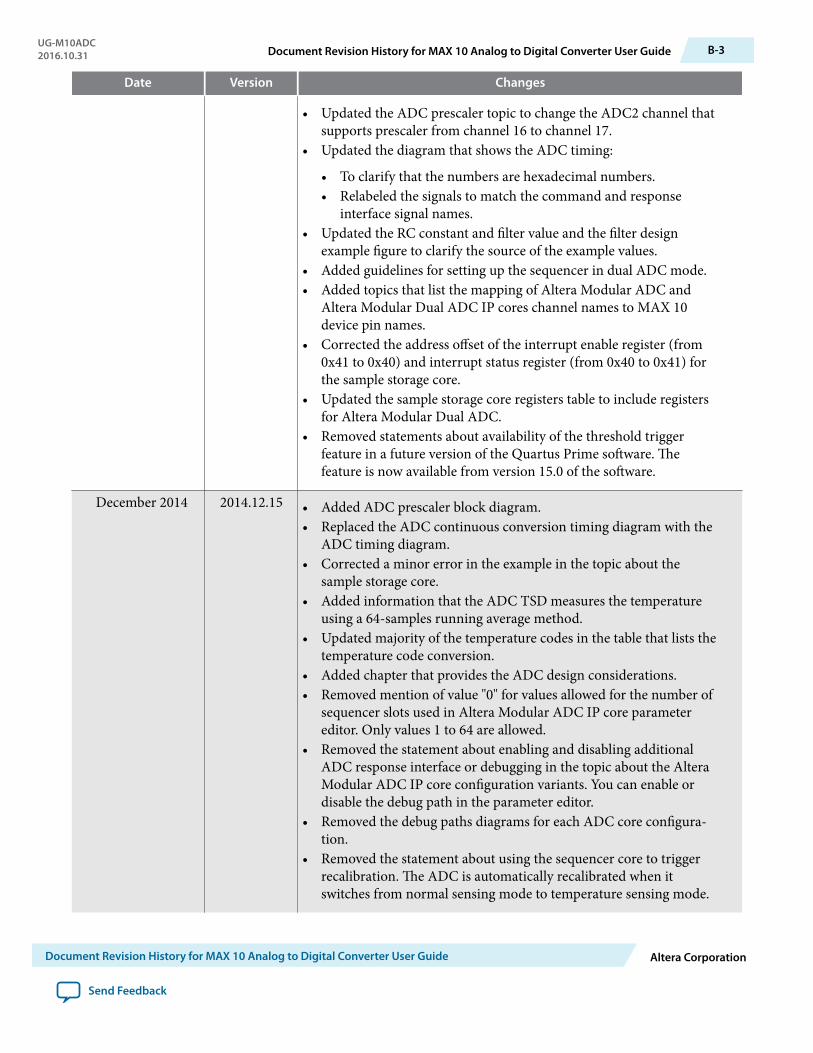
Date Version Changes
• Updated the ADC prescaler topic to change the ADC2 channel thatsupports prescaler from channel 16 to channel 17.
• Updated the diagram that shows the ADC timing:
• To clarify that the numbers are hexadecimal numbers.• Relabeled the signals to match the command and response
interface signal names.• Updated the RC constant and filter value and the filter design
example figure to clarify the source of the example values.• Added guidelines for setting up the sequencer in dual ADC mode.• Added topics that list the mapping of Altera Modular ADC and
Altera Modular Dual ADC IP cores channel names to MAX 10device pin names.
• Corrected the address offset of the interrupt enable register (from0x41 to 0x40) and interrupt status register (from 0x40 to 0x41) forthe sample storage core.
• Updated the sample storage core registers table to include registersfor Altera Modular Dual ADC.
• Removed statements about availability of the threshold triggerfeature in a future version of the Quartus Prime software. Thefeature is now available from version 15.0 of the software.
December 2014 2014.12.15 • Added ADC prescaler block diagram.• Replaced the ADC continuous conversion timing diagram with the
ADC timing diagram.• Corrected a minor error in the example in the topic about the
sample storage core.• Added information that the ADC TSD measures the temperature
using a 64-samples running average method.• Updated majority of the temperature codes in the table that lists the
temperature code conversion.• Added chapter that provides the ADC design considerations.• Removed mention of value "0" for values allowed for the number of
sequencer slots used in Altera Modular ADC IP core parametereditor. Only values 1 to 64 are allowed.
• Removed the statement about enabling and disabling additionalADC response interface or debugging in the topic about the AlteraModular ADC IP core configuration variants. You can enable ordisable the debug path in the parameter editor.
• Removed the debug paths diagrams for each ADC core configura‐tion.
• Removed the statement about using the sequencer core to triggerrecalibration. The ADC is automatically recalibrated when itswitches from normal sensing mode to temperature sensing mode.
UG-M10ADC2016.10.31 Document Revision History for MAX 10 Analog to Digital Converter User Guide B-3
Document Revision History for MAX 10 Analog to Digital Converter User Guide Altera Corporation
Send Feedback

Date Version Changes
• Edited text to clarify about routing power or ground traces if poweror ground plane is not possible.
• Updated the total RC constant values in the table that shows the RCconstant and filter values calculation.
• Corrected spelling for "prescaler".
September 2014 2014.09.22 Initial release.
B-4 Document Revision History for MAX 10 Analog to Digital Converter User GuideUG-M10ADC
2016.10.31
Altera Corporation Document Revision History for MAX 10 Analog to Digital Converter User Guide
Send Feedback

MAX 10 FPGA Configuration User Guide
Subscribe
Send Feedback
UG-M10CONFIG2016.10.31
101 Innovation DriveSan Jose, CA 95134www.altera.com
Contents
MAX 10 FPGA Configuration Overview............................................................1-1
MAX 10 FPGA Configuration Schemes and Features........................................2-1Configuration Schemes............................................................................................................................... 2-1
JTAG Configuration.........................................................................................................................2-1Internal Configuration.................................................................................................................... 2-2
Configuration Features..............................................................................................................................2-10Remote System Upgrade............................................................................................................... 2-10Configuration Design Security.....................................................................................................2-17SEU Mitigation and Configuration Error Detection.................................................................2-21Configuration Data Compression................................................................................................2-24
Configuration Details................................................................................................................................ 2-25Configuration Sequence................................................................................................................2-25MAX 10 Configuration Pins.........................................................................................................2-28
MAX 10 FPGA Configuration Design Guidelines............................................. 3-1Dual-Purpose Configuration Pins............................................................................................................. 3-1
Guidelines: Dual-Purpose Configuration Pin..............................................................................3-1Enabling Dual-purpose Pin............................................................................................................ 3-2
Configuring MAX 10 Devices using JTAG Configuration.....................................................................3-2JTAG Configuration Setup..............................................................................................................3-3ICB Settings in JTAG Configuration............................................................................................. 3-5
Configuring MAX 10 Devices using Internal Configuration.................................................................3-5Selecting Internal Configuration Modes.......................................................................................3-6.pof and ICB Settings....................................................................................................................... 3-6Programming .pof into Internal Flash...........................................................................................3-8
Implementing ISP Clamp in Quartus Prime Software............................................................................3-8Creating IPS File...............................................................................................................................3-9Executing IPS File............................................................................................................................ 3-9
Accessing Remote System Upgrade through User Logic........................................................................3-9Error Detection.......................................................................................................................................... 3-11
Verifying Error Detection Functionality.....................................................................................3-11Enabling Error Detection..............................................................................................................3-12Accessing Error Detection Block Through User Logic............................................................. 3-12
Enabling Data Compression.....................................................................................................................3-14Enabling Compression Before Design Compilation................................................................. 3-15Enabling Compression After Design Compilation....................................................................3-15
AES Encryption..........................................................................................................................................3-15Generating .ekp File and Encrypt Configuration File...............................................................3-16Generating .jam/.jbc/.svf file from .ekp file................................................................................ 3-17Programming .ekp File and Encrypted POF File.......................................................................3-18
TOC-2
Altera Corporation
Encryption in Internal Configuration.........................................................................................3-19MAX 10 JTAG Secure Design Example.................................................................................................. 3-21
Internal JTAG Interface.................................................................................................................3-21WYSIWYG Atom for Internal JTAG Block Access................................................................... 3-22Executing LOCK and UNLOCK JTAG Instructions................................................................ 3-24Verifying the JTAG Secure Mode.................................................................................................3-25
MAX 10 FPGA Configuration IP Core Implementation Guides.......................4-1Altera Unique Chip ID IP Core..................................................................................................................4-1
Instantiating the Altera Unique Chip ID IP Core........................................................................4-1Resetting the Altera Unique Chip ID IP Core..............................................................................4-1
Altera Dual Configuration IP Core........................................................................................................... 4-2Instantiating the Altera Dual Configuration IP Core................................................................. 4-2
Altera Dual Configuration IP Core References.................................................. 5-1Altera Dual Configuration IP Core Avalon-MM Address Map............................................................ 5-1Altera Dual Configuration IP Core Parameters.......................................................................................5-3
Altera Unique Chip ID IP Core References........................................................ 6-1Altera Unique Chip ID IP Core Ports....................................................................................................... 6-1
Additional Information for MAX 10 FPGA Configuration User Guide...........A-1Document Revision History for MAX 10 FPGA Configuration User Guide..................................... A-1
TOC-3
Altera Corporation
MAX 10 FPGA Configuration Overview 12016.10.31
UG-M10CONFIG Subscribe Send Feedback
You can configure MAX® 10 configuration RAM (CRAM) using the following configuration schemes:
• JTAG configuration—using JTAG interface.• Internal configuration—using internal flash.
Supported Configuration Features
Table 1-1: Configuration Schemes and Features Supported by MAX 10 Devices
Configuration Scheme Remote SystemUpgrade Compression Design Security SEU Mitigation
JTAG configuration — — — YesInternal configuration Yes Yes Yes Yes
Related IP Cores
• Altera Dual Configuration IP Core—used in the remote system upgrade feature.• Altera Unique Chip ID IP Core—retrieves the chip ID of MAX 10 devices.
Related Information
• MAX 10 FPGA Configuration Schemes and Features on page 2-1Provides information about the configuration schemes and features.
• MAX 10 FPGA Configuration Design Guidelines on page 3-1Provides information about using the configuration schemes and features.
• Altera Unique Chip ID IP Core on page 2-18• Altera Dual Configuration IP Core on page 2-16
© 2016 Intel Corporation. All rights reserved. Intel, the Intel logo, Altera, Arria, Cyclone, Enpirion, MAX, Megacore, NIOS, Quartus and Stratix words and logosare trademarks of Intel Corporation in the US and/or other countries. Other marks and brands may be claimed as the property of others. Intel warrantsperformance of its FPGA and semiconductor products to current specifications in accordance with Intel's standard warranty, but reserves the right to makechanges to any products and services at any time without notice. Intel assumes no responsibility or liability arising out of the application or use of anyinformation, product, or service described herein except as expressly agreed to in writing by Intel. Intel customers are advised to obtain the latest version ofdevice specifications before relying on any published information and before placing orders for products or services.
ISO9001:2008Registered
www.altera.com101 Innovation Drive, San Jose, CA 95134
MAX 10 FPGA Configuration Schemes andFeatures 2
2016.10.31
UG-M10CONFIG Subscribe Send Feedback
Configuration SchemesFigure 2-1: High-Level Overview of JTAG Configuration and Internal Configuration for MAX 10 Devices
CRAM
MAX 10 Device
JTAG In-System Programming
CFM
Configuration Data
InternalConfiguration
JTAG Configuration
.sof
.pof
JTAG ConfigurationIn MAX 10 devices, JTAG instructions take precedence over the internal configuration scheme.
Using the JTAG configuration scheme, you can directly configure the device CRAM through the JTAGinterface—TDI, TDO, TMS, and TCK pins. The Quartus® Prime software automatically generates an SRAMObject File (.sof). You can program the .sof using a download cable with the Quartus Prime softwareprogrammer.
Related InformationConfiguring MAX 10 Devices using JTAG Configuration on page 3-2Provides more information about JTAG configuration using download cable with Quartus Prime softwareprogrammer.
© 2016 Intel Corporation. All rights reserved. Intel, the Intel logo, Altera, Arria, Cyclone, Enpirion, MAX, Megacore, NIOS, Quartus and Stratix words and logosare trademarks of Intel Corporation in the US and/or other countries. Other marks and brands may be claimed as the property of others. Intel warrantsperformance of its FPGA and semiconductor products to current specifications in accordance with Intel's standard warranty, but reserves the right to makechanges to any products and services at any time without notice. Intel assumes no responsibility or liability arising out of the application or use of anyinformation, product, or service described herein except as expressly agreed to in writing by Intel. Intel customers are advised to obtain the latest version ofdevice specifications before relying on any published information and before placing orders for products or services.
ISO9001:2008Registered
www.altera.com101 Innovation Drive, San Jose, CA 95134
JTAG Pins
Table 2-1: JTAG Pin
Pin Function Description
TDI Serial input pin for:
• instructions• boundary-scan test data• programming data
• TDI is sampled on the rising edge of TCK• TDI pins have internal weak pull-up resistors.
TDO Serial output pin for:
• instructions• boundary-scan test data• programming data
• TDO is sampled on the falling edge of TCK• The pin is tri-stated if data is not shifted out
of the device.
TMS Input pin that provides the controlsignal to determine the transitions ofthe TAP controller state machine.
• TMS is sampled on the rising edge of TCK• TMS pins have internal weak pull-up resistors.
TCK Clock input to the BST circuitry. —
All the JTAG pins are powered by the VCCIO 1B. In JTAG mode, the I/O pins support the LVTTL/LVCMOS 3.3-1.5V standards.
Related Information
• MAX 10 Device DatasheetProvides more information about supported I/O standards in MAX 10 devices.
• Guidelines: Dual-Purpose Configuration Pin on page 3-1• Enabling Dual-purpose Pin on page 3-2
Internal ConfigurationYou need to program the configuration data into the configuration flash memory (CFM) before internalconfiguration can take place. The configuration data to be written to CFM will be part of the programmerobject file (.pof). Using JTAG In-System Programming (ISP), you can program the .pof into the internalflash.
During internal configuration, MAX 10 devices load the CRAM with configuration data from the CFM.
Internal Configuration Modes
Table 2-2: Supported Internal Configuration Modes Based on MAX 10 Feature Options
MAX 10 Feature Options Supported Internal Configuration Mode
Compact • Single Compressed Image• Single Uncompressed Image
2-2 JTAG PinsUG-M10CONFIG
2016.10.31
Altera Corporation MAX 10 FPGA Configuration Schemes and Features
Send Feedback
MAX 10 Feature Options Supported Internal Configuration Mode
Flash and Analog
• Dual Compressed Images• Single Compressed Image• Single Compressed Image with Memory Initialization• Single Uncompressed Image• Single Uncompressed Image with Memory Initialization
Note: In dual compressed images mode, you can use the CONFIG_SEL pin to select the configurationimage.
Related Information
• Configuring MAX 10 Devices using Internal Configuration on page 3-5• Remote System Upgrade on page 2-10
Configuration Flash Memory
The CFM is a non-volatile internal flash that is used to store configuration images. The CFM may store upto two compressed configuration images, depending on the compression and the MAX 10 devices. Thecompression ratio for the configuration image should be at least 30% for the device to be able store twoconfiguration images.
Related InformationConfiguration Flash Memory Permissions on page 2-20
Configuration Flash Memory Sectors
All CFM in MAX 10 devices consist of three sectors, CFM0, CFM1, and CFM2 except for the 10M02. Thesectors are programmed differently depending on the internal configuration mode you select.
The 10M02 device consists of only CFM0. The CFM0 sector in 10M02 devices is programmed similarlywhen you select single compressed image or single uncompressed image.
UG-M10CONFIG2016.10.31 Configuration Flash Memory 2-3
MAX 10 FPGA Configuration Schemes and Features Altera Corporation
Send Feedback
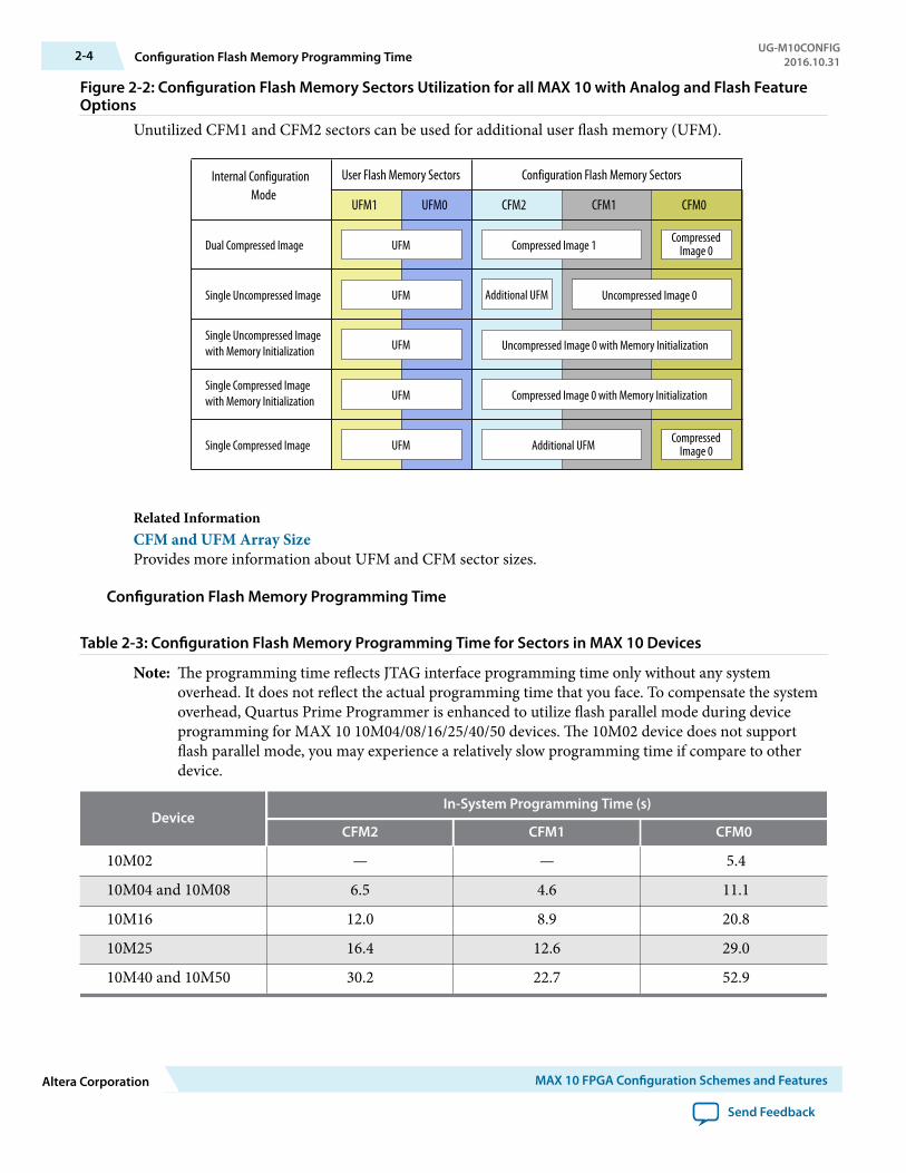
Figure 2-2: Configuration Flash Memory Sectors Utilization for all MAX 10 with Analog and Flash FeatureOptions
Unutilized CFM1 and CFM2 sectors can be used for additional user flash memory (UFM).
Configuration Flash Memory SectorsUser Flash Memory Sectors
CFM0UFM0UFM1 CFM1CFM2
Dual Compressed Image
Single Uncompressed Image
Single Uncompressed Imagewith Memory Initialization
Single Compressed Imagewith Memory Initialization
Single Compressed Image
CompressedImage 0
CompressedImage 0
Uncompressed Image 0 with Memory Initialization
Compressed Image 0 with Memory Initialization
Uncompressed Image 0
Compressed Image 1
Additional UFMUFM
UFM
UFM
UFM
UFM Additional UFM
Internal ConfigurationMode
Related InformationCFM and UFM Array SizeProvides more information about UFM and CFM sector sizes.
Configuration Flash Memory Programming Time
Table 2-3: Configuration Flash Memory Programming Time for Sectors in MAX 10 Devices
Note: The programming time reflects JTAG interface programming time only without any systemoverhead. It does not reflect the actual programming time that you face. To compensate the systemoverhead, Quartus Prime Programmer is enhanced to utilize flash parallel mode during deviceprogramming for MAX 10 10M04/08/16/25/40/50 devices. The 10M02 device does not supportflash parallel mode, you may experience a relatively slow programming time if compare to otherdevice.
DeviceIn-System Programming Time (s)
CFM2 CFM1 CFM0
10M02 — — 5.4
10M04 and 10M08 6.5 4.6 11.1
10M16 12.0 8.9 20.8
10M25 16.4 12.6 29.0
10M40 and 10M50 30.2 22.7 52.9
2-4 Configuration Flash Memory Programming TimeUG-M10CONFIG
2016.10.31
Altera Corporation MAX 10 FPGA Configuration Schemes and Features
Send Feedback
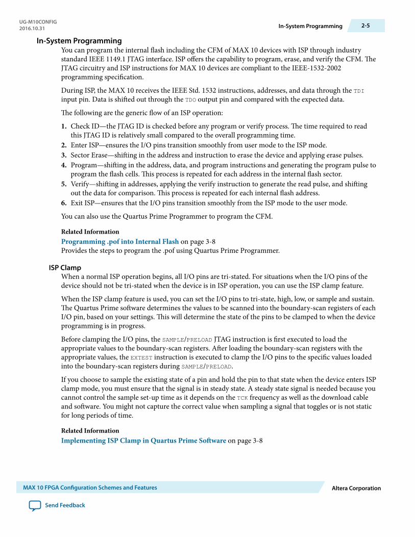
In-System ProgrammingYou can program the internal flash including the CFM of MAX 10 devices with ISP through industrystandard IEEE 1149.1 JTAG interface. ISP offers the capability to program, erase, and verify the CFM. TheJTAG circuitry and ISP instructions for MAX 10 devices are compliant to the IEEE-1532-2002programming specification.
During ISP, the MAX 10 receives the IEEE Std. 1532 instructions, addresses, and data through the TDIinput pin. Data is shifted out through the TDO output pin and compared with the expected data.
The following are the generic flow of an ISP operation:
1. Check ID—the JTAG ID is checked before any program or verify process. The time required to readthis JTAG ID is relatively small compared to the overall programming time.
2. Enter ISP—ensures the I/O pins transition smoothly from user mode to the ISP mode.3. Sector Erase—shifting in the address and instruction to erase the device and applying erase pulses.4. Program—shifting in the address, data, and program instructions and generating the program pulse to
program the flash cells. This process is repeated for each address in the internal flash sector.5. Verify—shifting in addresses, applying the verify instruction to generate the read pulse, and shifting
out the data for comparison. This process is repeated for each internal flash address.6. Exit ISP—ensures that the I/O pins transition smoothly from the ISP mode to the user mode.
You can also use the Quartus Prime Programmer to program the CFM.
Related InformationProgramming .pof into Internal Flash on page 3-8Provides the steps to program the .pof using Quartus Prime Programmer.
ISP ClampWhen a normal ISP operation begins, all I/O pins are tri-stated. For situations when the I/O pins of thedevice should not be tri-stated when the device is in ISP operation, you can use the ISP clamp feature.
When the ISP clamp feature is used, you can set the I/O pins to tri-state, high, low, or sample and sustain.The Quartus Prime software determines the values to be scanned into the boundary-scan registers of eachI/O pin, based on your settings. This will determine the state of the pins to be clamped to when the deviceprogramming is in progress.
Before clamping the I/O pins, the SAMPLE/PRELOAD JTAG instruction is first executed to load theappropriate values to the boundary-scan registers. After loading the boundary-scan registers with theappropriate values, the EXTEST instruction is executed to clamp the I/O pins to the specific values loadedinto the boundary-scan registers during SAMPLE/PRELOAD.
If you choose to sample the existing state of a pin and hold the pin to that state when the device enters ISPclamp mode, you must ensure that the signal is in steady state. A steady state signal is needed because youcannot control the sample set-up time as it depends on the TCK frequency as well as the download cableand software. You might not capture the correct value when sampling a signal that toggles or is not staticfor long periods of time.
Related InformationImplementing ISP Clamp in Quartus Prime Software on page 3-8
UG-M10CONFIG2016.10.31 In-System Programming 2-5
MAX 10 FPGA Configuration Schemes and Features Altera Corporation
Send Feedback
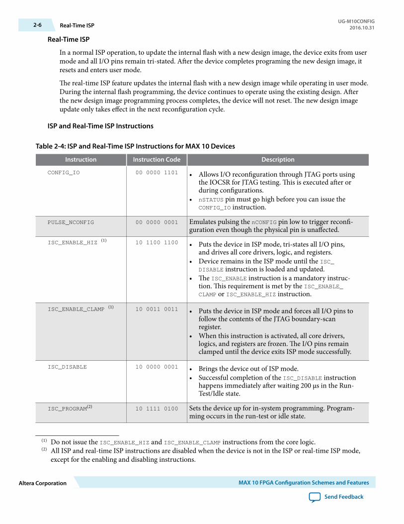
Real-Time ISP
In a normal ISP operation, to update the internal flash with a new design image, the device exits from usermode and all I/O pins remain tri-stated. After the device completes programing the new design image, itresets and enters user mode.
The real-time ISP feature updates the internal flash with a new design image while operating in user mode.During the internal flash programming, the device continues to operate using the existing design. Afterthe new design image programming process completes, the device will not reset. The new design imageupdate only takes effect in the next reconfiguration cycle.
ISP and Real-Time ISP Instructions
Table 2-4: ISP and Real-Time ISP Instructions for MAX 10 Devices
Instruction Instruction Code Description
CONFIG_IO 00 0000 1101 • Allows I/O reconfiguration through JTAG ports usingthe IOCSR for JTAG testing. This is executed after orduring configurations.
• nSTATUS pin must go high before you can issue theCONFIG_IO instruction.
PULSE_NCONFIG 00 0000 0001 Emulates pulsing the nCONFIG pin low to trigger reconfi‐guration even though the physical pin is unaffected.
ISC_ENABLE_HIZ (1) 10 1100 1100 • Puts the device in ISP mode, tri-states all I/O pins,and drives all core drivers, logic, and registers.
• Device remains in the ISP mode until the ISC_DISABLE instruction is loaded and updated.
• The ISC_ENABLE instruction is a mandatory instruc‐tion. This requirement is met by the ISC_ENABLE_CLAMP or ISC_ENABLE_HIZ instruction.
ISC_ENABLE_CLAMP (1) 10 0011 0011 • Puts the device in ISP mode and forces all I/O pins tofollow the contents of the JTAG boundary-scanregister.
• When this instruction is activated, all core drivers,logics, and registers are frozen. The I/O pins remainclamped until the device exits ISP mode successfully.
ISC_DISABLE 10 0000 0001 • Brings the device out of ISP mode.• Successful completion of the ISC_DISABLE instruction
happens immediately after waiting 200 µs in the Run-Test/Idle state.
ISC_PROGRAM(2) 10 1111 0100 Sets the device up for in-system programming. Program‐ming occurs in the run-test or idle state.
(1) Do not issue the ISC_ENABLE_HIZ and ISC_ENABLE_CLAMP instructions from the core logic.(2) All ISP and real-time ISP instructions are disabled when the device is not in the ISP or real-time ISP mode,
except for the enabling and disabling instructions.
2-6 Real-Time ISPUG-M10CONFIG
2016.10.31
Altera Corporation MAX 10 FPGA Configuration Schemes and Features
Send Feedback
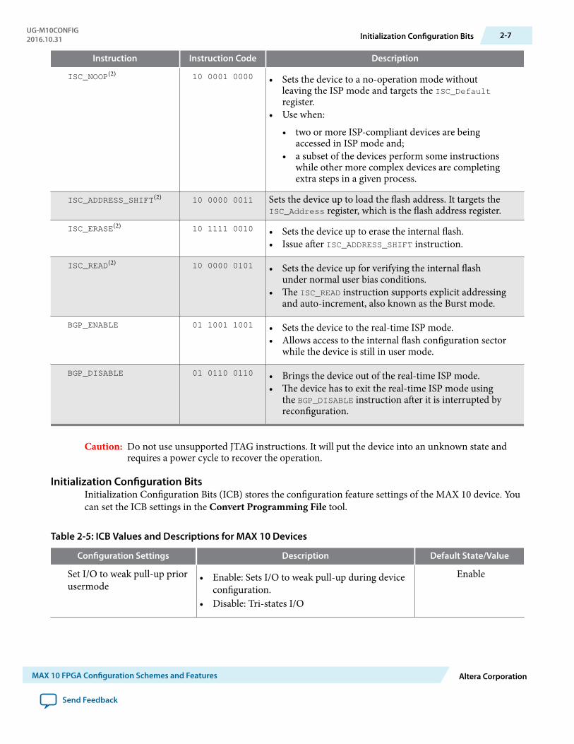
Instruction Instruction Code Description
ISC_NOOP(2) 10 0001 0000 • Sets the device to a no-operation mode withoutleaving the ISP mode and targets the ISC_Defaultregister.
• Use when:
• two or more ISP-compliant devices are beingaccessed in ISP mode and;
• a subset of the devices perform some instructionswhile other more complex devices are completingextra steps in a given process.
ISC_ADDRESS_SHIFT(2) 10 0000 0011 Sets the device up to load the flash address. It targets theISC_Address register, which is the flash address register.
ISC_ERASE(2) 10 1111 0010 • Sets the device up to erase the internal flash.• Issue after ISC_ADDRESS_SHIFT instruction.
ISC_READ(2) 10 0000 0101 • Sets the device up for verifying the internal flashunder normal user bias conditions.
• The ISC_READ instruction supports explicit addressingand auto-increment, also known as the Burst mode.
BGP_ENABLE 01 1001 1001 • Sets the device to the real-time ISP mode.• Allows access to the internal flash configuration sector
while the device is still in user mode.
BGP_DISABLE 01 0110 0110 • Brings the device out of the real-time ISP mode.• The device has to exit the real-time ISP mode using
the BGP_DISABLE instruction after it is interrupted byreconfiguration.
Caution: Do not use unsupported JTAG instructions. It will put the device into an unknown state andrequires a power cycle to recover the operation.
Initialization Configuration BitsInitialization Configuration Bits (ICB) stores the configuration feature settings of the MAX 10 device. Youcan set the ICB settings in the Convert Programming File tool.
Table 2-5: ICB Values and Descriptions for MAX 10 Devices
Configuration Settings Description Default State/Value
Set I/O to weak pull-up priorusermode
• Enable: Sets I/O to weak pull-up during deviceconfiguration.
• Disable: Tri-states I/O
Enable
UG-M10CONFIG2016.10.31 Initialization Configuration Bits 2-7
MAX 10 FPGA Configuration Schemes and Features Altera Corporation
Send Feedback
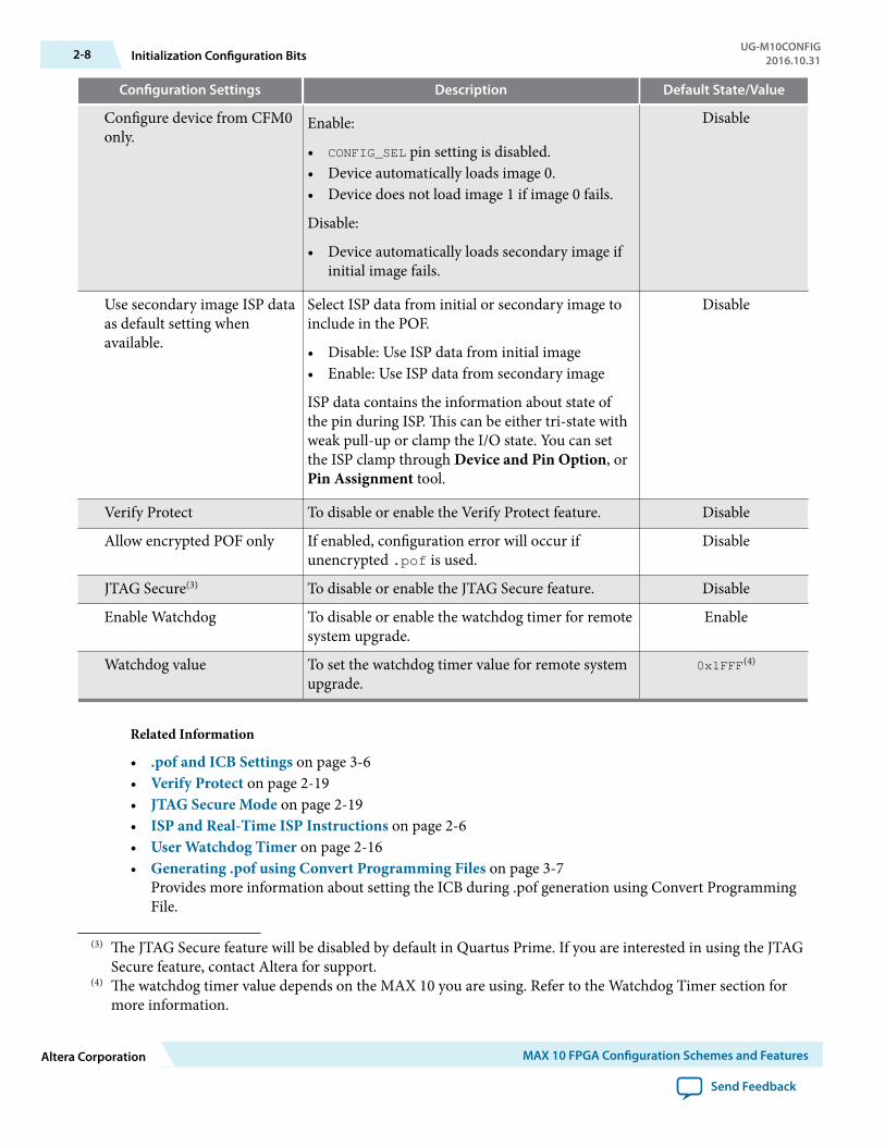
Configuration Settings Description Default State/Value
Configure device from CFM0only.
Enable:
• CONFIG_SEL pin setting is disabled.• Device automatically loads image 0.• Device does not load image 1 if image 0 fails.
Disable:
• Device automatically loads secondary image ifinitial image fails.
Disable
Use secondary image ISP dataas default setting whenavailable.
Select ISP data from initial or secondary image toinclude in the POF.
• Disable: Use ISP data from initial image• Enable: Use ISP data from secondary image
ISP data contains the information about state ofthe pin during ISP. This can be either tri-state withweak pull-up or clamp the I/O state. You can setthe ISP clamp through Device and Pin Option, orPin Assignment tool.
Disable
Verify Protect To disable or enable the Verify Protect feature. Disable
Allow encrypted POF only If enabled, configuration error will occur ifunencrypted .pof is used.
Disable
JTAG Secure(3) To disable or enable the JTAG Secure feature. Disable
Enable Watchdog To disable or enable the watchdog timer for remotesystem upgrade.
Enable
Watchdog value To set the watchdog timer value for remote systemupgrade.
0x1FFF(4)
Related Information
• .pof and ICB Settings on page 3-6• Verify Protect on page 2-19• JTAG Secure Mode on page 2-19• ISP and Real-Time ISP Instructions on page 2-6• User Watchdog Timer on page 2-16• Generating .pof using Convert Programming Files on page 3-7
Provides more information about setting the ICB during .pof generation using Convert ProgrammingFile.
(3) The JTAG Secure feature will be disabled by default in Quartus Prime. If you are interested in using the JTAGSecure feature, contact Altera for support.
(4) The watchdog timer value depends on the MAX 10 you are using. Refer to the Watchdog Timer section formore information.
2-8 Initialization Configuration BitsUG-M10CONFIG
2016.10.31
Altera Corporation MAX 10 FPGA Configuration Schemes and Features
Send Feedback
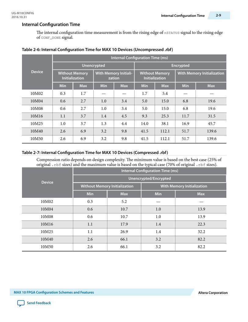
Internal Configuration Time
The internal configuration time measurement is from the rising edge of nSTATUS signal to the rising edgeof CONF_DONE signal.
Table 2-6: Internal Configuration Time for MAX 10 Devices (Uncompressed .rbf)
Device
Internal Configuration Time (ms)
Unencrypted Encrypted
Without MemoryInitialization
With Memory Initiali‐zation
Without MemoryInitialization
With Memory Initialization
Min Max Min Max Min Max Min Max
10M02 0.3 1.7 — — 1.7 5.4 — —10M04 0.6 2.7 1.0 3.4 5.0 15.0 6.8 19.610M08 0.6 2.7 1.0 3.4 5.0 15.0 6.8 19.610M16 1.1 3.7 1.4 4.5 9.3 25.3 11.7 31.510M25 1.0 3.7 1.3 4.4 14.0 38.1 16.9 45.710M40 2.6 6.9 3.2 9.8 41.5 112.1 51.7 139.610M50 2.6 6.9 3.2 9.8 41.5 112.1 51.7 139.6
Table 2-7: Internal Configuration Time for MAX 10 Devices (Compressed .rbf)
Compression ratio depends on design complexity. The minimum value is based on the best case (25% oforiginal .rbf sizes) and the maximum value is based on the typical case (70% of original .rbf sizes).
Device
Internal Configuration Time (ms)
Unencrypted/Encrypted
Without Memory Initialization With Memory Initialization
Min Max Min Max
10M02 0.3 5.2 — —10M04 0.6 10.7 1.0 13.910M08 0.6 10.7 1.0 13.910M16 1.1 17.9 1.4 22.310M25 1.1 26.9 1.4 32.210M40 2.6 66.1 3.2 82.210M50 2.6 66.1 3.2 82.2
UG-M10CONFIG2016.10.31 Internal Configuration Time 2-9
MAX 10 FPGA Configuration Schemes and Features Altera Corporation
Send Feedback
Configuration Features
Remote System UpgradeMAX 10 devices support the remote system upgrade feature. By default, the remote system upgradefeature is enabled when you select the dual compressed image internal configuration mode.
The remote system upgrade feature in MAX 10 devices offers the following capabilities:
• Manages remote configuration• Provides error detection, recovery, and information• Supports direct-to-application configuration image• Supports compressed and encrypted .pof
There are two methods to access remote system upgrade in MAX 10 devices:
• Altera Dual Configuration IP core• User interface
Related Information
• Altera Dual Configuration IP Core on page 2-16• Accessing Remote System Upgrade through User Logic on page 3-9• AN 741: Remote System Upgrade for MAX 10 FPGA Devices over UART with the Nios II Processor
Provides reference design for remote system upgrade in MAX 10 FPGA devices.• I2C Remote System Update Example
This example demonstrates a remote system upgrade using the I2C protocol.
Remote System Upgrade FlowBoth the application configuration images, image 0 and image 1, are stored in the CFM. The MAX 10device loads either one of the application configuration image from the CFM.
2-10 Configuration FeaturesUG-M10CONFIG
2016.10.31
Altera Corporation MAX 10 FPGA Configuration Schemes and Features
Send Feedback
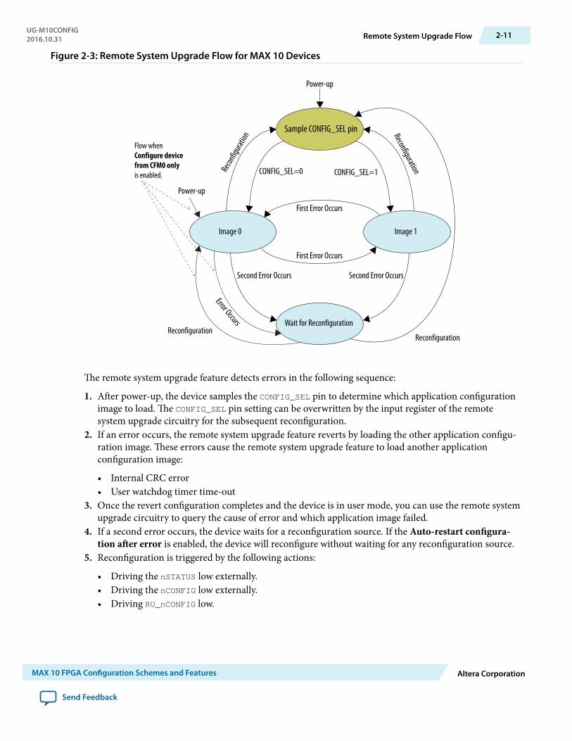
Figure 2-3: Remote System Upgrade Flow for MAX 10 Devices
Sample CONFIG_SEL pin
Image 0 Image 1
CONFIG_SEL=0 CONFIG_SEL=1
Wait for Reconfiguration
Power-up
ReconfigurationRecon
figura
tion
First Error Occurs
First Error Occurs
Second Error Occurs
Flow whenConfigure devicefrom CFM0 onlyis enabled.
Second Error Occurs
Error OccursReconfiguration
Reconfiguration
Power-up
The remote system upgrade feature detects errors in the following sequence:
1. After power-up, the device samples the CONFIG_SEL pin to determine which application configurationimage to load. The CONFIG_SEL pin setting can be overwritten by the input register of the remotesystem upgrade circuitry for the subsequent reconfiguration.
2. If an error occurs, the remote system upgrade feature reverts by loading the other application configu‐ration image. These errors cause the remote system upgrade feature to load another applicationconfiguration image:
• Internal CRC error• User watchdog timer time-out
3. Once the revert configuration completes and the device is in user mode, you can use the remote systemupgrade circuitry to query the cause of error and which application image failed.
4. If a second error occurs, the device waits for a reconfiguration source. If the Auto-restart configura‐tion after error is enabled, the device will reconfigure without waiting for any reconfiguration source.
5. Reconfiguration is triggered by the following actions:
• Driving the nSTATUS low externally.• Driving the nCONFIG low externally.• Driving RU_nCONFIG low.
UG-M10CONFIG2016.10.31 Remote System Upgrade Flow 2-11
MAX 10 FPGA Configuration Schemes and Features Altera Corporation
Send Feedback
Remote System Upgrade Circuitry
Figure 2-4: Remote System Upgrade Circuitry
Status Register (SR)
PreviousStateRegister 2Bit[31..0]
StateRegister 1Bit[31..0]
CurrentStateLogicBit[33..0]
Internal Oscillator
Control RegisterBit [38..0]
Logic
Input RegisterBit [38..0] update
Logic
Bit [40..39]doutdin
Bit [38..0]doutdin
capture
Shift Register
clkout capture updateLogic
clkin
RU_DIN RU_SHIFTnLD RU_CAPTnUPDT RU_CLK RU_nRSTIMER
Logic Array
RUReconfigurationStateMachine
User WatchdogTimer
RUMasterStateMachine
timeout
RU_nCONFIGRU_DOUT
Previous
The remote system upgrade circuitry does the following functions:
• Tracks the current state of configuration• Monitors all reconfiguration sources• Provides access to set up the application configuration image• Returns the device to fallback configuration if an error occurs• Provides access to the information on the failed application configuration image
Remote System Upgrade Circuitry Signals
Table 2-8: Remote System Upgrade Circuitry Signals for MAX 10 Devices
Core Signal Name LogicalSignalName
Input/Output
Description
RU_DIN regin InputUse this signal to write data to the shift register on the risingedge of RU_CLK. To load data to the shift register, assert RU_SHIFTnLD.
2-12 Remote System Upgrade CircuitryUG-M10CONFIG
2016.10.31
Altera Corporation MAX 10 FPGA Configuration Schemes and Features
Send Feedback
Core Signal Name LogicalSignalName
Input/Output
Description
RU_DOUT regout OutputUse this signal to get output data from the shift register. Datais clocked out on each rising edge of RU_CLK if RU_SHIFTnLD isasserted.
RU_nRSTIMER rsttimer Input
• Use this signal to reset the user watchdog timer. A fallingedge of this signal triggers a reset of the user watchdogtimer.
• To reset the timer, pulse the RU_nRSTIMER signal for aminimum of 250 ns.
RU_nCONFIG rconfig InputUse this signal to reconfigure the device. Driving this signallow triggers the device to reconfigure if you enable the remotesystem upgrade feature.
RU_CLK clk Input
The clock to the remote system upgrade circuitry. All registersin this clock domain are enabled in user mode if you enablethe remote system upgrade. Shift register and input registerare positive edge flip-flops.
RU_SHIFTnLD shiftnld Input Control signals that determine the mode of remote systemupgrade circuitry.
• When RU_SHIFTnLD is driven low and RU_CAPTnUPDT isdriven low, the input register is loaded with the contents ofthe shift register on the rising edge of RU_CLK.
• When RU_SHIFTnLD is driven low and RU_CAPTnUPDT isdriven high, the shift register captures values from theinput_cs_ps module on the rising edge of RU_CLK.
• When RU_SHIFTnLD is driven high, the RU_CAPTnUPDT willbe ignored and the shift register shifts data on each risingedge of RU_CLK.
RU_CAPTnUPDT captnupdt Input
Related InformationMAX 10 Device DatasheetProvides more information about Remote System Upgrade timing specifications.
Remote System Upgrade Circuitry Input Control
The remote system upgrade circuitry has three modes of operation.
• Update—loads the values in the shift register into the input register.• Capture—loads the shift register with data to be shifted out.• Shift—shifts out data to the user logic.
UG-M10CONFIG2016.10.31 Remote System Upgrade Circuitry Input Control 2-13
MAX 10 FPGA Configuration Schemes and Features Altera Corporation
Send Feedback
Table 2-9: Control Inputs to the Remote System Upgrade Circuitry
Remote System Upgrade Circuitry Control InputsOperation
Mode
Input Settings for Registers
RU_SHIFTnLD RU_CAPTnUPDT Shift register[40]
Shift register[39]
ShiftRegister[38:0]
InputRegister[38:0]
0 0 Don't Care Don't Care Update Shift Register[38:0]
Shift Register[38:0]
0 1 0 0 Capture Current State InputRegister[38:0]
0 1 0 1 Capture8’b0,
Previous StateApplication1
InputRegister[38:0]
0 1 1 0 Capture8’b0,
Previous StateApplication2
InputRegister[38:0]
0 1 1 1 Capture InputRegister[38:0]
InputRegister[38:0]
1 Don't Care Don't Care Don't Care Shiftru_din, Shift
Register[38:1]
InputRegister[38:0]
The following shows examples of driving the control inputs in the remote system upgrade circuitry:
• When you drive RU_SHIFTnLD high to 1’b1, the shift register shifts data on each rising edge of RU_CLKand RU_CAPTnUPDT has no function.
• When you drive both RU_SHIFTnLD and RU_CAPTnUPDT low to 1’b0, the input register is loaded with thecontents of the shift register on the rising edge of RU_CLK.
• When you drive RU_SHIFTnLD low to 1’b0 and RU_CAPTnUPDT high to 1’b1, the shift registercaptures values on the rising edge of RU_DCLK.
Remote System Upgrade Input Register
Table 2-10: Remote System Upgrade Input Register for MAX 10 Devices
Bits Name Description
38:14 Reserved Reserved—set to 0.
13 ru_config_sel
• 0: Load configuration image 0• 1: Load configuration image 1
This bit will only work if the ru_config_sel_overwrite bit is set to1.
12 ru_config_sel_
overwrite
• 0: Disable overwrite CONFIG_SEL pin• 1: Enable overwrite CONFIG_SEL pin
2-14 Remote System Upgrade Input RegisterUG-M10CONFIG
2016.10.31
Altera Corporation MAX 10 FPGA Configuration Schemes and Features
Send Feedback
Bits Name Description
11:0 Reserved Reserved—set to 0.
Remote System Upgrade Status Registers
Table 2-11: Remote System Upgrade Status Register—Current State Logic Bit for MAX 10 Devices
Bits Name Description
33:30 msm_cs The current state of the master state machine (MSM).
29 ru_wd_enThe current state of the enabled user watchdog timer. The defaultstate is active high.
28:0 wd_timeout_value The current, entire 29-bit watchdog time-out value.
Table 2-12: Remote System Upgrade Status Register—Previous State Bit for MAX 10 Devices
Bits Name Description
31 nconfig An active high field that describes the reconfiguration sources whichcaused the MAX 10 device to leave the previous application configu‐ration. In the event of a tie, the higher bit order takes precedence.For example, if the nconfig and the ru_nconfig triggered at thesame time, the nconfig takes precedence over the ru_nconfig.
30 crcerror
29 nstatus
28 wdtimer
27:26 Reserved Reserved—set to 0.
25:22 msm_cs
The state of the MSM when a reconfiguration event occurred. Thereconfiguration will cause the device to leave the previous applica‐tion configuration.
21:0 Reserved Reserved—set to 0.
Related InformationAltera Dual Configuration IP Core Avalon-MM Address Map on page 5-1
Master State Machine
The master state machine (MSM) tracks current configuration mode and enables the user watchdog timer.
Table 2-13: Remote System Upgrade Master State Machine Current State Descriptions for MAX 10 Devices
msm_cs Values State Description
0010 Image 0 is being loaded.
0011 Image 1 is being loaded after a revert in application image happens.
0100 Image 1 is being loaded.
0101 Image 0 is being loaded after a revert in application image happens.
UG-M10CONFIG2016.10.31 Remote System Upgrade Status Registers 2-15
MAX 10 FPGA Configuration Schemes and Features Altera Corporation
Send Feedback
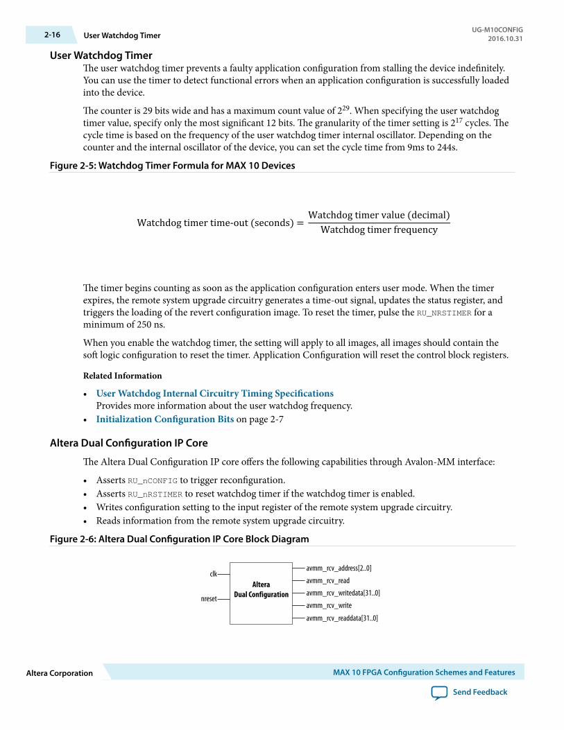
User Watchdog TimerThe user watchdog timer prevents a faulty application configuration from stalling the device indefinitely.You can use the timer to detect functional errors when an application configuration is successfully loadedinto the device.
The counter is 29 bits wide and has a maximum count value of 229. When specifying the user watchdogtimer value, specify only the most significant 12 bits. The granularity of the timer setting is 217 cycles. Thecycle time is based on the frequency of the user watchdog timer internal oscillator. Depending on thecounter and the internal oscillator of the device, you can set the cycle time from 9ms to 244s.
Figure 2-5: Watchdog Timer Formula for MAX 10 Devices
The timer begins counting as soon as the application configuration enters user mode. When the timerexpires, the remote system upgrade circuitry generates a time-out signal, updates the status register, andtriggers the loading of the revert configuration image. To reset the timer, pulse the RU_NRSTIMER for aminimum of 250 ns.
When you enable the watchdog timer, the setting will apply to all images, all images should contain thesoft logic configuration to reset the timer. Application Configuration will reset the control block registers.
Related Information
• User Watchdog Internal Circuitry Timing SpecificationsProvides more information about the user watchdog frequency.
• Initialization Configuration Bits on page 2-7
Altera Dual Configuration IP Core
The Altera Dual Configuration IP core offers the following capabilities through Avalon-MM interface:
• Asserts RU_nCONFIG to trigger reconfiguration.• Asserts RU_nRSTIMER to reset watchdog timer if the watchdog timer is enabled.• Writes configuration setting to the input register of the remote system upgrade circuitry.• Reads information from the remote system upgrade circuitry.
Figure 2-6: Altera Dual Configuration IP Core Block Diagram
AlteraDual Configuration
clk
nreset
avmm_rcv_address[2..0]
avmm_rcv_read
avmm_rcv_writedata[31..0]
avmm_rcv_write
avmm_rcv_readdata[31..0]
2-16 User Watchdog TimerUG-M10CONFIG
2016.10.31
Altera Corporation MAX 10 FPGA Configuration Schemes and Features
Send Feedback
Related Information
• Altera Dual Configuration IP Core Avalon-MM Address Map on page 5-1• Avalon Interface Specifications
Provides more information about the Avalon-MM interface specifications applied in Altera DualConfiguration IP Core.
• Instantiating the Altera Dual Configuration IP Core on page 4-2• Altera Dual Configuration IP Core References on page 5-1• Remote System Upgrade on page 2-10• AN 741: Remote System Upgrade for MAX 10 FPGA Devices over UART with the Nios II Processor
Provides reference design for remote system upgrade in MAX 10 FPGA devices.• I2C Remote System Update Example
This example demonstrates a remote system upgrade using the I2C protocol.
Configuration Design SecurityThe MAX 10 design security feature supports the following capabilities:
• Encryption—Built-in encryption standard (AES) to support 128-bit key industry-standard designsecurity algorithm
• Chip ID—Unique device identification• JTAG secure mode—limits access to JTAG instructions• Verify Protect—allows optional disabling of CFM content read-back
AES Encryption Protection
The MAX 10 design security feature provides the following security protection for your designs:
• Security against copying—the non-volatile key is securely stored in the MAX 10 devices and cannot beread through any interface. Without this key, attacker will not be able to decrypt the encrypted configu‐ration image.
• Security against reverse engineering—reverse engineering from an encrypted configuration file is verydifficult and time consuming because the file requires decryption.
• Security against tampering—after you enable the JTAG Secure and Encrypted POF (EPOF) only, theMAX 10 device can only accept configuration files encrypted with the same key. Additionally, configu‐ration through the JTAG interface is blocked.
Related InformationGenerating .pof using Convert Programming Files on page 3-7
Encryption and Decryption
MAX 10 supports AES encryption. Programming bitstream is encrypted based on the encryption key thatis specified by you. In MAX 10 devices, the key is part of the ICB settings stored in the internal flash.Hence, the key will be non-volatile but you can clear/delete the key by a full chip erase the device.
When you use compression with encryption, the configuration file is first compressed, and then encryptedusing the Quartus Prime software. During configuration, the device first decrypts, and then decompressesthe configuration file.
UG-M10CONFIG2016.10.31 Configuration Design Security 2-17
MAX 10 FPGA Configuration Schemes and Features Altera Corporation
Send Feedback
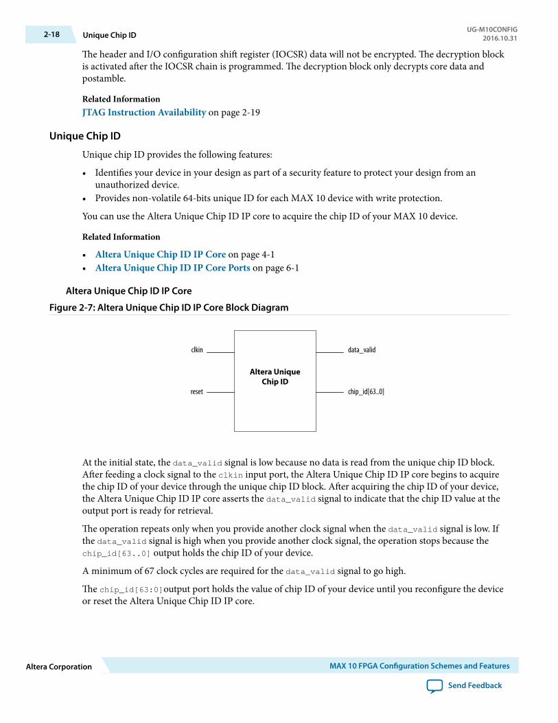
The header and I/O configuration shift register (IOCSR) data will not be encrypted. The decryption blockis activated after the IOCSR chain is programmed. The decryption block only decrypts core data andpostamble.
Related InformationJTAG Instruction Availability on page 2-19
Unique Chip ID
Unique chip ID provides the following features:
• Identifies your device in your design as part of a security feature to protect your design from anunauthorized device.
• Provides non-volatile 64-bits unique ID for each MAX 10 device with write protection.
You can use the Altera Unique Chip ID IP core to acquire the chip ID of your MAX 10 device.
Related Information
• Altera Unique Chip ID IP Core on page 4-1• Altera Unique Chip ID IP Core Ports on page 6-1
Altera Unique Chip ID IP Core
Figure 2-7: Altera Unique Chip ID IP Core Block Diagram
Altera UniqueChip ID
clkin data_valid
chip_id[63..0]reset
At the initial state, the data_valid signal is low because no data is read from the unique chip ID block.After feeding a clock signal to the clkin input port, the Altera Unique Chip ID IP core begins to acquirethe chip ID of your device through the unique chip ID block. After acquiring the chip ID of your device,the Altera Unique Chip ID IP core asserts the data_valid signal to indicate that the chip ID value at theoutput port is ready for retrieval.
The operation repeats only when you provide another clock signal when the data_valid signal is low. Ifthe data_valid signal is high when you provide another clock signal, the operation stops because thechip_id[63..0] output holds the chip ID of your device.
A minimum of 67 clock cycles are required for the data_valid signal to go high.
The chip_id[63:0]output port holds the value of chip ID of your device until you reconfigure the deviceor reset the Altera Unique Chip ID IP core.
2-18 Unique Chip IDUG-M10CONFIG
2016.10.31
Altera Corporation MAX 10 FPGA Configuration Schemes and Features
Send Feedback
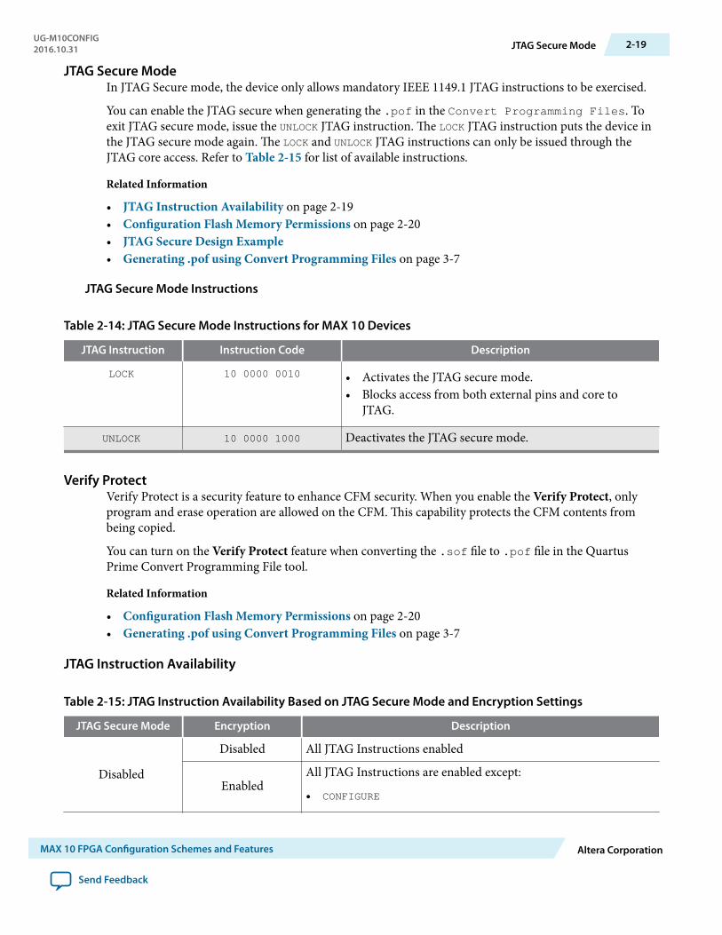
JTAG Secure ModeIn JTAG Secure mode, the device only allows mandatory IEEE 1149.1 JTAG instructions to be exercised.
You can enable the JTAG secure when generating the .pof in the Convert Programming Files. Toexit JTAG secure mode, issue the UNLOCK JTAG instruction. The LOCK JTAG instruction puts the device inthe JTAG secure mode again. The LOCK and UNLOCK JTAG instructions can only be issued through theJTAG core access. Refer to Table 2-15 for list of available instructions.
Related Information
• JTAG Instruction Availability on page 2-19• Configuration Flash Memory Permissions on page 2-20• JTAG Secure Design Example• Generating .pof using Convert Programming Files on page 3-7
JTAG Secure Mode Instructions
Table 2-14: JTAG Secure Mode Instructions for MAX 10 Devices
JTAG Instruction Instruction Code Description
LOCK 10 0000 0010 • Activates the JTAG secure mode.• Blocks access from both external pins and core to
JTAG.
UNLOCK 10 0000 1000 Deactivates the JTAG secure mode.
Verify ProtectVerify Protect is a security feature to enhance CFM security. When you enable the Verify Protect, onlyprogram and erase operation are allowed on the CFM. This capability protects the CFM contents frombeing copied.
You can turn on the Verify Protect feature when converting the .sof file to .pof file in the QuartusPrime Convert Programming File tool.
Related Information
• Configuration Flash Memory Permissions on page 2-20• Generating .pof using Convert Programming Files on page 3-7
JTAG Instruction Availability
Table 2-15: JTAG Instruction Availability Based on JTAG Secure Mode and Encryption Settings
JTAG Secure Mode Encryption Description
Disabled
Disabled All JTAG Instructions enabled
EnabledAll JTAG Instructions are enabled except:
• CONFIGURE
UG-M10CONFIG2016.10.31 JTAG Secure Mode 2-19
MAX 10 FPGA Configuration Schemes and Features Altera Corporation
Send Feedback
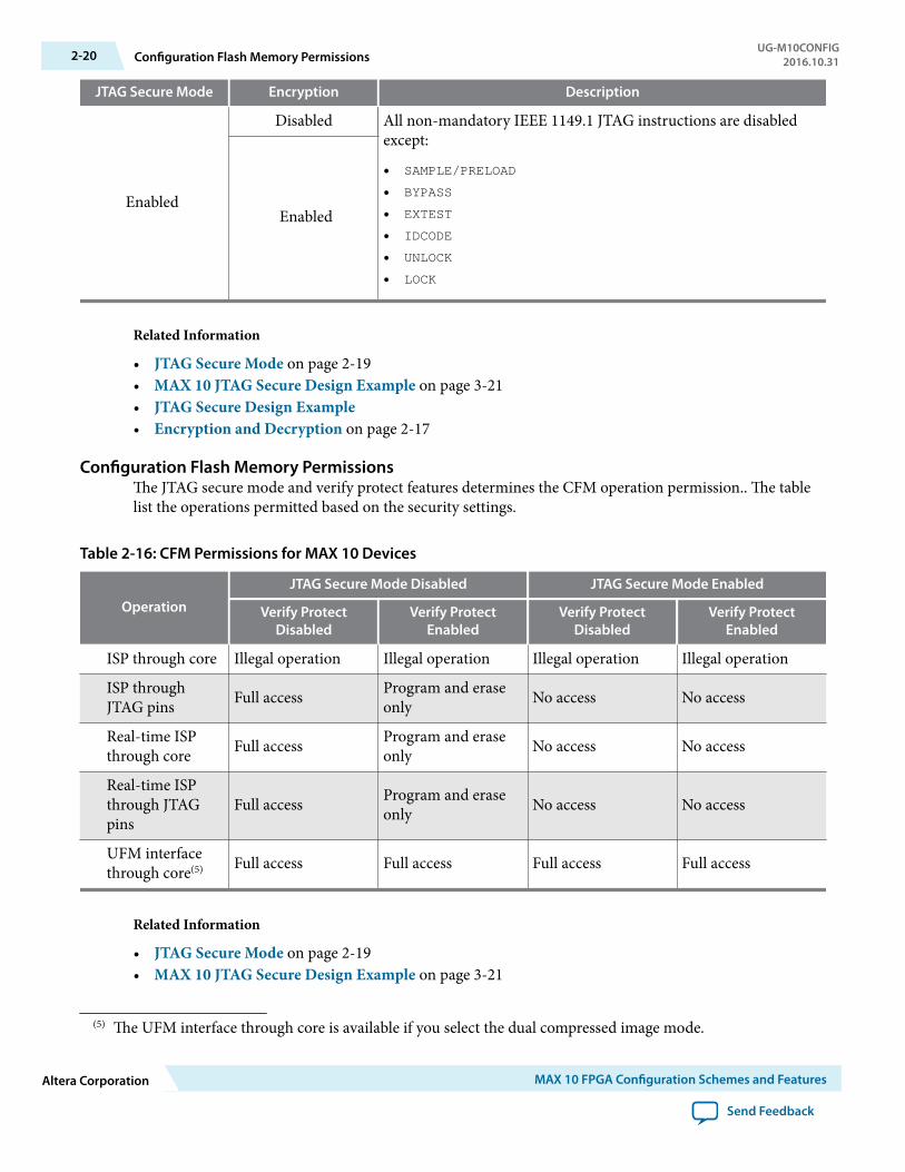
JTAG Secure Mode Encryption Description
Enabled
Disabled All non-mandatory IEEE 1149.1 JTAG instructions are disabledexcept:
• SAMPLE/PRELOAD
• BYPASS
• EXTEST
• IDCODE
• UNLOCK
• LOCK
Enabled
Related Information
• JTAG Secure Mode on page 2-19• MAX 10 JTAG Secure Design Example on page 3-21• JTAG Secure Design Example• Encryption and Decryption on page 2-17
Configuration Flash Memory PermissionsThe JTAG secure mode and verify protect features determines the CFM operation permission.. The tablelist the operations permitted based on the security settings.
Table 2-16: CFM Permissions for MAX 10 Devices
Operation
JTAG Secure Mode Disabled JTAG Secure Mode Enabled
Verify ProtectDisabled
Verify ProtectEnabled
Verify ProtectDisabled
Verify ProtectEnabled
ISP through core Illegal operation Illegal operation Illegal operation Illegal operation
ISP throughJTAG pins Full access Program and erase
only No access No access
Real-time ISPthrough core Full access Program and erase
only No access No access
Real-time ISPthrough JTAGpins
Full access Program and eraseonly No access No access
UFM interfacethrough core(5) Full access Full access Full access Full access
Related Information
• JTAG Secure Mode on page 2-19• MAX 10 JTAG Secure Design Example on page 3-21
(5) The UFM interface through core is available if you select the dual compressed image mode.
2-20 Configuration Flash Memory PermissionsUG-M10CONFIG
2016.10.31
Altera Corporation MAX 10 FPGA Configuration Schemes and Features
Send Feedback
• JTAG Secure Design Example• Verify Protect on page 2-19• Generating .pof using Convert Programming Files on page 3-7
SEU Mitigation and Configuration Error DetectionThe dedicated circuitry built in MAX 10 devices consists of an error detection cyclic redundancy check(EDCRC) feature. You can use this feature to mitigate single-event upset (SEU) or soft errors.
The hardened on-chip EDCRC circuitry allows you to perform the following operations without anyimpact on the fitting of the device:
• Auto-detection of cyclic redundancy check (CRC) errors during configuration.• Identification of SEU in user mode with the optional CRC error detection.• Testing of error detection by error detection verification through the JTAG interface.
Related Information
• Verifying Error Detection Functionality on page 3-11• Enabling Error Detection on page 3-12• Accessing Error Detection Block Through User Logic on page 3-12
Configuration Error DetectionIn configuration mode, a frame-based CRC is stored in the configuration data and contains the CRC valuefor each data frame.
During configuration, the MAX 10 device calculates the CRC value based on the frame of data that isreceived and compares it against the frame CRC value in the data stream. Configuration continues untilthe device detects an error or when all the values are calculated.
For MAX 10 devices, the CRC is computed by the Quartus Prime software and downloaded into thedevice as part of the configuration bit stream. These devices store the CRC in the 32-bit storage register atthe end of the configuration mode.
User Mode Error DetectionSEUs are changes in a CRAM bit state due to an ionizing particle. MAX 10 devices have built-in errordetection circuitry to detect data corruption in the CRAM cells.
This error detection capability continuously computes the CRC of the configured CRAM bits. The CRC ofthe contents of the device are compared with the pre-calculated CRC value obtained at the end of theconfiguration. If the CRC values match, there is no error in the current configuration CRAM bits. Theprocess of error detection continues until the device is reset—by setting nCONFIG to low.
The error detection circuitry in MAX 10 device uses a 32-bit CRC IEEE Std. 802 and a 32-bit polynomialas the CRC generator. Therefore, the device performs a single 32-bit CRC calculation. If an SEU does notoccur, the resulting 32-bit signature value is 0x000000, which results in a 0 on the output signalCRC_ERROR. If an SEU occurs in the device, the resulting signature value is non-zero and the CRC_ERRORoutput signal is 1. You must decide whether to reconfigure the FPGA by strobing the nCONFIG pin low orignore the error.
UG-M10CONFIG2016.10.31 SEU Mitigation and Configuration Error Detection 2-21
MAX 10 FPGA Configuration Schemes and Features Altera Corporation
Send Feedback
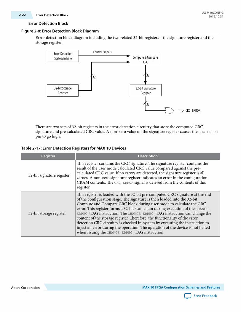
Error Detection Block
Figure 2-8: Error Detection Block DiagramError detection block diagram including the two related 32-bit registers—the signature register and thestorage register.
Control SignalsError DetectionState Machine
32-bit StorageRegister
Compute & CompareCRC
32-bit SignatureRegister
32 32
32
CRC_ERROR
There are two sets of 32-bit registers in the error detection circuitry that store the computed CRCsignature and pre-calculated CRC value. A non-zero value on the signature register causes the CRC_ERRORpin to go high.
Table 2-17: Error Detection Registers for MAX 10 Devices
Register Description
32-bit signature register
This register contains the CRC signature. The signature register contains theresult of the user mode calculated CRC value compared against the pre-calculated CRC value. If no errors are detected, the signature register is allzeroes. A non-zero signature register indicates an error in the configurationCRAM contents. The CRC_ERROR signal is derived from the contents of thisregister.
32-bit storage register
This register is loaded with the 32-bit pre-computed CRC signature at the endof the configuration stage. The signature is then loaded into the 32-bitCompute and Compare CRC block during user mode to calculate the CRCerror. This register forms a 32-bit scan chain during execution of the CHANGE_EDREG JTAG instruction. The CHANGE_EDREG JTAG instruction can change thecontent of the storage register. Therefore, the functionality of the errordetection CRC circuitry is checked in-system by executing the instruction toinject an error during the operation. The operation of the device is not haltedwhen issuing the CHANGE_EDREG JTAG instruction.
2-22 Error Detection BlockUG-M10CONFIG
2016.10.31
Altera Corporation MAX 10 FPGA Configuration Schemes and Features
Send Feedback
CHANGE_EDREG JTAG Instruction
Table 2-18: CHANGE_EDREG JTAG Instruction Description
JTAG Instruction Instruction Code Description
CHANGE_EDREG 00 0001 0101 This instruction connects the 32-bit CRC storage registerbetween TDI and TDO. Any precomputed CRC is loadedinto the CRC storage register to test the operation of theerror detection CRC circuitry at the CRC_ERROR pin.
Error Detection TimingWhen the error detection CRC feature is enabled through the Quartus Prime software, the deviceautomatically activates the CRC process upon entering user mode, after configuration and initialization iscomplete.
The CRC_ERROR pin will remain low until the error detection circuitry has detected a corrupted bit in theprevious CRC calculation. After the pin goes high, it remains high during the next CRC calculation. Thispin does not log the previous CRC calculation. If the new CRC calculation does not contain any corruptedbits, the CRC_ERROR pin is driven low. The error detection runs until the device is reset.
The error detection circuitry is clocked by an internal configuration oscillator with a divisor that sets themaximum frequency. The CRC calculation time depends on the device and the error detection clockfrequency.
Related InformationEnabling Error Detection on page 3-12
Error Detection FrequencyYou can set a lower clock frequency by specifying a division factor in the Quartus Prime software.
Table 2-19: Minimum and Maximum Error Detection Frequencies for MAX 10 Devices
Device Error Detection Frequency Maximum ErrorDetection
Frequency (MHz)
Minimum ErrorDetection
Frequency (kHz)
Valid Values for n
10M02
55 MHz/2n to 116 MHz/2n 58 214.8
2, 3, 4, 5, 6, 7, 8
10M04
10M08
10M16
10M25
10M4035 MHz/2n to 77 MHz/2n 38.5 136.7
10M50
UG-M10CONFIG2016.10.31 CHANGE_EDREG JTAG Instruction 2-23
MAX 10 FPGA Configuration Schemes and Features Altera Corporation
Send Feedback
Cyclic Redundancy Check Calculation Timing
Table 2-20: Cyclic Redundancy Check Calculation Time for MAX 10 Devices
DeviceDivisor Value (n = 2)
Minimum Time (ms) Maximum Time (ms)
10M02 2 6.6
10M04 6 15.7
10M08 6 15.7
10M16 10 25.5
10M25 14 34.7
10M40 43 106.7
10M50 43 106.7
Figure 2-9: CRC Calculation FormulaYou can use this formula to calculate the CRC calculation time for divisor other than 2.
Example 2-1: CRC Calcualtion Example
For 10M16 device with divisor value of 256:
Minimum CRC calculation time for divisor 256 = 10 x (256/2) = 1280 ms
Recovering from CRC ErrorsThe system that MAX 10 resides in must control device reconfiguration. After detecting an error on theCRC_ERROR pin, strobing the nCONFIG pin low directs the system to perform reconfiguration at a timewhen it is safe for the system to reconfigure the MAX 10 device.
When the data bit is rewritten with the correct value by reconfiguring the device, the device functionscorrectly.
While SEUs are uncommon in Altera devices, certain high-reliability applications might require a designto account for these errors.
Configuration Data CompressionMAX 10 devices can receive compressed configuration bitstream and decompress the data in real-timeduring configuration. This feature helps to reduce the configuration image size stored in the CFM. Dataindicates that compression typically reduces the configuration file size by at least 30% depending on thedesign.
2-24 Cyclic Redundancy Check Calculation TimingUG-M10CONFIG
2016.10.31
Altera Corporation MAX 10 FPGA Configuration Schemes and Features
Send Feedback
Related Information
• Enabling Compression Before Design Compilation on page 3-15• Enabling Compression After Design Compilation on page 3-15
Configuration Details
Configuration SequenceFigure 2-10: Configuration Sequence for MAX 10 Devices
Power supplies including VCCIO, VCCA and VCCreach recommended operating voltage
nSTATUS and nCONFIG released highCONF_DONE pulled low
CONF_DONE released high
Power Up
• nSTATUS and CONF_DONE driven low
• All I/Os pins are tri-stated
• Clears configuration RAM bits
Reset
• nSTATUS and CONF_DONE remain low
Initialization
• Initializes internal logic and registers
• Enables I/O buffers
Configuration Error Handling
• nSTATUS pulled low• CONF_DONE remains low• Restarts configuration if option
enabled
User Mode
Executes your design
Configuration
Writes configuration data to FPGA
• All I/Os pins are tri-stated• Samples CONFIG_SEL pin
UG-M10CONFIG2016.10.31 Configuration Details 2-25
MAX 10 FPGA Configuration Schemes and Features Altera Corporation
Send Feedback
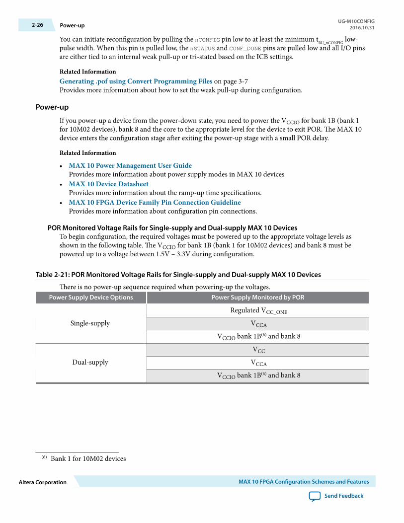
You can initiate reconfiguration by pulling the nCONFIG pin low to at least the minimum tRU_nCONFIG low-pulse width. When this pin is pulled low, the nSTATUS and CONF_DONE pins are pulled low and all I/O pinsare either tied to an internal weak pull-up or tri-stated based on the ICB settings.
Related InformationGenerating .pof using Convert Programming Files on page 3-7Provides more information about how to set the weak pull-up during configuration.
Power-up
If you power-up a device from the power-down state, you need to power the VCCIO for bank 1B (bank 1for 10M02 devices), bank 8 and the core to the appropriate level for the device to exit POR. The MAX 10device enters the configuration stage after exiting the power-up stage with a small POR delay.
Related Information
• MAX 10 Power Management User GuideProvides more information about power supply modes in MAX 10 devices
• MAX 10 Device DatasheetProvides more information about the ramp-up time specifications.
• MAX 10 FPGA Device Family Pin Connection GuidelineProvides more information about configuration pin connections.
POR Monitored Voltage Rails for Single-supply and Dual-supply MAX 10 DevicesTo begin configuration, the required voltages must be powered up to the appropriate voltage levels asshown in the following table. The VCCIO for bank 1B (bank 1 for 10M02 devices) and bank 8 must bepowered up to a voltage between 1.5V – 3.3V during configuration.
Table 2-21: POR Monitored Voltage Rails for Single-supply and Dual-supply MAX 10 Devices
There is no power-up sequence required when powering-up the voltages.Power Supply Device Options Power Supply Monitored by POR
Single-supply
Regulated VCC_ONE
VCCA
VCCIO bank 1B(6) and bank 8
Dual-supply
VCC
VCCA
VCCIO bank 1B(6) and bank 8
(6) Bank 1 for 10M02 devices
2-26 Power-upUG-M10CONFIG
2016.10.31
Altera Corporation MAX 10 FPGA Configuration Schemes and Features
Send Feedback
Monitored Power Supplies Ramp Time Requirement for MAX 10 Devices
Figure 2-11: Monitored Power Supplies Ramp Time Requirement Diagram for MAX 10 Devices
Time
POR trip level
Volts
POR Delay Configuration time
DeviceInitialization
User Mode
tRAMP
first power supply
last powersupply
nSTATUSgoes high
CONF_DONEgoes high
Table 2-22: Monitored Power Supplies Ramp Time Requirement for MAX 10 Devices
Symbol Parameter Minimum Maximum Unit
tRAMP Power Supply Ramp Time(7) —(8) 10 ms
Configuration
During configuration, configuration data is read from the internal flash and written to the CRAM.
Configuration Error Handling
To restart configuration automatically, turn on the Auto-restart configuration after error option in theGeneral page of the Device and Pin Options dialog box in the Quartus Prime software.
If you do not turn on this option, you can monitor the nSTATUS pin to detect errors. To restart configura‐tion, pull the nCONFIG pin low for at least the duration of tRU_nCONFIG.
(7) Ensure that all VCCIO power supply reaches full rail before configuration completes. See InternalConfiguration Time on page 2-9.
(8) There is no absolute minimum value for the ramp rate requirement. Altera characterized the minimumtRAMP of 200µs.
UG-M10CONFIG2016.10.31 Monitored Power Supplies Ramp Time Requirement for MAX 10 Devices 2-27
MAX 10 FPGA Configuration Schemes and Features Altera Corporation
Send Feedback
Initialization
The initialization sequence begins after the CONF_DONE pin goes high. The initialization clock source isfrom the internal oscillator and the MAX 10 device will receive enough clock cycles for proper initializa‐tion.
User Mode
After the initialization completes, your design starts executing. The user I/O pins will then function asspecified by your design.
MAX 10 Configuration PinsAll configuration pins and JTAG pins in MAX 10 devices are dual-purpose pins. The configuration pinsfunction as configuration pins prior to user mode. When the device is in user mode, they function as userI/O pins or remain as configuration pins.
Table 2-23: Configuration Pin Summary for MAX 10 Devices
All pins are powered by VCCIO Bank 1B (bank 1 for 10M02 devices) and 8.Configuration Pin Input/Output Configuration Scheme
CRC_ERROR Output only, open-drain Optional, JTAG and internal configurations
CONFIG_SEL Input only Internal configuration
DEV_CLRn Input only Optional, JTAG and internal configurations
DEV_OE Input only Optional, JTAG and internal configurations
CONF_DONE Bidirectional, open-drain JTAG and internal configurations
nCONFIG Input only JTAG and internal configurations
nSTATUS Bidirectional, open-drain JTAG and internal configurations
JTAGEN Input only Optional, JTAG configuration
TCK Input only JTAG configuration
TDO Output only JTAG configuration
TMS Input only JTAG configuration
TDI Input only JTAG configuration
Related Information
• Guidelines: Dual-Purpose Configuration Pin on page 3-1• Enabling Dual-purpose Pin on page 3-2
2-28 InitializationUG-M10CONFIG
2016.10.31
Altera Corporation MAX 10 FPGA Configuration Schemes and Features
Send Feedback
MAX 10 FPGA Configuration Design Guidelines 32016.10.31
UG-M10CONFIG Subscribe Send Feedback
Dual-Purpose Configuration Pins
Guidelines: Dual-Purpose Configuration PinTo use configuration pins as user I/O pins in user mode, you have to adhere to the following guidelines.
Table 3-1: Dual-Purpose Configuration Pin Guidelines for MAX 10 Devices
Guidelines Pins
Configuration pins during initialization:
• Tri-state the external I/O driver and drive an external pull-up resistor(9) or• Use the external I/O driver to drive the pins to the state same as the external
weak pull-up resistor
• nCONFIG
• nSTATUS
• CONF_DONE
JTAG pins:
• If you intend to switch back and forth between user I/O pins and JTAG pinfunctions using the JTAGEN pin, all JTAG pins must be assigned as single-endedI/O pins or voltage-referenced I/O pins. Schmitt trigger input is therecommended input buffer.
• JTAG pins cannot perform as JTAG pins in user mode if you assign any of theJTAG pin as a differential I/O pin.
• You must use the JTAG pins as dedicated pins and not as user I/O pins duringJTAG programming.
• Do not toggle JTAG pin during the initialization stage.• Put the test access port (TAP) controller in reset state by driving the TDI and
TMS pins high and TCK pin low for at least 5 clock cycles before the initialization.
• TDO
• TMS
• TCK
• TDI
Attention: Assign all JTAG pins as single-ended I/O pins or voltage-referenced I/O pins if you enableJTAG pin sharing feature.
(9) If you intend to remove the external weak pull-up resistor, Altera recommends that you remove it after thedevice enters user mode.
© 2016 Intel Corporation. All rights reserved. Intel, the Intel logo, Altera, Arria, Cyclone, Enpirion, MAX, Megacore, NIOS, Quartus and Stratix words and logosare trademarks of Intel Corporation in the US and/or other countries. Other marks and brands may be claimed as the property of others. Intel warrantsperformance of its FPGA and semiconductor products to current specifications in accordance with Intel's standard warranty, but reserves the right to makechanges to any products and services at any time without notice. Intel assumes no responsibility or liability arising out of the application or use of anyinformation, product, or service described herein except as expressly agreed to in writing by Intel. Intel customers are advised to obtain the latest version ofdevice specifications before relying on any published information and before placing orders for products or services.
ISO9001:2008Registered
www.altera.com101 Innovation Drive, San Jose, CA 95134
Related Information
• MAX 10 FPGA Device Family Pin Connection GuidelinesProvides more information about recommended resistor values.
• MAX 10 Configuration Pins on page 2-28• JTAG Pins on page 2-2
JTAG Pin Sharing Behavior
Table 3-2: JTAG Pin Sharing Behavior for MAX 10 Devices
Configuration Stage JTAG Pin Sharing JTAGEN Pin JTAG Pins (TDO, TDI, TCK, TMS)
User mode
Disabled User I/O pin Dedicated JTAG pins.
EnabledDriven low User I/O pins.
Driven high Dedicated JTAG pins.
Configuration Don’t Care Not used Dedicated JTAG pins.
Note: You have to set the pins according to Table 3-1 and with correct pin direction (input, output orbidirectional) for the JTAG pins work correctly.
Enabling Dual-purpose PinTo use the configuration and JTAG pins as user I/O in user mode, you must do the following in theQuartus Prime software:
1. On the Assignments menu, click Device.2. Click Device and Pin Options.3. Select the General tab of Device and Pin Options.4. In the General Options list, do the following:
• Check the Enable JTAG pin sharing.• Uncheck the Enable nCONFIG, nSTATUS, and CONF_DONE pins.
Related Information
• MAX 10 Configuration Pins on page 2-28• JTAG Pins on page 2-2
Configuring MAX 10 Devices using JTAG ConfigurationThe Quartus Prime software generates a .sof that can used for JTAG configuration. You can directlyconfigure the MAX 10 device by using a download cable with the Quartus Prime software programmer.
Alternatively, you can use the JAM Standard Test and Programming Language (STAPL) Format File (.jam)or JAM Byte Code File (.jbc) with other third-party programmer tools.
Related InformationAN 425: Using the Command-Line Jam STAPL Solution for Device Programming
3-2 JTAG Pin Sharing BehaviorUG-M10CONFIG
2016.10.31
Altera Corporation MAX 10 FPGA Configuration Design Guidelines
Send Feedback
JTAG Configuration SetupFigure 3-1: Connection Setup for JTAG Single-Device Configuration using Download Cable
Connect to VCCIO Bank 1 for 10M02 devices or VCCIO Bank 1B for all other MAX 10 devices.
nSTATUSCONF_DONEnCONFIG
JTAGEN
TCKTDOTMS
TDI
10 kΩ 10 kΩ 10 kΩ
VCCIO Bank 8
MAX 10
2468
10
3579
1
1 kΩ
VCCIO Bank 1 or 1B
Download Cable(JTAG Mode)
10-Pin Male Header
To use JTAGEN pin, you must enable the JTAG pin sharing.In user mode, to use JTAG pins as:- Regular I/O pins: Tie the JTAGEN pin to a weak 1-kΩ pull-down.- Dedicated JTAG pins: Tie the JTAGEN pin to VCCIO Bank 1B or 1B through a 10-kΩ pull-up.
10 kΩ 10 kΩ
VCCIO Bank 1 or 1B
The diodes and capacitors must be placed as close as possible to the MAX 10 device. For effective voltage clamping, Altera recommends using the chottky diode, which has a relatively lower forward diode voltage than the switching and Zener diodes. See Preventing Voltage Overshoot.
10pF 10pF 10pF10pF
UG-M10CONFIG2016.10.31 JTAG Configuration Setup 3-3
MAX 10 FPGA Configuration Design Guidelines Altera Corporation
Send Feedback
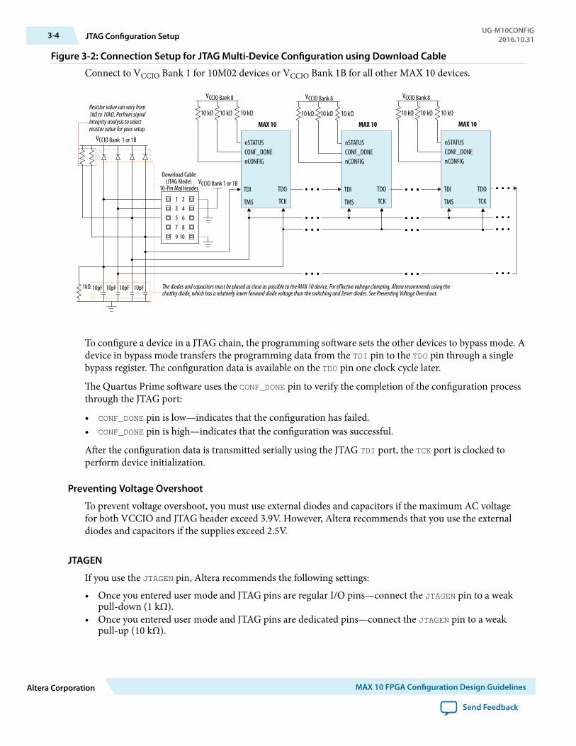
Figure 3-2: Connection Setup for JTAG Multi-Device Configuration using Download Cable
Connect to VCCIO Bank 1 for 10M02 devices or VCCIO Bank 1B for all other MAX 10 devices.
nSTATUSCONF_DONEnCONFIG
TCK
TDO
TMS
TDI
10 kΩ 10 kΩ 10 kΩ
VCCIO Bank 8
MAX 10
nSTATUSCONF_DONEnCONFIG
TMS
TDI
MAX 10
nSTATUSCONF_DONEnCONFIG
TMS
TDI
MAX 10
TCK
TDO
TCK
TDO2468
10
3579
1
Download Cable(JTAG Mode)
10-Pin Mal Header
1kΩ
Resistor value can vary from1kΩ to 10kΩ. Perfrom signalintegrity analysis to selectresistor value for your setup.
VCCIO Bank 1 or 1B
10 kΩ 10 kΩ 10 kΩ
VCCIO Bank 8
10 kΩ 10 kΩ 10 kΩ
VCCIO Bank 8
VCCIO Bank 1 or 1B
The diodes and capacitors must be placed as close as possible to the MAX 10 device. For effective voltage clamping, Altera recommends using the chottky diode, which has a relatively lower forward diode voltage than the switching and Zener diodes. See Preventing Voltage Overshoot.
10pF 10pF 10pF10pF
To configure a device in a JTAG chain, the programming software sets the other devices to bypass mode. Adevice in bypass mode transfers the programming data from the TDI pin to the TDO pin through a singlebypass register. The configuration data is available on the TDO pin one clock cycle later.
The Quartus Prime software uses the CONF_DONE pin to verify the completion of the configuration processthrough the JTAG port:
• CONF_DONE pin is low—indicates that the configuration has failed.• CONF_DONE pin is high—indicates that the configuration was successful.
After the configuration data is transmitted serially using the JTAG TDI port, the TCK port is clocked toperform device initialization.
Preventing Voltage Overshoot
To prevent voltage overshoot, you must use external diodes and capacitors if the maximum AC voltage for both VCCIO and JTAG header exceed 3.9V. However, Altera recommends that you use the external diodes and capacitors if the supplies exceed 2.5V.
JTAGEN
If you use the JTAGEN pin, Altera recommends the following settings:
• Once you entered user mode and JTAG pins are regular I/O pins—connect the JTAGEN pin to a weakpull-down (1 kΩ).
• Once you entered user mode and JTAG pins are dedicated pins—connect the JTAGEN pin to a weakpull-up (10 kΩ).
3-4 JTAG Configuration SetupUG-M10CONFIG
2016.10.31
Altera Corporation MAX 10 FPGA Configuration Design Guidelines
Send Feedback
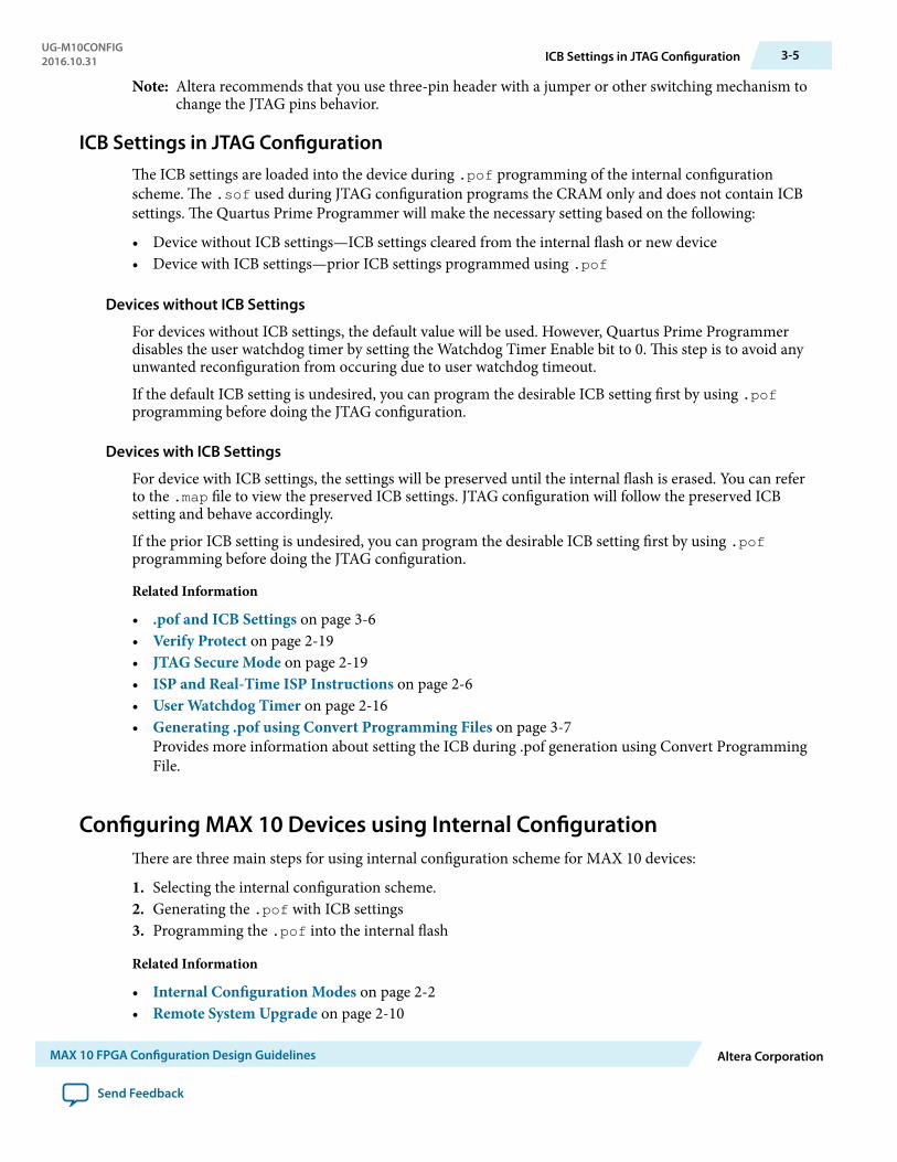
Note: Altera recommends that you use three-pin header with a jumper or other switching mechanism tochange the JTAG pins behavior.
ICB Settings in JTAG ConfigurationThe ICB settings are loaded into the device during .pof programming of the internal configurationscheme. The .sof used during JTAG configuration programs the CRAM only and does not contain ICBsettings. The Quartus Prime Programmer will make the necessary setting based on the following:
• Device without ICB settings—ICB settings cleared from the internal flash or new device• Device with ICB settings—prior ICB settings programmed using .pof
Devices without ICB Settings
For devices without ICB settings, the default value will be used. However, Quartus Prime Programmerdisables the user watchdog timer by setting the Watchdog Timer Enable bit to 0. This step is to avoid anyunwanted reconfiguration from occuring due to user watchdog timeout.
If the default ICB setting is undesired, you can program the desirable ICB setting first by using .pofprogramming before doing the JTAG configuration.
Devices with ICB Settings
For device with ICB settings, the settings will be preserved until the internal flash is erased. You can referto the .map file to view the preserved ICB settings. JTAG configuration will follow the preserved ICBsetting and behave accordingly.
If the prior ICB setting is undesired, you can program the desirable ICB setting first by using .pofprogramming before doing the JTAG configuration.
Related Information
• .pof and ICB Settings on page 3-6• Verify Protect on page 2-19• JTAG Secure Mode on page 2-19• ISP and Real-Time ISP Instructions on page 2-6• User Watchdog Timer on page 2-16• Generating .pof using Convert Programming Files on page 3-7
Provides more information about setting the ICB during .pof generation using Convert ProgrammingFile.
Configuring MAX 10 Devices using Internal ConfigurationThere are three main steps for using internal configuration scheme for MAX 10 devices:
1. Selecting the internal configuration scheme.2. Generating the .pof with ICB settings3. Programming the .pof into the internal flash
Related Information
• Internal Configuration Modes on page 2-2• Remote System Upgrade on page 2-10
UG-M10CONFIG2016.10.31 ICB Settings in JTAG Configuration 3-5
MAX 10 FPGA Configuration Design Guidelines Altera Corporation
Send Feedback
Selecting Internal Configuration ModesTo select the configuration mode, follow these steps:
1. Open the Quartus Prime software and load a project using a MAX 10 device.2. On the Assignments menu, click Settings. The Settings dialog box appears.3. In the Category list, select Device. The Device page appears.4. Click Device and Pin Options.5. In the Device and Pin Options dialog box, click the Configuration tab.6. In the Configuration Scheme list, select Internal Configuration.7. In the Configuration Mode list, select 1 out of 5 configuration modes available. The 10M02 devices has
only 2 modes available.8. Turn on Generate compressed bitstreams if needed.9. Click OK.
.pof and ICB SettingsThere are two methods which the .pof will be generated and setting-up the ICB. The internalconfiguration mode you selected will determine the corresponding method.
Table 3-3: .pof Generation and ICB Setting Method for Internal Configuration Modes
Internal Configuration Mode ICB Setting Description .pof GenerationMethod to Use
Single Compressed Image ICB can be set inDevice and PinOptions
Quartus Prime softwareautomatically generatesthe .pof during projectcompilation.
Auto-generated .pof(10)Single Uncompressed Image
Single Compressed Image withMemory Initialization. ICB can be set
during ConvertProgrammingFiles task.
You need to generatethe .pof using ConvertProgramming Files.
Generating .pofusing ConvertProgrammingFiles
Single Uncompressed Image withMemory Initialization
Dual Compressed Images
Auto-Generated .pof
To set the ICB for the auto-generated .pof, follow these steps:
1. On the Assignments menu, click Settings. The Settings dialog box appears.2. In the Category list, select Device. The Device page appears.3. Click Device and Pin Options.4. In the Device and Pin Options dialog box, select the Configuration from the category pane.5. Click the Device Options … button.6. The Max 10 Device Options dialog box allows you to set the following:
(10) Auto-generated .pof does not allow encryption. To enable the encryption feature in Single Compressedand Single Uncompressed mode, use the Convert Programming Files method.
3-6 Selecting Internal Configuration ModesUG-M10CONFIG
2016.10.31
Altera Corporation MAX 10 FPGA Configuration Design Guidelines
Send Feedback
a. User I/Os weak pull up during configuration.b. Verify Protect.
7. Click OK once setting is completed.
Generating .pof using Convert Programming Files
To convert .sof files to .pof files and to set the ICB, follow these steps:
1. On the File menu, click Convert Programming Files.2. Under Output programming file, select Programmer Object File (.pof) in the Programming file
type list.3. In the Mode list, select Internal Configuration.4. To set the ICB settings, click Option/Boot Info and the ICB setting dialog box will appear. The ICB
setting dialog box allows you to set the following:a. User I/Os weak pull up during configuration.b. Auto-recofigure from secondary image when initial image fails (enabled by default).
Note: When you disable this feature, the device will always load the configuration image 0 withoutsampling the physical CONFIG_SEL pin. After successfully load the configuration image 0,you can switch between configuration image using the config_sel_overwrite bit of theinput register. Refer to related information for details about Altera Dual Configuration IPcore input register.
c. Use secondary image ISP data as default setting when available.d. JTAG Secure.
Note: The JTAG Secure feature will be disabled by default in Quartus Prime. If you are interested inusing the JTAG Secure feature, contact Altera for support.
Caution: MAX 10 FPGA device would become permanently locked if you enabled JTAG securemode in the POF file and POF is encrypted with the wrong key. You must instantiate theinternal JTAG interface for you unlock the external JTAG when the device is in JTAGSecure mode.
e. Verify Protect.f. Allow encrypted POF only.g. Watchdog timer for dual configuration and watchdog timer value (Enabled after adding 2 .sof
page with two designs that compiled with Dual Compressed Internal Images).h. User Flash Memory settings.i. RPD File Endianness
5. In the File name box, specify the file name for the programming file you want to create.6. To generate a Memory Map File (.map), turn on Create Memory Map File (Auto generate
output_file.map). The .map contains the address of the CFM and UFM with the ICB setting that youset through the Option/Boot Info option.
7. To generate a Raw Programming Data (.rpd), turn on Create config data RPD (Generateoutput_file_auto.rpd).Separate Raw Programming Data (.rpd) for each configuration flash memory and user flash memory(CFM0, CFM1, UFM) section will be generated together for remote system upgrade purpose.
8. The .sof can be added through Input files to convert list and you can add up to two .sof files.
UG-M10CONFIG2016.10.31 Generating .pof using Convert Programming Files 3-7
MAX 10 FPGA Configuration Design Guidelines Altera Corporation
Send Feedback
For remote system upgrade purpose, you can retain the original page 0 data in the .pof, and replacespage 1 data with new .sof file. To perform this, you must to add the .pof file in page 0, thenadd .sof page, then add the new .sof file to page 1.
9. After all settings are set, click Generate to generate related programming file.
Related InformationEncryption in Internal Configuration on page 3-19Provides more information about internal configuration image loaded based on various settings.
Programming .pof into Internal FlashYou can use the Quartus Prime Programmer to program the .pof into the CFM through JTAG interface.The Quartus Prime Programmer also allows you to program the UFM part of the internal flash.
To program the .pof into the flash, follow these steps:
1. In the Programmer window, click Hardware Setup and select USB Blaster.2. In the Mode list, select JTAG.3. Click Auto Detect button on the left pane.4. Select the device to be programmed, and click Add File.5. Select the .pof to be programmed to the selected device.6. There are several options in programming the internal flash:
• To program any of the CFM0/CFM1/CFM2 only, select the corresponding CFM in the Program/Configure column.
• To program the UFM only, select the UFM in the Program/Configure column.• To program the CFM and UFM only, select the CFM and UFM in the Program/Configure column.
Note: ICB setting is preserved in this option. However, before the programming starts, QuartusPrime Programmer will make sure the ICB setting in the device and the ICB setting in theselected .pof are the same. If the ICB settings are different, Quartus Prime Programmer willoverwrite the ICB setting.
• To program the whole internal flash including the ICB settings, select the <yourpoffile.pof> inthe Program/Configure column.
7. To enable the real-time ISP mode, turn-on the Enable real-time ISP to allow background program‐ming.
8. After all settings are set, click Start to start programming.
Implementing ISP Clamp in Quartus Prime SoftwareTo implement ISP clamp, you have to:
1. Create a pin state information (.ips) file. The .ips file defines the state for all the pins of the devicewhen the device is in ISP clamp operation. You can use an existing .ips file.
2. Execute the .ips file.
Note: You can use the .ips file created to program the device with any designs, as long as it targets thesame device and package. You must use the .ips file together with a POF file.
Related InformationISP Clamp on page 2-5
3-8 Programming .pof into Internal FlashUG-M10CONFIG
2016.10.31
Altera Corporation MAX 10 FPGA Configuration Design Guidelines
Send Feedback
Creating IPS FileTo create an .ips file, perform the following steps:
1. Click Programmer on the toolbar, or on the Tools menu, click Programmer to open the Programmer.2. Click Add File in the programmer to add the programming file (POF, Jam, or JBC).3. Click on the programming file (the entire row will be highlighted) and on the Edit menu, click ISP
CLAMP State Editor.4. Specify the states of the pins in your design in the ISP Clamp State Editor. By default, all pins are set
to tri-state.5. Click Save to save IPS file after making the modifications.
Executing IPS FileTo execute ISP Clamp, perform the following steps:
1. In the Quartus Prime Programmer, select the .pof you want to program to the device.2. Select the .pof, right click and select Add IPS File and turn-on ISP CLAMP.
Note: You can change the start-up delay of the I/O Clamp after configuration. To do this, selectTools > Options, turn-on the Overwrite MAX10 configuration start up delay when using IOClamp in Programmer option, and change the delay value accordingly.
3. Select the .pof in the Program/Configure column.
Note: For third party programming, you can generate the .jam or .jbc file from the .pof filewith .ips file.
4. After all settings are set, click Start to start programming.
Accessing Remote System Upgrade through User LogicThe following example shows how the input and output ports of a WYSIWYG atom are defined in theMAX 10 device.
fiftyfivenm_rublock <rublock_name>( .clk(<clock source>), .shiftnld(<shiftnld source>), .captnupdt(<captnupdt source>), .regin(<regin input source from the core>), .rsttimer(<input signal to reset the watchdog timer>), .rconfig(<input signal to initiate configuration>), .regout(<data output destination to core>));defparam <rublock_name>.sim_init_config = <initial configuration for simulation only>;defparam <rublock_name>.sim_init_watchdog_value = <initial watchdog value for simulation only>;defparam <rublock_name>.sim_init_config = <initial status register value for simulation only>;
UG-M10CONFIG2016.10.31 Creating IPS File 3-9
MAX 10 FPGA Configuration Design Guidelines Altera Corporation
Send Feedback
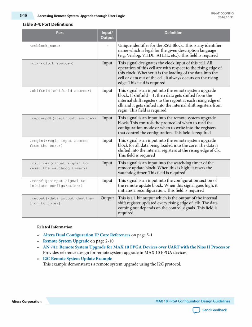
Table 3-4: Port Definitions
Port Input/Output
Definition
<rublock_name> - Unique identifier for the RSU Block. This is any identifiername which is legal for the given description language(e.g. Verilog, VHDL, AHDL, etc.). This field is required
.clk(<clock source>) Input This signal designates the clock input of this cell. Alloperation of this cell are with respect to the rising edge ofthis clock. Whether it is the loading of the data into thecell or data out of the cell, it always occurs on the risingedge. This field is required
.shiftnld(<shiftnld source>) Input This signal is an input into the remote system upgradeblock. If shiftnld = 1, then data gets shifted from theinternal shift registers to the regout at each rising edge ofclk and it gets shifted into the internal shift registers fromregin. This field is required
.captnupdt(<captnupdt source>) Input This signal is an input into the remote system upgradeblock. This controls the protocol of when to read theconfiguration mode or when to write into the registersthat control the configuration. This field is required
.regin(<regin input source
from the core>)
Input This signal is an input into the remote system upgradeblock for all data being loaded into the core. The data isshifted into the internal registers at the rising edge of clk.This field is required
.rsttimer(<input signal to
reset the watchdog timer>)
Input This signal is an input into the watchdog timer of theremote update block. When this is high, it resets thewatchdog timer. This field is required
.rconfig(<input signal to
initiate configuration>)
Input This signal is an input into the configuration section ofthe remote update block. When this signal goes high, itinitiates a reconfiguration. This field is required
.regout(<data output destina-
tion to core>)
Output This is a 1 bit output which is the output of the internalshift register updated every rising edge of .clk. The datacoming out depends on the control signals. This field isrequired.
Related Information
• Altera Dual Configuration IP Core References on page 5-1• Remote System Upgrade on page 2-10• AN 741: Remote System Upgrade for MAX 10 FPGA Devices over UART with the Nios II Processor
Provides reference design for remote system upgrade in MAX 10 FPGA devices.• I2C Remote System Update Example
This example demonstrates a remote system upgrade using the I2C protocol.
3-10 Accessing Remote System Upgrade through User LogicUG-M10CONFIG
2016.10.31
Altera Corporation MAX 10 FPGA Configuration Design Guidelines
Send Feedback
Error Detection
Verifying Error Detection FunctionalityYou can inject a soft error by changing the 32-bit CRC storage register in the CRC circuitry. After verifyingthe failure induced, you can restore the 32-bit CRC value to the correct CRC value using the sameinstruction and inserting the correct value. Be sure to read out the correct value before updating it with aknown bad value.
In user mode, MAX 10 devices support the CHANGE_EDREG JTAG instruction, which allows you to write tothe 32-bit storage register. You can use .jam to automate the testing and verification process. You can onlyexecute this instruction when the device is in user mode. This instruction enables you to dynamicallyverify the CRC functionality in-system without having to reconfigure the device. You can then switch touse the CRC circuit to check for real errors induced by an SEU.
After the test completes, to clear the CRC error and restore the original CRC value, power cycle the deviceor follow these steps:
1. After the configuration completes, use CHANGE_EDREG JTAG instruction to shift out the correctprecomputed CRC value and load the wrong CRC value to the CRC storage register. When an error isdetected, the CRC_ERROR pin will be asserted.
2. Use CHANGE_EDREG JTAG instruction to shift in the correct precomputed CRC value. The CRC_ERRORpin is de-asserted to show that the error detection CRC circuitry is working.
Example 3-1: JAM File
'EDCRC_ERROR_INJECT
ACTION ERROR_INJECT = EXECUTE;DATA DEVICE_DATA;BOOLEAN out[32];BOOLEAN in[32] = $02040608; 'shift in any wrong CRC valueENDDATA;PROCEDURE EXECUTE USES DEVICE_DATA;BOOLEAN X = 0;DRSTOP IDLE;IRSTOP IDLE;STATE IDLE;IRSCAN 10, $015; 'shift in CHANGE_EDREG instructionWAIT IDLE, 10 CYCLES, 1 USEC, IDLE;DRSCAN 32, in[31..0], CAPTURE out[31..0];WAIT IDLE, 10 CYCLES, 50 USEC, IDLE;PRINT " ";PRINT "Data read out from the Storage Register: "out[31], out[30], out[29], out[28], out[27],out[26], out[25], out[24], out[23], out[22], out[21], out[20], out[19], out[18], out[17], out[16], out[15], out[14], out[13], out[12], out[11], out[10], out[9], out[8], out[7], out[6], out[5], out[4], out[3], out[2], out[1], out[0]; 'Read out correct precomputed CRC valuePRINT " ";STATE IDLE;EXIT 0;ENDPROC;
You can run the .jam file using quartus_jli executable with the following command line:
quartus_jli -c<cable index> -a<action name> <filename>.jam
UG-M10CONFIG2016.10.31 Error Detection 3-11
MAX 10 FPGA Configuration Design Guidelines Altera Corporation
Send Feedback
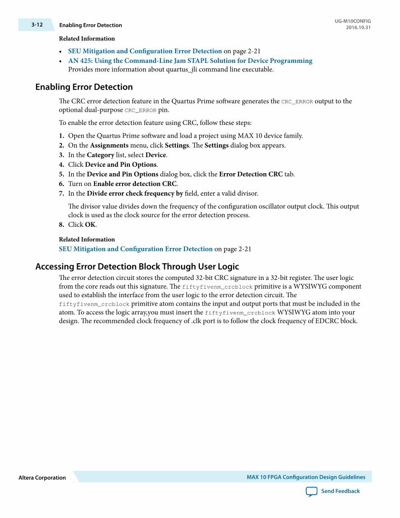
Related Information
• SEU Mitigation and Configuration Error Detection on page 2-21• AN 425: Using the Command-Line Jam STAPL Solution for Device Programming
Provides more information about quartus_jli command line executable.
Enabling Error DetectionThe CRC error detection feature in the Quartus Prime software generates the CRC_ERROR output to theoptional dual-purpose CRC_ERROR pin.
To enable the error detection feature using CRC, follow these steps:
1. Open the Quartus Prime software and load a project using MAX 10 device family.2. On the Assignments menu, click Settings. The Settings dialog box appears.3. In the Category list, select Device.4. Click Device and Pin Options.5. In the Device and Pin Options dialog box, click the Error Detection CRC tab.6. Turn on Enable error detection CRC.7. In the Divide error check frequency by field, enter a valid divisor.
The divisor value divides down the frequency of the configuration oscillator output clock. This outputclock is used as the clock source for the error detection process.
8. Click OK.
Related InformationSEU Mitigation and Configuration Error Detection on page 2-21
Accessing Error Detection Block Through User LogicThe error detection circuit stores the computed 32-bit CRC signature in a 32-bit register. The user logicfrom the core reads out this signature. The fiftyfivenm_crcblock primitive is a WYSIWYG componentused to establish the interface from the user logic to the error detection circuit. Thefiftyfivenm_crcblock primitive atom contains the input and output ports that must be included in theatom. To access the logic array,you must insert the fiftyfivenm_crcblock WYSIWYG atom into yourdesign. The recommended clock frequency of .clk port is to follow the clock frequency of EDCRC block.
3-12 Enabling Error DetectionUG-M10CONFIG
2016.10.31
Altera Corporation MAX 10 FPGA Configuration Design Guidelines
Send Feedback
Figure 3-3: Error Detection Block Diagram with Interfaces for MAX 10 Devices
Clock Divider(1 to 256 Factor)
Pre-Computed CRC(Saved in the Option Register)
CRCComputation
Error DetectionLogic
SRAMBits
CRC_ERROR(Shown in BIDIR Mode)
VCC
Logic ArrayCL
K
SHIFT
NLD
LDSR
C REGO
UT
CRC_
ERRO
R
Internal Chip Oscillator
The following example shows how the input and output ports of a WYSIWYG atom are defined in theMAX 10 device.
fiftyfivenm_crcblock <name>( .clk(<ED_CLK clock source>), .shiftnld(<ED_SHIFTNLD source>), .ldsrc (<LDSRC source>), .crcerror(<CRCERROR_CORE out destination>), .regout(<output destination>));defparam <crcblock_name>.oscillator_divider = <internal oscillator division (1 to 256)>;
Table 3-5: Port Definitions
Port Input/Output
Definition
<crcblock_name> — Unique identifier for the CRC block and represents any identifier namethat is legal for the given description language such as Verilog HDL,VHDL, AHDL. This field is required.
.clk(<clock source> Input This signal designates the clock input of this cell. All operations of thiscell are with respect to the rising edge of the clock. Whether it is theloading of the data into the cell or data out of the cell, it always occurson the rising edge. This port is required.
UG-M10CONFIG2016.10.31 Accessing Error Detection Block Through User Logic 3-13
MAX 10 FPGA Configuration Design Guidelines Altera Corporation
Send Feedback
Port Input/Output
Definition
.shiftnld
(<shiftnld source>)
Input This signal is an input into the error detection block. If shiftnld=1, thedata is shifted from the internal shift register to the regout at each risingedge of clk. If shiftnld=0, the shift register parallel loads either thepre-calculated CRC value or the update register contents depending onthe ldsrc port input. This port is required.
.ldsrc (<ldsrc
source>)
Input This signal is an input into the error detection block. If ldsrc=0, thepre-computed CRC register is selected for loading into the 32-bit shiftregister at the rising edge of clk when shiftnld=0. Ifldsrc=1, thesignature register (result of the CRC calculation) is selected for loadinginto the shift register at the rising edge of clk when shiftnld=0. Thisport is ignored when shiftnld=1. This port is required.
.crcerror
(<crcerror out
destination>)
Output This signal is the output of the cell that is synchronized to the internaloscillator of the device (100-MHz or 80-MHz internal oscillator) andnot to the clk port. It asserts automatically high if the error blockdetects that a SRAM bit has flipped and the internal CRC computationhas shown a difference with respect to the pre-computed value. Thissignal must be connected either to an output pin or a bidirectional pin.If it is connected to an output pin, you can only monitor the CRC_ERRORpin (the core cannot access this output). If the CRC_ERROR signal is usedby core logic to read error detection logic, this signal must beconnected to a BIDIR pin. The signal is fed to the core indirectly byfeeding a BIDIR pin that has its oe port connected to VCC.
.regout (<output
destination>)
Output This signal is the output of the error detection shift register synchron‐ized to the clk port, to be read by core logic. It shifts one bit at eachcycle. User should clock the clk signal 31 cycles to read out the 32 bitsof the shift register. The values at the .regout port are an inversion ofthe actual values.
Related Information
• SEU Mitigation and Configuration Error Detection on page 2-21• Error Detection Timing on page 2-23
Enabling Data CompressionWhen you enable compression, the Quartus Prime software generates configuration files with compressedconfiguration data.
A compressed configuration file is needed to use the dual configuration mode in the internal configurationscheme. This compressed file reduces the storage requirements in internal flash memory, and decreases thetime needed to send the bitstream to the MAX 10 device family. There are two methods to enablecompression for the MAX 10 device family bitstreams in the Quartus Prime software:
• Before design compilation—using the Compiler Settings menu.• After design compilation—using the Convert Programming Files option.
3-14 Enabling Data CompressionUG-M10CONFIG
2016.10.31
Altera Corporation MAX 10 FPGA Configuration Design Guidelines
Send Feedback
Enabling Compression Before Design CompilationTo enable compression before design compilation, follow these steps:
1. On the Assignments menu, click Device. The Settings dialog box appears.2. Click Device and Pin Options. The Device and Pin Options dialog box appears.3. Click the Configuration tab.4. Turn on Generate compressed bitstreams.5. Click OK.6. In the Settings dialog box, click OK.
Related InformationConfiguration Data Compression on page 2-24
Enabling Compression After Design CompilationTo enable compression after design compilation, follow these steps:
1. On the File menu, click Convert Programming Files.2. Under Output programming file, from the pull-down menu, select your desired file type.3. If you select the Programmer Object File (.pof), you must specify a configuration device, directly under
the file type.4. In the Input files to convert box, select SOF Data.5. Click Add File to browse to the MAX 10 device family .sof.6. In the Convert Programming Files dialog box, select the .pof you added to SOF Data and click
Properties.7. In the SOF Properties dialog box, turn on the Compression option.
Related InformationConfiguration Data Compression on page 2-24
AES EncryptionThis section covers detailed guidelines on applying AES Encryption for design security. There are twomain steps in applying design security in MAX 10 devices. First is to generate the encryption keyprogramming (.ekp) file and second is to program the .ekp file into the device.
The .ekp file has other different formats, depending on the hardware and system used for programming.There are three file formats supported by the Quartus Prime software:
• JAM Byte Code (.jbc) file• JAM™ Standard Test and Programming Language (STAPL) Format (.jam) file• Serial Vector Format (.svf) file
Only the .ekp file type generated automatically from the Quartus Prime software. You must createthe .jbc, .jam and .svf files using the Quartus Prime software if these files are required in the keyprogramming.
Note: Altera recommends that you keep the .ekp file confidential.
UG-M10CONFIG2016.10.31 Enabling Compression Before Design Compilation 3-15
MAX 10 FPGA Configuration Design Guidelines Altera Corporation
Send Feedback

Generating .ekp File and Encrypt Configuration FileTo generate the .ekp file and encrypt your configuration file, follow these steps:
1. On the File menu, click Convert Programming Files.2. Under Output programming file, select Programmer Object File (.pof) in the Programming file
type list.3. In the Mode list, select Internal Configuration.4. Click Option/Boot Info and the ICB setting dialog box will appear.5. You can enable the enable the Allow encrypted POF only option. Click OK once ICB setting is set.
The device will only accept encrypted bitstream during internal configuration if this option is enabled.If you encrypt one of CFM0, CFM1 or CFM2 only, the Programmer will post a warning.
6. Type the file name in the File name field, or browse to and select the file.7. Under the Input files to convert section, click SOF Data.8. Click Add File to open the Select Input File dialog box.9. Browse to the unencrypted .sof and click Open.10.Under the Input files to convert section, click on the added .sof.11.Click Properties and the SOF Files Properties: Bitstream Encryption dialog box will appear.12.Turn on Generate encrypted bitstream.13.Turn on Generate key programming file and type the .ekp file path and file name in the text area, or
browse to and select <filename>.ekp.14.You can the key with either a .key file or entering the key manually.
Note: MAX 10 devices require the entry of 128-bit keys.
3-16 Generating .ekp File and Encrypt Configuration FileUG-M10CONFIG
2016.10.31
Altera Corporation MAX 10 FPGA Configuration Design Guidelines
Send Feedback

• Adding key with a .key file.
The .key file is a plain text file in which each line represents a key unless the line starts with "#".The "#" symbol is used to denote comments. Each valid key line has the following format:
<key identity><white space><128-bit hexadecimal key># This is an example key filekey1 0123456789ABCDEF0123456789ABCDEF
1. Enable the Use key file checkbox.2. Click Open and add the desired .key file and click Open again.3. Under Key entry part, the key contained in the .key file will be selected in the drop-down list.4. Click OK.
• Entering your key manually.
1. Under Key entry part, click the Add button.2. Select the Key Entry Method to enter the encryption key either with the On-screen Keypad or
Keyboard.3. Enter a key name in the Key Name (alphanumeric) field.4. Key in the desired key in the Key (128-bit hexadecimal) field and repeat in the Confirm Key
field below it.5. Click OK.
15.Read the design security feature disclaimer. If you agree, turn on the acknowledgment box and clickOK.
16.In the Convert Programming Files dialog box, click OK. The <filename>.ekp and encryptedconfiguration file will be generated in the same project directory.
Note: For dual configuration .pof file, both .sof file need to be encrypted with the same key.Thegeneration of key file and encrypted configuration file will not be successful if different keys areused.
Generating .jam/.jbc/.svf file from .ekp fileTo generate .jam/.jbc/.svf file from .ekp file, follow these steps:
1. On the Tools menu, click Programmer and the Programmer dialog box will appear.2. In the Mode list, select JTAG as the programming mode.3. Click Hardware Setup. The Hardware Setup dialog box will appear.4. Select USBBlaster as the programming hardware in the currently selected hardware list and click
Done.5. Click Add File and the Select Programmer File dialog box will appear.6. Type <filename>.ekp in the File name field and click Open.7. Select the .ekp file you added and click Program/Configure.8. On the File menu, point to Create/Update and click Create JAM, SVF, or ISC File. The Create JAM,
SVF, or ISC File dialog box will appear.9. Select the file format required for the .ekp file in the File format field.
UG-M10CONFIG2016.10.31 Generating .jam/.jbc/.svf file from .ekp file 3-17
MAX 10 FPGA Configuration Design Guidelines Altera Corporation
Send Feedback

• JEDEC STAPL Format (.jam)• Jam STAPL Byte Code (.jbc)• Serial Vector Format (.svf)
10.Type the file name in the File name field, or browse to and select the file.11.Click OK to generate the .jam, .jbc or .svf file.
Programming .ekp File and Encrypted POF FileThere are two methods to program the encrypted .pof and .ekp files:
• Program the .ekp and .pof separately.
Note: You only can program the .ekp and .pof separately when Allow encrypted POF only optionis disabled.
• Integrate the .ekp into .pof and program both altogether.
Programming .ekp File and Encrypted .pof Separately
To program the .ekp and encrypted .pof separately using the Quartus Prime software, follow thesesteps:
1. In the Quartus Prime Programmer, under the Mode list, select JTAG as the programming mode.2. Click Hardware Setup and the Hardware Setup dialog box will appear.3. Select USBBlaster as the programming hardware in the Currently selected hardware list and click
Done.4. Click Add File and the Select Programmer File dialog box will appear.5. Type <filename>.ekp in the File name field and click Open.6. Select the .ekp file you added and click Program/Configure.7. Click Start to program the key.
Note: The Quartus Prime software message window provides information about the success or failureof the key programming operation. Once the .ekp is programmed, .pof can be programmedseparately. To retain the security key in the internal flash that had been programmed throughthe .ekp, continue with the following steps.
8. Select the .pof to be programmed to the selected device.9. Check only the functional block that need to be updated at child level for CFM and UFM. Do not
check operation at the parent level when using Programmer GUI.10.After all settings are set, click Start to start programming.
Integrate the .ekp into .pof Programming
To integrate the .ekp into .pof and program both altogether using the Quartus Prime software, followthese steps:
1. In the Quartus Prime Programmer, under the Mode list, select JTAG as the programming mode.2. Click Hardware Setup and the Hardware Setup dialog box will appear.3. Select USBBlaster as the programming hardware in the Currently selected hardware list and click
Done.4. Click the Auto Detect button on the left pane.5. Select the .pof you wish to program to the device.
3-18 Programming .ekp File and Encrypted POF FileUG-M10CONFIG
2016.10.31
Altera Corporation MAX 10 FPGA Configuration Design Guidelines
Send Feedback
6. Select the <yourpoffile.pof>, right click and select Add EKP File to integrate .ekp file withthe .pof file.Once the .ekp is integrated into the .pof, you can to save the integrated .pof into a new .pof. Thisnewly saved file will have original .pof integrated with .ekp information.
7. Select the <yourpoffile.pof> in the Program/Configure column.8. After all settings are set, click Start to start programming
Encryption in Internal ConfigurationDuring internal configuration, the FPGA decrypts the .pof with the stored key and uses the decrypteddata to configure itself. The configuration image loaded during configuration is also affected by theencryption settings and the Configure device from CFM0 only setting.
Table 3-6: Configuration Image Outcome Based on Encryption Settings, Encryption Key and CONFIG_SELPin Settings
Table shows the scenario when you disable the Configure device from CFM0 only. Key X and Key Y aresecurity keys included in your device and configuration image.
Configura‐tion Image
Mode
CFM0 (image 0)Encryption Key
CFM1 (image 1)Encryption Key
Key Stored inthe Device
AllowEncryptedPOF Only
CONFIG_SELpin
Design LoadedAfter Power-up
Single Not Encrypted Not Available No key Disabled 0 image 0Single Not Encrypted Not Available No key Disabled 1 image 0Single Not Encrypted Not Available Key X Disabled 0 image 0Single Not Encrypted Not Available Key X Disabled 1 image 0Single Not Encrypted Not Available Key X Enabled 0 Configuration FailSingle Not Encrypted Not Available Key X Enabled 1 Configuration FailSingle Key X Not Available No key Enabled 0 Configuration FailSingle Key X Not Available No key Enabled 1 Configuration FailSingle Key X Not Available Key X Enabled 0 image 0Single Key X Not Available Key X Enabled 1 image 0Single Key X Not Available Key Y Enabled 0 Configuration FailSingle Key X Not Available Key Y Enabled 1 Configuration FailDual Not Encrypted Not Encrypted No key Disabled 0 image 0Dual Not Encrypted Not Encrypted No key Disabled 1 image 1Dual Key X Not Encrypted No key Disabled 0 image 1(11)
Dual Key X Not Encrypted No key Disabled 1 image 1Dual Key X Not Encrypted Key X Disabled 0 image 0Dual Key X Not Encrypted Key X Disabled 1 image 1
(11) After image 0 configuration failed, device will automatically load image 1.
UG-M10CONFIG2016.10.31 Encryption in Internal Configuration 3-19
MAX 10 FPGA Configuration Design Guidelines Altera Corporation
Send Feedback
Configura‐tion Image
Mode
CFM0 (image 0)Encryption Key
CFM1 (image 1)Encryption Key
Key Stored inthe Device
AllowEncryptedPOF Only
CONFIG_SELpin
Design LoadedAfter Power-up
Dual Key X Not Encrypted Key X Enabled 0 image 0Dual Key X Not Encrypted Key X Enabled 1 image 0Dual Key X Not Encrypted Key Y Enabled 0 Configuration FailDual Key X Not Encrypted Key Y Enabled 1 Configuration FailDual Key X Key X No key Enabled 0 Configuration FailDual Key X Key X No key Enabled 1 Configuration FailDual Key X Key X Key X Enabled 0 image 0Dual Key X Key X Key X Enabled 1 image 1Dual Key X Key Y Key X Enabled 0 image 0Dual Key X Key Y Key X Enabled 1 image 0(12)
Dual Key Y Key Y Key Y Enabled 0 image 0Dual Key Y Key Y Key Y Enabled 1 image 1Dual Key X Key Y Key Y Enabled 0 image 1(11)
Dual Key X Key Y Key Y Enabled 1 image 1
Table 3-7: Configuration Image Outcome Based on Encryption Settings and Encryption Key
Table shows the scenario when you enable the Configure device from CFM0 only.CFM0 (image 0)Encryption Key
Key Stored in theDevice
Allow Encrypted POFOnly
Design Loaded After Power-up
Not Encrypted No key Disabled image 0Not Encrypted Key X Disabled image 0Not Encrypted Key Y Disabled image 0Not Encrypted No key Enabled Configuration FailNot Encrypted Key X Enabled Configuration FailNot Encrypted Key Y Enabled Configuration FailKey X No key Disabled Configuration FailKey X Key X Disabled image 0Key X Key Y Disabled Configuration FailKey X No key Enabled Configuration FailKey X Key X Enabled image 0Key X Key Y Enabled Configuration FailKey Y No key Disabled Configuration Fail
(12) After image 1 configuration failed, device will automatically load image 0.
3-20 Encryption in Internal ConfigurationUG-M10CONFIG
2016.10.31
Altera Corporation MAX 10 FPGA Configuration Design Guidelines
Send Feedback
CFM0 (image 0)Encryption Key
Key Stored in theDevice
Allow Encrypted POFOnly
Design Loaded After Power-up
Key Y Key X Disabled Configuration FailKey Y Key Y Disabled image 0Key Y No key Enabled Configuration FailKey Y Key X Enabled Configuration FailKey Y Key Y Enabled image 0
Related InformationGenerating .pof using Convert Programming Files on page 3-7
MAX 10 JTAG Secure Design ExampleThis design example demonstrates the instantiation of internal JTAG WYSIWYG atom and the example ofuser logic implementation in the Quartus Prime software to execute the LOCK and UNLOCK JTAG instruc‐tions. This design example is targeted for MAX 10 devices with the JTAG Secure Mode enabled.
Related Information
• JTAG Instruction Availability on page 2-19• Configuration Flash Memory Permissions on page 2-20• JTAG Secure Design Example
Internal JTAG InterfaceThere are two interfaces to access the JTAG control block in MAX 10 devices:
• External JTAG interface—connection of the JTAG control block from the physical JTAG pins; TCK, TDI,TDO, and TMS.
• Internal JTAG interface—connection of the JTAG control block from the internal FPGA core fabric.
You can only access the JTAG control block using either external or internal JTAG interface one at a time.External JTAG interface are commonly used for JTAG configuration using programming cable. To accessthe internal JTAG interface, you must include the WYSIWYG atom in your Quartus Prime softwaredesign.
UG-M10CONFIG2016.10.31 MAX 10 JTAG Secure Design Example 3-21
MAX 10 FPGA Configuration Design Guidelines Altera Corporation
Send Feedback
Figure 3-4: Internal and External JTAG Interface Connections
JTAGControl Block
TDI
TMS
TCK
TDO
Core InterfaceInternal JTAG
TDICORE
TMSCORE
TCKCORE
TDOCORE
CORECTL
I/O InterfaceExternal JTAG
TDITMSTCKTDO
TDITMSTCKTDO
TDI
TMS
TCK
TDO
Note: To ensure the internal JTAG of MAX 10 devices function correctly, all four JTAG signals (TCK, TDI,TMS and TDO) in the JTAG WYSIWYG atom need to be routed out. The Quartus Prime software willautomatically assign the ports to their corresponding dedicated JTAG pins.
WYSIWYG Atom for Internal JTAG Block AccessThe following example shows how the input and output ports of a WYSIWYG atom are defined in theMAX 10 device.
fiftyfivenm_jtag <name>( .tms(), .tck(), .tdi(), .tdoutap(), .tdouser(), .tdicore(), .tmscore(), .tckcore(), .corectl(), .tdo(), .tmsutap(), .tckutap(), .tdiutap(), .shiftuser(), .clkdruser(), .updateuser(), .runidleuser(), .usr1user(), .tdocore(),
3-22 WYSIWYG Atom for Internal JTAG Block AccessUG-M10CONFIG
2016.10.31
Altera Corporation MAX 10 FPGA Configuration Design Guidelines
Send Feedback
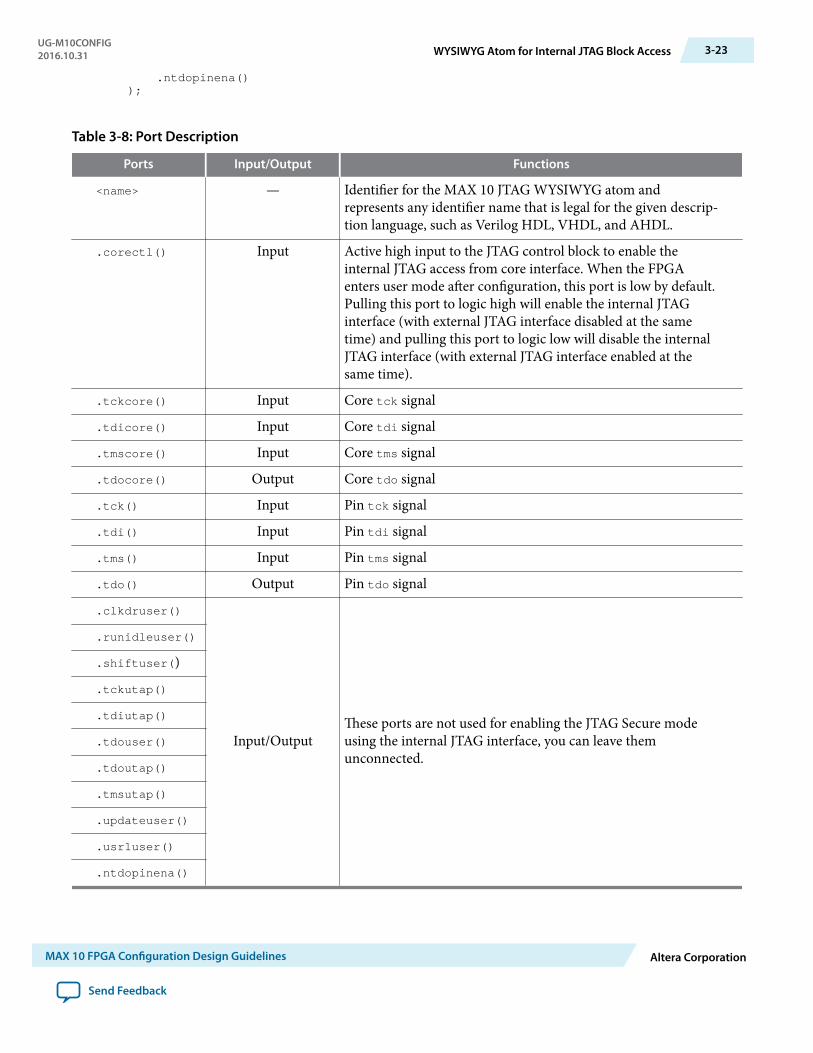
.ntdopinena());
Table 3-8: Port Description
Ports Input/Output Functions
<name> — Identifier for the MAX 10 JTAG WYSIWYG atom andrepresents any identifier name that is legal for the given descrip‐tion language, such as Verilog HDL, VHDL, and AHDL.
.corectl() Input Active high input to the JTAG control block to enable theinternal JTAG access from core interface. When the FPGAenters user mode after configuration, this port is low by default.Pulling this port to logic high will enable the internal JTAGinterface (with external JTAG interface disabled at the sametime) and pulling this port to logic low will disable the internalJTAG interface (with external JTAG interface enabled at thesame time).
.tckcore() Input Core tck signal
.tdicore() Input Core tdi signal
.tmscore() Input Core tms signal
.tdocore() Output Core tdo signal
.tck() Input Pin tck signal
.tdi() Input Pin tdi signal
.tms() Input Pin tms signal
.tdo() Output Pin tdo signal
.clkdruser()
Input/OutputThese ports are not used for enabling the JTAG Secure modeusing the internal JTAG interface, you can leave themunconnected.
.runidleuser()
.shiftuser()
.tckutap()
.tdiutap()
.tdouser()
.tdoutap()
.tmsutap()
.updateuser()
.usr1user()
.ntdopinena()
UG-M10CONFIG2016.10.31 WYSIWYG Atom for Internal JTAG Block Access 3-23
MAX 10 FPGA Configuration Design Guidelines Altera Corporation
Send Feedback
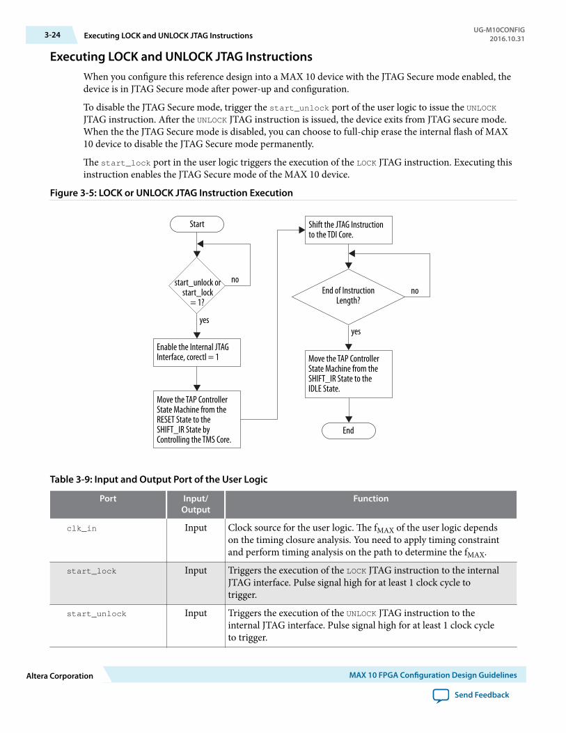
Executing LOCK and UNLOCK JTAG InstructionsWhen you configure this reference design into a MAX 10 device with the JTAG Secure mode enabled, thedevice is in JTAG Secure mode after power-up and configuration.
To disable the JTAG Secure mode, trigger the start_unlock port of the user logic to issue the UNLOCKJTAG instruction. After the UNLOCK JTAG instruction is issued, the device exits from JTAG secure mode.When the the JTAG Secure mode is disabled, you can choose to full-chip erase the internal flash of MAX10 device to disable the JTAG Secure mode permanently.
The start_lock port in the user logic triggers the execution of the LOCK JTAG instruction. Executing thisinstruction enables the JTAG Secure mode of the MAX 10 device.
Figure 3-5: LOCK or UNLOCK JTAG Instruction Execution
Start
Enable the Internal JTAGInterface, corectl = 1
Shift the JTAG Instruction to the TDI Core.
start_unlock orstart_lock
= 1?
no
yes
End of InstructionLength?
no
yes
Move the TAP ControllerState Machine from the RESET State to the SHIFT_IR State by Controlling the TMS Core.
Move the TAP ControllerState Machine from theSHIFT_IR State to theIDLE State.
End
Table 3-9: Input and Output Port of the User Logic
Port Input/Output
Function
clk_in Input Clock source for the user logic. The fMAX of the user logic dependson the timing closure analysis. You need to apply timing constraintand perform timing analysis on the path to determine the fMAX.
start_lock Input Triggers the execution of the LOCK JTAG instruction to the internalJTAG interface. Pulse signal high for at least 1 clock cycle totrigger.
start_unlock Input Triggers the execution of the UNLOCK JTAG instruction to theinternal JTAG interface. Pulse signal high for at least 1 clock cycleto trigger.
3-24 Executing LOCK and UNLOCK JTAG InstructionsUG-M10CONFIG
2016.10.31
Altera Corporation MAX 10 FPGA Configuration Design Guidelines
Send Feedback
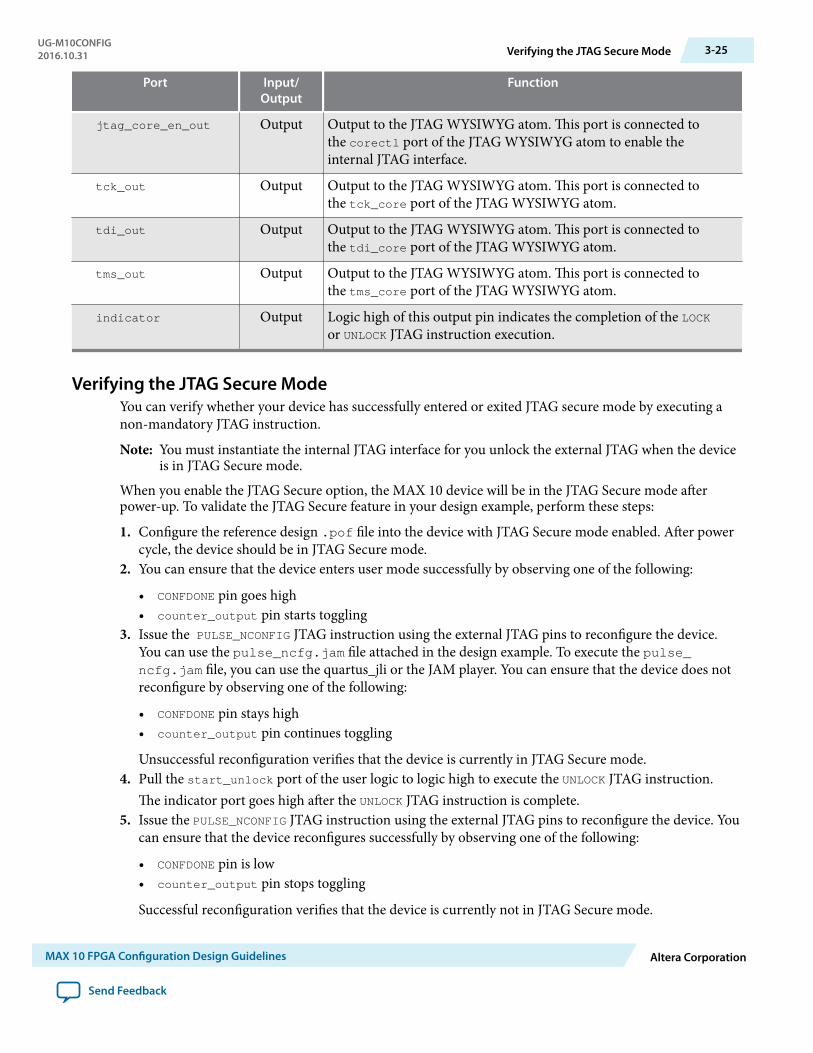
Port Input/Output
Function
jtag_core_en_out Output Output to the JTAG WYSIWYG atom. This port is connected tothe corectl port of the JTAG WYSIWYG atom to enable theinternal JTAG interface.
tck_out Output Output to the JTAG WYSIWYG atom. This port is connected tothe tck_core port of the JTAG WYSIWYG atom.
tdi_out Output Output to the JTAG WYSIWYG atom. This port is connected tothe tdi_core port of the JTAG WYSIWYG atom.
tms_out Output Output to the JTAG WYSIWYG atom. This port is connected tothe tms_core port of the JTAG WYSIWYG atom.
indicator Output Logic high of this output pin indicates the completion of the LOCKor UNLOCK JTAG instruction execution.
Verifying the JTAG Secure ModeYou can verify whether your device has successfully entered or exited JTAG secure mode by executing anon-mandatory JTAG instruction.
Note: You must instantiate the internal JTAG interface for you unlock the external JTAG when the deviceis in JTAG Secure mode.
When you enable the JTAG Secure option, the MAX 10 device will be in the JTAG Secure mode afterpower-up. To validate the JTAG Secure feature in your design example, perform these steps:
1. Configure the reference design .pof file into the device with JTAG Secure mode enabled. After powercycle, the device should be in JTAG Secure mode.
2. You can ensure that the device enters user mode successfully by observing one of the following:
• CONFDONE pin goes high• counter_output pin starts toggling
3. Issue the PULSE_NCONFIG JTAG instruction using the external JTAG pins to reconfigure the device.You can use the pulse_ncfg.jam file attached in the design example. To execute the pulse_ncfg.jam file, you can use the quartus_jli or the JAM player. You can ensure that the device does notreconfigure by observing one of the following:
• CONFDONE pin stays high• counter_output pin continues toggling
Unsuccessful reconfiguration verifies that the device is currently in JTAG Secure mode.4. Pull the start_unlock port of the user logic to logic high to execute the UNLOCK JTAG instruction.
The indicator port goes high after the UNLOCK JTAG instruction is complete.5. Issue the PULSE_NCONFIG JTAG instruction using the external JTAG pins to reconfigure the device. You
can ensure that the device reconfigures successfully by observing one of the following:
• CONFDONE pin is low• counter_output pin stops toggling
Successful reconfiguration verifies that the device is currently not in JTAG Secure mode.
UG-M10CONFIG2016.10.31 Verifying the JTAG Secure Mode 3-25
MAX 10 FPGA Configuration Design Guidelines Altera Corporation
Send Feedback
MAX 10 FPGA Configuration IP CoreImplementation Guides 4
2016.10.31
UG-M10CONFIG Subscribe Send Feedback
Related Information
• Introduction to Altera IP CoresProvides general information about all Altera FPGA IP cores, including parameterizing, generating,upgrading, and simulating IP cores.
• Creating Version-Independent IP and Qsys Simulation ScriptsCreate simulation scripts that do not require manual updates for software or IP version upgrades.
• Project Management Best PracticesGuidelines for efficient management and portability of your project and IP files.
Altera Unique Chip ID IP CoreThis section provides the guideline to implement the Altera Unique Chip ID IP Core.
Related Information
• Unique Chip ID on page 2-18• Altera Unique Chip ID IP Core Ports on page 6-1
Instantiating the Altera Unique Chip ID IP CoreTo instantiate the Altera Unique Chip ID IP Core, follow these steps:
1. On the Tools menu of the Quartus Prime software, click IP Catalog.2. Under the Library category, expand the Basic Functions and Configuration Programming.3. Select Altera Unique Chip ID and click Add, and enter your desired output file name4. In the Save IP Variation dialog box:
• Set your IP variation filename and directory.• Select IP variation file type.
5. Click Finish.
Resetting the Altera Unique Chip ID IP Core
To reset the Altera Unique Chip ID IP core, you must assert high to the reset signal for at least one clockcycle. After you de-assert the reset signal, the Altera Unique Chip ID IP core re-reads the unique chip ID
© 2016 Intel Corporation. All rights reserved. Intel, the Intel logo, Altera, Arria, Cyclone, Enpirion, MAX, Megacore, NIOS, Quartus and Stratix words and logosare trademarks of Intel Corporation in the US and/or other countries. Other marks and brands may be claimed as the property of others. Intel warrantsperformance of its FPGA and semiconductor products to current specifications in accordance with Intel's standard warranty, but reserves the right to makechanges to any products and services at any time without notice. Intel assumes no responsibility or liability arising out of the application or use of anyinformation, product, or service described herein except as expressly agreed to in writing by Intel. Intel customers are advised to obtain the latest version ofdevice specifications before relying on any published information and before placing orders for products or services.
ISO9001:2008Registered
www.altera.com101 Innovation Drive, San Jose, CA 95134
of your device from the fuse ID block. The Altera Unique Chip ID IP core asserts the data_valid signalafter completing the operation.
Altera Dual Configuration IP CoreThis section provides the guideline to implement the Altera Dual Configuration IP Core.
Instantiating the Altera Dual Configuration IP CoreTo instantiate the Altera Dual Configuration IP Core, follow these steps:
1. On the Tools menu of the Quartus Prime software, click IP Catalog.2. Under the Library category, expand the Basic Functions and Configuration Programming.3. Select Altera Dual Configuration and after clicking Add, the IP Parameter Editor appears.4. In the New IP Instance dialog box:
• Set the top-level name of your IP.• Select the Device family.• Select the Device
5. Click OK.
4-2 Altera Dual Configuration IP CoreUG-M10CONFIG
2016.10.31
Altera Corporation MAX 10 FPGA Configuration IP Core Implementation Guides
Send Feedback
Altera Dual Configuration IP Core References 52016.10.31
UG-M10CONFIG Subscribe Send Feedback
Related Information
• Altera Dual Configuration IP Core on page 2-16• Accessing Remote System Upgrade through User Logic on page 3-9• AN 741: Remote System Upgrade for MAX 10 FPGA Devices over UART with the Nios II Processor
Provides reference design for remote system upgrade in MAX 10 FPGA devices.• I2C Remote System Update Example
This example demonstrates a remote system upgrade using the I2C protocol.
Altera Dual Configuration IP Core Avalon-MM Address Map
Table 5-1: Altera Dual Configuration IP Core Avalon-MM Address Map for MAX 10 Devices
• Altera recommends you to set the reserve bits to 0 for write operations. For read operations, the IP corewill always generate 0 as the output.
• Write 1 to trigger any operation stated in the description.• You need to trigger the desired operation from offset 2 before any read operation of offset 4, 5, 6 and 7.
Offset R/W Width(Bits)
Description
0 W 32 • Bit 0—trigger reconfiguration.• Bit 1—reset the watchdog timer.• Bit 31:2—reserved.
Signals are triggered at the same write cycle on Avalon.
1 W 32 • Bit 0—trigger config_sel_overwrite to the input register.• Bit 1—writes config_sel to the input register. Set 0 or 1 to load
from configuration image 0 or 1 respectively.• Bit 31:2—reserved.
The busy signal is generated right after the write cycle, while theconfiguration image information is registered. Once busy signal ishigh, writing to this address is ignored until the process iscompleted and the busy signal is de-asserted.
© 2016 Intel Corporation. All rights reserved. Intel, the Intel logo, Altera, Arria, Cyclone, Enpirion, MAX, Megacore, NIOS, Quartus and Stratix words and logosare trademarks of Intel Corporation in the US and/or other countries. Other marks and brands may be claimed as the property of others. Intel warrantsperformance of its FPGA and semiconductor products to current specifications in accordance with Intel's standard warranty, but reserves the right to makechanges to any products and services at any time without notice. Intel assumes no responsibility or liability arising out of the application or use of anyinformation, product, or service described herein except as expressly agreed to in writing by Intel. Intel customers are advised to obtain the latest version ofdevice specifications before relying on any published information and before placing orders for products or services.
ISO9001:2008Registered
www.altera.com101 Innovation Drive, San Jose, CA 95134
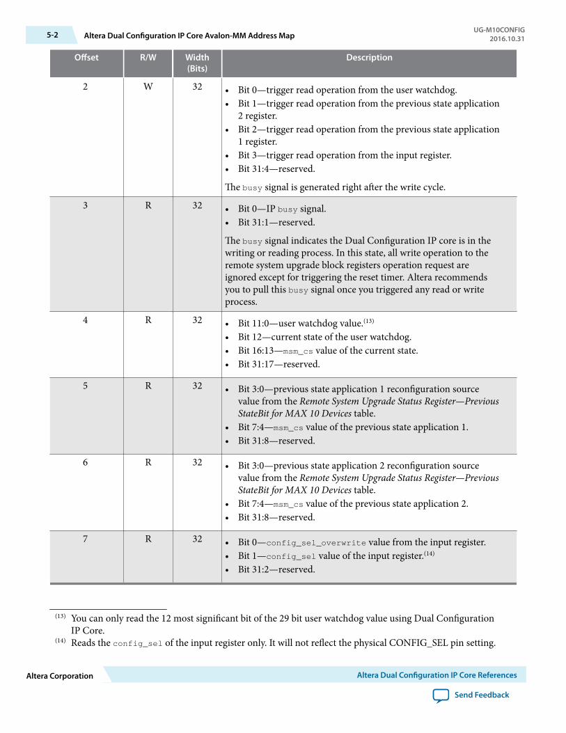
Offset R/W Width(Bits)
Description
2 W 32 • Bit 0—trigger read operation from the user watchdog.• Bit 1—trigger read operation from the previous state application
2 register.• Bit 2—trigger read operation from the previous state application
1 register.• Bit 3—trigger read operation from the input register.• Bit 31:4—reserved.
The busy signal is generated right after the write cycle.
3 R 32 • Bit 0—IP busy signal.• Bit 31:1—reserved.
The busy signal indicates the Dual Configuration IP core is in thewriting or reading process. In this state, all write operation to theremote system upgrade block registers operation request areignored except for triggering the reset timer. Altera recommendsyou to pull this busy signal once you triggered any read or writeprocess.
4 R 32 • Bit 11:0—user watchdog value.(13)
• Bit 12—current state of the user watchdog.• Bit 16:13—msm_cs value of the current state.• Bit 31:17—reserved.
5 R 32 • Bit 3:0—previous state application 1 reconfiguration sourcevalue from the Remote System Upgrade Status Register—PreviousStateBit for MAX 10 Devices table.
• Bit 7:4—msm_cs value of the previous state application 1.• Bit 31:8—reserved.
6 R 32 • Bit 3:0—previous state application 2 reconfiguration sourcevalue from the Remote System Upgrade Status Register—PreviousStateBit for MAX 10 Devices table.
• Bit 7:4—msm_cs value of the previous state application 2.• Bit 31:8—reserved.
7 R 32 • Bit 0—config_sel_overwrite value from the input register.• Bit 1—config_sel value of the input register.(14)
• Bit 31:2—reserved.
(13) You can only read the 12 most significant bit of the 29 bit user watchdog value using Dual ConfigurationIP Core.
(14) Reads the config_sel of the input register only. It will not reflect the physical CONFIG_SEL pin setting.
5-2 Altera Dual Configuration IP Core Avalon-MM Address MapUG-M10CONFIG
2016.10.31
Altera Corporation Altera Dual Configuration IP Core References
Send Feedback
Related Information
• Altera Dual Configuration IP Core on page 2-16• Avalon Interface Specifications
Provides more information about the Avalon-MM interface specifications applied in Altera DualConfiguration IP Core.
• Instantiating the Altera Dual Configuration IP Core on page 4-2• Remote System Upgrade Status Registers on page 2-15
The Remote System Upgrade Status Register—Previous StateBit for MAX 10 Devices table providesmore information about previous state applications reconfiguration sources.
Altera Dual Configuration IP Core Parameters
Table 5-2: Altera Dual Configuration IP Core Parameter for MAX 10
Parameter Value Description
Clock frequency Up to 80MHz Specifies the number of cycle to assert RU_nRSTIMER and RU_nCONFIG signals. Note that maximum RU_CLK is 40Mhz, AlteraDual Configuration IP Core has restriction to run at 80Mhzmaximum, which is twice faster than hardware limitation. This isbecause Altera Dual Configuration IP Core generate RU_CLK athalf rate of the input frequency.
UG-M10CONFIG2016.10.31 Altera Dual Configuration IP Core Parameters 5-3
Altera Dual Configuration IP Core References Altera Corporation
Send Feedback
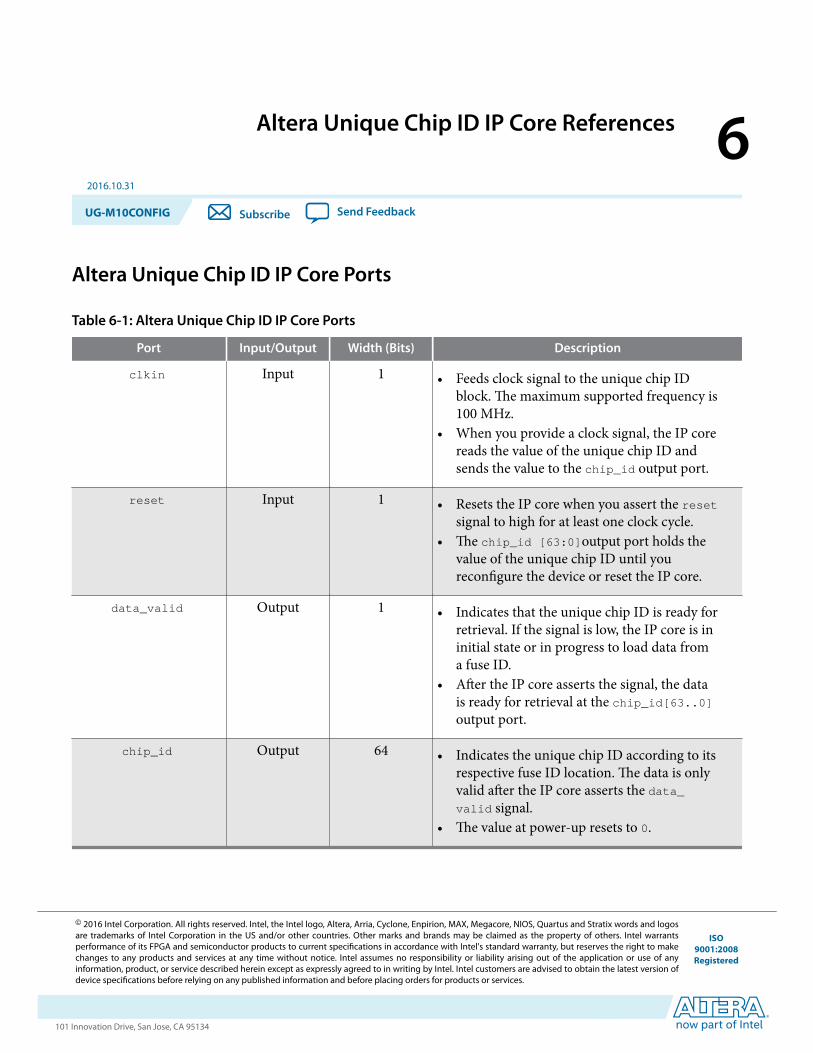
Altera Unique Chip ID IP Core References 62016.10.31
UG-M10CONFIG Subscribe Send Feedback
Altera Unique Chip ID IP Core Ports
Table 6-1: Altera Unique Chip ID IP Core Ports
Port Input/Output Width (Bits) Description
clkin Input 1 • Feeds clock signal to the unique chip IDblock. The maximum supported frequency is100 MHz.
• When you provide a clock signal, the IP corereads the value of the unique chip ID andsends the value to the chip_id output port.
reset Input 1 • Resets the IP core when you assert the resetsignal to high for at least one clock cycle.
• The chip_id [63:0]output port holds thevalue of the unique chip ID until youreconfigure the device or reset the IP core.
data_valid Output 1 • Indicates that the unique chip ID is ready forretrieval. If the signal is low, the IP core is ininitial state or in progress to load data froma fuse ID.
• After the IP core asserts the signal, the datais ready for retrieval at the chip_id[63..0]output port.
chip_id Output 64 • Indicates the unique chip ID according to itsrespective fuse ID location. The data is onlyvalid after the IP core asserts the data_valid signal.
• The value at power-up resets to 0.
© 2016 Intel Corporation. All rights reserved. Intel, the Intel logo, Altera, Arria, Cyclone, Enpirion, MAX, Megacore, NIOS, Quartus and Stratix words and logosare trademarks of Intel Corporation in the US and/or other countries. Other marks and brands may be claimed as the property of others. Intel warrantsperformance of its FPGA and semiconductor products to current specifications in accordance with Intel's standard warranty, but reserves the right to makechanges to any products and services at any time without notice. Intel assumes no responsibility or liability arising out of the application or use of anyinformation, product, or service described herein except as expressly agreed to in writing by Intel. Intel customers are advised to obtain the latest version ofdevice specifications before relying on any published information and before placing orders for products or services.
ISO9001:2008Registered
www.altera.com101 Innovation Drive, San Jose, CA 95134
Additional Information for MAX 10 FPGAConfiguration User Guide A
2016.10.31
UG-M10CONFIG Subscribe Send Feedback
Document Revision History for MAX 10 FPGA Configuration User Guide
Date Version Changes
October 2016 2016.10.31 • Updated Voltage Overshoot Prevention description.• Updated note in Connection Setup for JTAG Single-Device Configu‐
ration using Download Cable and Connection Setup for JTAG Multi-Device Configuration using Download Cable figures.
• Added steps to implement ISP clamp feature.• Updated Configuration Flash Memory Sectors Utilization for all
MAX 10 with Analog and Flash Feature Options figure to includeUFM sectors.
May 2016 2016.05.13 • Changed instances of Standard POR to Slow POR to reflect QuartusPrime GUI.
• Updated tCFG to tRU_nCONFIG.• Corrected file type from .ekp to .pof in Step 8 of Program‐
ming .ekp File and Encrypted .pof Separately.• Corrected Use secondary image ISP data as default setting when
available description in ICB Values and Descriptions for MAX 10Devices table.
• Corrected CFM programming time.• Added note on JTAG pin requirements when using JTAG pin
sharing.• Moved JTAG Pin Sharing Behavior under Guidelines: Dual-Purpose
Configuration Pin.• Updated configuration sequence diagram by moving 'Clears
configuration RAM bits from Power-up state to Reset state.• Corrected error detection port input and output for <crcblock_
name> from input to none.• Added example of remote system upgrade access through user
interface and port definitions.
© 2016 Intel Corporation. All rights reserved. Intel, the Intel logo, Altera, Arria, Cyclone, Enpirion, MAX, Megacore, NIOS, Quartus and Stratix words and logosare trademarks of Intel Corporation in the US and/or other countries. Other marks and brands may be claimed as the property of others. Intel warrantsperformance of its FPGA and semiconductor products to current specifications in accordance with Intel's standard warranty, but reserves the right to makechanges to any products and services at any time without notice. Intel assumes no responsibility or liability arising out of the application or use of anyinformation, product, or service described herein except as expressly agreed to in writing by Intel. Intel customers are advised to obtain the latest version ofdevice specifications before relying on any published information and before placing orders for products or services.
ISO9001:2008Registered
www.altera.com101 Innovation Drive, San Jose, CA 95134
Date Version Changes
• Removed preliminary terms for Error Detection Frequency andCyclic Redundancy Check Calculation Timing.
• Added Connection Setup for JTAG Multi-Device Configuration usingDownload Cable diagram.
• Updated Connection Setup for JTAG Single-Device Configurationusing Download Cable diagram.
• Added new JTAG Secure design example.• Edited Remote System Upgrade section title by removing in Dual
Image Configuration.• Updated Monitored Power Supplies Ramp Time Requirement for
MAX 10 Devices table.• Added Internal Configuration Time.• Removed Instant ON feature.• Updated User Flash Memory instances to additional UFM in
Configuration Flash Memory Sectors Utilization for all MAX 10 withAnalog and Flash Feature Options figure.
December 2015.12.14 • Updated ICB setting description for Set I/O to weak pull-up priorusermode option to state the weak pull-up is enabled duringconfiguration.
• Removed Accessing the Remote System Upgrade Block Through UserInterface.
• Added input and output port definition for error detectionWYSIWYG atom.
• Updated the I/O pin state to be dependent on ICB bit setting duringreconfiguration.
A-2 Document Revision History for MAX 10 FPGA Configuration User GuideUG-M10CONFIG
2016.10.31
Altera Corporation Additional Information for MAX 10 FPGA Configuration User Guide
Send Feedback
Date Version Changes
November 2015 2015.11.02 • Removed JRunner support for JTAG configuration and link to AN414.
• Updated differences in supported internal configuration modesupported based on device feature options in a table.
• Removed maximum number of compressed configuration imagetable do to redundancy.
• Updated Initialization Configuration Bits setting and description toreflect Quartus Prime 15.1 update.
• Updated Enable JTAG pin sharing and Enable nCONFIG,nSTATUS, and CONF_DONE pins to reflect Quartus II 15.1update.
• Added information about ISP clamp feature.• Updated information about steps to generate Raw Programming
Data (.rpd).• Renamed section title from Configuration Total Flash Memory
Programming Time to Configuration Flash Memory ProgrammingTime.
• Renamed table title from Configuration Total Flash MemoryProgramming Time for Sectors in MAX 10 Devices to ConfigurationFlash Memory Programming Time for Sectors in MAX 10 Devices.
• Added note to Configuration Flash Memory Programming Time forSectors in MAX 10 Devices table.
• Added information about internal JTAG interface and accessinginternal JTAG block through user interface.
• Added MAX 10 JTAG Secure design example.
June 2015 2015.06.15 • Added related information link to AN 741: Remote SystemUpgrade for MAX 10 FPGA Devices over UART with the Nios IIProcessor inAltera Dual Configuration IP Core References andRemote System Upgrade in Dual Compressed Images.
• Added pulse holding requirement time for RU_nRSTIMER in RemoteSystem Upgrade Circuitry Signals for MAX 10 Devices table.
• Added link to Remote System Upgrade Status Register—PreviousState Bit for MAX 10 Devices table for related entries in Altera DualConfiguration IP Core Avalon-MM Address Map for MAX 10Devices table.
UG-M10CONFIG2016.10.31 Document Revision History for MAX 10 FPGA Configuration User Guide A-3
Additional Information for MAX 10 FPGA Configuration User Guide Altera Corporation
Send Feedback
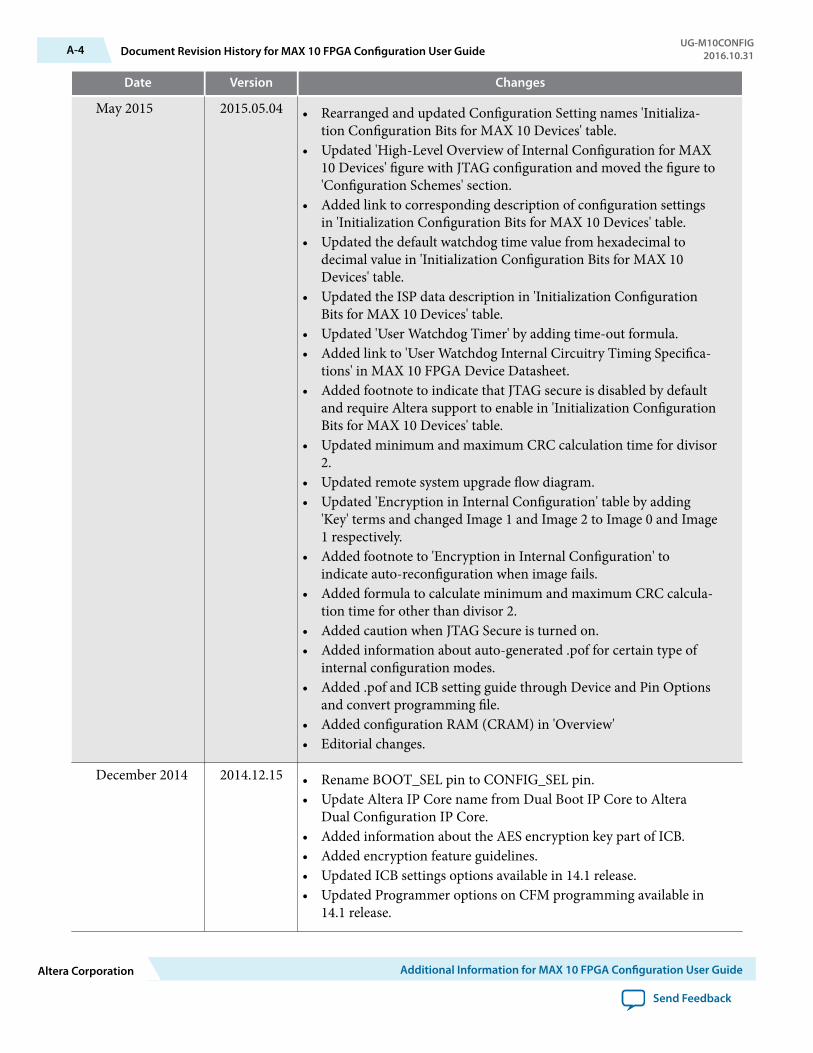
Date Version Changes
May 2015 2015.05.04 • Rearranged and updated Configuration Setting names 'Initializa‐tion Configuration Bits for MAX 10 Devices' table.
• Updated 'High-Level Overview of Internal Configuration for MAX10 Devices' figure with JTAG configuration and moved the figure to'Configuration Schemes' section.
• Added link to corresponding description of configuration settingsin 'Initialization Configuration Bits for MAX 10 Devices' table.
• Updated the default watchdog time value from hexadecimal todecimal value in 'Initialization Configuration Bits for MAX 10Devices' table.
• Updated the ISP data description in 'Initialization ConfigurationBits for MAX 10 Devices' table.
• Updated 'User Watchdog Timer' by adding time-out formula.• Added link to 'User Watchdog Internal Circuitry Timing Specifica‐
tions' in MAX 10 FPGA Device Datasheet.• Added footnote to indicate that JTAG secure is disabled by default
and require Altera support to enable in 'Initialization ConfigurationBits for MAX 10 Devices' table.
• Updated minimum and maximum CRC calculation time for divisor2.
• Updated remote system upgrade flow diagram.• Updated 'Encryption in Internal Configuration' table by adding
'Key' terms and changed Image 1 and Image 2 to Image 0 and Image1 respectively.
• Added footnote to 'Encryption in Internal Configuration' toindicate auto-reconfiguration when image fails.
• Added formula to calculate minimum and maximum CRC calcula‐tion time for other than divisor 2.
• Added caution when JTAG Secure is turned on.• Added information about auto-generated .pof for certain type of
internal configuration modes.• Added .pof and ICB setting guide through Device and Pin Options
and convert programming file.• Added configuration RAM (CRAM) in 'Overview'• Editorial changes.
December 2014 2014.12.15 • Rename BOOT_SEL pin to CONFIG_SEL pin.• Update Altera IP Core name from Dual Boot IP Core to Altera
Dual Configuration IP Core.• Added information about the AES encryption key part of ICB.• Added encryption feature guidelines.• Updated ICB settings options available in 14.1 release.• Updated Programmer options on CFM programming available in
14.1 release.
A-4 Document Revision History for MAX 10 FPGA Configuration User GuideUG-M10CONFIG
2016.10.31
Altera Corporation Additional Information for MAX 10 FPGA Configuration User Guide
Send Feedback

Date Version Changes
September 2014 2014.09.22 Initial release.
UG-M10CONFIG2016.10.31 Document Revision History for MAX 10 FPGA Configuration User Guide A-5
Additional Information for MAX 10 FPGA Configuration User Guide Altera Corporation
Send Feedback

MAX 10 User Flash Memory User Guide
Last updated for Quartus Prime Design Suite: 16.0
Subscribe
Send Feedback
UG-M10UFM2016.05.02
101 Innovation DriveSan Jose, CA 95134www.altera.com
Contents
MAX 10 User Flash Memory Overview...............................................................1-1
MAX 10 UFM Architecture and Features...........................................................2-1UFM and CFM Array Size..........................................................................................................................2-1UFM Memory Organization Map............................................................................................................. 2-2UFM Block Diagrams..................................................................................................................................2-2UFM Operating Modes............................................................................................................................... 2-5
MAX 10 UFM Design Considerations................................................................ 3-1Guideline: UFM Power Supply Requirement.......................................................................................... 3-1Guideline: Program and Read UFM with JTAG..................................................................................... 3-1Guideline: UFM Content Initialization.................................................................................................... 3-2Guideline: Erase Before Program.............................................................................................................. 3-2
MAX 10 UFM Implementation Guides.............................................................. 4-1Altera On-Chip Flash IP Core....................................................................................................................4-1UFM Avalon-MM Operating Modes........................................................................................................4-1
UFM Read Status and Control Register........................................................................................4-1UFM Write Control Register..........................................................................................................4-2UFM Program (Write) Operation................................................................................................. 4-2UFM Sector Erase Operation......................................................................................................... 4-4UFM Page Erase Operation............................................................................................................ 4-4UFM Read Operation...................................................................................................................... 4-5UFM Burst Read Operation............................................................................................................4-7
Flash Initialization Files............................................................................................................................ 4-12
Altera On-Chip Flash IP Core References.......................................................... 5-1Altera On-Chip Flash Parameters............................................................................................................. 5-1Altera On-Chip Flash Signals.....................................................................................................................5-2Altera On-Chip Flash Registers................................................................................................................. 5-4
MAX 10 User Flash Memory User Guide Archive.............................................A-1
Document Revision History for MAX 10 User Flash Memory User Guide...... B-1
TOC-2
Altera Corporation
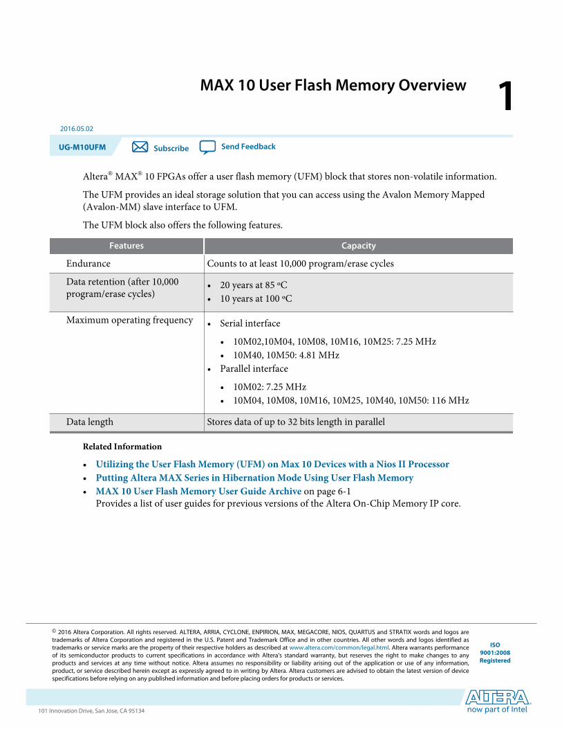
MAX 10 User Flash Memory Overview 12016.05.02
UG-M10UFM Subscribe Send Feedback
Altera® MAX® 10 FPGAs offer a user flash memory (UFM) block that stores non-volatile information.
The UFM provides an ideal storage solution that you can access using the Avalon Memory Mapped(Avalon-MM) slave interface to UFM.
The UFM block also offers the following features.
Features Capacity
Endurance Counts to at least 10,000 program/erase cycles
Data retention (after 10,000program/erase cycles)
• 20 years at 85 ºC• 10 years at 100 ºC
Maximum operating frequency • Serial interface
• 10M02,10M04, 10M08, 10M16, 10M25: 7.25 MHz• 10M40, 10M50: 4.81 MHz
• Parallel interface
• 10M02: 7.25 MHz• 10M04, 10M08, 10M16, 10M25, 10M40, 10M50: 116 MHz
Data length Stores data of up to 32 bits length in parallel
Related Information
• Utilizing the User Flash Memory (UFM) on Max 10 Devices with a Nios II Processor• Putting Altera MAX Series in Hibernation Mode Using User Flash Memory• MAX 10 User Flash Memory User Guide Archive on page 6-1
Provides a list of user guides for previous versions of the Altera On-Chip Memory IP core.
© 2016 Altera Corporation. All rights reserved. ALTERA, ARRIA, CYCLONE, ENPIRION, MAX, MEGACORE, NIOS, QUARTUS and STRATIX words and logos aretrademarks of Altera Corporation and registered in the U.S. Patent and Trademark Office and in other countries. All other words and logos identified astrademarks or service marks are the property of their respective holders as described at www.altera.com/common/legal.html. Altera warrants performanceof its semiconductor products to current specifications in accordance with Altera's standard warranty, but reserves the right to make changes to anyproducts and services at any time without notice. Altera assumes no responsibility or liability arising out of the application or use of any information,product, or service described herein except as expressly agreed to in writing by Altera. Altera customers are advised to obtain the latest version of devicespecifications before relying on any published information and before placing orders for products or services.
ISO9001:2008Registered
www.altera.com101 Innovation Drive, San Jose, CA 95134
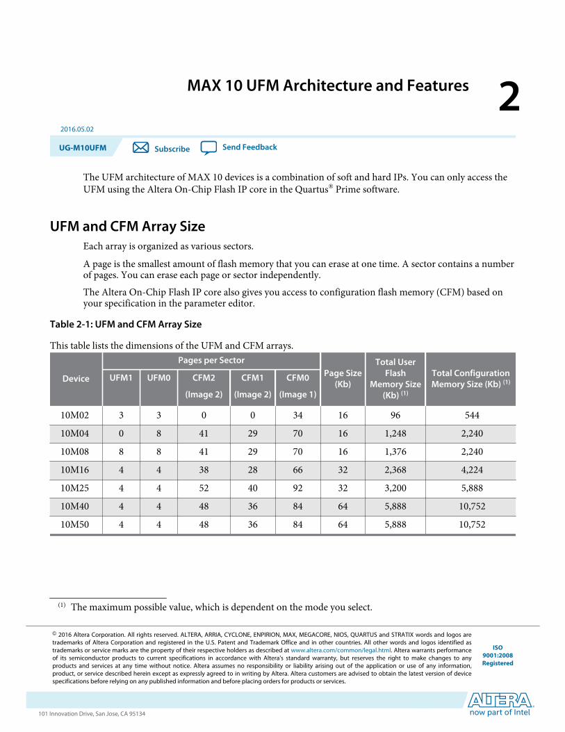
MAX 10 UFM Architecture and Features 22016.05.02
UG-M10UFM Subscribe Send Feedback
The UFM architecture of MAX 10 devices is a combination of soft and hard IPs. You can only access theUFM using the Altera On-Chip Flash IP core in the Quartus® Prime software.
UFM and CFM Array SizeEach array is organized as various sectors.
A page is the smallest amount of flash memory that you can erase at one time. A sector contains a numberof pages. You can erase each page or sector independently.
The Altera On-Chip Flash IP core also gives you access to configuration flash memory (CFM) based onyour specification in the parameter editor.
Table 2-1: UFM and CFM Array Size
This table lists the dimensions of the UFM and CFM arrays.
Device
Pages per SectorPage Size
(Kb)
Total UserFlash
Memory Size(Kb) (1)
Total ConfigurationMemory Size (Kb) (1)UFM1 UFM0 CFM2
(Image 2)
CFM1
(Image 2)
CFM0
(Image 1)
10M02 3 3 0 0 34 16 96 544
10M04 0 8 41 29 70 16 1,248 2,240
10M08 8 8 41 29 70 16 1,376 2,240
10M16 4 4 38 28 66 32 2,368 4,224
10M25 4 4 52 40 92 32 3,200 5,888
10M40 4 4 48 36 84 64 5,888 10,752
10M50 4 4 48 36 84 64 5,888 10,752
(1) The maximum possible value, which is dependent on the mode you select.
© 2016 Altera Corporation. All rights reserved. ALTERA, ARRIA, CYCLONE, ENPIRION, MAX, MEGACORE, NIOS, QUARTUS and STRATIX words and logos aretrademarks of Altera Corporation and registered in the U.S. Patent and Trademark Office and in other countries. All other words and logos identified astrademarks or service marks are the property of their respective holders as described at www.altera.com/common/legal.html. Altera warrants performanceof its semiconductor products to current specifications in accordance with Altera's standard warranty, but reserves the right to make changes to anyproducts and services at any time without notice. Altera assumes no responsibility or liability arising out of the application or use of any information,product, or service described herein except as expressly agreed to in writing by Altera. Altera customers are advised to obtain the latest version of devicespecifications before relying on any published information and before placing orders for products or services.
ISO9001:2008Registered
www.altera.com101 Innovation Drive, San Jose, CA 95134
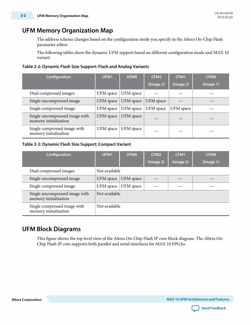
UFM Memory Organization MapThe address scheme changes based on the configuration mode you specify in the Altera On-Chip Flashparameter editor.
The following tables show the dynamic UFM support based on different configuration mode and MAX 10variant.
Table 2-2: Dynamic Flash Size Support: Flash and Analog Variants
Configuration UFM1 UFM0 CFM2
(Image 2)
CFM1
(Image 2)
CFM0
(Image 1)
Dual compressed images UFM space UFM space — — —Single uncompressed image UFM space UFM space UFM space — —Single compressed image UFM space UFM space UFM space UFM space —Single uncompressed image withmemory initialization
UFM space UFM space — — —
Single compressed image withmemory initialization
UFM space UFM space — — —
Table 2-3: Dynamic Flash Size Support: Compact Variant
Configuration UFM1 UFM0 CFM2
(Image 2)
CFM1
(Image 2)
CFM0
(Image 1)
Dual compressed images Not availableSingle uncompressed image UFM space UFM space — — —Single compressed image UFM space UFM space — — —Single uncompressed image withmemory initialization
Not available
Single compressed image withmemory initialization
Not available
UFM Block DiagramsThis figure shows the top level view of the Altera On-Chip Flash IP core block diagram. The Altera On-Chip Flash IP core supports both parallel and serial interfaces for MAX 10 FPGAs.
2-2 UFM Memory Organization MapUG-M10UFM
2016.05.02
Altera Corporation MAX 10 UFM Architecture and Features
Send Feedback
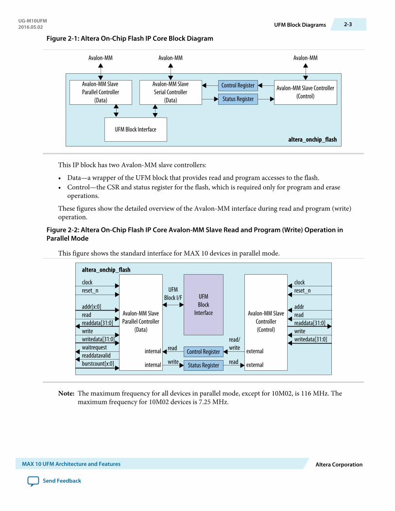
Figure 2-1: Altera On-Chip Flash IP Core Block Diagram
UFM Block Interface
Avalon-MM Slave Controller(Control)
Control Register
Status Register
altera_onchip_flash
Avalon-MM SlaveSerial Controller
(Data)
Avalon-MM
Avalon-MM Slave Parallel Controller
(Data)
Avalon-MM Avalon-MM
This IP block has two Avalon-MM slave controllers:
• Data—a wrapper of the UFM block that provides read and program accesses to the flash.• Control—the CSR and status register for the flash, which is required only for program and erase
operations.
These figures show the detailed overview of the Avalon-MM interface during read and program (write)operation.
Figure 2-2: Altera On-Chip Flash IP Core Avalon-MM Slave Read and Program (Write) Operation inParallel Mode
This figure shows the standard interface for MAX 10 devices in parallel mode.
Avalon-MM SlaveParallel Controller
(Data)
Avalon-MM SlaveController(Control)
Control Register
Status Register
altera_onchip_flash
UFMBlock
Interface
UFMBlock I/F
clockreset_n
addr[x:0]readreaddata[31:0]writewritedata[31:0]waitrequestreaddatavalidburstcount[x:0]
clockreset_n
addrreadreaddata[31:0]writewritedata[31:0]
read
write
read/write
read
internal
internal
external
external
Note: The maximum frequency for all devices in parallel mode, except for 10M02, is 116 MHz. Themaximum frequency for 10M02 devices is 7.25 MHz.
UG-M10UFM2016.05.02 UFM Block Diagrams 2-3
MAX 10 UFM Architecture and Features Altera Corporation
Send Feedback
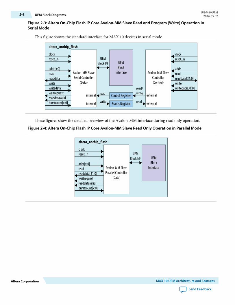
Figure 2-3: Altera On-Chip Flash IP Core Avalon-MM Slave Read and Program (Write) Operation inSerial Mode
This figure shows the standard interface for MAX 10 devices in serial mode.
Avalon-MM SlaveSerial Controller
(Data)
Avalon-MM SlaveController(Control)
Control Register
Status Register
altera_onchip_flash
UFMBlock
Interface
UFMBlock I/F
clockreset_n
addr[x:0]readreaddatawritewritedatawaitrequestreaddatavalidburstcount[x:0]
clockreset_n
addrreadreaddata[31:0]writewritedata[31:0]
read
write
read/write
read
internal
internal
external
external
These figures show the detailed overview of the Avalon-MM interface during read only operation.
Figure 2-4: Altera On-Chip Flash IP Core Avalon-MM Slave Read Only Operation in Parallel Mode
Avalon-MM SlaveParallel Controller
(Data)
altera_onchip_flash
UFMBlock
Interface
UFMBlock I/F
clockreset_n
addr[x:0]readreaddata[31:0]waitrequestreaddatavalidburstcount[x:0]
2-4 UFM Block DiagramsUG-M10UFM
2016.05.02
Altera Corporation MAX 10 UFM Architecture and Features
Send Feedback
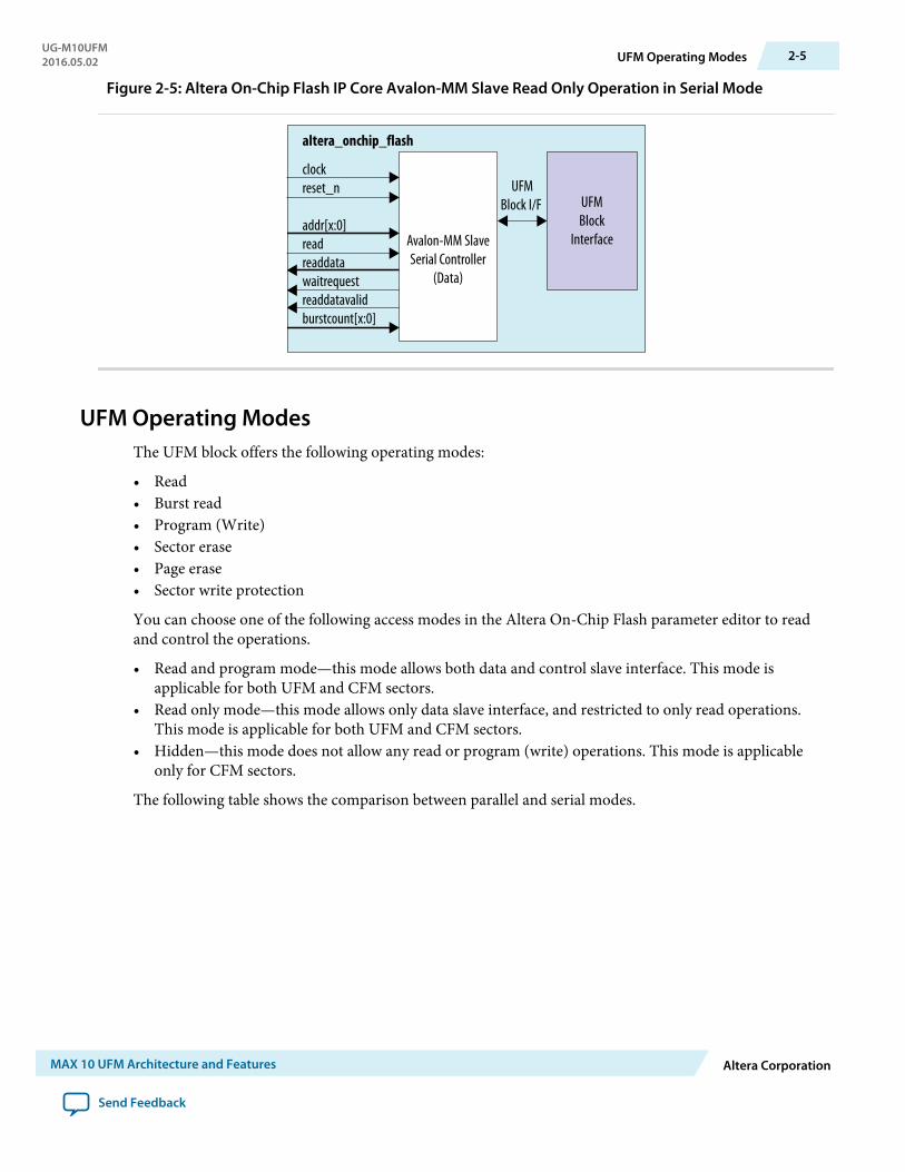
Figure 2-5: Altera On-Chip Flash IP Core Avalon-MM Slave Read Only Operation in Serial Mode
Avalon-MM SlaveSerial Controller
(Data)
altera_onchip_flash
UFMBlock
Interface
UFMBlock I/F
clockreset_n
addr[x:0]readreaddatawaitrequestreaddatavalidburstcount[x:0]
UFM Operating ModesThe UFM block offers the following operating modes:
• Read• Burst read• Program (Write)• Sector erase• Page erase• Sector write protection
You can choose one of the following access modes in the Altera On-Chip Flash parameter editor to readand control the operations.
• Read and program mode—this mode allows both data and control slave interface. This mode isapplicable for both UFM and CFM sectors.
• Read only mode—this mode allows only data slave interface, and restricted to only read operations.This mode is applicable for both UFM and CFM sectors.
• Hidden—this mode does not allow any read or program (write) operations. This mode is applicableonly for CFM sectors.
The following table shows the comparison between parallel and serial modes.
UG-M10UFM2016.05.02 UFM Operating Modes 2-5
MAX 10 UFM Architecture and Features Altera Corporation
Send Feedback
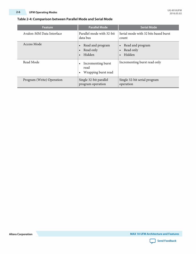
Table 2-4: Comparison between Parallel Mode and Serial Mode
Feature Parallel Mode Serial Mode
Avalon-MM Data Interface Parallel mode with 32-bitdata bus
Serial mode with 32 bits based burstcount
Access Mode • Read and program• Read only• Hidden
• Read and program• Read only• Hidden
Read Mode • Incrementing burstread
• Wrapping burst read
Incrementing burst read only
Program (Write) Operation Single 32-bit parallelprogram operation
Single 32-bit serial programoperation
2-6 UFM Operating ModesUG-M10UFM
2016.05.02
Altera Corporation MAX 10 UFM Architecture and Features
Send Feedback
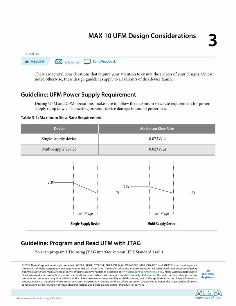
MAX 10 UFM Design Considerations 32016.05.02
UG-M10UFM Subscribe Send Feedback
There are several considerations that require your attention to ensure the success of your designs. Unlessnoted otherwise, these design guidelines apply to all variants of this device family.
Guideline: UFM Power Supply RequirementDuring UFM and CFM operations, make sure to follow the maximum slew rate requirement for powersupply ramp down. This setting prevents device damage in case of power loss.
Table 3-1: Maximum Slew Rate Requirement
Device Maximum Slew Rate
Single-supply device 0.073V/µs
Multi-supply device 0.023V/µs
<0.023V/µs
Multi-Supply Device
2.5V
0V
<0.073V/µs
Single-Supply Device
0V
3.3V
Guideline: Program and Read UFM with JTAGYou can program UFM using JTAG interface version IEEE Standard 1149.1.
© 2016 Altera Corporation. All rights reserved. ALTERA, ARRIA, CYCLONE, ENPIRION, MAX, MEGACORE, NIOS, QUARTUS and STRATIX words and logos aretrademarks of Altera Corporation and registered in the U.S. Patent and Trademark Office and in other countries. All other words and logos identified astrademarks or service marks are the property of their respective holders as described at www.altera.com/common/legal.html. Altera warrants performanceof its semiconductor products to current specifications in accordance with Altera's standard warranty, but reserves the right to make changes to anyproducts and services at any time without notice. Altera assumes no responsibility or liability arising out of the application or use of any information,product, or service described herein except as expressly agreed to in writing by Altera. Altera customers are advised to obtain the latest version of devicespecifications before relying on any published information and before placing orders for products or services.
ISO9001:2008Registered
www.altera.com101 Innovation Drive, San Jose, CA 95134
The JTAG interface supports Jam™ Standard Test and Programming Language (STAPL) Format File(.jam), Programmer Object File (.pof), and JAM Byte Code File (.jbc).
You can use the Quartus Prime Programmer to program .pof through the JTAG interface. Toprogram .pof, into the flash, follow these steps:
1. In the Programmer window, click Hardware Setup, and select USB Blaster.2. In the Mode list, select JTAG.3. Click Auto Detect on the left pane.4. Select the device to be programmed, and click Add File.5. Select the .pof to be programmed to the selected device.6. Select the UFM in the Program/Configure column.7. Click Start to start programming.
To program through .jam or .jbc files, refer to the Using the Command-Line Jam STAPL Solution forDevice Programming application note.
Related InformationAN 425: Using the Command-Line Jam STAPL Solution for Device Programming
Guideline: UFM Content InitializationYou can initialize the UFM content using Altera software.
The initial memory content supports Memory Initialization File (.mif), and Hexadecimal (Intel-Format)File (.hex).
You can initialize the UFM content using either one of the following ways:
• Set the initial memory content through the Altera On-Chip Flash IP core.• Set the initial memory content through the Convert Programming File tool in the Quartus Prime
software when you convert .sof to .pof.
Guideline: Erase Before ProgramMake sure to erase the flash location before you perform a program (write) operation.
3-2 Guideline: UFM Content InitializationUG-M10UFM
2016.05.02
Altera Corporation MAX 10 UFM Design Considerations
Send Feedback
MAX 10 UFM Implementation Guides 42016.05.02
UG-M10UFM Subscribe Send Feedback
Related Information
• Utilizing the User Flash Memory (UFM) on Max 10 Devices with a Nios II Processor• Putting Altera MAX Series in Hibernation Mode Using User Flash Memory
Altera On-Chip Flash IP CoreThe Altera IP core design flow helps you get started with any Altera IP core.
The Altera On-Chip Flash IP core is installed as part of the Quartus Prime installation process. You canselect and parameterize any Altera IP core from the library. Altera provides an integrated parametereditor that allows you to customize the Altera On-Chip Flash IP core to support a wide variety of applica‐tions. The parameter editor guides you through the setting of parameter values and selection of optionalports.
Related InformationIntroduction to Altera IP CoresProvides more information about Altera IP cores.
UFM Avalon-MM Operating ModesThe UFM operating modes use Avalon-MM interface.
UFM Read Status and Control RegisterYou can access the control register value through the Avalon-MM control slave interface.
© 2016 Altera Corporation. All rights reserved. ALTERA, ARRIA, CYCLONE, ENPIRION, MAX, MEGACORE, NIOS, QUARTUS and STRATIX words and logos aretrademarks of Altera Corporation and registered in the U.S. Patent and Trademark Office and in other countries. All other words and logos identified astrademarks or service marks are the property of their respective holders as described at www.altera.com/common/legal.html. Altera warrants performanceof its semiconductor products to current specifications in accordance with Altera's standard warranty, but reserves the right to make changes to anyproducts and services at any time without notice. Altera assumes no responsibility or liability arising out of the application or use of any information,product, or service described herein except as expressly agreed to in writing by Altera. Altera customers are advised to obtain the latest version of devicespecifications before relying on any published information and before placing orders for products or services.
ISO9001:2008Registered
www.altera.com101 Innovation Drive, San Jose, CA 95134
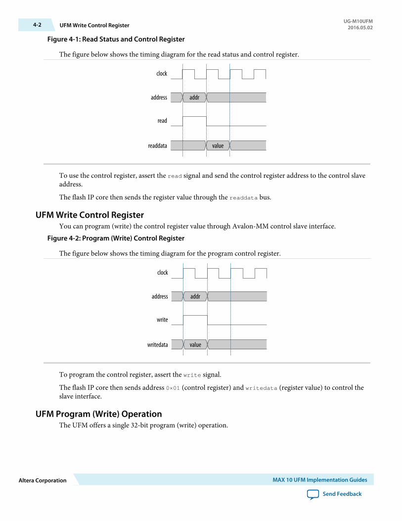
Figure 4-1: Read Status and Control Register
The figure below shows the timing diagram for the read status and control register.
clock
addr
value
address
read
readdata
To use the control register, assert the read signal and send the control register address to the control slaveaddress.
The flash IP core then sends the register value through the readdata bus.
UFM Write Control RegisterYou can program (write) the control register value through Avalon-MM control slave interface.
Figure 4-2: Program (Write) Control Register
The figure below shows the timing diagram for the program control register.
clock
addr
value
address
write
writedata
To program the control register, assert the write signal.
The flash IP core then sends address 0×01 (control register) and writedata (register value) to control theslave interface.
UFM Program (Write) OperationThe UFM offers a single 32-bit program (write) operation.
4-2 UFM Write Control RegisterUG-M10UFM
2016.05.02
Altera Corporation MAX 10 UFM Implementation Guides
Send Feedback
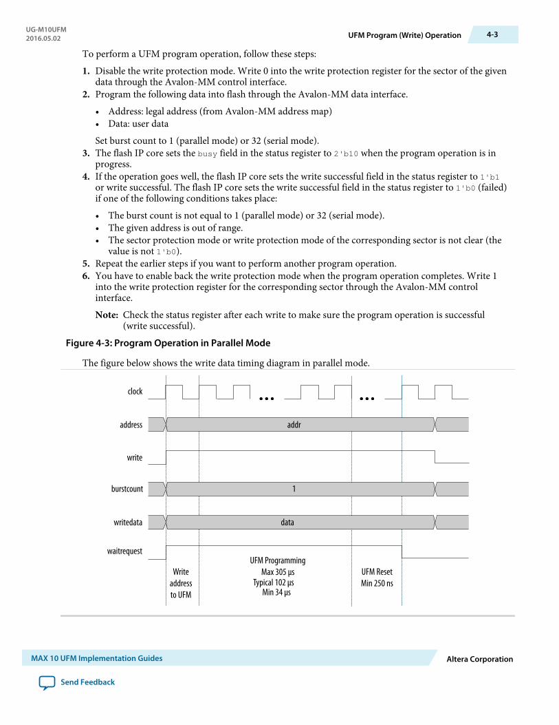
To perform a UFM program operation, follow these steps:
1. Disable the write protection mode. Write 0 into the write protection register for the sector of the givendata through the Avalon-MM control interface.
2. Program the following data into flash through the Avalon-MM data interface.
• Address: legal address (from Avalon-MM address map)• Data: user data
Set burst count to 1 (parallel mode) or 32 (serial mode).3. The flash IP core sets the busy field in the status register to 2'b10 when the program operation is in
progress.4. If the operation goes well, the flash IP core sets the write successful field in the status register to 1'b1
or write successful. The flash IP core sets the write successful field in the status register to 1'b0 (failed)if one of the following conditions takes place:
• The burst count is not equal to 1 (parallel mode) or 32 (serial mode).• The given address is out of range.• The sector protection mode or write protection mode of the corresponding sector is not clear (the
value is not 1'b0).5. Repeat the earlier steps if you want to perform another program operation.6. You have to enable back the write protection mode when the program operation completes. Write 1
into the write protection register for the corresponding sector through the Avalon-MM controlinterface.
Note: Check the status register after each write to make sure the program operation is successful(write successful).
Figure 4-3: Program Operation in Parallel Mode
The figure below shows the write data timing diagram in parallel mode.
clock
1
data
Writeaddressto UFM
addr
UFM ResetMin 250 ns
address
write
burstcount
writedata
waitrequestUFM Programming
Max 305 µsTypical 102 µs
Min 34 µs
UG-M10UFM2016.05.02 UFM Program (Write) Operation 4-3
MAX 10 UFM Implementation Guides Altera Corporation
Send Feedback
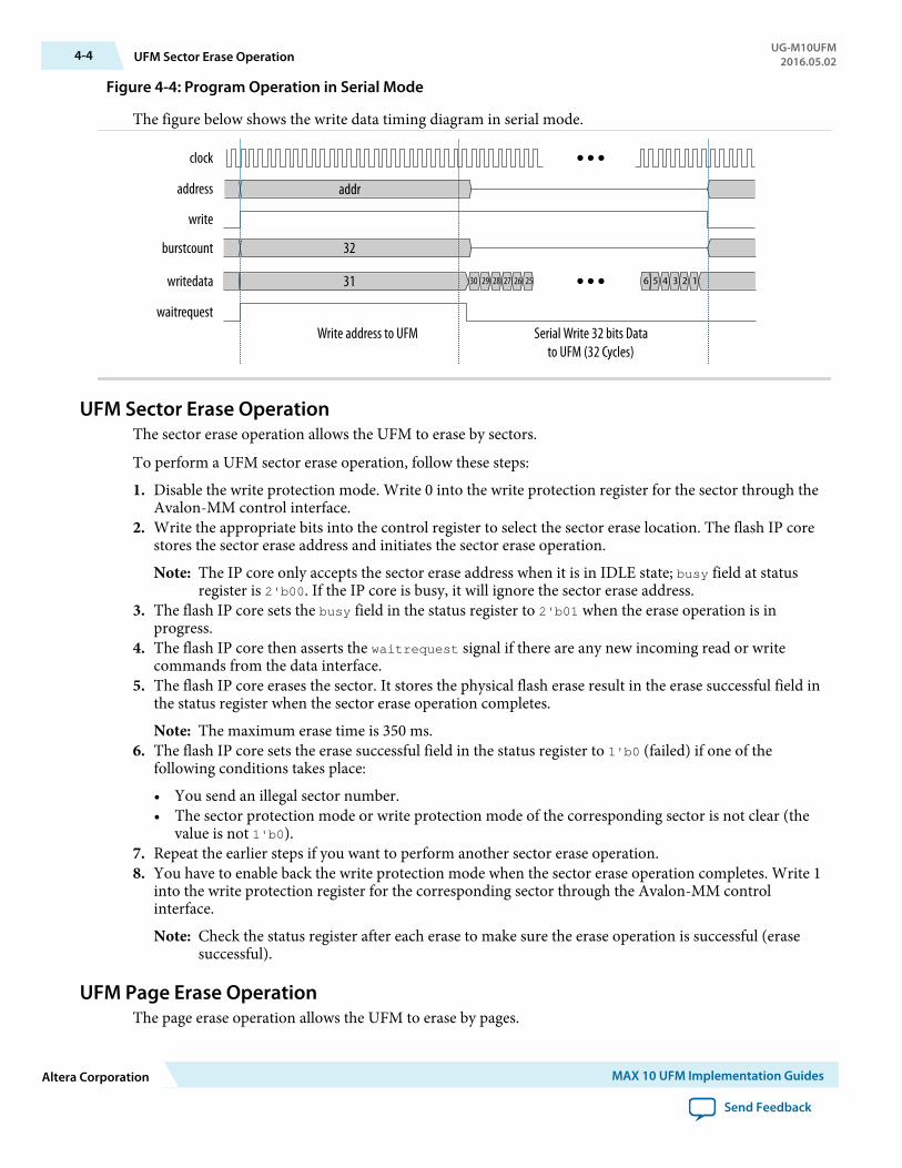
Figure 4-4: Program Operation in Serial Mode
The figure below shows the write data timing diagram in serial mode.
clock
addraddress
waitrequest
burstcount 32
writedata
write
31 30 29 28 27 26 25 56 4 3 2 1
Write address to UFM Serial Write 32 bits Datato UFM (32 Cycles)
UFM Sector Erase OperationThe sector erase operation allows the UFM to erase by sectors.
To perform a UFM sector erase operation, follow these steps:
1. Disable the write protection mode. Write 0 into the write protection register for the sector through theAvalon-MM control interface.
2. Write the appropriate bits into the control register to select the sector erase location. The flash IP corestores the sector erase address and initiates the sector erase operation.
Note: The IP core only accepts the sector erase address when it is in IDLE state; busy field at statusregister is 2'b00. If the IP core is busy, it will ignore the sector erase address.
3. The flash IP core sets the busy field in the status register to 2'b01 when the erase operation is inprogress.
4. The flash IP core then asserts the waitrequest signal if there are any new incoming read or writecommands from the data interface.
5. The flash IP core erases the sector. It stores the physical flash erase result in the erase successful field inthe status register when the sector erase operation completes.
Note: The maximum erase time is 350 ms.6. The flash IP core sets the erase successful field in the status register to 1'b0 (failed) if one of the
following conditions takes place:
• You send an illegal sector number.• The sector protection mode or write protection mode of the corresponding sector is not clear (the
value is not 1'b0).7. Repeat the earlier steps if you want to perform another sector erase operation.8. You have to enable back the write protection mode when the sector erase operation completes. Write 1
into the write protection register for the corresponding sector through the Avalon-MM controlinterface.
Note: Check the status register after each erase to make sure the erase operation is successful (erasesuccessful).
UFM Page Erase OperationThe page erase operation allows the UFM to erase by pages.
4-4 UFM Sector Erase OperationUG-M10UFM
2016.05.02
Altera Corporation MAX 10 UFM Implementation Guides
Send Feedback
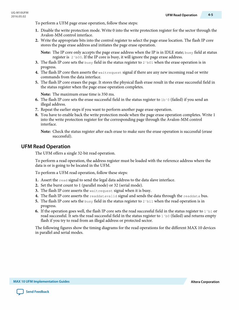
To perform a UFM page erase operation, follow these steps:
1. Disable the write protection mode. Write 0 into the write protection register for the sector through theAvalon-MM control interface.
2. Write the appropriate bits into the control register to select the page erase location. The flash IP corestores the page erase address and initiates the page erase operation.
Note: The IP core only accepts the page erase address when the IP is in IDLE state; busy field at statusregister is 2'b00. If the IP core is busy, it will ignore the page erase address.
3. The flash IP core sets the busy field in the status register to 2'b01 when the erase operation is inprogress.
4. The flash IP core then asserts the waitrequest signal if there are any new incoming read or writecommands from the data interface.
5. The flash IP core erases the page. It stores the physical flash erase result in the erase successful field inthe status register when the page erase operation completes.
Note: The maximum erase time is 350 ms.6. The flash IP core sets the erase successful field in the status register to 1b'0 (failed) if you send an
illegal address.7. Repeat the earlier steps if you want to perform another page erase operation.8. You have to enable back the write protection mode when the page erase operation completes. Write 1
into the write protection register for the corresponding page through the Avalon-MM controlinterface.
Note: Check the status register after each erase to make sure the erase operation is successful (erasesuccessful).
UFM Read OperationThe UFM offers a single 32-bit read operation.
To perform a read operation, the address register must be loaded with the reference address where thedata is or is going to be located in the UFM.
To perform a UFM read operation, follow these steps:
1. Assert the read signal to send the legal data address to the data slave interface.2. Set the burst count to 1 (parallel mode) or 32 (serial mode).3. The flash IP core asserts the waitrequest signal when it is busy.4. The flash IP core asserts the readdatavalid signal and sends the data through the readdata bus.5. The flash IP core sets the busy field in the status register to 2'b11 when the read operation is in
progress.6. If the operation goes well, the flash IP core sets the read successful field in the status register to 1'b1 or
read successful. It sets the read successful field in the status register to 1'b0 (failed) and returns emptyflash if you try to read from an illegal address or protected sector.
The following figures show the timing diagrams for the read operations for the different MAX 10 devicesin parallel and serial modes.
UG-M10UFM2016.05.02 UFM Read Operation 4-5
MAX 10 UFM Implementation Guides Altera Corporation
Send Feedback
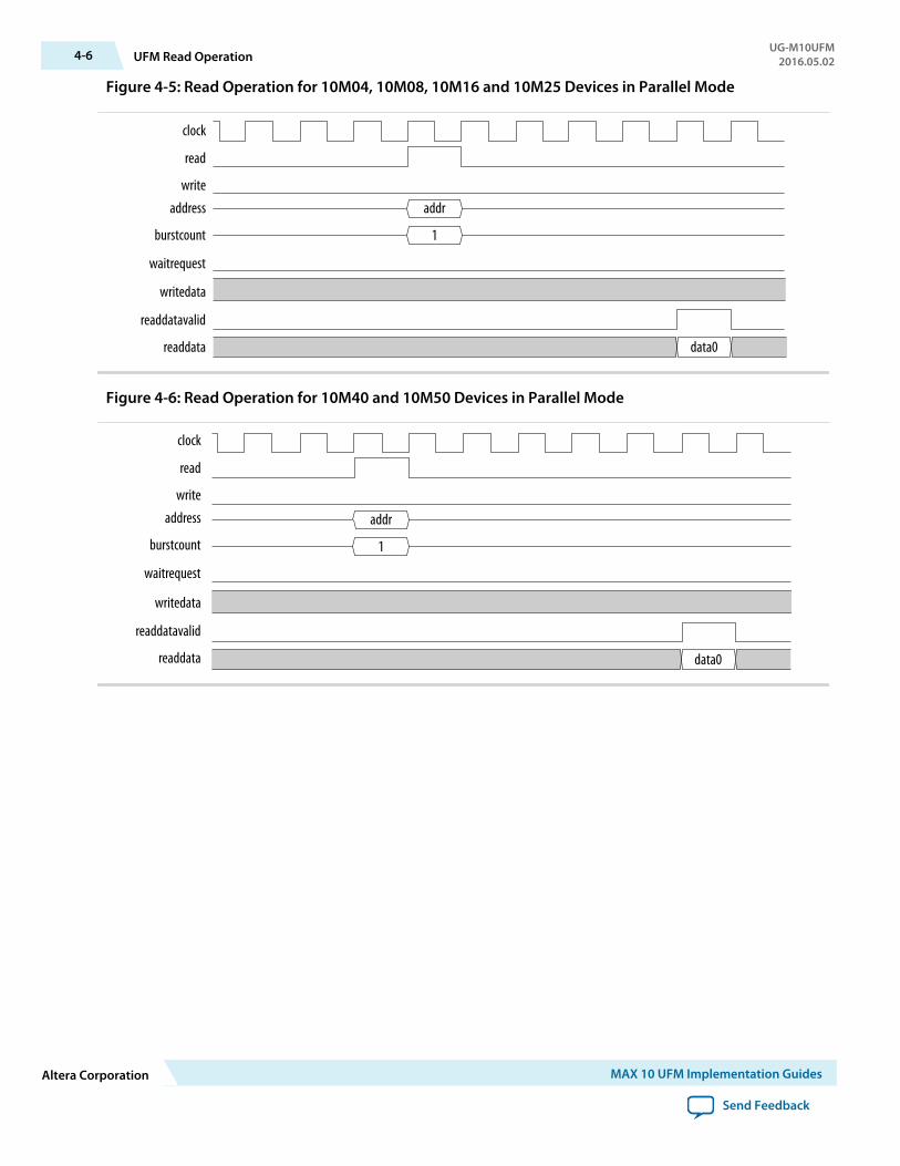
Figure 4-5: Read Operation for 10M04, 10M08, 10M16 and 10M25 Devices in Parallel Mode
clock
read
writeaddress
burstcount
waitrequest
writedata
readdatavalid
addr
1
readdata data0
Figure 4-6: Read Operation for 10M40 and 10M50 Devices in Parallel Mode
clock
read
writeaddress
burstcount
waitrequest
writedata
readdatavalid
readdata
addr
1
data0
4-6 UFM Read OperationUG-M10UFM
2016.05.02
Altera Corporation MAX 10 UFM Implementation Guides
Send Feedback
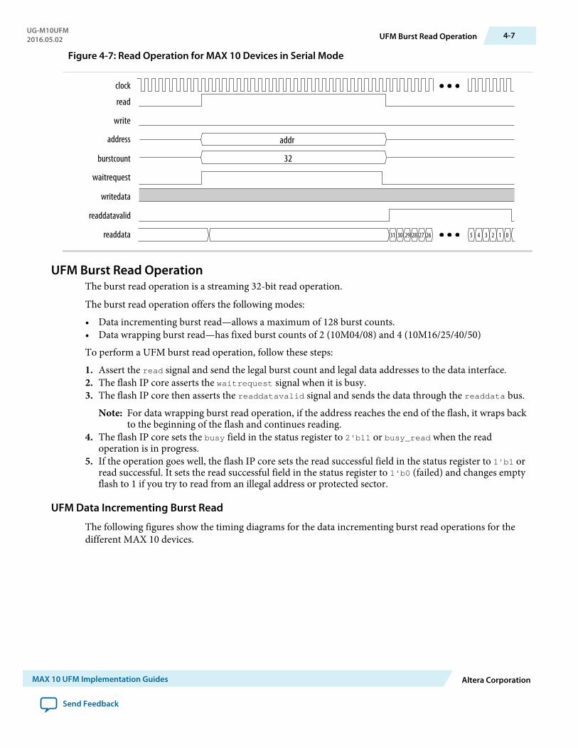
Figure 4-7: Read Operation for MAX 10 Devices in Serial Mode
clock
address addr
read
write
waitrequest
readdatavalid
readdata
burstcount 32
31 30 29 28 27 26 5 4 3 2 1 0
writedata
UFM Burst Read OperationThe burst read operation is a streaming 32-bit read operation.
The burst read operation offers the following modes:
• Data incrementing burst read—allows a maximum of 128 burst counts.• Data wrapping burst read—has fixed burst counts of 2 (10M04/08) and 4 (10M16/25/40/50)
To perform a UFM burst read operation, follow these steps:
1. Assert the read signal and send the legal burst count and legal data addresses to the data interface.2. The flash IP core asserts the waitrequest signal when it is busy.3. The flash IP core then asserts the readdatavalid signal and sends the data through the readdata bus.
Note: For data wrapping burst read operation, if the address reaches the end of the flash, it wraps backto the beginning of the flash and continues reading.
4. The flash IP core sets the busy field in the status register to 2'b11 or busy_read when the readoperation is in progress.
5. If the operation goes well, the flash IP core sets the read successful field in the status register to 1'b1 orread successful. It sets the read successful field in the status register to 1'b0 (failed) and changes emptyflash to 1 if you try to read from an illegal address or protected sector.
UFM Data Incrementing Burst Read
The following figures show the timing diagrams for the data incrementing burst read operations for thedifferent MAX 10 devices.
UG-M10UFM2016.05.02 UFM Burst Read Operation 4-7
MAX 10 UFM Implementation Guides Altera Corporation
Send Feedback
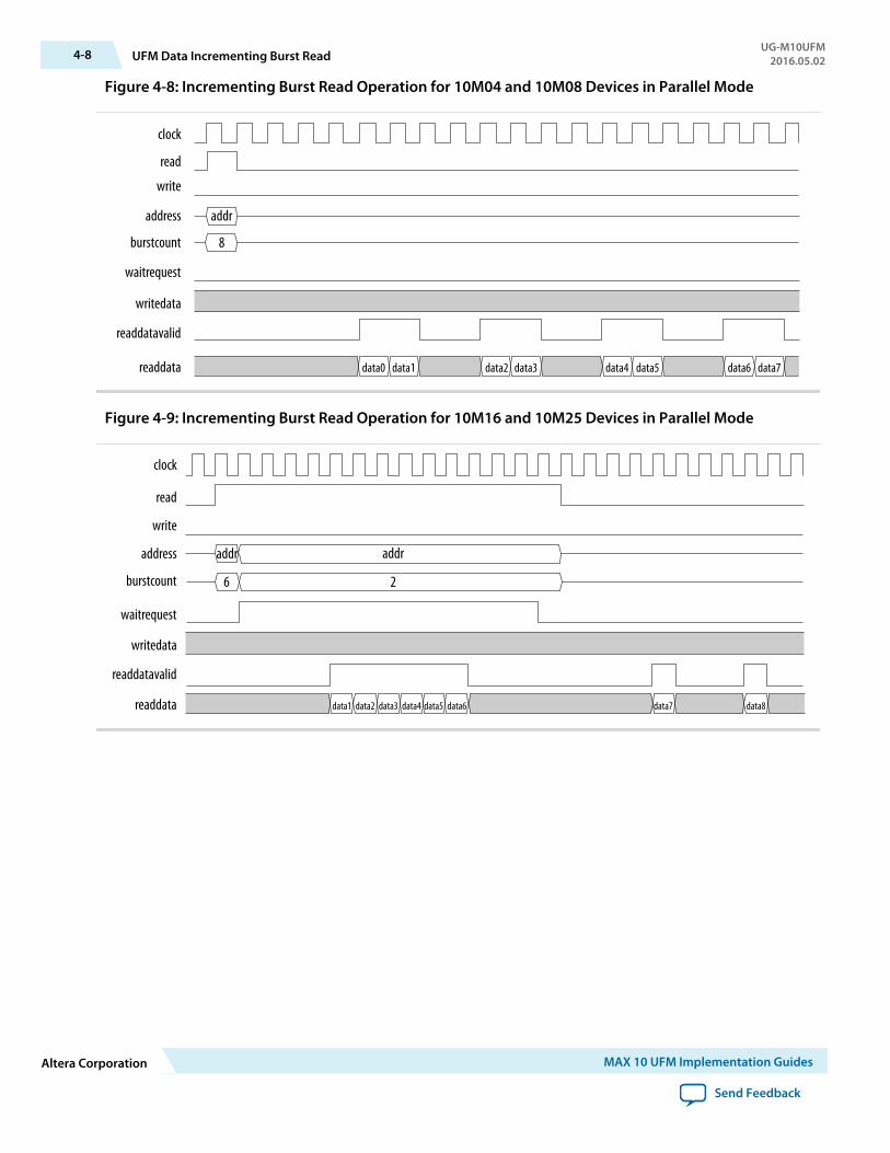
Figure 4-8: Incrementing Burst Read Operation for 10M04 and 10M08 Devices in Parallel Mode
clock
read
write
address
burstcount
waitrequest
writedata
readdatavalid
readdata
addr
8
data0 data1 data4data2 data3 data5 data6 data7
Figure 4-9: Incrementing Burst Read Operation for 10M16 and 10M25 Devices in Parallel Mode
clock
read
write
address
burstcount
waitrequest
writedata
readdatavalid
readdata
addr
data1 data2 data3 data4 data5 data6 data7 data8
addr
6 2
4-8 UFM Data Incrementing Burst ReadUG-M10UFM
2016.05.02
Altera Corporation MAX 10 UFM Implementation Guides
Send Feedback
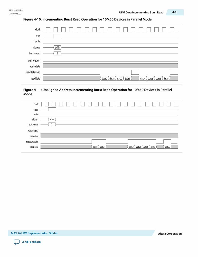
Figure 4-10: Incrementing Burst Read Operation for 10M50 Devices in Parallel Mode
clock
read
write
address
burstcount
waitrequest
writedata
readdatavalid
readdata
addr
data0
8
data1 data2 data4data3 data5 data6 data7
Figure 4-11: Unaligned Address Incrementing Burst Read Operation for 10M50 Devices in ParallelMode
clock
read
write
address
burstcount
waitrequest
writedata
readdatavalid
readdata
addr
data0
7
data4 data5 data6data1 data2 data3
UG-M10UFM2016.05.02 UFM Data Incrementing Burst Read 4-9
MAX 10 UFM Implementation Guides Altera Corporation
Send Feedback
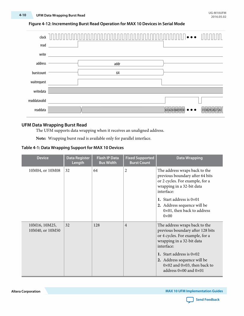
Figure 4-12: Incrementing Burst Read Operation for MAX 10 Devices in Serial Mode
clock
address addr
read
write
waitrequest
readdatavalid
burstcount 64
writedata
readdata 63 62 61 60 59 58 31 30 29 28 27 26
UFM Data Wrapping Burst ReadThe UFM supports data wrapping when it receives an unaligned address.
Note: Wrapping burst read is available only for parallel interface.
Table 4-1: Data Wrapping Support for MAX 10 Devices
Device Data RegisterLength
Flash IP DataBus Width
Fixed SupportedBurst Count
Data Wrapping
10M04, or 10M08 32 64 2 The address wraps back to theprevious boundary after 64 bitsor 2 cycles. For example, for awrapping in a 32-bit datainterface:
1. Start address is 0×012. Address sequence will be
0×01, then back to address0×00
10M16, 10M25,10M40, or 10M50
32 128 4 The address wraps back to theprevious boundary after 128 bitsor 4 cycles. For example, for awrapping in a 32-bit datainterface:
1. Start address is 0×022. Address sequence will be
0×02 and 0×03, then back toaddress 0×00 and 0×01
4-10 UFM Data Wrapping Burst ReadUG-M10UFM
2016.05.02
Altera Corporation MAX 10 UFM Implementation Guides
Send Feedback
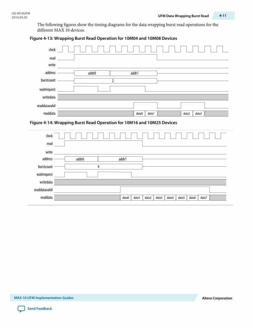
The following figures show the timing diagrams for the data wrapping burst read operations for thedifferent MAX 10 devices.
Figure 4-13: Wrapping Burst Read Operation for 10M04 and 10M08 Devices
clock
read
write
address
burstcount
waitrequest
writedata
readdatavalid
readdata
addr0
data0
2
data1 data2 data3
addr1
Figure 4-14: Wrapping Burst Read Operation for 10M16 and 10M25 Devices
clock
read
write
address
burstcount
waitrequest
writedata
readdatavalid
readdata data0
4
data7
addr0 addr1
data1 data2 data3 data4 data5 data6
UG-M10UFM2016.05.02 UFM Data Wrapping Burst Read 4-11
MAX 10 UFM Implementation Guides Altera Corporation
Send Feedback
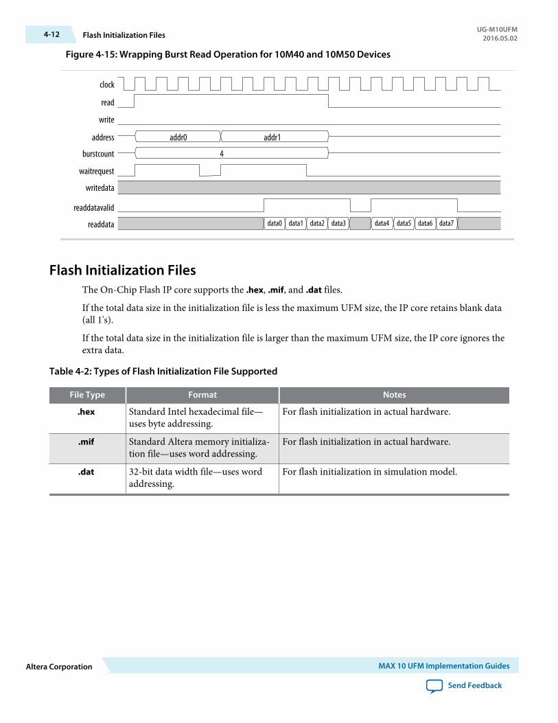
Figure 4-15: Wrapping Burst Read Operation for 10M40 and 10M50 Devices
clock
read
write
address
burstcount
waitrequest
writedata
readdatavalid
readdata
4
addr0 addr1
data0 data1 data2 data3 data4 data5 data6 data7
Flash Initialization FilesThe On-Chip Flash IP core supports the .hex, .mif, and .dat files.
If the total data size in the initialization file is less the maximum UFM size, the IP core retains blank data(all 1's).
If the total data size in the initialization file is larger than the maximum UFM size, the IP core ignores theextra data.
Table 4-2: Types of Flash Initialization File Supported
File Type Format Notes
.hex Standard Intel hexadecimal file—uses byte addressing.
For flash initialization in actual hardware.
.mif Standard Altera memory initializa‐tion file—uses word addressing.
For flash initialization in actual hardware.
.dat 32-bit data width file—uses wordaddressing.
For flash initialization in simulation model.
4-12 Flash Initialization FilesUG-M10UFM
2016.05.02
Altera Corporation MAX 10 UFM Implementation Guides
Send Feedback
Altera On-Chip Flash IP Core References 52016.05.02
UG-M10UFM Subscribe Send Feedback
This section provides information about the Altera On-Chip Flash IP Core parameters, signals, andregisters.
Altera On-Chip Flash ParametersThe following table lists the parameters for the Altera On-Chip Flash IP core.
Table 5-1: Altera On-Chip Flash IP Core Parameters
Parameters Default Value Description
Data interface Parallel Allows you to select the type of interface. You canchoose parallel or serial.
Read burst mode Incrementing Allows you to select the type of read burst mode. Youcan choose incrementing or wrapping.
Incrementing mode
Read burst count is 2, 4, 8, ... 128
Wrappingmode
Burst count fixed to 2 or 4
Note: Serial interface supports onlyincrementing mode. Parallel interface doesnot support wrapping mode for 10M02devices.
Read burst count 2 Allows you the flexibility to adjust the maximumburst count bus width.
• Parallel mode: This setting represents themaximum burst count number.
• Serial mode: This setting supports stream readand represents the words to be read for each readoperation. The Avalon-MM interface burst countbus width is equal to 32*read burst count.
© 2016 Altera Corporation. All rights reserved. ALTERA, ARRIA, CYCLONE, ENPIRION, MAX, MEGACORE, NIOS, QUARTUS and STRATIX words and logos aretrademarks of Altera Corporation and registered in the U.S. Patent and Trademark Office and in other countries. All other words and logos identified astrademarks or service marks are the property of their respective holders as described at www.altera.com/common/legal.html. Altera warrants performanceof its semiconductor products to current specifications in accordance with Altera's standard warranty, but reserves the right to make changes to anyproducts and services at any time without notice. Altera assumes no responsibility or liability arising out of the application or use of any information,product, or service described herein except as expressly agreed to in writing by Altera. Altera customers are advised to obtain the latest version of devicespecifications before relying on any published information and before placing orders for products or services.
ISO9001:2008Registered
www.altera.com101 Innovation Drive, San Jose, CA 95134
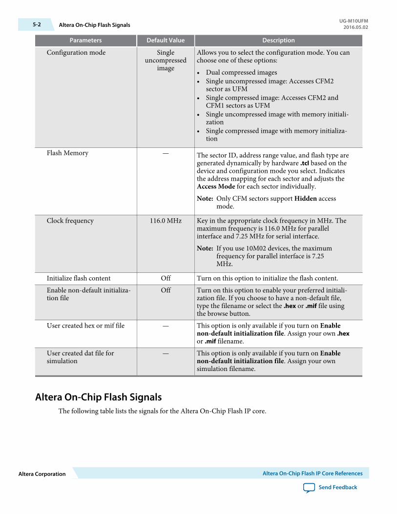
Parameters Default Value Description
Configuration mode Singleuncompressed
image
Allows you to select the configuration mode. You canchoose one of these options:
• Dual compressed images• Single uncompressed image: Accesses CFM2
sector as UFM• Single compressed image: Accesses CFM2 and
CFM1 sectors as UFM• Single uncompressed image with memory initiali‐
zation• Single compressed image with memory initializa‐
tion
Flash Memory — The sector ID, address range value, and flash type aregenerated dynamically by hardware .tcl based on thedevice and configuration mode you select. Indicatesthe address mapping for each sector and adjusts theAccess Mode for each sector individually.
Note: Only CFM sectors support Hidden accessmode.
Clock frequency 116.0 MHz Key in the appropriate clock frequency in MHz. Themaximum frequency is 116.0 MHz for parallelinterface and 7.25 MHz for serial interface.
Note: If you use 10M02 devices, the maximumfrequency for parallel interface is 7.25MHz.
Initialize flash content Off Turn on this option to initialize the flash content.Enable non-default initializa‐tion file
Off Turn on this option to enable your preferred initiali‐zation file. If you choose to have a non-default file,type the filename or select the .hex or .mif file usingthe browse button.
User created hex or mif file — This option is only available if you turn on Enablenon-default initialization file. Assign your own .hexor .mif filename.
User created dat file forsimulation
— This option is only available if you turn on Enablenon-default initialization file. Assign your ownsimulation filename.
Altera On-Chip Flash SignalsThe following table lists the signals for the Altera On-Chip Flash IP core.
5-2 Altera On-Chip Flash SignalsUG-M10UFM
2016.05.02
Altera Corporation Altera On-Chip Flash IP Core References
Send Feedback
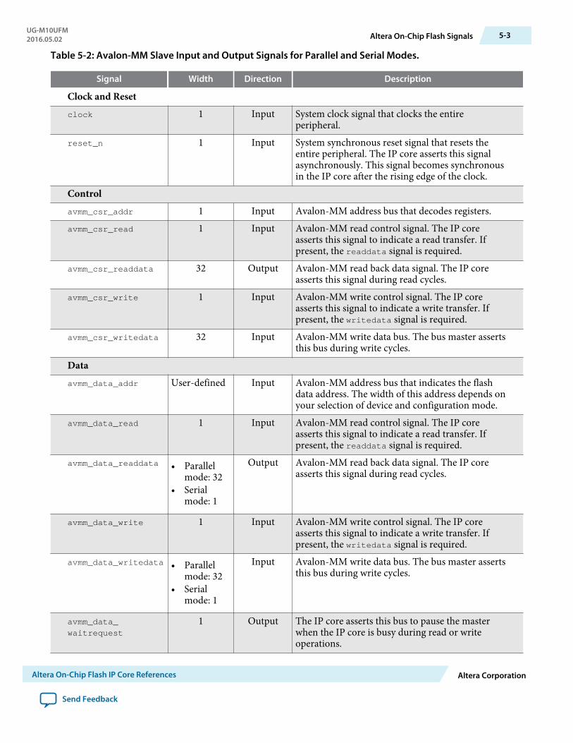
Table 5-2: Avalon-MM Slave Input and Output Signals for Parallel and Serial Modes.
Signal Width Direction Description
Clock and Resetclock 1 Input System clock signal that clocks the entire
peripheral.reset_n 1 Input System synchronous reset signal that resets the
entire peripheral. The IP core asserts this signalasynchronously. This signal becomes synchronousin the IP core after the rising edge of the clock.
Controlavmm_csr_addr 1 Input Avalon-MM address bus that decodes registers.avmm_csr_read 1 Input Avalon-MM read control signal. The IP core
asserts this signal to indicate a read transfer. Ifpresent, the readdata signal is required.
avmm_csr_readdata 32 Output Avalon-MM read back data signal. The IP coreasserts this signal during read cycles.
avmm_csr_write 1 Input Avalon-MM write control signal. The IP coreasserts this signal to indicate a write transfer. Ifpresent, the writedata signal is required.
avmm_csr_writedata 32 Input Avalon-MM write data bus. The bus master assertsthis bus during write cycles.
Dataavmm_data_addr User-defined Input Avalon-MM address bus that indicates the flash
data address. The width of this address depends onyour selection of device and configuration mode.
avmm_data_read 1 Input Avalon-MM read control signal. The IP coreasserts this signal to indicate a read transfer. Ifpresent, the readdata signal is required.
avmm_data_readdata • Parallelmode: 32
• Serialmode: 1
Output Avalon-MM read back data signal. The IP coreasserts this signal during read cycles.
avmm_data_write 1 Input Avalon-MM write control signal. The IP coreasserts this signal to indicate a write transfer. Ifpresent, the writedata signal is required.
avmm_data_writedata • Parallelmode: 32
• Serialmode: 1
Input Avalon-MM write data bus. The bus master assertsthis bus during write cycles.
avmm_data_
waitrequest
1 Output The IP core asserts this bus to pause the masterwhen the IP core is busy during read or writeoperations.
UG-M10UFM2016.05.02 Altera On-Chip Flash Signals 5-3
Altera On-Chip Flash IP Core References Altera Corporation
Send Feedback
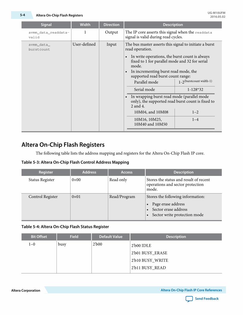
Signal Width Direction Description
avmm_data_readdata-
valid
1 Output The IP core asserts this signal when the readdatasignal is valid during read cycles.
avmm_data_
burstcount
User-defined Input The bus master asserts this signal to initiate a burstread operation.
• In write operations, the burst count is alwaysfixed to 1 for parallel mode and 32 for serialmode.
• In incrementing burst read mode, thesupported read burst count range:
Parallel mode 1-2(burstcount width-1)
Serial mode 1-128*32• In wrapping burst read mode (parallel mode
only), the supported read burst count is fixed to2 and 4.
10M04, and 10M08 1–210M16, 10M25,10M40 and 10M50
1–4
Altera On-Chip Flash RegistersThe following table lists the address mapping and registers for the Altera On-Chip Flash IP core.
Table 5-3: Altera On-Chip Flash Control Address Mapping
Register Address Access Description
Status Register 0×00 Read only Stores the status and result of recentoperations and sector protectionmode.
Control Register 0×01 Read/Program Stores the following information:
• Page erase address• Sector erase address• Sector write protection mode
Table 5-4: Altera On-Chip Flash Status Register
Bit Offset Field Default Value Description
1–0 busy 2'b00 2'b00 IDLE
2'b01 BUSY_ERASE
2'b10 BUSY_WRITE
2'b11 BUSY_READ
5-4 Altera On-Chip Flash RegistersUG-M10UFM
2016.05.02
Altera Corporation Altera On-Chip Flash IP Core References
Send Feedback
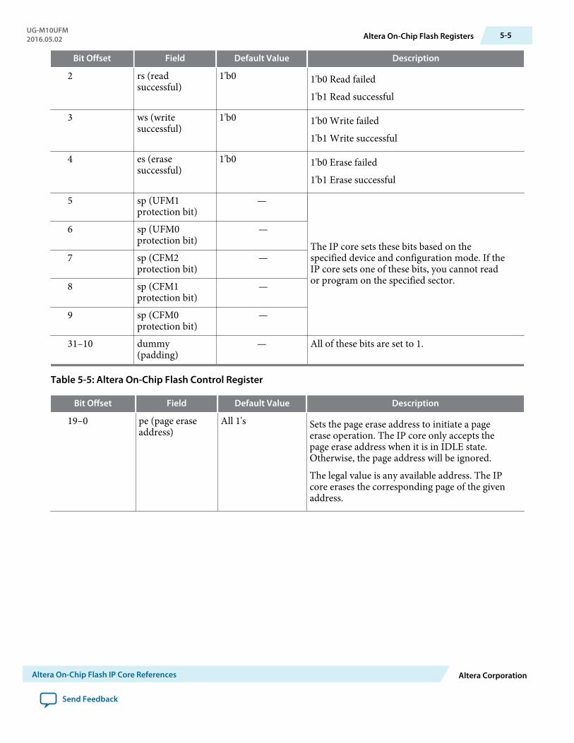
Bit Offset Field Default Value Description
2 rs (readsuccessful)
1'b0 1'b0 Read failed
1'b1 Read successful
3 ws (writesuccessful)
1'b0 1'b0 Write failed
1'b1 Write successful
4 es (erasesuccessful)
1'b0 1'b0 Erase failed
1'b1 Erase successful
5 sp (UFM1protection bit)
—
The IP core sets these bits based on thespecified device and configuration mode. If theIP core sets one of these bits, you cannot reador program on the specified sector.
6 sp (UFM0protection bit)
—
7 sp (CFM2protection bit)
—
8 sp (CFM1protection bit)
—
9 sp (CFM0protection bit)
—
31–10 dummy(padding)
— All of these bits are set to 1.
Table 5-5: Altera On-Chip Flash Control Register
Bit Offset Field Default Value Description
19–0 pe (page eraseaddress)
All 1's Sets the page erase address to initiate a pageerase operation. The IP core only accepts thepage erase address when it is in IDLE state.Otherwise, the page address will be ignored.
The legal value is any available address. The IPcore erases the corresponding page of the givenaddress.
UG-M10UFM2016.05.02 Altera On-Chip Flash Registers 5-5
Altera On-Chip Flash IP Core References Altera Corporation
Send Feedback
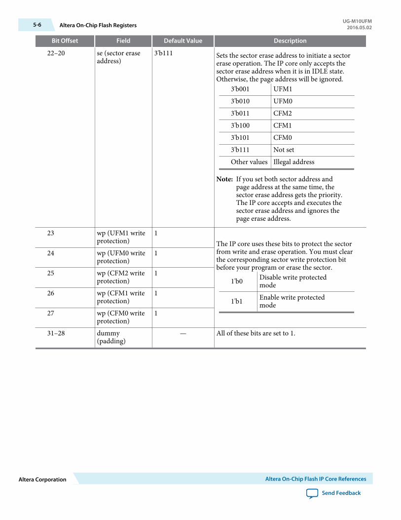
Bit Offset Field Default Value Description
22–20 se (sector eraseaddress)
3'b111 Sets the sector erase address to initiate a sectorerase operation. The IP core only accepts thesector erase address when it is in IDLE state.Otherwise, the page address will be ignored.
3'b001 UFM13'b010 UFM03'b011 CFM23'b100 CFM13'b101 CFM03'b111 Not setOther values Illegal address
Note: If you set both sector address andpage address at the same time, thesector erase address gets the priority.The IP core accepts and executes thesector erase address and ignores thepage erase address.
23 wp (UFM1 writeprotection)
1The IP core uses these bits to protect the sectorfrom write and erase operation. You must clearthe corresponding sector write protection bitbefore your program or erase the sector.
1'b0 Disable write protectedmode
1'b1 Enable write protectedmode
24 wp (UFM0 writeprotection)
1
25 wp (CFM2 writeprotection)
1
26 wp (CFM1 writeprotection)
1
27 wp (CFM0 writeprotection)
1
31–28 dummy(padding)
— All of these bits are set to 1.
5-6 Altera On-Chip Flash RegistersUG-M10UFM
2016.05.02
Altera Corporation Altera On-Chip Flash IP Core References
Send Feedback
MAX 10 User Flash Memory User Guide Archive A2016.05.02
UG-M10UFM Subscribe Send Feedback
If an IP core version is not listed, the user guide for the previous IP core version applies.IP Core Version User Guide
15.1 MAX 10 User Flash Memory User Guide
15.0 MAX 10 User Flash Memory User Guide
14.1 MAX 10 User Flash Memory User Guide
© 2016 Altera Corporation. All rights reserved. ALTERA, ARRIA, CYCLONE, ENPIRION, MAX, MEGACORE, NIOS, QUARTUS and STRATIX words and logos aretrademarks of Altera Corporation and registered in the U.S. Patent and Trademark Office and in other countries. All other words and logos identified astrademarks or service marks are the property of their respective holders as described at www.altera.com/common/legal.html. Altera warrants performanceof its semiconductor products to current specifications in accordance with Altera's standard warranty, but reserves the right to make changes to anyproducts and services at any time without notice. Altera assumes no responsibility or liability arising out of the application or use of any information,product, or service described herein except as expressly agreed to in writing by Altera. Altera customers are advised to obtain the latest version of devicespecifications before relying on any published information and before placing orders for products or services.
ISO9001:2008Registered
www.altera.com101 Innovation Drive, San Jose, CA 95134
Document Revision History for MAX 10 UserFlash Memory User Guide B
2016.05.02
UG-M10UFM Subscribe Send Feedback
Date Version Changes
May 2016 2016.05.02 • Added the typical and minimum UFM programming time in parallelmode.
• Corrected the minimum UFM reset time in parallel mode to 250 ns.• Added links to archived versions of the MAX 10 User Flash Memory
User Guide.
November2015
2015.11.02 • Added information about the supported flash initialization files.• Added serial interface support for 10M40 and 10M50 devices. The
maximum frequency for MAX 10 devices is 7.25 MHz, except for10M40 and 10M50 devices, which is 4.81 MHz.
• Added parallel interface support for 10M02 devices. The maximumfrequency for MAX 10 devices is 116 MHz, except for 10M02 devices,which is 7.25 MHz.
• Changed instances of Quartus II to Quartus Prime.
May 2015 2015.05.04 • Changed write to industry-standard term program.• Added a note to the UFM and CFM Array Size section that the total
UFM size is the maximum possible value, which is dependent on theselected mode.
• Added design consideration information about the maximum slewrate requirement for power supply ramp down.
• Added design consideration information about erasing the flashlocation before performing a program operation.
© 2016 Altera Corporation. All rights reserved. ALTERA, ARRIA, CYCLONE, ENPIRION, MAX, MEGACORE, NIOS, QUARTUS and STRATIX words and logos aretrademarks of Altera Corporation and registered in the U.S. Patent and Trademark Office and in other countries. All other words and logos identified astrademarks or service marks are the property of their respective holders as described at www.altera.com/common/legal.html. Altera warrants performanceof its semiconductor products to current specifications in accordance with Altera's standard warranty, but reserves the right to make changes to anyproducts and services at any time without notice. Altera assumes no responsibility or liability arising out of the application or use of any information,product, or service described herein except as expressly agreed to in writing by Altera. Altera customers are advised to obtain the latest version of devicespecifications before relying on any published information and before placing orders for products or services.
ISO9001:2008Registered
www.altera.com101 Innovation Drive, San Jose, CA 95134
Date Version Changes
December2014
2014.12.15 • Added support for serial interface.• Added maximum operating frequency of 7.25 MHz for serial
interface.• Updated the UFM block diagram to include serial interface.• Added design consideration information about creating initial
memory content using the IP core, and programming UFM usingJTAG interface version IEEE Standard 1149.1.
• Added new timing diagrams for read and write operations in serialmode.
• Added information for the new serial interface related GUIparameters, signals, and registers.
• Added information for the following new Avalon-MM slave interfacesignals for serial mode: addr, read, readdata, write, writedata,waitrequest, readdatavalid, and burstcount.
• Added information for the following new parameters:
• Data Interface that allows you to choose between Parallel andSerial interface.
• Configuration Scheme and Configuration Mode that replaceDual Images. The new parameters include all supported configu‐ration modes.
• Read Burst Count that allows the burst count width to be auto-adjusted.
September2014
2014.09.22 Initial release.
B-2 Document Revision History for MAX 10 User Flash Memory User GuideUG-M10UFM
2016.05.02
Altera Corporation Document Revision History for MAX 10 User Flash Memory User Guide
Send Feedback

MAX 10 JTAG Boundary-Scan TestingUser Guide
Subscribe
Send Feedback
UG-M10JTAG2015.05.04
101 Innovation DriveSan Jose, CA 95134www.altera.com
Contents
Overview.............................................................................................................. 1-1
JTAG BST Architecture.......................................................................................2-1JTAG Pins..................................................................................................................................................... 2-1JTAG Circuitry Functional Model............................................................................................................ 2-1JTAG Boundary-Scan Register...................................................................................................................2-2
Boundary-Scan Cells in MAX 10 I/O Pin.....................................................................................2-3
JTAG BST Operation Control............................................................................ 3-1JTAG IDCODE ........................................................................................................................................... 3-1JTAG Secure Mode...................................................................................................................................... 3-2JTAG Private instruction............................................................................................................................ 3-2JTAG Instructions........................................................................................................................................3-2
I/O Voltage Support in the JTAG Chain............................................................ 4-1
Enabling and Disabling JTAG BST Circuitry.....................................................5-1
Guidelines for JTAG BST....................................................................................6-1
Boundary-Scan Description Language Support.................................................7-1
Additional Information for MAX 10 JTAG Boundary-Scan Testing UserGuide .............................................................................................................. A-1
Document Revision History for MAX 10 JTAG Boundary-Scan Testing User Guide..................... A-1
TOC-2
Altera Corporation
Overview 12015.05.04
UG-M10JTAG Subscribe Send Feedback
MAX® 10 devices support the IEEE Std.1149.1 (JTAG) boundary-scan testing (BST).
When you perform BST, you can test pin connections without using physical test probes and capturefunctional data during normal operation. The boundary-scan cells (BSCs) in a device can force signalsonto pins, or capture data from pin or core logic signals. Forced test data is serially shifted into the BSCs.Captured data is serially shifted out and externally compared to expected results.
Note: You can perform BST on MAX 10 devices before, after, and during configuration.
Related Information
• MAX 10 FPGA Configuration User GuideProvides more information about JTAG in-system programming.
• JTAG BST Architecture on page 2-1• JTAG Boundary-Scan Register on page 2-2• JTAG BST Operation Control on page 3-1• I/O Voltage Support in the JTAG Chain on page 4-1• Enabling and Disabling JTAG BST Circuitry on page 5-1• Guidelines for JTAG BST on page 6-1• Boundary-Scan Description Language Support on page 7-1
© 2015 Altera Corporation. All rights reserved. ALTERA, ARRIA, CYCLONE, ENPIRION, MAX, MEGACORE, NIOS, QUARTUS and STRATIX words and logos aretrademarks of Altera Corporation and registered in the U.S. Patent and Trademark Office and in other countries. All other words and logos identified astrademarks or service marks are the property of their respective holders as described at www.altera.com/common/legal.html. Altera warrants performanceof its semiconductor products to current specifications in accordance with Altera's standard warranty, but reserves the right to make changes to anyproducts and services at any time without notice. Altera assumes no responsibility or liability arising out of the application or use of any information,product, or service described herein except as expressly agreed to in writing by Altera. Altera customers are advised to obtain the latest version of devicespecifications before relying on any published information and before placing orders for products or services.
ISO9001:2008Registered
www.altera.com101 Innovation Drive, San Jose, CA 95134
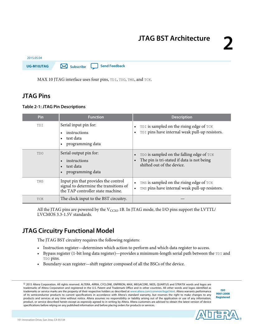
JTAG BST Architecture 22015.05.04
UG-M10JTAG Subscribe Send Feedback
MAX 10 JTAG interface uses four pins, TDI, TDO, TMS, and TCK.
JTAG PinsTable 2-1: JTAG Pin Descriptions
Pin Function Description
TDI Serial input pin for:
• instructions• test data• programming data
• TDI is sampled on the rising edge of TCK• TDI pins have internal weak pull-up resistors.
TDO Serial output pin for:
• instructions• test data• programming data
• TDO is sampled on the falling edge of TCK• The pin is tri-stated if data is not being
shifted out of the device.
TMS Input pin that provides the controlsignal to determine the transitions ofthe TAP controller state machine.
• TMS is sampled on the rising edge of TCK• TMS pins have internal weak pull-up resistors.
TCK The clock input to the BST circuitry. —
All the JTAG pins are powered by the VCCIO 1B. In JTAG mode, the I/O pins support the LVTTL/LVCMOS 3.3-1.5V standards.
JTAG Circuitry Functional ModelThe JTAG BST circuitry requires the following registers:
• Instruction register—determines which action to perform and which data register to access.• Bypass register (1-bit long data register)—provides a minimum-length serial path between the TDI and
TDO pins.• Boundary-scan register—shift register composed of all the BSCs of the device.
© 2015 Altera Corporation. All rights reserved. ALTERA, ARRIA, CYCLONE, ENPIRION, MAX, MEGACORE, NIOS, QUARTUS and STRATIX words and logos aretrademarks of Altera Corporation and registered in the U.S. Patent and Trademark Office and in other countries. All other words and logos identified astrademarks or service marks are the property of their respective holders as described at www.altera.com/common/legal.html. Altera warrants performanceof its semiconductor products to current specifications in accordance with Altera's standard warranty, but reserves the right to make changes to anyproducts and services at any time without notice. Altera assumes no responsibility or liability arising out of the application or use of any information,product, or service described herein except as expressly agreed to in writing by Altera. Altera customers are advised to obtain the latest version of devicespecifications before relying on any published information and before placing orders for products or services.
ISO9001:2008Registered
www.altera.com101 Innovation Drive, San Jose, CA 95134
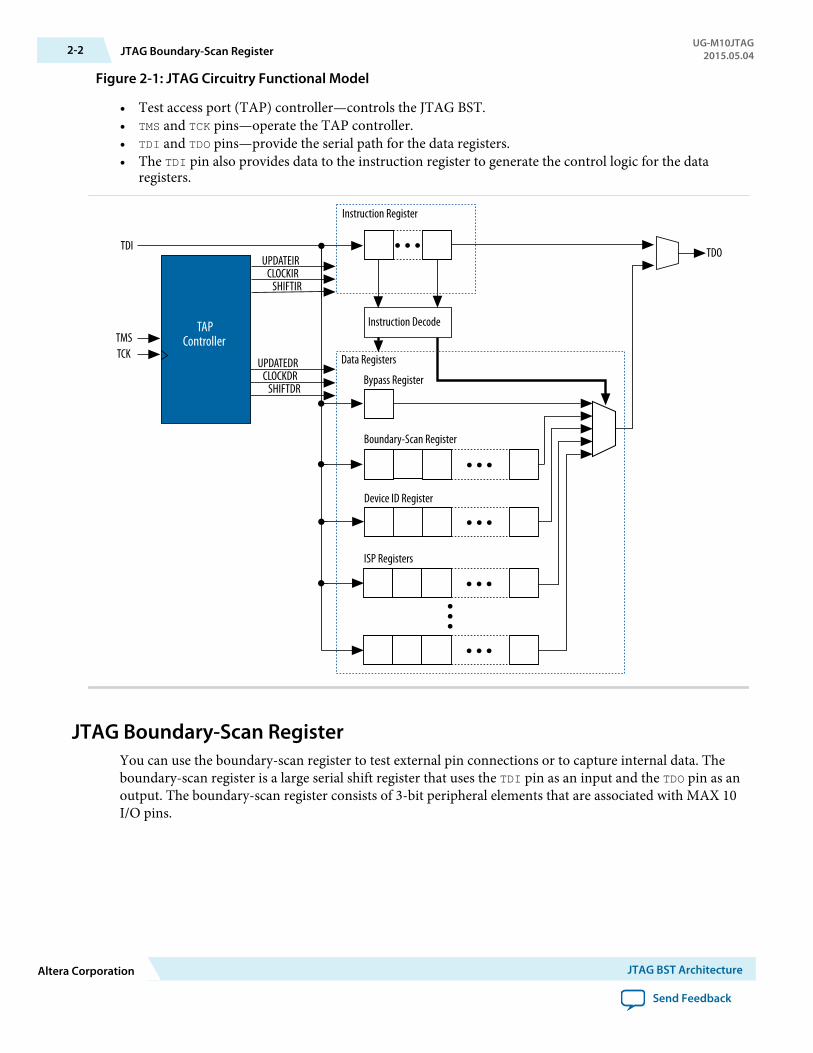
Figure 2-1: JTAG Circuitry Functional Model
• Test access port (TAP) controller—controls the JTAG BST.• TMS and TCK pins—operate the TAP controller.• TDI and TDO pins—provide the serial path for the data registers.• The TDI pin also provides data to the instruction register to generate the control logic for the data
registers.
a
UPDATEIRCLOCKIR
SHIFTIR
UPDATEDRCLOCKDR
SHIFTDR
TDI
Instruction Register
Bypass Register
Boundary-Scan Register
Instruction DecodeTMSTCK
TAPController
ISP Registers
TDO
Data Registers
Device ID Register
JTAG Boundary-Scan RegisterYou can use the boundary-scan register to test external pin connections or to capture internal data. Theboundary-scan register is a large serial shift register that uses the TDI pin as an input and the TDO pin as anoutput. The boundary-scan register consists of 3-bit peripheral elements that are associated with MAX 10I/O pins.
2-2 JTAG Boundary-Scan RegisterUG-M10JTAG
2015.05.04
Altera Corporation JTAG BST Architecture
Send Feedback
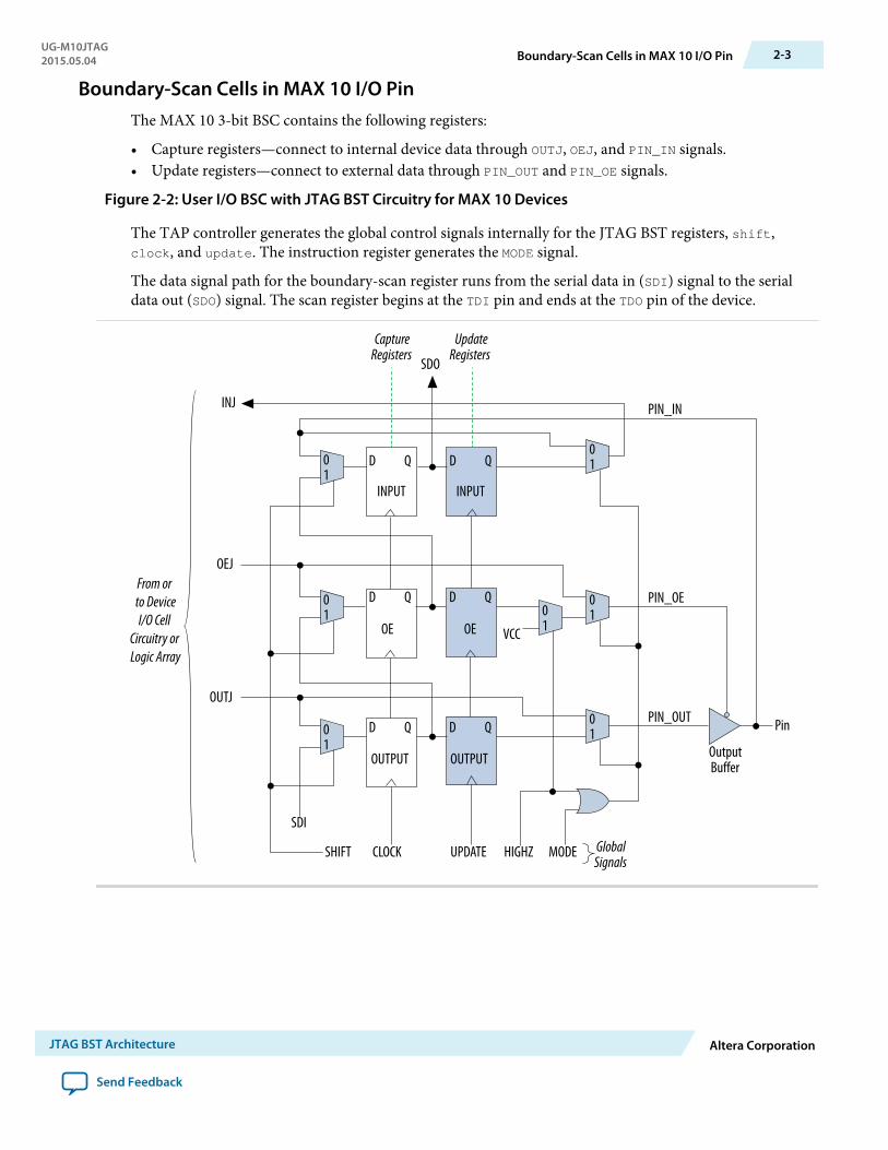
Boundary-Scan Cells in MAX 10 I/O PinThe MAX 10 3-bit BSC contains the following registers:
• Capture registers—connect to internal device data through OUTJ, OEJ, and PIN_IN signals.• Update registers—connect to external data through PIN_OUT and PIN_OE signals.
Figure 2-2: User I/O BSC with JTAG BST Circuitry for MAX 10 Devices
The TAP controller generates the global control signals internally for the JTAG BST registers, shift,clock, and update. The instruction register generates the MODE signal.
The data signal path for the boundary-scan register runs from the serial data in (SDI) signal to the serialdata out (SDO) signal. The scan register begins at the TDI pin and ends at the TDO pin of the device.
01
OUTPUT
OE
INPUTINPUT
OUTPUT
OE
From or to DeviceI/O Cell
Circuitry or Logic Array
01
010
1
010
1
01
PIN_OUT
INJ
OEJ
OUTJ
VCC
SDO
Pin
SHIFT
SDI
CLOCK HIGHZ MODE
PIN_OE
PIN_IN
OutputBuffer
CaptureRegisters
UpdateRegisters
GlobalSignals
UPDATE
D Q
D Q
D Q D Q
D Q
D Q
UG-M10JTAG2015.05.04 Boundary-Scan Cells in MAX 10 I/O Pin 2-3
JTAG BST Architecture Altera Corporation
Send Feedback
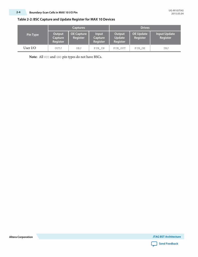
Table 2-2: BSC Capture and Update Register for MAX 10 Devices
Pin Type
Captures Drives
OutputCaptureRegister
OE CaptureRegister
InputCaptureRegister
OutputUpdateRegister
OE UpdateRegister
Input UpdateRegister
User I/O OUTJ OEJ PIN_IN PIN_OUT PIN_OE INJ
Note: All VCC and GND pin types do not have BSCs.
2-4 Boundary-Scan Cells in MAX 10 I/O PinUG-M10JTAG
2015.05.04
Altera Corporation JTAG BST Architecture
Send Feedback
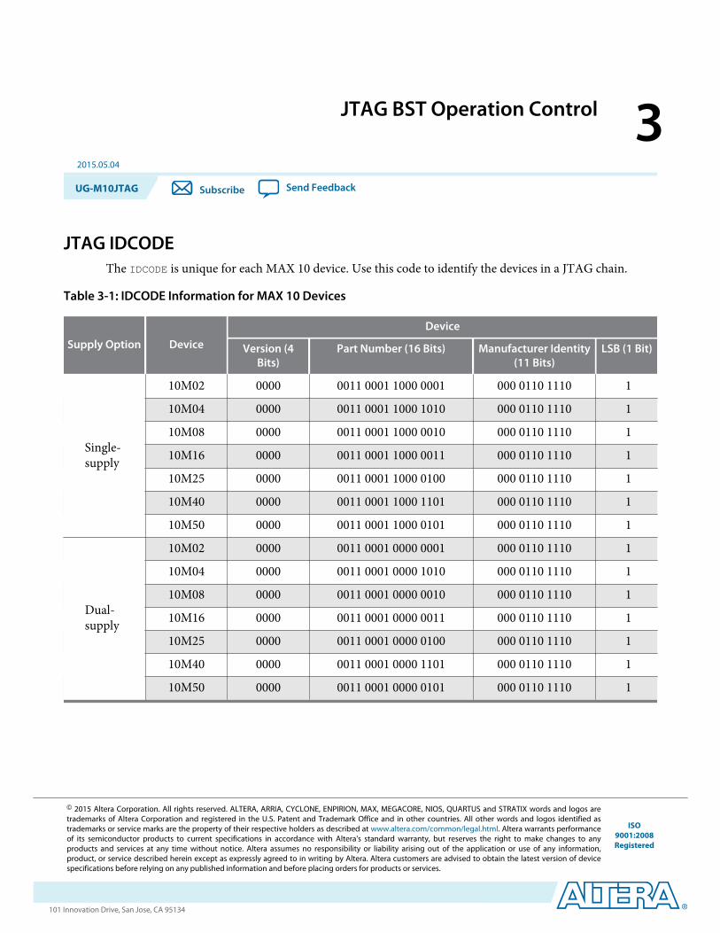
JTAG BST Operation Control 32015.05.04
UG-M10JTAG Subscribe Send Feedback
JTAG IDCODEThe IDCODE is unique for each MAX 10 device. Use this code to identify the devices in a JTAG chain.
Table 3-1: IDCODE Information for MAX 10 Devices
Supply Option Device
Device
Version (4Bits)
Part Number (16 Bits) Manufacturer Identity(11 Bits)
LSB (1 Bit)
Single-supply
10M02 0000 0011 0001 1000 0001 000 0110 1110 1
10M04 0000 0011 0001 1000 1010 000 0110 1110 1
10M08 0000 0011 0001 1000 0010 000 0110 1110 1
10M16 0000 0011 0001 1000 0011 000 0110 1110 1
10M25 0000 0011 0001 1000 0100 000 0110 1110 1
10M40 0000 0011 0001 1000 1101 000 0110 1110 1
10M50 0000 0011 0001 1000 0101 000 0110 1110 1
Dual-supply
10M02 0000 0011 0001 0000 0001 000 0110 1110 1
10M04 0000 0011 0001 0000 1010 000 0110 1110 1
10M08 0000 0011 0001 0000 0010 000 0110 1110 1
10M16 0000 0011 0001 0000 0011 000 0110 1110 1
10M25 0000 0011 0001 0000 0100 000 0110 1110 1
10M40 0000 0011 0001 0000 1101 000 0110 1110 1
10M50 0000 0011 0001 0000 0101 000 0110 1110 1
© 2015 Altera Corporation. All rights reserved. ALTERA, ARRIA, CYCLONE, ENPIRION, MAX, MEGACORE, NIOS, QUARTUS and STRATIX words and logos aretrademarks of Altera Corporation and registered in the U.S. Patent and Trademark Office and in other countries. All other words and logos identified astrademarks or service marks are the property of their respective holders as described at www.altera.com/common/legal.html. Altera warrants performanceof its semiconductor products to current specifications in accordance with Altera's standard warranty, but reserves the right to make changes to anyproducts and services at any time without notice. Altera assumes no responsibility or liability arising out of the application or use of any information,product, or service described herein except as expressly agreed to in writing by Altera. Altera customers are advised to obtain the latest version of devicespecifications before relying on any published information and before placing orders for products or services.
ISO9001:2008Registered
www.altera.com101 Innovation Drive, San Jose, CA 95134
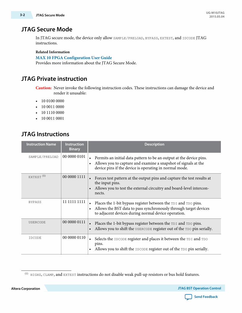
JTAG Secure ModeIn JTAG secure mode, the device only allow SAMPLE/PRELOAD, BYPASS, EXTEST, and IDCODE JTAGinstructions.
Related InformationMAX 10 FPGA Configuration User GuideProvides more information about the JTAG Secure Mode.
JTAG Private instructionCaution: Never invoke the following instruction codes. These instructions can damage the device and
render it unusable:
• 10 0100 0000• 10 0011 0000• 10 1110 0000• 10 0011 0001
JTAG InstructionsInstruction Name Instruction
BinaryDescription
SAMPLE/PRELOAD 00 0000 0101 • Permits an initial data pattern to be an output at the device pins.• Allows you to capture and examine a snapshot of signals at the
device pins if the device is operating in normal mode.
EXTEST (1) 00 0000 1111 • Forces test pattern at the output pins and capture the test results atthe input pins.
• Allows you to test the external circuitry and board-level intercon‐nects.
BYPASS 11 1111 1111 • Places the 1-bit bypass register between the TDI and TDO pins.• Allows the BST data to pass synchronously through target devices
to adjacent devices during normal device operation.
USERCODE 00 0000 0111 • Places the 1-bit bypass register between the TDI and TDO pins.• Allows you to shift the USERCODE register out of the TDO pin serially.
IDCODE 00 0000 0110 • Selects the IDCODE register and places it between the TDI and TDOpins.
• Allows you to shift the IDCODE register out of the TDO pin serially.
(1) HIGHZ, CLAMP, and EXTEST instructions do not disable weak pull-up resistors or bus hold features.
3-2 JTAG Secure ModeUG-M10JTAG
2015.05.04
Altera Corporation JTAG BST Operation Control
Send Feedback
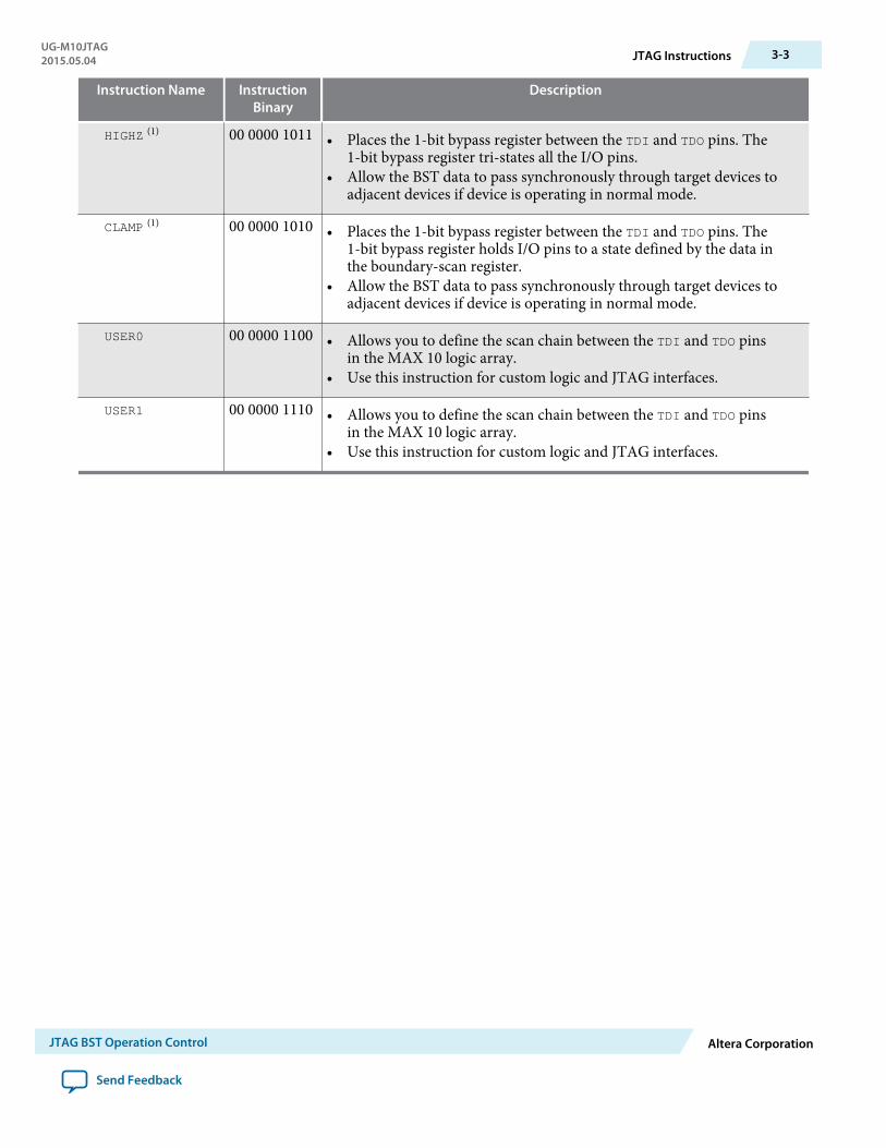
Instruction Name InstructionBinary
Description
HIGHZ (1) 00 0000 1011 • Places the 1-bit bypass register between the TDI and TDO pins. The1-bit bypass register tri-states all the I/O pins.
• Allow the BST data to pass synchronously through target devices toadjacent devices if device is operating in normal mode.
CLAMP (1) 00 0000 1010 • Places the 1-bit bypass register between the TDI and TDO pins. The1-bit bypass register holds I/O pins to a state defined by the data inthe boundary-scan register.
• Allow the BST data to pass synchronously through target devices toadjacent devices if device is operating in normal mode.
USER0 00 0000 1100 • Allows you to define the scan chain between the TDI and TDO pinsin the MAX 10 logic array.
• Use this instruction for custom logic and JTAG interfaces.
USER1 00 0000 1110 • Allows you to define the scan chain between the TDI and TDO pinsin the MAX 10 logic array.
• Use this instruction for custom logic and JTAG interfaces.
UG-M10JTAG2015.05.04 JTAG Instructions 3-3
JTAG BST Operation Control Altera Corporation
Send Feedback
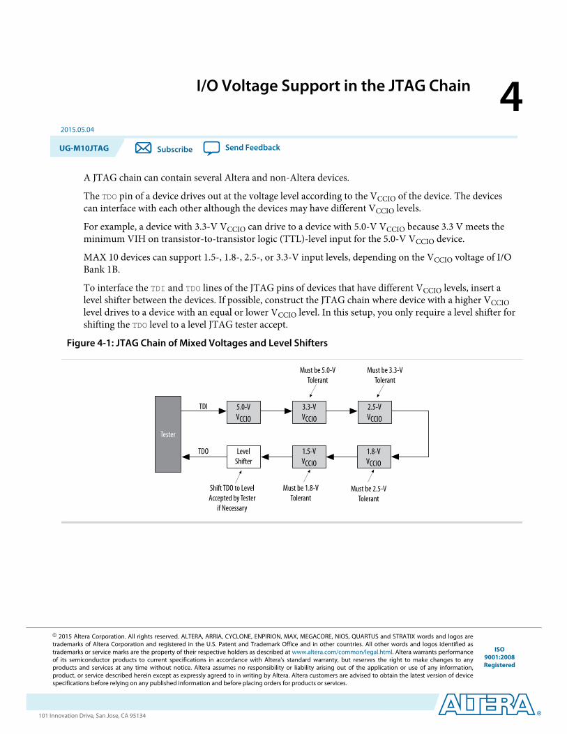
I/O Voltage Support in the JTAG Chain 42015.05.04
UG-M10JTAG Subscribe Send Feedback
A JTAG chain can contain several Altera and non-Altera devices.
The TDO pin of a device drives out at the voltage level according to the VCCIO of the device. The devicescan interface with each other although the devices may have different VCCIO levels.
For example, a device with 3.3-V VCCIO can drive to a device with 5.0-V VCCIO because 3.3 V meets theminimum VIH on transistor-to-transistor logic (TTL)-level input for the 5.0-V VCCIO device.
MAX 10 devices can support 1.5-, 1.8-, 2.5-, or 3.3-V input levels, depending on the VCCIO voltage of I/OBank 1B.
To interface the TDI and TDO lines of the JTAG pins of devices that have different VCCIO levels, insert alevel shifter between the devices. If possible, construct the JTAG chain where device with a higher VCCIOlevel drives to a device with an equal or lower VCCIO level. In this setup, you only require a level shifter forshifting the TDO level to a level JTAG tester accept.
Figure 4-1: JTAG Chain of Mixed Voltages and Level Shifters
2.5-VVCCIO
1.8-VVCCIO1.8-VVCCIO
TDI
TDO
Tester
Shift TDO to LevelAccepted by Tester
if Necessary
Must be 5.0-VTolerant
Must be 3.3-VTolerant
Must be 2.5-VTolerant
1.5-VVCCIO
Must be 1.8-VTolerant
LevelShifter
3.3-VVCCIO
5.0-VVCCIO
© 2015 Altera Corporation. All rights reserved. ALTERA, ARRIA, CYCLONE, ENPIRION, MAX, MEGACORE, NIOS, QUARTUS and STRATIX words and logos aretrademarks of Altera Corporation and registered in the U.S. Patent and Trademark Office and in other countries. All other words and logos identified astrademarks or service marks are the property of their respective holders as described at www.altera.com/common/legal.html. Altera warrants performanceof its semiconductor products to current specifications in accordance with Altera's standard warranty, but reserves the right to make changes to anyproducts and services at any time without notice. Altera assumes no responsibility or liability arising out of the application or use of any information,product, or service described herein except as expressly agreed to in writing by Altera. Altera customers are advised to obtain the latest version of devicespecifications before relying on any published information and before placing orders for products or services.
ISO9001:2008Registered
www.altera.com101 Innovation Drive, San Jose, CA 95134
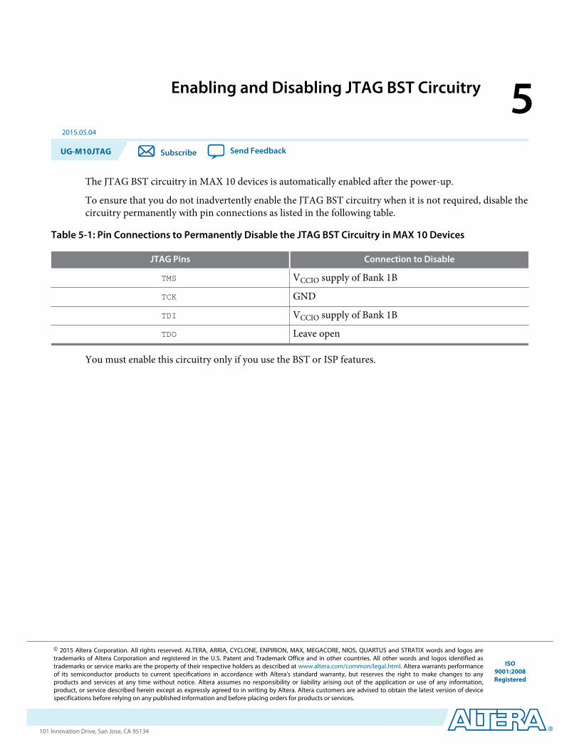
Enabling and Disabling JTAG BST Circuitry 52015.05.04
UG-M10JTAG Subscribe Send Feedback
The JTAG BST circuitry in MAX 10 devices is automatically enabled after the power-up.
To ensure that you do not inadvertently enable the JTAG BST circuitry when it is not required, disable thecircuitry permanently with pin connections as listed in the following table.
Table 5-1: Pin Connections to Permanently Disable the JTAG BST Circuitry in MAX 10 Devices
JTAG Pins Connection to Disable
TMS VCCIO supply of Bank 1B
TCK GND
TDI VCCIO supply of Bank 1B
TDO Leave open
You must enable this circuitry only if you use the BST or ISP features.
© 2015 Altera Corporation. All rights reserved. ALTERA, ARRIA, CYCLONE, ENPIRION, MAX, MEGACORE, NIOS, QUARTUS and STRATIX words and logos aretrademarks of Altera Corporation and registered in the U.S. Patent and Trademark Office and in other countries. All other words and logos identified astrademarks or service marks are the property of their respective holders as described at www.altera.com/common/legal.html. Altera warrants performanceof its semiconductor products to current specifications in accordance with Altera's standard warranty, but reserves the right to make changes to anyproducts and services at any time without notice. Altera assumes no responsibility or liability arising out of the application or use of any information,product, or service described herein except as expressly agreed to in writing by Altera. Altera customers are advised to obtain the latest version of devicespecifications before relying on any published information and before placing orders for products or services.
ISO9001:2008Registered
www.altera.com101 Innovation Drive, San Jose, CA 95134
Guidelines for JTAG BST 62015.05.04
UG-M10JTAG Subscribe Send Feedback
Consider the following guidelines when you perform BST with the device:
• If the “10...” pattern does not shift out of the instruction register through the TDO pin during the firstclock cycle of the SHIFT_IR state, the TAP controller did not reach the proper state. To solve thisproblem, try one of the following procedures:
• Verify that the TAP controller has reached the SHIFT_IR state correctly. To advance the TAPcontroller to the SHIFT_IR state, return TAP controller to the RESET state and send the 01100 codeto the TMS pin.
• Check the connections to the VCC, GND, JTAG, and dedicated configuration pins on the device.• Perform a SAMPLE/PRELOAD test cycle before the first EXTEST test cycle to ensure that known data is
present at the device pins when you enter EXTEST mode. If the OEJ update register contains 0, the datain the OUTJ update register is driven out. The state must be known and correct to avoid contentionwith other devices in the system.
• To perform testing before configuration, hold the nCONGFIG pin low.
© 2015 Altera Corporation. All rights reserved. ALTERA, ARRIA, CYCLONE, ENPIRION, MAX, MEGACORE, NIOS, QUARTUS and STRATIX words and logos aretrademarks of Altera Corporation and registered in the U.S. Patent and Trademark Office and in other countries. All other words and logos identified astrademarks or service marks are the property of their respective holders as described at www.altera.com/common/legal.html. Altera warrants performanceof its semiconductor products to current specifications in accordance with Altera's standard warranty, but reserves the right to make changes to anyproducts and services at any time without notice. Altera assumes no responsibility or liability arising out of the application or use of any information,product, or service described herein except as expressly agreed to in writing by Altera. Altera customers are advised to obtain the latest version of devicespecifications before relying on any published information and before placing orders for products or services.
ISO9001:2008Registered
www.altera.com101 Innovation Drive, San Jose, CA 95134

Boundary-Scan Description Language Support 72015.05.04
UG-M10JTAG Subscribe Send Feedback
The BSDL—a subset of VHDL—provides a syntax that allows you to describe the features of an IEEE Std.1149.1 BST-capable device that can be tested. Test software development systems then use the BSDL filesfor test generation, analysis, failure diagnostics, and in-system programming.
Related InformationIEEE 1149.1 BSDL FilesProvides more information about BSC group definitions.
© 2015 Altera Corporation. All rights reserved. ALTERA, ARRIA, CYCLONE, ENPIRION, MAX, MEGACORE, NIOS, QUARTUS and STRATIX words and logos aretrademarks of Altera Corporation and registered in the U.S. Patent and Trademark Office and in other countries. All other words and logos identified astrademarks or service marks are the property of their respective holders as described at www.altera.com/common/legal.html. Altera warrants performanceof its semiconductor products to current specifications in accordance with Altera's standard warranty, but reserves the right to make changes to anyproducts and services at any time without notice. Altera assumes no responsibility or liability arising out of the application or use of any information,product, or service described herein except as expressly agreed to in writing by Altera. Altera customers are advised to obtain the latest version of devicespecifications before relying on any published information and before placing orders for products or services.
ISO9001:2008Registered
www.altera.com101 Innovation Drive, San Jose, CA 95134
Additional Information for MAX 10 JTAGBoundary-Scan Testing User Guide A
2015.05.04
UG-M10JTAG Subscribe Send Feedback
Document Revision History for MAX 10 JTAG Boundary-Scan TestingUser Guide
Date Version Changes
May 2015 2015.05.04 Added note on about performing the boundary-scan testing in'Overview'.
September 2014 2014.09.22 Initial release.
© 2015 Altera Corporation. All rights reserved. ALTERA, ARRIA, CYCLONE, ENPIRION, MAX, MEGACORE, NIOS, QUARTUS and STRATIX words and logos aretrademarks of Altera Corporation and registered in the U.S. Patent and Trademark Office and in other countries. All other words and logos identified astrademarks or service marks are the property of their respective holders as described at www.altera.com/common/legal.html. Altera warrants performanceof its semiconductor products to current specifications in accordance with Altera's standard warranty, but reserves the right to make changes to anyproducts and services at any time without notice. Altera assumes no responsibility or liability arising out of the application or use of any information,product, or service described herein except as expressly agreed to in writing by Altera. Altera customers are advised to obtain the latest version of devicespecifications before relying on any published information and before placing orders for products or services.
ISO9001:2008Registered
www.altera.com101 Innovation Drive, San Jose, CA 95134

MAX 10 Power Management User Guide
Subscribe
Send Feedback
UG-M10PWR2016.05.02
101 Innovation DriveSan Jose, CA 95134www.altera.com
Contents
MAX 10 Power Management Overview..............................................................1-1
MAX 10 Power Management Features and Architecture.................................. 2-1Power Supply Device Options....................................................................................................................2-1
Single-Supply Device....................................................................................................................... 2-1Dual-Supply Device......................................................................................................................... 2-1Comparison of the MAX 10 Power Supply Device Options......................................................2-2Power Supply Design.......................................................................................................................2-3
Power-On Reset Circuitry.......................................................................................................................... 2-4Power Supplies Monitored and Not Monitored by the POR Circuitry................................... 2-5Instant-On Support......................................................................................................................... 2-6
Power Management Controller Scheme...................................................................................................2-6Power Management Controller Architecture.............................................................................. 2-6
Hot Socketing............................................................................................................................................... 2-8Hot-Socketing Specifications......................................................................................................... 2-8Hot-Socketing Feature Implementation.......................................................................................2-9
Power Management Controller Reference Design............................................. 3-1Clock Control Block.................................................................................................................................... 3-2I/O Buffer...................................................................................................................................................... 3-2Internal Oscillator........................................................................................................................................3-2Power Management Controller................................................................................................................. 3-3
Entering State....................................................................................................................................3-3Sleep State..........................................................................................................................................3-3Exiting State...................................................................................................................................... 3-3Awake State.......................................................................................................................................3-3
Entering or Exiting Sleep Mode.................................................................................................................3-4Entering Sleep Mode........................................................................................................................3-4Exiting Sleep Mode.......................................................................................................................... 3-4Timing Parameters.......................................................................................................................... 3-5
Hardware Implementation and Current Measurement......................................................................... 3-5
MAX 10 Power Management User Guide Archives...........................................A-1
Additional Information for MAX 10 Power Management User Guide ........... B-1Document Revision History for MAX 10 Power Management User Guide.......................................B-1
TOC-2
Altera Corporation

MAX 10 Power Management Overview 12016.05.02
UG-M10PWR Subscribe Send Feedback
MAX® 10 devices offer the following power supply device options:
• Single-supply device—requires 1 external power supply of 3.0 V or 3.3 V while offering maximumconvenience and board simplicity.
• Dual-supply device—requires 2 external power supplies of 1.2 V and 2.5 V while offering the mostfeatures, highest performance, and when coupled with high-efficiency Enpirion® PowerSoCs, thelowest power solution.
Related Information
• MAX 10 Power Management Features and Architecture on page 2-1Provides information about power management features and architecture
• MAX 10 Power Management User Guide Archives on page 4-1Provides a list of user guides for previous versions of the SmartVID IP core.
© 2016 Altera Corporation. All rights reserved. ALTERA, ARRIA, CYCLONE, ENPIRION, MAX, MEGACORE, NIOS, QUARTUS and STRATIX words and logos aretrademarks of Altera Corporation and registered in the U.S. Patent and Trademark Office and in other countries. All other words and logos identified astrademarks or service marks are the property of their respective holders as described at www.altera.com/common/legal.html. Altera warrants performanceof its semiconductor products to current specifications in accordance with Altera's standard warranty, but reserves the right to make changes to anyproducts and services at any time without notice. Altera assumes no responsibility or liability arising out of the application or use of any information,product, or service described herein except as expressly agreed to in writing by Altera. Altera customers are advised to obtain the latest version of devicespecifications before relying on any published information and before placing orders for products or services.
ISO9001:2008Registered
www.altera.com101 Innovation Drive, San Jose, CA 95134
MAX 10 Power Management Features andArchitecture 2
2016.05.02
UG-M10PWR Subscribe Send Feedback
MAX 10 power optimization features are as follows:
• Single-supply or dual-supply device options• Power-on reset (POR) circuitry• Power management controller scheme• Hot socketing
Power Supply Device Options
Single-Supply DeviceMAX 10 single-supply devices only need either a 3.0- or 3.3-V external power supply. The external powersupply serves as an input to the MAX 10 device VCC_ONE and VCCA power pins. This external power supplyis then regulated by an internal voltage regulator in the MAX 10 single-supply device to 1.2 V. The 1.2-Vvoltage level is required by core logic operation.
Figure 2-1: MAX 10 Single-Supply Device
VCC_ONE/VCCA
VoltageRegulator
3.3 V/3.0 V
1.2 V
Max 10 Single-Supply Device
Dual-Supply DeviceMAX 10 dual-supply devices require 1.2 V and 2.5 V for the device core logics and periphery operations.
© 2016 Altera Corporation. All rights reserved. ALTERA, ARRIA, CYCLONE, ENPIRION, MAX, MEGACORE, NIOS, QUARTUS and STRATIX words and logos aretrademarks of Altera Corporation and registered in the U.S. Patent and Trademark Office and in other countries. All other words and logos identified astrademarks or service marks are the property of their respective holders as described at www.altera.com/common/legal.html. Altera warrants performanceof its semiconductor products to current specifications in accordance with Altera's standard warranty, but reserves the right to make changes to anyproducts and services at any time without notice. Altera assumes no responsibility or liability arising out of the application or use of any information,product, or service described herein except as expressly agreed to in writing by Altera. Altera customers are advised to obtain the latest version of devicespecifications before relying on any published information and before placing orders for products or services.
ISO9001:2008Registered
www.altera.com101 Innovation Drive, San Jose, CA 95134
Figure 2-2: MAX 10 Dual-Supply Device
MAX 10 Dual-Supply DeviceVCC, VCCD_PLL, VCCINT
(1.2 V)
VCCA, VCCA_ADC(2.5 V)
Comparison of the MAX 10 Power Supply Device Options
Table 2-1: Comparison of the MAX 10 Power Supply Device Options
Characteristics Single-Supply Device Dual-Supply Device
Voltage regulator count (1) 1 2
Core and I/O performance Low High
For MAX 10 single-supply devices, only one power supply is required—3.0 V or 3.3 V to power the coreof the FPGA. The same power supply can be used to power the I/O if the same 3.0 V or 3.3 V voltage isrequired. If different I/O voltage is used, then additional voltage regulators will be needed.
For MAX 10 dual-supply devices, two power supplies are required to supply power to the device core,periphery, phase-locked loop (PLL), and analog-to-digital converters (ADC) blocks—1.2 V and 2.5 V.Depending on the I/O standard voltage requirement, you may use two or more voltage regulators.
As the power rails for the FPGA core are supplied externally in the MAX 10 dual-supply devices, thedesign can be optimized for power by using high efficiency switching power supplies on the board. Thepower savings will be equal to the increased efficiency of the regulators used compared to the internallinear regulators of the MAX 10 single-supply devices. If linear regulators are used to power the MAX 10dual-supply devices, the power consumption of the MAX 10 dual-supply devices will be approximatelyequal to the MAX 10 single-supply devices.
The device performance of the single-supply device is lower than that of the dual-supply device. For theperformance difference in terms of LVDS, pseudo-LVDS, digital signal processing (DSP), and internalmemory performance, refer to the MAX 10 FPGA device datasheet.
Related InformationMAX 10 FPGA Device DatasheetProvides details about the MAX 10 performance difference in terms of LVDS, pseudo-LVDS, DSP, andinternal memory performance.
(1) This shows the number of power supplies required by the core and periphery of the MAX 10 devices. Youmay need additional voltage regulators to supply power to the VCCIO if the VCCIO does not have the samevoltage level as the core and periphery supply.
2-2 Comparison of the MAX 10 Power Supply Device OptionsUG-M10PWR
2016.05.02
Altera Corporation MAX 10 Power Management Features and Architecture
Send Feedback
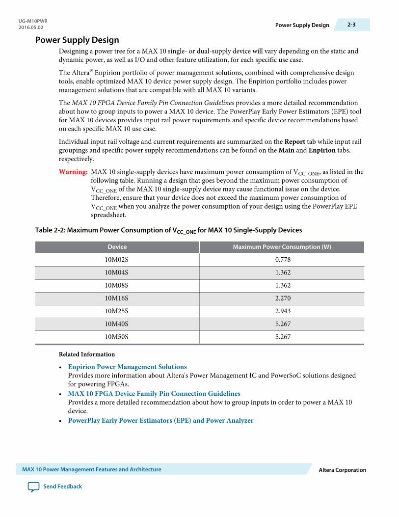
Power Supply DesignDesigning a power tree for a MAX 10 single- or dual-supply device will vary depending on the static anddynamic power, as well as I/O and other feature utilization, for each specific use case.
The Altera® Enpirion portfolio of power management solutions, combined with comprehensive designtools, enable optimized MAX 10 device power supply design. The Enpirion portfolio includes powermanagement solutions that are compatible with all MAX 10 variants.
The MAX 10 FPGA Device Family Pin Connection Guidelines provides a more detailed recommendationabout how to group inputs to power a MAX 10 device. The PowerPlay Early Power Estimators (EPE) toolfor MAX 10 devices provides input rail power requirements and specific device recommendations basedon each specific MAX 10 use case.
Individual input rail voltage and current requirements are summarized on the Report tab while input railgroupings and specific power supply recommendations can be found on the Main and Enpirion tabs,respectively.
Warning: MAX 10 single-supply devices have maximum power consumption of VCC_ONE, as listed in thefollowing table. Running a design that goes beyond the maximum power consumption ofVCC_ONE of the MAX 10 single-supply device may cause functional issue on the device.Therefore, ensure that your device does not exceed the maximum power consumption ofVCC_ONE when you analyze the power consumption of your design using the PowerPlay EPEspreadsheet.
Table 2-2: Maximum Power Consumption of VCC_ONE for MAX 10 Single-Supply Devices
Device Maximum Power Consumption (W)
10M02S 0.778
10M04S 1.362
10M08S 1.362
10M16S 2.270
10M25S 2.943
10M40S 5.267
10M50S 5.267
Related Information
• Enpirion Power Management SolutionsProvides more information about Altera's Power Management IC and PowerSoC solutions designedfor powering FPGAs.
• MAX 10 FPGA Device Family Pin Connection GuidelinesProvides a more detailed recommendation about how to group inputs in order to power a MAX 10device.
• PowerPlay Early Power Estimators (EPE) and Power Analyzer
UG-M10PWR2016.05.02 Power Supply Design 2-3
MAX 10 Power Management Features and Architecture Altera Corporation
Send Feedback
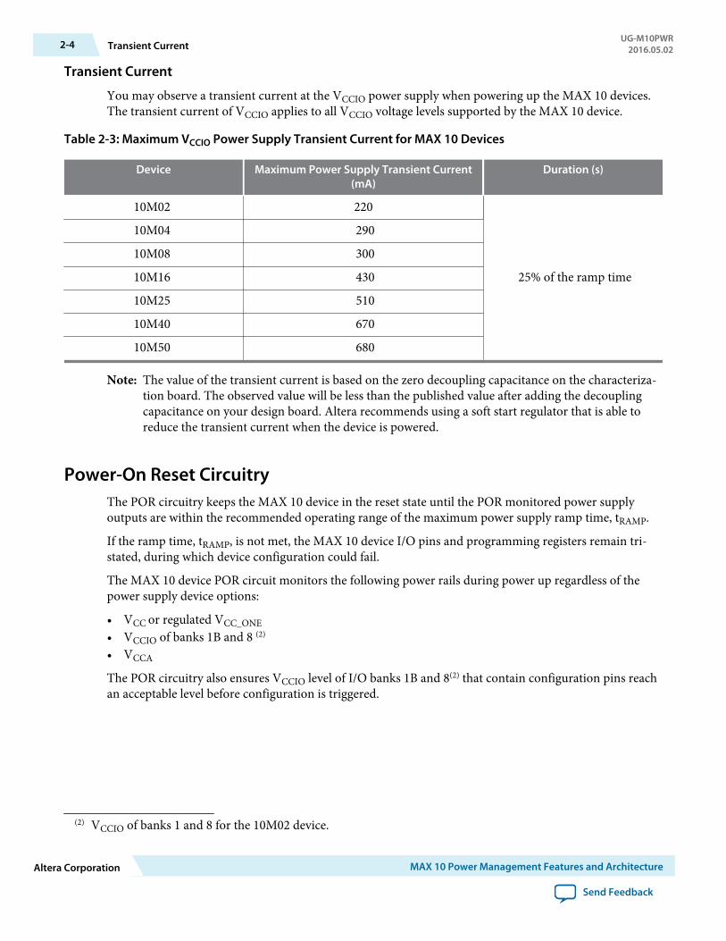
Transient Current
You may observe a transient current at the VCCIO power supply when powering up the MAX 10 devices.The transient current of VCCIO applies to all VCCIO voltage levels supported by the MAX 10 device.
Table 2-3: Maximum VCCIO Power Supply Transient Current for MAX 10 Devices
Device Maximum Power Supply Transient Current(mA)
Duration (s)
10M02 220
25% of the ramp time
10M04 290
10M08 300
10M16 430
10M25 510
10M40 670
10M50 680
Note: The value of the transient current is based on the zero decoupling capacitance on the characteriza‐tion board. The observed value will be less than the published value after adding the decouplingcapacitance on your design board. Altera recommends using a soft start regulator that is able toreduce the transient current when the device is powered.
Power-On Reset CircuitryThe POR circuitry keeps the MAX 10 device in the reset state until the POR monitored power supplyoutputs are within the recommended operating range of the maximum power supply ramp time, tRAMP.
If the ramp time, tRAMP, is not met, the MAX 10 device I/O pins and programming registers remain tri-stated, during which device configuration could fail.
The MAX 10 device POR circuit monitors the following power rails during power up regardless of thepower supply device options:
• VCC or regulated VCC_ONE• VCCIO of banks 1B and 8 (2)
• VCCA
The POR circuitry also ensures VCCIO level of I/O banks 1B and 8(2) that contain configuration pins reachan acceptable level before configuration is triggered.
(2) VCCIO of banks 1 and 8 for the 10M02 device.
2-4 Transient CurrentUG-M10PWR
2016.05.02
Altera Corporation MAX 10 Power Management Features and Architecture
Send Feedback
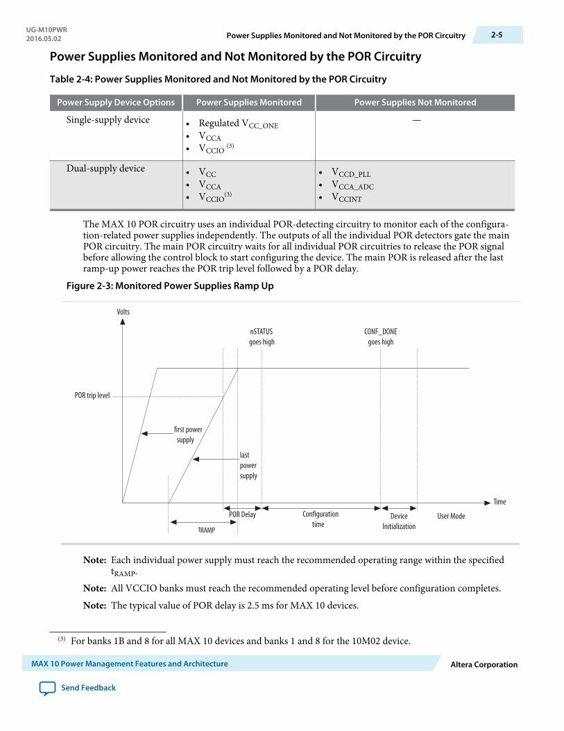
Power Supplies Monitored and Not Monitored by the POR Circuitry
Table 2-4: Power Supplies Monitored and Not Monitored by the POR Circuitry
Power Supply Device Options Power Supplies Monitored Power Supplies Not Monitored
Single-supply device • Regulated VCC_ONE• VCCA• VCCIO (3)
—
Dual-supply device • VCC• VCCA• VCCIO
(3)
• VCCD_PLL• VCCA_ADC• VCCINT
The MAX 10 POR circuitry uses an individual POR-detecting circuitry to monitor each of the configura‐tion-related power supplies independently. The outputs of all the individual POR detectors gate the mainPOR circuitry. The main POR circuitry waits for all individual POR circuitries to release the POR signalbefore allowing the control block to start configuring the device. The main POR is released after the lastramp-up power reaches the POR trip level followed by a POR delay.
Figure 2-3: Monitored Power Supplies Ramp Up
Time
POR trip level
Volts
POR Delay Configuration time
DeviceInitialization
User Mode
tRAMP
first power supply
last powersupply
nSTATUSgoes high
CONF_DONEgoes high
Note: Each individual power supply must reach the recommended operating range within the specifiedtRAMP.
Note: All VCCIO banks must reach the recommended operating level before configuration completes.
Note: The typical value of POR delay is 2.5 ms for MAX 10 devices.
(3) For banks 1B and 8 for all MAX 10 devices and banks 1 and 8 for the 10M02 device.
UG-M10PWR2016.05.02 Power Supplies Monitored and Not Monitored by the POR Circuitry 2-5
MAX 10 Power Management Features and Architecture Altera Corporation
Send Feedback
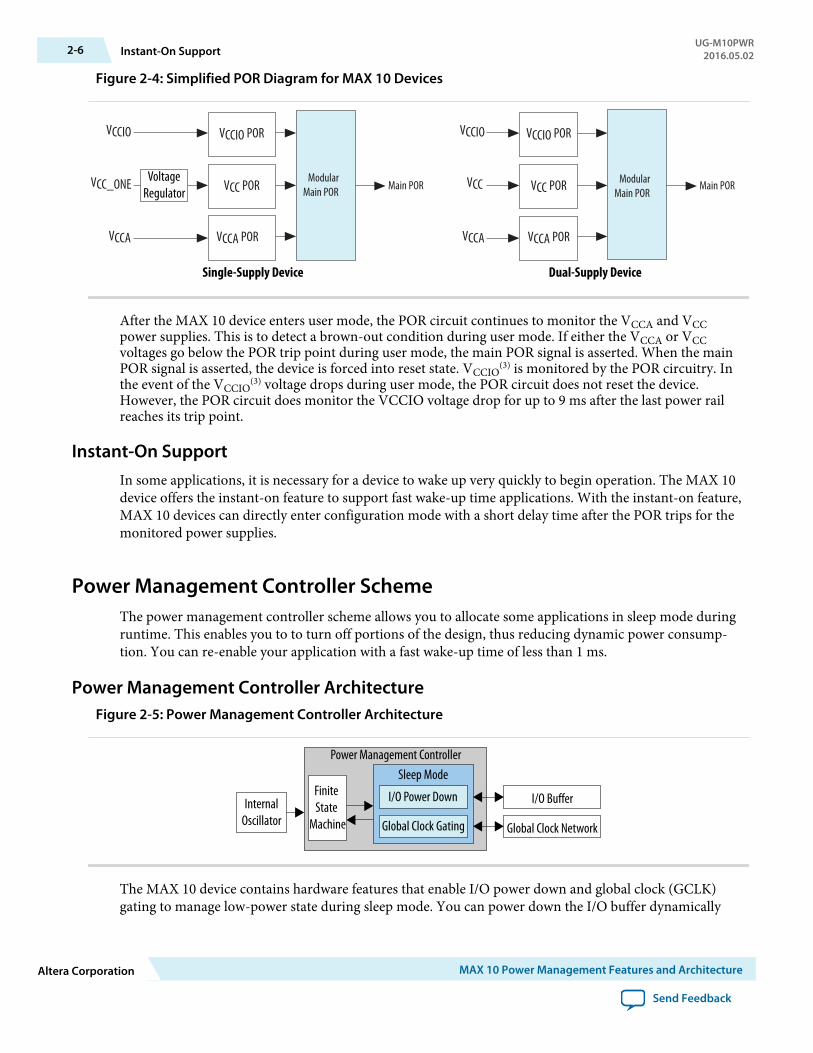
Figure 2-4: Simplified POR Diagram for MAX 10 Devices
VCCIO
ModularMain POR
Main POR
VCCA
VCCIO POR
VCC VCC POR
VCCA POR
VCCIO
ModularMain POR Main POR
VCCA
VCCIO POR
VCC_ONE VCC POR
VCCA POR
VoltageRegulator
Single-Supply Device Dual-Supply Device
After the MAX 10 device enters user mode, the POR circuit continues to monitor the VCCA and VCCpower supplies. This is to detect a brown-out condition during user mode. If either the VCCA or VCCvoltages go below the POR trip point during user mode, the main POR signal is asserted. When the mainPOR signal is asserted, the device is forced into reset state. VCCIO
(3) is monitored by the POR circuitry. Inthe event of the VCCIO
(3) voltage drops during user mode, the POR circuit does not reset the device.However, the POR circuit does monitor the VCCIO voltage drop for up to 9 ms after the last power railreaches its trip point.
Instant-On SupportIn some applications, it is necessary for a device to wake up very quickly to begin operation. The MAX 10device offers the instant-on feature to support fast wake-up time applications. With the instant-on feature,MAX 10 devices can directly enter configuration mode with a short delay time after the POR trips for themonitored power supplies.
Power Management Controller SchemeThe power management controller scheme allows you to allocate some applications in sleep mode duringruntime. This enables you to to turn off portions of the design, thus reducing dynamic power consump‐tion. You can re-enable your application with a fast wake-up time of less than 1 ms.
Power Management Controller ArchitectureFigure 2-5: Power Management Controller Architecture
I/O Power Down
Global Clock Gating
Sleep ModeFinite State
MachineInternal
Oscillator
Power Management Controller
I/O Buffer
Global Clock Network
The MAX 10 device contains hardware features that enable I/O power down and global clock (GCLK)gating to manage low-power state during sleep mode. You can power down the I/O buffer dynamically
2-6 Instant-On SupportUG-M10PWR
2016.05.02
Altera Corporation MAX 10 Power Management Features and Architecture
Send Feedback
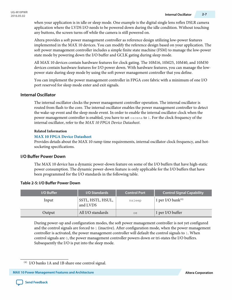
when your application is in idle or sleep mode. One example is the digital single lens reflex DSLR cameraapplication where the LVDS I/O needs to be powered down during the idle condition. Without touchingany buttons, the screen turns off while the camera is still powered on.
Altera provides a soft power management controller as reference design utilizing low-power featuresimplemented in the MAX 10 devices. You can modify the reference design based on your application. Thesoft power management controller includes a simple finite state machine (FSM) to manage the low-powerstate mode by powering down the I/O buffer and GCLK gating during sleep mode.
All MAX 10 devices contain hardware features for clock gating. The 10M16, 10M25, 10M40, and 10M50devices contain hardware features for I/O power down. With hardware features, you can manage the low-power state during sleep mode by using the soft power management controller that you define.
You can implement the power management controller in FPGA core fabric with a minimum of one I/Oport reserved for sleep mode enter and exit signals.
Internal Oscillator
The internal oscillator clocks the power management controller operation. The internal oscillator isrouted from flash to the core. The internal oscillator enables the power management controller to detectthe wake-up event and the sleep mode event. In order to enable the internal oscillator clock when thepower management controller is enabled, you have to set oscena to 1. For the clock frequency of theinternal oscillator, refer to the MAX 10 FPGA Device Datasheet.
Related InformationMAX 10 FPGA Device DatasheetProvides details about the MAX 10 ramp time requirements, internal oscillator clock frequency, and hot-socketing specifications.
I/O Buffer Power Down
The MAX 10 device has a dynamic power-down feature on some of the I/O buffers that have high-staticpower consumption. The dynamic power-down feature is only applicable for the I/O buffers that havebeen programmed for the I/O standards in the following table.
Table 2-5: I/O Buffer Power Down
I/O Buffer I/O Standards Control Port Control Signal Capability
Input SSTL, HSTL, HSUL,and LVDS
nsleep 1 per I/O bank(4)
Output All I/O standards oe 1 per I/O buffer
During power-up and configuration modes, the soft power management controller is not yet configuredand the control signals are forced to 1 (inactive). After configuration mode, when the power managementcontroller is activated, the power management controller will default the control signals to 1. Whencontrol signals are 0, the power management controller powers down or tri-states the I/O buffers.Subsequently the I/O is put into the sleep mode.
(4) I/O banks 1A and 1B share one control signal.
UG-M10PWR2016.05.02 Internal Oscillator 2-7
MAX 10 Power Management Features and Architecture Altera Corporation
Send Feedback
The MAX 10 device I/O buffers need to maintain the previous states during the sleep mode operation.The previous states in your core logics remain upon exiting the sleep mode.
Global Clock Gating
The dynamic power-down feature is available in GCLK networks only. You can use the powermanagement controller for the dynamic power-down of a GCLK network by controlling the active highenout signal. The GCLK networks serve as low-skew clock sources for functional blocks such as logicarray blocks (LABs), DSP, embedded memory, and PLLs.
When a GCLK network is gated, all the logics fed by the GCLK network are in off-state. This reduces theoverall power consumption of the device. The dynamic power-down feature allows core logics to controlthe following power-up and power-down conditions of the GCLK networks:
• Power down synchronously or asynchronously• Power up asynchronously
Figure 2-6: GCLK Gating
Power Management
Controller
enout
clk1clkn gclkin
lenoutgclkout
Clock Control Block
Hot SocketingThe MAX 10 device offers hot socketing, which is also known as hot plug-in or hot swap, and powersequencing support without the use of any external devices. You can insert or remove the MAX 10 deviceon a board in a system during system operation. This does not affect the running system bus or the boardthat is inserted into the system.
The hot-socketing feature removes some encountered difficulties when using the MAX 10 device on aPCB that contains a mixture of devices with different voltage levels.
With the MAX 10 device hot-socketing feature, you no longer need to ensure a proper power-up sequencefor each device on the board. MAX 10 device hot-socketing feature provides:
• Board or device insertion and removal without external components or board manipulation• Support for any power-up sequence• Non-intrusive I/O buffers to system buses during hot insertion
Hot-Socketing SpecificationsThe MAX 10 device is a hot-socketing compliant device that does not need any external components orspecial design requirements. Hot-socketing support in the MAX 10 device has the following advantages:
2-8 Global Clock GatingUG-M10PWR
2016.05.02
Altera Corporation MAX 10 Power Management Features and Architecture
Send Feedback
• You can drive the devices before power up without damaging the device.• I/O pins remain tri-stated during power up. The device does not drive out before or during power up,
therefore not affecting other buses in operation.
Drive MAX 10 Devices Before Power Up
Before or during power up or power down, you can drive signals into I/O pins, dedicated input pins, anddedicated clock pins without damaging the MAX 10 devices.
The MAX 10 device supports any power-up or power-down sequence to simplify system-level design.
I/O Pins Remain Tri-stated During Power up
The output buffers of the MAX 10 device are turned off during system power up or power down. TheMAX 10 device family does not drive out until the device is configured and working in recommendedoperating conditions. The I/O pins are tri-stated during power up or power down.
A possible concern for semiconductor devices in general regarding hot-socketing is the potential for latchup. Latch up can occur when electrical subsystems are hot-socketed into an active system. During hot-socketing, the signal pins may be connected and driven by the active system. This occurs before the powersupply can provide current to the VCC of the device and ground planes. This condition can lead to latchup and cause a low-impedance path from VCC to ground in the device. As a result, the device extends alarge amount of current, possibly causing electrical damage.
The design of the I/O buffers and hot-socketing circuitry ensures that the MAX 10 device family isimmune to latch up during hot-socketing.
Related InformationMAX 10 FPGA Device DatasheetProvides details about the MAX 10 ramp time requirements, internal oscillator clock frequency, and hot-socketing specifications.
Hot-Socketing Feature ImplementationThe hot-socketing feature tri-states the output buffer during the power-up (VCCIO or VCC power supplies)or power-down event. The hot-socketing circuitry generates an internal HOTSCKT signal when VCCIO orVCC is below the threshold voltage during power up or power down. The HOTSCKT signal cuts off theoutput buffer to ensure that no DC current leaks through the pin (except for weak pull-up leaking). EachI/O pin has the circuitry shown in the following figure. The hot-socketing circuit does not includeCONF_DONE and nSTATUS pins to ensure that these pins are able to operate during configuration. Thus, it isan expected behavior for these pins to drive out during power-up and power-down sequences.
UG-M10PWR2016.05.02 Drive MAX 10 Devices Before Power Up 2-9
MAX 10 Power Management Features and Architecture Altera Corporation
Send Feedback
Figure 2-7: Hot-Socketing Circuitry for MAX 10 Devices
VCCIO
PAD
R
VoltageTolerance
Control
Output Enable
Hot-Socket
OutputPre-Driver
Power-OnReset (POR)
Monitor
WeakPull-UpResistor
Input Bufferto Logic Array
The POR circuit monitors the voltage level of power supplies and keeps the I/O pins tri-stated duringpower up. The weak pull-up resistor in MAX 10 device I/O elements (IOE) keeps the I/O pins fromfloating. The voltage tolerance control circuit protects the I/O pins from being driven before VCCIO andVCC supplies are powered up. This prevents the I/O pins from driving out when the device is not in usermode.
Altera uses GND as reference for hot-socketing operation and I/O buffer designs. To ensure properoperation, Altera recommends connecting the GND between boards before connecting the powersupplies. This prevents the GND on your board from being pulled up inadvertently by a path to powerthrough other components on your board. A pulled up GND can cause an out-of-specification I/O voltageor current condition with the Altera device.
2-10 Hot-Socketing Feature ImplementationUG-M10PWR
2016.05.02
Altera Corporation MAX 10 Power Management Features and Architecture
Send Feedback
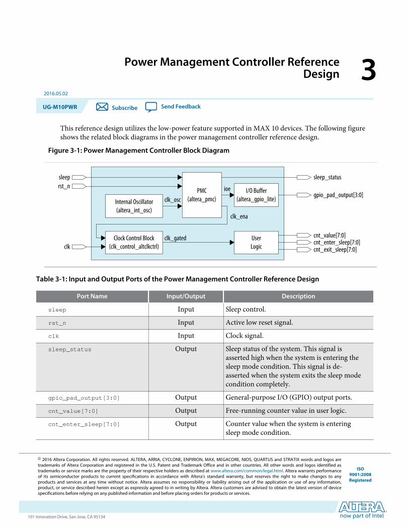
Power Management Controller ReferenceDesign 3
2016.05.02
UG-M10PWR Subscribe Send Feedback
This reference design utilizes the low-power feature supported in MAX 10 devices. The following figureshows the related block diagrams in the power management controller reference design.
Figure 3-1: Power Management Controller Block Diagram
PMC(altera_pmc)Internal Oscillator
(altera_int_osc)
sleeprst_n
Clock Control Block(clk_control_altclkctrl)
clk_osc
clk
I/O Buffer(altera_gpio_lite)
UserLogic
sleep_status
gpio_pad_output[3:0]
cnt_enter_sleep[7:0]cnt_value[7:0]
cnt_exit_sleep[7:0]
clk_gated
ioe
clk_ena
Table 3-1: Input and Output Ports of the Power Management Controller Reference Design
Port Name Input/Output Description
sleep Input Sleep control.
rst_n Input Active low reset signal.
clk Input Clock signal.
sleep_status Output Sleep status of the system. This signal isasserted high when the system is entering thesleep mode condition. This signal is de-asserted when the system exits the sleep modecondition completely.
gpio_pad_output[3:0] Output General-purpose I/O (GPIO) output ports.
cnt_value[7:0] Output Free-running counter value in user logic.
cnt_enter_sleep[7:0] Output Counter value when the system is enteringsleep mode condition.
© 2016 Altera Corporation. All rights reserved. ALTERA, ARRIA, CYCLONE, ENPIRION, MAX, MEGACORE, NIOS, QUARTUS and STRATIX words and logos aretrademarks of Altera Corporation and registered in the U.S. Patent and Trademark Office and in other countries. All other words and logos identified astrademarks or service marks are the property of their respective holders as described at www.altera.com/common/legal.html. Altera warrants performanceof its semiconductor products to current specifications in accordance with Altera's standard warranty, but reserves the right to make changes to anyproducts and services at any time without notice. Altera assumes no responsibility or liability arising out of the application or use of any information,product, or service described herein except as expressly agreed to in writing by Altera. Altera customers are advised to obtain the latest version of devicespecifications before relying on any published information and before placing orders for products or services.
ISO9001:2008Registered
www.altera.com101 Innovation Drive, San Jose, CA 95134
Port Name Input/Output Description
cnt_exit_sleep[7:0] Output Counter value when the system is exitingsleep mode condition.
The power management controller design is a FSM showing the state of powering down and powering upglobal clocks (GCLKs) and I/O buffers. The internal oscillator, clock control block, and I/O buffer areintellectual property (IP) that are supported by the Quartus® Prime software and you can instantiate theIPs from the IP catalog. The user logic can be any logical circuitry that are implemented using logicelement (LE) and an embedded component such as DSP and internal memory in your design. In thisreference design, the user logic used is a free-running 8-bit counter. The cnt_enter_sleep andcnt_exit_sleep ports are used to ensure user logic can enter and exit sleep mode without datacorruption. It is expected for that cnt_enter_sleep[7:0] and cnt_exit_sleep[7:0] are at the samevalue after the user logic enter and exit sleep mode. gpio_pad_output ports demonstrate tri-stated stateof the GPIO when the system is in sleep mode.
Related InformationPower Management Controller Reference Design
Clock Control BlockThe clock control IP core (clk_control_altclkctrl) is an IP provided in the Quartus Prime software.This IP is used to control the clock system in the device. The GCLKs that drive through the device can bedynamically powered down by controlling the active high ena signal. The ena port is an input to the clockcontrol IP block. When this IP is instantiated, select the ena port to enable the controls of GCLKs.
Related InformationClock Control Block (ALTCLKCTRL) Megafunction User Guide
I/O BufferAltera GPIO Lite IP core (altera_gpio_lite) is implemented as an input, output, or bidirectional I/Obuffer. You can control the power down of these I/O buffers by enabling the nsleep port of the inputbuffer and the oe port of the output buffer. The oe and nsleep ports are pulled low by the powermanagement controller design to power down the I/O buffers during sleep mode. Altera recommendsusing a separate Altera GPIO Lite IP when some of the I/O buffer is not required to be powered down.
Related InformationAltera GPIO Lite IP Core References
Internal OscillatorInternal Oscillator IP core (altera_in_osc) is a free-running oscillator once you enable it. This oscillatorruns throughout the entire power management controller design.
Related InformationInternal Oscillator IP Core
3-2 Clock Control BlockUG-M10PWR
2016.05.02
Altera Corporation Power Management Controller Reference Design
Send Feedback
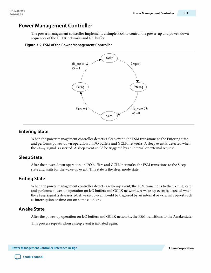
Power Management ControllerThe power management controller implements a simple FSM to control the power-up and power-downsequences of the GCLK networks and I/O buffer.
Figure 3-2: FSM of the Power Management Controller
Awake
Sleep
EnteringExiting
Sleep = 1clk_ena = 1 &ioe = 1
clk_ena = 0 &ioe = 0
Sleep = 0
Entering StateWhen the power management controller detects a sleep event, the FSM transitions to the Entering stateand performs power-down operation on I/O buffers and GCLK networks. A sleep event is detected whenthe sleep signal is asserted. A sleep event could be triggered by an internal or external request.
Sleep StateAfter the power-down operation on I/O buffers and GCLK networks, the FSM transitions to the Sleepstate and waits for the wake-up event. This state is the sleep mode state.
Exiting StateWhen the power management controller detects a wake-up event, the FSM transitions to the Exiting stateand performs power-up operation on I/O buffers and GCLK networks. A wake-up event is detected whenthe sleep signal is de-asserted. A wake-up event could be triggered by an internal or external request suchas interruption or time-out on some counters.
Awake StateAfter the power-up operation on I/O buffers and GCLK networks, the FSM transitions to the Awake state.
This process repeats when a sleep event is initiated again.
UG-M10PWR2016.05.02 Power Management Controller 3-3
Power Management Controller Reference Design Altera Corporation
Send Feedback
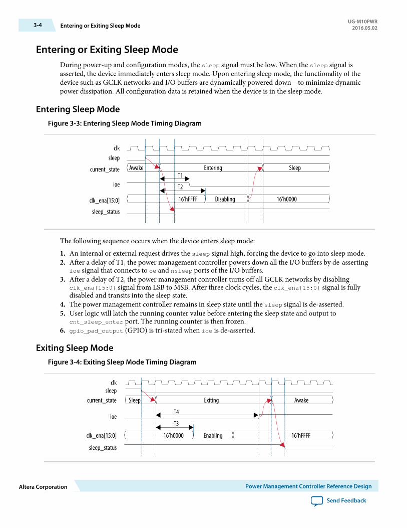
Entering or Exiting Sleep ModeDuring power-up and configuration modes, the sleep signal must be low. When the sleep signal isasserted, the device immediately enters sleep mode. Upon entering sleep mode, the functionality of thedevice such as GCLK networks and I/O buffers are dynamically powered down—to minimize dynamicpower dissipation. All configuration data is retained when the device is in the sleep mode.
Entering Sleep ModeFigure 3-3: Entering Sleep Mode Timing Diagram
clksleep
current_state
ioe
clk_ena[15:0]
sleep_status
Awake Entering Sleep
16’hFFFF Disabling 16’h0000
T1
T2
The following sequence occurs when the device enters sleep mode:
1. An internal or external request drives the sleep signal high, forcing the device to go into sleep mode.2. After a delay of T1, the power management controller powers down all the I/O buffers by de-asserting
ioe signal that connects to oe and nsleep ports of the I/O buffers.3. After a delay of T2, the power management controller turns off all GCLK networks by disabling
clk_ena[15:0] signal from LSB to MSB. After three clock cycles, the clk_ena[15:0] signal is fullydisabled and transits into the sleep state.
4. The power management controller remains in sleep state until the sleep signal is de-asserted.5. User logic will latch the running counter value before entering the sleep state and output to
cnt_sleep_enter port. The running counter is then frozen.6. gpio_pad_output (GPIO) is tri-stated when ioe is de-asserted.
Exiting Sleep ModeFigure 3-4: Exiting Sleep Mode Timing Diagram
clksleep
current_state
ioe
clk_ena[15:0]
sleep_status
Sleep Exiting Awake
16’hFFFFEnabling16’h0000
T4
T3
3-4 Entering or Exiting Sleep ModeUG-M10PWR
2016.05.02
Altera Corporation Power Management Controller Reference Design
Send Feedback
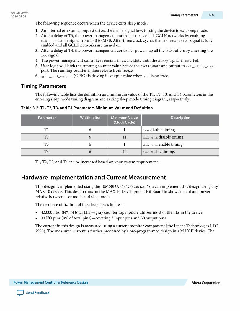
The following sequence occurs when the device exits sleep mode:
1. An internal or external request drives the sleep signal low, forcing the device to exit sleep mode.2. After a delay of T3, the power management controller turns on all GCLK networks by enabling
clk_ena[15:0] signal from LSB to MSB. After three clock cycles, the clk_ena[15:0] signal is fullyenabled and all GCLK networks are turned on.
3. After a delay of T4, the power management controller powers up all the I/O buffers by asserting theioe signal.
4. The power management controller remains in awake state until the sleep signal is asserted.5. User logic will latch the running counter value before the awake state and output to cnt_sleep_exit
port. The running counter is then release from freeze.6. gpio_pad_output (GPIO) is driving its output value when ioe is asserted.
Timing ParametersThe following table lists the definition and minimum value of the T1, T2, T3, and T4 parameters in theentering sleep mode timing diagram and exiting sleep mode timing diagram, respectively.
Table 3-2: T1, T2, T3, and T4 Parameters Minimum Value and Definition
Parameter Width (bits) Minimum Value(Clock Cycle)
Description
T1 6 1 ioe disable timing.T2 6 11 clk_ena disable timing.T3 6 1 clk_ena enable timing.T4 6 40 ioe enable timing.
T1, T2, T3, and T4 can be increased based on your system requirement.
Hardware Implementation and Current MeasurementThis design is implemented using the 10M50DAF484C6 device. You can implement this design using anyMAX 10 device. This design runs on the MAX 10 Development Kit Board to show current and powerrelative between user mode and sleep mode.
The resource utilization of this design is as follows:
• 42,000 LEs (84% of total LEs)—gray counter top module utilizes most of the LEs in the device• 33 I/O pins (9% of total pins)—covering 3 input pins and 30 output pins
The current in this design is measured using a current monitor component (the Linear Technologies LTC2990). The measured current is further processed by a pre-programmed design in a MAX II device. The
UG-M10PWR2016.05.02 Timing Parameters 3-5
Power Management Controller Reference Design Altera Corporation
Send Feedback
measured current is shown on Altera power monitor GUI when the PowerMonitor.exe is launched. Youwill see a current monitor for each of the main supplies to the MAX 10 device as follows:
• 2.5V_CORE(5)
• 2.5V_VCCIO• 1.5V_VCCIO• 1.2V_VCC
For design demonstration purpose, the push button is used for sleep control and the LEDs are used forsleep status. Thus, these signals have been inverted on the pin level. To enter sleep mode, press and holdthe push button USER_PB0. To release the design to user mode, release the push button USER_PB0.LED0 indicates the sleep status of the device. LED0 is turned on when the device enters sleep mode and isturned off when the device is in user mode. During sleep mode, gpio_pad_output ports connecting toLED1–LED4 are tri-stated and then turned off.
Figure 3-5: Current Monitor for Each Supply
User Mode Sleep Mode
User Mode Sleep Mode User Mode Sleep Mode
User Mode Sleep Mode
In sleep mode, all GCLK networks are gated and all output buffers are disabled.
(5) This is 2.5V_VCCA.
3-6 Hardware Implementation and Current MeasurementUG-M10PWR
2016.05.02
Altera Corporation Power Management Controller Reference Design
Send Feedback
Table 3-3: Comparison of Current and Power Consumption
Current and Power User Mode Sleep Mode
1.2V_ICC (mA) 160 11
2.5V_ICCA (mA) 28 28
1.5V_ICCIO (mA) 1.3 1.0
2.5V_ICCIO (mA) 2.7 1.2
Total power (mW) 270 88
The results show an approximate 93% reduction in the core current (1.2V_ICC) consumption and anapproximate 56% reduction in I/O current (2.5V_ICCIO) consumption in sleep mode relative to usermode. The total power consumption reduction in this design in sleep mode is about 68%.
UG-M10PWR2016.05.02 Hardware Implementation and Current Measurement 3-7
Power Management Controller Reference Design Altera Corporation
Send Feedback

MAX 10 Power Management User GuideArchives A
2016.05.02
UG-M10PWR Subscribe Send Feedback
If an IP core version is not listed, the user guide for the previous IP core version applies.IP Core Version User Guide
15.1 MAX 10 Power Management User Guide
15.0 MAX 10 Power Management User Guide
14.1 MAX 10 Power Management User Guide
© 2016 Altera Corporation. All rights reserved. ALTERA, ARRIA, CYCLONE, ENPIRION, MAX, MEGACORE, NIOS, QUARTUS and STRATIX words and logos aretrademarks of Altera Corporation and registered in the U.S. Patent and Trademark Office and in other countries. All other words and logos identified astrademarks or service marks are the property of their respective holders as described at www.altera.com/common/legal.html. Altera warrants performanceof its semiconductor products to current specifications in accordance with Altera's standard warranty, but reserves the right to make changes to anyproducts and services at any time without notice. Altera assumes no responsibility or liability arising out of the application or use of any information,product, or service described herein except as expressly agreed to in writing by Altera. Altera customers are advised to obtain the latest version of devicespecifications before relying on any published information and before placing orders for products or services.
ISO9001:2008Registered
www.altera.com101 Innovation Drive, San Jose, CA 95134
Additional Information for MAX 10 PowerManagement User Guide B
2016.05.02
UG-M10PWR Subscribe Send Feedback
Document Revision History for MAX 10 Power Management User GuideDate Version Changes
May 2016 2016.05.02 • Updated the I/O Pins Remain Tri-stated During Power Up section.• Updated the Power Supplies Monitored and Not Monitored by the
POR Circuitry section.• Updated the information for the single-supply device in the
Instant-On Power-Up Sequence Requirement table.
November 2015 2015.11.02 • Added the Transient Current section.• Changed instances of Quartus II to Quartus Prime.
February 2015 2015.02.09 Added the MAX 10 Power Management Controller Reference Design.
December 2014 2014.12.15 • Updated the MAX 10 Power Management Overview section.• Updated the Dual-Supply Device section to update details on
power consumption for dual-supply devices.• Updated the Power Supply Design section to include the maximum
power consumption for each MAX 10 single-supply device.• Updated the Power Management Controller Scheme section to
include updates on sleep mode.
September 2014 2014.09.22 Initial release.
© 2016 Altera Corporation. All rights reserved. ALTERA, ARRIA, CYCLONE, ENPIRION, MAX, MEGACORE, NIOS, QUARTUS and STRATIX words and logos aretrademarks of Altera Corporation and registered in the U.S. Patent and Trademark Office and in other countries. All other words and logos identified astrademarks or service marks are the property of their respective holders as described at www.altera.com/common/legal.html. Altera warrants performanceof its semiconductor products to current specifications in accordance with Altera's standard warranty, but reserves the right to make changes to anyproducts and services at any time without notice. Altera assumes no responsibility or liability arising out of the application or use of any information,product, or service described herein except as expressly agreed to in writing by Altera. Altera customers are advised to obtain the latest version of devicespecifications before relying on any published information and before placing orders for products or services.
ISO9001:2008Registered
www.altera.com101 Innovation Drive, San Jose, CA 95134