Embed Size (px)
Citation preview

EPIMETHEUS FPGA/CPLD Specification
Preparred by Steven Wilson, KA6SProject Leader: Philip Harman, VK6APH

1 EPIMETHEUS FPGA/CPLD Specification
This document describes the Verilog code which is the core of the Epimetheus (EPI) CPLD functionality. The board block diagram is shown below:
EPIMETHEUS Block Diagram
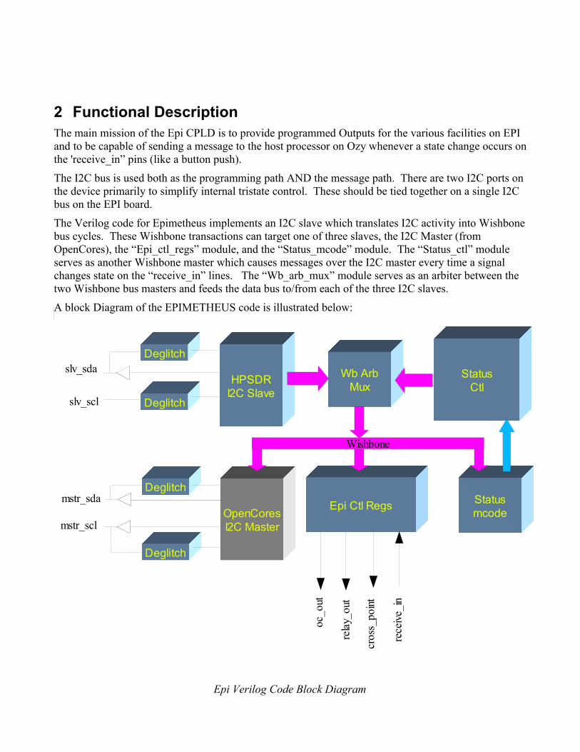
2 Functional DescriptionThe main mission of the Epi CPLD is to provide programmed Outputs for the various facilities on EPI and to be capable of sending a message to the host processor on Ozy whenever a state change occurs on the 'receive_in” pins (like a button push).
The I2C bus is used both as the programming path AND the message path. There are two I2C ports on the device primarily to simplify internal tristate control. These should be tied together on a single I2C bus on the EPI board.
The Verilog code for Epimetheus implements an I2C slave which translates I2C activity into Wishbone bus cycles. These Wishbone transactions can target one of three slaves, the I2C Master (from OpenCores), the “Epi_ctl_regs” module, and the “Status_mcode” module. The “Status_ctl” module serves as another Wishbone master which causes messages over the I2C master every time a signal changes state on the “receive_in” lines. The “Wb_arb_mux” module serves as an arbiter between the two Wishbone bus masters and feeds the data bus to/from each of the three I2C slaves.
A block Diagram of the EPIMETHEUS code is illustrated below:
Epi Verilog Code Block Diagram
HPSDRI2C Slave
Deglitch
Deglitch
OpenCoresI2C Master
Deglitch
Deglitch
Statusmcode
StatusCtl
Wb ArbMux
Epi Ctl Regs
Wishbone
rece
ive_i
n
cros
s_po
int
relay
_out
oc_o
ut
slv_sda
slv_scl
mstr_sda
mstr_scl

This document covers all of the modules colored in Blue. The “OpenCores I2C Master” has it's own documentation that can be found on the “www.opencores.org” web page.
2.1 EPI Module description
This module is the top level and incorporates several sub-modules which implement the CPLD functionality. The table below illustrates the module I/Os.
Signal Name Width Direction Descriptionreset_n 1 In Reset (Active low)CLK 1 In Clock input – should be 30-40Mhzslv_sda 1 In/Out I2C Slave Serial Dataslv_scl 1 In I2C Slave Serial Clockmstr_sda 1 In/Out I2CMaster Serial Datamstr_scl 1 In/Out I2C Master Serial Clockcross_point_ctl 48 Out Cross Point Controlrelay_out 8 Out Relay Controlreceive_in 8 In Received Inputs
oc_out 8 Out Open Collector Out
2.2 OpenCores I2C MasterThe OpenCores I2C master is a wishbone slave that is employed within this design to send messages to the system host (Ozy) when any bit within “receive_in” changes state. The initial conditions are set up by the I2C slave from Ozy, then the microcode inside “Status_mcode” that drives “Status_ctl” will send a copy of the “receive_in” bus anytime a bit changes state.
The table below illustrates the module I/O – please see the OpenCores I2C Master document for further design details.
Signal Name Width Direction Descriptionwb_clk_i 1 In Wishbone Clockwb_rst_i 1 In Wishbone Reset arst_i 1 In Asynchronouse resetwb_adr_i 3 In Wishbone Addresswb_dat_i 8 In Wishbone Data Inwb_dat_o 8 Out Wishbone Data Out
wb_we_i 1 In Wishbone Writewb_stb_i 1 In Wishbone Strobe/Selectwb_cyc_i 1 In Wishbone Cycle
wb_ack_o 1 Out Wishbone Ack wb_inta_o 1 Out Wishbone Interrupt Outscl_pad_i 1 In I2C Clock Inscl_pad_o 1 Out I2C Clock Outscl_padoen_o 1 Out I2C Clock Pad Out Enable (active low)sda_pad_i 1 In I2C Data Insda_pad_o 1 Out I2C Data Outsda_padoen_o 1 Out I2C Data Pad Out Enable (active low)
Please see the register description section for register bit definitions.
The define ADDRESS sets the I2C Slave address.
2.3 I2C_SLAVE (HPSDR)This module implements an I2C slave which translates I2C transactions into Wishbone operations.
The module receives it's I2C address from the top level module (the address which it responds on the I2C too). It is assumed that the I2C signals are de-glitched and that SDA occurs AFTER SCL to allow the STOP & START states to be determined reliably.
Signal Name Width Direction Descriptionrst_n 1 In reset (active low)clk 1 In Clockmy_addr 7 In I2C Slave Addressadr_o 8 Out Wishbone Addressdat_i 8 In Wishbone Data Indat_o 8 Out Wishbone Data Outwe_o 1 Out Wishbone Writestb_o 1 Out Wishbone Strobesel_o 1 Out Wishbone Select (redundant with strobe)cyc_o 1 Out Wishbone Cycle
ack_i 1 In Wishbone Ack debug 12 Out Debug bus (not required)

scl_in 1 In I2C Clock Insda_in 1 In I2C Data Insda_out 1 Out I2C Data Outsda_oe 1 Out I2C Data Pad Out Enable (active high)
I2C_SLAVE Block Diagram
The “START” detector detects the transition of SDA from high to low while the clock is high.
The “STOP” detector sets when the transition of SDA from low to high occurs while the clock is high.
The “RCV_REG” shifts in the received data when the SCL transitions from low to high. This allows it to capture the data transmitted over the I2C bus.
The “RCV_CNTR” counts the number of bits that have been shifted into “RCV_REG.”
Start
Stop
rcv_cntr
rcv_regsda_inscl_in
COMPmy_addr
I2C_SM
Cyc_sm
data_out dat_i8:1 muxsda_out
we_osel_ostb_ocyc_o
ack_i
adr_o adr_o
dat_o dat_o
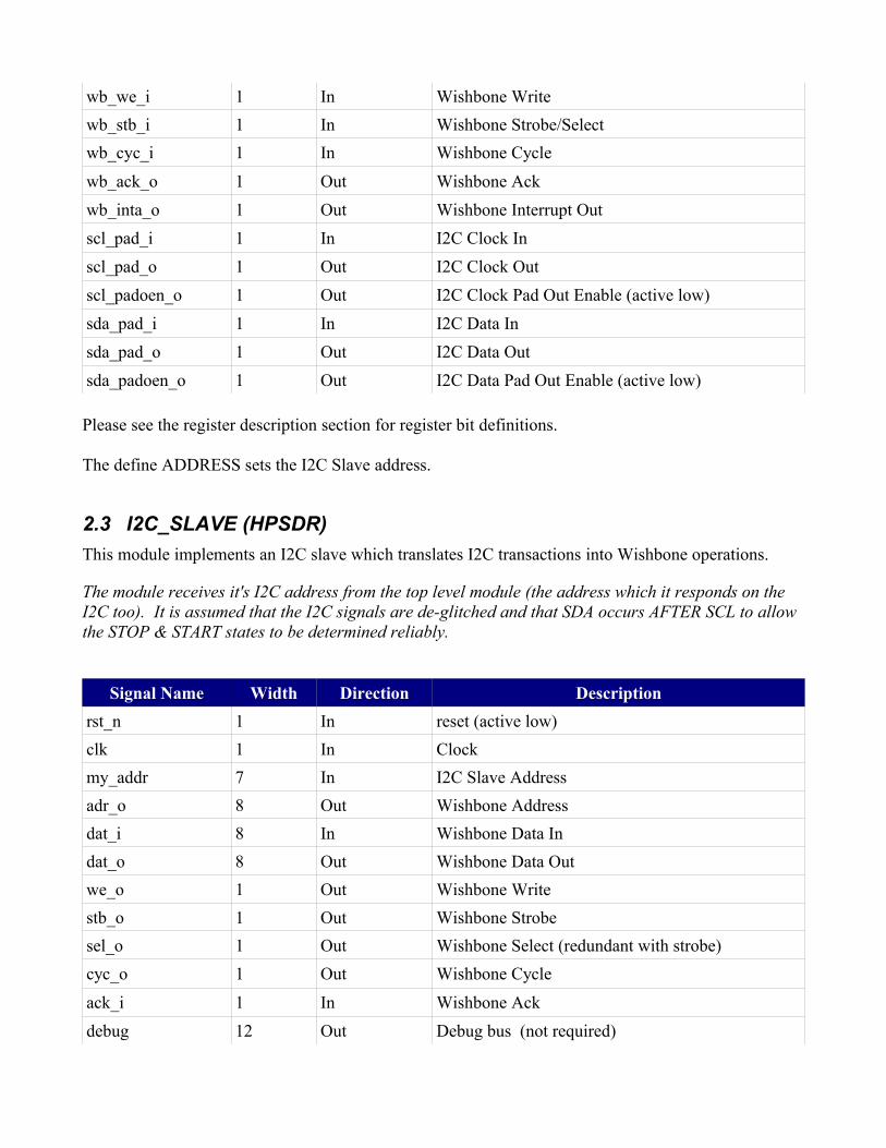
The “COMP” function watches the received data, and when the I2C_SM is in the SM_ADDR state and the data compares to the “my_addr” bus, it indicates an that device has been selected.
The “Data_out” module captures the data from the Wishbone dat_i bus and stores it to be sent out over the I2C SDA_OUT signal through the “8:1 Mux.”
The I2C_SM follows the state diagram below:
I2C SM State DiagramThe state machine goes asynchronously to IDLE when STOP occurs. This is how it exits the READ, WAIT, and WRITE states nominally during burst operations.
IDLE
ADDR
start cnt8 & !addr_dec |cnt8 & addr_dec & nack
READ WRITE
cnt8 & addr_dec & write & ack
cnt8 & addr_dec & !write & ack
start
WAIT
start
cnt8 & nack
stop | reset

The function of the state machine is to interpret multiple I2C sequences, separating them into Address phase which selects the target I2C device followed by either Write or Read phases.
I2C State Machine Sequence to Write Data to the Wisbhone bus
I2C State Machine Sequence to Read Data via the Wishbone bus
The “CYC_SM” is used to cause read and write transactions on the Wishbone bus. The CYC_SM interprets the different points within the I2C sequences and takes appropriate action to move data to or from the I2Cresources across the Wishbone bus.
I2C Addr+RW
ack
Wishbone Address
ack
WishboneWrite Data
ack
Start Stop
ADDR WRITEIDLE WRITE IDLE
I2C Addr+RW
ack
Wishbone Address
ackSt
art
ADDR WRITEIDLE
I2C Addr+RW
ackSt
art
ADDR
Wishbone Read Data
ack St
op
READ

CYC_SM State MachineNote that ALL of the signal state points mentioned above are synchronized copies of the state signals that exist in the I2C clock domain space. This is necessary to remove any problems with metastability.
CYC_SM state sequence following the I2C Write Transfer
I2C Addr+RW
ack
Wishbone Address
ack
WishboneWrite Data
ack
Start Stop
IDLE
WT0
ADD
R
WD
ATA
MVD
T
IDLE
WT0
start
ADDR
ack & target & write
RDATA
ack & target & !write
start
WDATA
ack & write
ack & !write
start
MVDT
clk clk
start
stop
stop | rst_n
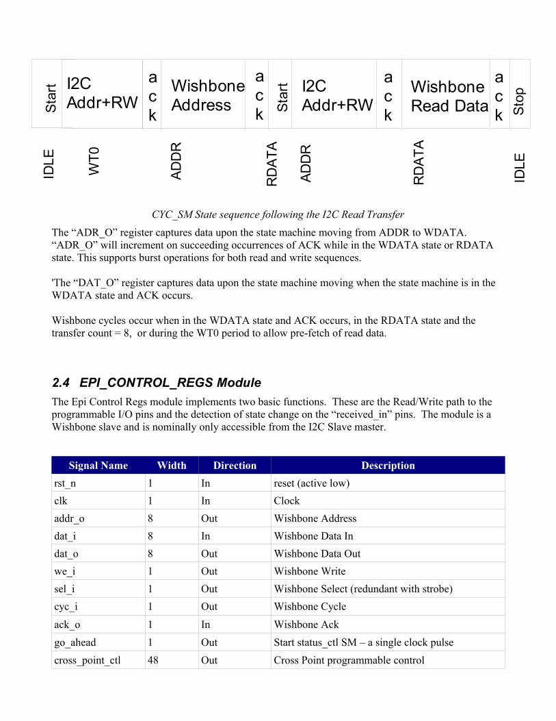
CYC_SM State sequence following the I2C Read TransferThe “ADR_O” register captures data upon the state machine moving from ADDR to WDATA. “ADR_O” will increment on succeeding occurrences of ACK while in the WDATA state or RDATA state. This supports burst operations for both read and write sequences.
'The “DAT_O” register captures data upon the state machine moving when the state machine is in the WDATA state and ACK occurs.
Wishbone cycles occur when in the WDATA state and ACK occurs, in the RDATA state and the transfer count = 8, or during the WT0 period to allow pre-fetch of read data.
2.4 EPI_CONTROL_REGS ModuleThe Epi Control Regs module implements two basic functions. These are the Read/Write path to the programmable I/O pins and the detection of state change on the “received_in” pins. The module is a Wishbone slave and is nominally only accessible from the I2C Slave master.
Signal Name Width Direction Descriptionrst_n 1 In reset (active low)clk 1 In Clockaddr_o 8 Out Wishbone Addressdat_i 8 In Wishbone Data Indat_o 8 Out Wishbone Data Outwe_i 1 Out Wishbone Writesel_i 1 Out Wishbone Select (redundant with strobe)cyc_i 1 Out Wishbone Cycle
ack_o 1 In Wishbone Ack go_ahead 1 Out Start status_ctl SM – a single clock pulsecross_point_ctl 48 Out Cross Point programmable control
I2C Addr+RW
ack
Wishbone Address
ackSt
art I2C
Addr+RW
ackSt
art Wishbone
Read Data
ack St
op
IDLE
WT0
ADD
R
RD
ATA
ADD
R
RD
ATA
IDLE

relay_out 8 Out Relay programmable controloc_out 8 Out Open Collector programmable Controlstat_in 8 Out Masked received_inreceive_in 8 In Received external bus
Write Addressable registers
Address Reg Name Description8'h40 MASK Masks the received_in bus when bit is 0.8'h41 RELAY Controls “relay_out[7:0]”8'h42 OC_OUT Controls “oc_out[7:0]”8'h43 CP0 Controls “cross_point_out[7:0]”8'h44 CP1 Controls “cross_point_out[15:8]”8'h45 CP2 Controls “cross_point_out[23:16]”8'h46 CP3 Controls “cross_point_out[31:24]”8'h47 CP4 Controls “cross_point_out[39:32]”
8'h48 CP5 Controls “cross_point_out[47:40]”
Note all read accesses receive the STAT_IN bus which is a time delayed version of the XOR output.
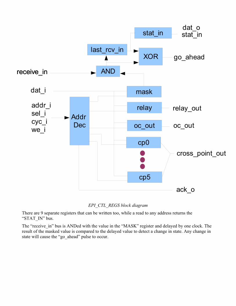
EPI_CTL_REGS block diagramThere are 9 separate registers that can be written too, while a read to any address returns the “STAT_IN” bus.
The “receive_in” bus is ANDed with the value in the “MASK” register and delayed by one clock. The result of the masked value is compared to the delayed value to detect a change in state. Any change in state will cause the “go_ahead” pulse to occur.
Addr Dec
addr_isel_icyc_iwe_i
rcv_maskmask
relay
oc_out
cp0
cp5
XORlast_rcv_in
ANDreceive_in
go_ahead
stat_in stat_in
receive_in
dat_i
relay_out
oc_out
cross_point_out
dat_o
ack_o

2.5 STATUS_MCODE This module implements a byte addressable 16X8 memory array that is attached as a Wishbone slave to the internal Wishbone bus. Bank 0 receives even addresses, while Bank1 receives odd addreses. A second read port feeds the Microcode word over to the “STATUS_CTL” module.
Signal Name Width Direction Descriptionrst_n 1 In reset (active low)clk 1 In Clockaddr_i 8 Out Wishbone Addressdat_i 8 In Wishbone Data Indat_o 8 Out Wishbone Data Outwe_i 1 Out Wishbone Writesel_i 1 Out Wishbone Select (redundant with strobe)cyc_i 1 Out Wishbone Cycle
ack_o 1 In Wishbone Ack mc_addr 3 In Microcode Addressmc_word 16 Out Microcode Data Word
Read/Write address descripton
Address Reg Name Description8'h00 Bank0 byte 0 Microcode Word 0 – lower byte8'h01 Bank1 byte 0 Microcode Word 0 – upper byte8'h02 Bank0 byte 1 Microcode Word 1 – lower byte8'h03 Bank1 byte 1 Microcode Word 1 – upper byte8'h04 Bank0 byte 2 Microcode Word 2 – lower byte8'h05 Bank1 byte 2 Microcode Word 2 – upper byte8'h06 Bank0 byte 3 Microcode Word 3 – lower byte8'h07 Bank1 byte 3 Microcode Word 3 – upper byte
8'h08 Bank0 byte 4 Microcode Word 4 – lower byte
8'h09 Bank1 byte 4 Microcode Word 4 – upper byte
8'h0A Bank0 byte 5 Microcode Word 5 – lower byte
8'h0B Bank1 byte 5 Microcode Word 5 – upper byte
8'h0C Bank0 byte 6 Microcode Word 6 – lower byte
8'h0D Bank1 byte 6 Microcode Word 6 – upper byte
8'h0E Bank0 byte 7 Microcode Word 7 – lower byte
8'h0F Bank1 byte 7 Microcode Word 7 – upper byte
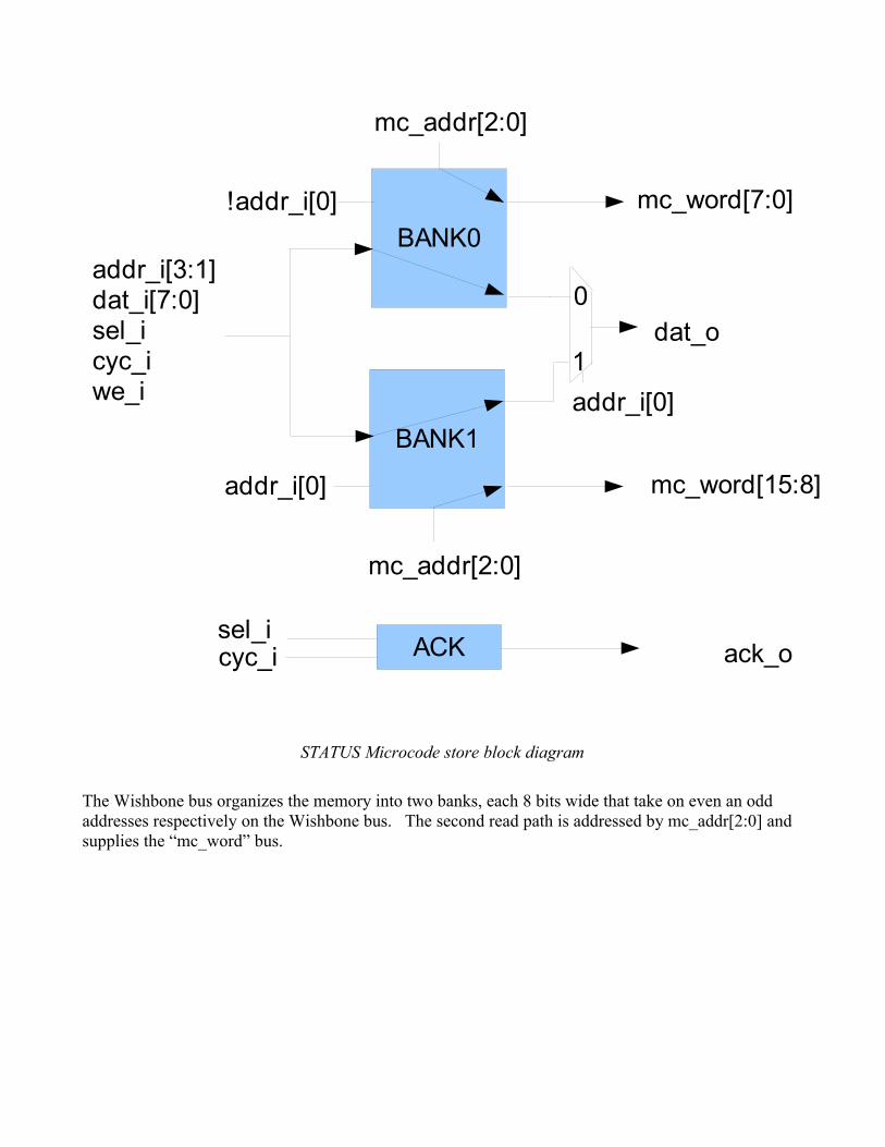
STATUS Microcode store block diagram
The Wishbone bus organizes the memory into two banks, each 8 bits wide that take on even an odd addresses respectively on the Wishbone bus. The second read path is addressed by mc_addr[2:0] and supplies the “mc_word” bus.
BANK0
BANK1addr_i[0]1
0dat_o
mc_word[7:0]
mc_word[15:8]addr_i[0]
!addr_i[0]
addr_i[3:1]dat_i[7:0]sel_icyc_iwe_i
ACKsel_icyc_i ack_o
mc_addr[2:0]
mc_addr[2:0]

2.6 STATUS_CTLThe “STATUS_CTL” module is serves as a Wishbone master which causes I2C messages to be sent via the I2C Master module. The “STATUS_CTL” receives it's micro-coded instructions from the “STATUS_MCODE” module via the “mc_word” bus and interprets them as to the action it's to take.
Signal Name Width Direction Descriptionrst_n 1 In reset (active low)clk 1 In Clockaddr_o 8 Out Wishbone Addressdat_i 8 In Wishbone Data Indat_o 8 Out Wishbone Data Outwe_o 1 Out Wishbone Writesel_o 1 Out Wishbone Select (redundant with strobe)cyc_o 1 Out Wishbone Cycle
ack_i 1 In Wishbone Ack mc_addr 3 Out Microcode Addressmc_word 16 In Microcode Data Wordgo_ahead 1 In Start interpreting the Microcodestat_in 8 In Synchronized version of masked “received_in” bus
The module receives “mc_word” which controls the operation of the module. The table below defines how the state machine decodes the micro-control word.
Signal Name Function mc_word[7:0] Data Out/Comparison wordmc_word[10:8] Address to I2C Mastermc_word[11] Source Select 0 = mc_word[7:0] 1=status_inmc_word[14:13] 00 – Wishbone Write Operation
01 – Wishbone Read and Compare/Loop10 = Wait till Interrupt11 – Undefined
mc_word[15] Stop execution after transaction

This section provides a block diagram of the STAT_CTL module:
STAT_CTL Block Diagram
Stat_SM
mc_word[15:8]
mc_addr
clr_mcadr
incr_mcadr
mc_addr
WishboneGen
run_cyc
cyc_ostb_o
we_o ack_i
mc_word[7:0]
stat_in
dat_o
AND
neq

STAT_CTL State Machine
IDLE
RUN0
!ack
loop & neq &!we0
stop
RUN1
WAIT
int Y/run_cyc Y
Y
N
N
N
Y
N
go_ahead/run_cycwait_till_int
!wait_till_int/run_cyc
/run_cyc
/clr_mcadr
/incr
_mca
dr/run_cyc
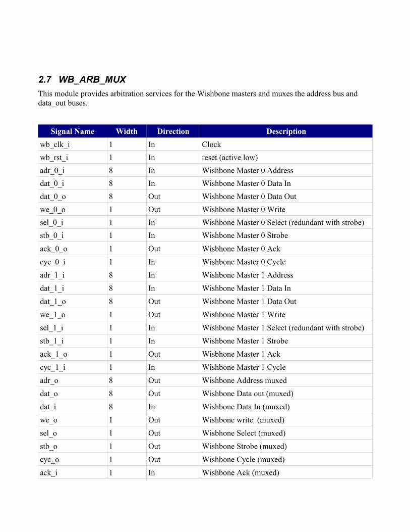
2.7 WB_ARB_MUXThis module provides arbitration services for the Wishbone masters and muxes the address bus and data_out buses.
Signal Name Width Direction Descriptionwb_clk_i 1 In Clockwb_rst_i 1 In reset (active low)adr_0_i 8 In Wishbone Master 0 Addressdat_0_i 8 In Wishbone Master 0 Data Indat_0_o 8 Out Wishbone Master 0 Data Outwe_0_o 1 Out Wishbone Master 0 Writesel_0_i 1 In Wishbone Master 0 Select (redundant with strobe)stb_0_i 1 In Wishbone Master 0 Strobe
ack_0_o 1 Out Wisbhone Master 0 Ack cyc_0_i 1 In Wishbone Master 0 Cycleadr_1_i 8 In Wishbone Master 1 Addressdat_1_i 8 In Wishbone Master 1 Data Indat_1_o 8 Out Wishbone Master 1 Data Outwe_1_o 1 Out Wishbone Master 1 Writesel_1_i 1 In Wishbone Master 1 Select (redundant with strobe)stb_1_i 1 In Wishbone Master 1 Strobeack_1_o 1 Out Wisbhone Master 1 Ack cyc_1_i 1 In Wishbone Master 1 Cycleadr_o 8 Out Wishbone Address muxeddat_o 8 Out Wishbone Data out (muxed)dat_i 8 In Wishbone Data In (muxed)we_o 1 Out Wishbone write (muxed)sel_o 1 Out Wisbhone Select (muxed)stb_o 1 Out Wishbone Strobe (muxed)cyc_o 1 Out Wishbone Cycle (muxed)ack_i 1 In Wishbone Ack (muxed)

WB_ARB_SM Block Diagram
ARB_SMcyc_0_i
cyc_1_i ack_1_o
adr_0_idat_0_iwe_0_istb_0_icyc_0_isel_0_i
adr_1_idat_1_iwe_1_istb_1_icyc_1_isel_1_i
adr_odat_owe_ostb_ocyc_osel_o
ack_0_o
dat_0_o
dat_1_odat_i

3 Microcode ControlThis section discusses how the microcode control is used. The basic idea is that a programmed response is required, consequently an agent that can interact with I2C Master over the wishbone bus is required. The micro-word is organized to be able to control reading/writing of the bus, and has the ability to write literals to selected addresses, write the current received data bus, and to loop on a masked status.
The micro-code is organized as illustrated below:
Signal Name Function mc_word[7:0] Data Out/Comparison wordmc_word[10:8] Address to I2C Mastermc_word[11] Source Select 0 = mc_word[7:0] 1=status_inmc_word[14:13] 00 – Wishbone Write Operation
01 – Wishbone Read and Compare/Loop10 = Wait till Interrupt11 – Undefined
mc_word[15] Stop execution after transaction
The easiest way to illustrate it's use is to give an example:
This is the microcode loaded in the basic test bench. It achieves the sending of the status word to the I2C slave addressed at 0x30. Note that bit 12 in the control word isn't currently defined.
wr_single(SADR1, 8'h00,8'h30); // Load the Slave address into bits 7-0wr_single(SADR1, 8'h01,{MCRUN,MCWRT,MCWORD,TXR});
Microword 0 = 16'b1_00_X_0_011_00110000
// This operation starts the first transmission of the Address phase of the I2C protocolwr_single(SADR1, 8'h02, STA | WRB ); // Set the Start bit and Write Bit in the CTL Regwr_single(SADR1, 8'h03, {MCRUN,MCWRT,MCWORD,CR}); // Write to Ctl Reg -
Microword 1 = 16'b1_00_X_0_100_10010000
/ This has the affect of continually reading the status register until the ANDed condition is true,// i.e. Bit 1 set in this case.wr_single(SADR1, 8'h04, 8'h02); // Mask for bit 1 of the Status wordwr_single(SADR1, 8'h05, {MCRUN,MCRDC,MCWORD,SR}); // Continually read SR until mask true
Microword 2 = 16'b1_01_X_0_100_00000010
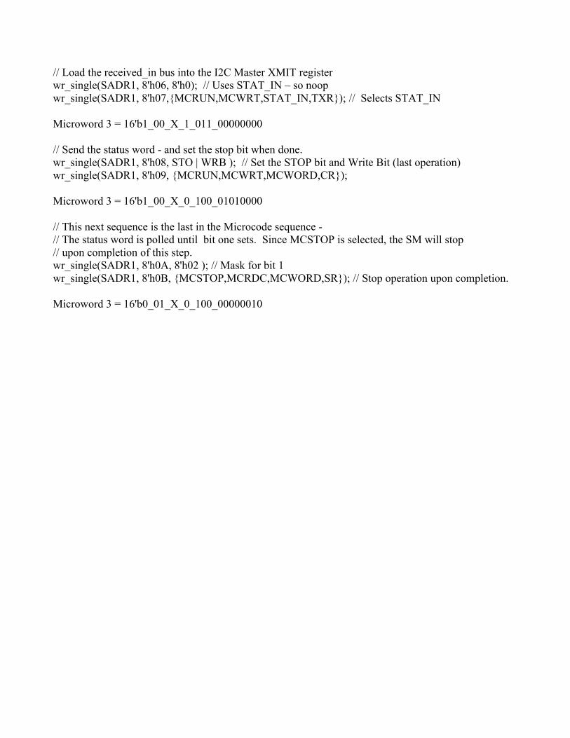
// Load the received_in bus into the I2C Master XMIT registerwr_single(SADR1, 8'h06, 8'h0); // Uses STAT_IN – so noopwr_single(SADR1, 8'h07,{MCRUN,MCWRT,STAT_IN,TXR}); // Selects STAT_IN
Microword 3 = 16'b1_00_X_1_011_00000000
// Send the status word - and set the stop bit when done.wr_single(SADR1, 8'h08, STO | WRB ); // Set the STOP bit and Write Bit (last operation)wr_single(SADR1, 8'h09, {MCRUN,MCWRT,MCWORD,CR});
Microword 3 = 16'b1_00_X_0_100_01010000
// This next sequence is the last in the Microcode sequence - // The status word is polled until bit one sets. Since MCSTOP is selected, the SM will stop // upon completion of this step.wr_single(SADR1, 8'h0A, 8'h02 ); // Mask for bit 1wr_single(SADR1, 8'h0B, {MCSTOP,MCRDC,MCWORD,SR}); // Stop operation upon completion.
Microword 3 = 16'b0_01_X_0_100_00000010