Embed Size (px)
Citation preview
HAL Id: hal-00670201https://hal.archives-ouvertes.fr/hal-00670201
Submitted on 14 Feb 2012
HAL is a multi-disciplinary open accessarchive for the deposit and dissemination of sci-entific research documents, whether they are pub-lished or not. The documents may come fromteaching and research institutions in France orabroad, or from public or private research centers.
L’archive ouverte pluridisciplinaire HAL, estdestinée au dépôt et à la diffusion de documentsscientifiques de niveau recherche, publiés ou non,émanant des établissements d’enseignement et derecherche français ou étrangers, des laboratoirespublics ou privés.
Matlab Code to Link and Pilot Softwares Used forMEMS Simulation
Hikmat Achkar, David Peyrou, Fabienne Pennec, Karim Yacine, AndréFerrand, Patrick Pons, Marc Sartor, Robert Plana
To cite this version:Hikmat Achkar, David Peyrou, Fabienne Pennec, Karim Yacine, André Ferrand, et al.. MatlabCode to Link and Pilot Softwares Used for MEMS Simulation. Advanced Computational Methods inEngineering 2008, May 2008, Liège, Belgium. 10 p. �hal-00670201�
Use Matlab Code to Link and Pilot Softwares Used for MEMS Simulation.
H. ACHKAR1, D. PEYROU1, F. PENNEC1, K. YACINE1, A. FERRAND2, P. PONS1, M.
SARTOR2 and R. PLANA1
1Universite de Toulouse, LAAS-CNRS 7 Av du colonel Roche, 31077, Toulouse, France.
2Universite de Toulouse, UPS, INSA, LGMT 135 Av de Rangueil, 31077, Toulouse, France.
e-mails: [email protected], {hachkar, dpeyrou, fpennec, ppons, plana}@laas.fr
Abstract
This paper presents the advances done in the field of simulation and design applied to MEMS. It will be discussed some techniques to link different finite element softwares, especially COMSOL and ANSYS, in order to profit from all the advantages offered by each finite element code. Then, an explication is done on how we piloted ABAQUS using a Matlab routine. In a third and very important section, the use of reverse engineering method is described and applied to RF-MEMS (Radio Frequency-Micro Electro Mechanical System) switches. The applications for each of these methods will be explained.
1 Introduction The MEMS are micro electromechanical systems which can do different jobs such as sensing, actuating or doing an electrical function. More specifically, RF MEMS characteristics have demonstrated during the last ten years a very attractive potential to allow the introduction of intelligence in the RF front end architecture [1] through analogue signal processing techniques. Nevertheless, those micro devices with moveable mechanical structures still have some issues to be solved before they can be successfully introduced in the industrial level and available in the market.
First the reliability issue that is related to the type of degradation and to the actuation methods. Until nowadays, cantilevers and membranes are actuated using electrostatic, thermal, magnetic and/or piezoelectric energy with all what every type of actuation brings in terms of advantages and inconvenient. It is to be mentioned that today, even that most of the people are turning to piezoelectric actuation since it’s actuated at a very low voltages, electrostatic actuators offer the best trade-off [2] [3] [4] [5] [6] this is if we exclude hybrid (electrostatic and piezoelectric) actuation.
Second is the MEMS process flow simulation which is until these days not complete and need to be developed more in order to become reliable and precise. This process flow simulation is very important since it drives the development of new devices and circuits. For that issue, a good knowledge of the material properties and specifically the mechanical properties is needed.
Third issue comes from the lake of efficient, complete and easy to use simulator covering the totality of the MEMS design procedure, from individual MEMS component design to complete system simulation. On the component level, finite element analysis (FEA) methods, offers high efficiency and are widely used in modelling and simulating the behaviour of MEMS. Since MEMS are multiphysics coupling thermal, mechanics, piezoelectricity, electrostatics, initial stress, mechanical contact and electromagnetic, it is difficult to find software competitive in all the fields.
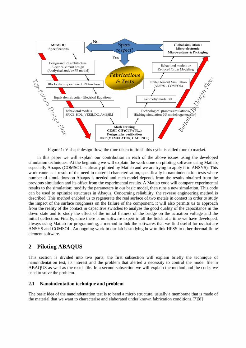
As for us, we are interested to ameliorate the reliability of our components and to develop the simulation platform in order to reduce the trial and error loops in the V shape conception flow shown in figure 1. Reducing the number of experimental steps reduces the cost, while developing the simulators and the simulation tools ameliorate the design phase and by consequence reduces the time to market.
In this paper we will explain our contribution in each of the above issues using the developed simulation techniques. At the beginning we will explain the work done on piloting software using Matlab, especially Abaqus (COMSOL is already piloted by Matlab and we are trying to apply it to ANSYS). This work came as a result of the need in material characterisation, specifically in nanoindentation tests where number of simulations on Abaqus is needed and each model depends from the results obtained from the previous simulation and its offset from the experimental results. A Matlab code will compare experimental results to the simulation; modify the parameters in our basic model, then runs a new simulation. This code can be used to optimize structures in Abaqus. Concerning reliability, the reverse engineering method is described. This method enabled us to regenerate the real surface of two metals in contact in order to study the impact of the surface roughness on the failure of the component, it will also permits us to approach from the reality of the contact in capacitive switches to analyse the good quality of the capacitance in the down state and to study the effect of the initial flatness of the bridge on the actuation voltage and the initial deflection. Finally, since there is no software expert in all the fields at a time we have developed, always using Matlab for programming, a method to link the softwares that we find useful for us that are ANSYS and COMSOL. An ongoing work in our lab is studying how to link HFSS to other thermal finite element software.
2 Piloting ABAQUS This section is divided into two parts; the first subsection will explain briefly the technique of nanoindentation test, its interest and the problem that alerted a necessity to control the model file in ABAQUS as well as the result file. In a second subsection we will explain the method and the codes we used to solve the problem. 2.1 Nanoindentation technique and problem The basic idea of the nanoindentation test is to bend a micro structure, usually a membrane that is made of the material that we want to characterise and elaborated under known fabrication conditions.[7][8]
Geometry model 3D
Technological process simulations(Etching simulation, 3D model regeneration)
Global simulation : Micro-electronic
Micro-systems & Packaging
Finite Element Simulation(ANSYS – COMSOL)
Behavioral models orReduced Order Modeling
Mask drawingGDSII, CIF (CLEWIN...)Design rules verification
DRC (MEMULATOR, CADENCE)
MEMS RFSpecifications
Design and RF architectureElectrical circuit design
(Analytical and/or FE model)
Blocks decomposition of RF function
Equivalent circuits – Electrical Equations
Behavioral modelsSPICE, HDL, VERILOG, AMESIM
Specs. respect?
Fabrications
& Tests
No
Yes
Figure 1: V shape design flow, the time taken to finish this cycle is called time to market.
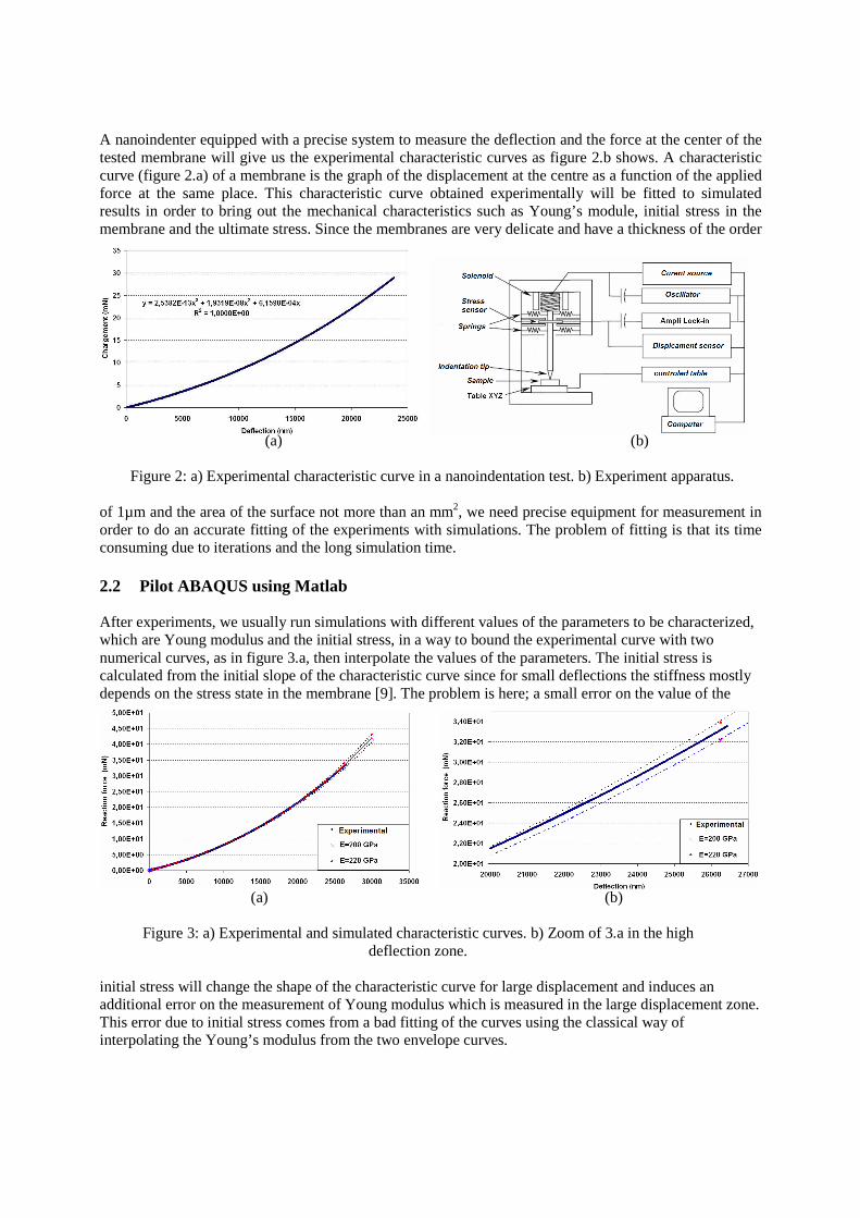
A nanoindenter equipped with a precise system to measure the deflection and the force at the center of the tested membrane will give us the experimental characteristic curves as figure 2.b shows. A characteristic curve (figure 2.a) of a membrane is the graph of the displacement at the centre as a function of the applied force at the same place. This characteristic curve obtained experimentally will be fitted to simulated results in order to bring out the mechanical characteristics such as Young’s module, initial stress in the membrane and the ultimate stress. Since the membranes are very delicate and have a thickness of the order
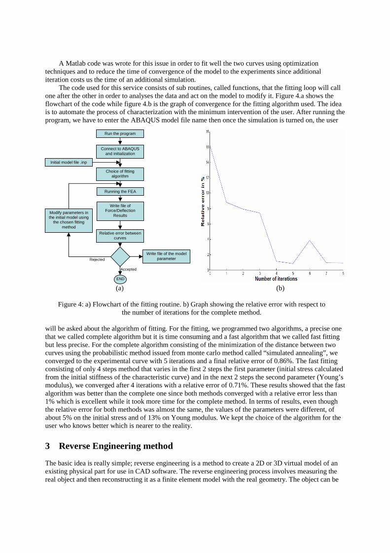
of 1µm and the area of the surface not more than an mm2, we need precise equipment for measurement in order to do an accurate fitting of the experiments with simulations. The problem of fitting is that its time consuming due to iterations and the long simulation time. 2.2 Pilot ABAQUS using Matlab After experiments, we usually run simulations with different values of the parameters to be characterized, which are Young modulus and the initial stress, in a way to bound the experimental curve with two numerical curves, as in figure 3.a, then interpolate the values of the parameters. The initial stress is calculated from the initial slope of the characteristic curve since for small deflections the stiffness mostly depends on the stress state in the membrane [9]. The problem is here; a small error on the value of the
initial stress will change the shape of the characteristic curve for large displacement and induces an additional error on the measurement of Young modulus which is measured in the large displacement zone. This error due to initial stress comes from a bad fitting of the curves using the classical way of interpolating the Young’s modulus from the two envelope curves.
(a) (b)
Figure 2: a) Experimental characteristic curve in a nanoindentation test. b) Experiment apparatus.
(a) (b)
Figure 3: a) Experimental and simulated characteristic curves. b) Zoom of 3.a in the high deflection zone.
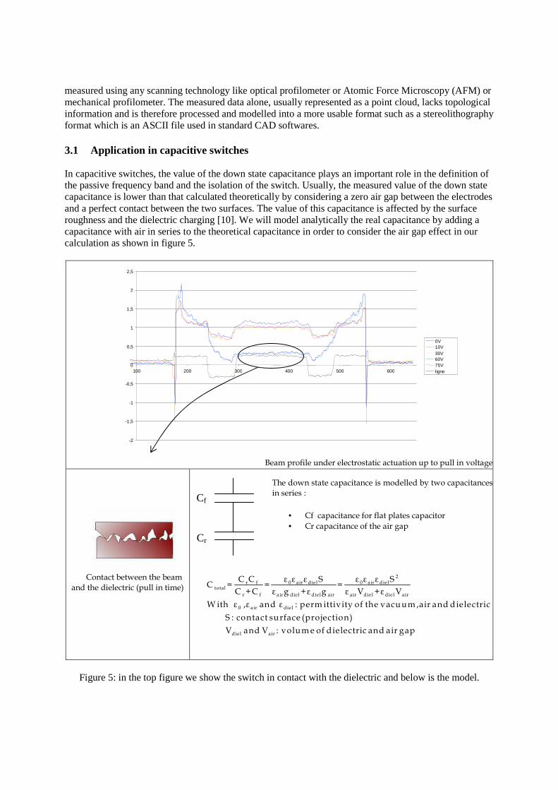
A Matlab code was wrote for this issue in order to fit well the two curves using optimization techniques and to reduce the time of convergence of the model to the experiments since additional iteration costs us the time of an additional simulation.
The code used for this service consists of sub routines, called functions, that the fitting loop will call one after the other in order to analyses the data and act on the model to modify it. Figure 4.a shows the flowchart of the code while figure 4.b is the graph of convergence for the fitting algorithm used. The idea is to automate the process of characterization with the minimum intervention of the user. After running the program, we have to enter the ABAQUS model file name then once the simulation is turned on, the user
will be asked about the algorithm of fitting. For the fitting, we programmed two algorithms, a precise one that we called complete algorithm but it is time consuming and a fast algorithm that we called fast fitting but less precise. For the complete algorithm consisting of the minimization of the distance between two curves using the probabilistic method issued from monte carlo method called “simulated annealing”, we converged to the experimental curve with 5 iterations and a final relative error of 0.86%. The fast fitting consisting of only 4 steps method that varies in the first 2 steps the first parameter (initial stress calculated from the initial stiffness of the characteristic curve) and in the next 2 steps the second parameter (Young’s modulus), we converged after 4 iterations with a relative error of 0.71%. These results showed that the fast algorithm was better than the complete one since both methods converged with a relative error less than 1% which is excellent while it took more time for the complete method. In terms of results, even though the relative error for both methods was almost the same, the values of the parameters were different, of about 5% on the initial stress and of 13% on Young modulus. We kept the choice of the algorithm for the user who knows better which is nearer to the reality.
3 Reverse Engineering method The basic idea is really simple; reverse engineering is a method to create a 2D or 3D virtual model of an existing physical part for use in CAD software. The reverse engineering process involves measuring the real object and then reconstructing it as a finite element model with the real geometry. The object can be
Run the program
Connect to ABAQUS and initialization
Choice of fitting algorithm
Initial model file .inp
Running the FEA
Write file of Force/Deflection
Results
Write file of the model parameter
Relative error between curves
Accepted
Rejected
Modify parameters in the initial model using
the chosen fitting method
END
(a) (b)
Figure 4: a) Flowchart of the fitting routine. b) Graph showing the relative error with respect to the number of iterations for the complete method.
Cf
Cr
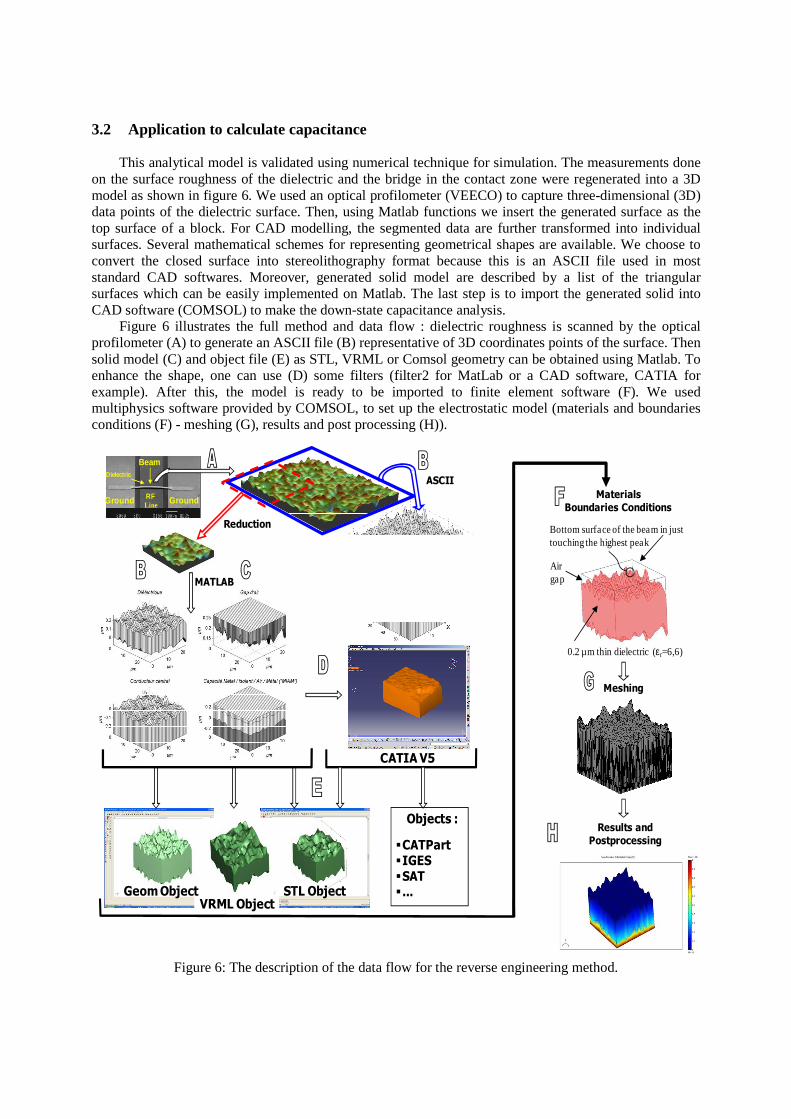
measured using any scanning technology like optical profilometer or Atomic Force Microscopy (AFM) or mechanical profilometer. The measured data alone, usually represented as a point cloud, lacks topological information and is therefore processed and modelled into a more usable format such as a stereolithography format which is an ASCII file used in standard CAD softwares. 3.1 Application in capacitive switches In capacitive switches, the value of the down state capacitance plays an important role in the definition of the passive frequency band and the isolation of the switch. Usually, the measured value of the down state capacitance is lower than that calculated theoretically by considering a zero air gap between the electrodes and a perfect contact between the two surfaces. The value of this capacitance is affected by the surface roughness and the dielectric charging [10]. We will model analytically the real capacitance by adding a capacitance with air in series to the theoretical capacitance in order to consider the air gap effect in our calculation as shown in figure 5.
Beam profile under electrostatic actuation up to pull in voltage
Contact between the beam
and the dielectric (pull in time)
The down state capacitance is modelled by two capacitances in series :
• Cf capacitance for flat plates capacitor
• Cr capacitance of the air gap
2
r f 0 air diel 0 air dieltotal
r f air diel diel air air diel diel air
0 air diel
diel air
C C ε ε ε S ε ε ε SC = = =
C +C ε g +ε g ε V +ε V
W ith ε ,ε and ε : perm ittivity of the vacuum ,air and dielectric
S : contact surface (projection)
V and V : volume of dielectric and air gap
Figure 5: in the top figure we show the switch in contact with the dielectric and below is the model.
-2
-1,5
-1
-0,5
0
0,5
1
1,5
2
2,5
100 200 300 400 500 600
0V10V30V60V75Vligne
3.2 Application to calculate capacitance This analytical model is validated using numerical technique for simulation. The measurements done
on the surface roughness of the dielectric and the bridge in the contact zone were regenerated into a 3D model as shown in figure 6. We used an optical profilometer (VEECO) to capture three-dimensional (3D) data points of the dielectric surface. Then, using Matlab functions we insert the generated surface as the top surface of a block. For CAD modelling, the segmented data are further transformed into individual surfaces. Several mathematical schemes for representing geometrical shapes are available. We choose to convert the closed surface into stereolithography format because this is an ASCII file used in most standard CAD softwares. Moreover, generated solid model are described by a list of the triangular surfaces which can be easily implemented on Matlab. The last step is to import the generated solid into CAD software (COMSOL) to make the down-state capacitance analysis.
Figure 6 illustrates the full method and data flow : dielectric roughness is scanned by the optical profilometer (A) to generate an ASCII file (B) representative of 3D coordinates points of the surface. Then solid model (C) and object file (E) as STL, VRML or Comsol geometry can be obtained using Matlab. To enhance the shape, one can use (D) some filters (filter2 for MatLab or a CAD software, CATIA for example). After this, the model is ready to be imported to finite element software (F). We used multiphysics software provided by COMSOL, to set up the electrostatic model (materials and boundaries conditions (F) - meshing (G), results and post processing (H)).
Figure 6: The description of the data flow for the reverse engineering method.
Dielectric
Ground
Beam
GroundRFLine
ASCII
0.2 µm thin dielectric (εr=6,6)
Air gap
Bottom surface of the beam in justtouching the highest peak
Materials
Boundaries Conditions
Meshing
Results and
Postprocessing
Reduction
MATLAB
CATIA V5
STL ObjectVRML Object
Objects :
�CATPart�IGES�SAT� ...GeomObject
The value of the capacitance obtained by simulation and the one obtained analytically are about 4% which is very good while it showed far values when compared with the measurements. This difference can be explained with the charging effect of the dielectric and neglecting of the deformation of the asperities during the contact. The table below summarizes the results obtained.
Simulated Calculated Measured Theoretical
0.999335 pF 0.9571255 pF 1.41 pF 3.03 pF
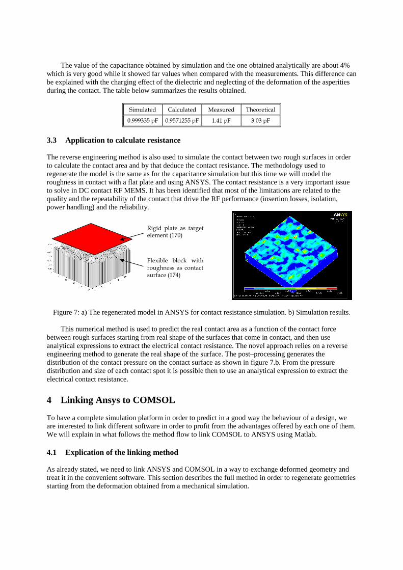
3.3 Application to calculate resistance The reverse engineering method is also used to simulate the contact between two rough surfaces in order to calculate the contact area and by that deduce the contact resistance. The methodology used to regenerate the model is the same as for the capacitance simulation but this time we will model the roughness in contact with a flat plate and using ANSYS. The contact resistance is a very important issue to solve in DC contact RF MEMS. It has been identified that most of the limitations are related to the quality and the repeatability of the contact that drive the RF performance (insertion losses, isolation, power handling) and the reliability.
Figure 7: a) The regenerated model in ANSYS for contact resistance simulation. b) Simulation results.
This numerical method is used to predict the real contact area as a function of the contact force between rough surfaces starting from real shape of the surfaces that come in contact, and then use analytical expressions to extract the electrical contact resistance. The novel approach relies on a reverse engineering method to generate the real shape of the surface. The post–processing generates the distribution of the contact pressure on the contact surface as shown in figure 7.b. From the pressure distribution and size of each contact spot it is possible then to use an analytical expression to extract the electrical contact resistance.
4 Linking Ansys to COMSOL To have a complete simulation platform in order to predict in a good way the behaviour of a design, we are interested to link different software in order to profit from the advantages offered by each one of them. We will explain in what follows the method flow to link COMSOL to ANSYS using Matlab. 4.1 Explication of the linking method As already stated, we need to link ANSYS and COMSOL in a way to exchange deformed geometry and treat it in the convenient software. This section describes the full method in order to regenerate geometries starting from the deformation obtained from a mechanical simulation.
Rigid plate as target element (170)
Flexible block with roughness as contact surface (174)

Figure8: flow chart of linking ANSYS to COMSOL.
Starting from a drawn geometry in any of the softwares, a mechanical simulation is done.
The mechanical deformation is written in an output file in .txt format.
Data treatment in Matlab, and rearrangement of the outputs.
From a set of point cloud, we create surfaces that will form the deformed geometry.
Contact analysis or any other application (ex: CFD, …) is done in ANSYS. Once more, the deformation information is written in a file .txt.
Data treatment in Matlab and rearrangement of the outputs.
Regenerated geometry with possibility to add parts to the deformed shape.
Finally meshing either the air between the membrane and the plane or meshing the membrane itself depending on the application.
COMSOL 3.3 appeared as software that is capable to do piezoelectric simulations combined to mechanical structure and contact problems, without forgetting thermal and initial stress effects. The problem appears here, when we need to simulate complicated contact problems and where COMSOL solver fails most of the time.
When talking about contact in COMSOL, it is somehow critical and difficult to converge the simulation specially that we have to vary the contact parameters and it’s still not sure to converge. The convergence of the contact model using COMSOL failed; one have then to find a way to link both ANSYS and COMSOL in order to use ANSYS contact models. By exchanging the deformed geometry between them and then running the convenient simulation using the appropriate tool, some simulation problems can be solved.
A very practical way to run simulations on two different softwares, is to pilot it using Matlab. To achieve our purpose, we created in Matlab some functions which make the piloting and the link between the softwares easier. In what follows, the flow chart shows the key steps of the method by using a simple membrane of 200x200µm2 subjected to constant pressure and blocked at its corner. We can begin the cycle from where we want, either from ANSYS or from COMSOL. In the flow chart, we began from COMSOL, with a simple membrane under pressure as explained in figure 8. The geometry is drawn, and then the loads and boundary conditions are applied. A mechanical simulation is run in order to obtain the deformation of the membrane. Considering that a contact analysis is needed after the deformation of the membrane, so we export the deformation of the membrane into a text file. In the text file there will be the displacement of each node of the chosen surface of interest as well as some data that we don’t need. Matlab will treat this file to clean unneeded information and to reorganize data in the file. The treated file will be used then to create a cloud of keypoints, by creating it one by one, and then generating surfaces from the keypoints. In ANSYS now, we will mesh the regenerated geometry, we will define the physics that we need to study (in our case it’s the contact) and then run a new simulation. The deformation is once again output in a text file, giving the displacement value for each node of the surface of interest. Another treatment and organization of the output data file, before being injected in the function that we created in Matlab which regenerates the surface and export it to COMSOL. The geometry is ready to be used in COMSOL, new objects can be added to it, for example electrode, before going into meshing and then boundary condition, to finish into a new simulation. The loop can turn as much times as we need, passing from software to another, until we attain our goal.
5 Conclusions and perspective This paper showed the modelling techniques that we used to advance the MEMS simulation and to ameliorate the reliability of the components by characterizing the material with higher precision and modelling the contact state of the switch using the reverse engineering method.
Piloting ABAQUS permitted us to save time in nano-indentation tests since the curves fitting method is done automatically and it increased the precision of the characterization. As perspectives, the pilot of ABAQUS can be integrated on a production line of a clean room in order to automatically characterize the material. A profilometer can detect the dimensions of the membrane in order to create the first model for the fitting loop, then the nano-indentor will be automatically positioned to perform the test, the experimental results will be used then by the program in order to give the mechanical characteristics.
The reverse engineering method was described and it was used to simulate the capacitance in the down state of a capacitance in order to validate the analytical formula for the air gap effect on the capacitance loss. It was also applied to contact simulation in order to extract the electrical contact resistance. Simulating the contact resistance replaced the expensive tests that needed to be done for different materials in contact and for different surface roughness. This method will be used later to simulate the effect of the real initial shape of the bridge on the deformation due to initial stress and on the actuation voltage as well as the capacitance quality in the down state.
Finally we showed a method to link COMSOL to ANSYS in order to profit of the advantages offered by different simulators. In a previous paper we did a study on the numerical platform validation and we
offered a table that lists the advantages and drawbacks of the softwares, this will help understand why we needed the link. In a future step, we seek to do an automatic link between the softwares and get rid of the user’s assistance in order to reduce the lost time. A new need in our group of work is to link the thermal results obtained from HFSS with ANSYS or COMSOL.
References
[1] G.M. Rebeiz and J.B. Muldavin. RF MEMS Switches and switch circuits. IEEE microwave magazine, vol. 2, no. 4:59-71, 2001.
[2] G. Tschulena. Market analysis for MEMS and Microsystems III, 2005-2009. A Nexus task force, edited by Nexus association, Wehrheim, Germany, 2005.
[3] S. Mellé, D.De. Conto, D. Dubuc, K. Grenier, O. Vendier, J.L. Muraro, J.L. Cazaux and R. Plana. Reliability modelling of capacitive RF-MEMS. IEEE Transactions on Microwave Theory and Techniques, vol. 53, no. 11:3482-3488, 2005.
[4] J.R. Reid and R.T. Webster. Measurments of charging in capacitive microelectromechanical switches. Electron lett, vol. 38, no. 24:1544-1545, 2002.
[5] W.M. Van Sprengen, R. Puers, R. Mertens and I.De. Wolf. A comprehensive model to predict the charging and reliability of RF-MEMS switches. J.Micromech. Microeng, vol. 14, no. 4:514-521, 2004.
[6] X. Yuan, Z. Peng, J.C.M. Wang, D. Forehand and C. Goldsmith. Acceleration of dielectric charging in RF-MEMS capacitive switches. IEEE Transactions on device and materials reliability, vol. 6, no. 4:556-563, 2006.
[7] L. Xiaodong and B. Bharat. A review of nanoindentation continuous stiffness measurement technique and its applications. Elsevier material characterization, 48:11-36, 2002.
[8] S. Staussa, P. Schwallera, J.-L. Bucaillea, R. Rabea, L. Rohra, J. Michlera, E. Blank. Determining the stress–strain behaviour of small devices by nanoindentation in combination with inverse methods. Elsevier microelectronic engineering, 68:818-825, 2003.
[9] H.D. Espinosa, M. Fischer, E.Herbert and W. Oliver. Identification of Residual Stress State in an RF-MEMS Device. MTS Systems Corporation, 100-034-533 RFMEMS Device-01, 2000.
[10] G. Palasantzas and J.Th.M DeHosson. Surface roughness influence on the pull-in voltage of microswitches in presence of thermal and quantum vacuum fluctuations. Surfaces Sciences, vol.600, No.7:1450-1455, 2006.