Embed Size (px)
Citation preview
Materials Science in Quantum Computing
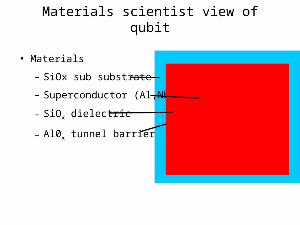
Materials scientist view of qubit
• Materials
– SiOx sub substrate
– Superconductor (Al,Nb)
– SiOx dielectric
– Al0x tunnel barrier
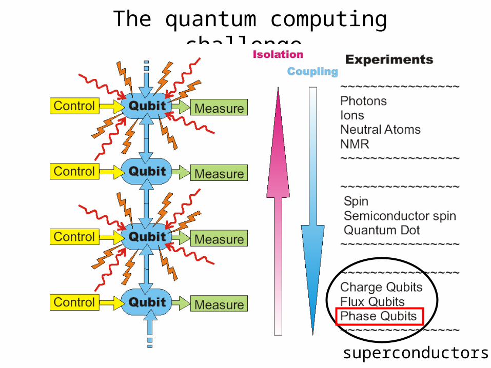
The quantum computing challenge
superconductors

Superconducting Josephson junction phase qubit principle
TunnelJunction~1.5 nm
Top superconductor
Bottom superconductor
Itop= 0
bot= 0ei
Cooper pairwavefunction
Josephsonrelations
e2V
)sin(II 0
• I depends on
• Voltage only when
phase is
changing
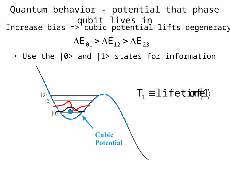
Quantum behavior - potential that phase qubit lives in• Increase bias => cubic potential lifts degeneracy
231201 EEE • Use the |0> and |1> states for information
1 of lifetimeT1
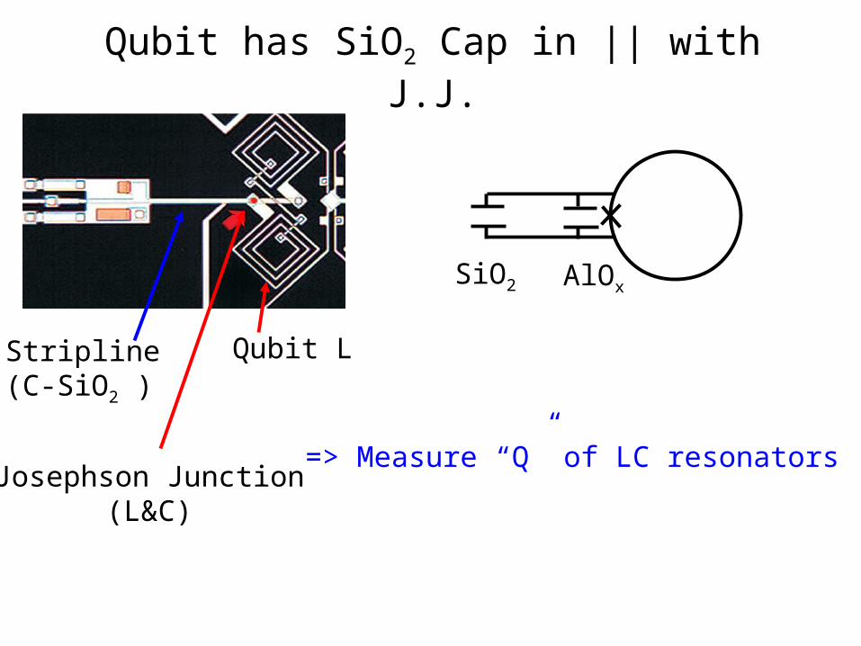
Insert qubit pic here
Qubit LStripline (C-SiO2 )
Josephson Junction(L&C)
=> Measure “Q” of LC resonators
Qubit has SiO2 Cap in || with J.J.
SiO2 AlOx
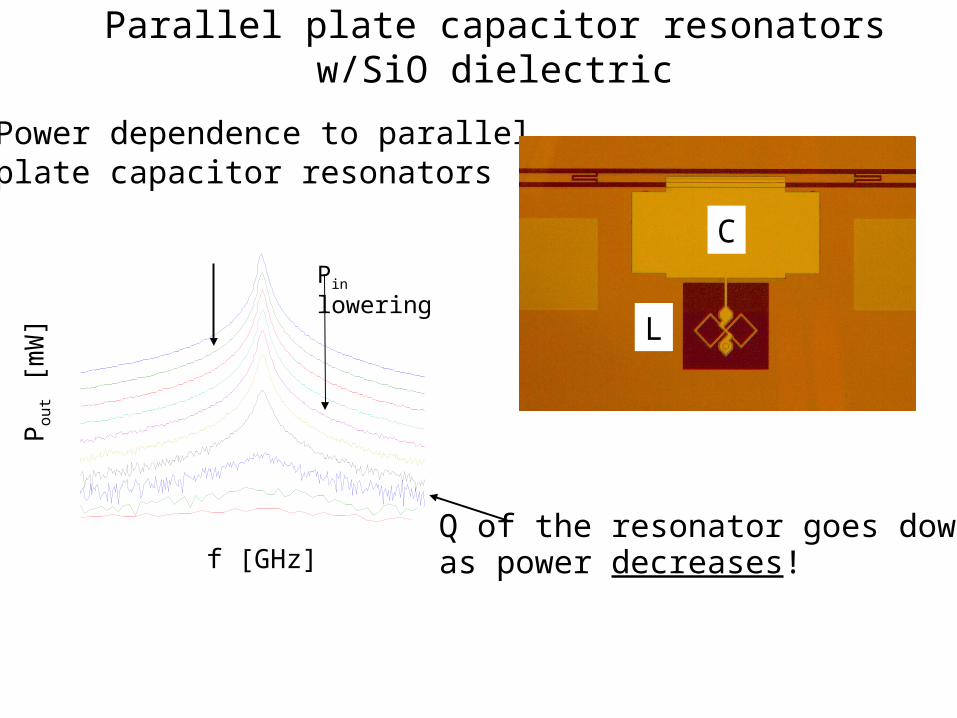
Power dependence to parallelplate capacitor resonators
wave resonator
L
f [GHz]
Po
ut [m
W]
Pin lowering
Q of the resonator goes downas power decreases!
Parallel plate capacitor resonators w/SiO dielectric
C
L
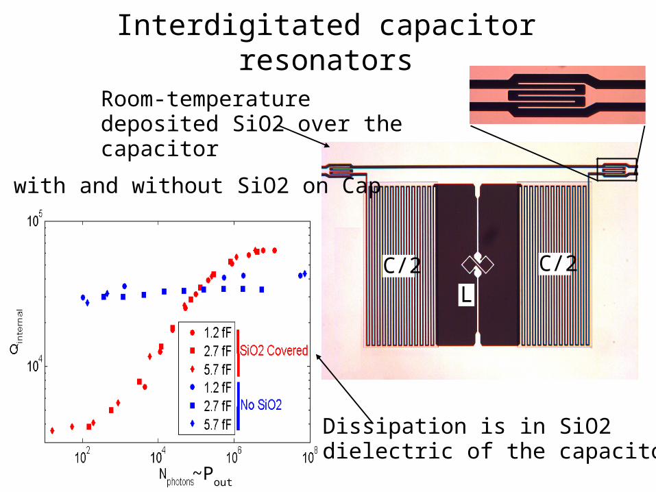
Room-temperature deposited SiO2 over the capacitor
C/2 C/2
L
Data with and without SiO2 on Cap
Dissipation is in SiO2dielectric of the capacitor!
~Pout
Interdigitated capacitor resonators
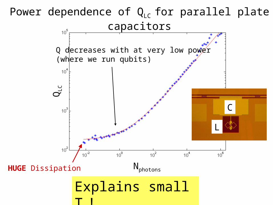
Power dependence of QLC for parallel plate capacitors
HUGE Dissipation
Q decreases with at very low power(where we run qubits)
Nphotons
QL
C
Explains small T1!
L
C
10-1
100
101
102
103
104
105
102
103
104
105
Q
number of photons
|E| [V/m]
1/lo
ss ta
ng
ent
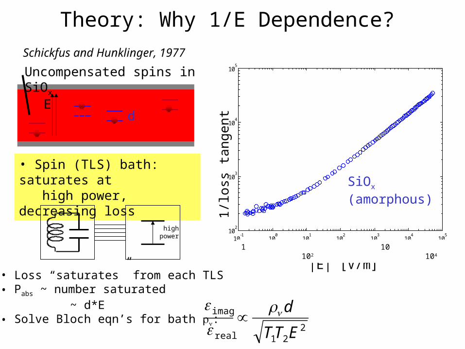
• Spin (TLS) bath: saturates at high power, decreasing loss
high power
SiOx
(amorphous)
Schickfus and Hunklinger, 1977
1 10 102 104
• Loss “saturates” from each TLS• Pabs ~ number saturated ~ d*E• Solve Bloch eqn’s for bath : 2
21real
imag
ETT
d
Theory: Why 1/E Dependence?
Uncompensated spins in SiOx
E d
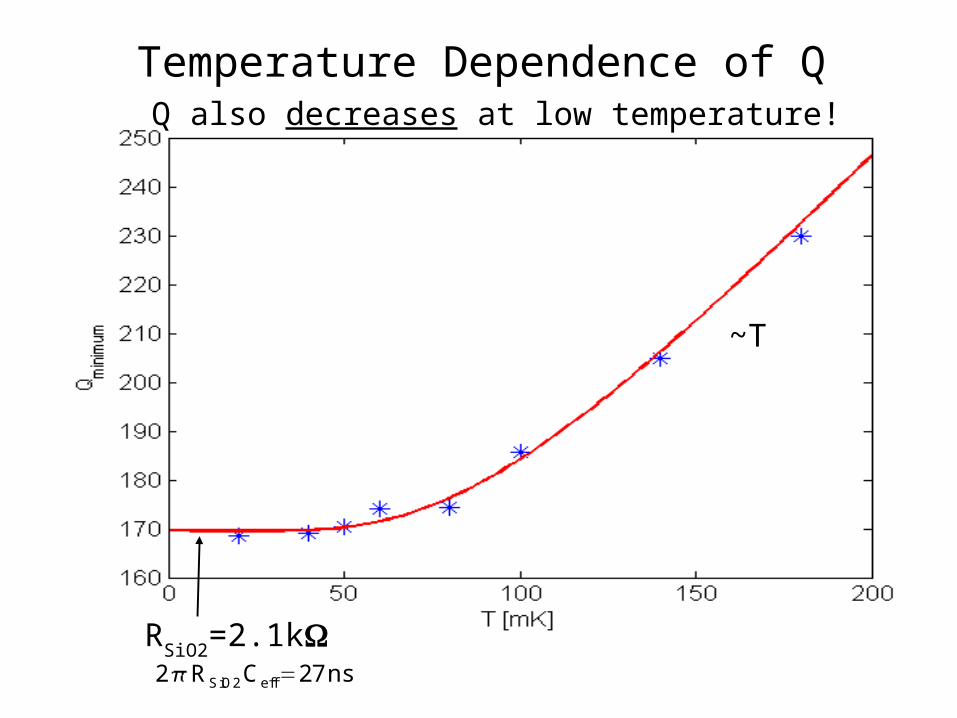
2 RSiO2Ceff 27ns
~T
RSiO2
=2.1k
Temperature Dependence of QQ also decreases at low temperature!
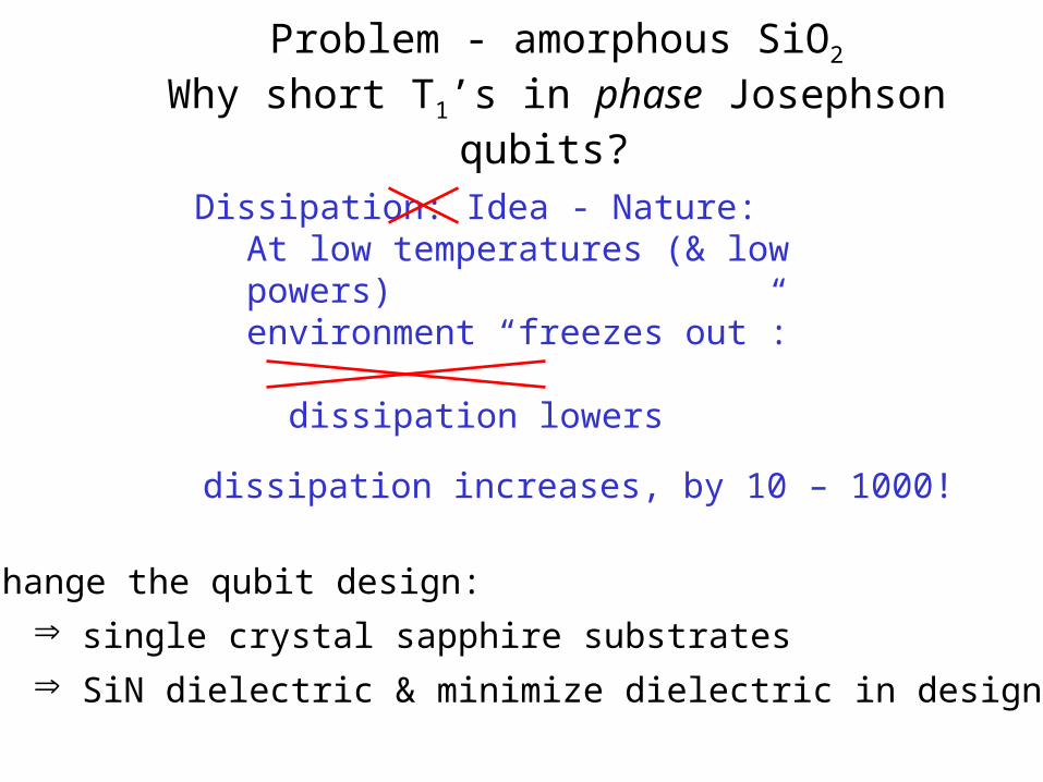
Problem - amorphous SiO2
Why short T1’s in phase Josephson qubits?
Dissipation: Idea - Nature:At low temperatures (& low powers)environment “freezes out”:
dissipation lowers
dissipation increases, by 10 – 1000!
Change the qubit design:
single crystal sapphire substrates
SiN dielectric & minimize dielectric in design
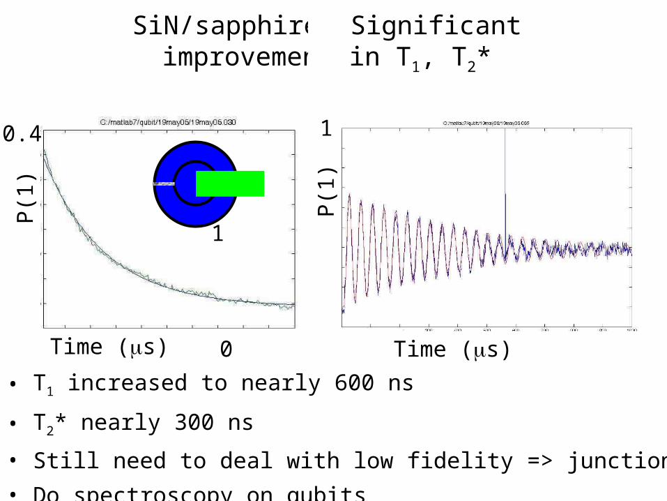
SiN/sapphire: Significant improvement in T1, T2*
0 Time (s) 2 0 Time (s) 1
P(1
)
0.4
P(1
)
• T1 increased to nearly 600 ns
• T2* nearly 300 ns
• Still need to deal with low fidelity => junctions
• Do spectroscopy on qubits
11
1
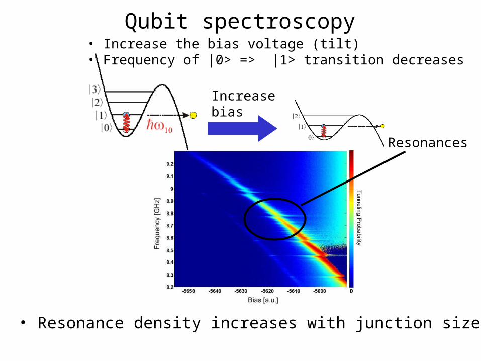
Qubit spectroscopy• Increase the bias voltage (tilt)• Frequency of |0> => |1> transition decreases
Resonances
Increasebias
• Resonance density increases with junction size
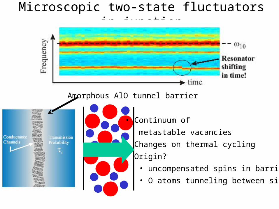
Microscopic two-state fluctuators in junction
Amorphous AlO tunnel barrier
• Continuum of
metastable vacancies
• Changes on thermal cycling
• Origin?
• uncompensated spins in barrier
• O atoms tunneling between sites
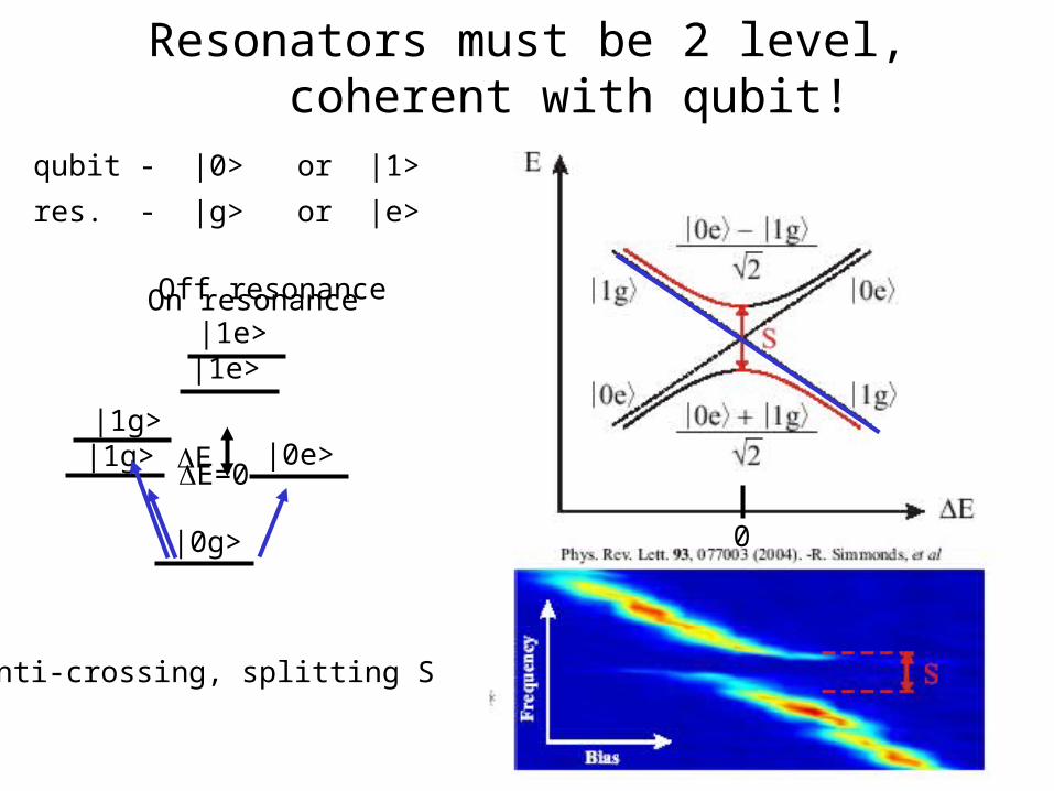
Resonators must be 2 level, coherent with qubit!
qubit - |0> or |1>
res. - |g> or |e>
|0e>
|0g> 0
|1e>
|1g>
On resonance
E=0
Anti-crossing, splitting S
|1e>
|1g>E
Off resonance
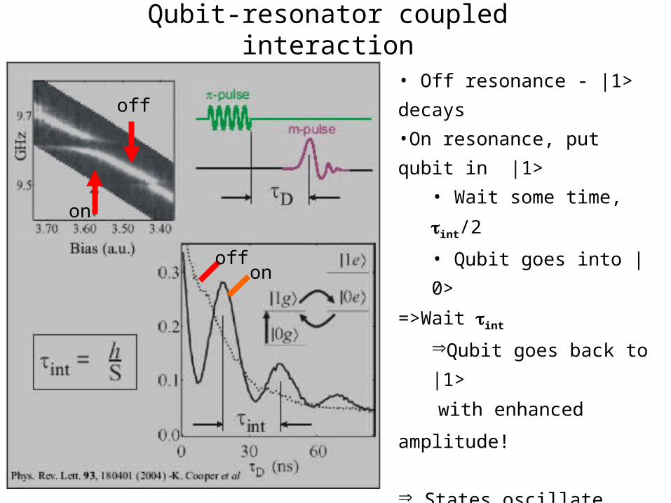
Qubit-resonator coupled interaction
• Off resonance - |1> decays
•On resonance, put qubit in |1>
• Wait some time, int/2
• Qubit goes into |0>
=>Wait int
Qubit goes back to |1>
with enhanced amplitude!
States oscillate
|1g> <=> |0e>
Resonator has longer
coherence time than qubit
off
off
on
on
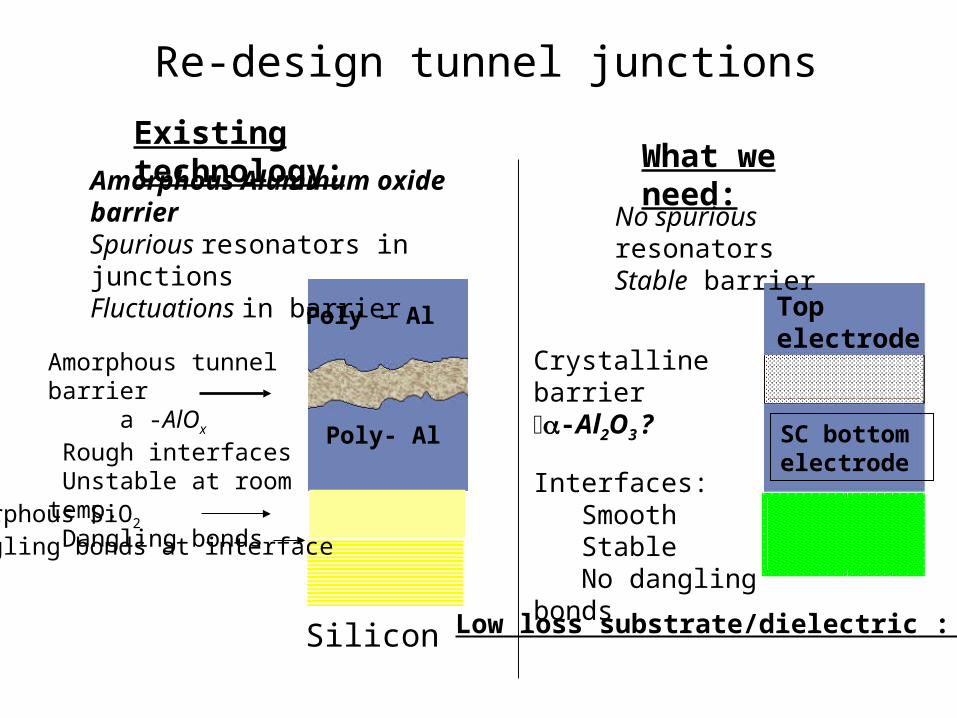
What we need:
Crystalline barrier-Al2O3 ?
Interfaces: Smooth Stable No dangling bonds
Poly - Al
Poly- Al
Existing technology:
Amorphous tunnel barrier a -AlOx
Rough interfaces Unstable at room temp. Dangling bonds
No spurious resonatorsStable barrier
Amorphous Aluminum oxide barrierSpurious resonators in junctionsFluctuations in barrier
Silicon
amorphous SiO2
dangling bonds at interface
Low loss substrate/dielectric : SiN
Re-design tunnel junctions
SC bottom electrode
Top electrode
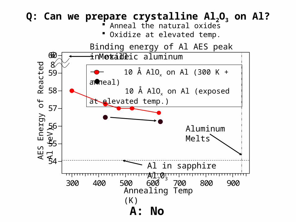
Q: Can we prepare crystalline Al2O3 on Al?
Binding energy of Al AES peak in oxide60
59
58
57
56
55
54
900800700600500400300Annealing Temp (K)
AE
S E
nerg
y of
Rea
cted
Al (
eV)
Al in sapphire Al203
Metallic aluminum
Aluminum Melts
68
10 Å AlOx on Al (300 K + anneal) 10 Å AlOx on Al (exposed at elevated temp.)
Anneal the natural oxides Oxidize at elevated temp.
A: No
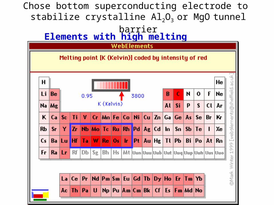
Chose bottom superconducting electrode to stabilize crystalline Al2O3 or MgO tunnel barrier
Elements with high melting temperature

Elements with TC > 1K
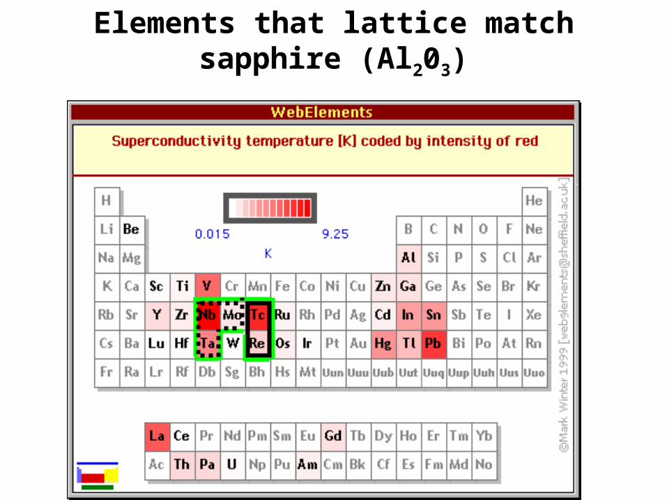
Elements that lattice match sapphire (Al203)

Elements that form weaker bond with oxygen than Al
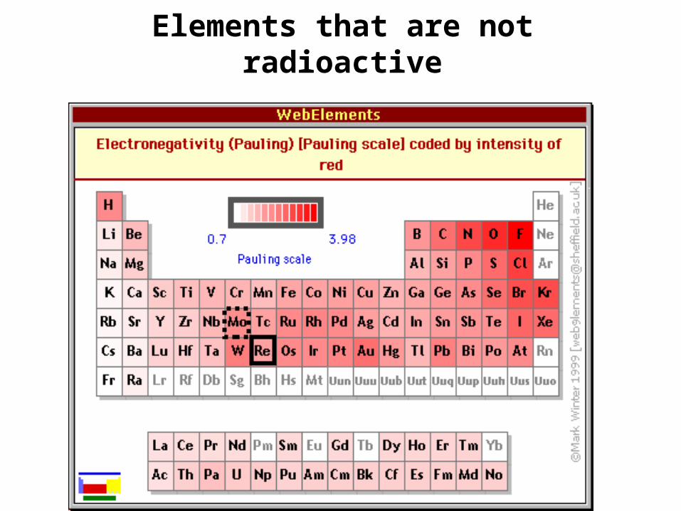
Elements that are not radioactive
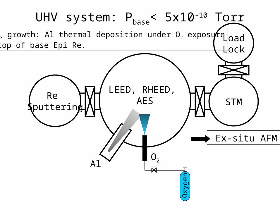
LEED, RHEED, AESRe
Sputtering
LoadLock
STM
Ex-situ AFM
Al
Oxy
gen
O2
Al2O3 growth: Al thermal deposition under O2 exposureon top of base Epi Re.
UHV system: Pbase< 5x10⁻¹⁰ Torr
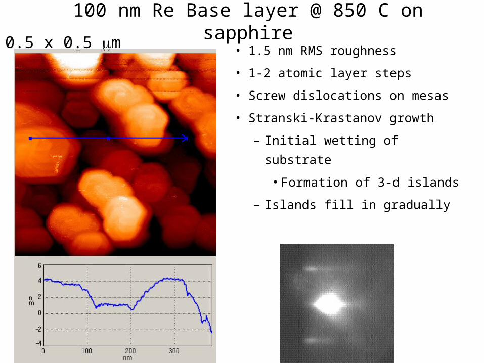
• 1.5 nm RMS roughness
• 1-2 atomic layer steps
• Screw dislocations on mesas
• Stranski-Krastanov growth
– Initial wetting of substrate
• Formation of 3-d islands
– Islands fill in gradually
0.5 x 0.5 m100 nm Re Base layer @ 850 C on sapphire
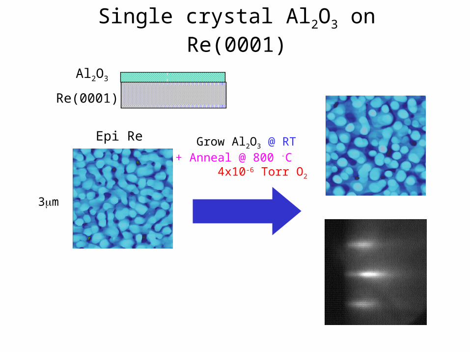
Epi Re Grow Al2O3 @ RT+ Anneal @ 800 ◦C 4x10⁻⁶ Torr O2
3m
Single crystal Al2O3 on Re(0001)
Re(0001)
Al2O3
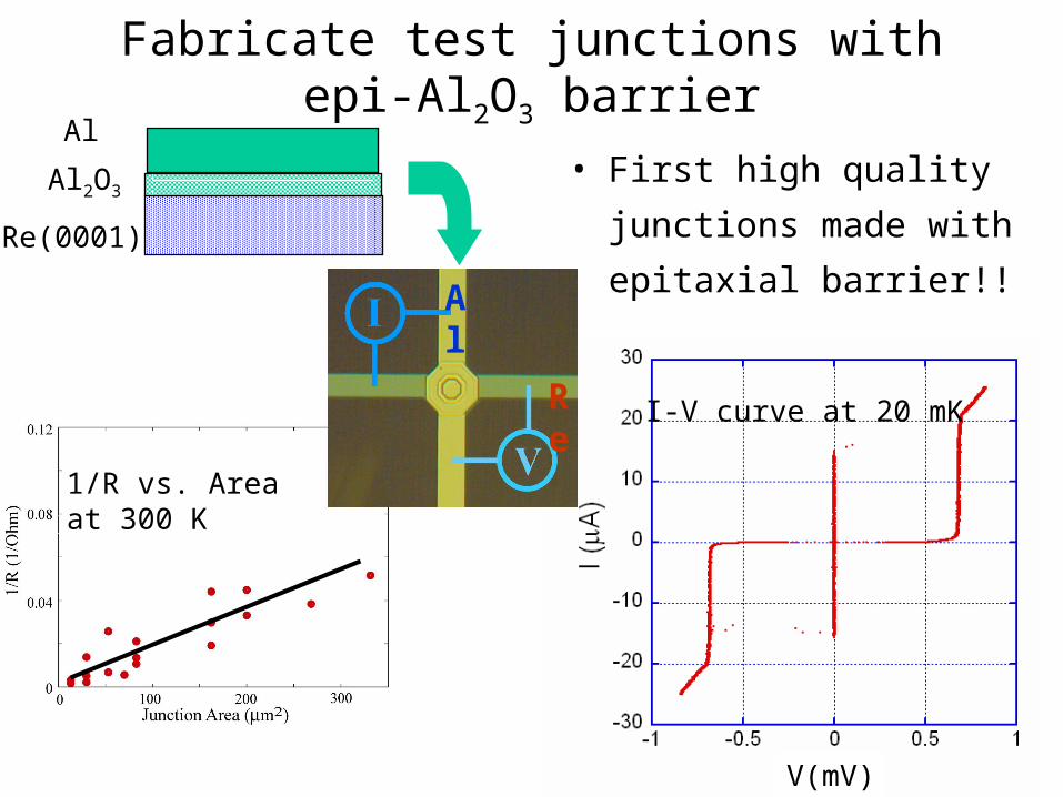
Fabricate test junctions with epi-Al2O3 barrier
• First high quality junctions
made with epitaxial
barrier!!Re(0001)
Al2O3
Al
1/R vs. Areaat 300 K
V(mV)
I-V curve at 20 mKRe
Al
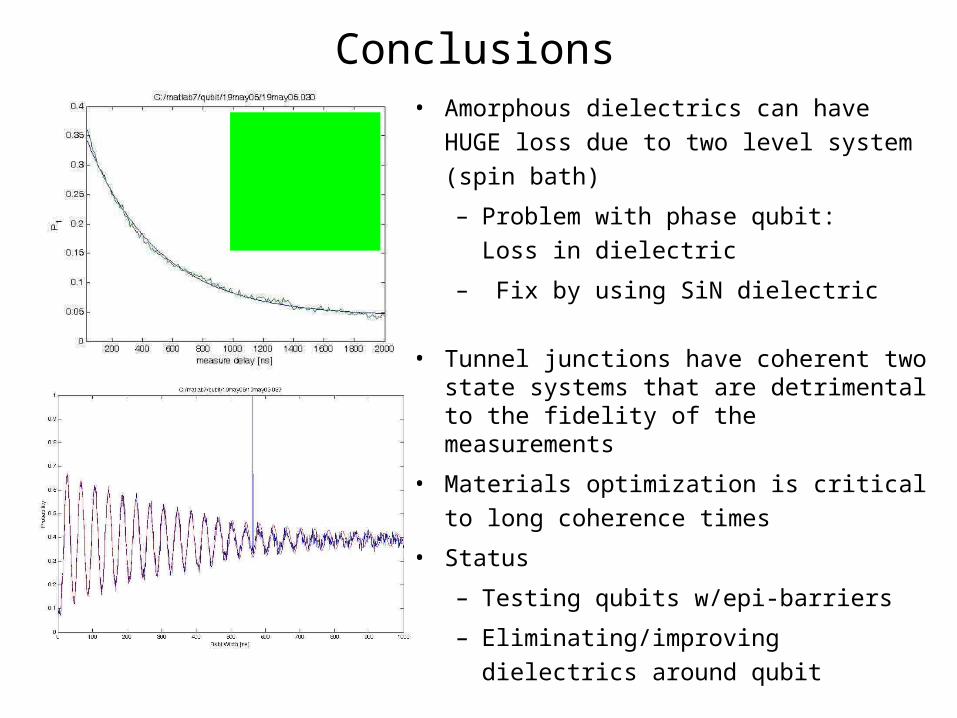
Conclusions• Amorphous dielectrics can have HUGE
loss due to two level system (spin bath)
– Problem with phase qubit:
Loss in dielectric
– Fix by using SiN dielectric
• Tunnel junctions have coherent two state systems that are detrimental to the fidelity of the measurements
• Materials optimization is critical to long
coherence times
• Status
– Testing qubits w/epi-barriers
– Eliminating/improving dielectrics
around qubit
1


![Transformation of SiOx films into nanocomposite SiO2(Si) films … · 2017. 10. 13. · transistors, resonant-tunnel diodes and nanocrystal memory cells [1-5]. The floating gates](https://img.pdfslide.us/doc/110x75/60ae97eac7a04f2e332550c2/transformation-of-siox-films-into-nanocomposite-sio2si-films-2017-10-13-transistors.jpg)