Embed Size (px)
Citation preview
BE14CH06-Rogers ARI 6 June 2012 8:7
Flexible and StretchableElectronics for BiointegratedDevicesDae-Hyeong Kim,1 Roozbeh Ghaffari,2 Nanshu Lu,3
and John A. Rogers4
1School of Chemical and Biological Engineering, Institute of Chemical Processes,Seoul National University, Seoul 151-744, Korea2MC10 Inc., Cambridge, Massachusetts 021403Department of Aerospace Engineering and Engineering Mechanics, University of Texas atAustin, Austin, Texas 787124Department of Materials Science and Engineering, Beckman Institute for Advanced Scienceand Technology, and Frederick Seitz Materials Research Laboratory, University of Illinois atUrbana-Champaign, Urbana, Illinois 61801; email: [email protected]
Annu. Rev. Biomed. Eng. 2012. 14:113–28
First published online as a Review in Advance onApril 18, 2012
The Annual Review of Biomedical Engineering isonline at bioeng.annualreviews.org
This article’s doi:10.1146/annurev-bioeng-071811-150018
Copyright c© 2012 by Annual Reviews.All rights reserved
1523-9829/12/0815-0113$20.00
Keywords
electrophysiology, flexible electronics, semiconductor nanomaterials,human-machine interfaces, epilepsy, arrhythmia
Abstract
Advances in materials, mechanics, and manufacturing now allow construc-tion of high-quality electronics and optoelectronics in forms that can readilyintegrate with the soft, curvilinear, and time-dynamic surfaces of the humanbody. The resulting capabilities create new opportunities for studying diseasestates, improving surgical procedures, monitoring health/wellness, establish-ing human-machine interfaces, and performing other functions. This reviewsummarizes these technologies and illustrates their use in forms integratedwith the brain, the heart, and the skin.
113
Ann
u. R
ev. B
iom
ed. E
ng. 2
012.
14:1
13-1
28. D
ownl
oade
d fr
om w
ww
.ann
ualr
evie
ws.
org
by U
nive
rsity
of
Illin
ois
- U
rban
a C
ham
paig
n on
07/
24/1
2. F
or p
erso
nal u
se o
nly.

BE14CH06-Rogers ARI 6 June 2012 8:7
Contents
1. INTRODUCTION . . . . . . . . . . . . . . . . . . . . . . . . . . . . . . . . . . . . . . . . . . . . . . . . . . . . . . . . . . . . 1142. MATERIALS, PROCESSING TECHNIQUES,
AND MECHANICS DESIGN . . . . . . . . . . . . . . . . . . . . . . . . . . . . . . . . . . . . . . . . . . . . . . . . . 1152.1. Semiconductor Nanomaterials . . . . . . . . . . . . . . . . . . . . . . . . . . . . . . . . . . . . . . . . . . . . . . 1152.2. Transfer Printing . . . . . . . . . . . . . . . . . . . . . . . . . . . . . . . . . . . . . . . . . . . . . . . . . . . . . . . . . . . 115
3. FLEXIBLE AND STRETCHABLE ELECTRONICSAND OPTOELECTRONICS . . . . . . . . . . . . . . . . . . . . . . . . . . . . . . . . . . . . . . . . . . . . . . . . . 1173.1. Flexible Devices . . . . . . . . . . . . . . . . . . . . . . . . . . . . . . . . . . . . . . . . . . . . . . . . . . . . . . . . . . . . 1173.2. Stretchable Devices . . . . . . . . . . . . . . . . . . . . . . . . . . . . . . . . . . . . . . . . . . . . . . . . . . . . . . . . . 118
4. BIOINTEGRATED DEVICES ON INTERNAL ORGANS . . . . . . . . . . . . . . . . . . . . 1194.1. Integrating with the Brain. . . . . . . . . . . . . . . . . . . . . . . . . . . . . . . . . . . . . . . . . . . . . . . . . . . 1194.2. Integrating with the Heart . . . . . . . . . . . . . . . . . . . . . . . . . . . . . . . . . . . . . . . . . . . . . . . . . . 120
5. BIOINTEGRATED DEVICES ON THE SKIN . . . . . . . . . . . . . . . . . . . . . . . . . . . . . . . . 1226. CONCLUSIONS . . . . . . . . . . . . . . . . . . . . . . . . . . . . . . . . . . . . . . . . . . . . . . . . . . . . . . . . . . . . . . 124
1. INTRODUCTION
All established classes of high-performance electronics exploit single-crystal inorganic materials,such as silicon or gallium arsenide, in forms (i.e., semiconductor wafers) that are fundamentallyrigid and planar (1–6). The human body is, by contrast, soft and curvilinear. This mismatch inproperties hinders the development of devices capable of intimate, conformal integration withbiological tissues, for applications ranging from basic measurement of electrophysiological signals(7), to delivery of advanced therapies (8), to establishment of human-machine interfaces (9). Oneenvisioned solution involves the use of organic electronic materials, whose flexible properties havegenerated interest in them for potential use in paper-like displays (10–12), solar cells (13–15), andother types of consumer electronic devices (16–18). Such materials are not, however, stretchable orcapable of wrapping curvilinear surfaces; they also offer only moderate performance, with uncertainreliability and capacity for integration into complex integrated circuits. Other materials, such asinorganic semiconductor nanowires (19) and carbon nanotubes (20), offer some promise, but theyremain in early stages of development.
Emerging design strategies and fabrication techniques that exploit conventional inorganicsemiconductor materials in unconventional ways provide compelling alternatives (21, 22), withseveral recent examples of use in clinically relevant thin, stretchable tissue-like devices that non-invasively integrate with various organs of the body (23, 24). This class of technology, which wedescribe as biointegrated to reflect its mode of deployment, exploits high-quality monocrystallinesemiconductor nanomaterials (e.g., membranes, ribbons) in mechanically optimized layouts onsoft, elastomeric, or flexible substrates (25, 26). Transfer printing techniques (27) provide thebasis for manufacturing such systems, in forms that allow facile, noninvasive lamination on bio-logical surfaces, including those of the brain (24, 28), heart (23, 26), and skin (25). Key mechanicsprinciples, such as neutral mechanical plane configurations (29, 30) and serpentine geometricaldesigns (22, 31), minimize strains in the active materials, whereas waterproof encapsulating films(26, 32) ensure long-term reliability. In advanced versions, bioresorbable substrates (e.g., silk) pro-vide routes for intimate physical coupling to soft tissues, with negligible mechanical disturbance(24).
114 Kim et al.
Ann
u. R
ev. B
iom
ed. E
ng. 2
012.
14:1
13-1
28. D
ownl
oade
d fr
om w
ww
.ann
ualr
evie
ws.
org
by U
nive
rsity
of
Illin
ois
- U
rban
a C
ham
paig
n on
07/
24/1
2. F
or p
erso
nal u
se o
nly.
BE14CH06-Rogers ARI 6 June 2012 8:7
This review highlights the use of these ideas in diagnostic devices for brain surgery, interfacesfor human-computer control systems (24, 28), skin-based physiological status monitors (25), andinstrumented balloon catheter tools for cardiac ablation therapy (23). These examples demon-strate the ability of biointegrated devices to (a) map electrical, temperature, mechanical strainand flow profiles, (b) wirelessly supply power, (c) provide quantitative feedback via tactile sensing,(d ) electrically or photodynamically stimulate tissues, and (e) ablate with fine spatial resolution. Inall cases, the components for the systems have the high performance and reliability standards ofestablished integrated circuit technologies. This review begins with a brief overview of the mate-rials, mechanics, and manufacturing strategies. Discussions of applications separate into devicesthat mount on internal organs and on the skin. A concluding section provides some perspectiveson future opportunities.
2. MATERIALS, PROCESSING TECHNIQUES,AND MECHANICS DESIGN
2.1. Semiconductor Nanomaterials
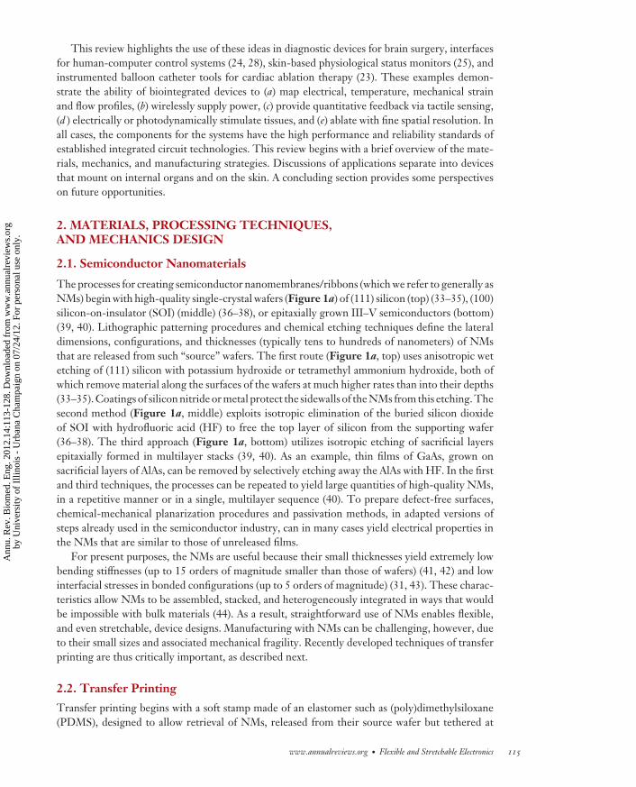
The processes for creating semiconductor nanomembranes/ribbons (which we refer to generally asNMs) begin with high-quality single-crystal wafers (Figure 1a) of (111) silicon (top) (33–35), (100)silicon-on-insulator (SOI) (middle) (36–38), or epitaxially grown III–V semiconductors (bottom)(39, 40). Lithographic patterning procedures and chemical etching techniques define the lateraldimensions, configurations, and thicknesses (typically tens to hundreds of nanometers) of NMsthat are released from such “source” wafers. The first route (Figure 1a, top) uses anisotropic wetetching of (111) silicon with potassium hydroxide or tetramethyl ammonium hydroxide, both ofwhich remove material along the surfaces of the wafers at much higher rates than into their depths(33–35). Coatings of silicon nitride or metal protect the sidewalls of the NMs from this etching. Thesecond method (Figure 1a, middle) exploits isotropic elimination of the buried silicon dioxideof SOI with hydrofluoric acid (HF) to free the top layer of silicon from the supporting wafer(36–38). The third approach (Figure 1a, bottom) utilizes isotropic etching of sacrificial layersepitaxially formed in multilayer stacks (39, 40). As an example, thin films of GaAs, grown onsacrificial layers of AlAs, can be removed by selectively etching away the AlAs with HF. In the firstand third techniques, the processes can be repeated to yield large quantities of high-quality NMs,in a repetitive manner or in a single, multilayer sequence (40). To prepare defect-free surfaces,chemical-mechanical planarization procedures and passivation methods, in adapted versions ofsteps already used in the semiconductor industry, can in many cases yield electrical properties inthe NMs that are similar to those of unreleased films.
For present purposes, the NMs are useful because their small thicknesses yield extremely lowbending stiffnesses (up to 15 orders of magnitude smaller than those of wafers) (41, 42) and lowinterfacial stresses in bonded configurations (up to 5 orders of magnitude) (31, 43). These charac-teristics allow NMs to be assembled, stacked, and heterogeneously integrated in ways that wouldbe impossible with bulk materials (44). As a result, straightforward use of NMs enables flexible,and even stretchable, device designs. Manufacturing with NMs can be challenging, however, dueto their small sizes and associated mechanical fragility. Recently developed techniques of transferprinting are thus critically important, as described next.
2.2. Transfer Printing
Transfer printing begins with a soft stamp made of an elastomer such as (poly)dimethylsiloxane(PDMS), designed to allow retrieval of NMs, released from their source wafer but tethered at
www.annualreviews.org • Flexible and Stretchable Electronics 115
Ann
u. R
ev. B
iom
ed. E
ng. 2
012.
14:1
13-1
28. D
ownl
oade
d fr
om w
ww
.ann
ualr
evie
ws.
org
by U
nive
rsity
of
Illin
ois
- U
rban
a C
ham
paig
n on
07/
24/1
2. F
or p
erso
nal u
se o
nly.

BE14CH06-Rogers ARI 6 June 2012 8:7
1 mm 1 mm 1 mm
100 μm
50 50 μm50 μm
70 70 μm70 μm
300 μm
100 μm
(111) silicon
Bottom silicon
Top silicon
a Retrieve
Transfer: contact and release
c
5 mm
d b 0.10% 0.08% 0.06% 0.04% 0.02% 0
ncchoohorhorssAAAnncncn ooA horhororssAAnchors
Adhesives
Nano-membranes
Strain
Figure 1Materials, processing approaches, and layouts that yield stretchable forms of inorganic semiconductors such as silicon and galliumarsenide. (a) Nanomembranes of these materials, produced from high-quality, single-crystal wafers using lithographic patterning andetching. (Top) A set of flexible nanomembranes/ribbons (NMs) made of (111) silicon created by anisotropic undercut etching of asilicon wafer. (Middle) (100) silicon NMs released from a silicon-on-insulator wafer by removal of the buried oxide. (Bottom) A largecollection of GaAs NMs prepared from epitaxial, multilayer stacks of GaAs/AlAs. Selectively etching the sacrificial AlAs layers releasesGaAs NMs. Reproduced with permission from Reference 40. Copyright Nature Publishing Group. (b) Schematic of the process fortransfer printing collections of NMs from their released forms on a source wafer to a target surface. Reproduced with permission fromReference 39. Copyright American Association for the Advancement of Science. (c) Automatic transfer printing tool. Inset shows acollection of GaAs NMs printed onto a flexible sheet of polyethylene terephthalate. (d ) Scanning electron microscope images and(insets) corresponding finite element modeling results for semiconductor NMs bonded to prestrained elastomeric substrates in threedifferent configurations. Upon releasing the prestrain, controlled buckling processes in the NMs lead to different layouts: (top)two-dimensional herringbone “wavy” patterns (reproduced with permission from Reference 37, copyright American Chemical Society)and noncoplanar bridge structures with (middle) straight and (bottom) serpentine (reproduced with permission from Reference 22,copyright National Academy of Sciences) interconnects. In all cases, strains in the silicon structures themselves are less than ∼0.1%,even when strains of the overall system exceed 100% in certain configurations.
strategic points (i.e., anchors), simply by the action of generalized adhesion forces to the PDMS,typically dominated by van der Waals interactions (27, 45) (Figure 1b, top). This transfercan be performed over large areas of uniform or segmented NMs using flat stamps (27) orover selected areas using structured stamps (46) (Figure 1b, top). The retrieved collections ofNMs (i.e., solid “inks” in this procedure) are selectively delivered to target substrate surfaces,at predefined locations with microscale precision (Figure 1b, bottom), by printing (39, 47).A variety of approaches allow the switching in adhesion needed for efficient operation; theserange from rate-dependent viscoelastic effects (27, 48), to biomimetic strategies (45), to useof interfacial bonding layers (49). Printing with automated tools that include high-resolution
116 Kim et al.
Ann
u. R
ev. B
iom
ed. E
ng. 2
012.
14:1
13-1
28. D
ownl
oade
d fr
om w
ww
.ann
ualr
evie
ws.
org
by U
nive
rsity
of
Illin
ois
- U
rban
a C
ham
paig
n on
07/
24/1
2. F
or p
erso
nal u
se o
nly.
BE14CH06-Rogers ARI 6 June 2012 8:7
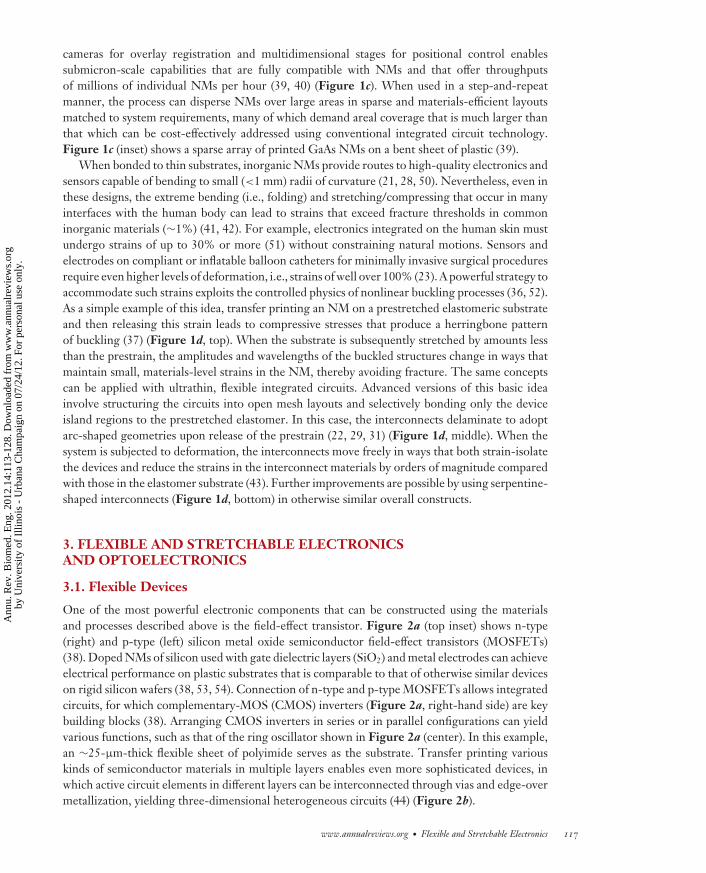
cameras for overlay registration and multidimensional stages for positional control enablessubmicron-scale capabilities that are fully compatible with NMs and that offer throughputsof millions of individual NMs per hour (39, 40) (Figure 1c). When used in a step-and-repeatmanner, the process can disperse NMs over large areas in sparse and materials-efficient layoutsmatched to system requirements, many of which demand areal coverage that is much larger thanthat which can be cost-effectively addressed using conventional integrated circuit technology.Figure 1c (inset) shows a sparse array of printed GaAs NMs on a bent sheet of plastic (39).
When bonded to thin substrates, inorganic NMs provide routes to high-quality electronics andsensors capable of bending to small (<1 mm) radii of curvature (21, 28, 50). Nevertheless, even inthese designs, the extreme bending (i.e., folding) and stretching/compressing that occur in manyinterfaces with the human body can lead to strains that exceed fracture thresholds in commoninorganic materials (∼1%) (41, 42). For example, electronics integrated on the human skin mustundergo strains of up to 30% or more (51) without constraining natural motions. Sensors andelectrodes on compliant or inflatable balloon catheters for minimally invasive surgical proceduresrequire even higher levels of deformation, i.e., strains of well over 100% (23). A powerful strategy toaccommodate such strains exploits the controlled physics of nonlinear buckling processes (36, 52).As a simple example of this idea, transfer printing an NM on a prestretched elastomeric substrateand then releasing this strain leads to compressive stresses that produce a herringbone patternof buckling (37) (Figure 1d, top). When the substrate is subsequently stretched by amounts lessthan the prestrain, the amplitudes and wavelengths of the buckled structures change in ways thatmaintain small, materials-level strains in the NM, thereby avoiding fracture. The same conceptscan be applied with ultrathin, flexible integrated circuits. Advanced versions of this basic ideainvolve structuring the circuits into open mesh layouts and selectively bonding only the deviceisland regions to the prestretched elastomer. In this case, the interconnects delaminate to adoptarc-shaped geometries upon release of the prestrain (22, 29, 31) (Figure 1d, middle). When thesystem is subjected to deformation, the interconnects move freely in ways that both strain-isolatethe devices and reduce the strains in the interconnect materials by orders of magnitude comparedwith those in the elastomer substrate (43). Further improvements are possible by using serpentine-shaped interconnects (Figure 1d, bottom) in otherwise similar overall constructs.
3. FLEXIBLE AND STRETCHABLE ELECTRONICSAND OPTOELECTRONICS
3.1. Flexible Devices
One of the most powerful electronic components that can be constructed using the materialsand processes described above is the field-effect transistor. Figure 2a (top inset) shows n-type(right) and p-type (left) silicon metal oxide semiconductor field-effect transistors (MOSFETs)(38). Doped NMs of silicon used with gate dielectric layers (SiO2) and metal electrodes can achieveelectrical performance on plastic substrates that is comparable to that of otherwise similar deviceson rigid silicon wafers (38, 53, 54). Connection of n-type and p-type MOSFETs allows integratedcircuits, for which complementary-MOS (CMOS) inverters (Figure 2a, right-hand side) are keybuilding blocks (38). Arranging CMOS inverters in series or in parallel configurations can yieldvarious functions, such as that of the ring oscillator shown in Figure 2a (center). In this example,an ∼25-μm-thick flexible sheet of polyimide serves as the substrate. Transfer printing variouskinds of semiconductor materials in multiple layers enables even more sophisticated devices, inwhich active circuit elements in different layers can be interconnected through vias and edge-overmetallization, yielding three-dimensional heterogeneous circuits (44) (Figure 2b).
www.annualreviews.org • Flexible and Stretchable Electronics 117
Ann
u. R
ev. B
iom
ed. E
ng. 2
012.
14:1
13-1
28. D
ownl
oade
d fr
om w
ww
.ann
ualr
evie
ws.
org
by U
nive
rsity
of
Illin
ois
- U
rban
a C
ham
paig
n on
07/
24/1
2. F
or p
erso
nal u
se o
nly.

BE14CH06-Rogers ARI 6 June 2012 8:7
c d
VInIn
VOutOut
VIn
VOutVDDDDVDD
0.5 mm0.5 mm0.5 mm
100 μm 500 μm
300 μm
Deform
e 1 mm
360° twisted
720° twisted
Flat
b a
1 mm1 mm1 mm
0.5 mm 0.5 mm 0.5 mm
RelRelReRe easeaseasasasasseeRelease200 200 μm 200 μm
Figure 2Flexible and stretchable electronic and optoelectronic devices. (a) Flexible circuit with transistors that usesilicon nanomembranes/ribbons (NMs) on a 25-μm-thick polyimide substrate: (left and top inset) n-type andand p-type transistors, (right) complementary metal oxide semiconductor (CMOS) inverters, and (center)three-stage ring oscillators. (a, bottom inset) A circuit diagram of a ring oscillator. Abbreviations: VIn, inputvoltage; VOut, output voltage; VDD, power supply voltage. Reproduced with permission from Reference 38.Copyright IEEE. (b) Three-dimensional, multilayer circuit on a plastic substrate formed by repeated cyclesof transfer printing and device processing. (c) Stretchable CMOS circuit that uses a “wavy” layout on anelastomeric substrate shown (top) before and (bottom) during application of normal force with a glass rod.Reproduced with permission from Reference 21. Copyright American Association for the Advancement ofScience. (d ) Scanning electron microscope images of a (top) deformed and (bottom) undeformed collection ofCMOS inverters that use straight, noncoplanar interconnects. A thin (∼1 mm) elastomer membrane servesas the substrate. Reproduced with permission from Reference 22. Copyright National Academy of Sciences.(e) Stretchable array of GaAs microscale inorganic light-emitting diodes with serpentine interconnects inflat, 360◦ twisted, and 720◦ twisted states. Reproduced with permission from Reference 32. CopyrightNature Publishing Group.
3.2. Stretchable Devices
Electronic systems can also be achieved on stretchable substrates. Figure 2c shows CMOS circuitson PDMS, capable of reversible elastic responses to significant mechanical deformations, by virtueof the buckling mechanics described previously (21). This type of system forms when an ultrathin(less than ∼3 μm) CMOS silicon circuit, transferred onto a biaxially prestretched PDMS, bucklesas a result of releasing the prestrain (Figure 1d ) to adopt generalized versions of the herringbonelayouts shown in Figure 1d (top). The circuits in this case lie between two identical polyimide layersin the neutral mechanical plane to minimize bending-induced strains. When mildly stretched, the
118 Kim et al.
Ann
u. R
ev. B
iom
ed. E
ng. 2
012.
14:1
13-1
28. D
ownl
oade
d fr
om w
ww
.ann
ualr
evie
ws.
org
by U
nive
rsity
of
Illin
ois
- U
rban
a C
ham
paig
n on
07/
24/1
2. F
or p
erso
nal u
se o
nly.

BE14CH06-Rogers ARI 6 June 2012 8:7
devices and interconnects gradually flatten in a way that avoids significant strains in the activematerials or associated changes in performance.
As an example of a device of more advanced design, Figure 2d shows an array of CMOS invert-ers with noncoplanar, arc-shaped interconnects under deformation (22). Similar interconnects,but with serpentine shapes, further increase the stretchability. Figure 2e shows twisting defor-mations (by up to 720◦) in an interconnected array of microscale inorganic light-emitting diodes(μ-ILEDs) built using these ideas (32). This type of mechanical response suggests an ability to wrapcomplex curvilinear and time-dynamic surfaces, such as those found in biology. The remainingsections highlight some examples; each begins with an overview of the existing state of the art.
4. BIOINTEGRATED DEVICES ON INTERNAL ORGANS
4.1. Integrating with the Brain
High-resolution neural interface devices have played important roles in brain and central nervoussystem research over the past decades (55). Electrical recordings performed with penetrating (56)or surface-contacting electrodes (57) have dramatically improved our understanding of the basicscience of neural activity; they have also been exploited for clinical usage in epilepsy surgery (58–60), prosthetic control (9), and other applications (61). Extensive reviews of electrode arrays usedin surgical procedures to treat epilepsy appear elsewhere (62, 63). Briefly, such devices often consistof a relatively small number of large electrodes (e.g., ∼6-mm diameters and ∼1-cm spacings) onflexible sheets that contact the surface of the brain to collect neural signals generated by clustersof neurons (57). Although the large area coverage provided by such technologies is attractive interms of gaining valuable information about precise brain activity and foci triggers of disease states,such as epilepsy, the spatial density of electrodes should be as high as possible, with spacings of∼400 μm or less (64). Electrode arrays positioned underneath the dura membrane and in directcontact with cortical surfaces can combine macroelectrodes with microwires (58–60) to achieve thisimproved resolution. The number of wire connections required in these types of passive systems,however, imposes practical constraints that preclude the possibility of simultaneous large-area andhigh-resolution operation (28).
Multiplexing circuits provide a solution that reduces the number of required connections forn electrodes, from n to sqrt(n). For example, a 16 × 16 array of electrodes requires ∼30 wireswith multiplexers, compared with ∼260 wires in passive configurations. The significance of thisreduction increases rapidly with electrode count. The challenge with multiplexing is that the re-quired electronics, in conventional forms, are rigid and flat, thereby rendering them incompatiblewith the soft, curved textures of the brain (65). One widely used approach bypasses this constraintby use of penetrating electrode pins that terminate on flat platforms, suitable for mounting ofconventional silicon integrated circuits (64, 66, 67). The Utah array represents a prominent andsuccessful example of this strategy (64, 66), where the pins provide access to clusters of neurons ina way that also overcomes the mismatches in geometry. An important disadvantage is that tissuedamage caused by electrode insertion and continued irritation during long-term implantation (dueto micromovement of brain tissue) can trigger adverse effects, including astrocyte proliferationand inflammation, both of which lead to signal degradation over time (68).
An alternative involves collections of diced silicon chips, each of which supports planar elec-trodes with hemispherical bumps and multiplexing electronics, bonded to plastic sheets (69). Thisapproach can be effective, but there are significant challenges due to the inflexibility and relativelylarge sizes of the chips. Reduction of stiffness is crucial for achieving systems that not only aresafe but also provide high-fidelity data streams (24). Flexible electronics using the NM concepts
www.annualreviews.org • Flexible and Stretchable Electronics 119
Ann
u. R
ev. B
iom
ed. E
ng. 2
012.
14:1
13-1
28. D
ownl
oade
d fr
om w
ww
.ann
ualr
evie
ws.
org
by U
nive
rsity
of
Illin
ois
- U
rban
a C
ham
paig
n on
07/
24/1
2. F
or p
erso
nal u
se o
nly.

BE14CH06-Rogers ARI 6 June 2012 8:7
a 5 mm 5 mm
Folded array Folded array
5 mm
Folded array
5 mm 5 mm 5 mm
Insertion Insertion Insertion
b
d Counterclockwise spiral
0 ms
165 ms
110 ms
55 ms
Clockwise spiral
0 ms
90 ms
60 ms
30 ms
c
5 mm 5 mm
Array onArray onvisual cortexvisual cortex
5 mm
Array onvisual cortex
5 mm 5 mm 5 mm
2 mm2 mm2 mm
Figure 3High-density, conformal electrode array for brain surface recording. (a) High-density device withmultiplexers based on silicon nanomembranes/ribbons. Inset shows a similar array folded around a thin(∼700 μm) elastomer sheet and inserted into an interhemispheric fissure. (b) Images (left) before and (right)after insertion. (c) Local administration of picrotoxin into the visual cortex causes spiral wave fronts that canbe seen clearly in recordings from the high-density array. Reproduced with permission from Reference 28.Copyright Nature Publishing Group. (d ) (left) Image and (right) mapping results of an ultrathin (∼2.5 μm)mesh electrode array laminated onto the surface of the brain following dissolution of a temporary silksubstrate. The mesh design enables exceptionally good conformal contact, and thus higher quality in themeasured signals compared with that possible with conventional flexible arrays. Reproduced with permissionfrom Reference 24. Copyright Nature Publishing Group.
described previously permit high-speed multiplexing, high temporal resolution, as well as confor-mal electrode-tissue interfaces over large areas (28) (Figure 3a). The thin form factor and low stiff-ness even offer direct mechanical access to the hemispherical fissure area of the brain (Figure 3a,inset). Folded electrode arrays enable simultaneous mapping from both sides of the hemispheres(Figure 3b). Furthermore, high-density systems with submillimeter spacing between the elec-trodes yield insights into new neural mechanisms, whereby unusual clockwise and counterclock-wise spiral patterns of excitation propagate in a manner correlated to signs of microseizures(28, 70) (Figure 3c).
Even fully flexible electrode arrays such as these may not, however, make complete conformalcontact with the most topologically demanding regions of the human brain (24) (Figure 3d ).Reducing thicknesses to less than ∼10 μm, and structuring the sheets into open mesh geometries,can improve the coupling (Figure 3d ). To enable mechanical manipulation for mounting suchsystems, which themselves are difficult to handle due to their extremely low bending stiffnesses,sacrificial substrates of materials (e.g., silk) that readily dissolve in biofluids can be useful. Oncedeployed on soft tissue, the silk dissolves leaving behind an ultrathin mesh of electrodes in intimatemechanical contact with even the most strongly curved/textured regions of the brain surface (24).
4.2. Integrating with the Heart
As with the brain, mapping electrical activity across the surface of the heart is important notonly for developing a fundamental understanding of disease states but also for diagnosing local
120 Kim et al.
Ann
u. R
ev. B
iom
ed. E
ng. 2
012.
14:1
13-1
28. D
ownl
oade
d fr
om w
ww
.ann
ualr
evie
ws.
org
by U
nive
rsity
of
Illin
ois
- U
rban
a C
ham
paig
n on
07/
24/1
2. F
or p
erso
nal u
se o
nly.

BE14CH06-Rogers ARI 6 June 2012 8:7
a b c
Figure 4Multielectrode catheters for cardiac mapping and ablation. (a) Multielectrode mapping and ablation catheter(HD Mesh AblatorTM, Bard; Lowell, MA) consists of 36 electrodes in mesh geometry, which optimizescontact with the pulmonary veins. (b) Multielectrode basket catheter (ConstellationTM, Boston Scientific;Boston, MA) provides high-density mapping of electrical activity within the atria. (c) Multielectrodemapping and ablation catheter (MAACTM, Medtronic; Minneapolis, MN) targets complex fractionatedatrial electrograms for both mapping and ablation of the atrial body.
tissue behavior during certain surgical operations. Existing approaches use single-point electricalmapping catheters; newer systems exploit arrays of electrodes integrated on catheter-type deliverysystems (8, 71). In both cases, clinical use in the context of treating certain types of arrhythmiasoften involves measurement of electrical potentials, in a point-by-point, manual fashion fromlocations within the ostium of the pulmonary veins (PVs) (where the PV is conjoined with theatria) (Figure 4a) and within the atria (Figure 4b,c). Positioning the catheters requires signifi-cant time and dexterity, often leading to inconsistent outcomes across multiple patients (71, 72).Furthermore, several sequential therapeutic procedures, such as ablation, followed by cycles ofelectrical mapping are required to produce a representation of electrical activity over a large re-gion of interest (8, 71). This serial approach requires highly skilled operators to minimize risk ofstroke and other clinical complications. In addition to atrial fibrillation treatment (73), cathetersare used as tools for ablation in minimally invasive strategies for treating various forms of othercardiac arrhythmias, including ventricular fibrillation (74) and ventricular tachycardia (75). Linearlesions generated by radiofrequency energy applied in a point-by-point manner are among themost common means to correct these abnormal rhythms (71, 76).
Another way to enhance the performance of cardiac ablation solutions is to develop contact-sensing feedback and multielectrode catheter systems, which can improve electrical mappingof complex arrhythmias and provide real-time force feedback during lesion formation (77).Emerging balloon catheter–based systems also under development and in clinical trials rely onballoon substrates to conform to the anatomical structure of the PV ostium (8, 71, 78–83). Theseballoons inflate within the left atrium and create a continuous ring of conformal contact betweenthe balloon and the tissue, followed by delivery of cryoenergy, high-intensity focused ultrasound(HIFU)–, or laser-based ablation therapies. Although conceptually straightforward, such balloonablation catheters do not provide sensory feedback about mechanical contact with soft tissue orinformation on the electrical state of intracardiac surfaces.
Advances in stretchable electronics enable integration of contact sensors, multielectrodearrays, and balloon substrates into a single, multifunctional instrumented catheter platform(23). A representative example of a device of this type appears in Figure 5. Electrodes forelectrical mapping integrate on the balloon surface with classes of serpentine interconnectsdescribed previously (Figure 5a,b). Figure 5c shows temperature sensors and stretchable arraysof μ-ILEDs. Electrogram recordings from an inflated balloon substrate positioned in direct
www.annualreviews.org • Flexible and Stretchable Electronics 121
Ann
u. R
ev. B
iom
ed. E
ng. 2
012.
14:1
13-1
28. D
ownl
oade
d fr
om w
ww
.ann
ualr
evie
ws.
org
by U
nive
rsity
of
Illin
ois
- U
rban
a C
ham
paig
n on
07/
24/1
2. F
or p
erso
nal u
se o
nly.

BE14CH06-Rogers ARI 6 June 2012 8:7
Inflate
Temperaturesensor
Electrode
Electrode
Deflate
μ-ILED
500 μm
d
Time (s)0 1 2 3 4 5
5 m
V
a
b
c
Lesion
Lesion
5 mm
Temperature sensor
Electro-cardiogramsensor
Electro-cardiogramsensor
e
Temperaturesensor
4 5
on
e sensor
sensorm
m
u
Electro-cardiogram
u
Electro-cardiogramsensor
cardiogramsensor
TemTTTTTT peratusensor
Figure 5Multifunctional balloon catheter. (a) Stretchable sensors mounted on a catheter balloon and (b) magnified view showing stretched(∼120%) serpentine interconnects after inflation. (c) Device in the deflated and inflated states, showing several different functionalities,ranging from electrodes for electrophysiological measurement and radiofrequency (RF) ablation to temperature sensors, contact forcegauges, and arrays of microscale inorganic light-emitting diodes (μ-ILEDs). (d ) Electrical recordings from the right ventricle of arabbit heart, measured with an instrumented balloon catheter. (e) Lesions created by RF ablation electrodes on a similar device. Yellowline denotes the location of a temperature sensor. The inset provides a corresponding image of RF ablation electrodes and temperaturesensors on the balloon catheter. Reproduced with permission from Reference 23. Copyright Nature Publishing Group.
mechanical contact with a live porcine heart are presented in Figure 5d. This mode of operationis particularly useful for balloon ablation catheters, where assessment of ablation can be achievedquickly without the need for separate diagnostic devices. In addition to electrical and temperaturesensors, contact sensors and stimulation electrodes (Figure 5e) are also supported on thisplatform. Contact sensors can report the moment when the balloon skin and endocardial tissuetouch, thereby providing important feedback (without X-ray imaging) on how to adjust andmaneuver inflated balloons to achieve optimal occlusion of the PVs during ablation procedures.
More advanced biointegrated mapping systems have been demonstrated in epicardial sheets,designed in ultrathin formats described previously to allow conformal contact to and adhesionwith the surface of the heart (26). Here, high-density electrodes, each with local amplifiers andmultiplexing circuitry based on silicon NMs, enable measurements with both high spatial andtemporal resolution. Figure 6a shows an image of a flexible mapping array with multiplexedelectrodes, adherent on a section of cardiac tissue through surface tension forces alone withoutpenetrating pins or separate adhesives. Electrograms collected at high sampling rates (12.5 kHz perelectrode) and combined spatiotemporally across 288 electrodes yield isochronal activation maps,demonstrating the natural electrophysiology of the heart (Figure 6b) in a noninvasive manner.These high-density arrays map activation patterns across entire regions of the heart, withoutmanual operation or repositioning, in a single beat cycle. Furthermore, their thin form factorand mechanical reliability permit packaging in medical instruments, like the sorts of cathetersdescribed previously, for endocardial purposes.
5. BIOINTEGRATED DEVICES ON THE SKIN
Although biointegrated electronics on internal tissues provide important functions, the skin rep-resents a mounting location that is applicable outside of hospital settings to allow much broadermodes of use (84). Traditional technologies use small numbers of point-contact electrodes that
122 Kim et al.
Ann
u. R
ev. B
iom
ed. E
ng. 2
012.
14:1
13-1
28. D
ownl
oade
d fr
om w
ww
.ann
ualr
evie
ws.
org
by U
nive
rsity
of
Illin
ois
- U
rban
a C
ham
paig
n on
07/
24/1
2. F
or p
erso
nal u
se o
nly.

BE14CH06-Rogers ARI 6 June 2012 8:7
a 1 cm
5 mm
b –10 mV
800 µm
–2 mV
+6 mV
t = 0 ms t = 11.2 ms
t = 14.4 ms t = 24 ms Time [t (ms)]
Electricalpotential
Figure 6High-density, conformal electrode array for cardiac surface recording. (a) Sensor array with embeddedmultiplexing circuits and amplifiers based on silicon nanomembranes/ribbons conformally laminated on theepicardial surface of a live porcine heart. Inset shows a magnified view. (b) Activation patterns ofdepolarization mapped at four different time frames. The recorded electrical potential is converted intoisochronal maps of activation patterns. Reproduced with permission from Reference 26. CopyrightAmerican Association for the Advancement of Science.
strap onto or penetrate through the surface of the skin (85, 86). For example, commercial de-vices for recording electroencephalograms (EEGs) from the scalp use tight caps embedded withelectrodes, each of which attaches to external electronics via bulk wires (87). In this case and inothers for measurement of ECG or electromyography (EMG), the skin is often prepared by lightabrasion and application of conductive gel or paste as a means to reduce the contact impedance(88). Such procedures are time-consuming and also unsuitable for long-term recording. As a re-sult, dry electrodes are of interest. Examples include micromachined pins (89) or arrays of carbonnanotubes (90) that allow penetration through the stratum corneum. This mode of integrationhas certain advantages over gels, but it can cause inflammation and discomfort (91). Capacitivecoupling provides an attractive option that eliminates contact entirely (92). To minimize signalattenuation and channel gain mismatch, the input capacitance of each sensor must be activelyneutralized using positive feedback and bootstrapping.
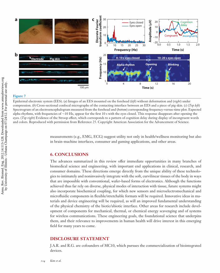
These systems have many important capabilities, but in general they are poorly suited for prac-tical application outside of clinical research due to their bulky size and difficulties in establishingrobust, nonirritating electrical contacts (93). Recently developed stretchable device technologies,referred to as epidermal electronic systems (EES), allow electrophysiological measurements withultrathin and low-modulus, skin-like sheets that conformally laminate onto the surface of theskin in a manner that is mechanically invisible to the user, much like a temporary transfer tattoo(25) (Figure 7a). The EES attaches intimately and physically couples to rough skin surfaces, viavan der Waals forces alone, as shown in the cross-sectional confocal micrographs in Figure 7b.Because attachment does not require separate adhesives or conductive gels, these systems canfunction for prolonged periods. EEG measurements using an EES mounted on the forehead areshown in Figure 7c: The bottom frame presents a spectrogram showing an alpha rhythm; thetop left frame shows a plot of discrete Fourier transform coefficients at ∼10 Hz. The patternscorrespond to periods with the eyes closed and opened. The responses at ∼10 s and ∼14 s resultfrom eye opening and blinking, respectively. The top right frame reveals Stroop effects (94), asan additional illustration of functionality of this technology. These and other electrophysiological
www.annualreviews.org • Flexible and Stretchable Electronics 123
Ann
u. R
ev. B
iom
ed. E
ng. 2
012.
14:1
13-1
28. D
ownl
oade
d fr
om w
ww
.ann
ualr
evie
ws.
org
by U
nive
rsity
of
Illin
ois
- U
rban
a C
ham
paig
n on
07/
24/1
2. F
or p
erso
nal u
se o
nly.
BE14CH06-Rogers ARI 6 June 2012 8:7
Frequency (Hz)
5 10 15 20 25 30
Dis
cre
te F
ou
rie
rtr
an
sfo
rm c
oe
ffici
en
t
0
10
20
30Eyes closed Eyes open
a c
Fre
qu
en
cy (
Hz)
Time (s)
0 4 8 12 16 20
20
5
10
15
0–10 s eyes closed 10–20 s eyes open
Opening Blinking Alpha rhythm
b Pig skinElectrode
100 μm
Time (s)
0.0 0.5 1.0 1.5 2.0
Am
pli
tud
e (μV
)
–20
–10
0
10
20 Cognitiondelay
Congruent Incongruent
Figure 7Epidermal electronic system (EES). (a) Images of an EES mounted on the forehead (left) without deformation and (right) undercompression. (b) Cross-sectional confocal micrographs of the contacting interface between an EES and a piece of pig skin. (c) (Top left)Spectrogram of an electroencephalogram measured from the forehead and (bottom) corresponding frequency-versus-time plot. Expectedalpha rhythms, with frequencies of ∼10 Hz, appear for the first 10 s with the eyes closed. This response disappears after opening theeyes. (Top right) Evidence of the Stroop effect, which corresponds to a pattern of cognition delay during display of incongruent wordsand colors. Reproduced with permission from Reference 25. Copyright American Association for the Advancement of Science.
measurements (e.g., EMG, ECG) suggest utility not only in health/wellness monitoring but alsoin brain-machine interfaces, consumer and gaming applications, and other areas.
6. CONCLUSIONS
The advances summarized in this review offer immediate opportunities in many branches ofbiomedical science and engineering, with important end applications in clinical, research, andconsumer domains. These directions emerge directly from the unique ability of these technolo-gies to intimately and noninvasively integrate with the soft, curvilinear tissues of the body in waysthat are impossible with conventional, wafer-based forms of electronics. Although the functionsachieved thus far rely on diverse, physical modes of interaction with tissue, future systems mightalso incorporate biochemical coupling, for which new sensors and microelectromechanical andmicrofluidic components in flexible/stretchable formats will be required. Innovative ideas in ma-terials and device engineering will be required, as will an improved fundamental understandingof the physical chemistry of the biotic/abiotic interface. Other areas for research include devel-opment of components for mechanical, thermal, or chemical energy scavenging and of systemsfor wireless communications. These engineering goals, the foundational science that underpinsthem, and their relevance to improvements in human health will drive interest in this emergingfield for many years to come.
DISCLOSURE STATEMENT
J.A.R. and R.G. are cofounders of MC10, which pursues the commercialization of biointegrateddevices.
124 Kim et al.
Ann
u. R
ev. B
iom
ed. E
ng. 2
012.
14:1
13-1
28. D
ownl
oade
d fr
om w
ww
.ann
ualr
evie
ws.
org
by U
nive
rsity
of
Illin
ois
- U
rban
a C
ham
paig
n on
07/
24/1
2. F
or p
erso
nal u
se o
nly.
BE14CH06-Rogers ARI 6 June 2012 8:7
ACKNOWLEDGMENTS
This material is based upon work supported by the Department of Defense, the National ScienceFoundation, and the Department of Energy. N.L. acknowledges support from a Beckman Institutepostdoctoral fellowship. This work is also supported by Global Frontier Research Center forAdvanced Soft Electronics.
LITERATURE CITED
1. Moore G. 1965. Cramming more components onto integrated circuits. Electronics 38:114–172. Arns RG. 1998. The other transistor: early history of the metal-oxide semiconductor field-effect transistor.
Eng. Sci. Educ. J. 7:233–403. Vogel EM. 2007. Technology and metrology of new electronic materials and devices. Nat. Nanotechnol.
2:25–324. International Technology Roadmap for Semiconductors. 2011. http://www.itrs.netLinks/2011ITRS/
Home2011.htm5. Streetman BG, Banerjee S. 2005. Solid State Electronic Devices. Upper Saddle River, NJ: Prentice
Hall. 6th ed.6. Hayashi I. 1993. Optoelectronic devices and material technologies for photo-electronic integrated systems.
Jpn. J. Appl. Phys. 32:266–717. Interwoven W. 1901. Un nouveau galvanometer. Arch. Neerl. Sc. Ex. Nat. 6:625–338. Dewire J, Calkins H. 2010. State-of-the-art and emerging technologies for atrial fibrillation ablation. Nat.
Rev. Cardiol. 7:129–389. Hochberg LR, Serruya MD, Friehs GM, Mukand JA, Saleh M, et al. 2006. Neuronal ensemble control
of prosthetic devices by a human with tetraplegia. Nature 442:164–7110. Forrest SR. 2004. The path to ubiquitous and low-cost organic electronic appliances on plastic. Nature
428:911–1811. Rogers JA, Bao Z, Baldwin K, Dodabalapur A, Crone B, et al. 2001. Paper-like electronic displays: large-
area rubber-stamped plastic sheets of electronics and microencapsulated electrophoretic inks. Proc. Natl.Acad. Sci. USA 9:4835–40
12. Gelinck GH, Huitema HEA, Veenendaal EV, Cantatore E, Schrijnemakers L, et al. 2004. Flexible active-matrix displays and shift registers based on solution-processed organic transistors. Nat. Mater. 3:106–10
13. Yu G, Gao J, Hummelen JC, Wudi F, Heeger AJ. 1995. Polymer photovoltaic cells: enhanced efficienciesvia a network of internal donor-acceptor heterojunctions. Science 270:1789–91
14. Kim JY, Lee K, Coates NE, Moses D, Nguyen TQ, et al. 2007. Efficient tandem polymer solar cellsfabricated by all-solution processing. Science 317:222–25
15. Shaheen SE, Ginley DS, Jabbour GE. 2005. Organic-based photovoltaics: toward low-cost power gener-ation. MRS Bull. 30:10–22
16. Ouyang J, Chu CW, Szmanda CR, Ma L, Yang Y. 2004. Programmable polymer thin film and non-volatilememory device. Nat. Mater. 3:918–22
17. Baude PF, Ender DA, Haase MA, Kelley TW, Muyres DV, et al. 2003. Pentacene-based radio-frequencyidentification circuitry. Appl. Phys. Lett. 82:3964–66
18. Cantatore E, Geuns TCT, Gelinck GH, Veenendaal E, Gruijthuijsen AFA, et al. 2007. A 13.56-MHzRFID system based on organic transponders. IEEE J. Solid-State Circuits 42:84–92
19. Tian B, Cohen-Karni T, Qing Q, Duan X, Xie P, et al. 2010. Three-dimensional, flexible nanoscalefield-effect transistors as localized bioprobes. Science 329:831–34
20. Keefer EW, Botterman BR, Romero MI, Rossi AF, Gross GW. 2008. Carbon nanotube coating improvesneuronal recordings. Nat. Nanotechnol. 3:434–39
21. Kim DH, Ahn JH, Choi WM, Kim HS, Kim TH, et al. 2008. Stretchable and foldable silicon integratedcircuits. Science 320:507–11
22. Kim DH, Song J, Choi WM, Kim HS, Kim RH, et al. 2008. Materials and noncoplanar mesh designs forintegrated circuits with linear elastic responses to extreme mechanical deformations. Proc. Natl. Acad. Sci.USA 105:18675–80
www.annualreviews.org • Flexible and Stretchable Electronics 125
Ann
u. R
ev. B
iom
ed. E
ng. 2
012.
14:1
13-1
28. D
ownl
oade
d fr
om w
ww
.ann
ualr
evie
ws.
org
by U
nive
rsity
of
Illin
ois
- U
rban
a C
ham
paig
n on
07/
24/1
2. F
or p
erso
nal u
se o
nly.

BE14CH06-Rogers ARI 6 June 2012 8:7
23. Kim DH, Lu N, Ghaffari R, Kim YS, Lee SP, et al. 2011. Materials for multifunctional balloon catheterswith capabilities in cardiac electrophysiological mapping and ablation therapy. Nat. Mater. 10:316–23
24. Kim DH, Viventi J, Amsden JJ, Xiao J, Vigeland L, et al. 2010. Dissolvable films of silk fibroin forultrathin, conformal biointegrated electronics. Nat. Mater. 9:511–17
25. Kim DH, Lu N, Ma R, Kim YS, Kim RH, et al. 2011. Epidermal electronics. Science 333:838–4326. Viventi J, Kim DH, Moss JD, Kim YS, Blanco JA, et al. 2010. A conformal, bio-interfaced class of silicon
electronics for mapping cardiac electrophysiology. Sci. Transl. Med. 2:24ra2227. Meitl MA, Zhu ZT, Kumar V, Lee KJ, Feng X, et al. 2006. Transfer printing by kinetic control of adhesion
to an elastomeric stamp. Nat. Mater. 5:33–3828. Viventi J, Kim DH, Vigeland L, Frechette ES, Blanco JA, et al. 2011. Flexible, foldable, actively multi-
plexed, high-density electrode array for mapping brain activity in vivo. Nat. Neurosci. 14:1599–60529. Ko HC, Stoykovich MP, Song J, Malyarchuk V, Choi WM, et al. 2008. A hemispherical electronic eye
camera based on compressible silicon optoelectronics. Nature 454:748–5330. Jung I, Xiao J, Malyarchuk V, Lu C, Li M, et al. 2011. Dynamically tunable hemispherical electronic eye
camera system with adjustable zoom capability. Proc. Natl. Acad. Sci. USA 108:1788–9331. Kim DH, Liu Z, Kim YS, Wu J, Song J, et al. 2009. Optimized structural designs for stretchable silicon
integrated circuits. Small 5:2841–4732. Kim RH, Kim DH, Xiao J, Kim BH, Park SI, et al. 2010. Waterproof AlInGaP optoelectronics on
stretchable substrates with applications in biomedicine and robotics. Nat. Mater. 9:929–3733. Mack S, Meitl MA, Baca AJ, Zhu ZT, Rogers JA. 2006. Mechanically flexible thin-film transistors that
use ultrathin ribbons of silicon derived from bulk wafers. Appl. Phys. Lett. 88:21310134. Baca AJ, Meitl MA, Ko HC, Mack S, Kim HS, et al. 2007. Printable single-crystal silicon micro/nanoscale
ribbons, platelets and bars generated from bulk wafers. Adv. Funct. Mater. 17:3051–6235. Ko HC, Baca AJ, Rogers JA. 2006. Bulk quantities of single-crystal silicon micro/nanoribbons generated
from bulk wafers. Nano Lett. 6:2318–2436. Khang DY, Jiang H, Huang Y, Rogers JA. 2006. A stretchable form of single crystal silicon for high
performance electronics on rubber substrates. Science 311:208–1237. Choi WM, Song J, Khang DY, Jiang H, Huang YY, et al. 2007. Biaxially stretchable “wavy” silicon
nanomembranes. Nano Lett. 7:1655–6338. Kim DH, Ahn JH, Kim HS, Lee KJ, Kim TH, et al. 2008. Complementary logic gates and ring oscillators
on plastic substrates by use of printed ribbons of single-crystalline silicon. IEEE Electron Device Lett.29:73–76
39. Park SI, Xiong Y, Kim RH, Elvikis P, Meitl M, et al. 2009. Printed assemblies of inorganic light-emittingdiodes for deformable and semitransparent displays. Science 325:977–81
40. Yoon J, Jo S, Chun IS, Jung I, Kim HS, et al. 2010. GaAs photovoltaics and optoelectronics using releasablemultilayer epitaxial assemblies. Nature 465:329–33
41. Rogers JA, Someya T, Huang Y. 2010. Materials and mechanics for stretchable electronics. Science327:1603–7
42. Rogers JA, Lagally MG, Nuzzo RG. 2011. Synthesis, assembly and applications of semiconductornanomembranes. Nature 477:45–53
43. Kim DH, Kim YS, Wu J, Liu Z, Song J, et al. 2009. Ultrathin silicon circuits with strain-isolationlayers and mesh layouts for high-performance electronics on fabric, vinyl, leather, and paper. Adv. Mater.21:3703–7
44. Ahn JH, Kim HS, Lee KJ, Jeon S, Kang SJ, et al. 2006. Heterogeneous three dimensional electronicsusing printed semiconductor nanomaterials. Science 314:1754–57
45. Kim S, Wu J, Carlson A, Jin SH, Kovalsky A, et al. 2010. Microstructured elastomeric surfaces withreversible adhesion and examples of their use in deterministic assembly by transfer printing. Proc. Natl.Acad. Sci. USA 107:17095–100
46. Kim TH, Choi WM, Kim DH, Meitl MA, Menard E, et al. 2008. Printable, flexible, and stretchable formsof ultrananocrystalline diamond with applications in thermal management. Adv. Mater. 20:2171–76
47. Kim H, Brueckner E, Song J, Li Y, Kim S, et al. 2011. Unusual strategies for using indium gallium nitridegrown on silicon (111) for solid-state lighting. Proc. Natl. Acad. Sci. USA 108:10072–77
126 Kim et al.
Ann
u. R
ev. B
iom
ed. E
ng. 2
012.
14:1
13-1
28. D
ownl
oade
d fr
om w
ww
.ann
ualr
evie
ws.
org
by U
nive
rsity
of
Illin
ois
- U
rban
a C
ham
paig
n on
07/
24/1
2. F
or p
erso
nal u
se o
nly.

BE14CH06-Rogers ARI 6 June 2012 8:7
48. Feng X, Meitl MA, Bowen AM, Huang Y, Nuzzo RG, et al. 2007. Competing fracture in kineticallycontrolled transfer printing. Langmuir 23:12555–60
49. Sun Y, Rogers JA. 2007. Structural forms of single crystal semiconductor nanoribbons for high-performance stretchable electronics. J. Mater. Chem. 17:832–40
50. Park SI, Le AP, Wu J, Huang Y, Li X, et al. 2010. Light emission characteristics and mechanics of foldableinorganic light-emitting diodes. Adv. Mater. 22:3062–66
51. Pailler-Mattei C, Bec S, Zahouani H. 2008. In vivo measurements of the elastic mechanical properties ofhuman skin by indentation tests. Med. Eng. Phys. 30:599–606
52. Sun Y, Choi WM, Jiang H, Huang Y, Rogers JA. 2006. Controlled buckling of semiconductor nanoribbonsfor stretchable electronics. Nat. Nanotechnol. 1: 201–7
53. Ahn JH, Kim HS, Lee KJ, Zhu ZT, Menard E, et al. 2006. High speed, mechanically flexible single-crystalsilicon thin-film transistors on plastic substrates. IEEE Electron Device Lett. 27:460–62
54. Ahn JH, Kim HS, Menard E, Lee KJ, Zhu ZT, et al. 2007. Bendable integrated circuits on plastic substratesby use of printed ribbons of single-crystalline silicon. Appl. Phys. Lett. 90:213501
55. Ryu SI, Shenoy KV. 2009. Human cortical prostheses: Lost in translation? Neurosurg. Focus 27:E556. Nicolelis MAL, Dimitrov D, Carmena JM, Crist R, Lehew G, et al. 2003. Chronic, multisite, multielec-
trode recordings in macaque monkeys. Proc. Natl. Acad. Sci. USA 100:11041–4657. Schalk G, Miller KJ, Anderson NR, Wilson JA, Smyth MD, et al. 2008. Two-dimensional movement
control using electrocorticographic signals in humans. J. Neural Eng. 5:75–8458. Worrell GA, Gardner AB, Stead SM, Hu S, Goerss S, et al. 2008. High-frequency oscillations in human
temporal lobe: simultaneous microwire and clinical macroelectrode recordings. Brain 131:928–3759. Asano E, Juhasz C, Shah A, Sood S, Chugani HT. 2009. Role of subdural electrocorticography in predic-
tion of long-term seizure outcome in epilepsy surgery. Brain 132:1038–4760. Stead M, Bower M, Brinkmann BH, Lee K, Marsh WR, et al. 2010. Microseizures and the spatiotemporal
scales of human partial epilepsy. Brain 133:2789–9761. Perlmutter JS, Mink JW. 2006. Deep brain stimulation. Annu. Rev. Neurosci. 29:229–5762. Stacey WC, Litt B. 2008. Technology insight: neuroengineering and epilepsy—designing devices for
seizure control. Nat. Clin. Pract. Neurol. 4:190–20163. Halpern CH, Samadani U, Litt B, Jaggi JL, Baltuch GH. 2008. Deep brain stimulation for epilepsy.
Neurotherapeutics 5:59–6764. Campbell PK, Jones KE, Huber RJ, Horch KW, Normann RA. 1991. A silicon-based, 3-dimensional
neural interface—manufacturing process for an intracortical electrode array. IEEE Trans. Biomed. Eng.38:758–68
65. Patterson WR, Song YK, Bull CW, Ozden I, Deangellis AP, et al. 2004. Modeling of elastic evolution ofcirrhotic human liver. IEEE Trans. Biomed. Eng. 51:1854–56
66. Kim S, Bhandari R, Klein M, Negi S, Rieth L, et al. 2009. Integrated wireless neural interface based onthe Utah electrode array. Biomed. Microdevices 11:453–66
67. Drake KL, Wise KD, Farraye J, Anderson DJ, BeMent SL. 1988. Performance of planar multisitemicrobes in recording extracellular single-unit intracortical activity. IEEE Trans. Biomed. Eng. 35:719–33
68. Griffith RW, Humphrey DR. 2006. Neuroprotective effect of FK506, an immunosuppressant, on transientglobal ischemia in gerbil. Neurosci. Lett. 206:81–84
69. Tokuda T, Pan YL, Uehara A, Kagawa K, Nunoshita M, et al. 2005. Flexible and extendible neuralinterface device based on cooperative multi-chip CMOS LSI architecture. Sens. Actuators A 122:88–98
70. Huang X, Xu W, Liang J, Takagaki K, Gao X, et al. 2010. Spiral wave dynamics in neocortex. Neuron9:978–90
71. Calkins H, Brugada J, Packer DL, Cappato R, Chen SA, et al. 2007. HRS/EHRA/ECAS expert consensusstatement on catheter and surgical ablation of atrial fibrillation: recommendations for personnel, policy,procedures and follow-up. Europace 9:335–79
72. Danik S, Neuzil P, d’Avila A, Malchano ZJ, Kralovec S, et al. 2008. Evaluation of catheter ablation ofperiatrial ganglionic plexi in patients with atrial fibrillation. Am. J. Cardiol. 102:578–83
73. Haıssaguerre M, Jaıs P, Shah DC, Takahashi A, Hocini M, et al. 1998. Spontaneous initiation of atrialfibrillation by ectopic beats originating in the pulmonary veins. N. Engl. J. Med. 339:659–66
www.annualreviews.org • Flexible and Stretchable Electronics 127
Ann
u. R
ev. B
iom
ed. E
ng. 2
012.
14:1
13-1
28. D
ownl
oade
d fr
om w
ww
.ann
ualr
evie
ws.
org
by U
nive
rsity
of
Illin
ois
- U
rban
a C
ham
paig
n on
07/
24/1
2. F
or p
erso
nal u
se o
nly.
BE14CH06-Rogers ARI 6 June 2012 8:7
74. Haıssaguerre M, Shoda M, Jaıs P, Nogami A, Shah DC, et al. 2002. Mapping and ablation of idiopathicventricular fibrillation. Circulation 106:962–67
75. Stevenson WG, Soejima K. 2007. Interventional cardiac electrophysiology. Circulation 115:2750–6076. Greenspon AJ. 2000. Advances in catheter ablation for the treatment of cardiac arrhythmias. IEEE Trans.
Microw. Theory Tech. 48:2670–7577. Di Biase L, Natale A, Barrett C, Tan C, Elayi CS, et al. 2009. Relationship between catheter forces, lesion
characteristics, “popping,” and char formation: experience with robotic navigation system. J. Cardiovasc.Electrophysiol. 20:436–40
78. Satake S, Tanaka K, Saito S, Tanaka S, Sohara H, et al. 2003. Usefulness of a new radiofrequency thermalballoon catheter for pulmonary vein isolation. J. Cardiovasc. Electrophysiol. 14:609–15
79. Schmidt B, Antz M, Ernst S, Ouyang F, Falk P, et al. 2007. Pulmonary vein isolation by high-intensityfocused ultrasound: first-in-man study with a steerable balloon catheter. Heart Rhythm 4:575–84
80. Reddy VY, Neuzil P, d’Avila A, Laragy M, Malchano ZJ, et al. 2008. Balloon catheter ablation to treatparoxysmal atrial fibrillation: What is the level of pulmonary venous isolation? Heart Rhythm 5:353–60
81. Mansour M, Forleo GB, Pappalardo A, Heist EK, Avella A, et al. 2008. Initial experience with the meshcatheter for pulmonary vein isolation in patients with paroxysmal atrial fibrillation. Heart Rhythm 5:1510–16
82. Reddy VY, Neuzil P, Themistoclakis S, Danik SB, Bonso A, et al. 2009. Visually-guided balloon catheterablation of atrial fibrillation: experimental feasibility and first-in-human multicenter clinical outcome.Circulation 120:12–20
83. Chun KR, Schmidt B, Metzner A, Tilz R, Zerm T, et al. 2009. Cryoballoon pulmonary vein isolationwith real time recordings from the pulmonary veins. J. Cardiovasc. Electrophysiol. 30:699–709
84. Hardyck CD, Petrinovich LF, Ellsworth DW. 1966. Feedback of muscle activity during silent reading:rapid extinction. Science 154:1467–68
85. Searle A, Kirkup L. 2000. A direct comparison of wet, dry and insulating bioelectric recording electrodes.Physiol. Meas. 21:271–83
86. Griss P, Tolvanen-Laakso HK, Merilainen P, Stemme G. 2002. Characterisation of micromachined spikeelectrodes for biopotential measurements. IEEE Trans. Biomed. Eng. 49:597–604
87. Carmo JP, Dias NS, Silva HR, Mendes PM, Couto C, et al. 2007. A 2.4-GHz low-power/low-voltagewireless plug-and-play module for EEG applications. IEEE Sens. J. 7:1524–31
88. Gerdle B, Karlsson S, Day S, Djupsjobacka M. 1999. Acquisition, processing and analysis of the surfaceelectromyogram. In Modern Techniques in Neuroscience Research, ed. U Windhorst, H Johansson, pp. 705–55. Berlin: Springer-Verlag
89. Ng WC, Seet HL, Lee KS, Ning N, Tai WX, et al. 2009. Micro-spike EEG electrode and the vacuum-casting technology for mass production. J. Mater. Process. Technol. 209:4434–38
90. Ruffini G, Dunne S, Fuentemilla L, Grau C, Farres E, et al. 2008. First human trials of a dry electrophys-iology sensor using a carbon nanotube array interface. Sens. Actuators A 144:275–79
91. Baek JY, An JH, Choi JM, Park KS, Lee SH. 2008. Flexible polymeric dry electrodes for the long-termmonitoring of ECG. Sens. Actuators A 143:423–29
92. Chi YM, Jung TP, Cauwenberghs G. 2010. Dry-contact and noncontact biopotential electrodes: method-ological review. IEEE Rev. Biomed. Eng. 3:106–19
93. Matteucci M, Carabalona R, Casella M, Di Fabrizio E, Gramatica F, et al. 2007. Micropatterned dryelectrodes for brain-computer interface. Microelectron. Eng. 84:1737–40
94. Stroop JR. 1935. Studies of interference in serial verbal reactions. J. Exp. Psychol. 18:643–62
128 Kim et al.
Ann
u. R
ev. B
iom
ed. E
ng. 2
012.
14:1
13-1
28. D
ownl
oade
d fr
om w
ww
.ann
ualr
evie
ws.
org
by U
nive
rsity
of
Illin
ois
- U
rban
a C
ham
paig
n on
07/
24/1
2. F
or p
erso
nal u
se o
nly.

BE14-FrontMatter ARI 18 June 2012 12:42
Annual Review ofBiomedicalEngineering
Volume 14, 2012Contents
The Effect of Nanoparticle Size, Shape, and Surface Chemistryon Biological SystemsAlexandre Albanese, Peter S. Tang, and Warren C.W. Chan � � � � � � � � � � � � � � � � � � � � � � � � � � � � � � 1
Mucosal Vaccine Design and DeliveryKim A. Woodrow, Kaila M. Bennett, and David D. Lo � � � � � � � � � � � � � � � � � � � � � � � � � � � � � � � � � � �17
Tendon Healing: Repair and RegenerationPramod B. Voleti, Mark R. Buckley, and Louis J. Soslowsky � � � � � � � � � � � � � � � � � � � � � � � � � � � � � �47
Rapid Prototyping for Biomedical Engineering: Current Capabilitiesand ChallengesAndres Dıaz Lantada and Pilar Lafont Morgado � � � � � � � � � � � � � � � � � � � � � � � � � � � � � � � � � � � � � � � � � �73
Continuum Mixture Models of Biological Growth and Remodeling:Past Successes and Future OpportunitiesG.A. Ateshian and J.D. Humphrey � � � � � � � � � � � � � � � � � � � � � � � � � � � � � � � � � � � � � � � � � � � � � � � � � � � � � � � � �97
Flexible and Stretchable Electronics for Biointegrated DevicesDae-Hyeong Kim, Roozbeh Ghaffari, Nanshu Lu, and John A. Rogers � � � � � � � � � � � � � � � � 113
Sculpting Organs: Mechanical Regulation of Tissue DevelopmentCeleste M. Nelson and Jason P. Gleghorn � � � � � � � � � � � � � � � � � � � � � � � � � � � � � � � � � � � � � � � � � � � � � � � � � 129
Synthetic Biology: An Emerging Engineering DisciplineAllen A. Cheng and Timothy K. Lu � � � � � � � � � � � � � � � � � � � � � � � � � � � � � � � � � � � � � � � � � � � � � � � � � � � � � � � 155
Nonlinear Dynamics in CardiologyTrine Krogh-Madsen and David J. Christini � � � � � � � � � � � � � � � � � � � � � � � � � � � � � � � � � � � � � � � � � � � � � 179
Microfluidic Models of Vascular FunctionsKeith H.K. Wong, Juliana M. Chan, Roger D. Kamm, and Joe Tien � � � � � � � � � � � � � � � � � � 205
Optical Nanoscopy: From Acquisition to AnalysisTravis J. Gould, Samuel T. Hess, and Joerg Bewersdorf � � � � � � � � � � � � � � � � � � � � � � � � � � � � � � � � � 231
Nonthermal Plasma Sterilization of Living and Nonliving SurfacesN. De Geyter and R. Morent � � � � � � � � � � � � � � � � � � � � � � � � � � � � � � � � � � � � � � � � � � � � � � � � � � � � � � � � � � � � � � 255
v
Ann
u. R
ev. B
iom
ed. E
ng. 2
012.
14:1
13-1
28. D
ownl
oade
d fr
om w
ww
.ann
ualr
evie
ws.
org
by U
nive
rsity
of
Illin
ois
- U
rban
a C
ham
paig
n on
07/
24/1
2. F
or p
erso
nal u
se o
nly.
BE14-FrontMatter ARI 18 June 2012 12:42
Robots for Use in Autism ResearchBrian Scassellati, Henny Admoni, and Maja Mataric � � � � � � � � � � � � � � � � � � � � � � � � � � � � � � � � � � � � 275
Regulation of Cell Behavior and Tissue Patterning by BioelectricalSignals: Challenges and Opportunities for Biomedical EngineeringMichael Levin and Claire G. Stevenson � � � � � � � � � � � � � � � � � � � � � � � � � � � � � � � � � � � � � � � � � � � � � � � � � � � 295
Intraoperative Stem Cell TherapyMonica Beato Coelho, Joaquim M.S. Cabral, and Jeffrey M. Karp � � � � � � � � � � � � � � � � � � � � � 325
Optical Imaging Using Endogenous Contrast to Assess Metabolic StateIrene Georgakoudi and Kyle P. Quinn � � � � � � � � � � � � � � � � � � � � � � � � � � � � � � � � � � � � � � � � � � � � � � � � � � � � 351
Quantitative Imaging Methods for the Development and Validationof Brain Biomechanics ModelsPhilip V. Bayly, Erik H. Clayton, and Guy M. Genin � � � � � � � � � � � � � � � � � � � � � � � � � � � � � � � � � � � 369
Advanced Technologies for Gastrointestinal EndoscopyPietro Valdastri, Massimiliano Simi, and Robert J. Webster III � � � � � � � � � � � � � � � � � � � � � � � � 397
Mechanical Regulation of Nuclear Structure and FunctionRui P. Martins, John D. Finan, Farshid Guilak, and David A. Lee � � � � � � � � � � � � � � � � � � � � 431
Indexes
Cumulative Index of Contributing Authors, Volumes 5–14 � � � � � � � � � � � � � � � � � � � � � � � � � � � � 457
Cumulative Index of Chapter Titles, Volumes 5–14 � � � � � � � � � � � � � � � � � � � � � � � � � � � � � � � � � � � � � 461
Errata
An online log of corrections to Annual Review of Biomedical Engineering articles may befound at http://bioeng.annualreviews.org/
vi Contents
Ann
u. R
ev. B
iom
ed. E
ng. 2
012.
14:1
13-1
28. D
ownl
oade
d fr
om w
ww
.ann
ualr
evie
ws.
org
by U
nive
rsity
of
Illin
ois
- U
rban
a C
ham
paig
n on
07/
24/1
2. F
or p
erso
nal u
se o
nly.