Embed Size (px)
Citation preview
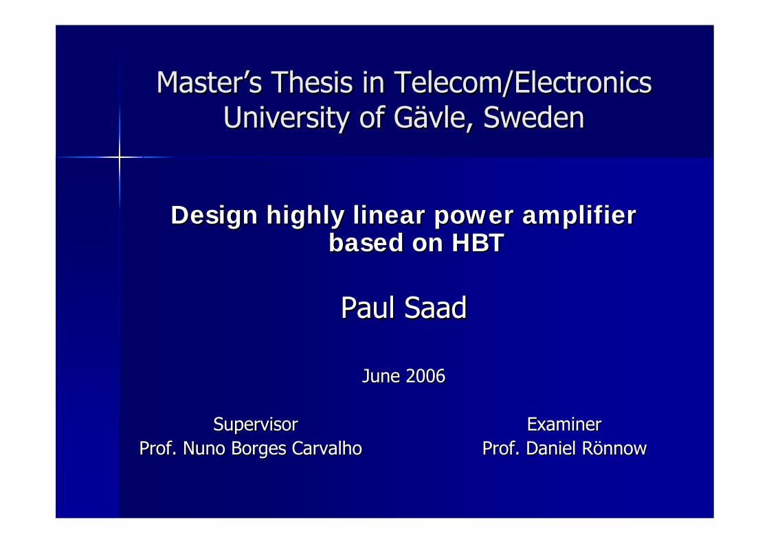
MasterMaster’’s Thesis in Telecom/Electronicss Thesis in Telecom/ElectronicsUniversity of GUniversity of Gäävle, Swedenvle, Sweden
Design highly linear power amplifier Design highly linear power amplifier based on HBTbased on HBT
Paul SaadPaul Saad
June 2006June 2006
Supervisor ESupervisor ExaminerxaminerProf. Nuno Borges Carvalho Prof. Daniel RProf. Nuno Borges Carvalho Prof. Daniel Röönnownnow
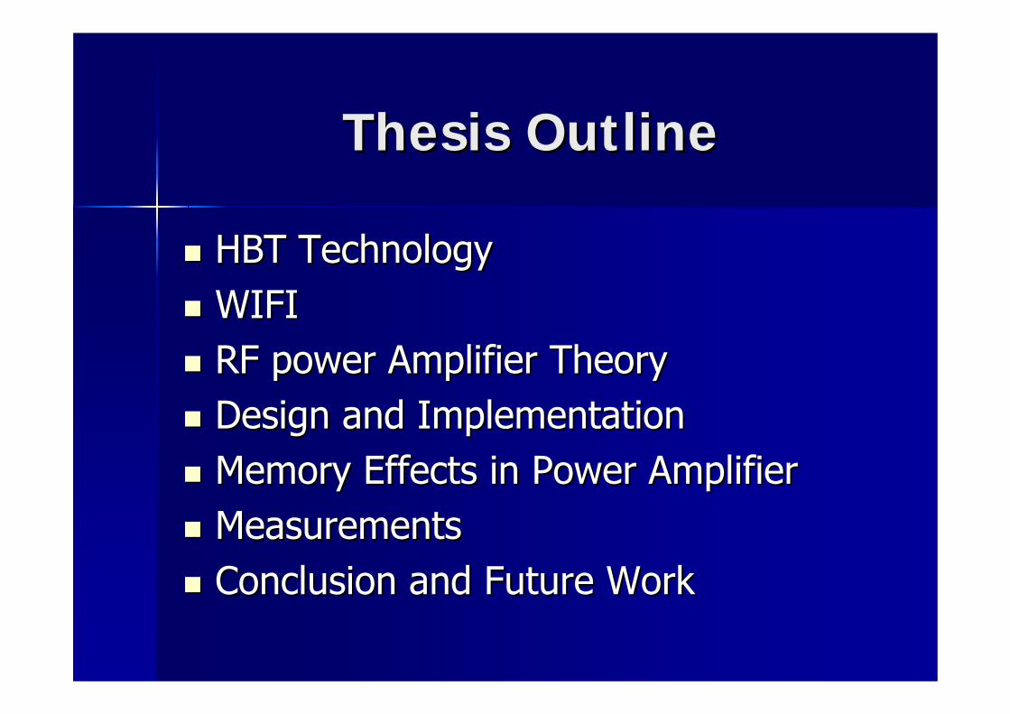
Thesis OutlineThesis Outline
HBT TechnologyHBT TechnologyWIFIWIFIRF power Amplifier TheoryRF power Amplifier TheoryDesign and ImplementationDesign and ImplementationMemory Effects in Power AmplifierMemory Effects in Power AmplifierMeasurementsMeasurementsConclusion and Future WorkConclusion and Future Work
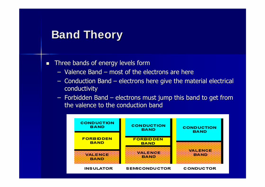
Band TheoryBand Theory
Three bands of energy levels formThree bands of energy levels form–– Valence Band Valence Band –– most of the electrons are heremost of the electrons are here–– Conduction Band Conduction Band –– electrons here give the material electrical electrons here give the material electrical
conductivityconductivity–– Forbidden Band Forbidden Band –– electrons must jump this band to get from electrons must jump this band to get from
the valence to the conduction bandthe valence to the conduction band
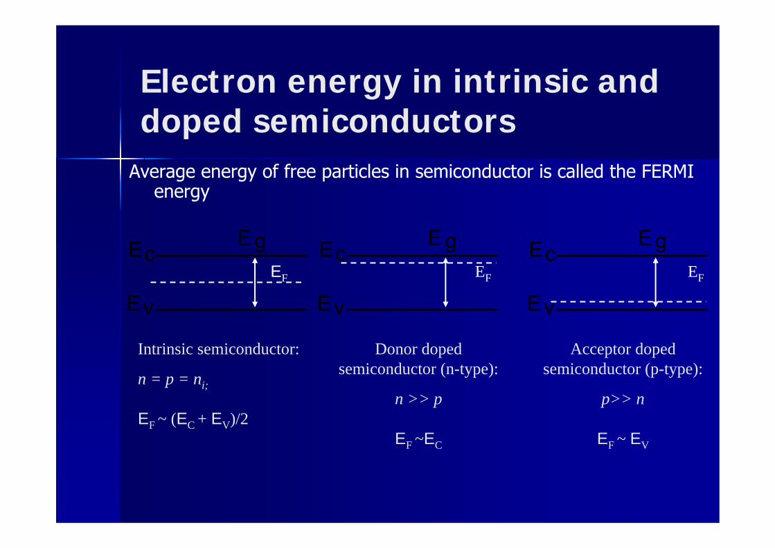
Electron energy in intrinsic and doped semiconductors
Average energy of free particles in semiconductor is called the FERMI energy
EF EF EF
Intrinsic semiconductor:
n = p = ni;
EF ~ (EC + EV)/2
Donor doped semiconductor (n-type):
n >> p
EF ~EC
Acceptor doped semiconductor (p-type):
p>> n
EF ~ EV
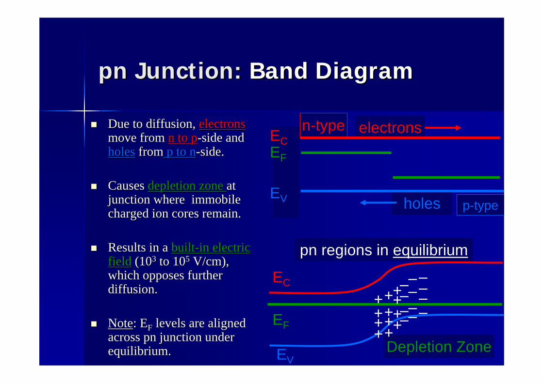
pn Junction:pn Junction: Band DiagramBand Diagram
Due to diffusion, Due to diffusion, electronselectronsmove from move from n to pn to p--side and side and holesholes fromfrom p to np to n--side.side.
Causes Causes depletion zone depletion zone at at junction where immobile junction where immobile charged ion cores remain.charged ion cores remain.
Results inResults in a a builtbuilt--in electric in electric fieldfield (10(1033 to 10to 1055 V/cm), V/cm), which opposes further which opposes further diffusion. diffusion.
NoteNote: E: EFF levels are aligned levels are aligned across pn junction under across pn junction under equilibrium.equilibrium. Depletion Zone
electrons
pn regions in equilibrium
holesEV
EF
EC
EV
EF
EC
+++
++++
++++
+––––
––––
––––
p-type
n-type
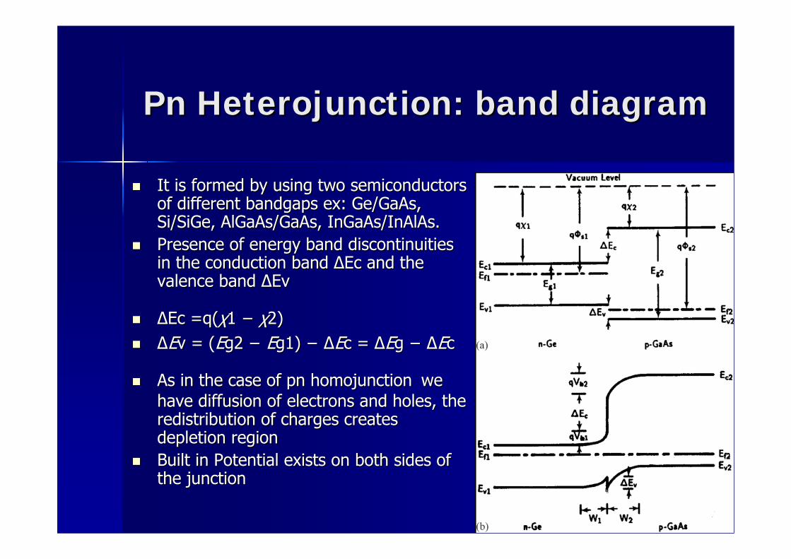
Pn Heterojunction: band diagramPn Heterojunction: band diagram
It is formed by using two semiconductors It is formed by using two semiconductors of different bandgaps exof different bandgaps ex: Ge/GaAs, : Ge/GaAs, Si/SiGe, AlGaAs/GaAs, InGaAs/InAlAs.Si/SiGe, AlGaAs/GaAs, InGaAs/InAlAs.Presence of energy band discontinuities Presence of energy band discontinuities in the conduction band in the conduction band ∆∆Ec Ec and the and the valence band valence band ∆∆EvEv
∆∆Ec =qEc =q((χχ1 1 −− χχ2)2)∆∆EEv = (v = (EEg2 g2 −− EEg1) g1) −− ∆∆EEc = c = ∆∆EEg g −− ∆∆EEcc
As in the case of pn homojunctionAs in the case of pn homojunction we we have diffusion of electrons and holes, the have diffusion of electrons and holes, the redistribution of charges creates redistribution of charges creates depletion region depletion region Built in Potential exists on both sides of Built in Potential exists on both sides of the junctionthe junction
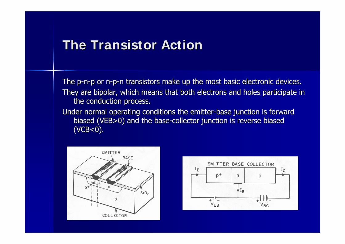
The Transistor ActionThe Transistor Action
The pThe p--nn--p or np or n--pp--n transistors make up the most basic electronic devices.n transistors make up the most basic electronic devices.They are bipolar, which means that both electrons and holes partThey are bipolar, which means that both electrons and holes participate in icipate in
the conduction process.the conduction process.Under normal operating conditions Under normal operating conditions the emitterthe emitter--base junction is forward base junction is forward
biased (VEB>0) and the basebiased (VEB>0) and the base--collector junction is reverse biased collector junction is reverse biased (VCB<0).(VCB<0).
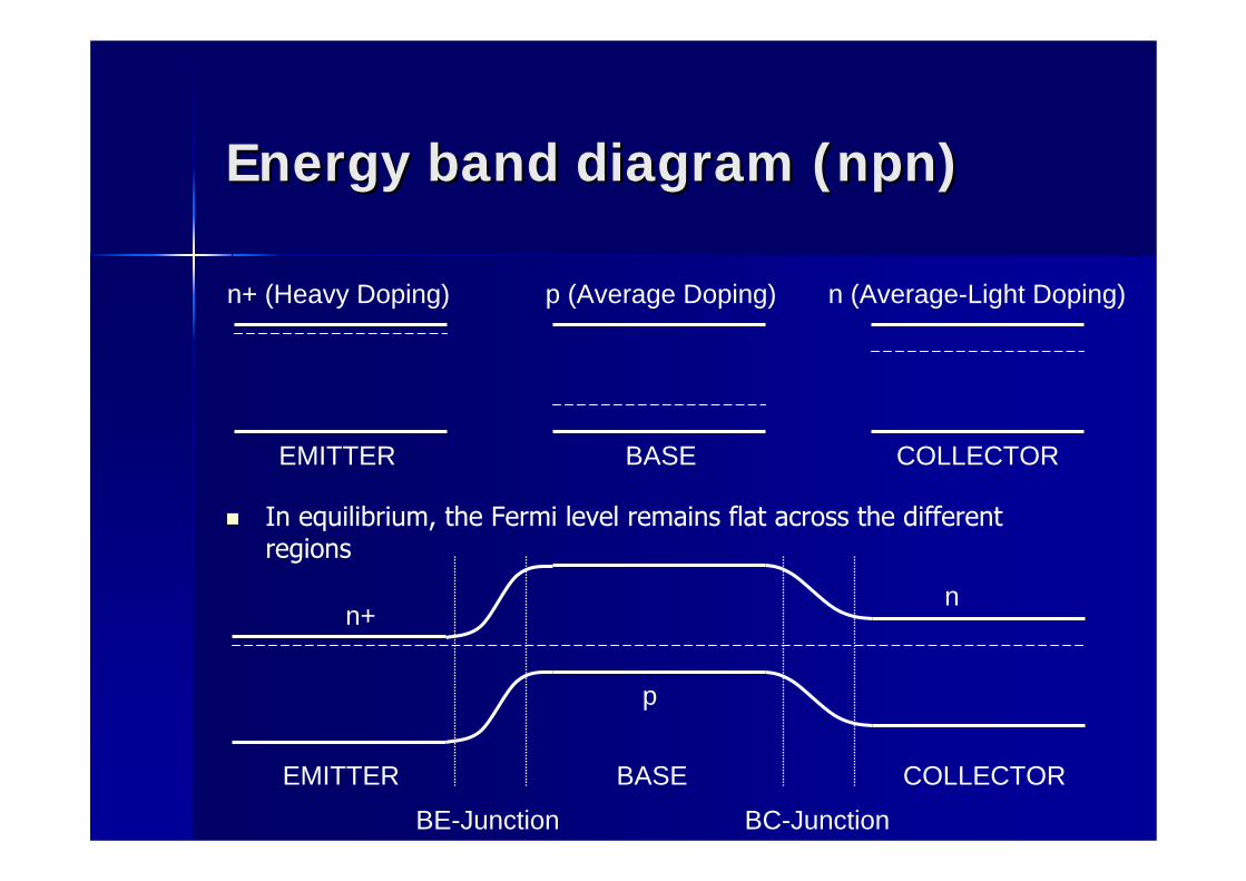
Energy band diagram (npn)Energy band diagram (npn)
In equilibrium, the Fermi level remains flat across the different regions
n+ (Heavy Doping)
EMITTER
p (Average Doping)
BASE
n (Average-Light Doping)
COLLECTOR
n+
p
n
EMITTER BASE COLLECTOR
BE-Junction BC-Junction
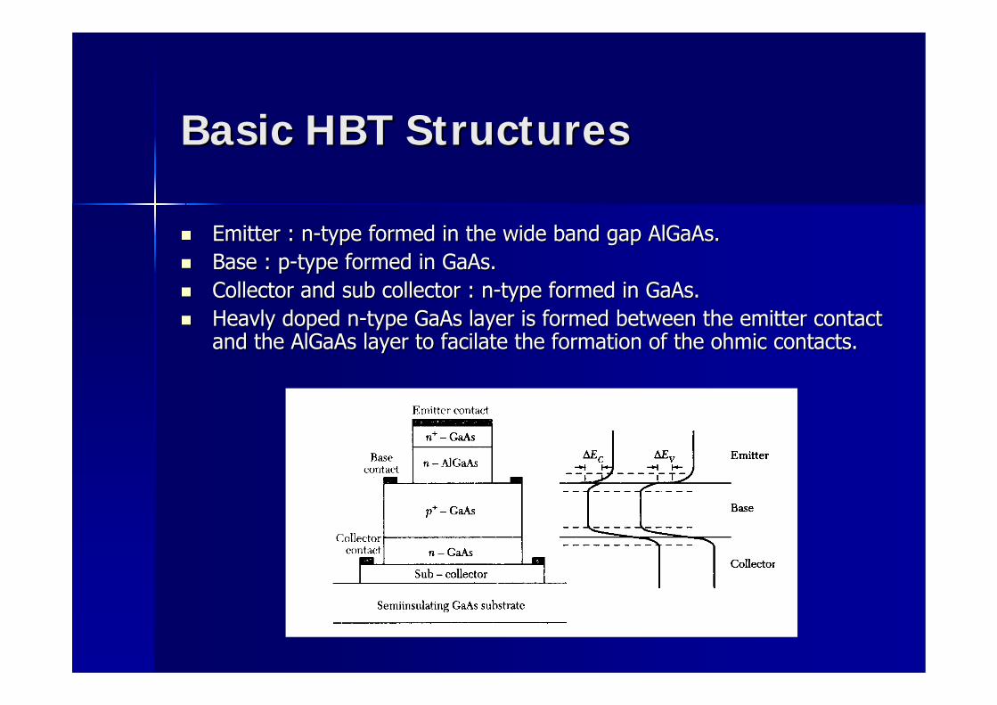
Basic HBT StructuresBasic HBT Structures
Emitter : nEmitter : n--type formed in the wide band gap AlGaAs.type formed in the wide band gap AlGaAs.Base : pBase : p--type formed in GaAs.type formed in GaAs.Collector and sub collector : nCollector and sub collector : n--type formed in GaAs.type formed in GaAs.Heavly doped nHeavly doped n--type GaAs layer is formed between the emitter contact type GaAs layer is formed between the emitter contact and the AlGaAs layer to facilate the formation of the ohmic contand the AlGaAs layer to facilate the formation of the ohmic contacts.acts.
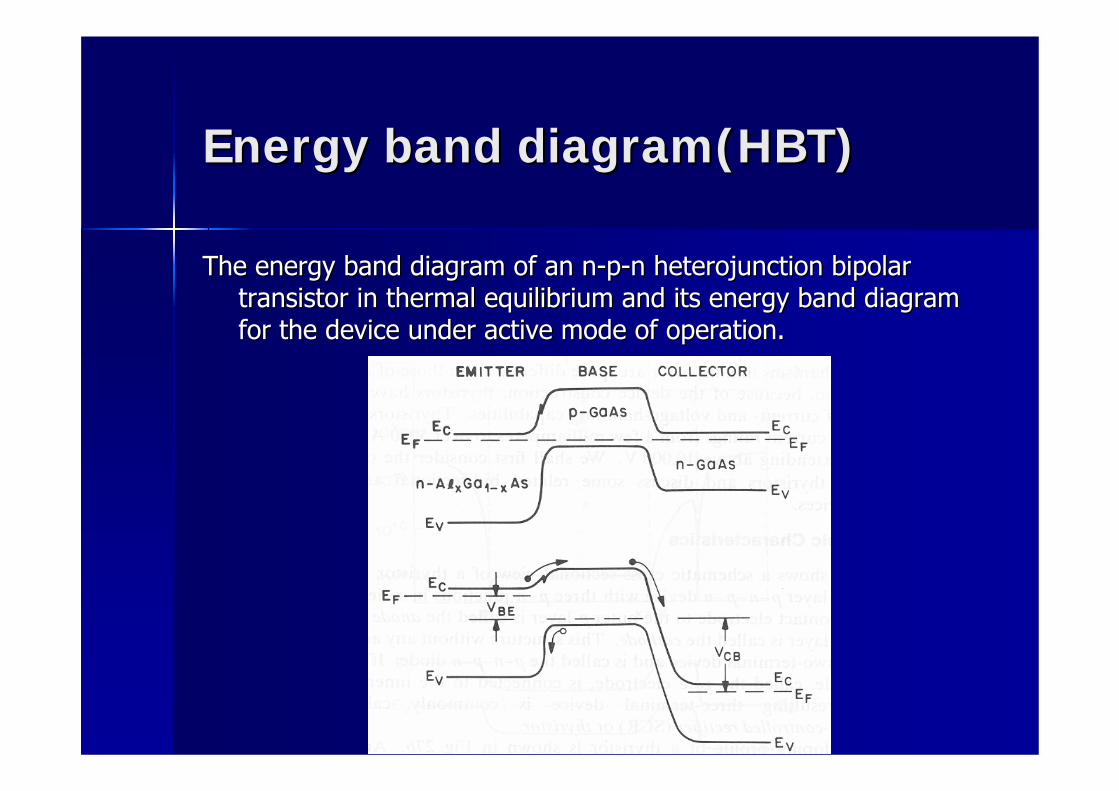
Energy band diagram(HBT)Energy band diagram(HBT)
The energy band diagram of an nThe energy band diagram of an n--pp--n heterojunction bipolar n heterojunction bipolar transistor in thermal equilibrium and its energy band diagram transistor in thermal equilibrium and its energy band diagram for the device under active mode of operation.for the device under active mode of operation.
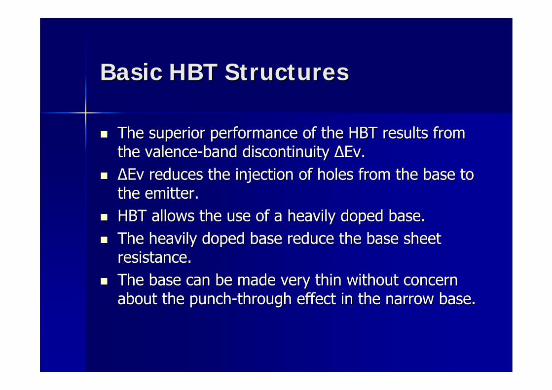
Basic HBT StructuresBasic HBT Structures
The superior performance of the HBT results from The superior performance of the HBT results from the valencethe valence--band discontinuity band discontinuity ∆∆Ev.Ev.∆∆Ev Ev reduces the injection of holes from the base to reduces the injection of holes from the base to the emitter.the emitter.HBT allows the use of a heavily doped base.HBT allows the use of a heavily doped base.The heavily doped base reduce the base sheet The heavily doped base reduce the base sheet resistance. resistance. The base can be made very thin without concern The base can be made very thin without concern about the punchabout the punch--through effect in the narrow base.through effect in the narrow base.
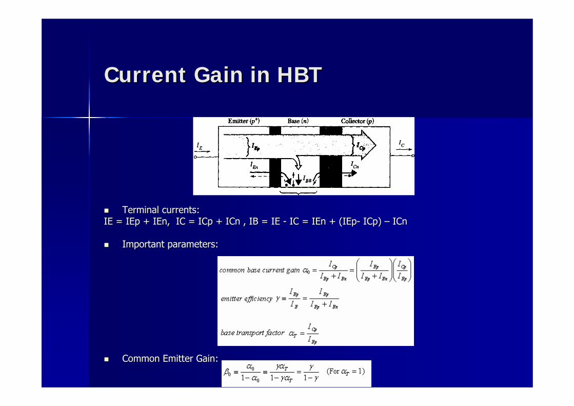
Current Gain in HBTCurrent Gain in HBT
Terminal currents:Terminal currents:IE = IEp + IEnIE = IEp + IEn, , IC = ICp + ICnIC = ICp + ICn , , IB = IE IB = IE -- IC = IEn + (IEpIC = IEn + (IEp-- ICp) ICp) –– ICnICn
Important parameters:Important parameters:
Common Emitter Gain:Common Emitter Gain:
Current Gain in HBTCurrent Gain in HBT
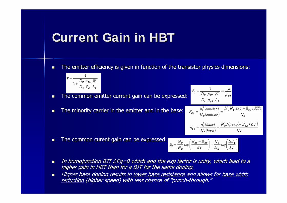
The emitter efficiency is given in function of the transistor phThe emitter efficiency is given in function of the transistor physics dimensions:ysics dimensions:
The common emitter current gain can be expressed:The common emitter current gain can be expressed:
The minority carrier in the emitter and in the base:The minority carrier in the emitter and in the base:
The common curent gain can be expressed:The common curent gain can be expressed:
In homojunction BJT In homojunction BJT ∆∆Eg=0 which and the exp factor is unity, which lead to a Eg=0 which and the exp factor is unity, which lead to a higher gain in HBT than for a BJT for the same doping.higher gain in HBT than for a BJT for the same doping.Higher base doping results in lower base resistance and allows for base width reduction (higher speed) with less chance of “punch-through.”
Cutoff frequencyCutoff frequency
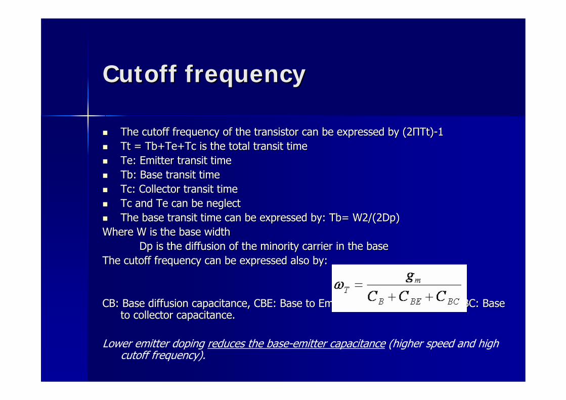
The cutoff frequency of the transistor can be expressed by The cutoff frequency of the transistor can be expressed by (2(2ΠΠTt)Tt)--1 1 Tt = Tb+Te+Tc is the total transit timeTt = Tb+Te+Tc is the total transit timeTe: Emitter transit timeTe: Emitter transit timeTb: Base transit timeTb: Base transit timeTc: Collector transit timeTc: Collector transit timeTc and Te can be neglectTc and Te can be neglectThe base transit time can be expressed by: Tb= W2/(2Dp)The base transit time can be expressed by: Tb= W2/(2Dp)
Where W is the base widthWhere W is the base widthDp is the diffusion of the minority carrier in the baDp is the diffusion of the minority carrier in the base se
The cutoff frequency can be expressed also by:The cutoff frequency can be expressed also by:
CB: Base diffusion capacitance, CBE: Base to Emitter junction caCB: Base diffusion capacitance, CBE: Base to Emitter junction capacitance,CBC: Base pacitance,CBC: Base to collector capacitance.to collector capacitance.
Lower emitter doping reduces the base-emitter capacitance (higher speed and high cutoff frequency).
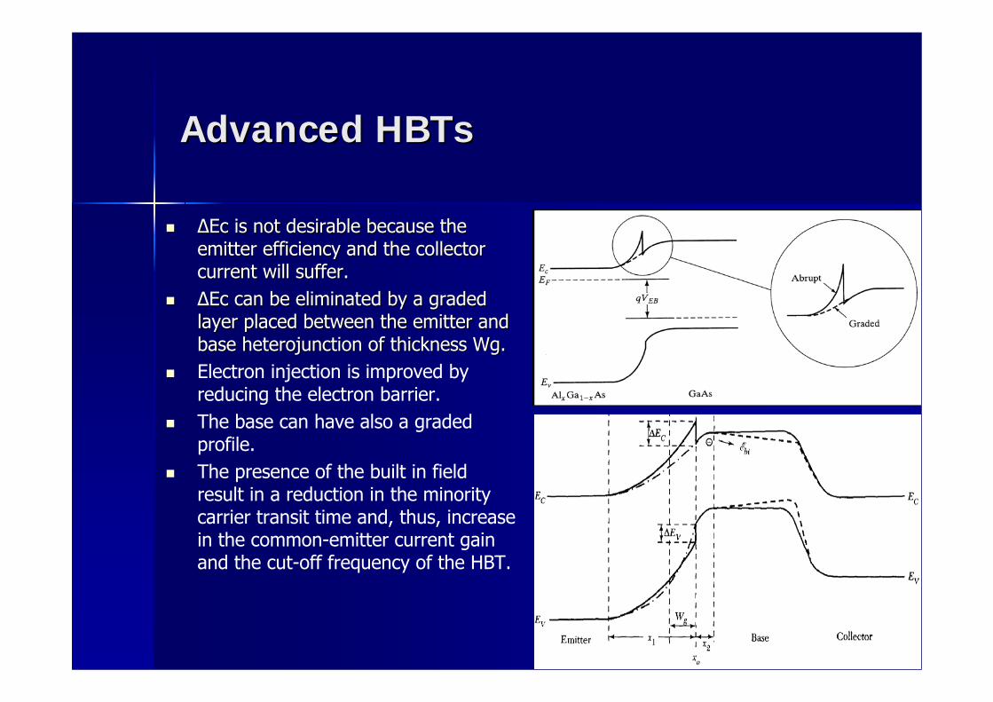
Advanced HBTsAdvanced HBTs
∆∆Ec is not desirable because the Ec is not desirable because the emitter efficiency and the collector emitter efficiency and the collector current will suffer.current will suffer.∆∆Ec can be eliminated by a graded Ec can be eliminated by a graded layer placed between the emitter and layer placed between the emitter and base heterojunction of thickness Wg. base heterojunction of thickness Wg. Electron injection is improved by reducing the electron barrier.The base can have also a graded profile. The presence of the built in field result in a reduction in the minority carrier transit time and, thus, increase in the common-emitter current gain and the cut-off frequency of the HBT.
SiGe HBT versus BJT
Higher speedHigher operating frequencyHigher transistor gain or lower base resistanceLower noiseLower RF noiseLow power consumptionSmaller circuits
SiGe Vs Cmos
Noise For same current, SiGe has lower noise figure, SiGe
has lower 1/f noise
Power consumption: For same noise, SiGe will have lower power
Circuit densitySiGe HBT circuits occupy one-quarter to one- third the
area of CMOS circuits of equivalent functionality.
WIFIWIFI
WIFI STANDS FOR WIFI STANDS FOR WIWIRELESS RELESS FIFIDELITYDELITY AND AND ENCOMPASSES A WORLDWIDE STANDARD, ENCOMPASSES A WORLDWIDE STANDARD, WHICH ALLOWS HIGHWHICH ALLOWS HIGH--SPEED WIRELESS SPEED WIRELESS INTERNET TRANSMITTED VIA RADIO WAVES INTERNET TRANSMITTED VIA RADIO WAVES WITH SPEEDS OF MBPS, RATHER THAN KBPS.WITH SPEEDS OF MBPS, RATHER THAN KBPS.
THE SOTHE SO--CALLED HOTSPOT OR HUB OR WLAN CALLED HOTSPOT OR HUB OR WLAN ACCESS POINT SENDS OUT A WIRELESS SIGNAL ACCESS POINT SENDS OUT A WIRELESS SIGNAL TO ALLOWS WIRELESS DEVICES ACCESS TO ALLOWS WIRELESS DEVICES ACCESS WITHIN A CIRCLE.WITHIN A CIRCLE.
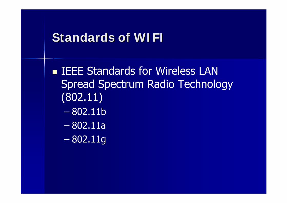
Standards of WIFIStandards of WIFI
IEEE Standards for Wireless LAN Spread Spectrum Radio Technology (802.11)– 802.11b– 802.11a– 802.11g
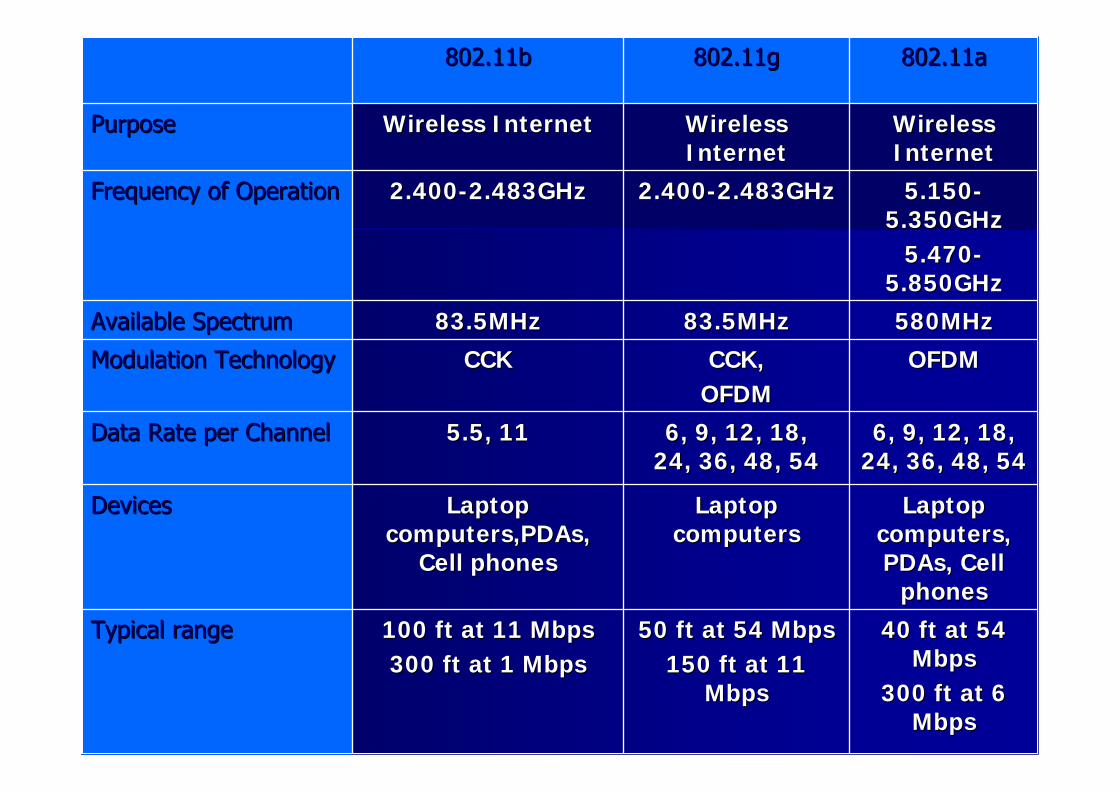
OFDMOFDMCCK,CCK,OFDMOFDM
CCKCCKModulation TechnologyModulation Technology
580MHz580MHz83.5MHz83.5MHz83.5MHz83.5MHzAvailable SpectrumAvailable Spectrum
Laptop Laptop computers, computers, PDAs, Cell PDAs, Cell
phonesphones
Laptop Laptop computerscomputers
Laptop Laptop computers,PDAs, computers,PDAs,
Cell phonesCell phones
DevicesDevices
50 ft at 54 Mbps50 ft at 54 Mbps150 ft at 11 150 ft at 11
MbpsMbps
6, 9, 12, 18,6, 9, 12, 18,24, 36, 48, 5424, 36, 48, 54
2.4002.400--2.483GHz2.483GHz
Wireless Wireless InternetInternet
802.11g802.11g
100 ft at 11 Mbps100 ft at 11 Mbps300 ft at 1 Mbps300 ft at 1 Mbps
5.5, 115.5, 11
2.4002.400--2.483GHz2.483GHz
Wireless InternetWireless Internet
802.11b802.11b
40 ft at 54 40 ft at 54 MbpsMbps
300 ft at 6 300 ft at 6 MbpsMbps
Typical rangeTypical range
6, 9, 12, 18,6, 9, 12, 18,24, 36, 48, 5424, 36, 48, 54
Data Rate per ChannelData Rate per Channel
5.1505.150--5.350GHz 5.350GHz
5.4705.470--5.850GHz5.850GHz
Frequency of OperationFrequency of Operation
Wireless Wireless InternetInternet
PurposePurpose
802.11a802.11a
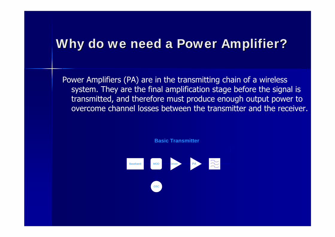
Why do we need a Power Amplifier?Why do we need a Power Amplifier?
Power Amplifiers (PA) are in the transmitting chain of a wireless system. They are the final amplification stage before the signal is transmitted, and therefore must produce enough output power to overcome channel losses between the transmitter and the receiver.
OSC
MODBaseband PADriver
Basic Transmitter
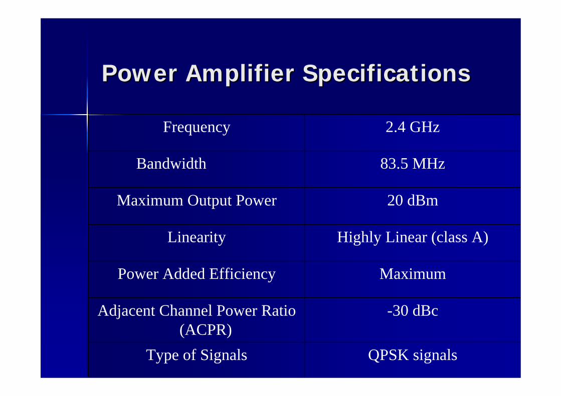
Power Amplifier SpecificationsPower Amplifier Specifications
QPSK signalsType of Signals
-30 dBcAdjacent Channel Power Ratio (ACPR)
MaximumPower Added Efficiency
Highly Linear (class A)Linearity
20 dBmMaximum Output Power
83.5 MHzBandwidth
2.4 GHzFrequency
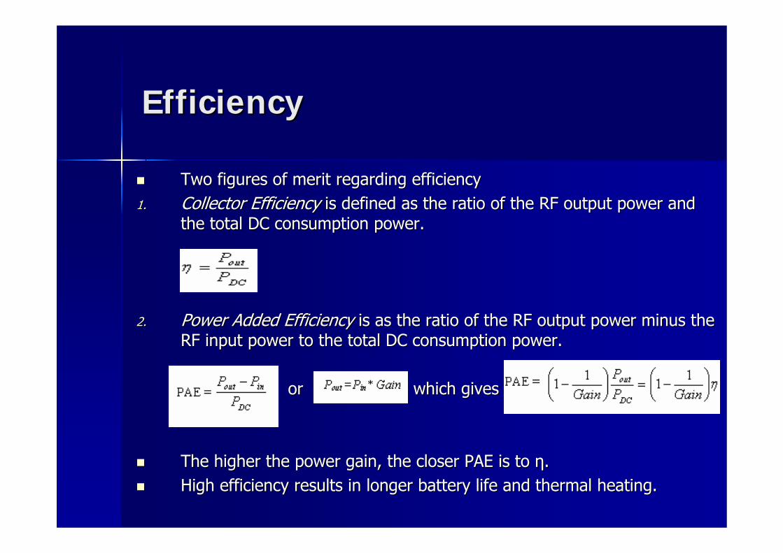
EfficiencyEfficiency
Two figures of merit regarding efficiencyTwo figures of merit regarding efficiency1.1. Collector EfficiencyCollector Efficiency is defined as the ratio of the RF output power and is defined as the ratio of the RF output power and
the total DC consumption power.the total DC consumption power.
2.2. Power Added Efficiency Power Added Efficiency is as the ratio of the RF output power minus the is as the ratio of the RF output power minus the RF input power to the total DC consumption power.RF input power to the total DC consumption power.
or which givesor which gives
The higher the power gain, the closer PAE is to The higher the power gain, the closer PAE is to ηη..High efficiency results in longer battery life and thermal heatiHigh efficiency results in longer battery life and thermal heating.ng.
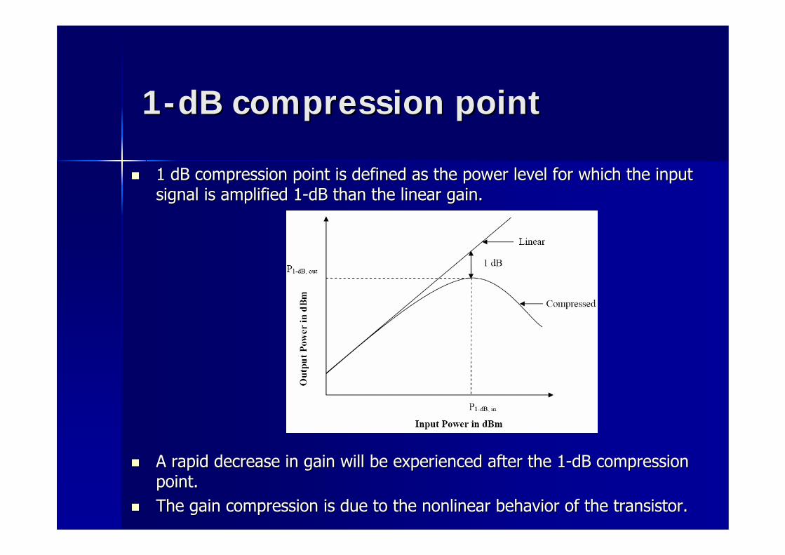
11--dB compression pointdB compression point
1 dB compression point is defined as the power level for which t1 dB compression point is defined as the power level for which the input he input signal is amplified 1signal is amplified 1--dB than the linear gain.dB than the linear gain.
A rapid decrease in gain will be experienced after the 1A rapid decrease in gain will be experienced after the 1--dB compression dB compression point.point.The gain compression is due to the nonlinear behavior of the traThe gain compression is due to the nonlinear behavior of the transistor.nsistor.
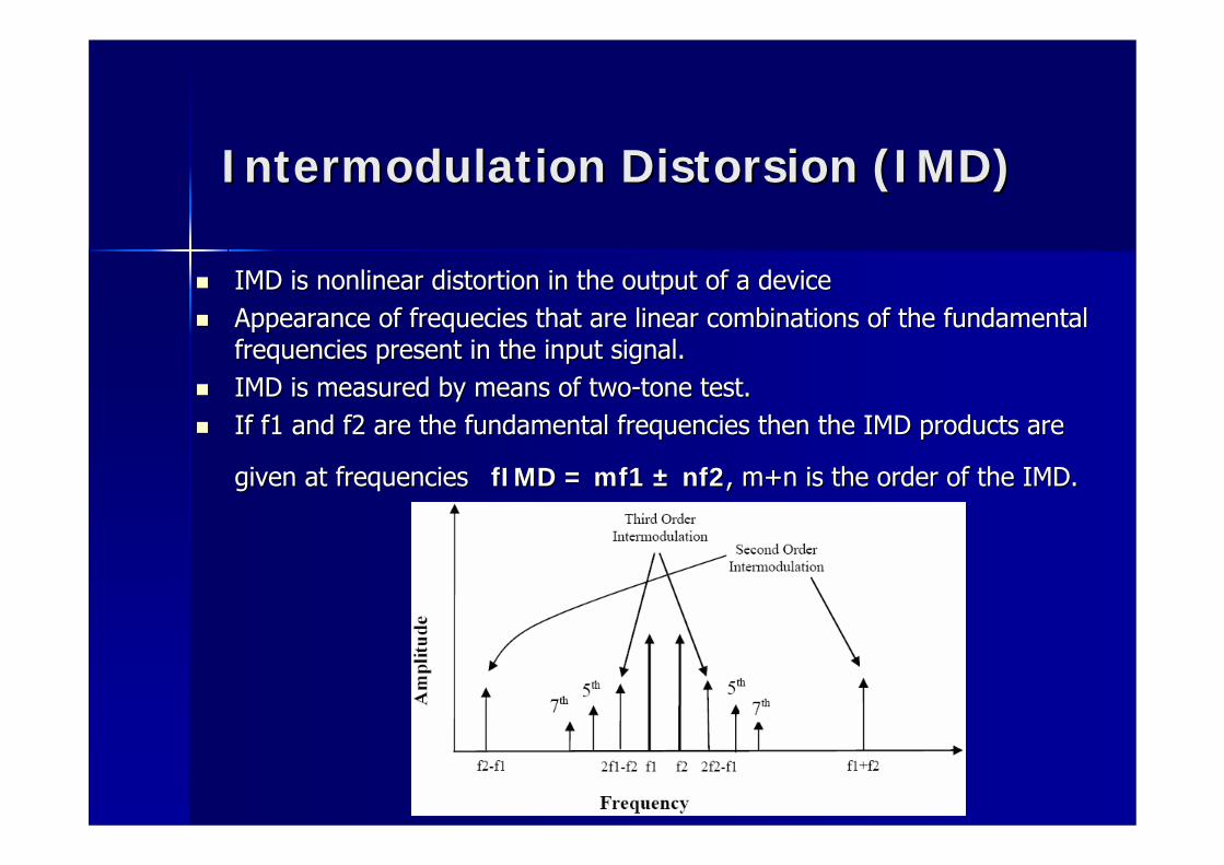
Intermodulation Distorsion (IMD)Intermodulation Distorsion (IMD)
IMD is nonlinear distortion in the output of a deviceIMD is nonlinear distortion in the output of a deviceAppearance of frequecies that are linear combinations of the funAppearance of frequecies that are linear combinations of the fundamental damental frequencies present in the input signal.frequencies present in the input signal.IMD is measured by means of twoIMD is measured by means of two--tone test.tone test.If f1 and f2 are the fundamental frequencies then the IMD producIf f1 and f2 are the fundamental frequencies then the IMD products are ts are
given at frequencies given at frequencies fIMD = mf1 fIMD = mf1 ±± nf2nf2, m+n is the order of the IMD., m+n is the order of the IMD.
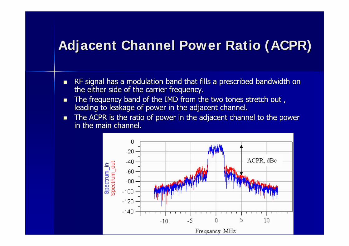
Adjacent Channel Power Ratio (ACPR)Adjacent Channel Power Ratio (ACPR)
RF signal has a modulation band that fills a prescribed bandwidtRF signal has a modulation band that fills a prescribed bandwidth on h on the either side of the carrier frequency.the either side of the carrier frequency.The frequency band of the IMD from the two tones stretch out , The frequency band of the IMD from the two tones stretch out , leading to leakage of power in the adjacent channel.leading to leakage of power in the adjacent channel.The ACPR is the ratio of power in the adjacent channel to the poThe ACPR is the ratio of power in the adjacent channel to the power wer in the main channel. in the main channel.
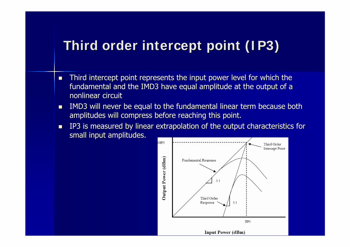
Third order intercept point (IP3)Third order intercept point (IP3)
Third intercept point represents the input power level for whichThird intercept point represents the input power level for which the the fundamental and the IMD3 have equal amplitude at the output of afundamental and the IMD3 have equal amplitude at the output of anonlinear circuitnonlinear circuitIMD3 will never be equal to the fundamental linear term because IMD3 will never be equal to the fundamental linear term because both both amplitudes will compress before reaching this point.amplitudes will compress before reaching this point.IP3 is measured by linear extrapolation of the output characteriIP3 is measured by linear extrapolation of the output characteristics for stics for small input amplitudes.small input amplitudes.
Power Amplifier ClassificationPower Amplifier Classification
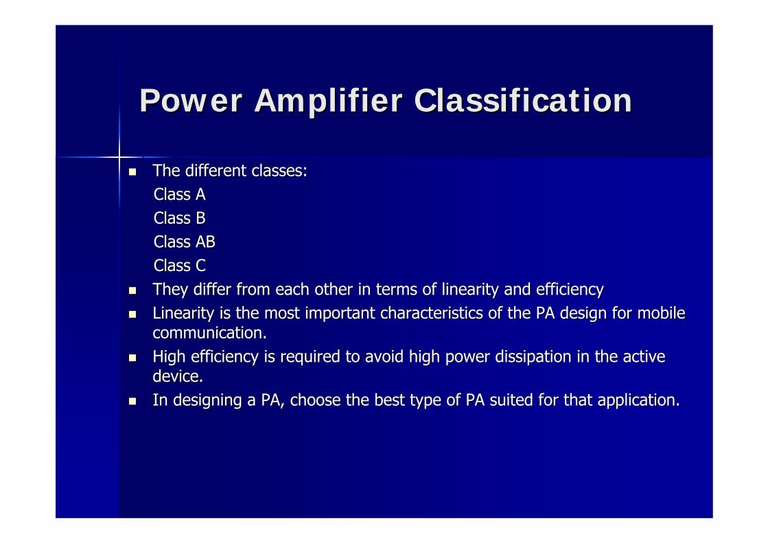
The different classes:The different classes:Class AClass AClass BClass BClass AB Class AB Class CClass CThey differ from each other in terms ofThey differ from each other in terms of linearity and efficiencylinearity and efficiencyLinearity is the most important characteristics of the PA designLinearity is the most important characteristics of the PA design for mobile for mobile communication.communication.High efficiency is required to avoid high power dissipation in tHigh efficiency is required to avoid high power dissipation in the active he active device.device.In designing a PA, choose the best type of PA suited for that apIn designing a PA, choose the best type of PA suited for that application.plication.
Class A Power AmplifierClass A Power Amplifier
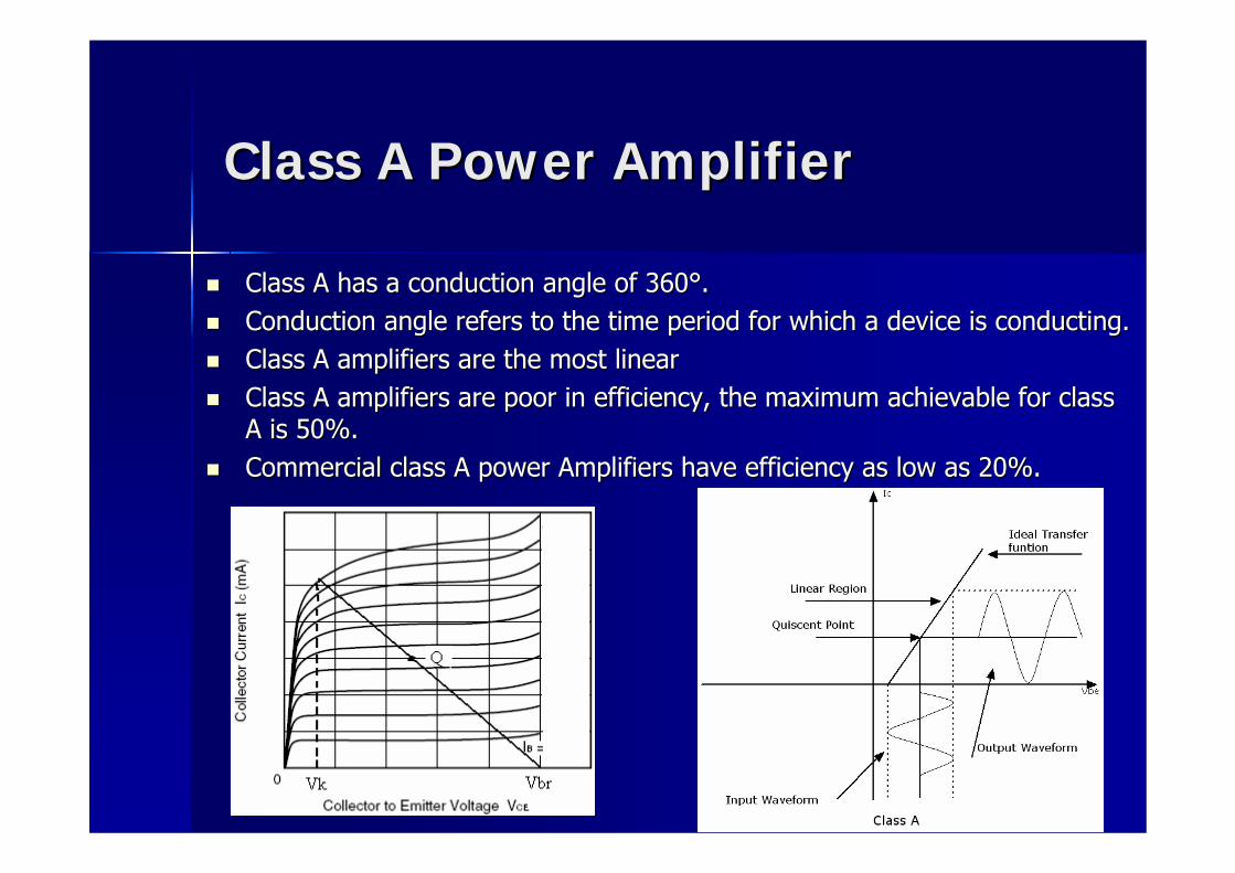
Class A has a conduction angle of Class A has a conduction angle of 360360°°..Conduction angle refers to the time period for which a device isConduction angle refers to the time period for which a device is conducting.conducting.Class A amplifiers are the most linear Class A amplifiers are the most linear Class A amplifiers are poor in efficiency, the maximum achievablClass A amplifiers are poor in efficiency, the maximum achievable for class e for class A is 50%.A is 50%.Commercial class A power Amplifiers have efficiency as low as 20Commercial class A power Amplifiers have efficiency as low as 20%.%.
Class B power AmplifierClass B power Amplifier
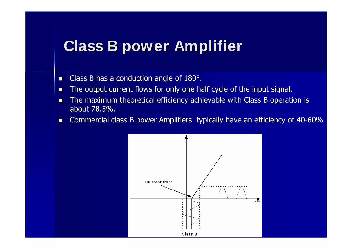
Class B has a conduction angle of Class B has a conduction angle of 180180°°..The output current flows for only one half cycle of the input siThe output current flows for only one half cycle of the input signal.gnal.The maximum theoretical efficiency achievable with Class B operaThe maximum theoretical efficiency achievable with Class B operation is tion is about 78.5%.about 78.5%.Commercial class B power Amplifiers typically have an efficiencCommercial class B power Amplifiers typically have an efficiency of 40y of 40--60%60%
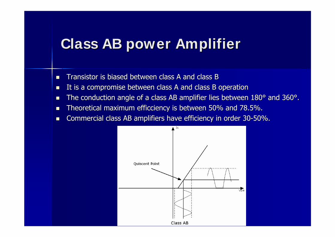
Class AB power AmplifierClass AB power Amplifier
Transistor is biased between class A and class B Transistor is biased between class A and class B It is a compromise between class A and class B operationIt is a compromise between class A and class B operationThe conduction angle of a class AB amplifier lies between 180The conduction angle of a class AB amplifier lies between 180°° and 360and 360°°..Theoretical maximum efficciency is between 50% and 78.5%.Theoretical maximum efficciency is between 50% and 78.5%.Commercial class AB amplifiers have efficiency in order 30Commercial class AB amplifiers have efficiency in order 30--50%.50%.
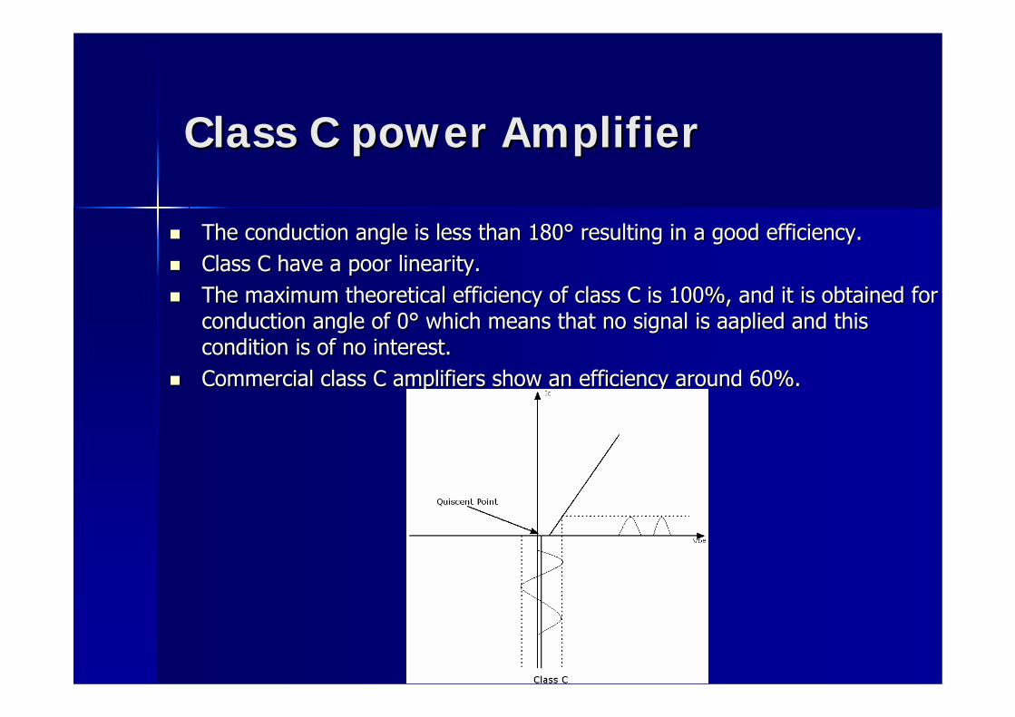
Class C power AmplifierClass C power Amplifier
The conduction angle is less than 180The conduction angle is less than 180°° resulting in a good efficiency.resulting in a good efficiency.Class C have a poor linearity.Class C have a poor linearity.The maximum theoretical efficiency of class C is 100%, and it isThe maximum theoretical efficiency of class C is 100%, and it is obtained for obtained for conduction angle of 0conduction angle of 0°° which means that no signal is aaplied and this which means that no signal is aaplied and this condition is of no interest.condition is of no interest.Commercial class C amplifiers show an efficiency around 60%.Commercial class C amplifiers show an efficiency around 60%.
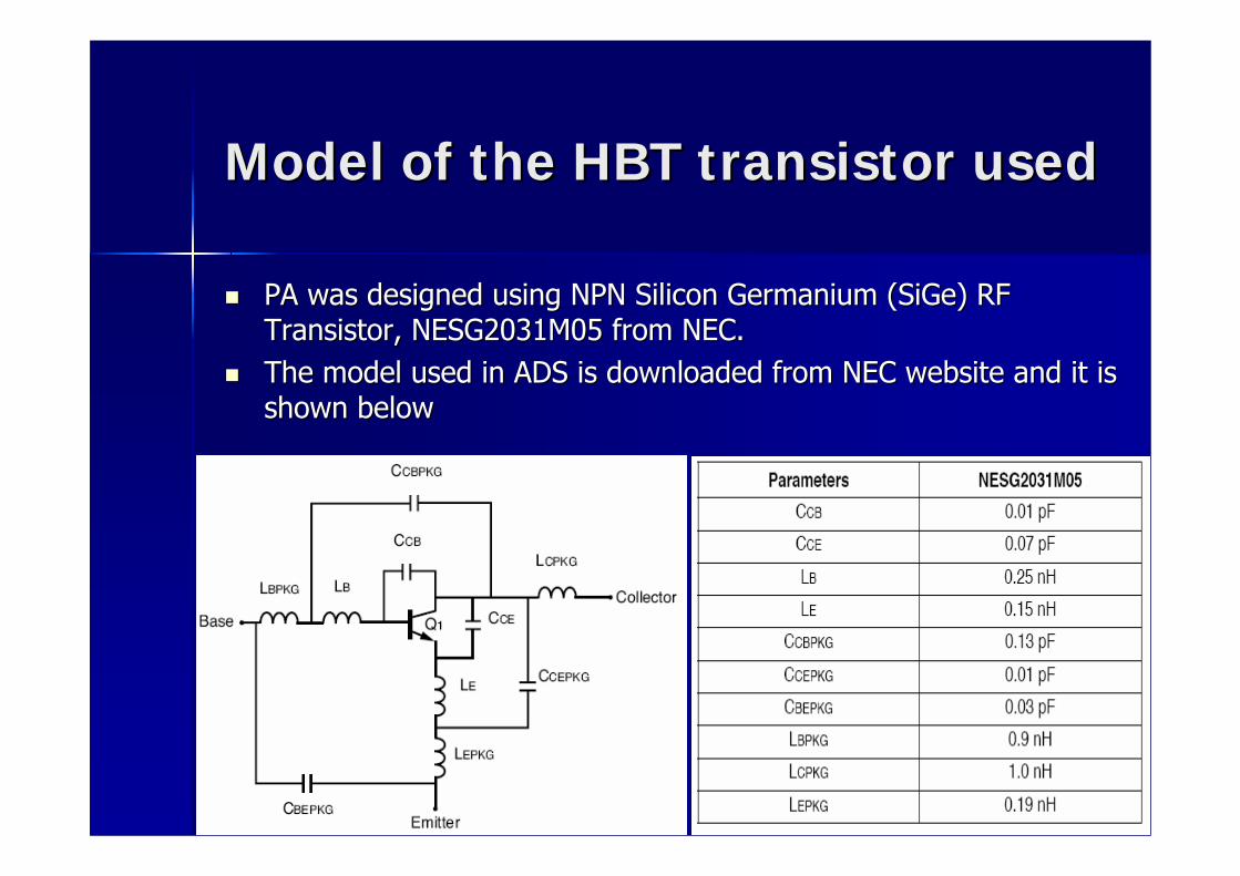
Model of the HBT transistor usedModel of the HBT transistor used
PA was designed using NPN Silicon Germanium PA was designed using NPN Silicon Germanium (SiGe) RF (SiGe) RF Transistor, NESG2031M05 from NEC.Transistor, NESG2031M05 from NEC.The model used in ADS is downloaded from NEC website and it is The model used in ADS is downloaded from NEC website and it is shown belowshown below
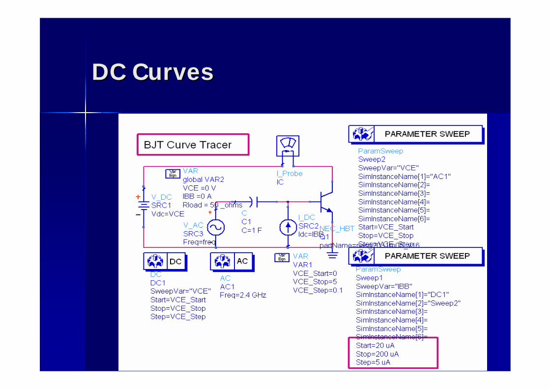
DC CurvesDC Curves
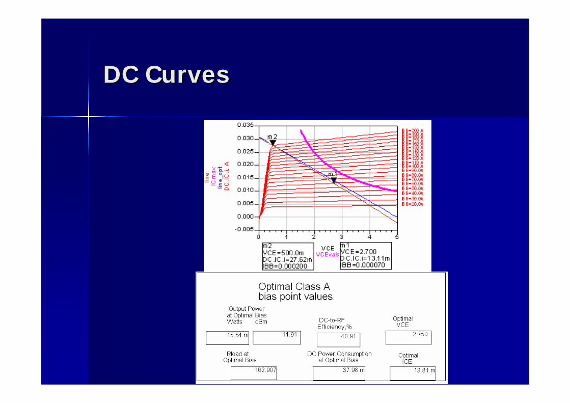
DC CurvesDC Curves
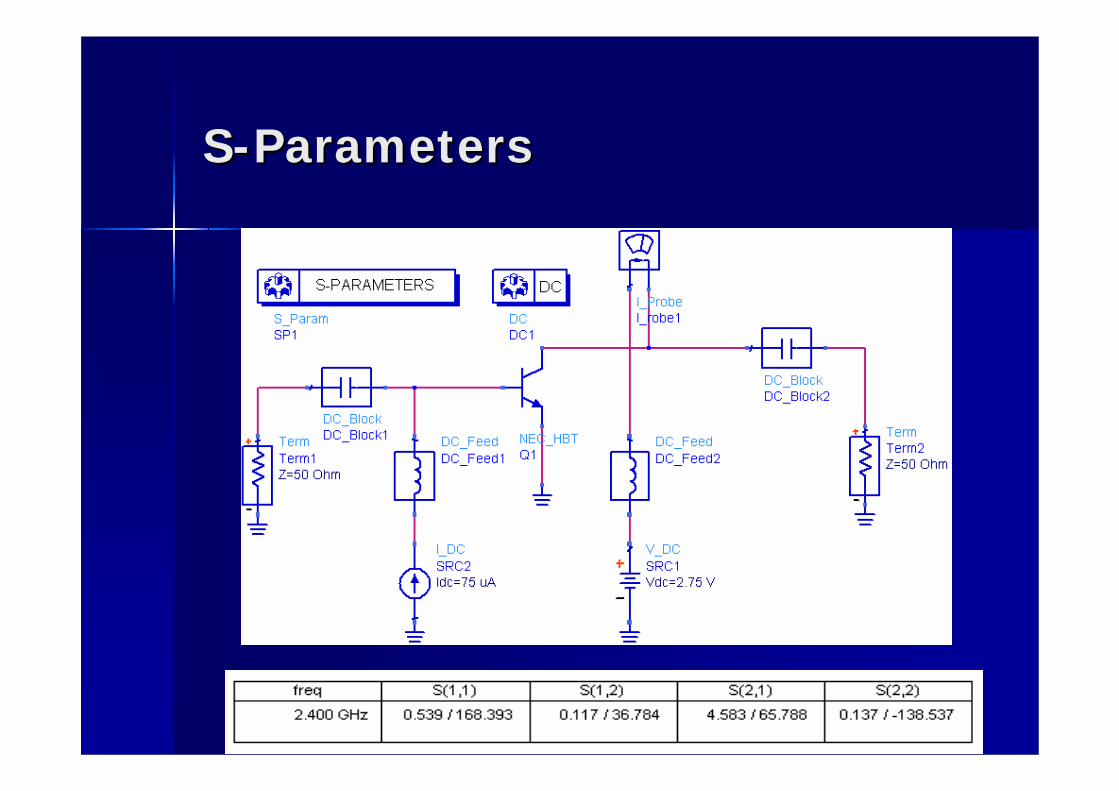
SS--ParametersParameters
StabilityStability
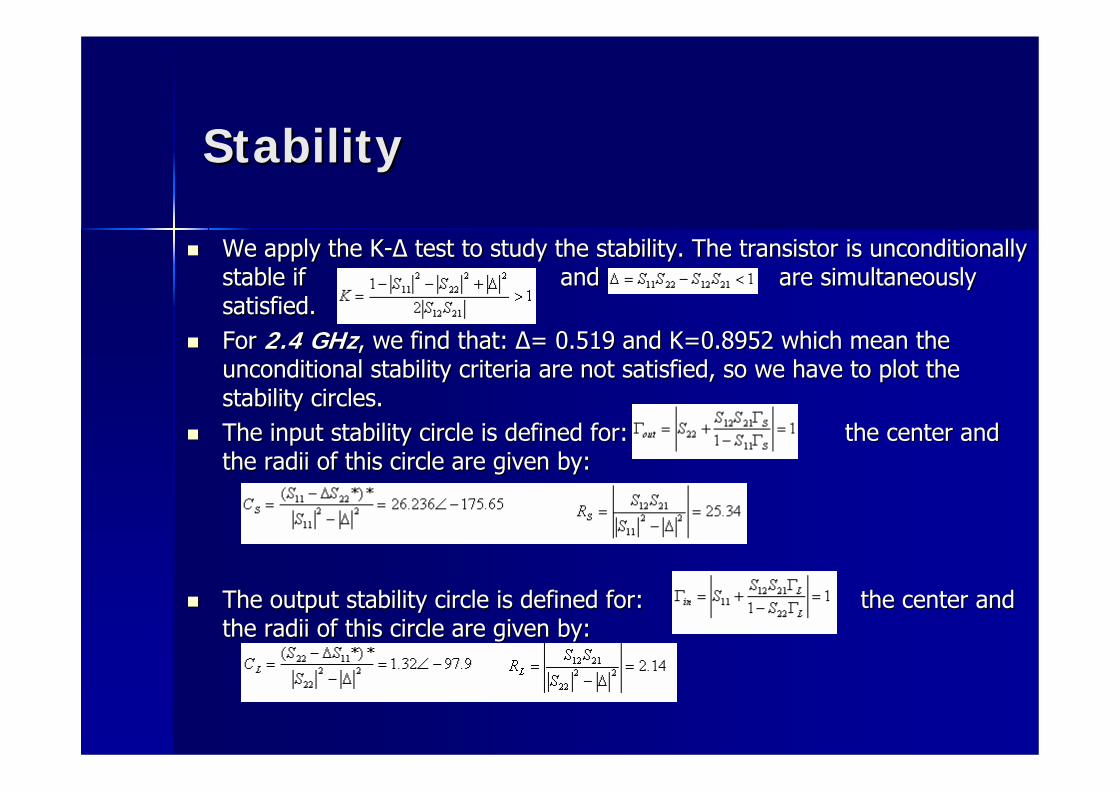
We apply the KWe apply the K--∆∆ test to study the stability. The transistor is unconditionally test to study the stability. The transistor is unconditionally stable if and stable if and are simultaneously are simultaneously satisfied.satisfied.For For 2.4 GHz2.4 GHz, we find that: , we find that: ∆∆= 0.519 and K=0.8952 which mean the = 0.519 and K=0.8952 which mean the unconditional stability criteria are not satisfied, so we have tunconditional stability criteria are not satisfied, so we have to plot the o plot the stability circles.stability circles.The input stability circle is defined for: The input stability circle is defined for: the center and the center and the radii of this circle are given by: the radii of this circle are given by:
The output stability circle is defined for: The output stability circle is defined for: the center and the center and the radii of this circle are given by: the radii of this circle are given by:
StabilityStability
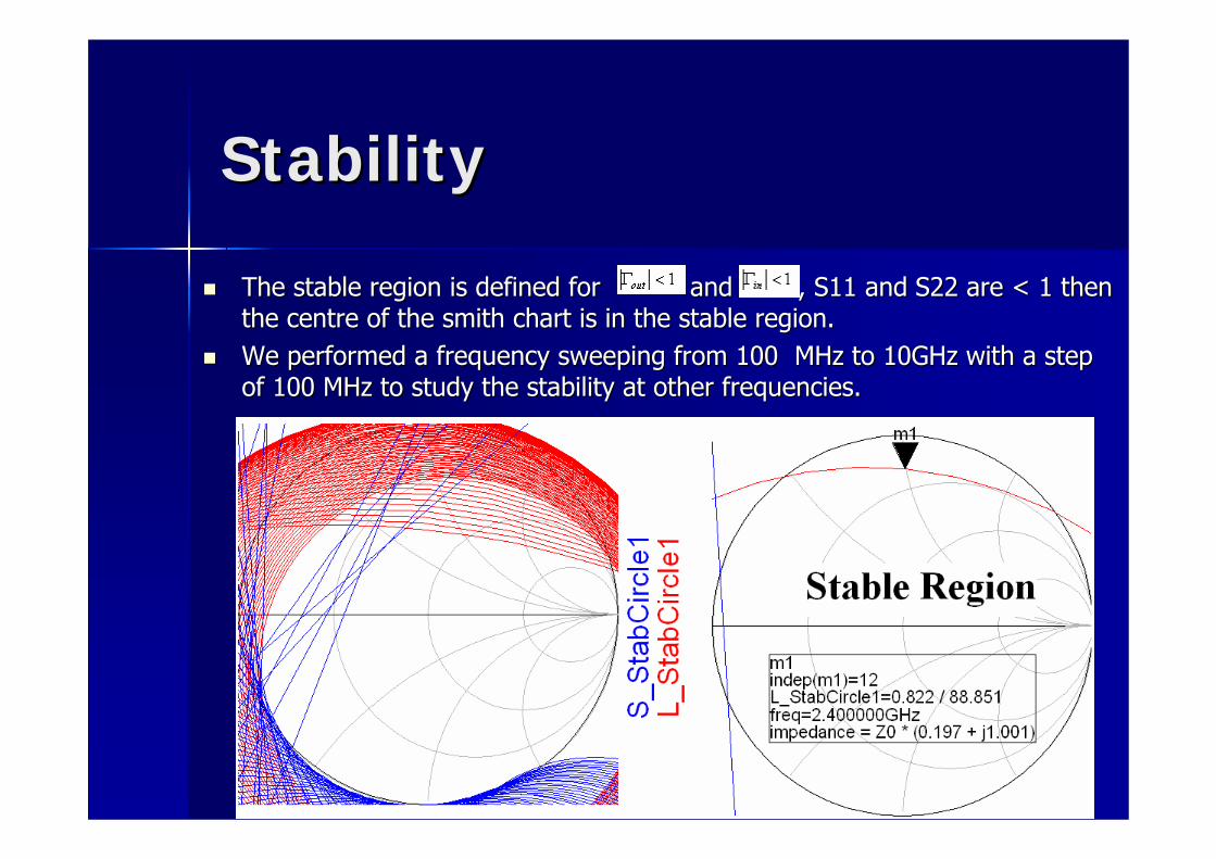
The stable region is defined for and , S11 and The stable region is defined for and , S11 and S22 are < 1 then S22 are < 1 then the centre of the smith chart is in the stable region.the centre of the smith chart is in the stable region.We performed a frequency sweeping from 100 MHz to 10GHz with a We performed a frequency sweeping from 100 MHz to 10GHz with a step step of 100 MHz to study the stability at other frequencies.of 100 MHz to study the stability at other frequencies.
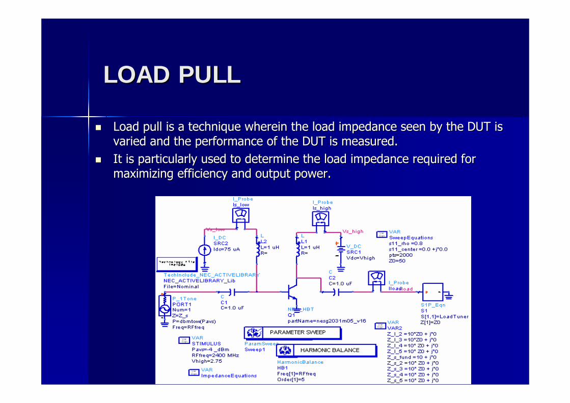
LOAD PULLLOAD PULL
Load pull is a technique wherein the load impedance seen by the Load pull is a technique wherein the load impedance seen by the DUT is DUT is varied and the performance of the DUT is measured.varied and the performance of the DUT is measured.It is particularly used to determine the load impedance requiredIt is particularly used to determine the load impedance required for for maximizing efficiency and output power.maximizing efficiency and output power.
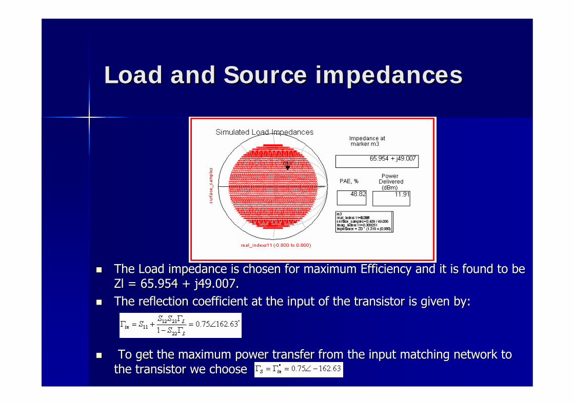
Load and Source impedancesLoad and Source impedances
The Load impedance is chosen for maximum Efficiency and it is foThe Load impedance is chosen for maximum Efficiency and it is found to be und to be Zl = 65.954 + j49.007.Zl = 65.954 + j49.007.The reflection coefficient at the input of the transistor is givThe reflection coefficient at the input of the transistor is given by:en by:
To get the maximum power transfer from the input matching netwoTo get the maximum power transfer from the input matching network to rk to the transistor we choose the transistor we choose
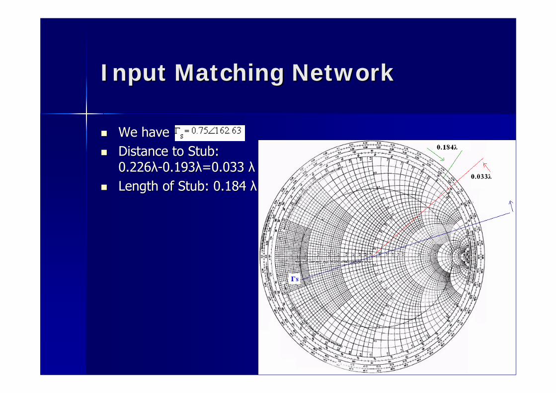
Input Matching NetworkInput Matching Network
We have We have Distance to Stub: Distance to Stub: 0.2260.226λλ--0.1930.193λλ=0.033 =0.033 λλLength of Stub: 0.184 Length of Stub: 0.184 λλ
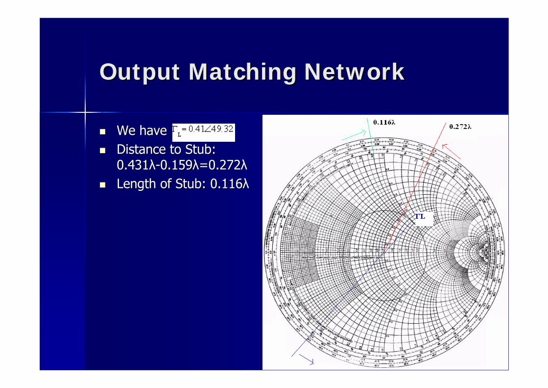
Output Matching NetworkOutput Matching Network
We haveWe haveDistance to Stub: Distance to Stub: 0.4310.431λλ--0.1590.159λλ=0.272=0.272λλLength of Stub: 0.116Length of Stub: 0.116λλ
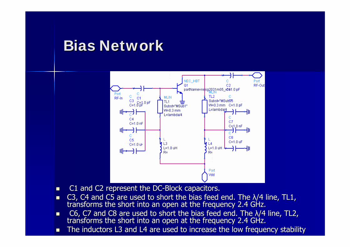
Bias NetworkBias Network
C1 and C2 represent the DCC1 and C2 represent the DC--Block capacitors.Block capacitors.C3, C4 and C5 are used to short the bias feed end. The C3, C4 and C5 are used to short the bias feed end. The λλ/4 line, TL1, /4 line, TL1, transforms the short into an open at the frequency 2.4 GHz.transforms the short into an open at the frequency 2.4 GHz.C6, C7 and C8 are used to short the bias feed end. The C6, C7 and C8 are used to short the bias feed end. The λλ/4 line, TL2, /4 line, TL2,
transforms the short into an open at the frequency 2.4 GHz.transforms the short into an open at the frequency 2.4 GHz.The inductors L3 and L4 are used to increase the low frequency sThe inductors L3 and L4 are used to increase the low frequency stabilitytability
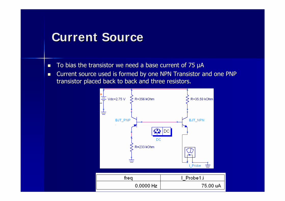
Current SourceCurrent Source
To bias the transistor we need a base current of 75 To bias the transistor we need a base current of 75 µµAACurrent source used is formed by one NPN Transistor and one PNP Current source used is formed by one NPN Transistor and one PNP transistor placed back to back and three resistors.transistor placed back to back and three resistors.
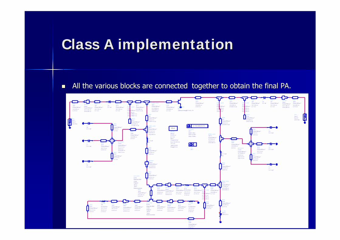
Class A implementationClass A implementation
All the various blocks are connectedAll the various blocks are connected together to obtain the final PA.together to obtain the final PA.
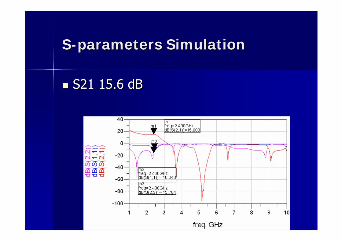
SS--parameters Simulationparameters Simulation
S21 15.6 dBS21 15.6 dB
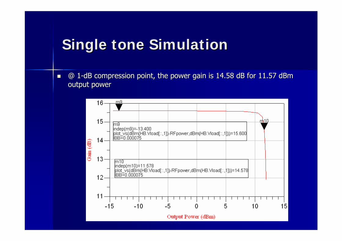
Single tone SimulationSingle tone Simulation
@ 1@ 1--dB compression point, the power gain is 14.58 dB for 11.57 dBm dB compression point, the power gain is 14.58 dB for 11.57 dBm output poweroutput power
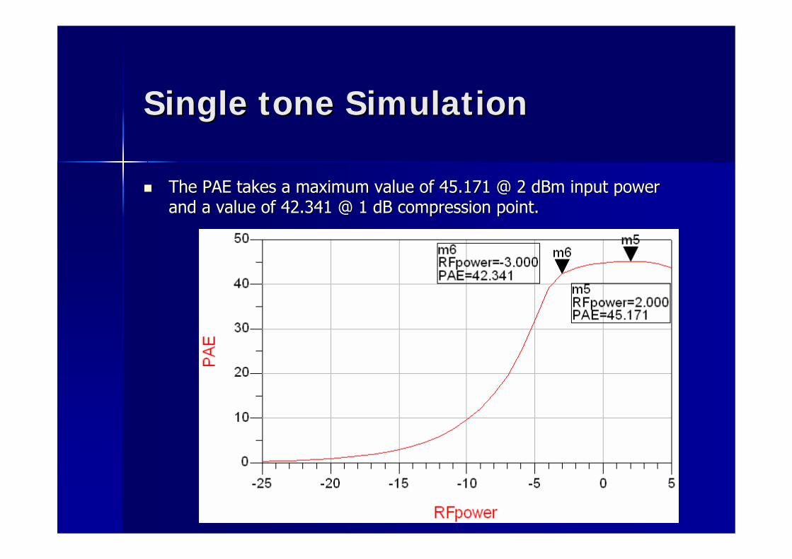
Single tone SimulationSingle tone Simulation
The PAE takes a maximum value of 45.171 @ 2 dBm input power The PAE takes a maximum value of 45.171 @ 2 dBm input power and a value of 42.341 @ 1 dB compression point.and a value of 42.341 @ 1 dB compression point.
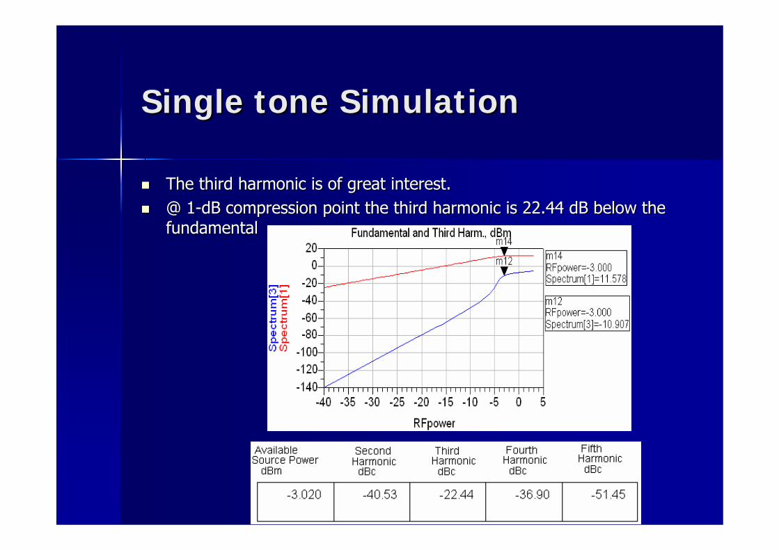
Single tone SimulationSingle tone Simulation
The third harmonic is of great interest. The third harmonic is of great interest. @ 1@ 1--dB compression point the third harmonic is 22.44 dB below the dB compression point the third harmonic is 22.44 dB below the fundamentalfundamental
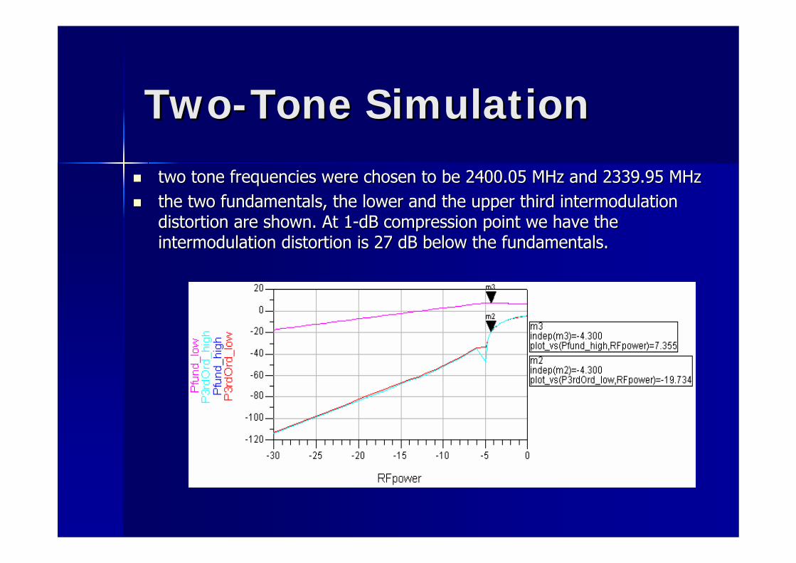
TwoTwo--Tone SimulationTone Simulationtwo tone frequencies were chosen to be 2400.05 MHz and 2339.95 Mtwo tone frequencies were chosen to be 2400.05 MHz and 2339.95 MHzHzthe two fundamentals, the lower and the upper third intermodulatthe two fundamentals, the lower and the upper third intermodulation ion distortion are shown. At 1distortion are shown. At 1--dB compression point we have the dB compression point we have the intermodulation distortion is 27 dB below the fundamentals.intermodulation distortion is 27 dB below the fundamentals.
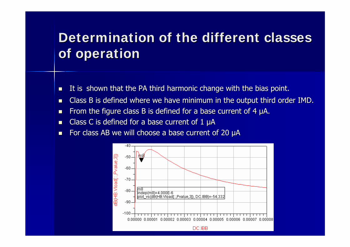
Determination of the different classes Determination of the different classes of operationof operation
It isIt is shown that the PA third harmonic change with the bias point.shown that the PA third harmonic change with the bias point.
Class B is defined where we have minimum in the output third ordClass B is defined where we have minimum in the output third order IMD.er IMD.From the figure class B is defined for a base current of 4 From the figure class B is defined for a base current of 4 µµA.A.Class C is defined for a base current of 1 Class C is defined for a base current of 1 µµAAFor class AB we will choose a base current of 20 For class AB we will choose a base current of 20 µµAA
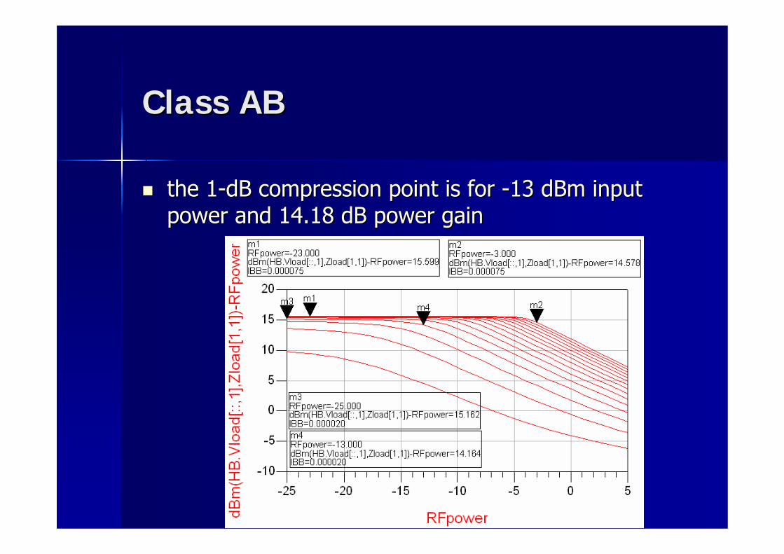
Class ABClass AB
the 1the 1--dB compression point is for dB compression point is for --13 dBm input 13 dBm input power and 14.18 dB power gain power and 14.18 dB power gain
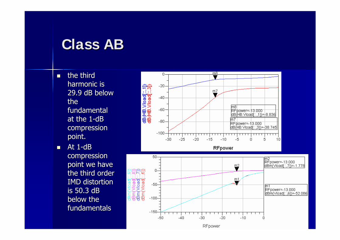
Class ABClass AB
the third the third harmonic is harmonic is 29.9 dB below 29.9 dB below the the fundamental fundamental at the 1at the 1--dB dB compression compression point.point.At 1At 1--dB dB compression compression point we have point we have the third order the third order IMD distortion IMD distortion is 50.3 dB is 50.3 dB below the below the fundamentalsfundamentals
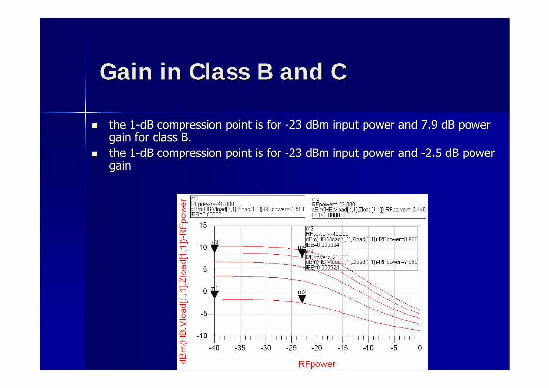
Gain in Class B and CGain in Class B and C
the 1the 1--dB compression point is for dB compression point is for --23 dBm input power and 7.9 dB power 23 dBm input power and 7.9 dB power gain for class B.gain for class B.the 1the 1--dB compression point is for dB compression point is for --23 dBm input power and 23 dBm input power and --2.5 dB power 2.5 dB power gain gain
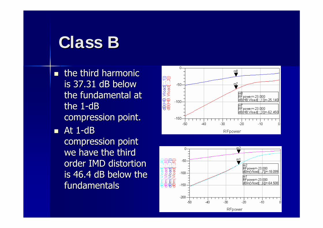
Class BClass B
the third harmonic the third harmonic is 37.31 dB below is 37.31 dB below the fundamental at the fundamental at the 1the 1--dB dB compression point.compression point.At 1At 1--dB dB compression point compression point we have the third we have the third order IMD distortion order IMD distortion is 46.4 dB below the is 46.4 dB below the fundamentalsfundamentals
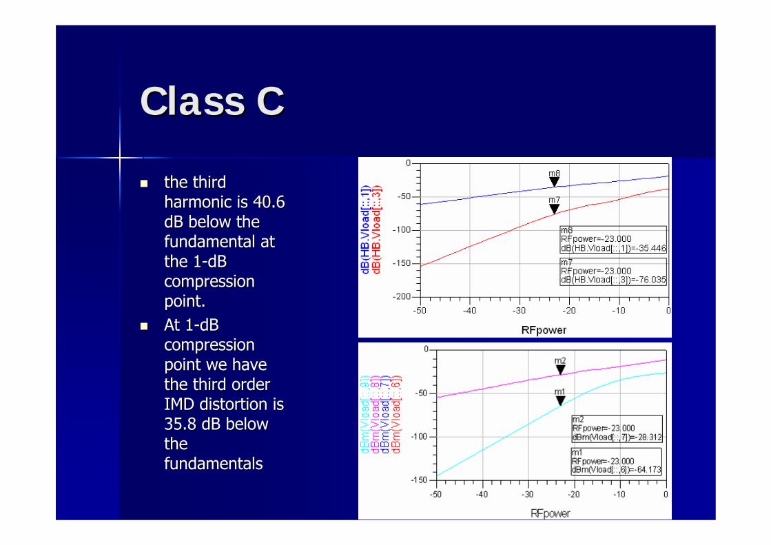
Class CClass C
the third the third harmonic is 40.6 harmonic is 40.6 dB below the dB below the fundamental at fundamental at the 1the 1--dB dB compression compression point.point.At 1At 1--dB dB compression compression point we have point we have the third order the third order IMD distortion is IMD distortion is 35.8 dB below 35.8 dB below the the fundamentalsfundamentals
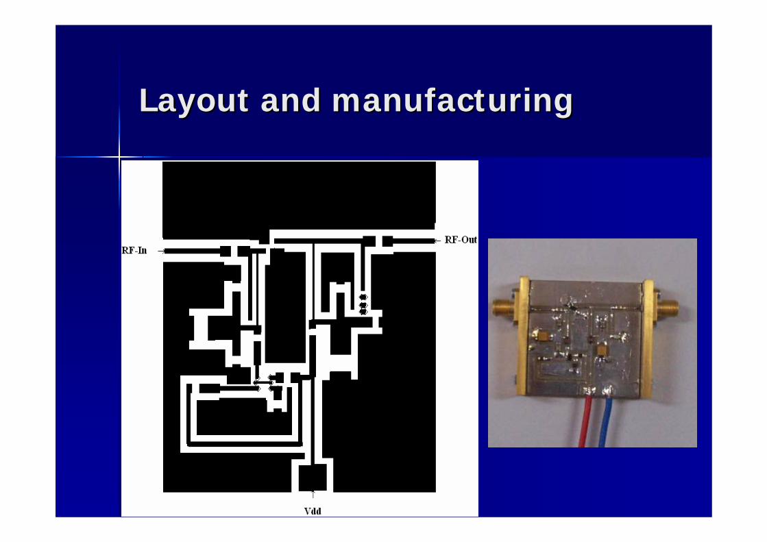
Layout and manufacturingLayout and manufacturing
Definition of Memory Effects in PADefinition of Memory Effects in PA
In Memory less systems the output signal In Memory less systems the output signal is only a function of the instantaneous is only a function of the instantaneous input signalinput signalIn systems with memory the output signal In systems with memory the output signal is a function of both instantaneous and is a function of both instantaneous and previous input signals.previous input signals.
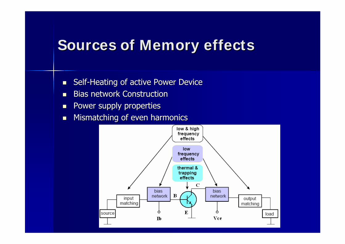
Sources of Memory effectsSources of Memory effects
SelfSelf--Heating of active Power DeviceHeating of active Power DeviceBias network ConstructionBias network ConstructionPower supply propertiesPower supply propertiesMismatching of even harmonicsMismatching of even harmonics
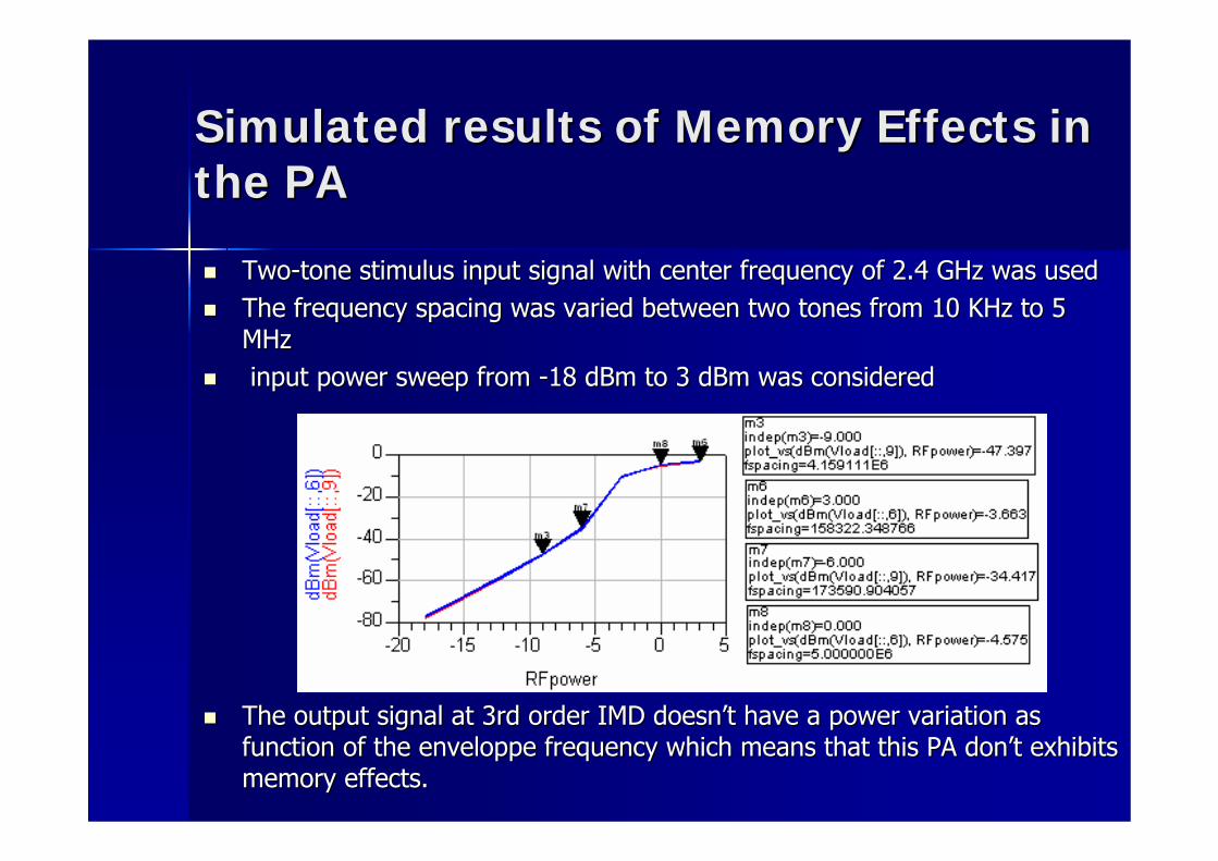
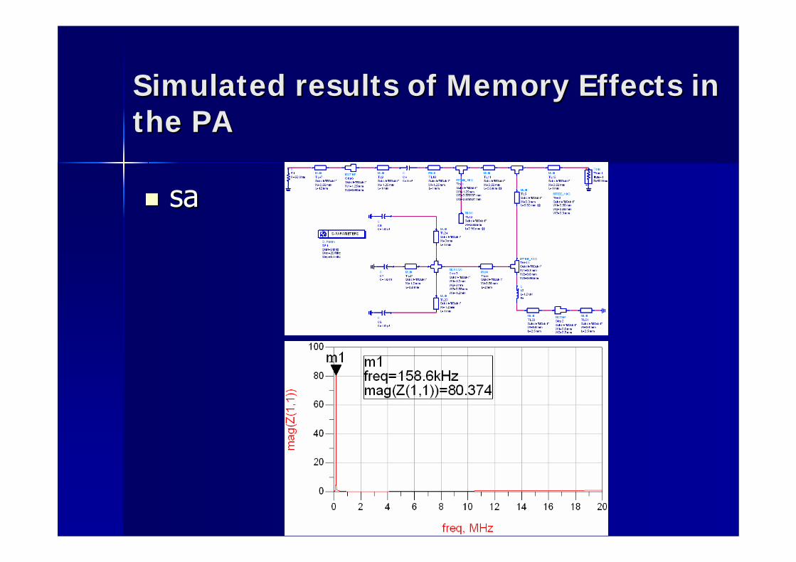
Simulated results of Memory Effects in Simulated results of Memory Effects in the PAthe PA
TwoTwo--tone stimulus input signal with center frequency of 2.4 GHz was tone stimulus input signal with center frequency of 2.4 GHz was used used The frequency spacing was varied between two tones from 10 KHz tThe frequency spacing was varied between two tones from 10 KHz to 5 o 5 MHz MHz input power sweep from input power sweep from --18 dBm to 3 dBm was considered18 dBm to 3 dBm was considered
The output signal at 3rd order IMD doesnThe output signal at 3rd order IMD doesn’’t have a power variation as t have a power variation as function of the enveloppe frequency which means that this PA donfunction of the enveloppe frequency which means that this PA don’’t exhibits t exhibits memory effects.memory effects.
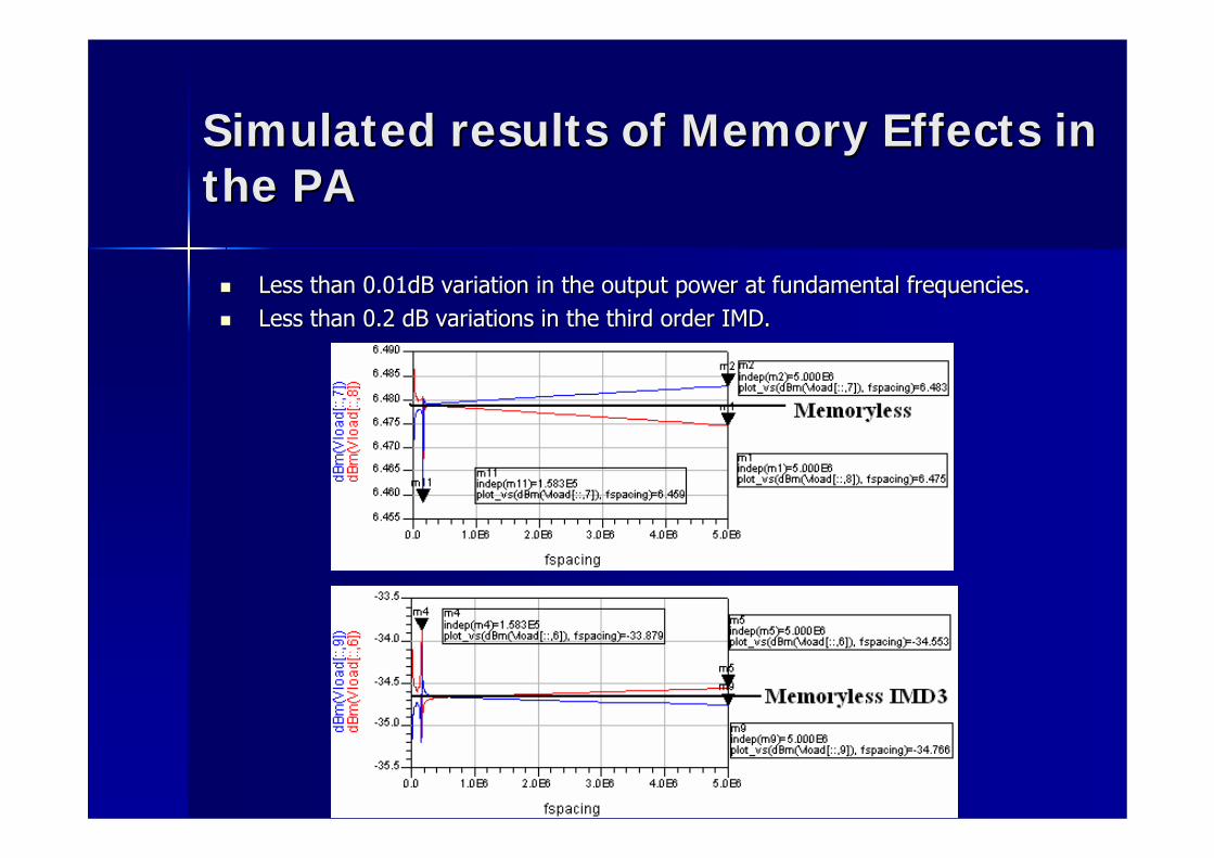
Simulated results of Memory Effects in Simulated results of Memory Effects in the PAthe PA
Less than 0.01dB variation in the output power at fundamental frLess than 0.01dB variation in the output power at fundamental frequencies.equencies.Less than 0.2 dB variations in the third order IMD.Less than 0.2 dB variations in the third order IMD.
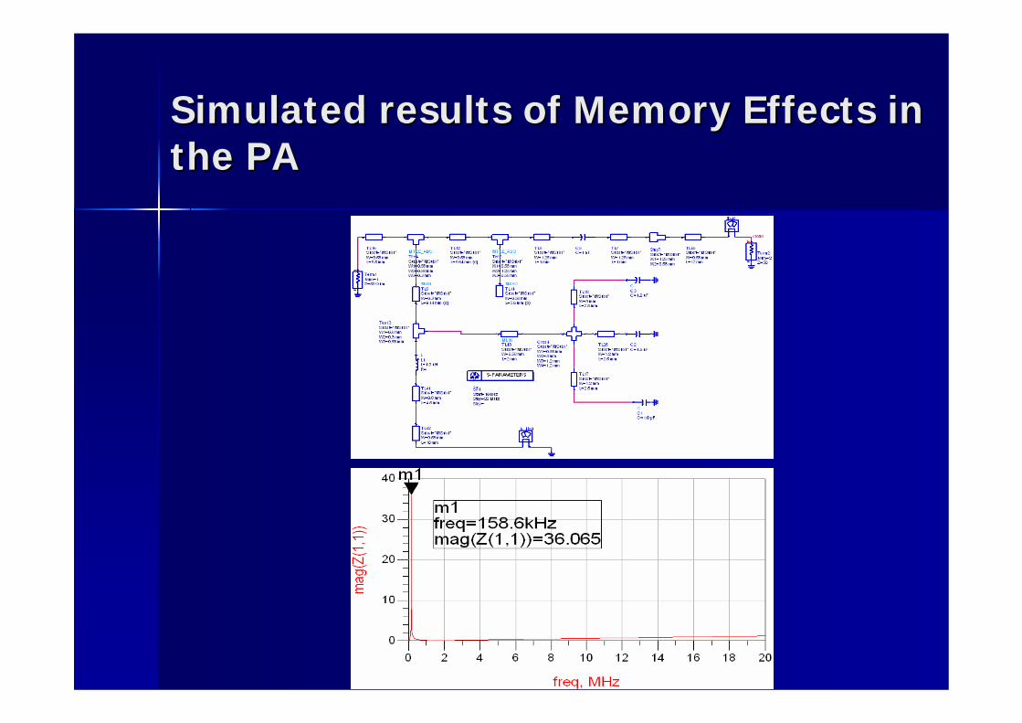
Simulated results of Memory Effects in Simulated results of Memory Effects in the PAthe PA
Simulated results of Memory Effects in Simulated results of Memory Effects in the PAthe PA
sasa
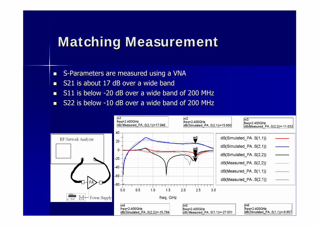
Matching MeasurementMatching Measurement
SS--Parameters are measured using a VNAParameters are measured using a VNAS21 is about 17 dB over a wide bandS21 is about 17 dB over a wide bandS11 is below S11 is below --20 dB over a wide band of 200 MHz20 dB over a wide band of 200 MHzS22 is below S22 is below --10 dB over a wide band of 200 MHz10 dB over a wide band of 200 MHz
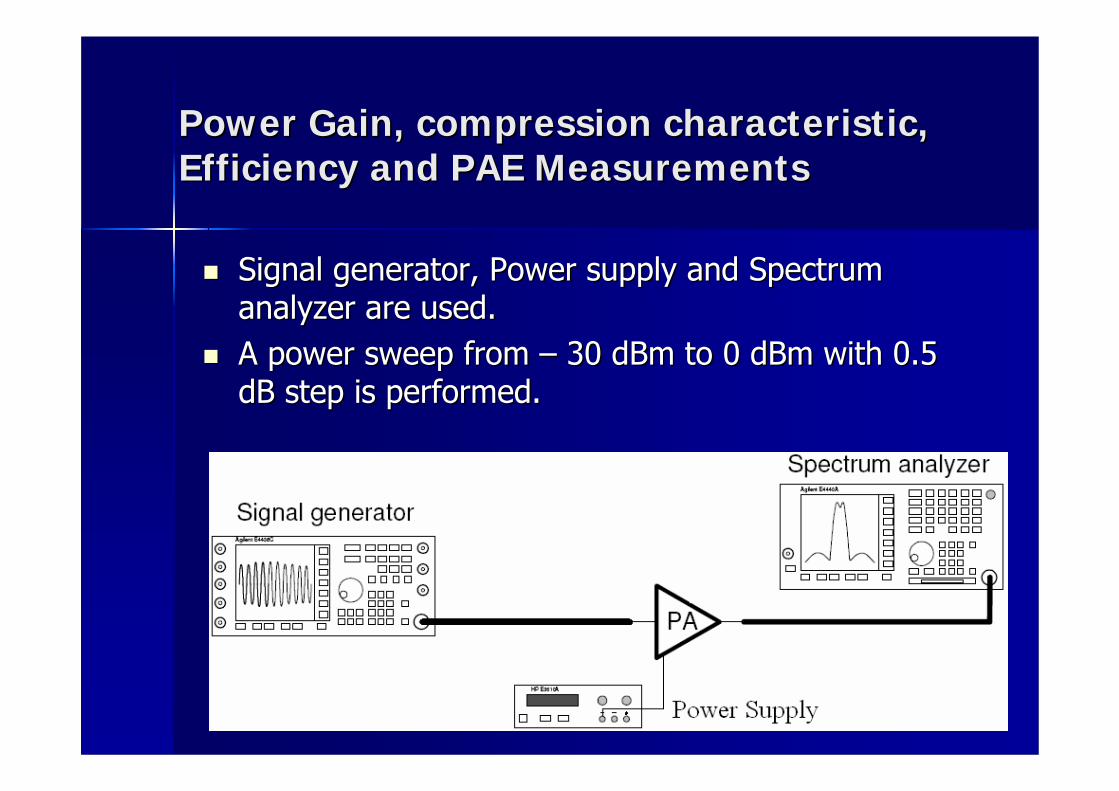
Power Gain, compression characteristic, Power Gain, compression characteristic, Efficiency and PAE MeasurementsEfficiency and PAE Measurements
Signal generator, Power supply and Spectrum Signal generator, Power supply and Spectrum analyzer are used.analyzer are used.A power sweep from A power sweep from –– 30 dBm to 0 dBm with 0.5 30 dBm to 0 dBm with 0.5 dB step is performed.dB step is performed.
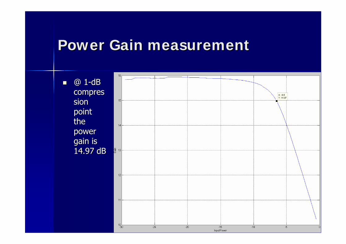
Power Gain measurementPower Gain measurement
@ 1@ 1--dB dB comprescompression sion point point the the power power gain is gain is 14.97 dB14.97 dB
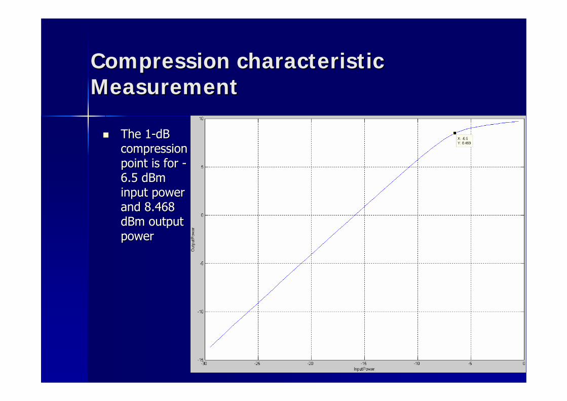
Compression characteristic Compression characteristic MeasurementMeasurement
The 1The 1--dB dB compression compression point is for point is for --6.5 dBm 6.5 dBm input power input power and 8.468 and 8.468 dBm output dBm output powerpower
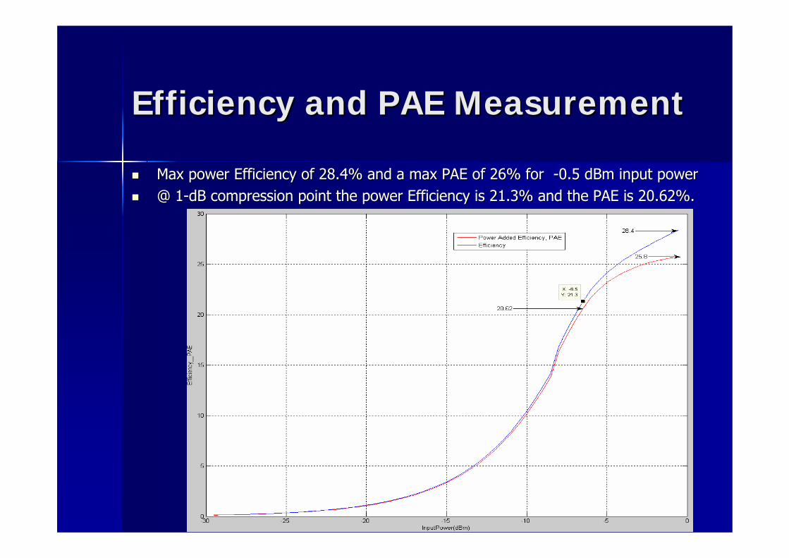
Efficiency and PAE MeasurementEfficiency and PAE Measurement
Max power Efficiency of 28.4% and a max PAE of 26% for Max power Efficiency of 28.4% and a max PAE of 26% for --0.5 dBm input power0.5 dBm input power@ 1@ 1--dB compression point the power Efficiency is 21.3% and the PAE idB compression point the power Efficiency is 21.3% and the PAE is 20.62%.s 20.62%.
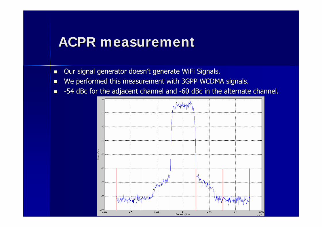
ACPR measurementACPR measurement
Our signal generator doesnOur signal generator doesn’’t generate WiFi Signals.t generate WiFi Signals.We performed this measurement with 3GPP WCDMA signals.We performed this measurement with 3GPP WCDMA signals.--54 dBc for the adjacent channel and 54 dBc for the adjacent channel and --60 dBc in the alternate channel.60 dBc in the alternate channel.
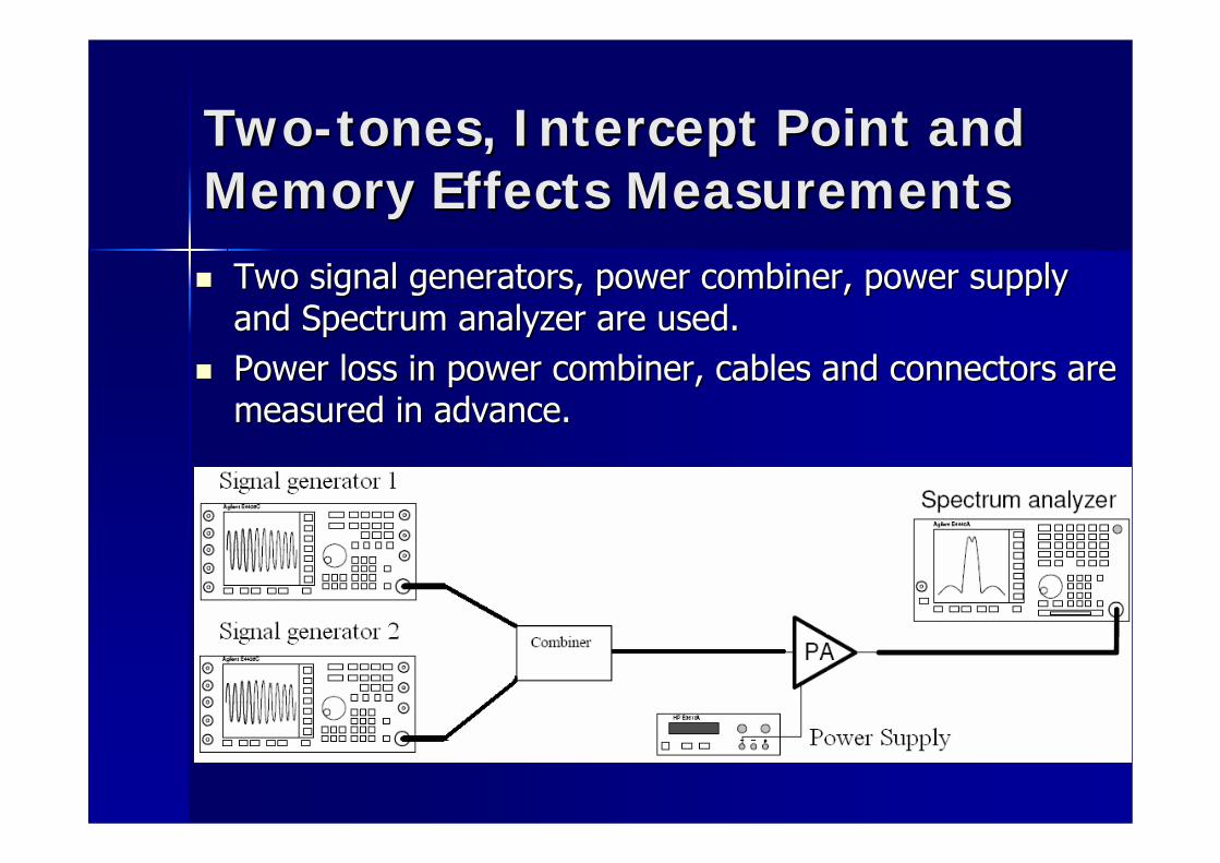
TwoTwo--tones, Intercept Point and tones, Intercept Point and Memory Effects MeasurementsMemory Effects Measurements
Two signal generators, power combiner, power supply Two signal generators, power combiner, power supply and Spectrum analyzer are used.and Spectrum analyzer are used.Power loss in power combiner, cables and connectors are Power loss in power combiner, cables and connectors are measured in advance.measured in advance.
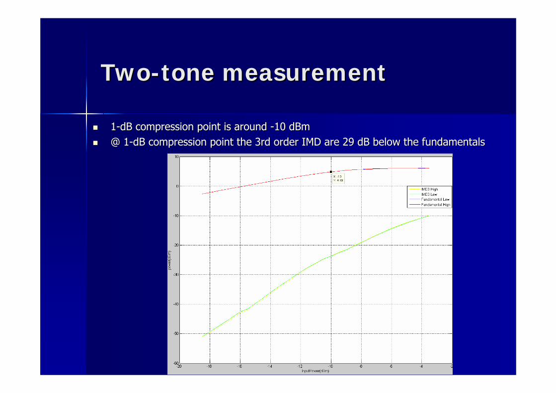
TwoTwo--tone measurementtone measurement
11--dB compression point is around dB compression point is around --10 dBm10 dBm@ 1@ 1--dB compression point the 3rd order IMD are 29 dB below the fundadB compression point the 3rd order IMD are 29 dB below the fundamentalsmentals
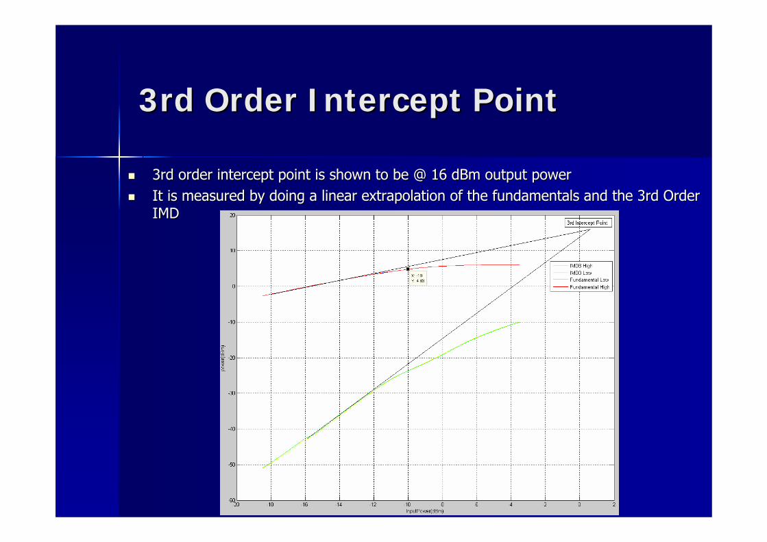
3rd Order Intercept Point3rd Order Intercept Point
3rd order intercept point is shown to be @ 16 dBm output power3rd order intercept point is shown to be @ 16 dBm output powerIt is measured by doing a linear extrapolation of the fundamentaIt is measured by doing a linear extrapolation of the fundamentals and the 3rd Order ls and the 3rd Order IMDIMD
Memory Effects MeasurementMemory Effects Measurement
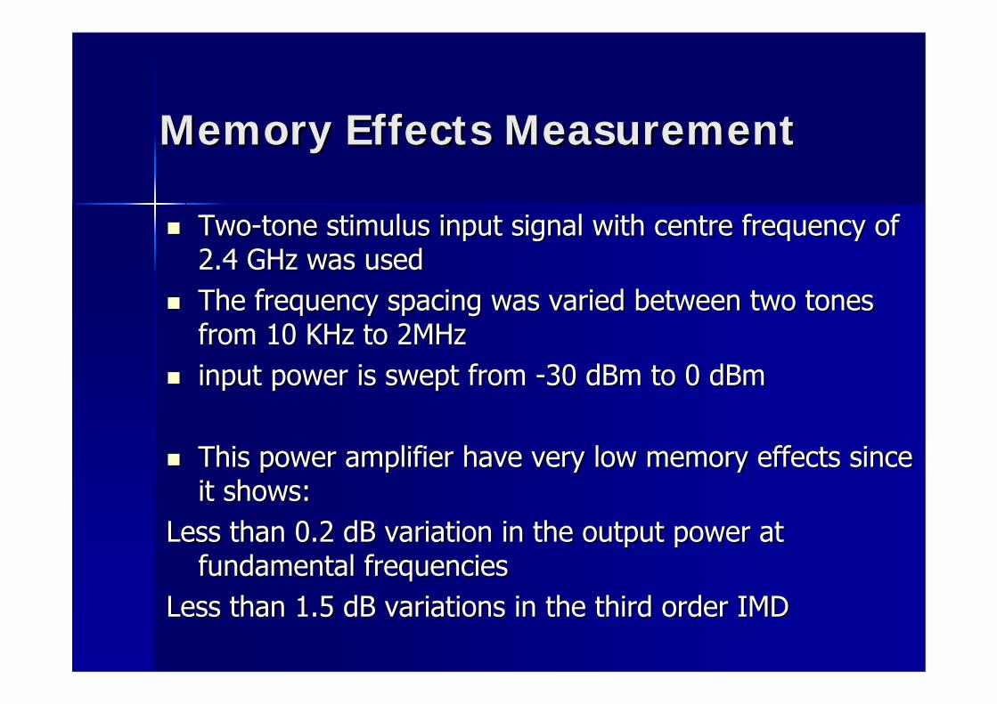
TwoTwo--tone stimulus input signal with centre frequency of tone stimulus input signal with centre frequency of 2.4 GHz was used2.4 GHz was usedThe frequency spacing was varied between two tones The frequency spacing was varied between two tones from 10 KHz to 2MHz from 10 KHz to 2MHz input power is swept from input power is swept from --30 dBm to 0 dBm30 dBm to 0 dBm
This power amplifier have very low memory effects since This power amplifier have very low memory effects since it shows:it shows:
Less than 0.2 dB variation in the output power at Less than 0.2 dB variation in the output power at fundamental frequenciesfundamental frequencies
Less than 1.5 dB variations in the third order IMDLess than 1.5 dB variations in the third order IMD
Memory Effects MeasurementMemory Effects Measurement
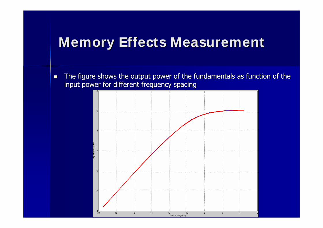
The figure shows the output power of the fundamentals as functioThe figure shows the output power of the fundamentals as function of the n of the input power for different frequency spacinginput power for different frequency spacing
Memory Effects MeasurementMemory Effects Measurement
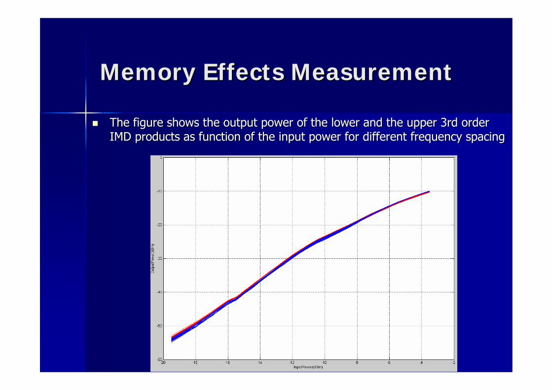
The figure shows the output power of the lower and the upper 3rdThe figure shows the output power of the lower and the upper 3rd order order IMD products as function of the input power for different frequeIMD products as function of the input power for different frequency spacingncy spacing
Memory Effects MeasurementMemory Effects Measurement
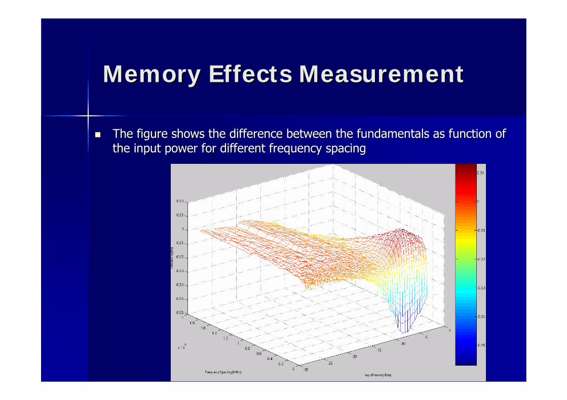
The figure shows the difference between the fundamentals as funcThe figure shows the difference between the fundamentals as function of tion of the input power for different frequency spacingthe input power for different frequency spacing
Memory Effects MeasurementMemory Effects Measurement
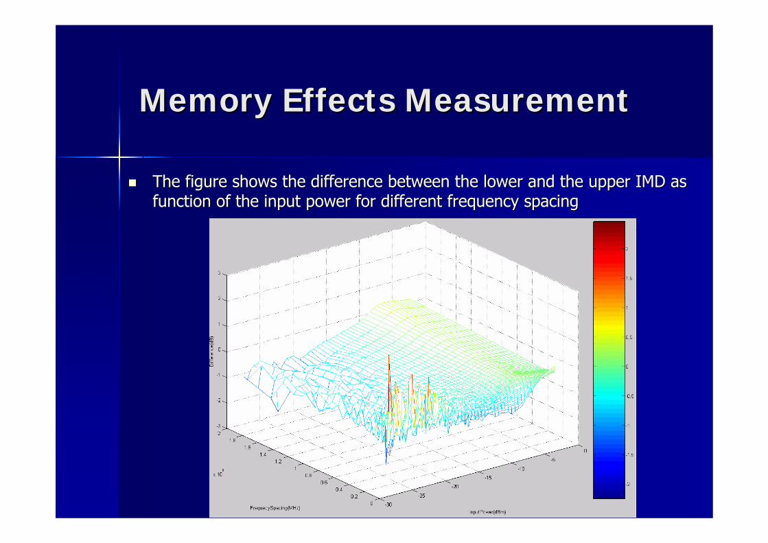
The figure shows the difference between the lower and the upper The figure shows the difference between the lower and the upper IMD as IMD as function of the input power for different frequency spacingfunction of the input power for different frequency spacing
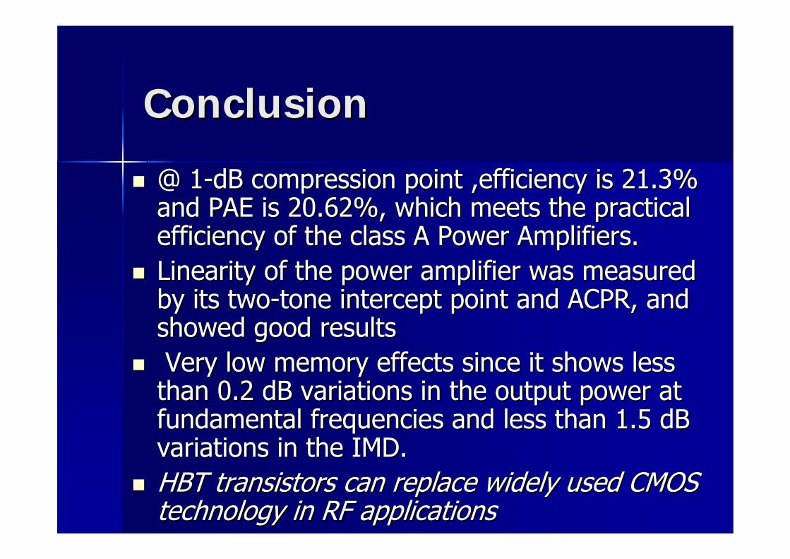
ConclusionConclusion
@@ 11--dB compression point ,efficiency is 21.3% dB compression point ,efficiency is 21.3% and PAE is 20.62%, which meets the practical and PAE is 20.62%, which meets the practical efficiency of the class A Power Amplifiers. efficiency of the class A Power Amplifiers. Linearity of the power amplifier was measured Linearity of the power amplifier was measured by its twoby its two--tone intercept point and ACPR, and tone intercept point and ACPR, and showed good resultsshowed good resultsVery low memory effects since it shows less Very low memory effects since it shows less than 0.2 dB variations in the output power at than 0.2 dB variations in the output power at fundamental frequencies and less than 1.5 dB fundamental frequencies and less than 1.5 dB variations in the IMD.variations in the IMD.HBT transistors can replace widely used CMOS HBT transistors can replace widely used CMOS technology in RF applicationstechnology in RF applications
Future WorkFuture WorkIt can be divided into two categoriesIt can be divided into two categories::
Theoretical ResearchTheoretical Researchincreasing the efficiency and the PAE more with increasing the increasing the efficiency and the PAE more with increasing the IMD performance at the same timeIMD performance at the same timego deeply in go deeply in understanding the sources of the memory effects and understanding the sources of the memory effects and try to minimize them more and moretry to minimize them more and moreoptimizing the design to get best resultsoptimizing the design to get best results
Practical areasPractical areasDesign multiple stage Power Amplifier to provide an increase in Design multiple stage Power Amplifier to provide an increase in gain for signals as well as better performance in RF applicationgain for signals as well as better performance in RF applicationss

My Supervisor and MeMy Supervisor and Me
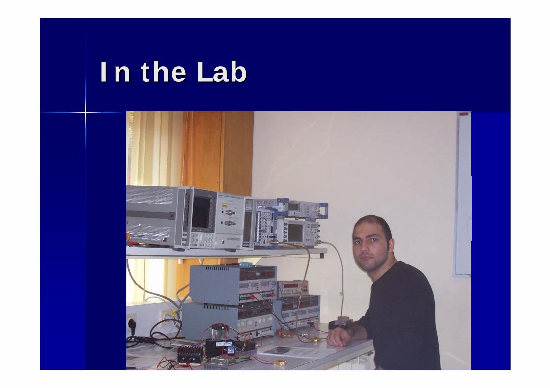
In the LabIn the Lab
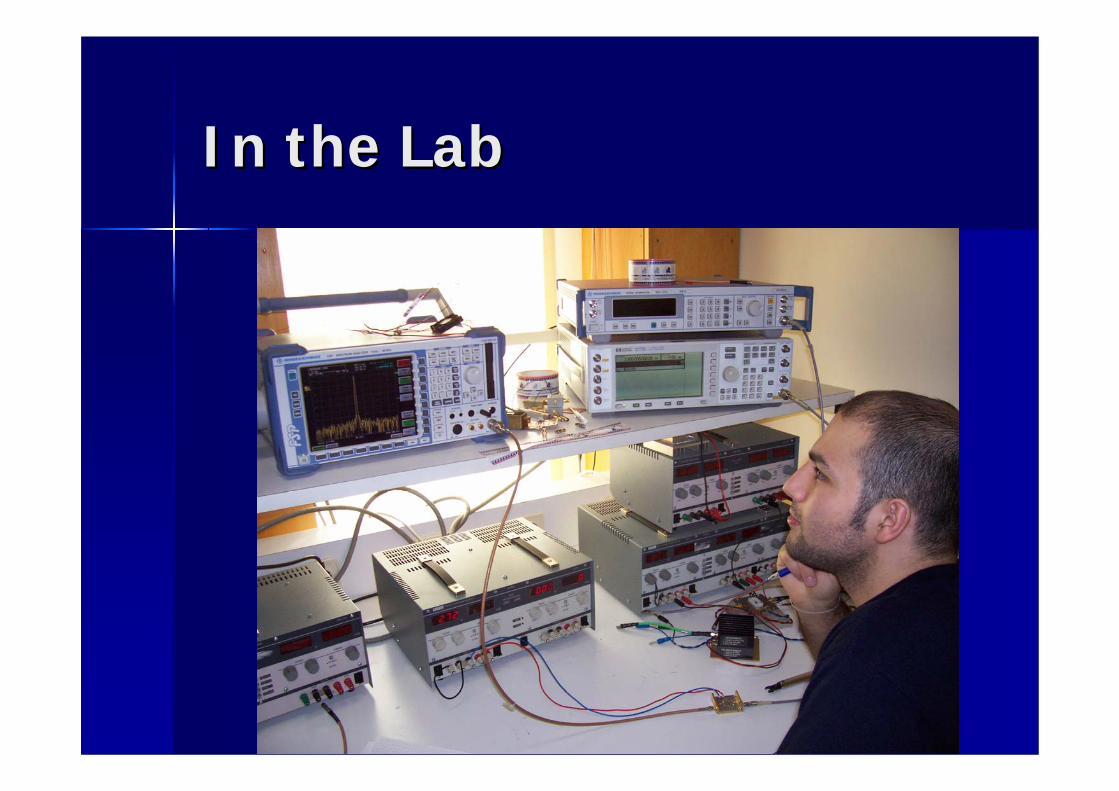
In the LabIn the Lab
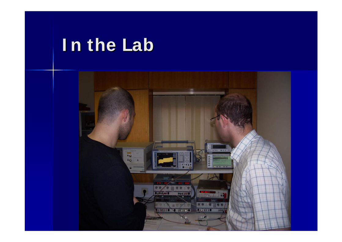
In the LabIn the Lab

Questions ?Questions ?