Embed Size (px)
Citation preview

This report applies to mask 0N50N for these products:• MPC5777M
Mask Specific InformationMajor mask revision number 0x1Minor mask revision number 0x1JTAG identifier 0x1AF0_F01DGTM Version GTM104: IP Release v1.5.5-A1
Table 1. Errata and Information Summary
Erratum ID Erratum Title
ERR010842 CMU: False upper frequency threshold alarm (FHH) signaled to Fault Collection and Control Unit(FCCU)
ERR050159 CMU: Monitoring signal for sudden loss of clock from CMU does not signal the Fault Collection andControl Unit
ERR007116 CRC: AutoSAR 4.0 8-bit CRC8 0x2F is not supported in hardware
ERR007824 DCI: Avoid asserting system reset when switching JTAG operating modes
ERR008343 DCI: EVTO[1:0] outputs remain stuck low if asserted while the system clock source is the IRC
ERR007111 DMA: DMA does not work properly with M_CAN modules
ERR007113 DMA: GTM accesses via DMA may fail
ERR010663 DS/RM: IRC trimming and LVD/HVD clarifications
ERR007351 DSMC: Lockstep-error notification is disabled
ERR050090 DSPI/SPI: Incorrect data may be transmitted in slave mode
ERR009783 DSPI: Frame transfer does not restart after DSI frame matches preprogrammed value
ERR009664 DSPI: Frame transfer does not restart in case of DSI parity error in master mode
ERR009656 DSPI: Frame transfer does not restart in case of SPI parity error in master mode
ERR007115 DSPI: Mixing 16 and 32 bits frame size in XSPI Mode can cause incorrect data to be transmitted
ERR007352 DSPI: reserved bits in slave CTAR are writable
ERR007299 DSPI: SOUT pins are not automatically configured as SOUT when Slave Select is asserted in SlaveMode
ERR010542 DSPI: Transmit, Command, and Receive FIFO fill flags in status register is not cleared when DMA isimproperly configured
Table continues on the next page...
NXP Semiconductors MPC5777M_0N50N
Mask Set Errata Rev. December 2019
Mask Set Errata for Mask 0N50N

Table 1. Errata and Information Summary (continued)
Erratum ID Erratum Title
ERR008547 e200z425: Additional cycles required for Load/Store accesses to guarded/precise space
ERR010385 e200z4: Incorrect branch displacement at 16K memory boundaries
ERR007210 e200z710: Nexus timestamps are not available
ERR007259 e200zx: ICNT and branch history information may be incorrect following a nexus overflow
ERR007305 e200zx: JTAG reads of the Performance Monitor Counter registers are not reliable
ERR007408 EBI: Minimum input setup time is 7 ns
ERR006967 eDMA: Possible misbehavior of a preempted channel when using continuous link mode
ERR010452 eDMA: When master ID replication is enabled, the stored ID and privilege level will change if read byanother master.
ERR007337 FCCU: Address feedback error disabled for the Safety Core local RAMS and Cache
ERR008034 FCCU: Channel 40 fault (COMP_XBIC_DSMC_Monitor) may be reported if a CPU is reset upon aMC_ME mode change
ERR008229 FCCU: Enabling the programmable glitch filter on EIN may cause a destructive reset
ERR008042 FCCU: EOUT signals are active, even when error out signaling is disabled
ERR007099 FCCU: Error pin signal length is not extended when the next enabled fault, with its alarm timeoutdisabled, occurs
ERR010900 FCCU: False indication of a fault state for a single safe clock period can be generated on the erroroutput pin
ERR007223 FCCU: FCCU_IRQ_EN register is writeable in all operating modes
ERR007869 FCCU: FOSU monitoring of a fault is blocked for second or later occurrence of the same fault
ERR009584 FCCU: MPC57xxM – FOSU may assert destructive reset when a hardware recoverable fault of widthless than one safe clock period occurs
ERR007226 FCCU: the error-out signalling cannot be disabled in non Bi-stable protocols
ERR007325 FCCU: Unsuccessful decorated storage access may cause erroneous signaling of FCCU Channel 40
ERR007638 FCCU: Unsuccessful decorated storage access may cause erroneous signaling of FCCU ChannelNCF[39]
ERR008647 FLASH: (SPC57xxM) Address Encode False Report (MCR[AEE] and possible FCCU channels)
ERR008004 FLASH: Array Integrity with Breakpoints enabled may skip addresses for certain RWSC and APCcombinations
ERR007991 FLASH: Rapid Program or Erase Suspend fail status
ERR050119 FlexRay: Disabling of FlexRay Message Buffer during the STARTUP Protocol State takes longer thanexpected three Slots
ERR008770 FlexRAY: Missing TX frames on Channel B when in dual channel mode and Channel A is disabled
ERR010647 GTM: (A)TOM asynchronous update in SOMP mode not functional with CM1=0 and selected CMUclock is not equal to the system clock
ERR010646 GTM: (A)TOM output signal postponed by one period for the values CM0=1 and CM1>CM0 if CN0is reset by the trigger of a preceding channel
ERR008122 GTM: (A)TOM’s CCU1 event interrupt is not generated when CM1=0 or 1 and RST_CCU0=1
ERR006639 GTM: A compare match event does not clear WR_REQ when ATOM is in SOMC mode
ERR007085 GTM: A TIM timeout occurs when the TDU is re-enabled
ERR007528 GTM: Action not always calculated immediately by DPLL
ERR007084 GTM: An active edge input, that is rejected by the DPLL trigger plausibility check, does not assert aMissing Trigger Interrupt
Table continues on the next page...
Mask Set Errata for Mask 0N50N, Rev. December 2019
2 NXP Semiconductors
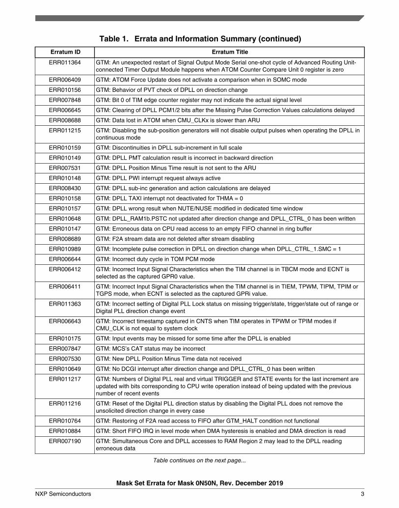
Table 1. Errata and Information Summary (continued)
Erratum ID Erratum Title
ERR011364 GTM: An unexpected restart of Signal Output Mode Serial one-shot cycle of Advanced Routing Unit-connected Timer Output Module happens when ATOM Counter Compare Unit 0 register is zero
ERR006409 GTM: ATOM Force Update does not activate a comparison when in SOMC mode
ERR010156 GTM: Behavior of PVT check of DPLL on direction change
ERR007848 GTM: Bit 0 of TIM edge counter register may not indicate the actual signal level
ERR006645 GTM: Clearing of DPLL PCM1/2 bits after the Missing Pulse Correction Values calculations delayed
ERR008688 GTM: Data lost in ATOM when CMU_CLKx is slower than ARU
ERR011215 GTM: Disabling the sub-position generators will not disable output pulses when operating the DPLL incontinuous mode
ERR010159 GTM: Discontinuities in DPLL sub-increment in full scale
ERR010149 GTM: DPLL PMT calculation result is incorrect in backward direction
ERR007531 GTM: DPLL Position Minus Time result is not sent to the ARU
ERR010148 GTM: DPLL PWI interrupt request always active
ERR008430 GTM: DPLL sub-inc generation and action calculations are delayed
ERR010158 GTM: DPLL TAXI interrupt not deactivated for THMA = 0
ERR010157 GTM: DPLL wrong result when NUTE/NUSE modified in dedicated time window
ERR010648 GTM: DPLL_RAM1b.PSTC not updated after direction change and DPLL_CTRL_0 has been written
ERR010147 GTM: Erroneous data on CPU read access to an empty FIFO channel in ring buffer
ERR008689 GTM: F2A stream data are not deleted after stream disabling
ERR010989 GTM: Incomplete pulse correction in DPLL on direction change when DPLL_CTRL_1.SMC = 1
ERR006644 GTM: Incorrect duty cycle in TOM PCM mode
ERR006412 GTM: Incorrect Input Signal Characteristics when the TIM channel is in TBCM mode and ECNT isselected as the captured GPR0 value.
ERR006411 GTM: Incorrect Input Signal Characteristics when the TIM channel is in TIEM, TPWM, TIPM, TPIM orTGPS mode, when ECNT is selected as the captured GPRi value.
ERR011363 GTM: Incorrect setting of Digital PLL Lock status on missing trigger/state, trigger/state out of range orDigital PLL direction change event
ERR006643 GTM: Incorrect timestamp captured in CNTS when TIM operates in TPWM or TPIM modes ifCMU_CLK is not equal to system clock
ERR010175 GTM: Input events may be missed for some time after the DPLL is enabled
ERR007847 GTM: MCS’s CAT status may be incorrect
ERR007530 GTM: New DPLL Position Minus Time data not received
ERR010649 GTM: No DCGI interrupt after direction change and DPLL_CTRL_0 has been written
ERR011217 GTM: Numbers of Digital PLL real and virtual TRIGGER and STATE events for the last increment areupdated with bits corresponding to CPU write operation instead of being updated with the previousnumber of recent events
ERR011216 GTM: Reset of the Digital PLL direction status by disabling the Digital PLL does not remove theunsolicited direction change in every case
ERR010764 GTM: Restoring of F2A read access to FIFO after GTM_HALT condition not functional
ERR010884 GTM: Short FIFO IRQ in level mode when DMA hysteresis is enabled and DMA direction is read
ERR007190 GTM: Simultaneous Core and DPLL accesses to RAM Region 2 may lead to the DPLL readingerroneous data
Table continues on the next page...
Mask Set Errata for Mask 0N50N, Rev. December 2019
NXP Semiconductors 3

Table 1. Errata and Information Summary (continued)
Erratum ID Erratum Title
ERR007087 GTM: The DPLL’s Address Pointer Extension value is added to the Address Pointer when the AddressPointer Status bit is 0
ERR007191 GTM: The DPLL’s SORI and TORI interrupts are not asserted
ERR007083 GTM: The DPLL’s SORI, TORI, MTI, and MSI interrupts may not be asserted
ERR010176 GTM: The DPLL_STATUS[BWD1/2] flags are not reset when DPLL is disabled and enabled again
ERR006642 GTM: THVAL not available immediately after inactive trigger in DPLL
ERR007529 GTM: TIM overflow bit is not set and the signal level bit has inverse value when sent to ARU in somecases
ERR007086 GTM: TIM PWM and PIM modes may capture the wrong timestamp
ERR008439 GTM: TOM and ATOM CM0, CM1 and CLK_SRC register updates may not be triggered
ERR011191 GTM: TRIGGER signal will not cause direction change of the Digital PLL when TRIGGER holdminimum value is zero
ERR008429 GTM: Unexpected TIM CNTS register reset in TPWM OSM mode
ERR006640 GTM: Valid edge after Timeout event ignored by TIM
ERR007088 GTM: When ATOM is in SOMP mode the SR0/SR1 registers could be updated twice in one PWMperiod
ERR006410 GTM: Write to ATOM_CH_CTRL sets WRF if CCU0 compare match has already occurred, but CCU1compare match is pending, in ATOM SOMC mode
ERR008438 GTM: Wrong signal level when TIM mode is changed from TBCM to any other mode
ERR008047 HSM: Nexus class 3 read/write accesses may be blocked by SMPU
ERR008951 I2C: Attempting a start cycle while the bus is busy may generate a short clock pulse
ERR007109 I2C: In master receive mode, data remains latched in I2C data I/O register (IBDR) until new data isreceived
ERR007433 JTAGM: Nexus error bit is cleared by successful RWA
ERR008935 JTAGM: write accesses to registers must be 32-bit wide
ERR007398 LBIST: Partitions 2, 4, and 5 during offline self-test mode not functional
ERR007274 LINFlexD: Consecutive headers received by LIN Slave triggers the LIN FSM to an unexpected state
ERR008731 LINFlexD: Corruption of Received Rx data in UART mode
ERR008561 LINFlexD: Corruption of Tx data in LIN mode with DMA feature enabled
ERR007269 LINFlexD: Erroneous timeout interrupt could be generated by LIN in master mode
ERR007228 LINFlexD: Erroneous transmission in LIN master mode for payload greater than eight bytes
ERR008933 LINFlexD: Inconsistent sync field may cause an incorrect baud rate and the Sync Field Error Flag maynot be set
ERR008526 LINFlexD: LIN or UART state may be incorrectly indicated by LINSR[LINS] bitfield
ERR008573 LINFlexD: Pre-mature header/response timeout in LIN mode
ERR007297 LINFlexD: Response timeout values is loaded in LINOCR[OC2] field instead of LINOCR[OC1]
ERR008970 LINFlexD: Spurious bit error in extended frame mode may cause an incorrect Idle State
ERR007589 LINFlexD: Spurious timeout error when switching from UART to LIN mode or when resettingLINTCSR[MODE] bit in LIN mode
ERR008602 LINFlexD: Tx through DMA can be re-triggered after abort in LIN/UART modes or can prematurely endon the event of bit error with LINCR2[IOBE] bit being set in LIN mode
ERR006350 LINFlexD: WLS feature cannot be used in buffered mode
Table continues on the next page...
Mask Set Errata for Mask 0N50N, Rev. December 2019
4 NXP Semiconductors

Table 1. Errata and Information Summary (continued)
Erratum ID Erratum Title
ERR010557 MC_CGM: Auxiliary clock divider may get stuck if programmed to divide by 2 and a reset occursduring operation
ERR010555 MC_CGM: Auxiliary Clock Divider Update Status register bits not documented
ERR007103 MC_CGM: Incorrect cause for the latest clock source switch may be reported by the CGM if a safemode request arrives when the system clock is the IRC
ERR010668 MC_CGM: Progressive Clock Switching (PCS) equations
ERR010559 MC_CGM: The device can become stuck in reset when reset occurs during a system clock switch to aPLL
ERR007211 MC_ME: Core register IAC8 is cleared during a mode change when the core is reset
ERR007911 MC_ME: Decorated accesses not supported to core local memories during reset
ERR003878 MC_ME: Flash low-power modes cannot be activated during MC_ME mode transitions.
ERR008117 MC_ME: Restrictions on enabling FlexRay in low power modes
ERR008145 MEMU: address registers in the uncorrectable error reporting tables can be written when thecorresponding valid bit is not asserted
ERR007335 MEMU: ECC errors may be double reported when initiated by the Safety core to local memory of othercores
ERR010613 MEMU: False IMEM RAM fault flag set after reset or core enabling
ERR007126 MEMU: Instead of Byte 1 of MEMU CTRL Register, Byte 3 is currently protected
ERR008885 MEMU: System RAM ECC errors on accesses by some masters report to MEMU Peripheral RAMtable
ERR007538 M_(TT)CAN: Switch between CAN operating modes during transmission or reception may be ignored
ERR007498 M_(TT)CAN: Transmitted bit in control field is falsified when using extreme bit time configurations
ERR007840 M_CAN: Change of operation mode during start of transmission
ERR009413 M_CAN: Data loss when the storage of a received frame is not complete before EOF
ERR007842 M_CAN: Erroneous Interrupt flag after setting / resetting INIT during frame reception
ERR009070 M_CAN: FD frame abort may cause Protocol exception event and extended Bus Integration state
ERR008923 M_CAN: FD frame format not compliant to the new ISO/CD 11898-1: 2014-12-11
ERR008062 M_CAN: Frame transmission in DAR mode
ERR008904 M_CAN: Incorrect activation of MRAF interrupt
ERR007841 M_CAN: Incorrect frame transmission after recovery from Restricted Operation Mode
ERR009415 M_CAN: Message RAM / RAM arbiter may not respond in time
ERR007796 M_CAN: Message reception and transmission directly after detection of Protocol Exception Event
ERR011470 M_CAN: Message transmitted with wrong arbitration and control fields
ERR050016 M_CAN: Retransmission in DAR mode due to lost arbitration at the first two identifier bits
ERR008655 M_CAN: Setting the Configuration Change Enable (CCE) bit during a transmission scan can halt CANtranmissions
ERR011458 M_CAN: Tx FIFO message sequence inversion
ERR011459 M_CAN: Unexpected High Priority Message (HPM) interrupt
ERR007532 M_TTCAN: Incorrect value of Reference Trigger Offset status for time slaves
ERR007932 NAR/SIPI: Part ID for NAR and Debug SIPI does not match the MIDR MINOR_MASK
ERR003970 NAR: Trace messages include a 6-bit Source Identification field instead of 4-bits
Table continues on the next page...
Mask Set Errata for Mask 0N50N, Rev. December 2019
NXP Semiconductors 5

Table 1. Errata and Information Summary (continued)
Erratum ID Erratum Title
ERR011021 NAR: Trace to memory buffer pointers corrupted after break-point
ERR009796 PAD_RING: Increased coupling current during current injection of nearby analog pin
ERR007930 PAD_RING: Pin PM[11] is powered from the FlexRAY and Ethernet I/O power supply instead of theMain I/O supply
ERR010309 PASS: JTAG password does not enable Debug Interface Access during functional reset
ERR010196 PASS: JTAG password match bypasses flash read protection set by PASS.LOCK3[RLx] bits
ERR007904 PASS: Programming Group Lock bit (PGL) can be de-asserted by multiple masters writing the correctpassword sections to the CINn registers.
ERR007905 PIT: Accessing the PIT by peripheral interface may fail immediately after enabling the PIT peripheralclock
ERR008054 PIT: DMA request stays asserted when initiated by PIT trigger, until PIT is reset
ERR050130 PIT: Temporary incorrect value reported in LMTR64H register in lifetimer mode
ERR007772 PMC: a SWT_2 destructive reset may be forced if the 5V supply is over voltage for longer than 16ms
ERR008019 PMC: Escalation of LVD and HVD functional resets should be expected
ERR010660 PMC: EPR flags may be set after an exit from reset
ERR007365 PRAM: Reset may change RAM content
ERR008141 PSI5-S: Global mode transition interrupt does not work
ERR008075 PSI5-S: Unrecoverable messages are not flagged in the mailbox status register channel 0
ERR007996 PSI5: Incorrect SMC message decoding and timestamp generation in case of late last sensormessage overlapping with next SYNC period pulse
ERR006992 PSI5: IS_DEBUG_FREEZE bit is not documented
ERR007234 PSI5: No transfer error generated for accesses within the unused range of the PSI5 peripheral window
ERR007134 RCCU: If any accesses to the I-MEM or D-MEM of the safety and checker core are performed whilethe cores are disabled, the cores will get out of lockstep when enabled
ERR010556 RGM: ESR0 long functional reset advances to the PHASE1[DEST] reset state, but sets the functionalreset only flag
ERR009764 SARADC : DMA interface limitation depending on PBRIDGE/SARADC clock ratio
ERR010171 SARADC: Channel number may show incorrect value for two clock cycles
ERR005947 SARADC: ADC may miss a GTM trigger pulse if width of pulse is less than 1 AD Clk cycle
ERR007245 SARADC: CDATA fields for Left justified data is not documented
ERR007246 SARADC: First conversion after exit from stop mode may be corrupted
ERR010428 SARADC: Interrupted conversions are aborted, but may not be properly restored
ERR007222 SARADC: Minimum value of precharge must be greater than or equal to 2 ADC clock cycles
ERR007138 SARADC: Missed conversion after ABORT of the last channel of an injected chain
ERR006197 SARADC: Positive DNL marginal at Cold
ERR007906 SARADC: The Data Overwritten flag bits in the SARADC may not be valid
ERR008126 SARADC_B: Some test channels are no longer available
ERR007362 SDADC: Additional DMA request generated after single read access
ERR010376 SDADC: Additional DMA request generated with slow SDADC SD_CLK clock
ERR008039 SDADC: digital filter and FIFO not disabled when MCR[EN] is cleared
Table continues on the next page...
Mask Set Errata for Mask 0N50N, Rev. December 2019
6 NXP Semiconductors

Table 1. Errata and Information Summary (continued)
Erratum ID Erratum Title
ERR008314 SDADC: Double trigger is generated for conversion when SW trigger is connected to SDADC own HWtrigger input
ERR008225 SDADC: FIFO Flush Reset command requires clearing the Data FIFO Full Flag
ERR010378 SDADC: Incorrect data provided when FIFO is disabled and FIFO overwrite is enabled
ERR006906 SDADC: Invalid conversion data when output settling delay value is less than 23
ERR008631 SDADC: low threshold watchdog cannot be used with signed data
ERR005749 SDADC: New conversion data is discarded if the overflow (DFORF) status bit is set
ERR007356 SDADC: The SDADC FIFO does not function correctly when FIFO overwrite option is used
ERR007185 SDADC: Watchdog Crossover event missed if PBRIDGEx_CLK less than SD_CLK
ERR007204 SENT: Number of Expected Edges Error status flag spuriously set when operating with Option 1 of theSuccessive Calibration Check method
ERR008082 SENT: A message overflow can lead to a loss of frames combined with NUM_EDGES_ERR being set
ERR007203 SENT: In debug mode SENT message data registers appear to lose contents
ERR007425 SENT: Unexpected NUM_EDGES_ERR error in certain conditions when message has a pause pulse
ERR010561 SIPI: Incorrect SIPI_ERR[TOEx] register bit description
ERR007788 SIUL2: A transfer error is not generated for 8-bit accesses to non-existent MSCRs
ERR009780 SIUL2: Open-drain or open-source configured outputs may briefly drive high or low during transitions
ERR007791 SIUL2: Transfer error not generated if reserved addresses within the range of SIUL BASE + 0x100 to0x23F are accessed
ERR008605 SMPU: debug SIPI accesses may be blocked by SMPU
ERR007781 SPC5777M: Current injection causes leakage path across the DSPI and LFAST LVDS pins
ERR009658 SPI: Inconsistent loading of shift register data into the receive FIFO following an overflow event
ERR006850 SSCM: Nexus enable required for mode changes when a debugger is attached
ERR007424 SSCM: The SSCM_STATUS register only contains two NXEN status bits
ERR007339 STCU2: STCU2 fault injected by FCCU is self clearing
ERR010560 STCU: ESR0 resets may not properly abort online self-tests
ERR010667 STCU: LBIST PRPG start value is 32 bits
ERR010607 STCU: STCU watchdog timer timeouts due to low voltage supply excursions
ERR009322 TDM: Erase of TDR flash block may be blocked by the TDM
ERR007948 TDM: Erase protection not enabled by reset
ERR008412 TSENSE: Temperature sensor status flags are incorrect
ERR007801 WKPU: functional NMI filter enable trigger FCCU fault monitor channel #47
ERR008738 XBAR: Masters on peripheral shell bus concentrator may stall or fetch data incorrectly
ERR006994 XBIC: XBIC may trigger false FCCU alarm
ERR008310 XBIC: Crossbar Integrity Checker may miss recording information from an initial fault event in the caseof back-to-back faults
ERR008730 XBIC: XBIC may store incorrect fault information when a fault occurs
ERR004136 XOSC and IRCOSC: Bus access errors are generated in only half of non-implemented address spaceof XOSC and IRCOSC, and the other half of address space is mirrored
ERR007947 XOSC: Incorrect external oscillator status flag after CMU event clear
ERR009709 XOSC: Oscillator jitter may be impacted by noise on VDD_HV_OSC and may cause PLL jitter
Table continues on the next page...
Mask Set Errata for Mask 0N50N, Rev. December 2019
NXP Semiconductors 7

Table 1. Errata and Information Summary (continued)
Erratum ID Erratum Title
ERR007862 ZIPWIRE: Incorrect Device ID returned from SIPI
ERR010436 ZipWire: SIPI can have only one initiator with one outstanding write frame at time
Table 2. Revision History
Revision Changes
December 2019 Revision 14
Revision history is now shown in reverse chronological order (newest first). Summary table now shows thecomplete erratum number.
The following errata were added.
• ERR050130• ERR050090
June 2019 Revision 13
The following erratum was removed.
• ERR011407: Replaced by e50159
The following errata were added.
• ERR050119• ERR050159
The following errata were revised.
• ERR007869• ERR008731
October 2018 Revision 12
The following errata were added.
• ERR011458• ERR011459• ERR011363• ERR011364• ERR011407• ERR011470• ERR050016
May 2018 Revision 11a
The following errata were added.
• ERR011191• ERR009764• ERR011021• ERR011217• ERR011216• ERR011215
The following errata were revised.
• ERR010660: Clarification added for the workaround.
Table continues on the next page...
Mask Set Errata for Mask 0N50N, Rev. December 2019
8 NXP Semiconductors
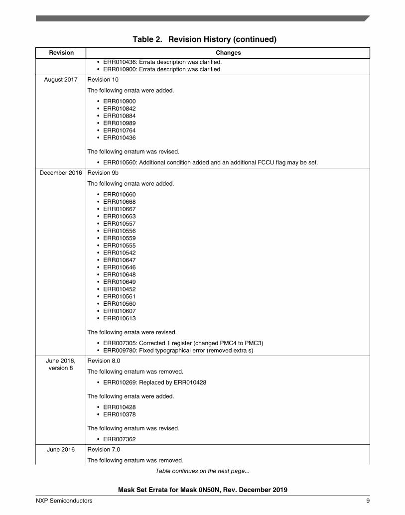
Table 2. Revision History (continued)
Revision Changes
• ERR010436: Errata description was clarified.• ERR010900: Errata description was clarified.
August 2017 Revision 10
The following errata were added.
• ERR010900• ERR010842• ERR010884• ERR010989• ERR010764• ERR010436
The following erratum was revised.
• ERR010560: Additional condition added and an additional FCCU flag may be set.
December 2016 Revision 9b
The following errata were added.
• ERR010660• ERR010668• ERR010667• ERR010663• ERR010557• ERR010556• ERR010559• ERR010555• ERR010542• ERR010647• ERR010646• ERR010648• ERR010649• ERR010452• ERR010561• ERR010560• ERR010607• ERR010613
The following errata were revised.
• ERR007305: Corrected 1 register (changed PMC4 to PMC3)• ERR009780: Fixed typographical error (removed extra s)
June 2016,version 8
Revision 8.0
The following erratum was removed.
• ERR010269: Replaced by ERR010428
The following errata were added.
• ERR010428• ERR010378
The following erratum was revised.
• ERR007362
June 2016 Revision 7.0
The following erratum was removed.
Table continues on the next page...
Mask Set Errata for Mask 0N50N, Rev. December 2019
NXP Semiconductors 9

Table 2. Revision History (continued)
Revision Changes
• ERR008056: This is now documented in the device Reference Manual.
The following errata were added.
• ERR010309• ERR010385• ERR010196• ERR008631• ERR007356• ERR010175• ERR010176• ERR010171• ERR010376• ERR007638• ERR010148• ERR010147• ERR010149• ERR010157• ERR010156• ERR010159• ERR010158• ERR010269• ERR009709
The following erratum was revised.
• ERR009796: Additional pin groups were added.
January 2016 The following erratum was removed.
• ERR007356: This is now documented in the device Reference Manual.
The following errata were added.
• ERR009656• ERR009658• ERR009664• ERR009413• ERR009796• ERR009780• ERR009783
The following errata were revised.
• ERR008933: Minor corrections in the grammar.• ERR008412• ERR009415: Description updated to allow operation for up to 500 k bits/second.
August 2015 Revision 5
The following errata were removed.
e7196: Moved to the device Reference Manual.
The following errata were added.
e9322, e9415, e9584, e9070
The following errata were revised.
e7274, e8951
-----------------------------------------------------------------------------------------------------------------------------------
Mask Set Errata for Mask 0N50N, Rev. December 2019
10 NXP Semiconductors

Table 2. Revision History
Revision Changes
Previous revision history is shown below.
-----------------------------------------------------------------------------------------------------------------------------------
Revision 1.0
Release date: 2014 November 05
The following errata were removed.
e7351: This errata was replaced with e8028.
e7652: This erratum was cancelled. This operation was already described in the device documentation.
e7355: Data sheet has been updated with the new specification.
e7363: Data sheet has been updated with the new specification.
The following errata were added.
e8438, e8439, e8225, e8229, e8526, e8429, e8430, e8343, e8561, e8605, e8602, e8075, e8573, e8145,e8141, e8126, e8655, e8028
The following errata were revised.
e8122, e7589, e7365, e8042, e7842, e7841, e6350, e7269
-----------------------------------------------------------------------------------------------------------------------------------
Revision 2.0
Release Date: December 19,21014
The following errata were removed.
e8028: Replaced by e7351.
The following errata were added.
e8310, e8314, e8904, e8647, e7351, e8689, e8688, e8412, e8885, e8738, e8731, e8730
The following errata were revised.
e7841, e8429
-----------------------------------------------------------------------------------------------------------------------------------
Revision 3.0
Release date: 03 February 2015
The following errata were added.
e8970, e8770, e8547, e8933, e8935, e8923
The following errata were revised.
e8688, e8412
-----------------------------------------------------------------------------------------------------------------------------------
Revision 4.0
Release date: 08 April 2015
The following errata were added.
e8951, e9060
The following errata were revised.
e8412: Wording updated to provide additional information.
e8904
Mask Set Errata for Mask 0N50N, Rev. December 2019
NXP Semiconductors 11

ERR010842: CMU: False upper frequency threshold alarm (FHH) signaled to FaultCollection and Control Unit (FCCU)
Description: A Clock Monitor Unit (CMU) can be configured to monitor the frequency of a clock signal(CLKMN1) and generate an event if CLKMN1 is greater than a high frequency boundarydefined by the CMU High Frequency Reference Register (CMU_HFREFR). If the monitoredCLKMN1 clock is above 300MHz, then there is the potential that the CMU_ISR[FHHI] may befalsely set but the frequency is in fact correct. The false CMU_ISR[FHHI] flag may they triggera false alarm to the FCCU, if so configured. If the measured clock frequency is actually abovethe upper threshold or below the lower threshold, a proper alarm is always correctly triggered.
Workaround: Prevent false FHH events by disabling the CMU by clearing the CMU_CSR[CME]. The PLL0-PHI frequency integrity can be verified by using other CMU modules that monitor the dividedversions of PLL0-PHI. Please refer to the Reference Manual for the complete list of availableCMU monitors.
The CMU may still be enabled to utilize the other clock monitoring features (such as FLLI andOLRI) and in this case the FHHI false flag can be ignored. If FHHI is set, the FHHI can becleared and re-read to determine a real permanent clock fault compared to just a transientfalse flag. A false FHHI flag being set has no adverse effects on the integrity of the FLLI orOLRI functions or on capturing true FHHI events. Disable the FCCU FHHI trigger event toprevent the FCCU from inadvertently reacting to a false FHHI event.
ERR050159: CMU: Monitoring signal for sudden loss of clock from CMU does notsignal the Fault Collection and Control Unit
Description: The Clock Monitor Unit (CMU) detects when the frequency of a monitored clock drops below aprogrammed threshold and asserts the Frequency Less than Low Threshold (FLL) signal if thisoccurs. The FLL signal is routed to the Fault Collection and Control Unit (FCCU) providing amechanism to react to the clock fault but due to the monitoring implementation the FLL signalwill not be triggered when the monitored clock suddenly stops.
Workaround: Each of the CMU monitored clocks has been analysed for the system level failure effect uponloss of the monitored clock and the safety mechanisms present to detect this. From thisanalysis it is concluded that loss of all the monitored clocks can be detected by other existingsafety mechanisms in the system.
Further, since the CMU monitored clocks are derived from one of the system clock sources(XOSC_CLK, PLL0_PHI_CLK, PLL1_PHI_CLK) if the loss of the monitored clock is caused bythe loss of the source clock then this will be detected and reported to FCCU by existing sourceclock loss detection mechanisms.
ERR007116: CRC: AutoSAR 4.0 8-bit CRC8 0x2F is not supported in hardware
Description: The Cyclic Redundancy Check (CRC) module does not implement the 8-bit CRC-8-H2Frequired to support the Autosar 4.0 specification. The CRC-8-H2F uses a polynomial generatorseed of 0x2F and an equation of x 5 + x 3 + x 2+x+1.
Workaround: Do not set the Polynomial selection to 0b11 in the CRC Configuration register (CRC_CFG).The 8-bit CRC-8-H2F function must be written in software to support AuroSAR 4.0.
Mask Set Errata for Mask 0N50N, Rev. December 2019
12 NXP Semiconductors
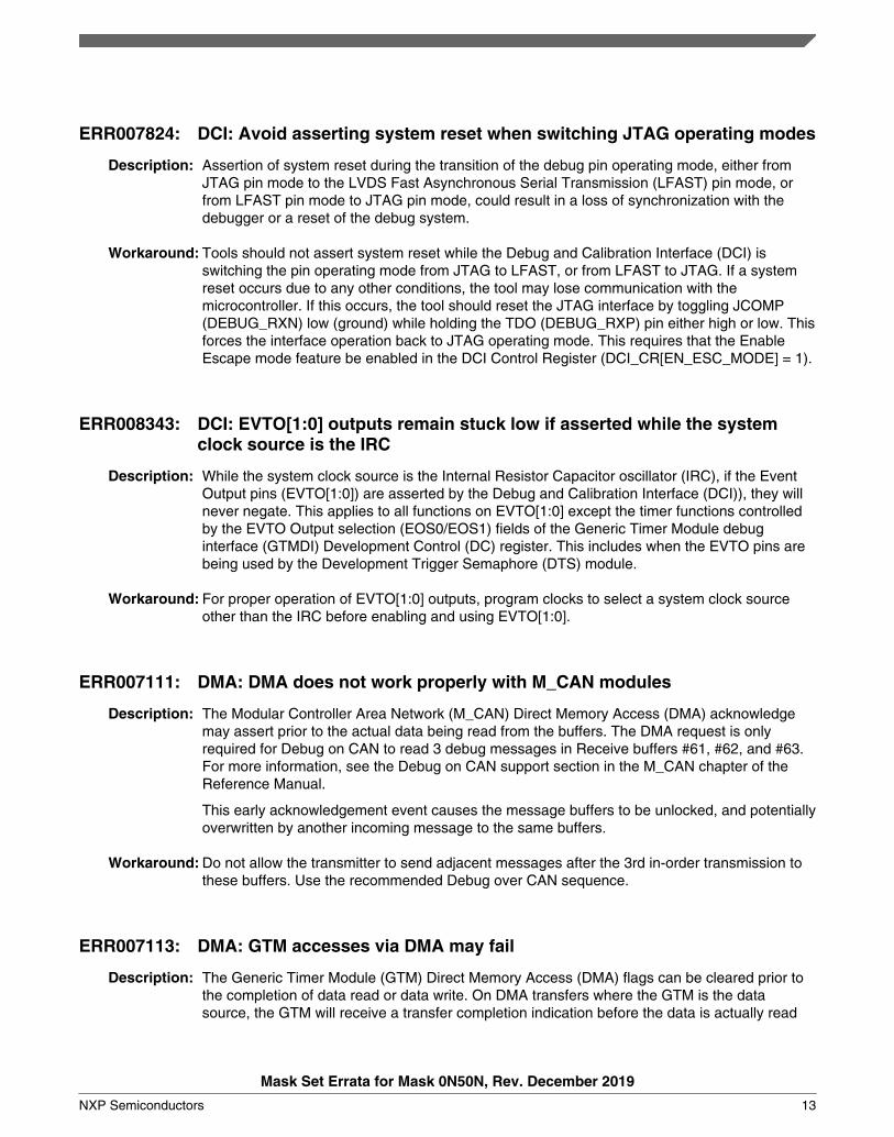
ERR007824: DCI: Avoid asserting system reset when switching JTAG operating modes
Description: Assertion of system reset during the transition of the debug pin operating mode, either fromJTAG pin mode to the LVDS Fast Asynchronous Serial Transmission (LFAST) pin mode, orfrom LFAST pin mode to JTAG pin mode, could result in a loss of synchronization with thedebugger or a reset of the debug system.
Workaround: Tools should not assert system reset while the Debug and Calibration Interface (DCI) isswitching the pin operating mode from JTAG to LFAST, or from LFAST to JTAG. If a systemreset occurs due to any other conditions, the tool may lose communication with themicrocontroller. If this occurs, the tool should reset the JTAG interface by toggling JCOMP(DEBUG_RXN) low (ground) while holding the TDO (DEBUG_RXP) pin either high or low. Thisforces the interface operation back to JTAG operating mode. This requires that the EnableEscape mode feature be enabled in the DCI Control Register (DCI_CR[EN_ESC_MODE] = 1).
ERR008343: DCI: EVTO[1:0] outputs remain stuck low if asserted while the systemclock source is the IRC
Description: While the system clock source is the Internal Resistor Capacitor oscillator (IRC), if the EventOutput pins (EVTO[1:0]) are asserted by the Debug and Calibration Interface (DCI)), they willnever negate. This applies to all functions on EVTO[1:0] except the timer functions controlledby the EVTO Output selection (EOS0/EOS1) fields of the Generic Timer Module debuginterface (GTMDI) Development Control (DC) register. This includes when the EVTO pins arebeing used by the Development Trigger Semaphore (DTS) module.
Workaround: For proper operation of EVTO[1:0] outputs, program clocks to select a system clock sourceother than the IRC before enabling and using EVTO[1:0].
ERR007111: DMA: DMA does not work properly with M_CAN modules
Description: The Modular Controller Area Network (M_CAN) Direct Memory Access (DMA) acknowledgemay assert prior to the actual data being read from the buffers. The DMA request is onlyrequired for Debug on CAN to read 3 debug messages in Receive buffers #61, #62, and #63.For more information, see the Debug on CAN support section in the M_CAN chapter of theReference Manual.
This early acknowledgement event causes the message buffers to be unlocked, and potentiallyoverwritten by another incoming message to the same buffers.
Workaround: Do not allow the transmitter to send adjacent messages after the 3rd in-order transmission tothese buffers. Use the recommended Debug over CAN sequence.
ERR007113: DMA: GTM accesses via DMA may fail
Description: The Generic Timer Module (GTM) Direct Memory Access (DMA) flags can be cleared prior tothe completion of data read or data write. On DMA transfers where the GTM is the datasource, the GTM will receive a transfer completion indication before the data is actually read
Mask Set Errata for Mask 0N50N, Rev. December 2019
NXP Semiconductors 13

from the GTM. This may lead to overwritten data, without any error indication. On DMAtransfers where the GTM is the data destination, the GTM will receive a transfer completionindication before the data is actually written into the GTM. The GTM may use incorrect data.
The following GTM channels can be affected: Sensor Pattern Evaluation Module (SPE),Parameter Storage Module (PSM), Multi-Channel Sequencer (MCS), Timer Output Module(TOM), Timer Input Module (TIM), and Advanced Routing Unit (ARU) controlled TOM (ATOM).Additionally, the TIM channel’s GPRz data overflow (GPROFL) bit in the TIM[i] Channel[x] IRQNotification Register (TIM[i]_CH[x]_IRQ_NOTIFY) will not be set if a DMA overrun eventoccurs.
Workaround: Use interrupts to control data flow to and from the GTM.
ERR010663: DS/RM: IRC trimming and LVD/HVD clarifications
Description: The MPC5777M Reference Manual (RM, revision 4.2) indicates that the user programmablefrequency trimming of the IRCOSC is controlled by IRCOSC_CTL[USER_TRIM] which isbased on the dFvar_SW value as defined in the MPC5777M Data Sheet (DS, dated 06/2016).However, the IRCOSC_CTL[USER_TRIM] should be based on dfTRIM instead of dFvar_SWas defined in the “Internal RC Oscillator electrical specifications” table in the Data Sheet.
Clarify the wording in the Data Sheet of table note #6 of the “Device operating conditions” tableto change from “In the LVD/HVD disabled case, it is necessary for the system to be within ahigher voltage range during destructive reset events.” to "In the LVD/HVD disabled case, it isnecessary for the system to be within a valid voltage range to correctly recover from power-on,destructive, or ESR0 long reset events."
Workaround: Update Data Sheet and Reference Manual with these clarifications.
ERR007351: DSMC: Lockstep-error notification is disabled
Description: The Decorated Storage Memory Controller (DSMC) associated with Safety-core local memoryis included in the sphere of replication for lockstep checking.
The checking of the DSMC outputs with its replicated checker DSMC by an RCCU(Redundancy Control Checker Unit) has been disabled.
The disabling only affects accesses of masters other than the Safety-core through the Safety-core backdoor (slave port s2) to the Safety-core local memory (read and write).
Accesses of the Safety-core to its own local memory are not affected by this errata.
Failures occurring during a backdoor write access are still covered by other RCCUmechanisms, signaling to either Fault Collection and Control Unit (FCCU) Fault Channel 10 or11 (depending on where the failure emerges).
Failures occurring during a backdoor read access are covered with end-to-end ECC protection(which has slightly less diagnostic coverage than lockstep checking) or are covered by anotherRCCU, depending on where the failure occurs.
Workaround: The customer safety assessment in the system Fault Mode Effects and Diagnostic Analysis(FMEDA) should take in to consideration that the end-to-end Error Correcting Code (ECC) isused instead of the depending on a lock-step read access mechanism when the Safety-corelocal memory is read via the backdoor by other cores.
Mask Set Errata for Mask 0N50N, Rev. December 2019
14 NXP Semiconductors

ERR050090: DSPI/SPI: Incorrect data may be transmitted in slave mode
Description: If the Serial Peripheral Interface (SPI or the Deserial/Serial Peripheral Interface) is operating inslave mode, incorrect or stale data may be transmitted in next transaction without underflowinterrupt generation if the set up time of the Peripheral Chip Select (PCS) to the SPI SerialClock (SCLK) is short and the transmit FIFO may become empty after one transaction.
This can occur if the PCS to SCK is less than:
4 X IPG_CLOCK_PERIOD + 4 X DSPI_CLOCK_PERIOD + 0.5 x SCK_CLOCK_PERIOD
Where:
IPG_CLOCK is the internal bus clock (“system” clock)
DSPI_CLOCK is the protocol clock.
SCK_CLOCK is the Line-Side Serial Communication Clock.
Workaround: When operating in slave mode, software must ensure that the time interval between PCSassertion to start of SCK Clock is greater than 4 X IPG_CLOCK_PERIOD + 4 XDSPI_CLOCK_PERIOD + 0.5 x SCK_CLOCK_PERIOD.
To meet this requirement, the Master SPI can either lengthen the PCS to SCK assertion timeor decrease the frequency of the communication interface, or both.
ERR009783: DSPI: Frame transfer does not restart after DSI frame matchespreprogrammed value
Description: In the Deserial Serial Peripheral Interface module, in the scenario when:
1. Master/slave mode select bit of module configuration register is set (MCR[MSTR]=0b1) toconfigure the module in master mode
2. Deserial Serial Interface (DSI) communication is selected via DSPI Configuration field(DCONF) in the Module Configuration Register (MCR [DCONF] = 0b01)
3. Preprogrammed value for data match with received DSI frame is configured using DSI De-serialized Data Polarity Interrupt Register (DPIR) and DSI De-serialized Data Interrupt MaskRegister (DIMR)
4. Data Match Stop (DMS) bit of DSI configuration register0 is set (DSICR0 [DMS] =0b1) whichstops DSI frame transfer in case of a data match with a preprogrammed value
5. DSI frame is received with bits matching preprogrammed value.
Under these conditions, the next frame transfer is stopped, DSI Data Received with Active Bitsbit of status register is set (SR [DDIF] =0b1) and the corresponding DDIF interrupt is asserted.Even after the interrupt is serviced and SR [DDIF] is reset, the frame transfer does not restart.
Workaround: DSI frame transfer stop in case of DSI data match condition should be disabled. For this, keepthe data match stop bit of DSI configuration register 0 de-asserted (DSICR0 [DMS]=0b0).
ERR009664: DSPI: Frame transfer does not restart in case of DSI parity error in mastermode
Description: In the Serial Peripheral Interface module, in the scenario when:
Mask Set Errata for Mask 0N50N, Rev. December 2019
NXP Semiconductors 15

1. Master/slave mode select bit of module configuration register is set (MCR[MSTR]=0b1) toconfigure the module in master mode
2. Deserial Serial Interface (DSI) communication is selected via DSPI Configuration field(DCONF) in MCR (MCR[DCONF] = 0b01)
3. Parity reception check on received DSI frame is enabled by setting Parity Enable bit (PE) ofDSI configuration register 0 (DSICR0[PE]=0b1)
4. Parity Error Stop (PES) bit of DSI configuration register0 is set (DSICR0[PES]=0b1) whichstops DSI frame transfer in case of parity error
5. Parity error is detected on received frame
Then the next frame transfer is stopped, DSI parity error flag bit of status register is set(SR[DPEF] =0b1) and the corresponding DSI parity error interrupt is asserted. Even after theinterrupt is serviced and SR [DPEF] is reset, the frame transfer does not restart.
Workaround: DSI frame transfer stop in case of parity error detection should be disabled. For this, keep theparity error stop bit of DSI configuration register0 de-asserted (DSICR0 [PES]=0b0).
ERR009656: DSPI: Frame transfer does not restart in case of SPI parity error in mastermode
Description: In the Deserial Serial Peripheral Interface (DSPI) module, in the scenario when:
1. Master/slave mode select bit (MTSR) of Module Configuration register (MCR) is set(MCR[MSTR]=0b1) to configure the module in master mode
2. SPI communication is selected via DSPI Configuration field (DCONF) in MCR(MCR[DCONF] = 0b00)
3. Parity reception check on received frame is enabled by setting the Parity Enable or MasktASC delay (PE_MASC) bit of DSPI PUSH FIFO Register In Master Mode (PUSHR), i.e.PUSHR[PE]=0b1.
4. Parity Error Stop bit (PES) of MCR is set (MCR[PES]=0b1) which stops SPI frame transferin case of parity error
5. Parity error is detected on received frame.
Then the next frame transfer is stopped, the SPI Parity Error Flag bit (SPEF) of the DSPIStatus Register (DSPI_SR) is set (SR[SPEF] =0b1) and the corresponding SPI parity errorinterrupt is asserted. Even after the interrupt is serviced and SR[SPEF] is reset, the frametransfer does not restart.
Workaround: Do not use SPI frame transfer stop in case of parity error detection for SPI transmission inmaster mode. For this, keep the Parity Error Stop bit of Module Configuration Register de-asserted (MCR[PES] = 0b0).
ERR007115: DSPI: Mixing 16 and 32 bits frame size in XSPI Mode can cause incorrectdata to be transmitted
Description: The Deserial Serial Peripheral Interface (DSPI) features an Extended SPI mode (XSPI)supporting frames of up to 32 bits.
Mask Set Errata for Mask 0N50N, Rev. December 2019
16 NXP Semiconductors

When the XSPI Mode is enabled, transferring a mixture of frames having a size up to 16 bitsand those having size above 16 bits can cause an incorrect data transmission to occur. Thishappens when the First In/First Out (FIFO) queue read pointers roll-over and a frame needs tobe extracted from both the bottom of the FIFO and the top of the FIFO when the Frame Size isgreater than 16 bits.
Workaround: Even number of Transmit FIFO Register (TXFR) registers:
Do not mix frames that have data sizes of less than 16 bits with those having a size more than16 bits in XSPI Mode.
Odd number of TXFR registers :
Do not mix frames that have data sizes of less than 16 bits with those having a size more than16 bits in XSPI Mode.
If the frame size is greater than 16, initially send a dummy frame (a frame with no chip select,but containing data) of less than or equal to 16 bits. Continue sending a dummy frame aftereach (number of TXFR Registers – 1) / 2 frames.
ERR007352: DSPI: reserved bits in slave CTAR are writable
Description: When the Deserial/Serial Peripheral Interface (DSPI) module is operating in slave mode (theMaster [MSTR] bit of the DSPI Module Configuration Register [DSPIx_MCR] is cleared), bits10 to 31 (31 = least significant bit) of the Clock and Transfer Attributes Registers(DSPIx_CTARx) should be read only (and always read 0). However, these bits are writable,but setting any of these bits to a 1 does not change the operation of the module.
Workaround: There are two possible workarounds.
Workaround 1: Always write zeros to the reserved bits of the DSPIx_CTARn_SLAVE (whenoperating in slave mode).
Workaround 2: Mask the reserved bits of DSPIx_CTARn_SLAVE when reading the register inslave mode.
ERR007299: DSPI: SOUT pins are not automatically configured as SOUT when SlaveSelect is asserted in Slave Mode
Description: The Deserial Serial Peripheral Interface (DSPI) Serial Data Out (SOUT) pins are notautomatically configured as SOUT when the Slave Select (SS) signal is asserted. Instead thepins must be configured as SOUT using the Source Signal Select (SSS) field of the pertinentMultiplexed Signal Configuration Register (MSCR) in the System Integration Unit Lite 2(SIUL2) module.
Workaround: In DSPI slave mode operation, the SOUT function must be selected in the MSCR. If the deviceis the only slave device then no functional issues will occur.
If the device is configured in DSPI slave mode and it is not the only slave then an externalmultiplexing scheme can be used based upon the DSPI Slave Select Signals.
Mask Set Errata for Mask 0N50N, Rev. December 2019
NXP Semiconductors 17

ERR010542: DSPI: Transmit, Command, and Receive FIFO fill flags in status register isnot cleared when DMA is improperly configured
Description: The Deserial/Serial Peripheral Interface Transmit, Receive, and Command First In/First Out(FIFO) buffers can request additional information to be transferred via the Direct MemoryAccess (DMA) module when either the Transmit, Receive, or Command FIFO Fill/Drain Flagsare set in the DSPI Status Register (SR[TFFF/RFDF/CMDFFF]). However, the Command/Transmit Fill Flag only indicates that at least 1 location in the FIFO is available to be written. Itdoes not indicate that the FIFO is empty. Similarly, Receive FIFO fill flag only indicates at least1 location of the FIFO is available to be read. It does not indicate that the FIFO is full. If theDMA is configured to transfer more than 1 FIFO location size of data, the FIFO Fill Flags maynot be properly cleared indicating that the FIFO is not full even when the FIFO is actually full(for Transmit and Command FIFO) and not empty when the FIFO is actually empty (forReceive FIFO).
Workaround: Properly configure the DMA to fill the Transmit, Receive, and Command FIFOs only one FIFOlocation, in other words, up to 2 bytes, at a time to each of the FIFOs.
Use the DMA loop to transfer more data if needed.
ERR008547: e200z425: Additional cycles required for Load/Store accesses to guarded/precise space
Description: If an access by the Load/Store unit is to a space that is guarded/precise then it will be subjectto additional cycles for completion because there is no pipeline bypass for the Bus InterfaceUnit. These spaces and accesses are characterized by any one of the following conditions:
• The Memory Protection Unit (MPU) Guarded bit is set for the address space• The access is a store with the Store Buffer disabled• The access is a Decorated Load or Store• The access is a Bypass Store• The access is an Atomic Load or Store
On this device, the peripheral address space, by default, is set to be guarded/precise space.
Each scenario below will cause a 2 cycle increase:
• Idle to guarded/precise load• Idle to guarded/precise store• Store to guarded/precise load• Store to guarded/precise store
The following scenarios may or may not add extra cycles depending on wait states and back toback requests:
• Load to guarded/precise store• Load to guarded/precise load
Workaround: Expect additional cycles when guarded/precise accesses occur.
Mask Set Errata for Mask 0N50N, Rev. December 2019
18 NXP Semiconductors

ERR010385: e200z4: Incorrect branch displacement at 16K memory boundaries
Description: The branch target address will be incorrectly calculated in the e200z4 core under the followingconditions (all conditions must be matched):
• The first full instruction in a 16 Kbyte section/page of code is a 32-bit long branch with abranch displacement value with the lower 14 bits of the displacement exactly 0x3FFE
• And this branch instruction is located at byte offset 0x0002 in the section/page• And the preceding instruction is a 32-bit length instruction which is misaligned across the
16K boundary• And both instructions are dual-issued
Under these conditions, the branch target address will be too small by 32Kbytes.
Workaround: After software is compiled and linked, code should be checked to ensure that there are nobranch instructions located at address 0x2 of any 16K memory boundary with the lower 14 bitsof the displacement equal to 0x3FFE if preceded a 32-bit instruction that crosses the 16Kmemory boundary. If this sequence occurs, add a NOP instruction or otherwise force a changeto the instruction addresses to remove the condition.
A tool is available on nxp.com that can be run to examine code for this condition, search forbranch_displacement_erratum_10385_checker.
ERR007210: e200z710: Nexus timestamps are not available
Description: The optional timestamps on the Nexus trace messages from the e200z710 cores are notimplemented and cannot be enabled.
Workaround: Timestamps of Nexus trace messages from the e200z425 core are available. Tools cancorrelate the e200z425 timestamps to the e200z710 messages for a rough approximation oftime.
ERR007259: e200zx: ICNT and branch history information may be incorrect following anexus overflow
Description: If an internal Nexus message queue over-flow occurs when the e200zx core is running inbranch history mode (Branch Method bit [BTM] in the Development Control register 1 [DC1] isset [1]), the instruction Count (ICNT) and branch history (HIST) information in the first programtrace message following the Program Correlation message caused by an over-flow of theinternal trace buffers, will contain incorrect ICNT and HIST information.
This can also occur following an overflow of the internal Nexus message queues in thetraditional branch mode (BTM in the DC1 is cleared [0]). Traditional branch mode Nexusmessages do not include HIST information, since all branches generate a trace message.
Workaround: There are two methods for dealing with this situation.
1) Avoid overflows of the Nexus internal FIFOs by reducing the amount of trace data beinggenerated by limiting the range of the trace area by utilizing watchpoint enabled trace windowsor by disabling unneeded trace information, or by utilizing the stall feature of the cores.
Mask Set Errata for Mask 0N50N, Rev. December 2019
NXP Semiconductors 19

2) After receiving an overflow ERROR message in Branch History mode, the ICNT and HISTinformation from the first Program Trace Synchronization message and the next ProgramTrace message with a relative address should be discarded. The address information iscorrect, however, the ICNT and previous branch history are not correct. All subsequentmessages will be correct.
In traditional branch mode, the ICNT information should be discarded from the Program TraceSync message and the next direct branch message.
ERR007305: e200zx: JTAG reads of the Performance Monitor Counter registers are notreliable
Description: Reads of the Performance Monitor Counter (PMC0, PMC1, PMC2, and PMC3) registersthrough the IEEE 1149.1 or IEEE 1149.7 (JTAG) interfaces may return occasional corruptedvalues.
Workaround: To ensure proper performance monitor counter data at all times, software can be modified toperiodically read the PMCx values and store them into memory. JTAG accesses could then beused to read the latest values from memory using Nexus Read/Write Access or the tool couldenable Nexus data trace for the stored locations for the information to be transmitted throughthe Nexus Trace port.
ERR007408: EBI: Minimum input setup time is 7 ns
Description: For the External bus Interface (EBI), the Input Signal Valid to the clock out signal (CLKOUT)positive edge (Setup Time) specification of 6 ns is not met over the full operating conditions ofthe MCU.
Workaround: Expect that the setup time for the EBI to be 7 ns minimum. Use an external memory whoseread data drive time is fast enough to meet desired CLKOUT frequency and meet the MCUInput Setup time, OR slow down the CLKOUT frequency such that timing can be met.
ERR006967: eDMA: Possible misbehavior of a preempted channel when usingcontinuous link mode
Description: When using Direct Memory Access (DMA) continuous link mode Control Register ContinuousLink Mode (DMA_CR[CLM]) = 1) with a high priority channel linking to itself, if the high prioritychannel preempts a lower priority channel on the cycle before its last read/write sequence, thecounters for the preempted channel (the lower priority channel) are corrupted. When thepreempted channel is restored, it continues to transfer data past its “done” point (that is thebyte transfer counter wraps past zero and it transfers more data than indicated by the bytetransfer count (NBYTES)) instead of performing a single read/write sequence and retiring.
The preempting channel (the higher priority channel) will execute as expected.
Workaround: Disable continuous link mode (DMA_CR[CLM]=0) if a high priority channel is using minor loopchannel linking to itself and preemption is enabled. The second activation of the preemptingchannel will experience the normal startup latency (one read/write sequence + startup) insteadof the shortened latency (startup only) provided by continuous link mode.
Mask Set Errata for Mask 0N50N, Rev. December 2019
20 NXP Semiconductors

ERR010452: eDMA: When master ID replication is enabled, the stored ID and privilegelevel will change if read by another master.
Description: When master ID replication is enabled (DMA_DCHMIDn[EMI]=1), the DMA_DCHMIDn[PAL]and DMA_DCHMIDn[MID] fields should reflect the privilege level and master ID respectively ofthe master that wrote the DMA_TCDn_CSR[DONE:START] byte. However, if a differentmaster reads the DMA_TCDn_CSR[DONE:START] byte, the master ID and privilege level willincorrectly change to this read access.
Workaround: Only allow the intended master ID replication core to access theDMA_TCDn_CSR[DONE:START] byte.
ERR007337: FCCU: Address feedback error disabled for the Safety Core local RAMSand Cache
Description: The additional, dedicated measures against addressing and control faults (such as address/control feedback) have been disabled. This applies to the following memories of the Safetymain core 0:
Memory type Name
Instruction SRAM I-MEM
Data SRAM D-MEM
Instruction CACHE I-CACHE
Data CACHE D-CACHE
Instruction TAG I-TAG
Data TAG D-TAG
This, in turn, has disabled the Fault Collection and Control Unit (FCCU) Failure Input Channel27 which Indicates an addressing error (address-feedback) inside the above memories.
Workaround: Checks for address errors should be performed using the Memory Built-In Self Test features ofthe device. FCCU input channel 27 will not be asserted.
ERR008034: FCCU: Channel 40 fault (COMP_XBIC_DSMC_Monitor) may be reported ifa CPU is reset upon a MC_ME mode change
Description: The Fault Collection and Control Unit (FCCU) channel 40 may report a fault during or aftercompletion of a Mode Entry module (MC_ME) mode change where a CPU is reset in the modechange (setting MC_ME_CADDRn[RMC]=1). FCCU channel 40(COMP_XBIC_DSMC_Monitor) indicates an addressing or control fault resulting in corruptedtransaction through the computational XBAR or interference by system RAM DecoratedStorage Memory Controller (DSMC).
Workaround: Disable the computational XBAR slave port 4 parking control (XBAR_0_CRS4[PCTL]=10) priorto a mode change where a CPU will be reset, or expect and clear a FCCU channel 40 faultfollowing the mode change if it occurs. Fault is cleared by clearing the FCCU channel status,FCCU_RF_Sn[RFSm].
Mask Set Errata for Mask 0N50N, Rev. December 2019
NXP Semiconductors 21

ERR008229: FCCU: Enabling the programmable glitch filter on EIN may cause adestructive reset
Description: The Fault Collection and Control Unit (FCCU) external error input (EIN) can be filtered by theFCCU on-chip programmable glitch filter. However, the EIN is routed directly to the FCCUOutput Supervision Unit (FOSU) without passing through the glitch filter. Additionally, when theglitch filter is programmed using the FCCU Control Register (FCCU_CTRL) FILTER_WIDTHfield, the effective duration may vary depending on time at which the EIN signal arrives, whichcan cause a missed or false EIN signal. As a result, it is possible for the FOSU to recognize anevent on EIN that is ignored by the FCCU resulting in a destructive reset when the FOSUtimeout period expires.
Workaround: Bypass the FCCU on-chip glitch filter by writing a 1 to the FCCU Control RegisterFILTER_BYPASS field (FCCU_CTRL[FILTER_BYPASS]) and use an external glitch filter toensure that only valid external error events are recognized by the FCCU. The impact on safetycan be avoided by using a feedback based signaling on Error In (EIN), wherein the EIN signalis kept asserted until the MCU acknowledges the event to the source.
ERR008042: FCCU: EOUT signals are active, even when error out signaling is disabled
Description: Every time the Fault Collection and Control Unit (FCCU) moves into fault state caused by aninput fault for which the error out reaction is disabled (FCCU_EOUT_SIG_ENn[EOUTENx]=0),the Error Out 1 and 2 (EOUT[0] and EOUT[1]) will become active for a duration of 250 us plusthe value programmed into the FCCU Delta Time register (FCCU_DELTA_T[DELTA_T]).EOUT is not affected if the FCCU moves into the alarm state that generates an interrupt (IRQ),if the Fault is cleared before the alarm timeout.
This erratum does not affect the outputs of other pins (for example, for communicationmodules like CAN/Flexray). Only the EOUT signal is impacted.
Workaround: There are three possible workarounds:
1) Enable EOUT signaling for all enabled error sources.
2) In case external device (which evaluates EOUT) can communicate with the MCU, thefollowing procedure could be used:
a) Program any duration of EOUT as per application needs (FCCU_DELTA_T[DELTA_T])
b) For faults requiring error out reaction, the software shall validate EOUT via separatecommunication channel (like I2C) while EOUT is asserted.
c) External device shall implement a timeout mechanism to monitor EOUT validation byseparate channel.
d) Following scenarios shall be considered as valid EOUT reactions:
d1) Validation is performed while EOUT is asserted
d2) Timeout occurs but no validation and EOUT is still asserted.
3) In case external device (which evaluates EOUT) cannot communicate with the MCU,following procedure could be used:
a) Program the error out duration to a duration x (FCCU_DELTA_T[DELTA_T]).
Mask Set Errata for Mask 0N50N, Rev. December 2019
22 NXP Semiconductors

b) For faults requiring error out reaction, clear the fault after the pin has continued to beasserted for a longer duration (for example 2*duration x). This will artificially create a longpulse on EOUT.
c) For faults which do not require error out reaction, clear the fault within duration x. This willartificially create a short pulse on EOUT.
d) External device should ignore short pulse of duration x while recognizing longer pulses asvalid reaction.
e) While clearing the fault, the associated software shall check the pending faults.
ERR007099: FCCU: Error pin signal length is not extended when the next enabledfault, with its alarm timeout disabled, occurs
Description: In the Fault Collection and Control Unit (FCCU), when the following conditions are met:
• two faults occur• the second fault arrises with a delay (T_delay) from the first error• the second fault has its alarm timeout disabled• T_delay is lower than the FCCU error pin minimum active time (T_min, defined in the
Delta T register (FCCU_DELTA_T))
Then the error output signal is not extended and its duration is only T_min, if the faults arecleared before the timer expires.
The expected behavior is to have the error output signal duration of T_min + T_delay, if thefaults are cleared before the timer expires.
Workaround: Take into account that the error out signal duration will only be T_min, if the faults are clearedbefore the timer expires.
The timer count is meaningful only when the Error pin is driven low, which can be checked byreading the pin status FCCU_STAT[ESTAT].
ERR010900: FCCU: False indication of a fault state for a single safe clock period canbe generated on the error output pin
Description: The error out pin from the Fault Collection and Control Unit (FCCU) may pulse to a logic low(0b0) when the following conditions are fulfilled:
• software changes the error out protocol from a toggling protocol to a not-togglingprotocol, and programs the FCCU_CFG.FCCU_SET_AFTER_RESET bit to 0b1
• software switches the Fault Collection and Control Unit (FCCU) state machine fromCONFIG to NORMAL state
The duration of the glitch is equal to a single clock period of the Internal RC oscillator andthere is a 50% of probability of the pulse occurring.
Workaround: Split the configuration of the FCCU in 2 phases.
During the first phase, software should do the following:
1) move the FCCU to the CONFIG state
2) configure the FCCU including the error out protocol, but without setting theFCCU_CFG.FCCU_SET_AFTER_RESET flag to 0b1 (leave as 0b0)
Mask Set Errata for Mask 0N50N, Rev. December 2019
NXP Semiconductors 23

3) exits to the NORMAL state
During the second phase, software should do the following:
4) move the FCCU to the CONFIG state
5) set the FCCU_CFG.FCCU_SET_AFTER_RESET flag to 0b1
6) exit to the NORMAL state
Note: The default (after reset) error out protocol is the Dual Rail. Since this is a togglingprotocol, the software must execute the above steps each time the user wants to switch to anon-toggling error out protocol.
ERR007223: FCCU: FCCU_IRQ_EN register is writeable in all operating modes
Description: In the Fault Collection and Control Unit (FCCU), the FCCU Interrupt Enable register(FCCU_IRQ_EN) is writable (and readable) in all states (NORMAL, CONFIG, FAULT andALARM) while in some revisions of the documentation it is stated “This register is writable onlyin the CONFIG state”.
Workaround: Take into account that FCCU_IRQ_EN register can be written in all the states of the FCCU.
Please ignore the following text in the description of FCCU_IRQ_EN register if you find it in thedocumentation revision in hand:
"This register is writable only in the CONFIG state."
ERR007869: FCCU: FOSU monitoring of a fault is blocked for second or lateroccurrence of the same fault
Description: The Fault Collection and Control Unit (FCCU) Output Supervision Unit (FOSU) will not monitorthe FCCU for the second or later occurrence of a given fault in the following cases:
1. Reset is programmed as the only reaction for the fault.
2. Assertion of the fault coincides with the long/short functional reset reaction to a faultpreviously asserted.
Workaround: Enable either Alarm state (NCFTOEx) or at least one other type of Fault-state reaction: Non-maskable Interrupt (NMI) or error out (EOUT) signaling reaction for the faults that have a resetreaction enabled only. Restrictions of combining reset reaction with additional reactions maybe written in the chip specific sub-section of the FCCU chapter.
ERR009584: FCCU: MPC57xxM – FOSU may assert destructive reset when a hardwarerecoverable fault of width less than one safe clock period occurs
Description: The Fault Collection and Control Unit Output Supervision Unit (FOSU) may issue a destructivereset if all of the following conditions are present:
• An input fault is programmed as hardware recoverable in a FCCU Non-Critical FaultConfiguration Register (FCCU_RF_CFGn)
• The only reaction programmed for this fault is FCCU Error Output signaling(FCCU_EOUT_SIG_ENn)
Mask Set Errata for Mask 0N50N, Rev. December 2019
24 NXP Semiconductors

• The source of the fault signal is asserted for less than one safe clock period. The safe clockfor this device is the internal RC oscillator (IRC).
Workaround: Always configure faults as software recoverable in the FCCU_RF_CFGn. Set the RecoverableFault Configuration (RFCx) bit to a ‘1’, this is the default condition for implemented faults afterreset.
ERR007226: FCCU: the error-out signalling cannot be disabled in non Bi-stableprotocols
Description: In the Fault Collection and Control Unit (FCCU) module, the error out signalling can only bedisabled when using the Bi-stable protocol and not all of the protocols.
The Error Out (EOUT) Signaling Enable Register (FCCU_EOUT_SIG_ENx) registers, whichcan be used for disabling error out signalling, are applicable only for bi-stable mode and do notaffect the other protocols. (Various protocols like Bi-stable, Dual rail and other protocols areselected by programming the Fault Output Mode (FOM) field of the Configuration Register(FCCU_CFG)).
Workaround: Do not expect and program the EOUT_SIGN_ENx register to support anything other than bi-stable protocol.
The EOUT Signaling Enable (EOUTENx) field description of FCCU_EOUT_SIG_EN should beread as follows:
0 = EOUT signaling is disabled for error Recoverable Fault (RF) source x for bi-stable protocol.Error pins behave as if in Non-Faulty state.
1 = EOUT signaling is enabled for error RF source x for bi-stable protocol.
ERR007325: FCCU: Unsuccessful decorated storage access may cause erroneoussignaling of FCCU Channel 40
Description: In rare conditions, a decorated memory reference targeting the system RAM may interfere withthe Decorated Storage Memory Controller (DSMC) safety monitor. The result is an erroneoussignalling of Channel 40 in the Fault Collection and Control Unit (FCCU). This will only occur ifthe decorated memory reference is unsuccessful due to either an illegal decoration encodingor a non-correctable Error Correction Code (ECC) event. Although this usually coincides withan exception taken by the core, no exact procedure is known to detect an erroneous signallingof Channel 40.
Workaround: No special workaround required. Software should handle any fault of FCCU Channel 40according to the chosen fault reaction for this channel.
ERR007638: FCCU: Unsuccessful decorated storage access may cause erroneoussignaling of FCCU Channel NCF[39]
Description: In rare conditions, a decorated memory reference targeting the system RAM may interfere withthe Decorated Storage Memory Controller (DSMC) safety monitor. The result is an erroneoussignalling of NCF[39] in the Fault Collection and Control Unit (FCCU). This will only occur if thedecorated memory reference is unsuccessful due to either an illegal decoration encoding or a
Mask Set Errata for Mask 0N50N, Rev. December 2019
NXP Semiconductors 25

non-correctable Error Correction Code (ECC) event. Although this usually coincides with anexception taken by the core, no exact procedure is known to detect an erroneous signalling ofNCF[39].
Workaround: No special workaround required. Software should handle any fault according to the chosenfault reaction for this channel.
ERR008647: FLASH: (SPC57xxM) Address Encode False Report (MCR[AEE] andpossible FCCU channels)
Description: During Flash Read while Write operations (RWW), it is possible for a Program or Eraseoperation to corrupt the Address Encode feature of the flash, and falsely give an AddressEncode Error (AEE) event. The false AEE event only occurs for RWW operations to partitionsin the Low, Mid or High address spaces, and may only occur if the read and write occur both inEven RWW partitions (i.e. 0, 2, or 4), or if the read and write occur both in Odd RWW partitions(i.e. 1, 3, 5).
Reads to even numbered RWW partitions while writing to odd numbered RWW partitions willnot trigger this false AEE condition. Likewise, reads to odd numbered RWW partitions whilewriting to even numbered RWW partitions will not trigger this false AEE condition.
Reads and Writes to 256K blocks, do not show the address encode corruption issue.
Read Data and ECC Parity bits returned for these Reads while writing are valid and notcorrupted.
Workaround: Disable the Fault Collection and Control Unit (FCCU) Failure input channels 38 and 39 byclearing the corresponding bits in the Recoverable Fault Enable Register 1 (FCCU_RF_E1).FCCU input channel 38 is the Encoding Error Flash, and covers the C55FMC_MCR[AEE]event indication in addition to Flash Read Voltage Error (C55FMC_MCR[RVE]) and FlashRead Reference Error (C55FMC_MCR[RRE]) indications and is controlled by theFCCU_RF_E1[bit 25]. FCCU input channel 39 is the flash controller address feedback eventindication and is controlled by the FCCU_RF_E1[bit 24].
Address Encode Error (AEE) fault recognition is a safety mechanism used to detect potentialpermanent and transient faults in the flash address decode logic. Even with AEE detectiondisabled, most faults that would be detected by AEE are still detected by other mechanisms aspart of the MPC57xxM redundant safety concept. Consequently, disabling the AEE faultnotifications in the FCCU has no impact to the overall functional safety integrity of the device,and the ISO26262 ASIL D target is achieved.
With the FCCU channels 38 and 39 disabled, the Read Voltage Error and Read Referenceerror may be monitored by reading the fields from the Flash Module Configuration register(C55FMC_MCR[RVE], C55FMC_MCR[RRE]).
ERR008004: FLASH: Array Integrity with Breakpoints enabled may skip addresses forcertain RWSC and APC combinations
Description: For certain combinations of the Flash Read Wait State Control (RWSC) and Address PipelineControl (APC) settings in the Platform Flash Configuration Register (PFLASH_PCFR1) theFlash’s array integrity (AI) check when run with breakpoints enabled may skip addressesresulting in an incorrect Multiple Input Signature Register (MISR) value or in the case of backto back ECC event errors (EER) or Single Bit Correction (SBC) events, a skipped breakpoint.This occurs for the following combinations:
Mask Set Errata for Mask 0N50N, Rev. December 2019
26 NXP Semiconductors

RWSC=1 and APC=1
RWSC=3 and APC=2
RWSC=5 and APC=3
If breakpoints are enabled and an EER or SBC cause a breakpoint to occur the address afterthe breakpoint will be skipped, and the resulting MISR will not match expectations. Likewise, ifthere are back to back errors (EER or SBC) during AI with the above RWSC/APCcombinations the 2nd error (and breakpoint) will be missed.
Margin Read (which by specification is a self timed event and is independent of wait statesselected) is not affected by this erratum. This erratum only applies to Array Integrity.
Workaround: One workaround is to follow the recommended RWSC and APC combinations for givenfrequencies. If this is done, Array Integrity with Breakpoints feature works as expected. ValidRWSC/APC combinations listed in the specification are:
Flash Operating Frequency RWSC APC
30 MHz 0 0
100 MHz 2 1
133 MHz 3 1
167 MHz 4 1
200 MHz 5 2
A second workaround is if the above RWSC and APC combinations (listed in the description)are desired to be checked, do so without enabling breakpoints. In this case, the first EER orSBC event will be logged, and the MISR will correctly reflect the result of all reads beingexecuted.
ERR007991: FLASH: Rapid Program or Erase Suspend fail status
Description: If a flash suspend operation occurs during a 5us window during a verify operation beingexecuted by the internal flash program and erase state machine, and the suspend ratecontinues at a consistent 20us rate after that, it is possible that the flash will not exit theprogram or erase operation. A single suspend during a single program or erase event will notcause this issue to occur.
Per the flash specification, a flash program or erase operation should not be suspended morethan once every 20 us, therefore, if this requirement is met, no issue will be seen. IF thesuspend rate is faster than 20 us continuously, a failure to program/erase could occur.
Workaround: When doing repeated suspends during program or erase ensure that suspend period is greaterthan 20us.
ERR050119: FlexRay: Disabling of FlexRay Message Buffer during the STARTUPProtocol State takes longer than expected three Slots
Description: Disabling of FlexRay Message Buffer takes longer than the expected three Slots. This isobserved, when software application tries to disable the Message Buffer during the FlexRaySTARTUP protocol state (VPOC!State = POC:startup) when vPOC!StartupState = “initializeschedule” or “integration consistency check”.
Mask Set Errata for Mask 0N50N, Rev. December 2019
NXP Semiconductors 27

In this scenario, FlexRay Communication Controller keeps the specific Message buffer searchresults until the availability of next cycle start/segment start/slot start events and thereforeprevent the disabling of Message Buffer.
Note:
1.All Message Buffers can be disabled immediately if FlexRay protocol state (vPOC!State) is infollowing States: “POC:default config”, “POC:config”, “POC:wakeup”, “POC:ready”, “POC:halt”,“POC:startup” and (vPOC!StartupState = "POC:integration listen” or "POC: ColdStart-Listen”).
2.All Message Buffers can be disabled within three slots, if FlexRay protocol state (vPOC!State) is in following states: ”POC: Normal-Active” or ”POC: Normal-Passive”.
Workaround: Do not disable Message Buffer, while FlexRay is in STARTUP protocol State
ERR008770: FlexRAY: Missing TX frames on Channel B when in dual channel modeand Channel A is disabled
Description: If the FlexRay module is configured in Dual Channel mode, by clearing the Single ChannelDevice Mode bit (SCM) of the Module Control register (FR_MCR[SCM]=0), and Channel A isdisabled, by clearing the Channel A Enable bit (FR_MCR[CHA]=0) and Channel B is enabled,by setting the Channel B enable bit (FR_MCR[CHB]=1), there will be a missing transmit (TX)frame in adjacent minislots (even/odd combinations in Dynamic Segment) on Channel B forcertain communication cycles. Which channel handles the Dynamic Segment or StaticSegment TX message buffers (MBs) is controlled by the Channel Assignment bits (CHA, CHB)of the Message Buffer Cycle Counter Filter Register (FR_MBCCFRn). The internal StaticSegment boundary indicator actually only uses the Channel A slot counter to identify the StaticSegment boundary even if the module configures the Static Segment to Channel B(FR_MBCCFRn[CHA]=0 and FR_MBCCFRn[CHB]=1). This results in the Buffer Control Unitwaiting for a corresponding data acknowledge signal for minislot:N in the Dynamic Segmentand misses the required TX frame transmission within the immediate next minislot:N+1.
Workaround: 1. Configure the FlexRay module in Single Channel mode (FR_MCR[SCM]=1) and enableChannel B (FR_MCR[CHB]=1) and disable Channel A (FR_MCR[CHA]=0). In this mode theinternal Channel A behaves as FlexRay Channel B. Note that in this mode only the internalchannel A and the FlexRay Port A is used. So externally you must connect to FlexRay Port A.
2. Enable both Channel A and Channel B when in Dual Channel mode (FR_MCR[CHA=1] andFR_MCR[CHB]=1). This will allow all configured TX frames to be transmitted correctly onChannel B.
ERR010647: GTM: (A)TOM asynchronous update in SOMP mode not functional withCM1=0 and selected CMU clock is not equal to the system clock
Description: (GTM-IP-260)
In the Generic Timer Module (GTM), an asynchronous update of the duty cycle by writing thevalue 0 to the Compare Register 1 (CM1) while the clock reference selected is not equal to theGTM system clock does not cause the signal to go to the inactive level. The output signalremains at its active level.
This behavior impacts both the Timer Output Module (TOM) and the Advanced Router Unit(ARU) connected TOM (ATOM) when used in Signal Output Mode Pule Width Modulation[PWM] (SOMP).
Mask Set Errata for Mask 0N50N, Rev. December 2019
28 NXP Semiconductors

Workaround: Write 1 to CM1 instead of 0.
ERR010646: GTM: (A)TOM output signal postponed by one period for the valuesCM0=1 and CM1>CM0 if CN0 is reset by the trigger of a precedingchannel
Description: (GTM-IP-270)
The following behavior impacts both the Timer Output Module (TOM) and the AdvancedRouter Unit (ARU) connected TOM (ATOM) when used in Signal Output Mode Pule WidthModulation [PWM] (SOMP) of the Generic Timer Module (GTM).
When the channel counter register (CN0) is reset by the trigger of a preceding channel, inother words the bit Reset source of Counter Compare Unit 0 [CCU0] (RST_CCU0) of the(A)TOM channel control register {(A)TOM[i]_CH[x]_CTRL} is set, the value of the CCU0Compare register (CM0) defines the assertion of the output signal level to the value of theSignal Level bit (SL) whereas the value of the CCU1 Compare register (CM1) defines theassertion to the inverted value of SL bit (!SL).
In the case where CM0 = 1 and CM1 is greater than CM0, the expected output edge ispostponed by one period.
Workaround: Instead of configuring CM0=1, configure CM1=1 and invert SL to get the expected edge with acounter value of 1 (CN0=1) the expected edge (of configuration CM0=1).
ERR008122: GTM: (A)TOM’s CCU1 event interrupt is not generated when CM1=0 or 1and RST_CCU0=1
Description: (GTM-IP-202)
If a Generic Timer Module (GTM) Timer Output Module (TOM) or Advanced Router Unit (ARU)connected TOM (ATOM) channel is configured with the reset source of the channel as theprevious channels trigger (CHn_CTRL[RST_CCU0]=1) and the counter 0 (CN0) counts from 0to MAX, the Counter Compare Unit 1 (CCU1) event interrupt is not generated if the CompareRegister 1 (CM1) is 0 and Compare Register 0 (CM0) is greater than 0. If the CompareRegister (CM1) is 1 and Compare Register 0 (CM0) is MAX+1 only one CCU1 interrupt will begenerated.
Workaround: To trigger channel x+1 which is the channel that triggers when channel x counter CN0 is resetuse the configuration of CM0=MAX and CM1=1.
• When the duty cycle configuration is CM1=0 and CM0>0 on channel x use the CCU0interrupt of triggering channel x+1 instead of CCU1 interrupt.
• When the duty cycle configuration is CM1=1 and CM0=MAX+1 on channel x use theCCU1 interrupt of triggering channel x+1 instead of CCU1 interrupt on channel x.
ERR006639: GTM: A compare match event does not clear WR_REQ when ATOM is inSOMC mode
Description: (GTM-IP-146)
Mask Set Errata for Mask 0N50N, Rev. December 2019
NXP Semiconductors 29

If a Generic Timer Module (GTM) ARU Connected Timer Output Module (ATOM) channel isoperating in Signal Output Mode Compare (SOMC) mode, with the Advanced Routing Unit(ARU) enabled and a late compare register update is requested by the CPU by settingWR_REQ (CPU Write request bit for late compare register update in ATOM[i]_CH[x]_CTRL), alate update of the Counter Compare Unit (CCU0/1) Compare registers (CM0/CM1) and/or thecompare strategy (i.e. ARU Control Bits (ACB) bits altered) is successfully done, but after finalcompare match the WR_REQ bit is not reset. As a result no new ARU read request is set upafter final compare match.
Workaround: CPU should clear WR_REQ by software after the late update.
ERR007085: GTM: A TIM timeout occurs when the TDU is re-enabled
Description: (GTM-IP-163)
The Generic Timer Module (GTM) Timer Input Module (TIM) Timeout Detection Unit (TDU)indicates a timeout event when it is re-enabled and the new TDU Timeout Value (TOV) islower than the previous TOV.
After stopping the TDU, the Time Out Counter (TO_CNT) field will have an arbitrary value lessthan or equal to (<=) the timeout value. When TOV is reconfigured to a value less than orequal to (<=) TO_CNT, and the TDU re-enabled an incorrect timeout is signaled. This isbecause if at the same time as the TDU is enabled the selected clock has an active edge,TO_CNT is greater than or equal to (>=) TOV because TO_CNT is not reset to zero.
Workaround: If the TDU needs to be changed to a TOV value which is less than the previous value either:
1) Postpone disabling the TDU until the TO_CNT is less than (<) the new TOV. Then disablethe TDU, configure TOV, and re-enable TDU Unit.
2) Disable the TDU and then write TOV with the value 0xFF. Then enable the TDU unit and re-configure TOV to the desired value.
ERR007528: GTM: Action not always calculated immediately by DPLL
Description: (GTM-IP-170)
If the Generic Timer Module (GTM) Digital PLL (DPLL) action calculation is interrupted by anew input event, the next TRIGGER/STATE input event action calculation (after the subincrement calculation is finished) starts at the previous internal action number. If new actiondata arrives during the sub increment calculation it is only used after the next input event. NewPosition Minus Time (PMT) data for an action with a higher action number is not recognizedimmediately.
Normally, the calculation of sub increments and PMT are not done in parallel because ofresource sharing. When the DPLL is doing the action calculation it has exclusive access rightsto RAM Region 1a which contains the PMT request values, so the DPLL cannot accept newPMT requests via the Advanced Routing Unit (ARU). Therefore requested actions are notcalculated regularly with every tooth.
Workaround: The GTM should only request actions which are not “past” with every new tooth. Thesynchronization of the Multi Channel Sequencer (MCS) task to Timer Input Module (TIM) inputevent can be done by routing the TIM edge capture event value via ARU to MCS. If new PMTdata arrives after the action number has reached the value zero, the action is calculatedimmediately starting with the highest action number again.
Mask Set Errata for Mask 0N50N, Rev. December 2019
30 NXP Semiconductors

You can request the action calculation tooth by tooth until an action runs in to the past.Additional PMT requests can be placed earlier while the DPLL is performing sub incrementcalculations because RAM Region 1a is exclusively used for PMT requests via ARU.
Send PMT requests at least 3 teeth before the action has to be executed. This ensures thatthe MCS and ARU Connected Timer Output Module (ATOM) get action results from acalculation an input event cycle before.
ERR007084: GTM: An active edge input, that is rejected by the DPLL triggerplausibility check, does not assert a Missing Trigger Interrupt
Description: (GTM-IP-162)
The Generic Timer Module (GTM) Digital PLL (DPLL) Missing Trigger Interrupt (MTI) is notasserted during a gap in the trigger profile, stored in RAM region 2c, when an active inputsignal edge is rejected by the Plausibility Value of Trigger (PVT) check.
In this case, the DPLL’s internal check for MTI is performed when the invalid active inputoccurs. The check for the first and valid active inputs is not done for this gap. As a result, whenmonitoring the DPLL synchronization using the MTI in a gap, the application may report asynchronization problem which is not real.
Workaround: The activated PVT check is reported by the activation of the Plausibility Window Violation ofTRIGGER (PWI) interrupt. This interrupt can be used to check if a gap condition in the profilehas occurred. This information can be used to correct the incorrect synchronization informationout of the DPLL.
ERR011364: GTM: An unexpected restart of Signal Output Mode Serial one-shot cycleof Advanced Routing Unit-connected Timer Output Module happens whenATOM Counter Compare Unit 0 register is zero
Description: (GTM-IP-320)
If Advanced Routing Unit(ARU)-connected Timer Output Module (ATOM) of the Generic TimerModule (GTM) is configured for Signal Output Mode Serial (SOMS) one-shot mode(ATOM[i]_CH[x]_CTRL.MODE = 0b11 and ATOM[i]_CH[x]_CTRL.OSM = 0b1), a one-shotcycle is being restarted immediately by writing a value differing from zero to ATOM channelshadow register (ATOM[i]_CH[x]_SR0 ) while the value of ATOM Counter Compare Unit 0(CCU0) compare register is zero (ATOM[i]_CH[x]_CM0 = 0).
Workaround: Avoid having value 0 in ATOM Counter Compare Unit 0 compare register(ATOM[i]_CH[x]_CM0) when Signal Output Mode Serial (SOMS) one-shot mode is enabled(ATOM[i]_CH[x]_CTRL.OSM = 0b1).
ERR006409: GTM: ATOM Force Update does not activate a comparison when in SOMCmode
Description: (GTM-IP-139)
Mask Set Errata for Mask 0N50N, Rev. December 2019
NXP Semiconductors 31

When the Generic Timer Module (GTM) ARU Connected Timer Output Unit (ATOM) isconfigured in Signal Output Mode Compare (SOMC) mode, with the Advanced Routing Unit(ARU) Enabled, and if no comparison is active (no valid data was received by ARU,ATOM[i]_CH[x]_STAT.B.DV = 0) a Force Update Request can cause the ATOM to remain in astate waiting for the update event to happen.
A Force Update is requested by first setting CPU Write Request field (WR_REQ) inATOM[i]_CH[x]_CTRL, then updating the Shadow Counter Registers (ATOM[i]_CH[x]_SRx)and optionally the ATOM Mode Control Bits (ACB) in ATOM[i]_CH[x]_CTRL, and finallyupdating the Counter Registers (ATOM[i]_CH[x]_CMx) via a Forced Update(ATOM[i]_TGCx_FUPD_CTRnL = 0b11).
Under the above conditions:
• The registers CMx are updated correctly but no new comparison is activated.• The ACBO bits are erroneously not cleared.• The ARU read request is canceled because of WR_REQ=1.
Workaround: After the Forced Update, re-write the desired values to CM0 or CM1 to activate the comparisonand to reset the ACBO bits.
ERR010156: GTM: Behavior of PVT check of DPLL on direction change
Description: (GTM-IP-220)
In the Generic Timer Module (GTM) documentation, the behavior of the check for PlausibilityValue of next active TRIGGER slope (PVT) inside the Digital PLL (DPLL) sub-module is notdescribed.
Workaround: Take into account the following behavior.
After a direction change, the PVT parameter is set to zero.
ERR007848: GTM: Bit 0 of TIM edge counter register may not indicate the actual signallevel
Description: (GTM-IP-181)
When a Generic Timer Module (GTM) Timer Input Module (TIM) channel is enabled, bit 0 ofthe Edge Counter register (ECNT) may not reflect the current signal level of the filtered inputTIM[i]_CH[x]_FOUT until the next input edge occurs. This issue occurs when the ECNTregister is not read before re-enabling the channel.
This erratum does not affect TIM Bit Compression Mode (TBCM).
Workaround: After disabling the TIM channel, ensure that the ECNT register is read at least once before theTIM channel is re-enabled. Alternatively. before re-enabling a TIM channel, issue a TIMchannel reset and reconfigure the TIM channel control registers.
ERR006645: GTM: Clearing of DPLL PCM1/2 bits after the Missing Pulse CorrectionValues calculations delayed
Description: (GTM-IP-158)
Mask Set Errata for Mask 0N50N, Rev. December 2019
32 NXP Semiconductors

The Generic Timer Module (GTM) Digital PLL (DPLL) Pulse Correction Mode bits (PCM1/2 inDPLL_CTRL_1) are expected to be cleared after the Missing Pulse Correction Values(MPVAL1/2) are used to calculate the number of sub_incs for the next increment and tocalculate the add_in values by the DPLL State Machine, however the PCM1/2 bit is transferredwith an active edge into the dedicated shadow registers, but cleared some time later. If thePCM1/2 bits are written by the CPU in between the point of time of the transfer to the shadowregister and the point of time were the PCM1/2 bits are cleared, the bits are cleared and neverused.
Workaround: Do not allow the CPU to write to the PCM1/2 bits until at least 750 system clocks have passedsince the previous Trigger Active Slope Detected (TASI) interrupt. This time could be derivedby an GTM resource like an ARU connected TOM (ATOM) channel.
ERR008688: GTM: Data lost in ATOM when CMU_CLKx is slower than ARU
Description: (GTM-IP-210)
The Generic Timer Module (GTM) Advanced Routing Unit (connected Timer Output Module(ATOM) in Signal Output Mode Serial (SOMS) one-shot mode (ATOM[i]_CHn_CTRL[OSM=1])starts to request new data from the Advanced Routing Unit (ARU) when the channel control(ATOM[i]_CHn_CTRL[ARU_EN]) is set to 1. When new data is delivered by the ARU andstored into the Shadow Registers (ATOM[i]_CHn_SR0 and ATOM[i]_CHn_SR1), the data isimmediately transferred to the Compare Match Registers (ATOM[i]_CHn_CM0 andATOM[i]_CHn_CM1) and the ATOM starts to shift with the next clock tick of the selectedCMU_CLKx. In parallel, the ATOM immediately requests new data from the ARU. If the ARUdelivers new data before the first bit of the previous data is shifted out, which means before theCMU_CLKx clock ticks, the data is stored into Shadow Registers but it is not marked as valid(ATOM[i]_CHn_STAT[DV] bit is not set) and therefore the data is ignored.
Workaround: Software programming must ensure that the time between two consecutive data beingdelivered from ARU is greater than two periods of the selected CMU_CLKx clock. This can beaccomplished by sourcing the data from the Multi-Channel Sequencer (MCS) instead of theFirst-In-First-Out (FIFO) buffer.
Ensure that the CMU_CLKx is twice the speed of the ARU round trip time. The data losscannot occur if the ARU round trip time is greater than two CMU_CLKx periods.
ERR011215: GTM: Disabling the sub-position generators will not disable output pulseswhen operating the DPLL in continuous mode
Description: (GTM-IP-302)
When the Digital PLL(DPLL) sub-module of the Generic Timer Module (GTM) is configured ina continuous mode (DPLL_CTRL_1.DMO = 0b1) the pulse generation cannot be switched offby disabling sub-position increment generators SUB_INC1 and SUB_INC2 in DPLL ControlRegister 1 (DPLL_CTRL_1.SGE1/2 = 0). The pulse generation is ongoing independently ofsub-position increment generator mode configured in DPLL Control Register 0 and ControlRegister 1 (DPLL_CTRL_0.RMO, DPLL_CTRL_1.SMC).
Workaround: Configure number of pulses in Counter for number of SUB_INC1/2 pulses to be zero(DPLL_CNT_NUM1/2 = 0) to suppress pulse generation when DPLL is in continuous mode.
Mask Set Errata for Mask 0N50N, Rev. December 2019
NXP Semiconductors 33

ERR010159: GTM: Discontinuities in DPLL sub-increment in full scale
Description: (GTM-IP-223)
In the Digital PLL sub-module (DPLL) of the Generic Timer Module (GTM), when:
• Number of recent TRIGGER events used (NUTE) is set to full scale, that is, the FullScale of TRIGGER (FST) bit is set in the DPLL Number of Recent TRIGGER eventsused for Calculations (DPLL_NUTC) register
or
• Number of recent STATE events used (NUSE) is set to full scale, that is, the Full Scale ofSTATE (FSS) bit is set in DPLL Number of Recent STATE events used for Calculations(DPLL_NUSC) register
and
• Physical deviations are used, meaning the Adapt mode TRIGGER (AMT) bit or the Adaptmode STATE (AMS) bit of the DPLL Control register 0 (DPLL_CTRL_0) are set
or
• High speed accelerations are occurring
Then the sub-increment generation will show an irregular behavior, meaning that the pulsegenerator frequency is not correct and the micro-ticks resulting are too fast or too slow.
Workaround: Do not use the DPLL in “full scale” mode when NUTE/NUSE is set to the maximum andFST/FSS bit is set to one, when stronger accelerations exist or physical deviation withsignificant deviation is used.
ERR010149: GTM: DPLL PMT calculation result is incorrect in backward direction
Description: (GTM-IP-219)
In the Generic Timer Module (GTM) Digital Phase Lock Loop (DPLL), an internal pointerregister is incorrectly calculated when running in the backwards direction. As a consequence,the Position Minus Time (PMT) computation of the action channels leads to incorrect results,such as a PMT result that is in the past.
Workaround: Use one of the following options.
Option 1: Do not use PMT calculation in backwards direction.
Option 2: In case PMT calculations are needed in the backwards direction, the PMT resultsmust be sent from the DPLL to a Multi Channel Sequencer (MCS) channel in order to verify theresult is not in the past. The MCS channel should therefore only provide valid PMT results tothe target ARU-connected Timer Output Module (ATOM) channel.
ERR007531: GTM: DPLL Position Minus Time result is not sent to the ARU
Description: (GTM-IP-174)
Mask Set Errata for Mask 0N50N, Rev. December 2019
34 NXP Semiconductors

The Generic Timer Module (GTM) Digital PLL (DPLL) has a state where there is a delaybetween when the New Output Data Values Concerning To Action t bit(DPLL_ACT_STA[ACT_N(t)]) is reset and when the corresponding shadow bit(DPLL_ACT_STA_shadow[ACT_N(t)]) is set to “1”, which starts the transfer of the output datavia the Advance Routing Unit (ARU).
If during this delay a new input event occurs (DPLL_ACT_STA[ACT_N(t)]) and the internalstate controller changes to process this new input event, DPLL_ACT_STA_shadow[ACT_N(t)]is not yet set, so there is no request to transmit the output data to the ARU. In this case, anaction calculation is finished without transferring the data via the ARU. PMT calculations wherethe result is not “past” are not affected by this issue. The time frame in which a incoming inputsignal causes the issue is about 25 system clock cycles.
Workaround: Use a Multi Channel Sequencer (MCS) channel to read the PMT data from DPLL via nonblocking ARU reads using the NARD or NARDI instructions. The data that is read should betested to check whether the requested action is ‘out of time’ by reading the Time Base UnitTime Stamp Channel 0 (TBU_TS0), or ‘out of angle’ by reading the Time Base Unit TimeStamp Channel 1 or 2 (TBU_TS1/2). If the TBU_TSx values are not within an acceptablewindow of the PMT value, the MCS can request the old value again, or if the requested eventis in the past, request a new value.
Additionally, the Timer Input Module 0 (TIM0) interrupt can be routed to the MCS to check if anactive edge occurred. Each action which delivers a PMT result should be checked only onceby the MCS. If the PMT result is transferred directly from the DPLL to the ARU connectedTimer Output Module (ATOM), the MCS should be prepared to send a default value to theATOM which is not in the past to ensure that even if the DPLL fails to send the PMT result tothe ATOM, the ATOM does not miss the event completely.
ERR010148: GTM: DPLL PWI interrupt request always active
Description: (GTM-IP-218)
When the Generic Timer Module (GTM) Digital PLL (DPLL) is activated by setting the DPLLenable bit (DEN) of the DPLL Control Register 1 (DPLL_CTRL_1) and after that the followingconditions occur:
a) a write is performed to the DPLL Control Register 0 (DPLL_CTRL_0)
b) the STATE input is activated
Then, once the Plausibility window (PVT) violation interrupt for the TRIGGER flag (PWI) is setin the DPLL Interrupt Notify register (DPLL_IRQ_NOTIFY), the interrupt will be constantlyactivated.
Workaround: Do not write to DPLL_CTRL_0 after enabling the DPLL (DPLL_CTRL_1.DEN = 1).
ERR008430: GTM: DPLL sub-inc generation and action calculations are delayed
Description: (GTM-IP-208)
The Generic Timer Module (GTM) Digital Phase Lock Loop (DPLL) delays the start of sub-increment (SUB_INC) generation and the action calculation (PMT) by one input event cycle ifthe DPLL starts after activation (DPLL_CTRL1[DEN]= 0 ->1) while the first TRIGGER detectedflag (DPLL_STATUS[FTD]) is not raised and Pulse Correction Mode (PCM) is enabled(DPLL_CTRL1[PCMn]= 1). This results in an incorrect angle clock (TBU_TS1).
Mask Set Errata for Mask 0N50N, Rev. December 2019
NXP Semiconductors 35

Workaround: Set DPLL_CTRL1[PCMn] bits to ‘0’ before the DPLL is activated.
ERR010158: GTM: DPLL TAXI interrupt not deactivated for THMA = 0
Description: (GTM-IP-222)
In the Digital PLL (DPLL) sub-module of the Generic Timer Module (GTM), the TRIGGERmaximum hold time violation interrupt (TAXI) event is not deactivated when the TRIGGER holdtime maximum value (THMA) is equal to zero (THMA = 0x0).
The TAXI bit of the DPLL interrupt register (DPLL_IRQ_NOTIFY) can only be reset if the TAXIinterrupt is deactivated with the next input event not causing an interrupt.
Workaround: When THMA = 0, the TAXI interrupt is not used and must be disabled by clearing theTRIGGER maximum hold time violation interrupt enable bit (TAXI_IRQ_EN) of the DPLLinterrupt enable register (DPLL_IRQ_EN).
ERR010157: GTM: DPLL wrong result when NUTE/NUSE modified in dedicated timewindow
Description: (GTM-IP-221)
In the Digital PLL (DPLL) sub-module of the Generic Timer Module (GTM), the followingparameters:
• NUTE = Number of recent TRIGGER events used• NUSE = Number of recent STATE events used
are used internally to the DPLL to modify pointers as well as to decide which data should beused for doing the prediction of the next increment or the selection of the algorithm of thePosition Minus Time (PMT) calculation should be used. After a new input signal reaches theDPLL, either on a TRIGGER or a STATE processing unit, the internal pointers are updatedshortly after the TRIGGER active slope interrupt (TASI) or STATE active slope interrupt(SASI). If the NUTE/NUSE parameter is changed after that point of time, the pointers are notupdated until the next input event resulting in an inconsistency. This inconsistency may lead tothe use of the wrong data which can corrupt the results of the increment prediction and thefrequency calculation as well as the calculation of PMT.
Workaround: Modify NUSE/NUTE and the number of virtual increments in the current NUTE region (VTN) /number of virtual state increments in the current NUSE region (VSN) parameters in uncriticaltime windows. There are 2 uncritical windows:
• Window 1: after a new input signal (interrupt on Timer Input Module (TIM) channel) andbefore the TASI/SASI event
• Window 2: if the number n of active PMT calculation is such that THVAL > 10us +n*3us,where:
# THVAL is the measured Trigger Hold Time value, meaning the time from the last valid slopeto the next inactive slope # n is the number of bits being set to “1” in the Action Status register(DPPL_ACT_STA) Then the parameters NUTE/VTN may be modified after the TRIGGERinactive slope interrupt (TISI).
Mask Set Errata for Mask 0N50N, Rev. December 2019
36 NXP Semiconductors

ERR010648: GTM: DPLL_RAM1b.PSTC not updated after direction change andDPLL_CTRL_0 has been written
Description: (GTM-IP-272)
In the Generic Timer Module (GTM), if the Digital Phase Lock-Loop (DPLL) is running innormal mode and a direction change is detected after the DPLL Control register 0(DPLL_CTRL_0) has been written, the Accurate calculated position stamp of last Trigger input(PSTC) value, stored in the DPPL RAM region 1b (DPLL_RAM1b), is not updated for thefollowing active input signal and keeps the difference for the following input signals.
Workaround: Workaround 1
Do not write to DPLL_CTRL_0 until both an active TRIGGER, STATE input signal hasoccurred in case of an direction change within this time frame.
The write operation to DPLL_CTRL_0 can be replaced by the following operations:
a) Deactivation of Trigger/state input signal (replacing writes to State ENable [SEN] andTrigger ENable [TEN] bits):
Switch the corresponding Timer Input Module (TIM) input channels receiving the TRIGGER/STATE input signal by configuring the TIM Auxiliary Input source selection register(TIM[i]_IN_SRC) as follow TIM[i]_CH[x]_IN:SRC.MODE[i]=“10”, VAL[i]
b) Changes from normal mode to emergency mode, write to Reference Mode bit (RMO):
If this is necessary, the write operation to DPLL_CTRL_0 cannot be prevented.
c) Changes of TRIGGER Number (TNU), STATE number (SNU) and Multiplier for TRIGGER(MLT) bit-fields:
Such changes should not be necessary, if not the write operation to DPLL_CTRL_0 cannot beprevented.
d) Changes of Adaption modes TRIGGER (AMT), STATE (AMS) bits
Activate AMT, AMS after power up, then activate/deactivate the adaptation mode by writingadapt data to the Physical Deviation (PD) of the Adapt and Profile Values of the TRIGGER(DPLL_ADT_T) or STATE (DPLL_ADT_S) memory location in respectively the RAM2(DPLL_ADT_T.PD_T) and RAM1c (DPLL_ADT_S.PD_S).
e) Changes of Input Delay TRIGGER (IDT), STATE (IDS) bits
Enable or disable filter input data by writing to the Filter Enable (FLT_EN) bit of thecorresponding TIM channel control register(TIM[i]_CH[x]CTRL).
f) Changes of Input filter position (IFP) bit
If such changes are necessary the write operation to DPLL_CTRL_0 cannot be prevented.
In case Workaround 1 cannot be used:
Workaround 2
In this case (direction change after DPLL_CTRL_0 must be written before both a TRIGGERand STATE input event has occurred) the PSTC value must be corrected via CPU access fromoutside the DPLL.
To achieve this the calculation
PSTC_new = PSTC_old + or – nmb_t_tar (+ forward(dir1=0); - backward(dir1=0))
Mask Set Errata for Mask 0N50N, Rev. December 2019
NXP Semiconductors 37

must be performed and stored to RAM1b.PSTC less than 1000 system clock cycles after theactive input event, or 850 system clock cycles after the TRIGGER active slope interrupt (TASI)has occurred.
The internal DPLL PSTC value is used for Position Minus Time (PMT) calculations. If no PMTcalculation is ongoing in the tooth after direction change and the PSTC value is not needed inGTM external processes the described timing constraint for the PSTC correction can berelaxed until before the next PMT calculations are requested or the PSTC value is neededotherwise.
ERR010147: GTM: Erroneous data on CPU read access to an empty FIFO channel inring buffer
Description: (GTM-IP-215)
In the Generic Timer Module (GTM), when a First-In-First-Out (FIFO) channel is configured inring buffer mode and a read access to the GTM Bus interface (AEI) to FIFO Data Interface(AFD) FIFO x buffer access register (AFD_CH[x]_ACC) is performed while the channel isempty, then the read pointer is incremented. As a consequence the channel will deliverundefined data on the next read access by the Advanced Routing Unit (ARU).
Workaround: Use one of the following options.
Option 1: Do not execute a read access to the AFD_CH[x]_BUF_ACC when the correspondingFIFO channel is in ring buffer mode and the FIFO channel is empty.
Option 2: Do not set a FIFO channel in ring buffer mode while the FIFO channel is empty. Fillthe FIFO channel first and then configure it into ring buffer mode.
ERR008689: GTM: F2A stream data are not deleted after stream disabling
Description: (GTM-IP-212)
When the Generic Timer Module (GTM) First-In-First-Out to Advanced Routing Unit (FIFO-to-ARU, F2A) data stream is disabled in the F2A enable register (F2A[i]_ENABLE[STRn_EN] =0b01), the existing valid data inside the stream is not deleted. After re-enabling this stream(F2A[i]_ENABLE[STRn_EN] = 0b10), the F2A delivers the old data, independent of theconfigured data transfer direction (F2A[i]_CHn_STR_CFG[DIR]).
Workaround: Before re-enabling an F2A data stream, the old data must to be removed from the FIFO. Thiscan be done after disabling the stream by performing the following steps.
1. Set the ARU Read Address Register (F2A[i]_CHn_ARU_RD_FIFO) to the reset value0x1FE.
2. Configure the F2A stream direction into ARU to FIFO (F2A[i]_CHn_STR_CFG[DIR] = 0).
3. Enable the stream (F2A[i]_ENABLE[STRn_EN] = 0b10), so that the old data are transportedinto FIFO.
4. Finally, flush the FIFO channel (FIFO[i]_CHn_CTRL[FLUSH] = 1).
Mask Set Errata for Mask 0N50N, Rev. December 2019
38 NXP Semiconductors

ERR010989: GTM: Incomplete pulse correction in DPLL on direction change whenDPLL_CTRL_1.SMC = 1
Description: (GTM-IP-292)
In the Digital PLL (DPLL) sub-module of the Generic Timer Module (GTM), when theSynchronous Motor Control (SMC) mode is enabled by setting the corresponding bit in theDPLL Control 1 register (DPLL_CTRL_1), the pulse correction at direction change is doneincompletely; some pulses may not be placed immediately after the change of direction.
Workaround: Enable the Automatic End mode by clearing the DPLL Mode select (DMO) bit of theDPLL_CTRL_1: the missing pulses will be added at the next active input event.
ERR006644: GTM: Incorrect duty cycle in TOM PCM mode
Description: (GTM-IP-154)
The Generic Timer Module (GTM) Timer Output Module (TOM) duty cycle output in PulseCount Modulation (PCM) mode is always one count less than the configured value in theCompare Match 1 (CM1) register. For example, if the value 1 is written to CM1, a duty cycle of0% will be generated and if a duty cycle of 100% was configured by writing the maximum value(0xFFFF) in to the CM1 register, the resultant waveform would be a signal with duty cycle lessthan 100%. A value of zero in the CM1 register results in 100 % duty cycle.
Workaround: Configure the CM1 value for the targeted duty cycle in the CM1 register with target duty cycle+ 1.
To get 0 % duty cycle, CM1 = 1.
To get 100 % duty cycle, CM1 = 0 and CM0 = 0xFFFF. (Setting CM0 = 0x1000 and CM1 =0xFFFF will also result in a duty cycle of 100%)
ERR006412: GTM: Incorrect Input Signal Characteristics when the TIM channel is inTBCM mode and ECNT is selected as the captured GPR0 value.
Description: (GTM-IP-142)
When a Generic Timer Module (GTM) Timer Input Module (TIM) channel captures an inputpattern match condition in TIM Bit Compression Mode (TBCM), the values captured by theGeneral Purpose Register TIM[i]_CH0_GPR0 are incorrect under the conditionEGPR0_SEL=1 with GPR0_SEL= 0 (use ECNT as input).
Starting at t=0 with counter value ECNT(t=0), the captured values of two consecutive edgescan be ECNT(t=0)+2 followed by ECNT(t=0)+2 instead of ECNT(t=0)+1 followed byECNT(t=0)+2. The captured ECNTs do not increment by 1 as expected, and readingTIM[i]_CH0_GPR0 shows an inconsistency when comparing ECNT [bits 31:24] to GPR0 [bits7:0].
Workaround: Ignore the captured data via the Advanced Routing Unit (ARU) and construct the edge countvalue with an independent Multi Channel Sequencer (MCS) counter which increments on eachARU transfer, or when reading TIM[i]_CH0_GPR0 use only TIM[i]_CH0_GPR0[31:24] asEDGE counter; do not use TIM[i]_CH0_GPR0[23:0].
Mask Set Errata for Mask 0N50N, Rev. December 2019
NXP Semiconductors 39

ERR006411: GTM: Incorrect Input Signal Characteristics when the TIM channel is inTIEM, TPWM, TIPM, TPIM or TGPS mode, when ECNT is selected as thecaptured GPRi value.
Description: (GTM-IP-141)
When a Generic Timer Module (GTM) Timer Input Module (TIM) channel captures a validrising edge event at TIM[i]_CH[x]_FOUT (post filtering) in TIM Input Event Mode (TIEM), TIMPWM Measurement Mode (TPWM), TIM Input Prescaler Mode (TIPM), TIM Pulse IntegrationMode (TPIM) or TIM Gated Periodic Sampling Mode (TGPS), the captured values of the EdgeCounter (TIM[i]_CH[x]_ECNT) to the General Purpose Registers (TIM[i]_CH[x]_GPRi) areincorrect. The captured value will be ECNT+2; bit 0 (signal level) will be 0 (Falling Edge). Thecorrect operation would be to capture ECNT+1; bit 1 (signal level) would be 1 (Rising Edge).
This leads to an inconsistency between the ARU signal level bit, bit 0 of the ARU word whichshows the captured ECNT value, and TIM[i]_CH[x]_GPRi which shows an inconsistency whencomparing GPRi [bits 31:24] to ECNT [bits 7:0].
Workaround: When using the TIMs captured data the correct data can be reconstructed by:
if ARU_SIGNAL_LEVEL ==1 and ARU_DATA[0] == 0 the ARU_DATA = ARU_DATA -1;
When reading TIM[i]_CH[x]_GPRi by the data can be corrected as long as there is no GPRoverflow and no new edge by:
if TIM[i]_CH[x]_GPRi[24] == 1 and TIM[i]_CH[x]_GPRi[0] == 0 then TIM[i]_CH[x]_GPRi[23:0] =TIM[i]_CH[x]_GPRi[23:0] -1;
ERR011363: GTM: Incorrect setting of Digital PLL Lock status on missing trigger/state,trigger/state out of range or Digital PLL direction change event
Description: (GTM-IP-317)
When the Digital PLL (DPLL) sub-module of the Generic Timer Module (GTM) is not locked forTRIGGER or STATE signals (DPLL_STATUS.LOCK1/2 = 0) and one of the three followingevents occurs:
i. Digital PLL direction change
ii. An input signal with unexpectedly missing TRIGGER/STATE (DPLL_STATUS.MT/MS = 1)
iii. TRIGGER/STATE out of range (DPLL_STATUS.TOR/SOR = 1)
the lock status bit is being set (DPLL_STATUS.LOCK1/2 = 1) after two subsequent missingTRIGGER/STATE interrupt events detected instead of this lock status bit being set after twosubsequent missing TRIGGER/STATE in either the same direction or without an unexpectedmissing TRIGGER/STATE interrupt (increment number of TRIGGER/STATE is different formprofile thus not plausible DPLL_STATUS.ITN/ISN=1 and missing TRIGGER/STATE interrupt)or a TRIGGER/STATE out of range interrupt occurs in between.
Workaround: When DPLL is not locked for TRIGGER/STATE signals the status of an unexpected missingTRIGGER/STATE, direction change and TRIGGER/STATE out of range must be monitored tomake decision if DPLL lock status bit (DPLL_STATUS.LOCK1/2) is being set correctly. For thisreason either the interrupt flags DPLL_IRQ_NOTIFY.MTI/MSI, DPLL_IRQ_NOTIFY.CDTI/CDSI, DPLL_IRQ_NOTIFY.TORI/SORI or the TRIGGER/STATE signal direction
Mask Set Errata for Mask 0N50N, Rev. December 2019
40 NXP Semiconductors

(DPLL_STATUS.BWD1/2), increment number of TRIGGER/STATE plausibility(DPLL_STATUS.ITN/ISN) and TRIGGER/STATE events out of range (DPLL_STATUS.TOR/SOR) need to be monitored.
ERR006643: GTM: Incorrect timestamp captured in CNTS when TIM operates in TPWMor TPIM modes if CMU_CLK is not equal to system clock
Description: (GTM-IP-153)
When a Generic Timer Module (GTM) Timer Input Module (TIM) channel operates in thefollowing configuration, the Timebase Unit Channel 0 (TBU_TS0) value is not capturedcorrectly in to the counter register CNTS:
• PWM Measurement Mode (TPWM) or Pulse Integration Mode (TPIM) and• TBU_TS0 selected as the input to CNTS (CNTS_SEL = 1 in TIM[i]_CH[x]_CTRL) and• selected clock (CMU_CLKn) of the TIM channel is not the same frequency as the system
clock.
Workaround: Configure the TIM channel to operate on a CMU_CLK (Divider =1) which is identical to thesystem clock when TBU_TS0 is to be captured in TPWM or TPIM modes.
ERR010175: GTM: Input events may be missed for some time after the DPLL isenabled
Description: (GTM-IP-247)
In the Generic Timer Module (GTM), a new input signal on either TRIGGER or STATE is notrecognized or stored by the Digital Phase-Lock Loop (DPLL) for some time after the DPLL isenabled in the DPLL Control Register 1 (DPLL_CTRL_1) by setting the DPLL Enable bit (DEN)(DPLL_CTRL_1[DEN] changed from 0 to 1).
After power on reset or a DPLL software reset, the time is approximately 140 clock cycles.When the DPLL is enabled after the module was disabled, the time is 20 clock cycles for theSTATE signal and approximately 45 clock cycles for the TRIGGER input signal. The TRIGGERsignal time is lengthened by parallel accesses to the RAM1b memory. Each RAM1b accesslengthens the time window by 10 clock cycles.
Workaround: When the DPLL is enabled for the first time after a reset, the first event may be neglected andthe DPLL calculation may be delayed by one event.
When the DPLL is re-enabled during operation (was enabled, then disabled), there are twopossible workarounds.
Workaround 1:
Within the time frame after the DPLL is enabled the Timer Input Module (TIM) inputs must beobserved to check for a new event on TRIGGER or STATE signal: The angle clock must thenbe adapted setting the Pulse Correction Mode for SUB_INC1 / SUB_INC2 bits (PCM1, PCM2)in the DPLL_CTRL_1 register.
Workaround 2:
Within the time frame after the DPLL is enabled the Timer Input Module (TIM) inputs must beobserved to check for a new event on TRIGGER or STATE signal: The angle clock must becorrected, for the missing pulses: re-generate a TIM input event by writing to TIM0 InputSource Register (TIM_0_IN_SRC).
Mask Set Errata for Mask 0N50N, Rev. December 2019
NXP Semiconductors 41

ERR007847: GTM: MCS’s CAT status may be incorrect
Description: (GTM-IP-178)
The Generic Timer Module (GTM) Multi-channel Sequencer’s (MCS) Advance Routing Unit(ARU) blocking read/write instructions, such as ARD, AWR, ARDI, and AWRI, describe the useof the Cancel ARU Transfer (CAT) status field to check whether the last ARU transfer wassuccessful (CAT=0) or canceled (CAT=1). Because CAT can be written by software to cancelan ARU transfer at any time, CAT does not reliably reflect the last ARU transfer status.
Workaround: Check data consistency of the ARU transfer by inspecting the transferred data (for example,check for the linear increment of the edge counter (ECNT) for data transfers from Timer InputModule (TIM) to the MCS) instead of relying on the CAT field.
ERR007530: GTM: New DPLL Position Minus Time data not received
Description: (GTM-IP-173)
When the Generic Timer Module (GTM) Digital PLL (DPLL) receives Position Minus Time(PMT) requests after a TRIGGER/STATE event, only that request can be considered. TheDPLL blocks new PMT requests for about 200 ns. New PMT requests are only accepted afterthe calculation of the pending action calculations are performed. This calculation starts in thestate machine, about 10 us after the input event and completes depending on the number ofactions (A) to be calculated A*3.7 us later. After this time the PMT request is accepted, but it isnot possible to adjust the action calculation with updated data. The “old” value is alwayscalculated.
The PMT result is calculated based on older PMT input data because the pending datatransfer with newer input data to the DPLL cannot be executed.
Workaround: When the calculated action is transmitted to the Multi Channel Sequencer (MCS), check ifthere was an Advanced Routing Unit (ARU) transfer with new data for this action blocked bythe ARU because the DPLL was not ready to receive new data within this time. If the ARUtransfer was just completed, the corresponding action contains only the older PMTrequirements. Ignore this action value and wait for the new value which appears about 3.7 usafter the PMT requirement update was transmitted.
ERR010649: GTM: No DCGI interrupt after direction change and DPLL_CTRL_0 hasbeen written
Description: (GTM-IP-271)
In the Generic Timer Module (GTM), if the Digital Phase Lock-Loop (DPLL) is running innormal mode and a direction change is detected after the DPLL Control register 0(DPLL_CTRL_0) has been written, the Direction change interrupt (DCGI) does not occur forfollowing direction changes until both a TRIGGER and a STATE input signal has been arrivedat the DPLL inputs.
Workaround: Workaround 1
Do not write to DPLL_CTRL_0 until both an active TRIGGER, STATE input signal hasoccurred in case of an direction change within this time frame.
Mask Set Errata for Mask 0N50N, Rev. December 2019
42 NXP Semiconductors

The write operation to DPLL_CTRL_0 can be replaced by the following operations:
a) Deactivation of Trigger/state input signal (replacing writes to State ENable [SEN] andTrigger ENable [TEN] bits):
Switch the corresponding Timer Input Module (TIM) input channels receiving the TRIGGER/STATE input signal by configuring the TIM Auxiliary Input source selection register(TIM[i]_IN_SRC) as follow TIM[i]_CH[x]_IN:SRC.MODE[i]=“10”, VAL[i]
b) Changes from normal mode to emergency mode, write to Reference Mode bit (RMO):
If this is necessary the write operation to DPLL_CTRL_0 cannot be prevented.
c) Changes of TRIGGER Number (TNU), STATE number (SNU) and Multiplier for TRIGGER(MLT) bit-fields:
Such changes should not be necessary, if not the write operation to DPLL_CTRL_0 cannot beprevented.
d) Changes of Adaption modes TRIGGER (AMT), STATE (AMS) bits
Activate AMT, AMS after power up, then activate/deactivate the adaptation mode by writingadapt data to the Physical Deviation (PD) of the Adapt and Profile Values of the TRIGGER(DPLL_ADT_T) or STATE (DPLL_ADT_S) memory location in respectively the RAM2(DPLL_ADT_T.PD_T) and RAM1c (DPLL_ADT_S.PD_S).
e) Changes of Input Delay TRIGGER (IDT), STATE (IDS) bits
Enable or disable filter input data by writing to the Filter Enable (FLT_EN) bit of thecorresponding TIM channel control register(TIM[i]_CH[x]CTRL).
f) Changes of Input filter position (IFP) bit
If such changes are necessary the write operation to DPLL_CTRL_0 cannot be prevented.
In case Workaround 1 can’t be used:
Workaround 2
After writing to DPLL_CTRL_0: Check for direction change by evaluating the Backwards driveof SUB_INC1 (BWD1) bit of the DPLL Status register (DPLL_STATUS) when an inactive edgeoccurred on TRIGGER (use the TRIGGER inactive slope detected interrupt [TISI]) until both anactive TRIGGER, STATE input signal has occurred.
The pulse corrections and pointer modifications of the direction change are operated correctly.
ERR011217: GTM: Numbers of Digital PLL real and virtual TRIGGER and STATE eventsfor the last increment are updated with bits corresponding to CPU writeoperation instead of being updated with the previous number of recentevents
Description: (GTM-IP-306)
According to the Digital PLL (DPLL) sub-module of the Generic Timer Module (GTM)specification the Number of recent TRIGGER events register configurationDPLL_NUTC.WSYN = 1 makes the SYN_T variable containing the nominal TRIGGERincrement value (NT) of the current increment (DPLL_NUTC. SYN_T) writeable, while theSYN_T_old variable of the DPLL_NUTC register (DPLL_NUTC.SYN_T_old) inherits theprevious value of SYN_T. Differing from the specified behavior the actual hardware does notupdate the value of DPLL_NUTC.SYN_T_old with the previous value of DPLL_NUTC. SYN_T.Instead the DPLL_NUTC.SYN_T_old is updated with the corresponding bits of the writeoperation executed by the CPU.
Mask Set Errata for Mask 0N50N, Rev. December 2019
NXP Semiconductors 43

Similarly, the Number of recent STATE events register configuration DPLL_NUSC.WSYN = 1makes the SYN_S variable containing the nominal STATE increment value (NS) of the currentincrement (DPLL_NUSC. SYN_S) writeable, while the SYN_S_old variable of theDPLL_NUSC register (DPLL_NUSC.SYN_S_old) inherits the previous value of SYN_S.Differing from the specified behavior the actual hardware does not update the value ofDPLL_NUSC.SYN_S_old with the previous value of DPLL_NUSC. SYN_S. Instead theDPLL_NUSC.SYN_S_old is updated with the corresponding bits of the write operationexecuted by the CPU.
Workaround: If the update of SYN_T/S_old is to be done as described in the specification, the registerDPLL_NU(T/S)C.SYN_(T/S) must be read first, then the DPLL_NU(T/S)C. SYN_(T/S) can beused to modify the bits which are written to DPLL_NU(T/S)C. SYN_(T/S)_old.
ERR011216: GTM: Reset of the Digital PLL direction status by disabling the Digital PLLdoes not remove the unsolicited direction change in every case
Description: (GTM-IP-301)
Digital PLL (DPLL) sub-module of the Generic Timer Module (GTM) may perform an unwanteddirection change when it is operating in normal mode (DPLL_CTRL_0.RMO=0,DPLL_CTRL_1.SMC=0) and the direction of the TRIGGER signal is evaluated by comparingthe TRIGGER Hold time Minimum value (THMI) with the duration between active and inactiveslope of TRIGGER signal (DPLL_CTRL_1.IDDS = 0). In this configuration, when a directionchange happens on the TRIGGER signal (which is not plausible, because the direction changemay happen due to e.g. a disturbed signal) such a direction change performed by the DPLLshould be removed.
The direction in which the DPLL is operating can be read out by the DPLL status register(DPLL_STATUS.BWD1). Disabling and then enabling the DPLL by settingDPLL_CTRL_1.DEN = 0 followed by DPLL_CTRL_1.DEN = 1 results in resetting the DPLLstatus register (DPLL_STATUS), so the backward bit of DPLL status register(DPLL_STATUS.BWD1) is cleared. However, this exercise does not remove the unsoliciteddirection change in every case and the BWD1 bit could be set to the unwanted direction again.The issue occurs when the DPLL has not received yet an active input signal on the STATEinput after DPLL was enabled (DPLL_STATUS.FSD = 0) before the DPLL is disabled(DPLL_CTRL_1.DEN = 1 followed by DPLL_CTRL_1.DEN = 0 followed byDPLL_CTRL_1.DEN = 1) and switched to emergency mode (DPLL_CTRL_0.RMO = 1). Theissue does not occur when at least one valid STATE event was detected after enabling DPLL(DPLL_STATUS.FSD = 1), or if the DPLL is not switched to emergency mode(DPLL_CTRL_0.RMO = 0) after the DPLL has been disabled/enabled.
The DPLL internal direction remains in current direction state while the backward drive bit ofthe DPLL status register (DPLL_STATUS.BWD1) is reflecting it’s reset value during a togglesequence (1->0->1) of the DPLL enable bit (DPLL_CTRL_1.DEN). At the end of the togglesequence the backward drive bit of the DPLL status register (DPLL_STATUS.BWD1) returnsto the state of the current internal direction.
Workaround: If the issue occurs under the described conditions the wrong direction could be corrected by:
1) Adding an additional input signal (active edge followed by inactive edge while the TRIGGERhold time minimum limit is not exceeded) to the TRIGGER input which switches the DPLL backto forward direction.
Mask Set Errata for Mask 0N50N, Rev. December 2019
44 NXP Semiconductors

2) Switching the DPLL to the direction control mode (DPLL_CTRL_1.IDDS = 1) and to controlthe direction by setting the GTM input signal TIM0_IN6 to e.g. zero (forward direction). Forcombustion engine operation the DPLL direction can be controlled with TRIGGER direction(TDIR) and STATE direction (SDIR) signals having configured Timer Input Module 0 channel 6input signal (TIM0_IN6) as direction signal TDIR (when MAP_CTRL.TSEL = 0).
ERR010764: GTM: Restoring of F2A read access to FIFO after GTM_HALT conditionnot functional
Description: (GTM-IP-278)
In the Generic Timer Module (GTM), the GTM_HALT signal is used to disable the clocks fordebug purposes.
When the GTM_HALT signal is activated while the FIFO to ARU unit (F2A) sub-module isexecuting a read access to a FIFO channel buffer, the F2A read access is stopped and thenrestored after GTM_HALT is deactivated. The restoring of the F2A read access provideserroneous data.
Workaround: Do not halt the GTM during debug, or take into account that erroneous data can be read by theF2A when resuming operation.
ERR010884: GTM: Short FIFO IRQ in level mode when DMA hysteresis is enabled andDMA direction is read
Description: (GTM-IP-283)
When the Generic Timer Module (GTM) First In First Out Module (FIF0) channel interrupt(IRQ) Mode is configured to level mode (FIFO[i]_CHn_IRQ_MODE[IRQ_MODE] = 0b00), DMAhysteresis mode is enabled (FIFO[i]_CHn_IRQ_MODE[DMA_HYSTERESIS] = 0b1) and DMAdirection is read (FIFO[i]_CHn_IRQ_MODE[DMA_HYST_DIR] = 0b0), the IRQ output level isset for just one clock period and not held as expected in level mode.
Workaround: Do not use IRQ level mode when DMA hysteresis is enabled and DMA direction is read.
ERR007190: GTM: Simultaneous Core and DPLL accesses to RAM Region 2 may leadto the DPLL reading erroneous data
Description: (GTM-IP-168)
A core or DMA access to the Generic Timer Module (GTM) RAM Region 2 at the same time asa Digital PLL (DPLL) accesses that memory may result in the DPLL reading erroneous data.As a result, calculations of the DPLL may be wrong and this may lead to loss ofsynchronization.
For example, if the DPLL accesses RAM Region 2 to read a value from the profile (forcalculation of TRIGGER) and at the same time the core or DMA has initiated a second read/write operation of RAM Region 2 via the Automotive Electronics Interface (AEI), it is possiblethat the output data of the core or DMA RAM read/write request is used as read data for theDPLL initiated read instead of the Number of Real and Virtual Events to be Considered for theCurrent or Last Increment (syn_t and syn_t_old) values.
Mask Set Errata for Mask 0N50N, Rev. December 2019
NXP Semiconductors 45

Workaround: Option 1: Synchronize core and DMA accesses to phases where the DPLL is not accessingRAM Region 2.
Example 1: synchronize DPLL RAM2 accesses to the TRIGGER signal using the TRIGGERActive Slope Interrupt (TASI) and checking that the RAM2 access is finished before the nextactive TRIGGER edge.
Example 2: use an Advanced Routing Unit (ARU) Connected Timer Output Module (ATOM)channel in Signal Output Mode PWM (SOMP) one shot mode to output a 200 SYS_CLK pulsewhen the DPLL calculation starts. Use a Timer Input Module (TIM) channel to generate anactive edge interrupt based on the DPLL calculation synchronized ATOM output. With theATOM’s Counter Compare Unit 1 (CCU1) interrupt (200 SYS_CLKs later) the DPLL subincrement calculation should be complete. At start of the ATOM interrupt service routine checkif any action calculation is ongoing in the DPLL by reading the Calculation of Actions InProgress (CAIP2) flag in the DPLL_STATUS register. If this flag is zero (0), RAM Region 2access by the core and DMA are safe to do.
Option 2: allow core and DMA accesses in tooth profile phases where DPLL is not accessingRAM2.
For example: use a Multi-channel Sequencer (MCS) to calculate and set flags that indicate thenon critical phases the tooth profile when the DPLL does not access RAM2.
ERR007087: GTM: The DPLL’s Address Pointer Extension value is added to theAddress Pointer when the Address Pointer Status bit is 0
Description: (GTM-IP-166)
If the Generic Timer Module (GTM) Digital PLL (DPLL) Address Pointer Extension field(APT_2b_EXT/APS_1c2_EXT) in the Address Pointer Trigger/State Synchronization Register(DPLL_APT_SYNC) is not zero during synchronization, it is added to the Address Pointer forTrigger/State (APT_2b/APS_1c2) in DPLL_APT/DPLL_APS registers regardless of the state ofthe status bits (APT_2b_STATUS/APS_1c2_STATUS) in DPLL_APT_SYNC.
Workaround: If the pointers should remain unchanged after synchronization, APT_2b_EXT/APS_1c2_EXTmust be set to zero before the synchronization is performed.
ERR007191: GTM: The DPLL’s SORI and TORI interrupts are not asserted
Description: (GTM-IP-169)
The Generic Timer Module (GTM) Digital PLL (DPLL) Trigger Out Of Range (TORI) and StateOut of Range (SORI) interrupts are not set (1) when the following conditions are met:
• the upper 24 bits of Timebase Timestamp Channel 0 (TBU_TS0) are used as the input(DPLL_STATUS[LOW_RES]=1)
• the trigger/state input time stamps have an 8 times higher resolution than TBU_TS0, andthe estimated time point value is multiplied by 8 (DPLL_CTRL1[TS0_HRT/S] = 0)
Workaround: In this configuration use a Timer Output Module (TOM) or ARU Connected TOM (ATOM) togenerate an interrupt on the time out of TRIGGER/STATE.
With every TRIGGER/STATE edge, adapt the (A)TOM period to the current speed and resetCounter 0 (CN0). If CN0 is not reset by the next TRIGGER/STATE event, (A)TOM raises anedge interrupt at the end of the period.
Mask Set Errata for Mask 0N50N, Rev. December 2019
46 NXP Semiconductors

ERR007083: GTM: The DPLL’s SORI, TORI, MTI, and MSI interrupts may not beasserted
Description: (GTM-IP-161)
The Generic Timer Module (GTM) Digital PLL (DPLL) Missing Trigger(MTI), Missing State(MSI), Trigger Out Of Range (TORI) and State Out of Range (SORI) interrupts are not set (1)when the 3 following conditions are met:
• the upper 24 bits of Timebase Timestamp Channel 0 (TBU_TS0) are used as the input(DPLL_STATUS[LOW_RES]=1)
• the trigger/state input time stamps have an 8 times higher resolution than TBU_TS0(DPLL_CTRL1[TS0_HRT/S] = 1)
• the upper three bits of TBU_TS0 are not equal to “000”.
The DPLL Lock Status bits for SUBINC1 and SUBINC2 (LOCK1/2) and the MTI/MSI flags inthe DPLL_STATUS register are incorrect if the above case occurs.
Workaround: Do not use the configuration DPLL_STATUS[LOW_RES]=1 with DPLL_CTRL1[TS0_HRT/S] =1.
ERR010176: GTM: The DPLL_STATUS[BWD1/2] flags are not reset when DPLL isdisabled and enabled again
Description: (GTM-IP-250)
When the Generic Timer Module (GTM) Digital PLL (DPLL) is disabled and enabled again(DPLL_CTRL_1[DEN] = 1 -> 0 -> 1), the following bits of the DPLL Status Register(DPLL_STATUS) may not be reset:
• Backwards drive of sub-increment 1 (BWD1)• Backwards drive of sub-increment 2 (BWD2)
The minimum time in the disabled state (DPLL_CTRL_1[DEN] = 0), needed to correctly resetDPLL_STATUS register, is either
a) 120 clock cycles if there is no active input event processed, or
b) 860 clock cycles if there is an active input event processed.
Workaround: When the DPLL is disabled (DPLL_CTRL_1[DEN] = 1 -> 0), ensure there is at least a time of
a) 120 clock cycles (1,5us @80MHz or 1,2us @100MHz GTM clock frequency) if no activeinput event is processed/expected
b) 860 clock cycles (10,75us @80MHz or 8,6us @100MHz GTM clock frequency) if there is anactive input event expected
before enabling the DPLL again (DPLL_CTRL_1[DEN] = 0 -> 1).
ERR006642: GTM: THVAL not available immediately after inactive trigger in DPLL
Description: (GTM-IP-152)
Mask Set Errata for Mask 0N50N, Rev. December 2019
NXP Semiconductors 47

The Generic Timer Module (GTM) Digital PLL (DPLL) Measured TRIGGER hold time value(THVAL) is calculated correctly for each INVALID trigger slope, but this value is only storedinto the THVAL memory location in RAM Region 1a with every new ACTIVE edge of the triggersignal.
Workaround: If the THVAL value is needed immediately with the inactive trigger edge it is necessary tocalculate the THVAL value by using Timer Input Module Channels 0/1 (TIM_CH0/1) to obtainthe active and inactive slopes in TIM input event mode (TIEM). With these timestamps theCPU is able to calculate the time span.
ERR007529: GTM: TIM overflow bit is not set and the signal level bit has inverse valuewhen sent to ARU in some cases
Description: (GTM-IP-172)
When the Generic Timer Module (GTM) Timer Input Module (TIM) is in Timer Input EventMode (TIEM, TIMn_CHx_CTRL[TIM_MODE] = 2), with Advanced Routing Unit (ARU) enabled(TIMn_CHx_CTRL[ARU_EN] = 1), and Input Signal Level high (ISL, TIMn_CHx_CTRL[ISL] =1, the Overflow Bit (ACB1) might not be set and the signal level bit (ACB0) will be incorrect.
This error occurs when two input signals change in close proximity (faster than the ARUrouting time), for example, an edge initiates an ARU transfer and one system clock before theARU request is serviced the second input signal changes. Note that the Interrupt Request bitassociated with the Overflow is set correctly.
Workaround: Workaround 1:
Use the TIM channel input filter to remove signal changes smaller than the ARU routing timeby configuring the filter parameters for rising and falling edges (TIMn_CHx_FLT_FE/TIMn_CHx_FLT_RE) with a delay which is greater than the ARU routing time.
Workaround 2:
Select the Edge Counter (TIMn_CHx_ECNT or TIMn_CHx_CNT) to be transferred in the ARUdata to the Mutli Channel Sequencer (MCS) and use the MCS to reconstruct the correct TIMdata as follows:
Last_CNT = -1 For each ARU_DATA If ARU_DATA(ACB1) ==0 If Last_CNT != -1 If Last_CNT+1 != ARU_DATA(CNT) Message(Hit on ERRATA: Detected overflow condition)ARU_DATA(ACB1) = 1 ARU_DATA(ACB0) = not ARU_DATA(ACB0) else Message(No signallevel present yet, cannot apply workaround) Last_CNT = ARU_DATA(CNT)
ERR007086: GTM: TIM PWM and PIM modes may capture the wrong timestamp
Description: (GTM-IP-164)
When the Generic Timer Module (GTM) Timer Input Module (TIM) channel is configured withCounter Select (CNT_SEL) of the Channel Control Register (CTRL) set, and an input edge isdetected by that channel before a rising edge on the clock, the Channel Counter ShadowRegister (CNTS) will capture the value of Channel Count Register (CNT) instead of thetimebase (TBU_TS0) in PWM measurement mode (TPWM) and pulse integration mode(TPIM).
Workaround: To avoid incorrect timestamp captures in the TIM PWM and PIM mode, the follow steps mustbe taken:
Mask Set Errata for Mask 0N50N, Rev. December 2019
48 NXP Semiconductors

1) Select a TIM clock source which is identical to SYS_CLK.
2) Use the input event mode (TIEM) to capture TBU_TS0 for rising and falling input edges.
3) In TPWM mode, use CNT register as input (CNTS_SEL=0) with CMU_CLK source selected.With TBU_TS0 selected as the input to General Purpose Register 0 (GPR0), and with CNTselected as the input to General Purpose Register 1 (GPR1), calculate the correct timestamp:GPR0 – GPR1 + CNTS.
ERR008439: GTM: TOM and ATOM CM0, CM1 and CLK_SRC register updates may notbe triggered
Description: (GTM-IP-209)
The trigger signal between the Generic Timer Module (GTM) Timer Output Module (TOM) orARU Connected TOM (ATOM) submodules (e.g. signal TOM_TRIG_[i]) can be stored in aregister at the module output to break long combinational paths. When this store register inplace, it results in a delay of one system clock period of the trigger signal.
Between module instances TOM[i] / ATOM[i] and TOM[i+1] / ATOM[i+1], when there is a storeregister in the the trigger path, this trigger is only recognized by the channel of TOM[i+1] /ATOM[i+1] if the channel is running from a source identical to the system clock (i.e. theselected Clock Management Unit Fixed Frequency Clock (CMU_FXCLKx) or ClockManagement Unit Clock (CMU_CLKx) period is the system clock (SYS_CLK) 1). If anotherfrequency is chosen to clock the TOM[i+1] / ATOM[i+1] channel, the trigger is not recognizedby the Compare Registers (CM0/CM1) or the Clock Source (CLK_SRC) register.
Workaround: TOM Workaround 1:
When there is a register in the trigger path between TOM[i] and TOM[i+1], the channel ofTOM[i+1] that should be triggered has to use a clock of period identical to SYS_CLK period.The configuration of the TOM outputs differs between devices, in some cases each TOM hasthe save trigger register, in some devices every second TOM module has the register. Checkthe GTM specification for the configuration applicable to the device in use.
TOM Workaround 2:
On TOM[i+1] configure a redundant channel to trigger another channel of TOM[i+1] as it wasconfigured on TOM[i] to trigger the other channel. Then start TOM[i] and TOM[i+1]synchronously by using the Time Base Unit (TBU) comparator of the TOM Global Control(TGCx) unit (TOM[i]_TGC[y]_ACT_TB register).
ATOM Workaround 1:
When there is a register in the trigger path between ATOM[i] and ATOM[i+1], the channel ofATOM[i+1] that should be triggered has to use a clock of period identical to SYS_CLK period.The configuration of the ATOM outputs differs between devices, in some cases each ATOMhas the save trigger register, in some devices every second ATOM module has the register.Check the GTM specification for the configuration applicable to the device in use.
ATOM Workaround 2:
On ATOM[i+1] configure a redundant channel to trigger another channel of ATOM[i+1] as itwas configured on ATOM[i] to trigger the other channel. Then start ATOM[i] and ATOM[i+1]synchronously by using the Time Base Unit (TBU) comparator of the ATOM Global Control(AGC) unit (ATOM[i]_AGC_ATC_TB register).
Mask Set Errata for Mask 0N50N, Rev. December 2019
NXP Semiconductors 49

ERR011191: GTM: TRIGGER signal will not cause direction change of the Digital PLLwhen TRIGGER hold minimum value is zero
Description: (GTM-IP-300)
When the Digital PLL (DPLL) sub-module of the Generic Timer Module (GTM) direction controlis being set up using the TRIGGER input signal in DPLL Control Register 1(DPLL_CTRL_1.IDDS = 0, DPLL_CTRL_1.SMC = 0) and the TRIGGER hold time minimumvalue is set to zero (DPLL_THMI = 0) the DPLL direction is not changed (direction status isreflected in DPLL_STATUS.BWD1). Instead, when DPLL_THMI = 0, the latest direction statusis held, it means in case of forward operation state (DPLL_STATUS.BWD1 = 0) the directionwill stay in forward state, in case of backward direction of operation (DPLL_STATUS.BWD1 =1) the direction stays held backward
Workaround: 1. In case of Input direction strategy is controlled by comparison of TRIGGER hold timeminimum value with the duration between valid and invalid slope of TRIGGER signal and if theDPLL is operating in forward direction (DPLL_STATUS.BWD1 = 0) the direction can be keptby setting the TRIGGER hold time minimum value to zero (DPLL_THMI = 0). If the DPLL isoperating in backward direction the direction can be switched to forward by setting theDPLL_THMI value to the biggest possible value DPLL_THMI = 0x00FFFF. This should set thedirection back to forward.
2. Use different mechanism of direction control. In this case the direction can be controlled byTimer Input Module 0 channel 6 input signal (TIM0_IN6) and Timer Input Module 0 channel 0(TIM0_CH0) is selected as TRIGGER output signal by configuration in TIM0 Input mappingmodule register (MAP_CTRL.TSEL = 0)
In both cases the direction evaluation is done with the inactive edge of the TRIGGER inputsignal. The TRIGGER input signal must be active even in emergency mode to handle thedirection changes correctly. If the TRIGGER input signal is not in a usable condition thenecessary input signal sequence can be generated by a direct modification of the input signalof TIM0_CH0 with the use of TIM0 Configuration registers (TIM[0]_IN_SRC.MAKE_0/VAL_0and TIM[0]_CH[0]_ECTRL.USE_LUT)
ERR008429: GTM: Unexpected TIM CNTS register reset in TPWM OSM mode
Description: (GTM-IP-205)
When a Generic Timer Module (GTM) Timer Input Module (TIM) channel is configured for OneShot PWM Measurement Mode (TIM[i]_CH[x]_CTRL[TIM_MODE]=0,TIM[i]_CH[x]_CTRL[OSM]=1) an active edge will stop the measurement. If this active edge isfollowed by an inactive edge 1 GTM system clock later, the Counter Shadow register(TIM[i]_CH[x]_CNTS) is unexpectedly reset.
Workaround: Configure the TIM channel to use a Clock Management Unit (CMU) clock source slower thanthe GTM system clock so that any subsequent active edge is captured at a time after 1 GTMsystem clock, and/or enable the channel filter with parameters set so that two consecutiveedges will be filtered out.
ERR006640: GTM: Valid edge after Timeout event ignored by TIM
Description: (GTM-IP-150)
Mask Set Errata for Mask 0N50N, Rev. December 2019
50 NXP Semiconductors

When a Generic Timer Module (GTM) Timer Input Module (TIM) timeout event triggers anAdvanced Routing unit (ARU) write request with timeout information “timeout detected withoutvalid edge” (ARU Control Bit 2 (ACB2)=1 and ACB1=0), and this request is acknowledged bythe ARU at the same time as a new valid edge occurs, the valid edge is neither acknowledgedby setting the bits ACB2=1 and ACB1=1 (timeout detected with subsequent valid edgedetected) within the acknowledged transfer nor acknowledged by setting up a subsequentARU write request for the new valid edge with ACB2=0 and ACB1=0 (valid edge detected).
Workaround: The workaround for this issue requires an additional plausibility check within the Multi ChannelSequencer (MCS) or CPU via FIFO:
Step 1) store the received data (ARUDATA(47:0)) and ACB0 in temporary variables.
Step 2) if an ARU transfer with ACB2=1 and ACB1=0 is received also check whether thepreviously received ARUDATA(47:0) and ACB0 values are the same:
If they are not the same values then a timeout with subsequent valid edge has occurred, whichmeans ACB1 must be corrected to 1.
ERR007088: GTM: When ATOM is in SOMP mode the SR0/SR1 registers could beupdated twice in one PWM period
Description: (GTM-IP-167)
When the Generic Timer Module (GTM) Advanced Routing Unit (ARU) Connected TimerOutput Module (ATOM) is in Signal Output Mode PWM (SOMP) mode with the ARU enabled,and the channel is configured to be updated by the preceding channel (ARU_EN=1 andRST_CCU0=1 in ATOM[i]_CH[x]_CTRL), an update of the channel’s Shadow Registers(ATOM[i]_CH[x]_SR0/SR1) via ARU is requested when Counter 0 (ATOM[i]_CH[x]_CN0)reaches Compare 0 (ATOM[i]_CH[x]_CM0).
In this case, if CN0 reaches CM0, CN0 is not reset and continues counting until it is reset bythe trigger of the preceding channel. As a result, the ATOM channel updates the SR0/SR1registers after the update of CM0/CM1, which is not synchronous with the counter reset.Depending on the time between CM0 and the value of CN0 when it was reset by the trigger,the SR0/SR1 registers may be updated twice in one period.
Workaround: If new data via ARU is provided by Multi Channel Sequencer (MCS) ensure, through software,that only one value per period of new data for SR0/SR1 register can be read. For example, thiscan be achieved by starting a ‘master period’ which triggers the reset of CN0 on a time basevalue and provides the start value and period to the MCS. The MCS can then calculate aminimum time it must wait before providing new ARU data.
If the above workaround is unsuitable (for example if new data via the ARU is provided by theFIFO) do not use SOMP mode with ARU_EN=1 and RST_CCU0=1.
ERR006410: GTM: Write to ATOM_CH_CTRL sets WRF if CCU0 compare match hasalready occurred, but CCU1 compare match is pending, in ATOM SOMCmode
Description: (GTM-IP-140)
When the Generic Timer Module (GTM) ARU Connected Timer Output Unit (ATOM) isconfigured in Signal Output Mode Compare (SOMC) mode, with the Advanced Routing Unit(ARU) Enabled, the capture/compare strategy is ‘Serve Last’ (ATOM[i]_CH[x]_CTRL.B.ACB42
Mask Set Errata for Mask 0N50N, Rev. December 2019
NXP Semiconductors 51

= 0b1xx), with Counter Compare Unit 0 (CCU0) matched but the CCU1 match is pending, awrite access to the ATOM Channel Control register (ATOM[i]_CH[x]_CTRL) will set the “WriteRequest of CPU Failed for the Last Update” (WRF) field in the Channel Status Register(ATOM[i]_CH[x]_STAT) independently of the status of the CPU Write Request Bit for LateCompare field (WR_REQ) in ATOM[i]_CH[x]_CTRL.
Workaround: If ATOM[i]_CH[x]_CTRL is written during an active ‘Serve Last’ comparison without theintention of setting WR_REQ, write to ATOM[i]_CH[x]_CTRL and then reset/clear WRF inATOM[i]_CH[x]_STAT by writing a ‘1’.
ERR008438: GTM: Wrong signal level when TIM mode is changed from TBCM to anyother mode
Description: (GTM-IP-204)
When a Generic Timer Module (GTM) Timer Input Module (TIM) channel is disabled(TIM[i]_CH[x]_CTRL[TIM_EN]=0) and in Bit Compression Mode (TBCM,TIM[i]_CH[x]_CTRL[TIM_MODE]=0x4) while the corresponding channel input is high, a modechange will not update the input signal level indication bit (Least Significant Bit ofTIM[i]_CH[x]_GPR0[ECNT]).
Workaround: If the input signal level information previously captured in TIM[i]_CH[x]_GPR0[ECNT] is sent toanother submodule by the ARU, and is then used by the other submodule to make a decisionon what action to take next, do not move from TBCM to any other TIM mode while the channelis disabled.
In general it would be unusual to use one TIM channel for a TBCM function and then reuse thechannel for another function, therefore this should not have any implications for most usecases.
ERR008047: HSM: Nexus class 3 read/write accesses may be blocked by SMPU
Description: The Hardware Security Module (HSM) e200z0h core Nexus debug interface is not defined as alogical bus master in the HSM System Memory Protection Unit (SMPU). As a result, NexusClass 3 read/write accesses will be blocked if the HSM SMPU is enabled.
Workaround: Either ensure that the HSM SMPU is disabled prior to performing any HSM Nexus class 3read/write accesses. Alternatively, avoid HSM Nexus 3 read/write accesses and insteadperform Nexus class 1 accesses through the HSM e200z0 core (stop the core and executeinstructions on the core to perform all memory accesses).
ERR008951: I2C: Attempting a start cycle while the bus is busy may generate a shortclock pulse
Description: When the I2C (Inter-Integrated Circuit) is operating in a multi-master network and a start cycleis attempted by the I2C device when the bus is busy, the attempting master will lose arbitrationas expected but a short extra clock cycle is generated in the bus. After losing arbitration, themaster switches to slave mode but it does not detect the short clock pulse. The acknowledgesignal is expected at the ninth clock by the current bus master but it is not sent as expecteddue to the undetected short clock pulse.
Mask Set Errata for Mask 0N50N, Rev. December 2019
52 NXP Semiconductors

Workaround: Software must ensure that the I2C BUS is idle by checking the bus busy bit in the I2C BusStatus Register (I2C_IBSR.IBB) before switching to master mode and attempting a Start cycle.
ERR007109: I2C: In master receive mode, data remains latched in I2C data I/O register(IBDR) until new data is received
Description: When the Inter-Integrated Circuit (I2C) is configured in master mode and receiving data from aslave which is transmitting data bytes on an irregular basis, there is no way for the master toknow if the data received in the I2C data Input/Output register (IBDR) is the old latched data orthe new data received from the slave.
Workaround: When slave is configured to transmit data on an irregular basis, in other words intermittently, itshould not send 2 consecutive bytes with the same data. When 2 consecutive data bytes aredifferent, a dummy read of the I2C data I/O register (IBDR) can be initiated before the actualread. These 2 bytes can be compared to know if it is the new data or the old data.
ERR007433: JTAGM: Nexus error bit is cleared by successful RWA
Description: The JTAG Master module status register includes a Nexus error status bit(JTAGM_SR[Nexus_err]) that indicates the status of the last Nexus Read/Write Access (RWA)command. Once this information is latched, it can only be cleared by performing a successfulRWA transaction via the same core that caused the error. In addition, if a RWA transaction isperformed by a different core, the error bit will not be cleared and it is not possible to determineif the access by the second core RWA was successful or generated another error.
In general, this bit should only be set when the Nexus RWA accesses non-existent orprotected memory spaces.
Workaround: If the status information is required from a specific core, the user software or tool should readthe error bit (ERR) of the e200zx core’s Nexus Read/Write Access Control/Status register. Toavoid setting the error bit, do not perform illegal memory accesses.
ERR008935: JTAGM: write accesses to registers must be 32-bit wide
Description: The JTAG Master module (JTAGM) supports only 32-bit write accesses to its registers. A bytewrite access will be converted into a 32-bit write with the other bytes values at 0x0.
Workaround: Perform only 32-bit write accesses on JTAGM registers. Do not use byte writes.
ERR007398: LBIST: Partitions 2, 4, and 5 during offline self-test mode not functional
Description: Offline Logic Built-in Self-Test (LBIST) executed by the Self-Test Control Unit (STCU) is notfunctional for the following partitions:
LBIST Partition Partition Name Partition Contents
2 Peripheral Shell MPU, PBRIDGE_B, SWT_3,LINFLEX_2, LINFLEX_15,SENT_1, PSI5_1, IIC_1,
Mask Set Errata for Mask 0N50N, Rev. December 2019
NXP Semiconductors 53

DSPI_2, DSPI_3, DSPI_5,CRC_1, SARADC_1,SARADC_2, SARADC_3,SARADC_5, SARADC_6,SARADC_7, SARADC_8,SARADC_9, SARADC_10,SDADC_1, SDADC_3,SDADC_5, SDADC_7,SDADC_9, CMU
4 Peripheral Shell Masters eDMA, DMACHMUX, DMA TCDRAM, FEC, RAM FEC, FlexRay,INTC, FCCU
5 Peripherals SDADC_0, SDADC_2,SDADC_4, SDADC_6,SDADC_8, SARADC_0,SARADC_4, SARADC_B, BAMROM, CRC_0, DSPI_0, DSPI_1,DSPI_4, DSPI_6, DSPI_12,IIC_0, PSI5_0, SENT_0,REG_PROT, LINFLEX_0,LINFLEX_1, LINFLEX_14,LINFLEX_16, MCAN, TTCAN,PBRIDGE_A, MEMU, WKPU,NAR, SPU, PIT
Workaround: Do not attempt to run LBIST on partitions 2, 4 and 5 during offline Self-test mode. Use the on-line mode to test these partitions.
ERR007274: LINFlexD: Consecutive headers received by LIN Slave triggers the LINFSM to an unexpected state
Description: As per the Local Interconnect Network (LIN) specification, the processing of one frame shouldbe aborted by the detection of a new header sequence and the LIN Finite State Machine(FSM) should move to the protected identifier (PID) state. In the PID state, the LIN FSM waitsfor the detection of an eight bit frame identifier value.
In LINFlexD, if the LIN Slave receives a new header instead of data response corresponding toa previous header received, it triggers a framing error during the new header’s reception andreturns to IDLE state.
Workaround: The following three steps should be followed -
1) Configure slave to Set the MODE bit in the LIN Time-Out Control Status Register(LINTCSR[MODE]) to ‘0’.
2) Configure slave to Set Idle on Timeout in the LINTCSR[IOT] register to ‘1’. This causes theLIN Slave to go to an IDLE state before the next header arrives, which will be accepted withoutany framing error.
3) Configure master to wait for Frame maximum time (T Frame_Maximum as per LINspecifications) before sending the next header.
Note:
THeader_Nominal = 34 * TBit
TResponse_Nominal = 10 * (NData + 1) * TBit
Mask Set Errata for Mask 0N50N, Rev. December 2019
54 NXP Semiconductors
THeader_Maximum = 1.4 * THeader_Nominal
TResponse_Maximum = 1.4 * TResponse_Nominal
TFrame_Maximum = THeader_Maximum + TResponse_Maximum
where TBit is the nominal time required to transmit a bit and NData is number of bits sent.
ERR008731: LINFlexD: Corruption of Received Rx data in UART mode
Description: The LINFlexD module is driven by two different clocks. The transmit/reception logic iscontrolled by the module clock (LIN_CLK) and register accesses are controlled by theperipheral bus clock (PBRIDGEx_CLK).
In the Universal Asynchronous Receive/Transmit (UART) Mode, the resynchronization of theaccess of the Buffer Data (BDRL and BDRM) registers may reset the internal counter whichgenerates the baud sampling signal to receive the incoming bits. This will occur only if LINInteger Baud Rate (LINIBRR) register is greater than 1.The data being received may not becorrectly sampled:
• Sampling point will be anticipated by maximum of 1 bit period• The final data may be shifted by one bit in the data BDRM register.
Workaround: When using the LINFlex module in UART mode:
• If possible, LINIBRR should be configured with value ‘1’. This is possible in cases wherethe baud rate has ratio of 4,5,6,8,16 with respect to clock LIN_CLK. For example withLIN_CLK at 80MHz this allows 20M baud down to 5M baud reception rate.
• If the baud rate is not compatible with a LINIBRR value of ‘1’,• In UART full duplex mode, application software must manage systematic detection
of the failure and on detection, request that the receive data be resent. See possibleimplementation below
• In UART half-duplex mode (receive mode only), systematic detection can beimplemented as above. Alternatively, software or DMA should ensure that BDRM isread before the start of the next frame reception. Reception information is availablethrough interrupt, DMA request, or the UART status register (UARTSR). Thisinformation is available 5 times the LINIBRR[IBR] period of the LIN_CLK before thecompletion of the STOP bit reception. Further delay may be available depending ondelay in between frame reception.
Systematic detection can be performed by using a ‘0’ logic parity bit and enable the generationof the Framing Error Interrupt. This is done by programming UARTCR[PCE] = ‘1’,UARTCR[PC1] = ‘1’, UARTCR[PC0] = ‘0’, and LINIER[FEIE] = ‘1’
Depending on the timing of the possible glitch occurrence, detection will be indicated by
• Either the setting of UARTSR[FE] bit, in other words, a Framing Error which generates aFraming Error Interrupt,
• Or the setting of the noise flag (UARTSR[NF]). Note: No interrupt is generated in thiscase.
ERR008561: LINFlexD: Corruption of Tx data in LIN mode with DMA feature enabled
Description: The LINFlexD module is driven by two different clocks. The transmit/reception logic iscontrolled by the module clock (LIN_CLK) and register accesses are controlled by theperipheral bus clock (PBRIDGEx_CLK). In LIN mode, the re-synchronization of the “Idle on bit
Mask Set Errata for Mask 0N50N, Rev. December 2019
NXP Semiconductors 55

error” between the two clocks may cause the Direct Memory Access (DMA) Finite StateMachine inside the LINFlexD module to move to the idle state while a transmission is inprocess. This unwanted idle state transition could lead trigger a new DMA request, potentiallyoverwriting the Buffer Identifier Register (BIDR) and the Buffer Data Registers (BDRL andBDRM).
Workaround: Do not enable the “Idle on bit error” of LIN Control Register 2 (lLINCR2[IOBE] = 0). Instead ofusing the “Idle on bit error", use the bit error interrupt of LIN Interrupt Enable Register(LINIER[BEIE] = 1) to trigger an Interrupt service routine and force the LIN into idle modethrough software if needed.
ERR007269: LINFlexD: Erroneous timeout interrupt could be generated by LIN inmaster mode
Description: When the LINFlexD (Local Interconnect Network module) is configured in LIN Master mode bysetting the Master Mode Enable bit of the LIN Control Register 1 (LINCR1[MME]=1) and theTime-out counter mode bit in the LIN Time-Out Control Status Register is cleared (LINTCSR[MODE]=0), if the LIN Master transmits an header and expects a response from a slave, it isunable to update the OC2[7:0] (Output Compare Value 2) bits in the LINOCR (LIN OutputCompare Register) with a timeout value called ‘Response Timeout Value’, which is used totrigger a timeout interrupt in case no response is received.
Consequently, an erroneous or no timeout interrupt will be generated by the LIN timer.
Workaround: In order to generate a Response Timeout, and consequently an interrupt, the LIN Master modeshould only be used with the MODE (Time-out counter mode) bit in the LINTCSR (LIN Time-Out Control Status Register) set.
In addition, the software must program the OC2[7:0] (Output Compare Value 2) bits in theLINOCR (LIN Output Compare Register) with the value of Header Duration plus ResponseTimeout value plus the LINTCSR CNT[7:0] before asserting the HTRQ (Header TransmissionRequest) value in the LINCR2 (LIN Control Register 2).
ERR007228: LINFlexD: Erroneous transmission in LIN master mode for payloadgreater than eight bytes
Description: When the LINFlexD module is configured as follows:
• LIN (Local interconnect network) master mode is enabled by setting the MME (MasterMode Enable) bit in the LINCR1 (LIN Control Register 1);
if an extended frame is transmitted (DFL (Data Field Length) bits in BIDR (buffer identifierregister) is bigger than 7) and the data buffer is refilled immediately after the DBEF (DataBuffer Empty Flag) bit in the LINSR (LIN Status Register) is set, then the DATA7 (DATA byte7) field of BDRM (Buffer Data Register Most Significant) register is overwritten by the receiveddata byte and sent instead of the desired value.
Workaround: Once the DBEF (Data Buffer Empty Flag) in LINSR (LIN Status Register) is set, add a delay of3 sample time duration before refilling the data buffer and then clear the DBEF flag.
Note: One sample time duration is (1/16*Baud Rate) seconds.
Mask Set Errata for Mask 0N50N, Rev. December 2019
56 NXP Semiconductors

ERR008933: LINFlexD: Inconsistent sync field may cause an incorrect baud rate andthe Sync Field Error Flag may not be set
Description: When the LINFlexD module is configured as follows:
1. LIN (Local Interconnect Network) slave mode is enabled by clearing the Master ModeEnable bit in the LIN Control Register 1 (LINCR1[MME] = 0b0)
2. Auto synchronization is enabled by setting LIN Auto Synchronization Enable(LINCR1[LASE] = 0b1)
The LINFlexD module may automatically synchronize to an incorrect baud rate without settingthe Sync Field Error Flag in the LIN Error Status register (LINESR[SFEF]) in case Sync Fieldvalue is not equal to 0x55, as per the Local Interconnect Network (LIN) specification.
The auto synchronization is only required when the baud-rate in the slave node can not beprogrammed directly in software and the slave node must synchronize to the master nodebaud rate.
Workaround: There are 2 possible workarounds.
Workaround 1:
When the LIN time-out counter is configured in LIN Mode by clearing the MODE bit of the LINTime-Out Control Status register (LINTCSR[MODE]= 0x0]):
1. Set the LIN state Interrupt enable bit in the LIN Interrupt Enable register (LINIER[LSIE] =0b1)
2. When the Data Reception Completed Flag is asserted in the LIN Status Register(LINSR[DRF] = 0b1) read the LIN State field (LINSR[LINS])
3. If LINSR[LINS]= 0b0101, read the Counter Value field of the LIN Time-Out Control Statusregister (LINTCSR[CNT]), otherwise repeat step 2
4. If LINTCSR[CNT] is greater than 0xA, discard the frame.
When the LIN Time-out counter is configured in Output Compare Mode by setting theLINTCSR[MODE] bit:
1. Set the LIN State Interrupt Enable bit in the LIN Interrupt Enable register (LINIER[LSIE])
2. When the Data Reception Completed flag bit is asserted in the LIN Status Register(LINSR[DRF] = 0b1), read the LINSR[LINS] field
3. If LINSR[LINS]= 0b0101, store LINTCSR[CNT] value in a variable (ValueA), otherwiserepeat step 2
4. Clear LINSR[DRF] flag by writing LINSR[LINS] field with 0xF
5. Wait for LINSR[DRF] to become asserted again and read LINSR[LINS] field
6. If LINSR[LINS] = 0b0101, store LINTCSR[CNT] value in a variable (ValueB), else repeatstep 4
7. If ValueB – ValueA is greater than 0xA, discard the frame
Workaround 2:
Do not use the auto synchronization feature (disable with LINCR1[LASE] = 0b0) in LIN slavemode.
Mask Set Errata for Mask 0N50N, Rev. December 2019
NXP Semiconductors 57

ERR008526: LINFlexD: LIN or UART state may be incorrectly indicated by LINSR[LINS]bitfield
Description: The Local Interconnect Network (LIN) or Universal Asynchronous Receiver/Transmitter(UART) state is shown in the read only LIN state bits in the LIN Status Register (LINSR[LINS]).Whenever the LinFLEXD (in either LIN or UART mode) updates these state bits, there is apossibility that the wrong LIN or UART state is indicated for one Peripheral Bridge Clock(PBRIDGEx_CLK) cycle. If software is asynchronously polling the LIN or UART state bits, thestate read by the software may be incorrect.
Workaround: The incorrect state in the LINSR[LINS] bit-field is auto-corrected in the next PBRIDGEx_CLKcycle. Therefore, any software polling the LINSR[LINS] bit-field should read the bit-field twiceand confirm that the back to back reads are the same value before taking further action basedon the state.
ERR008573: LINFlexD: Pre-mature header/response timeout in LIN mode
Description: The LINFlexD instance is driven by two different clocks. The transmit/reception logic iscontrolled by the module clock (LIN_CLK) and register accesses are controlled by theperipheral bus clock (PBRIDGEx_CLK). The PBRIDGEx_CLK is used to control timer logicduring header/response reception, while the LIN_CLK is used to control the header/responsereception. In LIN mode, the resynchronization between the two clocks may cause the pre-mature setting of the OCF bit (Output Compare Flag) of LIN Error Status Register (LINESR).
Depending on LIN Timeout, Control and Status Register, IOT = Idle On TimeOut(LINTCSR[IOT]) settings, effects of the pre-mature setting may be:
• if LINTCSR[IOT] is set , termination of the data reception• if LINTCSR[IOT] is not set, generation of spurious timeout event, though the reception
will continue.
Workaround: Always configure LINTCSR[IOT] as ‘0'. In case of a time out event, the spurious event can bedetected by comparing the LINOCR[OC1] and LINOCR[OC2] values with the timer value inLINTCSR[CNT]. The difference should not be more than one bit time period.
ERR007297: LINFlexD: Response timeout values is loaded in LINOCR[OC2] fieldinstead of LINOCR[OC1]
Description: In the LINFlex module, the response timeout value calculated by hardware is loaded onto theOC2[7:0] (Output Compare 2) bits of LINOCR (LIN Output Compare Register) instead of beingloaded into the OC1[7:0] (Output Compare 1) bits of the same register as stated in thedocumentation.
This applies when the Time-out counter mode is enabled by clearing the MODE (Time-outcounter mode) bit in the LINTCSR (LIN Timeout Control Status Register).
Workaround: Expect that OC2[7:0] (Output Compare 2) bits are loaded by hardware with the responsetimeout value when the MODE (Time-out counter mode) bit in LINTCSR is cleared.
Mask Set Errata for Mask 0N50N, Rev. December 2019
58 NXP Semiconductors

ERR008970: LINFlexD: Spurious bit error in extended frame mode may cause anincorrect Idle State
Description: The LINFlexD module may set a spurious Bit Error Flag (BEF) in the LIN Error Status Register(LINESR), when the LINFlexD module is configured as follows:
• Data Size greater than eight data bytes (extended frames) by configuring the Data FieldLength (DFL) bitfield in the Buffer Identifier Register (BIDR) with a value greater thanseven (eight data bytes)
• Bit error is able to reset the LIN state machine by setting Idle on Bit Error (IOBE) bit in theLIN Control Register 2 (LINCR2)
As consequence, the state machine may go to the Idle State when the LINFlexD module triesthe transmission of the next eight bytes, after the first ones have been successfully transmittedand Data Buffer Empty Flag (DBEF) was set in the LIN Status Register (LINSR).
Workaround: Do not use the extended frame mode by configuring Data Field Length (DFL) bit-field with avalue less than eight in the Buffer Identifier Register (BIDR) (BIDR[DFL] < 8)
ERR007589: LINFlexD: Spurious timeout error when switching from UART to LIN modeor when resetting LINTCSR[MODE] bit in LIN mode
Description: If the LINFlexD module is enabled in Universal Asynchronous Receiver/Transmitter (UART)mode and the value of the MODE bit of the LIN Timeout Control Status register (LINTCSR) is 0(default value after reset), any activity on the transmit or receive pins will cause an unwantedchange in the value of the 8-bit field Output Compare Value 2 (OC2) of the LIN OutputCompare register (LINOCR).
If the LINFlexD module is enabled in LIN mode and the value of the MODE bit of the LINTimeout Control Status register (LINTCSR) is changed from ‘1’ to ‘0’, then the old value of theOutput Compare Value 1 (OC1) and Output Compare Value 2 (OC2) of the LIN OutputCompare register (LINOCR) is retained.
As a consequence, if the module is reconfigured from UART to Local Interconnect Network(LIN) mode, or LINTCSR MODE bit is changed from ‘1’ to ‘0’, an incorrect timeout exception isgenerated when the LIN communication starts.
Workaround: If the LINFlexD module needs to be switched from UART mode to LIN mode, before writingUARTCR[UART] to 1, ensure that the LINTCSR[MODE] is first set to 1.
If the LINFlexD module is in LIN mode and LINTCSR[MODE] needs to be switched from 1 to 0in between frames, the LINOCR must be set to 0xFFFF by software.
ERR008602: LINFlexD: Tx through DMA can be re-triggered after abort in LIN/UARTmodes or can prematurely end on the event of bit error withLINCR2[IOBE] bit being set in LIN mode
Description: The LINFlexD module is driven by two different clocks. The transmit/reception logic iscontrolled by the module clock (LIN_CLK) and register accesses are controlled by theperipheral bus clock (PBRIDGEx_CLK). Due to possible synchronization issue between thetwo clock domains, there is a possibility that DMA transmission get stuck due to DMA FiniteState Machine doesn’t go into idle. This may occur in one of the following conditions:
Mask Set Errata for Mask 0N50N, Rev. December 2019
NXP Semiconductors 59
• if an abort request is triggered (LINCR2[ABRQ]=1) in LIN or UART modes• if idle on bit error feature is enabled (LINCR2[IOBE]=1) in LIN mode, and a bit error
occurs.
DMA state machine will not generate any transaction, waiting for data transmission flagLINSR[DTF] to be set which will never occur.
Workaround: If DMA is used:
• Bit error interrupt should be enabled through LINEIER[BEIE]. When an bit error interruptis triggered, the interrupt service routine must either reset the DMA Tx channel enable(DMATXE) and the DMA Rx channel enable (DMARXE) registers
• if an abort is requested (LINCR2[ABRQ]=1) in LIN/UART mode, either reset DMATXE/DMARXE of LINFlexD after writing LINCR2 [ABRQ]
ERR006350: LINFlexD: WLS feature cannot be used in buffered mode
Description: The Flexible Local Interconnect Network (LINFlex) module may not operate correctly if theSpecial Word Length (WLS) for enabling 12-bit data length is selected in theUniversalAsynchronous Receiver/Transmitter (UART) Mode Control Register (UARTCR) andthe module is configured in the receive buffered mode.
Workaround: When WLS mode is required, always use the First In, First Out (FIFO) mode of the UARTLINFLEX module by setting the Receive FIFO/Buffer mode bit of the UARTCR(UARTCR[RFBM]=1). In addition, the UART word length bits must be set (UARTCR[WL0 =0b1] and UARTCR[WL1] = 0b1).
ERR010557: MC_CGM: Auxiliary clock divider may get stuck if programmed to divideby 2 and a reset occurs during operation
Description: A reset of any type (except for power-on) when the Auxiliary Clock 0 Divider 0 in the ClockGeneration Module (MC_CGM) is programmed for divide by 2(MC_CGM_AC0_DC0[DIV]=0b0001) and is enabled (MC_CGM_AC0_DC0[DE]=1) and theclock source is selected for Phase Lock Loop PLL0 (MC_CGM_AC0_SC[SELCTL]=0b0010)may cause the divider to get stuck. A stuck clock divider will keep the correspondingMC_CGM_DIV_UPD_STAT[AUX0_UPD_STAT] flag set, stop the clock divider output clock,and prevent MC_CGM_AC0_DC0 from being reprogrammed. The other auxiliary clock dividershave a default reset of MC_CGM_ACn_DCx[DE]=0 (disabled) and are not affected.
Workaround: Avoid programming Auxiliary Clock 0 Divider 0 to a divide by 2 to prevent the possibility of astuck divider.
A stuck auxiliary clock divider can be detected by reading a stuck highMC_CGM_DIV_UPD_STAT[AUX0_UPD_STAT] flag. A stuck clock divider output clock canalso be detected using the corresponding Clock Monitor Unit (CMU).
Recovery from a stuck clock divider is by a change in the clock source selector byprogramming MC_CGM_AC0_SC[SELCTL]. Recovery is also by a power-on reset. A power-on reset back to the POWERUP reset phase is also possible by software without affectingdevice voltage by writing PMCDIG_VD_UTST[VD_UTST[5:0]] = 6b011110 (POR085_C)followed by setting PMCDIG_MCR[USER_SELF_TEST_EN].
To avoid a clock divider issue, execute the following software sequence after each non power-on reset for Auxiliary Clock 0 Divider 0 configured to divide by 2 and sourced from PLL0.
Mask Set Errata for Mask 0N50N, Rev. December 2019
60 NXP Semiconductors

• Disable the clock divider by clearing the clock divider enable to 0 (MC_CGM_AC0_DC0[DE]= 0). Note that the clock divider enable will already be 1 since the default reset value of theclock divider enable is 1.
• Change the clock divider source selection (MC_CGM_AC0_SC[SELCTL] = 0b0000). Notethat the clock divider source selection is not reset during the reset sequence.
• Re-select the configured PLL0 as the clock divider source selection(MC_CGM_AC0_SC[SELCTL] = 0b0010).
• Re-enable the clock divider by setting the clock divider enable to 1 (MC_CGM_AC0_DCx[DE]= 1).
Note: For any auxiliary clock divider, disable the clock divider (MC_CGM_ACn_DCx[DE] = 0)before switching the corresponding auxiliary clock divider source select(MC_CGM_ACn_SC[SELCTL] ) or changing the configuration of a clock source which hasalready been selected. Changing clock source configuration or clock source select while theauxiliary clock divider is enabled and configured for divide by 2 may cause the divider to getstuck.
ERR010555: MC_CGM: Auxiliary Clock Divider Update Status register bits notdocumented
Description: The Auxiliary Clock Divider Update Status bits (AUXn_UPD_STAT) in the Divider UpdateStatus register (MC_CGM_DIV_UPD_STAT) in the Clock Generation Module (CGM) are notdocumented. There is one update status register bit for each of the auxiliary divider groupsimplemented in the device. Thus, there are 9 AUXn_UPD_STAT register bits where n={10, 9,8, 7, 6, 5, 2, 1, 0} corresponding to MC_CGM_DIV_UPD_STAT register bits {21, 22, 23, 24,25, 26, 29, 30, 31} with default reset values of 0b0.
Register Bit Bit Description
0 System Clock Divider Update Status
1:20 Reserved
21 Auxiliary Clock 10 Divider Update Status
22 Auxiliary Clock 9 Divider Update Status
23 Auxiliary Clock 8 Divider Update Status
24 Auxiliary Clock 7 Divider Update Status
25 Auxiliary Clock 6 Divider Update Status
26 Auxiliary Clock 5 Divider Update Status
27 Reserved
28 Reserved
29 Auxiliary Clock 2 Divider Update Status
30 Auxiliary Clock 1 Divider Update Status
31 Auxiliary Clock 0 Divider Update Status
The bit description for the Auxiliary Clock n Divider Clock status is:
Value Description
0 the configuration for at least one auxiliary clock ndivider is not being updated
Mask Set Errata for Mask 0N50N, Rev. December 2019
NXP Semiconductors 61

1 the configuration for at least one auxiliary clock ndivider is being updated
In addition, the AUXn_UPD_STAT bits, including the SYS_UPD_STAT bit, are read only.
Workaround: Reading the MC_CGM_DIV_UPD_STAT[AUXn_UPD_STAT] bits are not required but may beused to indicate when the auxiliary dividers have been successfully updated after a change individer configuration.
ERR007103: MC_CGM: Incorrect cause for the latest clock source switch may bereported by the CGM if a safe mode request arrives when the systemclock is the IRC
Description: If the current system clock source is the Internal RC oscillator (IRC) as reported in the ClockGeneration Module System Clock Select Status Register System Clock Source Selection field(CGM_SC_SS.SELSTAT = 0b0000) and the Clock Generation Module System Clock SelectStatus Register Switch Trigger Cause shows the cause for the latest clock switch as MC_MEsucceeded (CGM_SC_SS.SWTRG = 0b001) indicating that a successful Mode Entry modechange was the cause of the last clock change then the CGM_SC_SS.SWTRG will incorrectlycontinue to show the cause for the latest clock switch as MC_ME succeeded after a safe moderequest is generated. If a subsequent safe mode request is generated CGM_SC_SS.SWTRGswitches to report the correct status value of 0b100 (switch to system clock source 0 due toSAFE mode request or reset succeeded).
Workaround: If the CGM_SC_SS.SELSTAT shows the system clock as IRC (0b0000), then software shouldcheck the Mode Entry Global Status register Current Mode field (ME_GS.CURRENT_MODE)and the Mode Entry Interrupt Status Register Safe mode Interrupt (ME_IS.I_SAFE) to establishthe cause of the switch.
ERR010668: MC_CGM: Progressive Clock Switching (PCS) equations
Description: The Reference Manual is inconsistent in the Progressive Clock Switching (PCS) equations.Here are a consistent set of equations.
k = 0.5 + SQRT[0.25 - (2*(1-fSRC/16MHz) / d)]
d = CGM_PCS_DIVCn[RATE] / 1000
PCS_DIVCn[INIT] = d*k*1000
PCS_DIVSn[DIVS] = (1 + d*k*(k+1)/2) * 1000 – 1
PCS_DIVEn[DIVE] = (fSRC / 16MHz) * 1000 – 1
Workaround: Refer to the AN4812 “Initializing the MPC5777M Clock Generation Module and ProgressiveClock Switching Feature” application note for more details.
Mask Set Errata for Mask 0N50N, Rev. December 2019
62 NXP Semiconductors

ERR010559: MC_CGM: The device can become stuck in reset when reset occursduring a system clock switch to a PLL
Description: A reset of any type (except for power-on) when the source of the system clock dividers is beingswitched to an enabled Phase Lock Loop (PLL) source (either PLL1 or PLL0) by programmingMode Entry Module Mode Configuration Register (ME_MC_*_MC[SYSCLK]=0b0010 or0b0100) may cause the system clock divider alignment logic to get stuck and thus prevent theexit from reset. The stuck in reset is only possible if there are more than one enabled systemclock divider not programmed to divide of a common divide multiple. Thus, system clockdividers which are disabled or programmed to divide by 1 are not affected.
When a system clock divider in the Clock Generation Module (CGM) is programmed for divideby 2 (MC_CGM_SC_DCn[DIV]=0b0001) and is enabled (MC_CGM_SC_DCn[DE]=1), thesame reset during a source switch to a PLL may cause the divider to get stuck. A stuck clockdivider will keep the MC_CGM_DIV_UPD_STAT[SYS_UPD_STAT] flag set, stop the clockdivider output clock, and prevent MC_CGM_SC_DCn from being reprogrammed.
Workaround: Recovery from the stuck in reset case or stuck clock divider is by a power-on reset. A power-on reset back to the POWERUP reset phase is also possible by software without affectingdevice voltage by writing PMCDIG_VD_UTST[VD_UTST[5:0]] = 6b011110 (POR085_C)followed by setting PMCDIG_MCR[USER_SELF_TEST_EN].
Prevent a stuck clock divider by avoiding a system clock divider configuration of divide by 2 foran enabled system clock divider during the system clock source switch to a PLL. A stucksystem clock divider can be detected by reading a stuck highMC_CGM_DIV_UPD_STAT[SYS_UPD_STAT] flag. A stuck clock divider output clock can alsobe detected using a corresponding Clock Monitor Unit (CMU).
Prevent a stuck in reset condition or a stuck divider by avoiding resets during the window oftime that a mode switch is used to switch the system clock source to a PLL.
Also a stuck in reset condition or a stuck divider are prevented if avoiding the use of a PLL asthe source of a system clock.
Prevent a stuck in reset condition by configuring the PLL maximum clock output frequency to50MHz and assure that the clock dividers are either disabled or selected to a divide by 1during the system clock source switch to a PLL. After the switch to the PLL is complete, thenconfigure the system clock dividers as desired while maintaining the lower PLL output clockfrequency.
ERR007211: MC_ME: Core register IAC8 is cleared during a mode change when thecore is reset
Description: If a core is reset (ME_CADDR[0,1,2].RMC =1) in the Core Address register during a ModeEntry module (MC_ME) mode change then the Instruction Address Compare 8 (IAC8) registerwithin the core which receives the reset will be cleared. In this implementation IAC8 is used asthe Security watchdog service address. If a watchdog time-out occurs after this mode changeand no valid service address exists, the core will attempt to execute code from the invalidaddress potentially resulting in an exception.
The watchdog (SWT) associated with that core is not reset by this change and retains itsconfiguration. If fixed address execution is configured by the Service Mode in the softwarewatchdog control register (SWT_CR.SMD= 0b10) when IAC8 is cleared to 0, it will not bepossible to update IAC8 with the correct value. For other service modes the IAC8 register willbe cleared to 0, but can be updated.
Mask Set Errata for Mask 0N50N, Rev. December 2019
NXP Semiconductors 63

Workaround: If the software watchdog mode is in fixed address execution (SWT_CR.SMD= 0b10), do notreset the corresponding core upon mode change. For all other modes, IAC8 must be updatedby software immediately after the mode transition completes.
ERR007911: MC_ME: Decorated accesses not supported to core local memoriesduring reset
Description: Resetting a core through a Mode Entry module (ME) mode change, while a decorated accessis being performed to that core’s local Instruction (I-MEM) or data memory (D-MEM) by adifferent core may cause the decorated access to end prematurely (without completion). Areset of a core is performed by setting the Reset on Mode Change bit of the Core Addressregister (ME_CADDR1[RMC] or ME_CADDR3[RMC] = 1) and then performing a mode changeby writing the proper sequence to the Mode Entry Mode Control register.
Workaround: There are 3 possible options for preventing loss of a decorated access:
1. Do not perform decorated accesses of either the safety (core 0) or the computational (core1) core by a different core. (Allow decorated accesses to only be performed by a core to itsown local memory. Do not allow decorated accesses to a different cores local memory.)
2. Do not use the mode entry module to reset or reboot the safety or computational core.
3. Implement a software controlled reset lock prior to performing any decorated access to thecomputational or safety cores’ local memory that prevents the mode change from occurringuntil after the decorated access completes. This requires that a flag be set and cleared beforeand after the decorated access occurs. Cores that perform mode change resets of other coreswould need to check this flag prior performing a mode change controlled reset of cores.
ERR003878: MC_ME: Flash low-power modes cannot be activated during MC_MEmode transitions.
Description: The flash does not support low-power modes. Therefore, if software configures a device modein the Mode Entry module (MC_ME) to put the flash into its low-power or power-down mode bysetting the FLAON field in the corresponding Mode Configuration register (ME_"mode"_MC) to0b01 or 0b10, the mode transition to that mode will fail, and the device will hang.
Workaround: Software must always configure the flash to be in its normal mode by settingME_"mode"_MC[FLAON] = 0b11 for all device modes.
Note that this must be actively done for HALT0 and STOP0 modes, since the default values ofME_HALT0_MC[FLAON] and ME_STOP0_MC[FLAON] after reset are 0b10 and 0b01,respectively. For all other modes, the default value after reset is already 0b11.
ERR008117: MC_ME: Restrictions on enabling FlexRay in low power modes
Description: The FlexRay module is dependent on the Auxiliary (AUX) Clock 2, for which the only sourceclock is Phase Lock Loop 0 (PLL0). This dependency between FlexRay and PLL0 results inthe following restrictions during entry to the low power modes, STOP0 and HALT0:
Mask Set Errata for Mask 0N50N, Rev. December 2019
64 NXP Semiconductors

• Entry into STOP0 with FlexRay enabled (by setting MC_ME_PCTLx[LP_CFG=n] andMC_ME_LP_PCn[STOP0]=1) is not possible, even if the Crystal Oscillator (XOSC) isselected as the FlexRay protocol clock source (FR_MCR[CLKSEL]=0).
• Entry into HALT0 with FlexRay enabled (by setting MC_ME_PCTLx[LP_CFG=n] andMC_ME_LP_PCn[HALT0]=1) is possible only if the PLL0 is enabled during HALT0 (bysetting MC_ME_HALT0_MC[PLL0ON]=1).
(For MC_ME_PCTLx, x=107 for FlexRay0 and x=235 for FlexRay1.)
Workaround: To enter STOP0, the FlexRay must be disabled (MC_ME_PCTLx[LP_CFG=n] andMC_ME_LP_PCn[STOP0]=0). To enter HALT0 with FlexRay enabled, enable the PLL0 inHALT0 (by setting MC_ME_HALT0_MC[PLL0ON]=1) prior to entering HALT0.
(For MC_ME_PCTLx, x=107 for FlexRay0 and x=235 for FlexRay1.)
ERR008145: MEMU: address registers in the uncorrectable error reporting tables canbe written when the corresponding valid bit is not asserted
Description: The Memory Error Management Unit (MEMU) allows error reporting tables to be written by theCPU to simulate a memory error condition or to disable memory errors from a known faultylocation. This requires that the valid bit for the System RAM, Peripheral RAM, or Flash memoryin the error reporting table (SYS_RAM_UNCERR_STS[VLD],PERIPH_RAM_UNCERR_STS[VLD], FLASH_UNCERR_STS[VLD]) corresponding to theaddress register (SYS_RAM_UNCERR_ADDR, PERIPH_RAM_UNCERR_ADDR,FLASH_UNCERR_ADDR) is asserted when the address is written to the register. Theuncorrectable error reporting tables allow these address registers to be written when the validbit is not asserted, when they should be read-only.
Workaround: Before writing to any of the uncorrectable error reporting tables address registers(SYS_RAM_UNCERR_ADDR, PERIPH_RAM_UNCERR_ADDR, FLASH_UNCERR_ADDR),the corresponding valid bit (SYS_RAM_UNCERR_STS[VLD],PERIPH_RAM_UNCERR_STS[VLD], FLASH_UNCERR_STS[VLD]) must be asserted.
ERR007335: MEMU: ECC errors may be double reported when initiated by the Safetycore to local memory of other cores
Description: Error Correction Code (ECC) events on memory references initiated by the Safety (Main) Core0 targeting the local memory of either the Main Core 1 or the Input/Output Peripheral Core 2(IOP) may be reported twice in the Memory Error Management Unit (MEMU) System RAMReporting Table with the same address. One entry will include syndrome information, the otherentry will not include this information.
Workaround: During operation, if the MEMU contains two entries for the same address of an address whichis part of a memory for which ECC syndromes are reported, software should check whetherone of the two syndromes is 0xFF. If so, this entry should be ignored and deleted. This entrycame from another ECC unit which does not report syndromes. As long as the entry with thecorrect syndrome is stored in the MEMU, entries for the same address without syndrome willnot be stored.
Mask Set Errata for Mask 0N50N, Rev. December 2019
NXP Semiconductors 65

ERR010613: MEMU: False IMEM RAM fault flag set after reset or core enabling
Description: Regardless of the boot address for the e200zx core, the e200zx cores initially perform aspeculative access (instruction fetch operation) to the local Instruction Memory (IMEM). If theIMEM has not been initialized, an Error Correcting Code (ECC) error will be flagged by theMemory Error Management Unit (MEMU) and captured as either a correctable fault(MEMU_ERR_FLAG[SR_CE]), uncorrectable fault (MEMU_ERR_FLAG[SR_UCE]), or anoverflow fault (MEMU_ERR_FLAG[SR_CEO, SR_UC, SR_EBO]). The e200z425 peripheralcore_2 performs this fetch operation after reset and the e200z710 main core_0 and core_1perform this fetch operation after being enabled via the Mode Entry module (MC_ME_CCTLn/MC_ME_CADDRn). However, the MEMU_SYS_RAM_CERR_ADDRn orMEMU_SYS_RAM_UNCERR_ADDRn contains the IMEM address flagged which will be equalto the address of the reset vector as defined in MC_ME_CADDRn. The local Data Memory(DMEM) memory is not affected. This is the normal operation of the cores and there are noadverse functional effects besides a potential false MEMU flag being set. This is only a singlefetch occurrence for each core and no overflow fault will occur unless the MEMU buffer wasalready full from prior faults. The set MEMU flag will set the corresponding FCCU input forFCCU channels 16 (MEMU_RAM_CE), 17 (MEMU_RAM_UCE), or 18 (MEMU_RAM_BOV).
Workaround: Initialize the e200z710 IMEM memories before enabling the e200z710 cores to prevent a falseMEMU fault.The e200z4 IMEM can not be pre-initialized since will be active by default afterreset.
Check for a potential peripheral core_2 MEMU set flag or FCCU flag after reset and if aperipheral core_2 IMEM address is flagged, then clear the associated MEMU and FCCU flags.Check for a potential e200z710 core_0 or core_1 MEMU set flag or FCCU flag after enablingthe e200z710 core, and if the corresponding e200z710 IMEM address is flagged, then clearthe associated MEMU and FCCU flags. Clear the FCCU flag by clearing the correspondingFCCU_RF_S0[RFSm] register bit. The MEMU flags may be cleared by writing a 1 to the setflag register bit for MEMU_ERR_FLAG[SR_CE], MEMU_ERR_FLAG[SR_UCE], orMEMU_ERR_FLAG[SR_CEO, SR_UC, SR_EBO].
ERR007126: MEMU: Instead of Byte 1 of MEMU CTRL Register, Byte 3 is currentlyprotected
Description: The Memory Error Management Unit (MEMU) Control (CTRL) register has Byte 3 protectedinstead of Byte 1 (using Byte numbering 3 to 0). Therefore the Software Reset bit (SWR) doesnot have register protection features.
Workaround: Write software such that it does not rely on register protection features for MEMU CTRL Byte 1SWR. Note that if the SWR bit is inadvertently set, only the status flags and overflow registerwill be cleared. The reporting tables are not cleared when SWR is set.
ERR008885: MEMU: System RAM ECC errors on accesses by some masters report toMEMU Peripheral RAM table
Description: As described in the reference manual, Error Correction Code (ECC) errors detected byCrossbar bus Concentrator 0 and Concentrator 1 are reported to the Memory ErrorManagement Unit (MEMU) Peripheral RAM table. ECC errors detected by other system busmasters are reported to the MEMU System RAM table. As a result, System RAM locationsmay appear in both the System RAM table and the Peripheral RAM table. The system bus
Mask Set Errata for Mask 0N50N, Rev. December 2019
66 NXP Semiconductors

masters which report to the MEMU Peripheral RAM table are the Hardware Security Module(HSM), and the DMA controller(s), Ethernet controller, Flexray controller(s), SIPI_0 (Zipwire/Interprocessor Interface), and SIPI_1 (debug Zipwire).
Workaround: Expect system RAM ECC errors encountered by masters on Concentrator 0 and Concentrator1 to be reported to the MEMU peripheral RAM table. The system bus masters which report tothe MEMU Peripheral RAM table are the Hardware Security Module (HSM), and the DMAcontroller(s), Ethernet controller, Flexray controller(s), SIPI_0 (Zipwire/InterprocessorInterface), and SIPI_1 (debug Zipwire). System RAM ECC errors encountered by other systembus masters will result in errors reported to the MEMU System RAM table.
ERR007538: M_(TT)CAN: Switch between CAN operating modes during transmissionor reception may be ignored
Description: When the Flexible Data rate (FD) mode is enabled in the Modular CAN (M_CAN) or in theTime Triggered Modular CAN (M_TTCAN), in other words, the 2-bit wide CAN Mode Enablefield (CME) of the CC Control Register (CCCR) is not set to 0b00, request for change of CANoperation mode may be ignored if a frame reception or transmission is in process.
The M_(TT)CAN supports three modes of operation:
• A: CAN 2.0 mode• B: CAN FD mode• C: CAN FD mode with bit rate switching enabled
A change of operation mode is done by writing the Change Mode Request field (CMR) of theCC Control Register (CCCR).
The affected transitions are between {A and B} or {B and C} modes.
The request is acknowledged (CCCR[CMR] reverts to 0b00) but the M_(TT)CAN remains in itsprevious operation mode.
Workaround: Verify the successful switch of operation mode by reading the CAN FD Bit Rate Switching(FDBS) and the CAN FD Operation (FDO) bits of the CCCR register. If the values do notmatch the intended operation mode, repeat the mode change request (write to CCCR[CMR])and the check operation until the change succeeds.
ERR007498: M_(TT)CAN: Transmitted bit in control field is falsified when usingextreme bit time configurations
Description: When the Modular CAN (M_CAN) or the Time Triggered Modular CAN (M_TTCAN) moduletransmits a frame, and when the values of both the Time segment after sample point (TSEG2)and the Baud Rate Prescaler (BRP) fields of the Bit Timing and Prescaler Register (BTP) are 0(zero), one bit in the control field will be transmitted with an erroneous value. The effect isdifferent for frames to be transmitted in Classic CAN format or CAN Flexible Data-rate (FD)format.
Case 1: Transmission of a classic CAN frame with the 2-bit wide CAN Mode Enable field(CME) of the CC Control Register (CCCR) is 0b00.
If the frame under transmission has a 29-bit identifier where the most significant bit (bit 28 ofidentifier) is “1”, then the reserved bit following the RTR bit will be transmitted recessiveinstead of dominant. As a consequence, this frame will be incorrectly interpreted as a CAN FD
Mask Set Errata for Mask 0N50N, Rev. December 2019
NXP Semiconductors 67

frame by any node with the CAN FD mode enabled that will therefore generate an error frame.Nodes supporting only the classic CAN mode will ignore this bit (reserved) and correctlyreceive the frame.
Case 2: For a transmission of a CAN FD Frame with the CME of the CCCR not equal to 0b00.
If the FD frame under transmission has a 29-bit identifier where the most significant bit is “0”,or has an 11-bit identifier, then the FD Frame Format (FDF) bit of the frame is transmitteddominant instead of recessive and the rest of the frame is transmitted in Classic CAN formatwith an incorrect Data Length Code (DLC) field.
Workaround: Do not use bit timing configurations where BTP.TSEG2 and BTP.BRP are both zero for CANFD communication.
ERR007840: M_CAN: Change of operation mode during start of transmission
Description: In the Modular CAN (M_CAN) module, when the transmit Event FIFO is used and a change ofCAN operation mode is requested (writing to the CAN Mode Request (CMR) field of the CANCore Control Register (CCCR)) during the start of transmission, the following incorrectbehaviors will occur.
Case 1: Change from classic CAN frame to Flexible Data rate (FD) frame with bit rateswitching
The Extended Data Length (EDL) and Bit Rate Switch (BRS) bits of the related Tx Event FIFOelement do not match with the transmitted frame type. They signal a CAN FD frame with bitrate switching (EDL and BRS bits are set) while a classic CAN frame was transmitted.
Case 2: Change from classic CAN to CAN FD without bit rate switching
The EDL bit of the related Tx Event FIFO element does not match with the transmitted frametype. It signals a CAN FD frame without bit rate switching (EDL is set) while a classic CANframe was transmitted.
Case 3: Change from CAN FD with bit rate switching to CAN FD without bit rate switching
The BRS bit of the related Tx Event FIFO element does not match with the transmitted frametype. It signals a CAN FD frame without bit rate switching while a CAN FD frame with bit rateswitching was transmitted.
Case 4: Change from CAN FD without bit rate switching to CAN FD with bit rate switching
The BRS bit of the related Tx Event FIFO element does not match with the transmitted frametype. It signals a CAN FD frame with bit rate switching while a CAN FD frame without bit rateswitching was transmitted.
Case 5: Change from CAN FD with/without bit rate switching to Classic
The Message RAM Access Failure flag (MRAF) of the M_CAN module Interrupt Register (IR)is set (IR.MRAF = 1), the M_CAN switches to Restricted Operation Mode and the transmissionis aborted.
Workaround: Wait that all the Transmission Request Pending n flags (TRPn) of the Tx Buffer RequestPending register (TXBRP) are cleared (TXBRP.TRPn = ‘0’) before changing the CANoperation mode.
Mask Set Errata for Mask 0N50N, Rev. December 2019
68 NXP Semiconductors

ERR009413: M_CAN: Data loss when the storage of a received frame is not completebefore EOF
Description: In the Modular Controller Area Network (M_CAN) module, during a frame reception, thereceive handler accesses the Message RAM for acceptance filtering (read access) andstorage of accepted messages (write access). The time needed for acceptance filtering andstorage of a received message depends on the Host clock frequency, the number of M_CANmodules connected to a single Message RAM, the Message RAM arbitration scheme, and thenumber of configured filter elements.
In the case where the storage of a receive message has not completed before the end offrame field (EOF) is reached, the following faulty behavior occurs:
• The last write to the Message RAM to complete the storage of the received message isomitted: this data is lost. This applies for data frames with a Data Length Code (DLC)different from 0, the worst case being for a DLC equal to 1
• the FIFO put index field (FnPI) of the Receive FIFO n Status register (RXFnS) is updatedalthough the last FIFO element holds corrupted data
• the corresponding New Data flag (NDxx) of the New Data y Register (NDATy) is setalthough the receive buffer holds corrupted data
• the Message RAM Access Failure flag (MRAF) of the M_CAN Interrupt Register (IR) isnot set
Workaround: In this device the M_CAN Host Clock is the Peripheral Bridge Clock (PBRIDGE_CLK).
For Classic CAN operation up to 1 Mbit/s, limit the number of filter elements to:
• 30 elements for 20 MHz if the PBRIDGE_CLK is less than 40 MHz, but is greater than orequal to 20 MHz
• 63 elements for PBRIDGE_CLK greater than or equal to 40 MHz
For non-ISO CAN FD operation up to 1 Mbit/second for arbitration and 4 Mbit/s for dataphases:
• limit the number of filter elements to 15 elements and the number of transmit buffer to 30for if the PBRIDGE_CLK < 40 MHz, and is greater than or equal to 20 MHz
• limit the number of filter elements to 33 elements and the number of transmit buffer to 30for PBRIDGE_CLK greater than or equal to 40 MHz
ERR007842: M_CAN: Erroneous Interrupt flag after setting / resetting INIT during framereception
Description: In the Modular Controller Area Network (M_CAN) module, when the Initialization bit (INIT) isset in the CAN Core Control Register (CCCR) during the reception of a frame, the firstreception of a frame after clearing the INIT bit will be correctly received but the Message RAMAccess Failure flag (MRAF) of the Interrupt Register (IR) will be set.
Workaround: If the Initialization (INIT) bit of the CC Control Register (CCCR) needs to be set duringoperation, proceed as follows:
Step 1: Issue a clock stop request by setting the Clock Stop Request (CSR) bit of CCCRregister
Step 2: Wait until the M_CAN sets INIT and the Clock Stop Acknowledge (CSA) bits of theCCCR register to one
Mask Set Errata for Mask 0N50N, Rev. December 2019
NXP Semiconductors 69

Before clearing INIT, first clear CSR.
ERR009070: M_CAN: FD frame abort may cause Protocol exception event andextended Bus Integration state
Description: In the Modular Controler Area Network module (M_CAN), when a transmission is abortedshortly before the transmission of the Flexible Data Frame (FDF) bit, a receiver will detect arecessive FDF bit followed by a recessive reserved (res) bit. In this case, the receiving M_CANmodules detect a protocol exception event and will enter Bus Integration state. The receiversshould leave the Bus Integration state after 11 consecutive recessive bits.
Instead of starting to count the 11 recessive bits immediately after entering the Bus Integrationstate, the M_CAN needs to see at least one dominant bit before it starts to count the sequenceof 11 recessive bits.
Workaround: Take into account that, in the described condition, the M_CAN module will take more time torecover as it will wait for 11 recessive bits after the first dominant bit on the network and not 11recessive bits after entering the Bus Integration state.
ERR008923: M_CAN: FD frame format not compliant to the new ISO/CD 11898-1:2014-12-11
Description: This version of the device implements a Modular Controller Area Network (M_CAN) moduleversion that implements a Flexible Data (CAN-FD) frame format according to ISO/WD11898-1: 2013-12-13. However, it is not compliant with the new ISO/CD 11898-1: 2014-12-11format. The frame format was updated during the ISO standardization process.
The limitations are the following:
• the FD frame format is incompatible, the Cyclic Redundancy Check [CRC] does notinclude the added stuff bit count field
• the FD CRC computation is incompatible, a different seed value is used.
As a consequence this device is not suitable for use in CAN-FD networks that use the new FDframe format according to ISO/CD 11898-1: 2014-12-11.
Workaround: Use CAN-FD mode in networks that only includes devices that conform to the ISO/WD11898-1: 2013-12-13 frame format.
The Classic CAN mode is unaffected and can be used without restrictions.
ERR008062: M_CAN: Frame transmission in DAR mode
Description: In the Modular CAN (M_CAN) module, when the Disable Automatic Re-transmission bit is setin the CAN Core Control Register CCCR (CCCR[DAR]), the two following incorrect behaviorsoccur.
1- Transmission of a frame will cause the Event Type (ET) field of the Transmit Event FIFOElement to be incorrectly set to ‘0b01’ (transmit event) instead of ‘0b10’ (transmission in spiteof cancellation).
2- When multiple messages are transmitted sequentially using the same Transmit buffer, aftera successful transmission, the next transmission will not start if it is requested before the CANbus becomes idle. This message is then treated as if it had lost arbitration.
Mask Set Errata for Mask 0N50N, Rev. December 2019
70 NXP Semiconductors

Workaround: Do not use the same transmit buffer for consecutive transmissions in DAR mode.
Or wait at least for 4 CAN bit times after successful transmission before requesting the nexttransmission from the same transmit buffer.
ERR008904: M_CAN: Incorrect activation of MRAF interrupt
Description: In the Modular CAN (M_CAN) module, the Message RAM Access Failure flag (MRAF) of theInterrupt register (IR) may be set although there was no Message RAM access failure.
This behavior occurs when the module is receiving a frame and:
• the module is in the Error Passive sate, and• the Receive Error counter (REC), field of the Error Counter register (ECR), has the value
127.
Workaround: In processing the interrupt from the M_CAN module, if the Error Passive flag of the ProtocolStatus register (ECR[RP]) is set ( ECR[RP] == 1) and the Receiver Error counter equals 127( ECR[REC] == 127 ), clear the IR.MRAF flag and exit the interrupt handler.
ERR007841: M_CAN: Incorrect frame transmission after recovery from RestrictedOperation Mode
Description: When the Modular CAN (M_CAN) module detects a Message RAM Access Failure (MRAF)during a frame transmission, it sets the MRAF bit of the Interrupt Register (IR) and enters theRestricted Operation Mode (ASM) bit of the CAN Core Control Register [CCCR] is set.
During the first transmission after leaving the Restricted Operation Mode by resetting theCCCR.ASM bit, a frame with an unexpected identifier and control field may be transmitted andcould be accepted and acknowledged by a receiver.
Workaround: Use the following procedure to exit from the Restricted Operation Mode:
Step 1: Cancel all pending transmission requests by writing 0xFFFF_FFFF to Transmit (TX)Buffer Cancellation Request (TXBCR) register
Step 2: Issue a clock stop request by setting the Clock Stop Request (CSR) bit of the CCControl Register (CCCR)
Step 3: Wait until the M_CAN sets the Initialization (INIT) and Clock Stop Acknowledge (CSA)bits of the CC Control Register (CCCR) to one
Step 4: First clear CSR bit
Step 5: Then clear INIT bit
Step 6: Wait until INIT is read as zero
Step 7: Issue a second clock stop request by setting CSR bit
Step 8: Wait until the M_CAN sets INIT and CSA bits to one
Step 9: Set the Configuration Change Enable (CCE) bit of the CC Control Register (CCCR),clear CSR and ASM bits in a single write operation.
Step 10: Restart M_CAN by clearing INIT bit.
Step 11: Configure the CAN operation mode by writing to the CAN Mode Request (CMR) fieldof the CC Control register.
Mask Set Errata for Mask 0N50N, Rev. December 2019
NXP Semiconductors 71

Step 12: Request the transmissions cancelled by step one
ERR009415: M_CAN: Message RAM / RAM arbiter may not respond in time
Description: If the Modular Controller Area Network (M_CAN) module needs to store a received frame, andthe Message RAM / RAM Arbiter does not respond in time, this message cannot be storedcompletely and it is discarded with the reception of the next message. The Message RAMAccess Failure flag (MRAF) of the M_CAN Interrupt Register (IR) gets correctly set(IR[MRAF]=1) but the next received message may be incompletely stored. In this case, therespective receive buffer or receive FIFO element contains inconsistent data. This errata onlyapplies when the bit rate is configured for greater than 500 kBit/s.
Workaround: Configure the RAM Watchdog register (RWD) to the maximum expected Message RAMaccess delay. In case the Message RAM / RAM Arbiter does not respond within this time, theWatchdog Interrupt flag (WDI) of the Interrupt Register (IR) will be set. The frame receivedafter IR[MRAF] has been set and with IR[WDI] set must be discarded.
ERR007796: M_CAN: Message reception and transmission directly after detection ofProtocol Exception Event
Description: In the Modular CAN (M_CAN) module, if a Flexible Data rate (FD) frame is received and thereserved bit (res) following the FD frame format bit (FDF) is recessive, the protocol controllercorrectly detects a Protocol Exception Event. The reception of the message is not finished andthe message is discarded but the first message after this Protocol Exception Event willgenerate the following wrong behaviors.
Case 1: Message reception directly after Protocol Exception Event
The Message RAM Access Failure flag (MRAF) of the M_CAN Interrupt Register (IR) is seteven if there was no incorrect access to the Message RAM and the frame has been correctlyreceived.
Case 2: Message transmission directly after Protocol Exception Event
The first frame transmitted after a Protocol Exception Event is transmitted with a faulty frameformat. In this case, the MRAF bit is not set.
The other nodes on the CAN network will react to this faulty format and generate error framescausing the M_CAN cell to resend the frame, with a correct format.
Workaround: For reception of messages: ignore the MRAF error. The MRAF signal is primarily intended tovalidate the correct integration of the M_CAN within a device.
For transmission of messages: the other node(s) will detect the error and trigger the resend ofthe frame.
ERR011470: M_CAN: Message transmitted with wrong arbitration and control fields
Description: Under the following conditions, the Modular Controller Area Network (M_CAN) module maytransmit a message with wrong ID, format fields, and Data Length Code (DLC):
• M_CAN is in state “Receiver” (M_CAN_PSR[ACT] = 10), with no pending transmission
Mask Set Errata for Mask 0N50N, Rev. December 2019
72 NXP Semiconductors

• A new transmission is requested before the 3rd bit of Intermission is reached• The CAN bus is sampled dominant at the third bit of Intermission, which is treated as
Start of Frame (SoF) (see: ISO11898-1:2015 Section 10.4.2.2). This dominant level atthe 3rd bit of Intermission may result from an external disturbance or may be transmittedby another node with a significantly faster clock.
Under the conditions listed above, the following can occur:
• The shift register is not loaded with ID, format fields, and DLC of the requested message• The M_CAN will start arbitration with wrong ID, format fields, and DLC on the next bit• In case the ID wins arbitration, a CAN message with wrong ID, format fields, and DLC is
transmitted, however this message will have a valid Cyclic Redundancy Check (CRC)and therefore will appear to the receiver as a valid frame with no errors. The incorrectformat fields and/or DLC may cause the data field to be truncated or padded, but theCRC will be computed after these changes and will be valid for the transmitted frame.
• In case this message is acknowledged, the ID stored in the Tx Event FIFO is the ID of therequested Tx message and not the ID of the message transmitted on the CAN bus. Noerror is detected by the transmitting M_CAN
• If the message loses arbitration or is disturbed by an error, it is re-transmitted with correctarbitration and control fields.
Workaround: If another transmission is already pending or the M_CAN is not in state “Receiver” (i.e. WhenM_CAN_PSR[ACT] != 10), a new transmission may be requested without causing this issue.
If no transmission is pending and the M_CAN is in state “Receiver” (M_CAN_PSR[ACT] = 10)then the application must avoid requesting the new transmission during the critical timewindow between the sample points of the 2nd and 3rd bit of Intermission.
To accomplish this, the application software can evaluate the Rx Interrupt flagsM_CAN_IR[DRX], M_CAN_IR[RF0N], and M_CAN_IR[RF1N] which are set at the last bit ofEnd of Frame (EoF) when a received and accepted message is validated. The last bit of EoF isfollowed by three bits of Intermission. Therefore the critical time window has safely terminatedthree bit times after the Rx interrupt. Now a transmission may be requested by writing toM_CAN_TXBAR.
After the interrupt, the application has to take care that the transmission request for the CANProtocol Controller is activated before the critical window of the following reception is reached.
If the application cannot reliably avoid the critical time interval described above, another optionis to implement additional application-defined protocol checks within the data payload of eachmessage. This protocol can be used by the receiving node to detect messages that have beencorrupted by this issue, discard them, and request retransmission. Such a protocol is alreadyrecommended for safety-relevant communication as described in the Safety Manual for thisdevice (See sub-section “Fault-tolerant communication protocol” in the Software Requirementschapter).
ERR050016: M_CAN: Retransmission in DAR mode due to lost arbitration at the firsttwo identifier bits
Description: When the Modular Controller Area Network module (M_CAN) is configured in DAR mode(CCCR.DAR = ’1’) the Automatic Retransmission for transmitted messages that have beendisturbed by an error or have lost arbitration is disabled. When the transmission attempt is notsuccessful, the Tx Buffer’s transmission request bit (TXBRP.TRPxx) shall be cleared and itscancellation finished bit (TXBCF.CFxx) shall be set. When the transmitted message losesarbitration at one of the first two identifier bits, it may happen, that instead of the bits of theactually transmitted Tx Buffer, the TXBRP.TRPxx and TXBCF.CFxx bits of the previously
Mask Set Errata for Mask 0N50N, Rev. December 2019
NXP Semiconductors 73

started Tx Buffer (or Tx Buffer 0 if there is no previous transmission attempt) are written(TXBRP.TRPxx = ’0’, TXBCF.CFxx = ’1’). If in this case the TXBRP.TRPxx bit of the Tx Bufferthat lost arbitration at the first two identifier bits has not been cleared, retransmission isattempted. When the M_CAN loses arbitration again at the immediately followingretransmission, then actually and previously transmitted Tx Buffer are the same and this TxBuffer’s TXBRP.TRPxx bit is cleared and its TXBCF.CFxx bit is set.
This erratum is limited to the case when the M_CAN loses arbitration at one of the first twotransmitted identifier bits while in DAR mode. The problem does not occur when thetransmitted message has been disturbed by an error.
Workaround: No workaround is necessary as there is no lasting impact to this erratum. When this issueoccurs, only one retransmission attempt will be made.
ERR008655: M_CAN: Setting the Configuration Change Enable (CCE) bit during atransmission scan can halt CAN tranmissions
Description: The Modular CAN (M_CAN) Transmission Handler normally scans for Transmission Bufferswith pending transmission requests. Pending transmissions are indicated by Transmit (Tx)Buffer Request Pending (TXBRP) register bits being set. If the user decides to reconfigure theM_CAN module by setting the Configuration Change Enable (CCE) bit of the CAN CoreControl Register (CCCR) while the Transmission Handler is scanning for pending transmissionrequests, the TXBRP register can be cleared and the Transmission Handler FSM is halted.This has the effect of halting any M_CAN message transmission.
After the Initialization (INIT) and CCE bits have been cleared by the Host, the M_CAN isunable to transmit messages. When the Host requests a transmission by writing to the TxBuffer Add Request (TXBAR) register, the respective Tx Buffer Request Pending bit in registerTXBRP is set, but the Transmission Handler will not start the requested transmission.
Workaround: If the M_CAN configuration needs to be changed while in use, place the M_CAN module in ahalted state (similar to preparing a Power Down (Sleep Mode) as described in the ReferenceManual). The following steps must be used:
Step 1: Cancel all pending transmission requests by writing 0xFFFF_FFFF to Tx BufferCancellation Request (TXBCR) register
Step 2: Issue a clock stop request by setting the Clock Stop Request (CSR) bit of the CCControl Register (CCCR)
Step 3: Wait until the M_CAN sets the Initialization (INIT) and Clock Stop Acknowledge (CSA)bits of the CC Control Register (CCCR) to one
Step 4: First clear the CSR bit of the CC Control Register (CCCR)
Step 5: Then, performing a separate write operation, clear the INIT bit of the CC ControlRegister (CCCR)
Step 6: Wait until INIT bit is read as zero
Step 7: Issue a second clock stop request by setting CSR bit
Step 8: Wait until the M_CAN sets INIT and CSA bits to one
Step 9: Set the Configuration Change Enable (CCE) bit of the CC Control Register (CCCR)and clear CSR bit in a single write operation
Now the M_CAN configuration can be modified.
Mask Set Errata for Mask 0N50N, Rev. December 2019
74 NXP Semiconductors
ERR011458: M_CAN: Tx FIFO message sequence inversion
Description: A message sequence inversion can occur if the following condition occurs. The conditionrequires that there be two transmit (TX) messages in the TX FIFO and a higher priority non-TxFIFO message is added, such as to a TX dedicated buffer. The sequence of events is asfollows:
Transmission of TX FIFO message 1 is started (from position 1 of the TX FIFO).
A second message is in the second position of the TX FIFO
The message buffer then contains:
Position 1: TX FIFO message 1 (transmission ongoing)
Position 2: TX FIFO message 2
Position 3: -
A higher priority non-TX FIFO message is input into the CAN module and will be the nextmessage to be transmitted. This message will be inserted into the message flow after themessage that is being transmitted and the previous second message is pushed down in thetransmission buffer.
After the following two message scans the output pipeline has the following content:
Position 1: TX FIFO message 1 (transmission ongoing)
Position 2: non TX FIFO message with higher CAN priority
Position 3: TX FIFO message 2
If the first message that is being transmitted is not successful, due to lost arbitration or CANbus error, the higher priority (non-TX FIFO) message will be transmitted. The aborted messageis put back in the output pipeline. However, instead of being put behind the non-TX FIFOmessage, it is placed after the previous second message in the TX FIFO.
The output pipeline will then appear as follows:
Position 1: non TX FIFO message with higher CAN priority (transmission ongoing)
Position 2: TX FIFO message 2
Position 3: TX FIFO message 1
At this point, TX FIFO message 2 is in the output pipeline in prior to TX FIFO message 1 andthey are transmitted in that order, resulting in a message sequence inversion.
The scope of erratum describes the case when the M_CAN uses both dedicated TX Buffersand a TX FIFO (TXBC.TQFM = ’0’) and the messages in the TX FIFO do not have the highestinternal CAN priority. The above described sequence inversion may also occur between twonon TX FIFO messages (TX Queue or dedicated TX Buffers) that have the same CANidentifier and that should be transmitted in the order of their buffer numbers (not the intendeduse).
Workaround: When transmitting messages from a dedicated TX Buffer with higher priority than themessages in the TX FIFO, choose one of the following workarounds:
First Workaround
Use two dedicated TX Buffers, for example, use TX Buffers 4 and 5 instead of the TX FIFO.The pseudo-code below replaces the function that fills the TX FIFO.
Write message to TX Buffer 4
Mask Set Errata for Mask 0N50N, Rev. December 2019
NXP Semiconductors 75

Transmit Loop:
• Request TX Buffer 4 by setting TXBAR.AR[27] bit to 1
• Write message to TX Buffer 5
• Wait until transmission of TX Buffer 4 completed by reading IR.TC and TXBTO.TO[27]
• Request TX Buffer 5 by setting TXBAR.AR[26] bit to 1
• Write message to TX Buffer 4
• Wait until transmission of TX Buffer 5 completed by reading IR.TC and TXBTO.TO[26]
Second Workaround
Assure that only one TX FIFO element is pending for transmission at any time. The TX FIFOelements may be filled at any time with messages to be transmitted, but their transmissionrequests are handled separately. Each time a TX FIFO transmission has completed and theTX FIFO gets empty (IR.TFE = ’1’) the next TX FIFO element is requested.
Third Workaround
Use only a TX FIFO. Send the message with the higher priority also from TX FIFO. However,this workaround has a drawback: the higher priority message has to wait until the precedingmessages in the TX FIFO have been sent.
ERR011459: M_CAN: Unexpected High Priority Message (HPM) interrupt
Description: The High Priority Message (HPM) Interrupt flag IR.HPM is set erroneously in the followingcases:
Configuration A:
• At least one Standard Message ID Filter Element is configured with priority flag set(S0.SFEC = “100”/“101”/“110”)
• No Extended Message ID Filter Element configured• Non-matching extended frames are accepted (GFC.ANFE = “00”/“01”)
In configuration A, the HPM interrupt flag is set erroneously on reception of a non-high-priorityextended message under the following conditions:
(1) A standard HPM frame is received, and accepted by a filter with priority flag set. Interruptflag IR.HPM is set as expected for this message.
(2) Next an extended frame is received and accepted because of GFC.ANFE configuration.Interrupt flag IR.HPM is set erroneously for this message.
Configuration B:
• At least one Extended Message ID Filter Element is configured with priority flag set(F0.EFEC = “100”/“101”/“110”)
• No Standard Message ID Filter Element configured• Non-matching standard frames are accepted (GFC.ANFS = “00”/“01”)
The HPM interrupt flag is set erroneously on reception of a non-high-priority standard messageunder the following conditions:
(1) An extended HPM frame is received, and accepted by a filter with priority flag set. Interruptflag IR.HPM is set as expected for this message.
(2) Next a standard frame is received and accepted because of GFC.ANFS configuration.Interrupt flag IR.HPM is set erroneously for this message.
Mask Set Errata for Mask 0N50N, Rev. December 2019
76 NXP Semiconductors

Workaround: For configuration A:
Set up an Extended Message ID Filter Element with the following configuration:
• F0.EFEC = “001”/“010” - select Rx FIFO for storage of extended frames• F0.EFID1 = any value – value not relevant as all ID bits are masked out by F1.EFID2• F1.EFT = “10” - classic filter, F0.EFID1 = filter, F1.EFID2 = mask• F1.EFID2 = zero – all bits of the received extended ID are masked out
Now all extended frames are stored in Rx FIFO 0 or Rx FIFO 1 depending on the configurationof F0.EFEC.
Configuration B:
Set up a Standard Message ID Filter Element with the following configuration:
• S0.SFEC = “001”/“010” - select Rx FIFO for storage of standard frames• S0.SFID1 = any value – value not relevant as all ID bits are masked out by S0.SFID2• S0.SFT = “10” - classic filter, S0.SFID1 = filter, S0.SFID2 = mask• S0.SFID2 = zero – all bits of the received standard ID are masked out
Now all standard frames are stored in Rx FIFO 0 or Rx FIFO 1 depending on the configurationof S0.SFEC.
ERR007532: M_TTCAN: Incorrect value of Reference Trigger Offset status for timeslaves
Description: When the Time Triggered Modular CAN (M_TTCAN) module is configured as time slave, readaccesses to the Reference Trigger Offset (RTO) field of the TT Operation Status register(TTOST) always return the value 0x7F when the Error Level (EL) 2-bit field of TTOST isgreater than 0b00, signalling the presence of error in the TTCAN operation.
The M_TTCAN should return the value configured in the Initial Reference Trigger Offset(IRTO) field of the TT Operation Configuration register (TTOCF).
Workaround: Ignore the value of the RTO field when reading the TTOST register for time slaves.
ERR007932: NAR/SIPI: Part ID for NAR and Debug SIPI does not match the MIDRMINOR_MASK
Description: The revision portion of Device Part Identification (ID) register in the Nexus Aurora Router(NAR) and the Serial Interprocessor Interface (SIPI) modules reads 0x0. However, it shouldmatch the mask minor revision (MINOR_MASK) in the System Integration Unit Lite (SIUL)Microcontroller Identification Register (MIDR), which is 0x1.
Workaround: Write software such that it does not depend on the minor revision portion of SIPI Part IDmatching between the SIPI ID (value = 0x0) and MIDR MINOR_MASK (value = 0x1). Toolsshould use the JTAG Identification for the minor revision value instead of the NAR ID.
Mask Set Errata for Mask 0N50N, Rev. December 2019
NXP Semiconductors 77

ERR003970: NAR: Trace messages include a 6-bit Source Identification field instead of4-bits
Description: The source field (SRC) of trace messages from the Nexus Aurora Router are 6-bits in length.All other clients implement a 4-bit SRC field. Per the IEEE-ISTO 5001 Standard (Nexus) theSRC field of all clients on a device should be the same length. The two most significant bits ofthe SRC are 0b00.
Workaround: Tools should treat the SRC field as a 4-bit field for all Nexus clients. In addition, tools shouldignore the extra 2-bits as an extra field with no meaning. In the case of the NAR ErrorMessage (TCODE=8), these two bits are between the 4-bit SRC field and the 4-bit Error Type(ETYPE) field. For the NAR Watchpoint Message, these bits are between the 4-bit SRC andthe 6-bit Watchpoint Hit (WPHIT) field.
ERR011021: NAR: Trace to memory buffer pointers corrupted after break-point
Description: When using the trace to memory feature of the Nexus Aurora Router (NAR), some addresspointers are not reset properly following a break-point. Therefore, following the break-point, thefull trace memory cannot be used to hold trace information. The amount of memory notavailable depends on the pointer state after the break-point.
Workaround: To use full trace memory debugger following a break-point, perform the additional steps belowbefore enabling trace after any break-point:
1. Perform a soft-reset of the NAR by setting the NAR Soft Reset bit in the NAR Controlregister (NCR[NSR]=1)
2. Re-configure all the NAR registers (that were cleared by this soft-reset) along with tracememory address register
3. Resume MCU execution from the break-point with trace enabled in the desired trace mode.
ERR009796: PAD_RING: Increased coupling current during current injection of nearbyanalog pin
Description: The Data Sheet input leakage current (ILK_INUD) for an ADC input channel pin is a maximumof 150 nA and applies even during an injection current (IINJ) event (maximum +/- 3mA) onanother ADC input pin. Under a specific set of conditions, there may be some coupling currentintroduced from a nearby analog pin that would add to the input leakage and then exceed theILK_INUD specification. The magnitude of the coupling current increases with a larger injectioncurrent. The magnitude will also vary depending on what pin has the injection current and whatpin is being measured. For the maximum current injection, the total input leakage current mayrange from 0 – 300 nA.
All of the following conditions need to apply before a potential increase in pin leakage currentis possible:
1) An analog input pin needs a negative current injection (in other words, the pin is pulledbelow ground). Positive current injection will not cause a coupling current to be seen.
2) The pin with the current injection and the affected pin with increased coupling current bothneed to be in the same pin grouping as defined below.
Mask Set Errata for Mask 0N50N, Rev. December 2019
78 NXP Semiconductors

3) The Analog Pad Control Enable (SIUL2_MSCR_IO_n[APC]) for both pins need to be set.Either pin APC value at 0 (default) will prevent the issue.
Pin groupings. Only the pins within the groupings are affected by current injection of anotherpin within the grouping. Not all pins are available in all packages.
(PB0, PB1)
(PB2, PB3)
(PB7, PR5)
(PB14, PY1)
(PB15, PG3, PR12, PR13)
(PG1, PR14)
(PG4, PR15)
(PG5, PG6)
(PR2, PR3, PR4)
(PR8, PR9, PY0)
Workaround: The coupling current may be prevented or reduced by preventing or reducing injection currentof corresponding pins in the pin groupings. If current injection is not preventable then isolate topins that are not in one of the pin groupings. To prevent coupling between the pins, clearSIUL2_MSCR_IO_n[APC]=0 (default) for one or both of the pins. For the affected pins, theSIUL2_MSCR_IO_n[APC] bit controls the pin use as a SAR ADC input channel. For pin use asa SD ADC input channel, then SIUL2_MSCR_IO_n[APC] can be at 0. The APC value may bechanged by software during the application.
ERR007930: PAD_RING: Pin PM[11] is powered from the FlexRAY and Ethernet I/Opower supply instead of the Main I/O supply
Description: Pin PM[11] is powered from the FlexRay & Ethernet I/O power supply (VDD_HV_IO_FLEX)instead of the specified Main I/O supply (VDD_HV_IO_MAIN). There are no FlexRay orEthernet functions on PM[11].
Workaround: Input or Output functions on pin PM[11] need to be designed to accommodate the voltagesupplied on the FlexRay & Ethernet I/O power supply (VDD_HV_IO_FLEX).
ERR010309: PASS: JTAG password does not enable Debug Interface Access duringfunctional reset
Description: The JTAG and Nexus Debug Interface Access cannot be enabled by supplying the JTAGpassword during functional reset.
Workaround: To enable the Debug Interface Access, supply the JTAG password after functional reset orwait until exit of functional reset for JTAG password to take effect. If the Debug InterfaceAccess needs to be enabled before exit of functional reset, use the JTAG Data Communication(JDC) interface to clear the PASS.LOCK3[DBL] bit instead.
Mask Set Errata for Mask 0N50N, Rev. December 2019
NXP Semiconductors 79

ERR010196: PASS: JTAG password match bypasses flash read protection set byPASS.LOCK3[RLx] bits
Description: On a censored device, setting the region lock bits in the Pass Lock Register 3(PASS.LOCK3[RLx]) of the Password and Device Security Module (PASS) should protect thecontents of flash memory blocks from being read when a debug tool is attached and the blockis enabled for any flash region that has the region lock set. Debug enable may be achievedeither through clearing the PASS.LOCK3[DBL] bit or providing a matching JTAG password.
However, providing a matching JTAG password bypasses the region lock control of thePASS.LOCK3[RLx] bits and allows all flash regions to be read, regardless of thePASS.LOCK3[RLx] bit settings.
Workaround: It is not possible to maintain the flash read protection on locked regions if the JTAG passwordis used to enable the debug interface.
In order to maintain the read protection on locked regions of the flash, only enable the debuginterface by clearing the Debug Interface Lock bit (PASS.LOCK3[DBL]) bit. ThePASS.LOCK3[DBL] bit can be cleared by providing the correct password sequence to apassword challenge/response, either via the hardware Security Module (HSM) and JTAGCommunication module (JDC), if available, or other external interface, such as CAN usingsoftware executing on the MCU.
For parts that support using specific JTAG passwords to invalidate the JTAG passwordcomparison, an invalid JTAG password can be used in UTEST flash to disable this feature.Otherwise, programming a random value for the JTAG password match, which is notcommunicated to users, can greatly reduce the chances of enabling the debug interface andunlocking flash read access.
ERR007904: PASS: Programming Group Lock bit (PGL) can be de-asserted by multiplemasters writing the correct password sections to the CINn registers.
Description: The eight Challenge Input Registers (CINn) in the Password and Device Security Module(PASS) where the 256-bit unlock lock password (8 × 32-bit registers) is provided, can bewritten by multiple masters. If the written password is correct even though it has been providedfrom different masters, the password Group Lock (PASS PGL) in the Password Group n Lock3 Status register (PASS_LOCK3_PGn) is de-asserted and UnLockMaster (MSTR) is set to0xF.
Therefore, internal registers would not be writable by any of the master other than masterwhose ID is 0xF if the Master Only (MO) bit is set PASS_LOCK3_PGn.
If a Master wants to update internal registers, it needs to unlock the PASS by writing into allthe 8 Password registers.
Workaround: Set the master only bit inside the PASS (LOCK3_PGn.MSTR) to block other master accessesto the unlocked registers. If the written password has been provided from different masters, asingle master should perform the unlock operation again by writing into all the 8 passwordregisters.
Mask Set Errata for Mask 0N50N, Rev. December 2019
80 NXP Semiconductors

ERR007905: PIT: Accessing the PIT by peripheral interface may fail immediately afterenabling the PIT peripheral clock
Description: If a write to the Periodic Interrupt Timer (PIT) module enable bit (PIT_MCR[MDIS]) occurswithin two bus clock cycles of enabling the PIT clock gate in the MC_CGM (Clock GenerationModule) register, the write will be ignored and the PIT will not be enabled.
Workaround: After enabling the PIT clock in the MC_CGM, insert a read of the PIT_MCR register beforewriting to the PIT_MCR register. This guarantees a minimum delay of two bus clocks toguarantee the write is not ignored.
ERR008054: PIT: DMA request stays asserted when initiated by PIT trigger, until PIT isreset
Description: When a Periodic Interrupt Timer 0 (PIT0) channel trigger is used to initiate a Direct MemoryAccess (DMA) transfer, the DMA request does not negate at the end of the DMA transfer. Theresult is that if that DMA channel is re-enabled, a subsequent PIT-triggered DMA transfer willbe initiated.
Workaround: Either do not use the PIT0 to initiate DMA transfers, or write software such that anytime a PIT0channel trigger is used to initiate a DMA transfer, the PIT0 module is then reset after that DMAtransfer completes, prior to re-enabling the DMA channel that was used for that transfer. ThePIT0 module should be reset by setting the PIT_RTC_0 reset bit in the Peripheral ResetRegister 0 in the Reset Generation Module.
Other timer systems, such as the System Timer Module (STM), can be used instead of the PITto trigger the DMA.
ERR050130: PIT: Temporary incorrect value reported in LMTR64H register in lifetimermode
Description: When the Programmable interrupt timer (PIT) module is used in lifetimer mode, timer 0 andtimer 1 are chained and the timer load start value (LDVAL0[TSV] and LDVAL1[TSV]) are setaccording to the application need for both timers. When timer 0 current time value(CVAL0[TVL]) reaches 0x0 and subsequently reloads to LDVAL0[TSV], then timer 1CVAL1[TVL] should decrement by 0x1.
However this decrement does not occur until one cycle later, therefore a read of the PIT upperlifetime timer register (LTMR64H) is followed by a read of the PIT lower lifetime timer register(LTMR64L) at the instant when timer 0 has reloaded to LDVAL0[TSV] and timer 1 is yet to bedecremented in next cycle then an incorrect timer value in LTMR64H[LTH] is expected.
Workaround: In lifetimer mode if the read value of LTMR64L[LTL] is equal to LDVAL0[TSV] then read bothLTMR64H and LTMR64L registers one additional time to obtain the correct lifetime value.
Mask Set Errata for Mask 0N50N, Rev. December 2019
NXP Semiconductors 81

ERR007772: PMC: a SWT_2 destructive reset may be forced if the 5V supply is overvoltage for longer than 16ms
Description: When the High Voltage Detect, HVD600_C, that monitors the high voltage supply, asserts,setting the Voltage Detect 15 flag in the Power Management Controller (PMC) Reset EventPending Register (PMCDIG_EPR_VD15[HVD15_C] due to an over voltage condition, a resetoccurs.
If this reset is configured to be a functional reset and the voltage is over voltage for more than16ms, the Software Watchdog Timer 2 (SWT_2) will time out while waiting for the voltage toreturn to a valid range.
The SWT_2 timeout will cause a destructive reset and indicate that there was an issue withFlash Initialization.
Destructive resets are not affected.
Workaround: If HVD600_C is configured to be a functional reset in the PMC Reset Event Select Register forVoltage Detect 15 (PMCDIG_RES_VD15[HVD15_C]), then software should expect thatSWT_2 may time out and cause a destructive reset. Destructive resets are not affected.
ERR008019: PMC: Escalation of LVD and HVD functional resets should be expected
Description: There are two conditions where Low Voltage Detect (LVD) and/or High Voltage Detects (HVD)functional resets may become escalated to a destructive reset.
First, as expected, if the ramp rate of the supply slowly exceeds a HVD trip point, the HVD mayassert multiple times. These multiple assertions can cause a functional reset escalation to adestructive reset.
The LVDs and HVDs themselves cannot cause a destructive reset escalation.
Second, some LVD/HVDs can be configured so that a functional reset escalation is possibleindependent of the supply ramp rate.
The list of these LVD/HVDs is
LVD108_P Low voltage supply PLL medium range low voltagedetector
LVD112_C Low voltage supply core medium range lowvoltage detector
HVD145_C Low Voltage supply core high voltage detector
HVD145_F Flash LV supply high voltage detector (cold point)
LVD270_EBI High voltage supply I/O Oscillator low range lowvoltage detector
LVD270_IF FlexRay I/O Supply low voltage detector
LVD270_IF2 Second FlexRay I/O low voltage detector
LVD360_IM HV IO main supply low voltage detector
LVD400_A HV ADC supply low voltage detector
LVD400_IM HV IO main supply low voltage detector
HVD360_F HV flash supply high voltage detector
HVD600_A HV ADC supply high voltage detector
Mask Set Errata for Mask 0N50N, Rev. December 2019
82 NXP Semiconductors

The configuration to cause this issue is if the Device Configuration Format record (DCF) clientassigned to the Power Management Controller digital Reset Event Enable register (PMC_DIGREE/PMC_REE_BUS) must disable the LVD/HVDs.
Also, the software must enable the LVD/HVD as a functional reset by writing to the PMC_DIGREE (to enable) and RES (to select functional resets) registers.
Note, that the following LVD/HVDs do not allow an exit from reset until the supply has returnedto a valid range:
LVD108_C LVD on Low voltage internal supply (hot point)
LVD108_F LVD on Flash Low voltage supply (hot point)
LVD270_C HV PMC supply low voltage detector
LVD270_F HV flash supply low voltage detector
LVD270_IJ JTAG I/O supply low voltage detector
LVD270_IM HV IO main supply low voltage detector
LVD270_O Oscillator supply low voltage detector
LVD295_F HV flash supply low voltage detector
LVD295_A HV ADC supply low voltage detector
HVD600_C HV PMC supply high voltage detector
These cannot cause a functional reset escalation even if configured via the PMC_REE_BUSDCF client and software enabling as described.
Workaround: Use LVD/HVD resets as destructive resets only.
Alternatively, if functional resets for the LVD/HVDs are used, the Reset Generation Module(RGM) functional escalation register (MC_RGM_FRET) should be cleared before enabling theLVD/HVD.
Also, if functional resets for the LVD/HVDs are used, the resets should not be enabled until thecurrent status of the LVD/HVD (shown in the PMC_DIG GR_S register) shows that the voltageis currently within a valid range.
ERR010660: PMC: EPR flags may be set after an exit from reset
Description: During parts of the reset sequence, the Low Voltage Detects (LVDs) and High Voltage Detects(HVDs) are masked until the Power Management Controller (PMC) can be trimmed. Duringthis masking, valid voltage levels are assured by Power On Reset (POR) signals and thus theVoltage Out of Range Destructive reset bit in the Reset Generation Module(MC_RGM_DES[F_VOR_DEST]) is not set. However, some register flags of the PMC DigitalModule Event Pending registers (PMCDIG_EPR_*) including PMCDIG_EPR_TD[TEMP_0,TEMP_2 & TEMP_3) may be set incorrectly after device reset.
Workaround: The statement in the PMC “Analog PMC interface” section of the Reference Manual whichcurrently states “After a POR, some of the EPR registers may be set due to slow supply rampsor noisy supplies during power up. Clear these flags during initialization after a POR.” needs tobe updated to "After any reset (except short functional), some of the EPR registers may be setdue to slow supply ramps or noisy supplies during reset events. Check the PMC Supply GaugeStatus Register (PMCDIG[GR_S]) to verify there is not a pending voltage event, and then clearthe EPR flags during initialization after resets."
Mask Set Errata for Mask 0N50N, Rev. December 2019
NXP Semiconductors 83

For temperature EPR flags, check the EPR flags PMCDIG_EPR_TD[TEMP_0, TEMP_2 &TEMP_3) and if found to be set use the ADC to measure the on chip temperature sensor anddetermine if it is the associated over temperature event that caused the flag to be set. Only ifthe ADC confirms the temperature is close to the over temperature condition then the flag canbe considered valid. Incorrect EPR_TD flag bits can then be cleared, this also includesclearing the interrupts, resets and FCCU events to avoid any false events. This must be doneprior to enabling any Interrupts, Resets, and FCCU events.
ERR007365: PRAM: Reset may change RAM content
Description: When Reset is asserted if a memory access cycle is pending for the platform ram controller, alocation in the system ram may be written with an unknown value. For a software initiated shortfunctional reset or a software initiated destructive reset (asserted with maximum system ramcontroller clock of 40MHz), the system RAM is preserved.
Workaround: 1) Critical data in the RAM which must be preserved across reset should be protected by achecksum/signature, or should be stored redundantly in the memory. Usage of softwarefunctional reset or a software initiated destructive reset (asserted with maximum system ramcontroller clock of 40MHz) will preserve the RAM contents.
2) System RAM can be protected from corruption if application uses a software initiated shortfunctional reset or a software initiated destructive reset (asserted with maximum system ramcontroller clock of 40MHz). The system ram controller clock is the same as the FXBAR_CLKclock . Thus, reconfigure the system clock PLL and/or dividers to achieve 40MHz. Or useeither the internal 16MIHz RCOSC clock or external oscillator clock as the system clocksource. These are the only types of resets. This is the only reset and the only RAM’s that arecovered by this statement.
A short functional reset can be generated by initiating a mode transition through the ModeEntry Module (MC_ME). This is done by writing 0b0000 to the Target Mode bits of the ModeControl Register (MC_ME.MCTL). This is a two step process as this register is protected andrequires a special sequence to modify the Target Mode bits.
MC_ME.MCTL.R = 0x00005AF0
MC_ME.MCTL.R = 0x0000A50F
A destructive reset can be generated by initiating a mode transition through the Mode EntryModule (MC_ME). This is done by writing 0b1111 to the Target Mode bits of the Mode ControlRegister (MC_ME.MCTL). This is a two step process as this register is protected and requiresa special sequence to modify the Target Mode bits.
MC_ME.MCTL.R = 0xF0005AF0
MC_ME.MCTL.R = 0xF000A50F
ERR008141: PSI5-S: Global mode transition interrupt does not work
Description: In the Peripheral Sensor Interface Support module (PSI5-S), the Global Mode Transition Donebit (GL_MODETR_DONE) of the Global Status Register (PSI5S_GLSR) does not get setunless there is a read access to the PSI5-S module.
As a consequence, even if enabled, the associated mode transition interrupt will not betriggered.
Mask Set Errata for Mask 0N50N, Rev. December 2019
84 NXP Semiconductors

Workaround: Do not enable the Global Mode transition enable interrupt. Poll thePSI5S_GLSR[GL_MODETR_DONE] to detect the module entered the desired mode.
ERR008075: PSI5-S: Unrecoverable messages are not flagged in the mailbox statusregister channel 0
Description: In the Peripheral Sensor Interface Support module (PSI5-S), unrecoverable messages arecorrectly routed to Frame 1 of the special channel 0 but the Frame 1 error bit (F1_ERR) of theMailbox status register channel 0 (PSI5S_MBOX_SR_CH0) is not set.
Instead, the Frame n error bit (Fn_ERR, n = 0 to 5) of the mailbox status register of thechannel y (PSI5S_MBOX_SR_CHy, y = 1 to 7) of the intended channel.
Workaround: Ignore the value of PS_SR_MBOX_CH0[F1_ERR].
Assume that any message that arrives in the Channel 0 Frame 1 always contains some errorthat can be identified reading the Message Recovery Unit output Buffer 2 register 1(PSI5S_MRU_BUF2_REG1). Also, when reading the message corresponding to the channel 0frame 1, the PSI5S_MBOX_SR_CHy[Fn_ERR] of the faulty channel must be cleared.
ERR007996: PSI5: Incorrect SMC message decoding and timestamp generation in caseof late last sensor message overlapping with next SYNC period pulse
Description: As stated in section 6.6 of Peripheral Sensor Interface (PSI5) Standard v2.0 and v2.1, PSI5sensor frames should not overlap with the SYNC pulse. This overlap is considered to be anerror condition. In extension to the standard requirement, the PSI5 module implemented in thisdevice allow the possibility to manage this overlap error condition.
In case of such overlap condition:
• PSI5 message extraction happens correctly• Timing bit error [T] and CRC error [C] flags are correctly set within the PSI5 message• The serial messaging channel (SMC) frame counter gets reset on Sync pulse and the
extraction of SMC message does not happen correctly, resulting in loss of SMC message
The PSI5 module correctly handles this error condition for the PSI5 message, but is not able tohandle the SMC message correctly.
Also during this overlap condition, the timestamp appended with the overlapped slot is the newsync pulse timestamp. Whenever a sync pulse comes, the internal sync pulse timestampcapture registers are updated with the timestamp of the new sync pulse. Hence if anymessage overlaps with the sync pulse and that message slot is configured to capture thetimestamp of the SYNC pulse (PSI5_SnFCR[TS_CAPT] = 1), then the timestamp appendedfor that slot is the timestamp corresponding to the new sync pulse and not of the previous syncpulse belonging to the PSI5 frame.
Workaround: The PSI5 message is properly received and analysed with the appropriate error flags set.Application software can identify from the properly received PSI5 message that an error on thebus occurred. If an SMC message is configured to be present in the slot, application softwarecan request an immediate halt and restart of the SMC or it can wait until the SMC receptionhas finished and check the CRC of the SMC message
Mask Set Errata for Mask 0N50N, Rev. December 2019
NXP Semiconductors 85

- if incorrect, a resend of the SMC message can be re-started at that point in time. Further,application software can check the timestamp of the previous message in the final slot from theprevious SYNC period to identify if the wrong timestamp has been captured
- if the difference between the two messages is equivalent to two SYNC periods, applicationsoftware can correctly identify that an overlap of the final message with the following SYNCpulse has occurred assuming the slot is configured to capture the SYNC pulse timestamp(PSI5_SnFCR[TS_CAPT] = 1) rather than the message timestamp (PSI5_SnFCR[TS_CAPT] =0)
ERR006992: PSI5: IS_DEBUG_FREEZE bit is not documented
Description: Bit 0 (the most significant bit of the register, MSB) of the Peripheral Sensor Interface 5 GeneralInterrupt Status Register (PSI5_GISR) is not documented. This bit is the IS_DEBUG_FREEZEbit and is set when the PSI5 module is stopped in debug freeze mode. To enable the debugfreeze mode, both PSI5 Debug mode Enable and the Debug Freeze Control bits must be set inthe PSI5 Channel Control register (PSI5_PCCR[DEBUG_EN] = 0b1 andPSI5_PCCR[DEBUG_FREEZE_CTRL] = 0b1). When thePSI5 module receives the request toenter the debug mode, it finishes the current processing and is stopped coherently. At thisstage, the IS_DEBUG_FREEZE bit is set to “1” . This bit automatically gets cleared by thehardware when the debug mode is exited.
Workaround: Expect bit 0 (MSB) of the PSI5_GISR register to be set when the PSI5 module is stopped indebug freeze mode if both DEBUG_EN and DEBUG_FREEZE_CTRL are set. Thedocumentation will be updated.
ERR007234: PSI5: No transfer error generated for accesses within the unused range ofthe PSI5 peripheral window
Description: The Peripheral Sensor Interface (PSI5) uses 4 Kbytes of the 16 Kbytes range of the peripheralbridge slot assigned to it.
Accesses after the 4 Kbytes (from offset 0x1000 to offset 0xFFFF) will not generate a transfererror.
Note: accesses to unimplemented locations within the 4 Kbyte window will correctly generate atransfer error.
Workaround: Take into account that no transfer error will be generated outside the 4 Kbyte region used bythe PSI5 module.
In case such accesses must be detected, use the memory protection unit (MPU) to limitaccesses.
ERR007134: RCCU: If any accesses to the I-MEM or D-MEM of the safety and checkercore are performed while the cores are disabled, the cores will get out oflockstep when enabled
Description: If any accesses to the local Instruction Memory (I-MEM) or Data Memory (D-MEM) of thesafety (Main Core_0) and checker core (Checker Core_0s) are performed while the cores aredisabled, the cores will get out of lockstep when enabled. A disablement of Main Core_0 andChecker Core_0s is defined to be when the corresponding status bits of the Core Status
Mask Set Errata for Mask 0N50N, Rev. December 2019
86 NXP Semiconductors

Register (ME_CS) are set to 0. Most typically, this will happen after a destructive RESETwhere the system is booted up with the I/O Processor (IOP) and Hardware Security Module(HSM) enabled, but the safety and checker cores are disabled.
Memory Built In Self Test (MBIST) and Logic Built In Self Test (LBIST) are not affected by thiserrata.
Workaround: Do not read or write the I-MEM or D-MEM of the safety core while it is disabled. Insure that theMain Core_0 and Checker Core_0s are enabled and executing out of some memory (I-MEM /D-MEM, system RAM, Flash, ROM, external memory) when any bus master is accessing thesafety core I-MEM / D-MEM.
ERR010556: RGM: ESR0 long functional reset advances to the PHASE1[DEST] resetstate, but sets the functional reset only flag
Description: The assertion time/action of the External System Reset 0 (ESR0) pin is configured in the ResetGeneration Module (RGM) Functional Event Short Sequence Register (FESS) to trigger eithera long functional reset (default) or a short functional reset (MC_RGM_FESS[SS_ESR0] =0b1). The “Reset Generation Module Reset Sequence” figure in the “Reset and Boot” chapterincorrectly shows an ESR0 functional reset advances to PHASE1[FUNC]. The correctoperation is that an ESR0 long functional reset advances to PHASE1[DEST] and an ESR0short functional reset advances to PHASE3[FUNC]. Both ESR0 long and short functionalresets will set the Functional ESR0 bit in the Functional Event Status register(MC_RGM_FES[F_ESR0].
Additional reset information for the Mode Entry DRUN Mode Configuration register(MC_ME_DRUN_MC) is that the system clock selector as controlled by SYSCLK is reset byany type of reset. Additional reset information for the MC_CGM registers is that theMC_CGM_SC_DCn, MC_CGM_ACn_DCx, and MC_CGM_DIV_UPD_* registers are reset inPOWERUP, PHASE0, PHASE1, PHASE2, and PHASE3 reset phases but theMC_CGM_ACn_SC clock source are only reset by POWERUP resets only.
Workaround: Assertion of an external ESR0 long functional reset may be used to activate an off-line self-testsequence. The system clock source selector will switch glitch free for any reset type and theauxiliary clock source selector and auxiliary clock divider control are only reset by POWERUP.
ERR009764: SARADC : DMA interface limitation depending on PBRIDGE/SARADCclock ratio
Description: The Successive Approximation Register Analog-to-Digital Converter (SARADC) modules cantrigger a Direct Memory Access (DMA) request through the DMA Enable (DMAE) registerinterface.
When the SARADC clock (SAR_CLK) frequency is slower than half of the peripheral bridge(PBRIDGEx_CLK) clock frequency, the SARADC may trigger a spurious transfer request tothe DMA module after the completion of a first valid transfer.
Workaround: Setting the DMA clear sequence enable (DCLR) bit in the DMAE register (DMAE[DCLR] = 1)forces the clearing of the DMA request on read access to the data register and thereforeprevents the spurious DMA transfer request.
Mask Set Errata for Mask 0N50N, Rev. December 2019
NXP Semiconductors 87

In case the Internal Channel Data Registers (ICDRn) are only accessed through DMA module(i.e. there are no bus accesses to ICDRn registers triggered by other than DMA bus masterwhen the DMAE[DMAEN] bit is set), it is possible to configure DMAE[DCLR] bit to ‘1’. This willclear DMA transfer request on the first DMA read access, ensuring both that DMA triggeredtransfer will complete successfully and that no other spurious DMA request will be triggered.
This work-around can be applied when any of below condition can be met:
• frequency ratio PBRIDGEx_CLK/SAR_CLK <= 8/3• PBRIDGEx_CLK is 40MHz and SAR_CLK >= 14MHz
ERR010171: SARADC: Channel number may show incorrect value for two clock cycles
Description: The Channel under measure (CHADDR) field of the Successive Approximation RegisterAnalog to Digital Converter (SARADC) Main Status Register may read an incorrect value for 2ADC clock cycles (SARADC_MSR:CHADDR).
Case 1: During an injected conversion, the CHADDR field will show an incorrect channelnumber instead of showing the injected channel number. The incorrect value depends onwhen the injection trigger is applied.
Case 2: When read, the CHADDR field may be incorrect for 2 clocks immediately after it isupdated.
Workaround: In order to ensure that the channel address of the current conversion is correct, theMSR:CHADDR field should be read at least three times consecutively. If all three reads are thesame, then this is the correct CHADDR. Otherwise read the MSR:CHADDR again andcompare until 3 values match.
ERR005947: SARADC: ADC may miss a GTM trigger pulse if width of pulse is less than1 AD Clk cycle
Description: The Successive Approximation Register Analog to Digital Converter (SARADC) may miss atrigger (and no conversions will be started) from the Generic Timer Module (GTM) if the pulsewidth from the GTM Timer Output Module (TOM) or Advanced Routing Unit (ARU) ConnectedTOM (ATOM) is less than one ADC clock. The GTM Counter Compare Unit registers (CM0/CM1) set the pulse width.
Workaround: The GTM registers Counter Compare Unit registers (CM0 and CM1) should be appropriatelyprogrammed such that pulse width of trigger pulses is always greater than one (1) ADC clockcycle.
ERR007245: SARADC: CDATA fields for Left justified data is not documented
Description: In the Successive Approximation Register Analog to Digital Converter (SARADC), the channelconverted data field (CDATA) of the Internal, Test and External Channel Data Registers(ICDRx, TCDRx and ECDRx) is a 16-bit field instead of 12-bit as documented.
In addition, depending on the Write left/right-aligned bit of the Main Configuration register(SARADC.MCR[WLSIDE]) and on the Conversion Resolution in the Conversion Timingregister (SARADC.CTRx[CRES]), the actual data will use only part of this 16-bit field.
Therefore the complete description of the CDATA field is:
Mask Set Errata for Mask 0N50N, Rev. December 2019
88 NXP Semiconductors

The CDATA field uses the bit-field [16:31] of the I/T/ECDR registers and:
A) For 12-Bit resolution (i.e. SARADC.CTRx[CRES]=0)
If MCR[WLSIDE]=0, i.e. Right Aligned Data, the rightmost 12 bits (I/T/ECDRx[20:31]) containthe converted data and the CDATA upper 4 bits (I/T/ECDRx[16:19]) always return 0b0000.
If MCR[WLSIDE]=1, i.e. Left Aligned Data, the leftmost 12 bits (I/T/ECDRx[16:27]) contain theconverted data and the CDATA lower 4 bits (I/T/ECDRx[28:31]) always return 0b0000.
B) For 10-Bit resolution (i.e. SARADC.CTRx[CRES]=1)
If MCR[WLSIDE]=0, the rightmost 10 bits (I/T/ECDRx[22:31]) contain the converted data andthe CDATA upper 6 bits return 0b000000.
If MCR[WLSIDE]=1, the leftmost 10 bits (I/T/ECDRx[16:25]) contain the converted data andthe CDATA lower 6 bits return 0b000000.
Workaround: Take into account the correct description above for the 10- and 12-bit, left or right justifiedCDATA field.
ERR007246: SARADC: First conversion after exit from stop mode may be corrupted
Description: In the Successive Approximation Analog to Digital Converter (SARADC), if a chain conversionis on going and a transition to stop mode request is done, the result of the first conversion afterexit of the stop mode (in other words, the conversion that was interrupted when going into stopmode) will be corrupted in the following cases:
Case A: the peripheral bridge clock (PBRIDGEx_CLK) becomes lower than the SARADC clock(SAR_CLK)
Note: this might be the case if the input of the PBRDIGEx_CLK divider is changed during themode transitions (from the output of the PLL to the internal RC Oscillator for example)
Case B: the PBRIDGEx_CLK is resumed after the SAR_CLK, with a delay greater than 10cycles of SAR_CLK
Workaround: The following workarounds are possible:
1) Disable PBRIDGEx_CLK during stop mode and enable it only with a configuration such thatit is greater than SAR_CLK.
OR
2) Verify that no analog conversion is ongoing before issuing a stop mode request by readingthe ADC status field of the Main Status Register (SARADC_x.MSR[ADCSTATUS] = 0b000,also known as IDLE).
OR
3) Ignore the result of the first conversion after stop mode exit, considering it as corrupted.
ERR010428: SARADC: Interrupted conversions are aborted, but may not be properlyrestored
Description: When a triggered conversion interrupts an on-going conversion in the SuccessiveApproximation Analog to Digital Converter (SARADC), it is possible that the abortedconversion does not get restored to the SARADC and is not converted during the chain. Thevulnerable configuration is for an injected chain over a normal chain.
Mask Set Errata for Mask 0N50N, Rev. December 2019
NXP Semiconductors 89

When the injected trigger arrives while the SARADC is in the conversion stage of the sampleand conversion, the sample is discarded and is not restored. This means that the ExternalChannel Data Register, Internal Channel Data Register, or Test Channel Data Register(SARADC_xCDRn) will not show the channel as being valid and the [External, Internal, orTest] Channel Interrupt Pending Register (SARADC_xCIPRn) End of Conversion fieldEOC_CHx will not indicate a pending conversion. The sample that was aborted is lost.
If the injection occurs when the finite state machine switches from the sample phase, it ispossible that on resuming normal chain, the chain is restored from an incorrect channel. Thismay lead to a second conversion on one of the channels in the chain.
Workaround: The application should check for valid data using the External Channel Data Register, InternalChannel Data Register or Test Channel Data Register (SARADC_xCDRn) status bits or the[External, Internal, or Test] Channel Interrupt Pending Register (SARADC_xCIPRn) registersto ensure all expected channels have converted. This can be tested by running a bitwise ANDand an Exclusive OR (XOR) with either the [External, Internal, or Test] Channel Injected MaskRegister (SARADC_xCJCMRn) or the [External, Internal, or Test] Channel Normal ConversionMask Register (SARADC_xCNCMRn) and the SARADC_xCIPRn registers during the NECH/JECH handler. Any non-zero value for (xCE_CHx & ( xCE_CHx ⊕ EOC_CHx ) ) /( SARADC_xCxCMRn & ( SARADC_xCxCMRn ⊕ SARADC_xCIPRn.EOC_CHx ) ) indicatesthat a channel has been missed and conversion should be requested again.
ERR007222: SARADC: Minimum value of precharge must be greater than or equal to 2ADC clock cycles
Description: The Successive Approximation Register Analog-to-Digital Converter (SARADC) requires aminimum valid value of the Precharging phase duration field (PRECHG) of the ConversionTiming Register (SARADC_x.CTRz[PRECHG]) must be 2, meaning the precharge phaseduration is two (2) SARADC clock cycles. This is incorrectly defined as ‘1’ in some revisions ofthe documentation.
Workaround: Take into account the minimum value of 2 when configuring the precharge duration in theSARADC_x.CTRz[PRECHG].
ERR007138: SARADC: Missed conversion after ABORT of the last channel of aninjected chain
Description: In the Successive Approximation Register Analog-to-Digital Converter (SARADC), when achain conversion is injected over a normal chain conversion and an abort conversioncommand is initiated by setting the abort conversion bit of the Main Configuration Register(SARADC.MCR[ABORT]), when the last channel of the injected chain is in the sampling phasethen a conversion will be missed.
The conversion of the next normal channel after the resume is skipped.
Expected behavior: the conversion of the last injected channel is aborted, and the normalchain is resumed.
Errata behavior: the conversion of the last injected channel is correctly aborted, but theconversion of the next normal channel is incorrectly aborted.
For example: If channels 0, 1, 2, 3, 4, and 5 are to be converted in Normal chain and channels6, 7, 8, and 9 are injected when the channel 3 conversion was ongoing the following behavioroccurs:
Mask Set Errata for Mask 0N50N, Rev. December 2019
90 NXP Semiconductors

nch0 --> nch1 --> nch2 --> nch3 (aborted by injected conversion chain) --> jch6 --> jch7 -->jch8 --> jch9 (MCR[ABORT] set at this time) --> nch3 (restarted after end of injected chain) * --> nch5
*The conversion of the normal channel 4 is missing.
Workaround: Do not issue a conversion abort request when the conversion of the last channel of an injectedchain is on going.
The user can read the Channel under measure address field (CHADDR) of the SARADC MainStatus register (SARADC_MSR) to identify the channel under conversion.
ERR006197: SARADC: Positive DNL marginal at Cold
Description: The Differential Non-Linearity (DNL) specifications for the Successive Approximation RegisterDigital to Analog Converter (SARADC) quoted in the Data Sheet is +/-1 least significant bit(LSB) with no missing codes. This specification will be changed to +2/-1 LSB in future versionsof the data sheet specification. At a temperature of -40C for some devices will be marginallywithin +1 LSB, however, some devices will exceed the previous +1 LSB specification. Sincethe negative DNL is well within the specification of -1 LSB, there are no missing codes.
Workaround: Expect the SARADC DNL to be within the new +2/-1 specification.
ERR007906: SARADC: The Data Overwritten flag bits in the SARADC may not be valid
Description: In the Succesive Approximation Analog to Digital converter (SARADC), if the overwrite unreadconverted data feature is enabled using the overwrite enable bit in the SARADC MainConfiguration Register (SARADC_MCR[OWREN]) then the data overwritten flag bit in theSARADC Internal Channel data register (SARADC_ICDR[OVERW]), External Channel DataRegister (SARADC_ECDR[OVERW]) and Test Data Registers (SARADC_TCDR[OVERW])registers may incorrectly show as “1". Software monitoring these OVERW bits could confusethis as an actual overwrite condition occurring.
Workaround: The SARADC_ICDR[OVERW], SARADC_ECDR[OVERW] or SARADC_TCDR[OVERW] flagsshould not be used by software to identify if an overwrite has occurred.
ERR008126: SARADC_B: Some test channels are no longer available
Description: Connections to some test points in the Power Management Controller (PMC) have beenremoved. The crude band gap (test channel 111) is no longer supported. In addition, some testpoints that were available through the PMC generic input to the Successive ApproximationDigital to Analog Converter B (SARADC_B) (channel 110) are no longer available. Thesepoints are shown in the following table.
Name Description PMC ADC Select value
REF_1P0 PMC 1.0V reference 0b111011
VBG_REF_1P22 1.2V crude band gap 0b111110
VREF_SOFT Reference for 3.3V flash supplyregulator
0b000111
BIS_VBG_REF_1P 22 Second crude band gap 0b100100
Mask Set Errata for Mask 0N50N, Rev. December 2019
NXP Semiconductors 91

Aux Reg REF Reference for Auxiliary regulator 0b100010
REF for LFAST PLL REG Reference to LFAST PLLregulator
0b100001
Workaround: Do not try to convert SARADC_B test channel 111 or any of the PMC test channels listedabove via the PMC ADC Select register.
ERR007362: SDADC: Additional DMA request generated after single read access
Description: The Sigma-Delta Analog-to-Digital Converter (SDADC) issues an extra transfer request whenthe FIFO full Direct Memory Access (DMA) channel is configured to read only 1 data valuefrom the SDADC.
Therefore, when the FIFO (First-In-First-Out) Threshold (FTHLD) field of the SDADC FIFOControl Register (FCR) is 0 (1 conversion) or when the FIFO Enable bit (FE) of FCR is 0 (FIFOis disabled), the extra read request will return invalid data.
The first DMA read access to the SDADC (correct read) returns good data, the second one(extra access, unwanted) returns the contents of the FIFO (undefined, old conversion results).
Workaround: Workaround 1:
Configure the SDADC FIFO threshold to a number N greater than 0 and its FIFO full DMAchannel to read at least 2 conversion results at a time.
Workaround 2:
Use the SDADC watchdog DMA channel, that is not generating extra requests, instead of theSDADC FIFO full channel. Use the following settings:
• FIFO threshold set to 1• Watchdog high and low threshold set to 0• FOWEN set to 1
Note: This workaround is not applicable when SDADC watchdog feature is not present.
ERR010376: SDADC: Additional DMA request generated with slow SDADC SD_CLKclock
Description: The Sigma-Delta Analog-to-Digital Converter (SDADC) may issue an extra Direct MemoryAccess (DMA) transfer request when the ratio between SDADC conversion clock (SD_CLK)period and the DMA clock (SXBAR_CLK) is more than 8:
(PERIOD SD_CLK)/PERIOD SXBAR_CLK)>8.
The DMA transfer may complete before the S/D data comparison cycle is completed, actuallytriggering a new DMA transfer request.
Workaround: When using Direct Memory Access transfer request including transfer using watchdogthreshold, ensure that clock relation between SD_CLK and SXBAR_CLK is granted: (PERIODSD_CLK)/PERIOD SXBAR_CLK)<=8
Mask Set Errata for Mask 0N50N, Rev. December 2019
92 NXP Semiconductors
ERR008039: SDADC: digital filter and FIFO not disabled when MCR[EN] is cleared
Description: When the Enable bit (EN) of the Sigma-Delta Analog to Digital Converter (SDADC) ModuleConfiguration Register (MCR) is cleared (MCR[EN]=0), the digital part of the SDADCcontinues operating and does not go to low power mode if the module is disabled while a validconversion is already in process and the application software continues to initiate conversions.As a consequence, the digital block of the SDADC still produces new conversion results in theChannel Data Register (CDR) and dummy data are transferred to the result First-In, First-Out(FIFO) buffers. In addition, interrupt and/or Direct Memory Access (DMA) events are stillgenerated.
Note: the analog part does enter the power-down mode, reducing the consumption on the ADChigh voltage supply domain (VDD_HV_ADV).
Workaround: Do not initiate a conversion prior to enabling the SDADC (MCR[EN]=1). In addition, once theSDADC has been enabled (MCR[EN]=1), if the SDADC needs to be disabled (MCR[EN]=0),prior to clearing the EN bit, either turn off the clock to the SDADC module in the ClockGeneration Module (CGM) or Select the External Modulator Mode (EMSEL) by setting theMCR[EMSEL] bit along with the clearing the MCR[EN].
ERR008314: SDADC: Double trigger is generated for conversion when SW trigger isconnected to SDADC own HW trigger input
Description: In the Sigma-Delta Analog-to-Digital Converter (SDADC), when the wraparound mechanism isenabled by setting the Wrap-Around Mode bit (WRMODE) of the Module ConfigurationRegister (MCR) register, the number of the channel to be sampled gets incremented based onsoftware (SW) and hardware (HW) triggers.
Each SDADC module is allowed to generate a SW trigger using the Software Trigger KeyRegister (STKR). The SW trigger generates a pulse which is used to synchronize otherSDADCs. To do this, the SW trigger of a SDADC module is connected to the HW trigger inputof other SDADCs.
In this device implementation, the SW trigger pulse is also connected to a HW trigger input ofthe same SDADC module.
Since there is a one cycle delay between the SW and the HW trigger pulses (forsynchronization), the SDADC using the SW triggered pulse will be triggered a second time byits own HW trigger input. This causes the channel to be incremented twice with just onetrigger.
Workaround: Do not program the SDADC_MCR[TRIGSEL] register of the master SDADC channel to selectthe HW input from itself.
ERR008225: SDADC: FIFO Flush Reset command requires clearing the Data FIFO FullFlag
Description: When the Sigma-Delta Analog-to-Digital Converter (SDADC) FIFO is flushed by writing ‘1’ tothe FIFO Control Register FIFO Flush Reset bit (SDADC_FCR[FRST]), the FIFO is correctlyflushed, but the Status Flag Register Data FIFO Full Flag (SDADC_SFR[DFFF]) may beincorrectly asserted, indicating the FIFO is full when it is empty..
Mask Set Errata for Mask 0N50N, Rev. December 2019
NXP Semiconductors 93

Workaround: Clear SDADC_SFR[DFFF] by writing a ‘1’ to this field after performing a FIFO Flush Resetcommand or after the FIFO is disabled.
ERR010378: SDADC: Incorrect data provided when FIFO is disabled and FIFOoverwrite is enabled
Description: The Sigma-Delta Analog-to-Digital Converter (SDADC) allows continuous data acquisition.When the overwrite functionality is enabled (FCR[FOWEN] = 1) in the FIFO Control Register(FCR), previously converted data will eventually be overwritten if it is not read before new datais available. In case the overwrite functionality is enabled (FCR[FOWEN] = 1) in the FIFOControl Register (FCR) together with the disabling of the associated FIFO buffer (FCR[FE] =0), the Data FIFO Empty flag in the Status Flag register (SFR[DFEF]) will toggle high (DataFIFO is empty) and low (Data FIFO is not empty). If the Converted Data Register (CDR) isread while in the “Data FIFO is empty" state, then the previous converted data is providedrather than newest converted data.
Workaround: Always disable the FIFO overwrite functionality in the FIFO Control Register (FCR[FOWEN]=0)if the FIFO buffer is disabled (FCR[FE]=0).
ERR006906: SDADC: Invalid conversion data when output settling delay value is lessthan 23
Description: In the Sigma Delta Analog to Digital Converter (SDADC), if the Output Settling Delay field ofthe Output Settling Delay register (OSDR[OSD]) is programmed to a value less than 23 thenthe initial converted data from SDADC block is “0000” instead of the correct conversion result.
Workaround: Program the OSDR[OSR] value equal to or greater than 23.
ERR008631: SDADC: low threshold watchdog cannot be used with signed data
Description: Each Sigma Delta Analog to Digital Converter (SDADC) provides a watchdog (WDG) tomonitor the converted data range. This watchdog should trigger when a converted value iseither higher than the value configured in the WDG Threshold Register Upper Threshold Valuebit-field (SDADC_WTHHLR[THRH]), or lower than the value configured in the Lower ThresholdValue bitfield (SDADC_WTHHLR[THRL]). Instead, the low WDG threshold acts as a highWDG threshold, triggering when a converted value is greater than the value configured inSDADC_WTHHLR[THRL].
Workaround: There are two workarounds available:
1) Do not use the WDG function by clearing the SDADC Module Control Register WatchdogEnable Bit (SDADC_MCR[WDGEN]).
2) Configure the WDG low threshold SDADC_WTHHLR[THRL] to the value 0x7FFF. Thisguarantees that a low threshold trigger will not be generated. The WDG high threshold(SDADC_WTHHLR[THRH]) can be used without restriction.
Mask Set Errata for Mask 0N50N, Rev. December 2019
94 NXP Semiconductors
ERR005749: SDADC: New conversion data is discarded if the overflow (DFORF) statusbit is set
Description: The Sigma-Delta Analog-to-Digital Converter (SDADC) stops filling the Converted DataRegister (CDR) and FIFO (if enabled) when the FIFO overrun bit in the Status Flag Register(SFR[DFORF]) becomes set.
The SFR[DFORF] bit becomes set when a FIFO or CDR overflow condition occurs, and oncethis happens the SDADC stops filling the CDR and FIFO, causing new converted data resultsto be discarded until the software clears the overflow bit. After clearing the overflow, normaloperation resumes.
Workaround: If the Global DMA/Interrupt gating feature is not being used then the problem can be avoidedby either of two methods.
1) If DMA is being used then continuously transferring the the CDR or FIFO data via DMA willprevent overflows.
2) If DMA is not used then use an interrupt service routine (ISR) to clear the overflow bit(SFR[DFORF]) and empty the FIFO/CDR
If the Global DMA/Interrupt gating feature is being used then use an interrupt service routine atthe start of the DMA gating window to clear the DFORF bit and empty the FIFO and CDR. Thiswill resume normal filling of the CDR. or FIFO which should then be serviced using DMA orISR for the duration of the gating window.
ERR007356: SDADC: The SDADC FIFO does not function correctly when FIFOoverwrite option is used
Description: In the Sigma-Delta Analog-to-Digital Converter (SDADC), when the FIFO Over Write Enablebit (FOWEN) of the FIFO Control Register (FCR) is set (FCR[FOWEN]=1), the following flagsof the Status Flag Register (SFR) may not reflect the correct status:
• Data FIFO Full Flag (DFFF)• Data FIFO Empty Flag (DFEF)
When the number of entries received by the FIFO reaches 2x the FIFO size (field FSIZE ofFIFO Control Register (FCR)):
• SFR[DFFF] is cleared, incorrectly indicating the FIFO is not full• SFR[DFEF] is set, incorrectly indicating the FIFO is empty
The expected behavior is that:
• SFR[DFFF] remains set until data is read out of the FIFO• SFR[DFEF] remains clear until all data is read out of the FIFO
Workaround: Do not use the FIFO Overwrite option to overwrite FIFO contents. Software shall clear theFIFO overrun condition (if necessary) and flush the FIFO contents before expecting valid datain the FIFO.
Mask Set Errata for Mask 0N50N, Rev. December 2019
NXP Semiconductors 95

ERR007185: SDADC: Watchdog Crossover event missed if PBRIDGEx_CLK less thanSD_CLK
Description: In the Sigma-Delta Analog-to-Digital Converter (SDADC), the watchdog monitor Lower andHigher threshold crossover events may get missed if the peripheral bridge clock(PBRDIGEx_CLK) is lower than the SDADC clock (SD_CLK). Therefore, the Watchdog UpperThreshold Cross Over Event (WTHH) and Watchdog Lower Threshold Cross Over Event(WTHL) bits of the Status Flag Register (SDADC.SFR) may not be set and the correspondingDirect Memory Access (DMA) or interrupts are not triggered.
Workaround: When setting the different clocks in the Clock Generation Module (MC_CGM), ensure thatPBRIDGEx_CLK is greater than SD_CLK.
ERR007204: SENT: Number of Expected Edges Error status flag spuriously set whenoperating with Option 1 of the Successive Calibration Check method
Description: When configuring the Single Edge Nibble Transmission (SENT) Receiver (SRX) to receivemessage with the Option 1 of the successive calibration pulse check method(CHn_CONFIG[SUCC_CAL_CHK] = 1), the number of expected edges error(CHn_STATUS[NUM[EDGES_ERR]) gets randomly asserted. Option 2 is not affected as thenumber of expected edges are not checked in this mode.
The error occurs randomly when the channel input (on the MCU pin) goes from idle to togglingof the calibration pulse.
Note: The Successive Calibration Pulse Check Method Option 1 and Option 2 are defined asfollows:
Option 2 : Low Latency Option per SAE specification
Option 1 : Preferred but High Latency Option per SAE specification
Workaround: To avoid getting the error, the sensor should be enabled first (by the MCU software) and whenit starts sending messages, the SENT module should be enabled in the SENT Global Controlregister (by making GBL_CTRL[SENT_EN] = 1). The delay in start of the two can be controlledby counting a fixed delay in software between enabling the sensor and enabling the SENTmodule. The first message will not be received but subsequent messages will get received andthere will be no false assertions of the number of expected edges error status bit(CHn_STATUS[NUM[EDGES_ERR]).
Alternatively, software can count the period from SENT enable (GBL_CTRL[SENT_EN] = 1) tothe first expected calibration pulse. If the number of expected edges error status bit(CHn_STATUS[NUM[EDGES_ERR]) is asserted, software can simply clear it as there have nomessages which have been completely received.
Alternatively, the software can clear this bit at the start and move ahead. When pause pulse isenabled, then NUM_EDGES will not assert spuriously for subsequent messages which do nothave errors in them or cause overflows.
Mask Set Errata for Mask 0N50N, Rev. December 2019
96 NXP Semiconductors
ERR008082: SENT: A message overflow can lead to a loss of frames combined withNUM_EDGES_ERR being set
Description: In the case of a Single Edge Nibble Transfer (SENT) receiver (Rx) message overflow(CHn_STATUS[FMSG_OFLW] = 1) and if the following registers are continuously being readwithout clearing the FMSG_RDY[F_RDYn] bit, there is a possibility that one message will belost. Additionally, if the pause pulse feature is enabled, the module assert up to twoNUM_EDGES_ERR in the status register (CHn_STATUS). In this case up to two frames canbe lost.
Note that some debuggers perform a continuous read of memory which can cause this issue tooccur.
Register Register Name
CHn_FMSG_DATA Channel Fast Message Data Read Register
CHn_FMSG_CRC Channel Cyclic Redundancy Check Register
CHn_FMSG_TS Channel Fast Message Time-stamp Register
Workaround: 1. Software should ensure that SENT message overflow does not occur.
If interrupts are used (when the Enable FDMA (FDMA_EN) bit of Fast Message DMA ControlRegister (SRX_FDMA_CTRL) is set to 0 ) to read the SENT messages, the interrupt for datareception should be enabled by setting the Enable for Fast Message Ready Interrupt(FRDY_IE[n]) bit of Fast Message Ready Interrupt Control Register (SRX_FRDY_IE) for everychannel n and the interrupt priority should be such that the software is able to read themessage before the next message arrives.
When using Direct Memory Accesses (eDMA) to access the SENT (when the Enable FDMA(FDMA_EN) bit of Fast Message DMA Control Register (SRX_FDMA_CTRL) is set to 1), theDMA request from the SENT module should be serviced before the next message arrives.
The minimum duration between the reception of two consecutive messages in one channel is92 times the utick length (time).
2. Ensure that the following registers are not read continuously either in the software code oras a result of a debugger being connected. The following registers should be read once permessage and the FMSG_RDY[F_RDYn] bit should be cleared after the reads.
Register Register Name
CHn_FMSG_DATA Channel Fast Message Data Read Register
CHn_FMSG_CRC Channel Cyclic Redundancy Check Register
CHn_FMSG_TS Channel Fast Message Time-stamp Register
ERR007203: SENT: In debug mode SENT message data registers appear to losecontents
Description: The message read registers [Channel ‘n' Fast Message Data Read Register (n = 0 to (CH-1))(CHn_FMSG_DATA), Channel ‘n' Fast Message CRC Read Register (n = 0 to (CH-1))(CHn_FMSG_CRC), Channel ‘n’ Fast Message Time Stamp Read Register (n = 0 to (CH-1))(CHn_FMSG_TS), Channel ‘n’ Serial Message Read Register (Bit 3) (n = 0 to (CH-1))
Mask Set Errata for Mask 0N50N, Rev. December 2019
NXP Semiconductors 97

(CHn_SMSG_BIT3), Channel ‘n’ Serial Message Read Register (Bit 2) (n = 0 to (CH-1))(CHn_SMSG_BIT2), Channel ‘n’ Serial Message Time Stamp Read Register (n = 0 to (CH-1))(CHn_SMSG_TS), DMA Fast Message Data Read Register (DMA_FMSG_DATA), DMA FastMessage CRC Read Register (DMA_FMSG_CRC), DMA Fast Message Time Stamp ReadRegister (DMA_FMSG_TS), DMA Slow Serial Message Bit3 Read Register(DMA_SMSG_BIT3), DMA Slow Serial Message Bit2 Read Register (DMA_SMSG_BIT2) andDMA Slow Serial Message Time Stamp Read Register (DMA_SMSG_TS)] will appear to losetheir contents in the following conditions:
(a) The very first message is being received but not yet completely received and the MCUenters debug or freeze mode, the current message reception will get discarded and messageread registers (as mentioned above) will read zeros
(b) Auto clear functionality is enabled (GBL_CTRL[FAST_CLR] = 1). In this case, when firstmessage is read, it will get clear the message read registers (due to auto clear functionalitybeing enabled). On reading again, the message read registers (as mentioned above) mightread zeros.
Workaround: If the MCU requests entry to debug or stop mode, the message being received currently bySENT Receiver is discarded and the MCU enters debug/stop mode immediately. This does notaffect the messages received completely, prior to entering debug mode and these messageswill still be present on the message buffer and registers until they are read out.
Thus allow one message to be received completely and do not enable “Auto Clear”(GBL_CTRL[FAST_CLR] = 0), to allow messages to be read in debug or stop mode.
ERR007425: SENT: Unexpected NUM_EDGES_ERR error in certain conditions whenmessage has a pause pulse
Description: When the Single Edge Nibble Transmission (SENT) Receiver (SRX) is configured to receive apause pulse (Channel ‘n' Configuration Register – CHn_CONFIG[PAUSE_EN] = 1) theNUM_EDGES error can get asserted spuriously (Channel ‘n' Status Register –CHn_STATUS(NUM_EDGES_ERR] = 1) when there is any diagnostic error (other thannumber of expected edges error) or overflow in the incoming messages from the sensor.
Workaround: Software can distinguish a spurious NUM_EDGES_ERR error from a real one by monitoringother error bits. The following tables will help distinguish between a false and real assertion ofNUM_EDGES_ERR error and other errors. Software should handle the first error detected asper application needs and other bits can be evaluated based on these tables. The additionalerror may appear in the very next SENT frame. Table 1 contains information due to erratumbehavior. Table 2 contains clarification of normal NUM_EDGES_ERR behavior.
Table 1. Erratum behavior of NUM_EDGES_ERR
First Error Detected Other error bitsasserted
Cause for extra errorbits getting asserted
Action
NIB_VAL_ERR NUM_EDGES_ERRasserted twice
Upon detection of thefirst error, the statemachine goes into astate where it waits for acalibration pulse, thefirst NUM_EDGES_ERRerror is for the currentmessage as the statemachine does not detectan end of message. The
Ignore bothNUM_EDGES_ERRerror
Mask Set Errata for Mask 0N50N, Rev. December 2019
98 NXP Semiconductors

second error comeswhen both the Pausepulse and theCalibration pulse areseen as back to backcalibration pulses andno edges in between.
FMSG_CRC_ERR NUM_EDGES_ERRasserted twice
Same asNIB_VAL_ERR.
Ignore bothNUM_EDGES_ERRerrors
CAL_LEN_ERR NUM_EDGES_ERRasserted once
Since the calibrationpulse is not detected asa valid calibration pulse,the internal edgescounter does not detectthe end of one messageand start of badmessage (which hasCAL_LEN_ERR); hencethe NUM_EDGES_ERRgets asserted.
IgnoreNUM_EDGES_ERRerror
FMSG_OFLW NUM_EDGES_ERRasserted once (randomoccurrence)
A message bufferoverflow may lead thestate machine to enter astate where it waits for acalibration pulse(behavior also seen inERR007404). When inthis state, the statemachine can detect botha Pause pulse and aCalibration pulse asback to back calibrationpulses and no edges inbetween. Then, theNUM_EDGES_ERR canget asserted. Sinceentry into this state israndom, the error canbe seen occasionally.
IgnoreNUM_EDGES_ERRerror
Table 2. Expected behavior, clarification of NUM_EDGES_ERR cases
First Error Detected Other error bitsasserted
Cause for extra errorbits getting asserted
Action
NUM_EDGES_ERR(when edges are lessthan expected)
NIB_VAL_ERR isasserted
When the actual numberof edges in the messageare less than expected,then a pause pulse getsdetected as a nibblesince the state machineexpects nibbles whenactually there is a pausepulse present. ThisgeneratesNIB_VAL_ERR.
Ignore theNIB_VAL_ERR
Mask Set Errata for Mask 0N50N, Rev. December 2019
NXP Semiconductors 99

NUM_EDGES_ERR(when edges are morethan expected)
NIB_VAL_ERR andPP_DIAG_ERR areasserted
When the actual numberof edges in a messageare more than expected,then after receiving theprogrammed number ofdata nibbles, the statemachine expects apause pulse. However,the pause pulse comeslater and gets detectedas a nibble and henceNIB_VAL_ERR isasserted. Since themessage length is notcorrect, PP_DIAG_ERRis also asserted.
Ignore NIB_VAL_ERRand PP_DIAG_ERR
ERR010561: SIPI: Incorrect SIPI_ERR[TOEx] register bit description
Description: The documented bit descriptions for Serial Interprocessor Interface (SIPI) Error RegisterTimeout Error bits (SIPI_ERR[TOEx], where x= 0, 1, 2, 3) are incorrect.
Incorrect description:
Timeout Error for Channel x.
0 Timeout error occurred
1 Timeout error didn’t occur
Correct description:
Timeout Error for Channel x.
0 Timeout error did not occur
1 Timeout error occurred
Workaround: Software accessing the SIPI_ERR[TOEx] bits need to reflect the corrected descriptions.
Timeout Error for Channel x.
0 Timeout error did not occur
1 Timeout error occurred
ERR007788: SIUL2: A transfer error is not generated for 8-bit accesses to non-existentMSCRs
Description: An 8-bit access attempt to non-existent MSCRs (Multiplexed Signal Configuration Registers) inthe SIUL2 (System Integration Unit Light 2) address space does not generate a transfer error.16-bit or 32-bit accesses to non-existent MSCRs will generate a transfer error.
Workaround: Do not expect transfer errors on 8-bit accesses to non-existent MSCRs in the SIUL2 addressspace.
Mask Set Errata for Mask 0N50N, Rev. December 2019
100 NXP Semiconductors

ERR009780: SIUL2: Open-drain or open-source configured outputs may briefly drivehigh or low during transitions
Description: The System Integration Unit Lite 2 (SIUL2) Output Drive Control in the Multiplexed SignalConfiguration registers (SIUL2_MSCR_IO_n[ODC]) specifies the type of output drive controlfor the associated pins. When configured as open-drain, the high drive for the output buffer isdisabled and when configured as open-source the low drive for the output buffer is disabled.However, during the transition from the driven to non-driven state, the output may momentarilydrive the opposite value. In other words, the open-drain output may momentarily drive high andthe open-source output may momentarily drive low. The duration of the contention is 0-10nanoseconds.
Workaround: Open-drain or open source pins need either internal or external weak pull devices to maintainthe default pin state. Strong external drivers connected to the pin need to assure a non-overlaptime with the pin driver to prevent contention.
ERR007791: SIUL2: Transfer error not generated if reserved addresses within therange of SIUL BASE + 0x100 to 0x23F are accessed
Description: If any reserved register within the System Integration Unit Lite 2 (SIUL2) register range fromSIUL2 BASE + 0x100 to 0x23F is accessed then no transfer error will occur.
Workaround: Software should not be dependent on the indication of a transfer error occurring from anaccess within the SIUL2 register range from SIUL2 BASE + 0x100 to 0x23F.
ERR008605: SMPU: debug SIPI accesses may be blocked by SMPU
Description: The debug Zipwire interface (logical bus master 6), made up of the debug SerialInterprocessor Interface (SIPI_1) and the Low Voltage Differential Signaling FastAsynchronous Serial Transmission (LFAST_1), is not defined as a valid logical bus master ineither of the System Memory Protection Units (SMPU_0 and SMPU_1). As a result, debugaccesses from the debug Zipwire interface will be blocked to any memory subsystemconnected through the SMPU if the SMPU is enabled.
Workaround: Disable the SMPU to allow accesses from the debug Zipwire interface (SIPI_1/LFAST_1).
ERR007781: SPC5777M: Current injection causes leakage path across the DSPI andLFAST LVDS pins
Description: The General Purpose Input/Output (GPIO) digital pins (including all digital CMOS input oroutput functions of the pin) connected to the differential LVDS drivers of the Deserial/SerialPeripheral Interface (DSPI), high-speed debug, and LVDS Fast Asynchronous Serial TransmitInterface (LFAST) do not meet the current injection specification given in the operatingconditions of the device electrical specification. When the LVDS transmitter or receiver isdisabled and current is positively or negatively injected into one pin of the GPIO pinsconnected to the differential pair, a leakage path across the internal termination resistor of thereceiver or through the output driver occurs potentially corrupting data on the complementaryGPIO pin of the differential pair. All LFAST and DSPI LVDS receive and transmit GPIO pairson the SPC5777M exhibit the current injection issue.
Mask Set Errata for Mask 0N50N, Rev. December 2019
NXP Semiconductors 101

There is an additional leakage path for the LFAST receive pins through the loopback test pathwhen current is negatively injected into a GPIO pin connected to an LFAST pair. In this casecurrent will be injected into the same terminal of the GPIO pin connected through the loopbackpath (terminal to positive terminal, negative terminal to negative terminal). The pins affected bythe loopback path on the SPC5777M are: PD[6] to/from PF[13], and PA[14] to/from PD[7].
There is no leakage issue when the pins are operating in normal LVDS mode (both LVDS pairsof the LFAST interface configured as LVDS).
Workaround: As long as the GPIO pad pins are operated between ground (VSS_HV_IO) and the Input/Output supply (VDD_HV_IO) then no leakage current between the differential pins occurs. Ifthe GPIO pad is configured as an input buffer then DC current injection must be limited to amaximum of 2.5mA. In this case, the adjacent CMOS pin will see a shift in the VOH/VOL levelsand A/C timing if configured as an output. If the GPIO pad is configured as an output careshould be taken to prevent undershoot/overshoot/ringing during transient switching ofcapacitive loads. This can be done by carefully configuring the output drive strength to thecapacitive load and ensuring board traces match the characteristic impedance of the outputbuffer to critically damp the rising and falling edges of the output signal.
ERR009658: SPI: Inconsistent loading of shift register data into the receive FIFOfollowing an overflow event
Description: In the Serial Peripheral Interface (SPI) module, when both the receive FIFO and shift registerare full (Receive FIFO Overflow Flag bit in Status Register is set (SR [RFOF] = 0b1)) and thenthe Clear Rx FIFO bit in Module Configuration Register (MCR [CLR_RXF]) is asserted to clearthe receive FIFO, shift register data is sometimes loaded into the receive FIFO after the clearoperation completes.
Workaround: 1. Avoid a receive FIFO overflow condition (SR[RFOF] should never be 0b1). To do this,monitor the RX FIFO Counter field of the Status Register (SR[RXCTR]) which indicates thenumber of entries in receive FIFO and clear before the counter equals the FIFO depth.
2. Alternatively, after every receive FIFO clear operation (MCR[CLR_RXF] = 0b1) following areceive FIFO overflow (SR[RFOF] = 0b1) scenario, perform a single read from receive FIFOand discard the read data.
ERR006850: SSCM: Nexus enable required for mode changes when a debugger isattached
Description: If the Nexus interface is enabled in the the e200zx cores, even if trace (program, data,ownership, watchpoint, data acquisition) is not enabled, the Nexus Aurora Router (NAR) mustbe enabled to allow mode changes via the Mode Entry module if debug mode is enabled(debugger connected to the MCU). In addition, trace options must be set to guarantee thatnone of the NAR trace buffers become full and to prevent new messages from being input intothe NAR since some Nexus trace messages are automatically generated regardless whetherany trace mode is disabled. Nexus is enabled in the core if any Nexus feature is accessed by atool (executing the Nexus_enable command to use the Nexus Read/Write Access feature toaccess memory).
Workaround: The Nexus enable bit (NEN) must be set in the NAR Control Register (NAR_CR[NEN]=0b1)when a debugger is connected to allow messaged to exit the core Nexus module.
Mask Set Errata for Mask 0N50N, Rev. December 2019
102 NXP Semiconductors

ERR007424: SSCM: The SSCM_STATUS register only contains two NXEN status bits
Description: The System Status and Configuration register (SSCM_STATUS) only contains two NexusEnable status bits (NXEN) to show the status of the e200zx core Nexus enables.
SSCM_STATUS[NXEN1] corresponds to Core_0 Nexus status. SSCM_STATUS[NXEN]corresponds to Core_1 status.
That status of the Core_2 Nexus interface is not supported in the SSCM_STATUS register.
Workaround: If it is required that software know when a tool is connected to the device and if Nexus hasbeen enabled on each core individually, alternate means of tool detection should be used.Alternate methods include using the JTAG Data Communication (JDC) module or theDevelopment Trigger Semaphore (DTS) module to signal between the tool and software whichcores have Nexus enabled on them.
The JDC module supports the tool writing to the JTAG Input (JIN) register a value thatsoftware can use to to indicate that the tool is connected. Software can then acknowledge thatit recognizes the tool by writing a value to the JTAG Output (JOUT_IPS) register in theperipheral memory space.
The DTS module includes a STARTUP register that can be written only by the tool and can beread by software. This STARTUP register defaults to all zeros after reset.
ERR007339: STCU2: STCU2 fault injected by FCCU is self clearing
Description: In the Self-Test Control Unit (STCU2), a fault can be injected by the Fault Collection andControl Unit (FCCU) in order to verify the correct behavior of the interface (fake fault).
The STCU_LMBIST_USR_ERR signal, which is connected to the FCCU input #8, generatesonly a pulse when an error is injected to this signal by the FCCU.
This is different to other signals from STCU2, where injected faults remain asserted untilexplicitly cleared.
Workaround: Use a software recoverable fault (select-able with FCCU_RF_CFG) for FCCU input #8, when afault is injected into the STCU2.
ERR010560: STCU: ESR0 resets may not properly abort online self-tests
Description: When External System Reset 0 (ESR0) is configured as a short reset (in the Reset GenerationModule Functional Event Short Sequence Register (RGM_FESS[SS_ESR0] = 1b1)) and ESR0is asserted during an online self-test operation, then the Self-Test Control Unit (STCU) may notproperly abort the online self-test and will not set the Hardware Abort Flag in the STCU2 ErrorStatus register (STCU2_ERR_STAT[ABORTHW]). The STCU operation may completenormally or may complete incorrectly which may result in a STCU watchdog timeout(STCU_ERR_STAT[WDTOSW] = 1b1).
ESR0 long resets (RGM_FESS[SS_ESR0] = 1b0) during an ongoing online STCU self-test willnot set the STCU2_ERR_STAT[ABORTHW] abort flag as expected, but may not properlyabort the STCU operation. The online self-test operation will be immediately interrupted andthe device proceeds with the PHASE1[DEST] reset sequence. The LBIST partition interruptedby the ESR0 long reset may not properly clear the logic on the destructive reset domain withinthe LBIST partition, for example PIT1 and MEMU in LBIST5; FCCU in LBIST4.
Mask Set Errata for Mask 0N50N, Rev. December 2019
NXP Semiconductors 103

Note: If the online Memory Built In Self-Test (MBIST) with Phase Lock Loop (PLL) Enabled(MBSWPLLEN) or Logic BIST with PLL Enabled (LBSWPLLEN) are set in the Self-TestControl Unit (STCU2) Run Software Register, the STCU2 monitors the PLL1 lock status (evenif the PLL1 is not enabled). If PLL1 is disabled or not locked, the STCU may not exit self-testmode. If PLL1 is enabled and locked, but a reset occurs during the self-test sequence, thenPLL1 is disabled and clears the lock status which also may not exit self-test mode. If the inputreference to PLL1 is interrupted, PLL1 will lose lock and switch to a free running mode until theinput reference returns and this also may interfere with properly exiting self-test mode. Anunexpected PLL unlock event may also cause (STCU_ERR_STAT[LOCKESW] = 1b1).Recovery from the STCU loss of lock condition will require a non-External System Reset 0(ESR0) reset, or a STCU2 Watchdog timeout, or a FCCU reset caused by a PLL loss of lock,or an external Power On Reset (PORST).
Running online self-test of lbist4, which contains the Fault Collection and Control Unit (FCCU)logic, may result in spurious settings of FCCU flags along with potential setting of theMC_RGM_DES FCCU failure to react reset status flag (F_FFRR) and MC_RGM_FES FCCUhard reaction reset flag (F_FCCU_HARD). The F_FFRR event will force a destructive resetwhich will clear the FCCU.
Workaround: Resets caused by ESR0 short or long resets as indicated by a set Functional ESR0 flag in theRGM Functional Event Status register (MC_RGM_FES[F_ESR0]) with incomplete online self-test operations, will need to perform a non-functional reset (in other words, a Power-On reset[PORST], destructive reset, or externally cause a low-voltage detect [POR/LVD]) to recoverfrom any potential issues from an improperly aborted online self-test. Configure the STCU2Watchdog timeout timer to better assure recover from improperly aborted online self-tests.
Prevent abort issues altogether by avoiding ESR0 resets during online self-test operation.
Always check and clear any spurious effects of the FCCU before the FCCU is used for safetyapplications. A destructive reset will always clear the FCCU.
ERR010667: STCU: LBIST PRPG start value is 32 bits
Description: The Logical Built-In Self Test (LBIST) controller Pseudo Random Pattern Generator (PRPG)start values are 32 bits but the Reference Manual incorrectly includes information for 64 bits.Thus, the STCU LBIST PRPG High Registers (STCU2_LB_PRPGH0-STCU2_LB_PRPGH9)registers as listed in the “STCU2 memory map” table do not exist and accesses will generatebus errors. The STCU_LB_PRPGH_0-STCU_LB_PRPGH_9 clients as listed in the “DCF clientlist” table do not exist and programming will have no effect.
Also, keep the STCU LBIST controller Enable PRPG Loading control bit(STCU_LB_CTRLn[PRPGEN]) at the default value of 0 (use the default LBIST value). Thusthere is no need to program the STCU LBIST PRPG Low Registers (STCU2_LB_PRPGL0-STCU2_LB_PRPGL9) registers.
In addition, the default start value of the PRPG is 0xFFFF_FFFF. Therefore, to support a MISRvalue calculated from a seed start value of 0xFFFF_FFFF, the STCU_LB_PRPGL_0-STCU_LB_PRPGL_9 DCF clients are not required to support either offline or online self-test.
Workaround: To prevent bus errors do not access the STCU2_LB_PRPGH0-STCU2_LB_PRPGH9registers. Keep STCU_LB_CTRLn[PRPGEN]=0.
Mask Set Errata for Mask 0N50N, Rev. December 2019
104 NXP Semiconductors

ERR010607: STCU: STCU watchdog timer timeouts due to low voltage supplyexcursions
Description: A Self-Test Control Unit (STCU) watchdog timeout, as indicated by the woatchdog Timeout bitin the STCU Error Status Register (STCU2_ERR_STAT[WDTO]==1), may occur during thereset sequence prior to the start of a STCU offline self-test operation thus skipping theexecution of the offline self-test.
Some scenarios which may produce this result:
- Slow power-on ramp of the VDD_LV supply while all other supplies are already powered on(for example a ramp rate of approximately 1.3V/0.2S)
- Slow power-on ramp of the VDD_HV_ADV_S supply while all other supplies are alreadypowered on (for example a ramp rate of approximately 5V/0.5S)
• Low voltage excursions that trigger one of the Low Voltage Detects (LVDs) with aduration that exceeds the default time of the STCU watchdog timeout as defined bySTCU2_WDG[WDGEOC]. Note that STCU2_WDG[WDGEOC]==0x0000_FFFF bydefault which equates to about 4mS.
Workaround: After reset, for applications configured to run a STCU offline self-test sequence, check theSTCU2_ERR_STAT[WDTO] flag and if set, perform a reset (either PORST, ESR0 long, or anydestructive reset) which will re-run the offline self-test sequence.
ERR009322: TDM: Erase of TDR flash block may be blocked by the TDM
Description: Erase of a flash block associated with a Tamper Detect Region (TDR) may be improperlyblocked by the Tamper Detect Module (TDM) in a system if the Hardware Security Module(HSM) is also performing a program or erase operation. When this occurs, the erase operationwill be shown as complete with Program/Erase Good (c5FMC_MCR.DONE=1 andC55FMC_MCR.PEG=1), but the block will not be erased.
Workaround: Avoid HSM program/erase operations when erasing a flash block covered by a TDR.Alternatively, when erase of a flash block is attempted, but it completes withC55FMC_MCR.PEG=1 and is not erased, a new diary entry should be written beforeattempting to erase the flash block again.
ERR007948: TDM: Erase protection not enabled by reset
Description: When writing a record to the Tamper Detection Module (TDM) diary to allow erase of a flashblock, if functional reset occurs during the erase operation, further erase of the flash block maybe allowed until the next destructive reset.
Workaround: Prior to programming a flash block protected by a TDM diary, verify that the tamper region islocked by reading the TDR Status Register (TDM_TDRSR). If the TDRSRx bit of the regionindicates the TDR is unlocked, the TDR should be locked (prior to programming) by performinga destructive reset. Other alternatives are to check the TDM_TDRSR after reset, and issuedestructive reset if the TDR is unlocked. Or if the TDM_TDRSR indicates the TDR is unlocked,issue another erase operation.
Mask Set Errata for Mask 0N50N, Rev. December 2019
NXP Semiconductors 105

ERR008412: TSENSE: Temperature sensor status flags are incorrect
Description: The temperature sensor over/under temperature status flags (PMC_EPR_TD[TEMP_x]) in thePower Management Controller Event Pending Register (PMCDIG_EPR_TD) that indicate thata temperature threshold was passed, do not operate correctly. The 3 status flags are TEMP_0(under the cold temperature range), TEMP_2 (temperature over 150C), and TEMP_3(temperature over 165C).
Workaround: All resets, interrupts, and Fault Collection and Control Unit (FCCU) events should be disabledin the respective PMC registers. This also includes all temperature sensor status flags in theHardware Security Module (HSM), if it is in use.
Register Bit Value
Temperature Sensor ResetEvent Enable register(PMCDIG_REE_TD )
TEMP_0 0b0
Temperature Sensor ResetEvent Enable register(PMCDIG_REE_TD )
TEMP_2 0b0
Temperature Sensor ResetEvent Enable register(PMCDIG_REE_TD )
TEMP_3 0b0
Temperature Sensorconfiguration register(PMCDIG_CTL_TD)
TS0SIE 0b0
Temperature Sensorconfiguration register(PMCDIG_CTL_TD)
TS2SIE 0b0
Temperature Sensorconfiguration register(PMCDIG_CTL_TD)
TS3SIE 0b0
Temperature Sensor FCCUEvent Enable register(PMCDIG_FEE_TD)
FEE_TS0 0b0
Temperature Sensor FCCUEvent Enable register(PMCDIG_FEE_TD)
FEE_TS2 0b0
Temperature Sensor FCCUEvent Enable register(PMCDIG_FEE_TD)
FEE_TS3 0b0
HSM External Sensor TriggersStatus register (HSM_ESIE)
ESIE[0] 0b0
HSM External Sensor TriggersStatus register (HSM_ESIE)
ESIE[1] 0b0
HSM External Sensor TriggersStatus register (HSM_ESIE)
ESIE[2] 0b0
HSM External Sensor TriggersStatus register (HSM_ESIE)
ESIE[3] 0b0
Mask Set Errata for Mask 0N50N, Rev. December 2019
106 NXP Semiconductors

Software should always monitor the temperature of the device and if the temperature is over130C, measures should be taken to reduce the temperature until the temperature is below 130C (hysteresis window plus additional inaccuracy factor).
ERR007801: WKPU: functional NMI filter enable trigger FCCU fault monitor channel#47
Description: The Wake Up Unit (WKPU) supports a glitch filter for the Non-maskable Interrupt (NMI) pin.This filter can be enabled through the NMI Filter Enable bit in the NMI Configuration Register(WKPU.NCR[NFE0]) and is disabled by default.
When this glitch filter is enabled, the Fault Collection and Control Unit (FCCU) channel #47 willbe permanently asserted. This prevents monitoring of the Test Circuitry Group 2 (DFT2) faultreporting associated with channel #47, indicating that circuitry has been put into a non-functional (test) mode.
Workaround: Do not enable the NMI glitch filter (set WKPU.NCR[NFE0]=0).
ERR008738: XBAR: Masters on peripheral shell bus concentrator may stall or fetchdata incorrectly
Description: The default programming of bus traffic optimization for a subset of masters on the peripheralshell crossbar (SXBAR/XBAR_1) can cause those masters to stall, receive wrong read data, orget a spurious read access when uncorrectable Error Correction Code (ECC) errors arereceived from slave modules. For a read transaction following an uncorrectable ECC errorfrom a slave on the computational shell crossbar (FXBAR/XBAR_0), a subset of masters canstall or receive the wrong data. For high-latency situations, a spurious read could occur afterthe mentioned read transaction. If a master of a bus concentrator on the SXBAR receives anuncorrectable ECC error from a slave on the computational shell crossbar, any master on thatconcentrator may stall, receive wrong data, or have a spurious read access. The masters onconcentrator 0 are the Hardware Security Module (HSM), and the DMA controller(s). Themasters on concentrator 1 are the Ethernet controller, Flexray controller(s), SIPI_0 (Zipwire/Interprocessor Interface), and SIPI_1 (debug Zipwire).
Workaround: Software should disable the Pending Read Enable for Slave 0 of the peripheral shell crossbarin the platform configuration module by clearing the Pending Read Enable S0 bit(PCM.IAHB_BE1.PRE_S0). This bit is initialized to 1 during reset. The PRE_S0 bit should becleared prior to enabling additional masters, and prior to performing accesses by anyperipheral shell crossbar master (Peripheral core 2 load/store, HSM, DMAx, Ethernet,FlexRayx, Zipwire, debug Zipwire) which might encounter an uncorrectable ECC error. AfterPRE_S0 is disabled, pipe-lined accesses from any peripheral shell crossbar master to a slaveon the computational FXBAR (system ram, overlay ram, flash controller, core 0/1 local memory[IMEM/DMEM]) may have increased latency of up to 3 FXBAR clocks.
ERR006994: XBIC: XBIC may trigger false FCCU alarm
Description: The Crossbar Integrity Checker (XBIC) will incorrectly signal a fault alarm when a system busrequest results in a bus error termination from a crossbar client. The Fault Correction andCollection Unit (FCCU) alarm number 40 (for XBIC_0) or number 35 for (XBIC_1) will besignaled.
Mask Set Errata for Mask 0N50N, Rev. December 2019
NXP Semiconductors 107

Workaround: Software should handle faults on FCCU alarm #35 and alarm #40 in case of a system buserror.
ERR008310: XBIC: Crossbar Integrity Checker may miss recording information froman initial fault event in the case of back-to-back faults
Description: When the Crossbar Integrity Checker (XBIC) detects back-to-back faults on a system bus paththrough the crossbar switch (AXBS), the fault information captured in the XBIC Error StatusRegister (XBIC_ESR) and the XBIC Error Address Register (XBIC_EAR) does not correspondto the initial fault event, but rather the subsequent fault event. While the fault event is properlydetected, diagnostic status information in the XBIC_ESR and XBIC_EAR registers describingthe initial fault event is lost. This defect can only occur in the event of a series of bustransactions targeting the same crossbar slave target, where the series of bus transactions arenot separated by idle or stall cycles.
Workaround: Expect that the XBIC_EAR and XBIC_ESR registers may not contain the initial faultinformation, but will contain the latest fault information.
ERR008730: XBIC: XBIC may store incorrect fault information when a fault occurs
Description: The Crossbar Integrity Checker (XBIC) may incorrectly identify a fault’s diagnostic informationin the case when the slave response signals encounter an unexpected fault when crossing thecrossbar switch (XBAR) during the data phase. While the fault event is detected, the diagnosticstatus information stored in the XBIC’s Error Status Register (XBIC_ESR) and Error AddressRegister (XBIC_EAR) does not reflect the proper master and slave involved in the fault.Instead, the preceding master or slave ID may be recorded.
Workaround: Expect that when a fault is reported in the XBIC_EAR and XBIC_ESR registers the actual faultinformation may be from the preceding transition.
ERR004136: XOSC and IRCOSC: Bus access errors are generated in only half of non-implemented address space of XOSC and IRCOSC, and the other half ofaddress space is mirrored
Description: Bus access errors are generated in only half of the non-implemented address space ofOscillator External Interface (40MHz XOSC) and IRCOSC Digital Interface (16MHz Internal RCoscillator [IRC]). In both cases, the other half of the address space is a mirrored version of the1st half. Thus reads/writes to the 2nd half of address space will actually read/write the registersof corresponding offset in the 1st half of address space.
Workaround: Do not access unimplemented address space for XOSC and IRCOSC register areas OR writesoftware that is not dependent on receiving an error when access to unimplemented XOSCand IRCOSC space occurs.
Mask Set Errata for Mask 0N50N, Rev. December 2019
108 NXP Semiconductors

ERR007947: XOSC: Incorrect external oscillator status flag after CMU event clear
Description: If an external oscillator (XOSC) is enabled and it becomes unstable (or the crystal fails), theOscillator Lost Reference status flag in the Clock Monitor Unit Interrupt Status register(CMU0.CMU_ISR[OLRI]) will be set. In addition, the Crystal Oscillator Status flag in the ModeEntry module Global Status Register (MC_ME_GS.S_XOSC) will be cleared (1 = stable clock,0 = no valid clock). However, if the CMU_ISR[OLRI] is cleared while the oscillator is still in afailing condition, the MC_ME_GS.S_XOSC will incorrectly be set, indicating a valid crystaloscillator.
Workaround: Monitor the XOSC external oscillator status using the MC_ME_GS.S_XOSC before theCMU0.CMU_ISR.OLRI flag is set. After the CMU0.CMU_ISR.OLRI flag has been set, theMC_ME_GS.S_XOSC flag is valid only after a functional reset. Alternately, the response to theOLRI flag after loss of XOSC clock, can be set in the FCCU to cause a functional reset to clearthe MC_ME_GS.S_XOSC flag.
ERR009709: XOSC: Oscillator jitter may be impacted by noise on VDD_HV_OSC andmay cause PLL jitter
Description: Noise on the oscillator power supply (VDD_HV_OSC) can impact the jitter performance of theoscillator module. In extreme cases, a loss of clock may be signaled.
Workaround: Design the VDD_HV_OSC power network using good noise immunity techniques to reducenoise.
When using the external oscillator functionality, noise on the VDD_HV_OSC must be limited toa maximum amplitude of 500 mV and maximum slope of 150 V/millisecond (ms).
Falling slopes greater than 50 mV and faster than 80 V/ms should be avoided onVDD_HV_OSC to prevent the possibility of a loss of clock. This criteria also limits the long-term oscillator jitter to less than +7 ns and -7 ns.
When using the oscillator as the reference to the Phase Lock Loop 0 (PLL0), the PLL0 may be10% worse than the specification for the PLL. The combined total jitter is less than 8 ns. Thisshould be taken into account when calculating communication interface speeds.
However, if more accuracy is required in the PLL jitter to meet a specification of +/- 1350ps,the following guidelines can be used:
Noise frequency Noise frequency * *
Minimum Maximum Maximum allowableVDD_HV_OSC variation (peakto peak voltage)
- 100 KHz Less than 150 mV
100 KHz 250 kHz 25 mV
250 KHz 5 MHz 4 mV
5 MHz - 50 mV
Mask Set Errata for Mask 0N50N, Rev. December 2019
NXP Semiconductors 109

ERR007862: ZIPWIRE: Incorrect Device ID returned from SIPI
Description: The Device Identification (ID) returned from a Serial Interprocessor Interface (SIPI)identification request is incorrect. It reads the value as 0x0AF0_E01D, instead of matching theJTAG ID of the device, which is 0x0AF0_F01D.
Workaround: When accessing the Device ID from the SIPI, software should expect the incorrect value of0x0AF0_E01D instead of 0x0AF0_F01D.
ERR010436: ZipWire: SIPI can have only one initiator with one outstanding write frameat time
Description: The Serial Inter-processor Interface (SIPI) module of the Zipwire interface only supports oneinitiator and one outstanding write frame at a time.
If a new write is initiated (by setting SIPI_CCRn[WRT] = 0b1, where n is the respectivechannel number for the transmission), or a new streaming write is initiated (by settingSIPI_CCRn[ST] =0b1) with acknowledgement of a previous frame pending, then the initiatornode may get a timeout error (indicated by SIPI_ERR[TOEn]=0b1). The previous write framelast byte may also be corrupted at the target node.
This also means that the target node cannot initiate a write transfer while the initiator node is inthe process of a write transfer.
Workaround: The initiator should maintain only one outstanding write/streaming write frame to the targetnode at any one time.
The user must ensure that before initiating a new write request or initiating a new streamingwrite that it has received an acknowledgement for the previous write transaction (indicated bySIPI_CSRn[ACKR] =0b1). The write acknowledgement interrupt can be enabled by settingSIPI_CIRn[WAIE]=0b1.
Implement a protocol that ensures both sides of the link cannot initiate a transfer at the sametime. For example, a token-passing protocol could be implemented using the SIPI triggercommand feature. Send a trigger command to pass the token to the other end of the link. Uponreceipt of the trigger command, either initiate a write transfer if one is pending, or pass thetoken back by sending a trigger command. If a write transfer is initiated, wait until ACK isreceived and then send a trigger command to pass the token back. In this manner, if each sideagrees only to initiate a transfer when it obtains the token, there will be no simultaneoustransfers that can cause the problem described.
Mask Set Errata for Mask 0N50N, Rev. December 2019
110 NXP Semiconductors

How to Reach Us:
Home Page:nxp.com
Web Support:nxp.com/support
Information in this document is provided solely to enable system and software implementers to use
NXP products. There are no express or implied copyright licenses granted hereunder to design or
fabricate any integrated circuits based on the information in this document. NXP reserves the right to
make changes without further notice to any products herein.
NXP makes no warranty, representation, or guarantee regarding the suitability of its products for any
particular purpose, nor does NXP assume any liability arising out of the application or use of any
product or circuit, and specifically disclaims any and all liability, including without limitation
consequential or incidental damages. “Typical” parameters that may be provided in NXP data sheets
and/or specifications can and do vary in different applications, and actual performance may vary over
time. All operating parameters, including “typicals,” must be validated for each customer application
by customerʼs technical experts. NXP does not convey any license under its patent rights nor the
rights of others. NXP sells products pursuant to standard terms and conditions of sale, which can be
found at the following address: nxp.com/SalesTermsandConditions.
While NXP has implemented advanced security features, all products may be subject to unidentified
vulnerabilities. Customers are responsible for the design and operation of their applications and
products to reduce the effect of these vulnerabilities on customer's applications and products, and
NXP accepts no liability for any vulnerability that is discovered. Customers should implement
appropriate design and operating safeguards to minimize the risks associated with their applications
and products.
NXP, the NXP logo, NXP SECURE CONNECTIONS FOR A SMARTER WORLD, COOLFLUX,
EMBRACE, GREENCHIP, HITAG, I2C BUS, ICODE, JCOP, LIFE VIBES, MIFARE, MIFARE
CLASSIC, MIFARE DESFire, MIFARE PLUS, MIFARE FLEX, MANTIS, MIFARE ULTRALIGHT,
MIFARE4MOBILE, MIGLO, NTAG, ROADLINK, SMARTLX, SMARTMX, STARPLUG, TOPFET,
TRENCHMOS, UCODE, Freescale, the Freescale logo, AltiVec, C-5, CodeTEST, CodeWarrior,
ColdFire, ColdFire+, C-Ware, the Energy Efficient Solutions logo, Kinetis, Layerscape, MagniV,
mobileGT, PEG, PowerQUICC, Processor Expert, QorIQ, QorIQ Qonverge, Ready Play, SafeAssure,
the SafeAssure logo, StarCore, Symphony, VortiQa, Vybrid, Airfast, BeeKit, BeeStack, CoreNet,
Flexis, MXC, Platform in a Package, QUICC Engine, SMARTMOS, Tower, TurboLink, and UMEMS
are trademarks of NXP B.V. All other product or service names are the property of their respective
owners. AMBA, Arm, Arm7, Arm7TDMI, Arm9, Arm11, Artisan, big.LITTLE, Cordio, CoreLink,
CoreSight, Cortex, DesignStart, DynamIQ, Jazelle, Keil, Mali, Mbed, Mbed Enabled, NEON, POP,
RealView, SecurCore, Socrates, Thumb, TrustZone, ULINK, ULINK2, ULINK-ME, ULINK-PLUS,
ULINKpro, μVision, Versatile are trademarks or registered trademarks of Arm Limited (or its
subsidiaries) in the US and/or elsewhere. The related technology may be protected by any or all of
patents, copyrights, designs and trade secrets. All rights reserved. Oracle and Java are registered
trademarks of Oracle and/or its affiliates. The Power Architecture and Power.org word marks and the
Power and Power.org logos and related marks are trademarks and service marks licensed by
Power.org.
© 2019 NXP B.V.