Embed Size (px)
Citation preview
Automotive Electronics GTM-IP GTM Cookbook Revision 0.5
Robert Bosch GmbH i 27.03.2014
GTM-Cookbook
Overview and
Application examples
GTM-IP
Date: 27.03.2014 (Released 27.03.2014)
Robert Bosch GmbH Automotive Electronics (AE)
Automotive Electronics GTM-IP GTM Cookbook Revision 0.5
Robert Bosch GmbH ii 27.03.2014
LEGAL NOTICE © Copyright 2014 by Robert Bosch GmbH and its licensors. All rights reserved. “Bosch” is a registered trademark of Robert Bosch GmbH. The content of this document is subject to continuous developments and improvements. All particulars and its use contained in this document are given by BOSCH in good faith. NO WARRANTIES: TO THE MAXIMUM EXTENT PERMITTED BY LAW, NEITHER THE INTELLECTUAL PROPERTY OWNERS, COPYRIGHT HOLDERS AND CONTRIBUTORS, NOR ANY PERSON, EITHER EXPRESSLY OR IMPLICITLY, WARRANTS ANY ASPECT OF THIS SPECIFICATION, SOFTWARE RELATED THERETO, CODE AND/OR PROGRAM RELATED THERETO, INCLUDING ANY OUTPUT OR RESULTS OF THIS SPECIFICATION, SOFTWARE RELATED THERETO, CODE AND/OR PROGRAM RELATED THERETO UNLESS AGREED TO IN WRITING. THIS SPECIFICATION, SOFTWARE RELATED THERETO, CODE AND/OR PROGRAM RELATED THERETO IS BEING PROVIDED "AS IS", WITHOUT ANY WARRANTY OF ANY TYPE OR NATURE, EITHER EXPRESS OR IMPLIED, INCLUDING, BUT NOT LIMITED TO, THE IMPLIED WARRANTIES OF MERCHANTABILITY AND FITNESS FOR A PARTICULAR PURPOSE, AND ANY WARRANTY THAT THIS SPECIFICATION, SOFTWARE RELATED THERETO, CODE AND/OR PROGRAM RELATED THERETO IS FREE FROM DEFECTS. ASSUMPTION OF RISK: THE RISK OF ANY AND ALL LOSS, DAMAGE, OR UNSATISFACTORY PERFORMANCE OF THIS SPECIFICATION (RESPECTIVELY THE PRODUCTS MAKING USE OF IT IN PART OR AS A WHOLE), SOFTWARE RELATED THERETO, CODE AND/OR PROGRAM RELATED THERETO RESTS WITH YOU AS THE USER. TO THE MAXIMUM EXTENT PERMITTED BY LAW, NEITHER THE INTELLECTUAL PROPERTY OWNERS, COPYRIGHT HOLDERS AND CONTRIBUTORS, NOR ANY PERSON EITHER EXPRESSLY OR IMPLICITLY, MAKES ANY REPRESENTATION OR WARRANTY REGARDING THE APPROPRIATENESS OF THE USE, OUTPUT, OR RESULTS OF THE USE OF THIS SPECIFICATION, SOFTWARE RELATED THERETO, CODE AND/OR PROGRAM RELATED THERETO IN TERMS OF ITS CORRECTNESS, ACCURACY, RELIABILITY, BEING CURRENT OR OTHERWISE. NOR DO THEY HAVE ANY OBLIGATION TO CORRECT ERRORS, MAKE CHANGES, SUPPORT THIS SPECIFICATION, SOFTWARE RELATED THERETO, CODE AND/OR PROGRAM RELATED THERETO, DISTRIBUTE UPDATES, OR PROVIDE NOTIFICATION OF ANY ERROR OR DEFECT, KNOWN OR UNKNOWN. IF YOU RELY UPON THIS SPECIFICATION, SOFTWARE RELATED THERETO, CODE AND/OR PROGRAM RELATED THERETO, YOU DO SO AT YOUR OWN RISK, AND YOU ASSUME THE RESPONSIBILITY FOR THE RESULTS. SHOULD THIS SPECIFICATION, SOFTWARE RELATED THERETO, CODE AND/OR PROGRAM RELATED THERETO PROVE DEFECTIVE, YOU ASSUME THE COST OF ALL LOSSES, INCLUDING, BUT NOT LIMITED TO, ANY NECESSARY SERVICING, REPAIR OR CORRECTION OF ANY PROPERTY INVOLVED TO THE MAXIMUM EXTEND PERMITTED BY LAW.
Automotive Electronics GTM-IP GTM Cookbook Revision 0.5
Robert Bosch GmbH iii 27.03.2014
DISCLAIMER: IN NO EVENT, UNLESS REQUIRED BY LAW OR AGREED TO IN WRITING, SHALL THE INTELLECTUAL PROPERTY OWNERS, COPYRIGHT HOLDERS OR ANY PERSON BE LIABLE FOR ANY LOSS, EXPENSE OR DAMAGE, OF ANY TYPE OR NATURE ARISING OUT OF THE USE OF, OR INABILITY TO USE THIS SPECIFICATION, SOFTWARE RELATED THERETO, CODE AND/OR PROGRAM RELATED THERETO, INCLUDING, BUT NOT LIMITED TO, CLAIMS, SUITS OR CAUSES OF ACTION INVOLVING ALLEGED INFRINGEMENT OF COPYRIGHTS, PATENTS, TRADEMARKS, TRADE SECRETS, OR UNFAIR COMPETITION. INDEMNIFICATION: TO THE MAXIMUM EXTEND PERMITTED BY LAW YOU AGREE TO INDEMNIFY AND HOLD HARMLESS THE INTELLECTUAL PROPERTY OWNERS, COPYRIGHT HOLDERS AND CONTRIBUTORS, AND EMPLOYEES, AND ANY PERSON FROM AND AGAINST ALL CLAIMS, LIABILITIES, LOSSES, CAUSES OF ACTION, DAMAGES, JUDGMENTS, AND EXPENSES, INCLUDING THE REASONABLE COST OF ATTORNEYS’ FEES AND COURT COSTS, FOR INJURIES OR DAMAGES TO THE PERSON OR PROPERTY OF THIRD PARTIES, INCLUDING, WITHOUT LIMITATIONS, CONSEQUENTIAL, DIRECT AND INDIRECT DAMAGES AND ANY ECONOMIC LOSSES, THAT ARISE OUT OF OR IN CONNECTION WITH YOUR USE, MODIFICATION, OR DISTRIBUTION OF THIS SPECIFICATION, SOFTWARE RELATED THERETO, CODE AND/OR PROGRAM RELATED THERETO, ITS OUTPUT, OR ANY ACCOMPANYING DOCUMENTATION. GOVERNING LAW: THE RELATIONSHIP BETWEEN YOU AND ROBERT BOSCH GMBH SHALL BE GOVERNED SOLELY BY THE LAWS OF THE FEDERAL REPUBLIC OF GERMANY. THE STIPULATIONS OF INTERNATIONAL CONVENTIONS REGARDING THE INTERNATIONAL SALE OF GOODS SHALL NOT BE APPLICABLE. THE EXCLUSIVE LEGAL VENUE SHALL BE DUESSELDORF, GERMANY. MANDATORY LAW SHALL BE UNAFFECTED BY THE FOREGOING PARAGRAPHS. INTELLECTUAL PROPERTY OWNERS/COPYRIGHT OWNERS/CONTRIBUTORS: ROBERT BOSCH GMBH, ROBERT BOSCH PLATZ 1, 70839 GERLINGEN, GERMANY AND ITS LICENSORS.
Automotive Electronics GTM-IP GTM Cookbook Revision 0.5
Robert Bosch GmbH iv 27.03.2014
Revision History
Issue Date Remark 0.1 19.10.2011 Initial version 0.2 16.12.2011 Updated and augmented version 0.3 05.11.2012 Introduce chapter about DPLL sub increment
generation 0.4 14.02.2014 Introduce chapter “Observing missing and additional
input events” Introduce chapter “Application note AN0608 – ATOM SOMP OSM” Architecture Figure updated DTM module mentioned SOMB mode description added
0.5 27.03.2014 SOMC example code added SOMS description changed
Conventions
The following conventions are used within this document. ARIAL BOLD CAPITALS Names of signals Arial bold Names of files and directories Courier bold Command line entries Courier Extracts of files
References
This document refers to the following documents. Ref Authors(s) Title 1 AE/EIN2 GTM-IP Specification v1.5.x (public) 2 AE/EIN2 GTM-IP Specification v2.1.x (public at a later point in time) Additionally, this document references to following public application notes.
Application note Description AN009 GTM-IP Integration tests AN011 DPLL Micro tick generation AN012 ATOM Flexible PWM generation AN013 DPLL PMT Calculation AN016 MCS SPI application
Table 1.2: Referenced GTM Application notes.
Terms and Abbreviations
This document uses the following terms and abbreviations.
Automotive Electronics GTM-IP GTM Cookbook Revision 0.5
Robert Bosch GmbH v 27.03.2014
Term Meaning GTM Generic Timer Module
Automotive Electronics GTM-IP GTM Cookbook Revision 0.5
Robert Bosch GmbH vi 27.03.2014
Table of Contents
1 Overview ....................................................................................................... 1 1.1 Background ........................................................................................................ 1 1.2 Structure of the document ................................................................................. 2 1.2.1 Overall chapter organization .......................................................................... 2 1.2.2 GTM-IP Application examples ........................................................................ 2 2 GTM Architecture overview......................................................................... 4 2.1 Overview ............................................................................................................ 4 2.2 Infrastructural submodules ................................................................................ 4 2.3 Input/Output submodules .................................................................................. 5 2.4 Programmable core ........................................................................................... 5 2.5 Application specific submodules ....................................................................... 6 2.6 Submodules to support functional safety .......................................................... 6 2.7 GTM Routing mechanism .................................................................................. 6 2.7.1 Overview and ARU data word ........................................................................ 6 2.7.2 ARU Routing principle .................................................................................... 7 2.7.3 ARU Data path definition ................................................................................ 8 2.7.4 ARU Blocking mechanism .............................................................................. 9 3 GTM-IP Infrastructural submodules ......................................................... 10 3.1 CMU – Clock management ............................................................................. 10 3.1.1 Highlights ....................................................................................................... 10 3.1.2 Submodule architecture ................................................................................ 10 3.2 TBU – Timer time base generation ................................................................. 11 3.2.1 Highlights ....................................................................................................... 11 3.3 PSM – Parameter storage module.................................................................. 11 3.3.1 Highlights ....................................................................................................... 11 3.4 BRC – Broadcast ............................................................................................. 11 3.4.1 Highlights ....................................................................................................... 12 3.4.2 Operation principle ........................................................................................ 12 3.4.3 Application example ...................................................................................... 12 4 GTM-IP Operational submodules ............................................................. 13 4.1 TIM – Input signal characterization and measurement .................................. 13 4.1.1 Highlights ....................................................................................................... 13 4.1.2 Channel architecture ..................................................................................... 13 4.1.3 Operation modes .......................................................................................... 14 4.2 TOM – Dedicated PWM Generation ............................................................... 15 4.2.1 Highlights ....................................................................................................... 15 4.2.2 Channel architecture ..................................................................................... 15 4.2.3 Operation principles ...................................................................................... 17 4.2.4 Global trigger mechanism ............................................................................. 18 4.3 ATOM – Complex output signal generation.................................................... 19 4.3.1 Highlights ....................................................................................................... 19 4.3.2 Channel architecture ..................................................................................... 19 4.3.3 Operation modes .......................................................................................... 20 4.3.4 SOMC Late update mechanism ................................................................... 24
Automotive Electronics GTM-IP GTM Cookbook Revision 0.5
Robert Bosch GmbH vii 27.03.2014
4.3.5 Application examples .................................................................................... 25 4.4 MCS – Programmable multi-tasking hardware core ...................................... 28 4.4.1 Highlights ....................................................................................................... 28 4.4.2 Submodule architecture ................................................................................ 28 4.4.3 MCS Instruction set summary ...................................................................... 30 4.4.4 Inter process communication mechanisms .................................................. 31 4.4.5 Application example ...................................................................................... 31 4.5 DPLL – Engine positioning .............................................................................. 33 4.5.1 Highlights ....................................................................................................... 33 4.5.2 Submodule architecture ................................................................................ 33 4.5.3 Micro tick generation ..................................................................................... 35 4.5.4 Observing missing and additional input events ........................................... 41 4.5.5 Event Time prediction ................................................................................... 42 4.5.6 Application examples .................................................................................... 43 4.6 SPE – BLDC Engine control ........................................................................... 45 4.6.1 Highlights ....................................................................................................... 46 4.6.2 Operation principles ...................................................................................... 46
Automotive Electronics GTM-IP GTM Cookbook Revision 0.5
Robert Bosch GmbH 1/47 27.03.2014
1 Overview
This GTM Cookbook should serve as a Whitepaper and initial working document for new users of GTM. It explains the ideas and principles behind the GTM-IP implementation and features and provides references to application note documents. The Generic Timer Module (GTM) was designed as an IP module for integration into microcontroller environments for monitoring and control of embedded systems. The architecture of the GTM was designed to be highly scalable and to serve a huge variety of applications. To reach the scalability, the GTM consists of submodules which can work independently from each other and therefore can be assembled together at system design. These different submodules can be configured to work together and realize functions. These can be very different functions thus serving different application domains with one generic timer module.
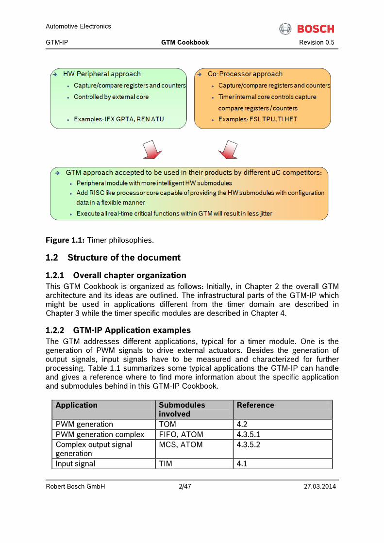
1.1 Background To date there can be found two timer philosophies on the market. One uses a more hardware centric approach where the timer module consists of capture/compare units and counters. This comparators and counters are controlled with an external processing unit or co-processor. The second approach uses a more processing oriented approach with a micro machine that is programmable and fulfils timer specific tasks. Because of the timer specific functionality, the assembler code often consists of timer specific instructions. While the hardware centric approach has the problem, that the external core has to answer a lot of interrupts for controlling the timer module via the microcontroller bus system, the software centric approach with the micro machine often has a lower resolution for the signal processing and is hard to program because of the very special instruction sets. The GTM combines both the approaches and uses the best of both worlds. While there are some submodules that can fulfil a specific function in hardware, there is a RISC-like processing engine build within the GTM that can do a kind of signal processing and flexible signal generation. Therefore, while the hardware centric submodules offer real time processing capabilities, the RISC-like processing engine adds flexibility to the GTM, while the instruction set is easy to understand and comparable to general purpose CPU cores. Figure 1.1 shows the timer philosophies and their correspondence to the GTM.
Automotive Electronics GTM-IP GTM Cookbook Revision 0.5
Robert Bosch GmbH 2/47 27.03.2014
Figure 1.1: Timer philosophies.
1.2 Structure of the document
1.2.1 Overall chapter organization This GTM Cookbook is organized as follows: Initially, in Chapter 2 the overall GTM architecture and its ideas are outlined. The infrastructural parts of the GTM-IP which might be used in applications different from the timer domain are described in Chapter 3 while the timer specific modules are described in Chapter 4.
1.2.2 GTM-IP Application examples The GTM addresses different applications, typical for a timer module. One is the generation of PWM signals to drive external actuators. Besides the generation of output signals, input signals have to be measured and characterized for further processing. Table 1.1 summarizes some typical applications the GTM-IP can handle and gives a reference where to find more information about the specific application and submodules behind in this GTM-IP Cookbook.
Application Submodules involved
Reference
PWM generation TOM 4.2 PWM generation complex FIFO, ATOM 4.3.5.1 Complex output signal generation
MCS, ATOM 4.3.5.2
Input signal TIM 4.1
Automotive Electronics GTM-IP GTM Cookbook Revision 0.5
Robert Bosch GmbH 3/47 27.03.2014
characterization Input signal measurement (PWM, pulses)
TIM 4.1
Engine angle clock for motor management
TIM, MAP, DPLL 4.5 and Application note AN011
Shift register output ATOM 4.3.3.4 Drive BLDC Engine TIM, SPE, TOM 4.6
Table 1.1: GTM application scenarios. Besides this GTM-IP Cookbook there are GTM-IP application examples which can be used to understand some more of the functions and features of the GTM. All these application notes are designed to run on the GTM-RM. The GTM-RM is an executable model of the GTM written in SystemC. There is no additional software or tooling required to run the reference model since it is an executable file for windows PCs. In general the GTM-IP integration test set can give an understanding of the very basic behavior like input signal sampling, output signal and interrupt generation. The other application notes describe more complex application examples especially with more submodules involved.
Automotive Electronics GTM-IP GTM Cookbook Revision 0.5
Robert Bosch GmbH 4/47 27.03.2014
2 GTM Architecture overview
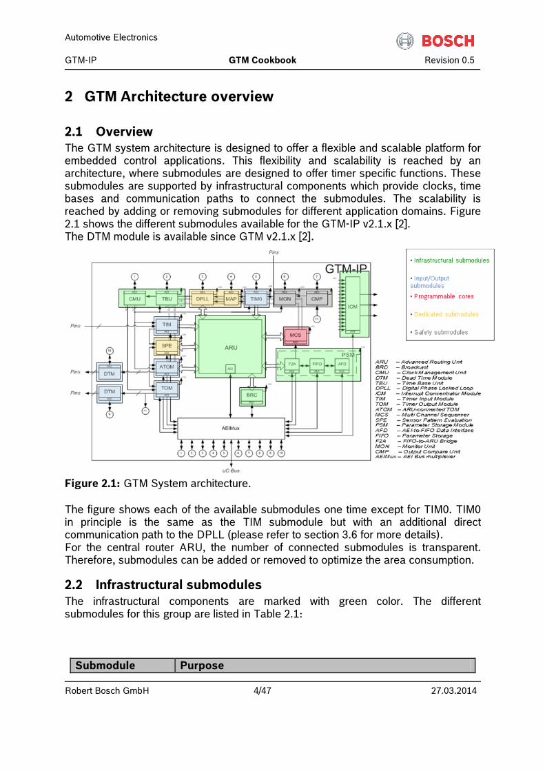
2.1 Overview The GTM system architecture is designed to offer a flexible and scalable platform for embedded control applications. This flexibility and scalability is reached by an architecture, where submodules are designed to offer timer specific functions. These submodules are supported by infrastructural components which provide clocks, time bases and communication paths to connect the submodules. The scalability is reached by adding or removing submodules for different application domains. Figure 2.1 shows the different submodules available for the GTM-IP v2.1.x [2]. The DTM module is available since GTM v2.1.x [2].
Figure 2.1: GTM System architecture. The figure shows each of the available submodules one time except for TIM0. TIM0 in principle is the same as the TIM submodule but with an additional direct communication path to the DPLL (please refer to section 3.6 for more details). For the central router ARU, the number of connected submodules is transparent. Therefore, submodules can be added or removed to optimize the area consumption.
2.2 Infrastructural submodules The infrastructural components are marked with green color. The different submodules for this group are listed in Table 2.1:
Submodule Purpose
Automotive Electronics GTM-IP GTM Cookbook Revision 0.5
Robert Bosch GmbH 5/47 27.03.2014
CMU Offers clock prescalers for GTM internal modules and counters.
TBU Offers 24 bit wide time bases distributed on time base buses to the submodules.
ICM Interrupt concentrator to bundle GTM internal interrupts to reduce the number of interrupt lines to the surrounding µC system.
PSM Parameter Storage Module which can be used as a FIFO to bring parameters into and get values out of the GTM.
BRC Broadcast data routed through the central router to more than one destination.
ARU Advanced routing unit to route 53 bits of data in a time multiplexed manner.
Table 2.1: GTM Infrastructural components.
2.3 Input/Output submodules A timer needs input ports to sample external signals and needs output modules to generate signals to drive the outside world. These modules are marked blue in Figure 2.1. Table 2.2 lists the input and output submodules of the GTM-IP:
Submodule Purpose TIM The Timer Input Module offers eight (8) input channels,
where incoming signals can be characterized or measured. TOM The Timer Output Module offers 16 channels for PWM
generation. Each channel is able to either run independent from the others or in relation to other TOM channels.
ATOM This ARU connected Timer Output Module can generate PWM signals or complex output sequences on behalf of time stamps. Also a shifter unit is implemented.
DTM Available since GTM-IP Specification v2.1.x [2]. The Dead Time Module provides hardware support for dead time generation, i.e. it generates out of one PWM signal additionally the inverse PWM signal and relaxes the edges of both signals. Additionally the Dead Time Module module can be used to combine TOM or ATOM output signals.
Table 2.2: GTM Input/Output submodules.
2.4 Programmable core There is a RISC-like programmable core (MCS) inside of the GTM marked red in Figure 2.1. This core has its own internal RAM where the code and data can be stored. With this core it is possible to operate on input signals and to generate
Automotive Electronics GTM-IP GTM Cookbook Revision 0.5
Robert Bosch GmbH 6/47 27.03.2014
complex output signals. The input signals are routed via the ARU to the MCS and the output commands are routed via the ARU to the ATOM. It is also possible to add more than one MCS submodule to the GTM, thus true multi core architectures with multiple cores working in parallel can be build with the GTM.
2.5 Application specific submodules The GTM-IP actually implements three (3) application specific submodules which are mainly driven by the engine management sector. These submodules are marked with yellow color in Figure 2.1 and are listed in Table 2.3:
Submodule Purpose DPLL The DPLL is used for engine positioning detection and
signalling (angle clock). MAP The MAP module is responsible to map the signals
sampled at the TIM0 inputs to the DPLL input ports TRIGGER and STATE.
SPE The SPE submodule offers together in the chain TIM SPE TOM a function for BLDC input pattern detection and BLDC output pattern generation.
Table 2.3: Application specific submodules.
2.6 Submodules to support functional safety The GTM provides two (2) submodules to support safety critical functions. These submodules are marked grey in Figure 2.1 and are listed in Table 2.4:
Submodule Purpose CMP The CMP submodule can compare two adjacent channel
outputs from TOM or ATOM submodules and raises an error, when the two signals are not identical. Therefore, redundancy can be generated on two adjacent TOM and ATOM output channels.
MON The MON submodule monitors the GTM internal clocks and the MCS functionality.
Table 2.4: Safety submodules.
2.7 GTM Routing mechanism
2.7.1 Overview and ARU data word One key element of the GTM is the communication scheme between the submodules of the GTM. Such communication is especially necessary when the GTM is expected to work independent of a CPU. In that case, an input signal can be captured and characterized at the input submodule TIM. The result than can be transferred to the
Automotive Electronics GTM-IP GTM Cookbook Revision 0.5
Robert Bosch GmbH 7/47 27.03.2014
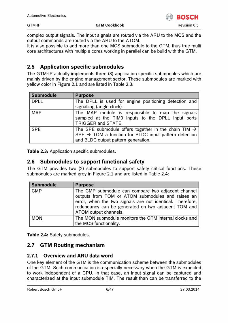
MCS to process the data and the MCS can trigger an ATOM to generate an output signal. Both communication paths are directed through the central router ARU. The routing data width is 53 bits, where two times 24 bit is the data and five (5) bits can be used as ARU Control Bits (ACB). The ARU routing data is organized as shown in Figure 2.2.
Figure 2.2: ARU Routing data organization.
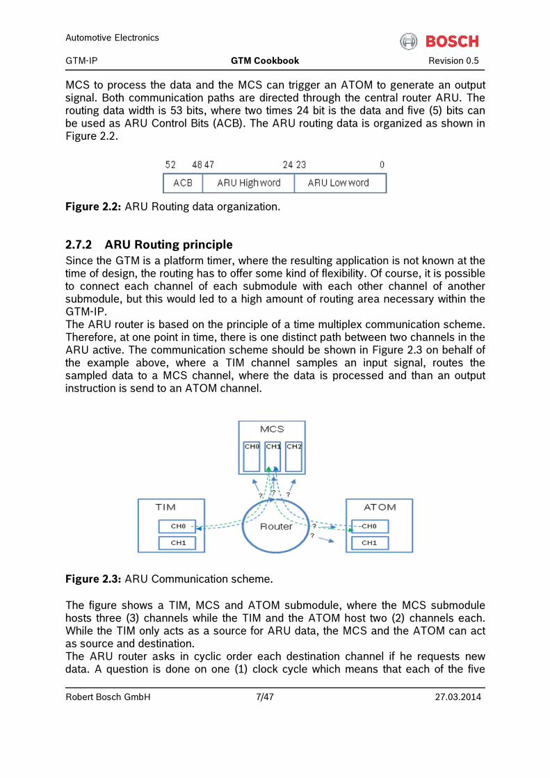
2.7.2 ARU Routing principle Since the GTM is a platform timer, where the resulting application is not known at the time of design, the routing has to offer some kind of flexibility. Of course, it is possible to connect each channel of each submodule with each other channel of another submodule, but this would led to a high amount of routing area necessary within the GTM-IP. The ARU router is based on the principle of a time multiplex communication scheme. Therefore, at one point in time, there is one distinct path between two channels in the ARU active. The communication scheme should be shown in Figure 2.3 on behalf of the example above, where a TIM channel samples an input signal, routes the sampled data to a MCS channel, where the data is processed and than an output instruction is send to an ATOM channel.
Figure 2.3: ARU Communication scheme. The figure shows a TIM, MCS and ATOM submodule, where the MCS submodule hosts three (3) channels while the TIM and the ATOM host two (2) channels each. While the TIM only acts as a source for ARU data, the MCS and the ATOM can act as source and destination. The ARU router asks in cyclic order each destination channel if he requests new data. A question is done on one (1) clock cycle which means that each of the five
Automotive Electronics GTM-IP GTM Cookbook Revision 0.5
Robert Bosch GmbH 8/47 27.03.2014
MCS and ATOM channels is asked every five (5) clock cycles. This is also the maximum delay that data could have when it should be routed from a source to a destination. In general, the router cycle time is determined by the number of destination channels connected to the router. Since this routing time could become very high for big GTM devices, the router can be doubled, to get half the routing delay. The routing time can be determined from the GTM specification for each individual GTM device. The green arrows represent the data flow of the data from the TIM to the ATOM channels. Since the MCS channel has to request the data first from the TIM input channel, the request can be raised just after the ARU router has asked him if data is requested. Thus, one ARU round would take place before new TIM input data can be transferred to the MCS channel. The MCS channel than would process the TIM input data and can provide ATOM output control data to the ATOM. This output data is requested by the ATOM channel, whenever the channel is ready to process new data. In general, the routing requests by destinations are blocking ones, which means that the destination channel requests as long data as long there is no new data available at the source. This means that the ATOM channel will block as long as the MCS channel has not provided new data on behalf of its calculations. Therefore, the calculation could be finished and new data could be scheduled at the ARU router just after the cycle, the ARU router has asked the ATOM channel if data is requested. The ATOM channel will be left blocking until one more ARU round trip has taken place, which leds also to a delay of one ARU round trip cycle
2.7.3 ARU Data path definition The blue arrows in Figure 2.3 represent the data path definition, which can be done during runtime by the software. To do this, each destination channel has a software programmable register, where a so called ARU read address can be defined by the software. In contrast to this register, each GTM channel which can act as a source to the ARU has a hard coded ARU write address. Let’s assume that the write addresses are defined by the hardware as shown in Table 2.5.
Submodule channel Write address TIM Channel 0 1 TIM Channel 1 2 MCS Channel 0 3 MCS Channel 1 4 MCS Channel 2 5 ATOM Channel 0 6 ATOM Channel 1 7
Table 2.5: Example for an ARU write address definition scheme.
Automotive Electronics GTM-IP GTM Cookbook Revision 0.5
Robert Bosch GmbH 9/47 27.03.2014
Then, the MCS read address has to be defined by the software to 1, and the ATOM read address has to be defined to 4.
2.7.4 ARU Blocking mechanism As mentioned above, the ATOM channel will block its operation as long as there is no new data provided by the MCS. The same holds for the MCS channel which blocks when now new data is available from the TIM input (in fact there can also non-blocking requests be done by the MCS). The ARU blocking mechanism is an important architectural feature of the GTM-IP. With this mechanism it is possible for a channel to be inactive as long as no new input data is available for the channel. For example, the MCS will block, until the TIM channel has received and processed new input data. Therefore, no interrupt is necessary for the MCS which informs the MCS channel about new data at the input. The MCS channel will just be provided by the router with the new data from the TIM channel and can proceed to work. By this construction, there is no need for an internal interrupt handling mechanism and controller. This role is established by the router.
Automotive Electronics GTM-IP GTM Cookbook Revision 0.5
Robert Bosch GmbH 10/47 27.03.2014
3 GTM-IP Infrastructural submodules
This chapter describes the other infrastructural submodules besides the central router that can be used by the application to implement timer functionality.
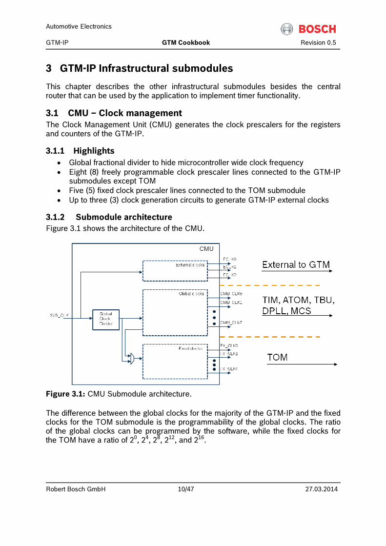
3.1 CMU – Clock management The Clock Management Unit (CMU) generates the clock prescalers for the registers and counters of the GTM-IP.
3.1.1 Highlights • Global fractional divider to hide microcontroller wide clock frequency • Eight (8) freely programmable clock prescaler lines connected to the GTM-IP
submodules except TOM • Five (5) fixed clock prescaler lines connected to the TOM submodule • Up to three (3) clock generation circuits to generate GTM-IP external clocks
3.1.2 Submodule architecture Figure 3.1 shows the architecture of the CMU.
Figure 3.1: CMU Submodule architecture. The difference between the global clocks for the majority of the GTM-IP and the fixed clocks for the TOM submodule is the programmability of the global clocks. The ratio of the global clocks can be programmed by the software, while the fixed clocks for the TOM have a ratio of 20, 24, 28, 212, and 216.
Automotive Electronics GTM-IP GTM Cookbook Revision 0.5
Robert Bosch GmbH 11/47 27.03.2014
3.2 TBU – Timer time base generation The Time Base Unit (TBU) generates the global time base for the GTM-IP. The TBU is channel based where each channel can generate an independent time base. Each time base has a bit width of 24 bit. Time base channels are designed to also connect to angle clock (DPLL, see section 4.5). These channels can count forward and backward dependent on the rotation of an associated engine rotation.
3.2.1 Highlights • Up to three independent 24bit time bases • Two of three time bases can be driven to count forward and backward • Application example 1:
o TimeBase0: System time o TimeBase1: Combustion engine angle clock
• Application example 2: o TimeBase0: System time o TimeBase1: Hybrid engine angle clock0 o TimeBase2: Hybrid engine angle clock1
3.3 PSM – Parameter storage module The Parameter Storage Module (PSM) can be used to transfer data to and from the GTM-IP in a buffered way. Thus, this helps to decrease the interrupt load of the CPU because the data is stored inside of the PSM and interrupts are only generated, when programmable thresholds are reached. The PSM has an ARU interface and can act as source and destination at the ARU. The PSM can be organized as a FIFO where the data is transferred in first-in-first-out order. A second possibility is to configure the PSM as a ring buffer, where the CPU writes in a bunch of data values which are served to destinations connected to the ARU as a ring buffer.
3.3.1 Highlights • Eight (8) independent channels with programmable depth • Programmable thresholds for interrupt generation
o High watermark (indicating that data stored from ARU will soon overflow the storage space)
o Low watermark (indicating that data transferred to ARU will soon be transferred and storage will get empty (which will block the destination))
• PSM empty and full interrupts • FIFO and ring buffer modes • PSM is very helpful for application testing and debugging
3.4 BRC – Broadcast Due to the operation principle of the ARU routing mechanism, data which is transferred to a destination is deleted inside of the source and cannot be read by a
Automotive Electronics GTM-IP GTM Cookbook Revision 0.5
Robert Bosch GmbH 12/47 27.03.2014
second destination channel. This operation principle has the advantage that a source always forces a destination to block, until new and valid data is generated. Otherwise, the ARU blocking mechanism would not work. To overcome the limitation to not distribute source data to more than two consumers, the Broadcast submodule (BRC) can be used.
3.4.1 Highlights • Programmable number of channels for data distribution • Trash bin functionality to consume data from a source module
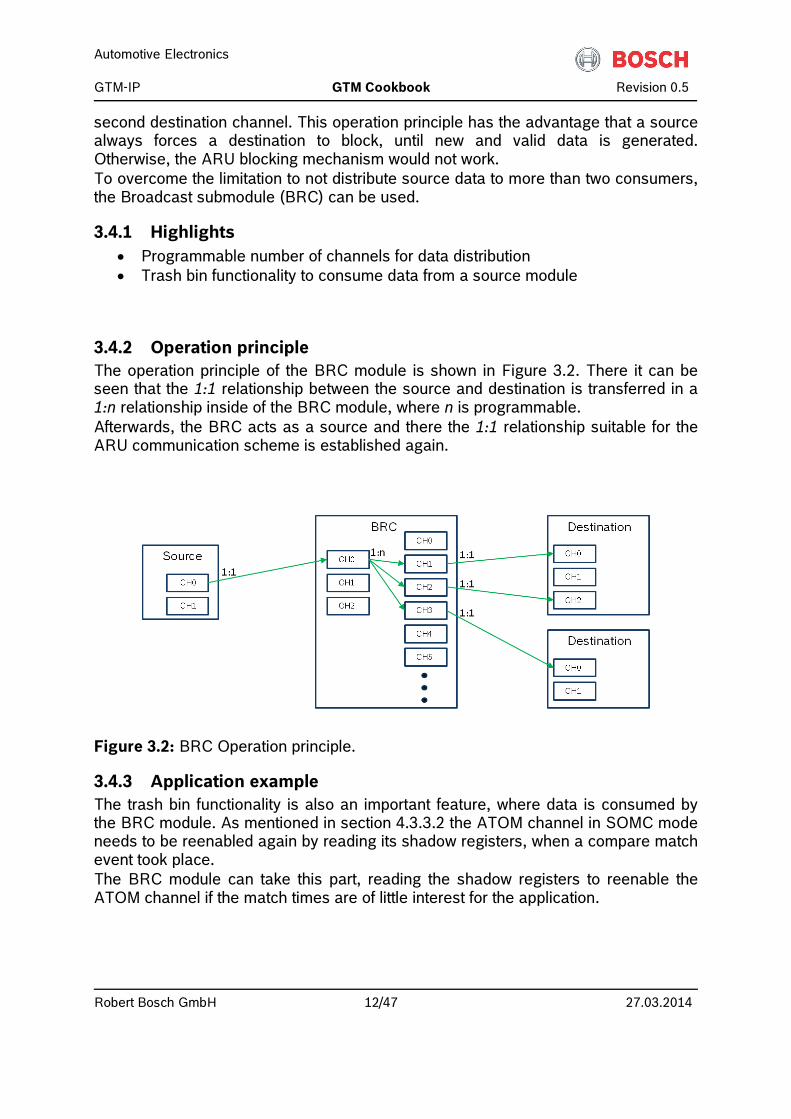
3.4.2 Operation principle The operation principle of the BRC module is shown in Figure 3.2. There it can be seen that the 1:1 relationship between the source and destination is transferred in a 1:n relationship inside of the BRC module, where n is programmable. Afterwards, the BRC acts as a source and there the 1:1 relationship suitable for the ARU communication scheme is established again.
Figure 3.2: BRC Operation principle.
3.4.3 Application example The trash bin functionality is also an important feature, where data is consumed by the BRC module. As mentioned in section 4.3.3.2 the ATOM channel in SOMC mode needs to be reenabled again by reading its shadow registers, when a compare match event took place. The BRC module can take this part, reading the shadow registers to reenable the ATOM channel if the match times are of little interest for the application.
Automotive Electronics GTM-IP GTM Cookbook Revision 0.5
Robert Bosch GmbH 13/47 27.03.2014
4 GTM-IP Operational submodules
This chapter tries to explain in brief words the tasks and responsibilities of the GTM-IP submodules to help the GTM to fulfil its function as a timer module. The description starts with the GTM input functions and explains further the GTM output functions. The chapter ends with the application specific submodules.
4.1 TIM – Input signal characterization and measurement The Timer Input Module (TIM) is responsible for the input signal characterization in the GTM-IP.
4.1.1 Highlights • Dedicated filter mechanism with two different filter strategies and edge filter
thresholds for each channel • Shadow registers to hold measurement data while new input signal is
processed • Control by CPU and/or ARU possible • Five different edge characterization modes configurable
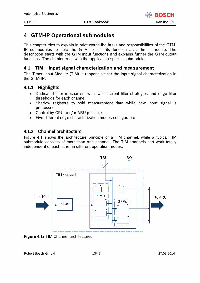
4.1.2 Channel architecture Figure 4.1 shows the architecture principle of a TIM channel, while a typical TIM submodule consists of more than one channel. The TIM channels can work totally independent of each other in different operation modes.
Figure 4.1: TIM Channel architecture.
Automotive Electronics GTM-IP GTM Cookbook Revision 0.5
Robert Bosch GmbH 14/47 27.03.2014
In general a TIM channel consists of a filter unit and a signal measurement unit where incoming signals are processed. It is possible to apply different filter strategies and even different filter time thresholds for the two different edges of an input signal. When an input signal edge is marked as valid by the filter, the signal edge is routed to the measurement unit where the edge is registered by an eight (8) bit edge counter and processed by the SMU. Processing means for example counting the edges or measuring the signal level time. When a measurement interval has finished (e.g. PWM duty cycle and period duration is determined for the last PWM period), the signal characteristics are stored in the two general purpose registers GPRs and a five bit status register. An interrupt is raised to the CPU when enabled and/or the data in the GPRs is marked as valid for the ARU. The CPU and/or ARU now can sample the data in the GPRs while a new measurement takes place in the SMU part. The data in the GPRs has to be processed before a new measurement cycle finishes. Otherwise, an overflow bit would be set in the five status bits and the characteristics of the newest measurement are stored in the GPRs overwriting the old ones.
4.1.3 Operation modes Each TIM channel offers different operation modes where the registers inside of the GTM have a different meaning. The operation modes and their functionality are listed in Table 4.1.
TIM Operation mode Functionality TIM PWM Measurement mode (TPWM)
In TPWM, the TIM channel measures the duty cycle duration and period length of an incoming signal in number of clock ticks of a selectable prescaler clock from CMU. The duty cycle level is configurable. Measurement starts with first relevant signal edge, e.g. rising edge when duty signal level is configured as high.
TIM Pulse Integration Mode (TPIM)
In TPIM, the length of high or low signal phases is measured and accumulated in amount of a selectable prescaler clock ticks from CMU. It is configurable if pulse high or low times are measured. Measurement starts with first relevant signal edge, e.g. rising edge when high signal level durations should be accumulated.
TIM Input Event Mode (TIEM)
In TIEM, edges at the TIM input channel can be characterized with either two different time stamps or a time stamp and an edge counter. It is configurable if both edges or only rising or falling edges should be considered as an input
Automotive Electronics GTM-IP GTM Cookbook Revision 0.5
Robert Bosch GmbH 15/47 27.03.2014
event. Measurement starts with the first relevant edge.
TIM Input Prescaler Mode (TIPM)
In TIPM, the TIM channel can be configured to downstream the input data frequency by defining the number of measured edges that should pass before an event is generated for the system and a time stamp value is sampled in the GPRs. It is configurable if both edges or only rising or falling edges should be considered for prescaling. Measurement starts with the first relevant edge.
TIM Bit Compression Mode (TBCM)
The TBCM is a mode where all input signals of a TIM submodule are considered in parallel by channel 0. E.g. when eight (8) channels are present in a TIM submodule it is possible to generate an eight (8) bit word for the eight different input levels. This eight bit word is sampled in channel 0 and is always updated when any edge on one of the eight input channels occurs.
Table 4.1: TIM Operation modes.
4.2 TOM – Dedicated PWM Generation The Timer Output Module (TOM) can be used to generate PWM signals that are dependent or independent of each other.
4.2.1 Highlights • Dedicated PWM time base counter for each channel (16 bit wide) • Shadow registers for PWM update and clock prescaler selection • Change of clock prescaler allows for a wide range of PWM durations with
different resolution factors • Dependent PWM generation possible by chaining the individual PWM time
base counters • Pulse count modulated output signal possible on one dedicated channel of
TOM submodule to emulate a DAC • Global trigger unit to start/stop, enable and disable a bunch of TOM channels
in parallel • Greater/equal comparators for asynchronous change of PWM duty cycle and
period
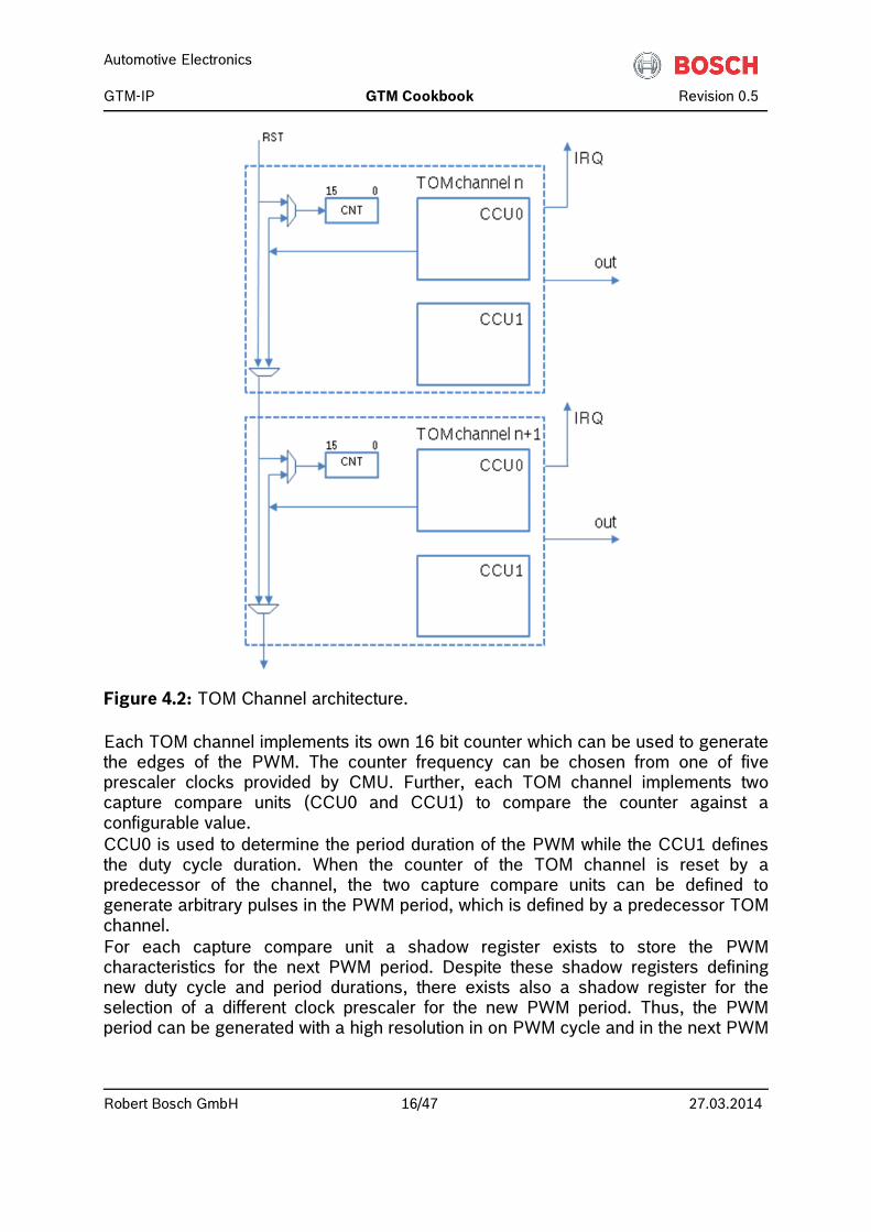
4.2.2 Channel architecture The architecture of two TOM submodule channels is shown in Figure 4.2.
Automotive Electronics GTM-IP GTM Cookbook Revision 0.5
Robert Bosch GmbH 16/47 27.03.2014
Figure 4.2: TOM Channel architecture. Each TOM channel implements its own 16 bit counter which can be used to generate the edges of the PWM. The counter frequency can be chosen from one of five prescaler clocks provided by CMU. Further, each TOM channel implements two capture compare units (CCU0 and CCU1) to compare the counter against a configurable value. CCU0 is used to determine the period duration of the PWM while the CCU1 defines the duty cycle duration. When the counter of the TOM channel is reset by a predecessor of the channel, the two capture compare units can be defined to generate arbitrary pulses in the PWM period, which is defined by a predecessor TOM channel. For each capture compare unit a shadow register exists to store the PWM characteristics for the next PWM period. Despite these shadow registers defining new duty cycle and period durations, there exists also a shadow register for the selection of a different clock prescaler for the new PWM period. Thus, the PWM period can be generated with a high resolution in on PWM cycle and in the next PWM
Automotive Electronics GTM-IP GTM Cookbook Revision 0.5
Robert Bosch GmbH 17/47 27.03.2014
cycle a very large PWM period with a reduced resolution can be generated with a lower clock frequency.
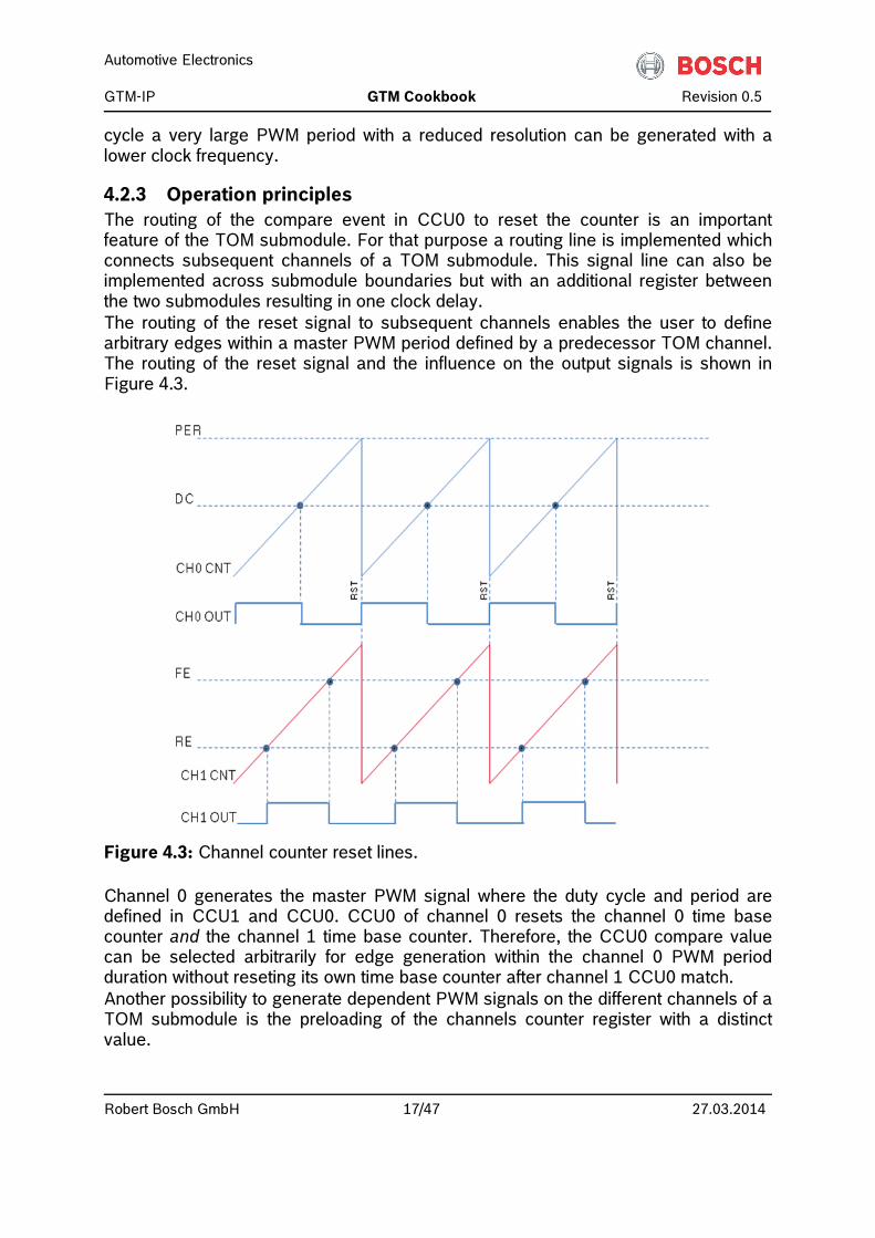
4.2.3 Operation principles The routing of the compare event in CCU0 to reset the counter is an important feature of the TOM submodule. For that purpose a routing line is implemented which connects subsequent channels of a TOM submodule. This signal line can also be implemented across submodule boundaries but with an additional register between the two submodules resulting in one clock delay. The routing of the reset signal to subsequent channels enables the user to define arbitrary edges within a master PWM period defined by a predecessor TOM channel. The routing of the reset signal and the influence on the output signals is shown in Figure 4.3.
Figure 4.3: Channel counter reset lines. Channel 0 generates the master PWM signal where the duty cycle and period are defined in CCU1 and CCU0. CCU0 of channel 0 resets the channel 0 time base counter and the channel 1 time base counter. Therefore, the CCU0 compare value can be selected arbitrarily for edge generation within the channel 0 PWM period duration without reseting its own time base counter after channel 1 CCU0 match. Another possibility to generate dependent PWM signals on the different channels of a TOM submodule is the preloading of the channels counter register with a distinct value.
Automotive Electronics GTM-IP GTM Cookbook Revision 0.5
Robert Bosch GmbH 18/47 27.03.2014
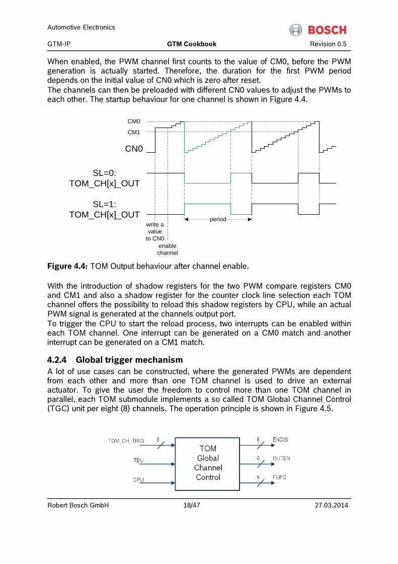
When enabled, the PWM channel first counts to the value of CM0, before the PWM generation is actually started. Therefore, the duration for the first PWM period depends on the initial value of CN0 which is zero after reset. The channels can then be preloaded with different CN0 values to adjust the PWMs to each other. The startup behaviour for one channel is shown in Figure 4.4.
CN0
SL=0: TOM_CH[x]_OUT
CM1
CM0
SL=1: TOM_CH[x]_OUT
enablechannel
write a value
to CN0
period
Figure 4.4: TOM Output behaviour after channel enable. With the introduction of shadow registers for the two PWM compare registers CM0 and CM1 and also a shadow register for the counter clock line selection each TOM channel offers the possibility to reload this shadow registers by CPU, while an actual PWM signal is generated at the channels output port. To trigger the CPU to start the reload process, two interrupts can be enabled within each TOM channel. One interrupt can be generated on a CM0 match and another interrupt can be generated on a CM1 match.
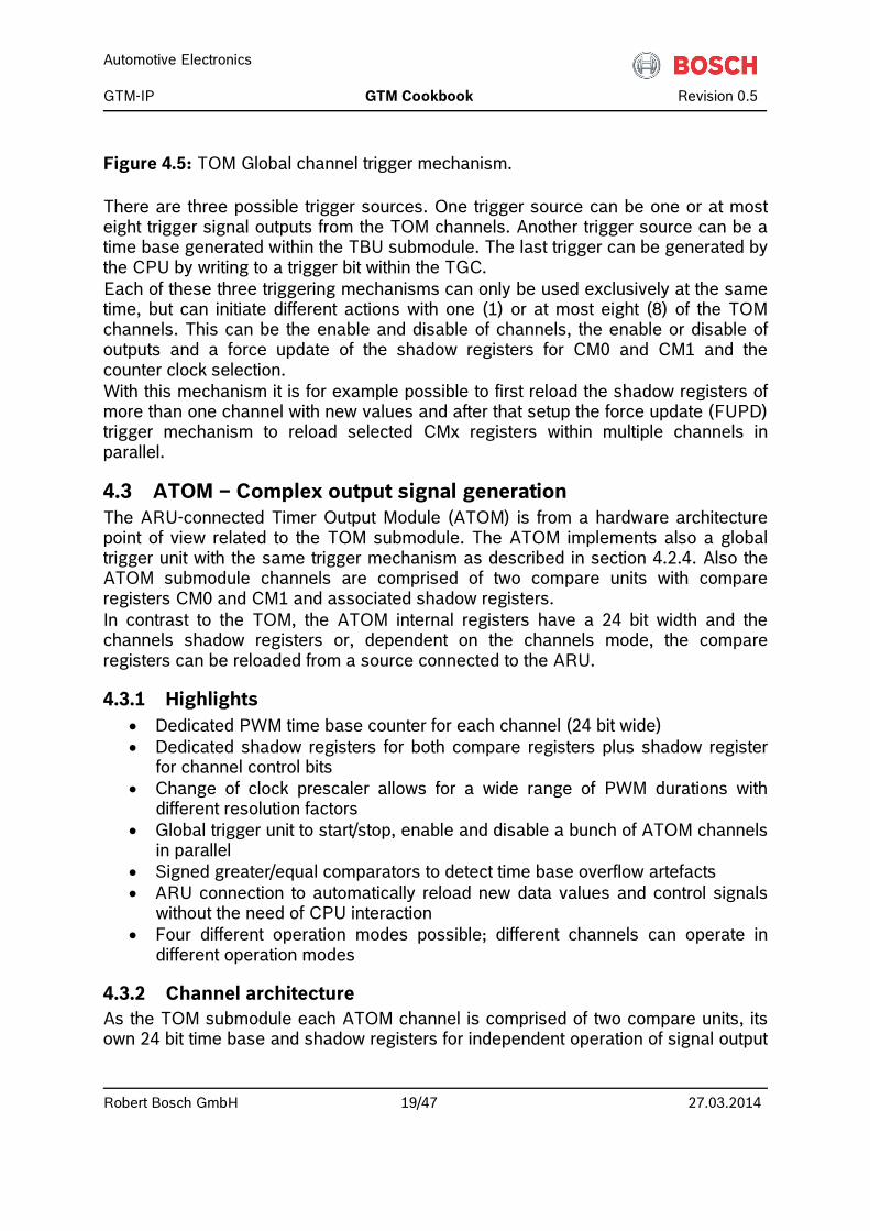
4.2.4 Global trigger mechanism A lot of use cases can be constructed, where the generated PWMs are dependent from each other and more than one TOM channel is used to drive an external actuator. To give the user the freedom to control more than one TOM channel in parallel, each TOM submodule implements a so called TOM Global Channel Control (TGC) unit per eight (8) channels. The operation principle is shown in Figure 4.5.
Automotive Electronics GTM-IP GTM Cookbook Revision 0.5
Robert Bosch GmbH 19/47 27.03.2014
Figure 4.5: TOM Global channel trigger mechanism. There are three possible trigger sources. One trigger source can be one or at most eight trigger signal outputs from the TOM channels. Another trigger source can be a time base generated within the TBU submodule. The last trigger can be generated by the CPU by writing to a trigger bit within the TGC. Each of these three triggering mechanisms can only be used exclusively at the same time, but can initiate different actions with one (1) or at most eight (8) of the TOM channels. This can be the enable and disable of channels, the enable or disable of outputs and a force update of the shadow registers for CM0 and CM1 and the counter clock selection. With this mechanism it is for example possible to first reload the shadow registers of more than one channel with new values and after that setup the force update (FUPD) trigger mechanism to reload selected CMx registers within multiple channels in parallel.
4.3 ATOM – Complex output signal generation The ARU-connected Timer Output Module (ATOM) is from a hardware architecture point of view related to the TOM submodule. The ATOM implements also a global trigger unit with the same trigger mechanism as described in section 4.2.4. Also the ATOM submodule channels are comprised of two compare units with compare registers CM0 and CM1 and associated shadow registers. In contrast to the TOM, the ATOM internal registers have a 24 bit width and the channels shadow registers or, dependent on the channels mode, the compare registers can be reloaded from a source connected to the ARU.
4.3.1 Highlights • Dedicated PWM time base counter for each channel (24 bit wide) • Dedicated shadow registers for both compare registers plus shadow register
for channel control bits • Change of clock prescaler allows for a wide range of PWM durations with
different resolution factors • Global trigger unit to start/stop, enable and disable a bunch of ATOM channels
in parallel • Signed greater/equal comparators to detect time base overflow artefacts • ARU connection to automatically reload new data values and control signals
without the need of CPU interaction • Four different operation modes possible; different channels can operate in
different operation modes
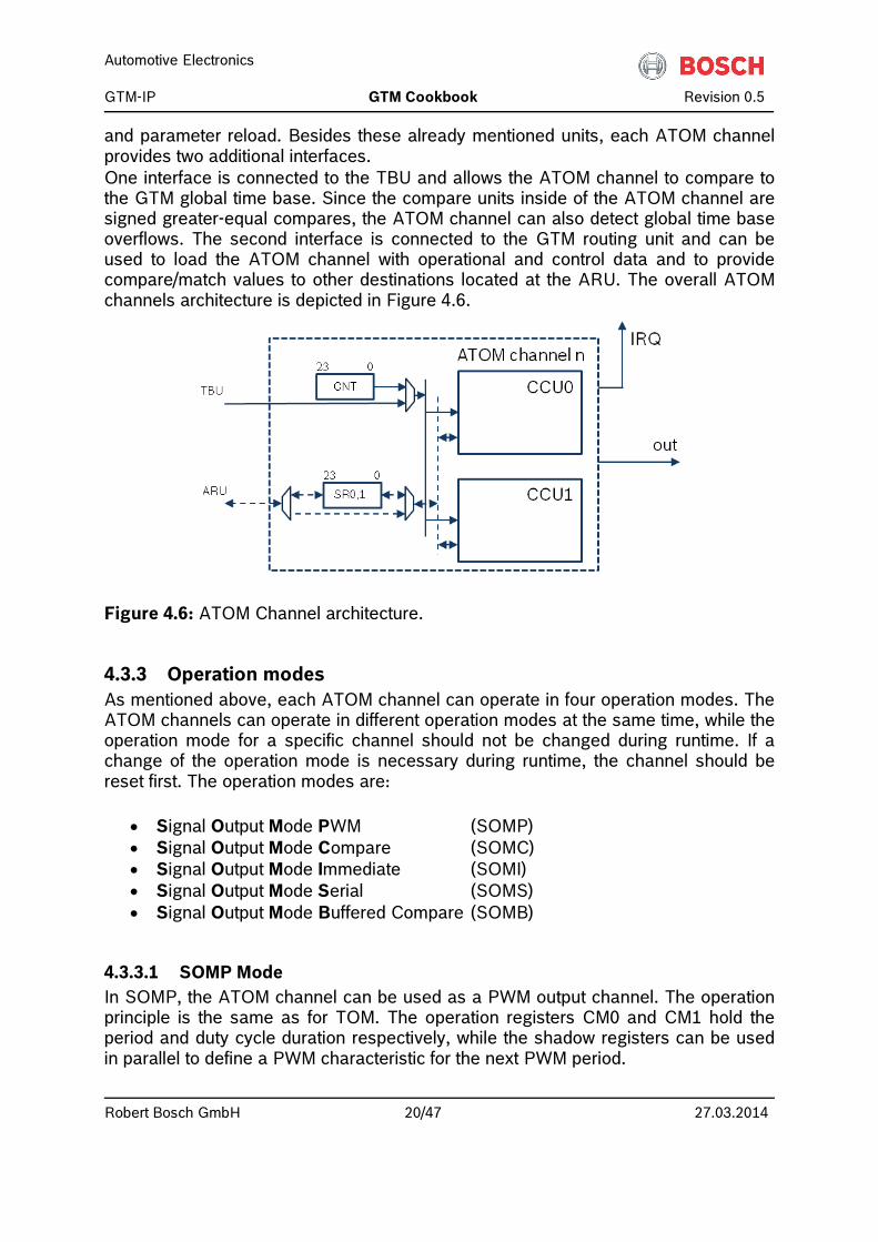
4.3.2 Channel architecture As the TOM submodule each ATOM channel is comprised of two compare units, its own 24 bit time base and shadow registers for independent operation of signal output
Automotive Electronics GTM-IP GTM Cookbook Revision 0.5
Robert Bosch GmbH 20/47 27.03.2014
and parameter reload. Besides these already mentioned units, each ATOM channel provides two additional interfaces. One interface is connected to the TBU and allows the ATOM channel to compare to the GTM global time base. Since the compare units inside of the ATOM channel are signed greater-equal compares, the ATOM channel can also detect global time base overflows. The second interface is connected to the GTM routing unit and can be used to load the ATOM channel with operational and control data and to provide compare/match values to other destinations located at the ARU. The overall ATOM channels architecture is depicted in Figure 4.6.
Figure 4.6: ATOM Channel architecture.
4.3.3 Operation modes As mentioned above, each ATOM channel can operate in four operation modes. The ATOM channels can operate in different operation modes at the same time, while the operation mode for a specific channel should not be changed during runtime. If a change of the operation mode is necessary during runtime, the channel should be reset first. The operation modes are:
• Signal Output Mode PWM (SOMP) • Signal Output Mode Compare (SOMC) • Signal Output Mode Immediate (SOMI) • Signal Output Mode Serial (SOMS) • Signal Output Mode Buffered Compare (SOMB)
4.3.3.1 SOMP Mode In SOMP, the ATOM channel can be used as a PWM output channel. The operation principle is the same as for TOM. The operation registers CM0 and CM1 hold the period and duty cycle duration respectively, while the shadow registers can be used in parallel to define a PWM characteristic for the next PWM period.
Automotive Electronics GTM-IP GTM Cookbook Revision 0.5
Robert Bosch GmbH 21/47 27.03.2014
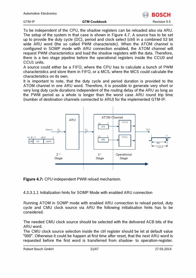
To be independent of the CPU, the shadow registers can be reloaded also via ARU. The setup of the system in that case is shown in Figure 4.7. A source has to be set up to provide the duty cycle (DC), period and clock select (ctrl) in a combined 53 bit wide ARU word (the so called PWM characteristic). When the ATOM channel is configured in SOMP mode with ARU connection enabled, the ATOM channel will request PWM characteristics and load the shadow registers with the data. Therefore, there is a two stage pipeline before the operational registers inside the CCU0 and CCU1 units. A source could either be a FIFO, where the CPU has to calculate a bunch of PWM characteristics and store them in FIFO, or a MCS, where the MCS could calculate the characteristics on its own. It is important to note, that the duty cycle and period duration is provided to the ATOM channel in one ARU word. Therefore, it is possible to generate very short or very long duty cycle durations independent of the routing delay of the ARU as long as the PWM period as a whole is longer than the worst case ARU round trip time (number of destination channels connected to ARU) for the implemented GTM-IP.
Figure 4.7: CPU-independent PWM reload mechanism.
4.3.3.1.1 Initialization hints for SOMP Mode with enabled ARU connection Running ATOM in SOMP mode with enabled ARU connection to reload period, duty cycle and CMU clock source via ARU the following initialisation hints has to be considered. The needed CMU clock source should be selected with the delivered ACB bits of the ARU word. The CMU clock source selection inside the ctrl register should be let at default value “000”. Otherwise it could be happen at first time after reset, that the next ARU word is requested before the first word is transferred from shadow- to operation-register.
Automotive Electronics GTM-IP GTM Cookbook Revision 0.5
Robert Bosch GmbH 22/47 27.03.2014
Depending on the frequency of the (pre-) selected CMU clock source it could be happened that the first values will be overwritten from the next ARU word – so the first ARU word will be lost. If it is necessary to pre-select the CMU clock source using the ctrl register, the operation register CM0 for the period has to be configured to ‘1’ to prevent data loss as described before.
4.3.3.2 SOMC Mode SOMC Mode is the most complex mode of the ATOM submodule. This mode should be used, if very complex output sequences should be generated, which can also be dependent on each other. Therefore, output signal changes are not defined on behalf of the independent counter registers within each channel, but with the global time bases generated by the TBU submodule. For this mode the doted signal path is used that is drawn in Figure 4.6. In this mode either the CPU or a source connected to ARU can provide the compare values to the ATOM channel. The compare registers inside of the CCU0 and CCU1 units can be updated with new compare values as long as no match event was detected by one of the compare units. After the match event the actual TBU time base values are stored within the shadow registers and marked as valid for transmission to the ARU when the ARU is enabled. Further on, it is possible to write new compare values into the operational registers, but these compare values will have no effect. Either the CPU or a destination connected to the ARU have to read at least one value from one shadow register to reenable the compare mechanism and written compare values have effect afterwards. There are five control bits used to control the compare mechanism inside of the two compare units. Two bits are used to define the output action, no action, set to ‘1’, set to ‘0’ and toggle. The three other bits are used to define a compare strategy, compare in CCU0 only, CCU1 only, compare in both at the same time and even use in one compare unit another TBU time base value than in the other one. With this construction, it is possible to define an output signal event even on two different time bases. The five control bits can be provided by CPU or by a source connected to the ARU and are valid as long as the match event not yet occurred.
4.3.3.3 SOMI Mode The SOMI mode is intended for use in combination with the ARU and when the ATOM channels output signal is allowed to jitter. In this mode, the ATOM channel requests data from the ARU and only looks on the control bit part of the ARU data word. This control bit part defines the output action the ATOM channel does immediately after he received the data from the ARU. Therefore, and because the ARU communication scheme is a time multiplexed communication methodology, the output at the ATOM channel can jitter with a maximum delay of one ARU round trip time when a source provides ARU data.
Automotive Electronics GTM-IP GTM Cookbook Revision 0.5
Robert Bosch GmbH 23/47 27.03.2014
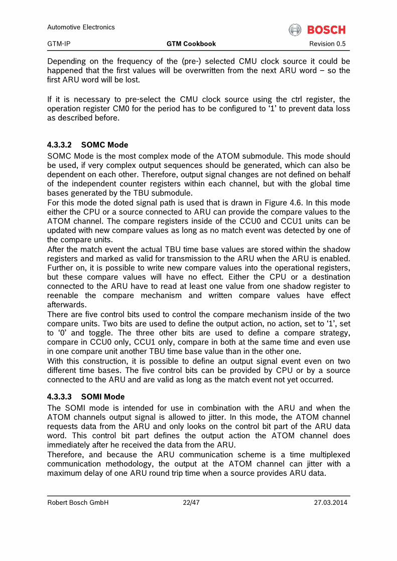
4.3.3.4 SOMS Mode In order to generate PWM signals according to a predefined bit pattern the ATOM channel can be used to implement a serial shifter. The shift register CM1 to store the pattern is implemented in the CCU1 unit. The number of bits to be shifted out is defined by the CCU0 CM0 register content. An update can be done via CPU or ARU by storing the next shift data in the shadow registers. The ATOM channel partitioning for the SOMS mode is depicted in Figure 4.8.
Figure 4.8: ATOM SOMS mode functional partitioning. The options for the programmer via the ATOM[i]_CH[x]_CTRL register are
• shift direction • signal level (SL) • flag for using oneshot mode • flag for using ARU • shifter frequency (also used for CM0 = counter)
Note: The least or most significant bit of the CM1 register defines the starting signal level of the shifter procedure dependent on the defined shift direction for the channel.
Note: !SL is shifted into shift register
4.3.3.5 SOMB Mode This mode is similar to the SOMC mode means that the values stored in the working register CM0 and CM1 are compared against TBU values and not against the counter CN0. The difference to SOMC mode is that after a compare match no time stamp value is captured in one of the shadow register SR0 or SR1. Instead, the shadow register SR0 and SR1 are used like in the SOMP mode for receiving data via the ARU.
Automotive Electronics GTM-IP GTM Cookbook Revision 0.5
Robert Bosch GmbH 24/47 27.03.2014
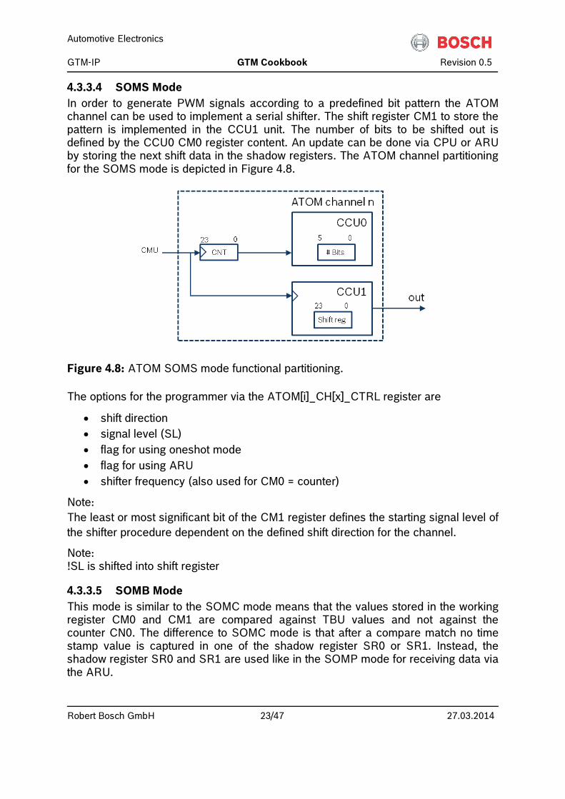
4.3.4 SOMC Late update mechanism There is an important feature for the SOMC mode that ensures access to the ATOM channel by the CPU even in an application scenario, where the ATOM channel receives its data via ARU. Although, the CPU could write updated compare values into the operation registers in CCU0 and CCU1, while the ATOM channel is in operation and waits for the compare match event, this is not the preferred procedure because the CPU has to do two write commands to two different registers. This can lead to a situation, where the CPU has updated one operation register while the second CCU1 unit detects the match on behalf of an old value and sets the output. Therefore, a second communication path can be used to update the operation registers. Figure 4.9 shows the two pathes. The blue path is the typical path where the compare values for CCU0 and CCU1 are directly received through the ARU interface. The matching time stamps are stored in SR0 and SR1 and send to the ARU.
Figure 4.9: CPU Access path to ATOM registers in case of late updates. When a consistent update of the compare registers inside the CCU0 and CCU1 units should be done, the green path is used by the CPU, where the shadow registers are used to intermediately store the update compare values. If a compare match event on the old values received through ARU takes place, the match time stamps are stored within the shadow registers as it would be the normal operation and further access to the shadow registers is blocked. To indicate the fail of this late update, the WRF bit is set inside of the channels status register. The procedure to do the late update is as follows:
1. CPU sets the WR_REQ bit inside of the channels control register
Automotive Electronics GTM-IP GTM Cookbook Revision 0.5
Robert Bosch GmbH 25/47 27.03.2014
2. CPU loads the shadow registers with the update compare values; please note that the compare strategy cannot be changed by the CPU, this will be the old compare strategy received through ARU
3. CPU should use the force update mechanism of the AGC unit to update the operation registers in CCU0 and CCU1 in a consistent way
4. CPU can check whether the late update mechanism was successful, if the WRF bit is not set inside of the channels status register
4.3.5 Application examples
4.3.5.1 Application note AN012 – Flexible PWM generation with ATOM Application note AN012 describes how to generate a sequence of PWM signals with a variable duty cycle. The duty cycle values are provided by the CPU on the fly. For details please refer to the separate application note document.
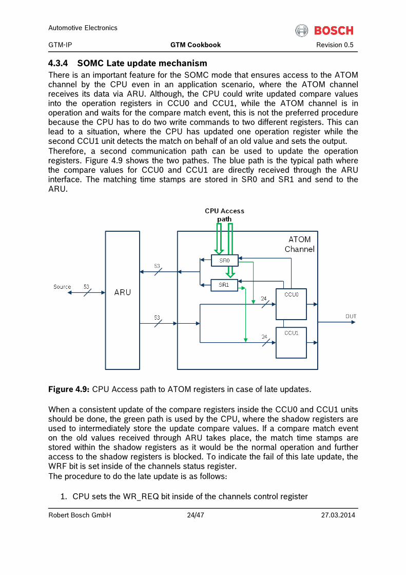
4.3.5.2 Application example – ATOM SOMC Mode In the following application example the ATOM SOMC mode is explained. For the ATOM SOMC mode after a match event, the resulting match times have to be read before new compare values have an effect at the ATOM output. To write compare values and to read results an MCS channel is used. The application example also shows the SOMC startup signal level behaviour at the ATOM output. Figure 4.11 shows the application scenario.
Figure 4.10: Application scenario with MCS and ATOM interaction. First the MCS program has to be loaded into MCS RAM. The program does the following: This program first writes the current TBU_TS0 value to ATOM0 channel 0 and commands a compare match on CCU0. The intention is to generate an immediate compare match event. After this the MCS waits in a WURM command on a trigger by CPU software. If the trigger bit is set (written by software), the MCS program reads back the compare match result values of ATOM0 channel 0 and writes an second compare value (actualized TBU_TS0 value) to ATOM0 channel 0. In a last step the second compare match event is read back. Then the MCS program disables the task execution. tsk0_init:
Automotive Electronics GTM-IP GTM Cookbook Revision 0.5
Robert Bosch GmbH 26/47 27.03.2014
mov R0 TBU_TS0 ; load TBU_TS0 to register R0 movl R1 $0 ; only register R0 of interest movl ACB $9 ; SF on CCU0, set output to '1' awr R0 R1 $0 ; issue immediate match event on old ; TBU_TS0 movl R2 $1 ; setup trigger bit to wait for wurm R2 CTRG $1 ; wait on trigger register match ard R4 R5 $11F ; read ATOM0 CH0 match result ; (0x11F) and do your job mov R0 TBU_TS0 ; load new TBU_TS0 to register R0 movl R1 $0 ; only register R0 of interest movl ACB $A ; SF on CCU0, set output to '0' awr R0 R1 $0 ; issue immediate match event on old ; TBU_TS0
ard R4 R5 $11F ; read ATOM0 CH0 match result ; (0x11F) and do your job tsk0_done: andl STA ~EN_MSK ; disable task In a second initialization step the ATOM0 channel 0 is configured: ATOM0_CH0_RDADDR = MCS0_WRADDR0; // use data from MCS0 CH0 ATOM0_CH0_CTRL = 0x01000009; // SL=0, ATOM in SOMC mode ATOM0_AGC_OUTEN_CTRL = 0x00000002; //enable output after update ATOM0_AGC_INT_TRIG = 0x00000002; //internal trigger mask ATOM0_AGC_ENDIS_STAT = 0x00000002; // enable CH0 immediately This initialization procedure has the intention to let the output of ATOM0 channel 0 be enabled by first ATOM0 channel 0 compare match event. The MCS can then be started by MCS0_CH0_CTRL = 0x00000001; The immediate compare match event has enabled the output. Now the MCS has to be commanded to write a second compare match event to ATOM0 channel 0 by writing the STRG bit 0. MCS0_STRG = 0x00000001; // trigger MCS0 CH0 WURM instruction
4.3.5.3 Application example – ATOM SOMP OSM In the following application example the handling of oneshot mode for ATOM SOMP mode is described. In this example ATOM 0 channel 2 is used. Please not that the similar application example can be applied on a TOM channel. To enable an ATOM channel for SOMP mode and oneshot handling, following steps are recommended:
Automotive Electronics GTM-IP GTM Cookbook Revision 0.5
Robert Bosch GmbH 27/47 27.03.2014
#define atom_clk4 (4<<12) #define atom_sl_hi (1<<11) #define atom_mode_somp ((0<<30) + (2<<0)) #define atom_osm_one (1<<26) #define atom_fupd2_en (2<<4) #define atom_fupd2_dis (1<<4) #define atom_endis2_dis (1<<4) #define atom_endis2_en (2<<4) ATOM0_CH2_CTRL = atom_mode_somp +
atom_sl_hi + atom_osm_one + atom_clk4;
ATOM0_CH2_CM0 = 1; ATOM0_CH2_CM1 = 1; ATOM0_CH2_SR0 = 1; ATOM0_CH2_SR1 = 1; ATOM0_AGC_FUPD_CTRL = atom_fupd2_en; ATOM0_AGC_GLB_CTRL = 1; force update to set CMU_CLK4 ATOM0_AGC_FUPD_CTRL = atom_fupd2_dis; ATOM0_AGC_ENDIS_CTRL = atom_endis2_en; ATOM0_AGC_ENDIS_STAT = atom_endis2_en; ; wait 2* period of CMU_CLK4: .. ; ATOM0_AGC_OUTEN_CTRL = atom_outen2_en; ATOM0_AGC_OUTEN_STAT = atom_outen2_en; After this initialization, one can trigger the generation of a single pulse of length 0 to FFFFFEh by calling the following function: void generateOSMPulse(unsigned int pulseLength) { if(pulseLength > 0xFFFFFE) { pulseLength = 0xFFFFFE; // clip pulseLength } if (pulseLength > 0) { // first force special internal state CM1 <= CN0 <= CM0 // by setting CM1,CM0,CN0: ATOM0_CH2_CM1 = 0xFFFFFF; // CM1 = max. possible value ATOM0_CH2_CM0 = 1; // CM0 = min. possible value ATOM0_CH2_CN0 = 1; // CN0 = CM0 // now set new desired value:
ATOM0_CH2_CM0 = pulseLength+1; // new pulse width+1 ATOM0_CH2_CM1 = pulseLength; // new pulse width
ATOM0_CH2_CN0 = pulseLength+1; // CN0 = CM0
Automotive Electronics GTM-IP GTM Cookbook Revision 0.5
Robert Bosch GmbH 28/47 27.03.2014
} else { ATOM0_CH2_CM1 = 1; // CM1 = min. possible value ATOM0_CH2_CM0 = 1; // CM0 = min. possible value // no udate of CN0 to avoid start counting! } }
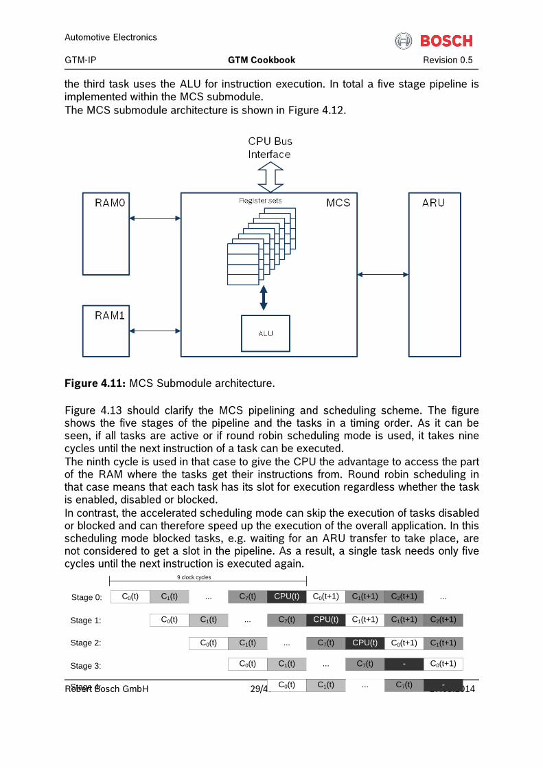
4.4 MCS – Programmable multi-tasking hardware core The Multi Channel Sequencer (MCS) is probably the most powerful submodule within the GTM-IP. It operates on a RISC-like instruction set located in its local RAM and can be source and destination at the ARU in parallel. The program for the MCS has to be loaded at system startup by the CPU via the MCS bus interface into the local RAM. Via that bus interface, the CPU is also able to control the internal states of the MCS and to access the local registers of the so called tasks. This tasks are independent operating threads of execution of instructions located in RAM. Since each task has its own program counter and register set, the tasks can operate on the same program or on different in parallel. Like all other submodules within the GTM-IP, also the MCS can be multiplied to gain more computing performance.
4.4.1 Highlights • Up to 20MIPS (only single task active) with 100MHz submodule clock or • About 12.5 MIPS (eight tasks active) with 100MHz submodule clock • Eight (8) independent tasks • Two different scheduling schemes for tasks
o Accelerated scheduling scheme o Round robin scheduling scheme
• Two independent RAM interfaces for parallel access of MCS task and CPU to two separate RAM blocks
• Shared instruction and data RAM • Up to 8KB of addressable RAM space • Up to eight (8) general purpose registers for each task • Dedicated interrupt for each task trigger able by MCS instruction
4.4.2 Submodule architecture The MCS submodule implements an ALU with a RISC-like instruction set and a set of register sets. The number of available register sets defines the number of tasks which can be used to build an application. These different tasks share one single ALU to process the instructions. One advantage with the approach of separate register sets is that on a task switch the registers must not be saved on the stack and the register content for the new task must not be loaded from the stack. The tasks can be executed immediately. Despite the fact that the ALU is shared amongst the different tasks the MCS is able to execute one instruction per clock cycle with a pipelined approach, where one task fetches a new command from the RAM while another task decodes its instruction and
Automotive Electronics GTM-IP GTM Cookbook Revision 0.5
Robert Bosch GmbH 29/47 27.03.2014
the third task uses the ALU for instruction execution. In total a five stage pipeline is implemented within the MCS submodule. The MCS submodule architecture is shown in Figure 4.12.
Figure 4.11: MCS Submodule architecture. Figure 4.13 should clarify the MCS pipelining and scheduling scheme. The figure shows the five stages of the pipeline and the tasks in a timing order. As it can be seen, if all tasks are active or if round robin scheduling mode is used, it takes nine cycles until the next instruction of a task can be executed. The ninth cycle is used in that case to give the CPU the advantage to access the part of the RAM where the tasks get their instructions from. Round robin scheduling in that case means that each task has its slot for execution regardless whether the task is enabled, disabled or blocked. In contrast, the accelerated scheduling mode can skip the execution of tasks disabled or blocked and can therefore speed up the execution of the overall application. In this scheduling mode blocked tasks, e.g. waiting for an ARU transfer to take place, are not considered to get a slot in the pipeline. As a result, a single task needs only five cycles until the next instruction is executed again.
C0(t) C1(t) C7(t) CPU(t)... C1(t+1) C1(t+1)
Stage 0: C0(t) C1(t) C7(t) CPU(t)... C0(t+1) C1(t+1) C2(t+1)
Stage 1:
Stage 2:
Stage 3:
C0(t) C1(t) C7(t) CPU(t)... C0(t+1)
C0(t) C1(t) C7(t) -...
9 clock cycles
Stage 4: C0(t) C1(t) C7(t) -...
C0(t+1)
C1(t+1)
C2(t+1)
...
Automotive Electronics GTM-IP GTM Cookbook Revision 0.5
Robert Bosch GmbH 30/47 27.03.2014
Figure 4.12: MCS Task pipelining principle.
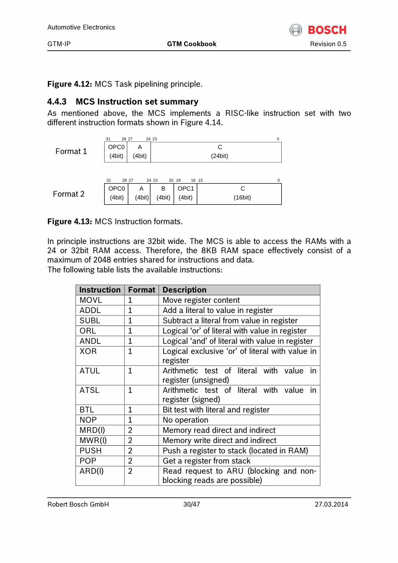
4.4.3 MCS Instruction set summary As mentioned above, the MCS implements a RISC-like instruction set with two different instruction formats shown in Figure 4.14.
Figure 4.13: MCS Instruction formats. In principle instructions are 32bit wide. The MCS is able to access the RAMs with a 24 or 32bit RAM access. Therefore, the 8KB RAM space effectively consist of a maximum of 2048 entries shared for instructions and data. The following table lists the available instructions:
Instruction Format Description MOVL 1 Move register content ADDL 1 Add a literal to value in register SUBL 1 Subtract a literal from value in register ORL 1 Logical ‘or’ of literal with value in register ANDL 1 Logical ‘and’ of literal with value in register XOR 1 Logical exclusive ‘or’ of literal with value in
register ATUL 1 Arithmetic test of literal with value in
register (unsigned) ATSL 1 Arithmetic test of literal with value in
register (signed) BTL 1 Bit test with literal and register NOP 1 No operation MRD(I) 2 Memory read direct and indirect MWR(I) 2 Memory write direct and indirect PUSH 2 Push a register to stack (located in RAM) POP 2 Get a register from stack ARD(I) 2 Read request to ARU (blocking and non-
blocking reads are possible)
OPC0(4bit)
A(4bit)
C(24bit)
027 242831 23
C(16bit)
B(4bit)
A(4bit)
OPC0(4bit)
OPC1(4bit)
027 242831 23 20 19 16 15
Format 1
Format 2
Format 1
Automotive Electronics GTM-IP GTM Cookbook Revision 0.5
Robert Bosch GmbH 31/47 27.03.2014
AWR(I) 2 Provide data to ARU (blocking and non-blocking writes to ARU are possible)
JMP 2 Jump to an address JBS 2 Conditional jump if bit is set JBC 2 Conditional jump if bit is cleared CALL 2 Call a function RET 2 Return from function WURM 2 Wait until two registers match (optional
mask possible to concentrate to specific bits within registers)
Table 4.2: MCS Instruction set overview.
4.4.4 Inter process communication mechanisms Especially, the WURM instruction is an important feature of the MCS submodules since it allows synchronization among the tasks of an MCS submodule or among the CPU and one or more tasks of the MCS submodule. For this purpose, each MCS submodule implements one physical and two logical registers. The two logical registers CTRG and STRG are visible within the MCS submodule address space for the CPU and within the local register address space of each task. Nevertheless, these two registers are physically implemented only once for the whole MCS submodule. When reading the CTRG or the STRG, always the content of the physical trigger register is returned to the task or CPU. Bits within this trigger register can be set by writing a ‘1’ to the corresponding bit(s) of the STRG register (set register bit(s)) that should be set. Bits within this register can be cleared by writing a ‘1’ to the corresponding bit(s) of the CTRG register (clear register bit(s)) that should be cleared. The WURM instruction can be used to block a task to wait for such a trigger bit or bit combinations. Also multiple tasks can be put to sleep and wait for one common trigger register bit that can be set by either another MCS task or the CPU. The CPU has the possibility to resume a task that is blocked on trigger bits in the trigger register without changing the state of the trigger register by using another bit in the submodules MCS_RST reset register. This is the CWTx bit (cancel WURM instruction). There is one bit available for each MCS task. The task for which the CWT bit is set resumes with its operation, when the task waits actually in a WURM instruction. The same mechanism to resume a task can be used, when a task is blocked in an ARU read or write command. Than the CATx bits can be set by the CPU to resume the corresponding task.
4.4.5 Application example With this architecture, the MCS submodule offers a lot of computing power inside of the GTM-IP. By implementation of a couple of MCS submodules, an application can be build where each input port at the TIM channels has a corresponding MCS task to
Automotive Electronics GTM-IP GTM Cookbook Revision 0.5
Robert Bosch GmbH 32/47 27.03.2014
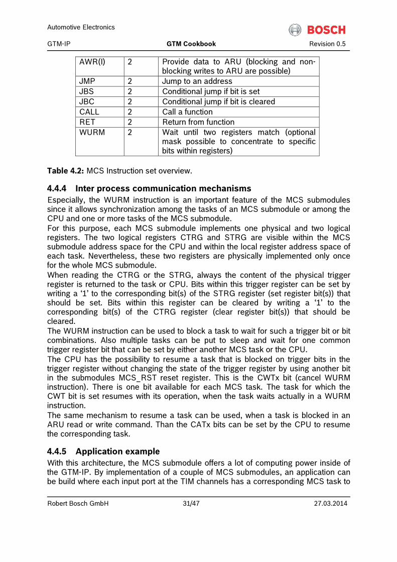
operate on the input data and each output at the ATOM channels has a MCS task that computes the output sequence for that ATOM channel. Such an application can look like Figure 4.15.
Figure 4.14: MCS Application example. The figure shows a TIM submodule with two channels inside and an ATOM submodule with four channels inside. The MCS submodule implements four tasks. The MCS task 0 is associated to the TIM channel 0 and requests sampled input data from there. The requests are done with an ARU read command, e.g. ARD, where the address to read from is coded within the instruction. Since the ARD instruction is a blocking one, the MCS task 0 will block until data is provided by the TIM channel 0. With this architecture, an interrupt controller for the MCS is obsolete, since the tasks will only resume if data is provided by the source (same as an interrupt would be triggered by source). The second task of the MCS channel, task 1, first gets input data from the TIM channel 1 by means of ARD command, can calculate then an output command for an ATOM and can provide this command with an AWR instruction to the ATOM. In this case the ATOM channel 3 blocks until the MCS task 1 issues the write command. With this, the MCS task and ATOM channel block, until the TIM channel 1 detects an event and provides the data to the MCS task 1. The MCS task 1 will wake up, the ATOM channel 3 is still blocked. In the end, the ATOM channel 3 will receive calculated data from MCS task 1 and will do the output. The third possibility is that there is a distinct task for each ATOM output channel. This is shown with MCS task 2 and ATOM channel 2. A forth possibility is shown with MCS task 3 which is able to control two ATOM channels 0 and 1 in parallel. This is possible, because the addresses to read and write from ARU are programmable within the ARU instructions. The same construction can be implemented for a TIM input and a MCS task. Please note, that in a case of multiple control of a MCS task, the MCS task should use the non-blocking ARU commands of its instruction set.
Automotive Electronics GTM-IP GTM Cookbook Revision 0.5
Robert Bosch GmbH 33/47 27.03.2014
4.5 DPLL – Engine positioning The DPLL is not only a submodule that can generate a higher frequent output signal derived from an input signal but it can also predict to some extent the behaviour of the input signal for the future. The naming DPLL is from this point of view somewhat misleading but has its name for historical reasons. There are only few limitations on the input signal characteristic where the DPLL operates on. The DPLL is designed to be highly flexible and offers a lot of configuration parameters to tailor the submodule to the application needs.
4.5.1 Highlights • Operation on two independent data input streams possible • Generation of two independent output signals from two independent input
signals or combination of two dependent input signals to one output signal • Highly configurable submodule • Prediction of future behaviour of input signal • Calculation of times for events in the future on behalf of the input signals
4.5.2 Submodule architecture As shown in Figure 4.16 the DPLL consists of several distinct subunits and associated independent RAM blocks to store configuration registers and application data. There exist also several interfaces to the surrounding world for interaction. The two input signals on which the DPLL operates come in on the two signal lines TRIGGER and STATE. The input signals which typically contain a time stamp, filter threshold and actual input signal level are processed first in the “Input Signal Capture” unit. In this unit e.g. a time stamp correction is done on behalf of the filter threshold values. Results are stored in RAM2 area for TRIGGER and RAM1bc for STATE. When the input signal is characterized as valid the TRIGGER or STATE engines are triggered and the DPLL calculations can start.
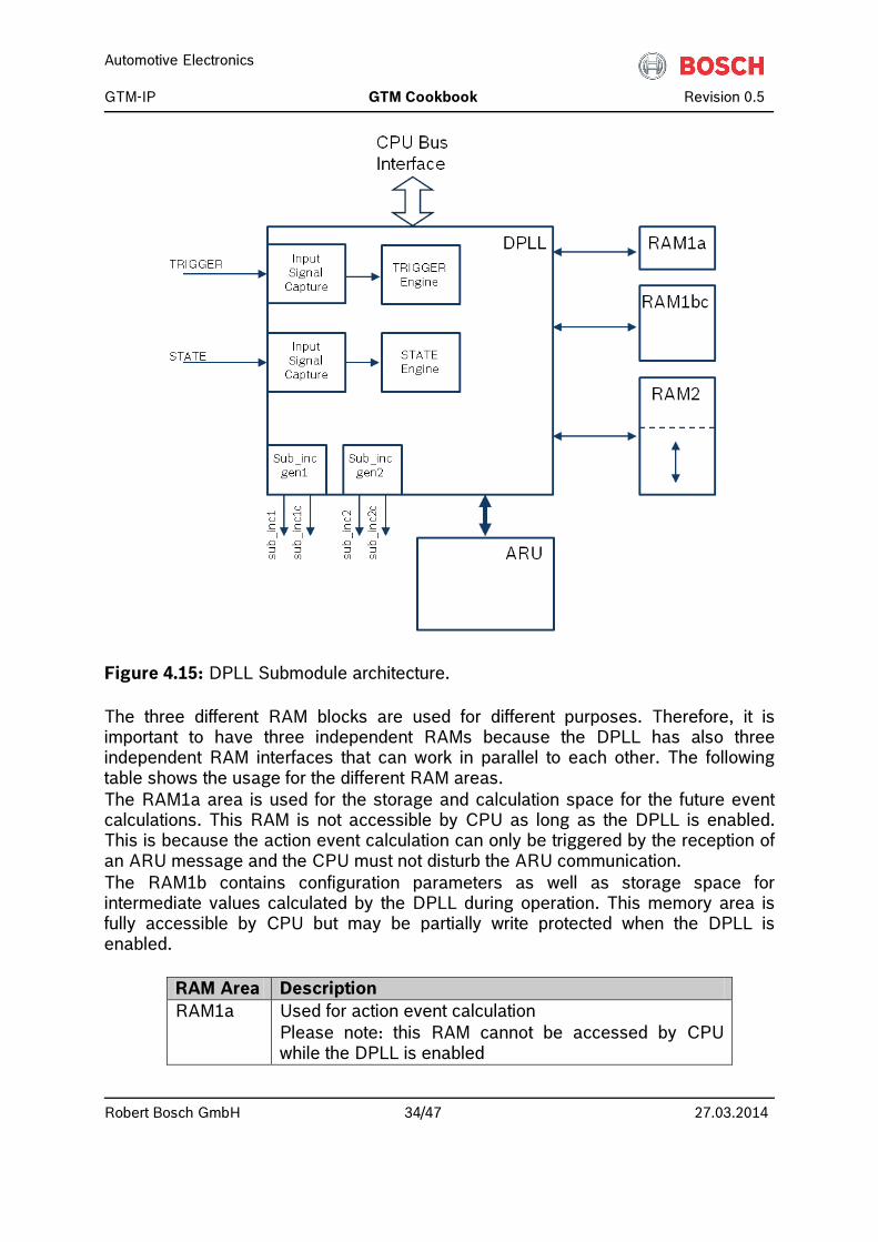
Automotive Electronics GTM-IP GTM Cookbook Revision 0.5
Robert Bosch GmbH 34/47 27.03.2014
Figure 4.15: DPLL Submodule architecture. The three different RAM blocks are used for different purposes. Therefore, it is important to have three independent RAMs because the DPLL has also three independent RAM interfaces that can work in parallel to each other. The following table shows the usage for the different RAM areas. The RAM1a area is used for the storage and calculation space for the future event calculations. This RAM is not accessible by CPU as long as the DPLL is enabled. This is because the action event calculation can only be triggered by the reception of an ARU message and the CPU must not disturb the ARU communication. The RAM1b contains configuration parameters as well as storage space for intermediate values calculated by the DPLL during operation. This memory area is fully accessible by CPU but may be partially write protected when the DPLL is enabled.
RAM Area Description RAM1a Used for action event calculation
Please note: this RAM cannot be accessed by CPU while the DPLL is enabled
Automotive Electronics GTM-IP GTM Cookbook Revision 0.5
Robert Bosch GmbH 35/47 27.03.2014
RAM1b RAM1c1 RAM1c2 RAM1c3 RAM1c4
Contains DPLL configuration values and intermediate results used throughout the operation of DPLL Contains reciprocal values of STATE signal durations Contains sampled time stamps of STATE input signal Contains STATE input signal profile Contains history of the durations of the STATE signal
RAM2a RAM2b RAM2c RAM2d
Contains reciprocal values of TRIGGER signal durations Contains sampled time stamps of TRIGGER input signal Contains TRIGGER input signal profile Contains history of the durations of the TRIGGER signal
Table 4.3: DPLL RAM areas. The RAM1c and RAM2 are logically divided into four parts. While RAM1c is integrated together with RAM1b into one RAM module, RAM2 is a separate RAM module and can have different physical sizes. The necessary size is determined by the input signal event number of TRIGGER within one cycle and can be controlled by 2 control bits resulting in 4 size versions (see Register DPLL_OSW).
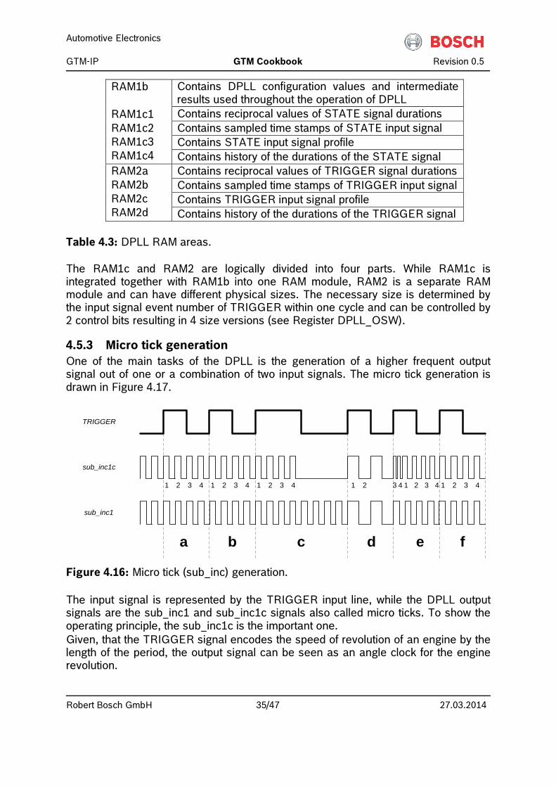
4.5.3 Micro tick generation One of the main tasks of the DPLL is the generation of a higher frequent output signal out of one or a combination of two input signals. The micro tick generation is drawn in Figure 4.17.
1 2 3 4 1 2 3 4 1 2 3 4 1 2 3 4 2 3 41 1 2 3 4
a b c d e f
TRIGGER
sub_inc1c
sub_inc1
Figure 4.16: Micro tick (sub_inc) generation. The input signal is represented by the TRIGGER input line, while the DPLL output signals are the sub_inc1 and sub_inc1c signals also called micro ticks. To show the operating principle, the sub_inc1c is the important one. Given, that the TRIGGER signal encodes the speed of revolution of an engine by the length of the period, the output signal can be seen as an angle clock for the engine revolution.
Automotive Electronics GTM-IP GTM Cookbook Revision 0.5
Robert Bosch GmbH 36/47 27.03.2014
In the example above, the input signal period is divided into four micro ticks. When one revolution of the engine consists of 90 PWM periods of the TRIGGER signals which means, that one PWM signal represents 4°, the division by four means that there is a resulting angle clock of 1° per micro tick. In principle, it is possible, to generate one micro tick output signal from two dependent input signals (TRIGGER and STATE), or to generate two independent output signals from two independent input signals (TRIGGER and STATE). The input signal is characterised by the TIM0 by annotating TBU time stamps to the input signal edges. The PWM duration is calculated by the DPLL on behalf of the received time stamps. The first DPLL application is shown in Figure 4.18. The TIM0 input channel 0 is directly routed to the TRIGGER input signal of DPLL, while one of the remaining five input channels of TIM0 is selected by the MAP submodule to route to the STATE input signal. It can be chosen by software whether the TRIGGER or STATE signal is used for micro tick generation. This gives redundancy on the input signal evaluation and micro tick generation.
Figure 4.17: DPLL Data path with “one” DPLL output signal generated. Figure 4.19 shows the second application of the DPLL. There the TIM0 input signals are split, where channels 0 to 2 represent the first input signal while channels 3 to 5 represent the second input signals. The six input signals are combined by the MAP submodule to the two input signals TRIGGER and STATE. The results from this application of the DPLL submodules are two independent micro ticks generated.
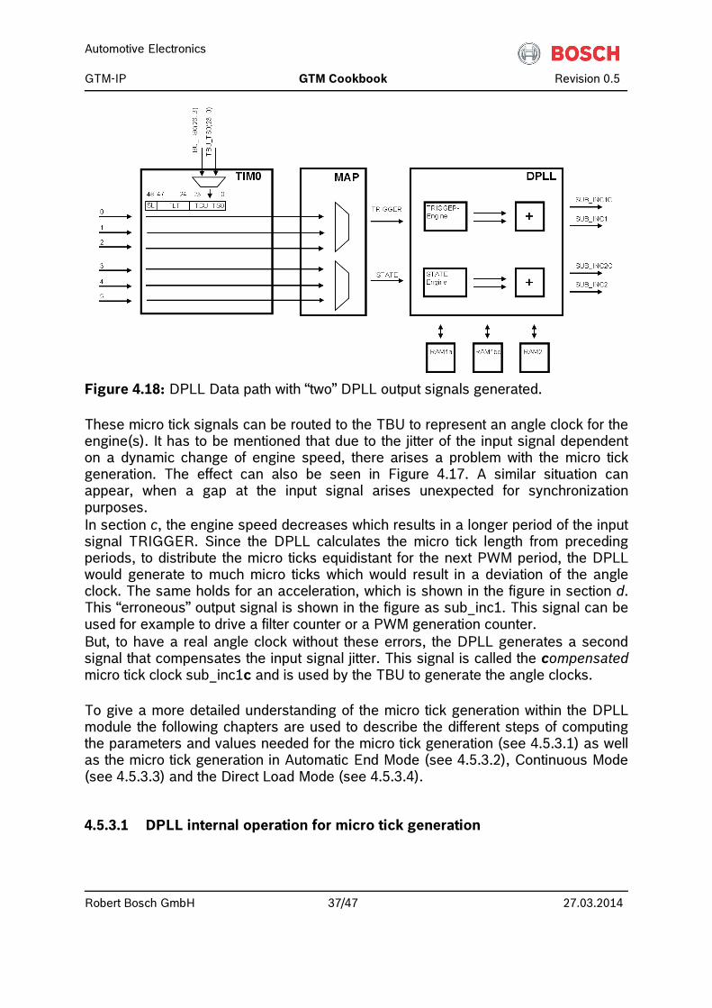
Automotive Electronics GTM-IP GTM Cookbook Revision 0.5
Robert Bosch GmbH 37/47 27.03.2014
Figure 4.18: DPLL Data path with “two” DPLL output signals generated. These micro tick signals can be routed to the TBU to represent an angle clock for the engine(s). It has to be mentioned that due to the jitter of the input signal dependent on a dynamic change of engine speed, there arises a problem with the micro tick generation. The effect can also be seen in Figure 4.17. A similar situation can appear, when a gap at the input signal arises unexpected for synchronization purposes. In section c, the engine speed decreases which results in a longer period of the input signal TRIGGER. Since the DPLL calculates the micro tick length from preceding periods, to distribute the micro ticks equidistant for the next PWM period, the DPLL would generate to much micro ticks which would result in a deviation of the angle clock. The same holds for an acceleration, which is shown in the figure in section d. This “erroneous” output signal is shown in the figure as sub_inc1. This signal can be used for example to drive a filter counter or a PWM generation counter. But, to have a real angle clock without these errors, the DPLL generates a second signal that compensates the input signal jitter. This signal is called the compensated micro tick clock sub_inc1c and is used by the TBU to generate the angle clocks. To give a more detailed understanding of the micro tick generation within the DPLL module the following chapters are used to describe the different steps of computing the parameters and values needed for the micro tick generation (see 4.5.3.1) as well as the micro tick generation in Automatic End Mode (see 4.5.3.2), Continuous Mode (see 4.5.3.3) and the Direct Load Mode (see 4.5.3.4).
4.5.3.1 DPLL internal operation for micro tick generation
Automotive Electronics GTM-IP GTM Cookbook Revision 0.5
Robert Bosch GmbH 38/47 27.03.2014
In general four different computation steps are needed to provide the micro tick generation of the DPLL:
1. Plausibility check of incoming signal event (Trigger/State: @ input event). 2. Set INC_CNT1/2 count for next increment (not relevant for Continous
Mode), Trigger/State @ step 1. 3. Correct missing pulses of last increment by fast pulse update (Automatic
End Mode only), Trigger/State @ step 6. 4. Calculation of new add_in_cal value, Trigger/State @ step 10.
These operation steps are according to the specification chapter 16.8.6.7 (or 17.8.6.7 for specification versions 2.0 and later). Because the DPLL is a hardware module these operation steps are performed in sequential order some time for calculation is needed. This calculation time depends on the implementation (technology, system clock frequency) and the activity of the software on the CPU interface of the DPLL module (e.g. concurring accesses to DPLL RAM’s during calculation). At a system clock frequency of 100MHz and moderate accesses to the DPLL RAM via the CPU interface the following times can be given as an estimation: Step 1 is reached within ~2,47us, step 6 can be reached after ~7,7us step 10 is reached approximately 9us after the input event has reached the DPLL input. The numbers of the timestamps are simulation results were just one input (TRIGGER) was active. The calculation of the pulse generation is based on the prediction of the next input event. From the timestamps of the input events of the actual tooth and the timestamp of the event before the difference dt_actual_T/S is calculated (see equations 16.1a0, 16.1b and 16.6a0, 16.6b). This value can be calculated independently from a synchronization gap once the DPLL is synchronized and the gap is considered in the profile (apt_2b and aps_1c2 are written correctly). This time difference and the according reciprocal value rdt_t/s_actual (equations 16.1c, 16.6c) are stored continuously into the RAM1c for the STATE input and RAM2 for the TRIGGER input so that after 2 complete rotations of a combustion engine the datasets for crankshaft (TRIGGER) and camshaft (STATE) are complete and continuously updated for each new input event. Afterwards the relation of the last two increment values QDT_T/S is calculated following equations 16.2a1, 16.2b1, 16.2b2 for TRIGGER and 16.7a1, 16.7b1, 16.7b2 for STATE depending on the parameter NUTE-VTN or NUSE-VSN which are set to determine on which relation the prediction shall be based out of the event history. Based on this relation the error of the last prediction EDT_T/S (.. for TRIGGER, … for STATE) is calculated which is used to calculate an average error MEDT_T/S (equation 16.4 for TRIGGER, equation 16.9 for STATE). Based on dt_t/s_actual, the calculated error and the relation selected by QDT(NUTE-VTN+1) the expected trigger/state duration CDT_TX/SX for the next event is predicted (equations 16.5a, 16.2c and 16.5b for TRIGGER and equations 16.10a, 16.7c and 16.10b for STATE). The add_in_cal value for the pulse generation unit is calculated out of the reciprocal value RCDT_TX/SX= 1/CDT_TX/SX by equations 16.21, 16.25 for TRIGGER and equations 16.22 and 16.26 for STATE. The NMB_T/S values in these formulas are
Automotive Electronics GTM-IP GTM Cookbook Revision 0.5
Robert Bosch GmbH 39/47 27.03.2014
representing the number of micro ticks to be sent for the next increment. This value is calculated differently depending on the selected operation mode. The possible components of the NMB_T/S values are:
• SYN_T * MLT or SYN_S* MLS1 or 2, which is the requested pulse number
weighted by the profile configuration (SYN_T/S) • MP, which is the number of missing pulses which could not be placed in
the increment before (e.g. acceleration), taken in an internal register at the moment when the new input event is arriving.
• PD_store, which is taken form the profile configuration (ADT_T/S) out of
the memory giving the possibility to correct “physical deviations” which occur regularly by the input events.
• MPVAL1 or 2, which are pulse numbers which can be added or subtracted
once by the use of the configuration bit DPLL_CTRL_1.PCM1/2 The micro tick generation itself is performed by a pulse generation unit which is basing on a modulo adder (see spec. chapter 16.8.3, 16.8.4). Depending on the operation mode of the DPLL the two available micro tick generators are feed differently by the TRIGGER or STATE processing engines. When DPLL_CTRL_0.RMO = ‘0’ the SUB_INC1, SUB_INC1c output signals are controlled by the calculations of the TRIGGER engine. If DPLL_CTRL_0.RMO = ‘1’ and DPLL_CTRL_1.SMC = ‘0’ the SUB_INC1, SUB_INC1c output signals are controlled by the calculations of the STATE engine. In case of DPLL_CTRL_0.RMO = ‘1’ and DPLL_CTRL_1.SMC = ‘1’ the SUB_INC1/c signals are controlled by TRIGGER engine and SUB_INC2/c signals are controlled by the STATE processing engine. The micro tick generator has two output signals the uncompensated output SUB_INC1/2 is running continuously once the micro tick generation has started. The pulses on the compensated output signal SUB_INC1/2c are depending on the configurations which are explained in the following chapters. The adder is updated with every timestamp clock (TS_CLK) where each overflow generates a micro tick on the SUB_INC1c output. Fast micro tick updates are placed with the CMU_CLK0.
4.5.3.2 Micro tick generation in Automatic End Mode The automatic end mode is used when the bit DPLL_CTRL_1.DMO is set to ’0’ and DPLL_CTRL_1.DLM1/2=’0’. In general in automatic end mode the micro tick on SUB_INC1/2c is active until the pulse number defined in the register INC_CNT1/2 are reached. If this counter reaches the value ‘0’ before a new event is detected on the inputs, the micro tick generation stops. If the next input event is detected before the counters inc_cnt1/2
Automotive Electronics GTM-IP GTM Cookbook Revision 0.5
Robert Bosch GmbH 40/47 27.03.2014
are reaching the ‘0’ state there are two different configurations to handle the missing micro ticks defined by the bit DPLL_CTRL_1.COA. If DPLL_CTRL_1.COA = ‘0’ the missing pulses which are stored in the internal register MP are sent out as fast update with the frequency CMU_CLK0. In so far the value MP is not used to calculate the value NMB_T/S which is the number of micro ticks to be sent out for the next increment. If DPLL_CTRL_1.COA = ‘1’ the missing pulses from the increment before are added to the value NMB_T/S for the calculation of the new ADD_IN_CAL value for the micro tick generator. This leads to a higher ADD_IN_CAL value so that the micro tick frequency is going to be increased so that the missing pulses of the passed increment are evenly distributed over the next increment. When not using the direct load mode the calculation of the micro tick frequency (add_in_cal1/2) is based on values which are calculated by the DPLL module out of the timestamps of the input signals and the configuration parameters alone. For operation without critical effects like unexpected missing triggers or loss of synchronization the DPLL is running autonomously.
4.5.3.3 Micro tick generation in Continuous Mode The continuous mode is initialized by setting the bit DPLL_CTRL_1.DMO=’1’. Within this mode the pulse generation is running independent from the inc_cnt_1/2 counters like in automatic end mode. In this mode the compensated output sub_inc1/2c behaves like the uncompensated output sub_inc1/2. The add_in_cal1/2 values for the micro tick generator are calculated based on the NMB_T/S = SYN_T/S * CNT_NUM1/2. CNT_NUM1/2 are pulse numbers which are RAM parameters written via the CPU interface. All pulse correction mechanisms like the determination of missing pulses (MP) or regular pulse correction via the PD parameter or singular pulse corrections via MPVAL1/2 are deactivated in Continuous Mode. If synchronized, the profile is considered by SYN_T/S. If DPLL_CTRL_1.DLM1/2 = ‘0’ (direct load mode deactivated) accelerations as well as decelerations are considered with the help of the value RCDT_T/Sx for the calculation of ADD_IN_CAL1/2 which determines the micro tick frequency. The calculation of ADD_IN_CAL1/2 is done when new input events are available after the above mentioned time for calculation. The correct number of micro ticks according to the TRIGGER/STATE input signal must be controlled via the TBU counters from outside of the DPLL module by the CPU. Corrections can be done via the CNT_NUM1/2 parameters.
4.5.3.4 Micro tick generation in Direct Load Mode When DPLL_CTRL_1.DLM1/2 = ‘1’ , the micro tick generators of the DPLL module are operating in Direct Load Mode. The ADD_IN value, which mean the determination of the pulse frequencies of the micro tick generators, are taken directly
Automotive Electronics GTM-IP GTM Cookbook Revision 0.5
Robert Bosch GmbH 41/47 27.03.2014
from the parameters ADD_IN_LD1/2 when a new input event on the relevant processing engine (TRIGGER/STATE) happens. The ADD_IN_LD1/2 parameters are stored in registers within the DPLL. The calculation of the NMB_T/S values as well as the control of the micro tick generation by the DPLL are depending on the set up of the configuration bits DPLL_CTRL_1.DMO and of DPLL_CTRL_1.COA if DPLL_CTRL_1.DMO = ‘0’. If DPLL_CTRL_1.DMO = ‘0’ (Automatic End Mode) is used the control of micro ticks per increment is under control of the INC_CNT1/2 counters. If ADD_IN_LD1/2 is high enough the micro tick generation stops when the necessary number of pulses is reached. If DPLL_CTRL_1.COA = ‘0’ the missing pulses which are stored in the internal register MP are sent out as fast update with the frequency CMU_CLK0. In so far the value MP is not used to calculate the value NMB_T/S which is the number of micro ticks to be sent out for the next increment. This happens if the ADD_IN_LD1/2 is not big enough so that not all micro ticks can be placed in the current increment. Because the NMB_T/S value is not relevant in Direct Load Mode the pulse correction mechanisms like the regular pulse correction via the PD parameter and singular pulse corrections via MPVAL1/2 are deactivated in this configuration. If DPLL_CTRL_1.COA = ‘1’ the missing pulses from the increment before are added to the value NMB_T/S for the calculation of the new ADD_IN_CAL value for the micro tick generator. Because in Direct Load Mode this internal ADD_IN_CAL value is not used for the micro tick generation this mechanism is not usable to control the correct number of micro ticks autonomously especially if ADD_IN_LD1/2 is not sufficiently high. This can lead to the loss of micro ticks. Because the NMB_T/S value is not relevant in Direct Load Mode the pulse correction mechanisms like the determination of missing pulses (MP) and the regular pulse correction via the PD parameter and singular pulse corrections via MPVAL1/2 are deactivated in this configuration. If Continuous Mode (DPLL_CTRL_1.DMO = ‘1’) is used together with Direct Load Mode neither the number of micro ticks in an increment is considered for the INC_CNT1/2 counters nor the pulse frequency of the micro tick generator is controlled by the timestamps of the input events on TRIGGER/STATE engines. In this case the compensated output sub_inc1/2c behaves like the uncompensated output sub_inc1/2. The pulse frequency is determined by ADD_IN_LD1/2 the correct number of micro ticks per increment must be controlled from outside the DPLL.
4.5.4 Observing missing and additional input events The observation of missing and additional input events is depending on the state of the DPLL. Before the synchronisation only missing events can be detected. Additional events are only detectable when the DPLL is synchronized. Before the synchronisation is done (writing to apt_2c for TRIGGER, aps_1c2 for STATE, see AN011) missing events can be detected via the interrupts MTI/MSI
Automotive Electronics GTM-IP GTM Cookbook Revision 0.5
Robert Bosch GmbH 42/47 27.03.2014
(missing trigger interrupt for Trigger, missing state interrupt for STATE) and TORI/SORI (Trigger/State out of range interrupt). The MTI/MSI interrupt is controlled by the parameter TOV/TOV_S (Time out value of active trigger/state slope) The time between two active edges of the input event is observed. If the time out is reached and no event happened so far the interrupts are activated. The TORI/SORI interrupts are controlled via the parameters TLR/SLR (TRIGGER/STATE locking range). After the timeouts defined by TLR/SLR parameters the TORI/SORI interrupts are drawn. The TOV/TOV_S parameters should be configured to observe the distance of a single missing event. The TORI/SORI interrupts are operating on a wider range were the parameters TLR/SLR should be configured such that the timeout lies beyond the biggest event gap of the system. The parameters TOV, TOV_S and TLR/SLR are setup in units of “teeth”. That means a “1” in case of TLR/SLR or a “1.0” for TOV/TOV_S means one actual event duration because the parameters are multiplied by the actual event duration to calculate the real timeout. That means that all the timeouts belonging to the named interrupts are calculated dynamically in dependence of the actual velocity of the system. After the synchronisation of the DPLL the above described interrupts MTI/MSI, TORI/SORI are still active. In an event gap the MTI Interrupt is also activated but if SYN_T/SYN_S is bigger than one this is fine. If the MTI/MSI Interrupt is activated outside a gap (SYN_T/S = 1) this is a misbehaviour which is resetting the lock1/2 bits. If an additional, unexpected event has happened this is not detectable immediately. One possibility to detect the incorrect event is that this event is leading to an virtual acceleration (dt_t/s_actual is getting much shorter) which leads in the correct event after that to an MTI/MSI interrupt when the system is getting the next event within the real velocity of the system. This detection depends on the point of time when the additional event occurs within the tooth period together with the setup of the TOV/TOV_S parameters. If set close to “1” this works more reliable compared to the case were the parameters are set closer to “2”. But in any case the profile is switched one step too far for which causes definitely an MTI/MSI interrupt in that point of the profile were the gap occurs and the values SYN_T/S are equal to “1“ as an effect of the additional event. This MTI/MSI interrupts in case of additional events are resetting the lock1/2 bits as well. To observe the synchronisation status and to verify that no events got lost or no additional teeth are occurring this is possible by checking for the MTI/MSI, TORI/SORI interrupts compared to the profile (SYN_T). The much easier way to check this is to observe the lock1/2 bits of the status register by monitoring the interrupts GL1i, LL1i for the increment generator 1 or the interrupts GL2i, LL2i according to increment generator 2.
4.5.5 Event Time prediction The DPLL offers an additional function which is able to calculate on behalf of an input characteristic an event where the system will reach a certain state. This event is sometimes also called action. The certain state is typically an angle in the future with
Automotive Electronics GTM-IP GTM Cookbook Revision 0.5
Robert Bosch GmbH 43/47 27.03.2014
a rate time to consider inertial delays. The definition of the action is shown in Figure 4.20. In the figure the x-Axis represents the time in ticks of one of the TBU channels and the y-Axis represents the position of the engine in micro ticks of another TBU channel. The system is now able to let the DPLL calculate a position and time in the future taking into account a history of sampled input characteristics of TRIGGER or STATE signals.
P
T
PT
TT dt
PE
Figure 4.19: Action event calculation. The system has to define a position and delta time (in ticks of the TBU time base (x-Axis)) for this action. The action result is a predicted time and a predicted angle, at which a given position including rate time is reached. The acceleration and deceleration is shown by the curve in the diagram. The delta time has to be always subtracted from the position value. Therefore, this feature of the DPLL is also called Position-Minus-Time (PMT) calculation. Please note that the request for these calculations can be only initiated via ARU and that the requested action angle must not exceed two engine revolutions in future. Due to the prediction, the calculated action time can differ from the real action time when the distance to the action is far and the engine behaviour is highly dynamic. Therefore, the DPLL automatically recalculates with each new input signal TRIGGER or STATE the action position and time. This has the effect that the results of the DPLL will become more precise, the shorter the distance to the action is.
4.5.6 Application examples There exist two application examples that show the micro tick generation and the action event prediction in a little bit more details. These application examples can be used as starting points to build own, more complex applications.
Automotive Electronics GTM-IP GTM Cookbook Revision 0.5
Robert Bosch GmbH 44/47 27.03.2014
4.5.6.1 Application note AN011 – DPLL Micro tick generation The application note AN011 shows how to generate micro ticks on behalf of an input signal. As it can be seen from the application, there are a lot of submodules involved to do this task. All the submodules involved can be seen from Figure 4.21. The CMU and TBU are needed to generate the GTM-IP time base for which the input signals are characterised and the DPLL calculates the input signal increment durations. The TIM and MAP modules are used to route the input signal from the GTM port pin to the DPLL signal processing units.
TIM0TIM0_CH0_IN
TBU CMU
DPLLMAP
RAM1A
RAM1BC RAM2
TRIGGER
STATETIM0_CH1_IN
TIM0_CH5_IN
TBU
_TS
0
TBU
_TS
1
sub_
inc1
c
dir sub_
inc1
PMTR0
PMTR1
PMTR23
DPLL_WRADDR0
DPLL_WRADDR1
DPLL_WRADDR23
CMU_CLK0
Figure 4.20: GTM-IP Setup for DPLL micro tick generation. The application note shows also how to use the DPLL RAMs to characterize an input signal by its profile and explains how to synchronize the DPLL to the input signal. Synchronization of the DPLL is an important topic, because the DPLL needs some assistance from the CPU to operate properly. One point is, that the CPU has to tell the DPLL for a given input signal part, to which position of the engine this signal part is related to. For a detailed description of the application and some code snippets, please refer to the application note AN011.
4.5.6.2 Application note AN013 – DPLL PMT Generation Based on calculations, which are also used for the micro tick generation it is now possible to perform the action event calculation for a system state in the future. Figure 4.22 shows the submodules of the GTM-IP involved in the PMT calculation and two possible application scenarios.
Automotive Electronics GTM-IP GTM Cookbook Revision 0.5
Robert Bosch GmbH 45/47 27.03.2014
The action event times are typically used as compare match times for ATOM channels, where the output signals change when the calculated PMT results are reached. As mentioned above, the action calculations can only be triggered GTM-IP internally via the DPLL ARU interface. In the application example this is done by two independent MCS tasks. For these two calculation requests, the further procedure is different. The MCS task 0 issues a calculation request and reads back the results for every incoming TIM0 input signal from the DPLL. The two compare match times received from DPLL are written to the ATOM channel for comparison. In the second possible solution the MSC provides only the PMT values and establishes a direct link between the DPLL action calculation and the ATOM output channel. This is shown in the picture for MCS task 1. This task issues the PMT request, and then blocks on the ATOM answer until the ATOM matches on the compare values received by the DPLL.
TIM0TIM0_CH0_IN
TBU
DPLLMAP TRIGGER
TBU
_TS0
TBU
_TS1
PMTR14
PMTR15
ARU ATOM0
CH0
MCS0
CH1
CH1
CH2
ATOM0_CH1_OUT
ATOM0_CH2_OUT
TBU
_TS0
TBU
_TS 1
1 2
12
3
4
Figure 4.21: Applications of the PMT functionality on the GTM device. For a detailed description of the application and some code snippets, please refer to the application note AN013.
4.6 SPE – BLDC Engine control The GTM-IP offers a dedicated submodule which can be used in combination with other submodules to drive a BLDC engine. The module is the Sensor Pattern Evaluator (SPE). The SPE can also be used to determine the engine revolution direction for the DPLL in a hybrid engine application to control up to two independent permanent magnet synchronous motors (PMSM) for forward and backward rotation. For that purpose in Figure 4.19 the connection between TIM and MAP is routed via two SPE channels. Figure 4.23 shows a BLDC engine control chain to TOM using SPE. There, three input signals coming typically from HAL sensors are sampled at the TIM input channels and are routed to the SPE.
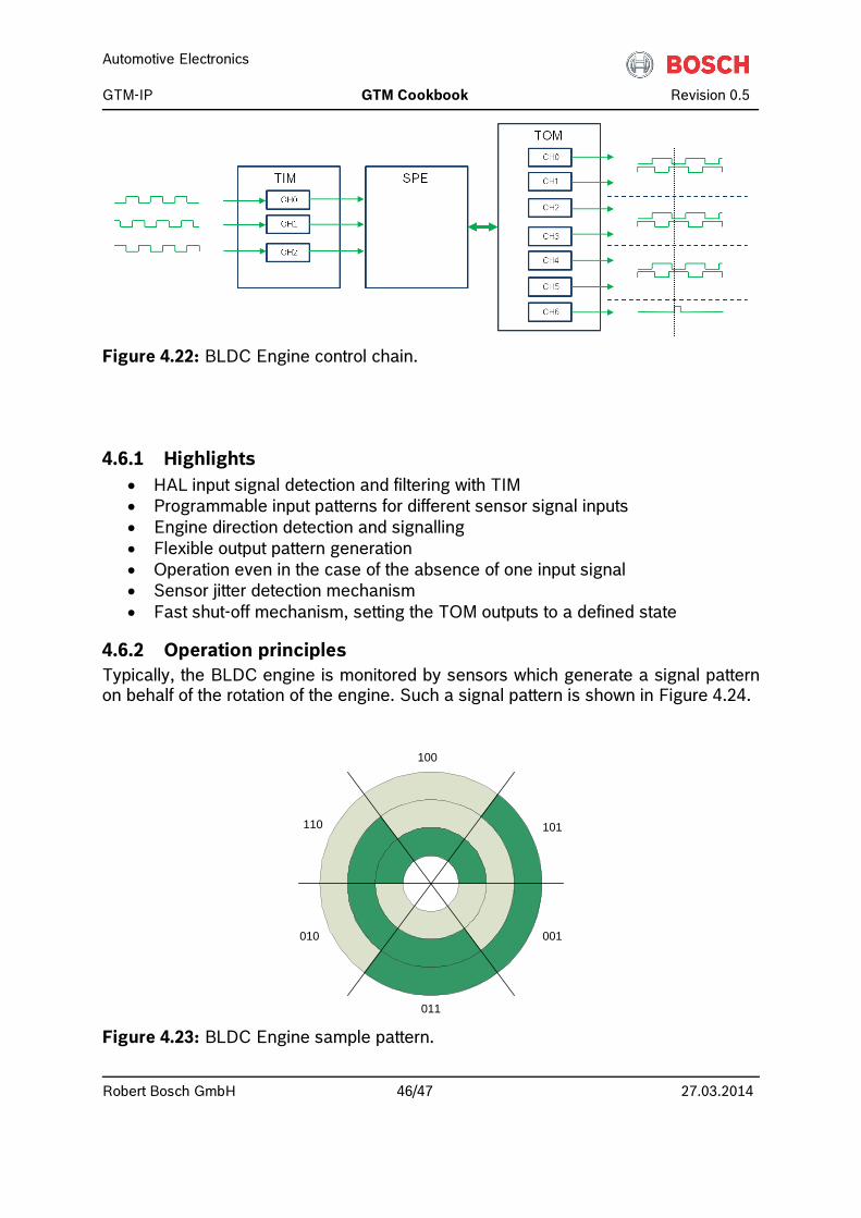
Automotive Electronics GTM-IP GTM Cookbook Revision 0.5
Robert Bosch GmbH 46/47 27.03.2014
Figure 4.22: BLDC Engine control chain.
4.6.1 Highlights • HAL input signal detection and filtering with TIM • Programmable input patterns for different sensor signal inputs • Engine direction detection and signalling • Flexible output pattern generation • Operation even in the case of the absence of one input signal • Sensor jitter detection mechanism • Fast shut-off mechanism, setting the TOM outputs to a defined state
4.6.2 Operation principles Typically, the BLDC engine is monitored by sensors which generate a signal pattern on behalf of the rotation of the engine. Such a signal pattern is shown in Figure 4.24.
100
011
001010
110 101
Figure 4.23: BLDC Engine sample pattern.
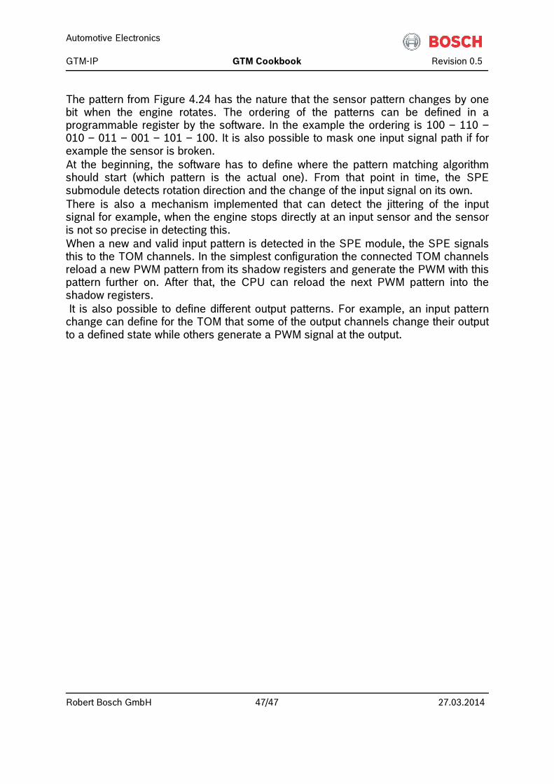
Automotive Electronics GTM-IP GTM Cookbook Revision 0.5
Robert Bosch GmbH 47/47 27.03.2014
The pattern from Figure 4.24 has the nature that the sensor pattern changes by one bit when the engine rotates. The ordering of the patterns can be defined in a programmable register by the software. In the example the ordering is 100 – 110 – 010 – 011 – 001 – 101 – 100. It is also possible to mask one input signal path if for example the sensor is broken. At the beginning, the software has to define where the pattern matching algorithm should start (which pattern is the actual one). From that point in time, the SPE submodule detects rotation direction and the change of the input signal on its own. There is also a mechanism implemented that can detect the jittering of the input signal for example, when the engine stops directly at an input sensor and the sensor is not so precise in detecting this. When a new and valid input pattern is detected in the SPE module, the SPE signals this to the TOM channels. In the simplest configuration the connected TOM channels reload a new PWM pattern from its shadow registers and generate the PWM with this pattern further on. After that, the CPU can reload the next PWM pattern into the shadow registers. It is also possible to define different output patterns. For example, an input pattern change can define for the TOM that some of the output channels change their output to a defined state while others generate a PWM signal at the output.