Embed Size (px)
Citation preview
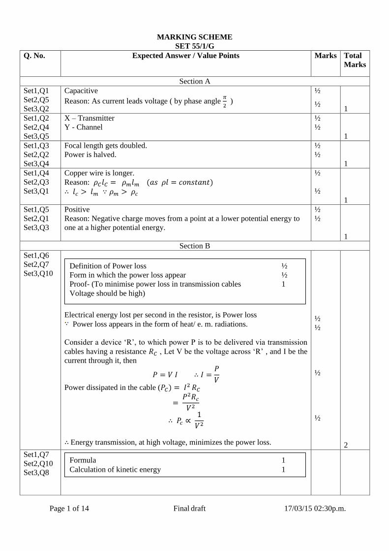
Page 1 of 14 Final draft 17/03/15 02:30p.m.
MARKING SCHEME
SET 55/1/G
Q. No. Expected Answer / Value Points Marks Total
Marks
Section A
Set1,Q1
Set2,Q5
Set3,Q2
Capacitive
Reason: As current leads voltage ( by phase angle )
½
½
1
Set1,Q2
Set2,Q4
Set3,Q5
X – Transmitter
Y - Channel
½
½
1
Set1,Q3
Set2,Q2
Set3,Q4
Focal length gets doubled.
Power is halved.
½
½
1
Set1,Q4
Set2,Q3
Set3,Q1
Copper wire is longer.
Reason:
½
½
1
Set1,Q5
Set2,Q1
Set3,Q3
Positive
Reason: Negative charge moves from a point at a lower potential energy to
one at a higher potential energy.
½
½
1
Section B
Set1,Q6
Set2,Q7
Set3,Q10
Electrical energy lost per second in the resistor, is Power loss
Power loss appears in the form of heat/ e. m. radiations.
Consider a device ‘R’, to which power P is to be delivered via transmission
cables having a resistance , Let V be the voltage across ‘R’ , and I be the
current through it, then
Power dissipated in the cable (
Energy transmission, at high voltage, minimizes the power loss.
½
½
½
½
2
Set1,Q7
Set2,Q10
Set3,Q8
Definition of Power loss ½
Form in which the power loss appear ½
Proof- (To minimise power loss in transmission cables 1
Voltage should be high)
Formula 1
Calculation of kinetic energy 1
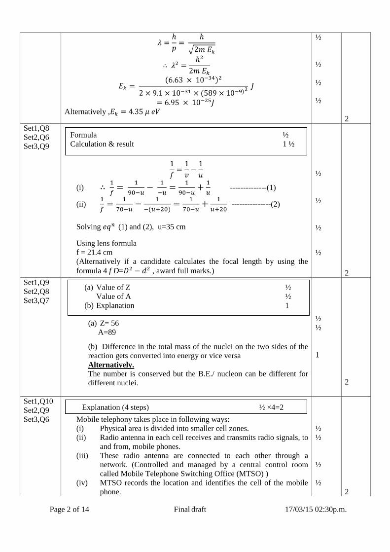
Page 2 of 14 Final draft 17/03/15 02:30p.m.
Alternatively ,
½
½
½
½
2
Set1,Q8
Set2,Q6
Set3,Q9
(i) --------------(1)
(ii) ---------------(2)
Solving (1) and (2), u=35 cm
Using lens formula
f = 21.4 cm
(Alternatively if a candidate calculates the focal length by using the
formula 4 f D= , award full marks.)
½
½
½
½
2
Set1,Q9
Set2,Q8
Set3,Q7
(a) Z= 56
A=89
(b) Difference in the total mass of the nuclei on the two sides of the
reaction gets converted into energy or vice versa
Alternatively.
The number is conserved but the B.E./ nucleon can be different for
different nuclei.
½
½
1
2
Set1,Q10
Set2,Q9
Set3,Q6
Mobile telephony takes place in following ways:
(i) Physical area is divided into smaller cell zones.
(ii) Radio antenna in each cell receives and transmits radio signals, to
and from, mobile phones.
(iii) These radio antenna are connected to each other through a
network. (Controlled and managed by a central control room
called Mobile Telephone Switching Office (MTSO) )
(iv) MTSO records the location and identifies the cell of the mobile
phone.
½
½
½
½
2
Formula ½
Calculation & result 1 ½
(a) Value of Z ½
Value of A ½
(b) Explanation 1
Explanation (4 steps) ½ ×4=2
Page 3 of 14 Final draft 17/03/15 02:30p.m.
OR
Line of sight / Broadcast
Space wave
, R is radius of earth
(Also accept if the student writes )
½
1
½
2
Section C
Set1,Q11
Set2,Q20
Set3,Q15
(a) Equivalent capacitance (Cn) = + C
(b) Charge on C4, q4 = C4×V=10×500 µC
=5×10 -3
C=5mC
Charge on C1,C2,C3 is same and is equal to ×V
1.67 mC
½
½
½
½
½
½
3
Set1,Q12
Set2,Q21
Set3,Q16
Net resistance of the circuit, Req =3 Ω
Current, I= = 3 A
P.D across CD, VCD = ICD×RCD
When the wire is stretched to double its length, each resistance becomes four
times, i.e. 16Ω each.
P.D across one of the diagonal, VAC or VBD V
½
½
½
½
½
½
3
Set1,Q13
Set2,Q22
Set3,Q17
The force, on the electron, due to the magnetic field, at any instant is
perpendicular to its instanteneous velocity.
½
Basic mode of communication ½
Type of mode 1
Expression for d ½
(a) Equivalent capacitance 1
(b) Charge on each capacitor 1+1
Current drawn from the source 1
P.D across C and D 1
P.D across one of the diagonals 1
Path of the electron ½
Determination of frequency of revolution 1 ½
Dependence of frequency on speed ½
Explanation / Reason ½
Page 4 of 14 Final draft 17/03/15 02:30p.m.
Alternatively,
Because necessary centripetal force is provided by Lorentz magnetic force
acting on the electron.
Hz
No
As i.e. is independent of
½
½
½
½
½
3
Set1,Q14
Set2,Q16
Set3,Q18
Three basic processes which take place to generate the emf in a solar cell
are:
(i) Generation of electron hole pairs due to the light incident close to
the junction.
(ii) Seperation of electrons and holes due to the electric field of the
depletion region.
(iii) Collection of electrons and holes by n-side and p-side
respectively.
I-V characteristics of solar cell
½
½
½
½
½
Circuit Diagram ½
Three basic processes 1 ½
I-V characteristics of solar cell ½
Important criteria ½
Page 5 of 14 Final draft 17/03/15 02:30p.m.
Any one criteria of the following:
(i) Small band gap (1.0 to 1.8 eV)
(ii) High optical absorption
(iii) Electrical conductivity
(iv) Availability of raw material
(v) Cost
OR
An LED is fabricated from a semiconductor having a band gap ≥ 1.8 eV /
LEDs of different colours are made from compound semiconductors.
Working
When LED is forward biased, the electrons move from n→p and holes from
p→n; thus concentration of minority charge carriers at the junction increases.
Excess minority charge carriers combine with majority charge carriers near
the junction and release energy as photons.
Advantages (Any three)
(i) Low operational voltage and less power
(ii) Fast action and no warm-up time required.
(iii) The bandwidth of emitted light is 100Ǻ to 500 Ǻ or, in other
words, it is nearly (but not exactly) monochromatic
(iv) Long life and ruggedness
(v) Fast on-off switching capability
½
½
½
½
½ ×3
=1 ½
3
3
Set1,Q15
Set2,Q17
Set3,Q11
Interference Diffraction
1)Equally spaced fringes
2)All maxima have equal
brightness
3)Formed by superposition of
wavefronts from two coherent
sources
4)There is a maxima at the
angle /a 5)Quite a large number of fringes are easily observable
1)Fringes are not equally
spaced
2)Intensity of maxima keeps
on decreasing
3)Formed through
superposition of wavelets
from a single wavefront
4)First minima occurs at an
angle /a 5)It becomes difficult to distinguish maxima and minima after a few fringes
(Any three)
1 ×3
3
Fabrication of LED ½
Working 1
Three advantages of LEDs 1 ½
Comparison and Explanation of three distinguishing features. 3
Page 6 of 14 Final draft 17/03/15 02:30p.m.
Set1,Q16
Set2,Q18
Set3,Q12
For an electron (mass ‘m’ and charge ‘e’) revolving in nth
stable circular
orbit of radius ‘rn’ , with velocity vn , in the hydrogen atom (z=1), we have
½
½
1
½
½
3
Set1,Q17
Set2,Q19
Set3,Q13
A B Output of AND gate
(Input of NOT gate)
Output of NOT gate
0 0 0 1
0 1 0 1
1 0 0 1
1 1 1 0
Truth table of NAND Gate
A B Y
0 0 1
0 1 1
1 0 1
1 1 0
NAND gate is called universal gate because all other basic gates like AND,
OR, NOT gate, can be realised by using NAND gates only.
1
1
1
3
Set1,Q18
Set2,Q11
Set3,Q14
Block Diagram
1
Expression for K.E 2
Relation for P.E 1
Showing that AND gate followed by NOT gate is NAND gate 1
Truth table of NAND gate 1
Why is NAND gate called universal gate? 1
Block Diagram / Explanation of AM 1
Can AM wave be transmitted as such 1
Explanation 1

Page 7 of 14 Final draft 17/03/15 02:30p.m.
Alternatively, Explanation of Amplitude Modulation
No / AM wave cannot be transmitted as such
Explanation
The A.M. wave has to be fed to power amplifier to provide the necessary
power. It is then fed to the antenna for transmission.
1
1
3
Set1,Q19
Set2,Q12
Set3,Q21
(a)
(b) Metal X
/ ,
1
½
½
½
½
3
Set1,Q20
Set2,Q13
Set3,Q22
(a)
(b)
=2×10⁻⁴
m=0.2 mm
½
½
½
½
½
½
3
Set1,Q21
Set2,Q14
Set3,Q19
(a) Emf induced =
(b)
½
½
1
½
½
3
(a) Formula 1
Calculation of number of photons per second 1
(b) Identification of Metal ½
Reason /explanation ½
½
(a) Formula ½
Calculation and Result 1
(b) Formula ½
Calculation and Result 1
½
(a) Derivation for induced emf 2
(b) Expression for power 1
Page 8 of 14 Final draft 17/03/15 02:30p.m.
Set1,Q22
Set2,Q15
Set3,Q20
The time dependent term i.e. represents the displacement current.
It exists in the region in which the electric flux (φo) i.e. the electric field ( )
changes with time.
Example- During charging or discharging of a capacitor, the current in the
wire connecting the capacitor plates to the source is conduction current
whereas in between the plates it is displacement current due to the change of
electric field between the plates which makes the circuit complete.
The conduction current is always equal to the displacement current.
1
½
½
½
½
3
Section D
Set1,Q23
Set2,Q23
Set3,Q23
(a) Principle
When magnetic flux through a coil changes , an emf is induced
across its ends.
Working :
When the coil (Armature ) is rotated in a uniform magnetic field by
some external means , the magnetic flux through it changes . So an
emf is induced across the ends of the coil connected to an external
circuit by means of slip rings and brushes.
(b) Two values displayed by Hari (Any two)
Scientific temperament / curiosity / learning attitude / any other
quality
Two values displayed by Science teacher (Any two)
Responsive / caring and concerned / encouraging / any other quality
1
1
½ + ½
½ + ½
4
Section E
Set1,Q24
Set2,Q26
Set3,Q25
Expression for generalized Ampere’s Circuital law 1
Explanation of significance of time dependent term 1
Suitable Example 1
1
a) Principle of a dynamo 1
Working of a dynamo 1
b) Two values displayed by Hari ½ + ½
Two values displayed by Science teacher ½ + ½
(a) Principle of working of a transformer 1
Labelled Diagram 1
(b) Deducing expression for the ratio of
(i) Output voltage to input voltage 1
(ii) Output current to input current 1
(c) One main source of energy loss ½
How is the energy loss reduced? ½
Page 9 of 14 Final draft 17/03/15 02:30p.m.
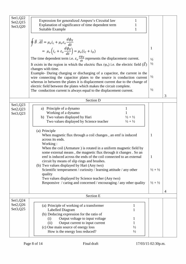
(a) Principle of working :
When the current through the primary coil changes , the magnetic
flux linked with the secondary coil also changes . Hence an emf is
induced across the ends of the secondary coil.
(If the student just writes , ‘mutual induction’ , award ½ mark)
(b) (i)
(ii)
(c) Main source of energy losses ( any one)
Flux leakage / Joule’s loss / loss due to eddy currents / Hysteresis
loss
How they are reduced (any one in the same order)
Winding the primary and secondary coils one over the other / using
thick wires / having laminated core / using a magnetic materal which
has a low hysterisis loss
OR
1
1
½
½
½
½
½
½
5
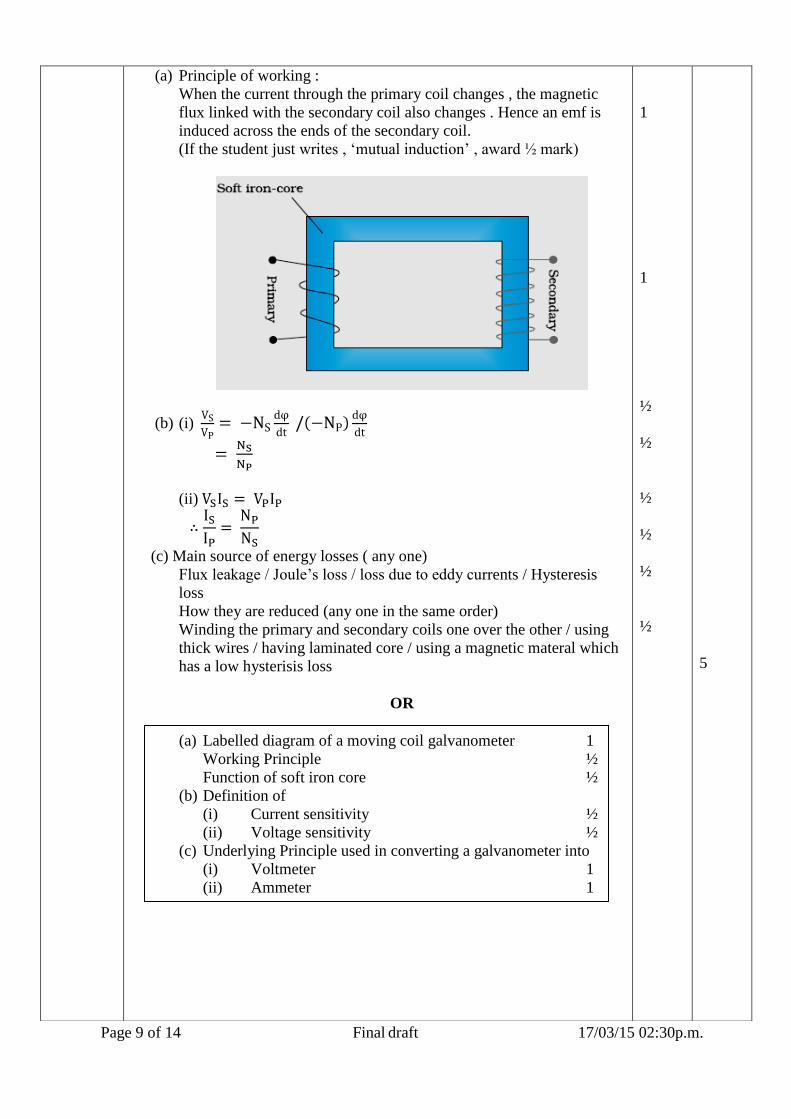
(a) Labelled diagram of a moving coil galvanometer 1
Working Principle ½
Function of soft iron core ½
(b) Definition of
(i) Current sensitivity ½
(ii) Voltage sensitivity ½
(c) Underlying Principle used in converting a galvanometer into
(i) Voltmeter 1
(ii) Ammeter 1
Page 10 of 14 Final draft 17/03/15 02:30p.m.
Principle : When a current carrying coil is kept in a magnetic field , it
experiences a torque .
Cylindrical soft iron core makes the magnetic field radial.
(b)(i) Current sensitivity : It is defined as deflection produced per unit
current flowing through the galvanometer.
(ii) Voltage sensitivity : It is defined as deflection produced per unit voltage
applied across the galvanometer.
(c ) (i) Conversion of galvanometer, into a voltmeter, is based on the fact that
the voltmeter should have very high resistance so that very little (negligible)
current flows through it.
(ii) Conversion of galvanometer, into an ammeter, is based on the fact that
the ammeter should have very little (negligible) resistance so that it does not
reduce the current in the circuit.
Alternatively,
A galvanometer can be converted into
(i) a voltmeter by connecting a suitable high resistance in series with its coil.
(ii) an ammeter by connecting a suitable shunt (Iav) resistance parallel with
its coil.
[Note: If the student just writes
(i)
and (ii)
award ½ mark in each case]
1
½
½
½
½
1
1
5
Set1,Q25
Set2,Q24
Set3,Q26
(a) Two essential conditions for the phenomenon of total internal
reflection 1+1
(b) Ray diagram 1
(c) Diagram with explanation 1 ½
Example to illustrate the use of optical fibre in transmission ½

Page 11 of 14 Final draft 17/03/15 02:30p.m.
(a) Essential conditions
(1) The ray should pass from an optically denser medium into an
optically rarer medium.
(2) Angle of incidence should be greater than the critical angle
for the given pair of media.
(b) Ray Diagram
(c)
When ray of light enters into an optical fibre through one of its ends , it
undergoes repeated total internal reflections along the length of the optical
fibre as the angle of incidence at every point inside optical fibre is greater
than the critical angle.
Example :
Optical fibres are used for transmitting and receiving optical signals to
facilitate visual examination of internal organs of human body / for long
distance communication through optical fibre cables. (any one)
OR
1
1
1
1
½
½
5
(a) Diagram demonstrating the location and shape of a wavefront
using Huygen’s principle 1
(b) Diagram 1
Verification of Snell’s law 1 ½
Reasons for decrease of wavelength and speed but no change
in frequency 1 ½
Page 12 of 14 Final draft 17/03/15 02:30p.m.
(a)
Alternatively,
(Any one of the above diagram)
(b)
Let t be the time taken by the wavefront to travel the distance BC in rarer
medium and AE in the denser medium
= constant
This constant is called ‘refractive index’ of the denser medium with respect
to the rarer medium . Thus , Snell’s law is verified.
1
1
½
½
½

Page 13 of 14 Final draft 17/03/15 02:30p.m.
Reason : If and denote the wavelengths of light in medium 1 and
medium 2 , then if BC = , AE =
Or
This equation implies that when a wave gets refracted into a denser medium ,
its wavelength and speed decrease but its frequency (v/ remains the same.
½
½
½
5
Set1,Q26
Set2,Q25
Set3,Q24
(a) Definition :
Total number of electric field lines passing perpendicularly through a
surface is called electric flux.
(Also accept: )
S.I unit of electric flux is
(b)From
Net flux through the cube ( = Net flux through the two faces of
the cube ( Perpendicular to X-axis + perpendicular to Y-axis +
Perpendicular to Z-axis)
(As is (separately) zero for ( ) for
the faces perpendicular to the y and the z-axis)
=
(Alternatively: )
Net charge inside cube (Q)=
=
OR
1
½
½
½
½
½
½
½
½
5
(a) Definition of Electric flux 1
S.I unit ½
(b) Formula for Electric flux ½
Calculation and result for net flux 2
Formula and result for net charge ½ + ½
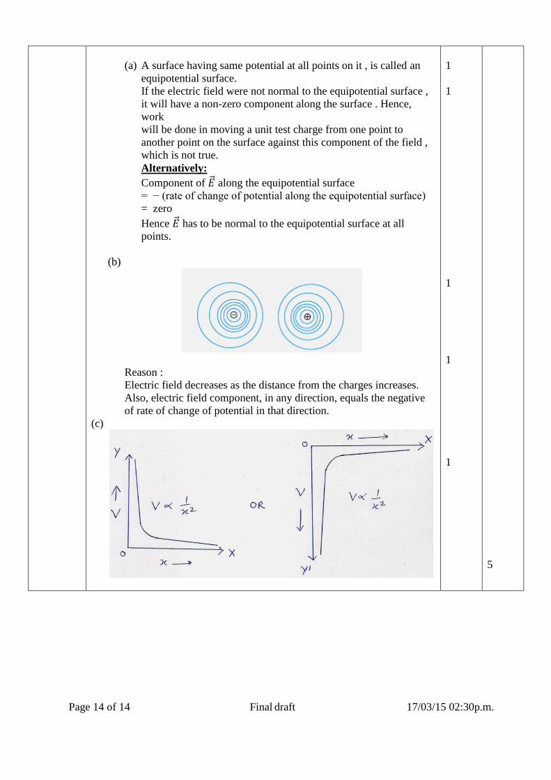
(a) Definition of equipotential surface 1
Reason (Electric field directed normal to the surface ) 1
(b) Diagram 1
Reason 1
(c) Plot of V versus X 1
Page 14 of 14 Final draft 17/03/15 02:30p.m.
(a) A surface having same potential at all points on it , is called an
equipotential surface.
If the electric field were not normal to the equipotential surface ,
it will have a non-zero component along the surface . Hence,
work
will be done in moving a unit test charge from one point to
another point on the surface against this component of the field ,
which is not true.
Alternatively:
Component of along the equipotential surface
= − (rate of change of potential along the equipotential surface)
= zero
Hence has to be normal to the equipotential surface at all
points.
(b)
Reason :
Electric field decreases as the distance from the charges increases.
Also, electric field component, in any direction, equals the negative
of rate of change of potential in that direction.
(c)
1
1
1
1
1
5