Embed Size (px)
Citation preview
Mapping the Dislocation Sub-Structure of Deformed Polycrystalline Ni
by Scanning Microbeam Diffraction Topography
Brian Abbey1,2*
, Felix Hofmann1, Jonathan Belnoue
1, Alexander Rack
3, Remi
Tucoulou3, Gareth Hughes
4 , Sophie Eve
5, and Alexander M. Korsunsky
1
1Department
of Engineering Science, University of Oxford, Parks Road, Oxford, OX1
3PJ, UK.
2School of Physics, The University of Melbourne, Parkville, Victoria 3010, Australia.
3European Synchrotron Radiation Facility, F-38043 Grenoble, France.
4Department of Materials, University of Oxford, Parks Road, Oxford, OX1 3PJ, UK.
5ESCTM du CRISMAT – CNRT-Matériaux / ENSICAEN, 6 Boulevard Maréchal
Juin, 14050 Caen Cedex 04, FRANCE
*Corresponding author: [email protected]
When subjected to plastic deformation, individual grains within ductile FCC
polycrystals fragment into relatively ‘soft’, low dislocation density cells separated by
‘hard’, dislocation-rich walls. Using a narrow bandwidth, sub-micrometer X-ray
beam, we have mapped the deformation structure inside a single grain within a
deformed Ni polycrystal. Dislocation multiplication and entanglement was found to
vary depending on the physical dimensions of the grain. The method we use
overcomes current limitations in classical X-ray topography allowing topographic
images to be formed from small, highly deformed grains.
Imaging a highly perfect crystal via the two-dimensional detection of X-rays
diffracted from its constituent lattice planes (diffraction topography) has been
employed since the 1940’s [1-3]. This technique has very different contrast
mechanisms from those of conventional absorption imaging. Diffraction contrast,
which can partly be accounted for by the dynamical theory of diffraction, allows
visualisation of individual crystallographic line defects (dislocations) and local lattice
strains [4]. Plastic deformation of metallic crystals is mediated by the formation and
propagation of dislocations which self-organise into ‘hard’ dislocation-rich walls
enclosing ‘soft’ regions of low dislocation density (cells) [5]. This dislocation
patterning has profound consequences for material hardening and failure. However,
because of lattice rotation between cells, ray-tracing from the diffraction image to the
sample required for topography is not possible. This intrinsic problem of real and
reciprocal space convolution has previously prevented X-ray topography from being
used to image deformation structure within (poly) crystals [6].
Deconvolution of real and reciprocal space information may be achieved by reducing
the size of the incident beam to the point where the cumulative amount of lattice
curvature within the sampling volume is sufficiently small. The caveat to this is that
the incident beam must contain a large enough spectral bandwidth to ensure all
illuminated parts of the crystal remain in diffraction condition [7]. When using a
broad bandwidth polychromatic (‘white’) incident beam however, quantitative
interpretation of the data becomes significantly more challenging. By using the
intense, narrow bandwidth ('pink') radiation from a single undulator peak we show
here that all parts of the deformed crystal can be kept (partially) in diffraction, whilst
the peak of the rocking curve can be determined via energy scanning. We hereafter
refer to the method of reconstructing a topographic image through the composition of
multiple pink microbeam topographs as scanning microbeam diffraction topography
(SMDT). In addition provided the incident beam is smaller than the length scale of the
dislocation cells is used, the lattice rotation gradient and FWHM of the Bragg
reflection provides a means of distinguishing between the individual cell walls and
their ordered interiors [8].
Dislocations trapped in the crystal lattice via random interactions with one another are
known as statistically stored dislocations (SSDs), whereas dislocations stored to
accommodate inelastic lattice curvature are called geometrically necessary
dislocations (GNDs) [9]. GND density varies approximately in accordance with the
reciprocal of the local length scale of the deformation field (l) imposed by the sample
structure; Fleck et al. [10] predicted that in polycrystals for l < 20 µm the number
density of GNDs should greatly exceed that of SSDs. The relative influence of
crystallite size on plasticity behaviour is a topic of considerable interest due to its
implications for the design and engineering of stronger and more resilient materials
[11-13]. Although length scale dependence does not feature in classical continuum
plasticity modelling [14] it is generally accepted that dislocation interactions must be
responsible for size effects in plasticity. In spite of the great practical importance of
polycrystalline metals, direct observation of the influence of size effects in dislocation
structure formation within individual grains has not previously been reported.
In this letter the through-thickness deformation structure within the micrometer sized
'wedge' shaped grain loaded in situ has been mapped at very high spatial and angular
resolution using SMDT. We note here that depth profiles of the dislocation tensor in
single crystals have previously been measured using white beam Laue diffraction and
differential aperture X-ray microscopy (DAXM) [15]. X-ray topography inherently
captures the fine structure of the individual Bragg spots and provides a significantly
higher sensitivity to lattice misorientation. Electron backscatter diffraction (EBSD)
allows the measurement of orientation in a shallow region (< 100 nm) near the grain
surface. However, since the majority of the grain is buried, EBSD does not reveal the
through-thickness dislocation structure of the grain, which is key to understanding its
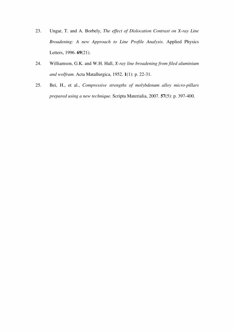
deformation behaviour. Figure 1 shows characterisation data of the 'micro-wedge'.
The wedge makes a shallow 17.7º angle with the sample surface and reaches a
maximum thickness of 7.6 µm, after which it runs underneath grain A1 in the corner.
At its thinnest point where the twin (A2) reaches the sample surface, the wedge grain
thickness vanishes. The wedge geometry (Fig. 1d) allows us to distinguish between
the influence of grain boundaries and the influence of the crystallite size. Due to the
lattice orientation spread resulting from plastic deformation classical X-ray
topography fails to produce an interpretable image of this sample.
Through-thickness orientation and lattice rotation values were confirmed using
microbeam Laue diffraction measurements [16] made on beamline B16 at the
Diamond Light Source (DLS) using a 5×5 µm parallel X-ray beam [17, 18]. The
wedge grain was part of a 15 µm thick polycrystalline Ni foil sample which had been
re-crystallised and annealed to minimise initial defect density. A schematic of the
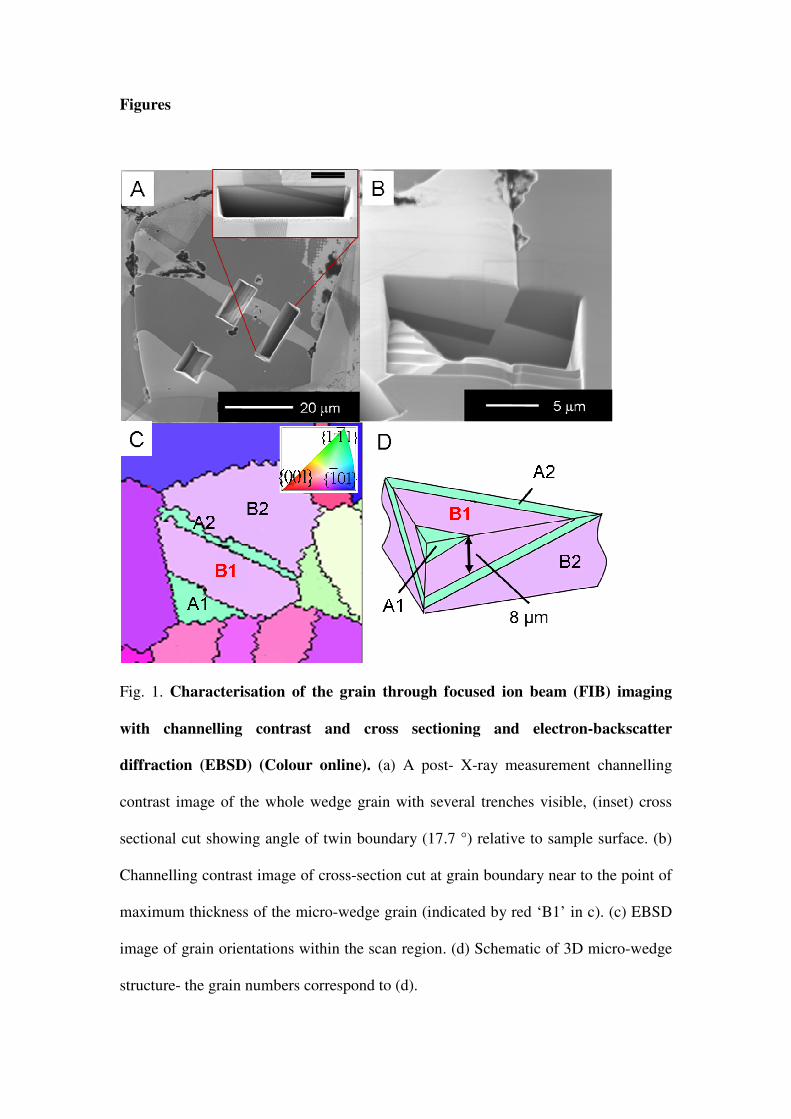
experimental SMDT geometry used on beamline ID22 at the European Synchrotron
Radiation Facility (ESRF) in Grenoble, France is shown in Fig. 2. The X-ray beam
was produced from the 2nd undulator harmonic; the peak photon energy could be
varied from 15 to 18 keV with ∆E/E ~ 1-2%. Kirkpatrick-Baez (KB) mirrors were
used to produce a focused 0.6 × 0.6 µm (H × V) FWHM beam. A photodiode placed
in the transmitted direct beam was used to record a scanning transmission X-ray
microscopy (STXM) image. A thin scintillator screen was used to convert X-rays
from the reflection under study to visible light. The luminescent image was magnified
via a commercial microscope and projected onto a high resolution CCD camera
(FReLoN) [19]. The CCD had 2048 × 2048 pixels of 14 µm giving an effective pixel
size of 0.70 µm (20x objective) after magnification. The scintillator to sample
distance was 50 mm giving an acceptance angle (measured across the diagonal) of
2.38°. The combined STXM and diffraction images (Fig. 2) make it possible to locate
the grain precisely within the sample.
After initially stretching and relaxing the sample (~ 4% plastic strain) the (220)
reflection from the grain (exhibiting severe streaking – asterism [20]) was located and
the undulator gap varied to find the peak energy. The KB mirrors were then installed
and the focused beam raster scanned across the sample in 1 µm steps whilst the
transmission and diffraction data were recorded (inset right, Fig. 2). A line scan
capturing the rocking curve for the reflection at each point was made. With the
knowledge of both the peak energy and Bragg angle (θ) we were able to determine
elastic strain close to the grain boundary (see Fig. S1).
The sample was stretched a second time and held at ~ 4% strain. The topograph from
the whole grain with 100 × 100 µm beam (KB removed) at the peak energy (16.41
keV) is shown in Fig. 3a. The striking lack of any resemblance to the diffracting grain
(or the incident box beam) is consistent with our earlier white beam topography
studies. Before deformation the topograph resembles a point-for-point image of the
grain. After plastic deformation, lattice break-up and rotation within the grain mean
the topograph cannot be corrected to provide a direct sample image. Fig. 3b shows a
topograph collected from a region within the same grain having low dislocation
density using a 0.6 × 0.6 µm FHWM beam (KB installed). Most microbeam
topographs collected from the interior of the grain show relatively minor streaking
due to deformation since each small gauge volume contains only a small amount of
cumulative lattice curvature. At the grain boundaries however, where the lattice
curvature is greater, the microbeam topographs become significantly more streaked.
Figs. 3c and 3d show a compound SMDT topograph made up of 5041 (3c) and 2601
(3d) microbeam topographs, of grain B1 (see EBSD map in Fig. 1) before and after
the final stretch. To form the compound image the centre-of-mass position of each
microbeam topograph was located and added to a larger array, according to the piezo
motor coordinates, removing the effect of large scale variations in θ across the grain.
There are two areas of increased strain in the topographs; one is at the surface twin
boundary labelled in Fig. 3c, the other at the corner of the grain where only the twin
(grain A1) is visible in the EBSD map. After the final load increment, the deformation
in these areas visibly increases.
Figs. 4a and 4b show the magnitude of the gradient and FWHM of the reflection in
the θ plane respectively (corresponding data for χ is given in Fig. S2) for the grain
before the final deformation step. Two dislocation depleted cells (L and M)
surrounded by higher dislocation density walls based on the available FCC slip
planes{111} , {1 11} and{1 11} are identified. Analysis of the (220) reflection FWHM
reveals the same dislocation structures (Fig 4b). The orientation for grain B1 matches
the observed slip directions. Since lattice rotation between dislocation cells and walls
is expected to be much greater than the angular resolution of the experiment [21]
however, features below the measurement resolution are detectable. Within the bulk
part of the grain individual dislocation boundaries separating relatively dislocation
free cells are visible, but moving toward the apex of the wedge these structures merge
together.
From a naïve interpretation of the sample geometry we expect a greater cumulative
number of dislocations to be present in the thicker part of the sample. In fact, the
exact opposite is observed: the thinner the grain, the higher the dislocation density.
This is indicated by the changes in both the lattice rotation and FWHM of the
reflection (Fig 4d). There is no reason or evidence to suppose that the
nature/orientation of the twin boundary is significantly different at the apex of the
wedge then at any other point within the sample, hence we conclude that the
differences in sub-grain deformation structure are size-dependent. For the rotation
data, a peak is observed at around 1 µm, though in general the behaviour is close to
linear. It is interesting to note that the FWHM, plotted as ( )( ) /K Cos∆ = θ ∆θ λ (where
λ is the photon wavelength) may be readily described by a power law of the form
0
NK k mt
−∆ = + (shown by the thin black line in Fig. 4g) where m ~ 0.3 and N ~ 0.4
and 0
k is an arbitrary constant. Both the Hall-Petch relationship and ordinary
dislocation plasticity (ODP) mediated deformation [22] describing the influence of
grain size (Hall-Petch) or sample dimensions (ODP) on the apparent strength of
materials also follow a power-law behaviour. The difference in the trend of the
FWHM and lattice rotation plots as a function of sample thickness is likely to be due
to the fact that the FWHM data is dependent on the size of the coherent scattering
volume in addition to the strain which arises from the presence of dislocations [23,
24]. Fig 4 together with the 2D maps of the grain in Fig. 3 provide direct evidence for
dislocations becoming trapped at the apex of the wedge. Further deformation of the
sample produced only a moderate shift of both plots vertically and an increase in the
dislocation density preferentially in the {1 11} plane.
In this letter we have demonstrated a method for recovering topographic images from
highly plastically deformed, micrometer sized crystals which previously could not be
imaged using conventional diffraction topography. Combined with the data from the
position and FWHM analysis of the >16000 very high-angular resolution topographs
collected during this study we have mapped the sub-grain dislocation structure within
a single Ni grain. The data clearly indicate that a higher GND density occurs at
reduced plastic length scales, interestingly this is the reverse of observations made in
single crystals e.g. in nano-indentation experiments made on pillars [25]. A complete
understanding of how a reduced grain size mediates dislocation activity has the
potential to fundamentally influence our understanding of polycrystalline
deformation. However this requires further advancement in the theoretical modelling
of the relevant processes including dislocation entanglement and the redistribution of
local stresses in order to match the experimental data presented here. The techniques
we have described here will find immediate application in the study of several key
phenomena including dislocation avalanches and strain bursts which have recently
been reported [14]. In addition this work highlights the fact that X-rays can now be
used to characterise the dislocation structure in a much larger range of samples than
was previously possible, bridging the gap with, for example, electron microscopy.

The authors gratefully acknowledge Bernadette Domenges, of the LAMIPS lab in
Caen (France) for FIB imaging and cross-sectioning work carried out on the earlier Ni
foils. Financial support for this research from Rolls-Royce plc. and the Engineering
and Physical Sciences Research Council (EPSRC) is also acknowledged.
References
1. Lang, A.R., The projection topograph: a new method in X-ray diffraction
microradiography. Acta Crystallographica, 1958. 12: p. 249-250.
2. Ramachandran, G.N., X-ray Topographs of Diamond. Proc. Indian Acad. Sci.
Sect. A 19 280-292, 1944.
3. Wooster, N. and W.A. Wooster, X-ray Topographs. Nature, 1945. 155: p. 786-
787.
4. Tuomi, T., K. Naukkarinen, and P. Rabe, Use of Synchrotron Radiation in X-
ray Diffraction Topography. Phys. Stat. Sol. (a), 1974. 25(93): p. 93-106.
5. Mughrabi, H., Dislocation wall and cell structures and long-range internal
stresses in deformed metal crystals. Acta Matallurgica, 1983. 31(9): p. 1367-
1379.
6. Polcarova, M. and J. Bradler, Application of X-ray Diffraction Topography
with a Monochromatic Divergent Beam to the Study of Distorted Crystals.
Journal of Applied Crystallography, 1987. 20: p. 374-378.
7. Mellaert, L.J.v. and G.H. Schwuttke, Feedback Control Scheme for Scanning
X-ray Topography. Journal of Applied Physics, 1972. 43(2).
8. Levine, L.E., et al., X-ray Microbeam measurments of individual dislocation
cell elastic strains in deformed single-crystal copper. Nature Materials, 2006.
5.
9. Ashby, M.F., The deformation of plastically non-homogeneous materials.
Philosophical magazine, 1969. 21(170): p. 399-424.
10. Fleck, N.A., et al., Strain gradient plasticity: theory and experiment. Acta
Matallurgica, 1993. 42(2): p. 475-487.
11. Hall, E.O., The Deformation and Ageing of Mild Steel: III Discussion of
Results. Proceedings of the Physical Society. Section B, 1951. 64(747).
12. Petch, N.J., Journal of Iron and Steel Instruments, 1951. 174.
13. Yip, S., Nature, 1998. 391(532).
14. Csikor, F.F., et al., Dislocation Avalanches, Strain Bursts, and the Problem of
Plastic Forming at the Micrometer Scale. Science, 2007. 318.
15. Ice, G.E., et al., At the limit of polychromatic microdiffraction. Materials
Science and Engineering: A, 2009. 524(1-2): p. 3-9.
16. Barabash, R.I., et al., White microbeam diffraction from distorted crystals
Applied Physics Letters, 2001. 79(6): p. 749-751.
17. Hofmann, F., et al., Intragranular Lattice Misorientation Mapping by
Synchrotron X-Ray Micro-Beams Laue VS Energy-Resolved Laue VS
Monochromatic Reciprocal Space Analysis. International Journal of Modern
Physics B, 2010. 24(1): p. 279-287.
18. Hofmann, F., et al., Probing intra-granular deformation by micro-beam Laue
diffraction. Mesomechnics, 2009. 1(1): p. 193-196.
19. Weitkamp, T., C. Raven, and A.A. Snigirev. Imaging and microtomography
facility at the ESRF beamline ID22. in Proceedings of SPIE. 1999.
20. Honycombe, R.W.K., Inhomogeneity of Deformation in Metal Single Crystals.
Proceedings of the Physical Society. Section A, 1950. 63: p. 672-673.
21. Jakonbsen, B., et al., Formation and Subdivision of Deformation Structures
During Plastic Deformation. Science, 2006. 312: p. 889-892.
22. Stanford, N., U. Carlson, and M.R. Barnett, Deformation twinning and the
Hall-Petch relation in commercial purity Ti. Matall. Materials Transactions.
A, 2008. 39: p. 934-944.
23. Ungar, T. and A. Borbely, The effect of Dislocation Contrast on X-ray Line
Broadening: A new Approach to Line Profile Analysis. Applied Physics
Letters, 1996. 69(21).
24. Williamson, G.K. and W.H. Hall, X-ray line broadening from filed aluminium
and wolfram. Acta Matallurgica, 1952. 1(1): p. 22-31.
25. Bei, H., et al., Compressive strengths of molybdenum alloy micro-pillars
prepared using a new technique. Scripta Materialia, 2007. 57(5): p. 397-400.
Figures
Fig. 1. Characterisation of the grain through focused ion beam (FIB) imaging
with channelling contrast and cross sectioning and electron-backscatter
diffraction (EBSD) (Colour online). (a) A post- X-ray measurement channelling
contrast image of the whole wedge grain with several trenches visible, (inset) cross
sectional cut showing angle of twin boundary (17.7 °) relative to sample surface. (b)
Channelling contrast image of cross-section cut at grain boundary near to the point of
maximum thickness of the micro-wedge grain (indicated by red ‘B1’ in c). (c) EBSD
image of grain orientations within the scan region. (d) Schematic of 3D micro-wedge
structure- the grain numbers correspond to (d).
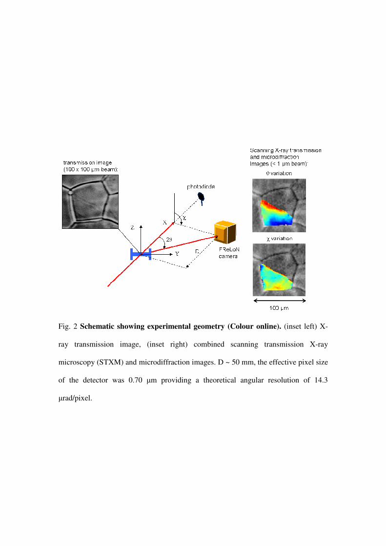
Fig. 2 Schematic showing experimental geometry (Colour online). (inset left) X-
ray transmission image, (inset right) combined scanning transmission X-ray
microscopy (STXM) and microdiffraction images. D ~ 50 mm, the effective pixel size
of the detector was 0.70 µm providing a theoretical angular resolution of 14.3
µrad/pixel.
Fig. 3 Scanning microbeam diffraction data. (a) High resolution image of the (220)
reflection from the whole grain (B1) taken with a 100 x 100 µm box beam at 16.41
keV. Image covers 1.68° horizontally and vertically (b) Image of a single microbeam
topograph of the (220) reflection resembling the incident 0.61 x 0.61 µm sized beam
incident upon a small sub-region within the grain. Image covers 0.42° horizontally
and vertically (c) Composite of 5041 microbeam topographs showing the geometry of
the partially buried plastically deformed grain studied in this letter. (d) Composite of
2601 microbeam topographs covering approximately 2/3 of the grain after further
loading. The broken arrow indicates regions close to the grain boundary where severe
streaking is observed. The two enlarged insets show the apex of the micro-wedge with
significant lattice distortion.
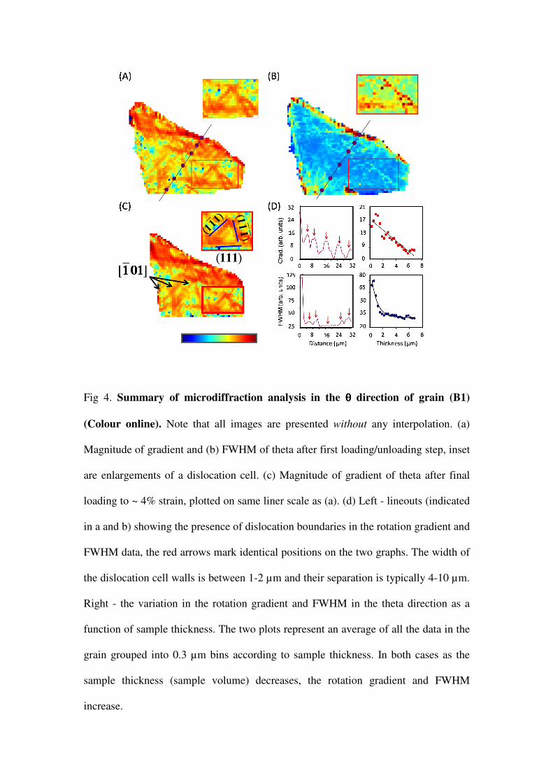
Fig 4. Summary of microdiffraction analysis in the θθθθ direction of grain (B1)
(Colour online). Note that all images are presented without any interpolation. (a)
Magnitude of gradient and (b) FWHM of theta after first loading/unloading step, inset
are enlargements of a dislocation cell. (c) Magnitude of gradient of theta after final
loading to ~ 4% strain, plotted on same liner scale as (a). (d) Left - lineouts (indicated
in a and b) showing the presence of dislocation boundaries in the rotation gradient and
FWHM data, the red arrows mark identical positions on the two graphs. The width of
the dislocation cell walls is between 1-2 µm and their separation is typically 4-10 µm.
Right - the variation in the rotation gradient and FWHM in the theta direction as a
function of sample thickness. The two plots represent an average of all the data in the
grain grouped into 0.3 µm bins according to sample thickness. In both cases as the
sample thickness (sample volume) decreases, the rotation gradient and FWHM
increase.