Embed Size (px)
Citation preview

MANUFACTURINGSCIENCE AND TECHNOLOGY
ELECTRO-OPTICS PLAN
NAVYMS&T
January 1995

Executive SummaryElectro-Optics Manufacturing ThrustBackgroundStudy MethodologyFindings
Laser and Laser DevicesFiber Optic DevicesInfrared Focal Plane Array (IRFPA’s)Flat Panel Displays
Proposed StrategyRecommendationsAttachment 1: Summary of DOC, ARPA and OIDA Reports on Electro-
Optics TechnologyAttachment 2: JDL MS&T Electronics Subpanel Roadmap for IRFPA
Assembly TechnologyAttachment 3: Overview of S&T Efforts in Electro-OpticsAttachment 4: JDL MS&T Planning ProcessAttachment 5: Notification of Electro-Optics Workshop

Executive Summary
In accordance with Congressional direction this U.S. NavyManufacturing Science and Technology Program (MS&T) reportidentifies potential opportunities in electro-optics manufacturing.
The report has drawn on a survey conducted for the Navy by thePennsylvania State University. Additional information was gatheredby the Joint Directors of Laboratories’ (JDL) MS&T ElectronicsSubpanel including:
1) A review of the FY 1995 Technology Area Plan forElectronics published by the Director, Defense Researchand Engineering.
2) A review of the FY 1995 Joint Service Program Plan (JSPP)for Electronic Devices Electro-Optics Subsection.
3) Ongoing planning activity charted by the JDL MS&T Panelon manufacturing technology requirements.
This review determined that electro-optics is not Navy unique, nornecessarily Navy driven. While electro-optics plays a major role inNavy programs, Army and Air Force efforts in electro-optics areheavily used by the Navy. As such Navy becomes a leveragedparticipant rather than the lead.
The electro-optics industry is characterized as a diverse set ofbusinesses with different expertise that provide products to theelectro-optics market place. The electro-optics industry thereforeencompasses a broad technology base, not conducive to a singlesource for process technology advances.
The four information sources identify inter-Service participationand those technology areas with potential for some Department ofDefense infusion to stimulate commercial investment to meetcritical electro-optics needs.
Consequently, the plan addresses three critical areas, indescending order of investment opportunity, where Department ofDefense involvement will help to ensure affordable weapons systems:
1) Affordable manufacture of Laser and Laser Devices such aslaser diode pump arrays.
2) Producible and Affordable Fiber Optic Devices includingfiber opticsensors.
3) Increased affordability involvement in and support forARPA efforts in Infrared Focal Plane Arrays.
Given the broad and diverse spectrum of requirements and theintegration with the other Services, no single entity can be

expected to provide significant expertise in the manufacturingissues necessary to meet the objectives of this report.Accordingly, the Navy proposes to solicit, through an open BroadAgency Announcement, specific industry/academic solutions to thedisparate requirements in major areas of electro-optics technology.This BM will assess industry/academia commitment through costsharing and provide the flexibility to address the most promisingmanufacturing process technologies in electro-optics.
This report provides the following recommendations:
1) Continue the ongoing roadmap/planning effort by theJDL MS&T Electronics Subpanel which will provide adetailed technical program plan in the April 1995time frame.
2) Publish a BM in early 1995, calling for industryand academia to propose execution methods for thetechnical developments required.
3) Award a contract or contracts for execution of thethrust by October 1995.
4) Whenever possible leverage MS&T investment withongoing activities within the government andprivate sector.

Electro-Optics Manufacturing Thrust
Tasking: The Navy Manufacturing Technology (MANTECH) Program wasdirected in the Report of the House Committee on Appropriations onthe Defense Appropriations Act for Fiscal Year 1994 to prepare astrategy for developing and executing a thrust in the area ofelectro-optics. The tasking language of HR103-254 is:
"Concerning electro-optics manufacturing, the Committee isaware of requirements within the Navy in the area of electro-optics manufacturing. A new generation of displays, targetingdevices, FLIR detectors, and fiber optics is scheduled forinsertion in weapon systems over the next five to ten years.Many of these technologies will provide valuable benefits tocommercial industry in the areas of computers, consumerelectronics, and transportation. Accordingly, the NavyManufacturing Technology Program is directed to develop atechnology thrust in electro-optics manufacturing, withemphasis on dual use technology deployment. The Committeedirects the Secretary of the Navy to submit a strategic planfor execution of this thrust to the Appropriations Committeesof Congress by February 1, 1994 which details executionmethods, technical plans, schedules, and budget requirements.The Committee has provided an additional $750,000 for thepurpose of developing the plan and for fiscal year 1994effort."

Background
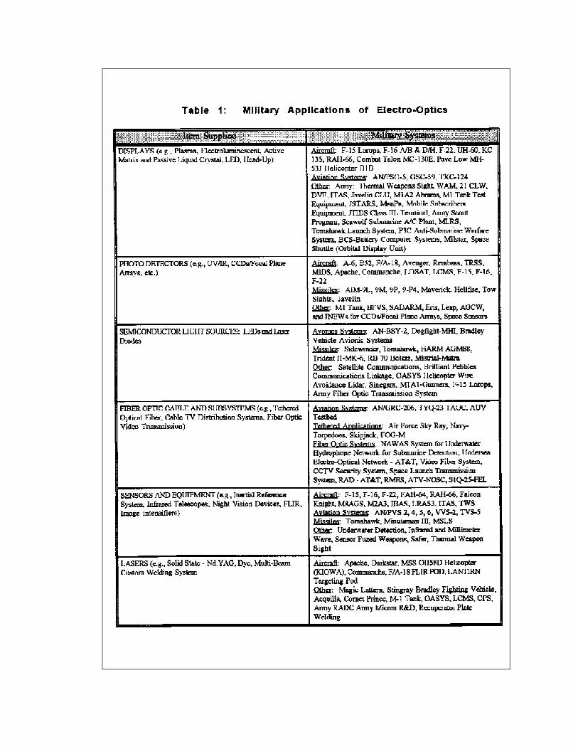
Background: A viable U.S. electro-optics industry is an essentialrequirement for national defense and will assure the nation’scompetitive participation in one of the fastest growing sectors ofthe global economy. The extended utility of electro-optictechnology is derived from merging the power of microelectronicswith the capabilities of optical light sources (e.g., lasers),sensors, waveguides (e.g., fiber optics), and displays. Theintegration of these technologies has created a plethora ofproducts for both military and civilian applications. Militaryapplications include target acquisition/fire control systems, nightvision equipment, missile seekers, guidance and controls,underwater acoustic sensors, electronic warfare signal processors,and communication networks. A more complete list of electro-opticitems of military importance and the systems in which they can beemployed is summarized in Table 1. Important civil sectorapplications include not only communications networks, but alsomedical imaging systems, environmental monitoring and pollutioncontrol, and checkout line automation.
Electro-optics will be a key component in the information age,providing for significant advances in the collection, processing,transport, storage, and display of information in both civil anddefense applications of the 21st Century. This diversity ofapplications has created a growing market, estimated to be $31B in1993, and forecasted to more than $100B by 2003, primarily drivenby the communications and video segments in the commercial market.Today, the U.S. electro-optic industry is judged to be competitivein the global market but losing ground. The reason for this is thatU.S. public and private sector investment in electro-opticmanufacturing science and technology is substantially smaller inaggregate than our foreign competitors. It has also beenestablished through various agency assessments that if the U. S. isto remain competitive in this market and fulfill the specializedneeds of Department of Defense (DoD), it must invest in thedevelopment and facilitation of advanced electro-opticmanufacturing technology.
In the case of the defense industrial needs, the primary concern isto maintain and develop improved critical manufacturingcapabilities in a period of declining DoD budgets. The emergingapproach to this problem is to support a more integrateddefense/commercial industrial base wherein investments andimprovements in one sector benefit the other, so-called dual-usetechnology. In this way, decreases in the defense acquisitionbudget will be compensated for, in part, by greater competitivenessand market share in the global market, thereby maintaining defenseessential manufacturing capabilities. Important to this paradigm isthe judicious investment by DoD to affect this synergism andthereby realize both the economic and technological benefits ofindustry, government, and academia working collaboratively onrelated military and civil sector topics. To this end, the DoD mustprovide U.S. industry the incentive and risk mitigation for

maintaining and developing electro-optic manufacturing capabilitieswhich address the DoD’s unique requirements and at the same timemake their own products more competitive. Such an integratedapproach to retaining the defense/commercial industrial base mustguard against the export of critical military technology.Conversely, it is equally important to preclude the sole dependenceon foreign supplies for critical materials and components neededfor defense systems. Indeed, the integrated paradigm not onlypresupposes continued export/import controls, but also improveddialogue between the DoD and industry and improved transfermechanisms of government-sponsored research to industry. Improvedtechnology transfer mechanisms include the level fieldparticipation of and equal benefit to relevant defense companies aswell as enhanced communications between government and industry.The challenges and benefits of an integrated technology base aremanifested preeminently in the electro-optics industry.


Study Methodology
Study Methodology: Although the Navy has been tasked with thedevelopment of a strategic thrust in Electro-Optics, the scope ofthis effort includes technology requirements from all Services. Itis anticipated that the resulting thrust will incorporate on-goingDefense efforts and will leverage both other department andindustry investments as applicable. Accordingly, the varioussources utilized to identify both requirements and current activityextend beyond the boundaries of Navy unique interest.
This report is an amalgam of information from four sources.
1) A study commissioned by the Navy MS&T Office and executedby the Applied Research Laboratory of Penn StateUniversity. This study included a review of previousreports published by the Department of Commerce (DOC),Advanced Research Projects Agency (ARPA), and the Opto-Electronics Industry Development Association (OIDA), aswell as ongoing initiatives with the DoD. Summaries ofthese reports are provided as Attachment 1.
2) A review of the FY 1995 Technology Area Plan forElectronics Electro-Optics subsection published by theDirector, Defense Research and Engineering (DDR&E) whichprovides a compendium of Science and Technologyrequirements across the Services based upon projectedweapon system developments.
3) A review of the FY 1995 Joint Service Program Plan (JSPP)for Electronic Devices Electro Optics subsectiondeveloped under the Joint Directors of Laboratories (JDL)Reliance Panel. This plan identifies both continuing andprojected developments within the Exploratory andAdvanced Development programs.
4) An ongoing planning activity chartered by the JDL MS&TPanel to identify, specifically, manufacturing technologyrequirements based upon weapon system procurement andDefense essential needs.
The analysis of input from all of these sources was intended toprovide an overview of Defense essential technology needs, as wellas work either on-going or planned which addresses these needs. Theneeds which are not being addressed constitute gaps in capabilitywhich are candidates for MS&T funding attention within the proposedthrust.
The scope of this study did not include project level analysis. Theintention was to identify general areas of focus which should beexamined and analyzed further. A discussion of how this should beaccomplished is addressed later in this report.

Findings
Findings: No single, generic MS&T breakthrough will achieve theperformance enhancements and cost reductions across the broadspectrum of Electro-Optic components and systems needed in both themilitary and civilian sectors. Rather, there are several genericmanufacturing method and infrastructure enhancements which togethercontribute to these goals. Included are enhanced methods forfabrication technology for packaging high speed optical detectorsand transmitters, automated fabrication of fiber grating andwavelength division multiples couplers, cost reductionmanufacturing technology for high power diode laser arrays and forthermal electric coolers for IR focal plane arrays. The developmentof robust packaging methodologies is needed as well. Theintegration of simulation-based design and process planning withFlexible Computer Integrated Manufacturing (FCIM) methodologiesneeds to be developed for a broad range of electro-optic systemcomponents to permit cost-effective customization of individualunits and small and mixed lot manufacturing. Such a custom orsmall-lot manufacturing capability is clearly important to makemilitary electro-optic systems affordable, and once developed willbe applicable to the production of both high end military and civilsector systems (e.g., for medical purposes) as well.
Both the Army and Air Force have extensive efforts to developelectro-optic technologies and the manufacturing technologiesnecessary to carry them out. The Navy’s approach is one of mutualcollaboration with the other Services and providing impetus inthose areas either Navy unique or where the Navy would find thebest payoff.
Given the broad and diverse spectrum of requirements and theintegration with the other Services, no single entity can beexpected to provide significant expertise in the manufacturingissues necessary to meet the objectives of this report.Accordingly, the Navy expects to solicit, through an open BroadAgency Announcement, specific industry/academic solutions to thedisparate requirements in major areas of electro-optics technology.
An examination of the various information sources noted above ledto a consensus in four major areas of technology. In all instances,there is a compelling Defense requirement not adequately addressedby the commercial market. Additionally, in each case, thetechnological bottleneck is the ability to manufacture affordableas compared to a performance of design technology limitation. Thefour general areas of Electro-optics which are primary candidatesfor manufacturing technology projects are:
General Electro-optics Areas
1) Laser and Laser Devices such as laser diode pump arrays.The Department of Defense is presently developing a broadrange of high peak power and high average power solid-state lasers. If the systems using these lasers go to

full military production, the cost of the laser diodepump arrays will approach $1B over the life-cycle of theweapons systems. These systems include IR and opticalcounter measures, ranging and designation, ASW, and minedetection. Current costs of these arrays is in the$10/peak Watt range, and it needs to be reduced by anorder of magnitude to be comparable to flash lamp pumpeddevices. A Balanced Technology Initiative during1989-1991 reduced costs from $300/peak watt to thecurrent levels, and a MS&T initiative could achieve theadditional manufacturing cost reduction required. TheArmy has proposed such a program for a FY 1995 startfocusing on devices to pump Neodymium lasers. Anadditional investment in developing reduced costmanufacturing methodologies for pump four-level rareearth lasers (e.g., Thulium, Holmium, and Erbium) wouldaddress other DoD needs in which long pump pulses andbroad spectral line width are required. As withinvestments in generic manufacturing methods, support ofmanufacturing cost reduction initiatives related tospecific subsystems such as laser diode pump arrays havedual-use implications including wind shear detection andmedical/surgical applications.
2) Fiber Optic Devices for optical fiber sensor, electronicwarfare and data transfer systems. Fiber optical sensorsare superior to conventional sensors for the detection ofa wide range of field types (e.g. acoustics, magnetic,gyroscopic, etc.) in important DoD applications such asNaval towed and hull mounted arrays and for smartstructures used for monitoring self noise or controllingstructural deflections. Further work is needed tofacilitate the inexpensive manufacture of these sensorsto permit cost effective utilization in military andcommercial applications. Three fiber optical deviceswhich will benefit from improved manufacturingtechnologies include; high frequency (>10 Ghz) analogsource and detection modules, in-line fiber Bragggratings and wavelength division multiplex (WDM) couplersfor IR surveillance and targeting subsystems. Inexpensivepackaging and device fabrication will be the specific aimof the high speed source and receiver module work. Thesehigh speed devices are used in electronic warfare andradar systems as well as cable TV products. The goal ofthe in-line fiber Bragg grating manufacturing task willbe to facilitate production of these gratings from thecurrent 10 gratings per day that the commercial sectorproduces to over 5,000 gratings per day. This advance ismade possible through a Navy patented process and willresult in a cost reduction of at least a factor of 10.The WDM coupler manufacturing task will be aimed atcommercializing a proven device design with superiorperformance to any currently available device.

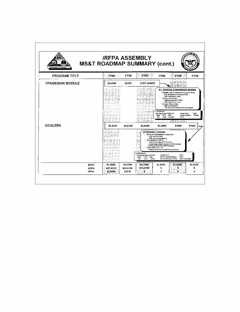
3) Infrared Focal Plane Array (IRFPA’s) are among the mostwidely fielded electro-optic systems. They are criticalto night operation and strategic surveillance on a widevariety of systems and platforms. Nevertheless, currentmanufacturing yield affects their availability; andenhanced performance is needed as well. Attachment 2provides a JDL proposed roadmap for the improvement ofassembly technology for IRFPA’s, and is typical ofongoing activity and planning within the JDL MS&T Panels.Specific areas such as the utilization of HgCdTe havebeen well addressed by ARPA among others, but otherelements of IRFPA technology, such as cooler productionremain major cost obstacles particularly in low rateenvironments.
The Navy MS&T effort will coordinate with the extensiveongoing ARPA, Army and Air Force efforts in this area andwill defer all focal plane array work to the otherServices and ARPA. However, the Navy will continue toensure its requirements are addressed in these otherprograms. The one area that the Navy anticipates MS&Twork is in the area of thermal electric coolermanufacturing. This includes the fabrication of highquality bismuth/antimony/telluride/selenide crystals aswell as the manufacture of the complete cooler assembly.Possible joint funding with the Army will be pursuedgiven the multi-service requirements for these devices.The goal here will be to develop moderate capacitythermal electric coolers capable of 1500K operation at acompetitive cost and to solve the manufacturing yieldissues.
4) Flat Panel Displays are utilized in a variety ofequipment including cockpits, helmet-mounted displays,test equipment and embedded computer/sensor readouts.Major efforts both at ARPA and within the Title III(Defense Production Act) program have targeted theaffordable production of Flat Panel Displays for many ofthe Defense applications. Although some efforts may stillrequire attention, MS&T investment should be usedjudiciously in specific instances
The generic and subsystem specific manufacturing initiatives notedabove are representative of steps that should be taken to ensurethe viability of the U.S. electro-optics enterprise for militarypurposes. Prioritization of unmet electro-optics manufacturingneeds requires a combined effort by industry, academia, and thethree Services, taking into account both emerging war fightingcapabilities and the most promising advances in electro-optics inthe emerging science and technology base.
Attachment 3 provides an overview of on-going or planned S&Tinvestments by the Services which need to be continued or builtupon. These actions would provide an initial core of a major thrust

in Defense essential Electro-Optics and coincide well with theoverall findings of this report. Such an effort is in keeping withthe Navy’s commitment to focus on MS&T early in technology basedevelopment for affordable weapons systems.

Proposed Strategy
Strategy to Develop and Execute the Opportunities: The strategyproposed consists of two simultaneous activities. The first is thetechnical analysis of specific, weapon system related Electro-Opticrequirements, i.e., the development of a project level program planor roadmap including funding schedules and implementation targets.The results of this study will serve as both guidance and a pointof departure for this program roadmap. Attachment 2, referencedearlier provides an example of one such roadmap for IRFPA assembly.Based on judiciously applied limited funds, the envisioned electro-optics manufacturing program plan would consist of some number ofthese project level roadmaps.
The mechanism which will be used to develop the specific technicalagenda is the JDL MS&T Subpanel on Electronics. This body consistsof Service and defense agency representatives who are experts inthe various electronic areas, including Electro-Optics. ThisSubpanel has been tasked to develop appropriate Electro-Opticroadmaps by the JDL MS&T Panel, primarily within the technicalareas identified by this study, i.e., Lasers, Fiber Optics,IRFPA’s, and as necessary, Displays. It is anticipated that theseroadmaps will be available by April 1995. As background, a synopsisof the JDL MS&T planning process which this body will follow isprovided as Attachment 4. Attachment 5 provides notification of aworkshop to be held in response to the subpanel tasking.
Concurrent with this effort, the Navy MS&T office is developing anappropriate execution method for the thrust. In developing thisexecution strategy the Navy is required by Section 256 of the FY1995 Defense Authorization Act to compete this program and torequire cost share on any project which has dual use potential.Section 2525, subsection (d) of Title 10, U.S.C. was amended toread as follows:
" (1) Competitive procedures shall be used for awarding allgrants and entering into all contracts, cooperativeagreements, and other transactions under the program."
" (2) A grant may not be awarded under the program, and acontract, cooperative agreement, or other transaction may notbe entered into under the program, on any basis other than acost-sharing basis unless the Secretary of Defense determinesthat the grant, contract, cooperative agreement, or othertransaction, as the case may be, is for a program that
"(A) is not likely to have any immediate and directcommercial application; or"(B) is of sufficient high risk to discourage costsharing by non-Federal Government sources."
The Secretary of Defense may obligate fiscal year 1994 defenseappropriations under the Manufacturing Technology Developmentprogram which remain available for obligation on the date ofthe enactment of this Act in accordance with the competition

and cost-sharing requirements of subsection (d) of section2525 of title 10, United States Code, as amended by section256 of this Act, notwithstanding any other provision of lawthat specifies (or has the effect of requiring) that acontract be entered into with, or a grant be made to, aparticular institution or entity."
In satisfying this language the Navy is planning to issue a BroadAgency Announcement (BAA) that will allow for organizations topropose an appropriate execution method for projects within thethrust.
The Navy considers industry share as a crucial element of anyexecution strategy. The funding provided by the government throughthe execution of this thrust is viewed as seed funding forleveraging industry investment through cost sharing. Furthermore,any funded efforts of significant duration will require atransition to overall industry support within a reasonable time.
Current funding for initiation of the thrust consists ofapproximately $1.5M in FY 1994 and FY 1995 funds. The Navy hasprepared a BAA to be advertised in early 1995. This BAA willsolicit private sector proposals for execution of the broad anddiverse spectrum of MS&T requirements addressingaffordability/producibility for electro-optics. The BAA will callfor abstracts that: (1) Enhance the critical defense manufacturingcapabilities and the development of integrated defense/commercialindustrial base; (2) Develop advanced manufacturing technologiesand their transfer to U.S. industry; (3) Identify opportunities inelectro-optic science and technology for public and privateinvestments; (4) Promote opportunities in dual-use applications anddefense conversion opportunities. The criteria for selectioninclude: (1) Soundness of technical approach; (2) A strong emphasison cost sharing; and (3) Realistic costs.
It is felt that these actions will provide for meaningful technicalprojects in Electro-Optics executed in a timely and logical manner.

Recommendations
The following actions are recommended:
1) Continue the ongoing roadmap/planning effort by theJDL MS&T Electronics Subpanel which will provide adetailed technical program plan in the April 1995 timeframe.
2) Publish a BAA in early 1995, calling for industryand academia to propose execution methods for thetechnical developments required.
3) Award a contract or contracts for execution of theprojects by October 1995.
4) Whenever possible leverage MS&T investment withongoing activities, such as IRFPA with the AdvancedResearch Projects Agency, within the government andprivate sector.

Attachment 1Summary of DOC, ARPA and OIDA Reports on Electro-Optics Technology
Understandably, much data and analysis regarding the economiccompetition of the electro-optics industry has been published overthe past several years. Two broad-based studies of competitivenessneeds have recently been completed - the first by the OIDA and thesecond by the DOC. In addition, ARPA hosted an Opto-electronicModule Technology and Manufacturing Workshop from whichrecommendations for future manufacturing initiatives emerged. Insupport of the current study, a survey was conducted to determinethe manufacturing technology needs as perceived by a representativesegment of the U.S. electro-optics industry and research community.These results, as well as the previous studies cited, are reviewedin the remainder of this section.
OIDA Opto-electronic Technology Road Map: This road map wasdeveloped over a two year period. A total of over 500 industryrepresentatives participated in the 11 workshops and two nationalforums were held to access future commercial market opportunitiesand to develop technology road maps to position U.S. industry totake advantage of these opportunities. Final recommendations weredivided into the following four categories: (i) displays; (ii)optical communications (including optics for switching andcomputing); (iii) optical storage; and (iv) hard copy.
The OIDA recommends an increased effort in manufacturing technologyin all areas except hard copy as well as continued R&D at currentor increased levels in all four categories. The study concludes,for example, that top priority in the display area is theestablishment of domestic, high volume, flat panel displaymanufacturing capabilities. Manufacturing technology initiatives aswell as R&D are required to develop such capabilities. In theoptical communications area, OIDA predicts that much of the futuremarket growth will be in short distance, high bandwidthcommunications systems (e.g., within building, factories, and othersimilar domains). They support steps to reduce the manufacturingcosts of optical fibers, switches, and other integrated optical-electronic components for such systems. (This emphasis ondeveloping lower cost manufacturing methodologies for opto-electronic devices and components is important as well in thefurther development of optical signal processing and sensing forboth military and civilian sectors). The U.S. is currently in anunfavorable competitive position in the optical storage area. Therecommendation of this report is that the U.S. emphasize thedevelopment of higher density storage devices based on shorterwavelength light (green, blue). R&D in support of cost-effectivemanufacturing of lasers and of substrates, media, and recordingsystems is essential to carry out this strategy for storagedevices. DoC Measurements for Competitiveness in Electronics: ThisDOC study focuses on the electro-optic areas of lasers, opticalfiber communications, optical fiber sensors, and video. The reportnotes that in 1992 materials processing, medicine, andcommunication were the three commercial applications for which the

highest dollar volume of lasers were sold. Materials processing andmedical surgery are associated in this study with higher powerenergy producing lasers (e.g., CO2) and medical imaging andcommunications systems with solid-state diode lasers. The reductionof the semiconductor diode laser to a reasonably priced commodityis the most important laser development of the past decade; thismarket is now dominated by Japan. Moreover, this type of laser isreplacing conventional lasers in a variety of application domainsas higher power and broader wavelength outputs become available.(It seems clear from these facts that manufacturing technologysteps to regain a portion of this market are critical to bothglobal competitiveness in electro-optics and having a domesticsource for specialized semiconductor diode lasers for militaryapplications.) The rate of progress of optical fiber communicationshas been very rapid, but even the most modern systems exploit onlyabout one one-thousandth of the information capacity of opticalfibers. The limitation is in the electro-optic components(switches, couplers, multiplexer, and demultiplexers) which are anintegral part of such a communication system. Research,development, and manufacturing technology initiatives are requiredthat provide low- cost, high performance, and high-reliabilitycomponents to serve as the basis for the next generation opticalcommunication system. Many of the issues identified in the videoarea by this study are similar to that in the display component ofthe OIDA report. An important additional requirement addressed inthis report is the need for advanced data compression methods andhardware for video systems. The data compression requirements forsuch systems will be one to two orders of magnitude more stringentthan for current networking systems used with computers. Given theenormous market potential for high-resolution video systems as wellas their potential importance in military systems, the uniquemanufacturing technology requirements for components of very highperformance data compression systems may be a fruitful area ofinvestment.
ARPA Workshop on Electro-Optics Module Technology andManufacturing: This workshop, held in May 1993, featuredpresentations by 28 U.S. companies developing and marketingproducts in this area. Among the critical manufacturing technologyshortfalls identified by the participants were packaging ofelectro-optic components (including alignment, interconnects, andsurface-emitting lasers), scale-up to volume manufacturing, processflexibility to handle complex modules, and improved methods forintegrating optical and electronic components. Manufacturingtechnology advances to address these needs were associated with awide range of military and civil sector benefits, includingimproved local area communications networks, imaging systems,optical sensors, and phased arrays.

Attachment 2
JDL MS&T Electronics SubpanelRoadmap for IRFPA Assembly Technology


Attachment 3Overview of S&T Efforts in Electro-Optics
Each of the Services has on-going technology base and/orManufacturing Science and Technology programs to address theirpresent and future needs for electro-optics components and systemsThese programs are motivated by a broad range of electro-opticssystem, subsystem, and component needs. The Services’ electro-optics program activities, encompassing such areas as photonics,fiber optics, lasers, displays, and focal plane arrays are beingworked in conjunction with other agencies, such as ARPA, NASA andNIST, to effectively leverage government investment Specifichighreturn" EO technologies (having a wide range of military andcommercial applications), listed below are being pursued. Theability to cost-effectively produce these technologies has becomethe focus of many joint Service efforts.
- Monolithic integrated functions (MIFs) combiningconventional IC technologies with high-speed digital,opto-electronic and microwave functions on the same chip.MIFs may include compound (GaAs, etc) or Group IV - suchas germanium (Ge) materials deposited on a siliconsubstrate.
- High power, diode-pumped, solid-state lasers for use inmilitary applications such as Infrared countermeasures,satellite to ground or satellite communications and lightdetection and ranging (LIDAR).
- High speed optical devices for radar remoting andelectronic warfare deception devices.
- High speed optical processors for high-throughput, real-time signal processing three-dimensional IC technology.
- High definition displays (flat panel - AMLCDs, etc.) forrapid and effective access to information resourceson/over the battlefield.
- Laser diode arrays for efficient, low-weight, lower-powersources for laser-directed energy applications.
- Infrared (IR) imaging sensor (improved focal planearrays) - image sensors providing increased capabilitiesfor missile seekers, surveillance and reconnaissancecameras.
- Fiber optical sensors for anti-submarine warfare (ASW),chemical/biological warfare (CBW) detectionsystems,tactical grade fiber optic gyroscopes, and smartstructures.
- Material manufacturing programs required to produce thetechnologies above specifically tailored rugate filters

for missile domes, FLIR windows, and laser protectioncoatings.
- Fabrication equipment - process equipment and associatedautomation and sensor technologies for low defectdensities and tight process control over the full rangeof fabrication steps.
- CAD for electro-optic domain - software tools, interfaceand integration standards, models and data structures foraccurate simulation of microwave/mm-wave and EO hardwareand systems.
Grouping the above technology listing into four main categories:Photonic/Fiber Optic devices, Lasers, Display Technology, andInfrared Sensor Technology, we will provide a summary of ongoingService work.
Photonic/Fiber Optic Devices
Photonics/fiber optics technology can support a number ofapplications that were the sole purpose of electronic andmicroelectronic devices. By combining fast, massively paralleltechniques, devices possessing high spatial resolution (used inoptical data storage), photonics can produce order-of-magnitudeimprovements over today’s conventional electronic devices.
The high power semiconductor diode laser is emerging as the devicethat will satisfy many of the energy generating needs of photonics.Semiconductor devices such as the master oscillator power amplifier(MOPA), using a single mode distributed feedback (DFB) lasercombined with a waveguide all deposited on a GaAs wafer for on chippower amplification, have proven extremely effective rivalling thatof gas, ion, and solid state lasers. The high power and highbrightness output of the MOPA device can be frequency doubled tothe blue wavelengths with an efficiency as high as 26%, promisinga significant impact on the development of advanced opticalmemories for photonic systems. Additionally, diode laser arrayshave proven to be superior pump sources for laser range finders,designators and counter measure sources.
New designs are being sought for photonic detectors in high speedfiber optic microwave systems. In a recent development, a photo-conductive detector was developed based on a low-temperature grownGaAs buffer layer to provide the required characteristics of sub-picosecond response, high carrier mobility and high breakdownvoltage. High sensitivity, comparable to that of a photo diode, wasachieved by reducing the carrier transit time across the electrodegap to match the carrier lifetime in order to approach thecondition of unity photo current gain. Other detectors have beendeveloped in packaged devices which operate up to 20 Ghz and 40Ghzpackaging has been demonstrated in laboratory environments. In aparallel photonic detector effort, state-of-the-art nanofabricationtechniques were used to fabricate the world’s fastest metal-

semiconductor-metal (MSM) photo diodes. It is expected that thesephoto diodes will find important use in numerous advanced signalprocessing and control systems and optically controlled phasedarray radars.
Further advances were made in wideband photonic networks to provideimage and sensor data, super computer interconnection, and highspeed access to electronic databases and libraries. Significantachievements were made in four-wave mixing in semiconductors as thepossible mechanism for low power frequency shifting in widebandoptical networks. These developments are important because an all-optical wideband communications network will most likely usefrequency division multiplexing. If the interconnects are optical,means must be developed for shifting a signal from a frequencychannel in one LAN to a different frequency channel in another LAN.Four-wave mixing in semiconductors has the potential for satisfyingthese requirements.
Recent advances in micro-optic fabrication methods havesignificantly added to photonic capabilities for advancedcomponents serving a wide range of applications. Binary micro-opticfabrication of photonic components has been carried out for manyyears. However, the problem of holding mechanical tolerances hasseverely limited the optical performance of binary optics in thevisible spectrum. To overcome that problem, analog micro-opticfabrication must be continued wherein optical surfaces fullycorrespond to bulk physical optics are produced on a very smallscale.
Surface electrical passivation is a major problem for m-vsemiconductor photonic devices, and significant work is beingcompleted to find a solution that will have a large impact onproducing high speed electronic and optical components for sensingand signal processing. Whereas an effective native oxide, SiO2, isavailable for silicon very large scale integration, none exists forGaAs microelectronics. In one government program it was shown thatoxidized aluminum gallium arsenide layers can provide effectivespace passivation. Such layers are compatible with modernlithographic and processing techniques. A manufacturing researchteam demonstrated the excellent performance of various optoelectronic devices fabricated using this method.
The base technologies in fiber optics include delay lines andcommunication links, computer applications, generic fiber opticsensor technology, coherent communications, and fiber optic sensorsurvivability and reliability. Various types of fiber optic sensorshave been developed by the Services that perform the function ofhydrophone, magnetometer, accelerometer, thermometer and gyroscope.One program is the tactical grade fiber optic gyroscopemanufacturing program focused on meeting a one degree per hourdrift rate. The government effort in this area has been ledprimarily by the Navy and Air Force.
The Navy is also conducting a MS&T program with Litton to
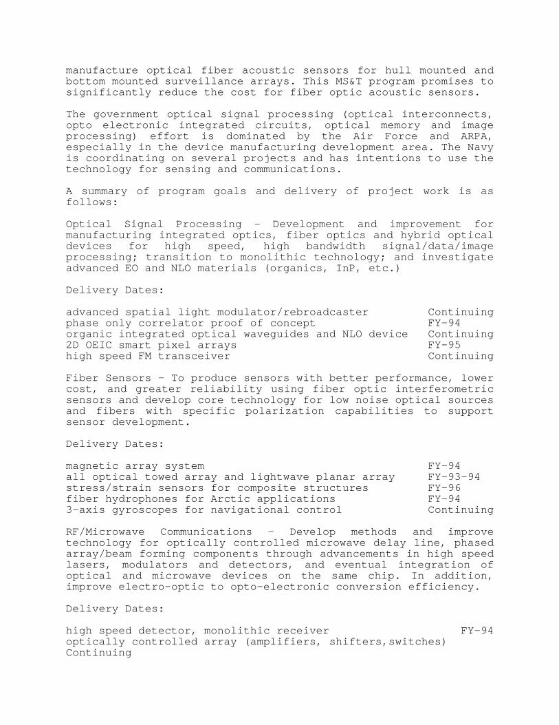
manufacture optical fiber acoustic sensors for hull mounted andbottom mounted surveillance arrays. This MS&T program promises tosignificantly reduce the cost for fiber optic acoustic sensors.
The government optical signal processing (optical interconnects,opto electronic integrated circuits, optical memory and imageprocessing) effort is dominated by the Air Force and ARPA,especially in the device manufacturing development area. The Navyis coordinating on several projects and has intentions to use thetechnology for sensing and communications.
A summary of program goals and delivery of project work is asfollows:
Optical Signal Processing - Development and improvement formanufacturing integrated optics, fiber optics and hybrid opticaldevices for high speed, high bandwidth signal/data/imageprocessing; transition to monolithic technology; and investigateadvanced EO and NLO materials (organics, InP, etc.)
Delivery Dates:
advanced spatial light modulator/rebroadcaster Continuingphase only correlator proof of concept FY-94organic integrated optical waveguides and NLO device Continuing2D OEIC smart pixel arrays FY-95high speed FM transceiver Continuing
Fiber Sensors - To produce sensors with better performance, lowercost, and greater reliability using fiber optic interferometricsensors and develop core technology for low noise optical sourcesand fibers with specific polarization capabilities to supportsensor development.
Delivery Dates:
magnetic array system FY-94all optical towed array and lightwave planar array FY-93-94stress/strain sensors for composite structures FY-96fiber hydrophones for Arctic applications FY-943-axis gyroscopes for navigational control Continuing
RF/Microwave Communications - Develop methods and improvetechnology for optically controlled microwave delay line, phasedarray/beam forming components through advancements in high speedlasers, modulators and detectors, and eventual integration ofoptical and microwave devices on the same chip. In addition,improve electro-optic to opto-electronic conversion efficiency.
Delivery Dates:
high speed detector, monolithic receiver FY-94optically controlled array (amplifiers, shifters,switches)Continuing

MESFET optical detector FY-962-8 GHZ wide dynamic range fiber link Continuing
Lasers
The military Services and NASA continue to seek low-cost compactlaser transmitters (semiconductor diode lasers) for spacecommunications. Particularly sought are better reliability andefficiency compared to the Nd:YAG solid state laser. One successfulapproach has been with the MOPA semiconductor discussed earlier.MOPA structures continue to require improvements in manufacturingto fabricate monolithic devices on a single chip.
In general, tri-service technology consists of three dominantthrust: (1) laser diode arrays, (2) the diode pumped 1 micrometerlaser, and (3) mid-IR laser sources. The diode array thrust seeksto reduce the cost and increase the performance and availability ofa pump for solid state lasers. The objective of the diode pumped 1micrometer laser effort is a compact, high efficiency laser sourcethat uses the diode pumped neodymium-doped solid state lasermaterial. The objective of the mid-IR technology is to developmilitarized lasers that use diode pumped solid state lasers andnonlinear optics to produce radiation in the 1.5 to 5.0 micrometerregion.
Tri-service participation is as follows: The Army is responsiblefor manufacturing technology in the NIR laser diode arrays, EOcountermeasures and managing the diode array pumped kilowattlasers, the Air Force is responsible for high power coherent laserdiodes, those diodes operating in the W spectrum, and high powerlaser radar sources, and the Navy is responsible for temperature-insensitive laser technology and wavelength conversion to the blue-green region, quasi-phase-matched nonlinear technology in the mid-IR, development of long wavelength diode arrays for mid-IR laserpump, and in-house programs on specific mid-IR applications.
A summary of program goals and delivery of project work is asfollows:
Laser Diode Arrays - Produce high power, efficient, incoherentlaser diode arrays and coherent laser diode arrays for pumpingsolid state lasers and for direct sources. High power density (1500W/cm2), low cost, quasi-CW, laser diode arrays at 807 nm withgreater than 40% efficiency for pumping Nd:Host solid state lasers.Diode array structures with efficient heat transfer; improvedoptical coatings and passivation techniques; and operation overwide temperature range are needed.
Delivery Dates:
coherent diode arrays (greater than 5 watts CW at 91lnm) FY-94coherent arrays (greater than 5 watts CW at 970-980nm) FY-95surface emitting array Continuingcoherent arrays (greater than 5 watts at 1.9-2.5 um) FY-95

Diode Pumped 1 um Laser - Produce compact, moderate power (10-100watts), high efficiency (min 10% to 1 um) 1 urn laser sources andcompatible technology for wavelength conversion into the visiblespectrum. Produce large rods/slabs of high quality; efficientoptical coupling of laser material; techniques for efficient heatextraction; techniques for low-tolerance optical alignment; highquality nonlinear crystals for frequency doubling; robust opticalcoatings for diodes, solid state lasers, and nonlinear crystals;and laser operation over military temperature range.
Delivery Dates:
temperature-insensitive diode pumped oscillator FY-94prototype 10 lb., 3 J. laser for EOCM FY-95prototype lKW laser FY-95
MID-IR Sources - Fabricate high efficiency lasers emitting in the1-5 um wavelength region; high efficiency lasers with a minimum of3% total efficiency in 2-5 um region for IRCM, and 1.5-2 um regionfor laser radar and obstacle avoidance; efficient high rep rate 2um laser source; optimized nonlinear subsystems for OPO wavelengthconversion to 3-5 um.
Delivery Dates:
50 watt flyable 2 um laser for BTIIRCM demo FY-94Brassboard laser operating with 2 watts at 2-5 um FY-95
Display Technology
Display technologies under development include: flat panel, lightvalves, and high-performance CRTs. Particularly needed are high-information-content displays that range from miniature, helmet-mounted devices, through potable and vehicular systems, and finallyon to large screen displays for command post and shipboardapplications. In addition, 3D and stereoscopic displays are neededfor robotics applications, while tele-operated and situationdisplays will be further developed using laser technology,miniature devices, polarizers and special optics. Leapfroggingcurrent technology, a U.S. company commercialized a displaymanufacturing process, developed by a U.S. university (inconjunction with ARPA), which deposits an array of thin-filmsilicon transistors on a wafer for the subsequent lift-off to thefinal stage of liquid crystal display assembly This approach isunique because it allows flat panel display manufacture to becarried out by the activity of separate companies, eachcontributing its own specialties in conventional IC foundryservices, lift-off and transfer processing, and LCD encapsulation.This achievement bodes well for the U.S. participation in producingboth projection and virtual-reality display systems.
Progress also continues in the U.S. in the areas of thin-filmelectro luminescent and plasma full color display technologies. Inboth cases, VGA-resolution displays have been demonstrated. In a

recent development, research on a producible, high-quality, Si-mirror, full-color, video image projection display technology wastransitioned to limited production. This technology will requireadditional work to realize a full production effort.
Another recent manufacturing achievement in the area of FPDs wasthe use of lift-off technology to produce a high performance, 1000lines-per-inch head-mounted FPD. Two approaches were investigated:active matrix electro luminescence and active matrix liquid crystalusing single crystal silicon circuit for high performancetransistors in an active matrix. Further manufacturing developmentmust occur in this area to allow the production of a helmet-mounteddisplay for the Combat Command and Control system being procured bythe Army.
Tri-service participation is as follows: The Army will possessoverall technology cognizance for electro luminescent and plasmadisplays, the Air Force will concentrate on liquid crystals andstereoscopic displays, and the Navy will serve as lead in the areaof volumetric and helmet applications
A summary of program goals and delivery of project work is asfollows:
Flat Panel Displays - Develop new capabilities in high resolutioncolor, flat panel display technology and apply them in the operatorinterface segments of military aircraft, shipboard, submarine,vehicle and ground systems.
Delivery Dates:
full color TFEL and plasma prototypes FY-9476 cm SVGA plasma panel in full color FY-9425 cm full color VGA TFEL in production FY-95
Large Screen Displays - High-resolution, large-screen displays forcommand post, shipboard and command centers.
Delivery Dates:
digital micromirror display prototype FY-9476 cm plasma flat panel display FY-94
Helmet Mounted and other Miniature Displays - High performance,small display devices, optics and interactive devices for helmetmounted displays; development of miniature flat panel technology isexpected to provide performance and efficiency.
Delivery Dates:
AMEL/LCD miniature flat panels FY-9412 micron pixel flat panel devices FY-94
3D/Stereoscopic Displays - Develop rugged, fieldable, 3D and

stereoscopic display systems for applications where depthperception is critical to mission performance.
Delivery Dates:
micropol stereo projection and flat panel displays FY-943D volumetric display FY-95
Infrared Sensor Technology
The central issue affecting the availability of the HgCdTe IRFPAfor military system development is the improvement of productyield. This is being addressed in manufacturing and producibilityprograms. In the Phase I ARPA IRFPA Program, for example,significantly better manufacturing yield has resulted. End-itemproduct cost has dropped from approximately $60,000 for the 480 x4 array and $190,000 for the 96 0 x 4 array in 1990 to about $30,000in 1993 for the 96 0 x 4 array (data was not available for the 480x 4 array).
In addition to improving the manufacturing yield of the HgCdTeIRFPA, the stability of the readout attachment is another area ofconcern. Bump bonding between the individual detectors and theassociated readout elements has always presented technical problemsbecause of the difference in thermal expansion of the detector andreadout subsystems. A significant achievement in 1993 was theimproved assembly and thinning of the layers of the array to allowrelease of stress in expansion or compression by slight mechanismdeformation. This has enabled the manufacture of arrays withimproved temperature cycling performance.
Intrinsic material instabilities remain for HgCdTe IR detectors andarray systems, and superlattice/quantum well infrared absorbingmaterials are being designed to replace HgCdTe for IR detectors andarrays. The possibility for tuning the superlattice wavelengthsuggests a wide range of applications in imaging and detection,surveillance, robotics, etc. In addition to superlatticestructures, quantum well infrared photo detectors (QWIPs) have beendemonstrated. These detectors were limited in the past by therequirement of non-normal incidence of the incoming radiation, withan associated loss in detection of the infrared signal. Usingtheoretical analysis and novel semiconductor growth techniques,researchers have succeeded in demonstrating normal and non-normalincidence detection in the same silicon-germanium multilayerstructure. This advance should also be possible in QWIPs fabricatedin III-V compound semiconductors and accelerate their incorporationinto night vision devices and systems.
There have been other recent advances in focal plane array systems,including successful transition of platinum silicide (PtSi)infrared detector technology from the laboratory to an Air Forceplatform. Much work is still needed to improve the yield rate ofPtSi detector manufacturing. Another area seeing revitalizedinterest is the use of Schottky diode arrays for infrared imaging

(originally proposed by the Air Force in the 1970s). the Air Forcecontinued a low-level development effort of this technology andcurrent infrared focal plane arrays are available which have morethan 300,000 separate elements in staring 480 x 640 format. Becauseof the use of silicon technology, which has exceptional supportfrom the semiconductor industry, these arrays turned out to beremarkably defect-free.
Many military focal plane array applications require thermoelectriccoolers that operate at cryogenic temperatures - the range below120°K. Currently, thermoelectric coolers operate at 1800K, andresearch is being carried out to reduce the thermoelectricoperating temperature to the cryogenic range. The dominantadvantages of improving the cooler for military and commercialapplications are increased efficiency, low weight, increasedreliability, reduced size, and elimination of the CFC coolant.
The three Services along with ARPA and BMDO have established jointfederated programs developing a broad spectrum of infrared focalplane arrays. Devices under development in this joint effortinclude two-dimensional arrays of detectors fabricated in HgCdTe,InSb, uncooled silicon and ferro-electric, and photoemissivematerials. IRFPAs are fabricated under contracts to industry andthe deliverables and underlying technology are evaluated ingovernment laboratories.
A summary of program goals and delivery of project work is asfollows:
IR Focal Plane Arrays (HgCdTe. Uncooled. Photoemissive) - Developthe technology and demonstrate the feasibility of focal plane arrayconcepts for DoD infrared sensor systems; Develop two dimensionalarrays of detectors and the associated readout electronics usingdetector materials which include HgCdTe, InSb, extrinsic silicon,and uncooled silicon and ferroelectrics.
Delivery Dates:
PtSi camera systems NEdeltaT < 0.01K FY-94monolithic HgCdTe MWIR FPA o f 1 X 1 FY-95multicolor staring FPA FY-96uncooled FPA with NEdeltaT FY-96smart FPA with advanced on-chip processing FY-98
IRFPAs: Alterative Approaches - Develop the technology anddemonstrate the feasibility of focal plane array concepts for DoDapplication; develop 2-D arrays of detectors and the associatedreadout electronics using alternate detector materials, includingGaAs. InGaAs, GaXxSb, high temperature superconductors and Si/Ge.
Delivery Dates:
InXxSb detector demo FY-94GaAs multicolor detector FY-96

GaAs IRPM (3-5 um) FY-97III-V monolithic quantum well detector/mux FY-97

Attachment 4JDL MS&T Planning Process
The affordable production, upgrading and sustainment oftechnologically superior weapon systems relies on a capable,competitive and responsive, private and organic, industrial base.The US industrial base must respond to sharply curtailed defenseproduction with defense-specific and integrated commercial-militaryproducts which are world class in cost, quality and meet customerneeds. Realizing these changes require development of new businesspractices implementing lean manufacturing concepts, a focus ontotal quality and variability reduction, full implementation ofintegrated product and process development, and a broadly capablemanufacturing and support infrastructure facilitating change andenabling implementation.
The JDL MS&T Panel, composed of the Manufacturing Technology(MANTECH) Directors of the DoD Components - Army, Navy, Air Forceand Defense Logistics Agency (DLA) - has developed a unifiedinvestment strategy that, when funded and executed, will providethe solutions necessary to implement the changes needed to respondto today’s shifting force structure requirements, industrial baserestructuring, and technology advances. The investment strategy wasjointly developed by the DoD components and is based uponidentification and prioritization of weapon system requirements andpervasive industrial base requirements.
As shown in Figure 1, each DoD Component first identifies its majorsystems currently in acquisition or sustainment. These systemscomprise the central target for MANTECH investment. They areanalyzed to identify outstanding manufacturing requirements, e.g.,fabrication processes which historically provide low quality oryield, or new material where forming parameters are not welldeveloped. The industrial base sectors that produce the systems andthe sustainment mechanisms that will maintain and repair thesystems are assessed for current and expected process technologydevelopments and shortfalls. This analysis provides the linkagebetween manufacturing and sustainment technology requirements ofthe industrial base and the defense system or systems which driveit. This strategy, based on system requirements, is a key elementof MANTECH which distinguishes it from other manufacturingprograms. Finally, the technology base efforts are analyzed toidentify technological opportunities with direct application toService needs.
These inputs are analyzed by each Service to develop its own set ofmanufacturing technology requirements, each DoD componentprioritizing their needs based upon similar criteria that nowincludes: availability of a technically feasible solution,potential benefit to be derived, probability of implementation(including management support and system stability) and urgency ofthe requirement. These requirements, together with an estimatedcost profile, comprise the DoD component investment plan.

Next, the DoD components’ investment plans are reviewed by the JDLReliance Subpanels. These subpanels are comprised of technicalexperts in specific categories, e.g., electronics, composites,metals processing, industrial base pilots and manufacturingsystems. Each panel reviews the proposed investments and providesa reprioritization based upon a DoD-wide perspective. At thispoint, ongoing efforts outside MANTECH are reviewed for relevancyand potential for coordination, as well as multi-servicerequirements which dictate joint development programs. Based uponthis analysis, the unified DoD MANTECH program for each technicalcategory is repriced and a budget request is prepared. Thesecategory programs are combined and refined by the overall JDL Panelto produce the unified DoD component’s program plan for MANTECH.

Attachment 5Notification of Electro-Optics Workshop
AMSEL-RD-NV-TTPD-MANTECH
MEMORANDUM FOR INFORMATION 15 NOVEMBER 94
SUBJECT: Workshop For Electro-Optics Manufacturing Science andTechnology
SPONSORING AGENCIES:
US Army Communications and Electronics Command, Night VisionDirectorate, Thermal Technology & Producibility Division,MANTECH TeamUS Army Missile Command, MANTECH DivisionUS Air Force, Wright Laboratory, Electronics DivisionUS Navy, Office of Naval Research, Production AssessmentDivision, Naval Manufacturing Technology ProgramAdvanced Research Project Agency
Defense Sciences, Material ScienceMicroelectronics TechnologyAdvanced Systems Technology
ENDORSED BY:
Joint Directors of Laboratories Manufacturing Science &Technology Reliance Panel, Electronics Manufacturing & ProcessesSub-Panel
1. The Night Vision and Electronics Sensors Directorate (NVESD),Fort Belvoir, Virginia, will be hosting a workshop on Electro-Optics Manufacturing Science & Technology (E-O MS&T) on 2-4 May1995. The purpose of the workshop is to allow industry, academiaand federal agencies to:
Identify critical areas in E-O Manufacturing that requiredevelopment in order to support future defenserequirementsDiscuss technical approaches to develop these critical E-O Manufacturing areas.
2. This memorandum solicits technical abstracts for presentationsduring the E-O MS&T workshop. The one page technical abstractsshould focus on E-O Manufacturing issues and proposed developmentapproaches. Abstracts must include a listing of the family, type,or class of weapons system which the new manufacturing effort wouldsupport. In addition, please briefly describe any new E-Otechnology if applicable. The abstracts must be received NLT 23January 95. The list below contains technical areas where E-OManufacturing may need development. Other applicable topics may beaddressed and submitted for consideration.

Focal Plane Arrays:Cooled, Uncooled, Monolithics/Smart FPA’s, Coolers,Dewars
Lasers:Laser Diodes, Diode Arrays, Diode Pumped Sources, Mid IRSources, Optical Coatings, Laser Materials, Non-linearOptics Materials
Optics:Conventional Optics, Advanced Optics (aspheric lenses,non-axisymmetric optics, conformal, non-linear, binary,holographic, & micro-optics), Advanced materials/processing (solgel, Gradient index, Coatings)
Display components:Flat Panel (miniature, helmet mounted)
Fiber Optics:Dynamic Guidance Links, FO Harnesses, FO Sensors, FOInverters, Commo Links, IFOGS
Opto Electronics:Optical Interconnects, Integrated Optics, Spatial LightModulators, Optical Correlators, Ring Laser Gyros
Advanced Image Intensifiers:Micro-channel Plates, Photo-anode, Photo-cathode
3. A panel consisting of staff from the sponsoring agencies willreview the responses solicited by this memorandum and select theabstracts for presentation during the workshop. The three days maybe organized into sessions, grouped by sub-technologies, to providea forum for the presentation of selected abstracts. Each sessionwill conclude with a discussion period which has been set aside toexpress comments, ideas, and alternative concepts. A copy of allpresentation materials will be made available to workshopattendees.
4. The workshop will be controlled unclassified. Only US citizenswithout direct foreign interests may attend. Interestedparticipants or attendees should send responses or questions via E-Mail, fax, or mail to the addresses listed below. A minimalregistration fee will be charged to cover lunches and refreshments.Abstracts should be sent to the address below NLT 23 January 1995.Registration material and more details will follow in March 95.
ADMINISTRATIVE CHAIR:Amy M. RyanNight Vision and Electronic Sensors DirectorateAMSEL-RD-NV-TTP-MANTECH ATTN: Amy M. Ryan10221 Burbeck Road, Suite 430Fort Belvoir, VA 22060-5806E-MAIL: [email protected]

Fax: (703) 704-1705
Sincerely,
WILLIAM E. SALAZARA/TmChfMANTECH, TTPD
39