Embed Size (px)
Citation preview
Manufacturing Challenges and their Implications on Design
Phi P kh Ph DPhiroze Parakh, Ph.D
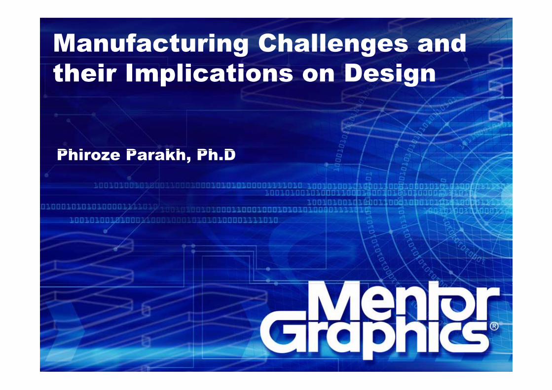
45nm/32nm Design Challenges
MANUFACTURING VARIATIONS
PROCESS & DESIGN VARIATIONS
LOW POWER
LARGE DESIGNS
LOW POWER
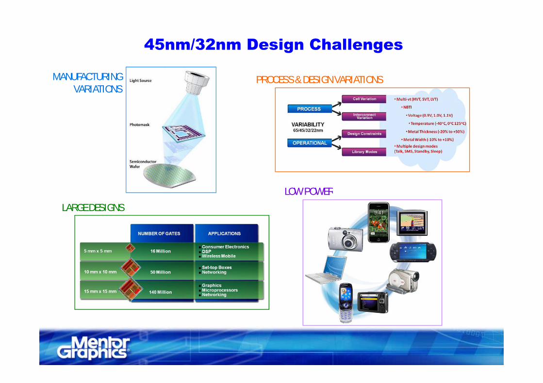
The Evolution of SignoffEO
UT
PRE-
TAPE
P
130nm 90nm 45nm65nmDRC
32nmDRCC
DRCC
DRCCCritical Feature
AnalysisCritical Feature
AnalysisCritical Area
AnalysisLith f i dl
Critical FeatureAnalysis
Critical AreaAnalysis
Lith f i dlLitho-friendlyDesign
Litho-friendlyDesign
Litho-aware SiliconModeling
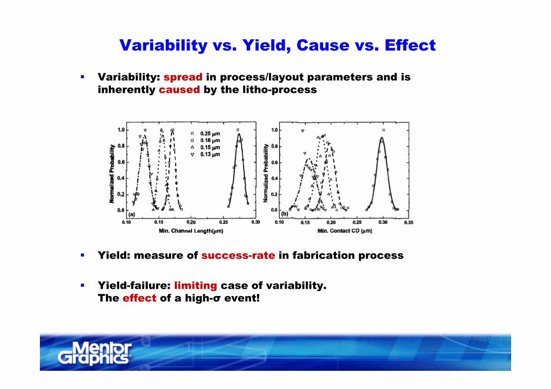
Variability vs. Yield, Cause vs. Effect
Variability: spread in process/layout parameters and is inherently caused by the litho-process
Yield: measure of success-rate in fabrication process
Yi ld f il li iti f i bilit Yield-failure: limiting case of variability. The effect of a high-σ event!
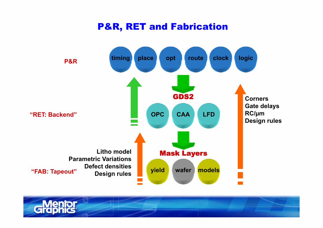
P&R, RET and Fabrication
timing place opt route clock logicP&RP&R
GDS2
OPC CAA LFD“RET: Backend”
CornersGate delaysRC/µmOPC CAA LFD“RET: Backend” RC/µmDesign rules
Mask LayersLitho modelParametric Variations
Defect densitiesDefect densitiesDesign rules“FAB: Tapeout” yield modelswafer
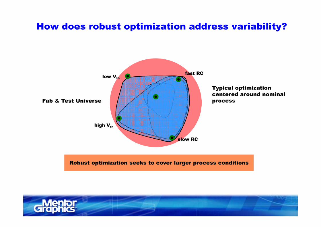
How does robust optimization address variability?
Typical optimization
fast RClow Vth
Typical optimizationcentered around nominalprocessFab & Test Universe
slow RC
high Vth
Robust optimization seeks to cover larger process conditionsRobust optimization seeks to cover larger process conditions
slow RC
p g pp g p
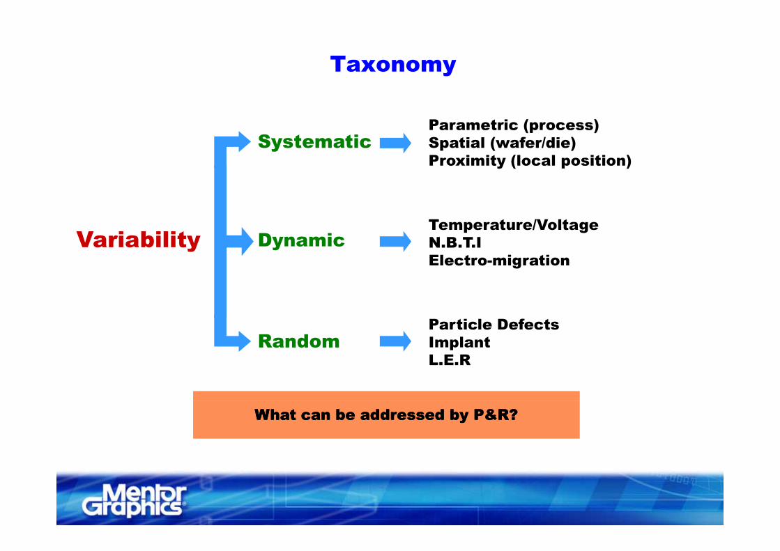
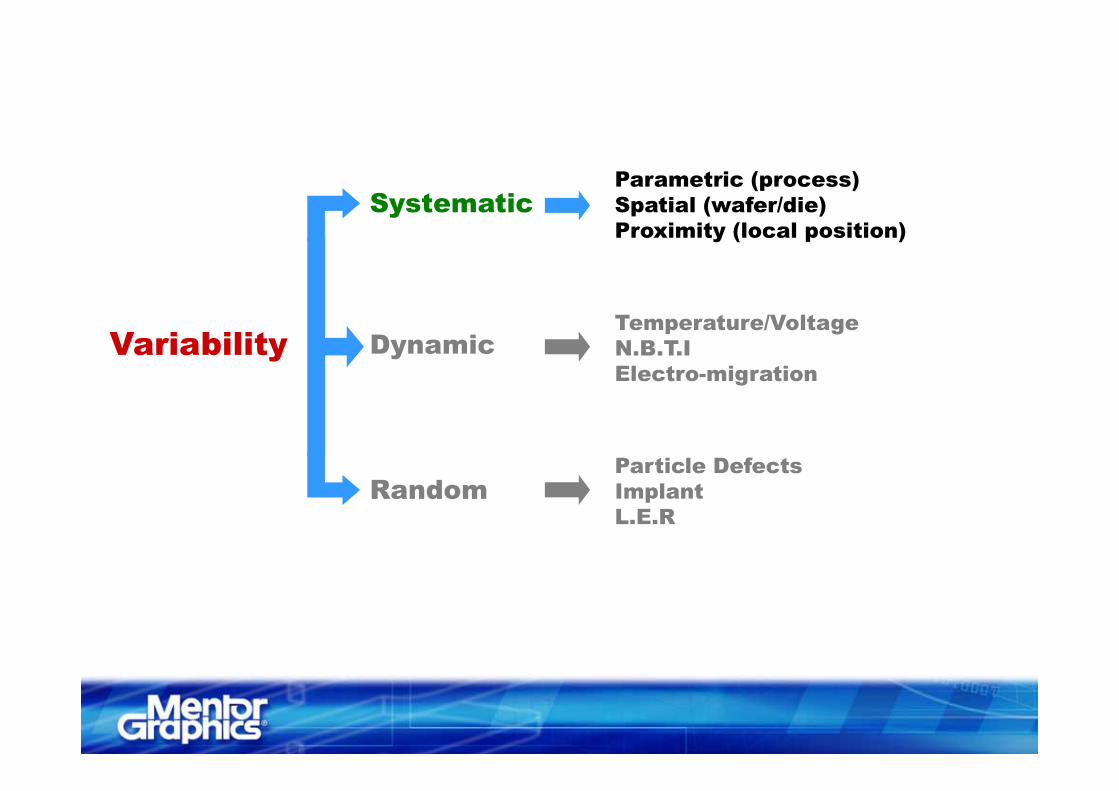
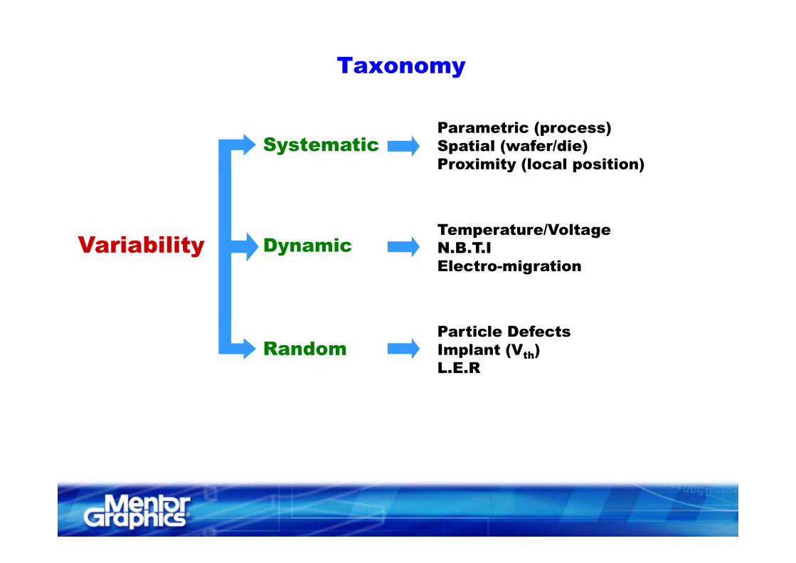
Taxonomy
SystematicParametric (process)Spatial (wafer/die)y p ( )Proximity (local position)
Variability DynamicTemperature/VoltageN.B.T.IElectro-migration
RandomParticle DefectsI l tRandom ImplantL.E.R
What can be addressed by P&R?What can be addressed by P&R?What can be addressed by P&R?What can be addressed by P&R?
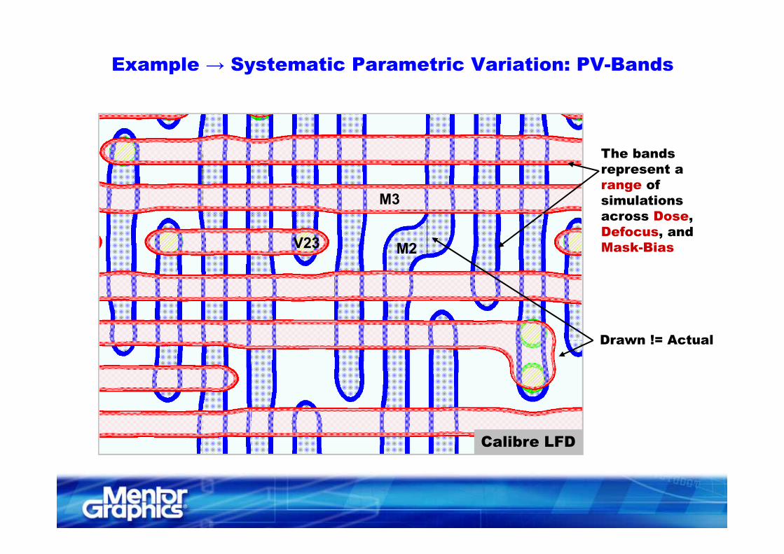
Example → Systematic Parametric Variation: PV-Bands
The bands The bands represent a range of simulations across Dose
M3across Dose, Defocus, and Mask-BiasM2V23
Drawn != ActualDrawn != Actual
OlympusCalibre LFD
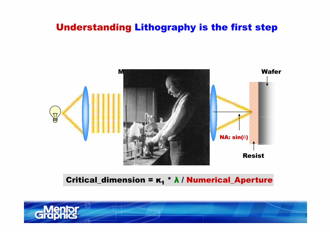
Understanding Lithography is the first step
Mask Wafer
λ
NA: sin(θ)
Resist
Critical_dimension = κ1 * λ / Numerical_Aperture
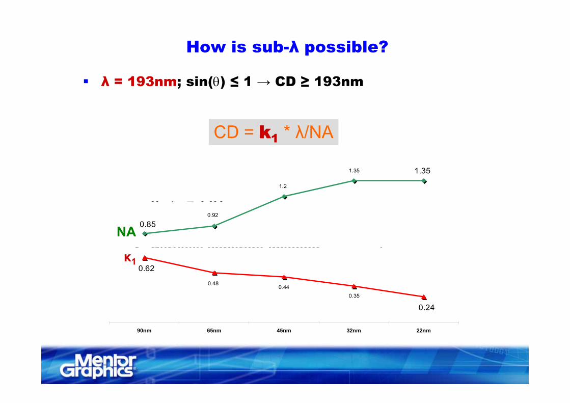
How is sub-λ possible?
λ = 193nm; sin(θ) ≤ 1 → CD ≥ 193nm
CD = k1 * λ/NA
• NA can be > 1 if we use immersion lithography• η t = 1 31
1.35
1.2
1.35
ηwater 1.31
• Take advantage of the mask-spectrum• Partially coherent imaging
0.850.92
NA• Partially coherent imaging• Off-axis illumination• Annular light sources
κ10.62
0.480.44
κ1
• Improve the mask via OPC0.35
0.24
90nm 65nm 45nm 32nm 22nm
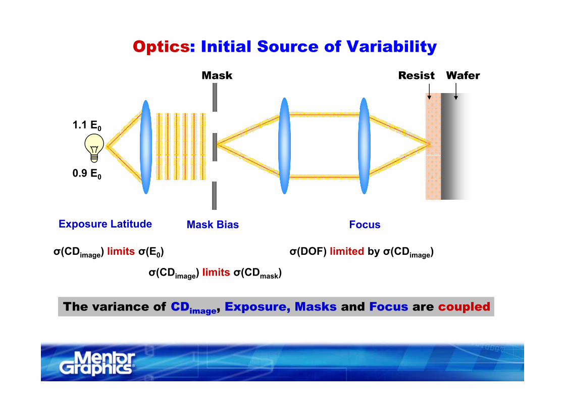
Optics: Initial Source of VariabilityMask WaferResist
1.1 E0
0.9 E0
Exposure Latitude FocusMask Bias
σ(CDimage) limits σ(E0) σ(DOF) limited by σ(CDimage)
σ(CDimage) limits σ(CDmask)
The variance of CDimage, Exposure, Masks and Focus are coupled
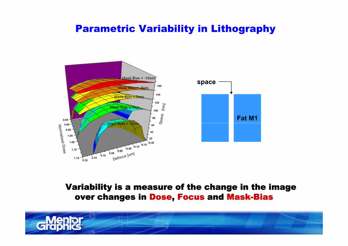
Parametric Variability in Lithography
space
Fat M1
Variability is a measure of the change in the image over changes in Dose, Focus and Mask-Bias
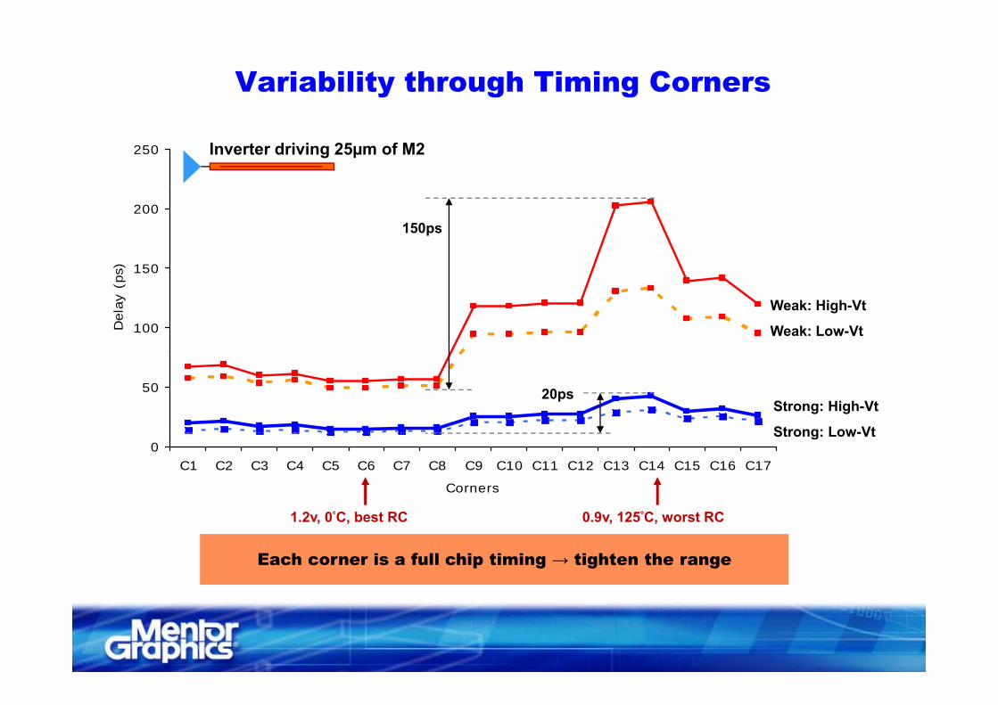
Variability through Timing Corners
250 Inverter driving 25µm of M2
150
200
s)
150ps
100
150
Dela
y (
ps
Weak: High-Vt
Weak: Low-Vt
50Strong: High-Vt
Strong: Low-Vt
20ps
0C1 C2 C3 C4 C5 C6 C7 C8 C9 C10 C11 C12 C13 C14 C15 C16 C17
Corners
Strong: Low-Vt
0 9 125°C t RC1 2 0°C b t RC 0.9v, 125°C, worst RC 1.2v, 0°C, best RC
Each corner is a full chip timing → tighten the rangeEach corner is a full chip timing → tighten the range
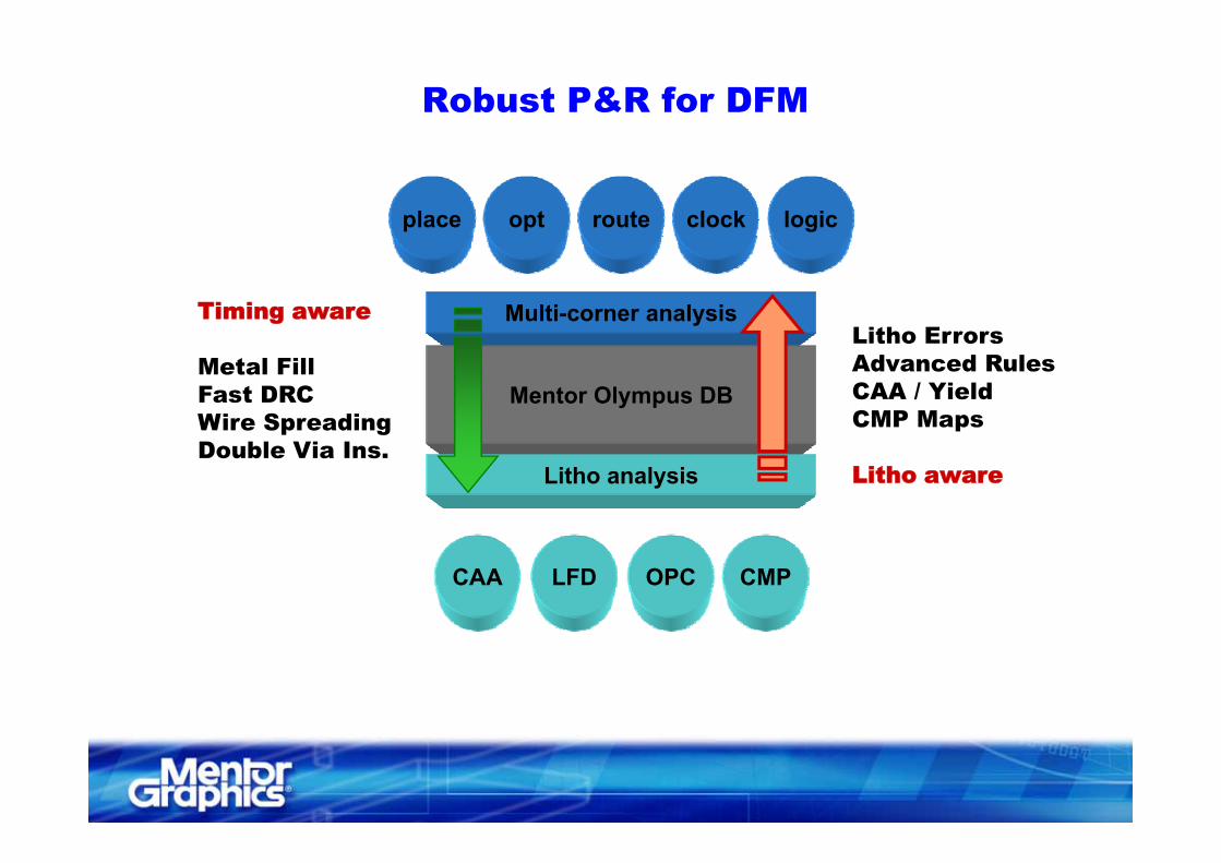
Robust P&R for DFM
place opt route clock logic
Multi-corner analysisLitho Errors
Timing aware
Mentor Olympus DB
Litho ErrorsAdvanced RulesCAA / YieldCMP Maps
Metal FillFast DRCWire Spreading
Litho analysis Litho aware
p gDouble Via Ins.
CAA LFD OPC CMP
SystematicParametric (process)Spatial (wafer/die)y p ( )Proximity (local position)
Variability DynamicTemperature/VoltageN.B.T.IElectro-migration
RandomParticle DefectsI l tRandom ImplantL.E.R

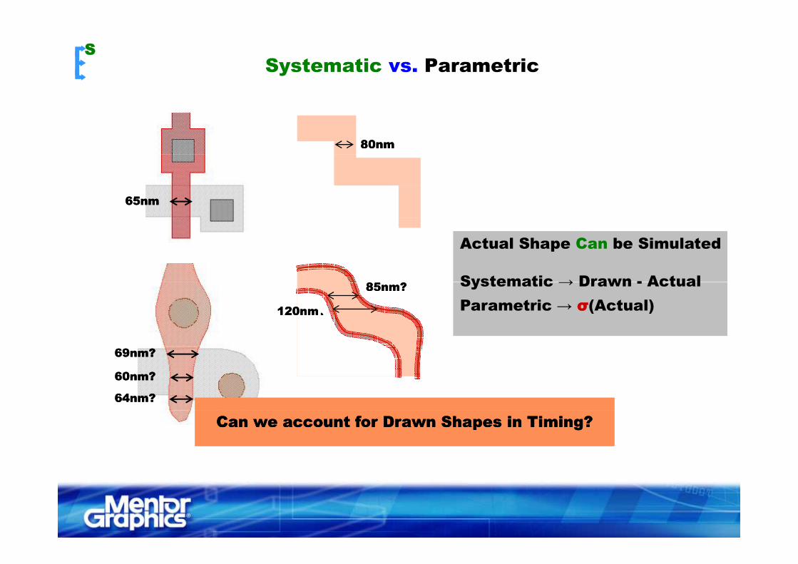
Systematic vs. ParametricS
80nm80nm
65nm65nm
Actual Shape Can be Simulated
Systematic → Drawn - ActualSystematic → Drawn - ActualParametric → σ(Actual)
85nm?85nm?
120nm?120nm?
69nm?69nm?
60nm?60nm?
64nm?64nm?
Can we account for Drawn Shapes in Routing?Can we account for Drawn Shapes in Routing?Can we account for Drawn Shapes in Routing?Can we account for Drawn Shapes in Routing?
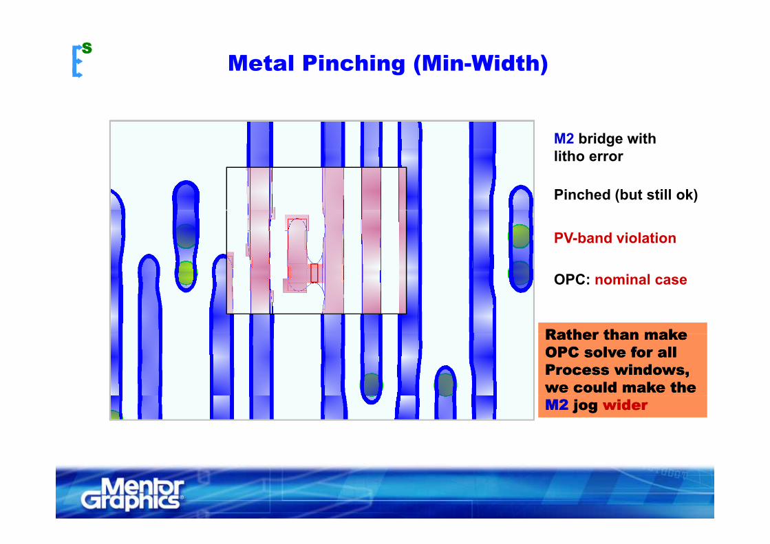
Metal Pinching (Min-Width)S
M2 bridge withlitho error
Pinched (but still ok)
PV-band violation
OPC: nominal case
Rather than makeRather than makeRather than makeRather than makeRather than makeRather than makeOPC solve for all OPC solve for all Process windows,Process windows,we could make the we could make the
Rather than makeRather than makeOPC solve for all OPC solve for all Process windows,Process windows,we could make the we could make the M2M2 jog jog widerwiderM2M2 jog jog widerwider
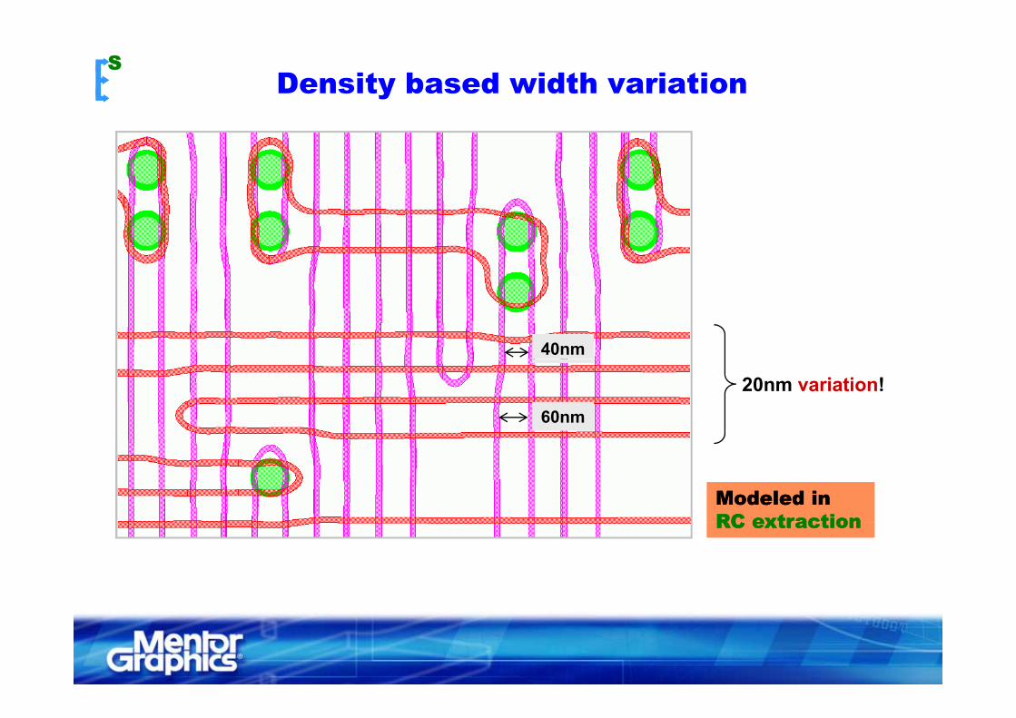
Density based width variationS
40nm
60nm
20nm variation!
Modeled in Modeled in RC extractionRC extractionModeled in Modeled in RC extractionRC extractionRC extractionRC extractionRC extractionRC extraction
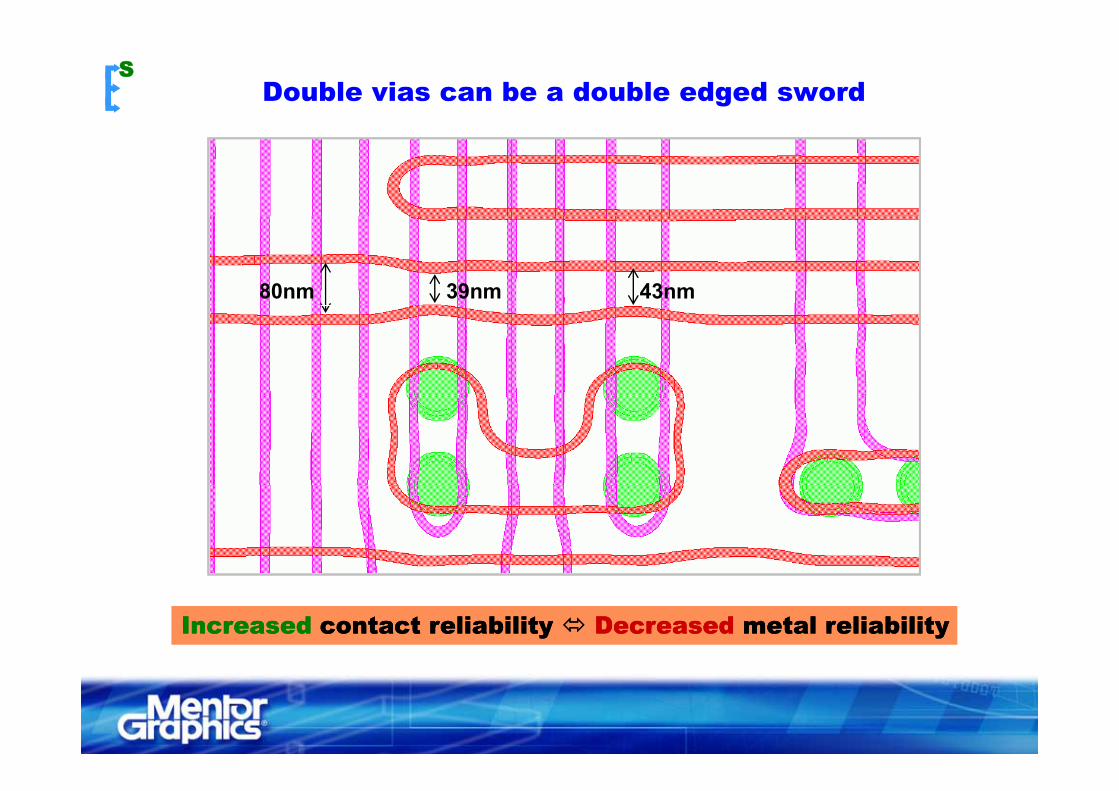
Double vias can be a double edged swordS
39nm80nm 43nm
IncreasedIncreased contact reliability contact reliability DecreasedDecreased metal reliabilitymetal reliabilityIncreasedIncreased contact reliability contact reliability DecreasedDecreased metal reliabilitymetal reliability
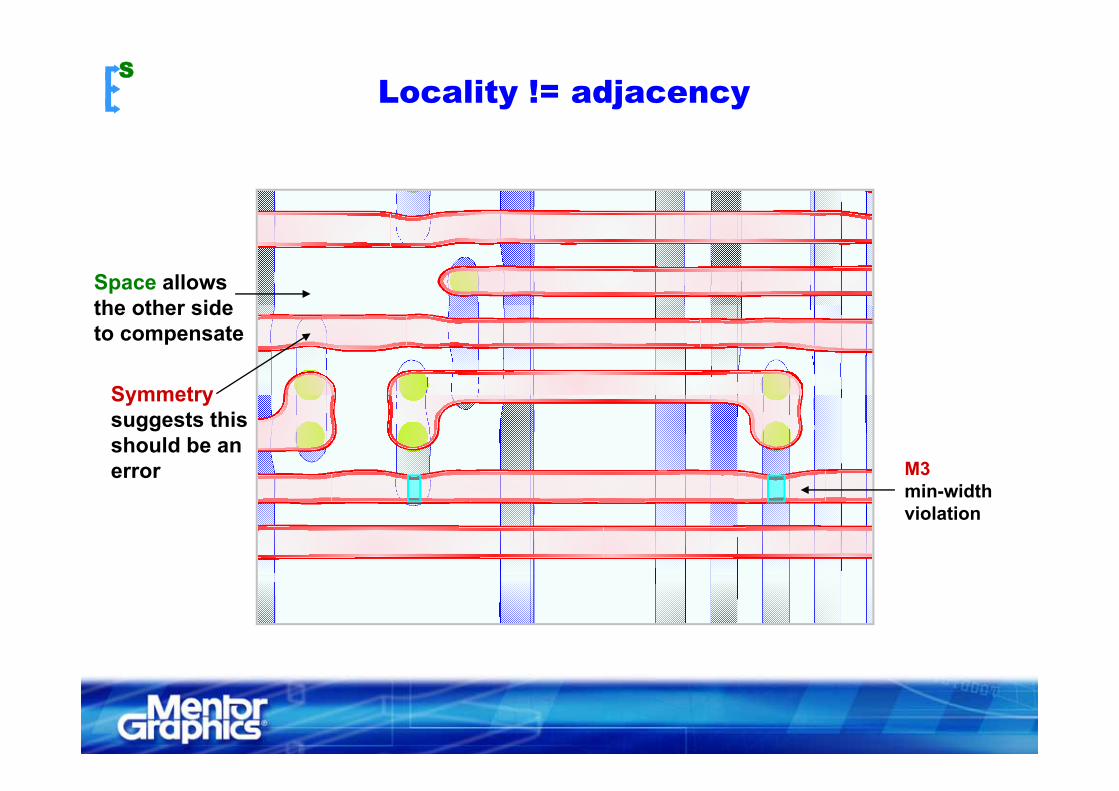
Locality != adjacencyS
Space allowsthe other side
Symmetry
the other sideto compensate
M3i idth
Symmetrysuggests thisshould be anerror
min-widthviolation
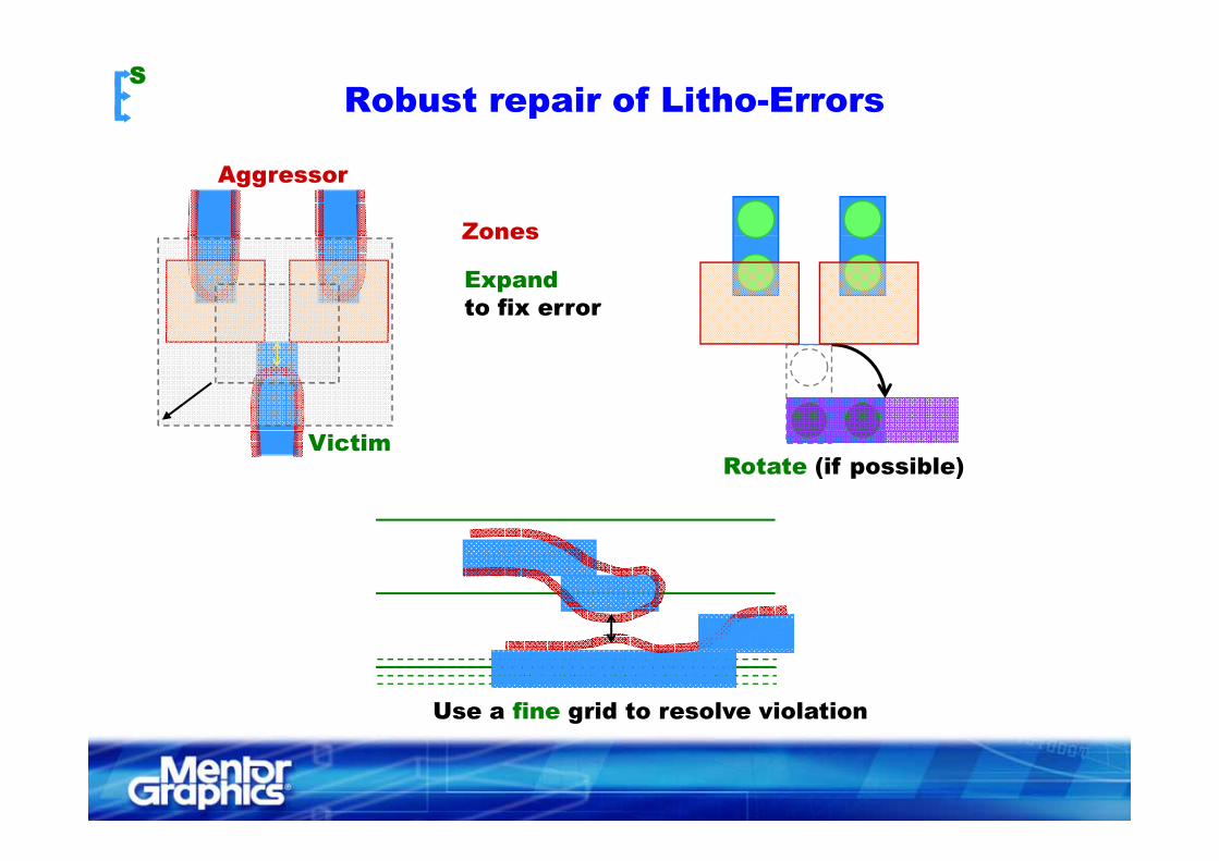
Robust repair of Litho-ErrorsS
Aggressor
ZonesZones
Expandto fix error
VictimRotate (if possible)
Use a fine grid to resolve violation
Systematic vs. ParametricS
80nm80nm
65nm65nm
Actual Shape Can be Simulated
Systematic → Drawn - ActualSystematic → Drawn - ActualParametric → σ(Actual)
85nm?85nm?
120nm?120nm?
69nm?69nm?
60nm?60nm?
64nm?64nm?
Can we account for Drawn Shapes in Timing?Can we account for Drawn Shapes in Timing?Can we account for Drawn Shapes in Timing?Can we account for Drawn Shapes in Timing?
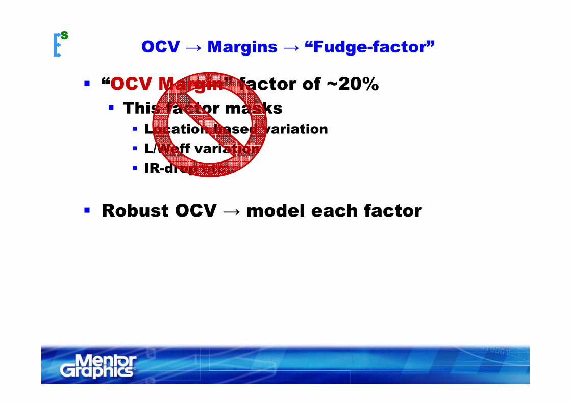
OCV → Margins → “Fudge-factor”S
“OCV Margin” factor of ~20%This factor masksThis factor masks
Location based variationL/Weff variationIR-drop etc..
Robust OCV → model each factor
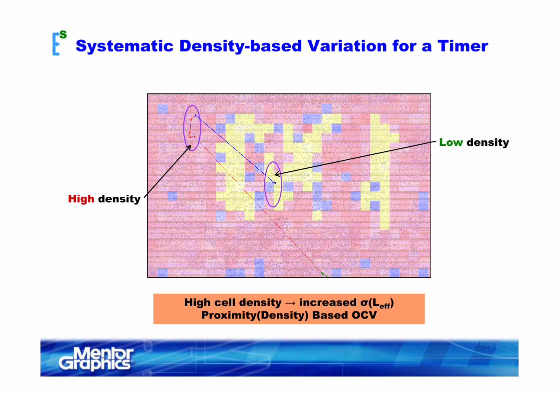
Systematic Density-based Variation for a TimerS
65nm65nm
45nm45nmLow density
32nm32nm
l dia
met
erHigh density
Opt
icalHigh density
High cell density → increased σ(Leff)Proximity(Density) Based OCV
High cell density → increased σ(Leff)Proximity(Density) Based OCV
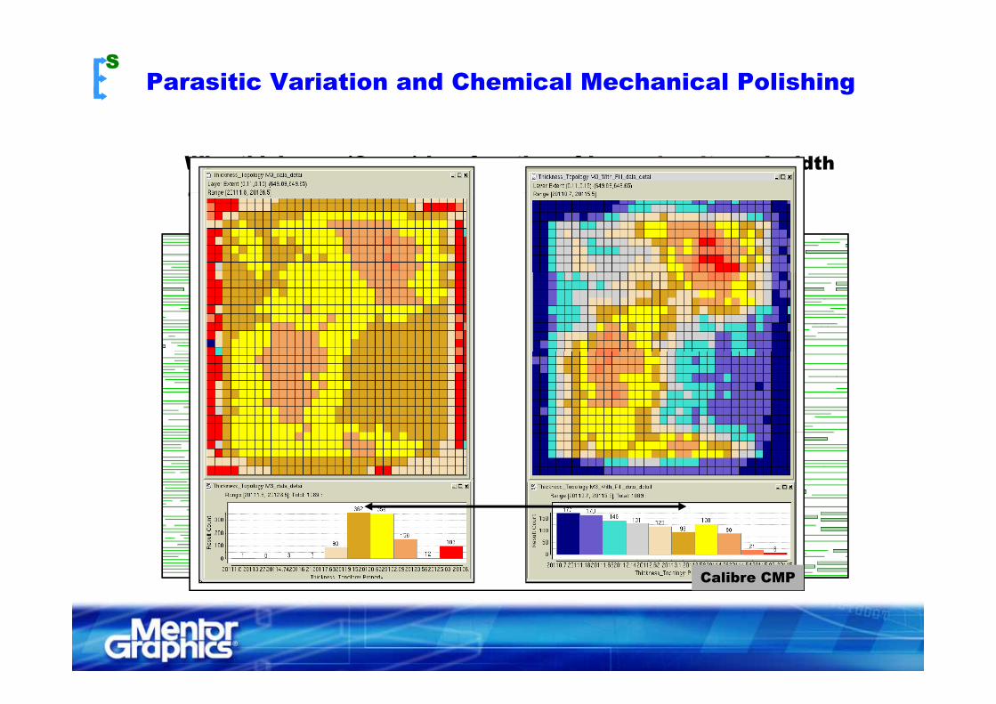
Parasitic Variation and Chemical Mechanical PolishingS
Wire thickness (Clateral) is a function of layer, density and width
The dielectric between layers will also vary → σ(Csubstrate)
Per layer CMP variation → M3 could be worse than M2!Metal fill makes density consistent
y
Calibre CMP

Taxonomy
SystematicParametric (process)Spatial (wafer/die)y p ( )Proximity (local position)
Variability DynamicTemperature/VoltageN.B.T.IElectro-migration
RandomParticle DefectsI l t (V )Random Implant (Vth)L.E.R
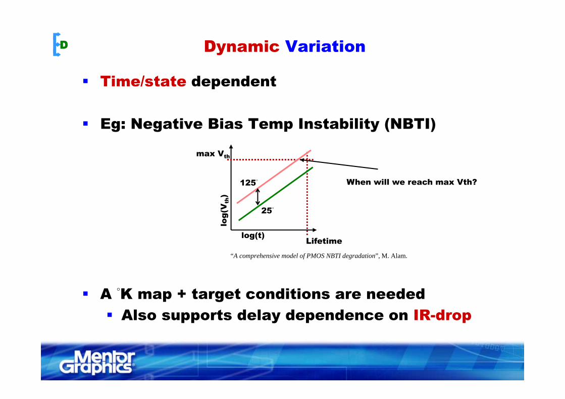
Dynamic VariationD
Time/state dependent
Eg: Negative Bias Temp Instability (NBTI)
max Vmax Vth
125°
h)
When will we reach max Vth?
Lifetime
25°lo
g(V
th
log(t)
A °K + t t diti d d
“A comprehensive model of PMOS NBTI degradation”, M. Alam.
A °K map + target conditions are neededAlso supports delay dependence on IR-drop
Taxonomy
SystematicParametric (process)Spatial (wafer/die)y p ( )Proximity (local position)
Variability DynamicTemperature/VoltageN.B.T.IElectro-migration
RandomParticle DefectsI l t (V )Random Implant (Vth)L.E.R
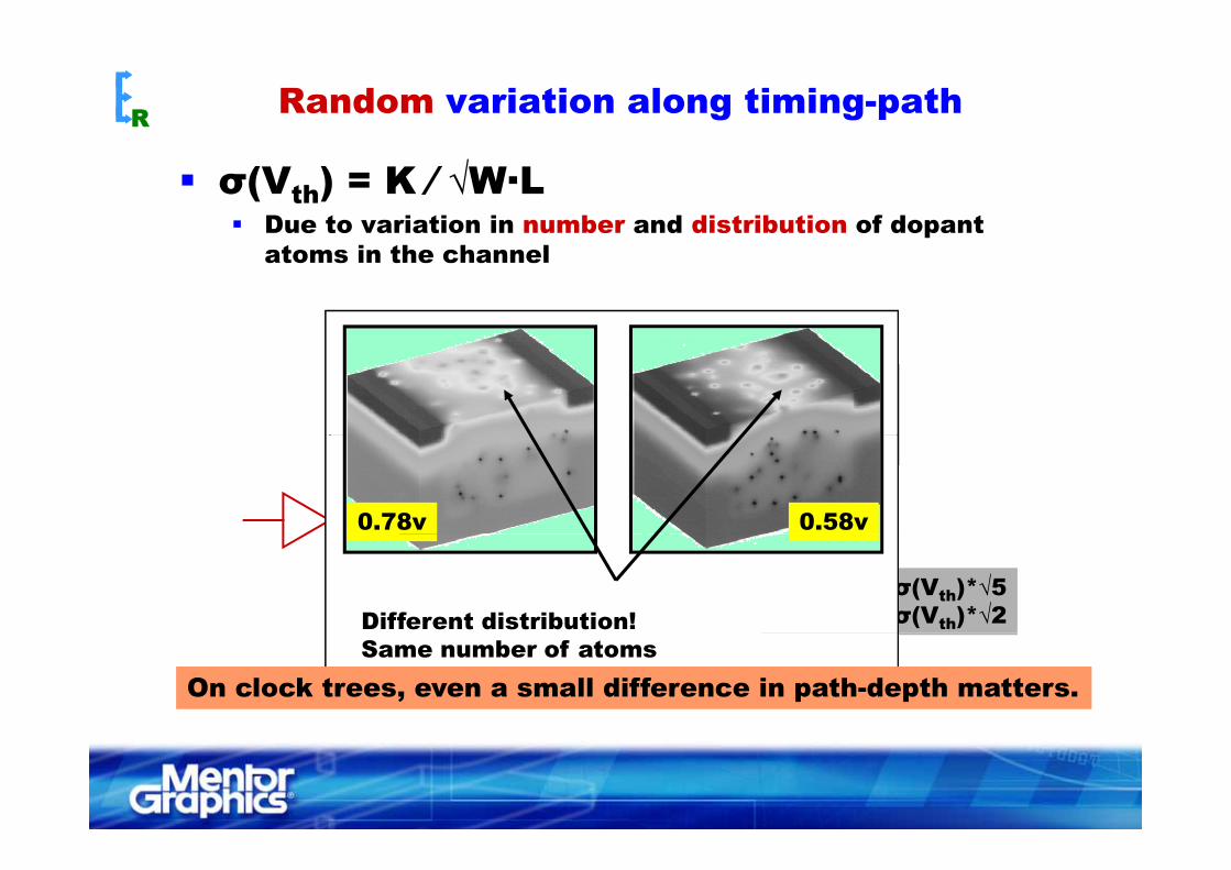
Random variation along timing-pathR
σ(Vth) = K ⁄ √W·LDue to variation in number and distribution of dopant patoms in the channel
l i th d th 5logic_path_depth: 5
0.78v 0.58v
clock_path_depth: 2σ(logic): σ(Vth)*√5σ(clock): σ(Vth)*√2Different distribution!
Same number of atoms“Random dopant induced threshold voltage lowering and fluctuations”, Asen Asenov.On clock trees, even a small difference in path-depth matters.On clock trees, even a small difference in path-depth matters.
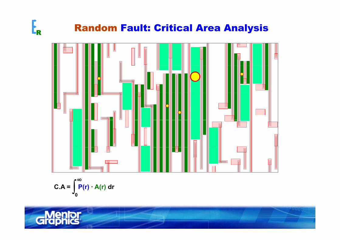
Random Fault: Critical Area AnalysisR
C.A = ∫ P(r) · A(r) dr0
∞
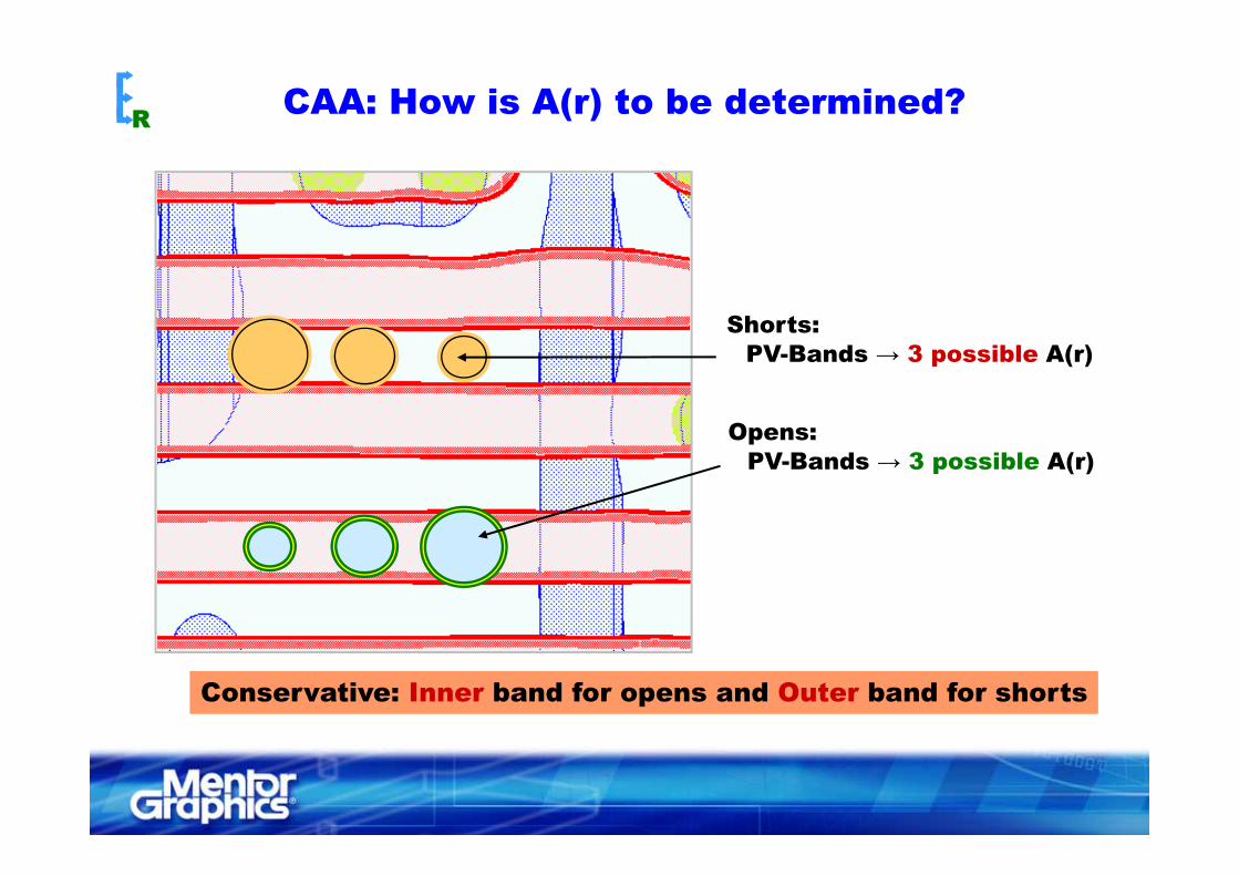
CAA: How is A(r) to be determined?R
Shorts:PV-Bands → 3 possible A(r)
Opens:PV-Bands → 3 possible A(r)
Opens:
Conservative: Inner band for opens and Outer band for shortsConservative: Inner band for opens and Outer band for shorts
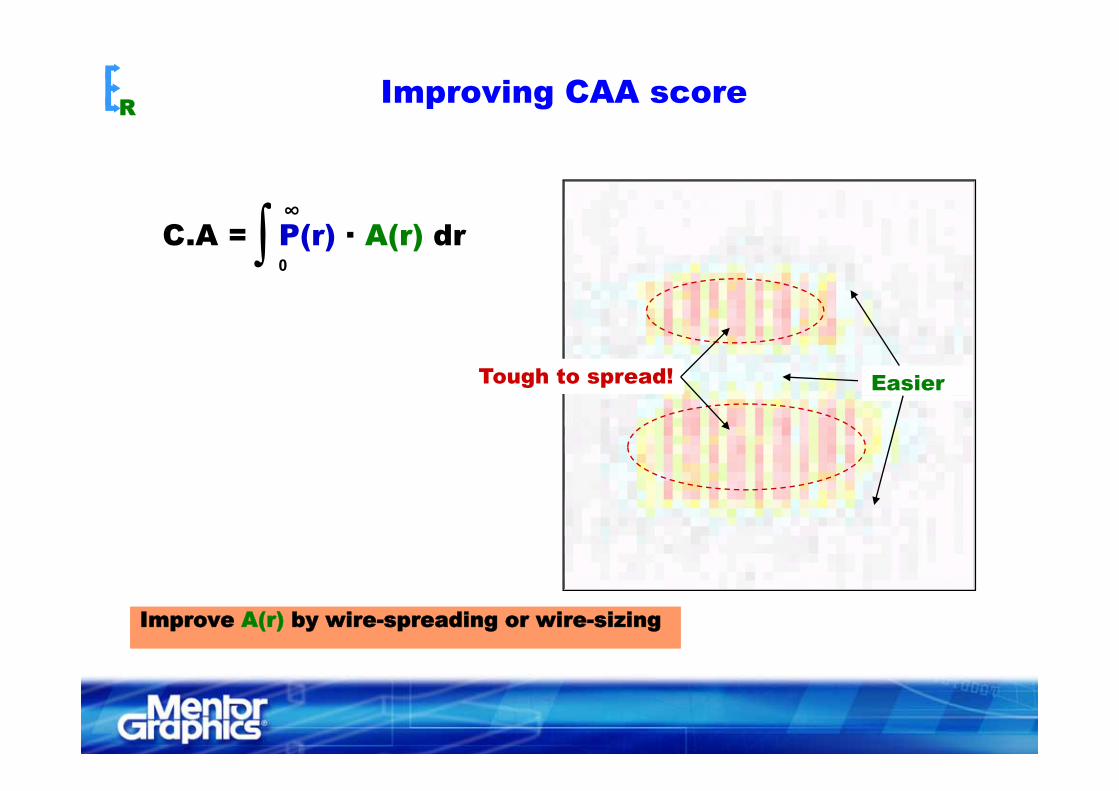
Improving CAA scoreR
∫ ∞C.A = ∫ P(r) · A(r) dr
0
Tough to spread! Easier
Improve A(r) by wire-spreading or wire-sizingImprove A(r) by wire-spreading or wire-sizing
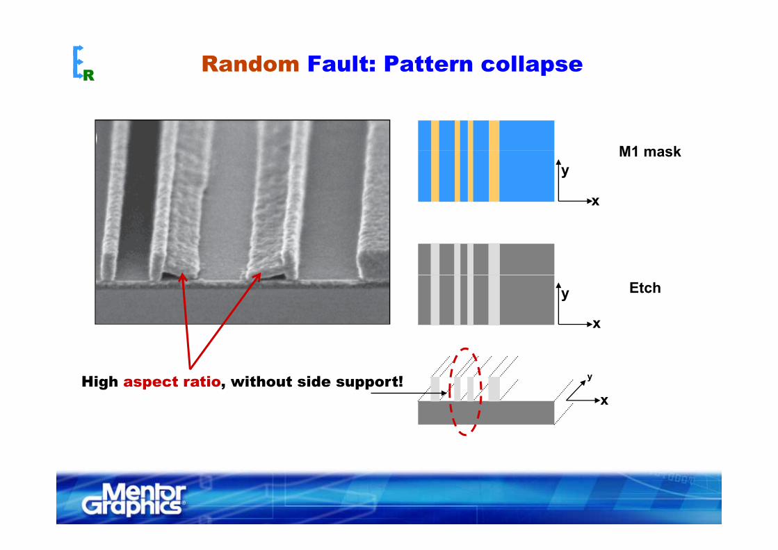
Random Fault: Pattern collapseR
M1 maskM1 masky
x
Etchy
x
y
xHigh aspect ratio, without side support!
x
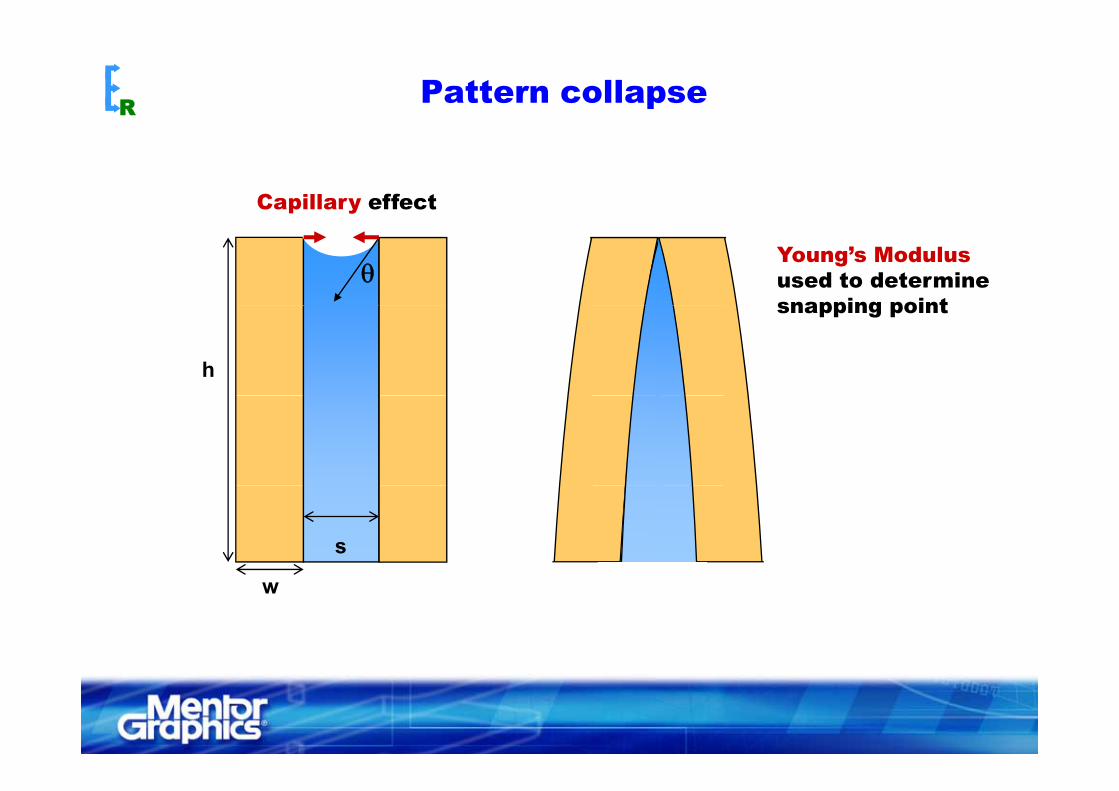
Pattern collapseR
Capillary effect
θYoung’s Modulusused to determinesnapping point
h
snapping point
s
w
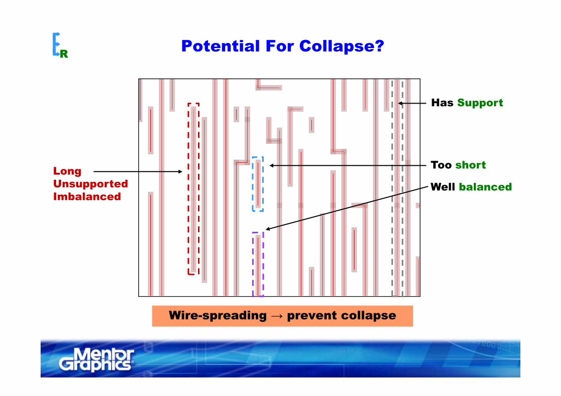
Potential For Collapse?R
Has Supportpp
Too short
Well balanced LongUnsupportedImbalancedImbalanced
Wire-spreading → prevent collapseWire-spreading → prevent collapse
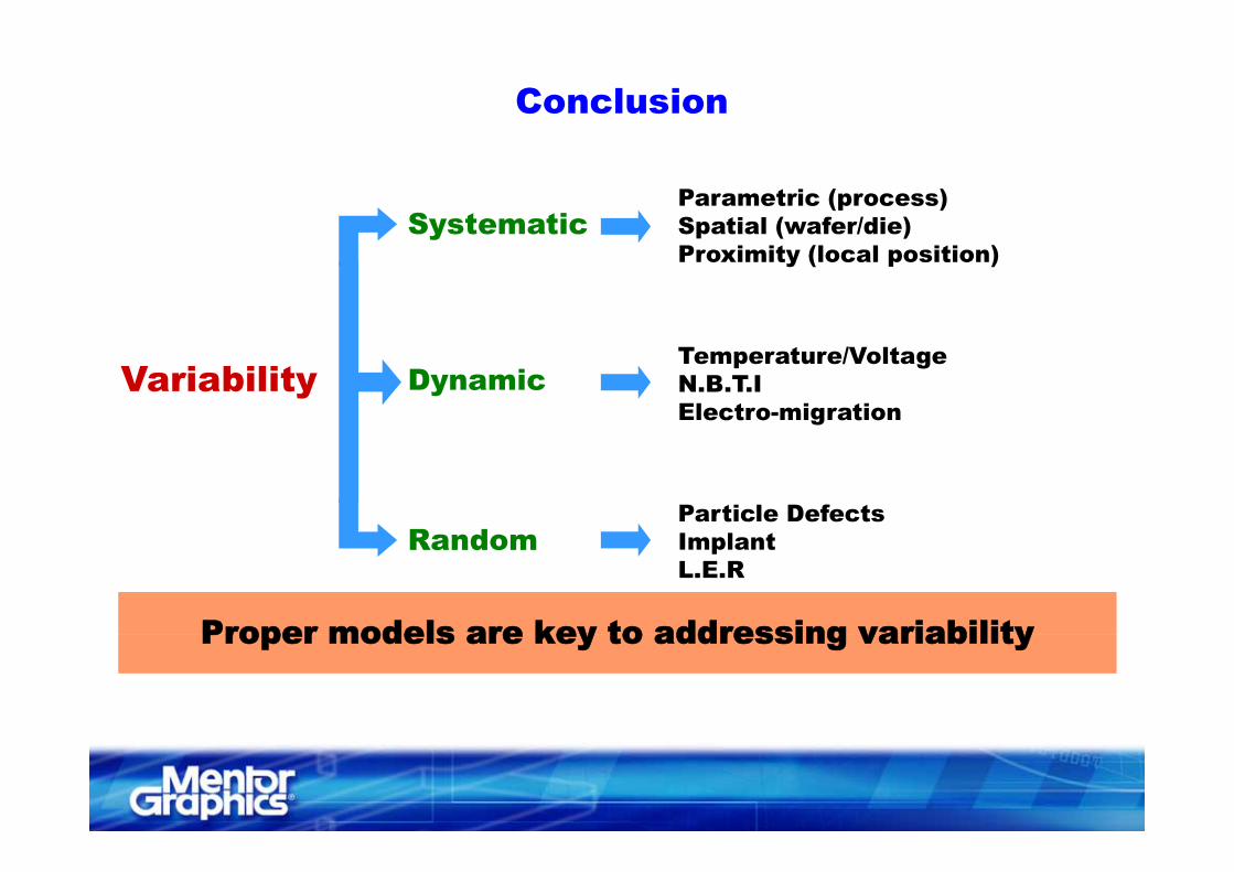
Conclusion
SystematicParametric (process)Spatial (wafer/die)y p ( )Proximity (local position)
Variability DynamicTemperature/VoltageN.B.T.IElectro-migration
RandomParticle DefectsI l tRandom ImplantL.E.R
Proper models are key to addressing variabilityProper models are key to addressing variabilityProper models are key to addressing variabilityProper models are key to addressing variability
Acknowledgements
Andres TorresAlex VolkovAlex VolkovShankar Krishnamoorthy
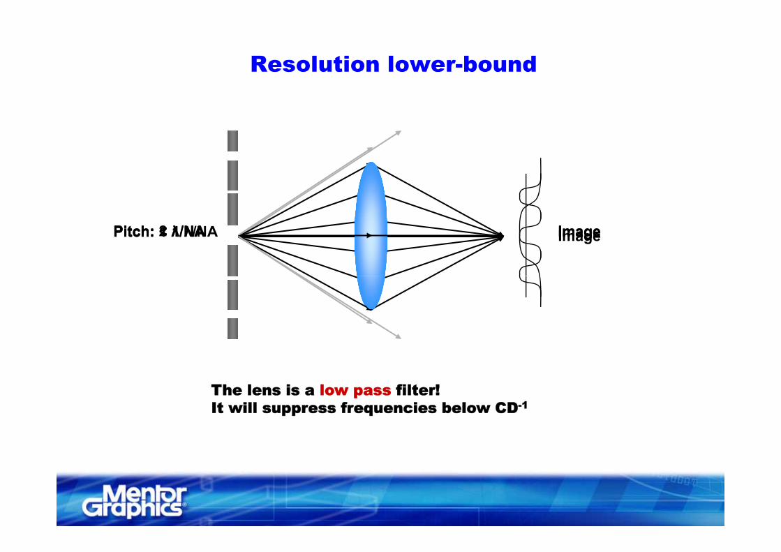
Resolution lower-bound
Pitch: 2 λ/NA ImagePitch: 1 λ/NA ImagePitch: < 1 λ/NA Image
The lens is a low pass filter!1It will suppress frequencies below CD-1
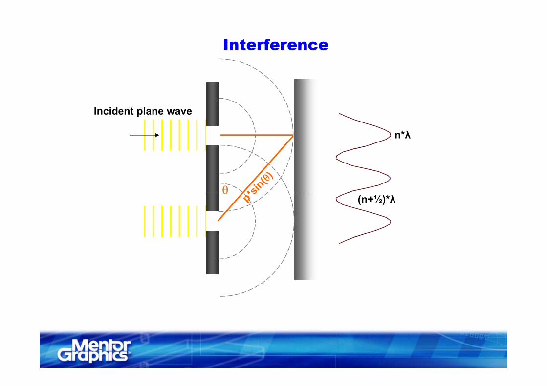
Interference
Incident plane wave
n*λ
θθ(n+½)*λ
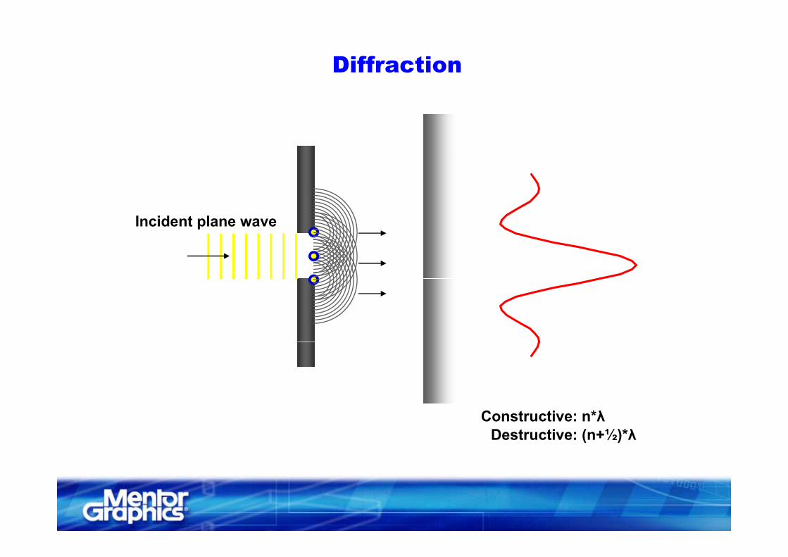
Diffraction
Incident plane wave
Constructive: n*λDestructive: (n+½)*λ
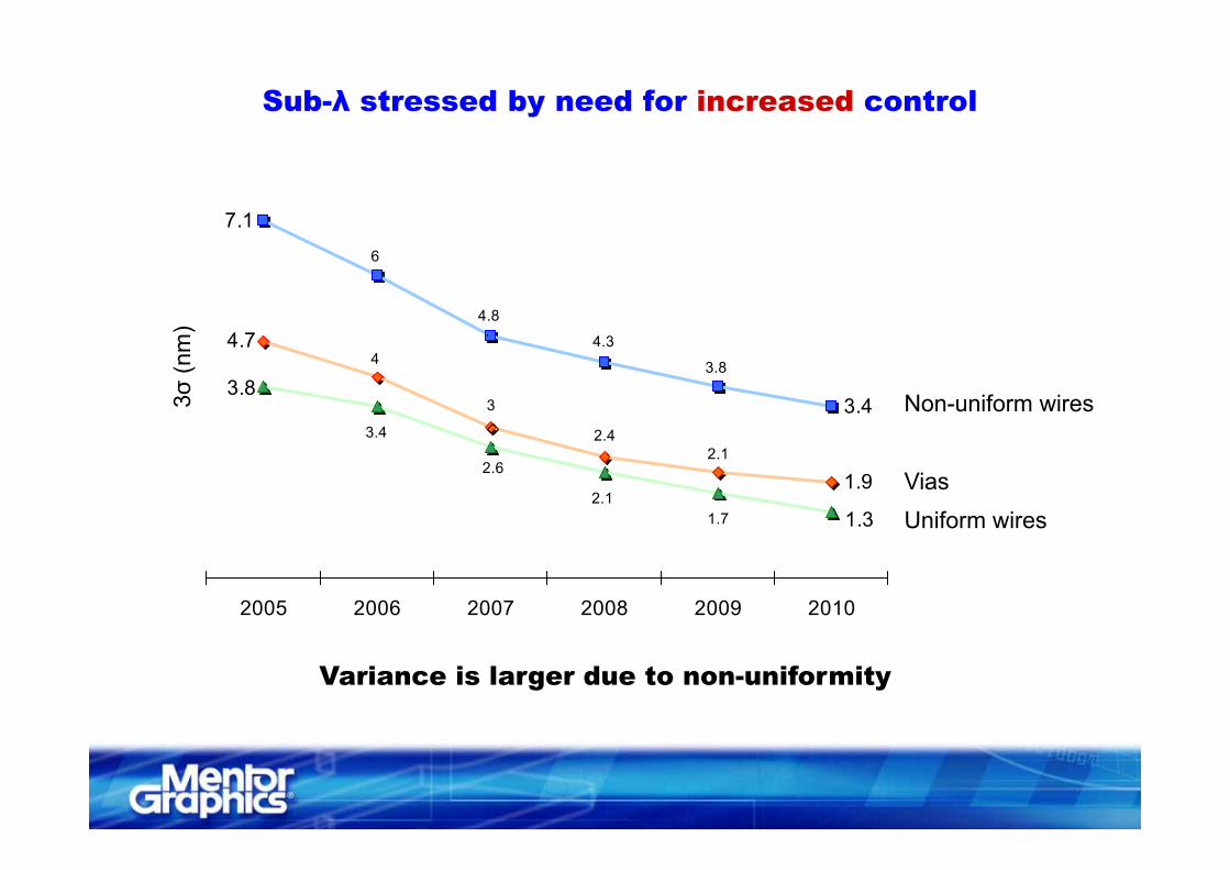
Sub-λ stressed by need for increased control
7.1
4 7
6
4.8
4 3m)
3 4
3.8
2 4
3
44.7
3.4
4.3
3.8
3σ(n
m
Non-uniform wires
1.31.72.1
2.6
3.4
1.92.1
2.4
ViasUniform wires
2005 2006 2007 2008 2009 2010
Variance is larger due to non-uniformity
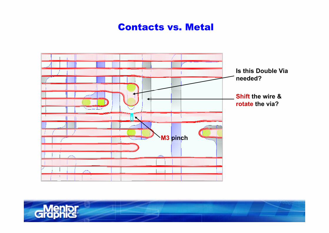
Contacts vs. Metal
Is this Double Vianeeded?
Shift the wire &rotate the via?
M3 pinch
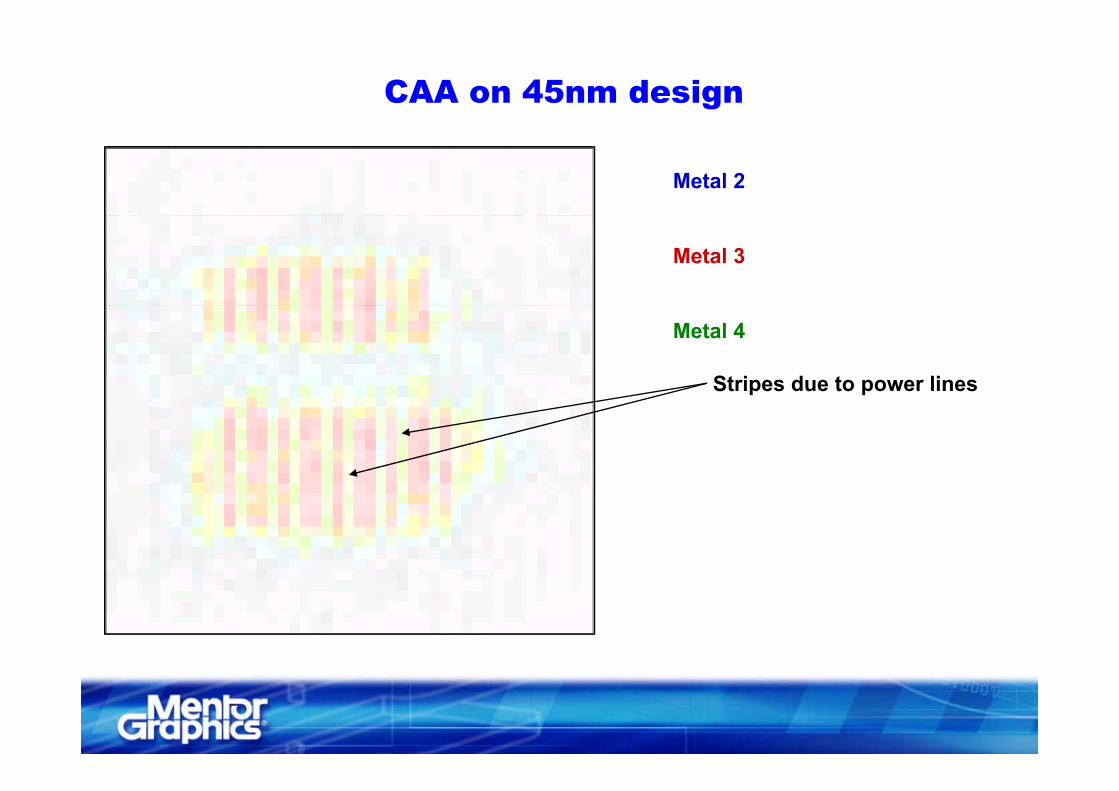
CAA on 45nm design
Metal 2
Metal 3
Metal 4
Stripes due to power lines
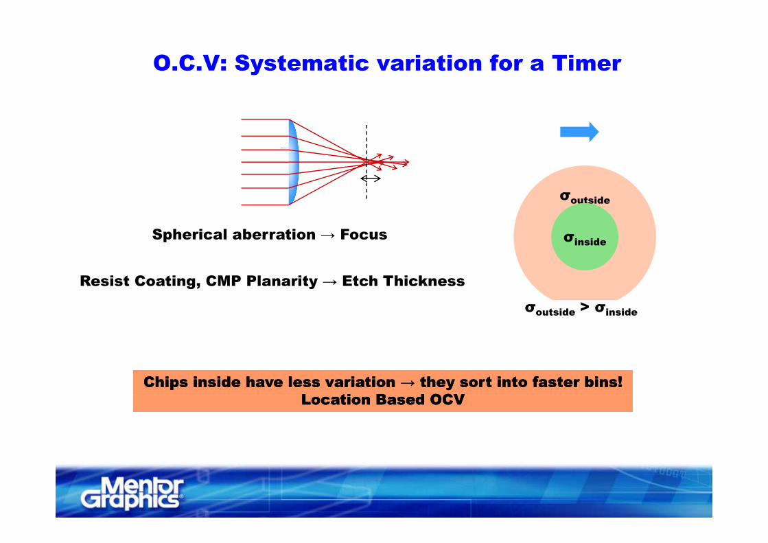
O.C.V: Systematic variation for a Timer
σoutside
Spherical aberration → Focus σinside
Resist Coating, CMP Planarity → Etch Thickness
σoutside > σinside
Chips inside have less variation → they sort into faster bins!Chips inside have less variation → they sort into faster bins!L ti B d OCVL ti B d OCV
Chips inside have less variation → they sort into faster bins!Chips inside have less variation → they sort into faster bins!L ti B d OCVL ti B d OCVLocation Based OCVLocation Based OCVLocation Based OCVLocation Based OCV
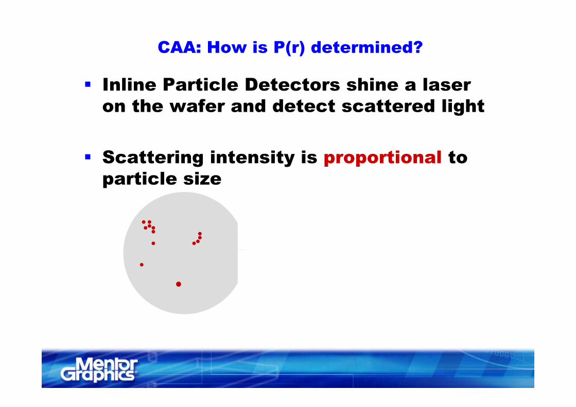
CAA: How is P(r) determined?
Inline Particle Detectors shine a laser on the wafer and detect scattered lighton the wafer and detect scattered light
Scattering intensity is proportional to Scattering intensity is proportional to particle size