Embed Size (px)
Citation preview
Document-No. 26-853 | Edition EN03 | 2013-09-18
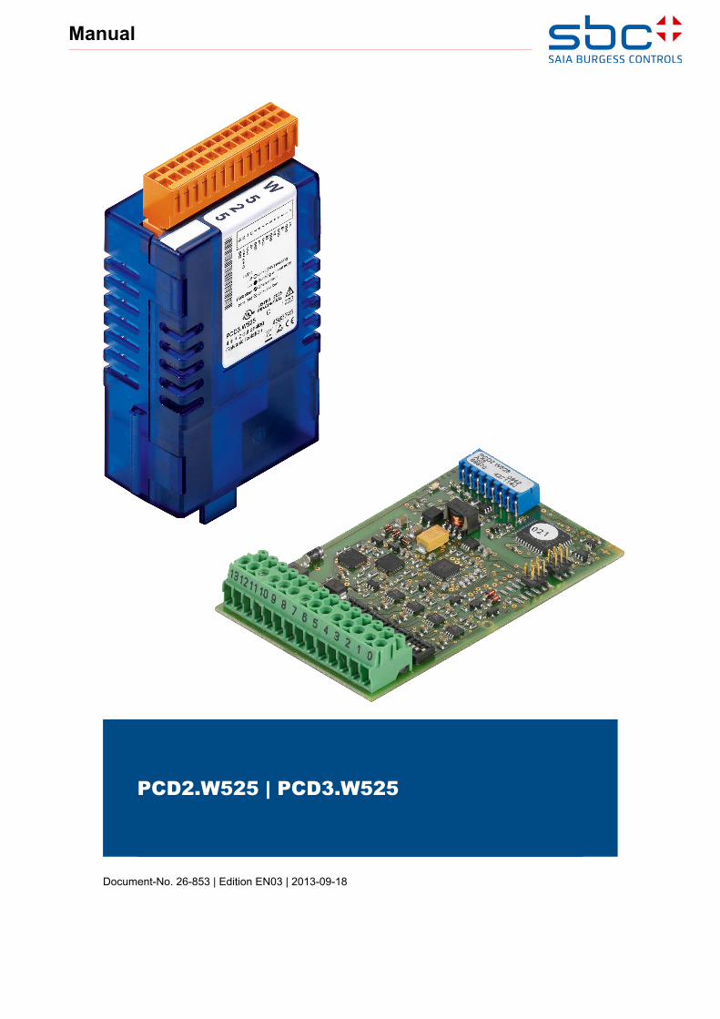
PCD2.W525 | PCD3.W525
Manual
Manual PCD2.W525&PCD3.W525Document 26/853; Edition EN032013-09-18
Saia-Burgess Controls AG
Content
0-1
00 Content
0.1 Document history ............................................................................................ 0-20.2 Trademarks ..................................................................................................... 0-2
1 Hardware
1.1 General Information ....................................................................................... 1-11.2 Configuration ................................................................................................... 1-2
1.2.1 Module connections/LED .............................................................................. 1-21.2.2 Howtoconfiguretheinputs........................................................................... 1-21.2.3 Howtoconfiguretheoutputs ........................................................................ 1-2
1.3 Function .......................................................................................................... 1-31.3.1 PowerSupply ................................................................................................ 1-31.3.2 Timing ........................................................................................................... 1-31.3.3 Filter .............................................................................................................. 1-4
1.4 Technical Data ................................................................................................ 1-5
2 Meaning of the I/O terminology of a PCD2/3.W525 module
A Appendix
A.1 Icons ............................................................................................................... A-1A.2 Address ........................................................................................................... A-2
0 Content
Manual PCD2.W525&PCD3.W525Document 26/853; Edition EN032013-09-18
Saia-Burgess Controls AG
Content
0-2
00.1 Document history
Document-no Edition Changes Remarks2007-03-31 pE1 complete Preliminary Edition2007-11-15 E1 complete AfewchangestopE12008-01-18 E2 Chapter
1.4PCD3.W525pluggableterminal:wrongorderingnumberreplaced
2013-09-18 EN03 - Chapter2
-NewLogoandnewcompanyname-Nouveauchapitre: Configuartiondesmotsd’E/S
0.2 Trademarks
Saia PCD® and Saia PG®areregisteredtrademarksofSaia-BurgessControlsAG
Technicalmodificationsandchangesaresubjecttothestateoftechnology
Saia-BurgessControlsAG,2007.
©Allrightsreserved
PublishedinSwitzerland
Manual PCD2.W525&PCD3.W525Document 26/853; Edition EN032013-09-18
Saia-Burgess Controls AG
General Information
Hardware
1-1
1
1 Hardware
1.1 General Information
PCD2/3.W525isananaloguemultipurposemodulewithfourinputsandtwooutputs.Eachinputandeachoutputcanbeindividuallyconfiguredasoneofthestandardindustrialinterfacetypelike0…10V,0…20mAand4…20mA.Inaddition,theinputscanbeconfiguredtosupportPt/Ni1000orPt500temperaturesensors.Furthermore,themoduleoffershighflexibilityinselectingfiltertypesandscalingranges.
Inputs-14 Bit 4Inputs.Everychannelhasfourmodesofoperation(configurablebyDIP- Switches):
DifferentialVoltageInputs 0…10V,resolution:0.61mVperLSB(14Bit)
DifferentialCurrentInputs-measured in differential mode 0…20mA,resolution:1.2μAperLSB(14Bit) 4…20mA,resolution:1.2μAperLSB(13.7Bit)
Temperature Pt1000,-50…400°C,resolution:0.1°C Pt500,-50…400°C,resolution:0.2°C Ni1000,-60…200°C,resolution0.1°C
Resistance 0…2500Ω,resolution0.2Ω
Eachchannelcanbeconfiguredtohaveasoftwarebased50Hz/60Hzfilter
Outputs-12 Bit 2Outputs.Everychannelhasthreemodesofoperation(configurablebysoft- ware):
Voltage 0…10V,resolution:2.44mVperLSB(12Bit)
Current 0…20mA,resolution:4.88μAperLSB(12Bit) 4…20mA,resolution4.88μAperLSB(11.7Bit)
HighimpedanceMiscellaneous AllI/O-ChannelsaregalvanicallyisolatedtothePCDandexternalpowersup- ply.(Butallchannelsaregalvanicallyconnectedtoeachother.)
Everychannelhastwoconnectionterminals.
Manual PCD2.W525&PCD3.W525Document 26/853; Edition EN032013-09-18
Saia-Burgess Controls AG
Configuration
Hardware
1-2
1
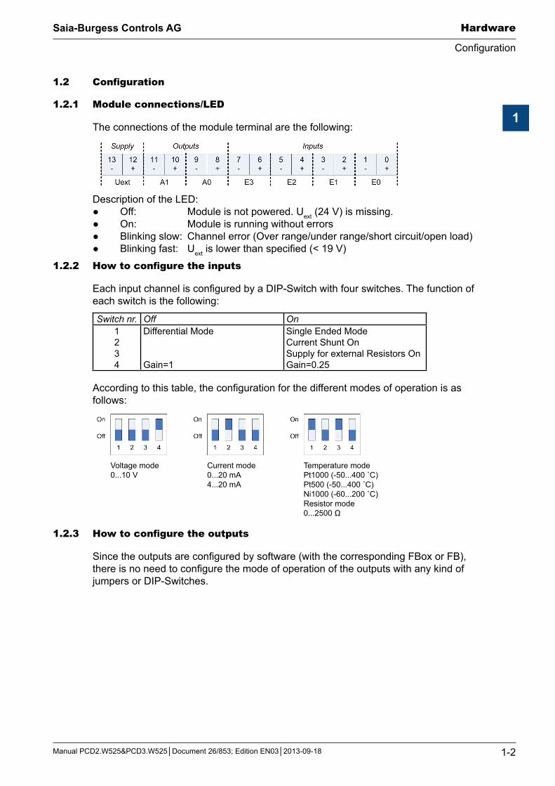
1.2 Configuration
1.2.1 Module connections/LED
Theconnectionsofthemoduleterminalarethefollowing:
DescriptionoftheLED: Off: Moduleisnotpowered.Uext(24V)ismissing. On: Moduleisrunningwithouterrors Blinkingslow: Channelerror(Overrange/underrange/shortcircuit/openload) Blinkingfast: Uextislowerthanspecified(<19V)
1.2.2 Howtoconfiguretheinputs
EachinputchannelisconfiguredbyaDIP-Switchwithfourswitches.Thefunctionofeachswitchisthefollowing:
Switch nr. Off On1 2 3 4
Differential Mode Gain=1
SingleEndedMode CurrentShuntOn SupplyforexternalResistorsOn Gain=0.25
Accordingtothistable,theconfigurationforthedifferentmodesofoperationisasfollows:
Voltage mode0...10 V
Current mode0...20 mA4...20 mA
Temperature modePt1000 (-50...400 ˚C)Pt500 (-50...400 ˚C)Ni1000 (-60...200 ˚C)Resistor mode0...2500 Ω
1.2.3 Howtoconfiguretheoutputs
Sincetheoutputsareconfiguredbysoftware(withthecorrespondingFBoxorFB),thereisnoneedtoconfigurethemodeofoperationoftheoutputswithanykindofjumpersorDIP-Switches.
Manual PCD2.W525&PCD3.W525Document 26/853; Edition EN032013-09-18
Saia-Burgess Controls AG
Function
Hardware
1-3
1
1.3 Function
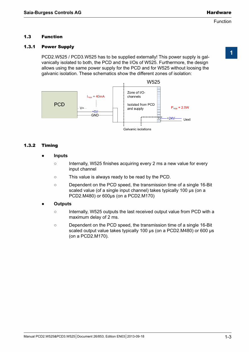
1.3.1 Power Supply
PCD2.W525/PCD3.W525hastobesuppliedexternally!Thispowersupplyisgal-vanicallyisolatedtoboth,thePCDandtheI/OsofW525.Furthermore,thedesignallowsusingthesamepowersupplyforthePCDandforW525withoutloosingthegalvanicisolation.Theseschematicsshowthedifferentzonesofisolation:
1.3.2 Timing
Inputs Internally,W525finishesacquiringevery2msanewvalueforevery inputchannel
ThisvalueisalwaysreadytobereadbythePCD.
DependentonthePCDspeed,thetransmissiontimeofasingle16-Bit scaledvalue(ofasingleinputchannel)takestypically100μs(ona PCD2.M480)or600μs(onaPCD2.M170)
Outputs Internally,W525outputsthelastreceivedoutputvaluefromPCDwitha maximumdelayof2ms.
DependentonthePCDspeed,thetransmissiontimeofasingle16-Bit scaledoutputvaluetakestypically100μs(onaPCD2.M480)or600μs (onaPCD2.M170).
Manual PCD2.W525&PCD3.W525Document 26/853; Edition EN032013-09-18
Saia-Burgess Controls AG
Function
Hardware
1-4
1
1.3.3 Filter
Inputs Therearetwofactors,whichhavefilteringeffectstotheacquiredvalues:
Thebasehardwarefilterwithatimeconstantof2ms.Thisfilterattenu- atestheinputsignalby6dB/decadeatacut-offfrequencyof80Hz.
Thesecondinfluenceiscausedbysoftwareandresultsinadelayof theacquiredvaluefor2mswithanotchfiltercharacteristicsat500Hzif nosoftwarebased50Hz/60Hzfilterisselected.
Incaseofuseofa50Hz(60Hz)filter,thenotchfilterfrequencyis50Hz (60Hz);thedelayremainsthementioned2ms.
Outputs Thereisonlythehardwarebasedfilterwithatimeconstantof1ms,whichis active
Manual PCD2.W525&PCD3.W525Document 26/853; Edition EN032013-09-18
Saia-Burgess Controls AG
Technical Data
Hardware
1-5
1
1.4 Technical Data
InputsGeneral:Resolution: 14BitKindofMeasurement: differential Numberofchannels: 4GalvanicisolatedtoPCD: yesGalvanicisolatedtoexternalsupply: yesGalvanicisolatedbetweenotherchannels: noKindofconnections: twowiresperchannelHowtoconfiguremodeofoperation: byDIP-SwitchesAccuracyat25°C: ±0.2%max.Accuracyrepetitive: ±0.05%max.Temperaturedrift(0...55°C)max.: ±70ppm/°COvervoltageprotection: ±50Vmin.Overcurrentprotection: ± 35 mA min.Commonmodevoltagemax: ±50Vmin.Commonmoderejectionratio: 70dBmin.Filter:Timeconstantofhardwarefilter: 2 msAttenuationofsoftwarebased50HzFilter: 40dBmin.between49.5and50.5HzAttenuationofsoftwarebased60HzFilter: 40dBmin.between59.5and60.5HzVoltagemode:Resolutionrange0…10Vmode: 14Bit;0.61mVperLSBCurrentmode:Currentshunt: 125ΩResolutionrange0…20mA: 14Bit;1.22µAperLSBResolutionrange4…20mA: 13.7Bit;1.22µAperLSBTemperature/Resistancemode:ResolutionforPt1000;Range-50…400°C 0.1°CResolutionforPt500;Range-50…400°C 0.2°CResolutionforNi1000;Range-60…200°C 0.1°CResolutionforResistor;Range0…2500Ω 0.2ΩPowerdissipationintemp.sensor/resistor: 2.5mWmax
OutputsGeneral:Resolution: 12BitNumberofchannels: 2GalvanicisolatedtoPCD: yesGalvanicisolatedtoexternalsupply: yesGalvanicisolatedbetweenotherchannels: noKindofconnections: twowiresperchannelHowtoconfiguremodeofoperation: bysoftware(FBOX,FB)Accuracyat25°C: ±0.5%max.Accuracyrepetitive: ±0.1%max.Temperaturedrift(0...55°C)max.: ±70ppm/°C.Overcurrentprotection: shortcircuitprotectedTimeconstantoffilter: 1 msVoltagemode:Max.loadtoguaranteespecifiedaccuracy: >700ΩResolutionrange0…10V: 12Bit;2.44mVperLSB
Manual PCD2.W525&PCD3.W525Document 26/853; Edition EN032013-09-18
Saia-Burgess Controls AG
Technical Data
Hardware
1-6
1
Currentmode:Workingresistance: <600ΩResolutionrange0…20mA: 12Bit;4.88µAperLSBResolutionrange4…20mA: 11.7Bit;4.88µAperLSB
General DataPowerconsumptionatI/O-Bus+5V: max.40mAPowerconsumptionatI/O-BusV+: unloadedTemperaturerange: 0…55°CStoragetemperaturerange: –25…+70°C
External power supply(ItispossibleandallowedtousethesamepowersupplyasthePCDitselfissuppliedwith–withoutlosingthegalvanicisolationoftheI/Os!)Operationvoltage: 24V±4VsmoothedPowerconsumption: max.2.5W(dependsonoutputload)
Terminal: PCD2 Pluggable14-polescrewterminal(PCD2.W525;Ono.440550020,willbedeliveredwiththemodule), bothforwiresupto1,5mm²
PCD3 Pluggable14-polecageclampterminal (PCD3.W525;Ono.440549980), bothforwiresupto1,5mm²
Manual PCD2.W525&PCD3.W525Document 26/853; Edition EN032013-09-18
Saia-Burgess Controls AG
Configuration
2-1
2
2 Meaning of the I/O terminology of a PCD2/3.W525 module
When configuring a W525 module using the Device Configurator or the Profi-S-I/O (or Profibus DP) Network Configurator, the PCD2/3.W525 needs two registers for the analogue outputs and 8 registers for the analogue inputs. Themeaningoftheregistersisasfollows:
Output registers
Register Bits31:16 Bits15..0
n ValueCH0output
n+1 ValueCH1outputDescriptionoftheoutputregisters
Value CH0…1 (Register n, n+1)Thisregister(bits0to15)containstheanalogueoutputvalueofthecorrespondinganalogueoutput.Itisa12bitvalue.
Input registers
Register Bits31..16 Bits15..0
n ValueCH0input
n+1 ValueCH1input
n+2 ValueCH2input
n+3 ValueCH3input
n+4 Loadcurrent/voltage
n+5 Module status
n+6 Inputstatus
n+7 OutputstatusDescriptionoftheinputregisters
Manual PCD2.W525&PCD3.W525Document 26/853; Edition EN032013-09-18
Saia-Burgess Controls AG
Configuration
2-2
2
Value CH0…CH3 (Register n…n+3)Thisregister(bits0to15)containstheanalogueinputvalueofthe correspondinganalogueinput.Itisa14bitvalue.
Load_Current / Load_Voltage (Register n+4)Theactualcurrentorvoltagevalueisdisplayedonthisregister(bits0to15).
currentin[μA](0…20,000) voltagein[mV](0…10,000)
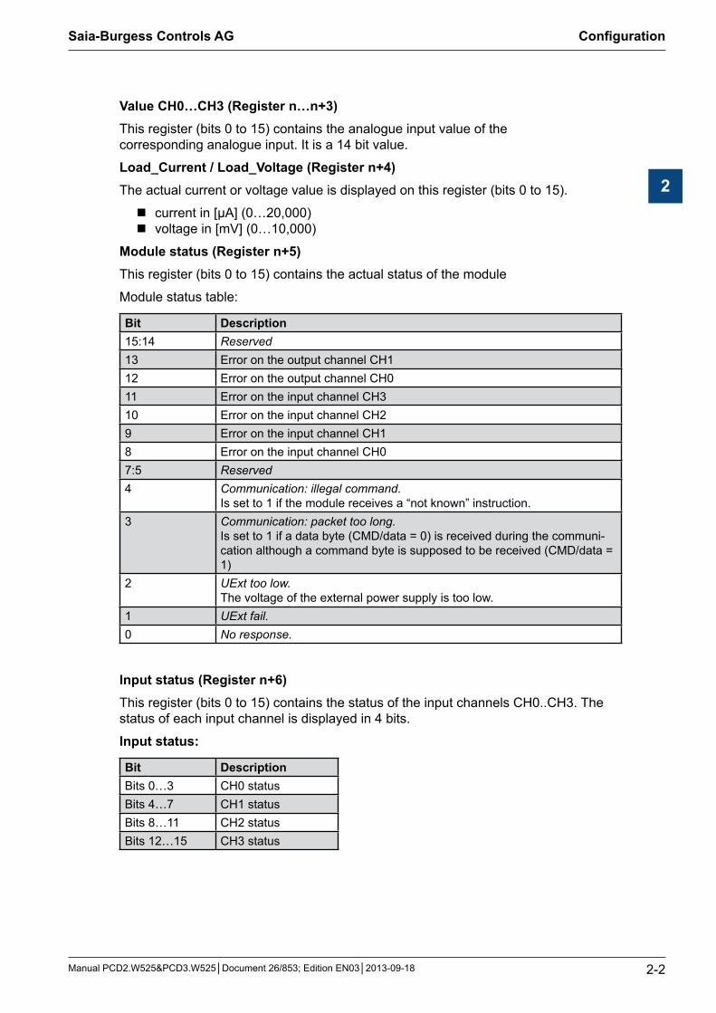
Module status (Register n+5)Thisregister(bits0to15)containstheactualstatusofthemodule
Modulestatustable:
Bit Description15:14 Reserved13 ErrorontheoutputchannelCH112 ErrorontheoutputchannelCH011 ErrorontheinputchannelCH310 ErrorontheinputchannelCH29 ErrorontheinputchannelCH18 ErrorontheinputchannelCH07:5 Reserved4 Communication: illegal command.
Is set to 1 if the module receives a “not known” instruction.3 Communication: packet too long.
Issetto1ifadatabyte(CMD/data=0)isreceivedduringthecommuni-cationalthoughacommandbyteissupposedtobereceived(CMD/data=1)
2 UExt too low. Thevoltageoftheexternalpowersupplyistoolow.
1 UExt fail.0 No response.
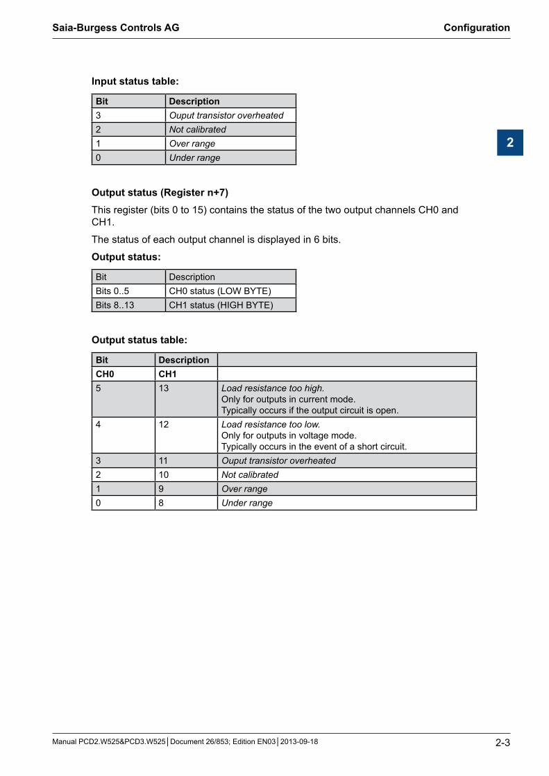
Input status (Register n+6)Thisregister(bits0to15)containsthestatusoftheinputchannelsCH0..CH3.Thestatusofeachinputchannelisdisplayedin4bits.
Input status:
Bit DescriptionBits0…3 CH0 statusBits4…7 CH1 statusBits8…11 CH2 statusBits12…15 CH3 status
Manual PCD2.W525&PCD3.W525Document 26/853; Edition EN032013-09-18
Saia-Burgess Controls AG
Configuration
2-3
2
Input status table:
Bit Description3 Ouput transistor overheated2 Not calibrated1 Over range0 Under range
Output status (Register n+7)Thisregister(bits0to15)containsthestatusofthetwooutputchannelsCH0andCH1.
Thestatusofeachoutputchannelisdisplayedin6bits.
Output status:
Bit DescriptionBits0..5 CH0status(LOWBYTE)Bits8..13 CH1status(HIGHBYTE)
Output status table:
Bit DescriptionCH0 CH15 13 Load resistance too high.
Onlyforoutputsincurrentmode. Typicallyoccursiftheoutputcircuitisopen.
4 12 Load resistance too low. Onlyforoutputsinvoltagemode. Typicallyoccursintheeventofashortcircuit.
3 11 Ouput transistor overheated2 10 Not calibrated1 9 Over range0 8 Under range
Manual PCD2.W525&PCD3.W525Document 26/853; Edition EN032013-09-18
Saia-Burgess Controls AG Appendix
A
A-1
Icons
A Appendix
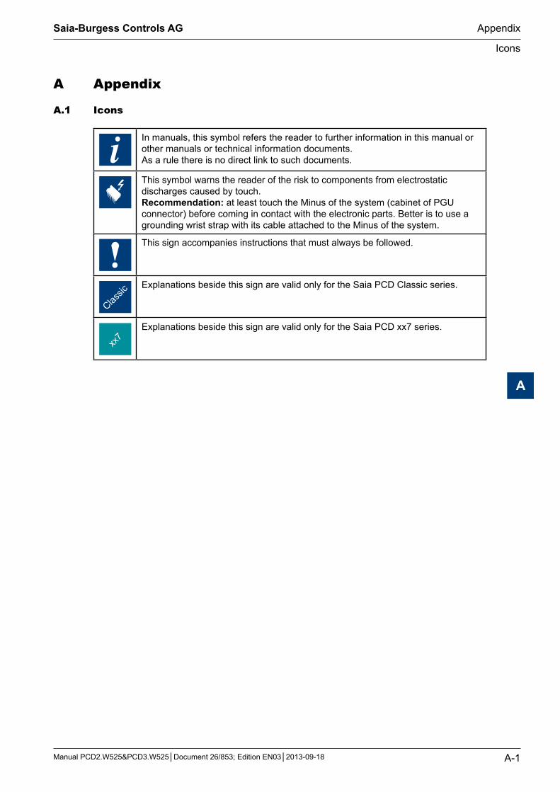
A.1 Icons
Inmanuals,thissymbolrefersthereadertofurtherinformationinthismanualorother manuals or technical information documents. As a rule there is no direct link to such documents.
Thissymbolwarnsthereaderoftherisktocomponentsfromelectrostaticdischargescausedbytouch. Recommendation:atleasttouchtheMinusofthesystem(cabinetofPGUconnector)beforecomingincontactwiththeelectronicparts.BetteristouseagroundingwriststrapwithitscableattachedtotheMinusofthesystem.
Thissignaccompaniesinstructionsthatmustalwaysbefollowed.
Classic
ExplanationsbesidethissignarevalidonlyfortheSaiaPCDClassicseries.
xx7
ExplanationsbesidethissignarevalidonlyfortheSaiaPCDxx7series.
Manual PCD2.W525&PCD3.W525Document 26/853; Edition EN032013-09-18
Saia-Burgess Controls AG Appendix
A
A-2
Address
A.2 Address
Saia-Burgess Controls AG Bahnhofstrasse18 3280Murten/Switzerland
Telephone ................................. ++41266727272 Fax ............................................ ++41266727499
E-mail: ...................................... [email protected] Homepage: .............................. www.saia-pcd.com Support: .................................... www.sbc-support.com Internationalbrancheoffices& SBCsalescompanies: ............ www.saia-pcd.com/contact
Reply address for customers in the Swiss market:
Saia-BurgessControlsAG ServiceAprès-Vente Bahnhofstrasse18 CH-3280Murten/Switzerland