Embed Size (px)
Citation preview

MAHARASHTRA STATE BOARD OF TECHNICAL EDUCATION (Autonomous)
(ISO/IEC - 27001 - 2013 Certified)
WINTER– 17 EXAMINATION
Subject Name: Microprocessor and Programming Model Answer
Sub Code: 17431
Important Instructions to examiners: 1) The answers should be examined by key words and not as word-to-word as given in the model answer scheme. 2) The model answer and the answer written by candidate may vary but the examiner may try to assess the
understanding level of the candidate. 3) The language errors such as grammatical, spelling errors should not be given more Importance
(Not applicable for subject English and Communication Skills. 4) While assessing figures, examiner may give credit for principal components indicated in the figure. The
figures drawn by candidate and model answer may vary. The examiner may give credit for anyequivalent figure drawn.
5) Credits may be given step wise for numerical problems. In some cases, the assumed constant values may vary and there may be some difference in the candidate’s answers and model answer.
6) In case of some questions credit may be given by judgement on part of examiner of relevant answer based on candidate’s understanding.
7) For programming language papers, credit may be given to any other program based on equivalent concept.
Q. Sub. Answer Marking
No. Q. No. Scheme
1 a) Attempt any SIX of the following: 12 M
i) List any four features of µP 8085. 2 M
Ans: (Any four) Any four
Features of 8085: features
1. 16 address line so 216
=64 Kbytes of memory can be addressed. ½ Mark
2. Operating clock frequency is 3MHz and minimum clock frequency is 500 KHz. each
3. On chip bus controller.
4. Provide 74 instructions with five addressing modes.
5. 8085 is 8 bit microprocessor.
6. Provides 5 level hardware interrupts and 8 software interrupts.
7. It can generate 8 bit I/O address so 28=256 input and 256 output ports can be
accessed.
8. Requires a single +5 volt supply
9. Requires 2 phase, 50% duty cycle TTL clock
10. Provide 2 serial I/O lines, so peripheral can be interfaced with 8085 μp
ii) Describe functions of following pins of µP 8086: 2 M
a) MN/𝑴𝑿̅̅ ̅̅ ̅ b ) ALE
Page 1/40
MAHARASHTRA STATE BOARD OF TECHNICAL EDUCATION (Autonomous)
(ISO/IEC - 27001 - 2013 Certified)
WINTER– 17 EXAMINATION
17431
Subject Name: Microprocessor and Programming Model Answer Sub Code:
Ans: MN/ 𝑴𝑿̅̅ ̅̅ ̅: The MN/𝑀𝑋̅̅̅̅̅ pin is used to select either the minimum mode or maximum 1 Mark
mode operation of the 8086. This is achieved by connecting this pin to either +5V
Each
directly (for minimum mode) or to the ground (for maximum mode).
ALE : This active high ,output signal used to indicate availability of valid address on
address/data lines and is connected to latch enable input of latches (8282 or 74LS373)
.
iii) List any two addressing modes of 8086 with example. 2 M
Ans: (Any two) Any two
Addressing modes of 8086: Modes
1. Immediate addressing mode:
1 Mark for
Each (1/2
An instruction in which 8-bit or 16-bit operand (data ) is specified in the instruction, for name
then the addressing mode of such instruction is known as Immediate addressing
and ½ for
example)
mode.
Example:
MOV AX,67D3H
2. Register addressing mode
An instruction in which an operand (data) is specified in general purpose
registers, then the addressing mode is known as register addressing mode.
Example:
MOV AX,CX
3. Direct addressing mode
An instruction in which 16 bit effective address of an operand is specified in
the instruction, then the addressing mode of such instruction is known as direct
addressing mode.
Example:
MOV CL,[2000H]
4. Register Indirect addressing mode
An instruction in which address of an operand is specified in pointer register or in
Page 2/40
MAHARASHTRA STATE BOARD OF TECHNICAL EDUCATION (Autonomous)
(ISO/IEC - 27001 - 2013 Certified)
WINTER– 17 EXAMINATION
Subject Name: Microprocessor and Programming
Model Answer
Sub Code: 17431
index register or in BX, then the addressing mode is known as register
indirect addressing mode.
Example:
MOV AX, [BX]
5. Indexed addressing mode
An instruction in which the offset address of an operand is stored in index
registers (SI or DI) then the addressing mode of such instruction is known as
indexed addressing mode.
DS is the default segment for SI and DI.
For string instructions DS and ES are the default segments for SI and DI resp. this is
a special case of register indirect addressing mode.
Example:
MOV AX,[SI]
6. Based Indexed addressing mode
an instruction in which the address of an operand is obtained by adding the contents
of base register (BX or BP) to the content of an index register (SI or DI) The
default segment register may be DS or ES
Example:
MOV AX, [BX][SI]
7. Register relative addressing mode
An instruction in which the address of the operand is obtained by adding the
displacement (8-bit or 16 bit) with the contents of base registers or index registers
(BX, BP, SI, DI). the default segment register is DS or ES
Example:
MOV AX, 50H[BX]
8. Relative Based Indexed addressing mode
An instruction in which the address of the operand is obtained by adding the
displacement (8 bit or 16 bit) with the base registers (BX or BP) and index
registers (SI or DI) to the default segment.
Page 3/40

MAHARASHTRA STATE BOARD OF TECHNICAL EDUCATION (Autonomous)
(ISO/IEC - 27001 - 2013 Certified)
WINTER– 17 EXAMINATION
17431
Subject Name: Microprocessor and Programming Model Answer Sub Code:
Example:
MOV AX, 50H [BX][SI]
iv) Define flow chart and algorithm. 2 M
Ans: Flowchart: 1 M Each
The flowchart is a graphically representation of the program operation or task.
Definition
Algorithm:
The formula or sequence of operations to be performed by the program, specified as
steps in general English, is called algorithm.
v) List maskable and non-maskable interrupts of 8085. 2 M
Ans: Maskable Interrupt : INTR, RST 7.5, RST 6.5, RST 5.5 1 M Each
Non-maskable Interrupts : Trap
vi) List any four features of 8086. 2 M
Ans: (Any four) Any four
1) It is a 16 bit μp. features
2) 8086 has a 20 bit address bus that can access upto 2
20 memory locations (1 MB) .
(½ Mark each)
3) It has two blocks: BIU and EU.
4) It provides 16-bit registers. AX,BX,CX,DX,CS,SS,DS,ES,BP,SP,SI,DI,IP &
FLAG REGISTER
5) It has multiplexed address and data bus AD0- AD15 and A16 – A19.
6) It works in a multiprocessor environment. Control signals are generated by an
external BUS Controller
7) 8086 is designed to operate in two modes, Minimum and Maximum.
8) It can prefetches up to 6 instruction bytes from memory and queues them in order
to speed up instruction execution.
9) Interrupts:-8086 has 256 vectored interrupts.
10) Provides separate instructions for string manipulation.
11) Operating frequency range is 6-10MHz.
vii) List directives used for procedure. 2 M
Ans: Procedure directives are: 1) PROC 2) ENDP 1 Mark for
each
Page 4/40

MAHARASHTRA STATE BOARD OF TECHNICAL EDUCATION (Autonomous)
(ISO/IEC - 27001 - 2013 Certified)
WINTER– 17 EXAMINATION
17431
Subject Name: Microprocessor and Programming Model Answer Sub Code:
viii) Write assembly language instructions of 8086 to 2 M
a) Multiply 4H by 5H
b) Rotate content of AX by 4 bit towards left.
Ans: a) Multiply 4H by 5H 1 Mark for
CODE SEGMENT
Each
(Even if
ASSUME CS:CODE, DS:DATA without
MOV AL,04H
directives)
MOV BL,05H
MUL BL
INT 21H
CODE ENDS
b) Rotate content of AX by 4 bit towards left.
MOV CL, 04H
RCL AX, CL
Or
MOV CL, 04H
ROL AX, CL
b) Attempt any TWO of the following: 8 M
i) Describe the functions of the following directives: 4 M
i)DD ii)DBiii)DUP iv)EQU
Ans: i) DD - (Define Double Word or Data Double Word) 1 Mark for
each
• This is used to define a double word (32-bit) type variable. directive
• The range of values: 0 to 2
32-1 bits for unsigned numbers. -2
32-1to +2
32-1 for signed
(½ Mark for
numbers Explanation
• This can be used to define a single double word or multiple double word.
and
Name_Of_Variable DD Initialization_Value(,s) 1/2 Mark
For
ii) DB - Define byte (8 bits)
Example)
• It is used to declare a byte type variable of 8 bit. It also can be used to declare an
array of bytes.
Page 5/40

MAHARASHTRA STATE BOARD OF TECHNICAL EDUCATION (Autonomous)
(ISO/IEC - 27001 - 2013 Certified)
WINTER– 17 EXAMINATION
17431
Subject Name: Microprocessor and Programming Model Answer Sub Code:
• The range of values that can be stored in a byte is 0 to 255 for unsigned numbers
and –128 +127 for signed numbers.
Name_Of_Variable DB Initialization_Value(,s)
iii) DUP: Duplicate memory location:-
• This directive can be used to generate multiple bytes or words with known as well
as un-initialized values.
iv) EQU :Equate to
The EQU directive is used to declare the micro symbols to which some constant value
is assigned. Micro assembler will replace every occurrence of the symbol in a
program by its value.
Syntax: Symbol name EQU expression
Example: CORRECTION_FACTOR EQU 100
ii) Describe Linker and Debugger. 4 M
Ans: Linker: Each 2
1. It is a programming tool used to convert Object code into executable program
Marks
called .EXE module.
2. It combines, if requested, more than one separated assembled modules into one
executable module such as two or more assembly programs or an assembly language
with C program.
Debugger: -
1. Debugger is a program that allows the execution of program in single step mode
under the control of the user.
2. The errors in program can be located and corrected using a debugger.
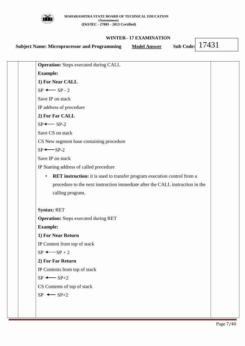
iii) Describe CALL and RET instructions. 4 M
Ans: CALL Instruction: It is used to transfer program control to the sub-program or 2 Marks
subroutine. The CALL can be NEAR, where the procedure is in the same segment
for each
whereas in FAR CALL, procedure is in a different segment.
Syntax: CALL procedure name (direct/indirect)
Page 6/40
MAHARASHTRA STATE BOARD OF TECHNICAL EDUCATION (Autonomous)
(ISO/IEC - 27001 - 2013 Certified)
WINTER– 17 EXAMINATION
Subject Name: Microprocessor and Programming Model Answer
Sub Code:
17431
Operation: Steps executed during CALL
Example:
1) For Near CALL
SP SP - 2
Save IP on stack
IP address of procedure
2) For Far CALL
SP SP-2
Save CS on stack
CS New segment base containing procedure
SP SP-2
Save IP on stack
IP Starting address of called procedure
• RET instruction: it is used to transfer program execution control from a
procedure to the next instruction immediate after the CALL instruction in the
calling program.
Syntax: RET
Operation: Steps executed during RET
Example:
1) For Near Return
IP Content from top of stack
SP SP + 2
2) For Far Return
IP Contents from top of stack
SP SP+2
CS Contents of top of stack
SP SP+2
Page 7/40

MAHARASHTRA STATE BOARD OF TECHNICAL EDUCATION (Autonomous)
(ISO/IEC - 27001 - 2013 Certified)
WINTER– 17 EXAMINATION
17431
Subject Name: Microprocessor and Programming Model Answer Sub Code:
Attempt any FOUR of following: 16 M
2
a) Draw functional block diagram of 8085. 4 M
Ans: Correct
Diagram
4M
b) Describe register organization of 8086. 4 M
Ans: Register Organization of 8086 2 Marks for
Diagram
All the registers of 8086 are 16-bit registers. The general purpose registers can be And 2Marks
used as either 8-bit registers or 16-bit registers.
For
Explanation
The register set of 8086 can be categorized into 4 different groups. The register (each type
organization of 8086 is shown in the figure. of
Register
1M)
Page 8/40

MAHARASHTRA STATE BOARD OF TECHNICAL EDUCATION (Autonomous)
(ISO/IEC - 27001 - 2013 Certified)
WINTER– 17 EXAMINATION
Subject Name: Microprocessor and Programming
Model Answer
Sub Code: 17431
SP AX AH AL
CS
BP
BX BH BL
SS
SI FLAGS/
PSW
CX CH CL
DS
DI
DX DH DL ES
IP
General data Registers Segment Pointers and index
Registers Registers
Register organization of 8086
General Data Registers:
The registers AX, BX, CX and DX are the general purpose 16-bit registers.
AX is used as 16-bit accumulator. The lower 8-bit is designated as AL and higher 8-bit
is designated as AH. AL can be used as an 8-bit accumulator for 8-bit operation.
All data register can be used as either 16 bit or 8 bit. BX is a 16 bit register, but BL
indicates the lower 8-bit of BX and BH indicates the higher 8-bit of BX.
The register CX is used default counter in case of string and loop instructions.
The register BX is used as offset storage for forming physical address in case of
certain addressing modes.
DX register is a general purpose register which may be used as an implicit operand or
destination in case of a few instructions.
Page 9/40

MAHARASHTRA STATE BOARD OF TECHNICAL EDUCATION (Autonomous)
(ISO/IEC - 27001 - 2013 Certified)
WINTER– 17 EXAMINATION
Subject Name: Microprocessor and Programming Model Answer
Sub Code:
17431
Segment Registers:
The 8086 architecture uses the concept of segmented memory. 8086 able to address to
address a memory capacity of 1 megabyte and it is byte organized. This 1 megabyte
memory is divided into 16 logical segments. Each segment contains 64 kbytes of
memory.
There are four segment register in 8086
• Code segment register (CS)
• Data segment register (DS)
• Extra segment register (ES)
• Stack segment register (SS)
Code segment register (CS): is used fro addressing memory location in the code
segment of the memory, where the executable program is stored.
Data segment register (DS): points to the data segment of the memory where the data
is stored.
Extra Segment Register (ES) : also refers to a segment in the memory which is
another data segment in the memory.
Stack Segment Register (SS): is used for addressing stack segment of the memory.
The stack segment is that segment of memory which is used to store stack data.
While addressing any location in the memory bank, the physical address is calculated
from two parts:
- The first is segment address, the segment registers contain 16-bit segment
base addresses, related to different segment.
- The second part is the offset value in that segment.
Page 10/40
MAHARASHTRA STATE BOARD OF TECHNICAL EDUCATION (Autonomous)
(ISO/IEC - 27001 - 2013 Certified)
WINTER– 17 EXAMINATION
Subject Name: Microprocessor and Programming
Model Answer
Sub Code: 17431
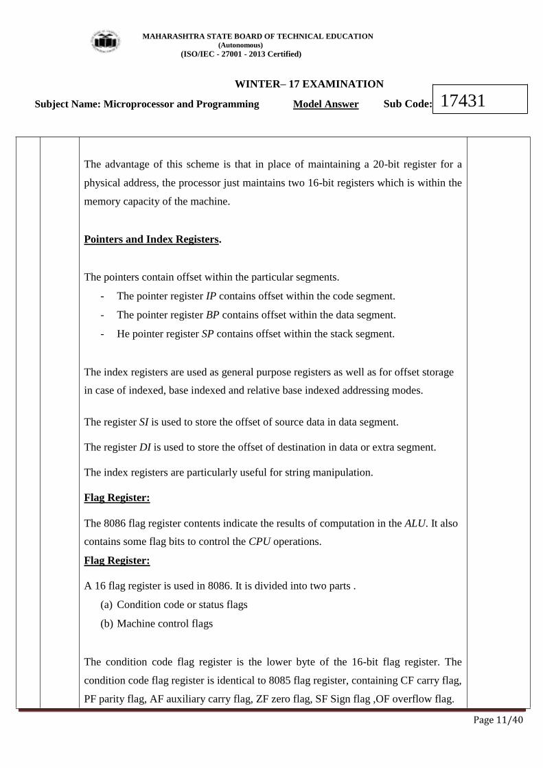
The advantage of this scheme is that in place of maintaining a 20-bit register for a
physical address, the processor just maintains two 16-bit registers which is within the
memory capacity of the machine.
Pointers and Index Registers.
The pointers contain offset within the particular segments.
- The pointer register IP contains offset within the code segment.
- The pointer register BP contains offset within the data segment.
- He pointer register SP contains offset within the stack segment.
The index registers are used as general purpose registers as well as for offset storage
in case of indexed, base indexed and relative base indexed addressing modes.
The register SI is used to store the offset of source data in data segment.
The register DI is used to store the offset of destination in data or extra segment.
The index registers are particularly useful for string manipulation.
Flag Register:
The 8086 flag register contents indicate the results of computation in the ALU. It also
contains some flag bits to control the CPU operations.
Flag Register:
A 16 flag register is used in 8086. It is divided into two parts .
(a) Condition code or status flags
(b) Machine control flags
The condition code flag register is the lower byte of the 16-bit flag register. The
condition code flag register is identical to 8085 flag register, containing CF carry flag,
PF parity flag, AF auxiliary carry flag, ZF zero flag, SF Sign flag ,OF overflow flag.
Page 11/40

MAHARASHTRA STATE BOARD OF TECHNICAL EDUCATION (Autonomous)
(ISO/IEC - 27001 - 2013 Certified)
WINTER– 17 EXAMINATION
Subject Name: Microprocessor and Programming
Model Answer
Sub Code: 17431
The control flag register is the higher byte of the flag register. It contains three flags
namely direction flag (D), interrupt flag (I) and trap flag (T).
c) Describe concept of memory segmentation of 8086. 4 M
Ans: 2 Marks
Diagram
And
2 Marks
For
description
Memory Segmentation of 8086
Memory Segmentation: The memory in an 8086 microprocessor is organized as a
segmented memory. The physical memory is divided into 4 segments namely,-
Data segment, Code Segment, Stack Segment and Extra Segment.
Description:
Data segment is used to hold data, Code segment for the executable program, Extra
segment also holds data specifically in strings and stack segment is used to store
stack data.
Each segment is 64Kbytes & addressed by one segment register.
Page 12/40

MAHARASHTRA STATE BOARD OF TECHNICAL EDUCATION (Autonomous)
(ISO/IEC - 27001 - 2013 Certified)
WINTER– 17 EXAMINATION
17431
Subject Name: Microprocessor and Programming Model Answer Sub Code:
The 16 bit segment register holds the starting address of the segment The offset
address to this segment address is specified as a 16-bit displacement (offset) between
0000 to FFFFH.
Since the memory size of 8086 is 1Mbytes, total 16 segments are possible with each
having 64Kbytes.
d) Draw labeled flag register of 8085 and explain functions of all flags. 4 M
Ans: Format
2 Marks
Explanation
2Marks
Format of flag register of 8085 μp
i) Carry flag (CY):
When μp performs addition/subtraction of 8 bit if the carry/borrow is generated from
the MSB, then the carry flag is set (CY=1), otherwise it resets the carry flag (CY=0).
ii) Auxiliary carry flag (AC)/ Half carry/ Nibble carry:
When μp performs addition of 8 bit number and if the carry is generated from
D3bit, then auxiliary carry flag is set, otherwise it is reset.
iii)Parity flag (P):
When μp performs addition or logical operations on 8 bit number and if number of
1‘s bit in 8 bit result is even number, then it is called as Even parity and parity flag is
set (P=1) otherwise it is called as Odd parity and parity flag is reset (P=0).
iv)Zero Flag(Z):
When μp performs arithmetic and logical operation of two 8 bit numbers, if the result
obtained is zero, then flag is set (Z=1),otherwise it is reset (Z=0).
Page 13/40
MAHARASHTRA STATE BOARD OF TECHNICAL EDUCATION (Autonomous)
(ISO/IEC - 27001 - 2013 Certified)
WINTER– 17 EXAMINATION
17431
Subject Name: Microprocessor and Programming Model Answer Sub Code:
v) Sign flag (S):
When μp performs arithmetic and logical operations on signed numbers and if the
MSB of the result is 1, then sign flag is set. i.e. for negative number sign flag is set
(S=1), otherwise it is reset (S=0).
e) Describe any two string operation instruction of 8086 with syntax & one example 4 M
of each.
Ans: (Any two) 2 M for
Each
1] REP: REP is a prefix which is written before one of the string instructions. It will (1 M for
cause during length counter CX to be decremented and the string instruction to be
Description
½ M for
repeated until CX becomes 0. Syntax
Two more prefix.
And 1/2M
For example
REPE/REPZ: Repeat if Equal /Repeat if Zero.
It will cause string instructions to be repeated as long as the compared bytes or words
are equal and CX≠0.
REPNE/REPNZ: Repeat if not equal/Repeat if not zero.
It repeats the strings instructions as long as compared bytes or words are not equal
and CX≠0.
Example: REP MOVSB
2] MOVS/ MOVSB/ MOVSW - Move String byte or word.
Syntax:
MOVS destination, source
MOVSB destination, source
MOVSW destination, source
Operation: ES:[DI]<----- DS:[SI]
It copies a byte or word a location in data segment to a location in extra segment. The
offset of source is pointed by SI and offset of destination is pointed by DI.CX register
contain counter and direction flag (DE) will be set or reset to auto increment or auto
decrement pointers after one move.
Page 14/40

MAHARASHTRA STATE BOARD OF TECHNICAL EDUCATION (Autonomous)
(ISO/IEC - 27001 - 2013 Certified)
WINTER– 17 EXAMINATION
Subject Name: Microprocessor and Programming Model Answer
Sub Code: 17431
Example
LEA SI, Source
LEA DI, destination
CLD
MOV CX, 04H
REP MOVSB
3] CMPS /CMPSB/CMPSW: Compare string byte or Words.
Syntax:
CMPS destination, source
CMPSB destination, source
CMPSW destination, source
Operation: Flags affected < ----- DS:[SI]- ES:[DI]
It compares a byte or word in one string with a byte or word in another string. SI
holds the offset of source and DI holds offset of destination strings. CS contains
counter and DF=0 or 1 to auto increment or auto decrement pointer after comparing
one byte/word.
Example
LEA SI, Source
LEA DI, destination
CLD
MOV CX, 100
REPE CMPSB
4] SCAS/SCASB/SCASW: Scan a string byte or word.
Syntax:
SCAS/SCASB/SCASW
Operation: Flags affected < ----- AL/AX-ES: [DI]
It compares a byte or word in AL/AX with a byte /word pointed by ES: DI. The
string to be scanned must be in the extra segment and pointed by DI. CX contains
counter and DF may be 0 or 1.
When the match is found in the string execution stops and ZF=1 otherwise ZF=0 .
Page 15/40

MAHARASHTRA STATE BOARD OF TECHNICAL EDUCATION (Autonomous)
(ISO/IEC - 27001 - 2013 Certified)
WINTER– 17 EXAMINATION
Subject Name: Microprocessor and Programming
Model Answer
Sub Code: 17431
Example
LEA DI, destination
MOV Al, 0DH
MOV CX, 80H
CLD
REPNE SCASB
5] LODS/LODSB/LODSW: Load String byte into AL or Load String word into AX.
Syntax:
LODS/LODSB/LODSW
Operation: AL/AX < ----- DS: [SI]
IT copies a byte or word from string pointed by SI in data segment into AL or AX.CX
may contain the counter and DF may be either 0 or 1
Example
LEA SI, destination
CLD
LODSB
6] STOS/STOSB/STOSW (Store Byte or Word in AL/AX)
Syntax STOS/STOSB/STOSW
Operation: ES:[DI] < ----- AL/AX
It copies a byte or word from AL or AX to a memory location pointed by DI in extra
segment CX may contain the counter and DF may either set or reset.
f) With the help of diagram, describe physical memory address generation of 8086. 4 M
Ans: Diagram
Formation of a physical address:- Segment registers carry 16 bit data, which is also 2 Marks
known as base address. BIU attaches 0 as LSB of the base address. So now this
Explanation
2Marks
address becomes 20-bit address. Any base/pointer or index register carry 16 bit offset.
Offset address is added into 20-bit base address which finally forms 20 bit physical
address of memory location.
Example:- Assume DS= 2632H, SI=4567H
Page 16/40

MAHARASHTRA STATE BOARD OF TECHNICAL EDUCATION (Autonomous)
(ISO/IEC - 27001 - 2013 Certified)
WINTER– 17 EXAMINATION
17431
Subject Name: Microprocessor and Programming Model Answer Sub Code:
DS : 26320H ……...0 added by BIU(or Hardwired 0)
+ SI : 4567H
----------------------------
2A887H
Physical address formation
3 Attempt any FOUR of following 16M
a. Explain DAA instruction with suitable example 4M
Ans: DAA – (Decimal Adjust AL after BCD Addition) Explanatio
Syntax- DAA
n: 2marks,
example:
Explanation: This instruction is used to make sure the result of adding two packed 2marks
BCD numbers is adjusted to be a correct BCD number.
The result of the addition must be in AL for DAA instruction to work correctly.
If the lower nibble in AL after addition is > 9 or Auxiliary Carry Flag is set, then add
6 to lower nibble of AL.
If the upper nibble in AL is > 9H or Carry Flag is set, and then add 6 to upper nibble
of AL.
Page 17/40

MAHARASHTRA STATE BOARD OF TECHNICAL EDUCATION (Autonomous)
(ISO/IEC - 27001 - 2013 Certified)
WINTER– 17 EXAMINATION
17431
Subject Name: Microprocessor and Programming Model Answer Sub Code:
Example: - (Any Same Type of Example)
if AL=99 BCD and BL=99 BCD
Then ADD AL, BL
1001 1001 = AL= 99 BCD
+ 1001 1001 = BL = 99 BCD
----------------------------------------
0011 0010 = AL =32 H and CF=1, AF=1
After the execution of DAA instruction, the result is CF = 1
0011 0010 =AL =32 H AH =1
+ 0110 0110
-------------------------
1001 1000 =AL =98 in BCD
b State all control signal generated by S0, S1, S2 with their function of 8086 4M
Ans: ( ½ mark
S2 S1 S0 FUNCTION for each
0 0 0 Interrupt correct
acknowledge control
signal/func
tion ) 0 0 1 Read I/O
0 1 0 Write I/O
0 1 1 Halt
1 0 0 Code access
1 0 1 Read memory
1 1 0 Write memory
1 1 1 Inactive
c Draw and explain interface of 8284 clock generated with 8086 4M
Ans: 1. Generate system clock: The Clock logic results in three different frequencies Diagram
required for the system. These outputs are CLOCK, OSC and PCLK.
2marks,
Explanation
2 marks)
Page 18/40

MAHARASHTRA STATE BOARD OF TECHNICAL EDUCATION (Autonomous)
(ISO/IEC - 27001 - 2013 Certified)
WINTER– 17 EXAMINATION
17431
Subject Name: Microprocessor and Programming Model AnswerSub Code:
2. Generate READY signal: The Ready logic has a READY output which is
connected to the processor. When this is low, wait states are added in the bus cycle.
3. Generate RESET signal: The Reset logic generates a RESET input for the
microprocessor. When this signal is High, processor performs reset sequence.
d What will be the content of register BX after execution of instruction ? 4 M
MOV BX 2050H
MOV CL 05H
SHL BX CL
Ans: (Correct
answer : 4
Marks )
Content of BX After execution =0A00H
Page 19/40

MAHARASHTRA STATE BOARD OF TECHNICAL EDUCATION (Autonomous)
(ISO/IEC - 27001 - 2013 Certified)
WINTER– 17 EXAMINATION
17431
Subject Name: Microprocessor and Programming Model AnswerSub Code:
e Write ALP to divide two 16 bit numbers. 4 M
Ans: [Note: Any other logic may be considered] (Correct
DATA SEGMENT Program :
A DW 4444H
4M)
B DW 0002H
C DW ?
DATA ENDS
CODE SEGMENT
ASSUME DS:DATA, CS:CODE
START:
MOV AX,DATA
MOV DS,AX
MOV AX,A
MOV BX,B
DIV BX
MOV C,AX
INT 3
CODE ENDS
END START
f Describe concept of pipelining in 8086 4 M
Ans: • In pipelined processor, fetch, decode and execute operation are performed concept of
simultaneously or in parallel. When first instruction is being decoded, same
pipeline: (4 Mark)
time code of the next instruction is fetched.
• When first instruction is getting executed, second one’s is decoded and third
instruction code is fetches from memory. This process is known as pipelining.
It improves speed of operation to great extent.
Page 20/40

MAHARASHTRA STATE BOARD OF TECHNICAL EDUCATION (Autonomous)
(ISO/IEC - 27001 - 2013 Certified)
WINTER– 17 EXAMINATION
17431
Subject Name: Microprocessor and Programming Model AnswerSub Code:
4 Attempt any FOUR of following 16 M
a With example, describe XLAT and AAA instructions 4 M
Ans: (1 mark
XLAT example,
• XLAT : translate
1 mark
Explanation
– Can be used for look up table for each)
– Default source & destination operand is AL
– Default base address of look up table is in BX
– Physical address in look up table = 10H * DS + AL +
BX AL<=DS:[BX+AL]
– Example:
MOV AL, NUM; read the number
MOV BX, OFFSET_TABLE; store the base address of look up table
XLAT; the value corresponding to the no. is stored in AL
AAA (ASCII Adjust after Addition):
Corrects result in AH and AL after addition when working with BCD values.
It works according to the following Algorithm:
if low nibble of AL > 9 or AF = 1 then:
AL = AL + 6
AH = AH + 1
AF = 1
CF = 1
else
AF = 0
CF = 0
Before execution suppose AH=00H,AL=0EH
After Execution AH=01H,AL=04H
Page 21/40

MAHARASHTRA STATE BOARD OF TECHNICAL EDUCATION (Autonomous)
(ISO/IEC - 27001 - 2013 Certified)
WINTER– 17 EXAMINATION
17431
Subject Name: Microprocessor and Programming Model Answer Sub Code:
b Describe any two bit manipulation instructions 4 M
Ans: (Any two) (1 mark
• AND − Used for ANDing each bit in a source operand with the corresponding
for description
bit in destination operand byte/word. And the result is stored in Destination , 1 for
operand. example,
for each
Eg:
instruction , Any
AND BH, AL; AND bit by bit Byte in AL with data in BH and the result is
suitable example)
stored in BH
Eg:
• OR − Used to multiply each bit in a byte/word with the corresponding bit in
another byte/word.
Eg:
OR AX, 00ABH; OR bit by bit word in AX with immediate data 00ABH
and the result is stored in AX
Eg:
• XOR − Used to perform Exclusive-OR operation over each bit in a byte/word
with the corresponding bit in another byte/word.
Eg:
XOR CX, [SI]; XOR bit by bit word at offset [SI] in DS with word in CX
and the result is stored in CX
Eg:
• NOT − Used to invert each bit of a byte or word.
Eg:
NOT AX; Complement the contents of AX
Page 22/40
MAHARASHTRA STATE BOARD OF TECHNICAL EDUCATION (Autonomous)
(ISO/IEC - 27001 - 2013 Certified)
WINTER– 17 EXAMINATION
Subject Name: Microprocessor and Programming Model Answer
Sub Code:
17431
• TEST - AND Operands to update flags, but don’t change operands
Eg:
TEST BH, AL ; AND bit by bit Byte in AL with data in BH ,no result,
update PF,SF,ZF
• SHL/SAL – Shifts bits of word or byte left, put zero’s in LSBs
Eg:
SAL BX, 1 ; Shift the Contents of BX register by four bits towards left, put
zero’s in LSBs
IF BX = 11110000 11110000
After Execution 11100001 111000000
• SHR - Shifts bits of word or byte right, put zero’s in MSBs
Eg:
SHR BX, 1 ; Shift the Contents of BX register by four bits towards right, put
zero’s in MSBs
IF BX = 11110000 11110000
After Execution 01111000 01111000, CF=1
• SAR - Shifts bits of word or byte right, copy old MSB into new MSB
Eg:
SAR BX, 1 ; Shift the Contents of BX register by four bits towards right, put
zero’s in LSBs, copy old MSB into new MSB.
IF BX = 11110000 11110000
After Execution 11111000 01111000, CF=1
• ROL – Rotate bits of byte or word left, MSB to LSB and to CF
Page 23/40

MAHARASHTRA STATE BOARD OF TECHNICAL EDUCATION (Autonomous)
(ISO/IEC - 27001 - 2013 Certified)
WINTER– 17 EXAMINATION
Subject Name: Microprocessor and Programming Model Answer
Sub Code:
17431
Eg:
ROL BL, 2 ; Rotate all bits in BL left by 1 bit ,copy MSB to LSB and to CF
IF BL = 11110000
After Execution 11000011, CF= 1
• ROR – Rotate bits of byte or word right, LSB to MSB and to CF
Eg:
ROR BL, 2 ; Rotate all bits in BL right by 1 bit ,copy LSB to MSB and to
CF
IF BL = 11110000
After Execution 00111100, CF= 0
• RCL – Rotate bits of byte or word left, MSB to CF and CF to LSB.
Eg:
RCL BL, 2 ; Rotate all bits in BL left by 1 bit ,copy MSB to CF and CF to
LSB
IF BL = 11110000, CF=0
After Execution 11000001 , CF= 1
• RCR – Rotate bits of byte or word right, LSB to CF and CF to MSB.
Eg:
RCR BL, 1 ; Rotate all bits in BL right by 1 bit ,copy LSB to CF and CF to
MSB.
IF BL = 11110000, CF= 0
After Execution 00111100 , CF= 0
Page 24/40

MAHARASHTRA STATE BOARD OF TECHNICAL EDUCATION (Autonomous)
(ISO/IEC - 27001 - 2013 Certified)
WINTER– 17 EXAMINATION
17431
Subject Name: Microprocessor and Programming Model AnswerSub Code:
c Write an ALP to find largest number from array of 10 numbers 4 M
Ans: [Note: Any other logic may be considered] (Correct
DATA SEGMENT Program :
ARRAY DB 15H,45H,08H,78H,56H,02H,04H,12H,23H,09H
4M)
LARGEST DB 00H
DATA ENDS
CODE SEGMENT
START:ASSUME CS:CODE,DS:DATA
MOV DX,DATA
MOV DS,DX
MOV CX,09H
MOV SI ,OFFSET ARRAY
MOV AL,[SI]
UP:INC SI
CMP AL,[SI]
JNC NEXT ;CHANGE
MOV AL,[SI]
NEXT:DEC CX
JNZ UP
MOV LARGEST,AL ; AL=78h
MOV AX,4C00H
INT 21H CODE ENDS
END START
d Write an ALP to find length of string 4 M
Ans: [Note: Any other logic may be considered] (Correct
Program :
DATA SEGMENT 4M)
STR1 DB ‘STUDENT$’
Page 25/40

MAHARASHTRA STATE BOARD OF TECHNICAL EDUCATION (Autonomous)
(ISO/IEC - 27001 - 2013 Certified)
WINTER– 17 EXAMINATION
17431
Subject Name: Microprocessor and Programming Model AnswerSub Code:
LENGTH_STRING DB?
DATA ENDS
ASSUME CS:CODE, DS:DATA
CODE SEGMENT
MOV AX, DATA
MOV DS, AX
MOV AL, ‘$’
MOV CX, 00H
MOV SI, OFFSET STR1
BACK: CMP AL, [SI]
JE DOWN
INC CL
INC SI
JMP BACK
DOWN: MOV LENGTH_STRING, CL
MOV AX, 4C00H
INT 21H
CODE ENDS
END
e Describe model of assembly language programming 4 M
Ans: Note : Any one model can be considered. (descriptio
Model 1 :
n 4marks)
1) Using SEGMENT, ASSUME and ENDS directives
2) In this Data_Seg is the name of the data segment where data are declared
3) Code_Seg is the name of the code segment where code is written
4) Start is the label name used to initialize the CS register.
5) ENDS to indicate the ends of code and data segment
6) END marks the end of the program.
Page 26/40

MAHARASHTRA STATE BOARD OF TECHNICAL EDUCATION (Autonomous)
(ISO/IEC - 27001 - 2013 Certified)
WINTER– 17 EXAMINATION
Subject Name: Microprocessor and Programming
Model Answer
Sub Code: 17431
Example
Data_Seg SEGMENT
:
:
Data declaration
:
:
Data_Seg ENDS
Code_Seg SEGMENT
ASSUME CS:Code_Seg, DS:Data_Seg
Start: MOV AX, Data_Seg
MOV DS,AX
:
:
Program code
:
:
Code_Seg ENDS
END Start
(OR)
Model 2 :
a. Using .Data and .code directive
b. In this, .model small is used to indicate small memory model is used in
the program
c. Stack 100 to indicate 100 word memory locations reserved for stack
d. Data indicates start of the data segment where data declaration of the program
is made.
e. Code indicates the beginning of the code segment h. END to indicate the
termination of the program.
Page 27/40

MAHARASHTRA STATE BOARD OF TECHNICAL EDUCATION (Autonomous)
(ISO/IEC - 27001 - 2013 Certified)
WINTER– 17 EXAMINATION
17431
Subject Name: Microprocessor and Programming Model Answer Sub Code:
.MODEL SMALL
.STACK 100
.DATA
:
:
:
Data Declaration
:
:
.CODE MOV AX, @DATA
MOV DS,AX
:
:
Program code
:
:
END
f Explain re-entrant procedure with diagram 4 M
Ans: Any other example diagram can also be considered. Diagram2
In some situation it may happen that Procedure 1 is called from main program
marks,
explanatio
Procrdure2 is called from procedure1And procedure1 is again called from procdure2. n -2
In this situation program execution flow re enters in the procedure1. These types of
Marks)
procedures are called re-entrant procedures.
A procedure is said to be re-entrant, if it can be interrupted, used and re-entered
without losing or writing over anything.,
Page 28/40

MAHARASHTRA STATE BOARD OF TECHNICAL EDUCATION (Autonomous)
(ISO/IEC - 27001 - 2013 Certified)
WINTER– 17 EXAMINATION
17431
Subject Name: Microprocessor and Programming Model AnswerSub Code:
5 Attempt any FOUR of following
a Write ALP to Subtract two 16 bit numbers 4 M
Ans: (Program with any other logic also be considered) Correct
DATA SEGMENT
Program
4M
NUM1 DW 3210H
NUM2 DW 1200H
R DW ?
DATA ENDS
CODE SEGMENT
ASSUME CS: CODE, DS: DATA
START: MOV AX, DATA
MOV DS, AX
MOV AX, NUM1
MOV BX, NUM2
SUB AX, BX
MOV R, AX
MOV AH, 4CH
INT 21H
CODE ENDS
END START
b Write ALP to count number of 0’s in a 16 bit number stored in AX register 4 M
Ans: [Assume suitable data] (Correct
(Program with any other logic also be considered) program -
4 Marks)
DATA SEGMENT
NUM DW 1102H
C DB 00H
DATA ENDS
CODE SEGMENT
Page 29/40

MAHARASHTRA STATE BOARD OF TECHNICAL EDUCATION (Autonomous)
(ISO/IEC - 27001 - 2013 Certified)
WINTER– 17 EXAMINATION
17431
Subject Name: Microprocessor and Programming Model AnswerSub Code:
ASSUME CS:CODE, DS:DATA
START:
MOV DX, DATA
MOV DS, DX
MOV CX, 10H
MOV AX, NUM
UP: ROR AX, 1
JC DN
INC C
DN: LOOP UP
MOV AX, 4C00H
INT 21H
CODE ENDS
END START
c Write ALP using Procedure to add two BCD numbers 4 M
Ans: Assume suitable data] (Correct
(Program with any other logic also be considered) program -
Ans: 4 Marks; 2
.MODEL SMALL marks to
.DATA be
NUM1 DB 04H considered
NUM2 DB 06H for correct
BCD_SUM DB ? procedure)
.CODE
MOV AX,@DATA
MOV DS, AX
CALL BCD_ADD
MOV AH,4CH
INT 21H
Page 30/40

MAHARASHTRA STATE BOARD OF TECHNICAL EDUCATION (Autonomous)
(ISO/IEC - 27001 - 2013 Certified)
WINTER– 17 EXAMINATION
17431
Subject Name: Microprocessor and Programming Model AnswerSub Code:
BCD_ADD PROC
MOV AL, NUM1
MOV BL, NUM2
ADD AL,BL
DAA
MOV BCD_SUM, AL
RET
BCD_ADD ENDP
END
d Explain following instructions 4 M
a) INC
b) LOOP
Ans: INC Instruction: Each
This instruction is used to increment (Add 01) the operand specified. instruction
Syntax: – 2Marks
• INC operand
– Operand can be either register( 8bit or 16 bit) or memory location.
– Operand = operand +1
– Immediate data cannot be the operand.
INC AX is equivalent to ADD AX,01H
Example: AX ← AX +1 ; AX is incremented by 1.
LOOP Instruction:
This instruction is used to repeat a series of instructions many number of times. The
number of times the instruction sequence is to be repeated is loaded into CX. Each
time the LOOP instruction executes, CX is automatically decremented by 1.
Syntax : LOOP label name
If CX is not 0, execution will jump to a destination specified by a label in the
instruction.
Page 31/40

MAHARASHTRA STATE BOARD OF TECHNICAL EDUCATION (Autonomous)
(ISO/IEC - 27001 - 2013 Certified)
WINTER– 17 EXAMINATION
Subject Name: Microprocessor and Programming
Model Answer
Sub Code: 17431
If CX =0 after auto decrement, execution will simply go on to the next
instruction after LOOP.
Example:
MOV BX, 1000H
MOV CX, 10H
NEXT: MOV AL, [BX]
ADD AL, 07H
MOV [BX], AL
INC BX
LOOP NEXT
Page 32/40

MAHARASHTRA STATE BOARD OF TECHNICAL EDUCATION (Autonomous)
(ISO/IEC - 27001 - 2013 Certified)
WINTER– 17 EXAMINATION
17431
Subject Name: Microprocessor and Programming Model Answer Sub Code:
e Compare of FAR and NEAR procedures 4 M
Ans:
FAR Procedure NEAR Procedure
1) A Far Procedure is a procedure 1) A Near Procedure is a
which is in different code procedure which is in the same
segment. code segment.
Any four
2) In Far call, the contents of SP is
2) In Near call, the contents of SP
comparison
decremented by ‘2’ and value of
is decremented by ‘2’ and the
– each
CS is loaded .Then SP is again
content of offset address IP is
1M
decremented by 2 and IP is
stored
loaded.
3) The contents of CS is also 3) The contents of CS is not
stored along with offset stored
4) Example :- Call FAR PTR 4) Example: - Call Delay
Delay
5) Operation performed : 5) Operation performed :
FAR PROC NEAR PROC
SP = SP – 2 SP = SP – 2
Save CS on stack Save IP on stack
CS = new segment base address of IP = Address of procedure
the called procedure
SP =SP-2
Save IP on the stack and
IP = New offset Address of the
called procedure
Page 33/40

MAHARASHTRA STATE BOARD OF TECHNICAL EDUCATION (Autonomous)
(ISO/IEC - 27001 - 2013 Certified)
WINTER– 17 EXAMINATION
17431
Subject Name: Microprocessor and Programming Model Answer Sub Code:
f. Describe Macro with Procedure. 4 M
Ans: Macro 3 marks
Small sequence of the codes of the same pattern is repeated frequently at different for
places which perform the same operation on the different data of same data type. description,
Such repeated code can be written separately called as Macro. 1 mark
Macro is also called as open subroutine. for correct
syntax
Syntax:
Macro _name MACRO [arg1, arg2,…..argN)
…..
ENDM
Example:
PRINT MACRO str
…
…
ENDM
• The Directive MACRO indicates the beginning of a MACRO
• Name of the Macro followed by MACRO and arguments if any are specified.
• ENDM is always associated with MACRO which ends the macro.
Call Macros from Code segment:
Macros are called from the code segment using the following syntax:
Macro_name [Arg1, arg2,…]
Example:
PRINT st
; where st is the argument used in the code segment.
Page 34/40

MAHARASHTRA STATE BOARD OF TECHNICAL EDUCATION (Autonomous)
(ISO/IEC - 27001 - 2013 Certified)
WINTER– 17 EXAMINATION
17431
Subject Name: Microprocessor and Programming Model Answer Sub Code:
6 Attempt any TWO of following 16 M
a With Diagram explain Maximum mode 8086 Configuration 8 M
Ans: Maximum mode Configuration: Diagram –
4M;
Explanation
– 4M (1
mark for
each block-
clock
generator,
Bus
controller,
latch &
transceiver)
8086 maximum mode of operation:
• line is LOW in maximum mode of operation.
• Maximum mode is designed to be used when a coprocessor exists in the
system.
• 8086 works in a multiprocessor environment.
• Control signals for memory and I/O are generated by an external BUS
Controller 8288.
• The control bus signals are sent out in coded form on the status lines S0, S1 &
S2.
• The external bus controller device such as Intel 8288 is used to produce
the required control bus signals from these lines.
• These signals include
Page 35/40

MAHARASHTRA STATE BOARD OF TECHNICAL EDUCATION (Autonomous)
(ISO/IEC - 27001 - 2013 Certified)
WINTER– 17 EXAMINATION
Subject Name: Microprocessor and Programming Model Answer
Sub Code:
17431
• A clock from 8086 synchronizes the bus controller.
• 8282 or 74373 octal latches are used to demultiplex the address signals.
ALE signal from 8288 is used as strobe.
• 8286 or 74245 bidirectional drivers are used to buffer the data bus. DEN &
from 8288 are used to enable the output & set the direction of the
transceiver respectively.
b Write ALP and draw flow chart to perform Block Transfer without using String 8 M
Instruction
Ans: Correct flow
chart 8M
Page 36/40

MAHARASHTRA STATE BOARD OF TECHNICAL EDUCATION (Autonomous)
(ISO/IEC - 27001 - 2013 Certified)
WINTER– 17 EXAMINATION
Subject Name: Microprocessor and Programming Model Answer
Sub Code: 17431
c Write ALP for SUM of series of 10 numbers using Procedure. Also draw a flow 8 M
chart for the same.
Ans: [Assume suitable data] (Correct
(Program with any other logic also be considered) program -
Note: Either 8 bit or 16 bit may be considered as given in the answer below. 4 Marks;
Sum of series of 10 numbers using procedure: Correct
Program: Using 8 bit data Flowchart-
4Marks)
DATA SEGMENT
NUM1 DB 10H,20H,30H,40H,50H
RESULT DB 0H
CARRY DB 0H
DATA ENDS
CODE SEGMENT
ASSUME CS:CODE, DS:DATA
START: MOV DX,DATA
MOV DS, DX
MOV CL,05H
MOV SI, OFFSET NUM1
UP: CALL SUM
INC SI
LOOP UP
MOV AH,4CH
INT 21H
SUM PROC; Procedure to add two 8 bit numbers
MOV AL,[SI]
ADD RESULT, AL
JNC NEXT
Page 37/40

MAHARASHTRA STATE BOARD OF TECHNICAL EDUCATION (Autonomous)
(ISO/IEC - 27001 - 2013 Certified)
WINTER– 17 EXAMINATION
Subject Name: Microprocessor and Programming Model Answer
Sub Code:
17431
INC CARRY
NEXT: RET
SUM ENDP
CODE ENDS
END START
OR
Program using 16 bit data:
DATA SEGMENT
NUM1 DW 1000H,2000H,3000H,4000H,5000H
RESULT DW 0H
CARRY DB 0H
DATA ENDS
CODE SEGMENT
ASSUME CS:CODE, DS:DATA
START: MOV DX,DATA
MOV DS, DX
MOV CL,05H
MOV SI, OFFSET NUM1
UP: CALL SUM
INC SI
INC SI
LOOP UP
MOV AH,4CH
INT 21H
SUM PROC; Procedure to add two 16 bit numbers
MOV AX,[SI]
ADD RESULT,AX
JNC NEXT
Page 38/40

MAHARASHTRA STATE BOARD OF TECHNICAL EDUCATION (Autonomous)
(ISO/IEC - 27001 - 2013 Certified)
WINTER– 17 EXAMINATION
Subject Name: Microprocessor and Programming Model Answer
Sub Code: 17431
INC CARRY
NEXT: RET
SUM ENDP
CODE ENDS
END START
Flowchart of Program SUM:
START
CX
N-1 COUNT
SI
ARRAY ADDRESS
SUM=0
CALL PROCEDURE SUM TO ADD TWO NUMBERS
NO Is Carry generated?
YES
INCREMENT CARRY
RETURN ; END PROCEDURE
CX=0 ? NO
YES
END
Page 39/40

MAHARASHTRA STATE BOARD OF TECHNICAL EDUCATION (Autonomous)
(ISO/IEC - 27001 - 2013 Certified)
WINTER– 17 EXAMINATION
Subject Name: Microprocessor and Programming Model Answer
Sub Code: 17431
Flowchart of Procedure SUM:
PROCEDURE
SUM
ADD contents of pointer SI to the RESULT
NO Is Carry generated?
YES INCREMENT CARRY
RETURN to CODE END PROCEDURE
Page 40/40