Embed Size (px)
Citation preview
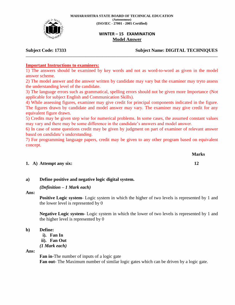
MAHARASHTRA STATE BOARD OF TECHNICAL EDUCATION (Autonomous)
(ISO/IEC - 27001 - 2005 Certified)
WINTER – 15 EXAMINATION
Model Answer
Subject Code: 17333 Subject Name: DIGITAL TECHNIQUES
____________________________________________________________________________________________________
Important Instructions to examiners:
1) The answers should be examined by key words and not as word-to-word as given in the model
answer scheme.
2) The model answer and the answer written by candidate may vary but the examiner may tryto assess
the understanding level of the candidate.
3) The language errors such as grammatical, spelling errors should not be given more Importance (Not
applicable for subject English and Communication Skills).
4) While assessing figures, examiner may give credit for principal components indicated in the figure.
The figures drawn by candidate and model answer may vary. The examiner may give credit for any
equivalent figure drawn.
5) Credits may be given step wise for numerical problems. In some cases, the assumed constant values
may vary and there may be some difference in the candidate’s answers and model answer.
6) In case of some questions credit may be given by judgment on part of examiner of relevant answer
based on candidate’s understanding.
7) For programming language papers, credit may be given to any other program based on equivalent
concept.
Marks
1. A) Attempt any six: 12
a) Define positive and negative logic digital system.
(Definition – 1 Mark each)
Ans:
Positive Logic system- Logic system in which the higher of two levels is represented by 1 and
the lower level is represented by 0
Negative Logic system- Logic system in which the lower of two levels is represented by 1 and
the higher level is represented by 0
b) Define:
i). Fan In
ii). Fan Out
(1 Mark each)
Ans:
Fan in-The number of inputs of a logic gate
Fan out- The Maximum number of similar logic gates which can be driven by a logic gate.
MAHARASHTRA STATE BOARD OF TECHNICAL EDUCATION (Autonomous)
(ISO/IEC - 27001 - 2005 Certified)
WINTER – 15 EXAMINATION
Model Answer
Subject Code: 17333 Subject Name: DIGITAL TECHNIQUES
____________________________________________________________________________________________________
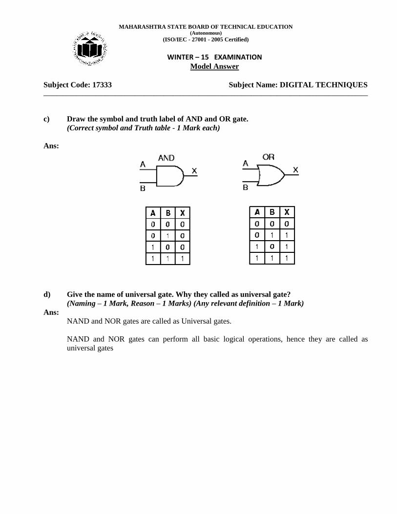
c) Draw the symbol and truth label of AND and OR gate.
(Correct symbol and Truth table - 1 Mark each)
Ans:
d) Give the name of universal gate. Why they called as universal gate?
(Naming – 1 Mark, Reason – 1 Marks) (Any relevant definition – 1 Mark)
Ans: NAND and NOR gates are called as Universal gates.
NAND and NOR gates can perform all basic logical operations, hence they are called as
universal gates
MAHARASHTRA STATE BOARD OF TECHNICAL EDUCATION (Autonomous)
(ISO/IEC - 27001 - 2005 Certified)
WINTER – 15 EXAMINATION
Model Answer
Subject Code: 17333 Subject Name: DIGITAL TECHNIQUES
____________________________________________________________________________________________________
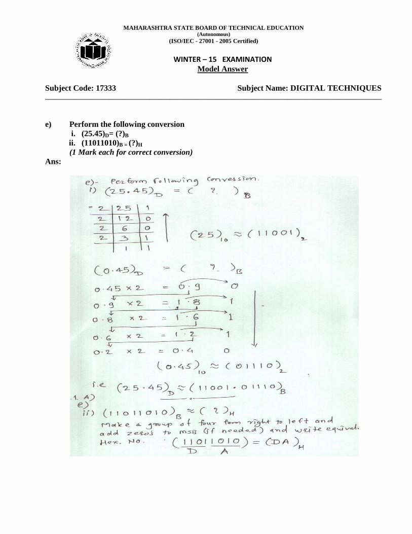
e) Perform the following conversion
i. (25.45)D= (?)B
ii. (11011010)B = (?)H
(1 Mark each for correct conversion)
Ans:
MAHARASHTRA STATE BOARD OF TECHNICAL EDUCATION (Autonomous)
(ISO/IEC - 27001 - 2005 Certified)
WINTER – 15 EXAMINATION
Model Answer
Subject Code: 17333 Subject Name: DIGITAL TECHNIQUES
____________________________________________________________________________________________________
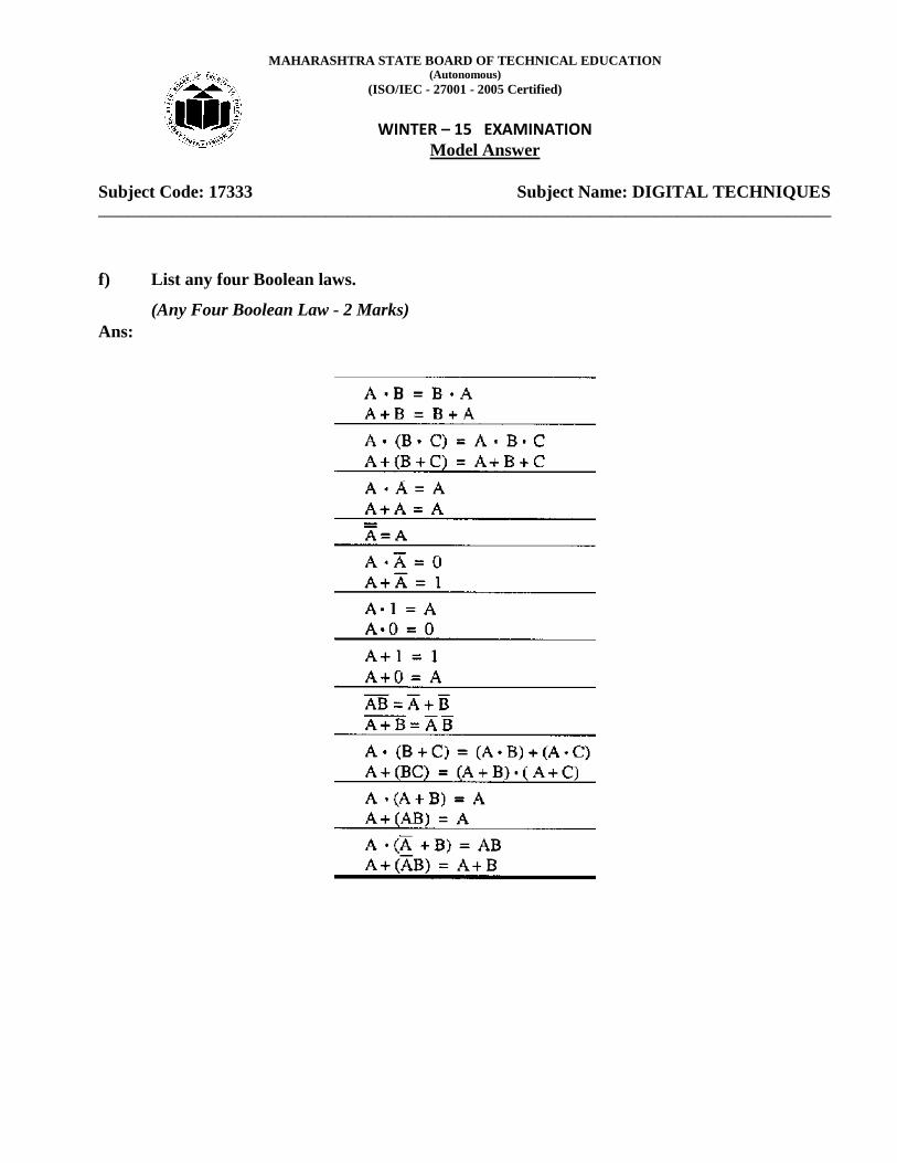
f) List any four Boolean laws.
(Any Four Boolean Law - 2 Marks)
Ans:
MAHARASHTRA STATE BOARD OF TECHNICAL EDUCATION (Autonomous)
(ISO/IEC - 27001 - 2005 Certified)
WINTER – 15 EXAMINATION
Model Answer
Subject Code: 17333 Subject Name: DIGITAL TECHNIQUES
____________________________________________________________________________________________________
g) Give the function of IC74147 & IC74181.
(Correct function - 1 Mark each)
Ans:
1. IC 74147- Decimal to BCD Encoder.
Encoder IC 74147 converts Decimal number to BCD.
2. IC 74181- Arithmetic Logic Unit (ALU)
ALU IC 74181 performs various Arithmetic and Logical operations.
h) List any two advantages of R-2R ladder DAC.
(Any two advantages - 1 Mark each)
Ans:
1. It is slightly complicated in construction.
2. It requires resistors of only two values, hence easy to build circuit.
3. It can be easily expanded o handle more number of bits by adding more sections of the R-2R
resistors.
4. It requires two resistors per bit
5. Due to small resisters can be fabricated monolithically with high accuracy and stability
MAHARASHTRA STATE BOARD OF TECHNICAL EDUCATION (Autonomous)
(ISO/IEC - 27001 - 2005 Certified)
WINTER – 15 EXAMINATION
Model Answer
Subject Code: 17333 Subject Name: DIGITAL TECHNIQUES
____________________________________________________________________________________________________
B) Attempt any two: 8
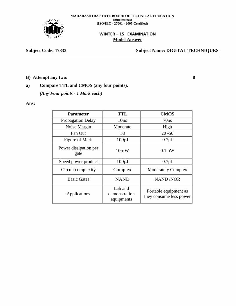
a) Compare TTL and CMOS (any four points).
(Any Four points - 1 Mark each)
Ans:
Parameter TTL CMOS
Propagation Delay 10ns 70ns
Noise Margin Moderate High
Fan Out 10 20 -50
Figure of Merit 100pJ 0.7pJ
Power dissipation per
gate 10mW 0.1mW
Speed power product 100pJ 0.7pJ
Circuit complexity Complex Moderately Complex
Basic Gates NAND NAND /NOR
Applications
Lab and
demonstration
equipments
Portable equipment as
they consume less power
MAHARASHTRA STATE BOARD OF TECHNICAL EDUCATION (Autonomous)
(ISO/IEC - 27001 - 2005 Certified)
WINTER – 15 EXAMINATION
Model Answer
Subject Code: 17333 Subject Name: DIGITAL TECHNIQUES
____________________________________________________________________________________________________
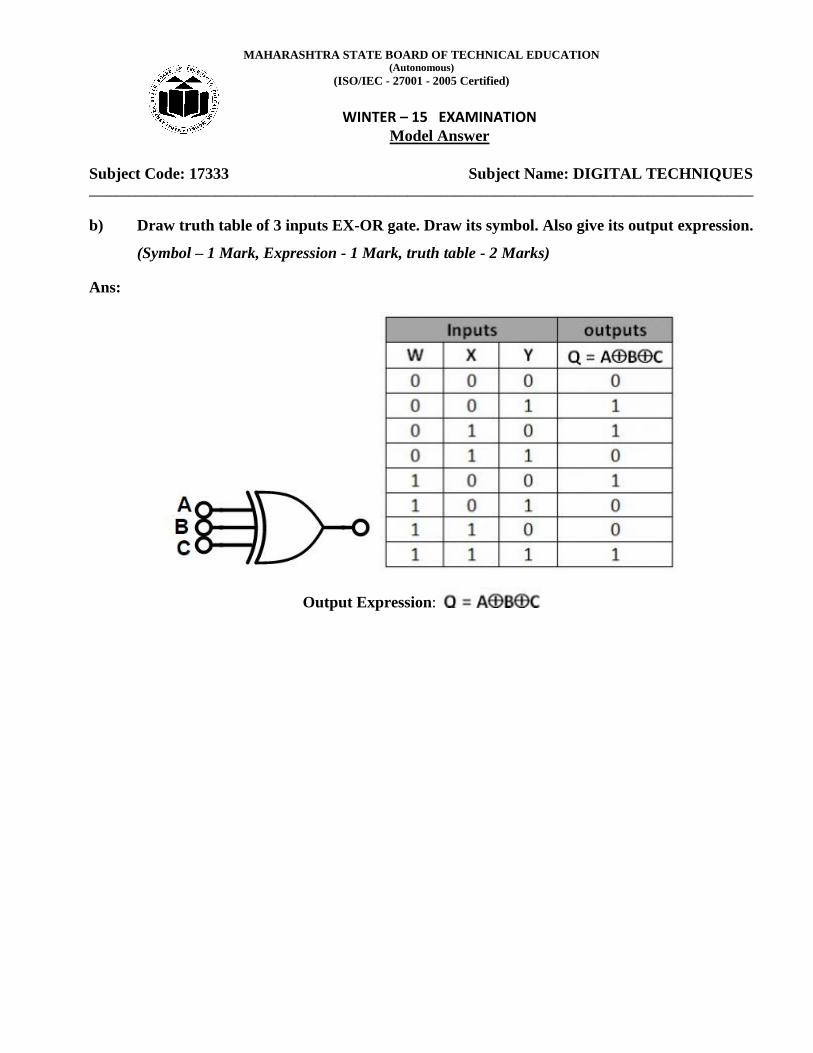
b) Draw truth table of 3 inputs EX-OR gate. Draw its symbol. Also give its output expression.
(Symbol – 1 Mark, Expression - 1 Mark, truth table - 2 Marks)
Ans:
Output Expression:
MAHARASHTRA STATE BOARD OF TECHNICAL EDUCATION (Autonomous)
(ISO/IEC - 27001 - 2005 Certified)
WINTER – 15 EXAMINATION
Model Answer
Subject Code: 17333 Subject Name: DIGITAL TECHNIQUES
____________________________________________________________________________________________________
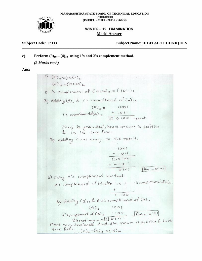
c) Perform (9)10 – (4)10 using 1’s and 2’s complement method.
(2 Marks each)
Ans:

MAHARASHTRA STATE BOARD OF TECHNICAL EDUCATION (Autonomous)
(ISO/IEC - 27001 - 2005 Certified)
WINTER – 15 EXAMINATION
Model Answer
Subject Code: 17333 Subject Name: DIGITAL TECHNIQUES
____________________________________________________________________________________________________
2. Attempt any four: 16
a) Define De-Morgan’s theorem and prove it.
(Theorem – 1 Mark each, Proof/Verification - 1 Mark each)
Ans:
Theorem1: It state that the, complement of a sum is equal to product of complements
Theorem2: It states that, the complement of a product is equal to sum of the complements.
MAHARASHTRA STATE BOARD OF TECHNICAL EDUCATION (Autonomous)
(ISO/IEC - 27001 - 2005 Certified)
WINTER – 15 EXAMINATION
Model Answer
Subject Code: 17333 Subject Name: DIGITAL TECHNIQUES
____________________________________________________________________________________________________
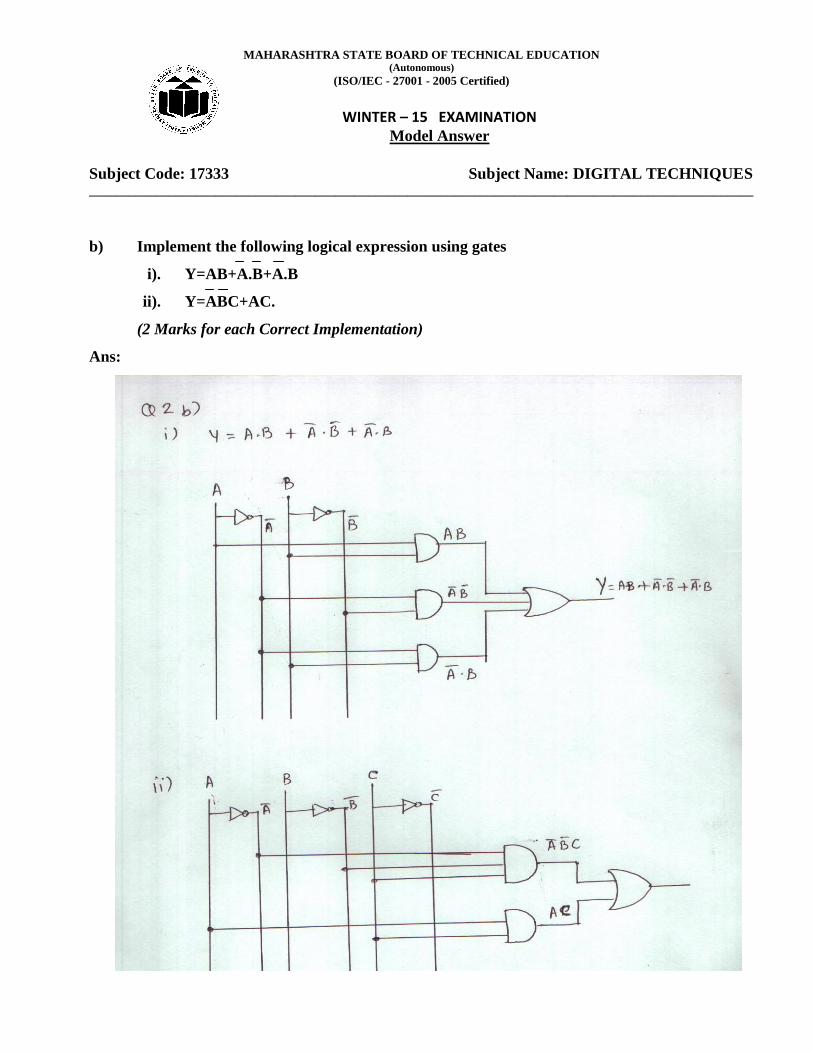
b) Implement the following logical expression using gates
i). Y=AB+A.B+A.B
ii). Y=ABC+AC.
(2 Marks for each Correct Implementation)
Ans:
MAHARASHTRA STATE BOARD OF TECHNICAL EDUCATION (Autonomous)
(ISO/IEC - 27001 - 2005 Certified)
WINTER – 15 EXAMINATION
Model Answer
Subject Code: 17333 Subject Name: DIGITAL TECHNIQUES
____________________________________________________________________________________________________
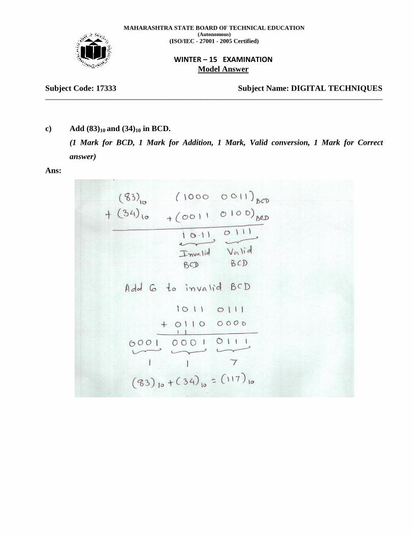
c) Add (83)10 and (34)10 in BCD.
(1 Mark for BCD, 1 Mark for Addition, 1 Mark, Valid conversion, 1 Mark for Correct
answer)
Ans:
MAHARASHTRA STATE BOARD OF TECHNICAL EDUCATION (Autonomous)
(ISO/IEC - 27001 - 2005 Certified)
WINTER – 15 EXAMINATION
Model Answer
Subject Code: 17333 Subject Name: DIGITAL TECHNIQUES
____________________________________________________________________________________________________
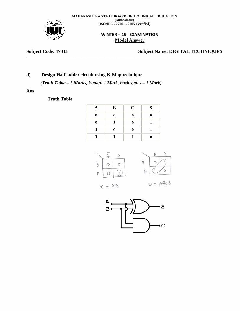
d) Design Half adder circuit using K-Map technique.
(Truth Table – 2 Marks, k-map- 1 Mark, basic gates – 1 Mark)
Ans:
Truth Table
A B C S
o o o o
o 1 o 1
1 o o 1
1 1 1 o
MAHARASHTRA STATE BOARD OF TECHNICAL EDUCATION (Autonomous)
(ISO/IEC - 27001 - 2005 Certified)
WINTER – 15 EXAMINATION
Model Answer
Subject Code: 17333 Subject Name: DIGITAL TECHNIQUES
____________________________________________________________________________________________________
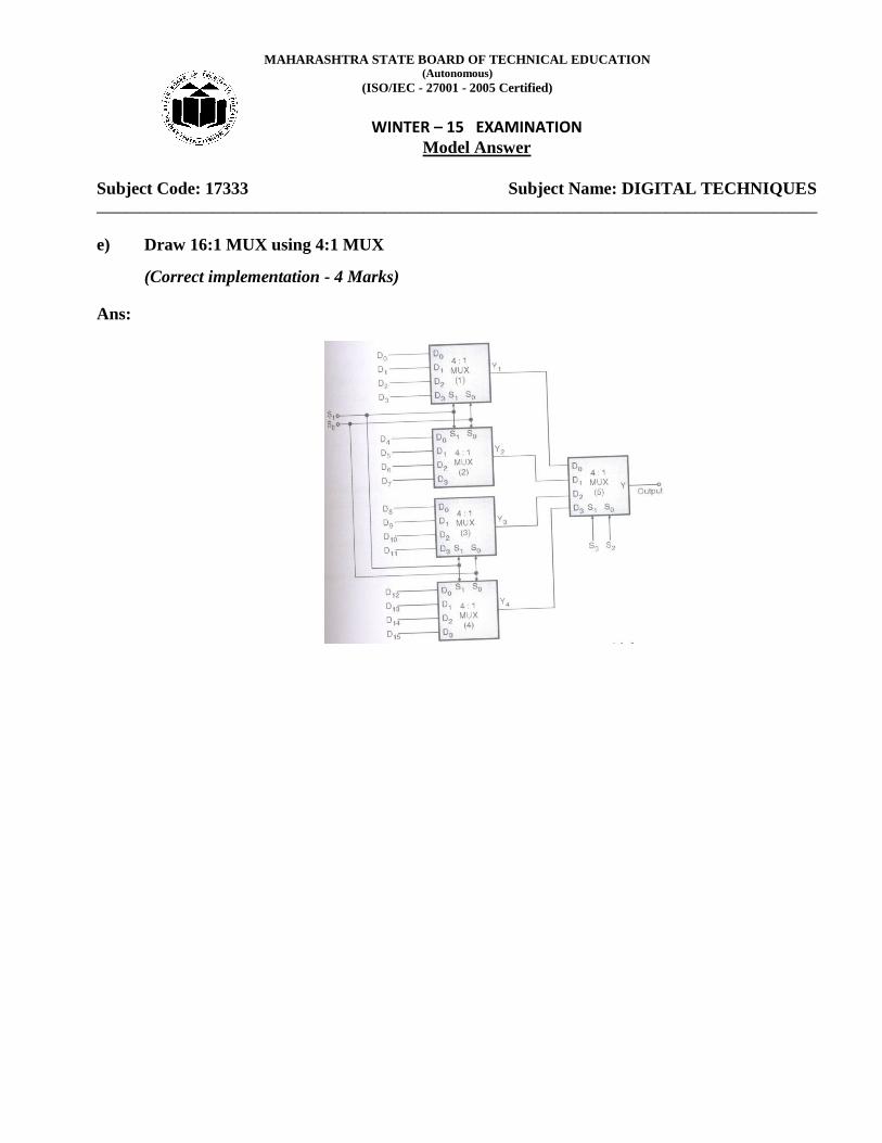
e) Draw 16:1 MUX using 4:1 MUX
(Correct implementation - 4 Marks)
Ans:
MAHARASHTRA STATE BOARD OF TECHNICAL EDUCATION (Autonomous)
(ISO/IEC - 27001 - 2005 Certified)
WINTER – 15 EXAMINATION
Model Answer
Subject Code: 17333 Subject Name: DIGITAL TECHNIQUES
____________________________________________________________________________________________________
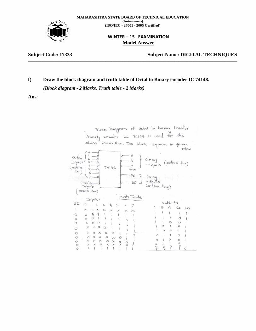
f) Draw the block diagram and truth table of Octal to Binary encoder IC 74148.
(Block diagram - 2 Marks, Truth table - 2 Marks)
Ans:
MAHARASHTRA STATE BOARD OF TECHNICAL EDUCATION (Autonomous)
(ISO/IEC - 27001 - 2005 Certified)
WINTER – 15 EXAMINATION
Model Answer
Subject Code: 17333 Subject Name: DIGITAL TECHNIQUES
____________________________________________________________________________________________________
3. Attempt any four : 16
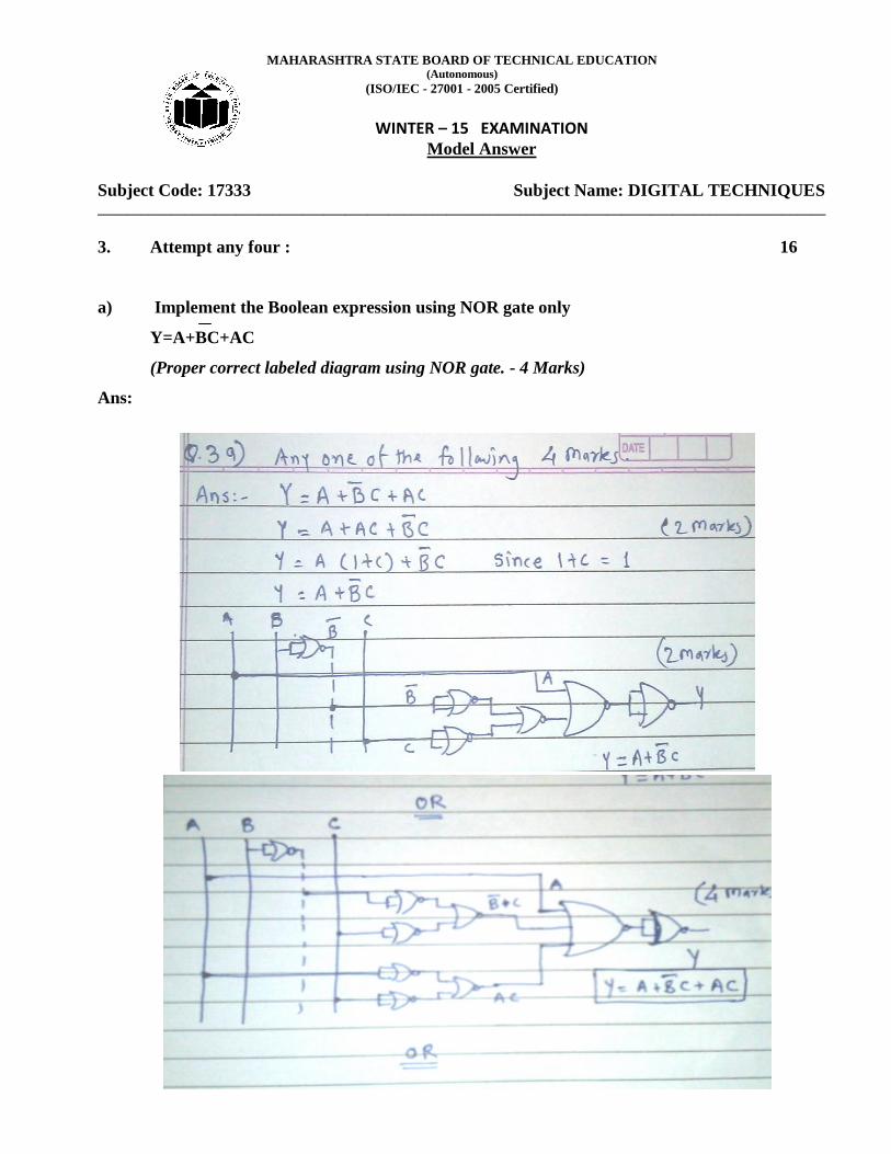
a) Implement the Boolean expression using NOR gate only
Y=A+BC+AC
(Proper correct labeled diagram using NOR gate. - 4 Marks)
Ans:
MAHARASHTRA STATE BOARD OF TECHNICAL EDUCATION (Autonomous)
(ISO/IEC - 27001 - 2005 Certified)
WINTER – 15 EXAMINATION
Model Answer
Subject Code: 17333 Subject Name: DIGITAL TECHNIQUES
____________________________________________________________________________________________________
OR
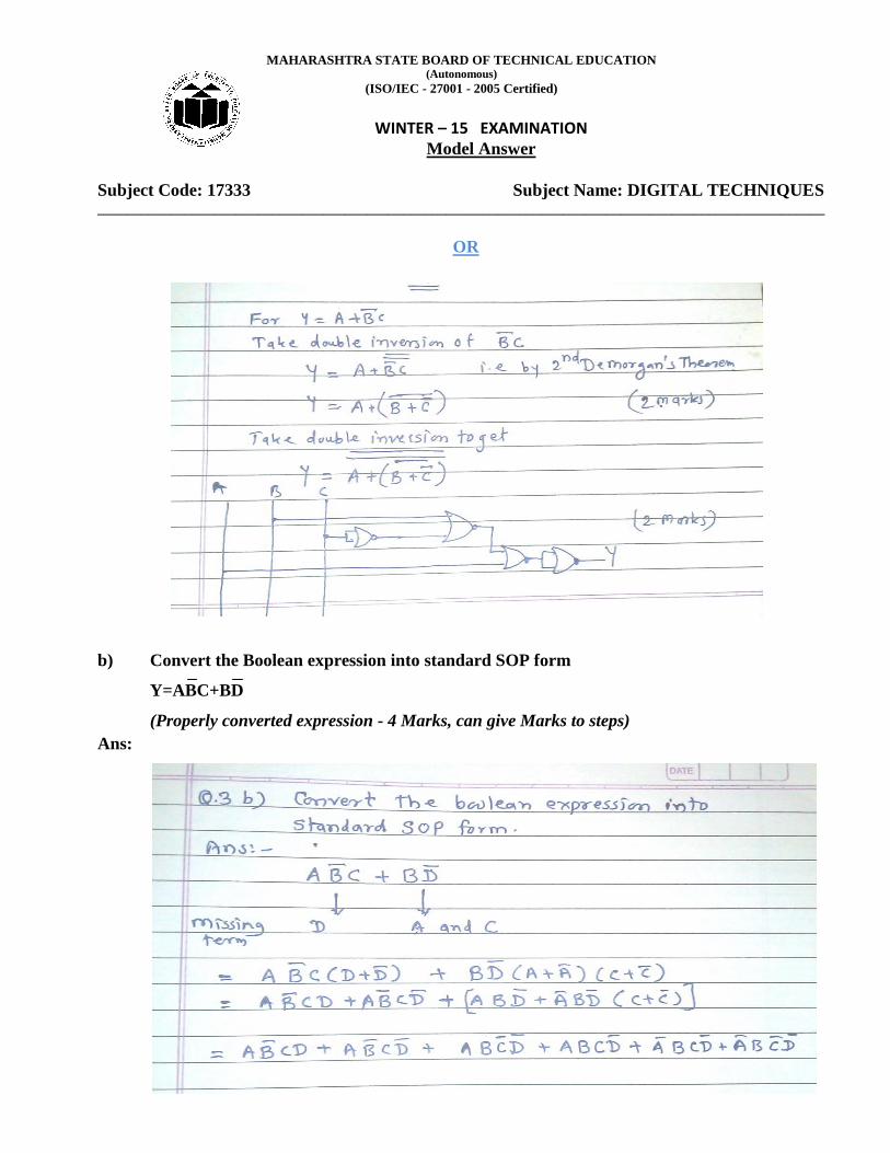
b) Convert the Boolean expression into standard SOP form
Y=ABC+BD
(Properly converted expression - 4 Marks, can give Marks to steps)
Ans:
MAHARASHTRA STATE BOARD OF TECHNICAL EDUCATION (Autonomous)
(ISO/IEC - 27001 - 2005 Certified)
WINTER – 15 EXAMINATION
Model Answer
Subject Code: 17333 Subject Name: DIGITAL TECHNIQUES
____________________________________________________________________________________________________
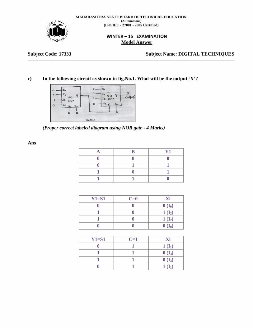
c) In the following circuit as shown in fig.No.1. What will be the output ‘X’?
(Proper correct labeled diagram using NOR gate - 4 Marks)
Ans
A B Y1
0 0 0
0 1 1
1 0 1
1 1 0
Y1=S1 C=0 Xi
0 0 0 (I0)
1 0 1 (I2)
1 0 1 (I2)
0 0 0 (I0)
Y1=S1 C=1 Xi
0 1 1 (I1)
1 1 0 (I3)
1 1 0 (I3)
0 1 1 (I1)
MAHARASHTRA STATE BOARD OF TECHNICAL EDUCATION (Autonomous)
(ISO/IEC - 27001 - 2005 Certified)
WINTER – 15 EXAMINATION
Model Answer
Subject Code: 17333 Subject Name: DIGITAL TECHNIQUES
____________________________________________________________________________________________________
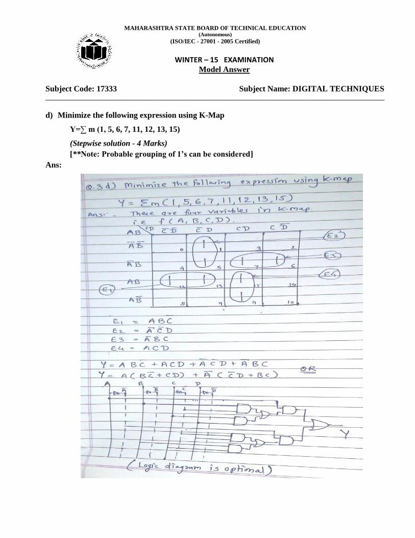
d) Minimize the following expression using K-Map
Y=∑ m (1, 5, 6, 7, 11, 12, 13, 15)
(Stepwise solution - 4 Marks)
[**Note: Probable grouping of 1’s can be considered]
Ans:

MAHARASHTRA STATE BOARD OF TECHNICAL EDUCATION (Autonomous)
(ISO/IEC - 27001 - 2005 Certified)
WINTER – 15 EXAMINATION
Model Answer
Subject Code: 17333 Subject Name: DIGITAL TECHNIQUES
____________________________________________________________________________________________________
e) Give any four differences between combinational and sequential logical circuit.
(Any 4 points can be considered - 1 Mark for each difference point)
Ans:
Combinational Circuit Sequential Circuit
1 Here the output at any instant of
time depends upon the inputs
present at that instant
Here the output at any instant of time
depends upon the inputs present as well as
past input/outputs.
2 Memory element is not required Memory element is required to provide
previous input ,,outputs
3 i.e. Adder, Subtractor, Multiplexer,
De-multiplexer, Code converters
i.e. Flip-flop, Shift registers, counters
4 As there is no memory element
previous state of input does not
have any effect on present state of
the circuit.
Memory element is included in feedback
path.
5 The sequence in which the inputs
are being applied has no effect on
the output of combinational circuit.
The sequence in which the inputs are
being applied should be maintained as
output depends on previous state of circuit
6 Clock input is not required Click input required
MAHARASHTRA STATE BOARD OF TECHNICAL EDUCATION (Autonomous)
(ISO/IEC - 27001 - 2005 Certified)
WINTER – 15 EXAMINATION
Model Answer
Subject Code: 17333 Subject Name: DIGITAL TECHNIQUES
____________________________________________________________________________________________________
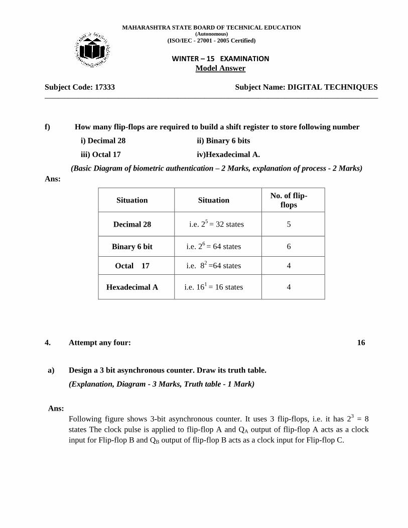
f) How many flip-flops are required to build a shift register to store following number
i) Decimal 28 ii) Binary 6 bits
iii) Octal 17 iv)Hexadecimal A.
(Basic Diagram of biometric authentication – 2 Marks, explanation of process - 2 Marks)
Ans:
Situation Situation No. of flip-
flops
Decimal 28 i.e. 25
= 32 states 5
Binary 6 bit i.e. 26
= 64 states 6
Octal 17 i.e. 82
=64 states 4
Hexadecimal A i.e. 161
= 16 states 4
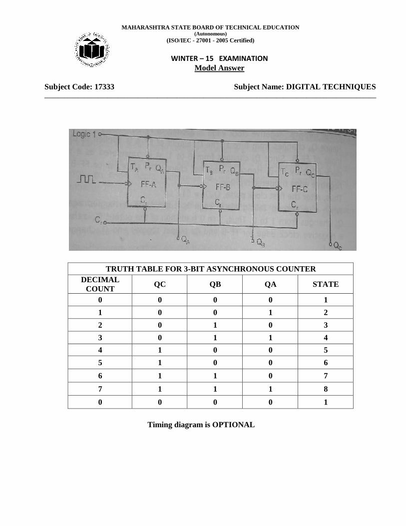
4. Attempt any four: 16
a) Design a 3 bit asynchronous counter. Draw its truth table.
(Explanation, Diagram - 3 Marks, Truth table - 1 Mark)
Ans:
Following figure shows 3-bit asynchronous counter. It uses 3 flip-flops, i.e. it has 23 = 8
states The clock pulse is applied to flip-flop A and QA output of flip-flop A acts as a clock
input for Flip-flop B and QB output of flip-flop B acts as a clock input for Flip-flop C.
MAHARASHTRA STATE BOARD OF TECHNICAL EDUCATION (Autonomous)
(ISO/IEC - 27001 - 2005 Certified)
WINTER – 15 EXAMINATION
Model Answer
Subject Code: 17333 Subject Name: DIGITAL TECHNIQUES
____________________________________________________________________________________________________
TRUTH TABLE FOR 3-BIT ASYNCHRONOUS COUNTER
DECIMAL
COUNT QC QB QA STATE
0 0 0 0 1
1 0 0 1 2
2 0 1 0 3
3 0 1 1 4
4 1 0 0 5
5 1 0 0 6
6 1 1 0 7
7 1 1 1 8
0 0 0 0 1
Timing diagram is OPTIONAL
MAHARASHTRA STATE BOARD OF TECHNICAL EDUCATION (Autonomous)
(ISO/IEC - 27001 - 2005 Certified)
WINTER – 15 EXAMINATION
Model Answer
Subject Code: 17333 Subject Name: DIGITAL TECHNIQUES
____________________________________________________________________________________________________
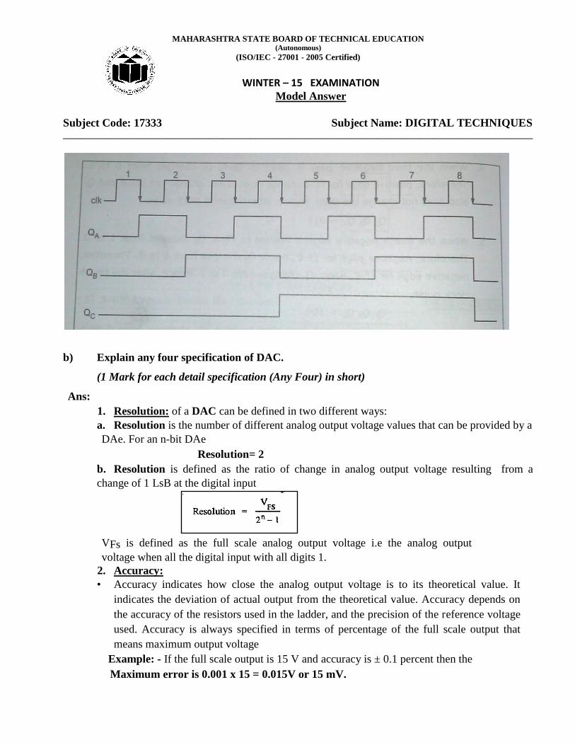
b) Explain any four specification of DAC.
(1 Mark for each detail specification (Any Four) in short)
Ans:
1. Resolution: of a DAC can be defined in two different ways:
a. Resolution is the number of different analog output voltage values that can be provided by a
DAe. For an n-bit DAe
Resolution= 2
b. Resolution is defined as the ratio of change in analog output voltage resulting from a
change of 1 LsB at the digital input
VFs is defined as the full scale analog output voltage i.e the analog output
voltage when all the digital input with all digits 1.
2. Accuracy:
• Accuracy indicates how close the analog output voltage is to its theoretical value. It
indicates the deviation of actual output from the theoretical value. Accuracy depends on
the accuracy of the resistors used in the ladder, and the precision of the reference voltage
used. Accuracy is always specified in terms of percentage of the full scale output that
means maximum output voltage
Example: - If the full scale output is 15 V and accuracy is ± 0.1 percent then the
Maximum error is 0.001 x 15 = 0.015V or 15 mV.

MAHARASHTRA STATE BOARD OF TECHNICAL EDUCATION (Autonomous)
(ISO/IEC - 27001 - 2005 Certified)
WINTER – 15 EXAMINATION
Model Answer
Subject Code: 17333 Subject Name: DIGITAL TECHNIQUES
____________________________________________________________________________________________________
3. Linearity:
The relation between the digital input and analog output should be linear.
However practically it is not so due to the error in the values of resistors used for the
resistive networks.
4. Temperature sensitivity:
The analog output voltage of D to A converter should not change due to changes in
temperature.
But practically the output is a function of temperature. It is so because the resistance
values and OPAMP parameters change with changes in temperature.
5. Settling time:
The time required to settle the analog output within the final value, after the change in
digital input is called as settling time.
The settling time should be as short as possible.
6. Long term drift
Long term drift are mainly due to resistor and semiconductor aging and can affect all the
characteristics.
Characteristics mainly affected are linearity, speed etc.
7. Supply rejection
Supply rejection indicates the ability of DAe to maintain scale, linearity and other
important characteristics when the supply voltage is varied.
supply rejection is usually specified as percentage of full scale change at or near full scale
voltage at 25oe
8. Speed:
It is defined as the time needed to perform a conversion from digital to analog.
It is also defined as the number of conversions that can be performed per second.
The speed of DAC should be as high as possible

MAHARASHTRA STATE BOARD OF TECHNICAL EDUCATION (Autonomous)
(ISO/IEC - 27001 - 2005 Certified)
WINTER – 15 EXAMINATION
Model Answer
Subject Code: 17333 Subject Name: DIGITAL TECHNIQUES
____________________________________________________________________________________________________
Page 24 of 42
c) Draw clock signal. Explain various triggering methods.
(Clock signal - 1 Mark, each triggering method 1 and ½ Mark each)
Ans:
MAHARASHTRA STATE BOARD OF TECHNICAL EDUCATION (Autonomous)
(ISO/IEC - 27001 - 2005 Certified)
WINTER – 15 EXAMINATION
Model Answer
Subject Code: 17333 Subject Name: DIGITAL TECHNIQUES
____________________________________________________________________________________________________
Page 25 of 42
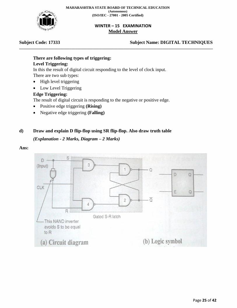
There are following types of triggering:
Level Triggering:
In this the result of digital circuit responding to the level of clock input.
There are two sub types:
High level triggering
Low Level Triggering
Edge Triggering:
The result of digital circuit is responding to the negative or positive edge.
Positive edge triggering (Rising)
Negative edge triggering (Falling)
d) Draw and explain D flip-flop using SR flip-flop. Also draw truth table
(Explanation - 2 Marks, Diagram – 2 Marks)
Ans:
MAHARASHTRA STATE BOARD OF TECHNICAL EDUCATION (Autonomous)
(ISO/IEC - 27001 - 2005 Certified)
WINTER – 15 EXAMINATION
Model Answer
Subject Code: 17333 Subject Name: DIGITAL TECHNIQUES
____________________________________________________________________________________________________
Page 26 of 42
Due to Inverter S and R will always be the complements of each other hence S=R=0 or S=R=1
conditions never appear.
D S R Qn+1 Qn+1
0 0 1 0 1
1 1 0 1 0
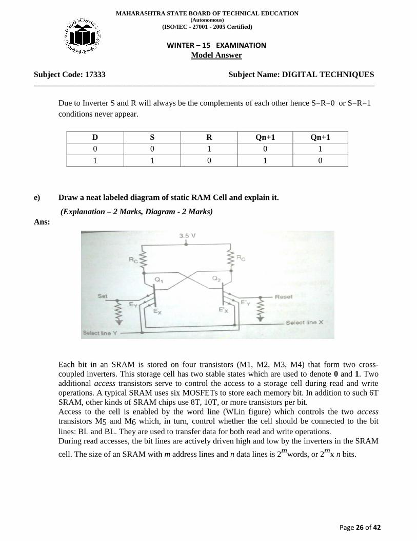
e) Draw a neat labeled diagram of static RAM Cell and explain it.
(Explanation – 2 Marks, Diagram - 2 Marks)
Ans:
Each bit in an SRAM is stored on four transistors (M1, M2, M3, M4) that form two cross-
coupled inverters. This storage cell has two stable states which are used to denote 0 and 1. Two
additional access transistors serve to control the access to a storage cell during read and write
operations. A typical SRAM uses six MOSFETs to store each memory bit. In addition to such 6T
SRAM, other kinds of SRAM chips use 8T, 10T, or more transistors per bit.
Access to the cell is enabled by the word line (WLin figure) which controls the two access
transistors M5 and M6 which, in turn, control whether the cell should be connected to the bit
lines: BL and BL. They are used to transfer data for both read and write operations.
During read accesses, the bit lines are actively driven high and low by the inverters in the SRAM
cell. The size of an SRAM with m address lines and n data lines is 2m
words, or 2m
x n bits.
MAHARASHTRA STATE BOARD OF TECHNICAL EDUCATION (Autonomous)
(ISO/IEC - 27001 - 2005 Certified)
WINTER – 15 EXAMINATION
Model Answer
Subject Code: 17333 Subject Name: DIGITAL TECHNIQUES
____________________________________________________________________________________________________
Page 27 of 42
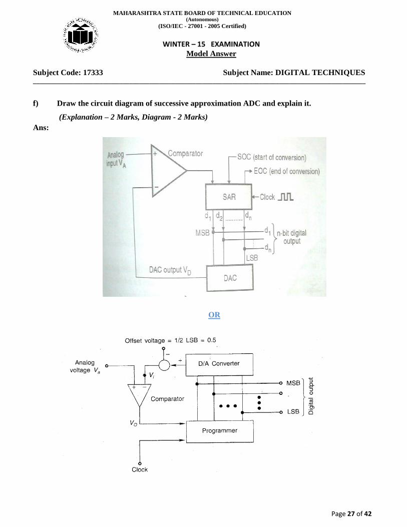
f) Draw the circuit diagram of successive approximation ADC and explain it.
(Explanation – 2 Marks, Diagram - 2 Marks)
Ans:
OR
MAHARASHTRA STATE BOARD OF TECHNICAL EDUCATION (Autonomous)
(ISO/IEC - 27001 - 2005 Certified)
WINTER – 15 EXAMINATION
Model Answer
Subject Code: 17333 Subject Name: DIGITAL TECHNIQUES
____________________________________________________________________________________________________
Page 28 of 42
Working: The comparator serves the function of the scale, the output of which is used for setting
/ resetting the bits at the output of the programmer. This output is converted into equivalent
analog voltage from which offset is subtracted and then applied to the inverting input terminal of
the comparator. The outputs of the programmer will change only when the clock pulse is present.
To start the conversion, the programmer sets the MSB to 1 and all other bits to O. This is
converted into analog voltage by the DAC and the comparator compares it with the analog input
voltage. If the analog input voltage Va >= Vi, the output voltage of the comparator is HIGH,
which sets the next bit also. On the other hand if Va <= Vi, Then the output of the comparator is
LOW which resets the MSB and sets the next bit. Thus a 1 is tried in each bit of DAC until the
binary equivalent of analog input voltage is obtained.
5. Attempt any four: 16
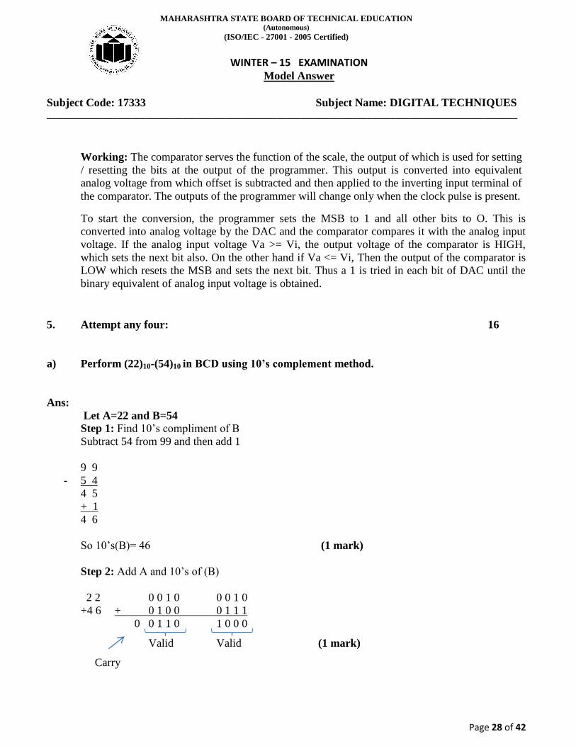
a) Perform (22)10-(54)10 in BCD using 10’s complement method.
Ans:
Let A=22 and B=54
Step 1: Find 10’s compliment of B
Subtract 54 from 99 and then add 1
9 9
- 5 4
4 5
+ 1
4 6
So 10’s(B)= 46 (1 mark)
Step 2: Add A and 10’s of (B)
2 2 0 0 1 0 0 0 1 0
+4 6 + 0 1 0 0 0 1 1 1
0 0 1 1 0 1 0 0 0
Valid Valid (1 mark)
Carry
MAHARASHTRA STATE BOARD OF TECHNICAL EDUCATION (Autonomous)
(ISO/IEC - 27001 - 2005 Certified)
WINTER – 15 EXAMINATION
Model Answer
Subject Code: 17333 Subject Name: DIGITAL TECHNIQUES
____________________________________________________________________________________________________
Page 29 of 42
Step 3: As carry generated is Zero, The answer is in negative form and not in its true form so we
have to take its 10’s Compliment
1 0 0 1 1 0 0 1
0 1 1 0 1 0 0 0
0 0 1 1 0 0 0 1
+ 1
0 0 1 1 0 0 1 0
- 3 2 (2 mark)
So, (22)10 – (54)10 = (-32)10
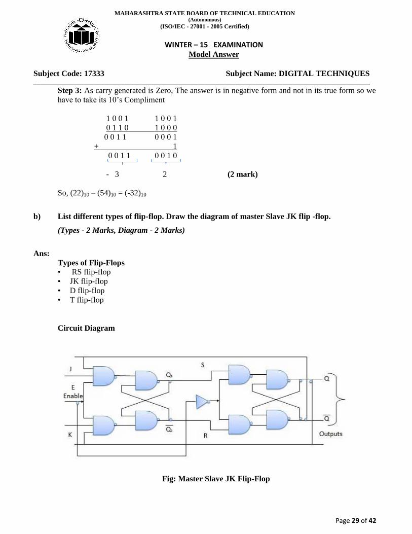
b) List different types of flip-flop. Draw the diagram of master Slave JK flip -flop.
(Types - 2 Marks, Diagram - 2 Marks)
Ans:
Types of Flip-Flops
• RS flip-flop
• JK flip-flop
• D flip-flop
• T flip-flop
Circuit Diagram
Fig: Master Slave JK Flip-Flop
MAHARASHTRA STATE BOARD OF TECHNICAL EDUCATION (Autonomous)
(ISO/IEC - 27001 - 2005 Certified)
WINTER – 15 EXAMINATION
Model Answer
Subject Code: 17333 Subject Name: DIGITAL TECHNIQUES
____________________________________________________________________________________________________
Page 30 of 42
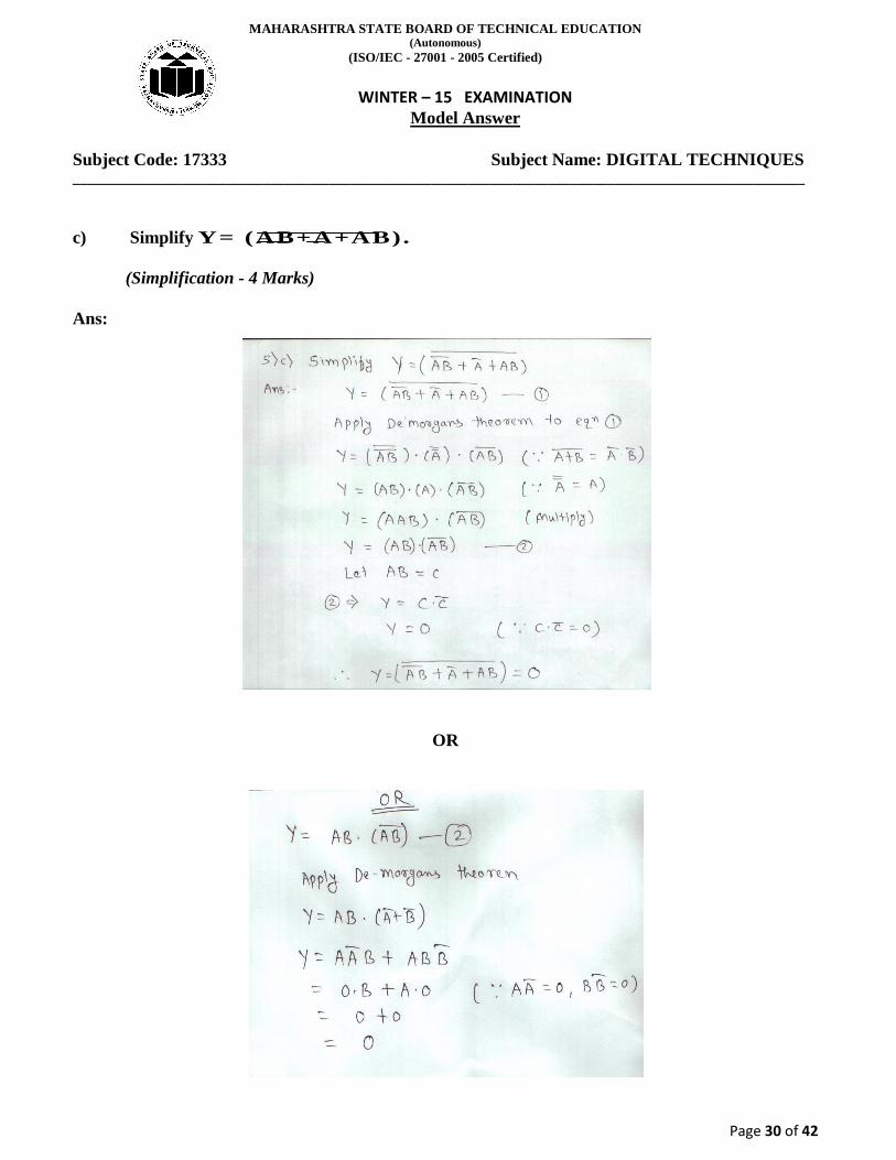
c) Simplify Y= (AB+A+AB).
(Simplification - 4 Marks)
Ans:
OR
MAHARASHTRA STATE BOARD OF TECHNICAL EDUCATION (Autonomous)
(ISO/IEC - 27001 - 2005 Certified)
WINTER – 15 EXAMINATION
Model Answer
Subject Code: 17333 Subject Name: DIGITAL TECHNIQUES
____________________________________________________________________________________________________
Page 31 of 42
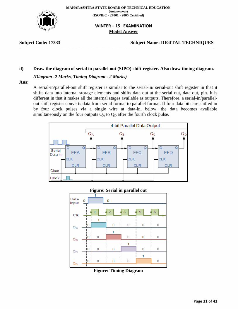
d) Draw the diagram of serial in parallel out (SIPO) shift register. Also draw timing diagram.
(Diagram -2 Marks, Timing Diagram - 2 Marks)
Ans: A serial-in/parallel-out shift register is similar to the serial-in/ serial-out shift register in that it
shifts data into internal storage elements and shifts data out at the serial-out, data-out, pin. It is
different in that it makes all the internal stages available as outputs. Therefore, a serial-in/parallel-
out shift register converts data from serial format to parallel format. If four data bits are shifted in
by four clock pulses via a single wire at data-in, below, the data becomes available
simultaneously on the four outputs QA to QD after the fourth clock pulse.
Figure: Serial in parallel out
Figure: Timing Diagram
MAHARASHTRA STATE BOARD OF TECHNICAL EDUCATION (Autonomous)
(ISO/IEC - 27001 - 2005 Certified)
WINTER – 15 EXAMINATION
Model Answer
Subject Code: 17333 Subject Name: DIGITAL TECHNIQUES
____________________________________________________________________________________________________
Page 32 of 42
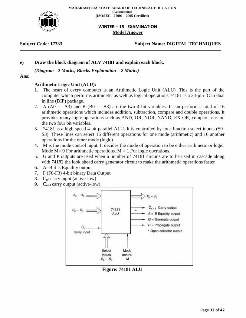
e) Draw the block diagram of ALV 74181 and explain each block.
(Diagram - 2 Marks, Blocks Explanation – 2 Marks)
Ans:
Arithmetic Logic Unit (ALU):
1. The heart of every computer is an Arithmetic Logic Unit (ALU). This is the part of the
computer which performs arithmetic as well as logical operations 74181 is a 24-pin IC in dual
in line (DIP) package.
2. A (A0 — A3) and B (B0 — B3) are the two 4 bit variables. It can perform a total of 16
arithmetic operations which includes addition, subtraction, compare and double operations. It
provides many logic operations such as AND, OR, NOR, NAND, EX-OR, compare, etc. on
the two four bit variables.
3. 74181 is a high speed 4 bit parallel ALU. It is controlled by four function select inputs (S0-
S3). These lines can select 16 different operations for one mode (arithmetic) and 16 another
operations for the other mode (logic).
4. M is the mode control input. It decides the mode of operation to be either arithmetic or logic.
Mode M= 0 For arithmetic operations. M = 1 For logic operations.
5. G and P outputs are used when a number of 74181 circuits are to be used in cascade along
with 74182 the look ahead carry generator circuit to make the arithmetic operations faster
6. A=B it is Equality output
7. F (F0-F3) 4-bit binary Data Output
8. Cn: carry input (active-low)
9. Cn+4 carry output (active-low)
Figure: 74181 ALU
MAHARASHTRA STATE BOARD OF TECHNICAL EDUCATION (Autonomous)
(ISO/IEC - 27001 - 2005 Certified)
WINTER – 15 EXAMINATION
Model Answer
Subject Code: 17333 Subject Name: DIGITAL TECHNIQUES
____________________________________________________________________________________________________
Page 33 of 42
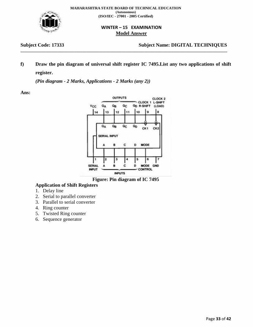
f) Draw the pin diagram of universal shift register IC 7495.List any two applications of shift
register.
(Pin diagram - 2 Marks, Applications - 2 Marks (any 2))
Ans:
Figure: Pin diagram of IC 7495
Application of Shift Registers
1. Delay line
2. Serial to parallel converter
3. Parallel to serial converter
4. Ring counter
5. Twisted Ring counter
6. Sequence generator
MAHARASHTRA STATE BOARD OF TECHNICAL EDUCATION (Autonomous)
(ISO/IEC - 27001 - 2005 Certified)
WINTER – 15 EXAMINATION
Model Answer
Subject Code: 17333 Subject Name: DIGITAL TECHNIQUES
____________________________________________________________________________________________________
Page 34 of 42
6. Attempt any two: 16
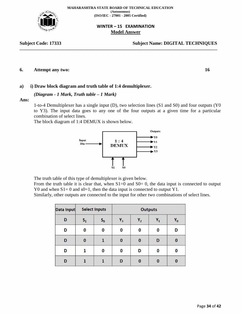
a) i) Draw block diagram and truth table of 1:4 demultiplexer.
(Diagram - 1 Mark, Truth table – 1 Mark)
Ans: 1-to-4 Demultiplexer has a single input (D), two selection lines (S1 and S0) and four outputs (Y0
to Y3). The input data goes to any one of the four outputs at a given time for a particular
combination of select lines.
The block diagram of 1:4 DEMUX is shown below.
The truth table of this type of demultiplexer is given below.
From the truth table it is clear that, when S1=0 and S0= 0, the data input is connected to output
Y0 and when S1= 0 and s0=1, then the data input is connected to output Y1.
Similarly, other outputs are connected to the input for other two combinations of select lines.
MAHARASHTRA STATE BOARD OF TECHNICAL EDUCATION (Autonomous)
(ISO/IEC - 27001 - 2005 Certified)
WINTER – 15 EXAMINATION
Model Answer
Subject Code: 17333 Subject Name: DIGITAL TECHNIQUES
____________________________________________________________________________________________________
Page 35 of 42
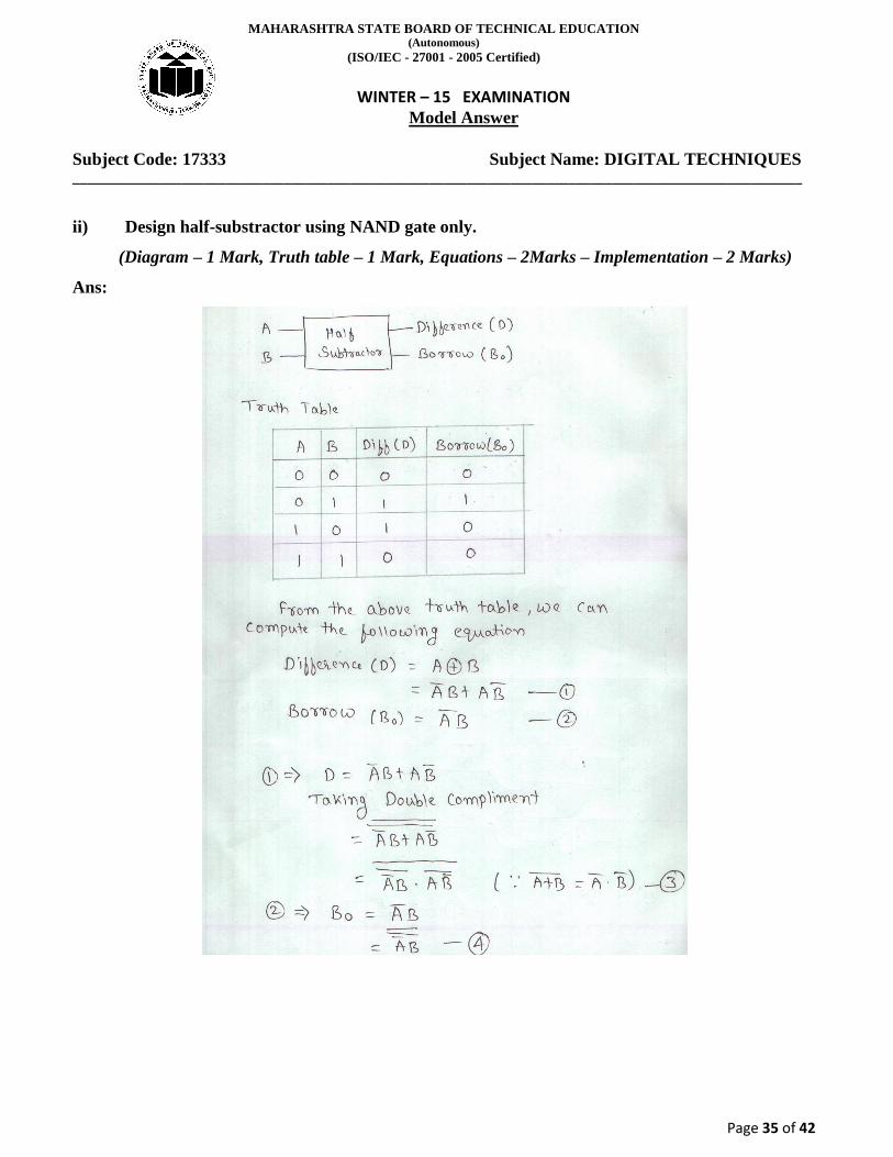
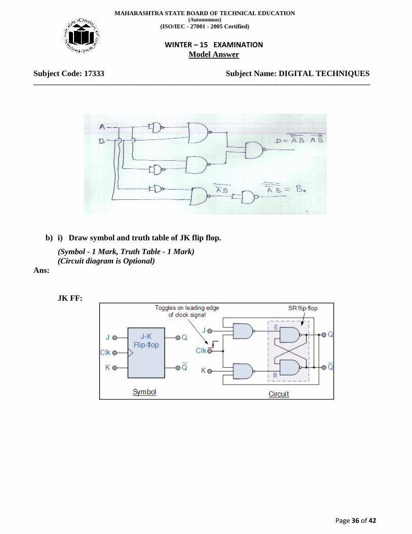
ii) Design half-substractor using NAND gate only.
(Diagram – 1 Mark, Truth table – 1 Mark, Equations – 2Marks – Implementation – 2 Marks)
Ans:
MAHARASHTRA STATE BOARD OF TECHNICAL EDUCATION (Autonomous)
(ISO/IEC - 27001 - 2005 Certified)
WINTER – 15 EXAMINATION
Model Answer
Subject Code: 17333 Subject Name: DIGITAL TECHNIQUES
____________________________________________________________________________________________________
Page 36 of 42
b) i) Draw symbol and truth table of JK flip flop.
(Symbol - 1 Mark, Truth Table - 1 Mark)
(Circuit diagram is Optional)
Ans:
JK FF:
MAHARASHTRA STATE BOARD OF TECHNICAL EDUCATION (Autonomous)
(ISO/IEC - 27001 - 2005 Certified)
WINTER – 15 EXAMINATION
Model Answer
Subject Code: 17333 Subject Name: DIGITAL TECHNIQUES
____________________________________________________________________________________________________
Page 37 of 42
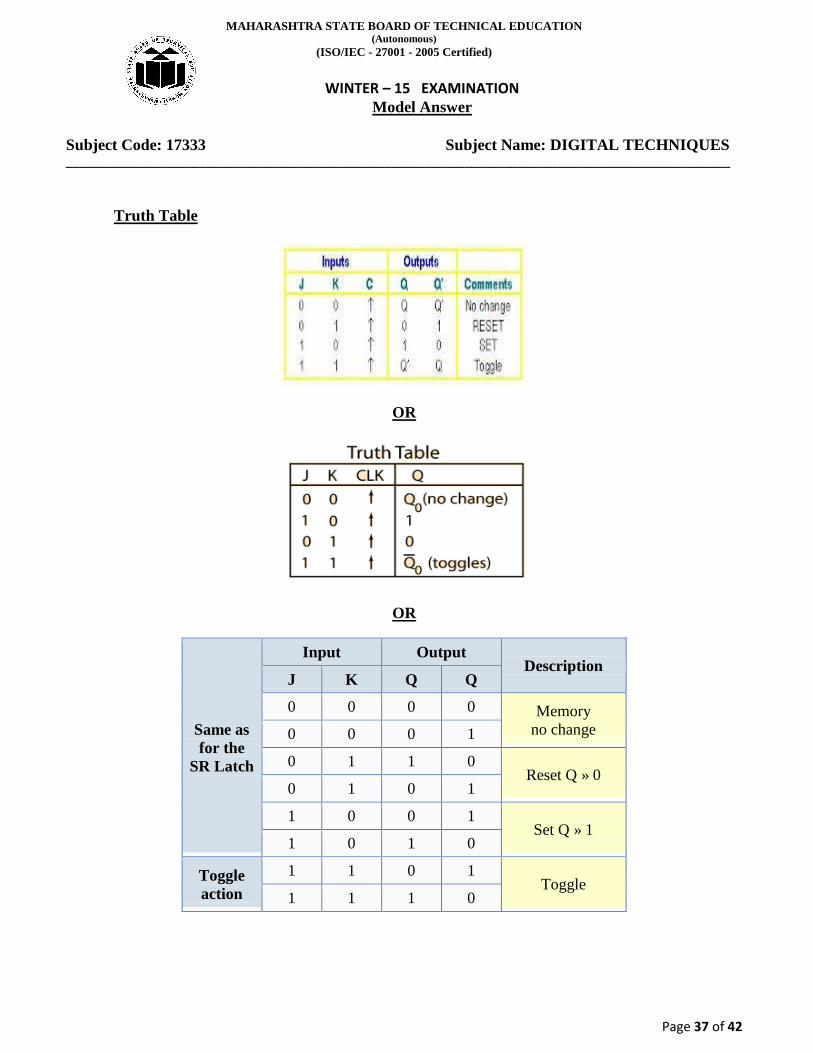
Truth Table
OR
OR
Same as
for the
SR Latch
Input Output Description
J K Q Q
0 0 0 0 Memory
no change 0 0 0 1
0 1 1 0 Reset Q » 0
0 1 0 1
1 0 0 1 Set Q » 1
1 0 1 0
Toggle
action
1 1 0 1 Toggle
1 1 1 0
MAHARASHTRA STATE BOARD OF TECHNICAL EDUCATION (Autonomous)
(ISO/IEC - 27001 - 2005 Certified)
WINTER – 15 EXAMINATION
Model Answer
Subject Code: 17333 Subject Name: DIGITAL TECHNIQUES
____________________________________________________________________________________________________
Page 38 of 42
ii) Define modulus of counter.
(Definition - 2 Marks)
Ans:
Modulus Counter (MOD-N Counter)
Modulus of a counter is the no. of different states through which the counter progress during its
operation. It indicates the no. of states in the counter; pulses to be counted are applied to counter.
The circuit comes back to its starting state after counting N pluses in the case of modulus N
counter.
The 2-bit ripple counter is called as MOD-4 counter and 3-bit ripple counter is called as MOD-8
counter. So in general, an n-bit ripple counter is called as modulo-N counter. Where, MOD
number = 2n.
MAHARASHTRA STATE BOARD OF TECHNICAL EDUCATION (Autonomous)
(ISO/IEC - 27001 - 2005 Certified)
WINTER – 15 EXAMINATION
Model Answer
Subject Code: 17333 Subject Name: DIGITAL TECHNIQUES
____________________________________________________________________________________________________
Page 39 of 42
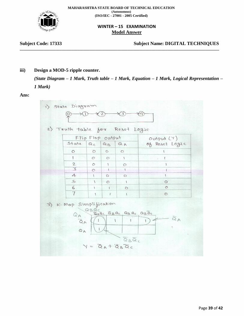
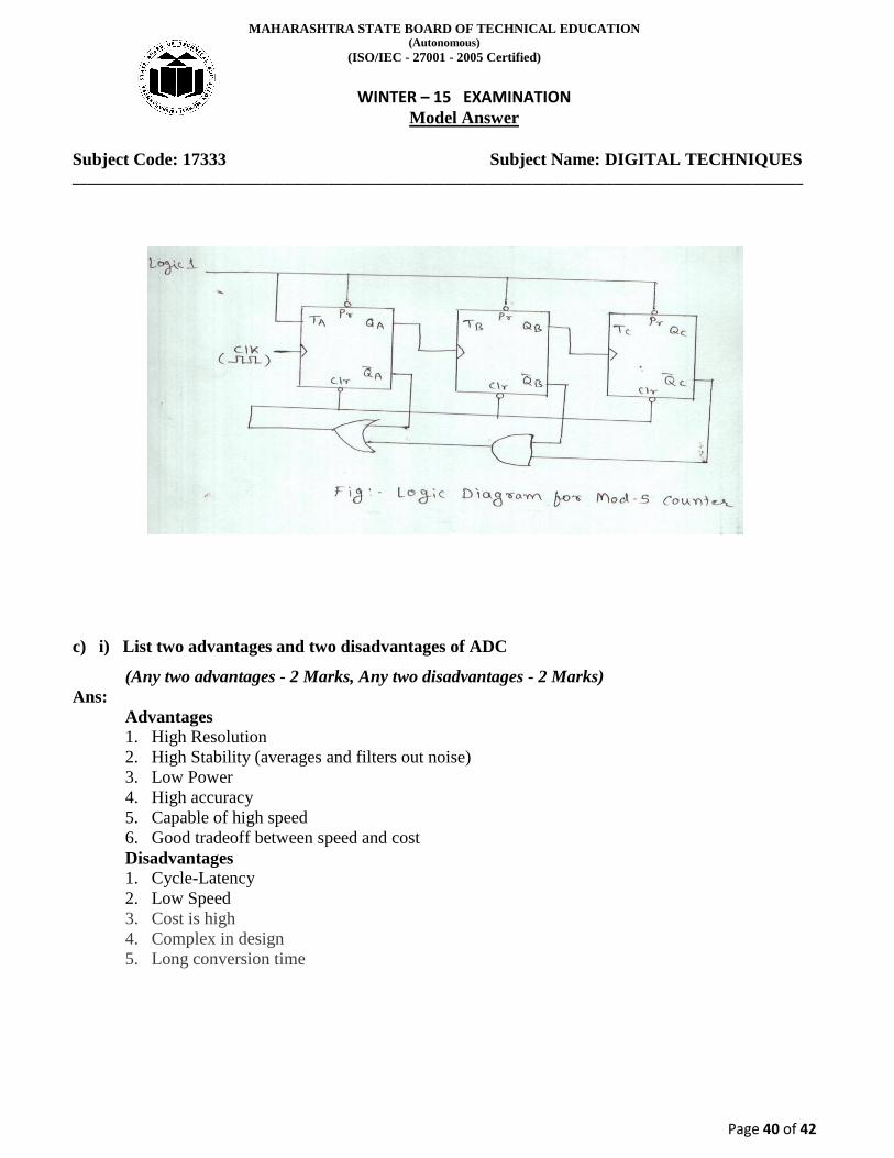
iii) Design a MOD-5 ripple counter.
(State Diagram – 1 Mark, Truth table – 1 Mark, Equation – 1 Mark, Logical Representation –
1 Mark)
Ans:
MAHARASHTRA STATE BOARD OF TECHNICAL EDUCATION (Autonomous)
(ISO/IEC - 27001 - 2005 Certified)
WINTER – 15 EXAMINATION
Model Answer
Subject Code: 17333 Subject Name: DIGITAL TECHNIQUES
____________________________________________________________________________________________________
Page 40 of 42
c) i) List two advantages and two disadvantages of ADC
(Any two advantages - 2 Marks, Any two disadvantages - 2 Marks)
Ans:
Advantages
1. High Resolution
2. High Stability (averages and filters out noise)
3. Low Power
4. High accuracy
5. Capable of high speed
6. Good tradeoff between speed and cost
Disadvantages
1. Cycle-Latency
2. Low Speed
3. Cost is high
4. Complex in design
5. Long conversion time

MAHARASHTRA STATE BOARD OF TECHNICAL EDUCATION (Autonomous)
(ISO/IEC - 27001 - 2005 Certified)
WINTER – 15 EXAMINATION
Model Answer
Subject Code: 17333 Subject Name: DIGITAL TECHNIQUES
____________________________________________________________________________________________________
Page 41 of 42
ii) Draw circuit diagram of weighted register DAC & explain its function.
(Circuit diagram - 2 Marks, Function - 2 Marks)
[**Note: Expressions are Optional]
Ans:
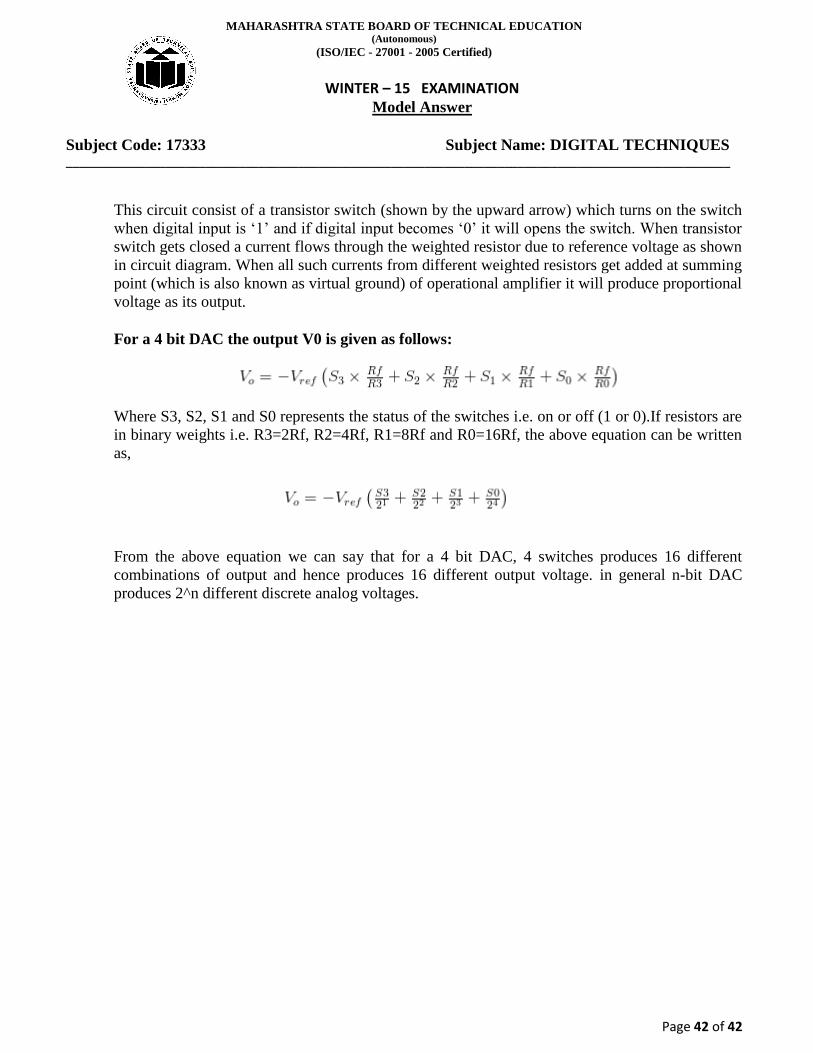
Following figure shows the circuit diagram of weighted resistor DAC. This DAC circuit uses
weighted values of resistor like 2R, 4R, 6R, 8R and so on depending on the digital inputs
available therefore such type of network is known as weighted resistor DAC.
Figure: Weighted Resistor DAC
OR
Figure: Weighted Resistor DAC
MAHARASHTRA STATE BOARD OF TECHNICAL EDUCATION (Autonomous)
(ISO/IEC - 27001 - 2005 Certified)
WINTER – 15 EXAMINATION
Model Answer
Subject Code: 17333 Subject Name: DIGITAL TECHNIQUES
____________________________________________________________________________________________________
Page 42 of 42
This circuit consist of a transistor switch (shown by the upward arrow) which turns on the switch
when digital input is ‘1’ and if digital input becomes ‘0’ it will opens the switch. When transistor
switch gets closed a current flows through the weighted resistor due to reference voltage as shown
in circuit diagram. When all such currents from different weighted resistors get added at summing
point (which is also known as virtual ground) of operational amplifier it will produce proportional
voltage as its output.
For a 4 bit DAC the output V0 is given as follows:
Where S3, S2, S1 and S0 represents the status of the switches i.e. on or off (1 or 0).If resistors are
in binary weights i.e. R3=2Rf, R2=4Rf, R1=8Rf and R0=16Rf, the above equation can be written
as,
From the above equation we can say that for a 4 bit DAC, 4 switches produces 16 different
combinations of output and hence produces 16 different output voltage. in general n-bit DAC
produces 2^n different discrete analog voltages.