Embed Size (px)
Citation preview


Till morfar


List of Papers
This thesis consists of the following papers, which are referred to in the text by their Roman numerals.
I A. Persson, R. Bejhed, H. Nguyen, K. Gunnarsson, B. T. Dal-
slet, F. W. Østerberg, M. F. Hansen, and P. Svedlindh. Low-frequency noise in planar Hall effect bridge sensors. Sensors and Actuators A, submitted.
II A. Persson, R. Bejhed, K. Gunnarsson, H. Nguyen, B. T. Dal-slet, F. W. Østerberg, M. F. Hansen, and P. Svedlindh. Low-frequency picotesla field detection with planar Hall effect bridge sensors, in manuscript.
III A. Persson, G. Thornell, and H. Nguyen. Rapid prototyping of magnetic tunnel junctions with focused ion beam processes. Journal of Micromechanics and Microengineering, 20:055039, 2010. doi: 10.1088/0960-1317/20/5/055039
IV A. Persson, F. Riddar, F. Ericson, H. Nguyen, and G. Thornell. Gallium implantation in a MgO based magnetic tunnel junction with Co60Fe20B20 electrodes. IEEE Transactions on Magnetics, 47:151-155, 2011. doi: 10.1109/TMAG.2010.2089634
V H. Nguyen, A. Persson, and G. Thornell. Material- and fabrica-tion-governed performance of a tunnelling magnetometer. Ad-vances in Natural Sciences: Nanoscience and Nanotechnology, 1:045006, 2010. doi: 10.1088/2043-6262/1/4/045006
VI A. Persson, F. Ericson, G. Thornell, and H. Nguyen. Etch stop technique for patterning of magnetic tunnel junctions for a magnetic field sensor. Journal of Micromechanics and Micro-engineering, 21:045014, 2011. doi: 10.1088/0960-1317/21/4/045014
VII A. Persson, G. Thornell, and H. Nguyen. Radiation tolerance of a spin-dependent tunnelling magnetometer for space applica-tions. Measurement Science and Technology, 22:045204, 2011. doi: 10.1088/0957-0233/22/4/045204
Reprints were made with permission from the respective publishers.

Author’s Contribution to the Publications
Paper I Part of planning and experimental work, most of evaluation and writing
Paper II Most of planning, part of experimental work, most of evalua-
tion and writing Paper III Most of planning, experimental work, evaluation and writing Paper IV Most of planning, experimental work, evaluation and writing Paper V Most of planning, experimental work, and evaluation, minor
part of writing Paper VI Most of planning, experimental work, evaluation and writing Paper VII Most of planning, experimental work, evaluation and writing
Parts of this thesis have been previously published. Papers III, V, VI, and VII are reprinted with kind permission from the Institute of Physics. Paper IV is reprinted with kind permission from Institute of Electrical and Elec-tronics Engineers.

Contents
Introduction.....................................................................................................9
Magnetism ....................................................................................................11
Space.............................................................................................................13 Magnetic fields in space ...........................................................................14 Magnetometers and space hardware in general........................................15
Magnetoresistive sensors ..............................................................................19 Tunnelling magnetoresistance..................................................................20 Planar Hall effect sensors .........................................................................21 Noise ........................................................................................................23
Manufacturing...............................................................................................25 Etching and etch stop monitoring.............................................................28
Electron spectroscopy for chemical analysis .......................................28 Focused ion beam ................................................................................33
Sensors ..........................................................................................................37 Planar Hall effect bridges .........................................................................37 Magnetic tunnel junctions ........................................................................40
Etching and redeposition .....................................................................42 Irradiation ............................................................................................44
Magnetoresistance in space...........................................................................49 Spin-dependent tunnelling magnetometer................................................50 Planar Hall effect magnetometer ..............................................................53
Conclusion ....................................................................................................57
Svensk sammanfattning ................................................................................59
Acknowledgements.......................................................................................63
References.....................................................................................................65

Abbreviations
AFM Antiferromagnetic AMR Anisotropic magnetoresistance at. % Atomic percent CVD Chemical vapour deposition EDS Energy dispersive spectroscopy EPD End-point detection ESA European Space Agency FGM Fluxgate magnetometer FIB Focused ion beam FM Ferromagnetic GMR Giant magnetoresistance MST Microstructure/system technology MTJ Magnetic Tunnel Junction OPM Optically pumped magnetometer PHE Planar Hall effect PHEB Planar Hall effect bridge PSD Power spectral density SCM Search-coil magnetometer SEM Scanning electron microscopy SERF Spin-exchange relaxation-free SIM Scanning ion microscopy SNR Signal-to-noise ratio TEM Transmission electron microscopy TMR Tunnelling magnetoresistance TRL Technology Readiness Level ÅSTC Ångström Space Technology Centre

9
Introduction
Magnetoresistance and space – the latter to many a daunting nothingness, reluctantly appreciated as the backdrop of a moonlight walk, and the former to most at best an empty concept incepted between tailcoats and ball gowns at a long-gone Nobel celebration.
However, during the last decades, our modern community’s increasing dependence on space has become more and more clear to the general public. With the launch of satellite television, communication and global positioning systems, along with the globalization process and the growing concern for our planet’s environmental condition, we have finally started to grasp the concept of Earth being just a small and limited planet, lonely and vulnerable, and not the cornucopia of past perceptions.
Magnetoresistance, on the other hand, may not be of such great signifi-cance to humanity but is still something that most of us unknowingly put to daily use, since it is responsible for reading the information from our com-puter hard drives. The aim of this thesis is to explain why there is a connec-tion between magnetoresistance and space and what remains to be done be-fore they are really compatible.
The work covered by the thesis has been performed as part of PhD studies at the Ångström Space Technology Centre (ÅSTC) at Uppsala University, Sweden. The overall aim of the research conducted by ÅSTC is miniaturiza-tion of instruments and subsystems for large and small spacecrafts, but also for demanding terrestrial applications. The reason why miniaturized devices are desirable to the space industry is primarily money. Launching 1 kg into space costs between 5000 and 10 000 €, hence replacing a heavy instrument with a miniaturized one without reducing the performance is obviously pref-erable. The miniaturization is achieved by employing both traditional engi-neering techniques, and different micro- and nanotechnologies.
This thesis work focused on creating a miniaturized high-end magnetome-ter for space applications. It was early concluded that the traditional magne-tometers were not suitable for miniaturization, and the strategy was instead to apply an already microscopic phenomenon, namely magnetoresistance.
The work consists of seven scientific papers, that require some insight to the fields of microstructuring, magnetism and sensorics to be fully appreci-ated, and this summary, which is not aimed for an expert in the field but rather for someone with a general education in engineering, e.g., a space mission manager looking for magnetic sensors for his or her satellite.


11
Magnetism
The concept of magnetism has been known to man for at least two and a half millennium although the origin of the discovery has been debated. As early as the second millennia BC, the Olmec civilization of Mesoamerica used magnetite – a magnetic iron-oxide ore – for making mirrors and incorporated it in monuments and statues. The Olmecs are known to have had an ad-vanced concept of astronomy and they are attributed to have developed the Mesoamerican calendar, but whether they understood the magnetic proper-ties of the magnetite and were able to use it as, e.g., a compass, remains mystery. [1]
Around the 6th century BC, records of magnetite and of its magnetic prop-erties appear both in Greece and in China. Chinese fortune tellers are known to have used magnetite spoons in their rituals and it was probably from this practice that the first compass was developed. Compasses used for naviga-tional purposes appeared in China in the 11th century AD and spread to In-dia, the Middle East and Europe during the following centuries. The first to demonstrate its full capacity was the Chinese admiral Zheng He, during his seven-ocean voyage in the early 15th century. [2, 3]
Regardless of the compass’s increasing popularity, the origin of magnet-ism remained a mystery until the beginning of the 19th century when Ørsted demonstrated the relationship between electricity and magnetism, and later when Ampère suggested that the magnetic field of a permanent magnet originated from the small current loops inside the material. However, this classical interpretation of magnetism and magnetic materials cannot fully explain all magnetic phenomena, and it was not until the birth of quantum physics that a more comprehensive theory could be formed. [4]
All kinds of magnetism originate from motion of electric charges, e.g. the current through an electromagnetic coil. In a magnetic material, two sources contribute to the magnetism, namely the angular momentum and the spin of the electrons. The angular momentum is basically what Ampere suggested: a magnetic moment is created by an electron orbiting an atomic nucleus. Apart from rotating around the nucleus, the electrons have an internal spin, which, if the electron is regarded as a spinning sphere with the charge localized to the surface, also creates a magnetic moment. In an arbitrary material, these small magnetic moments are not ordered and the overall moment tends to zero. [5]

12
However, in some materials, such as iron, nickel, cobalt and some of the rare earth metals, the magnetic moments of neighboring atoms are naturally aligned to each other. This phenomenon is called ferromagnetism and stems from the quantized energy states of electrons in an atom, overlapping wave functions of electrons in neighboring atoms, and the exchange of electrons between such atoms. It is these exchange interactions that make the magnetic moments of nearby atoms to polarize, i.e. magnetize, in the same direction. The overall magnetization of a ferromagnetic (FM) material still does not have to be in the same direction, but instead magnetic domains with a com-mon internal magnetization are formed. The magnetization of neighboring domains, however, is aligned antiparallel or perpendicular to minimize the energy of the whole system. The structure of these domains and the net magnetization of the whole material can be affected by applying an external magnetic field. By doing so, the domains and the individual magnetic mo-ments will start to align to the field. The magnetization typically has a num-ber of directions along which it prefers to be aligned. These are defined by, e.g., the crystallinity and shape of the material and are called easy axes. The magnetization reversal between different easy axes is associated with mov-ing domains and with hysteresis. There are also directions along which the magnetization does not like to align. These are called hard axes and mag-netization reversal between hard axes directions is associated with rotation of magnetic moments rather than movement of domains. The magnetization can only be kept along a hard axis by applying a magnetic field and once this field is removed, the magnetization instead realigns along an easy axis. This link between a magnetic field and the magnetization of a ferromagnetic ma-terial is the basis for magnetoresistive sensors. [6]
Apart from ferromagnetism, other magnetic phenomena such as anti-ferromagnetism, ferrimagnetism, paramagnetism, superparamagnetism, and diamagnetism exist. Only the first one has bearing on this thesis. The origin of antiferromagnetism is similar to that of ferromagnetism, but in an anti-ferromagnetic (AFM) material, the magnetic moments of neighbouring at-oms are aligned in antiparallel.
An FM and an AMF material can interact with each other via so called FM-AFM exchange coupling, also known as exchange bias, where the mag-netization of the FM material is pinned perpendicularly to the magnetization of the AFM material. Exchange bias is a convenient method for giving a FM material a reference magnetization – an important feature in magnetic sen-sors, Papers I, III, IV, and VI.

13
Space
Although mankind is a newcomer in the universe, space can be regarded as a newcomer to us, since the notion of Earth floating around in an endless, empty space covered in a thin veil of air is only a recent idea in our concep-tual world. The word space itself was introduced by the English poet John Milton in his poem Paradise Lost as late as 1667. Even though the ancient Greeks along with many other early civilizations had a fairly good concept of celestial mechanics, it was with the findings of Brahe, Copernicus, and Newton, the invention of the hot-air balloon by Rozier and Marquis d’Arlandes, and the scientific and industrial revolutions of the 18th and 19th centuries, that space, or outer space as it is also called, became something tangible. The idea of space being actually accessible to mankind was spread to the public in the early 20th century by novels such as “The First Men in the Moon” by H. G. Wells.
The motivation behind the early work on space was our cherished lust for discovery and exploration, but when the idea was realized, it was, as so often in our history, war that was the driving force. The first manmade object to leave the troposphere – the lower layer of the atmosphere – was a German artillery shell during the First World War. The shell was fired from the infa-mous Paris Gun and reached an altitude of about 40 km. Even though this does not qualify as actually entering space with today’s standards, where space begins at an altitude of 100 km according to Fédération Aéronautique Internationale, the Paris Gun was the first to exploit one of the principal properties of space, i.e. the lack of atmospheric drag, greatly extending its range. [7]
The first manmade object to actually reach space was another piece of German military equipment, namely the V2 rocket. This was early in Octo-ber 1942. During World War II, numerous V2 rockets were launched. After the war, both the Soviets and the Americans continued the Nazi rocket pro-gram with help from captured German scientists. The post-war years saw the dawn of scientific space flight. The first scientific space mission was based on a captured V2 rocket, equipped with instruments for studies of cosmic radiation, launched by the United States. Soon after, allegedly, the first life forms – fruit flies along with seeds of rye and cotton – were launched into space. However, the sterility of the early German rockets can be disputed. [8]

14
All the V2 rocket experiments, along with the first intercontinental ballis-tic missile systems developed in the 1950s, were so called sub-orbital mis-sions, meaning that neither the payload nor the rocket itself conducted a full orbit around the Earth. The first manmade orbiter, or satellite, was Sputnik 1 launched from the Soviet rocket range in Tyuratam the 4 October 1957. The launch of Sputnik 1 is often regarded as the start of the Space Age and of the Space Race, with the US launching its first satellite on the 1 February 1958. Two and a half months later, the Soviets launched Sputnik 3, carrying the first magnetometer into space. [7]
Magnetic fields in space English philosopher Karl Pilkington once said about space “What’s the point? There’s nothing there. Neil Armstrong, that spaceman, he went to the moon but he ain't been back. It can't have been that good.” So why bother putting a magnetometer on a satellite?
In fact, our solar system is packed with interesting phenomena involving magnetic fields. The sun, all the gas giants, and most importantly, Earth all have their own magnetic field. A planetary magnetic field creates a magnetic bubble, called a magnetosphere, around the planet, protecting it from the potentially hazardous particle radiation from the sun, called the solar wind, and limits atmospheric erosion. The presence of a magnetic field is therefore quite important for the environment on the planet itself. It has even been disputed whether or not more advanced forms of life would have been able to evolve on Earth unless we had been protected by our magnetosphere. [9]
The most straightforward magnetic feature to study in space is of course Earth’s magnetic field, since satellites, for practical reasons, often are con-fined to orbit Earth at relatively low altitudes. Already the magnetometer on board Sputnik 3 was aimed at mapping Earth’s magnetic field. Since then, extremely sensitive magnetometers on, e.g., the Ørsted mission have re-peated this task with great precision [10]. From the extensive data collected by such missions, precise models of Earth’s magnetic field at different alti-tudes have been created, e.g., the International Geomagnetic Reference Field model [11].
By employing these models, magnetometers can be used for satellite nav-igation by measuring Earth’s magnetic field vector and comparing the results with tabulated data. In this way, the pointing direction of the satellite can be established, in space lingo known as attitude determination. The strength of Earth’s magnetic field in low earth orbit is typically in the order of 10 µT and an attitude control magnetometer have to, at a minimum, be able to de-tect magnetic fields down to 100 nT, assuming a dynamic range of 40 dB for precise measurements. However, Earth’s magnetic field is far from constant and a high-end attitude control magnetometer should be able to account for

15
small scale field variations in the order of 10 nT, to properly determine the satellites attitude. Hence, it needs to be able to detect fields as low as 0.1 nT, again assuming a dynamic range of 40 dB.
Other interesting magnetic phenomena occur in the area where Earth’s magnetic field interacts with the magnetic field of the Sun which is carried by the solar wind. This region is called the magnetopause and is located be-tween 6 and 15 earth radii from the surface depending on the activity of the Sun. Studies of the interaction between the magnetosphere and the solar wind, sometimes referred to as space weather, have been popular among Swedish scientists, since it is closely linked to another phenomenon apparent at northern latitudes, namely the Aurora Borealis. Auroras occur when ener-getic particles are conducted from space down to the atmosphere in the mag-netic funnel that is formed near the magnetic poles. Auroras can for example be caused by magnetic sub-storms which in turn are caused by eruptions on the sun. The aurora is known to have somewhat of a treacherous beauty, since it can cause, e.g., power failure in electrical systems, in everything from satellites to whole cities, by induction. The space weather is therefore of direct importance to modern life on Earth. [9]
Magnetometers are not only useful to Earth orbiting satellites but have regularly been employed on more exotic space missions to other places in the solar system. Studies of the magnetic fields of the gas giants reveal cru-cial information about the structure and dynamics of their cores [12]. More-over, magnetometers have been brought on missions to both Mars [13] and Venus [14] to study the effects of atmospheric erosion, and to find out whether or not Mars once had a magnetosphere making it better suited for life.
Magnetometers and space hardware in general A common misconception is that all space technology is cutting edge. In reality, the space industry is extremely conservative. Faced with the choice between a technologically immature device with exceptional performance and an older device with inferior performance but being sure to work, the latter is almost always preferred. This conservatism has to do with the obvi-ous one-shot nature of a space mission and, needless to say, qualifying new technologies for space applications is quite time consuming. To simplify this process, the European Space Agency (ESA) has defined a classification, called Technology Readiness Level (TRL), with 9 steps defining the matur-ity of a certain technology or device and what work remains before it is fully space qualified, Table 1. The middle steps are sometimes referred to as the Valley of Death, where many projects are abandoned. To overcome the Catch 22 of a device having to be tested in space before it can be applicable to spacecrafts, the major space agencies along with private contractors have

16
started to carry out so called technology demonstration missions, where en-tire satellites are committed to un-qualified systems. Hopefully, this will speed up the space qualification process and help bridging the Valley of Death.
Table 1. Technology readiness levels as defined by ESA.
Level Description
TRL1 Basic principles observed and reported TRL2 Technology concept and/or application formulated TRL3 Analytical & experimental critical function and/or characteristic proof-of-concept TRL4 Component and/or breadboard validation in laboratory environment TRL5 Component and/or breadboard validation in relevant environment TRL6 System/subsystem model or prototype demonstration in a relevant environment
(ground or space) TRL7 System prototype demonstration in a space environment TRL8 Actual system completed and "Flight qualified" through test and demonstration
(ground or space) TRL9 Actual system "Flight proven" through successful mission operations
Most of the magnetic phenomena that are studied by magnetometers on
spacecraft occur in a frequency band from Hertz up to megahertz. For scien-tific purposes, spaceborne magnetometers need to be able to detect magnetic fields of around 10 pT at frequencies of 1-100 Hz. At these frequencies, fluxgate magnetometers (FGMs) have been the weapon of choice. FGMs are robust and reliable and this is probably the key to their success given the argumentation above. FGMs are vector magnetometers, meaning that three orthogonal sensors measure one component of the magnetic field vector each. FGMs are also relative magnetometers meaning that they require cali-bration. In order to study magnetic phenomena in a wider frequency band, FGMs are often combined with search-coil magnetometers (SCMs), e.g., on the Themis mission to the magnetopause. SCMs have a wider bandwidth but suffer from more noise at low frequencies and also have a frequency de-pendent sensitivity, stemming from their resonant nature. SCMs are, like FGMs, relative vector magnetometers. For missions with long timelines, such as the Cassini-Huygens mission to Saturn, the possibility of re-calibrating relative magnetometers is preferable. This requires an absolute magnetometer, e.g., one based on the precession of polarized protons or ion-ized atoms. Examples of such magnetometers are optically pumped magne-tometers (OPMs), and spin-exchange relaxation-free (SERF) magnetometers [15].
A summary of the parameters and performance of some magnetometers that have been or currently are employed by different spacecrafts is pre-sented in Table 2. A conclusion is that most spaceborne magnetometers are quite bulky. With the increasing interest for small-satellite missions, involv-

17
ing everything from microsatellites with a mass less than 100 kg down to picosatellites with a mass less than 1 kg, Figure 1, the market for miniatur-ized satellite instruments is flourishing. Efforts have been made to miniatur-ize traditional magnetometers. A good example of a miniaturized FGM is the SMILE magnetometer [16] developed by the Royal Institute of Technology, Sweden. Another example is the miniaturized SERF magnetometer [17] developed by the National Institute of Standards and Technology, USA. Although much smaller and lighter than their competitors, the total masses, including supporting electronics, are still hundreds of grams. Reducing the size of the traditional magnetometer technologies further has, for different reasons, turned out to be difficult [15].
Figure 1. Vietnamese satellite F-1 on a scale. (The display is showing the mass of the satellite in grams.)

18
Table 2. Performance of magnetometers in past, present and future space missions.
SM
ILE
FG
M
[16]
Them
is SC
M
[18]
Them
is FG
M
[19]
Cassini O
PM
[20]
Cassini F
GM
[20]
Rosetta lander F
GM
[21]
Rosetta orbiter F
GM
[21]
Mission
30
10
10
3.9
10
32
Noise @
1 Hz
[pT
Hz
-0.5]
20 3
3.9
4.9
10
31
Resolution
[p
T]
50 25
0.256
44
4
16
Ran
ge [µ
T]
4000
4000
64
10
30
32
25
Ban
dwid
th
[Hz]
21*
2000
1540
8820**
28*
Mass [g]
0.33
0.09
0.85
11.31
Pow
er [W
]
-30/45
-35/25
-10/40
-30/50
-160/120
-125/-45
Tem
peratu
re ran
ge [°C]
* Without electronics
** Both F
GM
and OP
M
30
100
100
Rad
iation d
ose [krad]

19
Magnetoresistive sensors
In resent years, the small-satellite community has started to look for alterna-tive means for measuring magnetic fields, given the problems with miniatur-izing the traditional instruments. Here, focus has started to be directed to-wards magnetoresistive sensors due to their inherent radiation tolerance, Paper VII, and the possibility of fabricating them with micro- and nanotech-niques, Paper III and VI.
Magnetoresistive sensors can be divided into two groups, utilizing either the inherent anisotropic magnetoresistance (AMR) of FM materials, or the magnetoresistance of FM/nonmagnetic multilayers.
The AMR effect was first discovered by Lord Kelvin in 1856 [22] while studying the resistance of iron and nickel conductors in the presence of a magnetic field. With a voltage applied along the FM conductor, Kelvin reg-istered a maximum resistance if the magnetic field, and thus the magnetiza-tion of the conductor, was aligned parallel to the voltage field and a mini-mum resistance if the fields were perpendicular. Since then, AMR sensors have found applications in many different areas such as read heads in com-puter hard disc drives [23], navigation [24], and space [25]. Compared to other magnetoresistive sensors, AMR sensors suffer from relatively little noise [26], but also have a relatively low signal. The signal is often referred to as the AMR ratio and is given by [27]:
1||AMR , (1)
where || and are the resistivity with the magnetic field parallel and per-pendicular to the current, respectively, and =( ||+2 )/3. The AMR ratio is typically a few percent.
More recently, scientists have started investigating the magnetoresistance of different FM/nonmagnetic multilayer structures. Most renowned might be the giant magnetoresistance (GMR) effect, employing the spin-dependent scattering of electrons on the interfaces of FM/nonmagnetic/FM heterostruc-tures. The GMR effect was independently discovered by the research groups of Fert [28] and Grünberg [29] in 1988 and was awarded the Nobel Prize in Physics 2007. Compared with AMR, GMR sensors have more noise but also a higher relative resistance change, typically 10-20% [30].

20
Multilayer structures experiencing even higher magnetoresistance are those based on the tunnelling magnetoresistance (TMR) effect, consisting of FM/dielectric/FM heterostructures. These, along with sensors based on the so called planar Hall effect (PHE), employing the perpendicular term of the anisotropic resistivity, were the focus of this work and will both be described in more detail below.
Tunnelling magnetoresistance The TMR effect employs tunnelling of electrons between two thin FM elec-trode layers, sandwiching a dielectric barrier. Tunnelling is a quantum me-chanical process where the probability of electrons tunnelling over the bar-rier is dependent on their spin. If the magnetization of the two FM electrodes is aligned in parallel, the spin of the electrons on one side, and of the elec-tron vacancies on the other side of the barrier are parallel as well, Figure 2 (left). In this configuration electrons are likely to tunnel and the resistance over the barrier is low. However, if the magnetization vectors of the FM electrodes are antiparallel, i.e. the spin of the electrons and the electron va-cancies are antiparallel, Figure 2 (right), the probability of tunnelling is low and the resistance is high.
Figure 2. Magnetization configuration and schematic band structure for the tunnel-ing process in the parallel, low-resistance state (left) and the antiparallel, high-resistance state (right).

21
A structure employing the TMR effect is called a magnetic tunnel junc-tion (MTJ). The signal from an MTJ is, in turn, is called the TMR ratio and is given by:
minminmax RRRTMR , (2)
where Rmax and Rmin are the maximum and minimum resistances of the junc-tion, respectively, Paper VI.
In order for the MTJ to work as a sensor, one of the FM electrodes must be made into a reference with a fixed magnetization, whereas the magnetiza-tion of the other electrode is free to rotate with the ambient magnetic field. There electrodes are called the reference and the sensing layer, respectively. In this way, the change in resistance over the junction, R, will depend on the angle between the magnetization vectors of the two electrodes,
= S- R, where S and R are the magnetization angles of the sensing and reference layers, respectively. The relationship between R and is described by the empirical expression:
,cos2 1TMRWhRAR (3)
where R is the resistance and A is the area of the junction, respectively, and Wh (width times height) is a geometry factor defining the shape anisotropy of the sensing layer, Paper III.
The TMR effect was first described by Julliere in 1975 [31] but it was not until the end of the 1990s that means of fabricating TMR structures with significant magnetoresistance were provided [32-34]. A major breakthrough was made by Parkin [35] and Yuasa [36] in 2004, when they managed to enhance the magnetoresistance from typical values of 40-50% to more than 200% by employing crystalline magnesium oxide barriers. Since then, mag-netoresistance values of more than 600% at room temperature have been reported [37]. Modern MTJs often employ such a magnesium oxide barrier together with cobalt-iron-boron soft-magnetic electrodes for high sensitivity [38]. After deposition, the MTJs are annealed triggering, predominantly, iron to crystallize on the barrier [39]. This facilitates a junction with an extremely well-defined interface between the barrier and the electrodes, still exhibiting the soft-magnetic properties of the amorphous electrode layers [37].
Planar Hall effect sensors Planar Hall effect sensors are based on the AMR effect, employing the odd terms of the magnetic field-dependent resistivity tensor of a FM material [40]. Traditionally, PHE sensors have been made in bar or cross shapes [41],

22
Figure 3. (b). The PHE voltage, i.e. the signal of the PHE sensor, is meas-ured with infinitesimal voltage probes perpendicular to the bias current. It is the similarity between this measurement setup and that used for measuring the ordinary Hall voltage that has given the effect its name.
Assuming the FM material to be in a single domain state, a PHE bar or cross with thickness tFM and width w, carrying a current I=JwtFM, where J is the current density and will have a PHE voltage of
1
FMcross 22sin tIVy . (4)
where is the angle between the magnetization and the current. In the absence of a magnetic field, the magnetization of a such a PHE
sensor is defined by the uniaxial, and shape anisotropy [41]. To improve the linearity and give the sensor a pronounced sensing direction, PHE sensors can be exchange biased by FM-AFM exchange interaction [42]. Adding an exchange bias also allows for PHE sensors to not rely on the shape anisot-ropy for controlling the zero-field magnetization. Interesting in this respect are PHE bridge (PHEB) sensors, that replace the cross geometry with a Wheatstone bridge design [40], Figure 3.(c). It has been shown that the sig-nal of such a device can be improved conveniently by a factor of 100 com-pared with that of a cross, by letting each branch of the bridge consist of a number of segments, n, with equal length, l, in a meander shape, Figure 3. (d). The PHE voltage of a PHEB, exchange biased along =0° and with branches at =±45° to the bias axis, Figure 3 (a) and (c), is amplified by a factor of nlw-1 as compared to Equation (4).
Figure 3. Geometry of a PHE resistor element (a), a PHE cross (b), a PHEB (c), and a meander PHEB (d).

23
Noise In an application, it is not enough to control the signal of a sensor; instead the signal-to-noise ratio (SNR) is what ultimately sets the limit to the per-formance. There are a number of different sources of noise in magnetoresis-tive sensors, all with different characteristics.
The thesis work presented here is aimed at studying the applicability of magnetoresistive sensors to space missions. As stated above, such sensors are expected to operate at relatively low frequencies. At these frequencies, primarily 1/f and thermal noise add to the noise power spectral density (PSD) of both MTJs, Paper VI, and PHEBs, Paper I.
Low-frequency 1/f noise can have both electric and magnetic origin. Ex-amples of electric origins of 1/f noise are fluctuations in the number of charge carriers, NC, due to charge trapping, and hopping of defects whitin the conductors [43]. The relatively high PSD of 1/f noise in MTJs is often attrib-uted to extra charge trapping in impurities and defects in the barrier or in the interface between the barrier and the FM electrodes perturbing the tunnelling process [44]. Magnetic 1/f noise originates from coupling between charge transport properties and magnetic fluctuations [45, 46], i.e. Barkhausen noise. There is no unified theory of 1/f noise in magnetic devices, but the PSD of the noise, S1/f, can be described by the phenomenological Hooge expression [47]
1CH
212/1 HzV fNVS f , (5)
where V is the bias voltage, f is the frequency, NC is the number of charge carriers, and H is the dimensionless Hooge parameter characterizing the low-frequency performance of the investigated material or device. For an MTJ, which is operated in the current-perpendicular-to-plane configuration, NC will be proportional to the area of the junction. The HNC
-1 ratio of Equa-tion (5) can therefore be replaced by HA-1 where A is the area of the junc-tion in square micrometers and H is the modified Hooge parameter with dimension micrometers.
Thermal noise, also known as Johnson or Nyquist noise, is caused by the random thermal motion of electrons in a conductor. Thermal noise has a flat spectrum and the PSD is given by
TRkS B12
T 4HzV , (6)
where kB is Boltzmann’s constant, T is the temperature, and R is the resis-tance.

24
A common way of evaluating the SNR of a magnetoresistive sensor is the detection limit, i.e. the smallest magnetic field that can be detected by the sensor [38]. The detection limit is given by the ratio between the voltage noise and the sensitivity, Papers I and II.

25
Manufacturing
Microstructure technology (MST) is a set of processes and techniques for manufacturing mechanical devices on very small scale. Many of these proc-esses stem from the semiconductor industry where they were developed for fabricating integrated circuits. The dimensions of the manufactured compo-nents are typically in the 0.1-100 µm range, wherefore nomenclature such as nanosystem and nanostructure technology have become more and more pop-ular. The processes can be divided into two main groups where material is either added, e.g. deposited or coated, or removed, e.g. etched or milled. Although there are many ways of doing this, almost all patterns produced by MST processes are more or less two-dimensional where structures can be created on the surface of a substrate but not in the vertical dimension. How-ever, consecutive processing can achieve 2.5-dimensional structures much like the blocks in a game of Jenga. The substrates have been and are still predominately single crystalline silicon wafers, although other substrate materials such as glass, polyimide, and printed circuit boards have become popular. [48]
As most of the processes act all over the work piece, i.e. the substrate, masking is necessary to localize the adding or removal of material. This is typically done by lithographical processes where the substrate is coated with a photosensitive polymer, called photoresist. A pattern is transferred from a pre-fabricated template, or mask, onto the photoresist by exposure to UV light, Figure 4 (a). The photoresist is then developed, Figure 4 (b), removing either the exposed or the unexposed polymer, depending on what kind of photoresist being used. The patterned photoresist can, in turn, be used as mask either during etching, thus protecting the underlying material, or dur-ing deposition of new material, Figure 4 (c). The latter technique is known as lift-off where the material deposited on top of the photoresist is later re-moved together with the polymer, leaving only the material that was depos-ited in the mask openings, Figure 4 (d). [49]

26
Figure 4. Scheme of the lift-off process with exposure of the already deposited photoresist (a), development of the photoresist (b), deposition of material, e.g. the PHEB layers (c), and removing of the photoresist and the excess material (d).
This lift-off process was used to pattern the PHEB sensors of Papers I and II, Figure 4. The sensors were made on an oxidized silicon wafer by sputtering, which is a deposition technique for making thin and uniform films. The PHEBs employs four layers of metal, top down: 5 nm tantalum, 30-45 nm permalloy, 20 nm iridium-manganese, and 5 nm tantalum, Figure 5. Here, the most important one is the FM permalloy layer since it carries the PHE signal. The thickness of the permalloy layer was 30 nm in Paper I, whereas thicknesses of 30 nm, 40 nm, and 45 nm were used in Paper II. The iridium-manganese layer is AFM and is used to exchange-bias the permalloy layer. The tantalum layers were used for protecting the sandwiched layers from oxidation. The layer stack was deposited in a magnetic field that defined the direction of both the uniaxial anisotropy of the permalloy layer and the ex-change coupling between the permalloy and iridium-manganese layers. Fi-nally, gold contact pads were made, these too by lift-off, to connect the bridges to the measurement setup. The PHEBs were structured into both single-segment bridges and meanders, Figure 3 (c) and (d), with different lengths, widths, and thicknesses, Papers I-II.

27
Like the PHEBs, the TMR layer stack used for the MTJs of Papers III-VII was made by sputtering, but both the layer structure and the structuring pro-cess were much more complicated than for the PHEBs. The sputter deposi-tion was performed by the company Singulus Technologies AG, Germany, with a ten-target TIMARIS sputter tool. The number of targets, i.e. material sources, corresponds to the number of different types of layers that can be deposited during one session. The stack used here employed 11 layers of 10 different elements. The stack was top down: 7 nm ruthenium, 10 nm tanta-lum, 3 nm cobalt-iron-boron, 1.1 nm magnesium oxide, 3 nm cobalt-iron-boron, 0.8 nm ruthenium, 2.5 nm cobalt-iron, 20 nm platinum-manganese, 5 nm tantalum, 30 nm copper nitride, 5 nm tantalum, Figure 5 (right).
The first two and the last three layers are only used as electrical contacts and to protect the middle layers from oxidation. The two cobalt-iron-boron layers are the heart of the sensor – the top one being the sensing layer and the bottom one being the reference layer. These are separated by the ex-tremely thin magnesium oxide barrier, only about four atom layers thick. The magnetization of the reference layer is pinned by a so called synthetic AFM structure consisting of an additional cobalt-iron layer and a ruthenium spacer. The cobalt-iron layer is exchange biased by the platinum-manganese AFM layer. The reference layer is, in turn, biased though interlayer ex-change coupling to the cobalt-iron layer. With a certain thickness of the ru-thenium spacer, the magnetizations of the two FM layers are aligned in an antiparallel configuration. In this way, the magnetic dipole field from the pinned layers acting on the sensing layer is minimized. After deposition, the TMR stack was annealed in a magnetic field, Paper VI, to improve the pin-ning of the reference layer and to improve the TMR ratio.
Figure 5. Layer structures of the PHEBs (left) and MTJs (right) with the thicknesses of the layers roughly to scale.

28
Etching and etch stop monitoring Together with depositing the TMR layer stack, the structuring of the actual junctions is the major issue in MTJ manufacturing. Unlike PHEBs, the bias current has to be conducted through the barrier, i.e. perpendicular to the sen-sor plane, Figure 5. Thus, the layer stack has to be etched through the top contact (the top ruthenium and tantalum layers) and magnetic layers, and fed with a current from the top contact to the bottom contact (the bottom tanta-lum and copper nitride layers) or vice versa. This means that the top contact has to be electrically isolated from the bottom one around the junction.
Etching of, i.e. removing material from, metallic film stacks can be per-formed in either a wet or a dry environment. Wet etching involves different etch fluids for different materials, making it less suitable for structuring a stack of 10 different elements. Dry etching is a vacuum process usually per-formed in a plasma environment, where the work piece is bombarded with ions extracted from the plasma. Dry etching processes can be divided into chemical and physical dry etching, where the first uses the chemistry of the plasma agents to enhance the etch process whereas the latter solely uses the kinetic energy of the ions to remove material. Given the argumentation for the wet etching, chemical dry etching is less suitable for structuring MTJs leaving only physical dry etching.
The Microstructure laboratory at the Ångström laboratory has two in-struments capable of dry etching MTJs, namely a PHI Quantum 2000 elec-tron spectroscopy for chemical analysis (ESCA) instrument equipped with an argon ion gun, mostly used for material analysis of surfaces, and a FEI Strata DB235 focused ion beam (FIB) instrument with a gallium ion gun, mostly used for surface analysis and preparation of samples for transmission electron microscopy (TEM). Neither of these instruments was dedicated to physical dry etching but, on the other hand, had additional traits, e.g., the FIB the capability of precise structuring and the ESCA the possibility to perform material analysis of extremely thin films. Chinese iron age military philosopher Sun Tzu once said “The good general cultivates his resources” [50] and, guided by this proverb, an aim of this work became utilizing these special properties of the ESCA and FIB instruments to MTJ manufacturing.
Electron spectroscopy for chemical analysis Electron spectroscopy for chemical analysis, also known as x-ray photoelec-tron spectroscopy (XPS) – yet another step in the apparent conspiracy against Uppsala nomenclature, renaming Celsius centigrades, Ångströms Angstroms, and last but not least the The Svedberg Laboratory the Svedberg Laboratory – is a method for surface characterization developed by Kai Siegbahn earning him the Nobel prize in Physics in 1981. In ESCA, the ana-lyzed surface is illuminated by a ray of photons of a well-defined energy.
29
When these photons interact with the surface, photoelectrons are emitted by the photoelectric effect – the principles of which earned Einstein his Nobel Prize. The emitted photoelectrons will receive a kinetic energy, equal to the difference between the energy of the incoming photons and the energy with which they were bound to their native atom [51]. Each element has a unique set of electron binding energies, and by studying the energy spectra of the emitted photoelectrons, the material composition of the surface can be de-termined. Moreover, the chemical state of the surface, i.e. how the atoms are bound to each other, will result in a small shift of the binding energy of the electrons. Hence, not only information about the material composition but also of the chemistry of the surface can be obtained by ESCA.
A most important property of surface analysis methods is the depth reso-lution. The depth resolution of ESCA is typically 0.2-3 nm and is governed by the depth from which photoelectrons can escape to the surface to be regis-tered by the detector. This is, in turn, governed by their kinetic energy, so loosely bound electrons can escape from greater depths than those more tightly bound.
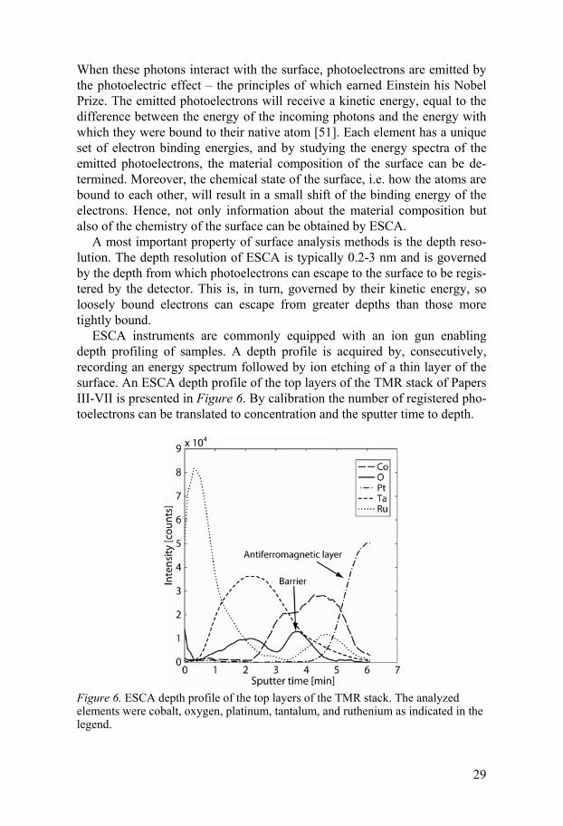
ESCA instruments are commonly equipped with an ion gun enabling depth profiling of samples. A depth profile is acquired by, consecutively, recording an energy spectrum followed by ion etching of a thin layer of the surface. An ESCA depth profile of the top layers of the TMR stack of Papers III-VII is presented in Figure 6. By calibration the number of registered pho-toelectrons can be translated to concentration and the sputter time to depth.
Figure 6. ESCA depth profile of the top layers of the TMR stack. The analyzed elements were cobalt, oxygen, platinum, tantalum, and ruthenium as indicated in the legend.

30
The manufacturing process consisted of four major steps, Paper VI, where, firstly, the bottom contacts were structured by UV lithography and argon ion etching, Figure 7 (a). Secondarily and similarly, the junctions were patterned by UV lithography and etched with the argon ion gun of the ESCA, Figure 7 (b). Finally, the bottom contact was isolated with silicon dioxide, Figure 7 (c), and contact leads were deposited to connect the sensor to the measurement system.
Figure 7. Process scheme for the MTJs etched in the ESCA, Papers IV-VII, with patterning of the bottom contact (a), patterning of the MTJ (b), isolation of the bot-tom contact (c), and deposition of contact wires (d). (Figure from Paper VI.)

31
Figure 8. Configuration of the ion beam and the sample during etching in the ESCA. (Figure from Paper VI)
The most crucial step was the structuring of the junction. In order for the MTJ to have a high TMR ratio and little inherent noise, the quality of the pattern had to be not far from the limit of what is possible using UV lithog-raphy. The size of the junction patterns, mostly circles and ellipses, were typically from a few up to tens of micrometers, Paper V-VI. The etch proc-ess had to accurately reproduce the pattern in the stack with a uniform etch rate over all of the patterned area. In the ESCA, an area of 4x4 mm could be etched at a time.
The ion gun of the ESCA was tilted at an angle of 45° to the sample stage, which was rotated during etching to give the sample an even etch dose. The tilted beam made direct transfer of the photoresist pattern to the TMR stack impossible, since the resist partly shadowed the stack from the incident ions, Figure 8. The actual MTJ pattern was therefore somewhat larger than the pattern of the resist and the etch profile, i.e. the silhouette, of the junction was tilted, Paper VI.
The principle of physical dry etching is basically a small-scale game of pool. The sample is bombarded by high-energy ions which, by transfer of momentum, eject atoms or clusters of atoms from the surface. The process is performed in vacuum and, ideally, the ejected atoms are pumped away. However, a major concern in all physical dry etching processes is redeposi-tion [52], where the ejected ions recombine with the surface. Redeposition is especially harmful to MTJ manufacturing, since the redeposit threaten to short-circuit the tunnel barrier [53], Figure 9 (top), which can reduce the TMR ratio and increase the inherent noise of the junction, Paper VI.
A convenient way of avoiding the problem with short circuiting is to stop the etching in the tunnel barrier, Figure 9 (bottom). In this way, the TMR-independent conduction path across the barrier is disabled and the full mag-netoresistive effect of the junction can be utilized. However, since the barrier is extremely thin, the etch depth has to be controlled with nanometer preci-sion. In ordinary physical dry etching this is close to impossible, but the

32
ESCA enabled monitoring of the material content of the stack surface with a precision in the order of the thickness of the barrier, Figure 6. This, in turn, provided a feedback etch-stop control process, where the material under removal was monitored live, and the etching could be aborted when the bar-rier was reached, Paper VI.
Figure 9. Effect of redeposit short-circuiting the barrier of an MTJ (top), and miti-gating effect of stopping the etching in the barrier (bottom).
Evaluating the quality of an etch stop technique that is to be controlled with a precision of a few atom layers is not trivial. In fact, there is almost only one method that is capable of this, namely transmission electron microscopy (TEM). In TEM, a focused electron beam is transmitted through an ex-tremely thin sample. The electrons interact with the sample via, e.g., diffrac-tion and the transmitted electrons are focused onto a florescent screen or a camera chip, creating an image. With this technique, images with extraordi-nary resolution, owing to the short de Broglie wavelength of the electrons, can be acquired. At best, the resolution is in the same order as the atomic radii.
In order to verify that the etch was actually stopped in the 1.1 nm thick barrier, a cross-sectional TEM sample was prepared from an etched MTJ, Paper VI, Figure 10 (inset). Not only the quality of the etch stop was inves-tigated, but also the tilted etch profile of the MTJs, due to the low angle inci-dence of the ESCA ion beam, Figure 8, and the presence of redeposition. The composition of the redeposit was investigated by energy dispersive spectroscopy (EDS), to see which elements that were prone to redeposition. EDS is a method for material analysis that can be seen as the opposite to ESCA, where the sample is illuminated with electrons causing material-characteristic photons to be emitted, the energy spectrum of which reveals the material composition of the surface, or as in this case, the bulk of the TEM sample.

33
Figure 10. TEM images of the TMR stack after ESCA etching of the junctions with the tilted etch profile and signs of redeposition (left), and the etch stopped in the barrier (right). The inset shows where the TEM sample was extracted.
From the TEM study, it could be confirmed that the etching actually stopped in the barrier, Figure 10 (right). Clear signs of redeposition were also seen, especially along the tilted etch profile of the MTJs, Figure 10 (right). The presence of redeposit close to the rim of the junction, made justice to the concern of the tunnel junction being short-circuited, should the barrier be penetrated.
The EDS analysis revealed the redeposit mainly to consist of cobalt, but also of noticeable amounts of tantalum, iron, and ruthenium. Here, the plati-num was from the TEM sample preparation process. The high percentage of cobalt was particularly worrying, since magnetic redeposit not only threaten to short circuit the junction electrically, but also magnetically by direct ex-change interaction between the sensing and reference layers.
Focused ion beam An ordinary cleanroom, like the Microstructure Laboratory at the Ångström Laboratory, typically houses instruments and options for deposition and etching of different materials, for patterning, e.g., lithographical processes, and for analyzing the manufactured components, e.g., different kinds of mi-croscopy. A FIB instrument can be said to house the same, thus being somewhat of a miniaturized cleanroom.
The two main components of a FIB are the electron and the ion gun. These can be used for imaging a sample by scanning electron/ion micros-copy (SEM/SIM) with a high resolution. The ion gun can, apart from imag-ing, also be used for physical dry etching. Mainly gallium ions are used in the beam which can be focused to spot size of less than 100 nm, making it

34
ideal for patterning of extremely small structures, e.g., TEM samples [54]. An example of a FIB-patterned structure can be seen in Figure 11, where the logotypes of Uppsala University and the Swedish National Space Board have been carved into the facets of the eye of a fly. Both the ion and electron beam can also be used for assisting chemical vapour deposition (CVD) of different materials, such as silicon dioxide, platinum and tungsten.
Figure 11. Logotypes of Uppsala University and the Swedish National Space Board etched in the facets of the eye of a fly. (The fly had died of natural causes before the structuring.)
Another great advantage of structuring with FIB is that no lithographical mask is needed. The ESCA manufacturing process, described in Paper VI, required four masks, and the process described in Paper VII even required six masks. The masks are typically quite costly and time consuming to pro-duce (hundreds of € and several days) and, given that research and develop-ment often require some iterations of the process, make maskless structuring techniques desirable.
The FIB works like an ordinary milling machine by scanning the ion beam over the surface. The pattern is loaded into the instrument as a bitmap image file and is converted to a milling file for the subsequent structuring, Paper III, Figure 12. The extensive processing-, and maskless patterning capabilities of the FIB enabled rapid prototyping of MTJs as described in Paper III. Here, it was possible to go from a design to a characterized MTJ in just a few hours.

35
Figure 12. Process scheme for the FIB structured MTJs with structuring of the bot-tom contact (a), structuring of the alignment marks (b), fine-structuring of the MTJ (c), isolation of the bottom contact (d), structuring of the bottom contact (e), isola-tion of the contact leads (f), and deposition of the contact leads (g). To the right are the bitmap images used to create the corresponding etching patterns. The lateral size of a single junction was in the submicron range. (Figure from Paper III)
The resolution and the milling rate of the ion beam depends on the beam current, where a low beam current gives a low milling rate but good resolu-tion, and vice versa. Hence, different beam currents were used for different purposes in the rapid prototyping process. Firstly, the bottom contact was defined by ion milling to the substrate, Figure 12 (a), and an alignment pat-tern was milled, Figure 12 (b), enabling alignment of the rough- and fine-
36
milled areas. The MTJs were defined using a low beam current for optimum resolution, Figure 12 (c), and isolated by ion-assisted CVD of silicon diox-ide, Figure 12 (d). These two process steps were performed with the same pattern, avoiding alignment problems. The less critical bottom contact was defined with a high beam current to shorten the milling time, Figure 12 (e), and was finally isolated, again by CVD, Figure 12 (f), before contact leads were deposited, Figure 12 (g).
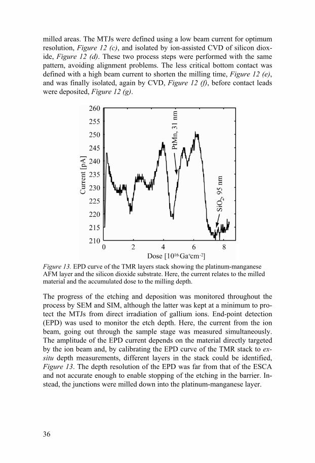
Figure 13. EPD curve of the TMR layers stack showing the platinum-manganese AFM layer and the silicon dioxide substrate. Here, the current relates to the milled material and the accumulated dose to the milling depth.
The progress of the etching and deposition was monitored throughout the process by SEM and SIM, although the latter was kept at a minimum to pro-tect the MTJs from direct irradiation of gallium ions. End-point detection (EPD) was used to monitor the etch depth. Here, the current from the ion beam, going out through the sample stage was measured simultaneously. The amplitude of the EPD current depends on the material directly targeted by the ion beam and, by calibrating the EPD curve of the TMR stack to ex-situ depth measurements, different layers in the stack could be identified, Figure 13. The depth resolution of the EPD was far from that of the ESCA and not accurate enough to enable stopping of the etching in the barrier. In-stead, the junctions were milled down into the platinum-manganese layer.

37
Sensors
To fully evaluate the process schemes, the manufactured sensors had to be studied thoroughly. Focus was directed toward the signal, i.e. the TMR and the PHE voltage, and to the noise of the sensors.
The TMR and the PHE voltage were measured in similar ways, where a magnetic field, from a computer controlled electromagnet, was applied to the sensors. The sensors were biased with a constant current and the voltage over the tunnel barrier, Papers III-VII, or the Wheatstone bridge, Papers I-II, was recorded while varying the strength and direction of the magnetic field.
The noise was measured with a spectrum analyzer, where the sensors were biased by a current supplied from a battery, and the noise voltage PSD was recorded after 40 dB preamplification, Papers I and VI-VII. The sensors and the electromagnet were placed in a magnetically shielded box and the electromagnet was powered with batteries, to remove any outside noise sources.
Planar Hall effect bridges The PHE voltage of the PHEBs of Paper I is presented in Figure 14. With similar width and thickness, a linear dependence of the sensitivity on the length of a branch is predicted, Paper I, which was confirmed by the meas-urements, Figure 14 (inset). Some of the other traits of the PHEBs, such as the linear low-field response and the negligible hysteresis, also become ap-parent.
Apart from increasing the length of a branch, the PHEB sensitivity could be improved by, e.g., increasing the thickness of the FM layer or reducing the width of a branch. However, the PHEB magnetic field range, i.e. the range of magnetic fields within which the sensor response was linear, was only dependent on the thickness, where a thicker FM layer resulted in a nar-rower field range. The field range of the PHEB sensors of Paper I was around ±1 mT. It should however be noticed that for very long and narrow branches, demagnetizing effects will appear and influence both the sensitiv-ity and the magnetic field range.

38
Figure 14. PHE voltage of the PHEBs of Paper I. The inset shows the sensitivity as a function of the total length of a bridge branch.
The inherent noise of the PHEBs was dominated by 1/f and thermal noise, Paper I, with a knee frequency between 200 and 400 Hz depending on the thickness of the FM layer, Papers I-II. The Hooge parameter of the 1/f noise could be calculated to H=0.016 from Equation (5), which is slightly higher than the Hooge parameter of a corresponding electrical conductor suggesting that part of the noise has a magnetic origin [43].
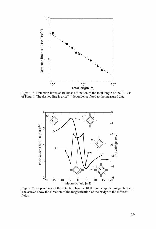
The detection limit of the PHEBs was calculated from the sensitivity and noise measurements. The dependence of the detection limit on the length of a branch was investigated, Figure 15, yielding the detection limit to be in-versely proportional to the square root of the total length of a branch, Paper I. This agreed well with theory predicting a (nlwtFM
3)-0.5 dependence. Hence, increasing the length of a branch a 100 times, gave a 100 times higher sensi-tivity but only improved the detection limit 10 times.
The magnetic part of the 1/f noise was studied in more detail by investi-gating the relationship between the applied field and the noise PSD at low frequencies. Magnetic low-frequency noise is caused by Barkhausen noise, i.e. hopping domain walls. Such noise is associated with weak anisotropies where the domains are less pinned. Hence, the noise PSD and the detection limit are expected to have minima along the anisotropy directions. Indeed, the PHEBs exhibited a field-induced anisotropy and exchange bias along
=0°, and a shape anisotropy along =±45°, Figure 3, and detection limit minima were observed at these particular directions, Figure 16, confirming the presence of magnetic low-frequency noise, Paper I.
39
Figure 15. Detection limits at 10 Hz as a function of the total length of the PHEBs of Paper I. The dashed line is a (nl)-0.5 dependence fitted to the measured data.
Figure 16. Dependence of the detection limit at 10 Hz on the applied magnetic field. The arrows show the direction of the magnetization of the bridge at the different fields.
40
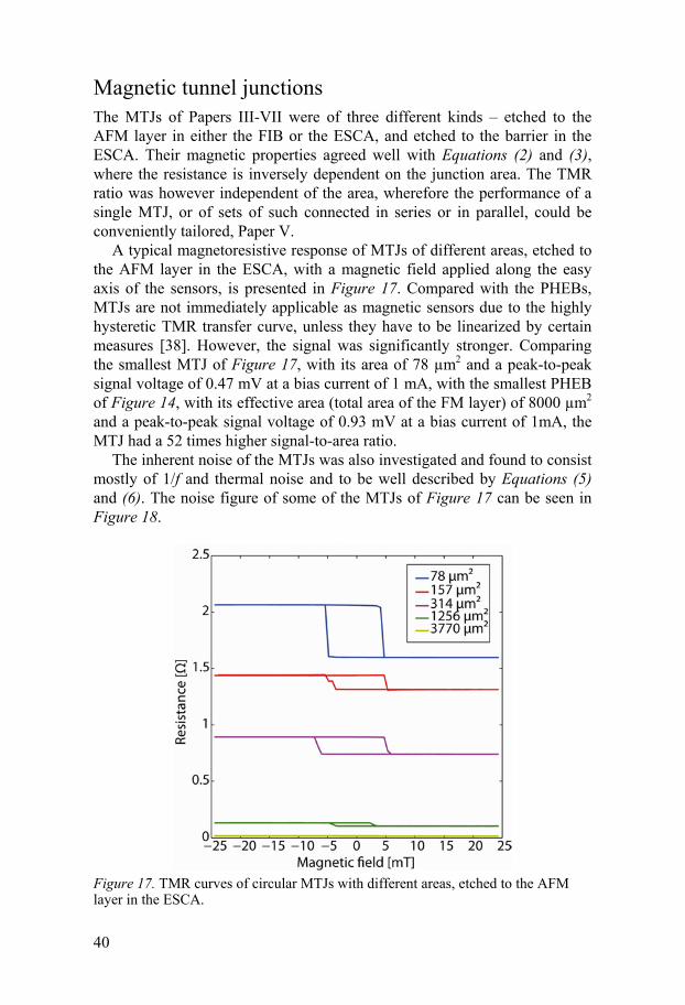
Magnetic tunnel junctions The MTJs of Papers III-VII were of three different kinds – etched to the AFM layer in either the FIB or the ESCA, and etched to the barrier in the ESCA. Their magnetic properties agreed well with Equations (2) and (3), where the resistance is inversely dependent on the junction area. The TMR ratio was however independent of the area, wherefore the performance of a single MTJ, or of sets of such connected in series or in parallel, could be conveniently tailored, Paper V.
A typical magnetoresistive response of MTJs of different areas, etched to the AFM layer in the ESCA, with a magnetic field applied along the easy axis of the sensors, is presented in Figure 17. Compared with the PHEBs, MTJs are not immediately applicable as magnetic sensors due to the highly hysteretic TMR transfer curve, unless they have to be linearized by certain measures [38]. However, the signal was significantly stronger. Comparing the smallest MTJ of Figure 17, with its area of 78 µm2 and a peak-to-peak signal voltage of 0.47 mV at a bias current of 1 mA, with the smallest PHEB of Figure 14, with its effective area (total area of the FM layer) of 8000 µm2 and a peak-to-peak signal voltage of 0.93 mV at a bias current of 1mA, the MTJ had a 52 times higher signal-to-area ratio.
The inherent noise of the MTJs was also investigated and found to consist mostly of 1/f and thermal noise and to be well described by Equations (5) and (6). The noise figure of some of the MTJs of Figure 17 can be seen in Figure 18.
Figure 17. TMR curves of circular MTJs with different areas, etched to the AFM layer in the ESCA.

41
Figure 18. Noise spectra of circular MTJs with different areas, etched to the AFM layer in the ESCA.
MTJs are known to have considerably more low-frequency noise than other types of magnetoresistive sensors. Again, comparing the low-frequency noise of the smallest MTJ with that of the smallest PHEB, the MTJ is found to have almost 2300 times higher noise-to-area ratio. Hence, for low-frequency applications, PHEBs are preferable from an SNR perspective. On the other hand, above the knee frequency of each of the two sensors, where the thermal noise dominates the spectra, the MTJs had only 12 times more noise per area and, hence, a better SNR performance.
The choice of sensors for a particular application is therefore mainly de-pendent on the system bandwidth, where PHEBs are preferable at low fre-quencies and MTJs at higher frequencies. However, other properties such as the maximum sensor area, supply voltage, pre-amplification circuit, etc., also have to be taken into account, making a thorough requirement specification important.

42
Etching and redeposition As can be seen from Figure 17, MTJs etched to the AFM layer in the ESCA did not show very high TMR ratios, typically around 30%, and far from TMR ratios up to 163%, expected from the structure. The reason for the low TMR ratio of these MTJs was assumed to be the redeposition observed in the manufacturing process, Figure 9. These effects were thoroughly investigated in Paper VI, and the suspicion was strengthened by the magnetic characteri-zation of the MTJs etched to the barrier, which showed a TMR ratio of al-most 150%, Figure 19 (top).
The main reason for the difference in TMR ratio was that the MTJs etched to the AFM layer had a considerably higher resistance than those etched to the barrier. This was somewhat counterintuitive, since the expected short-circuit of the barrier should reduce the resistance. However, the barrier protected the bottom contact from oxidation in the preceding process steps, but, if it was penetrated, some oxidation occurred, increasing the resistance and reducing the TMR ratio, Equation (2).
Still, the increased resistance could not fully explain the difference in TMR ratio between the two types of MTJs. The remaining part was attrib-uted to redeposit short-circuiting the barrier, i.e. a magnetic field independ-ent resistance in parallel with the barrier. This reduced the difference be-tween the high- and low-resistance states, thus reducing the TMR even fur-ther.
Signs of the redeposit short-circuiting the barrier not only electrically but also magnetically were seen from the magnetoresistive measurements along both the easy and hard axes of the MTJs, Figure 19 (top and bottom). The magnetization of well defined, circular FM structures is expected to relax in a vortex configuration [55]. This behaviour was seen in the MTJs etched to the barrier. The MTJs etched to the AFM layer, however, relaxed into a sin-gle domain state with the magnetization of the sensing and reference layers in parallel. This was explained by the sensing layer of the latter junctions partly being in direct magnetic contact with the reference layer through FM redeposit along the rim of the junction. Hence, the sensing layer had, or was prone to form, magnetic domains in parallel with the reference layer, per-turbing the natural (vortex) relaxation process, instead making the sensing layer relax into the parallel state. Such magnetic short circuit could also ex-plain the higher coercivity, i.e. hysteresis, in the easy axis TMR curve of the MTJs etched to the barrier, Figure 19 (top), since the magnetization reversal of these had to go through the vortex state whereas the magnetization rever-sal of the junctions etched to the AFM layer could flip directly into the op-posite state.

43
Figure 19. Easy axis (top) and hard axis (bottom) TMR curves of MTJs etched to the barrier and to the AFM layer, respectively. The arrows represent the magnetiza-tions of the sensing layer (white) and the reference layer (black) at different applied magnetic fields.
Furthermore, the MTJs etched to the barrier suffered from less inherent noise than those etched to the AFM layer, Figure 20. This was probably due to the former having less impurities and defects along the rim of the junctions, especially around and across the barrier. On average, MTJs etched to the

44
barrier showed between 5 and 10 times higher TMR ratio and around 3 times less noise, combining to a 15 to 30 times SNR improvement from employing the ESCA etch stop control.
Figure 20. Noise spectrum of MTJs manufactured in the ESCA, etched to the barrier and to the AFM layer, respectively.
Irradiation Like redeposition, implantation of ions is a potentially harmful side effect in physical dry etching. Here, ions from the etch beam do not sputter away material from the surface, but are implanted into the sample. For lighter ions, the implantation effects are not necessarily degrading, and the implanted ions can quite easily diffuse from the sample. Heavier ions, on the other hand, can cause more permanent damage. For FM materials, implantation mainly degrades the soft-magnetic properties, making the material more coercive, but can at high doses remove the FM properties completely.
The space environment holds many kinds of radiation, from rays to highly energetic particles, and a sensor aimed for it must be able to endure years of such irradiation. Conveniently, the manufacturing process could give a hint to the sensors tolerance to particle irradiation, since it employed ion irradiation, although not with ions and energies directly related to the space environment. The argon ions of the ESCA did not cause any perma-nent damage to the MTJs but the gallium ions of the FIB were potentially hazardous.
45
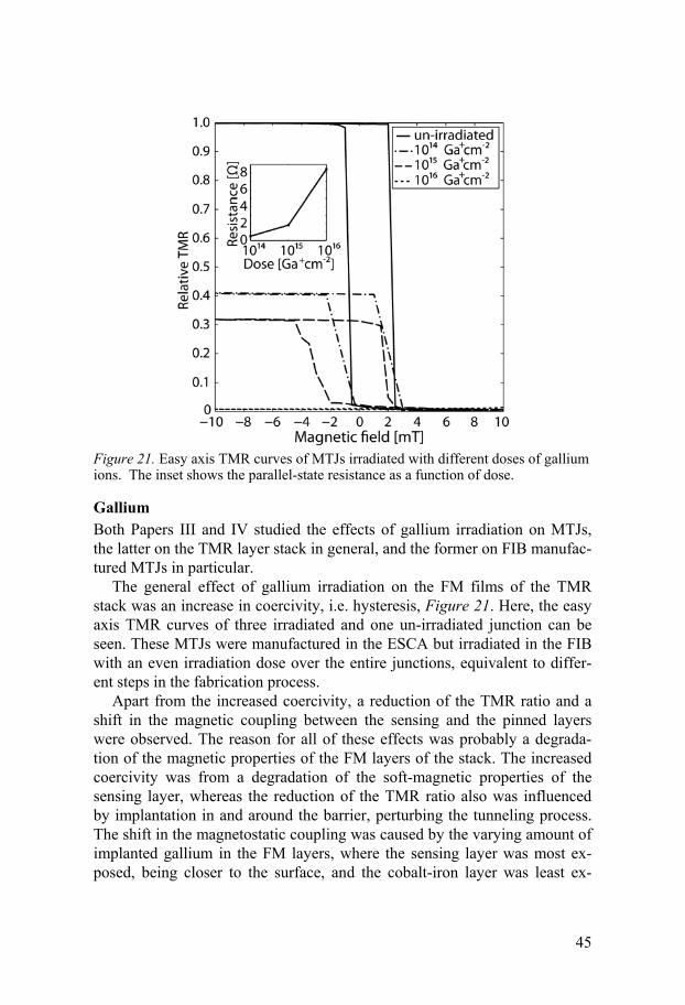
Figure 21. Easy axis TMR curves of MTJs irradiated with different doses of gallium ions. The inset shows the parallel-state resistance as a function of dose.
Gallium Both Papers III and IV studied the effects of gallium irradiation on MTJs, the latter on the TMR layer stack in general, and the former on FIB manufac-tured MTJs in particular.
The general effect of gallium irradiation on the FM films of the TMR stack was an increase in coercivity, i.e. hysteresis, Figure 21. Here, the easy axis TMR curves of three irradiated and one un-irradiated junction can be seen. These MTJs were manufactured in the ESCA but irradiated in the FIB with an even irradiation dose over the entire junctions, equivalent to differ-ent steps in the fabrication process.
Apart from the increased coercivity, a reduction of the TMR ratio and a shift in the magnetic coupling between the sensing and the pinned layers were observed. The reason for all of these effects was probably a degrada-tion of the magnetic properties of the FM layers of the stack. The increased coercivity was from a degradation of the soft-magnetic properties of the sensing layer, whereas the reduction of the TMR ratio also was influenced by implantation in and around the barrier, perturbing the tunneling process. The shift in the magnetostatic coupling was caused by the varying amount of implanted gallium in the FM layers, where the sensing layer was most ex-posed, being closer to the surface, and the cobalt-iron layer was least ex-

46
posed, especially since the ruthenium spacer served as an implantation bar-rier for gallium.
In the FIB manufacturing process of Paper III, direct irradiation of the junctions was kept at a minimum, given the potentially harmful effects of gallium implantation. However, the ion beam had a Gaussian intensity dis-tribution, and the rim of the milled junctions was unavoidably exposed to the flank of the beam. Hence, some gallium was implanted along the rim giving it different magnetic properties than the unirradiated centre.
Figure 22. Easy axis (top) and hard axis (bottom) TMR curves of MTJs manufac-tured in the FIB. The arrows show the magnetization of the soft magnetic center (black) and the stiffer rim (white) of the junctions, respectively.

47
The implantation made the rim more coercive, but also perturbed the tun-neling process in this area, effects of which could be seen in both the easy and hard axis TMR curves of the junctions manufactured in the FIB, Figure 22. The extra hysteresis in the easy axis TMR curve, as compared with an unirradiated junction, was from the stiffer rim countering the magnetization reversal of the more soft-magnetic centre, something that was confirmed by micromagnetic simulations. The surprising hysteresis in the hard axis TMR curve was from the junctions having two remnant states – one double do-main and one single domain state. These two domain states were in addition studied by magnetic force microscopy, Figure 23, and were probably, once again, due to interactions between the rim and the centre. The reason why the sensing layer relaxed into different states depending on direction of the hard axis bias field was more difficult to explain, but was probably due to an imbalance in the magnetostatic coupling, resulting from a slightly asym-metric distribution of the ion beam. This made the coercive rim somewhat wider on one side of the junction, giving the coupling field a component along the hard axis.
The width of the rim was estimated from the hard axis TMR curve, using both theory, Equation (3), and numerical interpolation, to 160 nm. This set the lower limit to the lateral of junction manufactured with the FIB process, Paper III.
Although gallium irradiation may not be an immediate danger in space, the study shows that MTJs may be damaged by point defects and disloca-tions induced by an impacting energetic particle. However, it is fairly easy to protect the sensor from such radiation by shielding it with a layer of, e.g., aluminum. In this way, the particle will unload most of its energy in the aluminum layer, although some of it will be transformed into radiation which is much more difficult to shield.
Figure 23. Atomic force micrograph (left) and magnetic force micrograph (right) of MTJs manufactured in the FIB. The latter shows the junctions in the double domain state.
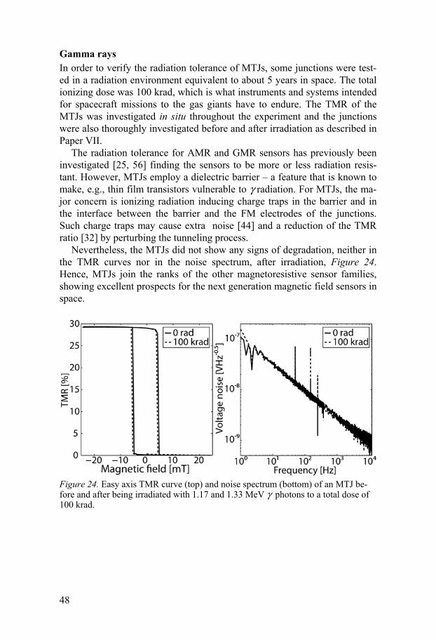
48
Gamma rays In order to verify the radiation tolerance of MTJs, some junctions were test-ed in a radiation environment equivalent to about 5 years in space. The total ionizing dose was 100 krad, which is what instruments and systems intended for spacecraft missions to the gas giants have to endure. The TMR of the MTJs was investigated in situ throughout the experiment and the junctions were also thoroughly investigated before and after irradiation as described in Paper VII.
The radiation tolerance for AMR and GMR sensors has previously been investigated [25, 56] finding the sensors to be more or less radiation resis-tant. However, MTJs employ a dielectric barrier – a feature that is known to make, e.g., thin film transistors vulnerable to radiation. For MTJs, the ma-jor concern is ionizing radiation inducing charge traps in the barrier and in the interface between the barrier and the FM electrodes of the junctions. Such charge traps may cause extra noise [44] and a reduction of the TMR ratio [32] by perturbing the tunneling process.
Nevertheless, the MTJs did not show any signs of degradation, neither in the TMR curves nor in the noise spectrum, after irradiation, Figure 24. Hence, MTJs join the ranks of the other magnetoresistive sensor families, showing excellent prospects for the next generation magnetic field sensors in space.
Figure 24. Easy axis TMR curve (top) and noise spectrum (bottom) of an MTJ be-fore and after being irradiated with 1.17 and 1.33 MeV photons to a total dose of 100 krad.

49
Magnetoresistance in space
Having strong signal, manageable noise, and extensive radiation tolerance, both MTJs and PHEBs show great promise for use in space. However, in order to employ them on a satellite, they first have to be integrated in a mag-netometer system. A conceptual design of such a magnetometer is presented in Figure 25.
Both MTJs and PHEBs measure only one component of the magnetic field. A magnetometer, however, is required to measure the whole magnetic field vector, wherefore a minimum of three sensors, one for each vector component, is required, Figure 25 (far left). Moreover, the PHEBs are al-ready, and the MTJs should be, connected in a Wheatstone bridge enabling an unbiased output signal and improved thermal stability [57]. The output of the Wheatstone bridges should be connected through a buffer stage to isolate the sensors from the rest of the system, Figure 25 (left), e.g., from high-frequency noise sources such as clock signals in the digital electronics. The signal should then be amplified to the correct input level of the analog-to-digital of the data acquisition unit, Figure 25 (right and far right). The signal from the Wheatstone bridges can be measured both differentially or single ended depending on the rest of the circuit.
Figure 25. Conceptual design of a magnetoresistive magnetometer with Wheatstone bridges, a buffer stage, preamplifiers, and an analog-to-digital (ADC) converter.

50
Spin-dependent tunnelling magnetometer A conceptual design of an MTJ magnetometer was presented in Paper VII where, a total of six Wheatstone bridges, instead of the minimum three, were employed to measure the three-dimensional magnetic field vector. The bridges were structured on two 8 mm x 8 mm chips, each having three bridges labelled A-C with sensitive directions separated by 120°, Figure 26 (top). The two chips were then mounted perpendicularly, to measure the full field vector.
Figure 26. Conceptual design of a triple Wheatstone bridge magnetometer chip with the three bridges labeled A-C (top), and a magnification of one bridge with each branch comprised of 16 MTJs (bottom). (Figure from Paper VII)

51
Each Wheatstone bridge branches consisted of eight pairs of MTJs con-nected in series, Figure 26 (bottom). This was to increase the SNR by in-creasing the total junction area. Two of the branches of each bridge were shielded by a soft-magnetic flux concentrator. These two branches were used as references, whereas the two un-shielded branches measured the actual field. The flux concentrators also focused the external magnetic field at the active branches and gave the bridge a pronounced sensing direction [58].
The 120° pitch of the bridge sensing directions was used for reducing the MTJ noise, partly by averaging, where the noise power decreases linearly with the number of junctions in the circuit [59], but also from the fact that the noise in an MTJ is strongly dependent on the ambient field amplitude [60]. By taking a weighted average, promoting the bridges with the strongest signal and thus the least noise, the unfavorable configuration with the ambi-ent field being perpendicular to one of the bridges could be avoided, Paper VII. Hence, the SNR in all three dimensions could be improved signifi-cantly.
The manufacturing process for the Wheatstone bridge chips, Paper VII, was similar to that for manufacturing MTJs in the ESCA, Paper VI, Figure 7, where, firstly, the bottom contacts of the MTJs were structured by UV lithography and ion milling in the ESCA, Figure 27 (a). The MTJs were patterned in a similar way, Figure 27 (b), and etched down to the barrier of the junctions for optimum SNR, Paper VI. The MTJs were structured in pairs, and eight such pairs were then connected in series by deposition of top contacts, Figure 27 (d), after the bottom contacts had been isolated with silicon dioxide, Figure 27 (c). Finally, the top contacts were isolated, Figure 27 (e), again with silicon dioxide, and the soft-magnetic shield was deposited on top of two of the branches, Figure 27 (f). The Wheatstone bridge chips were then connected to the buffer stage and the preamplifier that were made on a multilayer printed circuit board.
Beyond the work covered by Papers I-VII, a miniaturized MTJ magne-tometer for three-dimensional magnetic field measurements, employing Wheatstone bridges similar to those described in Paper VII, was developed. This magnetometer, Figure 28, called the Spin-dependent Tunneling Magne-tometer (SDTM), was developed for the Vietnamese picosatellite F-1, Figure 1, which will hopefully be launched into space before the end of 2011. The SDTM measures 6.5 mm x 22 mm x 4 mm and weighs only 0.79 g. However, the bandwidth of 10-100 kHz was adapted to the data acquisi-tion system of the F-1 satellite and not to the MTJs, wherefore the latter op-erated in the unfavorable low-frequency regime. Hence, the detection limit is a modest 100 pTHz-0.5 at 10 kHz. However, supported by a successful mis-sion, the prospects of launching an updated version of the SDTM, more adapted to the performance of the MTJs, will increase dramatically.

52
Figure 27. Manufacturing process of a MTJ Wheatstone bridge with structuring of bottom contacts (a), structuring of MTJs (b), isolation of the bottom contacts (c), structuring of top contacts (d), isolation of top contacts (e), and structuring of mag-netic shield (f). (Figure from Paper VII)

53
Figure 28. Miniaturized magnetometer for three-dimensional magnetic field meas-urements with MTJ sensors, buffer stages, and preamplifiers.
Planar Hall effect magnetometer When designing a magnetometer for a particular application, it is always convenient to have as many degrees of freedom as possible. MTJs, employ-ing a very complicated thin-film structure, are generally quite sensitive to design changes, where a slight modification of the thickness of a layer can have strong influence on, e.g., the TMR ratio, by altering the growth condi-tions during the deposition process. The only parameter really accessible for design is the area of the junction which can be used to govern the signal and noise figure.
PHEBs on the other hand, are quite versatile with respect to design, where the length, width, thickness and shape of a branch can be readily modified to fit a particular application. However, with so many degrees of freedom it can be difficult to find the optimum design, especially since, e.g., the exchange-bias and anisotropy fields, as well as the AMR and the intrinsic noise, de-pend differently on all these parameters.
In Paper II, a theoretical model was developed to be able to predict the performance of an arbitrary PHEB, Figure 29. Apart from theory, a set of approximations was adopted to estimate the anisotropy fields, including the demagnetizing field, and the resistivity change for a particular branch ge-ometry. These approximations were in some cases quite crude but adjusted so that the generated results did not overestimate the performance of the PHEB but offered somewhat of a worst-, or rather a worse-case scenario.
Nevertheless, the modelled data turned out to correlate quite well with measurements on actual PHEBs, Figure 30, at least for the thinner PHEBs which suffered less from demagnetizing effects. For the thicker bridges, the

54
model slightly underestimated the detection limit, as expected from the ap-proximations. Despite this deviation, the model was concluded to produce data in the right order of magnitude, and it could therefore be employed in making a first design draft of a PHEB given a certain requirement specifica-tion.
Figure 29. Predicted sensitivities (left) and detection limits (right) of PHEBs with varying length and thickness. The width of the PHEBs was in both cases 30 µm.
Figure 30. Modeled detection limits for PHEBs with different thicknesses (lines) as a function of the total branch length, compared with measurements on actual bridges (circles and squares).

55
Figure 31. Modeled performance of a PHEB with a detection limit of >100 pTHz-0.5 at 0.1 Hz and minimum size (solid line) or minimum power consumption (dashed line).
In Paper II, the optimized designs of three example magnetometers having different bandwidths, detection limit requirements, compliance voltages, and preamplifier noise figures were derived. Employing the theoretical model, the optimum length, width, thickness, and number of segments in a branch could be estimated, yielding the size, sensitivity and power consumption of the resulting PHEB.
Two different design methods were investigated, aiming either for as small or as power efficient PHEBs as possible. The modelled detection limit of a PHEB with a detection limit requirement of >100 pT at 0.1 Hz can be seen in Figure 31. The bridge was optimized both in terms of size and power efficiency. In the first case, the area of the whole PHEB was 23 mm2 and the power consumption was 45 mW, whereas in the second case the area was 231 mm2 and the power consumption was 4.6 mW.
Comparing this PHEB sensor with the spaceborne magnetometers in Table 2, the performance of the minimum size design is comparable to that of the miniaturized Galileo and SMILE fluxgate magnetometers. However, these magnetometers have a sensor mass of more than 20 g and, including their supporting electronics, the total system mass is more than 100 g [16]. The mass of the PHEB sensor is only a couple of milligrams and, including electronics similar to that of the SDTM, the total system mass can be ex-pected to be less than 1 g, excluding any radiation shields, booms etc.

56
There is no immediate reason why the detection limit of PHEBs should not be possible to reduce even further, eventually making them competitive even to the larger fluxgate magnetometer with a detection limit of ~1 pT at 1 Hz and a mass of more than a kilogram. Hence, PHEBs show great promise to be the next generation low-frequency magnetic field sensors for space.

57
Conclusion
The aim of this thesis work was to implement magnetoresistive technology in a magnetometer intended for space. Two different kinds of magnetoresis-tive sensors, MTJs and PHEBs, were manufactured and evaluated.
The major challenge in the manufacturing of the MTJs was controlling the etch depth with sub-nanometer resolution in order to stop the etching in the junction’s tunnel barrier. This was accomplished by employing ESCA for etch-depth control. The major challenge for the MTJs them self’s was their tolerance to the space environment. Being inherently tolerate to vacuum focus was directed towards their resistance to different kinds of radiation. Of the and particle radiation, threatening to damage the sensors in space, the MTJs turned out to be more or less unaffected by the former whereas the latter was potentially harmful. However, additional investigations exposing the sensors to particle radiation with doses and energies equivalent to that of different regions in space is required before drawing any final conclusions.
The manufacturing of the PHEBs, being structurally less complicated, was more straightforward. Here, the challenge was rather optimizing their design to a particular application. A design process, based on a theoretical model of the PHE effect, was developed, but the properties of sensors manu-factured according to the generated designs remain to be investigated.
The progress of qualifying new devices or technologies for space can be measured with the TRL scale presented in Table 1. The development of the MTJs and the SDTM has come the furthest and is currently at TRL7 waiting for the final flight qualification. With the launch of the SDTM during the end of 2011, the MTJ technology will have bridged the TRL “Valley of Death” and be almost fully space qualified. The PHEBs have not come as far and are currently somewhere between TRL3 and TRL4. However, the ex-perience acquired from the development of the MTJs will be of great help in the remaining qualification process, and there are no immediate reasons for the PHEBs not soon to join the MTJs at the opposite side of the valley.
Together, the two sensors will enable sensitive and broadband measure-ments, replacing the currently used FGMs and SCMs, reducing the system’s mass with a factor of a hundred. This will, in turn, enable completely new kinds of space missions with hundreds of magnetometers capable of high resolution constellation-mapping of small-scale magnetic features such as local magnetic turbulence in the magnetospheric cusps [61].


59
Svensk sammanfattning
Magnetoresistans och rymd är ett omaka par som denna avhandling syftar att föra närmare varandra. Rymden har nog de flesta en uppfattning om medan magnetoresistans är okänt begrepp för många. Ändå utnyttjar de flesta av oss detta fenomen nästan dagligen när vi läsa informationen frår våra hårddiskar. Magnetoresistans är egentligen ett samlingsnamn för flera olika fenomen med den gemensamma nämnaren att ett pålagt magnetfält förändrar en elekt-risk ledares resistans. Exempel på olika typer av magnetoresistiva magnet-fältssensorer är sådana baserade på anisotropisk magnetoresistans (AMR) där sensorer baserade på den plana Hall-effekten utgör en undergrupp, jätte-magnetoresistans (GMR), som belönades med 2007 års Nobelpris i fysik, och magnetiska tunnelövergångar. I arbetet bakom denna avhandling stude-rades just sådana magnetiska tunnelövergångar samt en speciell typ av plan Hall-effektsensorer kallade plan Hall-effektbryggor.
Målet med dessa studier var att undersöka om och hur magnetoresistiva sensorer kan användas i rymden. En legitim fråga är naturligtvis varför. Magnetiska fält i rymden kan kännas ganska oväsentliga men i själva verket är de av stor vikt för oss här på jorden. De flesta vet säkert att jorden har ett eget magnetfält men inte att det skapar vad man kan likna vid en magnetisk bubbla som skyddar jorden från farlig strålning, främst från solen. Nära den magnetiska nord- och sydpolen är dock bubblan svagare och ibland lyckas strålningen där tränga igenom och nå ned till atmosfären. Då uppstår vad vi kallar norrsken. Många upplever norrskenet som ett spännande himlafeno-men men faktum är att det kan vara farligt, speciellt för olika elektriska sy-stem. Bortsett från att orsaka strömavbrott, har de starka magnetfältsfluktua-tioner som förknippas med norrskenet setts påverka säkerhetssystemen i järnvägsnätet och orsaka problem i flygplan och satelliter. Att förstå de pro-cesser som förknippas med norrsken och jordens magnetfälts samverkan med solen är därför av största vikt för vårt moderna samhälle.
En följdfråga blir naturligtvis varför magnetoresistans. Många tror att man i rymden använder sig av det senaste och absolut mest avancerade som teknikutvecklingen har att erbjuda. I själva verket är dock rymdindustrin extremt konservativ. Anledningen till att man drar sig för att använda ny teknik är förklarligt nog svårigheten, för att inte säga omöjligheten, i att laga en satellit när den väl är uppskjuten. Får man välja mellan en oprövad kom-ponent med fantastisk prestanda och en gammal med låg prestanda men som man vet har fungerat på tidigare satellitmissioner, väljer man därför nästan

60
alltid den senare. Att skjuta upp något i rymden är också väldigt dyrt; att sätta ett kilo i omloppsbana kostar cirka 100000 kr. Mer och mer intresse riktas därför mot miniatyriserade system som, utan prestandaförlust, kan ersätta traditionella system och samtidigt kraftigt reducera en satellits totala vikt. I fallet magnetfältsensorer och magnetometrar, har dock denna strategi visat sig problematisk, då de traditionella systemen faktiskt förlorar prestan-da då de skalas ned. Istället har man börjat söka efter alternative sensortek-niker och här är magnetoresistiva sensorer potentiellt sett ideala då de lämpar sig utmärkt för miniatyrisering.
Råmaterialet till de magnetoresistiva sensorerna i detta avhandlingsarbete var ett antal så kallade tunnfilmer staplade på varandra. Tunna filmer kan ha något olika betydelser i olika sammanhang. Bland de tunnare filmer som vi hanterar till vardags finns exempelvis aluminiumfolie, vilken har en typisk tjocklek av 10 µm, det vill säga 0,01 mm. Detta motsvarar bara ungefär en tiondel av ett hårstrås diameter, men i tunnfilmssammanhang är 0,01 mm ändå tjockt. Om man låter alla Nationalencyklopedins band, staplade på var-andra, motsvara aluminiumfoliens tjocklek, så skulle tjockleken hos det tun-naste lagret i den magnetoresistiva lagerstrukturen motsvaras av en enda sida. I själva verket utgörs dessa lager av endast ett fåtal atomer staplade på varandra.
Tunnfilmsstrukturerna mönstrades till sensorer vars laterala storlek sträckte sig från 0,001 x 0,002 mm, för den minsta tunnelövergången, till 1,5 x 3 mm för den största Hall-effektsensorn. Mönstringen av Hall-effektsensorerna var förhållandevis enkel, där själva sensorn tillverkades i ett enda processteg. Detta möjliggjordes av att strömmen, som användes för att mäta magnetfältet i dessa sensorer, leds längs sensorns yta, det vill säga pa-rallellt med tunnfilmernas utbredning. I fallet med de magnetiska tunnel-övergångarna måste dock strömmen ledas tvärs igenom den isolerande tun-nelbarriären – ett 0,000001 mm tunt lager mitt i strukturen – och alltså ut ur sensorns plan. Detta krävde i sin tur att sensorn måste kunna mönstras, inte bara på bredden, utan också på djupet. Till råga på allt krävdes att mönst-ringen kunde kontrolleras med en precision som motsvarade tjockleken hos de tunnaste lagren i strukturen, det vill säga på ett fåtal atomlager när.
En sådan precision kan i princip endast åstadkommas med en metod där avverkningsdjupet hela tiden övervakas, och mönstringen kan avbrytas när önskat djup nåtts. Mönstring av metalliska tunnfilmer sker vanligtvis genom så kallad etsning. I det här fallet användes en särskild variant där provet bombarderas med högenergetiska joner vilka, genom en biljardliknande ef-fekt, slår loss material från provets yta. Ett sätt att övervaka mönstrings-, eller etsdjupet, är att växelvis etsa bort ett (i tunnfilmstermer mätt) tunt lager från provets yta för att sedan undersöka vilket material som blottlagts.
För att kunna tillämpa denna metod på tunnelövergångarna krävdes dock en analysmetod som endast beaktade materialsammansättningen på provets yta. Vanligt är emellertid att sådana ytanalysmetoder hämtar information om

61
materialsammansättningen från djup motsvarande hela den aktuella tunn-filmsstrukturens tjocklek, vilket är långt ifrån tillräckligt om de tunnaste lagren i strukturen skall kunna upplösas. Lyckligtvis har ett instrument med tillräcklig djupupplösning utvecklats just i Uppsala, något som gav universi-tetet dess senaste Nobelpris. Instrumentet kallas ESCA (Electron Spectros-copy for Chemical Analysis) och analyserar fotoelektronernas materialspeci-fika energispektrum för att avgöra provets ytsammansättningen. Instrumentet är även utrustat med en jonkanon för etsning vilket möjliggjorde högupplöst djupmönstring av de magnetiska tunnelövergångarna.
Både kvaliteten hos mönstringstekniken och de tillverkade tunnelöver-gångarnas magnetiska egenskaper och prestanda undersöktes, och det visade sig att det var högst fördelaktigt att stanna etsningen i tunnelbarriären. Detta berodde dels på att barriären, om den lämnades intakt, kunde användas som skydd för de underliggande lagren under resten av tillverkningsprocessen, dels på att just barriären riskerade att kortslutas av material som återdepone-rade på provet under etsningen. Sammantaget erhölls både en ökad signal och ett minskat brus när etsningen kunde avbrytas i barriären, något som knappast hade varit möjligt med en konventionell tillverkningsmetod.
De tillverkade sensorerna med tillhörande elektronik karaktäriserades inte bara med avseende på vilka magnetfält de kunde detektera. Även deras upp-trädande i en rymdlik miljö undersöktes. Många tänker nog på rymden som tom, men helt tom är den inte. Kring jorden strömmar den så kallade solvin-den som består av joniserade partiklar som slungats ut från solen. Nära jor-dens bana är solvindens täthet ungefär en partikel per kubikcentimeter. Dessutom är rymden full av fotoner av olika energi. Också de härrör mesta-dels från solen. Både partiklar och fotoner, främst -fotoner, kan skada elekt-ronik i rymden. Exempelvis kan en enda högenergetisk partikel förstöra en dator om den träffar en av minneskretsarna. Långvarig exponering för -strålning leder också ofta till degradering av elektroniska komponenter.
De magnetiska tunnelövergångarna utsattes både för - och partikelstrål-ning, den senare i from av galliumjoner. Även om gallium inte är särskilt vanligt förekommande i rymden, gav detta ändå en uppfattning om hur ener-getiska partiklar påverkar sensorerna. De visade sig var känslig för höga doser av sådan strålning. Å andra sidan visade sensorerna sig vara i princip helt okänsliga för -strålning, och då partikelstrålningens intensitet i rymden är tämligen begränsad medan intensiteten hos -strålningen är hög, var detta på det hela taget mycket positiva resultat.
Utöver det arbete som täcktes av denna avhandling, har ett miniatyriserat magnetometersystem utvecklats. Detta system, döpt till SDTM (Spin-Dependent Tunnelling Magnetometer), utnyttjar magnetiska tunnelöver-gångar för att mäta magnetfältet, och kommer, om inget oförutsett inträffar, att skjutas upp i rymden mot slutet av 2011 ombord på den vietnamesiska pikosatelliten F-1. En pikosatellit definieras av att den som mest får väga 1 kg och därför nästan omöjligt kan bära med sig en traditionell magnetometer

62
då dessa väger nästan ett kilo i sig. SDTM, å andra sidan, väger bara 0,79 g, inklusive all elektronik, och är ideal för denna satellitklass.
Om uppskjutningen lyckas kommer SDTM att sälla sig till en inte allt för stor skara mikrosystem som faktiskt nått omloppsbana. Anledningen till att mikrosystem ännu inte har fått något storskaligt genomslag i rymden är framförallt för att de ännu är tämligen oprövade. Endast ett fåtal har fått komma ombord på satelliter, och, väl i rymden, har ännu färre faktiskt fun-gerat som planerat. Detta leder i sin tur till att antalet flygchanser minskar ytterligare. I fallet magnetiska tunnelövergångar skall förhoppningsvis det Moment 22 som kravet på att ett system i princip skall ha flugit innan det kan flygas innebär, nu kunna hävas. Oavsett vad som händer kvarstår ändå den uppenbara fördelen med mikrosystem i rymdtillämpningar. Att ersätta ett traditionellt, kilogram-tungt magnetometersystem med en mikrostrukture-rad sensor möjliggör inte bara att exempelvis pikosatelliter kan utrustas med högpresterande magnetometrar, utan också helt nya satellitmissioner där hundratals distribuerade magnetometrar kartlägger lokala magnetfältsfluktu-ationer med hög precision. Om jag sedan bara kunde skala upp mig själv lika många gånger som jag skalat ned mina sensorer i förhållande till en traditio-nell magnetometer, skulle jag kunna erbjuda egna uppskjutningstillfällen bara genom att räcka upp handen, eftersom jag då skulle vara 100 km lång.

63
Acknowledgements
Hugo och Greger, tack för fyra intressanta, lärorika, utvecklande, men fram-för allt väldigt roliga år. Även om jag nog egentligen inte visste vad jag gav mig in på blev det ändå nästan som jag hade tänkt mig, och det är tack vare er. Mest av allt vill jag tacka för allt förtroende och ansvar ni gett mig. Att lära sig vad forskning är genom egna beslut, misslyckanden och slutligen framgångar är tveklöst den viktigaste lärdomen jag tar med mig. Ni har satt ribban högt för framtida arbetsgivare. Tack också till Lukas som var med och startade upp allt ihop. Vågade du tro att det ”modulära byggkonceptet” faktiskt skulle bli grunden till en riktig rymdmagnetometer? Extra tack till Johan som mer och mer förvandlas till ÅSTCs ryggrad utan vilken det mesta skulle falla ihop.
Tack till Frida och till Fredric för att ni lärde mig vad ESCA och FIB var, och för trevliga stunder i och utanför renrummet. Det var våra samarbeten som blev russinen i avhandlingskakan.
Tack till Peter, Rebecca, och Klas för det fina samarbetet med brusmät-ningar, PHEB-sensorer, nanopärlor, mm., och för att ni helt enkelt är väldigt trevliga.
Thanks to Mikkel, Bjarke and Frederik for interesting discussions and for letting me have a piece of the PHEB cake.
Thanks to Juergen Lange and Berthold Ocker at Singulus for helping us when we were lost in the world of TMR stacks, and in Hanau.
Tack till Magnus Wikberg and to Vassilios Kapaklis for helping me with the first TMR measurements, before I even knew if I’d ever manage to make working sensor.
Thanks to MSL, especially to Rimantas, Jan-Åke, och Angelo, for great help in the cleanroom on and off office hours.
Ett stort tack till Kristof(f)er som, även om du hamnade i den tråkiga noll-legruppen, har varit med mig ända sen jag först satte min fot på Pollacks-backen. Från backgammon på intressanta och ointressanta föreläsningar (även om jag fortfarande tycker du har olovligt mycket tur) och för mycket Outfit när man borde tentaplugga, via otaliga practial jokes, after works och senast joppes, till snart två hattar. Waferussion nästa.
Tack till Ville, Martin, Jonas, Sara, och alla exjobbare på ÅSTC. Till-sammans har vi lärt oss innebörden av både herrgårds-kickoffs och styr-gruppsmötespanik och någonstans kommer jag nog att sakna båda.

64
Tack till Quizlaget som gång på gång visat att Å2200 är allmänbildning-ens högborg i Uppsala, i.a.f. om man bortser från musikfrågor och Rodesia-kunskap.
Tack till alla MSTare, särskilt till Sam för en trevlig Denver-resa och för att du tog dig tid att korrekturläsa avhandlingen, till Hanna för att du tog hand om mig när jag var ny och för att du lärde mig massor i renrummet, och till Jan-Åke för att jag har fått jobba på den fantastiskt trevliga avdelning du skapat.
Tack också till alla Tribologer, MIMare och JonDeTechs för en härlig ar-betsatmosfär och alldeles för långa fikapauser. Tack till Jonatan, Anja, Karin och alla inom administrationen för all hjälp. Tack till 3010 och förlåt för att jag svek er.
Till sist ett stort tack till min familj för att jag är den jag är och ni är dom ni är. Utan tryggheten jag får från er hade jag aldrig klarat av det här. Tack till morfar. Även om jag inte riktigt förstår hur så är det nog du som gjorde så att jag hamnade här.
Ingrid, “Until the satellites deceased, and blows like garbage though the streets, of the night sky to infinity.”

65
References
[1] Guimareas A P 2003 Mexico and the Early History of Magnetism Revista Mexicana de Fisica 50 51-3
[2] Yu-qing Y 1987 Magnetic materials in China 4-14 [3] Zhongguo ke xue ji shu bo wu g 1983 China, 7000 years of discovery:
China's ancient technology China reconstructs magazine [4] Jiles D 1998 Introduction to magnetism and magnetic materials Chapman
and Hall [5] Wangsness R K 1986 Electromagnetic fields Wiley [6] Mohn P 2003 Magnetism in the Solid State, An Introduction Berlin
Springer-Verlag [7] Heppenheimer T A 1997 Countdown: a history of space flight John Wiley
& Sons [8] Campbell B and S W McCandless 1996 Introduction to space sciences and
spacecraft applications Houston Gult Publishing Company [9] Tascione T F 1994 Introduction to the space environment Malabar Krieger
Publ. [10] Nielsen O V and et al. 1995 Development, construction and analysis of the
'OErsted' fluxgate magnetometer Measurement Science and Technology 6 1099
[11] Mandea M, M Korte, S Macmillan and C Finlay The International Geo-magnetic Reference Field Geomagnetic Observations and Models 265-76 Springer Netherlands
[12] Dougherty M K, N Achilleos, N Andre, C S Arridge, A Balogh, C Bertucci, M E Burton, S W H Cowley, G Erdos, G Giampieri, K H Glassmeier, K K Khurana, J Leisner, F M Neubauer, C T Russell, E J Smith, D J Southwood and B T Tsurutani 2005 Cassini Magnetometer Observations During Saturn Orbit Insertion Science 307 1266-70
[13] Langlais B, M E Purucker and M Mandea 2004 Crustal magnetic field of Mars J. Geophys. Res. 109 E02008
[14] Zhang T L and e al. 2006 Magnetic field investigation of the Venus plasma environment: Expected new results from Venus Express Planetary and Space Science 54 1336-43
[15] Acuna M H 2002 Space-based magnetometers Review of Scientific Instru-ments 73 3717-36
[16] Forslund A, S Belyayev, N Ivchenko, G Olsson, T Edberg and A Ma-rusenkov 2008 Miniaturized digital fluxgate magnetometer for small space-craft applications Measurement Science & Technology 19 015202-1

66
[17] Griffith W C, R Jimenez-Martinez, V Shah, S Knappe and J Kitching 2009 Miniature atomic magnetometer integrated with flux concentrators Applied Physics Letters 94 023502 (3 pp.)
[18] Roux A, O Le Contel, C Coillot, A Bouabdellah, B de la Porte, D Alison, S Ruocco and M Vassal 2008 The Search Coil Magnetometer for THEMIS Space Science Reviews 141 265-75
[19] Auster H, K Glassmeier, W Magnes, O Aydogar, W Baumjohann, D Con-stantinescu, D Fischer, K Fornacon, E Georgescu, P Harvey, O Hillen-maier, R Kroth, M Ludlam, Y Narita, R Nakamura, K Okrafka, F Plaschke, I Richter, H Schwarzl, B Stoll, A Valavanoglou and M Wiedemann 2008 The THEMIS Fluxgate Magnetometer Space Science Reviews 141 235-64
[20] Dunlop M W, M K Dougherty, S Kellock and D J Southwood 1999 Opera-tion of the dual magnetometer on Cassini: science performance 47 1389-405
[21] Carr C, E Cupido, C G Y Lee, A Balogh, T Beek, J L Burch, C N Dunford, A I Eriksson, R Gill, K H Glassmeier, R Goldstein, D Lagoutte, R Lundin, K Lundin, B Lybekk, J L Michau, G Musmann, H Nilsson, C Pollock, I Richter and J G Trotignon 2007 RPC: the Rosetta Plasma Consortium Space Science Reviews 128 629-47
[22] Thomson W 1856 On the Electro-Dynamic Qualities of Metals:-Effects of Magnetization on the Electric Conductivity of Nickel and of Iron Proceed-ings of the Royal Society of London 8 546
[23] Prinz G A 1999 Magnetoelectronics applications Journal of Magnetism and Magnetic Materials 200 57-68
[24] Ding L, J Teng, X C Wang, C Feng, Y Jiang, G H Yu, S G Wang and R C C Ward 2010 Designed synthesis of materials for high-sensitivity geomag-netic sensors Applied Physics Letters 96 052515-3
[25] Michelena M D, I Arruego, J M Oter and H Guerrero 2010 COTS-Based Wireless Magnetic Sensor for Small Satellites IEEE Transactions on Aero-space and Electronic Systems 46 542-57
[26] Stutzke N A, S E Russek, D P Pappas and M Tondra 2005 Low-frequency noise measurements on commercial magnetoresistive magnetic field sen-sors Journal of Applied Physics 97 10Q107-3
[27] Damsgaard C D, S C Freitas, P P Freitas and M F Hansen 2008 Exchange-biased planar Hall effect sensor optimized for biosensor applications Jour-nal of Applied Physics 103 07A302-3
[28] Baibich M N, J M Broto, A Fert, F N Van Dau, F Petroff, P Etienne, G Creuzet, A Friederich and J Chazelas 1988 Giant Magnetoresistance of (001)Fe/(001)Cr Magnetic Superlattices Physical Review Letters 61 2472
[29] Binasch G, Gr, uuml, P nberg, F Saurenbach and W Zinn 1989 Enhanced magnetoresistance in layered magnetic structures with antiferromagnetic in-terlayer exchange Physical Review B 39 4828
[30] Hasegawa N, F Koike, K Ikarashi, M Ishizone, M Kawamura, Y Naka-zawa, A Takahashi, H Tomita, H Iwasaki and M Sahashi 2002 Nano-oxide-layer specular spin valve heads with synthetic pinned layer: Head perform-ance and reliability Journal of Applied Physics 91 8774-6

67
[31] Julliere M 1975 Tunneling between ferromagnetic films Physics Letters A 54 225-6
[32] Moodera J S, J Nassar and G Mathon 1999 Spin-Tunnelling in Ferromag-netic Junctions Annual Review of Materials Science 29 381-432
[33] Parkin S S P, K P Roche, M G Samant, P M Rice, R B Beyers, R E Scheuerlein, E J O'Sullivan, S L Brown, J Bucchigano, D W Abraham, Y Lu, M Rooks, P L Trouilloud, R A Wanner and W J Gallagher 1999 Ex-change-biased magnetic tunnel junctions and application to nonvolatile magnetic random access memory (invited) Journal of Applied Physics 85 5828-33
[34] Zhang Z, S Cardoso, P P Freitas, X Batlle, P Wei, N Barradas and J C Soares 2001 40% tunneling magnetoresistance after anneal at 380 [de-gree]C for tunnel junctions with iron--oxide interface layers Journal of Ap-plied Physics 89 6665-7
[35] Parkin S, C Kaiser, A Panchula, M R Philip, B Hughes, M Samant and S Yang 2004 Giant Tunneling Magnetoresistace at Room Temperature with MgO (100) Tunnel Barriers Nat. Mater. 3 862
[36] Yuasa S, T Nagahama, A Kukushima, Y Suzuki and K Ando 2004 Giant Room-Temperature Magnetoresistance in Single-Crystal Fe/Mg0/Fe Mag-netic Tunnel Junction Nat. Mater. 3 868
[37] Ikeda S, J Hayakawa, Y Ashizawa, Y M Lee, K Miura, H Hasegawa, M Tsunoda, F Matsukura and H Ohno 2008 Tunnel magnetoresistance of 604% at 300 K by suppression of Ta diffusion in CoFeB/MgO/CoFeB pseudo-spin-valves annealed at high temperature Applied Physics Letters 93 082508-3
[38] Freitas P P, R Ferreira, S Cardoso and F Cardoso 2007 Magnetoresistive sensors Journal of Physics: Condensed Matter 19 21 pp.
[39] Yuasa S, Y Suzuki, T Katayama and K Ando 2005 Characterization of growth and crystallization processes in CoFeB/MgO/CoFeB magnetic tun-nel junction structure by reflective high-energy electron diffraction Applied Physics Letters 87 242503-3
[40] Henriksen A D, B T Dalslet, D H Skieller, K H Lee, F Okkels and M F Hansen 2010 Planar Hall effect bridge magnetic field sensors Applied Physics Letters 97 013507-3
[41] Schuhl A, F N Van Dau and J R Childress 1995 Low-field magnetic sen-sors based on the planar Hall effect Applied Physics Letters 66 2751-3
[42] Ejsing L, M F Hansen, A K Menon, H A Ferreira, D L Graham and P P Freitas 2004 Planar Hall effect sensor for magnetic micro- and nanobead detection Applied Physics Letters 84 4729-31
[43] Raquet R 2001 Electric noise in magnetic materials and devices Lecture notes in physics 569 232-73
[44] Nowak E R, M B Weissman and S S P Parkin 1999 Electrical noise in hysteretic ferromagnet-insulator-ferromagnet tunnel junctions Applied Physics Letters 74 600-2
[45] Almeida J M, R Ferreira, P P Freitas, J Langer, B Ocker and W Maass 2006 1/f noise in linearized low resistance MgO magnetic tunnel junctions Jour-nal of Applied Physics 99 08B314-3

68
[46] Ren C, X Liu, B D Schrag and G Xiao 2004 Low-frequency magnetic noise in magnetic tunnel junctions Physical Review B 69 104405
[47] Hooge F N 1976 1/f noise Physica B 83 14 [48] Madou M J 2002 Fundamentals of Microfabrication Boca Raton CRC Press [49] Hsu T 2008 MEMS and microsystems : design, manufacture, and nanoscale
engineering Hoboken John Wiley ans Sons Inc. [50] Tzu S 2005 The art of war El Paso El Paso Norte Press [51] Siegbahn K 1970 Electron spectroscopy for chemical analysis (e.s.c.a.)
Philosophical Transactions of the Royal Society of London A (Mathemati-cal and Physical Sciences) 268 33-57
[52] Melliar-Smith C M 1976 Ion etching for pattern delineation Journal of Vacuum Science and Technology 13 1008-22
[53] Chen E, B Schwarz, C Chang Ju, W Kula, J Wolfman, K Ounadjela and S Geha 2003 Magnetic tunnel junction pattern technique Journal of Applied Physics 93 8379-81
[54] Giannuuzzi L A and F A Stevie 2004 Introduction to focused ion beams 201 Boston Springer Science
[55] Liou S H, R F Sabiryanov, S S Jaswal, J C Wu and Y D Yao 2001 Mag-netic domain patterns of rectangular and elliptic arrays of small permalloy elements Journal of Magnetism and Magnetic Materials 226-230 1270-2
[56] Kaakani H 2001 Radiation hardened memory development at Honeywell vol.5 2273-9
[57] Cao J and P P Freitas 2010 Wheatstone bridge sensor composed of linear MgO magnetic tunnel junctions Journal of Applied Physics 107 09E712-3
[58] Tondra M, J M Daughton, C Nordman, D Wang and J Taylor 2000 Micro-magnetic design of spin dependent tunnel junctions for optimized sensing performance Journal of Applied Physics 87 4679-81
[59] Tondra M, J M Daughton, D Wang, R S Beech, A Fink and J A Taylor 1998 Picotesla field sensor design using spin-dependent tunneling devices Journal of Applied Physics 83 6688-90
[60] Kim K S, H J Shim, I J Hwang, B K Cho, J H Seok and K Jin-Tae 2002 Magnetic field dependent noise in magnetic tunnel junction Journal of Ap-plied Physics 91 8804-6
[61] Sundkvist D, V Krasnoselskikh, P K Shukla, A Vaivads, M Andre, S Buchert and H Reme 2005 In situ multi-satellite detection of coherent vor-tices as a manifestation of Alfvenic turbulence Nature 436 825-8