Embed Size (px)
Citation preview
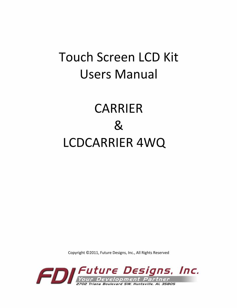
Touch Screen LCD Kit Users Manual
CARRIER
& LCDCARRIER 4WQ
Copyright ©2011, Future Designs, Inc., All Rights Reserved

ii
Table of Contents1. Introduction __________________________________________________________________________ 1
2. Functional Description __________________________________________________________________ 1
3. ESD Warning _________________________________________________________________________ 2
4. Requirements ________________________________________________________________________ 2
5. Board Layout _________________________________________________________________________ 3
CARRIER BOARD ________________________________________________________________________ 3
LCDCARRIER 4WQ _______________________________________________________________________ 5
6. Functional Block Diagram _______________________________________________________________ 6
7. I/O Connector Descriptions ______________________________________________________________ 7
CARRIER _______________________________________________________________________________ 7
DC Power Input – P5 ___________________________________________________________________ 7
Alternate Power Input – J8 ______________________________________________________________ 7
USB Device – P6 _______________________________________________________________________ 7
USB Host – P1 ________________________________________________________________________ 8
Ethernet – J5 _________________________________________________________________________ 8
CAN/RS485 – P3 _______________________________________________________________________ 9
RS232 – P4 ___________________________________________________________________________ 9
External I2C – J6 ______________________________________________________________________ 10
I2S Stereo Audio – J9 & J10 (Rev 4 PCB and later) ___________________________________________ 10
8. On Board Functions ___________________________________________________________________ 12
CARRIER ______________________________________________________________________________ 12
User I/O Expander – U8 ________________________________________________________________ 12
Real Time Clock – U10 _________________________________________________________________ 12
Accelerometer – U9 ___________________________________________________________________ 13
Temperature Sensor – U11 _____________________________________________________________ 13
Optional WiFi Module – U6 (Rev 2 PCB and later) ___________________________________________ 13
LCDCARRIER ___________________________________________________________________________ 14
Backlight Generator Micrel MIC2297 –U2 _________________________________________________ 14
Ambient Light Sensor – U4 _____________________________________________________________ 14
CARRIER Expansion Connector Descriptions ________________________________________________ 15
J2 ___________________________________________________________________________________ 15

iii
J3 ___________________________________________________________________________________ 16
J4 ___________________________________________________________________________________ 17
9. CARRIER Jumper Details _______________________________________________________________ 18
JP1 Real Time Clock Interrupt Enable _______________________________________________________ 18
JP2 3‐Axis Accelerometer Interrupt Enable __________________________________________________ 18
JP3 RS232 DCE<>DTE Configuration (Rev 2 PCB and later) _______________________________________ 19
JP4 – JP7 RS485 or CAN Mode Select for P3 (Rev 2 PCB and later) ________________________________ 20
JP8 UART RCV Data Disable – only used for ISP support on DIMM modules (Rev 2 PCB and later) _______ 20
10. SOMDIMM Module Installation _________________________________________________________ 21
11. Mechanical Details____________________________________________________________________ 22
CARRIER ______________________________________________________________________________ 22
LCDCARRIER ___________________________________________________________________________ 23
12. Software____________________________________________________________________________ 24
13. Schematics __________________________________________________________________________ 24
14. Table of Figures ______________________________________________________________________ 24
Information in this document is provided solely to enable the use of Future Designs products. FDI assumes no liability whatsoever, including infringement of any
patent or copyright. FDI reserves the right to make changes to these specifications at any time, without notice. No part of this document may be reproduced or
transmitted in any form or by any means, electronic or mechanical, for any purpose, without the express written permission of Future Designs, Inc. 2702 Triana Blvd,
Huntsville, AL 35805
NOTE: The inclusion of vendor software products in this kit does not imply an endorsement of the product by Future Designs, Inc.
2011 Future Designs, Inc. All rights reserved.
uEZ® is a registered trademark of Future Designs, Inc.
Microsoft, MS‐DOS, Windows, Windows XP, Microsoft Word are registered trademarks of Microsoft Corporation.
Other brand names are trademarks or registered trademarks of their respective owners.
FDI PN: MA00026
Revision: 1, 10/14/2011 3:02:00 PM
Printed in the United States of America

1
1. Introduction The DK‐TS‐KIT is optimized to save development time in typical embedded control applications. Its modular format uses a base carrier board, a core CPU DIMM board and an LCD carrier board. The base carrier board includes expansion connectors for added flexibility and a range of configurations. This manual supports the following DK‐TS‐KIT part numbers:
DK‐43WQT‐RX62N 4.3” WQVGA Touch Screen LCD Kit for the RX62N, Tianma PN: TM043NBH02
DK‐47WQT‐RX62N 4.7” WQVGA Touch Screen LCD Kit for the RX62N, Tianma PN: TM047NBH01
2. Functional Description CARRIER
200 pin SO‐DIMM Socket
RS232 Serial Port (Male DB9)
CAN Port (Male DB9) – alternate with RS485
RS485 Full Duplex (Male DB9) – alternate with CAN
10/100 Ethernet Connector
Optional 802.11 b/g WiFi Module
USB Type‐A Host Connector
USB Mini‐B Device Connector
LM75 Temperature Sensor
3‐axis Accelerometer
Real‐time Clock with Super‐Cap Backup
Four User Pushbuttons
Four User LEDs
Speaker
External I2C Connector (Optional)
Reset Button LCDCARRIER
4.3” Active TFT WQVGA LCD (480x272) mounted to LCDCARRIER 4WQ Board or
4.7” Active TFT WQVGA LCD (480x272) mounted to LCDCARRIER 4WQ Board
Touch Screen
LED Backlight

2
3. ESD Warning The DK‐TS‐KIT is shipped in a protective anti‐static package. The Kit must not be subjected to high electrostatic potentials. Damage may occur to the Kit that will not be covered under warranty. General practice for working with static sensitive devices should be followed when working with the DK‐TS‐KIT.
4. Requirements The DK‐TS‐KIT comes with all necessary cables to begin development right away. The Kit includes a Type‐A to Mini‐B USB cable, a CAT5 Ethernet cable, a 5.0VDC, 2A, AC Wall Adapter and either the Segger JTAG Debugger. A PC will be required to install the development tools to program the SOMDIMMs. The DK‐TS‐KIT will be powered using the 5VDC AC Wall Adapter included in the kit and may be plugged into any standard 110VAC wall socket. An available Ethernet network will be needed for using the Ethernet connection on the CARRIER and a free USB port will be needed for using the available USB connections. CAUTION: DO NOT POWER THE DK‐TS‐KIT WITH ANY OTHER POWER THAN 5VDC. USE OF ANY OTHER ADAPTER MAY DAMAGE THE BOARD AND VOID THE WARRANTY.

3
5. Board Layout
CARRIER BOARD
Figure 1 – CARRIER Top Side
(Rev 4 Shown)

4
Figure 2 – CARRIER Bottom Side
(Rev 4 Shown)

5
LCDCARRIER 4WQ
Figure 3 – LCDCARRIER Top Side

6
6. Functional Block Diagram
ETHERNET
CAN
RS232
POWERINPUT
200 PIN DIMM SOCKET
50 PIN LCD INTERFACE CONNECTOR
3-AXISACC
TEMPSENSOR
REALTIME
CLOCK
USERI/O
LED
PB
PB
PB
PB
LED
LED
LEDUSB
HOST
USBDEVICE
I2C
50 PIN LCD INTERFACE CONNECTOR
4.3" 480x272 LCDTOUCHSCREEN
textRenesasRX62N
Based Processor10/100PHY
SDRAM(x32)
uSDSlot
Mini-JTAG
200 PIN DIMM EDGE FINGER
Figure 4 – DK‐TS‐KIT System Block Diagram (RX62N Shown)
7
7. I/O Connector Descriptions
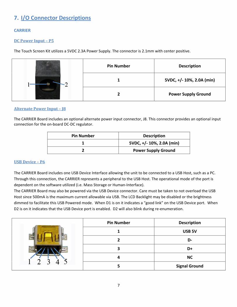
CARRIER DC Power Input – P5 The Touch Screen Kit utilizes a 5VDC 2.3A Power Supply. The connector is 2.1mm with center positive.
Pin Number Description
1 5VDC, +/‐ 10%, 2.0A (min)
2 Power Supply Ground
Alternate Power Input – J8 The CARRIER Board includes an optional alternate power input connector, J8. This connector provides an optional input connection for the on‐board DC‐DC regulator.
Pin Number Description
1 5VDC, +/‐ 10%, 2.0A (min)
2 Power Supply Ground
USB Device – P6
The CARRIER Board includes one USB Device Interface allowing the unit to be connected to a USB Host, such as a PC.
Through this connection, the CARRIER represents a peripheral to the USB Host. The operational mode of the port is
dependent on the software utilized (i.e. Mass Storage or Human‐Interface).
The CARRIER Board may also be powered via the USB Device connector. Care must be taken to not overload the USB
Host since 500mA is the maximum current allowable via USB. The LCD Backlight may be disabled or the brightness
dimmed to facilitate this USB Powered mode. When D1 is on it indicates a “good link” on the USB Device port. When
D2 is on it indicates that the USB Device port is enabled. D2 will also blink during re‐enumeration.
Pin Number Description
1 USB 5V
2 D‐
3 D+
4 NC
5 Signal Ground

8
USB Host – P1
The CARRIER Board includes one USB Host Port allowing the unit to interface to various USB peripherals such as a USB
Flash Drive (Thumb Drive). The operational mode of this port is dependent on the software utilized (i.e. driver support)
Please refer to the specific details of the processor module being utilized for support of the USB Host function.
D3 indicates VBUS power is good for the USB Host port.
Pin Number Description
1 USB VBus
2 D‐
3 D+
4 Signal Ground
Ethernet – J5 The CARRIER Board includes one 10/100 Ethernet Port to interface to a local area network via CAT5 cable. Please refer to the specific details of the processor module being utilized for support of the Ethernet Port function.
Pin Number Description
1 Tx+
2 3.3V
3 Tx‐
4 Rx+
5 3.3V
6 Rx‐
7 No Connect
8 Signal Ground

9
CAN/RS485 – P3
The CARRIER Board includes one Male DB9 Interface Connector that supports either CAN or RS485 (Rev 2 and later) depending on the configuration of jumpers JP4 – JP7. The CAN interface utilizes an NXP TJA1040TD high speed transceiver IC to provide fully ISO 11898 standard interface at up to 1MBaud. The TJA1040 allows up to 110 nodes and very low electromagnetic emissions. Note: Rev 1 PCB only supports CAN on P3 Please refer to the specific details of the processor module being utilized for support of the CAN interface function.
Pin Number CAN Mode RS485 Mode
(Rev 2 and later only)
1 No Connect No Connect
2 CANL 485_RDB‐
3 Signal Ground 485_TDA+
4 Signal Ground Signal Ground
5 Signal Ground Signal Ground
6 Signal Ground Signal Ground
7 CANH 485_RDA+
8 No Connect 485_TDB‐
9 5V No Connect RS232 – P4 The CARRIER Board includes one RS232 Serial Port Connector. This connector is a Male DB9 configured as either DCE or
DTE (Rev 2 and later only) depending on the configuration of jumper block JP3. The interface includes optional RTS &
CTS handshaking signals that are brought to test points that the user may connect as needed (see page 5 of the
schematic). Please verify proper connectivity of this connector to the proper TXD<>RXD orientation. TXD is an OUTPUT
from the CARRIER Board and RXD is an INPUT to the CARRIER Board.
Note: Rev 1 PCB only supports DCE on P4
Please refer to the specific details of the processor module being utilized for support of the RS232 Serial Port function.
Pin Number DCE Mode DTE Mode
(Rev 2 and later only)
1 No Connect No Connect
2 TXD (Output) RXD (Input)
3 RXD (Input) TXD (Output)
4 No Connect No Connect
5 Signal Ground Signal Ground
6 No Connect No Connect
7 (OPT) RTS (OPT) RTS
8 (OPT) CTS (OPT) CTS
9 No Connect No Connect

10
External I2C – J6
The CARRIER board provides an external I2C connector for users to connect to the I2C bus of the microprocessor. CARRIER Rev 2 and later
Pin Number Description
1 5V
2 5V
3 3.3V
4 3.3V
5 GPIO75_SCL
6 Signal Ground
7 GPIO74_SDA
8 GPIO116
9 GPIO117 Please refer to the specific details of the processor module for connectivity details. I2S Stereo Audio – J9 & J10 (Rev 4 PCB and later) The I2S audio circuitry is loaded and supports input and output of audio. J9 is microphone input and J10 in headphone
output, I2S audio is not support by the RX62N.

11
LCDCARRIER
J1 – Female 25x2 Socket for Board‐to‐Board Straight Connection to CARRIER Board
Pin Signal Name SOMDIMM Connection Pin Signal Name SOMDIMM Connection
1 GND Signal Ground 2 GND Signal Ground
3 LCD_TS_XL GPIO72 4 LCD_TS_YD GPIO73
5 LCDVD2 GPIO127 6 LCD_R1 GPIO128
7 LCD_R2 GPIO31 8 LCD_R3 GPIO32
9 LCD_R4 GPIO33 10 LCD_R5 GPIO34
11 GND Signal Ground 12 GND Signal Ground
13 SCL (1) I2C Clock 14 SDA (1) I2C Data
15 LCD_G0 GPIO88 16 LCD_G1 GPIO89
17 LCD_G2 GPIO90 18 LCD_G3 GPIO91
19 LCD_G4 GPIO92 20 LCD_G5 GPIO93
21 GND Signal Ground 22 GND Signal Ground
23 NC No connect 24 NC No connect
25 LCDVD18 GPIO45 26 LCD_B1 GPIO46
27 LCD_B2 GPIO94 28 LCD_B3 GPIO95
29 LCD_B4 GPIO96 30 LCD_B5 GPIO97
31 GND Signal Ground 32 GND Signal Ground
33 LCDPWR GPIO25 34 LCDLE GPIO26
35 LCD_VSYNC GPIO28 36 LCDENAB GPIO29
37 LCD_HSYN GPIO30 38 LCDDCLK GPIO27
39 GND Signal Ground 40 KEY No connect
41 3.3V 3.3V Power Supply 42 5.0V 5.0V Power Supply
43 EXT_SCK GPIO62 44 EXT_MOSI GPIO65
45 EXT_MISO GPIO64 46 LCD_TS_YU GPIO71
47 LCD_TS_XR GPIO70 48 LCD_SPI_CS GPIO36 (2)
49 EXT_IRQ GPIO69 50 LED_BR GPIO86
(1) Rev 2 CARRIER Only
Note: GPIOxx references the pin number of the DIMM socket, ex: GPIO45 is connected to pin 45 of the DIMM socket.

12
8. On Board Functions
CARRIER User I/O Expander – U8
User Input/Output functions are provided by an NXP PCA9551. The PCA9551 LED blinker blinks LEDs in I2C‐bus
and SMBus applications where it is necessary to limit bus traffic or free up the I2C‐bus master's CPU timer. The
uniqueness of this device is the internal oscillator with two programmable blink rates. The PCA9551 LED blinker
requires only the initial set‐up command to program BLINK RATE 1 and BLINK RATE 2 (i.e., the frequency and
duty cycle) for each individual output. From then on, only one command from the bus master is required to turn
each individual open‐drain output on, off, or to cycle at BLINK RATE 1 or BLINK RATE 2. Any bits not used for
controlling the LEDs can be used for General Purpose parallel Input/Output (GPIO) expansion. The active LOW
hardware reset pin (RESET) and Power‐On Reset (POR) initializes the registers to their default state, all zeroes,
causing the bits to be set HIGH (LED off).
Pushbuttons
There are four pushbuttons for general purpose user input; SW1, SW2, SW3, & SW4.
These pushbuttons are connected to the PCA9551 signals LED0 – LED3 respectively.
LEDs
There are four LEDs for program status output to the user; LED1, LED2, LED3, LED4.
These LEDs are connected to the PCA9551 signals LED4 – LED7 respectively.
PCA9551 Device I2C Address = 0xC0
For detailed information, please refer to the specific data sheet for this device available from the manufacturer.
Real Time Clock – U10
The CARRIER Board provides a low power Real Time Clock IC, an NXP PCF8563. This device is backed up by a
0.33F Super‐Cap. At a typical standby current of 250 nA, the Super‐Cap may provide backup power for up to 660
hours to the PCF8563 (at room temperature). The PCF8563 contains sixteen 8‐bit registers with an auto‐
incrementing address register, an on‐chip 32.768 kHz oscillator with one integrated capacitor, a frequency
divider which provides the source clock for the Real‐Time Clock/calendar (RTC), a programmable clock output, a
timer, an alarm, a voltage‐low detector and a 400 kHz I2C‐bus interface. In some kits the internal RTC on the
DIMM module will be the default, such as the SOMDIMM‐LPC1788, and U10 will not be used.
PCF8563 Device I2C Address = 0xA2
For detailed information, please refer to the specific data sheet for this device available from the manufacturer.

13
Accelerometer – U9
The CARRIER Board provides a 3‐axis Digital Accelerometer from Freescale MMA7445. Offering many smart
functional features, the MMA7455 is aimed for consumer market applications. It allows measurement of
accelerations in 3 perpendicular axes. An internal evaluation circuit converts the output of a three‐channel
micromechanical acceleration sensing structure that works according to the differential capacitance principle.
MMA7455 Device I2C Address = 0x1D
For detailed information, please refer to the specific data sheet for this device available from the manufacturer.
Temperature Sensor – U11
The CARRIER Board provides a Digital Temperature sensor from NXP, LM75A. The LM75A uses the on‐chip band
gap sensor to measure the device temperature with the resolution of 0.125 °C and stores the 11‐bit 2's
complement digital data, resulted from 11‐bit A‐to‐D conversion, into the device Temp register. This Temp
register can be read at any time by a controller on the I2C‐bus. Reading temperature data does not affect the
conversion in progress during the read operation. The LM75A has an accuracy of ±2° C at ‐25° C to +100° C.
LM75 Device I2C Address = 0x92 For detailed information, please refer to the specific data sheet for this device available from the manufacturer.
Optional WiFi Module – U6 (Rev 4 PCB and later)
The CARRIER Board optionally provides WiFi connectivity capability via the WiFi Module from Redpine, PN:
RS9110‐N. The WiFi module is optional and may not be loaded on all kit configurations but can be purchased
and added by the customer if desired. The WiFi module is connected to the SPI Bus and requires the use of an
interrupt output for proper operation. The interrupt is shared with the Real Time Clock. For specific details on
the WiFi module, please refer to the specific data sheet for this device available from the manufacturer.
14
LCDCARRIER
Backlight Generator Micrel MIC2297 –U2
The LCDCARRIER 4WQ utilizes a Micrel MIC2297. The backlight circuit supports PWM brightness control via the
‘LED_BR’ signal that is connected to the microprocessor SOMDIMM. Refer to the microprocessor module user’s
manual for specific connectivity of these signals.
Optional I2C Backlight control via an Analog Devices Digital Potentiometer, AD5259BRMZ10.
For detailed information, please refer to the specific data sheet for this device available from the manufacturer.
Ambient Light Sensor – U4
The LCDCARRIER 4WQ has an optional I2C ROHM, BH172FVC, light sensor for reading ambient light.
For detailed information, please refer to the specific data sheet for this device available from the manufacturer.

15
CARRIER Expansion Connector Descriptions J2
Pin Name Details Pin Name Details
1 GND GROUND 2 3V3 3.3V
3 GND GROUND 4 3V3 3.3V
5 RESET_IN RESET INPUT TO POR 6 RESET_OUT RESET OUTPUT FROM POR
7 3.3VA ADC VDD 8 VSSA ANALOG GROUND (ADC)
9 VREF ADC REFERENCE VOLTAGE 10 NC
11 GPIO57_TXD SERIAL TRANSMIST DATA 12 GPIO58_RXD SERIAL RECEIVE DATA
13 GPI059_USBH_PWRD USB HOST Power 14 GPIO60_USBD_UPLED USB DEVICE UP LED
15 GPI065_MOSI SPI MOSI 16 GPIO67_ESCL EXTERNAL I2C CLK
17 GPI069_TPIRQ TOUCH PANEL IRQ 18 GPIO71_AD0.1 ADC0 BIT 1
19 GPI073_AD0.3 ADC0 BIT 3 20 NC
21 GPI079 22 GPIO81
23 GPI083 24 GPIO85
25 GPI087_USBH_PPWR USB HOST PORT PWR 26 GPIO89_LCDVD11 LCD VIDEO BIT 11
27 GPI091_LCDVD13 LCD VIDEO BIT 13 28 GPIO93_LCDVD15 LCD VIDEO BIT 15
29 GPI0132 30 GPIO134
31 GPI0136 32 GPIO138
33 GPI0140 34 GPIO142
35 GPI0144 36 GPIO146
37 GPI0148 38 GPIO150
39 GPI0152 40 GPIO154
41 GPI0156 42 GPIO158
43 GPI0160 44 GPIO162
45 GPI0168 46 GPIO170
47 GPI0172 48 GPIO174
49 GPI0176 50 GPIO178
51 GPIO180 52 GPIO182
53 GPIO184 54 GPIO186
55 GPIO188 56 GPIO190
57 GPIO192 58 GPIO194
59 GPIO196 60 GPIO198
61 GND GROUND 62 3V3 3.3V
63 GND GROUND 64 3V3 3.3V
Note: GPIOxx references the pin number of the DIMM socket, ex: GPIO45 is connected to pin 45 of the DIMM socket.

16
J3
Pin Name Details Pin Name Details
1 GND GROUND 2 3V3 3.3V
3 GND GROUND 4 3V3 3.3V
5 GPIO25_LCDPWR LCD PANEL POWER ENABLE 6 GPIO26_LCDLE LCD LINE END
7 GPIO27_LCDCLK LCD PANEL CLK 8 GPIO28_LCDFP LCD VERT SYNC
9 GPIO29_LCDENAB LCD DATA ENABLE OUTPUT 10 GPIO30_LCDLP LCD HORZ SYNC
11 GPIO31_LCDVD4 LCD VIDEO BIT 4 12 GPIO32_LCDVD5 LCD VIDEO BIT 5
13 GPIO33_LCDVD6 LCD VIDEO BIT 6 14 GPIO34_LCDVD7 LCD VIDEO BIT 7
15 GPIO53_I2SRX_SDA I2S RECEIVE DATA 16 GPIO55_I2STX_WS I2S TRANSMIT WORD SELECT
17 GPIO61_USBD_CON USB DEVICE CONNECT CNTRL 18 GPIO63 GPIO63
19 GPIO95_LCDVD21 LCD VIDEO BIT 21 20 GPIO97_LCDVD23 LCD VIDEO BIT 23
21 GPIO99_AD0.5 ADC0 BIT 5 22 NC
23 NC 24 NC
25 NC 26 NC
27 GPIO131 28 GPIO133
29 GPIO135 30 GPIO137
31 GPIO139 32 GPIO141
33 GPIO143 34 GPIO145
35 GPIO147 36 GPIO149
37 GPIO151 38 GPIO153
39 GPIO155 40 GPIO157
41 GPIO159 42 GPIO161
43 NC 44 NC
45 GPIO167 46 GPIO169
47 GPIO171 48 GPIO173
49 GPIO175 50 GPIO177
51 GPIO179 52 GPIO181
53 GPIO183 54 GPIO185
55 GPIO187 56 GPIO189
57 GPIO191 58 GPIO193
59 GPIO195 60 GPIO197
61 GND GROUND 62 3V3 3.3V
63 GND GROUND 64 3V3 3.3V
Note: GPIOxx references the pin number of the DIMM socket, ex: GPIO45 is connected to pin 45 of the DIMM socket.

17
J4
Pin Name Details Pin Name Details
1 GND GROUND 2 3V3 3.3V
3 GND GROUND 4 3V3 3.3V
5 VBAT_IN RTC POWER SUPPLY 6 ALARM RTC ALARM
7 GPIO35 8 GPIO36
9 GPIO45_LCDVD18 LCD VIDEO BIT 18 10 GPIO46_LCDVD19 LCD VIDEO BIT 19
11 GPIO47_RD CAN1 RECEIVER INPUT 12 GPIO48_TD CAN1 TRANSMIT OUTPUT
13 GPIO49 14 GPIO50
15 GPIO51_I2SRX_CLK I2S RECEIVE CLK 16 GPIO52_I2SRX_WS I2S RECEIVE WORD SELECT
17 GPIO54_I2STX_CLK I2S TRANSMIT CLK 18 GPIO56_I2STX_SDA I2S TRANSMIT DATA
19 GPIO62_SCK SPI CLK 20 GPIO64_MISO SPI MISO
21 GPIO66_ESDA EXTERNAL I2C DATA 22 GPIO68_USBH_OVC USB HOST OVER CURR
23 GPIO70_AD0.0 ADC0 BIT 0 24 GPIO72_AD0.2 ADC0 BIT 2
25 GPIO74_SDA I2C DATA 26 GPIO75_SCL I2C CLK
27 GPIO78_ACC_IRQ ACC IRQ 28 GPIO80_RTC_IRQ RTC IRQ
29 GPIO82 30 GPIO84
31 GPIO86_LED_BR LED BACKLIGHT 32 GPIO88_LCDVD10 LCD VIDEO BIT 10
33 GPIO90_LCDVD12 LCD VIDEO BIT 12 34 GPIO92_LCDVD14 LCD VIDEO BIT 14
35 GPIO94_LCDVD20 LCD VIDEO BIT 20 36 GPIO96_LCDVD22 LCD VIDEO BIT 22
37 GPIO98_USBD_VBUS USB DEVICE PORT VBUS 38 GPIO100
39 NC 40 5V0 5.0V
41 NC 42 5V0 5.0V
43 NC 44 NC
45 GPIO116 46 GPIO118
47 GPIO120 48 GPIO122
49 GPIO124 50 GPIO126
51 GPIO128_LCDVD3 LCD VIDEO BIT 3 52 NC
53 GPIO115 54 GPIO117
55 GPIO119 56 GPIO121
57 GPIO123_MAT3.0 SPEAKER 58 GPIO125
59 GPIO127_LCDVD2 LCD VIDEO BIT 2 60 NC
61 GND GROUND 62 3V3 3.3V
63 GND GROUND 64 3V3 3.3V
Note: GPIOxx references the pin number of the DIMM socket, ex: GPIO45 is connected to pin 45 of the DIMM socket.

18
9. CARRIER Jumper Details
Figure 5 – Jumper Locations
(Rev 2 PCB shown)
Rev 4 PCB JP9 and JP10 not available
JP1 Real Time Clock Interrupt Enable JP1 enables the interrupt output from the PCF8563 connected to GPIO80_RTC_IRQ. Refer to the specific details for the processor module to determine the location this signal is connected. The default for this jumper is shorted in artwork. To disable this function, the trace must be cut and a 2‐pin jumper installed to re‐enable. For functional information on the interrupt capability of the PCF8563, please refer to the data sheet for the Real Time Clock.
JP2 3‐Axis Accelerometer Interrupt Enable JP2 enables the interrupt out from the 3‐Axis Accelerometer MM7445 connected to GPIO78_ACC_IRQ. Refer to the specific details for the processor module to determine the location this signal is connected. The default for this jumper is shorted in artwork. To disable this function, the trace must be cut and a 2‐pin jumper installed to re‐enable. For functional information on the interrupt capability of the MMA7445, please refer to the data sheet for the Freescale Accelerometer.

19
JP3 RS232 DCE<>DTE Configuration (Rev 2 PCB and later) JP3 allows the on‐board RS232 port (P4) to be configured as either DCE or DTE by loading the jumpers either horizontally or vertically.
DCE MODE DTE MODE JP3
1
3
2
4
JP3
1
3
2
4
Figure 6 – JP3 Illustration
P4 PINOUT DETAILSPin DCE Mode DTE Mode
1 NO CONNECT NO CONNECT
2 TXD OUTPUT RXD INPUT
3 RXD INPUT TXD OUTPUT
4 NO CONNECT NO CONNECT
5 SIGNAL GROUND SIGNAL GROUND
6 NO CONNECT NO CONNECT
7 OPTIONAL RTS (DTE MODE ONLY) OPTIONAL RTS (DTE MODE ONLY)
8 OPTIONAL CTS (DTE MODE ONLY) OPTIONAL CTS (DTE MODE ONLY)
9 NO CONNECT NO CONNECT

20
JP4 – JP7 RS485 or CAN Mode Select for P3 (Rev 2 PCB and later) JP4 through JP7 allow the selection of either CAN or RS485 functionality for the Male DB9 Connector P3. CAN is not available on RX62N.
CAN MODE RS485 MODE
CAN
RS485
MODE SELECT
CAN
RS485
MODE SELECT
Figure 7 – JP4 to JP7 Illustration
JP8 UART RCV Data Disable – only used for ISP support on DIMM modules (Rev 2 PCB and later) JP8 allows the user to disable the UART receive data on the RS485 port (P3) for microprocessors that support ISP programming via the ISP header (J1) on the DIMM module. The default for this jumper is shorted in artwork. To disable this function, the trace must be cut and then a 2‐pin jumper installed to re‐enable data after ISP. Please refer to the specific documentation for the module/processor being utilized to determine if ISP is supported.

21
10. SOMDIMM Module Installation
The SOMDIMM should be inserted into the DIMM Socket as shown below and then locked into place by pushing down
to the Carrier Board. Ensure the SOMDIMM is inserted completely into the socket prior to locking. The socket utilized on
the CARRIER Board is rated for a minimum of 25 insertions.
Figure 8 – SOMDIMM Insertion
22
11. Mechanical Details
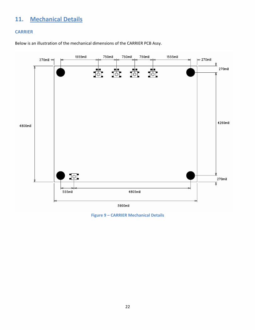
CARRIER Below is an illustration of the mechanical dimensions of the CARRIER PCB Assy.
Figure 9 – CARRIER Mechanical Details

23
LCDCARRIER Below is an illustration showing dimensions of the LCDCARRIER PCB Assy.
Figure 10 – LCDCARRIER Mechanical Details

24
12. Software Please refer to the Software section of the SOMDIMM Users Manual included with your kit for details on the software.
13. Schematics Please visit the FDI website at: http://www.teamfdi.com/DK‐TS‐KIT
14. Table of Figures Figure 1 – CARRIER Top Side ................................................................................................................................................... 3
Figure 2 – CARRIER Bottom Side ............................................................................................................................................. 4
Figure 4 – LCDCARRIER Top Side ............................................................................................................................................. 5
Figure 5 – DK‐TS‐KIT System Block Diagram (RX62N Shown) ................................................................................................. 6
Figure 6 – Jumper Locations ................................................................................................................................................. 18
Figure 7 – JP3 Illustration ...................................................................................................................................................... 19
Figure 8 – JP4 to JP7 Illustration ........................................................................................................................................... 20
Figure 9 – SOMDIMM Insertion ............................................................................................................................................ 21
Figure 10 – CARRIER Mechanical Details .............................................................................................................................. 22
Figure 11 – LCDCARRIER Mechanical Details ........................................................................................................................ 23