Embed Size (px)
Citation preview
1/50March 2008
M28W160ECTM28W160ECB
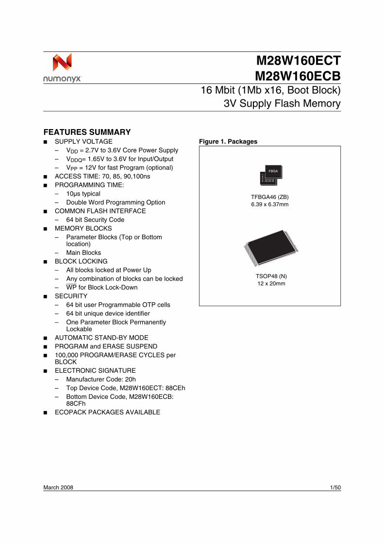
16 Mbit (1Mb x16, Boot Block)3V Supply Flash Memory
FEATURES SUMMARY■ SUPPLY VOLTAGE
– VDD = 2.7V to 3.6V Core Power Supply– VDDQ= 1.65V to 3.6V for Input/Output– VPP = 12V for fast Program (optional)
■ ACCESS TIME: 70, 85, 90,100ns■ PROGRAMMING TIME:
– 10µs typical– Double Word Programming Option
■ COMMON FLASH INTERFACE– 64 bit Security Code
■ MEMORY BLOCKS– Parameter Blocks (Top or Bottom
location)– Main Blocks
■ BLOCK LOCKING – All blocks locked at Power Up– Any combination of blocks can be locked– WP for Block Lock-Down
■ SECURITY– 64 bit user Programmable OTP cells– 64 bit unique device identifier– One Parameter Block Permanently
Lockable■ AUTOMATIC STAND-BY MODE■ PROGRAM and ERASE SUSPEND■ 100,000 PROGRAM/ERASE CYCLES per
BLOCK ■ ELECTRONIC SIGNATURE
– Manufacturer Code: 20h– Top Device Code, M28W160ECT: 88CEh– Bottom Device Code, M28W160ECB:
88CFh■ ECOPACK PACKAGES AVAILABLE
Figure 1. Packages
FBGA
TSOP48 (N)12 x 20mm
TFBGA46 (ZB)6.39 x 6.37mm
M28W160ECT, M28W160ECB
2/50
TABLE OF CONTENTS
FEATURES SUMMARY . . . . . . . . . . . . . . . . . . . . . . . . . . . . . . . . . . . . . . . . . . . . . . . . . . . . . . . . . . . . . 1
Figure 1. Packages . . . . . . . . . . . . . . . . . . . . . . . . . . . . . . . . . . . . . . . . . . . . . . . . . . . . . . . . . . . . . . 1
SUMMARY DESCRIPTION. . . . . . . . . . . . . . . . . . . . . . . . . . . . . . . . . . . . . . . . . . . . . . . . . . . . . . . . . . . 5
Figure 2. Logic Diagram . . . . . . . . . . . . . . . . . . . . . . . . . . . . . . . . . . . . . . . . . . . . . . . . . . . . . . . . . . 6Table 1. Signal Names . . . . . . . . . . . . . . . . . . . . . . . . . . . . . . . . . . . . . . . . . . . . . . . . . . . . . . . . . . 6Figure 3. TSOP Connections . . . . . . . . . . . . . . . . . . . . . . . . . . . . . . . . . . . . . . . . . . . . . . . . . . . . . . 6Figure 4. TFBGA Connections (Top view through package) . . . . . . . . . . . . . . . . . . . . . . . . . . . . . . 7Figure 5. Block Addresses . . . . . . . . . . . . . . . . . . . . . . . . . . . . . . . . . . . . . . . . . . . . . . . . . . . . . . . . 7Figure 6. Security Block and Protection Register Memory Map . . . . . . . . . . . . . . . . . . . . . . . . . . . . 8
SIGNAL DESCRIPTIONS . . . . . . . . . . . . . . . . . . . . . . . . . . . . . . . . . . . . . . . . . . . . . . . . . . . . . . . . . . . . 9
Address Inputs (A0-A19). . . . . . . . . . . . . . . . . . . . . . . . . . . . . . . . . . . . . . . . . . . . . . . . . . . . . . . . . . 9Data Input/Output (DQ0-DQ15). . . . . . . . . . . . . . . . . . . . . . . . . . . . . . . . . . . . . . . . . . . . . . . . . . . . . 9Chip Enable (E). . . . . . . . . . . . . . . . . . . . . . . . . . . . . . . . . . . . . . . . . . . . . . . . . . . . . . . . . . . . . . . . . 9Output Enable (G). . . . . . . . . . . . . . . . . . . . . . . . . . . . . . . . . . . . . . . . . . . . . . . . . . . . . . . . . . . . . . . 9Write Enable (W). . . . . . . . . . . . . . . . . . . . . . . . . . . . . . . . . . . . . . . . . . . . . . . . . . . . . . . . . . . . . . . . 9Write Protect (WP). . . . . . . . . . . . . . . . . . . . . . . . . . . . . . . . . . . . . . . . . . . . . . . . . . . . . . . . . . . . . . . 9Reset (RP). . . . . . . . . . . . . . . . . . . . . . . . . . . . . . . . . . . . . . . . . . . . . . . . . . . . . . . . . . . . . . . . . . . . . 9VDD Supply Voltage. . . . . . . . . . . . . . . . . . . . . . . . . . . . . . . . . . . . . . . . . . . . . . . . . . . . . . . . . . . . . . 9VDDQ Supply Voltage. . . . . . . . . . . . . . . . . . . . . . . . . . . . . . . . . . . . . . . . . . . . . . . . . . . . . . . . . . . . . 9VPP Program Supply Voltage . . . . . . . . . . . . . . . . . . . . . . . . . . . . . . . . . . . . . . . . . . . . . . . . . . . . . . 9VSS Ground. . . . . . . . . . . . . . . . . . . . . . . . . . . . . . . . . . . . . . . . . . . . . . . . . . . . . . . . . . . . . . . . . . . . 9
BUS OPERATIONS. . . . . . . . . . . . . . . . . . . . . . . . . . . . . . . . . . . . . . . . . . . . . . . . . . . . . . . . . . . . . . . . 10
Read. . . . . . . . . . . . . . . . . . . . . . . . . . . . . . . . . . . . . . . . . . . . . . . . . . . . . . . . . . . . . . . . . . . . . . . . . 10Write. . . . . . . . . . . . . . . . . . . . . . . . . . . . . . . . . . . . . . . . . . . . . . . . . . . . . . . . . . . . . . . . . . . . . . . . . 10Output Disable. . . . . . . . . . . . . . . . . . . . . . . . . . . . . . . . . . . . . . . . . . . . . . . . . . . . . . . . . . . . . . . . . 10Standby. . . . . . . . . . . . . . . . . . . . . . . . . . . . . . . . . . . . . . . . . . . . . . . . . . . . . . . . . . . . . . . . . . . . . . 10Automatic Standby. . . . . . . . . . . . . . . . . . . . . . . . . . . . . . . . . . . . . . . . . . . . . . . . . . . . . . . . . . . . . . 10Reset. . . . . . . . . . . . . . . . . . . . . . . . . . . . . . . . . . . . . . . . . . . . . . . . . . . . . . . . . . . . . . . . . . . . . . . . 10Table 2. Bus Operations . . . . . . . . . . . . . . . . . . . . . . . . . . . . . . . . . . . . . . . . . . . . . . . . . . . . . . . . 10
COMMAND INTERFACE . . . . . . . . . . . . . . . . . . . . . . . . . . . . . . . . . . . . . . . . . . . . . . . . . . . . . . . . . . . 11
Read Memory Array Command . . . . . . . . . . . . . . . . . . . . . . . . . . . . . . . . . . . . . . . . . . . . . . . . . . 11Read Status Register Command . . . . . . . . . . . . . . . . . . . . . . . . . . . . . . . . . . . . . . . . . . . . . . . . . 11Read Electronic Signature Command . . . . . . . . . . . . . . . . . . . . . . . . . . . . . . . . . . . . . . . . . . . . . 11Read CFI Query Command . . . . . . . . . . . . . . . . . . . . . . . . . . . . . . . . . . . . . . . . . . . . . . . . . . . . . . 11Block Erase Command . . . . . . . . . . . . . . . . . . . . . . . . . . . . . . . . . . . . . . . . . . . . . . . . . . . . . . . . . 11Program Command . . . . . . . . . . . . . . . . . . . . . . . . . . . . . . . . . . . . . . . . . . . . . . . . . . . . . . . . . . . . 11Double Word Program Command . . . . . . . . . . . . . . . . . . . . . . . . . . . . . . . . . . . . . . . . . . . . . . . . 12Clear Status Register Command . . . . . . . . . . . . . . . . . . . . . . . . . . . . . . . . . . . . . . . . . . . . . . . . . 12Program/Erase Suspend Command . . . . . . . . . . . . . . . . . . . . . . . . . . . . . . . . . . . . . . . . . . . . . . 12
3/50
M28W160ECT, M28W160ECB
Program/Erase Resume Command . . . . . . . . . . . . . . . . . . . . . . . . . . . . . . . . . . . . . . . . . . . . . . . 12Protection Register Program Command . . . . . . . . . . . . . . . . . . . . . . . . . . . . . . . . . . . . . . . . . . . 12Block Lock Command. . . . . . . . . . . . . . . . . . . . . . . . . . . . . . . . . . . . . . . . . . . . . . . . . . . . . . . . . . 13Block Unlock Command . . . . . . . . . . . . . . . . . . . . . . . . . . . . . . . . . . . . . . . . . . . . . . . . . . . . . . . . 13Block Lock-Down Command . . . . . . . . . . . . . . . . . . . . . . . . . . . . . . . . . . . . . . . . . . . . . . . . . . . . 13Table 3. Commands . . . . . . . . . . . . . . . . . . . . . . . . . . . . . . . . . . . . . . . . . . . . . . . . . . . . . . . . . . . 14Table 4. Read Electronic Signature . . . . . . . . . . . . . . . . . . . . . . . . . . . . . . . . . . . . . . . . . . . . . . . 14Table 5. Read Block Lock Signature . . . . . . . . . . . . . . . . . . . . . . . . . . . . . . . . . . . . . . . . . . . . . . 15Table 6. Read Protection Register and Lock Register . . . . . . . . . . . . . . . . . . . . . . . . . . . . . . . . . 15Table 7. Program, Erase Times and Program/Erase Endurance Cycles . . . . . . . . . . . . . . . . . . . 15
BLOCK LOCKING. . . . . . . . . . . . . . . . . . . . . . . . . . . . . . . . . . . . . . . . . . . . . . . . . . . . . . . . . . . . . . . . . 16
Reading a Block’s Lock Status . . . . . . . . . . . . . . . . . . . . . . . . . . . . . . . . . . . . . . . . . . . . . . . . . . 16Locked State . . . . . . . . . . . . . . . . . . . . . . . . . . . . . . . . . . . . . . . . . . . . . . . . . . . . . . . . . . . . . . . . . 16Unlocked State. . . . . . . . . . . . . . . . . . . . . . . . . . . . . . . . . . . . . . . . . . . . . . . . . . . . . . . . . . . . . . . . 16Lock-Down State . . . . . . . . . . . . . . . . . . . . . . . . . . . . . . . . . . . . . . . . . . . . . . . . . . . . . . . . . . . . . . 16Locking Operations During Erase Suspend . . . . . . . . . . . . . . . . . . . . . . . . . . . . . . . . . . . . . . . . 16Table 8. Block Lock Status . . . . . . . . . . . . . . . . . . . . . . . . . . . . . . . . . . . . . . . . . . . . . . . . . . . . . . 17Table 9. Protection Status . . . . . . . . . . . . . . . . . . . . . . . . . . . . . . . . . . . . . . . . . . . . . . . . . . . . . . 17
STATUS REGISTER . . . . . . . . . . . . . . . . . . . . . . . . . . . . . . . . . . . . . . . . . . . . . . . . . . . . . . . . . . . . . . . 18
Program/Erase Controller Status (Bit 7) . . . . . . . . . . . . . . . . . . . . . . . . . . . . . . . . . . . . . . . . . . . . . 18Erase Suspend Status (Bit 6) . . . . . . . . . . . . . . . . . . . . . . . . . . . . . . . . . . . . . . . . . . . . . . . . . . . . . 18Erase Status (Bit 5) . . . . . . . . . . . . . . . . . . . . . . . . . . . . . . . . . . . . . . . . . . . . . . . . . . . . . . . . . . . . . 18Program Status (Bit 4) . . . . . . . . . . . . . . . . . . . . . . . . . . . . . . . . . . . . . . . . . . . . . . . . . . . . . . . . . . . 18VPP Status (Bit 3). . . . . . . . . . . . . . . . . . . . . . . . . . . . . . . . . . . . . . . . . . . . . . . . . . . . . . . . . . . . . . . 18Program Suspend Status (Bit 2) . . . . . . . . . . . . . . . . . . . . . . . . . . . . . . . . . . . . . . . . . . . . . . . . . . . 18Block Protection Status (Bit 1) . . . . . . . . . . . . . . . . . . . . . . . . . . . . . . . . . . . . . . . . . . . . . . . . . . . . . 19Reserved (Bit 0). . . . . . . . . . . . . . . . . . . . . . . . . . . . . . . . . . . . . . . . . . . . . . . . . . . . . . . . . . . . . . . . 19Table 10. Status Register Bits . . . . . . . . . . . . . . . . . . . . . . . . . . . . . . . . . . . . . . . . . . . . . . . . . . . . . 19
MAXIMUM RATING. . . . . . . . . . . . . . . . . . . . . . . . . . . . . . . . . . . . . . . . . . . . . . . . . . . . . . . . . . . . . . . . 20
Table 11. Absolute Maximum Ratings . . . . . . . . . . . . . . . . . . . . . . . . . . . . . . . . . . . . . . . . . . . . . . . 20
DC and AC PARAMETERS . . . . . . . . . . . . . . . . . . . . . . . . . . . . . . . . . . . . . . . . . . . . . . . . . . . . . . . . . 21
Table 12. Operating and AC Measurement Conditions . . . . . . . . . . . . . . . . . . . . . . . . . . . . . . . . . . 21Figure 7. AC Measurement I/O Waveform . . . . . . . . . . . . . . . . . . . . . . . . . . . . . . . . . . . . . . . . . . . 21Figure 8. AC Measurement Load Circuit. . . . . . . . . . . . . . . . . . . . . . . . . . . . . . . . . . . . . . . . . . . . . 21Table 13. Capacitance. . . . . . . . . . . . . . . . . . . . . . . . . . . . . . . . . . . . . . . . . . . . . . . . . . . . . . . . . . . 21Table 14. DC Characteristics . . . . . . . . . . . . . . . . . . . . . . . . . . . . . . . . . . . . . . . . . . . . . . . . . . . . . 22Figure 9. Read Mode AC Waveforms . . . . . . . . . . . . . . . . . . . . . . . . . . . . . . . . . . . . . . . . . . . . . . . 23Table 15. Read AC Characteristics . . . . . . . . . . . . . . . . . . . . . . . . . . . . . . . . . . . . . . . . . . . . . . . . . 23Figure 10.Write AC Waveforms, Write Enable Controlled. . . . . . . . . . . . . . . . . . . . . . . . . . . . . . . . 24Table 16. Write AC Characteristics, Write Enable Controlled . . . . . . . . . . . . . . . . . . . . . . . . . . . . . 25Figure 11.Write AC Waveforms, Chip Enable Controlled . . . . . . . . . . . . . . . . . . . . . . . . . . . . . . . . 26Table 17. Write AC Characteristics, Chip Enable Controlled . . . . . . . . . . . . . . . . . . . . . . . . . . . . . 27
M28W160ECT, M28W160ECB
4/50
Figure 12.Power-Up and Reset AC Waveforms . . . . . . . . . . . . . . . . . . . . . . . . . . . . . . . . . . . . . . . 28Table 18. Power-Up and Reset AC Characteristics. . . . . . . . . . . . . . . . . . . . . . . . . . . . . . . . . . . . . 28
PACKAGE MECHANICAL . . . . . . . . . . . . . . . . . . . . . . . . . . . . . . . . . . . . . . . . . . . . . . . . . . . . . . . . . . 29
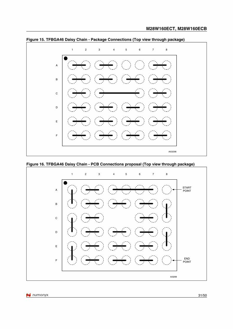
Figure 13.TSOP48 - 48 lead Plastic Thin Small Outline, 12 x 20mm, Package Outline . . . . . . . . . 29Table 19. TSOP48 - 48 lead Plastic Thin Small Outline, 12 x 20mm, Package Mechanical Data . 29Figure 14.TFBGA46 6.39x6.37mm - 8x6 ball array, 0.75mm pitch, Bottom View Package Outline 30Table 20. TFBGA46 6.39x6.37mm - 8x6 ball array, 0.75mm pitch, Package Mechanical Data . . . 30Figure 15.TFBGA46 Daisy Chain - Package Connections (Top view through package) . . . . . . . . 31Figure 16.TFBGA46 Daisy Chain - PCB Connections proposal (Top view through package) . . . . 31
PART NUMBERING . . . . . . . . . . . . . . . . . . . . . . . . . . . . . . . . . . . . . . . . . . . . . . . . . . . . . . . . . . . . . . . 32
Table 21. Ordering Information Scheme . . . . . . . . . . . . . . . . . . . . . . . . . . . . . . . . . . . . . . . . . . . . . 32Table 22. Daisy Chain Ordering Scheme . . . . . . . . . . . . . . . . . . . . . . . . . . . . . . . . . . . . . . . . . . . . 33
APPENDIX A.BLOCK ADDRESS TABLES . . . . . . . . . . . . . . . . . . . . . . . . . . . . . . . . . . . . . . . . . . . . . 34
Table 23. Top Boot Block Addresses, M28W160ECT. . . . . . . . . . . . . . . . . . . . . . . . . . . . . . . . . . . 34Table 24. Bottom Boot Block Addresses, M28W160ECB . . . . . . . . . . . . . . . . . . . . . . . . . . . . . . . . 34
APPENDIX B.COMMON FLASH INTERFACE (CFI) . . . . . . . . . . . . . . . . . . . . . . . . . . . . . . . . . . . . . . 35
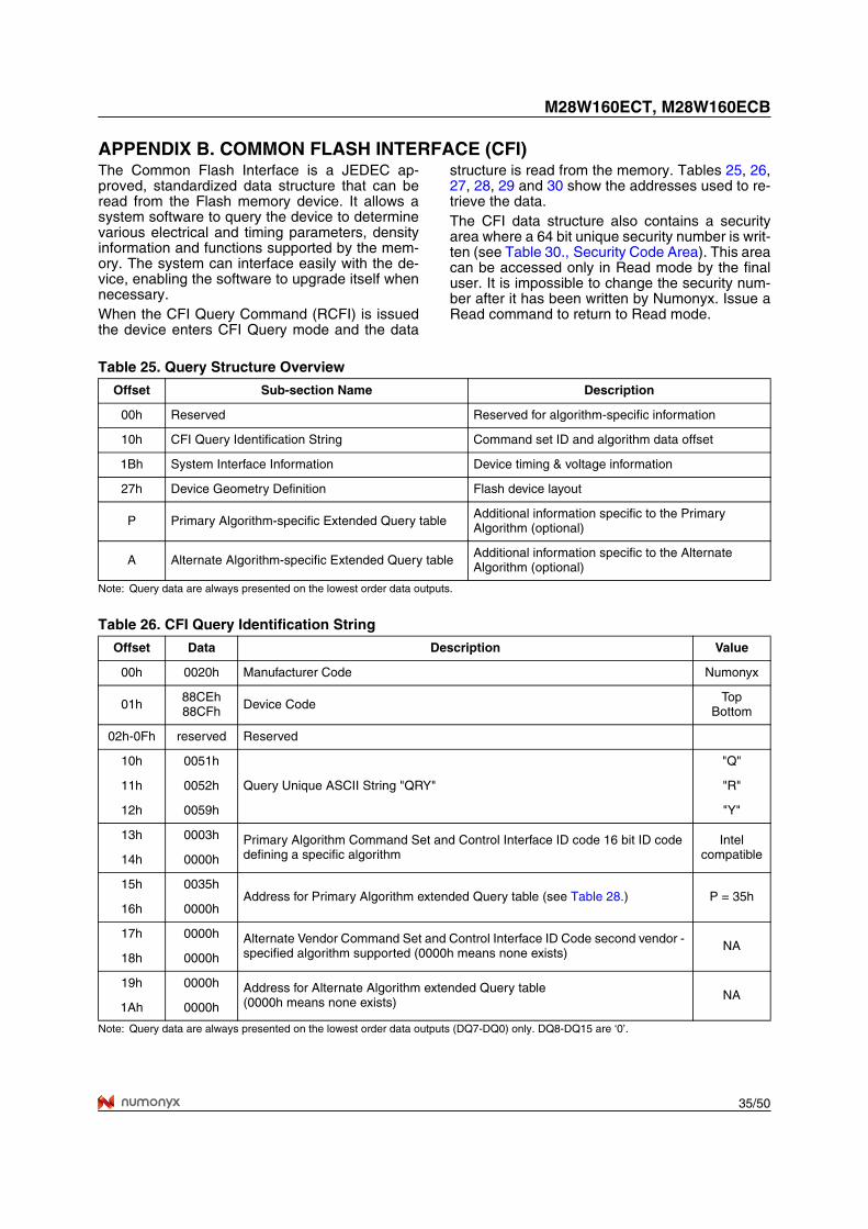
Table 25. Query Structure Overview . . . . . . . . . . . . . . . . . . . . . . . . . . . . . . . . . . . . . . . . . . . . . . . . 35Table 26. CFI Query Identification String. . . . . . . . . . . . . . . . . . . . . . . . . . . . . . . . . . . . . . . . . . . . . 35Table 27. CFI Query System Interface Information . . . . . . . . . . . . . . . . . . . . . . . . . . . . . . . . . . . . . 36Table 28. Device Geometry Definition . . . . . . . . . . . . . . . . . . . . . . . . . . . . . . . . . . . . . . . . . . . . . . 37Table 29. Primary Algorithm-Specific Extended Query Table . . . . . . . . . . . . . . . . . . . . . . . . . . . . . 38Table 30. Security Code Area . . . . . . . . . . . . . . . . . . . . . . . . . . . . . . . . . . . . . . . . . . . . . . . . . . . . . 39
APPENDIX C.FLOWCHARTS AND PSEUDO CODES . . . . . . . . . . . . . . . . . . . . . . . . . . . . . . . . . . . . 40
Figure 17.Program Flowchart and Pseudo Code . . . . . . . . . . . . . . . . . . . . . . . . . . . . . . . . . . . . . . 40Figure 18.Double Word Program Flowchart and Pseudo Code . . . . . . . . . . . . . . . . . . . . . . . . . . . 41Figure 19.Program Suspend & Resume Flowchart and Pseudo Code . . . . . . . . . . . . . . . . . . . . . . 42Figure 20.Erase Flowchart and Pseudo Code. . . . . . . . . . . . . . . . . . . . . . . . . . . . . . . . . . . . . . . . . 43Figure 21.Erase Suspend & Resume Flowchart and Pseudo Code . . . . . . . . . . . . . . . . . . . . . . . . 44Figure 22.Locking Operations Flowchart and Pseudo Code . . . . . . . . . . . . . . . . . . . . . . . . . . . . . . 45Figure 23.Protection Register Program Flowchart and Pseudo Code. . . . . . . . . . . . . . . . . . . . . . . 46
APPENDIX D.COMMAND INTERFACE AND PROGRAM/ERASE CONTROLLER STATE. . . . . . . . 47
Table 31. Write State Machine Current/Next, sheet 1 of 2. . . . . . . . . . . . . . . . . . . . . . . . . . . . . . . . 47Table 32. Write State Machine Current/Next, sheet 2 of 2. . . . . . . . . . . . . . . . . . . . . . . . . . . . . . . . 48
REVISION HISTORY. . . . . . . . . . . . . . . . . . . . . . . . . . . . . . . . . . . . . . . . . . . . . . . . . . . . . . . . . . . . . . . 49
Table 33. Document Revision History . . . . . . . . . . . . . . . . . . . . . . . . . . . . . . . . . . . . . . . . . . . . . . . 49
5/50
M28W160ECT, M28W160ECB
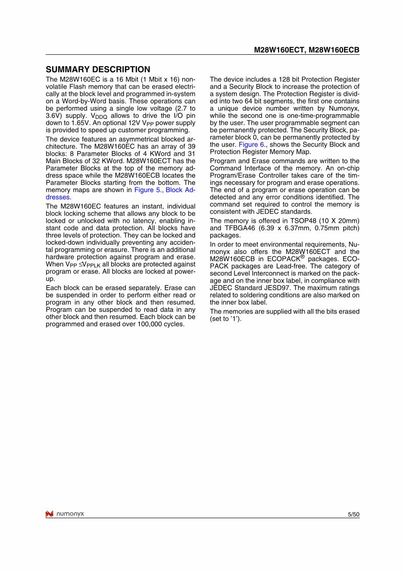
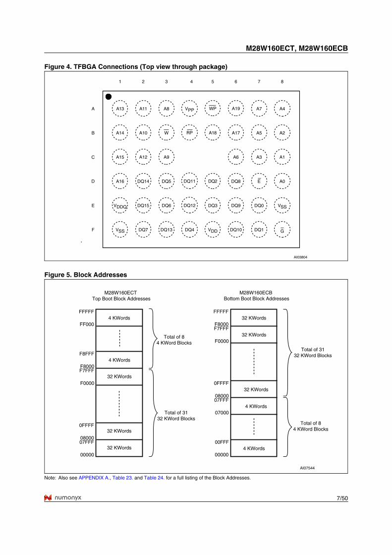
SUMMARY DESCRIPTIONThe M28W160EC is a 16 Mbit (1 Mbit x 16) non-volatile Flash memory that can be erased electri-cally at the block level and programmed in-systemon a Word-by-Word basis. These operations canbe performed using a single low voltage (2.7 to3.6V) supply. VDDQ allows to drive the I/O pindown to 1.65V. An optional 12V VPP power supplyis provided to speed up customer programming. The device features an asymmetrical blocked ar-chitecture. The M28W160EC has an array of 39blocks: 8 Parameter Blocks of 4 KWord and 31Main Blocks of 32 KWord. M28W160ECT has theParameter Blocks at the top of the memory ad-dress space while the M28W160ECB locates theParameter Blocks starting from the bottom. Thememory maps are shown in Figure 5., Block Ad-dresses. The M28W160EC features an instant, individualblock locking scheme that allows any block to belocked or unlocked with no latency, enabling in-stant code and data protection. All blocks havethree levels of protection. They can be locked andlocked-down individually preventing any acciden-tal programming or erasure. There is an additionalhardware protection against program and erase.When VPP ≤ VPPLK all blocks are protected againstprogram or erase. All blocks are locked at power-up. Each block can be erased separately. Erase canbe suspended in order to perform either read orprogram in any other block and then resumed.Program can be suspended to read data in anyother block and then resumed. Each block can beprogrammed and erased over 100,000 cycles.
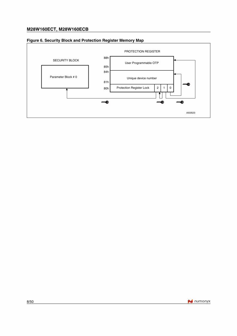
The device includes a 128 bit Protection Registerand a Security Block to increase the protection ofa system design. The Protection Register is divid-ed into two 64 bit segments, the first one containsa unique device number written by Numonyx,while the second one is one-time-programmableby the user. The user programmable segment canbe permanently protected. The Security Block, pa-rameter block 0, can be permanently protected bythe user. Figure 6., shows the Security Block andProtection Register Memory Map. Program and Erase commands are written to theCommand Interface of the memory. An on-chipProgram/Erase Controller takes care of the tim-ings necessary for program and erase operations.The end of a program or erase operation can bedetected and any error conditions identified. Thecommand set required to control the memory isconsistent with JEDEC standards.The memory is offered in TSOP48 (10 X 20mm)and TFBGA46 (6.39 x 6.37mm, 0.75mm pitch)packages.In order to meet environmental requirements, Nu-monyx also offers the M28W160ECT and theM28W160ECB in ECOPACK® packages. ECO-PACK packages are Lead-free. The category ofsecond Level Interconnect is marked on the pack-age and on the inner box label, in compliance withJEDEC Standard JESD97. The maximum ratingsrelated to soldering conditions are also marked onthe inner box label. The memories are supplied with all the bits erased(set to ’1’).
M28W160ECT, M28W160ECB
6/50
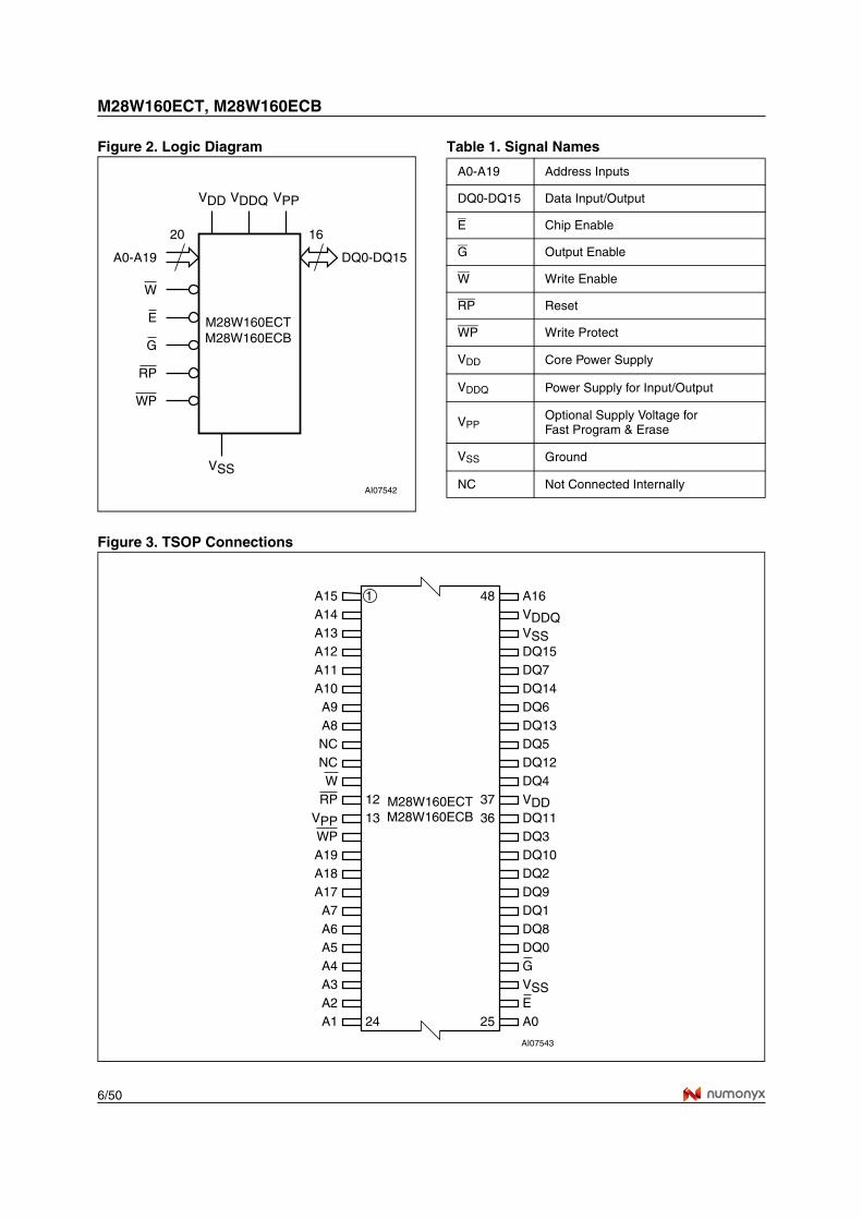
Figure 2. Logic Diagram Table 1. Signal Names
Figure 3. TSOP Connections
AI07542
20
A0-A19
W
DQ0-DQ15
VDD
M28W160ECTM28W160ECB
E
VSS
16
G
RP
WP
VDDQ VPP
A0-A19 Address Inputs
DQ0-DQ15 Data Input/Output
E Chip Enable
G Output Enable
W Write Enable
RP Reset
WP Write Protect
VDD Core Power Supply
VDDQ Power Supply for Input/Output
VPPOptional Supply Voltage for Fast Program & Erase
VSS Ground
NC Not Connected Internally
DQ3
DQ9DQ2
A6DQ0
W
A3
NC
DQ6A8A9
DQ13
A17
A10 DQ14
A2
DQ12
DQ10
DQ15
VDD
DQ4
DQ5
A7
DQ7
VPPWP
AI07543
M28W160ECTM28W160ECB
12
1
13
24 25
3637
48
DQ8
NC
A19
A1
A18
A4A5
DQ1
DQ11
G
A12A13
A16
A11
VDDQ
A15A14
VSS
EA0
RP
VSS
7/50
M28W160ECT, M28W160ECB
Figure 4. TFBGA Connections (Top view through package)
Figure 5. Block Addresses
Note: Also see APPENDIX A., Table 23. and Table 24. for a full listing of the Block Addresses.
AI03804
C
B
A
87654321
E
D
F
A4A7VPPA8A11A13
A0EDQ8DQ5DQ14A16
VSSDQ0DQ9DQ3DQ6DQ15VDDQ
DQ1DQ10VDDDQ7VSS
DQ2
A2A5A17WA10A14
A1A3A6A9A12A15
RP A18
DQ4DQ13 G
DQ12
DQ11
WP A19
AI07544
4 KWordsFFFFF
FF000
32 KWords
0FFFF
08000
32 KWords07FFF
00000
M28W160ECT Top Boot Block Addresses
4 KWordsF8FFF
F8000
32 KWordsF0000
F7FFF
Total of 84 KWord Blocks
Total of 3132 KWord Blocks
4 KWords
FFFFF
F800032 KWords
32 KWords
00FFF
00000
M28W160ECB Bottom Boot Block Addresses
4 KWords
F7FFF
0FFFF32 KWords
F0000
08000
Total of 3132 KWord Blocks
Total of 84 KWord Blocks
07FFF
07000
M28W160ECT, M28W160ECB
8/50
Figure 6. Security Block and Protection Register Memory Map
AI03523
Parameter Block # 0
User Programmable OTP
Unique device number
Protection Register Lock 2 1 0
88h
85h
84h
81h
80h
SECURITY BLOCK
PROTECTION REGISTER
9/50
M28W160ECT, M28W160ECB
SIGNAL DESCRIPTIONSSee Figure 2., Logic Diagram and Table 1., SignalNames, for a brief overview of the signals connect-ed to this device. Address Inputs (A0-A19). The Address Inputsselect the cells in the memory array to access dur-ing Bus Read operations. During Bus Write opera-tions they control the commands sent to theCommand Interface of the internal state machine.Data Input/Output (DQ0-DQ15). The Data I/Ooutputs the data stored at the selected addressduring a Bus Read operation or inputs a commandor the data to be programmed during a Write Busoperation.Chip Enable (E). The Chip Enable input acti-vates the memory control logic, input buffers, de-coders and sense amplifiers. When Chip Enable isat VILand Reset is at VIH the device is in activemode. When Chip Enable is at VIH the memory isdeselected, the outputs are high impedance andthe power consumption is reduced to the stand-bylevel. Output Enable (G). The Output Enable controlsdata outputs during the Bus Read operation of thememory.Write Enable (W). The Write Enable controls theBus Write operation of the memory’s CommandInterface. The data and address inputs are latchedon the rising edge of Chip Enable, E, or Write En-able, W, whichever occurs first.Write Protect (WP). Write Protect is an inputthat gives an additional hardware protection foreach block. When Write Protect is at VIL, the Lock-Down is enabled and the protection status of theblock cannot be changed. When Write Protect is atVIH, the Lock-Down is disabled and the block canbe locked or unlocked. (refer to Table 6., ReadProtection Register and Lock Register).Reset (RP). The Reset input provides a hard-ware reset of the memory. When Reset is at VIL,the memory is in reset mode: the outputs are highimpedance and the current consumption is mini-mized. After Reset all blocks are in the Locked
state. When Reset is at VIH, the device is in normaloperation. Exiting reset mode the device entersread array mode, but a negative transition of ChipEnable or a change of the address is required toensure valid data outputs. VDD Supply Voltage. VDD provides the powersupply to the internal core of the memory device.It is the main power supply for all operations(Read, Program and Erase). VDDQ Supply Voltage. VDDQ provides thepower supply to the I/O pins and enables all Out-puts to be powered independently from VDD. VDDQcan be tied to VDD or can use a separate supply.VPP Program Supply Voltage. VPP is both acontrol input and a power supply pin. The twofunctions are selected by the voltage range ap-plied to the pin. The Supply Voltage VDD and theProgram Supply Voltage VPP can be applied inany order.If VPP is kept in a low voltage range (0V to 3.6V)VPP is seen as a control input. In this case a volt-age lower than VPPLK gives an absolute protectionagainst program or erase, while VPP > VPP1 en-ables these functions (see Table 14., DC Charac-teristics, for the relevant values). VPP is onlysampled at the beginning of a program or erase; achange in its value after the operation has starteddoes not have any effect and program or erase op-erations continue.If VPP is in the range 11.4V to 12.6V it acts as apower supply pin. In this condition VPP must bestable until the Program/Erase algorithm is com-pleted (see Table 16. and Table 17.).VSS Ground. VSS is the reference for all voltagemeasurements. Note: Each device in a system should haveVDD, VDDQ and VPP decoupled with a 0.1µF ca-pacitor close to the pin. See Figure 8., AC Mea-surement Load Circuit. The PCB trace widthsshould be sufficient to carry the required VPPprogram and erase currents.
M28W160ECT, M28W160ECB
10/50
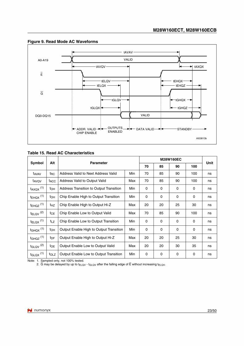
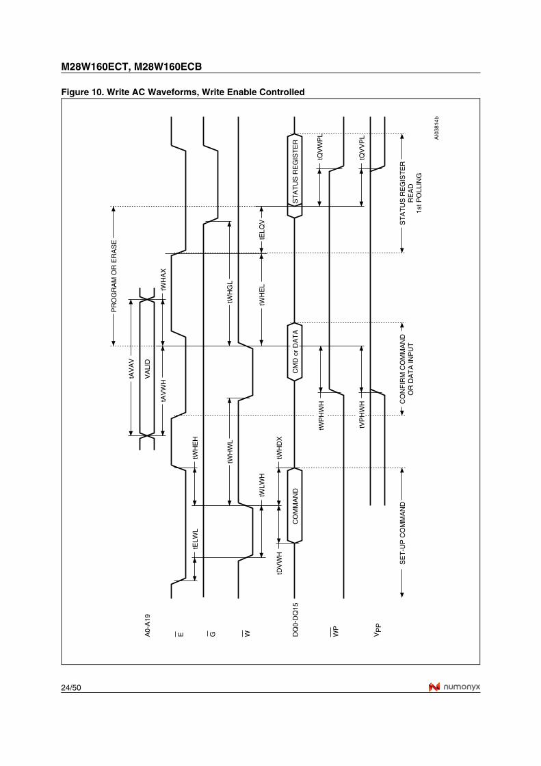
BUS OPERATIONSThere are six standard bus operations that controlthe device. These are Bus Read, Bus Write, Out-put Disable, Standby, Automatic Standby and Re-set. See Table 2., Bus Operations, for a summary. Typically glitches of less than 5ns on Chip Enableor Write Enable are ignored by the memory and donot affect bus operations.Read. Read Bus operations are used to outputthe contents of the Memory Array, the ElectronicSignature, the Status Register and the CommonFlash Interface. Both Chip Enable and Output En-able must be at VIL in order to perform a read op-eration. The Chip Enable input should be used toenable the device. Output Enable should be usedto gate data onto the output. The data read de-pends on the previous command written to thememory (see Command Interface section). SeeFigure 9., Read Mode AC Waveforms, and Table15., Read AC Characteristics, for details of whenthe output becomes valid.Read mode is the default state of the device whenexiting Reset or after power-up. Write. Bus Write operations write Commands tothe memory or latch Input Data to be programmed.A write operation is initiated when Chip Enableand Write Enable are at VIL with Output Enable atVIH. Commands, Input Data and Addresses arelatched on the rising edge of Write Enable or ChipEnable, whichever occurs first.
See Figures 10 and 11, Write AC Waveforms, andTables 16 and 17, Write AC Characteristics, fordetails of the timing requirements.Output Disable. The data outputs are high im-pedance when the Output Enable is at VIH. Standby. Standby disables most of the internalcircuitry allowing a substantial reduction of the cur-rent consumption. The memory is in stand-bywhen Chip Enable is at VIH and the device is inread mode. The power consumption is reduced tothe stand-by level and the outputs are set to highimpedance, independently from the Output Enableor Write Enable inputs. If Chip Enable switches toVIH during a program or erase operation, the de-vice enters Standby mode when finished. Automatic Standby. Automatic Standby pro-vides a low power consumption state during Readmode. Following a read operation, the device en-ters Automatic Standby after 150ns of bus inactiv-ity even if Chip Enable is Low, VIL, and the supplycurrent is reduced to IDD1. The data Inputs/Out-puts will still output data if a bus Read operation isin progress.Reset. During Reset mode when Output Enableis Low, VIL, the memory is deselected and the out-puts are high impedance. The memory is in Resetmode when Reset is at VIL. The power consump-tion is reduced to the Standby level, independentlyfrom the Chip Enable, Output Enable or Write En-able inputs. If Reset is pulled to VSS during a Pro-gram or Erase, this operation is aborted and thememory content is no longer valid.
Table 2. Bus Operations
Note: X = VIL or VIH, VPPH = 12V ± 5%.
Operation E G W RP WP VPP DQ0-DQ15
Bus Read VIL VIL VIH VIH X Don't Care Data Output
Bus Write VIL VIH VIL VIH X VDD or VPPH Data Input
Output Disable VIL VIH VIH VIH X Don't Care Hi-Z
Standby VIH X X VIH X Don't Care Hi-Z
Reset X X X VIL X Don't Care Hi-Z
11/50
M28W160ECT, M28W160ECB
COMMAND INTERFACEAll Bus Write operations to the memory are inter-preted by the Command Interface. Commandsconsist of one or more sequential Bus Write oper-ations. An internal Program/Erase Controller han-dles all timings and verifies the correct executionof the Program and Erase commands. The Pro-gram/Erase Controller provides a Status Registerwhose output may be read at any time during, tomonitor the progress of the operation, or the Pro-gram/Erase states. See APPENDIX D., Table 31.,Write State Machine Current/Next, for a summaryof the Command Interface.The Command Interface is reset to Read modewhen power is first applied, when exiting from Re-set or whenever VDD is lower than VLKO. Com-mand sequences must be followed exactly. Anyinvalid combination of commands will reset the de-vice to Read mode. Refer to Table 3., Commands,in conjunction with the text descriptions below.Read Memory Array Command The Read command returns the memory to itsRead mode. One Bus Write cycle is required to is-sue the Read Memory Array command and returnthe memory to Read mode. Subsequent read op-erations will read the addressed location and out-put the data. When a device Reset occurs, thememory defaults to Read mode. Read Status Register Command The Status Register indicates when a program orerase operation is complete and the success orfailure of the operation itself. Issue a Read StatusRegister command to read the Status Register’scontents. Subsequent Bus Read operations readthe Status Register at any address, until anothercommand is issued. See Table 10., Status Regis-ter Bits, for details on the definitions of the bits.The Read Status Register command may be is-sued at any time, even during a Program/Eraseoperation. Any Read attempt during a Program/Erase operation will automatically output the con-tent of the Status Register. Read Electronic Signature Command The Read Electronic Signature command readsthe Manufacturer and Device Codes and the BlockLocking Status, or the Protection Register.The Read Electronic Signature command consistsof one write cycle, a subsequent read will outputthe Manufacturer Code, the Device Code, theBlock Lock and Lock-Down Status, or the Protec-tion and Lock Register. See Tables 4, 5 and 6 forthe valid address. Read CFI Query Command The Read Query Command is used to read datafrom the Common Flash Interface (CFI) MemoryArea, allowing programming equipment or appli-
cations to automatically match their interface tothe characteristics of the device. One Bus Writecycle is required to issue the Read Query Com-mand. Once the command is issued subsequentBus Read operations read from the CommonFlash Interface Memory Area. See APPENDIXB., COMMON FLASH INTERFACE (CFI), Tables25, 26, 27, 28, 29 and 30 for details on the infor-mation contained in the Common Flash Interfacememory area.Block Erase Command The Block Erase command can be used to erasea block. It sets all the bits within the selected blockto ’1’. All previous data in the block is lost. If theblock is protected then the Erase operation willabort, the data in the block will not be changed andthe Status Register will output the error.Two Bus Write cycles are required to issue thecommand. ■ The first bus cycle sets up the Erase
command. ■ The second latches the block address in the
internal state machine and starts the Program/Erase Controller.
If the second bus cycle is not Write Erase Confirm(D0h), Status Register bits b4 and b5 are set andthe command aborts.Erase aborts if Reset turns to VIL. As data integritycannot be guaranteed when the Erase operation isaborted, the block must be erased again. During Erase operations the memory will acceptthe Read Status Register command and the Pro-gram/Erase Suspend command, all other com-mands will be ignored. Typical Erase times aregiven in Table 7., Program, Erase Times and Pro-gram/Erase Endurance Cycles.See APPENDIX C., Figure 20., Erase Flowchartand Pseudo Code, for a suggested flowchart forusing the Erase command.Program Command The memory array can be programmed word-by-word. Two bus write cycles are required to issuethe Program Command. ■ The first bus cycle sets up the Program
command. ■ The second latches the Address and the Data
to be written and starts the Program/Erase Controller.
During Program operations the memory will ac-cept the Read Status Register command and theProgram/Erase Suspend command. Typical Pro-gram times are given in Table 7., Program, EraseTimes and Program/Erase Endurance Cycles.
M28W160ECT, M28W160ECB
12/50
Programming aborts if Reset goes to VIL. As dataintegrity cannot be guaranteed when the programoperation is aborted, the block containing thememory location must be erased and repro-grammed. See APPENDIX C., Figure 17., Program Flow-chart and Pseudo Code, for the flowchart for usingthe Program command.Double Word Program Command This feature is offered to improve the programmingthroughput, writing a page of two adjacent wordsin parallel.The two words must differ only for theaddress A0. Programming should not be attempt-ed when VPP is not at VPPH. The command can beexecuted if VPP is below VPPH but the result is notguaranteed. Three bus write cycles are necessary to issue theDouble Word Program command.■ The first bus cycle sets up the Double Word
Program Command.■ The second bus cycle latches the Address and
the Data of the first word to be written.■ The third bus cycle latches the Address and
the Data of the second word to be written and starts the Program/Erase Controller.
Read operations output the Status Register con-tent after the programming has started. Program-ming aborts if Reset goes to VIL. As data integritycannot be guaranteed when the program opera-tion is aborted, the block containing the memorylocation must be erased and reprogrammed. See APPENDIX C., Figure 18., Double Word Pro-gram Flowchart and Pseudo Code, for the flow-chart for using the Double Word Programcommand.Clear Status Register Command The Clear Status Register command can be usedto reset bits 1, 3, 4 and 5 in the Status Register to‘0’. One bus write cycle is required to issue theClear Status Register command. The bits in the Status Register do not automatical-ly return to ‘0’ when a new Program or Erase com-mand is issued. The error bits in the StatusRegister should be cleared before attempting anew Program or Erase command.Program/Erase Suspend Command The Program/Erase Suspend command is used topause a Program or Erase operation. One buswrite cycle is required to issue the Program/Erasecommand and pause the Program/Erase control-ler.During Program/Erase Suspend the Command In-terface will accept the Program/Erase Resume,Read Array, Read Status Register, Read Electron-ic Signature and Read CFI Query commands. Ad-
ditionally, if the suspend operation was Erase thenthe Program, Block Lock, Block Lock-Down orProtection Program commands will also be ac-cepted. The block being erased may be protectedby issuing the Block Protect, Block Lock or Protec-tion Program commands. When the Program/Erase Resume command is issued the operationwill complete. Only the blocks not being erasedmay be read or programmed correctly.During a Program/Erase Suspend, the device canbe placed in a pseudo-standby mode by takingChip Enable to VIH. Program/Erase is aborted ifReset turns to VIL. See APPENDIX C., Figure 19., Program Suspend& Resume Flowchart and Pseudo Code, and Fig-ure 21., Erase Suspend & Resume Flowchart andPseudo Code, for flowcharts for using the Pro-gram/Erase Suspend command.Program/Erase Resume Command The Program/Erase Resume command can beused to restart the Program/Erase Controller aftera Program/Erase Suspend operation has pausedit. One Bus Write cycle is required to issue thecommand. Once the command is issued subse-quent Bus Read operations read the Status Reg-ister.See APPENDIX C., Figure 19., Program Suspend& Resume Flowchart and Pseudo Code, and Fig-ure 21., Erase Suspend & Resume Flowchart andPseudo Code, for flowcharts for using the Pro-gram/Erase Resume command.Protection Register Program CommandThe Protection Register Program command isused to Program the 64 bit user One-Time-Pro-grammable (OTP) segment of the Protection Reg-ister. The segment is programmed 16 bits at atime. When shipped all bits in the segment are setto ‘1’. The user can only program the bits to ‘0’. Two write cycles are required to issue the Protec-tion Register Program command. ■ The first bus cycle sets up the Protection
Register Program command.■ The second latches the Address and the Data
to be written to the Protection Register and starts the Program/Erase Controller.
Read operations output the Status Register con-tent after the programming has started. The segment can be protected by programming bit1 of the Protection Lock Register. Bit 1 of the Pro-tection Lock Register protects bit 2 of the Protec-tion Lock Register. Programming bit 2 of theProtection Lock Register will result in a permanentprotection of the Security Block (see Figure6., Security Block and Protection Register Memo-ry Map). Attempting to program a previously pro-tected Protection Register will result in a Status

13/50
M28W160ECT, M28W160ECB
Register error. The protection of the ProtectionRegister and/or the Security Block is not revers-ible.The Protection Register Program cannot be sus-pended. See APPENDIX C., Figure23., Protection Register Program Flowchart andPseudo Code, for the flowchart for using the Pro-tection Register Program command.Block Lock CommandThe Block Lock command is used to lock a blockand prevent Program or Erase operations fromchanging the data in it. All blocks are locked atpower-up or reset.Two Bus Write cycles are required to issue theBlock Lock command. ■ The first bus cycle sets up the Block Lock
command. ■ The second Bus Write cycle latches the block
address. The lock status can be monitored for each blockusing the Read Electronic Signature command.Table 9. shows the protection status after issuinga Block Lock command. The Block Lock bits are volatile, once set they re-main set until a hardware reset or power-down/power-up. They are cleared by a Blocks Unlockcommand. Refer to the section, Block Locking, fora detailed explanation.Block Unlock CommandThe Blocks Unlock command is used to unlock ablock, allowing the block to be programmed or
erased. Two Bus Write cycles are required to is-sue the Blocks Unlock command. ■ The first bus cycle sets up the Block Unlock
command. ■ The second Bus Write cycle latches the block
address. The lock status can be monitored for each blockusing the Read Electronic Signature command.Table 9. shows the protection status after issuinga Block Unlock command. Refer to the section,Block Locking, for a detailed explanation.Block Lock-Down CommandA locked block cannot be Programmed or Erased,or have its protection status changed when WP islow, VIL. When WP is high, VIH, the Lock-Downfunction is disabled and the locked blocks can beindividually unlocked by the Block Unlock com-mand.Two Bus Write cycles are required to issue theBlock Lock-Down command. ■ The first bus cycle sets up the Block Lock
command. ■ The second Bus Write cycle latches the block
address. The lock status can be monitored for each blockusing the Read Electronic Signature command.Locked-Down blocks revert to the locked (and notlocked-down) state when the device is reset onpower-down. Table 9. shows the protection statusafter issuing a Block Lock-Down command. Referto the section, Block Locking, for a detailed expla-nation.
M28W160ECT, M28W160ECB
14/50
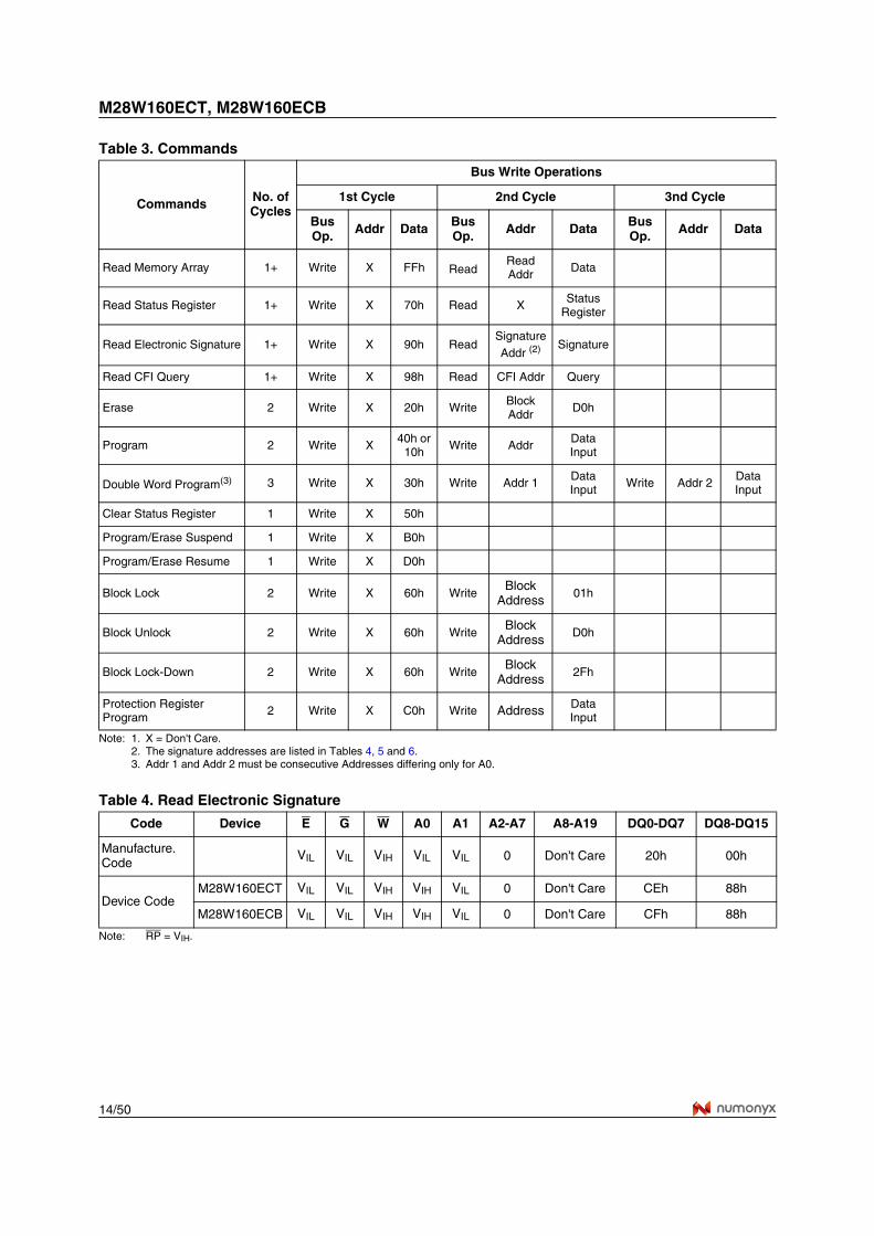
Table 3. Commands
Note: 1. X = Don't Care.2. The signature addresses are listed in Tables 4, 5 and 6.3. Addr 1 and Addr 2 must be consecutive Addresses differing only for A0.
Table 4. Read Electronic Signature
Note: RP = VIH.
Commands No. of Cycles
Bus Write Operations
1st Cycle 2nd Cycle 3nd Cycle
Bus Op. Addr Data Bus
Op. Addr Data Bus Op. Addr Data
Read Memory Array 1+ Write X FFh Read Read Addr Data
Read Status Register 1+ Write X 70h Read X Status Register
Read Electronic Signature 1+ Write X 90h Read Signature Addr (2) Signature
Read CFI Query 1+ Write X 98h Read CFI Addr Query
Erase 2 Write X 20h Write Block Addr D0h
Program 2 Write X 40h or 10h Write Addr Data
Input
Double Word Program(3) 3 Write X 30h Write Addr 1 Data Input Write Addr 2 Data
Input
Clear Status Register 1 Write X 50h
Program/Erase Suspend 1 Write X B0h
Program/Erase Resume 1 Write X D0h
Block Lock 2 Write X 60h WriteBlock
Address01h
Block Unlock 2 Write X 60h WriteBlock
AddressD0h
Block Lock-Down 2 Write X 60h WriteBlock
Address2Fh
Protection Register Program 2 Write X C0h Write Address Data
Input
Code Device E G W A0 A1 A2-A7 A8-A19 DQ0-DQ7 DQ8-DQ15
Manufacture. Code
VIL VIL VIH VIL VIL 0 Don't Care 20h 00h
Device CodeM28W160ECT VIL VIL VIH VIH VIL 0 Don't Care CEh 88h
M28W160ECB VIL VIL VIH VIH VIL 0 Don't Care CFh 88h
15/50
M28W160ECT, M28W160ECB
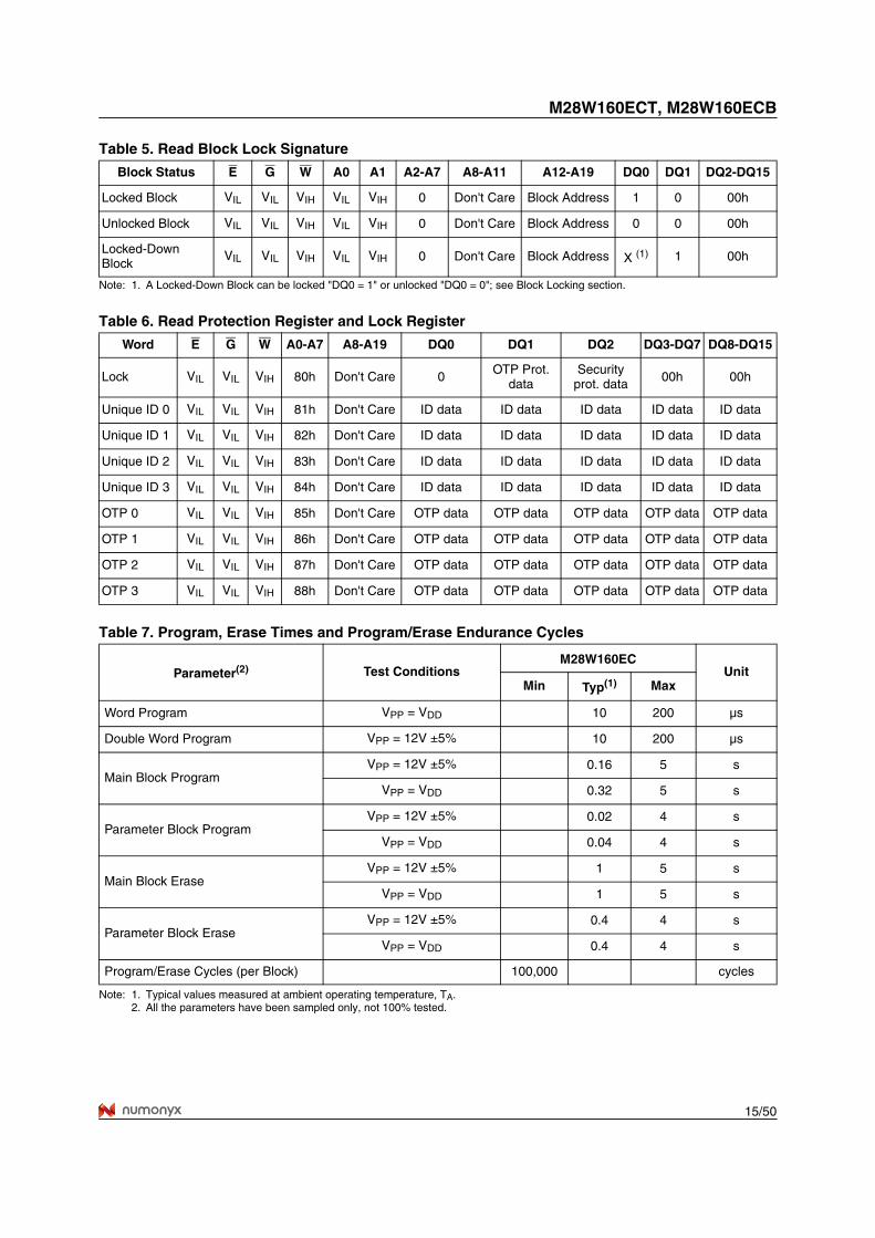
Table 5. Read Block Lock Signature
Note: 1. A Locked-Down Block can be locked "DQ0 = 1" or unlocked "DQ0 = 0"; see Block Locking section.
Table 6. Read Protection Register and Lock Register
Table 7. Program, Erase Times and Program/Erase Endurance Cycles
Note: 1. Typical values measured at ambient operating temperature, TA.2. All the parameters have been sampled only, not 100% tested.
Block Status E G W A0 A1 A2-A7 A8-A11 A12-A19 DQ0 DQ1 DQ2-DQ15
Locked Block VIL VIL VIH VIL VIH 0 Don't Care Block Address 1 0 00h
Unlocked Block VIL VIL VIH VIL VIH 0 Don't Care Block Address 0 0 00h
Locked-Down Block
VIL VIL VIH VIL VIH 0 Don't Care Block Address X (1) 1 00h
Word E G W A0-A7 A8-A19 DQ0 DQ1 DQ2 DQ3-DQ7 DQ8-DQ15
Lock VIL VIL VIH 80h Don't Care 0 OTP Prot. data
Security prot. data 00h 00h
Unique ID 0 VIL VIL VIH 81h Don't Care ID data ID data ID data ID data ID data
Unique ID 1 VIL VIL VIH 82h Don't Care ID data ID data ID data ID data ID data
Unique ID 2 VIL VIL VIH 83h Don't Care ID data ID data ID data ID data ID data
Unique ID 3 VIL VIL VIH 84h Don't Care ID data ID data ID data ID data ID data
OTP 0 VIL VIL VIH 85h Don't Care OTP data OTP data OTP data OTP data OTP data
OTP 1 VIL VIL VIH 86h Don't Care OTP data OTP data OTP data OTP data OTP data
OTP 2 VIL VIL VIH 87h Don't Care OTP data OTP data OTP data OTP data OTP data
OTP 3 VIL VIL VIH 88h Don't Care OTP data OTP data OTP data OTP data OTP data
Parameter(2) Test ConditionsM28W160EC
UnitMin Typ(1) Max
Word Program VPP = VDD 10 200 µs
Double Word Program VPP = 12V ±5% 10 200 µs
Main Block ProgramVPP = 12V ±5% 0.16 5 s
VPP = VDD 0.32 5 s
Parameter Block ProgramVPP = 12V ±5% 0.02 4 s
VPP = VDD 0.04 4 s
Main Block EraseVPP = 12V ±5% 1 5 s
VPP = VDD 1 5 s
Parameter Block EraseVPP = 12V ±5% 0.4 4 s
VPP = VDD 0.4 4 s
Program/Erase Cycles (per Block) 100,000 cycles
M28W160ECT, M28W160ECB
16/50
BLOCK LOCKINGThe M28W160EC features an instant, individualblock locking scheme that allows any block to belocked or unlocked with no latency. This lockingscheme has three levels of protection.■ Lock/Unlock - this first level allows software-
only control of block locking.■ Lock-Down - this second level requires
hardware interaction before locking can be changed.
■ VPP ≤ VPPLK - the third level offers a complete hardware protection against program and erase on all blocks.
The lock status of each block can be set toLocked, Unlocked, and Lock-Down. Table 9., de-fines all of the possible protection states (WP,DQ1, DQ0), and APPENDIX C., Figure 22., showsa flowchart for the locking operations.Reading a Block’s Lock StatusThe lock status of every block can be read in theRead Electronic Signature mode of the device. Toenter this mode write 90h to the device. Subse-quent reads at the address specified in Table 5.,will output the lock status of that block. The lockstatus is represented by DQ0 and DQ1. DQ0 indi-cates the Block Lock/Unlock status and is set bythe Lock command and cleared by the Unlockcommand. It is also automatically set when enter-ing Lock-Down. DQ1 indicates the Lock-Down sta-tus and is set by the Lock-Down command. Itcannot be cleared by software, only by a hardwarereset or power-down. The following sections explain the operation of thelocking system.Locked StateThe default status of all blocks on power-up or af-ter a hardware reset is Locked (states (0,0,1) or(1,0,1)). Locked blocks are fully protected fromany program or erase. Any program or erase oper-ations attempted on a locked block will return anerror in the Status Register. The Status of aLocked block can be changed to Unlocked orLock-Down using the appropriate software com-mands. An Unlocked block can be Locked by issu-ing the Lock command.Unlocked StateUnlocked blocks (states (0,0,0), (1,0,0) (1,1,0)),can be programmed or erased. All unlockedblocks return to the Locked state after a hardwarereset or when the device is powered-down. Thestatus of an unlocked block can be changed toLocked or Locked-Down using the appropriate
software commands. A locked block can be un-locked by issuing the Unlock command.Lock-Down StateBlocks that are Locked-Down (state (0,1,x))areprotected from program and erase operations (asfor Locked blocks) but their lock status cannot bechanged using software commands alone. ALocked or Unlocked block can be Locked-Down byissuing the Lock-Down command. Locked-Downblocks revert to the Locked state when the deviceis reset or powered-down.The Lock-Down function is dependent on the WPinput pin. When WP=0 (VIL), the blocks in theLock-Down state (0,1,x) are protected from pro-gram, erase and protection status changes. WhenWP=1 (VIH) the Lock-Down function is disabled(1,1,1) and Locked-Down blocks can be individu-ally unlocked to the (1,1,0) state by issuing thesoftware command, where they can be erased andprogrammed. These blocks can then be lockedagain (1,1,1) and unlocked (1,1,0) as desired whileWP remains high. When WP is low, blocks thatwere previously Locked-Down return to the Lock-Down state (0,1,x) regardless of any changesmade while WP was high. Device reset or power-down resets all blocks, including those in Lock-Down, to the Locked state.Locking Operations During Erase SuspendChanges to block lock status can be performedduring an erase suspend by using the standardlocking command sequences to unlock, lock orlock-down a block. This is useful in the case whenanother block needs to be updated while an eraseoperation is in progress.To change block locking during an erase opera-tion, first write the Erase Suspend command, thencheck the status register until it indicates that theerase operation has been suspended. Next writethe desired Lock command sequence to a blockand the protection status will be changed. Aftercompleting any desired lock, read, or program op-erations, resume the erase operation with theErase Resume command.If a block is locked or locked-down during an erasesuspend of the same block, the locking status bitswill be changed immediately, but when the eraseis resumed, the erase operation will complete.Locking operations cannot be performed during aprogram suspend. Refer to APPENDIXD., COMMAND INTERFACE AND PROGRAM/ERASE CONTROLLER STATE, for detailed infor-mation on which commands are valid during erasesuspend.
17/50
M28W160ECT, M28W160ECB
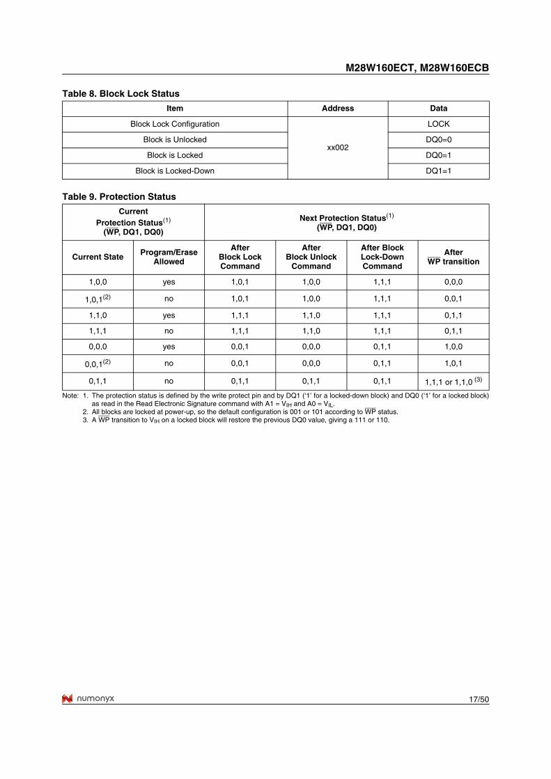
Table 8. Block Lock Status
Table 9. Protection Status
Note: 1. The protection status is defined by the write protect pin and by DQ1 (‘1’ for a locked-down block) and DQ0 (‘1’ for a locked block)as read in the Read Electronic Signature command with A1 = VIH and A0 = VIL.
2. All blocks are locked at power-up, so the default configuration is 001 or 101 according to WP status.3. A WP transition to VIH on a locked block will restore the previous DQ0 value, giving a 111 or 110.
Item Address Data
Block Lock Configuration
xx002
LOCK
Block is Unlocked DQ0=0
Block is Locked DQ0=1
Block is Locked-Down DQ1=1
Current Protection Status(1)
(WP, DQ1, DQ0)
Next Protection Status(1)
(WP, DQ1, DQ0)
Current State Program/Erase Allowed
After Block Lock Command
AfterBlock Unlock
Command
After Block Lock-Down Command
After WP transition
1,0,0 yes 1,0,1 1,0,0 1,1,1 0,0,0
1,0,1(2) no 1,0,1 1,0,0 1,1,1 0,0,1
1,1,0 yes 1,1,1 1,1,0 1,1,1 0,1,1
1,1,1 no 1,1,1 1,1,0 1,1,1 0,1,1
0,0,0 yes 0,0,1 0,0,0 0,1,1 1,0,0
0,0,1(2) no 0,0,1 0,0,0 0,1,1 1,0,1
0,1,1 no 0,1,1 0,1,1 0,1,1 1,1,1 or 1,1,0 (3)
M28W160ECT, M28W160ECB
18/50
STATUS REGISTERThe Status Register provides information on thecurrent or previous Program or Erase operation.The various bits convey information and errors onthe operation. To read the Status register theRead Status Register command can be issued, re-fer to Read Status Register Command section. Tooutput the contents, the Status Register is latchedon the falling edge of the Chip Enable or OutputEnable signals, and can be read until Chip Enableor Output Enable returns to VIH. Either Chip En-able or Output Enable must be toggled to updatethe latched data. Bus Read operations from any address alwaysread the Status Register during Program andErase operations. The bits in the Status Register are summarized inTable 10., Status Register Bits. Refer to Table 10.in conjunction with the following text descriptions.Program/Erase Controller Status (Bit 7). The Pro-gram/Erase Controller Status bit indicates whetherthe Program/Erase Controller is active or inactive.When the Program/Erase Controller Status bit isLow (set to ‘0’), the Program/Erase Controller isactive; when the bit is High (set to ‘1’), the Pro-gram/Erase Controller is inactive, and the deviceis ready to process a new command.The Program/Erase Controller Status is Low im-mediately after a Program/Erase Suspend com-mand is issued until the Program/Erase Controllerpauses. After the Program/Erase Controller paus-es the bit is High.During Program, Erase, operations the Program/Erase Controller Status bit can be polled to find theend of the operation. Other bits in the Status Reg-ister should not be tested until the Program/EraseController completes the operation and the bit isHigh. After the Program/Erase Controller completes itsoperation the Erase Status, Program Status, VPPStatus and Block Lock Status bits should be testedfor errors.Erase Suspend Status (Bit 6). The Erase Sus-pend Status bit indicates that an Erase operationhas been suspended or is going to be suspended.When the Erase Suspend Status bit is High (set to‘1’), a Program/Erase Suspend command hasbeen issued and the memory is waiting for a Pro-gram/Erase Resume command.The Erase Suspend Status should only be consid-ered valid when the Program/Erase Controller Sta-tus bit is High (Program/Erase Controller inactive).Bit 7 is set within 30µs of the Program/Erase Sus-pend command being issued therefore the memo-ry may still complete the operation rather thanentering the Suspend mode.
When a Program/Erase Resume command is is-sued the Erase Suspend Status bit returns Low.Erase Status (Bit 5). The Erase Status bit can beused to identify if the memory has failed to verifythat the block has erased correctly. When theErase Status bit is High (set to ‘1’), the Program/Erase Controller has applied the maximum num-ber of pulses to the block and still failed to verifythat the block has erased correctly. The Erase Sta-tus bit should be read once the Program/EraseController Status bit is High (Program/Erase Con-troller inactive).Once set High, the Erase Status bit can only be re-set Low by a Clear Status Register command or ahardware reset. If set High it should be reset be-fore a new Program or Erase command is issued,otherwise the new command will appear to fail.Program Status (Bit 4). The Program Status bitis used to identify a Program failure. When theProgram Status bit is High (set to ‘1’), the Pro-gram/Erase Controller has applied the maximumnumber of pulses to the byte and still failed to ver-ify that it has programmed correctly. The ProgramStatus bit should be read once the Program/EraseController Status bit is High (Program/Erase Con-troller inactive).Once set High, the Program Status bit can only bereset Low by a Clear Status Register command ora hardware reset. If set High it should be reset be-fore a new command is issued, otherwise the newcommand will appear to fail.VPP Status (Bit 3). The VPP Status bit can beused to identify an invalid voltage on the VPP pinduring Program and Erase operations. The VPPpin is only sampled at the beginning of a Programor Erase operation. Indeterminate results can oc-cur if VPP becomes invalid during an operation.When the VPP Status bit is Low (set to ‘0’), the volt-age on the VPP pin was sampled at a valid voltage;when the VPP Status bit is High (set to ‘1’), the VPPpin has a voltage that is below the VPP LockoutVoltage, VPPLK, the memory is protected and Pro-gram and Erase operations cannot be performed.Once set High, the VPP Status bit can only be resetLow by a Clear Status Register command or ahardware reset. If set High it should be reset be-fore a new Program or Erase command is issued,otherwise the new command will appear to fail.Program Suspend Status (Bit 2). The ProgramSuspend Status bit indicates that a Program oper-ation has been suspended. When the ProgramSuspend Status bit is High (set to ‘1’), a Program/Erase Suspend command has been issued andthe memory is waiting for a Program/Erase Re-sume command. The Program Suspend Statusshould only be considered valid when the Pro-
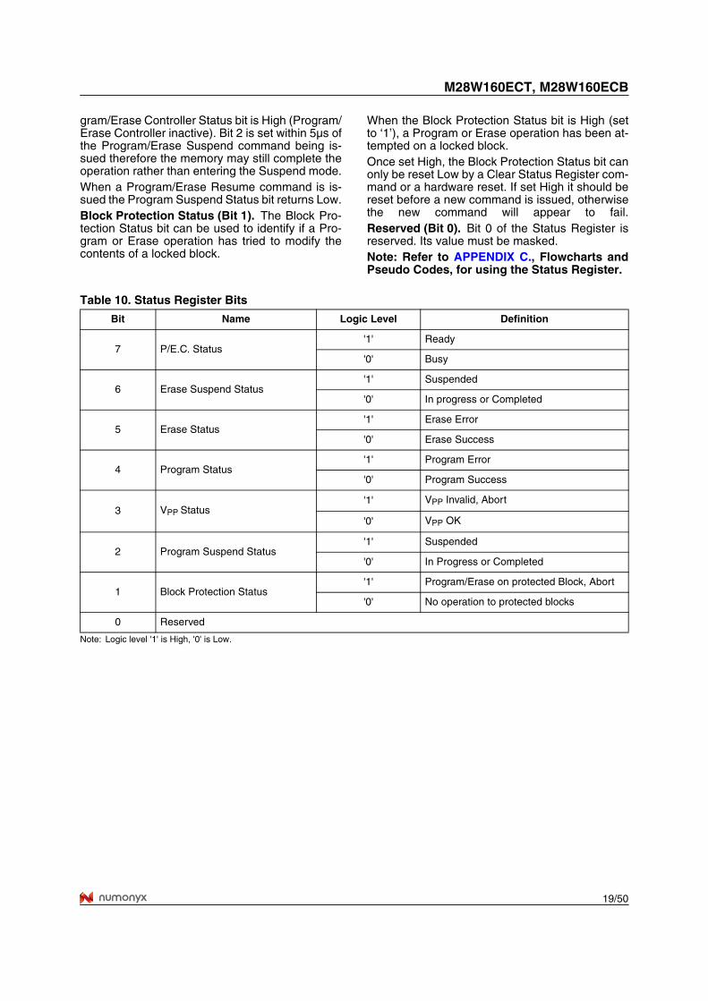
19/50
M28W160ECT, M28W160ECB
gram/Erase Controller Status bit is High (Program/Erase Controller inactive). Bit 2 is set within 5µs ofthe Program/Erase Suspend command being is-sued therefore the memory may still complete theoperation rather than entering the Suspend mode.When a Program/Erase Resume command is is-sued the Program Suspend Status bit returns Low.Block Protection Status (Bit 1). The Block Pro-tection Status bit can be used to identify if a Pro-gram or Erase operation has tried to modify thecontents of a locked block.
When the Block Protection Status bit is High (setto ‘1’), a Program or Erase operation has been at-tempted on a locked block.Once set High, the Block Protection Status bit canonly be reset Low by a Clear Status Register com-mand or a hardware reset. If set High it should bereset before a new command is issued, otherwisethe new command will appear to fail.Reserved (Bit 0). Bit 0 of the Status Register isreserved. Its value must be masked.Note: Refer to APPENDIX C., Flowcharts andPseudo Codes, for using the Status Register.
Table 10. Status Register Bits
Note: Logic level '1' is High, '0' is Low.
Bit Name Logic Level Definition
7 P/E.C. Status'1' Ready
'0' Busy
6 Erase Suspend Status'1' Suspended
'0' In progress or Completed
5 Erase Status'1' Erase Error
'0' Erase Success
4 Program Status'1' Program Error
'0' Program Success
3 VPP Status'1' VPP Invalid, Abort
'0' VPP OK
2 Program Suspend Status'1' Suspended
'0' In Progress or Completed
1 Block Protection Status'1' Program/Erase on protected Block, Abort
'0' No operation to protected blocks
0 Reserved
M28W160ECT, M28W160ECB
20/50
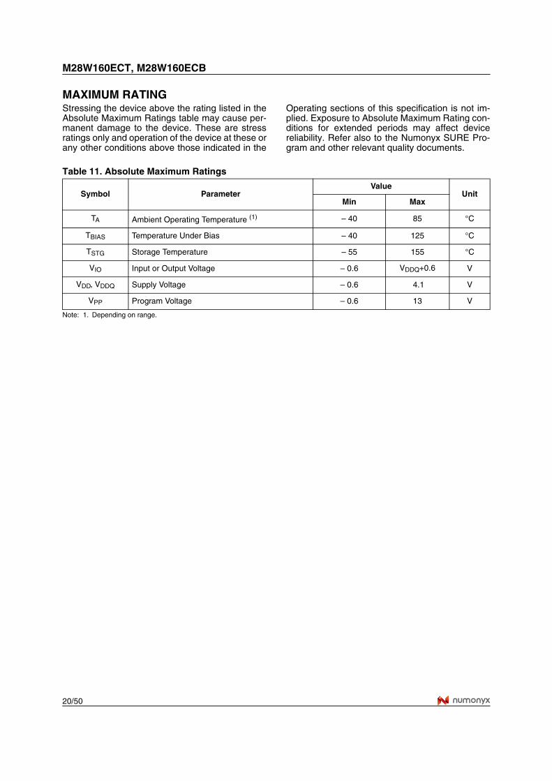
MAXIMUM RATINGStressing the device above the rating listed in theAbsolute Maximum Ratings table may cause per-manent damage to the device. These are stressratings only and operation of the device at these orany other conditions above those indicated in the
Operating sections of this specification is not im-plied. Exposure to Absolute Maximum Rating con-ditions for extended periods may affect devicereliability. Refer also to the Numonyx SURE Pro-gram and other relevant quality documents.
Table 11. Absolute Maximum Ratings
Note: 1. Depending on range.
Symbol ParameterValue
UnitMin Max
TA Ambient Operating Temperature (1) – 40 85 °C
TBIAS Temperature Under Bias – 40 125 °C
TSTG Storage Temperature – 55 155 °C
VIO Input or Output Voltage – 0.6 VDDQ+0.6 V
VDD, VDDQ Supply Voltage – 0.6 4.1 V
VPP Program Voltage – 0.6 13 V
21/50
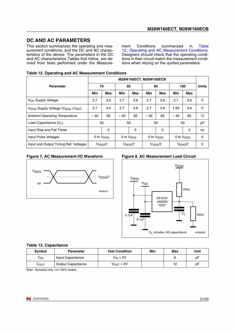
M28W160ECT, M28W160ECB
DC AND AC PARAMETERSThis section summarizes the operating and mea-surement conditions, and the DC and AC charac-teristics of the device. The parameters in the DCand AC characteristics Tables that follow, are de-rived from tests performed under the Measure-
ment Conditions summarized in Table12., Operating and AC Measurement Conditions.Designers should check that the operating condi-tions in their circuit match the measurement condi-tions when relying on the quoted parameters.
Table 12. Operating and AC Measurement Conditions
Figure 7. AC Measurement I/O Waveform Figure 8. AC Measurement Load Circuit
Table 13. Capacitance
Note: Sampled only, not 100% tested.
Parameter
M28W160ECT, M28W160ECB
Units70 85 90 100
Min Max Min Max Min Max Min Max
VDD Supply Voltage 2.7 3.6 2.7 3.6 2.7 3.6 2.7 3.6 V
VDDQ Supply Voltage (VDDQ ≤ VDD) 2.7 3.6 2.7 3.6 2.7 3.6 1.65 3.6 V
Ambient Operating Temperature – 40 85 – 40 85 – 40 85 – 40 85 °C
Load Capacitance (CL) 50 50 50 50 pF
Input Rise and Fall Times 5 5 5 5 ns
Input Pulse Voltages 0 to VDDQ 0 to VDDQ 0 to VDDQ 0 to VDDQ V
Input and Output Timing Ref. Voltages VDDQ/2 VDDQ/2 VDDQ/2 VDDQ/2 V
AI00610
VDDQ
0V
VDDQ/2
AI00609C
VDDQ
CL
CL includes JIG capacitance
25kΩ
DEVICEUNDERTEST
0.1µF
VDD
0.1µF
VDDQ
25kΩ
Symbol Parameter Test Condition Min Max Unit
CIN Input Capacitance VIN = 0V 6 pF
COUT Output Capacitance VOUT = 0V 12 pF
M28W160ECT, M28W160ECB
22/50
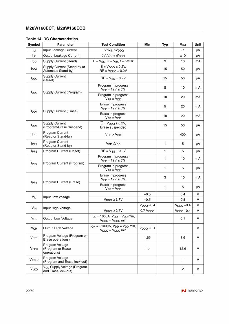
Table 14. DC Characteristics Symbol Parameter Test Condition Min Typ Max Unit
ILI Input Leakage Current 0V≤ VIN ≤ VDDQ ±1 µA
ILO Output Leakage Current 0V≤ VOUT ≤VDDQ ±10 µA
IDD Supply Current (Read) E = VSS, G = VIH, f = 5MHz 9 18 mA
IDD1Supply Current (Stand-by or Automatic Stand-by)
E = VDDQ ± 0.2V, RP = VDDQ ± 0.2V
15 50 µA
IDD2Supply Current (Reset)
RP = VSS ± 0.2V 15 50 µA
IDD3 Supply Current (Program)
Program in progressVPP = 12V ± 5% 5 10 mA
Program in progressVPP = VDD
10 20 mA
IDD4 Supply Current (Erase)
Erase in progressVPP = 12V ± 5% 5 20 mA
Erase in progressVPP = VDD
10 20 mA
IDD5Supply Current(Program/Erase Suspend)
E = VDDQ ± 0.2V, Erase suspended
15 50 µA
IPPProgram Current (Read or Stand-by)
VPP > VDD 400 µA
IPP1Program Current(Read or Stand-by)
VPP ≤ VDD 1 5 µA
IPP2 Program Current (Reset) RP = VSS ± 0.2V 1 5 µA
IPP3 Program Current (Program)
Program in progressVPP = 12V ± 5% 1 10 mA
Program in progressVPP = VDD
1 5 µA
IPP4 Program Current (Erase)
Erase in progressVPP = 12V ± 5% 3 10 mA
Erase in progressVPP = VDD
1 5 µA
VIL Input Low Voltage–0.5 0.4 V
VDDQ ≥ 2.7V –0.5 0.8 V
VIH Input High VoltageVDDQ –0.4 VDDQ +0.4 V
VDDQ ≥ 2.7V 0.7 VDDQ VDDQ +0.4 V
VOL Output Low VoltageIOL = 100µA, VDD = VDD min,
VDDQ = VDDQ min 0.1 V
VOH Output High VoltageIOH = –100µA, VDD = VDD min,
VDDQ = VDDQ minVDDQ –0.1 V
VPP1Program Voltage (Program or Erase operations) 1.65 3.6 V
VPPH
Program Voltage(Program or Erase operations)
11.4 12.6 V
VPPLKProgram Voltage(Program and Erase lock-out) 1 V
VLKOVDD Supply Voltage (Program and Erase lock-out)
2 V
23/50
M28W160ECT, M28W160ECB
Figure 9. Read Mode AC Waveforms
Table 15. Read AC Characteristics
Note: 1. Sampled only, not 100% tested.2. G may be delayed by up to tELQV - tGLQV after the falling edge of E without increasing tELQV.
Symbol Alt ParameterM28W160EC
Unit70 85 90 100
tAVAV tRC Address Valid to Next Address Valid Min 70 85 90 100 ns
tAVQV tACC Address Valid to Output Valid Max 70 85 90 100 ns
tAXQX (1) tOH Address Transition to Output Transition Min 0 0 0 0 ns
tEHQX (1) tOH Chip Enable High to Output Transition Min 0 0 0 0 ns
tEHQZ (1) tHZ Chip Enable High to Output Hi-Z Max 20 20 25 30 ns
tELQV (2) tCE Chip Enable Low to Output Valid Max 70 85 90 100 ns
tELQX (1) tLZ Chip Enable Low to Output Transition Min 0 0 0 0 ns
tGHQX (1) tOH Output Enable High to Output Transition Min 0 0 0 0 ns
tGHQZ (1) tDF Output Enable High to Output Hi-Z Max 20 20 25 30 ns
tGLQV (2) tOE Output Enable Low to Output Valid Max 20 20 30 35 ns
tGLQX (1) tOLZ Output Enable Low to Output Transition Min 0 0 0 0 ns
DQ0-DQ15
AI03813b
VALIDA0-A19
E
tAXQX
tAVAV
VALID
tAVQV
tELQV
tELQX
tGLQV
tGLQX
ADDR. VALID CHIP ENABLE
OUTPUTSENABLED
DATA VALID STANDBY
G
tGHQX
tGHQZ
tEHQX
tEHQZ
M28W160ECT, M28W160ECB
24/50
Figure 10. Write AC Waveforms, Write Enable Controlled
E G W DQ
0-D
Q15
CO
MM
AN
DC
MD
or
DA
TA
ST
AT
US
RE
GIS
TE
R
VP
P
VA
LID
A0-
A19
tAV
AV
tQV
VP
L
tAV
WH
tWH
AX
PR
OG
RA
M O
R E
RA
SE
tELW
LtW
HE
H
tWH
DX
tDV
WH
tWLW
H
tWH
WL
tVP
HW
H
SE
T-U
P C
OM
MA
ND
CO
NF
IRM
CO
MM
AN
DO
R D
AT
A IN
PU
TS
TA
TU
S R
EG
IST
ER
RE
AD
1st P
OLL
ING
tELQ
V
AI0
3814
b
tWP
HW
H
WP
tWH
GL
tQV
WP
L
tWH
EL
25/50
M28W160ECT, M28W160ECB
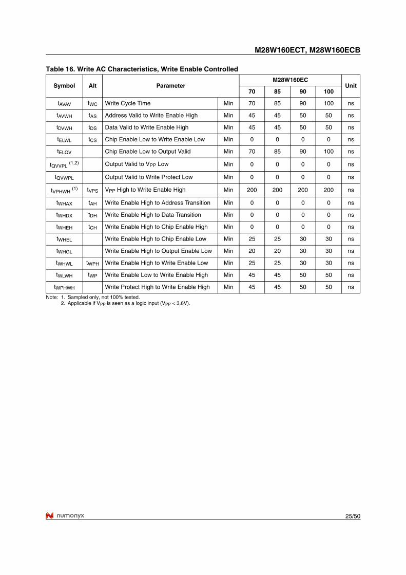
Table 16. Write AC Characteristics, Write Enable Controlled
Note: 1. Sampled only, not 100% tested.2. Applicable if VPP is seen as a logic input (VPP < 3.6V).
Symbol Alt ParameterM28W160EC
Unit70 85 90 100
tAVAV tWC Write Cycle Time Min 70 85 90 100 ns
tAVWH tAS Address Valid to Write Enable High Min 45 45 50 50 ns
tDVWH tDS Data Valid to Write Enable High Min 45 45 50 50 ns
tELWL tCS Chip Enable Low to Write Enable Low Min 0 0 0 0 ns
tELQV Chip Enable Low to Output Valid Min 70 85 90 100 ns
tQVVPL (1,2) Output Valid to VPP Low Min 0 0 0 0 ns
tQVWPL Output Valid to Write Protect Low Min 0 0 0 0 ns
tVPHWH (1) tVPS VPP High to Write Enable High Min 200 200 200 200 ns
tWHAX tAH Write Enable High to Address Transition Min 0 0 0 0 ns
tWHDX tDH Write Enable High to Data Transition Min 0 0 0 0 ns
tWHEH tCH Write Enable High to Chip Enable High Min 0 0 0 0 ns
tWHEL Write Enable High to Chip Enable Low Min 25 25 30 30 ns
tWHGL Write Enable High to Output Enable Low Min 20 20 30 30 ns
tWHWL tWPH Write Enable High to Write Enable Low Min 25 25 30 30 ns
tWLWH tWP Write Enable Low to Write Enable High Min 45 45 50 50 ns
tWPHWH Write Protect High to Write Enable High Min 45 45 50 50 ns
M28W160ECT, M28W160ECB
26/50
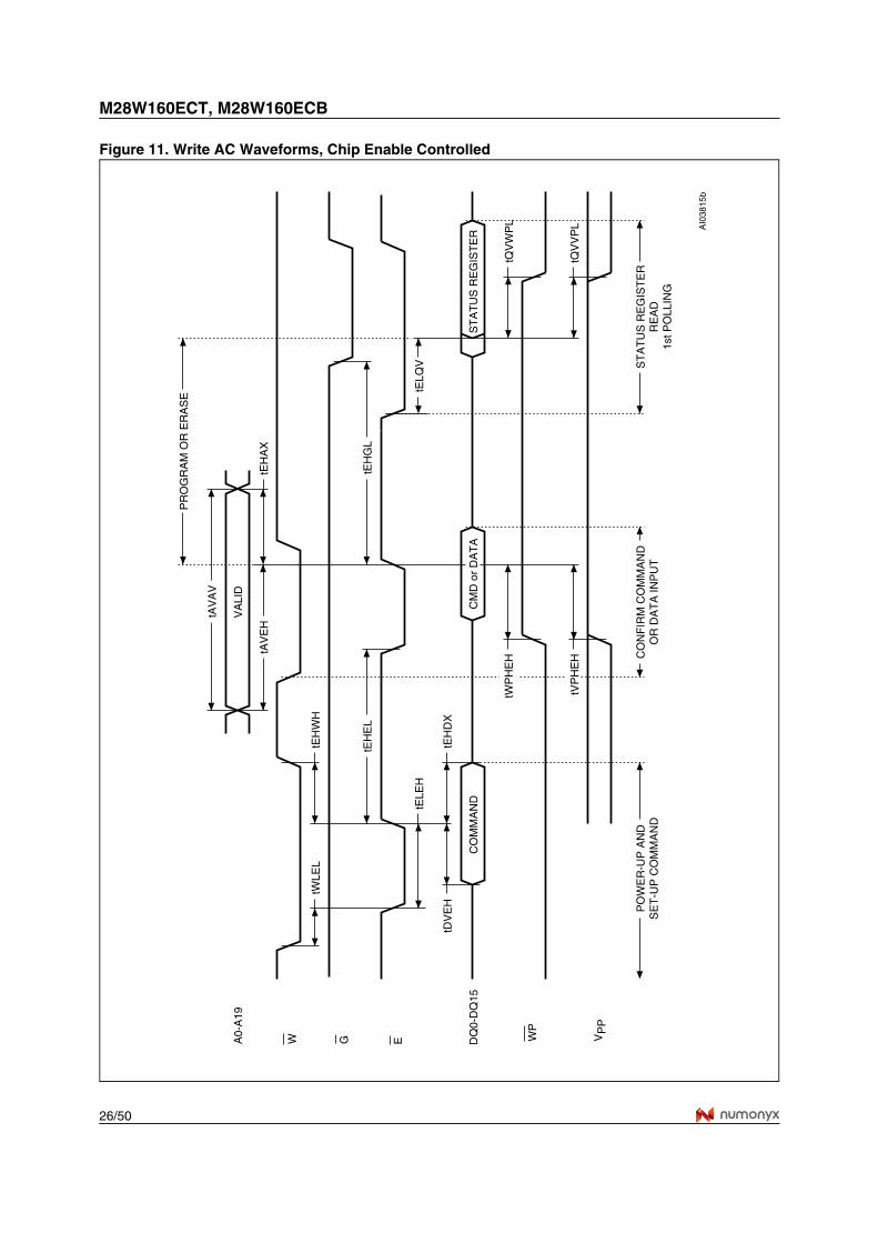
Figure 11. Write AC Waveforms, Chip Enable Controlled
EG DQ
0-D
Q15
CO
MM
AN
DC
MD
or
DA
TA
ST
AT
US
RE
GIS
TE
R
VP
P
VA
LID
A0-
A19
tAV
AV
tQV
VP
L
tAV
EH
tEH
AX
PR
OG
RA
M O
R E
RA
SE
tWLE
LtE
HW
H
tEH
DX
tDV
EH
tELE
H
tEH
EL
tVP
HE
H
PO
WE
R-U
P A
ND
SE
T-U
P C
OM
MA
ND
CO
NF
IRM
CO
MM
AN
DO
R D
AT
A IN
PU
TS
TA
TU
S R
EG
IST
ER
RE
AD
1st P
OLL
ING
tELQ
V
AI0
3815
b
W
tWP
HE
H
WP
tEH
GL
tQV
WP
L
27/50
M28W160ECT, M28W160ECB
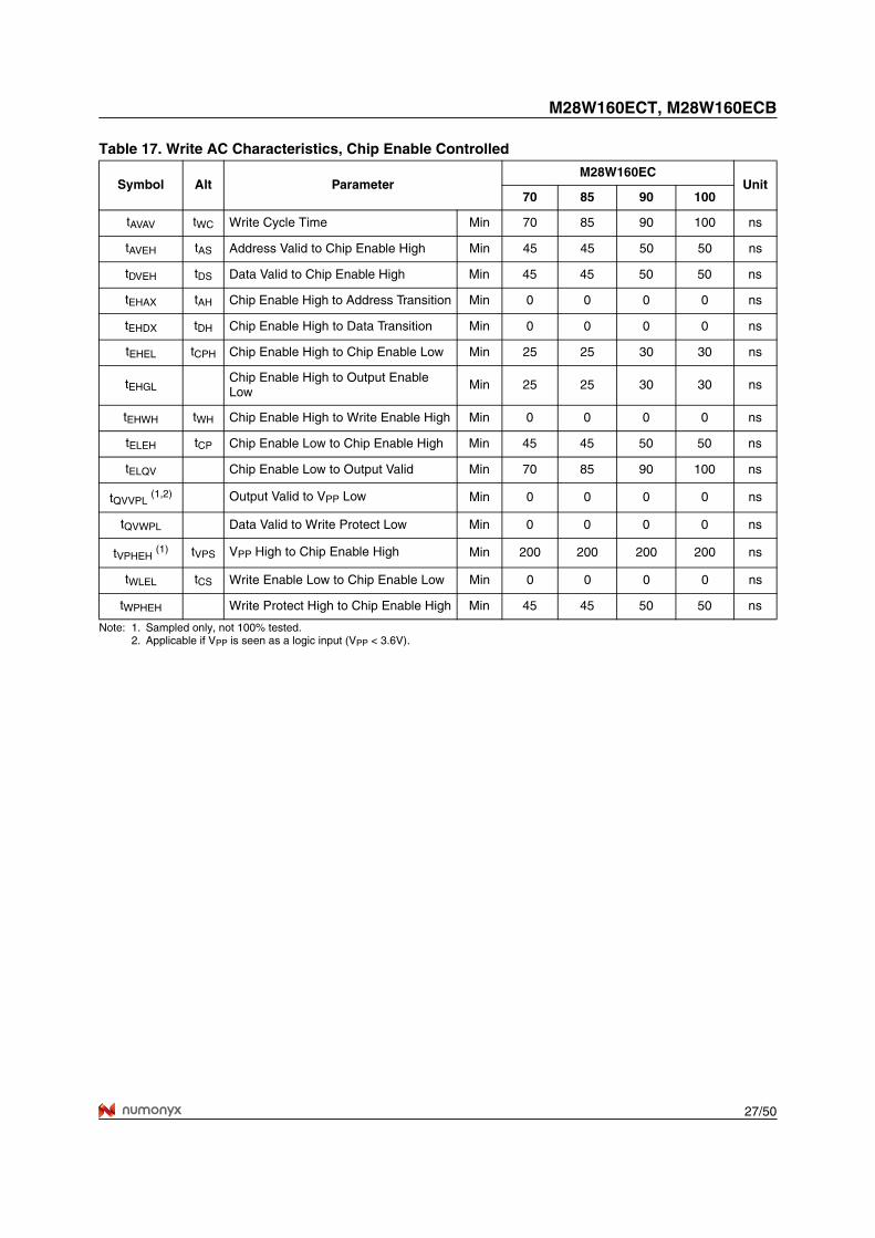
Table 17. Write AC Characteristics, Chip Enable Controlled
Note: 1. Sampled only, not 100% tested.2. Applicable if VPP is seen as a logic input (VPP < 3.6V).
Symbol Alt ParameterM28W160EC
Unit70 85 90 100
tAVAV tWC Write Cycle Time Min 70 85 90 100 ns
tAVEH tAS Address Valid to Chip Enable High Min 45 45 50 50 ns
tDVEH tDS Data Valid to Chip Enable High Min 45 45 50 50 ns
tEHAX tAH Chip Enable High to Address Transition Min 0 0 0 0 ns
tEHDX tDH Chip Enable High to Data Transition Min 0 0 0 0 ns
tEHEL tCPH Chip Enable High to Chip Enable Low Min 25 25 30 30 ns
tEHGLChip Enable High to Output Enable Low
Min 25 25 30 30 ns
tEHWH tWH Chip Enable High to Write Enable High Min 0 0 0 0 ns
tELEH tCP Chip Enable Low to Chip Enable High Min 45 45 50 50 ns
tELQV Chip Enable Low to Output Valid Min 70 85 90 100 ns
tQVVPL (1,2) Output Valid to VPP Low Min 0 0 0 0 ns
tQVWPL Data Valid to Write Protect Low Min 0 0 0 0 ns
tVPHEH (1) tVPS VPP High to Chip Enable High Min 200 200 200 200 ns
tWLEL tCS Write Enable Low to Chip Enable Low Min 0 0 0 0 ns
tWPHEH Write Protect High to Chip Enable High Min 45 45 50 50 ns
M28W160ECT, M28W160ECB
28/50
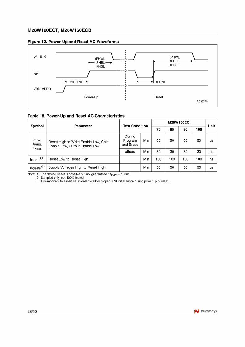
Figure 12. Power-Up and Reset AC Waveforms
Table 18. Power-Up and Reset AC Characteristics
Note: 1. The device Reset is possible but not guaranteed if tPLPH < 100ns.2. Sampled only, not 100% tested.3. It is important to assert RP in order to allow proper CPU initialization during power up or reset.
Symbol Parameter Test ConditionM28W160EC
Unit70 85 90 100
tPHWLtPHELtPHGL
Reset High to Write Enable Low, Chip Enable Low, Output Enable Low
During Program
and EraseMin 50 50 50 50 µs
others Min 30 30 30 30 ns
tPLPH(1,2) Reset Low to Reset High Min 100 100 100 100 ns
tVDHPH(3) Supply Voltages High to Reset High Min 50 50 50 50 µs
AI03537b
W,
RP
tPHWLtPHELtPHGL
E, G
VDD, VDDQ
tVDHPH
tPHWLtPHELtPHGL
tPLPH
Power-Up Reset
29/50
M28W160ECT, M28W160ECB
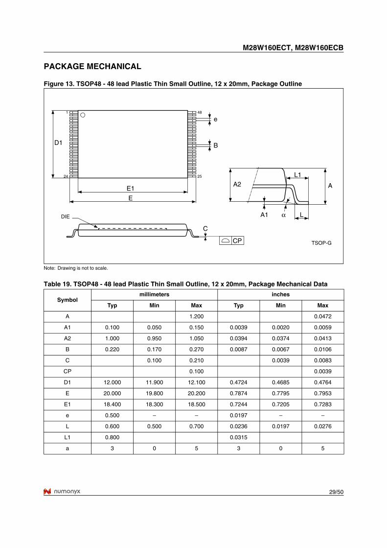
PACKAGE MECHANICAL
Figure 13. TSOP48 - 48 lead Plastic Thin Small Outline, 12 x 20mm, Package Outline
Note: Drawing is not to scale.
Table 19. TSOP48 - 48 lead Plastic Thin Small Outline, 12 x 20mm, Package Mechanical Data
Symbolmillimeters inches
Typ Min Max Typ Min Max
A 1.200 0.0472
A1 0.100 0.050 0.150 0.0039 0.0020 0.0059
A2 1.000 0.950 1.050 0.0394 0.0374 0.0413
B 0.220 0.170 0.270 0.0087 0.0067 0.0106
C 0.100 0.210 0.0039 0.0083
CP 0.100 0.0039
D1 12.000 11.900 12.100 0.4724 0.4685 0.4764
E 20.000 19.800 20.200 0.7874 0.7795 0.7953
E1 18.400 18.300 18.500 0.7244 0.7205 0.7283
e 0.500 – – 0.0197 – –
L 0.600 0.500 0.700 0.0236 0.0197 0.0276
L1 0.800 0.0315
a 3 0 5 3 0 5
TSOP-G
B
e
DIE
C
LA1 α
E1
E
AA2
1
24
48
25
D1
L1
CP
M28W160ECT, M28W160ECB
30/50
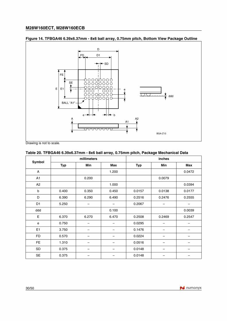
Figure 14. TFBGA46 6.39x6.37mm - 8x6 ball array, 0.75mm pitch, Bottom View Package Outline
Drawing is not to scale.
Table 20. TFBGA46 6.39x6.37mm - 8x6 ball array, 0.75mm pitch, Package Mechanical Data
E1E
D1
D
bA2
A1A
BGA-Z13
ddd
e
e
FD
FE
SD
SE
BALL "A1"
Symbolmillimeters inches
Typ Min Max Typ Min Max
A 1.200 0.0472
A1 0.200 0.0079
A2 1.000 0.0394
b 0.400 0.350 0.450 0.0157 0.0138 0.0177
D 6.390 6.290 6.490 0.2516 0.2476 0.2555
D1 5.250 – – 0.2067 – –
ddd 0.100 0.0039
E 6.370 6.270 6.470 0.2508 0.2469 0.2547
e 0.750 – – 0.0295 – –
E1 3.750 – – 0.1476 – –
FD 0.570 – – 0.0224 – –
FE 1.310 – – 0.0516 – –
SD 0.375 – – 0.0148 – –
SE 0.375 – – 0.0148 – –
31/50
M28W160ECT, M28W160ECB
Figure 15. TFBGA46 Daisy Chain - Package Connections (Top view through package)
Figure 16. TFBGA46 Daisy Chain - PCB Connections proposal (Top view through package)
AI03298
C
B
A
87654321
E
D
F
AI3299
C
B
A
87654321
E
D
F
STARTPOINT
ENDPOINT
M28W160ECT, M28W160ECB
32/50
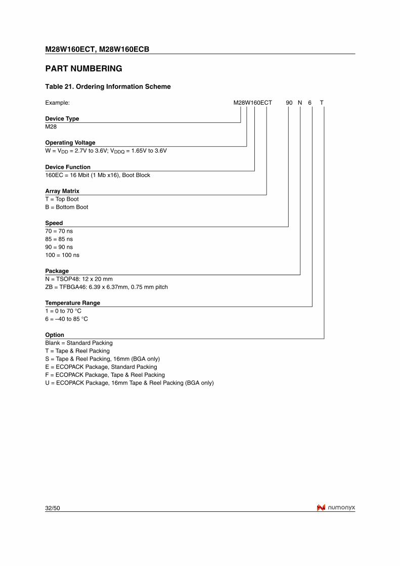
PART NUMBERING
Table 21. Ordering Information Scheme
Example: M28W160ECT 90 N 6 T
Device TypeM28
Operating VoltageW = VDD = 2.7V to 3.6V; VDDQ = 1.65V to 3.6V
Device Function160EC = 16 Mbit (1 Mb x16), Boot Block
Array MatrixT = Top BootB = Bottom Boot
Speed70 = 70 ns85 = 85 ns90 = 90 ns100 = 100 ns
PackageN = TSOP48: 12 x 20 mmZB = TFBGA46: 6.39 x 6.37mm, 0.75 mm pitch
Temperature Range1 = 0 to 70 °C6 = –40 to 85 °C
OptionBlank = Standard PackingT = Tape & Reel PackingS = Tape & Reel Packing, 16mm (BGA only)E = ECOPACK Package, Standard PackingF = ECOPACK Package, Tape & Reel PackingU = ECOPACK Package, 16mm Tape & Reel Packing (BGA only)
33/50
M28W160ECT, M28W160ECB
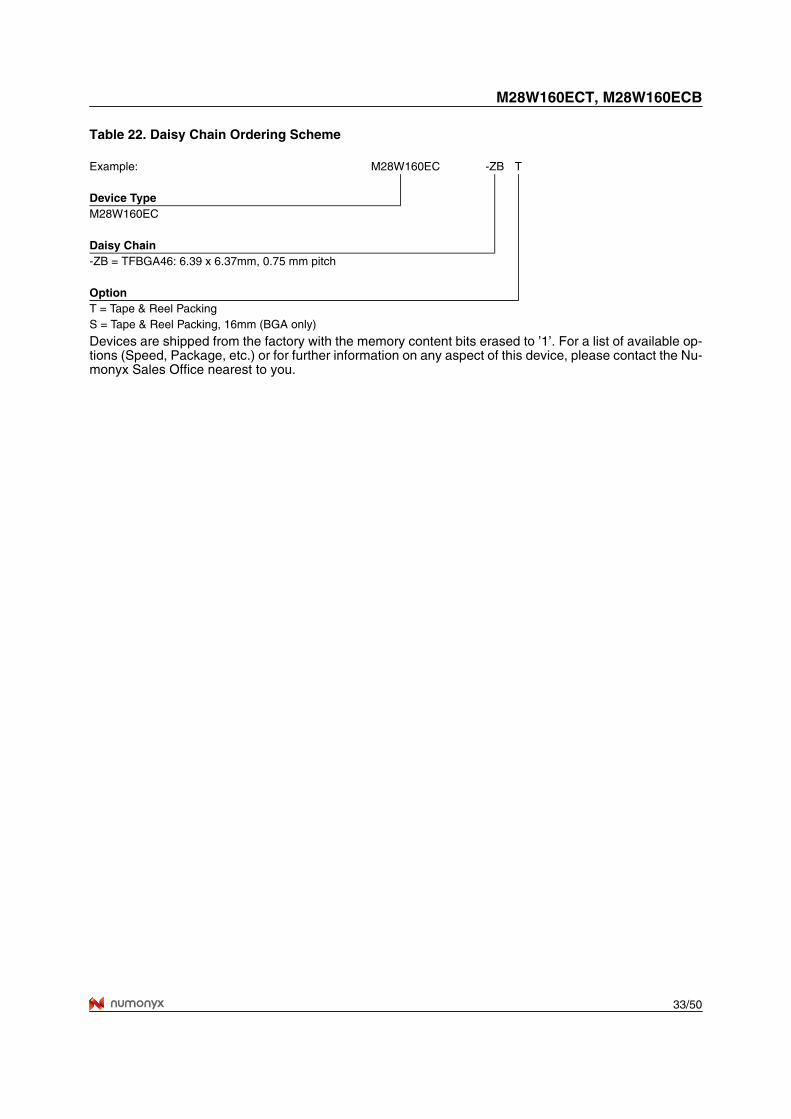
Table 22. Daisy Chain Ordering Scheme
Devices are shipped from the factory with the memory content bits erased to ’1’. For a list of available op-tions (Speed, Package, etc.) or for further information on any aspect of this device, please contact the Nu-monyx Sales Office nearest to you.
Example: M28W160EC -ZB T
Device TypeM28W160EC
Daisy Chain-ZB = TFBGA46: 6.39 x 6.37mm, 0.75 mm pitch
OptionT = Tape & Reel PackingS = Tape & Reel Packing, 16mm (BGA only)
M28W160ECT, M28W160ECB
34/50
APPENDIX A. BLOCK ADDRESS TABLES
Table 23. Top Boot Block Addresses, M28W160ECT
Table 24. Bottom Boot Block Addresses, M28W160ECB
# Size (KWord) Address Range
0 4 FF000-FFFFF
1 4 FE000-FEFFF
2 4 FD000-FDFFF
3 4 FC000-FCFFF
4 4 FB000-FBFFF
5 4 FA000-FAFFF
6 4 F9000-F9FFF
7 4 F8000-F8FFF
8 32 F0000-F7FFF
99 32 E8000-EFFFF
10 32 E0000-E7FFF
11 32 D8000-DFFFF
12 32 D0000-D7FFF
13 32 C8000-CFFFF
14 32 C0000-C7FFF
15 32 B8000-BFFFF
16 32 B0000-B7FFF
17 32 A8000-AFFFF
18 32 A0000-A7FFF
19 32 98000-9FFFF
20 32 90000-97FFF
21 32 88000-8FFFF
22 32 80000-87FFF
23 32 78000-7FFFF
24 32 70000-77FFF
25 32 68000-6FFFF
26 32 60000-67FFF
27 32 58000-5FFFF
28 32 50000-57FFF
29 32 48000-4FFFF
30 32 40000-47FFF
31 32 38000-3FFFF
32 32 30000-37FFF
33 32 28000-2FFFF
34 32 20000-27FFF
35 32 18000-1FFFF
36 32 10000-17FFF
37 32 08000-0FFFF
38 32 00000-07FFF
# Size (KWord) Address Range
38 32 F8000-FFFFF
37 32 F0000-F7FFF
36 32 E8000-EFFFF
35 32 E0000-E7FFF
34 32 D8000-DFFFF
33 32 D0000-D7FFF
32 32 C8000-CFFFF
31 32 C0000-C7FFF
30 32 B8000-BFFFF
29 32 B0000-B7FFF
28 32 A8000-AFFFF
27 32 A0000-A7FFF
26 32 98000-9FFFF
25 32 90000-97FFF
24 32 88000-8FFFF
23 32 80000-87FFF
22 32 78000-7FFFF
21 32 70000-77FFF
20 32 68000-6FFFF
19 32 60000-67FFF
18 32 58000-5FFFF
17 32 50000-57FFF
16 32 48000-4FFFF
15 32 40000-47FFF
14 32 38000-3FFFF
13 32 30000-37FFF
12 32 28000-2FFFF
11 32 20000-27FFF
10 32 18000-1FFFF
9 32 10000-17FFF
8 32 08000-0FFFF
7 4 07000-07FFF
6 4 06000-06FFF
5 4 05000-05FFF
4 4 04000-04FFF
3 4 03000-03FFF
2 4 02000-02FFF
1 4 01000-01FFF
0 4 00000-00FFF
35/50
M28W160ECT, M28W160ECB
APPENDIX B. COMMON FLASH INTERFACE (CFI) The Common Flash Interface is a JEDEC ap-proved, standardized data structure that can beread from the Flash memory device. It allows asystem software to query the device to determinevarious electrical and timing parameters, densityinformation and functions supported by the mem-ory. The system can interface easily with the de-vice, enabling the software to upgrade itself whennecessary.When the CFI Query Command (RCFI) is issuedthe device enters CFI Query mode and the data
structure is read from the memory. Tables 25, 26,27, 28, 29 and 30 show the addresses used to re-trieve the data.The CFI data structure also contains a securityarea where a 64 bit unique security number is writ-ten (see Table 30., Security Code Area). This areacan be accessed only in Read mode by the finaluser. It is impossible to change the security num-ber after it has been written by Numonyx. Issue aRead command to return to Read mode.
Table 25. Query Structure Overview
Note: Query data are always presented on the lowest order data outputs.
Table 26. CFI Query Identification String
Note: Query data are always presented on the lowest order data outputs (DQ7-DQ0) only. DQ8-DQ15 are ‘0’.
Offset Sub-section Name Description
00h Reserved Reserved for algorithm-specific information
10h CFI Query Identification String Command set ID and algorithm data offset
1Bh System Interface Information Device timing & voltage information
27h Device Geometry Definition Flash device layout
P Primary Algorithm-specific Extended Query tableAdditional information specific to the Primary Algorithm (optional)
A Alternate Algorithm-specific Extended Query tableAdditional information specific to the Alternate Algorithm (optional)
Offset Data Description Value
00h 0020h Manufacturer Code Numonyx
01h88CEh88CFh Device Code
TopBottom
02h-0Fh reserved Reserved
10h 0051h "Q"
11h 0052h Query Unique ASCII String "QRY" "R"
12h 0059h "Y"
13h 0003h Primary Algorithm Command Set and Control Interface ID code 16 bit ID code defining a specific algorithm
Intel compatible14h 0000h
15h 0035hAddress for Primary Algorithm extended Query table (see Table 28.) P = 35h
16h 0000h
17h 0000h Alternate Vendor Command Set and Control Interface ID Code second vendor - specified algorithm supported (0000h means none exists) NA
18h 0000h
19h 0000h Address for Alternate Algorithm extended Query table(0000h means none exists)
NA1Ah 0000h
M28W160ECT, M28W160ECB
36/50
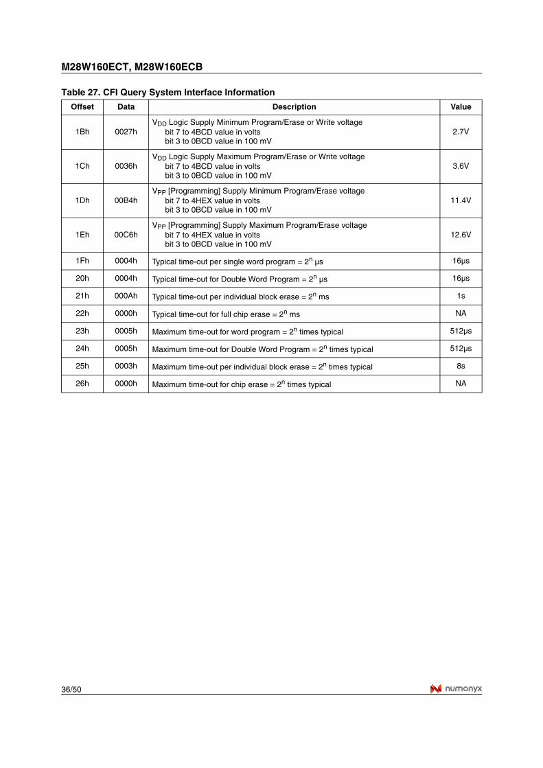
Table 27. CFI Query System Interface Information
Offset Data Description Value
1Bh 0027hVDD Logic Supply Minimum Program/Erase or Write voltage
bit 7 to 4BCD value in voltsbit 3 to 0BCD value in 100 mV
2.7V
1Ch 0036hVDD Logic Supply Maximum Program/Erase or Write voltage
bit 7 to 4BCD value in voltsbit 3 to 0BCD value in 100 mV
3.6V
1Dh 00B4hVPP [Programming] Supply Minimum Program/Erase voltage
bit 7 to 4HEX value in voltsbit 3 to 0BCD value in 100 mV
11.4V
1Eh 00C6hVPP [Programming] Supply Maximum Program/Erase voltage
bit 7 to 4HEX value in voltsbit 3 to 0BCD value in 100 mV
12.6V
1Fh 0004h Typical time-out per single word program = 2n µs 16µs
20h 0004h Typical time-out for Double Word Program = 2n µs 16µs
21h 000Ah Typical time-out per individual block erase = 2n ms 1s
22h 0000h Typical time-out for full chip erase = 2n ms NA
23h 0005h Maximum time-out for word program = 2n times typical 512µs
24h 0005h Maximum time-out for Double Word Program = 2n times typical 512µs
25h 0003h Maximum time-out per individual block erase = 2n times typical 8s
26h 0000h Maximum time-out for chip erase = 2n times typical NA
37/50
M28W160ECT, M28W160ECB
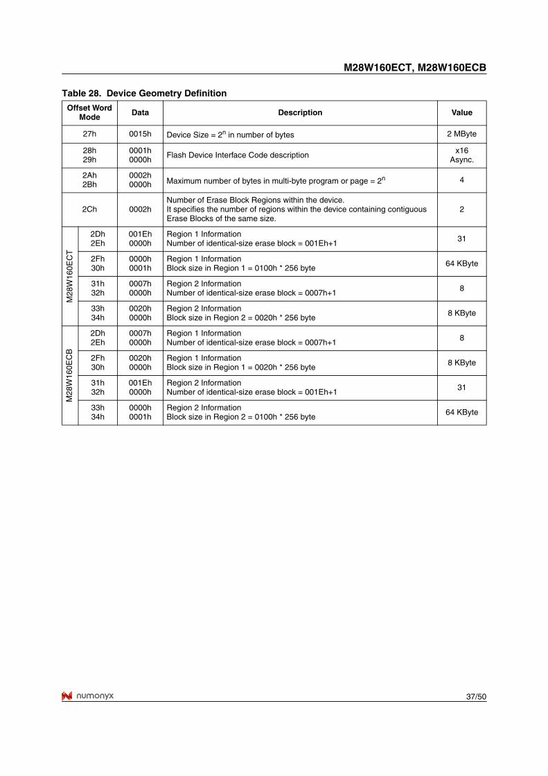
Table 28. Device Geometry Definition
Offset Word Mode Data Description Value
27h 0015h Device Size = 2n in number of bytes 2 MByte
28h29h
0001h0000h Flash Device Interface Code description x16
Async.
2Ah2Bh
0002h0000h Maximum number of bytes in multi-byte program or page = 2n 4
2Ch 0002hNumber of Erase Block Regions within the device.It specifies the number of regions within the device containing contiguous Erase Blocks of the same size.
2
M28
W16
0EC
T
2Dh2Eh
001Eh0000h
Region 1 InformationNumber of identical-size erase block = 001Eh+1 31
2Fh30h
0000h0001h
Region 1 InformationBlock size in Region 1 = 0100h * 256 byte 64 KByte
31h32h
0007h0000h
Region 2 InformationNumber of identical-size erase block = 0007h+1 8
33h34h
0020h0000h
Region 2 InformationBlock size in Region 2 = 0020h * 256 byte 8 KByte
M28
W16
0EC
B
2Dh2Eh
0007h0000h
Region 1 InformationNumber of identical-size erase block = 0007h+1 8
2Fh30h
0020h0000h
Region 1 InformationBlock size in Region 1 = 0020h * 256 byte 8 KByte
31h32h
001Eh0000h
Region 2 InformationNumber of identical-size erase block = 001Eh+1 31
33h34h
0000h0001h
Region 2 InformationBlock size in Region 2 = 0100h * 256 byte 64 KByte
M28W160ECT, M28W160ECB
38/50
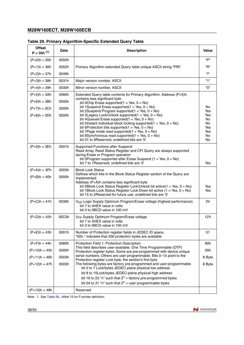
Table 29. Primary Algorithm-Specific Extended Query Table
Note: 1. See Table 26., offset 15 for P pointer definition.
OffsetP = 35h (1) Data Description Value
(P+0)h = 35h 0050h
Primary Algorithm extended Query table unique ASCII string “PRI”
"P"
(P+1)h = 36h 0052h "R"
(P+2)h = 37h 0049h "I"
(P+3)h = 38h 0031h Major version number, ASCII "1"
(P+4)h = 39h 0030h Minor version number, ASCII "0"
(P+5)h = 3Ah 0066h Extended Query table contents for Primary Algorithm. Address (P+5)h contains less significant byte.
bit 0Chip Erase supported(1 = Yes, 0 = No)bit 1Suspend Erase supported(1 = Yes, 0 = No)bit 2Suspend Program supported(1 = Yes, 0 = No)bit 3Legacy Lock/Unlock supported(1 = Yes, 0 = No)bit 4Queued Erase supported(1 = Yes, 0 = No)bit 5Instant individual block locking supported(1 = Yes, 0 = No)bit 6Protection bits supported(1 = Yes, 0 = No)bit 7Page mode read supported(1 = Yes, 0 = No)bit 8Synchronous read supported(1 = Yes, 0 = No)bit 31 to 9Reserved; undefined bits are ‘0’
NoYesYesNoNoYesYesNoNo
(P+6)h = 3Bh 0000h
(P+7)h = 3Ch 0000h
(P+8)h = 3Dh 0000h
(P+9)h = 3Eh 0001h Supported Functions after SuspendRead Array, Read Status Register and CFI Query are always supported during Erase or Program operation
bit 0Program supported after Erase Suspend (1 = Yes, 0 = No)bit 7 to 1Reserved; undefined bits are ‘0’ Yes
(P+A)h = 3Fh 0003h Block Lock StatusDefines which bits in the Block Status Register section of the Query are implemented.Address (P+A)h contains less significant byte
bit 0Block Lock Status Register Lock/Unlock bit active(1 = Yes, 0 = No)bit 1Block Lock Status Register Lock-Down bit active (1 = Yes, 0 = No)bit 15 to 2Reserved for future use; undefined bits are ‘0’
YesYes
(P+B)h = 40h 0000h
(P+C)h = 41h 0030h VDD Logic Supply Optimum Program/Erase voltage (highest performance)bit 7 to 4HEX value in voltsbit 3 to 0BCD value in 100 mV
3V
(P+D)h = 42h 00C0h VPP Supply Optimum Program/Erase voltagebit 7 to 4HEX value in voltsbit 3 to 0BCD value in 100 mV
12V
(P+E)h = 43h 0001h Number of Protection register fields in JEDEC ID space."00h," indicates that 256 protection bytes are available
01
(P+F)h = 44h 0080h Protection Field 1: Protection DescriptionThis field describes user-available. One Time Programmable (OTP) Protection register bytes. Some are pre-programmed with device unique serial numbers. Others are user programmable. Bits 0–15 point to the Protection register Lock byte, the section’s first byte.The following bytes are factory pre-programmed and user-programmable.
bit 0 to 7 Lock/bytes JEDEC-plane physical low addressbit 8 to 15Lock/bytes JEDEC-plane physical high address
bit 16 to 23 "n" such that 2n = factory pre-programmed bytesbit 24 to 31 "n" such that 2n = user programmable bytes
80h
(P+10)h = 45h 0000h 00h
(P+11)h = 46h 0003h 8 Byte
(P+12)h = 47h 0003h 8 Byte
(P+13)h = 48h Reserved
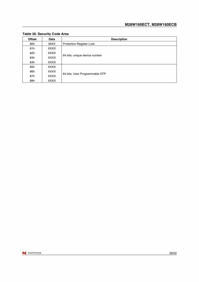
39/50
M28W160ECT, M28W160ECB
Table 30. Security Code Area
Offset Data Description
80h 00XX Protection Register Lock
81h XXXX
64 bits: unique device number82h XXXX
83h XXXX
84h XXXX
85h XXXX
64 bits: User Programmable OTP86h XXXX
87h XXXX
88h XXXX
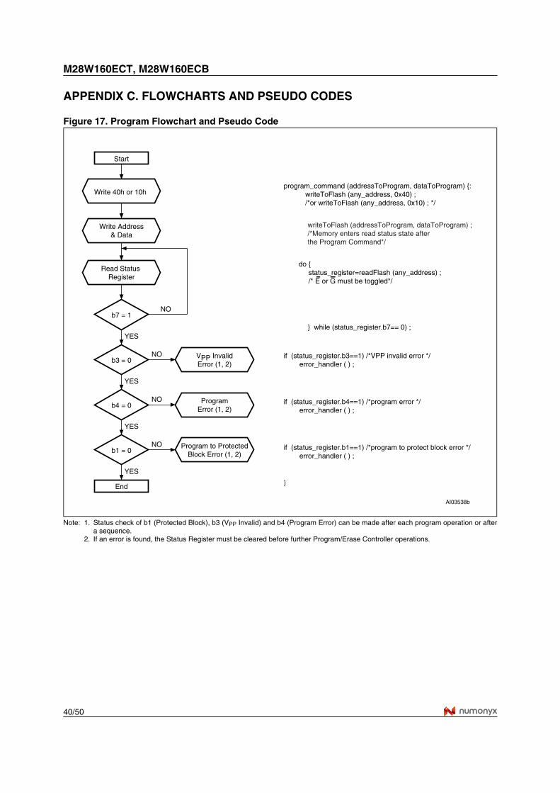
M28W160ECT, M28W160ECB
40/50
APPENDIX C. FLOWCHARTS AND PSEUDO CODES
Figure 17. Program Flowchart and Pseudo Code
Note: 1. Status check of b1 (Protected Block), b3 (VPP Invalid) and b4 (Program Error) can be made after each program operation or aftera sequence.
2. If an error is found, the Status Register must be cleared before further Program/Erase Controller operations.
Write 40h or 10h
AI03538b
Start
Write Address& Data
Read Status Register
YES
NOb7 = 1
YES
NOb3 = 0
NOb4 = 0
VPP InvalidError (1, 2)
ProgramError (1, 2)
program_command (addressToProgram, dataToProgram) {: writeToFlash (any_address, 0x40) ; /*or writeToFlash (any_address, 0x10) ; */
do { status_register=readFlash (any_address) ; /* E or G must be toggled*/
} while (status_register.b7== 0) ;
if (status_register.b3==1) /*VPP invalid error */ error_handler ( ) ;
YES
End
YES
NOb1 = 0
Program to ProtectedBlock Error (1, 2)
writeToFlash (addressToProgram, dataToProgram) ;/*Memory enters read status state after the Program Command*/
if (status_register.b4==1) /*program error */ error_handler ( ) ;
if (status_register.b1==1) /*program to protect block error */ error_handler ( ) ;
}
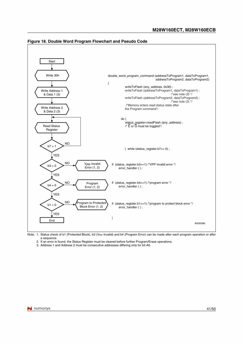
41/50
M28W160ECT, M28W160ECB
Figure 18. Double Word Program Flowchart and Pseudo Code
Note: 1. Status check of b1 (Protected Block), b3 (VPP Invalid) and b4 (Program Error) can be made after each program operation or aftera sequence.
2. If an error is found, the Status Register must be cleared before further Program/Erase operations.3. Address 1 and Address 2 must be consecutive addresses differing only for bit A0.
Write 30h
AI03539b
Start
Write Address 1& Data 1 (3)
Read Status Register
YES
NOb7 = 1
YES
NOb3 = 0
NOb4 = 0
VPP InvalidError (1, 2)
ProgramError (1, 2)
YES
End
YES
NOb1 = 0
Program to ProtectedBlock Error (1, 2)
Write Address 2& Data 2 (3)
double_word_program_command (addressToProgram1, dataToProgram1, addressToProgram2, dataToProgram2){ writeToFlash (any_address, 0x30) ; writeToFlash (addressToProgram1, dataToProgram1) ; /*see note (3) */ writeToFlash (addressToProgram2, dataToProgram2) ; /*see note (3) */ /*Memory enters read status state after the Program command*/
do { status_register=readFlash (any_address) ; /* E or G must be toggled*/
} while (status_register.b7== 0) ;
if (status_register.b3==1) /*VPP invalid error */ error_handler ( ) ;
if (status_register.b4==1) /*program error */ error_handler ( ) ;
if (status_register.b1==1) /*program to protect block error */ error_handler ( ) ;
}

M28W160ECT, M28W160ECB
42/50
Figure 19. Program Suspend & Resume Flowchart and Pseudo Code
Write 70h
AI03540b
Read Status Register
YES
NOb7 = 1
YES
NOb2 = 1
Program Continues
Write D0h
Read data fromanother address
Start
Write B0h
Program Complete
Write FFh
Read Data
program_suspend_command ( ) { writeToFlash (any_address, 0xB0) ;
writeToFlash (any_address, 0x70) ; /* read status register to check if program has already completed */
do { status_register=readFlash (any_address) ; /* E or G must be toggled*/
} while (status_register.b7== 0) ;
if (status_register.b2==0) /*program completed */ { writeToFlash (any_address, 0xFF) ; read_data ( ) ; /*read data from another block*/ /*The device returns to Read Array (as if program/erase suspend was not issued).*/
}else { writeToFlash (any_address, 0xFF) ; read_data ( ); /*read data from another address*/ writeToFlash (any_address, 0xD0) ; /*write 0xD0 to resume program*/ }}
Write FFh
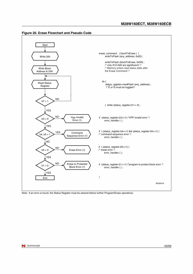
43/50
M28W160ECT, M28W160ECB
Figure 20. Erase Flowchart and Pseudo Code
Note: If an error is found, the Status Register must be cleared before further Program/Erase operations.
Write 20h
AI03541b
Start
Write Block Address & D0h
Read Status Register
YES
NOb7 = 1
YES
NOb3 = 0
YESb4, b5 = 1
VPP InvalidError (1)
CommandSequence Error (1)
NO
NOb5 = 0 Erase Error (1)
End
YES
NOb1 = 0
Erase to ProtectedBlock Error (1)
YES
erase_command ( blockToErase ) { writeToFlash (any_address, 0x20) ;
writeToFlash (blockToErase, 0xD0) ; /* only A12-A20 are significannt */ /* Memory enters read status state after the Erase Command */
} while (status_register.b7== 0) ;
do { status_register=readFlash (any_address) ; /* E or G must be toggled*/
if (status_register.b3==1) /*VPP invalid error */ error_handler ( ) ;
if ( (status_register.b4==1) && (status_register.b5==1) )/* command sequence error */ error_handler ( ) ;
if (status_register.b1==1) /*program to protect block error */ error_handler ( ) ;
if ( (status_register.b5==1) )/* erase error */ error_handler ( ) ;
}
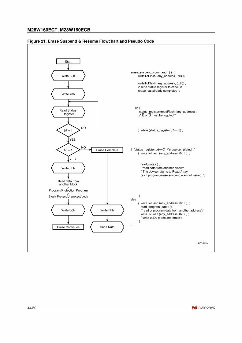
M28W160ECT, M28W160ECB
44/50
Figure 21. Erase Suspend & Resume Flowchart and Pseudo Code
Write 70h
AI03542b
Read Status Register
YES
NOb7 = 1
YES
NOb6 = 1
Erase Continues
Write D0h
Read data fromanother block
orProgram/Protection Program
orBlock Protect/Unprotect/Lock
Start
Write B0h
Erase Complete
Write FFh
Read Data
Write FFh
erase_suspend_command ( ) { writeToFlash (any_address, 0xB0) ;
writeToFlash (any_address, 0x70) ; /* read status register to check if erase has already completed */
do { status_register=readFlash (any_address) ; /* E or G must be toggled*/
} while (status_register.b7== 0) ;
if (status_register.b6==0) /*erase completed */ { writeToFlash (any_address, 0xFF) ;
read_data ( ) ; /*read data from another block*/ /*The device returns to Read Array (as if program/erase suspend was not issued).*/
}else { writeToFlash (any_address, 0xFF) ; read_program_data ( ); /*read or program data from another address*/ writeToFlash (any_address, 0xD0) ; /*write 0xD0 to resume erase*/ }}

45/50
M28W160ECT, M28W160ECB
Figure 22. Locking Operations Flowchart and Pseudo Code
Write 01h, D0h or 2Fh
AI04364
Read Block Lock States
YES
NOLocking change
confirmed?
Start
Write 60hlocking_operation_command (address, lock_operation) { writeToFlash (any_address, 0x60) ; /*configuration setup*/
if (readFlash (address) ! = locking_state_expected) error_handler () ; /*Check the locking state (see Read Block Signature table )*/
writeToFlash (any_address, 0xFF) ; /*Reset to Read Array mode*/ }
Write FFh
Write 90h
End
if (lock_operation==LOCK) /*to protect the block*/ writeToFlash (address, 0x01) ;else if (lock_operation==UNLOCK) /*to unprotect the block*/ writeToFlash (address, 0xD0) ;else if (lock_operation==LOCK-DOWN) /*to lock the block*/ writeToFlash (address, 0x2F) ;
writeToFlash (any_address, 0x90) ;
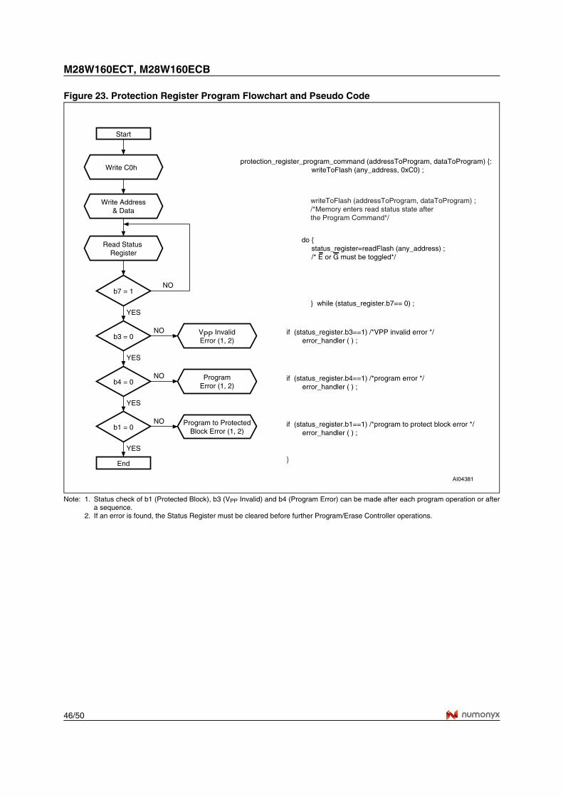
M28W160ECT, M28W160ECB
46/50
Figure 23. Protection Register Program Flowchart and Pseudo Code
Note: 1. Status check of b1 (Protected Block), b3 (VPP Invalid) and b4 (Program Error) can be made after each program operation or aftera sequence.
2. If an error is found, the Status Register must be cleared before further Program/Erase Controller operations.
Write C0h
AI04381
Start
Write Address& Data
Read Status Register
YES
NOb7 = 1
YES
NOb3 = 0
NOb4 = 0
VPP InvalidError (1, 2)
ProgramError (1, 2)
protection_register_program_command (addressToProgram, dataToProgram) {: writeToFlash (any_address, 0xC0) ;
do { status_register=readFlash (any_address) ; /* E or G must be toggled*/
} while (status_register.b7== 0) ;
if (status_register.b3==1) /*VPP invalid error */ error_handler ( ) ;
YES
End
YES
NOb1 = 0
Program to ProtectedBlock Error (1, 2)
writeToFlash (addressToProgram, dataToProgram) ;/*Memory enters read status state after the Program Command*/
if (status_register.b4==1) /*program error */ error_handler ( ) ;
if (status_register.b1==1) /*program to protect block error */ error_handler ( ) ;
}
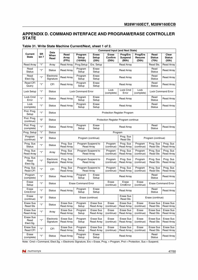
47/50
M28W160ECT, M28W160ECB
APPENDIX D. COMMAND INTERFACE AND PROGRAM/ERASE CONTROLLER STATE
Table 31. Write State Machine Current/Next, sheet 1 of 2.
Note: Cmd = Command, Elect.Sg. = Electronic Signature, Ers = Erase, Prog. = Program, Prot = Protection, Sus = Suspend.
Current State
SR bit 7
Data When Read
Command Input (and Next State)
Read Array (FFh)
ProgramSetup
(10/40h)
Erase Setup(20h)
Erase Confirm
(D0h)
Prog/Ers Suspend
(B0h)
Prog/Ers Resume
(D0h)
Read Status (70h)
Clear Status (50h)
Read Array “1” Array Read Array Prog.Setup Ers. Setup Read Array Read Sts. Read Array
Read Status
“1” Status Read ArrayProgram
SetupErase Setup
Read ArrayRead Status
Read Array
Read Elect.Sg.
“1”Electronic Signature
Read ArrayProgram
SetupErase Setup
Read ArrayRead Status
Read Array
Read CFI Query
“1” CFI Read ArrayProgram
SetupErase Setup
Read ArrayRead Status
Read Array
Lock Setup “1” Status Lock Command ErrorLock
(complete)Lock Cmd
ErrorLock
(complete) Lock Command Error
Lock Cmd Error
“1” Status Read ArrayProgram
SetupErase Setup
Read ArrayRead Status
Read Array
Lock (complete)
“1” Status Read ArrayProgram
SetupErase Setup
Read ArrayRead Status
Read Array
Prot. Prog. Setup
“1” Status Protection Register Program
Prot. Prog. (continue) “0” Status Protection Register Program continue
Prot. Prog. (complete)
“1” Status Read ArrayProgram
SetupErase Setup
Read ArrayRead Status
Read Array
Prog. Setup “1” Status Program
Program (continue)
“0” Status Program (continue)Prog. Sus Read Sts
Program (continue)
Prog. Sus Status
“1” StatusProg. Sus
Read ArrayProgram Suspend to
Read ArrayProgram
(continue)Prog. Sus
Read ArrayProgram
(continue)Prog. Sus Read Sts
Prog. Sus Read Array
Prog. Sus Read Array
“1” ArrayProg. Sus
Read ArrayProgram Suspend to
Read ArrayProgram
(continue)Prog. Sus
Read ArrayProgram
(continue)Prog. Sus Read Sts
Prog. Sus Read Array
Prog. Sus Read
Elect.Sg.“1”
Electronic Signature
Prog. Sus Read Array
Program Suspend to Read Array
Program (continue)
Prog. Sus Read Array
Program (continue)
Prog. Sus Read Sts
Prog. Sus Read Array
Prog. Sus Read CFI
“1” CFIProg. Sus
Read ArrayProgram Suspend to
Read ArrayProgram
(continue)Prog. Sus
Read ArrayProgram
(continue)Prog. Sus Read Sts
Prog. Sus Read Array
Program (complete)
“1” Status Read Array Program Setup
Erase Setup
Read Array Read Status
Read Array
Erase Setup
“1” Status Erase Command ErrorErase
(continue)Erase
CmdErrorErase
(continue)Erase Command Error
Erase Cmd.Error
“1” Status Read ArrayProgram
SetupErase Setup
Read ArrayRead Status
Read Array
Erase (continue)
“0” Status Erase (continue)Erase Sus Read Sts
Erase (continue)
Erase Sus Read Sts
“1” Status Erase Sus Read Array
ProgramSetup
Erase Sus Read Array
Erase(continue)
Erase Sus Read Array
Erase(continue)
Erase Sus Read Sts
Erase Sus Read Array
Erase Sus Read Array
“1” ArrayErase Sus Read Array
ProgramSetup
Erase Sus Read Array
Erase(continue)
Erase Sus Read Array
Erase(continue)
Erase Sus Read Sts
Erase Sus Read Array
Erase Sus Read
Elect.Sg.“1”
Electronic Signature
Erase Sus Read Array
ProgramSetup
Erase Sus Read Array
Erase(continue)
Erase Sus Read Array
Erase(continue)
Erase Sus Read Sts
Erase Sus Read Array
Erase Sus Read CFI
“1” CFIErase Sus Read Array
ProgramSetup
Erase Sus Read Array
Erase(continue)
Erase Sus Read Array
Erase(continue)
Erase Sus Read Sts
Erase Sus Read Array
Erase (complete)
“1” Status Read ArrayProgram
SetupErase Setup
Read ArrayRead Status
Read Array
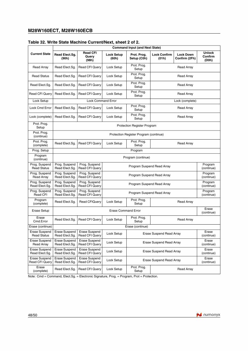
M28W160ECT, M28W160ECB
48/50
Table 32. Write State Machine Current/Next, sheet 2 of 2.
Note: Cmd = Command, Elect.Sg. = Electronic Signature, Prog. = Program, Prot = Protection.
Current State
Command Input (and Next State)
Read Elect.Sg.(90h)
Read CFI Query (98h)
Lock Setup(60h)
Prot. Prog. Setup (C0h)
Lock Confirm (01h)
Lock Down Confirm (2Fh)
Unlock Confirm
(D0h)
Read Array Read Elect.Sg. Read CFI Query Lock SetupProt. Prog.
SetupRead Array
Read Status Read Elect.Sg. Read CFI Query Lock Setup Prot. Prog. Setup
Read Array
Read Elect.Sg. Read Elect.Sg. Read CFI Query Lock SetupProt. Prog.
SetupRead Array
Read CFI Query Read Elect.Sg. Read CFI Query Lock SetupProt. Prog.
SetupRead Array
Lock Setup Lock Command Error Lock (complete)
Lock Cmd Error Read Elect.Sg. Read CFI Query Lock SetupProt. Prog.
SetupRead Array
Lock (complete) Read Elect.Sg. Read CFI Query Lock SetupProt. Prog.
SetupRead Array
Prot. Prog. Setup
Protection Register Program
Prot. Prog. (continue)
Protection Register Program (continue)
Prot. Prog. (complete)
Read Elect.Sg. Read CFI Query Lock SetupProt. Prog.
SetupRead Array
Prog. Setup Program
Program (continue)
Program (continue)
Prog. SuspendRead Status
Prog. Suspend Read Elect.Sg.
Prog. Suspend Read CFI Query
Program Suspend Read Array Program (continue)
Prog. Suspend Read Array
Prog. Suspend Read Elect.Sg.
Prog. Suspend Read CFI Query
Program Suspend Read ArrayProgram
(continue)
Prog. Suspend Read Elect.Sg.
Prog. Suspend Read Elect.Sg.
Prog. Suspend Read CFI Query
Program Suspend Read ArrayProgram
(continue)
Prog. Suspend Read CFI
Prog. Suspend Read Elect.Sg.
Prog. Suspend Read CFI Query
Program Suspend Read ArrayProgram
(continue)
Program (complete)
Read Elect.Sg. Read CFIQuery Lock Setup Prot. Prog. Setup
Read Array
Erase Setup Erase Command ErrorErase
(continue)
Erase Cmd.Error
Read Elect.Sg. Read CFI Query Lock SetupProt. Prog.
SetupRead Array
Erase (continue) Erase (continue)
Erase Suspend Read Status
Erase Suspend Read Elect.Sg.
Erase Suspend Read CFI Query
Lock Setup Erase Suspend Read ArrayErase
(continue)
Erase Suspend Read Array
Erase Suspend Read Elect.Sg.
Erase Suspend Read CFI Query
Lock Setup Erase Suspend Read ArrayErase
(continue)
Erase Suspend Read Elect.Sg.
Erase Suspend Read Elect.Sg.
Erase Suspend Read CFI Query
Lock Setup Erase Suspend Read ArrayErase
(continue)
Erase Suspend Read CFI Query
Erase Suspend Read Elect.Sg.
Erase Suspend Read CFI Query
Lock Setup Erase Suspend Read ArrayErase
(continue)
Erase (complete)
Read Elect.Sg. Read CFI Query Lock SetupProt. Prog.
SetupRead Array
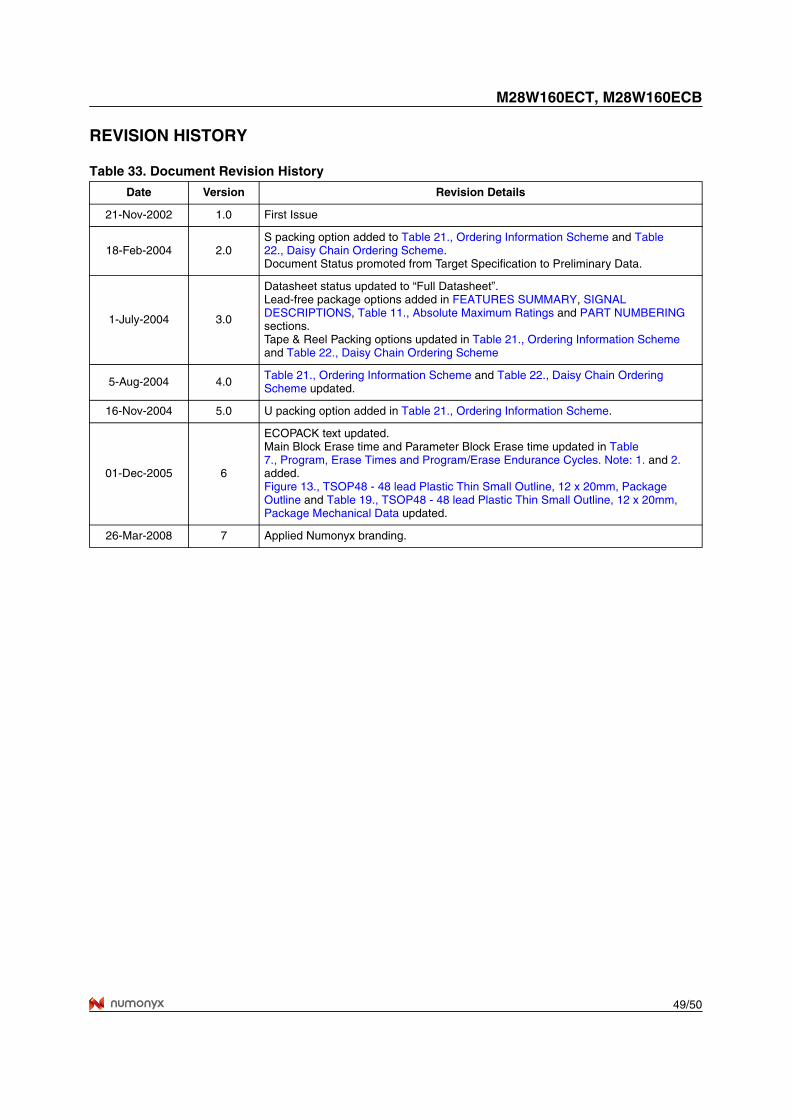
49/50
M28W160ECT, M28W160ECB
REVISION HISTORY
Table 33. Document Revision History
Date Version Revision Details
21-Nov-2002 1.0 First Issue
18-Feb-2004 2.0S packing option added to Table 21., Ordering Information Scheme and Table 22., Daisy Chain Ordering Scheme.Document Status promoted from Target Specification to Preliminary Data.
1-July-2004 3.0
Datasheet status updated to “Full Datasheet”.Lead-free package options added in FEATURES SUMMARY, SIGNAL DESCRIPTIONS, Table 11., Absolute Maximum Ratings and PART NUMBERING sections.Tape & Reel Packing options updated in Table 21., Ordering Information Scheme and Table 22., Daisy Chain Ordering Scheme
5-Aug-2004 4.0 Table 21., Ordering Information Scheme and Table 22., Daisy Chain Ordering Scheme updated.
16-Nov-2004 5.0 U packing option added in Table 21., Ordering Information Scheme.
01-Dec-2005 6
ECOPACK text updated.Main Block Erase time and Parameter Block Erase time updated in Table 7., Program, Erase Times and Program/Erase Endurance Cycles. Note: 1. and 2. added.Figure 13., TSOP48 - 48 lead Plastic Thin Small Outline, 12 x 20mm, Package Outline and Table 19., TSOP48 - 48 lead Plastic Thin Small Outline, 12 x 20mm, Package Mechanical Data updated.
26-Mar-2008 7 Applied Numonyx branding.
M28W160ECT, M28W160ECB
50/50
Please Read Carefully:
INFORMATION IN THIS DOCUMENT IS PROVIDED IN CONNECTION WITH NUMONYX™ PRODUCTS. NO LICENSE, EXPRESS OR IMPLIED, BY ESTOPPEL OR OTHERWISE, TO ANY INTELLECTUAL PROPERTY RIGHTS IS GRANTED BY THIS DOCUMENT. EXCEPT AS PROVIDED IN NUMONYX'S TERMS AND CONDITIONS OF SALE FOR SUCH PRODUCTS, NUMONYX ASSUMES NO LIABILITY
WHATSOEVER, AND NUMONYX DISCLAIMS ANY EXPRESS OR IMPLIED WARRANTY, RELATING TO SALE AND/OR USE OF NUMONYX PRODUCTS INCLUDING LIABILITY OR WARRANTIES RELATING TO FITNESS FOR A PARTICULAR PURPOSE, MERCHANTABILITY, OR INFRINGEMENT OF ANY PATENT, COPYRIGHT OR OTHER INTELLECTUAL PROPERTY RIGHT.
Numonyx products are not intended for use in medical, life saving, life sustaining, critical control or safety systems, or in nuclear facility applications.
Numonyx may make changes to specifications and product descriptions at any time, without notice.
Numonyx, B.V. may have patents or pending patent applications, trademarks, copyrights, or other intellectual property rights that relate to the presented subject matter. The furnishing of documents and other materials and information does not provide any license, express or
implied, by estoppel or otherwise, to any such patents, trademarks, copyrights, or other intellectual property rights.
Designers must not rely on the absence or characteristics of any features or instructions marked “reserved” or “undefined.” Numonyx reserves these for future definition and shall have no responsibility whatsoever for conflicts or incompatibilities arising from future changes to them.
Contact your local Numonyx sales office or your distributor to obtain the latest specifications and before placing your product order.
Copies of documents which have an order number and are referenced in this document, or other Numonyx literature may be obtained by visiting Numonyx's website at http://www.numonyx.com.
Numonyx StrataFlash is a trademark or registered trademark of Numonyx or its subsidiaries in the United States and other countries.
*Other names and brands may be claimed as the property of others.
Copyright © 11/5/7, Numonyx, B.V., All Rights Reserved.