Embed Size (px)
Citation preview
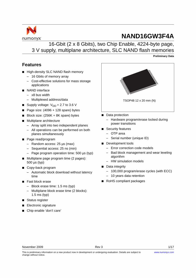
Preliminary Data
This is preliminary information on a new product now in development or undergoing evaluation. Details are subject to change without notice.
November 2009 Rev 3 1/17
1
NAND16GW3F4A16-Gbit (2 x 8 Gbits), two Chip Enable, 4224-byte page,
3 V supply, multiplane architecture, SLC NAND flash memories
Features High-density SLC NAND flash memory
– 16 Gbits of memory array– Cost-effective solutions for mass storage
applications
NAND interface– x8 bus width– Multiplexed address/data
Supply voltage: VDD = 2.7 to 3.6 V
Page size: (4096 + 128 spare) bytes
Block size: (256K + 8K spare) bytes
Multiplane architecture– Array split into two independent planes– All operations can be performed on both
planes simultaneously
Page read/program– Random access: 25 µs (max)– Sequential access: 25 ns (min)– Page program operation time: 500 µs (typ)
Multiplane page program time (2 pages): 500 µs (typ)
Copy-back program– Automatic block download without latency
time
Fast block erase– Block erase time: 1.5 ms (typ)– Multiplane block erase time (2 blocks):
1.5 ms (typ)
Status register
Electronic signature
Chip enable ‘don’t care’
Data protection– Hardware program/erase locked during
power transitions
Security features– OTP area– Serial number (unique ID)
Development tools– Error correction code models– Bad block management and wear leveling
algorithm– HW simulation models
Data integrity– 100,000 program/erase cycles (with ECC)– 10 years data retention
RoHS compliant packages
TSOP48 12 x 20 mm (N)
www.numonyx.com
NAND16GW3F4A
2/17
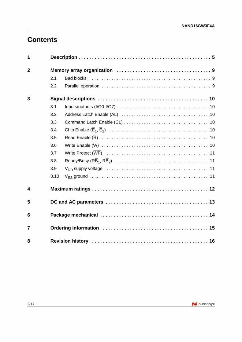
Contents
1 Description . . . . . . . . . . . . . . . . . . . . . . . . . . . . . . . . . . . . . . . . . . . . . . . . . 5
2 Memory array organization . . . . . . . . . . . . . . . . . . . . . . . . . . . . . . . . . . . 9
2.1 Bad blocks . . . . . . . . . . . . . . . . . . . . . . . . . . . . . . . . . . . . . . . . . . . . . . . . . 9
2.2 Parallel operation . . . . . . . . . . . . . . . . . . . . . . . . . . . . . . . . . . . . . . . . . . . . 9
3 Signal descriptions . . . . . . . . . . . . . . . . . . . . . . . . . . . . . . . . . . . . . . . . . 10
3.1 Inputs/outputs (I/O0-I/O7) . . . . . . . . . . . . . . . . . . . . . . . . . . . . . . . . . . . . . 10
3.2 Address Latch Enable (AL) . . . . . . . . . . . . . . . . . . . . . . . . . . . . . . . . . . . 10
3.3 Command Latch Enable (CL) . . . . . . . . . . . . . . . . . . . . . . . . . . . . . . . . . . 10
3.4 Chip Enable (E1, E2) . . . . . . . . . . . . . . . . . . . . . . . . . . . . . . . . . . . . . . . . 10
3.5 Read Enable (R) . . . . . . . . . . . . . . . . . . . . . . . . . . . . . . . . . . . . . . . . . . . . 10
3.6 Write Enable (W) . . . . . . . . . . . . . . . . . . . . . . . . . . . . . . . . . . . . . . . . . . . 10
3.7 Write Protect (WP) . . . . . . . . . . . . . . . . . . . . . . . . . . . . . . . . . . . . . . . . . . 11
3.8 Ready/Busy (RB1, RB2) . . . . . . . . . . . . . . . . . . . . . . . . . . . . . . . . . . . . . . 11
3.9 VDD supply voltage . . . . . . . . . . . . . . . . . . . . . . . . . . . . . . . . . . . . . . . . . . 11
3.10 VSS ground . . . . . . . . . . . . . . . . . . . . . . . . . . . . . . . . . . . . . . . . . . . . . . . . 11
4 Maximum ratings . . . . . . . . . . . . . . . . . . . . . . . . . . . . . . . . . . . . . . . . . . . 12
5 DC and AC parameters . . . . . . . . . . . . . . . . . . . . . . . . . . . . . . . . . . . . . . 13
6 Package mechanical . . . . . . . . . . . . . . . . . . . . . . . . . . . . . . . . . . . . . . . . 14
7 Ordering information . . . . . . . . . . . . . . . . . . . . . . . . . . . . . . . . . . . . . . . 15
8 Revision history . . . . . . . . . . . . . . . . . . . . . . . . . . . . . . . . . . . . . . . . . . . 16
NAND16GW3F4A
3/17
List of tables
Table 1. Device summary . . . . . . . . . . . . . . . . . . . . . . . . . . . . . . . . . . . . . . . . . . . . . . . . . . . . . . . . . . 5Table 2. Signal names . . . . . . . . . . . . . . . . . . . . . . . . . . . . . . . . . . . . . . . . . . . . . . . . . . . . . . . . . . . . 7Table 3. Valid blocks. . . . . . . . . . . . . . . . . . . . . . . . . . . . . . . . . . . . . . . . . . . . . . . . . . . . . . . . . . . . . . 9Table 4. Absolute maximum ratings . . . . . . . . . . . . . . . . . . . . . . . . . . . . . . . . . . . . . . . . . . . . . . . . . 12Table 5. Operating and AC measurement conditions. . . . . . . . . . . . . . . . . . . . . . . . . . . . . . . . . . . . 13Table 6. Capacitance . . . . . . . . . . . . . . . . . . . . . . . . . . . . . . . . . . . . . . . . . . . . . . . . . . . . . . . . . . . . 13Table 7. TSOP48 - 48 lead plastic thin small outline, 12 x 20 mm, package mechanical data. . . . . 14Table 8. Ordering information scheme . . . . . . . . . . . . . . . . . . . . . . . . . . . . . . . . . . . . . . . . . . . . . . . 15Table 9. Document revision history . . . . . . . . . . . . . . . . . . . . . . . . . . . . . . . . . . . . . . . . . . . . . . . . . 16
NAND16GW3F4A
4/17
List of figures
Figure 1. Functional block diagram . . . . . . . . . . . . . . . . . . . . . . . . . . . . . . . . . . . . . . . . . . . . . . . . . . . 6Figure 2. Logic diagram . . . . . . . . . . . . . . . . . . . . . . . . . . . . . . . . . . . . . . . . . . . . . . . . . . . . . . . . . . . . 7Figure 3. TSOP48 connections . . . . . . . . . . . . . . . . . . . . . . . . . . . . . . . . . . . . . . . . . . . . . . . . . . . . . . 8Figure 4. TSOP48 - 48 lead plastic thin small outline, 12 x 20 mm, package outline . . . . . . . . . . . . 14
NAND16GW3F4A Description
5/17
1 Description
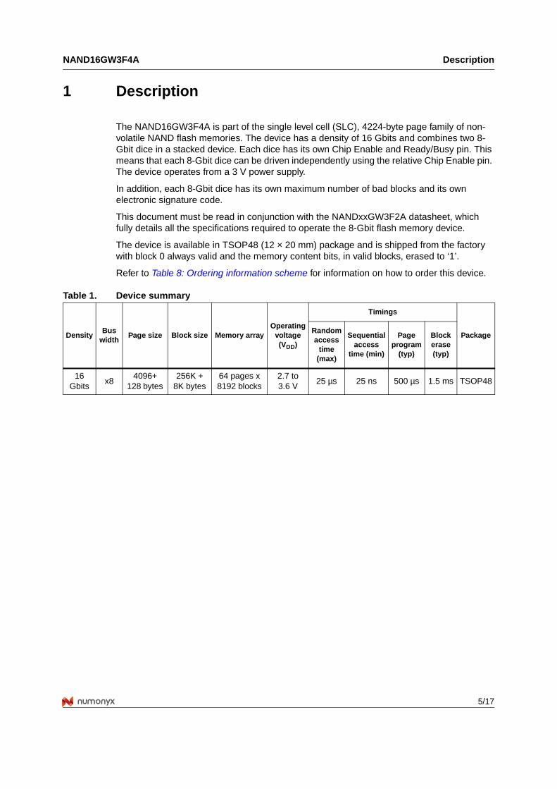
The NAND16GW3F4A is part of the single level cell (SLC), 4224-byte page family of non-volatile NAND flash memories. The device has a density of 16 Gbits and combines two 8-Gbit dice in a stacked device. Each dice has its own Chip Enable and Ready/Busy pin. This means that each 8-Gbit dice can be driven independently using the relative Chip Enable pin. The device operates from a 3 V power supply.
In addition, each 8-Gbit dice has its own maximum number of bad blocks and its own electronic signature code.
This document must be read in conjunction with the NANDxxGW3F2A datasheet, which fully details all the specifications required to operate the 8-Gbit flash memory device.
The device is available in TSOP48 (12 × 20 mm) package and is shipped from the factory with block 0 always valid and the memory content bits, in valid blocks, erased to ‘1’.
Refer to Table 8: Ordering information scheme for information on how to order this device.
Table 1. Device summary
DensityBus
widthPage size Block size Memory array
Operating voltage (VDD)
Timings
Package Random access
time (max)
Sequential access
time (min)
Page program
(typ)
Block erase (typ)
16 Gbits
x8 4096+
128 bytes 256K +
8K bytes 64 pages x 8192 blocks
2.7 to 3.6 V
25 µs 25 ns 500 µs 1.5 ms TSOP48
Description NAND16GW3F4A
6/17
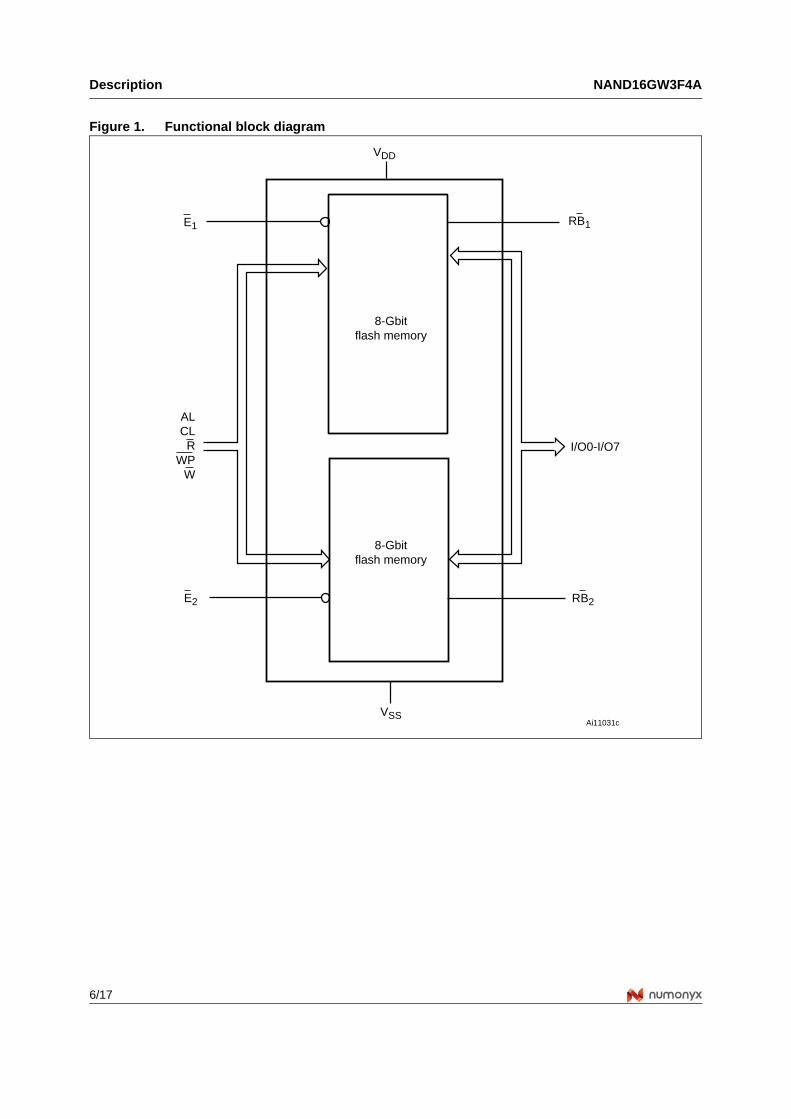
Figure 1. Functional block diagram
Ai11031c
E2
I/O0-I/O7
VDD
ALCL
RWP
W
8-Gbitflash memory
8-Gbitflash memory
E1 RB1
VSS
RB2
NAND16GW3F4A Description
7/17
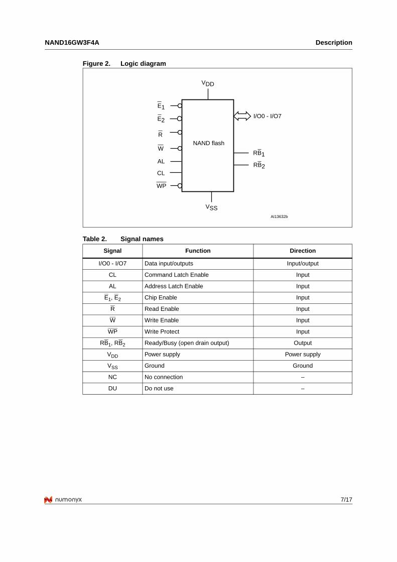
Figure 2. Logic diagram
Table 2. Signal names
Signal Function Direction
I/O0 - I/O7 Data input/outputs Input/output
CL Command Latch Enable Input
AL Address Latch Enable Input
E1, E2 Chip Enable Input
R Read Enable Input
W Write Enable Input
WP Write Protect Input
RB1, RB2 Ready/Busy (open drain output) Output
VDD Power supply Power supply
VSS Ground Ground
NC No connection –
DU Do not use –
AI13632b
I/O0 - I/O7
VDD
NAND flashW
VSS
WP
AL
CL
E1
R
RB1
E2
RB2
Description NAND16GW3F4A
8/17
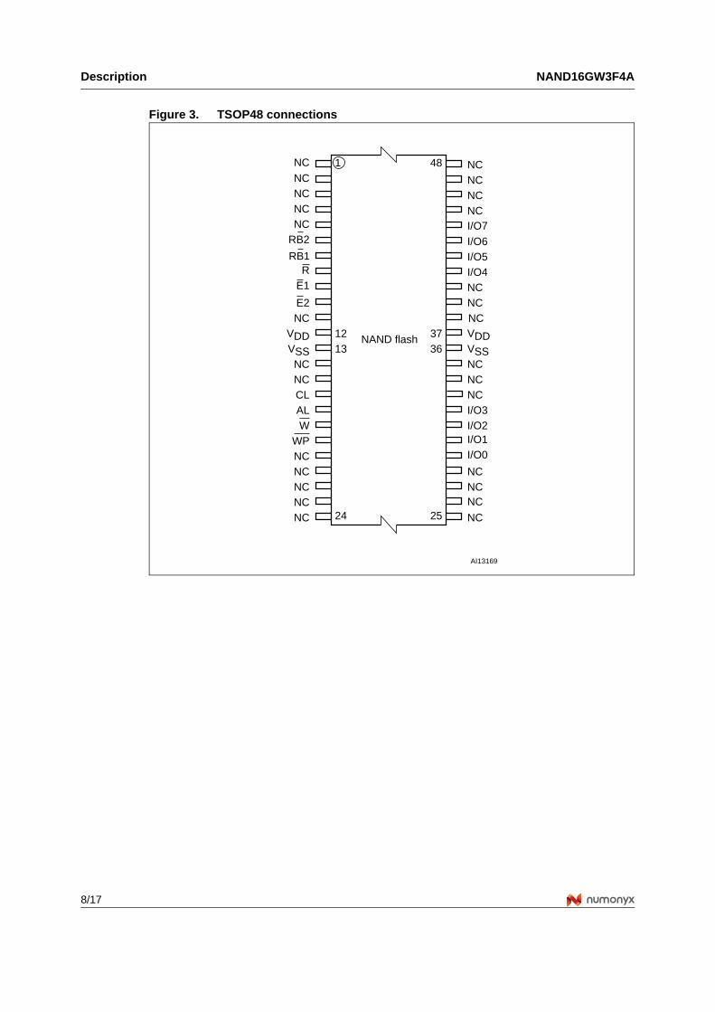
Figure 3. TSOP48 connections
I/O3I/O2
I/O6
RRB1
RB2
I/O4
I/O7
AI13169
NAND flash12
1
13
24 25
3637
48
E1
I/O1
NCNC
NC
NC
NC
NC
NCWP
W
NC
NC
NC
VSS
VDD
AL
E2NC
CL
NC
I/O5
NCNC
NC
I/O0
NCNC
NCNC
NCVDD
NCNCNC
VSS
NC
NC
NCNC
NAND16GW3F4A Memory array organization
9/17
2 Memory array organization
The memory array is split into two dice. Each dice is comprised of NAND structures where 32 cells are connected in series.
The array is organized into blocks, where each block contains 64 pages. The array is split into two areas: the main area and the spare area. The main area of the array stores data, whereas the spare area typically stores software flags or bad block identification.
The pages are split into a 4096-byte main area and a spare area of 128 bytes.
2.1 Bad blocksThe NAND16GW3F4A device may contain bad blocks, where the reliability of blocks that contain one or more invalid bits is not guaranteed. Additional bad blocks may develop during the lifetime of the device.
The bad block information is written prior to shipping (refer to the bad block management section of the NANDxxGW3F2A datasheet for more details).
Table 3: Valid blocks shows the minimum number of valid blocks. The values shown include both the bad blocks that are present when the device is shipped and the bad blocks that could develop later on. Each 8-Gbit dice can have the same maximum number of bad blocks.
These blocks need to be managed using bad blocks management and block replacement (refer to the software algorithms section of the NANDxxGW3F2A datasheet).
2.2 Parallel operationThe NAND16GW3F4A is composed of two 8-Gbit dice, each one driven by its Chip Enable pin (E1 and E2, respectively). It is possible to drive the two 8-Gbit dice in parallel, thus increasing the throughput in Mbyte/s.
When one of the two dice is in a busy state, every operation can be issued on the other available dice.
Table 3. Valid blocks
Density of device Minimum Maximum
16 Gbits 8032 8192
Signal descriptions NAND16GW3F4A
10/17
3 Signal descriptions
See Figure 1: Functional block diagram, and Table 2: Signal names for a brief overview of the signals connected to this device.
3.1 Inputs/outputs (I/O0-I/O7)Input/outputs 0 to 7 are used to input the selected address, output the data during a read operation, or input a command or data during a write operation. The inputs are latched on the rising edge of Write Enable. I/O0-I/O7 are left floating when the device is deselected or the outputs are disabled.
3.2 Address Latch Enable (AL)The Address Latch Enable activates the latching of the address inputs in the command interface. When AL is High, the inputs are latched on the rising edge of Write Enable.
3.3 Command Latch Enable (CL)The Command Latch Enable activates the latching of the command inputs in the command interface. When CL is High, the inputs are latched on the rising edge of Write Enable.
3.4 Chip Enable (E1, E2)The Chip Enable input activates the memory control logic, input buffers, decoders and sense amplifiers. When Chip Enable is Low, VIL, the device is selected. If Chip Enable goes High, VIH, while the device is busy, the device remains selected and does not go into standby mode.
3.5 Read Enable (R)The Read Enable pin, R, controls the sequential data output during read operations. Data is valid tRLQV after the falling edge of R. The falling edge of R also increments the internal column address counter by one.
3.6 Write Enable (W)The Write Enable input, W, controls writing to the command interface, input address, and data latches. Both addresses and data are latched on the rising edge of Write Enable.
During power-up and power-down a recovery time of 10 µs (min) is required before the command interface is ready to accept a command. It is recommended to keep Write Enable High during the recovery time.
NAND16GW3F4A Signal descriptions
11/17
3.7 Write Protect (WP)The Write Protect pin is an input that gives a hardware protection against unwanted program or erase operations. When Write Protect is Low, VIL, the device does not accept any program or erase operations.
It is recommended to keep the Write Protect pin Low, VIL, during power-up and power-down.
3.8 Ready/Busy (RB1, RB2)The Ready/Busy output, RB1 and RB2, is an open-drain output that can identify if the P/E/R controller is currently active.
When Ready/Busy is Low, VOL, a read, program or erase operation is in progress. When the operation completes, Ready/Busy goes High, VOH.
The use of an open-drain output allows the Ready/Busy pins from several memories to be connected to a single pull-up resistor. A Low indicates that one, or more, of the memories is busy.
During power-up and power-down a minimum recovery time of 10 µs is required before the command interface is ready to accept a command. During this period the Ready/Busy signal is Low, VOL.
Refer to the Ready/Busy signal electrical characteristics section of the NANDxxGW3F2A datasheet for details on how to calculate the value of the pull-up resistor.
3.9 VDD supply voltageVDD provides the power supply to the internal core of the memory device. It is the main power supply for operations (read, program, and erase).
An internal voltage detector disables all functions whenever VDD is below VLKO to protect the device from any involuntary program/erase during power-transitions.
Each device in a system should have VDD decoupled with a 0.1 µF capacitor. The PCB track widths should be sufficient to carry the required program and erase currents.
3.10 VSS groundGround, VSS, is the reference for the power supply. It must be connected to the system ground.
Maximum ratings NAND16GW3F4A
12/17
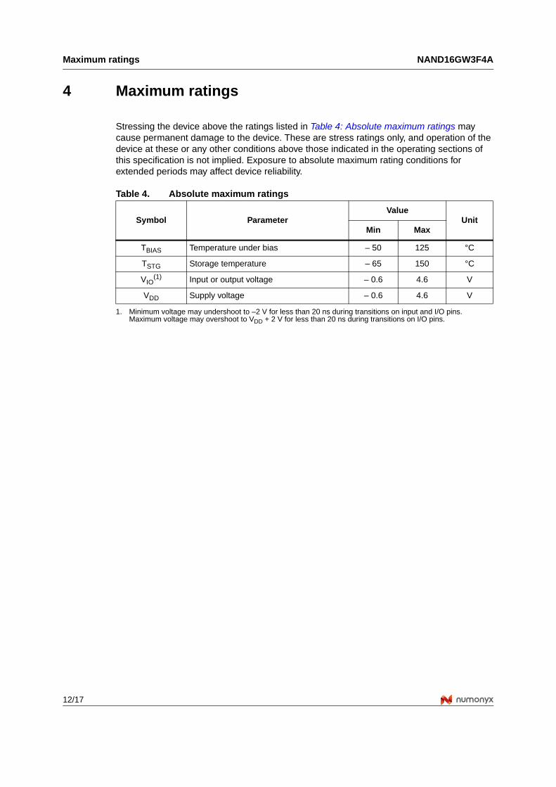
4 Maximum ratings
Stressing the device above the ratings listed in Table 4: Absolute maximum ratings may cause permanent damage to the device. These are stress ratings only, and operation of the device at these or any other conditions above those indicated in the operating sections of this specification is not implied. Exposure to absolute maximum rating conditions for extended periods may affect device reliability.
Table 4. Absolute maximum ratings
Symbol ParameterValue
UnitMin Max
TBIAS Temperature under bias – 50 125 °C
TSTG Storage temperature – 65 150 °C
VIO(1)
1. Minimum voltage may undershoot to –2 V for less than 20 ns during transitions on input and I/O pins. Maximum voltage may overshoot to VDD + 2 V for less than 20 ns during transitions on I/O pins.
Input or output voltage – 0.6 4.6 V
VDD Supply voltage – 0.6 4.6 V
NAND16GW3F4A DC and AC parameters
13/17
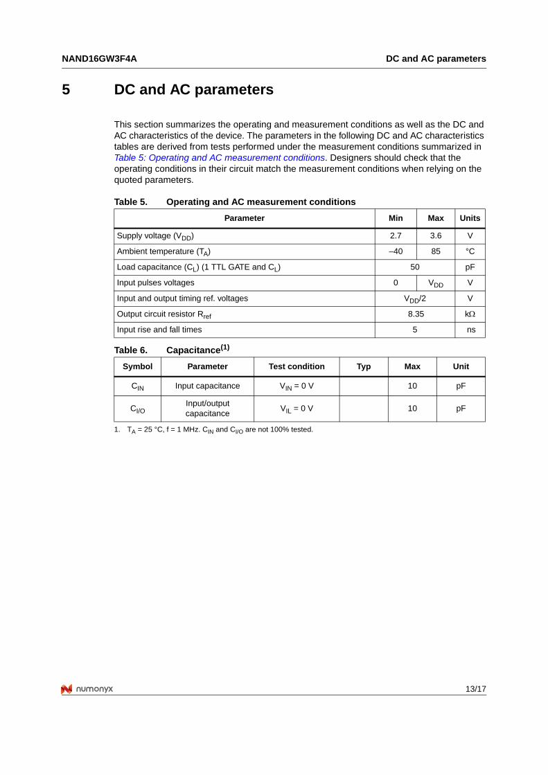
5 DC and AC parameters
This section summarizes the operating and measurement conditions as well as the DC and AC characteristics of the device. The parameters in the following DC and AC characteristics tables are derived from tests performed under the measurement conditions summarized in Table 5: Operating and AC measurement conditions. Designers should check that the operating conditions in their circuit match the measurement conditions when relying on the quoted parameters.
Table 5. Operating and AC measurement conditions
Parameter Min Max Units
Supply voltage (VDD) 2.7 3.6 V
Ambient temperature (TA) –40 85 °C
Load capacitance (CL) (1 TTL GATE and CL) 50 pF
Input pulses voltages 0 VDD V
Input and output timing ref. voltages VDD/2 V
Output circuit resistor Rref 8.35 kΩ
Input rise and fall times 5 ns
Table 6. Capacitance(1)
1. TA = 25 °C, f = 1 MHz. CIN and CI/O are not 100% tested.
Symbol Parameter Test condition Typ Max Unit
CIN Input capacitance VIN = 0 V 10 pF
CI/OInput/output capacitance
VIL = 0 V 10 pF
Package mechanical NAND16GW3F4A
14/17
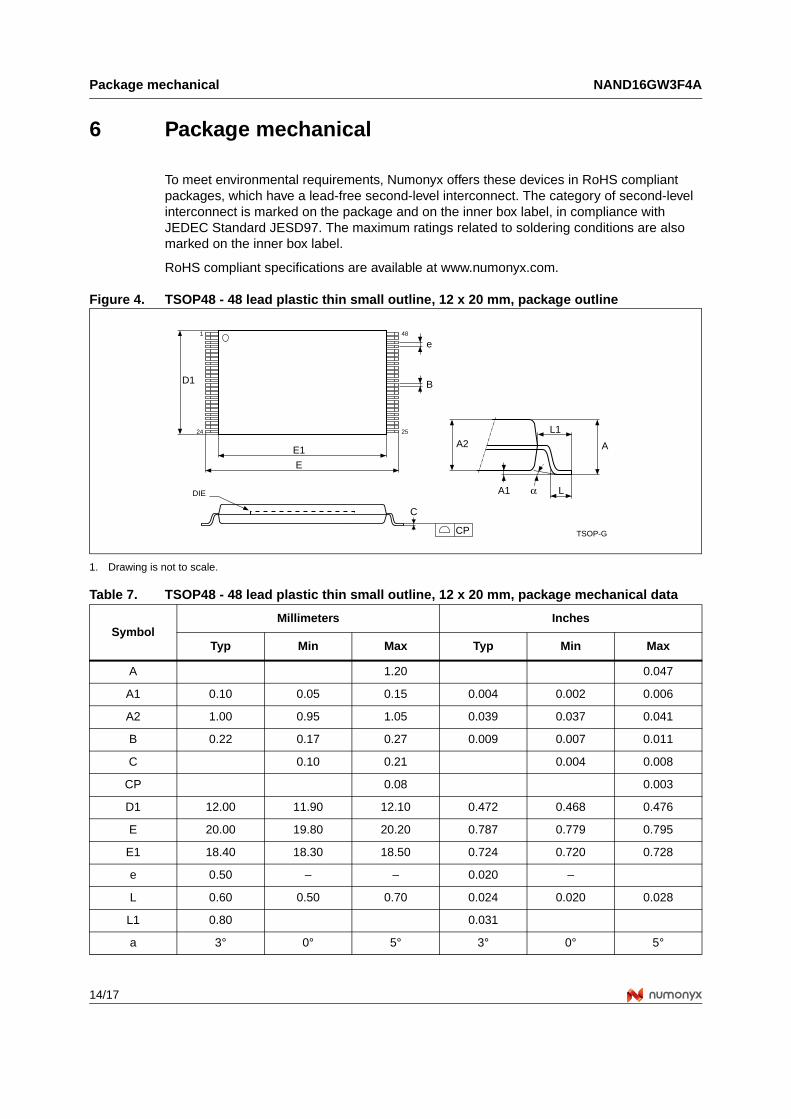
6 Package mechanical
To meet environmental requirements, Numonyx offers these devices in RoHS compliant packages, which have a lead-free second-level interconnect. The category of second-level interconnect is marked on the package and on the inner box label, in compliance with JEDEC Standard JESD97. The maximum ratings related to soldering conditions are also marked on the inner box label.
RoHS compliant specifications are available at www.numonyx.com.
Figure 4. TSOP48 - 48 lead plastic thin small outline, 12 x 20 mm, package outline
1. Drawing is not to scale.
TSOP-G
B
e
DIE
C
LA1 α
E1
E
AA2
1
24
48
25
D1
L1
CP
Table 7. TSOP48 - 48 lead plastic thin small outline, 12 x 20 mm, package mechanical data
SymbolMillimeters Inches
Typ Min Max Typ Min Max
A 1.20 0.047
A1 0.10 0.05 0.15 0.004 0.002 0.006
A2 1.00 0.95 1.05 0.039 0.037 0.041
B 0.22 0.17 0.27 0.009 0.007 0.011
C 0.10 0.21 0.004 0.008
CP 0.08 0.003
D1 12.00 11.90 12.10 0.472 0.468 0.476
E 20.00 19.80 20.20 0.787 0.779 0.795
E1 18.40 18.30 18.50 0.724 0.720 0.728
e 0.50 – – 0.020 –
L 0.60 0.50 0.70 0.024 0.020 0.028
L1 0.80 0.031
a 3° 0° 5° 3° 0° 5°
NAND16GW3F4A Ordering information
15/17
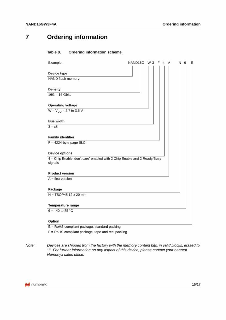
7 Ordering information
Note: Devices are shipped from the factory with the memory content bits, in valid blocks, erased to ‘1’. For further information on any aspect of this device, please contact your nearest Numonyx sales office.
Table 8. Ordering information scheme
Example: NAND16G W 3 F 4 A N 6 E
Device type
NAND flash memory
Density
16G = 16 Gbits
Operating voltage
W = VDD = 2.7 to 3.6 V
Bus width
3 = x8
Family identifier
F = 4224-byte page SLC
Device options
4 = Chip Enable ‘don't care’ enabled with 2 Chip Enable and 2 Ready/Busy signals
Product version
A = first version
Package
N = TSOP48 12 x 20 mm
Temperature range
6 = −40 to 85 °C
Option
E = RoHS compliant package, standard packing
F = RoHS compliant package, tape and reel packing
Revision history NAND16GW3F4A
16/17
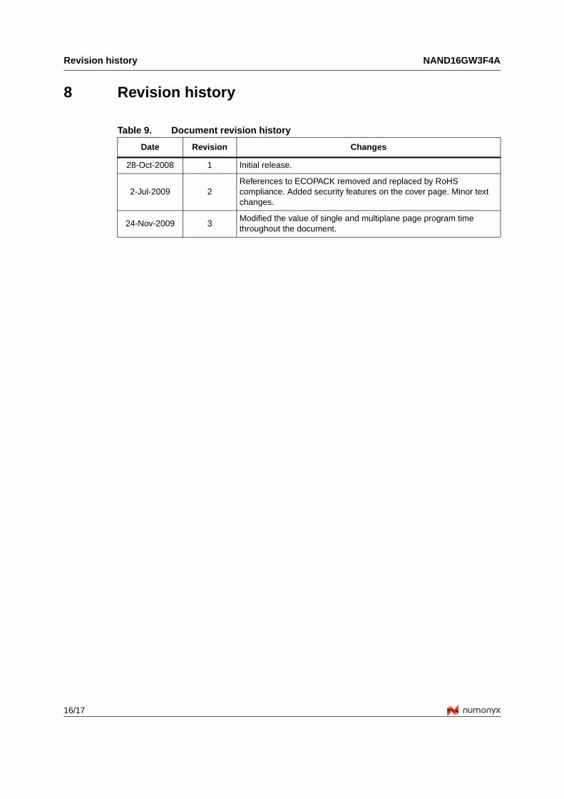
8 Revision history
Table 9. Document revision history
Date Revision Changes
28-Oct-2008 1 Initial release.
2-Jul-2009 2References to ECOPACK removed and replaced by RoHS compliance. Added security features on the cover page. Minor text changes.
24-Nov-2009 3Modified the value of single and multiplane page program time throughout the document.
NAND16GW3F4A
17/17
Please Read Carefully:
INFORMATION IN THIS DOCUMENT IS PROVIDED IN CONNECTION WITH NUMONYX™ PRODUCTS. NO LICENSE, EXPRESS OR IMPLIED, BY ESTOPPEL OR OTHERWISE, TO ANY INTELLECTUAL PROPERTY RIGHTS IS GRANTED BY THIS DOCUMENT. EXCEPT AS PROVIDED IN NUMONYX'S TERMS AND CONDITIONS OF SALE FOR SUCH PRODUCTS, NUMONYX ASSUMES NO LIABILITY
WHATSOEVER, AND NUMONYX DISCLAIMS ANY EXPRESS OR IMPLIED WARRANTY, RELATING TO SALE AND/OR USE OF NUMONYX PRODUCTS INCLUDING LIABILITY OR WARRANTIES RELATING TO FITNESS FOR A PARTICULAR PURPOSE, MERCHANTABILITY, OR INFRINGEMENT OF ANY PATENT, COPYRIGHT OR OTHER INTELLECTUAL PROPERTY RIGHT.
Numonyx products are not intended for use in medical, life saving, life sustaining, critical control or safety systems, or in nuclear facility applications.
Numonyx may make changes to specifications and product descriptions at any time, without notice.
Numonyx, B.V. may have patents or pending patent applications, trademarks, copyrights, or other intellectual property rights that relate to the presented subject matter. The furnishing of documents and other materials and information does not provide any license, express or implied,
by estoppel or otherwise, to any such patents, trademarks, copyrights, or other intellectual property rights.
Designers must not rely on the absence or characteristics of any features or instructions marked “reserved” or “undefined.” Numonyx reserves these for future definition and shall have no responsibility whatsoever for conflicts or incompatibilities arising from future changes to them.
Contact your local Numonyx sales office or your distributor to obtain the latest specifications and before placing your product order.
Copies of documents which have an order number and are referenced in this document, or other Numonyx literature may be obtained by visiting Numonyx's website at http://www.numonyx.com.
Numonyx StrataFlash is a trademark or registered trademark of Numonyx or its subsidiaries in the United States and other countries.
*Other names and brands may be claimed as the property of others.
Copyright © 11/5/7, Numonyx, B.V., All Rights Reserved.